Use of FTDI devices in life support and/or safety applications is entirely at the user’s risk, and the user agrees to defend, indemnify and hold FTDI harmless from any and all damages, claims, suits or expense resulting from such use. Future Technology Devices International Limited (FTDI) Unit 1, 2 Seaward Place, Glasgow G41 1HH, United Kingdom Tel.: +44 (0) 141 429 2777 Fax: + 44 (0) 141 429 2758 Web Site: http://ftdichip.com Copyright © 2014 Future Technology Devices International Limited Application Note AN_260 IR Remote Control Implementation by Java D2XX Version 1.0 Issue Date: 2013-09-25 This application note illustrates how NEC IR (38 KHz), RC 5, and RC 6 waveforms are generated by an Android device using Java D2XX with an FT-X chip working in Async bit-bang mode with minimum hardware cost. Also illustrates using Sync bit-bang mode to perform continuous reading.

Welcome message from author
This document is posted to help you gain knowledge. Please leave a comment to let me know what you think about it! Share it to your friends and learn new things together.
Transcript
Use of FTDI devices in life support and/or safety applications is entirely at the user’s risk, and the user agrees to defend, indemnify and hold FTDI harmless from any and all damages, claims, suits
or expense resulting from such use.
Future Technology Devices International Limited (FTDI) Unit 1, 2 Seaward Place, Glasgow G41 1HH, United Kingdom Tel.: +44 (0) 141 429 2777 Fax: + 44 (0) 141 429 2758
Web Site: http://ftdichip.com Copyright © 2014 Future Technology Devices International Limited
Application Note
AN_260
IR Remote Control Implementation by Java D2XX
Version 1.0
Issue Date: 2013-09-25
This application note illustrates how NEC IR (38 KHz), RC 5, and RC 6 waveforms are generated by an Android device using Java D2XX with an FT-X chip working in Async bit-bang mode with minimum hardware cost. Also illustrates using Sync bit-bang mode to perform continuous reading.

Application Note
AN_260 IR Remote Control Implementation by Java D2XX Version 1.0
Document Reference No.: FT_000901 Clearance No.: FTDI# 370
1 Product Page
Document Feedback Copyright © 2014 Future Technology Devices International Limited
Table of Contents
1 Introduction .................................................................................................................................... 2
1.1 Overview ................................................................................................................................. 2
1.2 Scope ....................................................................................................................................... 2
2 Infra Red (IR) Data Protocols ........................................................................................................... 3
2.1 NEC IR Protocol ....................................................................................................................... 3
2.2 Philips RC-5 IR Protocol ........................................................................................................... 3
2.3 Philips RC-6 IR Protocol ........................................................................................................... 4
3 Hardware Requirement .................................................................................................................. 5
3.1 Async BitBang Mode of FTDI Devices...................................................................................... 5
3.2 Sync BitBang Mode of FTDI Devices ........................................................................................ 5
4 Example Circuit ............................................................................................................................... 6
4.1 Typical UART to IR block diagram ........................................................................................... 6
4.2 A minimum hardware cost IR block diagram .......................................................................... 6
4.3 Schematic ................................................................................................................................ 6
5 Example Program(writing) .............................................................................................................. 7
5.1 MainActivity.java .................................................................................................................... 7
5.2 SetAsyncBitBang.java .............................................................................................................. 8
6 Example application (reading) ...................................................................................................... 13
6.1 Sample application to drive the IR reader ............................................................................ 13
6.2 JAVA D2xx Sync BitBang Reader App .................................................................................... 14
7 Testing Results .............................................................................................................................. 18
8 Contact Information ...................................................................................................................... 22
Appendix A – References ...................................................................................................................... 23
8.1 Document References ........................................................................................................... 23
8.2 Acronyms and Abbreviations ................................................................................................ 23
Appendix B – List of Tables & Figures ................................................................................................... 24
8.3 List of Figures ........................................................................................................................ 24
Appendix C – Revision History .............................................................................................................. 25
Application Note
AN_260 IR Remote Control Implementation by Java D2XX Version 1.0
Document Reference No.: FT_000901 Clearance No.: FTDI# 370
2 Product Page
Document Feedback Copyright © 2014 Future Technology Devices International Limited
1 Introduction
This application note illustrates how NEC IR (38 KHz), RC 5, and RC 6 waveforms are generated by an Android device using Java D2XX with an FT-X chip working in Async bit-bang mode with minimum hardware cost. Also illustrates using Sync bit-bang mode to perform continuous reading.
1.1 Overview
This document is designed for engineers who want to design an IR module with simple SetBitMode, Read and Write commands for an Android system.
1.2 Scope
NEC, Philip RC-5, and Philip RC-6 IR waveforms are described in following sections.
Application Note
AN_260 IR Remote Control Implementation by Java D2XX Version 1.0
Document Reference No.: FT_000901 Clearance No.: FTDI# 370
3 Product Page
Document Feedback Copyright © 2014 Future Technology Devices International Limited
2 Infra Red (IR) Data Protocols
Infra red data is typically serial data. It is encoded to different protocols that different vendors support. As an example such encoding is what allows a TV remote control to work with one TV but not another.
2.1 NEC IR Protocol
NEC IR features are listed below
8 bit address and 8 bit command Address and command are transmitted twice Pulse distance modulation Carrier frequency is 38KHz
Bit time is 1.125 ms (logical 0) or 2.25 ms (logical 1)
NEC IR protocol is listed as following
Figure 2.1 NEC IR Protocol
NEC IR modulation
Figure 2.2 NEC IR Modula
NEC IR carrier
Figure 2.3 NEC IR Carrier
2.2 Philips RC-5 IR Protocol
Philips RC-5 IR features are listed below
5 bit address and 6 bit command All bits have an equal length of 1.778ms Bi-phase modulation (also called Manchester coding) Carrier frequency is 36KHz The duty cycle of carrier frequency is 25% to 33%
Application Note
AN_260 IR Remote Control Implementation by Java D2XX Version 1.0
Document Reference No.: FT_000901 Clearance No.: FTDI# 370
4 Product Page
Document Feedback Copyright © 2014 Future Technology Devices International Limited
Figure 2.4 Philips RC-5 IR Protocol
Figure 2.5 Philips RC-5 IR Modula
Figure 2.6 Philips RC-5 IR Carrier
2.3 Philips RC-6 IR Protocol
RC-6 signals are modulated on a 36 kHz carrier the same as RC-5. The duty cycle of this carrier has to be between 25% and 50%.
Application Note
AN_260 IR Remote Control Implementation by Java D2XX Version 1.0
Document Reference No.: FT_000901 Clearance No.: FTDI# 370
5 Product Page
Document Feedback Copyright © 2014 Future Technology Devices International Limited
3 Hardware Requirement
The following hardware is required to test the IR transmitter on an Android platform.
An Android system with an OTG USB connector (Google Nexus 7 in this application note)
An FTDI UMFT234XD module
A NPN transistor (BC817 in this application note)
An IR LED
1KΩ and 100Ω resistors
3.1 Async BitBang Mode of FTDI Devices
Async BitBang Mode is able to set each pin independently as an input or an output. The data rate is controlled by the baud rate generator. New data is written when the baud rate clock ticks. If no
new data is written to the device, the pins will hold the last written value. This application uses only the TXD pin to generate IR LED signal( eg. 4 bytes of data are needed to send a data stream 0101.). The clock for the BitBang mode is actually 16 times the baudrate. A value of 9600 baud would
transfer the data at (9600 x 16) = 153600 bytes per second or once every 6.5 uS. Set the baud rate to 7102 to have 8.8 usec duty on cycle in this application note.
3.2 Sync BitBang Mode of FTDI Devices
Synchronous Bit Bang mode, data will only be sent out if there is space in the device for data to be read from the pins. This Synchronous Bit Bang mode will read the data bus pins first, before it sends out the byte that has just been transmitted. It is therefore 1 byte behind the output and so to read the inputs for the byte that you have just sent, another byte must be sent.” (AN_232R-01) Sync Bit Bang mode is used for IR signals reading in this application.
Set the baud rate to 625. The sample reate will be 1/(625*16) = 100us. The program will read IR
signals every 100 us. It is fast enough to sample NEC IR signals since stop bit is 560us, Logic “0” is 1.12ms, and Logic “1” is 2.25ms.

Application Note
AN_260 IR Remote Control Implementation by Java D2XX Version 1.0
Document Reference No.: FT_000901 Clearance No.: FTDI# 370
6 Product Page
Document Feedback Copyright © 2014 Future Technology Devices International Limited
4 Example Circuit
4.1 Typical UART to IR block diagram
Figure 4.1 Typical USB-to-IR block diagram
A typical IR design will take UART information from an MCU (USB/UART bridge in this diagram) and buffer this data through a dedicated IR transmitter.
4.2 A minimum hardware cost IR block diagram
Figure 4.2 A minimum USB-to-IR block diagram
Using an FTDI chip in bitbang mode whereby a data stream is bit banged out on a pin to the IR module removes the dedicated IR encoder. Encoding is done on the host tablet and bit banged on
the FT234XD.
4.3 Schematic
Figure 4.3 Schematic of IR LED module
FTDI
USB-to-UART chip
(FT234XD) FT230X)
U1
An Android system with an OTG USB connector
(Google Nexus 7)
USB OTG Connectoor
ST3795
NEC IR
OutputEnoderEncoder
TXD RXD
U2
IR_TX
An Android system with an OTG USB
connector
(Google Nexus 7)
FTDI
USB-to-UART chip
(FT234XD or other FT-X chips)
USB OTG
Connecto
r
U1
TXD
IR LED
Module
IR LED
Module
Application Note
AN_260 IR Remote Control Implementation by Java D2XX Version 1.0
Document Reference No.: FT_000901 Clearance No.: FTDI# 370
7 Product Page
Document Feedback Copyright © 2014 Future Technology Devices International Limited
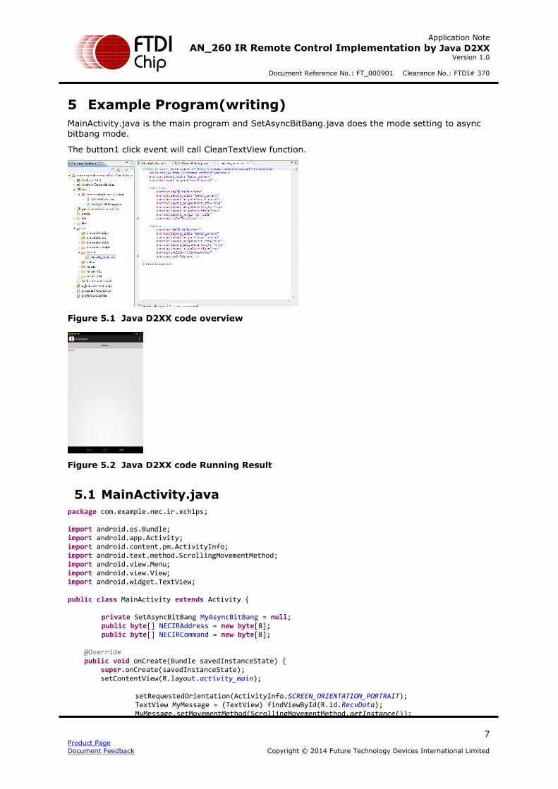
5 Example Program(writing)
MainActivity.java is the main program and SetAsyncBitBang.java does the mode setting to async bitbang mode.
The button1 click event will call CleanTextView function.
Figure 5.1 Java D2XX code overview
Figure 5.2 Java D2XX code Running Result
5.1 MainActivity.java
package com.example.nec.ir.xchips; import android.os.Bundle; import android.app.Activity; import android.content.pm.ActivityInfo; import android.text.method.ScrollingMovementMethod; import android.view.Menu; import android.view.View; import android.widget.TextView; public class MainActivity extends Activity { private SetAsyncBitBang MyAsyncBitBang = null; public byte[] NECIRAddress = new byte[8]; public byte[] NECIRCommand = new byte[8]; @Override public void onCreate(Bundle savedInstanceState) { super.onCreate(savedInstanceState); setContentView(R.layout.activity_main); setRequestedOrientation(ActivityInfo.SCREEN_ORIENTATION_PORTRAIT); TextView MyMessage = (TextView) findViewById(R.id.RecvData); MyMessage.setMovementMethod(ScrollingMovementMethod.getInstance());
Application Note
AN_260 IR Remote Control Implementation by Java D2XX Version 1.0
Document Reference No.: FT_000901 Clearance No.: FTDI# 370
8 Product Page
Document Feedback Copyright © 2014 Future Technology Devices International Limited
IRSetBitMode(); } @Override public boolean onCreateOptionsMenu(Menu menu) { getMenuInflater().inflate(R.menu.activity_main, menu); return true; } public void CleanTextView(View view) { TextView GetMyData = (TextView) findViewById(R.id.RecvData); GetMyData.setText(""); NECIRAddress[0]=0; NECIRAddress[1]=0; NECIRAddress[2]=0; NECIRAddress[3]=0; NECIRAddress[4]=0; NECIRAddress[5]=0; NECIRAddress[6]=0; NECIRAddress[7]=0; NECIRCommand[0]=1; NECIRCommand[1]=1; NECIRCommand[2]=0; NECIRCommand[3]=1; NECIRCommand[4]=1; NECIRCommand[5]=0; NECIRCommand[6]=1; NECIRCommand[7]=0; MyAsyncBitBang.Gen38KHzIR(NECIRAddress, NECIRCommand); } public void onMsgShow(final String recvdata){ runOnUiThread(new Runnable() { public void run() { TextView showstr = (TextView) findViewById(R.id.RecvData); showstr.append(recvdata); } }); } private void IRSetBitMode() { MyAsyncBitBang= new SetAsyncBitBang(this); } }
5.2 SetAsyncBitBang.java
package com.example.nec.ir.xchips; import android.app.Activity; import android.content.IntentFilter; import android.hardware.usb.UsbManager; import com.ftdi.j2xx.D2xxManager; import com.ftdi.j2xx.FT_Device; public class SetAsyncBitBang { private Activity mContext; private D2xxManager ftD2xx = null; private FT_Device ftDevice = null;
Application Note
AN_260 IR Remote Control Implementation by Java D2XX Version 1.0
Document Reference No.: FT_000901 Clearance No.: FTDI# 370
9 Product Page
Document Feedback Copyright © 2014 Future Technology Devices International Limited
private byte[] DataOutBuffer = new byte[7692]; public static final int NECIRHeaderLen= 341; private byte[] NECIRLeaderCode = new byte[3*NECIRHeaderLen]; // 9ms/26.4us = 341 public static final int NECIRSpaceLen= 170; private byte[] NECIRSpace = new byte[3*NECIRSpaceLen]; // 4.5m/26.4us = 170 public static final int NECIROneLen= 85; private byte[] NECIROne = new byte[3*NECIROneLen]; // 2.25m/26.4us = 85 public static final int NECIRZeroLen= 42; private byte[] NECIRZero = new byte[3*NECIRZeroLen]; // 1.12m/26.4us = 42 public static final int AddIdx =3*(NECIRHeaderLen+NECIRSpaceLen); // 1533 public static final int CmdIdx =3*(NECIRHeaderLen+NECIRSpaceLen+8*(NECIROneLen+NECIRZeroLen)); // the index to point the command length 4581 public static final int NECIRStopLen= 21; private byte[] NECIRStopBit = new byte[3*NECIRStopLen]; // 560u/26.4us = 21 public static final int StopIdx =3*(NECIRHeaderLen+NECIRSpaceLen+2*8*(NECIROneLen+NECIRZeroLen)); //7629 public SetAsyncBitBang (Activity activity) { mContext = activity; try{ ftD2xx = D2xxManager.getInstance(mContext); }catch (D2xxManager.D2xxException ex) { LogInfo(ex.getMessage()); } IntentFilter filter = new IntentFilter(); filter.addAction(UsbManager.ACTION_USB_DEVICE_DETACHED); } public void LogInfo(String val) { ((MainActivity)mContext).onMsgShow(val+"\n"); } public boolean Gen38KHzIR(byte[] nECIRAddress, byte[] nECIRCommand) { int i; int j; int devCount = ftD2xx.createDeviceInfoList(mContext); int AddOffset=0; //The offset of Address int CmdOffset=0; //The offset of Command if(devCount > 0) { D2xxManager.FtDeviceInfoListNode[] deviceList = new D2xxManager.FtDeviceInfoListNode[devCount]; ftD2xx.getDeviceInfoList(devCount, deviceList); switch (deviceList[0].type) { case D2xxManager.FT_DEVICE_232B: LogInfo("Device Name : FT232B device"); break; case D2xxManager.FT_DEVICE_8U232AM: LogInfo("Device Name : FT8U232AM device"); break; case D2xxManager.FT_DEVICE_UNKNOWN: LogInfo("Device Name : Unknown device"); break;

Application Note
AN_260 IR Remote Control Implementation by Java D2XX Version 1.0
Document Reference No.: FT_000901 Clearance No.: FTDI# 370
10 Product Page
Document Feedback Copyright © 2014 Future Technology Devices International Limited
case D2xxManager.FT_DEVICE_2232: LogInfo("Device Name : FT2232 device"); break; case D2xxManager.FT_DEVICE_232R: LogInfo("Device Name : FT232R device"); break; case D2xxManager.FT_DEVICE_2232H: LogInfo("Device Name : FT2232H device"); break; case D2xxManager.FT_DEVICE_4232H: LogInfo("Device Name : FT4232H device"); break; case D2xxManager.FT_DEVICE_232H: LogInfo("Device Name : FT232H device"); break; case D2xxManager.FT_DEVICE_X_SERIES: LogInfo("Device Name : FTDI X_SERIES"); break; default: LogInfo("Device Name : FT232B device"); break; } ftDevice = ftD2xx.openByIndex(mContext, 0); if(null == ftDevice) { LogInfo("ftDevice = null"); return false; } // ****************** // configure our port , Set to ASYNC BIT MODE if (!ftDevice.setBitMode((byte) 0xFF, D2xxManager.FT_BITMODE_ASYNC_BITBANG)) LogInfo("Set to ASYNC bitbang failed"); // **************** Configure Baud rate //** Reference AN232BM-01 to set the baud rate //** To have 8.8us baud rate in my case //** 9600 x 16 = 153600 //** 1/153600 = 6.5us //** So 1/113636.36 = 8.8us //** 113636.36 / 16 = 7102.27 if(!ftDevice.setBaudRate(7102)) LogInfo("Set bit rate failed"); //8.8us //****************** //****** Header ******* for (i=0;i<NECIRHeaderLen;i++) { NECIRLeaderCode[3*i]= (byte) 0xFF; NECIRLeaderCode[3*i+1]= (byte) 0x0; NECIRLeaderCode[3*i+2]= (byte) 0x0; } //****** Space *************** for (i=0;i<NECIRSpaceLen;i++) { NECIRSpace[3*i]= NECIRSpace[3*i+1] =NECIRSpace[3*i+2]=0; } //********NECIROne******** for (i=0;i<21;i++) { NECIROne[3*i]= (byte) 0xFF; NECIROne[3*i+1]= (byte) 0x0; NECIROne[3*i+2]= (byte) 0x0; }
Application Note
AN_260 IR Remote Control Implementation by Java D2XX Version 1.0
Document Reference No.: FT_000901 Clearance No.: FTDI# 370
11 Product Page
Document Feedback Copyright © 2014 Future Technology Devices International Limited
for (i=22;i< NECIROneLen; i++) { NECIROne[3*i]=NECIROne[3*i+1]=NECIROne[3*i+2]=0; } //********NECIRZero******** for (i=0;i<21;i++) { NECIRZero[3*i]= (byte) 0xFF; NECIRZero[3*i+1]= (byte) 0x0; NECIRZero[3*i+2]= (byte) 0x0; } for (i=22;i< NECIRZeroLen; i++) { NECIRZero[3*i]=NECIRZero[3*i+1]=NECIRZero[3*i+2]=0; } //********NECIR Stop bit******** for (i=0;i<21;i++) { NECIRStopBit[3*i]= (byte) 0xFF; NECIRStopBit[3*i+1]= (byte) 0x0; NECIRStopBit[3*i+2]= (byte) 0x0; } // *** fill up the IR Leader Code for (i=0;i<3*NECIRHeaderLen;i++) { DataOutBuffer[i]= NECIRLeaderCode[i]; } // *** fill up the NEC IR Space for (i=0;i<3*NECIRSpaceLen;i++) { DataOutBuffer[(3*NECIRHeaderLen)+i]= NECIRSpace[i]; } //**** NEC IR Address ***** for (j=0; j<8; j++) { // 8 bit of NECIRAddress; put Address if (nECIRAddress[j]==0) // nECIRAddress[j]==0 { for (i=0;i<NECIRZeroLen*3; i++) { DataOutBuffer[AddIdx+AddOffset]=NECIRZero[i]; AddOffset++; } } else { for (i=0;i<NECIROneLen*3; i++) { DataOutBuffer[AddIdx+AddOffset]=NECIROne[i]; AddOffset++; } } } // **** NEC IR Address Bar for (j=0; j<8; j++) { // 8 bit of NECIRAddress; put Address Bar if (nECIRAddress[j]!=0) // nECIRAddress[j]!=0 Address Bar { for (i=0;i<NECIRZeroLen*3; i++) { DataOutBuffer[AddIdx+AddOffset]=NECIRZero[i]; AddOffset++; } } else { for (i=0;i<NECIROneLen*3; i++) {
Application Note
AN_260 IR Remote Control Implementation by Java D2XX Version 1.0
Document Reference No.: FT_000901 Clearance No.: FTDI# 370
12 Product Page
Document Feedback Copyright © 2014 Future Technology Devices International Limited
DataOutBuffer[AddIdx+AddOffset]=NECIROne[i]; AddOffset++; } } } //**** End of NEC IR Address ***** CmdOffset=0; //**** NEC IR Command ***** for (j=0; j<8; j++) { // 8 bit of NECIRAddress; put Address if (nECIRCommand[j]==0) // nECIRAddress[j]==0 { for (i=0;i<NECIRZeroLen*3; i++) { DataOutBuffer[CmdIdx+CmdOffset]=NECIRZero[i]; CmdOffset++; } } else { for (i=0;i<NECIROneLen*3; i++) { DataOutBuffer[CmdIdx+CmdOffset]=NECIROne[i]; CmdOffset++; } } } // **** NEC IR Command Bar for (j=0; j<8; j++) { // 8 bit of NECIRAddress; put Address Bar if (nECIRCommand[j]!=0) // nECIRAddress[j]!=0 Address Bar { for (i=0;i<NECIRZeroLen*3; i++) { DataOutBuffer[CmdIdx+CmdOffset]=NECIRZero[i]; CmdOffset++; } } else { for (i=0;i<NECIROneLen*3; i++) { DataOutBuffer[CmdIdx+CmdOffset]=NECIROne[i]; CmdOffset++; } } } //**** End of NEC IR Command ***** //********** NEC IR Stop bit ******* for (i=0; i < 3*NECIRStopLen; i++) DataOutBuffer[StopIdx+i]= NECIRStopBit[i]; for (i=0; i<1; i++) { ftDevice.write(DataOutBuffer, 7692); } ftDevice.close(); return true; } return false; } }
Application Note
AN_260 IR Remote Control Implementation by Java D2XX Version 1.0
Document Reference No.: FT_000901 Clearance No.: FTDI# 370
13 Product Page
Document Feedback Copyright © 2014 Future Technology Devices International Limited
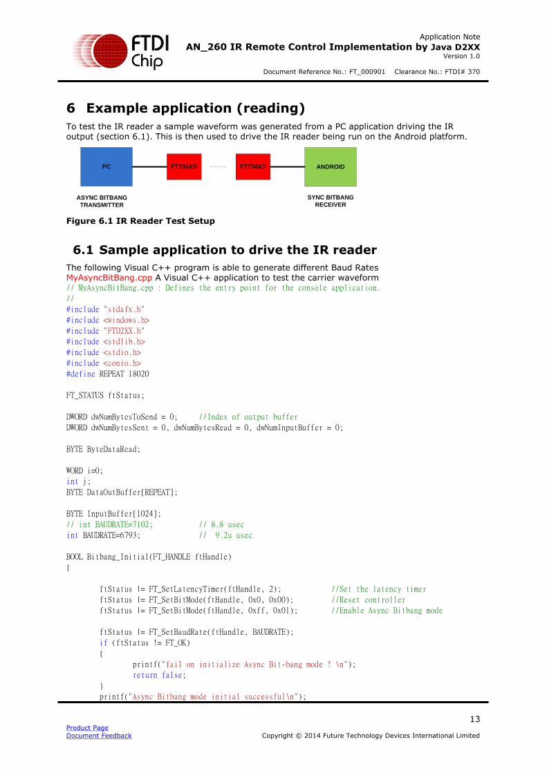
6 Example application (reading)
To test the IR reader a sample waveform was generated from a PC application driving the IR output (section 6.1). This is then used to drive the IR reader being run on the Android platform.
PC FT234XD FT234XD ANDROID
ASYNC BITBANG
TRANSMITTER
SYNC BITBANG
RECEIVER
Figure 6.1 IR Reader Test Setup
6.1 Sample application to drive the IR reader
The following Visual C++ program is able to generate different Baud Rates MyAsyncBitBang.cpp A Visual C++ application to test the carrier waveform // MyAsyncBitBang.cpp : Defines the entry point for the console application.
//
#include "stdafx.h"
#include <windows.h>
#include "FTD2XX.h"
#include <stdlib.h>
#include <stdio.h>
#include <conio.h>
#define REPEAT 18020
FT_STATUS ftStatus;
DWORD dwNumBytesToSend = 0; //Index of output buffer
DWORD dwNumBytesSent = 0, dwNumBytesRead = 0, dwNumInputBuffer = 0;
BYTE ByteDataRead;
WORD i=0;
int j;
BYTE DataOutBuffer[REPEAT];
BYTE InputBuffer[1024];
// int BAUDRATE=7102; // 8.8 usec
int BAUDRATE=6793; // 9.2u usec
BOOL Bitbang_Initial(FT_HANDLE ftHandle)
{
ftStatus |= FT_SetLatencyTimer(ftHandle, 2); //Set the latency timer
ftStatus |= FT_SetBitMode(ftHandle, 0x0, 0x00); //Reset controller
ftStatus |= FT_SetBitMode(ftHandle, 0xff, 0x01); //Enable Async Bitbang mode
ftStatus |= FT_SetBaudRate(ftHandle, BAUDRATE);
if (ftStatus != FT_OK)
{
printf("fail on initialize Async Bit-bang mode ! \n");
return false;
}
printf("Async Bitbang mode initial successful\n");
Application Note
AN_260 IR Remote Control Implementation by Java D2XX Version 1.0
Document Reference No.: FT_000901 Clearance No.: FTDI# 370
14 Product Page
Document Feedback Copyright © 2014 Future Technology Devices International Limited
return true;
}
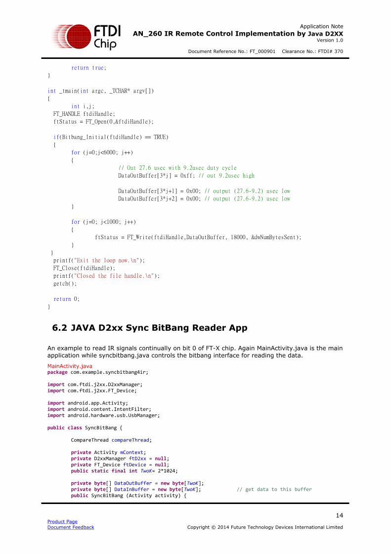
int _tmain(int argc, _TCHAR* argv[])
{
int i,j;
FT_HANDLE ftdiHandle;
ftStatus = FT_Open(0,&ftdiHandle);
if(Bitbang_Initial(ftdiHandle) == TRUE)
{
for (j=0;j<6000; j++)
{
// Out 27.6 usec with 9.2usec duty cycle
DataOutBuffer[3*j] = 0xff; // out 9.2usec high
DataOutBuffer[3*j+1] = 0x00; // output (27.6-9.2) usec low
DataOutBuffer[3*j+2] = 0x00; // output (27.6-9.2) usec low
}
for (j=0; j<1000; j++)
{
ftStatus = FT_Write(ftdiHandle,DataOutBuffer, 18000, &dwNumBytesSent);
}
}
printf("Exit the loop now.\n");
FT_Close(ftdiHandle);
printf("Closed the file handle.\n");
getch();
return 0;
}
6.2 JAVA D2xx Sync BitBang Reader App
An example to read IR signals continually on bit 0 of FT-X chip. Again MainActivity.java is the main application while syncbitbang.java controls the bitbang interface for reading the data.
MainActivity.java package com.example.syncbitbang4ir; import com.ftdi.j2xx.D2xxManager; import com.ftdi.j2xx.FT_Device; import android.app.Activity; import android.content.IntentFilter; import android.hardware.usb.UsbManager; public class SyncBitBang { CompareThread compareThread; private Activity mContext; private D2xxManager ftD2xx = null; private FT_Device ftDevice = null; public static final int TwoK= 2*1024; private byte[] DataOutBuffer = new byte[TwoK]; private byte[] DataInBuffer = new byte[TwoK]; // get data to this buffer public SyncBitBang (Activity activity) {
Application Note
AN_260 IR Remote Control Implementation by Java D2XX Version 1.0
Document Reference No.: FT_000901 Clearance No.: FTDI# 370
15 Product Page
Document Feedback Copyright © 2014 Future Technology Devices International Limited
mContext = activity; try{ ftD2xx = D2xxManager.getInstance(mContext); }catch (D2xxManager.D2xxException ex) { LogInfo(ex.getMessage()); } IntentFilter filter = new IntentFilter(); filter.addAction(UsbManager.ACTION_USB_DEVICE_DETACHED); } public void LogInfo(String val) { ((MainActivity)mContext).onMsgShow(val+"\n"); } public boolean Gen128KHzIR() { int devCount = ftD2xx.createDeviceInfoList(mContext); // LogInfo("Inside of Gen128KHzIR function..."); if(devCount > 0) { D2xxManager.FtDeviceInfoListNode[] deviceList = new D2xxManager.FtDeviceInfoListNode[devCount]; ftD2xx.getDeviceInfoList(devCount, deviceList); //*** send data and loop back**** // **************** Configure Baud rate //** Reference AN232BM-01 to set the baud rate //** To have 8.8us baud rate in my case //** 9600 x 16 = 153600 //** 1/153600 = 6.5us //** So 8.8us = 1/113636.36 //** 100 us = 1/(625*16) // if(!ftDevice.setBaudRate(8000)) //128Khz if(!ftDevice.setBaudRate(625)) //10kHz LogInfo("Set bit rate failed"); //****************** if(!ftDevice.setLatencyTimer((byte) 2)); //Set Latency time to 2ms LogInfo("Set latency time failed"); //****************** // Reset if (!ftDevice.setBitMode((byte) 0xFE, D2xxManager.FT_BITMODE_RESET)) LogInfo("Reset failed"); // Sync Write also read back // configure our port , Set to SYNC BIT MODE if (!ftDevice.setBitMode((byte) 0xFE, D2xxManager.FT_BITMODE_SYNC_BITBANG)) // bit 0 input, bit 1~7 output LogInfo("Set to SYNC bitbang failed"); else LogInfo("SYNC bitbang going..."); compareThread = new CompareThread(); compareThread.start(); return true; } return false; } class CompareThread extends Thread { public void run() { int i; ftDevice.write(DataOutBuffer, 256); // Sync write 256 bytes
Application Note
AN_260 IR Remote Control Implementation by Java D2XX Version 1.0
Document Reference No.: FT_000901 Clearance No.: FTDI# 370
16 Product Page
Document Feedback Copyright © 2014 Future Technology Devices International Limited
for (i=0;i<5000; i++) { ftDevice.write(DataOutBuffer, 256); // Sync another 256 bytes ftDevice.read(DataInBuffer, 256); // Sync read 256 bytes } ftDevice.close(); } } }
SyncBitBang.java package com.example.syncbitbang4ir; import com.ftdi.j2xx.D2xxManager; import com.ftdi.j2xx.FT_Device; import android.app.Activity; import android.content.IntentFilter; import android.hardware.usb.UsbManager; public class SyncBitBang { CompareThread compareThread; private Activity mContext; private D2xxManager ftD2xx = null; private FT_Device ftDevice = null; public static final int TwoK= 2*1024; private byte[] DataOutBuffer = new byte[TwoK]; private byte[] DataInBuffer = new byte[TwoK]; // get data to this buffer public SyncBitBang (Activity activity) { mContext = activity; try{ ftD2xx = D2xxManager.getInstance(mContext); }catch (D2xxManager.D2xxException ex) { LogInfo(ex.getMessage()); } IntentFilter filter = new IntentFilter(); filter.addAction(UsbManager.ACTION_USB_DEVICE_DETACHED); } public void LogInfo(String val) { ((MainActivity)mContext).onMsgShow(val+"\n"); } public boolean Gen128KHzIR() { int devCount = ftD2xx.createDeviceInfoList(mContext); // LogInfo("Inside of Gen128KHzIR function..."); if(devCount > 0) { D2xxManager.FtDeviceInfoListNode[] deviceList = new D2xxManager.FtDeviceInfoListNode[devCount]; ftD2xx.getDeviceInfoList(devCount, deviceList); //*** send data and loop back**** // **************** Configure Baud rate //** Reference AN232BM-01 to set the baud rate //** To have 8.8us baud rate in my case //** 9600 x 16 = 153600 //** 1/153600 = 6.5us //** So 8.8us = 1/113636.36 //** 100 us = 1/(625*16) // if(!ftDevice.setBaudRate(8000)) //128Khz if(!ftDevice.setBaudRate(625)) //10kHz
Application Note
AN_260 IR Remote Control Implementation by Java D2XX Version 1.0
Document Reference No.: FT_000901 Clearance No.: FTDI# 370
17 Product Page
Document Feedback Copyright © 2014 Future Technology Devices International Limited
LogInfo("Set bit rate failed"); //****************** if(!ftDevice.setLatencyTimer((byte) 2)); //Set Latency time to 2ms LogInfo("Set latency time failed"); //****************** // Reset if (!ftDevice.setBitMode((byte) 0xFE, D2xxManager.FT_BITMODE_RESET)) LogInfo("Reset failed"); // Sync Write also read back // configure our port , Set to SYNC BIT MODE if (!ftDevice.setBitMode((byte) 0xFE, D2xxManager.FT_BITMODE_SYNC_BITBANG)) // bit 0 input, bit 1~7 output LogInfo("Set to SYNC bitbang failed"); else LogInfo("SYNC bitbang going..."); compareThread = new CompareThread(); compareThread.start(); return true; } return false; } class CompareThread extends Thread { public void run() { int i; ftDevice.write(DataOutBuffer, 256); // Sync write 256 bytes for (i=0;i<5000; i++) { ftDevice.write(DataOutBuffer, 256); // Sync another 256 bytes ftDevice.read(DataInBuffer, 256); // Sync read 256 bytes } ftDevice.close(); } } }
Application Note
AN_260 IR Remote Control Implementation by Java D2XX Version 1.0
Document Reference No.: FT_000901 Clearance No.: FTDI# 370
18 Product Page
Document Feedback Copyright © 2014 Future Technology Devices International Limited
7 Testing Results
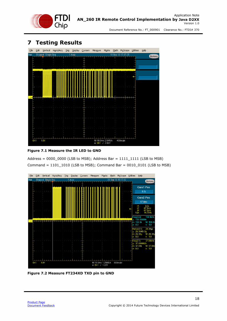
Figure 7.1 Measure the IR LED to GND
Address = 0000_0000 (LSB to MSB); Address Bar = 1111_1111 (LSB to MSB)
Command = 1101_1010 (LSB to MSB); Command Bar = 0010_0101 (LSB to MSB)
Figure 7.2 Measure FT234XD TXD pin to GND
Application Note
AN_260 IR Remote Control Implementation by Java D2XX Version 1.0
Document Reference No.: FT_000901 Clearance No.: FTDI# 370
19 Product Page
Document Feedback Copyright © 2014 Future Technology Devices International Limited
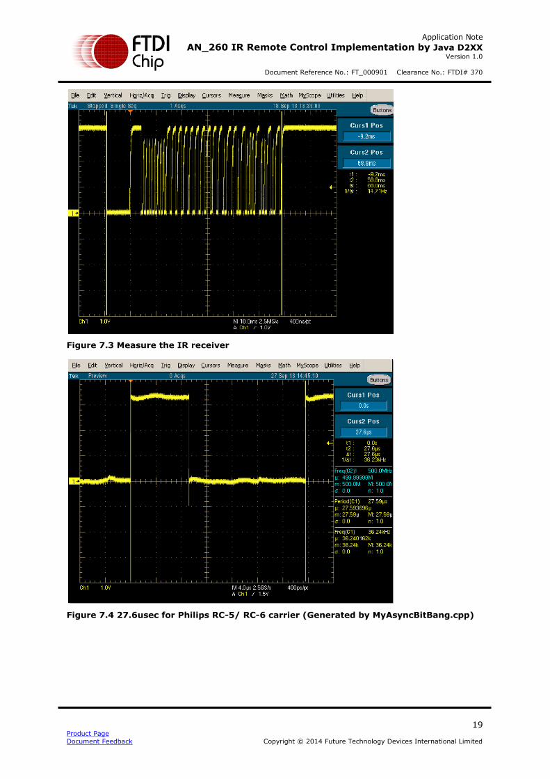
Figure 7.3 Measure the IR receiver
Figure 7.4 27.6usec for Philips RC-5/ RC-6 carrier (Generated by MyAsyncBitBang.cpp)
Application Note
AN_260 IR Remote Control Implementation by Java D2XX Version 1.0
Document Reference No.: FT_000901 Clearance No.: FTDI# 370
20 Product Page
Document Feedback Copyright © 2014 Future Technology Devices International Limited
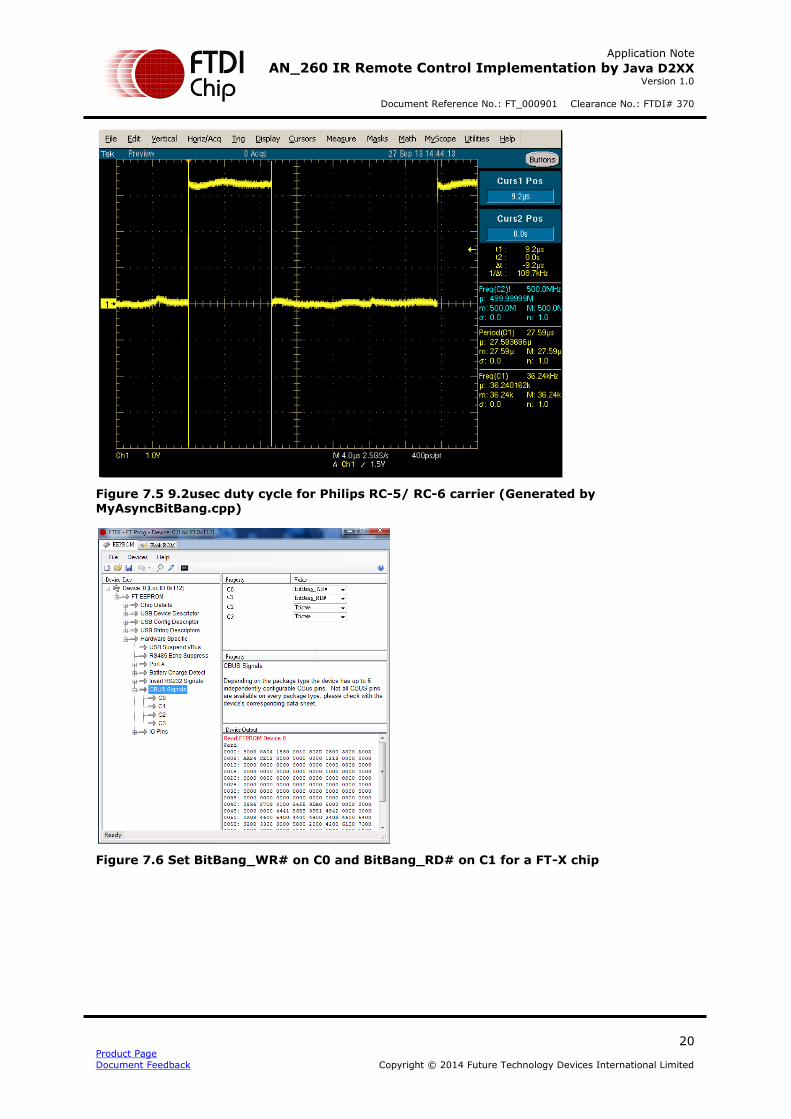
Figure 7.5 9.2usec duty cycle for Philips RC-5/ RC-6 carrier (Generated by MyAsyncBitBang.cpp)
Figure 7.6 Set BitBang_WR# on C0 and BitBang_RD# on C1 for a FT-X chip
Application Note
AN_260 IR Remote Control Implementation by Java D2XX Version 1.0
Document Reference No.: FT_000901 Clearance No.: FTDI# 370
21 Product Page
Document Feedback Copyright © 2014 Future Technology Devices International Limited
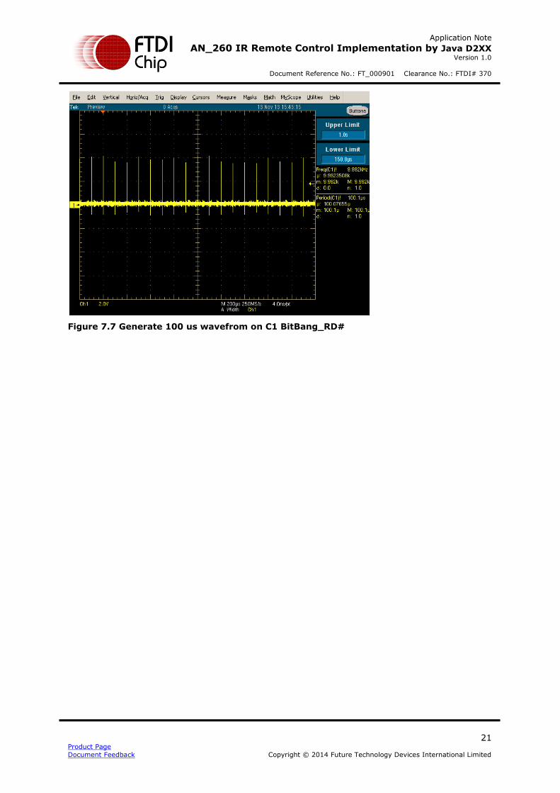
Figure 7.7 Generate 100 us wavefrom on C1 BitBang_RD#
Application Note
AN_260 IR Remote Control Implementation by Java D2XX Version 1.0
Document Reference No.: FT_000901 Clearance No.: FTDI# 370
22 Product Page
Document Feedback Copyright © 2014 Future Technology Devices International Limited
8 Contact Information
Head Office – Glasgow, UK Future Technology Devices International Limited Unit 1, 2 Seaward Place, Centurion Business Park Glasgow G41 1HH United Kingdom Tel: +44 (0) 141 429 2777 Fax: +44 (0) 141 429 2758 E-mail (Sales) [email protected] E-mail (Support) [email protected] E-mail (General Enquiries) [email protected]
Branch Office – Taipei, Taiwan Future Technology Devices International Limited (Taiwan) 2F, No. 516, Sec. 1, NeiHu Road
Taipei 114 Taiwan , R.O.C. Tel: +886 (0) 2 8797 1330 Fax: +886 (0) 2 8751 9737 E-mail (Sales) [email protected] E-mail (Support) [email protected] E-mail (General Enquiries) [email protected]
Branch Office – Tigard, Oregon, USA Future Technology Devices International Limited (USA) 7130 SW Fir Loop Tigard, OR 97223-8160 USA Tel: +1 (503) 547 0988 Fax: +1 (503) 547 0987 E-Mail (Sales) [email protected] E-Mail (Support) [email protected] E-Mail (General Enquiries) [email protected]
Branch Office – Shanghai, China Future Technology Devices International Limited (China) Room 1103, No. 666 West Huaihai Road,
Shanghai, 200052 China Tel: +86 21 62351596 Fax: +86 21 62351595 E-mail (Sales) [email protected] E-mail (Support) [email protected] E-mail (General Enquiries) [email protected]
Web Site http://ftdichip.com
System and equipment manufacturers and designers are responsible to ensure that their systems, and any Future Technology
Devices International Ltd (FTDI) devices incorporated in their systems, meet all applicable safety, regulatory and system-level
performance requirements. All application-related information in this document (including application descriptions, suggested
FTDI devices and other materials) is provided for reference only. While FTDI has taken care to assure it is accurate, this
information is subject to customer confirmation, and FTDI disclaims all liability for system designs and for any applications assistance provided by FTDI. Use of FTDI devices in life support and/or safety applications is entirely at the user’s risk, and the
user agrees to defend, indemnify and hold harmless FTDI from any and all damages, claims, suits or expense resulting from
such use. This document is subject to change without notice. No freedom to use patents or other intellectual property rights is
implied by the publication of this document. Neither the whole nor any part of the information contained in, or the product
described in this document, may be adapted or reproduced in any material or electronic form without the prior written consent
of the copyright holder. Future Technology Devices International Ltd, Unit 1, 2 Seaward Place, Centurion Business Park,
Glasgow G41 1HH, United Kingdom. Scotland Registered Company Number: SC136640
Application Note
AN_260 IR Remote Control Implementation by Java D2XX Version 1.0
Document Reference No.: FT_000901 Clearance No.: FTDI# 370
23 Product Page
Document Feedback Copyright © 2014 Future Technology Devices International Limited
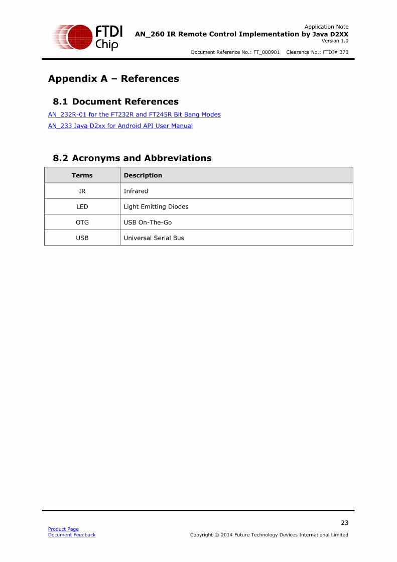
Appendix A – References
8.1 Document References
AN_232R-01 for the FT232R and FT245R Bit Bang Modes
AN_233 Java D2xx for Android API User Manual
8.2 Acronyms and Abbreviations
Terms Description
IR Infrared
LED Light Emitting Diodes
OTG USB On-The-Go
USB Universal Serial Bus
Application Note
AN_260 IR Remote Control Implementation by Java D2XX Version 1.0
Document Reference No.: FT_000901 Clearance No.: FTDI# 370
24 Product Page
Document Feedback Copyright © 2014 Future Technology Devices International Limited
Appendix B – List of Tables & Figures
8.3 List of Figures
Figure 2.1 NEC IR Protocol ................................................................................................... 3
Figure 2.2 NEC IR Modula ................................................................................................... 3
Figure 2.3 NEC IR Carrier .................................................................................................... 3
Figure 2.4 Philips RC-5 IR Protocol ........................................................................................ 4
Figure 2.5 Philips RC-5 IR Modula ........................................................................................ 4
Figure 2.6 Philips RC-5 IR Carrier ......................................................................................... 4
Figure 4.1 Typical USB-to-IR block diagram ........................................................................... 6
Figure 4.2 A minimum USB-to-IR block diagram ..................................................................... 6
Figure 4.3 Schematic of IR LED module ................................................................................. 6
Figure 5.1 Java D2XX code overview .................................................................................... 7
Figure 5.2 Java D2XX code Running Result ............................................................................ 7
Figure 6.1 IR Reader Test Setup ......................................................................................... 13
Figure 7.1 Measure the IR LED to GND ................................................................................ 18
Figure 7.2 Measure FT234XD TXD pin to GND ....................................................................... 18
Figure 7.3 Measure the IR receiver ...................................................................................... 19
Figure 7.4 27.6usec for Philips RC-5/ RC-6 carrier (Generated by MyAsyncBitBang.cpp) ............ 19
Figure 7.5 9.2usec duty cycle for Philips RC-5/ RC-6 carrier (Generated by MyAsyncBitBang.cpp) 20
Figure 7.6 Set BitBang_WR# on C0 and BitBang_RD# on C1 for a FT-X chip ............................ 20
Figure 7.7 Generate 100 us wavefrom on C1 BitBang_RD# .................................................... 21

Application Note
AN_260 IR Remote Control Implementation by Java D2XX Version 1.0
Document Reference No.: FT_000901 Clearance No.: FTDI# 370
25 Product Page
Document Feedback Copyright © 2014 Future Technology Devices International Limited
Appendix C – Revision History
Document Title: AN_260 IR Remote Control Implementation by Java D2XX
Document Reference No.: FT_000901
Clearance No.: FTDI# 370
Product Page: http://www.ftdichip.com/FTProducts.htm
Document Feedback: Send Feedback
Revision Changes Date
1.0 Initial Release 2014-02-17
Related Documents