IQ Switch ® ProxSense ® Series IQS253 Datasheet - Configurable 3 Channel DYCAL TM Capacitive Sensor with Automatic Compensation for Sensitivity Reducing Objects Unparallelled Features: ❏ DYCAL TM : Intelligent Hysteresis ❏ Internal Capacitor Implementation (ICI) - Reference capacitor on-chip ❏ Automatic Tuning Implementation (ATI) - Automatic adjustment for optimal sensor performance The IQS253 ProxSense ® IC is a fully integrated capacitive sensor implementing Dynamic Cali- bration (DYCAL TM ) technology: intelligent hysteresis to allow for sensor drift even during sensor activation. Main features: ❏ Self or Projected Technology sensors ❏ 3 Channels configurable as DYCAL TM /Normal output ❏ Self: Boolean direct output configurable through I 2 C ❏ Supply voltage: 1.8V to 3.6V ❏ Internal voltage regulator ❏ Advanced on-chip digital signal processing ❏ I 2 C adjustable settings • DYCAL TM settings • Control over filter operation • Time-out for stuck key • Proximity and Touch sensitivity selections • Low Power options • Event Mode possible (only communicates if an event is detected) Applications: ❏ Occupancy sensors ❏ SAR Compliant sensors for Tablet PCs ❏ On-ear detection for mobile phones ❏ 3D glasses ❏ Personal Media Players ❏ Remote Control Sleep implementation ❏ Gaming Controllers ❏ Proximity activated back lighting ❏ Any applications where a touch and proxim- ity condition can exist for a extended pe- riod of time Advantages: ❏ Allows for sensor drift in periods of activation and non-activation ❏ Improved digital filtering to reduce external noise ❏ Highly adjustable I 2 C device which only in- terrupts (Event Mode) when an event is detected Copyright ©Azoteq (Pty) Ltd 2016 All rights reserved IQS253 Datasheet Revision V1.10 Page 1 of 60 October 2016

Welcome message from author
This document is posted to help you gain knowledge. Please leave a comment to let me know what you think about it! Share it to your friends and learn new things together.
Transcript
IQ Switch®
ProxSense® Series
IQS253 Datasheet - Configurable 3 Channel DYCALTM
Capacitive Sensor with Automatic Compensation forSensitivity Reducing Objects
Unparallelled Features:
o DYCALTM: Intelligent Hysteresis
o Internal Capacitor Implementation (ICI) - Reference capacitor on-chip
o Automatic Tuning Implementation (ATI) - Automatic adjustment for optimal sensor performance
The IQS253 ProxSense® IC is a fully integrated capacitive sensor implementing Dynamic Cali-bration (DYCALTM) technology: intelligent hysteresis to allow for sensor drift even during sensoractivation.
Main features:
o Self or Projected Technology sensors
o 3 Channels configurable as DYCALTM /Normal output
o Self: Boolean direct output configurable through I2C
o Supply voltage: 1.8V to 3.6V
o Internal voltage regulator
o Advanced on-chip digital signal processing
o I2C adjustable settings
• DYCALTM settings
• Control over filter operation
• Time-out for stuck key
• Proximity and Touch sensitivity selections
• Low Power options
• Event Mode possible (only communicates if an event is detected)
Applications:
o Occupancy sensors
o SAR Compliant sensors for Tablet PCs
o On-ear detection for mobile phones
o 3D glasses
o Personal Media Players
o Remote Control Sleep implementation
o Gaming Controllers
o Proximity activated back lighting
o Any applications where a touch and proxim-ity condition can exist for a extended pe-riod of time
Advantages:
o Allows for sensor drift in periods of activationand non-activation
o Improved digital filtering to reduce externalnoise
o Highly adjustable I2C device which only in-terrupts (Event Mode) when an event isdetected
Copyright ©Azoteq (Pty) Ltd 2016All rights reserved
IQS253 DatasheetRevision V1.10
Page 1 of 60October 2016
IQ Switch®
ProxSense® Series
Contents
List of Figures 4
List of Tables 4
Revision History 4
List of Symbols 6
1 Functional Overview 71.1 Applicability . . . . . . . . . . . . . . . . . . . . . . . . . . . . . . . . . . . . . . . . 7
2 Analogue Functionality 7
3 Digital Functionality 8
4 Packaging and Pin-Out 94.1 IQS253 Self Capacitance . . . . . . . . . . . . . . . . . . . . . . . . . . . . . . . . . 94.2 IQS253 Projected . . . . . . . . . . . . . . . . . . . . . . . . . . . . . . . . . . . . . 104.3 Power Supply and PCB Layout . . . . . . . . . . . . . . . . . . . . . . . . . . . . . . 114.4 Design Rules for Harsh EMC Environments . . . . . . . . . . . . . . . . . . . . . . . 12
5 DYCAL 135.1 Operating Principle . . . . . . . . . . . . . . . . . . . . . . . . . . . . . . . . . . . . 14
6 ProxSense Module 156.1 Charge Transfer Concepts . . . . . . . . . . . . . . . . . . . . . . . . . . . . . . . . 15
7 Prox Module Setup 157.1 Self or Projected Capacitance . . . . . . . . . . . . . . . . . . . . . . . . . . . . . . 157.2 Rate of Charge Cycles . . . . . . . . . . . . . . . . . . . . . . . . . . . . . . . . . . 167.3 Report Rate . . . . . . . . . . . . . . . . . . . . . . . . . . . . . . . . . . . . . . . . 177.4 Active Channels . . . . . . . . . . . . . . . . . . . . . . . . . . . . . . . . . . . . . . 177.5 DYCALTM or Direct Output . . . . . . . . . . . . . . . . . . . . . . . . . . . . . . . . 177.6 Report Order (Channel Numbers) . . . . . . . . . . . . . . . . . . . . . . . . . . . . 177.7 Transfer Frequency (fcx) . . . . . . . . . . . . . . . . . . . . . . . . . . . . . . . . . . 177.8 Counts . . . . . . . . . . . . . . . . . . . . . . . . . . . . . . . . . . . . . . . . . . . 177.9 Long Term Average (LTA) . . . . . . . . . . . . . . . . . . . . . . . . . . . . . . . . . 177.10 Determine Touch or Prox . . . . . . . . . . . . . . . . . . . . . . . . . . . . . . . . . 197.11 ATI . . . . . . . . . . . . . . . . . . . . . . . . . . . . . . . . . . . . . . . . . . . . . 19
8 DYCALTM 208.1 DYCALTM channels enable . . . . . . . . . . . . . . . . . . . . . . . . . . . . . . . . 218.2 DYCALTM on TOUCH/PROX . . . . . . . . . . . . . . . . . . . . . . . . . . . . . . . 218.3 LTA Adapt rates (IN and OUT) . . . . . . . . . . . . . . . . . . . . . . . . . . . . . . 218.4 Block Channel . . . . . . . . . . . . . . . . . . . . . . . . . . . . . . . . . . . . . . . 218.5 DYCALTM Release Threshold . . . . . . . . . . . . . . . . . . . . . . . . . . . . . . 218.6 DYCALTM dynamic touch threshold . . . . . . . . . . . . . . . . . . . . . . . . . . . 218.7 10s_ATI_BLOCK . . . . . . . . . . . . . . . . . . . . . . . . . . . . . . . . . . . . . 218.8 250ms_DELAY_TM (tDYCAL) . . . . . . . . . . . . . . . . . . . . . . . . . . . . . . . 228.9 Turbo Mode . . . . . . . . . . . . . . . . . . . . . . . . . . . . . . . . . . . . . . . . 22
Copyright ©Azoteq (Pty) Ltd 2016All rights reserved
IQS253 DatasheetRevision V1.10
Page 2 of 60October 2016
IQ Switch®
ProxSense® Series
9 Communication 239.1 IC Setup Window . . . . . . . . . . . . . . . . . . . . . . . . . . . . . . . . . . . . . 239.2 Event Mode . . . . . . . . . . . . . . . . . . . . . . . . . . . . . . . . . . . . . . . . 239.3 I2C Specific Commands . . . . . . . . . . . . . . . . . . . . . . . . . . . . . . . . . . 239.4 I2C Read and Write specifics . . . . . . . . . . . . . . . . . . . . . . . . . . . . . . . 24
10 Boolean Output 2510.1 Channels for Boolean operation . . . . . . . . . . . . . . . . . . . . . . . . . . . . . 2510.2 Boolean NOT . . . . . . . . . . . . . . . . . . . . . . . . . . . . . . . . . . . . . . . 2510.3 Boolean AND/OR . . . . . . . . . . . . . . . . . . . . . . . . . . . . . . . . . . . . . 2510.4 Order of Boolean operation: . . . . . . . . . . . . . . . . . . . . . . . . . . . . . . . 25
11 RF Noise 2511.1 Noise Immunity . . . . . . . . . . . . . . . . . . . . . . . . . . . . . . . . . . . . . . 25
12 Electrical Specifications 2712.1 General Characteristics (Measured at 25 °C) . . . . . . . . . . . . . . . . . . . . . . 2712.2 Timing Characteristics . . . . . . . . . . . . . . . . . . . . . . . . . . . . . . . . . . . 28
13 Mechanical Dimensions 30
14 Device Marking 3314.1 Top Marking . . . . . . . . . . . . . . . . . . . . . . . . . . . . . . . . . . . . . . . . 3314.2 Bottom Marking . . . . . . . . . . . . . . . . . . . . . . . . . . . . . . . . . . . . . . 33
15 Ordering Information 33
16 Device Revision History 34
17 Errata 34
A DYCAL Illustrations 35
B IQS253 Memory Map 37B.1 Device Information . . . . . . . . . . . . . . . . . . . . . . . . . . . . . . . . . . . . 38B.2 System Flags . . . . . . . . . . . . . . . . . . . . . . . . . . . . . . . . . . . . . . . 38B.3 Proximity Status Bytes . . . . . . . . . . . . . . . . . . . . . . . . . . . . . . . . . . 39B.4 Touch Status Bytes . . . . . . . . . . . . . . . . . . . . . . . . . . . . . . . . . . . . 40B.5 DYCAL Touch Mode indication . . . . . . . . . . . . . . . . . . . . . . . . . . . . . . 41B.6 DYCAL Output indication . . . . . . . . . . . . . . . . . . . . . . . . . . . . . . . . . 41B.7 Halt Bytes . . . . . . . . . . . . . . . . . . . . . . . . . . . . . . . . . . . . . . . . . 42B.8 Channel Number . . . . . . . . . . . . . . . . . . . . . . . . . . . . . . . . . . . . . 43B.9 Counts . . . . . . . . . . . . . . . . . . . . . . . . . . . . . . . . . . . . . . . . . . . 43B.10 Long-Term Averages . . . . . . . . . . . . . . . . . . . . . . . . . . . . . . . . . . . 43B.11 Device Settings . . . . . . . . . . . . . . . . . . . . . . . . . . . . . . . . . . . . . . 44B.12 ATI Target . . . . . . . . . . . . . . . . . . . . . . . . . . . . . . . . . . . . . . . . . 44B.13 Compensation . . . . . . . . . . . . . . . . . . . . . . . . . . . . . . . . . . . . . . . 44B.14 Base Values . . . . . . . . . . . . . . . . . . . . . . . . . . . . . . . . . . . . . . . . 45B.15 Proximity Thresholds . . . . . . . . . . . . . . . . . . . . . . . . . . . . . . . . . . . 46B.16 Touch Thresholds . . . . . . . . . . . . . . . . . . . . . . . . . . . . . . . . . . . . . 47B.17 ProxSettings0 . . . . . . . . . . . . . . . . . . . . . . . . . . . . . . . . . . . . . . . 47B.18 ProxSettings1 . . . . . . . . . . . . . . . . . . . . . . . . . . . . . . . . . . . . . . . 49B.19 ProxSettings2 . . . . . . . . . . . . . . . . . . . . . . . . . . . . . . . . . . . . . . . 50B.20 ProxSettings3 . . . . . . . . . . . . . . . . . . . . . . . . . . . . . . . . . . . . . . . 51
Copyright ©Azoteq (Pty) Ltd 2016All rights reserved
IQS253 DatasheetRevision V1.10
Page 3 of 60October 2016
IQ Switch®
ProxSense® Series
B.21 Active Channels . . . . . . . . . . . . . . . . . . . . . . . . . . . . . . . . . . . . . . 52B.22 Low Power . . . . . . . . . . . . . . . . . . . . . . . . . . . . . . . . . . . . . . . . . 53B.23 DYCAL Settings . . . . . . . . . . . . . . . . . . . . . . . . . . . . . . . . . . . . . . 53B.24 DYCAL Enable . . . . . . . . . . . . . . . . . . . . . . . . . . . . . . . . . . . . . . . 54B.25 Event Mask . . . . . . . . . . . . . . . . . . . . . . . . . . . . . . . . . . . . . . . . 55B.26 Boolean Settings . . . . . . . . . . . . . . . . . . . . . . . . . . . . . . . . . . . . . 56B.27 Comms Pointer . . . . . . . . . . . . . . . . . . . . . . . . . . . . . . . . . . . . . . 57B.28 General Implementation Hints . . . . . . . . . . . . . . . . . . . . . . . . . . . . . . 57B.29 I2C Communication window . . . . . . . . . . . . . . . . . . . . . . . . . . . . . . . . 58B.30 Start-up Procedure . . . . . . . . . . . . . . . . . . . . . . . . . . . . . . . . . . . . 58B.31 General I2C Hints . . . . . . . . . . . . . . . . . . . . . . . . . . . . . . . . . . . . . 58
C IQS253 vs IQS253A 59
D Contact Information 60
List of Figures
4.1 IQS253 Pin Out. . . . . . . . . . . . . . . . . . . . . . . . . . . . . . . . . . . . . . . 94.2 Self Reference Design. . . . . . . . . . . . . . . . . . . . . . . . . . . . . . . . . . . 104.3 Projected Reference Design. . . . . . . . . . . . . . . . . . . . . . . . . . . . . . . . 114.4 EMC Design Choices. . . . . . . . . . . . . . . . . . . . . . . . . . . . . . . . . . . . 125.1 DYCAL Overview. . . . . . . . . . . . . . . . . . . . . . . . . . . . . . . . . . . . . . 137.1 Boost power as on CX/CRXx. . . . . . . . . . . . . . . . . . . . . . . . . . . . . . . . 167.2 Charge cycles as charged in LP modes. . . . . . . . . . . . . . . . . . . . . . . . . . 179.1 IC Setup Window. . . . . . . . . . . . . . . . . . . . . . . . . . . . . . . . . . . . . . 2313.1 MSOP10 Package . . . . . . . . . . . . . . . . . . . . . . . . . . . . . . . . . . . . . 3013.2 MSOP10 Footprint. . . . . . . . . . . . . . . . . . . . . . . . . . . . . . . . . . . . . 3113.3 MSOP10 Silk Screen. . . . . . . . . . . . . . . . . . . . . . . . . . . . . . . . . . . . 32A.1 DYCAL output selected on proximity. . . . . . . . . . . . . . . . . . . . . . . . . . . . 35A.2 DYCAL output selected on touch. . . . . . . . . . . . . . . . . . . . . . . . . . . . . . 35A.3 Filter halt upon Touch Mode Entry. . . . . . . . . . . . . . . . . . . . . . . . . . . . . 36C.1 Difference Highlighted between IQS253 and IQS253A . . . . . . . . . . . . . . . . . 59
List of Tables
4.1 IQS253 Self Capacitive Pin-out . . . . . . . . . . . . . . . . . . . . . . . . . . . . . . 94.2 IQS253 Projected Capacitive Pin-out . . . . . . . . . . . . . . . . . . . . . . . . . . . 107.1 LTA halting in non-TM. . . . . . . . . . . . . . . . . . . . . . . . . . . . . . . . . . . . 1912.1 IQS253 General Operating Conditions - Projected Capacitive Sensor. . . . . . . . . . 2712.2 IQS253 General Operating Conditions - Self Capacitive Sensor. . . . . . . . . . . . . 2712.3 Start-up and shut-down slope Characteristics . . . . . . . . . . . . . . . . . . . . . . 2812.4 Debounce employed on IQS253. . . . . . . . . . . . . . . . . . . . . . . . . . . . . . 2812.5 General Timing Characteristics for 1.80V ≤ VDDHI ≤ 3.60V . . . . . . . . . . . . . . 2812.6 IQS253 charging times . . . . . . . . . . . . . . . . . . . . . . . . . . . . . . . . . . 2912.7 IQS253 DYCAL (OUTPUT_ON_TOUCH = 0) /Proximity Response Times . . . . . . . 2913.1 MSOP10 Package Dimensions. . . . . . . . . . . . . . . . . . . . . . . . . . . . . . 3013.2 MSOP-10 Footprint Dimensions . . . . . . . . . . . . . . . . . . . . . . . . . . . . . 3113.3 MSOP-10 Silk Screen Dimensions . . . . . . . . . . . . . . . . . . . . . . . . . . . . 32
Copyright ©Azoteq (Pty) Ltd 2016All rights reserved
IQS253 DatasheetRevision V1.10
Page 4 of 60October 2016
IQ Switch®
ProxSense® Series
Revision History
Rev Description Date1.0.1 Preliminary Sept 20111.00 First Release Jan 20121.01 Update HC description March 20121.02 Update DFN-10 Footprint April 20121.03 Include the Memory Map in the Datasheet April 20121.04 Update Self Reference Schematic with pull-up on Boolean Output June 20121.05 Update Errata and DFN10 footprint June 20131.06 Add IQS253A and Remove DFN10 options June 20141.07 Update MSOP10 Mechanical Dimensions and patent numbers August 20141.08 Update multipliers in mem map, new patent numbers and address Feb 20151.09 Updated Electrical Specifications Oct 20151.10 Updated Reference Designs Oct 2016
Copyright ©Azoteq (Pty) Ltd 2016All rights reserved
IQS253 DatasheetRevision V1.10
Page 5 of 60October 2016
IQ Switch®
ProxSense® Series
List of Symbols
ATI Automatic Tuning Implementation. . . . . . . . . . . . . . . . . . . . . . . . . . . . . . . . . . . . . . . . . . . .7BP Boost Power Mode . . . . . . . . . . . . . . . . . . . . . . . . . . . . . . . . . . . . . . . . . . . . . . . . . . . . . . . . 16CS Count(s) . . . . . . . . . . . . . . . . . . . . . . . . . . . . . . . . . . . . . . . . . . . . . . . . . . . . . . . . . . . . . . . . . . .14CX Sensor Electrode . . . . . . . . . . . . . . . . . . . . . . . . . . . . . . . . . . . . . . . . . . . . . . . . . . . . . . . . . . . 9EMI Electromagnetic Interference . . . . . . . . . . . . . . . . . . . . . . . . . . . . . . . . . . . . . . . . . . . . . . 11ESD Electro-Static Discharge . . . . . . . . . . . . . . . . . . . . . . . . . . . . . . . . . . . . . . . . . . . . . . . . . . . 11FTB/EFT (Electrical) Fast Transient Bursts . . . . . . . . . . . . . . . . . . . . . . . . . . . . . . . . . . . . . . . . . . .11GND Ground . . . . . . . . . . . . . . . . . . . . . . . . . . . . . . . . . . . . . . . . . . . . . . . . . . . . . . . . . . . . . . . . . . . . . 9HC Halt Charge . . . . . . . . . . . . . . . . . . . . . . . . . . . . . . . . . . . . . . . . . . . . . . . . . . . . . . . . . . . . . . . 16LP Low Power Mode . . . . . . . . . . . . . . . . . . . . . . . . . . . . . . . . . . . . . . . . . . . . . . . . . . . . . . . . . . 16LTA Long Term Average . . . . . . . . . . . . . . . . . . . . . . . . . . . . . . . . . . . . . . . . . . . . . . . . . . . . . . . .14ND Noise Detect . . . . . . . . . . . . . . . . . . . . . . . . . . . . . . . . . . . . . . . . . . . . . . . . . . . . . . . . . . . . . . . .9NTM Non Touch Mode . . . . . . . . . . . . . . . . . . . . . . . . . . . . . . . . . . . . . . . . . . . . . . . . . . . . . . . . . . 14P Proximity . . . . . . . . . . . . . . . . . . . . . . . . . . . . . . . . . . . . . . . . . . . . . . . . . . . . . . . . . . . . . . . . . . 14RDY Ready . . . . . . . . . . . . . . . . . . . . . . . . . . . . . . . . . . . . . . . . . . . . . . . . . . . . . . . . . . . . . . . . . . . . . . 9SCL I2C Clock . . . . . . . . . . . . . . . . . . . . . . . . . . . . . . . . . . . . . . . . . . . . . . . . . . . . . . . . . . . . . . . . . . . 9SDA I2C Data . . . . . . . . . . . . . . . . . . . . . . . . . . . . . . . . . . . . . . . . . . . . . . . . . . . . . . . . . . . . . . . . . . . . 9t Time . . . . . . . . . . . . . . . . . . . . . . . . . . . . . . . . . . . . . . . . . . . . . . . . . . . . . . . . . . . . . . . . . . . . . . 16T Touch . . . . . . . . . . . . . . . . . . . . . . . . . . . . . . . . . . . . . . . . . . . . . . . . . . . . . . . . . . . . . . . . . . . . . 14THR Threshold . . . . . . . . . . . . . . . . . . . . . . . . . . . . . . . . . . . . . . . . . . . . . . . . . . . . . . . . . . . . . . . . . 14TM Touch Mode . . . . . . . . . . . . . . . . . . . . . . . . . . . . . . . . . . . . . . . . . . . . . . . . . . . . . . . . . . . . . . . . 7TVS Transient VoltageSuppression diode - ESD protection . . . . . . . . . . . . . . . . . . . . . . . 7VDDHI Supply (input) Voltage . . . . . . . . . . . . . . . . . . . . . . . . . . . . . . . . . . . . . . . . . . . . . . . . . . . . . . 7VREG Internal Regulator Output . . . . . . . . . . . . . . . . . . . . . . . . . . . . . . . . . . . . . . . . . . . . . . . . . . . 9WDT Watch-dog Timer . . . . . . . . . . . . . . . . . . . . . . . . . . . . . . . . . . . . . . . . . . . . . . . . . . . . . . . . . . . 7
Copyright ©Azoteq (Pty) Ltd 2016All rights reserved
IQS253 DatasheetRevision V1.10
Page 6 of 60October 2016
IQ Switch®
ProxSense® Series
1 Functional Overview
The IQS253 is a fully integrated three channelcapacitive sensor implementing the DYCALTM
functionality. Dynamic Calibration (DYCALTM)is an intelligent hysteresis to allow for sensordrift even during sensor activation. All channelscan be either configured as a DYCALTM chan-nel or as a normal direct output channel. Thedevice has an internal voltage regulator and ref-erence capacitor. The regulator is used as ref-erence for the charge transfer circuitry. Bothcircuits reduce the external component countneeded. The device automatically tracks slowvarying environmental changes via various sig-nal processing algorithms and has an Auto-matic Tuning (ATI) algorithm to calibrate the de-vice to the sense electrode. The charge trans-fer method of capacitive sensing is employedon the IQS253. (The charge transfer principleis thoroughly described in the application note:"AZD004 - Azoteq Capacitive Sensing".) TheIQS253 can be configured as either a self ca-pacitance sensor, where it has a Boolean out-put pin available. With the sensor configured asa projected capacitance sensor, this pin is con-figured as the transmitter electrode. DYCALTM
settings are highly configurable via I2C. Thesesettings include:
o DYCALTM activation with either Touch orProximity detection
o Release threshold
o Touch mode (TM) entry speed
o Downward filter adaptation rate when in TM
o Upward filter adaptation rate when in TM
o ATI block after exiting activation
o Boolean output configuration
The above mentioned configuration settings
do not include regular ProxSense® settings ad-
justable via I2C. Regular settings include:
o Proximity / Touch Thresholds
o Power Modes
o Adaptation rate when not in TM
o Noise detection activation
o ATI setup (control over sensitivity and whenATI should occur)
o Redo ATI
o Control over the LTA filters
o WDT enable / disable
o AC Filter enable / disable
o Proximity debounce
o Charge transfer frequency
o Block channel
o Event mode enable / disable
o Setup to wake communication with a partic-ular event
1.1 Applicability
All specifications, except where specifi-
cally mentioned otherwise, provided by this
datasheet are applicable to the following
ranges:
o Temperature −40 °C to +85 °C
o Supply voltage (VDDHI) 1.8V to 3.3V
2 Analogue Functionality
The analogue circuitry measures the capaci-
tance of the sense electrodes attached to the Cx
pins through a charge transfer process that is
periodically initiated by the digital circuitry. The
measuring process is referred to as a conver-
sion and consists of the discharging of Cs and
Cx, the charging of Cx and then a series of
charge transfers from Cx to Cs until a trip volt-
age is reached. The number of charge transfers
required to reach the trip voltage is referred to
as counts (Cs). The capacitance measurement
circuitry makes use of an internal reference ca-
pacitor and voltage reference (VREG). The ana-
logue circuitry further provides functionality for:
Copyright ©Azoteq (Pty) Ltd 2016All rights reserved
IQS253 DatasheetRevision V1.10
Page 7 of 60October 2016
IQ Switch®
ProxSense® Series
o Power on reset (POR) detection.
o Brown out detection (BOD).
3 Digital Functionality
The digital processing functionality is responsi-
ble for:
o Management of BOD and WDT events.
o Initiation of conversions at the selected rate.
o Processing of CS and execution of algo-rithms.
o Monitoring and automatic execution of theATI algorithm.
o Signal processing and digital filtering.
o Detection of PROX and TOUCH events.
o Managing outputs of the device.
o Managing serial communications.
o Manage programming of OTP options.
Copyright ©Azoteq (Pty) Ltd 2016All rights reserved
IQS253 DatasheetRevision V1.10
Page 8 of 60October 2016
IQ Switch®
ProxSense® Series
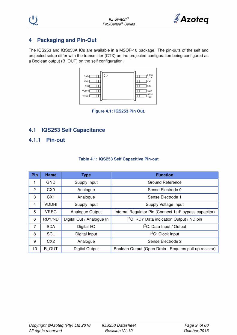
4 Packaging and Pin-Out
The IQS253 and IQS253A ICs are available in a MSOP-10 package. The pin-outs of the self andprojected setup differ with the transmitter (CTX) on the projected configuration being configured asa Boolean output (B_OUT) on the self configuration.
GND
CX0
CX1
VDDHI
VREG
B Out/
CTX
CX2
SCL
SDA
RDY/
ND
Figure 4.1: IQS253 Pin Out.
4.1 IQS253 Self Capacitance
4.1.1 Pin-out
Table 4.1: IQS253 Self Capacitive Pin-out
Pin Name Type Function
1 GND Supply Input Ground Reference
2 CX0 Analogue Sense Electrode 0
3 CX1 Analogue Sense Electrode 1
4 VDDHI Supply Input Supply Voltage Input
5 VREG Analogue Output Internal Regulator Pin (Connect 1µF bypass capacitor)
6 RDY/ND Digital Out / Analogue In I2C: RDY Data indication Output / ND pin
7 SDA Digital I/O I2C: Data Input / Output
8 SCL Digital Input I2C: Clock Input
9 CX2 Analogue Sense Electrode 2
10 B_OUT Digital Output Boolean Output (Open Drain - Requires pull-up resistor)
Copyright ©Azoteq (Pty) Ltd 2016All rights reserved
IQS253 DatasheetRevision V1.10
Page 9 of 60October 2016
IQ Switch®
ProxSense® Series
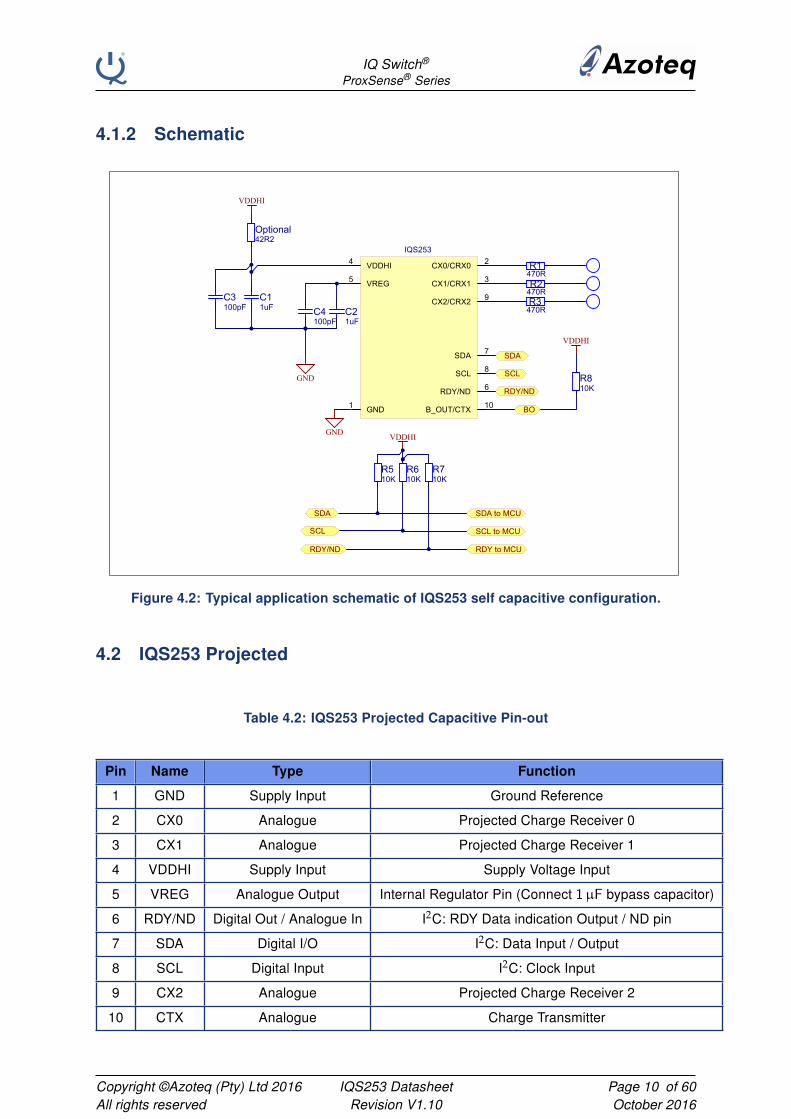
4.1.2 Schematic
GND
C11uF C2
1uFC4100pF
C3100pF
GND VDDHI
SDA to MCU
SCL to MCU
RDY to MCU
VREG5
VDDHI4 CX0/CRX0 2
GND1
CX1/CRX1 3
RDY/ND 6
SDA 7
B_OUT/CTX 10
SCL 8
CX2/CRX2 9
IQS253
SDA
SDA
SCL
SCL
RDY/ND
RDY/ND
R510K
R610K
R710K
R3470R
R2470R
R1470R
BO
R810K
VDDHI
VDDHI
Optional42R2
Figure 4.2: Typical application schematic of IQS253 self capacitive configuration.
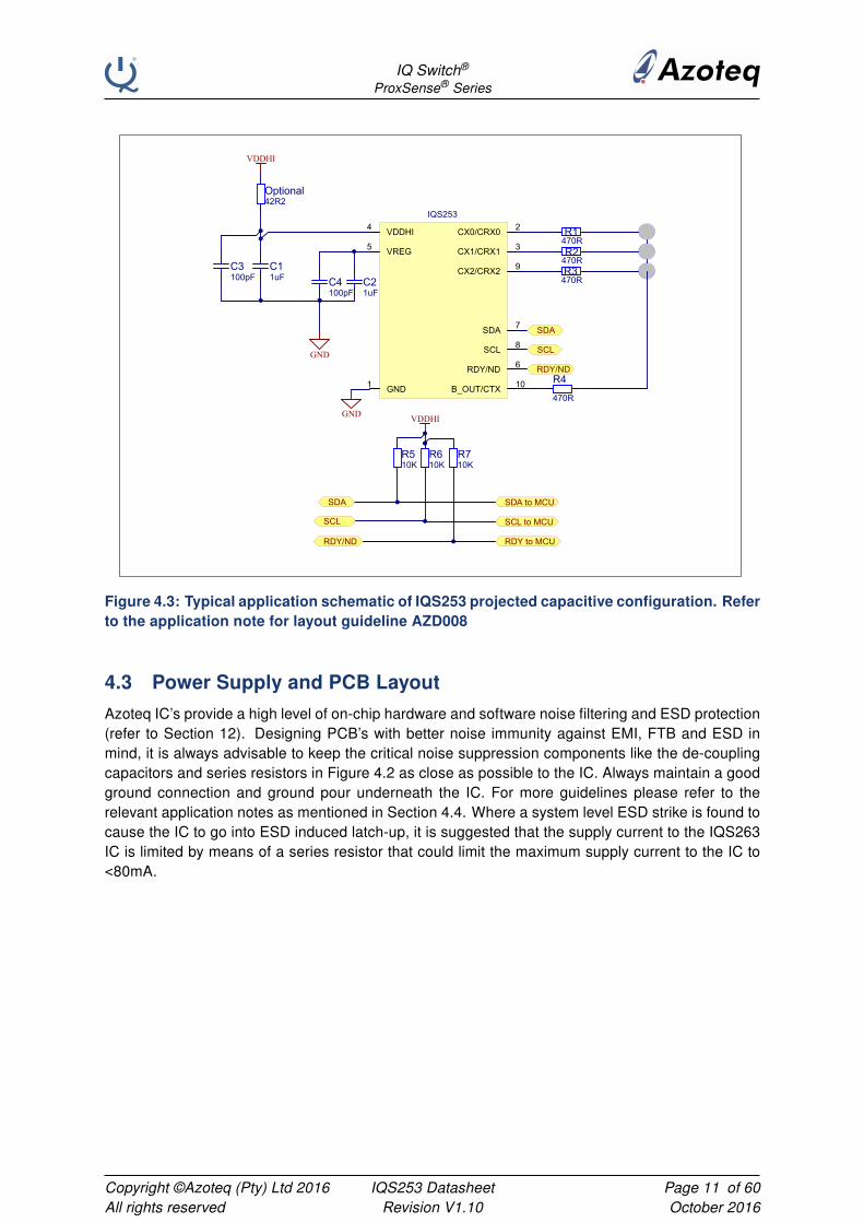
4.2 IQS253 Projected
Table 4.2: IQS253 Projected Capacitive Pin-out
Pin Name Type Function
1 GND Supply Input Ground Reference
2 CX0 Analogue Projected Charge Receiver 0
3 CX1 Analogue Projected Charge Receiver 1
4 VDDHI Supply Input Supply Voltage Input
5 VREG Analogue Output Internal Regulator Pin (Connect 1µF bypass capacitor)
6 RDY/ND Digital Out / Analogue In I2C: RDY Data indication Output / ND pin
7 SDA Digital I/O I2C: Data Input / Output
8 SCL Digital Input I2C: Clock Input
9 CX2 Analogue Projected Charge Receiver 2
10 CTX Analogue Charge Transmitter
Copyright ©Azoteq (Pty) Ltd 2016All rights reserved
IQS253 DatasheetRevision V1.10
Page 10 of 60October 2016
IQ Switch®
ProxSense® Series
GND
C11uF C2
1uFC4100pF
C3100pF
GND VDDHI
SDA to MCU
SCL to MCU
RDY to MCU
VREG5
VDDHI4 CX0/CRX0 2
GND1
CX1/CRX1 3
RDY/ND 6
SDA 7
B_OUT/CTX 10
SCL 8
CX2/CRX2 9
IQS253
SDA
SDA
SCL
SCL
RDY/ND
RDY/ND
R510K
R610K
R710K
R4
470R
R3470R
R2470R
R1470R
VDDHI
Optional42R2
Figure 4.3: Typical application schematic of IQS253 projected capacitive configuration. Referto the application note for layout guideline AZD008
4.3 Power Supply and PCB Layout
Azoteq IC’s provide a high level of on-chip hardware and software noise filtering and ESD protection(refer to Section 12). Designing PCB’s with better noise immunity against EMI, FTB and ESD inmind, it is always advisable to keep the critical noise suppression components like the de-couplingcapacitors and series resistors in Figure 4.2 as close as possible to the IC. Always maintain a goodground connection and ground pour underneath the IC. For more guidelines please refer to therelevant application notes as mentioned in Section 4.4. Where a system level ESD strike is found tocause the IC to go into ESD induced latch-up, it is suggested that the supply current to the IQS263IC is limited by means of a series resistor that could limit the maximum supply current to the IC to<80mA.
Copyright ©Azoteq (Pty) Ltd 2016All rights reserved
IQS253 DatasheetRevision V1.10
Page 11 of 60October 2016
IQ Switch®
ProxSense® Series
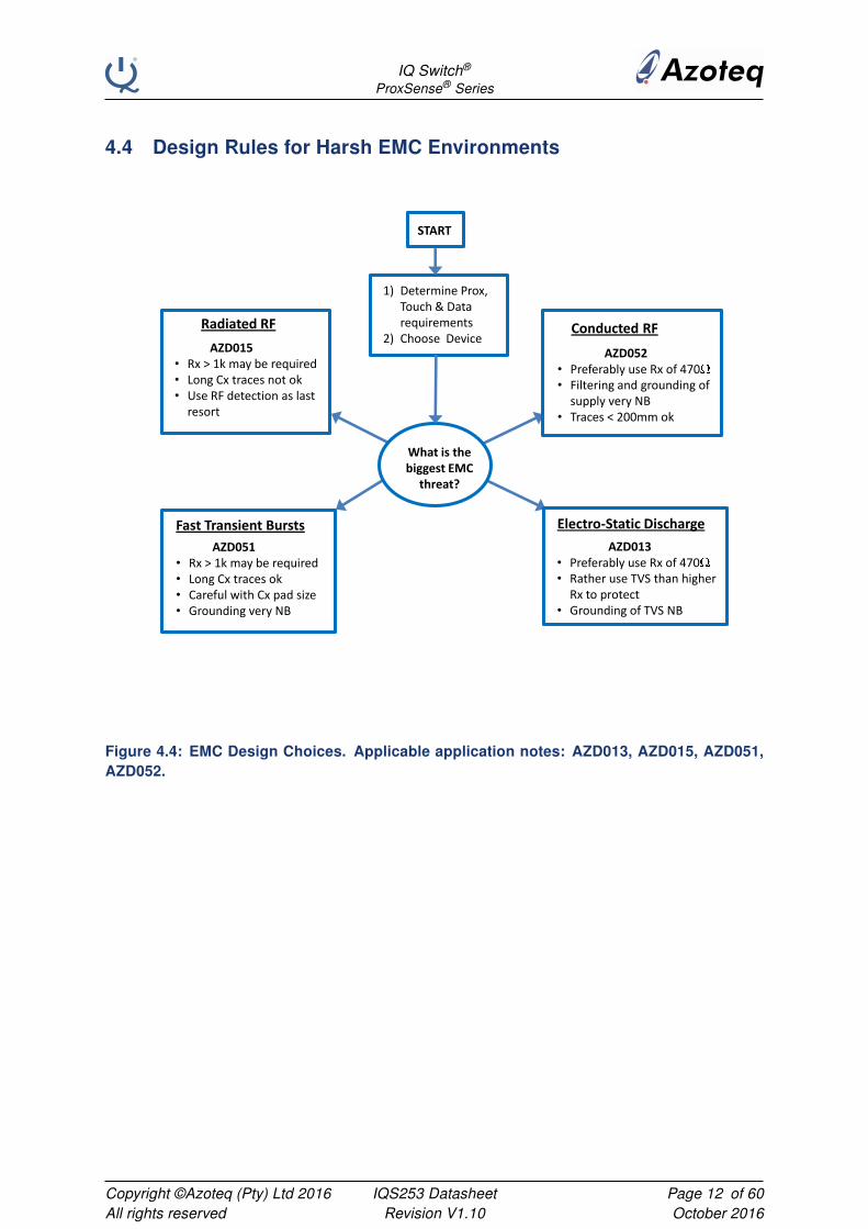
4.4 Design Rules for Harsh EMC Environments
1) Determine Prox, Touch & Data requirements
2) Choose DeviceRadiated RF
AZD015• Rx > 1k may be required• Long Cx traces not ok• Use RF detection as last
resort
Fast Transient Bursts
AZD051• Rx > 1k may be required• Long Cx traces ok• Careful with Cx pad size• Grounding very NB
Electro-Static Discharge
AZD013• Preferably use Rx of 470• Rather use TVS than higher
Rx to protect• Grounding of TVS NB
Conducted RF
AZD052 • Preferably use Rx of 470• Filtering and grounding of
supply very NB• Traces < 200mm ok
What is the biggest EMC
threat?
START
Figure 4.4: EMC Design Choices. Applicable application notes: AZD013, AZD015, AZD051,AZD052.
Copyright ©Azoteq (Pty) Ltd 2016All rights reserved
IQS253 DatasheetRevision V1.10
Page 12 of 60October 2016
IQS
witch
®
ProxS
ense®
Series
5 DYCAL
PTHR
TTHR
CS
1
0PO
Recallibrate LTA
CS
LTA – Long Term Average of CS
PTHR - derived from LTA
TTHR - derived from LTA
1. If touchpad is approached in Non-TM:
CS goes below LTA,
if CS goes below PTH, OUT = HIGH & LTA
will halt (not allowed to track CS),
if CS goes below TTH, OUT will stay HIGH
& LTA will recalibrate
Device will enter TM (Touch Mode) & OUT
will stay HIGH
TM: Touch Mode
TMNon-TM Non-TM
Non-TM: Non-Touch Mode
2. If touchpad is released in TM:
LTA will track CS as long as CS is below PTHR
CS goes above LTA
if CS goes above PTHR, LTA will halt,
if CS goes above REL_TTHR, OUT will go
LOW & LTA will recalibrate
LTA is allowed to track CS
LTA & LTARATE = LTA_ADAPT
LTARATE = LTA_ADAPT_IN
LTARATE = LTA_ADAPT_OUT
1
0TO
1
0DYCAL
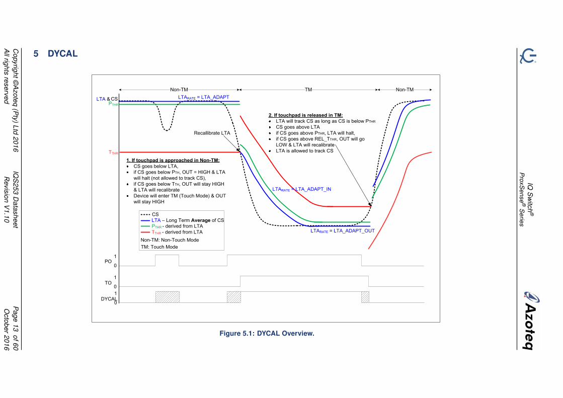
Figure 5.1: DYCAL Overview.
Copyright©
Azoteq
(Pty)
Ltd2016
Allrights
reservedIQ
S253
Datasheet
Revision
V1.10
Page
13of60
October
2016
IQ Switch®
ProxSense® Series
5.1 Operating Principle
Figure 5.1 is a visual representation of theDYCALTM functionality. The DYCAL output isused to indicate the status of a DYCALTM event(both a proximity and a touch event). TheDYCALTM functionality is summarised below.
Non-Touch ModeThe DYCAL output is activated on the success-ful detection of a proximity event and will remainactivated for the duration of the proximity event,permitting that this event is not longer than thefilter halt timings. The LTA will be halted in thistime. As soon as a touch condition is detected(CS below TTHR), the controller will dynamicallyre-calibrate its LTA to the halted LTA - TTHR. TheIC is now in Touch Mode (TM).
Touch ModeAfter the re-calibration of the LTA, it will followthe CS and be allowed to track slow varying en-vironmental changes. If the CS were to exceedthe LTA by a release threshold (REL_TTHR) thetouch detection will stop and the DYCAL outputwill return to its original state.
Copyright ©Azoteq (Pty) Ltd 2016All rights reserved
IQS253 DatasheetRevision V1.10
Page 14 of 60October 2016
IQ Switch®
ProxSense® Series
6 ProxSense Module
The IQS253 contains a ProxSense® modulethat uses patented technology to provide de-tection of PROX/TOUCH on numerous sensinglines. The ProxSense® module is a combinationof hardware and software, based on the princi-ples of charge transfer. A measurement is takenand used for calculating appropriate outputs.
6.1 Charge Transfer Concepts
Capacitance measurements are taken with acharge transfer process that is periodically ini-tiated. Self capacitive sensing measures thecapacitance between the sense electrode (Cx)relative to ground. Projected capacitance sens-ing measures the capacitance between 2 elec-trodes referred to as the transmitter (CTX) andreceiver (CRX). The measuring process is re-ferred to as a charge transfer cycle and consistsof the following:
o Discharging of an internal sampling capaci-tor (Cs) and the electrode capacitors (self:Cx or projected: CTX & CRX) on a chan-nel.
o charging of Cx’s / CTX’s connected to thechannel
o and then a series of charge transfers fromthe Cx’s / CRX’s to the internal samplingcapacitors (Cs), until the trip voltage isreached.
The number of charge transfers required to
reach the trip voltage on a channel is referred
to as Counts (CS). The device continuously re-
peats charge transfers on the sense electrode
connected to the Cx pin. For each channel
a Long Term Average (LTA) is calculated (12
bit unsigned integer values). The counts (12
bit unsigned integer values) are processed and
compared to the LTA to detect DYCAL, TOUCH
and PROX events. For more information re-
garding capacitive sensing, refer to the appli-
cation note "AZD004 - Azoteq Capacitive Sens-
ing". Please note: Attaching a probe to the
CX/CTX/CRX pin will influence the capaci-
tance of the sense electrodes and therefore
CS. This will have an immediate influence on
CS.
7 Prox Module Setup
7.1 Self or Projected Capaci-
tance
The IC can be used in either self or projected
capacitance mode. The IC is default in self ca-
pacitance mode. This can be changed to pro-
jected capacitance mode through either a FG
(one time programmable option) bit or in the
first communication window with start-up (use
the setup window to set the IC to Projected
mode). The user should set the PROJ bit (bit
7) in the PROX_SETTINGS1 [0xD2H] register
(refer to the Device Settings the Memory Map,
available in Appendix B) to enable projected ca-
pacitance technology. The technology enabled
on the IC will be reported in the SYSFLAGS
[0x10H] register. Refer to the IQS253 communi-
cation interface application note for more details
on the ’Setup Window’. This setting can only be
sent to the IQS253 in the setup-communication-
window. Please see the Section 9.1 for more
information regarding this. Note that this Setup-
Window is only available once after power-ON.
The IQS253 will always start-up in Event
Mode (default after POR). Thus, after the initial
Setup-Window, there will only be communica-
tion windows available upon Events (ATI, prox-
imity, etc. Refer to the Event_Mask [0xD9H]
register). Therefore, if the device is not set
to continuous streaming mode (bit 2 in the
PROX_SETTINGS2 [0xD3H] register) during
the Setup-Window, the master controller will
have to pull the RDY line low to force a com-
munication window to setup additional settings.
Please refer to application note AZD062 for
Copyright ©Azoteq (Pty) Ltd 2016All rights reserved
IQS253 DatasheetRevision V1.10
Page 15 of 60October 2016

IQ Switch®
ProxSense® Series
guidelines on setting up the IQS253.
When using more than one IQS253 device
on the same I2C bus (especially when sharing a
input pin on the master for the RDY lines), it is
recommended to use the FG options to set the
sensing technology (Self OR Projected) and the
individual sub-addresses.
7.2 Rate of Charge Cycles
7.2.1 Boost Power rate
With all 3 channels active and the IQS253
in Boost Power (BP) mode, the Counts (CS)
are charged at a fixed sampling frequency
(fSAMPLE) per channel. This is done to en-
sure regular samples for processing of results.
It is calculated as each channel having a time
(tCHANNEL = charge period (tCHARGE) + compu-
tation time) of 9ms, thus the time between con-
secutive samples on a channel (tSAMPLE) will
optimally be 27ms (or 37Hz).
CX2 /
CRX22 2
tSAMPLE
CX1 /
CRX11 1
tSAMPLE
CX0 /
CRX00 0
tCHARGE
tSAMPLE
tCHANNEL
Figure 7.1: Boost power as on CX / CRXx.
For every channel disabled, the sampling rate
on a channel will reduce with approximately
9ms.
7.2.2 Low Power Rates
Low current consumption charging modes are
available. In any Low Power (LP) mode, there
will be a tLP low power time applicable. This
is determined by the LOW_POWER register.
The value written into this register multiplied by
16ms will yield the LP time (tLP). Please note
that this time is only applicable from value 03H
and higher loaded into the LOW_POWER reg-
ister. The values 01H and 02H will have a
different time. See Table 12.6 for all timings.
With the detection of an undebounced proxim-
ity event the IC will zoom to BP mode, allow-
ing a very fast reaction time for further pos-
sible DYCAL /touch /proximity events. All ac-
tive channels will be consecutively charged ev-
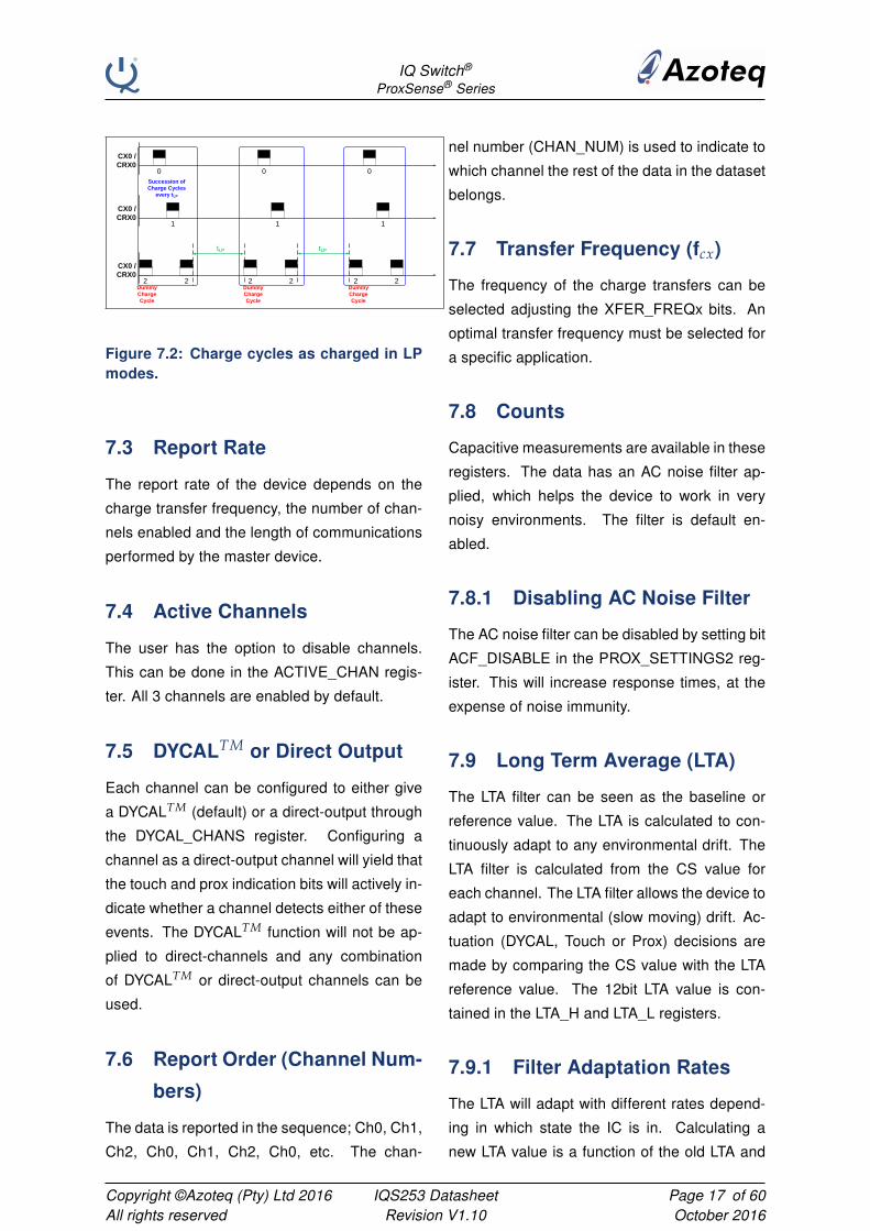
ery TLP. This succession of charge cycles are
succeeded by the charging of CX2 /CRX2 as a
dummy charge cycle. If a LP rate is selected
through register LOW_POWER and charging is
not in the zoomed in state (BP mode), the LP bit
(SYSFLAGS register) will be set.
When using low power mode, the designer must
ensure that the voltage drop on VREG is not
larger than 50mV. It is suggested to increase
the VREG capacitor to at least 4.7µF when us-
ing low power.
7.2.3 Halt Charge (HC)
Setting the HC bit will immediately cause the IC
to stop doing conversions (stop measuring ca-
pacitance), set the RDY line as an input and
enter a sleep mode. To wake up the IQS253,
and let it continue with conversions, the RDY
line should be pulled low for at least 2.5ms. The
RDY line should thereafter be monitored again
for communication windows. The HC bit in the
memory map will automatically be cleared.
Copyright ©Azoteq (Pty) Ltd 2016All rights reserved
IQS253 DatasheetRevision V1.10
Page 16 of 60October 2016
IQ Switch®
ProxSense® Series
Succession of
Charge Cycles
every tLP
CX0 /
CRX00 0 0
CX0 /
CRX0
tLP
2 2 2 2
tLP
2 2
CX0 /
CRX01 1 1
Dummy
Charge
Cycle
Dummy
Charge
Cycle
Dummy
Charge
Cycle
Figure 7.2: Charge cycles as charged in LPmodes.
7.3 Report Rate
The report rate of the device depends on the
charge transfer frequency, the number of chan-
nels enabled and the length of communications
performed by the master device.
7.4 Active Channels
The user has the option to disable channels.
This can be done in the ACTIVE_CHAN regis-
ter. All 3 channels are enabled by default.
7.5 DYCALTM or Direct Output
Each channel can be configured to either give
a DYCALTM (default) or a direct-output through
the DYCAL_CHANS register. Configuring a
channel as a direct-output channel will yield that
the touch and prox indication bits will actively in-
dicate whether a channel detects either of these
events. The DYCALTM function will not be ap-
plied to direct-channels and any combination
of DYCALTM or direct-output channels can be
used.
7.6 Report Order (Channel Num-
bers)
The data is reported in the sequence; Ch0, Ch1,
Ch2, Ch0, Ch1, Ch2, Ch0, etc. The chan-
nel number (CHAN_NUM) is used to indicate to
which channel the rest of the data in the dataset
belongs.
7.7 Transfer Frequency (fcx)
The frequency of the charge transfers can be
selected adjusting the XFER_FREQx bits. An
optimal transfer frequency must be selected for
a specific application.
7.8 Counts
Capacitive measurements are available in these
registers. The data has an AC noise filter ap-
plied, which helps the device to work in very
noisy environments. The filter is default en-
abled.
7.8.1 Disabling AC Noise Filter
The AC noise filter can be disabled by setting bit
ACF_DISABLE in the PROX_SETTINGS2 reg-
ister. This will increase response times, at the
expense of noise immunity.
7.9 Long Term Average (LTA)
The LTA filter can be seen as the baseline or
reference value. The LTA is calculated to con-
tinuously adapt to any environmental drift. The
LTA filter is calculated from the CS value for
each channel. The LTA filter allows the device to
adapt to environmental (slow moving) drift. Ac-
tuation (DYCAL, Touch or Prox) decisions are
made by comparing the CS value with the LTA
reference value. The 12bit LTA value is con-
tained in the LTA_H and LTA_L registers.
7.9.1 Filter Adaptation Rates
The LTA will adapt with different rates depend-
ing in which state the IC is in. Calculating a
new LTA value is a function of the old LTA and
Copyright ©Azoteq (Pty) Ltd 2016All rights reserved
IQS253 DatasheetRevision V1.10
Page 17 of 60October 2016
IQ Switch®
ProxSense® Series
the newly measured CS. The percentage of CS
used in this LTA calculation is specified as the
filter adaptation rate. 100% specifies that there
are no filtering and LTA = CS. A lower percent-
age value for the adaptation rate will yield a
slower adaptation rate. The IQS253 contains
3 user adjustable adaptation rates.
Filter adaptation rate in non-TM
The LTA filter will adapt according to the
LTA_ADAPT rate if the IQS253 is in non-TM and
no proximity event is detected. See Figure 5.1
for a visual representation.
Filter adaptation rate in TM
The LTA will adapt according to the
LTA_ADAPT_IN rate if IC is IN Touch Mode
(TM) and the LTA is adjusting towards CS. This
rate will apply until LTA has reached CS. See
Figure 5.1 for a visual representation.
Filter Halt in non-TM if |LTA-CS| > 16
The LTA will adapt according to the
LTA_ADAPT_OUT rate if IC is in Touch Mode
(TM), has reached the CS and
o Self: CS < LTA + 16
o Projected: CS > LTA - 16
This is the rate at which LTA adapts before CS
is on its way OUT of TM. See Figure 5.1 for a
visual representation.
7.9.2 Filter Reseed
Setting the RESEED bit in the PROX_SETTINGS0
register, will reseed LTA to:
o Self: 8 above CS
o Projected: 8 below CS
The IC will stay in the state in which it was
before the command was issued. Thus, ei-
ther non-TM or TM. The bit will automatically be
cleared by the IC as soon as the command has
been executed.
7.9.3 Filter Halting
LTA halt status The status of currently halted
channels is displayed in this byte. With the IC in
non-TM, it will only show that a channel is halted
if it detected a proximity condition. Once a touch
is detected the halting bit for that channel will be
cleared. With the IC in TM, it will show halting
bits of channels where:
Self: CS > LTA + 16 Projected: CS < LTA
- 16 Force halt
Setting the FORCE_HALT bit will cause all LTA
values to stop adapting to CS. This bit should be
cleared for the IC to start adapting to the envi-
ronment again. If the FORCE_HALT command
was issued while a channel was in non-TM and
a touch is made on that channel, it will cause the
LTA to stay halted but decrease with the Touch
Threshold for that channel.
Automatic LTA halting in non-TM
With the IC in non-TM, a proximity event will
cause halting of the LTA. The halting options
are:
Copyright ©Azoteq (Pty) Ltd 2016All rights reserved
IQS253 DatasheetRevision V1.10
Page 18 of 60October 2016
IQ Switch®
ProxSense® Series
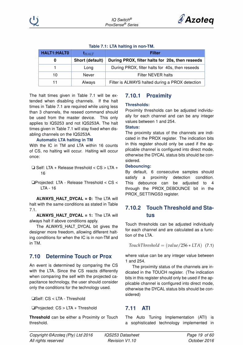
Table 7.1: LTA halting in non-TM.
HALT1:HALT0 tHALT Filter
0 Short (default) During PROX, filter halts for 20s, then reseeds
1 Long During PROX, filter halts for 40s, then reseeds
10 Never Filter NEVER halts
11 Always Filter is ALWAYS halted during a PROX detection
The halt times given in Table 7.1 will be ex-tended when disabling channels. If the halttimes in Table 7.1 are required while using lessthan 3 channels, the reseed command shouldbe used from the master device. This onlyapplies to IQS253 and not IQS253A. The halttimes given in Table 7.1 will stay fixed when dis-abling channels on the IQS253A.
Automatic LTA halting in TMWith the IC in TM and LTA within 16 countsof CS, no halting will occur. Halting will occuronce:
o Self: LTA + Release threshold < CS > LTA +16
oProjected: LTA - Release Threshold < CS <LTA - 16
ALWAYS_HALT_DYCAL = 0: The LTA willhalt with the same conditions as stated in Table7.1.
ALWAYS_HALT_DYCAL = 1: The LTA willalways halt if above conditions apply.
The ALWAYS_HALT_DYCAL bit gives thedesigner more freedom, allowing different halt-ing conditions for when the IC is in non-TM andin TM.
7.10 Determine Touch or Prox
An event is determined by comparing the CSwith the LTA. Since the CS reacts differentlywhen comparing the self with the projected ca-pacitance technology, the user should consideronly the conditions for the technology used.
oSelf: CS < LTA - Threshold
oProjected: CS > LTA + Threshold
Threshold can be either a Proximity or Touchthreshold.
7.10.1 Proximity
Thresholds:Proximity thresholds can be adjusted individu-ally for each channel and can be any integervalues between 1 and 254.Status:The proximity status of the channels are indi-cated in the PROX register. The indication bitsin this register should only be used if the ap-plicable channel is configured into direct mode,otherwise the DYCAL status bits should be con-sidered.Debouncing:By default, 6 consecutive samples shouldsatisfy a proximity detection condition.This debounce can be adjusted to 4through the PROX_DEBOUNCE bit in thePROX_SETTINGS3 register.
7.10.2 Touch Threshold and Sta-tus
Touch thresholds can be adjusted individuallyfor each channel and are calculated as a func-tion of the LTA.
TouchThreshold = (value/256 ∗ LTA) (7.1)
where value can be any integer value between1 and 254.
The proximity status of the channels are in-dicated in the TOUCH register. (The indicationbits in this register should only be used if the ap-plicable channel is configured into direct mode,otherwise the DYCAL status bits should be con-sidered)
7.11 ATI
The Auto Tuning Implementation (ATI) isa sophisticated technology implemented in
Copyright ©Azoteq (Pty) Ltd 2016All rights reserved
IQS253 DatasheetRevision V1.10
Page 19 of 60October 2016
IQ Switch®
ProxSense® Series
ProxSense® devices. It allows optimal perfor-mance of the devices for a wide range of sens-ing electrode capacitances, without modifica-tion or addition of external components. TheATI allows the tuning of two parameters, an ATIMultiplier and an ATI Compensation, to adjustthe sample value for an attached sensing elec-trode. ATI allows the designer to optimise a spe-cific design by adjusting the sensitivity and sta-bility of each channel through the adjustment ofthe ATI parameters. Partial ATI lets the designerspecify the MULTPLIER parameters instead ofan actual base value.See Section 7.11.3. TheIQS253 has an automated ATI function. Theauto-ATI function is by default enabled, but canbe disabled by setting the ATI_OFF bit. The ATIbit in the SYSFLAGS register will be set whilean ATI event is busy.
7.11.1 ATI Sensitivity
The designer can specify the BASE values foreach channel and a global TARGET value forall channels. A rough estimation of sensitivitycan be calculated as:
Sensitivity = TARGET/BASE (7.2)
As can be seen from this equation, the sen-sitivity can be increased by either increasingthe TARGET or decreasing the BASE value. Itshould, however, be noted that a higher sensi-tivity will yield a higher noise susceptibility.
7.11.2 ATI Target
The target is reached by adjusting the COM-PENSATION bits for each channel. The targetvalue is written into the ATI_TARGET register.The value written into this register (0 to 255)multiplied by 8 will yield the new target value.
7.11.3 ATI Base (MULTIPLIER)
The following parameters will influence the basevalue:
o CS_SIZE : Size of sampling capacitor.
o PROJ_BIAS bits: Adjusts the biasing ofsome analogue parameters in the pro-
jected IC. (Only applicable in projectedmode.)
o MULTIPLIER bits.
The base value used for the ATI function can be
implemented in 2 ways:
1. ATI_PARTIAL = 0. ATI automatically ad-
justs MULTIPLIER bits to reach a selected
base value . Base values are available
in the CHx_ATI_BASE registers. By us-
ing the ALT_BASE bit, an extended list of
base values are available.
2. ATI_PARTIAL = 1. The designer can
specify the multiplier settings. These set-
tings will give a custom base value from
where the compensation bits will be au-
tomatically implemented to reach the re-
quired target value. The base value is
determined by two sets of multiplier bits.
Sensitivity Multipliers which will also
scale the compensation to normalise the
sensitivity and Compensation Multipli-
ers to adjust the gain. Refer to the Mem-
ory Map were the multipliers bits can be
set in registers CH0_ATI_BASE (0xC8) to
CH2_ATI_BASE (0xCA).
7.11.4 Re-ATI
An automatic re-ATI event will occur if the CS is
outside its re-ATI limits. The re-ATI limit is cal-
culated as the target value divided by 8. For ex-
ample: Target = 1024 Re-ATI will occur if CS is
outside 1024 ±128. A re-ATI event can also be
issued by the master by setting the REDO_ATI
bit. It will clear automatically after the ATI event
was started.
8 DYCALTM
The DYCALTM technique is explained in Sec-
tion 5. DYCALTM detections are displayed in
the DYCAL_OUT register. The IQS253 will also
Copyright ©Azoteq (Pty) Ltd 2016All rights reserved
IQS253 DatasheetRevision V1.10
Page 20 of 60October 2016
IQ Switch®
ProxSense® Series
display whether each channel is in TM in the DY-
CAL_TM register. Important factors to consider
when designing the DYCALTM functionality are:
8.1 DYCALTM channels enable
Explained in Section 7.5.
8.2 DYCALTM on TOUCH/PROX
The DYCALTM output bits can either be
indicated when a proximity (default) or
touch is detected by configuring the OUT-
PUT_ON_TOUCH bit.
8.3 LTA Adapt rates (IN and
OUT)
Explained in Section 7.9.1.
8.4 Block Channel
A Touch on channel 1 can be used to block (and
clear) the other channels’ outputs. This is useful
in Event Mode as the MCU can remain uninter-
rupted from the IQS253 while a touch is present
on CH1.
o DYCAL_OUT if a channel is in DYCALTM
mode
o TOUCH if a channel is in direct-output mode
by setting bit BLOCK_ON_CH1_ENABLE. It
should be noted that, if another channel had
a DYCALTM detection and channel 1 detects
a touch event, it will clear the other channels’
DYCALTM outputs.
8.5 DYCALTM Release Thresh-
old
The release threshold is relevant for when
a channel is released after it was in TM.
It is dependent on the selected touch
threshold and the setting chosen with bits
REL_THR1:REL_THR0. (NOTE: the touch
threshold can either be the user selected
touch threshold or the dynamic touch thresh-
old, whichever is larger)
Example:
Technology: Self Capacitive
LTANTM = 1024 (IC in NTM, before detection)
LTATM = 850 (IC in TM, after detection)
TouchTHR = LTANTM*30/256
RelTHR = 75% * TouchTHR
Answer:
o The IQS253 detects a touch condition if: CS< LTANTM - TouchTHR, where TouchTHR= 1024*30/256 = 120. Thus if CS goesbelow 1024 - 120 = 904. Channel is inTM.
oThe IC will exit TM and clear the DY-CAL_OUT bit if:CS > LTATM + 0.75*120 Thus if CS ex-ceeds 850 + 90 = 940 IC will exit TM andclear DYCAL_OUT.
8.6 DYCALTM dynamic touch
threshold
The IQS253 calculates a dynamic touch thresh-
old. This dynamic threshold enables the IC
to calculate more accurately when a user re-
leases a button. The LTA will reseed to [LTA -
TouchTHR] once a touch is made. Using self
capacitance as example; the CS will probably
go much lower than the value to which the LTA
reseeded. The IQS253 will only calculate the
dynamic touch threshold once the LTA is within
16 counts of the CS.
8.7 10s_ATI_BLOCK
After a touch is released and the LTA is re-
seeded towards the CS, it is highly probable
that the LTA will be outside the re-ATI bound-
aries of the IC. This feature helps the channels
Copyright ©Azoteq (Pty) Ltd 2016All rights reserved
IQS253 DatasheetRevision V1.10
Page 21 of 60October 2016
IQ Switch®
ProxSense® Series
to block the re-ATI function for 10 seconds af-
ter an actuation has been released. It is also
applicable if a channel is configured in direct-
output mode. The 10seconds block of re-ATI
after an actuation can be disabled by setting the
10s_ATI_BLOCK bit.
8.8 250ms_DELAY_TM (tDYCAL)
By default, the LTA will only reseed to [LTA -
TouchTHR] after tDYCAL, when entering TM. An
option exists to disable this delay, thus the LTA
will reseed to [LTA - TouchThr] immediately with
the detection of a touch.
8.9 Turbo Mode
The channels are charged in sequence and
have a fixed period. By setting the Turbo_Mode
bit, this period will be shortened to the fastest
possible period, negating any dead-time. The
AC filter will also be disabled for transfers to
complete as fast as possible. If DYCAL is en-
abled, the Turbo_Mode bit will also allow the IC
to enter Touch Mode as fast as possible upon
an event.
Copyright ©Azoteq (Pty) Ltd 2016All rights reserved
IQS253 DatasheetRevision V1.10
Page 22 of 60October 2016
IQ Switch®
ProxSense® Series
9 Communication
The IQS253 can communicate on the I2C com-patible bus structure. It uses the 2 wire serialinterface bus which is I2C compatible and anoptional RDY pin is available which indicatesthe communication window. The IQS253 hasfour available sub addresses, 44H (default) to47H that is selected upon purchase of the IC.The maximum I2C compatible communicationspeed for the IQS253 is 400kbit/s. Please re-fer to AZD062 - IQS253 Communication Inter-face Guidelines [? ] and the Memory Map inAppendix B for more details.
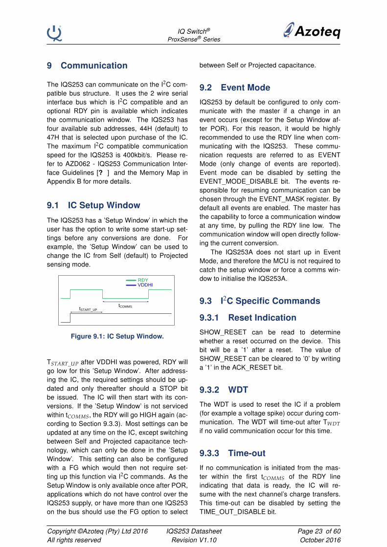
9.1 IC Setup Window
The IQS253 has a ’Setup Window’ in which theuser has the option to write some start-up set-tings before any conversions are done. Forexample, the ’Setup Window’ can be used tochange the IC from Self (default) to Projectedsensing mode.
VDDHIRDY
tCOMMStSTART_UP
Figure 9.1: IC Setup Window.
TSTART_UP after VDDHI was powered, RDY willgo low for this ’Setup Window’. After address-ing the IC, the required settings should be up-dated and only thereafter should a STOP bitbe issued. The IC will then start with its con-versions. If the ’Setup Window’ is not servicedwithin tCOMMS, the RDY will go HIGH again (ac-cording to Section 9.3.3). Most settings can beupdated at any time on the IC, except switchingbetween Self and Projected capacitance tech-nology, which can only be done in the ’SetupWindow’. This setting can also be configuredwith a FG which would then not require set-ting up this function via I2C commands. As theSetup Window is only available once after POR,applications which do not have control over theIQS253 supply, or have more than one IQS253on the bus should use the FG option to select
between Self or Projected capacitance.
9.2 Event Mode
IQS253 by default be configured to only com-municate with the master if a change in anevent occurs (except for the Setup Window af-ter POR). For this reason, it would be highlyrecommended to use the RDY line when com-municating with the IQS253. These commu-nication requests are referred to as EVENTMode (only change of events are reported).Event mode can be disabled by setting theEVENT_MODE_DISABLE bit. The events re-sponsible for resuming communication can bechosen through the EVENT_MASK register. Bydefault all events are enabled. The master hasthe capability to force a communication windowat any time, by pulling the RDY line low. Thecommunication window will open directly follow-ing the current conversion.
The IQS253A does not start up in EventMode, and therefore the MCU is not required tocatch the setup window or force a comms win-dow to initialise the IQS253A.
9.3 I2C Specific Commands
9.3.1 Reset Indication
SHOW_RESET can be read to determinewhether a reset occurred on the device. Thisbit will be a ’1’ after a reset. The value ofSHOW_RESET can be cleared to ’0’ by writinga ’1’ in the ACK_RESET bit.
9.3.2 WDT
The WDT is used to reset the IC if a problem(for example a voltage spike) occur during com-munication. The WDT will time-out after TWDTif no valid communication occur for this time.
9.3.3 Time-out
If no communication is initiated from the mas-ter within the first tCOMMS of the RDY lineindicating that data is ready, the IC will re-sume with the next channel’s charge transfers.This time-out can be disabled by setting theTIME_OUT_DISABLE bit.
Copyright ©Azoteq (Pty) Ltd 2016All rights reserved
IQS253 DatasheetRevision V1.10
Page 23 of 60October 2016

IQ Switch®
ProxSense® Series
9.4 I2C Read and Write specifics
Please refer to the Memory Map and Sam-ple Code Document for the I2C read and writespecifics as implemented on most ProxSense®
devices.
Copyright ©Azoteq (Pty) Ltd 2016All rights reserved
IQS253 DatasheetRevision V1.10
Page 24 of 60October 2016
IQ Switch®
ProxSense® Series
10 Boolean Output
Boolean arithmetic can be applied to one or acombination of channels to get a result. Thisresult is available in the BOOLEAN_OUTPUTbit in the TOUCH register. For the self ca-pacitive IQS253 version, a digital signal outputpin (B_OUT) exists, which corresponds to theBoolean output bit. This output pin is to be usedfor level detection on a master controller, or tobe used with a FET for LED driving. The pinis not rated to sink or source current. In boththe self and projected configuration, the "EventMode" communication could be triggered on aBoolean based result. The Boolean output willbe calculated using:
o DYCAL_OUT if channel is in DYCALTM
mode
o TOUCH output if channel is in direct-outputmode
10.1 Channels for Boolean oper-
ation
The channels that should be used to com-
pute the Boolean output bit is chosen in the
BOOLEAN_SETTINGS register.
10.2 Boolean NOT
A Boolean NOT can be applied to any or all
channels.
10.3 Boolean AND/OR
The Boolean AND operation will be applied
to the chosen channels. The OR op-
eration can alternatively be applied if the
BOOLEAN_AND_OR bit is set.
10.4 Order of Boolean opera-
tion:
1. Choose channels for Boolean operation
2. Should NOT be applied to a channel?
3. AND/OR operation?
11 RF Noise
11.1 Noise Immunity
The IQS253 has advanced immunity to RF
noise sources such as GSM cellular tele-
phones, DECT, Bluetooth and WIFI devices.
Design guidelines should however be followed
to ensure the best noise immunity. The design
of capacitive sensing applications can encom-
pass a large range of situations but as a sum-
mary the following should be noted to improve a
design:
o A ground plane should be placed under theIC, except under the Cx line.
o All the tracks on the PCB must be kept asshort as possible.
o The capacitor between VDDHI and VSS aswell as between VREG and VSS, must beplaced as close as possible to the IC.
o A 100 pF capacitor can be placed in paral-lel with the 1uF capacitor between VDDHIand VSS. Another 100 pF capacitor canbe placed in parallel with the 1uF capaci-tor between VREG and VSS.
o When the device is too sensitive for a spe-cific application a parasitic capacitor (max5pF) can be added between the Cx lineand ground.
o Proper sense electrode and button designprinciples must be followed.
o Unintentional coupling of sense electrode toground and other circuitry must be lim-ited by increasing the distance to thesesources or making use of the drivenshield.
o In some instances a ground plane somedistance from the device and sense elec-trode may provide significant shieldingfrom undesired interference.
Copyright ©Azoteq (Pty) Ltd 2016All rights reserved
IQS253 DatasheetRevision V1.10
Page 25 of 60October 2016
IQ Switch®
ProxSense® Series
When the capacitance between the sense elec-
trode and ground becomes too large the sensi-
tivity of the device may be influenced.
11.1.1 RF Detection
In cases of extreme RF interference, the on-
chip RF detection is suggested. This detec-
tor can be enabled by setting the ND bit in the
PROX_SETTINGS1 register. By connecting a
suitable antenna to the RF pin, it allows the de-
vice to detect RF noise and notify the master
of possible corrupt data. Noise affected sam-
ples are not allowed to influence the LTA filter,
and also do not contribute to DYCAL, PROX or
TOUCH detection. With the detection of noise,
the NOISE bit in SYSFLAGS will be set.
11.1.2 RF detector sensitivity
The sensitivity of the RF detector can be se-
lected by setting an appropriate RF detection
voltage through the ND_TRIM bits. Please see
AZD015 for further details regarding this.
Copyright ©Azoteq (Pty) Ltd 2016All rights reserved
IQS253 DatasheetRevision V1.10
Page 26 of 60October 2016
IQ Switch®
ProxSense® Series
12 Electrical Specifications
Absolute Maximum Specifications
The following absolute maximum parameters are specified for the device: Exceeding these maxi-mum specifications may cause damage to the device.
o Operating temperature −40 °C to +85 °Co Supply Voltage (VDDHI - GND) 3.6Vo Maximum pin voltage VDDHI + 0.5Vo Maximum continuous current (for specific Pins) 2mAo Minimum pin voltage GND - 0.5Vo Minimum power-on slope 100V /so ESD protection (HBM) ±4 kVo Moisture Sensitivity Level MSOP-10 MSL 1
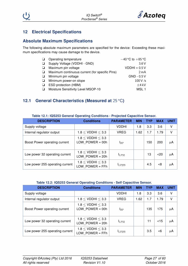
12.1 General Characteristics (Measured at 25 °C)
Table 12.1: IQS253 General Operating Conditions - Projected Capacitive Sensor.
DESCRIPTION Conditions PARAMETER MIN TYP MAX UNIT
Supply voltage VDDHI 1.8 3.3 3.6 V
Internal regulator output 1.8 ≤ VDDHI ≤ 3.3 VREG 1.62 1.7 1.79 V
Boost Power operating current1.8 ≤ VDDHI ≤ 3.3
IBP 150 200 µALOW_POWER = 00h
Low power 32 operating current1.8 ≤ VDDHI ≤ 3.3
ILP32 13 <20 µALOW_POWER = 20h
Low power 255 operating current1.8 ≤ VDDHI ≤ 3.3
ILP255 4.5 <8 µALOW_POWER = FFh
Table 12.2: IQS253 General Operating Conditions - Self Capacitive Sensor.
DESCRIPTION Conditions PARAMETER MIN TYP MAX UNIT
Supply voltage VDDHI 1.8 3.3 3.6 V
Internal regulator output 1.8 ≤ VDDHI ≤ 3.3 VREG 1.62 1.7 1.79 V
Boost Power operating current1.8 ≤ VDDHI ≤ 3.3
IBP 135 175 µALOW_POWER = 00h
Low power 32 operating current1.8 ≤ VDDHI ≤ 3.3
ILP32 11 <15 µALOW_POWER = 20h
Low power 255 operating current1.8 ≤ VDDHI ≤ 3.3
ILP255 3.5 <6 µALOW_POWER = FFh
Copyright ©Azoteq (Pty) Ltd 2016All rights reserved
IQS253 DatasheetRevision V1.10
Page 27 of 60October 2016
IQ Switch®
ProxSense® Series
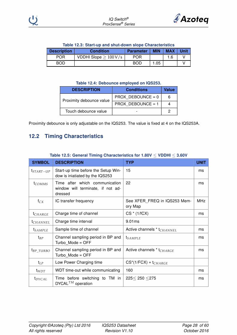
Table 12.3: Start-up and shut-down slope Characteristics
Description Condition Parameter MIN MAX Unit
POR VDDHI Slope ≥ 100V/s POR 1.6 V
BOD BOD 1.05 V
Table 12.4: Debounce employed on IQS253.
DESCRIPTION Conditions Value
Proximity debounce valuePROX_DEBOUNCE = 0 6
PROX_DEBOUNCE = 1 4
Touch debounce value - 2
Proximity debounce is only adjustable on the IQS253. The value is fixed at 4 on the IQS253A.
12.2 Timing Characteristics
Table 12.5: General Timing Characteristics for 1.80V ≤ VDDHI ≤ 3.60V
SYMBOL DESCRIPTION TYP UNIT
tSTART−UP Start-up time before the Setup Win-dow is iniatiated by the IQS253
15 ms
tCOMMS Time after which communicationwindow will terminate, if not ad-dressed
22 ms
fCX IC transfer frequency See XFER_FREQ in IQS253 Mem-ory Map
MHz
tCHARGE Charge time of channel CS * (1/fCX) ms
tCHANNEL Charge time interval 9.01ms
tSAMPLE Sample time of channel Active channels * tCHANNEL ms
tBP Channel sampling period in BP andTurbo_Mode = OFF
tSAMPLE ms
tBP_TURBO Channel sampling period in BP andTurbo_Mode = OFF
Active channels * tCHARGE ms
tLP Low Power Charging time CS*(1/FCX) + tCHARGE
tWDT WDT time-out while communicating 160 ms
tDYCAL Time before switching to TM inDYCALTM operation
225≤ 250 ≤275 ms
Copyright ©Azoteq (Pty) Ltd 2016All rights reserved
IQS253 DatasheetRevision V1.10
Page 28 of 60October 2016
IQ Switch®
ProxSense® Series
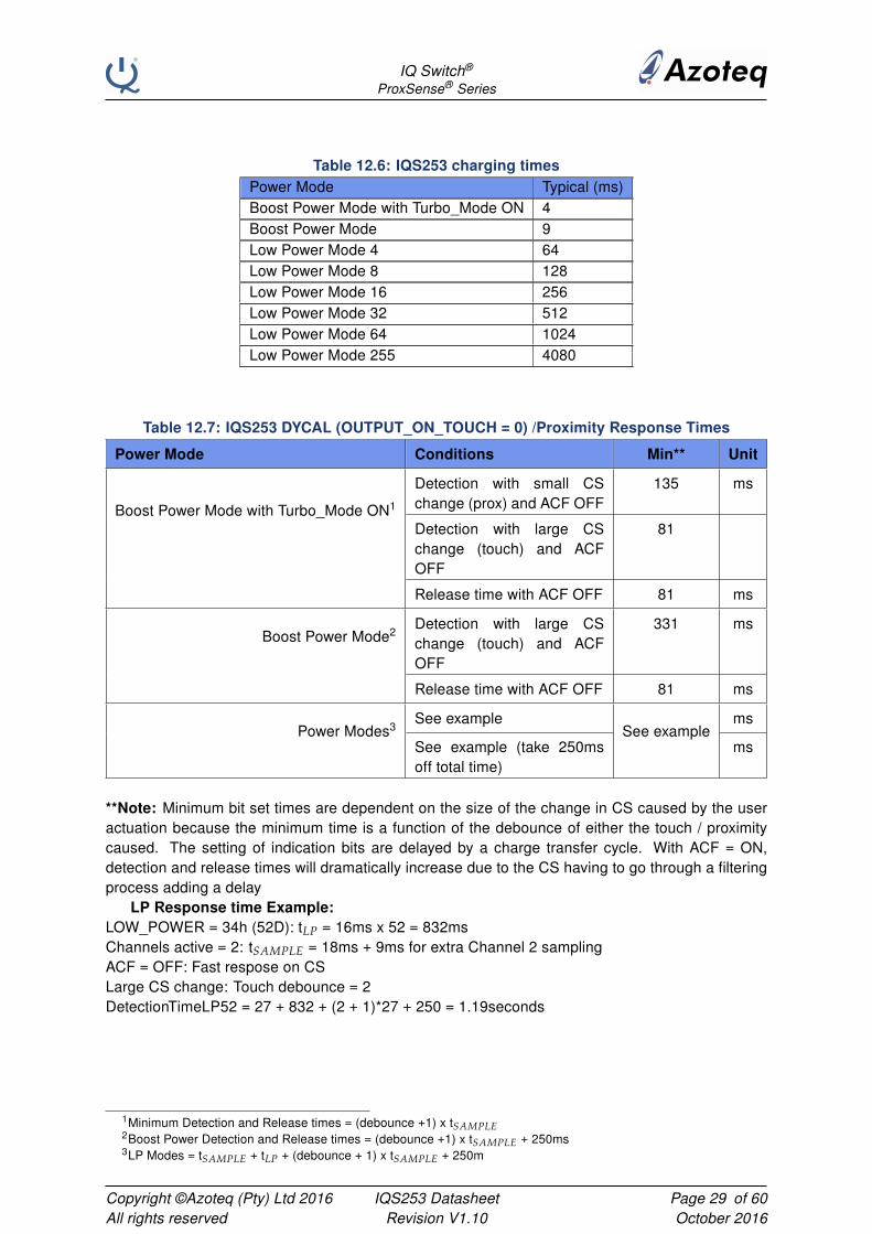
Table 12.6: IQS253 charging timesPower Mode Typical (ms)Boost Power Mode with Turbo_Mode ON 4Boost Power Mode 9Low Power Mode 4 64Low Power Mode 8 128Low Power Mode 16 256Low Power Mode 32 512Low Power Mode 64 1024Low Power Mode 255 4080
Table 12.7: IQS253 DYCAL (OUTPUT_ON_TOUCH = 0) /Proximity Response Times
Power Mode Conditions Min** Unit
Boost Power Mode with Turbo_Mode ON1
Detection with small CSchange (prox) and ACF OFF
135 ms
Detection with large CSchange (touch) and ACFOFF
81
Release time with ACF OFF 81 ms
Boost Power Mode2Detection with large CSchange (touch) and ACFOFF
331 ms
Release time with ACF OFF 81 ms
Power Modes3See example
See examplems
See example (take 250msoff total time)
ms
**Note: Minimum bit set times are dependent on the size of the change in CS caused by the useractuation because the minimum time is a function of the debounce of either the touch / proximitycaused. The setting of indication bits are delayed by a charge transfer cycle. With ACF = ON,detection and release times will dramatically increase due to the CS having to go through a filteringprocess adding a delay
LP Response time Example:LOW_POWER = 34h (52D): tLP = 16ms x 52 = 832msChannels active = 2: tSAMPLE = 18ms + 9ms for extra Channel 2 samplingACF = OFF: Fast respose on CSLarge CS change: Touch debounce = 2DetectionTimeLP52 = 27 + 832 + (2 + 1)*27 + 250 = 1.19seconds
1Minimum Detection and Release times = (debounce +1) x tSAMPLE2Boost Power Detection and Release times = (debounce +1) x tSAMPLE + 250ms3LP Modes = tSAMPLE + tLP + (debounce + 1) x tSAMPLE + 250m
Copyright ©Azoteq (Pty) Ltd 2016All rights reserved
IQS253 DatasheetRevision V1.10
Page 29 of 60October 2016
IQ Switch®
ProxSense® Series
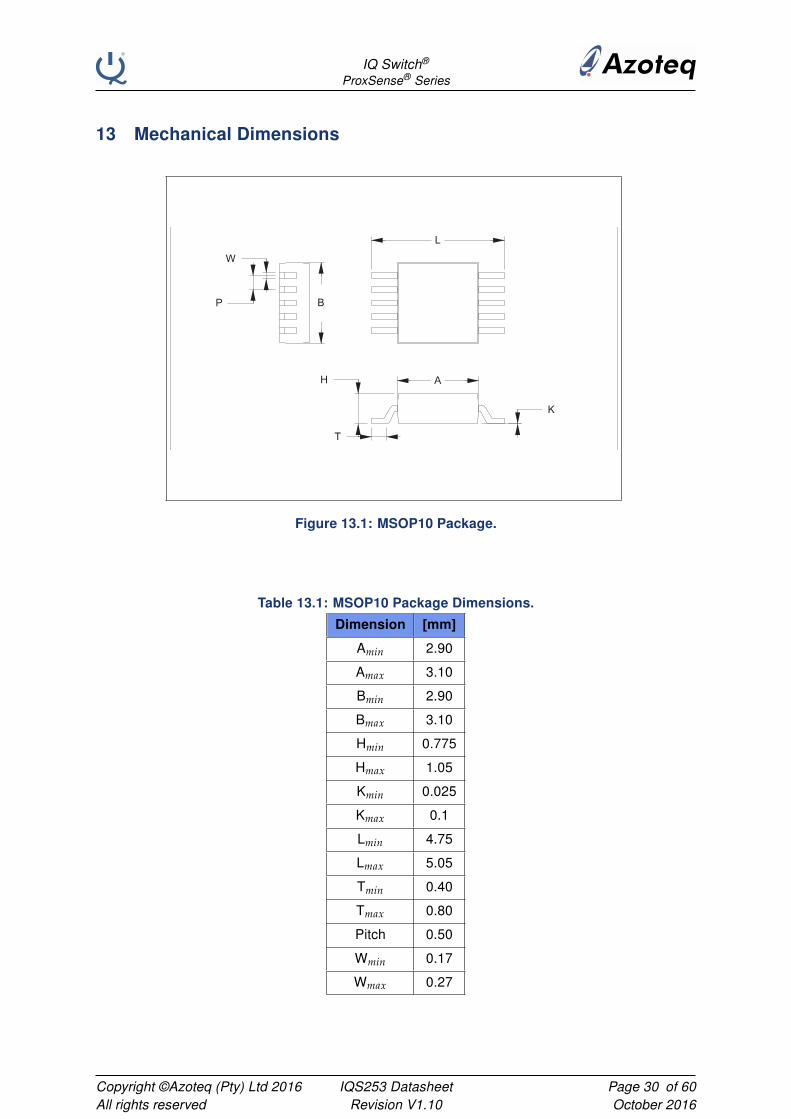
13 Mechanical Dimensions
�!"�
�
��
�
�
��
�
Figure 13.1: MSOP10 Package.
Table 13.1: MSOP10 Package Dimensions.
Dimension [mm]
Amin 2.90
Amax 3.10
Bmin 2.90
Bmax 3.10
Hmin 0.775
Hmax 1.05
Kmin 0.025
Kmax 0.1
Lmin 4.75
Lmax 5.05
Tmin 0.40
Tmax 0.80
Pitch 0.50
Wmin 0.17
Wmax 0.27
Copyright ©Azoteq (Pty) Ltd 2016All rights reserved
IQS253 DatasheetRevision V1.10
Page 30 of 60October 2016
IQ Switch®
ProxSense® Series
�!"#
�
�
�
�
�
�
�
�
�
�
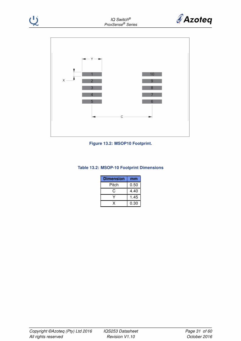
Figure 13.2: MSOP10 Footprint.
Table 13.2: MSOP-10 Footprint Dimensions
Dimension mm
Pitch 0.50
C 4.40
Y 1.45
X 0.30
Copyright ©Azoteq (Pty) Ltd 2016All rights reserved
IQS253 DatasheetRevision V1.10
Page 31 of 60October 2016
IQ Switch®
ProxSense® Series
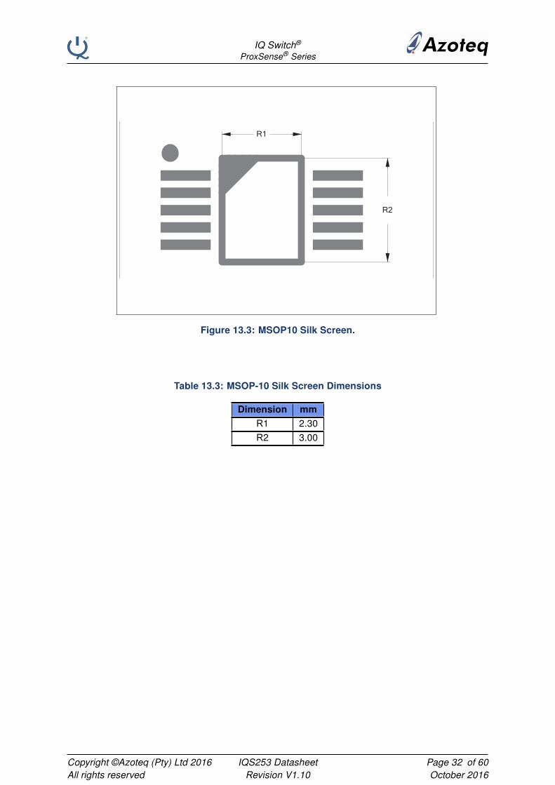
�
�
Figure 13.3: MSOP10 Silk Screen.
Table 13.3: MSOP-10 Silk Screen Dimensions
Dimension mm
R1 2.30
R2 3.00
Copyright ©Azoteq (Pty) Ltd 2016All rights reserved
IQS253 DatasheetRevision V1.10
Page 32 of 60October 2016
IQ Switch®
ProxSense® Series
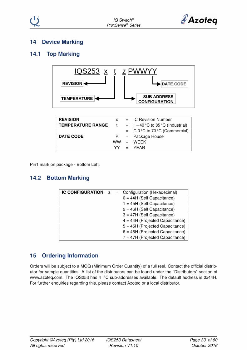
14 Device Marking
14.1 Top Marking
IQS253 x t z PWWYY
REVISION DATE CODE
SUB ADDRESS
CONFIGURATIONTEMPERATURE
REVISION x = IC Revision NumberTEMPERATURE RANGE t = I −40 °C to 85 °C (Industrial)
= C 0 °C to 70 °C (Commercial)DATE CODE P = Package House
WW = WEEKYY = YEAR
Pin1 mark on package - Bottom Left.
14.2 Bottom Marking
IC CONFIGURATION z = Configuration (Hexadecimal)0 = 44H (Self Capacitance)1 = 45H (Self Capacitance)2 = 46H (Self Capacitance)3 = 47H (Self Capacitance)4 = 44H (Projected Capacitance)5 = 45H (Projected Capacitance)6 = 46H (Projected Capacitance)7 = 47H (Projected Capacitance)
15 Ordering Information
Orders will be subject to a MOQ (Minimum Order Quantity) of a full reel. Contact the official distrib-utor for sample quantities. A list of the distributors can be found under the "Distributors" section ofwww.azoteq.com. The IQS253 has 4 I2C sub-addresses available. The default address is 0x44H.For further enquiries regarding this, please contact Azoteq or a local distributor.
Copyright ©Azoteq (Pty) Ltd 2016All rights reserved
IQS253 DatasheetRevision V1.10
Page 33 of 60October 2016
IQ Switch®
ProxSense® Series
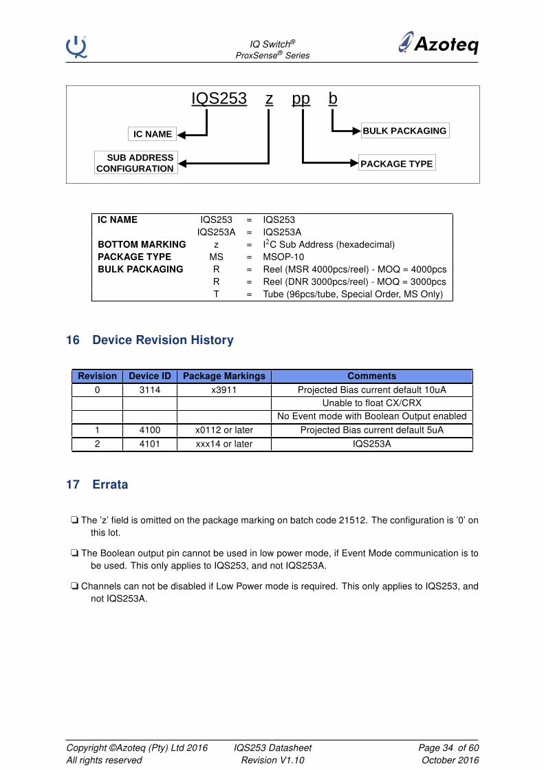
IQS253 z pp b
IC NAME
SUB ADDRESS
CONFIGURATION
BULK PACKAGING
PACKAGE TYPE
IC NAME IQS253 = IQS253IQS253A = IQS253A
BOTTOM MARKING z = I2C Sub Address (hexadecimal)PACKAGE TYPE MS = MSOP-10BULK PACKAGING R = Reel (MSR 4000pcs/reel) - MOQ = 4000pcs
R = Reel (DNR 3000pcs/reel) - MOQ = 3000pcsT = Tube (96pcs/tube, Special Order, MS Only)
16 Device Revision History
Revision Device ID Package Markings Comments
0 3114 x3911 Projected Bias current default 10uAUnable to float CX/CRX
No Event mode with Boolean Output enabled
1 4100 x0112 or later Projected Bias current default 5uA
2 4101 xxx14 or later IQS253A
17 Errata
o The ’z’ field is omitted on the package marking on batch code 21512. The configuration is ’0’ onthis lot.
o The Boolean output pin cannot be used in low power mode, if Event Mode communication is tobe used. This only applies to IQS253, and not IQS253A.
o Channels can not be disabled if Low Power mode is required. This only applies to IQS253, andnot IQS253A.
Copyright ©Azoteq (Pty) Ltd 2016All rights reserved
IQS253 DatasheetRevision V1.10
Page 34 of 60October 2016
IQ Switch®
ProxSense® Series
A DYCAL Illustrations
To view the illustrations in Appendix A, the document requires to be opened with Adobe Reader
Version 6 or later. Note that all illustrations are supplementary, and are not required to use with the
datasheet.
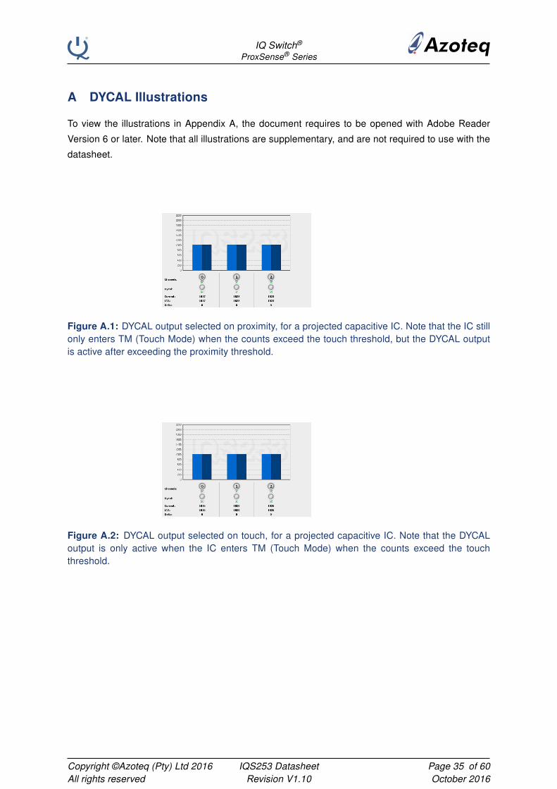
Figure A.1: DYCAL output selected on proximity, for a projected capacitive IC. Note that the IC stillonly enters TM (Touch Mode) when the counts exceed the touch threshold, but the DYCAL outputis active after exceeding the proximity threshold.
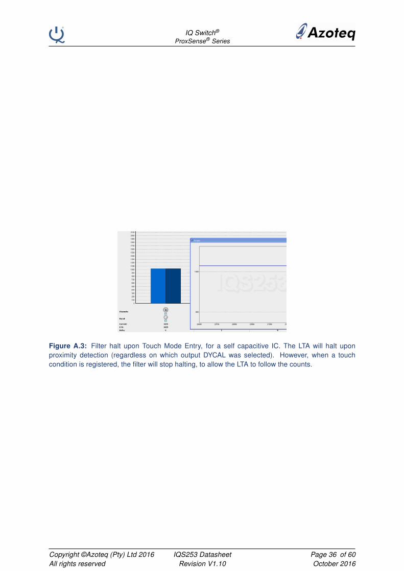
Figure A.2: DYCAL output selected on touch, for a projected capacitive IC. Note that the DYCALoutput is only active when the IC enters TM (Touch Mode) when the counts exceed the touchthreshold.
Copyright ©Azoteq (Pty) Ltd 2016All rights reserved
IQS253 DatasheetRevision V1.10
Page 35 of 60October 2016
IQ Switch®
ProxSense® Series
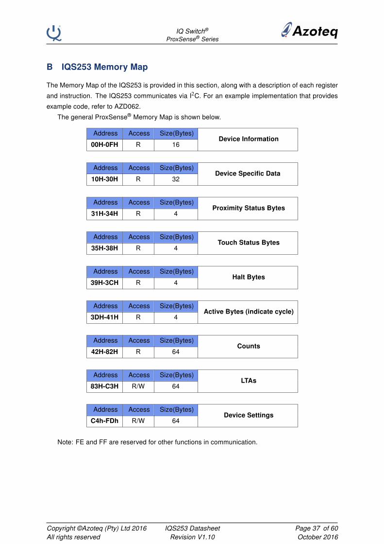
Figure A.3: Filter halt upon Touch Mode Entry, for a self capacitive IC. The LTA will halt uponproximity detection (regardless on which output DYCAL was selected). However, when a touchcondition is registered, the filter will stop halting, to allow the LTA to follow the counts.
Copyright ©Azoteq (Pty) Ltd 2016All rights reserved
IQS253 DatasheetRevision V1.10
Page 36 of 60October 2016
IQ Switch®
ProxSense® Series
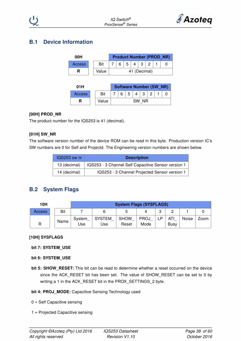
B IQS253 Memory Map
The Memory Map of the IQS253 is provided in this section, along with a description of each register
and instruction. The IQS253 communicates via I2C. For an example implementation that provides
example code, refer to AZD062.
The general ProxSense® Memory Map is shown below.
Address Access Size(Bytes)Device Information
00H-0FH R 16
Address Access Size(Bytes)Device Specific Data
10H-30H R 32
Address Access Size(Bytes)Proximity Status Bytes
31H-34H R 4
Address Access Size(Bytes)Touch Status Bytes
35H-38H R 4
Address Access Size(Bytes)Halt Bytes
39H-3CH R 4
Address Access Size(Bytes)Active Bytes (indicate cycle)
3DH-41H R 4
Address Access Size(Bytes)Counts
42H-82H R 64
Address Access Size(Bytes)LTAs
83H-C3H R/W 64
Address Access Size(Bytes)Device Settings
C4h-FDh R/W 64
Note: FE and FF are reserved for other functions in communication.
Copyright ©Azoteq (Pty) Ltd 2016All rights reserved
IQS253 DatasheetRevision V1.10
Page 37 of 60October 2016
IQ Switch®
ProxSense® Series
B.1 Device Information
00H Product Number (PROD_NR)
Access Bit 7 6 5 4 3 2 1 0
R Value 41 (Decimal)
01H Software Number (SW_NR)
Access Bit 7 6 5 4 3 2 1 0
R Value SW_NR
[00H] PROD_NR
The product number for the IQS253 is 41 (decimal).
[01H] SW_NR
The software version number of the device ROM can be read in this byte. Production version IC’s
SW numbers are 0 for Self and Projectd. The Engineering version numbers are shown below.
IQS253 sw nr Description
13 (decimal) IQS253 - 3 Channel Self Capacitive Sensor version 1
14 (decimal) IQS253 - 3 Channel Projected Sensor version 1
B.2 System Flags
10H System Flags (SYSFLAGS)
Access Bit 7 6 5 4 3 2 1 0
NameSystem_ SYSTEM_ SHOW_ PROJ_ LP ATI_ Noise Zoom
R Use Use Reset Mode Busy
[10H] SYSFLAGS
bit 7: SYSTEM_USE
bit 6: SYSTEM_USE
bit 5: SHOW_RESET: This bit can be read to determine whether a reset occurred on the device
since the ACK_RESET bit has been set. The value of SHOW_RESET can be set to 0 by
writing a 1 in the ACK_RESET bit in the PROX_SETTINGS_2 byte.
bit 4: PROJ_MODE: Capacitive Sensing Technology used
0 = Self Capacitive sensing
1 = Projected Capacitive sensing
Copyright ©Azoteq (Pty) Ltd 2016All rights reserved
IQS253 DatasheetRevision V1.10
Page 38 of 60October 2016
IQ Switch®
ProxSense® Series
bit 3: LP: If a LP mode is enabled, this bit indicates that charging is currently occurring in a LP
rate.
0 = Full-speed charging
1 = Charging currently occur at a lower rate
bit 2: ATI_BUSY: Status of automated ATI routine
0 = Auto ATI is not busy
1 = Auto ATI in progress
bit 1: NOISE: This bit indicates the presence of noise interference.
0 = IC has not detected the presence of noise
1 = IC has detected the presence of noise
bit 0: ZOOM: Zoom will indicate full-speed charging once an undebounced proximity is detected.
In NP mode, this will not change the charging frequency.
0 = IC not zoomed in
1 = IC detected undebounced proximity and IC is charging at full-speed
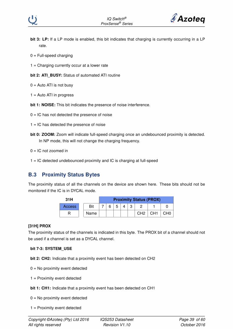
B.3 Proximity Status Bytes
The proximity status of all the channels on the device are shown here. These bits should not be
monitored if the IC is in DYCAL mode.
31H Proximity Status (PROX)
Access Bit 7 6 5 4 3 2 1 0
R Name CH2 CH1 CH0
[31H] PROX
The proximity status of the channels is indicated in this byte. The PROX bit of a channel should not
be used if a channel is set as a DYCAL channel.
bit 7-3: SYSTEM_USE
bit 2: CH2: Indicate that a proximity event has been detected on CH2
0 = No proximity event detected
1 = Proximity event detected
bit 1: CH1: Indicate that a proximity event has been detected on CH1
0 = No proximity event detected
1 = Proximity event detected
Copyright ©Azoteq (Pty) Ltd 2016All rights reserved
IQS253 DatasheetRevision V1.10
Page 39 of 60October 2016
IQ Switch®
ProxSense® Series
bit 0: CH0: Indicate that a proximity event has been detected on CH0
0 = No proximity event detected
1 = Proximity event detected
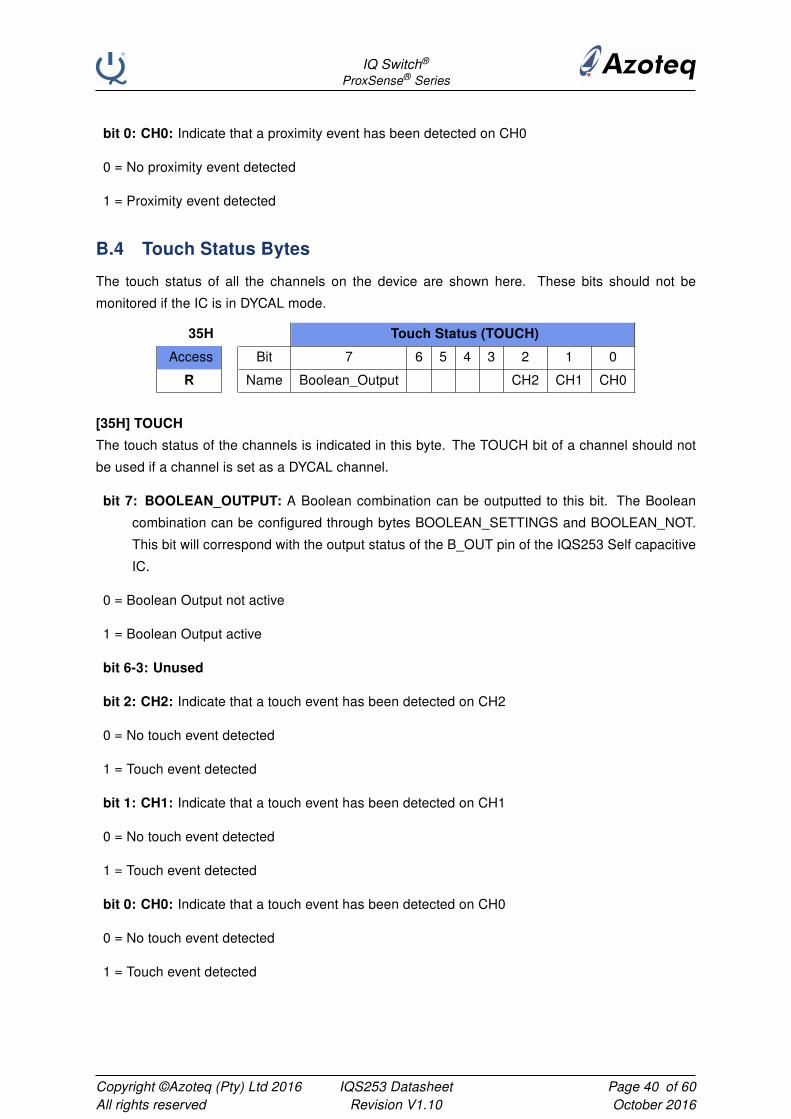
B.4 Touch Status Bytes
The touch status of all the channels on the device are shown here. These bits should not be
monitored if the IC is in DYCAL mode.
35H Touch Status (TOUCH)
Access Bit 7 6 5 4 3 2 1 0
R Name Boolean_Output CH2 CH1 CH0
[35H] TOUCH
The touch status of the channels is indicated in this byte. The TOUCH bit of a channel should not
be used if a channel is set as a DYCAL channel.
bit 7: BOOLEAN_OUTPUT: A Boolean combination can be outputted to this bit. The Boolean
combination can be configured through bytes BOOLEAN_SETTINGS and BOOLEAN_NOT.
This bit will correspond with the output status of the B_OUT pin of the IQS253 Self capacitive
IC.
0 = Boolean Output not active
1 = Boolean Output active
bit 6-3: Unused
bit 2: CH2: Indicate that a touch event has been detected on CH2
0 = No touch event detected
1 = Touch event detected
bit 1: CH1: Indicate that a touch event has been detected on CH1
0 = No touch event detected
1 = Touch event detected
bit 0: CH0: Indicate that a touch event has been detected on CH0
0 = No touch event detected
1 = Touch event detected
Copyright ©Azoteq (Pty) Ltd 2016All rights reserved
IQS253 DatasheetRevision V1.10
Page 40 of 60October 2016
IQ Switch®
ProxSense® Series
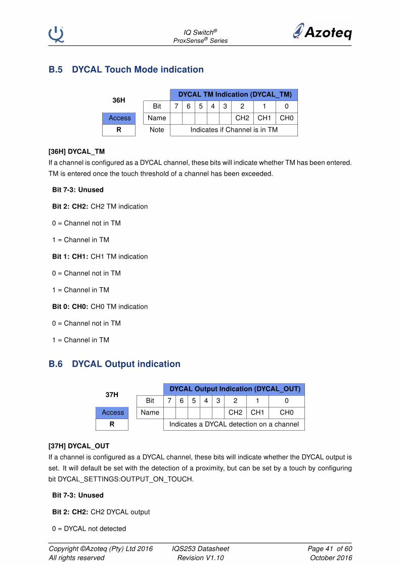
B.5 DYCAL Touch Mode indication
36HDYCAL TM Indication (DYCAL_TM)
Bit 7 6 5 4 3 2 1 0
Access Name CH2 CH1 CH0
R Note Indicates if Channel is in TM
[36H] DYCAL_TM
If a channel is configured as a DYCAL channel, these bits will indicate whether TM has been entered.
TM is entered once the touch threshold of a channel has been exceeded.
Bit 7-3: Unused
Bit 2: CH2: CH2 TM indication
0 = Channel not in TM
1 = Channel in TM
Bit 1: CH1: CH1 TM indication
0 = Channel not in TM
1 = Channel in TM
Bit 0: CH0: CH0 TM indication
0 = Channel not in TM
1 = Channel in TM
B.6 DYCAL Output indication
37HDYCAL Output Indication (DYCAL_OUT)
Bit 7 6 5 4 3 2 1 0
Access Name CH2 CH1 CH0
R Indicates a DYCAL detection on a channel
[37H] DYCAL_OUT
If a channel is configured as a DYCAL channel, these bits will indicate whether the DYCAL output is
set. It will default be set with the detection of a proximity, but can be set by a touch by configuring
bit DYCAL_SETTINGS:OUTPUT_ON_TOUCH.
Bit 7-3: Unused
Bit 2: CH2: CH2 DYCAL output
0 = DYCAL not detected
Copyright ©Azoteq (Pty) Ltd 2016All rights reserved
IQS253 DatasheetRevision V1.10
Page 41 of 60October 2016
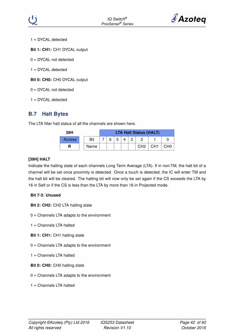
IQ Switch®
ProxSense® Series
1 = DYCAL detected
Bit 1: CH1: CH1 DYCAL output
0 = DYCAL not detected
1 = DYCAL detected
Bit 0: CH0: CH0 DYCAL output
0 = DYCAL not detected
1 = DYCAL detected
B.7 Halt Bytes
The LTA filter halt status of all the channels are shown here.
39H LTA Halt Status (HALT)
Access Bit 7 6 5 4 3 2 1 0
R Name CH2 CH1 CH0
[39H] HALT
Indicate the halting state of each channels Long Term Average (LTA). If in non-TM, the halt bit of a
channel will be set once proximity is detected. Once a touch is detected, the IC will enter TM and
the halt bit will be cleared. The halting bit will now only be set again if the CS exceeds the LTA by
16 in Self or if the CS is less than the LTA by more than 16 in Projected mode.
Bit 7-3: Unused
Bit 2: CH2: CH2 LTA halting state
0 = Channels LTA adapts to the environment
1 = Channels LTA halted
Bit 1: CH1: CH1 halting state
0 = Channels LTA adapts to the environment
1 = Channels LTA halted
Bit 0: CH0: CH0 halting state
0 = Channels LTA adapts to the environment
1 = Channels LTA halted
Copyright ©Azoteq (Pty) Ltd 2016All rights reserved
IQS253 DatasheetRevision V1.10
Page 42 of 60October 2016
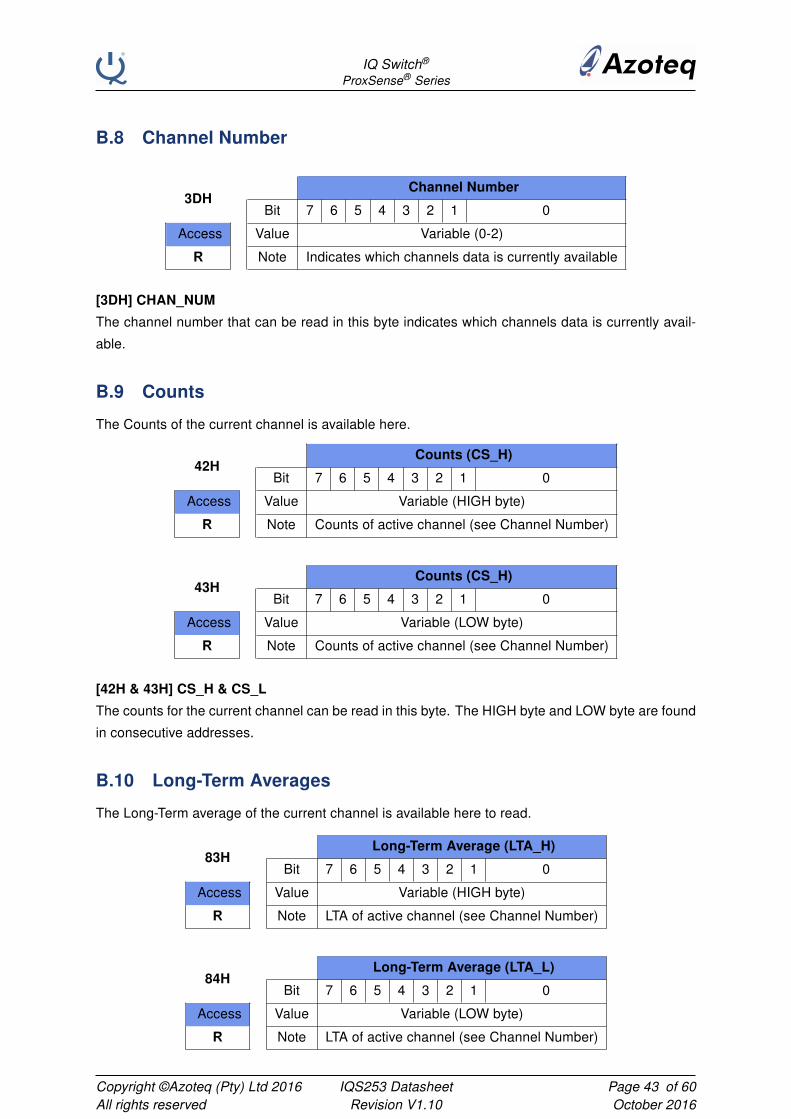
IQ Switch®
ProxSense® Series
B.8 Channel Number
3DHChannel Number
Bit 7 6 5 4 3 2 1 0
Access Value Variable (0-2)
R Note Indicates which channels data is currently available
[3DH] CHAN_NUM
The channel number that can be read in this byte indicates which channels data is currently avail-
able.
B.9 Counts
The Counts of the current channel is available here.
42HCounts (CS_H)
Bit 7 6 5 4 3 2 1 0
Access Value Variable (HIGH byte)
R Note Counts of active channel (see Channel Number)
43HCounts (CS_H)
Bit 7 6 5 4 3 2 1 0
Access Value Variable (LOW byte)
R Note Counts of active channel (see Channel Number)
[42H & 43H] CS_H & CS_L
The counts for the current channel can be read in this byte. The HIGH byte and LOW byte are found
in consecutive addresses.
B.10 Long-Term Averages
The Long-Term average of the current channel is available here to read.
83HLong-Term Average (LTA_H)
Bit 7 6 5 4 3 2 1 0
Access Value Variable (HIGH byte)
R Note LTA of active channel (see Channel Number)
84HLong-Term Average (LTA_L)
Bit 7 6 5 4 3 2 1 0
Access Value Variable (LOW byte)
R Note LTA of active channel (see Channel Number)
Copyright ©Azoteq (Pty) Ltd 2016All rights reserved
IQS253 DatasheetRevision V1.10
Page 43 of 60October 2016
IQ Switch®
ProxSense® Series
[83H & 84H] LTA_H & LTA_L
The LTA value for the current channel can be read in this byte. The HIGH byte and LOW byte are
found in consecutive addresses.
B.11 Device Settings
It is attempted that the commonly used settings are situated closer to the top of the memory block.
Settings that are regarded as more once-off are placed further down.
B.12 ATI Target
C4HATI Target Value (ATI_TARGET)
Bit 7 6 5 4 3 2 1 0
Access Value ATI Target value (x8 to get real target)
R/W Default 1 0 0 0 0 0 0 0
Note 128 Decimal (x8 gives Target value = 1024)
[C4H] ATI_TARGET
The IQS253 default target is 1024 counts. The IQS253A default target is 512 counts. The auto-
mated ATI target can be set in this byte. The value written to this byte multiplied by 8 will be the target
value of all 3 channels. If a new target value is required, the required target (divided by 8) should
be written to this byte, where-after a re-ATI event should be sent. All 3 channels will now be at the
target value once the SYSFLAGS_ATI_BUSY flag is cleared. ATI Multiplier and Compensation
The ATI Multiplier and ATI Compensation bits allow the controller to be compatible with a large
range of sensors, and in many applications with different environments. ATI allows the user to
maintain a specific sample value on all channels. The ATI Multiplier parameters would produce the
largest changes in sample values and can be thought of as the high bits of ATI. The ATI Compen-
sation bits are used to influence the sample values on a smaller scale to provide precision when
balancing all channels as close as possible to the target. The ATI Multiplier parameters are further
grouped into two parameters namely ATI Multiplier- Compensation and ATI Multiplier-Sensitivity. ATI
multiplier-Compensation consists of 2 bits and has the biggest effect on the sample value and can
be considered as the highest bit of the ATI parameters. The ATI Multiplier-Sensitivity can be ad-
justed with 4 bits for each channel. The value of 1111 would provide the highest CS value and the
value of 0000 would provide the lowest.
B.13 Compensation
C5HCH0 Compensation (COMP0)
Bit 7 6 5 4 3 2 1 0
Access Value Automatically adjusted when ATI enabled
R/W Default 0
Copyright ©Azoteq (Pty) Ltd 2016All rights reserved
IQS253 DatasheetRevision V1.10
Page 44 of 60October 2016
IQ Switch®
ProxSense® Series
C6HCH1 Compensation (COMP1)
Bit 7 6 5 4 3 2 1 0
Access Value Automatically adjusted when ATI enabled
R/W Default 0
C7HCH2 Compensation (COMP2)
Bit 7 6 5 4 3 2 1 0
Access Value Automatically adjusted when ATI enabled
R/W Default 0
[C5H, C6H, C7H] Compensation Settings (CH0_COMP, CH1_COMP, CH2_COMP)
The compensation settings for each channel are contained in these bytes. The values in these bytes
are automatically determined if the Auto ATI function was used. If PROX_SETTINGS0:ATI_OFF is
set, the Automatic ATI setting is disabled and this byte can be altered to achieve a custom target
value. The ATI Compensation parameter can be configured for each channel in a range between
0-255 (decimal). The ATI compensation bits can be used to make small adjustments of the sample
values of the individual channels.
B.14 Base Values
C8H CH0 ATI BASE and Multipliers (CH0_ATI_BASE)
Bit 7 6 5 4 3 2 1 0
ValueCH0_ CH0_ MULT_ MULT_ MULT_ MULT_ MULT_ MULT_Access
BASE1 BASE0 SENSE1 SENSE0 COMP3 COMP2 COMP1 COMP0
R/W gain scale
C9H CH1 ATI BASE and Multipliers (CH1_ATI_BASE)
Bit 7 6 5 4 3 2 1 0
Access CH1_ CH1_ MULT_ MULT_ MULT_ MULT_ MULT_ MULT_R/W BASE1 BASE0 SENSE1 SENSE0 COMP3 COMP2 COMP1 COMP0
CAH CH2 ATI BASE and Multipliers (CH2_ATI_BASE)
Bit 7 6 5 4 3 2 1 0
Access CH2_ CH2_ MULT_ MULT_ MULT_ MULT_ MULT_ MULT_R/W BASE1 BASE0 SENSE1 SENSE0 COMP3 COMP2 COMP1 COMP0
[C8H, C9H, CAH] Base values and Multiplier settings (CH0_BASE, CH1_BASE, CH2_BASE)
The base value or Multiplier settings of each channel can be set in these bytes.
Bit 7-6: CHx_BASE1:CHx_BASE0: Channel Base Values
ALT_BASE = 0
Copyright ©Azoteq (Pty) Ltd 2016All rights reserved
IQS253 DatasheetRevision V1.10
Page 45 of 60October 2016
IQ Switch®
ProxSense® Series
00 = 200 (IQS253 default)
01 = 50
10 = 100 (IQS253A default)
11 = 250
ALT_BASE = 1
00 = 150
01 = 350
10 = 500
11 = 700
Bit 5-4: MULT_SENSE1:MULT_SENSE0: Sensitivity Multiplier Settings. Rough adjustments of
base counts.
00 = 1 (small electrodes)
11 = 4 (large electrodes)
Bit 3-0: MULT_COMP3:MULT_COMP0: Compensation Multiplier Settings. Fine adjustments of
base counts.
0000 = 1 (smallest)
1111 = 18 (largest)
B.15 Proximity Thresholds
CBHProximity Threshold (PROX_THR_CH0)
Bit 7 6 5 4 3 2 1 0
Access Name PT_7 PT_6 PT_5 PT_4 PT_3 PT_2 PT_1 PT_0
R/W Default 0 0 0 0 0 1 0 0
CCHProximity Threshold (PROX_THR_CH1)
Bit 7 6 5 4 3 2 1 0
Access Name PT_7 PT_6 PT_5 PT_4 PT_3 PT_2 PT_1 PT_0
R/W Default 0 0 0 1 0 0
CDHProximity Threshold (PROX_THR_CH2)
Bit 7 6 5 4 3 2 1 0
Access Name PT_7 PT_6 PT_5 PT_4 PT_3 PT_2 PT_1 PT_0
R/W Default 0 0 0 1 0 0
Copyright ©Azoteq (Pty) Ltd 2016All rights reserved
IQS253 DatasheetRevision V1.10
Page 46 of 60October 2016
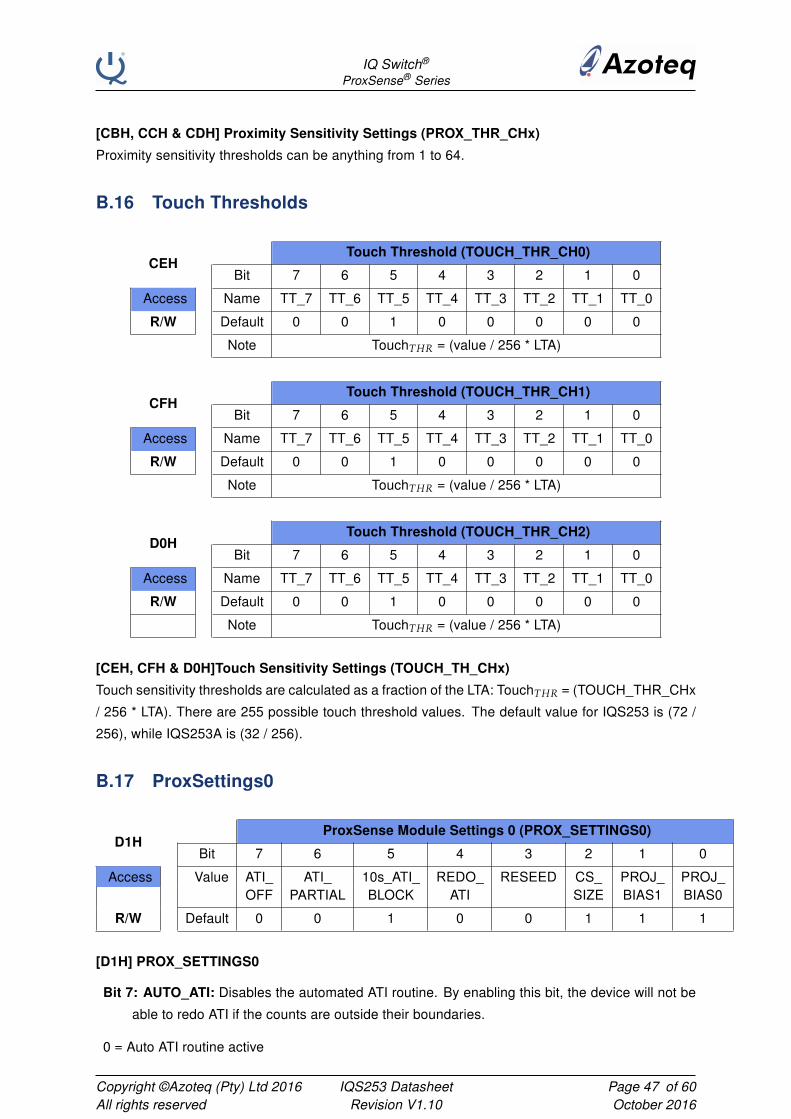
IQ Switch®
ProxSense® Series
[CBH, CCH & CDH] Proximity Sensitivity Settings (PROX_THR_CHx)
Proximity sensitivity thresholds can be anything from 1 to 64.
B.16 Touch Thresholds
CEHTouch Threshold (TOUCH_THR_CH0)
Bit 7 6 5 4 3 2 1 0
Access Name TT_7 TT_6 TT_5 TT_4 TT_3 TT_2 TT_1 TT_0
R/W Default 0 0 1 0 0 0 0 0
Note TouchTHR = (value / 256 * LTA)
CFHTouch Threshold (TOUCH_THR_CH1)
Bit 7 6 5 4 3 2 1 0
Access Name TT_7 TT_6 TT_5 TT_4 TT_3 TT_2 TT_1 TT_0
R/W Default 0 0 1 0 0 0 0 0
Note TouchTHR = (value / 256 * LTA)
D0HTouch Threshold (TOUCH_THR_CH2)
Bit 7 6 5 4 3 2 1 0
Access Name TT_7 TT_6 TT_5 TT_4 TT_3 TT_2 TT_1 TT_0
R/W Default 0 0 1 0 0 0 0 0
Note TouchTHR = (value / 256 * LTA)
[CEH, CFH & D0H]Touch Sensitivity Settings (TOUCH_TH_CHx)
Touch sensitivity thresholds are calculated as a fraction of the LTA: TouchTHR = (TOUCH_THR_CHx
/ 256 * LTA). There are 255 possible touch threshold values. The default value for IQS253 is (72 /
256), while IQS253A is (32 / 256).
B.17 ProxSettings0
D1HProxSense Module Settings 0 (PROX_SETTINGS0)
Bit 7 6 5 4 3 2 1 0
Access Value ATI_ ATI_ 10s_ATI_ REDO_ RESEED CS_ PROJ_ PROJ_OFF PARTIAL BLOCK ATI SIZE BIAS1 BIAS0
R/W Default 0 0 1 0 0 1 1 1
[D1H] PROX_SETTINGS0
Bit 7: AUTO_ATI: Disables the automated ATI routine. By enabling this bit, the device will not be
able to redo ATI if the counts are outside their boundaries.
0 = Auto ATI routine active
Copyright ©Azoteq (Pty) Ltd 2016All rights reserved
IQS253 DatasheetRevision V1.10
Page 47 of 60October 2016

IQ Switch®
ProxSense® Series
1 = ATI disabled
Bit 6: ATI_PARTIAL: Enable Partial ATI.
0 = If ATI occur, it will use the base values as reference
1 = If ATI occur, it will use the MULTIPLIER_COMPx and MULTIPLIER_SENSx as reference
Bit 5: ATI_BLOCK: Enable the 10 second block of ATI after an actuation.
0 = Channels will always redo ATI if LTA is outside boundaries if no actuation is detected
1 = ATI will be blocked for 10 seconds after an actuation has occurred.
Bit 4: REDO_AUTO_ATI: Force the ATI routine to perform. The last written ATI_TARGET value
will be used as target.
0 = No action
1 = Force ATI routine to perform.
Bit 3: RESEED: Reseed the LTA filter. This can be used to adapt to an abrupt environment
change, where the filter is too slow to track this change. Note that with the Short and Long
Halt selections, an automatic Reseed will be performed when the halt time has expired, thus
automatically adjusting to the new surroundings.
0 = Do not reseed
1 = Reseed (this is a global reseed)
Bit 2: CS: Set the size of the internal sampling capacitor. A larger CS capacitor requires more
transfers (higher counts) to be charged.
0 = 29.9pF
1 = 59.8pF
Bit 1-0: PROJ_BIAS1:PROJ_BIAS0: Projected Bias Current
00 = 1.25uA (smallest)
01 = 2.5uA
10 = 5uA
11 = 10uA
Copyright ©Azoteq (Pty) Ltd 2016All rights reserved
IQS253 DatasheetRevision V1.10
Page 48 of 60October 2016
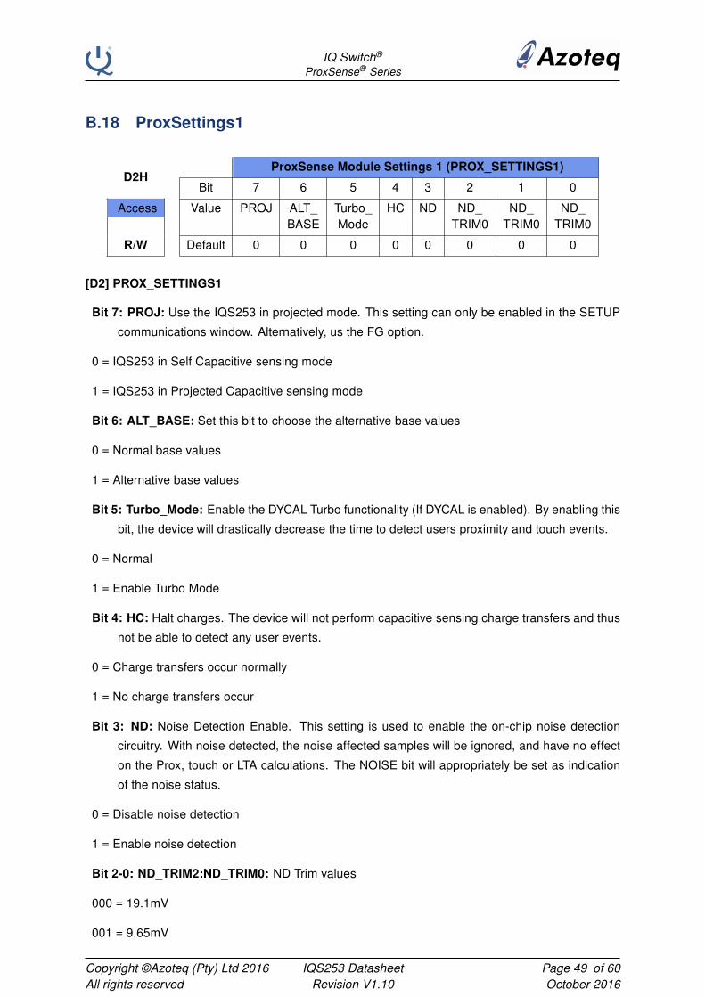
IQ Switch®
ProxSense® Series
B.18 ProxSettings1
D2HProxSense Module Settings 1 (PROX_SETTINGS1)
Bit 7 6 5 4 3 2 1 0
Access Value PROJ ALT_ Turbo_ HC ND ND_ ND_ ND_BASE Mode TRIM0 TRIM0 TRIM0
R/W Default 0 0 0 0 0 0 0 0
[D2] PROX_SETTINGS1
Bit 7: PROJ: Use the IQS253 in projected mode. This setting can only be enabled in the SETUP
communications window. Alternatively, us the FG option.
0 = IQS253 in Self Capacitive sensing mode
1 = IQS253 in Projected Capacitive sensing mode
Bit 6: ALT_BASE: Set this bit to choose the alternative base values
0 = Normal base values
1 = Alternative base values
Bit 5: Turbo_Mode: Enable the DYCAL Turbo functionality (If DYCAL is enabled). By enabling this
bit, the device will drastically decrease the time to detect users proximity and touch events.
0 = Normal
1 = Enable Turbo Mode
Bit 4: HC: Halt charges. The device will not perform capacitive sensing charge transfers and thus
not be able to detect any user events.
0 = Charge transfers occur normally
1 = No charge transfers occur
Bit 3: ND: Noise Detection Enable. This setting is used to enable the on-chip noise detection
circuitry. With noise detected, the noise affected samples will be ignored, and have no effect
on the Prox, touch or LTA calculations. The NOISE bit will appropriately be set as indication
of the noise status.
0 = Disable noise detection
1 = Enable noise detection
Bit 2-0: ND_TRIM2:ND_TRIM0: ND Trim values
000 = 19.1mV
001 = 9.65mV
Copyright ©Azoteq (Pty) Ltd 2016All rights reserved
IQS253 DatasheetRevision V1.10
Page 49 of 60October 2016
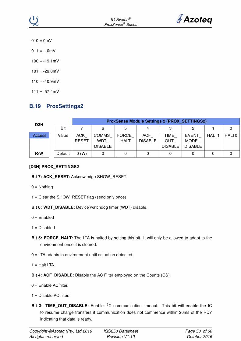
IQ Switch®
ProxSense® Series
010 = 0mV
011 = -10mV
100 = -19.1mV
101 = -29.8mV
110 = -40.9mV
111 = -57.4mV
B.19 ProxSettings2
D3HProxSense Module Settings 2 (PROX_SETTINGS2)
Bit 7 6 5 4 3 2 1 0
Access Value ACK_ COMMS_ FORCE_ ACF_ TIME_ EVENT_ HALT1 HALT0RESET WDT_ HALT DISABLE OUT_ MODE _
DISABLE DISABLE DISABLE
R/W Default 0 (W) 0 0 0 0 0 0 0
[D3H] PROX_SETTINGS2
Bit 7: ACK_RESET: Acknowledge SHOW_RESET.
0 = Nothing
1 = Clear the SHOW_RESET flag (send only once)
Bit 6: WDT_DISABLE: Device watchdog timer (WDT) disable.
0 = Enabled
1 = Disabled
Bit 5: FORCE_HALT: The LTA is halted by setting this bit. It will only be allowed to adapt to the
environment once it is cleared.
0 = LTA adapts to environment until actuation detected.
1 = Halt LTA.
Bit 4: ACF_DISABLE: Disable the AC Filter employed on the Counts (CS).
0 = Enable AC filter.
1 = Disable AC filter.
Bit 3: TIME_OUT_DISABLE: Enable I2C communication timeout. This bit will enable the IC
to resume charge transfers if communication does not commence within 20ms of the RDY
indicating that data is ready.
Copyright ©Azoteq (Pty) Ltd 2016All rights reserved
IQS253 DatasheetRevision V1.10
Page 50 of 60October 2016
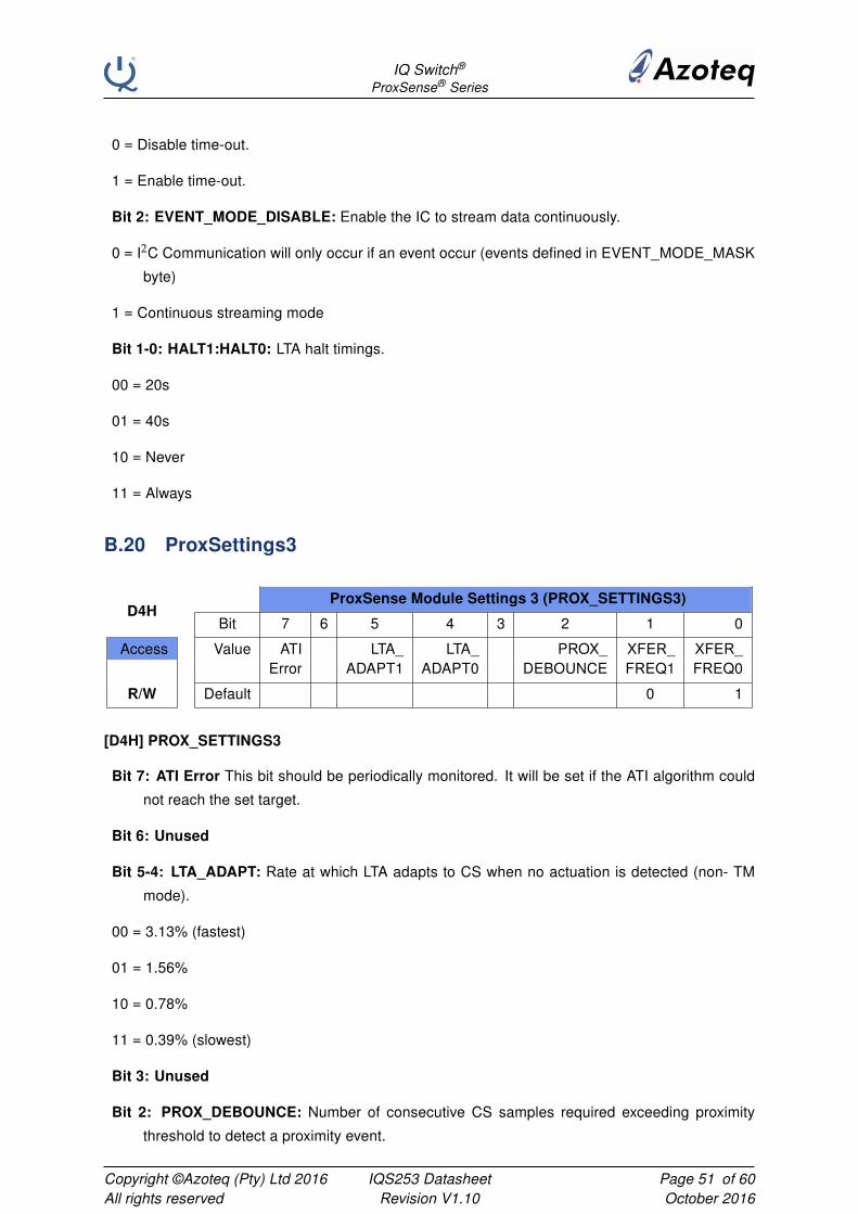
IQ Switch®
ProxSense® Series
0 = Disable time-out.
1 = Enable time-out.
Bit 2: EVENT_MODE_DISABLE: Enable the IC to stream data continuously.
0 = I2C Communication will only occur if an event occur (events defined in EVENT_MODE_MASK
byte)
1 = Continuous streaming mode
Bit 1-0: HALT1:HALT0: LTA halt timings.
00 = 20s
01 = 40s
10 = Never
11 = Always
B.20 ProxSettings3
D4HProxSense Module Settings 3 (PROX_SETTINGS3)
Bit 7 6 5 4 3 2 1 0
Access Value ATI LTA_ LTA_ PROX_ XFER_ XFER_Error ADAPT1 ADAPT0 DEBOUNCE FREQ1 FREQ0
R/W Default 0 1
[D4H] PROX_SETTINGS3
Bit 7: ATI Error This bit should be periodically monitored. It will be set if the ATI algorithm could
not reach the set target.
Bit 6: Unused
Bit 5-4: LTA_ADAPT: Rate at which LTA adapts to CS when no actuation is detected (non- TM
mode).
00 = 3.13% (fastest)
01 = 1.56%
10 = 0.78%
11 = 0.39% (slowest)
Bit 3: Unused
Bit 2: PROX_DEBOUNCE: Number of consecutive CS samples required exceeding proximity
threshold to detect a proximity event.
Copyright ©Azoteq (Pty) Ltd 2016All rights reserved
IQS253 DatasheetRevision V1.10
Page 51 of 60October 2016
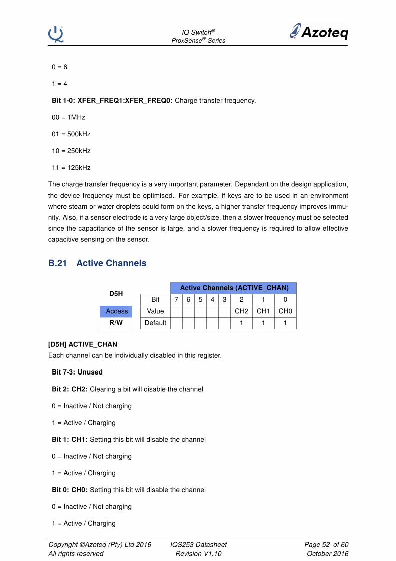
IQ Switch®
ProxSense® Series
0 = 6
1 = 4
Bit 1-0: XFER_FREQ1:XFER_FREQ0: Charge transfer frequency.
00 = 1MHz
01 = 500kHz
10 = 250kHz
11 = 125kHz
The charge transfer frequency is a very important parameter. Dependant on the design application,
the device frequency must be optimised. For example, if keys are to be used in an environment
where steam or water droplets could form on the keys, a higher transfer frequency improves immu-
nity. Also, if a sensor electrode is a very large object/size, then a slower frequency must be selected
since the capacitance of the sensor is large, and a slower frequency is required to allow effective
capacitive sensing on the sensor.
B.21 Active Channels
D5HActive Channels (ACTIVE_CHAN)
Bit 7 6 5 4 3 2 1 0
Access Value CH2 CH1 CH0
R/W Default 1 1 1
[D5H] ACTIVE_CHAN
Each channel can be individually disabled in this register.
Bit 7-3: Unused
Bit 2: CH2: Clearing a bit will disable the channel
0 = Inactive / Not charging
1 = Active / Charging
Bit 1: CH1: Setting this bit will disable the channel
0 = Inactive / Not charging
1 = Active / Charging
Bit 0: CH0: Setting this bit will disable the channel
0 = Inactive / Not charging
1 = Active / Charging
Copyright ©Azoteq (Pty) Ltd 2016All rights reserved
IQS253 DatasheetRevision V1.10
Page 52 of 60October 2016
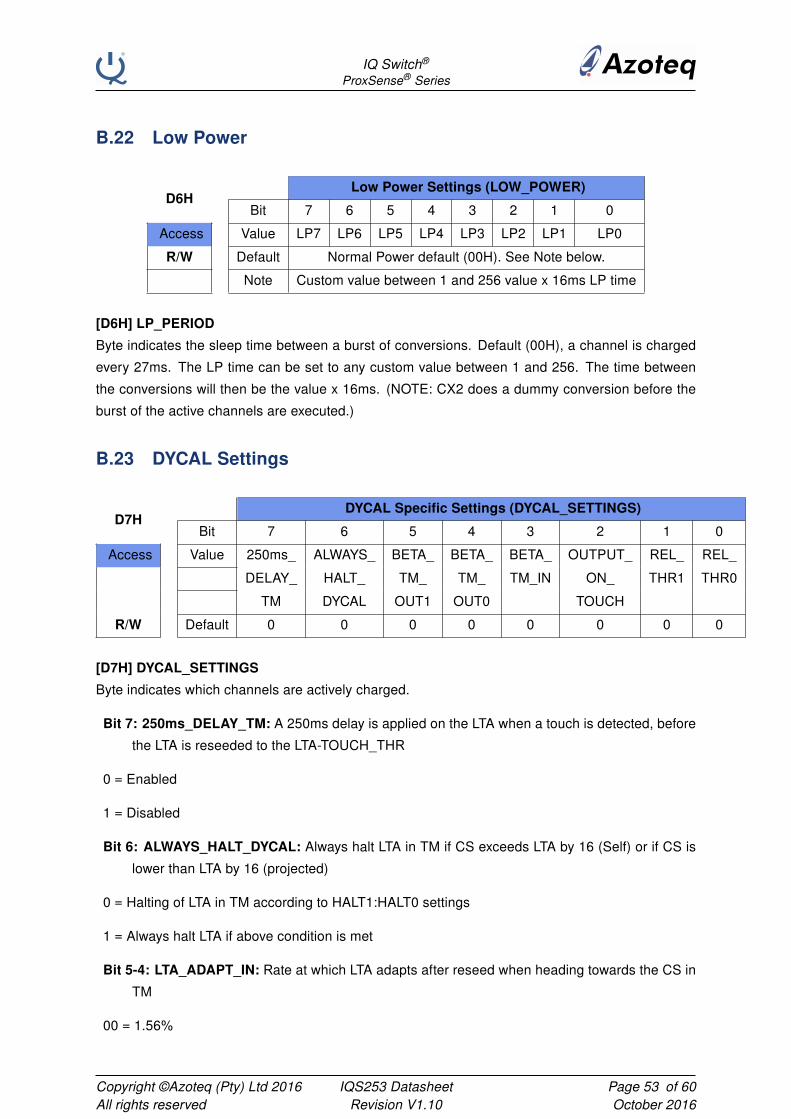
IQ Switch®
ProxSense® Series
B.22 Low Power
D6HLow Power Settings (LOW_POWER)
Bit 7 6 5 4 3 2 1 0
Access Value LP7 LP6 LP5 LP4 LP3 LP2 LP1 LP0
R/W Default Normal Power default (00H). See Note below.
Note Custom value between 1 and 256 value x 16ms LP time
[D6H] LP_PERIOD
Byte indicates the sleep time between a burst of conversions. Default (00H), a channel is charged
every 27ms. The LP time can be set to any custom value between 1 and 256. The time between
the conversions will then be the value x 16ms. (NOTE: CX2 does a dummy conversion before the
burst of the active channels are executed.)
B.23 DYCAL Settings
D7HDYCAL Specific Settings (DYCAL_SETTINGS)
Bit 7 6 5 4 3 2 1 0
Access Value 250ms_ ALWAYS_ BETA_ BETA_ BETA_ OUTPUT_ REL_ REL_
DELAY_ HALT_ TM_ TM_ TM_IN ON_ THR1 THR0
TM DYCAL OUT1 OUT0 TOUCH
R/W Default 0 0 0 0 0 0 0 0
[D7H] DYCAL_SETTINGS
Byte indicates which channels are actively charged.
Bit 7: 250ms_DELAY_TM: A 250ms delay is applied on the LTA when a touch is detected, before
the LTA is reseeded to the LTA-TOUCH_THR
0 = Enabled
1 = Disabled
Bit 6: ALWAYS_HALT_DYCAL: Always halt LTA in TM if CS exceeds LTA by 16 (Self) or if CS is
lower than LTA by 16 (projected)
0 = Halting of LTA in TM according to HALT1:HALT0 settings
1 = Always halt LTA if above condition is met
Bit 5-4: LTA_ADAPT_IN: Rate at which LTA adapts after reseed when heading towards the CS in
TM
00 = 1.56%
Copyright ©Azoteq (Pty) Ltd 2016All rights reserved
IQS253 DatasheetRevision V1.10
Page 53 of 60October 2016
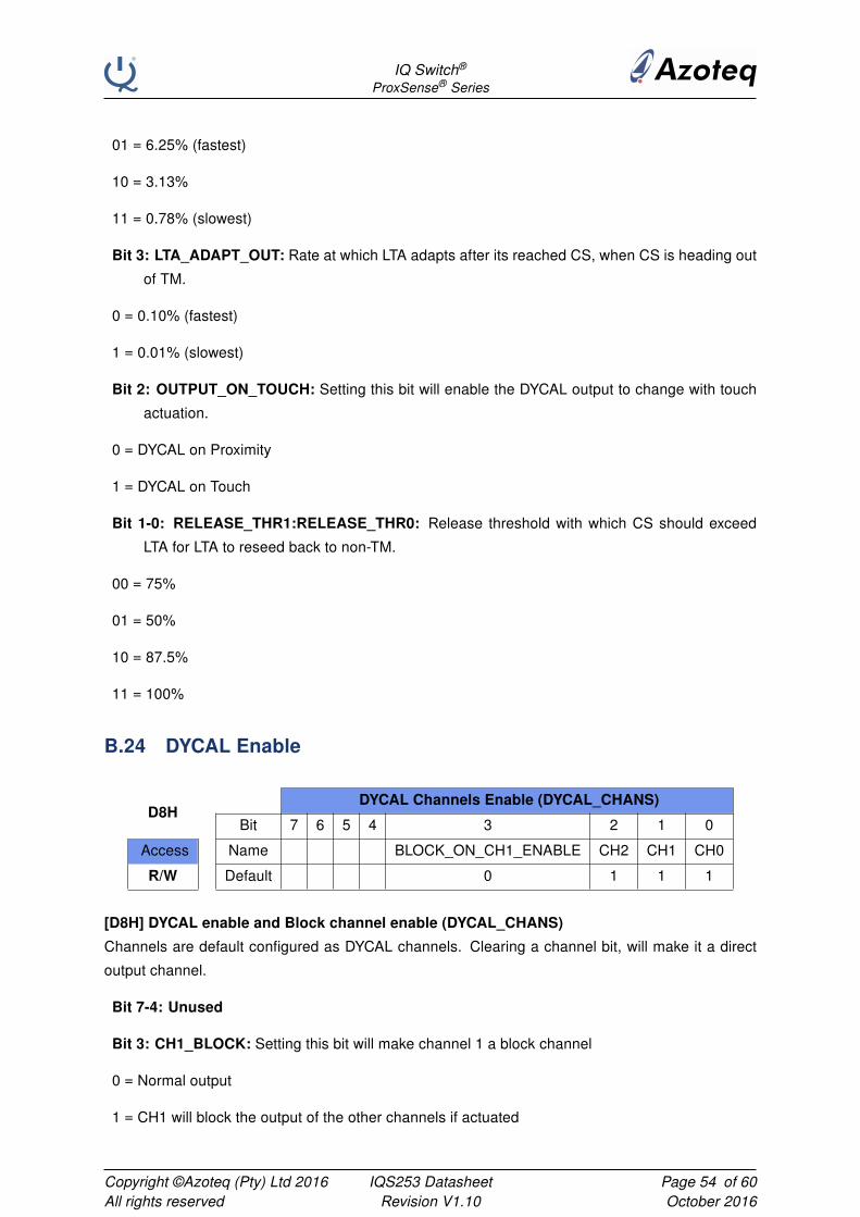
IQ Switch®
ProxSense® Series
01 = 6.25% (fastest)
10 = 3.13%
11 = 0.78% (slowest)
Bit 3: LTA_ADAPT_OUT: Rate at which LTA adapts after its reached CS, when CS is heading out
of TM.
0 = 0.10% (fastest)
1 = 0.01% (slowest)
Bit 2: OUTPUT_ON_TOUCH: Setting this bit will enable the DYCAL output to change with touch
actuation.
0 = DYCAL on Proximity
1 = DYCAL on Touch
Bit 1-0: RELEASE_THR1:RELEASE_THR0: Release threshold with which CS should exceed
LTA for LTA to reseed back to non-TM.
00 = 75%
01 = 50%
10 = 87.5%
11 = 100%
B.24 DYCAL Enable
D8HDYCAL Channels Enable (DYCAL_CHANS)
Bit 7 6 5 4 3 2 1 0
Access Name BLOCK_ON_CH1_ENABLE CH2 CH1 CH0
R/W Default 0 1 1 1
[D8H] DYCAL enable and Block channel enable (DYCAL_CHANS)
Channels are default configured as DYCAL channels. Clearing a channel bit, will make it a direct
output channel.
Bit 7-4: Unused
Bit 3: CH1_BLOCK: Setting this bit will make channel 1 a block channel
0 = Normal output
1 = CH1 will block the output of the other channels if actuated
Copyright ©Azoteq (Pty) Ltd 2016All rights reserved
IQS253 DatasheetRevision V1.10
Page 54 of 60October 2016
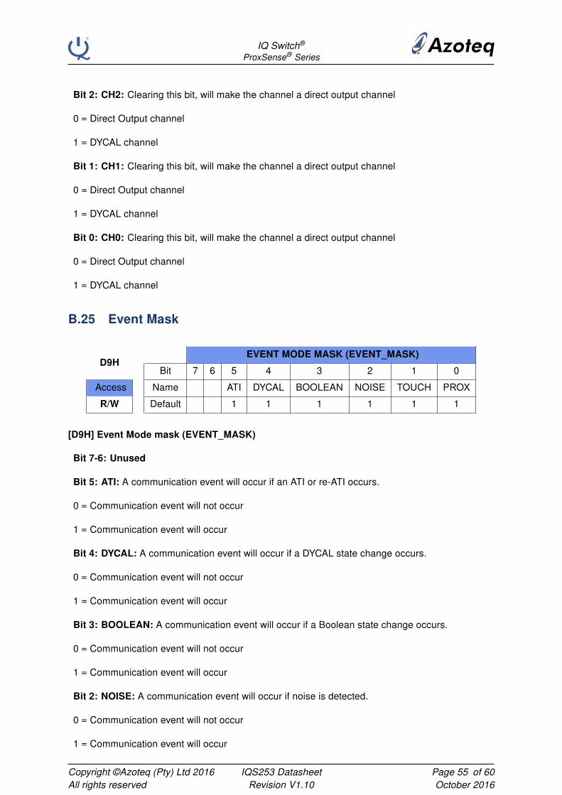
IQ Switch®
ProxSense® Series
Bit 2: CH2: Clearing this bit, will make the channel a direct output channel
0 = Direct Output channel
1 = DYCAL channel
Bit 1: CH1: Clearing this bit, will make the channel a direct output channel
0 = Direct Output channel
1 = DYCAL channel
Bit 0: CH0: Clearing this bit, will make the channel a direct output channel
0 = Direct Output channel
1 = DYCAL channel
B.25 Event Mask
D9HEVENT MODE MASK (EVENT_MASK)
Bit 7 6 5 4 3 2 1 0
Access Name ATI DYCAL BOOLEAN NOISE TOUCH PROX
R/W Default 1 1 1 1 1 1
[D9H] Event Mode mask (EVENT_MASK)
Bit 7-6: Unused
Bit 5: ATI: A communication event will occur if an ATI or re-ATI occurs.
0 = Communication event will not occur
1 = Communication event will occur
Bit 4: DYCAL: A communication event will occur if a DYCAL state change occurs.
0 = Communication event will not occur
1 = Communication event will occur
Bit 3: BOOLEAN: A communication event will occur if a Boolean state change occurs.
0 = Communication event will not occur
1 = Communication event will occur
Bit 2: NOISE: A communication event will occur if noise is detected.
0 = Communication event will not occur
1 = Communication event will occur
Copyright ©Azoteq (Pty) Ltd 2016All rights reserved
IQS253 DatasheetRevision V1.10
Page 55 of 60October 2016
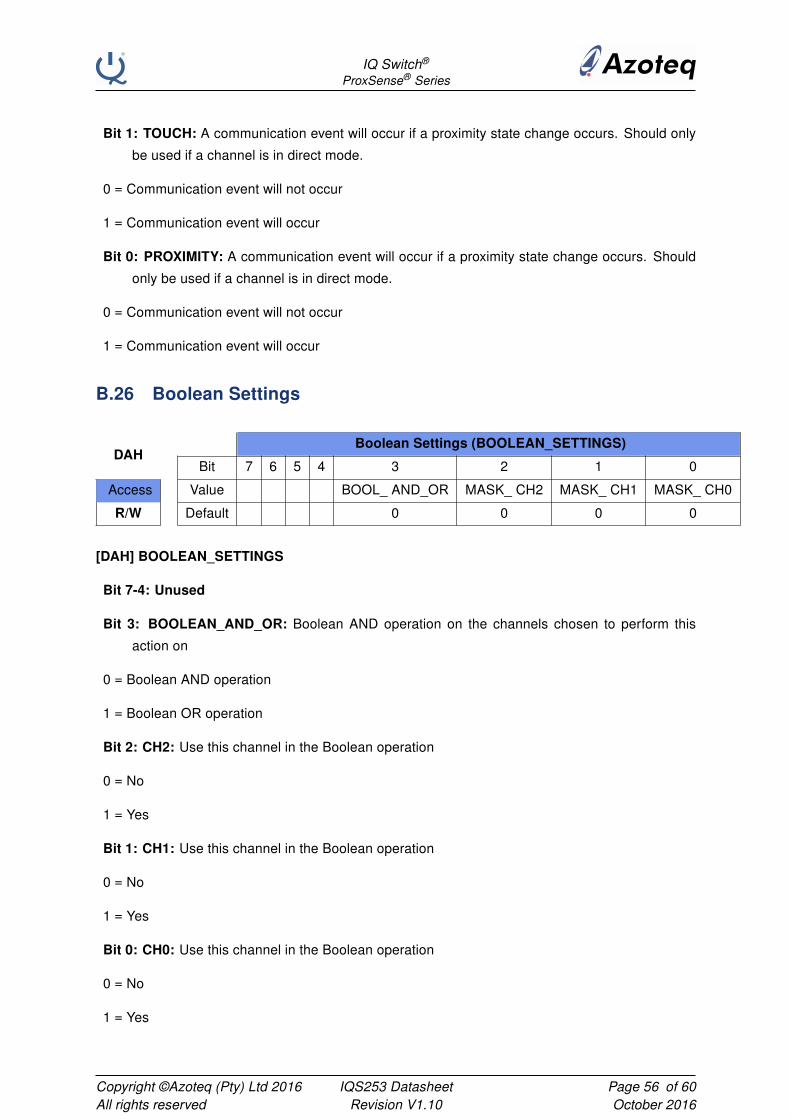
IQ Switch®
ProxSense® Series
Bit 1: TOUCH: A communication event will occur if a proximity state change occurs. Should only
be used if a channel is in direct mode.
0 = Communication event will not occur
1 = Communication event will occur
Bit 0: PROXIMITY: A communication event will occur if a proximity state change occurs. Should
only be used if a channel is in direct mode.
0 = Communication event will not occur
1 = Communication event will occur
B.26 Boolean Settings
DAHBoolean Settings (BOOLEAN_SETTINGS)
Bit 7 6 5 4 3 2 1 0
Access Value BOOL_ AND_OR MASK_ CH2 MASK_ CH1 MASK_ CH0
R/W Default 0 0 0 0
[DAH] BOOLEAN_SETTINGS
Bit 7-4: Unused
Bit 3: BOOLEAN_AND_OR: Boolean AND operation on the channels chosen to perform this
action on
0 = Boolean AND operation
1 = Boolean OR operation
Bit 2: CH2: Use this channel in the Boolean operation
0 = No
1 = Yes
Bit 1: CH1: Use this channel in the Boolean operation
0 = No
1 = Yes
Bit 0: CH0: Use this channel in the Boolean operation
0 = No
1 = Yes
Copyright ©Azoteq (Pty) Ltd 2016All rights reserved
IQS253 DatasheetRevision V1.10
Page 56 of 60October 2016
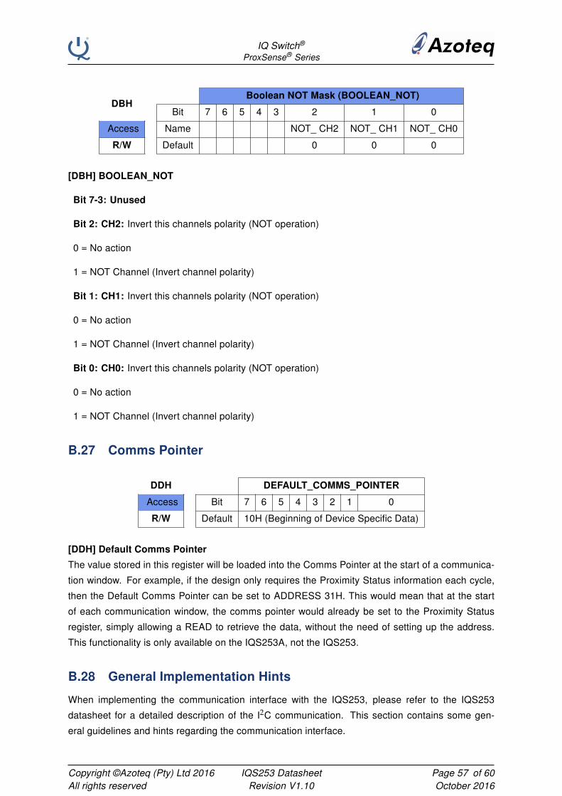
IQ Switch®
ProxSense® Series
DBHBoolean NOT Mask (BOOLEAN_NOT)
Bit 7 6 5 4 3 2 1 0
Access Name NOT_ CH2 NOT_ CH1 NOT_ CH0
R/W Default 0 0 0
[DBH] BOOLEAN_NOT
Bit 7-3: Unused
Bit 2: CH2: Invert this channels polarity (NOT operation)
0 = No action
1 = NOT Channel (Invert channel polarity)
Bit 1: CH1: Invert this channels polarity (NOT operation)
0 = No action
1 = NOT Channel (Invert channel polarity)
Bit 0: CH0: Invert this channels polarity (NOT operation)
0 = No action
1 = NOT Channel (Invert channel polarity)
B.27 Comms Pointer
DDH DEFAULT_COMMS_POINTER
Access Bit 7 6 5 4 3 2 1 0
R/W Default 10H (Beginning of Device Specific Data)
[DDH] Default Comms Pointer
The value stored in this register will be loaded into the Comms Pointer at the start of a communica-
tion window. For example, if the design only requires the Proximity Status information each cycle,
then the Default Comms Pointer can be set to ADDRESS 31H. This would mean that at the start
of each communication window, the comms pointer would already be set to the Proximity Status
register, simply allowing a READ to retrieve the data, without the need of setting up the address.
This functionality is only available on the IQS253A, not the IQS253.
B.28 General Implementation Hints
When implementing the communication interface with the IQS253, please refer to the IQS253
datasheet for a detailed description of the I2C communication. This section contains some gen-
eral guidelines and hints regarding the communication interface.
Copyright ©Azoteq (Pty) Ltd 2016All rights reserved
IQS253 DatasheetRevision V1.10
Page 57 of 60October 2016
IQ Switch®
ProxSense® Series
B.29 I2C Communication window
When communicating via I2C, the communication window will automatically close when a STOP bit
is received by the IQS253. The IQS253 will then proceed to start with a new conversion and the
READY line will be pulled low until the new conversion is complete. Note that there is no command
via I2C to initiate a new conversion. To perform multiple read and write commands, the repeated
start function of the I2C must be used to stack the commands together.
B.30 Start-up Procedure
After sending initial settings to the IQS253, it is important to execute a reseed. It is suggested to
execute an estimated 24 conversions after initial settings before calling for a reseed, to allow the
system to stabilise.
B.31 General I2C Hints
B.31.1 I2C Pull-up resistors
When implementing I2C it is important to remember the pull-up resistors on the data and clock lines.
4.7k is recommended, but for lower clock speeds bigger pull-ups will reduce power consumption.
The RDY line is SW OD and also requires a pull up resistor (typical 10k).
Copyright ©Azoteq (Pty) Ltd 2016All rights reserved
IQS253 DatasheetRevision V1.10
Page 58 of 60October 2016
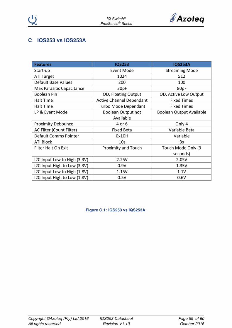
IQ Switch®
ProxSense® Series
C IQS253 vs IQS253A
Features IQS253 IQS253A
Start-up Event Mode Streaming Mode ATI Target 1024 512
Default Base Values 200 100
Max Parasitic Capacitance 30pF 80pF Boolean Pin OD, Floating Output OD, Active Low Output
Halt Time Active Channel Dependant Fixed Times
Halt Time Turbo Mode Dependant Fixed Times LP & Event Mode Boolean Output not
Available Boolean Output Available
Proximity Debounce 4 or 6 Only 4
AC Filter (Count Filter) Fixed Beta Variable Beta
Default Comms Pointer 0x10H Variable
ATI Block 10s 3s Filter Halt On Exit Proximity and Touch Touch Mode Only (3
seconds) I2C Input Low to High (3.3V) 2.25V 2.05V
I2C Input High to Low (3.3V) 0.9V 1.35V
I2C Input Low to High (1.8V) 1.15V 1.1V I2C Input High to Low (1.8V) 0.5V 0.6V
Figure C.1: IQS253 vs IQS253A.
Copyright ©Azoteq (Pty) Ltd 2016All rights reserved
IQS253 DatasheetRevision V1.10
Page 59 of 60October 2016

IQ Switch®
ProxSense® Series
D Contact Information
USA Asia South Africa
Physical Address 6507 Jester Blvd Rm2125, Glittery City 109 Main Street
Bldg 5, suite 510G Shennan Rd Paarl
Austin Futian District 7646
TX 78750 Shenzhen, 518033 South Africa
USA China
Postal Address 6507 Jester Blvd Rm2125, Glittery City PO Box 3534
Bldg 5, suite 510G Shennan Rd Paarl
Austin Futian District 7620
TX 78750 Shenzhen, 518033 South Africa
USA China
Tel +15125381995 +8675583035294 +27 21 863 0033
ext 808
Fax +15126728442 +27 21 863 1512
Email [email protected] [email protected] [email protected]
Please visit www.azoteq.com for a list of distributors and representations worldwide.
The following patents relate to the device or usage of the device: US 6,249,089; US 6,952,084; US 6,984,900; US
7,084,526; US 7,084,531; US 8,395,395; US 8,531,120; US 8,659,306; US 8,823,273; US 9,209,803; US 9,360,510; EP
2,351,220; EP 2,559,164; EP 2,656,189; HK 1,156,120; HK 1,157,080; SA 2001/2151; SA 2006/05363; SA 2014/01541; SA
2015/023634
IQ Switch®, SwipeSwitch™, ProxSense
®, LightSense™, AirButton
TM, ProxFusion™, Crystal Driver™ and the
logo are trademarks of Azoteq.
The information in this Datasheet is believed to be accurate at the time of publication. Azoteq uses reasonable effort to maintain the information up-to-date and accurate, but does not warrant the accuracy, completeness or reliability of the information contained herein. All content and information are provided on an “as is” basis only, without any representations or warranties, express or implied, of any kind, including representations about the suitabili ty of these products or information for any purpose. Values in the datasheet is subject to change without notice, please ensure to always use the latest version of this document. Application specific operating conditions should be taken into account during design and verified before mass production. Azoteq disclaims all warranties and conditions with regard to these products and information, including but not limited to all implied warranties and conditions of merchantability, fitness for a particular purpose, title and non-infringement of any third party intellectual property rights. Azoteq assumes no liability for any damages or injury arising from any use of the information or the product or caused by, without limitation, failure of performance, error, omission, interruption, defect, delay in operation or transmission, even if Azoteq has been advised of the possibility of such damages. The applications mentioned herein are used solely for the purpose of illustration and Azoteq makes no warranty or representation that such applications will be suitable without further modification, nor recommends the use of its products for application that may present a risk to human life due to malfunction or otherwise. Azoteq products are not authorized for use as critical components in life support devices or systems. No licenses to patents are granted, implicitly, express or implied, by estoppel or otherwise, under any intellectual property rights. In the event that any of the abovementioned limitations or exclusions does not apply, it is agreed that Azoteq’s total liability for all losses, damages and causes of action (in contract, tort (including without limitation, negligence) or otherwise) will not exceed the amount already paid by the customer for the products. Azoteq reserves the right to alter its products, to make corrections, deletions, modifications, enhancements, improvements and other changes to the content and information, its products, programs and services at any time or to move or discontinue any contents, products, programs or services without prior notification. For the most up-to-date information and binding Terms and Conditions please refer to www.azoteq.com
www.azoteq.com/ip
Copyright ©Azoteq (Pty) Ltd 2016All rights reserved
IQS253 DatasheetRevision V1.10
Page 60 of 60October 2016
Related Documents