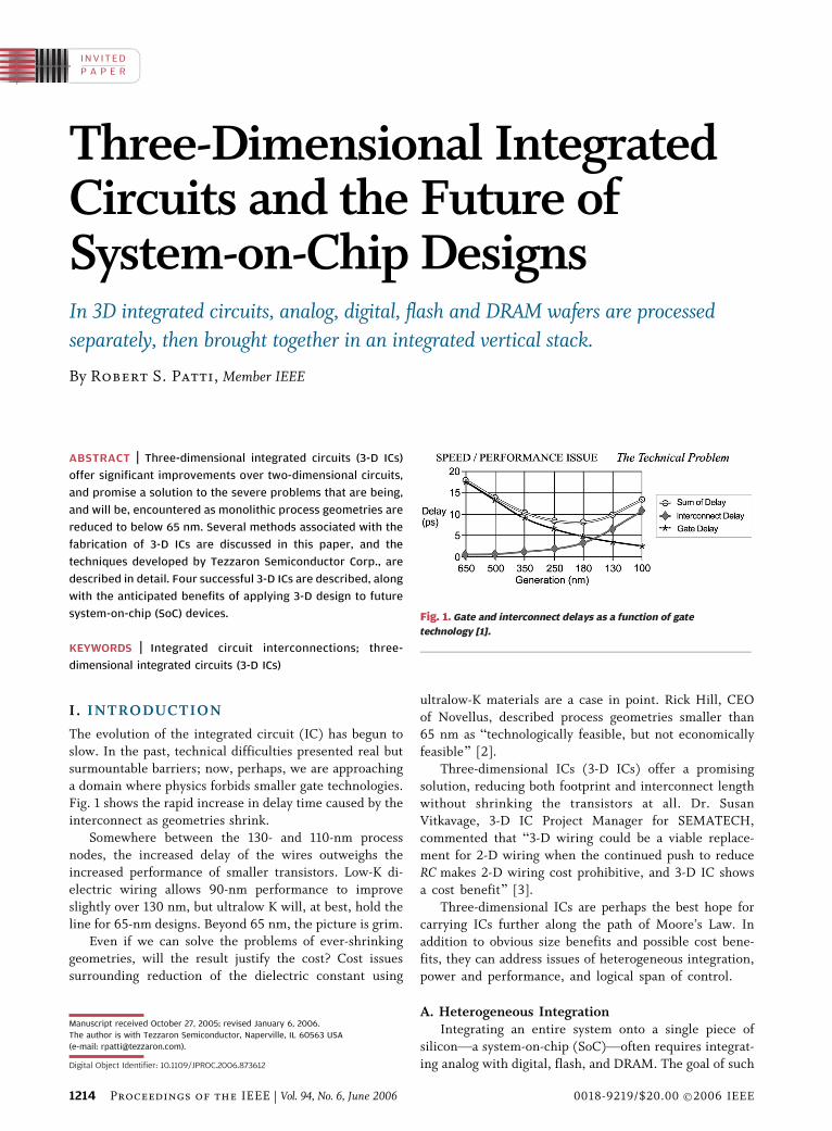
INVITED PAPER Three-Dimensional Integrated Circuits and the Future of System-on-Chip Designs In 3D integrated circuits, analog, digital, flash and DRAM wafers are processed separately, then brought together in an integrated vertical stack. By Robert S. Patti, Member IEEE ABSTRACT | Three-dimensional integrated circuits (3-D ICs) offer significant improvements over two-dimensional circuits, and promise a solution to the severe problems that are being, and will be, encountered as monolithic process geometries are reduced to below 65 nm. Several methods associated with the fabrication of 3-D ICs are discussed in this paper, and the techniques developed by Tezzaron Semiconductor Corp., are described in detail. Four successful 3-D ICs are described, along with the anticipated benefits of applying 3-D design to future system-on-chip (SoC) devices. KEYWORDS | Integrated circuit interconnections; three- dimensional integrated circuits (3-D ICs) I. INTRODUCTION The evolution of the integrated circuit (IC) has begun to slow. In the past, technical difficulties presented real but surmountable barriers; now, perhaps, we are approaching a domain where physics forbids smaller gate technologies. Fig. 1 shows the rapid increase in delay time caused by the interconnect as geometries shrink. Somewhere between the 130- and 110-nm process nodes, the increased delay of the wires outweighs the increased performance of smaller transistors. Low-K di- electric wiring allows 90-nm performance to improve slightly over 130 nm, but ultralow K will, at best, hold the line for 65-nm designs. Beyond 65 nm, the picture is grim. Even if we can solve the problems of ever-shrinking geometries, will the result justify the cost? Cost issues surrounding reduction of the dielectric constant using ultralow-K materials are a case in point. Rick Hill, CEO of Novellus, described process geometries smaller than 65 nm as Btechnologically feasible, but not economically feasible[ [2]. Three-dimensional ICs (3-D ICs) offer a promising solution, reducing both footprint and interconnect length without shrinking the transistors at all. Dr. Susan Vitkavage, 3-D IC Project Manager for SEMATECH, commented that B3-D wiring could be a viable replace- ment for 2-D wiring when the continued push to reduce RC makes 2-D wiring cost prohibitive, and 3-D IC shows a cost benefit[ [3]. Three-dimensional ICs are perhaps the best hope for carrying ICs further along the path of Moore’s Law. In addition to obvious size benefits and possible cost bene- fits, they can address issues of heterogeneous integration, power and performance, and logical span of control. A. Heterogeneous Integration Integrating an entire system onto a single piece of siliconVa system-on-chip (SoC)Voften requires integrat- ing analog with digital, flash, and DRAM. The goal of such Manuscript received October 27, 2005; revised January 6, 2006. The author is with Tezzaron Semiconductor, Naperville, IL 60563 USA (e-mail: [email protected]). Digital Object Identifier: 10.1109/JPROC.2006.873612 Fig. 1. Gate and interconnect delays as a function of gate technology [1]. 1214 Proceedings of the IEEE | Vol. 94, No. 6, June 2006 0018-9219/$20.00 Ó2006 IEEE

Welcome message from author
This document is posted to help you gain knowledge. Please leave a comment to let me know what you think about it! Share it to your friends and learn new things together.
Transcript
INV ITEDP A P E R
Three-Dimensional IntegratedCircuits and the Future ofSystem-on-Chip DesignsIn 3D integrated circuits, analog, digital, flash and DRAM wafers are processed
separately, then brought together in an integrated vertical stack.
By Robert S. Patti, Member IEEE
ABSTRACT | Three-dimensional integrated circuits (3-D ICs)
offer significant improvements over two-dimensional circuits,
and promise a solution to the severe problems that are being,
and will be, encountered as monolithic process geometries are
reduced to below 65 nm. Several methods associated with the
fabrication of 3-D ICs are discussed in this paper, and the
techniques developed by Tezzaron Semiconductor Corp., are
described in detail. Four successful 3-D ICs are described, along
with the anticipated benefits of applying 3-D design to future
system-on-chip (SoC) devices.
KEYWORDS | Integrated circuit interconnections; three-
dimensional integrated circuits (3-D ICs)
I . INTRODUCTION
The evolution of the integrated circuit (IC) has begun to
slow. In the past, technical difficulties presented real but
surmountable barriers; now, perhaps, we are approaching
a domain where physics forbids smaller gate technologies.Fig. 1 shows the rapid increase in delay time caused by the
interconnect as geometries shrink.
Somewhere between the 130- and 110-nm process
nodes, the increased delay of the wires outweighs the
increased performance of smaller transistors. Low-K di-
electric wiring allows 90-nm performance to improve
slightly over 130 nm, but ultralow K will, at best, hold the
line for 65-nm designs. Beyond 65 nm, the picture is grim.Even if we can solve the problems of ever-shrinking
geometries, will the result justify the cost? Cost issues
surrounding reduction of the dielectric constant using
ultralow-K materials are a case in point. Rick Hill, CEO
of Novellus, described process geometries smaller than65 nm as Btechnologically feasible, but not economically
feasible[ [2].
Three-dimensional ICs (3-D ICs) offer a promising
solution, reducing both footprint and interconnect length
without shrinking the transistors at all. Dr. Susan
Vitkavage, 3-D IC Project Manager for SEMATECH,
commented that B3-D wiring could be a viable replace-
ment for 2-D wiring when the continued push to reduceRC makes 2-D wiring cost prohibitive, and 3-D IC shows
a cost benefit[ [3].
Three-dimensional ICs are perhaps the best hope for
carrying ICs further along the path of Moore’s Law. In
addition to obvious size benefits and possible cost bene-
fits, they can address issues of heterogeneous integration,
power and performance, and logical span of control.
A. Heterogeneous IntegrationIntegrating an entire system onto a single piece of
siliconVa system-on-chip (SoC)Voften requires integrat-
ing analog with digital, flash, and DRAM. The goal of such
Manuscript received October 27, 2005; revised January 6, 2006.
The author is with Tezzaron Semiconductor, Naperville, IL 60563 USA
(e-mail: [email protected]).
Digital Object Identifier: 10.1109/JPROC.2006.873612
Fig. 1. Gate and interconnect delays as a function of gate
technology [1].
1214 Proceedings of the IEEE | Vol. 94, No. 6, June 2006 0018-9219/$20.00 �2006 IEEE

an SoC is to reduce the I/O count, system noise, power,EMI, and cost, and to increase performance. However,
integrating such disparate elements leads to enormously
complicated processes. In some cases, masking layers have
increased from a mere dozen to 50, 60, or more, because
the entire wafer must be processed for the needs of each
subcircuit. If the circuit could be dis-integrated by process
need, and the subcircuits reintegrated in very close
proximity, better processing options would be availableand the cost would be far lower. This is a promise of 3-D
ICs: separate parts of the design can be built in entirely
different processes, then brought together in an integrated
vertical stack.
B. Power and PerformanceBoth of these issues hinge on the capacitance of the
interconnect. Half of the dynamic power at 90 nm is in the
charging and discharging of the interconnect capacitance,
and that percentage will increase in each new generation.
The RC delay of key signals ultimately limits the maximumspeed of a circuit. The ITRS roadmap [4] concedes that
resistance in metal will increase in coming generations.
Even if all the ITRS goals are achieved, the RC time delay
will increase faster than the circuits can shrink.
Wire delay increases as the square of the wire’s length.
The experimentally derived formula is
td ¼ 0:35 rcl2: (1)
We cannot reduce resistance (r) or capacitance (c)Vindeed, they are increasingVso our only hope for re-
ducing propagation delay is to reduce wire length (l). As
noted above, wire length impacts performance as a squared
factor. In theory, the average wire length in a 3-D circuit
changes by the square root of the number of layers [5].
Hence, if two layers of transistors are used, the length is
reduced by the square root of two, and this is in turn
squared for calculation of the RC propagation delay,resulting in a 2 � improvement in propagation time. For
very local interconnect, less than perhaps 50 �m, this will
not really be true (there would be little or no improve-
ment), but for global interconnect it is very close to actual
reality. Similarly, three layers of transistors would give 3 �improvement; four layers, 4 �; etc.
C. Logical Span of ControlIn many large processors and SoCs, the propagation
delay of data signals, global control signals, and clock
signals dictates the minimum clock period [6]. The dis-
tance that a signal can travel in one clock period defines
the logical span of control that the circuit can govern.
Beyond this span, signals must be retimed and pipelined.
Today’s 2-D ICs must operate within a circle measured by
the span. In 3-D ICs the circle becomes a sphere. Thesphere of control can encompass perhaps 10 � as much
circuitry as the circle. This alone could give a tremendous,
albeit one time, boost to system speeds.
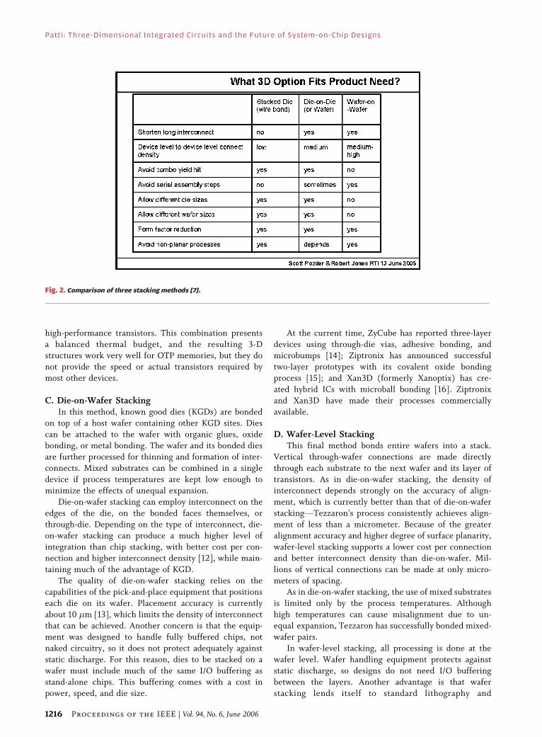
II . CONSTRUCTION METHODSFOR 3-D IC S
There are four basic methods for creating 3-D ICs: chip
stacking, transistor stacking, die-on-wafer stacking, and
wafer-level stacking. All four methods are described below.
Three of the methods were recently summarized by Scott
Pozder of Freescale as shown in Fig. 2.
A. Chip StackingThis method stacks fully processed and tested stand-
alone components to produce a system-in-package (SiP).
The components in the vertical stack are connected withtraditional wire bonding or flipchip techniques. Research
groups have announced functional stacks of as many as
eight chips [8].
The only significant benefit offered by chip stacking is
the reduction in size. Connecting wires may be somewhat
shorter, but the components are not integrated any more
tightly than in a normal 2-D system; signals traveling from
one layer to another must be pushed off-chip and thenbrought on-chip, just as before.
Chip stacking is a fairly mainstream technology today,
led by companies like Sharp and STATSChipPAC. Chip-
stacked SiPs are employed in cell phones and other por-
table devices that demand small and light form factors.
B. Transistor StackingAt the other end of the spectrum, this construction
method creates multiple levels of transistors on a single
substrate. This is the Bholy grail[ of 3-D circuits, but its
success to date has been limited by thermal budget is-
sues. The temperatures required to build a layer of high-
performance transistors would destroy any copper oraluminum already laid down and would cause migration
of transistor implants on previous layers.
Stanford is doing promising research on transistor
stacking technologies such as laser annealing and nickel
nucleation [9], [10]. Laser annealing circumvents ther-
mal budget issues by localizing the high temperatures as
each layer is built, but defect densities are a problem.
Nickel nucleation builds high quality transistors at lowertemperatures, but containment of the nickel ions is a
problem.
Matrix Semiconductor produces a highly successful
variation on stacked transistors in its one-time pro-
grammable (OTP) memories [11]. The Matrix method
uses tungsten in place of copper or aluminum and
builds low-performance polysilicon diodes rather than
Patti: Three-Dimensional Integrated Circuits and the Future of System-on-Chip Designs
Vol. 94, No. 6, June 2006 | Proceedings of the IEEE 1215
high-performance transistors. This combination presents
a balanced thermal budget, and the resulting 3-Dstructures work very well for OTP memories, but they do
not provide the speed or actual transistors required by
most other devices.
C. Die-on-Wafer StackingIn this method, known good dies (KGDs) are bonded
on top of a host wafer containing other KGD sites. Dies
can be attached to the wafer with organic glues, oxidebonding, or metal bonding. The wafer and its bonded dies
are further processed for thinning and formation of inter-
connects. Mixed substrates can be combined in a single
device if process temperatures are kept low enough to
minimize the effects of unequal expansion.
Die-on-wafer stacking can employ interconnect on the
edges of the die, on the bonded faces themselves, or
through-die. Depending on the type of interconnect, die-on-wafer stacking can produce a much higher level of
integration than chip stacking, with better cost per con-
nection and higher interconnect density [12], while main-
taining much of the advantage of KGD.
The quality of die-on-wafer stacking relies on the
capabilities of the pick-and-place equipment that positions
each die on its wafer. Placement accuracy is currently
about 10 �m [13], which limits the density of interconnectthat can be achieved. Another concern is that the equip-
ment was designed to handle fully buffered chips, not
naked circuitry, so it does not protect adequately against
static discharge. For this reason, dies to be stacked on a
wafer must include much of the same I/O buffering as
stand-alone chips. This buffering comes with a cost in
power, speed, and die size.
At the current time, ZyCube has reported three-layer
devices using through-die vias, adhesive bonding, andmicrobumps [14]; Ziptronix has announced successful
two-layer prototypes with its covalent oxide bonding
process [15]; and Xan3D (formerly Xanoptix) has cre-
ated hybrid ICs with microball bonding [16]. Ziptronix
and Xan3D have made their processes commercially
available.
D. Wafer-Level StackingThis final method bonds entire wafers into a stack.
Vertical through-wafer connections are made directly
through each substrate to the next wafer and its layer of
transistors. As in die-on-wafer stacking, the density of
interconnect depends strongly on the accuracy of align-
ment, which is currently better than that of die-on-wafer
stackingVTezzaron’s process consistently achieves align-
ment of less than a micrometer. Because of the greateralignment accuracy and higher degree of surface planarity,
wafer-level stacking supports a lower cost per connection
and better interconnect density than die-on-wafer. Mil-
lions of vertical connections can be made at only micro-
meters of spacing.
As in die-on-wafer stacking, the use of mixed substrates
is limited only by the process temperatures. Although
high temperatures can cause misalignment due to un-equal expansion, Tezzaron has successfully bonded mixed-
wafer pairs.
In wafer-level stacking, all processing is done at the
wafer level. Wafer handling equipment protects against
static discharge, so designs do not need I/O buffering
between the layers. Another advantage is that wafer
stacking lends itself to standard lithography and
Fig. 2. Comparison of three stacking methods [7].
Patti: Three-Dimensional Integrated Circuits and the Future of System-on-Chip Designs
1216 Proceedings of the IEEE | Vol. 94, No. 6, June 2006

processing techniques, so there are fewer unknowns tocontend with.
One drawback to wafer-level stacking is the lack of a
workable KGD approach. (There will be further discussion
of 3-D yield issues later in this paper.) This aside, the
wafer-on-wafer stacking process provides a great opportu-
nity to launch SoCs into the 3-D realm.
Wafer-level stacking can use the same bonding meth-
ods that are available to die-on-wafer methods: organic
gluing, oxide bonding, and metal bonding. Each of these
has achieved varying degrees of success. Rensselaer
Polytechnic is well known for working with organic glues
[17], Ziptronix has had excellent results with covalent
oxide bonding [18], and Tezzaron has used copper metal
bonding to produce fully functional devices (discussed
later in this paper). Each bonding technique has its plusses
and minuses. Organic glue bonding can better deal with
particle contamination, but it does not provide a good
intrinsic metal interconnect. Oxide bonding allows room
temperature prebonding and offers perhaps better align-
ment, but again does not have an intrinsic metal con-
nection. Metal bonding provides the interconnect, but
bonding is done at 400 �C, making alignment more dif-
ficult (especially with mixed substrates).
Wafer-level stacking techniques are further differenti-
ated by the method used to create vertical through-wafer
interconnect: either via-first or via-last. Via-last processes
create the interconnect after the wafers are bonded, using
a Bdrill and fill[ sequence. Via-first processes build the
through-wafer vertical interconnect wire on each wafer
prior to the bonding process, which is generally more ef-
ficient and cost-effective [19]. Each of the three earlier
mentioned bonding techniques can support either via-first
or via-last methods, but for the metal bonding process,
via-first is obvious and intrinsic.
Although all wafer stacking techniques are envisioned
to produce stacks of several layers, most published re-
search has described only two-layer stacks [20], [21].
III . TEZZARON’S STACKING METHOD
Tezzaron’s stacking method is wafer-level, via-first, with
metal-to-metal thermal bonding. This method has pro-
duced successful two-level devices, three-wafer stacks with
full electrical connectivity, and four-wafer mechanical
stacks. Tezzaron has developed two types of vertical inter-connect. The size, pitch, and parasitics of Tezzaron’s ver-
tical interconnects are given in Table 1.
The first-generation Bsuper-via[ process had the
advantage of being applied to wafers after they were
completely processed at a vendor fab. The disadvantage
was in the required via size and the need for keepout areas
in all layers. The second-generation Bsuper-contact[ pro-
cess requires a new process module at the vendor fab. Thismodule has proven relatively easy to add and does not
introduce any new materials at the stage where the con-
tact is added.
Images of Tezzaron wafer stacks implementing the two
types of interconnect are shown in Figs. 3 and 4.
The following sequence, Figs. 5–13, illustrates
Tezzaron’s stacking method with the BSuper-Contact[interconnect.
After complete processing of each layer, the height of
the total stack increases by about 15 �m per wafer. Thus,
even a stack of many layers can be housed in normal
packaging. Note that the bottom wafer retains its complete
thickness during the stacking process and there is no need
to handle the very thin (15 �m or less) upper layers as
individual pieces. This greatly eases the manufacturing
challenges. After the stack is completed, the thick bottomwafer can be thinned as usual and finished with standard
wire bonding or flipchip assembly.
Table 1 Interconnect Properties
Fig. 3. Three wafers, stacked and connected with Tezzaron’s
first-generation Bsuper-via[ interconnect process.
Patti: Three-Dimensional Integrated Circuits and the Future of System-on-Chip Designs
Vol. 94, No. 6, June 2006 | Proceedings of the IEEE 1217
Tezzaron has created stacks of up to four wafers and
intends to manufacture five-layer devices in the next couple
of years, but there is no fundamental limit on the number of
layers that this method can incorporate.
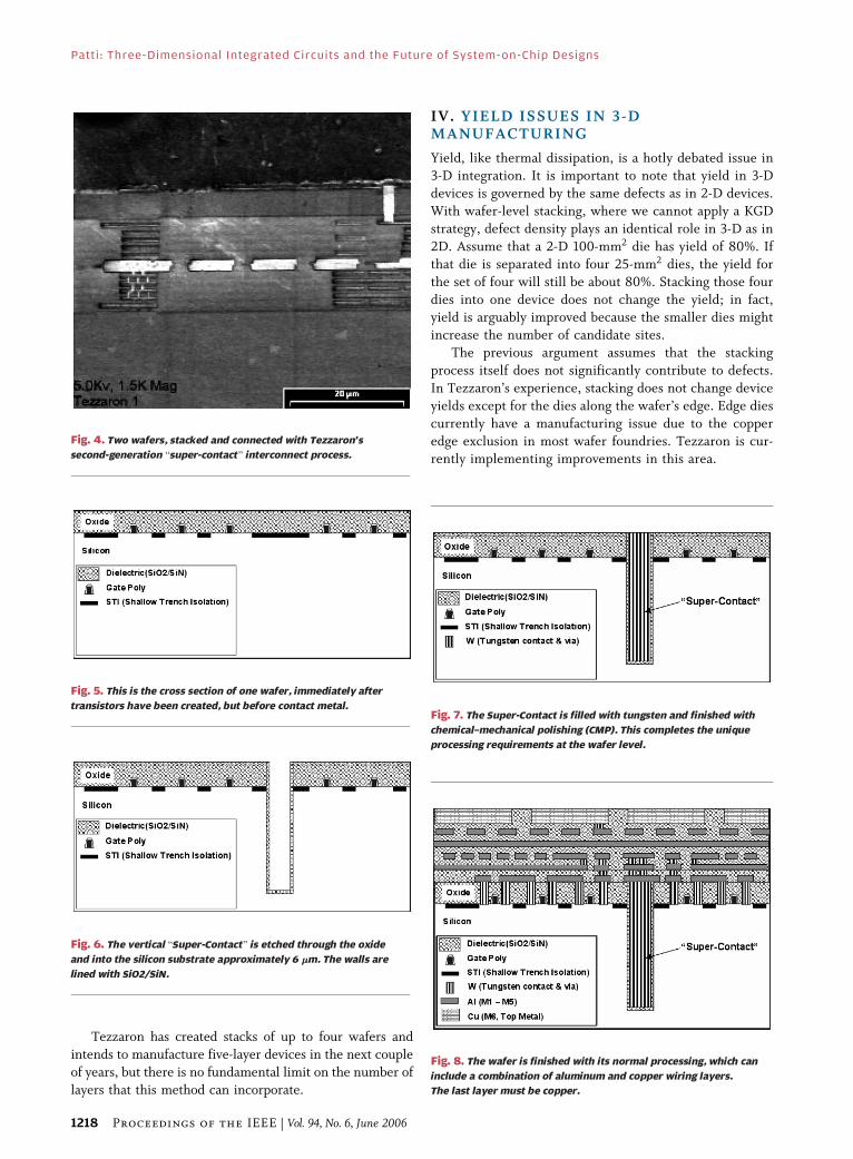
IV. YIELD ISSUES IN 3-DMANUFACTURING
Yield, like thermal dissipation, is a hotly debated issue in3-D integration. It is important to note that yield in 3-D
devices is governed by the same defects as in 2-D devices.
With wafer-level stacking, where we cannot apply a KGD
strategy, defect density plays an identical role in 3-D as in
2D. Assume that a 2-D 100-mm2 die has yield of 80%. If
that die is separated into four 25-mm2 dies, the yield for
the set of four will still be about 80%. Stacking those four
dies into one device does not change the yield; in fact,yield is arguably improved because the smaller dies might
increase the number of candidate sites.
The previous argument assumes that the stacking
process itself does not significantly contribute to defects.
In Tezzaron’s experience, stacking does not change device
yields except for the dies along the wafer’s edge. Edge dies
currently have a manufacturing issue due to the copper
edge exclusion in most wafer foundries. Tezzaron is cur-rently implementing improvements in this area.
Fig. 4. Two wafers, stacked and connected with Tezzaron’s
second-generation Bsuper-contact[ interconnect process.
Fig. 5. This is the cross section of one wafer, immediately after
transistors have been created, but before contact metal.
Fig. 6. The vertical BSuper-Contact[ is etched through the oxide
and into the silicon substrate approximately 6 ���m. The walls are
lined with SiO2/SiN.
Fig. 8. The wafer is finished with its normal processing, which can
include a combination of aluminum and copper wiring layers.
The last layer must be copper.
Fig. 7. The Super-Contact is filled with tungsten and finished with
chemical–mechanical polishing (CMP). This completes the unique
processing requirements at the wafer level.
Patti: Three-Dimensional Integrated Circuits and the Future of System-on-Chip Designs
1218 Proceedings of the IEEE | Vol. 94, No. 6, June 2006
The reality is that most people, when considering 3-Dintegration, are not looking to simply cut up a single
100-mm2 die into multiple layers. Even though such a
device would reap the benefits of shorter wires and het-
erogeneous integration, designers generally have larger
ideas, such as stacking multiple dies of greater than
100 mm2 each. In this case, yield is a larger issue be-
cause each layered device contains far more silicon area,
and is therefore far more likely to contain a defect.There is opportunity for significant yield improvements
for some specific types of large stacked devices. Memories,
sensor arrays, and FPGAs can be made redundant, and thus
reparable, providing significant yield benefits. Tezzaron’s
memories use a very advanced and complete test engine
and can be remapped at a small grain. The spare rows and
columns are shared not only between 2-D adjacent arrays,
but also among all of the vertically aligned arrays, verticaladjacency not being required. This makes a much larger
pool of repair components available to any single failed
region. Another entire paper could be dedicated to the
improved reparability that exists in 3-D, but the basic
principle is that 3-D devices can have significantly more
interconnect in close proximity. This gain in interconnect
translates to a much greater ability to reroute around de-
fects and to reach spare resources.
V. TEZZARON’S 3-D DEVICES
Tezzaron has created a number of 3-D devices with its
wafer-to-wafer stacking process, include a variety of stand-alone memories, a CMOS sensor, a 3-D FPGA, a mixed
signal ASIC, and a processor/memory stack. Each of these
devices demonstrates specific benefits gained from 3-D
integration. Here we will look at some of the important
characteristics of four of these devices. All four of these
devices were built in two layers and were processed in
180-nm technology at MagnaChip.
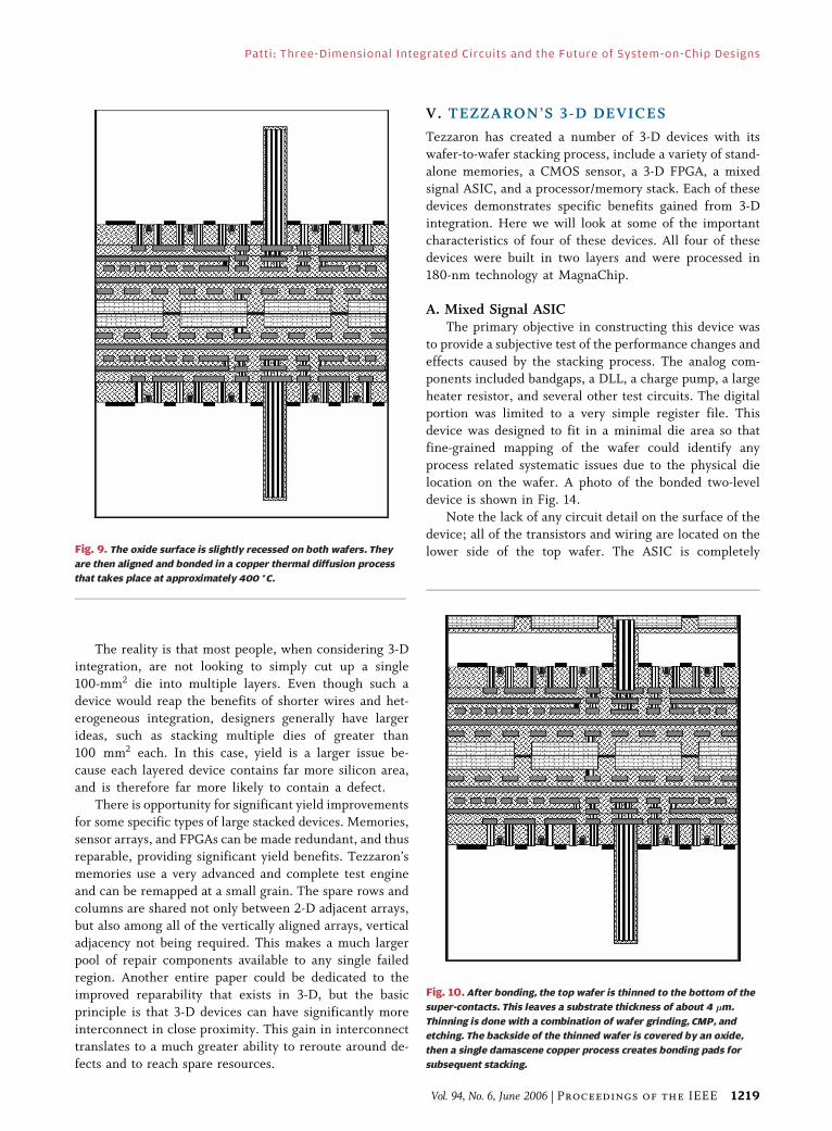
A. Mixed Signal ASICThe primary objective in constructing this device was
to provide a subjective test of the performance changes and
effects caused by the stacking process. The analog com-
ponents included bandgaps, a DLL, a charge pump, a large
heater resistor, and several other test circuits. The digital
portion was limited to a very simple register file. This
device was designed to fit in a minimal die area so thatfine-grained mapping of the wafer could identify any
process related systematic issues due to the physical die
location on the wafer. A photo of the bonded two-level
device is shown in Fig. 14.
Note the lack of any circuit detail on the surface of the
device; all of the transistors and wiring are located on the
lower side of the top wafer. The ASIC is completely
Fig. 10. After bonding, the top wafer is thinned to the bottom of the
super-contacts. This leaves a substrate thickness of about 4 ��m.
Thinning is done with a combination of wafer grinding, CMP, and
etching. The backside of the thinned wafer is covered by an oxide,
then a single damascene copper process creates bonding pads for
subsequent stacking.
Fig. 9. The oxide surface is slightly recessed on both wafers. They
are then aligned and bonded in a copper thermal diffusion process
that takes place at approximately 400 ˚C.
Patti: Three-Dimensional Integrated Circuits and the Future of System-on-Chip Designs
Vol. 94, No. 6, June 2006 | Proceedings of the IEEE 1219

functional and demonstrates no performance difference
between the analog circuits on the thick lower wafer and
those on the thin upper wafer. Also, the heater resistor
allowed 8 W to be dissipated in a mere 0.25-mm2 area. The
resulting stress did not cause any failure of the bonded
interface, nor any permanent failure of adjacent devices.
This provides strong evidence that localized hot spots will
not be an issue in 3-D. As an aside, our work indicated that3-D circuits are no worse with regard to heat issues than
2-D circuits. Research presented at the RTI 3-D conference
in 2005 [22], as well as our own, shows a temperature delta
of only 2 �C–7 �C. The underlying issue of heat removal is
neither better nor worse in 3-D than in 2-D ICs.
B. CMOS SensorThis device was created by placing photo diodes on the
thin upper layer and amplifiers on the thick lower layer.
The primary benefit here is the 100% array efficiency of
the diode array. The diodes are also backside illuminated
and have an increased quantum efficiency. The amplifiers
are the typical 3T type found in many commercial sensor
arrays, but they could easily have been made more
sophisticated. In fact, other groups have discussed using
high performance, high precision A-to-D converters. Withthis technique, pixels in the CMOS sensor could be
addressed individually. This in turn provides a very
important and interesting facility: a small, specific area
of the pixel field could be read over and over again at the
rate of thousands or even tens of thousands of hertz. This isa key feature requirement for video navigation sensors.
In our CMOS sensor, both the diode layer and the
amplifier layer were produced in the same CMOS process
to reduce our prototype development costs. However, the
sensor diodes could easily have been created in a four-mask
process, thus reducing manufacturing cost. Another choice
could be to use a different process to create other sensor
types or characteristics. The sensor layer no longer needsto be CMOS compatible in its processing. One more
benefit from this stacked sensor arrangement is the
elimination of the micro lenses, another significant cost
reduction. The layout is pictured in Fig. 15.
The main diode array in the center contains about
20 000 photosensors on a 5-�m pitch. There are four small
subarrays with 2.9- and 2.4-�m pitch diodes. Each photo
diode has its own connection to an amplifier on the bottomwafer. Thus, of the 40 000 interconnects on this 2.25-mm2
die, about 21 000 carry signals between the layers. Also,
given the pitch of the interconnect and its size, the wafer-
to-wafer alignment is known to be within 0.7 �m. Any
error greater than this would have caused shorts between
the diodes. A typical misalignment in Tezzaron’s process is
0.3 �m. The precision of alignment is shown in Fig. 16.
C. 3-D FPGAThis circuitry was designed to allow the stacking of any
number of layers, up to 256. While we have no intention of
Fig. 11. Here a third wafer has been added to the stack, using the same
technique by which the second wafer was added.
Fig. 12. Now the stack is inverted. Final processing will be applied to
the backside of the first wafer.
Patti: Three-Dimensional Integrated Circuits and the Future of System-on-Chip Designs
1220 Proceedings of the IEEE | Vol. 94, No. 6, June 2006
stacking that many layers, this device provides a window
into the extensibility of 3-D devices. What is of specific
interest in this device is the comingling of the 3-D
interconnect with the 2-D circuits. Unlike the obvious
separation of the 3-D interconnect from the circuitrydemonstrated in the processor/memory stack (next
section), the FPGA 3-D interconnect is interspersed
throughout the logic area. Each logic array block contains12 vertical interconnects. As you can see in Fig. 17, the 3-D
interconnect requires no great keepout areas or disrup-
tions in the logic array.
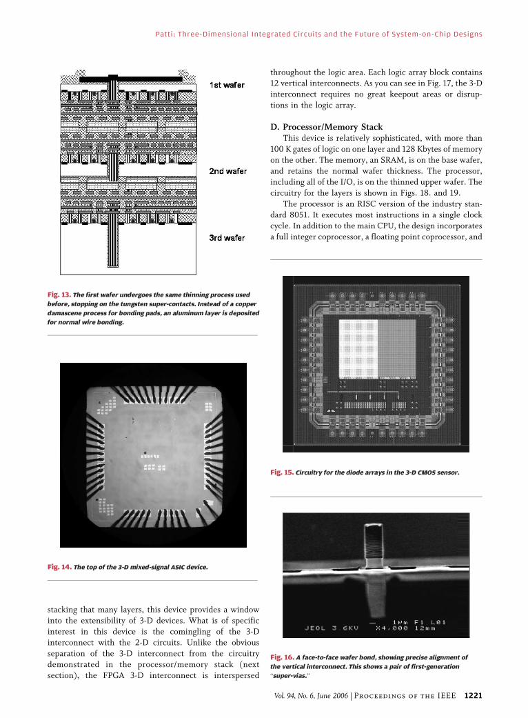
D. Processor/Memory StackThis device is relatively sophisticated, with more than
100 K gates of logic on one layer and 128 Kbytes of memory
on the other. The memory, an SRAM, is on the base wafer,and retains the normal wafer thickness. The processor,
including all of the I/O, is on the thinned upper wafer. The
circuitry for the layers is shown in Figs. 18. and 19.
The processor is an RISC version of the industry stan-
dard 8051. It executes most instructions in a single clock
cycle. In addition to the main CPU, the design incorporates
a full integer coprocessor, a floating point coprocessor, and
Fig. 14. The top of the 3-D mixed-signal ASIC device.
Fig. 13. The first wafer undergoes the same thinning process used
before, stopping on the tungsten super-contacts. Instead of a copper
damascene process for bonding pads, an aluminum layer is deposited
for normal wire bonding.
Fig. 16. A face-to-face wafer bond, showing precise alignment of
the vertical interconnect. This shows a pair of first-generation
Bsuper-vias.[
Fig. 15. Circuitry for the diode arrays in the 3-D CMOS sensor.
Patti: Three-Dimensional Integrated Circuits and the Future of System-on-Chip Designs
Vol. 94, No. 6, June 2006 | Proceedings of the IEEE 1221

a handful of additional special operations for cryptography.The 8051 core itself includes a multilevel interrupt
controller, two serial ports, and three counter-timers.
The entire memory range for the 8051 is 64 Kbytes for
data storage and 64 Kbytes for program space. For further
stacking, Tezzaron added a page register that allows up to
4 layers of memory, each containing 128 Kbytes, to be
integrated with the processor.
Tezzaron chose an 8051-based design in order toillustrate the performance gains to be achieved by stacking
memory on a processor. The 8051 core provides a very
simple basis for comparison. With a single clock per in-
struction, no caching, no pipelining, and no other
advanced techniques to hide memory latency, this device
gives a very raw look at the relationship between processor
performance and memory speed. The stacked memory
was a mere 3 ns away from the processor. That 3 ns in-cludes all latencies. In theory, the CPU could have run at
over 300 MHz, but its design actually limited the speed to
140 MHz. The nearest similar processor available in the
market is capable of only 33 MHz.
The memory–processor interface was intentionally
over-designed. The implemented bus provides more than
4 Gbytes/s of sustained data bandwidth. This is more than
an order of magnitude greater than what the 8051 can use,but it amply demonstrates the power of nearby memory.
A very notable point can be made here regarding the
improvement in power as well as in performance: When
running at the same clock rate as the commercial part,
the 3-D part consumes only one-tenth the power.
The 3-D device measures about 12.5 mm2 and contains
approximately 120 000 vertical interconnects. Only about
0.5% of these interconnects actually carry signal. Thedevice was temperature cycled from �65 �C to þ150 �C
with 15-min dwell cycles. More than 100 000 devicetemperature cycles were run on these devices with no
failures.
VI. A DIRECTION FOR THEFUTURE: 3-D S O C S
Three-dimensional ICs hold tremendous promise for SoCs.
First, consider the impact of putting memory on a separate
layer. According to the SIA and the ITRS, most of the area
in an SoC is occupied by embedded memory of one form or
Fig. 18. Circuitry for the processor layer of the processor/memory
stack.
Fig. 19. Circuitry for the SRAM layer of the processor/memory stack.
Fig. 17. Circuitry for the 3-D FPGA.
Patti: Three-Dimensional Integrated Circuits and the Future of System-on-Chip Designs
1222 Proceedings of the IEEE | Vol. 94, No. 6, June 2006

another [23]. The drive for ever-increasing system per-
formance drives a parallel need for more memory on
board. This, in turn, pushes SoC designers to use ever
smaller geometries in order to accommodate the vast
memory needs. A 65-nm SoC is likely to use that geometry,
not due to its need for speed or gate count, but rather dueto its appetite for memory. If that memory is moved to a
separate layer in a stacked 3-D IC, the rest of the SoC can
be fabricated at 130 nm or perhaps even 180 nm. The
process complications and costs are drastically reduced.
Consider another benefit of a separate memory layer:
the memory can now be built in a true memory process.
Perhaps it can be DRAM instead of SRAM, because it does
not need to share the process with the high performancetransistors of the SoC. It may prove to be cost-effective to
make the memory in 65 nm or even smaller. For a sample
design, see Fig. 20.
There is one more intriguing 3-D SoC concept to
introduce here: generic memory layers. Designers could
avoid developing a unique memory for each SoC if the
foundry offered a generic memory layer that was adaptable
to the needs of many (or perhaps all) of its customers.Tezzaron has discussed with various ASIC foundries the
possibility of creating Bgridless[ memory that is continu-
ous across the whole wafer but partitionable at 100-�m
intervals. (The memory is thus nearly gridless.) If ASICs
were designed to mate with a specific interface and to
interconnect with memory on a general interface grid, all
custom ASICs could share a single memory wafer design.
Further, this memory could be redundant and reparableoutside the ASIC. Tezzaron uses this approach in its own
memories, achieving greater than 90% yield on diesmeasuring multiple square centimeters. For SoCs, generic
memory layers would provide higher yield, lower power,
better performance, and a much lower cost for develop-
ment and production. A 3-D SoC of the future could in-
clude a custom ASIC, built at the best and lowest cost
process node, combined with generic DRAM, flash, SRAM
and perhaps even generic FPGA layers. Generic layers
would be picked from the foundry’s standard catalog muchas standard packages are today. A design kit would pro-
vide and enforce the design rules to ensure a physical and
electrical match for the vertical interconnects.
VII. CONCLUSION
In this paper, we have discussed several techniques for
fabricating 3-D ICs. The techniques developed by Tezzaron
Semiconductor Corp., are highlighted, and several exam-
ples of 3-D SoC devices are used to explain the concepts.Although 3-D fabrication techniques are currently not
mainstream commercial processes, the development of
3-D SoC devices will ultimately depend on the costs and
gains associated with the technology. There is ample evi-
dence that it is possible to design and fabricate 3-D ICs and
that there are benefits to be derived from 3-D integration.
There is also mounting evidence that the road to ever
deeper submicrometer technology may be simply toocostly. In the opinion of the author it is not a matter of if,but rather of when, 3-D IC technology is applied to SoC
devices. h
Acknowledgment
The author wishes to acknowledge the considerable
work and effort of his colleagues at Tezzaron, whose skill
and dedication made these results possible. Particular
gratitude is extended to Dr. S. Gupta and Dr. S. Hong, whowere responsible for the development of the stacking
process and for the fabrication of the wafers and stacked
devices.
RE FERENCES
[1] G. Metze, M. Khbels, N. Goldsman, andB. Jacob, BHeterogeneous integration,[ TechTrend Notes, vol. 12, no. 2, p. 3, 2003.
[2] E. Sperling and J. Chappell. (2005, Nov.).BRips in the road map,[ Electron. News.
[Online]. Available: http://www.reed-electronics.com/electronicnews/article/CA6253270.
[3] S. Vitkavage, personal communication.
[4] International Technology Roadmap forSemiconductors, 2004, update.
[5] J. Joyner, P. Zarkesh-Ha, and J. Meindl,BA global interconnect design windowfor a three-dimensional system-on-a-chip,[ inProc. IEEE Interconnect Technology Conf.,2001, pp. 154–156.
[6] K. Guarini, B3D IC technology: Capabilities
and applications,[ presented at theRTI Int. Technology Venture Forum,Burlingame, CA, 2004.
[7] S. Pozder, BIntegration challenges of 3-Dbonded structures,[ presented at theTechVenture Preconf. Symp., Tempe, AZ, 2005.
[8] K. Lee, BWafer-stacked package technologyfor high-performance system,[ presented atthe RTI Int. Technology Venture Forum,Tempe, AZ, 2005.
[9] B. Rajendran, D. J. Witte, R. F. W. Pease,R. S. Shenoy, N. S. Chokshi, R. L. DeLeon,and G. S. Tompa, BCMOS transistorprocessing compatible with monolithic 3-Dintegration,[ in Proc. VLSI InterconnectionConf. (VMIC), 2005, pp. 76–82.
[10] K. Saraswat, B3-dimensional ICs: Motivation,performance analysis and technology,[ pre-
sented at the 3D Technology, Modeling, andProcess Symp., Burlingame, CA, 2004.
[11] V. Dunton, T. Chen, M. Konevecki,U. Raghuram, and S. Sivaram, BZias: Verticalwires in 3-D memory devices,[ in Proc.VLSI Interconnection Conf. (VMIC), 2005,pp. 480–485.
[12] B. Markunas, B3D architectures forsemiconductor integration and packaging,[presented at the RTI Int. Technology VentureForum, Burlingame, CA, 2004.
[13] BZiptronix targets vertical scalability,[Electron. News. (2005, Oct. 17). [Online].Available: http://reed-electronics.com/electronicnews/article/CA6274984.html.
[14] M. Koyanagi, BA new super smart stacktechnology for 3-D LSIs,[ presented at theRTI Int. Technology Venture Forum,Tempe, AZ, 2005.
Fig. 20. One possible design for a 3-D SoC.
Patti: Three-Dimensional Integrated Circuits and the Future of System-on-Chip Designs
Vol. 94, No. 6, June 2006 | Proceedings of the IEEE 1223

[15] BZiptronix reports first 3-D SoC,[ Solid StateTechnol. [Online]. Available: http://sst.pennnet.com/articles/article_display.cfm?article_id=237 547.
[16] J. Trezza, BHybrid super systems,[ presentedat the RTI Int. Technology Venture Forum,Burlingame, CA, 2004.
[17] F. Nicklaus, J. J. McMahon, J. Yu, S. H. Lee,J. Q. Lu, T. S. Cale, and R. J. Gutmann,BWafer-level 3-D integration technologyplatforms for IC’s and MEMS,[ in Proc.VLSI Interconnection Conf. (VMIC), 2005,pp. 486–496.
[18] L. Peters. (2003, Nov. 1). BWafer bondingenables new technologies and applications,[Semiconductor Int. [Online]. Available: http://www.reed-electronics.com/semiconductor/article/CA331034?text=ziptronix.
[19] J. Baliga. (2005, Jun. 1). BThree-dimensionalICs solve the interconnect paradox,[Semiconductor Int. [Online]. Available:http://www.reed-electronics.com/semiconductor/article/CA604503.
[20] P. Clarke. (2002, Nov. 28)., B[IEDM late paper:IBM shows how to stack for 3-D circuitry,[EE Times. [Online]. Available: http://www.
eetimes.com/news/semi/showArticle.jhtml?articleID=10806078.
[21] H. Huebner, BSolid face-to-face goesproductive at Infineon,[ presented at theSEMICON Europa 2005, Munich, Germany.
[22] B3D architectures for semiconductorintegration and packaging,[ in RTI Int.Technology Venture Forum, Tempe, AZ, 2005.
[23] F. Ramsay. (2003, Apr. 28)., B[Embeddedmemories multiply in SoCs,[ EE Times.[Online]. Available: http://www.eetimes.com/story/OEG20030428S0089.
ABOUT THE AUT HOR
Robert S. Patti (Member, IEEE) received the B.S.
degrees in electrical engineering/computer sci-
ence and in physics from Rose-Hulman Institute
of Technology, Terra Haute, IN, in 1985.
He was a Member of Technical Staff for
Tellabs, Inc. He was the Founder and President
of ASIC Designs, Inc. (Tezzaron Semiconductor’s
predecessor company). He is currently CTO and
VP of Design Engineering for Tezzaron Semi-
conductor, Naperville, IL. He is also a Director of
Tezzaron Semiconductor (Singapore) Pte Ltd. He is responsible for
management of the company’s U.S. facility and for leading all technical
and engineering development aside from process development and
engineering. He holds 13 U.S. patents, numerous foreign patents, and
more than a dozen pending patent applications in submicrometer
semiconductor chip technologies.
Mr. Patti is a member of IEEE Computing Elements and serves as the
Vice-Chairman for JEDEC’s DDRIII/Future Memories Task Group.
Patti: Three-Dimensional Integrated Circuits and the Future of System-on-Chip Designs
1224 Proceedings of the IEEE | Vol. 94, No. 6, June 2006
Related Documents