INVITED PAPER Dynamic Surface Temperature Measurements in ICs High-sensitivity, high-resolution thermal mapping of integrated circuits can be provided by techniques such as scanning with laser beams and embedding of CMOS temperature sensors. By Josep Altet , Wilfrid Claeys , Stefan Dilhaire, and Antonio Rubio ABSTRACT | Measuring techniques of the die surface temper- ature in integrated circuits are reported as very appropriate for failure analysis, for thermal characterization, and for testing modern devices. The paper is arranged as a survey of tech- niques oriented towards measuring the temperature dynamics of the circuit surface and presenting and discussing both the merits and drawbacks of each technique with regard to the accuracy, reliability and efficiency of the measurements. Two methods are presented in detail: laser probing methods, based on interferometry and thermoreflectance, and embedded CMOS circuit sensors. For these techniques, the physical prin- ciples, the state of the art in figures of merit and some application examples are presented. KEYWORDS | CMOS temperature sensors; differential temper- ature sensors; integrated circuits (ICs); laser interferometry; laser thermoreflectance; temperature measurements I. INTRODUCTION: NEW CHALLENGES FOR IC TEMPERATURE MEASUREMENTS The temperature at the surface of an integrated circuit (IC) has a significant impact on the behavior, performance, and reliability of the semiconductor devices placed on it. Fur- thermore, temperature is a source of information re- garding the state of all the elements involved in the heat transfer process throughout the IC structure. Conse- quently, having knowledge of the thermal map at the IC surface (the temperature distribution throughout the whole die surface) may enhance the design, modelling and observability of the devices, circuits and structure of an IC. Within specialized literature, there is a considerable number of works where temperature analysis and mea- surements have been reported. From all such works, tem- perature sensing could be considered a mature topic. Nonetheless, scaling technology and design and test trends demand temperature measuring techniques with increas- ing performances. In each application area, due to its par- ticular casuistry, temperature measurements face specific challenges. For instance, in failure analysis, the detection and lo- calization of hot spots is usually related to the localization of bridges and gate oxide shorts (GOS) [1]. Steady state temperature measurements with liquid crystal [2], infra- red cameras [3], and fluorescent thermography [4] have been proposed and successfully used. Technology scaling directly affects these traditional methods in two senses: first, the increasing number of metal layers attenuates the temperature variations that can be measured at the IC surface [39]. Second, as devices become smaller, the la- teral resolution of the temperature measuring systems has to be below 1 "m with sensitivities in the order of a few mK. In this direction, the use of dynamic temperature measurements has enhanced the capability of detecting hot spots in current technologies [35], [41], [57]. For the characterization of the thermal coupling in ICs, different measures are reported: static (dc) [7], transient in the time domain [6], or complex small-signal parame- ters (ac) in the frequency domain [8]. Nowadays, certain technologies demand spot temperature measurement (measuring temperatures in areas less than 1 "m 2 ), high lateral resolution (below 1 "m), small amplitude resolu- tion (1 mK) and high bandwidth (compared to the band- width of the thermal coupling in the IC structure). Traditionally, the thermal characterization of packages has been used for the characterization of their thermal resistance [9] and for the detection of defects in the Manuscript received February 1, 2005; revised January 23, 2006. J. Altet and A. Rubio are with the Department of Electronic Engineering, Technical University of Catalonia, Barcelona ES-08034, Spain (e-mail: [email protected]; [email protected]). W. Claeys and S. Dilhaire are with the Centre de Physique Moleculaire Optique et Hertzienne, Universite ´ Bordeaux I, Bordeaux F-33405, France (e-mail: [email protected]; [email protected]). Digital Object Identifier: 10.1109/JPROC.2006.879793 Vol. 94, No. 8, August 2006 | Proceedings of the IEEE 1519 0018-9219/$20.00 Ó2006 IEEE

Welcome message from author
This document is posted to help you gain knowledge. Please leave a comment to let me know what you think about it! Share it to your friends and learn new things together.
Transcript

INV ITEDP A P E R
Dynamic Surface TemperatureMeasurements in ICsHigh-sensitivity, high-resolution thermal mapping of integrated circuits can be
provided by techniques such as scanning with laser beams and embedding
of CMOS temperature sensors.
By Josep Altet, Wilfrid Claeys, Stefan Dilhaire, and Antonio Rubio
ABSTRACT | Measuring techniques of the die surface temper-
ature in integrated circuits are reported as very appropriate for
failure analysis, for thermal characterization, and for testing
modern devices. The paper is arranged as a survey of tech-
niques oriented towards measuring the temperature dynamics
of the circuit surface and presenting and discussing both the
merits and drawbacks of each technique with regard to the
accuracy, reliability and efficiency of the measurements. Two
methods are presented in detail: laser probing methods, based
on interferometry and thermoreflectance, and embedded
CMOS circuit sensors. For these techniques, the physical prin-
ciples, the state of the art in figures of merit and some
application examples are presented.
KEYWORDS | CMOS temperature sensors; differential temper-
ature sensors; integrated circuits (ICs); laser interferometry;
laser thermoreflectance; temperature measurements
I . INTRODUCTION: NEW CHALLENGESFOR IC TEMPERATURE MEASUREMENTS
The temperature at the surface of an integrated circuit (IC)
has a significant impact on the behavior, performance, and
reliability of the semiconductor devices placed on it. Fur-
thermore, temperature is a source of information re-
garding the state of all the elements involved in the heat
transfer process throughout the IC structure. Conse-quently, having knowledge of the thermal map at the IC
surface (the temperature distribution throughout the
whole die surface) may enhance the design, modelling
and observability of the devices, circuits and structure of
an IC.
Within specialized literature, there is a considerablenumber of works where temperature analysis and mea-
surements have been reported. From all such works, tem-
perature sensing could be considered a mature topic.
Nonetheless, scaling technology and design and test trends
demand temperature measuring techniques with increas-
ing performances. In each application area, due to its par-
ticular casuistry, temperature measurements face specific
challenges.For instance, in failure analysis, the detection and lo-
calization of hot spots is usually related to the localization
of bridges and gate oxide shorts (GOS) [1]. Steady state
temperature measurements with liquid crystal [2], infra-
red cameras [3], and fluorescent thermography [4] have
been proposed and successfully used. Technology scaling
directly affects these traditional methods in two senses:
first, the increasing number of metal layers attenuates thetemperature variations that can be measured at the IC
surface [39]. Second, as devices become smaller, the la-
teral resolution of the temperature measuring systems
has to be below 1 �m with sensitivities in the order of a
few mK. In this direction, the use of dynamic temperature
measurements has enhanced the capability of detecting
hot spots in current technologies [35], [41], [57].
For the characterization of the thermal coupling in ICs,different measures are reported: static (dc) [7], transient
in the time domain [6], or complex small-signal parame-
ters (ac) in the frequency domain [8]. Nowadays, certain
technologies demand spot temperature measurement
(measuring temperatures in areas less than 1 �m2), high
lateral resolution (below 1 �m), small amplitude resolu-
tion (1 mK) and high bandwidth (compared to the band-
width of the thermal coupling in the IC structure).Traditionally, the thermal characterization of packages
has been used for the characterization of their thermal
resistance [9] and for the detection of defects in the
Manuscript received February 1, 2005; revised January 23, 2006.
J. Altet and A. Rubio are with the Department of Electronic Engineering,
Technical University of Catalonia, Barcelona ES-08034, Spain (e-mail:
[email protected]; [email protected]).
W. Claeys and S. Dilhaire are with the Centre de Physique Moleculaire
Optique et Hertzienne, Universite Bordeaux I, Bordeaux F-33405, France
(e-mail: [email protected]; [email protected]).
Digital Object Identifier: 10.1109/JPROC.2006.879793
Vol. 94, No. 8, August 2006 | Proceedings of the IEEE 15190018-9219/$20.00 �2006 IEEE

package structure [13]. As technology evolves and powerdissipation becomes the main design constraint, dynamic
thermal models of packages (so-called thermal imped-
ance) [10] are needed, requiring accurate, extended tran-
sient temperature measurements or low-frequency ac
measurements [14] in different mounting configurations
[11], [12], [15].
Temperature sensors embedded in an IC have been
proposed in [44], [52], [58] to guarantee thermal integrityand safe values of the working temperature. In micro-
processors, temperature sensors are being embedded in
order to control the power dissipated by the circuit and
thus ensure safe operating temperatures, e.g., by modu-
lating the frequency of the clock signal [16]. In [17], ring
oscillators are used to monitor the temperature in a field-
programmable gate array (FPGA). Differential tempera-
ture sensors are used when the objective is to track thepower dissipated by devices placed in the IC with inde-
pendence of the ambient temperature [19]. For instance,
in [53], transient differential thermal measurements taken
with a built-in sensor are used to protect a current booster
whereas, in [18], the transient activation of a hot spot is
detected with this sensing strategy. In this case, the chal-
lenge is to design reliable temperature sensors compat-
ible with the technology of the circuit whose temperatureis observed.
In this paper, we will expose recent advances in tem-
perature sensing strategies that offer interesting possibil-
ities for current and future IC technologies: reflectometry,
interferometry, and embedded temperature sensors. The
common factors displayed by all these techniques are that
they allow dynamic temperature measurements to be per-
formed (beyond the full bandwidth of the thermal couplingmechanism in the IC structure), they offer interesting
lateral resolutions, and they have sensitivities in the mK
range.
The paper is organized as follows. Section II shows a
survey of the temperature monitoring systems, classifying
them and explaining their working principles and per-
formances. Section III considers an electrical model of a
typical measuring/monitoring system, in order to discussthe influence of different variables (ambient temperature,
mounting configuration, IC structure) on the measured
signal. Sections IV and V present a deep insight into two
sensing categories: optical methods and embedded sen-
sors. Finally, Section VI concludes the paper.
II . SURVEY OF TEMPERATUREMONITORING SYSTEMS
Temperature measurement methods can be divided into
three categories [6], [59]: physically contacting methods,
optical methods, and electrical or embedded methods.
In contact methods, either a device or a film is physi-
cally in contact with the surface of the IC and it is the
temperature of this device or film that is actually
measured. Typical devices are thermistors [62] or thermo-couples [26], which are placed as a probe for a scanning
thermal microscope (SThM, which, in fact, is an atomic
force microscope). As an example, in [62], a platinum (Pt)
wire is used as a temperature-dependent resistor. SThM
measurements are very sensitive to surface roughness and
the water layer on the surface as they affect the thermal
exchange between the probe and the sample [60]. The
lateral resolution under atmospheric pressure is about100 nm, and it can reach 10 nm under vacuum.
Typical films are liquid crystals or fluorescent films.
Liquid crystals are organic compounds whose visible color
in the region being observed changes as the temperature of
the region changes [2]. Fluorescent films are polymer films
whose fluorescent quantum yield is heavily dependent on
temperature [4].
The main drawback of contacting methods is thatepoxy, metal, and passivation layers placed over the silicon
die attenuate the temperature measured when compared
to the real temperature at the silicon surface [26], [62].
Optical methods are based on measurements of light.
Infrared thermography, reflectometry, and interferometry
fall into this category. Infrared thermography measures the
light emitted by the IC due to its absolute temperature.
The phase and amplitude of the light reflected by the ICdepend on the temperature. A reflectance laser probe
measures variations in the amplitude of the reflected light,
whereas an interferometer measures variations in the
phase of the reflected light.
Layers placed over the silicon die, especially metal
layers, may affect the performance of optical techniques.
Temperature measurements can be done from backside or
lateral measurements [21], [22]. Backside temperaturemeasurement is invasive and need sample preparation.
Thermoreflectance measurements have been done in [5]
with 0.1 K resolution over fundamental electronic noise
when using a 5-�m-diameter laser spot through a 200-�m
substrate. Time gating thermoreflectance imaging seems
to be a promising technique [61]. Comparable to optical
coherence tomography, this technique allows 1-�m lateral
resolution and 8-�m-depth tomographic resolution. Thetemperature sensitivity is about 1 mK.
Electrical or embedded methods are based on the
temperature dependence of the electrical characteristics of
an electronic device. The device can be stand-alone or part
of a more complex circuit. The advantages of this tech-
nique are that it allows us to perform temperature mea-
surements in the field application of the IC and does not
require visual access to the silicon surface. However, thetemperature measuring circuitry increases the semicon-
ductor area (which is related to fabrication costs) and
requires input/output pins to have access to the terminals
of the sensor.
Table 1 gives figures of bandwidth, lateral resolution,
and temperature resolution obtained through the different
techniques as reported in the literature.
Altet et al.: Dynamic Surface Temperature Measurements in ICs
1520 Proceedings of the IEEE | Vol. 94, No. 8, August 2006

The temperature measurements can be static or dy-
namic. Static temperature measurements are performed
when devices dissipate a constant power, boundary con-
ditions are time independent, and the thermal steady state
is reached. In such circumstances, temperature does not
depend on time. In dynamic measurements, the power
dissipated by the devices tends to be time varying. These
measurements can be categorized into two sets: transient,where the temperature is observed as a function of time,
and ac (so-called small-signal or lock-in). In the latter
group, the amplitude and phase of one spectral component
of the temperature is observed. Such measurements are
usually performed when the power dissipated by the
devices can be expressed as a time periodical function.
AC measurements have the following advantages com-
pared to transient measurements.1) They are more robust to noise [57], [62], [63].
2) Amplitude and phase can be measured. Amplitude
is usually affected by the calibration constant,
whereas phase is not. Besides, phase measure-
ments have been reported in some works to be
more sensitive than amplitude. This makes phase
temperature measurements an interesting source
of information (e.g., [27], [39]–[41], [57], [62]).3) As we shall see in the following section, by
choosing the frequency of the spectral component
of the temperature, the penetration depth of the
heat in the IC can be controlled. Thus, the number
of IC layers which may affect the temperature
distribution at the silicon surface can be con-
trolled [27], [39], [40].
III . MEASURING TEMPERATURE INAN IC: GENERAL CONSIDERATIONS
The goal of this section is to present the key factors from
which the IC structure, the characteristics of the
dissipating device, and the placement/characteristics of
the sensor impact on the dynamic of temperature
measurements.
To establish a nomenclature, Fig. 1 shows a general
representation of a measurement procedure. Let us sup-
pose that devices or subcircuits in an IC dissipate power.
Due to the thermal coupling in the IC structure, a non-
homogeneous thermal map at the silicon surface appears.
With a sensor system, which in this section is assumed to
be embedded in the IC, the temperature can be observed at
one specific location of the silicon surface, causing a pro-portional electrical signal at the output of the sensor.
In the figure, a simplified equivalent electrical model of
all the electrothermal mechanisms is drawn. It is sim-
plified, as it is unidirectional and linear. The equivalence
between electrical variables in the thermal part of the
model and thermal variables in the IC is classical (e.g.,
[18]): temperature is modeled as voltage, and energy flow
(i.e., heat flow or power) is modeled as current. Thethermal coupling mechanism is modeled with the thermal
coupling impedance in the IC Zth c, the thermal impedance
Table 1 Temperature Monitoring Methods Classification
Fig. 1. Electrical model of an IC temperature measurement procedure.
Altet et al. : Dynamic Surface Temperature Measurements in ICs
Vol. 94, No. 8, August 2006 | Proceedings of the IEEE 1521
from the package to the ambient Zth p, and the offset valuegenerated by the ambient temperature VaðtÞ. Finally, hsðtÞmodels the transfer function of the sensor system, as its
input is temperature and its output is an electrical signal
[vðtÞ or iðtÞ].
The model gives us an approach to the main con-
tributors to the measured temperature TðtÞ and allows us
to analyze the effect of the different elements on the out-
put voltage dynamics.First, the dynamic characteristics of the thermal
coupling exhibit a low pass filter behavior. The cutoff
frequency is between 10 kHz and 1 MHz, depending on the
distance between the dissipating device and the temper-
ature measuring point/area. The lower limit of 10 kHz may
be even lower if the temperature is not measured on the
silicon surface. As an example, Fig. 2 shows two Bode
diagrams of thermal coupling. The temperature is mea-sured on the silicon surface with a differential temperature
sensor (reported in Section V) and Bode diagrams are
shown for two different distances between the dissipating
device (an MOS transistor with an aspect ratio of
10 �m=1.2 �m) and the temperature observation area.
Second, the dynamic temperature measured on the
surface reflects the thermal properties of the portion of
the IC affected by the thermal transfer mechanism. As thethermal coupling mechanism is a diffusion process, the
penetration depth in the IC structure of the heat injected
by the dissipating elements depends on its spectral form.
High-frequency components have a low penetration depthwhich increases as the frequency lowers.
To illustrate this, Fig. 3 shows ac phase temperature
measurements (both power dissipation and temperature
can be written as time dependent sinusoidal functions)
performed with the differential temperature sensor de-
scribed in Section V-B as well as with a thermoreflectance
laser probe Section V-A. The vertical axis shows phase shift
’ of the measured temperature as regards the periodicpower dissipated by an MOS transistor (with an aspect
ratio of 10 �m=1.2 �m), and the horizontal axis shows
distance between the dissipating device and the temper-
ature sensor. As we can see, all phase shifts are linear, with
a slope that depends on the frequency.
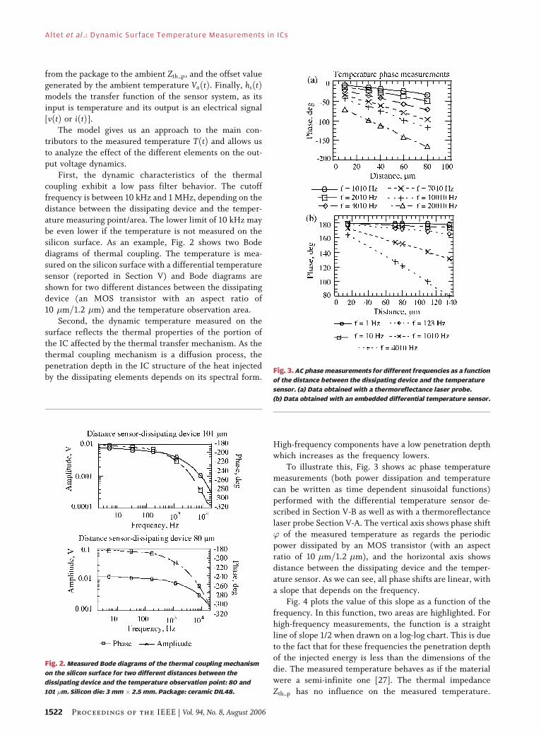
Fig. 4 plots the value of this slope as a function of the
frequency. In this function, two areas are highlighted. For
high-frequency measurements, the function is a straightline of slope 1/2 when drawn on a log-log chart. This is due
to the fact that for these frequencies the penetration depth
of the injected energy is less than the dimensions of the
die. The measured temperature behaves as if the material
were a semi-infinite one [27]. The thermal impedance
Zth p has no influence on the measured temperature.
Fig. 2. Measured Bode diagrams of the thermal coupling mechanism
on the silicon surface for two different distances between the
dissipating device and the temperature observation point: 80 and
101 �m. Silicon die: 3 mm � 2.5 mm. Package: ceramic DIL48.
Fig. 3. AC phase measurements for different frequencies as a function
of the distance between the dissipating device and the temperature
sensor. (a) Data obtained with a thermoreflectance laser probe.
(b) Data obtained with an embedded differential temperature sensor.
Altet et al.: Dynamic Surface Temperature Measurements in ICs
1522 Proceedings of the IEEE | Vol. 94, No. 8, August 2006
Measured data agrees with the analytical solution of a
spherical dissipating device in an infinite material [64]
’ðr; fÞ ¼ r
ffiffiffiffiffiffiffiffi� � f
D
r: (1)
Where the phase shift ð’Þ depends on the physical pro-
perties of the silicon (thermal diffusivity D), frequency ðfÞ,
and distance ðrÞ between the measuring point and thedissipating device. Therefore, if the first two variables are
known, the distance between the dissipating device and
the measuring point can be obtained from phase mea-
surements. As reported in the following section, temper-
ature measurements performed within this frequency
range can be applied for locating dissipating devices and so
be used in failure analysis [39].
In the middle range of frequencies, the functionSðfÞ measured on the surface of the silicon depends on
the thermal properties of the die attachment to the
package [14].
As the frequency lowers, the penetration depth in-
creases and the temperature on the surface depends on
deeper elements of the IC structure, until Zth p is reached.
Similar reasoning and conclusions can be reached if the
analysis and measurements are performed in the timedomain: short activation of the dissipating devices has an
associated low penetration depth. As the activation du-
ration of the dissipating devices becomes larger, the
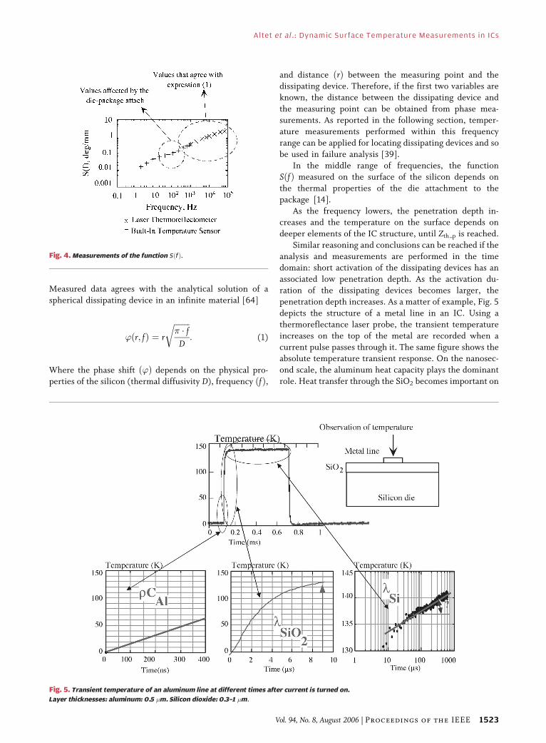
penetration depth increases. As a matter of example, Fig. 5
depicts the structure of a metal line in an IC. Using a
thermoreflectance laser probe, the transient temperature
increases on the top of the metal are recorded when a
current pulse passes through it. The same figure shows theabsolute temperature transient response. On the nanosec-
ond scale, the aluminum heat capacity plays the dominant
role. Heat transfer through the SiO2 becomes important on
Fig. 4. Measurements of the function SðfÞ.
Fig. 5. Transient temperature of an aluminum line at different times after current is turned on.
Layer thicknesses: aluminum: 0.5 �m. Silicon dioxide: 0.3–1 �m.
Altet et al. : Dynamic Surface Temperature Measurements in ICs
Vol. 94, No. 8, August 2006 | Proceedings of the IEEE 1523
the millisecond scale, while the thermal conductivity ofthe silicon die dominates the long time-domain response.
From these measurements, it is possible to obtain the
thermal properties of the different layers involved in the
transport mechanism [28].
Going back to Fig. 1, ambient temperature affects all
the measurements, as all the variables involved in the
electrothermal process (power-dissipated, physical vari-
ables that influence thermal transfer, electrical variables ofthe sensor system, sensitivities) depend on it. Once it is
set, then a Btemperature operating point[ is established
and the value of all the physical and electrical parameters
of all the blocks involved in the measurement can be
known. Most of the measurement methods considered in
this paper really measure temperature fluctuations over
the reference temperature on the surface. When amplitude
is measured, a calibration step is needed to obtain the exactvalue of the temperature change. On the other hand, when
phase is measured, the effect of the reference temperature
is negligible.
Finally, in Fig. 1, the block hsðtÞ models the dynamics
of the sensor systems. When the sensor is embedded in the
IC, hsðtÞ only models the electrical behavior of the sensor,
as the temperature evolution of the sensor is included in
the thermal coupling model. In other cases, especially incontact measuring methods, it is constituted by two blocks;
the first one models the heat transfer from the IC to the
sensor system, whereas the second models the electrical
response of the sensor [29].
IV. OPTICAL TECHNIQUES
When an IC operates, it induces physical changes in thematerials involved in its construction. Straightforward
effects are, for example, variations of temperature that
induces thermal expansion and corresponding deforma-
tion. By adopting appropriate methods, one can investigate
different features of working electronic devices by ana-
lyzing optically the physics that take place in it [30]–[33].
In this section, we give an overview of the passive laser
probing methods applied to electronic devices. By passiveprobing, we mean the laser has no measurable effect on
the running device, it only Breads[ the information. Two
situations will be distinguished: the laser beam is highly
focused in order to get a very small probing point or
the laser lights up the entire device and imaging tech-
niques are used to read the information contained in the
reflected light.
We will limit this survey to methods where a laserbeam is reflected back from the surface of the component
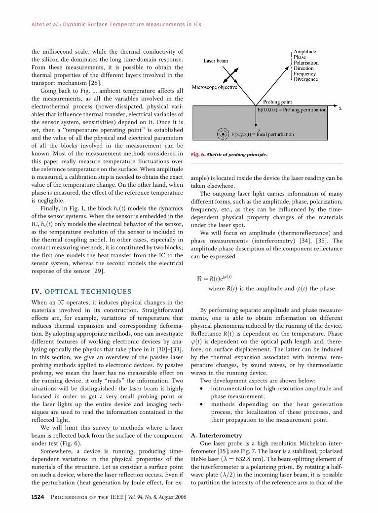
under test (Fig. 6).
Somewhere, a device is running, producing time-
dependent variations in the physical properties of the
materials of the structure. Let us consider a surface point
on such a device, where the laser reflection occurs. Even if
the perturbation (heat generation by Joule effect, for ex-
ample) is located inside the device the laser reading can be
taken elsewhere.The outgoing laser light carries information of many
different forms, such as the amplitude, phase, polarization,
frequency, etc., as they can be influenced by the time-
dependent physical property changes of the materials
under the laser spot.
We will focus on amplitude (thermoreflectance) and
phase measurements (interferometry) [34], [35]. The
amplitude-phase description of the component reflectancecan be expressed
< ¼ RðtÞej’ðtÞ
where RðtÞ is the amplitude and ’ðtÞ the phase:
By performing separate amplitude and phase measure-
ments, one is able to obtain information on different
physical phenomena induced by the running of the device.
Reflectance RðtÞ is dependent on the temperature. Phase
’ðtÞ is dependent on the optical path length and, there-
fore, on surface displacement. The latter can be induced
by the thermal expansion associated with internal tem-perature changes, by sound waves, or by thermoelastic
waves in the running device.
Two development aspects are shown below:
• instrumentation for high-resolution amplitude and
phase measurement;
• methods depending on the heat generation
process, the localization of these processes, and
their propagation to the measurement point.
A. InterferometryOne laser probe is a high resolution Michelson inter-
ferometer [35]; see Fig. 7. The laser is a stabilized, polarized
HeNe laser ð� ¼ 632:8 nmÞ. The beam-splitting element of
the interferometer is a polarizing prism. By rotating a half-
wave plate ð�=2Þ in the incoming laser beam, it is possible
to partition the intensity of the reference arm to that of the
Fig. 6. Sketch of probing principle.
Altet et al.: Dynamic Surface Temperature Measurements in ICs
1524 Proceedings of the IEEE | Vol. 94, No. 8, August 2006
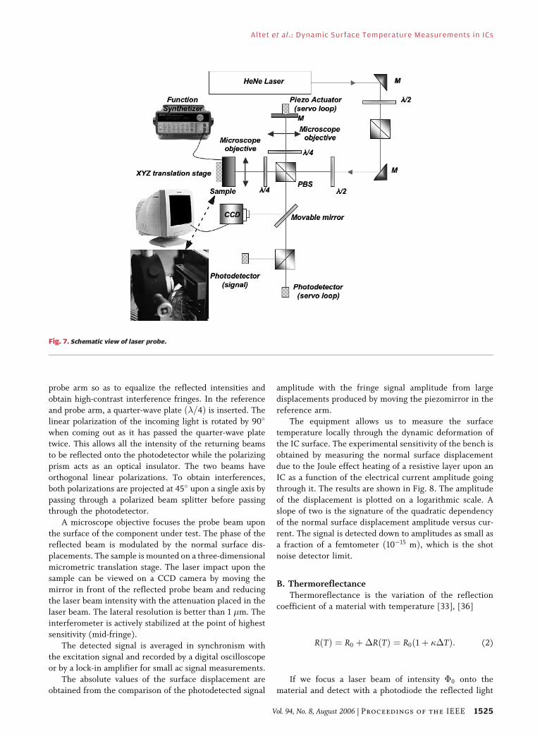
probe arm so as to equalize the reflected intensities and
obtain high-contrast interference fringes. In the reference
and probe arm, a quarter-wave plate ð�=4Þ is inserted. Thelinear polarization of the incoming light is rotated by 90�
when coming out as it has passed the quarter-wave plate
twice. This allows all the intensity of the returning beams
to be reflected onto the photodetector while the polarizing
prism acts as an optical insulator. The two beams have
orthogonal linear polarizations. To obtain interferences,
both polarizations are projected at 45� upon a single axis by
passing through a polarized beam splitter before passingthrough the photodetector.
A microscope objective focuses the probe beam upon
the surface of the component under test. The phase of the
reflected beam is modulated by the normal surface dis-
placements. The sample is mounted on a three-dimensional
micrometric translation stage. The laser impact upon the
sample can be viewed on a CCD camera by moving the
mirror in front of the reflected probe beam and reducingthe laser beam intensity with the attenuation placed in the
laser beam. The lateral resolution is better than 1 �m. The
interferometer is actively stabilized at the point of highest
sensitivity (mid-fringe).
The detected signal is averaged in synchronism with
the excitation signal and recorded by a digital oscilloscope
or by a lock-in amplifier for small ac signal measurements.
The absolute values of the surface displacement areobtained from the comparison of the photodetected signal
amplitude with the fringe signal amplitude from large
displacements produced by moving the piezomirror in the
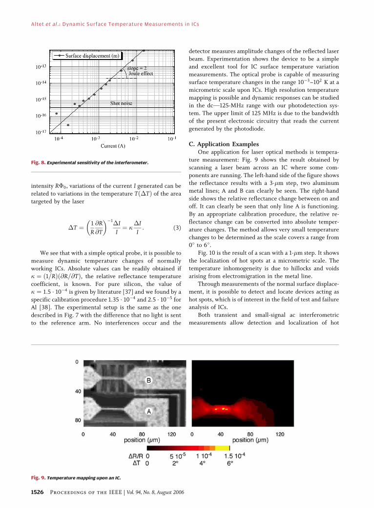
reference arm.The equipment allows us to measure the surface
temperature locally through the dynamic deformation of
the IC surface. The experimental sensitivity of the bench is
obtained by measuring the normal surface displacement
due to the Joule effect heating of a resistive layer upon an
IC as a function of the electrical current amplitude going
through it. The results are shown in Fig. 8. The amplitude
of the displacement is plotted on a logarithmic scale. Aslope of two is the signature of the quadratic dependency
of the normal surface displacement amplitude versus cur-
rent. The signal is detected down to amplitudes as small as
a fraction of a femtometer ð10�15 mÞ, which is the shot
noise detector limit.
B. ThermoreflectanceThermoreflectance is the variation of the reflection
coefficient of a material with temperature [33], [36]
RðTÞ ¼ R0 þ�RðTÞ ¼ R0ð1 þ ��TÞ: (2)
If we focus a laser beam of intensity �0 onto thematerial and detect with a photodiode the reflected light
Fig. 7. Schematic view of laser probe.
Altet et al. : Dynamic Surface Temperature Measurements in ICs
Vol. 94, No. 8, August 2006 | Proceedings of the IEEE 1525
intensity R�0, variations of the current I generated can be
related to variations in the temperature Tð�TÞ of the area
targeted by the laser
�T ¼ 1
R
@R
@T
� ��1�I
I¼ �
�I
I: (3)
We see that with a simple optical probe, it is possible to
measure dynamic temperature changes of normally
working ICs. Absolute values can be readily obtained if� ¼ ð1=RÞð@R=@TÞ, the relative reflectance temperature
coefficient, is known. For pure silicon, the value of
� ¼ 1:5 � 10�4 is given by literature [37] and we found by a
specific calibration procedure 1.35 � 10�4 and 2.5 � 10�5 for
Al [38]. The experimental setup is the same as the one
described in Fig. 7 with the difference that no light is sent
to the reference arm. No interferences occur and the
detector measures amplitude changes of the reflected laserbeam. Experimentation shows the device to be a simple
and excellent tool for IC surface temperature variation
measurements. The optical probe is capable of measuring
surface temperature changes in the range 10�3–102 K at a
micrometric scale upon ICs. High resolution temperature
mapping is possible and dynamic responses can be studied
in the dcV125-MHz range with our photodetection sys-
tem. The upper limit of 125 MHz is due to the bandwidthof the present electronic circuitry that reads the current
generated by the photodiode.
C. Application ExamplesOne application for laser optical methods is tempera-
ture measurement: Fig. 9 shows the result obtained by
scanning a laser beam across an IC where some com-
ponents are running. The left-hand side of the figure showsthe reflectance results with a 3-�m step, two aluminum
metal lines; A and B can clearly be seen. The right-hand
side shows the relative reflectance change between on and
off. It can clearly be seen that only line A is functioning.
By an appropriate calibration procedure, the relative re-
flectance change can be converted into absolute temper-
ature changes. The method allows very small temperature
changes to be determined as the scale covers a range from0� to 6�.
Fig. 10 is the result of a scan with a 1-�m step. It shows
the localization of hot spots at a micrometric scale. The
temperature inhomogeneity is due to hillocks and voids
arising from electromigration in the metal line.
Through measurements of the normal surface displace-
ment, it is possible to detect and locate devices acting as
hot spots, which is of interest in the field of test and failureanalysis of ICs.
Both transient and small-signal ac interferometric
measurements allow detection and localization of hot
Fig. 8. Experimental sensitivity of the interferometer.
Fig. 9. Temperature mapping upon an IC.
Altet et al.: Dynamic Surface Temperature Measurements in ICs
1526 Proceedings of the IEEE | Vol. 94, No. 8, August 2006
spots [39], [40]. Here we will focus on ac measurements,
as they are more robust to noise. For the particular case of
sine wave excitation, the power dissipation of such a hot
spot has a periodic time dependency. The propagation of
the heat flux in the IC produces an oscillating temperature
field. As a consequence, an oscillating surface displace-
ment at the same frequency at each point on the surface in
the vicinity of the fault is produced. This field is calledthermoelastic surface wave. The thermal properties of the
material determine the amplitude and the phase of the
temperature variation for a given frequency at a given
location on the surface of the component.
Therefore, the surface of the chip has, at a given
location, a displacement normal to the surface at the same
frequency as the heat source. The amplitude and the phase
of this surface movement depend upon the temperaturedistribution under the surface and the stress buildup in the
medium. A detailed characterization of this phenomenon
can be found in [36].
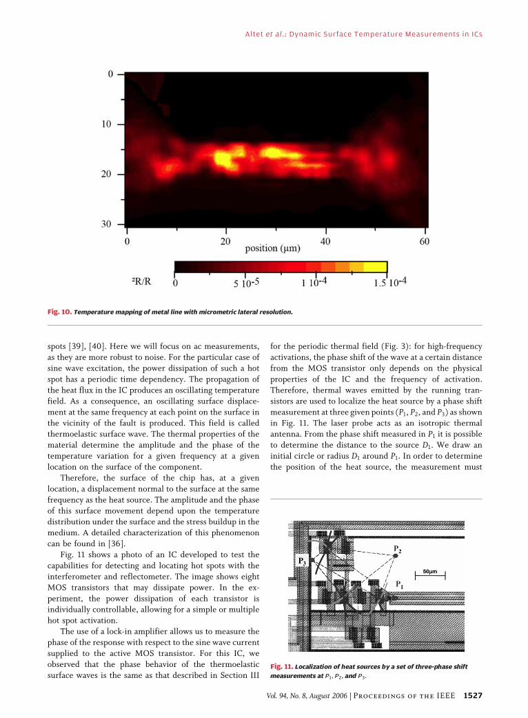
Fig. 11 shows a photo of an IC developed to test the
capabilities for detecting and locating hot spots with the
interferometer and reflectometer. The image shows eight
MOS transistors that may dissipate power. In the ex-
periment, the power dissipation of each transistor isindividually controllable, allowing for a simple or multiple
hot spot activation.
The use of a lock-in amplifier allows us to measure the
phase of the response with respect to the sine wave current
supplied to the active MOS transistor. For this IC, we
observed that the phase behavior of the thermoelastic
surface waves is the same as that described in Section III
for the periodic thermal field (Fig. 3): for high-frequency
activations, the phase shift of the wave at a certain distance
from the MOS transistor only depends on the physical
properties of the IC and the frequency of activation.
Therefore, thermal waves emitted by the running tran-
sistors are used to localize the heat source by a phase shift
measurement at three given points (P1, P2, and P3) as shown
in Fig. 11. The laser probe acts as an isotropic thermalantenna. From the phase shift measured in P1 it is possible
to determine the distance to the source D1. We draw an
initial circle or radius D1 around P1. In order to determine
the position of the heat source, the measurement must
Fig. 10. Temperature mapping of metal line with micrometric lateral resolution.
Fig. 11. Localization of heat sources by a set of three-phase shift
measurements at P1, P2, and P3.
Altet et al. : Dynamic Surface Temperature Measurements in ICs
Vol. 94, No. 8, August 2006 | Proceedings of the IEEE 1527

be taken at three points (P1, P2, and P3); the source is at
the intersection of the three circles as shown in Fig. 11.
Three heat sources #1, #3, and #5 have successively been
activated and localized.
An interferometer was used in [41], [42] to detect andlocate a hot spot in a 0.18-�m CMOS IC with five levels of
metal and metal fills. In this case, due to the metal fills, no
direct visual access to the silicon surface was possible. The
metal fills were formed by electrically isolated rectangular
metals. The laser probe allowed us to dynamically monitor
the displacement of a single rectangle due to the heat
dissipated by the device acting as a hot spot. These works
show how it is possible to use amplitude and ac small-signal phase measurements to detect and locate the heat
source. In the particular example of [42], if the hot spot
produces dissipation higher than 890 �W, it can be
detected and located through surface displacement mea-
surements. For the case of amplitude measurements, the
hot spot was beneath the metal fill whose displacement
was maximal.
So far, we have considered the case of punctual mea-surement. Interferometric and thermoreflectance imag-
ing (direct two-dimension image extraction) is possible
based on classical electronic speckle pattern interferom-
etry ESPI. In this case, the light source, usually a laser
diode or an He–Ne laser, can be replaced by a light-
emitting diode (LED). The laser lights up a complete area
of the IC and the reflected light is collected by a CCD
camera. Details about the instrumentation setup and in-formation process of the technique can be found in [43].
As an example of measurement, Fig. 12 shows the normal
surface displacement of a membrane and its temperature
surface variation in a micromachined IC holding a metal
line acting as a resistance.
V. EMBEDDED TEMPERATURE SENSORS
Embedded temperature sensors allow continuous dynamic
and static monitoring of the surface temperature of the IC
at specific locations. With this technique, temperature can
be measured without having direct visual access to the
silicon surface and measurements can be performed either
in-field, even online, or in a test laboratory.
There are two major drawbacks to embedding temper-
ature sensors: first, there is a silicon area overhead.
Second, temperature can only be sensed in specific areas ofthe IC: the location of the temperature-sensitive devices
which act as temperature transducers.
A specific requirement of the embedded temperature
sensors is that they must be fully compatible with the
technology process of the circuit into which they will be
embedded [44]. The output signal of the temperature
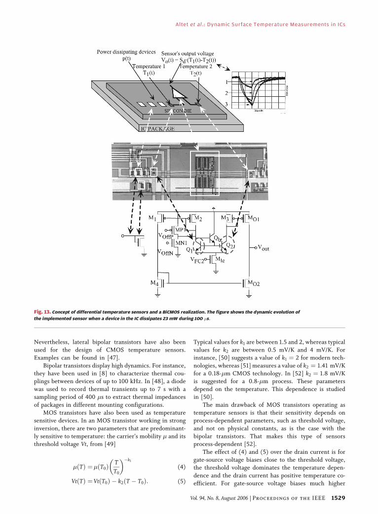
sensors can be proportional either to absolute temperature
at one point of the silicon surface (Fig. 1) or to the dif-ference in temperature at two points of the silicon surface
(Fig. 13). This leads to the categorization of temperature
sensors into two groups: absolute and differential.
A. Absolute Temperature SensorsAbsolute temperature sensors are used in today’s high-
performance microprocessors [16] in order to guarantee
thermal integrity and safe operating temperatures in theIC. Other uses of embedded temperature sensors include
the characterization of thermal impedances [8], [11] and
the thermal testing of packages [13], [14]. Absolute tem-
perature sensors may be categorized into single-device
sensors or multiple-device sensors.
Single-device sensors are formed by a temperature
sensitive device, whose sensitive terminals are accessible
through the IC pins. Although all devices in an IC aretemperature sensitive, the usual device for a single-device
sensor is a PN junction (or a forward-biased bipolar tran-
sistor), due to its predictability, long-term stability, and
linearity [45].
In the case of bipolar transistors, the key temperature-
dependent parameter observed is its base-emitter voltage,
whose sensitivity to temperature is almost linear with a
typical value of �2 mV/K.In the case of CMOS processes, vertical and lateral
parasitic bipolar transistors may be used. In [45] and
[46], vertical transistors are preferred as their electrical
characteristics are closer to real bipolar transistors.
Fig. 12. Normal surface displacement of a membrane and temperature surface variation.
Altet et al.: Dynamic Surface Temperature Measurements in ICs
1528 Proceedings of the IEEE | Vol. 94, No. 8, August 2006
Nevertheless, lateral bipolar transistors have also been
used for the design of CMOS temperature sensors.
Examples can be found in [47].
Bipolar transistors display high dynamics. For instance,
they have been used in [8] to characterize thermal cou-plings between devices of up to 100 kHz. In [48], a diode
was used to record thermal transients up to 7 s with a
sampling period of 400 �s to extract thermal impedances
of packages in different mounting configurations.
MOS transistors have also been used as temperature
sensitive devices. In an MOS transistor working in strong
inversion, there are two parameters that are predominant-
ly sensitive to temperature: the carrier’s mobility � and itsthreshold voltage Vt, from [49]
�ðTÞ ¼�ðT0ÞT
T0
� ��k1
(4)
VtðTÞ ¼ VtðT0Þ � k2ðT � T0Þ: (5)
Typical values for k1 are between 1.5 and 2, whereas typical
values for k2 are between 0.5 mV/K and 4 mV/K. For
instance, [50] suggests a value of k1 ¼ 2 for modern tech-
nologies, whereas [51] measures a value of k2 ¼ 1:41 mV/K
for a 0.18-�m CMOS technology. In [52] k2 ¼ 1:8 mV/Kis suggested for a 0.8-�m process. These parameters
depend on the temperature. This dependence is studied
in [50].
The main drawback of MOS transistors operating as
temperature sensors is that their sensitivity depends on
process-dependent parameters, such as threshold voltage,
and not on physical constants, as is the case with the
bipolar transistors. That makes this type of sensorsprocess-dependent [52].
The effect of (4) and (5) over the drain current is for
gate-source voltage biases close to the threshold voltage,
the threshold voltage dominates the temperature depen-
dence and the drain current has positive temperature co-
efficient. For gate-source voltage biases much higher
Fig. 13. Concept of differential temperature sensors and a BiCMOS realization. The figure shows the dynamic evolution of
the implemented sensor when a device in the IC dissipates 23 mW during 100 �s.
Altet et al. : Dynamic Surface Temperature Measurements in ICs
Vol. 94, No. 8, August 2006 | Proceedings of the IEEE 1529

than the threshold voltage, the dependence on the tem-perature of the mobility dominates and the drain current
has a negative temperature coefficient. In between both
extreme biases, there is a gate source voltage for which
the drain current has a null temperature coefficient [50].
If the MOS transistor works in weak inversion, the
current follows the same diffusion process as in a bipolar
transistor, and the temperature dependence has a similar
expression.There is a wide variety of multiple-device temperature
sensors. For any sensor to be used as a thermal monitor, it
should exhibit minimum area overhead and a simple
structure. In this context, several works use a temperature-
dependent digital oscillator, which provides digital readout
in the form of temperature-dependent frequency. By way
of example, in [50] a digital oscillator with an output
frequency in the 1–3-MHz range, which decreases at a rateof �8 to �6 KHz/K depending on the bias voltage (from 5
to 2.5 V), is presented. In [17], it is suggested that ring
oscillators are used to monitor the temperature in FPGAs.
FPGAs allow dynamic reconfiguration of their hardware
and, therefore, dynamic placement of temperature sen-
sors. The implemented oscillators have an oscillating
frequency between 21 and 27 MHz at 25 �C depending on
the configuration, and the temperature sensitivity is�0.20%=�C.
In [52], a sensor based on a threshold voltage reference
is used as a thermal monitor. The advantage of this sensor
is that the temperature dependence of both the mobility
and the threshold voltage contribute in the same direction
to the temperature dependence of the output current. Im-
plemented in a 1-�m CMOS process, the main perfor-
mances are as follows: area of 0.02 mm2, power dissipationof 200 �W, temperature sensitivity of �0.75%=�C, accu-
racy of 1 �C, and a sensitivity to power supply varia-
tions of 1%/V. The long-term stability was 0.5 �C over
160 days of continuous operation.
B. Differential Temperature SensorsDifferential temperature sensors are sensitive to the
difference of temperature at two points of the silicon
surface. Therefore, they provide immunity to any source
that may introduce an offset to the thermal map at the
silicon surface, e.g., variations in the ambient temperature.
The use of differential temperature sensors has been
reported in [53] as a part of a delayed short circuit
protection in power ICs. In [19], its use has been proposed
to detect dynamic thermal increases generated by un-desired hot spots associated to defects in digital circuits,
whereas in [54], their use has been suggested to measure
the bandwidth of RF amplifiers through temperature
measurements.
From an electrothermal point of view, differential
temperature sensors are characterized by two parameters:
their differential sensitivity, SdT , and their common sen-
sitivity, ScT . The general expression for the output voltageof a differential sensor is
Vout ¼ SdTðT2 � T1Þ þ ScTT2 þ T1
2
� �: (6)
In order to obtain an effective differential temperature
sensor, its differential sensitivity should be as high aspossible, whereas its common sensitivity should ideally be
zero. Similar to classical differential amplifiers, we can
define a common mode rejection ratio (CMRR), defined
as the ratio between the differential over the common
sensitivity.
Focusing on possible realizations, they are categorized
into passive and active.
Passive differential temperature sensors do not need apower supply and are based on the Seebeck effect that
exists in thermocouples. The Seebeck effect is the differ-
ence of potential that exists at both ends of the conductor,
V12, due to a difference of temperature at these ends
ðT2 � T1Þ. The proportional factor between differences of
voltage and temperature is called the Seebeck coefficient
of the conductor . As a matter of example, in [55] the
Seebeck factor of the gate and capacitor polysilicons in a1.2-�m CMOS technology were characterized with values
of 105 and 96 �V/K, respectively. Other examples are
reported in [65]. There, two thermocouples are placed at
5 �m from a dissipating device in a CMOS 0.35 tech-
nology. The thermopiles exhibit a differential sensitivity
of 0.1 and 0.26 V per W dissipated by the device.
Active sensors need a source of energy. Compared with
passive sensors, they exhibit a higher differential sen-sitivity with the drawback of the power consumption
required to work. The general principle of an active dif-
ferential sensor is the use of balanced circuits, for in-
stance, current mirrors [56] or coupled-emitter (or
source) stages [42], [53].
Temperature gradients in the circuit cause an unbalan-
cing of the operating point.
Fig. 13 shows a schematic for a differential temperaturesensor implemented in a 1.2-�m BiCMOS technology [6].
This sensor has been implemented in a test IC to
dynamically track the power dissipated by devices placed
in the same silicon IC. The circuit is based on a classic
operational transconductance amplifier [66] (OTA). How-
ever, in this case, the differential input stage is not
imbalanced by a different electrical biasing of the dif-
ferential pair Q1 and Q2, but by a difference in its tem-perature. Therefore, to measure a temperature gradient, a
distant placement of both devices is required. This is
shown in the layout of the circuit: the distance between Q1
and Q2 is 500 �m. To compensate for thermal offsets due
to mismatching between devices, the devices MN1 and
MP1 have been added. For instance, with the bias of this
Altet et al.: Dynamic Surface Temperature Measurements in ICs
1530 Proceedings of the IEEE | Vol. 94, No. 8, August 2006
circuit being VFC2 ¼ 1:7 V (@ VDD ¼ 5 V), the differ-ential sensitivity of the circuit is �2.7 V=�C.
To characterize the performances of the sensor, in the
test IC some MOS transistors in diode configuration (i.e.,
source tied to GND and gate connected to the drain and
to the bias voltage terminal [66]) have been placed
(Fig. 13). The use of these MOS transistors is to dissipate
power (and to change the IC surface thermal map) when
they are driven by a voltage source. Thus, it is possible toobserve the impact on the sensor’s output caused by the
static and dynamic activation of a specific device as a
function of the distance between the dissipating device
and the temperature sensitive device. Static measure-
ments show that the sensor is very sensitive. For instance,
the activation of an MOS transistor placed at 137 �m
from Q1 and at 637 �m from Q2 gives a static sensitivity
of �29.36 V per W dissipated at the MOS transistor.Fig. 13 shows the dynamic variation of the sensor’s output
voltage when an MOS transistor placed at 33 �m from Q1
and 533 �m from Q2 dissipates 23 mW during 100 �s.
Three different plots are superimposed, corresponding to
the three different biasing conditions of the sensor
(Bias 1: VFC2 ¼ 1:95, Bias 2: VFC2 ¼ 1:696 V, Bias 3:
VFC2 ¼ 1:2 V), showing the dependence of the differential
sensitivity and dynamic performances of the sensor on itsbiasing. In this figure, the vertical axis is 200 mV/div. As
we can see, the use of differential temperature sensors
provides a highly sensitive way to track power dissipatedby devices and circuits.
If the distance between the temperature-sensitive
devices of the sensor (Q1 and Q2) is long, we can assume
that a small dissipation of power close to Q1 may not
thermally affect Q2. In this case, differential temperature
sensors can be used to characterize thermal couplings in
ICs with high sensitivity. Fig. 2 is an example of the Bode
diagrams of the thermal coupling in an IC measured withthe differential sensor in Fig. 13.
VI. CONCLUSION
The dynamic evolution of the temperature on the surface
of an IC is a projection of the circuit’s behavior and IC
structure. In this paper, we have focused on those
measuring techniques that provide suitable performancesfor a reliable tracing of this dynamic, with detailed
description of two measuring techniques: laser-based
methods and embedded CMOS temperature sensors.
Temperature is a relevant physical variable for the
design and the characterization of devices and circuits. The
dynamics of the temperature contains information com-
plementary to the traditional voltage and current electrical
signals. The presented measuring techniques, along withtheir ongoing research, open new research scenarios for
future generations of technology. h
RE FERENCES
[1] J. M. Soden and R. E. Anderson, BIC failureanalysis: Techniques and tools for qualityreliability improvement,[ Proc. IEEE, vol. 81,no. 5, pp. 703–715, May 1993.
[2] J. Hiatt, BA method of detecting hot spots onsemiconductors using liquid crystals,[ in Proc.19th Annu. IEEE Reliability Physics Symp., 1981,pp. 130–133.
[3] D. H. Lee, BThermal analysis of integratedcircuit chips using thermographic imagingtechniques,[ IEEE Trans. Instrum. Meas.,vol. 43, no. 6, pp. 824–829, Dec. 1994.
[4] P. Kolodner and J. A. Tyson, BMicroscopicfluorescent imaging of surface temperatureprofiles with 0.01 �C resolution,[ Appl. Phys.Lett., vol. 40, no. 9, pp. 782–784, 1982.
[5] J. Christofferson and A. Shakouri, BThermalmeasurements of active semiconductormicro-structures acquired through thesubstrate using near IR thermoreflectance,[Microelectron. J., vol. 35, no. 10, pp. 791–796,Oct. 2004.
[6] J. Altet, A. Rubio, E. Schaub, S. Dilhaire, andW. Claeys, BThermal coupling in integratedcircuits: application to thermal testing,[ IEEEJ. Solid-State Circuits, vol. 36, no. 1, pp. 81–91,Jan. 2001.
[7] D. J. Walkey, T. S. Smy, R. G. Dickson,J. S. Brodsky, D. T. Zweidinger, andR. M. Fox, BEquivalent circuit modeling ofstatic substrate thermal coupling using VCVSrepresentation,[ IEEE J. Solid-State Circuits,vol. 37, no. 9, pp. 1198–1205, Sep. 2002.
[8] N. Nenadovic, S. Mijalkovic, L. K. Nanver,L. K. J. Vandamme, V. d’Alessandro,
H. Schellevis, and J. W. Slotboom, BExtractionand modeling of self-heating and mutualthermal coupling impedance of bipolartransistors,[ IEEE J. Solid-State Circuits,vol. 39, no. 10, pp. 1764–1772, Oct. 2004.
[9] F. F. Oettinger and D. L. Blackburn,BSemiconductor measurement technology:thermal resistance measurements, NISTSpecial Publication 400-86, Jul. 1990.
[10] T. S. Fisher, C. T. Avedisian, and J. P. Krusius,BTransient thermal response due to periodicheating on a convectively cooled substrate,[IEEE Trans. Compon., Packag., Manuf.Technol. B, vol. 19, no. 1, pp. 255–261,Feb. 1996.
[11] M. Rencz and V. Szekely, BStudies on thenonlinearity effects in dynamic compactmodel generation of packages,[ IEEE Trans.Compon. Packag. Technol., vol. 27, no. 1,pp. 124–130, Mar. 2004.
[12] V. Szekely and M. Renz, BIncreasing theaccuracy of thermal transientmeasurements,[ IEEE Trans. Compon.Packag. Technol., vol. 25, no. 4,pp. 539–546, Dec. 2002.
[13] M. R. Rencz and V. Szekely, BMeasuringpartial thermal resistance in a heat-flowpath,[ IEEE Trans. Compon. Packag. Technol.,vol. 25, no. 4, pp. 547–553, Dec. 2002.
[14] K. Kurabayashi and K. E. Goodson, BPrecisionmeasurement and mapping of die-attachthermal resistance,[ IEEE Trans. Compon.,Packag., Manuf. Technol. A, vol. 21, no. 3,pp. 506–514, Sep. 1998.
[15] M. Carmona, S. Marco, J. Palacın, andJ. Samitier, BA time-domain method for theanalysis of thermal impedance response
preserving the convolution form,[ IEEE Trans.Compon. Packag. Technol., vol. 22, no. 2,pp. 238–244, Jun. 1999.
[16] Pentium III processor active thermalmanagement techniques (application note),Aug. 2000, order no. 273405-001.
[17] S. L. Buedo, J. Garrido, and E. I. Boemo,BDynamically inserting, operating andeliminating thermal sensors on FPGA basedsystems,[ IEEE Trans. Compon. Packag.Technol., vol. 26, no. 4, pp. 561–566,Dec. 2002.
[18] J. Altet and A. Rubio, Thermal Testing of IC.Norwell, MA: Kluwer, 2002.
[19] VV, BDifferential sensing strategy fordynamic thermal testing of ICs,[ in Proc. 15thIEEE VLSI Test Symp., 1997, pp. 434–439.
[20] D. Mateo, J. Altet, and E. Aldrete-Vidrio, BAnapproach to the electrical characterization ofanalog blocks through thermalmeasurements,[ in Proc. 11th THERMINICWorkshop, 2005, pp. 59–64.
[21] J. Christofferson and A. Shakouri, BThermalmeasurements of active semiconductormicro-structures acquired through thesubstrate using near IR thermoreflectance,[Microelectron. J., vol. 35, no. 10, pp. 791–796,Oct. 2004.
[22] X. Perpina, X. Jorda, N. Mestres,M. Vellvehi, P. Godignon, J. Millan, andH. von Kiedrowski, BInternal infrared laserdeflection system: a tool for power devicecharacterization,[ Meas. Sci. Technol., vol. 15,no. 5, pp. 1011–1018.
[23] M. Nishiguchi, M. Fujihara, A. Miki, andH. Nishizawa, BPrecision comparison of
Altet et al. : Dynamic Surface Temperature Measurements in ICs
Vol. 94, No. 8, August 2006 | Proceedings of the IEEE 1531
surface temperaure measurement techniquesfor GaAs IC’s,[ IEEE Trans. Compon., Hybrids,Manuf. Technol., vol. 16, no. 5, pp. 543–549,Aug. 1993.
[24] W. Chen, H. Cheng, and H. Shen, BAneffective methodology for thermalcharacterization of electronic packaging,[IEEE Trans. Compon., Hybrids, Manuf. Technol.,vol. 26, no. 1, pp. 222–232, Mar. 2003.
[25] V. Szekely and M. Rencz, BImage processingprocedures for the thermal measurements,[IEEE Trans. Compon., Hybrids, Manuf. Technol.,vol. 22, no. 2, pp. 259–265, Jun. 1999.
[26] J. Lai, M. Chandrachood, A. Majumdar, andJ. P. Carrejo, BThermal detection of devicefailure by atomic force microscopy,[ IEEEElectron Device Lett., vol. 16, no. 7,pp. 312–315, Jul. 1995.
[27] J. Altet, J. M. Rampnoux, J. C. Batsale,S. Dilhaire, A. Rubio, W. Claeys, andS. Grauby, BApplications of temperaturephase measurements to IC testing,[Microelectron. Reliab., vol. 44,pp. 95–103, 2004.
[28] S. Dilhaire, S. Grauby, W. Claeys, andJ. C. Batsale, BThermal parametersidentification of micrometric layersof microelectronic devices bythermoreflectance,[ Microsc. Microelectron. J.,vol. 35, no. 10, pp. 811–816, Oct. 2004.
[29] L. D. Patino Lopez, S. Grauby, S. Dilhaire,M. A. Salhi, W. Claeys, S. Lefevre, andS. Volz, BCharacterization of the thermalbehavior of PN thermoelectric couples byscanning thermal microscope,[ Microelectron.J., vol. 35, no. 10, pp. 797–803, Oct. 2004.
[30] W. Claeys, S. Dilhaire, V. Quintard, andY. Danto, BThermoreflectance opticaltest probe for the measurement of currentinduced temperature changes inmicroelectronic components,[ Qual. Reliab.Eng. Int., vol. 9, pp. 303–308, 1993.
[31] W. Claeys, S. Dilhaire, and V. Quintard,BLaser probing of thermal behaviour ofelectronic components and its application inquality and reliability testing,[ Microelectron.Eng., vol. 24, pp. 411–420, 1994.
[32] W. Claeys, S. Dilhaire, V. Quintard, J. P. Dom,and Y. Danto, BThermoreflectance opticaltest probe for the measurement of currentinduced temperature changes inmicroelectronic components,[ Qual. Reliab.Eng. Int., vol. 9, pp. 303–308, 1993.
[33] V. Quintard, G. Deboy, S. Dilhaire, D. Lewis,T. Phan, and W. Claeys, BLaser beamthermography of circuits in the particular caseof passivated semiconductors,[ Microelectron.Eng., vol. 31, pp. 291–298, 1996.
[34] S. Grauby, S. Dilhaire, S. Jorez, andW. Claeys, BImaging setup for temperature,topography, and surface displacementmeasurements of microelectronic devices,[Rev. Sci. Instrum., vol. 74, no. 1, pp. 645–647,Jan. 2003.
[35] W. Claeys, S. Dilhaire, S. Jorez, andL.-D. Patino-Lopez, BLaser probes for thethermal and thermomechanicalcharacterisation of microelectronic devices,[Microelectron. J., vol. 32, no. 10–11,pp. 891–898, Oct.–Nov. 2001.
[36] A. Rosencwaig, J. Opsal, N. L. Smith, andD. L. Willenborg, BDetection of thermalwaves through optical reflectance,[ Appl.Phys. Lett., vol. 46, pp. 1013, 1985.
[37] H. A. Weakliem and D. Redfield,BTemperature dependence of the opticalproperties of silicon,[ J. Appl. Phys., vol. 50,no. 3, pp. 1491, 1979.
[38] S. Dilhaire, S. Jorez, L. D. Patino-Lopez,W. Claeys, and E. Schaub, BCalibrationprocedure of temperature measurements bythermoreflectance upon microelectronic de-vices.’’ presented at the 11th Int. Conf.Photoacoustic and Photothermal Phenomena,Kyoto, Japan, 2000.
[39] S. Dilhaire, E. Schaub, W. Claeys, J. Altet, andA. Rubio, BLocalisation of heat sources inelectronicrcuits by microthermal laserprobing,[ Int. J. Therm. Sci., vol. 39,pp. 544–549, 2000.
[40] S. Dilhaire, J. Altet, S. Jorez, E. Schaub,A. Rubio, and W. Claeys, BFault localisation inIC’s by goniometric laser probing of thermalinduced surface waves,[ Microelectron.Reliab., vol. 39, pp. 919–923, 1999.
[41] J. Altet, M. A. Salhi, S. Dilhaire, andA. Ivanov, BCalibration-free heat sourcelocalization in ICs entirely covered by metallayers,[ Electron. Lett., vol. 40, no. 4,pp. 241–242, Feb. 19, 2004.
[42] J. Altet, A. Rubio, A. Salhi, J. L. Galvez,S. Dilhaire, A. Syal, and A. Ivanov, BSensingtemperature in CMOS circuits for thermaltesting,[ in Proc. 22nd IEEE VLSI Test Symp.,2004, pp. 179–184.
[43] S. Dilhaire, S. Grauby, S. Jorez, L. D. P. Lopez,J.-M. Rampnoux, and W. Claeys, BSurfacedisplacement imaging by interferometry witha light emitting diode,[ Appl. Opt., vol. 41,no. 24, pp. 4996–5001, Aug. 20, 2002.
[44] V. Szekely, C. Marta, M. Rencz, Z. Benedek,and B. Courtois, BDesign for thermaltestability (DfTT) and a CMOS realization,[Sens. Actuators, vol. A55, no. 1, pp. 29–34,1996.
[45] G. C. M. Meijer, G. Wang, and F. Fruett,BTemperature sensors and voltage referencesimplemented in CMOS technology,[ IEEESensors J., vol. 1, no. 3, pp. 225–234,Oct. 2001.
[46] A. Bakker and J. H. Huijsing, BMicropowerCMOS temperature sensor with digitaloutput,[ IEEE J. Solid-State Circuits, vol. 31,no. 7, pp. 933–937, Jul. 1996.
[47] R. A. Bianchi, J. M. Karam, B. Courtois,R. Nadal, F. Pressecq, and S. Sifflet,BCMOS-compatible temperature sensor withdigital output for wide temperature rangeapplications,[ Microelectron. J., vol. 31,no. 9–10, pp. 803–810, Oct. 2000.
[48] P. E. Bagnoli, C. Casarosa, E. Dallago, andM. Nardoni, BThermal resistance analysisby induced transient (TRAIT) method forpower electronic devices thermalcharacterizationVPart II: Practice andexperiments,[ IEEE Trans. Power Electron.,vol. 13, no. 6, pp. 1220–1228, Nov. 1998.
[49] Y. P. Tsividis, Operation and Modeling of theMOS Transistor. New York: McGraw-Hill,1987.
[50] I. M. Filanovsky and A. Allan, BMutualcompensation of mobility and thresholdvoltage temperature effects with applicationin CMOS circuits,[ IEEE Trans. Circuits Syst. I,Fundam. Theory Appl., vol. 48, no. 7,pp. 876–884, Jul. 2001.
[51] I. M. Filanovsky and S. T. Lim, BTemperaturesensor applications of diode-connected MOStransistors,[ in IEEE Int. Symp. Circuits andSystems, 2002, pp. II-149–II-152.
[52] V. Szekely, C. Marta, Z. Kohari, andM. Rencz, BCMOS sensors for on-line thermalmonitoring of VLSI circuits,[ IEEE Trans. VeryLarge Scale Integr. (VLSI) Syst., vol. 5, no. 3,pp. 270–276, Sep. 1997.
[53] P. Antognetti, G. R. Bisio, F. Curatelli, andS. Palara, BThree-dimensional transientthermal simulation: Application to delayedshort circuit protection in power ICs,[IEEE J. Solid-State Circuits, vol. SC-15,no. 3, pp. 277–281, Jun. 1980.
[54] J. Altet, D. Mateo, and J. L. Gonzalez,BObservation of high-frequency analog/RFelectrical circuit characteristics by on-chipthermal measures,[ in Proc. ISCAS 2006.
[55] M. V. Arx, O. Paul, and H. Baltes, BTeststructures to measure the Seebeck coefficientof CMOS IC polysilicon,[ IEEE Trans.Semicond. Manuf., vol. 10, no. 2, pp. 201–208,May 1997.
[56] A. Syal, V. Lee, A. Ivanov, and J. Altet,BCMOS differential and absolute thermalsensor,[ J. Electron. Testing: Theory Appl.,vol. 18, pp. 295–304, 2002.
[57] O. Breitenstein, M. Langenkamp, F. Altmann,D. Katzer, A. Lindner, and H. Eggers,BMicroscopic lock-in thermographyinvestigation of leakage sites in integratedcircuits,[ Rev. Sci. Instrum., vol. 7, no. 11,pp. 4155–4160, Nov. 2000.
[58] K. Arabi and B. Kaminska, BBuilt-intemperature and current sensors for on-lineoscillation-testing,[ in Proc. 2nd IEEE Int.On-Line Testing Workshop, 1996, pp. 13–16.
[59] D. L. Blackburn, BTemperaturemeasurements of semiconductor devicesVAreview,[ in Proc. 20th SEMITHERM Symp.,2004, pp. 70–80.
[60] S. Volz, S. Dilhaire, S. Lefebvre, andL. D. Patino-Lopez, Scanning thermalmicroscopy applied to thin films andelectronic devices characterization,’’Handbook of Semiconductor Nanostructuresand Nanodevices, A. A. Balandin andK. L. Wang, Eds. North Lewis Way, CA:American Scientific, ch. 29.
[61] I. Abbadi, BNew imaging method for diffusiveand opaque media: Application to backsideimaging of integrated circuits,[ Ph.D.dissertation, Univ. Bordeaux 1, Bordeaux,France, 2005.
[62] J. Altet, S. Dilhaire, S. Volz, J. M. Rampnoux,A. Rubio, S. Grauby, L. D. Patino-Lopez,W. Claeys, and J. B. Saulnier, BFour differentapproaches for the measurement of IC surfacetemperature: Application to thermal testing,[Microelectron. J., vol. 33, pp. 689–696, 2002.
[63] J. Altet, M. A. Salhi, S. Dilhaire, A. Syal, andA. Ivanov, BLocalisation of devices acting asheat sources in ICs covered enterely bymetal layers,[ Electron. Lett., vol. 39, no. 20,pp. 1140–1442, 2003.
[64] H. S. Carslaw and J. C. Jaeger, ConductionHeat in Solids. New York: Oxford, 1993.
[65] E. Aldrete, J. Altet, and D. Mateo,BDifferential temperature sensors in0.35 �m CMOS technology,[ in Proc. IEEETHERMINIC 2005 Conf., pp. 122–128.
[66] K. R. Laker and W. Sansen, Design of AnalogIntegrated Circuits and Systems. New York:Mc Graw-Hill, 1994.
[67] P. Jeong, W. S. Moo, and C. C. Lee, BThermalmodeling and measurement of GaN-basedHFET devices,[ IEEE Electron Device Lett.,vol. 24, no. 7, pp. 424–426, Jul. 2003.
[68] A. M. Chaudhari, T. M. Woudenberg,M. Albin, and K. E. Goodson, BTransientliquid crystal thermometry of microfabricatedPCR vessel arrays,[ J. Microelectromech. Syst.,vol. 7, no. 4, pp. 345–355, 1998.
Altet et al.: Dynamic Surface Temperature Measurements in ICs
1532 Proceedings of the IEEE | Vol. 94, No. 8, August 2006

ABOUT T HE AUTHO RS
Josep Altet received the Technical Telecommu-
nication Engineering and the Electronic Engineer-
ing degrees from the Ramon Llull University, (URL)
Barcelona, Spain, and the Ph.D. degree from the
Technical University of Catalonia (UPC), Barcelona.
He is now an Associate Professor in the
Department of Electronic Engineering, UPC. His
research interests include VLSI design and test,
temperature sensor design, and thermal coupling
analysis and modeling in integrated circuits.
Wilfrid Claeys received the Ph.D. degree in 1974
at the University of Louvain, Louvain, Belgium.
He was an Assistant Professor at the University
of Louvain. He has been a Professor at the Uni-
versity of Bordeaux, Bordeaux, France, since 1990.
He is leading a research group dedicated to optical
probing of the thermal behavior of microelec-
tronics components.
Stefan Dilhaire received both an undergraduate
degree in microelectronics and the Ph.D. degree
in electronics from the University of Bordeaux,
Bordeaux, France.
He is now an associate professor at the Uni-
versity of Bordeaux. His work involves the design
of optical contactless probes for analyzing the
thermal behavior of integrated circuits.
Antonio Rubio received the M.S. and Ph.D. de-
grees from the Industrial Engineering Faculty of
Barcelona, Spain.
He has been Associate Professor of the Elec-
tronic Engineering Department at the Industrial
Engineering Faculty, Technical University of Cata-
lonia (UPC), Barcelona, and Professor of the
Physics Department at the Balearic Islands Uni-
versity. He is currently Professor of Electronic
Technology at the Telecommunication Engineer-
ing Faculty, UPC. His research interests include very large scale in-
tegration (VLSI) design and test, device and circuit modeling and high-
speed circuit design.
Altet et al. : Dynamic Surface Temperature Measurements in ICs
Vol. 94, No. 8, August 2006 | Proceedings of the IEEE 1533
Related Documents