Investigating The Effect Of Chirality On Coaxial Carbon Nanotube Field Effect Transistor P.A. Gowri Sankar, Research Scholar Department of Electrical and Electronics Engineering College of Engineering Guindy, Anna University Chennai, India [email protected] Abstract—Carbon Nanotube Field Effect Transistors (CNTFET) are promising nano-scaled devices for implementing high performance, very dense and low power circuits. The core of a CNTFET is a carbon nanotube. Its conductance property is determined by the chirality of the tube. In this paper, the current-voltage characteristics of coaxial type CNTFET is studied by quantum simulations using the non-equilibrium Green’s function formalism with the self- consistent born approximation. The simulation shows that the current-voltage characteristics of CNTFET vary depends on the chirality and thickness of the oxide layer. This analysis is applicable to primitive and complex digital and analog circuit design based on CNTFETs. The CNTFET simulation is carried out using Nanohub.org, which is an online based java platform engine. Keywords-CNTFET; SWNTs; CNTs; Chirality; On-Off ratio; Coaxial tube; I-V characteristics. I. INTRODUCTION As silicon technology is approaching to its limit, several emerging devices are studied to find a suitable alternative to silicon. Carbon nanotube FETs (CNFET) are shown to have potential of taking this place in the post silicon era. Its interesting structural and electrostatic properties (e.g., near ballistic transport) make it attractive for the future integrated circuit applications [1]. Superior performance for the CNTFETs can be expected if multiple parallel CNTs with highly transparent contact and good spatial control can be utilized to construct the CNTFETs, which includes high drive current and transconductance, low-power dissipation and noise. Several such nanodevices are currently being researched, such as the carbon nanotube based transistor (CNTFET), the resonant tunneling diode (RTD), the single electron transistor (SET), and the spin transistor (SPINFET). In general, nanoscience research focuses primarily on the search for new physical concepts and on creating the technology necessary for the development of nanodevices. However, research in nanoelectronic circuits (the integration of nanodevices in circuits or systems), in the context of leading-edge technologies to realize data processing, memorization and communication functions, is somewhat under-represented. Dr. K. Udhaya kumar, Assistant Professor, Department of Electrical and Electronics Engineering College of Engineering Guindy, Anna University Chennai, India [email protected] II. THEORY OF CARBON NANOTUBES (CNTs) Carbon nanotubes (CNTs) were discovered by Ijima in Japan in 1991. Theoretically, a CNT can be considered as sheet of graphene rolled into a tube [2]. When a honeycomb lattice of a piece of graphene sheet is being rolled into a cylinder, it forms a carbon nanotube, or CNT. Carbon nanotube can be classified into two main categories: (i) Single-Walled CNTs (SWCNT). (ii) Multi-Walled CNTs (MWCNT) Figure 1. Rolling of graphene to a carbon nanotube. A. Single-Walled CNTs (SWCNT) SWCNTs are several μms in length, typically will be up to 100μm. The diameter is approximately 1 to 2 nm [3]. They can be classified as armchair, zigzag and chiral structure. Chiral vector is a common term used to represent the way grapheme sheet is rolled up to form a nanotube. It is represented by two integer numbers n and m is normally define as (n, m). With this, its circumferential direction can be formulated as: 1 2 C na ma = + J G G J J G (1) where 1 a J G and 2 a J JG are the vectors of the graphene sheet. 2012 International Conference on Computing, Electronics and Electrical Technologies [ICCEET] 978-1-4673-0210-4/12/$31.00 ©2012 IEEE 663

Welcome message from author
This document is posted to help you gain knowledge. Please leave a comment to let me know what you think about it! Share it to your friends and learn new things together.
Transcript
Investigating The Effect Of Chirality On Coaxial Carbon Nanotube Field Effect Transistor
P.A. Gowri Sankar, Research Scholar
Department of Electrical and Electronics Engineering College of Engineering Guindy, Anna University
Chennai, India [email protected]
Abstract—Carbon Nanotube Field Effect Transistors (CNTFET) are promising nano-scaled devices for implementing high performance, very dense and low power circuits. The core of a CNTFET is a carbon nanotube. Its conductance property is determined by the chirality of the tube. In this paper, the current-voltage characteristics of coaxial type CNTFET is studied by quantum simulations using the non-equilibrium Green’s function formalism with the self-consistent born approximation. The simulation shows that the current-voltage characteristics of CNTFET vary depends on the chirality and thickness of the oxide layer. This analysis is applicable to primitive and complex digital and analog circuit design based on CNTFETs. The CNTFET simulation is carried out using Nanohub.org, which is an online based java platform engine.
Keywords-CNTFET; SWNTs; CNTs; Chirality; On-Off ratio; Coaxial tube; I-V characteristics.
I. INTRODUCTION
As silicon technology is approaching to its limit,
several emerging devices are studied to find a suitable alternative to silicon. Carbon nanotube FETs (CNFET) are shown to have potential of taking this place in the post silicon era. Its interesting structural and electrostatic properties (e.g., near ballistic transport) make it attractive for the future integrated circuit applications [1]. Superior performance for the CNTFETs can be expected if multiple parallel CNTs with highly transparent contact and good spatial control can be utilized to construct the CNTFETs, which includes high drive current and transconductance, low-power dissipation and noise. Several such nanodevices are currently being researched, such as the carbon nanotube based transistor (CNTFET), the resonant tunneling diode (RTD), the single electron transistor (SET), and the spin transistor (SPINFET). In general, nanoscience research focuses primarily on the search for new physical concepts and on creating the technology necessary for the development of nanodevices. However, research in nanoelectronic circuits (the integration of nanodevices in circuits or systems), in the context of leading-edge technologies to realize data processing, memorization and communication functions, is somewhat under-represented.
Dr. K. Udhaya kumar, Assistant Professor, Department of Electrical and Electronics Engineering
College of Engineering Guindy, Anna University Chennai, India
II. THEORY OF CARBON NANOTUBES (CNTs)
Carbon nanotubes (CNTs) were discovered by Ijima in Japan in 1991. Theoretically, a CNT can be considered as sheet of graphene rolled into a tube [2]. When a honeycomb lattice of a piece of graphene sheet is being rolled into a cylinder, it forms a carbon nanotube, or CNT. Carbon nanotube can be classified into two main categories: (i) Single-Walled CNTs (SWCNT). (ii) Multi-Walled CNTs (MWCNT)
Figure 1. Rolling of graphene to a carbon nanotube.
A. Single-Walled CNTs (SWCNT)
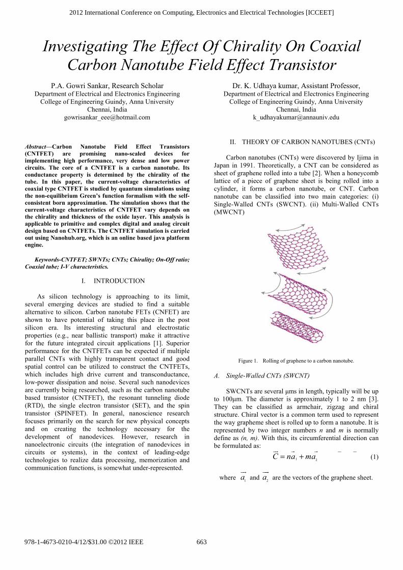
SWCNTs are several μms in length, typically will be up to 100μm. The diameter is approximately 1 to 2 nm [3]. They can be classified as armchair, zigzag and chiral structure. Chiral vector is a common term used to represent the way grapheme sheet is rolled up to form a nanotube. It is represented by two integer numbers n and m is normally define as (n, m). With this, its circumferential direction can be formulated as:
1 2C na ma= + (1)
where 1a and 2a are the vectors of the graphene sheet.
2012 International Conference on Computing, Electronics and Electrical Technologies [ICCEET]
978-1-4673-0210-4/12/$31.00 ©2012 IEEE 663
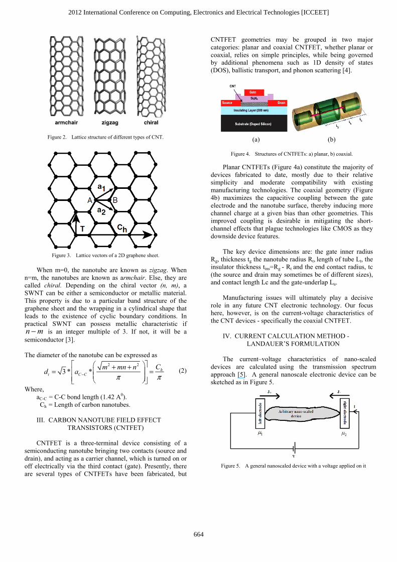
Figure 2. Lattice structure of different types of CNT.
Figure 3. Lattice vectors of a 2D graphene sheet.
When m=0, the nanotube are known as zigzag. When n=m, the nanotubes are known as armchair. Else, they are called chiral. Depending on the chiral vector (n, m), a SWNT can be either a semiconductor or metallic material. This property is due to a particular band structure of the graphene sheet and the wrapping in a cylindrical shape that leads to the existence of cyclic boundary conditions. In practical SWNT can possess metallic characteristic if
mn − is an integer multiple of 3. If not, it will be a semiconductor [3]. The diameter of the nanotube can be expressed as
2 2
3 * * ht C C
Cm mn nd aπ π−
⎡ ⎤⎛ ⎞+ +⎢ ⎥= =⎜ ⎟⎜ ⎟⎢ ⎥⎝ ⎠⎣ ⎦ (2)
Where, aC-C = C-C bond length (1.42 A0). Ch = Length of carbon nanotubes.
III. CARBON NANOTUBE FIELD EFFECT TRANSISTORS (CNTFET)
CNTFET is a three-terminal device consisting of a semiconducting nanotube bringing two contacts (source and drain), and acting as a carrier channel, which is turned on or off electrically via the third contact (gate). Presently, there are several types of CNTFETs have been fabricated, but
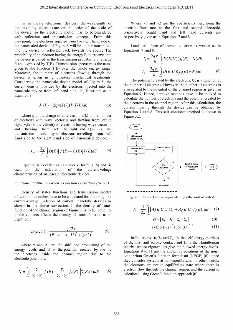
CNTFET geometries may be grouped in two major categories: planar and coaxial CNTFET, whether planar or coaxial, relies on simple principles, while being governed by additional phenomena such as 1D density of states (DOS), ballistic transport, and phonon scattering [4].
(a) (b)
Figure 4. Structures of CNTFETs: a) planar, b) coaxial.
Planar CNTFETs (Figure 4a) constitute the majority of devices fabricated to date, mostly due to their relative simplicity and moderate compatibility with existing manufacturing technologies. The coaxial geometry (Figure 4b) maximizes the capacitive coupling between the gate electrode and the nanotube surface, thereby inducing more channel charge at a given bias than other geometries. This improved coupling is desirable in mitigating the short-channel effects that plague technologies like CMOS as they downside device features. The key device dimensions are: the gate inner radius Rg, thickness tg the nanotube radius Rt, length of tube Lt, the insulator thickness tins=Rg - Rt and the end contact radius, tc (the source and drain may sometimes be of different sizes), and contact length Lc and the gate-underlap Lu. Manufacturing issues will ultimately play a decisive role in any future CNT electronic technology. Our focus here, however, is on the current-voltage characteristics of the CNT devices - specifically the coaxial CNTFET.
IV. CURRENT CALCULATION METHOD -LANDAUER’S FORMULATION
The current–voltage characteristics of nano-scaled
devices are calculated using the transmission spectrum approach [5]. A general nanoscale electronic device can be sketched as in Figure 5.
Figure 5. A general nanoscaled device with a voltage applied on it
2012 International Conference on Computing, Electronics and Electrical Technologies [ICCEET]
664
In nanoscale electronic devices, the wavelength of the travelling electrons are on the order of the scale of the device, so the electronic motion has to be considered with reflection and transmission concepts. From this viewpoint, the electrons injected from the right hand side of the nanoscaled device of Figure 5 will be either transmitted into the device or reflected back towards the source. The probability of an electron having the energy E to transmit into the device is called as the transmission probability at energy E and expressed by T(E). Transmission spectrum is the name given to the function T(E) over the whole energy range. Moreover, the number of electrons flowing through the device is given using quantum mechanical treatments. Considering the nanoscale device model of Figure 5, the current density provided by the electrons injected into the nanoscale device from left hand side, J+, is written as in Equation 3. ( ) 2 ( ) ( ) ( )eJ k qn k V k T k dk+ = (3)
where q is the charge of an electron, n(k) is the number of electrons with wave vector k and flowing from left to right, ve(k) is the velocity of electrons having wave vector k and flowing from left to right and T(k) is the transmission probability of electrons travelling from left hand side to the right hand side of nanoscaled device.
[ ]2
1
1 22 ( ) ( ) ( ) ( )net
qJ D E f E f E T E dEμ
μ
= −∫ (4)
Equation 4. is called as Landauer’s formula [5] and is used for the calculation of the current-voltage characteristics of nanoscale electronic devices. A. Non-Equilibrium Green’s Function Formalism (NEGF) Density of states functions and transmission spectra of carbon nanotubes have to be calculated for obtaining the current-voltage relation of carbon nanotube devices as shown in the above subsection. If the density of states function of the channel region of Figure 5 is D(E), coupling to the contacts affects the density of states function as in Equation 5.
2 2
2( , )( ) ( 2)
D E UE U
γ πε γ
=− − Δ − +
(5)
where γ and Δ are the shift and broadening of the energy levels and U is the potential created by the by the electrons inside the channel region due to the electrode potentials.
1 21 2
1 2 1 2
( ) ( ) ( , )N f E f E D E U dEγ γγ γ γ γ
∞
−∞
⎛ ⎞= −⎜ ⎟+ +⎝ ⎠∫ (6)
Where γ1 and γ2 are the coefficients describing the electron flow rate at the first and second electrode, respectively. Right hand and left hand currents are respectively given as in Equations 7 and 8. Landauer’s form of current equation is written as in Equations 7 and 8.
11 1
2 ( , )( ( ) )qI D E U f E N dEγ ∞
−∞
= −∫ (7)
22 2
2 ( , )( ( ) )qI D E U f E N dEγ ∞
−∞
= −∫ (8)
The potential created by the electrons, U, is a function of the number of electrons. However, the number of electrons is also related to the potential of the channel region as given in Equation 9. Hence, iterative methods have to be utilized to calculate the number of electrons and the potential created by the electrons in the channel region. After this calculation, the current flowing through the device can be obtained by Equation 7 and 8. This self–consistent method is shown in Figure 3.2.
Figure 6. Current Calculation procedure by self-consistent method
[ ]1 1 2 21 ( , ) ( ) ( , ) ( )
2N A E U f E A E U f E dE
π
∞
−∞
= +∫ (9)
[ ] 11 2G EI H −= − − Σ − Σ (10)
1
1 2( , )T E U Tr G G−+⎡ ⎤= Γ Γ⎣ ⎦ (11)
In Equations 10, Σ1 and Σ2 are the self energy matrices of the first and second contact and H is the Hamiltonian matrix whose eigenvalues give the allowed energy levels. Equations 9 to 11 are the known as equations of the non–equilibrium Green’s function formalism (NEGF) [6]. since they consider systems at non–equilibrium, in other words, the electrons are not in equilibrium state where there is electron flow through the channel region, and the current is calculated using Green’s function approach [6].
2012 International Conference on Computing, Electronics and Electrical Technologies [ICCEET]
665
V. SIMULATIONS OF COXIAL CNTFET
FETToy tool calculates the ballistic I-V characteristics for the typical MOSFETS design, coaxial or cylindrical CNTFET and Nanowire MOSFETS with the impact of quantum mechanical size quantization and phase coherence in zigzag carbon nanotube structures and architectures (as shown in Figure 8) The application is based on the Non-Equilibrium Greens’ Function (NEGF) techniques using a Pz-orbital nearest-neighbor tight binding.
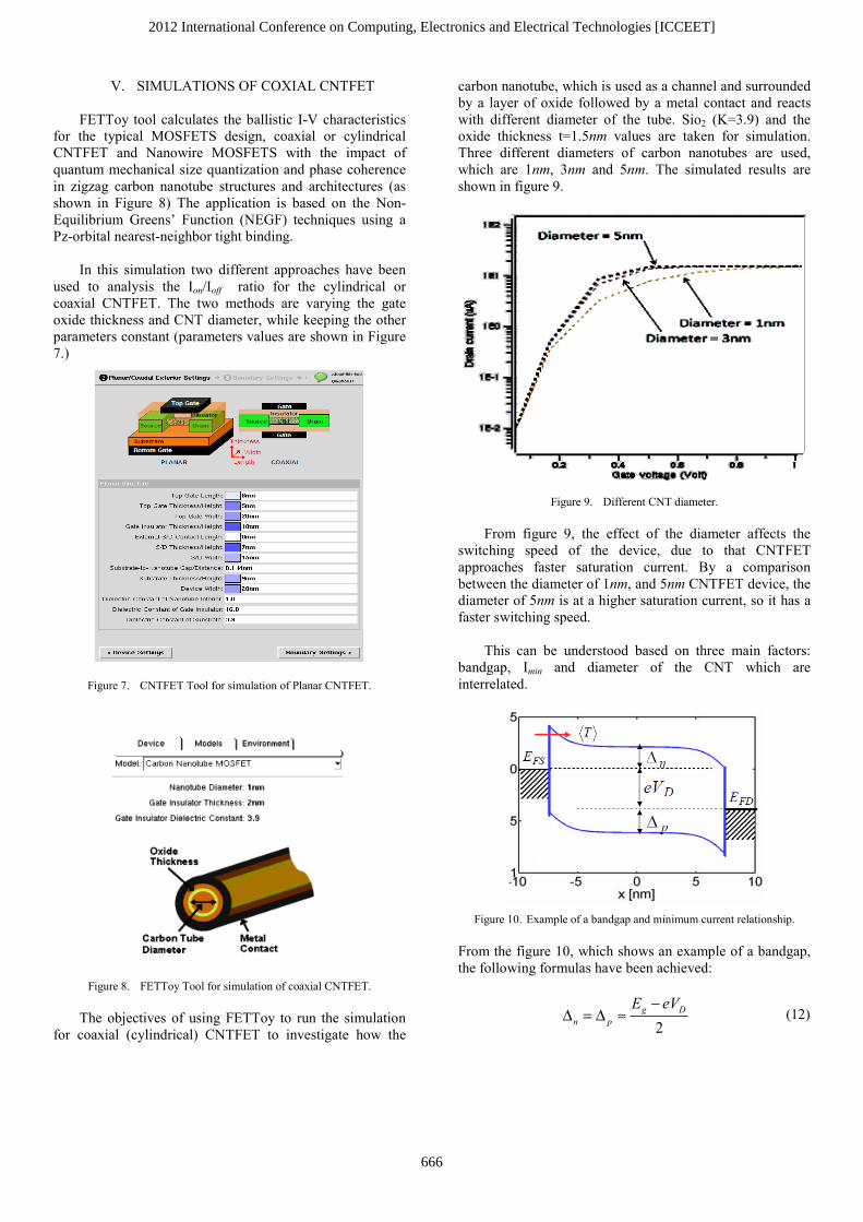
In this simulation two different approaches have been used to analysis the Ion/Ioff ratio for the cylindrical or coaxial CNTFET. The two methods are varying the gate oxide thickness and CNT diameter, while keeping the other parameters constant (parameters values are shown in Figure 7.)
Figure 7. CNTFET Tool for simulation of Planar CNTFET.
Figure 8. FETToy Tool for simulation of coaxial CNTFET. The objectives of using FETToy to run the simulation for coaxial (cylindrical) CNTFET to investigate how the
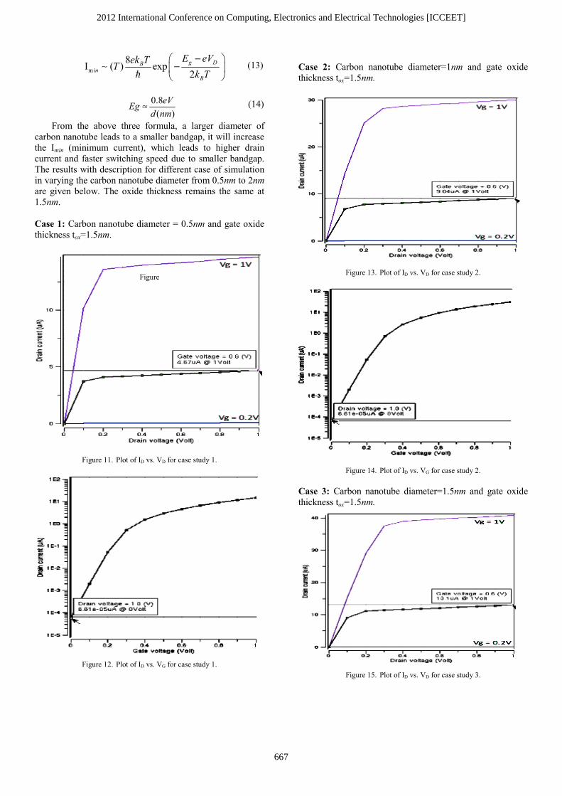
carbon nanotube, which is used as a channel and surrounded by a layer of oxide followed by a metal contact and reacts with different diameter of the tube. Sio2 (K=3.9) and the oxide thickness t=1.5nm values are taken for simulation. Three different diameters of carbon nanotubes are used, which are 1nm, 3nm and 5nm. The simulated results are shown in figure 9.
Figure 9. Different CNT diameter.
From figure 9, the effect of the diameter affects the switching speed of the device, due to that CNTFET approaches faster saturation current. By a comparison between the diameter of 1nm, and 5nm CNTFET device, the diameter of 5nm is at a higher saturation current, so it has a faster switching speed.
This can be understood based on three main factors:
bandgap, Imin and diameter of the CNT which are interrelated.
Figure 10. Example of a bandgap and minimum current relationship.
From the figure 10, which shows an example of a bandgap, the following formulas have been achieved:
2
g Dn p
E eV−Δ = Δ ≈ (12)
2012 International Conference on Computing, Electronics and Electrical Technologies [ICCEET]
666
m
8I ( ) exp2g DB
inB
E eVek TTk T−⎛ ⎞
−⎜ ⎟⎝ ⎠
∼ (13)
0.8
( )eVEg
d nm≈ (14)
From the above three formula, a larger diameter of carbon nanotube leads to a smaller bandgap, it will increase the Imin (minimum current), which leads to higher drain current and faster switching speed due to smaller bandgap. The results with description for different case of simulation in varying the carbon nanotube diameter from 0.5nm to 2nm are given below. The oxide thickness remains the same at 1.5nm.
Case 1: Carbon nanotube diameter = 0.5nm and gate oxide thickness tox=1.5nm.
Figure
Figure 11. Plot of ID vs. VD for case study 1.
Figure 12. Plot of ID vs. VG for case study 1.
Case 2: Carbon nanotube diameter=1nm and gate oxide thickness tox=1.5nm.
Figure 13. Plot of ID vs. VD for case study 2.
Figure 14. Plot of ID vs. VG for case study 2.
Case 3: Carbon nanotube diameter=1.5nm and gate oxide thickness tox=1.5nm.
Figure 15. Plot of ID vs. VD for case study 3.
2012 International Conference on Computing, Electronics and Electrical Technologies [ICCEET]
667
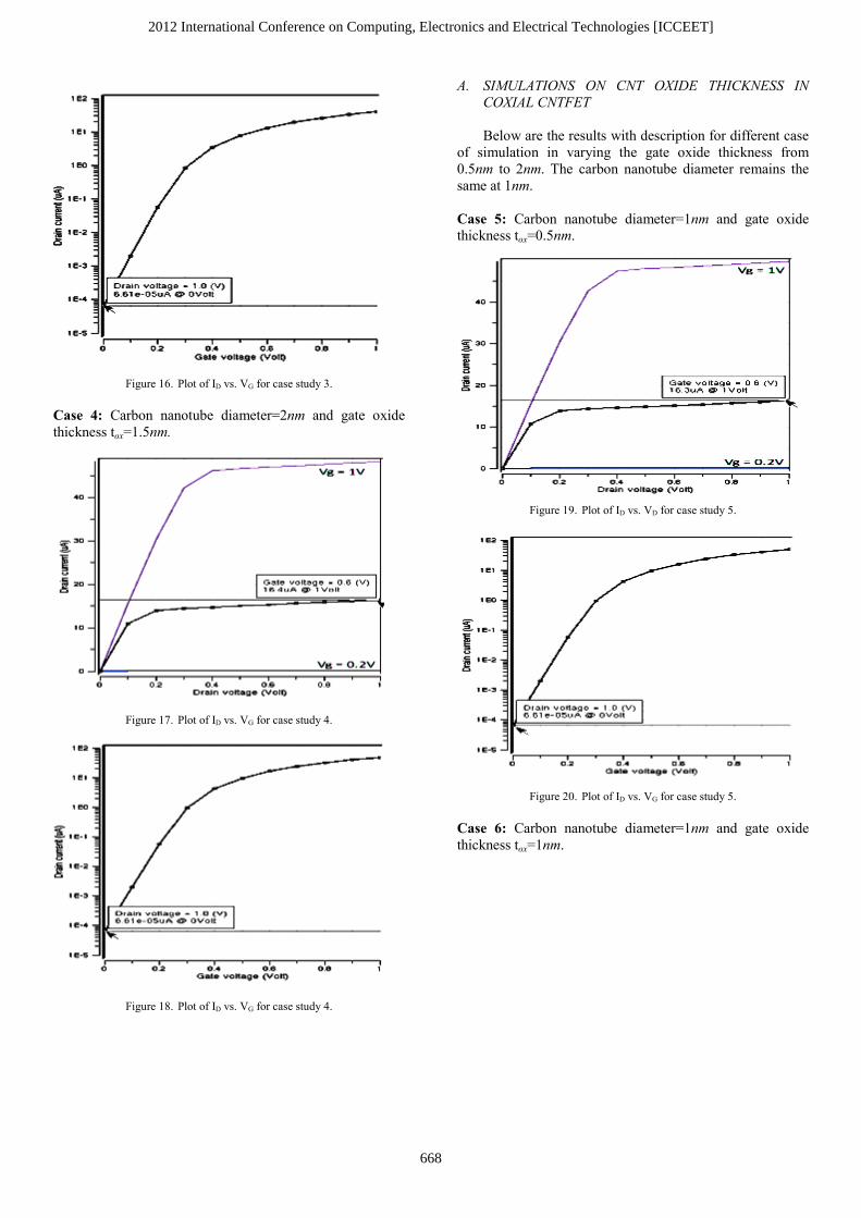
Figure 16. Plot of ID vs. VG for case study 3.
Case 4: Carbon nanotube diameter=2nm and gate oxide thickness tox=1.5nm.
Figure 17. Plot of ID vs. VG for case study 4.
Figure 18. Plot of ID vs. VG for case study 4.
A. SIMULATIONS ON CNT OXIDE THICKNESS IN COXIAL CNTFET
Below are the results with description for different case of simulation in varying the gate oxide thickness from 0.5nm to 2nm. The carbon nanotube diameter remains the same at 1nm.
Case 5: Carbon nanotube diameter=1nm and gate oxide thickness tox=0.5nm.
Figure 19. Plot of ID vs. VD for case study 5.
Figure 20. Plot of ID vs. VG for case study 5.
Case 6: Carbon nanotube diameter=1nm and gate oxide thickness tox=1nm.
2012 International Conference on Computing, Electronics and Electrical Technologies [ICCEET]
668
Figure 21. Plot of ID vs. VD for case study 5.
Figure 22. Plot of ID vs. VG for case study 6.
Case 7: Carbon nanotube diameter=1nm and gate oxide thickness tox=1.5nm.
Figure 23. Plot of ID vs. VD for case study 7.
Figure 24. Plot of ID vs. VG for case study 7.
Case 8: Carbon nanotube diameter=1nm and gate oxide thickness tox=2nm.
Figure 25. Plot of ID vs. VD for case study 8.
Figure 26. Plot of ID vs. VG for case study 8.
2012 International Conference on Computing, Electronics and Electrical Technologies [ICCEET]
669
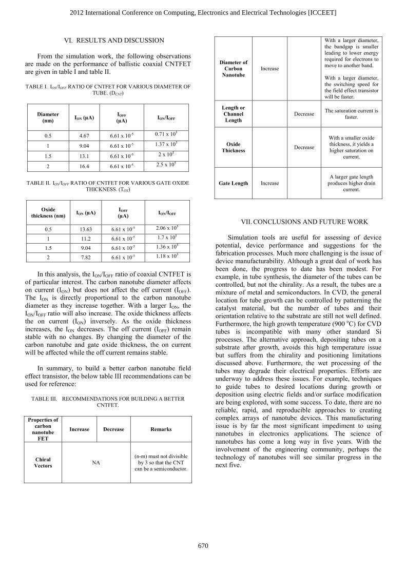
VI. RESULTS AND DISCUSSION From the simulation work, the following observations are made on the performance of ballistic coaxial CNTFET are given in table I and table II. TABLE I. ION/IOFF RATIO OF CNTFET FOR VARIOUS DIAMETER OF
TUBE. (DCNT)
Diameter (nm) ION (µA) IOFF
(µA) ION/IOFF
0.5 4.67 6.61 x 10⁻⁵ 0.71 x 10⁵
1 9.04 6.61 x 10⁻⁵ 1.37 x 10⁵
1.5 13.1 6.61 x 10⁻⁵ 2 x 10⁵
2 16.4 6.61 x 10⁻⁵ 2.5 x 10⁵
TABLE II. ION/IOFF RATIO OF CNTFET FOR VARIOUS GATE OXIDE THICKNESS. (TOX)
Oxide thickness (nm) ION (µA) IOFF
(µA) ION/IOFF
0.5 13.63 6.61 x 10⁻⁵ 2.06 x 10⁵
1 11.2 6.61 x 10⁻⁵ 1.7 x 10⁵
1.5 9.04 6.61 x 10⁻⁵ 1.36 x 10⁵
2 7.82 6.61 x 10⁻⁵ 1.18 x 10⁵
In this analysis, the ION/IOFF ratio of coaxial CNTFET is of particular interest. The carbon nanotube diameter affects on current (ION) but does not affect the off current (IOFF). The ION is directly proportional to the carbon nanotube diameter as they increase together. With a larger ION, the ION/IOFF ratio will also increase. The oxide thickness affects the on current (ION) inversely. As the oxide thickness increases, the ION decreases. The off current (IOFF) remain stable with no changes. By changing the diameter of the carbon nanotube and gate oxide thickness, the on current will be affected while the off current remains stable. In summary, to build a better carbon nanotube field effect transistor, the below table III recommendations can be used for reference:
TABLE III. RECOMMENDATIONS FOR BUILDING A BETTER CNTFET.
Properties of
carbon nanotube
FET
Increase Decrease Remarks
Chiral Vectors NA
(n-m) must not divisible by 3 so that the CNT
can be a semiconductor.
Diameter of Carbon
Nanotube Increase
With a larger diameter, the bandgap is smaller leading to lower energy required for electrons to move to another band.
With a larger diameter, the switching speed for the field effect transistor will be faster.
Length or Channel Length Decrease The saturation current is
faster.
Oxide Thickness Decrease
With a smaller oxide thickness, it yields a higher saturation on
current.
Gate Length Increase
A larger gate length produces higher drain
current.
VII. CONCLUSIONS AND FUTURE WORK
Simulation tools are useful for assessing of device potential, device performance and suggestions for the fabrication processes. Much more challenging is the issue of device manufacturability. Although a great deal of work has been done, the progress to date has been modest. For example, in tube synthesis, the diameter of the tubes can be controlled, but not the chirality. As a result, the tubes are a mixture of metal and semiconductors. In CVD, the general location for tube growth can be controlled by patterning the catalyst material, but the number of tubes and their orientation relative to the substrate are still not well defined. Furthermore, the high growth temperature (900 oC) for CVD tubes is incompatible with many other standard Si processes. The alternative approach, depositing tubes on a substrate after growth, avoids this high temperature issue but suffers from the chirality and positioning limitations discussed above. Furthermore, the wet processing of the tubes may degrade their electrical properties. Efforts are underway to address these issues. For example, techniques to guide tubes to desired locations during growth or deposition using electric fields and/or surface modification are being explored, with some success. To date, there are no reliable, rapid, and reproducible approaches to creating complex arrays of nanotube devices. This manufacturing issue is by far the most significant impediment to using nanotubes in electronics applications. The science of nanotubes has come a long way in five years. With the involvement of the engineering community, perhaps the technology of nanotubes will see similar progress in the next five.
2012 International Conference on Computing, Electronics and Electrical Technologies [ICCEET]
670
REFERENCES [1] P. Avouris, Supertubes: the unique properties of carbon nanotubes
may make them the natural successor to silicon microelectronics,� IEEE Spectrum, pp. 40-45, Aug. 2004.
[2] S. Iijima and T. Ichihashi, “Single-Shell Carbon Nanotubes of 1-Nm Diameter,” Nature, vol. 363, pp. 603-605, 1993. [3] M.J. O Connell, “Carbon Nanotubes: Properties and applications”,
Taylor and Francis Group, Boca Raton, FL, 2006. [4] A. Javey, J. Guo, Q. Wang, M. Lundstrom, and H. J. Dai, Ballistic
carbon nanotube field-effect transistors, Nature, Vol. 424, pp. 654-657, 2003.
[5] Datta, S., 2005. Quantum Transport: Atom to Transistor. Cambridge
University Press, London, UK. [6] Durkan, C., 2007, Current at the Nanoscale, Imperial College Press,
Cambridge, UK. [7] R. Saito, M. Fujita, G. Dresselhaus, and M. S. Dresselhaus,
“Electronic structure of chiral graphene tubules,” Applied Physics Letters, vol. 60, pp. 2204-6, 1992.
[8] T. W. Odom, H. Jin-Lin, P. Kim, and C. M. Lieber, “Atomic structure
and electronic properties of single-walled carbon nanotubes,” Nature, vol. 391, pp. 62-4, 1998.
[9] Fiori G. Iannaccone G. Klimeck G., A Three-Dimensional Simulation
Study of the Performance of Carbon Nanotube Field-Effect Transistors With Doped Reservoirs and Realistic Geometry, IEEE Transaction on Electron Devices, 53, 1782-1788, 2007.
[10] G.B. Abadi, K. Walus” Basis-set choice for DFT/NEGF simulations
of carbon nanotubes”, J Computational Electron (2009) 8: 1–9. [11] S. J. Tans, R. M. Verschueren, and C. Dekker, “Room temperature
transistor based on a single carbon nanotube,” Nature, vol. 393, pp. 49-52, 1998.
[12] S. Datta, Electronic Transport in Mesoscopic Systems. Cambridge: Cambridge University Press, 1995.
[13] McEuen, P. L., M. S. Fuhrer, et al., "Single-walled carbon nanotube
electronics." IEEE Transactions on Nanotechnology 1 78-85 (2002).
[14] D. J. Nagel, and S. Smith, “Nanotechnology-enabled sensor: possibilities, realities and application,” Sensor Magazine Online, Nov. 2003.
2012 International Conference on Computing, Electronics and Electrical Technologies [ICCEET]
671
Related Documents