To our customers, Old Company Name in Catalogs and Other Documents On April 1 st , 2010, NEC Electronics Corporation merged with Renesas Technology Corporation, and Renesas Electronics Corporation took over all the business of both companies. Therefore, although the old company name remains in this document, it is a valid Renesas Electronics document. We appreciate your understanding. Renesas Electronics website: http://www.renesas.com April 1 st , 2010 Renesas Electronics Corporation Issued by: Renesas Electronics Corporation (http://www.renesas.com) Send any inquiries to http://www.renesas.com/inquiry.

Welcome message from author
This document is posted to help you gain knowledge. Please leave a comment to let me know what you think about it! Share it to your friends and learn new things together.
Transcript
To our customers,
Old Company Name in Catalogs and Other Documents
On April 1st, 2010, NEC Electronics Corporation merged with Renesas Technology
Corporation, and Renesas Electronics Corporation took over all the business of both companies. Therefore, although the old company name remains in this document, it is a valid Renesas Electronics document. We appreciate your understanding.
Renesas Electronics website: http://www.renesas.com
April 1st, 2010 Renesas Electronics Corporation
Issued by: Renesas Electronics Corporation (http://www.renesas.com)
Send any inquiries to http://www.renesas.com/inquiry.

Notice 1. All information included in this document is current as of the date this document is issued. Such information, however, is
subject to change without any prior notice. Before purchasing or using any Renesas Electronics products listed herein, please confirm the latest product information with a Renesas Electronics sales office. Also, please pay regular and careful attention to additional and different information to be disclosed by Renesas Electronics such as that disclosed through our website.
2. Renesas Electronics does not assume any liability for infringement of patents, copyrights, or other intellectual property rights of third parties by or arising from the use of Renesas Electronics products or technical information described in this document. No license, express, implied or otherwise, is granted hereby under any patents, copyrights or other intellectual property rights of Renesas Electronics or others.
3. You should not alter, modify, copy, or otherwise misappropriate any Renesas Electronics product, whether in whole or in part. 4. Descriptions of circuits, software and other related information in this document are provided only to illustrate the operation of
semiconductor products and application examples. You are fully responsible for the incorporation of these circuits, software, and information in the design of your equipment. Renesas Electronics assumes no responsibility for any losses incurred by you or third parties arising from the use of these circuits, software, or information.
5. When exporting the products or technology described in this document, you should comply with the applicable export control laws and regulations and follow the procedures required by such laws and regulations. You should not use Renesas Electronics products or the technology described in this document for any purpose relating to military applications or use by the military, including but not limited to the development of weapons of mass destruction. Renesas Electronics products and technology may not be used for or incorporated into any products or systems whose manufacture, use, or sale is prohibited under any applicable domestic or foreign laws or regulations.
6. Renesas Electronics has used reasonable care in preparing the information included in this document, but Renesas Electronics does not warrant that such information is error free. Renesas Electronics assumes no liability whatsoever for any damages incurred by you resulting from errors in or omissions from the information included herein.
7. Renesas Electronics products are classified according to the following three quality grades: “Standard”, “High Quality”, and “Specific”. The recommended applications for each Renesas Electronics product depends on the product’s quality grade, as indicated below. You must check the quality grade of each Renesas Electronics product before using it in a particular application. You may not use any Renesas Electronics product for any application categorized as “Specific” without the prior written consent of Renesas Electronics. Further, you may not use any Renesas Electronics product for any application for which it is not intended without the prior written consent of Renesas Electronics. Renesas Electronics shall not be in any way liable for any damages or losses incurred by you or third parties arising from the use of any Renesas Electronics product for an application categorized as “Specific” or for which the product is not intended where you have failed to obtain the prior written consent of Renesas Electronics. The quality grade of each Renesas Electronics product is “Standard” unless otherwise expressly specified in a Renesas Electronics data sheets or data books, etc.
“Standard”: Computers; office equipment; communications equipment; test and measurement equipment; audio and visual equipment; home electronic appliances; machine tools; personal electronic equipment; and industrial robots.
“High Quality”: Transportation equipment (automobiles, trains, ships, etc.); traffic control systems; anti-disaster systems; anti-crime systems; safety equipment; and medical equipment not specifically designed for life support.
“Specific”: Aircraft; aerospace equipment; submersible repeaters; nuclear reactor control systems; medical equipment or systems for life support (e.g. artificial life support devices or systems), surgical implantations, or healthcare intervention (e.g. excision, etc.), and any other applications or purposes that pose a direct threat to human life.
8. You should use the Renesas Electronics products described in this document within the range specified by Renesas Electronics, especially with respect to the maximum rating, operating supply voltage range, movement power voltage range, heat radiation characteristics, installation and other product characteristics. Renesas Electronics shall have no liability for malfunctions or damages arising out of the use of Renesas Electronics products beyond such specified ranges.
9. Although Renesas Electronics endeavors to improve the quality and reliability of its products, semiconductor products have specific characteristics such as the occurrence of failure at a certain rate and malfunctions under certain use conditions. Further, Renesas Electronics products are not subject to radiation resistance design. Please be sure to implement safety measures to guard them against the possibility of physical injury, and injury or damage caused by fire in the event of the failure of a Renesas Electronics product, such as safety design for hardware and software including but not limited to redundancy, fire control and malfunction prevention, appropriate treatment for aging degradation or any other appropriate measures. Because the evaluation of microcomputer software alone is very difficult, please evaluate the safety of the final products or system manufactured by you.
10. Please contact a Renesas Electronics sales office for details as to environmental matters such as the environmental compatibility of each Renesas Electronics product. Please use Renesas Electronics products in compliance with all applicable laws and regulations that regulate the inclusion or use of controlled substances, including without limitation, the EU RoHS Directive. Renesas Electronics assumes no liability for damages or losses occurring as a result of your noncompliance with applicable laws and regulations.
11. This document may not be reproduced or duplicated, in any form, in whole or in part, without prior written consent of Renesas Electronics.
12. Please contact a Renesas Electronics sales office if you have any questions regarding the information contained in this document or Renesas Electronics products, or if you have any other inquiries.
(Note 1) “Renesas Electronics” as used in this document means Renesas Electronics Corporation and also includes its majority-owned subsidiaries.
(Note 2) “Renesas Electronics product(s)” means any product developed or manufactured by or for Renesas Electronics.
Printed in Japan
Document No. U17362EJ1V0AN00 (1st edition) Date Published December 2004 N CP(K)
Inverter Control by V850 Series
120° Excitation Method Control by Zero-Cross Detection Using Real-Time Output Function (RTO)
Application Note
V850ES/KJ1 Other microcontrollers with internal RTO
2004

Application Note U17362EJ1V0AN 2
[MEMO]

Application Note U17362EJ1V0AN 3
1
2
3
4
VOLTAGE APPLICATION WAVEFORM AT INPUT PIN
Waveform distortion due to input noise or a reflected wave may cause malfunction. If the input of the
CMOS device stays in the area between VIL (MAX) and VIH (MIN) due to noise, etc., the device may
malfunction. Take care to prevent chattering noise from entering the device when the input level is fixed,
and also in the transition period when the input level passes through the area between VIL (MAX) and
VIH (MIN).
HANDLING OF UNUSED INPUT PINS
Unconnected CMOS device inputs can be cause of malfunction. If an input pin is unconnected, it is
possible that an internal input level may be generated due to noise, etc., causing malfunction. CMOS
devices behave differently than Bipolar or NMOS devices. Input levels of CMOS devices must be fixed
high or low by using pull-up or pull-down circuitry. Each unused pin should be connected to VDD or GND
via a resistor if there is a possibility that it will be an output pin. All handling related to unused pins must
be judged separately for each device and according to related specifications governing the device.
PRECAUTION AGAINST ESD
A strong electric field, when exposed to a MOS device, can cause destruction of the gate oxide and
ultimately degrade the device operation. Steps must be taken to stop generation of static electricity as
much as possible, and quickly dissipate it when it has occurred. Environmental control must be
adequate. When it is dry, a humidifier should be used. It is recommended to avoid using insulators that
easily build up static electricity. Semiconductor devices must be stored and transported in an anti-static
container, static shielding bag or conductive material. All test and measurement tools including work
benches and floors should be grounded. The operator should be grounded using a wrist strap.
Semiconductor devices must not be touched with bare hands. Similar precautions need to be taken for
PW boards with mounted semiconductor devices.
STATUS BEFORE INITIALIZATION
Power-on does not necessarily define the initial status of a MOS device. Immediately after the power
source is turned ON, devices with reset functions have not yet been initialized. Hence, power-on does
not guarantee output pin levels, I/O settings or contents of registers. A device is not initialized until the
reset signal is received. A reset operation must be executed immediately after power-on for devices
with reset functions.
POWER ON/OFF SEQUENCE
In the case of a device that uses different power supplies for the internal operation and external
interface, as a rule, switch on the external power supply after switching on the internal power supply.
When switching the power supply off, as a rule, switch off the external power supply and then the
internal power supply. Use of the reverse power on/off sequences may result in the application of an
overvoltage to the internal elements of the device, causing malfunction and degradation of internal
elements due to the passage of an abnormal current.
The correct power on/off sequence must be judged separately for each device and according to related
specifications governing the device.
INPUT OF SIGNAL DURING POWER OFF STATE
Do not input signals or an I/O pull-up power supply while the device is not powered. The current
injection that results from input of such a signal or I/O pull-up power supply may cause malfunction and
the abnormal current that passes in the device at this time may cause degradation of internal elements.
Input of signals during the power off state must be judged separately for each device and according to
related specifications governing the device.
NOTES FOR CMOS DEVICES
5
6

Application Note U17362EJ1V0AN 4
These commodities, technology or software, must be exported in accordance with the export administration regulations of the exporting country.Diversion contrary to the law of that country is prohibited.
The information in this document is current as of October, 2004. The information is subject to change without notice. For actual design-in, refer to the latest publications of NEC Electronics data sheets or data books, etc., for the most up-to-date specifications of NEC Electronics products. Not all products and/or types are available in every country. Please check with an NEC Electronics sales representative for availability and additional information.No part of this document may be copied or reproduced in any form or by any means without the prior written consent of NEC Electronics. NEC Electronics assumes no responsibility for any errors that may appear in this document.NEC Electronics does not assume any liability for infringement of patents, copyrights or other intellectual property rights of third parties by or arising from the use of NEC Electronics products listed in this document or any other liability arising from the use of such products. No license, express, implied or otherwise, is granted under any patents, copyrights or other intellectual property rights of NEC Electronics or others.Descriptions of circuits, software and other related information in this document are provided for illustrative purposes in semiconductor product operation and application examples. The incorporation of these circuits, software and information in the design of a customer's equipment shall be done under the full responsibility of the customer. NEC Electronics assumes no responsibility for any losses incurred by customers or third parties arising from the use of these circuits, software and information.While NEC Electronics endeavors to enhance the quality, reliability and safety of NEC Electronics products, customers agree and acknowledge that the possibility of defects thereof cannot be eliminated entirely. To minimize risks of damage to property or injury (including death) to persons arising from defects in NEC Electronics products, customers must incorporate sufficient safety measures in their design, such as redundancy, fire-containment and anti-failure features.NEC Electronics products are classified into the following three quality grades: "Standard", "Special" and "Specific". The "Specific" quality grade applies only to NEC Electronics products developed based on a customer-designated "quality assurance program" for a specific application. The recommended applications of an NEC Electronics product depend on its quality grade, as indicated below. Customers must check the quality grade of each NEC Electronics product before using it in a particular application. "Standard": Computers, office equipment, communications equipment, test and measurement equipment, audio
and visual equipment, home electronic appliances, machine tools, personal electronic equipmentand industrial robots.
"Special": Transportation equipment (automobiles, trains, ships, etc.), traffic control systems, anti-disastersystems, anti-crime systems, safety equipment and medical equipment (not specifically designedfor life support).
"Specific": Aircraft, aerospace equipment, submersible repeaters, nuclear reactor control systems, lifesupport systems and medical equipment for life support, etc.
The quality grade of NEC Electronics products is "Standard" unless otherwise expressly specified in NEC Electronics data sheets or data books, etc. If customers wish to use NEC Electronics products in applications not intended by NEC Electronics, they must contact an NEC Electronics sales representative in advance to determine NEC Electronics' willingness to support a given application.
(Note)(1) "NEC Electronics" as used in this statement means NEC Electronics Corporation and also includes its
majority-owned subsidiaries.(2) "NEC Electronics products" means any product developed or manufactured by or for NEC Electronics (as
defined above).
•
•
•
•
•
•
M8E 02. 11-1

Application Note U17362EJ1V0AN 5
Regional Information
• Device availability
• Ordering information
• Product release schedule
• Availability of related technical literature
• Development environment specifications (for example, specifications for third-party tools and components, host computers, power plugs, AC supply voltages, and so forth)
• Network requirements
In addition, trademarks, registered trademarks, export restrictions, and other legal issues may also varyfrom country to country.
[GLOBAL SUPPORT] http://www.necel.com/en/support/support.html
NEC Electronics America, Inc. (U.S.)Santa Clara, CaliforniaTel: 408-588-6000 800-366-9782
NEC Electronics Hong Kong Ltd.Hong KongTel: 2886-9318
NEC Electronics Hong Kong Ltd.Seoul BranchSeoul, KoreaTel: 02-558-3737
NEC Electronics Shanghai Ltd.Shanghai, P.R. ChinaTel: 021-5888-5400
NEC Electronics Taiwan Ltd.Taipei, TaiwanTel: 02-2719-2377
NEC Electronics Singapore Pte. Ltd.Novena Square, SingaporeTel: 6253-8311
J04.1
NEC Electronics (Europe) GmbHDuesseldorf, GermanyTel: 0211-65030
• Sucursal en EspañaMadrid, SpainTel: 091-504 27 87
Vélizy-Villacoublay, FranceTel: 01-30-67 58 00
• Succursale Française
• Filiale ItalianaMilano, ItalyTel: 02-66 75 41
• Branch The NetherlandsEindhoven, The NetherlandsTel: 040-244 58 45
• Tyskland FilialTaeby, SwedenTel: 08-63 80 820
• United Kingdom BranchMilton Keynes, UKTel: 01908-691-133
Some information contained in this document may vary from country to country. Before using any NEC Electronics product in your application, pIease contact the NEC Electronics office in your country to obtain a list of authorized representatives and distributors. They will verify:
Application Note U17362EJ1V0AN 6
INTRODUCTION
Target Readers This application note is intended for users who understand real-time output functions
(RTO), and who design application systems using the function. The applicable products
are all products with internal RTO functions such as V850ES/KJ1. Applicable products
for the V850ES/KJ1 are shown below.
• V850ES/KJ1
Standard products: µPD703216, 703216Y, 703217, 703217Y, 70F3217, 70F3217H,
70F3217HY, 70F3217Y, 70F3218H, 70F3218HY
Special products: µPD703216(A), 703216Y(A), 703217(A), 703217Y(A),
70F3217(A), 70F3217Y(A), 703216(A1), 703216Y(A1),
703217(A1), 703217Y(A1), 703216(A2), 703216Y(A2),
703217(A2), 703217Y(A2)
Purpose The purpose of this application note is to help the user understand how a brushless DC
motor is controlled via the 120° sensorless drive excitation method using a system
example of RTO functions.
Organization This application note is divided into the following sections.
• Control method • Software configuration
• Hardware configuration • Program list
How to Use This Manual It is assumed that the reader of this application note has general knowledge in the fields
of electrical engineering, logic circuits, and microcontrollers.
Cautions 1. Of the products that have internal RTO functions, the V850ES/KJ1 is
described in this manual as a typical microcontroller.
2. Application examples in this manual are intended for the “standard”
quality models for general-purpose electronic systems. When using
an example in this manual for an application that requires the
“special” quality grade, evaluate each component and circuit to be
actually used to see if they satisfy the required quality standard.
3. When using the special grade product manuals, read the following
part numbers on the V850ES/KJ1 as follows. This also applies to
products other than the V850ES/KJ1 that have internal RTO
functions.
µPD703216 → µPD703216(A), 703216(A1), 703216(A2)
µPD703216Y → µPD703216Y(A), 703216Y(A1), 703216Y(A2)
µPD703217 → µPD703217(A), 703217(A1), 703217(A2)
µPD703217Y → µPD703217Y(A), 703217Y(A1), 703217Y(A2)
µPD70F3217 → µPD70F3217(A)
µPD70F3217Y → µPD70F3217Y(A)
Application Note U17362EJ1V0AN 7
For details of hardware functions (especially register functions, setting methods, etc.) and electrical specifications
→ See the user’s manual for products with internal RTO functions (such as
V850ES/KJ1 Hardware User’s Manual).
For details of instruction functions
→ See the architecture user’s manual for products with internal RTO functions (such
as V850ES Architecture User’s Manual).
Conventions Data significance: Higher digits on the left and lower digits on the right
Active low representation: xxx (overscore over pin or signal name)
Memory map address: Higher addresses on the top and lower addresses on
the bottom
Note: Footnote for item marked with Note in the text
Caution: Information requiring particular attention
Remark: Supplementary information
Numeric representation: Binary ... xxxx or xxxxB
Decimal ... xxxx
Hexadecimal ... xxxxH
Prefix indicating the power
of 2 (address space,
memory capacity): K (kilo): 210 = 1,024
M (mega): 220 = 1,0242
G (giga): 230 = 1,0243
Data type: Word: 32 bits
Halfword: 16 bits
Byte: 8 bits
Related Documents The related documents indicated in this publication may include preliminary versions.
However, preliminary versions are not marked as such.
Documents related to V850ES/KJ1
Document Name Document No.
V850ES Architecture User’s Manual U15943E
V850ES/KJ1 Hardware User’s Manual U16889E
Inverter Control by V850 Series 120° Excitation Method Control by Zero-
Cross Detection Using Real-Time Output Function (RTO) Application Note
This manual
Application Note U17362EJ1V0AN 8
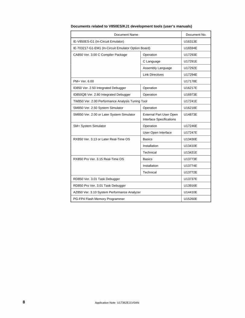
Documents related to V850ES/KJ1 development tools (user’s manuals)
Document Name Document No.
IE-V850ES-G1 (In-Circuit Emulator) U16313E
IE-703217-G1-EM1 (In-Circuit Emulator Option Board) U16594E
Operation U17293E
C Language U17291E
Assembly Language U17292E
CA850 Ver. 3.00 C Compiler Package
Link Directives U17294E
PM+ Ver. 6.00 U17178E
ID850 Ver. 2.50 Integrated Debugger Operation U16217E
ID850QB Ver. 2.80 Integrated Debugger Operation U16973E
TW850 Ver. 2.00 Performance Analysis Tuning Tool U17241E
SM850 Ver. 2.50 System Simulator Operation U16218E
SM850 Ver. 2.00 or Later System Simulator External Part User Open
Interface Specifications
U14873E
Operation U17246E SM+ System Simulator
User Open Interface U17247E
Basics U13430E
Installation U13410E
RX850 Ver. 3.13 or Later Real-Time OS
Technical U13431E
Basics U13773E
Installation U13774E
RX850 Pro Ver. 3.15 Real-Time OS
Technical U13772E
RD850 Ver. 3.01 Task Debugger U13737E
RD850 Pro Ver. 3.01 Task Debugger U13916E
AZ850 Ver. 3.10 System Performance Analyzer U14410E
PG-FP4 Flash Memory Programmer U15260E

9 Application Note U17362EJ1V0AN
CONTENTS
CHAPTER 1 CONTROL METHOD..........................................................................................................11 1.1 Outline of Brushless DC Motor Control.................................................................................. 11
CHAPTER 2 HARDWARE CONFIGURATION.......................................................................................16 2.1 Configuration ............................................................................................................................ 16 2.2 Circuit Diagram ......................................................................................................................... 18
CHAPTER 3 SOFTWARE CONFIGURATION........................................................................................21 3.1 Control Block ............................................................................................................................ 21 3.2 Peripheral I/O............................................................................................................................. 22 3.3 PWM Control.............................................................................................................................. 24 3.4 Software Processing Structure ............................................................................................... 25 3.5 Flowchart ................................................................................................................................... 27
3.5.1 Main processing ...........................................................................................................................27 3.5.2 LED display ..................................................................................................................................36 3.5.3 Motor control processing ..............................................................................................................37 3.5.4 U zero-cross point interrupt processing........................................................................................42 3.5.5 V zero-cross point interrupt processing ........................................................................................43 3.5.6 W zero-cross point interrupt processing .......................................................................................44 3.5.7 Real-time output timer interrupt processing..................................................................................45 3.5.8 Real-time output value set processing .........................................................................................46 3.5.9 10 mSEC interval interrupt processing .........................................................................................47 3.5.10 A/D converter interrupt processing ...............................................................................................48 3.5.11 Hardware initialization ..................................................................................................................50 3.5.12 Common area initialization ...........................................................................................................51 3.5.13 Revolution start initialization.........................................................................................................51 3.5.14 RTO output data initialization .......................................................................................................52
3.6 Common Areas ......................................................................................................................... 53 3.7 Tables......................................................................................................................................... 54 3.8 Constant Definitions................................................................................................................. 56
CHAPTER 4 PROGRAM LIST ................................................................................................................57 4.1 Program List (V850ES/KJ1)...................................................................................................... 57
4.1.1 Symbol definition ..........................................................................................................................57 4.1.2 Constant definition........................................................................................................................58 4.1.3 Interrupt handler setting ...............................................................................................................61 4.1.4 Startup routine setting ..................................................................................................................63 4.1.5 Main processing function..............................................................................................................66 4.1.6 LED display function.....................................................................................................................70 4.1.7 Motor control interrupt processing function ..................................................................................71 4.1.8 Zero-cross interrupt processing function ......................................................................................74 4.1.9 Real-time output interrupt processing function .............................................................................76 4.1.10 10 mSEC interval interrupt processing function ...........................................................................77 4.1.11 A/D converter interrupt processing function .................................................................................77 4.1.12 Hardware initialization processing function ..................................................................................78
10 Application Note U17362EJ1V0AN
4.1.13 Common area initialization processing function........................................................................... 80 4.1.14 Revolution start initialization processing function ........................................................................ 80 4.1.15 RTO output data initialization processing function....................................................................... 80 4.1.16 Link directive file for V850ES/KJ1................................................................................................ 81

Application Note U17362EJ1V0AN 11
CHAPTER 1 CONTROL METHOD
1.1 Outline of Brushless DC Motor Control
A brushless DC (BLDC) motor consists of a stator, coil, and rotor. The rotor, which includes a permanent magnet,
is rotated by the action of the magnetic field generated by the coil of the stator.
The magnetic field is generated by exciting the coil wound around the stator in a specific sequence. By controlling
the intensity and cycle of the magnetic field with a microcontroller, the torque response and the number of revolutions
of the motor can be controlled.
This section explains how to control a BLDC motor without a sensor by using the V850ES/KJ1 as a typical
microcontroller of the products that have internal real-time output functions (RTO).
Figure 1-3 shows an example of the circuit of a three-phase brushless DC motor. The internal PWM output
function of the microcontroller is used to control the current that flows through the motor, by using a transistor array
consisting of six transistors.
The magnetic field is generated by controlling the excitation pattern of the six transistors as shown in Table 1-1.
Table 1-1. Excitation Pattern
Upper Arm Lower Arm Excitation
Pattern U V W U V W
Excitation
Direction
<1> Active Inactive Inactive Inactive Active Inactive U → V
<2> Active Inactive Inactive Inactive Inactive Active U → W
<3> Inactive Active Inactive Inactive Inactive Active V → W
<4> Inactive Active Inactive Active Inactive Inactive V → U
<5> Inactive Inactive Active Active Inactive Inactive W → U
<6> Inactive Inactive Active Inactive Active Inactive W → V

CHAPTER 1 CONTROL METHOD
Application Note U17362EJ1V0AN 12
Figure 1-1. Three-Phase DC Motor Voltage Waveform
<1> <2> <3> <4> <5> <6>
U phase
U phase
U phase
V phase
V phase
V phase
W phase
W phase
W phase
Driving voltagewaveform
Induced voltagewaveform

CHAPTER 1 CONTROL METHOD
Application Note U17362EJ1V0AN 13
Figure 1-2. Rotor Position Detection Principle
Return to (a)
(a) Rotor position <1> … U-phase stator: S poleV-phase stator: N poleW-phase stator: Center point
(b) Rotor position <2> … U-phase stator: S poleV-phase stator: Center pointW-phase stator: N pole
A
S
S
N
N
VWC = 0
VCC
W-phase stator is located in the
center of the N pole and S pole of a
magnet rotor
Magneticflux
V
W
UA
S
S
N
N
VVC = 0
VCC
W
V
U
(d) Rotor position <4> … U-phase stator: N poleV-phase stator: S poleW-phase stator: Center point
(c) Rotor position <3> … U-phase stator: Center pointV-phase stator: S poleW-phase stator: N pole
A
U
S
SN
N
VUC = 0
VCC
V
W
A
U
S
S
N
N
VWC = 0
VCC
V
W
(e) Rotor position <5> … U-phase stator: N poleV-phase stator: Center pointW-phase stator: S pole
(f) Rotor position <6> … U-phase stator: Center pointV-phase stator: N poleW-phase stator: S pole
W
V
U
A
S
S
N
N
VVC = 0
VCC
S
SN
N
A
U
V
W
VCC
VUC = 0
CHAPTER 1 CONTROL METHOD
Application Note U17362EJ1V0AN 14
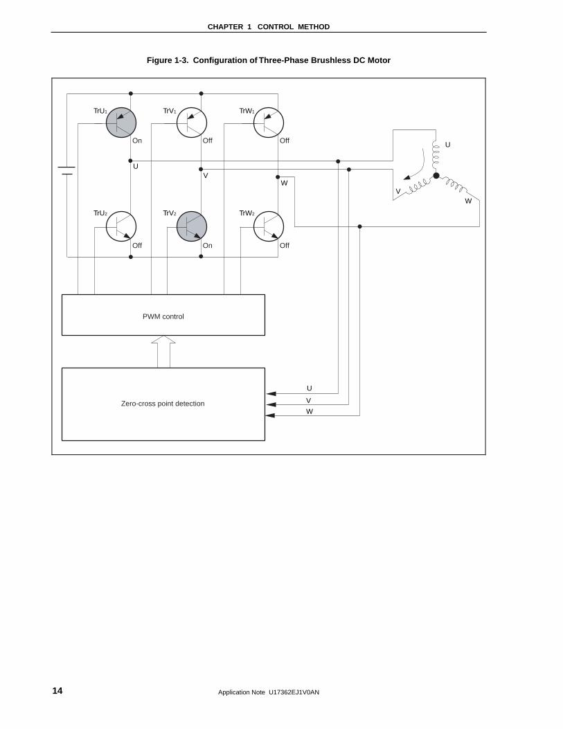
Figure 1-3. Configuration of Three-Phase Brushless DC Motor
U
U
UV
W
TrU1
On Off Off
Off On Off
TrV1 TrW1
TrU2 TrV2 TrW2
PWM control
Zero-cross point detection V
V
W
W
CHAPTER 1 CONTROL METHOD
Application Note U17362EJ1V0AN 15
The 120° control method for a BLDC motor without a sensor is described below.
To control a BLDC motor, the rotor position must be known.
To control a BLDC motor without a sensor, the rotor position is estimated using induced voltage.
The induced voltage is in phase with the driving voltage waveform and its waveform is close to a sine wave, as
shown in Figure 1-1. Figure 1-2 illustrates how the polarity of the stator of the motor is switched and how the magnet
rotor revolves.
As shown in Figures 1-1 and 1-2, a three-phase DC motor rotates its rotor by switching the three driving current
patterns on the three coil phases.
During period <1> in Figure 1-1, for example, transistor TrU1 in Figure 1-3 is turned on by the U-phase driving pin,
and TrV2 is turned on by the V-phase driving pin, causing the current to flow from the U-phase driving pin toward the V-
phase driving pin. At this time, the W-phase coil seems to be disconnected from the driver circuit and induced voltage
is generated.
This induced voltage is used to detect the rotor position.
To control the number of revolutions of the motor, the voltage applied to the motor is controlled to change the
current flowing through the coil. To change the voltage, a waveform that is controlled by PWM is applied to the
transistor.
The voltage is changed by applying a waveform (PWM waveform) in proportion to the voltage to be applied, to the
transistors on the lower arm side (TrU2, TrV2, and TrW2) while the transistors on the upper arm side (TrU1, TrV1, and
TrW1) are on.

Application Note U17362EJ1V0AN 16
CHAPTER 2 HARDWARE CONFIGURATION
This chapter describes the hardware configuration.
2.1 Configuration
The reference system’s main functions are described below. In this reference system, when the revolution
specification switch is pressed after power application, the motor starts revolving in the direction specified.
Figure 2-1. Overall System Configuration
Reset circuit
Positiondetection V-U
V-V
V-W
LED display
Revolution specification SW
3
6
13
A/D converter
Volume for speed control
Driver IC
Timer
Inte
rrup
t
RESET
Port
Microcontroller
V-U
V-V
V-W
M
Current voltageconversion
WDT
Current voltageconversion
Positiondetection
Positiondetection

CHAPTER 2 HARDWARE CONFIGURATION
Application Note U17362EJ1V0AN 17
(1) Volume for speed control
Volume for increasing and decreasing the number of revolutions of the motor
(2) Revolution specification SW
CW, CCW, and STOP switches
(3) LED display
LED displaying the number of revolutions, operation time, etc.
(4) WDT
Watchdog timer
(5) Driver IC
Driver for driving motor
(6) Current voltage converter
Converting the motor driving current to voltage, used for detecting overcurrent
(7) Position detector
Rotor position estimation signal output from the induced voltage
CHAPTER 2 HARDWARE CONFIGURATION
Application Note U17362EJ1V0AN 18
2.2 Circuit Diagram
Figure 2-2 shows a diagram of the sample reference system circuit.
This sample reference system circuit diagram includes the V850ES/KJ1, a reset circuit, oscillator, a pin handling
microcontroller peripheral block, operation mode switch block, LED output block, watchdog timer circuit block, drive
circuit block, motor controller, and motor revolution indicator.
(1) Microcontroller and microcontroller peripheral block
The V850ES/KJ1 includes a reset circuit, an oscillator that uses a resonator, and a block for handling the
unused pins.
(2) Operation mode switch block
This block includes switches that set the operation mode as CW or CCW operation.
(3) LED output block
This block includes 16 LEDs, which are used to indicate the revolution speed (rpm), errors, etc.
(4) Watchdog timer circuit block
This block outputs stop signals when pulse output from the V850ES/KJ1 stops for one ms or longer.
(5) Drive circuit block
The 6-phase outputs from the inverter timer are converted to U-, V-, and W-phase output for the motor driver.
This drive circuit is not shown in detail in this example, since it varies depending on the motor’s specifications.
(6) Motor controller
This block includes the HPS-3-AS, LM324, and other devices that are used to measure the motor’s U and V
drive currents via A/D conversion.
(7) Motor revolution indicator
This block includes a volume adjuster and the LM324 for setting the motor’s revolution speed (rpm).

CHAPTER 2 HARDWARE CONFIGURATION
Application Note U17362EJ1V0AN 19
Figure 2-2. Circuit Diagram of V850ES/KJ1
RESET
RESETSW
CLOCK5MHz
[U] [V]
[MOT OUT]
W
[W]
U
V
SpeedCont.
Watch Dog & Error
POWER
VPP
WD_CLR
P85
P77
P83
P100
P102
P81
P98
P87
P79
P75
P73
vUvVvW
Mot_Stop
M_HUM_LU
M_HVM_LV
M_HWM_LW
LED_Seg1LED_Seg2LED_Seg3LED_Seg4
LED_Seg1LED_Seg2LED_Seg3LED_Seg4LED_Seg5LED_Seg6LED_Seg7LED_Seg8
LED_Dig1LED_Dig2LED_Dig3
LED_WE
P99
P97
P95
P93
P88
P86
P84
P82
P80
P78
P76
P74
I_U
I_V
V_U
V_V
V_W
Velocity
Mot_ULMot_VLMot_WLMot_UHMot_VHMot_WH
LED_Dig4
+7V+5V
+5V
+5V
+12V +7V
-7V
+5V +3.3V
AGND
+12V
+12V
+12V
+12V
+12V
+12V
+5V
R12.2kΩ
+
-
U1ALM3243
21
411
VR1A
10kΩ
41
3
C247uF
SW1
U3A
74ACT14
1 2
5MHz
C433pF
R2610kΩ
C533pF
D1
2
R8410kΩ
U3B
74ACT14
3 4
J2
CON6
123456
TP3
LC-2-G
1
TP1
LC-2-G
1
TP2
LC-2-G
1
J1
CN 3P
123
rpm
kHz
uSEC
uSEC
7SEGLED1
7SEG_LEDx8
E5D4C3
DP8
B2A1
F6
G7
DG110
DG211
DG312
DG413
DG514
DG615
DG716
WE18
U2
MOT_DRV
HU1
LU2
HV3
LV4
HW5
LW6
ERR7
OU8
OV9
OW10
U6A
WDT
ERR3
W_CLR2
CLK1
WDO13
SW2SW_CW
SW3SW_CCW
SW4SW_STO
R8510kΩ
R8610kΩ
R10
010
kΩR
101
10kΩ
R10
210
kΩR
103
10kΩ
R12
010
kΩR
121
10kΩ
R12
210
kΩ
R99
10kΩ
U4
uPD70F3217GJ-UEN
AVREF01
AVSS2
P10/ANO03
P11/ANO14
AVREF15
P00/TOH06
P01/TOH17
VPP8
VDD9
REGC10
VSS11
X112
X213
RESET14
XT115
XT216
P02/NMI17
P03/INTP018
P04/INTP119
P05/INTP220
P06/INTP321
P40/SI0022
P41/SO0023
P42/SCK0024
P30/TXD025
P31/RXD026
P32/ASCK027
P33/TI000/TO0028
P34/TI00129
P35/TI010/TO0130
P3631
P3732
EVSS33
EVDD34
P3835
P3936
P50
/TI0
11/R
TP
00/K
R0
37
P51
/TI5
0/R
TP
01/K
R1
38
P52
/TO
50/R
TP
02/K
R2
39
P53
/SIA
0/R
TP
03/K
R3
40
P54
/SO
A0/
RT
P04
/KR
441
P55
/SC
KA
0/R
TP
05/K
R5
42
P60
/RT
P10
43
P61
/RT
P11
44
P62
/RT
P12
45
P63
/RT
P13
46
P64
/RT
P14
47
P65
/RT
P15
48
P66
/SI0
249
P67
/SO
0250
P68
/SC
K02
51
P69
/TI0
4052
P61
0/T
I041
53
P61
1/T
O04
54
P61
2/T
I050
55
P61
3/T
I051
/TO
0556
P61
457
P61
558
P80
/RX
D2
59
P81
/TX
D2
60
P90
/A0/
TX
D1/
KR
661
P91
/A1/
RX
D1/
KR
762
P92
/A2/
TI0
20/T
O02
63
P93
/A3/
TI0
2164
P94
/A4/
TI0
30/T
O03
65
P95
/A5/
TI0
3166
P96
/A6/
TI5
1/T
O51
67
P97
/A7/
SI0
168
P98
/A8/
SO
0169
P99
/A9/
SC
K01
70
P91
0/A
10/S
IA1
71
P91
1/A
11/S
OA
172
P912/A12/SCKA173P913/A13/INTP474P914/A14/INTP575P915/A15/INTP676PCD077PCD178PCD279PCD380PCS0/CS081PCS1/CS182PCS2/CS283PCS3/CS384PCM0/WAIT85PCM1/CLKOUT86PCM2/HLDAK87PCM3/HLDRQ88PCM489PCM590PCS491PCS592PCS693PCS794PCT0/WR095PCT1/WR196PCT297PCT398PCT4/RD99PCT5100PCT6/ASTB101PCT7102
BVSS 103BVDD 104
PDL0/AD0 105PDL1/AD1 106PDL2/AD2 107PDL3/AD3 108
PD
L4/A
D4
PD
L5/A
D5
PD
L6/A
D6
PD
L7/A
D7
PD
L8/A
D8
PLD
9/A
D9
PD
L10/
AD
10P
DL1
1/A
D11
PD
L12/
AD
12P
DL1
3/A
D13
PD
L14/
AD
14P
DL1
5/A
D15
PD
H0/
A16
PD
H1/
A17
PD
H2/
A18
PD
H3/
A19
PD
H4/
A20
PD
H5/
A21
PD
H6/
A22
PD
H7/
A23
P71
5/A
NI1
5P
714/
AN
I14
P71
3/A
NI1
3P
712/
AN
I12
P71
1/A
NI1
1P
710/
AN
I10
P79
/AN
I9P
78/A
NI8
P77
/AN
I7P
76/A
NI6
P75
/AN
I5P
74/A
NI4
P73
/AN
I3P
72/A
NI2
P71
/AN
I1P
70/A
NI0
R31 10kΩR32 10kΩ
R33 10kΩR35 10kΩR37 10kΩ
R46 10kΩ
R49 10kΩ
R57 10kΩR59 10kΩR60 10kΩ
R66 10kΩR68 10kΩR70 10kΩR72 10kΩ
R77 10kΩR79 10kΩ
R2
10kΩ
R3
10kΩ
R4
10kΩ
R5
10kΩ
R6
10kΩ
R7
10kΩ
R8
10kΩ
R9
10kΩ
R10
10kΩ
R11
10kΩ
R12
10kΩ
R13
10kΩ
R14
10kΩ
R15
10kΩ
R16
10kΩ
R17
10kΩ
R18
10kΩ
R19
10kΩ
R20
10kΩ
R21
10kΩ
R22
10kΩ
R23
10kΩ
R24
10kΩ
R25
10kΩ
R95
10kΩ
R96
10kΩ
R97
10kΩ
R98
10kΩ
R10
410
kΩR
105
10kΩ
R10
610
kΩR
107
10kΩ
R10
810
kΩR
109
10kΩ
R11
010
kΩR
111
10kΩ
R11
210
kΩR
113
10kΩ
R11
410
kΩR
115
10kΩ
R11
610
kΩR
117
10kΩ
R11
810
kΩR
119
10kΩ
R36 10kΩ
C110.1uF
C100.1uF
C120.1uF
C130.1uF
R39 10kΩR40 10kΩR41 10kΩR42 10kΩR43 10kΩR45 10kΩR47 10kΩR48 10kΩR50 10kΩR51 10kΩR54 10kΩ
R56 10kΩR58 10kΩ
R61 10kΩR62 10kΩR63 10kΩR64 10kΩR65 10kΩR67 10kΩR69 10kΩR71 10kΩR73 10kΩR74 10kΩR75 10kΩR78 10kΩR80 10kΩ
R55 10kΩ
R38 10kΩ
R30 2.2kΩR29 10kΩ
C60.01uF film
C70.1uF
C10.01uF film
C30.1uF
R34 100kΩ
R44 22kΩ
+
- U1BLM324
5
67
411
+
- U1CLM324
10
98
411
CT1HPS-3-AS
+12V1
NC2
OUT3
GND4
IN+5
IN-6
CT2
HPS-3-AS
+12V1
NC2
OUT3
GND4
IN+5
IN-6
R27 100kΩ
VR2
1kΩ
R28 22kΩ
R53 2.2kΩR52 10kΩ
C80.1uF
VR3
1kΩ
+
-
U5A
LM339
7
61
312
R83 10kΩ
R87 10kΩ
R76 1MΩ
R88
10kΩC90.1uF
R82 100kΩ
+
-
U5B
LM339
5
42
312
R92 10kΩ
R93 10kΩ
R89 1MΩ
R124
10kΩ
C140.1uF
R91 100kΩ
+
-
U5C
LM339
9
814
312
R128 10kΩ
R129 10kΩ
R126 1MΩ
R130
10kΩ
C150.1uF
R127 100kΩ
C160.1uF
R81 4.7kΩ
R90 4.7kΩ
R125
4.7kΩ
C170.1uF
R12
310
kΩ
R94
10kΩ
LED
_WE
LED
_Dig
4LE
D_D
ig3
LED
_Dig
2LE
D_D
ig1
LED
_Seg
8LE
D_S
eg7
LED
_Seg
6LE
D_S
eg5
+5V
109
110
111
112
113
114
115
116
117
118
119
120
121
122
123
124
125
126
127
128
129
130
131
132
133
134
135
136
137
138
139
140
141
142
143
144
P
1

Application Note U17362EJ1V0AN 21
CHAPTER 3 SOFTWARE CONFIGURATION
3.1 Control Block
Figure 3-1 shows a diagram of the software control block of the reference system.
Figure 3-1. Diagram of Software Control Block of Reference System
−
iu
iv
u
u, v, w
w
v
A/Dconver-
sion
PWMconver-
sionMotor
Drivercircuit
<1>Target speed
(volume)
<2>+
<3>Speed control
Speed detection
External zero-cross
point detection
<4>
<5>
<6>
Control by microcontroller
<7>Current monitor
<1> The volume is loaded by the A/D converter as a target speed.
<2> The speed to be calculated is determined by the difference from the present speed.
<3> Values of phases U, V, and W are set.
<4> The zero-cross point is detected by an induced voltage (by hardware).
<5> The speed is calculated by the interval of zero-cross point in each phase.
<6> An overcurrent is detected by the A/D converter.
<7> The speed is controlled by a current value.
CHAPTER 3 SOFTWARE CONFIGURATION
Application Note U17362EJ1V0AN 22
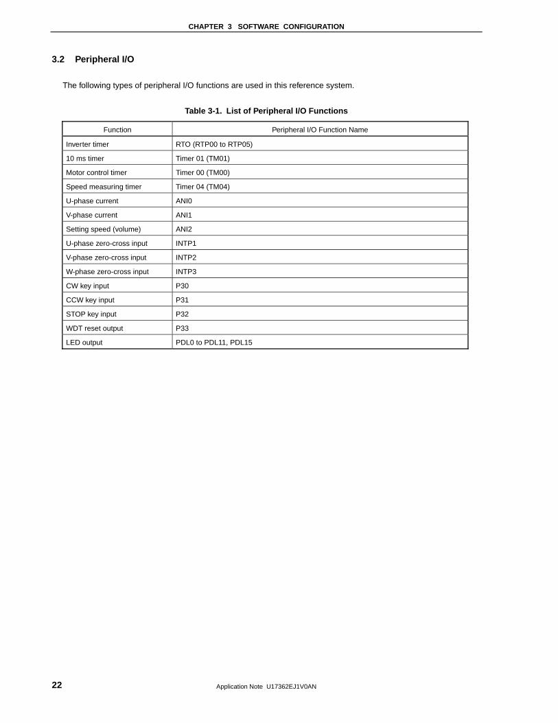
3.2 Peripheral I/O
The following types of peripheral I/O functions are used in this reference system.
Table 3-1. List of Peripheral I/O Functions
Function Peripheral I/O Function Name
Inverter timer RTO (RTP00 to RTP05)
10 ms timer Timer 01 (TM01)
Motor control timer Timer 00 (TM00)
Speed measuring timer Timer 04 (TM04)
U-phase current ANI0
V-phase current ANI1
Setting speed (volume) ANI2
U-phase zero-cross input INTP1
V-phase zero-cross input INTP2
W-phase zero-cross input INTP3
CW key input P30
CCW key input P31
STOP key input P32
WDT reset output P33
LED output PDL0 to PDL11, PDL15

CHAPTER 3 SOFTWARE CONFIGURATION
Application Note U17362EJ1V0AN 23
(1) Description of peripheral I/O functions
(a) Inverter timer
The RTP00 to RTP05 pins are used to output PWM waveforms.
In this reference system, the settings are as shown below.
• Inverter timer output: Low active
• When INTP0 pin input is at high level, PWM output is stopped.
(b) Motor control timer
Motor control timers are used to issue interrupts at a 50 µs interval.
(c) 10 ms timer
10 ms timers are used to issue interrupts at a 10 ms interval.
(d) Speed measuring timer
Used for measuring the revolution speed of the motor.
(e) Current value input
ANI0: U-phase current value (−5 to +5 A)
ANI1: V-phase current value (−5 to +5 A)
(f) Speed specification volume value input
ANI2 is used to input a value from 0 to 1,023.
CHAPTER 3 SOFTWARE CONFIGURATION
Application Note U17362EJ1V0AN 24
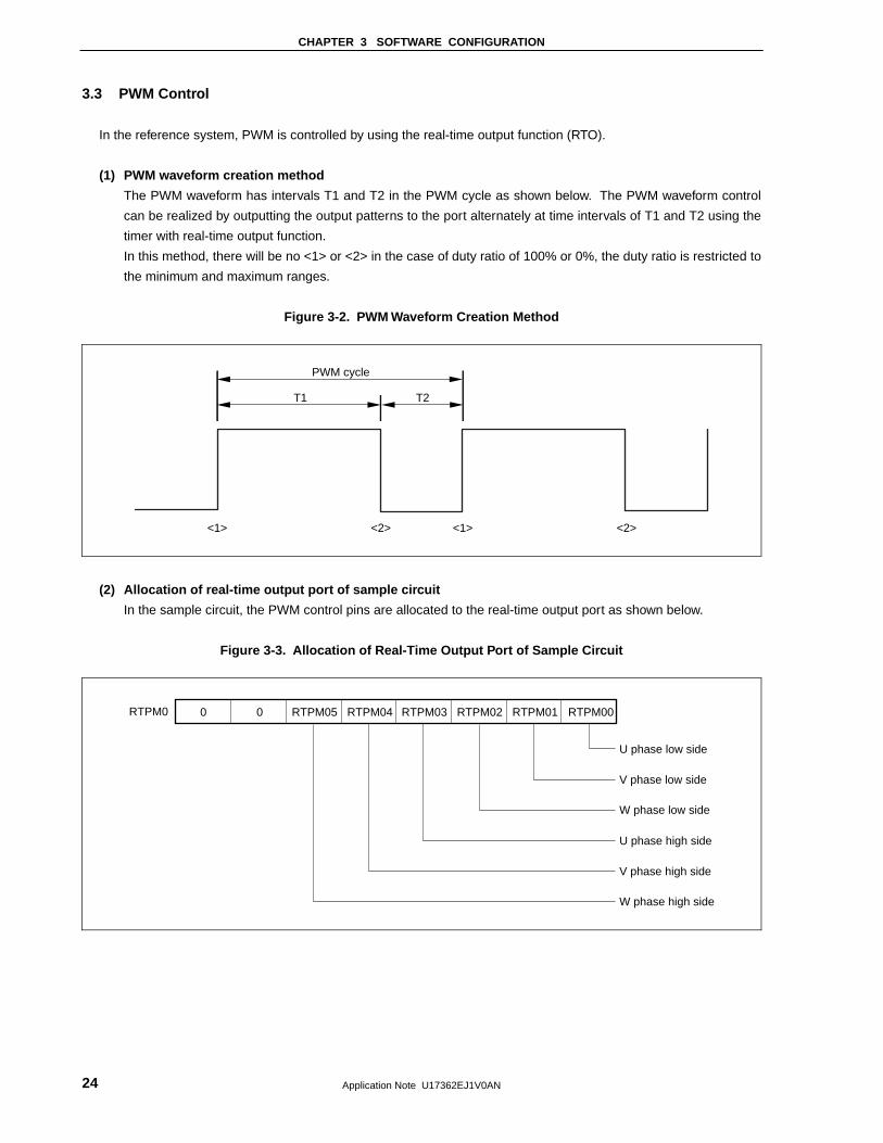
3.3 PWM Control
In the reference system, PWM is controlled by using the real-time output function (RTO).
(1) PWM waveform creation method
The PWM waveform has intervals T1 and T2 in the PWM cycle as shown below. The PWM waveform control
can be realized by outputting the output patterns to the port alternately at time intervals of T1 and T2 using the
timer with real-time output function.
In this method, there will be no <1> or <2> in the case of duty ratio of 100% or 0%, the duty ratio is restricted to
the minimum and maximum ranges.
Figure 3-2. PWM Waveform Creation Method
T1
PWM cycle
T2
<1> <2> <1> <2>
(2) Allocation of real-time output port of sample circuit
In the sample circuit, the PWM control pins are allocated to the real-time output port as shown below.
Figure 3-3. Allocation of Real-Time Output Port of Sample Circuit
0 0 RTPM05 RTPM04 RTPM03RTPM0
U phase low side
V phase low side
W phase low side
U phase high side
V phase high side
W phase high side
RTPM02 RTPM01 RTPM00

CHAPTER 3 SOFTWARE CONFIGURATION
Application Note U17362EJ1V0AN 25
3.4 Software Processing Structure
The software processing structure is shown below.
Figure 3-4. Main Processing Structure
Processingduring
deceleration
Detection timeprocessing
STOP processing
CW revolutionprocessing
CCWrevolutionprocessing
Operation(STOP CW)
CW revolution operation
CCWrevolution operation
Operation(STOP CCW)

CHAPTER 3 SOFTWARE CONFIGURATION
Application Note U17362EJ1V0AN 26
Figure 3-5. Interrupt Processing Structure
(a) Motor control processing (b) Control pin selection processing (c) Wait timer processing
Motor controlprocessing50 s interval interruptµ
U, V, W changeinterrupt
Control pin selection
processing
Wait timerprocessing 10 ms interval interrupt
The status of the operation mode switch is monitored by the main processing, and processing is transferred to CW,
CCW, and stop status. The motor is controlled in the specified status by using a 50 µs interval interrupt.
There are the following three motor control statuses.
• Stop status
The motor is not controlled.
• Initial operation status
Estimated revolution control is performed up to the speed at which the zero-cross point of electromotive force can
be detected.
• Speed control status
Feedback revolution control is performed so that the indication speed is attained.
CHAPTER 3 SOFTWARE CONFIGURATION
Application Note U17362EJ1V0AN 27
3.5 Flowchart
3.5.1 Main processing
Figure 3-6 shows the flowchart of the main processing.
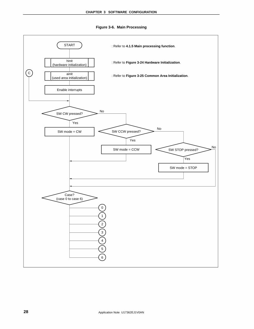
CHAPTER 3 SOFTWARE CONFIGURATION
Application Note U17362EJ1V0AN 28
Figure 3-6. Main Processing
START
hinit(hardware initialization)
ainit(used area initialization)
Enable interrupts
: Refer to Figure 3-24 Hardware Initialization.
: Refer to 4.1.5 Main processing function.
: Refer to Figure 3-25 Common Area Initialization.
SW CW pressed?
Case?(case 0 to case 6)
SW mode = CW SW CCW pressed?
SW mode = CCW SW STOP pressed?
SW mode = STOP
0
1
2
3
4
5
6
C
No
Yes
No
Yes
No
Yes

CHAPTER 3 SOFTWARE CONFIGURATION
Application Note U17362EJ1V0AN 29
Figure 3-7. Case 0 (Processing During Stoppage)
0
SW mode = CW?
Initialize target speed and request CCW initialization
Processing number 1
A
Initialize target speed and request CCW initialization
Processing number 4
No
Yes
Disable interrupts
Enable interrupts Enable interrupts
禁
Disable interrupts
CHAPTER 3 SOFTWARE CONFIGURATION
Application Note U17362EJ1V0AN 30
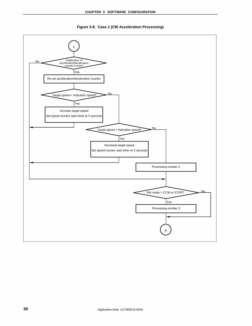
Figure 3-8. Case 1 (CW Acceleration Processing)
1
Initialization of acceleration/deceleration
counter 0 ends?
Increase target speed
Set speed monitor start timer to 5 seconds
A
No
Yes
Re-set acceleration/deceleration counter
Target speed < Indication speed?
Target speed > Indication speed?
Decrease target speed Set speed monitor start timer to 5 seconds
SW mode = CCW or STOP?
Processing number 2
Processing number 3
No
Yes
No
Yes
Yes
No
CHAPTER 3 SOFTWARE CONFIGURATION
Application Note U17362EJ1V0AN 31
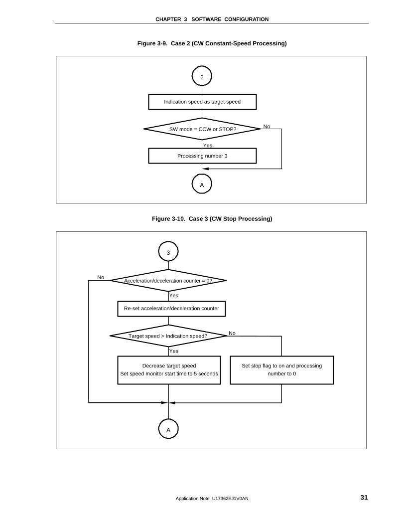
Figure 3-9. Case 2 (CW Constant-Speed Processing)
2
A
Yes
Indication speed as target speed
SW mode = CCW or STOP? No
Processing number 3
Figure 3-10. Case 3 (CW Stop Processing)
No
Target speed > Indication speed?
Acceleration/deceleration counter = 0?
Decrease target speed
Set speed monitor start time to 5 seconds
Yes
No
3
Re-set acceleration/deceleration counter
A
Set stop flag to on and processing
number to 0
Yes
CHAPTER 3 SOFTWARE CONFIGURATION
Application Note U17362EJ1V0AN 32
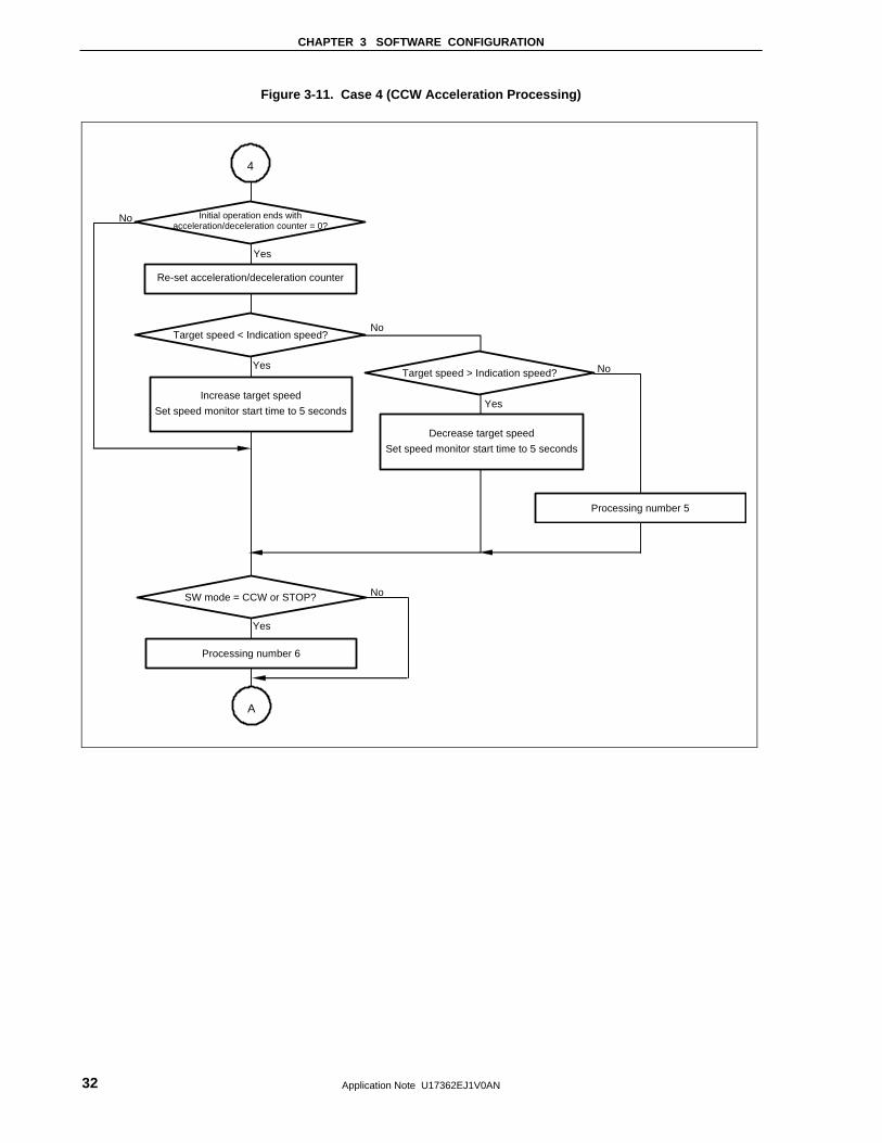
Figure 3-11. Case 4 (CCW Acceleration Processing)
4
Initial operation ends with acceleration/deceleration counter = 0?
Increase target speed
Set speed monitor start time to 5 seconds
No
Yes
Re-set acceleration/deceleration counter
Target speed < Indication speed?
Target speed > Indication speed?
Decrease target speed
Set speed monitor start time to 5 seconds
No
No
Yes
A
SW mode = CCW or STOP?
Processing number 5
Processing number 6
Yes
No
Yes

CHAPTER 3 SOFTWARE CONFIGURATION
Application Note U17362EJ1V0AN 33
Figure 3-12. Case 5 (CCW Constant-Speed Processing)
5
A
Yes
Target speed = (– indication speed)
SW mode = CW or STOP? No
Processing number 6
Figure 3-13. Case 6 (CCW Stop Processing)
No
Target speed < (− indication speed)?
Acceleration/deceleration counter = 0?
Increase target speed
Set speed monitor start time to 5 seconds
Yes
No
6
Re-set acceleration/deceleration counter
Set stop flag to on and processing
number to 0
A
Yes
CHAPTER 3 SOFTWARE CONFIGURATION
Application Note U17362EJ1V0AN 34
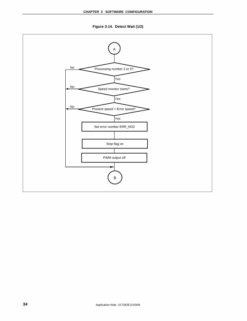
Figure 3-14. Detect Wait (1/2)
A
B
Processing number 2 or 5?
Speed monitor starts?
Present speed < Error speed?
Set error number ERR_NO2
Stop flag on
PWM output off
No
No
No
Yes
Yes
Yes
CHAPTER 3 SOFTWARE CONFIGURATION
Application Note U17362EJ1V0AN 35
Figure 3-14. Detect Wait (2/2)
Error flag on?
7-segment display off
B
Yes
No
500 ms?
Error number 1?
“1” displayed on 7-segment
500 ms?
C
“2” displayed on 7-segment
No
Yes
Yes
Yes
No
No
Display average counter = 0?
Set display average counter to 100
Yes
No
led_num
(Present average speed
indication)
led_num
(Control period indication)
led_num (Interrupt processing
time indication)
led_num (Operation processing
time indication)

CHAPTER 3 SOFTWARE CONFIGURATION
Application Note U17362EJ1V0AN 36
3.5.2 LED display
Figure 3-15. LED Display
led_num
Area 1? No
Display 4 digits of area 1
Area 2?
Display 2 digits of area 2
Area 3?
Display 2 digits of area 3
Display 2 digits of area 4
EXIT
Yes
Revolution speed
Control period
Control P processing time
Operation processing time
No
No
Yes
Yes
: Refer to 4.1.6 LED display function.
CHAPTER 3 SOFTWARE CONFIGURATION
Application Note U17362EJ1V0AN 37
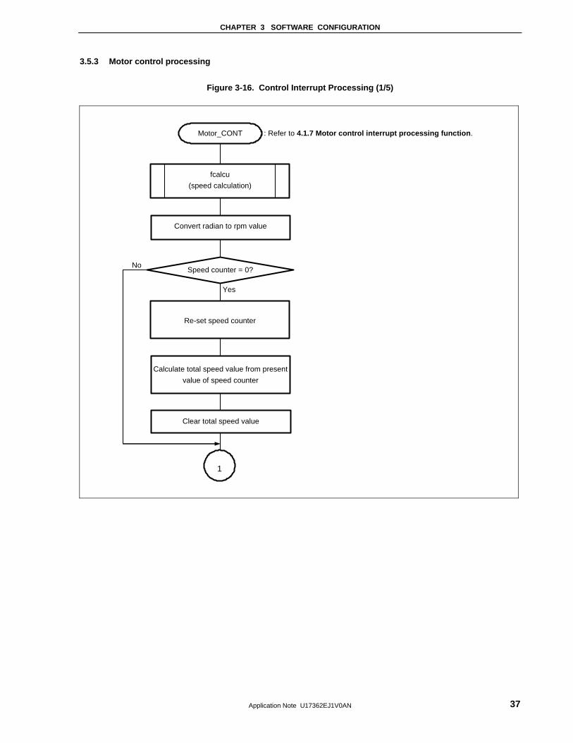
3.5.3 Motor control processing
Figure 3-16. Control Interrupt Processing (1/5)
Motor_CONT
fcalcu
(speed calculation)
Convert radian to rpm value
Speed counter = 0?
Re-set speed counter
Calculate total speed value from present
value of speed counter
Clear total speed value
1
No
Yes
: Refer to 4.1.7 Motor control interrupt processing function.
CHAPTER 3 SOFTWARE CONFIGURATION
Application Note U17362EJ1V0AN 38
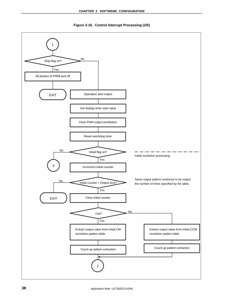
Figure 3-16. Control Interrupt Processing (2/5)
1
Stop flag on?
Initial revolution processing
All phases of PWM port off
Reset watchdog timer
Clear PWM output prohibition
Initial flag on?
Increment initial counter
Initial counter > Output time?
Clear initial counter
CW?
Extract output value from initial CW
revolution pattern table
Count up pattern extraction
2
3
No
Yes
No
Yes
Same output pattern continues to be output
the number of times specified by the table.
Extract output value from initial CCW
revolution pattern table
Count up pattern extraction
No
No
Yes
Yes
Get display timer start value
Operation start output EXIT
EXIT
CHAPTER 3 SOFTWARE CONFIGURATION
Application Note U17362EJ1V0AN 39
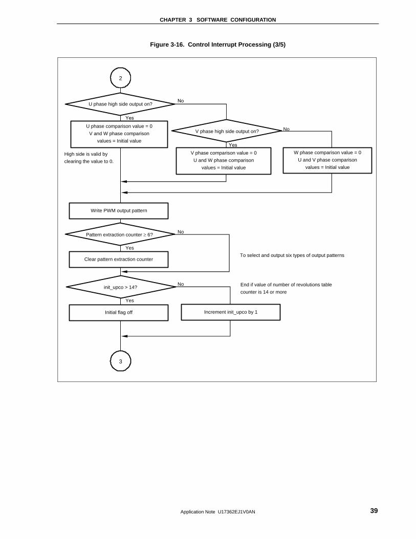
Figure 3-16. Control Interrupt Processing (3/5)
High side is valid by
clearing the value to 0.
End if value of number of revolutions table
counter is 14 or more
To select and output six types of output patterns
2
U phase high side output on?
U phase comparison value = 0
V and W phase comparison
values = Initial value
3
Yes
V phase high side output on?
V phase comparison value = 0
U and W phase comparison
values = Initial value
W phase comparison value = 0
U and V phase comparison
values = Initial value
Write PWM output pattern
Pattern extraction counter ≥ 6?
Clear pattern extraction counter
init_upco > 14?
Initial flag off Increment init_upco by 1
No
Yes
No
No
Yes
No
Yes

CHAPTER 3 SOFTWARE CONFIGURATION
Application Note U17362EJ1V0AN 40
Figure 3-16. Control Interrupt Processing (4/5)
3
No
Yes
Speed difference =
Target speed – Present speed
Calculate PWM output value
Speed integral value = MAX. value
Speed integral value
calculation
4
PWM value < 0?
PWM value as 1 PWM value > MAX.?
PWM value as MAX.
Normal revolution processing
No
No
No
Yes
Yes
Yes
Speed integral value > MAX. value?
Speed integral value < −MAX. value?
Speed integral value = −MAX. value
Remarks 1. PWM = (Present speed × ksp) + (Speed difference × ksp/10) + Speed integral value + Speed
offset value
2. Speed integral value = Speed integral value + (Speed difference × ksi)
3. ksp: Speed proportion gain
ksi: Speed integral gain

CHAPTER 3 SOFTWARE CONFIGURATION
Application Note U17362EJ1V0AN 41
Figure 3-16. Control Interrupt Processing (5/5)
4
Read present PWM output pattern
U phase high side output on?
U phase comparison value = 0
Set V and W phase comparison values U phase high side output on?
V phase comparison value = 0
Set U and W phase comparison
values
W phase comparison value = 0
Set U and V phase comparison
values
EXIT
No
Yes
Yes
No
CHAPTER 3 SOFTWARE CONFIGURATION
Application Note U17362EJ1V0AN 42
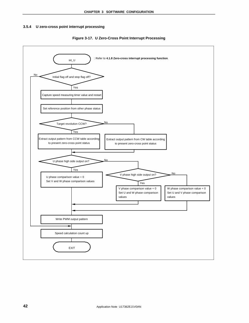
3.5.4 U zero-cross point interrupt processing
Figure 3-17. U Zero-Cross Point Interrupt Processing
Extract output pattern from CW table according
to present zero-cross point status
int_U
Initial flag off and stop flag off?
No
Target revolution CCW?
Extract output pattern from CCW table according
to present zero-cross point status
U phase high side output on?
U phase comparison value = 0
Set V and W phase comparison values
Write PWM output pattern
Speed calculation count up
EXIT
Yes
No
W phase comparison value = 0
Set U and V phase comparison
values
Yes
Yes
No
No
: Refer to 4.1.8 Zero-cross interrupt processing function.
Capture speed measuring timer value and restart
Set reference position from other phase status
V phase high side output on?
V phase comparison value = 0
Set U and W phase comparison
values
Yes
CHAPTER 3 SOFTWARE CONFIGURATION
Application Note U17362EJ1V0AN 43
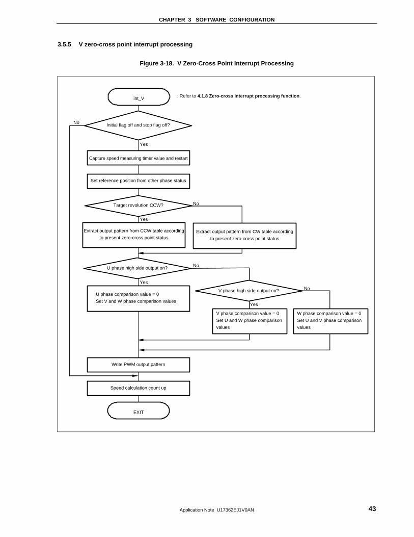
3.5.5 V zero-cross point interrupt processing
Figure 3-18. V Zero-Cross Point Interrupt Processing
Extract output pattern from CW table according
to present zero-cross point status
int_V
Initial flag off and stop flag off?
No
Target revolution CCW?
Extract output pattern from CCW table according
to present zero-cross point status
U phase high side output on?
U phase comparison value = 0
Set V and W phase comparison values
Write PWM output pattern
Speed calculation count up
EXIT
Yes
V phase high side output on?
V phase comparison value = 0
Set U and W phase comparison
values
W phase comparison value = 0
Set U and V phase comparison
values
Yes
Yes
No
No
No
Yes
: Refer to 4.1.8 Zero-cross interrupt processing function.
Capture speed measuring timer value and restart
Set reference position from other phase status
CHAPTER 3 SOFTWARE CONFIGURATION
Application Note U17362EJ1V0AN 44
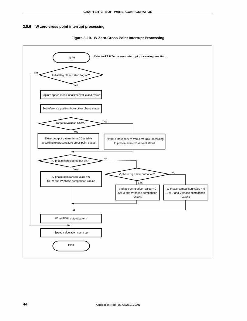
3.5.6 W zero-cross point interrupt processing
Figure 3-19. W Zero-Cross Point Interrupt Processing
Extract output pattern from CW table according
to present zero-cross point status
int_W
Initial flag off and stop flag off? No
Target revolution CCW?
Extract output pattern from CCW table
according to present zero-cross point status
U phase high side output on?
U phase comparison value = 0
Set V and W phase comparison values
Write PWM output pattern
Speed calculation count up
EXIT
Yes
V phase high side output on?
V phase comparison value = 0
Set U and W phase comparison
values
W phase comparison value = 0
Set U and V phase comparison
values
Yes
Yes
No
No
Yes
No
: Refer to 4.1.8 Zero-cross interrupt processing function.
Capture speed measuring timer value and restart
Set reference position from other phase status
CHAPTER 3 SOFTWARE CONFIGURATION
Application Note U17362EJ1V0AN 45
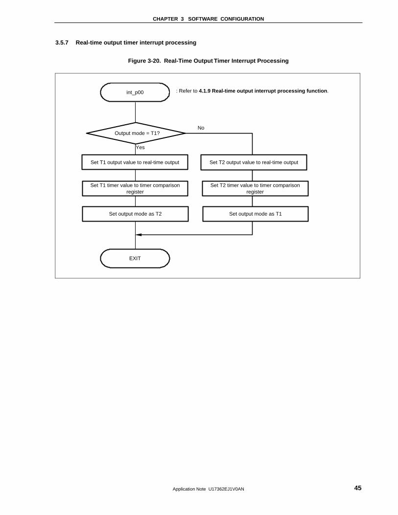
3.5.7 Real-time output timer interrupt processing
Figure 3-20. Real-Time Output Timer Interrupt Processing
Output mode = T1?
Set T1 timer value to timer comparison register
Set T2 timer value to timer comparison register
No
Yes
Set T1 output value to real-time output
Set output mode as T2 Set output mode as T1
Set T2 output value to real-time output
int_p00
EXIT
: Refer to 4.1.9 Real-time output interrupt processing function.

CHAPTER 3 SOFTWARE CONFIGURATION
Application Note U17362EJ1V0AN 46
3.5.8 Real-time output value set processing
Figure 3-21. Real-Time Output Value Set Processing
vCal_Timer
U phase high side output on?
Extract U phase pattern of T2 to
T1 output pattern value and set
as T1 output value
Yes
No
V phase high side output on?
Extract V phase pattern of T2 to
T1 output pattern value and set
as T1 output value
Extract W phase pattern of T2 to
T1 output pattern value and set
as T1 output value
No
Yes
: Refer to 4.1.9 Real-time output interrupt processing function.
Set data to T2 output pattern value
Calculate and set T1 timer value
T1 timer value < Minimum value?
Yes
No
T1 timer value ≥ (Maximum value − Minimum value)?
Set T1 timer value as
(Maximum value − Minimum value)
No
Yes
Set T2 timer value as
(Maximum value − T1 timer value)
Set T1 timer value as minimum value
EXIT

CHAPTER 3 SOFTWARE CONFIGURATION
Application Note U17362EJ1V0AN 47
3.5.9 10 mSEC interval interrupt processing
Figure 3-22. 10 mSEC Interval Interrupt Processing
int_ETC
Yes
Wait counter = 0?
Wait counter – 1
Acceleration/deceleration counter = 0?
Acceleration/deceleration counter – 1
Display counter = 0?
Display counter – 1
EXIT
No
No
No
Yes
Yes
: Refer to 4.1.10 10 mSEC interval interrupt processing function.

CHAPTER 3 SOFTWARE CONFIGURATION
Application Note U17362EJ1V0AN 48
3.5.10 A/D converter interrupt processing
Figure 3-23. A/D Converter Interrupt Processing (1/2)
int_AD0
Start A/D conversion of ANI1
ANI0?
EXIT
Read U phase current value
I Current value I > MAX_I?
U, V, W phase output off
Set error flag
Yes
No
No
Yes
: Refer to 4.1.11 A/D converter interrupt processing function.
1

CHAPTER 3 SOFTWARE CONFIGURATION
Application Note U17362EJ1V0AN 49
Figure 3-23. A/D Converter Interrupt Processing (2/2)
Read V phase current value
Start A/D conversion of ANI2
U, V, W phase output off
Set error flag
No | Current value | > MAX_|?
Yes
EXIT
No ANI1?
Yes
Motor_CONT
(motor control)
Read speed specification volume value
Set motor control interrupt processing time
1

CHAPTER 3 SOFTWARE CONFIGURATION
Application Note U17362EJ1V0AN 50
3.5.11 Hardware initialization
Figure 3-24. Hardware Initialization
hinit
Initialization of port used
7-segment LED extinguished
A/D initialization
Interrupt settings of
INTP1 to INTP3
EXIT
: Refer to 4.1.12 Hardware initialization processing function.
10 ms timer setting
Motor control timer setting
Initialization of inverter timer

CHAPTER 3 SOFTWARE CONFIGURATION
Application Note U17362EJ1V0AN 51
3.5.12 Common area initialization
Figure 3-25. Common Area Initialization
ainit
• Error flag off
• Initial flag off
• Display counter = 100
• Display speed = 0
• Stop flag on
• Target speed = 0
• Speed integral value = 0
EXIT
: Refer to 4.1.13 Common area initialization processing function.
3.5.13 Revolution start initialization
Figure 3-26. Revolution Start Initialization
start_init
Clear average speed buffer
Initialize average speed calculation area
EXIT
Output initial revolution pattern
Initialize processing area
: Refer to 4.1.14 Revolution start initialization processing function.

CHAPTER 3 SOFTWARE CONFIGURATION
Application Note U17362EJ1V0AN 52
3.5.14 RTO output data initialization
Figure 3-27. RTO Output Data Initialization
init_RTO
Set T1 and T2 timer values to duty 50%
EXIT
: Refer to 4.1.15 RTO output data initialization processing function.
Clear T1 and T2 output patterns to 0
CHAPTER 3 SOFTWARE CONFIGURATION
Application Note U17362EJ1V0AN 53
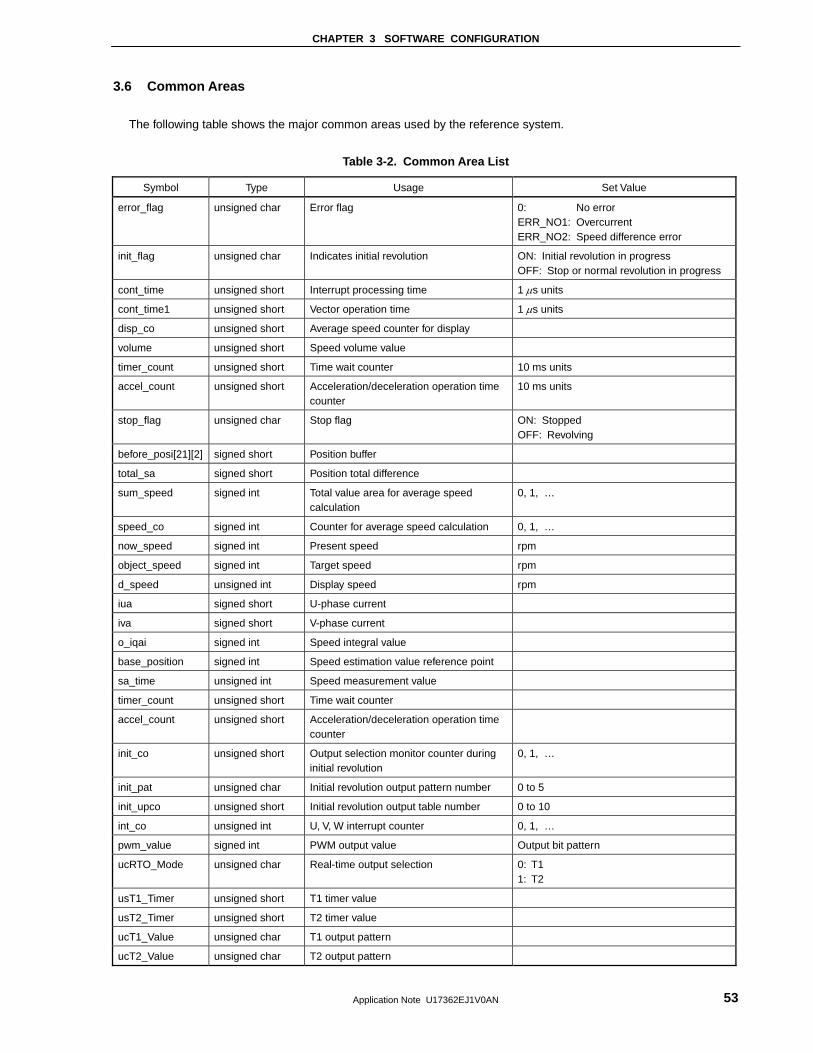
3.6 Common Areas
The following table shows the major common areas used by the reference system.
Table 3-2. Common Area List
Symbol Type Usage Set Value
error_flag unsigned char Error flag 0: No error ERR_NO1: Overcurrent ERR_NO2: Speed difference error
init_flag unsigned char Indicates initial revolution ON: Initial revolution in progress OFF: Stop or normal revolution in progress
cont_time unsigned short Interrupt processing time 1 µs units
cont_time1 unsigned short Vector operation time 1 µs units
disp_co unsigned short Average speed counter for display
volume unsigned short Speed volume value
timer_count unsigned short Time wait counter 10 ms units
accel_count unsigned short Acceleration/deceleration operation time counter
10 ms units
stop_flag unsigned char Stop flag ON: Stopped OFF: Revolving
before_posi[21][2] signed short Position buffer
total_sa signed short Position total difference
sum_speed signed int Total value area for average speed calculation
0, 1, …
speed_co signed int Counter for average speed calculation 0, 1, …
now_speed signed int Present speed rpm
object_speed signed int Target speed rpm
d_speed unsigned int Display speed rpm
iua signed short U-phase current
iva signed short V-phase current
o_iqai signed int Speed integral value
base_position signed int Speed estimation value reference point
sa_time unsigned int Speed measurement value
timer_count unsigned short Time wait counter
accel_count unsigned short Acceleration/deceleration operation time counter
init_co unsigned short Output selection monitor counter during initial revolution
0, 1, …
init_pat unsigned char Initial revolution output pattern number 0 to 5
init_upco unsigned short Initial revolution output table number 0 to 10
int_co unsigned int U, V, W interrupt counter 0, 1, …
pwm_value signed int PWM output value Output bit pattern
ucRTO_Mode unsigned char Real-time output selection 0: T1 1: T2
usT1_Timer unsigned short T1 timer value
usT2_Timer unsigned short T2 timer value
ucT1_Value unsigned char T1 output pattern
ucT2_Value unsigned char T2 output pattern
CHAPTER 3 SOFTWARE CONFIGURATION
Application Note U17362EJ1V0AN 54
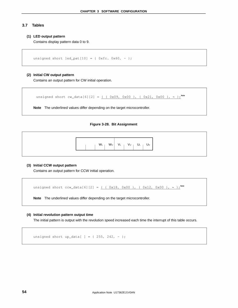
3.7 Tables
(1) LED output pattern
Contains display pattern data 0 to 9.
unsigned short led_pat[10] = 0xfc. 0x60, ~ ;
(2) Initial CW output pattern
Contains an output pattern for CW initial operation.
unsigned short cw_data[6][2] = 0x09, 0x00 , 0x21, 0x00 , ∼ ;Note Note The underlined values differ depending on the target microcontroller.
Figure 3-28. Bit Assignment
WL WU VL VU UL UU
(3) Initial CCW output pattern
Contains an output pattern for CCW initial operation.
unsigned short ccw_data[6][2] = 0x18, 0x00 , 0x12, 0x00 , ∼ ;Note
Note The underlined values differ depending on the target microcontroller.
(4) Initial revolution pattern output time
The initial pattern is output with the revolution speed increased each time the interrupt of this table occurs.
unsigned short up_data[ ] = 255, 242, ~ ;

CHAPTER 3 SOFTWARE CONFIGURATION
Application Note U17362EJ1V0AN 55
(5) Normal CW revolution output pattern
Contains an output pattern in accordance with the status of the zero-cross point during normal CW revolution.
unsigned short run_cw_data[8][2] = 0x00, 0x00 , 0x21, 0x00 , ∼ ;Note Note The underlined values differ depending on the target microcontroller.
(6) Normal CCW revolution output pattern
Contains an output pattern in accordance with the status of the zero-cross point during normal CCW revolution.
unsigned short run_ccw_data[8][2] = 0x00, 0x00 , 0x09, 0x00 , ∼ ;Note Note The underlined values differ depending on the target microcontroller.

CHAPTER 3 SOFTWARE CONFIGURATION
Application Note U17362EJ1V0AN 56
3.8 Constant Definitions
The following table shows the major constants used by the reference system.
Symbol Usage ValueNote
PAI π 3.141592
TH_U Radian value, jack-up constant 1000
RAD Radian value of one revolution 2 × PAI × TH_U
OFFSET Original point OFFSET 1945
RPM_RADS rpm → radian conversion constant 2 × PAI × TH_U/60
KSP Speed proportion constant 750
KSI Speed integral constant 10
P Number of motor poles 2
KSPGETA Speed proportion constant jack-up constant 10
KSIGETA Speed integral constant jack-up constant 14
SGETA sin jack-up constant 14
PWM_TS PWM cycle 80 µs
PWM_DATA PWM set value PWM_TS/0.2
SPEED_MAX Maximum speed 3000 rpm
SPEED_MINI Minimum speed 800 rpm
SPEED_INIT Initial revolution speed 700 rpm
SA_SPEED_MAX Maximum speed difference 800 rpm
IQAMAX Maximum speed integral value 200000
MAX_I Maximum current value 800
TS Motor control period 80 µs
ACCEL_TIME Acceleration/deceleration time constant, 10 ms 1
ACCEL_DATA Number of acceleration/deceleration incremental revolutions 40 rpm
WATCH_START Speed monitor start time, 10 ms 500
ACCEL_VAL_1ST Initial acceleration/deceleration time constant 50
ACCEL_VAL Acceleration/deceleration time constant 3
ACCEL_SPD Acceleration/deceleration constant 50
PWM_INIT PWM initial value PWM_DATA/4
TMCNT_MAX PWM maximum value 400 (80 µs)
TMCNT_MIN PWM minimum value 50 (10 µs)
Note Value used in the V850ES/KJ1

Application Note U17362EJ1V0AN 57
CHAPTER 4 PROGRAM LIST
4.1 Program List (V850ES/KJ1)
4.1.1 Symbol definition
/****************************************************************************** / /* Common area */ /****************************************************************************** / unsigned char ram_start ; unsigned char error_flag ; /* Error flag */ unsigned char init_flag ; /* Initial flag */ unsigned short cont_time ; /* Interrupt control time uSEC */ unsigned short cont_time1 ; /* Vector operation time uSEC */ unsigned short disp_co ; /* Interrupt control time display timer */ unsigned short volume ; /* Volume value */ unsigned short timer_count ; /* Time wait counter */ unsigned short accel_count ; /* Acceleration/deceleration operation time */ /* counter */ unsigned char stop_flag ; /* Stop flag */ signed short before_posi[21][2] ; /* Position buffer */ signed short total_sa ; /* Position total difference */ signed int sum_speed ; signed int speed_co ; signed int now_speed ; /* Present speed rms */ signed int object_speed ; /* Target speed rms */ unsigned int d_speed ; /* Display speed rms */ unsigned char ram_end ; #pragma section const begin const unsigned short led_pat[10] = 0xfc, 0x60, 0xda, 0xf2, 0x66, 0xb6, 0xbe, 0xe0, 0xfe, 0xe6 ; #pragma section const end /****************************************************************************** / /* Common flags */ /****************************************************************************** / extern unsigned char ram_start ; extern unsigned char error_flag ; /* Error flag */ extern unsigned char init_flag ; /* Initial flag */ extern unsigned short cont_time ; /* Interrupt control time uSEC */ extern unsigned short cont_time1 ; /* Vector operation time uSEC */ extern unsigned short disp_co ; /* Interrupt control time display timer */ extern unsigned short volume ; /* Volume value */ extern unsigned short timer_count ; /* Time wait counter */ extern unsigned short accel_count ; /* Acceleration/deceleration operation */ /* time counter */ extern unsigned char stop_flag ; /* Stop flag */

CHAPTER 4 PROGRAM LIST
Application Note U17362EJ1V0AN 58
extern signed short before_posi[21][2] ; /* Position buffer */ extern signed short total_sa ; /* Position total difference */ extern signed int sum_speed ; extern signed int speed_co ; extern signed int now_speed ; /* Present speed rms */ extern signed int object_speed ; /* Target speed rms */ extern unsigned int d_speed ; /* Display speed rms */ extern unsigned char ram_end ; #pragma section const begin extern const unsigned short led_pat[] ;; #pragma section const end /****************************************************************************** / /* Motor common definition */ /****************************************************************************** / extern signed short iua ; /* U-phase current */ extern signed short iva ; /* V-phase current */ extern signed int o_iqai ; /* Speed integral value area */ extern signed int base_position ; /* Speed estimation value reference point */ extern unsigned int sa_time ; /* Speed measurement value */ extern unsigned short timer_count ; /* Time wait counter */ extern unsigned short accel_count ; /* Acceleration/deceleration operation */ /* time counter */ extern unsigned short init_co ; /* Initial interrupt counter */ extern unsigned char init_pat ; /* Initial pattern counter */ extern unsigned short init_upco ; /* Initial speed-up counter */ extern unsigned int int_co ; /* UVW interrupt counter */ extern signed int pwm_value ; /* PWM output value */ extern unsigned char ucRTO_Mode ; /* Real-time output selection 0:T1 1:T2 */ extern unsigned short usT1_Timer ; /* T1 timer count */ extern unsigned short usT2_Timer ; /* T2 timer count */ extern unsigned char ucT1_Value ; /* T1 RTBL output value */ extern unsigned char ucT2_Value ; /* T2 RTBL output value */ #pragma section const begin extern const unsigned char cw_data[][2] ; extern const unsigned char ccw_data[][2] ; extern const unsigned char up_data[] ; extern const unsigned char run_cw_data[][2] ; extern const unsigned char run_ccw_data[][2] ; #pragma section const end 4.1.2 Constant definition
/****************************************************************************** / /* I/O */ /****************************************************************************** /

CHAPTER 4 PROGRAM LIST
Application Note U17362EJ1V0AN 59
#define BASE_IO 0xc200000 #define LED11 3 #define LED12 2 #define LED13 1 #define LED14 0 #define LED21 5 #define LED22 4 #define LED31 7 #define LED32 6 #define LED41 9 #define LED42 8 #define DIPSW 0x10 #define SW 0x20 #define DA1 0x30 #define DA2 0x40 #define DA3 0x50 #define WRESET 0x60 #define MODE 0x70 /****************************************************************************** / /* Constant */ /****************************************************************************** / #define ON 1 #define OFF 0 #define CW 1 /* CW operation mode */ #define CCW 2 /* CCW operation mode */ #define STOP 0 /* Operation stop mode */ #define ERR_NO1 1 /* Overcurrent error */ #define ERR_NO2 2 /* Speed difference error */ /****************************************************************************** / /* Motor constant */ /****************************************************************************** / /* Motor constant */ #define PAI 3.14159265 /* π */ #define TH_U 1000 /* Radian value jack-up constant */ #define RAD (int)(2*PAI*TH_U) /* Radian value of one revolution */ #define OFFSET 1945 /* Original point OFFSET */ #define RPM_RADS (int)((2*PAI*TH_U)/60) /* rpm -> radian conversion constant */ /* Motor constant */ #define KSP 750 /* Speed proportion constant */ #define KSI 10 /* Speed integral constant */ #define P 2 /* Number of poles */ #define KSPGETA 10 /* KSP jack-up constant */ #define KSIGETA 14 /* KSI jack-up constant */ #define SGETA 14 /* sin jack-up constant */ #define PWM_TS 80 /* PWM cycle */

CHAPTER 4 PROGRAM LIST
Application Note U17362EJ1V0AN 60
#define PWM_DATA (PWM_TS/0.2) /* PWM set value */ #define SPEED_MAX 3000 /* Maximum speed 3000 rpm */ #define SPEED_MINI 800 /* Minimum speed 800 rpm */ #define SPEED_INIT 700 /* Initial revolution speed rpm */ #define SA_SPEED_MAX 800 /* Maximum speed difference rpm */ #define IQAMAX 200000 /* Maximum speed integral value */ #define MAX_I 800 /* Maximum current value */ #define TS 80 /* Motor control time interval uSEC */ #define ACCEL_TIME 1 /* Acceleration/deceleration time */ /* constant 10 mSEC */ #define ACCEL_DATA 40 /* Number of acceleration/deceleration */
/* incremental revolutions rpm */ #define WATCH_START 500 /* Speed monitor start time 10 mSEC */ #define ACCEL_VAL_1ST 50 /* Initial acceleration/deceleration */ /* time constant */ #define ACCEL_VAL 3 /* Acceleration/deceleration time */ /* constant */ #define ACCEL_SPD 50 /* Acceleration/deceleration constant */ #define PWM_INIT PWM_DATA/4 /* PWM initial value */ #define TMCNT_MAX PWM_DATA /* TM00 counter maximum value */ #define TMCNT_MIN 50 /* TM00 counter minimum value 10 uSEC for */ /* the present */ /****************************************************************************** / /* Function constant */ /****************************************************************************** / void fcalcu( signed int *wrm, signed int *trm ); void OUT_data( unsigned short reg, unsigned short data ); unsigned short IN_data( int reg ); void led_num( int no, long data ) ; void vCal_Timer(int iVal,int iPWN ); void init_RTO( void ); /****************************************************************************** / /* Motor-related common area */ /****************************************************************************** / signed short iua ; /* U-phase current */ signed short iva ; /* V-phase current */ signed int o_iqai ; /* Speed integral value area */ signed int base_position ; /* Speed estimation value reference point */ unsigned int sa_time ; /* Speed measurement value */ unsigned short timer_count ; /* Time wait counter */ unsigned short accel_count ; /* Acceleration/deceleration operation time counter */ unsigned short init_co ; /* Initial interrupt counter */ unsigned char init_pat ; /* Initial pattern counter */ unsigned short init_upco ; /* Initial speed-up counter */ unsigned int int_co ; /* UVW interrupt counter */ signed int di ; signed int pwm_value ; /* PWM output value */

CHAPTER 4 PROGRAM LIST
Application Note U17362EJ1V0AN 61
unsigned char ucRTO_Mode ; /* Real-time output selection 0:T1 1:T2 */ unsigned short usT1_Timer ; /* T1 timer count */ unsigned short usT2_Timer ; /* T2 timer count */ unsigned char ucT1_Value ; /* T1 RTBL output value */ unsigned char ucT2_Value ; /* T2 RTBL output value */ unsigned short tp3_buf[5] ; /* TP3 output status management for measuring */ /* free time */ unsigned short tp3_co ; /* TP3 output status management for measuring */ /* free time */ #pragma section const begin const unsigned char cw_data[6][2] = 0x0a,0x00,0x0c,0x00,0x14,0x00, 0x11,0x00,0x21,0x00,0x22,0x00 ; const unsigned char ccw_data[6][2] = 0x22,0x00,0x21,0x00,0x11,0x00, 0x14,0x00,0x0c,0x00,0x0a,0x00 ; const unsigned char up_data[] = 255, 242, 229, 217, 206, 195, 185, 176, 166, 158, 158, 158, 158, 158, 158, 158, 158, 158, 158, 158 ; const unsigned char run_cw_data[8][2] = 0x00,0x00,0x0c,0x00,0x11,0x00, 0x14,0x00,0x22,0x00,0x0a,0x00, 0x21,0x00,0x00,0x00 ; const unsigned char run_ccw_data[8][2] = 0x00,0x00,0x0a,0x00,0x14,0x00, 0x0c,0x00, 0x21,0x00,0x22,0x00, 0x11,0x00,0x00,0x00 ; #pragma section const end 4.1.3 Interrupt handler setting
/****************************************************************************** / /* Interrupt symbol table */ /****************************************************************************** / .extern _ _start .extern _int_MOTOR .extern _int_U .extern _int_V .extern _int_W .extern _int_AD0 .extern _int_ETC .globl V_RESET .globl V_U .globl V_V .globl V_W .globl V_ETC .globl V_MOTOR .globl V_AD0 #******************************************************************************* .section ".handler",text V_RESET:

CHAPTER 4 PROGRAM LIST
Application Note U17362EJ1V0AN 62
jr _start V_U: ld.w [sp],r1 add 4,sp jr _int_U -- INTP1 V_V: ld.w [sp],r1 add 4,sp jr _int_V -- INTP2 V_W: ld.w [sp],r1 add 4,sp jr _int_W -- INTP3 V_ETC: ld.w [sp],r1 add 4,sp jr _int_ETC -- Other timers V_MOTOR: ld.w [sp],r1 add 4,sp jr _int_MOTOR -- Speed control timer V_AD0: ld.w [sp],r1 add 4,sp jr _int_AD0 -- A/D converter CH0 .extern V_RESET .extern V_U .extern V_V .extern V_W .extern V_ETC .extern V_MOTOR .extern V_AD0 /****************************************************************************** / /* Interrupt jump table */ /****************************************************************************** / .section ".vect_RESET",text mov #V_RESET,r1 jmp [r1] .section ".id_NO",text .byte 0xff,0xff,0xff,0xff,0xff,0xff,0xff,0xff,0xff,0xff .section ".vect_U",text add -4,sp st.w r1,[r3] mov #V_U,r1 jmp [r1]

CHAPTER 4 PROGRAM LIST
Application Note U17362EJ1V0AN 63
.section ".vect_V",text add -4,sp st.w r1,[r3] mov #V_V,r1 jmp [r1] .section ".vect_W",text add -4,sp st.w r1,[r3] mov #V_W,r1 jmp [r1] .section ".vect_ETC",text add -4,sp st.w r1,[r3] mov #V_ETC,r1 jmp [r1] .section ".vect_MOTOR",text add -4,sp st.w r1,[r3] mov #V_MOTOR,r1 jmp [r1] .section ".vect_AD0",text add -4,sp st.w r1,[r3] mov #V_AD0,r1 jmp [r1] 4.1.4 Startup routine setting
#============================================================================= # DESCRIPTIONS: # This assembly program is a sample of start-up module for ca850. # If you modified this program, you must assemble this file, and # locate a given directory. # # Unless -G is specified, sections are located as the following. # # | : | # | : | # tp -> -+-------------- + _ _start _ _tp_TEXT # | start up | # |-------------- | # text section | | # | user program |

CHAPTER 4 PROGRAM LIST
Application Note U17362EJ1V0AN 64
# | | # |-------------- | # | library | # -+-------------- + # | | # sdata section | | # | | # gp -> -+-------------- + _ _ssbss # | | # sbss section | | # | | # +-------------- + _ _stack _ _esbss _ _sbss # | stack area | # bss section | | # | 0x400 bytes | # sp -> -+-------------- + _ _stack + STACKSIZE _ _ebss # | : | # | : | # | : | # ep -> -+-------------- + _ _ep_DATA # tidata section | | # -+-------------- + # sidata section | | # -+-------------- + # | : | # | : | # #============================================================================= #----------------------------------------------------------------------------- # special symbols #----------------------------------------------------------------------------- .extern _ _tp_TEXT, 4 .extern _ _gp_DATA, 4 .extern _ _ep_DATA, 4 .extern _ _ssbss, 4 .extern _ _esbss, 4 .extern _ _sbss, 4 .extern _ _ebss, 4 #----------------------------------------------------------------------------- # C program main function #----------------------------------------------------------------------------- .extern _main #----------------------------------------------------------------------------- # dummy data declaration for creating sbss section
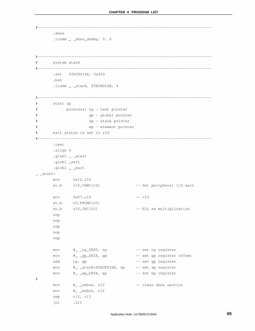
CHAPTER 4 PROGRAM LIST
Application Note U17362EJ1V0AN 65
#----------------------------------------------------------------------------- .sbss .lcomm _ _sbss_dummy, 0, 0 #----------------------------------------------------------------------------- # system stack #----------------------------------------------------------------------------- .set STACKSIZE, 0x400 .bss .lcomm _ _stack, STACKSIZE, 4 #----------------------------------------------------------------------------- # start up # pointers: tp - text pointer # gp - global pointer # sp - stack pointer # ep - element pointer # exit status is set to r10 #----------------------------------------------------------------------------- .text .align 4 .globl _ _start .globl _exit .globl _ _exit _ _start: mov 0x12,r10 st.b r10,VSWC[r0] -- Set peripheral I/O wait mov 0x07,r10 -- ×10 st.b r0,PHCMD[r0] st.b r10,CKC[r0] -- PLL xx multiplication nop nop nop nop nop mov #_ _tp_TEXT, tp -- set tp register mov #_ _gp_DATA, gp -- set gp register offset add tp, gp -- set gp register mov #_ _stack+STACKSIZE, sp -- set sp register mov #_ _ep_DATA, ep -- set ep register # mov #_ _ssbss, r13 -- clear sbss section mov #_ _esbss, r12 cmp r12, r13 jnl .L11
CHAPTER 4 PROGRAM LIST
Application Note U17362EJ1V0AN 66
.L12: st.w r0, [r13] add 4, r13 cmp r12, r13 jl .L12 .L11: # mov #_ _sbss, r13 -- clear bss section mov #_ _ebss, r12 cmp r12, r13 jnl .L14 .L15: st.w r0, [r13] add 4, r13 cmp r12, r13 jl .L15 .L14: # jarl _main, lp -- call main function _ _exit: halt -- end of program _ _startend: nop # # #-------------------------- end of start up module ----------------------------# # # 4.1.5 Main processing function
#include "Common.h" #include "Motor.h" #pragma ioreg /* Peripheral I/O register definition */ static int save_psw; /****************************************************************************** / /* 3-phase motor control program */ /****************************************************************************** / void main() unsigned char proc_no ; /* Present processing number */ signed int speed ; /* Indication speed rms */ signed int accel_spd ; int sw, sw_mode ; /* */ hinit() ; /* Hardware initialization */ ainit() ; /* Initialization of area used */ proc_no = 0 ; _ _EI();
CHAPTER 4 PROGRAM LIST
Application Note U17362EJ1V0AN 67
while( 1 ) accel_spd = ( SPEED_MAX - SPEED_MINI ) / 100; speed = ( ( SPEED_MAX - SPEED_MINI ) * volume / 1024 ) + SPEED_MINI ; /* Indication speed calculation by volume */ sw = ~IN_data( SW ) & 0x07 ; /* Read operation button */ if ( sw == 1 ) sw_mode = CW ; else if ( sw == 2 ) sw_mode = CCW ; else if ( sw == 4 ) sw_mode = STOP ; switch( proc_no ) /* STOP processing */ case 0 : if ( sw_mode == CW ) _ _DI() ; object_speed = SPEED_MINI ; /* Set target speed to minimum value */ stop_flag = OFF ; timer_count = WATCH_START ; /* Set speed monitor start time to 5 SEC */ accel_count = ACCEL_VAL_1ST ; /* Set acceleration/deceleration counter */ init_flag = 2 ; /* CCW initial request */ start_init() ; /* Initialize revolution start */ _ _EI() ; proc_no = 1 ; /* Set next processing number */ else if ( sw_mode == CCW ) _ _DI() ; stop_flag = OFF ; /* Stop flag off */ object_speed = -SPEED_MINI ; /* Set target speed to minimum value */ timer_count = WATCH_START ; /* Set speed monitor start time to */ /* 5 SEC */ accel_count = ACCEL_VAL_1ST ; /* Set acceleration/deceleration counter */ init_flag = 3 ; /* CCW initial request */ start_init() ; /* Initialize revolution start */ _ _EI() ; proc_no = 4 ; /* Set CCW processing number */ break ; /* CW processing, acceleration */ case 1 : if ( accel_count == 0 ) accel_count = ACCEL_VAL ; /* Set acceleration/deceleration counter */ if ( object_speed < speed ) object_speed += accel_spd ; if ( object_speed > speed ) object_speed = speed; timer_count = WATCH_START ; /* Set speed monitor start time to 5 SEC */ else if ( object_speed > speed ) object_speed -= accel_spd ;
CHAPTER 4 PROGRAM LIST
Application Note U17362EJ1V0AN 68
if ( object_speed < speed ) object_speed = speed; timer_count = WATCH_START ; /* Set speed monitor start time to 5 SEC */ else proc_no = 2 ; /* Constant-speed processing */ if ( (sw_mode == CCW) || (sw_mode == STOP) ) proc_no = 3 ; /* Deceleration, set processing number */ break ; /* CW processing, constant-speed */ case 2 : object_speed = speed ; if ( (sw_mode == CCW) || (sw_mode == STOP) ) proc_no = 3 ; /* Deceleration, set processing number */ break ; /* CW stop processing */ case 3 : if ( accel_count == 0 ) accel_count = ACCEL_VAL ; /* Set acceleration/deceleration counter */ if ( object_speed > SPEED_MINI ) object_speed -= accel_spd ; if ( object_speed < SPEED_MINI ) object_speed = SPEED_MINI; timer_count = WATCH_START ; /* Set speed monitor start time to 5 SEC */ else stop_flag = ON ; /* Stop flag on */ proc_no = 0 ; /* Set stop processing number */ break ; /* CCW processing, acceleration */ case 4 : if ( accel_count == 0 ) accel_count = ACCEL_VAL ; /* Set acceleration/deceleration counter */ if ( object_speed < -speed ) object_speed += accel_spd ; if ( object_speed > -speed ) object_speed = -speed; timer_count = WATCH_START ; /* Set speed monitor start time to 5 SEC */ else if ( object_speed > -speed ) object_speed -= accel_spd ; if ( object_speed < -speed ) object_speed = -speed; timer_count = WATCH_START ; /* Set speed monitor start time to 5 SEC */ else proc_no = 5 ; /* Constant-speed processing */ if ( (sw_mode == CW) || (sw_mode == STOP) )
CHAPTER 4 PROGRAM LIST
Application Note U17362EJ1V0AN 69
proc_no = 6 ; /* Deceleration, set processing number */ break ; /* CCW processing, constant-speed */ case 5 : object_speed = -speed ; if ( (sw_mode == CW) || (sw_mode == STOP) ) proc_no = 6 ; /* Deceleration, set processing number */ break ; /* CCW stop processing */ case 6 : if ( accel_count == 0 ) accel_count = ACCEL_VAL ; /* Set acceleration/deceleration counter */ if ( object_speed < -SPEED_MINI ) object_speed += accel_spd ; if ( object_speed > -SPEED_MINI ) object_speed = -SPEED_MINI; timer_count = WATCH_START ; /* Set speed monitor start time to 5 SEC */ else stop_flag = ON ; /* Stop flag on */ proc_no = 0 ; /* Set stop processing number */ break ; if ( ( proc_no == 2 ) || ( proc_no == 5 ) ) if ( timer_count == 0 ) if ( abs( object_speed - now_speed ) > SA_SPEED_MAX ) error_flag = ERR_NO2 ; /* Set error No. */ if ( disp_co == 0 ) led_num(1, d_speed / 100 ); /* Number of revolutions */ d_speed = 0 ; disp_co = 100 ; if ( abs(now_speed) == 0 ) disp_co = 0; led_num(2, 1000/PWM_TS ); /* Carrier frequency */ led_num(3, cont_time ); /* Overall processing time */ led_num(4, cont_time1 ); /* Vector operation processing time */ if ( error_flag ) while( 1 ) OUT_data( LED41, ~0x00 ) ; /* LED display off */
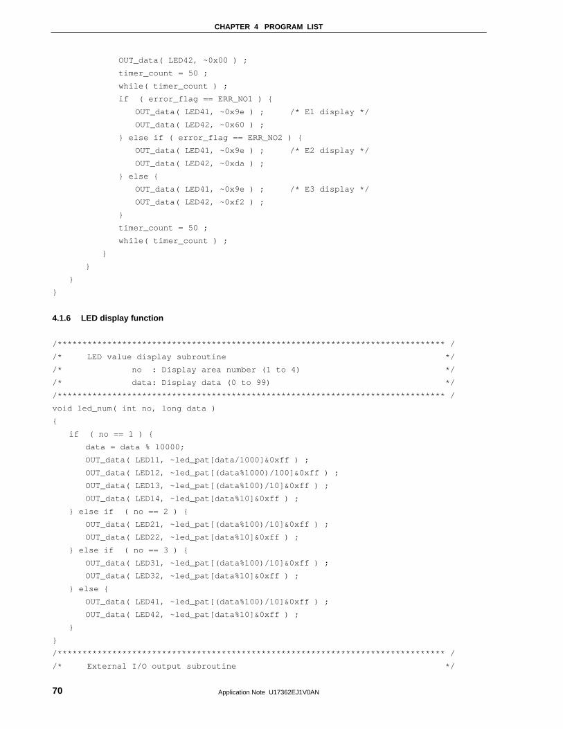
CHAPTER 4 PROGRAM LIST
Application Note U17362EJ1V0AN 70
OUT_data( LED42, ~0x00 ) ; timer_count = 50 ; while( timer_count ) ; if ( error_flag == ERR_NO1 ) OUT_data( LED41, ~0x9e ) ; /* E1 display */ OUT_data( LED42, ~0x60 ) ; else if ( error_flag == ERR_NO2 ) OUT_data( LED41, ~0x9e ) ; /* E2 display */ OUT_data( LED42, ~0xda ) ; else OUT_data( LED41, ~0x9e ) ; /* E3 display */ OUT_data( LED42, ~0xf2 ) ; timer_count = 50 ; while( timer_count ) ; 4.1.6 LED display function
/****************************************************************************** / /* LED value display subroutine */ /* no : Display area number (1 to 4) */ /* data: Display data (0 to 99) */ /****************************************************************************** / void led_num( int no, long data ) if ( no == 1 ) data = data % 10000; OUT_data( LED11, ~led_pat[data/1000]&0xff ) ; OUT_data( LED12, ~led_pat[(data%1000)/100]&0xff ) ; OUT_data( LED13, ~led_pat[(data%100)/10]&0xff ) ; OUT_data( LED14, ~led_pat[data%10]&0xff ) ; else if ( no == 2 ) OUT_data( LED21, ~led_pat[(data%100)/10]&0xff ) ; OUT_data( LED22, ~led_pat[data%10]&0xff ) ; else if ( no == 3 ) OUT_data( LED31, ~led_pat[(data%100)/10]&0xff ) ; OUT_data( LED32, ~led_pat[data%10]&0xff ) ; else OUT_data( LED41, ~led_pat[(data%100)/10]&0xff ) ; OUT_data( LED42, ~led_pat[data%10]&0xff ) ; /****************************************************************************** / /* External I/O output subroutine */
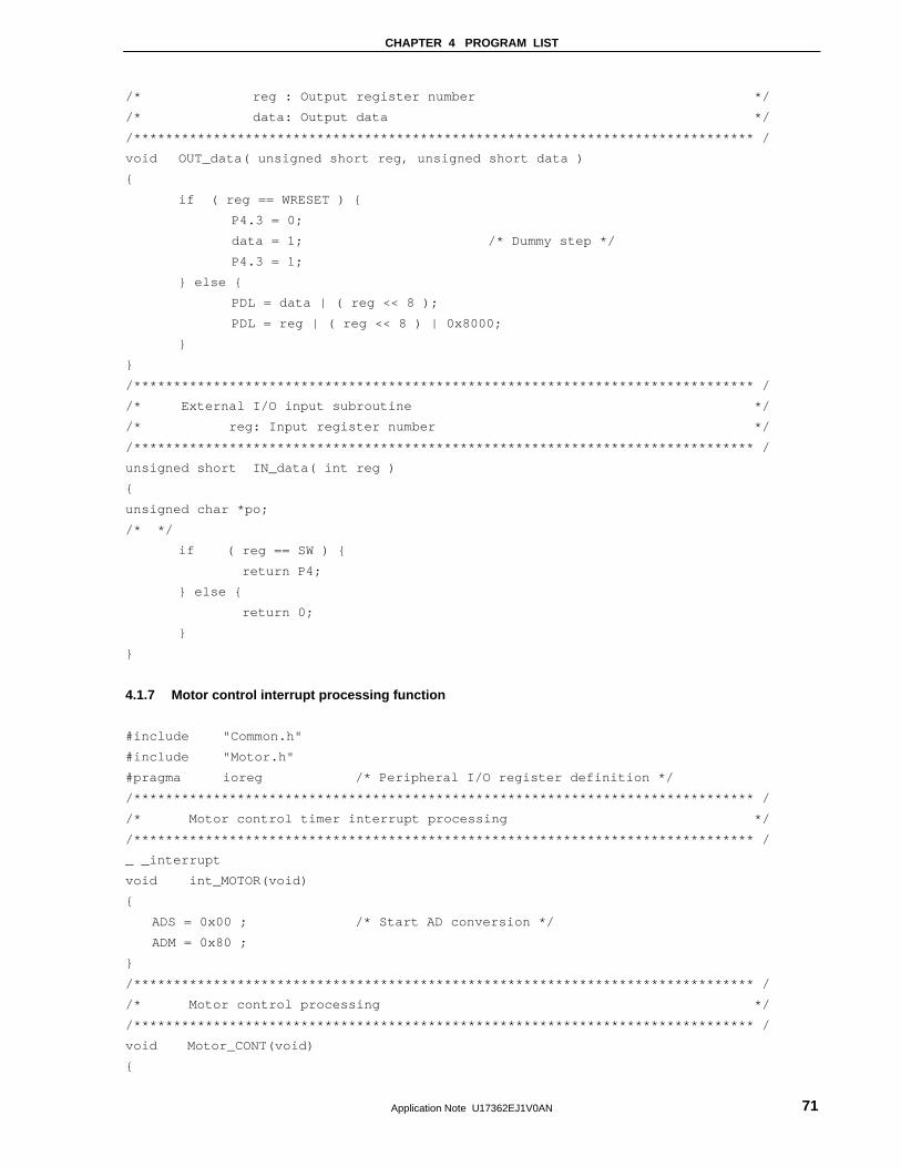
CHAPTER 4 PROGRAM LIST
Application Note U17362EJ1V0AN 71
/* reg : Output register number */ /* data: Output data */ /****************************************************************************** / void OUT_data( unsigned short reg, unsigned short data ) if ( reg == WRESET ) P4.3 = 0; data = 1; /* Dummy step */ P4.3 = 1; else PDL = data | ( reg << 8 ); PDL = reg | ( reg << 8 ) | 0x8000; /****************************************************************************** / /* External I/O input subroutine */ /* reg: Input register number */ /****************************************************************************** / unsigned short IN_data( int reg ) unsigned char *po; /* */ if ( reg == SW ) return P4; else return 0; 4.1.7 Motor control interrupt processing function
#include "Common.h" #include "Motor.h" #pragma ioreg /* Peripheral I/O register definition */ /****************************************************************************** / /* Motor control timer interrupt processing */ /****************************************************************************** / _ _interrupt void int_MOTOR(void) ADS = 0x00 ; /* Start AD conversion */ ADM = 0x80 ; /****************************************************************************** / /* Motor control processing */ /****************************************************************************** / void Motor_CONT(void)
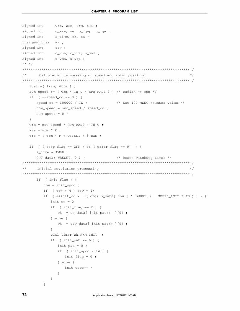
CHAPTER 4 PROGRAM LIST
Application Note U17362EJ1V0AN 72
signed int wrm, wre, trm, tre ; signed int o_wre, we, o_iqap, o_iqa ; signed int s_time, ek, sa ; unsigned char wk ; signed int cow ; signed int o_vua, o_vva, o_vwa ; signed int o_vda, o_vqa ; /* */ /****************************************************************************** / /* Calculation processing of speed and rotor position */ /****************************************************************************** / fcalcu( &wrm, &trm ) ; sum_speed += ( wrm * TH_U / RPM_RADS ) ; /* Radian -> rpm */ if ( --speed_co == 0 ) speed_co = 100000 / TS ; /* Set 100 mSEC counter value */ now_speed = sum_speed / speed_co ; sum_speed = 0 ; wrm = now_speed * RPM_RADS / TH_U ; wre = wrm * P ; tre = ( trm * P + OFFSET ) % RAD ; if ( ( stop_flag == OFF ) && ( error_flag == 0 ) ) s_time = TM00 ; OUT_data( WRESET, 0 ) ; /* Reset watchdog timer */ /****************************************************************************** / /* Initial revolution processing */ /****************************************************************************** / if ( init_flag ) cow = init_upco ; if ( cow > 4 ) cow = 4; if ( ++init_co > ( (long)up_data[ cow ] * 34000L / ( SPEED_INIT * TS ) ) ) init_co = 0 ; if ( init_flag == 2 ) wk = cw_data[ init_pat++ ][0] ; else wk = ccw_data[ init_pat++ ][0] ; vCal_Timer(wk,PWM_INIT) ; if ( init_pat >= 6 ) init_pat = 0 ; if ( init_upco > 14 ) init_flag = 0 ; else init_upco++ ;
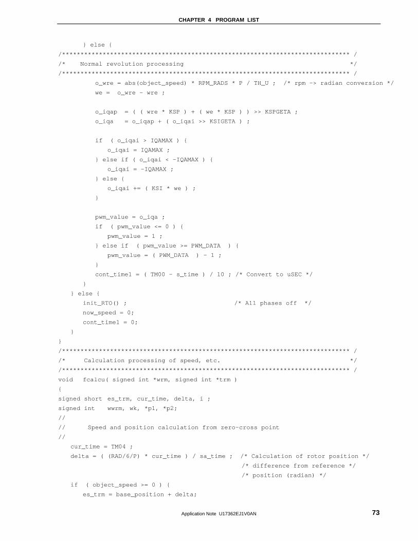
CHAPTER 4 PROGRAM LIST
Application Note U17362EJ1V0AN 73
else /****************************************************************************** / /* Normal revolution processing */ /****************************************************************************** / o_wre = abs(object_speed) * RPM_RADS * P / TH_U ; /* rpm -> radian conversion */ we = o_wre - wre ; o_iqap = ( ( wre * KSP ) + ( we * KSP ) ) >> KSPGETA ; o_iqa = o_iqap + ( o_iqai >> KSIGETA ) ; if ( o_iqai > IQAMAX ) o_iqai = IQAMAX ; else if ( o_iqai < -IQAMAX ) o_iqai = -IQAMAX ; else o_iqai += ( KSI * we ) ; pwm_value = o_iqa ; if ( pwm_value <= 0 ) pwm_value = 1 ; else if ( pwm_value >= PWM_DATA ) pwm_value = ( PWM_DATA ) - 1 ; cont_time1 = ( TM00 - s_time ) / 10 ; /* Convert to uSEC */ else init_RTO() ; /* All phases off */ now_speed = 0; cont_time1 = 0; /****************************************************************************** / /* Calculation processing of speed, etc. */ /****************************************************************************** / void fcalcu( signed int *wrm, signed int *trm ) signed short es_trm, cur_time, delta, i ; signed int wwrm, wk, *p1, *p2; // // Speed and position calculation from zero-cross point // cur_time = TM04 ; delta = ( (RAD/6/P) * cur_time ) / sa_time ; /* Calculation of rotor position */ /* difference from reference */ /* position (radian) */ if ( object_speed >= 0 ) es_trm = base_position + delta;
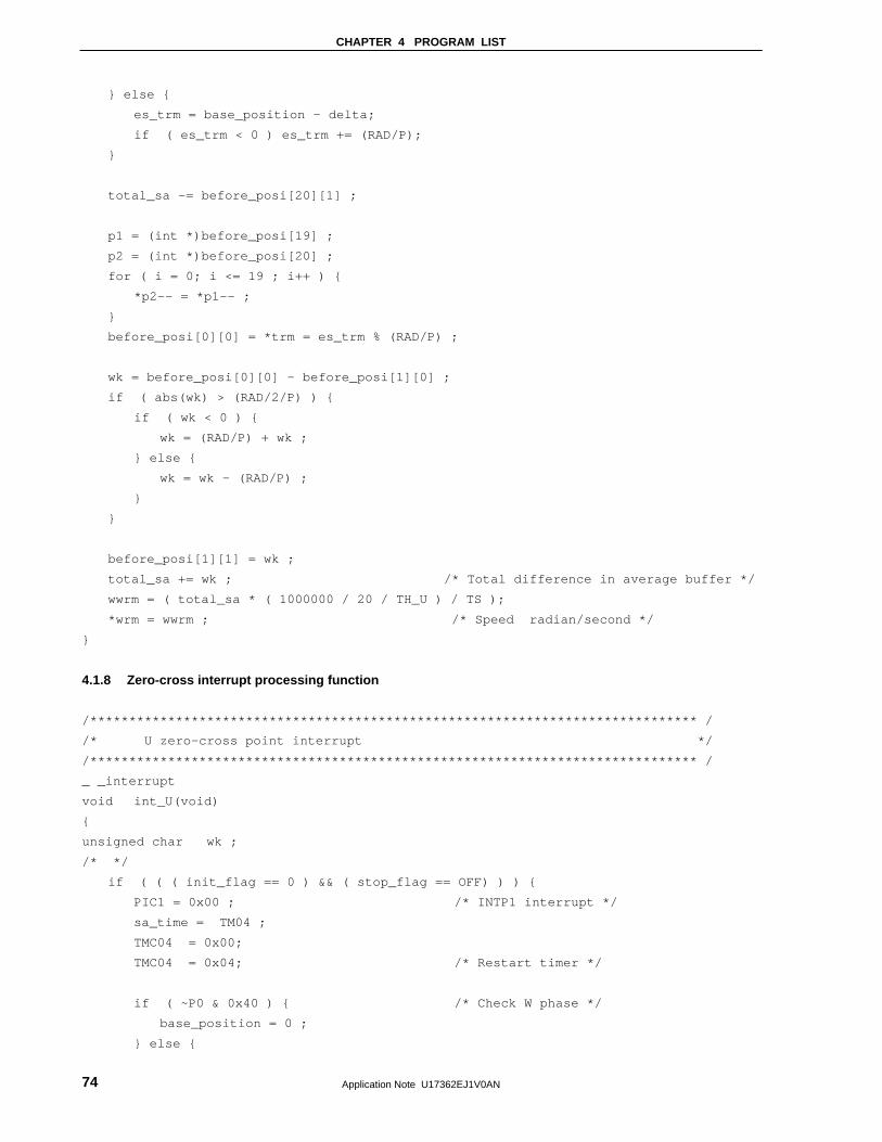
CHAPTER 4 PROGRAM LIST
Application Note U17362EJ1V0AN 74
else es_trm = base_position - delta; if ( es_trm < 0 ) es_trm += (RAD/P); total_sa -= before_posi[20][1] ; p1 = (int *)before_posi[19] ; p2 = (int *)before_posi[20] ; for ( i = 0; i <= 19 ; i++ ) *p2-- = *p1-- ; before_posi[0][0] = *trm = es_trm % (RAD/P) ; wk = before_posi[0][0] - before_posi[1][0] ; if ( abs(wk) > (RAD/2/P) ) if ( wk < 0 ) wk = (RAD/P) + wk ; else wk = wk - (RAD/P) ; before_posi[1][1] = wk ; total_sa += wk ; /* Total difference in average buffer */ wwrm = ( total_sa * ( 1000000 / 20 / TH_U ) / TS ); *wrm = wwrm ; /* Speed radian/second */ 4.1.8 Zero-cross interrupt processing function
/****************************************************************************** / /* U zero-cross point interrupt */ /****************************************************************************** / _ _interrupt void int_U(void) unsigned char wk ; /* */ if ( ( ( init_flag == 0 ) && ( stop_flag == OFF) ) ) PIC1 = 0x00 ; /* INTP1 interrupt */ sa_time = TM04 ; TMC04 = 0x00; TMC04 = 0x04; /* Restart timer */ if ( ~P0 & 0x40 ) /* Check W phase */ base_position = 0 ; else

CHAPTER 4 PROGRAM LIST
Application Note U17362EJ1V0AN 75
base_position = RAD/2/P ; if ( object_speed < 0 ) wk = run_ccw_data[ (P0 >> 4) & 0x07 ][0] ; else wk = run_cw_data[ (P0 >> 4) & 0x07 ][0] ; vCal_Timer(wk,pwm_value) ; int_co++ ; /****************************************************************************** / /* V zero-cross point interrupt */ /****************************************************************************** / _ _interrupt void int_V(void) unsigned char wk ; /* */ if ( ( ( init_flag == 0 ) && ( stop_flag == OFF) ) ) PIC2 = 0x00 ; /* INTP2 interrupt */ sa_time = TM04 ; TMC04 = 0x61; TMC04 = 0x63; /* Restart timer */ if ( ~P0 & 0x10 ) /* Check U phase */ base_position = RAD/3/P ; else base_position = RAD*5/6/P ; if ( object_speed < 0 ) wk = run_ccw_data[ (P0 >> 4) & 0x07 ][0] ; else wk = run_cw_data[ (P0 >> 4) & 0x07 ][0] ; vCal_Timer(wk,pwm_value) ; int_co++ ; /****************************************************************************** / /* W zero-cross point interrupt */ /****************************************************************************** / _ _interrupt void int_W(void) unsigned char wk ;

CHAPTER 4 PROGRAM LIST
Application Note U17362EJ1V0AN 76
/* */ if ( ( ( init_flag == 0 ) && ( stop_flag == OFF) ) ) PIC3 = 0x00 ; /* INTP3 interrupt */ sa_time = TM04 ; TMC04 = 0x00; TMC04 = 0x04; /* Restart timer */ if ( ~P0 & 0x20 ) /* Check V phase */ base_position = RAD*2/3/P ; else base_position = RAD/6/P ; if ( object_speed < 0 ) wk = run_ccw_data[ (P04 >> 4) & 0x07 ][0] ; else wk = run_cw_data[ (P04 >> 4) & 0x07 ][0] ; vCal_Timer(wk,pwm_value) ; int_co++ ; 4.1.9 Real-time output interrupt processing function
/****************************************************************************** / /* Real-time output timer interrupt */ /****************************************************************************** / _ _interrupt void int_p00(void) if ( ucRTO_Mode == 0 ) /* T1 interrupt */ RTBL0 = ucT1_Value ; /* Set next real-time output data */ TMC00= 0x00 ; /* Stop timer (reset counter) */ CR000= usT1_Timer ; /* Set timer value */ TMC00 = 0x0C ; /* Start timer */ ucRTO_Mode = 1 ; /* Next T2 */ else RTBL0 = ucT2_Value ; /* Set next real-time output data */ TMC00 = 0x00 ; /* Stop timer (reset counter) */ CR000 = usT2_Timer ; /* Set timer value */ TMC00 = 0x0C ; /* Start timer */ ucRTO_Mode = 0 ; /* Next T1 */ /****************************************************************************** /

CHAPTER 4 PROGRAM LIST
Application Note U17362EJ1V0AN 77
/* Set real-time output timer value to common */ /****************************************************************************** / void vCal_Timer(int iVal,int iPWN ) ucT2_Value = ( unsigned char) iVal ; if ( ucT2_Value & 0x08 ) ucT1_Value = ucT2_Value & 0x09 ; else if ( ucT2_Value & 0x10 ) ucT1_Value = ucT2_Value & 0x12 ; else ucT1_Value = ucT2_Value & 0x24 ; usT1_Timer = ( iPWN * TMCNT_MAX ) / PWM_DATA ; if ( usT1_Timer < TMCNT_MIN ) usT1_Timer = TMCNT_MIN ; else if ( usT1_Timer >= ( TMCNT_MAX - TMCNT_MIN ) ) usT1_Timer = TMCNT_MAX - TMCNT_MIN ; usT2_Timer = TMCNT_MAX - usT1_Timer ; 4.1.10 10 mSEC interval interrupt processing function
/****************************************************************************** / /* Other timer interrupt processing (10 mSEC interval) */ /****************************************************************************** / _ _multi_interrupt void int_ETC(void) /* Wait timer processing */ if ( timer_count != 0 ) timer_count -= 1 ; /* Acceleration/deceleration timer processing */ if ( accel_count != 0 ) accel_count -= 1 ; /* */ if ( disp_co != 0 ) d_speed += abs( now_speed ) ; disp_co -= 1 ; 4.1.11 A/D converter interrupt processing function
/****************************************************************************** /

CHAPTER 4 PROGRAM LIST
Application Note U17362EJ1V0AN 78
/* A/D converter interrupt processing for current and speed volume */ /****************************************************************************** / _ _multi_interrupt void int_AD0(void) unsigned char ucADS ; unsigned short usData ; int wk ; /* */ ucADS = ADS ; /* Input channel */ usData = ADCR ; /* Input data */ usData = ( usData >> 6 ) & 0x3FF ; /* Higher 10 bits */ switch ( ucADS ) case 0: iua = usData - 0x200 ; if ( abs(iua) > MAX_I ) init_RTO() ; /* All phases off */ error_flag = ERR_NO1 ; /* Set error No. */ ADS = 0x01 ; /* Next ANI1 */ ADM = 0x80 ; break ; case 1: iva = usData - 0x200 ; if ( abs(iva) > MAX_I ) init_RTO() ; /* All phases off */ error_flag = ERR_NO1 ; /* Set error No. */ ADS = 0x02 ; /* Next ANI2 */ ADM = 0x80 ; break ; case 2: wk = 1023 - usData ; /* Set volume value */ ADM = 0x00 ; Motor_CONT() ; cont_time = TM00 / 10 ; /* Convert to uSEC */ break ; 4.1.12 Hardware initialization processing function
/****************************************************************************** / /* Hardware (peripheral I/O) initialization */ /****************************************************************************** / void hinit( void ) /* Port mode register initialization */
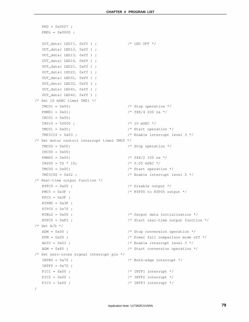
CHAPTER 4 PROGRAM LIST
Application Note U17362EJ1V0AN 79
PM3 = 0x00f7 ; PMDL = 0x0000 ; OUT_data( LED11, 0xff ) ; /* LED OFF */ OUT_data( LED12, 0xff ) ; OUT_data( LED13, 0xff ) ; OUT_data( LED14, 0xff ) ; OUT_data( LED21, 0xff ) ; OUT_data( LED22, 0xff ) ; OUT_data( LED31, 0xff ) ; OUT_data( LED32, 0xff ) ; OUT_data( LED41, 0xff ) ; OUT_data( LED42, 0xff ) ; /* Set 10 mSEC timer TM01 */ TMC01 = 0x00; /* Stop operation */ PRM01 = 0x01; /* fXX/4 200 ns */ CRC01 = 0x00; CR010 = 50000 ; /* 10 mSEC */ TMC01 = 0x0C; /* Start operation */ TM0IC10 = 0x03 ; /* Enable interrupt level 3 */ /* Set motor control interrupt timer TM00 */ TMC00 = 0x00; /* Stop operation */ CRC00 = 0x00; PRM00 = 0x00; /* fXX/2 100 ns */ CR000 = TS * 10; /* 0.05 mSEC */ TMC00 = 0x0C; /* Start operation */ TM0IC00 = 0x02 ; /* Enable interrupt level 2 */ /* Real-time output function */ RTPC0 = 0x00 ; /* Disable output */ PMC5 = 0x3F ; /* RTP00 to RTP05 output */ PFC5 = 0x3F ; RTPM0 = 0x3F ; RTPC0 = 0x70 ; RTBL0 = 0x00 ; /* Output data initialization */ RTPC0 = 0xF0 ; /* Start real-time output function */ /* Set A/D */ ADM = 0x00 ; /* Stop conversion operation */ PFM = 0x00 ; /* Power fail comparison mode off */ ADIC = 0x03 ; /* Enable interrupt level 3 */ ADM = 0x80 ; /* Start conversion operation */ /* Set zero-cross signal interrupt pin */ INTR0 = 0x70 ; /* Both-edge interrupt */ INTF0 = 0x70 ; PIC1 = 0x00 ; /* INTP1 interrupt */ PIC2 = 0x00 ; /* INTP2 interrupt */ PIC3 = 0x00 ; /* INTP3 interrupt */

CHAPTER 4 PROGRAM LIST
Application Note U17362EJ1V0AN 80
4.1.13 Common area initialization processing function
/****************************************************************************** / /* Common area initialization */ /****************************************************************************** / void ainit( void ) /* Initialization of flags */ error_flag = 0 ; /* Clear error flag */ init_flag = OFF ; /* Initial flag off */ disp_co = 100 ; d_speed = 0 ; /* Motor control area initialization */ stop_flag = ON ; /* Stop flag on */ object_speed = 0 ; /* Target speed 0 */ o_iqai = 0 ; /* Speed integral value 0 */ 4.1.14 Revolution start initialization processing function
/****************************************************************************** / /* Revolution start initialization */ /****************************************************************************** / void start_init( void ) int i; /* */ for ( i = 0 ; i < 21 ; i++ ) before_posi[i][1] = 0; total_sa = 0 ; sum_speed = 0 ; speed_co = 100000 / TS ; init_co = 0 ; init_pat = 0 ; init_upco = 0 ; 4.1.15 RTO output data initialization processing function
/****************************************************************************** / /* RTO output data initialization */ /****************************************************************************** / void init_RTO( void ) usT1_Timer = TMCNT_MAX / 2 ; /* Initial value half timer */ usT2_Timer = TMCNT_MAX / 2 ; ucT1_Value = 0 ; /* No data output */ ucT2_Value = 0 ;

CHAPTER 4 PROGRAM LIST
Application Note U17362EJ1V0AN 81
4.1.16 Link directive file for V850ES/KJ1
/****************************************************************************** / /* Link directive file for V850ES/KJ1 */ /****************************************************************************** / VECT_RESET: !LOAD ?RX V0x0000000 .vect_RESET = $PROGBITS ?AX .vect_RESET; ; ID_NO: !LOAD ?RX V0x0000070 .id_NO = $PROGBITS ?AX .id_NO; ; VECT_U: !LOAD ?RX V0x00000a0 .vect_U = $PROGBITS ?AX .vect_U; ; VECT_V: !LOAD ?RX V0x00000b0 .vect_V = $PROGBITS ?AX .vect_V; ; VECT_W: !LOAD ?RX V0x00000c0 .vect_W = $PROGBITS ?AX .vect_W; ; VECT_MOTOR: !LOAD ?RX V0x0000100 .vect_MOTOR = $PROGBITS ?AX .vect_MOTOR; ; VECT_ETC: !LOAD ?RX V0x0000120 .vect_ETC = $PROGBITS ?AX .vect_ETC; ; VECT_AD0: !LOAD ?RX V0x0000220 .vect_AD0 = $PROGBITS ?AX .vect_AD0; ; HANDLER: !LOAD ?RX V0x00001000 .handler = $PROGBITS ?AX .handler; ; TEXT: !LOAD ?RX .text = $PROGBITS ?AX .text; ; CONST : !LOAD ?R .const = $PROGBITS ?A .const; ; DATA : !LOAD ?RW V0x03ffe000 .data = $PROGBITS ?AW ; .sdata = $PROGBITS ?AWG ; .sbss = $NOBITS ?AWG ; .bss = $NOBITS ?AW ;
CHAPTER 4 PROGRAM LIST
Application Note U17362EJ1V0AN 82
; _ _tp_TEXT @ %TP_SYMBOL; _ _gp_DATA @ %GP_SYMBOL &_ _tp_TEXTDATA; _ _ep_DATA @ %EP_SYMBOL;
Related Documents