INTRODUCTION TO LOGIC DESIGN Chapter 4 Combinational Logic gürtaç yemişçioğlu

Welcome message from author
This document is posted to help you gain knowledge. Please leave a comment to let me know what you think about it! Share it to your friends and learn new things together.
Transcript
INTRODUCTION TO LOGIC DESIGN
Chapter 4
Combinational Logic
gürtaçyemişç ioğ lu

OUTLINE OF CHAPTER 4
1 2 D e c e m b e r , 2 0 1 6 I N T R O D U C T I O N T O L O G I C D E S I G N
2
Combinational Circuits
Analysis Procedure
Binary Adder Subtractor
Decimal Adder
Binary Multiplier
Magnitude Comparator
Decoders Encoders Multiplexers
Design Procedure

4.1 COMBINATIONAL CIRCUITS
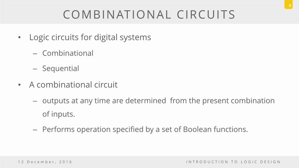
COMBINATIONAL CIRCUITS
• Logic circuits for digital systems
– Combinational
– Sequential
• A combinational circuit
– outputs at any time are determined from the present combination
of inputs.
– Performs operation specified by a set of Boolean functions.
1 2 D e c e m b e r , 2 0 1 6 I N T R O D U C T I O N T O L O G I C D E S I G N
4

COMBINATIONAL CIRCUITS
• Sequential circuits
– Employ storage elements in addition to logic gates.
– Their outputs are a function of inputs and state of the storage
elements.
– Not only present values of inputs, but also on past inputs.
– Circuit behaviour must be specified by a time sequence of inputs
and internal states.
1 2 D e c e m b e r , 2 0 1 6 I N T R O D U C T I O N T O L O G I C D E S I G N
5

COMBINATIONAL CIRCUITS
• Combinational circuit consist of
– Input variables
– Logic gates
• Accept signals from the inputs
• Generate signals to the output
– Output variables
1 2 D e c e m b e r , 2 0 1 6 I N T R O D U C T I O N T O L O G I C D E S I G N
6

COMBINATIONAL CIRCUITS
• For n input variable, there are 2n possible binary input
combinations.
• For each possible input combination there is one possible input
output value.
1 2 D e c e m b e r , 2 0 1 6 I N T R O D U C T I O N T O L O G I C D E S I G N
7
Combinational Circuit
n inputs m outputs

COMBINATIONAL CIRCUITS
• Analysis
– Given a circuit, find out its function
– Function may be expressed as:
• Boolean function
• Truth table
• Design
– Given a desired function, determine its circuit
– Function may be expressed as:
• Boolean function
• Truth table
1 2 D e c e m b e r , 2 0 1 6 I N T R O D U C T I O N T O L O G I C D E S I G N
8
? ?
C
BA
C
BA
BA
CA
CB
F1
F2
?

4.2 ANALYSIS PROCEDURE
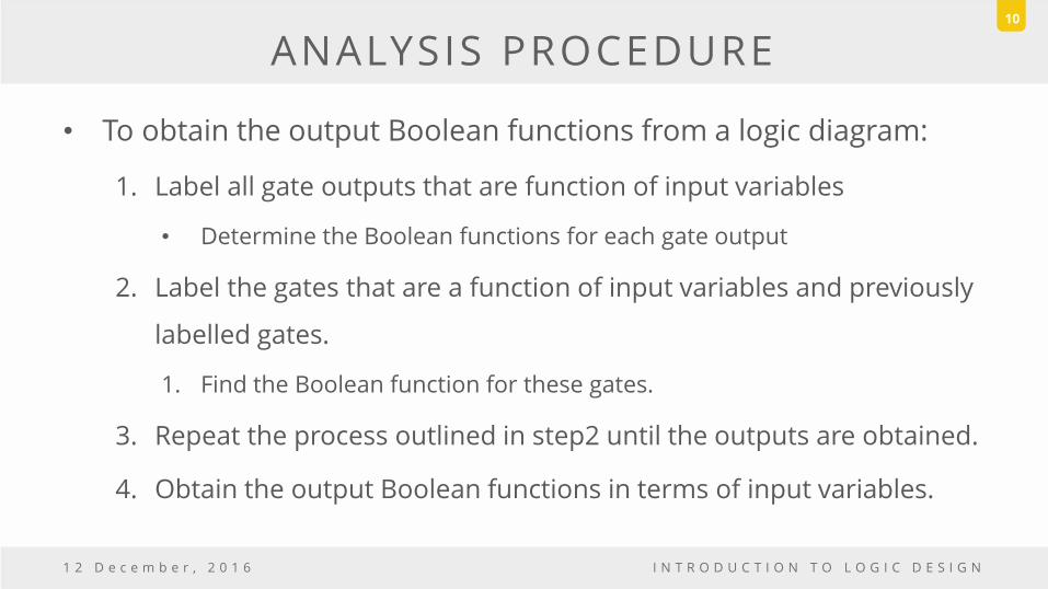
ANALYSIS PROCEDURE
• To obtain the output Boolean functions from a logic diagram:
1. Label all gate outputs that are function of input variables
• Determine the Boolean functions for each gate output
2. Label the gates that are a function of input variables and previously
labelled gates.
1. Find the Boolean function for these gates.
3. Repeat the process outlined in step2 until the outputs are obtained.
4. Obtain the output Boolean functions in terms of input variables.
1 2 D e c e m b e r , 2 0 1 6 I N T R O D U C T I O N T O L O G I C D E S I G N
10

ANALYSIS PROCEDURE
• Boolean expression approach
1 2 D e c e m b e r , 2 0 1 6 I N T R O D U C T I O N T O L O G I C D E S I G N
11
C
BA
C
BA
BA
CA
CB
F1
F2
A.B.C
A+B+C
A.B
B.C
A.C A.B+A.C+B.C
(A.B+A.C+B.C)'
(A.B+A.C+B.C)‘.A+B+C
(A.B+A.C+B.C)‘.A+B+C+A.B.C

• Boolean expression
approach
• T1 = A+B+C
• T2 = A.B.C
• F2 = A.B+A.C+B.C
• F2’ = (A’+B’)(A’+C’)(B’+C’) = (A’ + B’C’).(B’+C’) post4b
• T3 = F2’ . T1
• T3 = (A’+B’C’).(B’+C’).(A+B+C)
• T3 = (A’+B’C’).(AB’+B’C+AC’+BC’)
• T3 = (A’.A.B’+A’.B’.C+A’.A.C’+A’.B.C’+
• A.B’.B’.C’+B’.B’.C’.C+A.B’.C’.C’+B’.B.C’.C’)
• T3 =A’.B’.C + A’.B.C’ + A.B’.C’ + A.B’.C’
• T3 = A’.B’.C + A’.B.C’ + A.B’C’
• F1= T3+T2
• F1 = A’.B’.C + A’.B.C’ + A.B’C’ + A.B.C
1 2 D e c e m b e r , 2 0 1 6 I N T R O D U C T I O N T O L O G I C D E S I G N
ANALYSIS PROCEDURE 12
C
BA
C
BA
BA
CA
CB
F1
F2
T2
T1
F2
F2’
T3

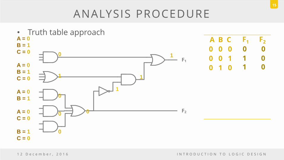
ANALYSIS PROCEDURE
• Truth table approach
1 2 D e c e m b e r , 2 0 1 6 I N T R O D U C T I O N T O L O G I C D E S I G N
13
F1
F2
A B C F1 F2
0 0 0
A = 0
B = 0
C = 0
A = 0
B = 0
C = 0
A = 0
B = 0
A = 0
C = 0
B = 0
C = 0
0
0
0
0
0
0
1
0
0 0 0

ANALYSIS PROCEDURE
• Truth table approach
1 2 D e c e m b e r , 2 0 1 6 I N T R O D U C T I O N T O L O G I C D E S I G N
14
F1
F2
A B C F1 F2
0 0 0
0 0 1
A = 0
B = 0
C = 1
A = 0
B = 0
C = 1
A = 0
B = 0
A = 0
C = 1
B = 0
C = 1
0
1
0
0
0
0
1
1
1 0 0
1 0
ANALYSIS PROCEDURE
• Truth table approach
1 2 D e c e m b e r , 2 0 1 6 I N T R O D U C T I O N T O L O G I C D E S I G N
15
F1
F2
A B C F1 F2
0 0 0
0 0 1
0 1 0
A = 0
B = 1
C = 0
A = 0
B = 1
C = 0
A = 0
B = 1
A = 0
C = 0
B = 1
C = 0
0
1
0
0
0
0
1
1
1 0 0
1 0 1 0

ANALYSIS PROCEDURE
• Truth table approach
1 2 D e c e m b e r , 2 0 1 6 I N T R O D U C T I O N T O L O G I C D E S I G N
16
F1
F2
A B C F1 F2
0 0 0
0 0 1
0 1 0
0 1 0
A = 0
B = 1
C = 1
A = 0
B = 1
C = 1
A = 0
B = 1
A = 0
C = 1
B = 1
C = 1
0
1
0
0
1
1
0
0
0 0 0
1 0 1 0
0 1
ANALYSIS PROCEDURE
• Truth table approach
1 2 D e c e m b e r , 2 0 1 6 I N T R O D U C T I O N T O L O G I C D E S I G N
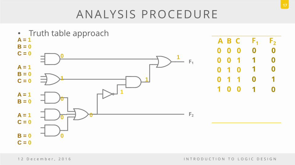
17
F1
F2
A B C F1 F2
0 0 0
0 0 1
0 1 0
0 1 1
1 0 0
A = 1
B = 0
C = 0
A = 1
B = 0
C = 0
A = 1
B = 0
A = 1
C = 0
B = 0
C = 0
0
1
0
0
0
0
1
1
1 0 0
1 0 1 0
0 1
1 0
ANALYSIS PROCEDURE
• Truth table approach
1 2 D e c e m b e r , 2 0 1 6 I N T R O D U C T I O N T O L O G I C D E S I G N
18
F1
F2
A B C F1 F2
0 0 0
0 0 1
0 1 0
0 1 1
1 0 0
1 0 1
A = 1
B = 0
C = 1
A = 1
B = 0
C = 1
A = 1
B = 0
A = 1
C = 1
B = 0
C = 1
0
1
0
1
0
1
0
0
0 0 0
1 0 1 0
0 1
1 0
0 1
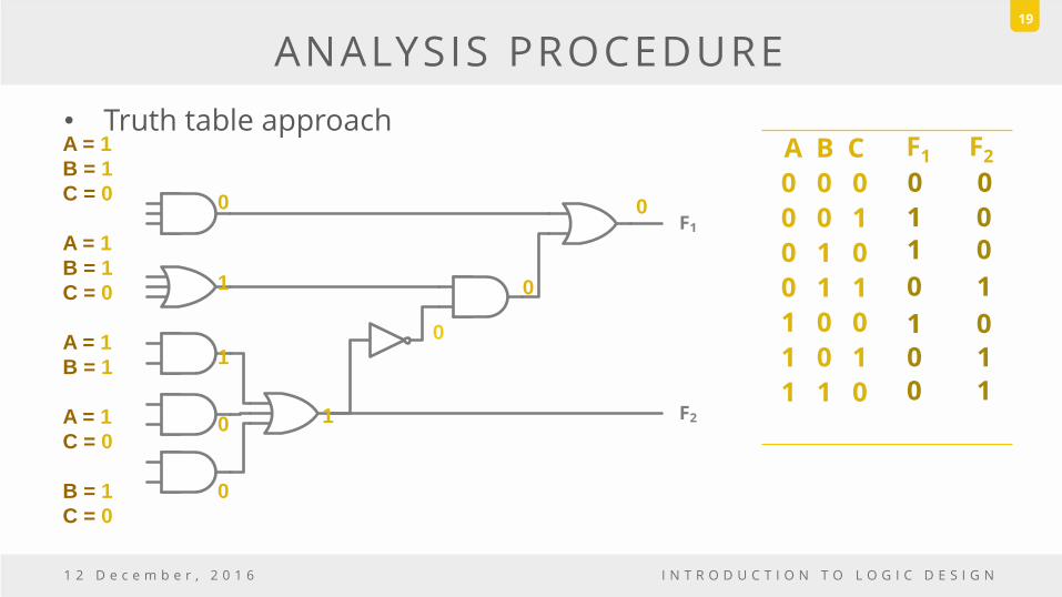
ANALYSIS PROCEDURE
• Truth table approach
1 2 D e c e m b e r , 2 0 1 6 I N T R O D U C T I O N T O L O G I C D E S I G N
19
F1
F2
A B C F1 F2
0 0 0
0 0 1
0 1 0
0 1 1
1 0 0
1 0 1
1 1 0
A = 1
B = 1
C = 0
A = 1
B = 1
C = 0
A = 1
B = 1
A = 1
C = 0
B = 1
C = 0
0
1
1
0
0
1
0
0
0 0 0
1 0 1 0
0 1
1 0
0 1
0 1

ANALYSIS PROCEDURE
• Truth table approach
1 2 D e c e m b e r , 2 0 1 6 I N T R O D U C T I O N T O L O G I C D E S I G N
20
F1
F2
A B C F1 F2
0 0 0
0 0 1
0 1 0
0 1 1
1 0 0
1 0 1
1 1 0
1 1 1
A = 1
B = 1
C = 1
A = 1
B = 1
C = 1
A = 1
B = 1
A = 1
C = 1
B = 1
C = 1
1
1
1
1
1
1
0
0
1 0 0
1 0 1 0
0 1
1 0
0 1
0 1
1 1
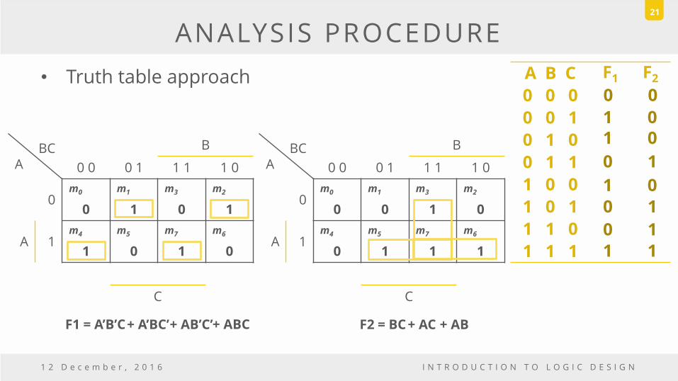
ANALYSIS PROCEDURE
• Truth table approach
1 2 D e c e m b e r , 2 0 1 6 I N T R O D U C T I O N T O L O G I C D E S I G N
21
A B C F1 F2
0 0 0
0 0 1
0 1 0
0 1 1
1 0 0
1 0 1
1 1 0
1 1 1
0 0
1 0 1 0
0 1
1 0
0 1
0 1
1 1
BC A
B
0 0 0 1 1 1 1 0
0 m0 m1 m3 m2
0 1 0 1
A 1 m4 m5 m7 m6
1 0 1 0
C
BC A
B
0 0 0 1 1 1 1 0
0 m0 m1 m3 m2
0 0 1 0
A 1 m4 m5 m7 m6
0 1 1 1
C
F1 = A’B’C + A’BC’ + AB’C’ + ABC F2 = BC + AC + AB

4.3 DESIGN PROCEDURE

DESIGN PROCEDURE
• For a given a problem statement:
– Determine the number of inputs and outputs
– Derive the truth table
– Simplify the Boolean expression for each output
– Produce the required circuit
1 2 D e c e m b e r , 2 0 1 6 I N T R O D U C T I O N T O L O G I C D E S I G N
23

DESIGN PROCEDURE
• A truth table for a combinational circuit consist of:
– Input columns
• Obtained from 2n binary numbers for the n input variables.
– Output columns
• Determined from the stated specifications.
• Output functions specified in the truth table give exact definition of the
combinational circuit.
1 2 D e c e m b e r , 2 0 1 6 I N T R O D U C T I O N T O L O G I C D E S I G N
24

DESIGN PROCEDURE
• The output binary functions listed in the truth table are
simplified by any method:
– Algebraic manipulation
– The map method
– Computer – based simplification program
• There is a variety of simplified expressions from which to choose.
1 2 D e c e m b e r , 2 0 1 6 I N T R O D U C T I O N T O L O G I C D E S I G N
25

DESIGN PROCEDURE
• Practical design must consider such constraints:
– The number of gates
– Number of inputs to a gate
– Propagation time of the signal through the gates
– Number of interconnections
– Limitations of the driving capability of each gate
– Etc.
1 2 D e c e m b e r , 2 0 1 6 I N T R O D U C T I O N T O L O G I C D E S I G N
26

DESIGN PROCEDURE
Code conversion example
• Code converter is a circuit that makes the two systems
compatible even though each uses a different binary code.
• To convert from binary code A to binary code B;
1 2 D e c e m b e r , 2 0 1 6 I N T R O D U C T I O N T O L O G I C D E S I G N
27
Combinational Circuit
Input: supply the bit combination of elements specified by code A
Output: generate the corresponding bit combination of code B.

DESIGN PROCEDURE
Example:
• Design a circuit to convert a “BCD” code to “Excess 3” code.
1 2 D e c e m b e r , 2 0 1 6 I N T R O D U C T I O N T O L O G I C D E S I G N
28
Combinational Circuit
BCD: 4 – bits 0 – 9 values
Excess 3: 4 – bits Value +3

1 2 D e c e m b e r , 2 0 1 6 I N T R O D U C T I O N T O L O G I C D E S I G N
DESIGN PROCEDURE 29
• Each code uses 4-bits to represent
a decimal digit.
– 4 input variables
• A, B, C, D
– 4 output variables
• w, x, y, z
– 24 = 16 bit combinations but
only 10 have meaning in BCD.
– Rest 6 bit combinations are
don’t-care combinations.
Input BCD Output Excess-3
A B C D w x y z
0 0 0 0 0 0 1 1
0 0 0 1 0 1 0 0
0 0 1 0 0 1 0 1
0 0 1 1 0 1 1 0
0 1 0 0 0 1 1 1
0 1 0 1 1 0 0 0
0 1 1 0 1 0 0 1
0 1 1 1 1 0 1 0
1 0 0 0 1 0 1 1
1 0 0 1 1 1 0 0
1 0 1 0 x x x x
1 0 1 1 x x x x
1 1 0 0 x x x x
1 1 0 1 x x x x
1 1 1 0 x x x x
1 1 1 1 x x x x
1 2 D e c e m b e r , 2 0 1 6 I N T R O D U C T I O N T O L O G I C D E S I G N
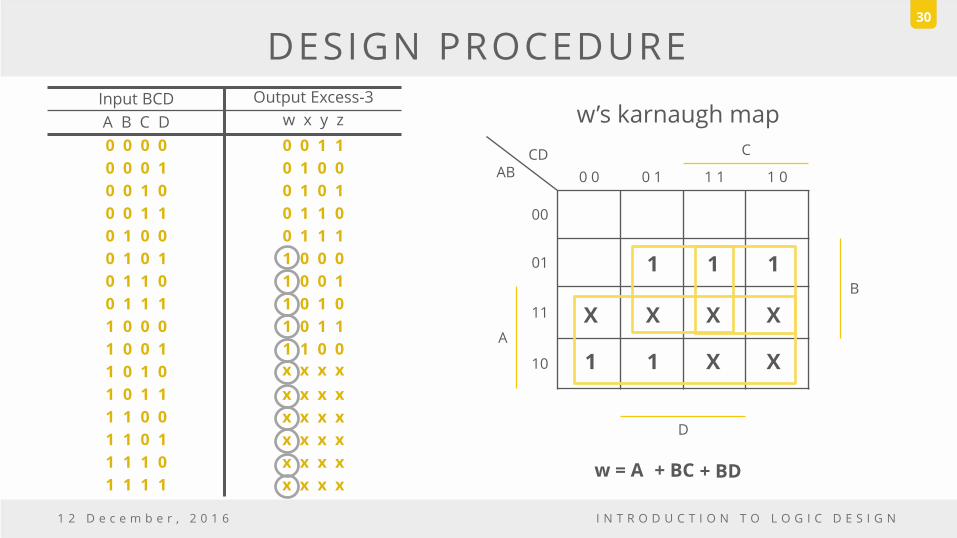
DESIGN PROCEDURE 30
Input BCD Output Excess-3
A B C D w x y z
0 0 0 0 0 0 1 1
0 0 0 1 0 1 0 0
0 0 1 0 0 1 0 1
0 0 1 1 0 1 1 0
0 1 0 0 0 1 1 1
0 1 0 1 1 0 0 0
0 1 1 0 1 0 0 1
0 1 1 1 1 0 1 0
1 0 0 0 1 0 1 1
1 0 0 1 1 1 0 0
1 0 1 0 x x x x
1 0 1 1 x x x x
1 1 0 0 x x x x
1 1 0 1 x x x x
1 1 1 0 x x x x
1 1 1 1 x x x x
CD AB
C
0 0 0 1 1 1 1 0
00
01
B
11
A
10
D
1
X
1 1
1 1
X X X
X X
w = A + BC + BD
w’s karnaugh map

1 2 D e c e m b e r , 2 0 1 6 I N T R O D U C T I O N T O L O G I C D E S I G N
DESIGN PROCEDURE 31
Input BCD Output Excess-3
A B C D w x y z
0 0 0 0 0 0 1 1
0 0 0 1 0 1 0 0
0 0 1 0 0 1 0 1
0 0 1 1 0 1 1 0
0 1 0 0 0 1 1 1
0 1 0 1 1 0 0 0
0 1 1 0 1 0 0 1
0 1 1 1 1 0 1 0
1 0 0 0 1 0 1 1
1 0 0 1 1 1 0 0
1 0 1 0 x x x x
1 0 1 1 x x x x
1 1 0 0 x x x x
1 1 0 1 x x x x
1 1 1 0 x x x x
1 1 1 1 x x x x
CD AB
C
0 0 0 1 1 1 1 0
00
01
B
11
A
10
D
1
X
1 1
1
1
X X X
X X
x = B’C + B’D + BC’D’
x’s karnaugh map
1 2 D e c e m b e r , 2 0 1 6 I N T R O D U C T I O N T O L O G I C D E S I G N
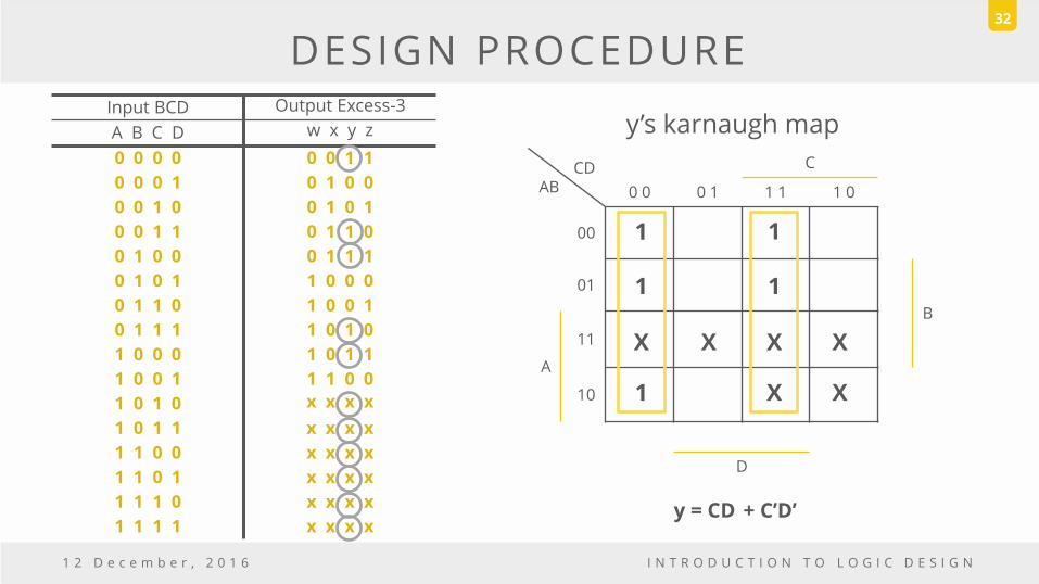
DESIGN PROCEDURE 32
Input BCD Output Excess-3
A B C D w x y z
0 0 0 0 0 0 1 1
0 0 0 1 0 1 0 0
0 0 1 0 0 1 0 1
0 0 1 1 0 1 1 0
0 1 0 0 0 1 1 1
0 1 0 1 1 0 0 0
0 1 1 0 1 0 0 1
0 1 1 1 1 0 1 0
1 0 0 0 1 0 1 1
1 0 0 1 1 1 0 0
1 0 1 0 x x x x
1 0 1 1 x x x x
1 1 0 0 x x x x
1 1 0 1 x x x x
1 1 1 0 x x x x
1 1 1 1 x x x x
CD AB
C
0 0 0 1 1 1 1 0
00
01
B
11
A
10
D
1
X
1
1 1
1
X X X
X X
y = CD + C’D’
y’s karnaugh map

1 2 D e c e m b e r , 2 0 1 6 I N T R O D U C T I O N T O L O G I C D E S I G N
DESIGN PROCEDURE 33
Input BCD Output Excess-3
A B C D w x y z
0 0 0 0 0 0 1 1
0 0 0 1 0 1 0 0
0 0 1 0 0 1 0 1
0 0 1 1 0 1 1 0
0 1 0 0 0 1 1 1
0 1 0 1 1 0 0 0
0 1 1 0 1 0 0 1
0 1 1 1 1 0 1 0
1 0 0 0 1 0 1 1
1 0 0 1 1 1 0 0
1 0 1 0 x x x x
1 0 1 1 x x x x
1 1 0 0 x x x x
1 1 0 1 x x x x
1 1 1 0 x x x x
1 1 1 1 x x x x
CD AB
C
0 0 0 1 1 1 1 0
00
01
B
11
A
10
D
1
X
1
1 1
1
X X X
X X
z = D’
z’s karnaugh map

• w = A + BC + BD = A + B (C + D)
• x = B’C + B’D + BC’D’ = B’ (C+D) +
BC’D’
x = B’ (C + D) + B (C+D)’
• y = CD + C’D’ = CD + (C + D)’
• z = D’
1 2 D e c e m b e r , 2 0 1 6 I N T R O D U C T I O N T O L O G I C D E S I G N
DESIGN PROCEDURE 34
Aw
B
x
C
D
y
z
B(C+D)
B’(C+D)
B(C+D)’
C+D (C+D)’
B’
CD
CD + (C+D)’
D’
C+D
C+D
B
B
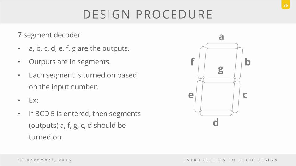
7 segment decoder
• a, b, c, d, e, f, g are the outputs.
• Outputs are in segments.
• Each segment is turned on based
on the input number.
• Ex:
• If BCD 5 is entered, then segments
(outputs) a, f, g, c, d should be
turned on.
1 2 D e c e m b e r , 2 0 1 6 I N T R O D U C T I O N T O L O G I C D E S I G N
DESIGN PROCEDURE 35
a
b
c
g
e
d
f

1 2 D e c e m b e r , 2 0 1 6 I N T R O D U C T I O N T O L O G I C D E S I G N
DESIGN PROCEDURE 36
a
b
c
g
e
d
f
7 segment decoder
w x y z
a b c d e f g

1 2 D e c e m b e r , 2 0 1 6 I N T R O D U C T I O N T O L O G I C D E S I G N
DESIGN PROCEDURE 37
a
b
c
g
e
d
f
Input BCD 7 - segment
w x y z a b c d e f g
0 0 0 0 1 1 1 1 1 1 0
0 0 0 1 0 1 1 0 0 0 0
0 0 1 0 1 1 0 1 1 0 1
0 0 1 1 1 1 1 1 0 0 1
0 1 0 0 0 1 1 0 0 1 1
0 1 0 1 1 0 1 1 0 1 1
0 1 1 0 1 0 1 1 1 1 1
0 1 1 1 1 1 1 0 0 0 0
1 0 0 0 1 1 1 1 1 1 1
1 0 0 1 1 1 1 1 0 1 1
1 0 1 0 X X X X X X X
1 0 1 1 X X X X X X X
1 1 0 0 X X X X X X X
1 1 0 1 X X X X X X X
1 1 1 0 X X X X X X X
1 1 1 1 X X X X X X X
0 1 2 3 4 5 6 7 8 9

1 2 D e c e m b e r , 2 0 1 6 I N T R O D U C T I O N T O L O G I C D E S I G N
DESIGN PROCEDURE 38
Input BCD 7 - segment
w x y z a b c d e f g
0 0 0 0 1 1 1 1 1 1 0
0 0 0 1 0 1 1 0 0 0 0
0 0 1 0 1 1 0 1 1 0 1
0 0 1 1 1 1 1 1 0 0 1
0 1 0 0 0 1 1 0 0 1 1
0 1 0 1 1 0 1 1 0 1 1
0 1 1 0 1 0 1 1 1 1 1
0 1 1 1 1 1 1 0 0 0 0
1 0 0 0 1 1 1 1 1 1 1
1 0 0 1 1 1 1 1 0 1 1
1 0 1 0 X X X X X X X
1 0 1 1 X X X X X X X
1 1 0 0 X X X X X X X
1 1 0 1 X X X X X X X
1 1 1 0 X X X X X X X
1 1 1 1 X X X X X X X
yz wx
y
0 0 0 1 1 1 1 0
00
01
x
11
w
10
z
1
X
1 1
1 1
X X X
X X
a = w + y + x z
a’s karnaugh map
1
1 1
+ x’ z’

1 2 D e c e m b e r , 2 0 1 6 I N T R O D U C T I O N T O L O G I C D E S I G N
DESIGN PROCEDURE 39
Input BCD 7 - segment
w x y z a b c d e f g
0 0 0 0 1 1 1 1 1 1 0
0 0 0 1 0 1 1 0 0 0 0
0 0 1 0 1 1 0 1 1 0 1
0 0 1 1 1 1 1 1 0 0 1
0 1 0 0 0 1 1 0 0 1 1
0 1 0 1 1 0 1 1 0 1 1
0 1 1 0 1 0 1 1 1 1 1
0 1 1 1 1 1 1 0 0 0 0
1 0 0 0 1 1 1 1 1 1 1
1 0 0 1 1 1 1 1 0 1 1
1 0 1 0 X X X X X X X
1 0 1 1 X X X X X X X
1 1 0 0 X X X X X X X
1 1 0 1 X X X X X X X
1 1 1 0 X X X X X X X
1 1 1 1 X X X X X X X
yz wx
y
0 0 0 1 1 1 1 0
00
01
x
11
w
10
z
1
X
1 1 1
1
X X X
X X
b = w + w’x’ + y z
b’s karnaugh map
1
1 1
+ y’ z’

1 2 D e c e m b e r , 2 0 1 6 I N T R O D U C T I O N T O L O G I C D E S I G N
DESIGN PROCEDURE 40
Input BCD 7 - segment
w x y z a b c d e f g
0 0 0 0 1 1 1 1 1 1 0
0 0 0 1 0 1 1 0 0 0 0
0 0 1 0 1 1 0 1 1 0 1
0 0 1 1 1 1 1 1 0 0 1
0 1 0 0 0 1 1 0 0 1 1
0 1 0 1 1 0 1 1 0 1 1
0 1 1 0 1 0 1 1 1 1 1
0 1 1 1 1 1 1 0 0 0 0
1 0 0 0 1 1 1 1 1 1 1
1 0 0 1 1 1 1 1 0 1 1
1 0 1 0 X X X X X X X
1 0 1 1 X X X X X X X
1 1 0 0 X X X X X X X
1 1 0 1 X X X X X X X
1 1 1 0 X X X X X X X
1 1 1 1 X X X X X X X
yz wx
y
0 0 0 1 1 1 1 0
00
01
x
11
w
10
z
1
X
1
1
1
1
X X X
X X
c = w + xy + x’ z
c’s karnaugh map
1 1
1
+ x’ y’
1

1 2 D e c e m b e r , 2 0 1 6 I N T R O D U C T I O N T O L O G I C D E S I G N
DESIGN PROCEDURE 41
Input BCD 7 - segment
w x y z a b c d e f g
0 0 0 0 1 1 1 1 1 1 0
0 0 0 1 0 1 1 0 0 0 0
0 0 1 0 1 1 0 1 1 0 1
0 0 1 1 1 1 1 1 0 0 1
0 1 0 0 0 1 1 0 0 1 1
0 1 0 1 1 0 1 1 0 1 1
0 1 1 0 1 0 1 1 1 1 1
0 1 1 1 1 1 1 0 0 0 0
1 0 0 0 1 1 1 1 1 1 1
1 0 0 1 1 1 1 1 0 1 1
1 0 1 0 X X X X X X X
1 0 1 1 X X X X X X X
1 1 0 0 X X X X X X X
1 1 0 1 X X X X X X X
1 1 1 0 X X X X X X X
1 1 1 1 X X X X X X X
yz wx
y
0 0 0 1 1 1 1 0
00
01
x
11
w
10
z
1
X
1 1
1
X X X
X X
d = w + yz’ + w’x’ y
d’s karnaugh map
1
1
+ x y’z
1
+ x’z’
1 2 D e c e m b e r , 2 0 1 6 I N T R O D U C T I O N T O L O G I C D E S I G N
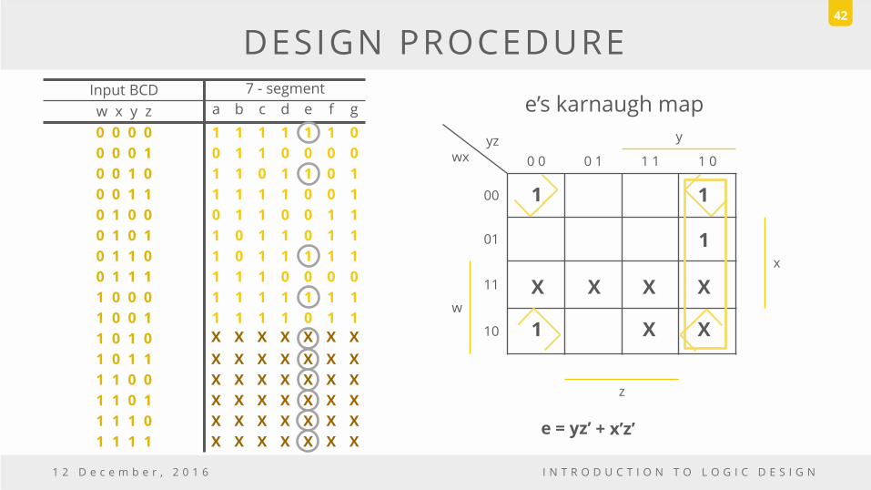
DESIGN PROCEDURE 42
Input BCD 7 - segment
w x y z a b c d e f g
0 0 0 0 1 1 1 1 1 1 0
0 0 0 1 0 1 1 0 0 0 0
0 0 1 0 1 1 0 1 1 0 1
0 0 1 1 1 1 1 1 0 0 1
0 1 0 0 0 1 1 0 0 1 1
0 1 0 1 1 0 1 1 0 1 1
0 1 1 0 1 0 1 1 1 1 1
0 1 1 1 1 1 1 0 0 0 0
1 0 0 0 1 1 1 1 1 1 1
1 0 0 1 1 1 1 1 0 1 1
1 0 1 0 X X X X X X X
1 0 1 1 X X X X X X X
1 1 0 0 X X X X X X X
1 1 0 1 X X X X X X X
1 1 1 0 X X X X X X X
1 1 1 1 X X X X X X X
yz wx
y
0 0 0 1 1 1 1 0
00
01
x
11
w
10
z
1
X
1
X X X
X X
e = yz’
e’s karnaugh map
1
1
+ x’z’
1 2 D e c e m b e r , 2 0 1 6 I N T R O D U C T I O N T O L O G I C D E S I G N
DESIGN PROCEDURE 43
Input BCD 7 - segment
w x y z a b c d e f g
0 0 0 0 1 1 1 1 1 1 0
0 0 0 1 0 1 1 0 0 0 0
0 0 1 0 1 1 0 1 1 0 1
0 0 1 1 1 1 1 1 0 0 1
0 1 0 0 0 1 1 0 0 1 1
0 1 0 1 1 0 1 1 0 1 1
0 1 1 0 1 0 1 1 1 1 1
0 1 1 1 1 1 1 0 0 0 0
1 0 0 0 1 1 1 1 1 1 1
1 0 0 1 1 1 1 1 0 1 1
1 0 1 0 X X X X X X X
1 0 1 1 X X X X X X X
1 1 0 0 X X X X X X X
1 1 0 1 X X X X X X X
1 1 1 0 X X X X X X X
1 1 1 1 X X X X X X X
yz wx
y
0 0 0 1 1 1 1 0
00
01
x
11
w
10
z
1
X
1 1
X X X
X X
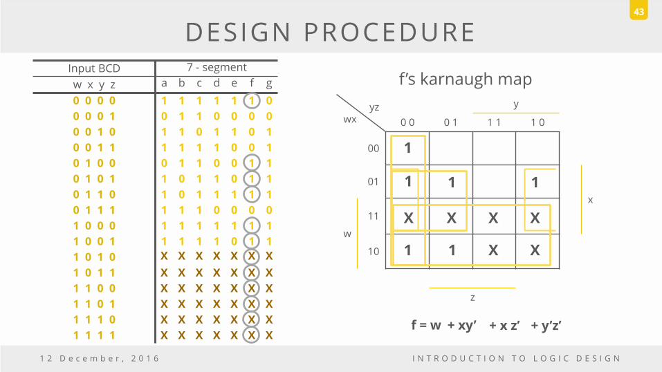
f = w + xy’ + x z’
f’s karnaugh map
1
1
+ y’z’
1

1 2 D e c e m b e r , 2 0 1 6 I N T R O D U C T I O N T O L O G I C D E S I G N
DESIGN PROCEDURE 44
Input BCD 7 - segment
w x y z a b c d e f g
0 0 0 0 1 1 1 1 1 1 0
0 0 0 1 0 1 1 0 0 0 0
0 0 1 0 1 1 0 1 1 0 1
0 0 1 1 1 1 1 1 0 0 1
0 1 0 0 0 1 1 0 0 1 1
0 1 0 1 1 0 1 1 0 1 1
0 1 1 0 1 0 1 1 1 1 1
0 1 1 1 1 1 1 0 0 0 0
1 0 0 0 1 1 1 1 1 1 1
1 0 0 1 1 1 1 1 0 1 1
1 0 1 0 X X X X X X X
1 0 1 1 X X X X X X X
1 1 0 0 X X X X X X X
1 1 0 1 X X X X X X X
1 1 1 0 X X X X X X X
1 1 1 1 X X X X X X X
yz wx
y
0 0 0 1 1 1 1 0
00
01
x
11
w
10
z
1
X
1 1
X X X
X X
g = w + xy’ + x z’
g’s karnaugh map
1
1
+ x’y
1
1

4.4 BINARY ADDER - SUBTRACTOR

BINARY ADDER - SUBTRACTOR
• The most basic arithmetic operation is the addition of two binary digits.
• Simple addition consists of 4 possible elementary operations:
– 0 + 0 = 0
– 0 + 1 = 1
– 1 + 0 = 1
– 1 + 1 = 10
• First 3 operations produce a sum of one digit.
• In the 4th operation, the binary sum consists of two digits.
1 2 D e c e m b e r , 2 0 1 6 I N T R O D U C T I O N T O L O G I C D E S I G N
46

BINARY ADDER - SUBTRACTOR
• The higher significant bit is called a carry.
• A combinational circuit that performs the addition of two bits is called a
half adder.
• One that performs the addition of three bits (two significant bits and a
previous carry) is a full adder.
• Two half adders can be employed to implement a full adder.
1 2 D e c e m b e r , 2 0 1 6 I N T R O D U C T I O N T O L O G I C D E S I G N
47

Half Adder
• Adds 2 bits
– 2 inputs
– 2 outputs
• Produces SUM and CARRY.
x y C S
0 0 0 0
0 1 0 1
1 0 0 1
1 1 1 0
1 2 D e c e m b e r , 2 0 1 6 I N T R O D U C T I O N T O L O G I C D E S I G N
BINARY ADDER - SUBTRACTOR 48
HA x
y
SUM (S)
CARRY (C)
S = x’y + xy’
C = xy
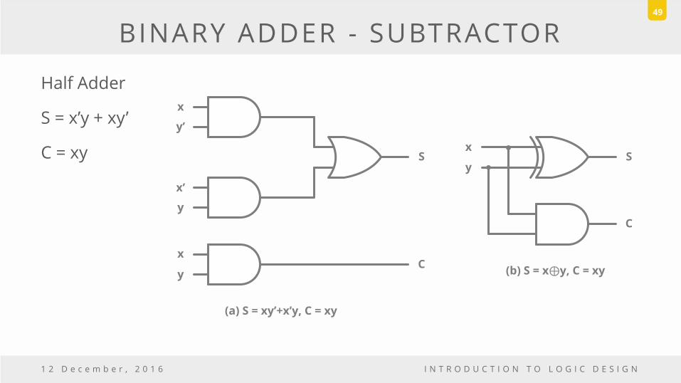
BINARY ADDER - SUBTRACTOR
Half Adder
S = x’y + xy’
C = xy
1 2 D e c e m b e r , 2 0 1 6 I N T R O D U C T I O N T O L O G I C D E S I G N
49
x
y’
x’
y
x
y
S
C
(a) S = xy’+x’y, C = xy
x
yS
C
(b) S = x⊕y, C = xy

Full Adder
• Adds 3 bits
– 3 inputs
– 2 outputs
• Produces SUM and CARRY.
x y z C S
0 0 0 0 0
0 0 1 0 1
0 1 0 0 1
0 1 1 1 0
1 0 0 0 1
1 0 1 1 0
1 1 0 1 0
1 1 1 1 1
1 2 D e c e m b e r , 2 0 1 6 I N T R O D U C T I O N T O L O G I C D E S I G N
BINARY ADDER - SUBTRACTOR 50
FA
x
y SUM (S)
CARRY (C)
S = x’y’z + x’yz
C = x’yz
z
+ xy’z’ + xyz
+ xy’z + xyz’ + xyz
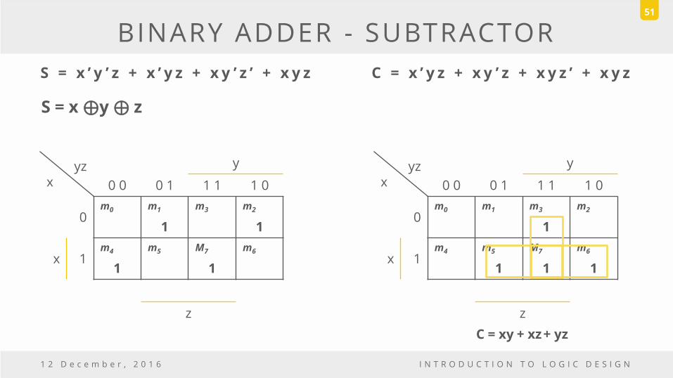
S = x ’ y ’ z + x ’ y z + x y ’ z ’ + x y z
C = x ’ y z + x y ’ z + x y z ’ + x y z
1 2 D e c e m b e r , 2 0 1 6 I N T R O D U C T I O N T O L O G I C D E S I G N
51
BINARY ADDER - SUBTRACTOR
yz x
y
0 0 0 1 1 1 1 0
0 m0 m1 m3 m2
1 1
x 1 m4 m5 M7 m6
1 1
z
yz x
y
0 0 0 1 1 1 1 0
0 m0 m1 m3 m2
1
x 1 m4 m5 M7 m6
1 1 1
z
C = xy + xz + yz
S = x ⊕y ⊕ z

Full adder implementation:
• S = x’y’z + x’yz + xy’z’ + xyz
• S = x ⊕y ⊕ z
• C = x’yz + xy’z + xyz’ + xyz
1 2 D e c e m b e r , 2 0 1 6 I N T R O D U C T I O N T O L O G I C D E S I G N
BINARY ADDER - SUBTRACTOR 52
SS
CC
x’y’z
x’yz’
xy’z’
xyz
x
y
x
z
y
z
S
x
y
z
C
x
y
x
z
y
z
x
y
z
x
y
z

BINARY ADDER - SUBTRACTOR
• Implementation of Full Adder with Two Half Adders and an OR gate
1 2 D e c e m b e r , 2 0 1 6 I N T R O D U C T I O N T O L O G I C D E S I G N
53
x
y S
Cz

BINARY ADDER - SUBTRACTOR
Binary Adder:
• Digital circuit that produces the arithmetic sum of two binary numbers.
• It can be constructed with full adders connected in cascade.
• The output carry from each full adder connected to the input carry of
the next full adder in the chain.
1 2 D e c e m b e r , 2 0 1 6 I N T R O D U C T I O N T O L O G I C D E S I G N
54
Binary Adder
x3x2x1x0 y3y2y1y0
S3S2S1S0
C0 Cy
c3 c2 c1 .
+ x3 x2 x1 x0 + y3 y2 y1 y0 ────────
Cy S3 S2 S1 S0
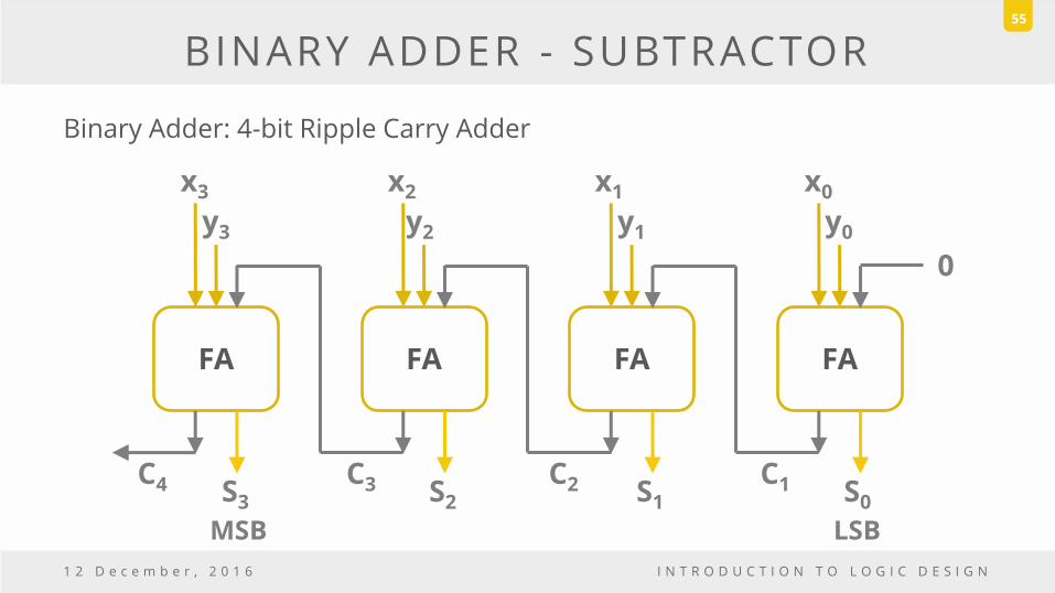
BINARY ADDER - SUBTRACTOR
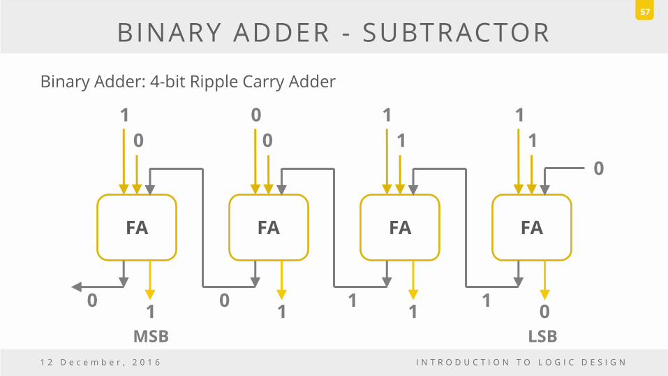
Binary Adder: 4-bit Ripple Carry Adder
1 2 D e c e m b e r , 2 0 1 6 I N T R O D U C T I O N T O L O G I C D E S I G N
55
FA
x0
FA FA FA
y0
S0
C1
0
x1 x2 x3
y1 y2 y3
S1 S2 S3
C2 C3 C4
LSB MSB

BINARY ADDER - SUBTRACTOR
• The S outputs generate the required sum bits.
• An n-bit adder requires n full adders with each output carry connected
to the input carry of the next higher-order full adder.
• Example: A = 1011 and B = 0011.
1 2 D e c e m b e r , 2 0 1 6 I N T R O D U C T I O N T O L O G I C D E S I G N
56
Subscript i: 3 2 1 0
Input carry Ci
Augend Ai
Addend Bi
Sum Si
Output Carry Ci+1
1
1
1
1
0
0
1
0
0 1 1 1
1 1 0 0
0 1 1 0
BINARY ADDER - SUBTRACTOR
Binary Adder: 4-bit Ripple Carry Adder
1 2 D e c e m b e r , 2 0 1 6 I N T R O D U C T I O N T O L O G I C D E S I G N
57
FA
1
FA FA FA
1
0
1
0
1 0 1
1 0 0
1 1 1
1 0 0
LSB MSB

BINARY ADDER - SUBTRACTOR
Carry propagation
• The addition of two binary numbers in parallel implies that all the bits of the
augend and addend are available at the same time.
• Signals must propagate through the gates before the correct output sum is
available in the output terminals.
• The total propagation time
– = propagation delay of a typical gate x the number of gate levels in the circuit.
• Longest propagation delay time in an adder is the time it takes the
carry to propagate through the full adders.
1 2 D e c e m b e r , 2 0 1 6 I N T R O D U C T I O N T O L O G I C D E S I G N
58

BINARY ADDER - SUBTRACTOR
Carry propagation
• Since each bit of the sum output depends on the value of the input
carry, the value of Si in any given stage in the adder will in its steady
state final value only after the input carry to that stage has been
propagated.
1 2 D e c e m b e r , 2 0 1 6 I N T R O D U C T I O N T O L O G I C D E S I G N
59
BINARY ADDER - SUBTRACTOR
Carry propagation
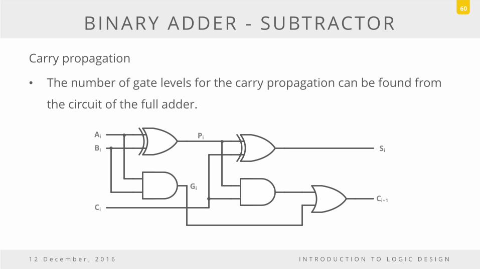
• The number of gate levels for the carry propagation can be found from
the circuit of the full adder.
1 2 D e c e m b e r , 2 0 1 6 I N T R O D U C T I O N T O L O G I C D E S I G N
60
Ai
Bi Si
Ci+1
Ci
Pi
Gi
BINARY ADDER - SUBTRACTOR
Carry propagation
• The signal from the input carry Ci to the output carry Ci+1, propagates
through
– an AND gate and an OR gate,
– which constitute two gate levels.
• If there are 4 full adders in the adder, the output carry C4 would have
– 2 x 4 = 8 gate levels from C0 to C4.
• For an n-bit adder, there are 2n gate levels for the carry to
propagate from input to output.
1 2 D e c e m b e r , 2 0 1 6 I N T R O D U C T I O N T O L O G I C D E S I G N
61
BINARY ADDER - SUBTRACTOR
• The carry propagation time is a limiting factor on the speed with which
two numbers are added.
• Since all other arithmetic operations are implemented by successive
additions, the time consumed during the addition process is very critical.
• Reduce the carry propagation delay
– Employ faster gates
– Look-ahead carry (more complex mechanism, yet faster)
1 2 D e c e m b e r , 2 0 1 6 I N T R O D U C T I O N T O L O G I C D E S I G N
62

• Consider
• Two new variables:
– Pi = Ai Bi
– Gi = Ai . Bi
• Sum = Pi Ci
• Carry = Gi + Pi Ci
1 2 D e c e m b e r , 2 0 1 6 I N T R O D U C T I O N T O L O G I C D E S I G N
BINARY ADDER - SUBTRACTOR 63
Ai
Bi Si
Ci+1
Ci
Pi
Gi
BINARY ADDER - SUBTRACTOR
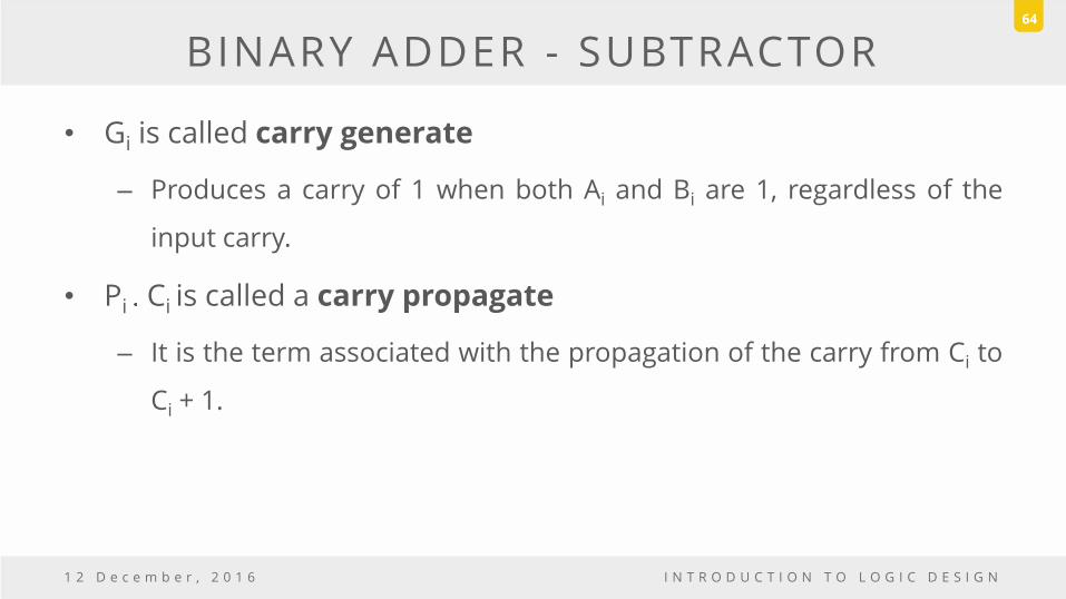
• Gi is called carry generate
– Produces a carry of 1 when both Ai and Bi are 1, regardless of the
input carry.
• Pi Ci is called a carry propagate
– It is the term associated with the propagation of the carry from Ci to
Ci + 1.
1 2 D e c e m b e r , 2 0 1 6 I N T R O D U C T I O N T O L O G I C D E S I G N
64

BINARY ADDER - SUBTRACTOR
• Boolean functions for the carry outputs of each stage:
– C0 = input carry
– C1 = G0 + P0 . C0
– C2 = G1 + P1. C1 = G1 + P1 (G0 + P0 . C0)
= G1 + P1 . G0 + P1 . P0 . C0
– C3 = G2 + P2 . C2 = G2 + P2 (G1 + P1 . G0 + P1 . P0 . CO)
= G2 + P2 . G1 + P2 . P1 . G0 + P2 . P1 . P0 . C0
1 2 D e c e m b e r , 2 0 1 6 I N T R O D U C T I O N T O L O G I C D E S I G N
65

BINARY ADDER - SUBTRACTOR
• Carry Lookahead Generator
1 2 D e c e m b e r , 2 0 1 6 I N T R O D U C T I O N T O L O G I C D E S I G N
66
G0
C0
P0
G1
P1
G2
P2
C3
C2
C1
• C3 does not have to wait for C2 and
C1 to propagate.
• C3 is propagated at the same time as
C1 and C2.

BINARY ADDER - SUBTRACTOR
• 4-Bit Adder with Carry Lookahead Generator
1 2 D e c e m b e r , 2 0 1 6 I N T R O D U C T I O N T O L O G I C D E S I G N
67
• Each sum output requires two XOR gates.
• First XOR gate generates the Pi
• AND gate generates the Gi variable.
• Carries are propagated through CLA and
applied as an input to the second XOR
gate.
• All output carries are generated after a
delay though two levels of gates. S1
through S3 have equal propagating delay
times.
B3
A3
Carry Look ahead generator
B2
A2
B1
A1
B0
A0 P0
P1
P2
P3
C0
C1
C2
C3
P3
G3
P2
G2
P1
G1
P0
G0
C0
S0
S1
S2
S3
C4C4

BINARY ADDER - SUBTRACTOR
Binary Subtactor
• The subtraction of unsigned binary numbers can be done most
conveniently by means of complements.
• A – B can be performed by taking 2’s complement of B and adding it to A.
• 2’s complement can be done by taking 1’s complement and adding 1.
• 1’s complement can be implemented with inverters.
1 2 D e c e m b e r , 2 0 1 6 I N T R O D U C T I O N T O L O G I C D E S I G N
68

BINARY ADDER - SUBTRACTOR
Binary Subtactor
• Circuit of subtractor consist of:
– An adder
– Inverters
• The input carry C0 = 1 when performing subtraction
• The operation performed becomes:
– A + 1’s complement of B + 1 = A + 2’s complement of B.
– A – B = A + (-B) = A +B’ + 1.
• For unsigned numbers,
– A – B if A ≥ B or 2’s complement of (B – A) if A < B.
1 2 D e c e m b e r , 2 0 1 6 I N T R O D U C T I O N T O L O G I C D E S I G N
69

• XOR gate combines addition and
subtraction into one circuit with
common binary adder.
• Mode input M controls the
operation.
– M = 0 = Addition.
– M = 1 = Subtraction.
1 2 D e c e m b e r , 2 0 1 6 I N T R O D U C T I O N T O L O G I C D E S I G N
BINARY ADDER - SUBTRACTOR 70
B0 A0
C0C1
S0
FA
B1 A1
S1
FA
B2 A2
C3
S2
FA
B3 A3
S3
FAC2
CC4
V
M

• When M = 0 (Addition).
– B ⊕ 0 = B.
– Full adders receive the value of B
– C0 = 0.
– Circuit performs A + B.
• When M = 1 (Subtraction).
– B ⊕ 0 = B’.
– C0 = 1.
– Circuit performs A + B’ + 1
1 2 D e c e m b e r , 2 0 1 6 I N T R O D U C T I O N T O L O G I C D E S I G N
BINARY ADDER - SUBTRACTOR 71
B0 A0
C0C1
S0
FA
B1 A1
S1
FA
B2 A2
C3
S2
FA
B3 A3
S3
FAC2
CC4
V
M
XOR with output V is for detecting an overflow.
BINARY ADDER - SUBTRACTOR
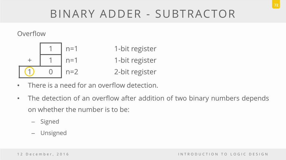
Overflow
• There is a need for an overflow detection.
• The detection of an overflow after addition of two binary numbers depends
on whether the number is to be:
– Signed
– Unsigned
1 2 D e c e m b e r , 2 0 1 6 I N T R O D U C T I O N T O L O G I C D E S I G N
72
1 n=1 1-bit register
+ 1 n=1 1-bit register
1 0 n=2 2-bit register

BINARY ADDER - SUBTRACTOR
Overflow
• Signed
– Left most bit represents the sign bit.
– Negative numbers are in 2’s complement format.
– Sign bit treated as part of the number and the end carry does not
indicate an overflow.
• Unsigned
1 2 D e c e m b e r , 2 0 1 6 I N T R O D U C T I O N T O L O G I C D E S I G N
73

BINARY ADDER - SUBTRACTOR
Overflow
• Unsigned
– When added, overflow is detected from the end carry out of the most
significant position.
• Overflow cannot occur if positive and negative numbers are added.
• Overflow occurs if both numbers are positive or negative.
1 2 D e c e m b e r , 2 0 1 6 I N T R O D U C T I O N T O L O G I C D E S I G N
74
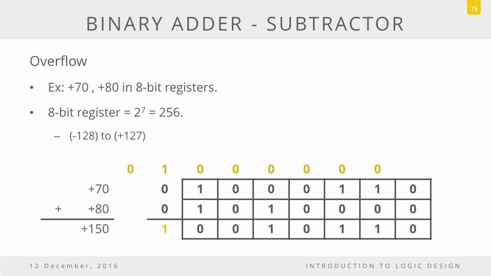
BINARY ADDER - SUBTRACTOR
Overflow
• Ex: +70 , +80 in 8-bit registers.
• 8-bit register = 27 = 256.
– (-128) to (+127)
1 2 D e c e m b e r , 2 0 1 6 I N T R O D U C T I O N T O L O G I C D E S I G N
75
0 1 0 0 0 0 0 0
+70 0 1 0 0 0 1 1 0
+ +80 0 1 0 1 0 0 0 0
+150 1 0 0 1 0 1 1 0

BINARY ADDER - SUBTRACTOR
Overflow
• 8-bit result that should have been positive has a negative sign bit and vice versa.
• If carry out of sign bit is taken as the sign bit of the result then the 8-bit answer will be
correct.
• Since it can not be accommodated within 8-bit register, then there is a overflow.
1 2 D e c e m b e r , 2 0 1 6 I N T R O D U C T I O N T O L O G I C D E S I G N
76
0 1 0 0 0 0 0 0
+70 0 1 0 0 0 1 1 0
+ +80 0 1 0 1 0 0 0 0
+150 1 0 0 1 0 1 1 0
BINARY ADDER - SUBTRACTOR
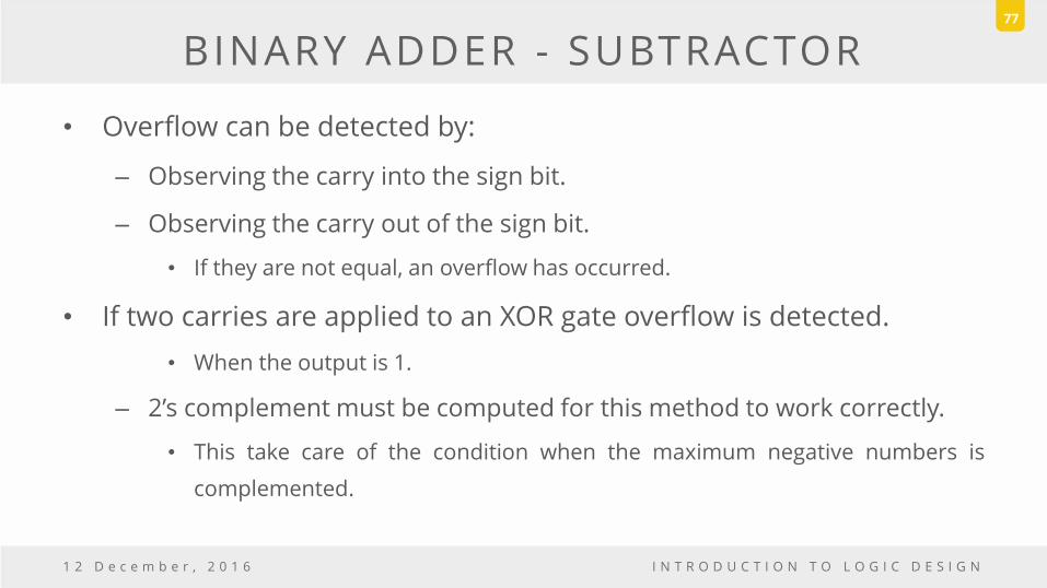
• Overflow can be detected by:
– Observing the carry into the sign bit.
– Observing the carry out of the sign bit.
• If they are not equal, an overflow has occurred.
• If two carries are applied to an XOR gate overflow is detected.
• When the output is 1.
– 2’s complement must be computed for this method to work correctly.
• This take care of the condition when the maximum negative numbers is
complemented.
1 2 D e c e m b e r , 2 0 1 6 I N T R O D U C T I O N T O L O G I C D E S I G N
77

BINARY ADDER - SUBTRACTOR
• If two binary numbers are unsigned
– the C bit detects
• a carry after addition or
• a borrow after subtraction.
• If the numbers are signed, then the V bit detects an overflow.
– If V = 0, then no overflow.
• The n-bit result is correct.
– If V = 1, then result contains n+1 bits only the right most n-bits of the number.
– Overflow has occurred. The (n+1)th bit is the actual sign and has been shifted out
of position.
1 2 D e c e m b e r , 2 0 1 6 I N T R O D U C T I O N T O L O G I C D E S I G N
78

4.5 DECIMAL ADDER

DECIMAL ADDER
• BCD Adder
• Consider the arithmetic addition of two decimal digits in BCD
and an input carry.
• In BCD each input digit does not exceed 9
• Output sum cannot be greater than 9 + 9 + 1 = 19.
– 1 is an input carry.
1 2 D e c e m b e r , 2 0 1 6 I N T R O D U C T I O N T O L O G I C D E S I G N
80

DECIMAL ADDER
• Suppose:
– Two BCD digits applied to a 4-bit binary adder.
– The output produces a result that ranges from 0 through 19.
1 2 D e c e m b e r , 2 0 1 6 I N T R O D U C T I O N T O L O G I C D E S I G N
81
c3 c2 c1 .
+ x3 x2 x1 x0 + y3 y2 y1 y0 ────────
Cy S3 S2 S1 S0

DECIMAL ADDER
1 2 D e c e m b e r , 2 0 1 6 I N T R O D U C T I O N T O L O G I C D E S I G N
82
X +Y x3 x2 x1 x0 y3 y2 y1 y0 Sum Cy S3 S2 S1 S0
0 + 0 0 0 0 0 0 0 0 0 = 0 0 0 0 0 0
0 + 1 0 0 0 0 0 0 0 1 = 1 0 0 0 0 1
0 + 2 0 0 0 0 0 0 1 0 = 2 0 0 0 1 0
0 + 9 0 0 0 0 1 0 0 1 = 9 0 1 0 0 1
1 + 0 0 0 0 1 0 0 0 0 = 1 0 0 0 0 1
1 + 1 0 0 0 1 0 0 0 1 = 2 0 0 0 1 0
1 + 8 0 0 0 1 1 0 0 0 = 9 0 1 0 0 1
1 + 9 0 0 0 1 1 0 0 1 = A 0 1 0 1 0
2 + 0 0 0 1 0 0 0 0 0 = 2 0 0 0 1 0
9 + 9 1 0 0 1 1 0 0 1 = 12 1 0 0 1 0
Invalid Code
Wrong BCD Value
0001 1000
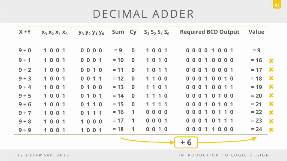
DECIMAL ADDER
1 2 D e c e m b e r , 2 0 1 6 I N T R O D U C T I O N T O L O G I C D E S I G N
83
X +Y x3 x2 x1 x0 y3 y2 y1 y0 Sum Cy S3 S2 S1 S0 Required BCD Output Value
9 + 0 1 0 0 1 0 0 0 0 = 9 0 1 0 0 1 0 0 0 0 1 0 0 1 = 9
9 + 1 1 0 0 1 0 0 0 1 = 10 0 1 0 1 0 0 0 0 1 0 0 0 0 = 16
9 + 2 1 0 0 1 0 0 1 0 = 11 0 1 0 1 1 0 0 0 1 0 0 0 1 = 17
9 + 3 1 0 0 1 0 0 1 1 = 12 0 1 1 0 0 0 0 0 1 0 0 1 0 = 18
9 + 4 1 0 0 1 0 1 0 0 = 13 0 1 1 0 1 0 0 0 1 0 0 1 1 = 19
9 + 5 1 0 0 1 0 1 0 1 = 14 0 1 1 1 0 0 0 0 1 0 1 0 0 = 20
9 + 6 1 0 0 1 0 1 1 0 = 15 0 1 1 1 1 0 0 0 1 0 1 0 1 = 21
9 + 7 1 0 0 1 0 1 1 1 = 16 1 0 0 0 0 0 0 0 1 0 1 1 0 = 22
9 + 8 1 0 0 1 1 0 0 0 = 17 1 0 0 0 1 0 0 0 1 0 1 1 1 = 23
9 + 9 1 0 0 1 1 0 0 1 = 18 1 0 0 1 0 0 0 0 1 1 0 0 0 = 24
+ 6

DECIMAL ADDER
• The problem is to find a rule by which the binary sum is to be
converted to the correct BCD digit representation of the number
in the BCD sum.
1 2 D e c e m b e r , 2 0 1 6 I N T R O D U C T I O N T O L O G I C D E S I G N
84

DECIMAL ADDER
Binary Sum BCD Sum Decimal
K Z3 Z2 Z1 Z0 C S3 S2 S1 S0
0 0 0 0 0 0 0 0 0 0 0
0 0 0 0 1 0 0 0 0 1 1
0 0 0 1 0 0 0 0 1 0 2
0 0 0 1 1 0 0 0 1 1 3
0 0 1 0 0 0 0 1 0 0 4
0 0 1 0 1 0 0 1 0 1 5
0 0 1 1 0 0 0 1 1 0 6
0 0 1 1 1 0 0 1 1 1 7
0 1 0 0 0 0 1 0 0 0 8
0 1 0 0 1 0 1 0 0 1 9
1 2 D e c e m b e r , 2 0 1 6 I N T R O D U C T I O N T O L O G I C D E S I G N
85
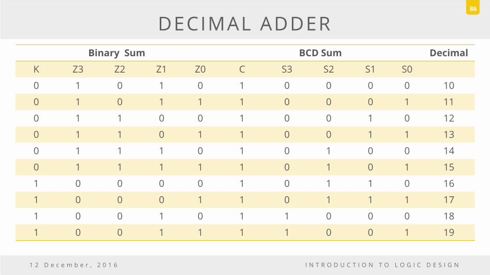
DECIMAL ADDER
Binary Sum BCD Sum Decimal
K Z3 Z2 Z1 Z0 C S3 S2 S1 S0
0 1 0 1 0 1 0 0 0 0 10
0 1 0 1 1 1 0 0 0 1 11
0 1 1 0 0 1 0 0 1 0 12
0 1 1 0 1 1 0 0 1 1 13
0 1 1 1 0 1 0 1 0 0 14
0 1 1 1 1 1 0 1 0 1 15
1 0 0 0 0 1 0 1 1 0 16
1 0 0 0 1 1 0 1 1 1 17
1 0 0 1 0 1 1 0 0 0 18
1 0 0 1 1 1 1 0 0 1 19
1 2 D e c e m b e r , 2 0 1 6 I N T R O D U C T I O N T O L O G I C D E S I G N
86

DECIMAL ADDER
• In examining the contents of the table;
– When the binary SUM = 1001, the corresponding BCD number is
identical.
– When the binary SUM >1001, the BCD number is invalid.
– The addition of 6 (0110) is required.
– Correction is needed when K = 1.
– Correction is needed from 1010 – 1111.
• Z4 = 1,
• Z3 and Z2 must = 1 to distinguish from 1000 and 1001
1 2 D e c e m b e r , 2 0 1 6 I N T R O D U C T I O N T O L O G I C D E S I G N
87

1 2 D e c e m b e r , 2 0 1 6 I N T R O D U C T I O N T O L O G I C D E S I G N
DECIMAL ADDER 88
Z3 Z2 Z1 Z0 Err
0 0 0 0 0
. .
. .
. .
1 0 0 0 0
1 0 0 1 0
1 0 1 0 1
1 0 1 1 1
1 1 0 0 1
1 1 0 1 1
1 1 1 0 1
1 1 1 1 1
Z1Z0
Z3Z2
Z1
0 0 0 1 1 1 1 0
00
01
Z2
11
Z3
10
Z0
1 1 1 1
1 1
Err = Z3Z2 + Z3Z1
Output Carry = K + Z3Z2+ Z3Z1

• When Output carry = 0,
– Nothing is added.
• When Output carry = 1,
– add 0110 to the binary sum.
– provide an output carry for
the next stage.
1 2 D e c e m b e r , 2 0 1 6 I N T R O D U C T I O N T O L O G I C D E S I G N
DECIMAL ADDER 89
Addend
4-bit binary adderCarry
in
4-bit binary adder
Carry out
Output Carry
Augend
0
S0S1S3 S2
K
4.6 BINARY MULTIPLIER

BINARY MULTIPLIER
• Consider; 2-bit number
1 2 D e c e m b e r , 2 0 1 6 I N T R O D U C T I O N T O L O G I C D E S I G N
91
x
+
Multiplicand bits
Multiplier bits
First partial product (AND gate) Second partial product (AND gate)
Product
A0
A1
B0
B1
HAHA
C0C1C2C3
BINARY MULTIPLIER
• For more bits;
– A bit of multiplier is ANDed with each bit of multiplicand in as many
levels as there are bits.
– The binary output of AND gate in each level is added with the partial
product of previous level.
– For J multiplier bits and K multiplicand bits we need
• J x K AND gates.
1 2 D e c e m b e r , 2 0 1 6 I N T R O D U C T I O N T O L O G I C D E S I G N
92

4.7 MAGNITUDE COMPARATOR
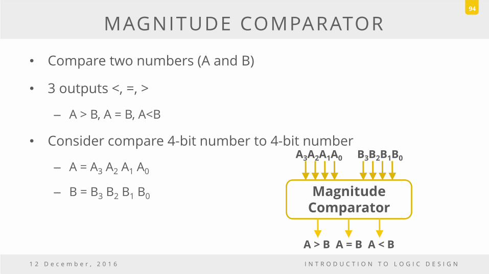
MAGNITUDE COMPARATOR
• Compare two numbers (A and B)
• 3 outputs <, =, >
– A > B, A = B, A<B
• Consider compare 4-bit number to 4-bit number
– A = A3 A2 A1 A0
– B = B3 B2 B1 B0
1 2 D e c e m b e r , 2 0 1 6 I N T R O D U C T I O N T O L O G I C D E S I G N
94
Magnitude Comparator
A3A2A1A0 B3B2B1B0
A > B A = B A < B
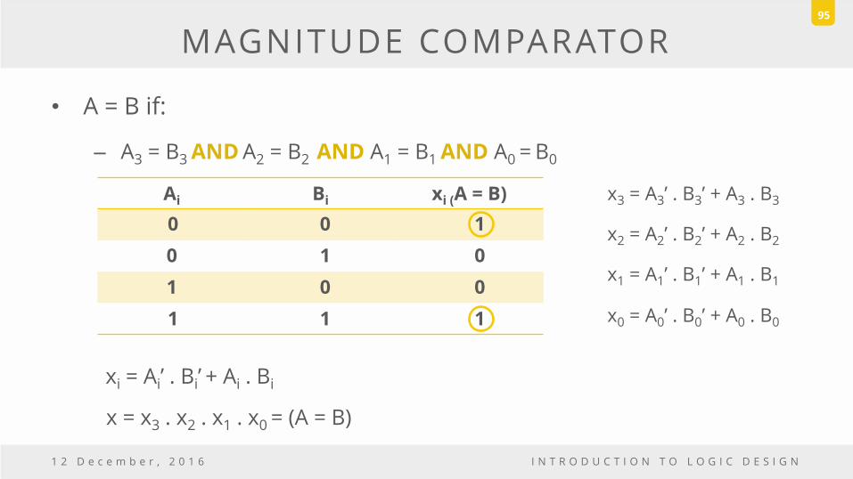
• A = B if:
– A3 = B3 AND A2 = B2 AND A1 = B1 AND A0 = B0
Ai Bi xi (A = B)
MAGNITUDE COMPARATOR
1 2 D e c e m b e r , 2 0 1 6 I N T R O D U C T I O N T O L O G I C D E S I G N
95
1
1
1 1
0
0
0
0
1
1
0
0
xi = Ai’ . Bi’ + Ai . Bi
x = x3 . x2 . x1 . x0 = (A = B)
x3 = A3’ . B3’ + A3 . B3
x2 = A2’ . B2’ + A2 . B2
x1 = A1’ . B1’ + A1 . B1
x0 = A0’ . B0’ + A0 . B0
MAGNITUDE COMPARATOR
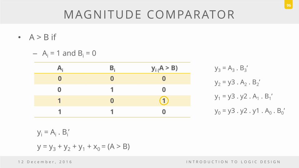
• A > B if
– Ai = 1 and Bi = 0
1 2 D e c e m b e r , 2 0 1 6 I N T R O D U C T I O N T O L O G I C D E S I G N
96
Ai Bi yi (A > B)
1
1
1 1
0
0
0
0
0
0
0
1
yi = Ai . Bi’
y3 = A3 . B3’
y2 = y3 . A2 . B2’
y1 = y3 . y2 . A1 . B1’
y0 = y3 . y2 . y1 . A0 . B0’
y = y3 + y2 + y1 + x0 = (A > B)

MAGNITUDE COMPARATOR
• A < B if
– Ai = 0 and Bi = 1
1 2 D e c e m b e r , 2 0 1 6 I N T R O D U C T I O N T O L O G I C D E S I G N
97
Ai Bi zi (A < B)
1
1
1 1
0
0
0
0
0
0
1
0
zi = Ai’ . Bi
z3 = A3’ . B3
z2 = y3 . A2’ . B2
z1 = y3 . y2 . A1’ . B1
z0 = y3 . y2 . y1 . A0’ . B0
z = z3 + z2 + z1 + z0 = (A < B)

MAGNITUDE COMPARATOR
1 2 D e c e m b e r , 2 0 1 6 I N T R O D U C T I O N T O L O G I C D E S I G N
98
A3
z = (A<B)
B3
A2
B2
A1
B1
A0
B0
y = (A>B)
x=(A=B)
x3
x2
x1
x0

4.8 DECODERS

DECODERS
• Discrete quantities of information are represented in digital
systems by binary codes.
• A binary code of n bits is capable of representing up to 2n distinct
elements of coded information.
• A decoder is a combinational circuit that converts binary
information from n input lines to a maximum of 2n unique
output lines.
1 2 D e c e m b e r , 2 0 1 6 I N T R O D U C T I O N T O L O G I C D E S I G N
100
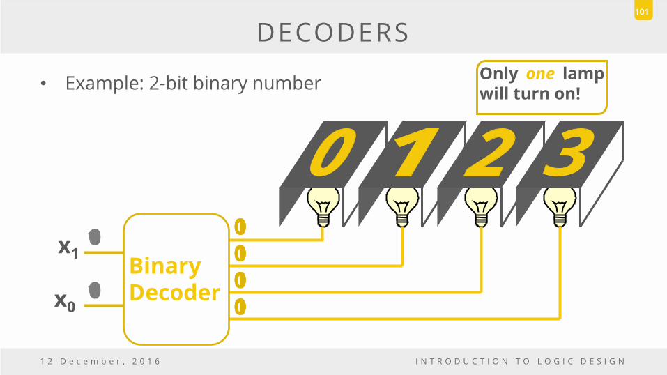
DECODERS
• Example: 2-bit binary number
1 2 D e c e m b e r , 2 0 1 6 I N T R O D U C T I O N T O L O G I C D E S I G N
101
Binary Decoder
x1
x0
Only one lamp will turn on!
0 0
1 0 0 0
1 0
0 1 0 0
0 1
0 0 1 0
1 1
0 0 0 1

DECODERS
• 2-to-4 Line Decoder
1 2 D e c e m b e r , 2 0 1 6 I N T R O D U C T I O N T O L O G I C D E S I G N
102
Bin
ary
D
eco
de
r
A
B
D3
D2
D1
D0
A B D0 D1 D2 D3
0 0 1 0 0 0
0 1 0 1 0 0
1 0 0 0 1 0
1 1 0 0 0 1
AB
D3
D2
D1
D0
D3= A’B’
D2= A’B
D1= AB’
D0= AB
DECODERS
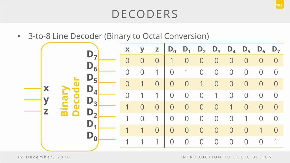
• 3-to-8 Line Decoder (Binary to Octal Conversion)
1 2 D e c e m b e r , 2 0 1 6 I N T R O D U C T I O N T O L O G I C D E S I G N
103
x y z D0 D1 D2 D3 D4 D5 D6 D7
0 0 0 1 0 0 0 0 0 0 0
0 0 1 0 1 0 0 0 0 0 0
0 1 0 0 0 1 0 0 0 0 0
0 1 1 0 0 0 1 0 0 0 0
1 0 0 0 0 0 0 1 0 0 0
1 0 1 0 0 0 0 0 1 0 0
1 1 0 0 0 0 0 0 0 1 0
1 1 1 0 0 0 0 0 0 0 1 y3= I1’I0’
y2= I1’I0
y1= I1I0’
y0= I1I0
Bin
ary
D
eco
de
r x
y z
D7
D6
D5
D4
D3
D2
D1
D0
DECODERS
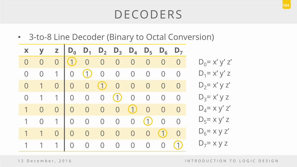
• 3-to-8 Line Decoder (Binary to Octal Conversion)
1 2 D e c e m b e r , 2 0 1 6 I N T R O D U C T I O N T O L O G I C D E S I G N
104
x y z D0 D1 D2 D3 D4 D5 D6 D7
0 0 0 1 0 0 0 0 0 0 0
0 0 1 0 1 0 0 0 0 0 0
0 1 0 0 0 1 0 0 0 0 0
0 1 1 0 0 0 1 0 0 0 0
1 0 0 0 0 0 0 1 0 0 0
1 0 1 0 0 0 0 0 1 0 0
1 1 0 0 0 0 0 0 0 1 0
1 1 1 0 0 0 0 0 0 0 1
D0= x’ y’ z’
D1= x’ y’ z
D2= x’ y z’
D3= x’ y z
D4= x y’ z’
D5= x y’ z
D6= x y z’
D7= x y z

DECODERS
• 3-to-8 Line Decoder (Binary to Octal Conversion)
1 2 D e c e m b e r , 2 0 1 6 I N T R O D U C T I O N T O L O G I C D E S I G N
105
x
z
D7
D6
D5
D4
D3
D2
D1
D0
y
D0= x’ y’ z’
D1= x’ y’ z
D2= x’ y z’
D3= x’ y z
D4= x y’ z’
D5= x y’ z
D6= x y z’
D7= x y z

DECODERS
• Some decoders are with NAND gates.
• NAND becomes more economical to generate the decoder
minterms in their complemented form.
• Decoders include one or more ENABLE inputs to control the
circuit operation.
1 2 D e c e m b e r , 2 0 1 6 I N T R O D U C T I O N T O L O G I C D E S I G N
106

DECODERS
• 2-to-4 Line Decoder with ENABLE input
1 2 D e c e m b e r , 2 0 1 6 I N T R O D U C T I O N T O L O G I C D E S I G N
107
Bin
ary
D
eco
de
r
A
B
E
D3
D2
D1
D0
E A B D0 D1 D2 D3
0 X X 0 0 0 0
1 0 0 1 0 0 0
1 0 1 0 1 0 0
1 1 0 0 0 1 0
1 1 1 0 0 0 1 EB
D3
D2
D1
D0
A
DECODERS
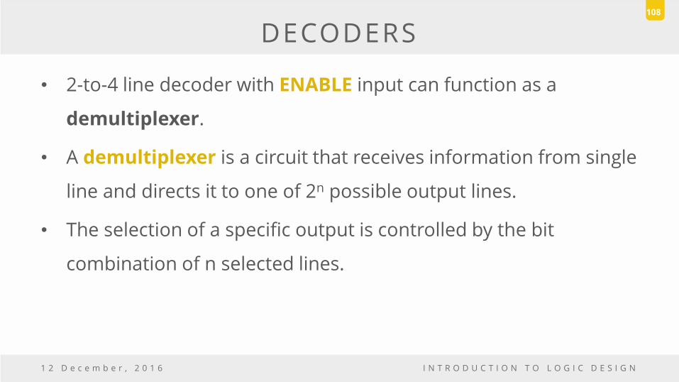
• 2-to-4 line decoder with ENABLE input can function as a
demultiplexer.
• A demultiplexer is a circuit that receives information from single
line and directs it to one of 2n possible output lines.
• The selection of a specific output is controlled by the bit
combination of n selected lines.
1 2 D e c e m b e r , 2 0 1 6 I N T R O D U C T I O N T O L O G I C D E S I G N
108

• The decoder can function as 1-
to-4 line demultiplexer.
– E is taken as a data input line.
– A and B are taken as the selection
inputs.
1 2 D e c e m b e r , 2 0 1 6 I N T R O D U C T I O N T O L O G I C D E S I G N
DECODERS 10
9
EB
D3
D2
D1
D0
A
E A B D0 D1 D2 D3
1/0 0 0 E 0 0 0
1/0 0 1 0 E 0 0
1/0 1 0 0 0 E 0
1/0 1 1 0 0 0 E
DECODERS
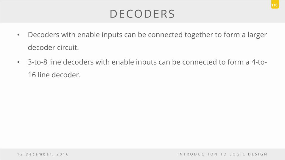
• Decoders with enable inputs can be connected together to form a larger
decoder circuit.
• 3-to-8 line decoders with enable inputs can be connected to form a 4-to-
16 line decoder.
1 2 D e c e m b e r , 2 0 1 6 I N T R O D U C T I O N T O L O G I C D E S I G N
110
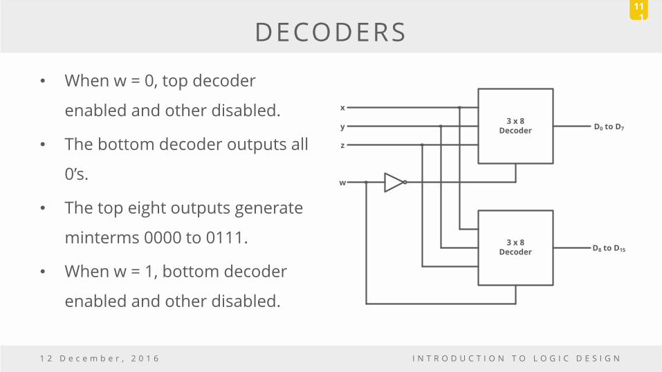
• When w = 0, top decoder
enabled and other disabled.
• The bottom decoder outputs all
0’s.
• The top eight outputs generate
minterms 0000 to 0111.
• When w = 1, bottom decoder
enabled and other disabled.
1 2 D e c e m b e r , 2 0 1 6 I N T R O D U C T I O N T O L O G I C D E S I G N
DECODERS 11
1
3 x 8 Decoder
3 x 8 Decoder
x
y
z
w
D0 to D7
D8 to D15
DECODERS
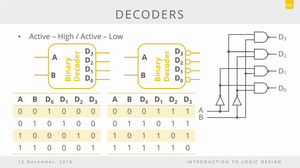
• Active – High / Active – Low
1 2 D e c e m b e r , 2 0 1 6 I N T R O D U C T I O N T O L O G I C D E S I G N
112
Bin
ary
D
eco
de
r
A
B
D3
D2
D1
D0 Bin
ary
D
eco
de
r
A
B
D3
D2
D1
D0
AB
D3
D2
D1
D0
A B D0 D1 D2 D3
0 0 1 0 0 0
0 1 0 1 0 0
1 0 0 0 1 0
1 1 0 0 0 1
A B D0 D1 D2 D3
0 0 0 1 1 1
0 1 1 0 1 1
1 0 1 1 0 1
1 1 1 1 1 0

DECODERS
• A decoder provides the 2n minterm of n input variables.
• Since any Boolean function can be expressed in sum of minterms
– Use decoder to generate the mintersm
– An external OR gate to form the logical sum.
• Any combinational circuit with n inputs and m outputs can be
implemented with an n-to-2n- line decoder and m OR gates.
1 2 D e c e m b e r , 2 0 1 6 I N T R O D U C T I O N T O L O G I C D E S I G N
113

Example: Full Adder
S(x, y, z) = ∑(1, 2, 4, 7)
C(x, y, z) = ∑(3, 5, 6, 7)
1 2 D e c e m b e r , 2 0 1 6 I N T R O D U C T I O N T O L O G I C D E S I G N
DECODERS 11
4
Bin
ary
Deco
der
x
y z
D7
D6
D5
D4
D3
D2
D1
D0
x y z
S C
4.9 ENCODERS

ENCODERS
• An encoder is a digital circuit that performs the inverse operation
of a decoder.
• An encoder has 2n (or fewer) input lines and n output lines.
• The output lines generate the binary code corresponding to the
input value.
1 2 D e c e m b e r , 2 0 1 6 I N T R O D U C T I O N T O L O G I C D E S I G N
116

ENCODERS
• Example: 4-to-2 Binary Encoder
1 2 D e c e m b e r , 2 0 1 6 I N T R O D U C T I O N T O L O G I C D E S I G N
117
x3 x2 x1 y1 y0
0 0 0 0 0
0 0 1 0 1
0 1 0 1 0
1 0 0 1 1
Binary Encoder
y1
y0
x1 x2 x3
Only one switch should be activated at a time
ENCODERS
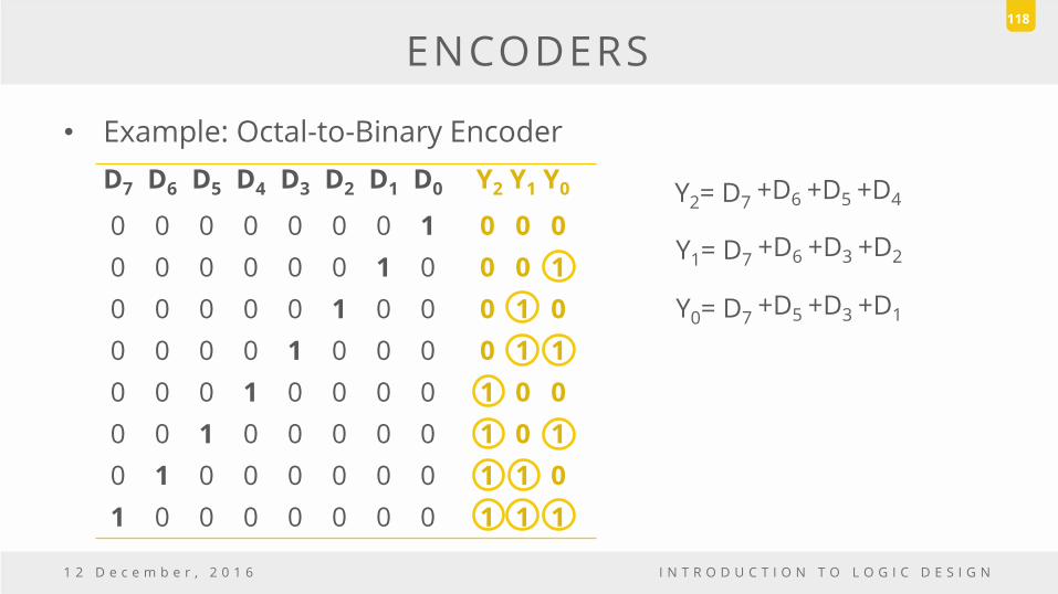
• Example: Octal-to-Binary Encoder
1 2 D e c e m b e r , 2 0 1 6 I N T R O D U C T I O N T O L O G I C D E S I G N
118
D7 D6 D5 D4 D3 D2 D1 D0 Y2 Y1 Y0
0 0 0 0 0 0 0 1 0 0 0
0 0 0 0 0 0 1 0 0 0 1
0 0 0 0 0 1 0 0 0 1 0
0 0 0 0 1 0 0 0 0 1 1
0 0 0 1 0 0 0 0 1 0 0
0 0 1 0 0 0 0 0 1 0 1
0 1 0 0 0 0 0 0 1 1 0
1 0 0 0 0 0 0 0 1 1 1
Y2= D7 +D6 +D5 +D4
Y1= D7 +D6 +D3 +D2
Y0= D7 +D5 +D3 +D1

ENCODERS
• Example: Octal-to-Binary Encoder
1 2 D e c e m b e r , 2 0 1 6 I N T R O D U C T I O N T O L O G I C D E S I G N
119
Y2= D7 +D6 +D5 +D4
Y1= D7 +D6 +D3 +D2
Y0= D7 +D5 +D3 +D1 B
ina
ry
En
co
de
r Y2
Y1 Y0
D7
D6
D5
D4
D3
D2
D1
D0
D7
D6
D5
D4
D3
D2
D1
D0
Y2
Y1
Y0

ENCODERS
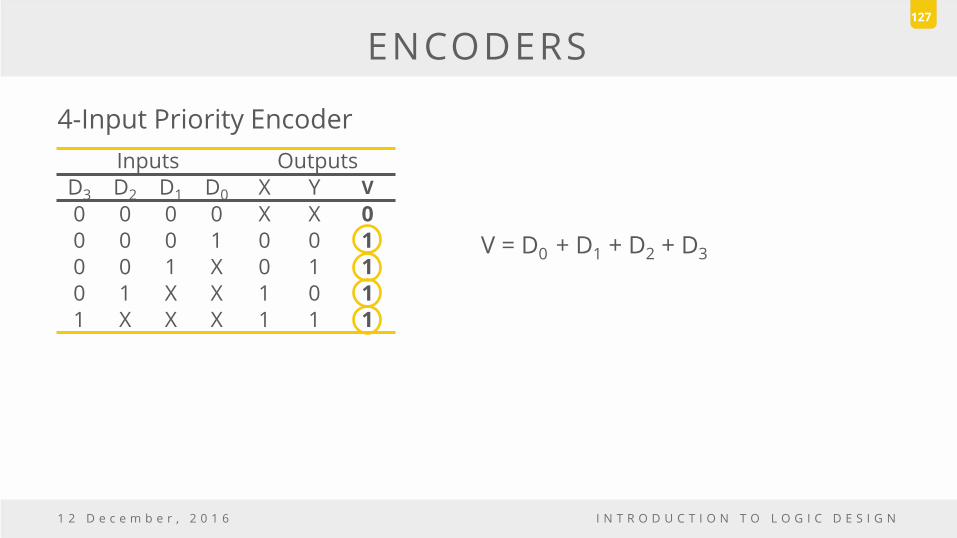
4-Input Priority Encoder
• Encoder circuit that includes the priority function.
• If two or more inputs are equal 1 at the same time,
– The input having the highest priority will take precedence.
1 2 D e c e m b e r , 2 0 1 6 I N T R O D U C T I O N T O L O G I C D E S I G N
120
Pri
ori
ty
En
co
de
r V
X Y
D3
D2
D1
D0
Inputs Outputs D3 D2 D1 D0 X Y V
0 0 0 0 x x 0 0 0 0 1 0 0 1 0 0 1 X 0 1 1 0 1 X X 1 0 1 1 X X X 1 1 1

ENCODERS
4-Input Priority Encoder
• X’s in the output represent don’t care conditions.
• X’s in the input are useful fir representing a truth table in condensed
form.
1 2 D e c e m b e r , 2 0 1 6 I N T R O D U C T I O N T O L O G I C D E S I G N
121
Inputs Outputs D3 D2 D1 D0 X Y V
0 0 0 0 X X 0 0 0 0 1 0 0 1 0 0 1 X 0 1 1 0 1 X X 1 0 1 1 X X X 1 1 1
Valid ouput = 1, when one or more inputs =1

4-Input Priority Encoder
• X’s in the input are useful for
representing a truth table in
condensed form.
• Truth table uses an X to
represent either 1 or 0.
• Example: X100 represents two
minterms 0100 and 1100.
1 2 D e c e m b e r , 2 0 1 6 I N T R O D U C T I O N T O L O G I C D E S I G N
ENCODERS 12
2
Inputs Outputs D3 D2 D1 D0 X Y V
0 0 0 0 X X 0 0 0 0 1 0 0 1 0 0 1 X 0 1 1 0 1 X X 1 0 1 1 X X X 1 1 1

4-Input Priority Encoder
• According to the table:
– Higher the subscript number,
– The higher the priority of the
input.
– Input D3 has the highest priority.
– When D3 = 1, the xy is 111,
regardless of the values of the
other inputs.
1 2 D e c e m b e r , 2 0 1 6 I N T R O D U C T I O N T O L O G I C D E S I G N
ENCODERS 12
3
Inputs Outputs D3 D2 D1 D0 X Y V
0 0 0 0 X X 0 0 0 0 1 0 0 1 0 0 1 X 0 1 1 0 1 X X 1 0 1 1 X X X 1 1 1

ENCODERS
4-Input Priority Encoder
• When each X in a row is replaced first by 0 and then by 1
– We obtain all 16 possible input combinations.
• 001X = 0010 and 0011
• 01XX = 0100 and 0101 and 0110 and 0111
• 1XXXX = 1000 and 1001 and 1010 and 1011 and 1100 and 1101
and 1110 and 1111
1 2 D e c e m b e r , 2 0 1 6 I N T R O D U C T I O N T O L O G I C D E S I G N
124

ENCODERS
4-Input Priority Encoder
1 2 D e c e m b e r , 2 0 1 6 I N T R O D U C T I O N T O L O G I C D E S I G N
125
Inputs Outputs D3 D2 D1 D0 X Y V
0 0 0 0 X X 0 0 0 0 1 0 0 1 0 0 1 X 0 1 1 0 1 X X 1 0 1 1 X X X 1 1 1
D1D0
D3D2
D1
0 0 0 1 1 1 1 0
00
01
D2
11
D3
10
D0
X
X’s K-MAP
0 0 0
1 1 1 1
1 1 1 1
1 1 1 1
X = D2 + D3

ENCODERS
4-Input Priority Encoder
1 2 D e c e m b e r , 2 0 1 6 I N T R O D U C T I O N T O L O G I C D E S I G N
126
Inputs Outputs D3 D2 D1 D0 X Y V
0 0 0 0 X X 0 0 0 0 1 0 0 1 0 0 1 X 0 1 1 0 1 X X 1 0 1 1 X X X 1 1 1
D1D0
D3D2
D1
0 0 0 1 1 1 1 0
00
01
D2
11
D3
10
D0
X
Y’s K-MAP
0 1 1
0 0 0 0
1 1 1 1
1 1 1 1
Y = D3 + D1D2’
ENCODERS
4-Input Priority Encoder
1 2 D e c e m b e r , 2 0 1 6 I N T R O D U C T I O N T O L O G I C D E S I G N
127
Inputs Outputs D3 D2 D1 D0 X Y V
0 0 0 0 X X 0 0 0 0 1 0 0 1 0 0 1 X 0 1 1 0 1 X X 1 0 1 1 X X X 1 1 1
V = D0 + D1 + D2 + D3

ENCODERS
4-Input Priority Encoder
• X = D2+ D3
• Y = D3+ D1D2’
• V = D0+ D1+ D2+ D3
1 2 D e c e m b e r , 2 0 1 6 I N T R O D U C T I O N T O L O G I C D E S I G N
128
D0
D1
D2
D3
X
Y
V

ENCODERS
1 2 D e c e m b e r , 2 0 1 6 I N T R O D U C T I O N T O L O G I C D E S I G N
129
X
Y Z
D7
D6
D5
D4
D3
D2
D1
D0
X
Y Z
D7
D6
D5
D4
D3
D2
D1
D0
Binary Encoder
Binary Decoder

4.10 MULTIPLEXERS

• A multiplexer (MUX) is a
combinational circuit that selects
binary information from one of
many input lines and directs it to a
single output line.
• The selection of a particular input
line is controlled by a set of
selection lines.
• There are 2n input lines and n
selected lines.
1 2 D e c e m b e r , 2 0 1 6 I N T R O D U C T I O N T O L O G I C D E S I G N
MULTIPLEXERS 13
1
MU
X
A
Q B
C
D
S0 S1
0 0 0 1 1 0 1 1
Q = A Q = B Q = C Q = D
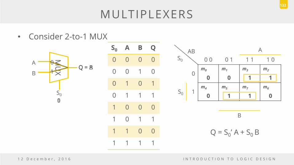
MULTIPLEXERS
• Consider 2-to-1 MUX
1 2 D e c e m b e r , 2 0 1 6 I N T R O D U C T I O N T O L O G I C D E S I G N
132
MU
X
A Q
B
S0
0 1
Q = A Q = B
S0 A B Q
0 0 0 0
0 0 1 0
0 1 0 1
0 1 1 1
1 0 0 0
1 0 1 1
1 1 0 0
1 1 1 1
A
S
Y
B
1
0
AB S0
A
0 0 0 1 1 1 1 0
0 m0 m1 m3 m2
0 0 1 1
S0 1 m4 m5 m7 m6
0 1 1 0
B
Q = S0’ A + S0 B

MULTIPLEXERS
• Consider 2-to-1 MUX
1 2 D e c e m b e r , 2 0 1 6 I N T R O D U C T I O N T O L O G I C D E S I G N
133
MU
X
A Q
B
S0
0
A
S
Y
B
1
0
Q = S0’ A + S0 B

MULTIPLEXERS
• 4-to-1 Multiplexer
1 2 D e c e m b e r , 2 0 1 6 I N T R O D U C T I O N T O L O G I C D E S I G N
134
MU
X
A
Q B
C
D
S0 S1
0 0 0 1 1 0 1 1
Q = A Q = B Q = C Q = D
S0 S1 Q
0 0 A
0 1 B
1 0 C
1 1 D
B
A
S1
YC
D
S0

MULTIPLEXERS
• 4-to-1 Multiplexer
1 2 D e c e m b e r , 2 0 1 6 I N T R O D U C T I O N T O L O G I C D E S I G N
135
x3
x2
x1
x0
y3
y2
y1
y0
D0
I0
I1
S
MU
X
D1
I0
I1
S
MU
X
D2
I0
I1
S
MU
X
D3
I0
I1
S
MU
X
D3
D2
D1
D0
S E
A3
A2
A1
A0
B3
B2
B1
B0
E
E
E
E
MULTIPLEXERS
• Example: F(x, y) = ∑ (0, 1, 3)
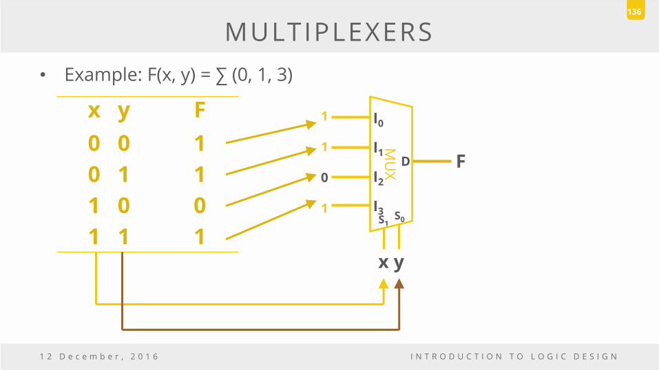
1 2 D e c e m b e r , 2 0 1 6 I N T R O D U C T I O N T O L O G I C D E S I G N
136
D
I0
I1
I2
I3 S1
x y F
0 0 1
0 1 1
1 0 0
1 1 1 x y
F
1
1
0
1
MU
X
S0

MULTIPLEXERS
• Boolean function implementation
– Decoder can be used to implement Boolean functions by employing
external OR gates. (see slide 114- DECODERS).
– Multiplexer is essentially a decoder that includes the OR gate within
the unit.
– The minterms of a function are generated in multiplexer by the
circuit associated with the selection inputs.
1 2 D e c e m b e r , 2 0 1 6 I N T R O D U C T I O N T O L O G I C D E S I G N
137

MULTIPLEXERS
• Boolean function implementation
– This provides a method of implementing a Boolean function of n
variables with a multiplexer that has n – 1 selection inputs.
– The first n – 1 variables of the function are connected to the
selection inputs of the multiplexer.
– The remaining single variable of the function is used for the data
inputs.
1 2 D e c e m b e r , 2 0 1 6 I N T R O D U C T I O N T O L O G I C D E S I G N
138

MULTIPLEXERS
• Example:F(x, y, z) = ∑(1, 2, 6, 7)
1 2 D e c e m b e r , 2 0 1 6 I N T R O D U C T I O N T O L O G I C D E S I G N
139
x y z F
0 0 0 0
0 0 1 1
0 1 0 1
0 1 1 0
1 0 0 0
1 0 1 0
1 1 0 1
1 1 1 1
MUX Y
I0
I1
I2
I3 I4
I5
I6
I7
S2 S1 S0
x y z
0 1 1 0 0 0 1 1
F
MUX Y
I0
I1
I2
I3 S1 S0
x y z F
0 0 0 0
0 0 1 1
0 1 0 1
0 1 1 0
1 0 0 0
1 0 1 0
1 1 0 1
1 1 1 1
x y
F F = z z
F = z
z
F = 0
0
F = 1
1

MULTIPLEXERS
• Example:F(x, y, z) = ∑(1, 2, 6, 7)
1 2 D e c e m b e r , 2 0 1 6 I N T R O D U C T I O N T O L O G I C D E S I G N
140
x y z F
0 0 0 0
0 0 1 1
0 1 0 1
0 1 1 0
1 0 0 0
1 0 1 0
1 1 0 1
1 1 1 1
MUX Y
I0
I1
I2
I3 S1 S0
x y
F F = z z
F = z’ z’
F = 0 0
F = 1
1

MULTIPLEXERS
• Example:F(A, B, C, D) = ∑(1,3,4,11,12,13,14,15)
1 2 D e c e m b e r , 2 0 1 6 I N T R O D U C T I O N T O L O G I C D E S I G N
141
F
MUX Y
I0
I1
I2
I3 I4
I5
I6
I7 S2 S1 S0
A B C D F
0 0 0 0 0 0 0 0 1 1 0 0 1 0 0 0 0 1 1 1 0 1 0 0 1 0 1 0 1 0 0 1 1 0 0 0 1 1 1 0 1 0 0 0 0 1 0 0 1 0 1 0 1 0 0 1 0 1 1 1 1 1 0 0 1 1 1 0 1 1 1 1 1 0 1 1 1 1 1 1 A B C
F
F = D D
F = D D
F = D’ D’
F = 0 0
F = 0
F = D
F = 1
F = 1
0
D
1
1

MULTIPLEXERS
• 8-to-1 MUX using Dual 4-to-1 MUX
1 2 D e c e m b e r , 2 0 1 6 I N T R O D U C T I O N T O L O G I C D E S I G N
142
Y
S 2 S 1 S 0
MUX Y
I0
I1
I2
I3 S1 S0
0 0 1
MUX Y
I0
I1
I2
I3 S1 S0
MUX Y I0
I1 S
I0
I1
I2
I3
I4
I5
I6
I7
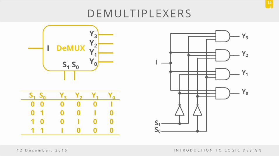
DEMULTIPLEXERS
1 2 D e c e m b e r , 2 0 1 6 I N T R O D U C T I O N T O L O G I C D E S I G N
143
DeMUX I
Y3
Y2
Y1
Y0 S1 S0
S1 S0 Y3 Y2 Y1 Y0
0 0 0 0 0 I
0 1 0 0 I 0
1 0 0 I 0 0
1 1 I 0 0 0
I
Y3
Y2
Y1
Y0
S0
S1

DEMULTIPLEXER
1 2 D e c e m b e r , 2 0 1 6 I N T R O D U C T I O N T O L O G I C D E S I G N
144
DeMUX I
Y3
Y2
Y1
Y0 S1 S0
S1 S0 Y3 Y2 Y1 Y0
0 0 0 0 0 I
0 1 0 0 I 0
1 0 0 I 0 0
1 1 I 0 0 0
Bin
ary
D
eco
de
r
A
B
E
D3
D2
D1
D0
E A B Y3 Y2 Y1 Y0
0 X X 0 0 0 0
1 0 0 0 0 0 1
1 0 1 0 0 1 0
1 1 0 0 1 0 0
1 1 1 1 0 0 0

MULTIPLEXERS
• A multiplexer can be constructed with three – state gates.
• A three – state gate is a digital circuit that exhibits three states.
• Two of the states are signals equivalent to logic 1 and 0.
• The third state is high – impedance state.
• Hight – impedance state behaves like an open circuit.
– The output appears to be disconnected.
– The circuit has no logic significance.
1 2 D e c e m b e r , 2 0 1 6 I N T R O D U C T I O N T O L O G I C D E S I G N
145

MULTIPLEXERS
• Three – state gates may perform any conventional logic such as AND or
NAND.
• The most commonly used is the buffer gate.
• The high – impedance state of a three – state gate provides a special
feature not available in other gates.
• Large number of three – state gate outputs can be connected with wires
to form a common line without endangering loading effects.
1 2 D e c e m b e r , 2 0 1 6 I N T R O D U C T I O N T O L O G I C D E S I G N
146
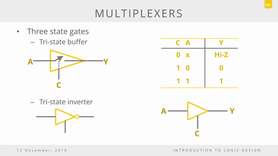
MULTIPLEXERS
• Three state gates
– Tri-state buffer
– Tri-state inverter
1 2 D e c e m b e r , 2 0 1 6 I N T R O D U C T I O N T O L O G I C D E S I G N
147
A Y
C
C A Y
0 x Hi-Z
1 0 0
1 1 1
A Y
C

MULTIPLEXERS
• Three state gates
1 2 D e c e m b e r , 2 0 1 6 I N T R O D U C T I O N T O L O G I C D E S I G N
148
A
Y C
B
D
C D Y
0 0 Hi-Z
0 1 B
1 0 A
1 1 ?
Not Allowed Y=
A C
B
A if C = 1 B if C = 0
2-to-1 MUX
MULTIPLEXERS
1 2 D e c e m b e r , 2 0 1 6 I N T R O D U C T I O N T O L O G I C D E S I G N
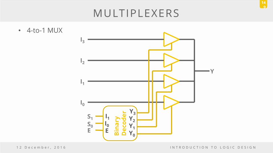
149
I0
Y
E
S1
I1
I2
I3
Bin
ary
D
eco
de
r I1
I0
E
Y3
Y2
Y1
Y0
S0
• 4-to-1 MUX
Related Documents