Welcome message from author
This document is posted to help you gain knowledge. Please leave a comment to let me know what you think about it! Share it to your friends and learn new things together.
Transcript


www.FreeEngineeringBooksPdf.com

Trim Size: 170mm x 244mm Single Column Ergul ffirs.tex V2 - 04/06/2017 11:08am Page i
Introduction to Electrical Circuit Analysis
www.FreeEngineeringBooksPdf.com

Trim Size: 170mm x 244mm Single Column Ergul ffirs.tex V2 - 04/06/2017 11:08am Page ii
www.FreeEngineeringBooksPdf.com
Trim Size: 170mm x 244mm Single Column Ergul ffirs.tex V2 - 04/06/2017 11:08am Page iii
Introduction to Electrical Circuit Analysis
Özgür ErgülMiddle East Technical University, Ankara, Turkey
www.FreeEngineeringBooksPdf.com

Trim Size: 170mm x 244mm Single Column Ergul ffirs.tex V2 - 04/06/2017 11:08am Page iv
This edition first published 2017© 2017 John Wiley and Sons Ltd
All rights reserved. No part of this publication may be reproduced, stored in a retrieval system, ortransmitted, in any form or by any means, electronic, mechanical, photocopying, recording or otherwise,except as permitted by law.Advice on how to obtain permision to reuse material from this title is available athttp://www.wiley.com/go/permissions.
The right of Özgür Ergül to be identified as the author of this work has been asserted in accordance with law.
Registered OfficesJohn Wiley & Sons, Inc., 111 River Street, Hoboken, NJ 07030, USAJohn Wiley & Sons Ltd, The Atrium, Southern Gate, Chichester, West Sussex, PO19 8SQ, UK
Editorial OfficeThe Atrium, Southern Gate, Chichester, West Sussex, PO19 8SQ, UK
For details of our global editorial offices, customer services, and more information about Wiley productsvisit us at www.wiley.com.
Wiley also publishes its books in a variety of electronic formats and by print-on-demand. Some content thatappears in standard print versions of this book may not be available in other formats.
Limit of Liability/Disclaimer of WarrantyWhile the publisher and author have used their best efforts in preparing this work, they make norepresentations or warranties with respect to the accuracy or completeness of the contents of this work andspecifically disclaim all warranties, including without limitation any implied warranties of merchantability orfitness for a particular purpose. No warranty may be created or extended by sales representatives, writtensales materials or promotional statements for this work. The fact that an organization, website, or product isreferred to in this work as a citation and/or potential source of further information does not mean that thepublisher and authors endorse the information or services the organization, website, or product may provideor recommendations it may make.This work is sold with the understanding that the publisher is not engagedin rendering professional services. The advice and strategies contained herein may not be suitable for yoursituation. You should consult with a specialist where appropriate. Further, readers should be aware thatwebsites listed in this work may have changed or disappeared between when this work was written and whenit is read. Neither the publisher nor authors shall be liable for any loss of profit or any other commercialdamages, including but not limited to special, incidental, consequential, or other damages.
Library of Congress Cataloging-in-Publication data applied for
ISBN: 9781119284932
Cover design by WileyCover image: (Circuit Board) © ratmaner/Gettyimages; (Electronic Components)© DonNichols/Gettyimages; (Formulas) © Bim/Gettyimages
Set in 10/12pt WarnockPro by SPi Global, Chennai, India
10 9 8 7 6 5 4 3 2 1
www.FreeEngineeringBooksPdf.com

Trim Size: 170mm x 244mm Single Column Ergul ffirs.tex V2 - 04/06/2017 11:08am Page v
For my wife Ayça, three cats (Boncuk, Pepe, and Misket), and the dog, who all sufferedduring the writing of this book
www.FreeEngineeringBooksPdf.com

Trim Size: 170mm x 244mm Single Column Ergul ffirs.tex V2 - 04/06/2017 11:08am Page vi
www.FreeEngineeringBooksPdf.com

Trim Size: 170mm x 244mm Single Column Ergul ftoc.tex V2 - 04/04/2017 7:18am Page vii
vii
Contents
Important Units xiConventions with Examples xiiiPreface xvAbout the Companion Website xix
1 Introduction 11.1 Circuits and Important Quantities 11.1.1 Electric Charge 11.1.2 Electric Potential (Voltage) 31.1.3 Electric Current 41.1.4 Electric Voltage and Current in Electrical Circuits 51.1.5 Electric Energy and Power of a Component 61.1.6 DC and AC Signals 71.1.7 Transient State and Steady State 81.1.8 Frequency in Circuits 91.2 Resistance and Resistors 91.2.1 Current Types, Conductance, and Ohm’s Law 101.2.2 Good Conductors and Insulators 101.2.3 Semiconductors 111.2.4 Superconductivity and Perfect Conductivity 111.2.5 Resistors as Circuit Components 121.3 Independent Sources 131.4 Dependent Sources 141.5 Basic Connections of Components 151.6 Limitations in Circuit Analysis 191.7 What You Need to Know before You Continue 20
2 Basic Tools: Kirchhoff’s Laws 232.1 Kirchhoff’s Current Law 232.2 Kirchhoff’s Voltage Law 242.3 WhenThings GoWrong with KCL and KVL 362.4 Series and Parallel Connections of Resistors 402.4.1 Series Connection 402.4.2 Parallel Connection 412.5 WhenThings GoWrong with Series/Parallel Resistors 452.6 What You Need to Know before You Continue 46
www.FreeEngineeringBooksPdf.com
Trim Size: 170mm x 244mm Single Column Ergul ftoc.tex V2 - 04/04/2017 7:18am Page viii
viii Contents
3 Analysis of Resistive Networks: Nodal Analysis 473.1 Application of Nodal Analysis 473.2 Concept of Supernode 593.3 Circuits with Multiple Independent Voltage Sources 723.4 Solving Challenging Problems Using Nodal Analysis 743.5 WhenThings GoWrong with Nodal Analysis 863.6 What You Need to Know before You Continue 90
4 Analysis of Resistive Networks: Mesh Analysis 934.1 Application of Mesh Analysis 934.2 Concept of Supermesh 1074.3 Circuits with Multiple Independent Current Sources 1214.4 Solving Challenging Problems Using the Mesh Analysis 1224.5 WhenThings GoWrong with Mesh Analysis 1354.6 What You Need to Know before You Continue 137
5 Black-Box Concept 1395.1 Thévenin and Norton Equivalent Circuits 1395.2 Maximum Power Transfer 1585.3 Shortcuts in Equivalent Circuits 1735.4 WhenThings GoWrong with Equivalent Circuits 1765.5 What You Need to Know before You Continue 178
6 Transient Analysis 1816.1 Capacitance and Capacitors 1816.2 Inductance and Inductors 1916.3 Time-Dependent Analysis of Circuits in Transient State 1956.3.1 Time-Dependent Analysis of RC Circuits 1956.3.2 Time-Dependent Analysis of RL Circuits 2046.3.3 Impossible Cases 2076.4 Switching and Fixed-Time Analysis 2086.5 Parallel and Series Connections of Capacitors and Inductors 2186.5.1 Connections of Capacitors 2186.5.2 Connections of Inductors 2206.6 WhenThings GoWrong in Transient Analysis 2226.7 What You Need to Know before You Continue 224
7 Steady-State Analysis of Time-Harmonic Circuits 2277.1 Steady-State Concept 2277.2 Time-Harmonic Circuits with Sinusoidal Sources 2287.2.1 Resistors Connected to Sinusoidal Sources 2297.2.2 Capacitors Connected to Sinusoidal Sources 2307.2.3 Inductors Connected to Sinusoidal Sources 2317.2.4 Root-Mean-Square Concept 2327.3 Concept of Phasor Domain and Component Transformation 2347.3.1 Resistors in Phasor Domain 2367.3.2 Capacitors in Phasor Domain 236
www.FreeEngineeringBooksPdf.com

Trim Size: 170mm x 244mm Single Column Ergul ftoc.tex V2 - 04/04/2017 7:18am Page ix
Contents ix
7.3.3 Inductors in Phasor Domain 2377.3.4 Impedance Concept 2387.4 Special Circuits in Phasor Domain 2437.4.1 RC Circuits in Phasor Domain 2437.4.2 RL Circuits in Phasor Domain 2447.4.3 RLC Circuits in Phasor Domain 2467.4.4 Other Combinations 2477.5 Analysis of Complex Circuits at Fixed Frequencies 2487.6 Power in Steady State 2597.6.1 Instantaneous and Average Power 2597.6.2 Complex Power 2607.6.3 Impedance Matching 2667.7 WhenThings GoWrong in Steady-State Analysis 2717.8 What You Need to Know before You Continue 274
8 Selected Components of Modern Circuits 2758.1 When Connections Are via Magnetic Fields: Transformers 2758.2 When Components Behave Differently from Two Sides: Diodes 2788.3 When Components Involve Many Connections: OP-AMPs 2848.4 When Circuits Become Modern: Transistors 2888.5 When Components Generate Light: LEDs 2938.6 Conclusion 294
9 Practical Technologies in Modern Circuits 2959.1 Measurement Instruments 2959.2 Three-Phase Power Delivery 2979.3 AD and DA Converters 3009.4 Logic Gates 3039.5 Memory Units 3079.6 Conclusion 309
10 Next Steps 31110.1 Energy Is Conserved, Always! 31110.2 Divide and Conquer Complex Circuits 31310.3 Appreciate the Package 31410.4 Consider Yourself as a Circuit Element 31610.5 Safety First 317
11 Photographs of Some Circuit Elements 321
A Appendix 325A.1 Basic Algebra Identities 325A.2 Trigonometry 325A.3 Complex Numbers 325
B Solutions to Exercises 327
Index 401
www.FreeEngineeringBooksPdf.com

Trim Size: 170mm x 244mm Single Column Ergul ftoc.tex V2 - 04/04/2017 7:18am Page x
www.FreeEngineeringBooksPdf.com

xi
Important Units
• Ampere (A)• Coulomb (C)• Farad (F): C/V• Henry (H): weber/A• Hertz (Hz): 1/s• Joule (J): N m = kg m2/s2• kilo (k…): ×1000• meter (m)• micro (𝜇…): ×10−6• milli (m…): ×10−3• Newton (N): kg m/s2• Second (s)• Siemens (S): A/V• Volt (V): J/C• Volt-ampere (VA): J/s• Watt (W): J/s
www.FreeEngineeringBooksPdf.com

www.FreeEngineeringBooksPdf.com
xiii
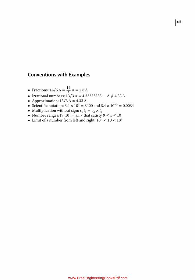
Conventions with Examples
• Fractions: 14∕5A = 145
A = 2.8A• Irrational numbers: 13∕3A = 4.33333333…A ≠ 4.33A• Approximation: 13∕3A ≈ 4.33A• Scientific notation: 3.4 × 103 = 3400 and 3.4 × 10−3 = 0.0034• Multiplication without sign: 𝑣aib = 𝑣a × ib• Number ranges: [9, 10] = all x that satisfy 9 ≤ x ≤ 10• Limit of a number from left and right: 10− < 10 < 10+
www.FreeEngineeringBooksPdf.com

www.FreeEngineeringBooksPdf.com

xv
Preface
Since the first known electricity experiments more than 25 centuries ago by Thalesof Miletus, who believed that there should be better ways than mythology to explainphysical phenomena, humankind has worked hard to understand and use electricity inmany beneficial ways. The last three centuries have seen rapid developments in under-standing electricity and related concepts, leading to constantly accelerating technologyadvancements in the last several decades. Today, most of us simply cannot live withoutelectricity, and it is almost ubiquitous in daily life. We are so attached to and dependenton electricity that there are even post-apocalyptic fiction movies and film series basedon sudden electrical power blackouts. And they are terrifying.Electricity is one of a few subjects with which we have a strange relationship. The
more we use it, less we know about it. Electrical and electronic devices, where electric-ity is somehow used to produce beneficial outputs, are a closed book to most of us, untilwe open them (not a suggested activity!) and see that they contain incredibly small buthighly intelligent parts.These parts, some of which once had huge dimensions and evenfilled entire rooms, are now so tiny that we are able to place literally billions of them (atthe time of writing) in a smartphone microprocessor. One billion is a huge number; ata rate of one a second, it takes 31 years to count. And we are able to put these uncount-able (OK, countable, but not feasibly so) numbers of components together and makethem work in harmony for our enjoyment. Yet most of us know little about how theyactually work.The topic of circuit analysis has naturally developed in parallel with electrical cir-
cuits and devices starting from centuries ago. To provide some intuition, Ohm’s law hasbeen known since 1827, while Kirchhoff’s laws were described in 1845. Nodal and meshanalysis methods have been developed and used for systematically applying Kirchhoff’slaws. Phasor notation is borrowed from mathematics to deal with time-harmonic cir-cuits. These fundamental laws have not changed, and they will most probably remainthe same in the coming years. In general, basic laws describe everything when they arewisely used. Hence, more and more sophisticated circuits in future technologies willalso benefit from them, independent of their complexity.Circuit analysis is naturally linked to all other technologies involving electricity,
including medical, automotive, computer, energy, and aerospace industries, as well asall subcategories of electrical and electronic engineering. Interestingly, with the rapid
www.FreeEngineeringBooksPdf.com
xvi Preface
development of technology, we tend to learn fundamental laws more superficially. Onecan identify two major factors, among many:• As circuits becomemore complicated and specialized, we are attracted and guided to
focus on higher-level representations, such as inputs and outputs of microchips withwell-defined functions, without spending time on fundamental laws.
• Great advancements in circuit-solver software “eliminate” the need to fully under-stand fundamental laws and appreciate their importance in everyday life, reducingcircuit analysis to numbers.
Unfortunately, without absorbing fundamental laws, we tend to make major concep-tual mistakes. Most instructors have had a student who offers infinite energy by rotatingsomething (usually a car wheel if s/he is a mechanical engineering student), disregard-ing the conservation of energy. It is often a confusing issue for a biomedical student toappreciate the necessity of grounding for medical safety. And it is probably a computa-tionalmistake but not a new technology if a circuit analyzer programprovides a negativeresistor value. The aim of this book is to gradually construct the basics of circuit anal-ysis, even though they are not new material, while accelerating our understanding ofelectrical circuits and all technologies using electricity.This is intended as an introductory book, mainly designed for college and university
students who may have different backgrounds and, for whatever reason, need to learnabout circuits for the first time. It mainly focuses on a few essential components of elec-trical components, namely,
• resistors,• independent voltage and current sources,• dependent sources (as closed components, not details),• capacitors, and• inductors.
On the other hand, transistors, diodes, OP-AMPs, and similar popular and inevitablecomponents of modern circuits, which are fixed topics (and even starting points) inmany circuit books, are not detailed. The aim of this book is not to teach electrical cir-cuits, but rather to teach how to analyze them. From this perspective, the componentslisted above provide the required combinations and possibilities to cover the fundamen-tal techniques, namely,
• Ohm’s and Kirchhoff’s laws,• nodal analysis,• mesh analysis,• the black-box approach andThévenin/Norton equivalent circuits.
This book also covers the analysis methods for both DC and AC cases in transient andsteady states.To sum up, the technology that is covered in this book is well established. The
analysis methods and techniques, as well as components, listed above have beenknown for decades. However, the fundamental methods and components need tobe known in sufficient depth in order to understand how electrical circuits work,
www.FreeEngineeringBooksPdf.com

Preface xvii
including state-of-the-art devices and their ingredients. Many books in this area aredominated by an increasing number of new electrical and electronic components andtheir special working principles, while the fundamental techniques are squeezed intoshort descriptions and limited to a few examples. Therefore, the purpose of this bookis to provide sufficient basic discussion and hands-on exercises (with solutions at theback of the book) before diving into modern circuits with higher-level properties.Enjoy!
www.FreeEngineeringBooksPdf.com

www.FreeEngineeringBooksPdf.com

xix
About the Companion Website
This book is accompanied by a companion website:
www.wiley.com/go/ergul4412
The website includes:
• Exercise sums and solutions• Videos
www.FreeEngineeringBooksPdf.com

www.FreeEngineeringBooksPdf.com

1
1
Introduction
We start with the iconic figure (Figure 1.1), which depicts a bulb connected to a battery.Whenever the loop is closed and a full connection is established, the bulb comes onand starts to consume energy provided by the battery. The process is often described asthe conversion of the chemical energy stored in the battery into electrical energy thatis further released as heat and light by the bulb. The connection between the bulb andbattery consists of two wires between the positive and negative terminals of the bulband battery. These wires are shown as simple straight lines, whereas in real life they areusually coaxial or paired cables that are isolated from the environment.The purpose of this first chapter is to introduce basic concepts of electrical circuits. In
order to understand circuits, such as the one above, we first need to understand electriccharge, potential, and current.These concepts provide a basis for recognizing the inter-actions between electrical components.We further discuss electric energy and power asfundamental variables in circuit analysis. The time and frequency in circuits, as well asrelated limitations, are briefly considered. Finally, we study conductivity and resistance,as well as resistors, independent sources, and dependent sources as common compo-nents of basic circuits.
1.1 Circuits and Important Quantities
An electrical circuit is a collection of components connected via metal wires. Electricalcomponents include but are not limited to resistors, inductors, capacitors, generators(sources), transformers, diodes, and transistors. In circuit analysis, wire shapes and geo-metric arrangements are not important and they can be changed, provided that theconnections between the components remain the same with fixed geometric topology.Wires often meet at intersection points; a connection of two or more wires at a point iscalled a node. Before discussing how circuits can be represented and analyzed, we firstneed to focus on important quantities, namely, electric charge, electric potential, andcurrent, as well as energy and power.
1.1.1 Electric Charge
Electric charge is a fundamental property ofmatter to describe force interactions amongparticles. According to Coulomb’s law, there is an attractive (negative) force between a
Introduction to Electrical Circuit Analysis, First Edition. Özgür Ergül.© 2017 John Wiley & Sons Ltd. Published 2017 by John Wiley & Sons Ltd.Companion Website: www.wiley.com/go/ergul4412
www.FreeEngineeringBooksPdf.com

2 Introduction to Electrical Circuit Analysis
+
_
Figure 1.1 A simple circuit involving a bulb connected toa battery. The connection between the bulb and battery isshown via simple lines.
1
2
3
A
B
C D
A
B
C D 1
2
3
A
B
C D 1
2
3 wires
nodes components
Figure 1.2 A circuit involving connections of four components labeled from A to D. From thecircuit-analysis perspective, connection shapes are not important, and these three representations areequivalent.
proton and an electron given by
Fpe ≈ −2.3071 × 10⁻²⁸d2 (newton (N)),
which is significantly larger than (around 1.2 × 1036 times) the gravity between theseparticles. In the above, d is the distance between the proton and electron, given inmeters(m). This law can be rewritten by using Coulomb’s constant
k ≈ 8.9876 × 10⁹ (N m2∕C2)
as
Fpe ≈ kqeqp
d2 (N),
where
qp ≈ +1.6022 × 10⁻¹⁹ (C)qe = −qp ≈ −1.6022 × 10⁻¹⁹ (C)
are the electrical charges of the proton and electron, respectively, in units of coulombs(C). Coulomb’s constant enables the generalization of the electric force between anyarbitrary charges q1 and q2 as
F12 ≈ kq1q2
d2 (N),
where q1 and q2 are assumed to be point charges (theoretically squeezed into zero vol-umes), which are naturally formed of collections of protons and electrons.
www.FreeEngineeringBooksPdf.com

Introduction 3
test charge
force
electric field lines
+ −
Figure 1.3 Electric field lines created individually by a positive charge and a negative charge. Anelectric field is assumed to be created whether there is a second test charge or not. If a test charge islocated in the field, repulsive or attractive force is applied on it.
The definition of the electric force above requires at least two charges. On the otherhand, it is common to extend the physical interpretation to a single charge. Specifically,a stationary charge q1 is assumed to create an electric field (intensity) that can be repre-sented as
E1 ≈ kq1
d2 (N∕C),
where d is now the distance measured from the location of the charge.This electric fieldis in the radial direction, either outward (positive) or inward (negative), depending onthe type (sign) of the charge.Therefore, we assume that an electric field is always formedwhether there is a second test charge or not. If there is q2 at a distance d, the electricforce is now measured as
F12 = E1q2 (N),
either as repulsive (if q1 and q2 have the same sign) or attractive (if q1 and q2 have differ-ent signs).The definition of the electric field is so useful that, in many cases, even the sources of
the field are discarded. Consider a test charge q exposed to some electric field E. Theforce on q can be calculated as
F = qE (N),
without even knowing the sources creating the field. This flexibility further allows us todefine the electric potential concept, as discussed below.
1.1.2 Electric Potential (Voltage)
Consider a charge q in some electric field created by external sources.Moving the chargefrom a position b to another position a may require energy if the movement is oppositeto the force due to the electric field. This energy can be considered to be absorbed bythe charge. If themovement and force are aligned, however, energy is extracted from thecharge. In general, the path from b to a may involve absorption and release of energy,depending on the alignment of the movement and electric force from position to posi-tion. In any case, the net energy absorbed/released depends on the start and end points,since the electric field is conservative and its line integral is path-independent.Electric potential (voltage) is nothing but the energy considered for a unit charge (1C)
such that it is defined independent of the testing scheme. Specifically, the work done in
www.FreeEngineeringBooksPdf.com
4 Introduction to Electrical Circuit Analysis
q b a
a
b c
vab vca +
_ +
_
v + bc _
groundelectric field lines
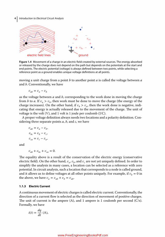
Figure 1.4 Movement of a charge in an electric field created by external sources. The energy absorbedor released by the charge does not depend on the path but depends on the potentials at the start andend points. The electric potential (voltage) is always defined between two points, while selecting areference point as a ground enables unique voltage definitions at all points.
moving a unit charge from a point b to another point a is called the voltage between aand b. Conventionally, we have
𝑣ab = 𝑣a − 𝑣b
as the voltage between a and b, corresponding to the work done in moving the chargefrom b to a. If 𝑣a > 𝑣b, then work must be done to move the charge (the energy of thecharge increases). On the other hand, if 𝑣b > 𝑣a, then the work done is negative, indi-cating that energy is actually released due to the movement of the charge. The unit ofvoltage is the volt (V), and 1 volt is 1 joule per coulomb (J/C).A proper voltage definition always needs two locations and a polarity definition. Con-
sidering three separate points a, b, and c, we have
𝑣ab = 𝑣a − 𝑣b,
𝑣bc = 𝑣b − 𝑣c,
𝑣ca = 𝑣c − 𝑣a,
and
𝑣ab + 𝑣bc + 𝑣ca = 0.
The equality above is a result of the conservation of the electric energy (conservativeelectric field). On the other hand, 𝑣a, 𝑣b, and 𝑣c are not yet uniquely defined. In order tosimplify the analysis in many cases, a location can be selected as a reference with zeropotential. In circuit analysis, such a location that corresponds to a node is called ground,and it allows us to define voltages at all other points uniquely. For example, if 𝑣b = 0 inthe above, we have 𝑣a = 𝑣ab + 𝑣b = 𝑣ab.
1.1.3 Electric Current
Acontinuousmovement of electric charges is called electric current. Conventionally, thedirection of a current flow is selected as the direction of movement of positive charges.The unit of current is the ampere (A), and 1 ampere is 1 coulomb per second (C/s).Formally, we have
i(t) =dqdt
(A),
www.FreeEngineeringBooksPdf.com
Introduction 5
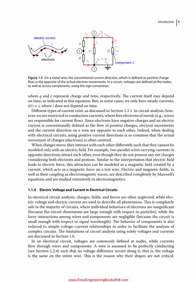
_ _ _ _
i
electrons
electric current
A
B
C D 1
2
3
id
vd+ _
v2
v3 = 0
ic
ia
ib component D
Figure 1.5 On a metal wire, the conventional current direction, which is defined as positive chargeflow, is the opposite of the actual electron movements. In a circuit, voltages are defined at the nodes,as well as across components, using the sign convention.
where q and t represent charge and time, respectively. The current itself may dependon time, as indicated in this equation. But, in some cases, we only have steady currents,i(t) = i, where i does not depend on time.Different types of current exist, as discussed in Section 1.2.1. In circuit analysis, how-
ever, we are restricted to conduction currents, where free electrons ofmetals (e.g., wires)are responsible for current flows. Since electrons have negative charges and an electriccurrent is conventionally defined as the flow of positive charges, electron movementsand the current direction on a wire are opposite to each other. Indeed, when dealingwith electrical circuits, using positive current directions is so common that the actualmovement of charges (electrons) is often omitted.When chargesmove, they interact with each other differently such that they cannot be
modeled only with an electric field. For example, two parallel wires carrying currents inopposite directions attract each other, even though they do not possess any net chargesconsidering both electrons and protons. Similar to the interpretation that electric fieldleads to electric force, this attraction can be modeled as a magnetic field created by acurrent, which acts as a magnetic force on a test wire. Electric and magnetic fields, aswell as their coupling as electromagnetic waves, are described completely by Maxwell’sequations and are studied extensively in electromagnetics.
1.1.4 Electric Voltage and Current in Electrical Circuits
In electrical circuit analysis, charges, fields, and forces are often neglected, while elec-tric voltage and electric current are used to describe all phenomena. This is completelysafe in the majority of circuits, where individual behaviors of electrons are insignificant(because the circuit dimensions are large enough with respect to particles), while theforce interactions among wires and components are negligible (because the circuit issmall enough with respect to signal wavelength). The behavior of components is alsoreduced to simple voltage–current relationships in order to facilitate the analysis ofcomplex circuits. The limitations of circuit analysis using solely voltages and currentsare discussed in Section 1.6.In an electrical circuit, voltages are commonly defined at nodes, while currents
flow through wires and components. A wire is assumed to be perfectly conducting(see Section 1.2.4) such that no voltage difference occurs along it, that is, the voltageis the same on the entire wire. This is the reason why their shapes are not critical.
www.FreeEngineeringBooksPdf.com

6 Introduction to Electrical Circuit Analysis
On the other hand, a voltage difference may occur across a component, depending thetype of the component and the overall circuit. For unique representation of a nodevoltage, a reference node should be selected as a ground. However, the voltage acrossa component can always be defined uniquely since it is based on two or more (if thecomponent has multiple terminals) points.In circuit analysis, voltages and currents are usually unknowns to be found. Since they
are not known, in most cases, their direction can be arbitrarily selected.When the solu-tion gives a negative value for a current or a voltage, it is understood that the initialassumption is incorrect. This is never a problem at all. For consistency, however, it isuseful to follow a sign convention by fixing the voltage polarity and current directionfor any given component. In the rest of this book, the current through a component isalways selected to flow from the positive to the negative terminal of the voltage.
1.1.5 Electric Energy and Power of a Component
Consider a component d with a current id and voltage 𝑣d, defined in accordance with thesign convention. If id > 0, one can assume that positive charges flow from the positiveto the negative terminal of the component. In addition, if 𝑣d > 0, these positive chargesencounter a drop in their potential values, that is, they release energy. This energy mustbe somehow used (consumed or stored) by the component. Formally, we define theenergy of the component as
𝑤d(t) = ∫
t
0𝑣d(t′)id(t′)dt′ (J),
where the time integral is used to account for all charges passing during 0 ≤ t′ ≤ t,assuming that the component is used from time t′ = 0. If 𝑤d(t) > 0, it is understoodthat the component consumes net energy during the time interval [0, t]. On the otherhand, if 𝑤d(t) < 0, the component produces net energy in the same time interval. Wenote that the unit of energy is the joule, as usual.Energy as defined above provides information in selected time intervals. In many
cases, however, it is required to know the behavior (change of the energy) of the compo-nent at a particular time. For a device d with a current id and voltage 𝑣d, this correspondsto the time derivative of the energy, namely the power of the device, defined as
pd(t) =dwdt
= 𝑣d(t)id(t) (W).
Specifically, for a given component, its power is defined as the product of its voltage andcurrent. The unit of power is the watt (W), where 1 watt is 1 volt ampere (V A) or 1joule per second (J/s). If p(t) > 0, the component absorbs energy at that specific time.Otherwise (i.e., if p(t) < 0), the component produces energy.
Example 1: Electric power and energy are often underestimated. Consider an 80Wbulb, which is on for 24 hours. Using the energy spent by the bulb, how many meterscan a 1000 kg object be lifted?
Solution: The energy spent by the bulb is
𝑤b = 24 × 60 × 60 × 80 = 6.912 × 10⁶ J.
www.FreeEngineeringBooksPdf.com
Introduction 7
Then, assuming g = 10m/s2, and using 𝑤p = mgh for the potential energy, we have
1000 × 10 × h = 6.912 × 10⁶ −−−−→ h = 691.2 m.
Example 2: There are approximately 12 × 109 bulbs on earth. Assuming an average onperiod of 6 hours and 50W average power, find the amount of coal required to producethe same amount of energy for 1 day. Assume that the thermal energy of coal is 3 ×10⁴ J/kg and the efficiency of the conversion of the energy is 100%.
Solution: The required energy for the bulbs per day is
𝑤b = 12 × 109 × 50 × 6 × 60 × 60 = 1.296 × 10¹⁶ J.
The corresponding amount of coal can be found as
13 × 104 × mc = 1.296 × 10¹⁶ −−−−→ mc = 432 × 109 kg.
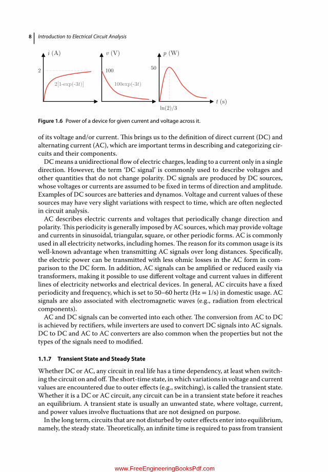
Example 3: Thevoltage and current of a device are given by 𝑣(t) = 100 exp(−3t)V andi(t) = 2[1 − exp(−3t)]A, respectively, as functions of time. Find the maximum power ofthe device.
Solution: We have
p(t) = 𝑣(t)i(t) = 200 exp(−3t)[1 − exp(−3t)]= 200[exp(−3t) − exp(−6t)] W
as the power of the device. We note that
p(0) = 0,p(∞) = 0.
In order to find the maximum point for the power, we usedp(t)
dt= 200[−3 exp(−3t) + 6 exp(−6t)] = 0,
leading to
16 exp(−6t) = 3 exp(−3t) −−−−→ exp(3t) = 2 −−−−→ t = ln(2)∕3 s.
Then the maximum power is
p(ln (2)∕3) = 200[exp(− ln (2)) − exp(−2 ln(2))]= 200(1∕2 − 1∕4) = 50 W.
Exercise 1: A device has a power of 60W when it is active and 10W when it is onstandby. An engineer measures that it spends a total of 2664 kJ energy in 24 hours. Howmany hours was the device actively used?
1.1.6 DC and AC Signals
Until now, we have considered the time concept in circuits for studying energy (whichneeds to be defined in time intervals) and power (which may depend on time). In fact,the time dependence of the power of a component corresponds to the time dependence
www.FreeEngineeringBooksPdf.com
8 Introduction to Electrical Circuit Analysis
i (A)
2
v (V) p (W)
t (s)
100 50
ln(2)/3
100exp(-3t) 2[1-exp(-3t)]
Figure 1.6 Power of a device for given current and voltage across it.
of its voltage and/or current. This brings us to the definition of direct current (DC) andalternating current (AC), which are important terms in describing and categorizing cir-cuits and their components.DCmeans a unidirectional flow of electric charges, leading to a current only in a single
direction. However, the term ‘DC signal’ is commonly used to describe voltages andother quantities that do not change polarity. DC signals are produced by DC sources,whose voltages or currents are assumed to be fixed in terms of direction and amplitude.Examples of DC sources are batteries and dynamos. Voltage and current values of thesesources may have very slight variations with respect to time, which are often neglectedin circuit analysis.AC describes electric currents and voltages that periodically change direction and
polarity.This periodicity is generally imposed byAC sources, whichmay provide voltageand currents in sinusoidal, triangular, square, or other periodic forms. AC is commonlyused in all electricity networks, including homes.The reason for its common usage is itswell-known advantage when transmitting AC signals over long distances. Specifically,the electric power can be transmitted with less ohmic losses in the AC form in com-parison to the DC form. In addition, AC signals can be amplified or reduced easily viatransformers, making it possible to use different voltage and current values in differentlines of electricity networks and electrical devices. In general, AC circuits have a fixedperiodicity and frequency, which is set to 50–60 hertz (Hz = 1/s) in domestic usage. ACsignals are also associated with electromagnetic waves (e.g., radiation from electricalcomponents).AC and DC signals can be converted into each other. The conversion from AC to DC
is achieved by rectifiers, while inverters are used to convert DC signals into AC signals.DC to DC and AC to AC converters are also common when the properties but not thetypes of the signals need to modified.
1.1.7 Transient State and Steady State
Whether DC or AC, any circuit in real life has a time dependency, at least when switch-ing the circuit on and off.The short-time state, in which variations in voltage and currentvalues are encountered due to outer effects (e.g., switching), is called the transient state.Whether it is a DC or AC circuit, any circuit can be in a transient state before it reachesan equilibrium. A transient state is usually an unwanted state, where voltage, current,and power values involve fluctuations that are not designed on purpose.In the long term, circuits that are not disturbed by outer effects enter into equilibrium,
namely, the steady state.Theoretically, an infinite time is required to pass from transient
www.FreeEngineeringBooksPdf.com

Introduction 9
i (A), v (V)
t (s) transient
statesteadystate
i (A), v (V)
t (s)transient
statesteadystate
Figure 1.7 Transient state and steady state in DC and AC signals.
state to equilibrium, while most circuits are assumed to reach steady state after a suffi-cient period (i.e., when fluctuations become negligible). For DC circuits in steady state,voltage and current values are assumed to be constant. In the first few chapters, a steadystate is automatically assumed when only resistors and DC sources are considered. Infact, the time needed to pass from transient state to steady state depends on a time con-stant, which is a contribution of both resistors and energy-storage elements (capacitorsand inductors). Hence, circuits with only resistors and DC sources have zero transienttime, that is, they can be assumed to be in steady state without any transient analysis. ForAC circuits, voltages and currents in steady state oscillate with the time period dictatedby the sources.Therefore, we emphasize that the steady state does not indicate constantproperties for all circuits.
1.1.8 Frequency in Circuits
When AC sources are involved in a circuit, voltage and current values oscillate withrespect to time. In most cases, the periodicity and frequency are fixed, that is, all volt-ages and currents change at the same rate, while there can be phase differences (delays)between them.The behavior of some components does not rely on the frequency, unlessthey are exposed to extreme conditions. As an example, resistors behave almost the samein a wide range of frequencies. On the other hand, many components, such as capaci-tors and inductors, strongly depend on the frequency. With DC sources, correspondingto zero frequency, capacitors/inductors act like open/short circuits, while they becomealmost the opposite at very high frequencies. Therefore, the behavior of an AC circuitdirectly depends on the frequency, as discussed extensively in time-harmonic analysis.
1.2 Resistance and Resistors
Resistors (Figure 11.1) are fundamental components in electrical circuits. They arebasically energy-consuming elements that are used to control voltage and currentvalues in circuits. In addition, the energy conversion ability of resistors can be usefulin various applications, where these elements are directly used for heating and lighting(conventional bulbs). Specifically, the energy consumed by a resistor is usually releasedas heat, and sometimes as useful light. Resistance is a common property of all metals,and even very conductive wires have resistances, which may need to be included incircuit analysis.
www.FreeEngineeringBooksPdf.com
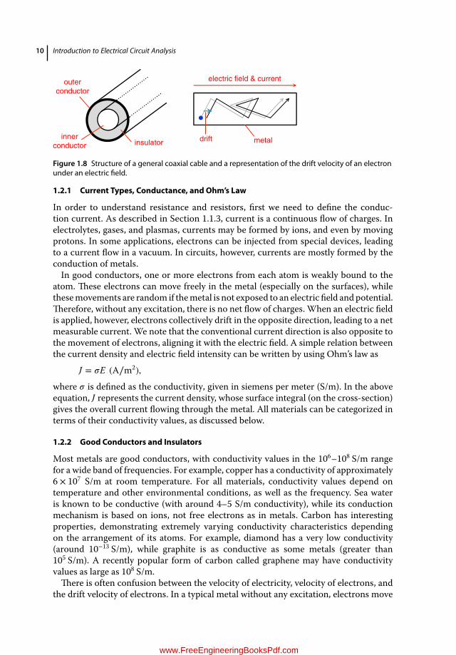
10 Introduction to Electrical Circuit Analysis
outerconductor
innerconductor insulator drift metal
electric field & current
Figure 1.8 Structure of a general coaxial cable and a representation of the drift velocity of an electronunder an electric field.
1.2.1 Current Types, Conductance, and Ohm’s Law
In order to understand resistance and resistors, first we need to define the conduc-tion current. As described in Section 1.1.3, current is a continuous flow of charges. Inelectrolytes, gases, and plasmas, currents may be formed by ions, and even by movingprotons. In some applications, electrons can be injected from special devices, leadingto a current flow in a vacuum. In circuits, however, currents are mostly formed by theconduction of metals.In good conductors, one or more electrons from each atom is weakly bound to the
atom. These electrons can move freely in the metal (especially on the surfaces), whilethesemovements are random if themetal is not exposed to an electric field and potential.Therefore, without any excitation, there is no net flow of charges. When an electric fieldis applied, however, electrons collectively drift in the opposite direction, leading to a netmeasurable current. We note that the conventional current direction is also opposite tothe movement of electrons, aligning it with the electric field. A simple relation betweenthe current density and electric field intensity can be written by using Ohm’s law as
J = 𝜎E (A∕m2),
where 𝜎 is defined as the conductivity, given in siemens per meter (S/m). In the aboveequation, J represents the current density, whose surface integral (on the cross-section)gives the overall current flowing through the metal. All materials can be categorized interms of their conductivity values, as discussed below.
1.2.2 Good Conductors and Insulators
Most metals are good conductors, with conductivity values in the 106–108 S/m rangefor a wide band of frequencies. For example, copper has a conductivity of approximately6 × 107 S/m at room temperature. For all materials, conductivity values depend ontemperature and other environmental conditions, as well as the frequency. Sea wateris known to be conductive (with around 4–5 S/m conductivity), while its conductionmechanism is based on ions, not free electrons as in metals. Carbon has interestingproperties, demonstrating extremely varying conductivity characteristics dependingon the arrangement of its atoms. For example, diamond has a very low conductivity(around 10−13 S/m), while graphite is as conductive as some metals (greater than105 S/m). A recently popular form of carbon called graphene may have conductivityvalues as large as 108 S/m.There is often confusion between the velocity of electricity, velocity of electrons, and
the drift velocity of electrons. In a typical metal without any excitation, electrons move
www.FreeEngineeringBooksPdf.com
Introduction 11
randomly with a high (Fermi) velocity. These movements are of high speed (e.g., 1.57 ×10⁶ m/s for copper). However, due to their random nature, no net current flows alongthe metal. When the metal is exposed to a voltage difference, leading to an electricfield, electrons continue their randommovements, while they tend to drift in the oppo-site direction to the electric field. The corresponding drift velocity is usually very low(e.g., only 10−5 m/s for a typical copper wire). On the other hand, the current measuredalong a wire is due to this drift velocity. Obviously, when AC sources are involved, elec-trons do not drift only in a single direction, but oscillate back and forth (in addition tohigh-velocity random movements) with the frequency of the signal. Since circuits areusually small with respect to wavelength, drift movements of electrons are almost syn-chronized through the entire circuit. Finally, the velocity of the electricity along a wire isnot related to any actual movement of electrons. It is related to the speed of the electro-magnetic wave through the wire (similar to sea waves that are not movements of watermolecules).This speed is comparable to the speed of light in a vacuum, but it is reducedby a velocity factor depending on the properties of the material.In general, materials with low conductivity values are called insulators. Wood, glass,
rubber, air, and Teflon are well-known insulators in real-life applications. Insulators arealso natural parts of all circuits, for example for isolating components and wires fromeach other, as well as the parts of electrical components. Since they are not electricallyactive, however, they are not considered directly in circuit analysis. For example, whenconsidering wires in circuits, we assume perfectly conducting metals without any insu-lator, while in real life, electrical wires have shielded or coaxial structures with layers ofconducting metals and insulating materials separating them.
1.2.3 Semiconductors
As their name suggests, semiconductors conduct electricity better than insulators andworse than good conductors. In addition, the conductivity of semiconductors can bealtered by externally modifying their material properties permanently (via chemicalprocesses) and temporarily (via electrical bias), making them suitable for controllingelectricity. Silicon is the best-known semiconductor, and has been used in producingdiverse components of integrated circuits. The key chemical operation is called doping,that is, modifying the conductivity of semiconductors by introducing impuritiesinto their crystal lattice structures. This way, different (e.g., n-type, p-type) kinds ofsemiconductors can be produced and used to form junctions that enable control overelectric current and voltage. Engineers use many different types of semiconductingdevices, such as diodes and transistors, to construct modern circuits. These specialcomponents are discussed in Chapter 8.
1.2.4 Superconductivity and Perfect Conductivity
Perfect conductivity is a theoretical limit when the conductivity of ametal becomes infi-nite, that is, 𝜎 → ∞. In this case, if a current J exists along the metal, E → 0 and there isno potential difference over it. Therefore, a perfect conductor does not dissipate powerwhile conducting electricity. Perfect conductivity is an idealized property as all metalsactually have finite conductivity, while some metals can be assumed to be perfect con-ductors to simplify theirmodeling. In circuit analysis, all wires are assumed to be perfect
www.FreeEngineeringBooksPdf.com
12 Introduction to Electrical Circuit Analysis
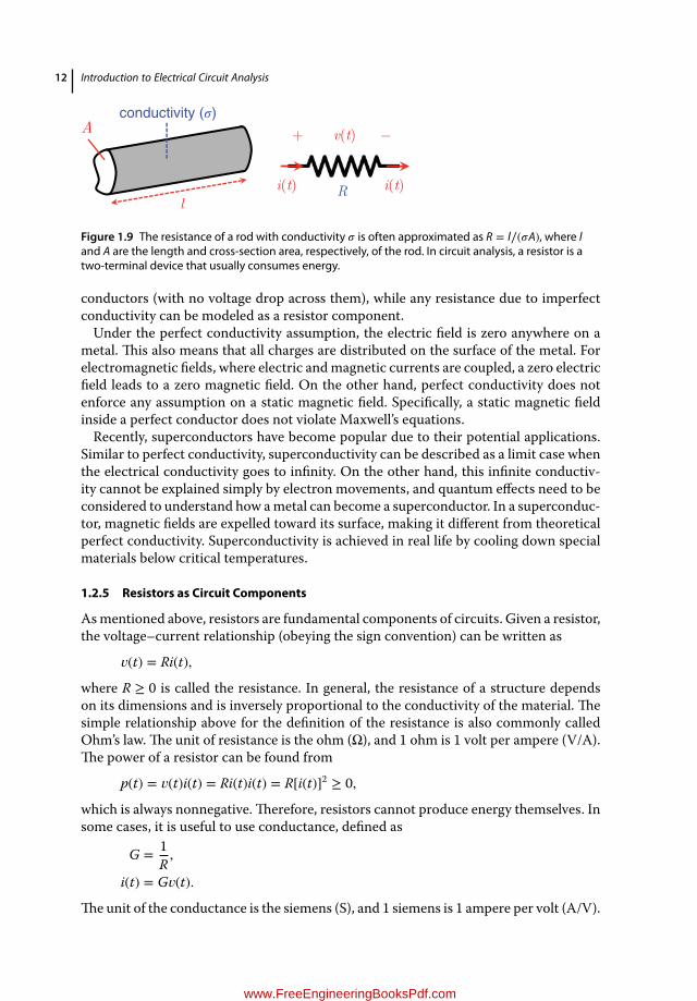
l
A conductivity (𝜎)
v(t)+ _
i(t) i(t) R
Figure 1.9 The resistance of a rod with conductivity 𝜎 is often approximated as R = l∕(𝜎A), where land A are the length and cross-section area, respectively, of the rod. In circuit analysis, a resistor is atwo-terminal device that usually consumes energy.
conductors (with no voltage drop across them), while any resistance due to imperfectconductivity can be modeled as a resistor component.Under the perfect conductivity assumption, the electric field is zero anywhere on a
metal. This also means that all charges are distributed on the surface of the metal. Forelectromagnetic fields, where electric andmagnetic currents are coupled, a zero electricfield leads to a zero magnetic field. On the other hand, perfect conductivity does notenforce any assumption on a static magnetic field. Specifically, a static magnetic fieldinside a perfect conductor does not violate Maxwell’s equations.Recently, superconductors have become popular due to their potential applications.
Similar to perfect conductivity, superconductivity can be described as a limit case whenthe electrical conductivity goes to infinity. On the other hand, this infinite conductiv-ity cannot be explained simply by electron movements, and quantum effects need to beconsidered to understand how ametal can become a superconductor. In a superconduc-tor, magnetic fields are expelled toward its surface, making it different from theoreticalperfect conductivity. Superconductivity is achieved in real life by cooling down specialmaterials below critical temperatures.
1.2.5 Resistors as Circuit Components
Asmentioned above, resistors are fundamental components of circuits. Given a resistor,the voltage–current relationship (obeying the sign convention) can be written as
𝑣(t) = Ri(t),
where R ≥ 0 is called the resistance. In general, the resistance of a structure dependson its dimensions and is inversely proportional to the conductivity of the material. Thesimple relationship above for the definition of the resistance is also commonly calledOhm’s law.The unit of resistance is the ohm (Ω), and 1 ohm is 1 volt per ampere (V/A).The power of a resistor can be found from
p(t) = 𝑣(t)i(t) = Ri(t)i(t) = R[i(t)]2 ≥ 0,
which is always nonnegative.Therefore, resistors cannot produce energy themselves. Insome cases, it is useful to use conductance, defined as
G = 1R,
i(t) = G𝑣(t).
Theunit of the conductance is the siemens (S), and 1 siemens is 1 ampere per volt (A/V).
www.FreeEngineeringBooksPdf.com
Introduction 13
v+ _
i i
v+ = 0 _
i i i = 0
v+ _
i = 0R R = 0 R = ∞
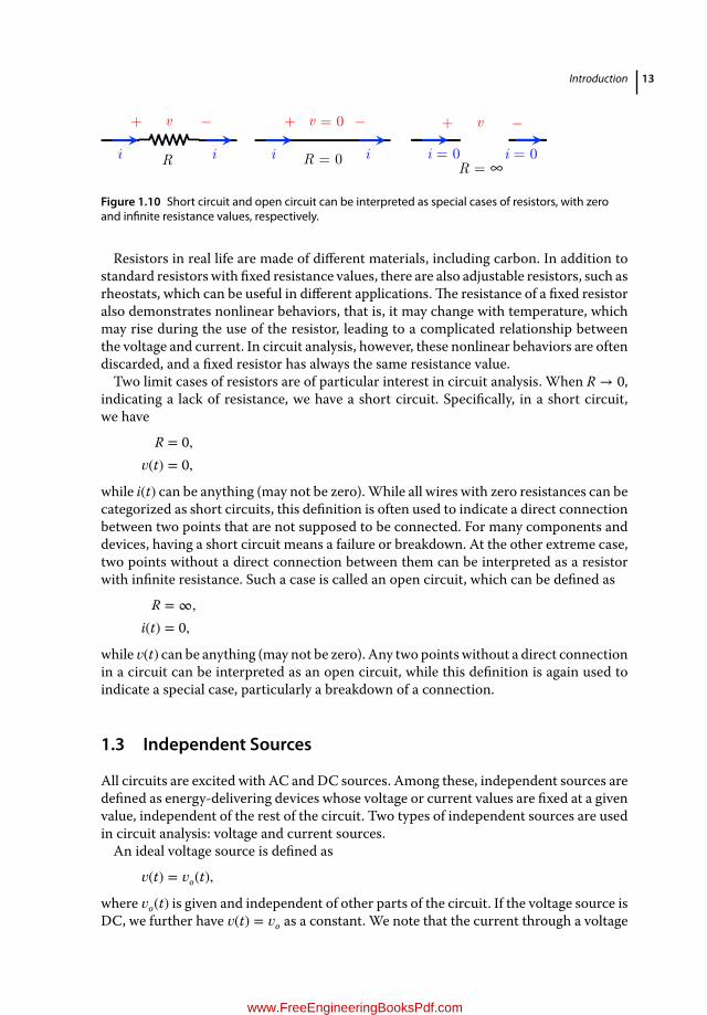
Figure 1.10 Short circuit and open circuit can be interpreted as special cases of resistors, with zeroand infinite resistance values, respectively.
Resistors in real life are made of different materials, including carbon. In addition tostandard resistors with fixed resistance values, there are also adjustable resistors, such asrheostats, which can be useful in different applications.The resistance of a fixed resistoralso demonstrates nonlinear behaviors, that is, it may change with temperature, whichmay rise during the use of the resistor, leading to a complicated relationship betweenthe voltage and current. In circuit analysis, however, these nonlinear behaviors are oftendiscarded, and a fixed resistor has always the same resistance value.Two limit cases of resistors are of particular interest in circuit analysis. When R → 0,
indicating a lack of resistance, we have a short circuit. Specifically, in a short circuit,we have
R = 0,𝑣(t) = 0,
while i(t) can be anything (may not be zero).While all wires with zero resistances can becategorized as short circuits, this definition is often used to indicate a direct connectionbetween two points that are not supposed to be connected. For many components anddevices, having a short circuit means a failure or breakdown. At the other extreme case,two points without a direct connection between them can be interpreted as a resistorwith infinite resistance. Such a case is called an open circuit, which can be defined as
R = ∞,
i(t) = 0,
while 𝑣(t) can be anything (may not be zero). Any two points without a direct connectionin a circuit can be interpreted as an open circuit, while this definition is again used toindicate a special case, particularly a breakdown of a connection.
1.3 Independent Sources
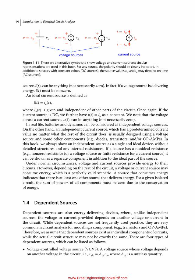
All circuits are excited with AC and DC sources. Among these, independent sources aredefined as energy-delivering devices whose voltage or current values are fixed at a givenvalue, independent of the rest of the circuit. Two types of independent sources are usedin circuit analysis: voltage and current sources.An ideal voltage source is defined as
𝑣(t) = 𝑣o(t),
where 𝑣o(t) is given and independent of other parts of the circuit. If the voltage source isDC, we further have 𝑣(t) = 𝑣o as a constant. We note that the current through a voltage
www.FreeEngineeringBooksPdf.com
14 Introduction to Electrical Circuit Analysis
v = vo v = vo+ + _ _
voltage sources
i = io
i = iovovo iov = -vo
+ _
vo
current source
Figure 1.11 There are alternative symbols to show voltage and current sources; circularrepresentations are used in this book. For any source, the polarity should be clearly indicated. Inaddition to sources with constant values (DC sources), the source values 𝑣o and io may depend on time(AC sources).
source, i(t), can be anything (not necessarily zero). In fact, if a voltage source is deliveringenergy, i(t)must be nonzero.An ideal current source is defined as
i(t) = io(t),
where io(t) is given and independent of other parts of the circuit. Once again, if thecurrent source is DC, we further have i(t) = io as a constant. We note that the voltageacross a current source, 𝑣(t), can be anything (not necessarily zero).In real life, batteries and dynamos can be considered as independent voltage sources.
On the other hand, an independent current source, which has a predetermined currentvalue no matter what the rest of the circuit does, is usually designed using a voltagesource and some other components (e.g., diodes, transistors, and/or OP-AMPs). Inthis book, we always show an independent source as a single and ideal device, withoutdetailed structures and any internal resistances. If a source has a nonideal resistance(e.g., nonzero resistance for a voltage source or finite resistance for a current source) itcan be shown as a separate component in addition to the ideal part of the source.Under normal circumstances, voltage and current sources provide energy to their
circuits. However, depending on the rest of the circuit, a voltage or current source mayconsume energy, which is a perfectly valid scenario. A source that consumes energyindicates that there is at least one other source that delivers energy. For a given isolatedcircuit, the sum of powers of all components must be zero due to the conservationof energy.
1.4 Dependent Sources
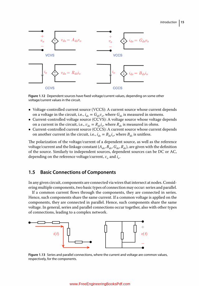
Dependent sources are also energy-delivering devices, where, unlike independentsources, the voltage or current provided depends on another voltage or current inthe circuit. While dependent sources are not frequently used practice, they are verycommon in circuit analysis for modeling a component, (e.g., transistors andOP-AMPs).Therefore, we assume that dependent sources exist as individual components of circuits,while the actual circuit structure may not be exactly the same. There are four types ofdependent sources, which can be listed as follows.
• Voltage-controlled voltage source (VCVS): A voltage source whose voltage dependson another voltage in the circuit, i.e., 𝑣ds = Ads𝑣o, where Ads is a unitless quantity.
www.FreeEngineeringBooksPdf.com
Introduction 15
vo+ _
vds = Adsvo vo+ _
ids = Gdsvo
VCVS VCCS
vds = Rdsio ids = Bdsio
CCVS CCCS
io io
↓
↓
+−
+−
Figure 1.12 Dependent sources have fixed voltage/current values, depending on some othervoltage/current values in the circuit.
• Voltage-controlled current source (VCCS): A current source whose current dependson a voltage in the circuit, i.e., ids = Gds𝑣o, where Gds is measured in siemens.
• Current-controlled voltage source (CCVS): A voltage source whose voltage dependson a current in the circuit, i.e., 𝑣ds = Rdsio, where Rds is measured in ohms.
• Current-controlled current source (CCCS): A current source whose current dependson another current in the circuit, i.e., ids = Bdsio, where Bds is unitless.
The polarization of the voltage/current of a dependent source, as well as the referencevoltage/current and the linkage constant (Ads, Bds, Gds, Rds), are given with the definitionof the source. Similarly to independent sources, dependent sources can be DC or AC,depending on the reference voltage/current, 𝑣o and io.
1.5 Basic Connections of Components
In any given circuit, components are connected viawires that intersect at nodes. Consid-eringmultiple components, two basic types of connectionmay occur: series and parallel.If a common current flows through the components, they are connected in series.
Hence, such components share the same current. If a common voltage is applied on thecomponents, they are connected in parallel. Hence, such components share the samevoltage. In general, series and parallel connections occur together, also with other typesof connections, leading to a complex network.
i(t) v(t)+
_
Figure 1.13 Series and parallel connections, where the current and voltage are common values,respectively, for the components.
www.FreeEngineeringBooksPdf.com

16 Introduction to Electrical Circuit Analysis
10V 20V
10A 20A
10A
10A
10A
10V
10V + _ 10V
Figure 1.14 Some possible and impossible configurations using ideal components.
Considering ideal components, some of the connections are impossible. Some basicexamples of possible and impossible scenarios are as follows.
• A 10A current source and a 20A current source cannot be connected in series.• A 10A current source and an open circuit cannot be connected in series.• A 10A current source and a short circuit can be connected in series. If these are the
only components of the circuit (with a full connection on both terminals), no voltageoccurs across the current source; hence, it does not produce any power.
• A 10V voltage source and a 20V voltage source cannot be connected in parallel.• A 10V voltage source and an open circuit can be connected in parallel. If these are the
only components of the circuit, no current flows through the voltage source; hence,it does not produce any power.
• A 10V voltage source and a short circuit cannot be connected in parallel.
In order to understand why a connection may not be possible, one can directly usethe definition of the components. For example, consider a series connection of 10Aand 20A current sources. The 10A source indicates that 10A is passing through theline. On the other hand, the 20A source, by definition, needs 20A current to flow in thesame line.Therefore, there is an inconsistency, since a wire cannot have different currentvalues at the same time. Similar inconsistencies can be found for all impossible cases.Such impossible configurations are not due to amodeling incapability in circuit analysis;they actually correspond to physically impossible practices in real life. Consider anotherexample involving a parallel connection of two voltage sources with different values. Inreal life, this configuration never exists since voltage sources have internal resistances,while the wires between them are also not perfectly conducting, leading to a voltagedrop.Therefore, a more realistic model of the physical scenario would require a resistorbetween the voltage sources, leading to a perfectly valid circuit that can be analyzed.All impossible configurations described above have similar missing components, whichcan be added to convert them into possible scenarios.Impossible scenarios rarely occur, even when we consider ideal components in circuit
analysis. In general, many circuits have multiple components and connections, wherethe voltage and current values become consistent. In order to find relations betweenvoltage and current values, we use basic rules, namely Kirchhoff’s laws, as described inthe next chapter.These rules, which are based on the conservation of energy and charge,provide the necessary equations to relate different voltage and current values.
www.FreeEngineeringBooksPdf.com
Introduction 17
10V 10A 10V 10A 10V + _
10A
0A
0V + _ 10V
+ _
10A
Figure 1.15 Some possible circuits involving only one or two components that are connectedconsistently. In the first and second circuits, where there is a current and a voltage source, the sourcesdo not produce any power. However, they still provide the current and voltage values, in accordancewith their definitions. In the third circuit, the voltage source absorbs power (100 W), while the currentsource delivers power (100 W).
10V 20V
1Ω
10V + _ 20V
+ _
10A 20A
1Ω 10A 20A
Figure 1.16 Two simple circuits that can be interpreted incorrectly as impossible. In fact, both twocircuits are possible and they involve consistent voltage and current values. In the first circuit, avoltage drop (by an amount of 20 − 10 = 10 V) exists across the resistor. In the second circuit, anonzero current (20 − 10 = 10 A) flows through the resistor. These values can easily be found byapplying Kirchhoff’s laws, as described in the next chapter.
At this stage, we can start analyzing some simple circuits, just by considering the def-initions of the components.
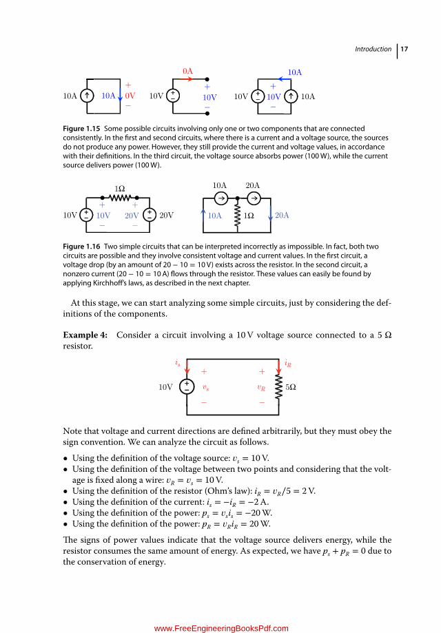
Example 4: Consider a circuit involving a 10V voltage source connected to a 5 Ωresistor.
10V 5Ω
is iR
vs
+
_ vR
+
_
Note that voltage and current directions are defined arbitrarily, but they must obey thesign convention. We can analyze the circuit as follows.
• Using the definition of the voltage source: 𝑣s = 10V.• Using the definition of the voltage between two points and considering that the volt-
age is fixed along a wire: 𝑣R = 𝑣s = 10V.• Using the definition of the resistor (Ohm’s law): iR = 𝑣R∕5 = 2V.• Using the definition of the current: is = −iR = −2A.• Using the definition of the power: ps = 𝑣sis = −20W.• Using the definition of the power: pR = 𝑣RiR = 20W.
The signs of power values indicate that the voltage source delivers energy, while theresistor consumes the same amount of energy. As expected, we have ps + pR = 0 due tothe conservation of energy.
www.FreeEngineeringBooksPdf.com
18 Introduction to Electrical Circuit Analysis
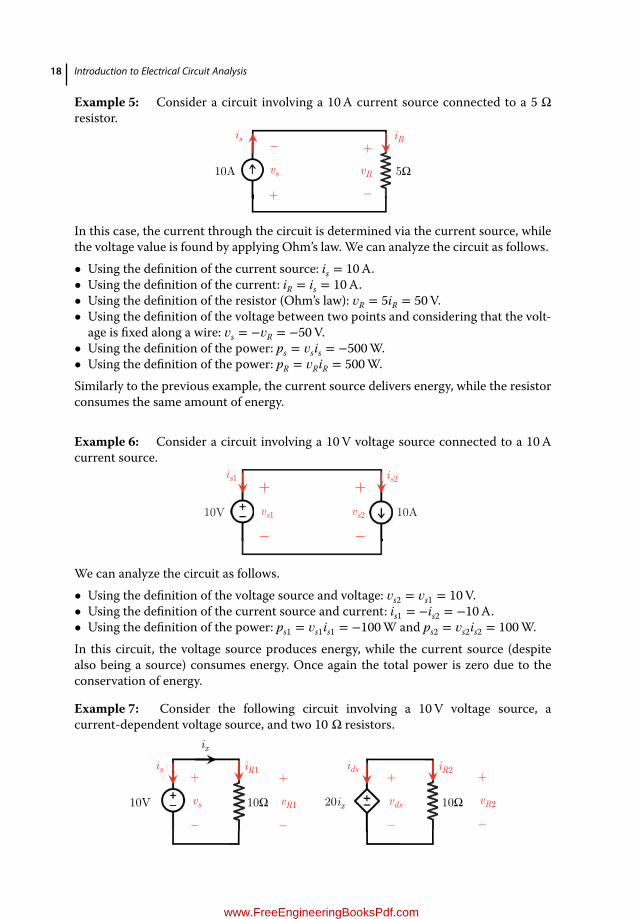
Example 5: Consider a circuit involving a 10A current source connected to a 5 Ωresistor.
10A 5Ω
is iR
vs vR
+
_ +
_
In this case, the current through the circuit is determined via the current source, whilethe voltage value is found by applying Ohm’s law. We can analyze the circuit as follows.• Using the definition of the current source: is = 10A.• Using the definition of the current: iR = is = 10A.• Using the definition of the resistor (Ohm’s law): 𝑣R = 5iR = 50V.• Using the definition of the voltage between two points and considering that the volt-
age is fixed along a wire: 𝑣s = −𝑣R = −50V.• Using the definition of the power: ps = 𝑣sis = −500W.• Using the definition of the power: pR = 𝑣RiR = 500W.Similarly to the previous example, the current source delivers energy, while the resistorconsumes the same amount of energy.
Example 6: Consider a circuit involving a 10V voltage source connected to a 10Acurrent source.
10V 10A
is1 is2
vs1
+
_vs2
+
_
We can analyze the circuit as follows.• Using the definition of the voltage source and voltage: 𝑣s2 = 𝑣s1 = 10V.• Using the definition of the current source and current: is1 = −is2 = −10A.• Using the definition of the power: ps1 = 𝑣s1is1 = −100W and ps2 = 𝑣s2is2 = 100W.In this circuit, the voltage source produces energy, while the current source (despitealso being a source) consumes energy. Once again the total power is zero due to theconservation of energy.
Example 7: Consider the following circuit involving a 10V voltage source, acurrent-dependent voltage source, and two 10 Ω resistors.
10V 10Ω 10Ω
ixis ids
vs
+
_ vR1
+
_ vR2
+
_ vds
+
_ 20ix
iR1 iR2
www.FreeEngineeringBooksPdf.com
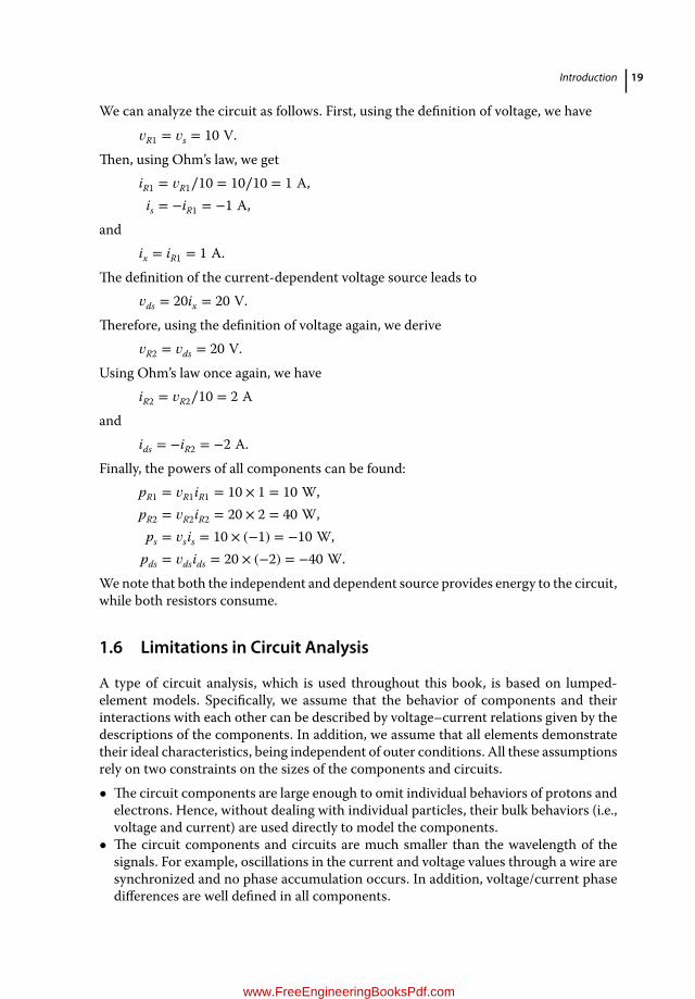
Introduction 19
We can analyze the circuit as follows. First, using the definition of voltage, we have𝑣R1 = 𝑣s = 10 V.
Then, using Ohm’s law, we getiR1 = 𝑣R1∕10 = 10∕10 = 1 A,
is = −iR1 = −1 A,and
ix = iR1 = 1 A.The definition of the current-dependent voltage source leads to
𝑣ds = 20ix = 20 V.Therefore, using the definition of voltage again, we derive
𝑣R2 = 𝑣ds = 20 V.Using Ohm’s law once again, we have
iR2 = 𝑣R2∕10 = 2 Aand
ids = −iR2 = −2 A.Finally, the powers of all components can be found:
pR1 = 𝑣R1iR1 = 10 × 1 = 10 W,pR2 = 𝑣R2iR2 = 20 × 2 = 40 W,
ps = 𝑣sis = 10 × (−1) = −10 W,pds = 𝑣dsids = 20 × (−2) = −40 W.
We note that both the independent and dependent source provides energy to the circuit,while both resistors consume.
1.6 Limitations in Circuit Analysis
A type of circuit analysis, which is used throughout this book, is based on lumped-element models. Specifically, we assume that the behavior of components and theirinteractions with each other can be described by voltage–current relations given by thedescriptions of the components. In addition, we assume that all elements demonstratetheir ideal characteristics, being independent of outer conditions. All these assumptionsrely on two constraints on the sizes of the components and circuits.• The circuit components are large enough to omit individual behaviors of protons and
electrons. Hence, without dealing with individual particles, their bulk behaviors (i.e.,voltage and current) are used directly to model the components.
• The circuit components and circuits are much smaller than the wavelength of thesignals. For example, oscillations in the current and voltage values through a wire aresynchronized and no phase accumulation occurs. In addition, voltage/current phasedifferences are well defined in all components.
www.FreeEngineeringBooksPdf.com

20 Introduction to Electrical Circuit Analysis
Obviously, lumped-element models fail when the size constraints are not satisfied. Forexample, in circuits larger than the wavelength, connections may need to be modeledas transmission lines, where wave equations are solved. Some circuits may need the fullapplication of Maxwell’s equations to precisely describe the electromagnetic interac-tions of components with each other.Depending on the complexity of the circuit model, further assumptions are often
made to simplify the analysis of circuits. In this book, we accept the following assump-tions that are also common in the circuit analysis literature.
• The voltage–current relationship defined for a component does not depend on outerconditions (temperature, pressure, light, etc.).This alsomeans that the circuit behavesalways the same (e.g., change in resistance due to rising temperature as the circuit isused is omitted).
• The voltage–current relationship defined for a component does not depend on othercomponents. For example, a resistor of 10 Ω always satisfies Ohm’s law as 𝑣R = 10iR,independent of other elements used in the same circuit. We also ignore cross-talkof circuits and their parts, other than the linkage through well-defined dependentsources.
• All components are ideal and we omit secondary effects, such as the resistance of avoltage source, inductance of a capacitor, or capacitance of a resistor. If these effectscannot be neglected, they can be represented as individual components. For example,the leakage of a capacitor can be represented by a resistor connected in parallel to thecapacitor.
Despite all these limitations and assumptions, circuit analysis methods presented in thisbook are widely accepted and used to analyze diverse circuits and electrical devices.In many cases, lumped elements are used as starting models before more complicatedanalysis techniques are applied.
1.7 What You Need to Know before You Continue
Before proceeding to the next chapter, we summarize a few key points that need to beknown to understand the higher-level topics.
• Sign convention: In this book, the current through a component is selected to flowfrom the positive to the negative side of the voltage.
• Steady state: For DC circuits in steady state, voltage and current values are assumedto be constant. In the first few chapters, steady state is automatically assumed whenonly resistors and DC sources are considered.
• Short circuit and open circuit: Short circuit and open circuit can be interpreted asspecial cases of resistors, with zero and infinite resistance values, respectively.
• Sources: There are alternative symbols to show voltage and current sources; circularrepresentations are used in this book. DC/AC types are indicated in the context ofsource values.
• Energy conservation: For a given isolated circuit, the sumof powers of all componentsmust be zero due to the conservation of energy.
www.FreeEngineeringBooksPdf.com

Introduction 21
• Series connection: Components that share the same current are connected in series.• Parallel connection: Components that share the same voltage are connected in
parallel.• Impossible configurations: Some connections of ideal components are not allowed
due to inconsistency of voltage and current values enforced by the definitions ofcomponents.
In the next chapter, we startwith themost basic tools, namelyKirchhoff’s laws, to analyzecircuits.
www.FreeEngineeringBooksPdf.com

www.FreeEngineeringBooksPdf.com
23
2
Basic Tools: Kirchhoff’s Laws
Circuits with a few components can be analyzed by using only the definitions of thecomponents. On the other hand, as the circuits become more complicated, involvingconnections of many components, well-defined solution tools are required to derive thenecessary equations. This chapter presents the most basic laws of circuit analysis basedon the conservation of charges (Kirchhoff’s current law) and conservation of energy(Kirchhoff’s voltage law).These fundamental rules, collectively named Kirchhoff’s laws,can be used to derive useful equations at nodes and in loops, in order to relate the volt-ages and currents of components to each other. Solutions of the resulting equations leadto numerical values of these variables, hence the analysis of the given circuit.In general, Kirchhoff’s laws should be sufficient to solve any type of circuit. On the
other hand, when a circuit involves many resistors, a direct application of Kirchhoff’slaws may lead to too many equations that can be difficult to solve. For scenarios ofthis kind, where multiple resistors are connected in series and parallel, one can deriveshortcuts (again using Kirchhoff’s laws) to simplify and represent the overall circuitusing a few resistors. This chapter also presents such shortcuts for the analysis of largeresistive circuits.
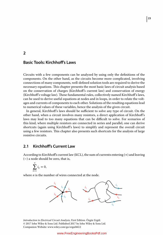
2.1 Kirchhoff’s Current Law
According to Kirchhoff’s current law (KCL), the sumof currents entering (+) and leaving(−) a node should be zero, that is,
n∑k=1
ik = 0,
where n is the number of wires connected at the node.
i1
i2 i3
i5 i4 i1
i2
i3
i4
i5
Introduction to Electrical Circuit Analysis, First Edition. Özgür Ergül.© 2017 John Wiley & Sons Ltd. Published 2017 by John Wiley & Sons Ltd.Companion Website: www.wiley.com/go/ergul4412
www.FreeEngineeringBooksPdf.com
24 Introduction to Electrical Circuit Analysis
In the examples above, we have
i1 + i2 − i3 + i4 − i5 = 0.
The conservation of charge is the background to KCL, which can be generalized to cur-rents entering and leaving closed surfaces. While the selection could be arbitrary, wealways select the entering and leaving currents as positive and negative, respectively.Obviously, KCL assumes that no charge accumulation occurs at the node or closed sur-face considered.In the analysis of circuits, we usually apply KCL at nodes.The format that we adopt is
• KCL(x): equation derived by applying KCL,
where x represents the node.
2.2 Kirchhoff’s Voltage Law
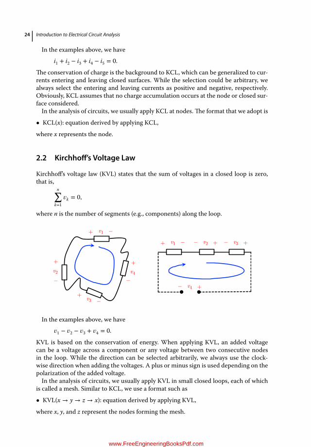
Kirchhoff’s voltage law (KVL) states that the sum of voltages in a closed loop is zero,that is,
n∑k=1
𝑣k = 0,
where n is the number of segments (e.g., components) along the loop.
_+ v1
+
_v2
+ v3 _
_
+v4
_+ v1 v2_ + v3
_ +
v4_ +
In the examples above, we have
𝑣1 − 𝑣2 − 𝑣3 + 𝑣4 = 0.
KVL is based on the conservation of energy. When applying KVL, an added voltagecan be a voltage across a component or any voltage between two consecutive nodesin the loop. While the direction can be selected arbitrarily, we always use the clock-wise direction when adding the voltages. A plus or minus sign is used depending on thepolarization of the added voltage.In the analysis of circuits, we usually apply KVL in small closed loops, each of which
is called a mesh. Similar to KCL, we use a format such as
• KVL(x → y → z → x): equation derived by applying KVL,
where x, y, and z represent the nodes forming the mesh.
www.FreeEngineeringBooksPdf.com
Basic Tools: Kirchhoff’s Laws 25
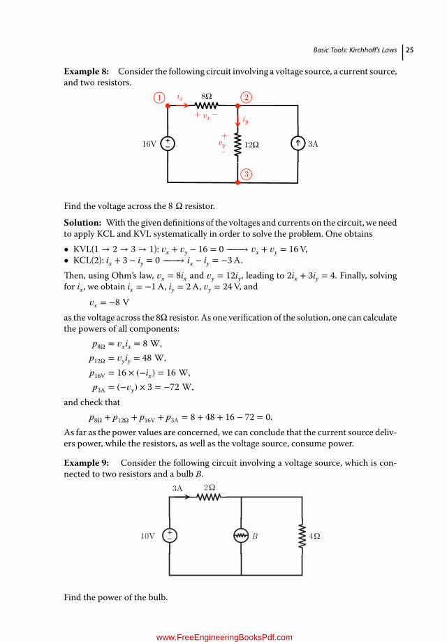
Example 8: Consider the following circuit involving a voltage source, a current source,and two resistors.
16V
8Ω
iy+
vy
+ _
_
1 2
3
vx
ix
12Ω 3A
Find the voltage across the 8 Ω resistor.
Solution: With the given definitions of the voltages and currents on the circuit, we needto apply KCL and KVL systematically in order to solve the problem. One obtains• KVL(1 → 2 → 3 → 1): 𝑣x + 𝑣y − 16 = 0 −−−−→ 𝑣x + 𝑣y = 16V,• KCL(2): ix + 3 − iy = 0 −−−−→ ix − iy = −3A.Then, using Ohm’s law, 𝑣x = 8ix and 𝑣y = 12iy, leading to 2ix + 3iy = 4. Finally, solvingfor ix, we obtain ix = −1A, iy = 2A, 𝑣y = 24V, and
𝑣x = −8 Vas the voltage across the 8Ω resistor. As one verification of the solution, one can calculatethe powers of all components:
p8Ω = 𝑣xix = 8 W,
p12Ω = 𝑣yiy = 48 W,
p16V = 16 × (−ix) = 16 W,
p3A = (−𝑣y) × 3 = −72 W,
and check thatp8Ω + p12Ω + p16V + p3A = 8 + 48 + 16 − 72 = 0.
As far as the power values are concerned, we can conclude that the current source deliv-ers power, while the resistors, as well as the voltage source, consume power.
Example 9: Consider the following circuit involving a voltage source, which is con-nected to two resistors and a bulb B.
10V
2Ω
4Ω
3A
B
Find the power of the bulb.
www.FreeEngineeringBooksPdf.com

26 Introduction to Electrical Circuit Analysis
Solution: In most circuits, the voltage and current directions are not defined a priori.Therefore, when analyzing such a circuit, we define the directions arbitrarily, whileenforcing the sign convention for all components. When a current/voltage valueis found to be negative, we understand that the initial assumption is not correct.However, this is not a problem at all, provided that we are consistent with the directionsthroughout the solution.For the circuit above, we label the nodes, define the directions of the currents, and
define the voltages in accordance with the sign convention, as follows.
10V
2Ω
4Ω
3A
B
ix iy+
vx+
+ _
_ _
1 2
3
Using KVL, one obtains
• KVL(1 → 2 → 3 → 1): −10 + 3 × 2 + 𝑣x = 0 −−−−→ 𝑣x = 4V.
Then, using Ohm’s law, iy = 𝑣x∕4 = 1A, and we further have
• KCL(2): 3 − ix − iy = 0 −−−−→ ix = 3 − 1 = 2A.
Finally, the power of the device is found to be
pB = 𝑣xix = 4 × 2 = 8 W.
Example 10: Consider the following circuit involving two voltage sources connectedto three resistors.
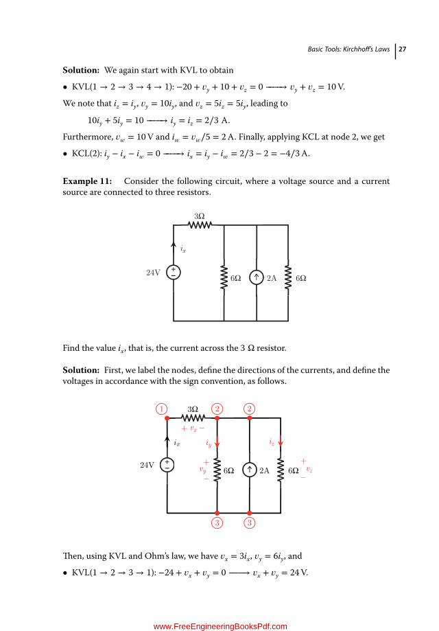
20V
10Ω
ix+ _ 1 2
3
vy
iy
10V 5Ω
4
iw
vw + _
iz 5Ω
+_ vz
Find the value of ix that passes through the 10V source.
www.FreeEngineeringBooksPdf.com
Basic Tools: Kirchhoff’s Laws 27
Solution: We again start with KVL to obtain
• KVL(1 → 2 → 3 → 4 → 1): −20 + 𝑣y + 10 + 𝑣z = 0 −−−−→ 𝑣y + 𝑣z = 10V.
We note that iz = iy, 𝑣y = 10iy, and 𝑣z = 5iz = 5iy, leading to
10iy + 5iy = 10 −−−−→ iy = iz = 2∕3 A.
Furthermore, 𝑣𝑤= 10V and i
𝑤= 𝑣
𝑤∕5 = 2A. Finally, applying KCL at node 2, we get
• KCL(2): iy − ix − i𝑤= 0 −−−−→ ix = iy − i
𝑤= 2∕3 − 2 = −4∕3A.
Example 11: Consider the following circuit, where a voltage source and a currentsource are connected to three resistors.
3Ω
6Ω2A24V 6Ω
ix
Find the value ix, that is, the current across the 3 Ω resistor.
Solution: First, we label the nodes, define the directions of the currents, and define thevoltages in accordance with the sign convention, as follows.
3Ω
6Ω2A 24V 6Ω
i iziy+ _
+_
+_
1 2 2
3 3
vx
vy vz
x
Then, using KVL and Ohm’s law, we have 𝑣x = 3ix, 𝑣y = 6iy, and
• KVL(1 → 2 → 3 → 1): −24 + 𝑣x + 𝑣y = 0 −−−−→ 𝑣x + 𝑣y = 24V.
www.FreeEngineeringBooksPdf.com
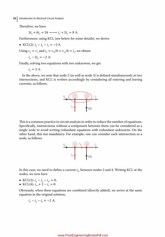
28 Introduction to Electrical Circuit Analysis
Therefore, we have
3ix + 6iy = 24 −−−−→ ix + 2iy = 8 A.
Furthermore, using KCL (see below for some details), we derive
• KCL(2): ix − iy − iz = −2A.
Using 𝑣y = 𝑣z and iy = 𝑣y∕6 = 𝑣z∕6 = iz, we obtain
ix − 2iy = −2 A.
Finally, solving two equations with two unknowns, we get
ix = 3 A.
In the above, we note that node 2 (as well as node 3) is defined simultaneously at twointersections, and KCL is written accordingly by considering all entering and leavingcurrents, as follows.
2 2
iy
izix
2A
This is a common practice in circuit analysis in order to reduce the number of equations.Specifically, intersections without a component between them can be considered as asingle node to avoid writing redundant equations with redundant unknowns. On theother hand, this not mandatory. For example, one can consider each intersection as anode, as follows.
2 4
iy
izix
2A
iw
In this case, we need to define a current i𝑤between nodes 2 and 4. Writing KCL at the
nodes, we now have
• KCL(2): ix − iy − i𝑤= 0,
• KCL(4): i𝑤+ 2 − iz = 0.
Obviously, when these equations are combined (directly added), we arrive at the sameequation in the original solution,
ix − iy − iz = −2 A.
www.FreeEngineeringBooksPdf.com
Basic Tools: Kirchhoff’s Laws 29
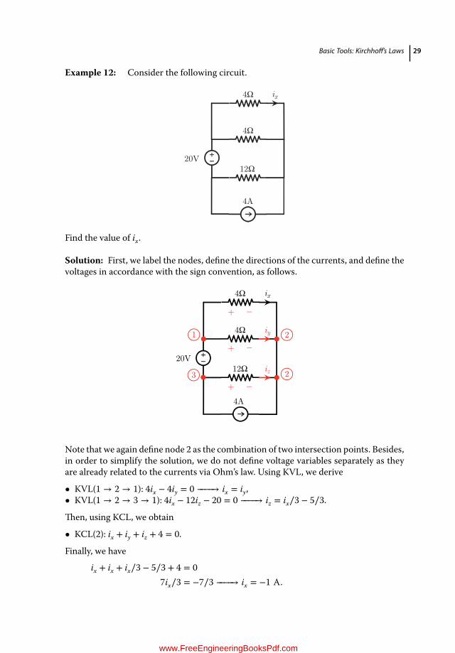
Example 12: Consider the following circuit.
4Ω
12Ω
4A
20V
4Ω
ix
Find the value of ix.
Solution: First, we label the nodes, define the directions of the currents, and define thevoltages in accordance with the sign convention, as follows.
4Ω
12Ω
4A
20V
4Ω
ix
iy
iz
_ +
_ +
_ +
1 2
2 3
Note that we again define node 2 as the combination of two intersection points. Besides,in order to simplify the solution, we do not define voltage variables separately as theyare already related to the currents via Ohm’s law. Using KVL, we derive
• KVL(1 → 2 → 1): 4ix − 4iy = 0 −−−−→ ix = iy,• KVL(1 → 2 → 3 → 1): 4ix − 12iz − 20 = 0 −−−−→ iz = ix∕3 − 5∕3.
Then, using KCL, we obtain
• KCL(2): ix + iy + iz + 4 = 0.
Finally, we have
ix + ix + ix∕3 − 5∕3 + 4 = 07ix∕3 = −7∕3 −−−−→ ix = −1 A.
www.FreeEngineeringBooksPdf.com
30 Introduction to Electrical Circuit Analysis
In solving this example, we further note the following.
• Thevoltage across the current source is unknown. Hence, it is not useful to write KVLfor 3 → 2 → 3.
• Thecurrent across the voltage source is unknown. Hence, it is not useful to write KCLat 1 or 3.
In general, we avoidwritingKCL at a node, towhich a voltage source is connected, unlessit is mandatory to find the current through the voltage source. In addition, applying KVLin a mesh containing a current source is usually not useful, unless the voltage across thecurrent source must be found.
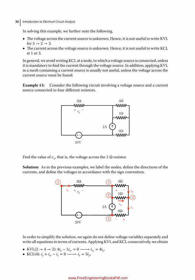
Example 13: Consider the following circuit involving a voltage source and a currentsource connected to four different resistors.
4Ω
1Ω
6Ω2A
2Ω
20V
vx_+
Find the value of 𝑣x, that is, the voltage across the 2 Ω resistor.
Solution: As in the previous examples, we label the nodes, define the directions of thecurrents, and define the voltages in accordance with the sign convention.
4Ω
1Ω
6Ω 2A
2Ω
20V
ix iy
iziw
vx _+ _+
+_
1 2
2
3
4
In order to simplify the solution, we again do not define voltage variables separately andwrite all equations in terms of currents. ApplyingKVL andKCL consecutively, we obtain
• KVL(2 → 4 → 2): 4iy − 1i𝑤= 0 −−−−→ i
𝑤= 4iy,
• KCL(4): iy + i𝑤− iz = 0 −−−−→ iz = 5iy,
www.FreeEngineeringBooksPdf.com
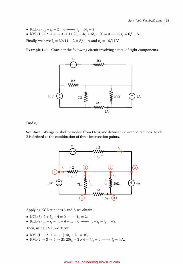
Basic Tools: Kirchhoff’s Laws 31
• KCL(3): iz − ix − 2 = 0 −−−−→ ix = 5iy − 2,• KVL(1 → 2 → 4 → 3 → 1): 2ix + 4iy + 6iz − 20 = 0 −−−−→ iy = 6∕11A.
Finally, we have ix = 30∕11 − 2 = 8∕11A and 𝑣x = 16∕11V.
Example 14: Consider the following circuit involving a total of eight components.
10V
4Ω
2Ω
7Ω6Ω
4A20Ω
2A
vx
Find 𝑣x.
Solution: Weagain label the nodes, from 1 to 4, and define the current directions. Node2 is defined as the combination of three intersection points.
10V
4Ω
2Ω
7Ω6Ω
4A 20Ω
2A
vx iy
is
+ _vy
+ _vs iz iw+ vz_
+ vw_
12 2 2
34
Applying KCL at nodes 3 and 2, we obtain
• KCL(3): 2 + i𝑤− 4 = 0 −−−−→ i
𝑤= 2,
• KCL(2): is − iz − i𝑤+ 4 + iy = 0 −−−−→ is + iy − iz = −2.
Then, using KVL, we derive
• KVL(1 → 2 → 4 → 1): 4is + 7iz = 10,• KVL(2 → 3 → 4 → 2): 20i
𝑤− 2 × 6 − 7iz = 0 −−−−→ iz = 4A.
www.FreeEngineeringBooksPdf.com

32 Introduction to Electrical Circuit Analysis
Using the updated information, we can also find is, as well as iy as
4is = 10 − 7iz = −18 −−−−→ is = −9∕2 A,iy = −2 − is + iz = −2 + 9∕2 + 4 = 13∕2 A.
Finally, we apply KVL(1 → 2 → 1) to find 𝑣x as
−𝑣x + 2iy − 4is = 0 −−−−→ 𝑣x = 2iy − 4is = 13 + 18 = 31 V.
Example 15: Consider the following circuit involving six components.
1A
vs3Ω
2Ω
24V 6A
1Ω
Find the value of 𝑣s.
Solution: As in the previous examples, we label the nodes, define the directions of thecurrents, and define the voltages using the sign convention.
1A
vs3Ω
2Ω
24V 6A
1Ωix
iy
+
_ +
_
1 1
2 2
3
Wenote that the 2 Ω resistor is short-circuited and can be omitted in the analysis. UsingKVL and KCL, we obtain
• KVL(1 → 2 → 1): 3ix + 24 = 0 −−−−→ ix = −8A,• KCL(2): ix + 1 + 6 + iy = 0 −−−−→ iy = 1A,• KVL(1 → 2 → 3 → 1): −24 − 1iy + 𝑣s = 0 −−−−→ 𝑣s = 25V.
www.FreeEngineeringBooksPdf.com
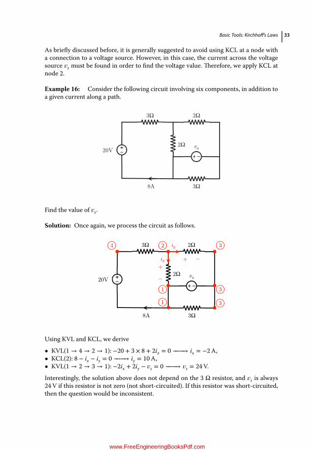
Basic Tools: Kirchhoff’s Laws 33
As briefly discussed before, it is generally suggested to avoid using KCL at a node witha connection to a voltage source. However, in this case, the current across the voltagesource 𝑣s must be found in order to find the voltage value. Therefore, we apply KCL atnode 2.
Example 16: Consider the following circuit involving six components, in addition toa given current along a path.
20V
3Ω 2Ω
2Ω
3Ω8A
vs
Find the value of 𝑣s.
Solution: Once again, we process the circuit as follows.
20V
3Ω 2Ω
2Ω
3Ω 8A
vs
ix
iy_ +
+ _
1
1
2 3
3
3
4
Using KVL and KCL, we derive
• KVL(1 → 4 → 2 → 1): −20 + 3 × 8 + 2ix = 0 −−−−→ ix = −2A,• KCL(2): 8 − ix − iy = 0 −−−−→ iy = 10A,• KVL(1 → 2 → 3 → 1): −2ix + 2iy − 𝑣s = 0 −−−−→ 𝑣s = 24V.
Interestingly, the solution above does not depend on the 3 Ω resistor, and 𝑣s is always24V if this resistor is not zero (not short-circuited). If this resistor was short-circuited,then the question would be inconsistent.
www.FreeEngineeringBooksPdf.com
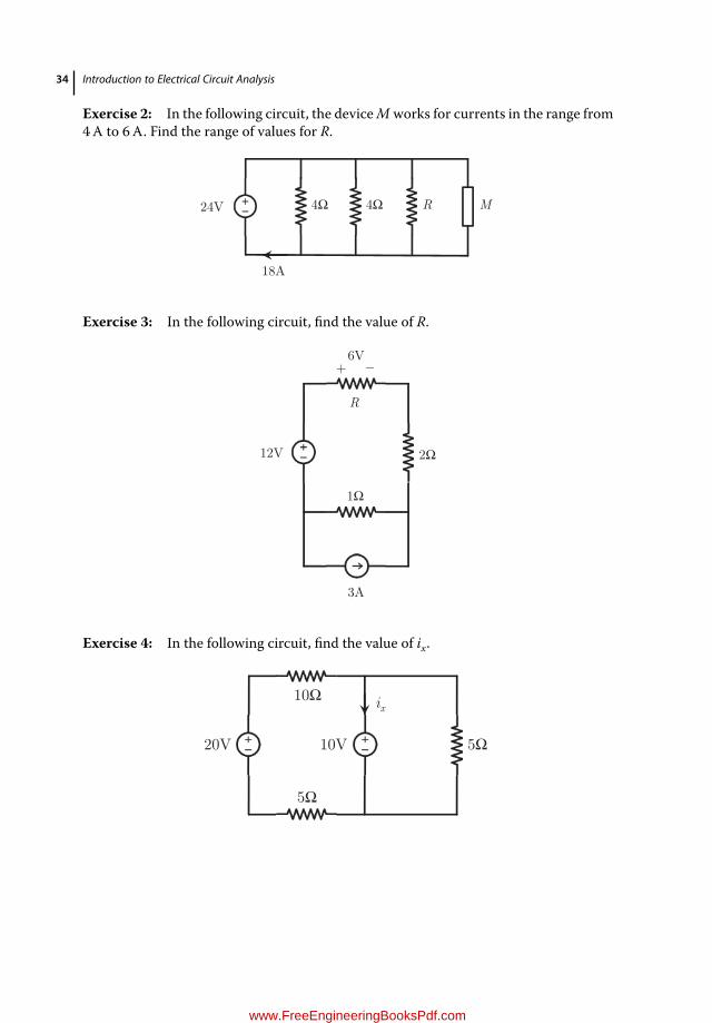
34 Introduction to Electrical Circuit Analysis
Exercise 2: In the following circuit, the device M works for currents in the range from4A to 6A. Find the range of values for R.
24V M 4Ω 4Ω R
18A
Exercise 3: In the following circuit, find the value of R.
12V
6V
2Ω
1Ω
3A
R
+ _
Exercise 4: In the following circuit, find the value of ix.
20V 10V
5Ω
10Ω
5Ω
ix
www.FreeEngineeringBooksPdf.com
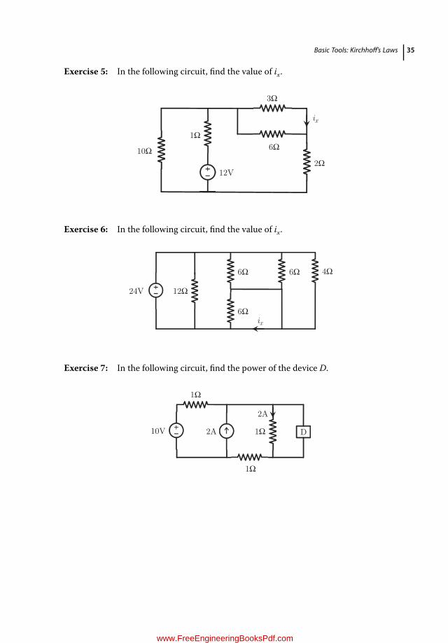
Basic Tools: Kirchhoff’s Laws 35
Exercise 5: In the following circuit, find the value of ix.
3Ω
1Ω
2Ω10Ω 6Ω
ix
12V
Exercise 6: In the following circuit, find the value of ix.
24V
6Ω 6Ω
6Ω
4Ω
12Ω
ix
Exercise 7: In the following circuit, find the power of the device D.
D10V 2A
1Ω
1Ω
1Ω
2A
www.FreeEngineeringBooksPdf.com
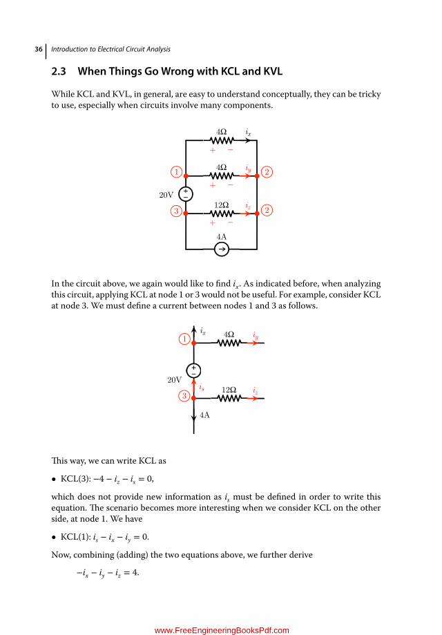
36 Introduction to Electrical Circuit Analysis
2.3 When Things Go Wrong with KCL and KVL
While KCL and KVL, in general, are easy to understand conceptually, they can be trickyto use, especially when circuits involve many components.
4Ω
12Ω
4A
20V
4Ω
ix
iy
iz
_+
_+
_+
1 2
2 3
In the circuit above, we again would like to find ix. As indicated before, when analyzingthis circuit, applying KCL at node 1 or 3 would not be useful. For example, consider KCLat node 3. We must define a current between nodes 1 and 3 as follows.
12Ω20V
4Ω iy
iz
1
3
4A
is
ix
This way, we can write KCL as
• KCL(3): −4 − iz − is = 0,
which does not provide new information as is must be defined in order to write thisequation. The scenario becomes more interesting when we consider KCL on the otherside, at node 1. We have
• KCL(1): is − ix − iy = 0.
Now, combining (adding) the two equations above, we further derive
−ix − iy − iz = 4.
www.FreeEngineeringBooksPdf.com

Basic Tools: Kirchhoff’s Laws 37
In this useful equation, we observe that the new variable is is eliminated. In other words,while KCL at node 1 or 3would not be useful alone, they could be used together to derivea single useful equation. In the original solution this is not considered, as the necessaryequations can already be obtained bymeans of KVL equations. However, in nodal analy-sis (see Chapter 3), where only KCL applications are allowed, we develop the supernodeconcept that effectively combines KCL equations at nodes, as practiced above.On the other hand, in some cases, current along a voltage source may be required,
needing KCL at one of its terminals. For example, consider the power of the voltagesource above. Using KCL at node 3 and borrowing iz = −2A from the original solution,we obtain
is = −4 − iz = −4 + 2 = −2 A.
Hence, considering the sign convention, the power of the voltage source is found to beps = 𝑣s(−is) = 40W.Problems also arisewhen applyingKVL in amesh involving a current source.We again
consider the circuit above, while applying KVL in loops 1 → 2 → 3 → 1 containing thecurrent source. Using one of the 4 Ω resistors, we have the following scenario.
12Ω
4A
20V
4Ω iy
iz
_+
_+
1 2
23
43+ _
Then KVL leads to
• KVL(1 → 2 → 3 → 1): 4iy − 𝑣4A − 20 = 0,
where 𝑣4 A is the voltage across the 4A source, using the sign convention. Obviously, thisequation is not useful alone, since it involves a new unknown, 𝑣4A. Constructing KVLthrough the 12 Ω resistor, we can also obtain
• KVL(1 → 2 → 3 → 1): 12iz − 𝑣4A = 0.
The two equations above can be combined to eliminate 𝑣4A as
4iy − 12iz = 20.
Nevertheless, the same equation could be found by applying KVL through the 4 Ω resis-tor, the 12 Ω resistor, and the voltage source (see the original solution, where ix is usedinstead of iy).Confusion often occurs when dealing with short circuits.We reconsider the following
circuit, where a 2 Ω resistor is short-circuited.
www.FreeEngineeringBooksPdf.com
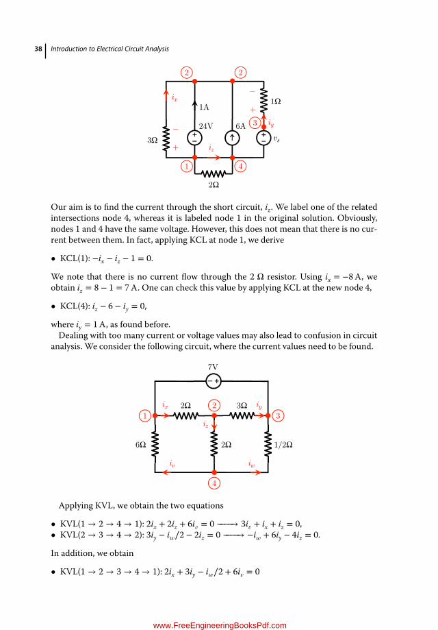
38 Introduction to Electrical Circuit Analysis
1A
vs3Ω
2Ω
24V 6A
1Ωix
iy
+
_ +
_
1 4
2 2
3
iz
Our aim is to find the current through the short circuit, iz. We label one of the relatedintersections node 4, whereas it is labeled node 1 in the original solution. Obviously,nodes 1 and 4 have the same voltage. However, this does not mean that there is no cur-rent between them. In fact, applying KCL at node 1, we derive
• KCL(1): −ix − iz − 1 = 0.
We note that there is no current flow through the 2 Ω resistor. Using ix = −8A, weobtain iz = 8 − 1 = 7A. One can check this value by applying KCL at the new node 4,
• KCL(4): iz − 6 − iy = 0,
where iy = 1A, as found before.Dealing with too many current or voltage values may also lead to confusion in circuit
analysis. We consider the following circuit, where the current values need to be found.
6Ω 1/2Ω2Ω
2Ω 3Ω
7V
12
3
4
ix iy
iz
iv iw
Applying KVL, we obtain the two equations
• KVL(1 → 2 → 4 → 1): 2ix + 2iz + 6i𝑣= 0 −−−−→ 3i
𝑣+ ix + iz = 0,
• KVL(2 → 3 → 4 → 2): 3iy − i𝑤∕2 − 2iz = 0 −−−−→ −i
𝑤+ 6iy − 4iz = 0.
In addition, we obtain
• KVL(1 → 2 → 3 → 4 → 1): 2ix + 3iy − i𝑤∕2 + 6i
𝑣= 0
www.FreeEngineeringBooksPdf.com
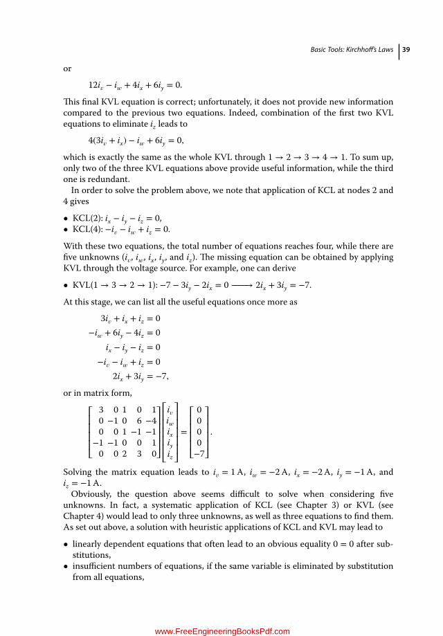
Basic Tools: Kirchhoff’s Laws 39
or
12i𝑣− i
𝑤+ 4ix + 6iy = 0.
This final KVL equation is correct; unfortunately, it does not provide new informationcompared to the previous two equations. Indeed, combination of the first two KVLequations to eliminate iz leads to
4(3i𝑣+ ix) − i
𝑤+ 6iy = 0,
which is exactly the same as the whole KVL through 1 → 2 → 3 → 4 → 1. To sum up,only two of the three KVL equations above provide useful information, while the thirdone is redundant.In order to solve the problem above, we note that application of KCL at nodes 2 and
4 gives
• KCL(2): ix − iy − iz = 0,• KCL(4): −i
𝑣− i
𝑤+ iz = 0.
With these two equations, the total number of equations reaches four, while there arefive unknowns (i
𝑣, i
𝑤, ix, iy, and iz). The missing equation can be obtained by applying
KVL through the voltage source. For example, one can derive
• KVL(1 → 3 → 2 → 1): −7 − 3iy − 2ix = 0 −−−−→ 2ix + 3iy = −7.
At this stage, we can list all the useful equations once more as
3i𝑣+ ix + iz = 0
−i𝑤+ 6iy − 4iz = 0ix − iy − iz = 0
−i𝑣− i
𝑤+ iz = 0
2ix + 3iy = −7,
or in matrix form,
⎡⎢⎢⎢⎢⎣
3 0 1 0 10 −1 0 6 −40 0 1 −1 −1
−1 −1 0 0 10 0 2 3 0
⎤⎥⎥⎥⎥⎦
⎡⎢⎢⎢⎢⎢⎣
i𝑣
i𝑤
ixiyiz
⎤⎥⎥⎥⎥⎥⎦=
⎡⎢⎢⎢⎢⎣
0000−7
⎤⎥⎥⎥⎥⎦.
Solving the matrix equation leads to i𝑣= 1A, i
𝑤= −2A, ix = −2A, iy = −1A, and
iz = −1A.Obviously, the question above seems difficult to solve when considering five
unknowns. In fact, a systematic application of KCL (see Chapter 3) or KVL (seeChapter 4) would lead to only three unknowns, as well as three equations to find them.As set out above, a solution with heuristic applications of KCL and KVL may lead to
• linearly dependent equations that often lead to an obvious equality 0 = 0 after sub-stitutions,
• insufficient numbers of equations, if the same variable is eliminated by substitutionfrom all equations,
www.FreeEngineeringBooksPdf.com
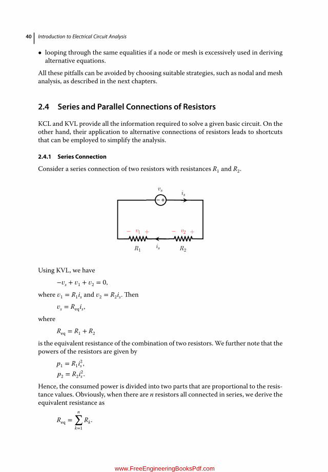
40 Introduction to Electrical Circuit Analysis
• looping through the same equalities if a node or mesh is excessively used in derivingalternative equations.
All these pitfalls can be avoided by choosing suitable strategies, such as nodal and meshanalysis, as described in the next chapters.
2.4 Series and Parallel Connections of Resistors
KCL and KVL provide all the information required to solve a given basic circuit. On theother hand, their application to alternative connections of resistors leads to shortcutsthat can be employed to simplify the analysis.
2.4.1 Series Connection
Consider a series connection of two resistors with resistances R1 and R2.
R1 R2
vs
_ +_ +
is
v1 v2
is
Using KVL, we have
−𝑣s + 𝑣1 + 𝑣2 = 0,
where 𝑣1 = R1is and 𝑣2 = R2is. Then
𝑣s = Reqis,
where
Req = R1 + R2
is the equivalent resistance of the combination of two resistors.We further note that thepowers of the resistors are given by
p1 = R1i2s ,p2 = R2i2s .
Hence, the consumed power is divided into two parts that are proportional to the resis-tance values. Obviously, when there are n resistors all connected in series, we derive theequivalent resistance as
Req =n∑
k=1Rk .
www.FreeEngineeringBooksPdf.com
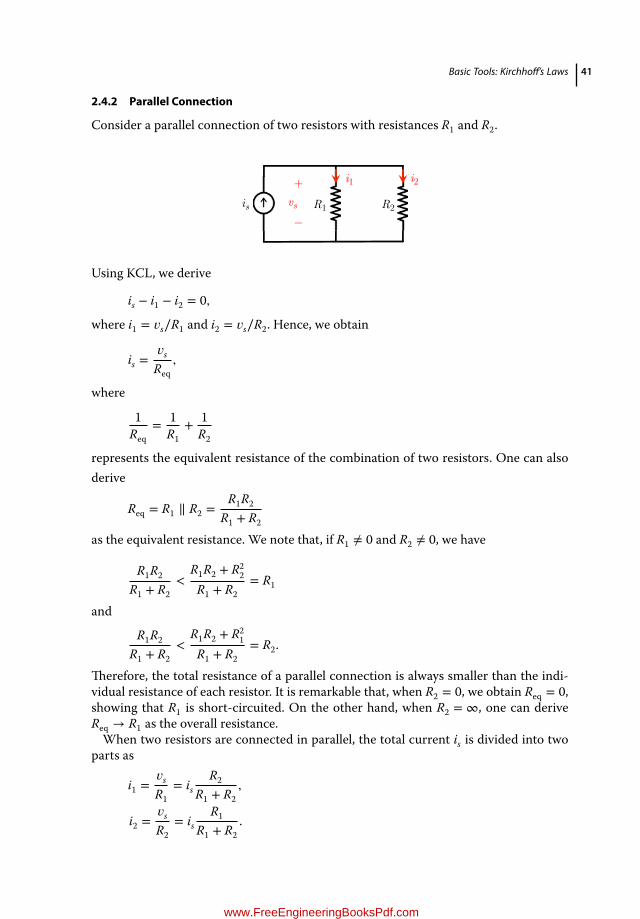
Basic Tools: Kirchhoff’s Laws 41
2.4.2 Parallel Connection
Consider a parallel connection of two resistors with resistances R1 and R2.
R1 R2is vs
+
_
i1 i2
Using KCL, we derive
is − i1 − i2 = 0,
where i1 = 𝑣s∕R1 and i2 = 𝑣s∕R2. Hence, we obtain
is =𝑣s
Req,
where
1Req
= 1R1
+ 1R2
represents the equivalent resistance of the combination of two resistors. One can alsoderive
Req = R1 ∥ R2 =R1R2
R1 + R2
as the equivalent resistance. We note that, if R1 ≠ 0 and R2 ≠ 0, we have
R1R2
R1 + R2<
R1R2 + R22
R1 + R2= R1
and
R1R2
R1 + R2<
R1R2 + R21
R1 + R2= R2.
Therefore, the total resistance of a parallel connection is always smaller than the indi-vidual resistance of each resistor. It is remarkable that, when R2 = 0, we obtain Req = 0,showing that R1 is short-circuited. On the other hand, when R2 = ∞, one can deriveReq → R1 as the overall resistance.When two resistors are connected in parallel, the total current is is divided into two
parts as
i1 =𝑣s
R1= is
R2
R1 + R2,
i2 =𝑣s
R2= is
R1
R1 + R2.
www.FreeEngineeringBooksPdf.com
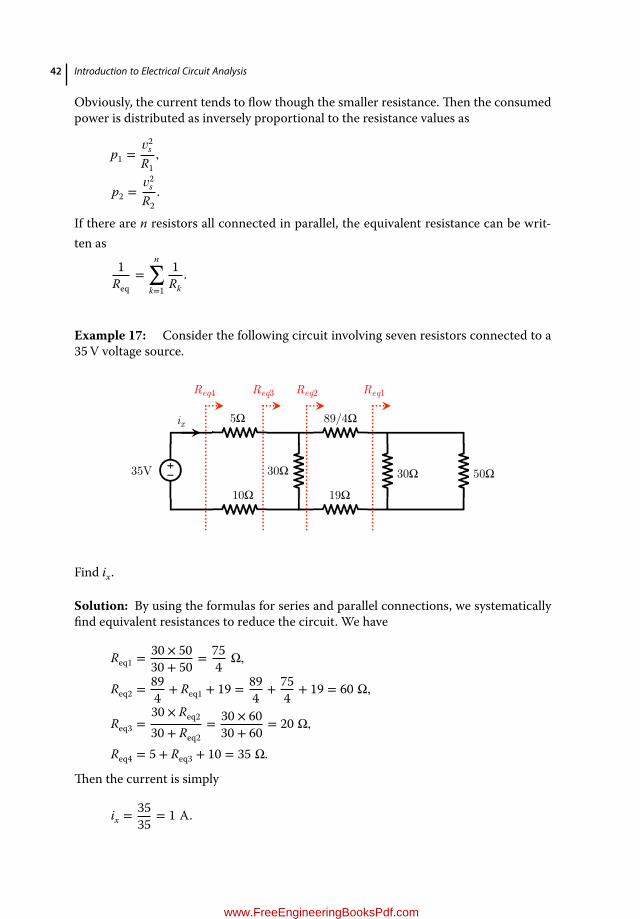
42 Introduction to Electrical Circuit Analysis
Obviously, the current tends to flow though the smaller resistance. Then the consumedpower is distributed as inversely proportional to the resistance values as
p1 =𝑣2s
R1,
p2 =𝑣2s
R2.
If there are n resistors all connected in parallel, the equivalent resistance can be writ-ten as
1Req
=n∑
k=1
1Rk
.
Example 17: Consider the following circuit involving seven resistors connected to a35V voltage source.
5Ω
10Ω30Ω
89/4Ω
19Ω30Ω 50Ω35V
ix
Req1Req2Req3Req4
Find ix.
Solution: By using the formulas for series and parallel connections, we systematicallyfind equivalent resistances to reduce the circuit. We have
Req1 =30 × 5030 + 50
= 754
Ω,
Req2 =894
+ Req1 + 19 = 894
+ 754
+ 19 = 60 Ω,
Req3 =30 × Req2
30 + Req2= 30 × 60
30 + 60= 20 Ω,
Req4 = 5 + Req3 + 10 = 35 Ω.
Then the current is simply
ix =3535
= 1 A.
www.FreeEngineeringBooksPdf.com
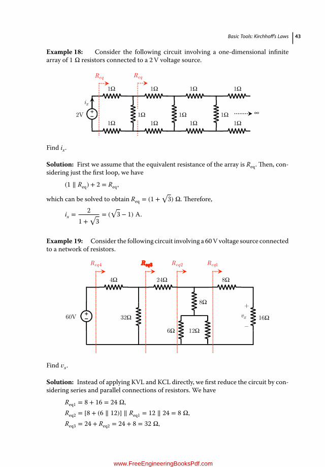
Basic Tools: Kirchhoff’s Laws 43
Example 18: Consider the following circuit involving a one-dimensional infinitearray of 1 Ω resistors connected to a 2V voltage source.
1Ω
1Ω1Ω
1Ω
1Ω
ix 2V 1Ω
1Ω 1Ω
1Ω
1Ω 1Ω
ReqReq
∞
Find ix.
Solution: First we assume that the equivalent resistance of the array is Req. Then, con-sidering just the first loop, we have
(1 ∥ Req) + 2 = Req,
which can be solved to obtain Req = (1 +√3) Ω. Therefore,
ix =2
1 +√3= (
√3 − 1) A.
Example 19: Consider the following circuit involving a 60V voltage source connectedto a network of resistors.
60V
4Ω
32Ω
6Ω 12Ω
8Ω
24Ω 8Ω
16Ωvx
+
_
Req1Req2Req3Req4
Find 𝑣x.
Solution: Instead of applying KVL and KCL directly, we first reduce the circuit by con-sidering series and parallel connections of resistors. We have
Req1 = 8 + 16 = 24 Ω,Req2 = [8 + (6 ∥ 12)] ∥ Req1 = 12 ∥ 24 = 8 Ω,Req3 = 24 + Req2 = 24 + 8 = 32 Ω,
www.FreeEngineeringBooksPdf.com
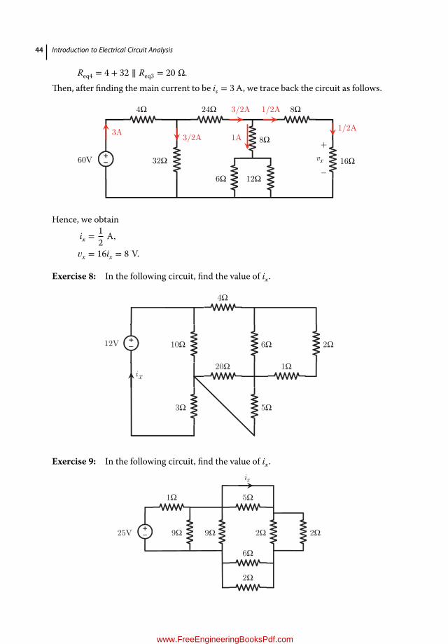
44 Introduction to Electrical Circuit Analysis
Req4 = 4 + 32 ∥ Req3 = 20 Ω.Then, after finding the main current to be is = 3A, we trace back the circuit as follows.
60V
4Ω
32Ω
6Ω 12Ω
8Ω
24Ω 8Ω
16Ω vx +
_
3A 3/2A
3/2A
1A
1/2A
1/2A
Hence, we obtain
ix =12A,
𝑣x = 16ix = 8 V.
Exercise 8: In the following circuit, find the value of ix.
6Ω12V 2Ω10Ω
4Ω
3Ω 5Ω
20Ω 1Ωix
Exercise 9: In the following circuit, find the value of ix.
1Ω
9Ω 9Ω
6Ω
2Ω
5Ω
2Ω 2Ω25V
ix
www.FreeEngineeringBooksPdf.com

Basic Tools: Kirchhoff’s Laws 45
Exercise 10: In the following circuit, find the value of ix.
2Ω
6Ω
4Ω 2Ω
2Ω
4Ω
8Ω
10V
12ixix
2.5 When Things Go Wrong with Series/Parallel Resistors
Major issues arise when considering resistors that appear to be connected in series orparallel, but in fact are not. We consider the following three different circuits.
vs
Req1
R1
R2
R3
R4
vs
Req2
R1
R2
R3
R4
vs
Req3
R1
R2
R3
R4 R5
In the first case (the circuit on the left), R1 and R2 are connected in series, leading toR1 + R2 total resistance. Similarly, R3 and R4 are connected in series, leading to R3 + R4.Then the overall resistance is given by
Req1 = (R1 + R2) ∥ (R3 + R4) =(R1 + R2)(R3 + R4)R1 + R2 + R3 + R4
.
In the second case (the circuit in the middle), R1 and R3 are connected in parallel,while R2 and R4 are similarly parallel. Therefore, the overall resistance is
Req2 = (R1 ∥ R3) + (R2 ∥ R4) =R1R3
R1 + R3+
R2R4
R2 + R4
=R1R3(R2 + R4) + R2R4(R1 + R3)
(R1 + R3)(R2 + R4),
which is obviously different from Req1. Only in some cases, such as whenR1 = R2 = R3 =R4 = R, do we have Req1 = Req2.
www.FreeEngineeringBooksPdf.com

46 Introduction to Electrical Circuit Analysis
In the third case (the circuit on the right), where R5 ≠ 0 or R5 ≠ ∞, none of theresistor pairs are connected in series or parallel. This is because, none of the pairs sharea common current or common voltage. For general values of the resistors, this circuitmust be analyzed via KVL and KCL or via nodal/mesh methods. Interestingly, whenR1 = R2 = R3 = R4 = R, we have Req3 = R, independent of the value of R5.
2.6 What You Need to Know before You Continue
Here are a few key points before proceeding to the next chapter.
• KCL: The sum of currents entering (+) and leaving (−) a node should be zero. Whenwriting aKCL equation,we use plus andminus signs for entering and leaving currents,respectively.
• KVL: The sum of voltages in a closed loop is zero. When writing a KVL equation,we always choose the clockwise direction. Then the voltages of the components areadded by considering their signs according to their first terminals.
• Current and voltage directions: When analyzing circuits, we define the current andvoltage directions arbitrarily, while enforcing the sign convention for all components.When a current/voltage value is found to be negative, we understand that the initialassumption is not correct, although this is not a problem.
• Useless equations:We usually avoid applying KCL at a node to which a voltage sourceis connected. Similarly, a KVL in a mesh containing a current source is usually notuseful.
• Series/parallel resistors: Combinations of resistors can often be simplified by con-sidering series and parallel connections before the circuit is analyzed via KCL andKVL.
In the next chapter, we focus on nodal analysis, which is a systematic way of applyingKCL at nodes. Such methods are essential for deriving required numbers of equations,so as to avoid redundant equations and variables, when analyzing circuits.
www.FreeEngineeringBooksPdf.com

47
3
Analysis of Resistive Networks: Nodal Analysis
KCL and KVL are fundamental laws for analyzing circuits. However, as discussed in theprevious chapter, their applicationmay not be always clear. Specifically, for large circuitsinvolving many components and connections, it may be difficult to derive necessaryrelationships between voltages and currents, while avoiding duplications and linearlydependent equations. In this chapter, we focus on nodal analysis, which is a higher-leveltool based on a systematic application of KCL. Given any circuit, a proper applicationof nodal analysis guarantees the derivation of necessary equations for the analysis. Wealso discuss the generalization of nodes to further use the benefits of nodal analysis forcomplex circuits.
3.1 Application of Nodal Analysis
We start by briefly listing the major steps of nodal analysis as follows.
• Ground selection: We select a reference node with zero voltage. Any node can beselected, but it usually better to choose one with more connections than the others.The node selected is called the ground of the circuit. All voltages at other nodes aredefined with respect to the ground.
• Constructing equations: We use only KCL at nodes, except the ground, to deriveall equations. KVL is not preferred in nodal analysis unless necessary. We write allequations in terms of node voltages.
• Solution: Next, we solve the equations to find the node voltages.• Analysis: Finally, by using the node voltages, we find the desired voltage, current,
and/or power values.
Once again, we emphasize that a formal voltage definition requires two points. On theother hand, if there is a node where the voltage is defined as zero, it becomes practicalto define node voltages as if they are independent values.
Introduction to Electrical Circuit Analysis, First Edition. Özgür Ergül.© 2017 John Wiley & Sons Ltd. Published 2017 by John Wiley & Sons Ltd.Companion Website: www.wiley.com/go/ergul4412
www.FreeEngineeringBooksPdf.com
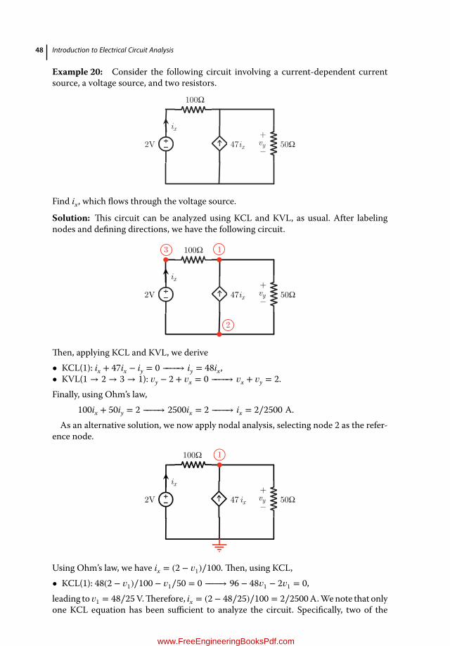
48 Introduction to Electrical Circuit Analysis
Example 20: Consider the following circuit involving a current-dependent currentsource, a voltage source, and two resistors.
50Ω2V 47ix
ix
100Ω
vy
+
_
Find ix, which flows through the voltage source.
Solution: This circuit can be analyzed using KCL and KVL, as usual. After labelingnodes and defining directions, we have the following circuit.
50Ω2V 47ix
ix
100Ω
vy
+
_
1
2
3
Then, applying KCL and KVL, we derive• KCL(1): ix + 47ix − iy = 0 −−−−→ iy = 48ix,• KVL(1 → 2 → 3 → 1): 𝑣y − 2 + 𝑣x = 0 −−−−→ 𝑣x + 𝑣y = 2.Finally, using Ohm’s law,
100ix + 50iy = 2 −−−−→ 2500ix = 2 −−−−→ ix = 2∕2500 A.As an alternative solution, we now apply nodal analysis, selecting node 2 as the refer-
ence node.
50Ω2V 47 ix
ix
100Ω
vy
1
+
_
Using Ohm’s law, we have ix = (2 − 𝑣1)∕100. Then, using KCL,• KCL(1): 48(2 − 𝑣1)∕100 − 𝑣1∕50 = 0 −−−−→ 96 − 48𝑣1 − 2𝑣1 = 0,leading to 𝑣1 = 48∕25V.Therefore, ix = (2 − 48∕25)∕100 = 2∕2500A.Wenote that onlyone KCL equation has been sufficient to analyze the circuit. Specifically, two of the
www.FreeEngineeringBooksPdf.com
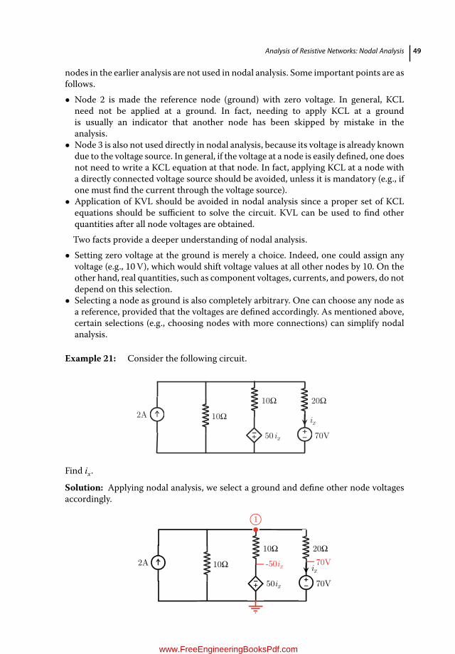
Analysis of Resistive Networks: Nodal Analysis 49
nodes in the earlier analysis are not used in nodal analysis. Some important points are asfollows.• Node 2 is made the reference node (ground) with zero voltage. In general, KCL
need not be applied at a ground. In fact, needing to apply KCL at a groundis usually an indicator that another node has been skipped by mistake in theanalysis.
• Node 3 is also not used directly in nodal analysis, because its voltage is already knowndue to the voltage source. In general, if the voltage at a node is easily defined, one doesnot need to write a KCL equation at that node. In fact, applying KCL at a node witha directly connected voltage source should be avoided, unless it is mandatory (e.g., ifone must find the current through the voltage source).
• Application of KVL should be avoided in nodal analysis since a proper set of KCLequations should be sufficient to solve the circuit. KVL can be used to find otherquantities after all node voltages are obtained.Two facts provide a deeper understanding of nodal analysis.
• Setting zero voltage at the ground is merely a choice. Indeed, one could assign anyvoltage (e.g., 10V), which would shift voltage values at all other nodes by 10. On theother hand, real quantities, such as component voltages, currents, and powers, do notdepend on this selection.
• Selecting a node as ground is also completely arbitrary. One can choose any node asa reference, provided that the voltages are defined accordingly. As mentioned above,certain selections (e.g., choosing nodes with more connections) can simplify nodalanalysis.
Example 21: Consider the following circuit.
10Ω
10Ω
2Aix
20Ω
70V 50 ix
Find ix.
Solution: Applying nodal analysis, we select a ground and define other node voltagesaccordingly.
10Ω
10Ω
2Aix
20Ω
i
70V50ix
1
-50ix 70V
www.FreeEngineeringBooksPdf.com
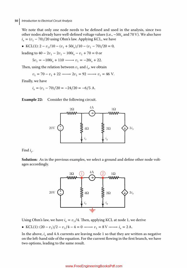
50 Introduction to Electrical Circuit Analysis
We note that only one node needs to be defined and used in the analysis, since twoother nodes already have well-defined voltage values (i.e.,−50ix and 70V).We also haveix = (𝑣1 − 70)∕20 using Ohm’s law. Applying KCL, we have
• KCL(1): 2 − 𝑣1∕10 − (𝑣1 + 50ix)∕10 − (𝑣1 − 70)∕20 = 0,
leading to 40 − 2𝑣1 − 2𝑣1 − 100ix − 𝑣1 + 70 = 0 or
5𝑣1 = −100ix + 110 −−−−→ 𝑣1 = −20ix + 22.
Then, using the relation between 𝑣1 and ix, we obtain
𝑣1 = 70 − 𝑣1 + 22 −−−−→ 2𝑣1 = 92 −−−−→ 𝑣1 = 46 V.
Finally, we have
ix = (𝑣1 − 70)∕20 = −24∕20 = −6∕5 A.
Example 22: Consider the following circuit.
2Ω
4Ω 2Ω
4A
20V
1Ω
ix
3ix
iy
Find iy.
Solution: As in the previous examples, we select a ground and define other node volt-ages accordingly.
4A 2Ω
4Ω 2Ω20V
1Ω
ix
3ix
1 2
iy
Using Ohm’s law, we have ix = 𝑣1∕4. Then, applying KCL at node 1, we derive
• KCL(1): (20 − 𝑣1)∕2 − 𝑣1∕4 − 4 = 0 −−−−→ 𝑣1 = 8V −−−−→ ix = 2A.
In the above, ix and 4A currents are leaving node 1 so that they are written as negativeon the left-hand side of the equation. For the current flowing in the first branch, we havetwo options, leading to the same result.
www.FreeEngineeringBooksPdf.com

Analysis of Resistive Networks: Nodal Analysis 51
• Defining the current as entering node 1, its value should be (20 − 𝑣1)∕2. This valueshould be treated as positive in the KCL equation.
• Defining the current as leaving node 1, its value should be (𝑣1 − 20)∕2. Thisvalue should be treated as negative in the KCL equation, making it (20 − 𝑣1)∕2overall.
Hence, the choice of current directions will change neither the KCL equation nor theresult. In order to complete the solution and find iy, we appply KCL at node 2, yielding
• KCL(2): 4 − 𝑣2∕2 − 3ix = 0 −−−−→ 𝑣2 = 8 − 6ix = −4V,
leading to
iy = 𝑣2∕2 = −2 A.
Example 23: Consider the following circuit.
2Ω 6A
1Ω12V 2Ω
ix
2Ω
2Ω
Find ix.
Solution: Using nodal analysis, we again select a ground and define other node voltagesaccordingly.
2Ω12V
2Ω
2Ω
ix
2Ω
2Ω 6A1 2
Using KCL at nodes 1 and 2, we obtain two equations with two unknowns as
• KCL(1): (12 − 𝑣1)∕2 − 𝑣1∕2 − (𝑣1 − 𝑣2)∕2 = 0 −−−−→ 3𝑣1 − 𝑣2 = 12,• KCL(2): (𝑣1 − 𝑣2)∕2 − 6 − 𝑣2 = 0 −−−−→ 𝑣1 − 3𝑣2 = 12.
Finally, solving the equations, we get 𝑣1 = 3V, 𝑣2 = −3V, and ix = 𝑣1∕2 = 3∕2A.
www.FreeEngineeringBooksPdf.com
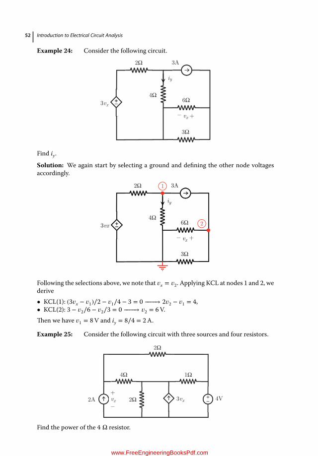
52 Introduction to Electrical Circuit Analysis
Example 24: Consider the following circuit.
2Ω
4Ω
i
3A
6Ω
3Ω
3vx
vx + _
y
Find iy.
Solution: We again start by selecting a ground and defining the other node voltagesaccordingly.
2Ω
4Ω
iy
3A
6Ω
3Ω
3vx
vx + _
1
2
Following the selections above, we note that 𝑣x = 𝑣2. Applying KCL at nodes 1 and 2, wederive• KCL(1): (3𝑣x − 𝑣1)∕2 − 𝑣1∕4 − 3 = 0 −−−−→ 2𝑣2 − 𝑣1 = 4,• KCL(2): 3 − 𝑣2∕6 − 𝑣2∕3 = 0 −−−−→ 𝑣2 = 6V.Then we have 𝑣1 = 8V and iy = 8∕4 = 2A.
Example 25: Consider the following circuit with three sources and four resistors.
2Ω 2A
2Ω
4V
4Ω 1Ω
3vxvx
+
_
Find the power of the 4 Ω resistor.
www.FreeEngineeringBooksPdf.com
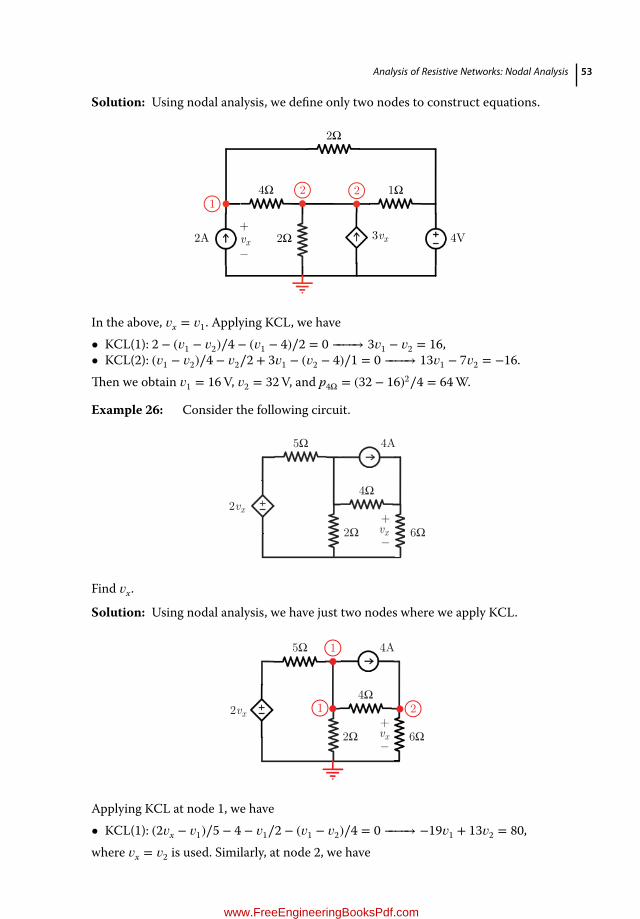
Analysis of Resistive Networks: Nodal Analysis 53
Solution: Using nodal analysis, we define only two nodes to construct equations.
2Ω2A
2Ω
4V
4Ω 1Ω
3vxvx
+
_
1 2 2
In the above, 𝑣x = 𝑣1. Applying KCL, we have• KCL(1): 2 − (𝑣1 − 𝑣2)∕4 − (𝑣1 − 4)∕2 = 0 −−−−→ 3𝑣1 − 𝑣2 = 16,• KCL(2): (𝑣1 − 𝑣2)∕4 − 𝑣2∕2 + 3𝑣1 − (𝑣2 − 4)∕1 = 0 −−−−→ 13𝑣1 − 7𝑣2 = −16.Then we obtain 𝑣1 = 16V, 𝑣2 = 32V, and p4Ω = (32 − 16)2∕4 = 64W.
Example 26: Consider the following circuit.
5Ω
2Ω 6Ω
4A
4Ω
vx
2vx+
_
Find 𝑣x.
Solution: Using nodal analysis, we have just two nodes where we apply KCL.
5Ω
2Ω 6Ω
4A
4Ω
vx
2vx
1
2 1 +
_
Applying KCL at node 1, we have• KCL(1): (2𝑣x − 𝑣1)∕5 − 4 − 𝑣1∕2 − (𝑣1 − 𝑣2)∕4 = 0 −−−−→ −19𝑣1 + 13𝑣2 = 80,where 𝑣x = 𝑣2 is used. Similarly, at node 2, we have
www.FreeEngineeringBooksPdf.com
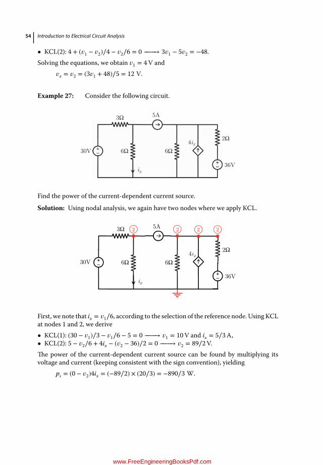
54 Introduction to Electrical Circuit Analysis
• KCL(2): 4 + (𝑣1 − 𝑣2)∕4 − 𝑣2∕6 = 0 −−−−→ 3𝑣1 − 5𝑣2 = −48.Solving the equations, we obtain 𝑣1 = 4V and
𝑣x = 𝑣2 = (3𝑣1 + 48)∕5 = 12 V.
Example 27: Consider the following circuit.
6Ω
3Ω 5A
30V
ix
6Ω
2Ω
36V
4ix
Find the power of the current-dependent current source.
Solution: Using nodal analysis, we again have two nodes where we apply KCL.
6Ω
3Ω 5A
30V
ix
6Ω
2Ω
36V
4ixix
2222
First, we note that ix = 𝑣1∕6, according to the selection of the reference node. Using KCLat nodes 1 and 2, we derive• KCL(1): (30 − 𝑣1)∕3 − 𝑣1∕6 − 5 = 0 −−−−→ 𝑣1 = 10V and ix = 5∕3A,• KCL(2): 5 − 𝑣2∕6 + 4ix − (𝑣2 − 36)∕2 = 0 −−−−→ 𝑣2 = 89∕2V.The power of the current-dependent current source can be found by multiplying itsvoltage and current (keeping consistent with the sign convention), yielding
ps = (0 − 𝑣2)4ix = (−89∕2) × (20∕3) = −890∕3 W.
www.FreeEngineeringBooksPdf.com

Analysis of Resistive Networks: Nodal Analysis 55
Example 28: Consider the following circuit involving four different kinds of sources.
4Ω
8iy
2Ω
2Ω
200V
iz iy
5A
ix
2ix
Find iz.
Solution: First, we note that ix = −5A. Using nodal analysis, we can define the groundand label the nodes as follows.
4Ω
2Ω
2Ω
8iy
200V
iz iy
5A
ix
2ix
1 2 3
We further note that KCL is not required (and not useful) at node 1, since 𝑣1 = 200V.In addition, one should avoid applying KCL at node 3 since a voltage source (dependentsource in this case) is connected to this node. Instead, using the definition of the voltagesource, we have
𝑣3 = 𝑣1 − 8iy = 200 − 8iy,
where iy = (𝑣2 − 𝑣3)∕4. Therefore,
𝑣3 = 200 − 2𝑣2 + 2𝑣3or
2𝑣2 − 𝑣3 = 200
www.FreeEngineeringBooksPdf.com
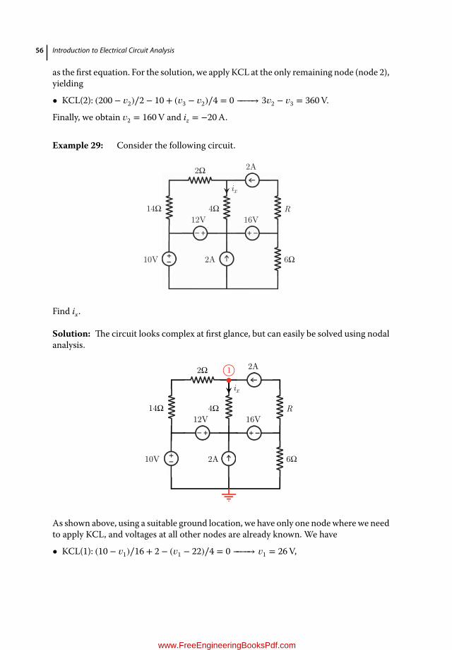
56 Introduction to Electrical Circuit Analysis
as the first equation. For the solution, we apply KCL at the only remaining node (node 2),yielding
• KCL(2): (200 − 𝑣2)∕2 − 10 + (𝑣3 − 𝑣2)∕4 = 0 −−−−→ 3𝑣2 − 𝑣3 = 360V.
Finally, we obtain 𝑣2 = 160V and iz = −20A.
Example 29: Consider the following circuit.
12V
10V
16V
2A
R
2Ω
14Ω 4Ω
2A 6Ω
ix
Find ix.
Solution: The circuit looks complex at first glance, but can easily be solved using nodalanalysis.
12V
10V
16V
2A
R
2Ω
14Ω 4Ω
2A 6Ω
ix
1
As shown above, using a suitable ground location, we have only one nodewhere we needto apply KCL, and voltages at all other nodes are already known. We have
• KCL(1): (10 − 𝑣1)∕16 + 2 − (𝑣1 − 22)∕4 = 0 −−−−→ 𝑣1 = 26V,
www.FreeEngineeringBooksPdf.com

Analysis of Resistive Networks: Nodal Analysis 57
leading to
ix = (𝑣1 − 22)∕4 = 1 A.
Exercise 11: In the following circuit, find the value of ix.
3Ω
6Ω 12Ω
6Ω
24V 3ix
ix
Exercise 12: In the following circuit, find the power of the 24 Ω resistor.
2A
18V 20Ω
6Ω6Ω5Ω
24Ω
20V
Exercise 13: In the following circuit, find the power of the 5 Ω resistor.
10V
20Ω
5Ω
4Ω 4Ω
2Ω
ix
2ix
www.FreeEngineeringBooksPdf.com

58 Introduction to Electrical Circuit Analysis
Exercise 14: In the following circuit, find 𝑣s given that ix = 2A.
10Ω
2Ω5Ω 5Ω
10Ω
10Ω
5V
ixvs
Exercise 15: In the following circuit, find the value of ix.
30Ω
60V
ix
5Ω 1Ω
28/5A 100Ω 4Ω60Ω
Exercise 16: In the following circuit, find the power of the 8A source.
8Ω
ix
24Ω
24Ω
10V
4A
8A
1Ω 3Ω 5ix
Exercise 17: In the following circuit, find the value of 𝑣y.
18V
2Ω 2Ω
2Ω 6vx
1/5Ω
vy + _
v _ + x
www.FreeEngineeringBooksPdf.com
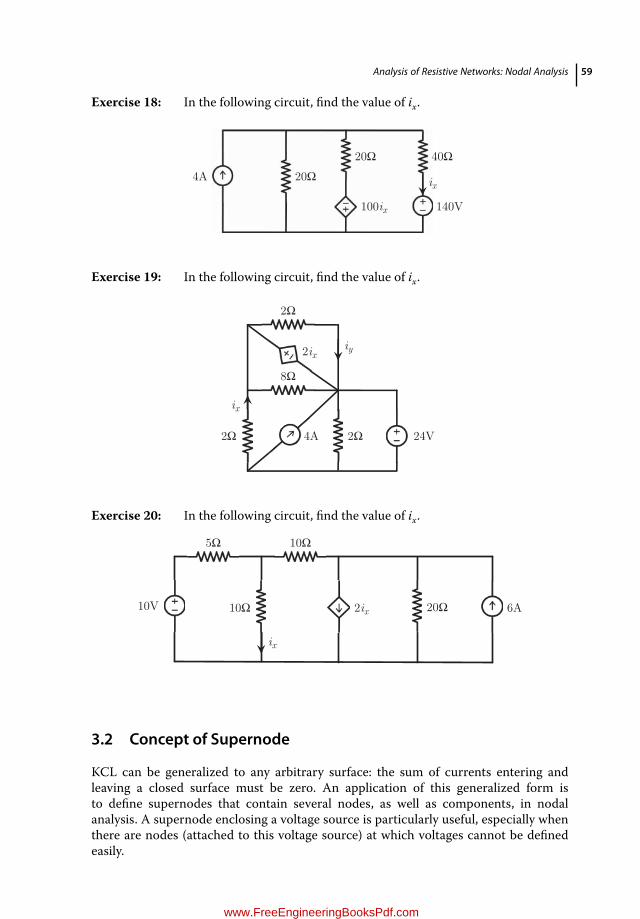
Analysis of Resistive Networks: Nodal Analysis 59
Exercise 18: In the following circuit, find the value of ix.
100ix 140V
20Ω
ix 4A
40Ω
20Ω
Exercise 19: In the following circuit, find the value of ix.
2Ω 4A
8Ω
2Ω
2Ω 24V
ix
iy2ix
Exercise 20: In the following circuit, find the value of ix.
5Ω
6A10V 20Ω
ix
10Ω
10Ω
2ix
3.2 Concept of Supernode
KCL can be generalized to any arbitrary surface: the sum of currents entering andleaving a closed surface must be zero. An application of this generalized form isto define supernodes that contain several nodes, as well as components, in nodalanalysis. A supernode enclosing a voltage source is particularly useful, especially whenthere are nodes (attached to this voltage source) at which voltages cannot be definedeasily.
www.FreeEngineeringBooksPdf.com
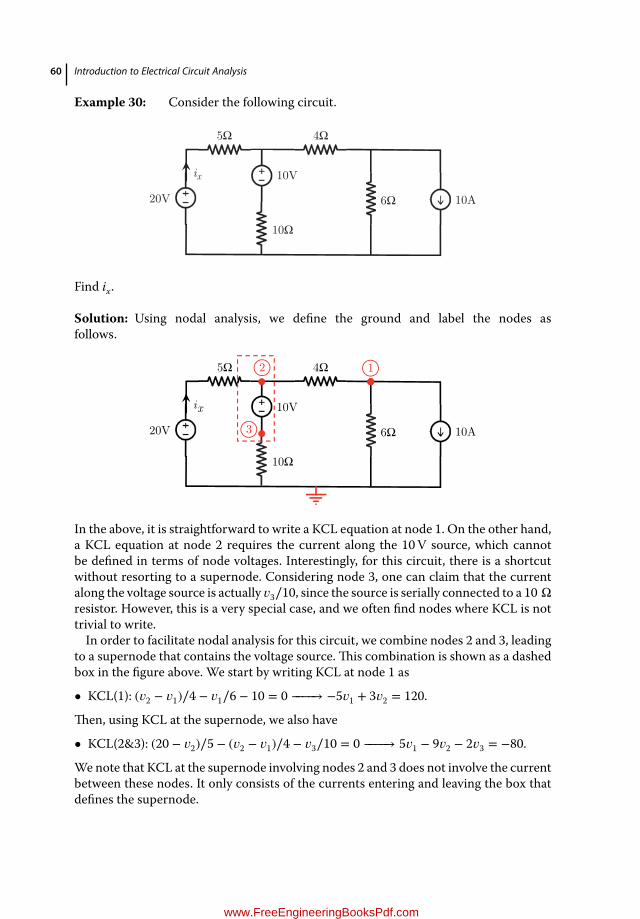
60 Introduction to Electrical Circuit Analysis
Example 30: Consider the following circuit.
6Ω20V
ix
4Ω5Ω
10V
10Ω
10A
Find ix.
Solution: Using nodal analysis, we define the ground and label the nodes asfollows.
6Ω20V
ix
5Ω 4Ω
10V
10Ω
10A
1 2
3
In the above, it is straightforward to write a KCL equation at node 1. On the other hand,a KCL equation at node 2 requires the current along the 10V source, which cannotbe defined in terms of node voltages. Interestingly, for this circuit, there is a shortcutwithout resorting to a supernode. Considering node 3, one can claim that the currentalong the voltage source is actually 𝑣3∕10, since the source is serially connected to a 10 Ωresistor. However, this is a very special case, and we often find nodes where KCL is nottrivial to write.In order to facilitate nodal analysis for this circuit, we combine nodes 2 and 3, leading
to a supernode that contains the voltage source. This combination is shown as a dashedbox in the figure above. We start by writing KCL at node 1 as
• KCL(1): (𝑣2 − 𝑣1)∕4 − 𝑣1∕6 − 10 = 0 −−−−→ −5𝑣1 + 3𝑣2 = 120.
Then, using KCL at the supernode, we also have
• KCL(2&3): (20 − 𝑣2)∕5 − (𝑣2 − 𝑣1)∕4 − 𝑣3∕10 = 0 −−−−→ 5𝑣1 − 9𝑣2 − 2𝑣3 = −80.
We note that KCL at the supernode involving nodes 2 and 3 does not involve the currentbetween these nodes. It only consists of the currents entering and leaving the box thatdefines the supernode.
www.FreeEngineeringBooksPdf.com

Analysis of Resistive Networks: Nodal Analysis 61
When using a supernode in nodal analysis, the number of equations derived from theapplication of KCL at nodes is usually one less than the number of unknowns, that is,node voltages. The extra equation needed is always derived from the supernode itself.Specifically, looking inside the node for the circuit above, we have
𝑣3 = 𝑣2 − 10,
leading to
5𝑣1 − 11𝑣2 = −100.
Then, solving the equations, we obtain 𝑣1 = −5∕2V, 𝑣2 = −5∕2V, 𝑣3 = −25∕2V, andix = 9∕2A.
Example 31: Consider the following circuit.
8Ω5A
2Ω
4Ω3A
10V
ix
Find ix.
Solution: Using nodal analysis, we define the ground, and then label the nodes.
8Ω5A
2Ω
4Ω3A
10V1 1 2
ix
In addition, we combine the nodes to obtain a supernode, leading to a single applicationof KCL,
• KCL(1&2): 5 − 3 − 𝑣1∕8 − 𝑣2∕4 = 0 −−−−→ 𝑣1 + 2𝑣2 = 16.
Using the supernode, the node voltages are related by 𝑣1 = 𝑣2 + 10. Hence, we obtain𝑣1 = 12V, 𝑣2 = 2V, and ix = 2∕4 = 1∕2A.
www.FreeEngineeringBooksPdf.com
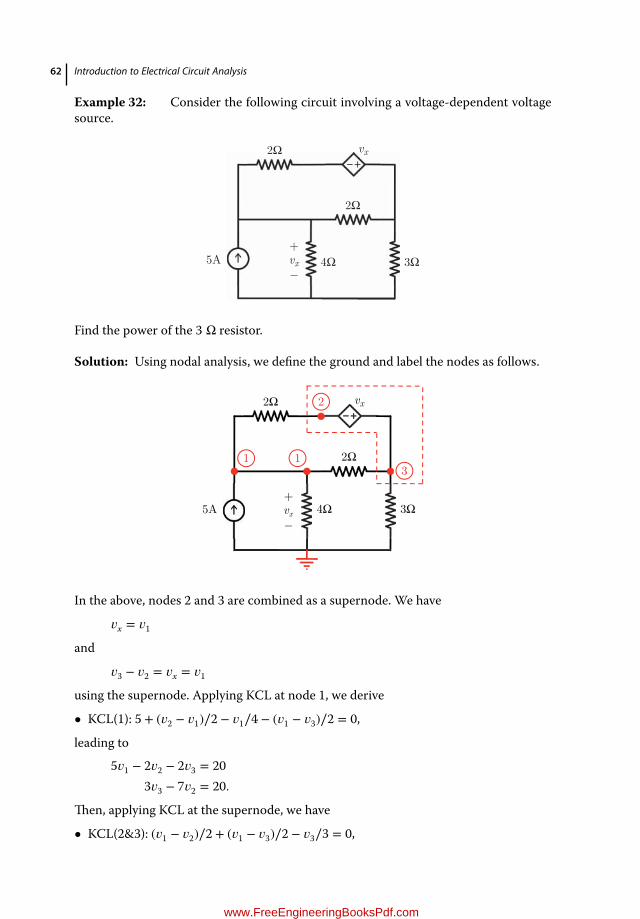
62 Introduction to Electrical Circuit Analysis
Example 32: Consider the following circuit involving a voltage-dependent voltagesource.
2Ω
2Ω
4Ω 3Ω5A
vx
vx
+
_
Find the power of the 3 Ω resistor.
Solution: Using nodal analysis, we define the ground and label the nodes as follows.
2Ω
2Ω
4Ω 3Ω5A
vx2
3 1 1
vx
+
_
In the above, nodes 2 and 3 are combined as a supernode. We have
𝑣x = 𝑣1
and
𝑣3 − 𝑣2 = 𝑣x = 𝑣1
using the supernode. Applying KCL at node 1, we derive
• KCL(1): 5 + (𝑣2 − 𝑣1)∕2 − 𝑣1∕4 − (𝑣1 − 𝑣3)∕2 = 0,
leading to
5𝑣1 − 2𝑣2 − 2𝑣3 = 203𝑣3 − 7𝑣2 = 20.
Then, applying KCL at the supernode, we have
• KCL(2&3): (𝑣1 − 𝑣2)∕2 + (𝑣1 − 𝑣3)∕2 − 𝑣3∕3 = 0,
www.FreeEngineeringBooksPdf.com
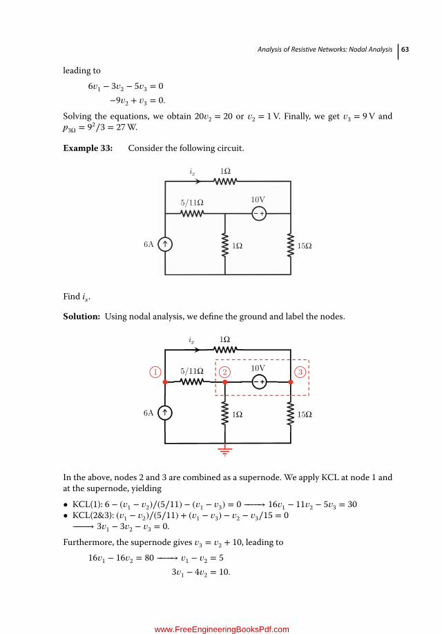
Analysis of Resistive Networks: Nodal Analysis 63
leading to6𝑣1 − 3𝑣2 − 5𝑣3 = 0
−9𝑣2 + 𝑣3 = 0.
Solving the equations, we obtain 20𝑣2 = 20 or 𝑣2 = 1V. Finally, we get 𝑣3 = 9V andp3Ω = 92∕3 = 27W.
Example 33: Consider the following circuit.
1Ωix
5/11Ω
1Ω 15Ω6A
10V
Find ix.
Solution: Using nodal analysis, we define the ground and label the nodes.
1Ω
5/11Ω
1Ω 15Ω6A
10V 1 2 3
ix
In the above, nodes 2 and 3 are combined as a supernode. We apply KCL at node 1 andat the supernode, yielding
• KCL(1): 6 − (𝑣1 − 𝑣2)∕(5∕11) − (𝑣1 − 𝑣3) = 0 −−−−→ 16𝑣1 − 11𝑣2 − 5𝑣3 = 30• KCL(2&3): (𝑣1 − 𝑣2)∕(5∕11) + (𝑣1 − 𝑣3) − 𝑣2 − 𝑣3∕15 = 0
−−−−→ 3𝑣1 − 3𝑣2 − 𝑣3 = 0.
Furthermore, the supernode gives 𝑣3 = 𝑣2 + 10, leading to16𝑣1 − 16𝑣2 = 80 −−−−→ 𝑣1 − 𝑣2 = 5
3𝑣1 − 4𝑣2 = 10.
www.FreeEngineeringBooksPdf.com
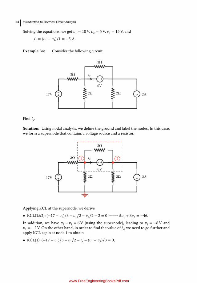
64 Introduction to Electrical Circuit Analysis
Solving the equations, we get 𝑣1 = 10V, 𝑣2 = 5V, 𝑣3 = 15V, and
ix = (𝑣1 − 𝑣3)∕1 = −5 A.
Example 34: Consider the following circuit.
3Ω
17V
ix
6V
2Ω 2Ω 2A
3Ω
Find ix.
Solution: Using nodal analysis, we define the ground and label the nodes. In this case,we form a supernode that contains a voltage source and a resistor.
3Ω
17V
ix
6V
2Ω 2Ω 2A
3Ω
1 2
Applying KCL at the supernode, we derive
• KCL(1&2): (−17 − 𝑣1)∕3 − 𝑣1∕2 − 𝑣2∕2 − 2 = 0 −−−−→ 5𝑣1 + 3𝑣2 = −46.
In addition, we have 𝑣2 − 𝑣1 = 6V (using the supernode), leading to 𝑣1 = −8V and𝑣2 = −2V. On the other hand, in order to find the value of ix, we need to go further andapply KCL again at node 1 to obtain
• KCL(1): (−17 − 𝑣1)∕3 − 𝑣1∕2 − ix − (𝑣1 − 𝑣2)∕3 = 0,
www.FreeEngineeringBooksPdf.com
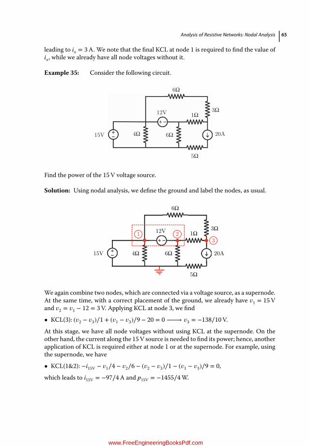
Analysis of Resistive Networks: Nodal Analysis 65
leading to ix = 3A. We note that the final KCL at node 1 is required to find the value ofix, while we already have all node voltages without it.
Example 35: Consider the following circuit.
15V
12V
4Ω 6Ω
1Ω
6Ω
3Ω
5Ω
20A
Find the power of the 15V voltage source.
Solution: Using nodal analysis, we define the ground and label the nodes, as usual.
15V
12V
4Ω 6Ω
1Ω
6Ω
3Ω
5Ω
20A
1 2 3
We again combine two nodes, which are connected via a voltage source, as a supernode.At the same time, with a correct placement of the ground, we already have 𝑣1 = 15Vand 𝑣2 = 𝑣1 − 12 = 3V. Applying KCL at node 3, we find
• KCL(3): (𝑣2 − 𝑣3)∕1 + (𝑣1 − 𝑣3)∕9 − 20 = 0 −−−−→ 𝑣3 = −138∕10V.
At this stage, we have all node voltages without using KCL at the supernode. On theother hand, the current along the 15V source is needed to find its power; hence, anotherapplication of KCL is required either at node 1 or at the supernode. For example, usingthe supernode, we have
• KCL(1&2): −i15V − 𝑣1∕4 − 𝑣2∕6 − (𝑣2 − 𝑣3)∕1 − (𝑣1 − 𝑣3)∕9 = 0,
which leads to i15V = −97∕4A and p15V = −1455∕4W.
www.FreeEngineeringBooksPdf.com
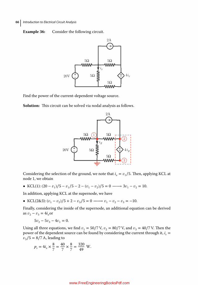
66 Introduction to Electrical Circuit Analysis
Example 36: Consider the following circuit.
2A
20V
5Ω 5Ω
5Ω
5Ω
ix
4ix
Find the power of the current-dependent voltage source.
Solution: This circuit can be solved via nodal analysis as follows.
2A
20V
5Ω 5Ω
5Ω
5Ω
ix
4ix
1 2
3
Considering the selection of the ground, we note that ix = 𝑣1∕5. Then, applying KCL atnode 1, we obtain
• KCL(1): (20 − 𝑣1)∕5 − 𝑣1∕5 − 2 − (𝑣1 − 𝑣2)∕5 = 0 −−−−→ 3𝑣1 − 𝑣2 = 10.
In addition, applying KCL at the supernode, we have
• KCL(2&3): (𝑣1 − 𝑣2)∕5 + 2 − 𝑣3∕5 = 0 −−−−→ 𝑣1 − 𝑣2 − 𝑣3 = −10.
Finally, considering the inside of the supernode, an additional equation can be derivedas 𝑣2 − 𝑣3 = 4ixor
5𝑣2 − 5𝑣3 − 4𝑣1 = 0.
Using all three equations, we find 𝑣1 = 50∕7V, 𝑣2 = 80∕7V, and 𝑣3 = 40∕7V. Then thepower of the dependent source can be found by considering the current through it, is =𝑣3∕5 = 8∕7A, leading to
ps = 4ix ×87= 40
7× 87= 320
49W.
www.FreeEngineeringBooksPdf.com
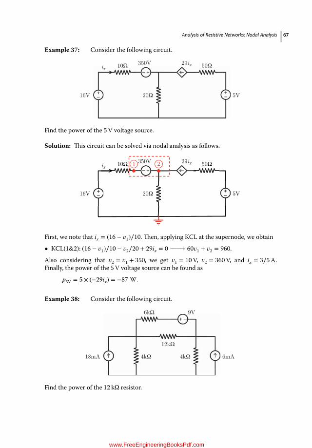
Analysis of Resistive Networks: Nodal Analysis 67
Example 37: Consider the following circuit.
16V
ix
20Ω
350V
5V
10Ω 29ix 50Ω
Find the power of the 5V voltage source.
Solution: This circuit can be solved via nodal analysis as follows.
16V
ix
20Ω
350V
5V
10Ω 29ix 50Ω1 2
First, we note that ix = (16 − 𝑣1)∕10. Then, applying KCL at the supernode, we obtain
• KCL(1&2): (16 − 𝑣1)∕10 − 𝑣2∕20 + 29ix = 0 −−−−→ 60𝑣1 + 𝑣2 = 960.
Also considering that 𝑣2 = 𝑣1 + 350, we get 𝑣1 = 10V, 𝑣2 = 360V, and ix = 3∕5A.Finally, the power of the 5V voltage source can be found as
p5V = 5 × (−29ix) = −87 W.
Example 38: Consider the following circuit.
18mA 4kΩ
12kΩ
4kΩ 6mA
6kΩ 9V
Find the power of the 12 kΩ resistor.
www.FreeEngineeringBooksPdf.com
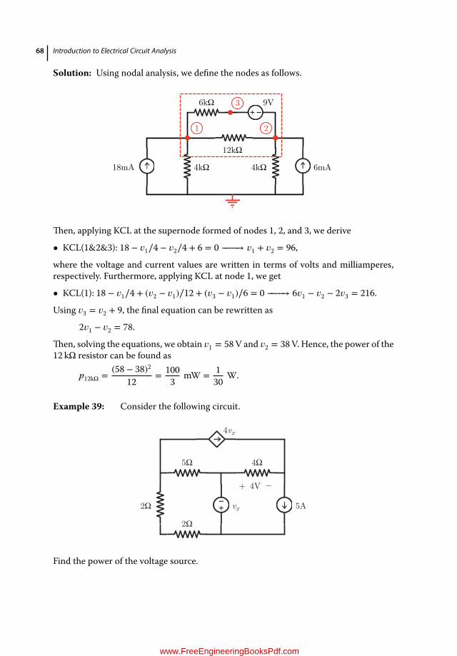
68 Introduction to Electrical Circuit Analysis
Solution: Using nodal analysis, we define the nodes as follows.
18mA 4kΩ
12kΩ
4kΩ 6mA
6kΩ 9V
1 2
3
Then, applying KCL at the supernode formed of nodes 1, 2, and 3, we derive
• KCL(1&2&3): 18 − 𝑣1∕4 − 𝑣2∕4 + 6 = 0 −−−−→ 𝑣1 + 𝑣2 = 96,
where the voltage and current values are written in terms of volts and milliamperes,respectively. Furthermore, applying KCL at node 1, we get
• KCL(1): 18 − 𝑣1∕4 + (𝑣2 − 𝑣1)∕12 + (𝑣3 − 𝑣1)∕6 = 0 −−−−→ 6𝑣1 − 𝑣2 − 2𝑣3 = 216.
Using 𝑣3 = 𝑣2 + 9, the final equation can be rewritten as
2𝑣1 − 𝑣2 = 78.
Then, solving the equations, we obtain 𝑣1 = 58V and 𝑣2 = 38V. Hence, the power of the12 kΩ resistor can be found as
p12kΩ = (58 − 38)2
12= 100
3mW = 1
30W.
Example 39: Consider the following circuit.
4vx
5Ω 4Ω
4V
2Ω
2Ω
5A
+ _
vx
Find the power of the voltage source.
www.FreeEngineeringBooksPdf.com

Analysis of Resistive Networks: Nodal Analysis 69
Solution: This circuit can be solved via nodal analysis as follows.
4vx
5Ω 4Ω
4V
2Ω
2Ω
5A
+ _
vx
13
2
First, we note that 𝑣1 − 𝑣3 = 4, leading to 1A current from node 1 to node 3. ApplyingKCL at the supernode, we have
• KCL(1&2): −𝑣1∕5 − 𝑣2∕4 + 5 − 1 = 0 −−−−→ 4𝑣1 + 5𝑣2 = 80.
Moreover, applying KCL at node 3, we derive
• KCL(3): 4𝑣x + 1 − 5 = 0 −−−−→ 𝑣x = 1V.
Inside the supernode, we further have 𝑣2 − 𝑣1 = 𝑣x; hence,
𝑣2 − 𝑣1 = 1.
Solving the equations, one obtains 𝑣1 = 25∕3V and 𝑣2 = 84∕9V. In order to find thepower of the voltage source, one needs to apply KCL either at node 1 or node 2. Forexample, we have
• KCL(2): 5 − is − 𝑣2∕4 = 0 −−−−→ is = 8∕3A,
leading to
ps = 𝑣x × is = 8∕3 W.
Exercise 21: In the following circuit, find the value of iy.
10Ω 5Ω
10Ω
5Ω
10V vx
+
_
2vx
iy
www.FreeEngineeringBooksPdf.com

70 Introduction to Electrical Circuit Analysis
Exercise 22: In the following circuit, find the power of the 2 Ω resistor.
D
6A
4Ω 6A
12V
2Ω
Exercise 23: In the following circuit, find the power of the top 10 Ω resistor.
10Ω
10Ω
5Ω 2Ω 2A5A
4V
Exercise 24: In the following circuit, find iy.
12V 4Ω
2A vx
3vx
6Ω 2Ω
+
_
iy
Exercise 25: In the following circuit, find 𝑣s.
12A
2Ω
6Ω 12Ω
1A
12Ω
vs
www.FreeEngineeringBooksPdf.com
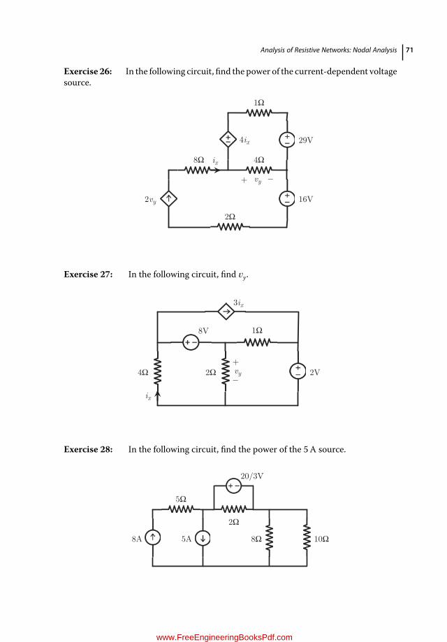
Analysis of Resistive Networks: Nodal Analysis 71
Exercise 26: In the following circuit, find the power of the current-dependent voltagesource.
4Ω8Ω
1Ω
2Ω
29V
16V
ix
4ix
2vy
+ _vy
Exercise 27: In the following circuit, find 𝑣y.
8V
2V 4Ω 2Ω
1Ω
ix
3ix
vy
+
_
Exercise 28: In the following circuit, find the power of the 5A source.
8A 5A
5Ω
20/3V
2Ω
8Ω 10Ω
www.FreeEngineeringBooksPdf.com

72 Introduction to Electrical Circuit Analysis
Exercise 29: In the following circuit, find ix.
3A
10Ω
20Ω
20V 20Ω
50ix
ix
Exercise 30: In the following circuit, find 𝑣x.
6Ω2Ω 2A
4Ω 12V
vx
+
_
3vx
3.3 Circuits with Multiple Independent Voltage Sources
In the next chapter, we present another systematic technique, namely mesh analysis, forthe analysis of circuits. Then an important question arises: for a given circuit, whichmethod is better than the others—nodal analysis, mesh analysis, or simply using KCLand KVL together. While there is not a simple answer to this question, we can claimthat nodal analysis is particularly useful when there are multiple voltage sources thatare connected to each other, leading to trivial determination of node voltages. By way ofdemonstration, consider the following circuit.
www.FreeEngineeringBooksPdf.com
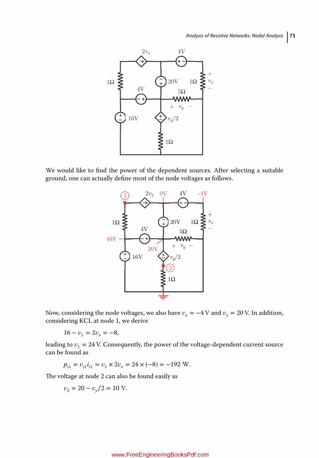
Analysis of Resistive Networks: Nodal Analysis 73
1Ω
1Ω
5Ω
1Ω
+ _ vy
vy/2
4V20V
4V
16V
vx
+
_
2vx
We would like to find the power of the dependent sources. After selecting a suitableground, one can actually define most of the node voltages as follows.
1Ω
1Ω
5Ω1Ω
+ _vy
vy/2
4V20V
4V
16V
vx
+
_
2vx
16V
20V
0V -4V1
2
Now, considering the node voltages, we also have 𝑣x = −4V and 𝑣y = 20V. In addition,considering KCL at node 1, we derive
16 − 𝑣1 = 2𝑣x = −8,
leading to 𝑣1 = 24V. Consequently, the power of the voltage-dependent current sourcecan be found as
ps1 = 𝑣s1is1 = 𝑣1 × 2𝑣x = 24 × (−8) = −192 W.
The voltage at node 2 can also be found easily as
𝑣2 = 20 − 𝑣y∕2 = 10 V.
www.FreeEngineeringBooksPdf.com
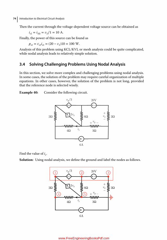
74 Introduction to Electrical Circuit Analysis
Then the current through the voltage-dependent voltage source can be obtained asis2 = i1Ω = 𝑣2∕1 = 10 A.
Finally, the power of this source can be found asps2 = 𝑣s2is2 = (20 − 𝑣2)10 = 100 W.
Analysis of this problem using KCL/KVL or mesh analysis could be quite complicated,while nodal analysis leads to relatively simple solution.
3.4 Solving Challenging Problems Using Nodal Analysis
In this section, we solve more complex and challenging problems using nodal analysis.In some cases, the solution of the problemmay require careful organization of multipleequations. In other cases, however, the solution of the problem is not long, providedthat the reference node is selected wisely.
Example 40: Consider the following circuit.
6A
2Ω
4Ω 3Ω
2Ω6Ω
20V
vx
+
_vy _+
vy/3
iz
2vx
Find the value of iz.
Solution: Using nodal analysis, we define the ground and label the nodes as follows.
6A
2Ω
4Ω 3Ω
2Ω6Ω
20V
vx+_
vy _ +
vy/3
iz
2vx
1 2 3
4 5
www.FreeEngineeringBooksPdf.com
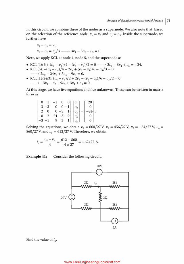
Analysis of Resistive Networks: Nodal Analysis 75
In this circuit, we combine three of the nodes as a supernode. We also note that, basedon the selection of the reference node, 𝑣x = 𝑣3 and 𝑣y = 𝑣5. Inside the supernode, wefurther have
𝑣2 − 𝑣3 = 20,𝑣1 − 𝑣2 = 𝑣y∕3 −−−−→ 3𝑣1 − 3𝑣2 − 𝑣5 = 0.
Next, we apply KCL at node 4, node 5, and the supernode as
• KCL(4): 6 + (𝑣5 − 𝑣4)∕4 − (𝑣4 − 𝑣1)∕2 = 0 −−−−→ 2𝑣1 − 3𝑣4 + 𝑣5 = −24,• KCL(5): −(𝑣5 − 𝑣4)∕4 − 2𝑣x + (𝑣2 − 𝑣5)∕6 − 𝑣5∕3 = 0
−−−−→ 2𝑣2 − 24𝑣3 + 3𝑣4 − 9𝑣5 = 0,• KCL(1&2&3): (𝑣4 − 𝑣1)∕2 + 2𝑣x − (𝑣2 − 𝑣5)∕6 − 𝑣3∕2 = 0
−−−−→ −3𝑣1 − 𝑣2 + 9𝑣3 + 3𝑣4 + 𝑣5 = 0.
At this stage, we have five equations and five unknowns.These can be written in matrixform as
⎡⎢⎢⎢⎢⎣
0 1 −1 0 03 −3 0 0 −12 0 0 −3 10 2 −24 3 −9
−3 −1 9 3 1
⎤⎥⎥⎥⎥⎦
⎡⎢⎢⎢⎢⎣
𝑣1𝑣2𝑣3𝑣4𝑣5
⎤⎥⎥⎥⎥⎦=
⎡⎢⎢⎢⎢⎣
200
−2400
⎤⎥⎥⎥⎥⎦.
Solving the equations, we obtain 𝑣1 = 660∕27V, 𝑣2 = 456∕27V, 𝑣3 = −84∕27V, 𝑣4 =860∕27V, and 𝑣5 = 612∕27V. Therefore, we obtain
iz =𝑣5 − 𝑣4
4= 612 − 860
4 × 27= −62∕27 A.
Example 41: Consider the following circuit.
10V
2Ω 2Ω
2Ω 2Ω
2Ω20V
5A
ix
Find the value of ix.
www.FreeEngineeringBooksPdf.com
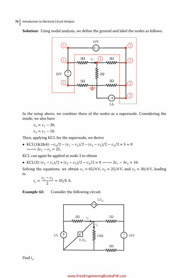
76 Introduction to Electrical Circuit Analysis
Solution: Using nodal analysis, we define the ground and label the nodes as follows.
2Ω
10V
2Ω
2Ω
2Ω
2Ω
20V
5A
ix
1
1
2
2
4 2
2
3
In the setup above, we combine three of the nodes as a supernode. Considering theinside, we also have
𝑣4 = 𝑣1 − 20,𝑣2 = 𝑣1 − 10.
Then, applying KCL for the supernode, we derive• KCL(1&2&4): −𝑣4∕2 − (𝑣1 − 𝑣3)∕2 − (𝑣2 − 𝑣3)∕2 − 𝑣2∕2 + 5 = 0
−−−−→ 2𝑣1 − 𝑣3 = 25.KCL can again be applied at node 3 to obtain• KCL(3): (𝑣1 − 𝑣3)∕2 + (𝑣2 − 𝑣3)∕2 − 𝑣3∕2 = 0 −−−−→ 2𝑣1 − 3𝑣3 = 10.Solving the equations, we obtain 𝑣1 = 65∕4V, 𝑣2 = 25∕4V, and 𝑣3 = 30∕4V, leadingto
ix =𝑣1 − 𝑣3
2= 35∕8 A.
Example 42: Consider the following circuit.
16V
5Ω
0.2ix
3Ω
10Ω
12iy
ix
4Ω
4A
iy
+−
Find ix.
www.FreeEngineeringBooksPdf.com

Analysis of Resistive Networks: Nodal Analysis 77
Solution: Using nodal analysis, we once again define the ground and label thenodes.
16V
5Ω
0.2ix
3Ω
10Ω
12iy
ix
4Ω
4A
iy1
2 3
4
In the above, three of four nodes are combined as a supernode. We have𝑣3 = 𝑣1 + 12iy = 𝑣1 + 6∕5𝑣2𝑣4 = 𝑣3 + 16 = 𝑣1 + 6∕5𝑣2 + 16,
considering that iy = 𝑣2∕10. Applying KCL at the supernode and at node 2, wederive• KCL(1&3&4): 4 − (𝑣1 − 𝑣2)∕3 − (𝑣3 − 𝑣2)∕5 − 𝑣4∕4 = 0 −−−−→ 𝑣2 = −235𝑣1∕2,• KCL(2): (𝑣1 − 𝑣2)∕3 − 0.2ix − (𝑣2 − 𝑣3)∕5 − 𝑣2∕10 = 0 −−−−→ 𝑣2 = 10𝑣1∕7.Then we have 𝑣1 = 0V, 𝑣2 = 0V, 𝑣3 = 0V, and 𝑣4 = 16V. Finally,
ix = (𝑣1 − 𝑣2)∕3 = 0 A.
Example 43: Consider the following circuit.
2Ω 2Ω
3Ω
1Ω 60V 1Ω
3ix ix
ix
Find the value of ix.
www.FreeEngineeringBooksPdf.com
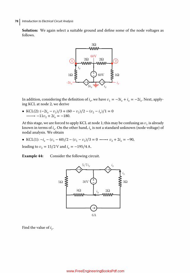
78 Introduction to Electrical Circuit Analysis
Solution: We again select a suitable ground and define some of the node voltages asfollows.
2Ω 2Ω
3Ω
1Ω 60V 1Ω
3ix ix
ix
1 260V
-3ix ix
In addition, considering the definition of ix, we have 𝑣1 = −3ix + ix = −2ix. Next, apply-ing KCL at node 2, we derive
• KCL(2): (−2ix − 𝑣2)∕3 + (60 − 𝑣2)∕2 − (𝑣2 − ix)∕1 = 0−−−−→ −11𝑣2 + 2ix = −180.
At this stage, we are forced to apply KCL at node 1; this may be confusing as 𝑣1 is alreadyknown in terms of ix. On the other hand, ix is not a standard unknown (node voltage) ofnodal analysis. We obtain
• KCL(1): −ix − (𝑣1 − 60)∕2 − (𝑣1 − 𝑣2)∕3 = 0 −−−−→ 𝑣2 + 2ix = −90,
leading to 𝑣2 = 15∕2V and ix = −195∕4A.
Example 44: Consider the following circuit.
iy
5Ω 30V
6A
ix
5/7ix
8Ω 2Ω
3Ω
ix
Find the value of iy.
www.FreeEngineeringBooksPdf.com
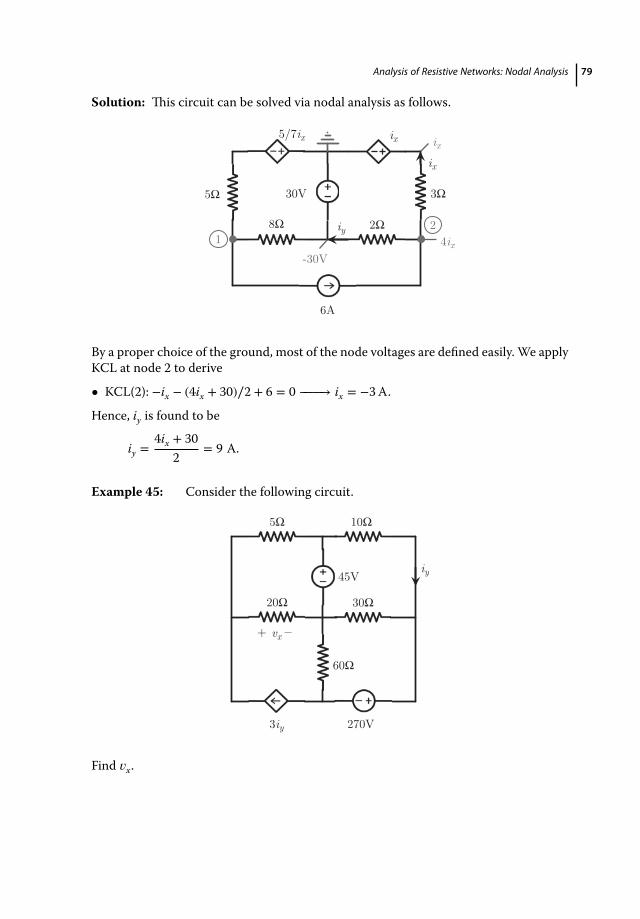
Analysis of Resistive Networks: Nodal Analysis 79
Solution: This circuit can be solved via nodal analysis as follows.
iy
5Ω 30V
6A
ix
5/7ix
8Ω 2Ω
3Ω
ix ix
4ix-30V
12
By a proper choice of the ground, most of the node voltages are defined easily. We applyKCL at node 2 to derive
• KCL(2): −ix − (4ix + 30)∕2 + 6 = 0 −−−−→ ix = −3A.
Hence, iy is found to be
iy =4ix + 30
2= 9 A.
Example 45: Consider the following circuit.
45V
60Ω
5Ω 10Ω
20Ω 30Ω
vx_+
270V
iy
3iy
Find 𝑣x.
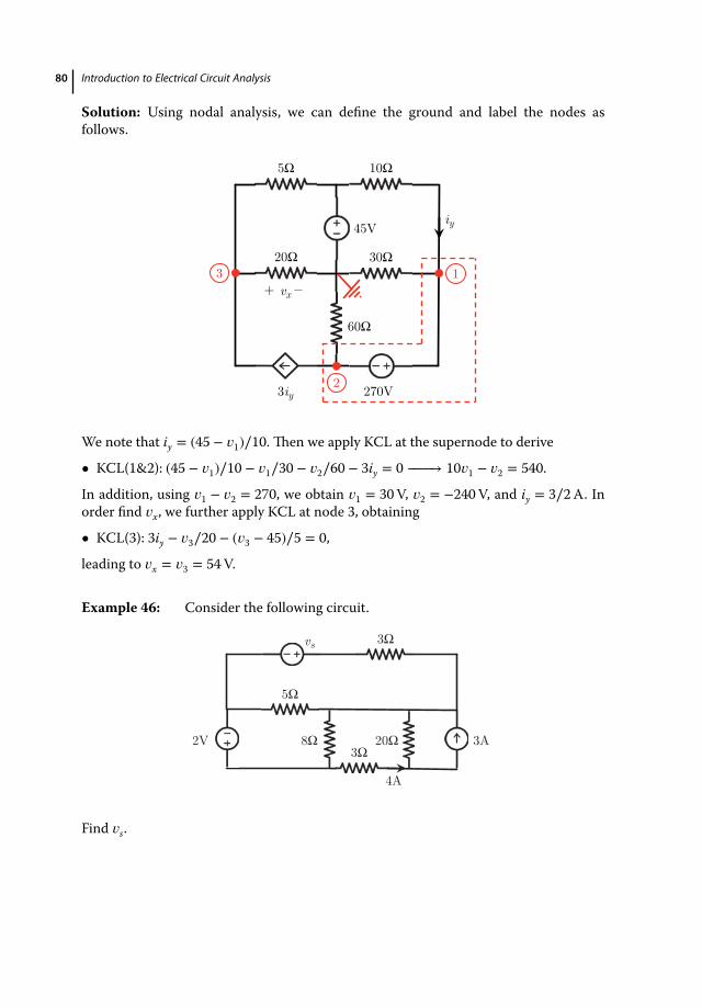
80 Introduction to Electrical Circuit Analysis
Solution: Using nodal analysis, we can define the ground and label the nodes asfollows.
45V
60Ω
5Ω 10Ω
20Ω 30Ω
vx_+
270V
iy
3iy
1
2
3
We note that iy = (45 − 𝑣1)∕10. Then we apply KCL at the supernode to derive
• KCL(1&2): (45 − 𝑣1)∕10 − 𝑣1∕30 − 𝑣2∕60 − 3iy = 0 −−−−→ 10𝑣1 − 𝑣2 = 540.
In addition, using 𝑣1 − 𝑣2 = 270, we obtain 𝑣1 = 30V, 𝑣2 = −240V, and iy = 3∕2A. Inorder find 𝑣x, we further apply KCL at node 3, obtaining
• KCL(3): 3iy − 𝑣3∕20 − (𝑣3 − 45)∕5 = 0,
leading to 𝑣x = 𝑣3 = 54V.
Example 46: Consider the following circuit.
vs
8Ω2V 3Ω
3A
4A
5Ω
3Ω
20Ω
Find 𝑣s.
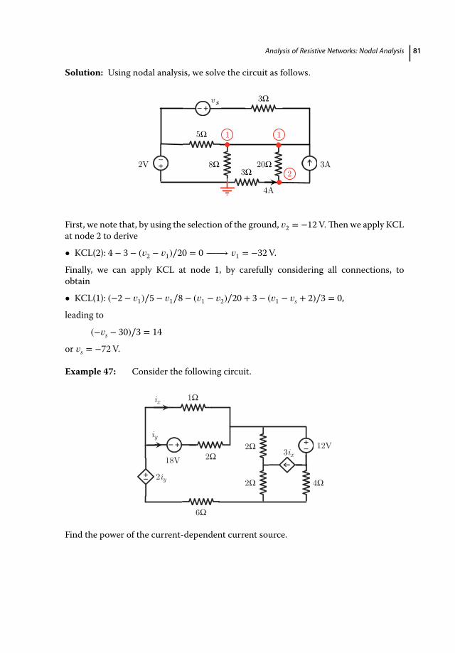
Analysis of Resistive Networks: Nodal Analysis 81
Solution: Using nodal analysis, we solve the circuit as follows.
vs
8Ω2V 3Ω
3A
4A
5Ω
3Ω
20Ω
1 1
2
First, we note that, by using the selection of the ground, 𝑣2 = −12V.Then we apply KCLat node 2 to derive
• KCL(2): 4 − 3 − (𝑣2 − 𝑣1)∕20 = 0 −−−−→ 𝑣1 = −32V.
Finally, we can apply KCL at node 1, by carefully considering all connections, toobtain
• KCL(1): (−2 − 𝑣1)∕5 − 𝑣1∕8 − (𝑣1 − 𝑣2)∕20 + 3 − (𝑣1 − 𝑣s + 2)∕3 = 0,
leading to
(−𝑣s − 30)∕3 = 14
or 𝑣s = −72V.
Example 47: Consider the following circuit.
2Ω
2Ω 4Ω
12V
18V
1Ω
2Ω
6Ω
3ix
ix
iy
2iy
Find the power of the current-dependent current source.

82 Introduction to Electrical Circuit Analysis
Solution: Using nodal analysis, this circuit can be solved as follows.
2Ω
2Ω 4Ω
12V
18V
1Ω
2Ω
6Ω
3ix
i
iy
2iy
2iy
18+2 iy
1 1 1
2
4
3
x
First, we note that 18 + 2iy − 𝑣1 = 2iy, leading to 𝑣1 = 18V. This leads in turn to ix =2iy − 18. In addition, we have 𝑣2 = 𝑣1 − 12 = 6V. Hence, we already know two nodevoltages without applying KCL. Next, we can apply KCL at nodes 3 and 4 to derive• KCL(3): (𝑣1 − 𝑣3)∕2 + 3ix − (𝑣3 − 𝑣4)∕2 = 0 −−−−→ 2𝑣3 − 6ix − 𝑣4 = 18
−−−−→ 2𝑣3 − 12iy − 𝑣4 = −90,• KCL(4): (𝑣3 − 𝑣4)∕2 + (𝑣2 − 𝑣4)∕4 − 𝑣4∕6 = 0 −−−−→ 11𝑣4 − 6𝑣3 = 18.Obviously, we need another equation to solve this problem. While there are alternativechoices, we apply KCL in the supernode formed of nodes 1, 2, 3, and 4 as• KCL(1&2&3&4): ix + iy − 𝑣4∕6 = 0 −−−−→ 18iy − 𝑣4 = 108.Combining two of the three equations, we get
6𝑣3 − 5𝑣4 = −54,leading to 𝑣3 = −14V, 𝑣4 = −6V, iy = 17∕3A, and ix = −20∕3A. Therefore, the powerof the dependent source is found to be
ps = (𝑣2 − 𝑣3) × 3ix = 20 × (−20) = −400 W.
Example 48: As a final example, consider the following circuit.
12V24V
4V
2A1Ω
30V
2V
2V
ix/121Ω 10Ω
ix
io
Find the power of the 12V voltage source.

Analysis of Resistive Networks: Nodal Analysis 83
Solution: This circuit can be solved via nodal analysis as follows.
12V24V
4V
2A1Ω
30V
2V
2V
ix/121Ω 10Ω
ix
io
24V 36V 6V
4V 6V
We note that most of the node voltages are known. In addition, ix = 24∕1 = 24A,i30V = 0A, and
i12V = ix∕12 = 2 A,leading to
p12V = 12 × 2 = 24 W.
Exercise 31: In the following circuit, find the power of the current-dependent voltagesource.
ix
2A
6Ω1Ω
2Ω
2ix
1/2Ω
1Ω
5V
Exercise 32: In the following circuit, find iz.
20V4Ω
6A
4vy
ix
6Ω
12Ω 8Ω
12ix
vy
iz
_ +
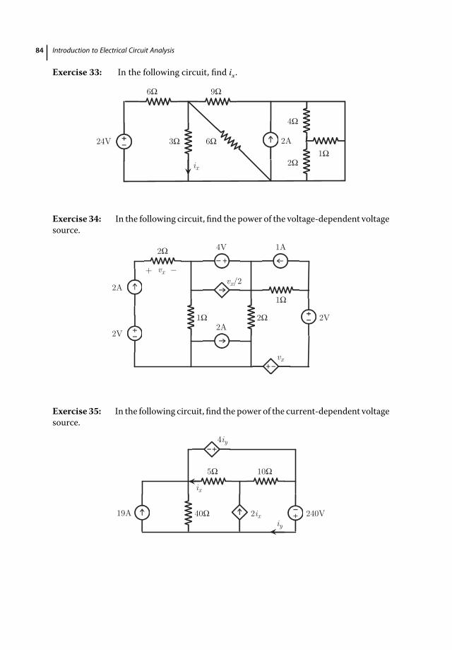
84 Introduction to Electrical Circuit Analysis
Exercise 33: In the following circuit, find ix.
6Ω 9Ω
3Ω 2A24V
ix
6Ω
4Ω
1Ω2Ω
Exercise 34: In the following circuit, find the power of the voltage-dependent voltagesource.
4V 1A
1Ω
2Ω1Ω 2V2A
2Ω
2A
2V
+ _vx
vx/2
vx
Exercise 35: In the following circuit, find the power of the current-dependent voltagesource.
40Ω19A 240V
10Ω5Ω
ix
2ix
4iy
iy
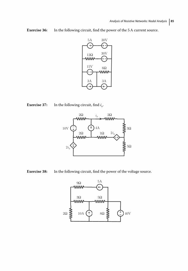
Analysis of Resistive Networks: Nodal Analysis 85
Exercise 36: In the following circuit, find the power of the 5A current source.
5A 30V
12Ω 30V
15V 6Ω
3A 3A
Exercise 37: In the following circuit, find ix.
10V 4A
2Ω
2Ω 2Ω
1Ω3Ω
5Ω2ix
2ix
ix
Exercise 38: In the following circuit, find the power of the voltage source.
2Ω
9Ω
3Ω 5Ω
8Ω
5A
10A 40V
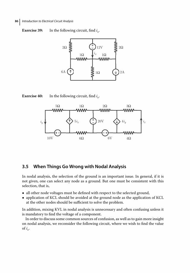
86 Introduction to Electrical Circuit Analysis
Exercise 39: In the following circuit, find ix.
2Ω
1Ω
1Ω
1Ω
2Ω12V
6A 2A
ix
Exercise 40: In the following circuit, find ix.
5Ω 1Ω 2Ω 3Ω
4Ω6Ω10V
5ix 20V 4iy
6V
ixiy
3.5 When Things Go Wrong with Nodal Analysis
In nodal analysis, the selection of the ground is an important issue. In general, if it isnot given, one can select any node as a ground. But one must be consistent with thisselection, that is,
• all other node voltages must be defined with respect to the selected ground,• application of KCL should be avoided at the ground node as the application of KCL
at the other nodes should be sufficient to solve the problem.
In addition, mixing KVL in nodal analysis is unnecessary and often confusing unless itis mandatory to find the voltage of a component.In order to discuss some common sources of confusion, as well as to gainmore insight
on nodal analysis, we reconsider the following circuit, where we wish to find the valueof ix.

Analysis of Resistive Networks: Nodal Analysis 87
1Ωix
5/11Ω
1Ω 15Ω6A
10V
In comparison to the original analysis of this circuit, we select a different ground asfollows.
1Ωix
5/11Ω
1Ω 15Ω6A
10V
1 2
3
is
Now one can start with KCL at node 1 which yields
• KCL(1): 6 − 𝑣1∕(5∕11) − (𝑣1 − 𝑣2)∕1 = 0 −−−−→ 16𝑣1 − 5𝑣2 = 30.
Similarly, at node 3, we have
• KCL(3): −6 − 𝑣3∕1 − (𝑣3 − 𝑣2)∕15 = 0 −−−−→ 𝑣2 − 16𝑣3 = 90.
But what about applying KCL at node 2 in order to obtain a third equation? If we areforced to do this, we have
• KCL(2): is − (𝑣2 − 𝑣3)∕15 − (𝑣2 − 𝑣1)∕1 = 0,
which is not useful since we need is as another variable. In fact, we should never applyKCL at node 2, because the voltage of this node is already known, 𝑣2 = 10V, consideringthe selection of the ground. We also note that the voltage of this node is 15V in theoriginal solution, but now it is different due to the different selection of the ground.Using 𝑣2 = 10V, we have 𝑣1 = 5V and 𝑣3 = −5V. Furthermore, the value of ix can befound to be
ix = (𝑣1 − 𝑣2)∕1 = −5 A.

88 Introduction to Electrical Circuit Analysis
We emphasize that the value of ix should be independent of the selection of the ground.Similarly, the voltage across the related resistor, 𝑣1Ω = 𝑣1 − 𝑣2 = −5V, should notdepend on the selection of the ground while 𝑣1 and 𝑣2 may change.In the circuit above, KCLmust be applied at node 2 if is must be found. Using KCL(2),
we derive
is = (𝑣2 − 𝑣3)∕15 + (𝑣2 − 𝑣1)∕1 = 1 + 5 = 6 A,
which must again be independent of the selection of the ground.We now consider the following circuit, where the value of ix needs to be found.
4A
1Ω
2V
1A 6Ω
3V
ix
We particularly consider the case below, where the ground is selected at the middle.
4A
1Ω
2V
1A 6Ω
3V
ix
1
2
3
4
Interestingly, this selection of the ground leads to a large number of nodes that need tobe defined in nodal analysis. In addition, following a formal procedure, wemust combinetwo pairs as supernodes. Using the definitions of the supernodes, we have two equations
𝑣4 = 𝑣2 + 2,𝑣3 = 𝑣1 + 3.

Analysis of Resistive Networks: Nodal Analysis 89
Applying KCL at the top supernode, we further derive
• KCL(1&3): −1 − 𝑣1∕6 = 0,
leading to 𝑣1 = −6V. Interestingly, and perhaps confusingly, the value of the node volt-age 𝑣1 does not depend on the 3V voltage source. Specifically, 𝑣1 is fixed to −6V due tothe 1A current source, whatever the value of the voltage source. However, the voltageacross the current source, 𝑣3 in this nodal analysis, depends on the voltage source, asindicated above. We have
𝑣3 = 𝑣1 + 3 = −3 V.
The supernode at the bottom leads to another equation for completing the analysis. Wederive
• KCL(2&4): −𝑣4∕1 − 4 = 0 −−−−→ 𝑣4 = −4V,
and
𝑣2 = 𝑣4 − 2 = −6 V.
At this stage, we have all the node voltages. On the other hand, they do not give com-plete information on the value of ix. In order to find ix, we are forced to apply KCL at aground node. More specifically, we have an exception to the general rule that applyingKCL at a ground is unnecessary and useless.We note that this extraordinary case occursdue to a specific selection of the ground.
4A
1Ω
2V
1A 6Ω
3V
ix
1
2
3
4
5
Considering the updated circuit, we have
• KCL(5): (𝑣4 − 𝑣5)∕1 + 1 − ix = 0,
where 𝑣5 = 0, leading to
ix = −3 A.

90 Introduction to Electrical Circuit Analysis
What about selecting another ground for the circuit above? We now consider the fol-lowing case, where the node labels are also changed.
4A
1Ω
2V
1A 6Ω
3V
ix
13
22
2V
First, we note that the voltage at a node (not labeled) is immediately known to be 2V.Considering all entering and leaving currents at node 2, we have
• KCL(2): 1 − (𝑣2 − 2)∕1 + (𝑣1 − 𝑣2)∕6 + 4 = 0 −−−−→ 𝑣1 − 7𝑣2 = −42.
In addition, KCL at the supernode leads to
• KCL(1&3): −1 − (𝑣1 − 𝑣2)∕6 = 0 −−−−→ 𝑣1 − 𝑣2 = −6.
Solving the equations, we obtain 𝑣1 = 0V and 𝑣2 = 6V. Once again, we have all nodevoltages, but obviously we still need to apply KCL again to find ix. We have
• KCL(2-left): 1 + (2 − 𝑣2)∕1 − ix = 0,
leading to ix = 1 − 4 = −3A.
3.6 What You Need to Know before You Continue
As discussed in this chapter, nodal analysis is a systematic way of analyzing circuits. Weemphasize the following points on this technique.
• Equations in nodal analysis: Only KCL is used in nodal analysis, while KVL is notrequired. All equations are written by using node voltages as unknowns. Once theanalysis is completed, KVL may be applied to find the voltage of a component, if it isnot already known.
• Effect of the ground: Voltages and currents through components do not depend onthe selection of the ground.The node voltages, however, may depend on the selectionof the ground.
• It is not necessary to use KCL at a ground for nodal analysis, except for special cases.Therefore, the number of equations derived in nodal analysis is usually the same asthe number of nodes other than the ground.

Analysis of Resistive Networks: Nodal Analysis 91
• A supernode, which involves a combination of multiple nodes and components, isoften required to simplify nodal analysis. KCL is applied by considering the supernodeas a closed surface with entering and leaving currents summing to zero. The extraequation required is obtained from the supernode itself.
In the next chapter, we focus on another systematic method, namely, mesh analysisbased on KVL instead of KCL.

93
4
Analysis of Resistive Networks: Mesh Analysis
We now turn our attention to mesh analysis, which is based on a systematic applicationof KVL. Similar to nodal analysis, mesh analysis guarantees the development ofsufficient numbers of equations, without any redundant equations or unknowns.However, in contrast to nodal analysis, where node voltages are major unknowns, loopcurrents are the unknowns of mesh analysis. These loop currents are not real currentsbut defined to facilitate the separation of meshes from each other. In addition to simpleloops, we consider the generalization of the loops and the advantages of mesh analysisin detail.
4.1 Application of Mesh Analysis
The steps involved in mesh analysis can be listed as follows.
• Mesh current definitions: We define mesh currents inside closed loops, namelymeshes, which contain only a sequence of components (but not an inner compo-nent). A mesh current is not a real current; it is defined as if it flows inside the loop,when the loop is not affected by the other parts of the circuit. A real current througha branch is the combination of the mesh currents sharing the branch.
• Constructing equations:We use only KVL inside meshes to derive all equations. KCLis not used in mesh analysis unless necessary. We write equations in terms of meshcurrents.
• Solution: We solve the equations to find the mesh currents.• Analysis: Finally, by using the mesh currents, we find the desired voltage, current,
and/or power values.
As usual, we start with simple techniques, and then consider more complex circuits thatare solved via mesh analysis.
Introduction to Electrical Circuit Analysis, First Edition. Özgür Ergül.© 2017 John Wiley & Sons Ltd. Published 2017 by John Wiley & Sons Ltd.Companion Website: www.wiley.com/go/ergul4412

94 Introduction to Electrical Circuit Analysis
Example 49: Consider the following circuit.
1Ω
50V
6Ω
4/5Ω
3Ω 10Ω
40V40V
Find the power of the 50V source.
Solution: Using mesh analysis, we define two mesh currents, namely, ia and ib. Whilethemesh currents can flow in an arbitrary direction, we only use the clockwise direction,to be consistentwithKVLoperations. In the following figure, we also define real currentsi1, i2, and i3, in order to demonstrate the details of the analysis.
1Ω
50V
6Ω
4/5 Ω
3Ω 10Ω
40V40V a b
i1
i2
i3
First, we note that the mesh and real currents are related to each other by
i1 = ia,
i2 = ia − ib,
i3 = ib.
In order to understand these relationships, consider the 1Ω resistor. The real currentthrough this resistor is defined as i1. On the other hand, this real current is only formedby the mesh current ia, which is flowing in the same direction.Therefore, i1 must be thesame as ia. Consider now the real current i2 that is flowing through the 4∕5Ω resistorand the 50V voltage source. In this case, two mesh currents are related to the branch:ia flowing in the same direction as i2 and ib flowing in the opposite direction. In otherwords, i2 must be formed by the combination of two mesh currents, ia and ib, whilethe contribution of ib is negative, leading to i2 = ia − ib. This important relationship isshown in detail as follows.
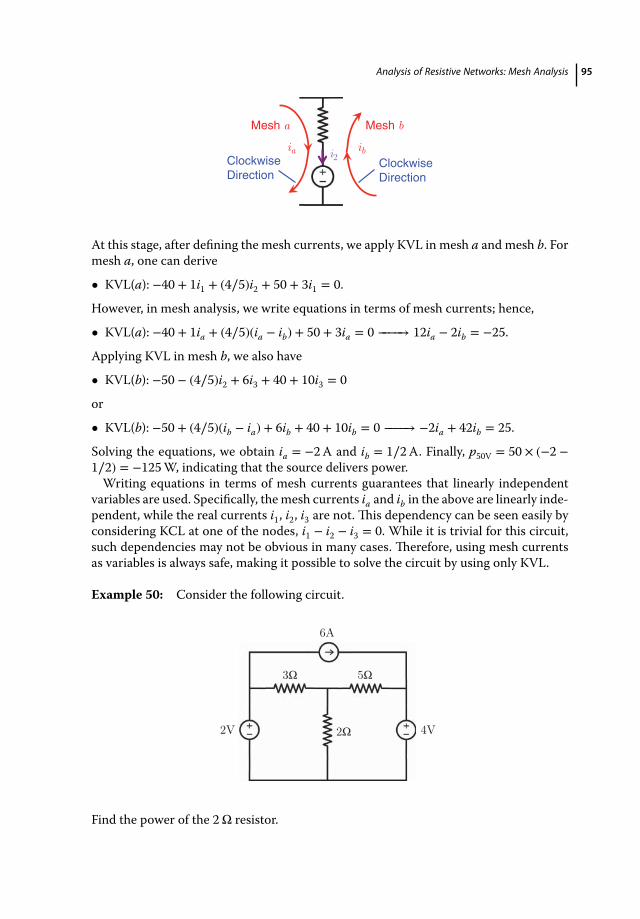
Analysis of Resistive Networks: Mesh Analysis 95
i2
Mesh aia ib
Mesh b
ClockwiseDirection
ClockwiseDirection
At this stage, after defining the mesh currents, we apply KVL in mesh a and mesh b. Formesh a, one can derive
• KVL(a): −40 + 1i1 + (4∕5)i2 + 50 + 3i1 = 0.
However, in mesh analysis, we write equations in terms of mesh currents; hence,
• KVL(a): −40 + 1ia + (4∕5)(ia − ib) + 50 + 3ia = 0 −−−−→ 12ia − 2ib = −25.
Applying KVL in mesh b, we also have
• KVL(b): −50 − (4∕5)i2 + 6i3 + 40 + 10i3 = 0
or
• KVL(b): −50 + (4∕5)(ib − ia) + 6ib + 40 + 10ib = 0 −−−−→ −2ia + 42ib = 25.
Solving the equations, we obtain ia = −2A and ib = 1∕2A. Finally, p50V = 50 × (−2 −1∕2) = −125W, indicating that the source delivers power.Writing equations in terms of mesh currents guarantees that linearly independent
variables are used. Specifically, themesh currents ia and ib in the above are linearly inde-pendent, while the real currents i1, i2, i3 are not. This dependency can be seen easily byconsidering KCL at one of the nodes, i1 − i2 − i3 = 0. While it is trivial for this circuit,such dependencies may not be obvious in many cases. Therefore, using mesh currentsas variables is always safe, making it possible to solve the circuit by using only KVL.
Example 50: Consider the following circuit.
2Ω
6A
4V 2V
3Ω 5Ω
Find the power of the 2Ω resistor.
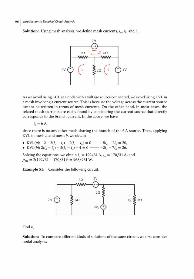
96 Introduction to Electrical Circuit Analysis
Solution: Using mesh analysis, we define mesh currents, ia, ib, and ic.
2Ω
6A
4V 2V
3Ω 5Ω
a b
c
Aswe avoid using KCL at a nodewith a voltage source connected, we avoid using KVL ina mesh involving a current source. This is because the voltage across the current sourcecannot be written in terms of mesh currents. On the other hand, in most cases, therelated mesh currents are easily found by considering the current source that directlycorresponds to the branch current. In the above, we have
ic = 6 A
since there is no any other mesh sharing the branch of the 6A source. Then, applyingKVL in mesh a and mesh b, we obtain
• KVL(a): −2 + 3(ia − ic) + 2(ia − ib) = 0 −−−−→ 5ia − 2ib = 20,• KVL(b): 2(ib − ia) + 5(ib − ic) + 4 = 0 −−−−→ −2ia + 7ib = 26.
Solving the equations, we obtain ia = 192∕31A, ib = 170∕31A, andp2Ω = 2(192∕31 − 170∕31)2 = 968∕961W.
Example 51: Consider the following circuit.
5V5Ω
2A 3Ωvx5Ω+ _
4vx
2Ω
Find 𝑣x.
Solution: To compare different kinds of solutions of the same circuit, we first considernodal analysis.
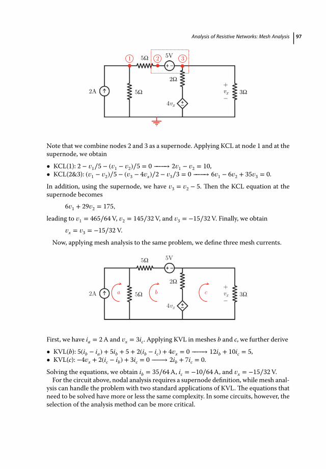
Analysis of Resistive Networks: Mesh Analysis 97
5V5Ω
2A 3Ωvx5Ω+ _
4vx
2Ω
1 3 2
Note that we combine nodes 2 and 3 as a supernode. Applying KCL at node 1 and at thesupernode, we obtain
• KCL(1): 2 − 𝑣1∕5 − (𝑣1 − 𝑣2)∕5 = 0 −−−−→ 2𝑣1 − 𝑣2 = 10,• KCL(2&3): (𝑣1 − 𝑣2)∕5 − (𝑣3 − 4𝑣x)∕2 − 𝑣3∕3 = 0 −−−−→ 6𝑣1 − 6𝑣2 + 35𝑣3 = 0.
In addition, using the supernode, we have 𝑣3 = 𝑣2 − 5. Then the KCL equation at thesupernode becomes
6𝑣1 + 29𝑣2 = 175,
leading to 𝑣1 = 465∕64V, 𝑣2 = 145∕32V, and 𝑣3 = −15∕32V. Finally, we obtain
𝑣x = 𝑣3 = −15∕32 V.
Now, applying mesh analysis to the same problem, we define three mesh currents.
5V5Ω
2A 3Ωvx5Ω+ _
4vx
2Ωa b c
First, we have ia = 2A and 𝑣x = 3ic. Applying KVL in meshes b and c, we further derive
• KVL(b): 5(ib − ia) + 5ib + 5 + 2(ib − ic) + 4𝑣x = 0 −−−−→ 12ib + 10ic = 5,• KVL(c): −4𝑣x + 2(ic − ib) + 3ic = 0 −−−−→ 2ib + 7ic = 0.
Solving the equations, we obtain ib = 35∕64A, ic = −10∕64A, and 𝑣x = −15∕32V.For the circuit above, nodal analysis requires a supernode definition, while mesh anal-
ysis can handle the problem with two standard applications of KVL.The equations thatneed to be solved have more or less the same complexity. In some circuits, however, theselection of the analysis method can be more critical.

98 Introduction to Electrical Circuit Analysis
Example 52: Consider the following circuit, previously studied using nodal analysis(see Example 45).
45V
60Ω
5Ω 10Ω
20Ω 30Ω
vx_ +
270V
iy
3iy
Find 𝑣x.
Solution: Using mesh analysis, we define four different mesh currents.
45V
60Ω
5Ω 10Ω
20Ω 30Ω
vx_ +
270V
iy
3iy
a
c
b
d
First, we note that ib = iy, as iy is defined on a branch that is used only by mesh b. Simi-larly, considering mesh c, we have ic = 3iy, leading to
ic = 3ib.Then, applying KVL in meshes a, b, and d, we get• KVL(a): 5ia + 45 + 20(ia − ic) = 0 −−−−→ 5ia − 12ib = −9,• KVL(b): −45 + 10ib + 30(ib − id) = 0 −−−−→ 8ib − 6id = 9,• KVL(d): 30(id − ib) + 270 + 60(id − ic) = 0 −−−−→ 7ib − 3id = 9.Solving the three equations above, we obtain mesh currents ia = 9∕5A, ib = 3∕2A, ic =9∕2A, and id = 1∕2A. Finally, we find 𝑣x to be
𝑣x = 20 × (ic − ia) = 20 × (9∕2 − 9∕5) = 54 V.

Analysis of Resistive Networks: Mesh Analysis 99
Example 53: Consider the following circuit, also previously studied using nodal anal-ysis (see Example 42).
16V0.2ix
12iy
ix iy
4A
3Ω 5Ω
10Ω
4Ω
Find iy.
Solution: As previously shown, the solution of this problem via nodal analysis is quitechallenging and involves a delicate use of the supernode concept. On the other hand,using mesh analysis, we define four standard mesh currents. Once again, we rememberthat the mesh currents are linearly independent; hence, we need four equations to solvethem.
16V
4A b
c
a
d
3Ω
10Ω
4Ω
5Ω
0.2ix
12iy
ix iy
In the above, considering mesh and real currents, we have
ib = 4 A,ix = ib − ia,
iy = ic − id,
ib − ic = 0.2ix −−−−→ 5ib − 5ic = ib − ia −−−−→ ia + 4ib − 5ic = 0.
Now, we need to apply KVL to only two meshes,
• KVL(a): −12iy + 5(ia − id) + 3(ia − ib) = 0 −−−−→ 8ia − 12ic + 7id = 12,• KVL(d): 10(id − ic) + 5(id − ia) − 16 + 4id = 0 −−−−→ −5ia − 10ic + 19id = 16.
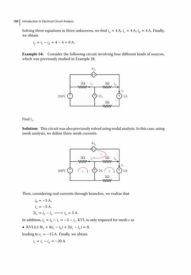
100 Introduction to Electrical Circuit Analysis
Solving three equations in three unknowns, we find ia = 4A, ic = 4A, id = 4A. Finally,we obtain
iy = ic − id = 4 − 4 = 0 A.
Example 54: Consider the following circuit involving four different kinds of sources,which was previously studied in Example 28.
200V 5A
2Ω 4Ω
2Ω
8ix
2ix ix
iz iy
Find iz.
Solution: This circuit was also previously solved using nodal analysis. In this case, usingmesh analysis, we define three mesh currents.
8iy
2Ω200V 5A 2ix
c
a b
2Ω 4Ω iy ix
iz
Then, considering real currents through branches, we realize that
ib = −5 A,ix = −5 A,
2ix = ib − ia −−−−→ ia = 5 A.
In addition, iy = ib − ic = −5 − ic. KVL is only required for mesh c as
• KVL(c): 8iy + 4(ic − ib) + 2(ic − ia) = 0,
leading to ic = −15A. Finally, we obtain
iz = ic − ia = −20 A.
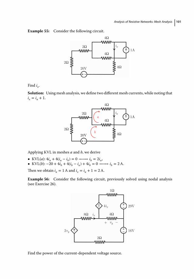
Analysis of Resistive Networks: Mesh Analysis 101
Example 55: Consider the following circuit.
1A
20V
2Ω
2Ω4Ω
4Ω
4Ω
ix
Find ix.
Solution: Usingmesh analysis, we define two differentmesh currents, while noting thatix = ia + 1.
1A
20V
ix a
b
2Ω
4Ω
4Ω
4Ω2Ω
Applying KVL in meshes a and b, we derive• KVL(a): 4ia + 4(ia − ib) = 0 −−−−→ ib = 2ia,• KVL(b): −20 + 4ib + 4(ib − ia) + 4ib = 0 −−−−→ ib = 2A.Then we obtain ia = 1A and ix = ia + 1 = 2A.
Example 56: Consider the following circuit, previously solved using nodal analysis(see Exercise 26).
29V
16V
ix
4ix
2vy
+ _ vy
8Ω
2Ω
4Ω
1Ω
Find the power of the current-dependent voltage source.

102 Introduction to Electrical Circuit Analysis
Solution: Using mesh analysis, we define only two different mesh currents.
29V
16V
ix
4ix
2vy
+ _ vy
a
b
8Ω
2Ω
4Ω
1Ω
First, we note that ib = ix. At the same time, ib = 2𝑣y and 𝑣y = 4(ib − ia). Then4ia = 4ib − 𝑣y = 7ib∕8 = 7ix∕8.
Applying KVL in mesh a, we derive• KVL(a): −4ix + ia + 29 + 4(ia − ib) = 0,which leads to the solution of ix as
−4ix + 7ix∕8 + 29 + 4(7ix∕8 − ix) = 0 −−−−→ ix = 8 A.Therefore, ia = 7A and ib = 8A. Finally, the power of the current-dependent voltagesource can be found to be
p4ix= 4ix × (−ia) = 32 × (−7) = −224W.
Example 57: Consider the following circuit.
12V
ix
6A 6ix3Ω
4Ω 4Ω2Ω
Find the power of the current-dependent voltage source.
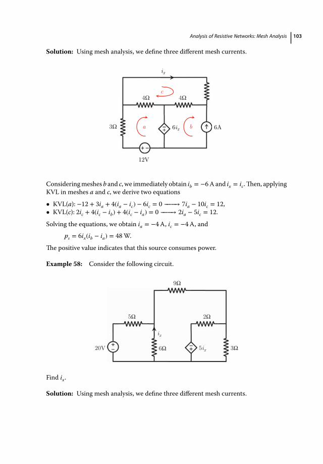
Analysis of Resistive Networks: Mesh Analysis 103
Solution: Using mesh analysis, we define three different mesh currents.
12V
ix
6A 6ix a b
c 4Ω 4Ω
3Ω
Consideringmeshes b and c, we immediately obtain ib = −6Aand ix = ic.Then, applyingKVL in meshes a and c, we derive two equations
• KVL(a): −12 + 3ia + 4(ia − ic) − 6ic = 0 −−−−→ 7ia − 10ic = 12,• KVL(c): 2ic + 4(ic − ib) + 4(ic − ia) = 0 −−−−→ 2ia − 5ic = 12.
Solving the equations, we obtain ia = −4A, ic = −4A, and
ps = 6ix(ib − ia) = 48W.
The positive value indicates that this source consumes power.
Example 58: Consider the following circuit.
20V
5Ω
6Ω
9Ω
2Ω
3Ω
ix
5ix
Find ix.
Solution: Using mesh analysis, we define three different mesh currents.

104 Introduction to Electrical Circuit Analysis
20V
5Ω
6Ω
9Ω
2Ω
3Ω
ix
5ixa
b
c
Then we have ix = ib − ia and we apply KVL to derive three equations• KVL(a): −20 + 5ia + 6(ia − ib) = 0 −−−−→ 11ia − 6ib = 20,• KVL(b): 6(ib − ia) + 9ib + 2(ib − ic) − 5ix = 0 −−−−→ −ia + 12ib − 2ic = 0,• KVL(c): 5ix + 2(ic − ib) + 3ic = 0 −−−−→ −5ia + 3ib + 5ic = 0.Solving the equations, we find ia = 22ib∕5, ib = 25∕53A, and ix = (−17∕5)(25∕53) =−85∕53A.
Exercise 41: In the following circuit, previously analyzed using the nodal approach(see Exercise 39), find ix.
2Ω
1Ω
1Ω
1Ω
2Ω12V
6A 2A
ix
Exercise 42: In the following circuit, find the power of the 10V voltage source.
1A
10Ω 10Ω 20Ω
10V
5Ω
2ix
ix

Analysis of Resistive Networks: Mesh Analysis 105
Exercise 43: In the following circuit, previously solved via nodal analysis (seeExample 44), find iy.
iy
5Ω 30V
6A
ix
5/7ix
8Ω 2Ω
3Ω
ix
Exercise 44: In the following circuit, previously considered using nodal analysis (seeExercise 29), find ix.
3A
10Ω
20Ω
20V 20Ω
50ix
ix
Exercise 45: In the following circuit, previously analyzed using nodal analysis (seeExercise 24), find iy.
12V4Ω
2Avx
3vx
6Ω2Ω+ _
iy
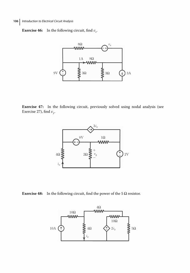
106 Introduction to Electrical Circuit Analysis
Exercise 46: In the following circuit, find 𝑣s.
vs8Ω
9V
8Ω
3Ω 3Ω 3A
1A
Exercise 47: In the following circuit, previously solved using nodal analysis (seeExercise 27), find 𝑣y.
8V
2V 4Ω 2Ω
1Ω
ix
3ix
vy+_
Exercise 48: In the following circuit, find the power of the 5Ω resistor.
10A
10Ω
4Ω
10Ω
5Ω
4Ω
ix
2ix
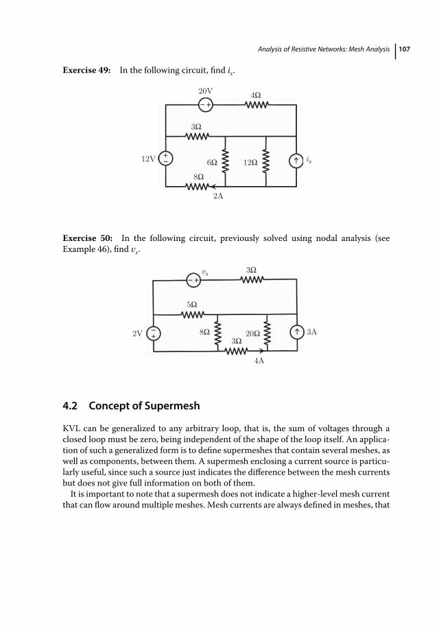
Analysis of Resistive Networks: Mesh Analysis 107
Exercise 49: In the following circuit, find is.
20V 4Ω
3Ω
6Ω 12Ω8Ω
12V is
2A
Exercise 50: In the following circuit, previously solved using nodal analysis (seeExample 46), find 𝑣s.
vs
8Ω2V3Ω
3A
4A
5Ω
3Ω
20Ω
4.2 Concept of Supermesh
KVL can be generalized to any arbitrary loop, that is, the sum of voltages through aclosed loop must be zero, being independent of the shape of the loop itself. An applica-tion of such a generalized form is to define supermeshes that contain several meshes, aswell as components, between them. A supermesh enclosing a current source is particu-larly useful, since such a source just indicates the difference between the mesh currentsbut does not give full information on both of them.It is important to note that a supermesh does not indicate a higher-level mesh current
that can flow aroundmultiple meshes. Mesh currents are always defined inmeshes, that

108 Introduction to Electrical Circuit Analysis
is, sequences of components without enclosing any inner component. Hence, a meshcurrent cannot enclose a part or the whole of another mesh. This is also the reason whymesh analysis is restricted to planar circuits (nonplanar circuits are not considered inthis book). But a supermesh indicates the application of KVL (a universal law basedon the conservation of energy) around multiple meshes using their mesh currents. Inthe following, we discuss the application of supermeshes by solving various complexcircuits.
Example 59: Consider the following circuit.
10V
1Ω
4ix1A
1Ω
4Ω
4Ω
2A
ix
iy
Find ix, iy, and the power of the 1A source.
Solution: Using mesh analysis, we define four mesh currents.
10V
1Ω
4ix1A
1Ω
4Ω
4Ω
2A
ix
iya b
c d
In the above, it is straightforward to write a KVL in mesh a,• KVL(a): 10 + 1(ia − ib) + 1(ia − ic) = 0 −−−−→ 2ia − ib − ic = −10.Also, inspecting mesh c, we have
ic = 1 A,which simplifies the equation above to
2ia − ib = −9.
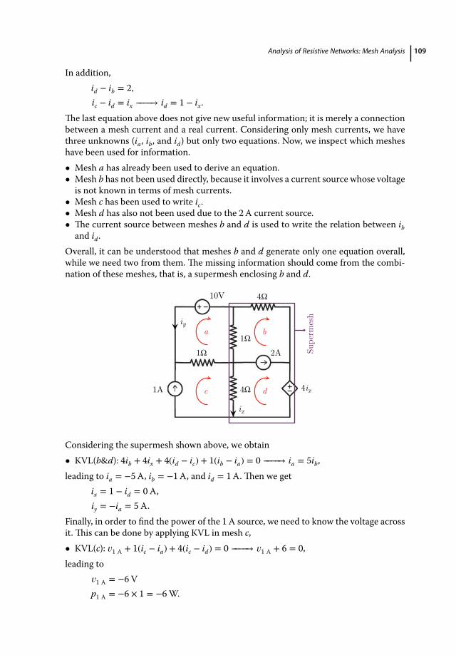
Analysis of Resistive Networks: Mesh Analysis 109
In addition,id − ib = 2,ic − id = ix −−−−→ id = 1 − ix.
The last equation above does not give new useful information; it is merely a connectionbetween a mesh current and a real current. Considering only mesh currents, we havethree unknowns (ia, ib, and id) but only two equations. Now, we inspect which mesheshave been used for information.• Mesh a has already been used to derive an equation.• Mesh b has not been used directly, because it involves a current source whose voltage
is not known in terms of mesh currents.• Mesh c has been used to write ic.• Mesh d has also not been used due to the 2A current source.• The current source between meshes b and d is used to write the relation between ib
and id.Overall, it can be understood that meshes b and d generate only one equation overall,while we need two from them. The missing information should come from the combi-nation of these meshes, that is, a supermesh enclosing b and d.
10V
1Ω
4ix1A
1Ω
4Ω
4Ω
2A
ix
iya b
c d
Supe
rmes
h
Considering the supermesh shown above, we obtain• KVL(b&d): 4ib + 4ix + 4(id − ic) + 1(ib − ia) = 0 −−−−→ ia = 5ib,leading to ia = −5A, ib = −1A, and id = 1A. Then we get
ix = 1 − id = 0 A,iy = −ia = 5 A.
Finally, in order to find the power of the 1A source, we need to know the voltage acrossit. This can be done by applying KVL in mesh c,• KVL(c): 𝑣1 A + 1(ic − ia) + 4(ic − id) = 0 −−−−→ 𝑣1 A + 6 = 0,leading to
𝑣1 A = −6 Vp1 A = −6 × 1 = −6W.
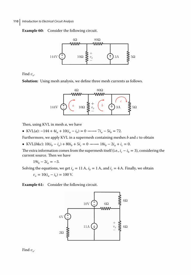
110 Introduction to Electrical Circuit Analysis
Example 60: Consider the following circuit.
144V 3A 10Ω
4Ω 80Ω
5Ω vx+ _
Find 𝑣x.
Solution: Using mesh analysis, we define three mesh currents as follows.
144V 3A 10Ω
4Ω 80Ω
5Ωvx+ _
a bc
Then, using KVL in mesh a, we have• KVL(a): −144 + 4ia + 10(ia − ib) = 0 −−−−→ 7ia − 5ib = 72.Furthermore, we apply KVL in a supermesh containing meshes b and c to obtain• KVL(b&c): 10(ib − ia) + 80ib + 5ic = 0 −−−−→ 18ib − 2ia + ic = 0.The extra information comes from the supermesh itself (i.e., ic − ib = 3), considering thecurrent source. Then we have
19ib − 2ia = −3.Solving the equations, we get ia = 11A, ib = 1A, and ic = 4A. Finally, we obtain
𝑣x = 10(ia − ib) = 100 V.
Example 61: Consider the following circuit.
10V
6V
11A
6Ω
vx
6Ω
6Ω2Ω
+ _
Find 𝑣x.
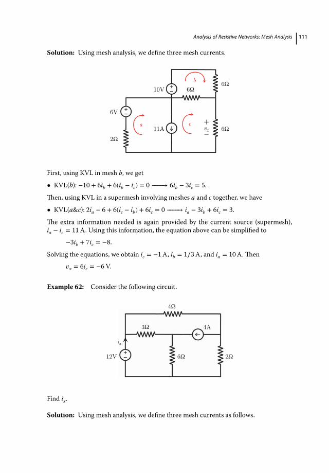
Analysis of Resistive Networks: Mesh Analysis 111
Solution: Using mesh analysis, we define three mesh currents.
10V
6V
11A
6Ω
vx
6Ω
6Ω2Ω
+ _
b
a c
First, using KVL in mesh b, we get
• KVL(b): −10 + 6ib + 6(ib − ic) = 0 −−−−→ 6ib − 3ic = 5.
Then, using KVL in a supermesh involving meshes a and c together, we have
• KVL(a&c): 2ia − 6 + 6(ic − ib) + 6ic = 0 −−−−→ ia − 3ib + 6ic = 3.
The extra information needed is again provided by the current source (supermesh),ia − ic = 11A. Using this information, the equation above can be simplified to
−3ib + 7ic = −8.
Solving the equations, we obtain ic = −1A, ib = 1∕3A, and ia = 10A. Then
𝑣x = 6ic = −6 V.
Example 62: Consider the following circuit.
6Ω 2Ω12V
3Ω
4Ω
4A
ix
Find ix.
Solution: Using mesh analysis, we define three mesh currents as follows.

112 Introduction to Electrical Circuit Analysis
6Ω 2Ω12V
3Ω
4Ω
4A
ix
a b
c
First, considering the current source, we have ic − ib = 4A.Then applying KVL in mesha gives one of the required equations as• KVL(a): −12 + 3(ia − ic) + 6(ia − ib) = 0 −−−−→ 3ia − 2ib − ic = 4.For the missing equation, we consider a supermesh involving meshes b and c,• KVL(b&c): 6(ib − ia) + 3(ic − ia) + 4ic + 2ib = 0 −−−−→ −9ia + 8ib + 7ic = 0.The equations above can be simplified via substitution to
3ia − 2ib − ic = 4 −−−−→ 3ia − 3ib = 8,−9ia + 8ib + 7ic = 0 −−−−→ −9ia + 15ib = −28.
Then we obtain ib = −2∕3A, ia = 2A, and ix = ia = 2A.
Example 63: Consider the following circuit.
1A
5Ω
4Ω
2A 1Ω
2V ix
Find ix.
Solution: Using mesh analysis, we define three mesh currents.
1A
5Ω
4Ω
2A 1Ω
2V ix
b
a
c

Analysis of Resistive Networks: Mesh Analysis 113
In mesh a, we immediately find ia = 1A. In addition, ic − ib = 2, considering the 2Acurrent source between meshes b and c. In order to solve the problem, we need a KVLequation simultaneously in meshes b and c, namely,• KVL(b&c): ib + 2 + 4(ic − ia) + 5(ib − ia) = 0 −−−−→ 6ib + 4ic = 7.Solving the equations, we get ib = −1∕10A and ic = 19∕10A. Finally, we obtain the valueof ix as
ix = ia − ib = 11∕10 A.
Example 64: Consider the following circuit, previously analyzed using the nodalapproach (see Exercise 38).
2Ω
9Ω
3Ω 5Ω
8Ω
5A
10A 40V
Find the power of the voltage source.
Solution: Using mesh analysis, we define four mesh currents.
2Ω
3Ω
9Ω
5Ω
8Ω10A 40V
5A
a bd
c
Then it can be seen that ic = −5A and ib − ia = 10. Applying KVL in a supermesh con-sisting of meshes a, b, and d, we derive• KVL(a&b&d): 2ia + 3(ia − ic) + 5(ib − ic) + 40 = 0 −−−−→ 5ia + 5ib − 8ic = −40or
ia + ib = −16.
We note that, by using a supermesh involving three meshes, the voltage across the 8Ωresistor is directly written as 40V, without resorting to an extra equation. We furtherobtain ib = −3A and id = ib − 5 = −8A since the real current across the 8Ω resistor is5A. Finally, the power of the voltage source can be found to be
p40 V = 40 × (−8) = −320W.

114 Introduction to Electrical Circuit Analysis
Example 65: Consider the following circuit.
5Ω
5Ω
5Ω
5Ω5Ω
5Ω
2A 20V 20V
ix
4ix
vy
Find the power of the top 5Ω resistor if 𝑣y = 20V.
Solution: Using mesh analysis, we define five mesh currents.
5Ω
5Ω
5Ω
5Ω 5Ω
5Ω
2A 20V 20V
ab
c
d e
ix
4ix
vy
With large circuits of this type, it can be easy to get lost. In order to analyze the circuitsystematically, we first consider the given real currents to find relationships between themesh currents. We have
• ix = ib − ia,• ie = 4ix = 4ib − 4ia,• ib − ic = 2.
Then, applying KVL in mesh a, we derive
• KVL(a): −20 + 5(ia − id) + 5(ia − ib) = 0 −−−−→ 2ia − ib − id = 4.
None of the pairs of equations above are solvable. As usual, the required information isavailable in a supermesh:
• KVL(b&c): 5(ib − ia) + 5(ic − ie) + 20 + 5ic + 5ib = 0 −−−−→ ia − 2ib − 2ic + ie = 4.

Analysis of Resistive Networks: Mesh Analysis 115
Substituting ie in the above, we get
ia − 2ib − 2ic + 4ib − 4ia = −3ia + 2ib − 2ic = 4.
Furthermore, using ib − ic = 2, we obtain ia = 0. In order to obtain id, we consider KVLin mesh d,
• KVL(d): 5id − 𝑣y + 5(id − ia) = 0 −−−−→ id = 2A.
Hence, ib = 2ia − id − 4 = −6A and ic = ib − 2 = −8A. We note that finding ib and icrequires extra calculations, since the power of the top 5Ω resistor can be found via id as
p5 Ω = 5i2d = 20W.
Example 66: Consider the following circuit, previously solved using nodal analysis(see Exercise 20).
5Ω
6A10V 20Ω
ix
10Ω
10Ω
2ix
Find the value of ix.
Solution: Using mesh analysis, we define four different mesh currents.
6A10V
ix
2ix a b c d
5Ω 10Ω
10Ω 20Ω
We immediately find that id = −6A. In addition, using KVL in mesh a, we get
• KVL(a): −10 + 5ia + 10(ia − ib) = 0 −−−−→ 3ia − 2ib = 2.
At this stage, KVL in a supermesh involving meshes b and c should be considered:
• KVL(b&c): 10(ib − ia) + 10ib + 20(ic − id) = 0 −−−−→ ia − 2ib − 2ic = 12.
Furthermore, inside the supermesh, we have
ib − ic = 2ix = 2ia − 2ib −−−−→ 2ia − 3ib + ic = 0.
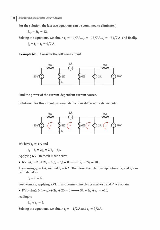
116 Introduction to Electrical Circuit Analysis
For the solution, the last two equations can be combined to eliminate ic,
5ia − 8ib = 12.
Solving the equations, we obtain ia = −4∕7A, ib = −13∕7A, ic = −31∕7A, and finally,
ix = ia − ib = 9∕7 A.
Example 67: Consider the following circuit.
20V 20V
4A 2Ω
4Ω 6Ω
2Ω
2ix ix
Find the power of the current-dependent current source.
Solution: For this circuit, we again define four different mesh currents.
20V 20V
4A 2Ω
4Ω 6Ω
2Ω
2ix ix
a b c d
We have ib = 4A and
id − ic = 2ix = 2(ia − ib).
Applying KVL in mesh a, we derive
• KVL(a): −20 + 2ia + 4(ia − ib) = 0 −−−−→ 3ia − 2ib = 10.
Then, using ib = 4A, we find ia = 6A.Therefore, the relationship between ic and id canbe updated as
id − ic = 4.
Furthermore, applying KVL in a supermesh involving meshes c and d, we obtain
• KVL(c&d): 6(ic − ib) + 2id + 20 = 0 −−−−→ 3ic − 3ib + id = −10,
leading to
3ic + id = 2.
Solving the equations, we obtain ic = −1∕2A and id = 7∕2A.
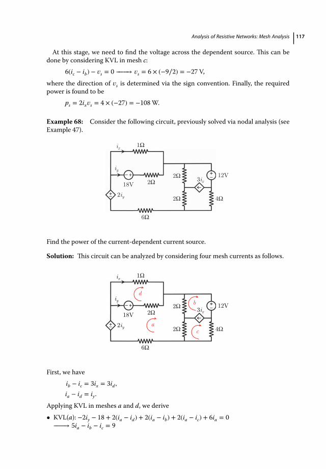
Analysis of Resistive Networks: Mesh Analysis 117
At this stage, we need to find the voltage across the dependent source. This can bedone by considering KVL in mesh c:
6(ic − ib) − 𝑣s = 0 −−−−→ 𝑣s = 6 × (−9∕2) = −27 V,
where the direction of 𝑣s is determined via the sign convention. Finally, the requiredpower is found to be
ps = 2ix𝑣s = 4 × (−27) = −108W.
Example 68: Consider the following circuit, previously solved via nodal analysis (seeExample 47).
2Ω
2Ω 4Ω
12V 18V
1Ω
2Ω
6Ω
3ix
ix
iy
2iy
Find the power of the current-dependent current source.
Solution: This circuit can be analyzed by considering four mesh currents as follows.
2Ω
2Ω 4Ω
12V 18V
1Ω
2Ω
6Ω
3ix
ix
iy
2iy a
b
c
d
First, we haveib − ic = 3ix = 3id,
ia − id = iy.
Applying KVL in meshes a and d, we derive
• KVL(a): −2iy − 18 + 2(ia − id) + 2(ia − ib) + 2(ia − ic) + 6ia = 0−−−−→ 5ia − ib − ic = 9
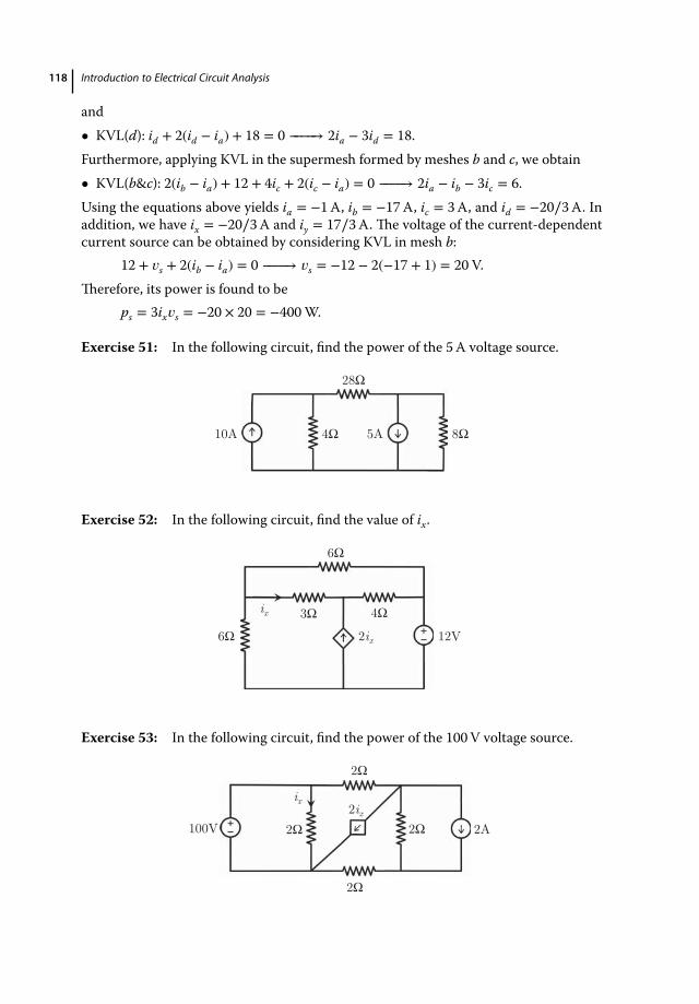
118 Introduction to Electrical Circuit Analysis
and• KVL(d): id + 2(id − ia) + 18 = 0 −−−−→ 2ia − 3id = 18.Furthermore, applying KVL in the supermesh formed by meshes b and c, we obtain• KVL(b&c): 2(ib − ia) + 12 + 4ic + 2(ic − ia) = 0 −−−−→ 2ia − ib − 3ic = 6.Using the equations above yields ia = −1A, ib = −17A, ic = 3A, and id = −20∕3A. Inaddition, we have ix = −20∕3A and iy = 17∕3A. The voltage of the current-dependentcurrent source can be obtained by considering KVL in mesh b:
12 + 𝑣s + 2(ib − ia) = 0 −−−−→ 𝑣s = −12 − 2(−17 + 1) = 20 V.Therefore, its power is found to be
ps = 3ix𝑣s = −20 × 20 = −400W.
Exercise 51: In the following circuit, find the power of the 5A voltage source.
28Ω
4Ω10A 5A 8Ω
Exercise 52: In the following circuit, find the value of ix.
6Ω 12V 3Ω 4Ω
6Ω
ix 2ix
Exercise 53: In the following circuit, find the power of the 100V voltage source.
2ix
2Ω ix
2A 2Ω
2Ω
100V 2Ω
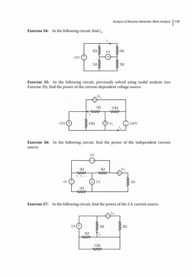
Analysis of Resistive Networks: Mesh Analysis 119
Exercise 54: In the following circuit, find ix.
2Ω 6Ω
2Ω1Ω
4A 10V
ix
Exercise 55: In the following circuit, previously solved using nodal analysis (seeExercise 35), find the power of the current-dependent voltage source.
40Ω19A 240V
10Ω5Ωix
2ix
4iy
iy
Exercise 56: In the following circuit, find the power of the independent currentsource.
2V
4V 2A
2Ω 4Ω
1Ω
+ _ vx
2vx
1Ω
Exercise 57: In the following circuit, find the power of the 2A current source.
2A 4Ω 2Ω5Ω
10Ω
ix
5ix
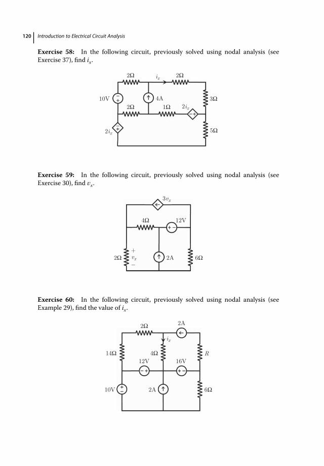
120 Introduction to Electrical Circuit Analysis
Exercise 58: In the following circuit, previously solved using nodal analysis (seeExercise 37), find ix.
10V 4A 2Ω
2Ω 2Ω
1Ω3Ω
5Ω2ix
2ix
ix
Exercise 59: In the following circuit, previously solved using nodal analysis (seeExercise 30), find 𝑣x.
6Ω2Ω 2A
4Ω 12V
+ _
3vx
vx
Exercise 60: In the following circuit, previously solved using nodal analysis (seeExample 29), find the value of ix.
12V
10V
16V
2A
R
2Ω
14Ω 4Ω
2A 6Ω
ix
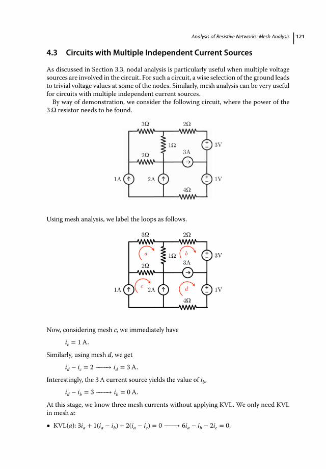
Analysis of Resistive Networks: Mesh Analysis 121
4.3 Circuits with Multiple Independent Current Sources
As discussed in Section 3.3, nodal analysis is particularly useful when multiple voltagesources are involved in the circuit. For such a circuit, a wise selection of the ground leadsto trivial voltage values at some of the nodes. Similarly, mesh analysis can be very usefulfor circuits with multiple independent current sources.By way of demonstration, we consider the following circuit, where the power of the
3Ω resistor needs to be found.
1A 2A
3A 3V
1V
3Ω
1Ω
2Ω
2Ω
4Ω
Using mesh analysis, we label the loops as follows.
1A 2A
3A3V
1V
3Ω
1Ω
2Ω
2Ω
4Ω
a b
c d
Now, considering mesh c, we immediately have
ic = 1 A.
Similarly, using mesh d, we get
id − ic = 2 −−−−→ id = 3 A.
Interestingly, the 3A current source yields the value of ib,
id − ib = 3 −−−−→ ib = 0 A.
At this stage, we know three mesh currents without applying KVL. We only need KVLin mesh a:
• KVL(a): 3ia + 1(ia − ib) + 2(ia − ic) = 0 −−−−→ 6ia − ib − 2ic = 0,
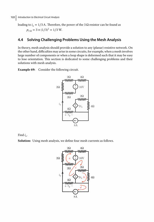
122 Introduction to Electrical Circuit Analysis
leading to ia = 1∕3A. Therefore, the power of the 3Ω resistor can be found asp3 Ω = 3 × (1∕3)2 = 1∕3W.
4.4 Solving Challenging Problems Using the Mesh Analysis
In theory, mesh analysis should provide a solution to any (planar) resistive network. Onthe other hand, difficultiesmay arise in some circuits, for example, when amesh involveslarge number of components or when a loop shape is deformed such that it may be easyto lose orientation. This section is dedicated to some challenging problems and theirsolutions with mesh analysis.
Example 69: Consider the following circuit.
2Ω
2Ω
2Ω
4Ω
2Ω
4Ω4Ω
ix 2ix
8A
16V
+ _ vy
Find ix.
Solution: Using mesh analysis, we define four mesh currents as follows.
2Ω
2Ω
2Ω
4Ω
2Ω
4Ω4Ω
ix
vy
2ix
8A
16V
+ _
a
b
c
d
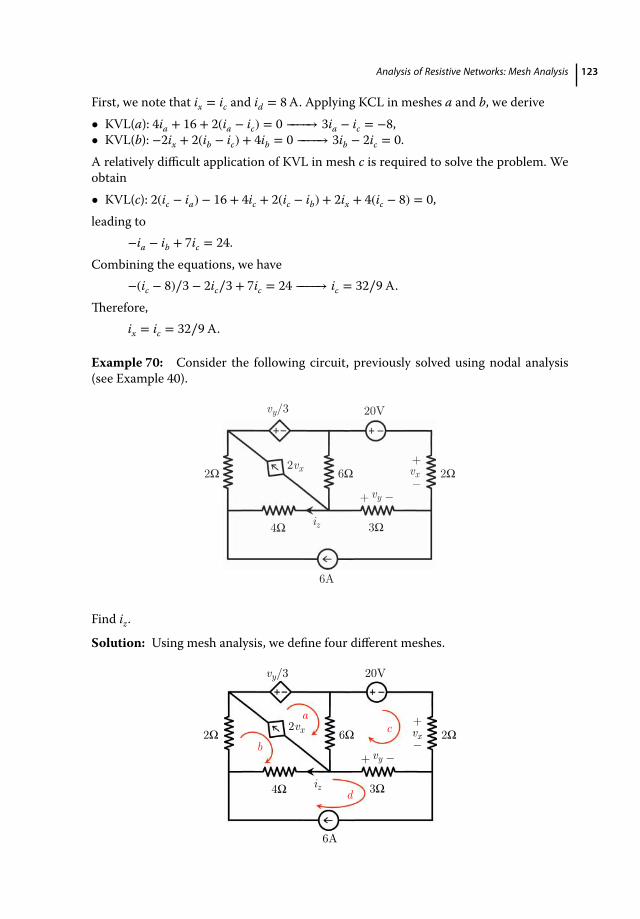
Analysis of Resistive Networks: Mesh Analysis 123
First, we note that ix = ic and id = 8A. Applying KCL in meshes a and b, we derive• KVL(a): 4ia + 16 + 2(ia − ic) = 0 −−−−→ 3ia − ic = −8,• KVL(b): −2ix + 2(ib − ic) + 4ib = 0 −−−−→ 3ib − 2ic = 0.A relatively difficult application of KVL in mesh c is required to solve the problem. Weobtain• KVL(c): 2(ic − ia) − 16 + 4ic + 2(ic − ib) + 2ix + 4(ic − 8) = 0,leading to
−ia − ib + 7ic = 24.Combining the equations, we have
−(ic − 8)∕3 − 2ic∕3 + 7ic = 24 −−−−→ ic = 32∕9 A.Therefore,
ix = ic = 32∕9 A.
Example 70: Consider the following circuit, previously solved using nodal analysis(see Example 40).
6A
2Ω
4Ω 3Ω
2Ω6Ω
20V
+_
_ +
vy/3
2vx
iz
vy
vx
Find iz.
Solution: Using mesh analysis, we define four different meshes.
6A
2Ω
4Ω 3Ω
2Ω6Ω
20V
+ _
_ +
2vxa
bc
d
vy/3
vx
vy
iz
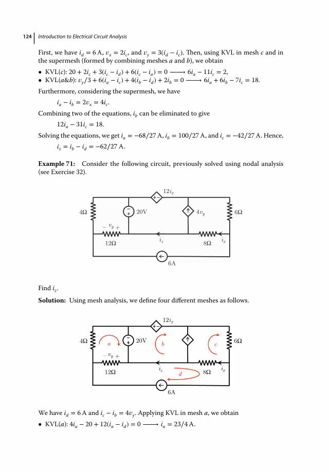
124 Introduction to Electrical Circuit Analysis
First, we have id = 6A, 𝑣x = 2ic, and 𝑣y = 3(id − ic). Then, using KVL in mesh c and inthe supermesh (formed by combining meshes a and b), we obtain• KVL(c): 20 + 2ic + 3(ic − id) + 6(ic − ia) = 0 −−−−→ 6ia − 11ic = 2,• KVL(a&b): 𝑣y∕3 + 6(ia − ic) + 4(ib − id) + 2ib = 0 −−−−→ 6ia + 6ib − 7ic = 18.Furthermore, considering the supermesh, we have
ia − ib = 2𝑣x = 4ic.Combining two of the equations, ib can be eliminated to give
12ia − 31ic = 18.Solving the equations, we get ia = −68∕27A, ib = 100∕27A, and ic = −42∕27A. Hence,
iz = ib − id = −62∕27 A.
Example 71: Consider the following circuit, previously solved using nodal analysis(see Exercise 32).
20V4Ω
6A
4vy
vy
6Ω
12Ω 8Ω
12ix
_ + ixiz
Find iz.
Solution: Using mesh analysis, we define four different meshes as follows.
20V4Ω
6A
6Ω
12Ω 8Ω
12ix
– + ba c
dixiz
vy
We have id = 6A and ic − ib = 4𝑣y. Applying KVL in mesh a, we obtain• KVL(a): 4ia − 20 + 12(ia − id) = 0 −−−−→ ia = 23∕4A.
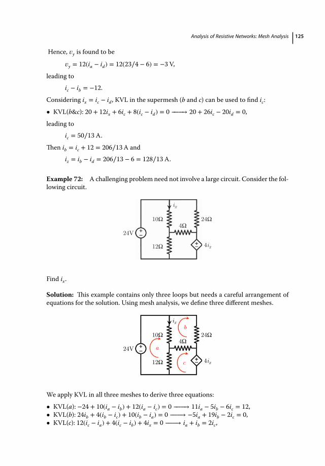
Analysis of Resistive Networks: Mesh Analysis 125
Hence, 𝑣y is found to be
𝑣y = 12(ia − id) = 12(23∕4 − 6) = −3 V,
leading to
ic − ib = −12.
Considering ix = ic − id, KVL in the supermesh (b and c) can be used to find ic:
• KVL(b&c): 20 + 12ix + 6ic + 8(ic − id) = 0 −−−−→ 20 + 26ic − 20id = 0,
leading to
ic = 50∕13 A.
Then ib = ic + 12 = 206∕13A and
iz = ib − id = 206∕13 − 6 = 128∕13 A.
Example 72: A challenging problem need not involve a large circuit. Consider the fol-lowing circuit.
24V4ix
10Ω 24Ω
12Ω
4Ω
ix
Find ix.
Solution: This example contains only three loops but needs a careful arrangement ofequations for the solution. Using mesh analysis, we define three different meshes.
24V4ix
10Ω 24Ω
12Ω
4Ωa
b
c
ix
We apply KVL in all three meshes to derive three equations:
• KVL(a): −24 + 10(ia − ib) + 12(ia − ic) = 0 −−−−→ 11ia − 5ib − 6ic = 12,• KVL(b): 24ib + 4(ib − ic) + 10(ib − ia) = 0 −−−−→ −5ia + 19ib − 2ic = 0,• KVL(c): 12(ic − ia) + 4(ic − ib) + 4ix = 0 −−−−→ ia + ib = 2ic,

126 Introduction to Electrical Circuit Analysis
using ix = ia − ib. At this stage, the equations must be solved using a method such assubstitution. For example, using ia = 2ic − ib, we have
22ic − 11ib − 5ib − 6ic = −16ib + 16ic = 12 −−−−→ −4ib + 4ic = 3,− 10ic + 5ib + 19ib − 2ic = 24ib − 12ic = 0.
The final equation states that ic = 2ib; hence, we have ib = 3∕4A, ic = 3∕2A, and ia =9∕4A. Finally, we obtain
ix = ia − ib = 9∕4 − 3∕4 = 3∕2 A.
Example 73: Consider the following circuit.
9V 12V 4Ω
15V2Ω+
–
1Ω
3Ω
ix
6ixvy
5vy
iz
iw
Find iz.
Solution: Using mesh analysis, we define four different meshes.
9V 12V 4Ω
15V2Ω
ix
6ix vy+
–
5vy
1Ω
3Ω
iz
iw
a b
c d
First, we note that ix = ia − ic and 𝑣y = 2(ia − ib) = 15V, which can be found by consid-ering KVL in mesh b. Applying KVL in meshes a and c, we obtain
• KVL(a): −6ix + (ia − ic) + 2(ia − ib) = 0 −−−−→ ia − ic = 3,• KVL(c): −9 + 3ic + 12 + (ic − ia) = 0 −−−−→ 4ic − ia = −3.

Analysis of Resistive Networks: Mesh Analysis 127
Solving the equations, we obtain ic = 0A, ia = 3A, and ib = −9∕2A. In order to find iz,we further need KVL in mesh d,
• KVL(d): −12 + 5𝑣y + 4id = 0 −−−−→ id = −63∕4A.
Finally, iz is found to be
iz = ib − id = 45∕4 A.
Example 74: In general, given a basic circuit, it may not be obvious which analysismethod (nodal or mesh) leads to an easier solution. In some circuits (see Section4.3), however, there are consecutive meshes, each involving one or more independentcurrent sources, leading to trivial determination of mesh currents. Consider thefollowing circuit.
10A 5A
6Ω
10Ω 2Ω
15V
Find the power of the 5A source.
Solution: Using mesh analysis, we define three mesh currents.
10A 5A
6Ω
10Ω 2Ω
15V
a b c
Considering meshes a and b, we have ia = 10A and ib = ia − 5 = 5A, respectively. KVLis required for only one mesh (mesh c):
• KVL(c): 10(ic − ib) + 15 + 2ic = 0 −−−−→ ic = 35∕12A.
Then 𝑣5 A = 10(ib − ic) = 125∕6V and
p5 A = 𝑣5 Ai5 A = (125∕6) × 5 = 625∕6W.
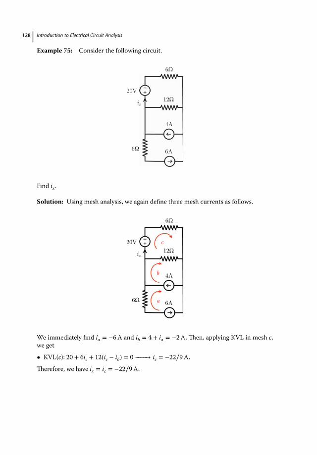
128 Introduction to Electrical Circuit Analysis
Example 75: Consider the following circuit.
6Ω
12Ω
6Ω
4A
6A
20Vix
Find ix.
Solution: Using mesh analysis, we again define three mesh currents as follows.
6Ω
12Ω
6Ω
4A
6A
20V
a
b
cix
We immediately find ia = −6A and ib = 4 + ia = −2A. Then, applying KVL in mesh c,we get
• KVL(c): 20 + 6ic + 12(ic − ib) = 0 −−−−→ ic = −22∕9A.
Therefore, we have ix = ic = −22∕9A.

Analysis of Resistive Networks: Mesh Analysis 129
Example 76: Consider the following circuit, previously solved using nodal analysis.5A 30V
12Ω 30V
15V 6Ω
3A 3A
Find the power of the 5A current source.
Solution: Using mesh analysis, we define three mesh currents.5A 30V
12Ω 30V
15V 6Ω
3A 3A
c
b
a
First, we note that ia = 3A and ic = 5A. Second, applying KVL in mesh b, we obtain
• KVL(b): 6(ib − ia) + 15 + 12(ib − ic) + 30 = 0 −−−−→ ib = 11∕6A.
In order to find the power of the 5A source, we need its voltage, which can be obtainedvia KVL as
• KVL(c): 𝑣5A + 30 − 30 + 12(ic − ib) = 0 −−−−→ 𝑣5A = −38V.
Then we have
p5A = −38 × 5 = −190W.
We also note that no mesh current is defined (and needed) for the mesh involving the15V source and one of the 3A sources.
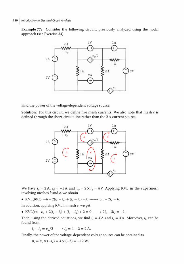
130 Introduction to Electrical Circuit Analysis
Example 77: Consider the following circuit, previously analyzed using the nodalapproach (see Exercise 34).
4V 1A
1Ω
2Ω1Ω 2V2A
2Ω
2A
2V
+ vx –vx/2
vx
Find the power of the voltage-dependent voltage source.
Solution: For this circuit, we define five mesh currents. We also note that mesh c isdefined through the short-circuit line rather than the 2A current source.
4V 1A
1Ω
2Ω1Ω 2V2A
2Ω
2A
2V
+ vx –vx/2
vx
a
b
c
d
e
We have ia = 2A, id = −1A and 𝑣x = 2 × ia = 4V. Applying KVL in the supermeshinvolving meshes b and c, we obtain• KVL(b&c): −4 + 2(ic − ie) + (ic − ia) = 0 −−−−→ 3ic − 2ie = 6.In addition, applying KVL in mesh e, we get• KVL(e): −𝑣x + 2(ie − ic) + (ie − id) + 2 = 0 −−−−→ 2ic − 3ie = −1.Then, using the derived equations, we find ic = 4A and ie = 3A. Moreover, ib can befound from
ic − ib = 𝑣x∕2 −−−−→ ib = 4 − 2 = 2 A.Finally, the power of the voltage-dependent voltage source can be obtained as
ps = 𝑣x × (−ie) = 4 × (−3) = −12W.

Analysis of Resistive Networks: Mesh Analysis 131
Example 78: Consider the following circuit, previously studied using nodal analysis(see Exercise 15).
30Ω
60V
ix
5Ω
28/5A 100Ω
1Ω
4Ω60Ω
Find the value of ix.
Solution: Using mesh analysis, we define four mesh currents as follows.
30Ω
60V
5Ω
28/5A 100Ω
1Ω
4Ω60Ωab c
d
ix
First, we note that ic − ib = 28∕5. Applying KVL in meshes a and d, we obtain• KVL(a): 60 + 30ia + 60(ia − ib) = 0 −−−−→ 3ia − 2ib = −2,• KVL(d): 100(id − ic) + 5id = 0 −−−−→ 20ic = 21id.In addition, applying KVL in the supermesh involving b, c, and d, we have• KVL(b&c&d): 60(ib − ia) + 5ib + 5id = 0 −−−−→ −12ia + 13ib + id = 0.Solving the equations yields ix = id = 16∕5A.
Exercise 61: In the following circuit, previously solved using nodal analysis (seeExample 43), find the value of ix.
2Ω 2Ω
3Ω
1Ω 60V 1Ω
3ix
ix
ix
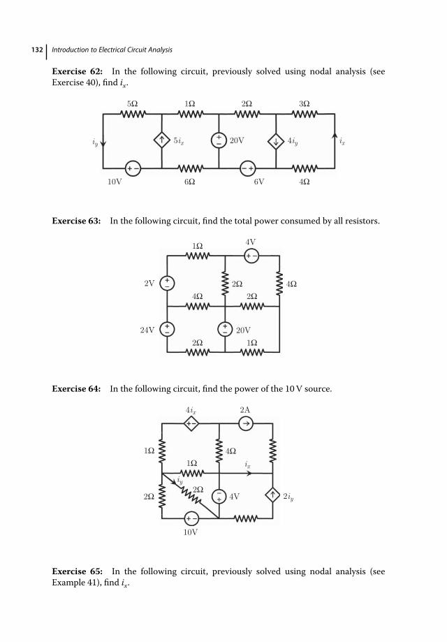
132 Introduction to Electrical Circuit Analysis
Exercise 62: In the following circuit, previously solved using nodal analysis (seeExercise 40), find ix.
5Ω 1Ω 2Ω 3Ω
4Ω6Ω10V
5ix 20V 4iy
6V
ixiy
Exercise 63: In the following circuit, find the total power consumed by all resistors.
2V
24V 20V
4V 1Ω
4Ω
2Ω 1Ω
2Ω2Ω 4Ω
Exercise 64: In the following circuit, find the power of the 10V source.
1Ω
2Ω 4V
2A
1Ω4Ω
2Ω
4ix
10V
2iy
ixiy
Exercise 65: In the following circuit, previously solved using nodal analysis (seeExample 41), find ix.

Analysis of Resistive Networks: Mesh Analysis 133
10V
2Ω 2Ω
2Ω2Ω 2Ω
20V
5A
ix
Exercise 66: In the following circuit, find 𝑣x.
10Ω
10Ω
5Ω
5Ω
5Ω
8Ω
10V
10V
4Vx
– Vx +
Exercise 67: In the following circuit, find ix.
2Ω
2Ω
4Ω 4Ω
20V
10V 5A
2A
ix
iy

134 Introduction to Electrical Circuit Analysis
Exercise 68: In the following circuit, previously solved using nodal analysis (seeExercise 28), find the power of the 5A source.
8A 5A
20/3V
5Ω
2Ω8Ω 10Ω
Exercise 69: In the following circuit, find the power of the voltage source.
2A
8A 30V
5Ω
5Ω
3Ω3Ω
Exercise 70: In the following circuit, previously studied using nodal analysis (seeExample 35), find the power of the 15V source.
15V
12V
20A
6Ω
6Ω4Ω
5Ω
3Ω1Ω

Analysis of Resistive Networks: Mesh Analysis 135
4.5 When Things Go Wrong with Mesh Analysis
We again consider some common issues and sources of confusion when dealing withcircuits, now in the context ofmesh analysis. One of themost commonmistakes inmeshanalysis is to assume zero voltage for a current source. This happens particularly whentrying to apply KVL in a mesh containing a current source. As an example, consider thefollowing circuit, previously solved using nodal analysis (see Example 37), but now tobe analyzed via mesh analysis.
16V
ix29ix350V
5V20Ω
50Ω10Ω
As usual, we can define two mesh currents as follows.
16V
ix29ix350V
5Va b
10Ω 50Ω
20Ω
Then we have
• KVL(a): −16 + 10ia − 350 + 20(ia − ib) = 0 −−−−→ 15ia − 10ib = 183
as one of the equations to solve the mesh currents. However, the following equation isincorrect:
• KVL (b): 20(ib − ia) + 50ib + 5 = 0.
The correct version of KVL in mesh b is
• KVL(b): 20(ib − ia) − 𝑣c + 50ib + 5 = 0,
where 𝑣c is the voltage of the current-dependent current source in accordance withthe sign convention. Unfortunately, this equation is not useful since it includes a new

136 Introduction to Electrical Circuit Analysis
unknown 𝑣c. Instead, one should deduce the link between the mesh currents by usingthe definition of the current source as
ib = −29ix = −29ia.
Using this equation in the first one, we obtain ia = 3∕5A and ib = −87∕5A. Now, ifneeded, we can use this information to obtain the voltage of the dependent source as
• KVL(b): 20(ib − ia) − 𝑣c + 50ib + 5 = 0 −−−−→ 𝑣c = −280 − 870 + 5 = −1145V.
Obviously, it is not zero.Confusion often occurs in mesh analysis when current sources are connected in par-
allel to components. Consider the following circuit.
ix
6ix
5A10Ω
5Ω
Our aim is to find the power delivered by the independent voltage source, if the power ofthe independent current source is given as 250W. Formally, we must define three meshcurrents as follows.
6ix
ix5A a b
c
5Ω10Ω
At this stage, it is not useful to apply a supermesh in this circuit. This is because noneof the combinations a&b, a&c, or a&b&c contains a current source as an inner com-ponent. Applying KVL in any of these supermesh requires the voltage across a currentsource, which must be avoided. On the other hand, considering that the power of theindependent current source is given as 250W, we already have
ix = 50∕10 = 5 A.
In addition, considering the relationship between true and mesh currents, we obtainib = 5A and ic = 6ix = 30A. Finally, we have ia − ib = ix, leading to ia = 35A.Therefore,we obtain the values of all mesh currents without using KVL. At this stage, KVL inmesha can be used to find the value of the voltage source,

Analysis of Resistive Networks: Mesh Analysis 137
• KVL(a): 𝑣s + 5(ia − ic) + 10(ia − ib) = 0 −−−−→ 𝑣s = −325V.
Then the power of this source can be obtained as
ps = 𝑣s × ia = −325 × 35 = 11 375W = 11.375 kW.
4.6 What You Need to Know before You Continue
Similar to nodal analysis, mesh analysis is a systematic way of analyzing circuits. Beforemoving on to the next chapter, we emphasize the following points.
• Equations in mesh analysis: Only KVL is used in mesh analysis, while KCL is usuallynot required. All equations are written by using mesh currents as unknowns, whichare linearly independent. Once the analysis is completed, KCL may be applied to findthe current through a component, if it is not already known.
• A supermesh, which involves a combination of multiple meshes and componentsbetween them, is often required to simplify mesh analysis. KVL is applied by con-sidering the supermesh as a global loop with zero sum of voltages.The extra equationneeded is obtained from the supermesh itself.
In the next chapter, we continue with a useful simplification method based on the appli-cation of theThévenin and Norton equivalent circuits.

139
5
Black-Box Concept
Kirchhoff’s laws (KVL and KCL) and their systematic applications in nodal and meshanalysis enable the solution of all circuits involving complex networks of electrical com-ponents. On the other hand, various simplification and transformation techniques mayfacilitate the analysis of a given circuit. For example, as discussed in Section 2.4, resis-tors that are connected in series and parallel can be combined, reducing the numberof components, before the circuit is further analyzed. In this chapter, we discuss theblack-box concept for the simplification of complex and crowded circuits into simpleand neat ones.We particularly considerThévenin andNorton equivalent circuits, whichare suitable for simplifying linear circuits. These transformations are useful in variousapplications, such as finding load resistor values for maximum power transfer.
5.1 Thévenin and Norton Equivalent Circuits
Consider a complex circuit involvingmany components and two nodes (e.g., terminals).These terminals can be thought as input/output of the circuit to be used for a connectionto another circuit or simply to a component. The circuit seen from these terminals canbe simplified into two different circuits.
• Thévenin equivalent circuit: A circuit involving a series connection of a voltage source𝑣th and a resistor Rth.
• Norton equivalent circuit: A circuit involving a parallel connection of a current sourceino and a resistor Rno.
In the following, we find ways to derive the values of 𝑣th, Rth, ino, and Rno. Thus, insteadof using the whole circuit, we represent it as a simple one, either aThévenin circuit or aNorton circuit. After such a transformation and finding the equivalent simple circuit, wedo not need to reconsider the actual components in the full circuit; hence, we considerit as a black box.In order to use theThévenin or Norton equivalence, the circuit to be simplified must
be linear, that is, it must contain linear elements. A linear element has electrical prop-erties that do not change with the applied voltage and/or current. Hence, a resistoror a source (independent or dependent) with a given fixed value can be consideredas a linear element. In the next chapters, we also consider capacitors and inductorsas linear elements with fixed capacitance and inductance values. In real life, all ele-ments change behavior with the applied voltage and current values. However, these
Introduction to Electrical Circuit Analysis, First Edition. Özgür Ergül.© 2017 John Wiley & Sons Ltd. Published 2017 by John Wiley & Sons Ltd.Companion Website: www.wiley.com/go/ergul4412
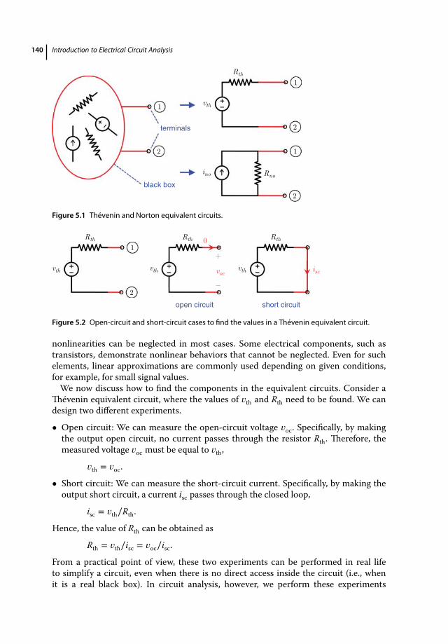
140 Introduction to Electrical Circuit Analysis
1
2
1
2
vth
Rth
1
2
ino Rno
black box
terminals
Figure 5.1 Thévenin and Norton equivalent circuits.
1
2
vth
Rth
vth
Rth 0
+
_
voc vth
Rth
isc
open circuit short circuit
Figure 5.2 Open-circuit and short-circuit cases to find the values in a Thévenin equivalent circuit.
nonlinearities can be neglected in most cases. Some electrical components, such astransistors, demonstrate nonlinear behaviors that cannot be neglected. Even for suchelements, linear approximations are commonly used depending on given conditions,for example, for small signal values.We now discuss how to find the components in the equivalent circuits. Consider a
Thévenin equivalent circuit, where the values of 𝑣th and Rth need to be found. We candesign two different experiments.
• Open circuit: We can measure the open-circuit voltage 𝑣oc. Specifically, by makingthe output open circuit, no current passes through the resistor Rth. Therefore, themeasured voltage 𝑣oc must be equal to 𝑣th,
𝑣th = 𝑣oc.
• Short circuit: We can measure the short-circuit current. Specifically, by making theoutput short circuit, a current isc passes through the closed loop,
isc = 𝑣th∕Rth.
Hence, the value of Rth can be obtained as
Rth = 𝑣th∕isc = 𝑣oc∕isc.
From a practical point of view, these two experiments can be performed in real lifeto simplify a circuit, even when there is no direct access inside the circuit (i.e., whenit is a real black box). In circuit analysis, however, we perform these experiments

Black-Box Concept 141
ino
1
2
Rno ino Rno
0
+
_voc
ino Rno isc
open circuit short circuit
Figure 5.3 Open-circuit and short-circuit cases to find the values in a Norton equivalent circuit.
numerically, by solving the real circuit twice—once for the open-circuit case and oncefor the short-circuit case.Next, we consider the derivation of the Norton circuit elements. In order to find the
values of ino and Rno, we again need two tests.
• Open circuit: Making the output open circuit, all current passes through the resistorRno. Therefore, the measured voltage 𝑣oc can be derived as
𝑣oc = inoRno.
• Short circuit: Making the output short circuit, no current passes through the resistorRno. Then the measured current isc should be the same as ino,
ino = isc.
Therefore, the value of Rno can be obtained as
Rno = 𝑣oc∕ino = 𝑣oc∕isc,
which is the same as Rth.
It can be observed that bothThévenin andNorton equivalent circuits can be obtainedvia two experiments, that is, solutions to two different problems: one with open-circuitoutput and another with short-circuit output. These can be considered as using testresistors with extreme values (0 and∞). From these tests, one can find 𝑣oc, isc, and Rth =Rno = 𝑣oc∕isc which can be used to simplify the circuit for further analysis.
Example 79: Consider the following problem, with a large circuit involving variouscomponents and a resistor Ro.
60Ω 4A 80Ω 40Ω
20Ω 160ix
ix
Ro
io
Find the current across Ro for different values of Ro, particularly for Ro = 5, 10, 20,80,290 Ω.
Solution: Using a conventional approach, the overall circuit must be solved several(here five) times, where each solution corresponds to a given value of Ro. Obviously,
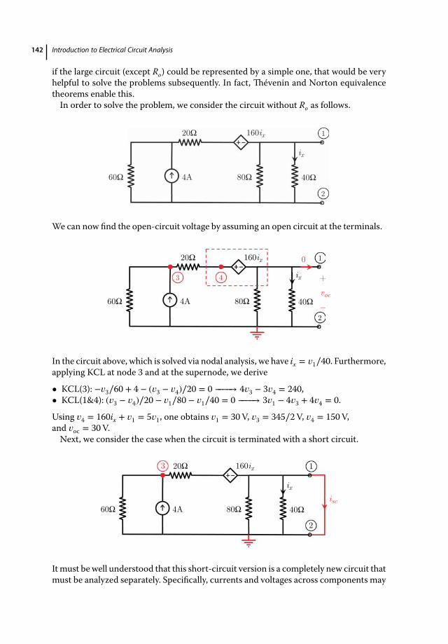
142 Introduction to Electrical Circuit Analysis
if the large circuit (except Ro) could be represented by a simple one, that would be veryhelpful to solve the problems subsequently. In fact, Thévenin and Norton equivalencetheorems enable this.In order to solve the problem, we consider the circuit without Ro as follows.
1
2
60Ω 4A 80Ω 40Ω
20Ω 160ix
ix
We can now find the open-circuit voltage by assuming an open circuit at the terminals.
1
2
60Ω 4A 80Ω 40Ω
20Ω 160ix
+
_ voc
0
ix3 4
In the circuit above, which is solved via nodal analysis, we have ix = 𝑣1∕40. Furthermore,applying KCL at node 3 and at the supernode, we derive
• KCL(3): −𝑣3∕60 + 4 − (𝑣3 − 𝑣4)∕20 = 0 −−−−→ 4𝑣3 − 3𝑣4 = 240,• KCL(1&4): (𝑣3 − 𝑣4)∕20 − 𝑣1∕80 − 𝑣1∕40 = 0 −−−−→ 3𝑣1 − 4𝑣3 + 4𝑣4 = 0.
Using 𝑣4 = 160ix + 𝑣1 = 5𝑣1, one obtains 𝑣1 = 30V, 𝑣3 = 345∕2V, 𝑣4 = 150V,and 𝑣oc = 30V.Next, we consider the case when the circuit is terminated with a short circuit.
1
2
60Ω 4A 80Ω 40Ω
20Ω 160ix
ix isc
3
It must be well understood that this short-circuit version is a completely new circuit thatmust be analyzed separately. Specifically, currents and voltages across components may

Black-Box Concept 143
not be the same as those in the open-circuit case. Of course, there may be similarities ifthe same technique is used to solve circuits, but possible differences do not indicate anerror in the solution. In the above, we have 𝑣1 = 𝑣2 = 0V and ix = 0A, leading to
• KCL (3): −𝑣3∕60 + 4 − 𝑣3∕20 = 0 −−−−→ 𝑣3 = 60V.
Then we obtain isc = 60∕20 = 3A.Finally, in order to obtain the Thévenin or Norton equivalent circuit, we calculate
Rth = Rno as
Rth = Rno = 𝑣oc∕isc = 10 Ω.
Then theThévenin and Norton equivalent circuits are obtained as follows.
10Ω
30V
1
2
10Ω3A
1
2
Thevenin Norton
After representing the circuit with an equivalent one, we can be go back to the originalscenario with Ro connected to the terminals, at which the equivalent circuits are found.A simplified representation of the circuit excluding Ro is called the equivalent circuitseen byRo. Using theThévenin andNorton equivalents, we have the following simplifiedcircuits.
10Ω
30V
Thevenin
Ro
io
10Ω3A
Norton
Ro
io
Both of these circuits can be used to solve the problem. Using the Thévenin equivalentcircuit, we can find io for different values of Ro,
io =𝑣th
Rth + Ro= 30
10 + Ro.
Alternatively, we can use the Norton equivalent circuit, leading to
io = inoRno
Rno + Ro= 3 × 10
10 + Ro= 30
10 + Ro,
which gives exactly the same expression.
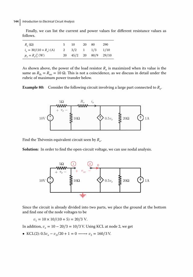
144 Introduction to Electrical Circuit Analysis
Finally, we can list the current and power values for different resistance values asfollows.
Ro (Ω) 5 10 20 80 290io = 30∕(10 + Ro) (A) 2 3∕2 1 1∕3 1∕10po = Roi2o (W) 20 45∕2 20 80∕9 29∕10
As shown above, the power of the load resistor Ro is maximized when its value is thesame as Rth = Rno = 10 Ω. This is not a coincidence, as we discuss in detail under therubric of maximum power transfer below.
Example 80: Consider the following circuit involving a large part connected to Ro.
10V 10Ω 20Ω 1A
Ro
0.5vx
5Ω io
+ _vx
Find theThévenin equivalent circuit seen by Ro.
Solution: In order to find the open-circuit voltage, we can use nodal analysis.
10V 10Ω 20Ω 1A0.5vx
5Ω 1 02
v _ + oc + _vx
Since the circuit is already divided into two parts, we place the ground at the bottomand find one of the node voltages to be
𝑣1 = 10 × 10∕(10 + 5) = 20∕3 V.
In addition, 𝑣x = 10 − 20∕3 = 10∕3V. Using KCL at node 2, we get
• KCL(2): 0.5𝑣x − 𝑣2∕20 + 1 = 0 −−−−→ 𝑣2 = 160∕3V.
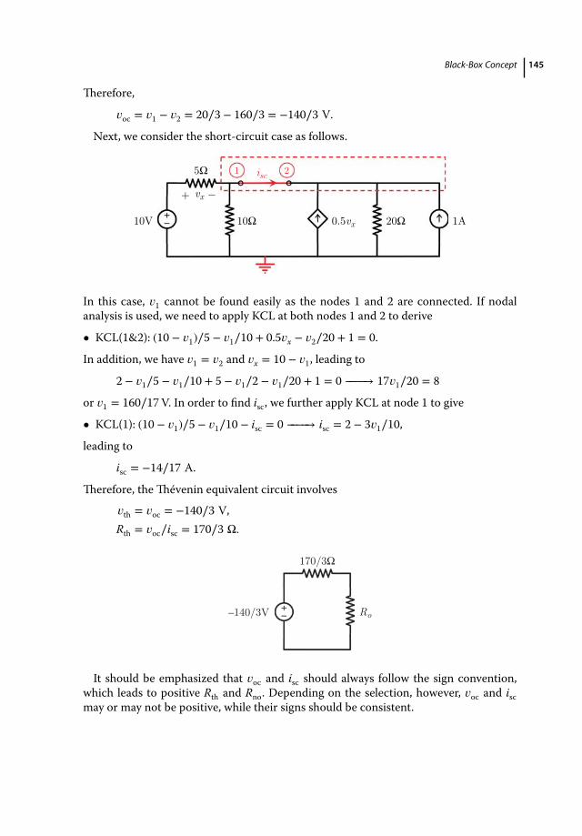
Black-Box Concept 145
Therefore,
𝑣oc = 𝑣1 − 𝑣2 = 20∕3 − 160∕3 = −140∕3 V.
Next, we consider the short-circuit case as follows.
10V 10Ω 20Ω 1A0.5vx
5Ω 1 2
+ _vx
isc
In this case, 𝑣1 cannot be found easily as the nodes 1 and 2 are connected. If nodalanalysis is used, we need to apply KCL at both nodes 1 and 2 to derive
• KCL(1&2): (10 − 𝑣1)∕5 − 𝑣1∕10 + 0.5𝑣x − 𝑣2∕20 + 1 = 0.
In addition, we have 𝑣1 = 𝑣2 and 𝑣x = 10 − 𝑣1, leading to
2 − 𝑣1∕5 − 𝑣1∕10 + 5 − 𝑣1∕2 − 𝑣1∕20 + 1 = 0 −−−−→ 17𝑣1∕20 = 8
or 𝑣1 = 160∕17V. In order to find isc, we further apply KCL at node 1 to give
• KCL(1): (10 − 𝑣1)∕5 − 𝑣1∕10 − isc = 0 −−−−→ isc = 2 − 3𝑣1∕10,
leading to
isc = −14∕17 A.
Therefore, the Thévenin equivalent circuit involves
𝑣th = 𝑣oc = −140∕3 V,Rth = 𝑣oc∕isc = 170∕3 Ω.
170/3Ω
–140/3V Ro
It should be emphasized that 𝑣oc and isc should always follow the sign convention,which leads to positive Rth and Rno. Depending on the selection, however, 𝑣oc and iscmay or may not be positive, while their signs should be consistent.
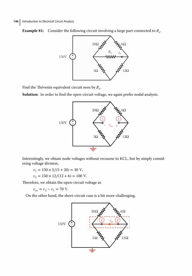
146 Introduction to Electrical Circuit Analysis
Example 81: Consider the following circuit involving a large part connected to Ro.
150V
20Ω 6Ω
5Ω
Ro io
12Ω
Find theThévenin equivalent circuit seen by Ro.
Solution: In order to find the open-circuit voltage, we again prefer nodal analysis.
150V
20Ω 6Ω
5Ω 12Ω
voc_
+
1 2
Interestingly, we obtain node voltages without recourse to KCL, but by simply consid-ering voltage division,
𝑣1 = 150 × 5∕(5 + 20) = 30 V,𝑣2 = 150 × 12∕(12 + 6) = 100 V.
Therefore, we obtain the open-circuit voltage as𝑣oc = 𝑣2 − 𝑣1 = 70 V.
On the other hand, the short-circuit case is a bit more challenging.
150V
20Ω 6Ω
5Ω 12Ω
1 2isc
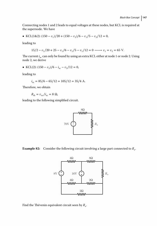
Black-Box Concept 147
Connecting nodes 1 and 2 leads to equal voltages at these nodes, but KCL is required atthe supernode. We have
• KCL(1&2): (150 − 𝑣1)∕20 + (150 − 𝑣2)∕6 − 𝑣1∕5 − 𝑣2∕12 = 0,
leading to
15∕2 − 𝑣1∕20 + 25 − 𝑣1∕6 − 𝑣1∕5 − 𝑣1∕12 = 0 −−−−→ 𝑣1 = 𝑣2 = 65 V.
The current isc can only be found by using an extra KCL either at node 1 or node 2. Usingnode 2, we derive
• KCL(2): (150 − 𝑣2)∕6 − isc − 𝑣2∕12 = 0,
leading to
isc = 85∕6 − 65∕12 = 105∕12 = 35∕4 A.
Therefore, we obtain
Rth = 𝑣oc∕isc = 8 Ω,
leading to the following simplified circuit.
8Ω
70V Ro
Example 82: Consider the following circuit involving a large part connected to Ro.
4Ω 8Ω
8V 16V Ro
4Ω 2Ω
2Ω
Find theThévenin equivalent circuit seen by Ro.

148 Introduction to Electrical Circuit Analysis
Solution: First, we can find the open-circuit voltage using mesh analysis.
4Ω 8Ω
8V 16V
4Ω 2Ω
2Ω
+
_
voc
0
a
b
Applying KVL in meshes a and b, we obtain
• KVL(a): −8 + 4ia − 16 + 4(ia − ib) = 0 −−−−→ 2ia − ib = 6,• KVL(b): 4(ib − ia) + 2ib + 2ib = 0 −−−−→ ia = 2ib.
Solving the equations, we get ia = 4A, ib = 2A, and 𝑣oc = −16 + 2ib = −12V.Next, we consider the short-circuit case.
4Ω 8Ω
8V 16V
4Ω 2Ω
2Ω
a
b
iscc
Applying KVL in meshes a, b, and c, we have
• KVL(a): −8 + 4ia − 16 + 4(ia − ib) = 0 −−−−→ 2ia − ib = 6,• KVL(b): 4(ib − ia) + 2(ib − ic) + 2ib = 0 −−−−→ 2ia + ic − 4ib = 0,• KVL(c): 16 + 8ic + 2(ic − ib) = 0 −−−−→ ib − 5ic = 8.
We note that the equation formesh a does not change in comparison to the open-circuitcase, while the equation for mesh b does. Using substitution, we eliminate ia, obtainingic − 3ib = −6.Then, solving the equations, we obtain ib = 11∕7A, ic = −9∕7A, and isc =ic = −9∕7A. Overall, we have
𝑣th = 𝑣oc = −12 V,Rth = 𝑣oc∕isc = 28∕3 Ω.
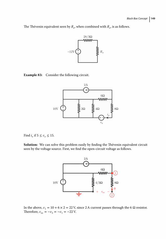
Black-Box Concept 149
TheThévenin equivalent seen by Ro, when combined with Ro, is as follows.
28/3Ω
−12V Ro
Example 83: Consider the following circuit.
2Ω 4Ω 8Ω
6Ω
2A
10V
vo
io
Find io if 5 ≤ 𝑣o ≤ 15.
Solution: We can solve this problem easily by finding the Thévenin equivalent circuitseen by the voltage source. First, we find the open-circuit voltage as follows.
4/3Ω 8Ω
6Ω
2A
10V
voc_ +
2
0
1
In the above, 𝑣1 = 10 + 6 × 2 = 22V, since 2A current passes through the 6 Ω resistor.Therefore, 𝑣oc = −𝑣2 = −𝑣1 = −22V.
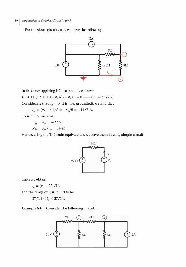
150 Introduction to Electrical Circuit Analysis
For the short-circuit case, we have the following.
4/3Ω 8Ω
6Ω
2A
10V
2
1
isc
In this case, applying KCL at node 1, we have• KCL(1): 2 + (10 − 𝑣1)∕6 − 𝑣1∕8 = 0 −−−−→ 𝑣1 = 88∕7V.Considering that 𝑣2 = 0 (it is now grounded), we find that
isc = (𝑣2 − 𝑣1)∕8 = −𝑣1∕8 = −11∕7 A.To sum up, we have
𝑣th = 𝑣oc = −22 V,Rth = 𝑣oc∕isc = 14 Ω.
Hence, using theThévenin equivalence, we have the following simple circuit.
14Ω
−22V vo
io
Then we obtainio = (𝑣o + 22)∕14
and the range of io is found to be27∕14 ≤ io ≤ 37∕14.
Example 84: Consider the following circuit.
2A
ix
10V
2Ω 4Ω
5Ω 5Ω
1 2
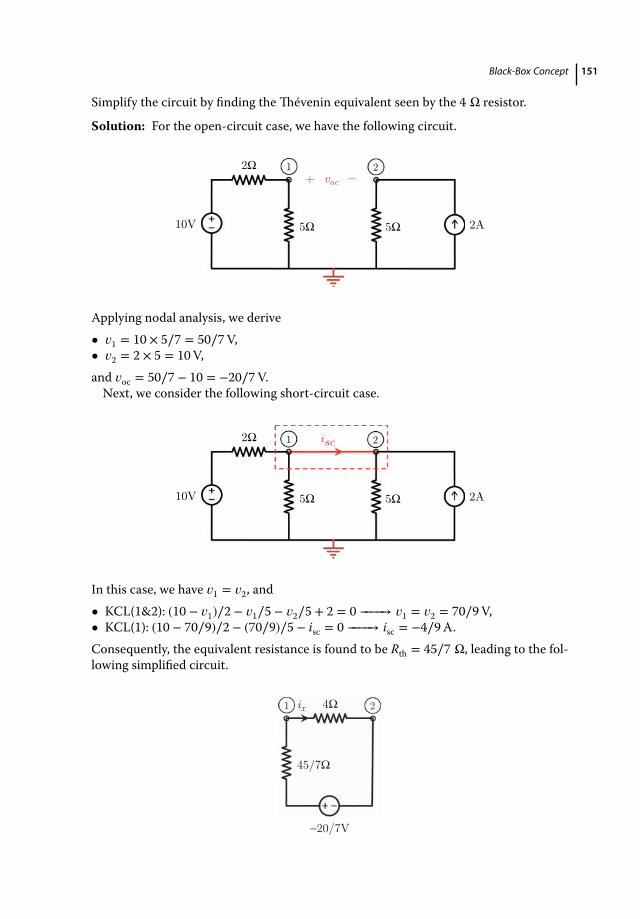
Black-Box Concept 151
Simplify the circuit by finding theThévenin equivalent seen by the 4 Ω resistor.
Solution: For the open-circuit case, we have the following circuit.
10V 2A
2Ω
5Ω 5Ω
voc_+
1 2
Applying nodal analysis, we derive• 𝑣1 = 10 × 5∕7 = 50∕7V,• 𝑣2 = 2 × 5 = 10V,and 𝑣oc = 50∕7 − 10 = −20∕7V.Next, we consider the following short-circuit case.
2A10V
2Ω
5Ω 5Ω
isc1 2
In this case, we have 𝑣1 = 𝑣2, and• KCL(1&2): (10 − 𝑣1)∕2 − 𝑣1∕5 − 𝑣2∕5 + 2 = 0 −−−−→ 𝑣1 = 𝑣2 = 70∕9V,• KCL(1): (10 − 70∕9)∕2 − (70∕9)∕5 − isc = 0 −−−−→ isc = −4∕9A.Consequently, the equivalent resistance is found to be Rth = 45∕7 Ω, leading to the fol-lowing simplified circuit.
45/7Ω
1 2ix 4Ω
−20/7V

152 Introduction to Electrical Circuit Analysis
Example 85: Consider the following circuit.
5Ω
3A150V
5Ω 10Ω5Ω
5Ω 5Ω
vx_ +
0.5vx
1 2 iy
Simplify the circuit by finding theThévenin equivalent seen by the 5 Ω resistor betweennodes 1 and 2.
Solution: We first consider the open-circuit case as follows.
5Ω
3A150V
10Ω5Ω
5Ω 5Ω
vx_+
0.5vx
1 2 voc
_+3
In the above, we note that 𝑣x = −3 × 10 = −30V. Moreover, using nodal analysis, wehave 𝑣1 = 150 × 5∕10 = 75V and 𝑣2 = 0.5𝑣x = −15V, leading to 𝑣oc = 𝑣1 − 𝑣2 = 90V.Then we consider the short-circuit case as follows.
5Ω
3A150V
10Ω5Ω
5Ω 5Ω
v_ + x
0.5vx
1 2 3isc
In this case, we still have 𝑣x = −3 × 10 = −30V and 𝑣2 = 0.5𝑣x = −15V. On the otherhand, due to the short circuit, 𝑣1 = 𝑣2 = −15V and
• KCL(1): (150 + 15)∕5 + 15∕5 − isc = 0 −−−−→ isc = 36A.
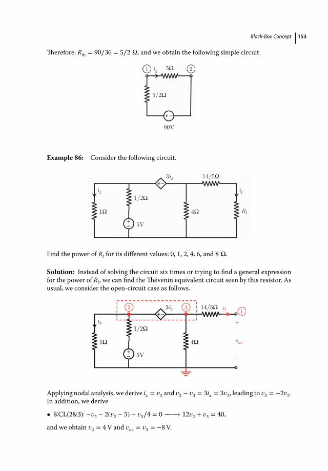
Black-Box Concept 153
Therefore, Rth = 90∕36 = 5∕2 Ω, and we obtain the following simple circuit.
5/2Ω
90V
1 2iy 5Ω
Example 86: Consider the following circuit.
1/2Ω
1Ω
5V
4Ω
14/5Ω
Rl
3ix
ix il
Find the power of Rl for its different values: 0, 1, 2, 4, 6, and 8 Ω.
Solution: Instead of solving the circuit six times or trying to find a general expressionfor the power of Rl, we can find theThévenin equivalent circuit seen by this resistor. Asusual, we consider the open-circuit case as follows.
1/2Ω
1Ω
5V
4Ω
14/5Ω3ix
ix
31
+
_
voc
02
Applying nodal analysis, we derive ix = 𝑣2 and 𝑣2 − 𝑣3 = 3ix = 3𝑣2, leading to 𝑣3 = −2𝑣2.In addition, we derive
• KCL(2&3): −𝑣2 − 2(𝑣2 − 5) − 𝑣3∕4 = 0 −−−−→ 12𝑣2 + 𝑣3 = 40,
and we obtain 𝑣2 = 4V and 𝑣oc = 𝑣3 = −8V.
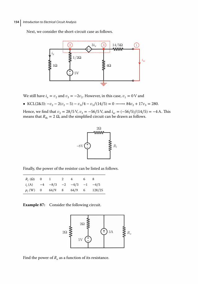
154 Introduction to Electrical Circuit Analysis
Next, we consider the short-circuit case as follows.
1/2Ω
1Ω
5V
4Ω
14/5Ω3ix
ix
32
isc
1
We still have ix = 𝑣2 and 𝑣3 = −2𝑣2. However, in this case, 𝑣1 = 0V and
• KCL(2&3): −𝑣2 − 2(𝑣2 − 5) − 𝑣3∕4 − 𝑣3∕(14∕5) = 0 −−−−→ 84𝑣2 + 17𝑣3 = 280.
Hence, we find that 𝑣2 = 28∕5V, 𝑣3 = −56∕5V, and isc = (−56∕5)∕(14∕5) = −4A. Thismeans that Rth = 2 Ω, and the simplified circuit can be drawn as follows.
2Ω
−8V Rl
Finally, the power of the resistor can be listed as follows.
Rl (Ω) 0 1 2 4 6 8il (A) −4 −8∕3 −2 −4∕3 −1 −4∕5pl (W) 0 64∕9 8 64∕9 6 128∕25
Example 87: Consider the following circuit.
5V
3A2Ω
2Ω
Ro
Find the power of Ro as a function of its resistance.
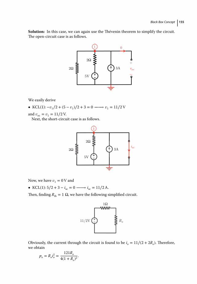
Black-Box Concept 155
Solution: In this case, we can again use the Thévenin theorem to simplify the circuit.The open-circuit case is as follows.
5V
3A2Ω
2Ω+
_ voc
01
We easily derive
• KCL(1): −𝑣1∕2 + (5 − 𝑣1)∕2 + 3 = 0 −−−−→ 𝑣1 = 11∕2V
and 𝑣oc = 𝑣1 = 11∕2V.Next, the short-circuit case is as follows.
5V
3A 2Ω
2Ω
1
isc
Now, we have 𝑣1 = 0V and
• KCL(1): 5∕2 + 3 − isc = 0 −−−−→ isc = 11∕2A.
Then, finding Rth = 1 Ω, we have the following simplified circuit.
1Ω
11/2V Ro
Obviously, the current through the circuit is found to be io = 11∕(2 + 2Ro). Therefore,we obtain
po = Roi2o =121Ro
4(1 + Ro)2.
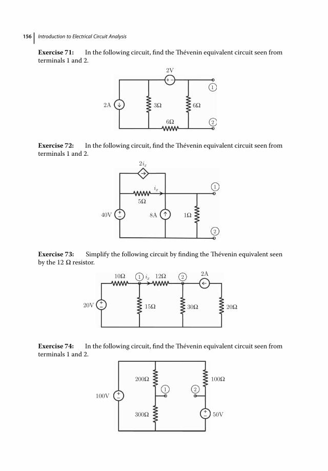
156 Introduction to Electrical Circuit Analysis
Exercise 71: In the following circuit, find theThévenin equivalent circuit seen fromterminals 1 and 2.
3Ω
1
2A
2V
2
6Ω
6Ω
Exercise 72: In the following circuit, find theThévenin equivalent circuit seen fromterminals 1 and 2.
1
2
40V 8A 1Ω
5Ω
2ix
ix
Exercise 73: Simplify the following circuit by finding the Thévenin equivalent seenby the 12 Ω resistor.
20Ω
ix
20V
10Ω 12Ω
15Ω 30Ω
1 2 2A
Exercise 74: In the following circuit, find theThévenin equivalent circuit seen fromterminals 1 and 2.
100V
200Ω
1
100Ω
50V300Ω
2
Black-Box Concept 157
Exercise 75: Simplify the following circuit by finding the Thévenin equivalent seenby the 10 Ω resistor.
100V2Ω
1
2
2A 10Ω
ix
Exercise 76: Simplify the following circuit by finding the Thévenin equivalent seenby the 8 Ω resistor.
8Ω
1
2
ix
2Ω
3Ω2Ω
8Ω
4Ω
60V
Exercise 77: In the following circuit, find the Thévenin equivalent circuit seen bythe voltage source 𝑣o.
25V
1Ω 16Ω
1A 4Ω 3Ω
1Ω2A
ix2ix
18V
iovo
Exercise 78: In the following circuit, find theThévenin equivalent circuit seen by Rl.
2Ω
2A16V 2Ω vy
+
_2vy Rl
158 Introduction to Electrical Circuit Analysis
Exercise 79: In the following circuit, find theThévenin equivalent circuit seen byRo.
40Ω 3A
60Ω
300V
6Ω
Ro
Exercise 80: In the following circuit, find theThévenin equivalent circuit seen by Rl.
20Ω40Ω
2A 3V
Rl60Ω
vy /20
vy_ +
5.2 Maximum Power Transfer
In electrical and electronic engineering, it is often required to combine different cir-cuits. While such combination seems trivial (just connect the nodes that need to beconnected!), a good connection needs to be a good match between the circuits. In mostcases, a good match is one that provides the maximum power transfer from one circuitto another. As an example, consider a simple case involving a voltage source and resistor(circuit 1) that are connected in series to another resistor (circuit 2).
vg
Rg
Rl
circuit 1 circuit 2
il
We would like to match circuits 1 and 2. Specifically, we would like to find the value ofRl such that the power consumed by this resistor is maximized. This can be interpretedas themaximum power transfer from circuit 1 to circuit 2. Obviously, both Rl = 0 (shortcircuit) and Rl = ∞ (open circuit) lead to pl = 0.

Black-Box Concept 159
We start with a general expression for the current,
il =𝑣g
Rg + Rl.
Therefore, the power of the resistor can be written as
pl = Rli2l =Rl𝑣
2g
(Rg + Rl)2.
Taking the derivative with respect to Rl and making it equal to zero,
𝜕pl
𝜕Rl=
𝑣2g
(Rg + Rl)2−
2Rl𝑣2g
(Rg + Rl)3=
𝑣2g (Rg − Rl)(Rg + Rl)3
= 0,
we obtainRl = Rg .
Hence, the best selection occurs by setting Rl equal to Rg , leading to
pmaxl =
Rg𝑣2g
4R2g=
𝑣2g
4Rg.
We note that, in this matched case, Rg consumes the same amount of power.In practice, more complex circuits (compared to the example above) need to be
matched. Nevertheless, if the circuits are linear, they can be converted into Théveninequivalent models such that matching corresponds to selecting the equivalent resistorsequally. In the following examples, we consider various cases involving a resistor to bematched to a complex circuit.
Example 88: Consider the following circuit, which has previously been studied (seeExample 86).
1/2Ω
1Ω
5V
4Ω
14/5Ω
Rl
3ix
ix il
Thepower ofRl for different valueswas found and listed.TheThévenin equivalent circuitseen by Rl is also found as follows.
2Ω
−8V Rl

160 Introduction to Electrical Circuit Analysis
Obviously, the selection Rl = 2 Ω maximizes the power transferred to this load. Thispower was found to be 8W, the maximum among all trials.
Example 89: Consider the following circuit involving a resistor Rl.
2Ω
2A16V 2Ω vy
+
_2vy Rl
The Thévenin equivalent circuit seen by Rl was previously found to be as follows (seethe solution to Exercise 78).
1/3Ω
10/3V Rl
Therefore, in order to maximize the power transfer, one needs to select Rl = 1∕3 Ω. Inthis case, the voltage 𝑣oc = 10∕3V is divided equally among the resistors so that
𝑣l = 𝑣oc∕2 = 5∕3 V
and
pmaxl =
(5∕3)2
1∕3= 25
3W.
Example 90: In the following circuit, Ro again needs to be selected to maximize thepower transfer.
40Ω 3A
60Ω
300V
6Ω
Ro

Black-Box Concept 161
The Thévenin equivalent circuit seen by Ro was previously found to be as follows (seethe solution to Exercise 79).
30Ω
48V Ro
Then one must select Ro = 30 Ω, leading to𝑣o = 𝑣oc∕2 = 24 V
and
pmaxo = 242
30= 96
5W.
One can check these voltage and power values as follows.
40Ω 3A
60Ω
300V
6Ω1
30Ω
Applying KCL at node 1, we have• KCL (1): −𝑣1∕40 − 3 − (𝑣1 − 300)∕60 − 𝑣1∕36 = 0,leading to 𝑣1 = 144∕5V.Then the voltage across the 30 Ω load resistor can be derived as
𝑣o =3036
𝑣1 =56× 144
5= 24 V,
as expected.
Example 91: Consider the following circuit.
4A 4Ω vx
+
_
1
2
vx/4
2Ω

162 Introduction to Electrical Circuit Analysis
Find the value of the resistor to be connected between 1 and 2 for maximum powertransfer.
Solution: In order to find the value of the resistor, we can first find theThévenin equiv-alent circuit seen from 1 and 2. First, we consider the open-circuit case as follows.
3
4A 4Ω vx
+
_
1
2
vx/4
2Ω
+
_ voc
00
Using nodal analysis, we easily obtain 𝑣3 = 𝑣x = 4 × 4 = 16V. Then𝑣oc = 𝑣1 = 𝑣3 + 2 × 𝑣x∕4 = 24 V.
It is interesting that 𝑣x∕4 current flows through the 2 Ω resistor as a closed loop.Next, we consider the short-circuit case.
isc
3
4A 4Ω vx
+
_
1
2
vx /4
2Ω
In this case, we have 𝑣1 = 𝑣2 = 0 and 𝑣3 = 𝑣x. Applying KCL at node 3, we get• KCL (3): 4 − 𝑣3∕4 − 𝑣3∕4 − 𝑣3∕2 = 0 −−−−→ 𝑣3 = 4V.Then isc = 𝑣3∕4 + 𝑣3∕2 = 3A. Consequently, we obtain
𝑣th = 𝑣oc = 24 V,Rth = 𝑣oc∕isc = 24∕3 = 8 Ω,
and theThévenin equivalent circuit can be drawn as follows.
8Ω
24V
1
2

Black-Box Concept 163
For maximum power transfer, the resistor to be connected to this circuit must be equalto Rl = 8 Ω. And, in this case, we have
pmaxl =
𝑣2l
Rl=
(𝑣th∕2)2
Rl= 144
8= 18 W.
Example 92: Consider the following circuit.
25Ω
ix20ix
5V
2kΩ
vy
+
_3vy
1
2
Find the value of the resistor to be connected between 1 and 2 for maximum powertransfer.
Solution: In order to find the value of the resistor, one can find theThévenin equivalentcircuit seen from 1 and 2. The open-circuit case is considered as follows.
25Ω
ix20ix
5V
2kΩ
vy
+
_3vy
+
_ voc
03 1 1
2
Using nodal analysis, we have 𝑣y = 𝑣1. Applying KCL at node 1 and node 3, we get• KCL (1): −20ix − 𝑣1∕25 = 0 −−−−→ 𝑣1 = −500ix,• KCL (3): (5 − 3𝑣y)∕2000 − ix = 0 −−−−→ 2000ix + 3𝑣1 = 5.Then we obtain ix = 10mA and 𝑣oc = 𝑣y = −5V.Next, we consider the short-circuit case.
25Ω
ix20ix
5V
2kΩ
vy
+
_3vy
isc
3 1 1
2
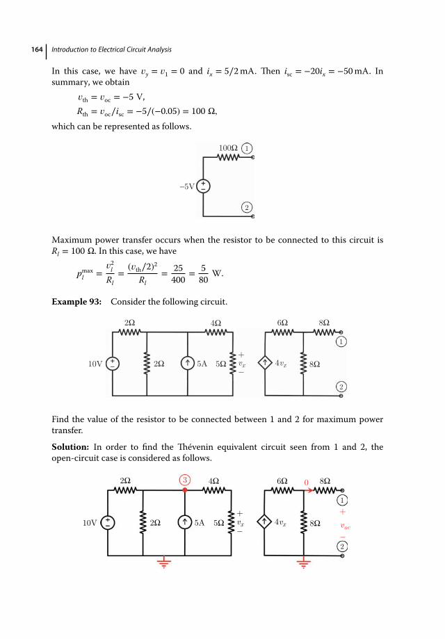
164 Introduction to Electrical Circuit Analysis
In this case, we have 𝑣y = 𝑣1 = 0 and ix = 5∕2mA. Then isc = −20ix = −50mA. Insummary, we obtain
𝑣th = 𝑣oc = −5 V,Rth = 𝑣oc∕isc = −5∕(−0.05) = 100 Ω,
which can be represented as follows.
100Ω
−5V
1
2
Maximum power transfer occurs when the resistor to be connected to this circuit isRl = 100 Ω. In this case, we have
pmaxl =
𝑣2l
Rl=
(𝑣th∕2)2
Rl= 25
400= 5
80W.
Example 93: Consider the following circuit.
10V
4Ω2Ω 6Ω 8Ω
2Ω 8Ωvx_
+
1
2
5Ω5A 4vx
Find the value of the resistor to be connected between 1 and 2 for maximum powertransfer.
Solution: In order to find the Thévenin equivalent circuit seen from 1 and 2, theopen-circuit case is considered as follows.
6Ω
10V
4Ω 8Ω2Ω
2Ω 8Ωvx_
+
1
2
5Ω5A 4vx
+
_ voc
03

Black-Box Concept 165
Using nodal analysis, we apply KCL at node 3 to obtain 𝑣3 as
• KCL(3): (10 − 𝑣3)∕2 − 𝑣3∕2 + 5 − 𝑣3∕9 = 0 −−−−→ 𝑣3 = 9V.
Therefore, 𝑣x = 5V and 𝑣oc = 4𝑣x × 8 = 32𝑣x = 160V.Next, we consider the short-circuit case.
6Ω
10V
4Ω 8Ω2Ω
2Ω 8Ωvx_
+ 1
2
5Ω5A 4vx
3
isc
Interestingly, 𝑣x does not change, equaling 5V as in the open-circuit case. A currentdivision occurs on the right-hand side of the circuit, that is, isc = 4𝑣x∕2 = 10A. Conse-quently, we have
𝑣th = 𝑣oc = 160 V,Rth = 𝑣oc∕isc = 16 Ω.
TheThévenin equivalent circuit can be drawn as follows.
16Ω
160V
1
2
Maximum power transfer occurs when Rl = 16 Ω is connected to the terminals, lead-ing to
pmaxl =
𝑣2l
Rl=
(𝑣th∕2)2
Rl= 80 × 80
16= 400 W.

166 Introduction to Electrical Circuit Analysis
Example 94: Consider the following circuit.
1
2
6V Rl
2Ω 2Ω
6Ω
2Ω 2Ω
Find the value of the resistor Rl for maximum power transfer to this load.
Solution: First, we consider the open-circuit case as follows.
1
2
6V
2Ω 2Ω
6Ω
2Ω 2Ω
+
_
voc
03
Using nodal analysis, we apply KCL at nodes 1 and 3 to derive• KCL(1): (𝑣3 − 𝑣1)∕2 + (6 − 𝑣1)∕6 − 𝑣1∕2 = 0 −−−−→ 7𝑣1 − 3𝑣3 = 6,• KCL(3): (6 − 𝑣3)∕2 − 𝑣3∕2 − (𝑣3 − 𝑣1)∕2 = 0 −−−−→ 𝑣1 − 3𝑣3 = −6,leading to 𝑣oc = 𝑣1 = 2V.Next, we can consider the short-circuit case as follows.
1
2
6V
2Ω 2Ω
6Ω
2Ω 2Ω
3
isc
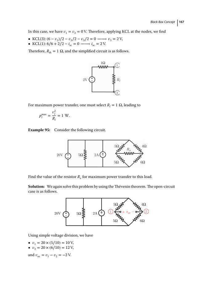
Black-Box Concept 167
In this case, we have 𝑣1 = 𝑣2 = 0V. Therefore, applying KCL at the nodes, we find
• KCL(3): (6 − 𝑣3)∕2 − 𝑣3∕2 − 𝑣3∕2 = 0 −−−−→ 𝑣3 = 2V,• KCL(1): 6∕6 + 2∕2 − isc = 0 −−−−→ isc = 2V.
Therefore, Rth = 1 Ω, and the simplified circuit is as follows.
1Ω
2V Rl
1
2
For maximum power transfer, one must select Rl = 1 Ω, leading to
pmaxl =
𝑣2l
Rl= 1 W.
Example 95: Consider the following circuit.
Ro5Ω
5Ω 2A20V
5Ω 6Ω
4Ω
Find the value of the resistor Ro for maximum power transfer to this load.
Solution: Weagain solve this problembyusing theThévenin theorem.Theopen-circuitcase is as follows.
5Ω
5Ω 2A20V
5Ω 6Ω
4Ω
voc_+1 2
Using simple voltage division, we have
• 𝑣1 = 20 × (5∕10) = 10V,• 𝑣2 = 20 × (6∕10) = 12V,
and 𝑣oc = 𝑣1 − 𝑣2 = −2V.

168 Introduction to Electrical Circuit Analysis
Similarly, the short-circuit case is as follows.
5Ω
5Ω 2A20V
5Ω 6Ω
4Ω
1 2isc
For this circuit, one finds the equivalent resistor for the combination of the four resistorsto be
Req = 5 ∥ 4 + 5 ∥ 6 = 209
+ 3011
= 49099
Ω.
Then the current through the 5 Ω resistors can be found via current division to be
i5 Ω, upper =4920Req
= 809
99490
= 8849
A,
i5 Ω, lower =611
20Req
= 12011
99490
= 10849
A.
Next, applying KCL at node 1, we derive
• KCL(1): isc = (−108 + 88)∕49 = −20∕49A.
Therefore, Rth = 49∕10 Ω and one must select Ro = 49∕10 Ω for maximum powertransfer.
49/10Ω
−2V Ro
The value of the transferred power can be obtained as
po =1
49∕10= 10
49W.
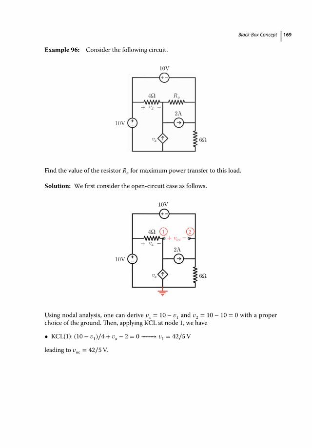
Black-Box Concept 169
Example 96: Consider the following circuit.
4Ω
10V
2A
6Ω
10V
vx
vx+ _
Ro
Find the value of the resistor Ro for maximum power transfer to this load.
Solution: We first consider the open-circuit case as follows.
4Ω
10V
2A
6Ω
10V
vx
vx+ _ voc_ +
1 2
Using nodal analysis, one can derive 𝑣x = 10 − 𝑣1 and 𝑣2 = 10 − 10 = 0 with a properchoice of the ground. Then, applying KCL at node 1, we have
• KCL(1): (10 − 𝑣1)∕4 + 𝑣x − 2 = 0 −−−−→ 𝑣1 = 42∕5V
leading to 𝑣oc = 42∕5V.
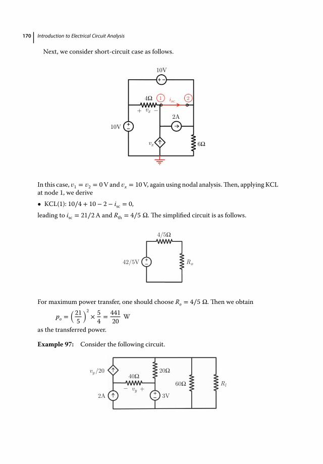
170 Introduction to Electrical Circuit Analysis
Next, we consider short-circuit case as follows.
4Ω
10V
2A
6Ω
10V
vx
vx+ _
1 2isc
In this case, 𝑣1 = 𝑣2 = 0V and 𝑣x = 10V, again using nodal analysis.Then, applying KCLat node 1, we derive• KCL(1): 10∕4 + 10 − 2 − isc = 0,leading to isc = 21∕2A and Rth = 4∕5 Ω. The simplified circuit is as follows.
4/5Ω
42/5V Ro
For maximum power transfer, one should choose Ro = 4∕5 Ω. Then we obtain
po =(215
)2× 54= 441
20W
as the transferred power.
Example 97: Consider the following circuit.
20Ω40Ω
2A 3V
Rl60Ω
vy /20
vy_ +
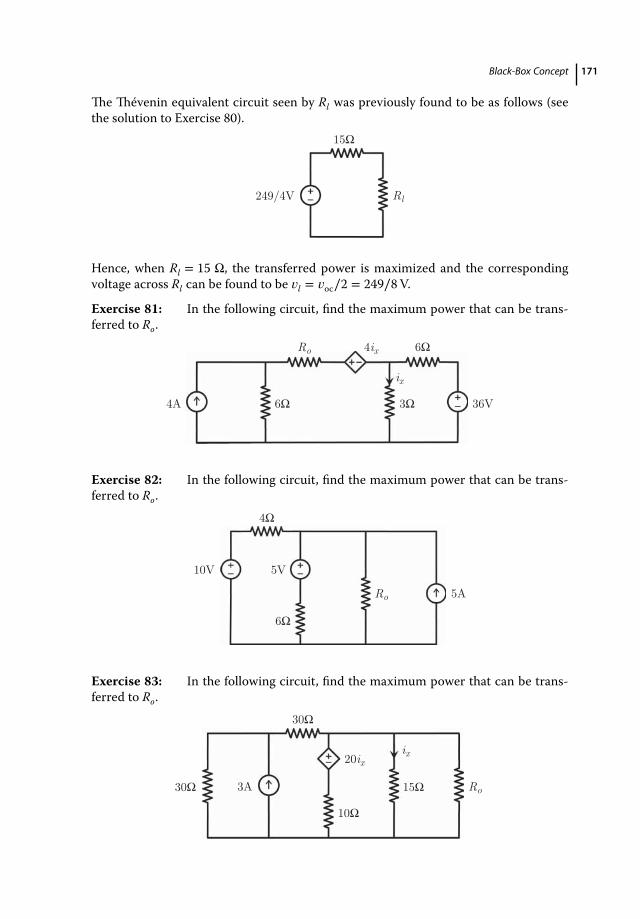
Black-Box Concept 171
The Thévenin equivalent circuit seen by Rl was previously found to be as follows (seethe solution to Exercise 80).
15Ω
249/4V Rl
Hence, when Rl = 15 Ω, the transferred power is maximized and the correspondingvoltage across Rl can be found to be 𝑣l = 𝑣oc∕2 = 249∕8V.
Exercise 81: In the following circuit, find the maximum power that can be trans-ferred to Ro.
4A 6Ω 3Ω 36V
Ro 6Ω4ix
ix
Exercise 82: In the following circuit, find the maximum power that can be trans-ferred to Ro.
4Ω
10V 5V
6Ω
5ARo
Exercise 83: In the following circuit, find the maximum power that can be trans-ferred to Ro.
30Ω
30Ω
10Ω
15Ω Ro 3A
20ix ix
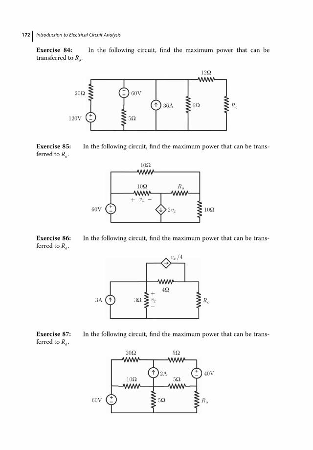
172 Introduction to Electrical Circuit Analysis
Exercise 84: In the following circuit, find the maximum power that can betransferred to Ro.
12Ω
5Ω120V
20Ω 60V
6Ω Ro36A
Exercise 85: In the following circuit, find the maximum power that can be trans-ferred to Ro.
60V
10Ω
10Ω
10Ω2vx
Ro
vx+ _
Exercise 86: In the following circuit, find the maximum power that can be trans-ferred to Ro.
3A 3Ω
4Ω
vx
+
_
vx /4
Ro
Exercise 87: In the following circuit, find the maximum power that can be trans-ferred to Ro.
20Ω
10Ω
5Ω
5Ω
5Ω Ro60V
40V2A

Black-Box Concept 173
Exercise 88: In the following circuit, find the maximum power that can be trans-ferred to Ro.
1Ω 3Ωix
20V 6Ω (2/3)A2ix Ro
Exercise 89: In the following circuit, find the expression for the maximum powerthat can transferred to Ro.
R1 R2 Roio
5.3 Shortcuts in Equivalent Circuits
As shown in the previous section, maximum power transfer is achieved when the equiv-alent resistances of two circuits (e.g., a large circuit and a single resistor as a small circuit)are equal. On the other hand, in order to find the Thévenin/Norton equivalent resis-tance, we need to find both the open-circuit voltage and short-circuit current. In thissection, we discuss a shortcut to find the equivalent resistance.In order to derive a shortcut to find the equivalent resistance for a given circuit, we
reconsider theThévenin and Norton equivalent circuits in Figure 5.1. We already knowthat Rth = Rno = 𝑣th∕ino. On the other hand, if we replace 𝑣th with a short circuit, theresistance measured in the Thévenin equivalent circuit is the same as Rth. Similarly, ifino is replaced with an open circuit, Rno is directly seen from the terminals of the Nortoncircuit. Consequently, given a complex circuit, one can perform the following steps tofind the equivalent resistance.
• Replace all independent voltage sources with short circuits.• Replace all independent current sources with open circuits.• Calculate the overall resistance seen from the terminals.
This shortcut is particularly useful when replacing the independent sources withshort/open circuits leads only to resistors such that series and parallel connections ofresistors can easily be calculated. When dependent sources (that cannot be replaced)are involved, however, the equivalent resistance may not be trivial to find.As an example, we reconsider the following circuit, where the resistance seen by 𝑣o
needs to be found.
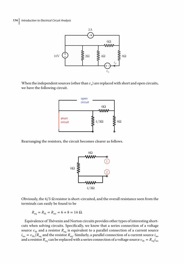
174 Introduction to Electrical Circuit Analysis
2Ω 4Ω 8Ω
6Ω
2A
10V
vo
io
When the independent sources (other than 𝑣o) are replacedwith short and open circuits,we have the following circuit.
4/3Ω 8Ω
6Ω
opencircuit
shortcircuit
Rearranging the resistors, the circuit becomes clearer as follows.
8Ω
6Ω
4/3Ω
1
2
Obviously, the 4∕3 Ω resistor is short-circuited, and the overall resistance seen from theterminals can easily be found to be
Req = Rth = Rno = 6 + 8 = 14 Ω.
Equivalence ofThévenin andNorton circuits provides other types of interesting short-cuts when solving circuits. Specifically, we know that a series connection of a voltagesource 𝑣th and a resistor Req is equivalent to a parallel connection of a current sourceino = 𝑣th∕Req and the resistor Req. Similarly, a parallel connection of a current source inoand a resistorReq can be replacedwith a series connection of a voltage source 𝑣th = Reqino

Black-Box Concept 175
and the same resistor Req. Such substitutions can facilitate the analysis of circuits withmany connections of resistors.As an example, consider the following circuit involving five resistors and two inde-
pendent voltage sources.
2Ω
2Ω
1Ω
4Ω
6Ω
4V2V
io
We would like to find the value of the current io, which can be done in many differentways. In this case, however, we consider the equivalence of circuits. First, a series con-nection of the 2V voltage source and the 2 Ω resistor on the left can be replaced with a2∕2 = 1A current source and a 2 Ω resistor as follows.
2Ω 2Ω
1Ω
4Ω
6Ω
4V1A
io
1Ω
In the above, the new 2 Ω resistor is parallel to another 2 Ω resistor, leading to 1 Ω over-all. Hence, we have a 1A current source that is connected in parallel to a 1 Ω resistor inthe updated circuit. Using the equivalence again, this parallel connection can be replacedas follows.
1Ω
4Ω
6Ω
4V1V
io
1Ω
In the updated circuit, we observe that the new 1 Ω resistor is connected in series toanother 1 Ω resistor. Therefore, we have a series connection of a 1V voltage source anda 2 Ω resistor, which can be replaced again as follows.
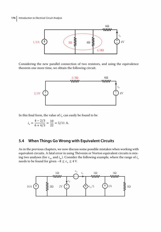
176 Introduction to Electrical Circuit Analysis
4Ω
6Ω
4V1/2A
io
2Ω
4/3Ω
Considering the new parallel connection of two resistors, and using the equivalencetheorem one more time, we obtain the following circuit.
6Ω
4V2/3V
io
4/3Ω
In this final form, the value of io can easily be found to be
io =4 − 2∕36 + 4∕3
= 1022
= 5∕11 A.
5.4 When Things Go Wrong with Equivalent Circuits
As in the previous chapters, we now discuss some possible mistakes when working withequivalent circuits. A fatal error in usingThévenin or Norton equivalent circuits is mix-ing two analyses (for 𝑣oc and isc). Consider the following example, where the range of ioneeds to be found for given −8 ≤ 𝑣o ≤ 4V.
16A 2Ω
1Ω
2V
1Ω 1Ω
1Ω2Aix/5
ix
vo io
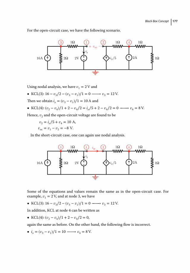
Black-Box Concept 177
For the open-circuit case, we have the following scenario.
16A 2Ω
1Ω
2V
1Ω 1Ω
1Ω2Aix/5
ix
voc _+
1 23 4
Using nodal analysis, we have 𝑣1 = 2V and
• KCL(3): 16 − 𝑣3∕2 − (𝑣3 − 𝑣1)∕1 = 0 −−−−→ 𝑣3 = 12V.
Then we obtain ix = (𝑣3 − 𝑣1)∕1 = 10A and
• KCL(4): (𝑣2 − 𝑣4)∕1 + 2 − 𝑣4∕2 = ix∕5 + 2 − 𝑣4∕2 = 0 −−−−→ 𝑣4 = 8V.
Hence, 𝑣2 and the open-circuit voltage are found to be
𝑣2 = ix∕5 + 𝑣4 = 10 A,𝑣oc = 𝑣1 − 𝑣2 = −8 V.
In the short-circuit case, one can again use nodal analysis.
16A 2Ω
1Ω
2V
1Ω 1Ω
1Ω2Aix/5
ix
1 23 4isc
Some of the equations and values remain the same as in the open-circuit case. Forexample, 𝑣1 = 2V, and at node 3, we have
• KCL(3): 16 − 𝑣3∕2 − (𝑣3 − 𝑣1)∕1 = 0 −−−−→ 𝑣3 = 12V.
In addition, KCL at node 4 can be written as
• KCL(4): (𝑣2 − 𝑣4)∕1 + 2 − 𝑣4∕2 = 0,
again the same as before. On the other hand, the following flow is incorrect.
• ix = (𝑣3 − 𝑣1)∕1 = 10 −−−−→ 𝑣4 = 8V.

178 Introduction to Electrical Circuit Analysis
Instead, KCL at node 1 reveals that
• KCL(1): ix + isc = (𝑣3 − 𝑣1)∕1 = 10,
which is valid but not useful as the equation involves a new unknown isc. For a correctsolution, one may use 𝑣1 = 𝑣2 = 2V, and find 𝑣4 = 8∕3V by using the equation derivedfrom KCL at node 4. Then the correct value of ix can be obtained by applying KCL atthe supernode involving nodes 1 and 2,
• KCL(1&2): (𝑣3 − 𝑣1)∕1 − ix + ix∕5 − (𝑣2 − 𝑣4)∕1 = 0 −−−−→ ix = 40∕3A.
Finally, using KCL at node 1, we have isc = 10 − ix = −10∕3A. To complete the solution,one can consider theThévenin equivalent seen by the voltage source 𝑣o as follows.
12/5Ω
−8V vo
In the above, the value of the resistor is found to be Rth = 𝑣oc∕isc = −8∕(−10∕3) =12∕5 Ω. Then we derive
𝑣o = −8 − (12∕5)io −−−−→ −8 ≤ [−8 − (12∕5)io] ≤ 4
leading to
0 ≤ −(12∕5)io ≤ 12
or
−5 ≤ io ≤ 0 A.
5.5 What You Need to Know before You Continue
As discussed in this chapter, Thévenin and Norton equivalences allow us to simplifycircuits before analyzing them in some scenarios, such as maximum power transfer.Before proceeding to the next chapter, we emphasize a few important points.
• Equivalence: Thévenin and Norton equivalent circuits can be used to represent anylinear circuit involving linear elements.
• Maximumpower transfer: Circuits arematched best when their equivalent resistancevalues are the same. Considering a voltage source and a resistor, a matched resistordraws the maximum power that can be extracted.

Black-Box Concept 179
• The equivalence of Thévenin and Norton circuits enables the simplification of com-plex resistive networks by applying the equivalence consecutively on series and par-allel connections of sources and resistors.
In the next chapter, we start with two new types of components, namely, capacitors andinductors, which are commonly used in real-life circuits. Unlike with resistors, time isan important parameter in the analysis of capacitors and inductors, since these compo-nents present delayed responses (that cannot be neglected) to the change in voltage andcurrent values.

181
6
Transient Analysis
As discussed at various points in Chapter 1, time is an important parameter in electricalcircuits. On the other hand, in subsequent chapters, we neglected the time concept inthe circuit analysis because
• all sources have been DC sources that deliver fixed voltage and current values,• we have considered only resistors, in addition to dependent and independent sources,
but not energy-storage elements.
Basically, there are two fundamental types of energy-storage elements, namely, capac-itors and inductors. Similar to resistance, capacitance and inductance are natural prop-erties of all structures, while capacitors and inductors appear as individual componentsin many circuits. Unlike resistors, the response of a capacitor and inductor to an appliedvoltage and current is not instant. Specifically, for DC circuits involving energy-storageelements (and resistors), it takes time for these components to store and release energy,leading to a transient state that does not occur in resistor-only circuits. This chapter isdevoted to the analysis of such transient states. In Chapter 7 we focus on AC circuits,where the energy-storage elements add phases between current and voltage values thatare oscillatory.
6.1 Capacitance and Capacitors
In general terms, the capacitance of a structure is its ability to store charge for a givenvoltage. Therefore, it is defined as
C =q𝑣.
The unit of capacitance is the farad (F), where 1 farad is 1 coulomb per volt. Typically,a capacitance is defined for a structure with two parts that are separated by a distance,while a voltage is applied between them. For such structures, the capacitance is usuallyproportional to the sizes (e.g., areas) of the parts and inversely proportional to distancebetween them. Capacitance also depends on (and is proportional to) the electrical prop-erties (specifically, the electric permittivity) of the medium in which the structure islocated. Capacitance can also be defined for a single body when the voltage is definedwith respect to a reference (usually infinity).Capacitors (see Figure 11.2) are two-port devices that have fixed capacitance values.
While the capacitance may actually depend on the frequency, applied voltage, and
Introduction to Electrical Circuit Analysis, First Edition. Özgür Ergül.© 2017 John Wiley & Sons Ltd. Published 2017 by John Wiley & Sons Ltd.Companion Website: www.wiley.com/go/ergul4412

182 Introduction to Electrical Circuit Analysis
v
+q –q+q
reference
electric fieldlines
electric field lines
∞
Figure 6.1 The capacitance between two bodies is proportional to the amount of charge (q) in thepositively charged body for a given voltage difference between them. The capacitance of a singlebody can also be defined when the voltage difference is defined with respect to infinity.
_
+ _
C
+ + + + +
+ +
_ _
_ _ _
_
electric fieldlines
+ v(t)i(t)i(t)
i(t) i(t)
v(t)
Figure 6.2 When a nonzero current exists through a capacitor involving two bodies (e.g., conductingplates), leading to the accumulation of positive and negative charges, it builds up electric field, hencea voltage difference, between the bodies. In circuit analysis, a capacitor is a two-port device that storesand releases energy.
current values (leading to nonlinear behavior), as well as on outer conditions, weconsider only ideal capacitors with constant capacitance values. In order to derive thevoltage/current response of a capacitor, we use the definition of the capacitance andtake the time-derivative of the charge,
dq(t)dt
= ddt
[C𝑣(t)] = C d𝑣(t)dt
,
leading to
i(t) = C d𝑣(t)dt
,
using the definition of the current.Therefore, the current through a capacitor is propor-tional to the time derivative of its voltage.This can be interpreted as follows. An increasein the voltage of a capacitor corresponds to an increase in the amount of charge accumu-lated in the capacitor. The flow of these charges also corresponds to a positive currentpassing through the capacitor, as formulated in the equation above. Obviously, the largerthe capacitance, larger the value of the flow of the charges, that is, the current.Given a current with respect to time, the voltage across a capacitor is given by
𝑣(t) = 1C ∫
t
t0i(t′)dt′ + 𝑣0,
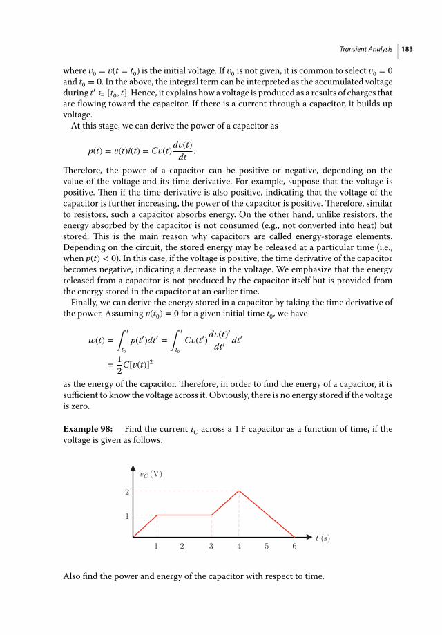
Transient Analysis 183
where 𝑣0 = 𝑣(t = t0) is the initial voltage. If 𝑣0 is not given, it is common to select 𝑣0 = 0and t0 = 0. In the above, the integral term can be interpreted as the accumulated voltageduring t′ ∈ [t0, t]. Hence, it explains how a voltage is produced as a results of charges thatare flowing toward the capacitor. If there is a current through a capacitor, it builds upvoltage.At this stage, we can derive the power of a capacitor as
p(t) = 𝑣(t)i(t) = C𝑣(t)d𝑣(t)dt
.
Therefore, the power of a capacitor can be positive or negative, depending on thevalue of the voltage and its time derivative. For example, suppose that the voltage ispositive. Then if the time derivative is also positive, indicating that the voltage of thecapacitor is further increasing, the power of the capacitor is positive. Therefore, similarto resistors, such a capacitor absorbs energy. On the other hand, unlike resistors, theenergy absorbed by the capacitor is not consumed (e.g., not converted into heat) butstored. This is the main reason why capacitors are called energy-storage elements.Depending on the circuit, the stored energy may be released at a particular time (i.e.,when p(t) < 0). In this case, if the voltage is positive, the time derivative of the capacitorbecomes negative, indicating a decrease in the voltage. We emphasize that the energyreleased from a capacitor is not produced by the capacitor itself but is provided fromthe energy stored in the capacitor at an earlier time.Finally, we can derive the energy stored in a capacitor by taking the time derivative of
the power. Assuming 𝑣(t0) = 0 for a given initial time t0, we have
𝑤(t) =∫
t
t0p(t′)dt′ =
∫
t
t0C𝑣(t′)d𝑣(t)′
dt′dt′
= 12
C[𝑣(t)]2
as the energy of the capacitor. Therefore, in order to find the energy of a capacitor, it issufficient to know the voltage across it. Obviously, there is no energy stored if the voltageis zero.
Example 98: Find the current iC across a 1 F capacitor as a function of time, if thevoltage is given as follows.
654321
1
2
t (s)
vC (V)
Also find the power and energy of the capacitor with respect to time.

184 Introduction to Electrical Circuit Analysis
Solution: Using the expression for the current of a capacitor, we list the values in dif-ferent time ranges as
• 0 < t < 1 s: iC(t) =d𝑣C(t)
dt= dt
dt= 1A,
• 1 < t < 3 s: iC(t) =d𝑣C(t)
dt= d1
dt= 0A,
• 3 < t < 4 s: iC(t) =d𝑣C(t)
dt= d
dt(t − 2) = 1A,
• 4 < t < 6 s: iC(t) =d𝑣C(t)
dt= d
dt(−t + 6) = −1A.
Therefore, the current through the capacitor can be drawn with respect to time as fol-lows.
0
1
–11 2 3 54 6
iC (A)
t (s)
We note that the current through a capacitor can be discontinuous. Specifically, inthis example, the current values at exactly t = 0, t = 1 s, t = 3 s, and t = 6 s are not welldefined. Such an instant change in the polarization of a current is due to the suddenchange in the slope of the corresponding voltage of the capacitor.This is a characteristicof ideal capacitors when they are modeled as purely capacitive. In real life, where eachcapacitor involves a small amount of resistance and inductance, it would be impossibleto change its current as well as the slope of its voltage instantaneously.Even when they are modeled ideally, capacitors that are connected to resistors cannot
have discontinuous voltages. As is revealed later, it takes time for a capacitor (connectedto some resistors) to store and release energy, that is, there cannot be a jump in its energy.Since the energy of a capacitor is proportional to the square of its voltage, there also can-not be a jump in the voltage, that is, it must be continuous.We note that a discontinuousvoltage at a particular time would also need an infinite amount of current at the sametime since it is the derivative of the voltage.The power of the capacitor above can be obtained from pC(t) = 𝑣C(t)iC(t) as
• 0 < t < 1 s: pC(t) = (t)W,• 1 < t < 3 s: pC(t) = 0,• 3 < t < 4 s: pC(t) = (t − 2)W,• 4 < t < 6 s: pC(t) = (t − 6)W.
Then we have the following plot.
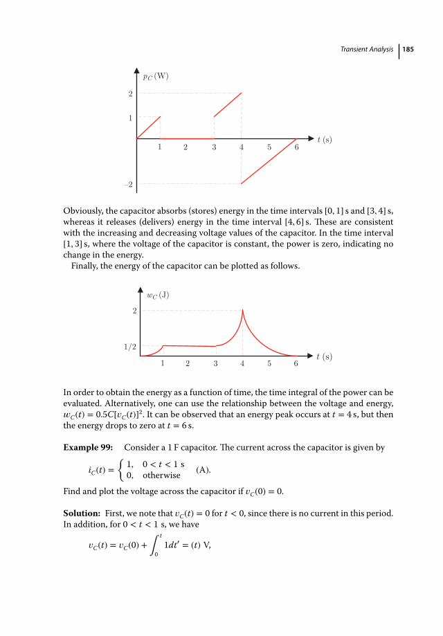
Transient Analysis 185
1 2 3 5 64
1
2
–2
t (s)
pC (W)
Obviously, the capacitor absorbs (stores) energy in the time intervals [0, 1] s and [3, 4] s,whereas it releases (delivers) energy in the time interval [4, 6] s. These are consistentwith the increasing and decreasing voltage values of the capacitor. In the time interval[1, 3] s, where the voltage of the capacitor is constant, the power is zero, indicating nochange in the energy.Finally, the energy of the capacitor can be plotted as follows.
1/2 1 2 3 4 5 6
2
t (s)
wC (J)
In order to obtain the energy as a function of time, the time integral of the power can beevaluated. Alternatively, one can use the relationship between the voltage and energy,𝑤C(t) = 0.5C[𝑣C(t)]2. It can be observed that an energy peak occurs at t = 4 s, but thenthe energy drops to zero at t = 6 s.
Example 99: Consider a 1 F capacitor. The current across the capacitor is given by
iC(t) =
1, 0 < t < 1 s0, otherwise (A).
Find and plot the voltage across the capacitor if 𝑣C(0) = 0.
Solution: First, we note that 𝑣C(t) = 0 for t < 0, since there is no current in this period.In addition, for 0 < t < 1 s, we have
𝑣C(t) = 𝑣C(0) + ∫
t
01dt′ = (t) V,

186 Introduction to Electrical Circuit Analysis
leading to 𝑣C(1) = 1V. Finally, for t > 1 s, we get
𝑣C(t) = 𝑣C(1) + ∫
t
10dt′ = 1 V.
Overall, the voltage across the capacitor can be written as
𝑣C(t) =⎧⎪⎨⎪⎩
0, t < 0t, 0 < t < 1 s1, t > 1 s
(V).
The current and voltage across the capacitor can be plotted as follows.
1 2 1 20
1
0
1
iC (A) vC (V)
t (s) t (s)
Once again, we note that the current across an ideal capacitor can be discontinuous,while the voltage must be continuous for finite values of the current.
Example 100: Consider a time-dependent current across a 1 F capacitor given by
iC(t) =⎧⎪⎨⎪⎩
1, 0 < t < 1 s−1, 1 < t < 3 s0, otherwise.
(A).
Assuming 𝑣C(0) = 0, find and plot the voltage across the capacitor, as well as the powerof the capacitor and the stored energy.
Solution: We again have 𝑣C(t) = 0 for t < 0. In addition,
𝑣C(t) = (t) V
for 0 < t < 1 s and 𝑣C(1) = 1V, as in the previous example. Then, for 1 < t < 3 s, wehave
𝑣C(t) = 𝑣C(1) + ∫
t
1(−1)dt′ = (−t + 2) V,
leading to 𝑣C(3) = −1V and 𝑣C(t) = −1V for t > 3 s. Overall, we have
𝑣C(t) =⎧⎪⎨⎪⎩
0, t < 0t, 0 < t < 1 s
−t + 2, 1 < t < 3 s−1, t > 3 s
(V).
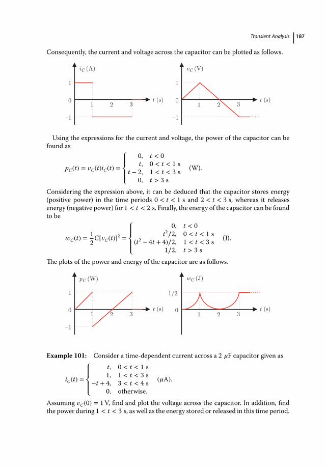
Transient Analysis 187
Consequently, the current and voltage across the capacitor can be plotted as follows.
0
1
–1
0
1
–1
1 2 3 1 2 3
iC (A) vC (V)
t (s) t (s)
Using the expressions for the current and voltage, the power of the capacitor can befound as
pC(t) = 𝑣C(t)iC(t) =⎧⎪⎨⎪⎩
0, t < 0t, 0 < t < 1 s
t − 2, 1 < t < 3 s0, t > 3 s
(W).
Considering the expression above, it can be deduced that the capacitor stores energy(positive power) in the time periods 0 < t < 1 s and 2 < t < 3 s, whereas it releasesenergy (negative power) for 1 < t < 2 s. Finally, the energy of the capacitor can be foundto be
𝑤C(t) =12
C[𝑣C(t)]2 =⎧⎪⎨⎪⎩
0, t < 0t2∕2, 0 < t < 1 s
(t2 − 4t + 4)∕2, 1 < t < 3 s1∕2, t > 3 s
(J).
The plots of the power and energy of the capacitor are as follows.
0
1
–1
0
1/2
21 3 21 3
pC (W) wC (J)
t (s) t (s)
Example 101: Consider a time-dependent current across a 2 𝜇F capacitor given as
iC(t) =⎧⎪⎨⎪⎩
t, 0 < t < 1 s1, 1 < t < 3 s
−t + 4, 3 < t < 4 s0, otherwise.
(𝜇A).
Assuming 𝑣C(0) = 1V, find and plot the voltage across the capacitor. In addition, findthe power during 1 < t < 3 s, as well as the energy stored or released in this time period.
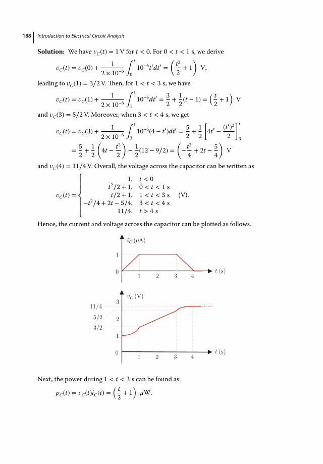
188 Introduction to Electrical Circuit Analysis
Solution: We have 𝑣C(t) = 1V for t < 0. For 0 < t < 1 s, we derive
𝑣C(t) = 𝑣C(0) +1
2 × 10⁻⁶ ∫
t
010−6t′dt′ =
(t22+ 1
)V,
leading to 𝑣C(1) = 3∕2V. Then, for 1 < t < 3 s, we have
𝑣C(t) = 𝑣C(1) +1
2 × 10⁻⁶ ∫
t
110−6dt′ = 3
2+ 1
2(t − 1) =
( t2+ 1
)V
and 𝑣C(3) = 5∕2V. Moreover, when 3 < t < 4 s, we get
𝑣C(t) = 𝑣C(3) +1
2 × 10⁻⁶ ∫
t
310−6(4 − t′)dt′ = 5
2+ 1
2
[4t′ − (t′)2
2
]t
3
= 52+ 1
2
(4t − t2
2
)− 1
2(12 − 9∕2) =
(− t24+ 2t − 5
4
)V
and 𝑣C(4) = 11∕4V. Overall, the voltage across the capacitor can be written as
𝑣C(t) =
⎧⎪⎪⎨⎪⎪⎩
1, t < 0t2∕2 + 1, 0 < t < 1 st∕2 + 1, 1 < t < 3 s
−t2∕4 + 2t − 5∕4, 3 < t < 4 s11∕4, t > 4 s
(V).
Hence, the current and voltage across the capacitor can be plotted as follows.
0
1
0
1
2
3
3/2
5/2
11/4
21 3 4
21 3 4
iC (μA)
vC (V)
t (s)
t (s)
Next, the power during 1 < t < 3 s can be found as
pC(t) = 𝑣C(t)iC(t) =( t2+ 1
)𝜇W.
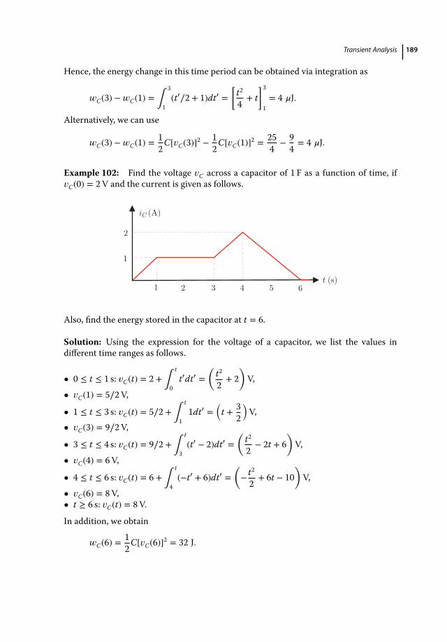
Transient Analysis 189
Hence, the energy change in this time period can be obtained via integration as
𝑤C(3) −𝑤C(1) = ∫
3
1(t′∕2 + 1)dt′ =
[t24+ t
]31= 4 𝜇J.
Alternatively, we can use
𝑤C(3) −𝑤C(1) =12
C[𝑣C(3)]2 −12
C[𝑣C(1)]2 =254
− 94= 4 𝜇J.
Example 102: Find the voltage 𝑣C across a capacitor of 1 F as a function of time, if𝑣C(0) = 2V and the current is given as follows.
1
2
21 3 4 65
iC (A)
t (s)
Also, find the energy stored in the capacitor at t = 6.
Solution: Using the expression for the voltage of a capacitor, we list the values indifferent time ranges as follows.
• 0 ≤ t ≤ 1 s: 𝑣C(t) = 2 +∫
t
0t′dt′ =
(t22+ 2
)V,
• 𝑣C(1) = 5∕2V,
• 1 ≤ t ≤ 3 s: 𝑣C(t) = 5∕2 +∫
t
11dt′ =
(t + 3
2
)V,
• 𝑣C(3) = 9∕2V,
• 3 ≤ t ≤ 4 s: 𝑣C(t) = 9∕2 +∫
t
3(t′ − 2)dt′ =
(t22− 2t + 6
)V,
• 𝑣C(4) = 6V,
• 4 ≤ t ≤ 6 s: 𝑣C(t) = 6 +∫
t
4(−t′ + 6)dt′ =
(− t22+ 6t − 10
)V,
• 𝑣C(6) = 8V,• t ≥ 6 s: 𝑣C(t) = 8V.
In addition, we obtain
𝑤C(6) =12
C[𝑣C(6)]2 = 32 J.
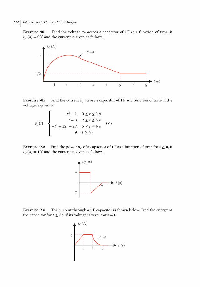
190 Introduction to Electrical Circuit Analysis
Exercise 90: Find the voltage 𝑣C across a capacitor of 1 F as a function of time, if𝑣C(0) = 0V and the current is given as follows.
4
1/2
21 3 4 6 7 85
iC (A)
–t2+4t
t (s)
Exercise 91: Find the current iC across a capacitor of 1 F as a function of time, if thevoltage is given as
𝑣C(t) =
⎧⎪⎪⎨⎪⎪⎩
t2 + 1, 0 ≤ t ≤ 2 st + 3, 2 ≤ t ≤ 5 s
−t2 + 12t − 27, 5 ≤ t ≤ 6 s9, t ≥ 6 s
(V).
Exercise 92: Find the power pC of a capacitor of 1 F as a function of time for t ≥ 0, if𝑣C(0) = 1V and the current is given as follows.
2
–21 2
iC (A)
t (s)
Exercise 93: The current through a 2 F capacitor is shown below. Find the energy ofthe capacitor for t ≥ 3 s, if its voltage is zero is at t = 0.
5
1 32
iC (A)
t (s)
9–t2
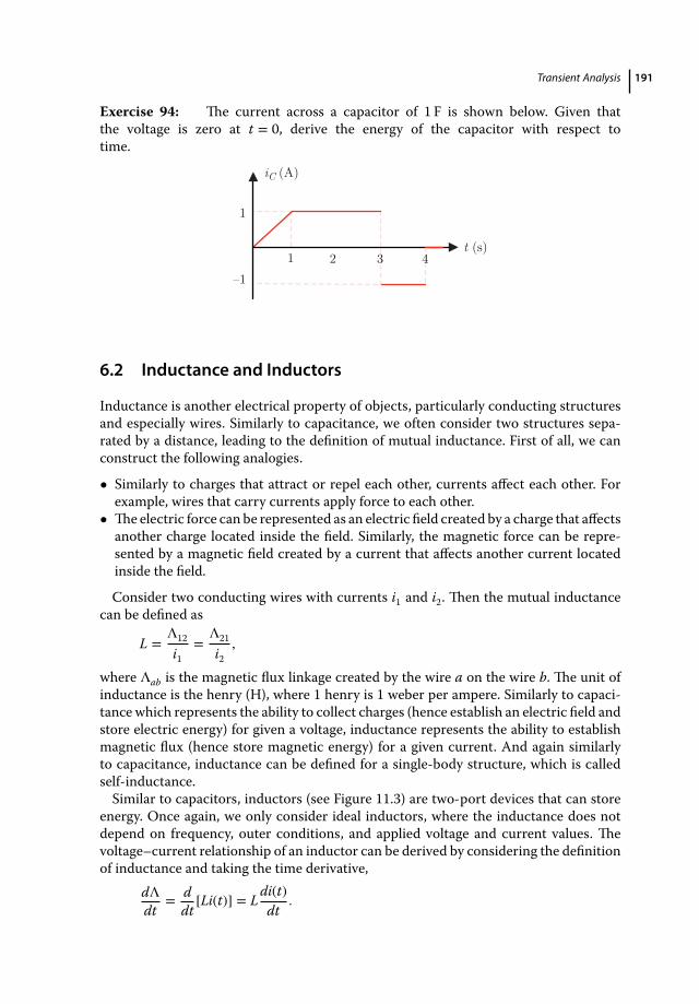
Transient Analysis 191
Exercise 94: The current across a capacitor of 1 F is shown below. Given thatthe voltage is zero at t = 0, derive the energy of the capacitor with respect totime.
1
–11 3 42
iC (A)
t (s)
6.2 Inductance and Inductors
Inductance is another electrical property of objects, particularly conducting structuresand especially wires. Similarly to capacitance, we often consider two structures sepa-rated by a distance, leading to the definition of mutual inductance. First of all, we canconstruct the following analogies.
• Similarly to charges that attract or repel each other, currents affect each other. Forexample, wires that carry currents apply force to each other.
• Theelectric force can be represented as an electric field created by a charge that affectsanother charge located inside the field. Similarly, the magnetic force can be repre-sented by a magnetic field created by a current that affects another current locatedinside the field.
Consider two conducting wires with currents i1 and i2. Then the mutual inductancecan be defined as
L =Λ12
i1=
Λ21
i2,
where Λab is the magnetic flux linkage created by the wire a on the wire b. The unit ofinductance is the henry (H), where 1 henry is 1 weber per ampere. Similarly to capaci-tance which represents the ability to collect charges (hence establish an electric field andstore electric energy) for given a voltage, inductance represents the ability to establishmagnetic flux (hence store magnetic energy) for a given current. And again similarlyto capacitance, inductance can be defined for a single-body structure, which is calledself-inductance.Similar to capacitors, inductors (see Figure 11.3) are two-port devices that can store
energy. Once again, we only consider ideal inductors, where the inductance does notdepend on frequency, outer conditions, and applied voltage and current values. Thevoltage–current relationship of an inductor can be derived by considering the definitionof inductance and taking the time derivative,
dΛdt
= ddt
[Li(t)] = L di(t)dt
.
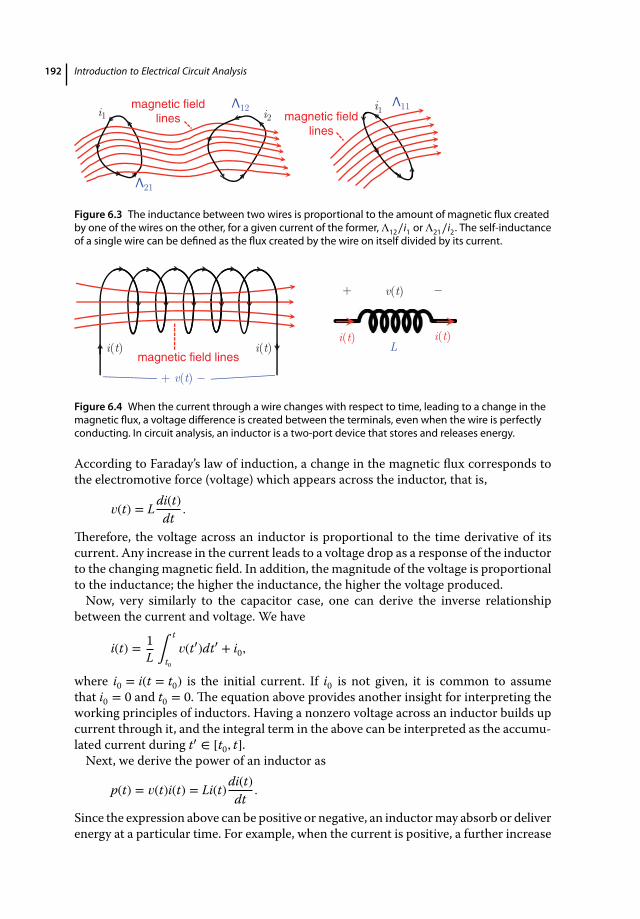
192 Introduction to Electrical Circuit Analysis
magnetic fieldlines
magnetic fieldlines
i1 12
21
11 i1 i2
Figure 6.3 The inductance between two wires is proportional to the amount of magnetic flux createdby one of the wires on the other, for a given current of the former, Λ12∕i1 or Λ21∕i2. The self-inductanceof a single wire can be defined as the flux created by the wire on itself divided by its current.
+ _
Lmagnetic field lines
_ + v(t)
i(t) i(t)
v(t)
i(t)i(t)
Figure 6.4 When the current through a wire changes with respect to time, leading to a change in themagnetic flux, a voltage difference is created between the terminals, even when the wire is perfectlyconducting. In circuit analysis, an inductor is a two-port device that stores and releases energy.
According to Faraday’s law of induction, a change in the magnetic flux corresponds tothe electromotive force (voltage) which appears across the inductor, that is,
𝑣(t) = L di(t)dt
.
Therefore, the voltage across an inductor is proportional to the time derivative of itscurrent. Any increase in the current leads to a voltage drop as a response of the inductorto the changing magnetic field. In addition, the magnitude of the voltage is proportionalto the inductance; the higher the inductance, the higher the voltage produced.Now, very similarly to the capacitor case, one can derive the inverse relationship
between the current and voltage. We have
i(t) = 1L ∫
t
t0𝑣(t′)dt′ + i0,
where i0 = i(t = t0) is the initial current. If i0 is not given, it is common to assumethat i0 = 0 and t0 = 0. The equation above provides another insight for interpreting theworking principles of inductors. Having a nonzero voltage across an inductor builds upcurrent through it, and the integral term in the above can be interpreted as the accumu-lated current during t′ ∈ [t0, t].Next, we derive the power of an inductor as
p(t) = 𝑣(t)i(t) = Li(t)di(t)dt
.
Since the expression above can be positive or negative, an inductormay absorb or deliverenergy at a particular time. For example, when the current is positive, a further increase
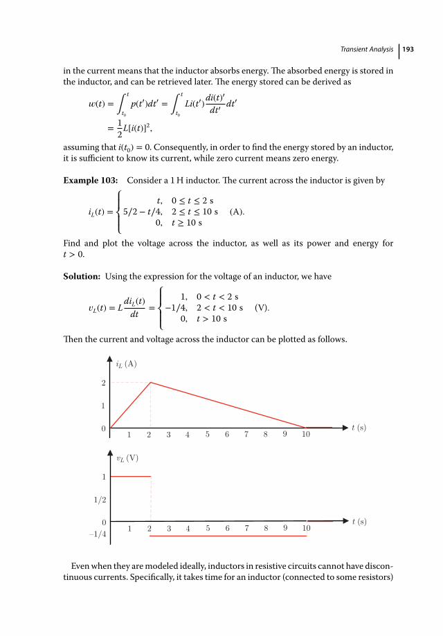
Transient Analysis 193
in the current means that the inductor absorbs energy.The absorbed energy is stored inthe inductor, and can be retrieved later. The energy stored can be derived as
𝑤(t) =∫
t
t0p(t′)dt′ =
∫
t
t0Li(t′)di(t)′
dt′dt′
= 12
L[i(t)]2,
assuming that i(t0) = 0. Consequently, in order to find the energy stored by an inductor,it is sufficient to know its current, while zero current means zero energy.
Example 103: Consider a 1H inductor. The current across the inductor is given by
iL(t) =⎧⎪⎨⎪⎩
t, 0 ≤ t ≤ 2 s5∕2 − t∕4, 2 ≤ t ≤ 10 s
0, t ≥ 10 s(A).
Find and plot the voltage across the inductor, as well as its power and energy fort > 0.
Solution: Using the expression for the voltage of an inductor, we have
𝑣L(t) = LdiL(t)
dt=⎧⎪⎨⎪⎩
1, 0 < t < 2 s−1∕4, 2 < t < 10 s
0, t > 10 s(V).
Then the current and voltage across the inductor can be plotted as follows.
1
2
0
1/2
1
0–1/4
1 3 4 5 6 7 8 9 102
1 3 4 5 6 7 8 9 102
iL (A)
vL (V)
t (s)
t (s)
Evenwhen they aremodeled ideally, inductors in resistive circuits cannot have discon-tinuous currents. Specifically, it takes time for an inductor (connected to some resistors)
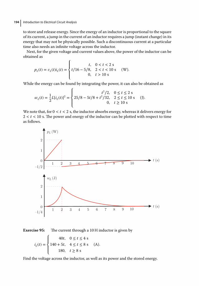
194 Introduction to Electrical Circuit Analysis
to store and release energy. Since the energy of an inductor is proportional to the squareof its current, a jump in the current of an inductor requires a jump (instant change) in itsenergy that may not be physically possible. Such a discontinuous current at a particulartime also needs an infinite voltage across the inductor.Next, for the given voltage and current values above, the power of the inductor can be
obtained as
pL(t) = 𝑣L(t)iL(t) =⎧⎪⎨⎪⎩
t, 0 < t < 2 st∕16 − 5∕8, 2 < t < 10 s
0, t > 10 s(W).
While the energy can be found by integrating the power, it can also be obtained as
𝑤L(t) =12
L[iL(t)]2 =⎧⎪⎨⎪⎩
t2∕2, 0 ≤ t ≤ 2 s25∕8 − 5t∕8 + t2∕32, 2 ≤ t ≤ 10 s
0, t ≥ 10 s(J).
We note that, for 0 < t < 2 s, the inductor absorbs energy, whereas it delivers energy for2 < t < 10 s. The power and energy of the inductor can be plotted with respect to timeas follows.
1
2
0–1/4
1
2
0–1/2
1 3 4 5 6 7 8 9 102
1 3 4 5 6 7 8 9 102
t (s)
t (s)
pL (W)
wL (J)
Exercise 95: The current through a 10H inductor is given by
iL(t) =⎧⎪⎨⎪⎩
40t, 0 ≤ t ≤ 4 s140 + 5t, 4 ≤ t ≤ 8 s
180, t ≥ 8 s(A).
Find the voltage across the inductor, as well as its power and the stored energy.

Transient Analysis 195
6.3 Time-Dependent Analysis of Circuits in Transient State
Until now, we have considered capacitors and inductors as individual components.Given voltage/current across a capacitor or inductor and necessary initial conditions,one can find the current/voltage as well as the power and energy of the component. Inaddition, we claim that the voltage/current of a capacitor/inductor that is connectedto resistors cannot have a discontinuity, since any jump in these values correspondsto a jump in the energy. In this section, we proceed further by considering simplecircuits involving capacitors, inductors, and resistors connected to DC sources. Wefocus on the electrical variables with respect to time and study how circuits behave inthe transient state.
6.3.1 Time-Dependent Analysis of RC Circuits
Consider the following circuit involving a capacitor connected in series to a resistor.Since it contains a resistor (R) and a capacitor (C), it is commonly called an RC circuitin the literature.
+ _
_
R
C
switch
t = 0 + vR (t) iR (t)iC (t)
vC (t)vsvs
vR+vC (V)
t (s)
It is also given that 𝑣C(t) = 0 for t < 0, which indicates that the capacitor is empty withzero energy for t < 0. However, at t = 0, a switch is closed and a voltage source withvalue 𝑣s becomes connected to the capacitor and resistor. We assume that the switch isperfect, so that it closes exactly at t = 0. Therefore, using KVL, the voltage provided bythe sourcemust appear across the combination of the resistor and capacitor. Specifically,for t > 0, we have
𝑣R(t) + 𝑣C(t) = 𝑣s,
while 𝑣R and 𝑣C depend on time. Our aim is to find these voltages, as well as the valueof the current through the resistor and capacitor with respect to time.In order to solve the problem, we note that
iR(t) = iC(t) =𝑣R(t)
R= C
d𝑣C(t)dt
due to the voltage–current characteristics of the resistor and capacitor. In addition,𝑣R(t) = 𝑣s − 𝑣C(t), leading to
Cd𝑣C(t)
dt+
𝑣C(t)R
=𝑣s
Ror
d𝑣C(t)dt
+𝑣C(t)RC
=𝑣s
RC.

196 Introduction to Electrical Circuit Analysis
The equation above can be solved by substituting𝑣C(t) = b exp (at) − b,
where a and b are constants. Using the expression for the voltage in the main equation,we get
ab exp (at) + bRC
exp (at) − bRC
=𝑣s
RC,
leading to
a = − 1RC
b = −𝑣s.
Therefore, we obtain𝑣C(t) = −𝑣s exp (−t∕RC) + 𝑣s = 𝑣s[1 − exp (−t∕RC)].
In addition, we can derive𝑣R(t) = 𝑣s − 𝑣C(t) = 𝑣s exp (−t∕RC),
iR(t) = iC(t) =𝑣s
Rexp (−t∕RC).
The voltage and current values above provide interesting information on the behaviorof the RC circuit. First, for a better understanding, we plot these values with respect totime as follows.
vs/RvC (V) vR (V)
vs vs
iR = iC (A)
t (s)
We have the following observations.• The voltage of the capacitor increases with respect to time from 0 toward 𝑣s. As it
increases, however, the rate of change decreases continuously. Specifically, the voltage(hence the energy) of the capacitor increases more and more slowly with time.
• The voltage of the resistor has a jump at t = 0 from 0 to 𝑣s. Then it decreases toward0 as a function of time, since the sum of the voltages across the resistor and capacitormust be fixed.
• The current through the resistor and capacitor has a jump at t = 0 from 0 to 𝑣s∕R.Then it also decreases toward 0 as time proceeds. Larger values of the current at thebeginning mean that the capacitor is filled (with electric energy) faster. But, as timeprogresses, the filling process slows down and the current value drops to zero.Basically, in this transient analysis, we witness how the capacitor is filled with energy
provided by the voltage source. Obviously, there is a limit to the energy that can bestored, given by
𝑤maxC = 1
2C[𝑣s]2,

Transient Analysis 197
since 𝑣s is the maximum voltage that the capacitor can have. Theoretically, the voltageof the capacitor can never reach 𝑣s, unless we consider the limit case as
𝑣C(t = ∞) → 𝑣s,
𝑣R(t = ∞) → 0,iR(t = ∞) = iC(t = ∞) → 0.
These final values represent the steady state of the circuit. As defined before, a steadystate is an equilibrium state, where the circuit is not affected by outer effects (a switchin this case). For a circuit involving only DC sources, the steady state corresponds tothe case where the voltage and current values do not change. For the above circuit, thesteady state occurs when 𝑣C = 𝑣s and
iC = Cd𝑣C
dt= 0.
In general, it can be deduced that the current though any capacitor must be zero insteady state when only DC sources are involved. This is because when the voltage of acapacitor becomes constant, its derivative (hence the current across it) must be zero. Inthe literature, this is often interpreted as the capacitor becoming open circuit in steadystate, since its voltage can be anything (depending on the rest of the circuit) while itscurrent must be zero in the DC equilibrium.As also discussed before, except for very special and ideal cases, infinite time
is required to pass from transient state to equilibrium. In the expressions for thevoltage and current above, the time variance is exp (−t∕RC), which describes how thevalues change with respect to time. In this exponential function, 𝜏 = RC is a specialquantity called the time constant. It represents how fast the circuit approaches thesteady state, that is, the state when electrical variables (voltages and currents) becomeconstant (due to DC sources). Specifically, if RC is large, it takes a longer time forthe variables to come close to steady state. If RC is small, however, the circuit quicklyapproaches the steady state. We note that the unit of RC is volt/ampere × coulomb/volt= coulomb/ampere = second. While, theoretically, it takes infinite time to completelyenter steady state, most circuits are assumed to reach equilibrium after a sufficientperiod. For example, when t = 5𝜏 and t = 10𝜏 , the voltage of the capacitor can beevaluated as
𝑣C(t = 5𝜏) ≈ 0.9932621𝑣s
𝑣C(t = 10𝜏) ≈ 0.9999546𝑣s.
Obviously, the smaller the value of 𝜏 , the shorter the time to steady state that one canassume.The following figure illustrates how the value of 𝑣C changes with respect to timefor different values of 𝜏 .
large τ
moderate τ
small τvC (V)vs
t (s)
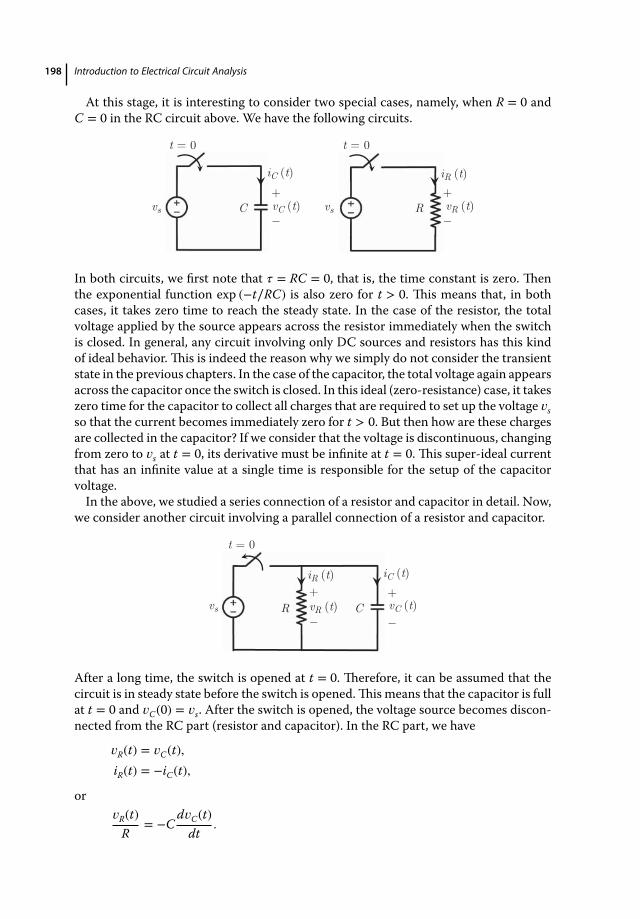
198 Introduction to Electrical Circuit Analysis
At this stage, it is interesting to consider two special cases, namely, when R = 0 andC = 0 in the RC circuit above. We have the following circuits.
+ _
+ _ C R
t = 0 t = 0
vs vs
iC (t) iR (t)
vR (t)vC (t)
In both circuits, we first note that 𝜏 = RC = 0, that is, the time constant is zero. Thenthe exponential function exp (−t∕RC) is also zero for t > 0. This means that, in bothcases, it takes zero time to reach the steady state. In the case of the resistor, the totalvoltage applied by the source appears across the resistor immediately when the switchis closed. In general, any circuit involving only DC sources and resistors has this kindof ideal behavior. This is indeed the reason why we simply do not consider the transientstate in the previous chapters. In the case of the capacitor, the total voltage again appearsacross the capacitor once the switch is closed. In this ideal (zero-resistance) case, it takeszero time for the capacitor to collect all charges that are required to set up the voltage 𝑣sso that the current becomes immediately zero for t > 0. But then how are these chargesare collected in the capacitor? If we consider that the voltage is discontinuous, changingfrom zero to 𝑣s at t = 0, its derivative must be infinite at t = 0. This super-ideal currentthat has an infinite value at a single time is responsible for the setup of the capacitorvoltage.In the above, we studied a series connection of a resistor and capacitor in detail. Now,
we consider another circuit involving a parallel connection of a resistor and capacitor.
+ _ R C
+ _
t = 0
iC (t)
vC (t)vR (t)
iR (t)
vs
After a long time, the switch is opened at t = 0. Therefore, it can be assumed that thecircuit is in steady state before the switch is opened.This means that the capacitor is fullat t = 0 and 𝑣C(0) = 𝑣s. After the switch is opened, the voltage source becomes discon-nected from the RC part (resistor and capacitor). In the RC part, we have
𝑣R(t) = 𝑣C(t),iR(t) = −iC(t),
or𝑣R(t)
R= −C
d𝑣C(t)dt
.
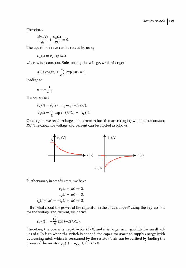
Transient Analysis 199
Therefore,
d𝑣C(t)dt
+𝑣C(t)RC
= 0.
The equation above can be solved by using
𝑣C(t) = 𝑣s exp (at),
where a is a constant. Substituting the voltage, we further get
a𝑣s exp (at) +𝑣s
RCexp (at) = 0,
leading to
a = − 1RC
.
Hence, we get
𝑣C(t) = 𝑣R(t) = 𝑣s exp (−t∕RC),
iR(t) =𝑣s
Rexp (−t∕RC) = −iC(t).
Once again, we reach voltage and current values that are changing with a time constantRC. The capacitor voltage and current can be plotted as follows.
vC (V) iC (A)vs
t (s) t (s)
–vs/R
Furthermore, in steady state, we have
𝑣C(t = ∞) → 0,𝑣R(t = ∞) → 0,
iR(t = ∞) = −iC(t = ∞) → 0.
But what about the power of the capacitor in the circuit above? Using the expressionsfor the voltage and current, we derive
pC(t) = −𝑣2s
Rexp (−2t∕RC).
Therefore, the power is negative for t > 0, and it is larger in magnitude for small val-ues of t. In fact, when the switch is opened, the capacitor starts to supply energy (withdecreasing rate), which is consumed by the resistor. This can be verified by finding thepower of the resistor, pR(t) = −pC(t) for t > 0.
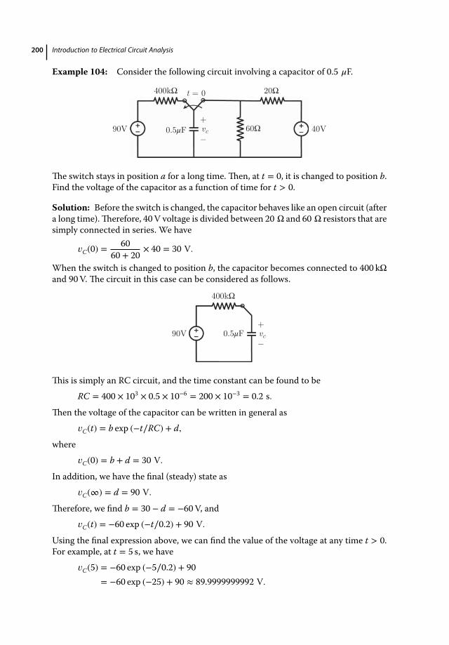
200 Introduction to Electrical Circuit Analysis
Example 104: Consider the following circuit involving a capacitor of 0.5 𝜇F.
400kΩ
90V+ _
t = 0 20Ω
60Ω 40V0.5μF vc
The switch stays in position a for a long time. Then, at t = 0, it is changed to position b.Find the voltage of the capacitor as a function of time for t > 0.
Solution: Before the switch is changed, the capacitor behaves like an open circuit (aftera long time).Therefore, 40V voltage is divided between 20 Ω and 60 Ω resistors that aresimply connected in series. We have
𝑣C(0) =60
60 + 20× 40 = 30 V.
When the switch is changed to position b, the capacitor becomes connected to 400 kΩand 90V. The circuit in this case can be considered as follows.
400kΩ
90V+
_ 0.5μF vc
This is simply an RC circuit, and the time constant can be found to beRC = 400 × 103 × 0.5 × 10−6 = 200 × 10−3 = 0.2 s.
Then the voltage of the capacitor can be written in general as𝑣C(t) = b exp (−t∕RC) + d,
where𝑣C(0) = b + d = 30 V.
In addition, we have the final (steady) state as𝑣C(∞) = d = 90 V.
Therefore, we find b = 30 − d = −60V, and𝑣C(t) = −60 exp (−t∕0.2) + 90 V.
Using the final expression above, we can find the value of the voltage at any time t > 0.For example, at t = 5 s, we have
𝑣C(5) = −60 exp (−5∕0.2) + 90= −60 exp (−25) + 90 ≈ 89.9999999992 V.
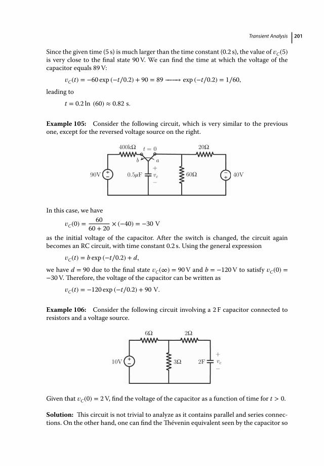
Transient Analysis 201
Since the given time (5 s) is much larger than the time constant (0.2 s), the value of 𝑣C(5)is very close to the final state 90V. We can find the time at which the voltage of thecapacitor equals 89V:
𝑣C(t) = −60 exp (−t∕0.2) + 90 = 89 −−−−→ exp (−t∕0.2) = 1∕60,
leading to
t = 0.2 ln (60) ≈ 0.82 s.
Example 105: Consider the following circuit, which is very similar to the previousone, except for the reversed voltage source on the right.
400kΩ
90V+ _
t = 0 20Ω
60Ω 40V0.5μF
a b
vc
In this case, we have
𝑣C(0) =60
60 + 20× (−40) = −30 V
as the initial voltage of the capacitor. After the switch is changed, the circuit againbecomes an RC circuit, with time constant 0.2 s. Using the general expression
𝑣C(t) = b exp (−t∕0.2) + d,
we have d = 90 due to the final state 𝑣C(∞) = 90V and b = −120V to satisfy 𝑣C(0) =−30V. Therefore, the voltage of the capacitor can be written as
𝑣C(t) = −120 exp (−t∕0.2) + 90 V.
Example 106: Consider the following circuit involving a 2 F capacitor connected toresistors and a voltage source.
10V
6Ω 2Ω
3Ω 2F+_ vc
Given that 𝑣C(0) = 2V, find the voltage of the capacitor as a function of time for t > 0.
Solution: This circuit is not trivial to analyze as it contains parallel and series connec-tions. On the other hand, one can find theThévenin equivalent seen by the capacitor so
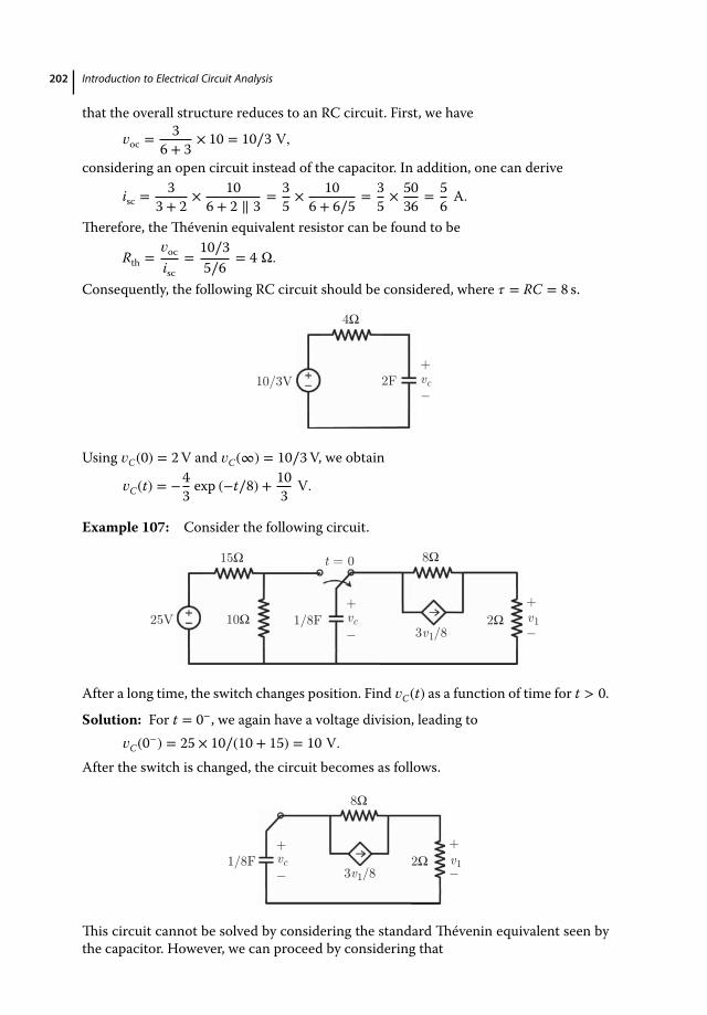
202 Introduction to Electrical Circuit Analysis
that the overall structure reduces to an RC circuit. First, we have
𝑣oc =3
6 + 3× 10 = 10∕3 V,
considering an open circuit instead of the capacitor. In addition, one can derive
isc =3
3 + 2× 10⁶ + 2 ∥ 3
= 35× 106 + 6∕5
= 35× 5036
= 56A.
Therefore, theThévenin equivalent resistor can be found to be
Rth =𝑣oc
isc=
10∕35∕6
= 4 Ω.
Consequently, the following RC circuit should be considered, where 𝜏 = RC = 8 s.
10/3V
4Ω
2F+_ vc
Using 𝑣C(0) = 2V and 𝑣C(∞) = 10∕3V, we obtain
𝑣C(t) = −43exp (−t∕8) + 10
3V.
Example 107: Consider the following circuit.
25V+ _
t = 0 15Ω
10Ω 1/8F
8Ω
2Ω3v1/8
v1+_ vc
After a long time, the switch changes position. Find 𝑣C(t) as a function of time for t > 0.
Solution: For t = 0−, we again have a voltage division, leading to𝑣C(0−) = 25 × 10∕(10 + 15) = 10 V.
After the switch is changed, the circuit becomes as follows.
+ _ 1/8F
8Ω
2Ω3v1/8
v1+_ vc
This circuit cannot be solved by considering the standard Thévenin equivalent seen bythe capacitor. However, we can proceed by considering that
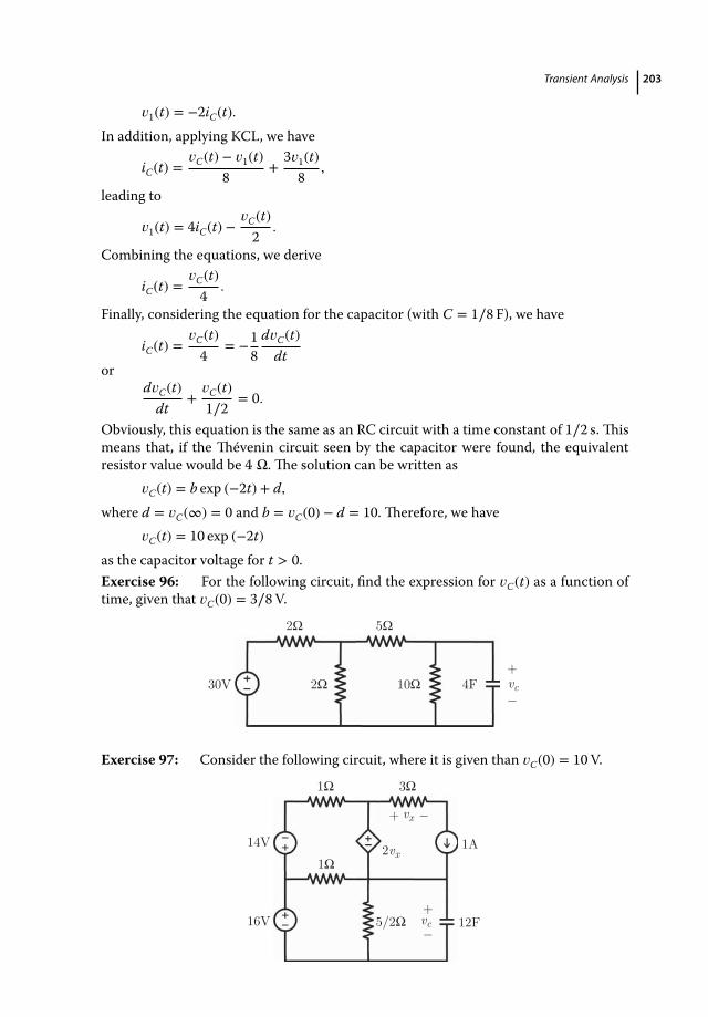
Transient Analysis 203
𝑣1(t) = −2iC(t).In addition, applying KCL, we have
iC(t) =𝑣C(t) − 𝑣1(t)
8+
3𝑣1(t)8
,
leading to
𝑣1(t) = 4iC(t) −𝑣C(t)2
.
Combining the equations, we derive
iC(t) =𝑣C(t)4
.
Finally, considering the equation for the capacitor (with C = 1∕8 F), we have
iC(t) =𝑣C(t)4
= −18
d𝑣C(t)dt
ord𝑣C(t)
dt+
𝑣C(t)1∕2
= 0.
Obviously, this equation is the same as an RC circuit with a time constant of 1∕2 s. Thismeans that, if the Thévenin circuit seen by the capacitor were found, the equivalentresistor value would be 4 Ω. The solution can be written as
𝑣C(t) = b exp (−2t) + d,where d = 𝑣C(∞) = 0 and b = 𝑣C(0) − d = 10. Therefore, we have
𝑣C(t) = 10 exp (−2t)as the capacitor voltage for t > 0.Exercise 96: For the following circuit, find the expression for 𝑣C(t) as a function oftime, given that 𝑣C(0) = 3∕8V.
30V
2Ω
2Ω
5Ω
10Ω 4F+_ vc
Exercise 97: Consider the following circuit, where it is given than 𝑣C(0) = 10V.
14V
16V
1Ω
1Ω 3Ω
2vx
vc
1A
12F5/2Ω+ _
+ _ vx
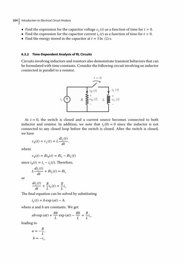
204 Introduction to Electrical Circuit Analysis
• Find the expression for the capacitor voltage 𝑣C(t) as a function of time for t > 0.• Find the expression for the capacitor current iC(t) as a function of time for t > 0.• Find the energy stored in the capacitor at t = 5 ln (2) s.
6.3.2 Time-Dependent Analysis of RL Circuits
Circuits involving inductors and resistors also demonstrate transient behaviors that canbe formulated with time constants. Consider the following circuit involving an inductorconnected in parallel to a resistor.
+ _
+ _ L R
t = 0
iR (t) iL (t)
vL (t)vR (t)is
At t = 0, the switch is closed and a current source becomes connected to bothinductor and resistor. In addition, we note that iL(0) = 0 since the inductor is notconnected to any closed loop before the switch is closed. After the switch is closed,we have
𝑣R(t) = 𝑣L(t) = LdiL(t)
dt,
where
𝑣R(t) = RiR(t) = Ris − RiL(t)
since iR(t) = is − iL(t). Therefore,
LdiL(t)
dt+ RiL(t) = Ris
ordiL(t)
dt+ R
LiL(t) =
RL
is.
The final equation can be solved by substituting
iL(t) = b exp (at) − b,
where a and b are constants. We get
ab exp (at) + RbL
exp (at) − RbL
= RL
is,
leading to
a = −RL,
b = −is.

Transient Analysis 205
Hence, the current of the inductor can be rewritten as
iL(t) = −is exp (−tR∕L) + is = is[1 − exp (−tR∕L)].
Furthermore, we have
iR(t) = is − iL(t) = is exp (−tR∕L),𝑣R(t) = 𝑣L(t) = Ris exp (−tR∕L),
for t > 0. The current and voltage values can be plotted with respect to time as follows.
vL = vR
Ris
(A)is
(V)
vL
vR
t (s) t (s)
iR
iL
It can be seen that the RL circuit above demonstrates transient characteristics similarto RC circuits. Once the switch is closed, the current of the inductor starts to increasewith a time constant of 𝜏 = L∕R. While the limit value is is, the current through theinductor never reaches this value for finite values of t. Specifically, the rate of change inthe inductor current decreases as time passes. With the increase in the current value,the energy stored in the inductor also increases and approaches a limit value
𝑤maxL = 1
2L[is]2.
When the voltage across the components is investigated, it can be seen that it decaysfrom a maximum value of Ris to zero, while the rate of change again decreases for largevalues of t. In the steady state, we have
iL(t = ∞) → is,
iR(t = ∞) → 0,𝑣R(t = ∞) = 𝑣L(t = ∞) → 0.
In practice, RL circuits are also assumed to enter steady state for sufficiently large valuesof t (e.g., for t > 5𝜏).Obviously, the inductor in the circuit above has a zero voltage in steady state. This
is because the inductor energy is saturated (the current through the inductor is maxi-mized) and it cannot store any further energy. Since the current through the inductorcan be arbitrary depending on the rest of the circuit (the current source in this case), theinductor can be thought of as a short circuit after a sufficient time. In fact, for DC cir-cuits, any inductor can be modeled as a short circuit, very similarly to the open-circuitcharacteristics of the capacitors, in steady state. This is particularly because a constantcurrent iL leads to
𝑣L(t) = LdiL(t)
dt= 0,
no matter what the value of iL is.
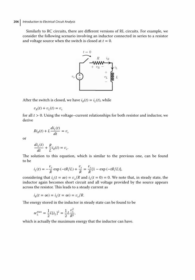
206 Introduction to Electrical Circuit Analysis
Similarly to RC circuits, there are different versions of RL circuits. For example, weconsider the following scenario involving an inductor connected in series to a resistorand voltage source when the switch is closed at t = 0.
L
R
vs
iL
t = 0iR
vL+
_
vR_ +
After the switch is closed, we have iR(t) = iL(t), while
𝑣R(t) + 𝑣L(t) = 𝑣s
for all t > 0. Using the voltage–current relationships for both resistor and inductor, wederive
RiR(t) + LdiL(t)
dt= 𝑣s
ordiL(t)
dt+ R
LiR(t) = 𝑣s.
The solution to this equation, which is similar to the previous one, can be foundto be
iL(t) = −𝑣s
Rexp (−tR∕L) +
𝑣s
R=
𝑣s
R[1 − exp (−tR∕L)],
considering that iL(t = ∞) = 𝑣s∕R and iL(t = 0) = 0. We note that, in steady state, theinductor again becomes short circuit and all voltage provided by the source appearsacross the resistor. This leads to a steady current as
iR(t = ∞) = iL(t = ∞) = 𝑣s∕R.
The energy stored in the inductor in steady state can be found to be
𝑤maxL = 1
2L[iL]2 =
12
L𝑣2s
R2 ,
which is actually the maximum energy that the inductor can have.
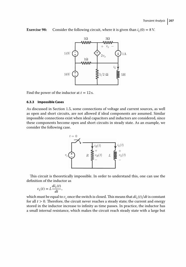
Transient Analysis 207
Exercise 98: Consider the following circuit, where it is given than iL(0) = 8V.
14V
16V
1Ω
1Ω 3Ω
+ _ vx
2vx1A
5H 5/2 Ω
iL
Find the power of the inductor at t = 12 s.
6.3.3 Impossible Cases
As discussed in Section 1.5, some connections of voltage and current sources, as wellas open and short circuits, are not allowed if ideal components are assumed. Similarimpossible connections exist when ideal capacitors and inductors are considered, sincethese components become open and short circuits in steady state. As an example, weconsider the following case.
vs vL(t)+
_ vR(t)R L
t = 0
iR(t) iL(t)+
_
This circuit is theoretically impossible. In order to understand this, one can use thedefinition of the inductor as
𝑣L(t) = LdiL(t)
dt,
whichmust be equal to 𝑣s once the switch is closed.Thismeans that diL(t)∕dt is constantfor all t > 0. Therefore, the circuit never reaches a steady state; the current and energystored in the inductor increase to infinity as time passes. In practice, the inductor hasa small internal resistance, which makes the circuit reach steady state with a large but
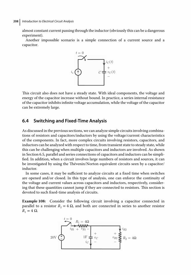
208 Introduction to Electrical Circuit Analysis
almost constant current passing through the inductor (obviously this can be a dangerousexperiment).Another impossible scenario is a simple connection of a current source and a
capacitor.
is vC(t)+
_ C
t = 0
iC(t)
This circuit also does not have a steady state. With ideal components, the voltage andenergy of the capacitor increase without bound. In practice, a series internal resistanceof the capacitor inhibits infinite voltage accumulation, while the voltage of the capacitorcan be extremely large.
6.4 Switching and Fixed-Time Analysis
As discussed in the previous sections, we can analyze simple circuits involving combina-tions of resistors and capacitors/inductors by using the voltage/current characteristicsof the components. In fact, more complex circuits involving resistors, capacitors, andinductors can be analyzedwith respect to time, from transient state to steady state, whilethis can be challenging when multiple capacitors and inductors are involved. As shownin Section 6.5, parallel and series connections of capacitors and inductors can be simpli-fied. In addition, when a circuit involves large numbers of resistors and sources, it canbe investigated by using the Thévenin/Norton equivalent circuits seen by a capacitor/inductor.In some cases, it may be sufficient to analyze circuits at a fixed time when switches
are opened and/or closed. In this type of analysis, one can enforce the continuity ofthe voltage and current values across capacitors and inductors, respectively, consider-ing that these quantities cannot jump if they are connected to resistors. This section isdevoted to such fixed-time analysis of circuits.
Example 108: Consider the following circuit involving a capacitor connected inparallel to a resistor R2 = 4 Ω, and both are connected in series to another resistorR1 = 4 Ω.
t = 0
20ViC
vC+ _
iR1 vR1
R1 = 4Ω
+ _ + _ vR2
iR2
R2 = 4Ω1F
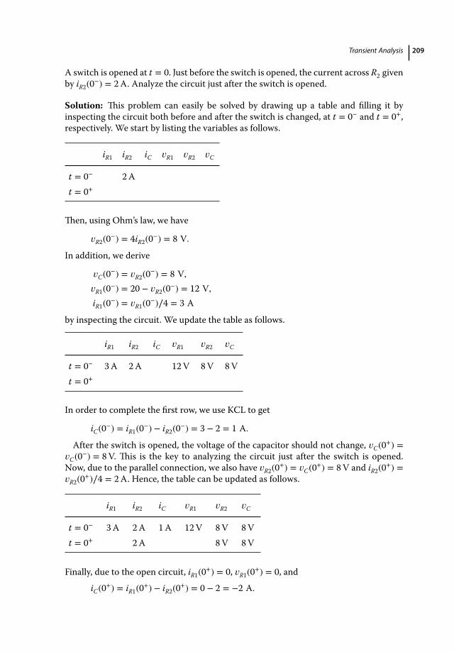
Transient Analysis 209
A switch is opened at t = 0. Just before the switch is opened, the current across R2 givenby iR2(0−) = 2A. Analyze the circuit just after the switch is opened.
Solution: This problem can easily be solved by drawing up a table and filling it byinspecting the circuit both before and after the switch is changed, at t = 0− and t = 0+,respectively. We start by listing the variables as follows.
iR1 iR2 iC 𝑣R1 𝑣R2 𝑣C
t = 0− 2At = 0+
Then, using Ohm’s law, we have
𝑣R2(0−) = 4iR2(0−) = 8 V.
In addition, we derive
𝑣C(0−) = 𝑣R2(0−) = 8 V,𝑣R1(0−) = 20 − 𝑣R2(0−) = 12 V,iR1(0−) = 𝑣R1(0−)∕4 = 3 A
by inspecting the circuit. We update the table as follows.
iR1 iR2 iC 𝑣R1 𝑣R2 𝑣C
t = 0− 3A 2A 12V 8V 8Vt = 0+
In order to complete the first row, we use KCL to get
iC(0−) = iR1(0−) − iR2(0−) = 3 − 2 = 1 A.
After the switch is opened, the voltage of the capacitor should not change, 𝑣C(0+) =𝑣C(0−) = 8V. This is the key to analyzing the circuit just after the switch is opened.Now, due to the parallel connection, we also have 𝑣R2(0+) = 𝑣C(0+) = 8V and iR2(0+) =𝑣R2(0+)∕4 = 2A. Hence, the table can be updated as follows.
iR1 iR2 iC 𝑣R1 𝑣R2 𝑣C
t = 0− 3A 2A 1A 12V 8V 8Vt = 0+ 2A 8V 8V
Finally, due to the open circuit, iR1(0+) = 0, 𝑣R1(0+) = 0, and
iC(0+) = iR1(0+) − iR2(0+) = 0 − 2 = −2 A.
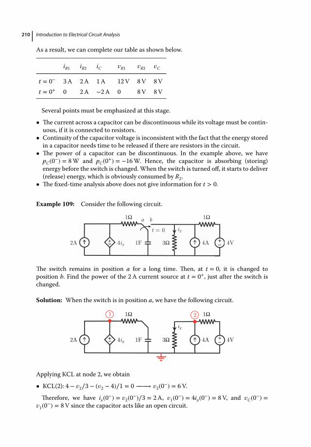
210 Introduction to Electrical Circuit Analysis
As a result, we can complete our table as shown below.
iR1 iR2 iC 𝑣R1 𝑣R2 𝑣C
t = 0− 3A 2A 1A 12V 8V 8Vt = 0+ 0 2A −2A 0 8V 8V
Several points must be emphasized at this stage.
• The current across a capacitor can be discontinuous while its voltage must be contin-uous, if it is connected to resistors.
• Continuity of the capacitor voltage is inconsistent with the fact that the energy storedin a capacitor needs time to be released if there are resistors in the circuit.
• The power of a capacitor can be discontinuous. In the example above, we havepC(0−) = 8W and pC(0+) = −16W. Hence, the capacitor is absorbing (storing)energy before the switch is changed.When the switch is turned off, it starts to deliver(release) energy, which is obviously consumed by R2.
• The fixed-time analysis above does not give information for t > 0.
Example 109: Consider the following circuit.
t = 0a b
2A 4ix
ix
1F 3Ω
1Ω
4V4A
1Ω
The switch remains in position a for a long time. Then, at t = 0, it is changed toposition b. Find the power of the 2A current source at t = 0+, just after the switch ischanged.
Solution: When the switch is in position a, we have the following circuit.
2A 4ix
ix
1F 3Ω
1Ω
4V4A
1Ω1 2
Applying KCL at node 2, we obtain
• KCL(2): 4 − 𝑣2∕3 − (𝑣2 − 4)∕1 = 0 −−−−→ 𝑣2(0−) = 6V.
Therefore, we have ix(0−) = 𝑣2(0−)∕3 = 2A, 𝑣1(0−) = 4ix(0−) = 8V, and 𝑣C(0−) =𝑣1(0−) = 8V since the capacitor acts like an open circuit.
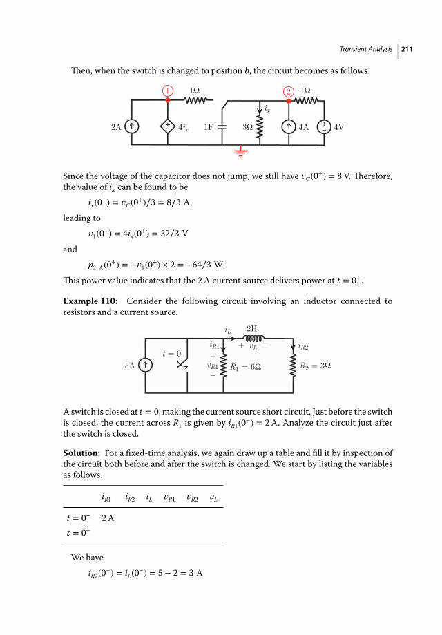
Transient Analysis 211
Then, when the switch is changed to position b, the circuit becomes as follows.
2A 4ix
ix
1F 3Ω
1Ω
4V4A
1Ω1 2
Since the voltage of the capacitor does not jump, we still have 𝑣C(0+) = 8V. Therefore,the value of ix can be found to be
ix(0+) = 𝑣C(0+)∕3 = 8∕3 A,
leading to𝑣1(0+) = 4ix(0+) = 32∕3 V
andp2 A(0+) = −𝑣1(0+) × 2 = −64∕3 W.
This power value indicates that the 2A current source delivers power at t = 0+.
Example 110: Consider the following circuit involving an inductor connected toresistors and a current source.
R1 = 6Ω+ _ vR1
vL+ _ t = 0
5A
2H
R2 = 3Ω
iR1 iR2
iL
A switch is closed at t = 0,making the current source short circuit. Just before the switchis closed, the current across R1 is given by iR1(0−) = 2A. Analyze the circuit just afterthe switch is closed.
Solution: For a fixed-time analysis, we again draw up a table and fill it by inspection ofthe circuit both before and after the switch is changed. We start by listing the variablesas follows.
iR1 iR2 iL 𝑣R1 𝑣R2 𝑣L
t = 0− 2At = 0+
We haveiR2(0−) = iL(0−) = 5 − 2 = 3 A
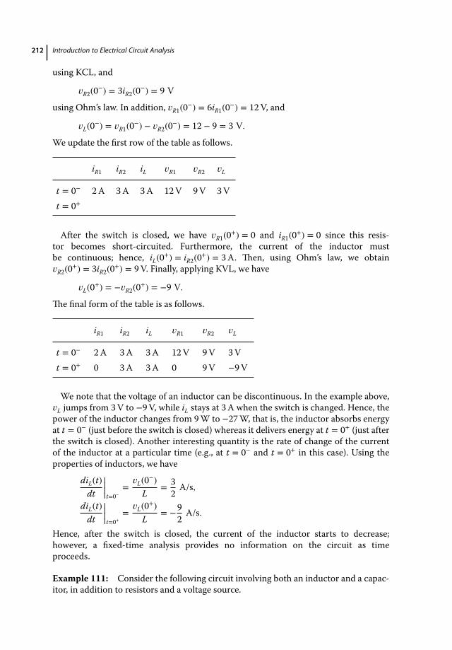
212 Introduction to Electrical Circuit Analysis
using KCL, and
𝑣R2(0−) = 3iR2(0−) = 9 V
using Ohm’s law. In addition, 𝑣R1(0−) = 6iR1(0−) = 12V, and
𝑣L(0−) = 𝑣R1(0−) − 𝑣R2(0−) = 12 − 9 = 3 V.
We update the first row of the table as follows.
iR1 iR2 iL 𝑣R1 𝑣R2 𝑣L
t = 0− 2A 3A 3A 12V 9V 3Vt = 0+
After the switch is closed, we have 𝑣R1(0+) = 0 and iR1(0+) = 0 since this resis-tor becomes short-circuited. Furthermore, the current of the inductor mustbe continuous; hence, iL(0+) = iR2(0+) = 3A. Then, using Ohm’s law, we obtain𝑣R2(0+) = 3iR2(0+) = 9V. Finally, applying KVL, we have
𝑣L(0+) = −𝑣R2(0+) = −9 V.
The final form of the table is as follows.
iR1 iR2 iL 𝑣R1 𝑣R2 𝑣L
t = 0− 2A 3A 3A 12V 9V 3Vt = 0+ 0 3A 3A 0 9V −9V
We note that the voltage of an inductor can be discontinuous. In the example above,𝑣L jumps from 3V to −9V, while iL stays at 3A when the switch is changed. Hence, thepower of the inductor changes from 9W to −27W, that is, the inductor absorbs energyat t = 0− (just before the switch is closed) whereas it delivers energy at t = 0+ (just afterthe switch is closed). Another interesting quantity is the rate of change of the currentof the inductor at a particular time (e.g., at t = 0− and t = 0+ in this case). Using theproperties of inductors, we have
diL(t)dt
||||t=0−=
𝑣L(0−)L
= 32A/s,
diL(t)dt
||||t=0+=
𝑣L(0+)L
= −92A/s.
Hence, after the switch is closed, the current of the inductor starts to decrease;however, a fixed-time analysis provides no information on the circuit as timeproceeds.
Example 111: Consider the following circuit involving both an inductor and a capac-itor, in addition to resistors and a voltage source.
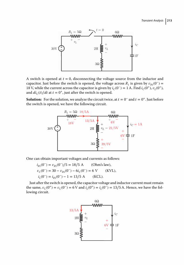
Transient Analysis 213
t = 0
2H
3Ω
6Ω
1F
iC30V vL
+ _
_ + v1
R1 = 5Ω
A switch is opened at t = 0, disconnecting the voltage source from the inductor andcapacitor. Just before the switch is opened, the voltage across R1 is given by 𝑣R1(0−) =18V, while the current across the capacitor is given by iC(0−) = 1A. Find iC(0+), 𝑣L(0+),and diC(t)∕dt at t = 0+, just after the switch is opened.
Solution: For the solution, we analyze the circuit twice, at t = 0− and t = 0+. Just beforethe switch is opened, we have the following circuit.
2H
3Ω
6Ω
1F
iC = 1A30V vL = 21/5V
+ _
_ + 18V
18/5A _ + 6V
+ _ 6V
+ _ 39/5V
13/5A
R1 = 5Ω
One can obtain important voltages and currents as follows:iR1(0−) = 𝑣R1(0−)∕5 = 18∕5 A (Ohm’s law),𝑣C(0−) = 30 − 𝑣R1(0−) − 6iC(0−) = 6 V (KVL),iL(0−) = iR1(0−) − 1 = 13∕5 A (KCL).
Just after the switch is opened, the capacitor voltage and inductor currentmust remainthe same, 𝑣C(0+) = 𝑣C(0−) = 6V and iL(0+) = iL(0−) = 13∕5A. Hence, we have the fol-lowing circuit.
2H
3Ω
6Ω
1F
iCvL+ _ +
_ 6V
13/5A
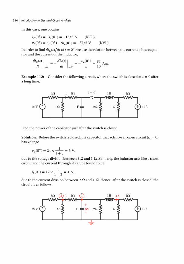
214 Introduction to Electrical Circuit Analysis
In this case, one obtains
iC(0+) = −iL(0+) = −13∕5 A (KCL),𝑣L(0+) = 𝑣C(0+) − 9iL(0+) = −87∕5 V (KVL).
In order to find diC(t)∕dt at t = 0+, we use the relation between the current of the capac-itor and the current of the inductor,
diC(t)dt
||||t=0+= −
diL(t)dt
||||t=0+= −
𝑣L(0+)L
= 8710
A/s.
Example 112: Consider the following circuit, where the switch is closed at t = 0 aftera long time.
24V
3Ω
1Ω
1Ω
1F 2Ω
1H 1Ω
1Ω 12A
t = 0ix
Find the power of the capacitor just after the switch is closed.
Solution: Before the switch is closed, the capacitor that acts like an open circuit (ix = 0)has voltage
𝑣C(0−) = 24 × 11 + 3
= 6 V,
due to the voltage division between 3 Ω and 1 Ω. Similarly, the inductor acts like a shortcircuit and the current through it can be found to be
iL(0−) = 12 × 11 + 2
= 4 A,
due to the current division between 2 Ω and 1 Ω. Hence, after the switch is closed, thecircuit is as follows.
24V
3Ω
1Ω
1Ω
1F 2Ω
1H 1Ω
1Ω 12A
ix
+ _ 6V
4A 1 2
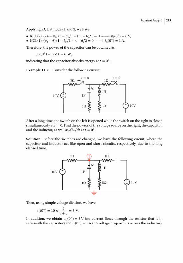
Transient Analysis 215
Applying KCL at nodes 1 and 2, we have
• KCL(2): (24 − 𝑣2)∕3 − 𝑣2∕1 − (𝑣2 − 6)∕1 = 0 −−−−→ 𝑣2(0+) = 6V,• KCL(1): (𝑣2 − 6)∕1 − iC∕1 + 4 − 6∕2 = 0 −−−−→ iC(0+) = 1A.
Therefore, the power of the capacitor can be obtained as
pC(0+) = 6 × 1 = 6 W,
indicating that the capacitor absorbs energy at t = 0+.
Example 113: Consider the following circuit.
5Ω
10V
10V5Ω
1H
1Ω
1F
t = 0 t = 0
1Ω
iC
After a long time, the switch on the left is opened while the switch on the right is closedsimultaneously at t = 0. Find the powers of the voltage source on the right, the capacitor,and the inductor, as well as diC∕dt at t = 0+.
Solution: Before the switches are changed, we have the following circuit, where thecapacitor and inductor act like open and short circuits, respectively, due to the longelapsed time.
5Ω
10V
10V5Ω
1H
1Ω
1F
1Ω
1
iC
Then, using simple voltage division, we have
𝑣1(0−) = 10 × 55 + 5
= 5 V.
In addition, we obtain 𝑣C(0−) = 5V (no current flows through the resistor that is inserieswith the capacitor) and iL(0−) = 1A (no voltage drop occurs across the inductor).
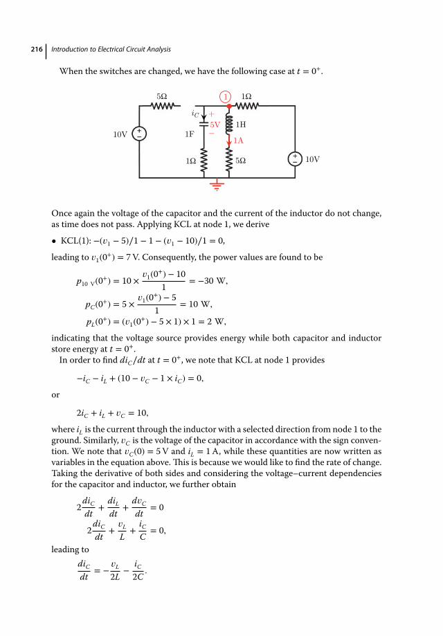
216 Introduction to Electrical Circuit Analysis
When the switches are changed, we have the following case at t = 0+.
5Ω
10V
10V5Ω
1H
1Ω
1F
1Ω
+ _ 5V
1A
1 iC
Once again the voltage of the capacitor and the current of the inductor do not change,as time does not pass. Applying KCL at node 1, we derive
• KCL(1): −(𝑣1 − 5)∕1 − 1 − (𝑣1 − 10)∕1 = 0,
leading to 𝑣1(0+) = 7V. Consequently, the power values are found to be
p10 V(0+) = 10 ×𝑣1(0+) − 10
1= −30 W,
pC(0+) = 5 ×𝑣1(0+) − 5
1= 10 W,
pL(0+) = (𝑣1(0+) − 5 × 1) × 1 = 2 W,
indicating that the voltage source provides energy while both capacitor and inductorstore energy at t = 0+.In order to find diC∕dt at t = 0+, we note that KCL at node 1 provides
−iC − iL + (10 − 𝑣C − 1 × iC) = 0,
or
2iC + iL + 𝑣C = 10,
where iL is the current through the inductor with a selected direction from node 1 to theground. Similarly, 𝑣C is the voltage of the capacitor in accordance with the sign conven-tion. We note that 𝑣C(0) = 5V and iL = 1A, while these quantities are now written asvariables in the equation above.This is because we would like to find the rate of change.Taking the derivative of both sides and considering the voltage–current dependenciesfor the capacitor and inductor, we further obtain
2diC
dt+
diL
dt+
d𝑣C
dt= 0
2diC
dt+
𝑣L
L+
iC
C= 0,
leading todiC
dt= −
𝑣L
2L−
iC
2C.
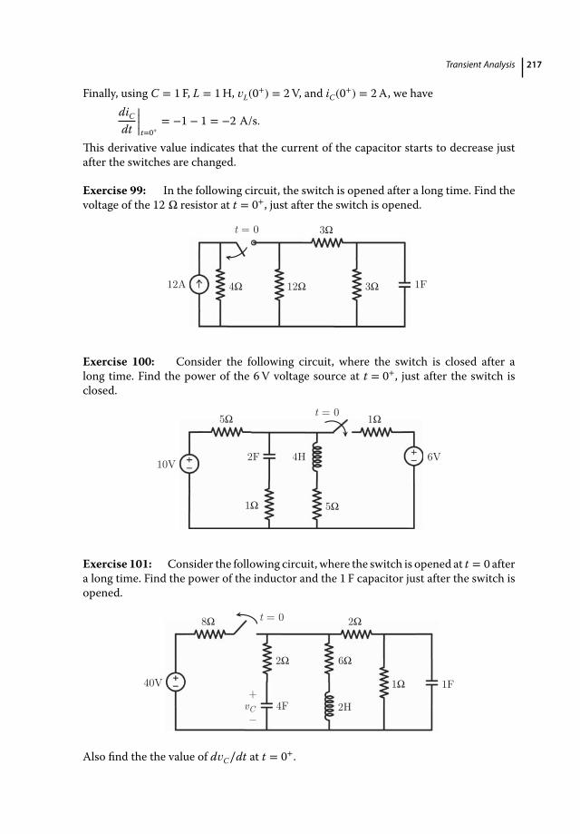
Transient Analysis 217
Finally, using C = 1 F, L = 1H, 𝑣L(0+) = 2V, and iC(0+) = 2A, we havediC
dt||||t=0+
= −1 − 1 = −2 A/s.
This derivative value indicates that the current of the capacitor starts to decrease justafter the switches are changed.
Exercise 99: In the following circuit, the switch is opened after a long time. Find thevoltage of the 12 Ω resistor at t = 0+, just after the switch is opened.
3Ω12Ω
3Ωt = 0
12A 1F 4Ω
Exercise 100: Consider the following circuit, where the switch is closed after along time. Find the power of the 6V voltage source at t = 0+, just after the switch isclosed.
t = 0
2F10V
5Ω
1Ω
4H
5Ω
6V
1Ω
Exercise 101: Consider the following circuit, where the switch is opened at t = 0 aftera long time. Find the power of the inductor and the 1 F capacitor just after the switch isopened.
t = 0
40V
8Ω
2Ω
4F
6Ω
2H
2Ω
1Ω 1F
vC
+
_
Also find the the value of d𝑣C∕dt at t = 0+.
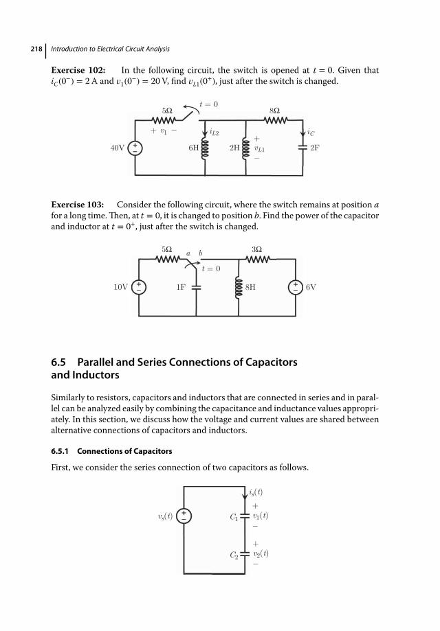
218 Introduction to Electrical Circuit Analysis
Exercise 102: In the following circuit, the switch is opened at t = 0. Given thatiC(0−) = 2A and 𝑣1(0−) = 20V, find 𝑣L1(0+), just after the switch is changed.
t = 0
40V 6H 2H
8Ω5Ω
2F
v1_ + iC
vL1
+
_
iL2
Exercise 103: Consider the following circuit, where the switch remains at position afor a long time.Then, at t = 0, it is changed to position b. Find the power of the capacitorand inductor at t = 0+, just after the switch is changed.
10V
5Ω
t = 0
6V1F 8H
3Ωa b
6.5 Parallel and Series Connections of Capacitorsand Inductors
Similarly to resistors, capacitors and inductors that are connected in series and in paral-lel can be analyzed easily by combining the capacitance and inductance values appropri-ately. In this section, we discuss how the voltage and current values are shared betweenalternative connections of capacitors and inductors.
6.5.1 Connections of Capacitors
First, we consider the series connection of two capacitors as follows.
vs(t) v1(t)+ _ C1
is(t)
v2(t)+ _ C2

Transient Analysis 219
Note that, in order to obtain the overall response, we assume 𝑣s also depends on time.We have
𝑣s(t) = 𝑣1(t) + 𝑣2(t),
where
𝑣1(t) =1
C1 ∫
t
t0is(t′)dt′ + 𝑣1(t0),
𝑣2(t) =1
C2 ∫
t
t0is(t′)dt′ + 𝑣2(t0),
according to the definition of the capacitors. Therefore, the relationship between theoverall voltage and the current is found to be
𝑣s(t) =(
1C1
+ 1C2
)∫
t
t0is(t′)dt′ + 𝑣1(t0) + 𝑣2(t0)
or
𝑣s(t) =(
1C1
+ 1C2
)∫
t
t0is(t′)dt′ + 𝑣s(t0)
since 𝑣s(t0) = 𝑣1(t0) + 𝑣2(t0). Finally, we obtain
𝑣s(t) =1
Ceq ∫
t
t0is(t′)dt′ + 𝑣s(t0),
where1
Ceq= 1
C1+ 1
C2.
As a result, the equivalent capacitance corresponding to the series connection of C1 andC2 is
Ceq =C1C2
C1 + C2.
At first glance, the expression above may seem strange since Ceq ≤ C1 and Ceq ≤ C2,meaning that the ability to store charges for a given voltage decreases when two capac-itors are connected in series. This can be understood if we consider the fact that thenegative terminal of one capacitor is actually connected to the positive terminal of theother, if we fix the current flowing between them in a single direction. Therefore, thesecapacitances work opposite to each other, making the overall combination have lesscapacitance. In the limit as C2 → 0, we have
Ceq → 0,
since this corresponds to the case where an open circuit exists instead of C2. In the limitas C2 → ∞, corresponding to the short-circuited C2, one can derive
Ceq → C1
as expected.

220 Introduction to Electrical Circuit Analysis
We now consider a parallel connection of two capacitors and a time-varying currentsource.
is(t) C1 C2
i1(t) i2(t)
vs(t)+_
In this case, KCL can be used to writeis(t) = i1(t) + i2(t),
where
i1(t) = C1d𝑣s(t)
dt,
i2(t) = C2d𝑣s(t)
dt.
Hence, the overall current and voltage are related by
is(t) = C1d𝑣s(t)
dt+ C2
d𝑣s(t)dt
= (C1 + C2)d𝑣s(t)
dtor
is(t) = Ceqd𝑣s(t)
dt,
whereCeq = C1 + C2
is the equivalent capacitance for a parallel connection of two capacitors. Obviously,when two the capacitors are connected in parallel, their combination is able to storemore charge for a given voltage. Therefore, the overall capacitance grows in parallelconnections of capacitors.
6.5.2 Connections of Inductors
We now discuss the series and parallel connections of inductors. When two inductorsare connected in series, we have the following.
v1(t)+ _ L1
v2(t)+ _ L2
is(t)+
_ vs(t)
We note that the choice of source does not change the result of the analysis, while weoften select the one that leads to easier manipulations. Using the inductor definition, we
Transient Analysis 221
derive
𝑣1(t) = L1dis(t)
dt,
𝑣2(t) = L2dis(t)
dt,
leading to
𝑣s(t) = 𝑣1(t) + 𝑣2(t) = L1dis(t)
dt+ L2
dis(t)dt
or
𝑣s(t) = (L1 + L2)dis(t)
dt.
Therefore, the overall inductance can be written as
Leq = L1 + L2.
Next, we consider a parallel connection of two inductors as follows.
vs(t) L1 L2
i1(t) i2(t)
is(t)
We derive
is(t) = i1(t) + i2(t),
where
i1(t) =1L1 ∫
t
t0𝑣s(t′)dt′ + i1(t0),
i2(t) =1L2 ∫
t
t0𝑣s(t′)dt′ + i2(t0).
Therefore, the relationship between the overall voltage and the current is found to be
is(t) =(
1L1
+ 1L2
)∫
t
t0𝑣s(t′)dt′ + i1(t0) + i2(t0)
or
is(t) =(
1L1
+ 1L2
)∫
t
t0𝑣s(t′)dt′ + is(t0),
using is(t0) = i1(t0) + i2(t0). Therefore, we obtain
is(t) =1
Leq ∫
t
t0𝑣s(t′)dt′ + i(t0),
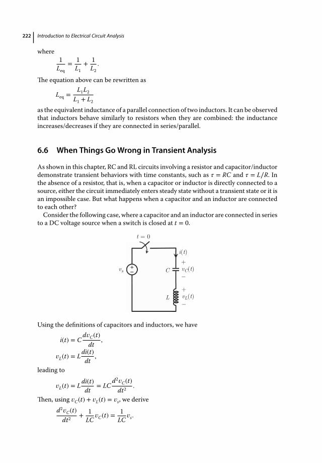
222 Introduction to Electrical Circuit Analysis
where1
Leq= 1
L1+ 1
L2.
The equation above can be rewritten as
Leq =L1L2
L1 + L2
as the equivalent inductance of a parallel connection of two inductors. It can be observedthat inductors behave similarly to resistors when they are combined: the inductanceincreases/decreases if they are connected in series/parallel.
6.6 When Things Go Wrong in Transient Analysis
As shown in this chapter, RC and RL circuits involving a resistor and capacitor/inductordemonstrate transient behaviors with time constants, such as 𝜏 = RC and 𝜏 = L∕R. Inthe absence of a resistor, that is, when a capacitor or inductor is directly connected to asource, either the circuit immediately enters steady state without a transient state or it isan impossible case. But what happens when a capacitor and an inductor are connectedto each other?Consider the following case, where a capacitor and an inductor are connected in series
to a DC voltage source when a switch is closed at t = 0.
vs vC(t)+
_ C
i(t)
vL(t)+
_ L
t = 0
Using the definitions of capacitors and inductors, we have
i(t) = Cd𝑣C(t)
dt,
𝑣L(t) = L di(t)dt
,
leading to
𝑣L(t) = L di(t)dt
= LCd2𝑣C(t)
dt2.
Then, using 𝑣C(t) + 𝑣L(t) = 𝑣s, we derived2𝑣C(t)
dt2+ 1
LC𝑣C(t) =
1LC
𝑣s.

Transient Analysis 223
A general solution to this equation can be written as
𝑣C(t) = a cos(𝜔ot) + b sin(𝜔ot) + 𝑣s,
where a and b can be found by checking the initial conditions and 𝜔o = 1∕√
LC. Thenthe current through the loop is found to be
i(t) = Cd𝑣C(t)
dt= −Ca𝜔o sin(𝜔ot) + Cb𝜔o cos(𝜔ot).
Now, choosing 𝑣C(t = 0) = 0 and i(t = 0) = 0, one obtains
a = −𝑣s,
b = 0.
Consequently, the voltage and current values for these initial conditions are found to be
𝑣C(t) = 𝑣s[1 − cos(𝜔ot)],𝑣L(t) = 𝑣s − 𝑣C(t) = 𝑣s cos(𝜔ot),
i(t) = 𝑣s𝜔oC sin(𝜔ot) = 𝑣s
√CLsin(𝜔ot).
But what does this mean, considering that the cos and sin functions represent oscilla-tions for all values of t?The expressions above indicate that the voltage and current values oscillate infinitely,
without reaching constant values. On the other hand, the oscillations fit into a repetitivebehavior, starting from t = 0. In fact, despite the fact that voltage and current values vary,this circuit does not have any transient state; it immediately enters steady state once theswitch is closed. The oscillation rate, 𝜔o, is often called the natural angular frequencyof the circuit since it represents how fast the voltage and current values change. In thenext chapter, we consider time-harmonic sources, where the oscillation of the voltageand current values are enforced by the sources, where they also vary with respect to timein steady state.For the circuit above, an interesting case occurs when there is no voltage source (𝑣s =
0), but 𝑣C(t = 0) = 𝑣C0 ≠ 0, that is, the capacitor is charged before the switched is closed.Once the connection is established between the capacitor and inductor, we have
𝑣C(t) = 𝑣C0 cos(𝜔ot),
i(t) = −𝑣C0
√CLsin(𝜔ot).
This circuit is called an LC tank, since it involves an oscillatory (repetitive) transfer ofenergy between the capacitor and inductor. Specifically, these energies can be calculatedas
𝑤C(t) =12
C𝑣2C0cos
2(𝜔ot),
𝑤L(t) =12
C𝑣2C0sin
2(𝜔ot),
and
𝑤C(t) +𝑤L(t) =12
C𝑣2C0 = 𝑤C(t = 0).

224 Introduction to Electrical Circuit Analysis
Hence, the total energy of the capacitor and inductor is constant and equal to the initiallystored energy in the capacitor, while this energy oscillates back and forth between thecapacitor and inductor with respect to time.This circuit also does not have any transientstate.As discussed in this chapter, there cannot be a jump in the voltage/current of a capac-
itor/inductor (hence its energy) if it is connected to a resistor. We note that such aresistor can be a part of the circuit, while they can also be internal resistances of thecapacitor/inductor in real life. Considering ideal components, this claim may be mis-interpreted as saying that any circuit involving a resistor must have continuous energyvalues. As a (counter)example, the following scenario involves two sources, a capacitor,and a resistor. After a long time, the switch is closed at t = 0.
t = 0
20V vC
+
_
R = 1Ω
1F 10V
Before the switch is closed, the voltage of the capacitor can be written as𝑣C(0−) = 10 V,
considering that the capacitor acts as an open circuit. When the switch is closed, how-ever, the voltage of the capacitor must jump to 20V,
𝑣C(0+) = 20 V,
as a result of the voltage source on the left. Interestingly, the circuit is still valid afterthe switch is closed. In this case, 20V voltage of the capacitor leads to 10V across theresistor. On the other hand, there are jumps in the voltage and energy of the capacitorat t = 0 and this circuit immediately enters steady state without any transient behavior.
6.7 What You Need to Know before You Continue
As discussed in this chapter, transient analysis is essential to understand the behavior ofcircuits involving energy storage elements in addition to resistors. We emphasize a fewimportant points, before proceeding to the next chapter.
• Voltage/current values of energy storage elements (capacitors and inductors) arerelated to each other via the time derivative. Therefore, their responses depend ontime, leading to transient states.
• While theoretically a steady state never occurs, it is assumed to be reached after asufficiently long time such that the unwanted variations in the voltage and currentvalues diminish below some threshold values.
• When only DC sources are involved in a circuit, capacitors and inductors becomeopen and short circuits, respectively, in steady state.This happenswhen the capacitorsand inductors are saturated and cannot store any more energy.

Transient Analysis 225
• When connected directly to resistors, the voltage/current value of a capacitor/inductor cannot have a jump since this would require a jump in their energy. Suchjumps can occur in some ideal cases, for example, when a capacitor is connected toa voltage source without a resistor.
In the next chapter, we consider the steady state of AC circuits, where sources providetime-varying voltage and current values. We focus in particular on circuits driven bysinusoidal sources, which can be analyzed in the phasor domain.

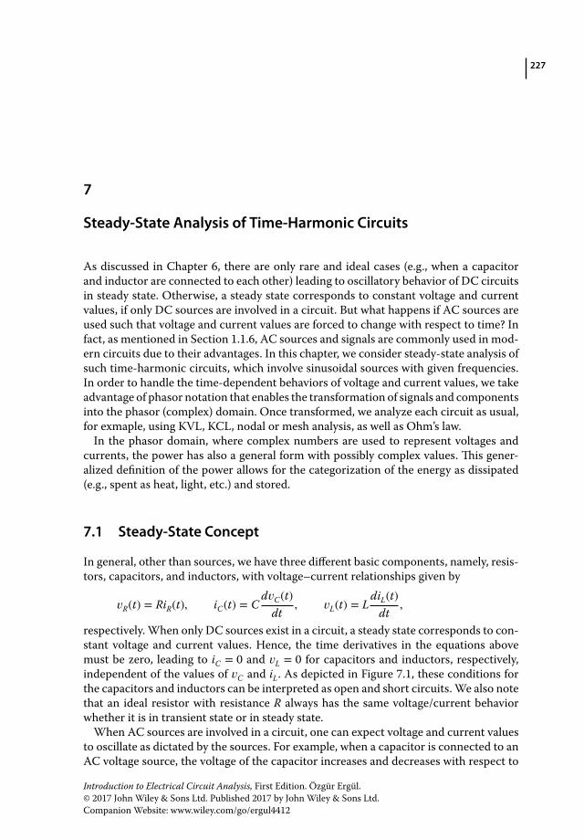
227
7
Steady-State Analysis of Time-Harmonic Circuits
As discussed in Chapter 6, there are only rare and ideal cases (e.g., when a capacitorand inductor are connected to each other) leading to oscillatory behavior of DC circuitsin steady state. Otherwise, a steady state corresponds to constant voltage and currentvalues, if only DC sources are involved in a circuit. But what happens if AC sources areused such that voltage and current values are forced to change with respect to time? Infact, as mentioned in Section 1.1.6, AC sources and signals are commonly used in mod-ern circuits due to their advantages. In this chapter, we consider steady-state analysis ofsuch time-harmonic circuits, which involve sinusoidal sources with given frequencies.In order to handle the time-dependent behaviors of voltage and current values, we takeadvantage of phasor notation that enables the transformation of signals and componentsinto the phasor (complex) domain. Once transformed, we analyze each circuit as usual,for exmaple, using KVL, KCL, nodal or mesh analysis, as well as Ohm’s law.In the phasor domain, where complex numbers are used to represent voltages and
currents, the power has also a general form with possibly complex values. This gener-alized definition of the power allows for the categorization of the energy as dissipated(e.g., spent as heat, light, etc.) and stored.
7.1 Steady-State Concept
In general, other than sources, we have three different basic components, namely, resis-tors, capacitors, and inductors, with voltage–current relationships given by
𝑣R(t) = RiR(t), iC(t) = Cd𝑣C(t)
dt, 𝑣L(t) = L
diL(t)dt
,
respectively. When only DC sources exist in a circuit, a steady state corresponds to con-stant voltage and current values. Hence, the time derivatives in the equations abovemust be zero, leading to iC = 0 and 𝑣L = 0 for capacitors and inductors, respectively,independent of the values of 𝑣C and iL. As depicted in Figure 7.1, these conditions forthe capacitors and inductors can be interpreted as open and short circuits.We also notethat an ideal resistor with resistance R always has the same voltage/current behaviorwhether it is in transient state or in steady state.When AC sources are involved in a circuit, one can expect voltage and current values
to oscillate as dictated by the sources. For example, when a capacitor is connected to anAC voltage source, the voltage of the capacitor increases and decreases with respect to
Introduction to Electrical Circuit Analysis, First Edition. Özgür Ergül.© 2017 John Wiley & Sons Ltd. Published 2017 by John Wiley & Sons Ltd.Companion Website: www.wiley.com/go/ergul4412
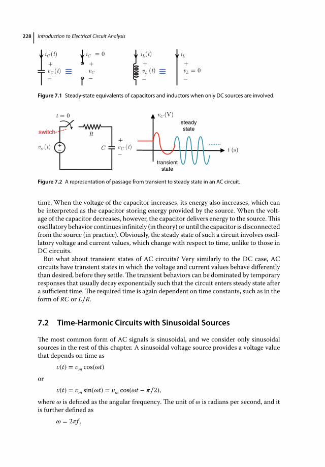
228 Introduction to Electrical Circuit Analysis
+ _
iC (t) (t)
(t)
iC iL iL
vLvC (t) vC
+
_ + _
= 0
vL = 0+
_
Figure 7.1 Steady-state equivalents of capacitors and inductors when only DC sources are involved.
vs (t) vC (t)
+ _
R
C
t = 0
switch
vC (V)
t (s)
transientstate
steadystate
Figure 7.2 A representation of passage from transient to steady state in an AC circuit.
time. When the voltage of the capacitor increases, its energy also increases, which canbe interpreted as the capacitor storing energy provided by the source. When the volt-age of the capacitor decreases, however, the capacitor delivers energy to the source.Thisoscillatory behavior continues infinitely (in theory) or until the capacitor is disconnectedfrom the source (in practice). Obviously, the steady state of such a circuit involves oscil-latory voltage and current values, which change with respect to time, unlike to those inDC circuits.But what about transient states of AC circuits? Very similarly to the DC case, AC
circuits have transient states in which the voltage and current values behave differentlythan desired, before they settle.The transient behaviors can be dominated by temporaryresponses that usually decay exponentially such that the circuit enters steady state aftera sufficient time.The required time is again dependent on time constants, such as in theform of RC or L∕R.
7.2 Time-Harmonic Circuits with Sinusoidal Sources
The most common form of AC signals is sinusoidal, and we consider only sinusoidalsources in the rest of this chapter. A sinusoidal voltage source provides a voltage valuethat depends on time as
𝑣(t) = 𝑣m cos(𝜔t)
or𝑣(t) = 𝑣m sin(𝜔t) = 𝑣m cos(𝜔t − 𝜋∕2),
where 𝜔 is defined as the angular frequency. The unit of 𝜔 is radians per second, and itis further defined as
𝜔 = 2𝜋f ,
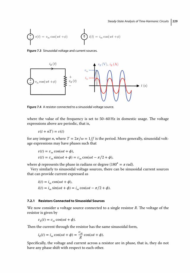
Steady-State Analysis of Time-Harmonic Circuits 229
v(t) = vm cos(wt +φ) i(t) = im cos(wt +φ)
Figure 7.3 Sinusoidal voltage and current sources.
+ _
vR (V), iR (A)
t (s)vm cos(wt +φ)
iR (t)
vR (t)
vm
im
Figure 7.4 A resistor connected to a sinusoidal voltage source.
where the value of the frequency is set to 50–60Hz in domestic usage. The voltageexpressions above are periodic, that is,
𝑣(t + nT) = 𝑣(t)
for any integer n, where T = 2𝜋∕𝜔 = 1∕f is the period. More generally, sinusoidal volt-age expressions may have phases such that
𝑣(t) = 𝑣m cos(𝜔t + 𝜙),𝑣(t) = 𝑣m sin(𝜔t + 𝜙) = 𝑣m cos(𝜔t − 𝜋∕2 + 𝜙),
where 𝜙 represents the phase in radians or degree (180∘ = 𝜋 rad).Very similarly to sinusoidal voltage sources, there can be sinusoidal current sources
that can provide current expressed as
i(t) = im cos(𝜔t + 𝜙),i(t) = im sin(𝜔t + 𝜙) = im cos(𝜔t − 𝜋∕2 + 𝜙).
7.2.1 Resistors Connected to Sinusoidal Sources
We now consider a voltage source connected to a single resistor R. The voltage of theresistor is given by
𝑣R(t) = 𝑣m cos(𝜔t + 𝜙).
Then the current through the resistor has the same sinusoidal form,
iR(t) = im cos(𝜔t + 𝜙) =𝑣m
Rcos(𝜔t + 𝜙).
Specifically, the voltage and current across a resistor are in phase, that is, they do nothave any phase shift with respect to each other.
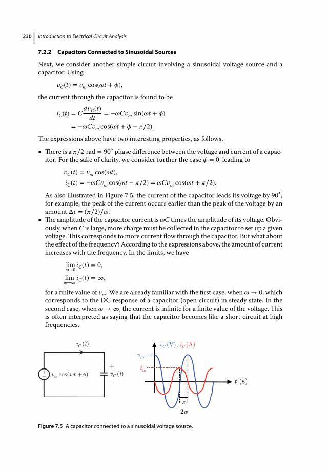
230 Introduction to Electrical Circuit Analysis
7.2.2 Capacitors Connected to Sinusoidal Sources
Next, we consider another simple circuit involving a sinusoidal voltage source and acapacitor. Using
𝑣C(t) = 𝑣m cos(𝜔t + 𝜙),
the current through the capacitor is found to be
iC(t) = Cd𝑣C(t)
dt= −𝜔C𝑣m sin(𝜔t + 𝜙)
= −𝜔C𝑣m cos(𝜔t + 𝜙 − 𝜋∕2).
The expressions above have two interesting properties, as follows.
• There is a 𝜋∕2 rad = 90∘ phase difference between the voltage and current of a capac-itor. For the sake of clarity, we consider further the case 𝜙 = 0, leading to
𝑣C(t) = 𝑣m cos(𝜔t),iC(t) = −𝜔C𝑣m cos(𝜔t − 𝜋∕2) = 𝜔C𝑣m cos(𝜔t + 𝜋∕2).
As also illustrated in Figure 7.5, the current of the capacitor leads its voltage by 90∘;for example, the peak of the current occurs earlier than the peak of the voltage by anamount Δt = (𝜋∕2)∕𝜔.
• The amplitude of the capacitor current is𝜔C times the amplitude of its voltage. Obvi-ously, when C is large, more chargemust be collected in the capacitor to set up a givenvoltage.This corresponds tomore current flow through the capacitor. But what aboutthe effect of the frequency?According to the expressions above, the amount of currentincreases with the frequency. In the limits, we have
lim𝜔→0
iC(t) = 0,
lim𝜔→∞
iC(t) = ∞,
for a finite value of 𝑣m. We are already familiar with the first case, when 𝜔 → 0, whichcorresponds to the DC response of a capacitor (open circuit) in steady state. In thesecond case, when 𝜔 → ∞, the current is infinite for a finite value of the voltage.Thisis often interpreted as saying that the capacitor becomes like a short circuit at highfrequencies.
+ _ t (s)
vm
im
2w
vC (V), iC (A)
vm cos(wt +φ) vC (t)
iC (t)
π
Figure 7.5 A capacitor connected to a sinusoidal voltage source.
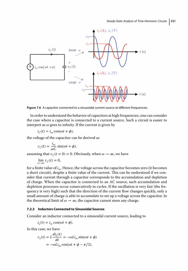
Steady-State Analysis of Time-Harmonic Circuits 231
vC (t)+ _
iC (A), vC (V)
t (s)
im cos(wt +φ)
iC (t)
vm
im
iC (A), vC (V)
t (s)vm
im
Small w
Large w
Figure 7.6 A capacitor connected to a sinusoidal current source at different frequencies.
In order to understand the behavior of capacitors at high frequencies, one can considerthe case where a capacitor is connected to a current source. Such a circuit is easier tointerpret as 𝜔 goes to infinity. If the current is given by
iC(t) = im cos(𝜔t + 𝜙),
the voltage of the capacitor can be derived as
𝑣C(t) =im
𝜔Csin(𝜔t + 𝜙),
assuming that 𝑣C(t = 0) = 0. Obviously, when 𝜔 → ∞, we havelim𝜔→∞
𝑣C(t) = 0,
for a finite value of im. Hence, the voltage across the capacitor becomes zero (it becomesa short circuit), despite a finite value of the current. This can be understood if we con-sider that current through a capacitor corresponds to the accumulation and depletionof charge. When the capacitor is connected to an AC source, such accumulation anddepletion processes occur consecutively in cycles. If the oscillation is very fast (the fre-quency is very high) such that the direction of the current flow changes quickly, only asmall amount of charge is able to accumulate to set up a voltage across the capacitor. Inthe theoretical limit of 𝜔 → ∞, the capacitor cannot store any charge.
7.2.3 Inductors Connected to Sinusoidal Sources
Consider an inductor connected to a sinusoidal current source, leading toiL(t) = im cos(𝜔t + 𝜙).
In this case, we have
𝑣L(t) = LdiL(t)
dt= −𝜔Lim sin(𝜔t + 𝜙)
= −𝜔Lim cos(𝜔t + 𝜙 − 𝜋∕2).
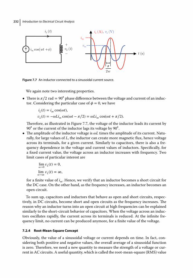
232 Introduction to Electrical Circuit Analysis
vL (t)+ _
iL (A), vL (V)
t (s)im cos(wt +φ)
iL (t)imvm
2wπ
Figure 7.7 An inductor connected to a sinusoidal current source.
We again note two interesting properties.
• There is 𝜋∕2 rad = 90∘ phase difference between the voltage and current of an induc-tor. Considering the particular case of 𝜙 = 0, we have
iL(t) = im cos(𝜔t),𝑣L(t) = −𝜔Lim cos(𝜔t − 𝜋∕2) = 𝜔Lim cos(𝜔t + 𝜋∕2).
Therefore, as illustrated in Figure 7.7, the voltage of the inductor leads its current by90∘ or the current of the inductor lags its voltage by 90∘.
• The amplitude of the inductor voltage is 𝜔L times the amplitude of its current. Natu-rally, for large values of L, the inductor can create more magnetic flux, hence voltageacross its terminals, for a given current. Similarly to capacitors, there is also a fre-quency dependence in the voltage and current values of inductors. Specifically, fora fixed current value, the voltage across an inductor increases with frequency. Twolimit cases of particular interest are
lim𝜔→0
𝑣L(t) = 0,
lim𝜔→∞
𝑣L(t) = ∞,
for a finite value of im. Hence, we verify that an inductor becomes a short circuit forthe DC case. On the other hand, as the frequency increases, an inductor becomes anopen circuit.
To sum up, capacitors and inductors that behave as open and short circuits, respec-tively, in DC circuits, become short and open circuits as the frequency increases. Thereason why an inductor turns into an open circuit at high frequencies can be explainedsimilarly to the short-circuit behavior of capacitors. When the voltage across an induc-tors oscillates rapidly, the current across its terminals is reduced. At the infinite fre-quency limit, no current can be produced anymore, for a finite value of the voltage.
7.2.4 Root-Mean-Square Concept
Obviously, the value of a sinusoidal voltage or current depends on time. In fact, con-sidering both positive and negative values, the overall average of a sinusoidal functionis zero. Therefore, we need a new quantity to measure the strength of a voltage or cur-rent in AC circuits. A useful quantity, which is called the root-mean-square (RMS) value
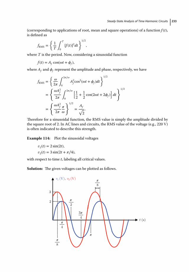
Steady-State Analysis of Time-Harmonic Circuits 233
(corresponding to applications of root, mean and square operations) of a function f (t),is defined as
fRMS =
1T ∫
T
0[f (t)]2dt
1∕2
,
where T is the period. Now, considering a sinusoidal function
f (t) = Af cos(𝜔t + 𝜙f ),
where Af and 𝜙f represent the amplitude and phase, respectively, we have
fRMS =
𝜔
2𝜋 ∫
2𝜋∕𝜔
0A2
f cos2(𝜔t + 𝜙f )dt
1∕2
=
𝜔A2
f
2𝜋 ∫
2𝜋∕𝜔
0
[12+ 1
2cos(2𝜔t + 2𝜙f )
]dt
1∕2
=
𝜔A2
f
2𝜋𝜋
𝜔
1∕2
=Af√2.
Therefore for a sinusoidal function, the RMS value is simply the amplitude divided bythe square root of 2. In AC lines and circuits, the RMS value of the voltage (e.g., 220 V)is often indicated to describe this strength.
Example 114: Plot the sinusoidal voltages
𝑣1(t) = 2 sin(2t),𝑣2(t) = 3 sin(2t + 𝜋∕4),
with respect to time t, labeling all critical values.
Solution: The given voltages can be plotted as follows.
v1 (V), v2 (V)
t (s)4
8
3π4
2
83
2 π
π
π
ππ
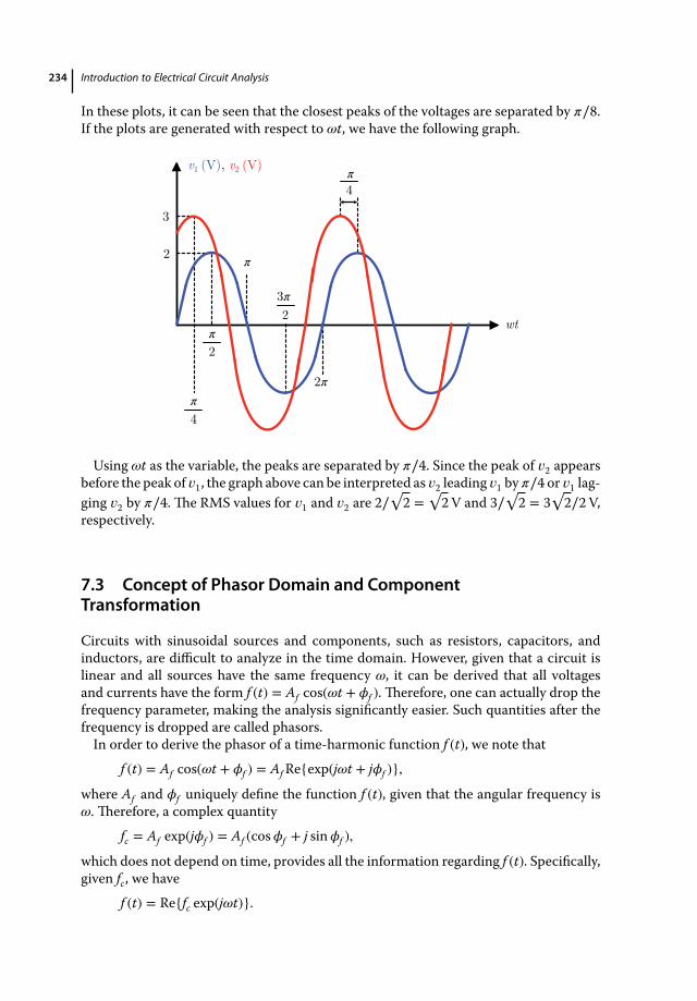
234 Introduction to Electrical Circuit Analysis
In these plots, it can be seen that the closest peaks of the voltages are separated by 𝜋∕8.If the plots are generated with respect to 𝜔t, we have the following graph.
v1 (V), v2 (V)
wt
2
4
3π2
2π
43
2 π
π
π
π
Using 𝜔t as the variable, the peaks are separated by 𝜋∕4. Since the peak of 𝑣2 appearsbefore the peak of 𝑣1, the graph above can be interpreted as 𝑣2 leading 𝑣1 by𝜋∕4 or 𝑣1 lag-ging 𝑣2 by 𝜋∕4. The RMS values for 𝑣1 and 𝑣2 are 2∕
√2 =
√2V and 3∕
√2 = 3
√2∕2V,
respectively.
7.3 Concept of Phasor Domain and ComponentTransformation
Circuits with sinusoidal sources and components, such as resistors, capacitors, andinductors, are difficult to analyze in the time domain. However, given that a circuit islinear and all sources have the same frequency 𝜔, it can be derived that all voltagesand currents have the form f (t) = Af cos(𝜔t + 𝜙f ). Therefore, one can actually drop thefrequency parameter, making the analysis significantly easier. Such quantities after thefrequency is dropped are called phasors.In order to derive the phasor of a time-harmonic function f (t), we note that
f (t) = Af cos(𝜔t + 𝜙f ) = Af Reexp(j𝜔t + j𝜙f ),
where Af and 𝜙f uniquely define the function f (t), given that the angular frequency is𝜔. Therefore, a complex quantity
fc = Af exp(j𝜙f ) = Af (cos𝜙f + j sin𝜙f ),
which does not depend on time, provides all the information regarding f (t). Specifically,given fc, we have
f (t) = Refc exp(j𝜔t).

Steady-State Analysis of Time-Harmonic Circuits 235
In circuit analysis, it is useful to define a phasor quantity as
f =Af√2exp(j𝜙f ),
leading to
f (t) =√2Ref exp(j𝜔t).
where f is the phasor of f (t). In the above, Af ∕√2 corresponds to the RMS of the sinu-
soidal function, that is,
f = fRMS exp(j𝜙f ).
Therefore, given the phasor, the RMS of the function is given by
fRMS = |f |.Example 115: Find the phasors of the voltage values
𝑣1(t) = 10 cos(4t + 𝜋∕6),𝑣2(t) = 20 sin(3t + 45∘).
Solution: From the definition of the phasor, we have
𝑣1 =10√2exp(j𝜋∕6)
= 5√2(cos(𝜋∕6) + j sin(𝜋∕6)) = 5
√2
(√32
+j2
)
=5√6
2+ j
5√2
2for the first voltage. For the second one, we first convert it into cosine form as
𝑣2(t) = 20 cos(3t − 45∘).
Then we derive
𝑣2 =20√2exp(−j𝜋∕4)
= 20√2(cos(𝜋∕4) − j sin(𝜋∕4)) = 20√
2
(1√2−
j√2
)
= 10 − j10 = 10(1 − j).
We note that, without the angular frequency, the phasor of a function does not providefull information. For example, given only 𝑣2 = 10(1 − j), one cannot find 𝑣2(t) withoutknowing the corresponding angular frequency (i.e., 𝜔 = 3 rad/s).A major advantage of using the phasor domain appears when derivatives of func-
tions are used. In steady-state analysis of circuits in the phasor domain, resistors arenot affected while capacitors and inductors are converted into imaginary resistors.
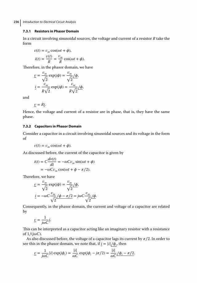
236 Introduction to Electrical Circuit Analysis
7.3.1 Resistors in Phasor Domain
In a circuit involving sinusoidal sources, the voltage and current of a resistor R take theform
𝑣(t) = 𝑣m cos(𝜔t + 𝜙),
i(t) = 𝑣(t)R
=𝑣m
Rcos(𝜔t + 𝜙).
Therefore, in the phasor domain, we have
𝑣 =𝑣m√2exp(j𝜙) =
𝑣m√2
𝜙,
i =𝑣m
R√2exp(j𝜙) =
𝑣m
R√2
𝜙,
and
𝑣 = Ri.
Hence, the voltage and current of a resistor are in phase, that is, they have the samephase.
7.3.2 Capacitors in Phasor Domain
Consider a capacitor in a circuit involving sinusoidal sources and its voltage in the formof
𝑣(t) = 𝑣m cos(𝜔t + 𝜙).
As discussed before, the current of the capacitor is given by
i(t) = C dv(t)dt
= −𝜔C𝑣m sin(𝜔t + 𝜙)
= −𝜔C𝑣m cos(𝜔t + 𝜙 − 𝜋∕2).
Therefore, we have
𝑣 =𝑣m√2exp(j𝜙) =
𝑣m√2
𝜙,
i = −𝜔C𝑣m√2
𝜙 − 𝜋∕2 = j𝜔C𝑣m√2
𝜙.
Consequently, in the phasor domain, the current and voltage of a capacitor are relatedby
𝑣 = 1j𝜔C
i.
This can be interpreted as a capacitor acting like an imaginary resistor with a resistanceof 1∕(j𝜔C).As also discussed before, the voltage of a capacitor lags its current by 𝜋∕2. In order to
see this in the phasor domain, we note that, if i = |i| 𝜙i, then
𝑣 = 1j𝜔C
|i| exp(j𝜙i) =|i|𝜔C
exp(j𝜙i − j𝜋∕2) = |i|𝜔C
𝜙i − 𝜋∕2.
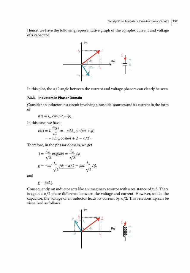
Steady-State Analysis of Time-Harmonic Circuits 237
Hence, we have the following representative graph of the complex current and voltageof a capacitor.
Im
Re
iI
φi
iR
i
v
vR
vI
v+
_
i
In this plot, the 𝜋∕2 angle between the current and voltage phasors can clearly be seen.
7.3.3 Inductors in Phasor Domain
Consider an inductor in a circuit involving sinusoidal sources and its current in the formof
i(t) = im cos(𝜔t + 𝜙).
In this case, we have
𝑣(t) = L di(t)dt
= −𝜔Lim sin(𝜔t + 𝜙)
= −𝜔Lim cos(𝜔t + 𝜙 − 𝜋∕2).
Therefore, in the phasor domain, we get
i =im√2exp(j𝜙) =
im√2
𝜙
𝑣 = −𝜔Lim√2
𝜙 − 𝜋∕2 = j𝜔Lim√2
𝜙,
and𝑣 = j𝜔Li.
Consequently, an inductor acts like an imaginary resistor with a resistance of j𝜔L.Thereis again a 𝜋∕2 phase difference between the voltage and current. However, unlike thecapacitor, the voltage of an inductor leads its current by 𝜋∕2. This relationship can bevisualized as follows.
Im
Re
iI
φi
iR
iv
vR
vI
v+
_
i

238 Introduction to Electrical Circuit Analysis
7.3.4 Impedance Concept
In general, AC circuits involve resistors, capacitors, and inductors, in addition toAC sources. In a steady-state analysis of circuits with time-harmonic sources, Ohm’slaw can be used for all of these components by treating capacitors and inductors asimaginary resistors. A combination of resistors, capacitors, and inductors in part ofa circuit may lead to a complex resistance value, which is called impedance, in theform of
Z = R + jX,
where R is the normal resistance (due to resistors) and X is the reactance (due to capac-itors and/or inductors). Such a combination can be considered as a single componentfor easier analysis. For a component with impedance Z, its voltage and current arerelated by
𝑣 = Zi,
where complex values of Z introduce phase differences between 𝑣(t) and i(t).
Example 116: Consider the following circuit involving two capacitors and threeinductors that are connected to a time-harmonic voltage source.
4cos(1000t+45°)VvC(t)_ + 0.4H
5μF
0.2H 0.1H
1.25μF
Find 𝑣C(t) in steady state.
Solution: In order to solve this problem, we need to convert the time-domain circuitinto a phasor-domain circuit. Considering that 𝜔 = 1000 rad/s, we have the followingconversions:
• 4 cos(1000t + 45∘) V −−−−→ 4√2
𝜋∕4V,
• 0.1 H −−−−→ j × 1000 × 0.1 = j100 Ω,• 0.2 H −−−−→ j × 1000 × 0.2 = j200 Ω,• 0.4 H −−−−→ j × 1000 × 0.4 = j400 Ω,• 1.25 μF −−−−→ 1∕(j × 1000 × 1.25 × 10−6) = −j800 Ω,• 5 μF −−−−→ 1∕(j × 1000 × 5 × 10−6) = −j200 Ω.
Consequently, in the phasor domain, we have the following circuit.
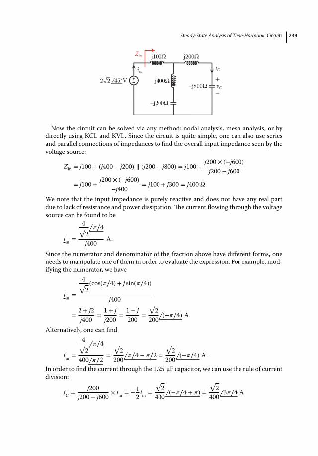
Steady-State Analysis of Time-Harmonic Circuits 239
vC_ +
j100Ω
j400Ω2 2 45°V
–j200Ω
j200Ω
–j800Ω
iin iC
Zin
Now the circuit can be solved via any method: nodal analysis, mesh analysis, or bydirectly using KCL and KVL. Since the circuit is quite simple, one can also use seriesand parallel connections of impedances to find the overall input impedance seen by thevoltage source:
Zin = j100 + (j400 − j200) ∥ (j200 − j800) = j100 +j200 × (−j600)
j200 − j600
= j100 +j200 × (−j600)
−j400= j100 + j300 = j400 Ω.
We note that the input impedance is purely reactive and does not have any real partdue to lack of resistance and power dissipation.The current flowing through the voltagesource can be found to be
iin =
4√2
𝜋∕4
j400A.
Since the numerator and denominator of the fraction above have different forms, oneneeds to manipulate one of them in order to evaluate the expression. For example, mod-ifying the numerator, we have
iin =
4√2(cos(𝜋∕4) + j sin(𝜋∕4))
j400
=2 + j2j400
=1 + jj200
=1 − j200
=√2
200(−𝜋∕4) A.
Alternatively, one can find
iin =
4√2
𝜋∕4
400 𝜋∕2=
√2
200𝜋∕4 − 𝜋∕2 =
√2
200(−𝜋∕4) A.
In order to find the current through the 1.25 μF capacitor, we can use the rule of currentdivision:
iC =j200
j200 − j600× iin = −1
2iin =
√2
400(−𝜋∕4 + 𝜋) =
√2
4003𝜋∕4 A.

240 Introduction to Electrical Circuit Analysis
Finally, the voltage across the capacitor can be found to be
𝑣C = ZCiC = −j800 ×√2
4003𝜋∕4 A = 2
√2 3𝜋∕4 − 𝜋∕2
= 2√2 𝜋∕4 V.
Converting the final expression into the time domain, we have
𝑣C(t) =√2Re𝑣C exp(j𝜔t) = 4 cos(1000t + 𝜋∕4)
= 4 cos(1000t + 45∘) V.We note that, as a coincidence, the voltage of the capacitor is in phase with the voltagesource, while this could not be understood directly without analyzing the circuit.
Example 117: Consider the following circuit.
3/10H 6/10H
3/10H
4/10H
5μF
5μF
6cos(2000t+45°)V
vL_ +
Find 𝑣L(t) in steady state.
Solution: We again consider the following conversions:
• 6 cos(2000t + 45∘) V −−−−→ 3√2
𝜋∕4V,
• 3∕10 H −−−−→ j × 2000 × 3∕10 = j600 Ω,• 4∕10 H −−−−→ j × 2000 × 4∕10 = j800 Ω,• 6∕10 H −−−−→ j × 2000 × 6∕10 = j1200 Ω,• 5 𝜇F −−−−→ 1∕(j × 2000 × 5 × 10−6) = −j100 Ω,Therefore, in the phasor domain, the circuit can be represented as follows.
j600Ω j1200Ω
j600Ω 3 2 45°V
–j100Ω
j800Ω
–j100Ω
vL_ +
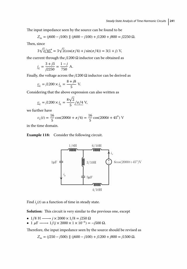
Steady-State Analysis of Time-Harmonic Circuits 241
The input impedance seen by the source can be found to be
Zin = (j600 − j100) ∥ (j600 − j100) + j1200 + j800 = j2250 Ω.
Then, since
3√2 45∘ = 3
√2(cos(𝜋∕4) + j sin(𝜋∕4)) = 3(1 + j) V,
the current through the j1200 Ω inductor can be obtained as
iL =3 + j3j2250
=1 − j750
A.
Finally, the voltage across the j1200 Ω inductor can be derived as
𝑣L = j1200 × iL =8 + j85
V.
Considering that the above expression can also written as
𝑣L = j1200 × iL =8√2
5𝜋∕4 V,
we further have
𝑣L(t) =165
cos(2000t + 𝜋∕4) = 165
cos(2000t + 45∘) V
in the time domain.
Example 118: Consider the following circuit.
1/8H 6/10H
3/10H
4/10H
1μF
5μF
6cos(2000t+45°)V
ix
iy
Find iy(t) as a function of time in steady state.
Solution: This circuit is very similar to the previous one, except
• 1∕8 H −−−−→ j × 2000 × 1∕8 = j250 Ω• 1 𝜇F −−−−→ 1∕(j × 2000 × 1 × 10−6) = −j500 Ω.
Therefore, the input impedance seen by the source should be revised as
Zin = (j250 − j500) ∥ (j600 − j100) + j1200 + j800 = j1500 Ω.

242 Introduction to Electrical Circuit Analysis
Therefore, we obtain ix as
ix =3 + j3j1500
=1 − j500
A.
Then iy can be obtained via current division as
iy =j500j250
ix = 2ix =1 − j250
A.
Therefore, in the time domain, we have
iy(t) =2
250cos(2000t − 𝜋∕4) A.
Exercise 104: In the following circuit, find 𝑣x(t) in steady state.
0.4H 0.6H
0.2H
4μF
2μF vx_ +
3cos(1000t+45°)V
Exercise 105: Consider the following circuit.
2Ω 1/6F 1/9F
2H 1H2 2cos(3t-45°)V
ix
Find ix(t) in steady state.
Exercise 106: In the following circuit, find 𝑣L(t) in steady state.
20mH
30mH 40mH
20μF
50μF
40μF
4cos(1000t+45°)V
+
_ vL
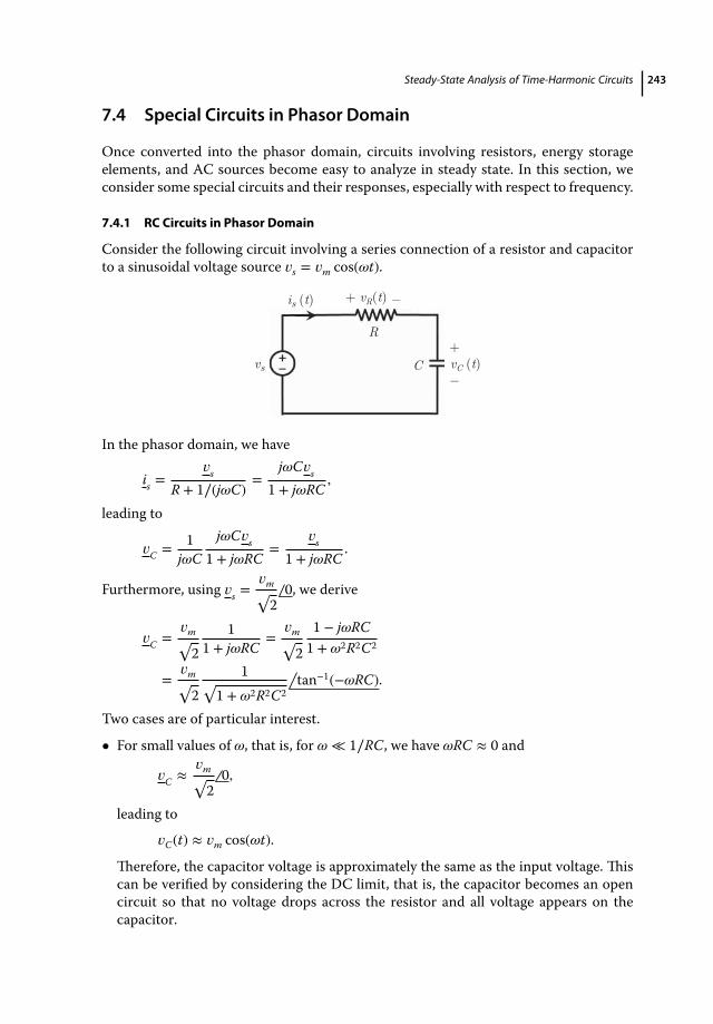
Steady-State Analysis of Time-Harmonic Circuits 243
7.4 Special Circuits in Phasor Domain
Once converted into the phasor domain, circuits involving resistors, energy storageelements, and AC sources become easy to analyze in steady state. In this section, weconsider some special circuits and their responses, especially with respect to frequency.
7.4.1 RC Circuits in Phasor Domain
Consider the following circuit involving a series connection of a resistor and capacitorto a sinusoidal voltage source 𝑣s = 𝑣m cos(𝜔t).
+_
R
Cvs
is (t)
vC (t)
+ vR(t) _
In the phasor domain, we have
is =𝑣s
R + 1∕(j𝜔C)=
j𝜔C𝑣s
1 + j𝜔RC,
leading to
𝑣C = 1j𝜔C
j𝜔C𝑣s
1 + j𝜔RC=
𝑣s
1 + j𝜔RC.
Furthermore, using 𝑣s =𝑣m√2
0, we derive
𝑣C =𝑣m√2
11 + j𝜔RC
=𝑣m√2
1 − j𝜔RC1 + 𝜔2R2C2
=𝑣m√2
1√1 + 𝜔2R2C2
tan−1(−𝜔RC).
Two cases are of particular interest.
• For small values of 𝜔, that is, for 𝜔 ≪ 1∕RC, we have 𝜔RC ≈ 0 and
𝑣C ≈𝑣m√2
0,
leading to
𝑣C(t) ≈ 𝑣m cos(𝜔t).
Therefore, the capacitor voltage is approximately the same as the input voltage. Thiscan be verified by considering the DC limit, that is, the capacitor becomes an opencircuit so that no voltage drops across the resistor and all voltage appears on thecapacitor.

244 Introduction to Electrical Circuit Analysis
• For large values of 𝜔, that is, for 𝜔 ≫ 1∕RC, we have
𝑣C ≈𝑣m√2
1𝜔RC
(−𝜋∕2),
leading to
𝑣C(t) ≈𝑣m
𝜔RCcos(𝜔t − 𝜋∕2).
Hence, the amplitude of the capacitor voltage drops to small values, while itbecomes 90∘ out of phase compared to the source. In the limit 𝜔 → ∞, we furtherhave
𝑣C(t) → 0
since the capacitor becomes a short circuit.
Considering the special cases above, as well as the behavior for different values of 𝜔,the RC circuit can be considered as a low-pass filter. Specifically, if the capacitor volt-age is selected as the output, low-frequency signals easily pass through the circuit, whilehigh-frequency signals are filtered out (cannot appear across the capacitor). This prop-erty makes the RC circuit an important ingredient of many practical circuits. Obviously,the values of R and C in the circuit determine which frequencies are to be filtered for agiven threshold. For example, in order to filter 90% of any signal above 100MHz, onemust select
1√1 + 𝜔2R2C2
< 0.9 → RC > 7.71 × 10⁻¹⁰ s.
Finally, we note that the same RC circuit can be considered as a high-pass circuit if theresistor voltage is selected as the output.
7.4.2 RL Circuits in Phasor Domain
Consider the following circuit involving a series connection of a resistor and inductorto a voltage source 𝑣s = 𝑣m cos(𝜔t).
+_
R
Lvs
is (t)
vL (t)
+ vR(t) _
Investigating the circuit in the phasor domain, we derive
is =𝑣s
R + j𝜔L
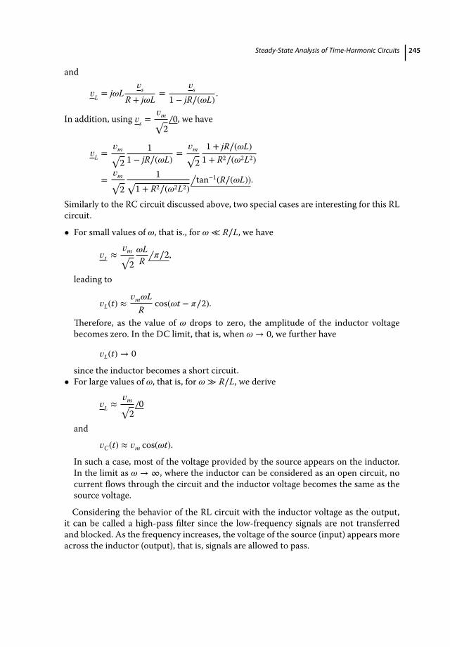
Steady-State Analysis of Time-Harmonic Circuits 245
and
𝑣L = j𝜔L𝑣s
R + j𝜔L=
𝑣s
1 − jR∕(𝜔L).
In addition, using 𝑣s =𝑣m√2
0, we have
𝑣L =𝑣m√2
11 − jR∕(𝜔L)
=𝑣m√2
1 + jR∕(𝜔L)1 + R2∕(𝜔2L2)
=𝑣m√2
1√1 + R2∕(𝜔2L2)
tan−1(R∕(𝜔L)).
Similarly to the RC circuit discussed above, two special cases are interesting for this RLcircuit.
• For small values of 𝜔, that is., for 𝜔 ≪ R∕L, we have
𝑣L ≈𝑣m√2𝜔LR
𝜋∕2,
leading to
𝑣L(t) ≈𝑣m𝜔L
Rcos(𝜔t − 𝜋∕2).
Therefore, as the value of 𝜔 drops to zero, the amplitude of the inductor voltagebecomes zero. In the DC limit, that is, when 𝜔 → 0, we further have
𝑣L(t) → 0
since the inductor becomes a short circuit.• For large values of 𝜔, that is, for 𝜔 ≫ R∕L, we derive
𝑣L ≈𝑣m√2
0
and
𝑣C(t) ≈ 𝑣m cos(𝜔t).
In such a case, most of the voltage provided by the source appears on the inductor.In the limit as 𝜔 → ∞, where the inductor can be considered as an open circuit, nocurrent flows through the circuit and the inductor voltage becomes the same as thesource voltage.
Considering the behavior of the RL circuit with the inductor voltage as the output,it can be called a high-pass filter since the low-frequency signals are not transferredand blocked. As the frequency increases, the voltage of the source (input) appears moreacross the inductor (output), that is, signals are allowed to pass.

246 Introduction to Electrical Circuit Analysis
7.4.3 RLC Circuits in Phasor Domain
Now, we consider the following circuit involving a series connection of a resistor R, acapacitor C, and an inductor L.
+ _ R
C
L
vs
is (t)
vR (t)
+ vc(t) _
vL(t)_ +
A sinusoidal voltage source with angular frequency 𝜔 is connected to the components,leading to
is =𝑣s
R + j𝜔L − j∕(𝜔C)=
𝑣s
R + j(𝜔L − 1∕(𝜔C)).
The RMS of the current can be found directly from the phasor as
iRMS = |is| = 𝑣RMS
|R + j(𝜔L − 1∕(𝜔C))|=
𝑣RMS√R2 + (𝜔L − 1∕(𝜔C))2
.
For the circuit above, the frequency at which the RMS of the current is maximum isparticularly interesting. This corresponds to the case where the power of the resistor ismaximized. Using the expression above, one can derive
𝜕iRMS
𝜕𝜔= 𝑣RMS
𝜕
𝜕𝜔
[R2 +
(𝜔L − 1
𝜔C
)2]−1∕2
= −𝑣RMS
[R2 +
(𝜔L − 1
𝜔C
)2]−3∕2 (𝜔L − 1
𝜔C
)(L + 1
𝜔2C
).
Then, for 𝜕iRMS∕𝜕𝜔 = 0, a positive value of the angular frequency can be found,
𝜔 = 1√LC
.
For this value of 𝜔, the overall impedance of the series connection becomes R, so thatwe have is = 𝑣s∕R and iRMS = 𝑣RMS∕R. This can be seen as a result of the cancelation ofthe impedances of the inductor and capacitor, that is,
ZL = j𝜔L = j 1√LC
L = j√
LC,
ZC = 1j𝜔C
= −j√
LC 1C
= −j√
LC,
ZL + ZC = 0.Consequently, if the resistor is considered as the output of this circuit, frequencies ataround 𝜔 = 1∕
√LC pass through the circuit, while the other signals (with smaller and
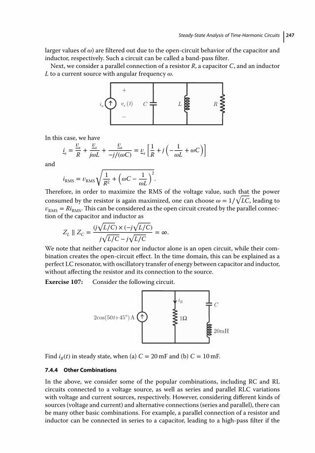
Steady-State Analysis of Time-Harmonic Circuits 247
larger values of 𝜔) are filtered out due to the open-circuit behavior of the capacitor andinductor, respectively. Such a circuit can be called a band-pass filter.Next, we consider a parallel connection of a resistor R, a capacitor C, and an inductor
L to a current source with angular frequency 𝜔.
+
_ RLCis vs (t)
In this case, we have
is =𝑣s
R+
𝑣s
j𝜔L+
𝑣s
−j∕(𝜔C)= 𝑣s
[ 1R+ j
(− 1𝜔L
+ 𝜔C)]
and
iRMS = 𝑣RMS
√1
R2 +(𝜔C − 1
𝜔L
)2.
Therefore, in order to maximize the RMS of the voltage value, such that the powerconsumed by the resistor is again maximized, one can choose 𝜔 = 1∕
√LC, leading to
𝑣RMS = RiRMS.This can be considered as the open circuit created by the parallel connec-tion of the capacitor and inductor as
ZL ∥ ZC =(j√
L∕C) × (−j√
L∕C)
j√
L∕C − j√
L∕C= ∞.
We note that neither capacitor nor inductor alone is an open circuit, while their com-bination creates the open-circuit effect. In the time domain, this can be explained as aperfect LC resonator, with oscillatory transfer of energy between capacitor and inductor,without affecting the resistor and its connection to the source.Exercise 107: Consider the following circuit.
2cos(50t+45°) A 1Ω
20mH
C iR
Find iR(t) in steady state, when (a) C = 20mF and (b) C = 10mF.
7.4.4 Other Combinations
In the above, we consider some of the popular combinations, including RC and RLcircuits connected to a voltage source, as well as series and parallel RLC variationswith voltage and current sources, respectively. However, considering different kinds ofsources (voltage and current) and alternative connections (series and parallel), there canbe many other basic combinations. For example, a parallel connection of a resistor andinductor can be connected in series to a capacitor, leading to a high-pass filter if the
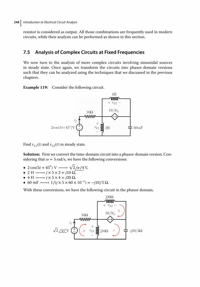
248 Introduction to Electrical Circuit Analysis
resistor is considered as output. All those combinations are frequently used in moderncircuits, while their analysis can be performed as shown in this section.
7.5 Analysis of Complex Circuits at Fixed Frequencies
We now turn to the analysis of more complex circuits involving sinusoidal sourcesin steady state. Once again, we transform the circuits into phasor-domain versionssuch that they can be analyzed using the techniques that we discussed in the previouschapters.
Example 119: Consider the following circuit.
2cos(5t+45°)V
10Ω 10/3ix
60mF
4H
+ _
2H +
_
ix
vL1
vL2
Find 𝑣L1(t) and 𝑣L2(t) in steady state.
Solution: First we convert the time-domain circuit into a phasor-domain version. Con-sidering that 𝜔 = 5 rad/s, we have the following conversions:
• 2 cos(5t + 45∘) V −−−−→√2 𝜋∕4V,
• 2 H −−−−→ j × 5 × 2 = j10 Ω,• 4 H −−−−→ j × 5 × 4 = j20 Ω,• 60 mF −−−−→ 1∕(j × 5 × 60 × 10−3) = −j10∕3 Ω.
With these conversions, we have the following circuit in the phasor domain.
10Ω
45°V2
10/3ix
-j10/3Ω
j20Ω
+ _
j10Ω+
_ a
b
c
ix
vL1
vL2
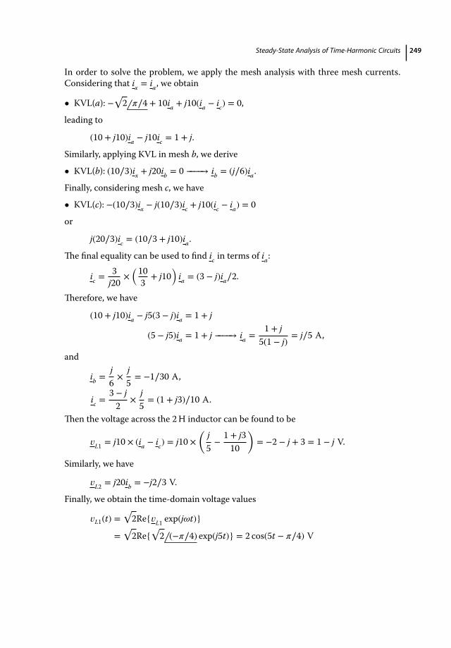
Steady-State Analysis of Time-Harmonic Circuits 249
In order to solve the problem, we apply the mesh analysis with three mesh currents.Considering that ix = ia, we obtain
• KVL(a): −√2 𝜋∕4 + 10ia + j10(ia − ic) = 0,
leading to
(10 + j10)ia − j10ic = 1 + j.
Similarly, applying KVL in mesh b, we derive
• KVL(b): (10∕3)ix + j20ib = 0 −−−−→ ib = (j∕6)ia.
Finally, considering mesh c, we have
• KVL(c): −(10∕3)ix − j(10∕3)ic + j10(ic − ia) = 0
or
j(20∕3)ic = (10∕3 + j10)ia.
The final equality can be used to find ic in terms of ia:
ic =3
j20×(103
+ j10)
ia = (3 − j)ia∕2.
Therefore, we have
(10 + j10)ia − j5(3 − j)ia = 1 + j
(5 − j5)ia = 1 + j −−−−→ ia =1 + j
5(1 − j)= j∕5 A,
and
ib =j6×
j5= −1∕30 A,
ic =3 − j2
×j5= (1 + j3)∕10 A.
Then the voltage across the 2H inductor can be found to be
𝑣L1 = j10 × (ia − ic) = j10 ×(
j5−
1 + j310
)= −2 − j + 3 = 1 − j V.
Similarly, we have
𝑣L2 = j20ib = −j2∕3 V.
Finally, we obtain the time-domain voltage values
𝑣L1(t) =√2Re𝑣L1 exp(j𝜔t)
=√2Re
√2 (−𝜋∕4) exp(j5t) = 2 cos(5t − 𝜋∕4) V
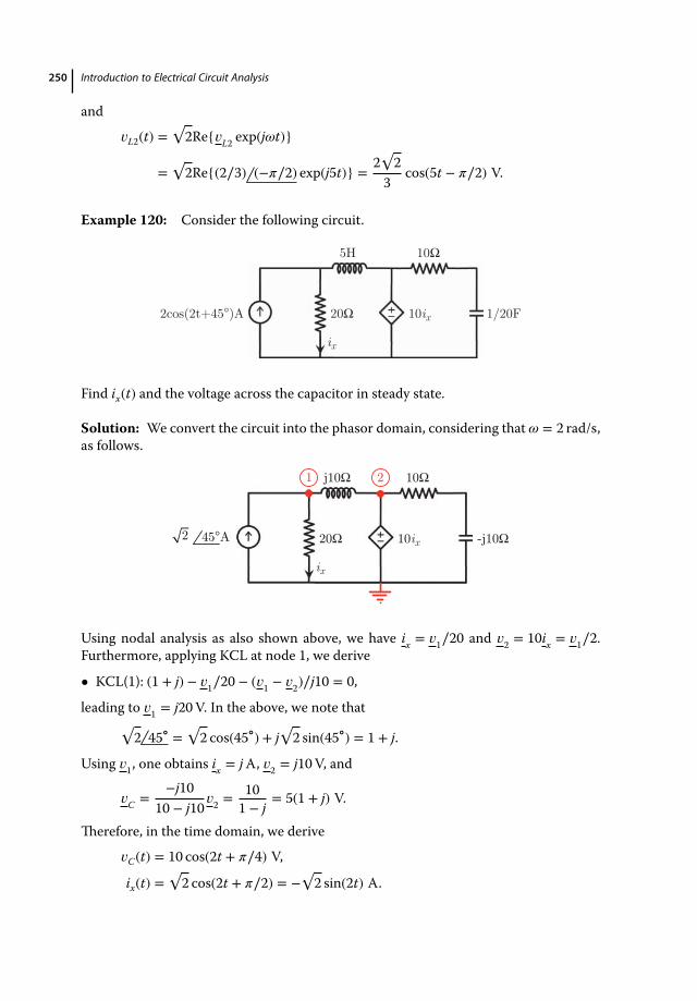
250 Introduction to Electrical Circuit Analysis
and
𝑣L2(t) =√2Re𝑣L2 exp(j𝜔t)
=√2Re(2∕3) (−𝜋∕2) exp(j5t) =
2√2
3cos(5t − 𝜋∕2) V.
Example 120: Consider the following circuit.
10Ω
ix
20Ω 10ix
5H
2cos(2t+45°)A 1/20F
Find ix(t) and the voltage across the capacitor in steady state.
Solution: We convert the circuit into the phasor domain, considering that 𝜔 = 2 rad/s,as follows.
10Ω
ix
20Ω2 45°A 10ix
j10Ω
-j10Ω
1 2
Using nodal analysis as also shown above, we have ix = 𝑣1∕20 and 𝑣2 = 10ix = 𝑣1∕2.Furthermore, applying KCL at node 1, we derive
• KCL(1): (1 + j) − 𝑣1∕20 − (𝑣1 − 𝑣2)∕j10 = 0,
leading to 𝑣1 = j20V. In the above, we note that√2 45∘ =
√2 cos(45∘) + j
√2 sin(45∘) = 1 + j.
Using 𝑣1, one obtains ix = jA, 𝑣2 = j10V, and
𝑣C =−j10
10 − j10𝑣2 =
101 − j
= 5(1 + j) V.
Therefore, in the time domain, we derive
𝑣C(t) = 10 cos(2t + 𝜋∕4) V,
ix(t) =√2 cos(2t + 𝜋∕2) = −
√2 sin(2t) A.
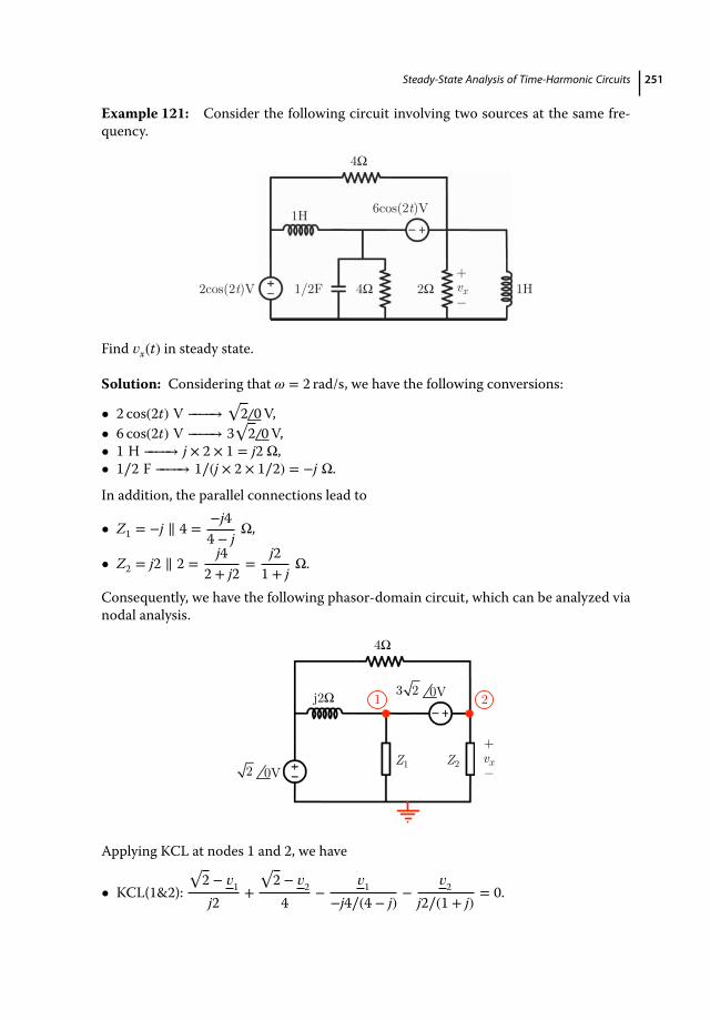
Steady-State Analysis of Time-Harmonic Circuits 251
Example 121: Consider the following circuit involving two sources at the same fre-quency.
4Ω2cos(2t)V 1/2F 2Ω 1H
6cos(2t)V1H
4Ω
_
+ vx
Find 𝑣x(t) in steady state.
Solution: Considering that 𝜔 = 2 rad/s, we have the following conversions:
• 2 cos(2t) V −−−−→√2 0V,
• 6 cos(2t) V −−−−→ 3√2 0V,
• 1 H −−−−→ j × 2 × 1 = j2 Ω,• 1∕2 F −−−−→ 1∕(j × 2 × 1∕2) = −j Ω.
In addition, the parallel connections lead to
• Z1 = −j ∥ 4 =−j44 − j
Ω,
• Z2 = j2 ∥ 2 =j4
2 + j2=
j21 + j
Ω.
Consequently, we have the following phasor-domain circuit, which can be analyzed vianodal analysis.
j2Ω
4Ω
_
+
2
3 21 2
Z1 Z20V
0V
vx
Applying KCL at nodes 1 and 2, we have
• KCL(1&2):
√2 − 𝑣1
j2+
√2 − 𝑣2
4−
𝑣1
−j4∕(4 − j)−
𝑣2
j2∕(1 + j)= 0.
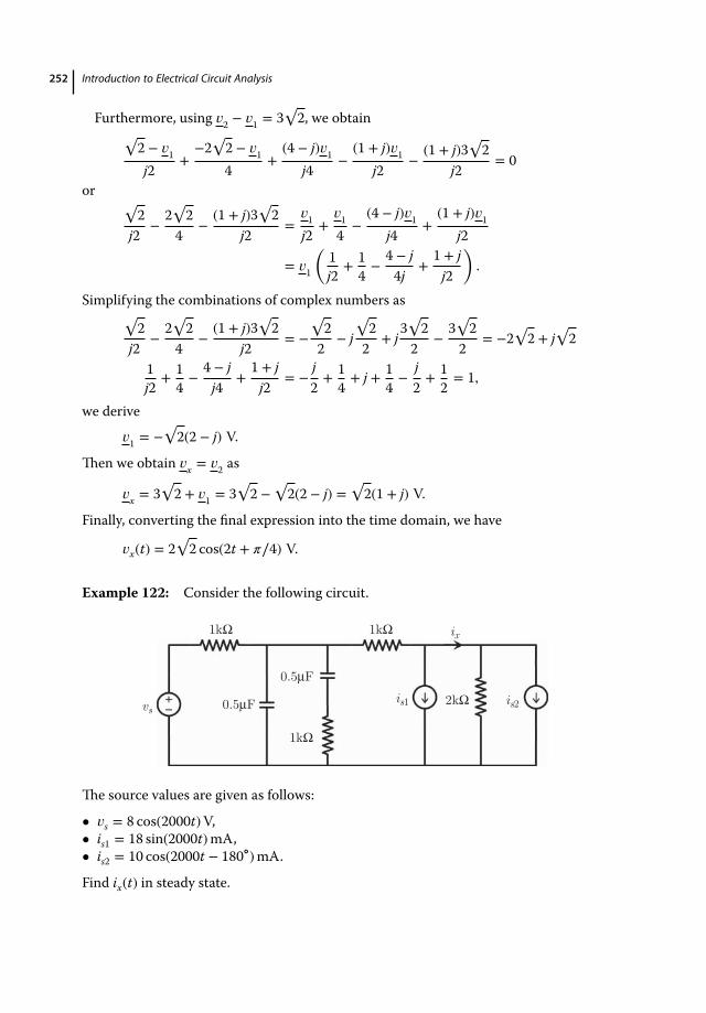
252 Introduction to Electrical Circuit Analysis
Furthermore, using 𝑣2 − 𝑣1 = 3√2, we obtain√
2 − 𝑣1
j2+
−2√2 − 𝑣1
4+
(4 − j)𝑣1j4
−(1 + j)𝑣1
j2−
(1 + j)3√2
j2= 0
or √2
j2−
2√2
4−
(1 + j)3√2
j2=
𝑣1
j2+
𝑣1
4−
(4 − j)𝑣1j4
+(1 + j)𝑣1
j2
= 𝑣1
(1j2
+ 14−
4 − j4j
+1 + j
j2
).
Simplifying the combinations of complex numbers as√2
j2−
2√2
4−
(1 + j)3√2
j2= −
√22
− j√22
+ j3√2
2−
3√2
2= −2
√2 + j
√2
1j2
+ 14−
4 − jj4
+1 + j
j2= −
j2+ 1
4+ j + 1
4−
j2+ 1
2= 1,
we derive
𝑣1 = −√2(2 − j) V.
Then we obtain 𝑣x = 𝑣2 as
𝑣x = 3√2 + 𝑣1 = 3
√2 −
√2(2 − j) =
√2(1 + j) V.
Finally, converting the final expression into the time domain, we have
𝑣x(t) = 2√2 cos(2t + 𝜋∕4) V.
Example 122: Consider the following circuit.
1kΩ
0.5μF
0.5μF
1kΩ
1kΩ
2kΩvsis1
ix
is2
The source values are given as follows:
• 𝑣s = 8 cos(2000t)V,• is1 = 18 sin(2000t)mA,• is2 = 10 cos(2000t − 180∘)mA.
Find ix(t) in steady state.
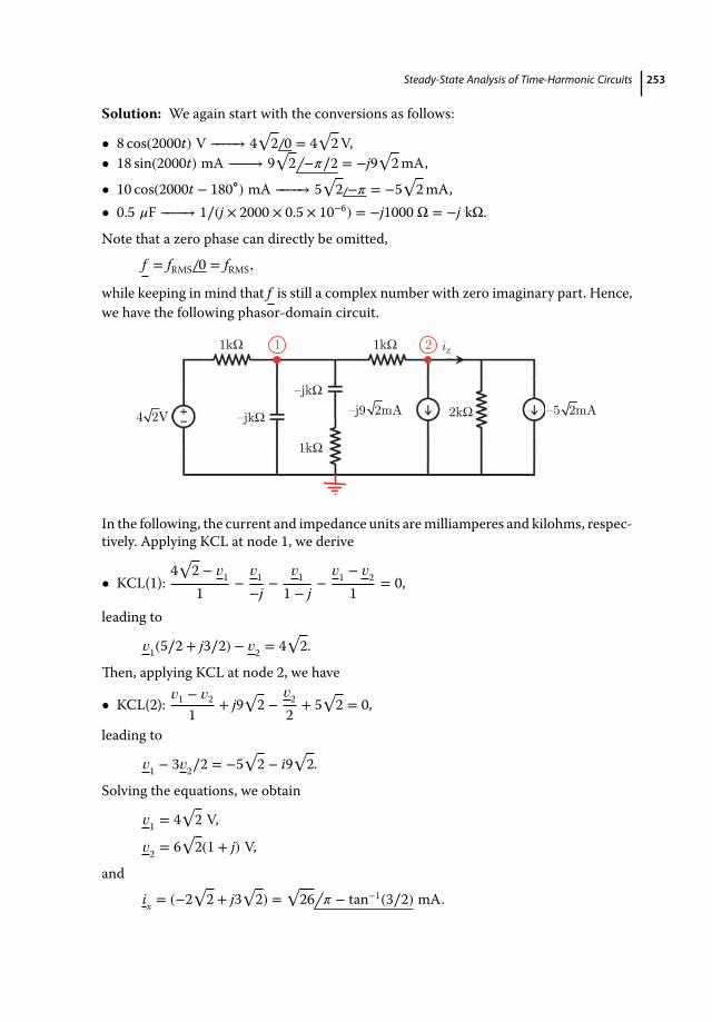
Steady-State Analysis of Time-Harmonic Circuits 253
Solution: We again start with the conversions as follows:
• 8 cos(2000t) V −−−−→ 4√2 0 = 4
√2V,
• 18 sin(2000t) mA −−−−→ 9√2 −𝜋∕2 = −j9
√2mA,
• 10 cos(2000t − 180∘) mA −−−−→ 5√2 −𝜋 = −5
√2mA,
• 0.5 𝜇F −−−−→ 1∕(j × 2000 × 0.5 × 10−6) = −j1000 Ω = −j kΩ.
Note that a zero phase can directly be omitted,
f = fRMS 0 = fRMS,
while keeping in mind that f is still a complex number with zero imaginary part. Hence,we have the following phasor-domain circuit.
1kΩ
1kΩ
1kΩ
2kΩ–jkΩ
–jkΩ4 2V –5 2mA–j9 2mA
1 2 ix
In the following, the current and impedance units aremilliamperes and kilohms, respec-tively. Applying KCL at node 1, we derive
• KCL(1):4√2 − 𝑣1
1−
𝑣1
−j−
𝑣1
1 − j−
𝑣1 − 𝑣2
1= 0,
leading to
𝑣1(5∕2 + j3∕2) − 𝑣2 = 4√2.
Then, applying KCL at node 2, we have
• KCL(2):𝑣1 − 𝑣2
1+ j9
√2 −
𝑣2
2+ 5
√2 = 0,
leading to
𝑣1 − 3𝑣2∕2 = −5√2 − i9
√2.
Solving the equations, we obtain
𝑣1 = 4√2 V,
𝑣2 = 6√2(1 + j) V,
and
ix = (−2√2 + j3
√2) =
√26 𝜋 − tan−1(3∕2) mA.
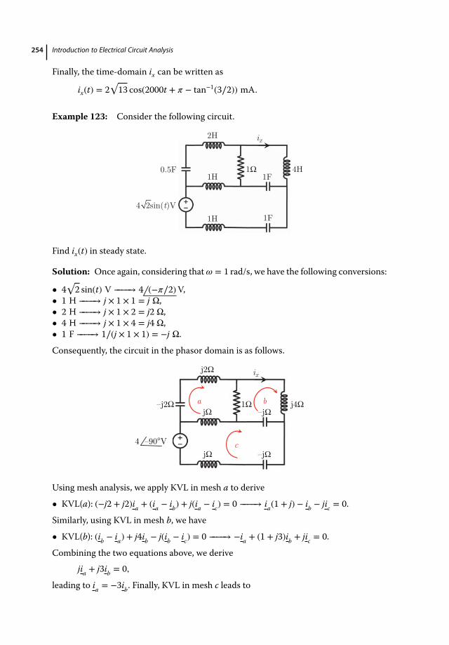
254 Introduction to Electrical Circuit Analysis
Finally, the time-domain ix can be written as
ix(t) = 2√13 cos(2000t + 𝜋 − tan−1(3∕2)) mA.
Example 123: Consider the following circuit.
4 2sin(t)V
0.5F1H
1H
1F
1F
2H
1Ω 4H
ix
Find ix(t) in steady state.
Solution: Once again, considering that𝜔 = 1 rad/s, we have the following conversions:
• 4√2 sin(t) V −−−−→ 4 (−𝜋∕2)V,
• 1 H −−−−→ j × 1 × 1 = j Ω,• 2 H −−−−→ j × 1 × 2 = j2 Ω,• 4 H −−−−→ j × 1 × 4 = j4 Ω,• 1 F −−−−→ 1∕(j × 1 × 1) = −j Ω.
Consequently, the circuit in the phasor domain is as follows.
–j2Ω
4 –90°V
jΩ
jΩ
–jΩ
–jΩ
j2Ω
1Ω j4Ωa b
c
ix
Using mesh analysis, we apply KVL in mesh a to derive
• KVL(a): (−j2 + j2)ia + (ia − ib) + j(ia − ic) = 0 −−−−→ ia(1 + j) − ib − jic = 0.
Similarly, using KVL in mesh b, we have
• KVL(b): (ib − ia) + j4ib − j(ib − ic) = 0 −−−−→ −ia + (1 + j3)ib + jic = 0.
Combining the two equations above, we derivejia + j3ib = 0,
leading to ia = −3ib. Finally, KVL in mesh c leads to

Steady-State Analysis of Time-Harmonic Circuits 255
• KVL(c): j4 + j(ic − ia) − j(ic − ib) = 0 −−−−→ ia − ib = 4.
Solving the equations, one obtains ia = 3A and ib = ix = −1A. Therefore, in the timedomain, we have
ix(t) = −√2 cos(t) A
or
ix(t) =√2 cos(t + 𝜋) =
√2 cos(t + 180∘) A.
In this circuit, we note that the capacitor and inductor in the bottombranch actually can-cel each other out in the phasor domain. Therefore, their combination can be replacedby a short circuit.
Example 124: Consider the following circuit, where 𝑣o(t) = 2√2 sin(2t).
1H 1/2F 1H
1/8F
1H2Ω
2Ω
2ix
iy
vo
ix
Find ix(t) in steady state.
Solution: Considering that 𝜔 = 2 rad/s, the circuit in the phasor domain is asfollows:
j2Ω –jΩ
2Ω
2Ω
2ix
vo
j2Ω
–j4Ω
j2Ωa b
c
ix
iy
First, we note that
𝑣o = 2 −𝜋∕2 = −j2 V
in the phasor domain. In addition, the parallel connection of the inductor and capacitorleads to
j2 ∥ (−j) = −j2 Ω.
Using mesh analysis, we further have ix = ic. Applying KCL in mesh b, we derive
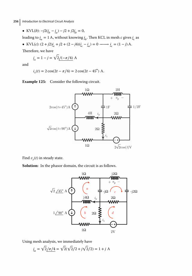
256 Introduction to Electrical Circuit Analysis
• KVL(b): −j2(ib − ia) − j2 + j2ib = 0,leading to ia = 1A, without knowing ib. Then KCL in mesh c gives ic as• KVL(c): (2 + j2)ic + j2 + (2 − j4)(ic − ia) = 0 −−−−→ ic = (1 − j)A.Therefore, we have
ix = 1 − j =√2 (−𝜋∕4) A
andix(t) = 2 cos(2t − 𝜋∕4) = 2 cos(2t − 45∘) A.
Example 125: Consider the following circuit.
2cos(t+45°)A
2cos(t+90°)A 2Ω
1Ω
1F
2H
1/2F2Ω
1Ω
4H
+ _
2 2cos(t)V
vy
iz
ix
Find 𝑣y(t) in steady state.
Solution: In the phasor domain, the circuit is as follows.
2Ω
1Ω
2
1
45° A
90° A
-jΩ
j2Ω
-j2Ω
2V
2Ω
1Ω
j4Ω
+ _
a
b d
c
vy
ix
iz
Using mesh analysis, we immediately have
ia =√2 𝜋∕4 =
√2(√2∕2 + j
√2∕2) = 1 + j A
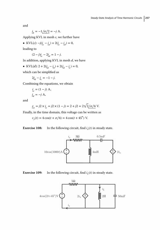
Steady-State Analysis of Time-Harmonic Circuits 257
and
ib = −1 𝜋∕2 = −j A.
Applying KVL in mesh c, we further have
• KVL(c): −j(ic − ia) + 2(ic − id) = 0,
leading to
(2 − j)ic − 2id = 1 − j.
In addition, applying KVL in mesh d, we have
• KVL(d): 2 + 2(id − ib) + 2(id − ic) = 0,
which can be simplified as
2id − ic = −1 − j.
Combining the equations, we obtain
ic = (1 − j) A,id = −j A,
and
𝑣y = j2 × ic = j2 × (1 − j) = 2 + j2 = 2√2 𝜋∕4 V.
Finally, in the time domain, this voltage can be written as
𝑣y(t) = 4 cos(t + 𝜋∕4) = 4 cos(t + 45∘) V.
Exercise 108: In the following circuit, find ix(t) in steady state.
10cos(1000t)A
3Ω
4mH 2ix
0.5mFix
Exercise 109: In the following circuit, find iL(t) in steady state.
4cos(2t+45°)V
5Ω
2H 50mF2ix
iL
ix

258 Introduction to Electrical Circuit Analysis
Exercise 110: In the following circuit, find ix(t) in steady state.
0.5H 2Ω
3Ω 6Ω1/16F10 2 sin(4t)V
ix
Exercise 111: In the following circuit, find 𝑣x(t) in steady state.
2cos(20t)A 10Ω 0.01F_
+ vx vx/10A
Exercise 112: Consider the following circuit in steady state.
4Ω
0.2F
2H 0.25Fix
is1
is2
Find ix(t), given that• is1(t) = 2 cos(t − 45∘)A,• is2(t) =
√2 cos(t)A.
Exercise 113: Consider the following circuit in steady state.
2Ω 1/16F
2Ω1/16F
16Ω 2H_ +
is1
is2vx
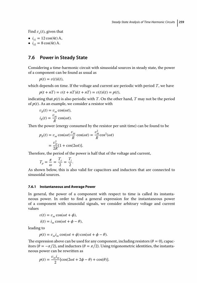
Steady-State Analysis of Time-Harmonic Circuits 259
Find 𝑣x(t), given that• is1 = 12 cos(4t)A,• is2 = 8 cos(4t)A.
7.6 Power in Steady State
Considering a time-harmonic circuit with sinusoidal sources in steady state, the powerof a component can be found as usual as
p(t) = 𝑣(t)i(t),which depends on time. If the voltage and current are periodic with period T , we have
p(t + nT) = 𝑣(t + nT)i(t + nT) = 𝑣(t)i(t) = p(t),indicating that p(t) is also periodic with T . On the other hand, T may not be the periodof p(t). As an example, we consider a resistor with
𝑣R(t) = 𝑣m cos(𝜔t),
iR(t) =𝑣m
Rcos(𝜔t).
Then the power (energy consumed by the resistor per unit time) can be found to be
pR(t) = 𝑣m cos(𝜔t)𝑣m
Rcos(𝜔t) =
𝑣2m
Rcos2(𝜔t)
=𝑣2m
2R[1 + cos(2𝜔t)].
Therefore, the period of the power is half that of the voltage and current,
Tp = 𝜋
𝜔=
T𝑣
2=
Ti
2.
As shown below, this is also valid for capacitors and inductors that are connected tosinusoidal sources.
7.6.1 Instantaneous and Average Power
In general, the power of a component with respect to time is called its instanta-neous power. In order to find a general expression for the instantaneous powerof a component with sinusoidal signals, we consider arbitrary voltage and currentvalues
𝑣(t) = 𝑣m cos(𝜔t + 𝜙),i(t) = im cos(𝜔t + 𝜙 − 𝜃),
leading top(t) = 𝑣mim cos(𝜔t + 𝜙) cos(𝜔t + 𝜙 − 𝜃).
The expression above can be used for any component, including resistors (𝜃 = 0), capac-itors (𝜃 = −𝜋∕2), and inductors (𝜃 = 𝜋∕2). Using trigonometric identities, the instanta-neous power can be rewritten as
p(t) =𝑣mim
2[cos(2𝜔t + 2𝜙 − 𝜃) + cos(𝜃)].

260 Introduction to Electrical Circuit Analysis
Hence, the power has two components: an oscillating part
po(t) =𝑣mim
2cos(2𝜔t + 2𝜙 − 𝜃),
and a constant part (shift in the amplitude)
ps(t) =𝑣mim
2cos 𝜃
that exists only if the component has a resistive part (𝜃 ≠ ±𝜋∕2).The instantaneous power provides information on the power of a component at any
given time. Another important quantity is the average power, which can be obtained viaintegration as
pavg =1T ∫
T
0p(t)dt = 1
Tp ∫
Tp
0p(t)dt,
where Tp = 𝜋∕𝜔. Using the expression above, we have
pavg =𝜔
𝜋
𝜋
𝜔
𝑣mim
2cos 𝜃 =
𝑣mim
2cos 𝜃.
Conventionally, the average power is written in terms of RMS voltage and current valuesas
pavg =𝑣m√2
im√2cos 𝜃 = 𝑣RMSiRMS cos 𝜃,
where 𝜃 is the phase difference between the voltage and current. Hence, for a singlecapacitor or inductor, the average power is zero. In fact, for a passive element, the aver-age power represents the dissipated power; hence, it is nonzero only when the compo-nent involves a resistive part that consumes energy.
7.6.2 Complex Power
In phasor domain, the voltage and current of an arbitrary element can be written as𝑣 = 𝑣RMS 𝜙,
i = iRMS 𝜙 − 𝜃,
where
Z =𝑣
i=
𝑣RMS
iRMS𝜃
is the impedance of the element. The complex power of the element is defined ass = 𝑣 × i∗
= 𝑣RMS 𝜙 × iRMS 𝜃 − 𝜙
= (𝑣RMSiRMS) 𝜃.
Hence, the complex power can be written ass = 𝑣RMSiRMS cos 𝜃 + j𝑣RMSiRMS sin 𝜃,
where the real part is the same as the average power in the time domain. Therefore,the real part of the complex power is related to the resistive part of the component.
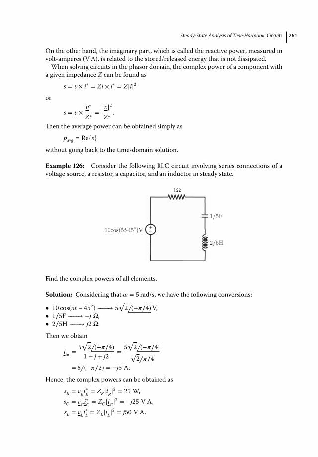
Steady-State Analysis of Time-Harmonic Circuits 261
On the other hand, the imaginary part, which is called the reactive power, measured involt-amperes (VA), is related to the stored/released energy that is not dissipated.When solving circuits in the phasor domain, the complex power of a component with
a given impedance Z can be found as
s = 𝑣 × i∗ = Zi × i∗ = Z|i|2or
s = 𝑣 ×𝑣∗
Z∗ =|𝑣|2Z∗ .
Then the average power can be obtained simply as
pavg = Res
without going back to the time-domain solution.
Example 126: Consider the following RLC circuit involving series connections of avoltage source, a resistor, a capacitor, and an inductor in steady state.
10cos(5t-45°)V
1Ω
1/5F
2/5H
Find the complex powers of all elements.
Solution: Considering that 𝜔 = 5 rad/s, we have the following conversions:
• 10 cos(5t − 45∘) −−−−→ 5√2 (−𝜋∕4)V,
• 1∕5F −−−−→ −j Ω,• 2∕5H −−−−→ j2 Ω.
Then we obtain
iin =5√2 (−𝜋∕4)
1 − j + j2=
5√2 (−𝜋∕4)√2 𝜋∕4
= 5 (−𝜋∕2) = −j5 A.
Hence, the complex powers can be obtained as
sR = 𝑣Ri∗R = ZR|iR|2 = 25 W,sC = 𝑣Ci∗C = ZC|iC|2 = −j25 V A,sL = 𝑣Li∗L = ZL|iL|2 = j50 V A.
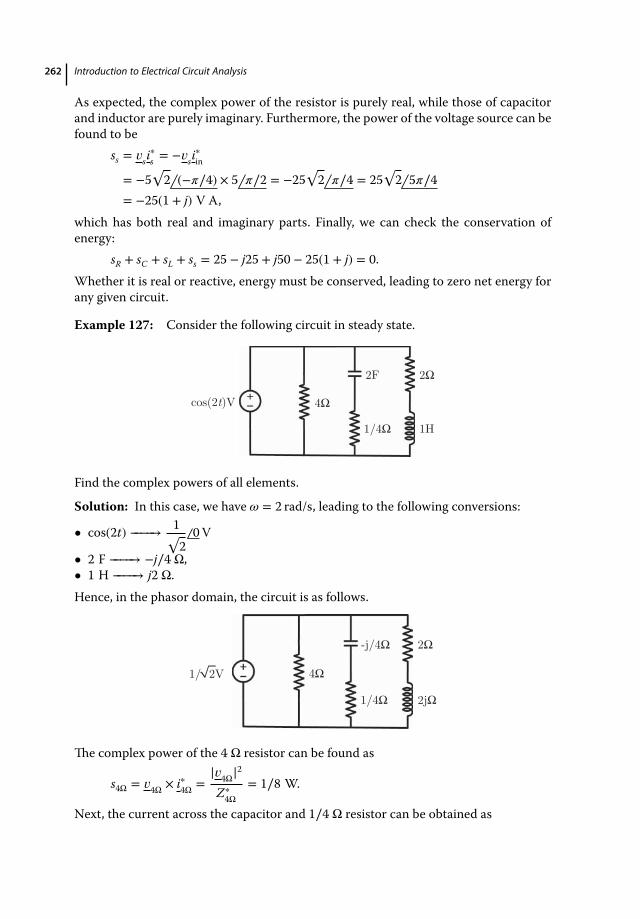
262 Introduction to Electrical Circuit Analysis
As expected, the complex power of the resistor is purely real, while those of capacitorand inductor are purely imaginary. Furthermore, the power of the voltage source can befound to be
ss = 𝑣si∗s = −𝑣si
∗in
= −5√2 (−𝜋∕4) × 5 𝜋∕2 = −25
√2 𝜋∕4 = 25
√2 5𝜋∕4
= −25(1 + j) V A,which has both real and imaginary parts. Finally, we can check the conservation ofenergy:
sR + sC + sL + ss = 25 − j25 + j50 − 25(1 + j) = 0.Whether it is real or reactive, energy must be conserved, leading to zero net energy forany given circuit.
Example 127: Consider the following circuit in steady state.
2Ω
1H
2F
1/4Ω
4Ωcos(2t)V
Find the complex powers of all elements.
Solution: In this case, we have 𝜔 = 2 rad/s, leading to the following conversions:
• cos(2t) −−−−→ 1√2
0V
• 2 F −−−−→ −j∕4 Ω,• 1 H −−−−→ j2 Ω.Hence, in the phasor domain, the circuit is as follows.
2Ω
2jΩ
-j/4Ω
1/4Ω
4Ω1/ 2V
The complex power of the 4 Ω resistor can be found as
s4Ω = 𝑣4Ω × i∗4Ω =|𝑣4Ω|2
Z∗4Ω
= 1∕8 W.
Next, the current across the capacitor and 1∕4 Ω resistor can be obtained as

Steady-State Analysis of Time-Harmonic Circuits 263
iC = i1∕4Ω =
1√2
0
14−
j4
=
1√2
0
√24
(−𝜋∕4)
= 2 𝜋∕4,
leading tosC = 𝑣C × i∗C = ZC|iC|2 = (−j∕4) × 4 = −j V A,
s1∕4Ω = 𝑣1∕4Ω × i∗1∕4Ω = Z1∕4Ω|i1∕4Ω|2 = 1 W.
Finally, the current across the inductor and 2 Ω resistor is obtained similarly as
iL = i2Ω =
1√2
0
2 + j2=
1√2
0
2√2 𝜋∕4
= 14
(−𝜋∕4).
Therefore, the corresponding complex powers can be calculated as
sL = 𝑣L × i∗L = ZL|iL|2 = j2 × 116
= j∕8 V A
s2Ω = 𝑣2Ω × i∗2Ω = Z2Ω|i2Ω|2 = 1∕8 W.Using the conservation of energy, we can also obtain the power of the voltage source as
ss = −s4Ω − sC − s1∕4Ω − sL − s2Ω= −1∕8 + j − 1 − j∕8 − 1∕8 = −10∕8 + j7∕8 = (−10 + j7)∕8 V A.
Example 128: Consider the following circuit in steady state.
j10Ω -j12Ω20Ω
16Ω
is
If the complex power of the current source is −144 − j112, find the complex power ofeach component.
Solution: First, we can find the impedance seen by the source as
Zin = 20 ∥ j10 ∥ (16 − j12) =j202 + j
∥ (16 − j12)
= (4 + j8) ∥ (16 − j12) =(4 + j8)(16 − j12)
20 − j4
=4(1 + j2)(4 − j3)
5 − j= 20
2 + j5 − j
Ω.
Using this impedance and the given complex power, we can find the absolute value ofthe source voltage tro be

264 Introduction to Electrical Circuit Analysis
ss = 𝑣si∗s =
|𝑣s|2−Z∗
in= −144 − j112
−−−−→ |𝑣s|2 = (−144 − j112) × (−20)2 − j5 + j
= 1600,
leading to |𝑣s| = 40V. Then, using this voltage value, we obtain• s20Ω = 1600∕20 = 80W,• sj10Ω = 1600∕(−j10) = j160VA,• s16Ω = Re1600∕(16 + 12j) = 64W,• s−j12Ω = Im1600∕(16 + 12j) = −j48VA.We also note that
s20Ω + sj10Ω + s16Ω + s−j12Ω = 144 + j112 = −ss,
as expected from the conservation of energy.
Example 129: Consider the following circuit in steady state.
2cos(t+45°)A
2Ω
1Ω
1F
2H
1/4F
12cos(t -135°)V
2Ω 4H
+ _ vy
ix
Find the time-average power of the voltage source.
Solution: In the phasor domain, the circuit is as follows.
2Ω
1Ω
2 45°A
2 -135°V
-jΩ
j2Ω
-j4Ω2Ωj4Ω
+ _
a b
c
vy
ix
Steady-State Analysis of Time-Harmonic Circuits 265
Applying mesh analysis, we first have
ia =√2 𝜋∕4 = (1 + j) A.
Then, applying KVL in meshes b and c, we obtain
• KVL(b): −j(ib − ia) − j2ib + 2(ib − ic) = 0 −−−−→ (2 − j3)ib − 2ic = 1 − j,• KVL(c): 2ic + 2(ic − ib) + (6 + j6) = 0 −−−−→ 2ic − ib = −3 − j3.Combining the equations, we get
(1 − j3)ib = −2 − j4 −−−−→ ib =−2 − j41 − j3
= (1 − j) A
andic = (−1 − j2) A.
Therefore, the complex power of the voltage source can be found to be
ss = (−6 − j6) × (−ic)∗ = (−6 − j6) × (1 − j2)
= −6 + j12 − j6 − 12 = (−18 + j6) V A.Finally, the time-average power can be obtained as
pavg,s = Ress = −18 W.
Exercise 114: Consider the following circuit in steady state.
4H
2H
2mF
4mF 6H2 2 cos(10t+90°)V
Find the complex power of the voltage source.
Exercise 115: Consider the following circuit in steady state.
4cos(4t-135°)V
2Ω 1/8F
4Ω 2Ω
2iy
1H
4Ω
1/16F
1/2H
ix
ix
iy
• Find the power of the current-dependent voltage source.• Find the time-average power of the current-dependent current source.

266 Introduction to Electrical Circuit Analysis
7.6.3 ImpedanceMatching
Consider a load impedance Zl = Rl + jXl connected in series to a voltage source 𝑣s anda resistor Zs = Rs + jXs.
is(t)
vs(t)
Zs = Rs + jXs
Zl = Rl + jXl
Our aim is to maximize the average power delivered to Zl. We have
is =𝑣s
(Rs + Rl) + j(Xs + Xl),
leading to
sl = Zl|il|2 = (Rl + jXl)|𝑣s|2
(Rs + Rl)2 + (Xs + Xl)2
and
pavg,l =Rl|𝑣s|2
(Rs + Rl)2 + (Xs + Xl)2.
In order to maximize the expression above, one must select Xl = −Xs, leading to
pavg,l =Rl|𝑣s|2
(Rs + Rl)2.
This final form is the same as themaximization of the power delivered to a resistive load.Hence, we further have Rl = Rs so that
pmaxavg,l =
|𝑣s|24R2
s.
Consequently, for the maximum average power transferred to the load, its impedanceshould be
Zl = Z∗s .
This expression reduces to Rl = Rs, as expected, for purely resistive (real) impedances(see Section 5.2).
Example 130: Consider the following circuit in steady state.
Zl
25Ω 1/5H
5ix
1Ω
3/50H100 2cos(50t)V
ix
Find the impedance of the load for the maximum power transfer.
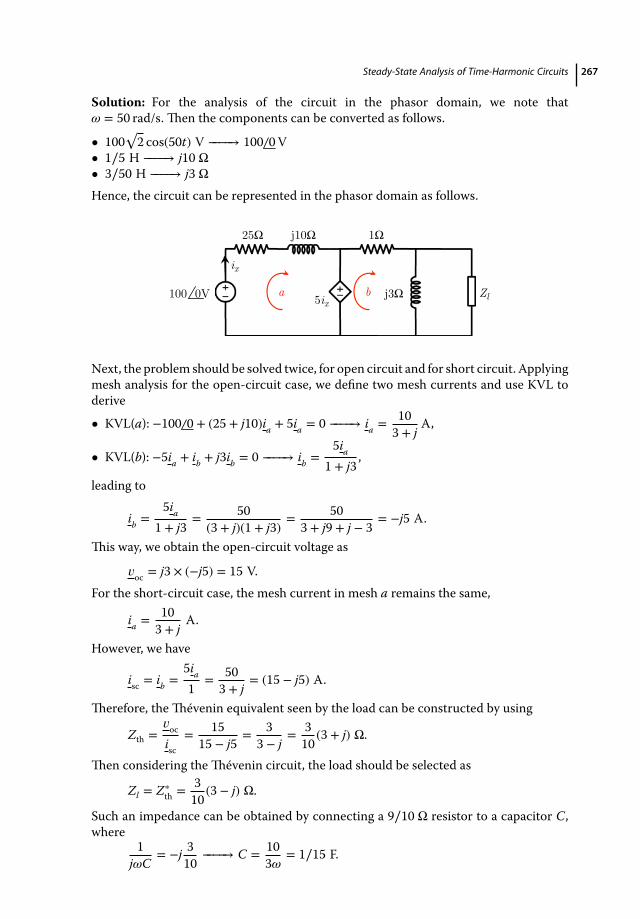
Steady-State Analysis of Time-Harmonic Circuits 267
Solution: For the analysis of the circuit in the phasor domain, we note that𝜔 = 50 rad/s. Then the components can be converted as follows.
• 100√2 cos(50t) V −−−−→ 100 0V
• 1∕5 H −−−−→ j10 Ω• 3∕50 H −−−−→ j3 ΩHence, the circuit can be represented in the phasor domain as follows.
Zl
25Ω j10Ω
5ix
1Ω
j3Ω100 0V a b
ix
Next, the problem should be solved twice, for open circuit and for short circuit. Applyingmesh analysis for the open-circuit case, we define two mesh currents and use KVL toderive
• KVL(a): −100 0 + (25 + j10)ia + 5ia = 0 −−−−→ ia = 103 + j
A,
• KVL(b): −5ia + ib + j3ib = 0 −−−−→ ib =5ia
1 + j3,
leading to
ib =5ia
1 + j3= 50
(3 + j)(1 + j3)= 50
3 + j9 + j − 3= −j5 A.
This way, we obtain the open-circuit voltage as
𝑣oc = j3 × (−j5) = 15 V.For the short-circuit case, the mesh current in mesh a remains the same,
ia = 103 + j
A.
However, we have
isc = ib =5ia
1= 50
3 + j= (15 − j5) A.
Therefore, the Thévenin equivalent seen by the load can be constructed by using
Zth =𝑣oc
isc= 15
15 − j5= 3
3 − j= 3
10(3 + j) Ω.
Then considering theThévenin circuit, the load should be selected as
Zl = Z∗th =
310
(3 − j) Ω.
Such an impedance can be obtained by connecting a 9∕10 Ω resistor to a capacitor C,where
1j𝜔C
= −j 310
−−−−→ C = 103𝜔
= 1∕15 F.
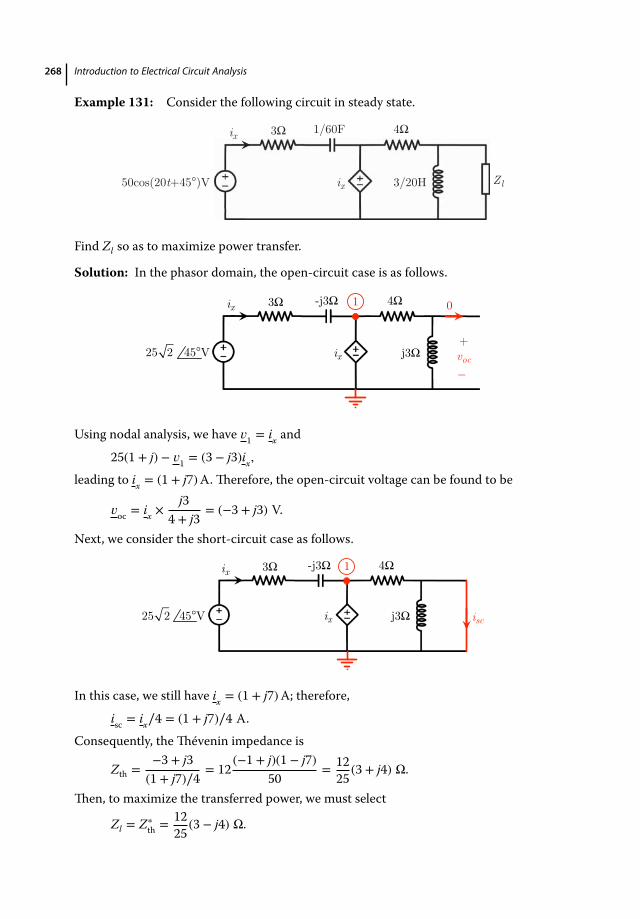
268 Introduction to Electrical Circuit Analysis
Example 131: Consider the following circuit in steady state.
50cos(20t+45°)V
3Ω 1/60F 4Ω
3/20H Zlix
ix
Find Zl so as to maximize power transfer.
Solution: In the phasor domain, the open-circuit case is as follows.
3Ω -j3Ω 4Ω
j3Ω25 2 45°V
0
+
_
1 ix
ix voc
Using nodal analysis, we have 𝑣1 = ix and
25(1 + j) − 𝑣1 = (3 − j3)ix,
leading to ix = (1 + j7)A.Therefore, the open-circuit voltage can be found to be
𝑣oc = ix ×j3
4 + j3= (−3 + j3) V.
Next, we consider the short-circuit case as follows.
3Ω
25 2 45°V
-j3Ω 4Ω
j3Ω
1 ix
ix isc
In this case, we still have ix = (1 + j7)A; therefore,
isc = ix∕4 = (1 + j7)∕4 A.Consequently, the Thévenin impedance is
Zth =−3 + j3
(1 + j7)∕4= 12
(−1 + j)(1 − j7)50
= 1225
(3 + j4) Ω.
Then, to maximize the transferred power, we must select
Zl = Z∗th =
1225
(3 − j4) Ω.
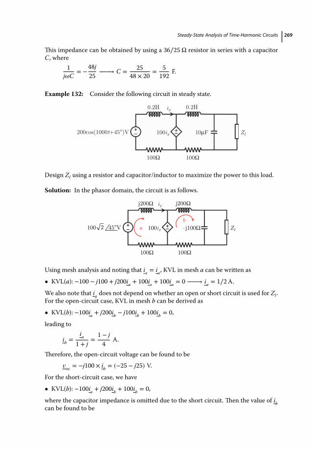
Steady-State Analysis of Time-Harmonic Circuits 269
This impedance can be obtained by using a 36∕25 Ω resistor in series with a capacitorC, where
1j𝜔C
= −48j25
−−−−→ C = 2548 × 20
= 5192
F.
Example 132: Consider the following circuit in steady state.
200cos(1000t+45°)V
0.2H 0.2H
100ix Zl
100Ω 100Ω
10μF
ix
Design Zl using a resistor and capacitor/inductor to maximize the power to this load.
Solution: In the phasor domain, the circuit is as follows.
j200Ω
100 2 45°V
j200Ω
100ix Zl
100Ω 100Ω
–j100Ωab
ix
Using mesh analysis and noting that ix = ia, KVL in mesh a can be written as
• KVL(a): −100 − j100 + j200ia + 100ix + 100ia = 0 −−−−→ ia = 1∕2A.
We also note that ia does not depend on whether an open or short circuit is used for Zl.For the open-circuit case, KVL in mesh b can be derived as
• KVL(b): −100ix + j200ib − j100ib + 100ib = 0,
leading to
ib =ia
1 + j=
1 − j4
A.
Therefore, the open-circuit voltage can be found to be
𝑣oc = −j100 × ib = (−25 − j25) V.
For the short-circuit case, we have
• KVL(b): −100ix + j200ib + 100ib = 0,
where the capacitor impedance is omitted due to the short circuit. Then the value of ibcan be found to be

270 Introduction to Electrical Circuit Analysis
ib =ia
1 + j2=
1 − j210
A.
This value corresponds to the short-circuit current, that is,
isc = ib =1 − j210
A.
Therefore, theThévenin impedance is
Zth =−25 − j25(1 − j2)∕10
= −2501 + j1 − j2
= −50(1 + j)(1 + j2) = 50(1 − j3) Ω.
Hence, in order to maximize the transferred power, one needs to selectZl = Z∗
th = 50(1 + j3) Ω.Such a load can be designed by connecting a 50 Ω resistor in series to a 150∕𝜔 = 0.15Hinductor.
Exercise 116: Consider the following circuit in steady state.
1H 5mF
0.5H
10Ω
Zl40 2 cos(20t)V
Find Zl in the phasor domain to maximize the power transferred to this load.
Exercise 117: Consider the following circuit in steady state.
Zl
2Ω
2Ω2H
0.25F
40 2 cos(2t)V
FindZl in the phasor domain tomaximize the power transferred to this load. Also designZl using a resistor and capacitor/inductor.
Exercise 118: Consider the following circuit in steady state.
200
0.4H 50Ω 2Ω
120mH10ix Zl
ix
2 cos(50t)V
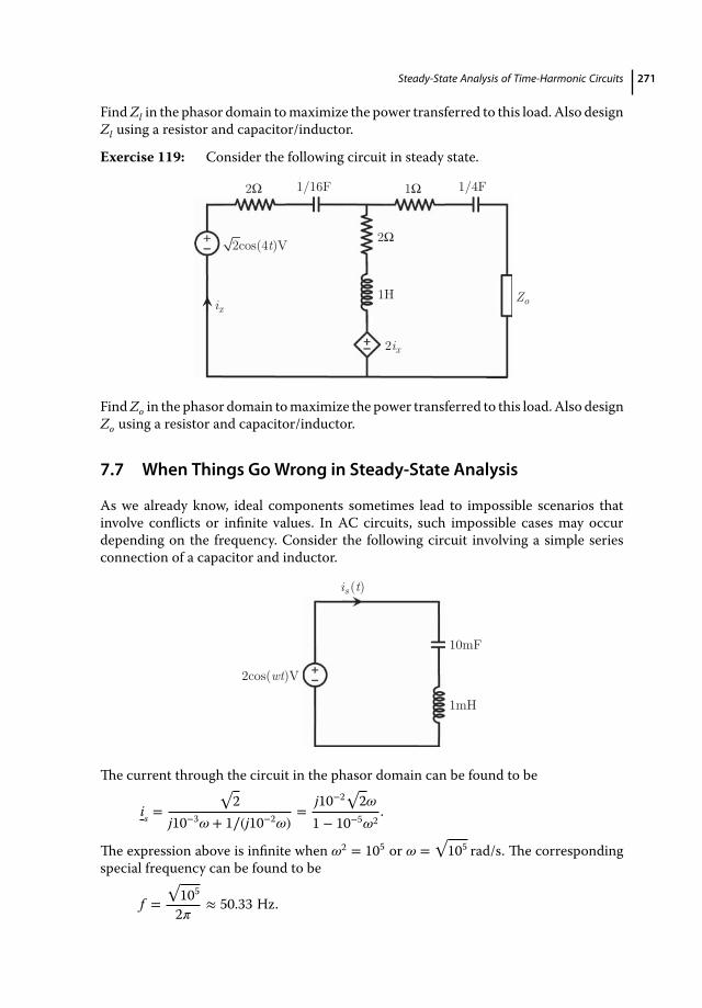
Steady-State Analysis of Time-Harmonic Circuits 271
FindZl in the phasor domain tomaximize the power transferred to this load. Also designZl using a resistor and capacitor/inductor.
Exercise 119: Consider the following circuit in steady state.
2cos(4t)V
2Ω
2Ω
1Ω1/16F 1/4F
2ix
1H Zoix
FindZo in the phasor domain tomaximize the power transferred to this load.Also designZo using a resistor and capacitor/inductor.
7.7 When Things Go Wrong in Steady-State Analysis
As we already know, ideal components sometimes lead to impossible scenarios thatinvolve conflicts or infinite values. In AC circuits, such impossible cases may occurdepending on the frequency. Consider the following circuit involving a simple seriesconnection of a capacitor and inductor.
2cos(wt)V
10mF
1mH
is (t)
The current through the circuit in the phasor domain can be found to be
is =√2
j10−3𝜔 + 1∕(j10−2𝜔)=
j10−2√2𝜔
1 − 10−5𝜔2.
The expression above is infinite when 𝜔2 = 105 or 𝜔 =√105 rad/s. The corresponding
special frequency can be found to be
f =√1052𝜋
≈ 50.33 Hz.
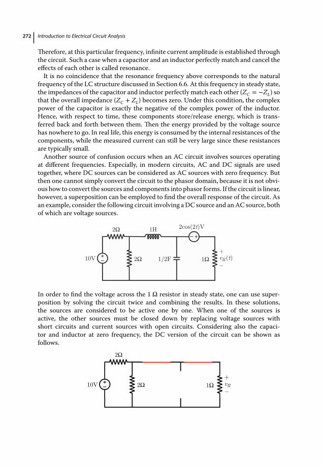
272 Introduction to Electrical Circuit Analysis
Therefore, at this particular frequency, infinite current amplitude is established throughthe circuit. Such a case when a capacitor and an inductor perfectly match and cancel theeffects of each other is called resonance.It is no coincidence that the resonance frequency above corresponds to the natural
frequency of the LC structure discussed in Section 6.6. At this frequency in steady state,the impedances of the capacitor and inductor perfectly match each other (ZC = −ZL) sothat the overall impedance (ZC + ZL) becomes zero. Under this condition, the complexpower of the capacitor is exactly the negative of the complex power of the inductor.Hence, with respect to time, these components store/release energy, which is trans-ferred back and forth between them. Then the energy provided by the voltage sourcehas nowhere to go. In real life, this energy is consumed by the internal resistances of thecomponents, while the measured current can still be very large since these resistancesare typically small.Another source of confusion occurs when an AC circuit involves sources operating
at different frequencies. Especially, in modern circuits, AC and DC signals are usedtogether, where DC sources can be considered as AC sources with zero frequency. Butthen one cannot simply convert the circuit to the phasor domain, because it is not obvi-ous how to convert the sources and components into phasor forms. If the circuit is linear,however, a superposition can be employed to find the overall response of the circuit. Asan example, consider the following circuit involving aDC source and anAC source, bothof which are voltage sources.
10V
2Ω
2Ω
1H
1/2F 1Ω
2cos(2t)V
vR (t)+_
In order to find the voltage across the 1 Ω resistor in steady state, one can use super-position by solving the circuit twice and combining the results. In these solutions,the sources are considered to be active one by one. When one of the sources isactive, the other sources must be closed down by replacing voltage sources withshort circuits and current sources with open circuits. Considering also the capaci-tor and inductor at zero frequency, the DC version of the circuit can be shown asfollows.
10V
2Ω
2Ω 1Ω+_vR

Steady-State Analysis of Time-Harmonic Circuits 273
For this circuit, the voltage of the resistor is given by
𝑣R,DC = 10 × 2 ∥ 1(2 ∥ 1) + 2
= 10 ×2∕3
2∕3 + 2= 10∕4 = 5∕2 V.
Next, the AC version of the circuit can be considered as follows.
2Ω
2Ω
j2Ω
–jΩ 1Ω+_
2Zin
0V
vR
In this case, we have
Zin = 1 + (1 + j2) ∥ (−j) = 32(1 − j) Ω
and
𝑣R,AC =2√2
3(1 − j)=
√2(1 + j)3
= 23
45∘V,
leading to
𝑣R,AC(t) =2√2
3cos(2t + 45∘) V.
Consequently, the overall voltage across the resistor is
𝑣R(t) =52+
2√2
3cos(2t + 45∘) V.
An common mistake occurs when dealing with series and parallel connections ofcapacitors when they are represented in the phasor domain. Consider a parallel con-nection of 1∕2 F and 1∕10 F capacitors when the frequency is 𝜔 = 2 rad/s.
1/10F1/2F -j5Ω-jΩ
Ceq Zeq
Once converted into impedances, series and parallel connections should be treated sim-ilarly to resistors, even when the origin of the impedance is a capacitor. For the parallelconnection above, we have
Zeq = (−j) ∥ (−j5) =j25−j6
= −5−j6
= −j56
Ω.
274 Introduction to Electrical Circuit Analysis
Alternatively, we can combine the capacitors in the original circuit as
Ceq =12+ 1
10= 3
5F,
leading to the same value as before,
Zeq =1
j2 × 3∕5= −
j56
Ω.
7.8 What You Need to Know before You Continue
As shown in this chapter, transformation to the phasor domain is essential to analyzeAC circuits in steady state. A few important points are as follows.
• In time-harmonic circuits, once converted into the phasor domain, capacitors andinductors can be investigated as resistors with imaginary resistances. This leads to ageneralized definition of resistance as impedance, which can have complex values.
• Unlike their behaviors for DC signals, capacitors and inductors behave like short andopen circuits, respectively, for sufficiently large frequencies.
• RC, RL, and RLC circuits with time-harmonic sources behave like filters, allowing thetransmission of signals in different ranges of frequencies while blocking others.
• In the phasor domain, a complex power can be defined to represent both dissipated(real) and stored/released (imaginary) powers.
• To maximize the real power transferred to a load, its impedance should be selectedas the complex conjugate of the input impedance of the circuit.
• Phasor-domain analysis is only valid for single-frequency circuits, where all sourceshave the same frequency. For linear circuits, however, superposition can be used toanalyze circuits involving sources with different frequencies (including DC as zerofrequency).
With the steady-state analysis of time-harmonic circuits, we have completed all thebasic topics of circuit analysis, which form the major focus of this book. In the nextthree extension chapters, we briefly consider some important components and practicaltechnologies of modern circuits, as well as some final suggestions that might be usefulwhen exploring electrical and electronic circuits beyond this book.

275
8
Selected Components of Modern Circuits
Previous chapters have presented fundamental laws (e.g., KVL andKCL) and techniques(e.g., nodal analysis, mesh analysis, and black-box equivalence) for the analysis of cir-cuits involving independent and dependent sources, resistors, capacitors, and inductors.While they are used to solve basic circuits, the laws and techniques presented are appli-cable to all types of circuits and components.We have been particularly concerned withresistors, capacitors, and inductors, since they are not just components but also repre-sent basic electrical properties of objects; any structure has a resistance, capacitance,and inductance, which characterize its electrical response. From this perspective, thetopics covered in the previous chapters can be seen as universal. However, electricaland electronic circuits evolve continuously thanks to rapid developments in science andtechnology. As the first extension, this chapter presents some selected components inmodern circuits.We emphasize that “modern” is a subjective term. For example, transis-tors are essential parts of modern circuits, whereas they have been conceptually knownfor decades.Thesemodern components also evolve and are physically transformed (e.g.,transistors become smaller and smaller), and perhaps some of them will completelydiminish in the future, with the term “modern” moving on to cover other types of com-ponents.In the following, we focus on five types of components, each of which demonstrates
different electrical characteristics, making them essential parts of modern circuits instate-of-the-art technology.We also discuss the analysis of basic circuits involving thesecomponents, in order to provide hints on their analysis in more complex scenarios.
8.1 When Connections Are via Magnetic Fields: Transformers
In electrical circuits and components, electrical connectivity is mainly constructed byelectrical conduction, or more generally, an electric field. This includes the terminals ofthe capacitor and the space between them filled with the electric field formed by accu-mulated charge. As seen in inductors, magnetic fields also play a major role in electricalcircuits. On the other hand, an exact counterpart of a capacitor (where connectivityis established by an electric field) is not an inductor, but a proper combination of twoinductors, namely, a transformer.As shown below (see also Figure 11.4), a transformer is a two-sided component, lead-
ing to the definition of two pairs of voltage and current values.
Introduction to Electrical Circuit Analysis, First Edition. Özgür Ergül.© 2017 John Wiley & Sons Ltd. Published 2017 by John Wiley & Sons Ltd.Companion Website: www.wiley.com/go/ergul4412
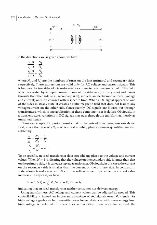
276 Introduction to Electrical Circuit Analysis
N1:N2
_
+
_
+
v1(t)
i1(t)
v2(t)
i2(t)
If the directions are as given above, we have𝑣1(t)𝑣2(t)
=N1
N2,
i1(t)i2(t)
=N2
N1,
where N1 and N2 are the numbers of turns on the first (primary) and secondary sides,respectively. These expressions are valid only for AC voltage and current signals. Thisis because the two sides of a transformer are connected via a magnetic field. This field,which is created by an input current in one of the sides (e.g., primary side) and passesthrough the other side (e.g., secondary side), induces an electromotive force (voltageand current) only if it changes with respect to time. When a DC signal appears on oneof the sides in steady state, it creates a static magnetic field that does not lead to anyvoltage/current on the other side. Consequently, DC signals are filtered out throughtransformers, which is one application of these components as isolators. Obviously, ina transient state, variations in DC signals may pass through the transformer, mostly asunwanted signals.There are a couple of important results that can be derived from the expressions above.
First, since the ratio N2∕N1 = N is a real number, phasor-domain quantities are alsorelated by
𝑣1
𝑣2=
N1
N2= 1
N,
i1i2
=N2
N1= N .
To be specific, an ideal transformer does not add any phase to the voltage and currentvalues.When N > 1, indicating that the voltage on the secondary side is larger than thaton the primary side, it is called a step-up transformer. Obviously, in this case, the currenton the secondary side is smaller than the current on the primary side. In contrast, ina step-down transformer with N < 1, the voltage value drops while the current valueincreases. In any case, we have
s1 = 𝑣1 × i∗1 =𝑣2
N× (Ni2)
∗ = 𝑣2 × i∗2 = s2,
indicating that an ideal transformer neither consumes nor delivers energy.Using transformers, AC voltage and current values can be adjusted as needed. This
controllability is indeed an important advantage of AC signals over DC signals. Ashigh-voltage signals can be transmitted over longer distances with lower energy loss,high voltage is preferred in power lines across cities. Then, once transmitted, the

Selected Components of Modern Circuits 277
electricity is transformed into lower voltage values without loss of power (or in practicewith small power loss), for safe indoor usage.
Example 133: Consider the following circuit in steady state.
24Ω
2:12Ω 8Ω
1/40F
40cos(6t)V
4:1
2Ωis(t)
Find is(t) in steady state.
Solution: This circuit can be analyzed in the phasor domain. At first glance, it may notbe obvious how to simplify the transformers. For this purpose, we consider the followingcase, where an impedance Zs is connected on the secondary side.
1:N
ZS _
+
_
+
Zin
v1 v2
i2i1
Using the definitions, we have 𝑣1 = 𝑣2∕N and i1 = Ni2, leading to
Zin =𝑣1
i1=
𝑣2
N2i2=
Zs
N2 .
Hence, using a transformer with turn ratio N , an impedance is transformed by a scalingwith N2 (e.g., reduced to a smaller value if N > 1).Now, considering the impedance transformation described above, the circuit can be
represented in the phasor domain as follows.
2Ω 8Ω
–20j/3Ω
20
6Ω 32Ω
0 V2
is
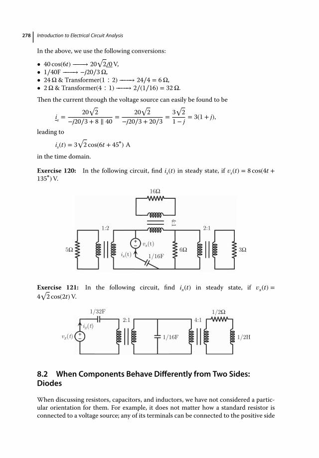
278 Introduction to Electrical Circuit Analysis
In the above, we use the following conversions:
• 40 cos(6t) −−−−→ 20√2 0V,
• 1∕40F −−−−→ −j20∕3Ω,• 24Ω & Transformer(1 ∶ 2) −−−−→ 24∕4 = 6Ω,• 2Ω & Transformer(4 ∶ 1) −−−−→ 2∕(1∕16) = 32Ω.
Then the current through the voltage source can easily be found to be
is =20
√2
−j20∕3 + 8 ∥ 40=
20√2
−j20∕3 + 20∕3=
3√2
1 − j= 3(1 + j),
leading to
is(t) = 3√2 cos(6t + 45∘) A
in the time domain.
Exercise 120: In the following circuit, find is(t) in steady state, if 𝑣s(t) = 8 cos(4t +135∘)V.
5Ω 3Ω6Ω1/16F
16Ω
1:2 2:1
4:1
is(t)vs(t)
Exercise 121: In the following circuit, find ix(t) in steady state, if 𝑣x(t) =4√2 cos(2t)V.
2:1
1/16F
1/32F4:1
1/2Ω
1/2Hix(t)
vx(t)
8.2 When Components Behave Differently from Two Sides:Diodes
When discussing resistors, capacitors, and inductors, we have not considered a partic-ular orientation for them. For example, it does not matter how a standard resistor isconnected to a voltage source; any of its terminals can be connected to the positive side
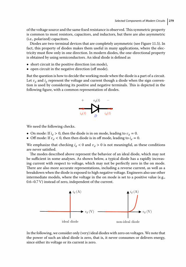
Selected Components of Modern Circuits 279
of the voltage source and the same fixed resistance is observed.This symmetric propertyis common to most resistors, capacitors, and inductors, but there are also asymmetric(i.e., polarized) capacitors.Diodes are two-terminal devices that are completely asymmetric (see Figure 11.5). In
fact, this property of diodes makes them useful in many applications, where the elec-tricity must flow only in one direction. In modern diodes, the one-directional propertyis obtained by using semiconductors. An ideal diode is defined as
• short circuit in the positive direction (on mode),• open circuit in the negative direction (off mode).
But the question is how to decide the workingmode when the diode is a part of a circuit.Let 𝑣d and id represent the voltage and current though a diode when the sign conven-tion is used by considering its positive and negative terminals. This is depicted in thefollowing figure, with a common representation of diodes.
+ _
D
vd(t)
id(t) id(t)
We need the following checks.
• On mode: If id > 0, then the diode is in on mode, leading to 𝑣d = 0.• Off mode: If 𝑣d < 0, then then diode is in off mode, leading to id = 0.
We emphasize that checking id < 0 and 𝑣d > 0 is not meaningful, as these conditionsare never satisfied.The modes described above represent the behavior of an ideal diode, which may not
be sufficient in some analyses. As shown below, a typical diode has a rapidly increas-ing current with respect to voltage, which may not be perfectly zero in the on mode.There are also more accurate representations, including a reverse current, as well as abreakdown when the diode is exposed to high negative voltage. Engineers also use otherintermediate models, where the voltage in the on mode is set to a positive value (e.g.,0.6–0.7V) instead of zero, independent of the current.
ideal diode non-ideal diode
id (A) id (A)
vd (V) vd (V)
In the following, we consider only (very) ideal diodes with zero on voltages.We note thatthe power of such an ideal diode is zero, that is, it never consumes or delivers energy,since either its voltage or its current is zero.
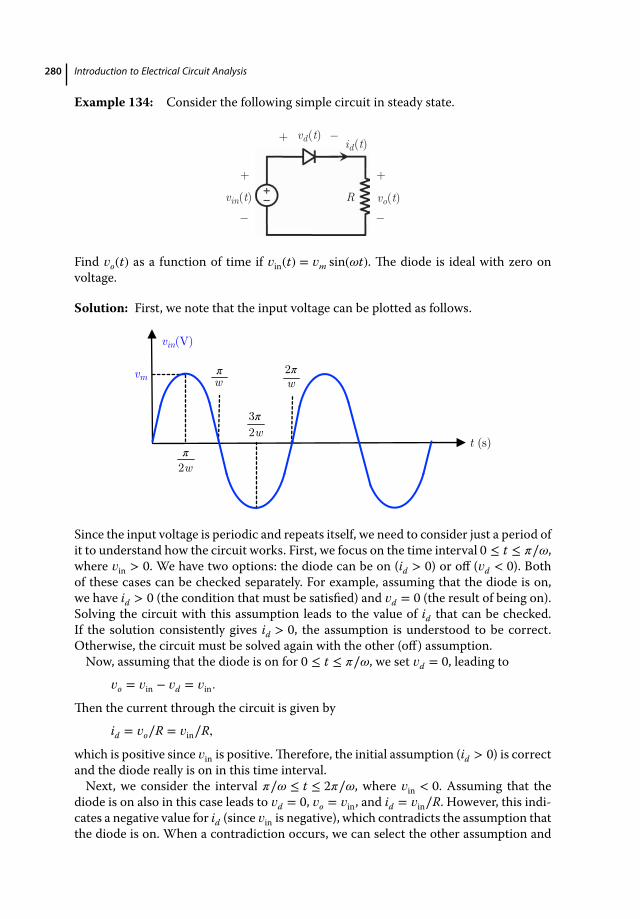
280 Introduction to Electrical Circuit Analysis
Example 134: Consider the following simple circuit in steady state.
+ _
+
_
+
_vin(t)
vd(t) id(t)
vo(t)R
Find 𝑣o(t) as a function of time if 𝑣in(t) = 𝑣m sin(𝜔t). The diode is ideal with zero onvoltage.
Solution: First, we note that the input voltage can be plotted as follows.
vin(V)
t (s)
3π
vm wπ
π
2w
2w
2πw
Since the input voltage is periodic and repeats itself, we need to consider just a period ofit to understand how the circuit works. First, we focus on the time interval 0 ≤ t ≤ 𝜋∕𝜔,where 𝑣in > 0. We have two options: the diode can be on (id > 0) or off (𝑣d < 0). Bothof these cases can be checked separately. For example, assuming that the diode is on,we have id > 0 (the condition that must be satisfied) and 𝑣d = 0 (the result of being on).Solving the circuit with this assumption leads to the value of id that can be checked.If the solution consistently gives id > 0, the assumption is understood to be correct.Otherwise, the circuit must be solved again with the other (off) assumption.Now, assuming that the diode is on for 0 ≤ t ≤ 𝜋∕𝜔, we set 𝑣d = 0, leading to
𝑣o = 𝑣in − 𝑣d = 𝑣in.
Then the current through the circuit is given by
id = 𝑣o∕R = 𝑣in∕R,
which is positive since 𝑣in is positive.Therefore, the initial assumption (id > 0) is correctand the diode really is on in this time interval.Next, we consider the interval 𝜋∕𝜔 ≤ t ≤ 2𝜋∕𝜔, where 𝑣in < 0. Assuming that the
diode is on also in this case leads to 𝑣d = 0, 𝑣o = 𝑣in, and id = 𝑣in∕R. However, this indi-cates a negative value for id (since 𝑣in is negative), which contradicts the assumption thatthe diode is on. When a contradiction occurs, we can select the other assumption and
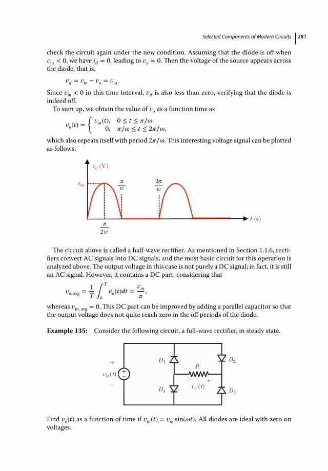
Selected Components of Modern Circuits 281
check the circuit again under the new condition. Assuming that the diode is off when𝑣in < 0, we have id = 0, leading to 𝑣o = 0. Then the voltage of the source appears acrossthe diode, that is,
𝑣d = 𝑣in − 𝑣o = 𝑣in.
Since 𝑣in < 0 in this time interval, 𝑣d is also less than zero, verifying that the diode isindeed off.To sum up, we obtain the value of 𝑣o as a function time as
𝑣o(t) =
𝑣in(t), 0 ≤ t ≤ 𝜋∕𝜔0, 𝜋∕𝜔 ≤ t ≤ 2𝜋∕𝜔,
which also repeats itself with period 2𝜋∕𝜔.This interesting voltage signal can be plottedas follows.
vo (V)
t (s)
vm w
2wπ
π 2πw
The circuit above is called a half-wave rectifier. As mentioned in Section 1.1.6, recti-fiers convert AC signals into DC signals; and the most basic circuit for this operation isanalyzed above.The output voltage in this case is not purely a DC signal; in fact, it is stillan AC signal. However, it contains a DC part, considering that
𝑣o, avg =1T ∫
T
0𝑣o(t)dt =
𝑣m
𝜋,
whereas 𝑣in, avg = 0.This DC part can be improved by adding a parallel capacitor so thatthe output voltage does not quite reach zero in the off periods of the diode.
Example 135: Consider the following circuit, a full-wave rectifier, in steady state.
D1
D4
D2
D3
R vin(t)
+
_ + vo (t)
_
Find 𝑣o(t) as a function of time if 𝑣in(t) = 𝑣m sin(𝜔t). All diodes are ideal with zero onvoltages.

282 Introduction to Electrical Circuit Analysis
Solution: Once again, we need to consider separate time intervals.
• For 0 ≤ t ≤ 𝜋∕𝜔, when 𝑣in(t) > 0, we assume that D2 and D4 are on, while D1 andD3 are off. Therefore, we have 𝑣D2 = 0 (short circuit), 𝑣D4 = 0 (short circuit), iD1 = 0(open circuit), and iD3 = 0 (open circuit). Then the circuit in this case can be redrawnas follows (note the voltage and current orientations according to the sign conventionand diode definitions).
R vin (t)
+
_ + vo (t)
_ +
_
+
_
vD1(t)
vD3 (t)
iD2 (t)
iD4(t)
We can check the necessary voltage and current values: we have
𝑣D1(t) = −𝑣in(t) < 0,iD2(t) = 𝑣in(t)∕R > 0,𝑣D3(t) = −𝑣in(t) < 0,iD4(t) = 𝑣in(t)∕R > 0,
verifying that all assumptions are correct. Hence, in this mode of operation, we have
𝑣o(t) = 𝑣in(t) = 𝑣m sin(𝜔t) (0 ≤ t ≤ 𝜋∕𝜔).
• For 𝜋∕𝜔 ≤ t ≤ 2𝜋∕𝜔, when 𝑣in(t) < 0, we assume that D1 and D3 are on, while D2 andD4 are off. Therefore, we have 𝑣D1 = 0 (short circuit), 𝑣D3 = 0 (short circuit), iD2 = 0(open circuit), and iD4 = 0 (open circuit). The circuit is as follows.
R vin(t)
+
_ + vo (t)
_
iD1 (t)
iD3 (t)
vD2 (t)+
_
+vD4 (t)
_
With 𝑣in(t) < 0, we have
iD1(t) = −𝑣in(t)∕R > 0,𝑣D2(t) = 𝑣in(t) < 0,iD3(t) = −𝑣in(t)∕R > 0,𝑣D4(t) = 𝑣in(t) < 0,
all of which satisfy the required conditions for the assumptions. Then
𝑣o(t) = −𝑣in(t) = −𝑣m sin(𝜔t) (𝜋∕𝜔 ≤ t ≤ 2𝜋∕𝜔).
It can be observed that the output voltage across the resistor is the same as the inputvoltage when the input voltage is positive, while it reversed when the input voltage is

Selected Components of Modern Circuits 283
negative. The output voltage, which is periodic with period 𝜋∕𝜔, can now be plotted asfollows.
vo (V)
t (s)
vm
w2w2πw
3πw
4πw
π π
Unlike the output of the half-wave rectifier, the output voltage of the full-wave rectifieris nonzero in all time intervals, indicating a more effective conversion of the AC signalinto a DC signal. It can be shown that
𝑣o, avg =1T ∫
T
0𝑣o(t)dt =
2𝑣m
𝜋,
using T = 2𝜋∕𝜔 as the period of the input voltage. Hence, using a full-wave rectifier,the DC content of the output signal is twice the DC content of output of the half-waverectifier.
Exercise 122: In the following circuit, where the diode combination is used as a limiter(clipper), find 𝑣o(t) in steady state, if 𝑣in(t) = 𝑣m sin(𝜔t) and 0 < 𝑣cl < 𝑣m is a DC source.Assume an ideal diode with zero on voltage.
vin(t)+
_
R
vcl
vo(t)+
_
Exercise 123: In the following circuit, find 𝑣o(t) in steady state, if 𝑣in(t) = 𝑣m sin(𝜔t),and 0 < 𝑣c1 < 𝑣m and 0 < 𝑣c2 < 𝑣m are DC sources. Assume ideal diodes with zero onvoltages.
vin(t)+
_
R
vc1
vo(t)+
_ vc2
D1 D2

284 Introduction to Electrical Circuit Analysis
8.3 When Components Involve Many Connections: OP-AMPs
Until now, we have considered mostly two-terminal components (e.g., independentand dependent sources, resistors, capacitors, inductors, and diodes). Transformers aretwo-port devices, where a port can be defined as a pair of terminals with positive andnegative values. In higher-level circuits, it is common to combine basic elements intomore complex packages and devices. To take an important example, integrated circuitsinvolve microchips that contain multiple elements (e.g., transistors). As the complexityincreases, these packages, which can also be considered as components themselves,involve more and more terminals. Operational amplifiers (or OP-AMPs) are popularcomponents of this kind with multiple connections (see Figure 11.6).OP-AMPs usually consist of many transistors and resistors, but are often represented
as multi-terminal components (without reference to what is inside them) in circuitanalysis. As their name suggests, OP-AMPs are amplifiers, that is, they amplify givensignals with smaller amplitudes into other forms with larger amplitudes.The input of anOP-AMP is provided through two terminals, namely inverting and noninverting inputs,while their difference is amplified and provided as the output.The amplification providesenables engineers to control signals and design electrical devices for various purposes.As shown below, five terminals of an OP-AMP are usually shown, among which the
DC terminals 𝑣Sp (positive) and 𝑣Sm (negative) that are used to power up the OP-AMPare usually neglected in their analysis.
vSp
vSm
vp
vm
+
_ vo
ip
imio
Similarly to diodes, there are different levels of approximations (idealizations) when ana-lyzing OP-AMPs. In an ideal model, we have
𝑣o = Ag(𝑣p − 𝑣m),where Ag is the gain, typically very large (e.g., 100 000). Hence, the voltage of the output(defined with respect to a ground) is Ag times the difference between the voltages of thenoninverting (𝑣p) and inverting (𝑣m) terminals. Obviously, some limitations are needed,in the form of saturation voltages, the highest and lowest values that can be obtainedat the output terminal. These saturation voltages are often the same as 𝑣Sp and 𝑣Sm. Anequivalent representation for this OP-AMP model can be depicted as follows.
voim
ip Ro
RiRi
Agvin
+ vin_ +
_
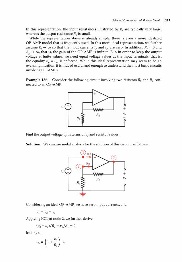
Selected Components of Modern Circuits 285
In this representation, the input resistances illustrated by Ri are typically very large,whereas the output resistance Ro is small.While the representation above is already simple, there is even a more idealized
OP-AMP model that is frequently used. In this more ideal representation, we furtherassume Ri → ∞ so that the input currents ip and im are zero. In addition, Ro = 0 andAg → ∞, that is, the gain of the OP-AMP is infinite. But, in order to keep the outputvoltage at finite values, we need equal voltage values at the input terminals, that is,the equality 𝑣p = 𝑣m is enforced. While this ideal representation may seem to be anoversimplification, it is indeed useful and enough to understand the most basic circuitsinvolving OP-AMPs.
Example 136: Consider the following circuit involving two resistors R1 and R2 con-nected to an OP-AMP.
+_
+
_ voR2R1
vs
Find the output voltage 𝑣o in terms of 𝑣s and resistor values.
Solution: We can use nodal analysis for the solution of this circuit, as follows.
+ _
+ _
voR2R1
vs
1
2
30A
0A
Considering an ideal OP-AMP, we have zero input currents, and
𝑣1 = 𝑣2 = 𝑣s.
Applying KCL at node 2, we further derive
(𝑣3 − 𝑣2)∕R2 − 𝑣2∕R1 = 0,
leading to
𝑣3 =(1 +
R2
R1
)𝑣2.

286 Introduction to Electrical Circuit Analysis
0A
0A 0A
circuit A circuit B
_
+
Figure 8.1 A voltage follower between two circuits, A and B.
Therefore, we obtain
𝑣o =(1 +
R2
R1
)𝑣s.
In this final expression, 1 + R2∕R1 can be interpreted as the finite gain of the circuit.Thisgain can easily be controlled by selecting the values of R1 and R2, in contrast to the hugegain of the OP-AMP itself. Therefore, the circuit above, which is called a noninvertingamplifier in reference to its positive gain, is commonly used in electrical circuits (insteadof a direct usage of a single OP-AMP). We note that selecting R2 = 0 and/or R1 → ∞leads to a gain of unity, leading to 𝑣o = 𝑣s. Such a circuit, where the output voltage isexactly the same as the input voltage, can be used as a buffer to isolate two circuits fromeach other. As shown above, the voltage is directly transferred in this case, whereas thecircuits A and B do not share any current flow. This kind of buffer is called a voltagefollower.
Example 137: Consider the following circuit, which is called a differential amplifier.
R1
R2
R3
R4
+ _
+
_
vovs1
vs2
Find 𝑣o in terms of 𝑣s1 and 𝑣s2.
Solution: Using nodal analysis, we label the nodes as follows.
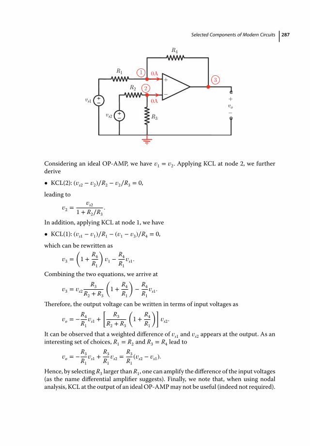
Selected Components of Modern Circuits 287
R1
R2
R3
R4
+ _ vo
vs1
vs2
1 0A
23
0A_
+
Considering an ideal OP-AMP, we have 𝑣1 = 𝑣2. Applying KCL at node 2, we furtherderive
• KCL(2): (𝑣s2 − 𝑣2)∕R2 − 𝑣2∕R3 = 0,
leading to
𝑣2 =𝑣s2
1 + R2∕R3.
In addition, applying KCL at node 1, we have
• KCL(1): (𝑣s1 − 𝑣1)∕R1 − (𝑣1 − 𝑣3)∕R4 = 0,
which can be rewritten as
𝑣3 =(1 +
R4
R1
)𝑣1 −
R4
R1𝑣s1.
Combining the two equations, we arrive at
𝑣3 = 𝑣s2R3
R2 + R3
(1 +
R4
R1
)−
R4
R1𝑣s1.
Therefore, the output voltage can be written in terms of input voltages as
𝑣o = −R4
R1𝑣s1 +
[ R3
R2 + R3
(1 +
R4
R1
)]𝑣s2.
It can be observed that a weighted difference of 𝑣s1 and 𝑣s2 appears at the output. As aninteresting set of choices, R1 = R2 and R3 = R4 lead to
𝑣o = −R3
R1𝑣s1 +
R3
R1𝑣s2 =
R3
R1(𝑣s2 − 𝑣s1).
Hence, by selectingR3 larger thanR1, one can amplify the difference of the input voltages(as the name differential amplifier suggests). Finally, we note that, when using nodalanalysis, KCL at the output of an idealOP-AMPmay not be useful (indeed not required).

288 Introduction to Electrical Circuit Analysis
In most circuits involving an OP-AMP, it is common to connect the output (e.g., byusing a resistor) back to the negative input terminal (see all circuits above).This feedbackloop is particularly important for obtaining stable behavior, which may not be achievedotherwise due to the very high (ideally infinite) gain of OP-AMPs.
Exercise 124: Consider the following circuit, which is called an inverting amplifier.
+
_
+ _ vo
R1
vs
R2
Find 𝑣o in terms of 𝑣s.
Exercise 125: In the following circuit, find 𝑣o in terms of 𝑣s1 and 𝑣s2.
R1
R2
R3
+ _
+
_
vovs1
vs2
8.4 When Circuits Become Modern: Transistors
Transistors are essential components of modern circuits. Following their first practi-cal implementation in 1947, they became key components of many electronic devicesdue to their favorable properties, for example, being inexpensive and suitable for massproduction (as integrated circuits). Transistors are made of semiconductors, exploitingthe flexibility and controllability of the conductivity of these special materials. Basi-cally, a transistor is a kind of amplifier, which transforms a signal into another one withhigher amplitude, depending on its operatingmode that is determined by aDC bias.Thefact that the response of a transistor depends on its operating mode makes it suitableespecially for switching operations. A collection of transistors working together lead to
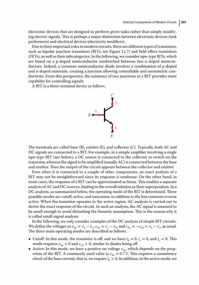
Selected Components of Modern Circuits 289
electronic devices that are designed to perform given tasks rather than simply modify-ing electric signals. This is perhaps a major distinction between electronic devices (taskperformers) and electrical devices (electricity modifiers).Due to their important roles inmodern circuits, there are different types of transistors,
such as bipolar junction transistors (BJTs; see Figure 11.7) and field-effect transistors(FETs), as well as their subcategories. In the following, we consider npn-type BJTs, whichare based on a p-doped semiconductor sandwiched between two n-doped semicon-ductors. Indeed, a common semiconductor diode involves a combination of p-dopedand n-doped materials, creating a junction allowing controllable and asymmetric con-ductivity. From this perspective, the existence of two junctions in a BJT provides morecapability for controlling signals.A BJT is a three-terminal device as follows.
B
C
E
ib
ic
ie
The terminals are called base (B), emitter (E), and collector (C). Typically, both AC andDC signals are connected to a BJT. For example, in a simple amplifier involving a singlenpn-type BJT (see below), a DC source is connected to the collector to switch on thetransistor, whereas the signal to be amplified (usually AC) is connected between the baseand emitter. Then the output of the circuit appears between the collector and emitter.Even when it is connected to a couple of other components, an exact analysis of a
BJT may not be straightforward since its response is nonlinear. On the other hand, inmost cases, the response of a BJT can be approximated as linear.This enables a separateanalysis of AC andDC sources, leading to the overall solution as their superposition. In aDC analysis, as summarized below, the operating mode of the BJT is determined.Threepossible modes are cutoff, active, and saturation, in addition to the less common reverseactive. When the transistor operates in the active region, AC analysis is carried out toderive the exact response of the circuit. In such an analysis, the AC signal is assumed tobe small enough to avoid disturbing the linearity assumption. This is the reason why itis called small-signal analysis.In the following, we only consider examples of the DC analysis of simple BJT circuits.
We define the voltages as 𝑣be = 𝑣b − 𝑣e, 𝑣cb = 𝑣c − 𝑣b, and 𝑣bc = −𝑣cb = 𝑣b − 𝑣c, as usual.The three main operating modes are described as follows.
• Cutoff: In this mode, the transistor is off, and we have ib = 0, ic = 0, and ie = 0. Thismode requires 𝑣be < 0 and 𝑣cb > 0, similar to diodes being off.
• Active: In this mode, we have a positive on voltage 𝑣be, which depends on the prop-erties of the BJT. A commonly used value is 𝑣be = 0.7V. This requires a consistencycheck of the base current, that is, we require ib > 0. In addition, in the activemode, we

290 Introduction to Electrical Circuit Analysis
must have 𝑣cb > 0. But, if ib is nonzero, the analysis requires a relationship betweenthe currents of the transistor. The required equality is
ic = 𝛽ib,
where 𝛽 is called the common-emitter current gain. Obviously, using KCL, we furtherhave
ie = ib + ic = ib + 𝛽ib = (1 + 𝛽)ib.
The value of 𝛽 is typically large, of the order of hundreds.• Saturation: In saturation mode, we still have 𝑣be = 0.7V, which requires ib > 0. In
addition, due to the forward bias of the BC junction, we should have a nonzero 𝑣bc,typically, 𝑣bc = 0.2V. In addition to nonzero ib, we must check if ic < 𝛽ib in order toverify that the BJT is indeed in saturation mode.
Similarly to the analysis of diodes, we start with an assumption for the mode of a BJTand check whether the required conditions are satisfied. In case of conflicting values,the assumption is revised accordingly.
Example 138: Consider the following circuit, involving a BJT with 0.7V on voltagefor 𝑣be and 𝛽 = 100.
vs
7V2.8V
2Ω
0.7Ω
1Ω
+ _ vo
Find the DC signal at the output.
Solution: First, we draw the DC version of the circuit as follows.
7V2.8V
2Ω
0.7Ω
1Ω
+ _ vo
ibic
ie
1
2
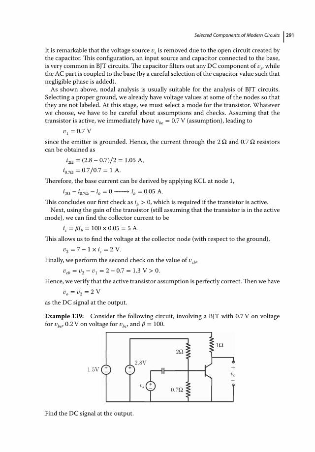
Selected Components of Modern Circuits 291
It is remarkable that the voltage source 𝑣s is removed due to the open circuit created bythe capacitor. This configuration, an input source and capacitor connected to the base,is very common in BJT circuits.The capacitor filters out any DC component of 𝑣s, whilethe AC part is coupled to the base (by a careful selection of the capacitor value such thatnegligible phase is added).As shown above, nodal analysis is usually suitable for the analysis of BJT circuits.
Selecting a proper ground, we already have voltage values at some of the nodes so thatthey are not labeled. At this stage, we must select a mode for the transistor. Whateverwe choose, we have to be careful about assumptions and checks. Assuming that thetransistor is active, we immediately have 𝑣be = 0.7V (assumption), leading to
𝑣1 = 0.7 Vsince the emitter is grounded. Hence, the current through the 2Ω and 0.7Ω resistorscan be obtained as
i2Ω = (2.8 − 0.7)∕2 = 1.05 A,i0.7Ω = 0.7∕0.7 = 1 A.
Therefore, the base current can be derived by applying KCL at node 1,i2Ω − i0.7Ω − ib = 0 −−−−→ ib = 0.05 A.
This concludes our first check as ib > 0, which is required if the transistor is active.Next, using the gain of the transistor (still assuming that the transistor is in the active
mode), we can find the collector current to beic = 𝛽ib = 100 × 0.05 = 5 A.
This allows us to find the voltage at the collector node (with respect to the ground),𝑣2 = 7 − 1 × ic = 2 V.
Finally, we perform the second check on the value of 𝑣cb,𝑣cb = 𝑣2 − 𝑣1 = 2 − 0.7 = 1.3 V > 0.
Hence, we verify that the active transistor assumption is perfectly correct.Then we have𝑣o = 𝑣2 = 2 V
as the DC signal at the output.
Example 139: Consider the following circuit, involving a BJT with 0.7V on voltagefor 𝑣be, 0.2 V on voltage for 𝑣bc, and 𝛽 = 100.
vs
1.5V2.8V
2Ω
0.7Ω
1Ω
+ _ vo
Find the DC signal at the output.

292 Introduction to Electrical Circuit Analysis
Solution: We note that this circuit is very similar to the previous one, except for thevalue of the leftmost voltage source, which is now 1.5V.
1.5V2.8V
2Ω
0.7Ω
1Ω
+ _ vo
ibic
ie
1
2
Assuming that the transistor is active, we have 𝑣be = 0.7V, leading to
𝑣1 = 0.7 V,i2 Ω = (2.8 − 0.7)∕2 = 1.05 A,
i0.7 Ω = 0.7∕0.7 = 1 A,ib = 0.05 A,
exactly as before. Then, using the gain, we should also have
ic = 𝛽ib = 100 × 0.05 = 5 A.
However, this leads to a collector voltage of
𝑣2 = 2.8 − 1 × ic = −2.2 V,
leading to 𝑣cb = −2.2 − 0.7 = −2.9V which is less than zero. Therefore, our active tran-sistor assumption is incorrect and we must revise the analysis.We can restart the analysis by assuming that the transistor is in saturation mode. In
this case, we still have 𝑣be = 0.7V, and the following steps are still valid:
𝑣1 = 0.7 V,i2 Ω = (2.8 − 0.7)∕2 = 1.05 A,
i0.7 Ω = 0.7∕0.7 = 1 A,ib = 0.05 A.
On the other hand, we cannot use ic = 𝛽ib. Instead, supposing that the transistor is sat-urated, we assume that 𝑣bc = 0.2V, leading to
𝑣2 = 𝑣1 − 0.2 = 0.5 V.
Consequently, the collector current can be obtained as
ic = (1.5 − 0.5)∕1 = 1 A.
As a final check, we note that
ic = 1 < 𝛽ib = 5,
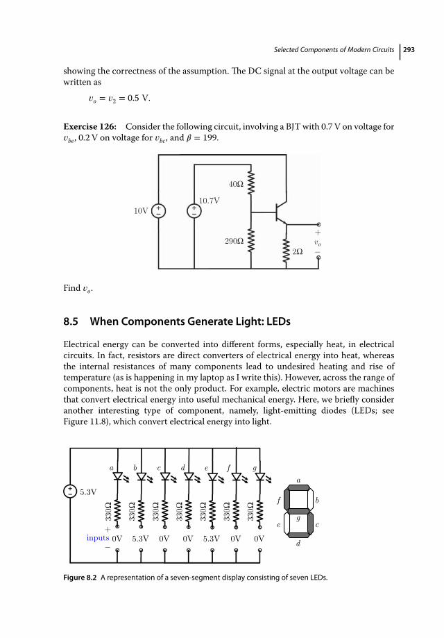
Selected Components of Modern Circuits 293
showing the correctness of the assumption. The DC signal at the output voltage can bewritten as
𝑣o = 𝑣2 = 0.5 V.
Exercise 126: Consider the following circuit, involving a BJT with 0.7V on voltage for𝑣be, 0.2 V on voltage for 𝑣bc, and 𝛽 = 199.
10V10.7V
40Ω
290Ω+ _ vo
2Ω
Find 𝑣o.
8.5 When Components Generate Light: LEDs
Electrical energy can be converted into different forms, especially heat, in electricalcircuits. In fact, resistors are direct converters of electrical energy into heat, whereasthe internal resistances of many components lead to undesired heating and rise oftemperature (as is happening in my laptop as I write this). However, across the range ofcomponents, heat is not the only product. For example, electric motors are machinesthat convert electrical energy into useful mechanical energy. Here, we briefly consideranother interesting type of component, namely, light-emitting diodes (LEDs; seeFigure 11.8), which convert electrical energy into light.
a b c d e f g
330Ω
330Ω
330Ω
330Ω
330Ω
330Ω
330Ω
5.3V
0V 5.3V 0V 0V 0V 0V 5.3V + _ inputs
a
b
c
d
e
fg
Figure 8.2 A representation of a seven-segment display consisting of seven LEDs.

294 Introduction to Electrical Circuit Analysis
A typical LED is a pn-junction diodewith a relatively large on-voltage value such that iteffectively consumes energy to be released as light. Usually, the on-voltage value and thedesired current through the LED, hence the power of the LED, are known. Therefore,given a source voltage, the current through the LED is controlled by a resistor. Thereare also reverse components called photodiodes and photoresistors, whose electricalresponse depend on the light illuminating them. LEDs, photodiodes, and photoresis-tors can be used together to build electronic devices, for example isolators, where thecomponents interact via light. This is similar to transformers using the magnetic fieldinstead of electric current for operation.An iconic and probably one of the most common applications of LEDs is the
seven-segment display in the form of the number 8. A total of seven LEDs are usedto represent numeric values from 0 to 9, depending on the LEDs that are on and off.As shown below, this can be achieved by controlling the LED voltages, according thenumber to be displayed.In the circuit above, each LED has an on voltage of 2V. The inputs, which are con-
trolled by a logic gate, are either 5.3V or zero, making the LEDs off and on, respectively.Specifically, when a LED is on with 2V across its terminal, the current through it is
ion =5.3 − 2330
= 10 mA.
Then the power of the LED can be obtained as pon = 2 × ion = 20mW, which representsthe amount of energy released mostly as light per second.
8.6 Conclusion
Five different types of components of modern circuits are briefly considered in thischapter. All these components have special properties, making them useful as compo-nents of electrical and electronic devices. Transformers usemagnetic induction betweentheir ports and are employed for controlling the amplitudes of voltage and currents,as well as for isolation. Diodes have unidirectional characteristics, providing engineersa control ability that can be used in constructing rectifiers, clippers, and logic gates.LEDs are also diodes with distinct light-emitting properties that can be used in dis-play technologies, lighting, and optical controllers. OP-AMPs are particularly usefulfor amplifiers, filters, and oscillators. Finally, transistors are fundamental componentsof modern circuits, enabling engineers to build smaller and cheaper electronic circuitswithmore capabilities. A typical smartphone, at the time of writing, involves a chip with2 billion transistors, each of which has dimensions of the order of tens of nanometers.While we focus on representative types, there are also different subcategories of all thesecomponents with diverse properties.Our exploration of modern circuits continues in the next chapter, where we consider
several practical technologies in modern circuits.
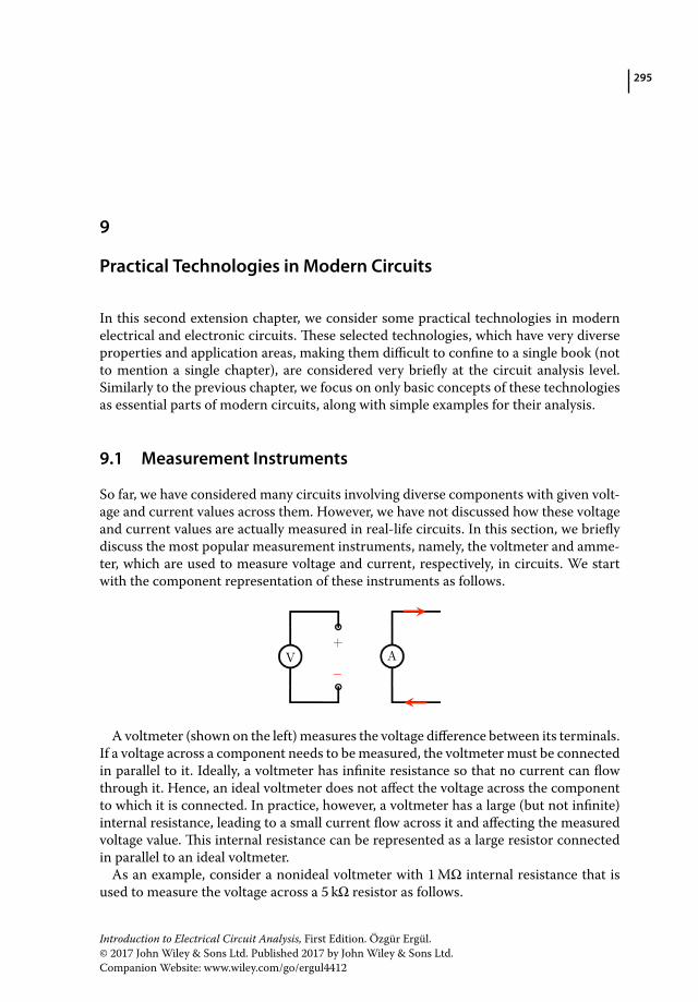
295
9
Practical Technologies in Modern Circuits
In this second extension chapter, we consider some practical technologies in modernelectrical and electronic circuits. These selected technologies, which have very diverseproperties and application areas, making them difficult to confine to a single book (notto mention a single chapter), are considered very briefly at the circuit analysis level.Similarly to the previous chapter, we focus on only basic concepts of these technologiesas essential parts of modern circuits, along with simple examples for their analysis.
9.1 Measurement Instruments
So far, we have considered many circuits involving diverse components with given volt-age and current values across them. However, we have not discussed how these voltageand current values are actually measured in real-life circuits. In this section, we brieflydiscuss the most popular measurement instruments, namely, the voltmeter and amme-ter, which are used to measure voltage and current, respectively, in circuits. We startwith the component representation of these instruments as follows.
+AV _
A voltmeter (shown on the left) measures the voltage difference between its terminals.If a voltage across a component needs to bemeasured, the voltmeter must be connectedin parallel to it. Ideally, a voltmeter has infinite resistance so that no current can flowthrough it. Hence, an ideal voltmeter does not affect the voltage across the componentto which it is connected. In practice, however, a voltmeter has a large (but not infinite)internal resistance, leading to a small current flow across it and affecting the measuredvoltage value. This internal resistance can be represented as a large resistor connectedin parallel to an ideal voltmeter.As an example, consider a nonideal voltmeter with 1MΩ internal resistance that is
used to measure the voltage across a 5 kΩ resistor as follows.
Introduction to Electrical Circuit Analysis, First Edition. Özgür Ergül.© 2017 John Wiley & Sons Ltd. Published 2017 by John Wiley & Sons Ltd.Companion Website: www.wiley.com/go/ergul4412
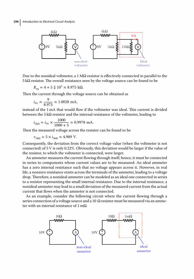
296 Introduction to Electrical Circuit Analysis
9V
non-idealvoltmeter
9V
Idealvoltmeter
0A 4kΩ4kΩ
5kΩ5kΩ 1MΩ
Due to the nonideal voltmeter, a 1MΩ resistor is effectively connected in parallel to the5 kΩ resistor. The overall resistance seen by the voltage source can be found to be
Req = 4 + 5 ∥ 103 ≈ 8.975 kΩ.Then the current through the voltage source can be obtained as
i9V ≈ 98.975
≈ 1.0028 mA,
instead of the 1mA that would flow if the voltmeter was ideal. This current is dividedbetween the 5 kΩ resistor and the internal resistance of the voltmeter, leading to
i5kΩ = i9V × 10001000 + 5
≈ 0.9978 mA.
Then the measured voltage across the resistor can be found to be𝑣5kΩ = 5 × i5kΩ ≈ 4.989 V.
Consequently, the deviation from the correct voltage value (when the voltmeter is notconnected) of 5V is only 0.22%. Obviously, this deviation would be larger if the value ofthe resistor, to which the voltmeter is connected, were larger.An ammetermeasures the current flowing through itself; hence, it must be connected
in series to components whose current values are to be measured. An ideal ammeterhas a zero internal resistance such that no voltage appears across it. However, in reallife, a nonzero resistance exists across the terminals of the ammeter, leading to a voltagedrop.Therefore, a nonideal ammeter can bemodeled as an ideal one connected in seriesto a resistor representing the small internal resistance. Due to the internal resistance, anonideal ammetermay lead to a small deviation of themeasured current from the actualcurrent that flows when the ammeter is not connected.As an example, consider the following circuit where the current flowing through a
series connection of a voltage source and a 10 Ω resistormust bemeasured via an amme-ter with an internal resistance of 1mΩ.
10Ω
10V A A
non-idealammeter
10Ω
10V
idealammeter
1mΩ
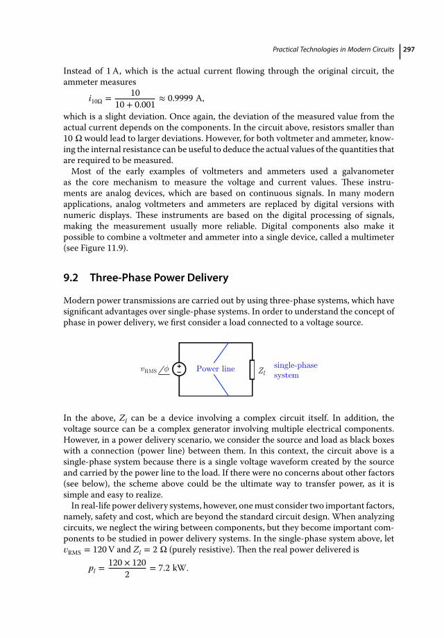
Practical Technologies in Modern Circuits 297
Instead of 1A, which is the actual current flowing through the original circuit, theammeter measures
i10Ω = 1010 + 0.001
≈ 0.9999 A,
which is a slight deviation. Once again, the deviation of the measured value from theactual current depends on the components. In the circuit above, resistors smaller than10 Ω would lead to larger deviations. However, for both voltmeter and ammeter, know-ing the internal resistance can be useful to deduce the actual values of the quantities thatare required to be measured.Most of the early examples of voltmeters and ammeters used a galvanometer
as the core mechanism to measure the voltage and current values. These instru-ments are analog devices, which are based on continuous signals. In many modernapplications, analog voltmeters and ammeters are replaced by digital versions withnumeric displays. These instruments are based on the digital processing of signals,making the measurement usually more reliable. Digital components also make itpossible to combine a voltmeter and ammeter into a single device, called a multimeter(see Figure 11.9).
9.2 Three-Phase Power Delivery
Modern power transmissions are carried out by using three-phase systems, which havesignificant advantages over single-phase systems. In order to understand the concept ofphase in power delivery, we first consider a load connected to a voltage source.
vRMS φ Zlsingle-phasesystemPower line
In the above, Zl can be a device involving a complex circuit itself. In addition, thevoltage source can be a complex generator involving multiple electrical components.However, in a power delivery scenario, we consider the source and load as black boxeswith a connection (power line) between them. In this context, the circuit above is asingle-phase system because there is a single voltage waveform created by the sourceand carried by the power line to the load. If there were no concerns about other factors(see below), the scheme above could be the ultimate way to transfer power, as it issimple and easy to realize.In real-life power delivery systems, however, onemust consider two important factors,
namely, safety and cost, which are beyond the standard circuit design. When analyzingcircuits, we neglect the wiring between components, but they become important com-ponents to be studied in power delivery systems. In the single-phase system above, let𝑣RMS = 120V and Zl = 2 Ω (purely resistive). Then the real power delivered is
pl =120 × 120
2= 7.2 kW.
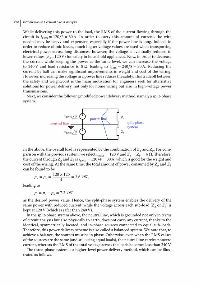
298 Introduction to Electrical Circuit Analysis
While delivering this power to the load, the RMS of the current flowing through thecircuit is iRMS = 120∕2 = 60A. In order to carry this amount of current, the wireneeded may be heavy and expensive, especially if the power line is long. Indeed, inorder to reduce ohmic losses, much higher voltage values are used when transportingelectrical power across long distances; however, the voltage is eventually reduced tolower values (e.g., 120V) for safety in household appliances. Now, in order to decreasethe current while keeping the power at the same level, we can increase the voltageto 240V and load resistance to 8 Ω, leading to iRMS = 240∕8 = 30A. Reducing thecurrent by half can make significant improvements in weight and cost of the wiring.However, increasing the voltage in a power line reduces the safety.This tradeoff betweenthe safety and weight/cost is the main motivation for engineers seek for alternativesolutions for power delivery, not only for home wiring but also in high-voltage powertransmissions.Next, we consider the followingmodified power deliverymethod, namely a split-phase
system.
vRMS
vRMS
φ
φ
power linesplit-phasesystem
neutral lineZa
Zb
In the above, the overall load is represented by the combination of Za and Zb. For com-parisonwith the previous system, we select 𝑣RMS = 120V andZa = Zb = 4 Ω.Therefore,the current through Za and Zb is iRMS = 120∕4 = 30A, which is good for the weight andcost of the wiring. At the same time, the total amount of power consumed by Za and Zbcan be found to be
pa = pb = 120 × 1204
= 3.6 kW,
leading to
pl = pa + pb = 7.2 kW
as the desired power value. Hence, the split-phase system enables the delivery of thesame power with reduced current, while the voltage across each sub-load (Za or Zb) iskept at 120V (which is safer than 240V).In the split-phase system above, the neutral line, which is grounded not only in terms
of circuit analysis but also physically to earth, does not carry any current, thanks to theidentical, symmetrically located, and in-phase sources connected to equal sub-loads.Therefore, this power delivery scheme is also called a balanced system. We note that, toachieve a balance, the sources must be in phase. Otherwise, even when the RMS valuesof the sources are the same (and still using equal loads), the neutral line carries nonzerocurrent, whereas the RMS of the total voltage across the loads becomes less than 240V.The three-phase system is a higher-level power delivery method, which can be illus-
trated as follows.
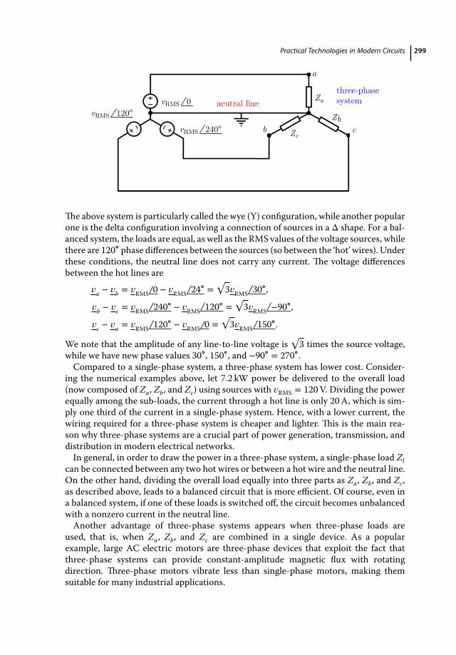
Practical Technologies in Modern Circuits 299
three-phasesystemneutral linevRMS 0
vRMS 120°vRMS 240°
Za
Zc
Zb
a
b c
The above system is particularly called the wye (Y) configuration, while another popularone is the delta configuration involving a connection of sources in a Δ shape. For a bal-anced system, the loads are equal, as well as the RMS values of the voltage sources, whilethere are 120∘ phase differences between the sources (so between the ‘hot’ wires). Underthese conditions, the neutral line does not carry any current. The voltage differencesbetween the hot lines are
𝑣a − 𝑣b = 𝑣RMS 0 − 𝑣RMS 24∘ =√3𝑣RMS 30∘,
𝑣b − 𝑣c = 𝑣RMS 240∘ − 𝑣RMS 120∘ =√3𝑣RMS −90∘,
𝑣c − 𝑣a = 𝑣RMS 120∘ − 𝑣RMS 0 =√3𝑣RMS 150∘.
We note that the amplitude of any line-to-line voltage is√3 times the source voltage,
while we have new phase values 30∘, 150∘, and −90∘ = 270∘.Compared to a single-phase system, a three-phase system has lower cost. Consider-
ing the numerical examples above, let 7.2 kW power be delivered to the overall load(now composed of Za, Zb, and Zc) using sources with 𝑣RMS = 120V. Dividing the powerequally among the sub-loads, the current through a hot line is only 20A, which is sim-ply one third of the current in a single-phase system. Hence, with a lower current, thewiring required for a three-phase system is cheaper and lighter. This is the main rea-son why three-phase systems are a crucial part of power generation, transmission, anddistribution in modern electrical networks.In general, in order to draw the power in a three-phase system, a single-phase load Zl
can be connected between any two hot wires or between a hot wire and the neutral line.On the other hand, dividing the overall load equally into three parts as Za, Zb, and Zc,as described above, leads to a balanced circuit that is more efficient. Of course, even ina balanced system, if one of these loads is switched off, the circuit becomes unbalancedwith a nonzero current in the neutral line.Another advantage of three-phase systems appears when three-phase loads are
used, that is, when Za, Zb, and Zc are combined in a single device. As a popularexample, large AC electric motors are three-phase devices that exploit the fact thatthree-phase systems can provide constant-amplitude magnetic flux with rotatingdirection. Three-phase motors vibrate less than single-phase motors, making themsuitable for many industrial applications.
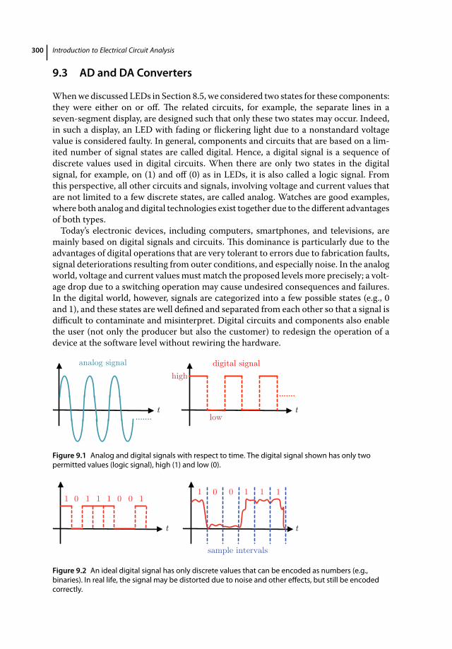
300 Introduction to Electrical Circuit Analysis
9.3 AD and DA Converters
Whenwe discussed LEDs in Section 8.5, we considered two states for these components:they were either on or off. The related circuits, for example, the separate lines in aseven-segment display, are designed such that only these two states may occur. Indeed,in such a display, an LED with fading or flickering light due to a nonstandard voltagevalue is considered faulty. In general, components and circuits that are based on a lim-ited number of signal states are called digital. Hence, a digital signal is a sequence ofdiscrete values used in digital circuits. When there are only two states in the digitalsignal, for example, on (1) and off (0) as in LEDs, it is also called a logic signal. Fromthis perspective, all other circuits and signals, involving voltage and current values thatare not limited to a few discrete states, are called analog. Watches are good examples,where both analog and digital technologies exist together due to the different advantagesof both types.Today’s electronic devices, including computers, smartphones, and televisions, are
mainly based on digital signals and circuits. This dominance is particularly due to theadvantages of digital operations that are very tolerant to errors due to fabrication faults,signal deteriorations resulting from outer conditions, and especially noise. In the analogworld, voltage and current valuesmustmatch the proposed levelsmore precisely; a volt-age drop due to a switching operation may cause undesired consequences and failures.In the digital world, however, signals are categorized into a few possible states (e.g., 0and 1), and these states are well defined and separated from each other so that a signal isdifficult to contaminate and misinterpret. Digital circuits and components also enablethe user (not only the producer but also the customer) to redesign the operation of adevice at the software level without rewiring the hardware.
t t
analog signal digital signalhigh
low
Figure 9.1 Analog and digital signals with respect to time. The digital signal shown has only twopermitted values (logic signal), high (1) and low (0).
t
1 0 1 1 1 0 0 1
t
1 0 0 1 1 1
sample intervals
Figure 9.2 An ideal digital signal has only discrete values that can be encoded as numbers (e.g.,binaries). In real life, the signal may be distorted due to noise and other effects, but still be encodedcorrectly.

Practical Technologies in Modern Circuits 301
Since there are only two or several states in digital signals, analysis of digital circuits isoften reduced to studying inputs and outputs of higher-level components (which con-tain more basic elements, such as transistors). For example, in logic circuits, inputs andoutputs of components are only a set of 0s and 1s, leading to a finite number of possi-ble scenarios.This simplification allows engineers to combine many digital componentstogether to build complex electronic devices that perform given tasks that are beyondthe capabilities of analog circuits. Nevertheless, analog circuits maintain their position,at least as alternatives to digital counterparts, in various areas. While digital circuits aretolerant of operational errors, such as noise, their failure may have larger impacts. Forexample, a single faulty component in a digital circuit may turn off a huge electronicdevice, system, or network. Replacing such a faulty component can be expensive anddifficult; in many cases, replacing the overall circuit and even the device is preferred.In addition, when a real-life analog signal (e.g., voice) is converted into a digital signal,there is always some loss of information that may not be recovered.In the next two sections of this chapter, we consider some popular components of dig-
ital circuits. In the following, we study the conversion of analog and digital signals intoeach other, using analog-to-digital (AD) and digital-to-analog (DA) converters. Sincewe are living in an analog world, practically speaking, these conversions are essentialto interact with digital circuits and devices. We consider AD and DA converters, onceagain, from the perspective of circuit analysis.Conventional AD converters are packed as small chips that contain many elements
working together to convert the given analog signals into digital forms. Among alterna-tives, integrating converters are relatively slow but quite precise in digitization. A com-plete integrating converter usually consists of an integrating unit, comparator, clock, andcontroller. Here, we focus on the integrating unit as the heart of the converter. In orderto understand why we need integration, the following figure depicts how a continuous(analog) signal can be discretized.
t
analog signaldigital levels
In the above, the smaller the time intervals, the better the discretized waveform approx-imates the analog signal. The digital levels, which are determined via integration, maynot be the final digital signal. However, these levels can easily be categorized (using acomparator and clock) according to the number of configurations to be used in the digi-tal output. For example, signal levels above a given threshold can be set to 1 while othersare set to 0, leading to a 1-bit device. Conventional AD converters usually have largernumbers of bits (e.g., 8–24) that allow for many digital levels in the discretization ofanalog signals.Obviously, in order to implement anAD converter, we need to find the total amount of
signal (integral of the analog function) in given time intervals. To perform this operation,the following integrator based on an OP-AMP can be used.
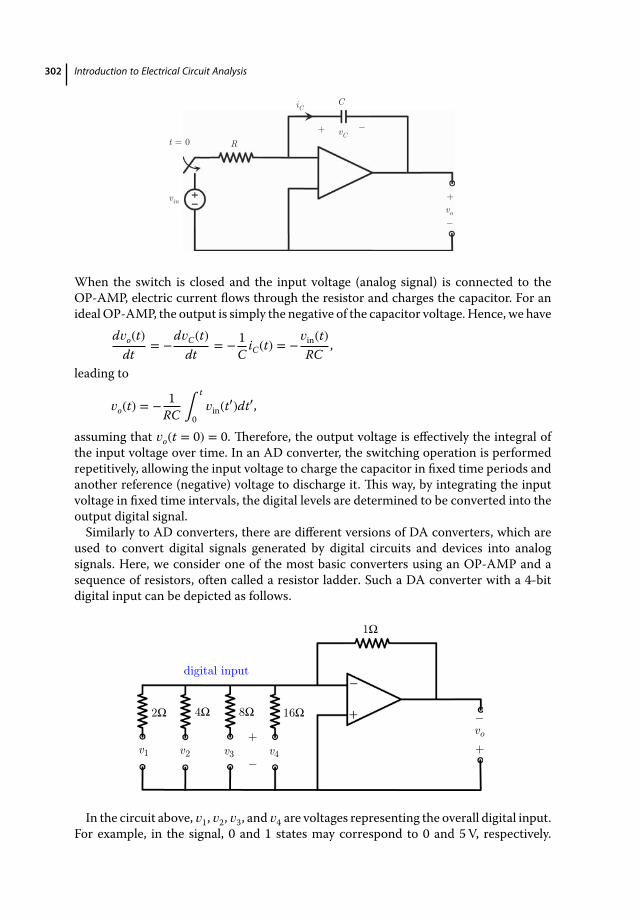
302 Introduction to Electrical Circuit Analysis
R
C
+
_ vo
vin
t = 0 + _
vC
iC
When the switch is closed and the input voltage (analog signal) is connected to theOP-AMP, electric current flows through the resistor and charges the capacitor. For anidealOP-AMP, the output is simply the negative of the capacitor voltage. Hence, we have
d𝑣o(t)dt
= −d𝑣C(t)
dt= − 1
CiC(t) = −
𝑣in(t)RC
,
leading to
𝑣o(t) = − 1RC ∫
t
0𝑣in(t′)dt′,
assuming that 𝑣o(t = 0) = 0. Therefore, the output voltage is effectively the integral ofthe input voltage over time. In an AD converter, the switching operation is performedrepetitively, allowing the input voltage to charge the capacitor in fixed time periods andanother reference (negative) voltage to discharge it. This way, by integrating the inputvoltage in fixed time intervals, the digital levels are determined to be converted into theoutput digital signal.Similarly to AD converters, there are different versions of DA converters, which are
used to convert digital signals generated by digital circuits and devices into analogsignals. Here, we consider one of the most basic converters using an OP-AMP and asequence of resistors, often called a resistor ladder. Such a DA converter with a 4-bitdigital input can be depicted as follows.
+
_
1Ω
+
_ vo
16Ω
digital input
8Ω4Ω2Ω
v1 v2 v3 v4+
_
In the circuit above, 𝑣1, 𝑣2, 𝑣3, and 𝑣4 are voltages representing the overall digital input.For example, in the signal, 0 and 1 states may correspond to 0 and 5V, respectively.

Practical Technologies in Modern Circuits 303
The purpose of the DA converter is to generate a unique output voltage correspondingto a given digital signal. The ladder structure above enables such an ability to distin-guish different digital signals represented by four digits. Assuming an ideal OP-AMP,the output voltage can be found to be
𝑣o =𝑣1
2+
𝑣2
4+
𝑣3
8+
𝑣4
16.
Then, if the digital signal is [d1, d2, d3, d4] = [1, 0, 0, 1], we have 𝑣1 = 𝑣4 = 5V and𝑣2 = 𝑣3 = 0, leading to
𝑣o = 5∕2 + 0 + 0 + 5∕16 = 45∕16 = 2.8125 V.We note that this voltage value corresponds to [1, 0, 0, 1] and no other combinationsof four bits. As further examples, [0, 1, 1, 0] leads to 𝑣o = 1.875V, whereas [1, 1, 1, 1]and [0, 0, 0, 0] lead to 𝑣o = 4.6875V and 𝑣o = 0 as the maximum and minimum values,respectively.We now know ways to convert analog signals into digital and vice versa. But how can
digital circuits be analyzed? In the next sections, we consider logic gates and memoryunits as popular components of digital circuits.
9.4 Logic Gates
Logic gates are building blocks of most digital circuits. They are usually made of diodesand transistors, which are packed into single components that can carry out the requiredlogic operations. Since the signal levels are reduced to a set of values (i.e., 0 and 1) inlogic circuits, the input/output functions of logic gates are generally defined in terms ofthese discrete values, without considering the actual strengths of voltages and currents.This simplification allows engineers to combine and cascade many logic gates to buildelectronic circuits and devices that can perform complex tasks.Among various types, the most basic logic gates with one or two input and single
output terminals can be described as follows.
AND OR NOT NAND
NORinputs output
For all these components, inputs and outputs are defined as 0 or 1. Considering logicoperations, these low and high states are also called FALSE and TRUE, respectively.Thebehavior of each component is well defined and tabulated as a truth table. For example,the output of an AND gate for different input combinations can be shown as follows.
00 0 0
1 0 10 0 1
1 1
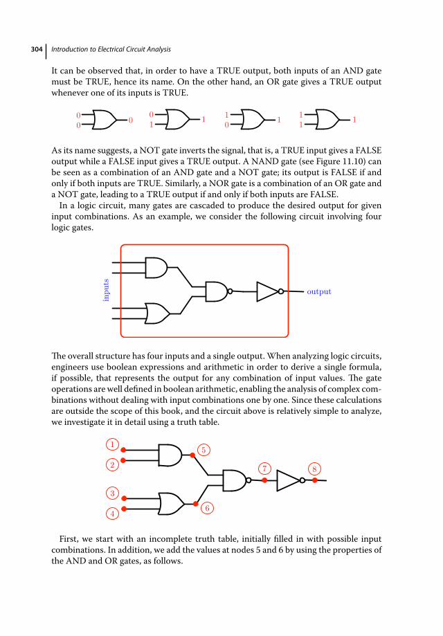
304 Introduction to Electrical Circuit Analysis
It can be observed that, in order to have a TRUE output, both inputs of an AND gatemust be TRUE, hence its name. On the other hand, an OR gate gives a TRUE outputwhenever one of its inputs is TRUE.
00 0 0
1 1 10 1 1
1 1
As its name suggests, a NOT gate inverts the signal, that is, a TRUE input gives a FALSEoutput while a FALSE input gives a TRUE output. A NAND gate (see Figure 11.10) canbe seen as a combination of an AND gate and a NOT gate; its output is FALSE if andonly if both inputs are TRUE. Similarly, a NOR gate is a combination of an OR gate anda NOT gate, leading to a TRUE output if and only if both inputs are FALSE.In a logic circuit, many gates are cascaded to produce the desired output for given
input combinations. As an example, we consider the following circuit involving fourlogic gates.
inpu
ts
output
The overall structure has four inputs and a single output. When analyzing logic circuits,engineers use boolean expressions and arithmetic in order to derive a single formula,if possible, that represents the output for any combination of input values. The gateoperations are well defined in boolean arithmetic, enabling the analysis of complex com-binations without dealing with input combinations one by one. Since these calculationsare outside the scope of this book, and the circuit above is relatively simple to analyze,we investigate it in detail using a truth table.
1
2
3
4
5
6
7 8
First, we start with an incomplete truth table, initially filled in with possible inputcombinations. In addition, we add the values at nodes 5 and 6 by using the properties ofthe AND and OR gates, as follows.

Practical Technologies in Modern Circuits 305
n1 n2 n3 n4 n5 n6 n7 n8
0 0 0 0 0 00 0 0 1 0 10 0 1 0 0 10 0 1 1 0 10 1 0 0 0 00 1 0 1 0 10 1 1 0 0 10 1 1 1 0 11 0 0 0 0 01 0 0 1 0 11 0 1 0 0 11 0 1 1 0 11 1 0 0 1 01 1 0 1 1 11 1 1 0 1 11 1 1 1 1 1
We note that n5 is TRUE if and only if both n1 and n2 are TRUE. On the other hand,n6 is FALSE if and only if both n3 and n4 are FALSE. Next, for given values of n5 andn6, as well as the properties of the NAND gate, we find the value at node 7 for differentcases. The output of the NAND gate is FALSE if and only if both inputs are TRUE (onlythe last three cases). The output at node 8 is simply the reverse of the value at node 7;hence, we obtain the following complete table.
n1 n2 n3 n4 n5 n6 n7 n8
0 0 0 0 0 0 1 00 0 0 1 0 1 1 00 0 1 0 0 1 1 00 0 1 1 0 1 1 00 1 0 0 0 0 1 00 1 0 1 0 1 1 00 1 1 0 0 1 1 00 1 1 1 0 1 1 01 0 0 0 0 0 1 01 0 0 1 0 1 1 01 0 1 0 0 1 1 01 0 1 1 0 1 1 01 1 0 0 1 0 1 01 1 0 1 1 1 0 11 1 1 0 1 1 0 11 1 1 1 1 1 0 1

306 Introduction to Electrical Circuit Analysis
It can be observed that the output of the circuit is TRUE only for three (outof 16) combinations of the inputs. Specifically, these are [n1, n2, n3, n4] = [1, 1, 0, 1],[n1, n2, n3, n4] = [1, 1, 1, 0], and [n1, n2, n3, n4] = [1, 1, 1, 1]. The output is FALSE for allother cases.This response of the circuit can be represented by using boolean operationson the inputs. Then, with a well-defined input–output relationship, the circuit can becombined with other circuits to implement larger and more technological circuits andelectronic devices.As briefly mentioned above, logic gates are mainly made of diodes and transistors, as
well as resistors for coupling and adjusting current values. Here we consider one of themost basic gates, namely, the resistor-transistor-logic (RTL) NOR gate, which involvesa BJT transistor combined with a few resistors. There are also RTL gates with multipleBJTs, but we investigate the single-transistor version for simplicity while understandingthe working principles of transistors as logic elements.Consider the following RTL NOR gate with two inputs and an output.
100Ω
220Ω
10Ω
voib
ic
ie
1
2
100Ωvi1
vi2
+5V
–5V
We assume that the transistor has 𝛽 = 100, 0.7V on voltage for 𝑣be, and 0.2V on voltagefor 𝑣bc. In addition, all node voltages are defined with respect to a common ground,which is also depicted in the figure. First, we consider the asymmetric case where oneof the inputs is TRUE and the other is FALSE. Using 𝑣i1 = 5V (for TRUE) and 𝑣i2 =0V (for FALSE), the transistor is in saturation mode, leading to 𝑣1 = 𝑣be = 0.7V and𝑣2 = 𝑣1 − 𝑣bc = 0.5V. Applying KCL at node 1, we have
• KCL(1): (5 − 0.7)∕100 + (0 − 0.7)∕100 − (0.7 + 5)∕220 − ib = 0,
leading to ib ≈ 10.1mA. We can also find the collector current, ic = (5 − 0.5)∕10 = 0.45A. Therefore, we verify that ic < 𝛽ib = 1.01A as a requirement of the sat-uration mode. In this case, the output voltage (i.e., the collector voltage) is simply𝑣o = 0.5V. While this value is not a perfect zero, it is a low value that can be interpretedas a FALSE output. The solution of the circuit is very similar when 𝑣i1 = 0V and𝑣i2 = 5V, leading again to a FALSE output.
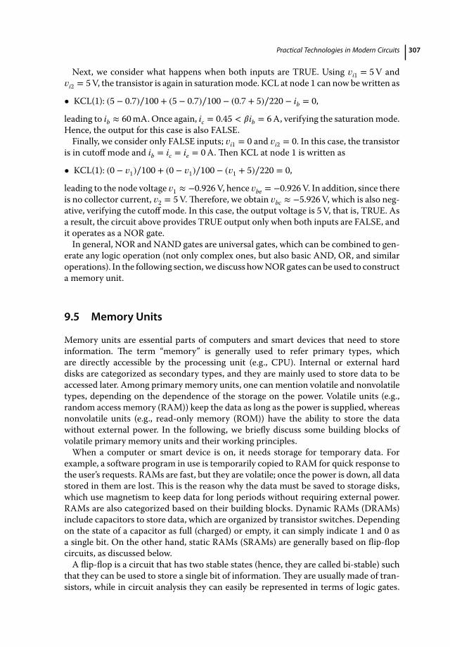
Practical Technologies in Modern Circuits 307
Next, we consider what happens when both inputs are TRUE. Using 𝑣i1 = 5V and𝑣i2 = 5V, the transistor is again in saturationmode. KCL at node 1 can now bewritten as
• KCL(1): (5 − 0.7)∕100 + (5 − 0.7)∕100 − (0.7 + 5)∕220 − ib = 0,
leading to ib ≈ 60mA. Once again, ic = 0.45 < 𝛽ib = 6A, verifying the saturationmode.Hence, the output for this case is also FALSE.Finally, we consider only FALSE inputs; 𝑣i1 = 0 and 𝑣i2 = 0. In this case, the transistor
is in cutoff mode and ib = ic = ie = 0A. Then KCL at node 1 is written as
• KCL(1): (0 − 𝑣1)∕100 + (0 − 𝑣1)∕100 − (𝑣1 + 5)∕220 = 0,
leading to the node voltage 𝑣1 ≈ −0.926V, hence 𝑣be = −0.926V. In addition, since thereis no collector current, 𝑣2 = 5V.Therefore, we obtain 𝑣bc ≈ −5.926V, which is also neg-ative, verifying the cutoff mode. In this case, the output voltage is 5V, that is, TRUE. Asa result, the circuit above provides TRUE output only when both inputs are FALSE, andit operates as a NOR gate.In general, NOR and NAND gates are universal gates, which can be combined to gen-
erate any logic operation (not only complex ones, but also basic AND, OR, and similaroperations). In the following section,we discuss howNORgates can be used to constructa memory unit.
9.5 Memory Units
Memory units are essential parts of computers and smart devices that need to storeinformation. The term “memory” is generally used to refer primary types, whichare directly accessible by the processing unit (e.g., CPU). Internal or external harddisks are categorized as secondary types, and they are mainly used to store data to beaccessed later. Among primary memory units, one can mention volatile and nonvolatiletypes, depending on the dependence of the storage on the power. Volatile units (e.g.,random access memory (RAM)) keep the data as long as the power is supplied, whereasnonvolatile units (e.g., read-only memory (ROM)) have the ability to store the datawithout external power. In the following, we briefly discuss some building blocks ofvolatile primary memory units and their working principles.When a computer or smart device is on, it needs storage for temporary data. For
example, a software program in use is temporarily copied to RAM for quick response tothe user’s requests. RAMs are fast, but they are volatile; once the power is down, all datastored in them are lost. This is the reason why the data must be saved to storage disks,which use magnetism to keep data for long periods without requiring external power.RAMs are also categorized based on their building blocks. Dynamic RAMs (DRAMs)include capacitors to store data, which are organized by transistor switches. Dependingon the state of a capacitor as full (charged) or empty, it can simply indicate 1 and 0 asa single bit. On the other hand, static RAMs (SRAMs) are generally based on flip-flopcircuits, as discussed below.A flip-flop is a circuit that has two stable states (hence, they are called bi-stable) such
that they can be used to store a single bit of information.They are usually made of tran-sistors, while in circuit analysis they can easily be represented in terms of logic gates.
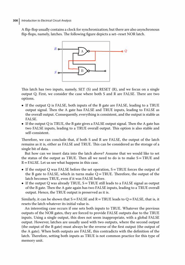
308 Introduction to Electrical Circuit Analysis
A flip-flop usually contains a clock for synchronization; but there are also asynchronousflip-flops, namely, latches. The following figure depicts a set–reset NOR latch.
R
S
QA
B
This latch has two inputs, namely, SET (S) and RESET (R), and we focus on a singleoutput Q. First, we consider the case where both S and R are FALSE. There are twooptions.
• If the output Q is FALSE, both inputs of the B gate are FALSE, leading to a TRUEoutput signal. Then the A gate has FALSE and TRUE inputs, leading to FALSE asthe overall output. Consequently, everything is consistent, and the output is stable asFALSE.
• If the output Q is TRUE, the B gate gives a FALSE output signal. Then the A gate hastwo FALSE inputs, leading to a TRUE overall output. This option is also stable andself-consistent.
Therefore, we can conclude that, if both S and R are FALSE, the output of the latchremains as it is, either as FALSE and TRUE. This can be considered as the storage of asingle bit of data.But how can we insert data into the latch above? Assume that we would like to set
the status of the output as TRUE. Then all we need to do is to make S=TRUE andR= FALSE. Let us see what happens in this case.
• If the output Q was FALSE before the set operation, S=TRUE forces the output ofthe B gate to FALSE, which in turns make Q=TRUE. Therefore, the output of thelatch becomes TRUE, even if it was FALSE before.
• If the output Q was already TRUE, S=TRUE still leads to a FALSE signal as outputof the B gate. Then the A gate again has two FALSE inputs, leading to a TRUE overalloutput. Hence, the TRUE output is preserved as it is.
Similarly, it can be shown that S= FALSE and R=TRUE leads to Q= FALSE, that is, itresets the latch whatever its initial value is.An interesting case occurs if one sets both inputs to TRUE. Whatever the previous
outputs of the NOR gates, they are forced to provide FALSE outputs due to the TRUEinputs. Using a single output, this does not seem inappropriate, with a global FALSEoutput. However, latches are usually used with two outputs, where the second output(the output of the B gate) must always be the reverse of the first output (the output ofthe A gate). When both outputs are FALSE, this contradicts with the definition of thelatch. Therefore, setting both inputs as TRUE is not common practice for this type ofmemory unit.

Practical Technologies in Modern Circuits 309
There aremany combinations of NOR andNANDgates, ormore precisely transistors,to construct latches as the building blocks of memory devices, particularly SRAMs. Weemphasize that memory is merely one application of logic gates, which are basic unitsof all electronic circuits in modern technology.
9.6 Conclusion
Some practical technologies are considered in this extension chapter. Measurementtools allow engineers to test voltage and current values in circuits and to detect faultycomponents easily. Three-phase systems are used for distributing electric power safelyand less expensively, across long distances in the AC form.The last three sections tell ushow analog circuits evolve into digital circuits, involving logic gates as building blocks.This is also how electrical circuits become electronic circuits as decision-making andprogrammable systems via logic operations.We are now very close to the end of this book. In the final extension chapter, we pro-
vide some advice on how to approach complex electrical and electronic circuits anddevices in real life.


311
10
Next Steps
We conclude this book with some final notes. In this short farewell chapter, we discussa couple of important points when we deal with complex circuits and devices. As thepurpose of this book is to cover the fundamentals of analyzing circuits, but not the cir-cuits themselves, we clearly emphasize the main ideas before the reader enters into thecomplex world of electrical and electronic circuits in specialized areas. Whatever thearea is, we keep in mind that
• energy is always conserved,• complex circuits can be analyzed by considering them as combinations of sub-
circuits, whose functions are well known,• state-of-the-art components are usually squeezed into integrated microchips, allow-
ing us to build more complex circuits,• the human body itself can be considered as a circuit element,• and electricity is a natural phenomenon that must be handled with care.
Good luck!
10.1 Energy Is Conserved, Always!
When we analyze a circuit, we keep in mind that the total power of all elements mustbe zero, as a result of the conservation of energy. Specifically, some components mayhave positive power values (consuming energy) while others have negative (deliveringenergy), but their algebraic sum must be zero. A component that consumes energy at aparticular timemay store it (capacitors and inductors) or convert it into other forms (e.g.,heat in resistors, light in LEDs) that may not be recovered. Similarly, a component thatdelivers energy may actually produce it (voltage and current sources) from other forms(e.g., chemical energy in batteries) or use energy that is stored earlier (again, capacitorsand inductors). Energy is always conserved; there is no way to produce it from nothingand consume it without converting it into another form.This is not because of a specialbalance mechanism; it is due to how we define energy.The conservation of energy must hold when electrical circuits are combined with
other mechanisms and devices. In some cases, however, the balance of energy amongthe elements may not be trivial. Consider the following circuit involving a DC motor.
Introduction to Electrical Circuit Analysis, First Edition. Özgür Ergül.© 2017 John Wiley & Sons Ltd. Published 2017 by John Wiley & Sons Ltd.Companion Website: www.wiley.com/go/ergul4412

312 Introduction to Electrical Circuit Analysis
t = 0
12V, 50mA12V
i
DCmotors convert electrical energy into mechanical energy, using DC voltage and cur-rent, unlike ACmotors. Each DCmotor is described with voltage/current/power valuesthat are specified when the motor is fully operational. In the circuit above, a motor with12V and 50mA is used, leading to pm = 12 × 0.05 = 0.6W. Hence, when it is fully oper-ational, this motor converts 0.6 J electrical energy into mechanical energy (torque) persecond. The energy required is provided by the voltage source (e.g., battery).But now let us consider the instant at which the switch is closed and themotor (which
is at rest) just becomes connected to the voltage source. At t = 0+, the motor is still notworking (e.g., its rotor does not rotate). Hence, it should not consume any energy atthis particular time. Then, due to the conservation of energy, the voltage source shouldnot deliver any energy, leading to i(0+) = 0 current through the circuit. But here is thedilemma: If the current is zero, how the motor can start gaining energy such that itsrotor accelerates? Should not the motor be at rest infinitely?Indeed, when the switch is closed in the circuit above, there is a large current flowing
through the circuit.This inrush current, which decays to the steady-state value of 50mAas time passes, is responsible for starting up the motor and accelerating the rotor untilit gains full angular velocity. In order to understand the circuit at t = 0+, we need toconsider the small internal resistance of the motor.
t = 0+
12V
0.3Ωi
12V, 50mA
At t = 0+, the rotor does not rotate, that is, no electrical energy is converted intomechanical energy, but due to the small internal resistance of the motor, a huge amountof current flows: i = 12∕0.3 = 40A. As the current flows through the wires on therotor, a magnetic force is generated between the rotor and stationary magnets, leadingto acceleration. Hence, the mechanical power increases with time. In the limit case,when i = 50mA, most of the energy provided by the voltage source is converted intomechanical energy. In this case, the power consumed by the internal resistance of themotor is 0.3 × 0.05 = 0.015W, which is a small percentage of the power consumed bythe motor for mechanical operation.
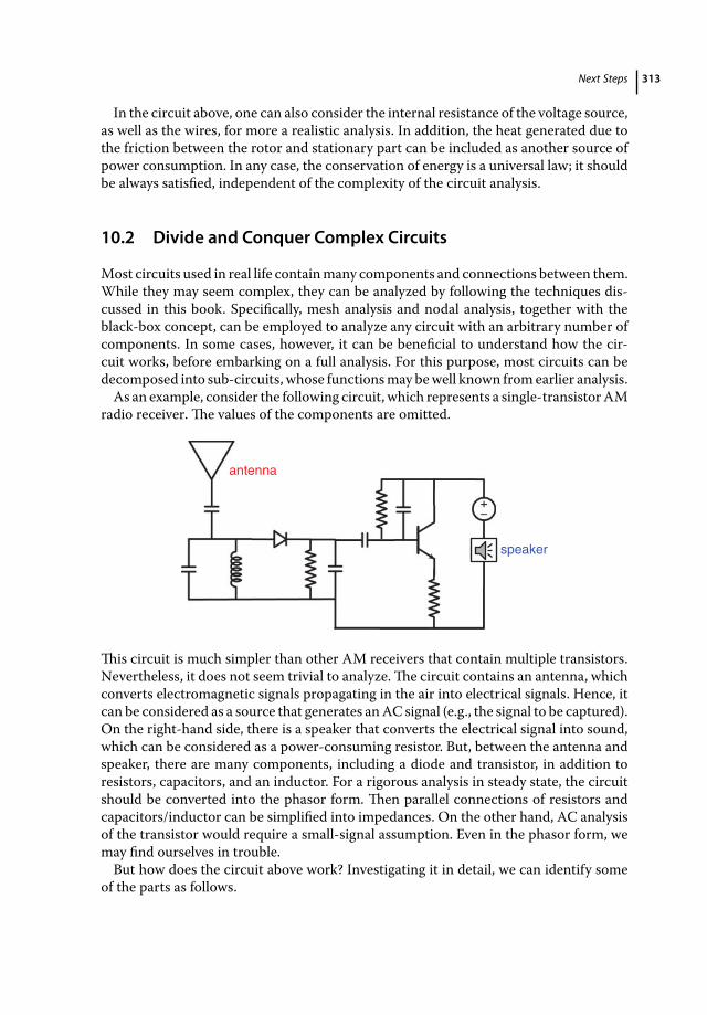
Next Steps 313
In the circuit above, one can also consider the internal resistance of the voltage source,as well as the wires, for more a realistic analysis. In addition, the heat generated due tothe friction between the rotor and stationary part can be included as another source ofpower consumption. In any case, the conservation of energy is a universal law; it shouldbe always satisfied, independent of the complexity of the circuit analysis.
10.2 Divide and Conquer Complex Circuits
Most circuits used in real life containmany components and connections between them.While they may seem complex, they can be analyzed by following the techniques dis-cussed in this book. Specifically, mesh analysis and nodal analysis, together with theblack-box concept, can be employed to analyze any circuit with an arbitrary number ofcomponents. In some cases, however, it can be beneficial to understand how the cir-cuit works, before embarking on a full analysis. For this purpose, most circuits can bedecomposed into sub-circuits, whose functionsmay bewell known fromearlier analysis.As an example, consider the following circuit, which represents a single-transistorAM
radio receiver. The values of the components are omitted.
antenna
speaker
This circuit is much simpler than other AM receivers that contain multiple transistors.Nevertheless, it does not seem trivial to analyze.The circuit contains an antenna, whichconverts electromagnetic signals propagating in the air into electrical signals. Hence, itcan be considered as a source that generates anAC signal (e.g., the signal to be captured).On the right-hand side, there is a speaker that converts the electrical signal into sound,which can be considered as a power-consuming resistor. But, between the antenna andspeaker, there are many components, including a diode and transistor, in addition toresistors, capacitors, and an inductor. For a rigorous analysis in steady state, the circuitshould be converted into the phasor form. Then parallel connections of resistors andcapacitors/inductor can be simplified into impedances. On the other hand, AC analysisof the transistor would require a small-signal assumption. Even in the phasor form, wemay find ourselves in trouble.But how does the circuit above work? Investigating it in detail, we can identify some
of the parts as follows.
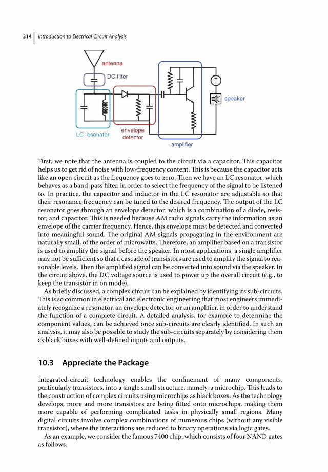
314 Introduction to Electrical Circuit Analysis
antenna
speaker
amplifier
DC filter
LC resonatorenvelopedetector
First, we note that the antenna is coupled to the circuit via a capacitor. This capacitorhelps us to get rid of noise with low-frequency content.This is because the capacitor actslike an open circuit as the frequency goes to zero.Then we have an LC resonator, whichbehaves as a band-pass filter, in order to select the frequency of the signal to be listenedto. In practice, the capacitor and inductor in the LC resonator are adjustable so thattheir resonance frequency can be tuned to the desired frequency. The output of the LCresonator goes through an envelope detector, which is a combination of a diode, resis-tor, and capacitor. This is needed because AM radio signals carry the information as anenvelope of the carrier frequency. Hence, this envelope must be detected and convertedinto meaningful sound. The original AM signals propagating in the environment arenaturally small, of the order of microwatts.Therefore, an amplifier based on a transistoris used to amplify the signal before the speaker. In most applications, a single amplifiermay not be sufficient so that a cascade of transistors are used to amplify the signal to rea-sonable levels.Then the amplified signal can be converted into sound via the speaker. Inthe circuit above, the DC voltage source is used to power up the overall circuit (e.g., tokeep the transistor in on mode).As briefly discussed, a complex circuit can be explained by identifying its sub-circuits.
This is so common in electrical and electronic engineering that most engineers immedi-ately recognize a resonator, an envelope detector, or an amplifier, in order to understandthe function of a complete circuit. A detailed analysis, for example to determine thecomponent values, can be achieved once sub-circuits are clearly identified. In such ananalysis, it may also be possible to study the sub-circuits separately by considering themas black boxes with well-defined inputs and outputs.
10.3 Appreciate the Package
Integrated-circuit technology enables the confinement of many components,particularly transistors, into a single small structure, namely, a microchip. This leads tothe construction of complex circuits usingmicrochips as black boxes. As the technologydevelops, more and more transistors are being fitted onto microchips, making themmore capable of performing complicated tasks in physically small regions. Manydigital circuits involve complex combinations of numerous chips (without any visibletransistor), where the interactions are reduced to binary operations via logic gates.As an example, we consider the famous 7400 chip, which consists of four NAND gates
as follows.
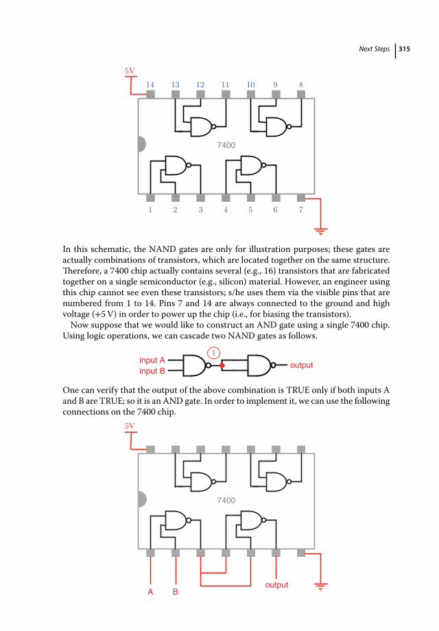
Next Steps 315
1 2 3 4 5 6 7
14 13 12 11 10 9 8
7400
5V
In this schematic, the NAND gates are only for illustration purposes; these gates areactually combinations of transistors, which are located together on the same structure.Therefore, a 7400 chip actually contains several (e.g., 16) transistors that are fabricatedtogether on a single semiconductor (e.g., silicon) material. However, an engineer usingthis chip cannot see even these transistors; s/he uses them via the visible pins that arenumbered from 1 to 14. Pins 7 and 14 are always connected to the ground and highvoltage (+5V) in order to power up the chip (i.e., for biasing the transistors).Now suppose that we would like to construct an AND gate using a single 7400 chip.
Using logic operations, we can cascade two NAND gates as follows.
input Ainput B
output
1
One can verify that the output of the above combination is TRUE only if both inputs Aand B are TRUE; so it is an AND gate. In order to implement it, we can use the followingconnections on the 7400 chip.
7400
5V
A Boutput
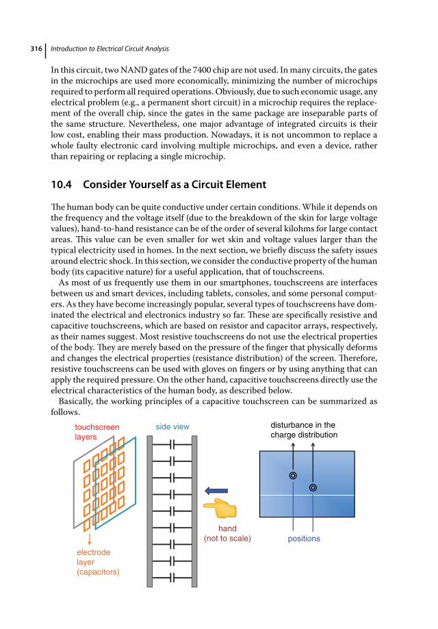
316 Introduction to Electrical Circuit Analysis
In this circuit, twoNAND gates of the 7400 chip are not used. Inmany circuits, the gatesin the microchips are used more economically, minimizing the number of microchipsrequired to perform all required operations. Obviously, due to such economic usage, anyelectrical problem (e.g., a permanent short circuit) in a microchip requires the replace-ment of the overall chip, since the gates in the same package are inseparable parts ofthe same structure. Nevertheless, one major advantage of integrated circuits is theirlow cost, enabling their mass production. Nowadays, it is not uncommon to replace awhole faulty electronic card involving multiple microchips, and even a device, ratherthan repairing or replacing a single microchip.
10.4 Consider Yourself as a Circuit Element
Thehuman body can be quite conductive under certain conditions.While it depends onthe frequency and the voltage itself (due to the breakdown of the skin for large voltagevalues), hand-to-hand resistance can be of the order of several kilohms for large contactareas. This value can be even smaller for wet skin and voltage values larger than thetypical electricity used in homes. In the next section, we briefly discuss the safety issuesaround electric shock. In this section, we consider the conductive property of the humanbody (its capacitive nature) for a useful application, that of touchscreens.As most of us frequently use them in our smartphones, touchscreens are interfaces
between us and smart devices, including tablets, consoles, and some personal comput-ers. As they have become increasingly popular, several types of touchscreens have dom-inated the electrical and electronics industry so far. These are specifically resistive andcapacitive touchscreens, which are based on resistor and capacitor arrays, respectively,as their names suggest. Most resistive touchscreens do not use the electrical propertiesof the body. They are merely based on the pressure of the finger that physically deformsand changes the electrical properties (resistance distribution) of the screen. Therefore,resistive touchscreens can be used with gloves on fingers or by using anything that canapply the required pressure. On the other hand, capacitive touchscreens directly use theelectrical characteristics of the human body, as described below.Basically, the working principles of a capacitive touchscreen can be summarized as
follows.touchscreenlayers
side view
electrodelayer(capacitors)
hand(not to scale)
disturbance in thecharge distribution
positions
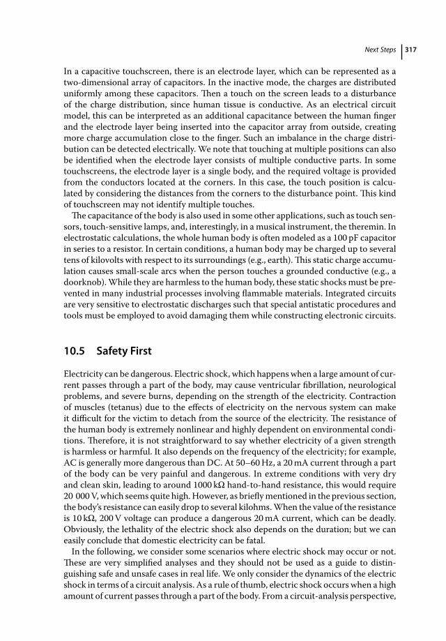
Next Steps 317
In a capacitive touchscreen, there is an electrode layer, which can be represented as atwo-dimensional array of capacitors. In the inactive mode, the charges are distributeduniformly among these capacitors. Then a touch on the screen leads to a disturbanceof the charge distribution, since human tissue is conductive. As an electrical circuitmodel, this can be interpreted as an additional capacitance between the human fingerand the electrode layer being inserted into the capacitor array from outside, creatingmore charge accumulation close to the finger. Such an imbalance in the charge distri-bution can be detected electrically. We note that touching at multiple positions can alsobe identified when the electrode layer consists of multiple conductive parts. In sometouchscreens, the electrode layer is a single body, and the required voltage is providedfrom the conductors located at the corners. In this case, the touch position is calcu-lated by considering the distances from the corners to the disturbance point. This kindof touchscreen may not identify multiple touches.The capacitance of the body is also used in some other applications, such as touch sen-
sors, touch-sensitive lamps, and, interestingly, in a musical instrument, the theremin. Inelectrostatic calculations, the whole human body is often modeled as a 100 pF capacitorin series to a resistor. In certain conditions, a human body may be charged up to severaltens of kilovolts with respect to its surroundings (e.g., earth).This static charge accumu-lation causes small-scale arcs when the person touches a grounded conductive (e.g., adoorknob).While they are harmless to the human body, these static shocksmust be pre-vented in many industrial processes involving flammable materials. Integrated circuitsare very sensitive to electrostatic discharges such that special antistatic procedures andtools must be employed to avoid damaging them while constructing electronic circuits.
10.5 Safety First
Electricity can be dangerous. Electric shock, which happenswhen a large amount of cur-rent passes through a part of the body, may cause ventricular fibrillation, neurologicalproblems, and severe burns, depending on the strength of the electricity. Contractionof muscles (tetanus) due to the effects of electricity on the nervous system can makeit difficult for the victim to detach from the source of the electricity. The resistance ofthe human body is extremely nonlinear and highly dependent on environmental condi-tions. Therefore, it is not straightforward to say whether electricity of a given strengthis harmless or harmful. It also depends on the frequency of the electricity; for example,AC is generally more dangerous than DC. At 50–60Hz, a 20mA current through a partof the body can be very painful and dangerous. In extreme conditions with very dryand clean skin, leading to around 1000 kΩ hand-to-hand resistance, this would require20 000V,which seems quite high.However, as brieflymentioned in the previous section,the body’s resistance can easily drop to several kilohms.When the value of the resistanceis 10 kΩ, 200V voltage can produce a dangerous 20mA current, which can be deadly.Obviously, the lethality of the electric shock also depends on the duration; but we caneasily conclude that domestic electricity can be fatal.In the following, we consider some scenarios where electric shock may occur or not.
These are very simplified analyses and they should not be used as a guide to distin-guishing safe and unsafe cases in real life. We only consider the dynamics of the electricshock in terms of a circuit analysis. As a rule of thumb, electric shock occurs when a highamount of current passes through a part of the body. From a circuit-analysis perspective,

318 Introduction to Electrical Circuit Analysis
this needs a sufficiently high voltage difference to occur between two separate points ofthe body. Hence, the current is formed on the pathway between these two points, pass-ing through tissues and organs, some of which can be critical (e.g., the heart and lungsbetween two hands). This is important; a high voltage value at a single point may notlead to a current flow and electric shock. We need two points with different potentialsso that current may flow.Consider the following figure.
device
earth
device
connections to ground
A
BC
DE
220V
We have an electrical circuit involving two devices and a 220V voltage source. Theground of the circuit is defined not only as a mathematical reference but also physi-cally (via a connection to the earth), as commonly practiced in real life. The followingcases can be considered.• Case A: If a person touches the ground line of the circuit and if s/he is standing on
the ground, no voltage difference occurs across the body and s/he does not receivea shock. Most electrical and electronic devices have insulator cases, which are alsogrounded. Hence, it is safe to touch them, unless there is an electrical fault.
• Case B: If a person touches the hot line of the circuit and s/he is isolated from theground, no electrical shock occurs. This can be a confusing case because the voltageof the person with respect to the ground is around 220V. However, since the personis isolated, there is no current flow across her/his body. It should be emphasized thatthe isolation must be very good to prevent any current flow. For example, most shoesare not designed for electrical insulation, and it is not safe to touch a hot line withoutrigorous isolation.
• Case C: This is a typical case for most electric shocks. If a person standing on theground touches the hot line of the circuit, the voltage difference between her/his handand foot can lead to a serious current flow through her/his body.This case may occurdue to a faulty circuit, leading to positive voltage values at conductors that are sup-posed to be grounded.
• Case D and E: It does not matter how the connection occurs for an electric shock. Ifthere is a conductive path, even involving two persons as depicted above, the electriccurrent flows through them. In this case (one person is grounded and the other persontouches the hot line), the overall voltage is divided between the persons, which mayreduce the effect of the shock.
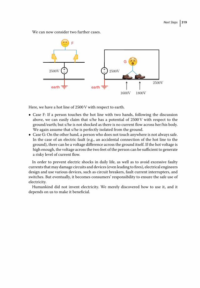
Next Steps 319
We can now consider two further cases.
2500V
earth
2500V
earth2500V
1800V1600V
F
G
Here, we have a hot line of 2500V with respect to earth.
• Case F: If a person touches the hot line with two hands, following the discussionabove, we can easily claim that s/he has a potential of 2500V with respect to theground/earth; but s/he is not shocked as there is no current flow across her/his body.We again assume that s/he is perfectly isolated from the ground.
• Case G: On the other hand, a person who does not touch anywhere is not always safe.In the case of an electric fault (e.g., an accidental connection of the hot line to theground), there can be a voltage difference across the ground itself. If the hot voltage ishigh enough, the voltage across the two feet of the person can be sufficient to generatea risky level of current flow.
In order to prevent electric shocks in daily life, as well as to avoid excessive faultycurrents thatmay damage circuits anddevices (even leading to fires), electrical engineersdesign and use various devices, such as circuit breakers, fault current interrupters, andswitches. But eventually, it becomes consumers’ responsibility to ensure the safe use ofelectricity.Humankind did not invent electricity. We merely discovered how to use it, and it
depends on us to make it beneficial.


321
11
Photographs of Some Circuit Elements
The following photographs were taken by Barıscan Karaosmanoglu and Sadri Güler ofthe Middle East Technical University, Ankara, Turkey.
Figure 11.1 Resistors.
Figure 11.2 Capacitors.
Introduction to Electrical Circuit Analysis, First Edition. Özgür Ergül.© 2017 John Wiley & Sons Ltd. Published 2017 by John Wiley & Sons Ltd.Companion Website: www.wiley.com/go/ergul4412
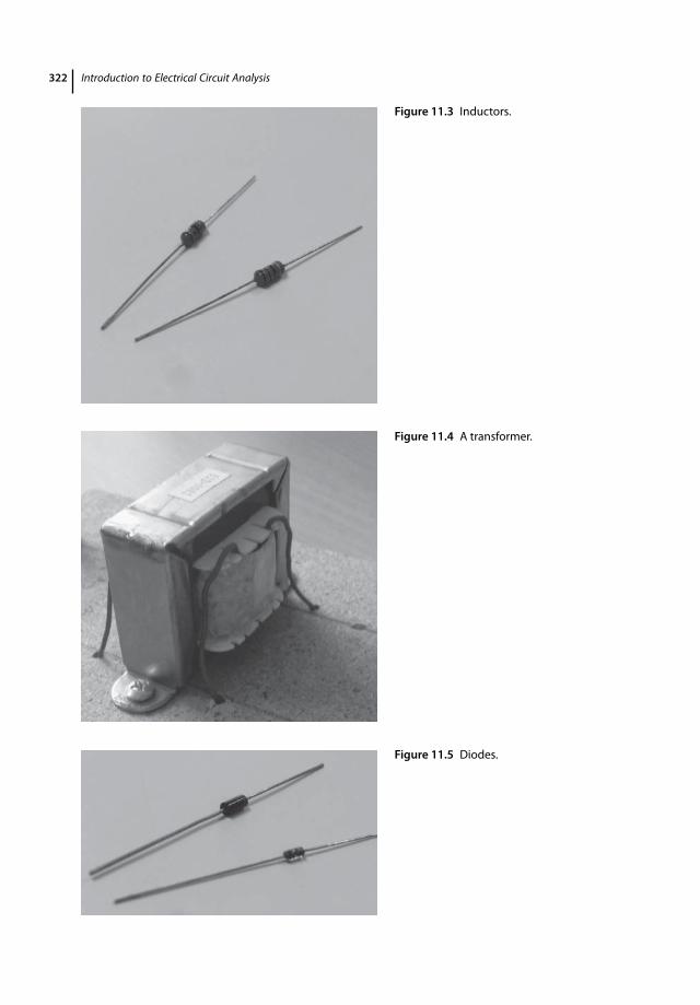
322 Introduction to Electrical Circuit Analysis
Figure 11.3 Inductors.
Figure 11.4 A transformer.
Figure 11.5 Diodes.

Photographs of Some Circuit Elements 323
Figure 11.6 An OP-AMP.
Figure 11.7 A bipolar junctiontransistor.
Figure 11.8 A light-emitting diode.

324 Introduction to Electrical Circuit Analysis
Figure 11.9 A digital multimeter.
Figure 11.10 A chip involving NANDgates.

325
A
Appendix
This appendix contains the brief mathematical background required to understand thetopics covered by this book.
A.1 Basic Algebra Identities
• Difference of squares: a2 − b2 = (a − b)(a + b)• Square of sum: (a + b)2 = a2 + 2ab + b2
• Roots of quadratic equation: ax2 + bx + c = 0 −−−−→ x =−b ±
√b2 − 4ac2a
• Infinity: a0= ∞ if a ≠ 0 and a
∞= 0 if a ≠ ∞
A.2 Trigonometry
• Radian to degree conversion: 𝜋 radians = 180∘• Sine to cosine conversion: sin x = cos(𝜋∕2 − x) = cos(x − 𝜋∕2)• Cosine to sine conversion: cos x = sin(𝜋∕2 − x) = − sin(x − 𝜋∕2)• Argument sum for sine: sin(x ± y) = sin x cos y ± cos x sin y• Argument sum for cosine: cos(x ± y) = cos x cos y ∓ sin x sin y• Half-argument formulas: sin(2x) = 2 sin x cos x and cos(2x) = 2cos2x − 1• Product of cosines: 2 cos x cos y = cos(x − y) + cos(x + y)• Product of sines: 2 sin x sin y = cos(x − y) − cos(x + y)• Sum to product for sines: sin x + sin y = 2 sin
(x + y2
)cos
(x − y2
)
• Sum to product for cosines: cos x + cos y = 2 cos(x + y
2
)cos
(x − y2
)
A.3 Complex Numbers
• Standard form: z = a + jb, where a = Rez, b = Imz, and j =√−1
• Polar form: z = |z|ej𝜙 = |z| exp(j𝜙) = |z| 𝜙, where |z| = √a2 + b2 and 𝜙 =
tan−1(b∕a)
Introduction to Electrical Circuit Analysis, First Edition. Özgür Ergül.© 2017 John Wiley & Sons Ltd. Published 2017 by John Wiley & Sons Ltd.Companion Website: www.wiley.com/go/ergul4412

326 Appendix
Im
Re
a
b
a2+b2
ϕ
• Complex conjugate: z∗ = a − jb and (z∗)∗ = a + jb = z
• Sum: z1 + z2 = (a1 + jb1) + (a2 + jb2) = (a1 + a2) + j(b1 + b2)
• Multiplication: z1z2 = (a1 + jb1)(a2 + jb2) = (a1a2 − b1b2) + j(a1b2 + b1a2)
• Multiplication (polar form): z1z2 = |z1z2| exp[j(𝜙1 + 𝜙2)] = |z1z2| (𝜙1 + 𝜙2)
• Identity for amplitude: |z|2 = a2 + b2 = (a + jb)(a − jb) = zz∗
• Powers: zn = |z|n n𝜙 and jn = |j|n n𝜋∕2 = cos(n𝜋∕2) + j sin(n𝜋∕2)
• Euler’s identity: ej𝜙 = cos𝜙 + j sin𝜙 and e−j𝜙 = cos𝜙 − j sin𝜙
• Real part: Reej𝜙 = cos𝜙 = (ej𝜙 + e−j𝜙)∕2
• Imaginary part: Imej𝜙 = sin𝜙 = (ej𝜙 − e−j𝜙)∕(2j)
• Negative phases: exp(−j𝜙) = cos(−𝜙) + j sin(−𝜙) = cos𝜙 − j sin𝜙
• Identities for 𝜋 phases: exp(j𝜋) = ej𝜋 = −1 and exp(−j𝜋) = e−j𝜋 = −1
• 𝜋∕2 phases: exp(j𝜋∕2) = ej𝜋∕2 = j and exp(−j𝜋∕2) = e−j𝜋∕2 = −j

327
B
Solutions to Exercises
This chapter presents the solutions of exercises considered in this book. In most cases,the solution steps are provided as recipes.
Chapter 1
Solution to Exercise 1:
10 hours
Chapter 2
Solution to Exercise 2:
24V M 4Ω 4Ω R
ix iy iz iw
18A
+ _
1 1 1
• KCL(1): 18 − ix − iy − iz − i𝑤= 0 −−−−→ 6 − 24∕R − i
𝑤= 0 −−−−→ i
𝑤= 6 − 24∕R
• Then 4 ≤ 6 − 24∕R ≤ 6 −−−−→ 24∕R ≤ 2 −−−−→ R ≥ 12
Introduction to Electrical Circuit Analysis, First Edition. Özgür Ergül.© 2017 John Wiley & Sons Ltd. Published 2017 by John Wiley & Sons Ltd.Companion Website: www.wiley.com/go/ergul4412
328 Solutions to Exercises
Solution to Exercise 3:
12V 2Ω
1Ω
3A
ix
iy
R
6V+ _
+ _
+ _
2
3 4
1
• KVL(1 → 2 → 3 → 4 → 1): −1iy − 12 + 6 + 2ix = 0 −−−−→ 2ix − iy = 6• KCL(a): ix + iy + 3 = 0 −−−−→ ix + iy = −3• Then 3ix = 3 −−−−→ ix = 1A −−−−→ R = 6∕1 = 6Ω
Solution to Exercise 4:
_iy +
20V 10V
5Ω
10Ω
5Ω
iz
iy
ix+ _
+ _
1 2
3 4
• KVL(1 → 2 → 3 → 4 → 1): 10iy + 10 + 5iy − 20 = 0 −−−−→ iy = 10∕15 = 2∕3A• KVL(2 → 3 → 2): 5iz − 10 = 0 −−−−→ iz = 2A• KCL(2): iy − ix − iz = 0 −−−−→ ix = iy − iz = −4∕3A
Solutions to Exercises 329
Solution to Exercise 5:
3Ω
1Ω
2Ω
10Ω6Ω
ix
12V
iy
iziw
+ _
+ _
+
_
1 1
2
3
• KVL(1 → 2 → 1): 3ix − 6i𝑤= 0 −−−−→ ix = 2i
𝑤
• KVL(1 → 3 → 1): 1iz + 12 + 10iy = 0 −−−−→ iz + 10iy = −12• KVL(1 → 2 → 3 → 1): 6i
𝑤+ 2(ix + i
𝑤) − 12 − 1iz = 0 −−−−→ −iz + 6ix = 12
• KCL (1): iy − iz − (i𝑤+ ix) = 0 −−−−→ iy − iz − (3∕2)ix = 0
• Then ix = 40∕27A
Solution to Exercise 6:
24V
6Ω 6Ω
6Ω
4Ω
12Ω
ix
iy iz iw
ivim
in
il
6 3
1 4
2 2 2
5
• KVLs(2 → · · · → 2): iy = 2A, iz = i𝑤= 4A, i
𝑣= 6A
• KVL(6 → 3 → 4 → 5 → 6): il = 0• KCL(6): iz − in − il = 0 −−−−→ in = 4A• KCL(3): i
𝑤+ in − im = 0 −−−−→ im = 8A
• KCL(4): i𝑣+ im − ix = 0 −−−−→ ix = 14A
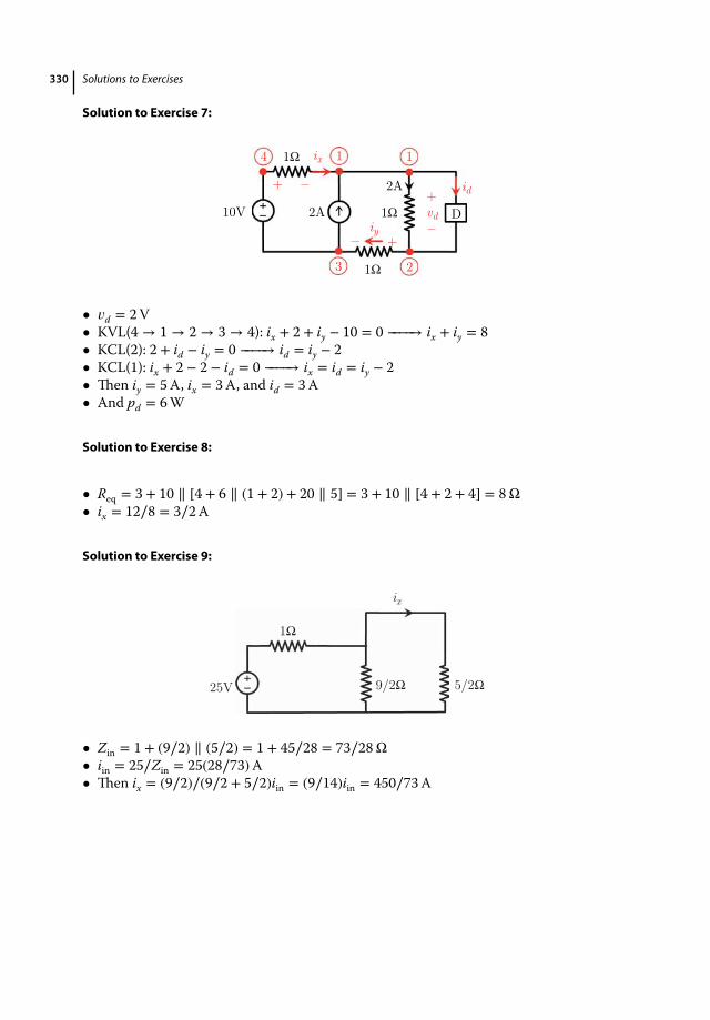
330 Solutions to Exercises
Solution to Exercise 7:
10V 2A
1Ω
1Ω
1Ω
2A
1 1 ix
2 3
4
iy
id_ +
_ +
+ _ vd D
• 𝑣d = 2V• KVL(4 → 1 → 2 → 3 → 4): ix + 2 + iy − 10 = 0 −−−−→ ix + iy = 8• KCL(2): 2 + id − iy = 0 −−−−→ id = iy − 2• KCL(1): ix + 2 − 2 − id = 0 −−−−→ ix = id = iy − 2• Then iy = 5A, ix = 3A, and id = 3A• And pd = 6W
Solution to Exercise 8:
.• Req = 3 + 10 ∥ [4 + 6 ∥ (1 + 2) + 20 ∥ 5] = 3 + 10 ∥ [4 + 2 + 4] = 8Ω• ix = 12∕8 = 3∕2A
Solution to Exercise 9:
1Ω
9/2Ω 5/2Ω25V
ix
• Zin = 1 + (9∕2) ∥ (5∕2) = 1 + 45∕28 = 73∕28Ω• iin = 25∕Zin = 25(28∕73)A• Then ix = (9∕2)∕(9∕2 + 5∕2)iin = (9∕14)iin = 450∕73A
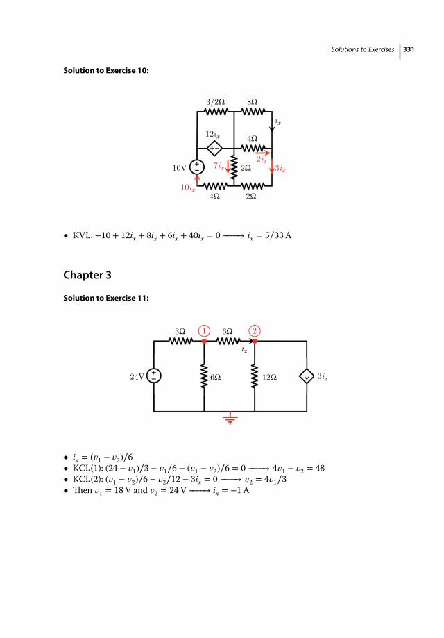
Solutions to Exercises 331
Solution to Exercise 10:
3/2Ω
4Ω 2Ω
2Ω
4Ω
8Ω
10V
12ixix
3ix2ix7ix
10ix
• KVL: −10 + 12ix + 8ix + 6ix + 40ix = 0 −−−−→ ix = 5∕33A
Chapter 3
Solution to Exercise 11:
3Ω
6Ω 12Ω
6Ω
24V 3ix
ix
2 1
• ix = (𝑣1 − 𝑣2)∕6• KCL(1): (24 − 𝑣1)∕3 − 𝑣1∕6 − (𝑣1 − 𝑣2)∕6 = 0 −−−−→ 4𝑣1 − 𝑣2 = 48• KCL(2): (𝑣1 − 𝑣2)∕6 − 𝑣2∕12 − 3ix = 0 −−−−→ 𝑣2 = 4𝑣1∕3• Then 𝑣1 = 18V and 𝑣2 = 24V −−−−→ ix = −1A
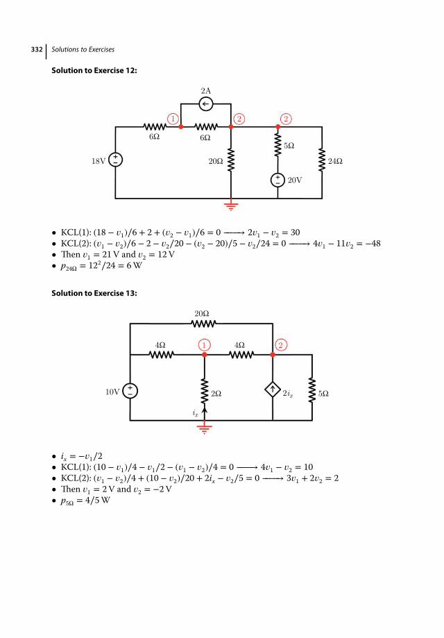
332 Solutions to Exercises
Solution to Exercise 12:
2A
18V 20Ω
6Ω6Ω
5Ω
24Ω
20V
1 2 2
• KCL(1): (18 − 𝑣1)∕6 + 2 + (𝑣2 − 𝑣1)∕6 = 0 −−−−→ 2𝑣1 − 𝑣2 = 30• KCL(2): (𝑣1 − 𝑣2)∕6 − 2 − 𝑣2∕20 − (𝑣2 − 20)∕5 − 𝑣2∕24 = 0 −−−−→ 4𝑣1 − 11𝑣2 = −48• Then 𝑣1 = 21V and 𝑣2 = 12V• p24Ω = 122∕24 = 6W
Solution to Exercise 13:
10V
20Ω
5Ω
4Ω 4Ω
2Ω
ix
2ix
1 2
• ix = −𝑣1∕2• KCL(1): (10 − 𝑣1)∕4 − 𝑣1∕2 − (𝑣1 − 𝑣2)∕4 = 0 −−−−→ 4𝑣1 − 𝑣2 = 10• KCL(2): (𝑣1 − 𝑣2)∕4 + (10 − 𝑣2)∕20 + 2ix − 𝑣2∕5 = 0 −−−−→ 3𝑣1 + 2𝑣2 = 2• Then 𝑣1 = 2V and 𝑣2 = −2V• p5Ω = 4∕5W

Solutions to Exercises 333
Solution to Exercise 14:
10Ω
2Ω
5Ω 5Ω
10Ω
10Ω
5V
ixvs
1 1 2
• 𝑣2 = −5ix = −10V• KCL(2): (𝑣1 − 𝑣2)∕10 + (𝑣1 − 𝑣2)∕10 + ix = 0 −−−−→ 𝑣1∕5 + 4 = 0 −−−−→ 𝑣1 = −20V• KCL(1): (𝑣s − 𝑣1)∕10 + (5 − 𝑣1)∕2 − 𝑣1∕5 − 2(𝑣1 − 𝑣2)∕10 = 0 −−−−→ 𝑣s∕10 = −41∕2• Then 𝑣s = −205V
Solution to Exercise 15:
30Ω
60V
ix
5Ω
28/5A 100Ω
1Ω
4Ω60Ω
1 2 2
• KCL(1): (−60 − 𝑣1)∕30 − 𝑣1∕60 − (𝑣1 − 𝑣2)∕5 = 0 −−−−→ 5𝑣1 − 4𝑣2 = −40• KCL(2): (𝑣1 − 𝑣2)∕5 + 28∕5 − 𝑣2∕100 − 𝑣2∕5 = 0 −−−−→ 20𝑣1 − 41𝑣2 = −560• Then 𝑣1 = 24∕5V, 𝑣2 = 16V, and ix = 16∕5A
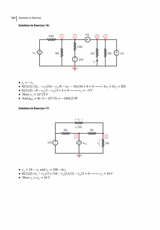
334 Solutions to Exercises
Solution to Exercise 16:
8Ω
ix
24Ω
24Ω
10V
4A
8A
1Ω 3Ω5ix
1 1 2 2
• ix = −𝑣2• KCL(1): (5ix − 𝑣1)∕24 − 𝑣1∕8 − (𝑣1 − 10)∕24 + 8 = 0 −−−−→ 5𝑣1 + 5𝑣2 = 202• KCL(2): −8 − 𝑣2∕1 − 𝑣2∕3 + 4 = 0 −−−−→ 𝑣2 = −3V• Then 𝑣1 = 217∕5V• And p8A = 8(−3 − 217∕5) = −1856∕5W
Solution to Exercise 17:
18V
2Ω 2Ω
2Ω6vx
1/5Ω
vy+ _
vx _ +
1 2
• 𝑣x = 18 − 𝑣2 and 𝑣1 = 108 − 6𝑣2• KCL(2): (𝑣1 − 𝑣2)∕2 + (18 − 𝑣2)∕(1∕5) − 𝑣2∕2 = 0 −−−−→ 𝑣2 = 16V• Then 𝑣y = 𝑣2 = 16V

Solutions to Exercises 335
Solution to Exercise 18:
100ix 140V
20Ω
ix4A 40Ω
20Ω
1 1 1
• ix = (𝑣1 − 140)∕40• KCL(1): 4 − 𝑣1∕20 − (𝑣1 + 100ix)∕20 − (𝑣1 − 140)∕40 = 0 −−−−→ 𝑣1 = 100V• Then ix = −1A
Solution to Exercise 19:
2ix
2Ω 4A
8Ω
2Ω
2Ω 24V
ix
iy
1 2
• 𝑣2 = 24V• 𝑣1 = 𝑣2 + 2ix = 24 + 2ix and 𝑣1 = −2ix• Then −2ix = 24 + 2ix −−−−→ ix = −6A

336 Solutions to Exercises
Solution to Exercise 20:
5Ω
6A10V 20Ω
ix
10Ω
10Ω
2ix
1 2 2
• ix = 𝑣1∕10• KCL(1): (10 − 𝑣1)∕5 − 𝑣1∕10 − (𝑣1 − 𝑣2)∕10 = 0 −−−−→ 4𝑣1 − 𝑣2 = 20• KCL(2): (𝑣1 − 𝑣2)∕10 − 2ix − 𝑣2∕20 + 6 = 0 −−−−→ 2𝑣1 + 3𝑣2 = 120• Then 𝑣1 = 90∕7V, 𝑣2 = 220∕7V, and ix = 9∕7A
Solution to Exercise 21:
10Ω 5Ω
10Ω
5Ω
10Vvx+ _
2vx
iy
1 2
• 𝑣x = 𝑣2• KCL(1&2): −𝑣1∕10 − 𝑣2∕5 + (10 − 𝑣1)∕5 + (10 − 𝑣2)∕10 = 0 −−−−→ 𝑣1 + 𝑣2 = 10• Supernode: 𝑣1 − 𝑣2 = 2𝑣x −−−−→ 𝑣1 = 3𝑣2 −−−−→ 𝑣1 = 15∕2V• Then iy = 𝑣1∕10 = 3∕4A
Solution to Exercise 22:
6A
4Ω 6A
12V
2Ω
1 1 2
D
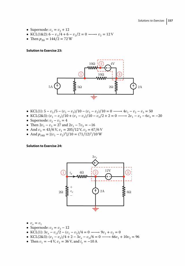
Solutions to Exercises 337
• Supernode: 𝑣1 = 𝑣2 + 12• KCL(1&2): 6 − 𝑣1∕4 + 6 − 𝑣2∕2 = 0 −−−−→ 𝑣2 = 12V• Then p2Ω = 144∕2 = 72W
Solution to Exercise 23:
10Ω
10Ω
5Ω 2Ω 2A5A
4V
1
2
3
• KCL(1): 5 − 𝑣1∕5 − (𝑣1 − 𝑣3)∕10 − (𝑣1 − 𝑣2)∕10 = 0 −−−−→ 4𝑣1 − 𝑣2 − 𝑣3 = 50• KCL(2&3): (𝑣1 − 𝑣2)∕10 + (𝑣1 − 𝑣3)∕10 − 𝑣3∕2 + 2 = 0 −−−−→ 2𝑣1 − 𝑣2 − 6𝑣3 = −20• Supernode: 𝑣2 − 𝑣3 = 4• Then 2𝑣1 − 𝑣3 = 27 and 2𝑣1 − 7𝑣3 = −16• And 𝑣3 = 43∕6V, 𝑣1 = 205∕12V, 𝑣2 = 67∕6V• And p10Ω = [(𝑣1 − 𝑣2)2]∕10 = (71∕12)2∕10W
Solution to Exercise 24:
12V4Ω
2A vx
3vx
6Ω2Ω
+ _
iy1 2 3
• 𝑣x = 𝑣1• Supernode: 𝑣3 = 𝑣2 − 12• KCL(1): 3𝑣x − 𝑣1∕2 − (𝑣1 − 𝑣2)∕4 = 0 −−−−→ 9𝑣1 + 𝑣2 = 0• KCL(2&3): (𝑣1 − 𝑣2)∕4 + 2 − 3𝑣x − 𝑣3∕6 = 0 −−−−→ 66𝑣1 + 10𝑣2 = 96• Then 𝑣1 = −4V, 𝑣2 = 36V, and iy = −10A

338 Solutions to Exercises
Solution to Exercise 25:
12A
2Ω
6Ω 12Ω
1A
12Ω
vs
1 2
• KCL(1&2): 12 − 𝑣1∕6 − 𝑣2∕12 − 𝑣2∕12 = 0 −−−−→ 𝑣1 + 𝑣2 = 72• Resistor: 𝑣2 = 12V −−−−→ 𝑣1 = 60V• Then 𝑣s = 𝑣1 − 𝑣2 = 48V
Solution to Exercise 26:
8Ω 4Ω
1Ω
2Ω
29V
16V
ix
4ix
2vy
_ vy
1
2 +
• ix = 2𝑣y = 2𝑣2• KCL(1&2): ix − 𝑣2∕4 − (𝑣1 − 29)∕1 = 0 −−−−→ 4𝑣1 − 7𝑣2 = 116• Supernode: 𝑣1 − 𝑣2 = 4ix = 8𝑣2 −−−−→ 𝑣1 = 9𝑣2• Then 𝑣2 = 4V, 𝑣1 = 36V, ix = 8A• And ps = 4ix × (29 − 𝑣1)∕1 = −224W

Solutions to Exercises 339
Solution to Exercise 27:
8V
2V4Ω 2Ω
1Ω
ix
3ix
vy+ _
1 2
• ix = −𝑣1∕4• Supernode: 𝑣1 − 𝑣2 = 8• KCL(1&2): −𝑣1∕4 − 𝑣2∕2 − (𝑣2 − 2)∕1 − 3ix = 0 −−−−→ 𝑣1 − 3𝑣2 = −4• Then 𝑣1 = 14V, 𝑣2 = 6V, and 𝑣y = 6V
Solution to Exercise 28:
8A 5A
5Ω
20/3V
2Ω
8Ω 10Ω
1 2
• Supernode: 𝑣1 − 𝑣2 = 20∕3• KCL(1&2): 8 − 5 − 𝑣2∕8 − 𝑣2∕10 = 0 −−−−→ 𝑣2 = 40∕3V• Then 𝑣1 = 20V and p5A = 20 × 5 = 100W

340 Solutions to Exercises
Solution to Exercise 29:
3A
10Ω
20Ω
20V 20Ω
50ix
ix
1 2
• KCL(1&2): −𝑣1∕20 + 3 − 𝑣1∕10 − (𝑣2 − 20)∕20 = 0 −−−−→ 3𝑣1 + 𝑣2 = 80• Supernode: 𝑣1 − 𝑣2 = 50ix = 50(𝑣2 − 20) −−−−→ 51𝑣2 − 𝑣1 = 1000• Then 𝑣1 = 20V, 𝑣2 = 20V, and ix = 0A
Solution to Exercise 30:
6Ω2Ω 2A
4Ω 12V
vx+ _
3vx
1 2 3
• 𝑣3 = 𝑣x• KCL(3): 3𝑣x + (𝑣1 − 𝑣3)∕4 − 𝑣3∕2 = 0 −−−−→ 𝑣1 + 9𝑣3 = 0• KCL(1&2): −(𝑣1 − 𝑣3)∕4 + 2 − 𝑣2∕6 − 3𝑣x = 0 −−−−→ 3𝑣1 + 2𝑣2 + 33𝑣3 = 24• Supernode: 𝑣1 − 𝑣2 = 12• Then 𝑣1 = 36V, 𝑣2 = 24V, and 𝑣3 = −4V• And 𝑣x = 𝑣3 = −4V
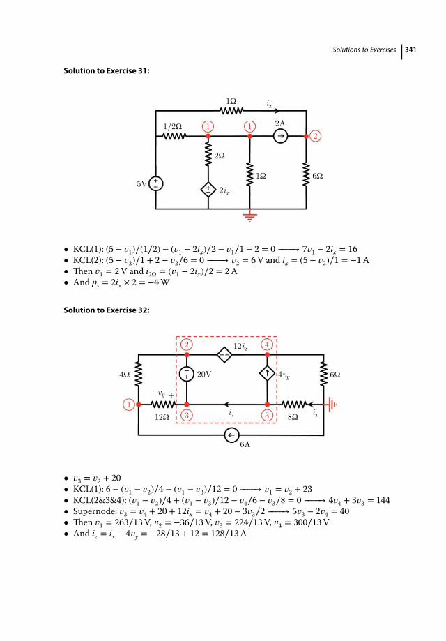
Solutions to Exercises 341
Solution to Exercise 31:
ix
2A
6Ω1Ω
2Ω
2ix
1/2Ω
1Ω
5V
1 1 2
• KCL(1): (5 − 𝑣1)∕(1∕2) − (𝑣1 − 2ix)∕2 − 𝑣1∕1 − 2 = 0 −−−−→ 7𝑣1 − 2ix = 16• KCL(2): (5 − 𝑣2)∕1 + 2 − 𝑣2∕6 = 0 −−−−→ 𝑣2 = 6V and ix = (5 − 𝑣2)∕1 = −1A• Then 𝑣1 = 2V and i2Ω = (𝑣1 − 2ix)∕2 = 2A• And ps = 2ix × 2 = −4W
Solution to Exercise 32:
20V4Ω
6A
4vy
ix
6Ω
12Ω 8Ω
12ix
vy
iz
_ + 1
2
3
4
3
• 𝑣3 = 𝑣2 + 20• KCL(1): 6 − (𝑣1 − 𝑣2)∕4 − (𝑣1 − 𝑣3)∕12 = 0 −−−−→ 𝑣1 = 𝑣2 + 23• KCL(2&3&4): (𝑣1 − 𝑣2)∕4 + (𝑣1 − 𝑣3)∕12 − 𝑣4∕6 − 𝑣3∕8 = 0 −−−−→ 4𝑣4 + 3𝑣3 = 144• Supernode: 𝑣3 = 𝑣4 + 20 + 12ix = 𝑣4 + 20 − 3𝑣3∕2 −−−−→ 5𝑣3 − 2𝑣4 = 40• Then 𝑣1 = 263∕13V, 𝑣2 = −36∕13V, 𝑣3 = 224∕13V, 𝑣4 = 300∕13V• And iz = ix − 4𝑣y = −28∕13 + 12 = 128∕13A
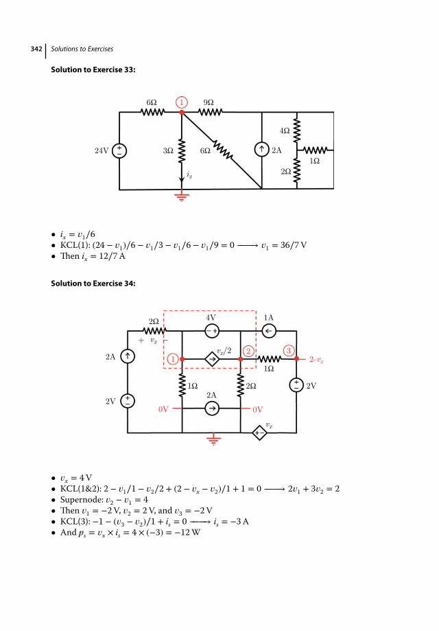
342 Solutions to Exercises
Solution to Exercise 33:
6Ω 9Ω
3Ω 2A 24V
ix
6Ω
4Ω
1Ω
2Ω
1
• ix = 𝑣1∕6• KCL(1): (24 − 𝑣1)∕6 − 𝑣1∕3 − 𝑣1∕6 − 𝑣1∕9 = 0 −−−−→ 𝑣1 = 36∕7V• Then ix = 12∕7A
Solution to Exercise 34:
4V 1A
1Ω
2Ω1Ω 2V 2A
2Ω
2A
2V
+ _ vxvx/2
vx
1 2
0V 0V
2-vx3
• 𝑣x = 4V• KCL(1&2): 2 − 𝑣1∕1 − 𝑣2∕2 + (2 − 𝑣x − 𝑣2)∕1 + 1 = 0 −−−−→ 2𝑣1 + 3𝑣2 = 2• Supernode: 𝑣2 − 𝑣1 = 4• Then 𝑣1 = −2V, 𝑣2 = 2V, and 𝑣3 = −2V• KCL(3): −1 − (𝑣3 − 𝑣2)∕1 + is = 0 −−−−→ is = −3A• And ps = 𝑣x × is = 4 × (−3) = −12W
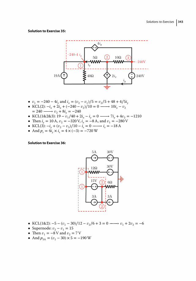
Solutions to Exercises 343
Solution to Exercise 35:
40Ω19A 240V
10Ω5Ω
ix
2ix
4iy
iy
–240V–240-4 iy
1
2 3
• 𝑣1 = −240 − 4iy and ix = (𝑣2 − 𝑣1)∕5 = 𝑣2∕5 + 48 + 4∕5iy• KCL(2): −ix + 2ix + (−240 − 𝑣2)∕10 = 0 −−−−→ 10ix − 𝑣2
= 240 −−−−→ 𝑣2 + 8iy = −240• KCL(1&2&3): 19 − 𝑣1∕40 + 2ix − iy = 0 −−−−→ 7iy + 4𝑣2 = −1210• Then iy = 10A, 𝑣2 = −320V, ix = −8A, and 𝑣1 = −280V• KCL(3): −iy + (𝑣2 − 𝑣3)∕10 − is = 0 −−−−→ is = −18A• And ps = 4iy × is = 4 × (−3) = −720W
Solution to Exercise 36:
5A 30V
12Ω30V
15V 6Ω
3A 3A
1
1 2
2
• KCL(1&2): −5 − (𝑣1 − 30)∕12 − 𝑣2∕6 + 3 = 0 −−−−→ 𝑣1 + 2𝑣2 = −6• Supernode: 𝑣2 − 𝑣1 = 15• Then 𝑣1 = −8V and 𝑣2 = 7V• And p5A = (𝑣1 − 30) × 5 = −190W
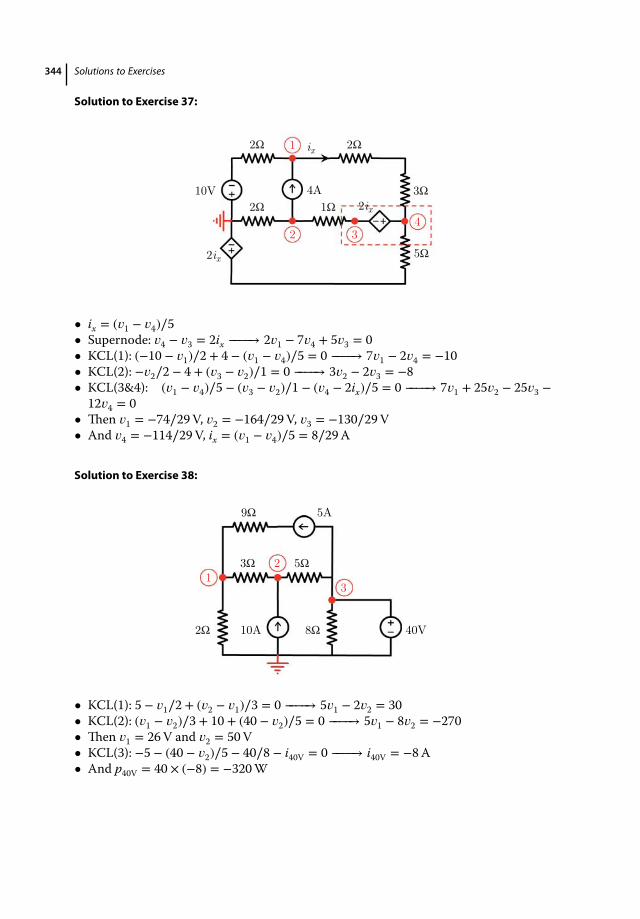
344 Solutions to Exercises
Solution to Exercise 37:
10V 4A 2Ω
2Ω 2Ω
1Ω
3Ω
5Ω2ix
2ix
ix1
2 3 4
• ix = (𝑣1 − 𝑣4)∕5• Supernode: 𝑣4 − 𝑣3 = 2ix −−−−→ 2𝑣1 − 7𝑣4 + 5𝑣3 = 0• KCL(1): (−10 − 𝑣1)∕2 + 4 − (𝑣1 − 𝑣4)∕5 = 0 −−−−→ 7𝑣1 − 2𝑣4 = −10• KCL(2): −𝑣2∕2 − 4 + (𝑣3 − 𝑣2)∕1 = 0 −−−−→ 3𝑣2 − 2𝑣3 = −8• KCL(3&4): (𝑣1 − 𝑣4)∕5 − (𝑣3 − 𝑣2)∕1 − (𝑣4 − 2ix)∕5 = 0 −−−−→ 7𝑣1 + 25𝑣2 − 25𝑣3 −
12𝑣4 = 0• Then 𝑣1 = −74∕29V, 𝑣2 = −164∕29V, 𝑣3 = −130∕29V• And 𝑣4 = −114∕29V, ix = (𝑣1 − 𝑣4)∕5 = 8∕29A
Solution to Exercise 38:
2Ω
3Ω
9Ω
5Ω
8Ω 10A 40V
5A
1 2
3
• KCL(1): 5 − 𝑣1∕2 + (𝑣2 − 𝑣1)∕3 = 0 −−−−→ 5𝑣1 − 2𝑣2 = 30• KCL(2): (𝑣1 − 𝑣2)∕3 + 10 + (40 − 𝑣2)∕5 = 0 −−−−→ 5𝑣1 − 8𝑣2 = −270• Then 𝑣1 = 26V and 𝑣2 = 50V• KCL(3): −5 − (40 − 𝑣2)∕5 − 40∕8 − i40V = 0 −−−−→ i40V = −8A• And p40V = 40 × (−8) = −320W
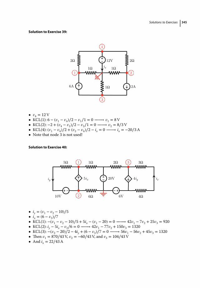
Solutions to Exercises 345
Solution to Exercise 39:
2Ω
1Ω
1Ω
1Ω
2Ω12V
6A 2A
ix1 2
3
4
• 𝑣4 = 12V• KCL(1): 6 − (𝑣1 − 𝑣4)∕2 − 𝑣1∕1 = 0 −−−−→ 𝑣1 = 8V• KCL(2): −2 + (𝑣4 − 𝑣2)∕2 − 𝑣2∕1 = 0 −−−−→ 𝑣2 = 8∕3V• KCL(4): (𝑣1 − 𝑣4)∕2 + (𝑣2 − 𝑣4)∕2 − ix = 0 −−−−→ ix = −20∕3A• Note that node 3 is not used!
Solution to Exercise 40:
5Ω 1Ω 2Ω 3Ω
4Ω6Ω10V
5ix 20V 4iy
6V
ixiy
1
2
3
• iy = (𝑣1 − 𝑣2 − 10)∕5• ix = (6 − 𝑣3)∕7• KCL(1): −(𝑣1 − 𝑣2 − 10)∕5 + 5ix − (𝑣1 − 20) = 0 −−−−→ 42𝑣1 − 7𝑣2 + 25𝑣3 = 920• KCL(2): iy − 5ix − 𝑣2∕6 = 0 −−−−→ 42𝑣1 − 77𝑣2 + 150𝑣3 = 1320• KCL(3): −(𝑣3 − 20)∕2 − 4iy + (6 − 𝑣3)∕7 = 0 −−−−→ 56𝑣1 − 56𝑣2 + 45𝑣3 = 1320• Then 𝑣1 = 870∕43V, 𝑣2 = −60∕43V, and 𝑣3 = 104∕43V• And ix = 22∕43A
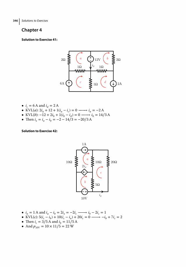
346 Solutions to Exercises
Chapter 4
Solution to Exercise 41:
2Ω
1Ω
1Ω
1Ω
2Ω12V
6A 2A
ix
a b
c d
• ic = 6A and id = 2A• KVL(a): 2ia + 12 + 1(ia − ic) = 0 −−−−→ ia = −2A• KVL(b): −12 + 2ib + 1(ib − id) = 0 −−−−→ ib = 14∕3A• Then ix = ia − ib = −2 − 14∕3 = −20∕3A
Solution to Exercise 42:
1A
10Ω 10Ω 20Ω
10V
5Ω
2ix
ix
a
b
c
• ia = 1A and ia − ib = 2ix = −2ic −−−−→ ib − 2ic = 1• KVL(c): 5(ic − ib) + 10(ic − ia) + 20ic = 0 −−−−→ −ib + 7ic = 2• Then ic = 3∕5A and ib = 11∕5A• And p10V = 10 × 11∕5 = 22W
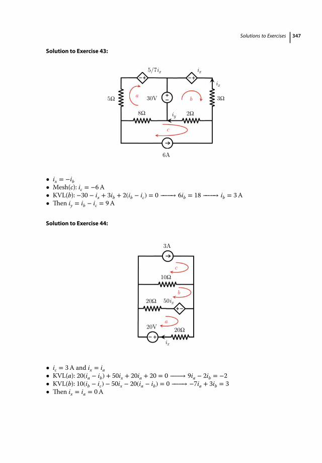
Solutions to Exercises 347
Solution to Exercise 43:
iy
5Ω 30V
6A
ix
5/7ix
8Ω 2Ω
3Ω
ix
b
c
a
• ix = −ib• Mesh(c): ic = −6A• KVL(b): −30 − ix + 3ib + 2(ib − ic) = 0 −−−−→ 6ib = 18 −−−−→ ib = 3A• Then iy = ib − ic = 9A
Solution to Exercise 44:
3A
10Ω
20Ω
20V 20Ω
50ix
ix
c
b
a
• ic = 3A and ix = ia• KVL(a): 20(ia − ib) + 50ix + 20ia + 20 = 0 −−−−→ 9ia − 2ib = −2• KVL(b): 10(ib − ic) − 50ix − 20(ia − ib) = 0 −−−−→ −7ia + 3ib = 3• Then ix = ia = 0A

348 Solutions to Exercises
Solution to Exercise 45:
12V4Ω
2A vx
3vx
6Ω2Ω
+ _
iy
a b
c
• 𝑣x = −2ia• ib − ia = 2A• KVL(a): 2ia + 4(ia − ic) − 𝑣2A = 0• KVL(b): 𝑣2A + 12 + 6ib = 0• Then 2ia + 4(ia − ic) + 12 + 6ib = 0 −−−−→ ia = 2A• Then ib = 4A, ic = 12A, iy = −10AThis question can be solved better using the concept of the supermesh.
Solution to Exercise 46:
vs 8Ω
9V
8Ω
3Ω 3Ω 3A
1A
a b c
d
• ic = 3A• KVL(b): 3(ib − ia) + 8 + 3(ib − ic) = 0 −−−−→ −3ia + 6ib = 1A• KVL(a): −9 + 3(ia − ib) = 0 −−−−→ ia − ib = 3A
−−−−→ ia = 19∕3A and ib = 10∕3A• ib − id = 1A −−−−→ id = 7∕3A• KVL(d): 8id − 𝑣s − 8 = 0 −−−−→ 𝑣s = 32∕3V

Solutions to Exercises 349
Solution to Exercise 47:
8V
2V4Ω 2Ω
1Ω
ix
3ix
vy + _ a b
c
• ic = 3ia• KVL(a): 4ia + 8 + 2(ia − ib) = 0 −−−−→ 3ia − ib = −4• KVL(b): 2(ib − ia) + 1(ib − ic) + 2 = 0 −−−−→ −5ia + 3ib = −2• Then ia = −7∕2A and ib = −13∕2A• And 𝑣y = 2(−7∕2 + 13∕2) = 6V
Solution to Exercise 48:
10A
10Ω
4Ω
10Ω
5Ω
4Ω
ix
2ixa b c
• ia = 10A and ix = ia − ib• KVL(b): 4(ib − ia) + 4ib + 10(ib − ic) + 2ix = 0 −−−−→ 16ib − 10ic = 20
−−−−→ 8ib − 5ic = 10• KVL(c): −2ix + 10(ic − ib) + 5ic = 0 −−−−→ −8ib + 15ic = 20• Then ic = 3A and p5Ω = 45W
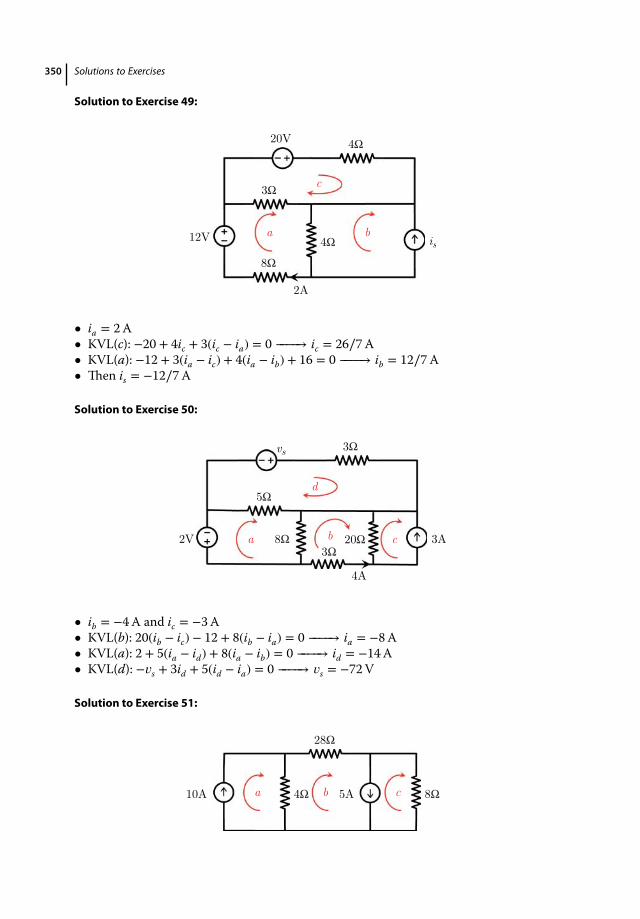
350 Solutions to Exercises
Solution to Exercise 49:
20V 4Ω
3Ω
4Ω
8Ω
12V is
2A
a b
c
• ia = 2A• KVL(c): −20 + 4ic + 3(ic − ia) = 0 −−−−→ ic = 26∕7A• KVL(a): −12 + 3(ia − ic) + 4(ia − ib) + 16 = 0 −−−−→ ib = 12∕7A• Then is = −12∕7A
Solution to Exercise 50:
vs
8Ω2V3Ω
3A
4A
5Ω
3Ω
20Ωa b c
d
• ib = −4A and ic = −3A• KVL(b): 20(ib − ic) − 12 + 8(ib − ia) = 0 −−−−→ ia = −8A• KVL(a): 2 + 5(ia − id) + 8(ia − ib) = 0 −−−−→ id = −14A• KVL(d): −𝑣s + 3id + 5(id − ia) = 0 −−−−→ 𝑣s = −72V
Solution to Exercise 51:
28Ω
4Ω10A 5A 8Ωa b c

Solutions to Exercises 351
• ia = 10A• Supermesh: ib − ic = 5• KVL(b&c): 4(ib − ia) + 28ib + 8ic = 0 −−−−→ 4ib + ic = 5• Then ib = 2A and ic = −3A• And p5A = 𝑣5A × 5 = 8ic × 5 = −120W
Solution to Exercise 52:
6Ω 12V3Ω 4Ω
6Ω
ix
2ixa b
c
• ix = ia − ic• Supermesh: 2ix = ib − ia −−−−→ 3ia − ib − 2ic = 0• KVL(a&b): 6ia + 3(ia − ic) + 4(ib − ic) + 12 = 0 −−−−→ 9ia + 4ib − 7ic = −12• KVL(c): 3(ic − ia) + 6ic + 4(ic − ib) = 0 −−−−→ −3ia − 4ib + 13ic = 0• Then ia = −7∕6A, ib = −11∕5A, and ic = −5∕6A• And ix = ia − ic = −1∕3A
Solution to Exercise 53:
2ix
2Ω
ix
2A2Ω
2Ω
a100V db
c2Ω
• id = 2A• KVL(a): −100 + 2(ia − ib) = 0 −−−−→ ia − ib = 50• Supermesh: ib − ic = 2ix = 2(ia − ib) −−−−→ 2ia − 3ib + ic = 0• KVL(b&c): 2(ib − ia) + 2ib + 2(ic − id) + 2ic = 0 −−−−→ ia − 2ib − 2ic = −2• Then ia = 134A, ib = 84A, ic = −16A• And p100V = −100 × 134 = −13.4 kW
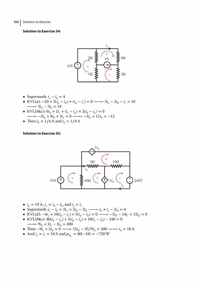
352 Solutions to Exercises
Solution to Exercise 54:
2Ω 6Ω
2Ω1Ω
4A 10V
ix
a
c
b
• Supermesh: ic − ib = 4• KVL(a): −10 + 2(ia − ib) + (ia − ic) = 0 −−−−→ 3ia − 2ib − ic = 10
−−−−→ 3ia − 3ib = 14• KVL(b&c): 6ib + 2ic + (ic − ia) + 2(ib − ia) = 0
−−−−→ −3ia + 8ib + 3ic = 0 −−−−→ −3ia + 11ib = −12• Then ib = 1∕4A and ix = 1∕4A
Solution to Exercise 55:
40Ω 19A 240V
10Ω 5Ω ix
2ix
4iy
iy
a b c
d
• ia = 19A, ix = id − ib, and iy = ic• Supermesh: ic − ib = 2ix = 2id − 2ib −−−−→ ib + ic − 2id = 0• KVL(d): −4iy + 10(id − ic) + 5(id − ib) = 0 −−−−→ −5ib − 14ic + 15id = 0• KVL(b&c): 40(ib − ia) + 5(ib − id) + 10(ic − id) − 240 = 0
−−−−→ 9ib + 2ic − 3id = 200• Then −9ic + 5id = 0 −−−−→ 15id − 35∕9id = 200 −−−−→ id = 18A• And iy = ic = 10A and p4iy
= 40(−18) = −720W
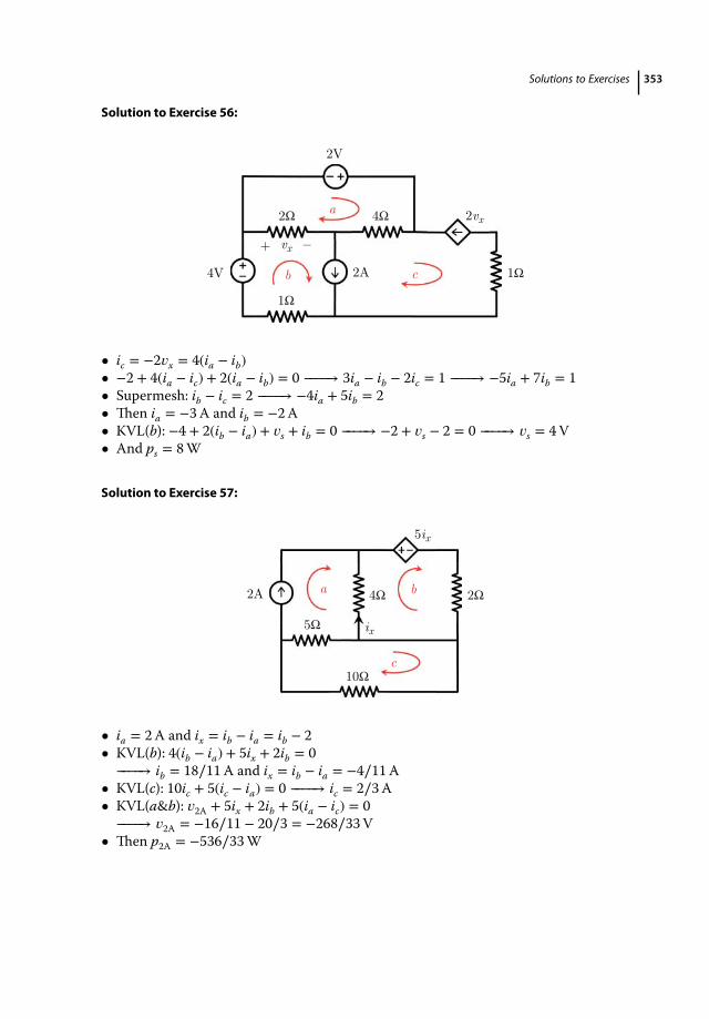
Solutions to Exercises 353
Solution to Exercise 56:
2V
4V 2A
2Ω 4Ω
1Ω
+ _ vx
2vx
1Ω
a
b c
• ic = −2𝑣x = 4(ia − ib)• −2 + 4(ia − ic) + 2(ia − ib) = 0 −−−−→ 3ia − ib − 2ic = 1 −−−−→ −5ia + 7ib = 1• Supermesh: ib − ic = 2 −−−−→ −4ia + 5ib = 2• Then ia = −3A and ib = −2A• KVL(b): −4 + 2(ib − ia) + 𝑣s + ib = 0 −−−−→ −2 + 𝑣s − 2 = 0 −−−−→ 𝑣s = 4V• And ps = 8W
Solution to Exercise 57:
2A 4Ω 2Ω
5Ω
10Ω
ix
5ix
a b
c
• ia = 2A and ix = ib − ia = ib − 2• KVL(b): 4(ib − ia) + 5ix + 2ib = 0
−−−−→ ib = 18∕11A and ix = ib − ia = −4∕11A• KVL(c): 10ic + 5(ic − ia) = 0 −−−−→ ic = 2∕3A• KVL(a&b): 𝑣2A + 5ix + 2ib + 5(ia − ic) = 0
−−−−→ 𝑣2A = −16∕11 − 20∕3 = −268∕33V• Then p2A = −536∕33W
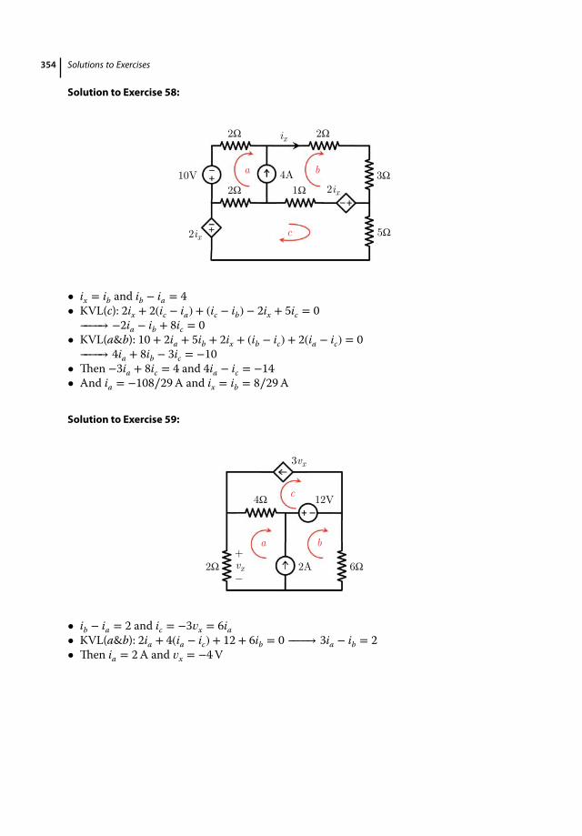
354 Solutions to Exercises
Solution to Exercise 58:
10V 4A 2Ω
2Ω 2Ω
1Ω
3Ω
5Ω2ix
2ix
ix
c
a b
• ix = ib and ib − ia = 4• KVL(c): 2ix + 2(ic − ia) + (ic − ib) − 2ix + 5ic = 0
−−−−→ −2ia − ib + 8ic = 0• KVL(a&b): 10 + 2ia + 5ib + 2ix + (ib − ic) + 2(ia − ic) = 0
−−−−→ 4ia + 8ib − 3ic = −10• Then −3ia + 8ic = 4 and 4ia − ic = −14• And ia = −108∕29A and ix = ib = 8∕29A
Solution to Exercise 59:
6Ω2Ω 2A
4Ω 12V
vx+ _
3vx
a b
c
• ib − ia = 2 and ic = −3𝑣x = 6ia• KVL(a&b): 2ia + 4(ia − ic) + 12 + 6ib = 0 −−−−→ 3ia − ib = 2• Then ia = 2A and 𝑣x = −4V
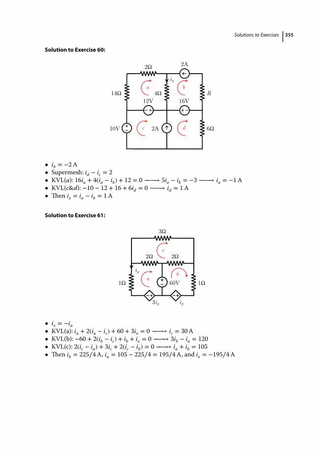
Solutions to Exercises 355
Solution to Exercise 60:
12V
10V
16V
2A
R
2Ω
14Ω 4Ω
2A 6Ω
ixa b
c d
• ib = −2A• Supermesh: id − ic = 2• KVL(a): 16ia + 4(ia − ib) + 12 = 0 −−−−→ 5ia − ib = −3 −−−−→ ia = −1A• KVL(c&d): −10 − 12 + 16 + 6id = 0 −−−−→ id = 1A• Then ix = ia − ib = 1A
Solution to Exercise 61:
2Ω 2Ω
3Ω
1Ω 60V 1Ω
3ix ix
ixa b
c
• ix = −ia• KVL(a): ia + 2(ia − ic) + 60 + 3ix = 0 −−−−→ ic = 30A• KVL(b): −60 + 2(ib − ic) + ib + ix = 0 −−−−→ 3ib − ia = 120• KVL(c): 2(ic − ia) + 3ic + 2(ic − ib) = 0 −−−−→ ia + ib = 105• Then ib = 225∕4A, ia = 105 − 225∕4 = 195∕4A, and ix = −195∕4A
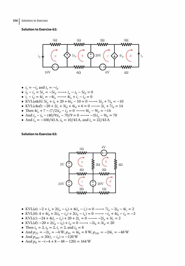
356 Solutions to Exercises
Solution to Exercise 62:
5Ω 1Ω 2Ω 3Ω
4Ω6Ω10V
5ix 20V 4iy
6V
ixiy a b c d
• iy = −ia and ix = −id• ib − ia = 5ix = −5id −−−−→ ia − ib − 5id = 0• ic − id = 4iy = −4ia −−−−→ 4ia + ic − id = 0• KVL(a&b): 5ia + ib + 20 + 6ib − 10 = 0 −−−−→ 5ia + 7ib = −10• KVL(c&d): −20 + 2ic + 3id + 4id + 6 = 0 −−−−→ 2ic + 7id = 14• Then 4ia + 7 − (7∕2)id − id = 0 −−−−→ 8ia − 9id = −14• And ia − ib − (40∕9)ia − 70∕9 = 0 −−−−→ −31ia − 9ib = 70• And ia = −100∕43A, ib = 10∕43A, and ix = 22∕43A
Solution to Exercise 63:
2V
24V 20V
4V 1Ω
4Ω
2Ω 1Ω
2Ω
2Ω 4Ω
a b
c d
• KVL(a): −2 + ia + 2(ia − ib) + 4(ia − ic) = 0 −−−−→ 7ia − 2ib − 4ic = 2• KVL(b): 4 + 4ib + 2(ib − id) + 2(ib − ia) = 0 −−−−→ −ia + 4ib − id = −2• KVL(c): −24 + 4(ic − ia) + 20 + 2ic = 0 −−−−→ −2ia + 3ic = 2• KVL(d): −20 + 2(id − ib) + id = 0 −−−−→ −2ib + 3id = 20• Then ia = 2, ib = 2, ic = 2, and id = 8• And p2V = −2ia = −4W, p4V = 4ib = 8W, p24V = −24ic = −48W• And p20V = 20(ic − id) = −120W• And pR = −(−4 + 8 − 48 − 120) = 164W
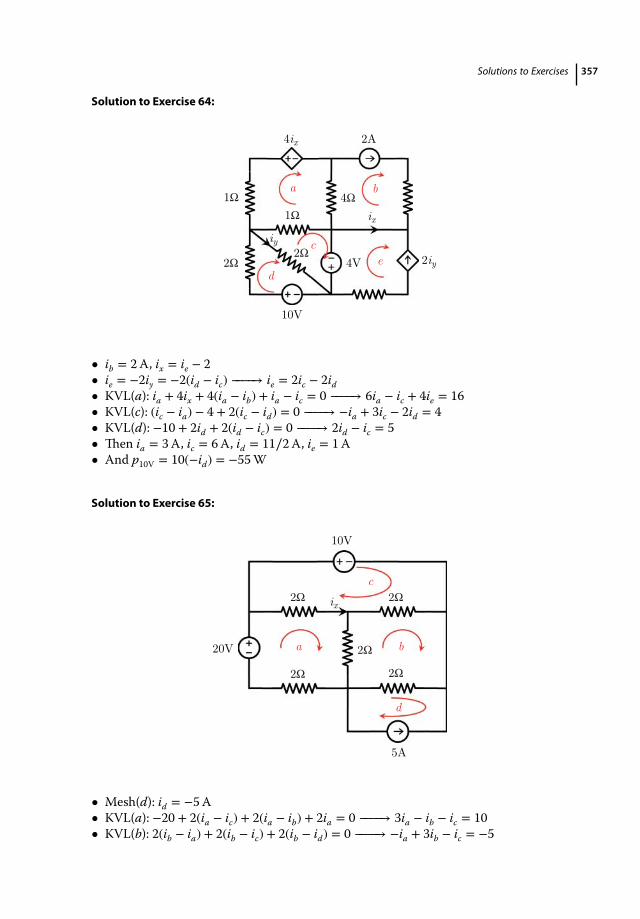
Solutions to Exercises 357
Solution to Exercise 64:
1Ω
2Ω 4V
2A
1Ω
4Ω
2Ω
4ix
10V
2iy
ixiy
a b
ed
c
• ib = 2A, ix = ie − 2• ie = −2iy = −2(id − ic) −−−−→ ie = 2ic − 2id• KVL(a): ia + 4ix + 4(ia − ib) + ia − ic = 0 −−−−→ 6ia − ic + 4ie = 16• KVL(c): (ic − ia) − 4 + 2(ic − id) = 0 −−−−→ −ia + 3ic − 2id = 4• KVL(d): −10 + 2id + 2(id − ic) = 0 −−−−→ 2id − ic = 5• Then ia = 3A, ic = 6A, id = 11∕2A, ie = 1A• And p10V = 10(−id) = −55W
Solution to Exercise 65:
2Ω
10V
2Ω
2Ω
2Ω
2Ω
20V
5A
ix
a b
c
d
• Mesh(d): id = −5A• KVL(a): −20 + 2(ia − ic) + 2(ia − ib) + 2ia = 0 −−−−→ 3ia − ib − ic = 10• KVL(b): 2(ib − ia) + 2(ib − ic) + 2(ib − id) = 0 −−−−→ −ia + 3ib − ic = −5
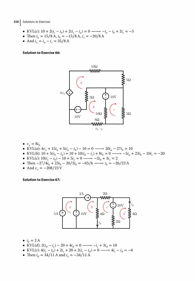
358 Solutions to Exercises
• KVL(c): 10 + 2(ic − ib) + 2(ic − ia) = 0 −−−−→ −ia − ib + 2ic = −5• Then ia = 15∕8A, ib = −15∕8A, ic = −20∕8A• And ix = ia − ic = 35∕8A
Solution to Exercise 66:
10Ω
5Ω
5Ω10Ω
5Ω
8Ω
10V
10V
4vx
vx + –
a
b c
• 𝑣x = 8ib• KVL(a): 4𝑣x + 15ia + 5(ia − ib) − 10 = 0 −−−−→ 20ia − 27ib = 10• KVL(b): 10 + 5(ib − ia) + 10 + 10(ib − ic) + 8ib = 0 −−−−→ −5ia + 23ib − 10ic = −20• KVL(c): 10(ic − ib) − 10 + 5ic = 0 −−−−→ −2ib + 3ic = 2• Then −27∕4ib + 23ib − 20∕3ib = −65∕6 −−−−→ ib = −26∕23A• And 𝑣x = −208∕23V
Solution to Exercise 67:
2Ω
4Ω
2Ω
4Ω
20V
10V 5A
2A
ix
iy
a b cd
• ib = 2A• KVL(d): 2(id − ic) − 20 + 4id = 0 −−−−→ −ic + 3id = 10• KVL(c): 4(ic − ib) + 2ic + 20 + 2(ic − id) = 0 −−−−→ 4ic − id = −6• Then id = 34∕11A and ix = −34∕11A
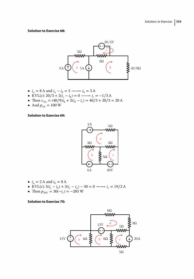
Solutions to Exercises 359
Solution to Exercise 68:
8A 5A
5Ω
20/3V
2Ω
40/9Ωa b
c
• ia = 8A and ia − ib = 5 −−−−→ ib = 3A• KVL(c): 20∕3 + 2(ic − ib) = 0 −−−−→ ic = −1∕3A• Then 𝑣5A = (40∕9)ib + 2(ib − ic) = 40∕3 + 20∕3 = 20A• And p5A = 100W
Solution to Exercise 69:
2A 5Ω
3Ω 3Ω
5Ω
8A 30V
a
b c
• ia = 2A and ib = 8A• KVL(c): 5(ic − ib) + 3(ic − ia) − 30 = 0 −−−−→ ic = 19∕2A• Then p30V = 30(−ic) = −285W
Solution to Exercise 70:
15V
12V
4Ω 6Ω
1Ω
6Ω
3Ω
5Ω
20Aa b c
d

360 Solutions to Exercises
• ic = 20A• KVL(a): −15 + 4(ia − ib) = 0 −−−−→ 4ia − 4ib = 15• KVL(b): 4(ib − ia) + 12 + 6(ib − ic) = 0 −−−−→ −2ia + 5ib = 54• Then ib = 41∕2A and ia = 97∕4A• And p15V = 15 × (−ia) = −1455∕4W
Chapter 5
Solution to Exercise 71:
3Ω
1
2A
2V
6Ω
6Ω
+
_ voc
03
2
For 𝑣oc:
• Supernode: 𝑣3 = 𝑣1 + 2• KCL(1&3): −2 − 𝑣3∕3 − 𝑣1∕12 = 0 −−−−→ 𝑣1 + 4𝑣3 = −24• Then 𝑣1 = −32∕5V, 𝑣oc = (−32∕5)∕2 = −16∕5V
3Ω
1
2A
2V
2
6Ω
6Ω
3
isc
For isc:
• 𝑣1 = 𝑣2• Supernode: 𝑣3 = 𝑣1 + 2 = 𝑣2 + 2• KCL(1&2&3): −2 − 𝑣3∕3 − 𝑣2∕6 = 0 −−−−→ 𝑣2 + 2𝑣3 = −12• Then 𝑣1 = 𝑣2 = −16∕3V, 𝑣3 = −10∕3V, isc = 𝑣2∕6 = −8∕9A• Rth = 18∕5Ω
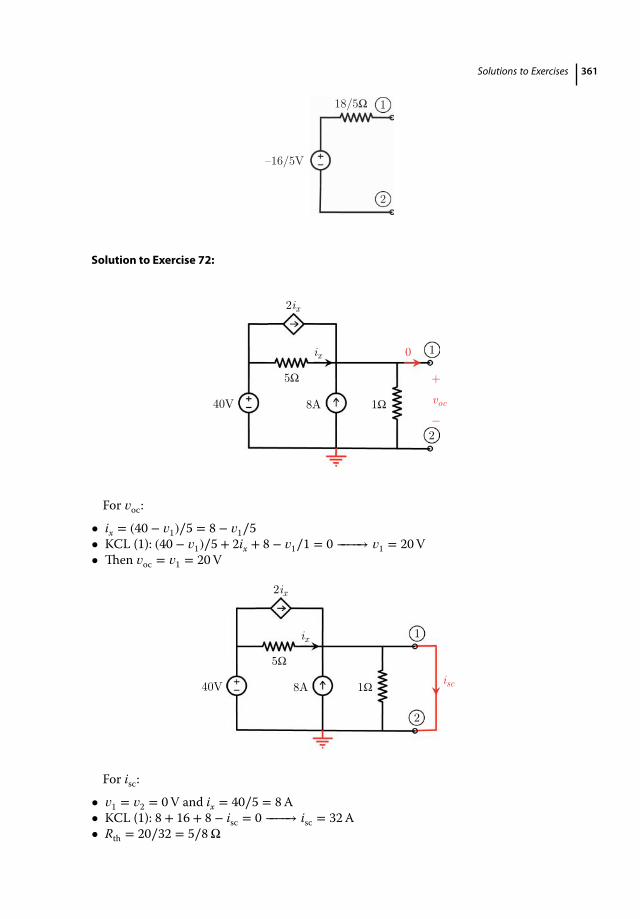
Solutions to Exercises 361
18/5Ω
–16/5V
1
2
Solution to Exercise 72:
1
2
40V 8A 1Ω
5Ω
2ix
ix+
_ voc
0
For 𝑣oc:
• ix = (40 − 𝑣1)∕5 = 8 − 𝑣1∕5• KCL (1): (40 − 𝑣1)∕5 + 2ix + 8 − 𝑣1∕1 = 0 −−−−→ 𝑣1 = 20V• Then 𝑣oc = 𝑣1 = 20V
2ix
isc
1
2
40V 8A 1Ω
5Ω
ix
For isc:
• 𝑣1 = 𝑣2 = 0V and ix = 40∕5 = 8A• KCL (1): 8 + 16 + 8 − isc = 0 −−−−→ isc = 32A• Rth = 20∕32 = 5∕8Ω
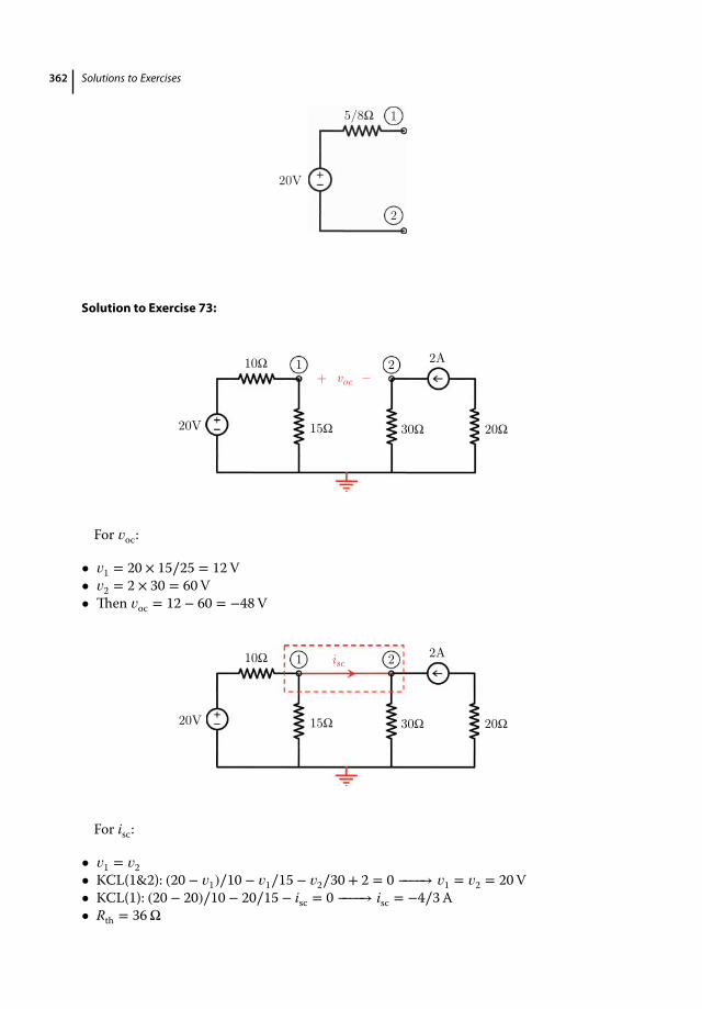
362 Solutions to Exercises
5/8Ω
20V
1
2
Solution to Exercise 73:
20Ω20V
10Ω
15Ω 30Ω
1 2 2A voc
_ +
For 𝑣oc:
• 𝑣1 = 20 × 15∕25 = 12V• 𝑣2 = 2 × 30 = 60V• Then 𝑣oc = 12 − 60 = −48V
20Ω20V
10Ω
15Ω 30Ω
1 2 2A isc
For isc:
• 𝑣1 = 𝑣2• KCL(1&2): (20 − 𝑣1)∕10 − 𝑣1∕15 − 𝑣2∕30 + 2 = 0 −−−−→ 𝑣1 = 𝑣2 = 20V• KCL(1): (20 − 20)∕10 − 20∕15 − isc = 0 −−−−→ isc = −4∕3A• Rth = 36Ω
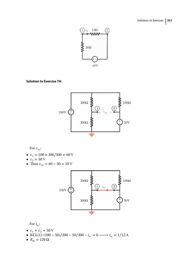
Solutions to Exercises 363
36Ω
1 2 ix 12Ω
–48V
Solution to Exercise 74:
100V
200Ω 1
100Ω
50V 300Ω
2 voc _+
For 𝑣oc:
• 𝑣1 = 100 × 300∕500 = 60V• 𝑣2 = 50V• Then 𝑣oc = 60 − 50 = 10V
100V
200Ω
1 100Ω
50V300Ω
2 isc
For isc:
• 𝑣1 = 𝑣2 = 50V• KCL(1): (100 − 50)∕200 − 50∕300 − isc = 0 −−−−→ isc = 1∕12A• Rth = 120Ω

364 Solutions to Exercises
120Ω
10V
1 2
Solution to Exercise 75:
100V 2Ω
1
2
2A +
_ voc
For 𝑣oc:
• 𝑣oc = −100V
100V2Ω
1
2
2A isc
For isc:
• isc = −∞ −−−−→ Rth = 0Ω
–100V1
2
10Ω
ix
We normally consider a parallel connection of a voltage source and short circuit as animpossible scenario. However, in this case, since the aim is to find theThévenin seen bya component, we mathematically carry out the process to reach Rth = 0. For confused
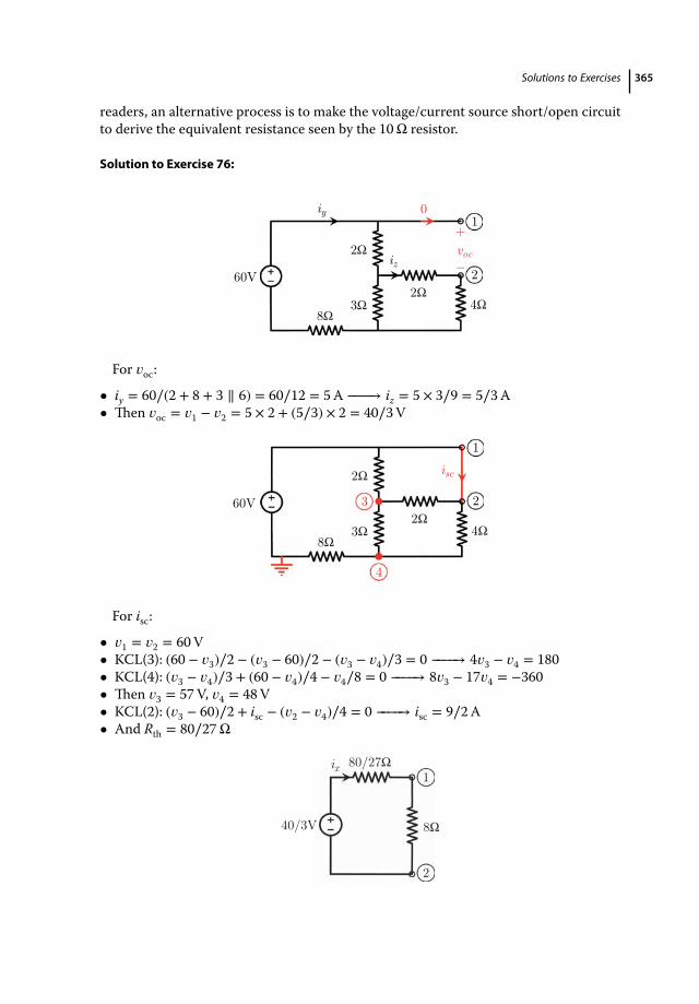
Solutions to Exercises 365
readers, an alternative process is to make the voltage/current source short/open circuitto derive the equivalent resistance seen by the 10Ω resistor.
Solution to Exercise 76:
8Ω
1
2 2Ω
3Ω 2Ω
4Ω
60V
+
_ voc
0 iy
iz
For 𝑣oc:
• iy = 60∕(2 + 8 + 3 ∥ 6) = 60∕12 = 5A −−−−→ iz = 5 × 3∕9 = 5∕3A• Then 𝑣oc = 𝑣1 − 𝑣2 = 5 × 2 + (5∕3) × 2 = 40∕3V
8Ω
1
2 2Ω
3Ω
2Ω
4Ω
60V
isc
3
4
For isc:
• 𝑣1 = 𝑣2 = 60V• KCL(3): (60 − 𝑣3)∕2 − (𝑣3 − 60)∕2 − (𝑣3 − 𝑣4)∕3 = 0 −−−−→ 4𝑣3 − 𝑣4 = 180• KCL(4): (𝑣3 − 𝑣4)∕3 + (60 − 𝑣4)∕4 − 𝑣4∕8 = 0 −−−−→ 8𝑣3 − 17𝑣4 = −360• Then 𝑣3 = 57V, 𝑣4 = 48V• KCL(2): (𝑣3 − 60)∕2 + isc − (𝑣2 − 𝑣4)∕4 = 0 −−−−→ isc = 9∕2A• And Rth = 80∕27Ω
80/27Ω
40/3V
1
2
8Ω
ix
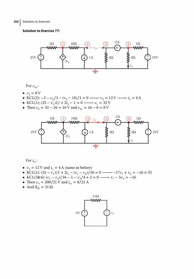
366 Solutions to Exercises
Solution to Exercise 77:
25V
1Ω 16Ω
1A 4Ω 3Ω
1Ω2A
ix2ix
18V
voc_ +
1 4 3 2
For 𝑣oc:
• 𝑣3 = 8V• KCL(2): −2 − 𝑣2∕3 − (𝑣2 − 18)∕1 = 0 −−−−→ 𝑣2 = 12V −−−−→ ix = 4A• KCL(1): (25 − 𝑣1)1∕ + 2ix − 1 = 0 −−−−→ 𝑣1 = 32V• Then 𝑣4 = 32 − 16 = 16V and 𝑣oc = 16 − 8 = 8V
25V
1Ω 16Ω
1A 4Ω 3Ω
1Ω2A
ix2ix
18V
1 4 3 2 isc
For isc:
• 𝑣2 = 12V and ix = 4A (same as before)• KCL(1): (25 − 𝑣1)∕1 + 2ix − (𝑣1 − 𝑣4)∕16 = 0 −−−−→ −17𝑣1 + 𝑣4 = −16 × 33• KCL(3&4): (𝑣1 − 𝑣4)∕16 − 1 − 𝑣3∕4 + 2 = 0 −−−−→ 𝑣1 − 5𝑣4 = −16• Then 𝑣4 = 200∕21V and isc = 8∕21A• And Rth = 21Ω
21Ω
8V vo

Solutions to Exercises 367
Solution to Exercise 78:
2Ω
2A16V 2Ω vy+ _ 2vy
+
_ voc
1
For 𝑣oc:
• 𝑣y = 𝑣1• KCL(1): (16 − 𝑣1)∕2 + 2 − 𝑣1∕2 − 2𝑣y = 0 −−−−→ 𝑣1 = 10∕3V• 𝑣oc = 𝑣1 = 10∕3A
2Ω
2A 16V 2Ω vy+ _ 2vy
1
isc
For isc:
• 𝑣1 = 0V and 𝑣y = 0V• KCL(1): (16 − 𝑣1)∕2 + 2 − 𝑣1∕2 − 2𝑣y − isc = 0 −−−−→ isc = 10A• Then Rth = 1∕3Ω
1/3Ω
10/3V Rl
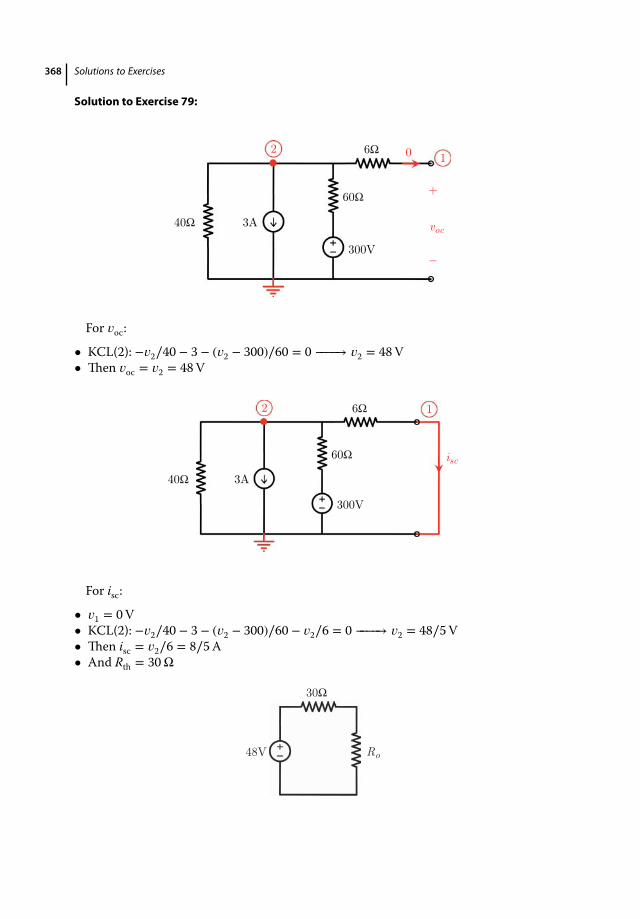
368 Solutions to Exercises
Solution to Exercise 79:
40Ω 3A
60Ω
300V
6Ω 1
+
_
voc
02
For 𝑣oc:
• KCL(2): −𝑣2∕40 − 3 − (𝑣2 − 300)∕60 = 0 −−−−→ 𝑣2 = 48V• Then 𝑣oc = 𝑣2 = 48V
40Ω 3A 60Ω
300V
6Ω2
isc
1
For isc:
• 𝑣1 = 0V• KCL(2): −𝑣2∕40 − 3 − (𝑣2 − 300)∕60 − 𝑣2∕6 = 0 −−−−→ 𝑣2 = 48∕5V• Then isc = 𝑣2∕6 = 8∕5A• And Rth = 30Ω
30Ω
48V Ro
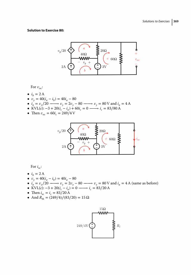
Solutions to Exercises 369
Solution to Exercise 80:
20Ω
40Ω
2A 3V
60Ω
vy/20
vy_ +
+
_ voc
a
b
c
For 𝑣oc:
• ib = 2A• 𝑣y = 40(ia − ib) = 40ia − 80• ia = 𝑣y∕20 −−−−→ 𝑣y = 2𝑣y − 80 −−−−→ 𝑣y = 80V and ia = 4A• KVL(c): −3 + 20(ic − ia) + 60ic = 0 −−−−→ ic = 83∕80A• Then 𝑣oc = 60ic = 249∕4V
20Ω
40Ω
2A 3V
60Ω
vy/20
vy_ +
a
b
c isc
For isc:
• ib = 2A• 𝑣y = 40(ia − ib) = 40ia − 80• ia = 𝑣y∕20 −−−−→ 𝑣y = 2𝑣y − 80 −−−−→ 𝑣y = 80V and ia = 4A (same as before)• KVL(c): −3 + 20(ic − ia) = 0 −−−−→ ic = 83∕20A• Then isc = ic = 83∕20A• And Rth = (249∕4)∕(83∕20) = 15Ω
15Ω
249/4V Rl
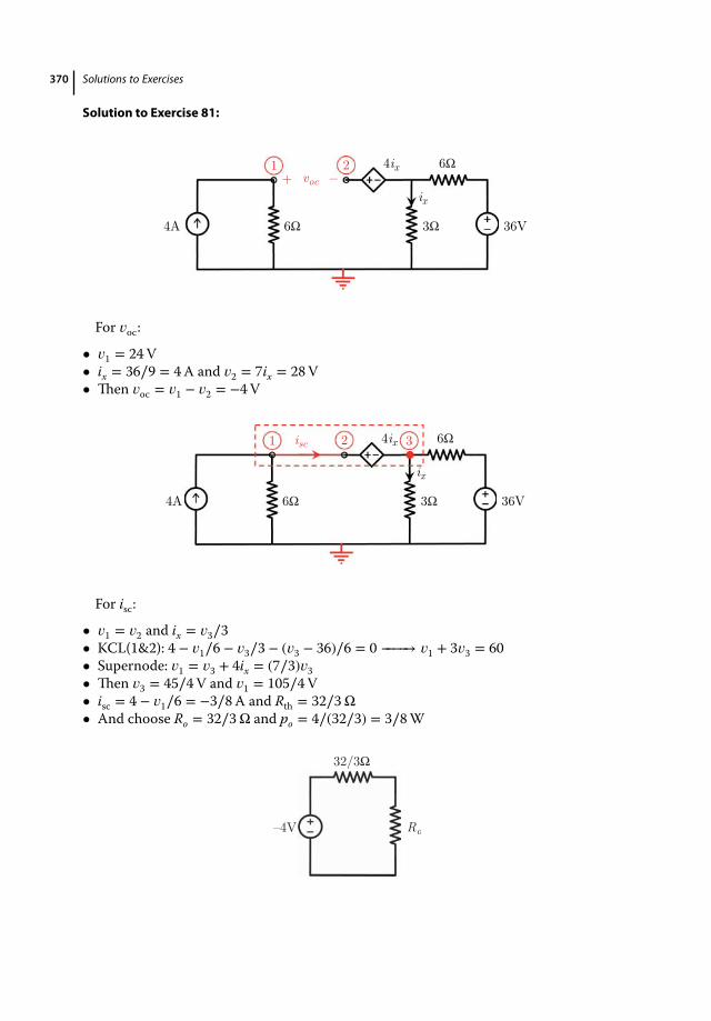
370 Solutions to Exercises
Solution to Exercise 81:
4A 6Ω 3Ω 36V
6Ω4ix
ix
_ +1 2
voc
For 𝑣oc:
• 𝑣1 = 24V• ix = 36∕9 = 4A and 𝑣2 = 7ix = 28V• Then 𝑣oc = 𝑣1 − 𝑣2 = −4V
4A 6Ω 3Ω 36V
6Ω4ix
ix
1 2 isc 3
For isc:
• 𝑣1 = 𝑣2 and ix = 𝑣3∕3• KCL(1&2): 4 − 𝑣1∕6 − 𝑣3∕3 − (𝑣3 − 36)∕6 = 0 −−−−→ 𝑣1 + 3𝑣3 = 60• Supernode: 𝑣1 = 𝑣3 + 4ix = (7∕3)𝑣3• Then 𝑣3 = 45∕4V and 𝑣1 = 105∕4V• isc = 4 − 𝑣1∕6 = −3∕8A and Rth = 32∕3Ω• And choose Ro = 32∕3Ω and po = 4∕(32∕3) = 3∕8W
32/3Ω
–4V Ro
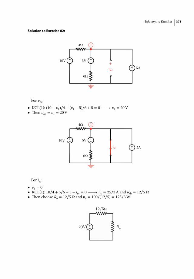
Solutions to Exercises 371
Solution to Exercise 82:
4Ω
10V 5V
6Ω
5Avoc_
+
1
For 𝑣oc:
• KCL(1): (10 − 𝑣1)∕4 − (𝑣1 − 5)∕6 + 5 = 0 −−−−→ 𝑣1 = 20V• Then 𝑣oc = 𝑣1 = 20V
4Ω
10V 5V
6Ω
5A
1
isc
For isc:
• 𝑣1 = 0• KCL(1): 10∕4 + 5∕6 + 5 − isc = 0 −−−−→ isc = 25∕3A and Rth = 12∕5Ω• Then choose Ro = 12∕5Ω and po = 100∕(12∕5) = 125∕3W
12/5Ω
20V Ro

372 Solutions to Exercises
Solution to Exercise 83:
30Ω
30Ω
10Ω
15Ω3A
20ixix +
_
voc
01 2
3
For 𝑣oc:
• 𝑣2 = 15ix• Supernode: 𝑣2 = 𝑣3 + 20ix −−−−→ 𝑣3 = −𝑣2∕3• KCL(1): −𝑣1∕30 + 3 + (𝑣2 − 𝑣1)∕30 = 0 −−−−→ 2𝑣1 − 𝑣2 = 90• KCL(2&3): (𝑣1 − 𝑣2)∕30 − 𝑣3∕10 − 𝑣2∕15 = 0 −−−−→ 𝑣1 − 2𝑣2 = 0• Then 𝑣oc = 𝑣2 = 30V
30Ω
30Ω
10Ω
15Ω3A
20ixix
1 2
3 isc
For isc:
• ix = 0 and 𝑣2 = 𝑣3 = 0• KCL(1): −𝑣1∕30 + 3 − 𝑣1∕30 = 0 −−−−→ 𝑣1 = 45V• isc = 45∕30 = 3∕2A and Rth = 20Ω• Then choose Ro = 20Ω and po = 225∕20 = 45∕4W
20Ω
30V Ro

Solutions to Exercises 373
Solution to Exercise 84:
12Ω
5Ω120V
20Ω 60V
6Ω36A
+
_
voc
01
For 𝑣oc:
• (120 − 𝑣1)∕20 − (𝑣1 + 60)∕5 + 36 − 𝑣1∕6 = 0 −−−−→ 𝑣1 = 72V• Then 𝑣oc = 𝑣1 = 72V
12Ω
5Ω120V
20Ω 60V 6Ω36A
1
isc
For isc:
• (120 − 𝑣1)∕20 − (𝑣1 + 60)∕5 + 36 − 𝑣1∕6 − 𝑣1∕12 = 0 −−−−→ 𝑣1 = 60V• Then isc = 𝑣1∕12 = 5A and Rth = 72∕5Ω• Therefore, choose Ro = 72∕5Ω and po = 362∕(72∕5) = 90W
72/5Ω
72V Ro
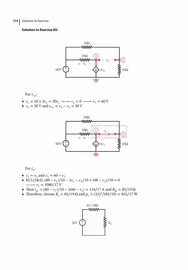
374 Solutions to Exercises
Solution to Exercise 85:
60V
10Ω
10Ω
10Ω2vx
vx+ _ voc_ +
1 2
For 𝑣oc:
• 𝑣x = 10 × 2𝑣x = 20𝑣x −−−−→ 𝑣x = 0 −−−−→ 𝑣1 = 60V• 𝑣2 = 30V and 𝑣oc = 𝑣1 − 𝑣2 = 30V
60V
10Ω
10Ω
10Ω2vx
vx+ _ 1
2 isc
For isc:
• 𝑣1 = 𝑣2 and 𝑣x = 60 − 𝑣1• KCL(1&2): (60 − 𝑣1)∕10 − 2𝑣x − 𝑣2∕10 + (60 − 𝑣2)∕10 = 0
−−−−→ 𝑣1 = 1080∕17V• Then isc = (60 − 𝑣1)∕10 − 2(60 − 𝑣1) = 114∕17A and Rth = 85∕19Ω• Therefore, choose Ro = 85∕19Ω and po = (15)2∕(85∕19) = 855∕17W
85/19Ω
30V Ro

Solutions to Exercises 375
Solution to Exercise 86:
3A 3Ω
4Ω
vx+_
vx/4
1 +
_ voc
02
For 𝑣oc:
• 𝑣x = 𝑣2• KCL(1): 𝑣x∕4 + (𝑣2 − 𝑣1)∕4 = 0 −−−−→ 𝑣1 = 2𝑣2• KCL(2): 3 − 𝑣2∕3 − (𝑣2 − 𝑣1)∕4 − 𝑣2∕4 = 0 −−−−→ 3𝑣1 − 10𝑣2 = −36• Then 𝑣2 = 9V, 𝑣1 = 18V, and 𝑣oc = 𝑣1 = 18V
3A 3Ω
4Ω
vx+_
vx/4
12
isc
For isc:
• 𝑣x = 𝑣2 and 𝑣1 = 0V• KCL(2): 3 − 𝑣2∕3 − 𝑣2∕4 − 𝑣2∕4 = 0 −−−−→ 𝑣2 = 18∕5V• Then isc = 𝑣2∕4 + 𝑣2∕4 = 9∕5A and Rth = 10Ω• Therefore, choose Ro = 10Ω and po = 92∕10 = 81∕10W
10Ω
18V Ro
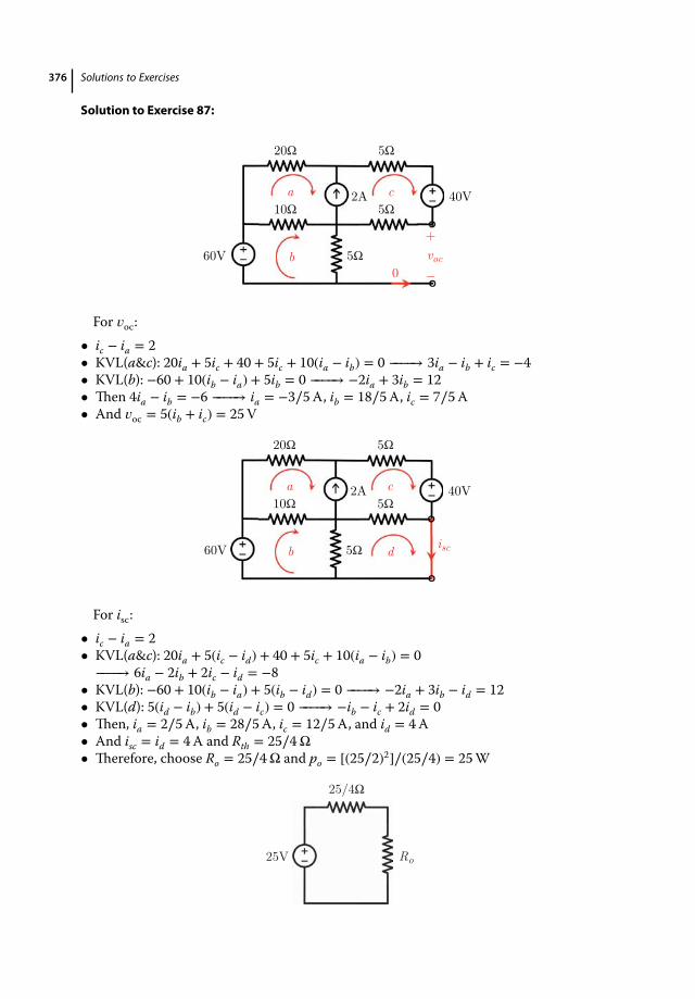
376 Solutions to Exercises
Solution to Exercise 87:
20Ω
10Ω
5Ω
5Ω
5Ω60V
40V 2A
+
_ voc
0
a
b
c
For 𝑣oc:• ic − ia = 2• KVL(a&c): 20ia + 5ic + 40 + 5ic + 10(ia − ib) = 0 −−−−→ 3ia − ib + ic = −4• KVL(b): −60 + 10(ib − ia) + 5ib = 0 −−−−→ −2ia + 3ib = 12• Then 4ia − ib = −6 −−−−→ ia = −3∕5A, ib = 18∕5A, ic = 7∕5A• And 𝑣oc = 5(ib + ic) = 25V
20Ω
10Ω
5Ω
5Ω
5Ω60V
40V 2A a
b
c
iscd
For isc:• ic − ia = 2• KVL(a&c): 20ia + 5(ic − id) + 40 + 5ic + 10(ia − ib) = 0
−−−−→ 6ia − 2ib + 2ic − id = −8• KVL(b): −60 + 10(ib − ia) + 5(ib − id) = 0 −−−−→ −2ia + 3ib − id = 12• KVL(d): 5(id − ib) + 5(id − ic) = 0 −−−−→ −ib − ic + 2id = 0• Then, ia = 2∕5A, ib = 28∕5A, ic = 12∕5A, and id = 4A• And isc = id = 4A and Rth = 25∕4Ω• Therefore, choose Ro = 25∕4Ω and po = [(25∕2)2]∕(25∕4) = 25W
25/4Ω
25V Ro
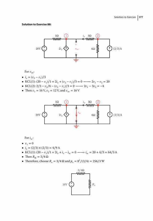
Solutions to Exercises 377
Solution to Exercise 88:
1Ω 3Ωix
20V 6Ω (2/3)A2ix+
_ voc
1 2
For 𝑣oc:
• ix = (𝑣2 − 𝑣1)∕3• KCL(1): (20 − 𝑣1)∕1 + 2ix + (𝑣2 − 𝑣1)∕3 = 0 −−−−→ 2𝑣1 − 𝑣2 = 20• KCL(2): 2∕3 − 𝑣2∕6 − (𝑣2 − 𝑣1)∕3 = 0 −−−−→ 2𝑣1 − 3𝑣2 = −4• Then 𝑣1 = 16V, 𝑣2 = 12V, and 𝑣oc = 16V
1Ω 3Ωix
20V 6Ω (2/3)A2ix
1 2
isc
For isc:
• 𝑣1 = 0• ix = (2∕3) × (2∕3) = 4∕9A• KCL(1): (20 − 𝑣1)∕1 + 2ix + ix − isc = 0 −−−−→ isc = 20 + 4∕3 = 64∕3A• Then Rth = 3∕4Ω• Therefore, choose Ro = 3∕4Ω and po = 82∕(3∕4) = 256∕3W
3/4Ω
16V Ro

378 Solutions to Exercises
Solution to Exercise 89:
The Thévenin equivalent circuit seen by Ro can be found by recognizing the rest of thecircuit as a Norton equivalent with isc = io and Rth = R1 ∥ R2. Then we have
𝑣oc = Rthisc =R1R2
R1 + R2io,
and one must select Ro = Rth = R1 ∥ R2 for maximum power transfer. For this selection,the voltage across Ro can be found to be
𝑣o =𝑣oc
2=
R1R2
R1 + R2
io
2.
Finally, the transferred power can be obtained as
pmaxo =
𝑣2o
Ro=
R21R2
2
(R1 + R2)2i2o4
1Ro
=R1R2
4(R1 + R2)i2o.
Chapter 6
Solution to Exercise 90:
.• 0 ≤ t ≤ 3 s: 𝑣C(t) = 0 +
∫
t
0(−t′2 + 4t′)dt′ =
(− t33+ 2t2
)V
and 𝑣C(3) = 9V
• 3 ≤ t ≤ 6 s: 𝑣C(t) = 9 +∫
t
3(−5t′∕6 + 11∕2)dt′ =
(−5t212
+ 11t2
− 154
)V
and 𝑣C(3) =92V
• 3 ≤ t ≤ 4 s: 𝑣C(t) = 9∕2 +∫
t
3(t′ − 2)dt′ =
(t22− 2t + 6
)V
and 𝑣C(6) =574
V
• 6 ≤ t ≤ 8 s: 𝑣C(t) = 57∕4 +∫
t
6(1∕2)dt′ =
( t2+ 45
4
)V
and 𝑣C(8) =614
V
• t ≥ 8 s: 𝑣C(t) =614
V
Solution to Exercise 91:
.
iC(t) = Cd𝑣C(t)
dt=
⎧⎪⎪⎨⎪⎪⎩
2t, 0 ≤ t ≤ 2 s1, 2 ≤ t ≤ 5 s
−2t + 12, 5 ≤ t ≤ 6 s0, t ≥ 6 s
(A).

Solutions to Exercises 379
Solution to Exercise 92:
.• 0 ≤ t ≤ 1 s: 𝑣C(t) = 1 +∫
t
02dt′ = (2t + 1)V and 𝑣C(1) = 3V
• 1 ≤ t ≤ 2 s: 𝑣C(t) = 3 +∫
t
1(2t′ − 4)dt′ = (t2 − 4t + 6)V and 𝑣C(2) = 2V
• t ≥ 2 s: 𝑣C(t) = 2V• 0 ≤ t ≤ 1 s: pC(t) = iC(t)𝑣C(t) = 2(2t + 1)W• 1 ≤ t ≤ 2 s: pC(t) = iC(t)𝑣C(t) = (2t − 4)(t2 − 4t + 6)W• t ≥ 2 s: pC(t) = 0
Solution to Exercise 93:
.• 0 ≤ t ≤ 1 s: 𝑣C(t) = 0 + 12 ∫
t
05t′dt′ = (5t2∕4)V and 𝑣C(1) = 5∕4V
• 1 ≤ t ≤ 2 s: 𝑣C(t) = 5∕4 + 12 ∫
t
15dt′ = (5t∕2 − 5∕4)V and
𝑣C(2) = 15∕4V
• 2 ≤ t ≤ 3 s: 𝑣C(t) = 15∕4 + 12 ∫
t
2(9 − t′2)dt′ = (−t3∕6 + 9t∕2 − 47∕12)V and
𝑣C(3) = 61∕12V• t ≥ 3 s: 𝑣C(t) = 61∕12V• Then, for t ≥ 3 s: 𝑤C(t) =
12
C[𝑣C]2 = (61∕12)2 J
Solution to Exercise 94:
.• 0 ≤ t ≤ 1 s: 𝑣C(t) = 0 +∫
t
0t′dt′ = (t2∕2)V and 𝑣C(1) = 1∕2V
• 1 ≤ t ≤ 3 s: 𝑣C(t) = 1∕2 +∫
t
11dt′ = (t − 1∕2)V and 𝑣C(3) = 5∕2V
• 3 ≤ t ≤ 4 s: 𝑣C(t) = 5∕2 +∫
t
3(−1)dt′ = (−t + 11∕2)V and 𝑣C(3) = 3∕2V
• t ≥ 4 s: 𝑣C(t) = 3∕2V
𝑤C(t) =12
C[𝑣C(t)]2 =
⎧⎪⎪⎨⎪⎪⎩
t4∕8, 0 ≤ t ≤ 1 st2∕2 − t∕2 + 1∕8, 1 ≤ t ≤ 3 s
t2∕2 − 11t∕2 + 121∕8, 3 ≤ t ≤ 4 s9∕8, t ≥ 4 s
(W).
Solution to Exercise 95:
.𝑣L(t) = L
diL(t)dt
=⎧⎪⎨⎪⎩
400, 0 < t < 4 s50, 4 < t < 8 s0, t > 8 s
(V).
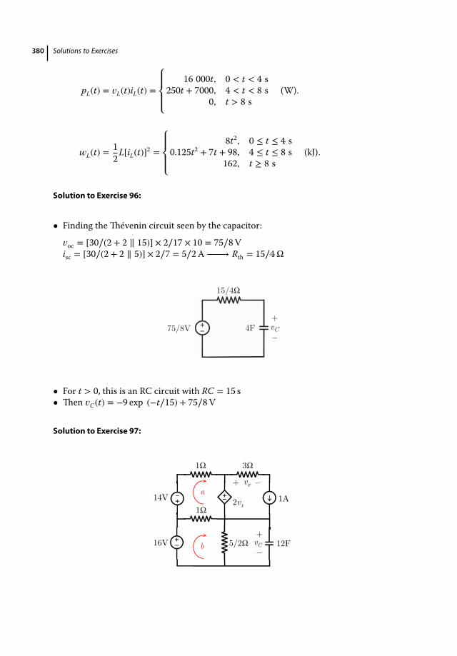
380 Solutions to Exercises
pL(t) = 𝑣L(t)iL(t) =⎧⎪⎨⎪⎩
16 000t, 0 < t < 4 s250t + 7000, 4 < t < 8 s
0, t > 8 s(W).
𝑤L(t) =12
L[iL(t)]2 =⎧⎪⎨⎪⎩
8t2, 0 ≤ t ≤ 4 s0.125t2 + 7t + 98, 4 ≤ t ≤ 8 s
162, t ≥ 8 s(kJ).
Solution to Exercise 96:
.• Finding theThévenin circuit seen by the capacitor:
𝑣oc = [30∕(2 + 2 ∥ 15)] × 2∕17 × 10 = 75∕8Visc = [30∕(2 + 2 ∥ 5)] × 2∕7 = 5∕2A −−−−→ Rth = 15∕4Ω
75/8V
15/4Ω
4F vC+
_
• For t > 0, this is an RC circuit with RC = 15 s• Then 𝑣C(t) = −9 exp (−t∕15) + 75∕8V
Solution to Exercise 97:
14V
16V
1Ω
1Ω 3Ω + _ vx
2vx 1A
12F 5/2Ω vC + _
a
b
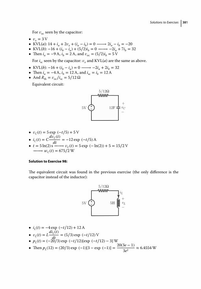
Solutions to Exercises 381
For 𝑣oc seen by the capacitor:• 𝑣x = 3V• KVL(a): 14 + ia + 2𝑣x + (ia − ib) = 0 −−−−→ 2ia − ib = −20• KVL(b): −16 + (ib − ia) + (5∕2)ib = 0 −−−−→ −2ia + 7ib = 32• Then ia = −9A, ib = 2A, and 𝑣oc = (5∕2)ib = 5VFor isc seen by the capacitor: 𝑣x and KVL(a) are the same as above.
• KVL(b): −16 + (ib − ia) = 0 −−−−→ −2ia + 2ib = 32• Then ia = −4A, ib = 12A, and isc = ib = 12A• And Rth = 𝑣oc∕isc = 5∕12ΩEquivalent circuit:
5V
5/12Ω
12F vC+
_
• 𝑣C(t) = 5 exp (−t∕5) + 5V
• iC(t) = Cd𝑣C(t)
dt= −12 exp (−t∕5)A
• t = 5 ln(2) s −−−−→ 𝑣C(t) = 5 exp (− ln(2)) + 5 = 15∕2V−−−−→ 𝑤C(t) = 675∕2W
Solution to Exercise 98:
The equivalent circuit was found in the previous exercise (the only difference is thecapacitor instead of the inductor):
5V
5/12Ω
5H vL+_
iL
• iL(t) = −4 exp (−t∕12) + 12A
• 𝑣L(t) = LdiL(t)
dt= (5∕3) exp (−t∕12)V
• pL(t) = (−20∕3) exp (−t∕12)[exp (−t∕12) − 3]W• Then pL(12) = (20∕3) exp (−1)[3 − exp (−1)] = 20(3e − 1)
3e2≈ 6.4554W
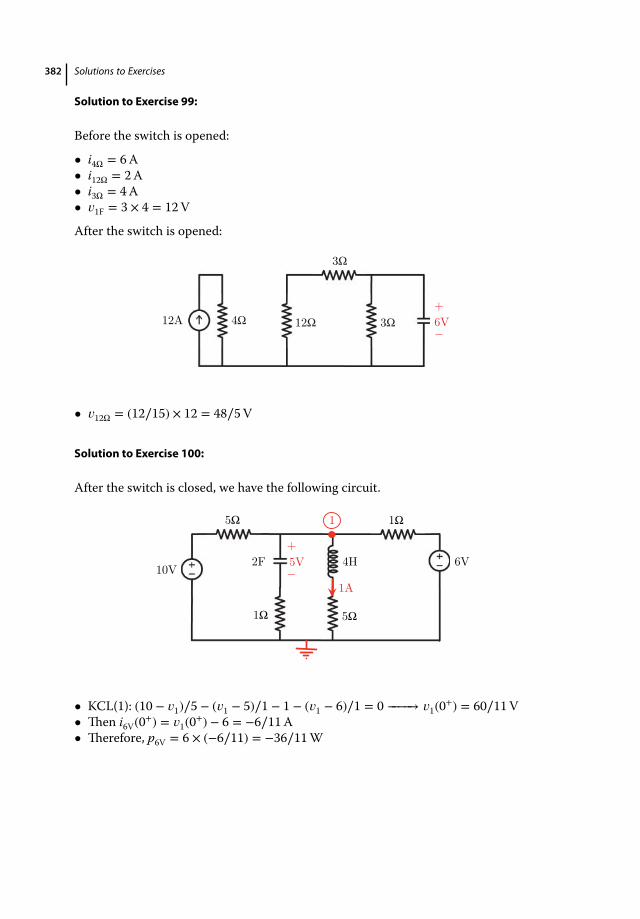
382 Solutions to Exercises
Solution to Exercise 99:
Before the switch is opened:
• i4Ω = 6A• i12Ω = 2A• i3Ω = 4A• 𝑣1F = 3 × 4 = 12V
After the switch is opened:
3Ω12Ω
3Ω
12A 4Ω
+
_ 6V
• 𝑣12Ω = (12∕15) × 12 = 48∕5V
Solution to Exercise 100:
After the switch is closed, we have the following circuit.
2F10V
5Ω
1Ω
4H
5Ω
6V
1Ω
+
_ 5V
1A
1
• KCL(1): (10 − 𝑣1)∕5 − (𝑣1 − 5)∕1 − 1 − (𝑣1 − 6)∕1 = 0 −−−−→ 𝑣1(0+) = 60∕11V• Then i6V(0+) = 𝑣1(0+) − 6 = −6∕11A• Therefore, p6V = 6 × (−6∕11) = −36∕11W
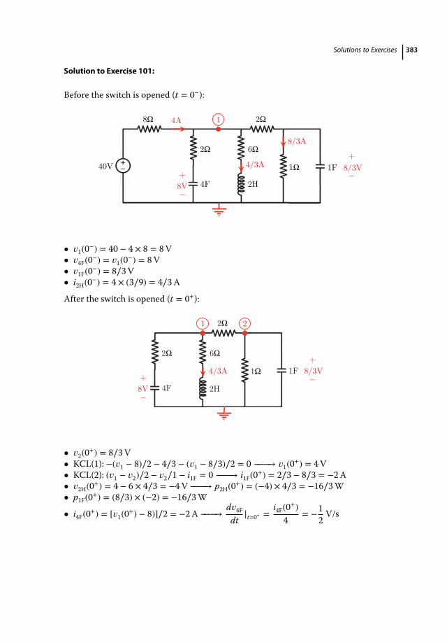
Solutions to Exercises 383
Solution to Exercise 101:
Before the switch is opened (t = 0−):
40V
8Ω
2Ω
4F
6Ω
2H
2Ω
1Ω 1F +
_
4A
4/3A
8/3A
1
8V
+
_ 8/3V
• 𝑣1(0−) = 40 − 4 × 8 = 8V• 𝑣4F(0−) = 𝑣1(0−) = 8V• 𝑣1F(0−) = 8∕3V• i2H(0−) = 4 × (3∕9) = 4∕3A
After the switch is opened (t = 0+):
2Ω
4F
6Ω
2H
2Ω
1Ω 1F+
_ 8V
4/3A+
_ 8/3V
1 2
• 𝑣2(0+) = 8∕3V• KCL(1): −(𝑣1 − 8)∕2 − 4∕3 − (𝑣1 − 8∕3)∕2 = 0 −−−−→ 𝑣1(0+) = 4V• KCL(2): (𝑣1 − 𝑣2)∕2 − 𝑣2∕1 − i1F = 0 −−−−→ i1F(0+) = 2∕3 − 8∕3 = −2A• 𝑣2H(0+) = 4 − 6 × 4∕3 = −4V −−−−→ p2H(0+) = (−4) × 4∕3 = −16∕3W• p1F(0+) = (8∕3) × (−2) = −16∕3W
• i4F(0+) = [𝑣1(0+) − 8)]∕2 = −2A −−−−→d𝑣4F
dt|t=0+ =
i4F(0+)4
= −12V/s
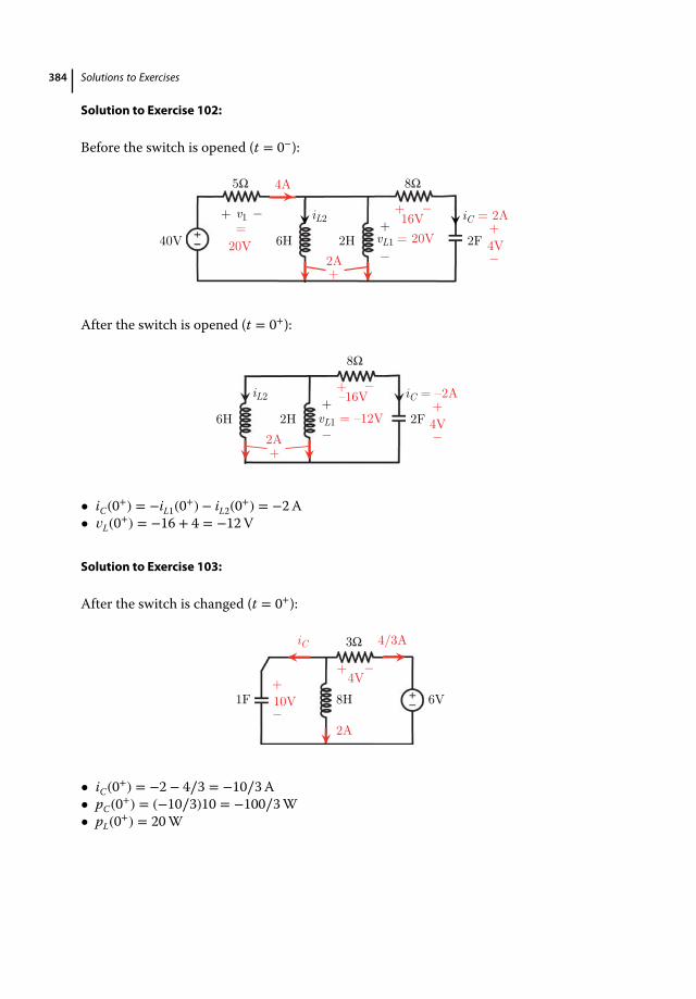
384 Solutions to Exercises
Solution to Exercise 102:
Before the switch is opened (t = 0−):
40V 6H 2H
8Ω5Ω
2F
v1_ + iC = 2A
vL1 = 20V+
_
iL2 =
20V
_ + 16V
+
_ 4V
4A
2A+
After the switch is opened (t = 0+):
6H 2H
8Ω
2F
iC = –2A
vL1 = –12V+
_
iL2
_ + –16V
+
_ 4V2A+
• iC(0+) = −iL1(0+) − iL2(0+) = −2A• 𝑣L(0+) = −16 + 4 = −12V
Solution to Exercise 103:
After the switch is changed (t = 0+):
6V1F 8H
3Ω
+
_ 10V
_ + 4V
4/3A
2A
iC
• iC(0+) = −2 − 4∕3 = −10∕3A• pC(0+) = (−10∕3)10 = −100∕3W• pL(0+) = 20W
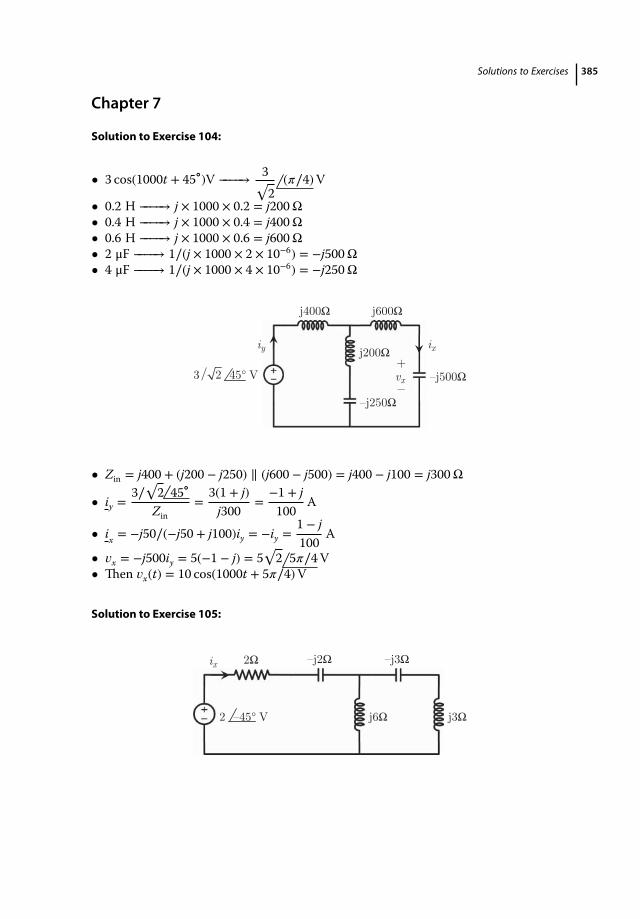
Solutions to Exercises 385
Chapter 7
Solution to Exercise 104:
• 3 cos(1000t + 45∘)V −−−−→ 3√2
(𝜋∕4)V
• 0.2 H −−−−→ j × 1000 × 0.2 = j200Ω• 0.4 H −−−−→ j × 1000 × 0.4 = j400Ω• 0.6 H −−−−→ j × 1000 × 0.6 = j600Ω• 2 μF −−−−→ 1∕(j × 1000 × 2 × 10−6) = −j500Ω• 4 μF −−−−→ 1∕(j × 1000 × 4 × 10−6) = −j250Ω
j400Ω j600Ω
j200Ω
–j250Ω
–j500Ωvx_
+
iy ix
3 2 45° V
• Zin = j400 + (j200 − j250) ∥ (j600 − j500) = j400 − j100 = j300Ω
• iy =3∕
√2 45∘
Zin=
3(1 + j)j300
=−1 + j100
A
• ix = −j50∕(−j50 + j100)iy = −iy =1 − j100
A
• 𝑣x = −j500iy = 5(−1 − j) = 5√2 5𝜋∕4V
• Then 𝑣x(t) = 10 cos(1000t + 5𝜋∕4)V
Solution to Exercise 105:
2Ω –j2Ω –j3Ω
j6Ω j3Ω
ix
2 –45° V

386 Solutions to Exercises
• Zin = 2 − j2 + 6 ∥ (−j3 + j3) = (2 − 2j) = 2√2 (−𝜋∕4) Ω
• ix = 2 (−𝜋∕4)∕Zin =1√2
0A
• Then ix(t) =√2√2cos(3t) = cos(3t)A
Solution to Exercise 106:
j20Ω
j30Ωj40Ω –j20Ω
–j25Ω
–j50Ω
vL
+
_ 2 2 45° V
• Zin = −j50 + j40 ∥ [−j5 + (−j20 ∥ j30)] = −j50 + j40 ∥ (−j65) = j54Ω
• is =2 + 2j
j54A and iL =
−j65j40 − j65
× is =135
×(2 + j2)
j54A
• Then 𝑣L = j40 × iL = 10427
(1 + j)V
• And 𝑣L(t) =20827
cos(1000t + 𝜋∕4)V
Solution to Exercise 107:
1Ω
jΩ
1/jwC iR
2 45° V
For C = 20mF:
• ZCL = −j + j = 0• Then iR = 0A and iR(t) = 0A
For C = 10mF:
• ZCL = −2j + j = −j Ω
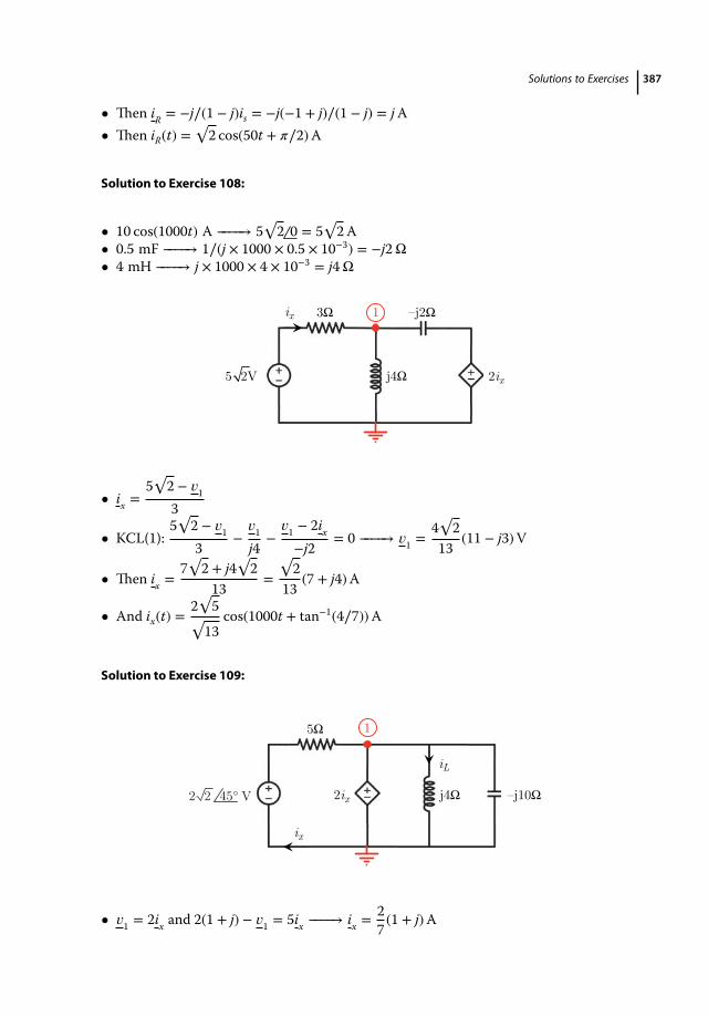
Solutions to Exercises 387
• Then iR = −j∕(1 − j)is = −j(−1 + j)∕(1 − j) = jA• Then iR(t) =
√2 cos(50t + 𝜋∕2)A
Solution to Exercise 108:
.• 10 cos(1000t) A −−−−→ 5
√2 0 = 5
√2A
• 0.5 mF −−−−→ 1∕(j × 1000 × 0.5 × 10−3) = −j2Ω• 4 mH −−−−→ j × 1000 × 4 × 10−3 = j4Ω
3Ωix
2ix
–j2Ω
5 2V j4Ω
1
• ix =5√2 − 𝑣1
3
• KCL(1):5√2 − 𝑣1
3−
𝑣1
j4−
𝑣1 − 2ix
−j2= 0 −−−−→ 𝑣1 =
4√2
13(11 − j3)V
• Then ix =7√2 + j4
√2
13=
√2
13(7 + j4)A
• And ix(t) =2√5√
13cos(1000t + tan−1(4∕7))A
Solution to Exercise 109:
5Ω
j4Ω –j10Ω2ix
ix
iL
1
2 2 45° V
• 𝑣1 = 2ix and 2(1 + j) − 𝑣1 = 5ix −−−−→ ix =27(1 + j)A
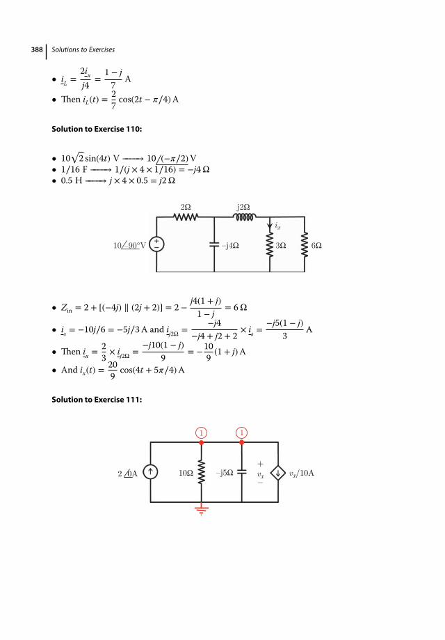
388 Solutions to Exercises
• iL =2ix
j4=
1 − j7
A
• Then iL(t) =27cos(2t − 𝜋∕4)A
Solution to Exercise 110:
.• 10√2 sin(4t) V −−−−→ 10 (−𝜋∕2)V
• 1∕16 F −−−−→ 1∕(j × 4 × 1∕16) = −j4Ω• 0.5 H −−−−→ j × 4 × 0.5 = j2Ω
j2Ω2Ω
10 –90°V 3Ω 6Ω
ix
–j4Ω
• Zin = 2 + [(−4j) ∥ (2j + 2)] = 2 −j4(1 + j)1 − j
= 6Ω
• is = −10j∕6 = −5j∕3A and ij2Ω =−j4
−j4 + j2 + 2× is =
−j5(1 − j)3
A
• Then ix =23× ij2Ω =
−j10(1 − j)9
= −109(1 + j)A
• And ix(t) =209
cos(4t + 5𝜋∕4)A
Solution to Exercise 111:
2 0A 10Ω –j5Ω vx/10A vx_
+
1 1
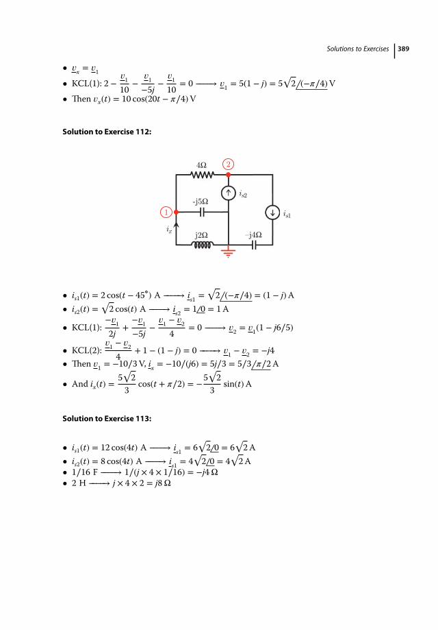
Solutions to Exercises 389
• 𝑣x = 𝑣1
• KCL(1): 2 −𝑣1
10−
𝑣1
−5j−
𝑣1
10= 0 −−−−→ 𝑣1 = 5(1 − j) = 5
√2 (−𝜋∕4)V
• Then 𝑣x(t) = 10 cos(20t − 𝜋∕4)V
Solution to Exercise 112:
4Ω
-j5Ω
j2Ω –j4Ω
is1
is2
ix
1
2
• is1(t) = 2 cos(t − 45∘) A −−−−→ is1 =√2 (−𝜋∕4) = (1 − j)A
• is2(t) =√2 cos(t) A −−−−→ is2 = 1 0 = 1A
• KCL(1):−𝑣12j
+−𝑣1−5j
−𝑣1 − 𝑣2
4= 0 −−−−→ 𝑣2 = 𝑣1(1 − j6∕5)
• KCL(2):𝑣1 − 𝑣2
4+ 1 − (1 − j) = 0 −−−−→ 𝑣1 − 𝑣2 = −j4
• Then 𝑣1 = −10∕3V, ix = −10∕(j6) = 5j∕3 = 5∕3 𝜋∕2A
• And ix(t) =5√2
3cos(t + 𝜋∕2) = −
5√2
3sin(t)A
Solution to Exercise 113:
.• is1(t) = 12 cos(4t) A −−−−→ is1 = 6√2 0 = 6
√2A
• is2(t) = 8 cos(4t) A −−−−→ is1 = 4√2 0 = 4
√2A
• 1∕16 F −−−−→ 1∕(j × 4 × 1∕16) = −j4Ω• 2 H −−−−→ j × 4 × 2 = j8Ω
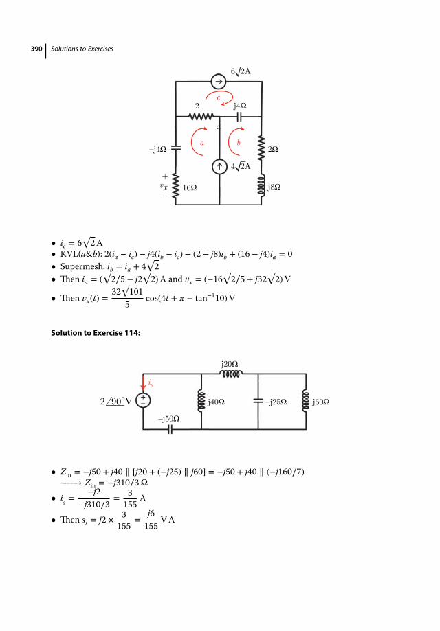
390 Solutions to Exercises
2 –j4Ω
2Ω–j4Ω
16Ω j8Ωvx_
+
6 2A
4 2A
a b
c
x
• ic = 6√2A
• KVL(a&b): 2(ia − ic) − j4(ib − ic) + (2 + j8)ib + (16 − j4)ia = 0• Supermesh: ib = ia + 4
√2
• Then ia = (√2∕5 − j2
√2)A and 𝑣x = (−16
√2∕5 + j32
√2)V
• Then 𝑣x(t) =32
√1015
cos(4t + 𝜋 − tan−110)V
Solution to Exercise 114:
j40Ω
j20Ω
–j50Ω
–j25Ω j60Ω
is
• Zin = −j50 + j40 ∥ [j20 + (−j25) ∥ j60] = −j50 + j40 ∥ (−j160∕7)−−−−→ Zin = −j310∕3Ω
• is =−j2
−j310∕3= 3
155A
• Then ss = j2 × 3155
=j6155
VA
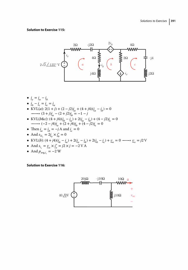
Solutions to Exercises 391
Solution to Exercise 115:
2Ω -j2Ω
4Ω 2Ωix
2iy
iy
j4Ω ix
4Ω
–j4
j2Ω
a b c2 2 –135° V
• iy = ia − ib• ib − ic = ix = ia• KVL(a): 2(1 + j) + (2 − j2)ia + (4 + j4)(ia − ib) = 0
−−−−→ (3 + j)ia − (2 + j2)ib = −1 − j• KVL(b&c): (4 + j4)(ib − ia) + 2(ia − ib) + (4 − j2)ic = 0
−−−−→ (−2 − j4)ia + (2 + j4)ib + (4 − j2)ic = 0• Then ia = ib = −jA and ic = 0• And s2iy
= 2iy × i∗b = 0• KVL(b): (4 + j4)(ib − ia) + 2(ia − ib) + 2(ib − ic) + 𝑣x = 0 −−−−→ 𝑣x = j2V• And six
= 𝑣x × i∗x = j2 × j = −2VA• And pavg,ix
= −2W
Solution to Exercise 116:
40 0V
20jΩ –j10Ω
j10Ω
10Ω
+
_ voc
0

392 Solutions to Exercises
For 𝑣oc:
• 𝑣oc = 40(j10∕j20) = 20V
20jΩ –j10Ω
j10Ω
10Ω
isc40 0V
For isc:
• Zin = j10 + j10 ∥ 10 = j10 + j100∕(10 + j10) = j10 + j10∕(1 + j)−−−−→ Zin = 5(1 + j3) Ω
• isc =40Zin
j1010 + j10
=j20(1 − j)
Zin=
8 − j45
A
• Then Zth = 100∕(8 − 4j) = (10 + j5) Ω• And choose Zl = Z∗
th = (10 − j5) Ω for maximum power transfer
Solution to Exercise 117:
2Ω
2Ωj4Ω
–j2Ω
40 0V voc_ +
For 𝑣oc:
• 𝑣oc = 40[−j2∕(−j2 + j4) − 2∕(2 + 2)] = 40(−1 − 1∕2) = −60V
2Ω
2Ωj4Ω
–j2Ω
40 0Visc
1 2
For isc:
• Zin = (2 ∥ j4) + (−j2 ∥ 2) = j8∕(2 + j4) − j4∕(2 − j2) = (13 − j)∕5Ω• is = 40∕Zin = 200∕(13 − j)A

Solutions to Exercises 393
• ij4 =2
2 + 4j× is =
200(1 + j2)(13 − j)
A
• i−2j =2
2 − 2j× is =
200(1 − j)(13 − j)
A
• KCL(1): isc = i4j − i−2j =200
(13 − j)×3(−1 − j3)
10= −60
(1 + j4)17
A• Then Zth = 17∕(1 + 4j) = (1 − 4j) Ω• And choose Zl = Z∗
th = (1 + 4j) Ω for maximum power transfer• Considering that 𝜔 = 2 rad/s, use a 2H inductor in series with a 1Ω resistor
Solution to Exercise 118:
200 0V
j20Ω 50Ω 2Ω
j6Ω
ix
10ix
+
_ voc
0
a b
For 𝑣oc:
• ix = ia• KVL(a): −200 + (50 + j20)ia + 10ia = 0 −−−−→ ia = 10∕(3 + j) = (3 − j)A• KVL(b): −10ix + (2 + j6)ib = 0 −−−−→ ib = 5ia∕(1 + j3) = −j5A• Then 𝑣oc = j6 × ib = 30V
200 0V
j20Ω 50Ω 2Ω
j6Ω
ix
10ixa b isc
For isc:
• ia = 10∕(3 + j) = (3 − j)A (as before)• KVL(b): −10ix + 2ib = 0 −−−−→ ib = 5ia = 5(3 − j)A• Then isc = 5(3 − j)A and Zth = 6∕(3 − j) = 6(3 + j)∕10Ω
• And choose Zl = Z∗th =
9 − j35
Ω• Considering that 𝜔 = 50 rad/s, use a 1∕30 F capacitor in series with a 9∕5Ω resistor
Solution to Exercise 119:
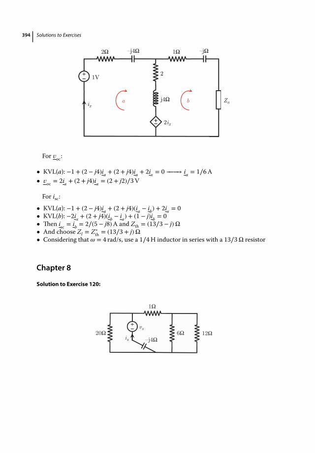
394 Solutions to Exercises
ix
1V
2Ω
2
1Ω–j4Ω –jΩ
2ix
j4Ω Zoa b
For 𝑣oc:
• KVL(a): −1 + (2 − j4)ia + (2 + j4)ia + 2ix = 0 −−−−→ ia = 1∕6A• 𝑣oc = 2ix + (2 + j4)ia = (2 + j2)∕3V
For isc:
• KVL(a): −1 + (2 − j4)ia + (2 + j4)(ia − ib) + 2ix = 0• KVL(b): −2ix + (2 + j4)(ib − ia) + (1 − j)ib = 0• Then isc = ib = 2∕(5 − j8)A and Zth = (13∕3 − j) Ω• And choose Zl = Z∗
th = (13∕3 + j) Ω• Considering that 𝜔 = 4 rad/s, use a 1∕4H inductor in series with a 13∕3Ω resistor
Chapter 8
Solution to Exercise 120:
1Ω
12Ω6Ω
vs
–j4Ωis20Ω
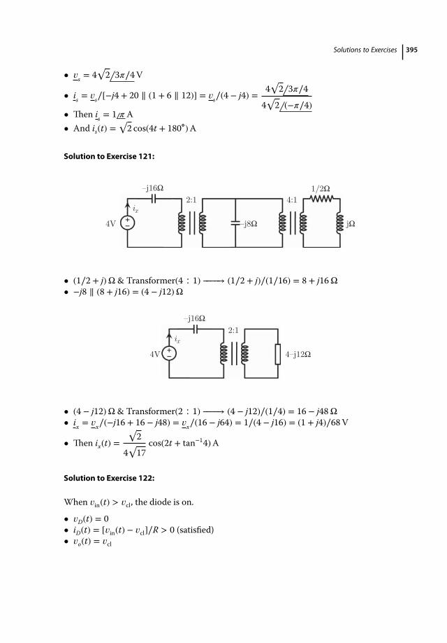
Solutions to Exercises 395
• 𝑣s = 4√2 3𝜋∕4V
• is = 𝑣s∕[−j4 + 20 ∥ (1 + 6 ∥ 12)] = 𝑣s∕(4 − j4) =4√2 3𝜋∕4
4√2 (−𝜋∕4)
• Then is = 1 𝜋 A• And is(t) =
√2 cos(4t + 180∘)A
Solution to Exercise 121:
2:1
–j8Ω4V
ix
–j16Ω
4:11/2Ω
jΩ
• (1∕2 + j) Ω & Transformer(4 ∶ 1) −−−−→ (1∕2 + j)∕(1∕16) = 8 + j16Ω• −j8 ∥ (8 + j16) = (4 − j12) Ω
2:1
4–j12Ω4V
ix
–j16Ω
• (4 − j12) Ω & Transformer(2 ∶ 1) −−−−→ (4 − j12)∕(1∕4) = 16 − j48Ω• ix = 𝑣x∕(−j16 + 16 − j48) = 𝑣x∕(16 − j64) = 1∕(4 − j16) = (1 + j4)∕68V
• Then ix(t) =√2
4√17
cos(2t + tan−14)A
Solution to Exercise 122:
When 𝑣in(t) > 𝑣cl, the diode is on.
• 𝑣D(t) = 0• iD(t) = [𝑣in(t) − 𝑣cl]∕R > 0 (satisfied)• 𝑣o(t) = 𝑣cl

396 Solutions to Exercises
When 𝑣in(t) < 𝑣cl, the diode is off.
• iD(t) = 0• 𝑣D(t) = 𝑣in(t) − 𝑣cl < 0 (satisfied)• 𝑣o(t) = 𝑣in
vo(V)
t(s)
3vcl
w
2w
2w
2w
–vm
Solution to Exercise 123:
When 𝑣in(t) > 𝑣c1, D1 is on and D2 is off.
• 𝑣D1(t) = 0 and iD2 = 0• iD1(t) = [𝑣in(t) − 𝑣c1]∕R > 0 (satisfied)• 𝑣D2(t) = −𝑣c2 − 𝑣c1 < 0 (satisfied)• 𝑣o(t) = 𝑣c1
When 𝑣in(t) < −𝑣c2, D1 is off and D2 is on.
• iD1 = 0 and 𝑣D2(t) = 0• 𝑣D1(t) = 𝑣in − 𝑣c1 < 0 (satisfied)• iD2(t) = [−𝑣c2 − 𝑣in(t)]∕R > 0 (satisfied)• 𝑣o(t) = −𝑣c2
When −𝑣c2 < 𝑣in(t) < 𝑣c1, both D1 and D2 are off.
• iD1(t) = 0 and iD2 = 0• 𝑣D1(t) = 𝑣in − 𝑣c1 < 0 (satisfied)

Solutions to Exercises 397
• 𝑣D2(t) = −𝑣c2 − 𝑣c1 < 0 (satisfied)• 𝑣o(t) = 𝑣in(t)
vo(V)
t (s)
3vc1
w
2w
2w
2w
–vc2
Solution to Exercise 124:
+
_
+
_ vo
R1
vs
R2
1
0A
0A
2
• Ideal OP-AMP: 𝑣1 = 0• KCL(1): (𝑣s − 𝑣1)∕R1 − (𝑣1 − 𝑣2)∕R2 = 0 −−−−→ 𝑣2 = −(R2∕R1)𝑣s• Then 𝑣o = −(R2∕R1)𝑣s
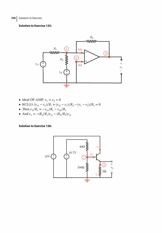
398 Solutions to Exercises
Solution to Exercise 125:
+
_ R1
R2
R3
+
_ vo
vs1
vs2
1
2 3
0A
0A
• Ideal OP-AMP: 𝑣1 = 𝑣2 = 0• KCL(1): (𝑣s1 − 𝑣1)∕R1 + (𝑣s2 − 𝑣1)∕R2 − (𝑣1 − 𝑣3)∕R3 = 0• Then 𝑣3∕R3 = −𝑣s1∕R1 − 𝑣s2∕R2• And 𝑣o = −(R3∕R1)𝑣s1 − (R3∕R2)𝑣s2
Solution to Exercise 126:
10V10.7V
40Ω
290Ω
+
_ vo
2Ω
1
2
ib
ic
ie

Solutions to Exercises 399
Assuming active mode:
• ie = (𝛽 + 1)ib = 200ib• 𝑣2 = 2ie = 400ib• 𝑣1 = 0.7 + 𝑣2 = 0.7 + 400ib• KCL(1): (10.7 − 𝑣1)∕40 − 𝑣1∕290 − ib = 0 −−−−→ 𝑣1 = 8.7V• Then ib = 0.02A, ie = 4A, and 𝑣2 = 8V• Check 𝑣cb = 10 − 8.7 = 1.3 > 0• And 𝑣o = 8V


401
Index
aAC 8, 227, 276AM receiver 313ammeter 296amplifier 314analog 297, 300analog-to-digital converter 301angular frequency 228average power 260
bbipolar junction transistor 289
ccapacitance 181capacitor 181, 230, 236charge 1complex power 260conductance 12conductivity 10, 11conductor 10conservation of energy 14, 17, 262, 311current 4, 10current source 14
dDC 8, 227, 276DC motor 312dependent sources 14differential amplifier 286digital 300digital-to-analog converter 301diode 279drift velocity 10
eelectric field 3, 10energy 6, 183, 194envelope detector 314
ffeedback 288filter 244, 245, 247flip-flop 308frequency 9, 223, 229
gground 47, 318
iimpedance 238impedance matching 266independent sources 13inductance 191inductor 181, 191, 232,
237instantaneous power 259insulator 11integrator 301inverting amplifier 288isolator 276
kKCL 23, 36Kirchhoff’s current law 23,
36Kirchhoff’s laws 17, 23Kirchhoff’s voltage law 24,
36
Introduction to Electrical Circuit Analysis, First Edition. Özgür Ergül.© 2017 John Wiley & Sons Ltd. Published 2017 by John Wiley & Sons Ltd.Companion Website: www.wiley.com/go/ergul4412
402 Index
llatch 308LC circuit 222, 314light-emitting diode 293logic circuit 301logic gate 303, 314
mmaximum power transfer 158memory unit 307mesh 24, 93mesh analysis 40, 93, 137microchip 314multimeter 297
nnodal analysis 40, 47, 90node 1, 47noninverting amplifier 286NOR gate 306Norton equivalent circuit 139
oOhm’s law 10open circuit 13operational amplifier 284
pparallel connection 15, 41, 220, 221period 229, 259phase 229phasor 227, 234potential 3power 6, 12, 183, 194, 259
rRAM 307RC circuit 195, 243RCL circuit 246reactance 238
reactive power 261rectifier 281resistance 12resistor 9, 12, 236resistor ladder 302resonance 272rheostat 13RL circuit 204, 244RLC circuit 246RMS 232
ssafety 317semiconductor 11, 279, 288series connection 15, 40, 218,
220seven-segment display 294short circuit 13, 32, 37sign convention 6, 26sinusoidal source 228split-phase system 298steady state 8, 197, 227superconductivity 12supermesh 107supernode 37, 59superposition 272
tThévenin equivalent circuit 139, 267three-phase system 297time constant 197, 205touchscreen 316transformer 275transient state 8, 181, 228transistor 288, 306
vvoltage follower 286voltage source 13voltmeter 295

WILEY END USER LICENSE AGREEMENTGo to www.wiley.com/go/eula to access Wiley’s ebook EULA.
Related Documents