Introduction to Design for Testability Mikael Olausson & Daniel Wiklund Electronic Devices, IFM

Welcome message from author
This document is posted to help you gain knowledge. Please leave a comment to let me know what you think about it! Share it to your friends and learn new things together.
Transcript
Introduction to Design forTestability
Mikael Olausson & Daniel Wiklund
Electronic Devices, IFM
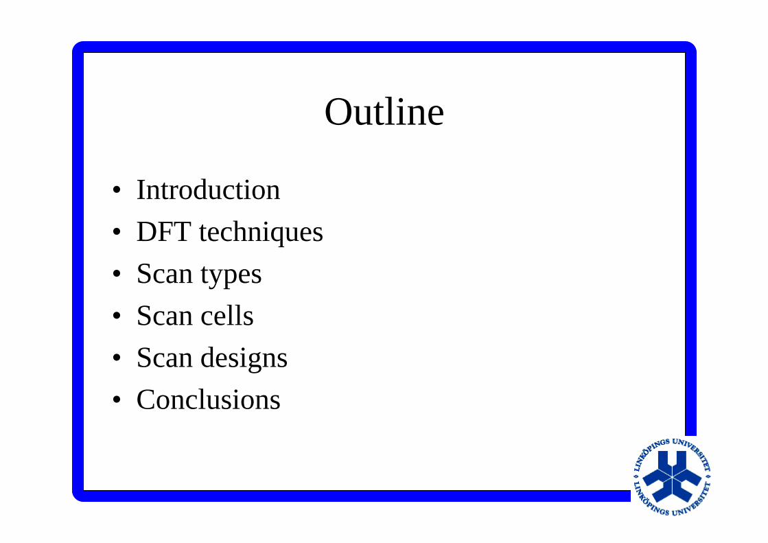
Outline
• Introduction
• DFT techniques
• Scan types
• Scan cells
• Scan designs
• Conclusions
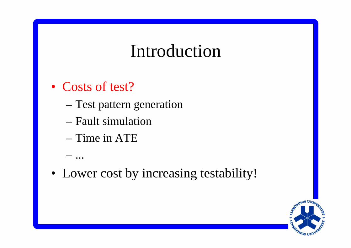
Introduction
• Costs of test?– Test pattern generation
– Fault simulation
– Time in ATE
– ...
• Lower cost by increasing testability!
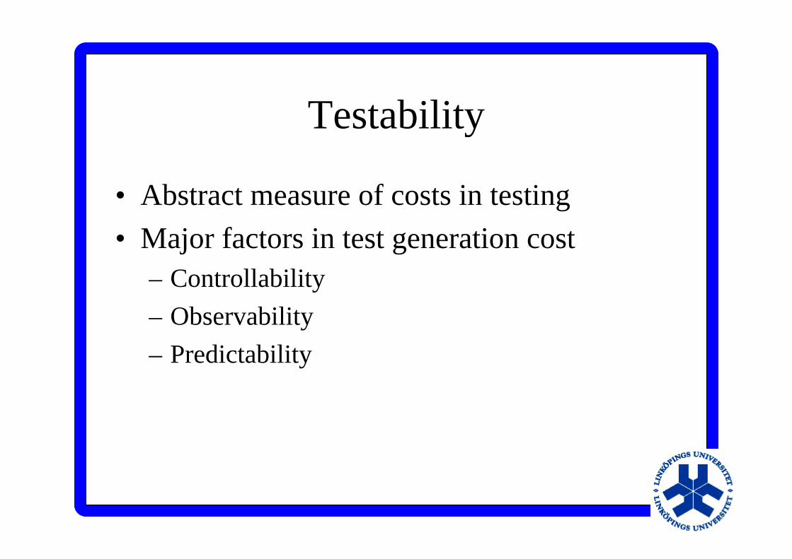
Testability
• Abstract measure of costs in testing
• Major factors in test generation cost– Controllability
– Observability
– Predictability
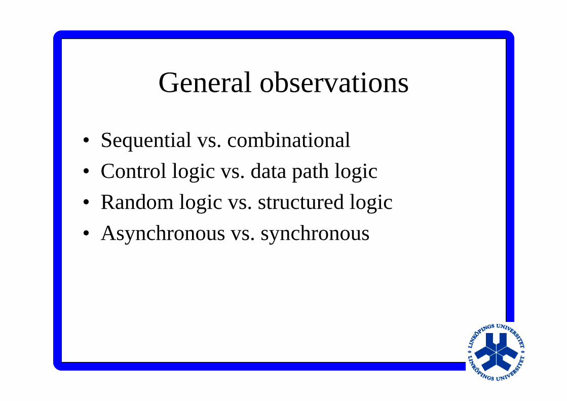
General observations
• Sequential vs. combinational
• Control logic vs. data path logic
• Random logic vs. structured logic
• Asynchronous vs. synchronous
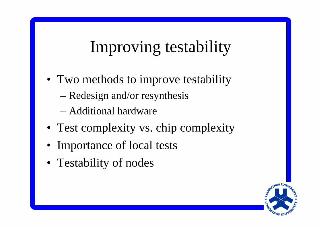
Improving testability
• Two methods to improve testability– Redesign and/or resynthesis
– Additional hardware
• Test complexity vs. chip complexity
• Importance of local tests
• Testability of nodes
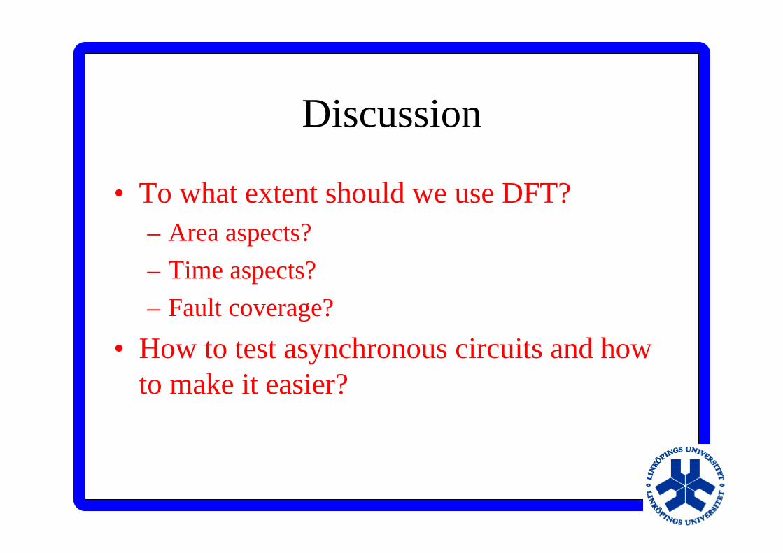
• To what extent should we use DFT?– Area aspects?
– Time aspects?
– Fault coverage?
• How to test asynchronous circuits and howto make it easier?
Discussion
Outline
• Introduction
• DFT techniques• Scan types
• Scan cells
• Scan designs
• Conclusions
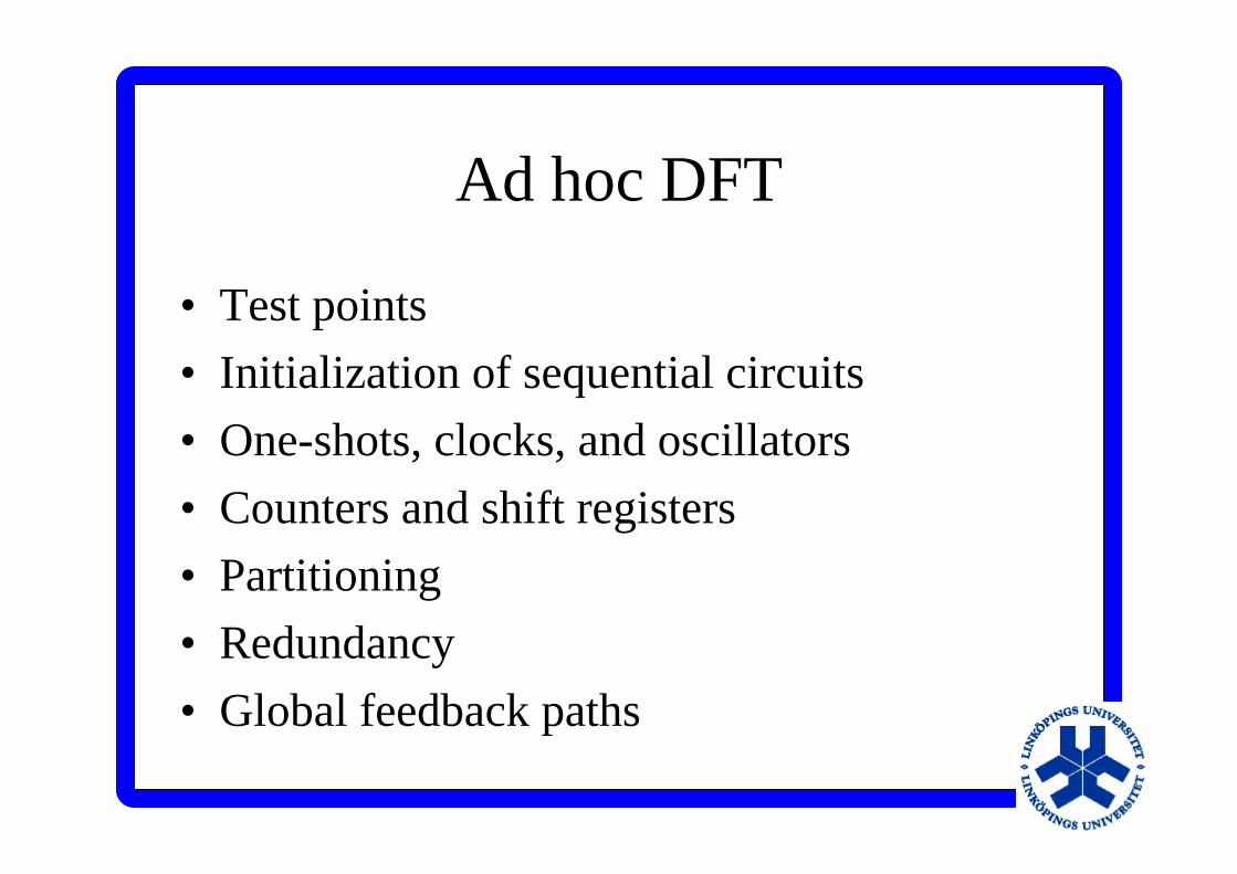
Ad hoc DFT
• Test points
• Initialization of sequential circuits
• One-shots, clocks, and oscillators
• Counters and shift registers
• Partitioning
• Redundancy
• Global feedback paths
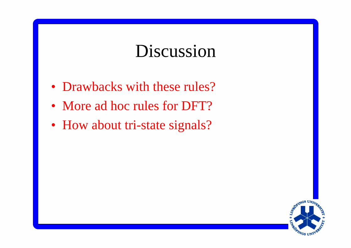
Discussion
• Drawbacks with these rules?
• More ad hoc rules for DFT?
• How about tri-state signals?

Outline
• Introduction
• DFT techniques
• Scan types• Scan cells
• Scan designs
• Conclusions
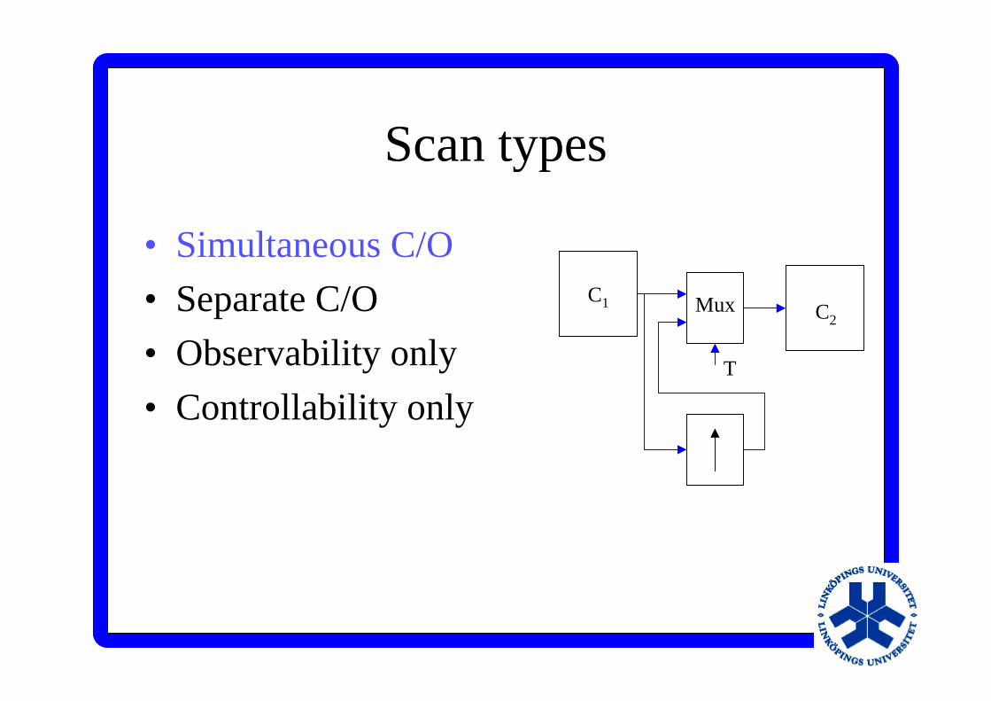
Scan types
• Simultaneous C/O
• Separate C/O
• Observability only
• Controllability only
C1 C2Mux
T
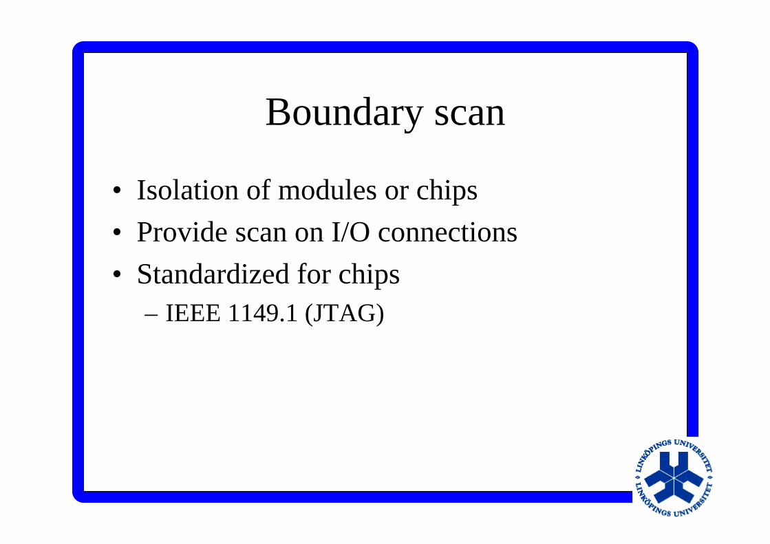
Boundary scan
• Isolation of modules or chips
• Provide scan on I/O connections
• Standardized for chips– IEEE 1149.1 (JTAG)
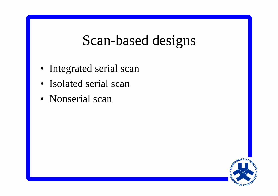
Scan-based designs
• Integrated serial scan
• Isolated serial scan
• Nonserial scan
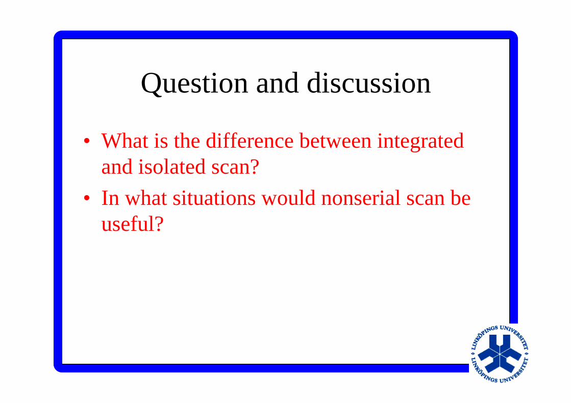
Question and discussion
• What is the difference between integratedand isolated scan?
• In what situations would nonserial scan beuseful?
Outline
• Introduction
• DFT techniques
• Scan types
• Scan cells• Scan designs
• Conclusions

Scan cells
• Memory type– Single or double latch
– Flip-flop
• Clocking– Single clock
– Multiple non-overlapping clocks
L1 L2
DSi
Clk
Q1
Q2
T
L1 L2
DSi
Clk1
Q1
Q2
T
Clk2
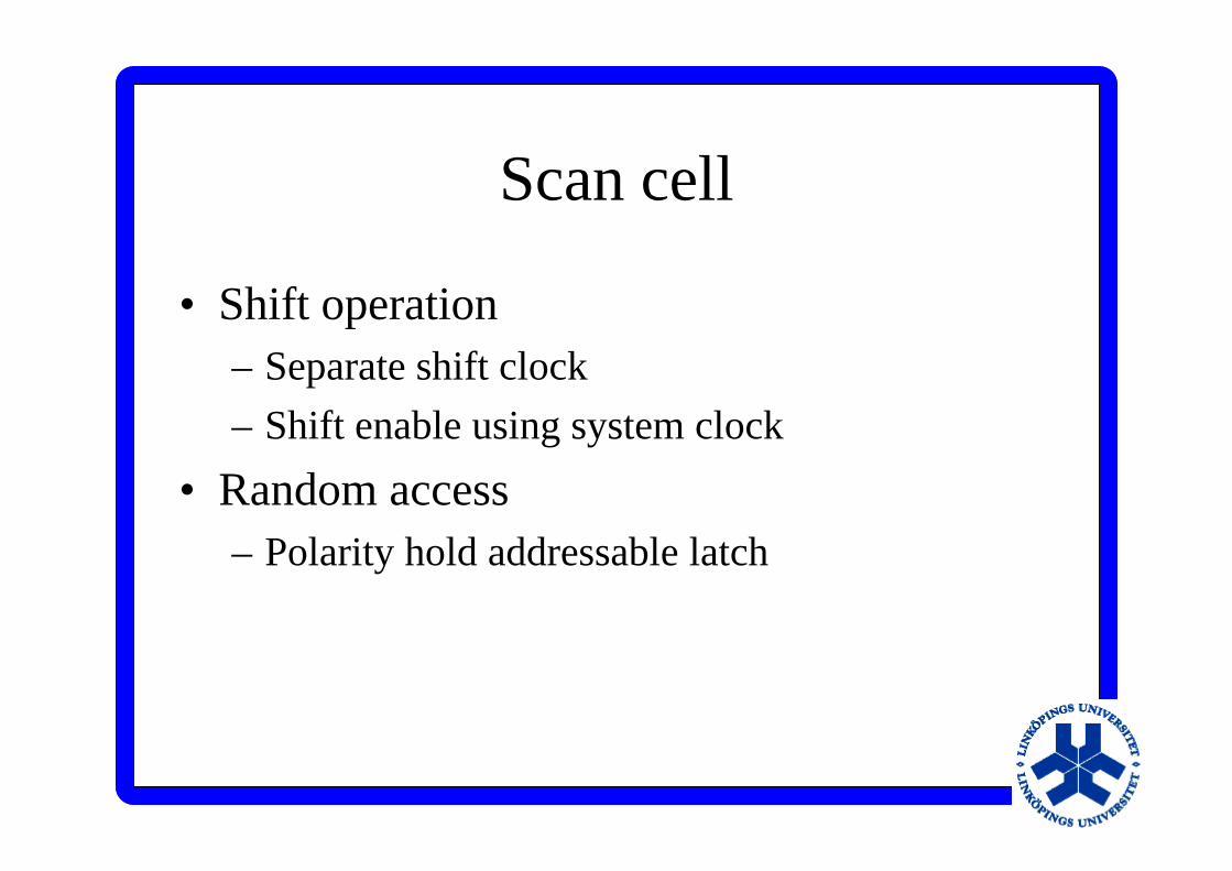
Scan cell
• Shift operation– Separate shift clock
– Shift enable using system clock
• Random access– Polarity hold addressable latch
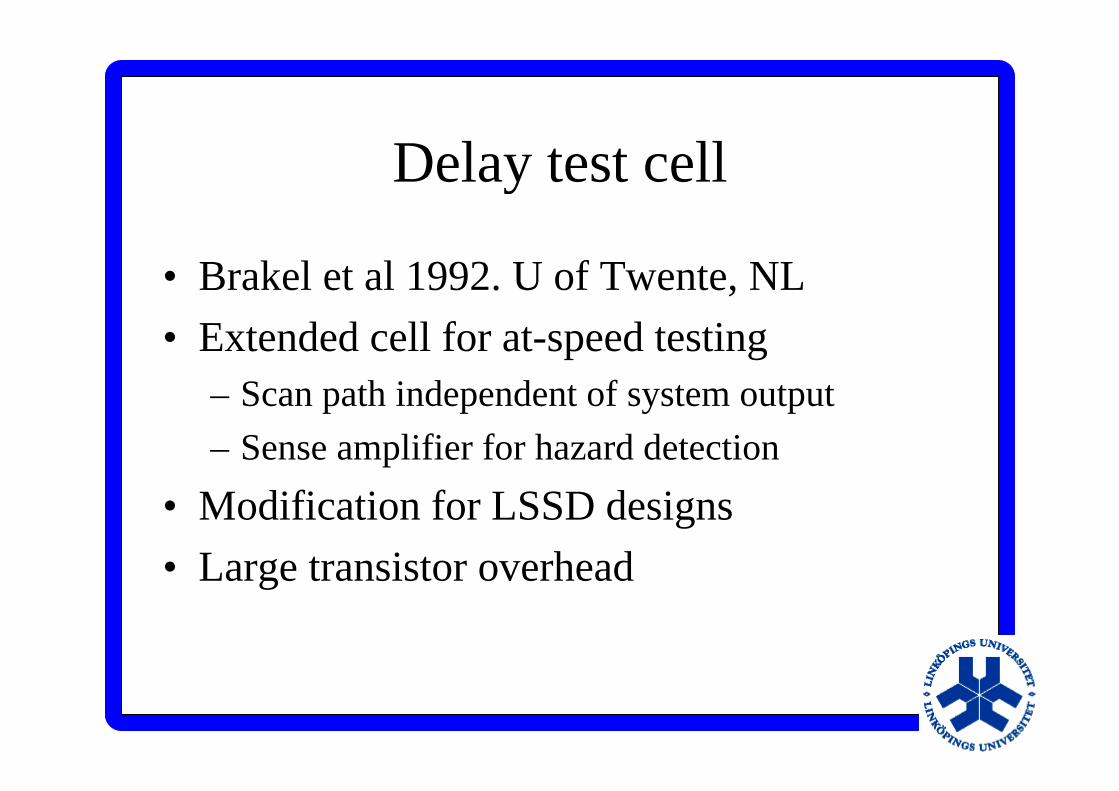
Delay test cell
• Brakel et al 1992. U of Twente, NL
• Extended cell for at-speed testing– Scan path independent of system output
– Sense amplifier for hazard detection
• Modification for LSSD designs
• Large transistor overhead
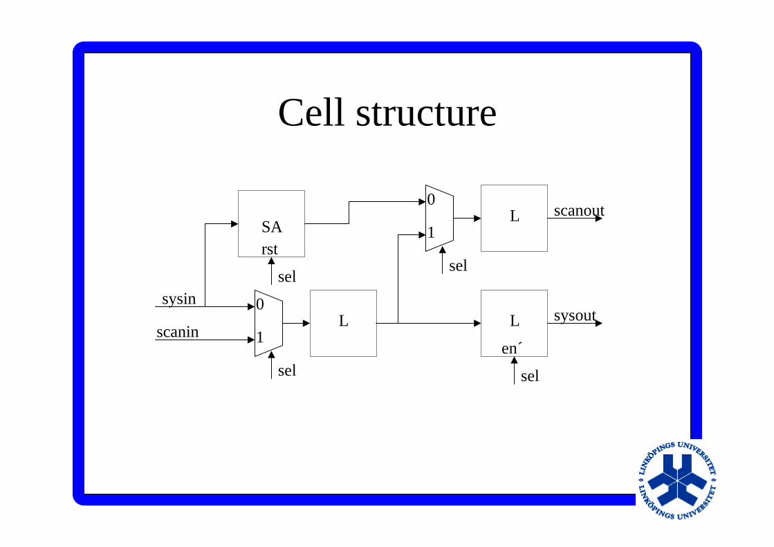
Cell structure
SA
L
L
L
sel
sel
sel
sel
sysin
scaninsysout
scanout
en´
rst
0
1
0
1
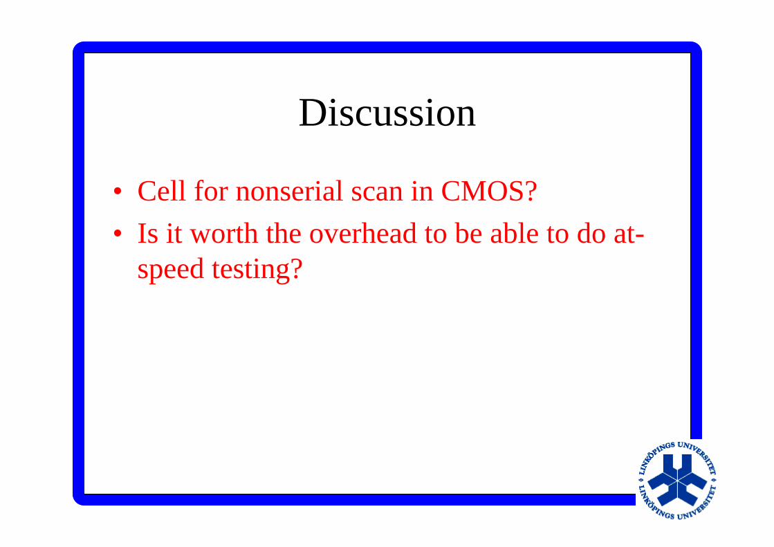
Discussion
• Cell for nonserial scan in CMOS?
• Is it worth the overhead to be able to do at-speed testing?
Outline
• Introduction
• DFT techniques
• Scan types
• Scan cells
• Scan designs• Conclusions
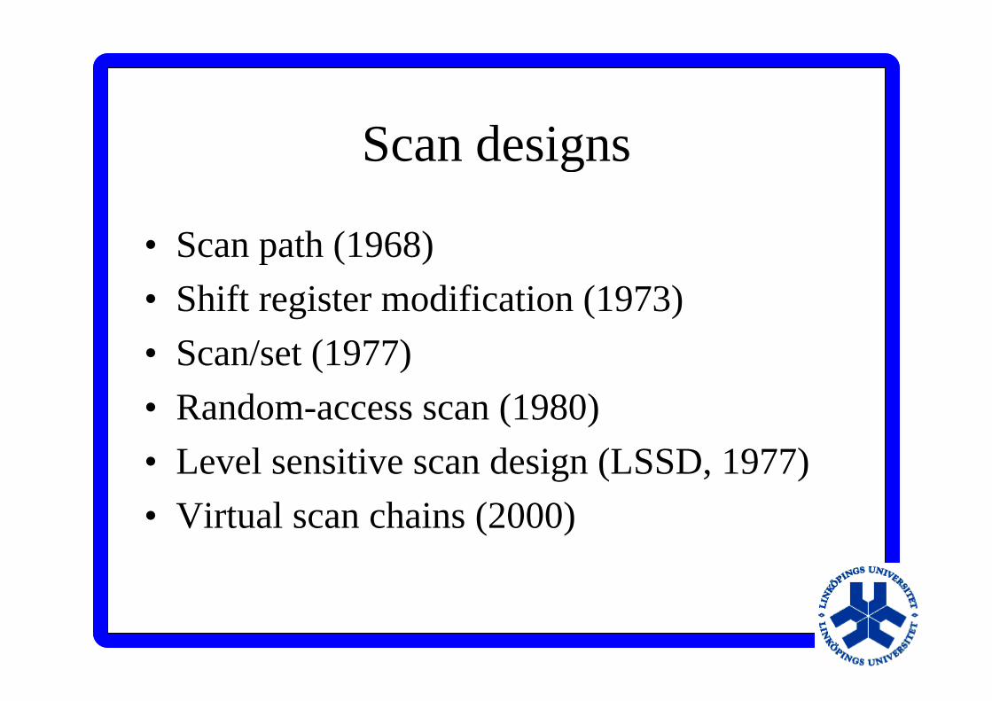
Scan designs
• Scan path (1968)
• Shift register modification (1973)
• Scan/set (1977)
• Random-access scan (1980)
• Level sensitive scan design (LSSD, 1977)
• Virtual scan chains (2000)
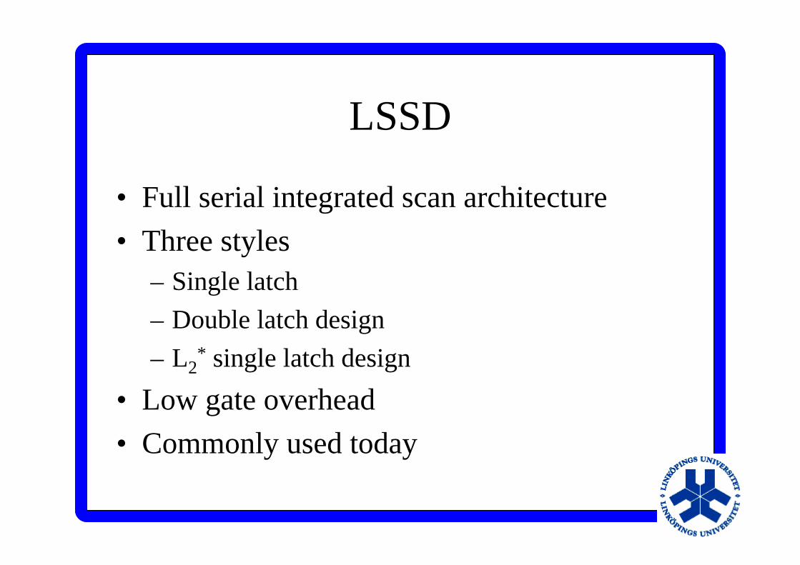
LSSD
• Full serial integrated scan architecture
• Three styles– Single latch
– Double latch design
– L2* single latch design
• Low gate overhead
• Commonly used today
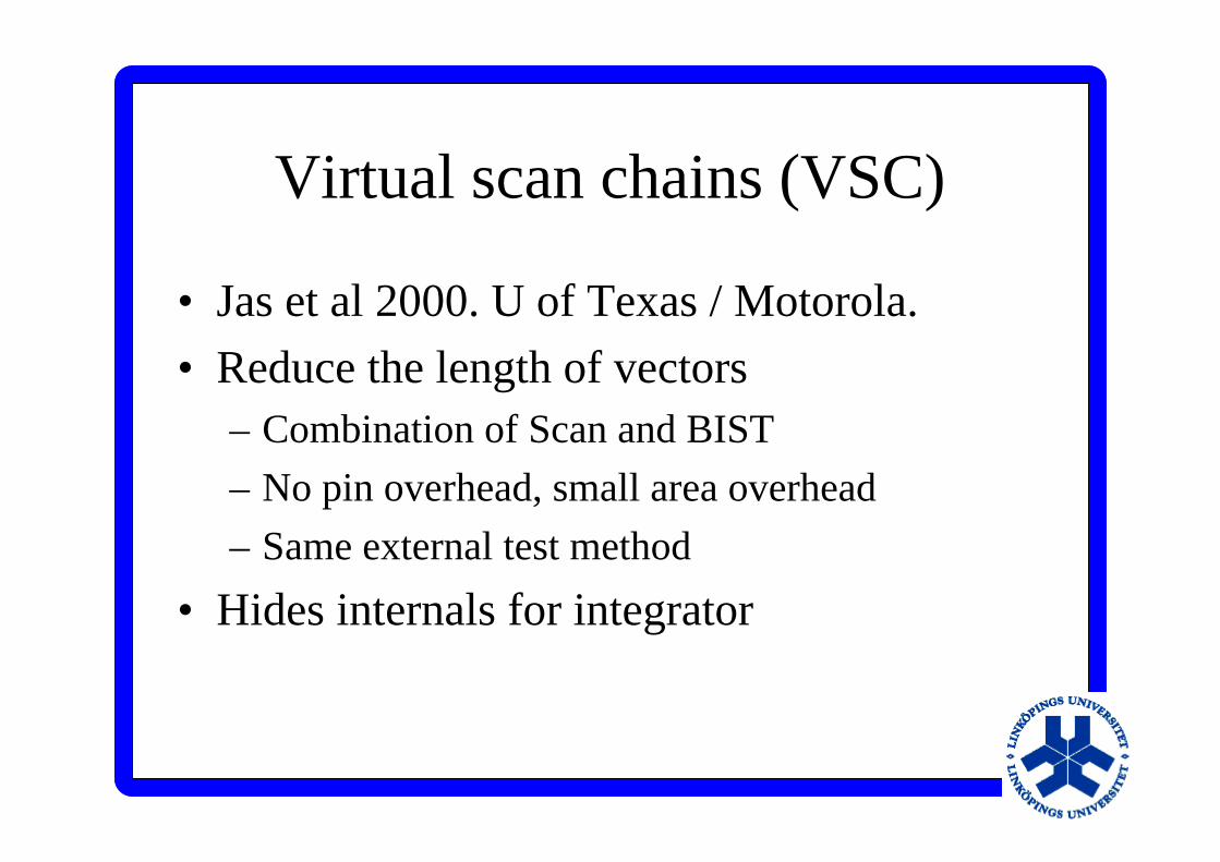
Virtual scan chains (VSC)
• Jas et al 2000. U of Texas / Motorola.
• Reduce the length of vectors– Combination of Scan and BIST
– No pin overhead, small area overhead
– Same external test method
• Hides internals for integrator

VSC concept
Core
Scan chainSi So
Sclk
LFSR LFSRSC
Sel
MUX
MUX
MIS
R
Scan chain
Scan chain
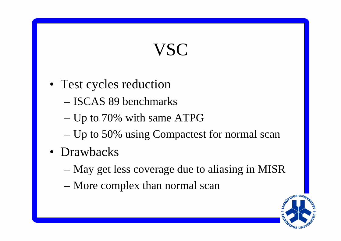
VSC
• Test cycles reduction– ISCAS 89 benchmarks
– Up to 70% with same ATPG
– Up to 50% using Compactest for normal scan
• Drawbacks– May get less coverage due to aliasing in MISR
– More complex than normal scan
Outline
• Introduction
• DFT techniques
• Scan types
• Scan cells
• Scan designs
• Conclusions
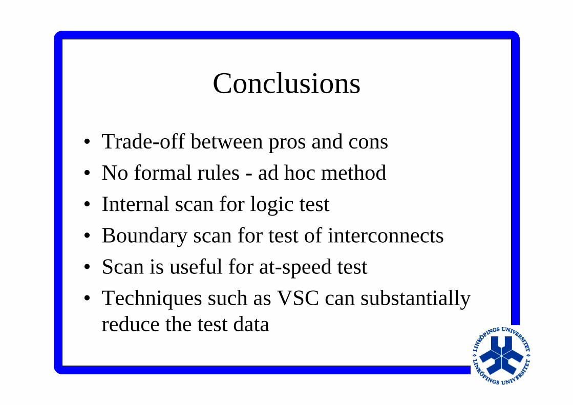
Conclusions
• Trade-off between pros and cons
• No formal rules - ad hoc method
• Internal scan for logic test
• Boundary scan for test of interconnects
• Scan is useful for at-speed test
• Techniques such as VSC can substantiallyreduce the test data

Questions?
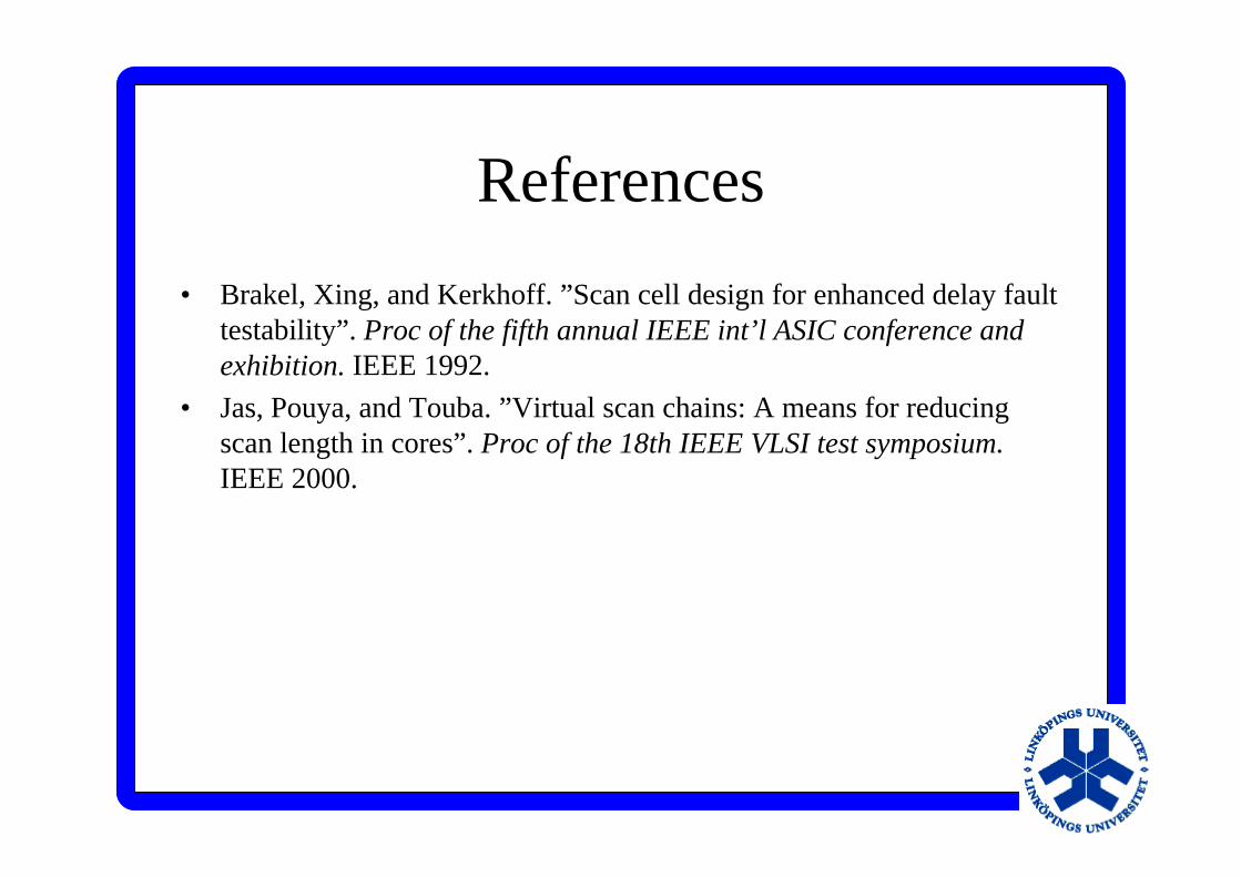
References
• Brakel, Xing, and Kerkhoff. ”Scan cell design for enhanced delay faulttestability”. Proc of the fifth annual IEEE int’l ASIC conference andexhibition. IEEE 1992.
• Jas, Pouya, and Touba. ”Virtual scan chains: A means for reducingscan length in cores”. Proc of the 18th IEEE VLSI test symposium.IEEE 2000.
Related Documents


