1 © 2006 Microchip Technology Incorporated. All Rights Reserved. Enhanced Mid-Range Architecture Slide 1 Introducing the Enhanced Mid-Range Architecture Hello, my name is Marc McComb Technical Training Engineer in the Security Microcontroller Technology Division at Microchip. Thank you for viewing this web seminar introducing Microchip’s newly enhanced Mid-Range 8-bit PIC ® Microcontrollers.

Welcome message from author
This document is posted to help you gain knowledge. Please leave a comment to let me know what you think about it! Share it to your friends and learn new things together.
Transcript
1
© 2006 Microchip Technology Incorporated. All Rights Reserved. Enhanced Mid-Range Architecture Slide 1
Introducing the EnhancedMid-Range Architecture
Hello, my name is Marc McComb Technical Training Engineer in the Security Microcontroller Technology Division at Microchip. Thank you for viewing this web seminar introducing Microchip’s newly enhanced Mid-Range 8-bit PIC®
Microcontrollers.
2
© 2006 Microchip Technology Incorporated. All Rights Reserved. Enhance Mid-Range Architecture Slide 22
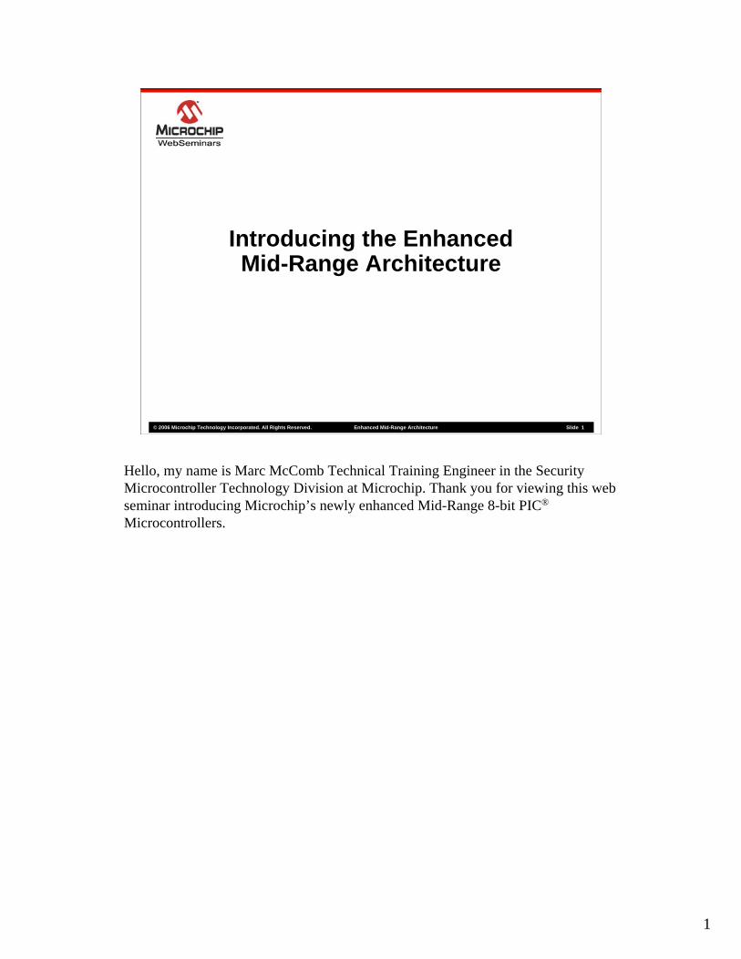
Agenda
Introducing the Enhanced Mid-Range Architecture
Enhancements to the Data Memory Map
New Instructions
Indirect Addressing Enhancements
Migration Considerations
We will cover a number of topics during the course of this web seminar. First, an overview of the enhancements made to the 8-bit mid-range PIC architecture. Next, a detailed description of some of the enhancements to the Data Memory Map, indirect memory addressing and some of the new instructions added. Finally, I will describe what should be considered when migrating designs from the current architecture to the new enhanced core. So let’s begin…
3
© 2006 Microchip Technology Incorporated. All Rights Reserved. Enhance Mid-Range Architecture Slide 33
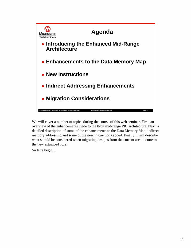
PIC® Microcontroller Family Roadmap
PricePriceBaseline
(12-bit instruction word)BaselineBaseline
(12(12--bit instruction word)bit instruction word)
Mid-Range(14-bit instruction word)
MidMid--RangeRange(14(14--bit instruction word)bit instruction word)
PIC18(16-bit instruction word)
PIC18PIC18(16(16--bit instruction word)bit instruction word)
PIC24PIC24PIC24dsPIC® DSCsdsPICdsPIC®® DSCsDSCs
PIC32PIC32PIC32M
emor
y/Pe
rfor
man
ceM
emor
y/Pe
rfor
man
ce
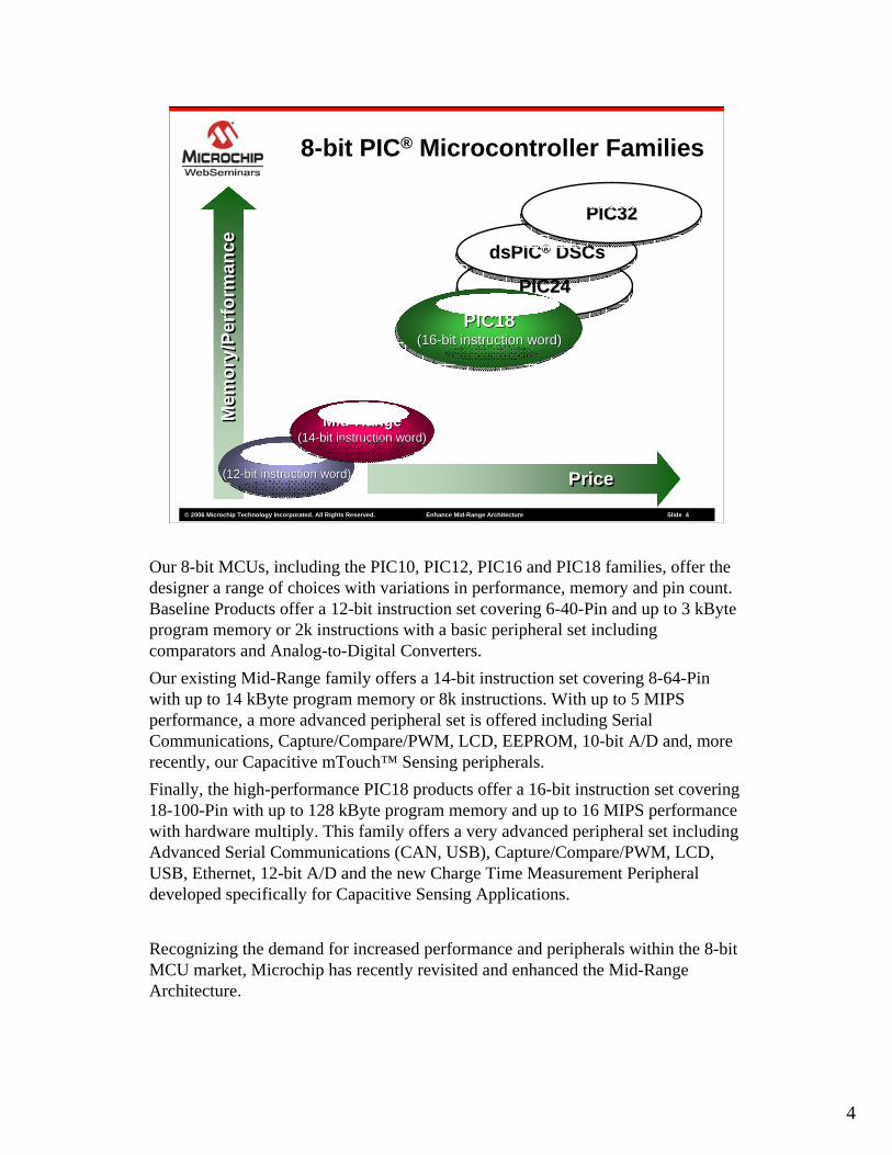
Microchip currently offers a wide variety of 8-bit to 32-bit microcontrollers along with digital signal controllers. These products range from the very small, low-cost 8-bit Baseline family all the way up to the sophisticated dsPIC® DSCs with powerful high-level digital signal processing capabilities.
4
© 2006 Microchip Technology Incorporated. All Rights Reserved. Enhance Mid-Range Architecture Slide 44
PIC24PIC24PIC24dsPIC® DSCsdsPICdsPIC®® DSCsDSCs
PIC32PIC32PIC32
8-bit PIC® Microcontroller Families
PricePriceBaseline
(12-bit instruction word)BaselineBaseline
(12(12--bit instruction word)bit instruction word)
Mid-Range(14-bit instruction word)
MidMid--RangeRange(14(14--bit instruction word)bit instruction word)
PIC18(16-bit instruction word)
PIC18PIC18(16(16--bit instruction word)bit instruction word)
Mem
ory/
Perf
orm
ance
Mem
ory/
Perf
orm
ance
Our 8-bit MCUs, including the PIC10, PIC12, PIC16 and PIC18 families, offer the designer a range of choices with variations in performance, memory and pin count. Baseline Products offer a 12-bit instruction set covering 6-40-Pin and up to 3 kByte program memory or 2k instructions with a basic peripheral set including comparators and Analog-to-Digital Converters.Our existing Mid-Range family offers a 14-bit instruction set covering 8-64-Pin with up to 14 kByte program memory or 8k instructions. With up to 5 MIPS performance, a more advanced peripheral set is offered including Serial Communications, Capture/Compare/PWM, LCD, EEPROM, 10-bit A/D and, more recently, our Capacitive mTouch™ Sensing peripherals.Finally, the high-performance PIC18 products offer a 16-bit instruction set covering 18-100-Pin with up to 128 kByte program memory and up to 16 MIPS performance with hardware multiply. This family offers a very advanced peripheral set including Advanced Serial Communications (CAN, USB), Capture/Compare/PWM, LCD, USB, Ethernet, 12-bit A/D and the new Charge Time Measurement Peripheral developed specifically for Capacitive Sensing Applications.
Recognizing the demand for increased performance and peripherals within the 8-bit MCU market, Microchip has recently revisited and enhanced the Mid-Range Architecture.
5
© 2006 Microchip Technology Incorporated. All Rights Reserved. Enhance Mid-Range Architecture Slide 55
PIC18(16-bit instruction word)
PIC18PIC18(16(16--bit instruction word)bit instruction word)
Baseline(12-bit instruction word)
BaselineBaseline(12(12--bit instruction word)bit instruction word)
Mid-Range(14-bit instruction word)
MidMid--RangeRange(14(14--bit instruction word)bit instruction word)
PIC24PIC24PIC24dsPIC® DSCsdsPICdsPIC®® DSCsDSCs
PIC32PIC32PIC32
PricePrice
PIC® Microcontroller Family Roadmap
Mem
ory/
Perf
orm
ance
Mem
ory/
Perf
orm
ance
•More Memory•Faster Operation•‘C’ Optimized
Enhanced Mid-Range(14-bit instruction word)
Enhanced MidEnhanced Mid--RangeRange(14(14--bit instruction word)bit instruction word)
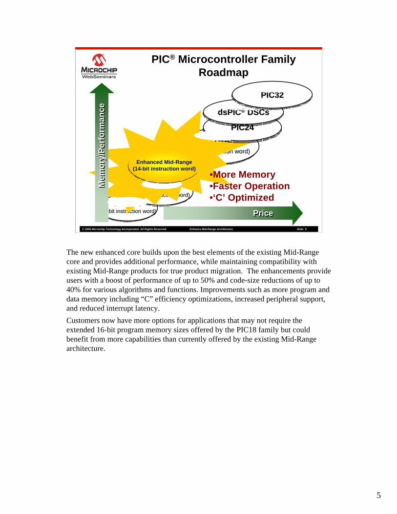
The new enhanced core builds upon the best elements of the existing Mid-Range core and provides additional performance, while maintaining compatibility with existing Mid-Range products for true product migration. The enhancements provide users with a boost of performance of up to 50% and code-size reductions of up to 40% for various algorithms and functions. Improvements such as more program and data memory including “C” efficiency optimizations, increased peripheral support, and reduced interrupt latency.Customers now have more options for applications that may not require the extended 16-bit program memory sizes offered by the PIC18 family but could benefit from more capabilities than currently offered by the existing Mid-Range architecture.
6
© 2006 Microchip Technology Incorporated. All Rights Reserved. Enhance Mid-Range Architecture Slide 66
Existing Mid-Range PIC®
Microcontroller Architecture
CPU
Peripheral I/O DriversPeripheral I/O DriversPeripheral I/O DriversPeripheral I/O Drivers
ProgramMemory
Oscillator
CPU
DataMemory
14 bits
Existing Mid-Range PIC Microcontroller
Up-to 14 KBor
8K Instructions•35 Instructions•Interrupt Support•8 Level Stack
Up-to 20 MHz
Up to 446 bytes 8 bits
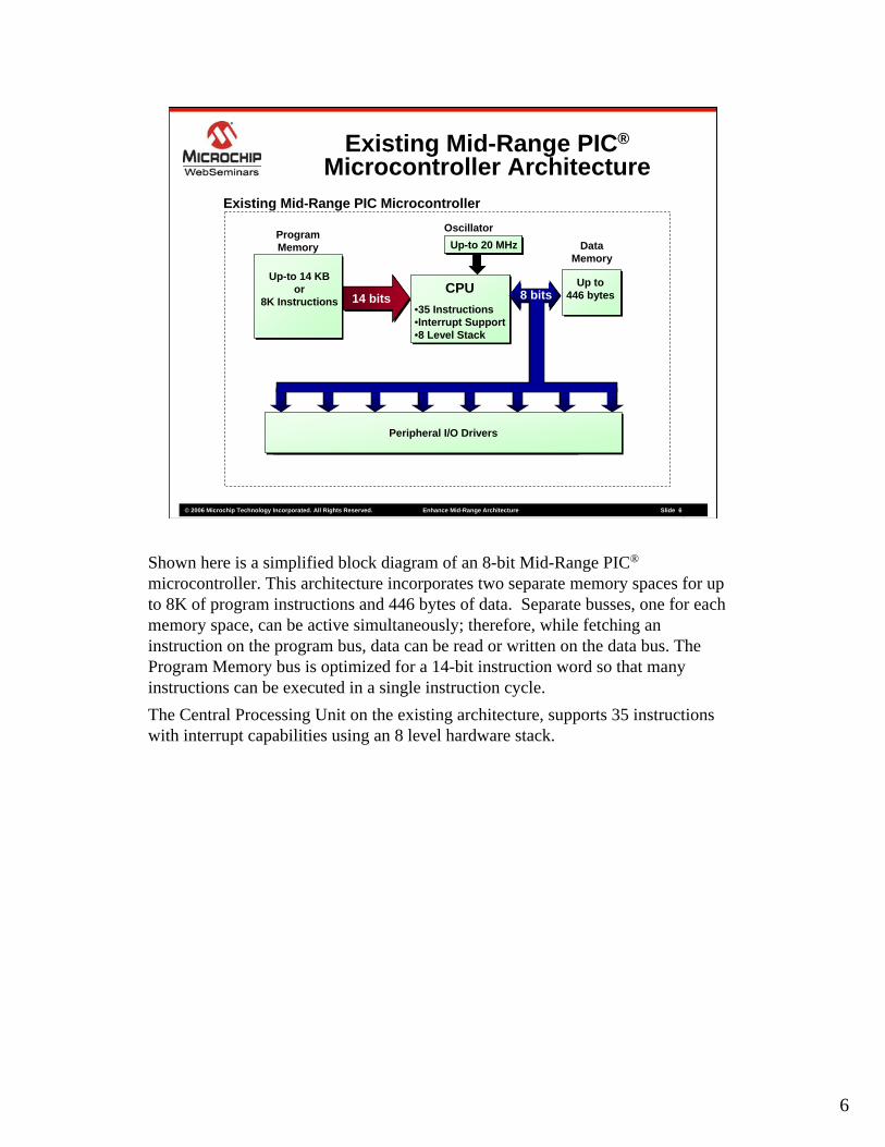
Shown here is a simplified block diagram of an 8-bit Mid-Range PIC®
microcontroller. This architecture incorporates two separate memory spaces for up to 8K of program instructions and 446 bytes of data. Separate busses, one for each memory space, can be active simultaneously; therefore, while fetching an instruction on the program bus, data can be read or written on the data bus. The Program Memory bus is optimized for a 14-bit instruction word so that many instructions can be executed in a single instruction cycle. The Central Processing Unit on the existing architecture, supports 35 instructions with interrupt capabilities using an 8 level hardware stack.
7
© 2006 Microchip Technology Incorporated. All Rights Reserved. Enhance Mid-Range Architecture Slide 77
Enhanced Mid-Range PIC®
Microcontroller Architecture
CPU
Room for Future Peripheral and I/O Driver Expansion
ProgramMemory
Oscillator
CPU
DataMemory
14 bits
Enhanced Mid-Range PIC Microcontroller
Up to 57 KBor
32K Instructions •49 Instructions•Interrupt Supportwith Context Save•16 Level Stack with RESET options
Up-to 32 MHz
More than 3 KBwith Additional Features 8 bits
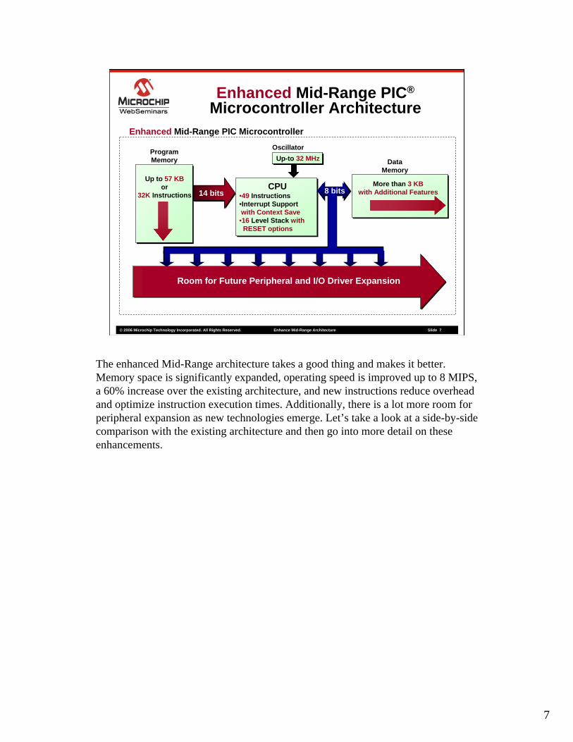
The enhanced Mid-Range architecture takes a good thing and makes it better. Memory space is significantly expanded, operating speed is improved up to 8 MIPS, a 60% increase over the existing architecture, and new instructions reduce overhead and optimize instruction execution times. Additionally, there is a lot more room for peripheral expansion as new technologies emerge. Let’s take a look at a side-by-side comparison with the existing architecture and then go into more detail on these enhancements.
8
© 2006 Microchip Technology Incorporated. All Rights Reserved. Enhance Mid-Range Architecture Slide 88
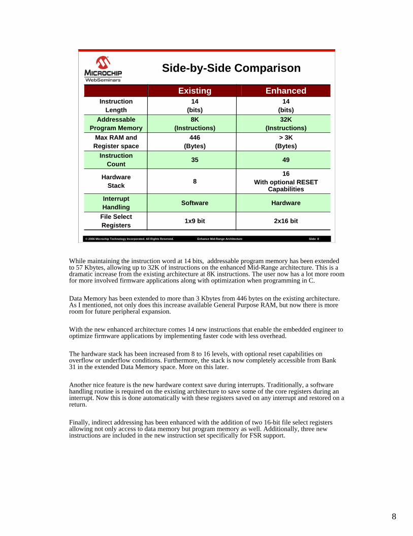
Side-by-Side Comparison
2x16 bit1x9 bitFile SelectRegisters
Hardware
16With optional RESET
Capabilities
49
> 3K(Bytes)
32K(Instructions)
14(bits)
Enhanced
SoftwareInterruptHandling
8HardwareStack
35InstructionCount
446(Bytes)
Max RAM andRegister space
8K(Instructions)
AddressableProgram Memory
14(bits)
InstructionLength
Existing
While maintaining the instruction word at 14 bits, addressable program memory has been extended to 57 Kbytes, allowing up to 32K of instructions on the enhanced Mid-Range architecture. This is a dramatic increase from the existing architecture at 8K instructions. The user now has a lot more room for more involved firmware applications along with optimization when programming in C.
Data Memory has been extended to more than 3 Kbytes from 446 bytes on the existing architecture. As I mentioned, not only does this increase available General Purpose RAM, but now there is more room for future peripheral expansion.
With the new enhanced architecture comes 14 new instructions that enable the embedded engineer to optimize firmware applications by implementing faster code with less overhead.
The hardware stack has been increased from 8 to 16 levels, with optional reset capabilities on overflow or underflow conditions. Furthermore, the stack is now completely accessible from Bank 31 in the extended Data Memory space. More on this later.
Another nice feature is the new hardware context save during interrupts. Traditionally, a software handling routine is required on the existing architecture to save some of the core registers during an interrupt. Now this is done automatically with these registers saved on any interrupt and restored on a return.
Finally, indirect addressing has been enhanced with the addition of two 16-bit file select registers allowing not only access to data memory but program memory as well. Additionally, three new instructions are included in the new instruction set specifically for FSR support.
9
© 2006 Microchip Technology Incorporated. All Rights Reserved. Enhanced Mid-Range Architecture Slide 9
Data Memory
Let’s take a closer look at these enhancements starting with the new memory map.
10
© 2006 Microchip Technology Incorporated. All Rights Reserved. Enhance Mid-Range Architecture Slide 1010
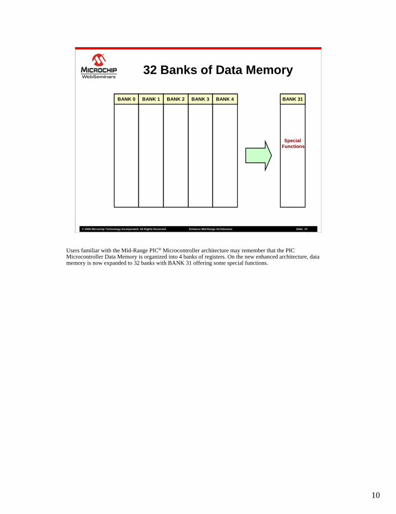
32 Banks of Data Memory
BANK 0 BANK 1 BANK 2 BANK 3 BANK 4 BANK 31
SpecialFunctions
Users familiar with the Mid-Range PIC® Microcontroller architecture may remember that the PIC Microcontroller Data Memory is organized into 4 banks of registers. On the new enhanced architecture, data memory is now expanded to 32 banks with BANK 31 offering some special functions.
11
© 2006 Microchip Technology Incorporated. All Rights Reserved. Enhance Mid-Range Architecture Slide 1111
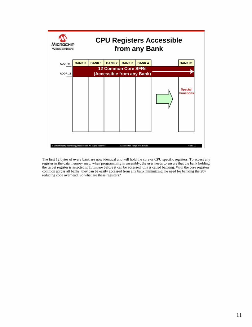
CPU Registers Accessible from any Bank
BANK 0 BANK 1 BANK 2 BANK 3 BANK 4 BANK 31
12 Common Core SFRs(Accessible from any Bank)
ADDR 0
ADDR 11
SpecialFunctions
The first 12 bytes of every bank are now identical and will hold the core or CPU specific registers. To access any register in the data memory map, when programming in assembly, the user needs to ensure that the bank holding the target register is selected in firmware before it can be accessed, this is called banking. With the core registers common across all banks, they can be easily accessed from any bank minimizing the need for banking thereby reducing code overhead. So what are these registers?
12
© 2006 Microchip Technology Incorporated. All Rights Reserved. Enhance Mid-Range Architecture Slide 1212
Program Counter Latch High
Common Core Registers
0x0B
0x0A
0x090x080x070x060x050x040x030x020x010x00Address
INTCON
PCLATH
WREGBSRFSR1 HighFSR1 LowFSR0 HighFSR0 LowSTATUSPCLINDF1INDF0Register
Interrupt Control Register
Working RegisterBank Select RegisterFile Select Register 1 High ByteFile Select Register 1 Low ByteFile Select Register 0 High ByteFile Select Register 0 Low ByteStatus RegisterProgram Counter LowIndirect Register 1Indirect Register 0Function
NEWNEW
NEW
NEW
NEWNEW
NEW
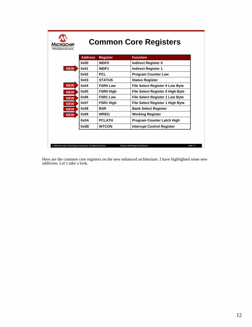
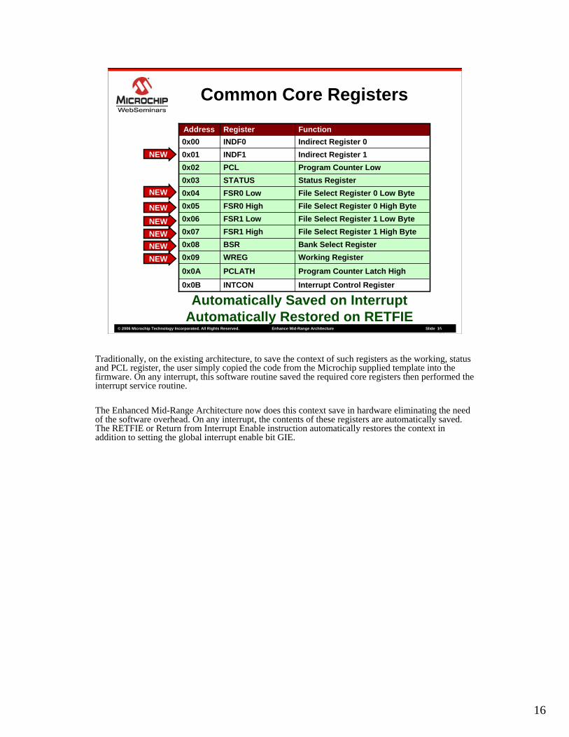
Here are the common core registers on the new enhanced architecture. I have highlighted some new additions. Let’s take a look.
13
© 2006 Microchip Technology Incorporated. All Rights Reserved. Enhance Mid-Range Architecture Slide 1313
Program Counter Latch High
Common Core Registers
0x0B
0x0A
0x090x080x070x060x050x040x030x020x010x00Address
INTCON
PCLATH
WREGBSRFSR1 HighFSR1 LowFSR0 HighFSR0 LowSTATUSPCLINDF1INDF0Register
Interrupt Control Register
Working RegisterBank Select RegisterFile Select Register 1 High ByteFile Select Register 1 Low ByteFile Select Register 0 High ByteFile Select Register 0 Low ByteStatus RegisterProgram Counter LowIndirect Register 1Indirect Register 0Function
NEWNEW
NEW
NEW
NEWNEW
NEW
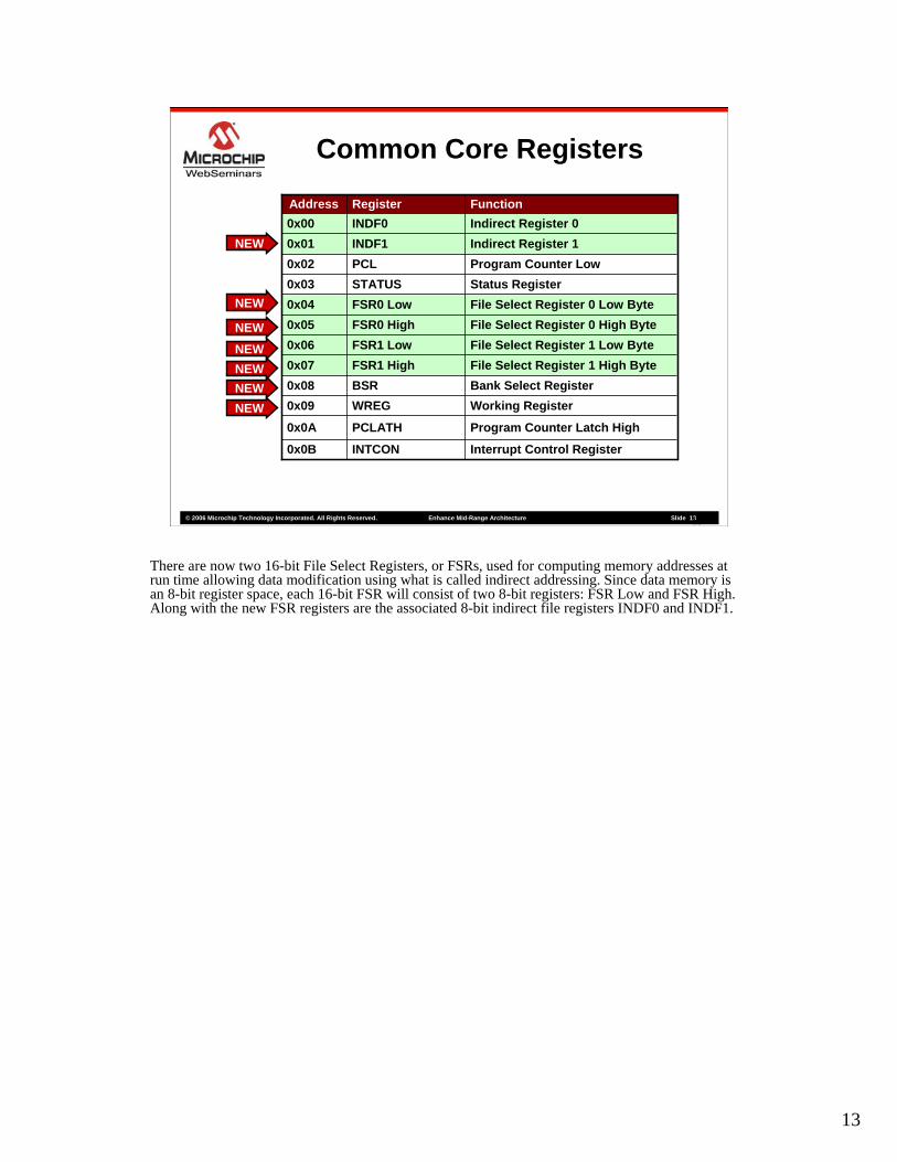
There are now two 16-bit File Select Registers, or FSRs, used for computing memory addresses at run time allowing data modification using what is called indirect addressing. Since data memory is an 8-bit register space, each 16-bit FSR will consist of two 8-bit registers: FSR Low and FSR High. Along with the new FSR registers are the associated 8-bit indirect file registers INDF0 and INDF1.
14
© 2006 Microchip Technology Incorporated. All Rights Reserved. Enhance Mid-Range Architecture Slide 1414
Program Counter Latch High0x0A
0x09
PCLATH
WREG Working Register
Common Core Registers
0x0B
0x080x070x060x050x040x030x020x010x00Address
INTCON
BSRFSR1 HighFSR1 LowFSR0 HighFSR0 LowSTATUSPCLINDF1INDF0Register
Interrupt Control Register
Bank Select RegisterFile Select Register 1 High ByteFile Select Register 1 Low ByteFile Select Register 0 High ByteFile Select Register 0 Low ByteStatus RegisterProgram Counter LowIndirect Register 1Indirect Register 0Function
NEWNEW
NEW
NEW
NEWNEW
NEW
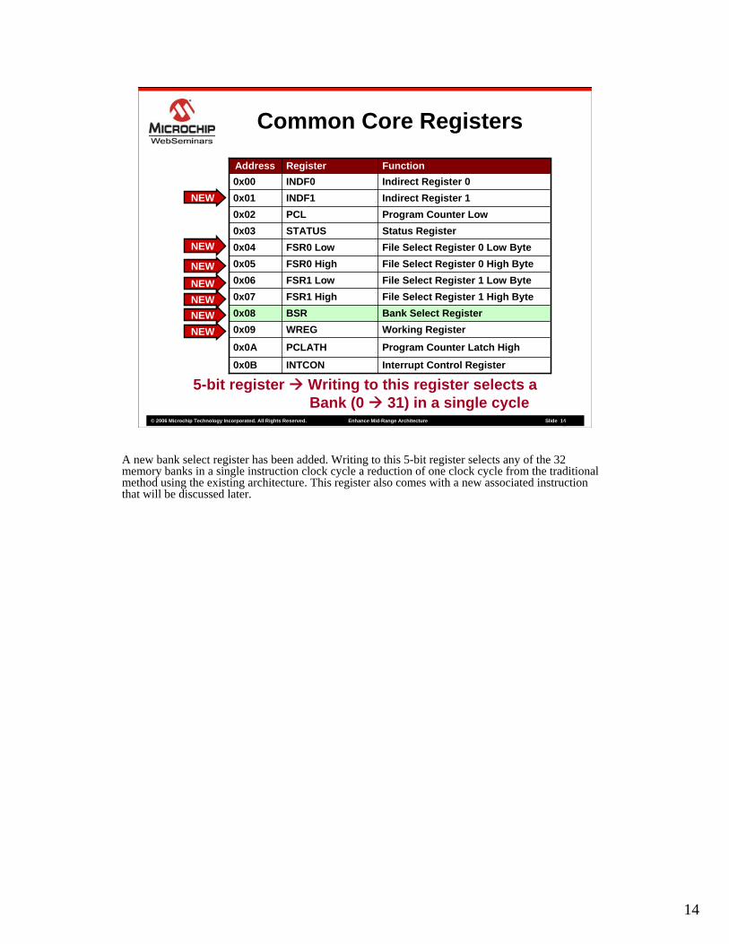
5-bit register Writing to this register selects a Bank (0 31) in a single cycle
A new bank select register has been added. Writing to this 5-bit register selects any of the 32 memory banks in a single instruction clock cycle a reduction of one clock cycle from the traditional method using the existing architecture. This register also comes with a new associated instruction that will be discussed later.
15
© 2006 Microchip Technology Incorporated. All Rights Reserved. Enhance Mid-Range Architecture Slide 1515
Bank Select Register
Program Counter Latch High
Common Core Registers
0x0B
0x0A
0x090x080x070x060x050x040x030x020x010x00Address
INTCON
PCLATH
WREGBSRFSR1 HighFSR1 LowFSR0 HighFSR0 LowSTATUSPCLINDF1INDF0Register
Interrupt Control Register
Working Register
File Select Register 1 High ByteFile Select Register 1 Low ByteFile Select Register 0 High ByteFile Select Register 0 Low ByteStatus RegisterProgram Counter LowIndirect Register 1Indirect Register 0Function
NEWNEW
NEW
NEW
NEWNEW
NEW
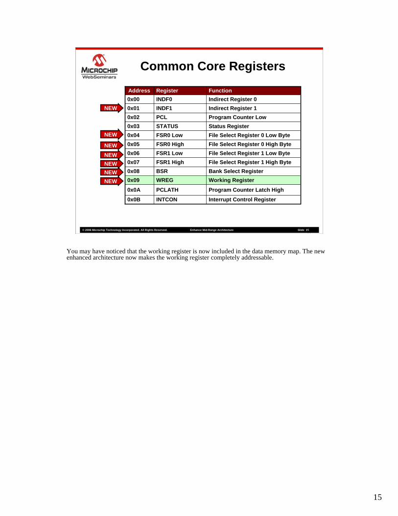
You may have noticed that the working register is now included in the data memory map. The new enhanced architecture now makes the working register completely addressable.
16
© 2006 Microchip Technology Incorporated. All Rights Reserved. Enhance Mid-Range Architecture Slide 1616
Program Counter Latch High
0x0B
0x0A
0x090x080x070x060x050x040x030x020x010x00Address
INTCON
PCLATH
WREGBSRFSR1 HighFSR1 LowFSR0 HighFSR0 LowSTATUSPCLINDF1INDF0Register
Interrupt Control Register
Working RegisterBank Select RegisterFile Select Register 1 High ByteFile Select Register 1 Low ByteFile Select Register 0 High ByteFile Select Register 0 Low ByteStatus RegisterProgram Counter LowIndirect Register 1Indirect Register 0Function
NEWNEW
NEW
NEW
NEWNEW
NEW
Common Core Registers
Automatically Saved on InterruptAutomatically Restored on RETFIE
Traditionally, on the existing architecture, to save the context of such registers as the working, status and PCL register, the user simply copied the code from the Microchip supplied template into the firmware. On any interrupt, this software routine saved the required core registers then performed the interrupt service routine.
The Enhanced Mid-Range Architecture now does this context save in hardware eliminating the need of the software overhead. On any interrupt, the contents of these registers are automatically saved. The RETFIE or Return from Interrupt Enable instruction automatically restores the context in addition to setting the global interrupt enable bit GIE.
17
© 2006 Microchip Technology Incorporated. All Rights Reserved. Enhance Mid-Range Architecture Slide 1717
Special Function Registers
BANK 0 BANK 1 BANK 2 BANK 3 BANK 4 BANK 31ADDR 0
ADDR 11
ADDR 12ADDR 31
SFRs20
SFRs20
SFRs20
SFRs20
SFRs20
12 Common Core SFRs(Accessible from any Bank)
SpecialFunctions
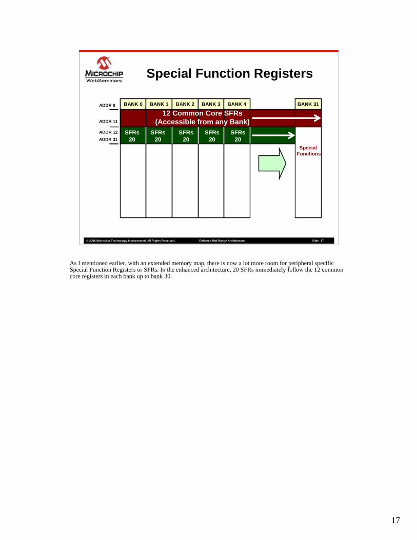
As I mentioned earlier, with an extended memory map, there is now a lot more room for peripheral specific Special Function Registers or SFRs. In the enhanced architecture, 20 SFRs immediately follow the 12 common core registers in each bank up to bank 30.
18
© 2006 Microchip Technology Incorporated. All Rights Reserved. Enhance Mid-Range Architecture Slide 1818
General Purpose Registers
BANK 0 BANK 1 BANK 2 BANK 3 BANK 4 BANK 31ADDR 0
ADDR 11
ADDR 12ADDR 31
SFRs20
SFRs20
SFRs20
SFRs20
SFRs20
GPR80 Bytes
GPR80 Bytes
GPR80 Bytes
GPR80 Bytes
GPR80 Bytes
ADDR 32
ADDR 111
12 Common Core SFRs(Accessible from any Bank)
SpecialFunctions
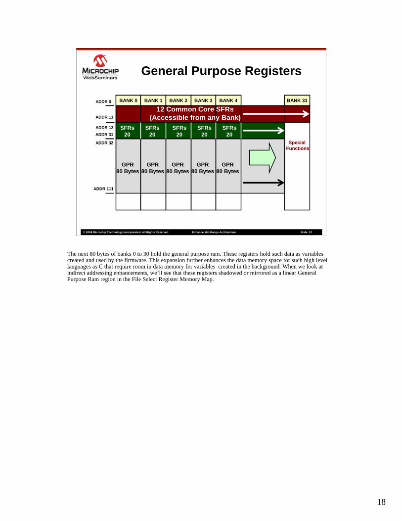
The next 80 bytes of banks 0 to 30 hold the general purpose ram. These registers hold such data as variables created and used by the firmware. This expansion further enhances the data memory space for such high level languages as C that require room in data memory for variables created in the background. When we look at indirect addressing enhancements, we’ll see that these registers shadowed or mirrored as a linear General Purpose Ram region in the File Select Register Memory Map.
19
© 2006 Microchip Technology Incorporated. All Rights Reserved. Enhance Mid-Range Architecture Slide 1919
Common General Purpose Registers
BANK 0 BANK 1 BANK 2 BANK 3 BANK 4 BANK 31ADDR 0
ADDR 11
ADDR 12ADDR 31
SFRs20
SFRs20
SFRs20
SFRs20
SFRs20
GPR80 Bytes
GPR80 Bytes
GPR80 Bytes
GPR80 Bytes
GPR80 Bytes
ADDR 32
ADDR 111
12 Common Core SFRs(Accessible from any Bank)
ADDR 112
ADDR 127
Common GPR Memory (16 bytes)(Accessible from any Bank)
SpecialFunctions
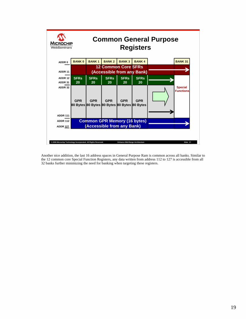
Another nice addition, the last 16 address spaces in General Purpose Ram is common across all banks. Similar to the 12 common core Special Function Registers, any data written from address 112 to 127 is accessible from all 32 banks further minimizing the need for banking when targeting these registers.
20
© 2006 Microchip Technology Incorporated. All Rights Reserved. Enhance Mid-Range Architecture Slide 2020
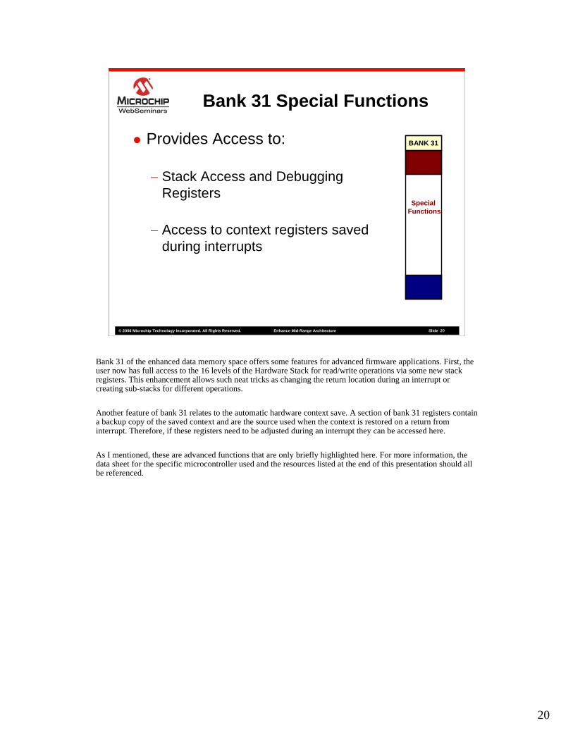
Bank 31 Special Functions
BANK 31Provides Access to:
− Stack Access and Debugging Registers
− Access to context registers saved during interrupts
SpecialFunctions
Bank 31 of the enhanced data memory space offers some features for advanced firmware applications. First, the user now has full access to the 16 levels of the Hardware Stack for read/write operations via some new stack registers. This enhancement allows such neat tricks as changing the return location during an interrupt or creating sub-stacks for different operations.
Another feature of bank 31 relates to the automatic hardware context save. A section of bank 31 registers contain a backup copy of the saved context and are the source used when the context is restored on a return from interrupt. Therefore, if these registers need to be adjusted during an interrupt they can be accessed here.
As I mentioned, these are advanced functions that are only briefly highlighted here. For more information, the data sheet for the specific microcontroller used and the resources listed at the end of this presentation should all be referenced.
21
© 2006 Microchip Technology Incorporated. All Rights Reserved. Enhanced Mid-Range Architecture Slide 21
New Instructions
That’s a brief overview of the enhanced Data Memory Map. Let’s now turn our attention to the new instructions added and associated benefits to the user.
22
© 2006 Microchip Technology Incorporated. All Rights Reserved. Enhance Mid-Range Architecture Slide 2222
New Instructions
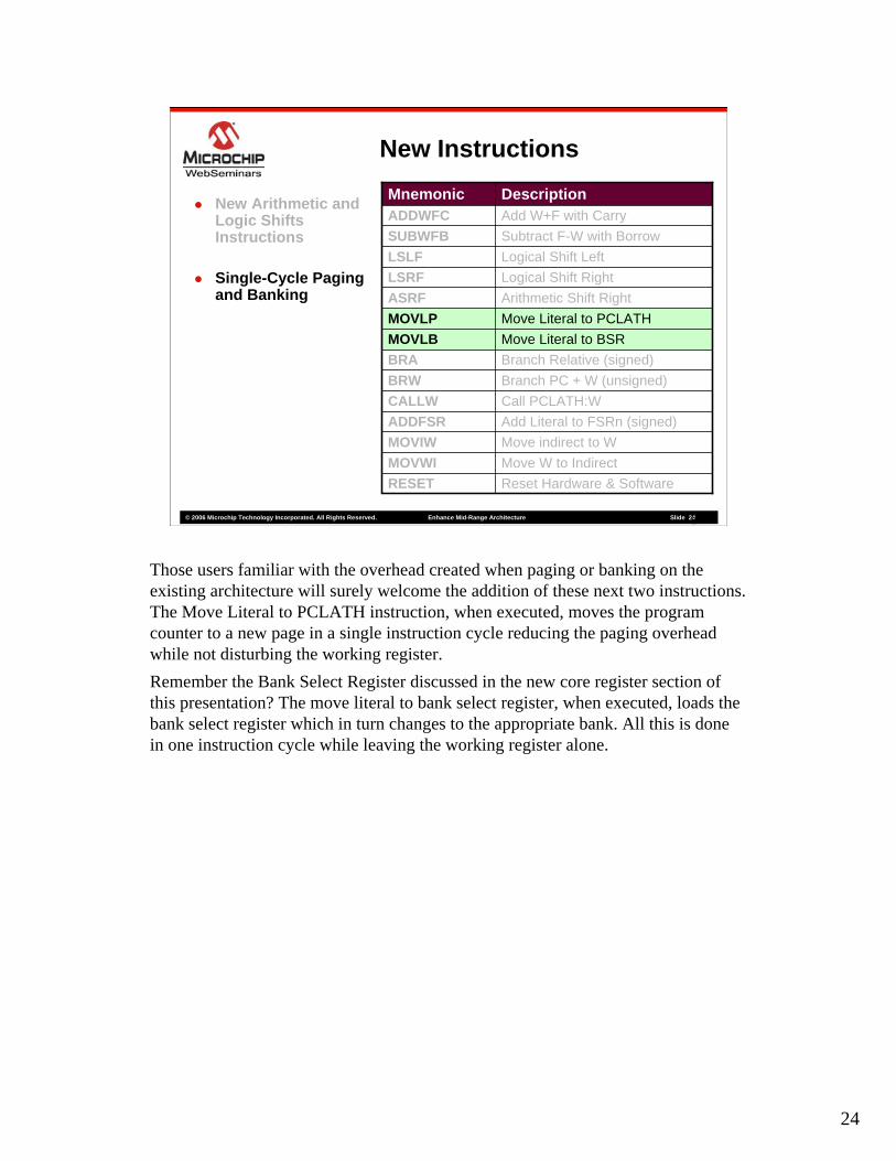
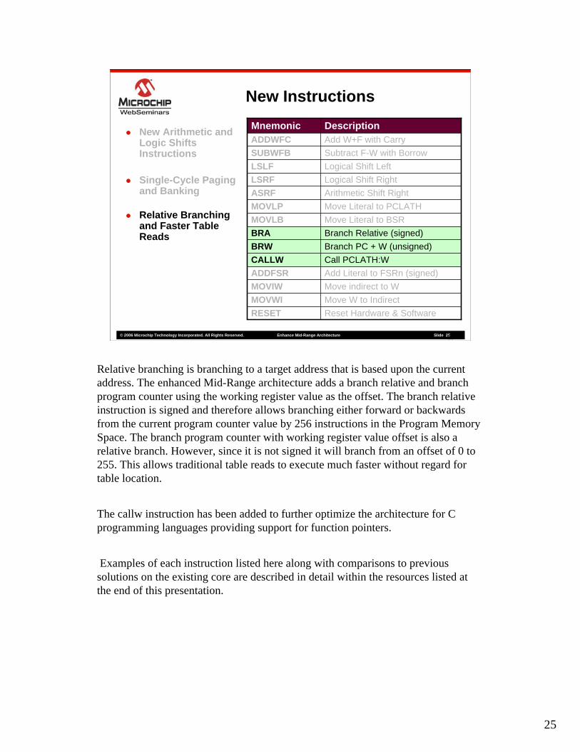
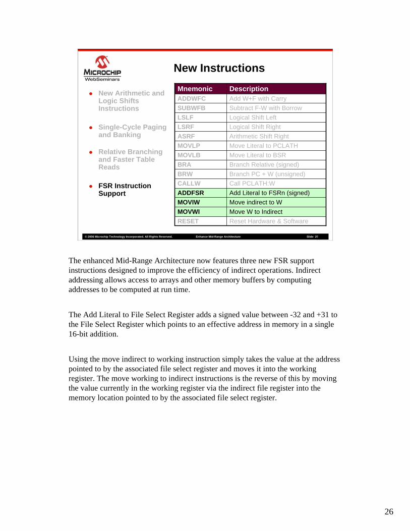
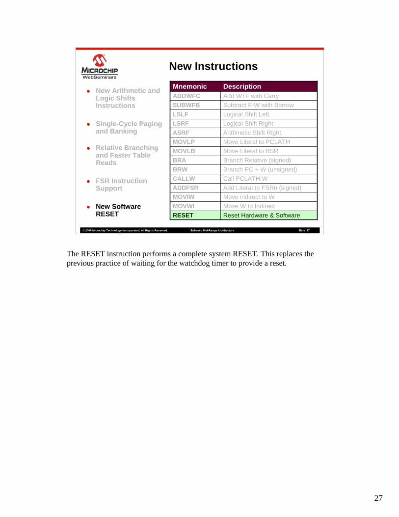
Reset Hardware & SoftwareRESETMove W to IndirectMOVWIMove indirect to WMOVIWAdd Literal to FSRn (signed)ADDFSRCall PCLATH:WCALLWBranch PC + W (unsigned)BRWBranch Relative (signed)BRAMove Literal to BSRMOVLBMove Literal to PCLATHMOVLPArithmetic Shift RightASRFLogical Shift RightLSRFLogical Shift LeftLSLFSubtract F-W with BorrowSUBWFBAdd W+F with CarryADDWFCDescriptionMnemonic
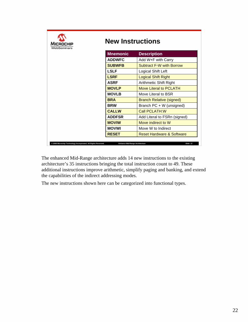
The enhanced Mid-Range architecture adds 14 new instructions to the existing architecture’s 35 instructions bringing the total instruction count to 49. These additional instructions improve arithmetic, simplify paging and banking, and extend the capabilities of the indirect addressing modes. The new instructions shown here can be categorized into functional types.
23
© 2006 Microchip Technology Incorporated. All Rights Reserved. Enhance Mid-Range Architecture Slide 2323
New Instructions
Reset Hardware & SoftwareRESETMove W to IndirectMOVWIMove indirect to WMOVIWAdd Literal to FSRn (signed)ADDFSRCall PCLATH:WCALLWBranch PC + W (unsigned)BRWBranch Relative (signed)BRAMove Literal to BSRMOVLBMove Literal to PCLATHMOVLPArithmetic Shift RightASRFLogical Shift RightLSRFLogical Shift LeftLSLFSubtract F-W with BorrowSUBWFBAdd W+F with CarryADDWFCDescriptionMnemonicNew Arithmetic and
Logic Shifts Instructions
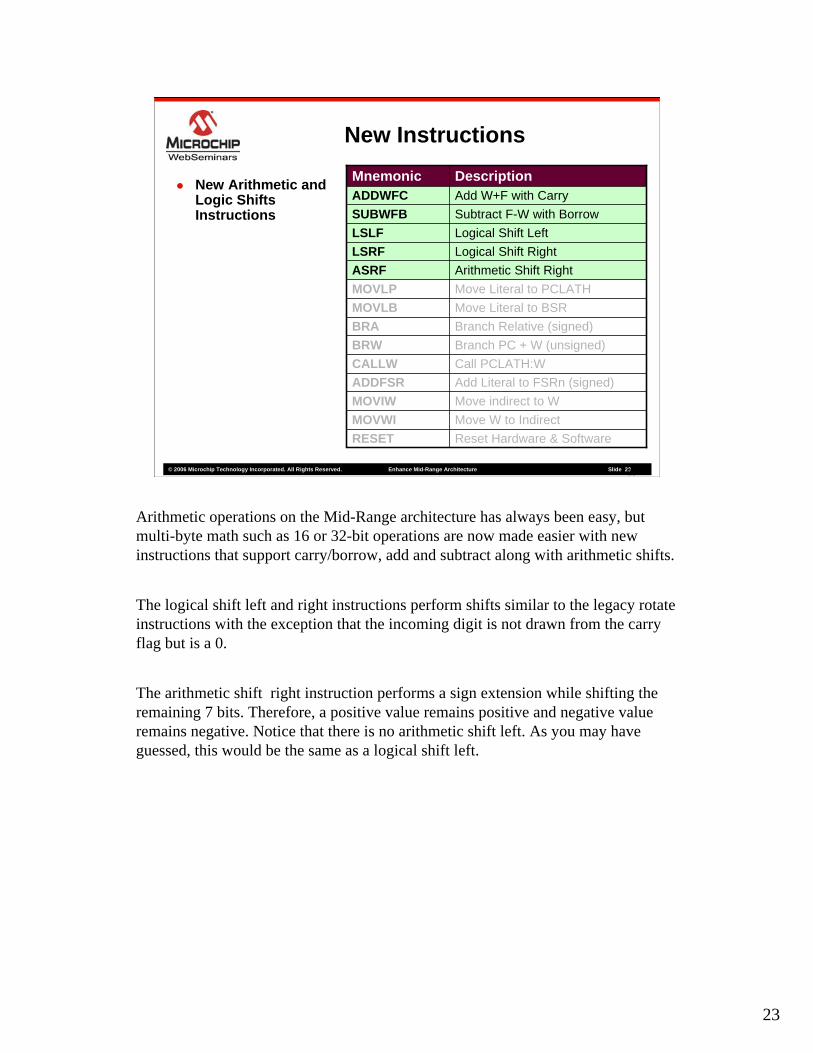
Arithmetic operations on the Mid-Range architecture has always been easy, but multi-byte math such as 16 or 32-bit operations are now made easier with new instructions that support carry/borrow, add and subtract along with arithmetic shifts.
The logical shift left and right instructions perform shifts similar to the legacy rotate instructions with the exception that the incoming digit is not drawn from the carry flag but is a 0.
The arithmetic shift right instruction performs a sign extension while shifting the remaining 7 bits. Therefore, a positive value remains positive and negative value remains negative. Notice that there is no arithmetic shift left. As you may have guessed, this would be the same as a logical shift left.
24
© 2006 Microchip Technology Incorporated. All Rights Reserved. Enhance Mid-Range Architecture Slide 2424
New Instructions
Reset Hardware & SoftwareRESETMove W to IndirectMOVWIMove indirect to WMOVIWAdd Literal to FSRn (signed)ADDFSRCall PCLATH:WCALLWBranch PC + W (unsigned)BRWBranch Relative (signed)BRAMove Literal to BSRMOVLBMove Literal to PCLATHMOVLPArithmetic Shift RightASRFLogical Shift RightLSRFLogical Shift LeftLSLFSubtract F-W with BorrowSUBWFBAdd W+F with CarryADDWFCDescriptionMnemonicNew Arithmetic and
Logic Shifts Instructions
Single-Cycle Paging and Banking
Those users familiar with the overhead created when paging or banking on the existing architecture will surely welcome the addition of these next two instructions. The Move Literal to PCLATH instruction, when executed, moves the program counter to a new page in a single instruction cycle reducing the paging overhead while not disturbing the working register. Remember the Bank Select Register discussed in the new core register section of this presentation? The move literal to bank select register, when executed, loads the bank select register which in turn changes to the appropriate bank. All this is done in one instruction cycle while leaving the working register alone.
25
© 2006 Microchip Technology Incorporated. All Rights Reserved. Enhance Mid-Range Architecture Slide 2525
New Instructions
Reset Hardware & SoftwareRESETMove W to IndirectMOVWIMove indirect to WMOVIWAdd Literal to FSRn (signed)ADDFSRCall PCLATH:WCALLWBranch PC + W (unsigned)BRWBranch Relative (signed)BRAMove Literal to BSRMOVLBMove Literal to PCLATHMOVLPArithmetic Shift RightASRFLogical Shift RightLSRFLogical Shift LeftLSLFSubtract F-W with BorrowSUBWFBAdd W+F with CarryADDWFCDescriptionMnemonicNew Arithmetic and
Logic Shifts Instructions
Single-Cycle Paging and Banking
Relative Branching and Faster Table Reads
Relative branching is branching to a target address that is based upon the current address. The enhanced Mid-Range architecture adds a branch relative and branch program counter using the working register value as the offset. The branch relative instruction is signed and therefore allows branching either forward or backwards from the current program counter value by 256 instructions in the Program Memory Space. The branch program counter with working register value offset is also a relative branch. However, since it is not signed it will branch from an offset of 0 to 255. This allows traditional table reads to execute much faster without regard for table location.
The callw instruction has been added to further optimize the architecture for C programming languages providing support for function pointers.
Examples of each instruction listed here along with comparisons to previous solutions on the existing core are described in detail within the resources listed at the end of this presentation.
26
© 2006 Microchip Technology Incorporated. All Rights Reserved. Enhance Mid-Range Architecture Slide 2626
New Instructions
Reset Hardware & SoftwareRESETMove W to IndirectMOVWIMove indirect to WMOVIWAdd Literal to FSRn (signed)ADDFSRCall PCLATH:WCALLWBranch PC + W (unsigned)BRWBranch Relative (signed)BRAMove Literal to BSRMOVLBMove Literal to PCLATHMOVLPArithmetic Shift RightASRFLogical Shift RightLSRFLogical Shift LeftLSLFSubtract F-W with BorrowSUBWFBAdd W+F with CarryADDWFCDescriptionMnemonicNew Arithmetic and
Logic Shifts Instructions
Single-Cycle Paging and Banking
Relative Branching and Faster Table Reads
FSR Instruction Support
The enhanced Mid-Range Architecture now features three new FSR support instructions designed to improve the efficiency of indirect operations. Indirect addressing allows access to arrays and other memory buffers by computing addresses to be computed at run time.
The Add Literal to File Select Register adds a signed value between -32 and +31 to the File Select Register which points to an effective address in memory in a single 16-bit addition.
Using the move indirect to working instruction simply takes the value at the address pointed to by the associated file select register and moves it into the working register. The move working to indirect instructions is the reverse of this by moving the value currently in the working register via the indirect file register into the memory location pointed to by the associated file select register.
27
© 2006 Microchip Technology Incorporated. All Rights Reserved. Enhance Mid-Range Architecture Slide 2727
New Instructions
Reset Hardware & SoftwareRESETMove W to IndirectMOVWIMove indirect to WMOVIWAdd Literal to FSRn (signed)ADDFSRCall PCLATH:WCALLWBranch PC + W (unsigned)BRWBranch Relative (signed)BRAMove Literal to BSRMOVLBMove Literal to PCLATHMOVLPArithmetic Shift RightASRFLogical Shift RightLSRFLogical Shift LeftLSLFSubtract F-W with BorrowSUBWFBAdd W+F with CarryADDWFCDescriptionMnemonicNew Arithmetic and
Logic Shifts Instructions
Single-Cycle Paging and Banking
Relative Branching and Faster Table Reads
FSR Instruction Support
New Software RESET
The RESET instruction performs a complete system RESET. This replaces the previous practice of waiting for the watchdog timer to provide a reset.
28
© 2006 Microchip Technology Incorporated. All Rights Reserved. Enhanced Mid-Range Architecture Slide 28
Enhanced Indirect Addressing
As I have been eluding to throughout this presentation, there are a number of enhancements to indirect addressing. Let’s expand on this…
29
© 2006 Microchip Technology Incorporated. All Rights Reserved. Enhance Mid-Range Architecture Slide 2929
Working Register
(2) 16-bit File Select Registers (FSRs)
0x0B
0x0A
0x090x080x070x060x050x040x030x020x010x00Address
INTCON
PCLATH
WREGBSRFSR1 HighFSR1 LowFSR0 HighFSR0 LowSTATUSPCLINDF1INDF0Register
Program Counter Latch High
Interrupt Control Register
Bank Select RegisterFile Select Register 1 High ByteFile Select Register 1 Low ByteFile Select Register 0 High ByteFile Select Register 0 Low ByteStatus RegisterProgram Counter LowIndirect Register 1Indirect Register 0Function
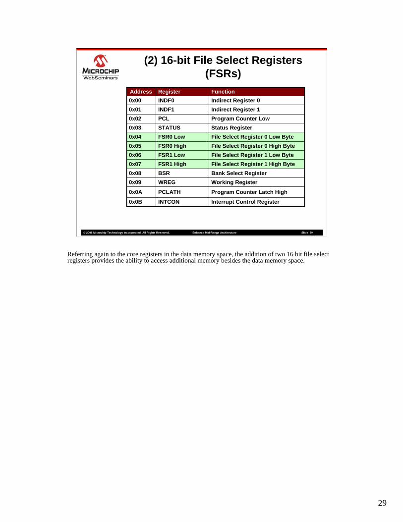
Referring again to the core registers in the data memory space, the addition of two 16 bit file select registers provides the ability to access additional memory besides the data memory space.
30
© 2006 Microchip Technology Incorporated. All Rights Reserved. Enhance Mid-Range Architecture Slide 3030
FSR Memory Map
SFRs&
GPRs
RESERVED
PROGRAMMEMORY
0x0000
0x0FFF0x1000
0x7FFF0x8000
0xFFFF
0x0000
0x7FFF
FSR Addresses
Program Counter Addresses
BSR + File Register Addresses
0x0000
0x0FFF
FSR Addresses
Linear GPR Region
Reach
able
by
FSR only0x29FF0x3A00
RESERVED0x1FFF0x2000
Access both data and program memory space
One data pointer for ALL memory
Supported by new instructions
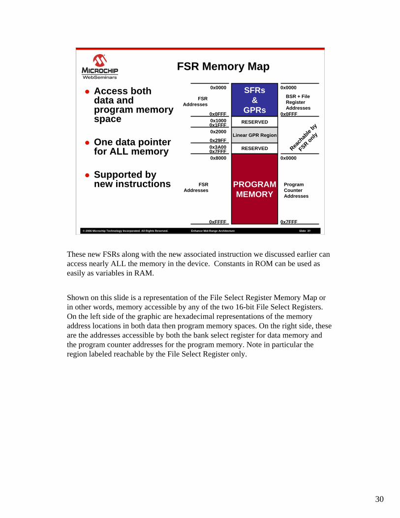
These new FSRs along with the new associated instruction we discussed earlier can access nearly ALL the memory in the device. Constants in ROM can be used as easily as variables in RAM.
Shown on this slide is a representation of the File Select Register Memory Map or in other words, memory accessible by any of the two 16-bit File Select Registers. On the left side of the graphic are hexadecimal representations of the memory address locations in both data then program memory spaces. On the right side, these are the addresses accessible by both the bank select register for data memory and the program counter addresses for the program memory. Note in particular the region labeled reachable by the File Select Register only.
31
© 2006 Microchip Technology Incorporated. All Rights Reserved. Enhance Mid-Range Architecture Slide 3131
0x3A00
SFRs&
GPRs
RESERVED
PROGRAMMEMORY
0x0000
0x0FFF0x1000
0x7FFF0x8000
0xFFFF
0x0000
0x7FFF
FSR Addresses
Program Counter Addresses
BSR + File Register Addresses
0x0000
0x0FFF
FSR Addresses
Reach
able
by
FSR only0x29FF
RESERVED0x1FFF
Linear GPR Region0x2000
Linear General Purpose RAM
0x20000x20000x204F0x204F
0x20500x2050
0x20A00x20A00x209F0x209F
0x20EF0x20EF0x20F00x20F0
0x213F0x213F0x21400x2140
0x218F0x218F
BANK 0BANK 0
BANK 1BANK 1
BANK 2BANK 2
BANK 3BANK 3
BANK 4BANK 4
0x21900x2190
0x21DF0x21DFBANK 5BANK 5
FSRFSRAddressesAddresses
Simply a differentview of GPR memory
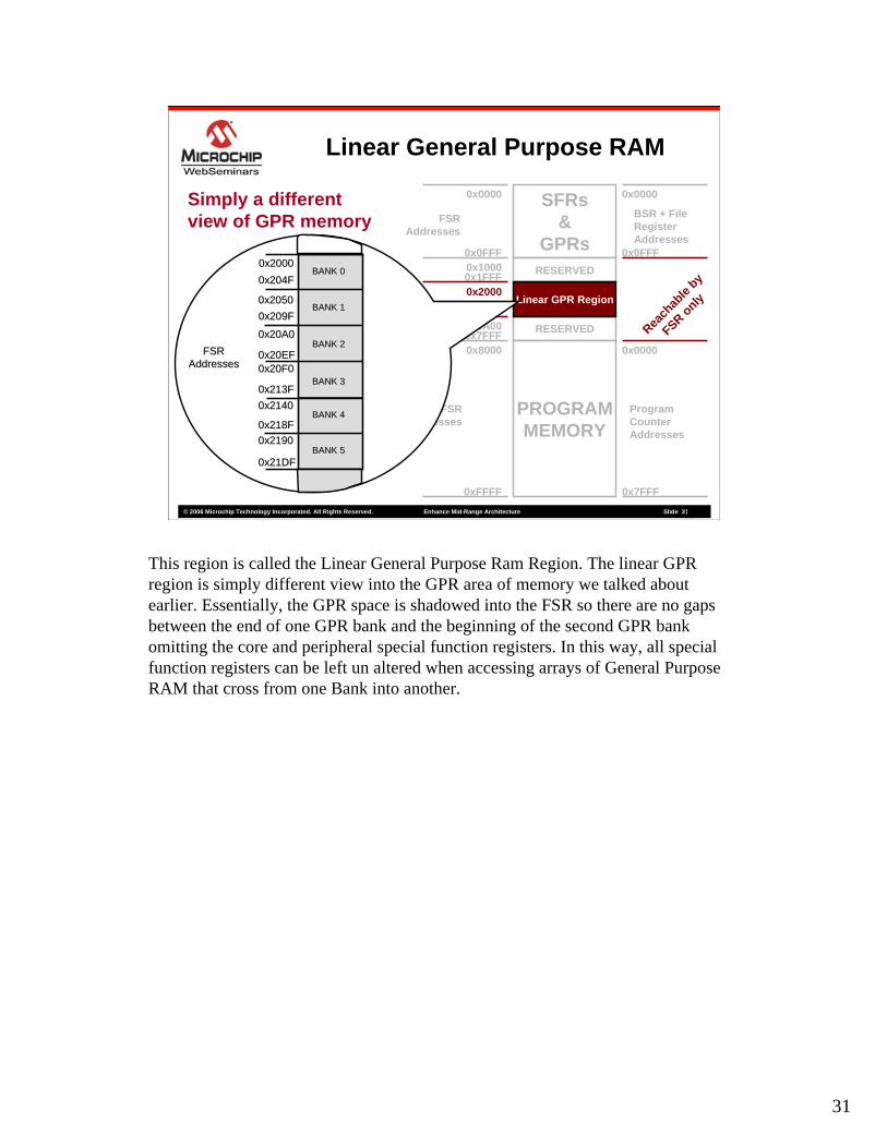
This region is called the Linear General Purpose Ram Region. The linear GPR region is simply different view into the GPR area of memory we talked about earlier. Essentially, the GPR space is shadowed into the FSR so there are no gaps between the end of one GPR bank and the beginning of the second GPR bank omitting the core and peripheral special function registers. In this way, all special function registers can be left un altered when accessing arrays of General Purpose RAM that cross from one Bank into another.
32
© 2006 Microchip Technology Incorporated. All Rights Reserved. Enhance Mid-Range Architecture Slide 3232
Accessing Data Memory with the FSRs
PROGRAMMEMORY
0x0000
0x0FFF0x1000
0x7FFF0x8000
0xFFFF
0x0000
0x7FFF
FSR Addresses
Program Counter Addresses
BSR + File Register Addresses
0x0000
0x0FFF
FSR Addresses
Reach
able
by
FSR only0x29FF0x3A00
0x1FFF0x200000000000
FSRx HIGH
FSRx LOW
00000000
11111111
FSRx HIGH
FSRx LOW
11111110
SFRs&
GPRs
RESERVED
Linear GPR Region
RESERVED
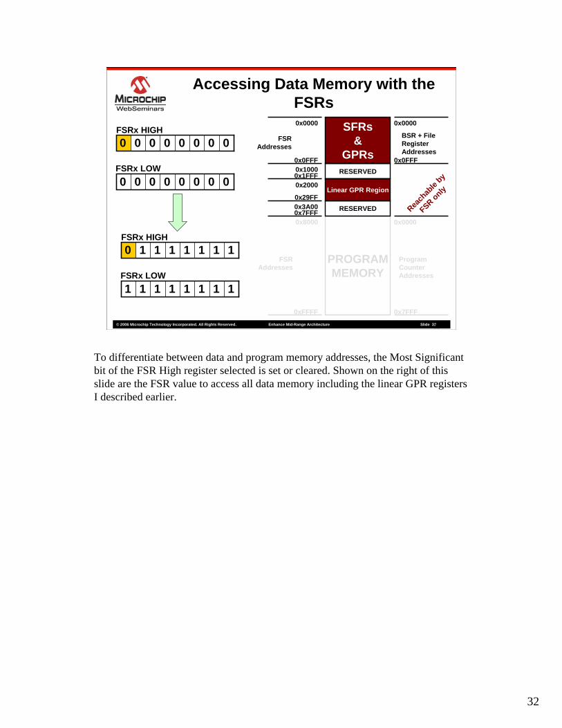
To differentiate between data and program memory addresses, the Most Significant bit of the FSR High register selected is set or cleared. Shown on the right of this slide are the FSR value to access all data memory including the linear GPR registers I described earlier.
33
© 2006 Microchip Technology Incorporated. All Rights Reserved. Enhance Mid-Range Architecture Slide 3333
File Select Registers (FSR)
SFRs&
GPRs
RESERVED
PROGRAMMEMORY
0x0000
0x0FFF0x1000
0x7FFF0x8000
0xFFFF
0x0000
0x7FFF
FSR Addresses
Program Counter Addresses
BSR + File Register Addresses
0x0000
0x0FFF
FSR Addresses
Linear GPR Region
Reach
able
by
FSR only0x29FF0x3A00
RESERVED0x1FFF0x200000000000
FSRx HIGH
FSRx LOW
00000001
11111111
FSRx HIGH
FSRx LOW
11111111
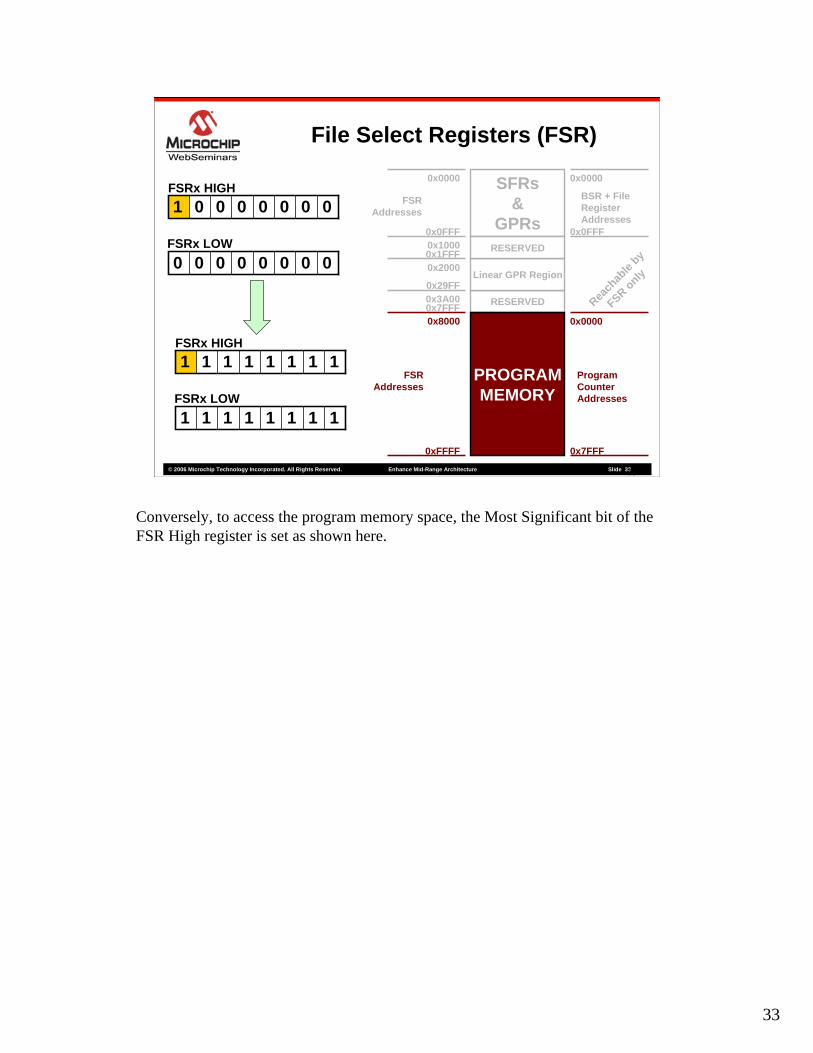
Conversely, to access the program memory space, the Most Significant bit of the FSR High register is set as shown here.
34
© 2006 Microchip Technology Incorporated. All Rights Reserved. Enhanced Mid-Range Architecture Slide 34
Enhanced Mid-Range Stack
Let’s now discuss enhancements made to the stack…
35
© 2006 Microchip Technology Incorporated. All Rights Reserved. Enhance Mid-Range Architecture Slide 3535
Expanded Hardware Stack
Extended to 16 Levels
Increased function/subroutine call depth
Optional Overflow/Underflow RESET
User Access
Program CounterProgram Memory
STACK
Existing(8 Levels)
Enhanced(16 Levels)
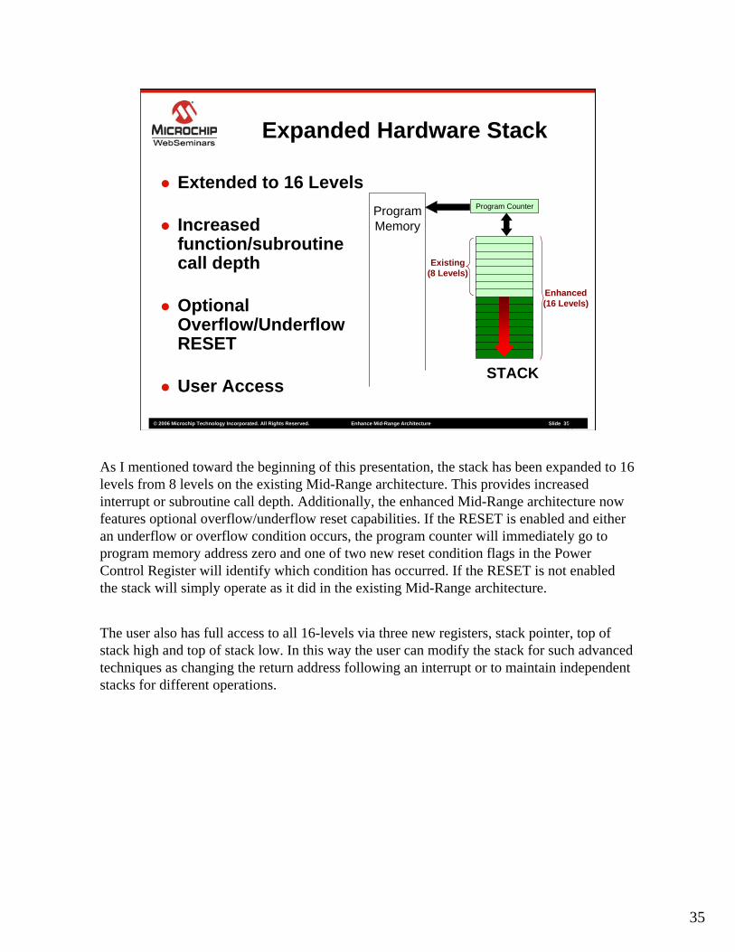
As I mentioned toward the beginning of this presentation, the stack has been expanded to 16 levels from 8 levels on the existing Mid-Range architecture. This provides increased interrupt or subroutine call depth. Additionally, the enhanced Mid-Range architecture now features optional overflow/underflow reset capabilities. If the RESET is enabled and either an underflow or overflow condition occurs, the program counter will immediately go to program memory address zero and one of two new reset condition flags in the Power Control Register will identify which condition has occurred. If the RESET is not enabled the stack will simply operate as it did in the existing Mid-Range architecture.
The user also has full access to all 16-levels via three new registers, stack pointer, top of stack high and top of stack low. In this way the user can modify the stack for such advanced techniques as changing the return address following an interrupt or to maintain independent stacks for different operations.
36
© 2006 Microchip Technology Incorporated. All Rights Reserved. Enhanced Mid-Range Architecture Slide 36
Migrating to the Enhanced Mid-Range Architecture
Finally, let’s discuss migrating existing code to the enhance Mid-Range architecture…
37
© 2006 Microchip Technology Incorporated. All Rights Reserved. Enhance Mid-Range Architecture Slide 3737
Migration
Considerations:
− Interrupts
− Indirect Memory
− Paging
− Banking
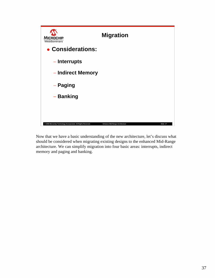
Now that we have a basic understanding of the new architecture, let’s discuss what should be considered when migrating existing designs to the enhanced Mid-Range architecture. We can simplify migration into four basic areas: interrupts, indirect memory and paging and banking.
38
© 2006 Microchip Technology Incorporated. All Rights Reserved. Enhance Mid-Range Architecture Slide 3838
Interrupts
RETFIE works a little different− Automatically restores context registers
Working Register
0x0B
0x0A
0x090x080x070x060x050x040x030x020x010x00Address
INTCON
PCLATH
WREGBSRFSR1 HighFSR1 LowFSR0 HighFSR0 LowSTATUSPCLINDF1INDF0Register
Program Counter Latch High
Interrupt Control Register
Bank Select RegisterFile Select Register 1 High ByteFile Select Register 1 Low ByteFile Select Register 0 High ByteFile Select Register 0 Low ByteStatus RegisterProgram Counter LowIndirect Register 1Indirect Register 0Function
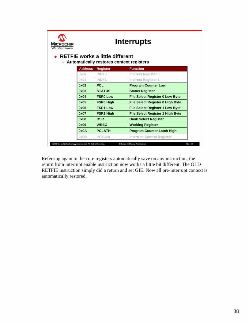
Referring again to the core registers automatically save on any instruction, the return from interrupt enable instruction now works a little bit different. The OLD RETFIE instruction simply did a return and set GIE. Now all pre-interrupt context is automatically restored.
39
© 2006 Microchip Technology Incorporated. All Rights Reserved. Enhance Mid-Range Architecture Slide 3939
Interrupts
RETFIE works a little different− Automatically restores context registers
Remove old core context save/restore algorithm− If not, this will not affect your code other than
wasting clock cycles
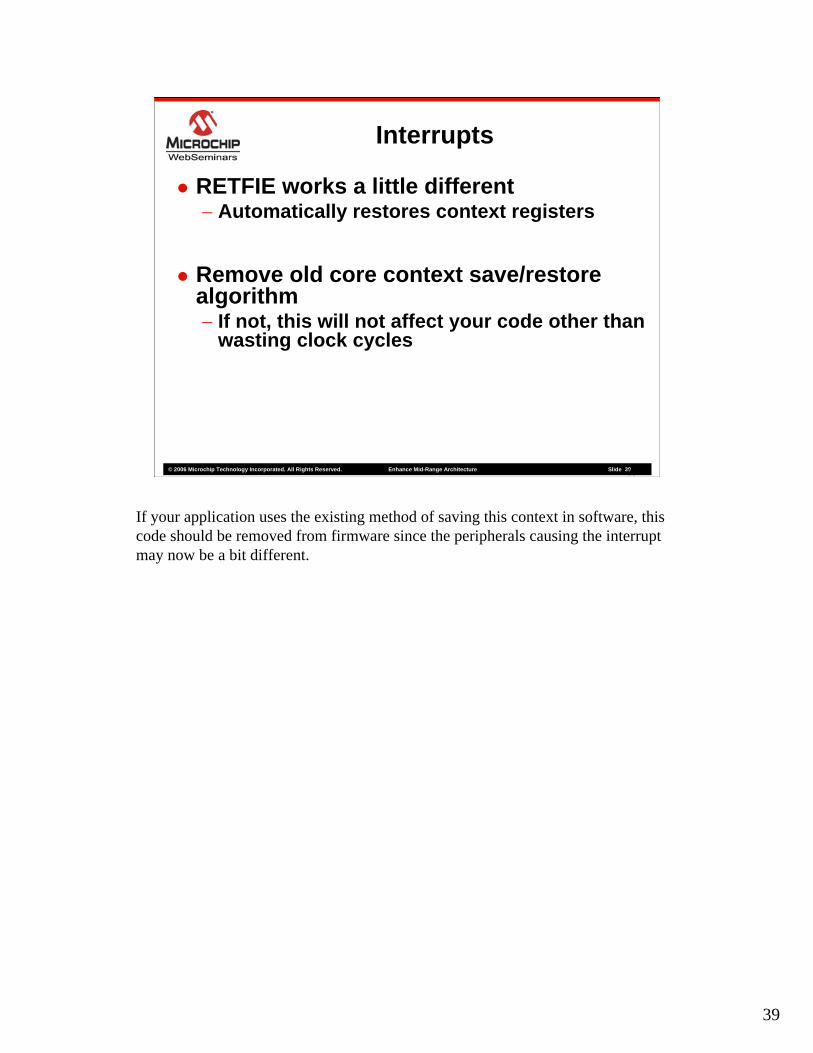
If your application uses the existing method of saving this context in software, this code should be removed from firmware since the peripherals causing the interrupt may now be a bit different.
40
© 2006 Microchip Technology Incorporated. All Rights Reserved. Enhance Mid-Range Architecture Slide 4040
Indirect Memory
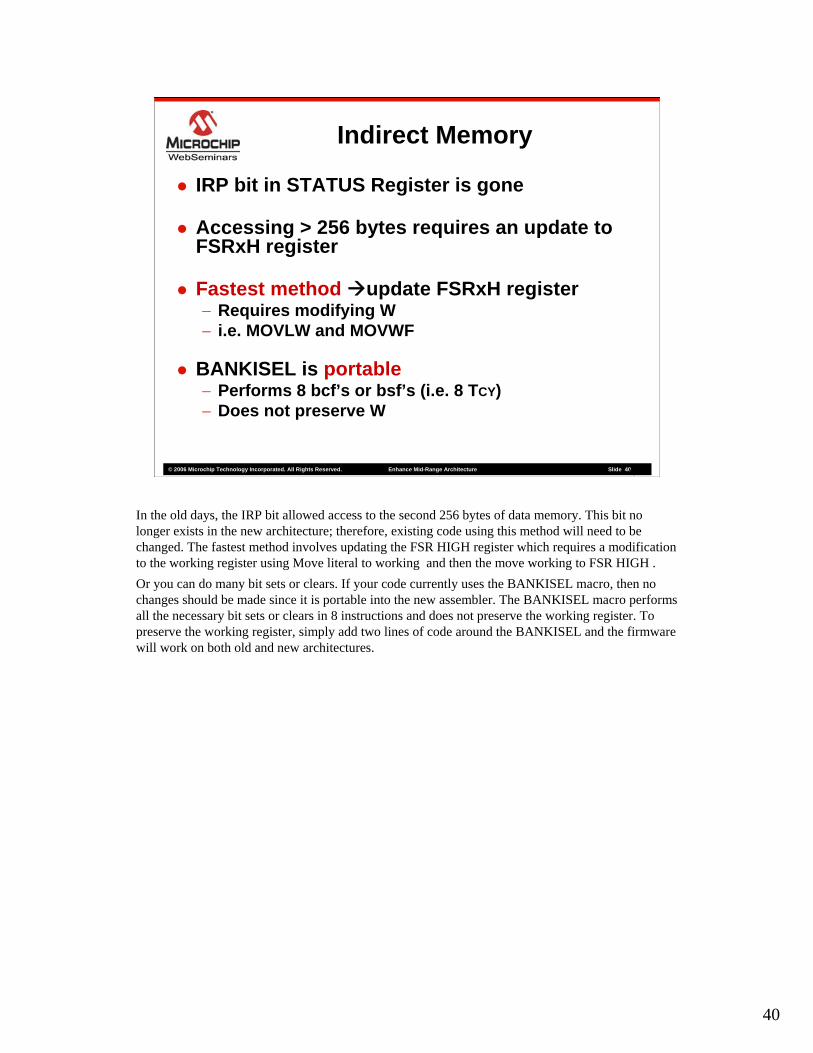
IRP bit in STATUS Register is gone
Accessing > 256 bytes requires an update to FSRxH register
Fastest method update FSRxH register− Requires modifying W− i.e. MOVLW and MOVWF
BANKISEL is portable− Performs 8 bcf’s or bsf’s (i.e. 8 TCY)− Does not preserve W
In the old days, the IRP bit allowed access to the second 256 bytes of data memory. This bit no longer exists in the new architecture; therefore, existing code using this method will need to be changed. The fastest method involves updating the FSR HIGH register which requires a modification to the working register using Move literal to working and then the move working to FSR HIGH . Or you can do many bit sets or clears. If your code currently uses the BANKISEL macro, then no changes should be made since it is portable into the new assembler. The BANKISEL macro performs all the necessary bit sets or clears in 8 instructions and does not preserve the working register. To preserve the working register, simply add two lines of code around the BANKISEL and the firmware will work on both old and new architectures.

41
© 2006 Microchip Technology Incorporated. All Rights Reserved. Enhance Mid-Range Architecture Slide 4141
Paging and Banking
PAGESEL and BANKSEL macros are portable− Automatically uses MOVLP and MOVLB
Otherwise
Paging− Update all PCLATH code− Assure 7 bit data in PCLATH
Banking− Replace writes to STATUS with writes to BSR
How about paging and banking? If your existing code uses the PAGESEL and BANKSEL macros, there is no need to change anything in firmware since these macros are portable and existing code is automatically converted by the new assembler using the MOVLP and MOVLB instructions in the background. Otherwise, updates to the PCLATH code using the MOVLP and replacing writes to the status register with the MOVLB instruction will be needed.
42
© 2006 Microchip Technology Incorporated. All Rights Reserved. Enhanced Mid-Range Architecture Slide 42
Summary
Let’s summarize what was discussed in the preceding web seminar…
43
© 2006 Microchip Technology Incorporated. All Rights Reserved. Enhance Mid-Range Architecture Slide 4343
Summary
CPU
Room for Future Peripheral and I/O Driver Expansion
ProgramMemory
Oscillator
CPU
DataMemory
14 bits
Enhanced Mid-Range PIC® Microcontroller
Up-to 57 KBor
32K Instructions •49 Instructions•Interrupt Supportwith Context Save•16 Level Stack with RESET options
Up-to 32 MHz
More than 3 KBwith Additional Features 8 bits
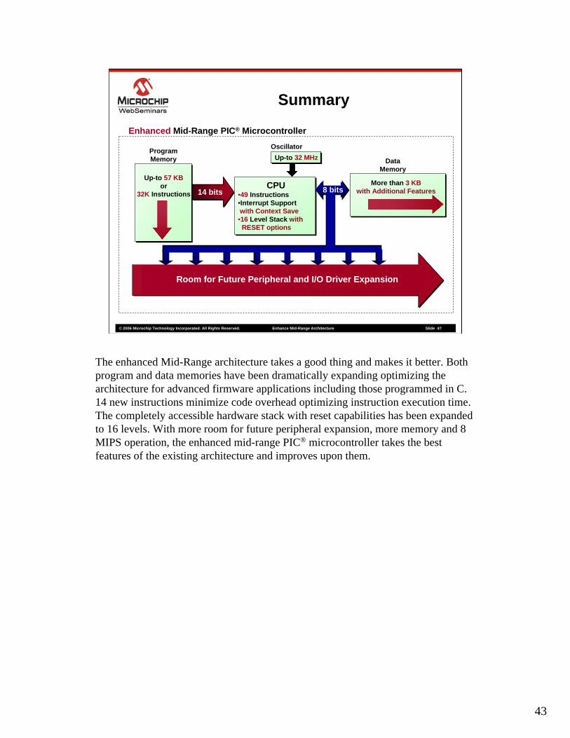
The enhanced Mid-Range architecture takes a good thing and makes it better. Both program and data memories have been dramatically expanding optimizing the architecture for advanced firmware applications including those programmed in C. 14 new instructions minimize code overhead optimizing instruction execution time. The completely accessible hardware stack with reset capabilities has been expanded to 16 levels. With more room for future peripheral expansion, more memory and 8 MIPS operation, the enhanced mid-range PIC® microcontroller takes the best features of the existing architecture and improves upon them.
44
© 2006 Microchip Technology Incorporated. All Rights Reserved. Enhance Mid-Range Architecture Slide 4444
Resources
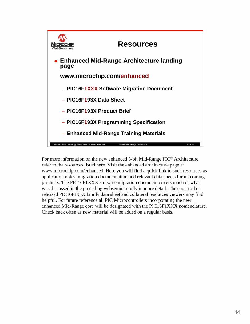
Enhanced Mid-Range Architecture landing pagewww.microchip.com/enhanced
− PIC16F1XXX Software Migration Document
− PIC16F193X Data Sheet
− PIC16F193X Product Brief
− PIC16F193X Programming Specification
− Enhanced Mid-Range Training Materials
For more information on the new enhanced 8-bit Mid-Range PIC® Architecture refer to the resources listed here. Visit the enhanced architecture page at www.microchip.com/enhanced. Here you will find a quick link to such resources as application notes, migration documentation and relevant data sheets for up coming products. The PIC16F1XXX software migration document covers much of what was discussed in the preceding webseminar only in more detail. The soon-to-be-released PIC16F193X family data sheet and collateral resources viewers may find helpful. For future reference all PIC Microcontrollers incorporating the new enhanced Mid-Range core will be designated with the PIC16F1XXX nomenclature. Check back often as new material will be added on a regular basis.

45
© 2006 Microchip Technology Incorporated. All Rights Reserved. Enhanced Mid-Range Architecture Slide 45
Thank You!
My name is Marc McComb, and I thank you for viewing this web seminar.
46
© 2006 Microchip Technology Incorporated. All Rights Reserved. Enhance Mid-Range Architecture Slide 4646
Trademarks
The Microchip name and logo, the Microchip logo, Accuron, dsPIC, KeeLoq, KeeLoq logo, MPLAB, PIC, PICmicro, PICSTART, rfPIC, SmartShunt and UNI/O are registered trademarks of Microchip Technology Incorporated in the U.S.A. and other countries.FilterLab, Linear Active Thermistor, MXDEV, MXLAB, SEEVAL, SmartSensor and The Embedded Control Solutions Company are registered trademarks of Microchip Technology Incorporated in the U.S.A.Analog-for-the-Digital Age, Application Maestro, CodeGuard, dsPICDEM, dsPICDEM.net, dsPICworks, dsSPEAK, ECAN, ECONOMONITOR, FanSense, In-Circuit Serial Programming, ICSP, ICEPIC, Mindi, MiWi, MPASM, MPLAB Certified logo, MPLIB, MPLINK, mTouch, PICkit, PICDEM, PICDEM.net, PICtail, PIC32 logo, PowerCal, PowerInfo, PowerMate,PowerTool, REAL ICE, rfLAB, Select Mode, Total Endurance, WiperLock and ZENA are trademarks of Microchip Technology Incorporated in the U.S.A. and other countries.SQTP is a service mark of Microchip Technology Incorporated in the U.S.A.All other trademarks mentioned herein are property of their respective companies.© 2008, Microchip Technology Incorporated, All Rights Reserved.
Related Documents