Intro to Chemical Vapor Deposition (CVD) in Semiconductor Fabrication www.intel.com Paul Otellini, Intel CEO and President (ca. 2012) is holding a 300 mm- diameter wafer of single-crystal Si that has been patterned with hundreds of identical integrated circuits. CVD is one process used in the production of the circuits. Questions? Contact Richard K. Herz, [email protected]

Welcome message from author
This document is posted to help you gain knowledge. Please leave a comment to let me know what you think about it! Share it to your friends and learn new things together.
Transcript

Intro to Chemical Vapor Deposition (CVD) in Semiconductor Fabrication
www.intel.com
Paul Otellini, Intel CEO and President (ca. 2012) is holding a 300 mm-diameter wafer of single-crystal Si that has been patterned with hundreds of identical integrated circuits. CVD is one process used in the production of the circuits.
Questions? Contact Richard K. Herz, [email protected]

Thin layers are patterned
www.intel.com
This is an enlarged cross section of a transistor circuit as a thin pattern of materials on the surface of a wafer. The horizontal dimension is on the order of 100's of nm. To the bottom is the bulk of the Si wafer. Layers such as SiO2 and polycrystalline Si are grown on the wafer and then patterned by photolithography. See Intel's From Sand to Silicon, The Making of a Chip <http://newsroom.intel.com/docs/DOC-2476>. Paper, colored ink and printing are to magazines as are Si wafers, elements such as B and P, and photolithography are to integrated circuits.

Thin layers are patterned
This is an enlarged cross section of a transistor circuit as a thin pattern of materials on the surface of a wafer. The horizontal dimension is on the order of 100's of nm. To the bottom is the bulk of the Si wafer. Layers such as SiO2 and polycrystalline Si are grown on the wafer and then patterned by photolithography. See Intel's From Sand to Silicon, The Making of a Chip <http://newsroom.intel.com/docs/DOC-2476>. Paper, colored ink and printing are to magazines as are Si wafers, elements such as B and P, and photolithography are to integrated circuits.

www.intel.com
As the technology improves, the dimensions of circuit elements keep getting smaller so they can pack more transistors per unit area over the wafer surface. "Frillier" software, haha! They must be referring to Microsoft Office's "ribbon."

Wafers are cut from single crystals
www.cnfolio.com
Si orginates by reducing "sand" (SiO2) by reaction with carbon. This makes relatively impure metallurgical grade Si. This is further purified by reacting the Si and C impurities with HCl, separating the resulting chloride gas products by distillation, and then decomposing them back to Si solid. This is then melted and a large cylindrical single crystal is pulled slowly from the melt in the Czochralski method.

Czochralski furnace
people.seas.harvard.edu/~jones/es154

Hanging by a thread!
www.gauss-centre.eu

www.jdisolar.com
www.missionsilicon.com

The large cylindrical single crystals of Si are cut into thin wafers with a wire saw and then polished.
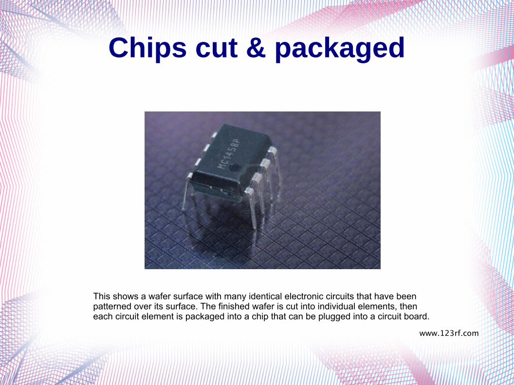
Chips cut & packaged
www.123rf.com
This shows a wafer surface with many identical electronic circuits that have been patterned over its surface. The finished wafer is cut into individual elements, then each circuit element is packaged into a chip that can be plugged into a circuit board.

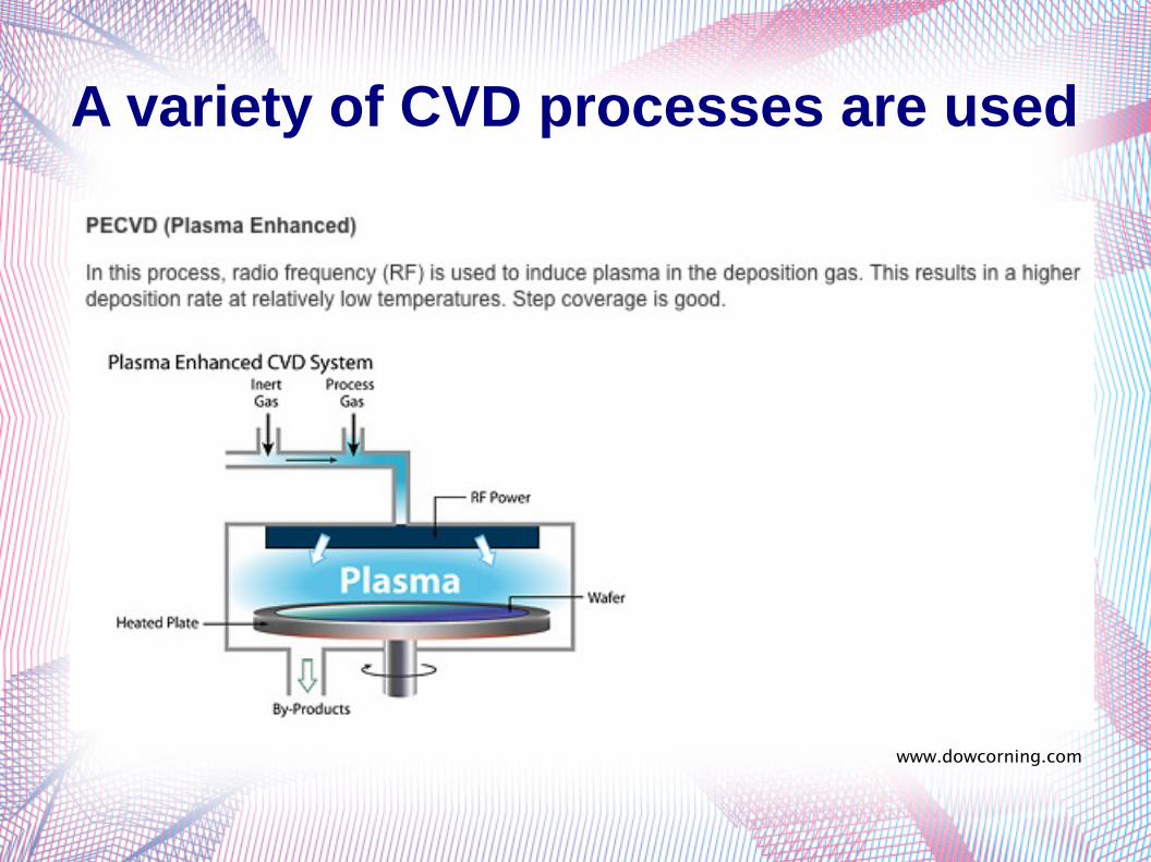
A variety of CVD processes are used
www.dowcorning.com
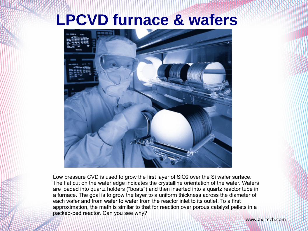
LPCVD furnace & wafers
www.axrtech.com
Low pressure CVD is used to grow the first layer of SiO2 over the Si wafer surface. The flat cut on the wafer edge indicates the crystalline orientation of the wafer. Wafers are loaded into quartz holders ("boats") and then inserted into a quartz reactor tube in a furnace. The goal is to grow the layer to a uniform thickness across the diameter of each wafer and from wafer to wafer from the reactor inlet to its outlet. To a first approximation, the math is similar to that for reaction over porous catalyst pellets in a packed-bed reactor. Can you see why?

www.dowcorning.com
A variety of CVD processes are used
www.dowcorning.com
A variety of CVD processes are used

www.dowcorning.com
A variety of CVD processes are used
Related Documents

![Chemical Vapor Deposition (CVD) - [email protected]: Home](https://static.cupdf.com/doc/110x72/61fb77462e268c58cd5e7f28/chemical-vapor-deposition-cvd-emailprotected-home.jpg)