INTRO | Hey there, thanks for buying this DIY-kit! We – Erica Synths and Moritz Klein – have developed it with one specific goal in mind: teaching people with little to no prior experience how to design analog synthesizer circuits from scratch. So what you’ll find in the box is not simply meant to be soldered together and then disappear in your rack. Instead, we want to take you through the circuit design process step by step, explaining every choice we’ve made and how it impacts the finished module. For that, we strongly suggest you follow along on a breadboard – which is a non-permanent circuit 1 prototyping tool that allows you to experiment and play around with your components. To help you with this, we’ve included a suggested breadboard layout in almost every chapter. Generally, this manual is intended to be read and worked through front-to-back, but there were a few things we felt should go into a dedicated appendix. These are general vignettes on electronic components & concepts, tools, and the process of putting the module together once you’re done experimenting. Feel free to check in there whenever you feel like you’re missing an important piece of information! TABLE OF CONTENTS CIRCUIT DESIGN CLOSE-UP …………………………………………………………….. 2 COMPONENTS & CONCEPTS APPENDIX ……………………………………………… 28 TOOLS APPENDIX ………………………………………………………………………….. 39 MODULE ASSEMBLY APPENDIX ………………………………………………………… 41 SOLDERING APPENDIX ……………………………………………………………………. 50 Note that there’s no breadboard included in this kit! You will also need a pack of jumper wires 1 and two 9V batteries with clips. These things are cheap & easy to find in your local electronics shop! 1

Welcome message from author
This document is posted to help you gain knowledge. Please leave a comment to let me know what you think about it! Share it to your friends and learn new things together.
Transcript
INTRO | Hey there, thanks for buying this DIY-kit! We – Erica Synths and Moritz Klein – have developed it with one specific goal in mind: teaching people with little to no prior experience how to design analog synthesizer circuits from scratch. So what you’ll find in the box is not simply meant to be soldered together and then disappear in your rack. Instead, we want to take you through the circuit design process step by step, explaining every choice we’ve made and how it impacts the finished module. For that, we strongly suggest you follow along on a breadboard – which is a non-permanent circuit 1
prototyping tool that allows you to experiment and play around with your components. To help you with this, we’ve included a suggested breadboard layout in almost every chapter.Generally, this manual is intended to be read and worked through front-to-back, but there were a few things we felt should go into a dedicated appendix. These are general vignettes on electronic components & concepts, tools, and the process of putting the module together once you’re done experimenting. Feel free to check in there whenever you feel like you’re missing an important piece of information!
TABLE OF CONTENTS CIRCUIT DESIGN CLOSE-UP …………………………………………………………….. 2COMPONENTS & CONCEPTS APPENDIX ……………………………………………… 28TOOLS APPENDIX ………………………………………………………………………….. 39MODULE ASSEMBLY APPENDIX ………………………………………………………… 41SOLDERING APPENDIX ……………………………………………………………………. 50
Note that there’s no breadboard included in this kit! You will also need a pack of jumper wires 1
and two 9V batteries with clips. These things are cheap & easy to find in your local electronics shop!
1
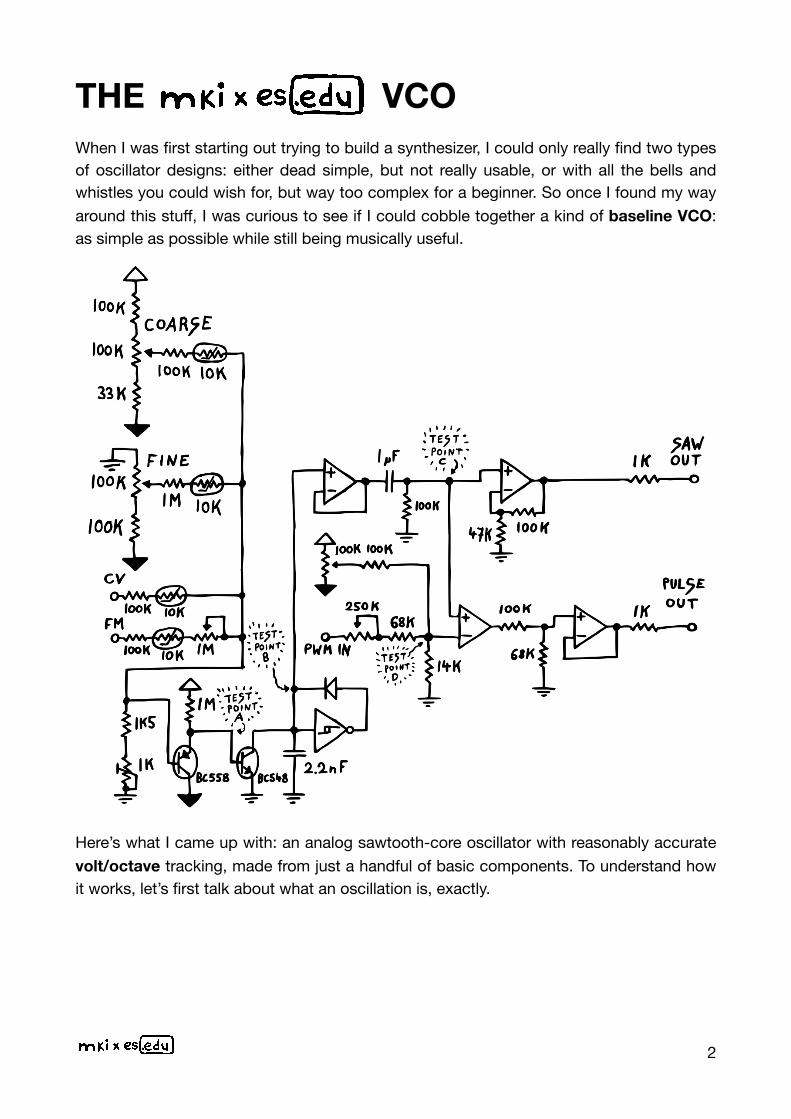
THE VCO When I was first starting out trying to build a synthesizer, I could only really find two types of oscillator designs: either dead simple, but not really usable, or with all the bells and whistles you could wish for, but way too complex for a beginner. So once I found my way around this stuff, I was curious to see if I could cobble together a kind of baseline VCO: as simple as possible while still being musically useful.
Here’s what I came up with: an analog sawtooth-core oscillator with reasonably accurate volt/octave tracking, made from just a handful of basic components. To understand how it works, let’s first talk about what an oscillation is, exactly.
2
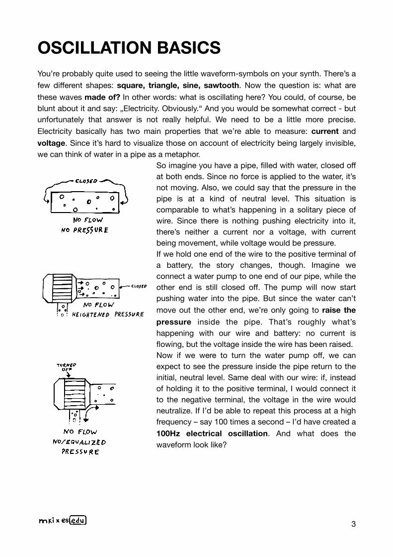
OSCILLATION BASICS You’re probably quite used to seeing the little waveform-symbols on your synth. There’s a few different shapes: square, triangle, sine, sawtooth. Now the question is: what are these waves made of? In other words: what is oscillating here? You could, of course, be blunt about it and say: „Electricity. Obviously.“ And you would be somewhat correct - but unfortunately that answer is not really helpful. We need to be a little more precise. Electricity basically has two main properties that we’re able to measure: current and voltage. Since it’s hard to visualize those on account of electricity being largely invisible, we can think of water in a pipe as a metaphor.
So imagine you have a pipe, filled with water, closed off at both ends. Since no force is applied to the water, it’s not moving. Also, we could say that the pressure in the pipe is at a kind of neutral level. This situation is comparable to what’s happening in a solitary piece of wire. Since there is nothing pushing electricity into it, there’s neither a current nor a voltage, with current being movement, while voltage would be pressure. If we hold one end of the wire to the positive terminal of a battery, the story changes, though. Imagine we connect a water pump to one end of our pipe, while the other end is still closed off. The pump will now start pushing water into the pipe. But since the water can’t move out the other end, we’re only going to raise the pressure inside the pipe. That’s roughly what’s happening with our wire and battery: no current is flowing, but the voltage inside the wire has been raised. Now if we were to turn the water pump off, we can expect to see the pressure inside the pipe return to the initial, neutral level. Same deal with our wire: if, instead of holding it to the positive terminal, I would connect it to the negative terminal, the voltage in the wire would neutralize. If I’d be able to repeat this process at a high frequency – say 100 times a second – I’d have created a 100Hz electrical oscillation. And what does the waveform look like?
3
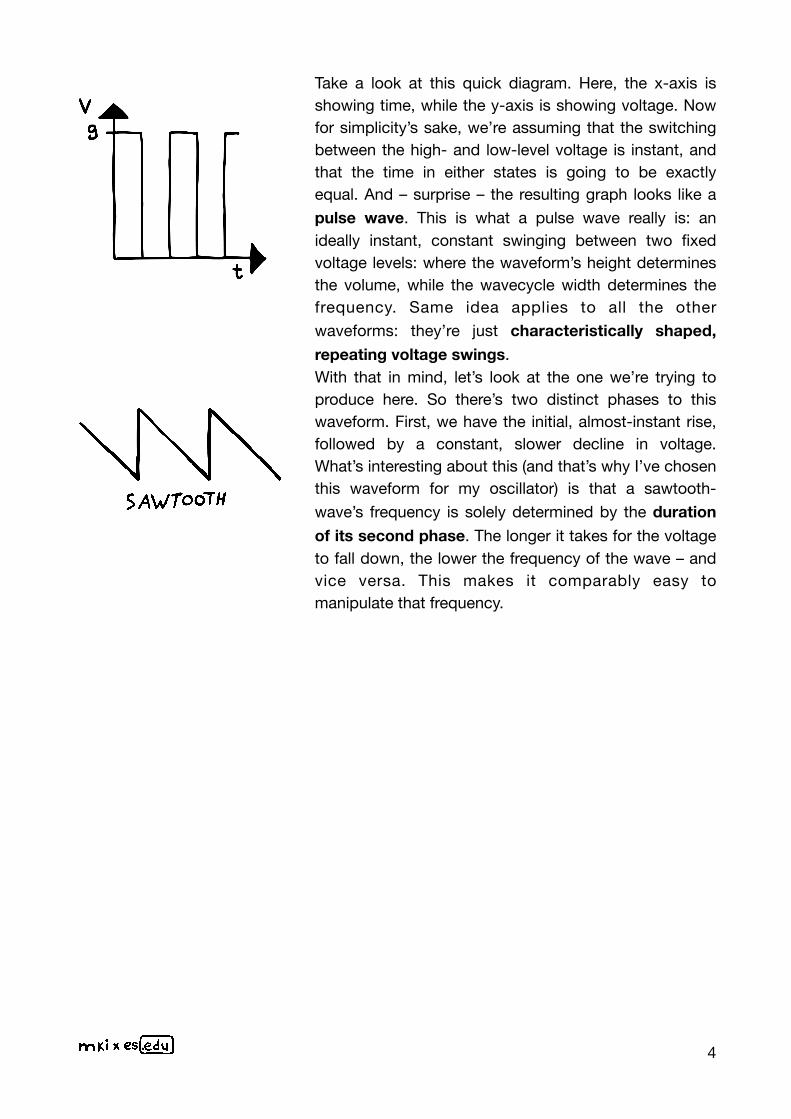
Take a look at this quick diagram. Here, the x-axis is showing time, while the y-axis is showing voltage. Now for simplicity’s sake, we’re assuming that the switching between the high- and low-level voltage is instant, and that the time in either states is going to be exactly equal. And – surprise – the resulting graph looks like a pulse wave. This is what a pulse wave really is: an ideally instant, constant swinging between two fixed voltage levels: where the waveform’s height determines the volume, while the wavecycle width determines the frequency. Same idea applies to all the other waveforms: they’re just characteristically shaped, repeating voltage swings. With that in mind, let’s look at the one we’re trying to produce here. So there’s two distinct phases to this waveform. First, we have the initial, almost-instant rise, followed by a constant, slower decline in voltage. What’s interesting about this (and that’s why I’ve chosen this waveform for my oscillator) is that a sawtooth-wave’s frequency is solely determined by the duration of its second phase. The longer it takes for the voltage to fall down, the lower the frequency of the wave – and vice versa. This makes it comparably easy to manipulate that frequency.
4
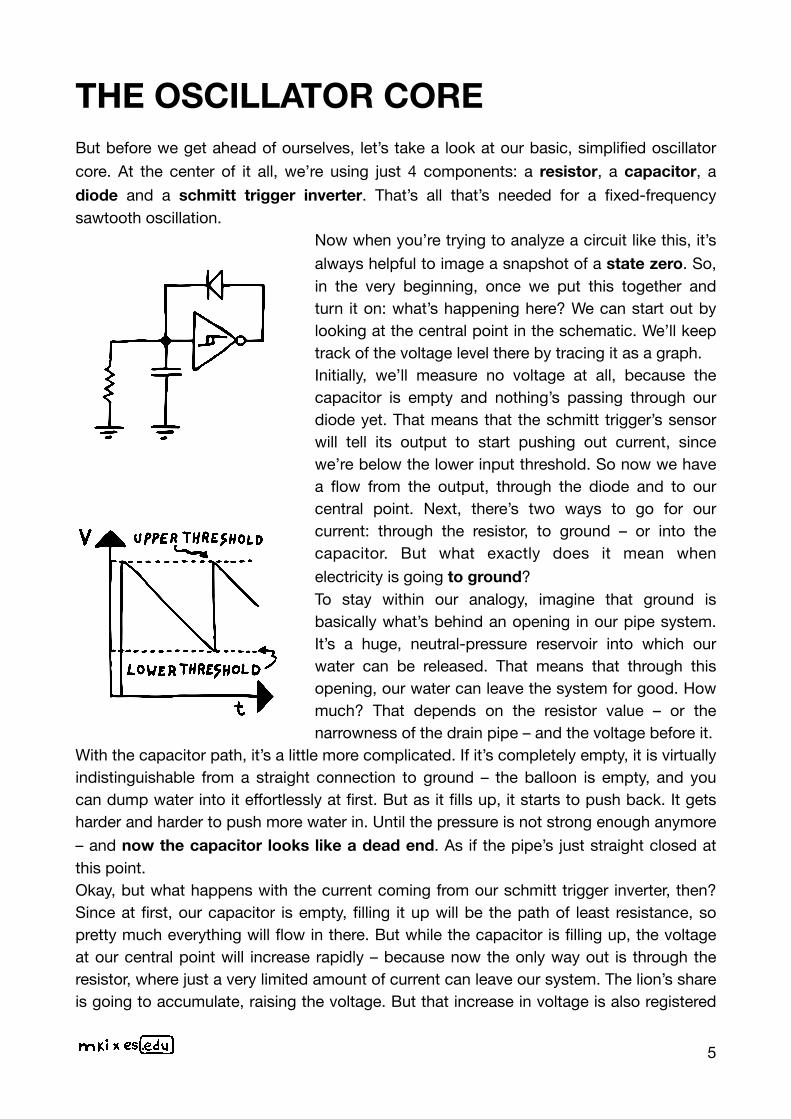
THE OSCILLATOR CORE But before we get ahead of ourselves, let’s take a look at our basic, simplified oscillator core. At the center of it all, we’re using just 4 components: a resistor, a capacitor, a diode and a schmitt trigger inverter. That’s all that’s needed for a fixed-frequency sawtooth oscillation.
Now when you’re trying to analyze a circuit like this, it’s always helpful to image a snapshot of a state zero. So, in the very beginning, once we put this together and turn it on: what’s happening here? We can start out by looking at the central point in the schematic. We’ll keep track of the voltage level there by tracing it as a graph. Initially, we’ll measure no voltage at all, because the capacitor is empty and nothing’s passing through our diode yet. That means that the schmitt trigger’s sensor will tell its output to start pushing out current, since we’re below the lower input threshold. So now we have a flow from the output, through the diode and to our central point. Next, there’s two ways to go for our current: through the resistor, to ground – or into the capacitor. But what exactly does it mean when electricity is going to ground?To stay within our analogy, imagine that ground is basically what’s behind an opening in our pipe system. It’s a huge, neutral-pressure reservoir into which our water can be released. That means that through this opening, our water can leave the system for good. How much? That depends on the resistor value – or the narrowness of the drain pipe – and the voltage before it.
With the capacitor path, it’s a little more complicated. If it’s completely empty, it is virtually indistinguishable from a straight connection to ground – the balloon is empty, and you can dump water into it effortlessly at first. But as it fills up, it starts to push back. It gets harder and harder to push more water in. Until the pressure is not strong enough anymore – and now the capacitor looks like a dead end. As if the pipe’s just straight closed at this point. Okay, but what happens with the current coming from our schmitt trigger inverter, then? Since at first, our capacitor is empty, filling it up will be the path of least resistance, so pretty much everything will flow in there. But while the capacitor is filling up, the voltage at our central point will increase rapidly – because now the only way out is through the resistor, where just a very limited amount of current can leave our system. The lion’s share is going to accumulate, raising the voltage. But that increase in voltage is also registered
5
by the schmitt trigger’s input – so as a reaction, the output will drop down to 0V once the capacitor is charged and the voltage passes the upper input threshold. This means that no additional current is being forced through the diode, which in turn means that our capacitor has no opposing force anymore. We’ve essentially stopped pushing water into it, so our balloon will push its contents back into the system. And where does the current go? It can’t go back into the schmitt trigger’s output, because the diode is blocking that. There’s only one pathway this time: through the resistor, to ground. But because that resistor is restricting the amount of current that can pass through, our capacitor won’t discharge instantly. It will take some time. So on the voltage graph, we’ll see a slow decline. This will keep going until we reach our schmitt trigger inverter’s lower threshold. Once we pass that on our way down, we’ll basically restart the cycle – because now the output will swing high again, and everything repeats. The capacitor will be charged, the output swings low, the capacitor discharges via our resistor. And so on. And that’s really all there is to a very basic sawtooth oscillation. But don’t take my word for it - get your breadboard and try it for yourself! If you’ve never used one before, I strongly suggest you watch my beginner’s guide to breadboards, which you can find on my YouTube-channel. 2
Here’s a direct link: https://youtu.be/XpMZoR3fgd02
6
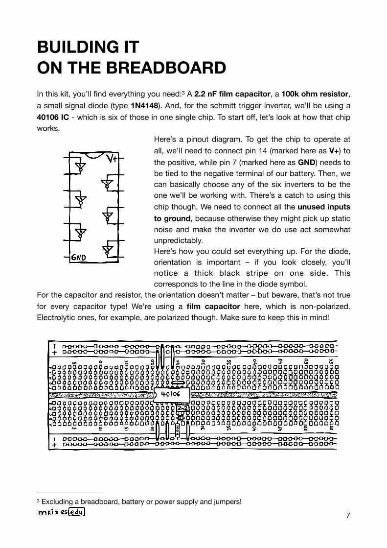
BUILDING IT ON THE BREADBOARD In this kit, you’ll find everything you need: A 2.2 nF film capacitor, a 100k ohm resistor, 3
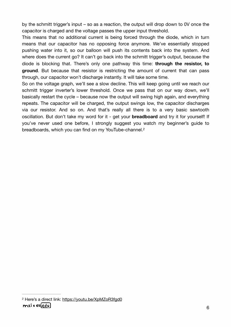
a small signal diode (type 1N4148). And, for the schmitt trigger inverter, we’ll be using a 40106 IC - which is six of those in one single chip. To start off, let’s look at how that chip works.
Here’s a pinout diagram. To get the chip to operate at all, we’ll need to connect pin 14 (marked here as V+) to the positive, while pin 7 (marked here as GND) needs to be tied to the negative terminal of our battery. Then, we can basically choose any of the six inverters to be the one we’ll be working with. There’s a catch to using this chip though. We need to connect all the unused inputs to ground, because otherwise they might pick up static noise and make the inverter we do use act somewhat unpredictably. Here’s how you could set everything up. For the diode, orientation is important – if you look closely, you’ll notice a thick black stripe on one side. This corresponds to the line in the diode symbol.
For the capacitor and resistor, the orientation doesn’t matter – but beware, that’s not true for every capacitor type! We’re using a film capacitor here, which is non-polarized. Electrolytic ones, for example, are polarized though. Make sure to keep this in mind!
Excluding a breadboard, battery or power supply and jumpers!3
7

If you’ve connected everything as shown here, the circuit should already be oscillating. But what good is an oscillator that you can’t hear? Right, so let’s figure out how to connect this to a sound system. Or headphones, whatever you prefer. You might be tempted to just attach an audio jack socket to where the diode, capacitor, resistor and schmitt trigger inverter meet. Generally, that’s going in the right direction, but unfortunately, it won’t work at all.Why? Because by connecting an audio jack there, we’re setting up another path for our proverbial water to flow into. That way, our capacitor is never being charged, because all of the current is leaving through the audio jack. So by trying to listen to the oscillation, we’re actively stopping it, because we’re tampering with oscillator’s core structure.
8
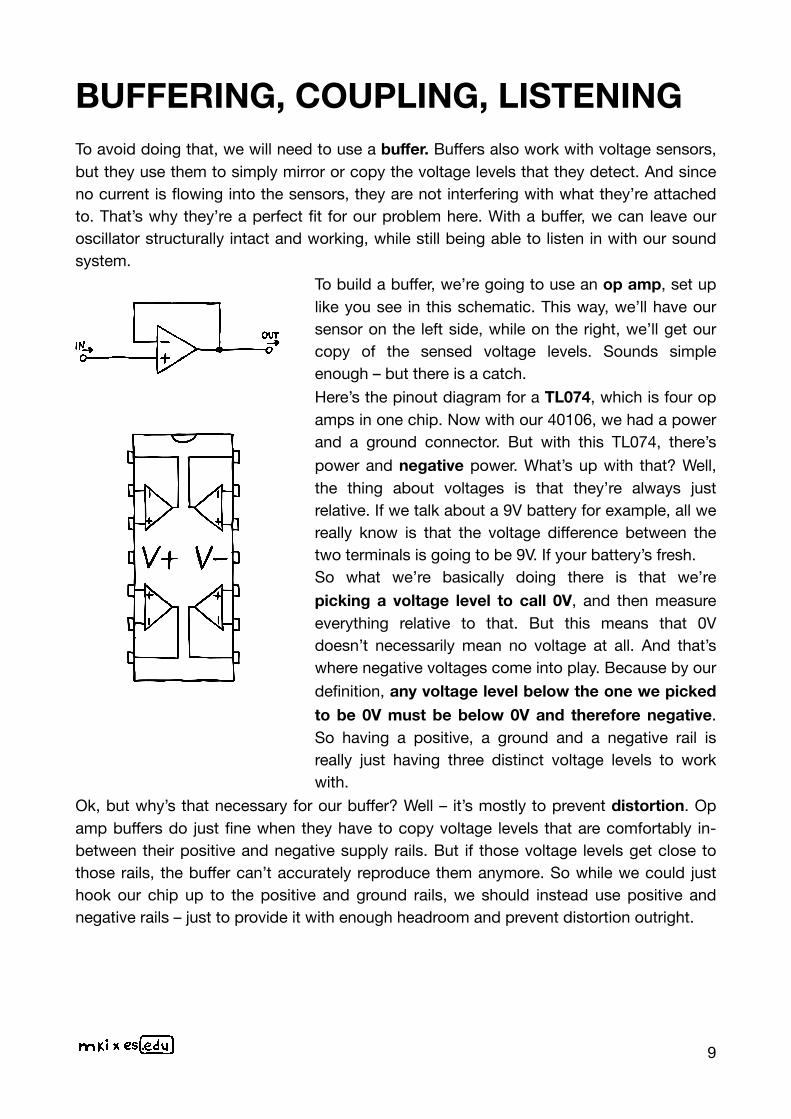
BUFFERING, COUPLING, LISTENING To avoid doing that, we will need to use a buffer. Buffers also work with voltage sensors, but they use them to simply mirror or copy the voltage levels that they detect. And since no current is flowing into the sensors, they are not interfering with what they’re attached to. That’s why they’re a perfect fit for our problem here. With a buffer, we can leave our oscillator structurally intact and working, while still being able to listen in with our sound system.
To build a buffer, we’re going to use an op amp, set up like you see in this schematic. This way, we’ll have our sensor on the left side, while on the right, we’ll get our copy of the sensed voltage levels. Sounds simple enough – but there is a catch. Here’s the pinout diagram for a TL074, which is four op amps in one chip. Now with our 40106, we had a power and a ground connector. But with this TL074, there’s power and negative power. What’s up with that? Well, the thing about voltages is that they’re always just relative. If we talk about a 9V battery for example, all we really know is that the voltage difference between the two terminals is going to be 9V. If your battery’s fresh. So what we’re basically doing there is that we’re picking a voltage level to call 0V, and then measure everything relative to that. But this means that 0V doesn’t necessarily mean no voltage at all. And that’s where negative voltages come into play. Because by our definition, any voltage level below the one we picked to be 0V must be below 0V and therefore negative. So having a positive, a ground and a negative rail is really just having three distinct voltage levels to work with.
Ok, but why’s that necessary for our buffer? Well – it’s mostly to prevent distortion. Op amp buffers do just fine when they have to copy voltage levels that are comfortably in-between their positive and negative supply rails. But if those voltage levels get close to those rails, the buffer can’t accurately reproduce them anymore. So while we could just hook our chip up to the positive and ground rails, we should instead use positive and negative rails – just to provide it with enough headroom and prevent distortion outright.
9
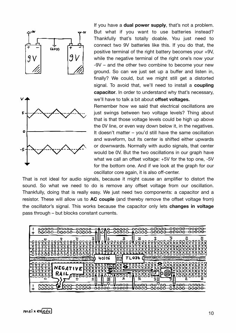
If you have a dual power supply, that’s not a problem. But what if you want to use batteries instead? Thankfully that’s totally doable. You just need to connect two 9V batteries like this. If you do that, the positive terminal of the right battery becomes your +9V, while the negative terminal of the right one’s now your -9V – and the other two combine to become your new ground. So can we just set up a buffer and listen in, finally? We could, but we might still get a distorted signal. To avoid that, we’ll need to install a coupling capacitor. In order to understand why that’s necessary, we’ll have to talk a bit about offset voltages. Remember how we said that electrical oscillations are just swings between two voltage levels? Thing about that is that those voltage levels could be high up above the 0V line, or even way down below it, in the negatives. It doesn’t matter – you’d still have the same oscillation and waveform, but its center is shifted either upwards or downwards. Normally with audio signals, that center would be 0V. But the two oscillations in our graph have what we call an offset voltage: +5V for the top one, -5V for the bottom one. And if we look at the graph for our oscillator core again, it is also off-center.
That is not ideal for audio signals, because it might cause an amplifier to distort the sound. So what we need to do is remove any offset voltage from our oscillation. Thankfully, doing that is really easy. We just need two components: a capacitor and a resistor. These will allow us to AC couple (and thereby remove the offset voltage from) the oscillator’s signal. This works because the capacitor only lets changes in voltage pass through – but blocks constant currents.
10
If you now hook up your oscilloscope to the output, you should see that our sawtooth is properly centered around the 0V line. Great! So now, we can finally listen in for the first time. Plug some cheap headphones into the audio jack socket, and you should be able to hear a very high-pitched tone.
11
CHANGING THE FREQUENCY Since that tone is pretty annoying, let’s talk about changing the oscillator’s frequency. Remember when I said that a sawtooth wave’s pitch is easy to manipulate – because it’s solely dependent on the wave’s second phase? That’s going to come in handy now, since that second phase is really just a capacitor discharging through a resistor. If it’s discharging fast, the pitch is high – if it’s discharging slow, the pitch is low. The speed of that discharging process is determined by exactly two factors: the capacitor’s size and the resistor’s strength. The bigger the balloon, the more water it can store, and the longer it takes to release that water. The tighter the drain pipe, the more it restricts the amount of water that can flow.Let’s try this out by first swapping the 2.2 nF capacitor for a 1 uF one. (That’s about 450 times bigger.) As you should be able to hear, the frequency is a lot lower – almost in the LFO range. Next, let’s swap the old capacitor back in and then switch our 100k drain resistor for a 1M. That’s 10 times bigger – and so the pitch doesn’t go down as much as before. So which route do we take – changing the capacitance or changing the resistance? To be honest, that’s pretty much a non-choice, because changing the capacitor can only be done manually – by taking the old one out and installing a new one. And that’s probably not the most fun way to make music. Which leaves us with only one true option: changing the resistance value. Here, we thankfully have way more options than just changing it by hand. We could use a light dependent resistor, where the resistance value depends on the amount of light that shines onto it. We could use a thermistor, which is the same idea but reacting to temperature instead.
But the classic idea would be to use a transistor as a constant current sink. Transistors are uniquely qualified here, because the relation between the voltage applied to their base and the current they allow to flow between collector and emitter is exponential. Why is this important? Because of the relation between musical notes and their assigned frequencies. Starting out with the lowest C, this note corresponds to a frequency of 16.35 Hz. Going up one octave means that for the next C, our frequency is doubled at around 32 Hz. One more octave, and the frequency doubles again. That means that the relationship between notes and frequencies is also an exponential one.
Since we’re trying to make our VCO conform to the volt/octave standard, we want to match voltages and frequencies like this: whenever the voltage increases by 1, our oscillator’s pitch should go up an octave. To achieve this, the relationship between voltage input and frequency output also needs to exponential, because we’re basically mapping voltages to musical notes. And because our oscillator’s pitch is determined by
12
how open our transistor is, it’s crucial that that transistor opens up exponentially as the voltage at its base increases linearly.
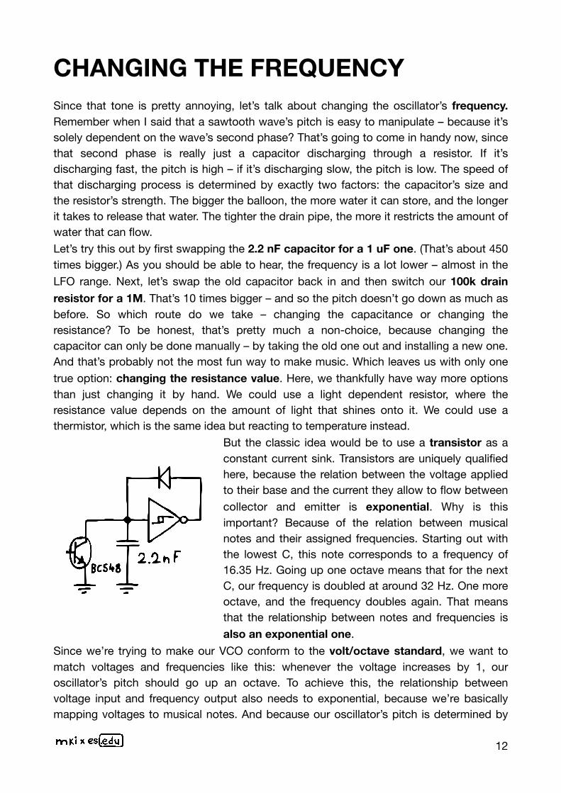
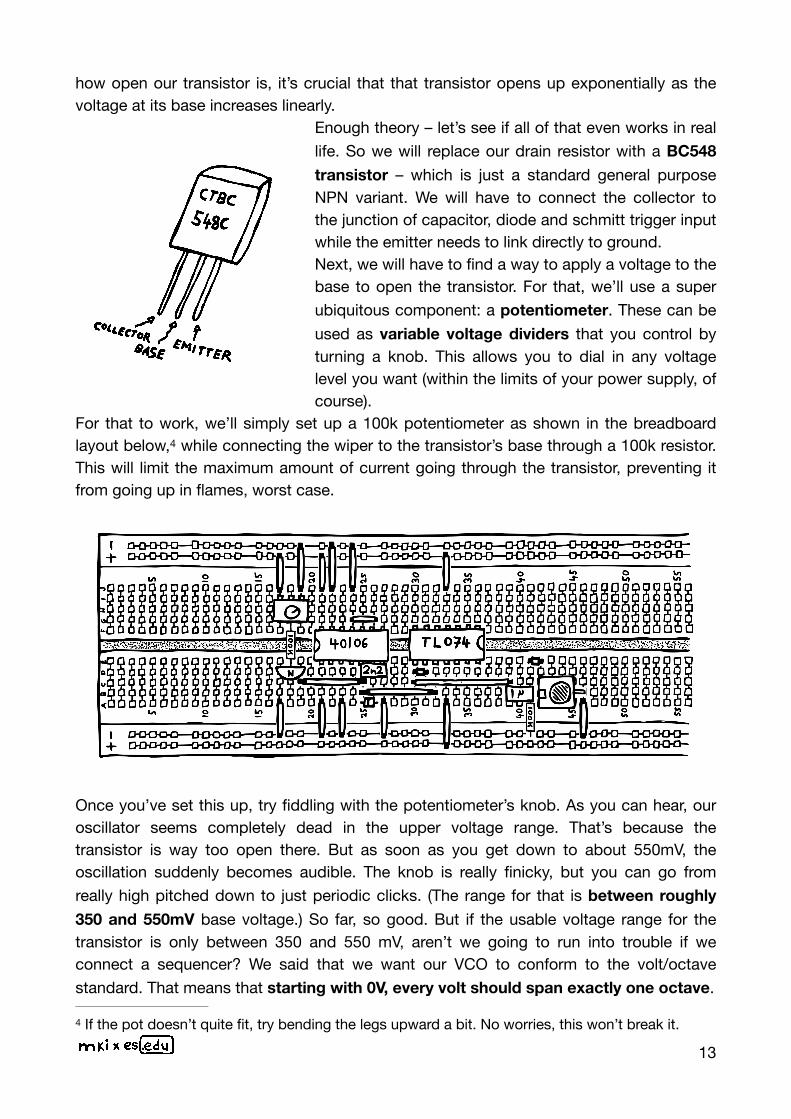
Enough theory – let’s see if all of that even works in real life. So we will replace our drain resistor with a BC548 transistor – which is just a standard general purpose NPN variant. We will have to connect the collector to the junction of capacitor, diode and schmitt trigger input while the emitter needs to link directly to ground. Next, we will have to find a way to apply a voltage to the base to open the transistor. For that, we’ll use a super ubiquitous component: a potentiometer. These can be used as variable voltage dividers that you control by turning a knob. This allows you to dial in any voltage level you want (within the limits of your power supply, of course).
For that to work, we’ll simply set up a 100k potentiometer as shown in the breadboard layout below, while connecting the wiper to the transistor’s base through a 100k resistor. 4
This will limit the maximum amount of current going through the transistor, preventing it from going up in flames, worst case.
Once you’ve set this up, try fiddling with the potentiometer’s knob. As you can hear, our oscillator seems completely dead in the upper voltage range. That’s because the transistor is way too open there. But as soon as you get down to about 550mV, the oscillation suddenly becomes audible. The knob is really finicky, but you can go from really high pitched down to just periodic clicks. (The range for that is between roughly 350 and 550mV base voltage.) So far, so good. But if the usable voltage range for the transistor is only between 350 and 550 mV, aren’t we going to run into trouble if we connect a sequencer? We said that we want our VCO to conform to the volt/octave standard. That means that starting with 0V, every volt should span exactly one octave.
If the pot doesn’t quite fit, try bending the legs upward a bit. No worries, this won’t break it.4
13
SEQUENCES, SCALING AND OFFSETS
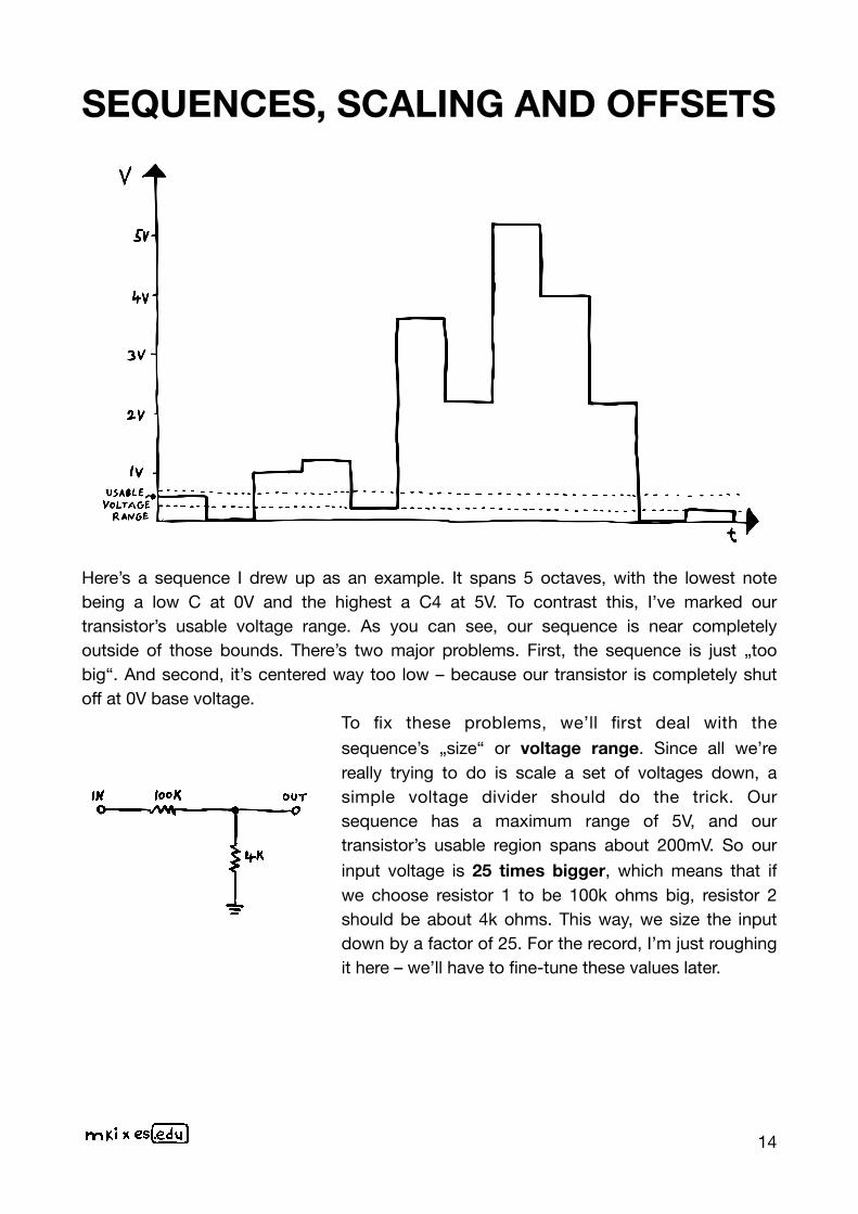
Here’s a sequence I drew up as an example. It spans 5 octaves, with the lowest note being a low C at 0V and the highest a C4 at 5V. To contrast this, I’ve marked our transistor’s usable voltage range. As you can see, our sequence is near completely outside of those bounds. There’s two major problems. First, the sequence is just „too big“. And second, it’s centered way too low – because our transistor is completely shut off at 0V base voltage.
To fix these problems, we’ll first deal with the sequence’s „size“ or voltage range. Since all we’re really trying to do is scale a set of voltages down, a simple voltage divider should do the trick. Our sequence has a maximum range of 5V, and our transistor’s usable region spans about 200mV. So our input voltage is 25 times bigger, which means that if we choose resistor 1 to be 100k ohms big, resistor 2 should be about 4k ohms. This way, we size the input down by a factor of 25. For the record, I’m just roughing it here – we’ll have to fine-tune these values later.
14
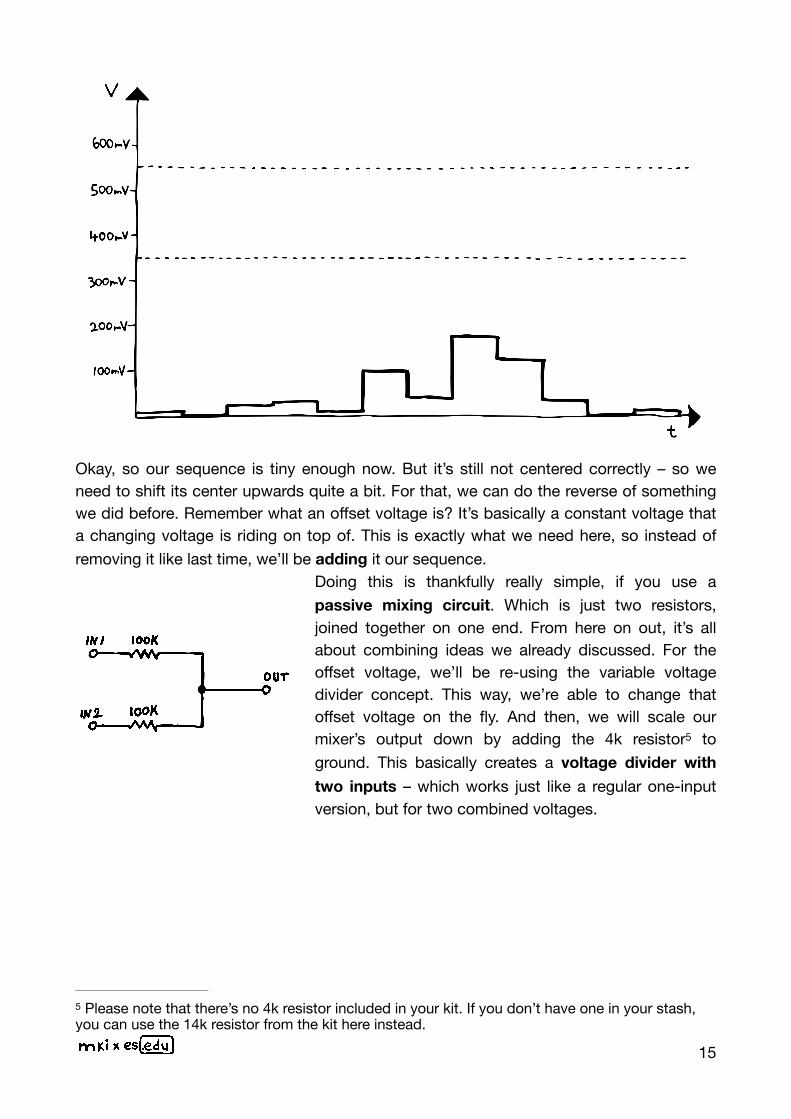
Okay, so our sequence is tiny enough now. But it’s still not centered correctly – so we need to shift its center upwards quite a bit. For that, we can do the reverse of something we did before. Remember what an offset voltage is? It’s basically a constant voltage that a changing voltage is riding on top of. This is exactly what we need here, so instead of removing it like last time, we’ll be adding it our sequence.
Doing this is thankfully really simple, if you use a passive mixing circuit. Which is just two resistors, joined together on one end. From here on out, it’s all about combining ideas we already discussed. For the offset voltage, we’ll be re-using the variable voltage divider concept. This way, we’re able to change that offset voltage on the fly. And then, we will scale our mixer’s output down by adding the 4k resistor to 5
ground. This basically creates a voltage divider with two inputs – which works just like a regular one-input version, but for two combined voltages.
Please note that there’s no 4k resistor included in your kit. If you don’t have one in your stash, 5
you can use the 14k resistor from the kit here instead.
15
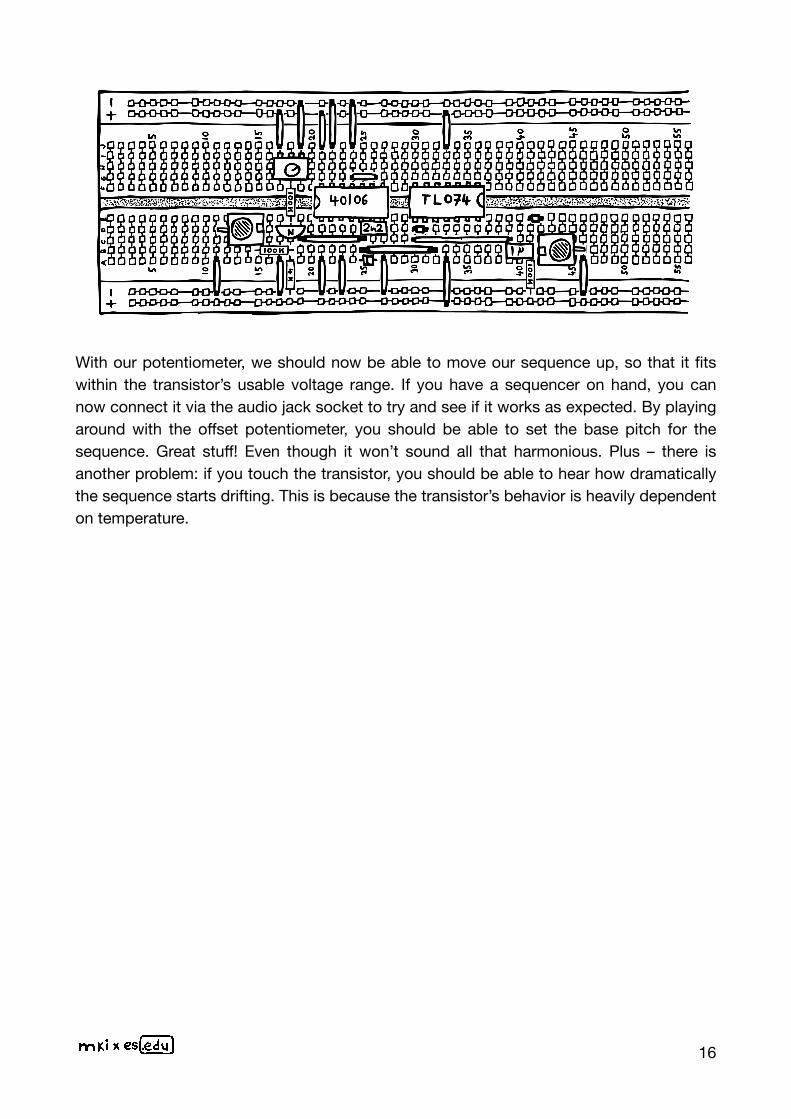
With our potentiometer, we should now be able to move our sequence up, so that it fits within the transistor’s usable voltage range. If you have a sequencer on hand, you can now connect it via the audio jack socket to try and see if it works as expected. By playing around with the offset potentiometer, you should be able to set the base pitch for the sequence. Great stuff! Even though it won’t sound all that harmonious. Plus – there is another problem: if you touch the transistor, you should be able to hear how dramatically the sequence starts drifting. This is because the transistor’s behavior is heavily dependent on temperature.
16
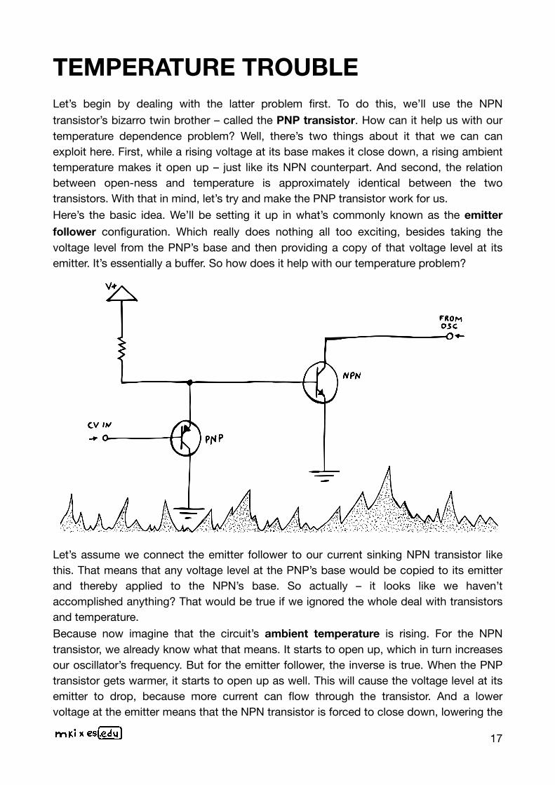
TEMPERATURE TROUBLE Let’s begin by dealing with the latter problem first. To do this, we’ll use the NPN transistor’s bizarro twin brother – called the PNP transistor. How can it help us with our temperature dependence problem? Well, there’s two things about it that we can can exploit here. First, while a rising voltage at its base makes it close down, a rising ambient temperature makes it open up – just like its NPN counterpart. And second, the relation between open-ness and temperature is approximately identical between the two transistors. With that in mind, let’s try and make the PNP transistor work for us. Here’s the basic idea. We’ll be setting it up in what’s commonly known as the emitter follower configuration. Which really does nothing all too exciting, besides taking the voltage level from the PNP’s base and then providing a copy of that voltage level at its emitter. It’s essentially a buffer. So how does it help with our temperature problem?
Let’s assume we connect the emitter follower to our current sinking NPN transistor like this. That means that any voltage level at the PNP’s base would be copied to its emitter and thereby applied to the NPN’s base. So actually – it looks like we haven’t accomplished anything? That would be true if we ignored the whole deal with transistors and temperature. Because now imagine that the circuit’s ambient temperature is rising. For the NPN transistor, we already know what that means. It starts to open up, which in turn increases our oscillator’s frequency. But for the emitter follower, the inverse is true. When the PNP transistor gets warmer, it starts to open up as well. This will cause the voltage level at its emitter to drop, because more current can flow through the transistor. And a lower voltage at the emitter means that the NPN transistor is forced to close down, lowering the
17
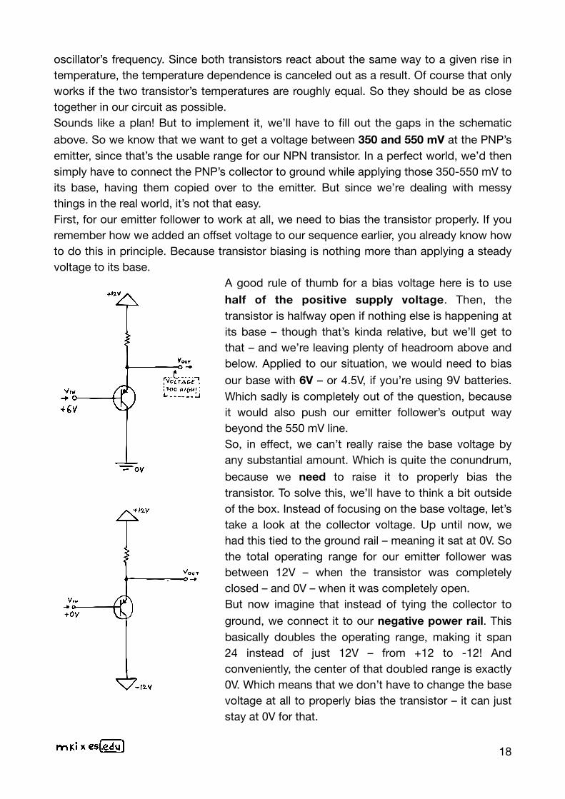
oscillator’s frequency. Since both transistors react about the same way to a given rise in temperature, the temperature dependence is canceled out as a result. Of course that only works if the two transistor’s temperatures are roughly equal. So they should be as close together in our circuit as possible. Sounds like a plan! But to implement it, we’ll have to fill out the gaps in the schematic above. So we know that we want to get a voltage between 350 and 550 mV at the PNP’s emitter, since that’s the usable range for our NPN transistor. In a perfect world, we’d then simply have to connect the PNP’s collector to ground while applying those 350-550 mV to its base, having them copied over to the emitter. But since we’re dealing with messy things in the real world, it’s not that easy. First, for our emitter follower to work at all, we need to bias the transistor properly. If you remember how we added an offset voltage to our sequence earlier, you already know how to do this in principle. Because transistor biasing is nothing more than applying a steady voltage to its base.
A good rule of thumb for a bias voltage here is to use half of the positive supply voltage. Then, the transistor is halfway open if nothing else is happening at its base – though that’s kinda relative, but we’ll get to that – and we’re leaving plenty of headroom above and below. Applied to our situation, we would need to bias our base with 6V – or 4.5V, if you’re using 9V batteries. Which sadly is completely out of the question, because it would also push our emitter follower’s output way beyond the 550 mV line. So, in effect, we can’t really raise the base voltage by any substantial amount. Which is quite the conundrum, because we need to raise it to properly bias the transistor. To solve this, we’ll have to think a bit outside of the box. Instead of focusing on the base voltage, let’s take a look at the collector voltage. Up until now, we had this tied to the ground rail – meaning it sat at 0V. So the total operating range for our emitter follower was between 12V – when the transistor was completely closed – and 0V – when it was completely open. But now imagine that instead of tying the collector to ground, we connect it to our negative power rail. This basically doubles the operating range, making it span 24 instead of just 12V – from +12 to -12! And conveniently, the center of that doubled range is exactly 0V. Which means that we don’t have to change the base voltage at all to properly bias the transistor – it can just stay at 0V for that.
18
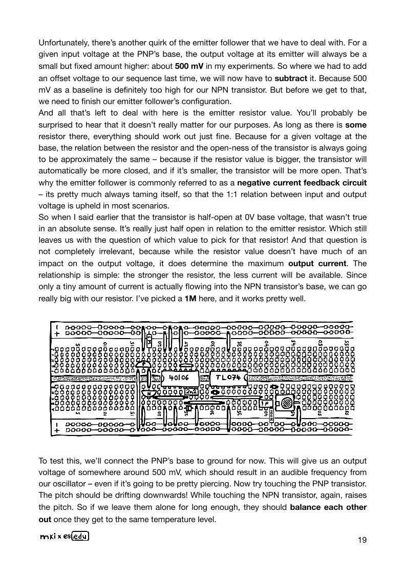
Unfortunately, there’s another quirk of the emitter follower that we have to deal with. For a given input voltage at the PNP’s base, the output voltage at its emitter will always be a small but fixed amount higher: about 500 mV in my experiments. So where we had to add an offset voltage to our sequence last time, we will now have to subtract it. Because 500 mV as a baseline is definitely too high for our NPN transistor. But before we get to that, we need to finish our emitter follower’s configuration.And all that’s left to deal with here is the emitter resistor value. You’ll probably be surprised to hear that it doesn’t really matter for our purposes. As long as there is some resistor there, everything should work out just fine. Because for a given voltage at the base, the relation between the resistor and the open-ness of the transistor is always going to be approximately the same – because if the resistor value is bigger, the transistor will automatically be more closed, and if it’s smaller, the transistor will be more open. That’s why the emitter follower is commonly referred to as a negative current feedback circuit – its pretty much always taming itself, so that the 1:1 relation between input and output voltage is upheld in most scenarios. So when I said earlier that the transistor is half-open at 0V base voltage, that wasn’t true in an absolute sense. It’s really just half open in relation to the emitter resistor. Which still leaves us with the question of which value to pick for that resistor! And that question is not completely irrelevant, because while the resistor value doesn’t have much of an impact on the output voltage, it does determine the maximum output current. The relationship is simple: the stronger the resistor, the less current will be available. Since only a tiny amount of current is actually flowing into the NPN transistor’s base, we can go really big with our resistor. I’ve picked a 1M here, and it works pretty well.
To test this, we’ll connect the PNP’s base to ground for now. This will give us an output voltage of somewhere around 500 mV, which should result in an audible frequency from our oscillator – even if it’s going to be pretty piercing. Now try touching the PNP transistor.The pitch should be drifting downwards! While touching the NPN transistor, again, raises the pitch. So if we leave them alone for long enough, they should balance each other out once they get to the same temperature level.
19
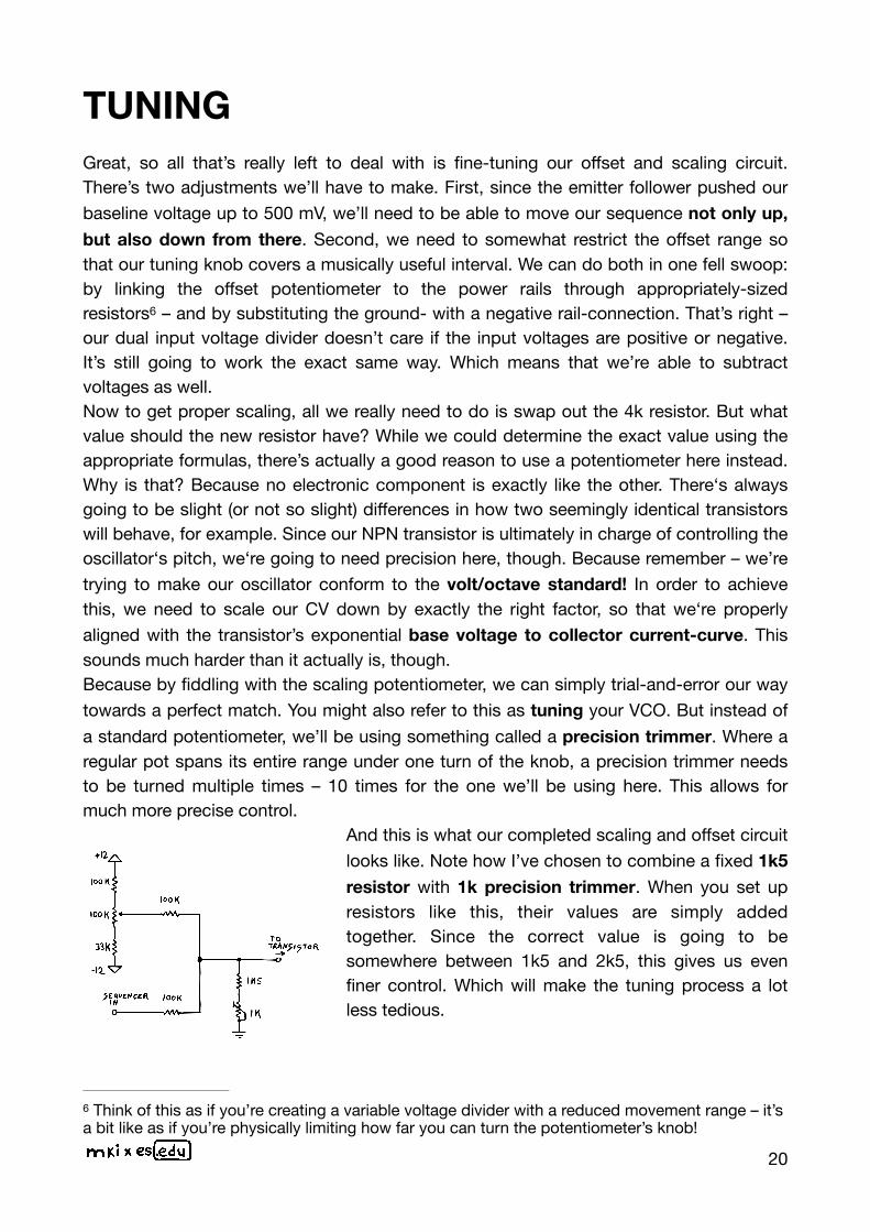
TUNING Great, so all that’s really left to deal with is fine-tuning our offset and scaling circuit. There’s two adjustments we’ll have to make. First, since the emitter follower pushed our baseline voltage up to 500 mV, we’ll need to be able to move our sequence not only up, but also down from there. Second, we need to somewhat restrict the offset range so that our tuning knob covers a musically useful interval. We can do both in one fell swoop: by linking the offset potentiometer to the power rails through appropriately-sized resistors – and by substituting the ground- with a negative rail-connection. That’s right – 6
our dual input voltage divider doesn’t care if the input voltages are positive or negative. It’s still going to work the exact same way. Which means that we’re able to subtract voltages as well.Now to get proper scaling, all we really need to do is swap out the 4k resistor. But what value should the new resistor have? While we could determine the exact value using the appropriate formulas, there’s actually a good reason to use a potentiometer here instead. Why is that? Because no electronic component is exactly like the other. There‘s always going to be slight (or not so slight) differences in how two seemingly identical transistors will behave, for example. Since our NPN transistor is ultimately in charge of controlling the oscillator‘s pitch, we‘re going to need precision here, though. Because remember – we’re trying to make our oscillator conform to the volt/octave standard! In order to achieve this, we need to scale our CV down by exactly the right factor, so that we‘re properly aligned with the transistor’s exponential base voltage to collector current-curve. This sounds much harder than it actually is, though.Because by fiddling with the scaling potentiometer, we can simply trial-and-error our way towards a perfect match. You might also refer to this as tuning your VCO. But instead of a standard potentiometer, we’ll be using something called a precision trimmer. Where a regular pot spans its entire range under one turn of the knob, a precision trimmer needs to be turned multiple times – 10 times for the one we’ll be using here. This allows for much more precise control.
And this is what our completed scaling and offset circuit looks like. Note how I’ve chosen to combine a fixed 1k5 resistor with 1k precision trimmer. When you set up resistors like this, their values are simply added together. Since the correct value is going to be somewhere between 1k5 and 2k5, this gives us even finer control. Which will make the tuning process a lot less tedious.
Think of this as if you’re creating a variable voltage divider with a reduced movement range – it’s 6
a bit like as if you’re physically limiting how far you can turn the potentiometer’s knob!
20
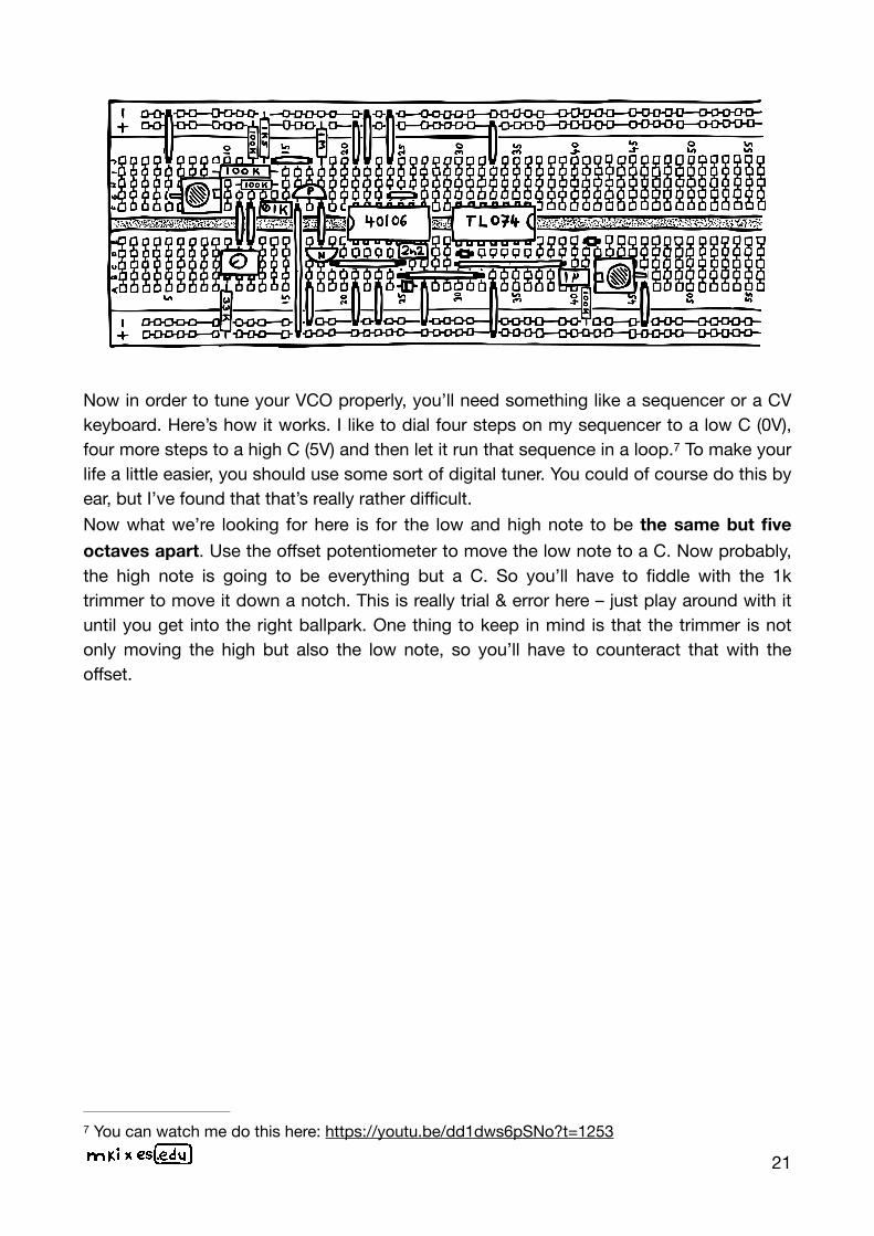
Now in order to tune your VCO properly, you’ll need something like a sequencer or a CV keyboard. Here’s how it works. I like to dial four steps on my sequencer to a low C (0V), four more steps to a high C (5V) and then let it run that sequence in a loop. To make your 7
life a little easier, you should use some sort of digital tuner. You could of course do this by ear, but I’ve found that that’s really rather difficult.Now what we’re looking for here is for the low and high note to be the same but five octaves apart. Use the offset potentiometer to move the low note to a C. Now probably, the high note is going to be everything but a C. So you’ll have to fiddle with the 1k trimmer to move it down a notch. This is really trial & error here – just play around with it until you get into the right ballpark. One thing to keep in mind is that the trimmer is not only moving the high but also the low note, so you’ll have to counteract that with the offset.
You can watch me do this here: https://youtu.be/dd1dws6pSNo?t=12537
21
TEMPERATURE TROUBLE … AGAIN? Once you get it to be acceptably in tune, you should be able to play sequences from any sequencer. Great! But before we move on to the next part – waveshaping –, there’s one final step we’ll have to take to minimize temperature dependence. Unfortunately, the theory behind this step is somewhat complicated (it involves the infamous ebers-moll-equation), so you’ll have to do some research of your own if you really want to understand it. But the basic gist is that in order to really get rid of temperature dependence, the resistance after our external CV input needs to be tied to ambient temperature as well. More specifically, it needs to decrease with a rising temperature.
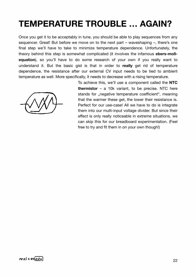
To achieve this, we’ll use a component called the NTC thermistor – a 10k variant, to be precise. NTC here stands for „negative temperature coefficient“, meaning that the warmer these get, the lower their resistance is. Perfect for our use-case! All we have to do is integrate them into our multi-input voltage divider. But since their effect is only really noticeable in extreme situations, we can skip this for our breadboard experimentation. (Feel free to try and fit them in on your own though!)
22
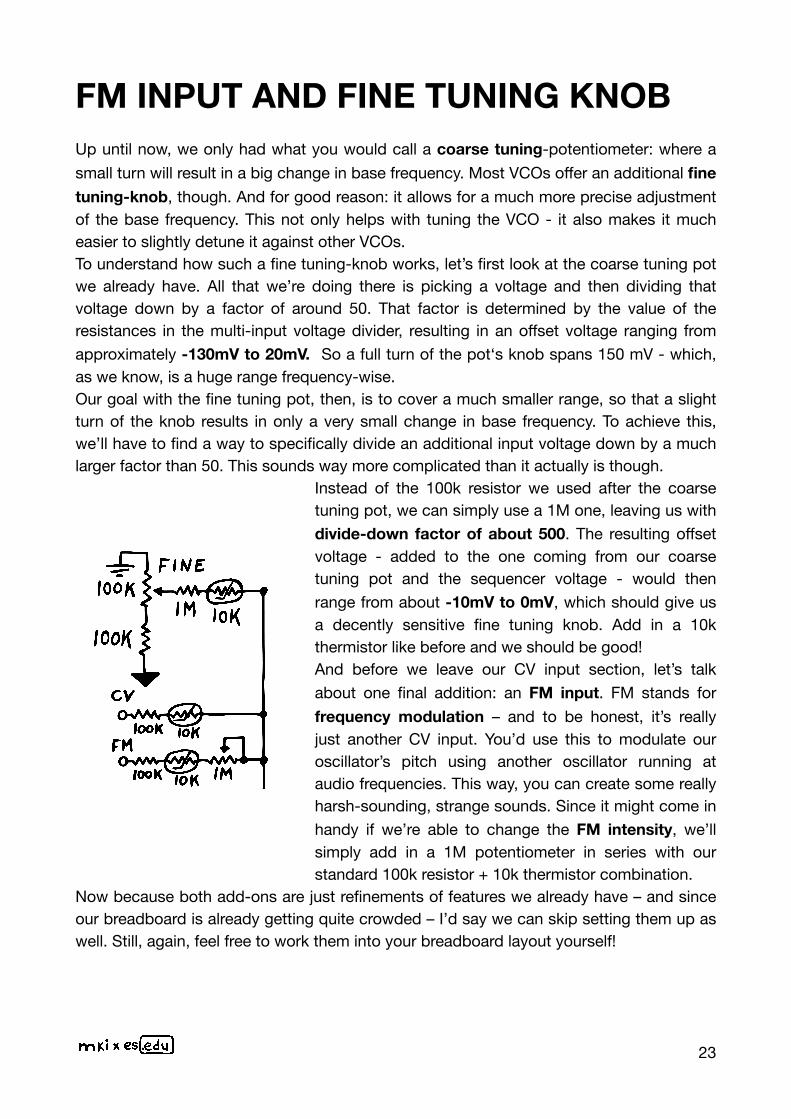
FM INPUT AND FINE TUNING KNOB Up until now, we only had what you would call a coarse tuning-potentiometer: where a small turn will result in a big change in base frequency. Most VCOs offer an additional fine tuning-knob, though. And for good reason: it allows for a much more precise adjustment of the base frequency. This not only helps with tuning the VCO - it also makes it much easier to slightly detune it against other VCOs.To understand how such a fine tuning-knob works, let’s first look at the coarse tuning pot we already have. All that we’re doing there is picking a voltage and then dividing that voltage down by a factor of around 50. That factor is determined by the value of the resistances in the multi-input voltage divider, resulting in an offset voltage ranging from approximately -130mV to 20mV. So a full turn of the pot‘s knob spans 150 mV - which, as we know, is a huge range frequency-wise. Our goal with the fine tuning pot, then, is to cover a much smaller range, so that a slight turn of the knob results in only a very small change in base frequency. To achieve this, we’ll have to find a way to specifically divide an additional input voltage down by a much larger factor than 50. This sounds way more complicated than it actually is though.
Instead of the 100k resistor we used after the coarse tuning pot, we can simply use a 1M one, leaving us with divide-down factor of about 500. The resulting offset voltage - added to the one coming from our coarse tuning pot and the sequencer voltage - would then range from about -10mV to 0mV, which should give us a decently sensitive fine tuning knob. Add in a 10k thermistor like before and we should be good!And before we leave our CV input section, let’s talk about one final addition: an FM input. FM stands for frequency modulation – and to be honest, it’s really just another CV input. You’d use this to modulate our oscillator’s pitch using another oscillator running at audio frequencies. This way, you can create some really harsh-sounding, strange sounds. Since it might come in handy if we’re able to change the FM intensity, we’ll simply add in a 1M potentiometer in series with our standard 100k resistor + 10k thermistor combination.
Now because both add-ons are just refinements of features we already have – and since our breadboard is already getting quite crowded – I’d say we can skip setting them up as well. Still, again, feel free to work them into your breadboard layout yourself!
23
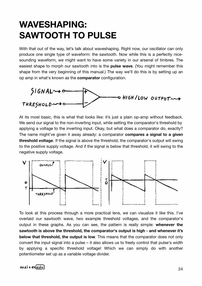
WAVESHAPING: SAWTOOTH TO PULSE With that out of the way, let’s talk about waveshaping. Right now, our oscillator can only produce one single type of waveform: the sawtooth. Now while this is a perfectly nice-sounding waveform, we might want to have some variety in our arsenal of timbres. The easiest shape to morph our sawtooth into is the pulse wave. (You might remember this shape from the very beginning of this manual.) The way we’ll do this is by setting up an op amp in what‘s known as the comparator configuration.
At its most basic, this is what that looks like: it’s just a plain op-amp without feedback. We send our signal to the non-inverting input, while setting the comparator‘s threshold by applying a voltage to the inverting input. Okay, but what does a comparator do, exactly?The name might’ve given it away already: a comparator compares a signal to a given threshold voltage. If the signal is above the threshold, the comparator‘s output will swing to the positive supply voltage. And if the signal is below that threshold, it will swing to the negative supply voltage.
To look at this process through a more practical lens, we can visualize it like this. I‘ve overlaid our sawtooth wave, two example threshold voltages, and the comparator‘s output in these graphs. As you can see, the pattern is really simple: whenever the sawtooth is above the threshold, the comparator‘s output is high - and whenever it’s below that threshold, the output is low. This means that the comparator does not only convert the input signal into a pulse – it also allows us to freely control that pulse‘s width by applying a specific threshold voltage! Which we can simply do with another potentiometer set up as a variable voltage divider.
24
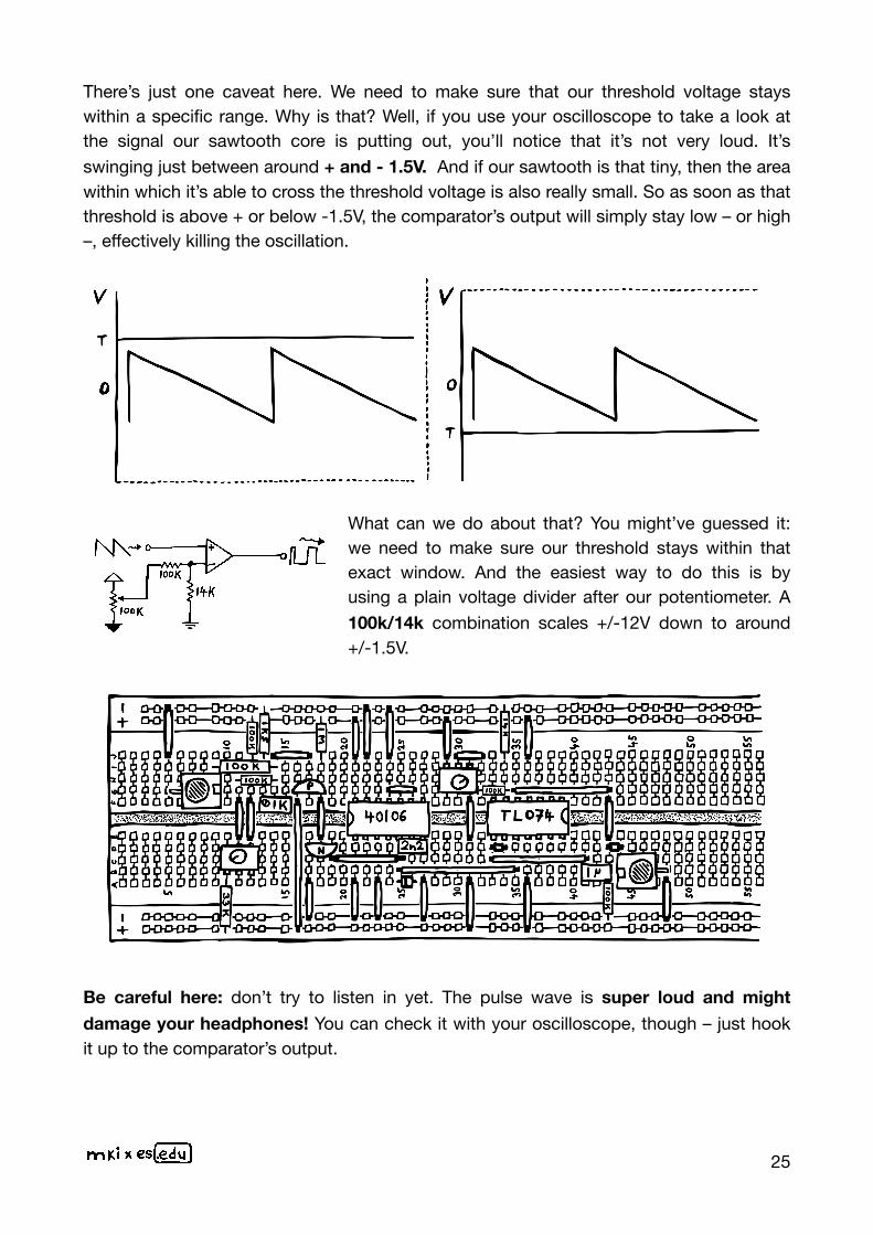
There’s just one caveat here. We need to make sure that our threshold voltage stays within a specific range. Why is that? Well, if you use your oscilloscope to take a look at the signal our sawtooth core is putting out, you’ll notice that it’s not very loud. It’s swinging just between around + and - 1.5V. And if our sawtooth is that tiny, then the area within which it’s able to cross the threshold voltage is also really small. So as soon as that threshold is above + or below -1.5V, the comparator’s output will simply stay low – or high –, effectively killing the oscillation.
What can we do about that? You might’ve guessed it: we need to make sure our threshold stays within that exact window. And the easiest way to do this is by using a plain voltage divider after our potentiometer. A 100k/14k combination scales +/-12V down to around +/-1.5V.
Be careful here: don’t try to listen in yet. The pulse wave is super loud and might damage your headphones! You can check it with your oscilloscope, though – just hook it up to the comparator’s output.
25
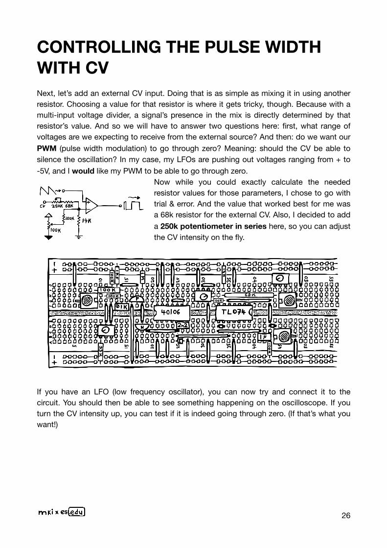
CONTROLLING THE PULSE WIDTH WITH CV Next, let’s add an external CV input. Doing that is as simple as mixing it in using another resistor. Choosing a value for that resistor is where it gets tricky, though. Because with a multi-input voltage divider, a signal’s presence in the mix is directly determined by that resistor’s value. And so we will have to answer two questions here: first, what range of voltages are we expecting to receive from the external source? And then: do we want our PWM (pulse width modulation) to go through zero? Meaning: should the CV be able to silence the oscillation? In my case, my LFOs are pushing out voltages ranging from + to -5V, and I would like my PWM to be able to go through zero.
Now while you could exactly calculate the needed resistor values for those parameters, I chose to go with trial & error. And the value that worked best for me was a 68k resistor for the external CV. Also, I decided to add a 250k potentiometer in series here, so you can adjust the CV intensity on the fly.
If you have an LFO (low frequency oscillator), you can now try and connect it to the circuit. You should then be able to see something happening on the oscilloscope. If you turn the CV intensity up, you can test if it is indeed going through zero. (If that’s what you want!)
26
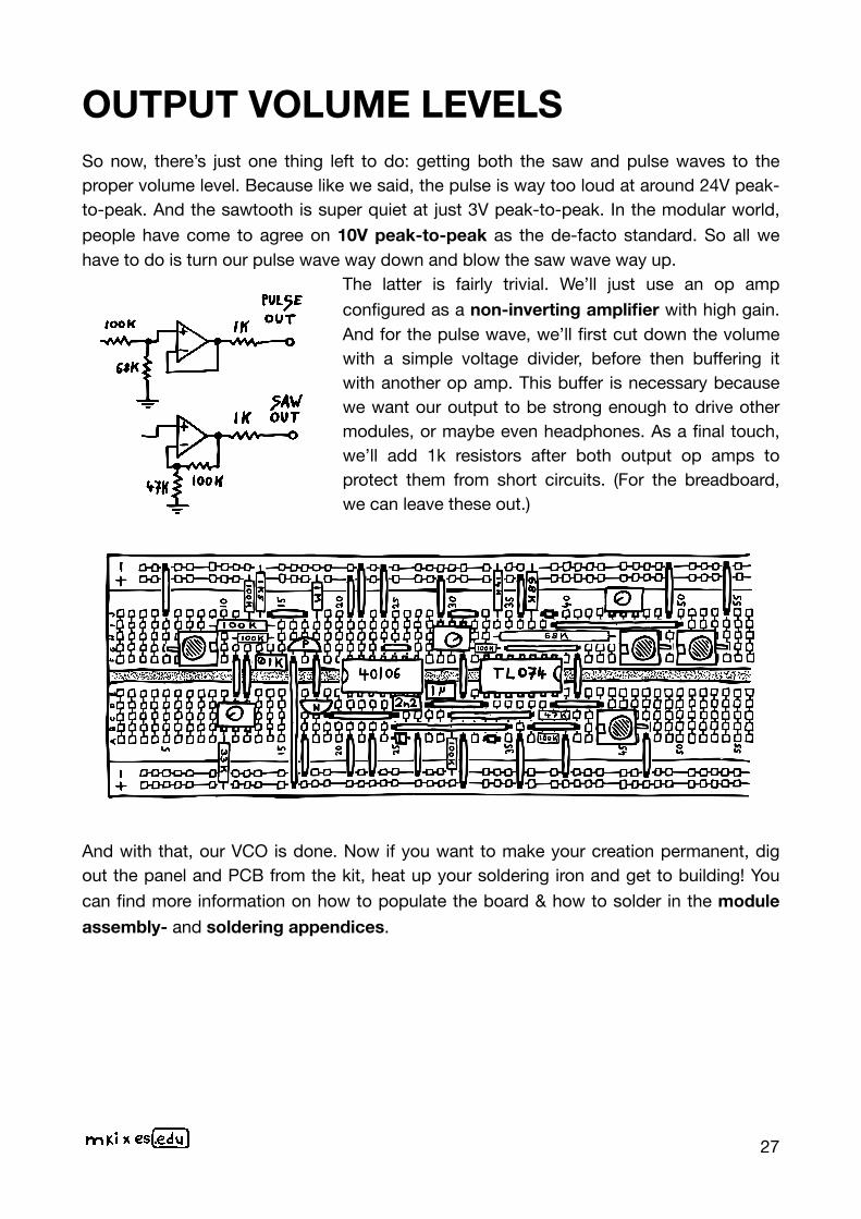
OUTPUT VOLUME LEVELS So now, there’s just one thing left to do: getting both the saw and pulse waves to the proper volume level. Because like we said, the pulse is way too loud at around 24V peak-to-peak. And the sawtooth is super quiet at just 3V peak-to-peak. In the modular world, people have come to agree on 10V peak-to-peak as the de-facto standard. So all we have to do is turn our pulse wave way down and blow the saw wave way up.
The latter is fairly trivial. We’ll just use an op amp configured as a non-inverting amplifier with high gain. And for the pulse wave, we’ll first cut down the volume with a simple voltage divider, before then buffering it with another op amp. This buffer is necessary because we want our output to be strong enough to drive other modules, or maybe even headphones. As a final touch, we’ll add 1k resistors after both output op amps to protect them from short circuits. (For the breadboard, we can leave these out.)
And with that, our VCO is done. Now if you want to make your creation permanent, dig out the panel and PCB from the kit, heat up your soldering iron and get to building! You can find more information on how to populate the board & how to solder in the module assembly- and soldering appendices.
27
COMPONENTS & CONCEPTS APPENDIX In this section, we’ll take a closer look at the components and elemental circuit design concepts we’re using to build our module. Check these whenever the main manual moves a bit too fast for you!
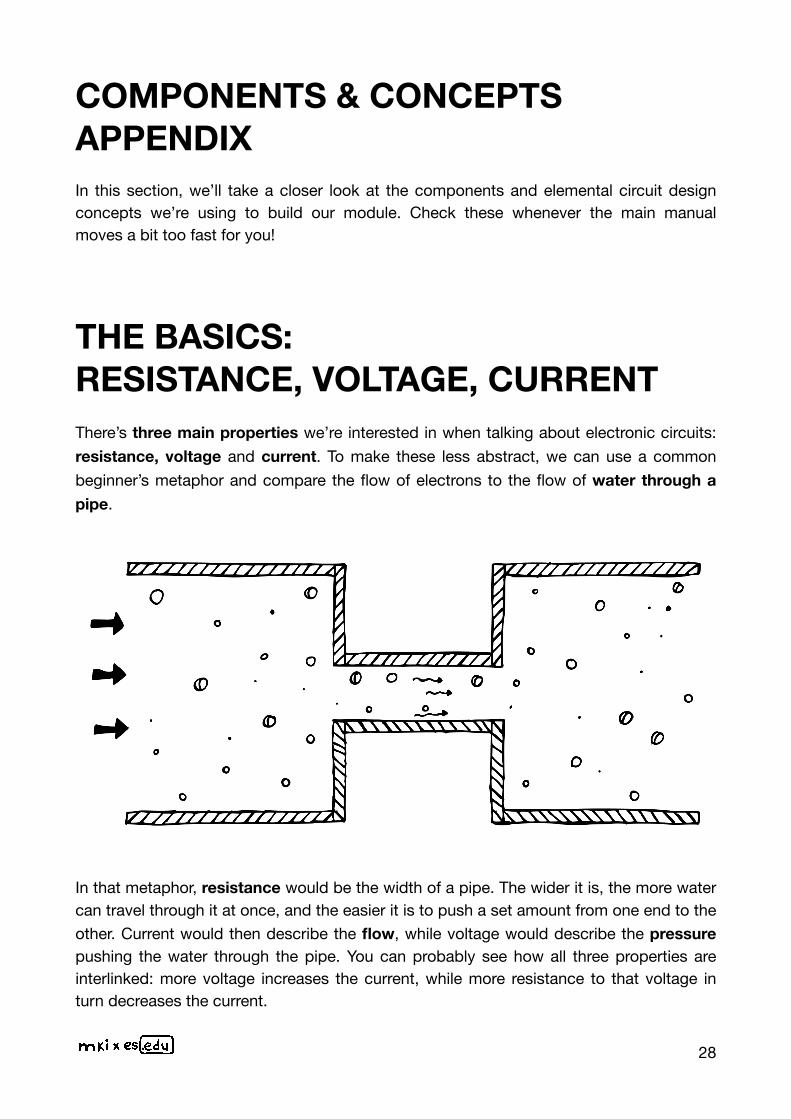
THE BASICS: RESISTANCE, VOLTAGE, CURRENT There’s three main properties we’re interested in when talking about electronic circuits: resistance, voltage and current. To make these less abstract, we can use a common beginner’s metaphor and compare the flow of electrons to the flow of water through a pipe.
In that metaphor, resistance would be the width of a pipe. The wider it is, the more water can travel through it at once, and the easier it is to push a set amount from one end to the other. Current would then describe the flow, while voltage would describe the pressure pushing the water through the pipe. You can probably see how all three properties are interlinked: more voltage increases the current, while more resistance to that voltage in turn decreases the current.
28
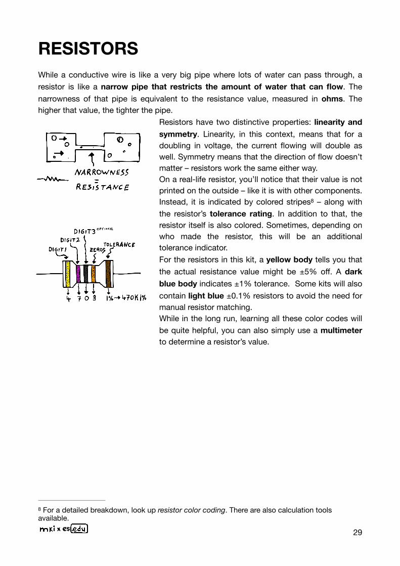
RESISTORS While a conductive wire is like a very big pipe where lots of water can pass through, a resistor is like a narrow pipe that restricts the amount of water that can flow. The narrowness of that pipe is equivalent to the resistance value, measured in ohms. The higher that value, the tighter the pipe.
Resistors have two distinctive properties: linearity and symmetry. Linearity, in this context, means that for a doubling in voltage, the current flowing will double as well. Symmetry means that the direction of flow doesn’t matter – resistors work the same either way.On a real-life resistor, you’ll notice that their value is not printed on the outside – like it is with other components. Instead, it is indicated by colored stripes – along with 8
the resistor’s tolerance rating. In addition to that, the resistor itself is also colored. Sometimes, depending on who made the resistor, this will be an additional tolerance indicator. For the resistors in this kit, a yellow body tells you that the actual resistance value might be ±5% off. A dark blue body indicates ±1% tolerance. Some kits will also contain light blue ±0.1% resistors to avoid the need for manual resistor matching.While in the long run, learning all these color codes will be quite helpful, you can also simply use a multimeter to determine a resistor’s value.
For a detailed breakdown, look up resistor color coding. There are also calculation tools 8
available.
29
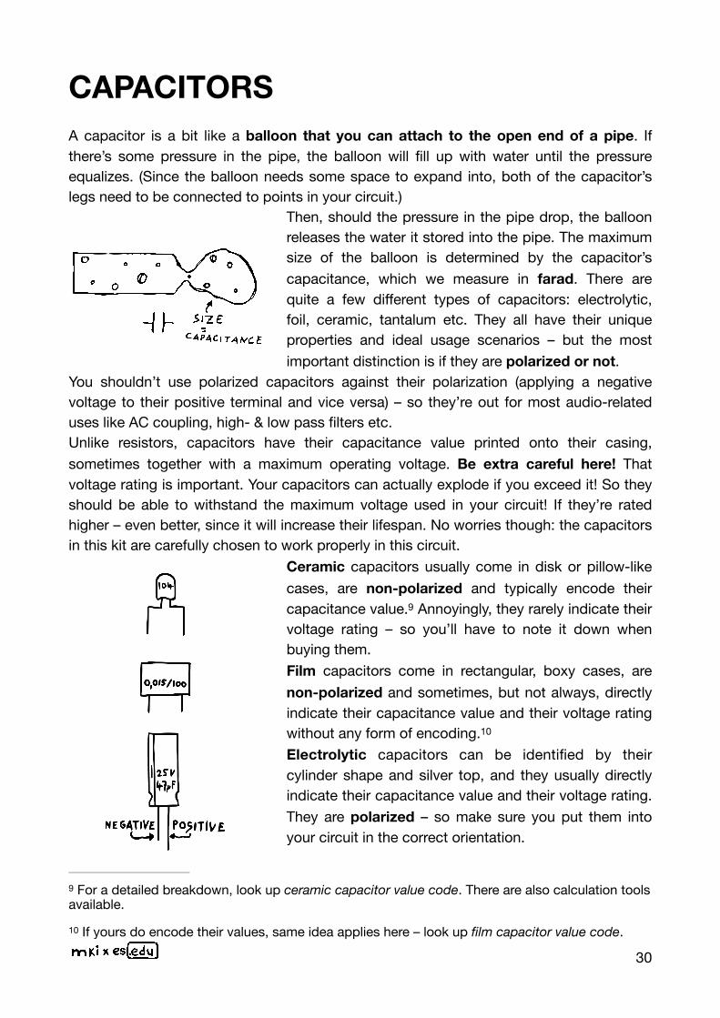
CAPACITORS A capacitor is a bit like a balloon that you can attach to the open end of a pipe. If there’s some pressure in the pipe, the balloon will fill up with water until the pressure equalizes. (Since the balloon needs some space to expand into, both of the capacitor’s legs need to be connected to points in your circuit.)
Then, should the pressure in the pipe drop, the balloon releases the water it stored into the pipe. The maximum size of the balloon is determined by the capacitor’s capacitance, which we measure in farad. There are quite a few different types of capacitors: electrolytic, foil, ceramic, tantalum etc. They all have their unique properties and ideal usage scenarios – but the most important distinction is if they are polarized or not.
You shouldn’t use polarized capacitors against their polarization (applying a negative voltage to their positive terminal and vice versa) – so they’re out for most audio-related uses like AC coupling, high- & low pass filters etc. Unlike resistors, capacitors have their capacitance value printed onto their casing, sometimes together with a maximum operating voltage. Be extra careful here! That voltage rating is important. Your capacitors can actually explode if you exceed it! So they should be able to withstand the maximum voltage used in your circuit! If they’re rated higher – even better, since it will increase their lifespan. No worries though: the capacitors in this kit are carefully chosen to work properly in this circuit.
Ceramic capacitors usually come in disk or pillow-like cases, are non-polarized and typically encode their capacitance value. Annoyingly, they rarely indicate their 9
voltage rating – so you’ll have to note it down when buying them. Film capacitors come in rectangular, boxy cases, are non-polarized and sometimes, but not always, directly indicate their capacitance value and their voltage rating without any form of encoding. 10
Electrolytic capacitors can be identified by their cylinder shape and silver top, and they usually directly indicate their capacitance value and their voltage rating. They are polarized – so make sure you put them into your circuit in the correct orientation.
For a detailed breakdown, look up ceramic capacitor value code. There are also calculation tools 9
available.
If yours do encode their values, same idea applies here – look up film capacitor value code.10
30
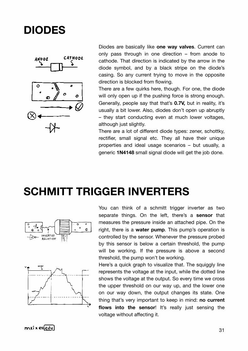
DIODES Diodes are basically like one way valves. Current can only pass through in one direction – from anode to cathode. That direction is indicated by the arrow in the diode symbol, and by a black stripe on the diode’s casing. So any current trying to move in the opposite direction is blocked from flowing.There are a few quirks here, though. For one, the diode will only open up if the pushing force is strong enough. Generally, people say that that’s 0.7V, but in reality, it’s usually a bit lower. Also, diodes don’t open up abruptly – they start conducting even at much lower voltages, although just slightly.There are a lot of different diode types: zener, schottky, rectifier, small signal etc. They all have their unique properties and ideal usage scenarios – but usually, a generic 1N4148 small signal diode will get the job done.
SCHMITT TRIGGER INVERTERS You can think of a schmitt trigger inverter as two separate things. On the left, there’s a sensor that measures the pressure inside an attached pipe. On the right, there is a water pump. This pump’s operation is controlled by the sensor. Whenever the pressure probed by this sensor is below a certain threshold, the pump will be working. If the pressure is above a second threshold, the pump won’t be working. Here’s a quick graph to visualize that. The squiggly line represents the voltage at the input, while the dotted line shows the voltage at the output. So every time we cross the upper threshold on our way up, and the lower one on our way down, the output changes its state. One thing that’s very important to keep in mind: no current flows into the sensor! It’s really just sensing the voltage without affecting it.
31
VOLTAGE DIVIDERS
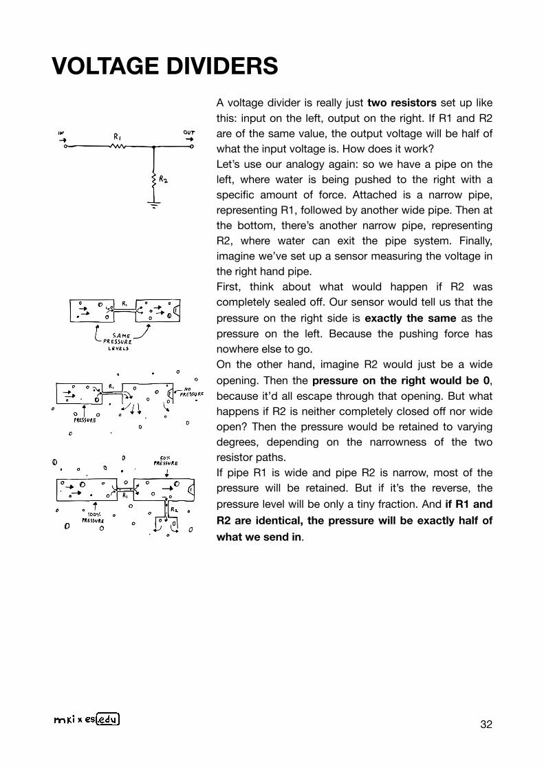
A voltage divider is really just two resistors set up like this: input on the left, output on the right. If R1 and R2 are of the same value, the output voltage will be half of what the input voltage is. How does it work? Let’s use our analogy again: so we have a pipe on the left, where water is being pushed to the right with a specific amount of force. Attached is a narrow pipe, representing R1, followed by another wide pipe. Then at the bottom, there’s another narrow pipe, representing R2, where water can exit the pipe system. Finally, imagine we’ve set up a sensor measuring the voltage in the right hand pipe. First, think about what would happen if R2 was completely sealed off. Our sensor would tell us that the pressure on the right side is exactly the same as the pressure on the left. Because the pushing force has nowhere else to go. On the other hand, imagine R2 would just be a wide opening. Then the pressure on the right would be 0, because it’d all escape through that opening. But what happens if R2 is neither completely closed off nor wide open? Then the pressure would be retained to varying degrees, depending on the narrowness of the two resistor paths. If pipe R1 is wide and pipe R2 is narrow, most of the pressure will be retained. But if it’s the reverse, the pressure level will be only a tiny fraction. And if R1 and R2 are identical, the pressure will be exactly half of what we send in.
32
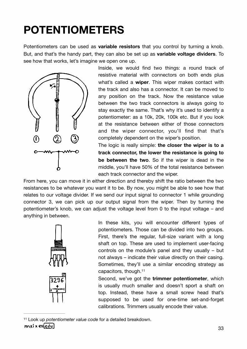
POTENTIOMETERS Potentiometers can be used as variable resistors that you control by turning a knob. But, and that’s the handy part, they can also be set up as variable voltage dividers. To see how that works, let’s imagine we open one up.
Inside, we would find two things: a round track of resistive material with connectors on both ends plus what’s called a wiper. This wiper makes contact with the track and also has a connector. It can be moved to any position on the track. Now the resistance value between the two track connectors is always going to stay exactly the same. That’s why it’s used to identify a potentiometer: as a 10k, 20k, 100k etc. But if you look at the resistance between either of those connectors and the wiper connector, you’ll find that that’s completely dependent on the wiper’s position. The logic is really simple: the closer the wiper is to a track connector, the lower the resistance is going to be between the two. So if the wiper is dead in the middle, you’ll have 50% of the total resistance between each track connector and the wiper.
From here, you can move it in either direction and thereby shift the ratio between the two resistances to be whatever you want it to be. By now, you might be able to see how that relates to our voltage divider. If we send our input signal to connector 1 while grounding connector 3, we can pick up our output signal from the wiper. Then by turning the potentiometer’s knob, we can adjust the voltage level from 0 to the input voltage – and anything in between.
In these kits, you will encounter different types of potentiometers. Those can be divided into two groups. First, there’s the regular, full-size variant with a long shaft on top. These are used to implement user-facing controls on the module’s panel and they usually – but not always – indicate their value directly on their casing. Sometimes, they’ll use a similar encoding strategy as capacitors, though. 11
Second, we’ve got the trimmer potentiometer, which is usually much smaller and doesn’t sport a shaft on top. Instead, these have a small screw head that’s supposed to be used for one-time set-and-forget calibrations. Trimmers usually encode their value.
Look up potentiometer value code for a detailed breakdown.11
33
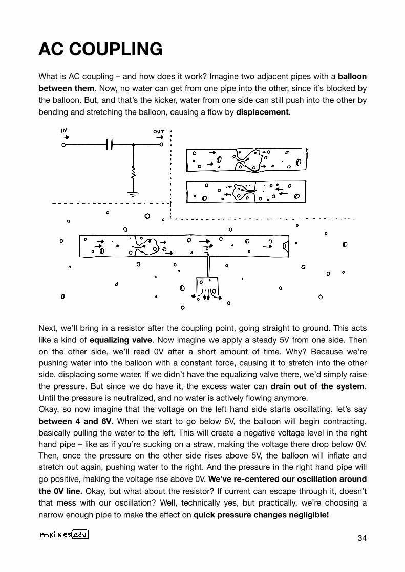
AC COUPLING What is AC coupling – and how does it work? Imagine two adjacent pipes with a balloon between them. Now, no water can get from one pipe into the other, since it’s blocked by the balloon. But, and that’s the kicker, water from one side can still push into the other by bending and stretching the balloon, causing a flow by displacement.
Next, we’ll bring in a resistor after the coupling point, going straight to ground. This acts like a kind of equalizing valve. Now imagine we apply a steady 5V from one side. Then on the other side, we’ll read 0V after a short amount of time. Why? Because we’re pushing water into the balloon with a constant force, causing it to stretch into the other side, displacing some water. If we didn’t have the equalizing valve there, we’d simply raise the pressure. But since we do have it, the excess water can drain out of the system. Until the pressure is neutralized, and no water is actively flowing anymore. Okay, so now imagine that the voltage on the left hand side starts oscillating, let’s say between 4 and 6V. When we start to go below 5V, the balloon will begin contracting, basically pulling the water to the left. This will create a negative voltage level in the right hand pipe – like as if you’re sucking on a straw, making the voltage there drop below 0V. Then, once the pressure on the other side rises above 5V, the balloon will inflate and stretch out again, pushing water to the right. And the pressure in the right hand pipe will go positive, making the voltage rise above 0V. We’ve re-centered our oscillation around the 0V line. Okay, but what about the resistor? If current can escape through it, doesn’t that mess with our oscillation? Well, technically yes, but practically, we’re choosing a narrow enough pipe to make the effect on quick pressure changes negligible!
34
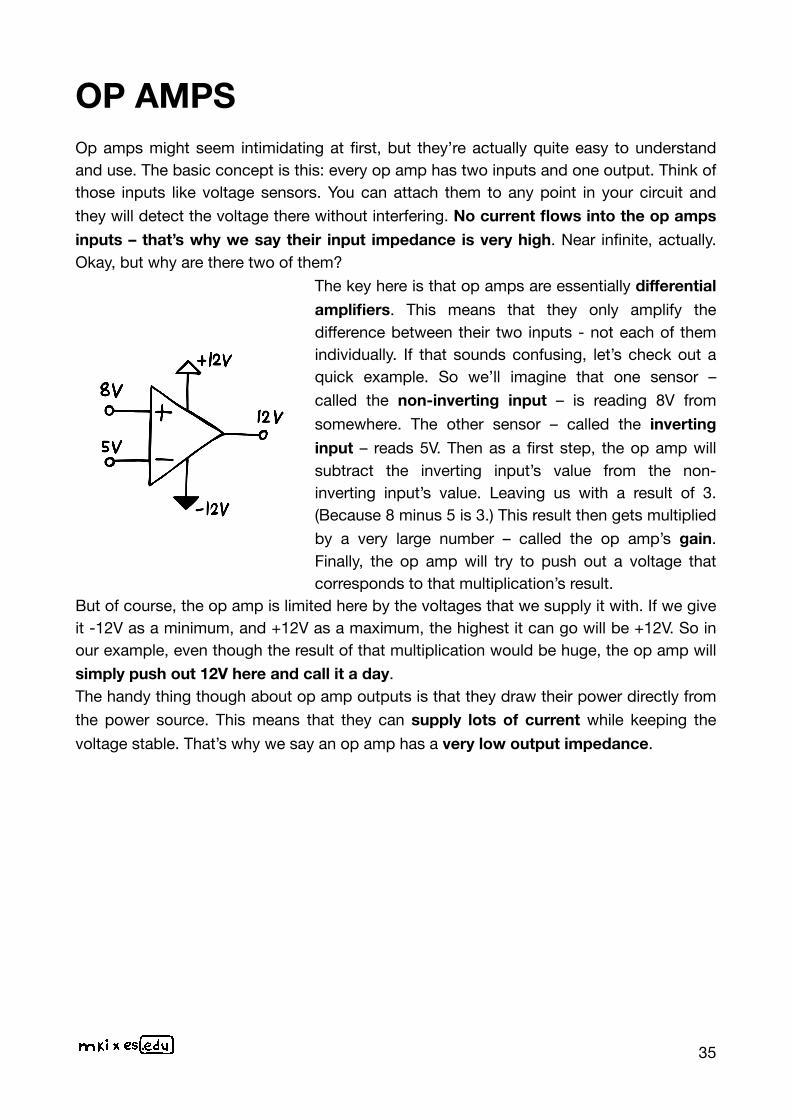
OP AMPS Op amps might seem intimidating at first, but they’re actually quite easy to understand and use. The basic concept is this: every op amp has two inputs and one output. Think of those inputs like voltage sensors. You can attach them to any point in your circuit and they will detect the voltage there without interfering. No current flows into the op amps inputs – that’s why we say their input impedance is very high. Near infinite, actually. Okay, but why are there two of them?
The key here is that op amps are essentially differential amplifiers. This means that they only amplify the difference between their two inputs - not each of them individually. If that sounds confusing, let’s check out a quick example. So we’ll imagine that one sensor – called the non-inverting input – is reading 8V from somewhere. The other sensor – called the inverting input – reads 5V. Then as a first step, the op amp will subtract the inverting input’s value from the non-inverting input’s value. Leaving us with a result of 3. (Because 8 minus 5 is 3.) This result then gets multiplied by a very large number – called the op amp’s gain. Finally, the op amp will try to push out a voltage that corresponds to that multiplication’s result.
But of course, the op amp is limited here by the voltages that we supply it with. If we give it -12V as a minimum, and +12V as a maximum, the highest it can go will be +12V. So in our example, even though the result of that multiplication would be huge, the op amp will simply push out 12V here and call it a day. The handy thing though about op amp outputs is that they draw their power directly from the power source. This means that they can supply lots of current while keeping the voltage stable. That’s why we say an op amp has a very low output impedance.
35
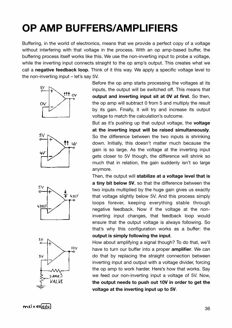
OP AMP BUFFERS/AMPLIFIERS Buffering, in the world of electronics, means that we provide a perfect copy of a voltage without interfering with that voltage in the process. With an op amp-based buffer, the buffering process itself works like this. We use the non-inverting input to probe a voltage, while the inverting input connects straight to the op amp’s output. This creates what we call a negative feedback loop. Think of it this way. We apply a specific voltage level to the non-inverting input – let’s say 5V.
Before the op amp starts processing the voltages at its inputs, the output will be switched off. This means that output and inverting input sit at 0V at first. So then, the op amp will subtract 0 from 5 and multiply the result by its gain. Finally, it will try and increase its output voltage to match the calculation’s outcome.But as it’s pushing up that output voltage, the voltage at the inverting input will be raised simultaneously. So the difference between the two inputs is shrinking down. Initially, this doesn’t matter much because the gain is so large. As the voltage at the inverting input gets closer to 5V though, the difference will shrink so much that in relation, the gain suddenly isn’t so large anymore.Then, the output will stabilize at a voltage level that is a tiny bit below 5V, so that the difference between the two inputs multiplied by the huge gain gives us exactly that voltage slightly below 5V. And this process simply loops forever, keeping everything stable through negative feedback. Now if the voltage at the non-inverting input changes, that feedback loop would ensure that the output voltage is always following. So that’s why this configuration works as a buffer: the output is simply following the input. How about amplifying a signal though? To do that, we’ll have to turn our buffer into a proper amplifier. We can do that by replacing the straight connection between inverting input and output with a voltage divider, forcing the op amp to work harder. Here’s how that works. Say we feed our non-inverting input a voltage of 5V. Now, the output needs to push out 10V in order to get the voltage at the inverting input up to 5V.
36
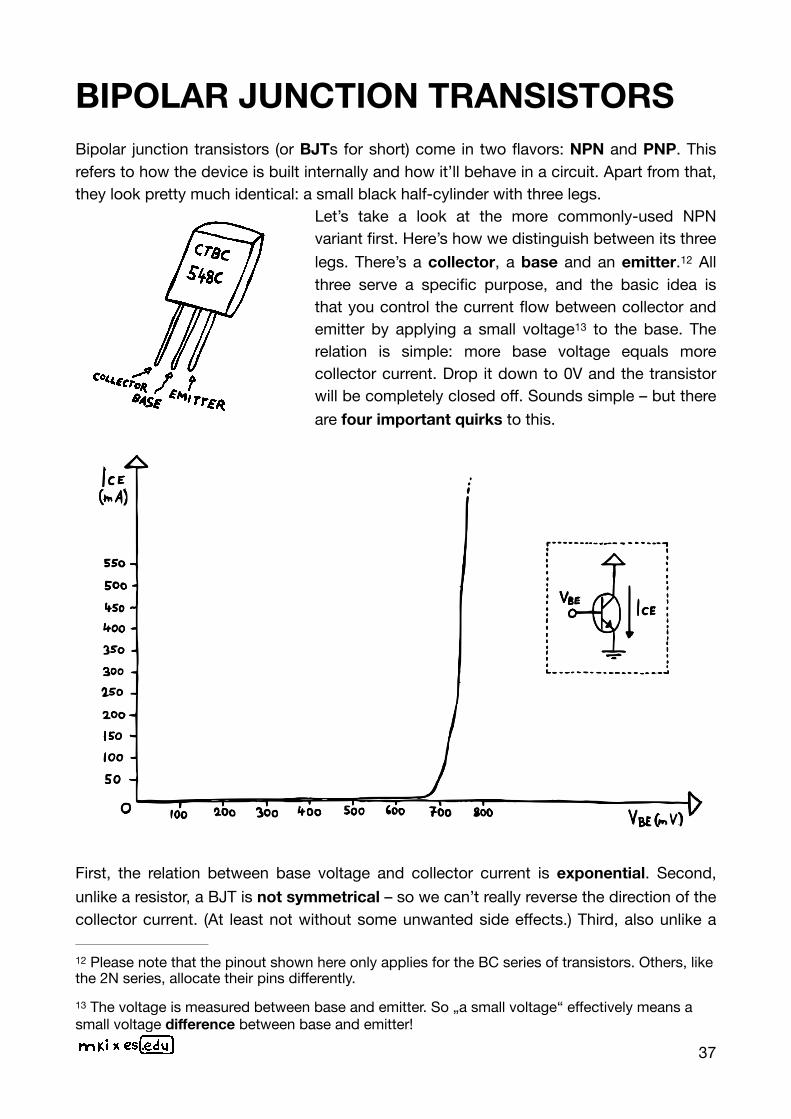
BIPOLAR JUNCTION TRANSISTORS Bipolar junction transistors (or BJTs for short) come in two flavors: NPN and PNP. This refers to how the device is built internally and how it’ll behave in a circuit. Apart from that, they look pretty much identical: a small black half-cylinder with three legs.
Let’s take a look at the more commonly-used NPN variant first. Here’s how we distinguish between its three legs. There’s a collector, a base and an emitter. All 12
three serve a specific purpose, and the basic idea is that you control the current flow between collector and emitter by applying a small voltage to the base. The 13
relation is simple: more base voltage equals more collector current. Drop it down to 0V and the transistor will be completely closed off. Sounds simple – but there are four important quirks to this.
First, the relation between base voltage and collector current is exponential. Second, unlike a resistor, a BJT is not symmetrical – so we can’t really reverse the direction of the collector current. (At least not without some unwanted side effects.) Third, also unlike a
Please note that the pinout shown here only applies for the BC series of transistors. Others, like 12
the 2N series, allocate their pins differently.
The voltage is measured between base and emitter. So „a small voltage“ effectively means a 13
small voltage difference between base and emitter!
37
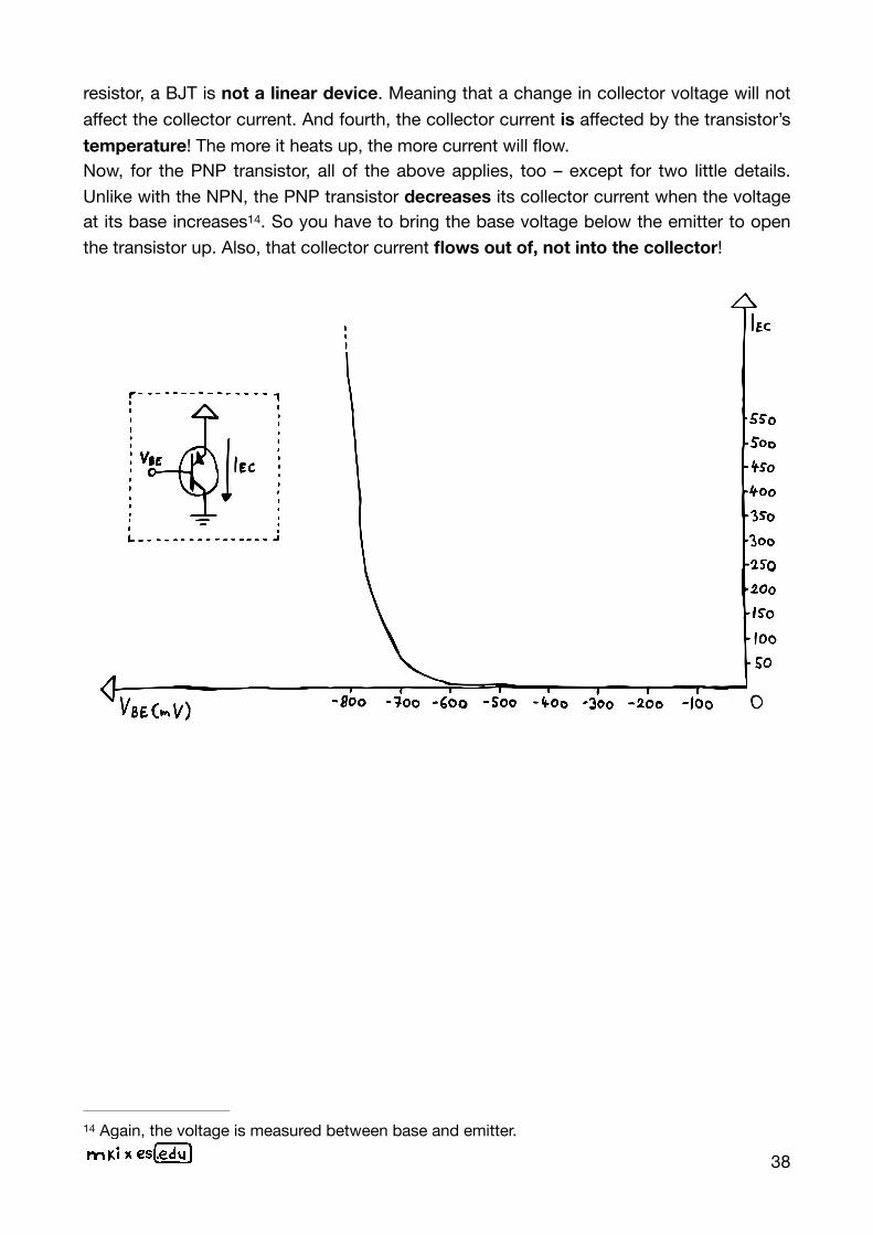
resistor, a BJT is not a linear device. Meaning that a change in collector voltage will not affect the collector current. And fourth, the collector current is affected by the transistor’s temperature! The more it heats up, the more current will flow.Now, for the PNP transistor, all of the above applies, too – except for two little details. Unlike with the NPN, the PNP transistor decreases its collector current when the voltage at its base increases . So you have to bring the base voltage below the emitter to open 14
the transistor up. Also, that collector current flows out of, not into the collector!
Again, the voltage is measured between base and emitter.14
38
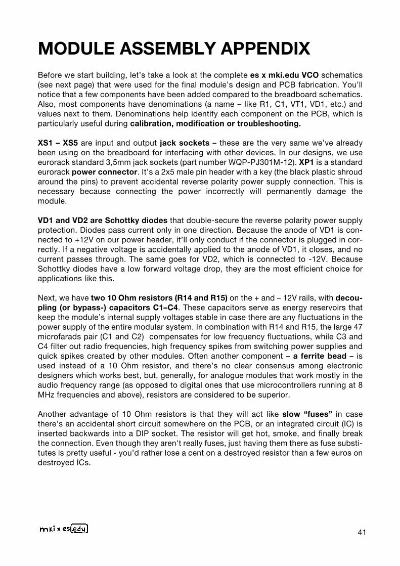
TOOLS APPENDIX There are two types of tools that will help you tremendously while designing a circuit: multimeters and oscilloscopes. In this appendix, we’ll take a quick look at each of these and explore how you use them.
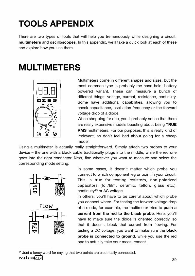
MULTIMETERS Multimeters come in different shapes and sizes, but the most common type is probably the hand-held, battery powered variant. These can measure a bunch of different things: voltage, current, resistance, continuity. Some have additional capabilities, allowing you to check capacitance, oscillation frequency or the forward voltage drop of a diode.When shopping for one, you’ll probably notice that there are really expensive models boasting about being TRUE RMS multimeters. For our purposes, this is really kind of irrelevant, so don’t feel bad about going for a cheap model!
Using a multimeter is actually really straightforward. Simply attach two probes to your device – the one with a black cable traditionally plugs into the middle, while the red one goes into the right connector. Next, find whatever you want to measure and select the corresponding mode setting.
In some cases, it doesn’t matter which probe you connect to which component leg or point in your circuit. This is true for testing resistors, non-polarized capacitors (foil/film, ceramic, teflon, glass etc.), continuity or AC voltage.15
In others, you’ll have to be careful about which probe you connect where. For testing the forward voltage drop of a diode, for example, the multimeter tries to push a current from the red to the black probe. Here, you’ll have to make sure the diode is oriented correctly, so that it doesn’t block that current from flowing. For testing a DC voltage, you want to make sure the black probe is connected to ground, while you use the red one to actually take your measurement.
Just a fancy word for saying that two points are electrically connected.15
39
OSCILLOSCOPES
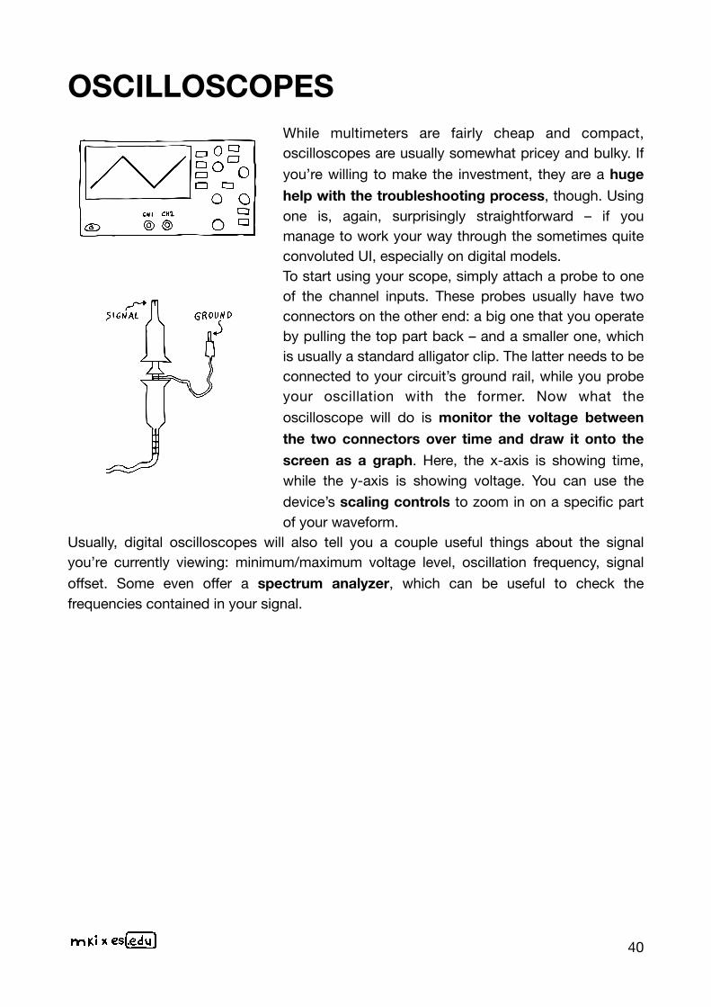
While multimeters are fairly cheap and compact, oscilloscopes are usually somewhat pricey and bulky. If you’re willing to make the investment, they are a huge help with the troubleshooting process, though. Using one is, again, surprisingly straightforward – if you manage to work your way through the sometimes quite convoluted UI, especially on digital models.To start using your scope, simply attach a probe to one of the channel inputs. These probes usually have two connectors on the other end: a big one that you operate by pulling the top part back – and a smaller one, which is usually a standard alligator clip. The latter needs to be connected to your circuit’s ground rail, while you probe your oscillation with the former. Now what the oscilloscope will do is monitor the voltage between the two connectors over time and draw it onto the screen as a graph. Here, the x-axis is showing time, while the y-axis is showing voltage. You can use the device’s scaling controls to zoom in on a specific part of your waveform.
Usually, digital oscilloscopes will also tell you a couple useful things about the signal you’re currently viewing: minimum/maximum voltage level, oscillation frequency, signal offset. Some even offer a spectrum analyzer, which can be useful to check the frequencies contained in your signal.
40
Next, insert & solder the film- and electrolytic capacitors. Electrolytic capacitors are bipolar, and you need to mind their orientation. The positive lead of each electrolytic capacitor is longer, and there’s a minus stripe on the side of the capacitor’s body to indicate the neg-ative lead. On our PCBs, the positive pad for a capacitor has a square shape, and the negative lead should go into the pad next to the notch on the silkscreen.
Now your PCB should look like this.
Capacitors C6, C7 and C9 are additional decoupling capacitors. If you inspect the PCB, you’ll see that these are placed as close to the power supply pins of the ICs as possible. For well-designed larger PCBs you will find decoupling capacitors next to each IC. Like the others, their job is to simply compensate for any unwanted noise in the supply rails. If the input voltage drops, then these capacitors will be able to bridge the gap to keep the voltage at the IC stable. And vice-versa - if the voltage increases, then they’ll be able to absorb the excess energy trying to flow through to the IC, which again keeps the voltage stable. Typi-cally, 0.1uF capacitors are used for this purpose.
All unused inputs of DD1 (DD1B-DD1F) are connected to ground, just like before on the breadboard – this is good practice which helps to prevent random voltages appearing on the IC’s inputs and outputs. TP11-TP42 are “fake” test points or a “kludge area”. On the PCB, this allows you to make some custom modifications to the module – you can intro-duce, for example, a VCO range switch, synchronization input, etc. As you can see, TP11 and TP12 are connected to +12V, while TP17 and TP18 link to -12V – since you may need a power supply connection for your modifications.
Before you start soldering, we highly recommend printing out these part placement diagrams with designators and values. Because some of our PCBs are rather densely pop-ulated, this will help you to avoid mistakes in the build process.
Before we start building, let’s take a look at the complete es x mki.edu VCO schematics (see next page) that were used for the final module’s design and PCB fabrication. You’ll notice that a few components have been added compared to the breadboard schematics. Also, most components have denominations (a name – like R1, C1, VT1, VD1, etc.) and values next to them. Denominations help identify each component on the PCB, which is particularly useful during calibration, modification or troubleshooting.
XS1 – XS5 are input and output jack sockets – these are the very same we’ve already been using on the breadboard for interfacing with other devices. In our designs, we use eurorack standard 3,5mm jack sockets (part number WQP-PJ301M-12). XP1 is a standard eurorack power connector. It’s a 2x5 male pin header with a key (the black plastic shroud around the pins) to prevent accidental reverse polarity power supply connection. This is necessary because connecting the power incorrectly will permanently damage the module.
VD1 and VD2 are Schottky diodes that double-secure the reverse polarity power supply protection. Diodes pass current only in one direction. Because the anode of VD1 is con-nected to +12V on our power header, it’ll only conduct if the connector is plugged in cor-rectly. If a negative voltage is accidentally applied to the anode of VD1, it closes, and no current passes through. The same goes for VD2, which is connected to -12V. Because Schottky diodes have a low forward voltage drop, they are the most efficient choice for applications like this.
Next, we have two 10 Ohm resistors (R14 and R15) on the + and – 12V rails, with decou-pling (or bypass-) capacitors C1–C4. These capacitors serve as energy reservoirs that keep the module’s internal supply voltages stable in case there are any fluctuations in the power supply of the entire modular system. In combination with R14 and R15, the large 47 microfarads pair (C1 and C2) compensates for low frequency fluctuations, while C3 and C4 filter out radio frequencies, high frequency spikes from switching power supplies and quick spikes created by other modules. Often another component – a ferrite bead – is used instead of a 10 Ohm resistor, and there’s no clear consensus among electronic designers which works best, but, generally, for analogue modules that work mostly in the audio frequency range (as opposed to digital ones that use microcontrollers running at 8 MHz frequencies and above), resistors are considered to be superior.
Another advantage of 10 Ohm resistors is that they will act like slow “fuses” in case there’s an accidental short circuit somewhere on the PCB, or an integrated circuit (IC) is inserted backwards into a DIP socket. The resistor will get hot, smoke, and finally break the connection. Even though they aren't really fuses, just having them there as fuse substi-tutes is pretty useful - you’d rather lose a cent on a destroyed resistor than a few euros on destroyed ICs.
Place the VCO PCB in a PCB holder for soldering or simply on top of some spacers (I use two empty solder wire coils here). I usually start with lower, horizontally placed components. Start with populating the PCB. Bend the resis-tor leads and insert them in the relevant places according to the part placement diagram above. All components on the PCB have both their value and denomi-nation printed onto the silkscreen. If you are not sure about a resistor’s value, use a multimeter to double check. Next, insert the diodes. Remember – when inserting the diodes, orientation is critical! A thick white stripe on the PCB indicates the cathode of a diode – match it with a stripe on the component.
With resistors and diodes inserted, there are two ways to proceed: (1) If you are not confident in your soldering skills, it is better to solder from the bottom of the PCB. This will prevent your compo-nents from overheating and possible damage. Flip the PCB around and place it on a flat surface. Make sure all components are still in place and solder all the leads. (2) Our PCBs are double-sided, with all holes metalized – which means that each solder pad is electrically connected to its other-side counterpart, and it doesn’t really matter from which side you solder. If you are an experi-enced DIYer, solder one lead of each compo-nent from the top in order to fix it in place. Make sure you do not overheat the compo-nents. Then flip the PCB around and solder the second lead for each. You can even solder both leads from the top side of the PCB.
Once done with soldering, use pliers to cut off the excess leads. Next, insert the first DIP socket, hold it in place and solder one of the pins. Continue with the next DIP socket. Make sure the DIP sock-ets are oriented correctly – the notch on the socket should match the notch on the PCB’s silkscreen. Now, turn the PCB around and solder all remaining pins of the DIP sockets. Then proceed with the ceramic capacitors. Place the PCB on spacers, insert the capacitors and solder them like you did with the resistors & diodes before.
Next up: inserting & soldering the NTC thermistors and transistors. Make sure you place the transistors in their desig-nated spots. Also, they need to be prop-erly aligned with the marked outline on the silkscreen – orientation is critically important here. Complete this step by soldering vertically placed resistors.
Next, solder the precision trimmer and the power supply socket. Make sure the Insert the jack sockets and solder them.-orientation of the socket is as shown in the picture below – the arrow pointing to the first pin is aligned with a notch on the silkscreen. The key on the socket will be facing outwards from the PCB.
Now, turn the PCB around and inspect your solder joints. Make sure all compo-nents are soldered properly and there are no cold solder joints or accidental shorts. Clean the PCB to remove extra flux, if necessary.
Insert the jack sockets and solder them.
Insert the potentiometers. Don’t mix up their values and don’t solder them yet! Fit the front panel and make sure that the potentiometers’ shafts are aligned with the holes on the panel – and that they rotate freely. Now, go ahead and solder the potentiometers.
Install the front panel and fix it in place with the 5 hex nuts on the jack sockets and a washer plus hex nut on the top potentiometer. Fit the large knob on the bare potentiometer shaft and fix it in place with a small screwdriver. We are almost done
Now, insert the ICs into their respec-tive DIP sockets. Mind the orientation of the ICs – match the notch on each IC with the one on its socket.
Congratulations! You have completed the assembly of the es x mki.edu VCO module! Now connect it to your eurorack power supply and switch it on. If there’s no “magic smoke“, it’s a good sign that your build was successful. Connect the VCO’s SAW output to a mixer and check if you get a signal. Rotate the COARSE knob and
DIY electronics is a great (and quite addictive) hobby, therefore we highly recommend you invest in good tools. In order to really enjoy soldering, you’ll need:
A decent soldering station. Top-of-the-line soldering stations (brands like Weller) will cost 200EUR and above, but cheaper alternatives around 50EUR are often good enough. Make sure your soldering station of choice comes with multiple differently-sized soldering iron tips. The most useful ones for DIY electronics are flat, 2mm wide tips.
When heated up, the tips of soldering irons tend to oxidize. As a result, solder won’t stick to them, so you’ll need to clean your tip frequently. Most soldering stations come with a damp sponge for cleaning the iron tips – but there are also profes-sional solder tip cleaners with golden curls (not really gold, so not as expensive as it sounds). These work much better because they do not cool down the iron.
Solder wire with flux. I find 0,7mm solder wire works best for DIY projects.
Some soldering flux paste or pen will be useful as well.
Cutting pliers. Use them to cut off excess leads of components after soldering.
A solder suction pump. No matter how refined your soldering skills are, you will make mistakes. So when you’ll inevitably need to de-solder components, you will also need to remove any remaining solder from the solder pads in order to insert new components.
Once you have finished soldering your PCB, it’s recommended to remove excess flux from the solder joints. A PCB cleaner is the best way to go.
All of these tools can be found on major electronic components retailer websites, like Mouser, Farnell and at your local electronics shops. As you work your way towards more and more advanced projects, you’ll need to expand your skillset and your tool belt – but the gratification will be much greater.
“We keep moving forward, opening new doors, and doing new things, because we're curious and curiosity keeps leading us down new paths.” - Walt Disney
41
MODULE ASSEMBLY APPENDIX
make sure you hear a change in pitch. If you do, you can proceed with tuning the VCO as we’ve done before on the breadboard.If you’ve never soldered before – or if your skills have become rusty – it’s probably wise to check out some THT (through-hole technology) soldering tutorials on YouTube. The main thing you have to remember while soldering is that melted solder will flow towards higher temperature areas. So you need to make sure you apply equal heat to the component you are soldering and the solder pad on the PCB. The pad will typically absorb more heat (especially ground-connected pads which have more thermal mass), so keep your soldering iron closer to the pad on the PCB. It’s critically important to dial in the right temperature on your soldering station. I found that about 320 °C is the opti-mal temperature for most of parts, while for larger elements like potentiometers and sockets, you may want to increase that temperature to 370 °C.
Here’s the recommended soldering sequence:
After you have completed soldering, inspect the solder joint:
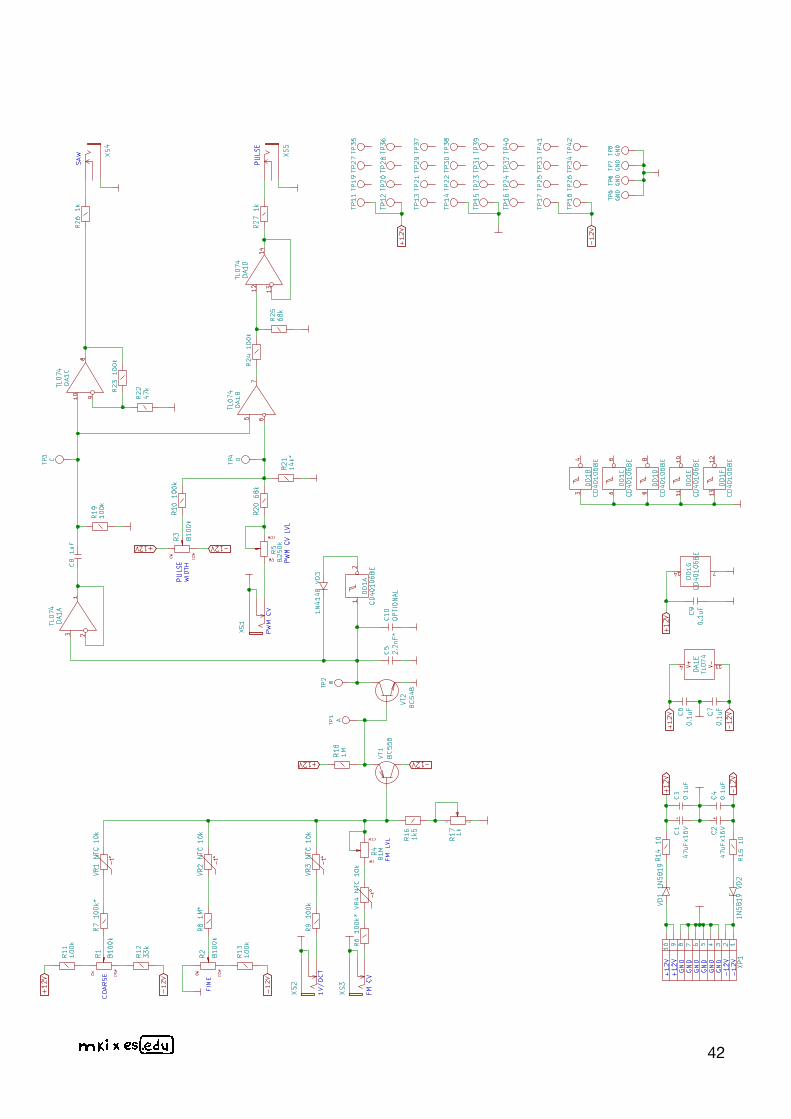
Next, insert & solder the film- and electrolytic capacitors. Electrolytic capacitors are bipolar, and you need to mind their orientation. The positive lead of each electrolytic capacitor is longer, and there’s a minus stripe on the side of the capacitor’s body to indicate the neg-ative lead. On our PCBs, the positive pad for a capacitor has a square shape, and the negative lead should go into the pad next to the notch on the silkscreen.
Now your PCB should look like this.
Capacitors C6, C7 and C9 are additional decoupling capacitors. If you inspect the PCB, you’ll see that these are placed as close to the power supply pins of the ICs as possible. For well-designed larger PCBs you will find decoupling capacitors next to each IC. Like the others, their job is to simply compensate for any unwanted noise in the supply rails. If the input voltage drops, then these capacitors will be able to bridge the gap to keep the voltage at the IC stable. And vice-versa - if the voltage increases, then they’ll be able to absorb the excess energy trying to flow through to the IC, which again keeps the voltage stable. Typi-cally, 0.1uF capacitors are used for this purpose.
All unused inputs of DD1 (DD1B-DD1F) are connected to ground, just like before on the breadboard – this is good practice which helps to prevent random voltages appearing on the IC’s inputs and outputs. TP11-TP42 are “fake” test points or a “kludge area”. On the PCB, this allows you to make some custom modifications to the module – you can intro-duce, for example, a VCO range switch, synchronization input, etc. As you can see, TP11 and TP12 are connected to +12V, while TP17 and TP18 link to -12V – since you may need a power supply connection for your modifications.
Before you start soldering, we highly recommend printing out these part placement diagrams with designators and values. Because some of our PCBs are rather densely pop-ulated, this will help you to avoid mistakes in the build process.
Place the VCO PCB in a PCB holder for soldering or simply on top of some spacers (I use two empty solder wire coils here). I usually start with lower, horizontally placed components. Start with populating the PCB. Bend the resis-tor leads and insert them in the relevant places according to the part placement diagram above. All components on the PCB have both their value and denomi-nation printed onto the silkscreen. If you are not sure about a resistor’s value, use a multimeter to double check. Next, insert the diodes. Remember – when inserting the diodes, orientation is critical! A thick white stripe on the PCB indicates the cathode of a diode – match it with a stripe on the component.
With resistors and diodes inserted, there are two ways to proceed: (1) If you are not confident in your soldering skills, it is better to solder from the bottom of the PCB. This will prevent your compo-nents from overheating and possible damage. Flip the PCB around and place it on a flat surface. Make sure all components are still in place and solder all the leads. (2) Our PCBs are double-sided, with all holes metalized – which means that each solder pad is electrically connected to its other-side counterpart, and it doesn’t really matter from which side you solder. If you are an experi-enced DIYer, solder one lead of each compo-nent from the top in order to fix it in place. Make sure you do not overheat the compo-nents. Then flip the PCB around and solder the second lead for each. You can even solder both leads from the top side of the PCB.
Once done with soldering, use pliers to cut off the excess leads. Next, insert the first DIP socket, hold it in place and solder one of the pins. Continue with the next DIP socket. Make sure the DIP sock-ets are oriented correctly – the notch on the socket should match the notch on the PCB’s silkscreen. Now, turn the PCB around and solder all remaining pins of the DIP sockets. Then proceed with the ceramic capacitors. Place the PCB on spacers, insert the capacitors and solder them like you did with the resistors & diodes before.
Next up: inserting & soldering the NTC thermistors and transistors. Make sure you place the transistors in their desig-nated spots. Also, they need to be prop-erly aligned with the marked outline on the silkscreen – orientation is critically important here. Complete this step by soldering vertically placed resistors.
Next, solder the precision trimmer and the power supply socket. Make sure the Insert the jack sockets and solder them.-orientation of the socket is as shown in the picture below – the arrow pointing to the first pin is aligned with a notch on the silkscreen. The key on the socket will be facing outwards from the PCB.
Now, turn the PCB around and inspect your solder joints. Make sure all compo-nents are soldered properly and there are no cold solder joints or accidental shorts. Clean the PCB to remove extra flux, if necessary.
Insert the jack sockets and solder them.
Insert the potentiometers. Don’t mix up their values and don’t solder them yet! Fit the front panel and make sure that the potentiometers’ shafts are aligned with the holes on the panel – and that they rotate freely. Now, go ahead and solder the potentiometers.
Install the front panel and fix it in place with the 5 hex nuts on the jack sockets and a washer plus hex nut on the top potentiometer. Fit the large knob on the bare potentiometer shaft and fix it in place with a small screwdriver. We are almost done
Now, insert the ICs into their respec-tive DIP sockets. Mind the orientation of the ICs – match the notch on each IC with the one on its socket.
Congratulations! You have completed the assembly of the es x mki.edu VCO module! Now connect it to your eurorack power supply and switch it on. If there’s no “magic smoke“, it’s a good sign that your build was successful. Connect the VCO’s SAW output to a mixer and check if you get a signal. Rotate the COARSE knob and
DIY electronics is a great (and quite addictive) hobby, therefore we highly recommend you invest in good tools. In order to really enjoy soldering, you’ll need:
A decent soldering station. Top-of-the-line soldering stations (brands like Weller) will cost 200EUR and above, but cheaper alternatives around 50EUR are often good enough. Make sure your soldering station of choice comes with multiple differently-sized soldering iron tips. The most useful ones for DIY electronics are flat, 2mm wide tips.
When heated up, the tips of soldering irons tend to oxidize. As a result, solder won’t stick to them, so you’ll need to clean your tip frequently. Most soldering stations come with a damp sponge for cleaning the iron tips – but there are also profes-sional solder tip cleaners with golden curls (not really gold, so not as expensive as it sounds). These work much better because they do not cool down the iron.
Solder wire with flux. I find 0,7mm solder wire works best for DIY projects.
Some soldering flux paste or pen will be useful as well.
Cutting pliers. Use them to cut off excess leads of components after soldering.
A solder suction pump. No matter how refined your soldering skills are, you will make mistakes. So when you’ll inevitably need to de-solder components, you will also need to remove any remaining solder from the solder pads in order to insert new components.
Once you have finished soldering your PCB, it’s recommended to remove excess flux from the solder joints. A PCB cleaner is the best way to go.
All of these tools can be found on major electronic components retailer websites, like Mouser, Farnell and at your local electronics shops. As you work your way towards more and more advanced projects, you’ll need to expand your skillset and your tool belt – but the gratification will be much greater.
“We keep moving forward, opening new doors, and doing new things, because we're curious and curiosity keeps leading us down new paths.” - Walt Disney
42
make sure you hear a change in pitch. If you do, you can proceed with tuning the VCO as we’ve done before on the breadboard.If you’ve never soldered before – or if your skills have become rusty – it’s probably wise to check out some THT (through-hole technology) soldering tutorials on YouTube. The main thing you have to remember while soldering is that melted solder will flow towards higher temperature areas. So you need to make sure you apply equal heat to the component you are soldering and the solder pad on the PCB. The pad will typically absorb more heat (especially ground-connected pads which have more thermal mass), so keep your soldering iron closer to the pad on the PCB. It’s critically important to dial in the right temperature on your soldering station. I found that about 320 °C is the opti-mal temperature for most of parts, while for larger elements like potentiometers and sockets, you may want to increase that temperature to 370 °C.
Here’s the recommended soldering sequence:
After you have completed soldering, inspect the solder joint:
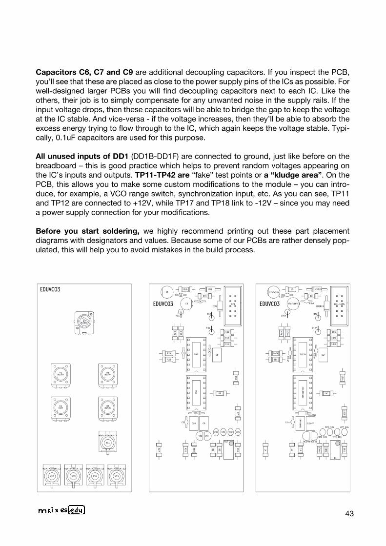
Next, insert & solder the film- and electrolytic capacitors. Electrolytic capacitors are bipolar, and you need to mind their orientation. The positive lead of each electrolytic capacitor is longer, and there’s a minus stripe on the side of the capacitor’s body to indicate the neg-ative lead. On our PCBs, the positive pad for a capacitor has a square shape, and the negative lead should go into the pad next to the notch on the silkscreen.
Now your PCB should look like this.
Capacitors C6, C7 and C9 are additional decoupling capacitors. If you inspect the PCB, you’ll see that these are placed as close to the power supply pins of the ICs as possible. For well-designed larger PCBs you will find decoupling capacitors next to each IC. Like the others, their job is to simply compensate for any unwanted noise in the supply rails. If the input voltage drops, then these capacitors will be able to bridge the gap to keep the voltage at the IC stable. And vice-versa - if the voltage increases, then they’ll be able to absorb the excess energy trying to flow through to the IC, which again keeps the voltage stable. Typi-cally, 0.1uF capacitors are used for this purpose.
All unused inputs of DD1 (DD1B-DD1F) are connected to ground, just like before on the breadboard – this is good practice which helps to prevent random voltages appearing on the IC’s inputs and outputs. TP11-TP42 are “fake” test points or a “kludge area”. On the PCB, this allows you to make some custom modifications to the module – you can intro-duce, for example, a VCO range switch, synchronization input, etc. As you can see, TP11 and TP12 are connected to +12V, while TP17 and TP18 link to -12V – since you may need a power supply connection for your modifications.
Before you start soldering, we highly recommend printing out these part placement diagrams with designators and values. Because some of our PCBs are rather densely pop-ulated, this will help you to avoid mistakes in the build process.
Place the VCO PCB in a PCB holder for soldering or simply on top of some spacers (I use two empty solder wire coils here). I usually start with lower, horizontally placed components. Start with populating the PCB. Bend the resis-tor leads and insert them in the relevant places according to the part placement diagram above. All components on the PCB have both their value and denomi-nation printed onto the silkscreen. If you are not sure about a resistor’s value, use a multimeter to double check. Next, insert the diodes. Remember – when inserting the diodes, orientation is critical! A thick white stripe on the PCB indicates the cathode of a diode – match it with a stripe on the component.
With resistors and diodes inserted, there are two ways to proceed: (1) If you are not confident in your soldering skills, it is better to solder from the bottom of the PCB. This will prevent your compo-nents from overheating and possible damage. Flip the PCB around and place it on a flat surface. Make sure all components are still in place and solder all the leads. (2) Our PCBs are double-sided, with all holes metalized – which means that each solder pad is electrically connected to its other-side counterpart, and it doesn’t really matter from which side you solder. If you are an experi-enced DIYer, solder one lead of each compo-nent from the top in order to fix it in place. Make sure you do not overheat the compo-nents. Then flip the PCB around and solder the second lead for each. You can even solder both leads from the top side of the PCB.
Once done with soldering, use pliers to cut off the excess leads. Next, insert the first DIP socket, hold it in place and solder one of the pins. Continue with the next DIP socket. Make sure the DIP sock-ets are oriented correctly – the notch on the socket should match the notch on the PCB’s silkscreen. Now, turn the PCB around and solder all remaining pins of the DIP sockets. Then proceed with the ceramic capacitors. Place the PCB on spacers, insert the capacitors and solder them like you did with the resistors & diodes before.
Next up: inserting & soldering the NTC thermistors and transistors. Make sure you place the transistors in their desig-nated spots. Also, they need to be prop-erly aligned with the marked outline on the silkscreen – orientation is critically important here. Complete this step by soldering vertically placed resistors.
Next, solder the precision trimmer and the power supply socket. Make sure the Insert the jack sockets and solder them.-orientation of the socket is as shown in the picture below – the arrow pointing to the first pin is aligned with a notch on the silkscreen. The key on the socket will be facing outwards from the PCB.
Now, turn the PCB around and inspect your solder joints. Make sure all compo-nents are soldered properly and there are no cold solder joints or accidental shorts. Clean the PCB to remove extra flux, if necessary.
Insert the jack sockets and solder them.
Insert the potentiometers. Don’t mix up their values and don’t solder them yet! Fit the front panel and make sure that the potentiometers’ shafts are aligned with the holes on the panel – and that they rotate freely. Now, go ahead and solder the potentiometers.
Install the front panel and fix it in place with the 5 hex nuts on the jack sockets and a washer plus hex nut on the top potentiometer. Fit the large knob on the bare potentiometer shaft and fix it in place with a small screwdriver. We are almost done
Now, insert the ICs into their respec-tive DIP sockets. Mind the orientation of the ICs – match the notch on each IC with the one on its socket.
Congratulations! You have completed the assembly of the es x mki.edu VCO module! Now connect it to your eurorack power supply and switch it on. If there’s no “magic smoke“, it’s a good sign that your build was successful. Connect the VCO’s SAW output to a mixer and check if you get a signal. Rotate the COARSE knob and
DIY electronics is a great (and quite addictive) hobby, therefore we highly recommend you invest in good tools. In order to really enjoy soldering, you’ll need:
A decent soldering station. Top-of-the-line soldering stations (brands like Weller) will cost 200EUR and above, but cheaper alternatives around 50EUR are often good enough. Make sure your soldering station of choice comes with multiple differently-sized soldering iron tips. The most useful ones for DIY electronics are flat, 2mm wide tips.
When heated up, the tips of soldering irons tend to oxidize. As a result, solder won’t stick to them, so you’ll need to clean your tip frequently. Most soldering stations come with a damp sponge for cleaning the iron tips – but there are also profes-sional solder tip cleaners with golden curls (not really gold, so not as expensive as it sounds). These work much better because they do not cool down the iron.
Solder wire with flux. I find 0,7mm solder wire works best for DIY projects.
Some soldering flux paste or pen will be useful as well.
Cutting pliers. Use them to cut off excess leads of components after soldering.
A solder suction pump. No matter how refined your soldering skills are, you will make mistakes. So when you’ll inevitably need to de-solder components, you will also need to remove any remaining solder from the solder pads in order to insert new components.
Once you have finished soldering your PCB, it’s recommended to remove excess flux from the solder joints. A PCB cleaner is the best way to go.
All of these tools can be found on major electronic components retailer websites, like Mouser, Farnell and at your local electronics shops. As you work your way towards more and more advanced projects, you’ll need to expand your skillset and your tool belt – but the gratification will be much greater.
“We keep moving forward, opening new doors, and doing new things, because we're curious and curiosity keeps leading us down new paths.” - Walt Disney
43
make sure you hear a change in pitch. If you do, you can proceed with tuning the VCO as we’ve done before on the breadboard.If you’ve never soldered before – or if your skills have become rusty – it’s probably wise to check out some THT (through-hole technology) soldering tutorials on YouTube. The main thing you have to remember while soldering is that melted solder will flow towards higher temperature areas. So you need to make sure you apply equal heat to the component you are soldering and the solder pad on the PCB. The pad will typically absorb more heat (especially ground-connected pads which have more thermal mass), so keep your soldering iron closer to the pad on the PCB. It’s critically important to dial in the right temperature on your soldering station. I found that about 320 °C is the opti-mal temperature for most of parts, while for larger elements like potentiometers and sockets, you may want to increase that temperature to 370 °C.
Here’s the recommended soldering sequence:
After you have completed soldering, inspect the solder joint:
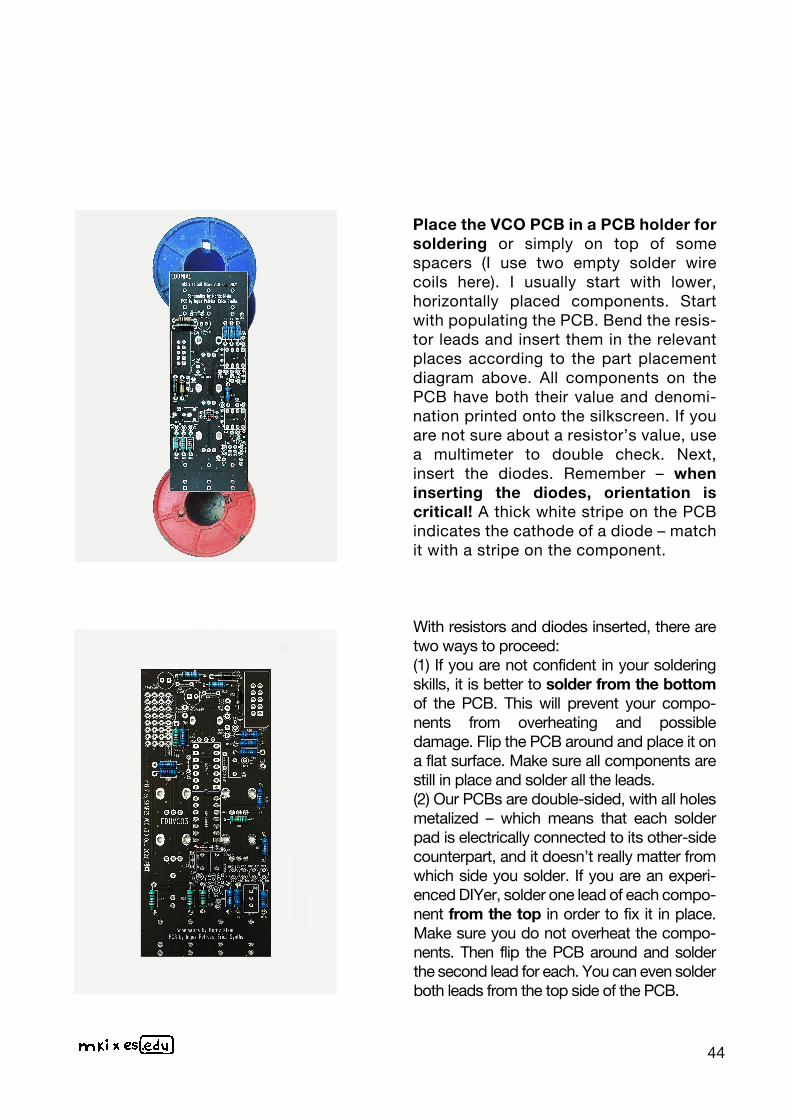
Next, insert & solder the film- and electrolytic capacitors. Electrolytic capacitors are bipolar, and you need to mind their orientation. The positive lead of each electrolytic capacitor is longer, and there’s a minus stripe on the side of the capacitor’s body to indicate the neg-ative lead. On our PCBs, the positive pad for a capacitor has a square shape, and the negative lead should go into the pad next to the notch on the silkscreen.
Now your PCB should look like this.
Capacitors C6, C7 and C9 are additional decoupling capacitors. If you inspect the PCB, you’ll see that these are placed as close to the power supply pins of the ICs as possible. For well-designed larger PCBs you will find decoupling capacitors next to each IC. Like the others, their job is to simply compensate for any unwanted noise in the supply rails. If the input voltage drops, then these capacitors will be able to bridge the gap to keep the voltage at the IC stable. And vice-versa - if the voltage increases, then they’ll be able to absorb the excess energy trying to flow through to the IC, which again keeps the voltage stable. Typi-cally, 0.1uF capacitors are used for this purpose.
All unused inputs of DD1 (DD1B-DD1F) are connected to ground, just like before on the breadboard – this is good practice which helps to prevent random voltages appearing on the IC’s inputs and outputs. TP11-TP42 are “fake” test points or a “kludge area”. On the PCB, this allows you to make some custom modifications to the module – you can intro-duce, for example, a VCO range switch, synchronization input, etc. As you can see, TP11 and TP12 are connected to +12V, while TP17 and TP18 link to -12V – since you may need a power supply connection for your modifications.
Before you start soldering, we highly recommend printing out these part placement diagrams with designators and values. Because some of our PCBs are rather densely pop-ulated, this will help you to avoid mistakes in the build process.
Place the VCO PCB in a PCB holder for soldering or simply on top of some spacers (I use two empty solder wire coils here). I usually start with lower, horizontally placed components. Start with populating the PCB. Bend the resis-tor leads and insert them in the relevant places according to the part placement diagram above. All components on the PCB have both their value and denomi-nation printed onto the silkscreen. If you are not sure about a resistor’s value, use a multimeter to double check. Next, insert the diodes. Remember – when inserting the diodes, orientation is critical! A thick white stripe on the PCB indicates the cathode of a diode – match it with a stripe on the component.
With resistors and diodes inserted, there are two ways to proceed: (1) If you are not confident in your soldering skills, it is better to solder from the bottom of the PCB. This will prevent your compo-nents from overheating and possible damage. Flip the PCB around and place it on a flat surface. Make sure all components are still in place and solder all the leads. (2) Our PCBs are double-sided, with all holes metalized – which means that each solder pad is electrically connected to its other-side counterpart, and it doesn’t really matter from which side you solder. If you are an experi-enced DIYer, solder one lead of each compo-nent from the top in order to fix it in place. Make sure you do not overheat the compo-nents. Then flip the PCB around and solder the second lead for each. You can even solder both leads from the top side of the PCB.
Once done with soldering, use pliers to cut off the excess leads. Next, insert the first DIP socket, hold it in place and solder one of the pins. Continue with the next DIP socket. Make sure the DIP sock-ets are oriented correctly – the notch on the socket should match the notch on the PCB’s silkscreen. Now, turn the PCB around and solder all remaining pins of the DIP sockets. Then proceed with the ceramic capacitors. Place the PCB on spacers, insert the capacitors and solder them like you did with the resistors & diodes before.
Next up: inserting & soldering the NTC thermistors and transistors. Make sure you place the transistors in their desig-nated spots. Also, they need to be prop-erly aligned with the marked outline on the silkscreen – orientation is critically important here. Complete this step by soldering vertically placed resistors.
Next, solder the precision trimmer and the power supply socket. Make sure the Insert the jack sockets and solder them.-orientation of the socket is as shown in the picture below – the arrow pointing to the first pin is aligned with a notch on the silkscreen. The key on the socket will be facing outwards from the PCB.
Now, turn the PCB around and inspect your solder joints. Make sure all compo-nents are soldered properly and there are no cold solder joints or accidental shorts. Clean the PCB to remove extra flux, if necessary.
Insert the jack sockets and solder them.
Insert the potentiometers. Don’t mix up their values and don’t solder them yet! Fit the front panel and make sure that the potentiometers’ shafts are aligned with the holes on the panel – and that they rotate freely. Now, go ahead and solder the potentiometers.
Install the front panel and fix it in place with the 5 hex nuts on the jack sockets and a washer plus hex nut on the top potentiometer. Fit the large knob on the bare potentiometer shaft and fix it in place with a small screwdriver. We are almost done
Now, insert the ICs into their respec-tive DIP sockets. Mind the orientation of the ICs – match the notch on each IC with the one on its socket.
Congratulations! You have completed the assembly of the es x mki.edu VCO module! Now connect it to your eurorack power supply and switch it on. If there’s no “magic smoke“, it’s a good sign that your build was successful. Connect the VCO’s SAW output to a mixer and check if you get a signal. Rotate the COARSE knob and
DIY electronics is a great (and quite addictive) hobby, therefore we highly recommend you invest in good tools. In order to really enjoy soldering, you’ll need:
A decent soldering station. Top-of-the-line soldering stations (brands like Weller) will cost 200EUR and above, but cheaper alternatives around 50EUR are often good enough. Make sure your soldering station of choice comes with multiple differently-sized soldering iron tips. The most useful ones for DIY electronics are flat, 2mm wide tips.
When heated up, the tips of soldering irons tend to oxidize. As a result, solder won’t stick to them, so you’ll need to clean your tip frequently. Most soldering stations come with a damp sponge for cleaning the iron tips – but there are also profes-sional solder tip cleaners with golden curls (not really gold, so not as expensive as it sounds). These work much better because they do not cool down the iron.
Solder wire with flux. I find 0,7mm solder wire works best for DIY projects.
Some soldering flux paste or pen will be useful as well.
Cutting pliers. Use them to cut off excess leads of components after soldering.
A solder suction pump. No matter how refined your soldering skills are, you will make mistakes. So when you’ll inevitably need to de-solder components, you will also need to remove any remaining solder from the solder pads in order to insert new components.
Once you have finished soldering your PCB, it’s recommended to remove excess flux from the solder joints. A PCB cleaner is the best way to go.
All of these tools can be found on major electronic components retailer websites, like Mouser, Farnell and at your local electronics shops. As you work your way towards more and more advanced projects, you’ll need to expand your skillset and your tool belt – but the gratification will be much greater.
“We keep moving forward, opening new doors, and doing new things, because we're curious and curiosity keeps leading us down new paths.” - Walt Disney
44
make sure you hear a change in pitch. If you do, you can proceed with tuning the VCO as we’ve done before on the breadboard.If you’ve never soldered before – or if your skills have become rusty – it’s probably wise to check out some THT (through-hole technology) soldering tutorials on YouTube. The main thing you have to remember while soldering is that melted solder will flow towards higher temperature areas. So you need to make sure you apply equal heat to the component you are soldering and the solder pad on the PCB. The pad will typically absorb more heat (especially ground-connected pads which have more thermal mass), so keep your soldering iron closer to the pad on the PCB. It’s critically important to dial in the right temperature on your soldering station. I found that about 320 °C is the opti-mal temperature for most of parts, while for larger elements like potentiometers and sockets, you may want to increase that temperature to 370 °C.
Here’s the recommended soldering sequence:
After you have completed soldering, inspect the solder joint:
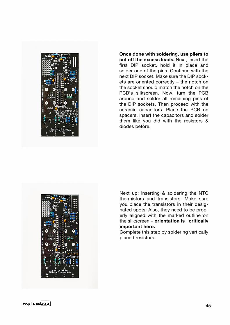
Next, insert & solder the film- and electrolytic capacitors. Electrolytic capacitors are bipolar, and you need to mind their orientation. The positive lead of each electrolytic capacitor is longer, and there’s a minus stripe on the side of the capacitor’s body to indicate the neg-ative lead. On our PCBs, the positive pad for a capacitor has a square shape, and the negative lead should go into the pad next to the notch on the silkscreen.
Now your PCB should look like this.
Capacitors C6, C7 and C9 are additional decoupling capacitors. If you inspect the PCB, you’ll see that these are placed as close to the power supply pins of the ICs as possible. For well-designed larger PCBs you will find decoupling capacitors next to each IC. Like the others, their job is to simply compensate for any unwanted noise in the supply rails. If the input voltage drops, then these capacitors will be able to bridge the gap to keep the voltage at the IC stable. And vice-versa - if the voltage increases, then they’ll be able to absorb the excess energy trying to flow through to the IC, which again keeps the voltage stable. Typi-cally, 0.1uF capacitors are used for this purpose.
All unused inputs of DD1 (DD1B-DD1F) are connected to ground, just like before on the breadboard – this is good practice which helps to prevent random voltages appearing on the IC’s inputs and outputs. TP11-TP42 are “fake” test points or a “kludge area”. On the PCB, this allows you to make some custom modifications to the module – you can intro-duce, for example, a VCO range switch, synchronization input, etc. As you can see, TP11 and TP12 are connected to +12V, while TP17 and TP18 link to -12V – since you may need a power supply connection for your modifications.
Before you start soldering, we highly recommend printing out these part placement diagrams with designators and values. Because some of our PCBs are rather densely pop-ulated, this will help you to avoid mistakes in the build process.
Place the VCO PCB in a PCB holder for soldering or simply on top of some spacers (I use two empty solder wire coils here). I usually start with lower, horizontally placed components. Start with populating the PCB. Bend the resis-tor leads and insert them in the relevant places according to the part placement diagram above. All components on the PCB have both their value and denomi-nation printed onto the silkscreen. If you are not sure about a resistor’s value, use a multimeter to double check. Next, insert the diodes. Remember – when inserting the diodes, orientation is critical! A thick white stripe on the PCB indicates the cathode of a diode – match it with a stripe on the component.
With resistors and diodes inserted, there are two ways to proceed: (1) If you are not confident in your soldering skills, it is better to solder from the bottom of the PCB. This will prevent your compo-nents from overheating and possible damage. Flip the PCB around and place it on a flat surface. Make sure all components are still in place and solder all the leads. (2) Our PCBs are double-sided, with all holes metalized – which means that each solder pad is electrically connected to its other-side counterpart, and it doesn’t really matter from which side you solder. If you are an experi-enced DIYer, solder one lead of each compo-nent from the top in order to fix it in place. Make sure you do not overheat the compo-nents. Then flip the PCB around and solder the second lead for each. You can even solder both leads from the top side of the PCB.
Once done with soldering, use pliers to cut off the excess leads. Next, insert the first DIP socket, hold it in place and solder one of the pins. Continue with the next DIP socket. Make sure the DIP sock-ets are oriented correctly – the notch on the socket should match the notch on the PCB’s silkscreen. Now, turn the PCB around and solder all remaining pins of the DIP sockets. Then proceed with the ceramic capacitors. Place the PCB on spacers, insert the capacitors and solder them like you did with the resistors & diodes before.
Next up: inserting & soldering the NTC thermistors and transistors. Make sure you place the transistors in their desig-nated spots. Also, they need to be prop-erly aligned with the marked outline on the silkscreen – orientation is critically important here. Complete this step by soldering vertically placed resistors.
Next, solder the precision trimmer and the power supply socket. Make sure the Insert the jack sockets and solder them.-orientation of the socket is as shown in the picture below – the arrow pointing to the first pin is aligned with a notch on the silkscreen. The key on the socket will be facing outwards from the PCB.
Now, turn the PCB around and inspect your solder joints. Make sure all compo-nents are soldered properly and there are no cold solder joints or accidental shorts. Clean the PCB to remove extra flux, if necessary.
Insert the jack sockets and solder them.
Insert the potentiometers. Don’t mix up their values and don’t solder them yet! Fit the front panel and make sure that the potentiometers’ shafts are aligned with the holes on the panel – and that they rotate freely. Now, go ahead and solder the potentiometers.
Install the front panel and fix it in place with the 5 hex nuts on the jack sockets and a washer plus hex nut on the top potentiometer. Fit the large knob on the bare potentiometer shaft and fix it in place with a small screwdriver. We are almost done
Now, insert the ICs into their respec-tive DIP sockets. Mind the orientation of the ICs – match the notch on each IC with the one on its socket.
Congratulations! You have completed the assembly of the es x mki.edu VCO module! Now connect it to your eurorack power supply and switch it on. If there’s no “magic smoke“, it’s a good sign that your build was successful. Connect the VCO’s SAW output to a mixer and check if you get a signal. Rotate the COARSE knob and
DIY electronics is a great (and quite addictive) hobby, therefore we highly recommend you invest in good tools. In order to really enjoy soldering, you’ll need:
A decent soldering station. Top-of-the-line soldering stations (brands like Weller) will cost 200EUR and above, but cheaper alternatives around 50EUR are often good enough. Make sure your soldering station of choice comes with multiple differently-sized soldering iron tips. The most useful ones for DIY electronics are flat, 2mm wide tips.
When heated up, the tips of soldering irons tend to oxidize. As a result, solder won’t stick to them, so you’ll need to clean your tip frequently. Most soldering stations come with a damp sponge for cleaning the iron tips – but there are also profes-sional solder tip cleaners with golden curls (not really gold, so not as expensive as it sounds). These work much better because they do not cool down the iron.
Solder wire with flux. I find 0,7mm solder wire works best for DIY projects.
Some soldering flux paste or pen will be useful as well.
Cutting pliers. Use them to cut off excess leads of components after soldering.
A solder suction pump. No matter how refined your soldering skills are, you will make mistakes. So when you’ll inevitably need to de-solder components, you will also need to remove any remaining solder from the solder pads in order to insert new components.
Once you have finished soldering your PCB, it’s recommended to remove excess flux from the solder joints. A PCB cleaner is the best way to go.
All of these tools can be found on major electronic components retailer websites, like Mouser, Farnell and at your local electronics shops. As you work your way towards more and more advanced projects, you’ll need to expand your skillset and your tool belt – but the gratification will be much greater.
“We keep moving forward, opening new doors, and doing new things, because we're curious and curiosity keeps leading us down new paths.” - Walt Disney
45
make sure you hear a change in pitch. If you do, you can proceed with tuning the VCO as we’ve done before on the breadboard.If you’ve never soldered before – or if your skills have become rusty – it’s probably wise to check out some THT (through-hole technology) soldering tutorials on YouTube. The main thing you have to remember while soldering is that melted solder will flow towards higher temperature areas. So you need to make sure you apply equal heat to the component you are soldering and the solder pad on the PCB. The pad will typically absorb more heat (especially ground-connected pads which have more thermal mass), so keep your soldering iron closer to the pad on the PCB. It’s critically important to dial in the right temperature on your soldering station. I found that about 320 °C is the opti-mal temperature for most of parts, while for larger elements like potentiometers and sockets, you may want to increase that temperature to 370 °C.
Here’s the recommended soldering sequence:
After you have completed soldering, inspect the solder joint:
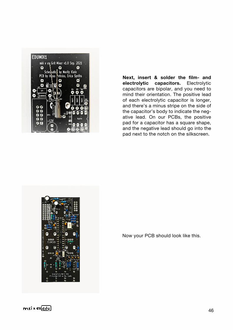
Next, insert & solder the film- and electrolytic capacitors. Electrolytic capacitors are bipolar, and you need to mind their orientation. The positive lead of each electrolytic capacitor is longer, and there’s a minus stripe on the side of the capacitor’s body to indicate the neg-ative lead. On our PCBs, the positive pad for a capacitor has a square shape, and the negative lead should go into the pad next to the notch on the silkscreen.
Now your PCB should look like this.
Capacitors C6, C7 and C9 are additional decoupling capacitors. If you inspect the PCB, you’ll see that these are placed as close to the power supply pins of the ICs as possible. For well-designed larger PCBs you will find decoupling capacitors next to each IC. Like the others, their job is to simply compensate for any unwanted noise in the supply rails. If the input voltage drops, then these capacitors will be able to bridge the gap to keep the voltage at the IC stable. And vice-versa - if the voltage increases, then they’ll be able to absorb the excess energy trying to flow through to the IC, which again keeps the voltage stable. Typi-cally, 0.1uF capacitors are used for this purpose.
All unused inputs of DD1 (DD1B-DD1F) are connected to ground, just like before on the breadboard – this is good practice which helps to prevent random voltages appearing on the IC’s inputs and outputs. TP11-TP42 are “fake” test points or a “kludge area”. On the PCB, this allows you to make some custom modifications to the module – you can intro-duce, for example, a VCO range switch, synchronization input, etc. As you can see, TP11 and TP12 are connected to +12V, while TP17 and TP18 link to -12V – since you may need a power supply connection for your modifications.
Before you start soldering, we highly recommend printing out these part placement diagrams with designators and values. Because some of our PCBs are rather densely pop-ulated, this will help you to avoid mistakes in the build process.
Place the VCO PCB in a PCB holder for soldering or simply on top of some spacers (I use two empty solder wire coils here). I usually start with lower, horizontally placed components. Start with populating the PCB. Bend the resis-tor leads and insert them in the relevant places according to the part placement diagram above. All components on the PCB have both their value and denomi-nation printed onto the silkscreen. If you are not sure about a resistor’s value, use a multimeter to double check. Next, insert the diodes. Remember – when inserting the diodes, orientation is critical! A thick white stripe on the PCB indicates the cathode of a diode – match it with a stripe on the component.
With resistors and diodes inserted, there are two ways to proceed: (1) If you are not confident in your soldering skills, it is better to solder from the bottom of the PCB. This will prevent your compo-nents from overheating and possible damage. Flip the PCB around and place it on a flat surface. Make sure all components are still in place and solder all the leads. (2) Our PCBs are double-sided, with all holes metalized – which means that each solder pad is electrically connected to its other-side counterpart, and it doesn’t really matter from which side you solder. If you are an experi-enced DIYer, solder one lead of each compo-nent from the top in order to fix it in place. Make sure you do not overheat the compo-nents. Then flip the PCB around and solder the second lead for each. You can even solder both leads from the top side of the PCB.
Once done with soldering, use pliers to cut off the excess leads. Next, insert the first DIP socket, hold it in place and solder one of the pins. Continue with the next DIP socket. Make sure the DIP sock-ets are oriented correctly – the notch on the socket should match the notch on the PCB’s silkscreen. Now, turn the PCB around and solder all remaining pins of the DIP sockets. Then proceed with the ceramic capacitors. Place the PCB on spacers, insert the capacitors and solder them like you did with the resistors & diodes before.
Next up: inserting & soldering the NTC thermistors and transistors. Make sure you place the transistors in their desig-nated spots. Also, they need to be prop-erly aligned with the marked outline on the silkscreen – orientation is critically important here. Complete this step by soldering vertically placed resistors.
Next, solder the precision trimmer and the power supply socket. Make sure the Insert the jack sockets and solder them.-orientation of the socket is as shown in the picture below – the arrow pointing to the first pin is aligned with a notch on the silkscreen. The key on the socket will be facing outwards from the PCB.
Now, turn the PCB around and inspect your solder joints. Make sure all compo-nents are soldered properly and there are no cold solder joints or accidental shorts. Clean the PCB to remove extra flux, if necessary.
Insert the jack sockets and solder them.
Insert the potentiometers. Don’t mix up their values and don’t solder them yet! Fit the front panel and make sure that the potentiometers’ shafts are aligned with the holes on the panel – and that they rotate freely. Now, go ahead and solder the potentiometers.
Install the front panel and fix it in place with the 5 hex nuts on the jack sockets and a washer plus hex nut on the top potentiometer. Fit the large knob on the bare potentiometer shaft and fix it in place with a small screwdriver. We are almost done
Now, insert the ICs into their respec-tive DIP sockets. Mind the orientation of the ICs – match the notch on each IC with the one on its socket.
Congratulations! You have completed the assembly of the es x mki.edu VCO module! Now connect it to your eurorack power supply and switch it on. If there’s no “magic smoke“, it’s a good sign that your build was successful. Connect the VCO’s SAW output to a mixer and check if you get a signal. Rotate the COARSE knob and
DIY electronics is a great (and quite addictive) hobby, therefore we highly recommend you invest in good tools. In order to really enjoy soldering, you’ll need:
A decent soldering station. Top-of-the-line soldering stations (brands like Weller) will cost 200EUR and above, but cheaper alternatives around 50EUR are often good enough. Make sure your soldering station of choice comes with multiple differently-sized soldering iron tips. The most useful ones for DIY electronics are flat, 2mm wide tips.
When heated up, the tips of soldering irons tend to oxidize. As a result, solder won’t stick to them, so you’ll need to clean your tip frequently. Most soldering stations come with a damp sponge for cleaning the iron tips – but there are also profes-sional solder tip cleaners with golden curls (not really gold, so not as expensive as it sounds). These work much better because they do not cool down the iron.
Solder wire with flux. I find 0,7mm solder wire works best for DIY projects.
Some soldering flux paste or pen will be useful as well.
Cutting pliers. Use them to cut off excess leads of components after soldering.
A solder suction pump. No matter how refined your soldering skills are, you will make mistakes. So when you’ll inevitably need to de-solder components, you will also need to remove any remaining solder from the solder pads in order to insert new components.
Once you have finished soldering your PCB, it’s recommended to remove excess flux from the solder joints. A PCB cleaner is the best way to go.
All of these tools can be found on major electronic components retailer websites, like Mouser, Farnell and at your local electronics shops. As you work your way towards more and more advanced projects, you’ll need to expand your skillset and your tool belt – but the gratification will be much greater.
“We keep moving forward, opening new doors, and doing new things, because we're curious and curiosity keeps leading us down new paths.” - Walt Disney
46
make sure you hear a change in pitch. If you do, you can proceed with tuning the VCO as we’ve done before on the breadboard.If you’ve never soldered before – or if your skills have become rusty – it’s probably wise to check out some THT (through-hole technology) soldering tutorials on YouTube. The main thing you have to remember while soldering is that melted solder will flow towards higher temperature areas. So you need to make sure you apply equal heat to the component you are soldering and the solder pad on the PCB. The pad will typically absorb more heat (especially ground-connected pads which have more thermal mass), so keep your soldering iron closer to the pad on the PCB. It’s critically important to dial in the right temperature on your soldering station. I found that about 320 °C is the opti-mal temperature for most of parts, while for larger elements like potentiometers and sockets, you may want to increase that temperature to 370 °C.
Here’s the recommended soldering sequence:
After you have completed soldering, inspect the solder joint:
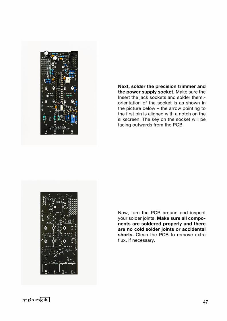
Next, insert & solder the film- and electrolytic capacitors. Electrolytic capacitors are bipolar, and you need to mind their orientation. The positive lead of each electrolytic capacitor is longer, and there’s a minus stripe on the side of the capacitor’s body to indicate the neg-ative lead. On our PCBs, the positive pad for a capacitor has a square shape, and the negative lead should go into the pad next to the notch on the silkscreen.
Now your PCB should look like this.
Capacitors C6, C7 and C9 are additional decoupling capacitors. If you inspect the PCB, you’ll see that these are placed as close to the power supply pins of the ICs as possible. For well-designed larger PCBs you will find decoupling capacitors next to each IC. Like the others, their job is to simply compensate for any unwanted noise in the supply rails. If the input voltage drops, then these capacitors will be able to bridge the gap to keep the voltage at the IC stable. And vice-versa - if the voltage increases, then they’ll be able to absorb the excess energy trying to flow through to the IC, which again keeps the voltage stable. Typi-cally, 0.1uF capacitors are used for this purpose.
All unused inputs of DD1 (DD1B-DD1F) are connected to ground, just like before on the breadboard – this is good practice which helps to prevent random voltages appearing on the IC’s inputs and outputs. TP11-TP42 are “fake” test points or a “kludge area”. On the PCB, this allows you to make some custom modifications to the module – you can intro-duce, for example, a VCO range switch, synchronization input, etc. As you can see, TP11 and TP12 are connected to +12V, while TP17 and TP18 link to -12V – since you may need a power supply connection for your modifications.
Before you start soldering, we highly recommend printing out these part placement diagrams with designators and values. Because some of our PCBs are rather densely pop-ulated, this will help you to avoid mistakes in the build process.
Place the VCO PCB in a PCB holder for soldering or simply on top of some spacers (I use two empty solder wire coils here). I usually start with lower, horizontally placed components. Start with populating the PCB. Bend the resis-tor leads and insert them in the relevant places according to the part placement diagram above. All components on the PCB have both their value and denomi-nation printed onto the silkscreen. If you are not sure about a resistor’s value, use a multimeter to double check. Next, insert the diodes. Remember – when inserting the diodes, orientation is critical! A thick white stripe on the PCB indicates the cathode of a diode – match it with a stripe on the component.
With resistors and diodes inserted, there are two ways to proceed: (1) If you are not confident in your soldering skills, it is better to solder from the bottom of the PCB. This will prevent your compo-nents from overheating and possible damage. Flip the PCB around and place it on a flat surface. Make sure all components are still in place and solder all the leads. (2) Our PCBs are double-sided, with all holes metalized – which means that each solder pad is electrically connected to its other-side counterpart, and it doesn’t really matter from which side you solder. If you are an experi-enced DIYer, solder one lead of each compo-nent from the top in order to fix it in place. Make sure you do not overheat the compo-nents. Then flip the PCB around and solder the second lead for each. You can even solder both leads from the top side of the PCB.
Once done with soldering, use pliers to cut off the excess leads. Next, insert the first DIP socket, hold it in place and solder one of the pins. Continue with the next DIP socket. Make sure the DIP sock-ets are oriented correctly – the notch on the socket should match the notch on the PCB’s silkscreen. Now, turn the PCB around and solder all remaining pins of the DIP sockets. Then proceed with the ceramic capacitors. Place the PCB on spacers, insert the capacitors and solder them like you did with the resistors & diodes before.
Next up: inserting & soldering the NTC thermistors and transistors. Make sure you place the transistors in their desig-nated spots. Also, they need to be prop-erly aligned with the marked outline on the silkscreen – orientation is critically important here. Complete this step by soldering vertically placed resistors.
Next, solder the precision trimmer and the power supply socket. Make sure the Insert the jack sockets and solder them.-orientation of the socket is as shown in the picture below – the arrow pointing to the first pin is aligned with a notch on the silkscreen. The key on the socket will be facing outwards from the PCB.
Now, turn the PCB around and inspect your solder joints. Make sure all compo-nents are soldered properly and there are no cold solder joints or accidental shorts. Clean the PCB to remove extra flux, if necessary.
Insert the jack sockets and solder them.
Insert the potentiometers. Don’t mix up their values and don’t solder them yet! Fit the front panel and make sure that the potentiometers’ shafts are aligned with the holes on the panel – and that they rotate freely. Now, go ahead and solder the potentiometers.
Install the front panel and fix it in place with the 5 hex nuts on the jack sockets and a washer plus hex nut on the top potentiometer. Fit the large knob on the bare potentiometer shaft and fix it in place with a small screwdriver. We are almost done
Now, insert the ICs into their respec-tive DIP sockets. Mind the orientation of the ICs – match the notch on each IC with the one on its socket.
Congratulations! You have completed the assembly of the es x mki.edu VCO module! Now connect it to your eurorack power supply and switch it on. If there’s no “magic smoke“, it’s a good sign that your build was successful. Connect the VCO’s SAW output to a mixer and check if you get a signal. Rotate the COARSE knob and
DIY electronics is a great (and quite addictive) hobby, therefore we highly recommend you invest in good tools. In order to really enjoy soldering, you’ll need:
A decent soldering station. Top-of-the-line soldering stations (brands like Weller) will cost 200EUR and above, but cheaper alternatives around 50EUR are often good enough. Make sure your soldering station of choice comes with multiple differently-sized soldering iron tips. The most useful ones for DIY electronics are flat, 2mm wide tips.
When heated up, the tips of soldering irons tend to oxidize. As a result, solder won’t stick to them, so you’ll need to clean your tip frequently. Most soldering stations come with a damp sponge for cleaning the iron tips – but there are also profes-sional solder tip cleaners with golden curls (not really gold, so not as expensive as it sounds). These work much better because they do not cool down the iron.
Solder wire with flux. I find 0,7mm solder wire works best for DIY projects.
Some soldering flux paste or pen will be useful as well.
Cutting pliers. Use them to cut off excess leads of components after soldering.
A solder suction pump. No matter how refined your soldering skills are, you will make mistakes. So when you’ll inevitably need to de-solder components, you will also need to remove any remaining solder from the solder pads in order to insert new components.
Once you have finished soldering your PCB, it’s recommended to remove excess flux from the solder joints. A PCB cleaner is the best way to go.
All of these tools can be found on major electronic components retailer websites, like Mouser, Farnell and at your local electronics shops. As you work your way towards more and more advanced projects, you’ll need to expand your skillset and your tool belt – but the gratification will be much greater.
“We keep moving forward, opening new doors, and doing new things, because we're curious and curiosity keeps leading us down new paths.” - Walt Disney
47
make sure you hear a change in pitch. If you do, you can proceed with tuning the VCO as we’ve done before on the breadboard.If you’ve never soldered before – or if your skills have become rusty – it’s probably wise to check out some THT (through-hole technology) soldering tutorials on YouTube. The main thing you have to remember while soldering is that melted solder will flow towards higher temperature areas. So you need to make sure you apply equal heat to the component you are soldering and the solder pad on the PCB. The pad will typically absorb more heat (especially ground-connected pads which have more thermal mass), so keep your soldering iron closer to the pad on the PCB. It’s critically important to dial in the right temperature on your soldering station. I found that about 320 °C is the opti-mal temperature for most of parts, while for larger elements like potentiometers and sockets, you may want to increase that temperature to 370 °C.
Here’s the recommended soldering sequence:
After you have completed soldering, inspect the solder joint:
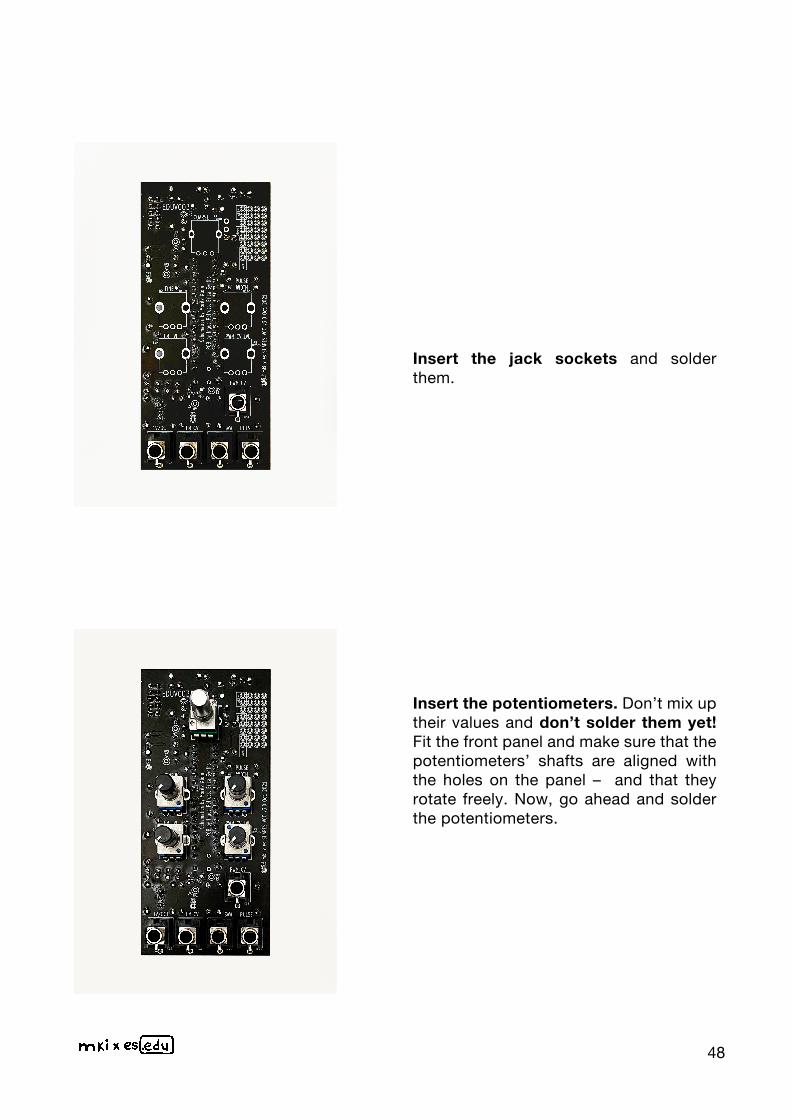
Next, insert & solder the film- and electrolytic capacitors. Electrolytic capacitors are bipolar, and you need to mind their orientation. The positive lead of each electrolytic capacitor is longer, and there’s a minus stripe on the side of the capacitor’s body to indicate the neg-ative lead. On our PCBs, the positive pad for a capacitor has a square shape, and the negative lead should go into the pad next to the notch on the silkscreen.
Now your PCB should look like this.
Capacitors C6, C7 and C9 are additional decoupling capacitors. If you inspect the PCB, you’ll see that these are placed as close to the power supply pins of the ICs as possible. For well-designed larger PCBs you will find decoupling capacitors next to each IC. Like the others, their job is to simply compensate for any unwanted noise in the supply rails. If the input voltage drops, then these capacitors will be able to bridge the gap to keep the voltage at the IC stable. And vice-versa - if the voltage increases, then they’ll be able to absorb the excess energy trying to flow through to the IC, which again keeps the voltage stable. Typi-cally, 0.1uF capacitors are used for this purpose.
All unused inputs of DD1 (DD1B-DD1F) are connected to ground, just like before on the breadboard – this is good practice which helps to prevent random voltages appearing on the IC’s inputs and outputs. TP11-TP42 are “fake” test points or a “kludge area”. On the PCB, this allows you to make some custom modifications to the module – you can intro-duce, for example, a VCO range switch, synchronization input, etc. As you can see, TP11 and TP12 are connected to +12V, while TP17 and TP18 link to -12V – since you may need a power supply connection for your modifications.
Before you start soldering, we highly recommend printing out these part placement diagrams with designators and values. Because some of our PCBs are rather densely pop-ulated, this will help you to avoid mistakes in the build process.
Place the VCO PCB in a PCB holder for soldering or simply on top of some spacers (I use two empty solder wire coils here). I usually start with lower, horizontally placed components. Start with populating the PCB. Bend the resis-tor leads and insert them in the relevant places according to the part placement diagram above. All components on the PCB have both their value and denomi-nation printed onto the silkscreen. If you are not sure about a resistor’s value, use a multimeter to double check. Next, insert the diodes. Remember – when inserting the diodes, orientation is critical! A thick white stripe on the PCB indicates the cathode of a diode – match it with a stripe on the component.
With resistors and diodes inserted, there are two ways to proceed: (1) If you are not confident in your soldering skills, it is better to solder from the bottom of the PCB. This will prevent your compo-nents from overheating and possible damage. Flip the PCB around and place it on a flat surface. Make sure all components are still in place and solder all the leads. (2) Our PCBs are double-sided, with all holes metalized – which means that each solder pad is electrically connected to its other-side counterpart, and it doesn’t really matter from which side you solder. If you are an experi-enced DIYer, solder one lead of each compo-nent from the top in order to fix it in place. Make sure you do not overheat the compo-nents. Then flip the PCB around and solder the second lead for each. You can even solder both leads from the top side of the PCB.
Once done with soldering, use pliers to cut off the excess leads. Next, insert the first DIP socket, hold it in place and solder one of the pins. Continue with the next DIP socket. Make sure the DIP sock-ets are oriented correctly – the notch on the socket should match the notch on the PCB’s silkscreen. Now, turn the PCB around and solder all remaining pins of the DIP sockets. Then proceed with the ceramic capacitors. Place the PCB on spacers, insert the capacitors and solder them like you did with the resistors & diodes before.
Next up: inserting & soldering the NTC thermistors and transistors. Make sure you place the transistors in their desig-nated spots. Also, they need to be prop-erly aligned with the marked outline on the silkscreen – orientation is critically important here. Complete this step by soldering vertically placed resistors.
Next, solder the precision trimmer and the power supply socket. Make sure the Insert the jack sockets and solder them.-orientation of the socket is as shown in the picture below – the arrow pointing to the first pin is aligned with a notch on the silkscreen. The key on the socket will be facing outwards from the PCB.
Now, turn the PCB around and inspect your solder joints. Make sure all compo-nents are soldered properly and there are no cold solder joints or accidental shorts. Clean the PCB to remove extra flux, if necessary.
Insert the jack sockets and solder them.
Insert the potentiometers. Don’t mix up their values and don’t solder them yet! Fit the front panel and make sure that the potentiometers’ shafts are aligned with the holes on the panel – and that they rotate freely. Now, go ahead and solder the potentiometers.
Install the front panel and fix it in place with the 5 hex nuts on the jack sockets and a washer plus hex nut on the top potentiometer. Fit the large knob on the bare potentiometer shaft and fix it in place with a small screwdriver. We are almost done
Now, insert the ICs into their respec-tive DIP sockets. Mind the orientation of the ICs – match the notch on each IC with the one on its socket.
Congratulations! You have completed the assembly of the es x mki.edu VCO module! Now connect it to your eurorack power supply and switch it on. If there’s no “magic smoke“, it’s a good sign that your build was successful. Connect the VCO’s SAW output to a mixer and check if you get a signal. Rotate the COARSE knob and
DIY electronics is a great (and quite addictive) hobby, therefore we highly recommend you invest in good tools. In order to really enjoy soldering, you’ll need:
A decent soldering station. Top-of-the-line soldering stations (brands like Weller) will cost 200EUR and above, but cheaper alternatives around 50EUR are often good enough. Make sure your soldering station of choice comes with multiple differently-sized soldering iron tips. The most useful ones for DIY electronics are flat, 2mm wide tips.
When heated up, the tips of soldering irons tend to oxidize. As a result, solder won’t stick to them, so you’ll need to clean your tip frequently. Most soldering stations come with a damp sponge for cleaning the iron tips – but there are also profes-sional solder tip cleaners with golden curls (not really gold, so not as expensive as it sounds). These work much better because they do not cool down the iron.
Solder wire with flux. I find 0,7mm solder wire works best for DIY projects.
Some soldering flux paste or pen will be useful as well.
Cutting pliers. Use them to cut off excess leads of components after soldering.
A solder suction pump. No matter how refined your soldering skills are, you will make mistakes. So when you’ll inevitably need to de-solder components, you will also need to remove any remaining solder from the solder pads in order to insert new components.
Once you have finished soldering your PCB, it’s recommended to remove excess flux from the solder joints. A PCB cleaner is the best way to go.
All of these tools can be found on major electronic components retailer websites, like Mouser, Farnell and at your local electronics shops. As you work your way towards more and more advanced projects, you’ll need to expand your skillset and your tool belt – but the gratification will be much greater.
“We keep moving forward, opening new doors, and doing new things, because we're curious and curiosity keeps leading us down new paths.” - Walt Disney
48
make sure you hear a change in pitch. If you do, you can proceed with tuning the VCO as we’ve done before on the breadboard.If you’ve never soldered before – or if your skills have become rusty – it’s probably wise to check out some THT (through-hole technology) soldering tutorials on YouTube. The main thing you have to remember while soldering is that melted solder will flow towards higher temperature areas. So you need to make sure you apply equal heat to the component you are soldering and the solder pad on the PCB. The pad will typically absorb more heat (especially ground-connected pads which have more thermal mass), so keep your soldering iron closer to the pad on the PCB. It’s critically important to dial in the right temperature on your soldering station. I found that about 320 °C is the opti-mal temperature for most of parts, while for larger elements like potentiometers and sockets, you may want to increase that temperature to 370 °C.
Here’s the recommended soldering sequence:
After you have completed soldering, inspect the solder joint:
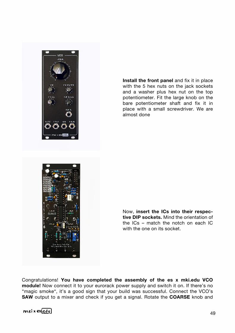
Next, insert & solder the film- and electrolytic capacitors. Electrolytic capacitors are bipolar, and you need to mind their orientation. The positive lead of each electrolytic capacitor is longer, and there’s a minus stripe on the side of the capacitor’s body to indicate the neg-ative lead. On our PCBs, the positive pad for a capacitor has a square shape, and the negative lead should go into the pad next to the notch on the silkscreen.
Now your PCB should look like this.
Capacitors C6, C7 and C9 are additional decoupling capacitors. If you inspect the PCB, you’ll see that these are placed as close to the power supply pins of the ICs as possible. For well-designed larger PCBs you will find decoupling capacitors next to each IC. Like the others, their job is to simply compensate for any unwanted noise in the supply rails. If the input voltage drops, then these capacitors will be able to bridge the gap to keep the voltage at the IC stable. And vice-versa - if the voltage increases, then they’ll be able to absorb the excess energy trying to flow through to the IC, which again keeps the voltage stable. Typi-cally, 0.1uF capacitors are used for this purpose.
All unused inputs of DD1 (DD1B-DD1F) are connected to ground, just like before on the breadboard – this is good practice which helps to prevent random voltages appearing on the IC’s inputs and outputs. TP11-TP42 are “fake” test points or a “kludge area”. On the PCB, this allows you to make some custom modifications to the module – you can intro-duce, for example, a VCO range switch, synchronization input, etc. As you can see, TP11 and TP12 are connected to +12V, while TP17 and TP18 link to -12V – since you may need a power supply connection for your modifications.
Before you start soldering, we highly recommend printing out these part placement diagrams with designators and values. Because some of our PCBs are rather densely pop-ulated, this will help you to avoid mistakes in the build process.
Place the VCO PCB in a PCB holder for soldering or simply on top of some spacers (I use two empty solder wire coils here). I usually start with lower, horizontally placed components. Start with populating the PCB. Bend the resis-tor leads and insert them in the relevant places according to the part placement diagram above. All components on the PCB have both their value and denomi-nation printed onto the silkscreen. If you are not sure about a resistor’s value, use a multimeter to double check. Next, insert the diodes. Remember – when inserting the diodes, orientation is critical! A thick white stripe on the PCB indicates the cathode of a diode – match it with a stripe on the component.
With resistors and diodes inserted, there are two ways to proceed: (1) If you are not confident in your soldering skills, it is better to solder from the bottom of the PCB. This will prevent your compo-nents from overheating and possible damage. Flip the PCB around and place it on a flat surface. Make sure all components are still in place and solder all the leads. (2) Our PCBs are double-sided, with all holes metalized – which means that each solder pad is electrically connected to its other-side counterpart, and it doesn’t really matter from which side you solder. If you are an experi-enced DIYer, solder one lead of each compo-nent from the top in order to fix it in place. Make sure you do not overheat the compo-nents. Then flip the PCB around and solder the second lead for each. You can even solder both leads from the top side of the PCB.
Once done with soldering, use pliers to cut off the excess leads. Next, insert the first DIP socket, hold it in place and solder one of the pins. Continue with the next DIP socket. Make sure the DIP sock-ets are oriented correctly – the notch on the socket should match the notch on the PCB’s silkscreen. Now, turn the PCB around and solder all remaining pins of the DIP sockets. Then proceed with the ceramic capacitors. Place the PCB on spacers, insert the capacitors and solder them like you did with the resistors & diodes before.
Next up: inserting & soldering the NTC thermistors and transistors. Make sure you place the transistors in their desig-nated spots. Also, they need to be prop-erly aligned with the marked outline on the silkscreen – orientation is critically important here. Complete this step by soldering vertically placed resistors.
Next, solder the precision trimmer and the power supply socket. Make sure the Insert the jack sockets and solder them.-orientation of the socket is as shown in the picture below – the arrow pointing to the first pin is aligned with a notch on the silkscreen. The key on the socket will be facing outwards from the PCB.
Now, turn the PCB around and inspect your solder joints. Make sure all compo-nents are soldered properly and there are no cold solder joints or accidental shorts. Clean the PCB to remove extra flux, if necessary.
Insert the jack sockets and solder them.
Insert the potentiometers. Don’t mix up their values and don’t solder them yet! Fit the front panel and make sure that the potentiometers’ shafts are aligned with the holes on the panel – and that they rotate freely. Now, go ahead and solder the potentiometers.
Install the front panel and fix it in place with the 5 hex nuts on the jack sockets and a washer plus hex nut on the top potentiometer. Fit the large knob on the bare potentiometer shaft and fix it in place with a small screwdriver. We are almost done
Now, insert the ICs into their respec-tive DIP sockets. Mind the orientation of the ICs – match the notch on each IC with the one on its socket.
Congratulations! You have completed the assembly of the es x mki.edu VCO module! Now connect it to your eurorack power supply and switch it on. If there’s no “magic smoke“, it’s a good sign that your build was successful. Connect the VCO’s SAW output to a mixer and check if you get a signal. Rotate the COARSE knob and
DIY electronics is a great (and quite addictive) hobby, therefore we highly recommend you invest in good tools. In order to really enjoy soldering, you’ll need:
A decent soldering station. Top-of-the-line soldering stations (brands like Weller) will cost 200EUR and above, but cheaper alternatives around 50EUR are often good enough. Make sure your soldering station of choice comes with multiple differently-sized soldering iron tips. The most useful ones for DIY electronics are flat, 2mm wide tips.
When heated up, the tips of soldering irons tend to oxidize. As a result, solder won’t stick to them, so you’ll need to clean your tip frequently. Most soldering stations come with a damp sponge for cleaning the iron tips – but there are also profes-sional solder tip cleaners with golden curls (not really gold, so not as expensive as it sounds). These work much better because they do not cool down the iron.
Solder wire with flux. I find 0,7mm solder wire works best for DIY projects.
Some soldering flux paste or pen will be useful as well.
Cutting pliers. Use them to cut off excess leads of components after soldering.
A solder suction pump. No matter how refined your soldering skills are, you will make mistakes. So when you’ll inevitably need to de-solder components, you will also need to remove any remaining solder from the solder pads in order to insert new components.
Once you have finished soldering your PCB, it’s recommended to remove excess flux from the solder joints. A PCB cleaner is the best way to go.
All of these tools can be found on major electronic components retailer websites, like Mouser, Farnell and at your local electronics shops. As you work your way towards more and more advanced projects, you’ll need to expand your skillset and your tool belt – but the gratification will be much greater.
“We keep moving forward, opening new doors, and doing new things, because we're curious and curiosity keeps leading us down new paths.” - Walt Disney
49
make sure you hear a change in pitch. If you do, you can proceed with tuning the VCO as we’ve done before on the breadboard.If you’ve never soldered before – or if your skills have become rusty – it’s probably wise to check out some THT (through-hole technology) soldering tutorials on YouTube. The main thing you have to remember while soldering is that melted solder will flow towards higher temperature areas. So you need to make sure you apply equal heat to the component you are soldering and the solder pad on the PCB. The pad will typically absorb more heat (especially ground-connected pads which have more thermal mass), so keep your soldering iron closer to the pad on the PCB. It’s critically important to dial in the right temperature on your soldering station. I found that about 320 °C is the opti-mal temperature for most of parts, while for larger elements like potentiometers and sockets, you may want to increase that temperature to 370 °C.
Here’s the recommended soldering sequence:
After you have completed soldering, inspect the solder joint:
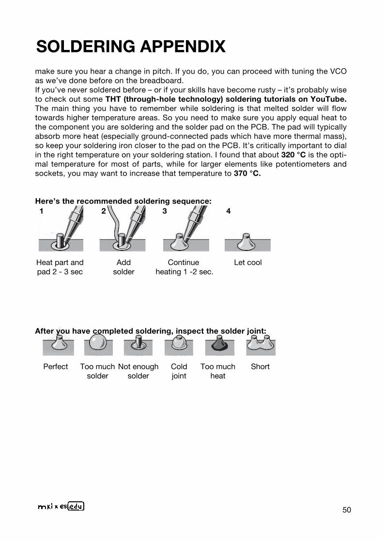
Next, insert & solder the film- and electrolytic capacitors. Electrolytic capacitors are bipolar, and you need to mind their orientation. The positive lead of each electrolytic capacitor is longer, and there’s a minus stripe on the side of the capacitor’s body to indicate the neg-ative lead. On our PCBs, the positive pad for a capacitor has a square shape, and the negative lead should go into the pad next to the notch on the silkscreen.
Now your PCB should look like this.
Capacitors C6, C7 and C9 are additional decoupling capacitors. If you inspect the PCB, you’ll see that these are placed as close to the power supply pins of the ICs as possible. For well-designed larger PCBs you will find decoupling capacitors next to each IC. Like the others, their job is to simply compensate for any unwanted noise in the supply rails. If the input voltage drops, then these capacitors will be able to bridge the gap to keep the voltage at the IC stable. And vice-versa - if the voltage increases, then they’ll be able to absorb the excess energy trying to flow through to the IC, which again keeps the voltage stable. Typi-cally, 0.1uF capacitors are used for this purpose.
All unused inputs of DD1 (DD1B-DD1F) are connected to ground, just like before on the breadboard – this is good practice which helps to prevent random voltages appearing on the IC’s inputs and outputs. TP11-TP42 are “fake” test points or a “kludge area”. On the PCB, this allows you to make some custom modifications to the module – you can intro-duce, for example, a VCO range switch, synchronization input, etc. As you can see, TP11 and TP12 are connected to +12V, while TP17 and TP18 link to -12V – since you may need a power supply connection for your modifications.
Before you start soldering, we highly recommend printing out these part placement diagrams with designators and values. Because some of our PCBs are rather densely pop-ulated, this will help you to avoid mistakes in the build process.
Place the VCO PCB in a PCB holder for soldering or simply on top of some spacers (I use two empty solder wire coils here). I usually start with lower, horizontally placed components. Start with populating the PCB. Bend the resis-tor leads and insert them in the relevant places according to the part placement diagram above. All components on the PCB have both their value and denomi-nation printed onto the silkscreen. If you are not sure about a resistor’s value, use a multimeter to double check. Next, insert the diodes. Remember – when inserting the diodes, orientation is critical! A thick white stripe on the PCB indicates the cathode of a diode – match it with a stripe on the component.
With resistors and diodes inserted, there are two ways to proceed: (1) If you are not confident in your soldering skills, it is better to solder from the bottom of the PCB. This will prevent your compo-nents from overheating and possible damage. Flip the PCB around and place it on a flat surface. Make sure all components are still in place and solder all the leads. (2) Our PCBs are double-sided, with all holes metalized – which means that each solder pad is electrically connected to its other-side counterpart, and it doesn’t really matter from which side you solder. If you are an experi-enced DIYer, solder one lead of each compo-nent from the top in order to fix it in place. Make sure you do not overheat the compo-nents. Then flip the PCB around and solder the second lead for each. You can even solder both leads from the top side of the PCB.
Once done with soldering, use pliers to cut off the excess leads. Next, insert the first DIP socket, hold it in place and solder one of the pins. Continue with the next DIP socket. Make sure the DIP sock-ets are oriented correctly – the notch on the socket should match the notch on the PCB’s silkscreen. Now, turn the PCB around and solder all remaining pins of the DIP sockets. Then proceed with the ceramic capacitors. Place the PCB on spacers, insert the capacitors and solder them like you did with the resistors & diodes before.
Next up: inserting & soldering the NTC thermistors and transistors. Make sure you place the transistors in their desig-nated spots. Also, they need to be prop-erly aligned with the marked outline on the silkscreen – orientation is critically important here. Complete this step by soldering vertically placed resistors.
Next, solder the precision trimmer and the power supply socket. Make sure the Insert the jack sockets and solder them.-orientation of the socket is as shown in the picture below – the arrow pointing to the first pin is aligned with a notch on the silkscreen. The key on the socket will be facing outwards from the PCB.
Now, turn the PCB around and inspect your solder joints. Make sure all compo-nents are soldered properly and there are no cold solder joints or accidental shorts. Clean the PCB to remove extra flux, if necessary.
Insert the jack sockets and solder them.
Insert the potentiometers. Don’t mix up their values and don’t solder them yet! Fit the front panel and make sure that the potentiometers’ shafts are aligned with the holes on the panel – and that they rotate freely. Now, go ahead and solder the potentiometers.
Install the front panel and fix it in place with the 5 hex nuts on the jack sockets and a washer plus hex nut on the top potentiometer. Fit the large knob on the bare potentiometer shaft and fix it in place with a small screwdriver. We are almost done
Now, insert the ICs into their respec-tive DIP sockets. Mind the orientation of the ICs – match the notch on each IC with the one on its socket.
Congratulations! You have completed the assembly of the es x mki.edu VCO module! Now connect it to your eurorack power supply and switch it on. If there’s no “magic smoke“, it’s a good sign that your build was successful. Connect the VCO’s SAW output to a mixer and check if you get a signal. Rotate the COARSE knob and
DIY electronics is a great (and quite addictive) hobby, therefore we highly recommend you invest in good tools. In order to really enjoy soldering, you’ll need:
A decent soldering station. Top-of-the-line soldering stations (brands like Weller) will cost 200EUR and above, but cheaper alternatives around 50EUR are often good enough. Make sure your soldering station of choice comes with multiple differently-sized soldering iron tips. The most useful ones for DIY electronics are flat, 2mm wide tips.
When heated up, the tips of soldering irons tend to oxidize. As a result, solder won’t stick to them, so you’ll need to clean your tip frequently. Most soldering stations come with a damp sponge for cleaning the iron tips – but there are also profes-sional solder tip cleaners with golden curls (not really gold, so not as expensive as it sounds). These work much better because they do not cool down the iron.
Solder wire with flux. I find 0,7mm solder wire works best for DIY projects.
Some soldering flux paste or pen will be useful as well.
Cutting pliers. Use them to cut off excess leads of components after soldering.
A solder suction pump. No matter how refined your soldering skills are, you will make mistakes. So when you’ll inevitably need to de-solder components, you will also need to remove any remaining solder from the solder pads in order to insert new components.
Once you have finished soldering your PCB, it’s recommended to remove excess flux from the solder joints. A PCB cleaner is the best way to go.
All of these tools can be found on major electronic components retailer websites, like Mouser, Farnell and at your local electronics shops. As you work your way towards more and more advanced projects, you’ll need to expand your skillset and your tool belt – but the gratification will be much greater.
“We keep moving forward, opening new doors, and doing new things, because we're curious and curiosity keeps leading us down new paths.” - Walt Disney
50
SOLDERING APPENDIX
Heat part andpad 2 - 3 sec
Addsolder
Continue heating 1 -2 sec.
Let cool
Perfect Too muchsolder
Not enoughsolder
ShortToo muchheat
Coldjoint
1 2 3 4
make sure you hear a change in pitch. If you do, you can proceed with tuning the VCO as we’ve done before on the breadboard.If you’ve never soldered before – or if your skills have become rusty – it’s probably wise to check out some THT (through-hole technology) soldering tutorials on YouTube. The main thing you have to remember while soldering is that melted solder will flow towards higher temperature areas. So you need to make sure you apply equal heat to the component you are soldering and the solder pad on the PCB. The pad will typically absorb more heat (especially ground-connected pads which have more thermal mass), so keep your soldering iron closer to the pad on the PCB. It’s critically important to dial in the right temperature on your soldering station. I found that about 320 °C is the opti-mal temperature for most of parts, while for larger elements like potentiometers and sockets, you may want to increase that temperature to 370 °C.
Here’s the recommended soldering sequence:
After you have completed soldering, inspect the solder joint:
Next, insert & solder the film- and electrolytic capacitors. Electrolytic capacitors are bipolar, and you need to mind their orientation. The positive lead of each electrolytic capacitor is longer, and there’s a minus stripe on the side of the capacitor’s body to indicate the neg-ative lead. On our PCBs, the positive pad for a capacitor has a square shape, and the negative lead should go into the pad next to the notch on the silkscreen.
Now your PCB should look like this.
Capacitors C6, C7 and C9 are additional decoupling capacitors. If you inspect the PCB, you’ll see that these are placed as close to the power supply pins of the ICs as possible. For well-designed larger PCBs you will find decoupling capacitors next to each IC. Like the others, their job is to simply compensate for any unwanted noise in the supply rails. If the input voltage drops, then these capacitors will be able to bridge the gap to keep the voltage at the IC stable. And vice-versa - if the voltage increases, then they’ll be able to absorb the excess energy trying to flow through to the IC, which again keeps the voltage stable. Typi-cally, 0.1uF capacitors are used for this purpose.
All unused inputs of DD1 (DD1B-DD1F) are connected to ground, just like before on the breadboard – this is good practice which helps to prevent random voltages appearing on the IC’s inputs and outputs. TP11-TP42 are “fake” test points or a “kludge area”. On the PCB, this allows you to make some custom modifications to the module – you can intro-duce, for example, a VCO range switch, synchronization input, etc. As you can see, TP11 and TP12 are connected to +12V, while TP17 and TP18 link to -12V – since you may need a power supply connection for your modifications.
Before you start soldering, we highly recommend printing out these part placement diagrams with designators and values. Because some of our PCBs are rather densely pop-ulated, this will help you to avoid mistakes in the build process.
Place the VCO PCB in a PCB holder for soldering or simply on top of some spacers (I use two empty solder wire coils here). I usually start with lower, horizontally placed components. Start with populating the PCB. Bend the resis-tor leads and insert them in the relevant places according to the part placement diagram above. All components on the PCB have both their value and denomi-nation printed onto the silkscreen. If you are not sure about a resistor’s value, use a multimeter to double check. Next, insert the diodes. Remember – when inserting the diodes, orientation is critical! A thick white stripe on the PCB indicates the cathode of a diode – match it with a stripe on the component.
With resistors and diodes inserted, there are two ways to proceed: (1) If you are not confident in your soldering skills, it is better to solder from the bottom of the PCB. This will prevent your compo-nents from overheating and possible damage. Flip the PCB around and place it on a flat surface. Make sure all components are still in place and solder all the leads. (2) Our PCBs are double-sided, with all holes metalized – which means that each solder pad is electrically connected to its other-side counterpart, and it doesn’t really matter from which side you solder. If you are an experi-enced DIYer, solder one lead of each compo-nent from the top in order to fix it in place. Make sure you do not overheat the compo-nents. Then flip the PCB around and solder the second lead for each. You can even solder both leads from the top side of the PCB.
Once done with soldering, use pliers to cut off the excess leads. Next, insert the first DIP socket, hold it in place and solder one of the pins. Continue with the next DIP socket. Make sure the DIP sock-ets are oriented correctly – the notch on the socket should match the notch on the PCB’s silkscreen. Now, turn the PCB around and solder all remaining pins of the DIP sockets. Then proceed with the ceramic capacitors. Place the PCB on spacers, insert the capacitors and solder them like you did with the resistors & diodes before.
Next up: inserting & soldering the NTC thermistors and transistors. Make sure you place the transistors in their desig-nated spots. Also, they need to be prop-erly aligned with the marked outline on the silkscreen – orientation is critically important here. Complete this step by soldering vertically placed resistors.
Next, solder the precision trimmer and the power supply socket. Make sure the Insert the jack sockets and solder them.-orientation of the socket is as shown in the picture below – the arrow pointing to the first pin is aligned with a notch on the silkscreen. The key on the socket will be facing outwards from the PCB.
Now, turn the PCB around and inspect your solder joints. Make sure all compo-nents are soldered properly and there are no cold solder joints or accidental shorts. Clean the PCB to remove extra flux, if necessary.
Insert the jack sockets and solder them.
Insert the potentiometers. Don’t mix up their values and don’t solder them yet! Fit the front panel and make sure that the potentiometers’ shafts are aligned with the holes on the panel – and that they rotate freely. Now, go ahead and solder the potentiometers.
Install the front panel and fix it in place with the 5 hex nuts on the jack sockets and a washer plus hex nut on the top potentiometer. Fit the large knob on the bare potentiometer shaft and fix it in place with a small screwdriver. We are almost done
Now, insert the ICs into their respec-tive DIP sockets. Mind the orientation of the ICs – match the notch on each IC with the one on its socket.
Congratulations! You have completed the assembly of the es x mki.edu VCO module! Now connect it to your eurorack power supply and switch it on. If there’s no “magic smoke“, it’s a good sign that your build was successful. Connect the VCO’s SAW output to a mixer and check if you get a signal. Rotate the COARSE knob and
DIY electronics is a great (and quite addictive) hobby, therefore we highly recommend you invest in good tools. In order to really enjoy soldering, you’ll need:
A decent soldering station. Top-of-the-line soldering stations (brands like Weller) will cost 200EUR and above, but cheaper alternatives around 50EUR are often good enough. Make sure your soldering station of choice comes with multiple differently-sized soldering iron tips. The most useful ones for DIY electronics are flat, 2mm wide tips.
When heated up, the tips of soldering irons tend to oxidize. As a result, solder won’t stick to them, so you’ll need to clean your tip frequently. Most soldering stations come with a damp sponge for cleaning the iron tips – but there are also profes-sional solder tip cleaners with golden curls (not really gold, so not as expensive as it sounds). These work much better because they do not cool down the iron.
Solder wire with flux. I find 0,7mm solder wire works best for DIY projects.
Some soldering flux paste or pen will be useful as well.
Cutting pliers. Use them to cut off excess leads of components after soldering.
A solder suction pump. No matter how refined your soldering skills are, you will make mistakes. So when you’ll inevitably need to de-solder components, you will also need to remove any remaining solder from the solder pads in order to insert new components.
Once you have finished soldering your PCB, it’s recommended to remove excess flux from the solder joints. A PCB cleaner is the best way to go.
All of these tools can be found on major electronic components retailer websites, like Mouser, Farnell and at your local electronics shops. As you work your way towards more and more advanced projects, you’ll need to expand your skillset and your tool belt – but the gratification will be much greater.
“We keep moving forward, opening new doors, and doing new things, because we're curious and curiosity keeps leading us down new paths.” - Walt Disney
51
make sure you hear a change in pitch. If you do, you can proceed with tuning the VCO as we’ve done before on the breadboard.If you’ve never soldered before – or if your skills have become rusty – it’s probably wise to check out some THT (through-hole technology) soldering tutorials on YouTube. The main thing you have to remember while soldering is that melted solder will flow towards higher temperature areas. So you need to make sure you apply equal heat to the component you are soldering and the solder pad on the PCB. The pad will typically absorb more heat (especially ground-connected pads which have more thermal mass), so keep your soldering iron closer to the pad on the PCB. It’s critically important to dial in the right temperature on your soldering station. I found that about 320 °C is the opti-mal temperature for most of parts, while for larger elements like potentiometers and sockets, you may want to increase that temperature to 370 °C.
Here’s the recommended soldering sequence:
After you have completed soldering, inspect the solder joint:
Next, insert & solder the film- and electrolytic capacitors. Electrolytic capacitors are bipolar, and you need to mind their orientation. The positive lead of each electrolytic capacitor is longer, and there’s a minus stripe on the side of the capacitor’s body to indicate the neg-ative lead. On our PCBs, the positive pad for a capacitor has a square shape, and the negative lead should go into the pad next to the notch on the silkscreen.
Now your PCB should look like this.
Capacitors C6, C7 and C9 are additional decoupling capacitors. If you inspect the PCB, you’ll see that these are placed as close to the power supply pins of the ICs as possible. For well-designed larger PCBs you will find decoupling capacitors next to each IC. Like the others, their job is to simply compensate for any unwanted noise in the supply rails. If the input voltage drops, then these capacitors will be able to bridge the gap to keep the voltage at the IC stable. And vice-versa - if the voltage increases, then they’ll be able to absorb the excess energy trying to flow through to the IC, which again keeps the voltage stable. Typi-cally, 0.1uF capacitors are used for this purpose.
All unused inputs of DD1 (DD1B-DD1F) are connected to ground, just like before on the breadboard – this is good practice which helps to prevent random voltages appearing on the IC’s inputs and outputs. TP11-TP42 are “fake” test points or a “kludge area”. On the PCB, this allows you to make some custom modifications to the module – you can intro-duce, for example, a VCO range switch, synchronization input, etc. As you can see, TP11 and TP12 are connected to +12V, while TP17 and TP18 link to -12V – since you may need a power supply connection for your modifications.
Before you start soldering, we highly recommend printing out these part placement diagrams with designators and values. Because some of our PCBs are rather densely pop-ulated, this will help you to avoid mistakes in the build process.
Place the VCO PCB in a PCB holder for soldering or simply on top of some spacers (I use two empty solder wire coils here). I usually start with lower, horizontally placed components. Start with populating the PCB. Bend the resis-tor leads and insert them in the relevant places according to the part placement diagram above. All components on the PCB have both their value and denomi-nation printed onto the silkscreen. If you are not sure about a resistor’s value, use a multimeter to double check. Next, insert the diodes. Remember – when inserting the diodes, orientation is critical! A thick white stripe on the PCB indicates the cathode of a diode – match it with a stripe on the component.
With resistors and diodes inserted, there are two ways to proceed: (1) If you are not confident in your soldering skills, it is better to solder from the bottom of the PCB. This will prevent your compo-nents from overheating and possible damage. Flip the PCB around and place it on a flat surface. Make sure all components are still in place and solder all the leads. (2) Our PCBs are double-sided, with all holes metalized – which means that each solder pad is electrically connected to its other-side counterpart, and it doesn’t really matter from which side you solder. If you are an experi-enced DIYer, solder one lead of each compo-nent from the top in order to fix it in place. Make sure you do not overheat the compo-nents. Then flip the PCB around and solder the second lead for each. You can even solder both leads from the top side of the PCB.
Once done with soldering, use pliers to cut off the excess leads. Next, insert the first DIP socket, hold it in place and solder one of the pins. Continue with the next DIP socket. Make sure the DIP sock-ets are oriented correctly – the notch on the socket should match the notch on the PCB’s silkscreen. Now, turn the PCB around and solder all remaining pins of the DIP sockets. Then proceed with the ceramic capacitors. Place the PCB on spacers, insert the capacitors and solder them like you did with the resistors & diodes before.
Next up: inserting & soldering the NTC thermistors and transistors. Make sure you place the transistors in their desig-nated spots. Also, they need to be prop-erly aligned with the marked outline on the silkscreen – orientation is critically important here. Complete this step by soldering vertically placed resistors.
Next, solder the precision trimmer and the power supply socket. Make sure the Insert the jack sockets and solder them.-orientation of the socket is as shown in the picture below – the arrow pointing to the first pin is aligned with a notch on the silkscreen. The key on the socket will be facing outwards from the PCB.
Now, turn the PCB around and inspect your solder joints. Make sure all compo-nents are soldered properly and there are no cold solder joints or accidental shorts. Clean the PCB to remove extra flux, if necessary.
Insert the jack sockets and solder them.
Insert the potentiometers. Don’t mix up their values and don’t solder them yet! Fit the front panel and make sure that the potentiometers’ shafts are aligned with the holes on the panel – and that they rotate freely. Now, go ahead and solder the potentiometers.
Install the front panel and fix it in place with the 5 hex nuts on the jack sockets and a washer plus hex nut on the top potentiometer. Fit the large knob on the bare potentiometer shaft and fix it in place with a small screwdriver. We are almost done
Now, insert the ICs into their respec-tive DIP sockets. Mind the orientation of the ICs – match the notch on each IC with the one on its socket.
Congratulations! You have completed the assembly of the es x mki.edu VCO module! Now connect it to your eurorack power supply and switch it on. If there’s no “magic smoke“, it’s a good sign that your build was successful. Connect the VCO’s SAW output to a mixer and check if you get a signal. Rotate the COARSE knob and
DIY electronics is a great (and quite addictive) hobby, therefore we highly recommend you invest in good tools. In order to really enjoy soldering, you’ll need:
A decent soldering station. Top-of-the-line soldering stations (brands like Weller) will cost 200EUR and above, but cheaper alternatives around 50EUR are often good enough. Make sure your soldering station of choice comes with multiple differently-sized soldering iron tips. The most useful ones for DIY electronics are flat, 2mm wide tips.
When heated up, the tips of soldering irons tend to oxidize. As a result, solder won’t stick to them, so you’ll need to clean your tip frequently. Most soldering stations come with a damp sponge for cleaning the iron tips – but there are also profes-sional solder tip cleaners with golden curls (not really gold, so not as expensive as it sounds). These work much better because they do not cool down the iron.
Solder wire with flux. I find 0,7mm solder wire works best for DIY projects.
Some soldering flux paste or pen will be useful as well.
Cutting pliers. Use them to cut off excess leads of components after soldering.
A solder suction pump. No matter how refined your soldering skills are, you will make mistakes. So when you’ll inevitably need to de-solder components, you will also need to remove any remaining solder from the solder pads in order to insert new components.
Once you have finished soldering your PCB, it’s recommended to remove excess flux from the solder joints. A PCB cleaner is the best way to go.
All of these tools can be found on major electronic components retailer websites, like Mouser, Farnell and at your local electronics shops. As you work your way towards more and more advanced projects, you’ll need to expand your skillset and your tool belt – but the gratification will be much greater.
“We keep moving forward, opening new doors, and doing new things, because we're curious and curiosity keeps leading us down new paths.” - Walt Disney
52
make sure you hear a change in pitch. If you do, you can proceed with tuning the VCO as we’ve done before on the breadboard.If you’ve never soldered before – or if your skills have become rusty – it’s probably wise to check out some THT (through-hole technology) soldering tutorials on YouTube. The main thing you have to remember while soldering is that melted solder will flow towards higher temperature areas. So you need to make sure you apply equal heat to the component you are soldering and the solder pad on the PCB. The pad will typically absorb more heat (especially ground-connected pads which have more thermal mass), so keep your soldering iron closer to the pad on the PCB. It’s critically important to dial in the right temperature on your soldering station. I found that about 320 °C is the opti-mal temperature for most of parts, while for larger elements like potentiometers and sockets, you may want to increase that temperature to 370 °C.
Here’s the recommended soldering sequence:
After you have completed soldering, inspect the solder joint:
Related Documents


