SPIE 2004 5378-11 - 1 - Intra-wafer CDU characterization to determine process and focus contributions based on Scatterometry Metrology Mircea Dusa a , Richard Moerman b , Bhanwar Singh c , Paul Friedberg c , Ray Hoobler d , Terrence Zavecz e a ASML, 4800 Great America Prkwy, Santa Clara, CA 95054 b ASML, De Run 1110, 5503 LA Veldhoven, The Netherlands c Advanced Micro Devices, One AMD Place, Sunnyvale, CA 94088, d Nanometrics, 1550 Buckeye Dr., Milpitas, CA 95035-7418, e TEA Systems, Alburtis, PA 18011 ABSTRACT Current advanced lithography processes are based on a Critical Dimension (CD) budget of 10nm or less with errors caused by exposure tool, wafer substrate, wafer process, and reticle. As such, allowable CD variation across wafer becomes an important parameter to understand, control and minimize. Three sources of errors have an effect on intra-wafer CD Uniformity (CDU), run-to-run (R2R), wafer-to-wafer (W2W) and intra-wafer. While R2R and W2W components are characterized and compensation control techniques were developed to minimize their contribution [1] the intra-wafer component is more or less ignored with the consequence that its sources of errors have not been characterized and no compensation technique is available. In this paper, we propose an approach to analyze intra- wafer CD sources of variations identifying the non-random CDU behavior and connect this with disturbances caused by processing errors described by their wafer spatial coordinates. We defined a process error as disturbance and its effect as a feature response. We study the impact of modeling spatial distribution of a feature response as calculated by diffractive optical CD metrology (scatterometry) and relate it to a programmed process disturbance. Process disturbances are classified in terms of time characteristics that define their spatial distribution. We demonstrated feature response to a disturbance behavior in terms of statistical values as well as spatial profile. We identified that CD response is not sufficient to determine the sources of process disturbance and consequently added other feature responses to enhance detection of CDU sources of error. These came from scatterometry principle that starts with a litho pattern described by a shape with characteristic parameters: bottom CD, resist thickness, sidewall angle and bottom antireflective layer thickness. Our results show that process errors with continuous intra-wafer variation, such as PEB and BARC thickness have larger effects on CDU then errors with discrete behavior such as dose and defocus. Correlation between multiple feature responses to process disturbance is characterized by spatial covariance between CD to resist thickness and CD to SWA and this proves to enhance capability to infer sources of process disturbance from metrology data. Keywords: Diffractive OCD, CDU, SWA, spatial distribution, process disturbances, feature response, spatial covariance 1. INTRODUCTION Intra-wafer linewidth variations caused by sources of errors from exposure tool and wafer process were first discussed by A. Wong et all [2]. A critical aspect of intra-wafer linewidth variation is the metrology procedure that has to be able to generate accurate CD maps with high speed and good averaging of localized linewidth errors. Electrical Linewidth Measurement (ELM) and scatterometry are the two metrology methods that could generate CD information in the form of spatial distributions [1,3]. Recent developments have shown diffractive optical metrology based on specular spectroscopic scatterometry [4] to be capable of measuring wafer CDU distributions with the necessary confidence [5]. The metrology platform utilized in this work is a normal-incidence variable angle polarized light scatterometry tool [6]. This tool has been used to measure wafers generated on a state-of-the-art 193- nm scanner (TWINSCAN™ AT:1100) and to characterize across-wafer CDU spatial distributions for a typical 90- nm process. We characterized effects from process disturbances, during exposure and resist/track steps, considering their stability across the wafer. Wafer process disturbances are in most cases uncontrollable and this makes it difficult if not impossible completely prevent or eliminate them. These disturbances, while uncontrollable, do not vary across the wafer in a completely random manner; therefore, they can be represented as stochastic processes with dependence on the spatial wafer coordinates [7]. Characterization of the intra-wafer litho process led us to

Welcome message from author
This document is posted to help you gain knowledge. Please leave a comment to let me know what you think about it! Share it to your friends and learn new things together.
Transcript

SPIE 2004 5378-11 - 1 -
Intra-wafer CDU characterization to determine process and focus contributions based on Scatterometry Metrology
Mircea Dusaa, Richard Moermanb, Bhanwar Singhc, Paul Friedbergc, Ray Hooblerd, Terrence Zavecze
aASML, 4800 Great America Prkwy, Santa Clara, CA 95054 bASML, De Run 1110, 5503 LA Veldhoven, The Netherlands
cAdvanced Micro Devices, One AMD Place, Sunnyvale, CA 94088, dNanometrics, 1550 Buckeye Dr., Milpitas, CA 95035-7418, eTEA Systems, Alburtis, PA 18011
ABSTRACT Current advanced lithography processes are based on a Critical Dimension (CD) budget of 10nm or less with errors caused by exposure tool, wafer substrate, wafer process, and reticle. As such, allowable CD variation across wafer becomes an important parameter to understand, control and minimize. Three sources of errors have an effect on intra-wafer CD Uniformity (CDU), run-to-run (R2R), wafer-to-wafer (W2W) and intra-wafer. While R2R and W2W components are characterized and compensation control techniques were developed to minimize their contribution [1] the intra-wafer component is more or less ignored with the consequence that its sources of errors have not been characterized and no compensation technique is available. In this paper, we propose an approach to analyze intra-wafer CD sources of variations identifying the non-random CDU behavior and connect this with disturbances caused by processing errors described by their wafer spatial coordinates. We defined a process error as disturbance and its effect as a feature response. We study the impact of modeling spatial distribution of a feature response as calculated by diffractive optical CD metrology (scatterometry) and relate it to a programmed process disturbance. Process disturbances are classified in terms of time characteristics that define their spatial distribution. We demonstrated feature response to a disturbance behavior in terms of statistical values as well as spatial profile. We identified that CD response is not sufficient to determine the sources of process disturbance and consequently added other feature responses to enhance detection of CDU sources of error. These came from scatterometry principle that starts with a litho pattern described by a shape with characteristic parameters: bottom CD, resist thickness, sidewall angle and bottom antireflective layer thickness. Our results show that process errors with continuous intra-wafer variation, such as PEB and BARC thickness have larger effects on CDU then errors with discrete behavior such as dose and defocus. Correlation between multiple feature responses to process disturbance is characterized by spatial covariance between CD to resist thickness and CD to SWA and this proves to enhance capability to infer sources of process disturbance from metrology data.
Keywords: Diffractive OCD, CDU, SWA, spatial distribution, process disturbances, feature response, spatial covariance
1. INTRODUCTION
Intra-wafer linewidth variations caused by sources of errors from exposure tool and wafer process were first discussed by A. Wong et all [2]. A critical aspect of intra-wafer linewidth variation is the metrology procedure that has to be able to generate accurate CD maps with high speed and good averaging of localized linewidth errors. Electrical Linewidth Measurement (ELM) and scatterometry are the two metrology methods that could generate CD information in the form of spatial distributions [1,3]. Recent developments have shown diffractive optical metrology based on specular spectroscopic scatterometry [4] to be capable of measuring wafer CDU distributions with the necessary confidence [5]. The metrology platform utilized in this work is a normal-incidence variable angle polarized light scatterometry tool [6]. This tool has been used to measure wafers generated on a state-of-the-art 193-nm scanner (TWINSCAN™ AT:1100) and to characterize across-wafer CDU spatial distributions for a typical 90-nm process. We characterized effects from process disturbances, during exposure and resist/track steps, considering their stability across the wafer. Wafer process disturbances are in most cases uncontrollable and this makes it difficult if not impossible completely prevent or eliminate them. These disturbances, while uncontrollable, do not vary across the wafer in a completely random manner; therefore, they can be represented as stochastic processes with dependence on the spatial wafer coordinates [7]. Characterization of the intra-wafer litho process led us to
SPIE 2004 5378-11 - 2 -
identify two types of disturbances that appear at different stages of the process flow. Their differences are determined by way the wafer is processed in time, i.e., steps where the whole wafer is processed at a time and steps where only certain parts of the wafer (a single die) are individually processed. Consequently we defined lithography disturbances as time-characteristic functions of wafer processing. For example, during the PEB process step, across-wafer temperature variation caused by PEB plate non-uniformity, tends to be a slow and continuous function of position within the wafer. This type of disturbance is characteristic to those steps where the whole wafer is processed at one time. In general, all process steps that occur within the track are of a “whole-wafer-at-a-time” type. Another example is the exposure step, where only a region of the wafer (a single exposure field) is processed at a time. In this case, the process disturbances tend to be discrete and non-continuous functions of the position within the wafer. In a lithography space, disturbances with certain spatial distributions generate CD errors either during single wafer or single die per wafer processing steps. Different disturbances with continuous wafer spatial distributions could generate CD errors that frequently, present identical intra-wafer spatial distribution. In almost all cases, CD error disturbances with continuous and discrete variation are coupled together and this makes it more difficult to deconvolve an individual contribution so that its variation can be corrected. Fig. 1, summarizes the primary lithography process disturbances causing CD spatial errors with their sources.
Fig.1. Primary disturbances causing CDU variations grouped upon their sources. Highlighted are those disturbances with identified spatial distributions and that were studied in this work.
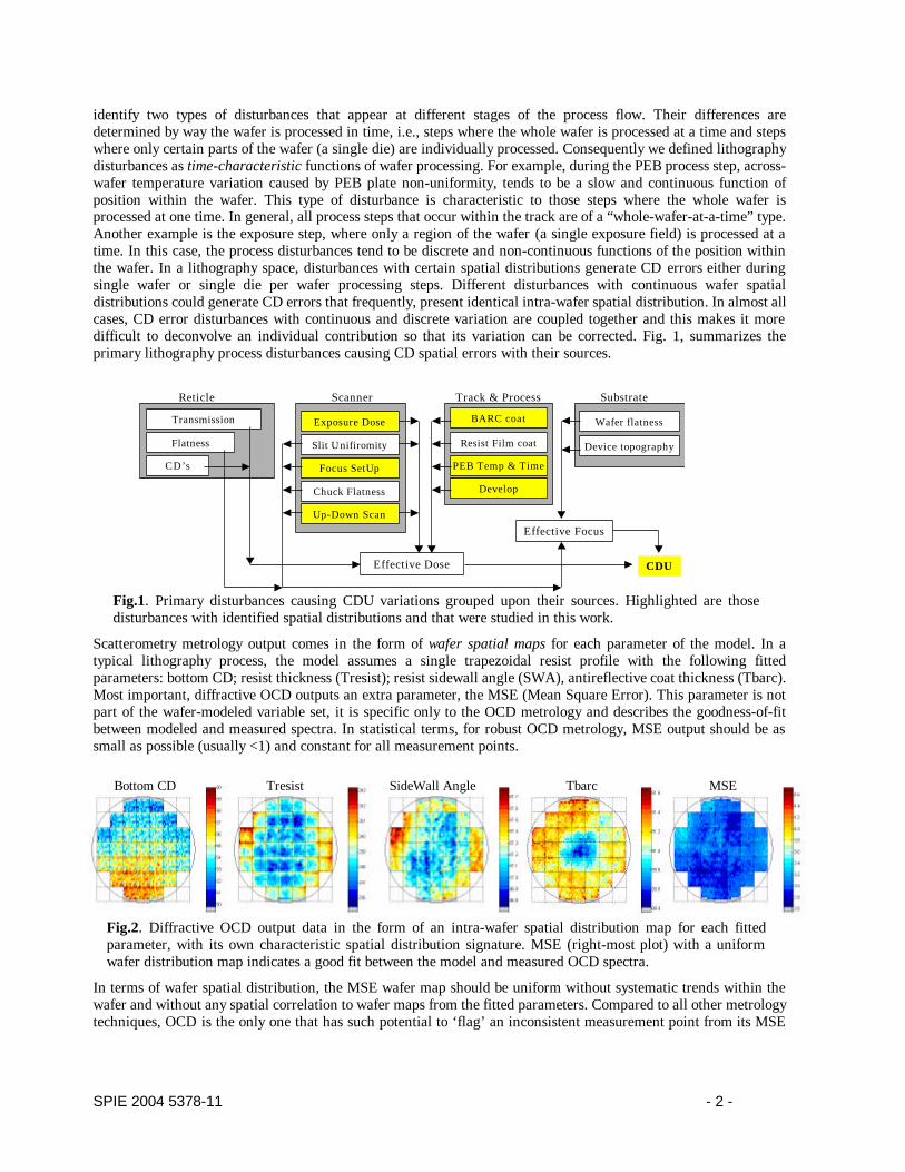
Scatterometry metrology output comes in the form of wafer spatial maps for each parameter of the model. In a typical lithography process, the model assumes a single trapezoidal resist profile with the following fitted parameters: bottom CD; resist thickness (Tresist); resist sidewall angle (SWA), antireflective coat thickness (Tbarc). Most important, diffractive OCD outputs an extra parameter, the MSE (Mean Square Error). This parameter is not part of the wafer-modeled variable set, it is specific only to the OCD metrology and describes the goodness-of-fit between modeled and measured spectra. In statistical terms, for robust OCD metrology, MSE output should be as small as possible (usually <1) and constant for all measurement points.
Fig.2. Diffractive OCD output data in the form of an intra-wafer spatial distribution map for each fitted parameter, with its own characteristic spatial distribution signature. MSE (right-most plot) with a uniform wafer distribution map indicates a good fit between the model and measured OCD spectra.
In terms of wafer spatial distribution, the MSE wafer map should be uniform without systematic trends within the wafer and without any spatial correlation to wafer maps from the fitted parameters. Compared to all other metrology techniques, OCD is the only one that has such potential to ‘flag’ an inconsistent measurement point from its MSE
Reticle Scanner Track & Process
Effective Focus
Flatness
CD’s
Transmission Wafer flatness
Device topography
Substrate
BARC coat
Resist Film coat
PEB Temp & Time
Develop
Exposure Dose
Slit U nifiromity
Focus SetUp
Chuck Flatness
Up-Down Scan
Effective Dose CDU
Bottom CD SideWall Angle MSE Tresist Tbarc

SPIE 2004 5378-11 - 3 -
value. As a result, MSE has been used to ‘check’ validity of metrology results providing a basis for the analysis to filter out outliers based on physical reasons. OCD-generated wafer spatial distributed maps are shown in Fig. 2, where each fitted parameter has an associated statistical value (within wafer mean and 3 ) and a distinctive intra-wafer spatial signature.
2. METHOD FOR DIAGNOSIS OF ACROSS WAFER CDU Our CDU analysis data indicates intra-wafer variation as being the largest contributor to CD distribution. As a consequence, in terms of CD variability, the most critical aspect of today’s lithography performance is the uniformity of process conditions within the wafer. Uniformity of process conditions within the wafer is subject to process disturbances, which, on their turn, exhibit characteristic spatial dependencies. In terms of statistical values, disturbances are related to a feature response through a linear function where a constant coefficient describes feature-disturbance sensitivity:
(1)
where FRa is the response of feature a to a process disturbance m and is the sensitivity coefficient.
A typical example is the CD response to small variations in thickness of the bottom antireflective layer (Tbarc). In this case, the feature response is the CD value, the disturbance is the barc thickness variation and sensitivity is the linear coefficient of CD=f(Tbarc) function, as follows:
(2)
2.1. Problem formalization
As discussed in previous section, depending on the time characteristics of wafer process, a typical lithography process presents two types of spatial distributions. Consequently, the response of a lithography feature to a disturbance should also present two types of spatial distributions. In real situations, when both type of disturbances are present, the feature has a combined response to disturbances with both continuous and discrete wafer spatial characteristics, as these must be considered additive in nature. On this basis, the measured feature response can be described by the following equation [8]:
(3)
The spatial distribution of feature response is described by x and y variables, representing Cartesian wafer coordinates. In a complete representation, equation (3) has four terms, while in this work, we removed the reticle and intrafield systematic component, IFp and used only three terms. The terms in eq.3 are:
- IFp(x,y): IntraField periodic signature composed from a reticle component and a systematic –within-wafer, periodic component describing the scanner field (slit and scan signatures)
- Wp (x,y): feature response variability caused by disturbances with slow and continuous function of wafer position (Wafer periodic). This component is primarily a result of the “whole-wafer-at-a-time” process steps, characteristic to resist and track.
- DD (x,y): is the Die-to-Die variability of the feature response. This component exhibits mainly discrete distribution sets rather than a continuous variation within the wafer. DD distributions occur from exposure field-to-field and result from variations in discrete scanning disturbances such as effective dose, the incidental focus or scan direction.
- r: the residual component, or the random error remaining after subtracting feature response to all non-random components. The residual component has a zero mean value and no spatial systematic characteristics.
Next step in formalization is to model the feature response as function of wafer coordinates. Each component of feature response to process disturbances, as presented in eq. 3, is modeled by high order polynomial fitting functions, which could be described either in terms of wafer radial coordinate (radius and angular position) or in wafer rectangular x,y coordinates. Both cases are shown in equation (4) and (5) below.

SPIE 2004 5378-11 - 4 -
(4)
(5)
Equation (4) describes feature response to disturbances dependent on the radial and angular distance of the measured location from the center of the wafer, while equation (5) describes identical response but in wafer rectangular coordinates. For both equations, the rightmost term, describes the link between feature response to process disturbances through each sensitivity parameter. It also indicates that wafer spatial distributions, attributed to process disturbances, are identified as the SOURCES of spatial variation of a lithography feature.
2.2. Procedure for intra-wafer diagnosis
On a given wafer, OCD measurement generates a number of responses, each of them representing one lithographic feature under analysis. In this work, we identified the disturbances and feature response shown in Table 1 that correspond to disturbances shown Fig 1. We selected those disturbances and feature responses, which are characterized by clear spatial variation profiles.
Table 1. Process Disturbances and lithographic responses
Disturbance Feature response Continuous and slow variation within wafer
PEB Temperature PEB time BARC Thickness Development time
Bottom CD Resist Thickness (Tresist) Sidewall Angle (SWA)
Discrete, non-continuous variation within wafer Dose Focus Scan direction
Bottom CD Resist Thickness (Tresist) Sidewall Angle (SWA)
The Intra-wafer diagnosis algorithm starts with the selection of a number of data points on the wafer. Each data point is described by an X,Y coordinate within the wafer and by x,y coordinates within a field (scanner die)
(6)
Each data point is then represented with its spatial coordinate (equation 6) and the feature response information:
To accurately determine wafer spatial characteristics and capture continuous to discrete types of variations, a rather large number of data points were selected for measurements and analysis: 6x5 points per field (6 points within slit, 5 points along scan) and 37 fields per wafer. Selecting the number and location of data points is a critical step and was dictated primarily by the need to maintain spatial characteristics of a feature response and less by reducing the measured points to minimize metrology time.
First step after data generation is to remove the catastrophic failures represented by points with OCD parameters outside initial model, as this creates unsuccessful fitting to measured spectra. Removing outliers is based on applying a threshold filter to MSE (fitting parameter) followed by edge exclusion zone. The points removed by the MSE filter are also removed from all other feature responses. For CD response, a reticle CD correction, REC, is applied next and this removes reticle contribution, IFp (x,y), from wafer CD spatial profile. Reticle CD fingerprint has been determined from separate CD measurements on identical locations as the ones used for intrafield wafer measurements.
Following step is to calculate the term Wp(x,y) (eq.3), describing the wafer’s periodic spatial profile. This is calculated applying equation (4) or (5) and consists in modeling wafer spatial pattern and generating a modeled pattern with linear, quadratic and larger order terms as well as a random error term (residual).

SPIE 2004 5378-11 - 5 -
Results from equation (4) or (5) are the feature response statistical values (mean, range, 3 etc.) and their spatial distributions for field and wafer. Typical spatial distribution for bottom CD feature response is shown in Fig. 3, where each spatial distribution map corresponds to one term in equation (3)
Fig.3. OCD output data for bottom CD feature, in the form of wafer spatial distribution maps with calculated spatially distributed components based on equation (3).
3. MATCHING FEATURE RESPONSE TO PROCESS DISTURBANCE
Fig.4. Example of feature response to process disturbance: both statistical and spatial correlation between PEB bake plate (process disturbance) and bottom CD feature response, are clearly visible.
Matching feature response to process disturbance has two aspects. One is the statistical matching of the response to a disturbance, as described in equation #1, through a linear function, where the constant coefficient expresses the feature-disturbance sensitivity. Another aspect is the spatial matching of disturbance distribution to the feature response distribution, as described in equation #2 and #3. A hypothesis of this study is that OCD fitted parameters in the form of spatial variation provide extra information needed to determine CDU sources of errors typically found in lithography process. It also implied that process errors are disturbances with a characteristic spatial distribution that can be then identified in the feature response. The last hypothesis is that a correlation exists between the defined process disturbances, lithography feature response and their sources; in other words, a process disturbance with specific spatial profile will determine changes in spatial profiles of all three feature responses considered, bottom CD, resist thickness, sidewall angle. However, parameters with similar spatial dependence could have a high correlation coefficient but this not always mean they have common cause and to determine the amount of correlation which is due to common spatial dependence, they should be coupled with physical reasons. This implies that feature response sensitivity to a process disturbance is well known and its spatial variation is also understood. A typical example of physical interpretation of feature response-process disturbance is shown in Fig. 4, showing intra-wafer CDU variation for two PEB plates with different temperature distributions. Statistical correlation (based on CD-PEB temperature sensitivity) and spatial distribution correlation are clearly and unmistakably present.
3.1. Statistical Match of Feature Response to Process Disturbance
Statistical feature response to process disturbance in the form of a formalized sensitivity relation has been simulated as well as experimentally determined. Results of statistical matching (sensitivity) for bottom CD feature response to process disturbances listed in Table 1 are presented in Table 2. These are relatively well known and expected values for a typical 90nm lithography process using 0.75NA 193nm exposure tool. .
PEB temp range of 1deg = CD variation range of 7nm PEB temp range of 0.5deg = CD variation range of 4nm
All filters All filters+REC filters+REC
Wp (x,y)
wafer periodic comp
r (x,y)
wafer random error
DD(x,y)
field model

SPIE 2004 5378-11 - 6 -
Table 2. Bottom CD Sensitivity to Process Disturbances Disturbance PEB temp PEB time Develop time Tbarc Dose Defocus CD sensitivity 7.2nm/oC 0.7nm/sec 0.25nm/sec
(+/- nominal time) 1.2nm/nm 6nm/mj ~5nm/100nm
(+/- BF) As indicated in the hypothesis our analysis included responses from two other lithographic features calculated by OCD fitted model parameters: the thickness of resist within the measured grating and sidewall angle of same resist grating. Their response to process disturbances were unknown as no other metrology technique can output such information. The first unexpected result in this study was the SWA and Tresist response to dose and defocus (FEM) as presented in Fig. 5. Resist thickness has a Bossung-type response to FEM disturbance, with a relative symmetric resist thickness loss through focus and relative uniform thickness loss through energy. A small asymmetry is visible as a steeper decrease in resist thickness for positive defocuses settings. This implies that Tresist and bottom CD will have identical response to dose and defocus errors, when they are present as local, discrete points within a wafer. On the other hand, sidewall angle response to FEM disturbance is asymmetric to both defocus and energy and presents an inflexion point, where its sensitivity to dose changes from the negative to positive defocus areas. For negative defocuses, SWA has a distinct variation to energy with steeper decrease for lower doses. For positive defocuses, SWA completely changes its FEM behavior, with steeper decrease to defocus at higher doses. Such asymmetric SWA behavior to FEM disturbance and in principal the linear change with defocus for a particular dose, is what makes SWA a good candidate to infer defocus variations with less uncertainty than using CD or Tresist responses. Due to their Bossung-type behavior through focus, CD and Tresist responses cannot indicate which side of defocus we operate. On the other hand, due to its linear defocus behavior, SWA has the potential to detect defocus sign with the caveat that such monitor requires extremely sensitive and accurate SWA data from fitted OCD parameters (of ~ 0.1o (3 ))
Fig.5. Resist thickness (left) and Sidewall Angle (right) statistical responses to FEM disturbance
3.2. Spatial Match of Feature Response to Process Disturbance
To study feature response spatial distribution matching to process disturbance, we created wafers with programmed process errors for disturbances with both types of expected spatial variations, slow and continuous as well as discrete. Table 3 lists the experimental conditions for wafers with known spatial disturbances as follows:
- Programmed PEB and development errors with expected slow and continuous within-wafer variation - Programmed defocus and dose errors on discrete within-wafer locations - Combined disturbances - continuous and discrete, such as PEB combined with localized field defocuses - Scan direction localized error, by spatial and statistical analysis of collapsed UP and DOWN scanned fields
Table 3 – experimentally created process disturbances
Process Disturbance Programmed Error PEB Temperature Nominal; +/- 4% from nominal PEB time Nominal; +/- 10% from nominal Development time Nominal; +/- 5; 10% from nominal Defocus across entire wafer Best Focus; +/- 100 nm defocus
Tresist response to FEM SWA response to FEM

SPIE 2004 5378-11 - 7 -
Process Disturbance Programmed Error Localized defocus and exposure Wafer at nominal process condition with random placed
fields with +/-100nm defocus and +/- 0.5% Dose changes from dose to size
Combined PEB and localized defocus and dose Nominal; +/- PEB time; +/- PEB Temp and random placed fields with +/-100nm defocus and +/- 0.5% En
3.3. Feature Matched Response to Disturbances with Continuous and Slow Spatial Variation
Variation in PEB plate temperature is a typical disturbance with slow and continuous change as function of intra-wafer coordinates. Changes in spatial PEB fingerprint is caused by variation in the “steady-state” condition of a bake module, in case PEB time or temperature varies in time, or simply, by differences in the temperature distribution from one bake module to another (Fig. 4). Fig. 6 presents bottom CD feature response to variation in PEB bake process, with programmed variations in PEB temperature (the three left most wafer maps) and PEB time (rightmost map). All these spatial maps are generated on the same PEB plate. Statistical CD-mean value response to PEB variations is in line with sensitivity expectations, while changes in spatial distributions were less expected and need further analysis to understand why the PEB plate fingerprint changes with temperature or time variation. It is obvious that a change in PEB temperature or time has two effects, first an induced spatial disturbance effect at wafer level creating different intra-wafer CD fingerprint, second, a statistical disturbance effect who’s wafer CD-mean changes according to some sensitivity function CD = f(PEB).
Fig.6. Bottom CD feature response to PEB process disturbance in the form of intra-wafer spatial distribution profiles. Changes in PEB temperature distribution are reflected in differences between CDU profiles.
Further analysis into intra-wafer spatial distribution characteristics consists in modeling the wafer spatial profile using equation (4) or (5). Equation (4) outputs a radial CD profile, while equation (5) outputs a X-Y profile along the wafer diameter. Results from applying equation 4 to wafers with PEB continuous intra-wafer disturbance (wafers with spatial variation shown in Fig 6) is a CD radial distribution plot in the form of “cloud points” with unique spatial characteristics. Fig. 7, presents two differential cloud plots, calculated from subtracting CD radial profile of the modified PEB temperature conditions from the CD radial profile of the standard (nominal) PEB process condition.
Fig.7. Bottom CD modeled intra-wafer profiles plotted as radial distributions for the difference between nominal and +/- temperature disturbed PEB. On the right-side plot, wafer average has been subtracted from CD differential radial distributions to enhance the spatial differences between the responses
Std PEB + 4% PEB Temp - 4% PEB Temp -10% PEB time

SPIE 2004 5378-11 - 8 -
Fig. 7-left, contains mostly statistical information and shows changes in wafer mean CD by +/-35nm, which is expected from this process with a sensitivity of 7nm/oC and +/-5oC variations in PEB temperature. However, this plot does not allow an in-depth intra-wafer spatial analysis for which, we subtracted wafer means and produced the enhanced radial plots shown in Fig. 7-right. Now, the radial profile changes with PEB condition is noticeable, presenting a slow and continuous variation from wafer center, to around 40 to 60mm from the center and followed by a steep CDU increase at wafer edges. We can also distinguish PEB temperature effects from an increase in PEB temperature (nominal +4% PEB Temp) to the decreased PEB temperature condition (nominal -4% PEB Temp). A decrease in PEB temperature reduces CD variation across wafer and creates a quadratic variation at wafer center, which appears to be characteristics only for this PEB value. Spatial differences observed in Fig. 7-right, are further enhanced and their differences quantified by fitting polynomial functions through the cloud plot and calculate fitted profile with their coefficients. Calculated fitted profiles are shown in Fig. 8, where the concept of slow and continuous intra-wafer variation and matching of a feature response to programmed process disturbances clearly appears as a “slow” CD profile oscillations along wafer diameter.
Fig. 8 Bottom CD modeled intra-wafer profiles plotted as function of wafer diameter for differential CDU
between nominal and programmed PEB disturbances in temperature (left) and time (right). PEB time-induced disturbances appear to induce far less intra-wafer feature response (less variation in CDU spatial distribution).
Calculated linear and higher order quadratic coefficients of the profile plots shown in Fig. 8 are presented in Fig. 9. Coefficients for linear and quadratic modeled terms exhibit variations with trends related to PEB intra-wafer spatial disturbance. This proves our initial hypothesis that intra-wafer feature response has a spatial distribution, which is a function of process disturbance spatial distribution changes, caused in this case by PEB process.
Fig. 9 Bottom CD modeled intra-wafer coefficients for PEB programmed errors – triagonal polynomial coefficients from 1st order fit (left) and 4th order fit (right). For PEB disturbance with slow intra-wafer variation, changes in linear terms are smaller than quadratic terms. Higher order modeled coefficients indicate larger and more unique spatial disturbances generated by changes in PEB temperature compared to changes in PEB time
To complete the analysis of feature – disturbance matching, we examined responses of the two other lithography features generated by OCD metrology, resist thickness (Tr) and sidewall angle (SWA). Previously (section 3.1), we established characteristic Tr and SWA statistical response to FEM disturbances. Now, we add the spatial response of SWA and Tresist to PEB process disturbance. Fig. 10-right, illustrates changes in statistical values and radial
-2
-1
0
1
2
3
-100 -75 -50 -25 0 2 5 5 0 7 5 1 0 0W a fe r D i a m e te r (m m )
Diff
eren
tial F
itted
CD
Pro
file
Nominal - 4%Temp
Nominal + 4%Temp
-2
-1
0
1
2
-100 -75 -50 -25 0 25 50 75 100
W a fe r D i a m e te r (m m )
Diff
eren
tial F
itted
CD
Pro
file
Nominal + 10%time
Nominal - 10%time
-2.0E-02
-1.6E-02
-1.2E-02
-8.0E-03
-4.0E-03
0.0E+00
Line
arl S
patia
l Coe
ff
+4%
Tem
p
-4%
Tem
p
+10%
time
-10%
time -4.0E-07
-2.0E-07
0.0E+00
2.0E-07
4.0E-07
6.0E-07
4th
Pol
y S
patia
l Coe
ff
+4%
Tem
p
-4%
Tem
p
+10%
time
-10%
time

SPIE 2004 5378-11 - 9 -
distribution of SWA caused by PEB temperature disturbance. From wafer center to periphery, the SWA spatial variation increases dramatically, from 0.2o to 2o. An interesting effect appears at lower PEB temperature disturbance: SWA spatial distribution is tighter (Nominal - 4%Temp curve) a behavior similar to CD spatial response to lower PEB temperature (Fig 7)! This could be an indication that minimum intra-wafer CDU is obtained at lower PEB temperature than what was used here as process nominal conditions.
Statistical and spatial response of resist thickness feature, Tresist to PEB temperature disturbances is shown in Fig. 10-left. Resist thickness presents a high sensitivity to PEB disturbances. Compared to PEB nominal conditions, the programmed PEB variations of +/-4degC induced a total of 20nm (+ 8/- 12nm) asymmetric variation in resist thickness. Lower PEB temperature appears to induce larger intra-wafer resist thickness variation, which is opposite from CD and SWA spatial responses to lower PEB temperature. An asymmetry in Tr and SWA feature responses to PEB symmetric variation is visible in both statistical and spatial response as asymmetric position of radial cloud plot Vs vertical axis origin. Both SWA and Tresist present increased spatial variation at wafer edges.
Fig.10: SWA (right) and Tresist (left) responses to PEB programmed errors, calculated as differential between nominal conditions and programmed PEB errors.
3.4. Feature Matched Response to Disturbances with Discrete Spatial Variation
3.4.1. Discrete Dose and Defocus Errors
Fig.11. Discrete process disturbances programmed as Dose and Defocus on top of PEB continuous intra-wafer disturbance. Locations of the discrete dose-defocus errors shown on the leftmost wafer map. Next to it is the bottom CD wafer map where the feature response to programmed errors are clearly visible as changes in field color -- (indicates average field CD differences from wafer mean).
Die-to-die exposure variations are the most typical disturbances with discrete and localized spatial distribution in effective dose or effective focus. To mimic such disturbances, we programmed dose and focus errors on random wafer locations (Fig. 11-left). Dose and focus disturbances were programmed on top of slow, continuous disturbance caused by changes in PEB temperature, with the goal to infer and separate CD response from discrete to continuous disturbances. The right side plots in Fig.11, illustrate the interactions between continuous to discrete disturbances in the form of average field CD variation from wafer mean for the fields with dose and defocus errors. For 115o PEB temperature, CD response to dose changes (+/-dE) appears to be as expected with symmetric increase-decrease in average field CD. This is not the case for 120o, where the increase in PEB temperature appears to modify
-2
-1.5
-1
-0.5
0
0.5
Offs
et F
ield
del
ta C
D
115deg 120deg 125deg
-dF
+dF
-4
-3
-2
-1
0
1
2
Offs
et F
ield
del
ta C
D
115deg 120deg 125deg
-dE
+dE
Location of discrete programmed errors in dose and focus
Bottom CD response to programmed dose and defocus errors
Bottom CD response to programmed errors, dose (left) and defocus (right). Response in the form of intrafield average statistical difference from non-error field average
-dE +dE
-dF
+dF
-dE+-dF
+dE+-dF

SPIE 2004 5378-11 - 10 -
the wafer spatial profile such that a symmetric dose disturbance induces an asymmetric CD response! Same conclusion is for CD response to defocus changes (+/-dF, rightmost graph in Fig.11). In a well-controlled process, CD response to defocus should be identical in magnitude as this indicates symmetric operation on top of Bossung curve and this is visible for 115o PEB case. As observed for CD response to dose errors, the 120o and 125o PEB temperatures, create disturbed wafer spatial distributions, which move the position of best focus, resulting in a large asymmetric CD response to defocus.
3.4.2. Scan UP-DOWN discrete errors
Another typical lithographic process disturbance with discrete spatial behavior is the scan direction of the reticle during field exposure. To identify CD response to such disturbances, we processed intra-wafer CD data by separating and collapsing together the UP-scan fields from DOWN fields and subtracting wafer mean from both.
Fig.12. CD response to discrete process disturbance represented by UP-DOWN scan direction. Both statistical and spatial responses are shown for up and down fields in the form of CD variation after subtracting wafer mean. This type of disturbance does not appear to be a significant CDU source of error and indicates good scanner dynamics.
Results are presented in Fig 12 where we plot scan UP and scan DOWN CD spatial distribution along scan direction for five locations within slit. Statistical CD response (average CD values) shows no real difference from UP to DOWN scanned fields. Spatial CD response is also identical for all seven scan positions with slit and wafer variation included. For this process and exposure tool, scan direction does not need to be considered one of the intra-wafer discrete disturbance with effects on CDU. It is to note that a conclusion like this is dependent on the particular process and system and a different process environment could include scan direction as process disturbance.
4. COVARIANCE OF MULTIPLE FEATURE RESPONSE TO SAME DISTURBANCE
Our OCD output data consisted of four parameters, CD, resist thickness, sidewall angle and bottom antireflective thickness. It is important to establish whether there is any correlation between the response of these parameters, i.e., whether they will have correlated response to the same disturbance and, as a result, will present correlated spatial distribution across the wafer. Covariance is the statistical parameter that examines how two features correlate to each other. Covariance of two features measures their tendency to vary together, i.e., to co-vary. Covariance of feature i and feature j is defined by the covariance coefficient, c(i,j)
c(i,j) = { [ x(1,i) - m(i) ] [ x(1,j) - m(j) ] + ... + [ x(n,i) - m(i) ] [ x(n,j) - m(j) ] } / ( n - 1 ) (7)
where: c(i,j) = 0, if feature i and j are independent; c(i,j) > 0, if feature i and j tend to increase together; c(i,j) <0, if feature i and j tend to decrease together
Possible covariance between SWA and Tresist to CD response has been identified (section 3.1 and 3.3) and calculated as standardized covariance lots for Tresist-CD and SWA-CD from intra-wafer spatial data on a PEB Temperature disturbed wafer. CD-to-itself covariance curve is included for reference. For this wafer, SWA to CD covariance coefficient is negative (–0.85), indicating large spatial correlation with SWA decreasing when CD increases. A positive 0.67 Tresist to CD covariance coefficient (+0.67) indicates that Tresist and CD increase together.
Scan position within slit (mm)
Ave CD 95.74nm
DOWN SCAN
Scan Position within slit
Ave CD 95.20nm
UP SCAN

SPIE 2004 5378-11 - 11 -
Fig.13. Covariance between Tresist (squares) and SWA (plus) features to CD (circle) with CD variable on the abscissa
Once a feature covariance is identified, the information could be used to infer process disturbances that created a certain response. An attempt is made to infer defocus disturbances from covariance of SWA and Tresist feature response to CD, using wafers with +/- 100nm global defocus disturbance. Results are shown in Fig 14, left, as CD to SWA and CD to Tresist covariance coefficients for best focus and two defocus conditions. SWA and CD tend to increase together for positive defocus with a large coefficient (0.8) and decrease together for negative defocus or for best focus setting, with a significant lower covariance (-0.25 to -0.4). Similarly, resist thickness and CD co-vary symmetrically with respect to positive or negative defocus while a negative covariance is present at best focus. Another way to analyze feature correlation from their spatial distributions is to calculate intra-wafer spatial profile applying triagonal polynomial fitting followed by comparison of the modeled coefficients. An example is shown in Fig. 14-right, where linear fitted coefficients for CD and SWA are plotted side by side for wafers at best focus and +/- defocus conditions. Linear coefficients indicating wafer profile tilts for CD and SWA, are clearly correlated to defocus global disturbance which indicate the possibility to use SWA spatial information to infer defocus errors. We selected the linear coefficient because this process disturbance was applied to the entire wafer and exhibits a slow and continuous intra-wafer variation.
Fig.14. Two ways to characterize feature correlation to process disturbance (global defocus). Left: covariance coefficients for CD to SWA and Tresist. Right: CD and SWA linear modeled coefficients for wafers with different spatial profiles, dependent to defocus condition.
5. CONCLUSIONS
A method was developed to determine intra-wafer CDU characteristics for a typical 90nm litho process. Lithography parameters such as CD are defined as features while CD error sources are defined as process disturbances. Method consists in analysis of a feature response to a process disturbance. Analysis included statistical values and spatial distributions. Statistical results after removing reticle contribution point out to process components, PEB and Barc thickness, as the largest CDU error component According to the same data, contribution from the exposure tool (TWINSCAN™ AT:1100) accounts for less than 20% in CDU variation.
Tresist to CDCD to CD (reference)SWA to CD
Covariance CoefficientsCD to CD 1.0SWA to CD -0.85Tresist to CD 0.67
-0.4
-0.2
0
0.2
0.4
0.6
0.8
1
Cov
aria
nce
Coe
ff
CD-SWA CD-Tr
-0.1defoc
BF
+0.1defoc
-0 .040
-0.030
-0.020
-0.010
0.000
-De f+o f f - 0 .1de f BF +0.1def
CD
Mod
eled
Coe
ff
0 .000
0.002
0.004
0.006
SW
A M
odel
ed C
oeff
L inear CD
L inea r SWA

SPIE 2004 5378-11 - 12 -
Information from Spatial Patterns clearly identified CD common spatial dependence to process disturbance. Process disturbances are characterized by slow and continuous dependence to wafer coordinates which is characteristic to “wafer-at-a-time” processing mode. This variation was modeled by 6th degree triagonal XY polynomial fitting with radial fitted profile and associated modeled coefficients are used as characterization metrics. CDU errors introduced by disturbances in exposure tool operation are randomly distributed with localized variations within the wafer. These are characteristic to “part-of-the-wafer” processed at a time (die to die). Analysis of process disturbances, both continuous and discrete, was based on wafers with known, programmed disturbances, from which OCD feature response were calculated.
Identifying CDU errors generated by exposure tool, such as dose and defocus requires spatial and statistical covariance of CD to other litho feature response, such as Tresist and SWA. Covariance analysis clearly indicated CD to SWA correlation with different spatial profiles for process disturbances (PEB, +/- defocus)
OCD metrology has the capability to generate multiple feature response to process disturbance in the statistical and spatial profile form. OCD multiple feature responses could be used to infer dose and defocus disturbances. CD to dose sensitivity is a linear function and is easier to be determined. Intra-wafer dose errors (effective dose) couple with process disturbances and unique determination requires a 2nd feature response with a similar linear response to dose variation (such as CD-Tresist). Focus has a quadratic effect on CD where deducing defocus sign is the most difficult information. To infer defocus sign, a 2nd parameter with asymmetric focus-response is needed to convert CD defocus quadratic behavior into a linear variation (CD-SWA)
The intra-wafer CDU characterization method proposed here with its analysis of spatial characteristic could be extended to a full wafer CD compensation using modeled coefficients in a manner similar to the way intra-wafer spatially distributed overlay corrections are currently corrected.
6. ACKNOWLEDGMENTS
The authors would like to acknowledge fruitful discussions with Ton Kiers and Hugo Cramer from ASML Europe and the support from John Heaton and Douglas Rea of Nanometrics. We are very grateful to Anita Fumar-Pici who made possible the whole experimental work. Data analysis was possible by using Weir Analysis software (TEA Systems) combined with ASML internal DAT Analysis program.
7. REFERENCES
[1] Peter Vanoppen, Oscar Noordman, Jan Baselmans, Jan van Schoot, “Analysis of Full Wafer/Full Batch CD Uniformity Using Electrical Line Width Measurements”, Proceedings of SPIE Vol. 4404, 05, 2001
[2] Alfred Wong, Antoinette Molless, Timothy Brunner, Eric Coker, Robert Fair, George Mack, Scott Mansfield,, “Characterization of line width variation”, Proc. SPIE Vol. 4000, Optical Lithography XIII, 184 -191, 2000
[3] H. Y. Liu, et all, “Contributions of stepper lenses to systematic CD errors within exposure field”, Proceedings SPIE Optical Lithography, Santa Clara, CA 1995,
[4] W. A. McGahan, J. M. Holden, P. I. Rovira, R. Lowe-Webb, R. A. Yarussi, V. Zhuang, and V. J. Coates, Design and Performance of a Normal-Incidence Optical Critical Dimension Metrology System, Microprocesses and Nanotechnology Conference, Shimane, Japan, October, 2001
[5] Hugo Cramer, Ton Kiers, Peter Vanoppen, Jeroen Meessen, Frans Blok, Mircea Dusa, “ Total Test Repeatability, a new figure of merit for CD metrology tools” Proc. SPIE, vol. 5375-160, 2004.
[6] J. M. Holden, T. Gubiotti, W. A. McGahan, Nanometrics Inc.; M. Dusa, T. Kiers, “Normal incidence spectroscopic ellipsometry and polarized reflectometry for measurement and control of photoresist critical dimension”, Proc. SPIE, vol. 4689, pp. 1110 – 1121, 2002.
[7] J. K. Kibarian, et all, “Using spatial information to analyze correlations between test structure data”, IEEE Transaction on Semiconductor Manufacturing, Vol. 4,3, p219-225, August 1991
[8] Crid Yu, Costas Spanos, Hua Yu Liu, Dirk Bartelink, “Lithography error sources quantified by statistical metrology”, Solid State Technology, February 1996
[9] Hsu-Ting Huang, Wei Kong, and Fred Lewis Terry, Jr, “Normal-incidence spectroscopic ellipsometry for critical dimension monitoring”, Appl. Phys. Lett. 78(25) 3983-3985, 2001.
Related Documents