May 2005 6024 Silver Creek Valley Road, San Jose, California 95138 Telephone: (800) 345-7015 • (408) 284-8200 • FAX: (408) 284-2775 Printed in U.S.A. ©2005 Integrated Device Technology, Inc. IDT ™ Interprise ™ 79RC32438 Integrated Communications Processor User Reference Manual

Welcome message from author
This document is posted to help you gain knowledge. Please leave a comment to let me know what you think about it! Share it to your friends and learn new things together.
Transcript

May 2005
6024 Silver Creek Valley Road, San Jose, California 95138Telephone: (800) 345-7015 • (408) 284-8200 • FAX: (408) 284-2775
Printed in U.S.A.©2005 Integrated Device Technology, Inc.
IDT™ Interprise™ 79RC32438Integrated Communications
Processor
User Reference Manual
GENERAL DISCLAIMERIntegrated Device Technology, Inc. reserves the right to make changes to its products or specifications at any time, without notice, in order to improve design or performance and to supply the best possible product. IDT does not assume any responsibility for use of any circuitry described other than the circuitry embodied in an IDT product. The Company makes no representations that circuitry described herein is free from patent infringement or other rights of third parties which may result from its use. No license is granted by implication or otherwise under any patent, patent rights or other rights, of Integrated Device Technology, Inc.
CODE DISCLAIMERCode examples provided by IDT are for illustrative purposes only and should not be relied upon for developing applications. Any use of the code examples below is completely at your own risk. IDT MAKES NO REPRESENTATIONS OR WARRANTIES OF ANY KIND CONCERNING THE NONINFRINGEMENT, QUALITY, SAFETY OR SUITABILITY OF THE CODE, EITHER EXPRESS OR IMPLIED, INCLUDING WITHOUT LIMITATION ANY IMPLIED WARRANTIES OF MERCHANTABILITY, FITNESS FOR A PARTICU-LAR PURPOSE, OR NON-INFRINGEMENT. FURTHER, IDT MAKES NO REPRESENTATIONS OR WARRANTIES AS TO THE TRUTH, ACCURACY OR COMPLETENESS OF ANY STATEMENTS, INFORMATION OR MATERIALS CONCERNING CODE EXAMPLES CONTAINED IN ANY IDT PUBLICATION OR PUBLIC DISCLOSURE OR THAT IS CONTAINED ON ANY IDT INTERNET SITE. IN NO EVENT WILL IDT BE LIABLE FOR ANY DIRECT, CONSEQUENTIAL, INCIDENTAL, INDIRECT, PUNITIVE OR SPECIAL DAMAGES, HOWEVER THEY MAY ARISE, AND EVEN IF IDT HAS BEEN PREVIOUSLY ADVISED ABOUT THE POSSIBILITY OF SUCH DAMAGES. The code examples also may be subject to United States export control laws and may be subject to the export or import laws of other countries and it is your responsibility to comply with any applicable laws or regulations.
LIFE SUPPORT POLICYIntegrated Device Technology's products are not authorized for use as critical components in life support devices or systems unless a specific written agreement pertaining to such intended use is executed between the manufacturer and an officer of IDT.1. Life support devices or systems are devices or systems which (a) are intended for surgical implant into the body or (b) support or sustain life and whose failure to perform,when properly used in accordance with instructions for use provided in the labeling, can be reasonably expected to result in a significant injury to the user.2. A critical component is any components of a life support device or system whose failure to perform can be reasonably expected to cause the failure of the life support device or system, or to affect its safety or effectiveness.
The IDT logo is a registered trademark of Integrated Device Technology, Inc. IDT, Interprise, RISController, RISCore, RC3041, RC3052, RC3081, RC32134, RC32332, RC32333, RC32334, RC32336, RC32355, RC32351, RC32365, RC32438, RC32364, RC36100, RC4700, RC4640, RC64145, RC4650, RC5000, RC64474, RC64475 are trademarks of Integrated Device Technology, Inc..
Powering What's Next and Enabling A Digitally Connected World are service marks of Integrated Device Technology, Inc. Q, QSI, SynchroSwitch and Turboclock are registered trademarks of Quality Semiconduc-tor, a wholly-owned subsidiary of Integrated Device Technology, Inc.
Notes
79RC32438 User Reference Manual
About This Manual
IntroductionThis user reference manual includes hardware and software information on the RC32438, a high perfor-
mance integrated processor that combines a high performance 32-bit CPU core with system logic toprovide direct connection to boot memory, main memory, I/O, and PCI. It also includes on-chip peripheralssuch as DMA channels, reset circuitry, interrupts, timers, and UARTs. Each chapter is designed to cover thefollowing topics:
High level feature summary of the specific moduleSummary of the register set associates with a specific moduleOutline of the operation of the moduleDetailed register description.
Finding Additional InformationInformation not included in this manual such as mechanicals, package pin-outs, and electrical character-
istics can be found in the data sheet for this device, which is available from the IDT website (www.idt.com)as well as through your local IDT sales representative.
Content SummaryChapter 1, “RC32438 Device Overview,” provides a complete introduction to the performance capabil-
ities of the RC32438. Included in this chapter is a summary of features for the device as well as a systemblock diagram and internal register maps.
Chapter 2, “MIPS32 4Kc Processor Core,” provides basic information on the architecture and opera-tion of the 4Kc™ processor core from MIPS® Technologies as it applies to the RC32438.
Chapter 3, “Clocking and Initialization,” discusses the reset initialization sequence required by theRC32438 and provides information on boot vector settings and clock signals.
Chapter 4, “System Integrity Functions,” discusses system integrity functions, including the registersthat log system activity and that can be used to indicate the source of hardware or software errors.
Chapter 5, “Bus Arbitration,” describes the internal arbitration mechanism used among the variouson-chip modules. The chapter also describes the bus protocol used by an external bus master to gainownership of the memory and peripheral bus.
Chapter 6, “Device Controller,” describes the operation of the device controller, including registersand device transactions, which provides a glueless interface to SRAMs, ROMs/PROMs/EEPROMs, dualport memories, and other devices.
Chapter 7, “Double Data Rate (DDR) Controller,” describes the features, functions, and operation ofthe DDR Controller, including a description of the registers.
Chapter 8, “Interrupt Controller,” provides information about the interrupt controller and interruptsource descriptions.
Chapter 9, “DMA Controller,” describes the DMA controller, channels, descriptors, registers, transac-tions, and operations.
Chapter 10, “PCI Bus Interface,” describes the features, functions, and operations of the PCI businterface on the RC32438.
Chapter 11, “Ethernet Interfaces,” discusses the two Ethernet interfaces on the RC32438 which canbe used in applications such as SOHO routers or high speed modems for PCs.
i May 11, 2005
IDT About This Manual Documentation Conventions and Definitions
79RC32438 User Refer
Notes
Chapter 12, “General Purpose I/O Controller,” describes this controller and how it is configured tooperate as a general purpose I/O or as an alternate function.Chapter 13, “UART Controller,” provides information about the two separate UARTs within theRC32438, including the UART registers.
Chapter 14, “Counter Timers,” describes the three general purpose 32-bit counter/timers on theRC32438.
Chapter 15, “I2C Bus Interface,” describes the standard I2C bus interface, supporting both master andslave operations, that is implemented on the RC32438.
Chapter 16, “Serial Peripheral Interface,” describes the SPI master interface which uses three signalsto connect to low-cost SPI peripherals and memory.
Chapter 17, “On-Chip Memory,” describes the operation and support provided by on-chip memory formemory read and write operations on the RC32438.
Chapter 18, “Debugging and Performance Monitoring,” discusses the three different debuggingfeatures available on the RC32438: IPBus Monitor, Event Monitor, and Debug Pins.
Chapter 19, “JTAG Boundary Scan,” discusses an enhanced JTAG interface, including a system logicTAP controller, signal definitions, a test data register, an instruction register, and usage considerations.
Chapter 20, “EJTAG System,” describes the EJTAG’s features, its Debug Control Register, TAP regis-ters, EJTAG Probe, hardware breakpoints, and other related topics.
Appendix A, “4Kc Processor Core Instructions,” contains additional information about the 4Kcprocessor core instruction set.
Documentation Conventions and DefinitionsThroughout this manual the following conventions and terms are used:
To avoid confusion when dealing with a mixture of “active-low” and “active-high” signals, the terms assertion and negation are used. The term assert or assertion is used to indicate that a signal is active or true, independent of whether that level is represented by a high or low voltage. The term negate or negation is used to indicate that a signal is inactive or false.To define the active polarity of a signal, a suffix will be used. Signals ending with an ‘N’ should be interpreted as being active, or asserted, when at a logic zero (low) level. All other signals (including clocks, buses and select lines) will be interpreted as being active, or asserted, when at a logic one (high) level. To define buses, the most significant bit (MSB) will be on the left and least significant bit (LSB) will be on the right. No leading zeros will be included. To represent numerical values, either decimal, binary, or hexadecimal formats will be used. The binary format is as follows: 0bDDD, where “D” represents either 0 or 1; the hexadecimal format is as follows: 0xDD, where “D” represents the hexadecimal digit(s); otherwise, it is decimal.Unless otherwise denoted, a byte will refer to an 8-bit quantity. A halfword will refer to a 16-bit quan-tity. A triple-byte will refer to a 24-bit quantity. A word will refer to a 32-bit quantity, and a double or double word will refer to a 64-bit quantity. A bit is set when its value is 0b1. A bit is cleared when its value is 0b0.The compressed notation ABC[x|y|z]D refers to ABCxD, ABCyD, and ABCzD.The compressed notation ABC[x..y]D refers to ABCxD, ABC(x+1)D, ABC(x+2)D, ... ABCyD.In words, bit 31 is always the most significant bit and bit 0 is the least significant bit. In halfwords, bit 15 is always the most significant bit and bit 0 is the least significant bit. In bytes, bit 7 is always the most significant bit and bit 0 is the least significant bit.The ordering of bytes within words is referred to as either “big endian” or “little endian.” Big endian systems label byte zero as the most significant (leftmost) byte of a word. Little endian systems label byte zero as the least significant (rightmost) byte of a word.
ence Manual ii May 11, 2005
IDT About This Manual Signal Terminology
79RC32438 User Refer
Notes
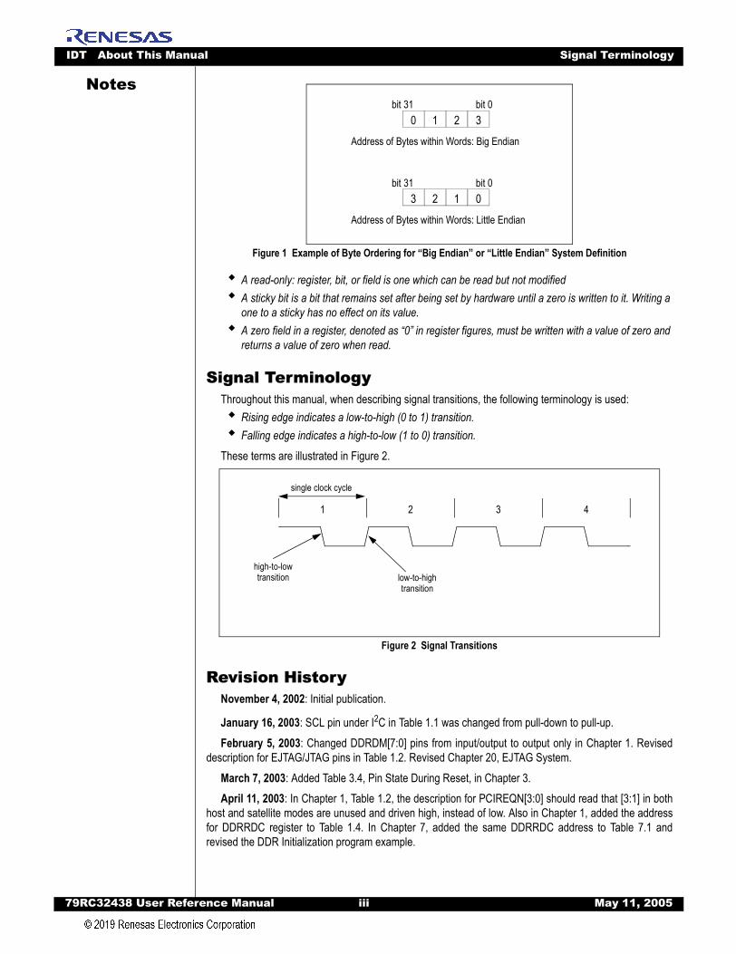
Figure 1 Example of Byte Ordering for “Big Endian” or “Little Endian” System Definition
A read-only: register, bit, or field is one which can be read but not modifiedA sticky bit is a bit that remains set after being set by hardware until a zero is written to it. Writing a one to a sticky has no effect on its value.A zero field in a register, denoted as “0” in register figures, must be written with a value of zero and returns a value of zero when read.
Signal TerminologyThroughout this manual, when describing signal transitions, the following terminology is used:
Rising edge indicates a low-to-high (0 to 1) transition.Falling edge indicates a high-to-low (1 to 0) transition.
These terms are illustrated in Figure 2.
Figure 2 Signal Transitions
Revision HistoryNovember 4, 2002: Initial publication.
January 16, 2003: SCL pin under I2C in Table 1.1 was changed from pull-down to pull-up. February 5, 2003: Changed DDRDM[7:0] pins from input/output to output only in Chapter 1. Revised
description for EJTAG/JTAG pins in Table 1.2. Revised Chapter 20, EJTAG System.March 7, 2003: Added Table 3.4, Pin State During Reset, in Chapter 3.April 11, 2003: In Chapter 1, Table 1.2, the description for PCIREQN[3:0] should read that [3:1] in both
host and satellite modes are unused and driven high, instead of low. Also in Chapter 1, added the addressfor DDRRDC register to Table 1.4. In Chapter 7, added the same DDRRDC address to Table 7.1 andrevised the DDR Initialization program example.
0 1 2 3bit 0bit 31
Address of Bytes within Words: Big Endian
3 2 1 0bit 0bit 31
Address of Bytes within Words: Little Endian
1 2 3 4
high-to-low transition low-to-high
transition
single clock cycle
ence Manual iii May 11, 2005
IDT About This Manual Revision History
79RC32438 User Refer
Notes
May 5, 2003: In Chapter 10, PCI Serial EEPROM Interface section, revised 1st paragraph as follows:changed register addresses from 0x80 to 0x40, added sentence “The interface only supports 93C46-compatible serial EEPROMs,” and added sentence “Only EEPROMs which are 2048 bits in size should beused.” In the second paragraph, the following sentence was deleted, “EEPROM addresses which aregreater than or equal to 0x40 in EEPROMs whose size is greater than 1024 bits may be used to store appli-cation specific information.” Also in Chapter 10, Disabled Mode section, second paragraph, revised 1stsentence as follows: “When the PCI bus interface is disabled, all of the PCI pins are tri-stated, exceptPCIGNTN[3:1], and thus should be held at a valid logic level on the board.” Also added that PCIGNTN[3:1]signals are driven high. In Chapter 16, Function Overview, added clarification on PCI serial EEPROM modeof operation.May 21, 2003: In Chapter 11, Address Recognition Logic section, the 2nd through the 4th paragraphson page 11-8 were revised.
July 11, 2003: Removed references to IPBus Monitor feature. In Chapter 5, deleted Enable EagerPrefetching bit from IPBus Arbiter Control Register in the IPBus Registers section. In Chapter 10, reviseddescription for EN bit in PCI Control Register, Changed Byte Swapping bit in PCI Local Address Controlregister to Force Endianess, added “byte and halfword target IO transactions are not supported” to Target I/O Read and Target I/O Write sections, and changed DMA limitations to “32KB minus 8 bytes” for channels8 and 9. In Chapter 11, removed table associated with MII Management Command Register. In Chapter 16,added information in the Functional Overview section. In Chapter 17, revised first 4 paragraphs of Theory ofOperation section.
July 28, 2003: In Chapter 11, changed the First Descriptor bit in Figure 11.10 to Reserved and deletedinformation about FD in 2 sections: Ethernet Input DMA Operations and Ethernet Output DMA Operations.
November 21, 2003: In Chapter 10, changed the description of the IGM bit on page 10-6, the CWE biton page 10-8, and the CLS bit on page 10-52.
March 10, 2004: In Chapter 2, references to the RP bit were deleted. In the Target I/O Read and TargetI/O Write sections of Chapter 10, the following sentences were removed “The RC32438 PCI I/O interface isa 32-bit interface. Byte and halfword Target I/O transactions are not supported.” In fact, the RC32438 doessupport PCI Target I/O transactions of byte and half word size. In Chapter 11, changed the description ofthe PEN bit on page 11-15.
May 11, 2005: In Table 10.6: switched Chapter 8 and Chapter 9 headings only - not the values in thecolumns; also, switched Yes and No for these two headings in the Memory Read Multiple row.
ence Manual iv May 11, 2005
Notes
79RC32438 User Refer
Table of Contents
About This ManualIntroduction .......................................................................................................................... iContent Summary ................................................................................................................. iDocumentation Conventions and Definitions........................................................................... iiSignal Terminology .............................................................................................................. iiiRevision History .................................................................................................................. iii
1 RC32438 Device OverviewIntroduction ..................................................................................................................................1-1Key Features ...............................................................................................................................1-1System Block Diagram ................................................................................................................1-2Additional Resources...................................................................................................................1-2Feature List Summary .................................................................................................................1-2System Identification....................................................................................................................1-5Logic Diagram — RC32438.........................................................................................................1-7Pin Characteristics.......................................................................................................................1-8Pin Description........................................................................................................................... 1-11Default Memory Map .................................................................................................................1-20RC32438 Internal Register Map ................................................................................................1-21
2 MIPS32 4Kc Processor CoreIntroduction ..................................................................................................................................2-1 Functional Overview ...................................................................................................................2-1Features.......................................................................................................................................2-1Functional Overview ....................................................................................................................2-3
Blocks.................................................................................................................................2-3Pipeline Description .....................................................................................................................2-6
Instruction Cache Miss .......................................................................................................2-8Multiply/Divide Operations..................................................................................................2-9MDU Pipeline .....................................................................................................................2-9Branch Delay....................................................................................................................2-14Data Bypassing ................................................................................................................2-14Interlock Handling.............................................................................................................2-16Slip Conditions .................................................................................................................2-17Instruction Interlocks ........................................................................................................2-18Instruction Hazards ..........................................................................................................2-19
Memory Management................................................................................................................2-20Modes of Operation..........................................................................................................2-21Translation Lookaside Buffer............................................................................................2-27Virtual to Physical Address Translation ............................................................................2-31System Control Coprocessor ...........................................................................................2-35
ence Manual v May 11, 2005
IDT Table of Contents
79RC32438 User Refer
Notes
Exceptions .................................................................................................................................2-35Exception Conditions .......................................................................................................2-35Exception Priority .............................................................................................................2-36Exception Vector Locations ..............................................................................................2-37General Exception Processing.........................................................................................2-38Debug Exception Processing ...........................................................................................2-39Exceptions........................................................................................................................2-39Exception Handling and Servicing Flowcharts .................................................................2-49CP0 Registers............................................................................................................................2-54CP0 Register Summary ...................................................................................................2-54CP0 Registers ..................................................................................................................2-56
Hardware and Software Initialization .........................................................................................2-79Hardware Initialized Processor State ...............................................................................2-79Software Initialized Processor State ................................................................................2-80
Caches.......................................................................................................................................2-80Cache Protocols...............................................................................................................2-81Instruction Cache .............................................................................................................2-82Data Cache ......................................................................................................................2-82Memory Coherence Issues ..............................................................................................2-83
Power Management...................................................................................................................2-83Instruction-Controlled Power Management ......................................................................2-83
Instruction Set............................................................................................................................2-83Load and Store Instructions .............................................................................................2-84Computational Instructions...............................................................................................2-85Control Instructions ..........................................................................................................2-86Coprocessor Instructions .................................................................................................2-86Enhancements to the MIPS Architecture .........................................................................2-86
Processor Core Instructions ......................................................................................................2-87
3 Clocking and InitializationIntroduction ..................................................................................................................................3-1Block Diagram .............................................................................................................................3-1Clocking Overview .......................................................................................................................3-1Reset Register Description ..........................................................................................................3-3Reset and Initialization.................................................................................................................3-3
Cold Reset .........................................................................................................................3-3Boot Configuration Vector ..................................................................................................3-4
Reset/Initialization Registers .......................................................................................................3-6Boot Configuration Vector Register ....................................................................................3-6Warm Reset .......................................................................................................................3-6Reset Register ...................................................................................................................3-8
Pin State During Reset ................................................................................................................3-9
4 System Integrity FunctionsIntroduction ..................................................................................................................................4-1Features.......................................................................................................................................4-1Functional Overview ....................................................................................................................4-1System Integrity Register Description..........................................................................................4-1
ence Manual vi May 11, 2005
IDT Table of Contents
79RC32438 User Refer
Notes
System Integrity Registers...........................................................................................................4-2Error Control and Status Register ......................................................................................4-2CPU Error Address Register ..............................................................................................4-4Address Space Monitor ...............................................................................................................4-4Watchdog Timer...........................................................................................................................4-5
Watchdog Timer Count Register ........................................................................................4-6Watchdog Timer Compare Register ...................................................................................4-6Watchdog Timer Control Register ......................................................................................4-7
IPBus Slave Acknowledge Errors ................................................................................................4-7
5 Bus ArbitrationIntroduction ..................................................................................................................................5-1Functional Overview ....................................................................................................................5-1IPBus Register Description..........................................................................................................5-2PMBus Arbitration Register Description ......................................................................................5-2Theory of Operation.....................................................................................................................5-3
Example IPBus Arbiter Configurations ...............................................................................5-6IPBus Registers ...........................................................................................................................5-9
IPBus Arbiter Control Register ...........................................................................................5-9IPBus Arbiter Priority Configuration Register ...................................................................5-10IPBus Arbiter Bus Master Configuration Register ............................................................ 5-11IPBus Idle Transaction Cycle Count Register ..................................................................5-12
PMBus Arbitration......................................................................................................................5-12IPBus Idle.........................................................................................................................5-12IPBus Active .....................................................................................................................5-12Sneak Transactions..........................................................................................................5-12Bus Parking ......................................................................................................................5-13
PMBus Registers .......................................................................................................................5-13PMBus Arbiter Processor Priority Register ......................................................................5-13PMBus Arbiter Sneak Access Control Register ...............................................................5-13
Memory and Peripheral Bus Arbitration.....................................................................................5-14
6 Device ControllerIntroduction ..................................................................................................................................6-1Features.......................................................................................................................................6-1Device Controller Register Description........................................................................................6-1Theory of Operation.....................................................................................................................6-2Device Control Registers .............................................................................................................6-5
Device [0..5] Base Register................................................................................................6-5Device [0..5] Mask Register ...............................................................................................6-5Device [0..5] Control Register ............................................................................................6-6Device [0..5] Timing Control Register.................................................................................6-8
Memory And Peripheral Bus Transaction Timer ..........................................................................6-9Bus Transaction Timer Control and Status Register ........................................................6-10Bus Transaction Timer Compare Register .......................................................................6-10Bus Transaction Timer Address Register......................................................................... 6-11
Device Read Transaction........................................................................................................... 6-11
ence Manual vii May 11, 2005

IDT Table of Contents
79RC32438 User Refer
Notes
Burst Device Read Transaction .................................................................................................6-14Device Write Transaction...........................................................................................................6-15Burst Device Write Transaction .................................................................................................6-17Decoupled CPU Device Transactions........................................................................................6-18Device Decoupled Access Control and Status Register ..................................................6-19Device Decoupled Access Address Register ...................................................................6-20Device Decoupled Access Data Register.........................................................................6-20
7 DDR ControllerIntroduction ..................................................................................................................................7-1Features.......................................................................................................................................7-1Additional Resources...................................................................................................................7-1DDR Controller Register Description ...........................................................................................7-1Theory of Operation.....................................................................................................................7-1
DDR Address Multiplexing Scheme ...................................................................................7-3DDR Command Encoding ..................................................................................................7-5
DDR Registers.............................................................................................................................7-5DDR Control Register ........................................................................................................7-5DDR Read Data Capture Register .....................................................................................7-9DDR Address Mapping .................................................................................................... 7-11DDR [0|1] Base Register ..................................................................................................7-12DDR [0|1] Mask Register..................................................................................................7-13DDR 0 Alternate Base Register .......................................................................................7-13DDR 0 Alternate Mask Register .......................................................................................7-14DDR 0 Alternate Mapping Register ..................................................................................7-14DDR Data Bus Multiplexing..............................................................................................7-14
DDR Initialization .......................................................................................................................7-16DDR Custom Transaction Register ..................................................................................7-17
DDR Refresh Timer ...................................................................................................................7-18Refresh Timer Count Register..........................................................................................7-18Refresh Timer Compare Register ....................................................................................7-19Refresh Timer Control Register........................................................................................7-19
DDR Read Transaction..............................................................................................................7-20DDR Write Transaction ..............................................................................................................7-21DDR Refresh Transaction..........................................................................................................7-23DDR Custom Transaction ..........................................................................................................7-24Example of DDR SDRAM Initialization ......................................................................................7-25
8 Interrupt ControllerIntroduction ..................................................................................................................................8-1Features.......................................................................................................................................8-1Block Diagram .............................................................................................................................8-2Interrupt Controller Register Description .....................................................................................8-2
Interrupt Pending [2..6] Register ........................................................................................8-3Interrupt Test [2..6] Register ...............................................................................................8-3Interrupt Mask [2..6] Register .............................................................................................8-4
Interrupt Status Description .........................................................................................................8-4
ence Manual viii May 11, 2005
IDT Table of Contents
79RC32438 User Refer
Notes
Non-Maskable Interrupts .............................................................................................................8-6Non-Maskable Interrupt Pin Status Register ......................................................................8-79 DMA ControllerIntroduction ..................................................................................................................................9-1Features.......................................................................................................................................9-1DMA Registers.............................................................................................................................9-1Data Flow within the RC32438 ....................................................................................................9-3
The IPBus™.......................................................................................................................9-34Kc Core as Bus Master ....................................................................................................9-3DMA Controller...................................................................................................................9-4No Alignment Restrictions ..................................................................................................9-4Data Flow Using the DMA Controller .................................................................................9-5Memory-to-Memory Transfer..............................................................................................9-5
DMA Channels.............................................................................................................................9-6Internal DMA Operation ...............................................................................................................9-7
DMA Descriptor Register....................................................................................................9-8DMA Registers ...................................................................................................................9-9DMA Stopping Conditions ..................................................................................................9-9DMA Request Event.........................................................................................................9-10DMA Descriptor List and Chaining ...................................................................................9-10DMA [0..9] Control Register .............................................................................................9-12DMA [0..9] Status Register...............................................................................................9-13DMA [0..9] Status Mask Register .....................................................................................9-14DMA [0..9] Descriptor Pointer Register ............................................................................9-15DMA [0..9] Next Descriptor Pointer Register....................................................................9-15
External DMA Operations ..........................................................................................................9-16Device Control and Status Field for External DMA ..........................................................9-16Device Command Field for External DMA........................................................................9-16
Memory to Memory DMA Operations ........................................................................................9-19Examples ...................................................................................................................................9-20
10 PCI Bus InterfaceIntroduction ................................................................................................................................10-1Features.....................................................................................................................................10-1Use of Decoupled PCI Transactions..........................................................................................10-2IPBus Access.............................................................................................................................10-2PCI Register Description ...........................................................................................................10-3
PCI Control Register ........................................................................................................10-4PCI Status Register..........................................................................................................10-7PCI Status Mask Register ..............................................................................................10-10
Reset .......................................................................................................................................10-13Disabled Mode.........................................................................................................................10-14PCI Host Mode ........................................................................................................................10-14
Reset and Initialization ...................................................................................................10-14Bus Arbitration................................................................................................................10-14Interrupts ........................................................................................................................10-15
ence Manual ix May 11, 2005
IDT Table of Contents
79RC32438 User Refer
Notes
PCI Satellite Mode ...................................................................................................................10-15Reset and Initialization ...................................................................................................10-15Bus Arbitration................................................................................................................10-16Interrupts ........................................................................................................................10-17PCI Serial EEPROM Interface .......................................................................................10-17PCI Transactions .....................................................................................................................10-17Endianness and PCI Swapping ...............................................................................................10-18PCI Master...............................................................................................................................10-18
Master I/O Read.............................................................................................................10-19Master I/O Write .............................................................................................................10-19Master Memory Read.....................................................................................................10-19Master Memory Write .....................................................................................................10-19Master Configuration Read ............................................................................................10-19Master Configuration Write.............................................................................................10-20Master Memory Read Line .............................................................................................10-21Master Error Handling ....................................................................................................10-21PCI Configuration Address Register ..............................................................................10-22PCI Configuration Data Register ....................................................................................10-23PCI Local Base Address [0|1|2|3] Register ....................................................................10-23PCI Local Base Address [0|1|2|3] Control ......................................................................10-24PCI Local Base Address [0|1|2|3] Mapping Register .....................................................10-25
Decoupled PCI Master Transactions .......................................................................................10-25PCI Decoupled Access Control Register........................................................................10-26PCI Decoupled Access Status Register .........................................................................10-27PCI Decoupled Access Status Mask Register ...............................................................10-28PCI Decoupled Access Data Register............................................................................10-29
PCI Master—PCI to Memory DMA (DMA Channel 8) .............................................................10-30Channel 8 Memory Read ...............................................................................................10-31Channel 8 Memory Read Multiple..................................................................................10-31Channel 8 Memory Read Line .......................................................................................10-31Channel 8 I/O Read .......................................................................................................10-31Channel 8 Error Handling...............................................................................................10-32PCI DMA Channel 8 Configuration Register ..................................................................10-32
PCI Master — Memory to PCI DMA (DMA Channel 9) ...........................................................10-33Channel 9 Memory Write................................................................................................10-34Channel 9 Memory Write and Invalidate ........................................................................10-34Channel 9 I/O Write........................................................................................................10-35Channel 9 Error Handling...............................................................................................10-35PCI DMA Channel 9 Configuration Register ..................................................................10-35
PCI Target................................................................................................................................10-35Target I/O Read..............................................................................................................10-37Target I/O Write ..............................................................................................................10-37Target Memory Read......................................................................................................10-37Target Memory Write ......................................................................................................10-37Target Configuration Read .............................................................................................10-37Target Configuration Write..............................................................................................10-38Target Memory Read Multiple ........................................................................................10-38Target Memory Read Line ..............................................................................................10-38Target Memory Write and Invalidate...............................................................................10-38Target Error Handling .....................................................................................................10-38
ence Manual x May 11, 2005
IDT Table of Contents
79RC32438 User Refer
Notes
PCI Target Control Register ...........................................................................................10-39Transaction Ordering ...............................................................................................................10-40PCI Messaging Unit .................................................................................................................10-41PCI Inbound Message [0|1] Register .............................................................................10-41PCI Outbound Message [0|1] Register...........................................................................10-41PCI Inbound Doorbell Register ......................................................................................10-42PCI Inbound Interrupt Cause Register ...........................................................................10-42PCI Inbound Interrupt Mask Register .............................................................................10-43PCI Outbound Doorbell Register....................................................................................10-44PCI Outbound Interrupt Cause Register ........................................................................10-44PCI Outbound Interrupt Mask Register ..........................................................................10-45
PCI Configuration Registers ....................................................................................................10-45Vendor ID Register .........................................................................................................10-47Device ID Register .........................................................................................................10-47Command Register ........................................................................................................10-47Status Register...............................................................................................................10-49Device Revision ID Register...........................................................................................10-51Class Code Register ......................................................................................................10-51Cache Line Size Register...............................................................................................10-52Master Latency Register ................................................................................................10-52Header Type Register ....................................................................................................10-53BIST Register .................................................................................................................10-53PCI Base Address [0|1|2|3] Register..............................................................................10-54Subsystem Vendor ID ....................................................................................................10-55Subsystem ID Register ..................................................................................................10-55Interrupt Line Register....................................................................................................10-55Interrupt Pin Register .....................................................................................................10-56Minimum Grant Register ................................................................................................10-56Maximum Latency Register............................................................................................10-57Target Ready Time-out Register ....................................................................................10-57Retry Limit Register........................................................................................................10-58PCI Base Address [0|1|2|3] Control ...............................................................................10-58PCI Base Address [0|1|2|3] Mapping Register ...............................................................10-60PCI Management Register .............................................................................................10-61
11 Ethernet InterfacesIntroduction ................................................................................................................................ 11-1Features..................................................................................................................................... 11-1Block Diagram ........................................................................................................................... 11-1Functional Overview .................................................................................................................. 11-1Input and Output FIFOs ............................................................................................................. 11-2Ethernet Register Description.................................................................................................... 11-2
Ethernet Interface Control Register.................................................................................. 11-5Ethernet FIFO Transmit Threshold Register .................................................................... 11-7
Address Recognition Logic ........................................................................................................ 11-7Ethernet Address Recognition Control Register............................................................... 11-9Ethernet Hash Table [0|1] Register ................................................................................ 11-11Ethernet Station Address [0|1|2|3] Low Register ........................................................... 11-11Ethernet Station Address [0|1|2|3] High Register........................................................... 11-12
ence Manual xi May 11, 2005

IDT Table of Contents
79RC32438 User Refer
Notes
DMA Interface.......................................................................................................................... 11-12Ethernet Input DMA Operations ..................................................................................... 11-12Ethernet Output DMA Operations .................................................................................. 11-14Ethernet Statistics.................................................................................................................... 11-16Ethernet Receive Byte Count Register .......................................................................... 11-16Ethernet Receive Packet Count Register....................................................................... 11-17Ethernet Receive Undersized Packet Count Register.................................................... 11-17Ethernet Receive Fragment Count Register .................................................................. 11-18Ethernet Transmit Byte Count Register.......................................................................... 11-18
PAUSE Control Frames ........................................................................................................... 11-18Ethernet Generate Pause Frame Register..................................................................... 11-19Ethernet Pause Frame Status Register ......................................................................... 11-19Ethernet Control Frame Station Address 0 Register ...................................................... 11-20Ethernet Control Frame Station Address 1 Register ...................................................... 11-21Ethernet Control Frame Station Address 2 Register ...................................................... 11-21
Ethernet Medium Access Controller (MAC)............................................................................. 11-22Ethernet MAC Configuration Register #1....................................................................... 11-22Ethernet MAC Configuration Register #2....................................................................... 11-23Ethernet Back-to-Back Inter-Packet Gap Register......................................................... 11-27Ethernet Non Back-to-Back Inter-Packet Gap Register ................................................. 11-27Ethernet Collision Window and Retry Register .............................................................. 11-28Ethernet Maximum Frame Length Register ................................................................... 11-29Ethernet MAC Test Register........................................................................................... 11-29
Ethernet MII Management Interface ........................................................................................ 11-30MII Management Configuration Register........................................................................ 11-30MII Management Command Register ............................................................................ 11-31MII Management Address Register................................................................................ 11-32MII Management Write Data Register ............................................................................ 11-32MII Management Read Data Register............................................................................ 11-33MII Management Indicators Register ............................................................................. 11-33
Ethernet Clock Prescalar ......................................................................................................... 11-34Programming Example ............................................................................................................ 11-34
12 General Purpose I/O ControllerIntroduction ................................................................................................................................12-1Functional Overview ..................................................................................................................12-1Theory of Operation...................................................................................................................12-2
GPIO Pin Configured As Input .........................................................................................12-2GPIO Pin Configured As Output ......................................................................................12-2GPIO Pin Configured As an Alternate Function ...............................................................12-3GPIO Pins As Interrupt Sources ......................................................................................12-3GPIO Pins As Non-maskable Interrupt Sources ..............................................................12-3
General Purpose I/O Register Description ................................................................................12-3GPIO Function Register ...................................................................................................12-4GPIO Configuration Register ...........................................................................................12-4GPIO Data Register .........................................................................................................12-5GPIO Interrupt Level Register ..........................................................................................12-5GPIO Interrupt Status Register ........................................................................................12-5GPIO Non-maskable Interrupt Enable Register ...............................................................12-6
ence Manual xii May 11, 2005
IDT Table of Contents
79RC32438 User Refer
Notes
13 UART ControllerIntroduction ................................................................................................................................13-1Features.....................................................................................................................................13-1Functional Overview ..................................................................................................................13-1UART Register Description........................................................................................................13-2Baud Rate Selection ..................................................................................................................13-3UART Interrupts.........................................................................................................................13-4UART Channel Reset ................................................................................................................13-4UART Registers.........................................................................................................................13-4Reset Register .................................................................................................................13-5Receive Buffer Register ...................................................................................................13-5Transmit Holding Register ................................................................................................13-5Interrupt Enable Register .................................................................................................13-6Interrupt Identification Register ........................................................................................13-7FIFO Control Register ......................................................................................................13-8Line Control Register .......................................................................................................13-9Modem Control Register ................................................................................................13-10Line Status Register ....................................................................................................... 13-11Modem Status Register..................................................................................................13-13Scratch Register.............................................................................................................13-14Divisor Latch Low Register ............................................................................................13-14Divisor Latch High Register............................................................................................13-15
14 Counter/TimersFunctional Overview ..................................................................................................................14-1Counter/Timers Register Description.........................................................................................14-1Theory of Operation...................................................................................................................14-1
Counter Timer [0|1|2] Count Register...............................................................................14-2Counter Timer [0|1|2] Compare Register .........................................................................14-2Counter Timer [0|1|2] Control Register.............................................................................14-3
15 I2C Bus InterfaceIntroduction ................................................................................................................................15-1Features.....................................................................................................................................15-1Block Diagram ...........................................................................................................................15-1Functional Overview and Theory of Operation ..........................................................................15-1I2C Register Description............................................................................................................15-2
I2C Bus Control Register ..................................................................................................15-2I2C Bus Data Input Register ............................................................................................15-3I2C Bus Data Output Register..........................................................................................15-4
I2C Bus Clock Prescalar............................................................................................................15-4I2C Bus Master Interface ...........................................................................................................15-5
Example I2C Bus Transactions ........................................................................................15-7I2C Bus Master Command Register.................................................................................15-9I2C Bus Master Status Register .....................................................................................15-10I2C Bus Master Status Mask Register ........................................................................... 15-11
I2C Bus Slave Interface ...........................................................................................................15-12
ence Manual xiii May 11, 2005
IDT Table of Contents
79RC32438 User Refer
Notes
Example of I2C Bus Transaction....................................................................................15-12I2C Bus Slave Status Register .......................................................................................15-14I2C Bus Slave Status Mask Register .............................................................................15-15I2C Bus Slave Address Register ....................................................................................15-17I2C Bus Slave Acknowledge Register............................................................................15-18Programming Example ............................................................................................................15-18
16 Serial Peripheral InterfaceIntroduction ................................................................................................................................16-1Block Diagram ...........................................................................................................................16-1SPI Register Description............................................................................................................16-2Functional Overview ..................................................................................................................16-2
PCI Serial EEPROM Mode (Microwire)............................................................................16-2SPI Interface Mode ..........................................................................................................16-3
SPI Clock Prescalar...................................................................................................................16-3Clock Prescalar Register..................................................................................................16-4SPI Control Register ........................................................................................................16-4SPI Status Register ..........................................................................................................16-6SPI Data Register ............................................................................................................16-7
SPI Setup...................................................................................................................................16-7Serial Bit I/O Pins.......................................................................................................................16-8
Serial I/O Function Register .............................................................................................16-8Serial I/O Configuration Register .....................................................................................16-9Serial I/O Data Register .................................................................................................16-10
Master Programming Example ................................................................................................ 16-11SPI Initialization.............................................................................................................. 16-11
17 On-Chip MemoryIntroduction ................................................................................................................................17-1Theory of Operation...................................................................................................................17-1
On-chip Memory Base Register .......................................................................................17-1On-chip Memory Mask Register.......................................................................................17-1
18 Debugging and Performance MonitoringIntroduction ................................................................................................................................18-1Features.....................................................................................................................................18-1Debug and Performance Register Description ..........................................................................18-1IPBus Monitor ............................................................................................................................18-2IPBus Monitor Registers ............................................................................................................18-3
IPBus Monitor Trigger Configuration Register..................................................................18-3IPBus Monitor Trigger Select Register .............................................................................18-6IPBus Monitor Manual Trigger Register ...........................................................................18-8IPBus Monitor Trigger Condition 0 Register.....................................................................18-9IPBus Monitor Trigger Condition 1 Register.....................................................................18-9IPBus Monitor Trigger Condition 2 Register...................................................................18-10IPBus Monitor Trigger Condition 3 Register...................................................................18-10IPBus Monitor Filter Select Register .............................................................................. 18-11
ence Manual xiv May 11, 2005
IDT Table of Contents
79RC32438 User Refer
Notes
IPBus Monitor Filter Control 0 Register..........................................................................18-12IPBus Monitor Filter Control 1 Register..........................................................................18-13IPBus Monitor Filter Control 2 Register..........................................................................18-13IPBus Monitor Record Control .......................................................................................18-14IPBus Monitor Trigger Position.......................................................................................18-15IPBus Monitor Trigger Time............................................................................................18-15IPBus Monitor Record Formats......................................................................................18-16Event Monitor...........................................................................................................................18-17Event Monitor Control Register ......................................................................................18-20Event Monitor [0..7] Count Register ...............................................................................18-20Event Monitor 0 Compare Register ................................................................................18-21
Debug Pins ..............................................................................................................................18-22
19 JTAG Boundary ScanIntroduction ................................................................................................................................19-1System Logic TAP Controller Overview.....................................................................................19-2Signal Definitions .......................................................................................................................19-2Test Data Register (DR).............................................................................................................19-3
Boundary Scan Registers ................................................................................................19-3Instruction Register (IR).............................................................................................................19-5
EXTEST ...........................................................................................................................19-6SAMPLE/PRELOAD ........................................................................................................19-7BYPASS ...........................................................................................................................19-7CLAMP.............................................................................................................................19-7DEVICEID ........................................................................................................................19-7VALIDATE ........................................................................................................................19-8RESERVED......................................................................................................................19-8UNUSED ..........................................................................................................................19-8
Usage Considerations ...............................................................................................................19-8
20 EJTAG SystemIntroduction ................................................................................................................................20-1Functional Description ...............................................................................................................20-1
EJTAG Components.........................................................................................................20-2Register and Memory Map Overview...............................................................................20-3
Pin Description...........................................................................................................................20-6EJTAG Processor Core Extensions...........................................................................................20-6
Overview ..........................................................................................................................20-6Debug Mode Execution ....................................................................................................20-7Debug Exceptions ..........................................................................................................20-13Debug Mode Exceptions ................................................................................................20-19Interrupts and NMIs........................................................................................................20-21Reset and Soft Reset of Processor ................................................................................20-22EJTAG Instructions.........................................................................................................20-23EJTAG Coprocessor 0 Registers ...................................................................................20-24
Debug Control Register ...........................................................................................................20-30Hardware Breakpoints .............................................................................................................20-32
Instruction Breakpoint Features .....................................................................................20-32
ence Manual xv May 11, 2005

IDT Table of Contents
79RC32438 User Refer
Notes
Data Breakpoint Features ..............................................................................................20-33Overview of Instruction and Data Breakpoint Registers.................................................20-33Conditions for Matching Breakpoints .............................................................................20-35Debug Exceptions from Breakpoints..............................................................................20-40Breakpoints Used as Triggerpoints ................................................................................20-42Instruction Breakpoint Registers ....................................................................................20-43Data Breakpoint Registers .............................................................................................20-47Recommendations for Implementing Hardware Breakpoints .........................................20-51Breakpoint Examples .....................................................................................................20-52EJTAG Test Access Port..........................................................................................................20-54TAP Signals....................................................................................................................20-55TAP Controller ................................................................................................................20-56Instruction Register and Special Instructions .................................................................20-58TAP Data Registers........................................................................................................20-59Examples of Use ............................................................................................................20-68
Probe Interfaces ......................................................................................................................20-72Mechanical Connector ...................................................................................................20-72Target System PCB Design............................................................................................20-73Using the EJTAG Probe .................................................................................................20-74Probe Requirements and Recommendations ................................................................20-75Connecting Multiple EJTAG Controllers .........................................................................20-76Connecting EJTAG and JTAG Controllers .....................................................................20-76
Appendix A 4Kc Processor Core InstructionsIntroduction ................................................................................................................................. A-1Understanding the Instruction Set .............................................................................................. A-1
Instruction Fields ............................................................................................................... A-2Instruction Descriptive Name and Mnemonic.................................................................... A-3Format Field ...................................................................................................................... A-3Purpose Field .................................................................................................................... A-3Description Field ............................................................................................................... A-3Restrictions Field............................................................................................................... A-4Operation Field.................................................................................................................. A-4Exceptions Field ................................................................................................................ A-5Programming Notes and Implementation Notes Fields..................................................... A-5
Operation Section Notation and Functions ................................................................................. A-5Instruction Execution Ordering.......................................................................................... A-5Special Symbols in Pseudocode Notation ........................................................................ A-6Pseudocode Functions...................................................................................................... A-7Op and Function Subfield Notation ..................................................................................A-11
CPU Opcode Map......................................................................................................................A-11Instruction Set........................................................................................................................... A-13
Index ....................................................................................................................................................... I-1
ence Manual xvi May 11, 2005
Notes
79RC32438 User Refer
List of Tables
Table 1.1 Pin Characteristics............................................................................................................1-8Table 1.2 Pin Description................................................................................................................ 1-11Table 1.3 RC32438 Default Memory Map Following a Cold Reset ................................................1-20Table 1.4 Internal Register Map .....................................................................................................1-21Table 2.1 4Kc Core Instruction Latencies.......................................................................................2-10Table 2.2 4Kc Core Instruction Repeat Rates ................................................................................ 2-11Table 2.3 Pipeline Interlocks...........................................................................................................2-16Table 2.4 Instruction Interlocks.......................................................................................................2-18Table 2.5 Instruction Hazards.........................................................................................................2-19Table 2.6 User Mode Segments .....................................................................................................2-23Table 2.7 Kernel Mode Segments ..................................................................................................2-25Table 2.8 Physical Address and Cache Attributes for dseg, dmseg, and drseg Address Spaces..2-26Table 2.9 CPU Access to drseg Address Range............................................................................2-27Table 2.10 CPU Access to dmseg Address Range ..........................................................................2-27Table 2.11 TLB Tag Entry Fields ......................................................................................................2-29Table 2.12 TLB Data Entry Fields.....................................................................................................2-30Table 2.13 TLB Instructions..............................................................................................................2-35Table 2.14 Priority of Exceptions ......................................................................................................2-36Table 2.15 Exception Vector Base Addresses..................................................................................2-37Table 2.16 Exception Vector Offsets ................................................................................................2-37Table 2.17 Exception Vectors ...........................................................................................................2-37Table 2.18 Debug Exception Vector Addresses ...............................................................................2-39Table 2.19 Register States an Interrupt Exception ...........................................................................2-43Table 2.20 Register States on a Watch Exception ...........................................................................2-44Table 2.21 CP0 Register States on an Address Exception Error .....................................................2-44Table 2.22 CP0 Register States on a TLB Refill Exception..............................................................2-45Table 2.23 CP0 Register States on a TLB Invalid Exception ...........................................................2-46Table 2.24 Register States on a TLB Modified Exception ................................................................2-49Table 2.25 CP0 Registers.................................................................................................................2-55Table 2.26 CP0 Register Field Types ...............................................................................................2-56Table 2.27 Index Register Field Descriptions ...................................................................................2-57Table 2.28 Random Register Field Descriptions ..............................................................................2-57Table 2.29 EntryLo0, EntryLo1 Register Field Descriptions .............................................................2-58Table 2.30 Cache Coherency Attributes...........................................................................................2-58Table 2.31 Context Register Field Descriptions ...............................................................................2-59Table 2.32 PageMask Register Field Descriptions...........................................................................2-59Table 2.33 Values for the Mask Field of the PageMask Register .....................................................2-60Table 2.34 Wired Register Field Descriptions ..................................................................................2-61Table 2.35 BadVAddr Register Field Descriptions............................................................................2-61Table 2.36 Count Register Field Descriptions ..................................................................................2-61Table 2.37 EntryHi Register Field Descriptions ................................................................................2-62Table 2.38 Compare Register Field Description...............................................................................2-62Table 2.39 Status Register Field Description ...................................................................................2-63Table 2.40 Cause Register Field Descriptions .................................................................................2-66Table 2.41 Cause Register ExcCode Field Descriptions..................................................................2-67Table 2.42 EPC Register Field Description ......................................................................................2-68Table 2.43 PRId Register Field Descriptions....................................................................................2-68Table 2.44 Config Register Field Descriptions .................................................................................2-69Table 2.45 Cache Coherency Attributes...........................................................................................2-70
ence Manual xvii May 11, 2005
IDT List of Tables
79RC32438 User Refer
Notes
Table 2.46 Config1 Register Field Descriptions — Select 1.............................................................2-70Table 2.47 LLAddr Register Field Descriptions ................................................................................2-72Table 2.48 WatchLo Register Field Descriptions..............................................................................2-72Table 2.49 WatchHi Register Field Descriptions ..............................................................................2-73Table 2.50 Debug Register Field Descriptions .................................................................................2-74Table 2.51 DEPC Register Field Description....................................................................................2-76Table 2.52 ErrCtl Register Field Descriptions...................................................................................2-77Table 2.53 TagLo Register Field Descriptions ..................................................................................2-77Table 2.54 DataLo Register Field Descriptions ................................................................................2-78Table 2.55 ErrorEPC Register Field Descriptions ............................................................................2-78Table 2.56 DeSave Register Field Descriptions ...............................................................................2-79Table 2.57 Instruction and Data Cache Attributes ............................................................................2-81Table 2.58 Byte Access within a Word .............................................................................................2-85Table 3.1 Processor Clock PLL Multiplier Modes.............................................................................3-2Table 3.2 Reset Register Map..........................................................................................................3-3Table 3.3 Boot Configuration Encoding............................................................................................3-5Table 3.4 Pin State During Reset .....................................................................................................3-9Table 4.1 System Integrity Register Map..........................................................................................4-1Table 4.2 Address Space Monitor Undecoded Address Error Reporting .........................................4-5Table 4.3 IPBus Slave Acknowledge Error Reporting ......................................................................4-8Table 5.1 Bus Master Index..............................................................................................................5-1Table 5.2 IPBus Arbitration Register Map ........................................................................................5-2Table 5.3 PMBus Arbitration Register Map ......................................................................................5-2Table 6.1 Device Controller Register Map........................................................................................6-1Table 6.2 Default Values for Device Configuration Registers...........................................................6-4Table 7.1 DDR Controller Register Map...........................................................................................7-1Table 7.2 Supported DDR Configurations ........................................................................................7-2Table 7.3 DDR Address Multiplexing in 32-bit Mode........................................................................7-3Table 7.4 DDR Address Multiplexing in 16-bit Mode........................................................................7-4Table 7.5 DDR Command Encoding ................................................................................................7-5Table 8.1 Interrupt Controller Register Map .....................................................................................8-2Table 8.2 IPEND2 Interrupt Source Description ...............................................................................8-4Table 8.3 IPEND3 Interrupt Source Description ...............................................................................8-4Table 8.4 IPEND5 Interrupt Source Description ...............................................................................8-5Table 8.5 IPEND6 Interrupt Source Description ...............................................................................8-5Table 9.1 DMA Register Map ...........................................................................................................9-1Table 9.2 DMA Channels and Device Selects..................................................................................9-6Table 9.3 External DMA Operations ...............................................................................................9-17Table 9.4 Memory to DMA FIFO DMA Operations .........................................................................9-20Table 9.5 DMA FIFO to Memory DMA Operations .........................................................................9-20Table 10.1 PCI Bus Interface FIFO Sizes.........................................................................................10-3Table 10.2 PCI Register Map ...........................................................................................................10-3Table 10.3 PCI Arbitration Pin Functionality in PCI Host Mode with Internal Arbiter Enabled........10-15Table 10.4 PCI Arbitration Pin Functionality in PCI Host Mode Using External Arbiter..................10-15Table 10.5 PCI Arbitration Pin Functionality in PCI Satellite Mode ................................................10-16Table 10.6 Supported PCI Transactions.........................................................................................10-17Table 10.7 PCI Device Fields to IDSEL Mapping ...........................................................................10-20Table 10.8 PCI to Memory DMA Operations ..................................................................................10-30Table 10.9 Memory to PCI DMA Operations ..................................................................................10-33Table 10.10 PCI Configuration Registers .........................................................................................10-46Table 11.1 Ethernet Register Map.................................................................................................... 11-2Table 11.2 Ethernet Interface Input DMA Operations..................................................................... 11-13Table 11.3 Ethernet Interface Output DMA Operations.................................................................. 11-14Table 11.4 Padding Operation........................................................................................................ 11-26Table 12.1 General Purpose I/O Pin Alternate Function ..................................................................12-1ence Manual xviii May 11, 2005
IDT List of Tables
79RC32438 User Refer
Notes
Table 12.2 Possible GPIO Configurations ........................................................................................12-3Table 12.3 Ethernet Register Map....................................................................................................12-3Table 13.1 UART Input/Output Pins .................................................................................................13-1Table 13.2 UART Register Map........................................................................................................13-2Table 13.3 Divisor Values for Typical Baud Rates and IPBus Clock Frequencies ...........................13-3Table 15.1 I2C Register Map............................................................................................................15-2Table 15.2 I2C Bus Master Interface Commands.............................................................................15-5Table 15.3 I2C Bus Data Transfer Abbreviations .............................................................................15-7Table 16.1 SPI Register Map............................................................................................................16-2Table 16.2 Serial I/O Pin Configuration ............................................................................................16-3Table 18.1 Debug and Performance Register Map ..........................................................................18-1Table 18.2 Event Monitor Sources .................................................................................................18-17Table 18.3 Debug Pin Operation ....................................................................................................18-22Table 19.1 JTAG Pin Descriptions....................................................................................................19-2Table 19.2 Instructions Supported By RC32438’s JTAG Boundary Scan ........................................19-6Table 19.3 System Controller Device Identification Register............................................................19-7Table 20.1 Overview of Coprocessor 0 Registers for EJTAG...........................................................20-3Table 20.2 Overview of Debug Control Register as Memory-mapped Register for EJTAG .............20-3Table 20.3 Overview of Instruction Hardware Breakpoint Registers ................................................20-4Table 20.4 Overview of Data Hardware Breakpoint Registers .........................................................20-4Table 20.5 Overview of Test Access Port Registers.........................................................................20-5Table 20.6 JTAG / EJTAG Pin Description .......................................................................................20-6Table 20.7 Overview of Test Access Port Registers.........................................................................20-8Table 20.8 Physical Address and Cache Attribute for dseg’s dmsg and drseg ................................20-9Table 20.9 Access to dmseg Address Range...................................................................................20-9Table 20.10 Access to drseg Address Range ..................................................................................20-10Table 20.11 SYNC Instruction References.......................................................................................20-12Table 20.12 “Required” CP0 and dseg Hazard Spacing ..................................................................20-13Table 20.13 Priority of Non-Debug and Debug Exceptions ..............................................................20-14Table 20.14 Debug Exception Vector Location.................................................................................20-15Table 20.15 Priority of Non-Debug and Debug Exceptions ..............................................................20-19Table 20.16 Coprocessor 0 Registers for EJTAG.............................................................................20-25Table 20.17 Debug Register Field Descriptions ...............................................................................20-26Table 20.18 DEPC Register Field Description..................................................................................20-30Table 20.19 DESAVE Register Field Description .............................................................................20-30Table 20.20 DCR Register Field Descriptions ..................................................................................20-31Table 20.21 Instruction Breakpoint Register Summary ....................................................................20-34Table 20.22 Data Breakpoint Register Description...........................................................................20-34Table 20.23 Instruction Breakpoint Condition Parameters ...............................................................20-36Table 20.24 Data Breakpoint Condition Parameters ........................................................................20-37Table 20.25 BYTELANE at Unaligned Address for 32-bit Processors .............................................20-39Table 20.26 Behavior on Precise Exceptions from Data Breakpoints ..............................................20-41Table 20.27 Behavior on Precise Exceptions from Data Breakpoints ..............................................20-41Table 20.28 Rules for Update of BS Bits on Data Triggerpoints ......................................................20-43Table 20.29 Instruction Breakpoint Register Mapping......................................................................20-43Table 20.30 IBS Register Field Description......................................................................................20-44Table 20.31 IBAn Register Field Description....................................................................................20-45Table 20.32 IBMn Register Field Description ...................................................................................20-45Table 20.33 IBASIDn Register Field Description..............................................................................20-46Table 20.34 IBCn Register Field Description....................................................................................20-46Table 20.35 Data Breakpoint Register Mapping...............................................................................20-47Table 20.36 DBS Register Field Description ....................................................................................20-47Table 20.37 DBAn Register Field Description ..................................................................................20-48Table 20.38 DBMn Register Field Description..................................................................................20-49Table 20.39 DBASIDn Register Field Description ............................................................................20-49ence Manual xix May 11, 2005
IDT List of Tables
79RC32438 User Refer
Notes
Table 20.40 DBCn Register Field Description ..................................................................................20-50Table 20.41 DBVn Register Field Description ..................................................................................20-51Table 20.42 EJTAG TAP Instruction Overview .................................................................................20-58Table 20.43 EJTAG TAP Data Registers..........................................................................................20-59Table 20.44 Device ID Register Field Description ............................................................................20-61Table 20.45 Implementation Register Field Description ...................................................................20-62Table 20.46 Data Register Field Description ....................................................................................20-63Table 20.47 Data Register Contents for 32-bit Processors ..............................................................20-63Table 20.48 Address Register Field Description ..............................................................................20-64Table 20.49 EJTAG Control Register Field Description....................................................................20-65Table 20.50 Combinations of ProbTrap and ProbEn........................................................................20-68Table 20.51 Bypass Register Field Description................................................................................20-68Table 20.52 Information Provided to Probe at Processor Access ....................................................20-70Table 20.53 EJTAG Connector Pinout..............................................................................................20-73Table A.1 Symbols Used in Instruction Operation Statements ........................................................ A-6Table A.2 AccessLength Specifications for Loads/Stores................................................................ A-9Table A.3 Encoding of the Opcode Field ........................................................................................A-11Table A.4 Special Opcode Encoding of Function Field...................................................................A-11Table A.5 Special2 Opcode Encoding of Function Field................................................................ A-12Table A.6 RegImm Encoding of rt Field ......................................................................................... A-12Table A.7 COP0 Encoding of rs Field ............................................................................................ A-12Table A.8 CP0 Encoding of Function Field when rs=CO ............................................................... A-13Table A.9 Instruction Set................................................................................................................ A-13Table A.10 Values of the hint Field for the PREF Instruction ........................................................... A-70Table A.11 Use of Effective Address ............................................................................................. A-103Table A.12 Encoding of Bits [17:16] of CACHE Instruction............................................................ A-104Table A.13 Encoding of Bits [20:18] of CACHE Instruction ErrCtl[WST,SPR] Cleared.................. A-104Table A.14 Encoding of Bits [20:18] of CACHE Instruction ErrCtl[WST] Set, ErrCtl[SPR]Cleared ........................................................................................................................ A-105Table A.15 Encoding of Bits [20:18] of CACHE Instruction ErrCtl[SPR] Set.................................. A-106
ence Manual xx May 11, 2005
Notes
79RC32438 User Refer
List of Figures
Figure 1.1 RC32438 Block Diagram .................................................................................................1-2Figure 1.2 System Identification Register (SYSID) ............................................................................1-5Figure 1.3 Logic Diagram for the RC32438 .......................................................................................1-7Figure 2.1 RC32438 Block Diagram ..................................................................................................2-3Figure 2.2 Address Translation During a Cache Access in the 4Kc Core .........................................2-5Figure 2.3 4Kc Core Pipeline Stages.................................................................................................2-7Figure 2.4 4Kc Instruction Cache Miss Timing ..................................................................................2-8Figure 2.5 Load/Store Cache Miss Timing.........................................................................................2-9Figure 2.6 MDU Pipeline Behavior During Multiply Operations .......................................................2-11Figure 2.7 MDU Pipeline Flow During a 32x16 Multiply Operation..................................................2-12Figure 2.8 MDU Pipeline Flow During a 32x32 Multiply Operation..................................................2-13Figure 2.9 MDU Pipeline Flow During an 8-bit Divide (DIV) Operation ...........................................2-13Figure 2.10 MDU Pipeline Flow During a 16-bit Divide (DIV) Operation ...........................................2-13Figure 2.11 MDU Pipeline Flow During a 24-bit Divide (DIV) Operation ...........................................2-13Figure 2.12 MDU Pipeline Flow During a 32-bit Divide (DIV) Operation ...........................................2-14Figure 2.13 IU Pipeline Branch Delay................................................................................................2-14Figure 2.14 IU Pipeline Data Bypass .................................................................................................2-15Figure 2.15 IU Pipeline M to E Bypass ..............................................................................................2-15Figure 2.16 IU Pipeline A to E Data Bypass ......................................................................................2-16Figure 2.17 IU Pipeline Slip after MFHI .............................................................................................2-16Figure 2.18 Instruction Cache Miss Slip ............................................................................................2-18Figure 2.19 Address Translation During a Cache Access .................................................................2-21Figure 2.20 4K Processor Core Virtual Memory Map ........................................................................2-22Figure 2.21 User Mode Virtual Address Space..................................................................................2-23Figure 2.22 Kernel Mode Virtual Address Space...............................................................................2-24Figure 2.23 Debug Mode Virtual Address Space...............................................................................2-26Figure 2.24 JTLB Entry (Tag and Data).............................................................................................2-28Figure 2.25 Overview of a Virtual-to-Physical Address Translation...................................................2-32Figure 2.26 32-bit Virtual Address Translation...................................................................................2-33Figure 2.27 TLB Address Translation Flow in the 4Kc Processor Core.............................................2-34Figure 2.28 Register States on a Coprocessor Unusable Exception.................................................2-47Figure 2.29 General Exception Handler (HW) ...................................................................................2-50Figure 2.30 General Exception Servicing Guidelines (SW) ...............................................................2-51Figure 2.31 TLB Miss Exception Handler (HW) .................................................................................2-52Figure 2.32 TLB Exception Servicing Guidelines (SW) .....................................................................2-53Figure 2.33 Reset, Soft Reset, and NMI Exception Handling and Servicing Guidelines ...................2-54Figure 2.34 Wired and Random Entries in the TLB ...........................................................................2-60Figure 2.35 Cache Array Formats......................................................................................................2-81Figure 2.36 Instruction Set Formats...................................................................................................2-84Figure 3.1 System Block Diagram of Reset and Boot Configuration Vector Generation ...................3-1Figure 3.2 RC32438 Clocking Architecture........................................................................................3-2Figure 3.3 Cold Reset ........................................................................................................................3-4Figure 3.4 PCI Reset in Host Mode ...................................................................................................3-4Figure 3.5 Boot Configuration Vector Register (BCV) .......................................................................3-6Figure 3.6 Externally Initiated Warm Reset .......................................................................................3-7Figure 3.7 Internally Initiated Warm Reset.........................................................................................3-8Figure 3.8 PCI Reset in Satellite Mode..............................................................................................3-8Figure 3.9 Reset Register (RESET)...................................................................................................3-8Figure 4.1 Error Control and Status Register (ERRCS).....................................................................4-2
ence Manual xxi May 11, 2005
IDT List of Figures
79RC32438 User Refer
Notes
Figure 4.2 CPU Error Address Register (CEA)..................................................................................4-4Figure 4.3 Watchdog Timer Count Register (WTCOUNT).................................................................4-6Figure 4.4 Watchdog Timer Compare Register (WTCOMPARE) ......................................................4-6Figure 4.5 Watchdog Timer Control Register (WTC).........................................................................4-7Figure 5.1 Illustration of IPbus Arbitration Algorithm..........................................................................5-3Figure 5.2 IPBus Arbitration Algorithm Flow Chart ............................................................................5-5Figure 5.3 IPBus Arbiter Configuration for Strict Priority Arbitration ..................................................5-6Figure 5.4 Example Operation of IPBus Arbiter with Strict Priority Arbitration...................................5-6Figure 5.5 IPBus Arbiter Configuration for Fair Arbitration ................................................................5-7Figure 5.6 Example Operation of IPBus Arbiter with Fair Arbitration.................................................5-7Figure 5.7 IPBus Arbiter Configuration for Priority Arbitration with Fairness .....................................5-7Figure 5.8 Example Operation of IPBus Arbiter with Priority Arbitration with Fairness......................5-8Figure 5.9 IPBus Arbiter Configuration for Weighted Round Robin...................................................5-8Figure 5.10 Example Operation of IPBus Arbiter with Weighted Round Robin ...................................5-8Figure 5.11 IPBus Arbiter Control Register (IPAC)..............................................................................5-9Figure 5.12 IPBus Arbiter Priority Configuration [0..3] Register (IPAP[0..3]C) ..................................5-10Figure 5.13 IPBus Arbiter Bus Master [0..16] Configuration Register (IPABM[0..16]) .......................5-11Figure 5.14 IPBus Idle Transaction Cycle Count Register (IPAITCC)...............................................5-12Figure 5.15 PMBus Arbiter Processor Priority Register (PMAPP).....................................................5-13Figure 5.16 PMBus Arbiter Sneak Access Control Register (PMASAC) ...........................................5-13Figure 5.17 External Bus Arbitration ..................................................................................................5-15Figure 5.18 External Bus Arbitration with RC32438 Requesting that Ownership Be Relinquished...5-15Figure 6.1 Connecting Devices to the RC32438 Data Bus (Right Aligned) .......................................6-3Figure 6.2 Device [0..5] Base Register (DEV[0..5]BASE)..................................................................6-5Figure 6.3 Device [0..5] Mask Register (DEV[0..5]MASK).................................................................6-5Figure 6.4 Device [0..5] Control Register (DEV[0..5]C) .....................................................................6-6Figure 6.5 Device [0..5] Timing Control Register (DEV[0..5]TC) .......................................................6-8Figure 6.6 Bus Timer Control and Status Register (BTCS) .............................................................6-10Figure 6.7 Bus Transaction Timer Compare Register (BTCOMPARE) ...........................................6-10Figure 6.8 Bus Transaction Timer Address Register (BTADDR).....................................................6-11Figure 6.9 Generic Device Read Transaction..................................................................................6-12Figure 6.10 Device Read Transaction1 (WAITACKN Configured As Wait) .......................................6-13Figure 6.11 Device Read Transaction (WAITACKN Configured As Transfer Acknowledge) ............6-13Figure 6.12 Generic Burst Device Read Transaction ........................................................................6-14Figure 6.13 Burst Device Read Transaction ......................................................................................6-15Figure 6.14 Generic Device Write Transaction1 ................................................................................6-16Figure 6.15 Generic Burst Device Write Transaction.........................................................................6-17Figure 6.16 Device Decoupled Access Control and Status Register (DEVDACS) ............................6-19Figure 6.17 Device Decoupled Access Address Register (DEVDAA) ...............................................6-20Figure 6.18 Device Decoupled Access Data Register (DEVDAD).....................................................6-20Figure 7.1 DDR Control Register (DDRC) .........................................................................................7-5Figure 7.2 DDR Read Data Capture Edge Select Configurations ...................................................7-10Figure 7.3 DDR Read Data Capture Register (DDRRDC)...............................................................7-10Figure 7.4 DDR0 Alternate Address Mapping..................................................................................7-12Figure 7.5 DDR [0|1] Base Register (DDR[0|1]BASE).....................................................................7-12Figure 7.6 DDR [0|1] Mask Register (DDR[0|1]MASK)....................................................................7-13Figure 7.7 DDR 0 Alternate Base Register (DDR0ABASE).............................................................7-13Figure 7.8 DDR 0 Alternate Mask Register (DDR0AMASK)............................................................7-14Figure 7.9 DDR 0 Alternate Mapping Register (DDR0AMAP) .........................................................7-14Figure 7.10 DDR Data Bus Multiplexing Address Range Expansion.................................................7-15Figure 7.11 32-bit Bank DDR Data Bus Multiplexing .........................................................................7-15Figure 7.12 16-bit Bank DDR Data Bus Multiplexing .........................................................................7-16Figure 7.13 DDR Custom Transaction Register (DDRCUST) ...........................................................7-17Figure 7.14 Refresh Timer Count Register (RCOUNT) .....................................................................7-18Figure 7.15 Refresh Timer Compare Register (RCOMPARE)...........................................................7-19ence Manual xxii May 11, 2005
IDT List of Figures
79RC32438 User Refer
Notes
Figure 7.16 Refresh Timer Control Register (RTC) ...........................................................................7-19Figure 7.17 DDR SDRAM Read Transaction with Wrong Page Active in Bank (Bank Page Miss) ...7-20Figure 7.18 DDR SDRAM Write Transaction with Wrong Page Active in Bank (Bank Page Miss) ...7-22Figure 7.19 DDR SDRAM Refresh Transaction with Active Pages ...................................................7-23Figure 7.20 DDR SDRAM Custom Transaction.................................................................................7-25Figure 8.1 Mapping of Interrupts to the CPU Cause Register ...........................................................8-2Figure 8.2 Interrupt Pending [2..6] Register (IPEND[2..6]) ................................................................8-3Figure 8.3 Interrupt Test [2..6] Register (ITEST[2..6]) .......................................................................8-3Figure 8.4 Interrupt Mask [2..6] Register (IMASK[2..6]).....................................................................8-4Figure 8.5 Non-Maskable Interrupt Pin Status...................................................................................8-7Figure 9.1 DMA Block Diagram .........................................................................................................9-4Figure 9.2 Anatomy of DMA Operations ............................................................................................ 9-5Figure 9.3 Memory to Memory DMA Transfers..................................................................................9-6Figure 9.4 DMA Descriptor Register ..................................................................................................9-8Figure 9.5 DMA Chaining Example..................................................................................................9-11Figure 9.6 DMA [0..9] Control Register (DMA[0..9]C)......................................................................9-12Figure 9.7 DMA [0..9] Status Register (DMA[0..9]S) .......................................................................9-13Figure 9.8 DMA [0..9] Status Mask Register (DMA[0..9]SM)...........................................................9-14Figure 9.9 DMA [0..9] Descriptor Pointer Register (DMA[0..9]DPTR) .............................................9-15Figure 9.10 DMA [0..9] Next Descriptor Pointer Register (DMA[0..9]NDPTR) ..................................9-15Figure 9.11 Device Control and Status Value for External DMA Descriptors ....................................9-16Figure 9.12 Device Command Field for External DMA Descriptors...................................................9-16Figure 9.13 External DMA Operation (Transfer Request Mode)........................................................9-17Figure 9.14 External DMA Operation (Burst Request Mode).............................................................9-18Figure 9.15 Sampling of DMADONENx During External Peripheral Read Transactions...................9-18Figure 9.16 Sampling of DMADONENx During External Peripheral Write Transactions...................9-18Figure 9.17 Assertion of DMAFINNx During External Peripheral Read Transactions .......................9-19Figure 9.18 Assertion of DMAFINNx During External Peripheral Write Transactions .......................9-19Figure 9.19 Device Command Field for Memory to Memory DMA Descriptors .................................9-19Figure 10.1 PCI Interface Block Diagram ..........................................................................................10-1Figure 10.2 PCI Control Register (PCIC)...........................................................................................10-4Figure 10.3 PCI Status Register (PCIS) ............................................................................................10-7Figure 10.4 PCI Status Mask Register (PCISM) .............................................................................10-10Figure 10.5 PCI Configuration Address Register (PCICFGA) .........................................................10-22Figure 10.6 PCI Configuration Data Register (PCICFGD)...............................................................10-23Figure 10.7 PCI Local Base Address [0|1|2|3] Register (PCILBA[0|1|2|3])......................................10-23Figure 10.8 PCI Local Base Address [0|1|2|3] Control (PCILBA[0|1|2|3]C).....................................10-24Figure 10.9 PCI Local Base Address [0|1|2|3] Mapping Register (PCILBA[0|1|2|3]M)....................10-25Figure 10.10 PCI Decoupled Access Control Register (PCIDAC) .....................................................10-26Figure 10.11 PCI Decoupled Access Status Register (PCIDAS).......................................................10-27Figure 10.12 PCI Decoupled Access Status Mask Register (PCIDASM)).........................................10-28Figure 10.13 PCI Decoupled Access Data Register (PCIDAD) .........................................................10-29Figure 10.14 Device Command Field for PCI to Memory DMA Descriptors ......................................10-31Figure 10.15 Device Control and Status Value for PCI to Memory DMA Descriptors .......................10-31Figure 10.16 PCI DMA Channel 8 Configuration Register (PCIDMA8C)...........................................10-32Figure 10.17 Device Command Field for Memory to PCI DMA Descriptors ......................................10-34Figure 10.18 Device Control and Status Value for Memory to PCI DMA Descriptors .......................10-34Figure 10.19 PCI DMA Channel 9 Configuration Register (PCIDMA9C)...........................................10-35Figure 10.20 PCI Target Control Register (PCITC) ...........................................................................10-39Figure 10.21 PCI Inbound Message [0|1] Register (PCIIM[0|1]) .......................................................10-41Figure 10.22 PCI Outbound Message [0|1] Register (PCIOM[0|1]) ...................................................10-41Figure 10.23 PCI Inbound Doorbell Register (PCIID) ........................................................................10-42Figure 10.24 PCI Inbound Interrupt Cause Register (PCIIIC)............................................................10-42Figure 10.25 PCI Inbound Interrupt Mask Register (PCIIIM) .............................................................10-43Figure 10.26 PCI Outbound Doorbell Register (PCIOD) ...................................................................10-44ence Manual xxiii May 11, 2005
IDT List of Figures
79RC32438 User Refer
Notes
Figure 10.27 PCI Outbound Interrupt Cause Register (PCIOIC) .......................................................10-44Figure 10.28 PCI Outbound Interrupt Mask Register (PCIOIM) ........................................................10-45Figure 10.29 Vendor ID Register (VENDOR_ID)...............................................................................10-47Figure 10.30 Device ID Register (DEVICE_ID) .................................................................................10-47Figure 10.31 Command Register (COMMAND) ................................................................................10-47Figure 10.32 Status Register (STATUS)............................................................................................10-49Figure 10.33 Device Revision ID Register (REVISION_ID)...............................................................10-51Figure 10.34 Class Code Register (CLASS_CODE) .........................................................................10-51Figure 10.35 Class Code Register (CLASS_CODE) .........................................................................10-52Figure 10.36 Master Latency Register (MASTER_LATENCY)..........................................................10-52Figure 10.37 Header Type Register (HEADER_TYPE).....................................................................10-53Figure 10.38 Header Type Register (BIST) .......................................................................................10-53Figure 10.39 PCI Base Address [0|1|2|3] Register (PBA[0|1|2|3]).....................................................10-54Figure 10.40 Subsystem Vendor ID Register (SVI) ...........................................................................10-55Figure 10.41 Subsystem ID Register (SUBSYSTEM_ID)..................................................................10-55Figure 10.42 Interrupt Line Register (INTERRUPT_LINE) ................................................................10-55Figure 10.43 Interrupt Pin Register (INTERRUPT_PIN)....................................................................10-56Figure 10.44 Minimum Grant Register (MIN_GNT) ...........................................................................10-56Figure 10.45 Maximum Latency Register (MAX_LAT) ......................................................................10-57Figure 10.46 Target Time-out Register (TRDY_TIMEOUT) ..............................................................10-57Figure 10.47 Retry Limit Register (RETRY_LIMIT) ...........................................................................10-58Figure 10.48 PCI Base Address [0|1|2|3] Control (PBA[0|1|2|3]C) ....................................................10-58Figure 10.49 PCI Base Address [0|1|2|3] Mapping Register (PBA[0|1|2|3]M) ...................................10-60Figure 10.50 PCI Management Register (PMGT)..............................................................................10-61Figure 11.1 Ethernet Interface with Management Feature ................................................................11-1Figure 11.2 Ethernet Interface Control Register (ETH[0|1]INTFC) ....................................................11-5Figure 11.3 Ethernet FIFO Transmit Threshold Register (ETH[0|1]FIFOTT) ....................................11-7Figure 11.4 Representation of MAC Address ....................................................................................11-7Figure 11.5 Ethernet Address Recognition Control Register (ETH[0|1]ARC)....................................11-9Figure 11.6 Ethernet Address Filtering Algorithm............................................................................11-10Figure 11.7 Ethernet Hash Table [0|1] Register (ETH[0|1]HASH[0|1]) ............................................11-11Figure 11.8 Ethernet Station Address [0|1|2|3] Low Register (ETH[0|1]SAL[0|1|2|3]).....................11-11Figure 11.9 Ethernet Station Address [0|1|2|3] High Register (ETH[0|1]SAH[0|1|2|3]) ...................11-12Figure 11.10 Device Control and Status Value for Ethernet Receive Descriptors.............................11-13Figure 11.11 Device Control and Status Value for Ethernet Transmit Descriptors............................11-15Figure 11.12 Ethernet Receive Byte Count (ETH[0|1]RBC) ..............................................................11-16Figure 11.13 Ethernet Receive Packet Count (ETH[0|1]RPC) ..........................................................11-17Figure 11.14 Ethernet Receive Undersized Packet Count (ETH[0|1]RUPC).....................................11-17Figure 11.15 Ethernet Receive Fragment Count (ETH[0|1]RFC) ......................................................11-18Figure 11.16 Ethernet Transmit Byte Count (ETH[0|1]TBC)..............................................................11-18Figure 11.17 Ethernet Generate Pause Frame Register (ETH[0|1]GPF) ..........................................11-19Figure 11.18 Ethernet Pause Frame Status Register (ETH[0|1]PFS) ...............................................11-19Figure 11.19 Ethernet Control Frame Station Address 0 (ETH[0|1]CFSA0)......................................11-20Figure 11.20 Ethernet Control Frame Station Address 1 (ETH[0|1]CFSA1)......................................11-21Figure 11.21 Ethernet Control Frame Station Address 2 (ETH[0|1]CFSA2)......................................11-21Figure 11.22 Ethernet MAC Configuration Register #1 (ETH[0|1]MAC1)..........................................11-22Figure 11.23 Ethernet MAC Configuration Register #2 (ETH[0|1]MAC2)..........................................11-23Figure 11.24 Ethernet Back-to-Back Inter-Packet Gap Register (ETH[0|1]IPGT) .............................11-27Figure 11.25 Ethernet Non Back-to-Back Inter-Packet Gap Register (ETH[0|1]IPGR) .....................11-27Figure 11.26 Ethernet Collision Window and Retry Register (ETH[0|1]CLRT)..................................11-28Figure 11.27 Ethernet Maximum Frame Length Register (ETH[0|1]MAXF) ......................................11-29Figure 11.28 Ethernet MAC Test Register (ETH[0|1]MTEST) ...........................................................11-29Figure 11.29 MII Management Configuration Register (MIIMCFG) ...................................................11-30Figure 11.30 MII Management Command Register (MIIMCMD) .......................................................11-31Figure 11.31 MII Management Address Register (MIIMADDR).........................................................11-32ence Manual xxiv May 11, 2005

IDT List of Figures
79RC32438 User Refer
Notes
Figure 11.32 MII Management Write Data Register (MIIMWTD).......................................................11-32Figure 11.33 MII Management Read Data Register (MIIMRDD) .......................................................11-33Figure 11.34 MII Management Indicators Register (MIIMIND) ..........................................................11-33Figure 11.35 Ethernet Management Clock Prescalar Register (ETHMCP) .......................................11-34Figure 12.1 GPIO Function Register (GPIOFUNC) ...........................................................................12-4Figure 12.2 GPIO Configuration Register (GPIOCFG) ......................................................................12-4Figure 12.3 GPIO Data Register (GPIOD).........................................................................................12-5Figure 12.4 GPIO Interrupt Level Register (GPIOILEVEL)................................................................12-5Figure 12.5 GPIO Interrupt Status Register (GPIOISTAT) ................................................................12-5Figure 12.6 GPIO Non-maskable Interrupt Enable Register (GPIONMIEN)......................................12-6Figure 13.1 UART [0|1] Reset Register .............................................................................................13-5Figure 13.2 UART [0|1] Receive Buffer Register (UART[0|1]RB)......................................................13-5Figure 13.3 UART [0|1] Transmit Holding Register (UART[0|1]TH) ..................................................13-5Figure 13.4 UART [0|1] Interrupt Enable Register (UART[0|1]IE) .....................................................13-6Figure 13.5 UART [0|1] Interrupt Identification Register (UART[0|1]II) ..............................................13-7Figure 13.6 UART [0|1] FIFO Control Register (UART[0|1]FC).........................................................13-8Figure 13.7 UART [0|1] Line Control Register (UART[0|1]LC) ..........................................................13-9Figure 13.8 UART[0|1] Modem Control Register (UART0MC) ........................................................13-10Figure 13.9 UART [0|1] Line Status Register (UART[0|1]LS) ..........................................................13-11Figure 13.10 UART[0|1] Modem Status Register (UART0MS)..........................................................13-13Figure 13.11 UART [0|1] Scratch Register (UART[0|1]S)..................................................................13-14Figure 13.12 UART [0|1] Divisor Latch Low Register (UART[0|1]DLL) .............................................13-14Figure 13.13 UART [0|1] Divisor Latch High Register (UART[0|1]DLH) ............................................13-15Figure 14.1 Counter Timer [0|1|2] Count Register (COUNT[0|1|2])...................................................14-2Figure 14.2 Counter Timer [0|1|2] Compare Register (COMPARE[0|1|2]) ........................................14-2Figure 14.3 Counter Timer [0|1|2] Control Register (CTC[0|1|2]) ......................................................14-3Figure 15.1 I2C Bus Interface Block Diagram....................................................................................15-1Figure 15.2 I2C Bus Control Register (I2CC).....................................................................................15-2Figure 15.3 I2C Bus Data Input Register (I2CDI) ..............................................................................15-3Figure 15.4 I2C Bus Data Output Register (I2CDO)..........................................................................15-4Figure 15.5 I2C Bus Clock Prescalar Register (I2CCP) ....................................................................15-4Figure 15.6 Using the I2C Bus Clock (SCL) to Adapt the Operating Rate.........................................15-6Figure 15.7 Master Operation: Master Transmitter Addressing a Slave Receiver (7-bit Address) ....15-8Figure 15.8 Master Operation: Master Receiver Addressing a Slave Transmitter (7-bit Address) ....15-8Figure 15.9 Master Operation: Master Interface Initiated Repeated Start Condition .........................15-9Figure 15.10 Master Operation: Addressing a 10-bit Slave as a Slave Transmitter ............................15-9Figure 15.11 I2C Bus Master Command Register (I2CMCMD)...........................................................15-9Figure 15.12 I2C Bus Master Status Register (I2CMS) .....................................................................15-10Figure 15.13 I2C Bus Master Status Mask Register (I2CMSM) ........................................................15-11Figure 15.14 Slave Operation: Master Transmitter Addressing a Slave Receiver (7-bit Address) ....15-13Figure 15.15 Slave Operation: Master Receiver Addressing a Slave Transmitter (7-bit Address) ....15-13Figure 15.16 Slave Operation: Addressing a 10-bit Slave as a Slave Transmitter ............................15-14Figure 15.17 I2C Bus Slave Status Register (I2CSS)........................................................................15-14Figure 15.18 I2C Bus Slave Status Mask Register (I2CSSM) ...........................................................15-15Figure 15.19 I2C Bus Slave Address Register (I2CSADDR).............................................................15-17Figure 15.20 I2C Bus Slave Acknowledge Register (I2CSACK) .......................................................15-18Figure 16.1 SPI and PCI Serial EEPROMs Interfacing......................................................................16-1Figure 16.2 SPI Clock Prescalar Register (SPCP) ............................................................................16-4Figure 16.3 SPI Control Register (SPC) ............................................................................................16-4Figure 16.4 Serial Peripheral Interface (SPI) Clock/Data Timing.......................................................16-6Figure 16.5 SPI Status Register (SPS)..............................................................................................16-6Figure 16.6 SPI Data Register (SPD) ................................................................................................16-7Figure 16.7 Serial I/O Function Register (SIOFUNC) ........................................................................16-8Figure 16.8 Serial I/O Configuration Register (SIOCFG)...................................................................16-9Figure 16.9 Serial I/O Data Register (SIOD)....................................................................................16-10ence Manual xxv May 11, 2005

IDT List of Figures
79RC32438 User Refer
Notes
Figure 17.1 On-chip Memory Base Register (OCMBASE) ................................................................17-1Figure 17.2 On-chip Memory Mask Register (OCMMASK) ...............................................................17-1Figure 18.1 IPBus Monitor On-Chip Memory Usage .........................................................................18-2Figure 18.2 IPBus Monitor Trigger Configuration Register (IPBMTCFG) ..........................................18-3Figure 18.3 IPBus Monitor Trigger Select Register (IPBMTS)...........................................................18-6Figure 18.4 IPBus Monitor Manual Trigger Register (IPBMMT) ........................................................18-8Figure 18.5 IPBus Monitor Trigger Condition 0 Register (IPBMTC0) ................................................18-9Figure 18.6 IPBus Monitor Trigger Condition 1 Register (IPBMTC1) ................................................18-9Figure 18.7 IPBus Monitor Trigger Condition 2 Register (IPBMTC2) ..............................................18-10Figure 18.8 IPBus Monitor Trigger Condition 3 Register (IPBMTC3) ..............................................18-10Figure 18.9 IPBus Monitor Filter Select Register (IPBMFS) ............................................................18-11Figure 18.10 IPBus Monitor Filter Control 0 Register (IPBMFC0) .....................................................18-12Figure 18.11 IPBus Monitor Filter Control 1 Register (IPBMFC1 ......................................................18-13Figure 18.12 IPBus Monitor Filter Control 2 Register (IPBMFC2) .....................................................18-13Figure 18.13 IPBus Monitor Record Control Register (IPBMRC) ......................................................18-14Figure 18.14 IPBus Monitor Trigger Position Register (IPBMTP)......................................................18-15Figure 18.15 IPBus Monitor Trigger Time Register (IPBMTT)...........................................................18-15Figure 18.16 IPBus Monitor Transaction Summary Record Format ..................................................18-16Figure 18.17 IPBus Monitor Clock Cycle Record Format ..................................................................18-17Figure 18.18 Event Monitor Control Register (EMC) .........................................................................18-20Figure 18.19 Event Monitor [0..7] Count Register (EM[0..7]COUNT) ................................................18-20Figure 18.20 Event Monitor 0 Compare Register (EM0COMPARE) .................................................18-21Figure 19.1 Dual TAP Controller Block Diagram ...............................................................................19-1Figure 19.2 Diagram of the JTAG Logic ............................................................................................19-2Figure 19.3 State Diagram of RC32438’s TAP Controller .................................................................19-3Figure 19.4 Diagram of Observe-only Input Cell................................................................................19-4Figure 19.5 Diagram of Output Cell ...................................................................................................19-4Figure 19.6 Diagram of Output Enable Cell ....................................................................................... 19-5Figure 19.7 Diagram of Bidirectional Cell .........................................................................................19-5Figure 19.8 System Controller Device ID Instruction Format.............................................................19-8Figure 20.1 Simplified EJTAG Block Diagram ...................................................................................20-2Figure 20.2 Virtual Address Spaces with Debug Mode Segments ....................................................20-8Figure 20.3 Debug Register Format ................................................................................................20-26Figure 20.4 DEPC Register Forma..................................................................................................20-29Figure 20.5 DESAVE Register Format ............................................................................................20-30Figure 20.6 DCR Register Format ...................................................................................................20-31Figure 20.7 Instruction Breakpoint Overview...................................................................................20-33Figure 20.8 Data Breakpoint Overview ............................................................................................20-33Figure 20.9 IBS Register Format .....................................................................................................20-44Figure 20.10 IBAn Register Format ...................................................................................................20-44Figure 20.11 IBMn Register Format...................................................................................................20-45Figure 20.12 IBASIDn Register Format .............................................................................................20-45Figure 20.13 IBCn Register Format ...................................................................................................20-46Figure 20.14 DBS Register Format....................................................................................................20-47Figure 20.15 DBAn Register Format..................................................................................................20-48Figure 20.16 DBMn Register Format .................................................................................................20-49Figure 20.17 DBASIDn Register Format............................................................................................20-49Figure 20.18 DBCn Register Format .................................................................................................20-50Figure 20.19 DBVn Register Format..................................................................................................20-51Figure 20.20 Data Break on Store with Value Compare....................................................................20-54Figure 20.21 Data Break on Store with Value Compare....................................................................20-54Figure 20.22 Test Access Port (TAP) Overview ................................................................................20-55Figure 20.23 EJTAG TAP Controller State Diagram..........................................................................20-56Figure 20.24 JTAG_TDI to JTAG_TDO Path in Shift Mode State .....................................................20-57Figure 20.25 JTAG_TDI to JTAG_TDO Path for Selected Data Register(s) in Shift-DR State .........20-57ence Manual xxvi May 11, 2005

IDT List of Figures
79RC32438 User Refer
Notes
Figure 20.26 JTAG_TDI to JTAG_TDO Path in Shft-DR State and ALL Instruction is Selected .......20-59Figure 20.27 JTAG_TDI to JTAG_TDO Path in Shift-DR State and FASTDATA Instruction isSelected........................................................................................................................20-59Figure 20.28 Device ID Register Format ...........................................................................................20-61Figure 20.29 Implementation Register Format ..................................................................................20-61Figure 20.30 Data Register Format ...................................................................................................20-62Figure 20.31 Address Register Format..............................................................................................20-64Figure 20.32 EJTAG Control Register Format...................................................................................20-64Figure 20.33 Bypass Register Format ...............................................................................................20-68Figure 20.34 TAP Operation Example ...............................................................................................20-69Figure 20.35 Write Processor Access Example.................................................................................20-71Figure 20.36 Read Processor Access Example ................................................................................20-72Figure 20.37 EJTAG Connector Mechanical Dimensions..................................................................20-73Figure 20.38 Target System Electrical EJTAG Connection ...............................................................20-74Figure 20.39 Target System Layout for EJTAG Connection..............................................................20-75Figure 20.40 Daisy Chaining of Multi-core EJTAG TAP Controllers..................................................20-76Figure 20.41 Connecting EJTAG and JTAG Controllers ...................................................................20-77Figure A.1 Example of Instruction Description .................................................................................. A-2Figure A.2 Example of Instruction Fields........................................................................................... A-3Figure A.3 Example of Instruction Descriptive and Mnemonic Name ............................................... A-3Figure A.4 Example of Instruction Format......................................................................................... A-3Figure A.5 Example of Instruction Purpose....................................................................................... A-3Figure A.6 Example of Instruction Description .................................................................................. A-4Figure A.7 Example of Instruction Restrictions ................................................................................. A-4Figure A.8 Sample Instruction Operation .......................................................................................... A-5Figure A.9 Sample Instruction Exception .......................................................................................... A-5Figure A.10 Sample Instruction Programming Notes .......................................................................... A-5Figure A.11 Unaligned Word Load Using LWL and LWR ................................................................. A-54Figure A.12 Bytes Loaded by LWL Instruction.................................................................................. A-54Figure A.13 Unaligned Word Load Using LWL and LWR ................................................................. A-56Figure A.14 Bytes Loaded by LWL Instruction.................................................................................. A-56Figure A.15 Unaligned Word Store Using SWL and SWR................................................................ A-85Figure A.16 Bytes Stored by an SWL Instruction .............................................................................. A-85Figure A.17 Unaligned Word Store Using SWR and SW.................................................................. A-87Figure A.18 Bytes Stored by SWR Instruction .................................................................................. A-87Figure A.19 Use of Address Fields to Select Index and Way.......................................................... A-103
ence Manual xxvii May 11, 2005
IDT List of Figures
79RC32438 User Refer
Notes
ence Manual xxviii May 11, 2005
Notes
79RC32438 User Reference Manual 1 - 1 M
Chapter 1
RC32438 DeviceOverview
IntroductionThe objective of this chapter is to provide an overview of the capabilities of the RC32438 device. In addi-
tion, it is a centralized resource for three standard items:Summary of the address map for all the registers included in this device. The functionality of each register bit is covered in the relevant chapter within this manual.Default address memory map.Pin description list, pin types, drive strengths, and alternate functions.
The RC32438 is a member of the IDT™ Interprise™ family of PCI integrated communications proces-sors. It is a general-purpose integrated processor that incorporates a high performance CPU core and anumber of on-chip peripherals. The integrated processor is designed to transfer information from IOmodules to main memory with minimal CPU intervention, using a highly sophisticated direct memoryaccess (DMA) engine. All data transfers through the RC32438 are achieved by writing data from an on-chipIO peripheral to main memory and then out to another IO module.
Key FeaturesThe key features of this part include the following:
– A 32-bit CPU core 100% compatible with the MIPS32 instruction set architecture (ISA). Specifi-cally, this core features the 4kc developed by MIPS Technologies Inc. (www.mips.com). This coreissues a single instruction per cycle, includes a five stage pipeline and is optimized for applicationsthat require integer arithmetic. The version in the RC32438 includes 16 KB instruction and 16 KBdata caches. Both caches are 4-way set associative and can be locked on a per line basis, whichallows the programmer control over this precious on-chip memory resource. The core alsofeatures a memory management unit (MMU). The CPU core also incorporates an enhanced jointtest access group (EJTAG) interface that is used to interface to in-circuit emulator tools, providingaccess to internal registers and enabling the part to be controlled externally, simplifying the systemdebug process. The use of this core allows IDT's customers to leverage the broad range of soft-ware and development tools available for the MIPS architecture, including operating systems,compilers and in-circuit emulators.
– High performance double data rate (DDR) memory controller. This supports both x16 and x32memory configurations up to 2GB. The module provides all of the signals required to interface toboth memory modules and discrete devices, including two chip selects, differential clockingoutputs, and data strobes.
– A dedicated local memory/IO controller including a de-multiplexed 16-bit data and 26-bit addressbus. This device includes all of the signals required to interface directly to up to six Intel orMotorola-style external peripherals. This interface can be configured to support both 8-bit and 16-bit peripherals.
– Two Ethernet Channels supporting 10Mbps and 100Mbps speeds, and providing a standardmedia independent interface (MII) off-chip, to enable a wide range of external devices to beconnected up efficiently.
– A PCI interface compatible with version 2.2 of the PCI specification. An on-chip arbiter supportsup to six external bus masters, supporting both fixed priority and rotating priority arbitrationschemes. The part can support both satellite and host PCI configurations, enabling the RC32438to act as a slave controller for a PCI add-in card application, or as the primary PCI controller in thesystem. The PCI interface can be operated synchronously or asynchronously to the other IO inter-faces on the RC32438 device
– Two standard 16550-compatible serial ports, with both channels including hardware flow controlsignals
ay 11, 2005
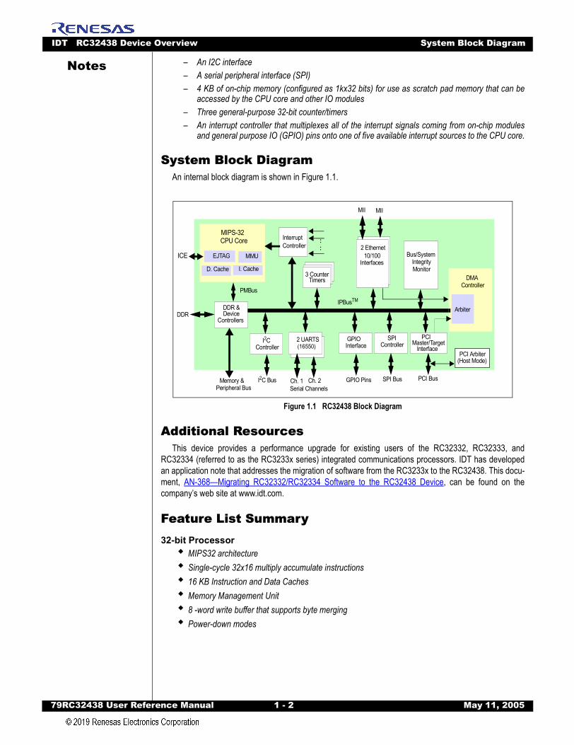
IDT RC32438 Device Overview System Block Diagram
79RC32438 User Refer
Notes
– An I2C interface – A serial peripheral interface (SPI) – 4 KB of on-chip memory (configured as 1kx32 bits) for use as scratch pad memory that can beaccessed by the CPU core and other IO modules – Three general-purpose 32-bit counter/timers– An interrupt controller that multiplexes all of the interrupt signals coming from on-chip modules
and general purpose IO (GPIO) pins onto one of five available interrupt sources to the CPU core.
System Block DiagramAn internal block diagram is shown in Figure 1.1.
Figure 1.1 RC32438 Block Diagram
Additional ResourcesThis device provides a performance upgrade for existing users of the RC32332, RC32333, and
RC32334 (referred to as the RC3233x series) integrated communications processors. IDT has developedan application note that addresses the migration of software from the RC3233x to the RC32438. This docu-ment, AN-368—Migrating RC32332/RC32334 Software to the RC32438 Device, can be found on thecompany’s web site at www.idt.com.
Feature List Summary32-bit Processor
MIPS32 architectureSingle-cycle 32x16 multiply accumulate instructions16 KB Instruction and Data CachesMemory Management Unit8 -word write buffer that supports byte mergingPower-down modes
EJTAG MMU
D. Cache I. Cache
MIPS-32CPU Core
ICE
InterruptController
3 CounterTimers
Bus/System
DMAController
ArbiterDDR
DDR &Device
2 UARTS(16550)
GPIOInterface
PCIMaster/Target
Memory &Peripheral Bus
Ch. 1 Ch. 2Serial Channels
GPIO Pins PCI Bus
ControllerControllerSPII2C
SPI BusI2C Bus
::
10/1002 Ethernet
Interfaces
MII MII
IntegrityMonitor
IPBusTM
InterfacePCI Arbiter
(Host Mode)
Controllers
PMBus
ence Manual 1 - 2 May 11, 2005

IDT RC32438 Device Overview Feature List Summary
79RC32438 User Refer
Notes
Debugging through Enhanced JTAG (EJTAG) interface– Version 2.5 compatible– Non-intrusive real-time debugging– Single stepping– Instruction and data breakpointsDDR Memory ControllerSupports up to 2GB of DDR SDRAM (using data bus multiplexing and two chip selects)2 chip selects (each chip select supports 4 internal DDR banks)Supports 16-bit or 32-bit data bus width using 8, 16, or 32-bit devicesSupports 64 Mb, 128 Mb, 256 Mb, 512 Mb, and 1Gb DDR SDRAM devicesData bus multiplexing support allows interfacing to standard DDR DIMMs and SODIMMsAutomatic refresh generation
Memory and Peripheral Device ControllerProvides “glueless” interface to standard SRAM, Flash, ROM, dual-port memory, and peripheral devicesDemultiplexed address and data buses
– 16-bit data bus– 26-bit address bus– 6 chip selects– Supports alternate bus masters– Control for external data bus buffers
Supports 8-bit and 16-bit width devices– Automatic byte gathering and scattering
Flexible protocol configuration parameters– Programmable number of wait states (0 to 63)– Programmable postread/postwrite delay (0 to 31)– Supports external wait state generation– Supports Intel and Motorola style peripherals
Write protect capability per chip selectProgrammable bus transaction timer generates warm reset when counter expiresSupports up to 64 MB of memory per chip select
Counter/TimersThree general purpose 32-bit counter timers
Interrupt ControllerAllows status of all interrupt sources to be readEach interrupt source may be maskedProvides interrupt test capability
System Integrity FunctionsProgrammable watchdog timer generates NMI when counter expiresAddress space monitor reports error in response to accesses to undecoded address regions
ence Manual 1 - 3 May 11, 2005
IDT RC32438 Device Overview Feature List Summary
79RC32438 User Refer
Notes
DMA Controller10 DMA channels– Two channels for PCI (PCI to Memory and Memory to PCI)– Four Ethernet channels — two for each Ethernet interface (transmit/receive)– Two DMA channels for memory to memory DMA operations– Two DMA channel for external DMA operations
Provides flexible descriptor based operationSupports external peripheral DMA operationsSupports unaligned transfers (i.e., source or destination address may be on any byte boundary) with arbitrary byte length.
Two Ethernet Interfaces10 and 100 Mb/s ISO/IEC 8802-3:1996 compliantTwo IEEE 802.3u compatible Media Independent Interfaces (MII) with serial management interfaceMII supports IEEE 802.3u auto-negotiation speed selectionSupports 64 entry hash table based multicast address filtering512 byte transmit and receive FIFOsSupports flow control functions outlined in IEEE Std. 802.3x-1997
PCI Interface32-bit PCI revision 2.2 compliantSupports host or satellite operation in both master and target modesPCI clock
– Supports PCI clock frequencies from 16 MHz to 66 MHz– PCI clock may be asynchronous to master clock (CLK)
PCI arbiter in Host mode– Supports 6 external masters– Fixed priority or round robin arbitration
I2O “like” PCI Messaging Unit
Universal Asynchronous Receiver Transmitter (UART)Compatible with the 16550 and 16450 UARTsTwo completely separate serial channelsModem control functions (CTS, RTS, DSR, DTR, RI, DCD)16-byte transmit and receive buffersProgrammable baud rate generator derived from the system clockFully programmable serial characteristics:
– 5, 6, 7, or 8 bit characters– Even, odd or no parity bit generation and detection– 1, 1 1/2, or 2 stop bit generation
Line break generation and detectionFalse start bit detectionInternal loopback mode
I2C-BusSupports standard 100 Kbps mode as well as 400 Kbps fast modeSupports 7-bit and 10-bit addressing
ence Manual 1 - 4 May 11, 2005
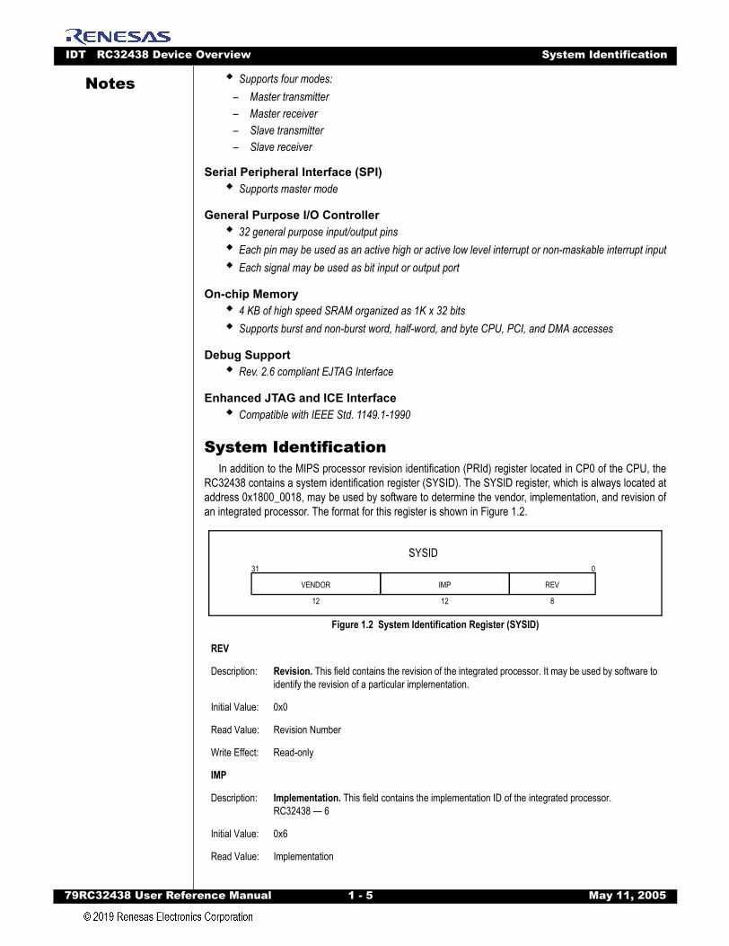
IDT RC32438 Device Overview System Identification
79RC32438 User Refer
Notes
Supports four modes:– Master transmitter– Master receiver– Slave transmitter– Slave receiverSerial Peripheral Interface (SPI)Supports master mode
General Purpose I/O Controller32 general purpose input/output pinsEach pin may be used as an active high or active low level interrupt or non-maskable interrupt inputEach signal may be used as bit input or output port
On-chip Memory4 KB of high speed SRAM organized as 1K x 32 bitsSupports burst and non-burst word, half-word, and byte CPU, PCI, and DMA accesses
Debug SupportRev. 2.6 compliant EJTAG Interface
Enhanced JTAG and ICE InterfaceCompatible with IEEE Std. 1149.1-1990
System IdentificationIn addition to the MIPS processor revision identification (PRId) register located in CP0 of the CPU, the
RC32438 contains a system identification register (SYSID). The SYSID register, which is always located ataddress 0x1800_0018, may be used by software to determine the vendor, implementation, and revision ofan integrated processor. The format for this register is shown in Figure 1.2.
Figure 1.2 System Identification Register (SYSID)
REV
Description: Revision. This field contains the revision of the integrated processor. It may be used by software to identify the revision of a particular implementation.
Initial Value: 0x0
Read Value: Revision Number
Write Effect: Read-only
IMP
Description: Implementation. This field contains the implementation ID of the integrated processor.RC32438 — 6
Initial Value: 0x6
Read Value: Implementation
SYSID031
8
REV
12
VENDOR
12
IMP
ence Manual 1 - 5 May 11, 2005
IDT RC32438 Device Overview System Identification
79RC32438 User Refer
Notes
Write Effect: Read-onlyVENDOR
Description: Vendor. This field contains the vendor of the integrated processor. The currently defined vendor is:0 Integrated Device Technology
Initial Value: 0x0
Read Value: Vendor
Write Effect: Read-only
ence Manual 1 - 6 May 11, 2005
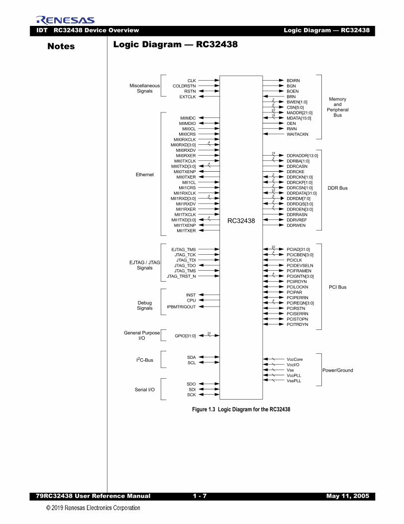
IDT RC32438 Device Overview Logic Diagram — RC32438
79RC32438 User Refer
Notes
Logic Diagram — RC32438Figure 1.3 Logic Diagram for the RC32438
MiscellaneousSignals
Memoryand
PeripheralBus
CLKCOLDRSTN
RSTN
4
MIIMDCMIIMDIO
MII0CLMII0CRS
MII0RXCLKMII0RXD[3:0]
MII0RXDVMII0RXER
MII0TXCLKMII0TXD[3:0]
MII0TXENPMII0TXER
MII1CLMII1CRS
MII1RXCLKMII1RXD[3:0]
MII1RXDVMII1RXER
MII1TXCLKMII1TXD[3:0]
MII1TXENPMII1TXER
BDIRNBGNBOENBRNBWEN[1:0]CSN[5:0]MADDR[21:0]MDATA[15:0]OENRWNWAITACKN
DDRADDR[13:0]DDRBA[1:0]DDRCASNDDRCKEDDRCKN[1:0]DDRCKP[1:0]DDRCSN[1:0]DDRDATA[31:0]DDRDM[7:0]DDRDQS[3:0]
DDRRASNDDRVREFDDRWEN
PCIAD[31:0]PCICBEN[3:0]PCICLKPCIDEVSELNPCIFRAMENPCIGNTN[3:0]PCIIRDYNPCILOCKNPCIPARPCIPERRNPCIREQN[3:0]PCIRSTNPCISERRNPCISTOPNPCITRDYN
GPIO[31:0]
SDO
SDASCL
JTAG_TCKJTAG_TDI
JTAG_TDOJTAG_TMS
JTAG_TRST_N
INSTCPU
IPBMTRIGOUT
4
4
4
32
4
4
4
32
4
8
32
2
2
2
2
14
16
22
6
2
EJTAG / JTAGSignals
DebugSignals
General PurposeI/O
I2C-Bus
Serial I/O
PCI Bus
DDR Bus
Ethernet
RC32438
VccCoreVccI/OVssVccPLLVssPLL
Power/Ground
SDISCK
DDROEN[3:0]4
EJTAG_TMS
EXTCLK
ence Manual 1 - 7 May 11, 2005
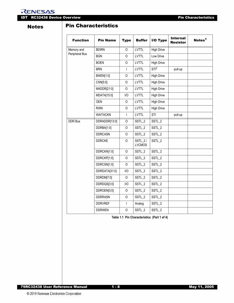
IDT RC32438 Device Overview Pin Characteristics
79RC32438 User Refer
Notes
Pin CharacteristicsFunction Pin Name Type Buffer I/O Type Internal Resistor Notes1
Memory and Peripheral Bus
BDIRN O LVTTL High Drive
BGN O LVTTL Low Drive
BOEN O LVTTL High Drive
BRN I LVTTL STI2 pull-up
BWEN[1:0] O LVTTL High Drive
CSN[5:0] O LVTTL High Drive
MADDR[21:0] O LVTTL High Drive
MDATA[15:0] I/O LVTTL High Drive
OEN O LVTTL High Drive
RWN O LVTTL High Drive
WAITACKN I LVTTL STI pull-up
DDR Bus DDRADDR[13:0] O SSTL_2 SSTL_2
DDRBA[1:0] O SSTL_2 SSTL_2
DDRCASN O SSTL_2 SSTL_2
DDRCKE O SSTL_2 / LVCMOS
SSTL_2
DDRCKN[1:0] O SSTL_2 SSTL_2
DDRCKP[1:0] O SSTL_2 SSTL_2
DDRCSN[1:0] O SSTL_2 SSTL_2
DDRDATA[31:0] I/O SSTL_2 SSTL_2
DDRDM[7:0] O SSTL_2 SSTL_2
DDRDQS[3:0] I/O SSTL_2 SSTL_2
DDROEN[3:0] O SSTL_2 SSTL_2
DDRRASN O SSTL_2 SSTL_2
DDRVREF I Analog SSTL_2
DDRWEN O SSTL_2 SSTL_2
Table 1.1 Pin Characteristics (Part 1 of 4)
ence Manual 1 - 8 May 11, 2005
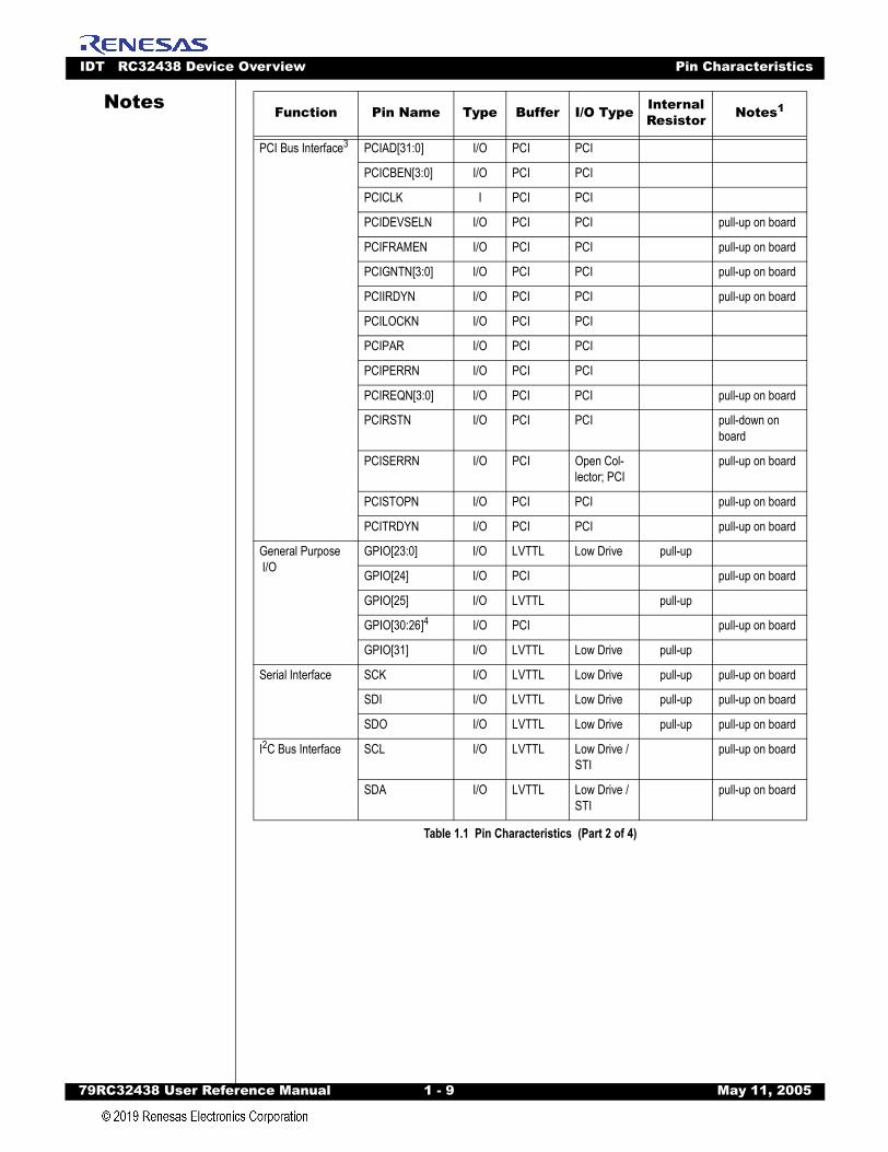
IDT RC32438 Device Overview Pin Characteristics
79RC32438 User Refer
Notes
PCI Bus Interface3 PCIAD[31:0] I/O PCI PCI
PCICBEN[3:0] I/O PCI PCI
PCICLK I PCI PCI
PCIDEVSELN I/O PCI PCI pull-up on board
PCIFRAMEN I/O PCI PCI pull-up on board
PCIGNTN[3:0] I/O PCI PCI pull-up on board
PCIIRDYN I/O PCI PCI pull-up on board
PCILOCKN I/O PCI PCI
PCIPAR I/O PCI PCI
PCIPERRN I/O PCI PCI
PCIREQN[3:0] I/O PCI PCI pull-up on board
PCIRSTN I/O PCI PCI pull-down on board
PCISERRN I/O PCI Open Col-lector; PCI
pull-up on board
PCISTOPN I/O PCI PCI pull-up on board
PCITRDYN I/O PCI PCI pull-up on board
General Purpose I/O
GPIO[23:0] I/O LVTTL Low Drive pull-up
GPIO[24] I/O PCI pull-up on board
GPIO[25] I/O LVTTL pull-up
GPIO[30:26]4 I/O PCI pull-up on board
GPIO[31] I/O LVTTL Low Drive pull-up
Serial Interface SCK I/O LVTTL Low Drive pull-up pull-up on board
SDI I/O LVTTL Low Drive pull-up pull-up on board
SDO I/O LVTTL Low Drive pull-up pull-up on board
I2C Bus Interface SCL I/O LVTTL Low Drive / STI
pull-up on board
SDA I/O LVTTL Low Drive / STI
pull-up on board
Function Pin Name Type Buffer I/O Type Internal Resistor Notes1
Table 1.1 Pin Characteristics (Part 2 of 4)
ence Manual 1 - 9 May 11, 2005
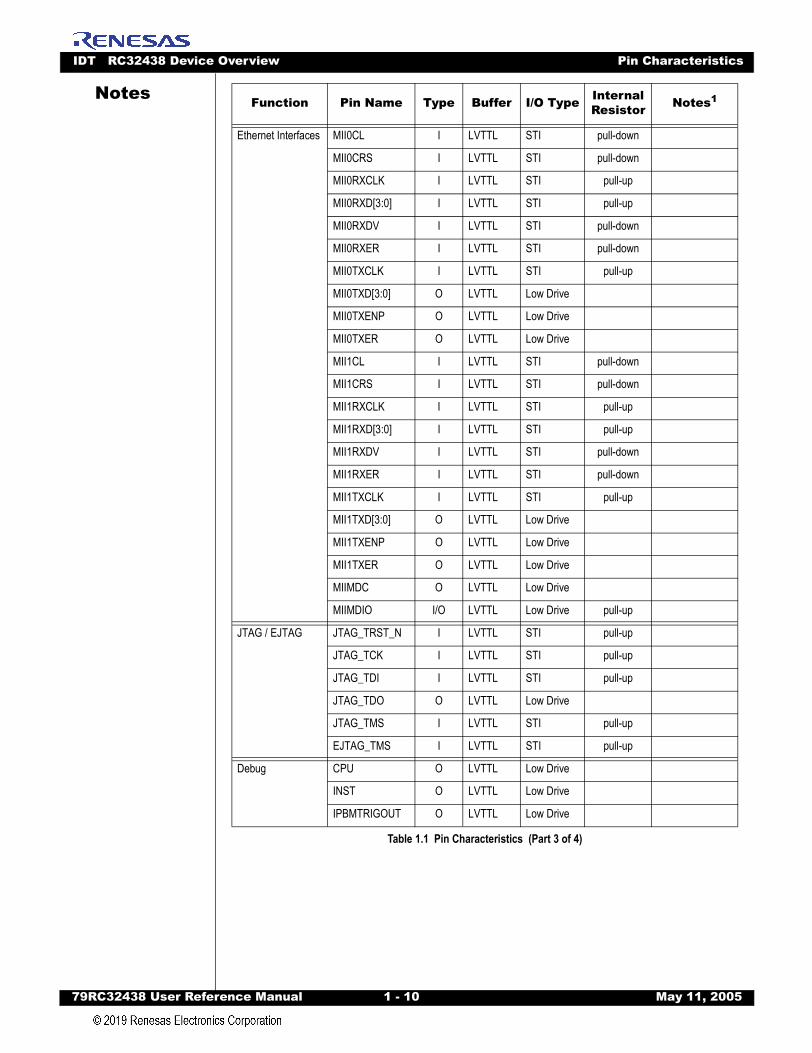
IDT RC32438 Device Overview Pin Characteristics
79RC32438 User Refer
Notes
Ethernet Interfaces MII0CL I LVTTL STI pull-down
MII0CRS I LVTTL STI pull-down
MII0RXCLK I LVTTL STI pull-up
MII0RXD[3:0] I LVTTL STI pull-up
MII0RXDV I LVTTL STI pull-down
MII0RXER I LVTTL STI pull-down
MII0TXCLK I LVTTL STI pull-up
MII0TXD[3:0] O LVTTL Low Drive
MII0TXENP O LVTTL Low Drive
MII0TXER O LVTTL Low Drive
MII1CL I LVTTL STI pull-down
MII1CRS I LVTTL STI pull-down
MII1RXCLK I LVTTL STI pull-up
MII1RXD[3:0] I LVTTL STI pull-up
MII1RXDV I LVTTL STI pull-down
MII1RXER I LVTTL STI pull-down
MII1TXCLK I LVTTL STI pull-up
MII1TXD[3:0] O LVTTL Low Drive
MII1TXENP O LVTTL Low Drive
MII1TXER O LVTTL Low Drive
MIIMDC O LVTTL Low Drive
MIIMDIO I/O LVTTL Low Drive pull-up
JTAG / EJTAG JTAG_TRST_N I LVTTL STI pull-up
JTAG_TCK I LVTTL STI pull-up
JTAG_TDI I LVTTL STI pull-up
JTAG_TDO O LVTTL Low Drive
JTAG_TMS I LVTTL STI pull-up
EJTAG_TMS I LVTTL STI pull-up
Debug CPU O LVTTL Low Drive
INST O LVTTL Low Drive
IPBMTRIGOUT O LVTTL Low Drive
Function Pin Name Type Buffer I/O Type Internal Resistor Notes1
Table 1.1 Pin Characteristics (Part 3 of 4)
ence Manual 1 - 10 May 11, 2005
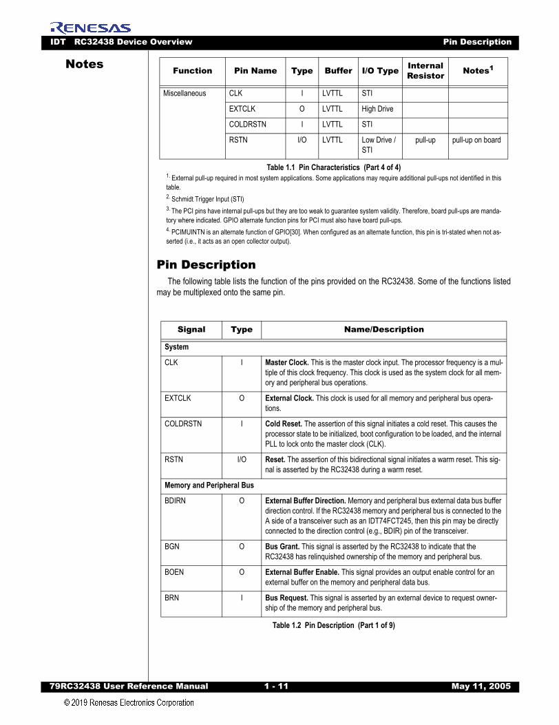
IDT RC32438 Device Overview Pin Description
79RC32438 User Refer
Notes
Pin DescriptionThe following table lists the function of the pins provided on the RC32438. Some of the functions listed
may be multiplexed onto the same pin.
Miscellaneous CLK I LVTTL STI
EXTCLK O LVTTL High Drive
COLDRSTN I LVTTL STI
RSTN I/O LVTTL Low Drive / STI
pull-up pull-up on board
1. External pull-up required in most system applications. Some applications may require additional pull-ups not identified in thistable.2. Schmidt Trigger Input (STI)3. The PCI pins have internal pull-ups but they are too weak to guarantee system validity. Therefore, board pull-ups are manda-tory where indicated. GPIO alternate function pins for PCI must also have board pull-ups.4. PCIMUINTN is an alternate function of GPIO[30]. When configured as an alternate function, this pin is tri-stated when not as-serted (i.e., it acts as an open collector output).
Signal Type Name/Description
System
CLK I Master Clock. This is the master clock input. The processor frequency is a mul-tiple of this clock frequency. This clock is used as the system clock for all mem-ory and peripheral bus operations.
EXTCLK O External Clock. This clock is used for all memory and peripheral bus opera-tions.
COLDRSTN I Cold Reset. The assertion of this signal initiates a cold reset. This causes the processor state to be initialized, boot configuration to be loaded, and the internal PLL to lock onto the master clock (CLK).
RSTN I/O Reset. The assertion of this bidirectional signal initiates a warm reset. This sig-nal is asserted by the RC32438 during a warm reset.
Memory and Peripheral Bus
BDIRN O External Buffer Direction. Memory and peripheral bus external data bus buffer direction control. If the RC32438 memory and peripheral bus is connected to the A side of a transceiver such as an IDT74FCT245, then this pin may be directly connected to the direction control (e.g., BDIR) pin of the transceiver.
BGN O Bus Grant. This signal is asserted by the RC32438 to indicate that the RC32438 has relinquished ownership of the memory and peripheral bus.
BOEN O External Buffer Enable. This signal provides an output enable control for an external buffer on the memory and peripheral data bus.
BRN I Bus Request. This signal is asserted by an external device to request owner-ship of the memory and peripheral bus.
Table 1.2 Pin Description (Part 1 of 9)
Function Pin Name Type Buffer I/O Type Internal Resistor Notes1
Table 1.1 Pin Characteristics (Part 4 of 4)
ence Manual 1 - 11 May 11, 2005
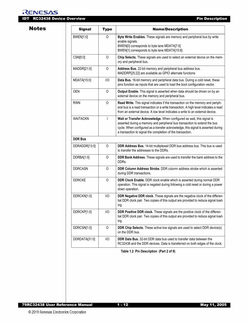
IDT RC32438 Device Overview Pin Description
79RC32438 User Refer
Notes
BWEN[1:0] O Byte Write Enables. These signals are memory and peripheral bus by writeenable signals.BWEN[0] corresponds to byte lane MDATA[7:0]BWEN[1] corresponds to byte lane MDATA[15:8]
CSN[5:0] O Chip Selects. These signals are used to select an external device on the mem-ory and peripheral bus.
MADDR[21:0] O Address Bus. 22-bit memory and peripheral bus address bus.MADDRP[25:22] are available as GPIO alternate functions
MDATA[15:0] I/O Data Bus. 16-bit memory and peripheral data bus. During a cold reset, these pins function as inputs that are used to load the boot configuration vector.
OEN O Output Enable. This signal is asserted when data should be driven on by an external device on the memory and peripheral bus.
RWN O Read Write. This signal indicates if the transaction on the memory and periph-eral bus is a read transaction or a write transaction. A high level indicates a read from an external device. A low level indicates a write to an external device.
WAITACKN I Wait or Transfer Acknowledge. When configured as wait, this signal is asserted during a memory and peripheral bus transaction to extend the bus cycle. When configured as a transfer acknowledge, this signal is asserted during a transaction to signal the completion of the transaction.
DDR Bus
DDRADDR[13:0] O DDR Address Bus. 14-bit multiplexed DDR bus address bus. This bus is used to transfer the addresses to the DDRs.
DDRBA[1:0] O DDR Bank Address. These signals are used to transfer the bank address to the DDRs.
DDRCASN O DDR Column Address Strobe. DDR column address strobe which is asserted during DDR transactions.
DDRCKE O DDR Clock Enable. DDR clock enable which is asserted during normal DDR operation. This signal is negated during following a cold reset or during a power down operation.
DDRCKN[1:0] I/O DDR Negative DDR clock. These signals are the negative clock of the differen-tial DDR clock pair. Two copies of this output are provided to reduce signal load-ing.
DDRCKP[1:0] I/O DDR Positive DDR clock. These signals are the positive clock of the differen-tial DDR clock pair. Two copies of this output are provided to reduce signal load-ing.
DDRCSN[1:0] O DDR Chip Selects. These active low signals are used to select DDR device(s) on the DDR bus.
DDRDATA[31:0] I/O DDR Data Bus. 32-bit DDR data bus used to transfer data between the RC32438 and the DDR devices. Data is transferred on both edges of the clock.
Signal Type Name/Description
Table 1.2 Pin Description (Part 2 of 9)
ence Manual 1 - 12 May 11, 2005
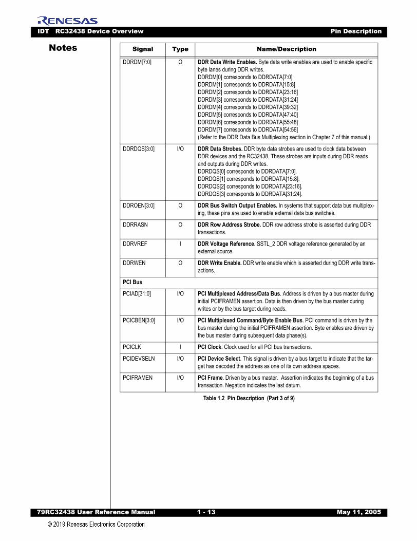
IDT RC32438 Device Overview Pin Description
79RC32438 User Refer
Notes
DDRDM[7:0] O DDR Data Write Enables. Byte data write enables are used to enable specificbyte lanes during DDR writes.DDRDM[0] corresponds to DDRDATA[7:0]DDRDM[1] corresponds to DDRDATA[15:8]DDRDM[2] corresponds to DDRDATA[23:16] DDRDM[3] corresponds to DDRDATA[31:24] DDRDM[4] corresponds to DDRDATA[39:32] DDRDM[5] corresponds to DDRDATA[47:40] DDRDM[6] corresponds to DDRDATA[55:48] DDRDM[7] corresponds to DDRDATA[54:56] (Refer to the DDR Data Bus Multiplexing section in Chapter 7 of this manual.)
DDRDQS[3:0] I/O DDR Data Strobes. DDR byte data strobes are used to clock data between DDR devices and the RC32438. These strobes are inputs during DDR reads and outputs during DDR writes.DDRDQS[0] corresponds to DDRDATA[7:0].DDRDQS[1] corresponds to DDRDATA[15:8].DDRDQS[2] corresponds to DDRDATA[23:16].DDRDQS[3] corresponds to DDRDATA[31:24].
DDROEN[3:0] O DDR Bus Switch Output Enables. In systems that support data bus multiplex-ing, these pins are used to enable external data bus switches.
DDRRASN O DDR Row Address Strobe. DDR row address strobe is asserted during DDR transactions.
DDRVREF I DDR Voltage Reference. SSTL_2 DDR voltage reference generated by an external source.
DDRWEN O DDR Write Enable. DDR write enable which is asserted during DDR write trans-actions.
PCI Bus
PCIAD[31:0] I/O PCI Multiplexed Address/Data Bus. Address is driven by a bus master during initial PCIFRAMEN assertion. Data is then driven by the bus master during writes or by the bus target during reads.
PCICBEN[3:0] I/O PCI Multiplexed Command/Byte Enable Bus. PCI command is driven by the bus master during the initial PCIFRAMEN assertion. Byte enables are driven by the bus master during subsequent data phase(s).
PCICLK I PCI Clock. Clock used for all PCI bus transactions.
PCIDEVSELN I/O PCI Device Select. This signal is driven by a bus target to indicate that the tar-get has decoded the address as one of its own address spaces.
PCIFRAMEN I/O PCI Frame. Driven by a bus master. Assertion indicates the beginning of a bus transaction. Negation indicates the last datum.
Signal Type Name/Description
Table 1.2 Pin Description (Part 3 of 9)
ence Manual 1 - 13 May 11, 2005
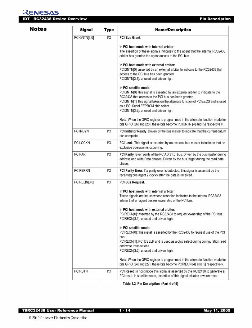
IDT RC32438 Device Overview Pin Description
79RC32438 User Refer
Notes
PCIGNTN[3:0] I/O PCI Bus Grant.In PCI host mode with internal arbiter:The assertion of these signals indicates to the agent that the internal RC32438 arbiter has granted the agent access to the PCI bus.
In PCI host mode with external arbiter:PCIGNTN[0]: asserted by an external arbiter to indicate to the RC32438 that access to the PCI bus has been granted. PCIGNTN[3:1]: unused and driven high.
In PCI satellite mode:PCIGNTN[0]: this signal is asserted by an external arbiter to indicate to the RC32438 that access to the PCI bus has been granted.PCIGNTN[1]: this signal takes on the alternate function of PCIEECS and is used as a PCI Serial EEPROM chip select.PCIGNTN[3:2]: unused and driven high.
Note: When the GPIO register is programmed in the alternate function mode for bits GPIO [26] and [28], these bits become PCIGNTN [4] and [5] respectively.
PCIIRDYN I/O PCI Initiator Ready. Driven by the bus master to indicate that the current datum can complete.
PCILOCKN I/O PCI Lock. This signal is asserted by an external bus master to indicate that an exclusive operation is occurring.
PCIPAR I/O PCI Parity. Even parity of the PCIAD[31:0] bus. Driven by the bus master during address and write Data phases. Driven by the bus target during the read data phase.
PCIPERRN I/O PCI Parity Error. If a parity error is detected, this signal is asserted by the receiving bus agent 2 clocks after the data is received.
PCIREQN[3:0] I/O PCI Bus Request.
In PCI host mode with internal arbiter:These signals are inputs whose assertion indicates to the internal RC32438 arbiter that an agent desires ownership of the PCI bus.
In PCI host mode with external arbiter:PCIREQN[0]: asserted by the RC32438 to request ownership of the PCI bus.PCIREQN[3:1]: unused and driven high.
In PCI satellite mode:PCIREQN[0]: this signal is asserted by the RC32438 to request use of the PCI bus.PCIREQN[1]: PCIIDSELP and is used as a chip select during configuration read and write transactions.PCIREQN[3:2]: unused and driven high.
Note: When the GPIO register is programmed in the alternate function mode for bits GPIO [24] and [27], these bits become PCIREQN [4] and [5] respectively.
PCIRSTN I/O PCI Reset. In host mode this signal is asserted by the RC32438 to generate a PCI reset. In satellite mode, assertion of this signal initiates a warm reset.
Signal Type Name/Description
Table 1.2 Pin Description (Part 4 of 9)
ence Manual 1 - 14 May 11, 2005
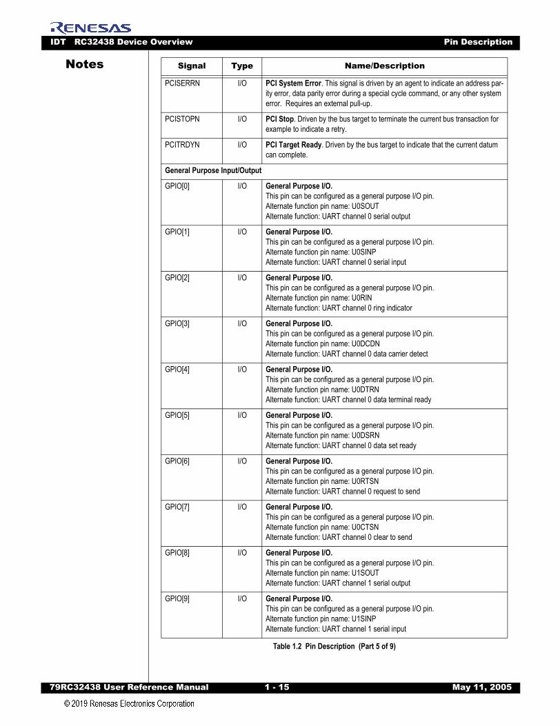
IDT RC32438 Device Overview Pin Description
79RC32438 User Refer
Notes
PCISERRN I/O PCI System Error. This signal is driven by an agent to indicate an address par-ity error, data parity error during a special cycle command, or any other system error. Requires an external pull-up.
PCISTOPN I/O PCI Stop. Driven by the bus target to terminate the current bus transaction for example to indicate a retry.
PCITRDYN I/O PCI Target Ready. Driven by the bus target to indicate that the current datum can complete.
General Purpose Input/Output
GPIO[0] I/O General Purpose I/O.This pin can be configured as a general purpose I/O pin.Alternate function pin name: U0SOUTAlternate function: UART channel 0 serial output
GPIO[1] I/O General Purpose I/O.This pin can be configured as a general purpose I/O pin.Alternate function pin name: U0SINPAlternate function: UART channel 0 serial input
GPIO[2] I/O General Purpose I/O.This pin can be configured as a general purpose I/O pin.Alternate function pin name: U0RINAlternate function: UART channel 0 ring indicator
GPIO[3] I/O General Purpose I/O.This pin can be configured as a general purpose I/O pin.Alternate function pin name: U0DCDNAlternate function: UART channel 0 data carrier detect
GPIO[4] I/O General Purpose I/O.This pin can be configured as a general purpose I/O pin.Alternate function pin name: U0DTRNAlternate function: UART channel 0 data terminal ready
GPIO[5] I/O General Purpose I/O.This pin can be configured as a general purpose I/O pin.Alternate function pin name: U0DSRNAlternate function: UART channel 0 data set ready
GPIO[6] I/O General Purpose I/O.This pin can be configured as a general purpose I/O pin.Alternate function pin name: U0RTSNAlternate function: UART channel 0 request to send
GPIO[7] I/O General Purpose I/O.This pin can be configured as a general purpose I/O pin.Alternate function pin name: U0CTSNAlternate function: UART channel 0 clear to send
GPIO[8] I/O General Purpose I/O.This pin can be configured as a general purpose I/O pin.Alternate function pin name: U1SOUTAlternate function: UART channel 1 serial output
GPIO[9] I/O General Purpose I/O.This pin can be configured as a general purpose I/O pin.Alternate function pin name: U1SINPAlternate function: UART channel 1 serial input
Signal Type Name/Description
Table 1.2 Pin Description (Part 5 of 9)
ence Manual 1 - 15 May 11, 2005

IDT RC32438 Device Overview Pin Description
79RC32438 User Refer
Notes
GPIO[10] I/O General Purpose I/O.This pin can be configured as a general purpose I/O pin.Alternate function pin name: U1DTRNAlternate function: UART channel 1 data terminal ready
GPIO[11] I/O General Purpose I/O.This pin can be configured as a general purpose I/O pin. Alternate function pin name: U1DSRNAlternate function: UART channel 1 data set ready
GPIO[12] I/O General Purpose I/O.This pin can be configured as a general purpose I/O pin. Alternate function pin name: U1RTSNAlternate function: UART channel 1 request to send
GPIO[13] I/O General Purpose I/O.This pin can be configured as a general purpose I/O pin.Alternate function pin name: U1CTSNAlternate function: UART channel 1 clear to send
GPIO[14] I/O General Purpose I/O.This pin can be configured as a general purpose I/O pin.Alternate function pin name: DMAREQN0Alternate function: External DMA channel 0 request
GPIO[15] I/O General Purpose I/O.This pin can be configured as a general purpose I/O pin.Alternate function pin name: DMAREQN1Alternate function: External DMA channel 1 request
GPIO[16] I/O General Purpose I/O.This pin can be configured as a general purpose I/O pin.Alternate function pin name: DMADONEN0Alternate function: External DMA channel 0 done
GPIO[17] I/O General Purpose I/O.This pin can be configured as a general purpose I/O pin.Alternate function pin name: DMADONEN1Alternate function: External DMA channel 1 done
GPIO[18] I/O General Purpose I/O.This pin can be configured as a general purpose I/O pin.Alternate function pin name: DMAFINN0Alternate function: External DMA channel 0 finished
GPIO[19] I/O General Purpose I/O.This pin can be configured as a general purpose I/O pin.Alternate function pin name: DMAFINN1Alternate function: External DMA channel 1 finished
GPIO[20] I/O General Purpose I/O.This pin can be configured as a general purpose I/O pin.Alternate function pin name: MADDR[22]Alternate function: Memory and peripheral bus address
GPIO[21] I/O General Purpose I/O.This pin can be configured as a general purpose I/O pin.Alternate function pin name: MADDR[23]Alternate function: Memory and peripheral bus address
Signal Type Name/Description
Table 1.2 Pin Description (Part 6 of 9)
ence Manual 1 - 16 May 11, 2005
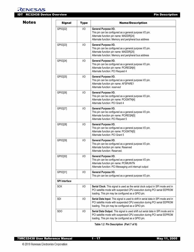
IDT RC32438 Device Overview Pin Description
79RC32438 User Refer
Notes
GPIO[22] I/O General Purpose I/O.This pin can be configured as a general purpose I/O pin.Alternate function pin name: MADDR[24]Alternate function: Memory and peripheral bus address
GPIO[23] I/O General Purpose I/O.This pin can be configured as a general purpose I/O pin.Alternate function pin name: MADDR[25]Alternate function: Memory and peripheral bus address
GPIO[24] I/O General Purpose I/O.This pin can be configured as a general purpose I/O pin.Alternate function pin name: PCIREQN[4]Alternate function: PCI Request 4
GPIO[25] I/O General Purpose I/O.This pin can be configured as a general purpose I/O pin.Alternate function pin name: AFSPARE1Alternate function: reserved
GPIO[26] I/O General Purpose I/O.This pin can be configured as a general purpose I/O pin.Alternate function pin name: PCIGNTN[4]Alternate function: PCI Grant 4
GPIO[27] I/O General Purpose I/O.This pin can be configured as a general purpose I/O pin.Alternate function pin name: PCIREQN[5]Alternate function: PCI Request 5
GPIO[28] I/O General Purpose I/O.This pin can be configured as a general purpose I/O pin.Alternate function pin name: PCIGNTN[5]Alternate function: PCI Grant 5
GPIO[29] I/O General Purpose I/O.This pin can be configured as a general purpose I/O pin.Alternate function pin name: ReservedAlternate function: Reserved.
GPIO[30] I/O General Purpose I/O.This pin can be configured as a general purpose I/O pin.Alternate function pin name: PCIMUINTNAlternate function: PCI Messaging unit interrupt output
GPIO[31] I/O General Purpose I/O.This pin can be configured as a general purpose I/O pin.
SPI Interface
SCK I/O Serial Clock. This signal is used as the serial clock output in SPI mode and in PCI satellite mode with suspended CPU execution during PCI serial EEPROM loading. This pin may be configured as a GPIO pin.
SDI I/O Serial Data Input. This signal is used to shift in serial data in SPI mode and in PCI satellite mode with suspended CPU execution during PCI serial EEPROM loading. This pin may be configured as a GPIO pin.
SDO I/O Serial Data Output. This signal is used shift out serial data in SPI mode and in PCI satellite mode with suspended CPU execution during PCI serial EEPROM loading. This pin may be configured as a GPIO pin.
Signal Type Name/Description
Table 1.2 Pin Description (Part 7 of 9)
ence Manual 1 - 17 May 11, 2005

IDT RC32438 Device Overview Pin Description
79RC32438 User Refer
Notes
I2C Bus InterfaceSCL I/O I2C Clock. I2C-bus clock.
SDA I/O I2C Data Bus. I2C-bus data bus.
Ethernet Interfaces
MII0CL I Ethernet 0 MII Collision Detected. This signal is asserted by the ethernet PHY when a collision is detected.
MII0CRS I Ethernet 0 MII Carrier Sense. This signal is asserted by the ethernet PHY when either the transmit or receive medium is not idle.
MII0RXCLK I Ethernet 0 MII Receive Clock. This clock is a continuous clock that provides a timing reference for the reception of data.
MII0RXD[3:0] I Ethernet 0 MII Receive Data. This nibble wide data bus contains the data received by the ethernet PHY.
MII0RXDV I Ethernet 0 MII Receive Data Valid. The assertion of this signal indicates that valid receive data is in the MII receive data bus.
MII0RXER I Ethernet 0 MII Receive Error. The assertion of this signal indicates that an error was detected somewhere in the ethernet frame currently being sent in the MII receive data bus.
MII0TXCLK I Ethernet 0 MII Transmit Clock. This clock is a continuous clock that provides a timing reference for the transfer of transmit data.
MII0TXD[3:0] O Ethernet 0 MII Transmit Data. This nibble wide data bus contains the data to be transmitted.
MII0TXENP O Ethernet 0 MII Transmit Enable. The assertion of this signal indicates that data is present on the MII for transmission.
MII0TXER O Ethernet 0 MII Transmit Coding Error. When this signal is asserted together with MIITXENP, the ethernet PHY will transmit symbols which are not valid data or delimiters.
MII1CL I Ethernet 1 MII Collision Detected. This signal is asserted by the ethernet PHY when a collision is detected.
MII1CRS I Ethernet 1 MII Carrier Sense. This signal is asserted by the ethernet PHY when either the transmit or receive medium is not idle.
MII1RXCLK I Ethernet 1 MII Receive Clock. This clock is a continuous clock that provides a timing reference for the reception of data.
MII1RXD[3:0] I Ethernet 1 MII Receive Data. This nibble wide data bus contains the data received by the ethernet PHY.
MII1RXDV I Ethernet 1 MII Receive Data Valid. The assertion of this signal indicates that valid receive data is in the MII receive data bus.
MII1RXER I Ethernet 1 MII Receive Error. The assertion of this signal indicates that an error was detected somewhere in the ethernet frame currently being sent in the MII receive data bus.
MII1TXCLK I Ethernet 1 MII Transmit Clock. This clock is a continuous clock that provides a timing reference for the transfer of transmit data.
MII1TXD[3:0] O Ethernet 1 MII Transmit Data. This nibble wide data bus contains the data to be transmitted.
Signal Type Name/Description
Table 1.2 Pin Description (Part 8 of 9)
ence Manual 1 - 18 May 11, 2005

IDT RC32438 Device Overview Pin Description
79RC32438 User Refer
Notes
MII1TXENP O Ethernet 1 MII Transmit Enable. The assertion of this signal indicates that datais present on the MII for transmission.
MII1TXER O Ethernet 1 MII Transmit Coding Error. When this signal is asserted together with MIITXENP, the ethernet PHY will transmit symbols which are not valid data or delimiters.
MIIMDC O MII Management Data Clock. This signal is used as a timing reference for transmission of data on the management interface.
MIIMDIO I/O MII Management Data. This bidirectional signal is used to transfer data between the station management entity and the ethernet PHY.
JTAG / EJTAG
EJTAG_TMS I EJTAG Mode. The value on this signal controls the test mode select of the EJTAG Controller. When using the JTAG boundary scan, this pin should be left disconnected (since there is an internal pull-up) or driven high.
JTAG_TCK I JTAG Clock. This is an input test clock used to clock the shifting of data into or out of the boundary scan logic, JTAG Controller, or the EJTAG Controller. JTAG_TCK is independent of the system and the processor clock with a nomi-nal 50% duty cycle.
JTAG_TDI I JTAG Data Input. This is the serial data input to the boundary scan logic, JTAG Controller, or the EJTAG Controller.
JTAG_TDO O JTAG Data Output. This is the serial data shifted out from the boundary scan logic, JTAG Controller, or the EJTAG Controller. When no data is being shifted out, this signal is tri-stated.
JTAG_TMS I JTAG Mode. The value on this signal controls the test mode select of the boundary scan logic or JTAG Controller. When using the EJTAG debug inter-face, this pin should be left disconnected (since there is an internal pull-up) or driven high.
JTAG_TRST_N I JTAG Reset. This active low signal asynchronously resets the boundary scan logic, JTAG TAP Controller, and the EJTAG Debug TAP Controller. An external pull-up on the board is recommended to meet the JTAG specification in cases where the tester can access this signal. However, for systems running in func-tional mode, one of the following should occur:1) actively drive this signal low with control logic2) statically drive this signal low with an external pull-down on the board3) clock JTAG_TCK while holding EJTAG_TMS and/or JTAG_TMS high.
Debug
CPU O CPU Transaction. This signal is asserted during all CPU instruction fetches and data transfers to/from the DDR and devices on the memory and peripheral bus. The signal is negated during PCI and DMA transactions to/from the DDR and devices on the memory and peripheral bus.
INST O Instruction or Data. This signal is driven high during CPU instruction fetches on the memory and peripheral bus memory or DDR bus.
Signal Type Name/Description
Table 1.2 Pin Description (Part 9 of 9)
ence Manual 1 - 19 May 11, 2005
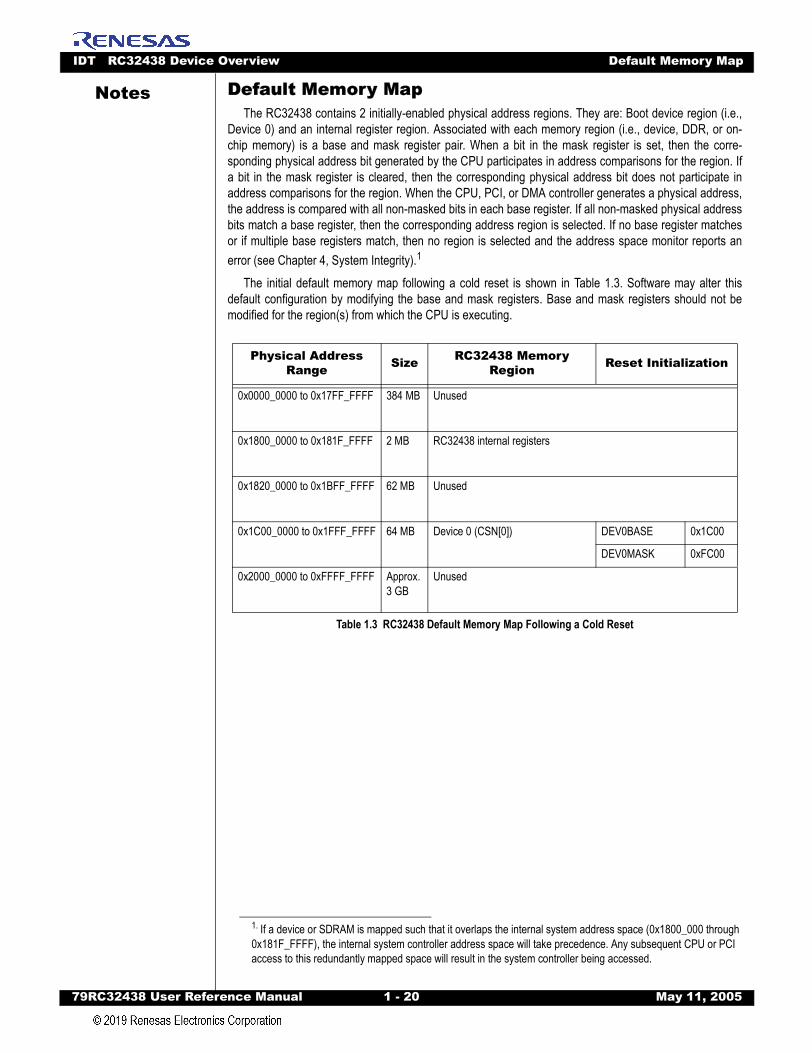
IDT RC32438 Device Overview Default Memory Map
79RC32438 User Refer
Notes
Default Memory MapThe RC32438 contains 2 initially-enabled physical address regions. They are: Boot device region (i.e.,Device 0) and an internal register region. Associated with each memory region (i.e., device, DDR, or on-chip memory) is a base and mask register pair. When a bit in the mask register is set, then the corre-sponding physical address bit generated by the CPU participates in address comparisons for the region. Ifa bit in the mask register is cleared, then the corresponding physical address bit does not participate inaddress comparisons for the region. When the CPU, PCI, or DMA controller generates a physical address,the address is compared with all non-masked bits in each base register. If all non-masked physical addressbits match a base register, then the corresponding address region is selected. If no base register matchesor if multiple base registers match, then no region is selected and the address space monitor reports anerror (see Chapter 4, System Integrity).1
The initial default memory map following a cold reset is shown in Table 1.3. Software may alter thisdefault configuration by modifying the base and mask registers. Base and mask registers should not bemodified for the region(s) from which the CPU is executing.
1. If a device or SDRAM is mapped such that it overlaps the internal system address space (0x1800_000 through 0x181F_FFFF), the internal system controller address space will take precedence. Any subsequent CPU or PCI access to this redundantly mapped space will result in the system controller being accessed.
Physical Address Range Size RC32438 Memory
Region Reset Initialization
0x0000_0000 to 0x17FF_FFFF 384 MB Unused
0x1800_0000 to 0x181F_FFFF 2 MB RC32438 internal registers
0x1820_0000 to 0x1BFF_FFFF 62 MB Unused
0x1C00_0000 to 0x1FFF_FFFF 64 MB Device 0 (CSN[0]) DEV0BASE 0x1C00
DEV0MASK 0xFC00
0x2000_0000 to 0xFFFF_FFFF Approx. 3 GB
Unused
Table 1.3 RC32438 Default Memory Map Following a Cold Reset
ence Manual 1 - 20 May 11, 2005
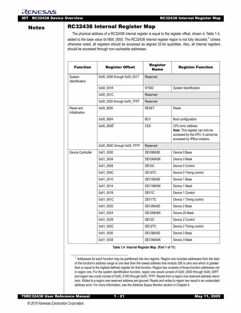
IDT RC32438 Device Overview RC32438 Internal Register Map
79RC32438 User Refer
Notes
RC32438 Internal Register MapThe physical address of a RC32438 internal register is equal to the register offset, shown in Table 1.4,added to the base value 0x1800_0000. The RC32438 internal register region is not fully decoded.1 Unlessotherwise noted, all registers should be accessed as aligned 32-bit quantities. Also, all internal registersshould be accessed through non-cacheable addresses.
1. Addresses for each function may be partitioned into two regions. Region one includes addresses from the start of the function’s address range to one less than the lowest address that modulo 256 is zero and which is greater than or equal to the highest defined register for that function. Region two consists of those function addresses not in region one. For the system identification function, region one would consist of 0x00_0000 through 0x00_00FF and region two could consist of 0x00_0100 through 0x00_7FFF. Reads from a region one reserved address return zero. Writes to a region one reserved address are ignored. Reads and writes to region two result in an undecoded address error. For more information, see the Address Space Monitor section in Chapter 4.
Function Register Offset Register Name Register Function
System Identification
0x00_0000 through 0x00_0017 Reserved
0x00_0018 SYSID System Identification
0x00_001C Reserved
0x00_0020 through 0x00_7FFF Reserved
Reset andInitialization
0x00_8000 RESET Reset
0x00_8004 BCV Boot configuration
0x00_80081 CEA CPU error address Note: This register can only be accessed by the CPU. It cannot be accessed by IPBus masters.
0x00_800C through 0x00_FFFF Reserved
Device Controller 0x01_0000 DEV0BASE Device 0 Base
0x01_0004 DEV0MASK Device 0 Mask
0x01_0008 DEV0C Device 0 Control
0x01_000C DEV0TC Device 0 Timing control
0x01_0010 DEV1BASE Device 1 Base
0x01_0014 DEV1MASK Device 1 Mask
0x01_0018 DEV1C Device 1 Control
0x01_001C DEV1TC Device 1 Timing control
0x01_0020 DEV2BASE Device 2 Base
0x01_0024 DEV2MASK Device 20 Mask
0x01_0028 DEV2C Device 2 Control
0x01_002C DEV2TC Device 2 Timing control
0x01_0030 DEV3BASE Device 3 Base
0x01_0034 DEV3MASK Device 3 Mask
Table 1.4 Internal Register Map (Part 1 of 11)
ence Manual 1 - 21 May 11, 2005
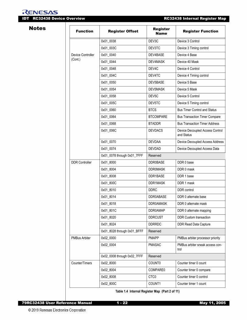
IDT RC32438 Device Overview RC32438 Internal Register Map
79RC32438 User Refer
Notes
0x01_0038 DEV3C Device 3 Control
0x01_003C DEV3TC Device 3 Timing control
Device Controller (Cont.)
0x01_0040 DEV4BASE Device 4 Base
0x01_0044 DEV4MASK Device 40 Mask
0x01_0048 DEV4C Device 4 Control
0x01_004C DEV4TC Device 4 Timing control
0x01_0050 DEV5BASE Device 5 Base
0x01_0054 DEV5MASK Device 5 Mask
0x01_0058 DEV5C Device 5 Control
0x01_005C DEV5TC Device 5 Timing control
0x01_0060 BTCS Bus Timer Control and Status
0x01_0064 BTCOMPARE Bus Transaction Timer Compare
0x01_0068 BTADDR Bus Transaction Timer Address
0x01_006C DEVDACS Device Decoupled Access Control and Status
0x01_0070 DEVDAA Device Decoupled Access Address
0x01_0074 DEVDAD Device Decoupled Access Data
0x01_0078 through 0x01_7FFF Reserved
DDR Controller 0x01_8000 DDR0BASE DDR 0 base
0x01_8004 DDR0MASK DDR 0 mask
0x01_8008 DDR1BASE DDR 1 base
0x01_800C DDR1MASK DDR 1 mask
0x01_8010 DDRC DDR control
0x01_8014 DDR0ABASE DDR 0 alternate base
0x01_8018 DDR0AMASK DDR 0 alternate mask
0x01_801C DDR0AMAP DDR 0 alternate mapping
0x01_8020 DDRCUST DDR Custom transaction
0x01_8024 DDRRDC DDR Read Data Capture
0x01_8028 through 0x01_BFFF Reserved
PMBus Arbiter 0x02_0000 PMAPP PMBus arbiter processor priority
0x02_0004 PMASAC PMBus arbiter sneak access con-trol
0x02_0008 through 0x02_7FFF Reserved
Counter/Timers 0x02_8000 COUNT0 Counter timer 0 count
0x02_8004 COMPARE0 Counter timer 0 compare
0x02_8008 CTC0 Counter timer 0 control
0x02_800C COUNT1 Counter timer 1 count
Function Register Offset Register Name Register Function
Table 1.4 Internal Register Map (Part 2 of 11)
ence Manual 1 - 22 May 11, 2005

IDT RC32438 Device Overview RC32438 Internal Register Map
79RC32438 User Refer
Notes
0x02_8010 COMPARE1 Counter timer 1 compare
0x02_8014 CTC1 Counter timer 1 control
0x02_8018 COUNT2 Counter timer 2 count
0x02_801C COMPARE2 Counter timer 2 compare
0x02_8020 CTC2 Counter timer 2 control
0x02_8024 RCOUNT Refresh timer count
0x02_8028 RCOMPARE Refresh timer compare
0x02_802C RTC Refresh timer control
0x02_8030 through 0x02_FFFF Reserved
System Integrity Functions
0x03_0000 through 0x03_002C Reserved
0x03_0030 ERRCS Error control and status
0x03_0034 WTCOUNT Watchdog timer count
0x03_0038 WTCOMPARE Watchdog timer compare
0x03_003C WTC Watchdog timer control
0x03_0040 through 0x03_7FFF Reserved
Interrupt Controller 0x03_8000 IPEND2 Interrupt pending 2
0x03_8004 ITEST2 Interrupt test 2
0x03_8008 IMASK2 Interrupt mask 2
0x03_800C IPEND3 Interrupt pending 3
0x03_8010 ITEST3 Interrupt test 3
0x03_8014 IMASK3 Interrupt mask 3
0x03_8018 IPEND4 Interrupt pending 4
0x03_801C ITEST4 Interrupt test 4
0x03_8020 IMASK4 Interrupt mask 4
0x03_8024 IPEND5 Interrupt pending 5
0x03_8028 ITEST5 Interrupt test 5
0x03_802C IMASK5 Interrupt mask 5
0x03_8030 IPEND6 Interrupt pending 6
0x03_8034 ITEST6 Interrupt test 6
0x03_8038 IMASK6 Interrupt mask 6
0x03_803C NMIPS Non-maskable interrupt pin status
0x03_8040 through 0x03_FFFF Reserved
DMA Controller 0x04_0000 DMA0C DMA 0 control
0x04_0004 DMA0S DMA 0 status
0x04_0008 DMA0SM DMA 0 status mask
Function Register Offset Register Name Register Function
Table 1.4 Internal Register Map (Part 3 of 11)
ence Manual 1 - 23 May 11, 2005

IDT RC32438 Device Overview RC32438 Internal Register Map
79RC32438 User Refer
Notes
0x04_000C DMA0DPTR DMA 0 descriptor pointer
0x04_0010 DMA0NDPTR DMA 0 next descriptor pointer
0x04_0014 DMA1C DMA 1 control
DMA Controller (Cont.)
0x04_0018 DMA1S DMA 1 status
0x04_001C DMA1SM DMA 1 status mask
0x04_0020 DMA1DPTR DMA 1 descriptor pointer
0x04_0024 DMA1NDPTR DMA 1 next descriptor pointer
0x04_0028 DMA2C DMA 2 control
0x04_002C DMA2S DMA 2 status
0x04_0030 DMA2SM DMA 2 status mask
0x04_0034 DMA2DPTR DMA 2 descriptor pointer
0x04_0038 DMA2NDPTR DMA 2 next descriptor pointer
0x04_003C DMA3C DMA 3 control
0x04_0040 DMA3S DMA 3 status
0x04_0044 DMA3SM DMA 3 status mask
0x04_0048 DMA3DPTR DMA 3 descriptor pointer
0x04_004C DMA3NDPTR DMA 3 next descriptor pointer
0x04_0050 DMA4C DMA 4 control
0x04_0054 DMA4S DMA 4 status
0x04_0058 DMA4SM DMA 4 status mask
0x04_005C DMA4DPTR DMA 4 descriptor pointer
0x04_0060 DMA4NDPTR DMA 4 next descriptor pointer
0x04_0064 DMA5C DMA 5 control
0x04_0068 DMA5S DMA 5 status
0x04_006C DMA5SM DMA 5 status mask
0x04_0070 DMA5DPTR DMA 5 descriptor pointer
0x04_0074 DMA5NDPTR DMA 5 next descriptor pointer
0x04_0078 DMA6C DMA 6 control
0x04_007C DMA6S DMA 6 status
0x04_0080 DMA6SM DMA 6 status mask
0x04_0084 DMA6DPTR DMA 6 descriptor pointer
0x04_0088 DMA6NDPTR DMA 6 next descriptor pointer
0x04_008C DMA7C DMA 7 control
0x04_0090 DMA7S DMA 7 status
0x04_0094 DMA7SM DMA 7 status mask
0x04_0098 DMA7DPTR DMA 7 descriptor pointer
Function Register Offset Register Name Register Function
Table 1.4 Internal Register Map (Part 4 of 11)
ence Manual 1 - 24 May 11, 2005
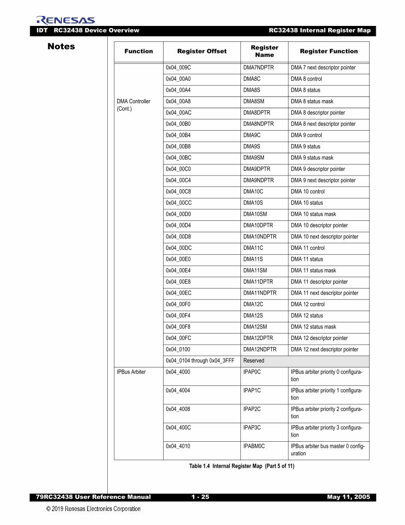
IDT RC32438 Device Overview RC32438 Internal Register Map
79RC32438 User Refer
Notes
0x04_009C DMA7NDPTR DMA 7 next descriptor pointer
0x04_00A0 DMA8C DMA 8 control
0x04_00A4 DMA8S DMA 8 status
DMA Controller (Cont.)
0x04_00A8 DMA8SM DMA 8 status mask
0x04_00AC DMA8DPTR DMA 8 descriptor pointer
0x04_00B0 DMA8NDPTR DMA 8 next descriptor pointer
0x04_00B4 DMA9C DMA 9 control
0x04_00B8 DMA9S DMA 9 status
0x04_00BC DMA9SM DMA 9 status mask
0x04_00C0 DMA9DPTR DMA 9 descriptor pointer
0x04_00C4 DMA9NDPTR DMA 9 next descriptor pointer
0x04_00C8 DMA10C DMA 10 control
0x04_00CC DMA10S DMA 10 status
0x04_00D0 DMA10SM DMA 10 status mask
0x04_00D4 DMA10DPTR DMA 10 descriptor pointer
0x04_00D8 DMA10NDPTR DMA 10 next descriptor pointer
0x04_00DC DMA11C DMA 11 control
0x04_00E0 DMA11S DMA 11 status
0x04_00E4 DMA11SM DMA 11 status mask
0x04_00E8 DMA11DPTR DMA 11 descriptor pointer
0x04_00EC DMA11NDPTR DMA 11 next descriptor pointer
0x04_00F0 DMA12C DMA 12 control
0x04_00F4 DMA12S DMA 12 status
0x04_00F8 DMA12SM DMA 12 status mask
0x04_00FC DMA12DPTR DMA 12 descriptor pointer
0x04_0100 DMA12NDPTR DMA 12 next descriptor pointer
0x04_0104 through 0x04_3FFF Reserved
IPBus Arbiter 0x04_4000 IPAP0C IPBus arbiter priority 0 configura-tion
0x04_4004 IPAP1C IPBus arbiter priority 1 configura-tion
0x04_4008 IPAP2C IPBus arbiter priority 2 configura-tion
0x04_400C IPAP3C IPBus arbiter priority 3 configura-tion
0x04_4010 IPABM0C IPBus arbiter bus master 0 config-uration
Function Register Offset Register Name Register Function
Table 1.4 Internal Register Map (Part 5 of 11)
ence Manual 1 - 25 May 11, 2005
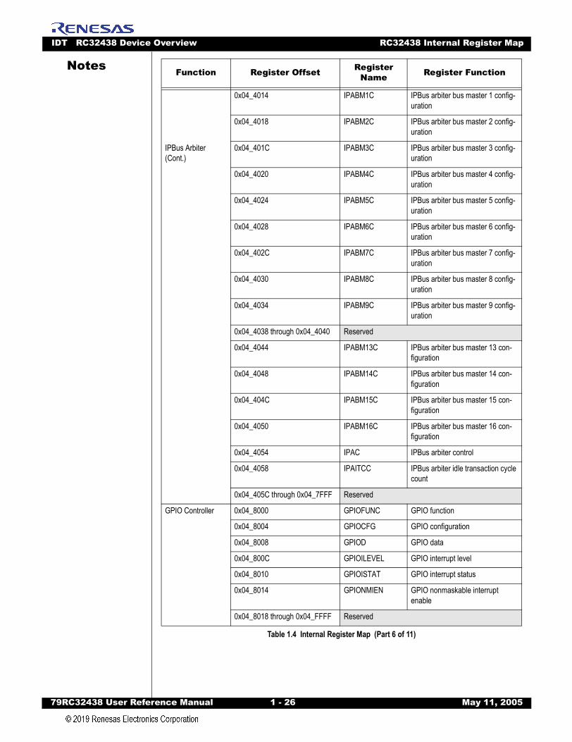
IDT RC32438 Device Overview RC32438 Internal Register Map
79RC32438 User Refer
Notes
0x04_4014 IPABM1C IPBus arbiter bus master 1 config-uration
0x04_4018 IPABM2C IPBus arbiter bus master 2 config-uration
IPBus Arbiter (Cont.)
0x04_401C IPABM3C IPBus arbiter bus master 3 config-uration
0x04_4020 IPABM4C IPBus arbiter bus master 4 config-uration
0x04_4024 IPABM5C IPBus arbiter bus master 5 config-uration
0x04_4028 IPABM6C IPBus arbiter bus master 6 config-uration
0x04_402C IPABM7C IPBus arbiter bus master 7 config-uration
0x04_4030 IPABM8C IPBus arbiter bus master 8 config-uration
0x04_4034 IPABM9C IPBus arbiter bus master 9 config-uration
0x04_4038 through 0x04_4040 Reserved
0x04_4044 IPABM13C IPBus arbiter bus master 13 con-figuration
0x04_4048 IPABM14C IPBus arbiter bus master 14 con-figuration
0x04_404C IPABM15C IPBus arbiter bus master 15 con-figuration
0x04_4050 IPABM16C IPBus arbiter bus master 16 con-figuration
0x04_4054 IPAC IPBus arbiter control
0x04_4058 IPAITCC IPBus arbiter idle transaction cycle count
0x04_405C through 0x04_7FFF Reserved
GPIO Controller 0x04_8000 GPIOFUNC GPIO function
0x04_8004 GPIOCFG GPIO configuration
0x04_8008 GPIOD GPIO data
0x04_800C GPIOILEVEL GPIO interrupt level
0x04_8010 GPIOISTAT GPIO interrupt status
0x04_8014 GPIONMIEN GPIO nonmaskable interrupt enable
0x04_8018 through 0x04_FFFF Reserved
Function Register Offset Register Name Register Function
Table 1.4 Internal Register Map (Part 6 of 11)
ence Manual 1 - 26 May 11, 2005
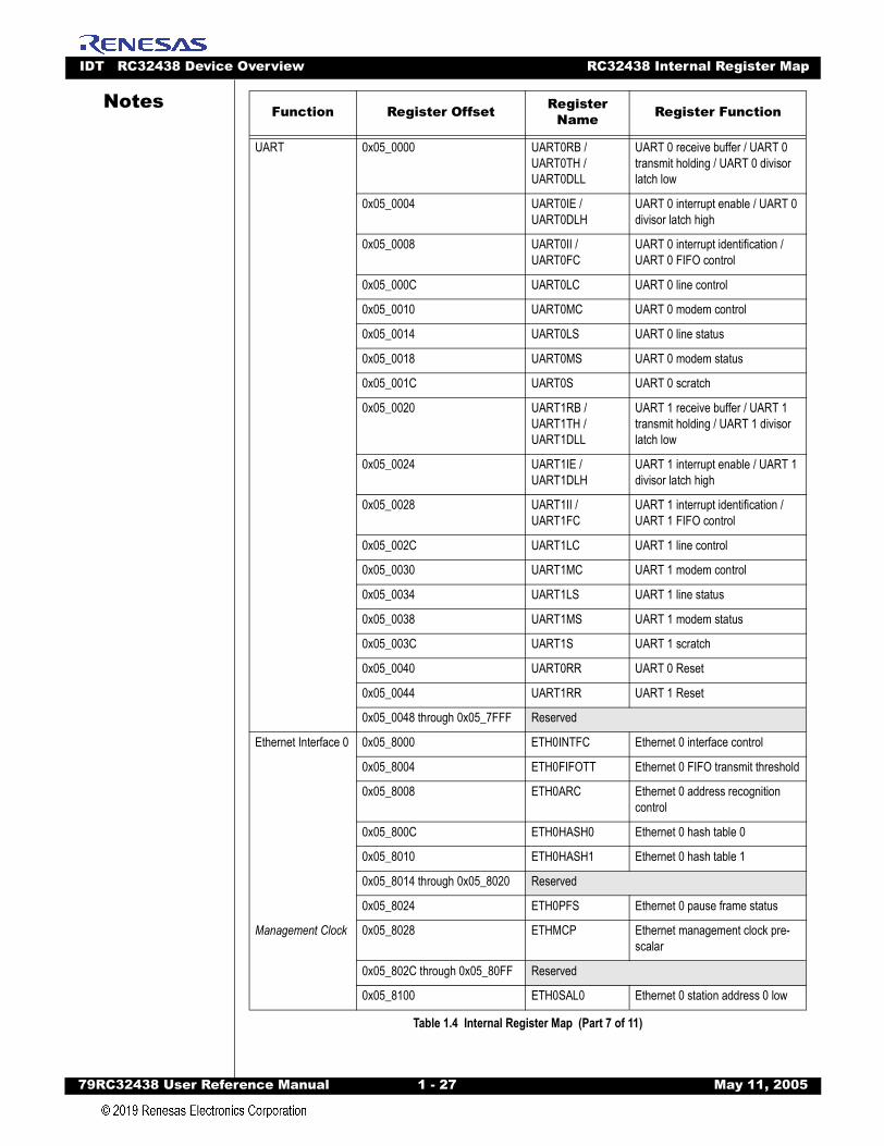
IDT RC32438 Device Overview RC32438 Internal Register Map
79RC32438 User Refer
Notes
UART 0x05_0000 UART0RB / UART0TH / UART0DLL
UART 0 receive buffer / UART 0 transmit holding / UART 0 divisor latch low
0x05_0004 UART0IE / UART0DLH
UART 0 interrupt enable / UART 0 divisor latch high
0x05_0008 UART0II / UART0FC
UART 0 interrupt identification / UART 0 FIFO control
0x05_000C UART0LC UART 0 line control
0x05_0010 UART0MC UART 0 modem control
0x05_0014 UART0LS UART 0 line status
0x05_0018 UART0MS UART 0 modem status
0x05_001C UART0S UART 0 scratch
0x05_0020 UART1RB / UART1TH / UART1DLL
UART 1 receive buffer / UART 1 transmit holding / UART 1 divisor latch low
0x05_0024 UART1IE / UART1DLH
UART 1 interrupt enable / UART 1 divisor latch high
0x05_0028 UART1II / UART1FC
UART 1 interrupt identification / UART 1 FIFO control
0x05_002C UART1LC UART 1 line control
0x05_0030 UART1MC UART 1 modem control
0x05_0034 UART1LS UART 1 line status
0x05_0038 UART1MS UART 1 modem status
0x05_003C UART1S UART 1 scratch
0x05_0040 UART0RR UART 0 Reset
0x05_0044 UART1RR UART 1 Reset
0x05_0048 through 0x05_7FFF Reserved
Ethernet Interface 0 0x05_8000 ETH0INTFC Ethernet 0 interface control
0x05_8004 ETH0FIFOTT Ethernet 0 FIFO transmit threshold
0x05_8008 ETH0ARC Ethernet 0 address recognition control
0x05_800C ETH0HASH0 Ethernet 0 hash table 0
0x05_8010 ETH0HASH1 Ethernet 0 hash table 1
0x05_8014 through 0x05_8020 Reserved
0x05_8024 ETH0PFS Ethernet 0 pause frame status
Management Clock 0x05_8028 ETHMCP Ethernet management clock pre-scalar
0x05_802C through 0x05_80FF Reserved
0x05_8100 ETH0SAL0 Ethernet 0 station address 0 low
Function Register Offset Register Name Register Function
Table 1.4 Internal Register Map (Part 7 of 11)
ence Manual 1 - 27 May 11, 2005
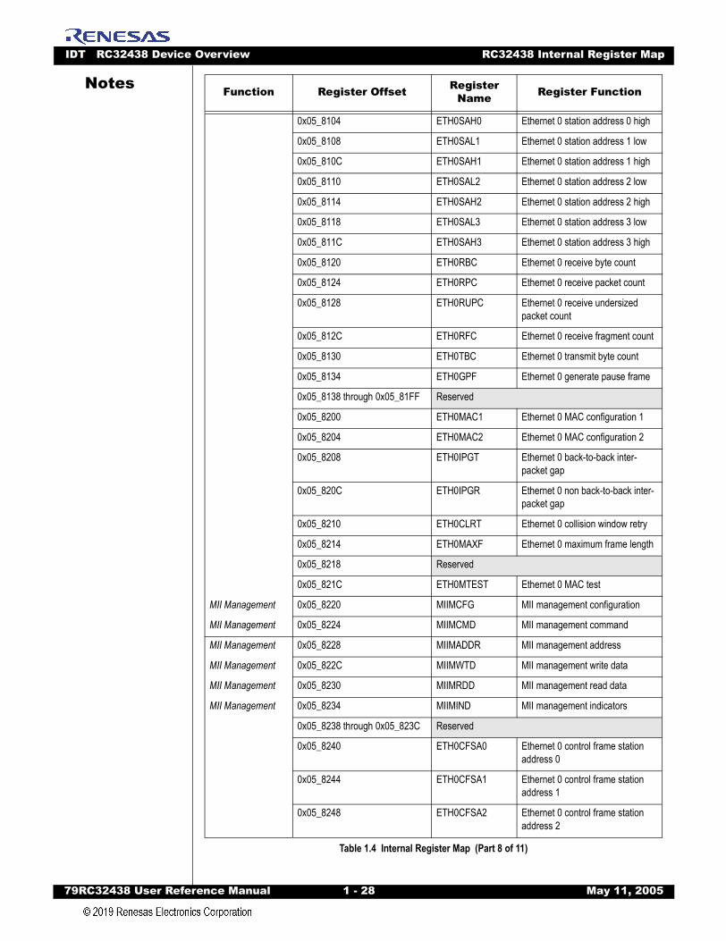
IDT RC32438 Device Overview RC32438 Internal Register Map
79RC32438 User Refer
Notes
0x05_8104 ETH0SAH0 Ethernet 0 station address 0 high
0x05_8108 ETH0SAL1 Ethernet 0 station address 1 low
0x05_810C ETH0SAH1 Ethernet 0 station address 1 high
0x05_8110 ETH0SAL2 Ethernet 0 station address 2 low
0x05_8114 ETH0SAH2 Ethernet 0 station address 2 high
0x05_8118 ETH0SAL3 Ethernet 0 station address 3 low
0x05_811C ETH0SAH3 Ethernet 0 station address 3 high
0x05_8120 ETH0RBC Ethernet 0 receive byte count
0x05_8124 ETH0RPC Ethernet 0 receive packet count
0x05_8128 ETH0RUPC Ethernet 0 receive undersized packet count
0x05_812C ETH0RFC Ethernet 0 receive fragment count
0x05_8130 ETH0TBC Ethernet 0 transmit byte count
0x05_8134 ETH0GPF Ethernet 0 generate pause frame
0x05_8138 through 0x05_81FF Reserved
0x05_8200 ETH0MAC1 Ethernet 0 MAC configuration 1
0x05_8204 ETH0MAC2 Ethernet 0 MAC configuration 2
0x05_8208 ETH0IPGT Ethernet 0 back-to-back inter-packet gap
0x05_820C ETH0IPGR Ethernet 0 non back-to-back inter-packet gap
0x05_8210 ETH0CLRT Ethernet 0 collision window retry
0x05_8214 ETH0MAXF Ethernet 0 maximum frame length
0x05_8218 Reserved
0x05_821C ETH0MTEST Ethernet 0 MAC test
MII Management 0x05_8220 MIIMCFG MII management configuration
MII Management 0x05_8224 MIIMCMD MII management command
MII Management 0x05_8228 MIIMADDR MII management address
MII Management 0x05_822C MIIMWTD MII management write data
MII Management 0x05_8230 MIIMRDD MII management read data
MII Management 0x05_8234 MIIMIND MII management indicators
0x05_8238 through 0x05_823C Reserved
0x05_8240 ETH0CFSA0 Ethernet 0 control frame station address 0
0x05_8244 ETH0CFSA1 Ethernet 0 control frame station address 1
0x05_8248 ETH0CFSA2 Ethernet 0 control frame station address 2
Function Register Offset Register Name Register Function
Table 1.4 Internal Register Map (Part 8 of 11)
ence Manual 1 - 28 May 11, 2005
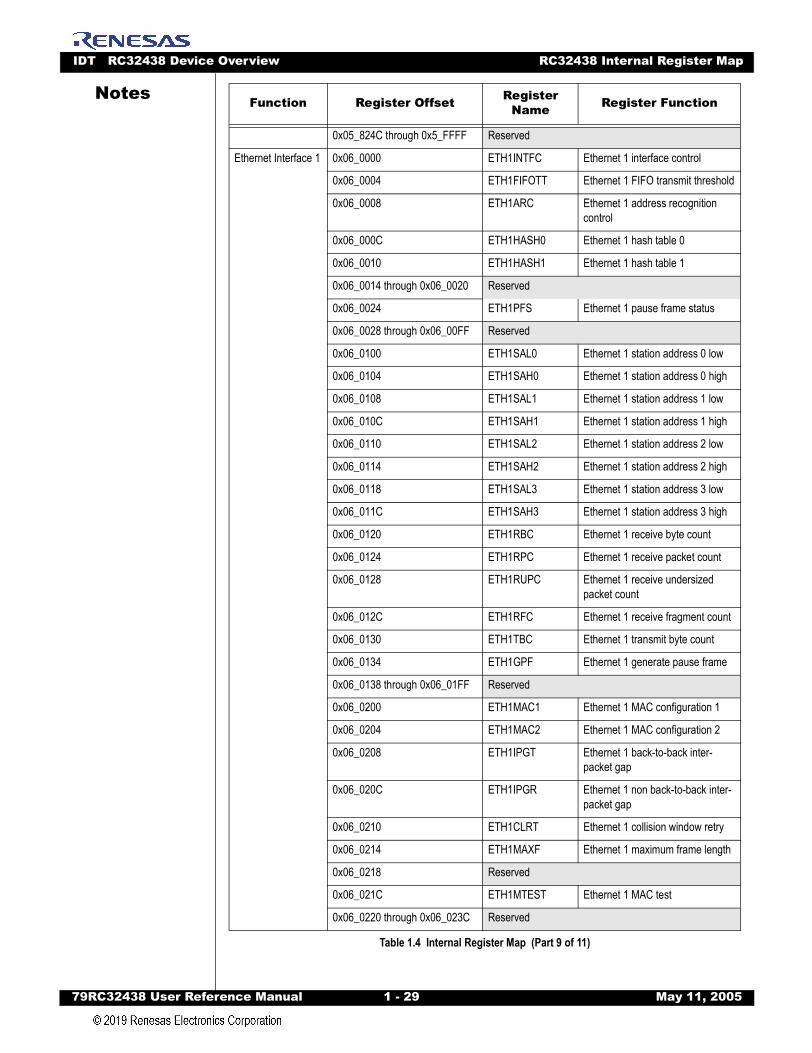
IDT RC32438 Device Overview RC32438 Internal Register Map
79RC32438 User Refer
Notes
0x05_824C through 0x5_FFFF Reserved
Ethernet Interface 1 0x06_0000 ETH1INTFC Ethernet 1 interface control
0x06_0004 ETH1FIFOTT Ethernet 1 FIFO transmit threshold
0x06_0008 ETH1ARC Ethernet 1 address recognition control
0x06_000C ETH1HASH0 Ethernet 1 hash table 0
0x06_0010 ETH1HASH1 Ethernet 1 hash table 1
0x06_0014 through 0x06_0020 Reserved
0x06_0024 ETH1PFS Ethernet 1 pause frame status
0x06_0028 through 0x06_00FF Reserved
0x06_0100 ETH1SAL0 Ethernet 1 station address 0 low
0x06_0104 ETH1SAH0 Ethernet 1 station address 0 high
0x06_0108 ETH1SAL1 Ethernet 1 station address 1 low
0x06_010C ETH1SAH1 Ethernet 1 station address 1 high
0x06_0110 ETH1SAL2 Ethernet 1 station address 2 low
0x06_0114 ETH1SAH2 Ethernet 1 station address 2 high
0x06_0118 ETH1SAL3 Ethernet 1 station address 3 low
0x06_011C ETH1SAH3 Ethernet 1 station address 3 high
0x06_0120 ETH1RBC Ethernet 1 receive byte count
0x06_0124 ETH1RPC Ethernet 1 receive packet count
0x06_0128 ETH1RUPC Ethernet 1 receive undersized packet count
0x06_012C ETH1RFC Ethernet 1 receive fragment count
0x06_0130 ETH1TBC Ethernet 1 transmit byte count
0x06_0134 ETH1GPF Ethernet 1 generate pause frame
0x06_0138 through 0x06_01FF Reserved
0x06_0200 ETH1MAC1 Ethernet 1 MAC configuration 1
0x06_0204 ETH1MAC2 Ethernet 1 MAC configuration 2
0x06_0208 ETH1IPGT Ethernet 1 back-to-back inter-packet gap
0x06_020C ETH1IPGR Ethernet 1 non back-to-back inter-packet gap
0x06_0210 ETH1CLRT Ethernet 1 collision window retry
0x06_0214 ETH1MAXF Ethernet 1 maximum frame length
0x06_0218 Reserved
0x06_021C ETH1MTEST Ethernet 1 MAC test
0x06_0220 through 0x06_023C Reserved
Function Register Offset Register Name Register Function
Table 1.4 Internal Register Map (Part 9 of 11)
ence Manual 1 - 29 May 11, 2005
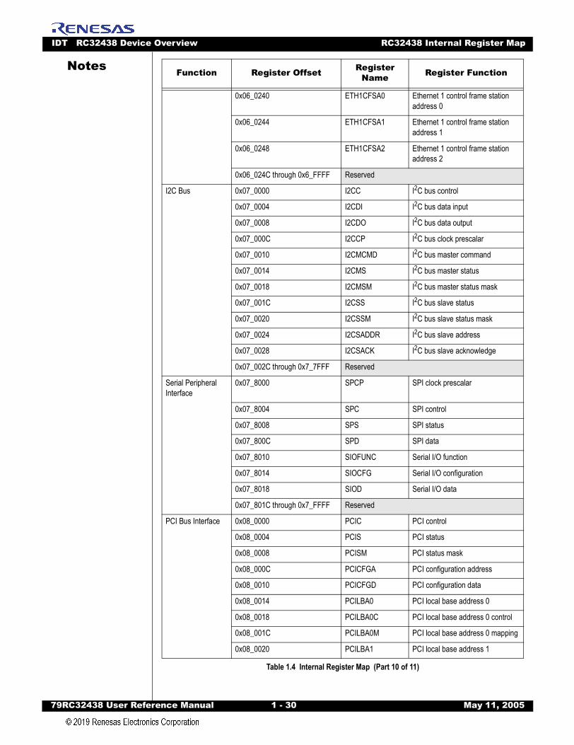
IDT RC32438 Device Overview RC32438 Internal Register Map
79RC32438 User Refer
Notes
0x06_0240 ETH1CFSA0 Ethernet 1 control frame station address 0
0x06_0244 ETH1CFSA1 Ethernet 1 control frame station address 1
0x06_0248 ETH1CFSA2 Ethernet 1 control frame station address 2
0x06_024C through 0x6_FFFF Reserved
I2C Bus 0x07_0000 I2CC I2C bus control
0x07_0004 I2CDI I2C bus data input
0x07_0008 I2CDO I2C bus data output
0x07_000C I2CCP I2C bus clock prescalar
0x07_0010 I2CMCMD I2C bus master command
0x07_0014 I2CMS I2C bus master status
0x07_0018 I2CMSM I2C bus master status mask
0x07_001C I2CSS I2C bus slave status
0x07_0020 I2CSSM I2C bus slave status mask
0x07_0024 I2CSADDR I2C bus slave address
0x07_0028 I2CSACK I2C bus slave acknowledge
0x07_002C through 0x7_7FFF Reserved
Serial Peripheral Interface
0x07_8000 SPCP SPI clock prescalar
0x07_8004 SPC SPI control
0x07_8008 SPS SPI status
0x07_800C SPD SPI data
0x07_8010 SIOFUNC Serial I/O function
0x07_8014 SIOCFG Serial I/O configuration
0x07_8018 SIOD Serial I/O data
0x07_801C through 0x7_FFFF Reserved
PCI Bus Interface 0x08_0000 PCIC PCI control
0x08_0004 PCIS PCI status
0x08_0008 PCISM PCI status mask
0x08_000C PCICFGA PCI configuration address
0x08_0010 PCICFGD PCI configuration data
0x08_0014 PCILBA0 PCI local base address 0
0x08_0018 PCILBA0C PCI local base address 0 control
0x08_001C PCILBA0M PCI local base address 0 mapping
0x08_0020 PCILBA1 PCI local base address 1
Function Register Offset Register Name Register Function
Table 1.4 Internal Register Map (Part 10 of 11)
ence Manual 1 - 30 May 11, 2005
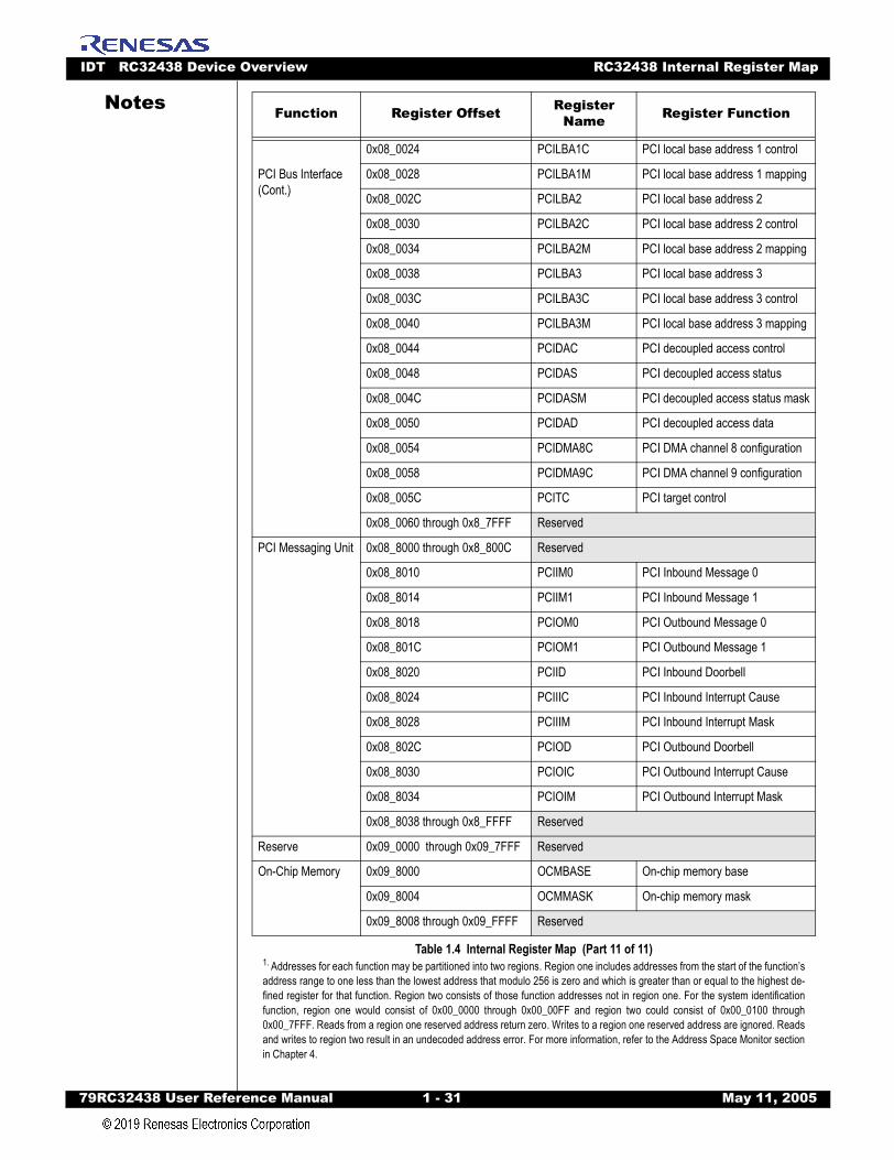
IDT RC32438 Device Overview RC32438 Internal Register Map
79RC32438 User Refer
Notes
0x08_0024 PCILBA1C PCI local base address 1 control
PCI Bus Interface (Cont.)
0x08_0028 PCILBA1M PCI local base address 1 mapping
0x08_002C PCILBA2 PCI local base address 2
0x08_0030 PCILBA2C PCI local base address 2 control
0x08_0034 PCILBA2M PCI local base address 2 mapping
0x08_0038 PCILBA3 PCI local base address 3
0x08_003C PCILBA3C PCI local base address 3 control
0x08_0040 PCILBA3M PCI local base address 3 mapping
0x08_0044 PCIDAC PCI decoupled access control
0x08_0048 PCIDAS PCI decoupled access status
0x08_004C PCIDASM PCI decoupled access status mask
0x08_0050 PCIDAD PCI decoupled access data
0x08_0054 PCIDMA8C PCI DMA channel 8 configuration
0x08_0058 PCIDMA9C PCI DMA channel 9 configuration
0x08_005C PCITC PCI target control
0x08_0060 through 0x8_7FFF Reserved
PCI Messaging Unit 0x08_8000 through 0x8_800C Reserved
0x08_8010 PCIIM0 PCI Inbound Message 0
0x08_8014 PCIIM1 PCI Inbound Message 1
0x08_8018 PCIOM0 PCI Outbound Message 0
0x08_801C PCIOM1 PCI Outbound Message 1
0x08_8020 PCIID PCI Inbound Doorbell
0x08_8024 PCIIIC PCI Inbound Interrupt Cause
0x08_8028 PCIIIM PCI Inbound Interrupt Mask
0x08_802C PCIOD PCI Outbound Doorbell
0x08_8030 PCIOIC PCI Outbound Interrupt Cause
0x08_8034 PCIOIM PCI Outbound Interrupt Mask
0x08_8038 through 0x8_FFFF Reserved
Reserve 0x09_0000 through 0x09_7FFF Reserved
On-Chip Memory 0x09_8000 OCMBASE On-chip memory base
0x09_8004 OCMMASK On-chip memory mask
0x09_8008 through 0x09_FFFF Reserved
1. Addresses for each function may be partitioned into two regions. Region one includes addresses from the start of the function’saddress range to one less than the lowest address that modulo 256 is zero and which is greater than or equal to the highest de-fined register for that function. Region two consists of those function addresses not in region one. For the system identificationfunction, region one would consist of 0x00_0000 through 0x00_00FF and region two could consist of 0x00_0100 through0x00_7FFF. Reads from a region one reserved address return zero. Writes to a region one reserved address are ignored. Readsand writes to region two result in an undecoded address error. For more information, refer to the Address Space Monitor sectionin Chapter 4.
Function Register Offset Register Name Register Function
Table 1.4 Internal Register Map (Part 11 of 11)
ence Manual 1 - 31 May 11, 2005
IDT RC32438 Device Overview RC32438 Internal Register Map
79RC32438 User Refer
Notes
ence Manual 1 - 32 May 11, 2005
Notes
79RC32438 User Reference Manual 2 - 1 M
Chapter 2
MIPS32 4Kc Processor Core
IntroductionThe MIPS32™ 4Kc™ processor core from MIPS® Technologies is a high performance, low power, 32 bit
MIPS RISC core intended for custom system-on-silicon applications. The 4Kc processor incorporatesaspects of both the MIPS Technologies R3000® and R4000® processors. This chapter provides basic infor-mation on the architecture and operation of the 4Kc processor core as it applies to the RC32438. Additionalinformation about the 4Kc core can be obtained by contacting MIPS Technologies or visiting their 4Kc webpage at: http://www.mips.com/products/s2p4.html.
Functional OverviewThe 4Kc core contains a fully-associative translation lookaside buffer (TLB) based MMU (Memory
Management Unit) and a pipelined MDU (Multiply/Divide Unit). The instruction and data caches are both 16Kbytes in size and organized as 4-way set associative. On a cache miss, loads are blocked only until thefirst critical word becomes available. The pipeline resumes execution while the remaining words are beingwritten to the cache. Both caches are virtually indexed and physically tagged. Virtual indexing allows thecache to be indexed in the same clock in which the address is generated rather than waiting for the virtual-to-physical address translation in the Memory Management Unit (MMU).
The 4Kc core executes the MIPS32 instruction set architecture (ISA). The MIPS32 ISA contains allMIPS II instructions as well as special multiply-accumulate, conditional move, prefetch, wait, and zero/onedetect instructions. The R4000-style memory management unit of the 4Kc core contains a 3-entry instruc-tion TLB (ITLB), a 3-entry data TLB (DTLB), and a 16 dual-entry joint TLB (JTLB) with variable page sizes.
The 4Kc MDU supports a maximum issue rate of one 32x16 multiply (MUL/MULT/MULTU), multiply-add(MADD/MADDU), or multiply-subtract (MSUB/MSUBU) operation per clock, or one 32x32 MUL, MADD, orMSUB every other clock. The basic Enhanced JTAG (EJTAG) features provide CPU run control with stop,single stepping and re-start, and with software breakpoints through the SDBBP instruction. In addition,optional instruction and data virtual address hardware breakpoints, and optional connection to an externalEJTAG probe through the Test Access Port (TAP) may be included.
Features32-bit Address and Data PathsMIPS32 compatible instruction set
– All MIPSII™ instructions– Multiply-add and multiply-subtract instructions (MADD, MADDU, MSUB, MSUBU)– Targeted multiply instruction (MUL)– Zero and one detect instructions (CLZ, CLO)– Wait instruction (WAIT)– Conditional move instructions (MOVZ, MOVN)– Prefetch instruction (PREF)
ay 11, 2005
IDT MIPS32 4Kc Processor Core Features
79RC32438 User Refer
Notes
Cache Sizes– 16KB instruction and data caches – 4-Way set associative– Loads that miss in the cache are blocked only until critical word is available– Write-through, no write-allocate– 128 bit (16-byte) cache line size, word sectored - suitable for standard 32-bit wide single-portSRAM– Virtually indexed, physically tagged– Cache line locking support
R4000 Style Privileged Resource Architecture– Count/compare registers for real-time timer interrupts– Instruction and data watch registers for software breakpoints– Separate interrupt exception vector
Programmable Memory Management Unit – 16 dual-entry R4000 style JTLB with variable page sizes– 3-entry instruction TLB– 3-entry data TLB
Multiply-Divide Unit – Max issue rate of one 32x16 multiply per clock– Max issue rate of one 32x32 multiply every other clock– Early in divide control. Minimum 11, maximum 34 clock latency on divide
Power Control– No minimum frequency– Power-down mode (triggered by WAIT instruction)– Support for software-controlled clock divider
EJTAG Debug Support – CPU control with start, stop, and single stepping– Software breakpoints via the SDBBP instruction– Optional hardware breakpoints on virtual addresses; 4 instruction and 2 data breakpoints, 2
instruction and 1 data breakpoint, or no breakpoints– Test Access Port (TAP) facilitates high speed download of application code
ence Manual 2 - 2 May 11, 2005
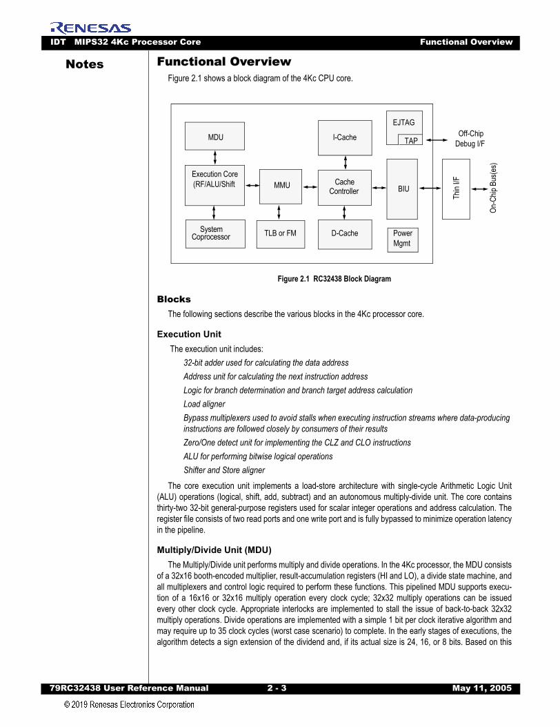
IDT MIPS32 4Kc Processor Core Functional Overview
79RC32438 User Refer
Notes
Functional OverviewFigure 2.1 shows a block diagram of the 4Kc CPU core.Figure 2.1 RC32438 Block Diagram
BlocksThe following sections describe the various blocks in the 4Kc processor core.
Execution Unit The execution unit includes:
32-bit adder used for calculating the data addressAddress unit for calculating the next instruction addressLogic for branch determination and branch target address calculationLoad alignerBypass multiplexers used to avoid stalls when executing instruction streams where data-producing instructions are followed closely by consumers of their resultsZero/One detect unit for implementing the CLZ and CLO instructionsALU for performing bitwise logical operationsShifter and Store aligner
The core execution unit implements a load-store architecture with single-cycle Arithmetic Logic Unit(ALU) operations (logical, shift, add, subtract) and an autonomous multiply-divide unit. The core containsthirty-two 32-bit general-purpose registers used for scalar integer operations and address calculation. Theregister file consists of two read ports and one write port and is fully bypassed to minimize operation latencyin the pipeline.
Multiply/Divide Unit (MDU)The Multiply/Divide unit performs multiply and divide operations. In the 4Kc processor, the MDU consists
of a 32x16 booth-encoded multiplier, result-accumulation registers (HI and LO), a divide state machine, andall multiplexers and control logic required to perform these functions. This pipelined MDU supports execu-tion of a 16x16 or 32x16 multiply operation every clock cycle; 32x32 multiply operations can be issuedevery other clock cycle. Appropriate interlocks are implemented to stall the issue of back-to-back 32x32multiply operations. Divide operations are implemented with a simple 1 bit per clock iterative algorithm andmay require up to 35 clock cycles (worst case scenario) to complete. In the early stages of executions, thealgorithm detects a sign extension of the dividend and, if its actual size is 24, 16, or 8 bits. Based on this
SystemCoprocessor
CacheController
MDU
TLB or FM
MMU
D-Cache
BIU
TAP
EJTAG
Power Mgmt
I-Cache Off-Chip Debug I/F
Execution Core (RF/ALU/Shift
Thin
I/F
On-C
hip B
us(e
s)
ence Manual 2 - 3 May 11, 2005
IDT MIPS32 4Kc Processor Core Functional Overview
79RC32438 User Refer
Notes
information, the divider will skip 7, 15, or 23 iterations respectively (out of a total of 32 iterations). Anattempt to issue a subsequent MDU instruction while a divide is still in progress causes a pipeline stall untilthe divide operation is completed.An additional multiply instruction, MUL, is implemented. This instruction specifies that the lower 32 bitsof the multiply result be placed in the register file instead of the HI/LO register pair. By avoiding the explicitmove from the LO (MFLO) instruction (required when using the LO register) and by supporting multipledestination registers, the throughput of multiply-intensive operations is increased.
Two instructions, multiply-add (MADD/MADDU) and multiply-subtract (MSUB/MSUBU), are used toperform the multiply-add and multiply-subtract operations. The MADD instruction multiplies two numbersand then adds the product to the current contents of the HI and LO registers. Similarly, the MSUB instruc-tion multiplies two operands and then subtracts the product from the HI and LO registers. The MADD/MADDU and MSUB/MSUBU operations are commonly used in Digital Signal Processor (DSP) algorithms.
System Control Coprocessor (CP0)In the MIPS architecture, CP0 is responsible for the virtual-to-physical address translation, cache proto-
cols, the exception control system, the processor’s diagnostics capability, operating mode selection (kernelvs. user mode), and the enabling/disabling of interrupts. Configuration information, such as cache size, setassociativity, and EJTAG debug features, is available by accessing the CP0 registers. Additional informa-tion on CP0 registers can be found in the CP0 Registers section. Additional information on EJTAG can befound in Chapter 20.
Memory Management Unit (MMU)Each core contains an MMU that interfaces between the execution unit and the cache controller, shown
in Figure 2.1. Although the 4Kc core implements a 32-bit architecture, the Memory Management Unit(MMU) is modeled after the MMU found in the 64-bit R4000 family, as defined by the MIPS32 architecture.
The 4Kc core implements an MMU based on a Translation Lookaside Buffer (TLB). The TLB actuallyconsists of three translation buffers: a 16 dual-entry fully associative Joint TLB (JTLB), a 3-entry fully asso-ciative Instruction TLB (ITLB), and a 3-entry fully associative data TLB(DTLB). The ITLB and DTLB, alsoreferred to as the micro TLBs, are managed by the hardware and are not software visible. The micro TLBscontain subsets of the JTLB. When translating addresses, the corresponding micro TLB (I or D) is accessedfirst. If there is no matching entry, the JTLB is used to translate the address and refill the micro TLB. If theentry is not found in the JTLB, an exception is taken. To minimize the micro TLB miss penalty, the JTLB islooked-up in parallel with the DTLB for data references. This results in a 1 cycle stall for a DTLB miss and a2 cycle stall for an ITLB miss.
Figure 2.2 shows how the ITLB, DTLB, and JTLB are used in the 4Kc core.
ence Manual 2 - 4 May 11, 2005
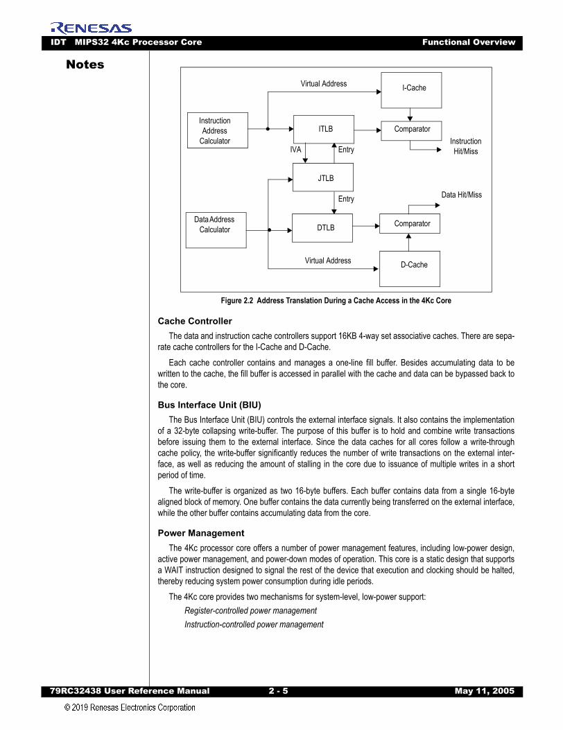
IDT MIPS32 4Kc Processor Core Functional Overview
79RC32438 User Refer
Notes
Figure 2.2 Address Translation During a Cache Access in the 4Kc Core
Cache ControllerThe data and instruction cache controllers support 16KB 4-way set associative caches. There are sepa-
rate cache controllers for the I-Cache and D-Cache.Each cache controller contains and manages a one-line fill buffer. Besides accumulating data to be
written to the cache, the fill buffer is accessed in parallel with the cache and data can be bypassed back tothe core.
Bus Interface Unit (BIU)The Bus Interface Unit (BIU) controls the external interface signals. It also contains the implementation
of a 32-byte collapsing write-buffer. The purpose of this buffer is to hold and combine write transactionsbefore issuing them to the external interface. Since the data caches for all cores follow a write-throughcache policy, the write-buffer significantly reduces the number of write transactions on the external inter-face, as well as reducing the amount of stalling in the core due to issuance of multiple writes in a shortperiod of time.
The write-buffer is organized as two 16-byte buffers. Each buffer contains data from a single 16-bytealigned block of memory. One buffer contains the data currently being transferred on the external interface,while the other buffer contains accumulating data from the core.
Power ManagementThe 4Kc processor core offers a number of power management features, including low-power design,
active power management, and power-down modes of operation. This core is a static design that supportsa WAIT instruction designed to signal the rest of the device that execution and clocking should be halted,thereby reducing system power consumption during idle periods.
The 4Kc core provides two mechanisms for system-level, low-power support:Register-controlled power managementInstruction-controlled power management
I-Cache
D-Cache
Comparator
Comparator
Instruction Hit/Miss
Data Hit/Miss
Virtual Address
Virtual Address
ITLB
JTLB
DTLB
Instruction Address
Calculator
Data Address Calculator
Entry
EntryIVA
ence Manual 2 - 5 May 11, 2005
IDT MIPS32 4Kc Processor Core Pipeline Description
79RC32438 User Refer
Notes
In register-controlled power management mode, the 4Kc core provides three bits in the CP0 Statusregister for software control of the power management function and allows interrupts to be serviced evenwhen the core is in power-down mode. In instruction-controlled power-down mode, execution of the WAITinstruction is used to invoke low-power mode.For additional information on power management, refer to the Power Management section.
Instruction CacheThe instruction cache is 16 Kbytes in size. The cache is virtually indexed and physically tagged, allowing
the virtual-to-physical address translation to occur in parallel with the cache access rather than having towait for the physical address translation. The tag holds 22 bits of the physical address, 4 valid bits, a lockbit, and the LRF (Least Recently Filled) replacement bit.
All cores support instruction cache locking. Cache locking allows critical code to be locked into thecache on a per-line basis, enabling the system designer to maximize the efficiency of the system cache.Cache locking is always available on all instruction cache entries. Entries can be marked as locked orunlocked (by setting or clearing the lock-bit) on a per-entry basis using the CACHE instruction.
Data CacheThe data cache is 16-Kbytes in size. The cache is virtually indexed and physically tagged, allowing the
virtual-to-physical address translation to occur in parallel with the cache access. The tag holds 22 bits of thephysical address, 4 valid bits, a lock bit, and the LRF replacement bit.
In addition to instruction cache locking, all cores also support a data cache locking mechanism identicalto the instruction cache, with critical data segments to be locked into the cache on a per-line basis. Thelocked contents cannot be selected for replacement on a cache miss, but can be updated on a store hit.
Cache locking is always available on all data cache entries. Entries can be marked as locked orunlocked on a per-entry basis using the CACHE instruction.
The physical data cache memory must be byte-writable to support non-word store operations.
EJTAG ControllerAll cores provide basic EJTAG support with debug mode, run control, single step and software break-
point instruction (SDBBP) as part of the core. These features allow for the basic software debug of user andkernel code.
Optional EJTAG features include hardware breakpoints. A 4K core may have four instruction break-points and two data breakpoints, two instruction breakpoints and one data breakpoint, or no breakpoints.The hardware instruction breakpoints can be configured to generate a debug exception when an instructionis executed anywhere in the virtual address space. Bit mask and address space identifier (ASID) valuesmay apply in the address compare. These breakpoints are not limited to code in RAM like the softwareinstruction breakpoint (SDBBP). The data breakpoints can be configured to generate a debug exception ona data transaction. The data transaction may be qualified with both virtual address, data value, size, andload/store transaction type. Bit mask and ASID values may apply in the address compare, and byte maskmay apply in the value compare.
An optional Test Access Port (TAP), which provides for the communication from an EJTAG probe to theCPU through a dedicated port, may also be applied to the core. This provides the possibility for debuggingwithout debug code in the application and for download of application code to the system.
For additional information on the EJTAG controller, refer to Chapter 20, EJTAG System.
Pipeline DescriptionThe MIPS32 4Kc processor core implements a 5-stage pipeline similar to the original R3000 pipeline.
The five stages are:Instruction (I stage)Execution (E stage)
ence Manual 2 - 6 May 11, 2005
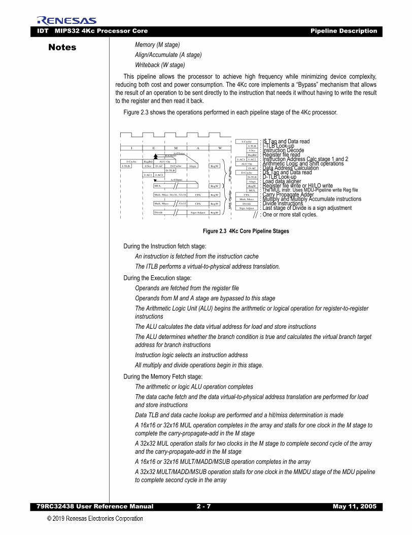
IDT MIPS32 4Kc Processor Core Pipeline Description
79RC32438 User Refer
Notes
Memory (M stage)Align/Accumulate (A stage)Writeback (W stage)This pipeline allows the processor to achieve high frequency while minimizing device complexity,reducing both cost and power consumption. The 4Kc core implements a “Bypass” mechanism that allowsthe result of an operation to be sent directly to the instruction that needs it without having to write the resultto the register and then read it back.
Figure 2.3 shows the operations performed in each pipeline stage of the 4Kc processor.
Figure 2.3 4Kc Core Pipeline Stages
During the Instruction fetch stage:An instruction is fetched from the instruction cacheThe ITLB performs a virtual-to-physical address translation.
During the Execution stage:Operands are fetched from the register fileOperands from M and A stage are bypassed to this stageThe Arithmetic Logic Unit (ALU) begins the arithmetic or logical operation for register-to-register instructionsThe ALU calculates the data virtual address for load and store instructionsThe ALU determines whether the branch condition is true and calculates the virtual branch target address for branch instructionsInstruction logic selects an instruction addressAll multiply and divide operations begin in this stage.
During the Memory Fetch stage:The arithmetic or logic ALU operation completesThe data cache fetch and the data virtual-to-physical address translation are performed for load and store instructionsData TLB and data cache lookup are performed and a hit/miss determination is madeA 16x16 or 32x16 MUL operation completes in the array and stalls for one clock in the M stage to complete the carry-propagate-add in the M stageA 32x32 MUL operation stalls for two clocks in the M stage to complete second cycle of the array and the carry-propagate-add in the M stageA 16x16 or 32x16 MULT/MADD/MSUB operation completes in the arrayA 32x32 MULT/MADD/MSUB operation stalls for one clock in the MMDU stage of the MDU pipeline to complete second cycle in the array
I
A->E BypassM->E Bypass
A->E Bypass
E M A W
I-Cache
I-TLB
RegRd
I Dec D-AC
I-AC1 I-AC2
ALU Op
D-Cache
D-TLB
Align
MUL RegWRegW
RegW
RegW
RegW
Mult, Macc 16x16, 32x16 CPA
CPAMult, Macc 32x32
Sign AdjustDivide
IU-P
ipel
ine
MD
U-P
ipel
ine
I-AC2
D-AC
Align
MUL
I-TLB
I Dec
ALU Op
D-Cache
D-TLB
Divide
Mult, Macc
Sign Adjust
I-Cache
RegRd
I-AC1
RegW
CPA
: I$ Tag and Data read: I-TLB Look-up: Instruction Decode: Register file read: Instruction Address Calc stage 1 and 2: Arithmetic Logic and Shift operations: Data Address Calculation: D$ Tag and Data read: D-TLB Look-up: Load data aligner: Register file write or HI/LO write: The MUL instr. Uses MDU-Pipeline write Reg file: Carry Propagate Adder: Multiply and Multiply Accumulate instructions: Divide instructions: Last stage of Divide is a sign adjustment: One or more stall cycles.
ence Manual 2 - 7 May 11, 2005
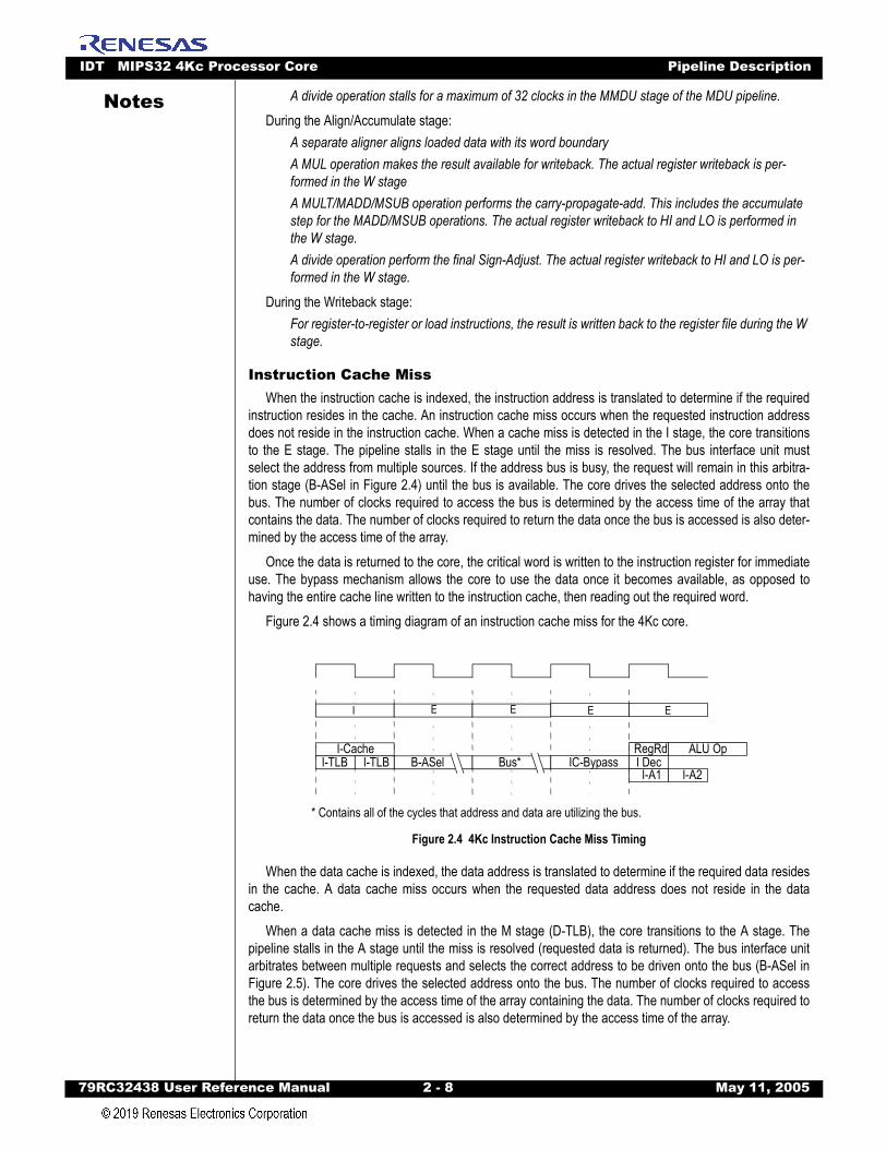
IDT MIPS32 4Kc Processor Core Pipeline Description
79RC32438 User Refer
Notes
A divide operation stalls for a maximum of 32 clocks in the MMDU stage of the MDU pipeline.During the Align/Accumulate stage:A separate aligner aligns loaded data with its word boundaryA MUL operation makes the result available for writeback. The actual register writeback is per-formed in the W stageA MULT/MADD/MSUB operation performs the carry-propagate-add. This includes the accumulate step for the MADD/MSUB operations. The actual register writeback to HI and LO is performed in the W stage.A divide operation perform the final Sign-Adjust. The actual register writeback to HI and LO is per-formed in the W stage.
During the Writeback stage:For register-to-register or load instructions, the result is written back to the register file during the W stage.
Instruction Cache MissWhen the instruction cache is indexed, the instruction address is translated to determine if the required
instruction resides in the cache. An instruction cache miss occurs when the requested instruction addressdoes not reside in the instruction cache. When a cache miss is detected in the I stage, the core transitionsto the E stage. The pipeline stalls in the E stage until the miss is resolved. The bus interface unit mustselect the address from multiple sources. If the address bus is busy, the request will remain in this arbitra-tion stage (B-ASel in Figure 2.4) until the bus is available. The core drives the selected address onto thebus. The number of clocks required to access the bus is determined by the access time of the array thatcontains the data. The number of clocks required to return the data once the bus is accessed is also deter-mined by the access time of the array.
Once the data is returned to the core, the critical word is written to the instruction register for immediateuse. The bypass mechanism allows the core to use the data once it becomes available, as opposed tohaving the entire cache line written to the instruction cache, then reading out the required word.
Figure 2.4 shows a timing diagram of an instruction cache miss for the 4Kc core.
Figure 2.4 4Kc Instruction Cache Miss Timing
When the data cache is indexed, the data address is translated to determine if the required data residesin the cache. A data cache miss occurs when the requested data address does not reside in the datacache.
When a data cache miss is detected in the M stage (D-TLB), the core transitions to the A stage. Thepipeline stalls in the A stage until the miss is resolved (requested data is returned). The bus interface unitarbitrates between multiple requests and selects the correct address to be driven onto the bus (B-ASel inFigure 2.5). The core drives the selected address onto the bus. The number of clocks required to accessthe bus is determined by the access time of the array containing the data. The number of clocks required toreturn the data once the bus is accessed is also determined by the access time of the array.
EEE EI
I DecI-Cache
I-TLB I-TLB B-ASel Bus* IC-BypassRegRd ALU Op
I-A2I-A1
* Contains all of the cycles that address and data are utilizing the bus.
ence Manual 2 - 8 May 11, 2005
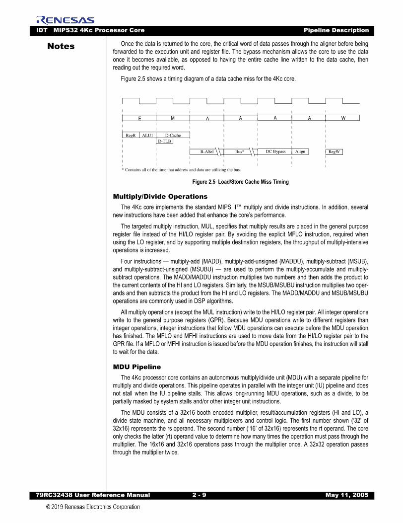
IDT MIPS32 4Kc Processor Core Pipeline Description
79RC32438 User Refer
Notes
Once the data is returned to the core, the critical word of data passes through the aligner before beingforwarded to the execution unit and register file. The bypass mechanism allows the core to use the dataonce it becomes available, as opposed to having the entire cache line written to the data cache, thenreading out the required word.Figure 2.5 shows a timing diagram of a data cache miss for the 4Kc core.
Figure 2.5 Load/Store Cache Miss Timing
Multiply/Divide OperationsThe 4Kc core implements the standard MIPS II™ multiply and divide instructions. In addition, several
new instructions have been added that enhance the core’s performance. The targeted multiply instruction, MUL, specifies that multiply results are placed in the general purpose
register file instead of the HI/LO register pair. By avoiding the explicit MFLO instruction, required whenusing the LO register, and by supporting multiple destination registers, the throughput of multiply-intensiveoperations is increased.
Four instructions — multiply-add (MADD), multiply-add-unsigned (MADDU), multiply-subtract (MSUB),and multiply-subtract-unsigned (MSUBU) — are used to perform the multiply-accumulate and multiply-subtract operations. The MADD/MADDU instruction multiplies two numbers and then adds the product tothe current contents of the HI and LO registers. Similarly, the MSUB/MSUBU instruction multiplies two oper-ands and then subtracts the product from the HI and LO registers. The MADD/MADDU and MSUB/MSUBUoperations are commonly used in DSP algorithms.
All multiply operations (except the MUL instruction) write to the HI/LO register pair. All integer operationswrite to the general purpose registers (GPR). Because MDU operations write to different registers thaninteger operations, integer instructions that follow MDU operations can execute before the MDU operationhas finished. The MFLO and MFHI instructions are used to move data from the HI/LO register pair to theGPR file. If a MFLO or MFHI instruction is issued before the MDU operation finishes, the instruction will stallto wait for the data.
MDU PipelineThe 4Kc processor core contains an autonomous multiply/divide unit (MDU) with a separate pipeline for
multiply and divide operations. This pipeline operates in parallel with the integer unit (IU) pipeline and doesnot stall when the IU pipeline stalls. This allows long-running MDU operations, such as a divide, to bepartially masked by system stalls and/or other integer unit instructions.
The MDU consists of a 32x16 booth encoded multiplier, result/accumulation registers (HI and LO), adivide state machine, and all necessary multiplexers and control logic. The first number shown (‘32’ of32x16) represents the rs operand. The second number (‘16’ of 32x16) represents the rt operand. The coreonly checks the latter (rt) operand value to determine how many times the operation must pass through themultiplier. The 16x16 and 32x16 operations pass through the multiplier once. A 32x32 operation passesthrough the multiplier twice.
D-TLBD-CacheALU1
B-ASel
RegR
Bus* RegWAlignDC Bypass
* Contains all of the time that address and data are utilizing the bus.
WAAAAME
ence Manual 2 - 9 May 11, 2005
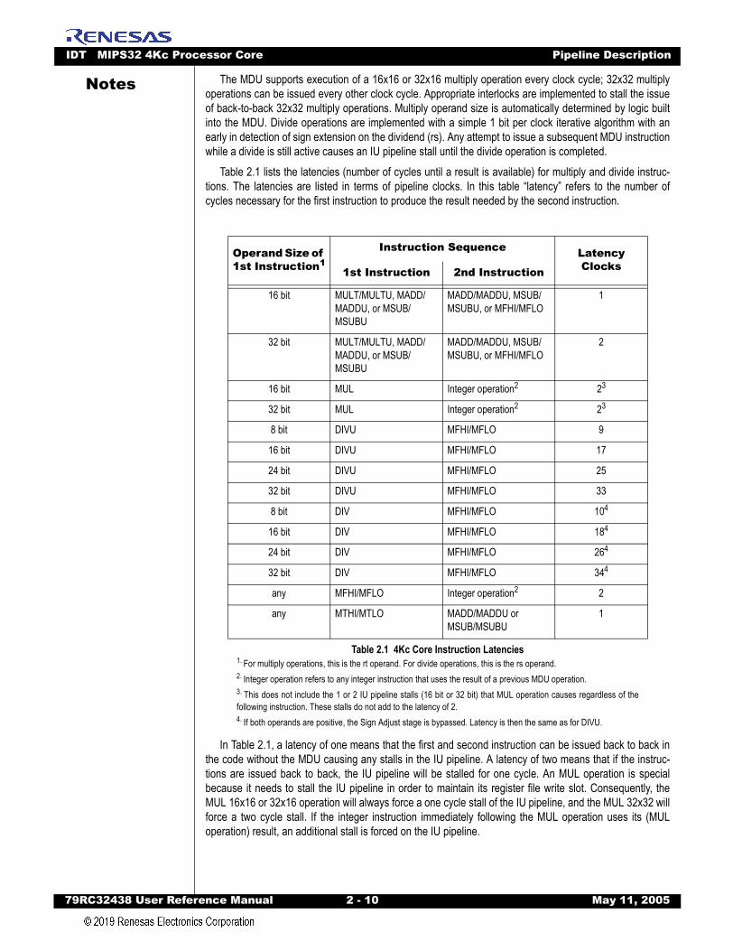
IDT MIPS32 4Kc Processor Core Pipeline Description
79RC32438 User Refer
Notes
The MDU supports execution of a 16x16 or 32x16 multiply operation every clock cycle; 32x32 multiplyoperations can be issued every other clock cycle. Appropriate interlocks are implemented to stall the issueof back-to-back 32x32 multiply operations. Multiply operand size is automatically determined by logic builtinto the MDU. Divide operations are implemented with a simple 1 bit per clock iterative algorithm with anearly in detection of sign extension on the dividend (rs). Any attempt to issue a subsequent MDU instructionwhile a divide is still active causes an IU pipeline stall until the divide operation is completed.Table 2.1 lists the latencies (number of cycles until a result is available) for multiply and divide instruc-tions. The latencies are listed in terms of pipeline clocks. In this table “latency” refers to the number ofcycles necessary for the first instruction to produce the result needed by the second instruction.
In Table 2.1, a latency of one means that the first and second instruction can be issued back to back inthe code without the MDU causing any stalls in the IU pipeline. A latency of two means that if the instruc-tions are issued back to back, the IU pipeline will be stalled for one cycle. An MUL operation is specialbecause it needs to stall the IU pipeline in order to maintain its register file write slot. Consequently, theMUL 16x16 or 32x16 operation will always force a one cycle stall of the IU pipeline, and the MUL 32x32 willforce a two cycle stall. If the integer instruction immediately following the MUL operation uses its (MULoperation) result, an additional stall is forced on the IU pipeline.
Operand Size of 1st Instruction1
1. For multiply operations, this is the rt operand. For divide operations, this is the rs operand.
Instruction Sequence Latency Clocks1st Instruction 2nd Instruction
16 bit MULT/MULTU, MADD/MADDU, or MSUB/MSUBU
MADD/MADDU, MSUB/MSUBU, or MFHI/MFLO
1
32 bit MULT/MULTU, MADD/MADDU, or MSUB/MSUBU
MADD/MADDU, MSUB/MSUBU, or MFHI/MFLO
2
16 bit MUL Integer operation2
2. Integer operation refers to any integer instruction that uses the result of a previous MDU operation.
23
3. This does not include the 1 or 2 IU pipeline stalls (16 bit or 32 bit) that MUL operation causes regardless of thefollowing instruction. These stalls do not add to the latency of 2.
32 bit MUL Integer operation2 23
8 bit DIVU MFHI/MFLO 9
16 bit DIVU MFHI/MFLO 17
24 bit DIVU MFHI/MFLO 25
32 bit DIVU MFHI/MFLO 33
8 bit DIV MFHI/MFLO 104
4. If both operands are positive, the Sign Adjust stage is bypassed. Latency is then the same as for DIVU.
16 bit DIV MFHI/MFLO 184
24 bit DIV MFHI/MFLO 264
32 bit DIV MFHI/MFLO 344
any MFHI/MFLO Integer operation2 2
any MTHI/MTLO MADD/MADDU or MSUB/MSUBU
1
Table 2.1 4Kc Core Instruction Latencies
ence Manual 2 - 10 May 11, 2005
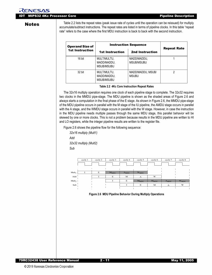
IDT MIPS32 4Kc Processor Core Pipeline Description
79RC32438 User Refer
Notes
Table 2.2 lists the repeat rates (peak issue rate of cycles until the operation can be reissued) for multiplyaccumulate/subtract instructions. The repeat rates are listed in terms of pipeline clocks. In this table “repeatrate” refers to the case where the first MDU instruction is back to back with the second instruction.The 32x16 multiply operation requires one clock of each pipeline stage to complete. The 32x32 requirestwo clocks in the MMDU pipe-stage. The MDU pipeline is shown as the shaded areas of Figure 2.6 andalways starts a computation in the final phase of the E stage. As shown in Figure 2.6, the MMDU pipe-stageof the MDU pipeline occurs in parallel with the M stage of the IU pipeline, the AMDU stage occurs in parallelwith the A stage, and the WMDU stage occurs in parallel with the W stage. However, in case the instructionin the MDU pipeline needs multiple passes through the same MDU stage, this parallel behavior will beskewed by one or more clocks. This is not a problem because results in the MDU pipeline are written to HIand LO registers, while the integer pipeline results are written to the register file.
Figure 2.6 shows the pipeline flow for the following sequence:32x16 multiply (Mult1)Add32x32 multiply (Mult2)Sub
Figure 2.6 MDU Pipeline Behavior During Multiply Operations
Operand Size of 1st Instruction
Instruction SequenceRepeat Rate
1st Instruction 2nd Instruction
16 bit MULT/MULTU,MADD/MADDU,MSUB/MSUBU
MADD/MADDU,MSUB/MSUBU
1
32 bit MULT/MULTU,MADD/MADDU,MSUB/MSUBU
MADD/MADDU, MSUB/MSUBU
2
Table 2.2 4Kc Core Instruction Repeat Rates
I E A WM
cycle 1 cycle 2 cycle 3 cycle 4 cycle 5 cycle 6 cycle 7 cycle 8
Mult1
Add
Mult2
I E AMDU WMDUMMDU
I E AMDU WMDUMMDUMMDU
Sub
I E A WM
ence Manual 2 - 11 May 11, 2005
IDT MIPS32 4Kc Processor Core Pipeline Description
79RC32438 User Refer
Notes
The following is a cycle-by-cycle analysis of Figure 2.6.1. The first 32x16 multiply operation (Mult1) enters the I stage and is fetched from the instruction cache.2. An Add operation enters the I stage. The Mult1 operation enters the E stage. The integer and MDUpipelines share the I and E pipeline stages. At the end of the E stage in cycle 2, the multiply opera-tion (Mult1) is passed to the MDU pipeline.
3. In cycle 3 a 32x32 multiply operation (Mult2) enters the I stage and is fetched from the instructioncache. Since the Add operation has not yet reached the M stage by cycle 3, there is no activity inthe M stage of the integer pipeline at this time.
4. In cycle 4 the Sub instruction enters I stage. The second multiply operation (Mult2) enters the Estage. And the Add operation enters M stage of the integer pipe. Since the Mult1 multiply is a 32x16operation, only one clock is required for the MMDU stage, hence the Mult1 operation passes to theAMDU stage of the MDU pipeline.
5. In cycle 5 the Sub instruction enters E stage. The Mult2 multiply enters the MMDU stage. The Addoperation enters the A stage of the integer pipeline. The Mult1 operation completes and is writtenback in to the HI/LO register pair in the WMDU stage.
6. Since a 32x32 multiply requires two passes through the multiplier, with each pass requiring oneclock, the 32x32 Mult2 remains in the MMDU stage in cycle 6. The Sub instruction enters M stagein the integer pipeline. The Add operation completes and is written to the register file in the W stageof the integer pipeline.
7. The Mult2 multiply operation progresses to the AMDU stage, and the Sub instruction progress to Astage.
8. The Mult2 operation completes and is written to the HI/LO registers pair the WMDU stage, while theSub instruction write to the register file in W stage.
32x16 MultiplyThe 32x16 multiply operation begins in the last phase of the E stage, which is shared between the
integer and MDU pipelines. In the latter phase of the E stage, the rs and rt operands arrive and the boothrecoding function occurs at this time. The multiply calculation requires one clock and occurs in the MMDUstage. In the AMDU stage, the carry-propagate-add function occurs and the operation is completed. Theresult is written back to the HI/LO register pair in the first half of the WMDU stage.
Figure 2.7 shows a diagram of a 32x16 multiply operation.
Figure 2.7 MDU Pipeline Flow During a 32x16 Multiply Operation
32x32 MultiplyThe 32x32 multiply operation begins in the last phase of the E stage, which is shared between the
integer and MDU pipelines. In the latter phase or the E stage, the rs and rt operands arrive and the boothrecoding function occurs at this time. The multiply calculation requires two clocks and occurs in the MMDUstage. In the AMDU stage, the carry-propagate-add (CPA) function occurs and the operation is completed.The result is written back to the HI/LO register pair in the first half of the WMDU stage.
Figure 2.8 shows a diagram of a 32x32 multiply operation.
Booth Array CPA
E MMDU AMDU
Reg WR
WMDU
Clock 1 2 3 4
ence Manual 2 - 12 May 11, 2005
IDT MIPS32 4Kc Processor Core Pipeline Description
79RC32438 User Refer
Notes
Figure 2.8 MDU Pipeline Flow During a 32x32 Multiply Operation
Divide OperationsDivide operations are implemented using a simple non-restoring division algorithm. This algorithm works
only for positive operands, thus the first cycle of the MMDU stage is used to negate the rs operand (RSAdjust) if needed. Note that this cycle is executed even if the adjustment is not necessary. At maximum, thenext 32 clocks (3-34) execute an iterative add/subtract function. In cycle 3, an early in detection isperformed in parallel with the add/subtract. The adjusted rs operand is detected to be zero extended on theupper most 8, 16, or 24 bits. If this is the case the following 7, 15, or 23 cycles of the add/subtract iterationsare skipped.
The remainder adjust (Rem Adjust) cycle is required if the remainder was negative. Note that this cycleis taken even if the remainder was positive. A sign adjust is performed on the quotient and/or remainder ifnecessary. Note that the sign adjust cycle is skipped if both operands are positive. In this case the RemAdjust is moved to the AMDU stage.
Figures 2.9 through 2.12 show the latency for 8, 16, 24, and 32-bit divide operations, respectively. Therepeat rate is either 11, 19, 27, or 35 cycles (one less if the Sign Adjust stage is skipped) since a seconddivide can be in the RS Adjust stage when the first divide is in the Reg WR stage.
Figure 2.9 MDU Pipeline Flow During an 8-bit Divide (DIV) Operation
Figure 2.10 MDU Pipeline Flow During a 16-bit Divide (DIV) Operation
Figure 2.11 MDU Pipeline Flow During a 24-bit Divide (DIV) Operation
Booth Array
E MMDU MMDU AMDU
Reg WR
WMDU
CPAArrayBooth
Clock 1 2 3 4 5
RS Adjust
E Stage MMDU Stage MMDU Stage MMDU Stage AMDU Stage
Rem AdjustAdd/Subtract
Clock 1 2 4-10 11 12
WMDU Stage
13
Reg WRSign Adjust
MMDU Stage
Add/Subtract
3
Early In
RS Adjust
E Stage MMDU Stage MMDU Stage MMDU Stage AMDU Stage
Rem AdjustAdd/Subtract
Clock 1 2 4-18 19 20
WMDU Stage
21
Reg WRSign Adjust
MMDU Stage
Add/Subtract
3
Early In
RS Adjust
E Stage MMDU Stage MMDU Stage MMDU Stage AMDU Stage
Rem AdjustAdd/Subtract
Clock 1 2 4-26 27 28
WMDU Stage
29
Reg WRSign Adjust
MMDU Stage
Add/Subtract
3
Early In
ence Manual 2 - 13 May 11, 2005
IDT MIPS32 4Kc Processor Core Pipeline Description
79RC32438 User Refer
Notes
Figure 2.12 MDU Pipeline Flow During a 32-bit Divide (DIV) Operation
Branch DelayThe pipeline has a branch delay of one cycle. The one-cycle branch delay is a result of the branch deci-
sion logic operating during the E pipeline stage. This allows the branch target address calculated in theprevious stage to be used for the instruction access in the following E stage. The branch delay slot meansthat no bubbles are injected into the pipeline on branch instructions. The address calculation and branchcondition check are both performed in the E stage. The target PC is used for the next instruction in the I stage (2nd instruction after the branch).
The pipeline begins the fetch of either the branch path or the fall-through path in the cycle following thedelay slot. After the branch decision is made, the processor continues with the fetch of either the branchpath (for a taken branch) or the fall-through path (for the non-taken branch).
The branch delay means that the instruction immediately following a branch is always executed, regard-less of the branch direction. If no useful instruction can be placed after the branch, then the compiler orassembler must insert a NOP instruction in the delay slot.
Figure 2.13 illustrates the branch delay.
Figure 2.13 IU Pipeline Branch Delay
Data BypassingMost MIPS32 instructions use one or two register values as source operands for the execution. These
operands are fetched from the register file in the first part of E stage. The ALU straddles the E to Mboundary, and can present the result early in M stage. However, the result is not written in the register fileuntil W stage. This leaves following instructions unable to use the result for 3 cycles. To overcome thisproblem, Data bypassing is used.
Between the register file and the ALU, a data bypass multiplexer is placed on both operands (see Figure2.14). This enables the 4K core to forward data from preceding instructions which have the target register ofthe first instruction as one of the source operands. An M to E bypass and an A to E bypass feed the bypassmultiplexers. A W to E bypass is not needed, as the register file is capable of making an internal bypass ofRd write data directly to the Rs and Rt read ports.
RS Adjust
E Stage MMDU Stage MMDU Stage MMDU Stage AMDU Stage
Rem AdjustAdd/Subtract
Clock 1 2 4-34 35 36
WMDU Stage
37
Reg WRSign Adjust
MMDU Stage
Add/Subtract
3
Early In
One Cycle
Jump Target Instruction
Delay Slot Instruction
One Clock Branch Delay
One Cycle One Cycle One Cycle One Cycle One Cycle
I E M A W
I E M A W
I E M A
Jump or Branch
ence Manual 2 - 14 May 11, 2005
IDT MIPS32 4Kc Processor Core Pipeline Description
79RC32438 User Refer
Notes
Figure 2.14 IU Pipeline Data Bypass
Figure 2.15 shows the Data bypass for an Add1 instruction followed by a Sub2 and another Add3instruction. The Sub2 instruction uses the output from the Add1 instruction as one of the operands, andthus the M to E bypass is used. The following Add3 uses the result from both the first Add1 instruction andthe Sub2 instruction. Since the Add1 data is now in A stage, the A to E bypass is used, and the M to Ebypass is used to bypass the Sub2 data to the Add2 instruction.
Figure 2.15 IU Pipeline M to E Bypass
Load DelayLoad delay means that data fetched by a load instruction is not available in the integer pipeline until after
the load aligner is in A stage. All instructions need the source operands available in E stage. An instructionimmediately following a load instruction will, if it has the same source register as the target of the load,cause an instruction interlock pipeline slip in E stage (see the Instruction Interlocks section). If the secondinstruction after the load (not the first instruction), uses the data from the load, the A to E bypass exists toprovide for stall free operation (refer to Figure 2.14). An instruction flow of this is shown in Figure 2.16.
Bypass multiplexers
E stage M stage A stage W stageI stage
Load data, HI/LO Data or CP0 data
A to E bypass
M to E bypass
InstructionALU
M stageALU
E stageReg File
Rs AddrRt Addr
Rs Read
Rt ReadRd Write
One Cycle One Cycle One Cycle One Cycle One Cycle One Cycle
R3=R2+R1E M A W
I E M A W
I E M A
ADD1
R4=R3-R7SUB2
R5=R3+R4ADD3
I
A to E bypassM to E bypass
M to E bypass
ence Manual 2 - 15 May 11, 2005
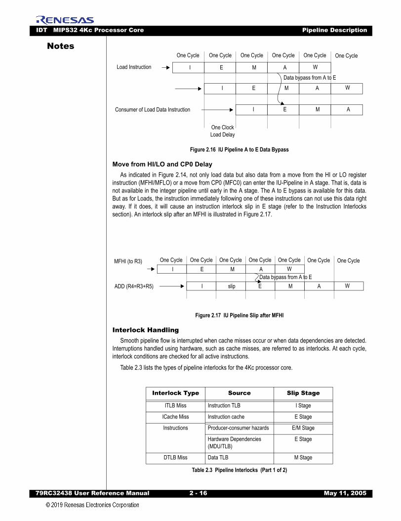
IDT MIPS32 4Kc Processor Core Pipeline Description
79RC32438 User Refer
Notes
Figure 2.16 IU Pipeline A to E Data Bypass
Move from HI/LO and CP0 DelayAs indicated in Figure 2.14, not only load data but also data from a move from the HI or LO register
instruction (MFHI/MFLO) or a move from CP0 (MFC0) can enter the IU-Pipeline in A stage. That is, data isnot available in the integer pipeline until early in the A stage. The A to E bypass is available for this data.But as for Loads, the instruction immediately following one of these instructions can not use this data rightaway. If it does, it will cause an instruction interlock slip in E stage (refer to the Instruction Interlockssection). An interlock slip after an MFHI is illustrated in Figure 2.17.
Figure 2.17 IU Pipeline Slip after MFHI
Interlock HandlingSmooth pipeline flow is interrupted when cache misses occur or when data dependencies are detected.
Interruptions handled using hardware, such as cache misses, are referred to as interlocks. At each cycle,interlock conditions are checked for all active instructions.
Table 2.3 lists the types of pipeline interlocks for the 4Kc processor core.
Interlock Type Source Slip Stage
ITLB Miss Instruction TLB I Stage
ICache Miss Instruction cache E Stage
Instructions Producer-consumer hazards E/M Stage
Hardware Dependencies (MDU/TLB)
E Stage
DTLB Miss Data TLB M Stage
Table 2.3 Pipeline Interlocks (Part 1 of 2)
One Cycle One Cycle One Cycle One Cycle One Cycle One Cycle
I E M A W
I E M A W
I E M A
Load Instruction
Consumer of Load Data Instruction
Data bypass from A to E
One Clock Load Delay
One Cycle One Cycle One Cycle One Cycle One Cycle One Cycle One CycleI E M A W
E M A WslipI
MFHI (to R3)
ADD (R4=R3+R5)Data bypass from A to E
ence Manual 2 - 16 May 11, 2005
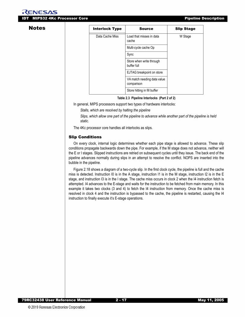
IDT MIPS32 4Kc Processor Core Pipeline Description
79RC32438 User Refer
Notes
In general, MIPS processors support two types of hardware interlocks:Stalls, which are resolved by halting the pipelineSlips, which allow one part of the pipeline to advance while another part of the pipeline is held static.
The 4Kc processor core handles all interlocks as slips.
Slip ConditionsOn every clock, internal logic determines whether each pipe stage is allowed to advance. These slip
conditions propagate backwards down the pipe. For example, if the M stage does not advance, neither willthe E or I stages. Slipped instructions are retried on subsequent cycles until they issue. The back end of thepipeline advances normally during slips in an attempt to resolve the conflict. NOPS are inserted into thebubble in the pipeline.
Figure 2.18 shows a diagram of a two-cycle slip. In the first clock cycle, the pipeline is full and the cachemiss is detected. Instruction I0 is in the A stage, instruction I1 is in the M stage, instruction I2 is in the Estage, and instruction I3 is in the I stage. The cache miss occurs in clock 2 when the I4 instruction fetch isattempted. I4 advances to the E-stage and waits for the instruction to be fetched from main memory. In thisexample it takes two clocks (3 and 4) to fetch the I4 instruction from memory. Once the cache miss isresolved in clock 4 and the instruction is bypassed to the cache, the pipeline is restarted, causing the I4instruction to finally execute it’s E-stage operations.
Data Cache Miss Load that misses in data cache
W Stage
Multi-cycle cache Op
Sync
Store when write through buffer full
EJTAG breakpoint on store
VA match needing data value comparison
Store hitting in fill buffer
Interlock Type Source Slip Stage
Table 2.3 Pipeline Interlocks (Part 2 of 2)
ence Manual 2 - 17 May 11, 2005
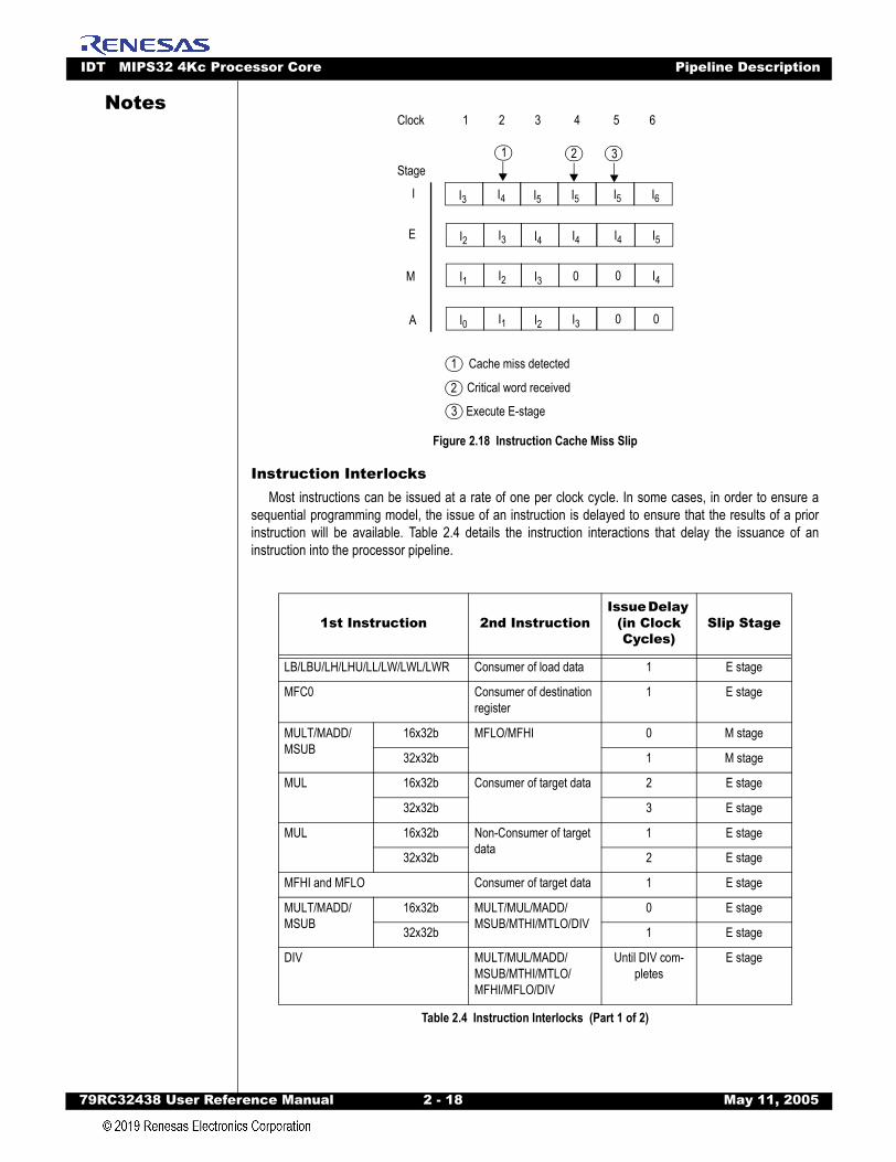
IDT MIPS32 4Kc Processor Core Pipeline Description
79RC32438 User Refer
Notes
Figure 2.18 Instruction Cache Miss Slip
Instruction InterlocksMost instructions can be issued at a rate of one per clock cycle. In some cases, in order to ensure a
sequential programming model, the issue of an instruction is delayed to ensure that the results of a priorinstruction will be available. Table 2.4 details the instruction interactions that delay the issuance of aninstruction into the processor pipeline.
1st Instruction 2nd InstructionIssue Delay
(in Clock Cycles)
Slip Stage
LB/LBU/LH/LHU/LL/LW/LWL/LWR Consumer of load data 1 E stage
MFC0 Consumer of destination register
1 E stage
MULT/MADD/MSUB
16x32b MFLO/MFHI 0 M stage
32x32b 1 M stage
MUL 16x32b Consumer of target data 2 E stage
32x32b 3 E stage
MUL 16x32b Non-Consumer of target data
1 E stage
32x32b 2 E stage
MFHI and MFLO Consumer of target data 1 E stage
MULT/MADD/MSUB
16x32b MULT/MUL/MADD/MSUB/MTHI/MTLO/DIV
0 E stage
32x32b 1 E stage
DIV MULT/MUL/MADD/MSUB/MTHI/MTLO/MFHI/MFLO/DIV
Until DIV com-pletes
E stage
Table 2.4 Instruction Interlocks (Part 1 of 2)
1 Cache miss detected
1 2
00
E
M I1 I2 I3
A
I
0I3I0 I1 I2
I4I4I2 I3 I4
I5I5I3 I4 I5
3 Execute E-stage
Stage
I4
0
I5
I6
3
Clock 1 2 3 4 5 6
2 Critical word received
ence Manual 2 - 18 May 11, 2005
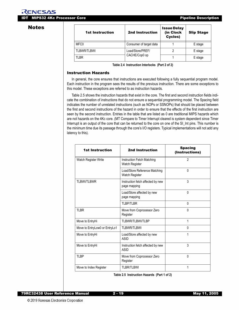
IDT MIPS32 4Kc Processor Core Pipeline Description
79RC32438 User Refer
Notes
Instruction HazardsIn general, the core ensures that instructions are executed following a fully sequential program model.
Each instruction in the program sees the results of the previous instruction. There are some exceptions tothis model. These exceptions are referred to as instruction hazards.
Table 2.5 shows the instruction hazards that exist in the core. The first and second instruction fields indi-cate the combination of instructions that do not ensure a sequential programming model. The Spacing fieldindicates the number of unrelated instructions (such as NOPs or SSNOPs) that should be placed betweenthe first and second instructions of the hazard in order to ensure that the effects of the first instruction areseen by the second instruction. Entries in the table that are listed as 0 are traditional MIPS hazards whichare not hazards on the 4Kc core. (MT Compare to Timer Interrupt cleared is system dependent since TimerInterrupt is an output of the core that can be returned to the core on one of the SI_Int pins. This number isthe minimum time due its passage through the core’s I/O registers. Typical implementations will not add anylatency to this).
MFC0 Consumer of target data 1 E stage
TLBWR/TLBWI Load/Store/PREF/CACHE/Cop0 op
2 E stage
TLBR 1 E stage
1st Instruction 2nd Instruction Spacing (Instructions)
Watch Register Write Instruction Fetch Matching Watch Register
2
Load/Store Reference Matching Watch Register
0
TLBWI/TLBWR Instruction fetch affected by new page mapping
3
Load/Store affected by new page mapping
0
TLBP/TLBR 0
TLBR Move from Coprocessor Zero Register
0
Move to EntryHi TLBWR/TLBWI/TLBP 1
Move to EntryLow0 or EntryLo1 TLBWR/TLBWI 0
Move to EntryHi Load/Store affected by new ASID
1
Move to EntryHi Instruction fetch affected by new ASID
3
TLBP Move from Coprocessor Zero Register
0
Move to Index Register TLBR/TLBWI 1
Table 2.5 Instruction Hazards (Part 1 of 2)
1st Instruction 2nd InstructionIssue Delay
(in Clock Cycles)
Slip Stage
Table 2.4 Instruction Interlocks (Part 2 of 2)
ence Manual 2 - 19 May 11, 2005
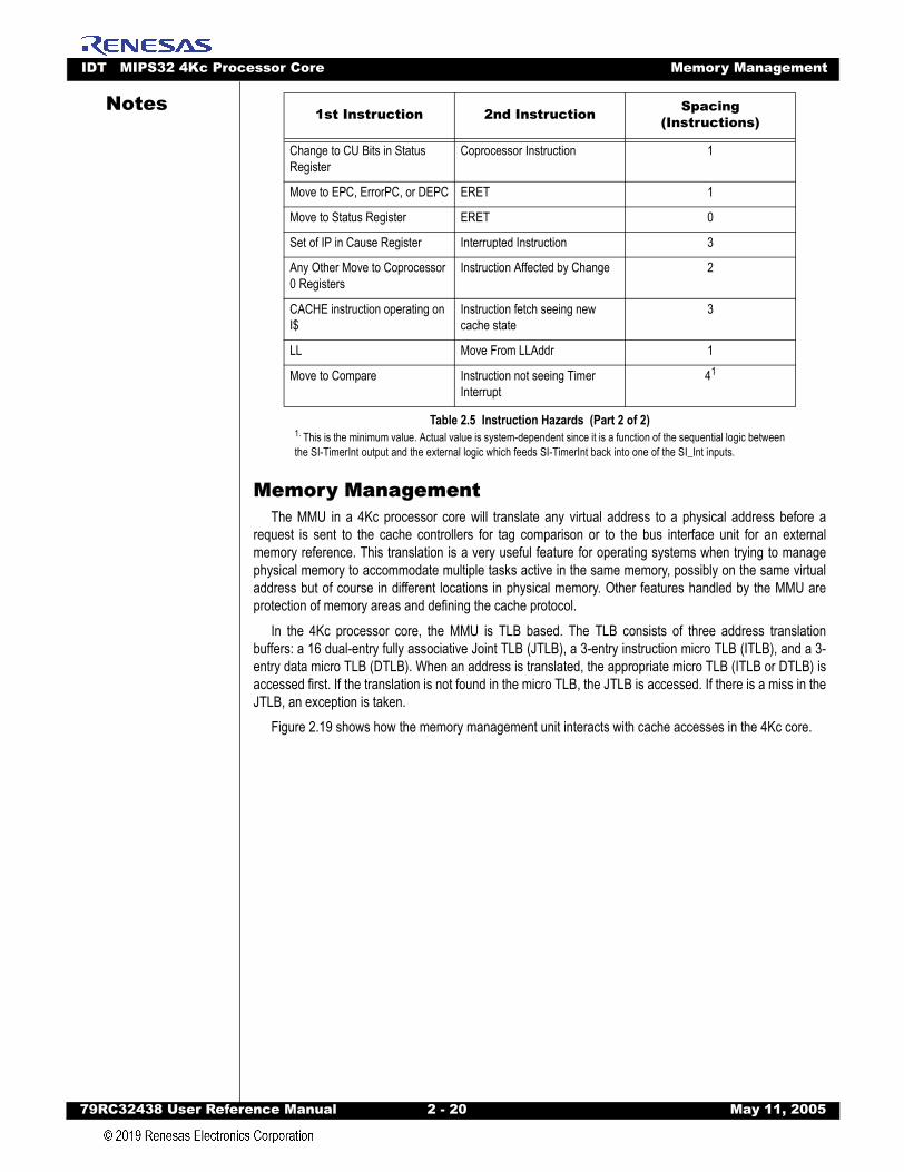
IDT MIPS32 4Kc Processor Core Memory Management
79RC32438 User Refer
Notes
Memory ManagementThe MMU in a 4Kc processor core will translate any virtual address to a physical address before a
request is sent to the cache controllers for tag comparison or to the bus interface unit for an externalmemory reference. This translation is a very useful feature for operating systems when trying to managephysical memory to accommodate multiple tasks active in the same memory, possibly on the same virtualaddress but of course in different locations in physical memory. Other features handled by the MMU areprotection of memory areas and defining the cache protocol.
In the 4Kc processor core, the MMU is TLB based. The TLB consists of three address translationbuffers: a 16 dual-entry fully associative Joint TLB (JTLB), a 3-entry instruction micro TLB (ITLB), and a 3-entry data micro TLB (DTLB). When an address is translated, the appropriate micro TLB (ITLB or DTLB) isaccessed first. If the translation is not found in the micro TLB, the JTLB is accessed. If there is a miss in theJTLB, an exception is taken.
Figure 2.19 shows how the memory management unit interacts with cache accesses in the 4Kc core.
Change to CU Bits in Status Register
Coprocessor Instruction 1
Move to EPC, ErrorPC, or DEPC ERET 1
Move to Status Register ERET 0
Set of IP in Cause Register Interrupted Instruction 3
Any Other Move to Coprocessor 0 Registers
Instruction Affected by Change 2
CACHE instruction operating on I$
Instruction fetch seeing new cache state
3
LL Move From LLAddr 1
Move to Compare Instruction not seeing Timer Interrupt
41
1. This is the minimum value. Actual value is system-dependent since it is a function of the sequential logic betweenthe SI-TimerInt output and the external logic which feeds SI-TimerInt back into one of the SI_Int inputs.
1st Instruction 2nd Instruction Spacing (Instructions)
Table 2.5 Instruction Hazards (Part 2 of 2)
ence Manual 2 - 20 May 11, 2005
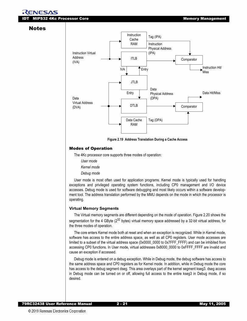
IDT MIPS32 4Kc Processor Core Memory Management
79RC32438 User Refer
Notes
Figure 2.19 Address Translation During a Cache Access
Modes of OperationThe 4Kc processor core supports three modes of operation:
User modeKernel modeDebug mode
User mode is most often used for application programs. Kernel mode is typically used for handlingexceptions and privileged operating system functions, including CP0 management and I/O deviceaccesses. Debug mode is used for software debugging and most likely occurs within a software develop-ment tool. The address translation performed by the MMU depends on the mode in which the processor isoperating.
Virtual Memory SegmentsThe Virtual memory segments are different depending on the mode of operation. Figure 2.20 shows the
segmentation for the 4 GByte (232 bytes) virtual memory space addressed by a 32-bit virtual address, forthe three modes of operation.
The core enters Kernel mode both at reset and when an exception is recognized. While in Kernel mode,software has access to the entire address space, as well as all CP0 registers. User mode accesses arelimited to a subset of the virtual address space (0x0000_0000 to 0x7FFF_FFFF) and can be inhibited fromaccessing CP0 functions. In User mode, virtual addresses 0x8000_0000 to 0xFFFF_FFFF are invalid andcause an exception if accessed.
Debug mode is entered on a debug exception. While in Debug mode, the debug software has access tothe same address space and CP0 registers as for Kernel mode. In addition, while in Debug mode the corehas access to the debug segment dseg. This area overlays part of the kernel segment kseg3. dseg accessin Debug mode can be turned on or off, allowing full access to the entire kseg3 in Debug mode, if sodesired.
Instruction Virtual Address(IVA)
DataVirtual Address(DVA)
JTLB
ITLB
InstructionCache RAM
DTLB
Data Cache RAM
IVA Entry
EntryDataPhysical Address(DPA)
InstructionPhysical Address(IPA)
Tag (IPA)
Tag (DPA)
Comparator
Comparator
Data Hit/Miss
Instruction Hit/Miss
ence Manual 2 - 21 May 11, 2005
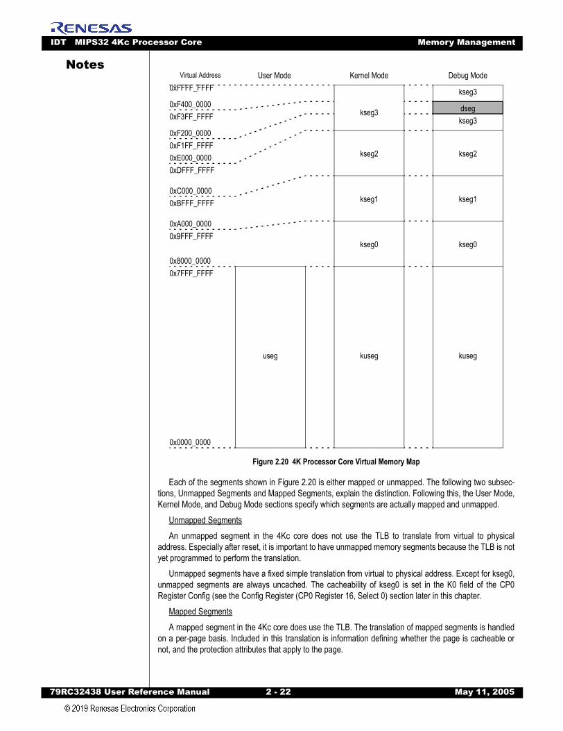
IDT MIPS32 4Kc Processor Core Memory Management
79RC32438 User Refer
Notes
Figure 2.20 4K Processor Core Virtual Memory Map
Each of the segments shown in Figure 2.20 is either mapped or unmapped. The following two subsec-tions, Unmapped Segments and Mapped Segments, explain the distinction. Following this, the User Mode,Kernel Mode, and Debug Mode sections specify which segments are actually mapped and unmapped.
Unmapped SegmentsAn unmapped segment in the 4Kc core does not use the TLB to translate from virtual to physical
address. Especially after reset, it is important to have unmapped memory segments because the TLB is notyet programmed to perform the translation.
Unmapped segments have a fixed simple translation from virtual to physical address. Except for kseg0,unmapped segments are always uncached. The cacheability of kseg0 is set in the K0 field of the CP0Register Config (see the Config Register (CP0 Register 16, Select 0) section later in this chapter.
Mapped SegmentsA mapped segment in the 4Kc core does use the TLB. The translation of mapped segments is handled
on a per-page basis. Included in this translation is information defining whether the page is cacheable ornot, and the protection attributes that apply to the page.
useg kuseg kuseg
kseg0
kseg1
kseg2
kseg3
kseg2
kseg1
kseg0
kseg3
kseg3
dseg
User Mode Kernel Mode Debug ModeVirtual Address
0x7FFF_FFFF0x8000_0000
0x9FFF_FFFF
0xBFFF_FFFF
0xDFFF_FFFF
0xF1FF_FFFF
0xF3FF_FFFF
0xFFFF_FFFF
0xA000_0000
0xC000_0000
0xE000_0000
0xF200_0000
0xF400_0000
0x0000_0000
ence Manual 2 - 22 May 11, 2005
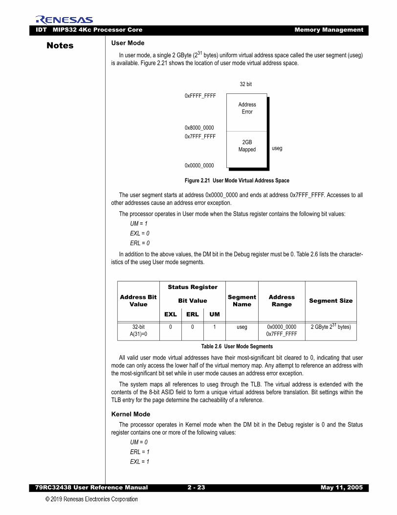
IDT MIPS32 4Kc Processor Core Memory Management
79RC32438 User Refer
Notes
User ModeIn user mode, a single 2 GByte (231 bytes) uniform virtual address space called the user segment (useg)is available. Figure 2.21 shows the location of user mode virtual address space.
Figure 2.21 User Mode Virtual Address Space
The user segment starts at address 0x0000_0000 and ends at address 0x7FFF_FFFF. Accesses to allother addresses cause an address error exception.
The processor operates in User mode when the Status register contains the following bit values:UM = 1EXL = 0ERL = 0
In addition to the above values, the DM bit in the Debug register must be 0. Table 2.6 lists the character-istics of the useg User mode segments.
All valid user mode virtual addresses have their most-significant bit cleared to 0, indicating that usermode can only access the lower half of the virtual memory map. Any attempt to reference an address withthe most-significant bit set while in user mode causes an address error exception.
The system maps all references to useg through the TLB. The virtual address is extended with thecontents of the 8-bit ASID field to form a unique virtual address before translation. Bit settings within theTLB entry for the page determine the cacheability of a reference.
Kernel ModeThe processor operates in Kernel mode when the DM bit in the Debug register is 0 and the Status
register contains one or more of the following values:UM = 0ERL = 1EXL = 1
Address Bit Value
Status RegisterSegment
NameAddress Range Segment SizeBit Value
EXL ERL UM
32-bit A(31)=0
0 0 1 useg 0x0000_0000 0x7FFF_FFFF
2 GByte 231 bytes)
Table 2.6 User Mode Segments
0x0000_0000
0x8000_00000x7FFF_FFFF
0xFFFF_FFFF
32 bit
Address Error
2GB Mapped useg
ence Manual 2 - 23 May 11, 2005
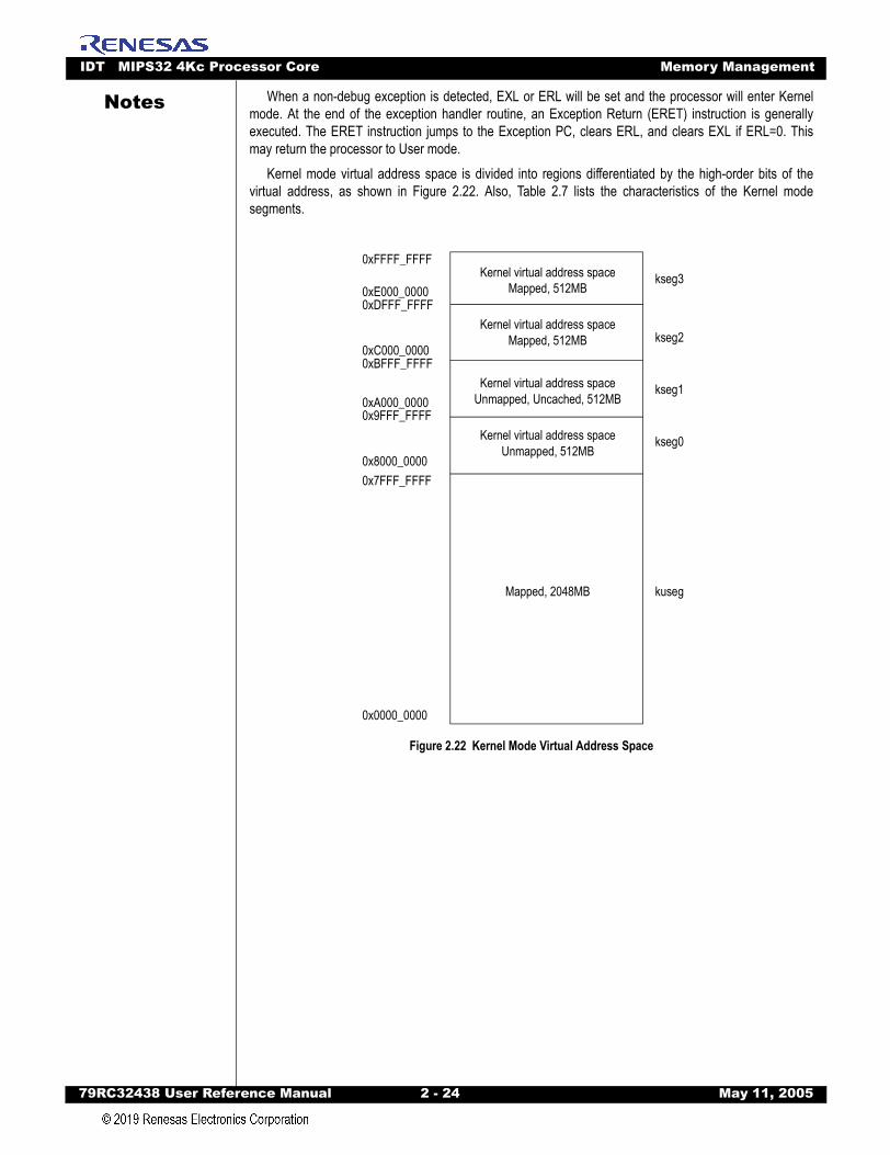
IDT MIPS32 4Kc Processor Core Memory Management
79RC32438 User Refer
Notes
When a non-debug exception is detected, EXL or ERL will be set and the processor will enter Kernelmode. At the end of the exception handler routine, an Exception Return (ERET) instruction is generallyexecuted. The ERET instruction jumps to the Exception PC, clears ERL, and clears EXL if ERL=0. Thismay return the processor to User mode.Kernel mode virtual address space is divided into regions differentiated by the high-order bits of thevirtual address, as shown in Figure 2.22. Also, Table 2.7 lists the characteristics of the Kernel modesegments.
Figure 2.22 Kernel Mode Virtual Address Space
Kernel virtual address spaceUnmapped, 512MB
kuseg
kseg0
kseg1
kseg2
kseg3
Mapped, 2048MB
Kernel virtual address spaceUnmapped, Uncached, 512MB
Kernel virtual address spaceMapped, 512MB
Kernel virtual address spaceMapped, 512MB
0x0000_0000
0x8000_0000
0xA000_0000
0xC000_0000
0xE000_0000
0x7FFF_FFFF
0x9FFF_FFFF
0xBFFF_FFFF
0xDFFF_FFFF
0xFFFF_FFFF
ence Manual 2 - 24 May 11, 2005
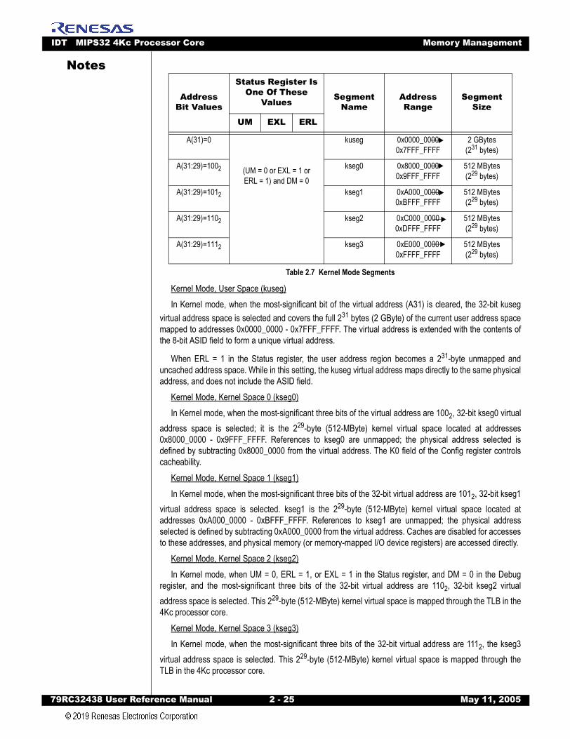
IDT MIPS32 4Kc Processor Core Memory Management
79RC32438 User Refer
Notes
Kernel Mode, User Space (kuseg)In Kernel mode, when the most-significant bit of the virtual address (A31) is cleared, the 32-bit kuseg
virtual address space is selected and covers the full 231 bytes (2 GByte) of the current user address spacemapped to addresses 0x0000_0000 - 0x7FFF_FFFF. The virtual address is extended with the contents ofthe 8-bit ASID field to form a unique virtual address.
When ERL = 1 in the Status register, the user address region becomes a 231-byte unmapped anduncached address space. While in this setting, the kuseg virtual address maps directly to the same physicaladdress, and does not include the ASID field.
Kernel Mode, Kernel Space 0 (kseg0)In Kernel mode, when the most-significant three bits of the virtual address are 1002, 32-bit kseg0 virtual
address space is selected; it is the 229-byte (512-MByte) kernel virtual space located at addresses0x8000_0000 - 0x9FFF_FFFF. References to kseg0 are unmapped; the physical address selected isdefined by subtracting 0x8000_0000 from the virtual address. The K0 field of the Config register controlscacheability.
Kernel Mode, Kernel Space 1 (kseg1)In Kernel mode, when the most-significant three bits of the 32-bit virtual address are 1012, 32-bit kseg1
virtual address space is selected. kseg1 is the 229-byte (512-MByte) kernel virtual space located ataddresses 0xA000_0000 - 0xBFFF_FFFF. References to kseg1 are unmapped; the physical addressselected is defined by subtracting 0xA000_0000 from the virtual address. Caches are disabled for accessesto these addresses, and physical memory (or memory-mapped I/O device registers) are accessed directly.
Kernel Mode, Kernel Space 2 (kseg2)In Kernel mode, when UM = 0, ERL = 1, or EXL = 1 in the Status register, and DM = 0 in the Debug
register, and the most-significant three bits of the 32-bit virtual address are 1102, 32-bit kseg2 virtualaddress space is selected. This 229-byte (512-MByte) kernel virtual space is mapped through the TLB in the4Kc processor core.
Kernel Mode, Kernel Space 3 (kseg3)In Kernel mode, when the most-significant three bits of the 32-bit virtual address are 1112, the kseg3
virtual address space is selected. This 229-byte (512-MByte) kernel virtual space is mapped through theTLB in the 4Kc processor core.
Address Bit Values
Status Register Is One Of These
Values Segment Name
Address Range
Segment Size
UM EXL ERL
A(31)=0
(UM = 0 or EXL = 1 or ERL = 1) and DM = 0
kuseg 0x0000_0000 0x7FFF_FFFF
2 GBytes (231 bytes)
A(31:29)=1002 kseg0 0x8000_0000 0x9FFF_FFFF
512 MBytes (229 bytes)
A(31:29)=1012 kseg1 0xA000_0000 0xBFFF_FFFF
512 MBytes (229 bytes)
A(31:29)=1102 kseg2 0xC000_0000 0xDFFF_FFFF
512 MBytes (229 bytes)
A(31:29)=1112 kseg3 0xE000_0000 0xFFFF_FFFF
512 MBytes (229 bytes)
Table 2.7 Kernel Mode Segments
ence Manual 2 - 25 May 11, 2005

IDT MIPS32 4Kc Processor Core Memory Management
79RC32438 User Refer
Notes
Debug ModeDebug mode address space is identical to Kernel mode address space with respect to mapped andunmapped areas, except for kseg3. In kseg3, a debug segment dseg co-exists in the virtual address range0xFF20_0000 to 0xFF3F_FFFF. The layout is shown in Figure 2.23.
Figure 2.23 Debug Mode Virtual Address Space
The dseg is sub-divided into the dmseg segment at 0xFF20_0000 to 0xFF2F_FFFF which is used whenthe probe services the memory segment, and the drseg segment at 0xFF30_0000 to 0xFF3F_FFFF whichis used when memory mapped debug registers are accessed. The subdivision and attributes for thesegments are shown in Table 2.8.
Accesses to memory that would normally cause an exception if tried from kernel mode cause the core tore-enter debug mode via a debug mode exception. This includes accesses usually causing a TLB exception(4Kc core only), with the result that such accesses are not handled by the usual memory managementroutines. The unmapped kseg0 and kseg1 segments from kernel mode address space are available fromdebug mode, which allows the debug handler to be executed from uncached and unmapped memory.
Conditions and Behavior for Access to drseg and EJTAG RegistersThe behavior of CPU access to the drseg address range at 0xFF30_0000 to 0xFF3F_FFFF is deter-
mined as shown in Table 2.9.
Segment Name
Sub-segment Name
Virtual Address
Generates Physical Address
Cache Attribute
dseg dmseg 0xFF20_0000through
0xFF2F_FFFF
mseg maps to addresses 0x0_0000 - 0xF_FFFF in EJTAG probe mem-ory space.
Uncached
drseg 0xFF30_0000through
0xFF3F_FFFF
drseg maps to the breakpoint registers 0x0_0000 - 0xF_FFFF
Table 2.8 Physical Address and Cache Attributes for dseg, dmseg, and drseg Address Spaces
0x0000_0000
0xFF20_0000
0xFF40_00000xFFFF_FFFF
dseg
kseg1
kseg0 Unmapped
Mapped if mapped in Kernel Mode
ence Manual 2 - 26 May 11, 2005
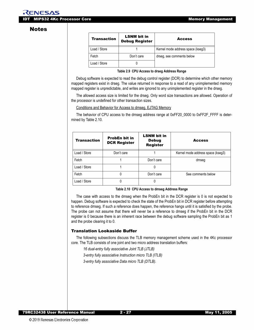
IDT MIPS32 4Kc Processor Core Memory Management
79RC32438 User Refer
Notes
Debug software is expected to read the debug control register (DCR) to determine which other memorymapped registers exist in drseg. The value returned in response to a read of any unimplemented memorymapped register is unpredictable, and writes are ignored to any unimplemented register in the drseg.
The allowed access size is limited for the drseg. Only word size transactions are allowed. Operation ofthe processor is undefined for other transaction sizes.
Conditions and Behavior for Access to dmseg, EJTAG MemoryThe behavior of CPU access to the dmseg address range at 0xFF20_0000 to 0xFF2F_FFFF is deter-
mined by Table 2.10.
The case with access to the dmseg when the ProbEn bit in the DCR register is 0 is not expected tohappen. Debug software is expected to check the state of the ProbEn bit in DCR register before attemptingto reference dmseg. If such a reference does happen, the reference hangs until it is satisfied by the probe.The probe can not assume that there will never be a reference to dmseg if the ProbEn bit in the DCRregister is 0 because there is an inherent race between the debug software sampling the ProbEn bit as 1and the probe clearing it to 0.
Translation Lookaside BufferThe following subsections discuss the TLB memory management scheme used in the 4Kc processor
core. The TLB consists of one joint and two micro address translation buffers: 16 dual-entry fully associative Joint TLB (JTLB)3-entry fully associative Instruction micro TLB (ITLB)3-entry fully associative Data micro TLB (DTLB).
Transaction LSNM bit in Debug Register Access
Load / Store 1 Kernel mode address space (kseg3)
Fetch Don’t care drseg, see comments below
Load / Store 0
Table 2.9 CPU Access to drseg Address Range
Transaction ProbEn bit in DCR Register
LSNM bit in Debug
RegisterAccess
Load / Store Don’t care 1 Kernel mode address space (kseg3)
Fetch 1 Don’t care dmseg
Load / Store 1 0
Fetch 0 Don’t care See comments below
Load / Store 0 0
Table 2.10 CPU Access to dmseg Address Range
ence Manual 2 - 27 May 11, 2005
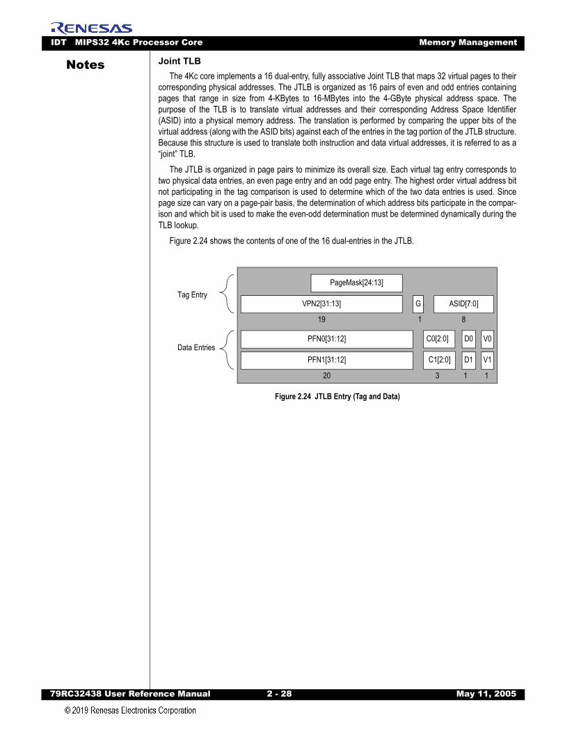
IDT MIPS32 4Kc Processor Core Memory Management
79RC32438 User Refer
Notes
Joint TLBThe 4Kc core implements a 16 dual-entry, fully associative Joint TLB that maps 32 virtual pages to theircorresponding physical addresses. The JTLB is organized as 16 pairs of even and odd entries containingpages that range in size from 4-KBytes to 16-MBytes into the 4-GByte physical address space. Thepurpose of the TLB is to translate virtual addresses and their corresponding Address Space Identifier(ASID) into a physical memory address. The translation is performed by comparing the upper bits of thevirtual address (along with the ASID bits) against each of the entries in the tag portion of the JTLB structure.Because this structure is used to translate both instruction and data virtual addresses, it is referred to as a“joint” TLB.
The JTLB is organized in page pairs to minimize its overall size. Each virtual tag entry corresponds totwo physical data entries, an even page entry and an odd page entry. The highest order virtual address bitnot participating in the tag comparison is used to determine which of the two data entries is used. Sincepage size can vary on a page-pair basis, the determination of which address bits participate in the compar-ison and which bit is used to make the even-odd determination must be determined dynamically during theTLB lookup.
Figure 2.24 shows the contents of one of the 16 dual-entries in the JTLB.
Figure 2.24 JTLB Entry (Tag and Data)
PageMask[24:13]
D0
G ASID[7:0]
PFN0[31:12] C0[2:0]
D1PFN1[31:12] C1[2:0]
VPN2[31:13]
V0
V1
GTag Entry
Data Entries
19 1 8
20 3 1 1
ence Manual 2 - 28 May 11, 2005
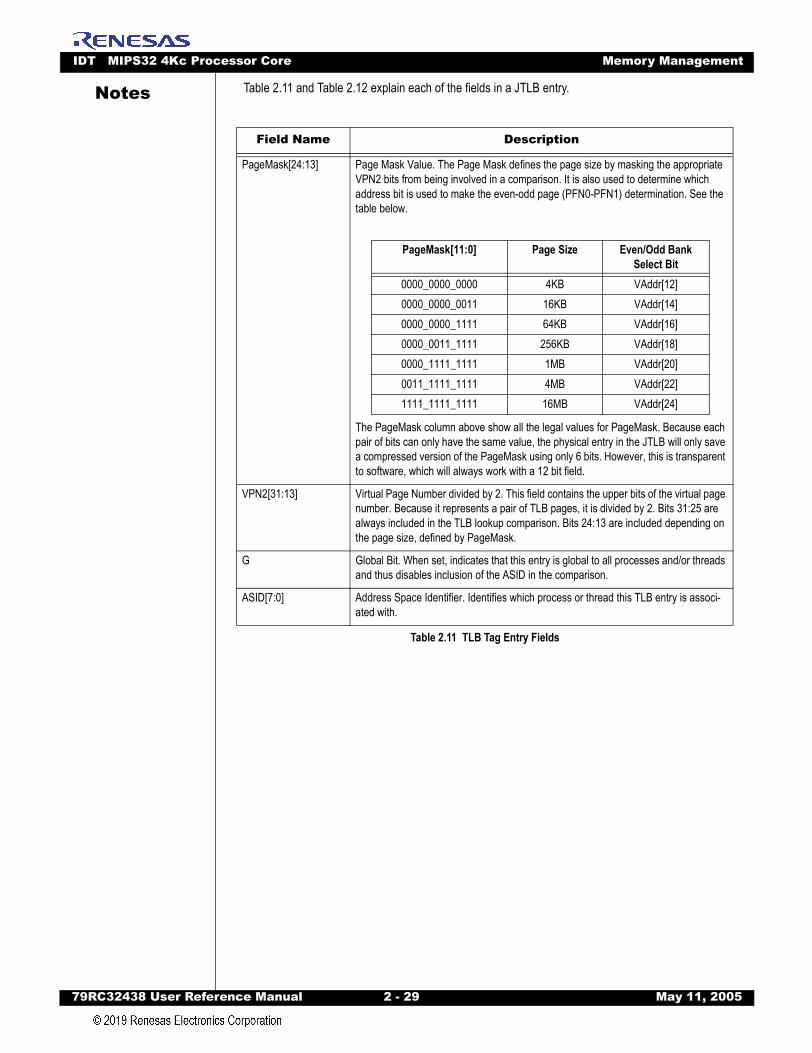
IDT MIPS32 4Kc Processor Core Memory Management
79RC32438 User Refer
Notes
Table 2.11 and Table 2.12 explain each of the fields in a JTLB entry.Field Name Description
PageMask[24:13] Page Mask Value. The Page Mask defines the page size by masking the appropriate VPN2 bits from being involved in a comparison. It is also used to determine which address bit is used to make the even-odd page (PFN0-PFN1) determination. See the table below.
The PageMask column above show all the legal values for PageMask. Because each pair of bits can only have the same value, the physical entry in the JTLB will only save a compressed version of the PageMask using only 6 bits. However, this is transparent to software, which will always work with a 12 bit field.
VPN2[31:13] Virtual Page Number divided by 2. This field contains the upper bits of the virtual page number. Because it represents a pair of TLB pages, it is divided by 2. Bits 31:25 are always included in the TLB lookup comparison. Bits 24:13 are included depending on the page size, defined by PageMask.
G Global Bit. When set, indicates that this entry is global to all processes and/or threads and thus disables inclusion of the ASID in the comparison.
ASID[7:0] Address Space Identifier. Identifies which process or thread this TLB entry is associ-ated with.
Table 2.11 TLB Tag Entry Fields
PageMask[11:0] Page Size Even/Odd Bank Select Bit
0000_0000_0000 4KB VAddr[12]0000_0000_0011 16KB VAddr[14]0000_0000_1111 64KB VAddr[16]0000_0011_1111 256KB VAddr[18]0000_1111_1111 1MB VAddr[20]0011_1111_1111 4MB VAddr[22]1111_1111_1111 16MB VAddr[24]
ence Manual 2 - 29 May 11, 2005

IDT MIPS32 4Kc Processor Core Memory Management
79RC32438 User Refer
Notes
In order to fill an entry in the JTLB, software executes a TLBWI or TLBWR instruction (see the TLBInstructions section). Prior to invoking one of these instructions, several CP0 registers must be updatedwith the information to be written to a TLB entry:
PageMask is set in the CP0 PageMask registerVPN2 and ASID are set in the CP0 EntryHi registerPFN0, C0, D0, V0 and G bit are set in the CP0 EntryLo0 registerPFN1, C1, D1, V1 and G bit are set in the CP0 EntryLo1 register.
Note that the global bit “G” is part of both EntryLo0 and EntryLo1. The resulting “G” bit in the JTLB entryis the logical AND between the two fields in EntryLo0 and EntryLo1. For additional information, refer tosection “CP0 Registers” on page 2-56.
The address space identifier (ASID) helps to reduce the frequency of TLB flushing on a context switch.The existence of the ASID allows multiple processes to exist in both the TLB and instruction caches. TheASID value is stored in the EntryHi register and is compared to the ASID value of each entry.
Field Name Description
PFN0[31:12],PFN1[31:12]
Physical Frame Number. Defines the upper bits of the physical address. For page sizes larger than 4 KBytes, only a subset of these bits is actually used.
C0[2:0],C1[2:0]
Cacheability. Contains an encoded value of the cacheability attributes and determines whether the page should be placed in the cache or not. The field is encoded as fol-lows:
D0, D1 “Dirty” or Write-enable Bit. Indicates that the page has been written, and/or is writable. If this bit is set, stores to the page are permitted. If the bit is cleared, stores to the page cause a TLB Modified exception.
V0, V1 Valid Bit. Indicates that the TLB entry and, thus, the virtual page mapping are valid. If this bit is set, accesses to the page are permitted. If the bit is cleared, accesses to the page cause a TLB Invalid exception.
Table 2.12 TLB Data Entry Fields
C[2:0] Coherency Attribute000 Cacheable, noncoherent, write-through, no write allo-
cated001 Cacheable, noncoherent, write-through, no write allo-
cated010 Uncached011 Cacheable, noncoherent, write-through, no write allo-
cated100 Cacheable, noncoherent, write-through, no write allo-
cated101 Cacheable, noncoherent, write-through, no write allo-
cated110 Cacheable, noncoherent, write-through, no write allo-
cated111 Cacheable, noncoherent, write-through, no write allo-
cated
ence Manual 2 - 30 May 11, 2005

IDT MIPS32 4Kc Processor Core Memory Management
79RC32438 User Refer
Notes
Instruction TLBThe ITLB is a small 3-entry, fully associative TLB dedicated to performing translations for the instructionstream. The ITLB only maps 4-Kbyte pages/sub-pages.The ITLB is managed by hardware and is transparent to software. If a fetch address cannot be trans-
lated by the ITLB, the JTLB is accessed to attempt to translate it in the following clock cycle. If successful,the translation information is copied into the ITLB. The ITLB is then re-accessed and the address will besuccessfully translated. This results in an ITLB miss penalty of at least 2 cycles (if the JTLB is busy withother operations, it may take additional cycles).
Data TLBThe DTLB is a small 3-entry, fully associative TLB which provides a faster translation for Load/Store
addresses than is possible with the JTLB. The DTLB only maps 4-Kbyte pages/sub-pages.Like the ITLB, the DTLB is managed by hardware and is transparent to software. Unlike the ITLB, when
translating Load/Store addresses, the JTLB is accessed in parallel with the DTLB. If there is a DTLB missand a JTLB hit, the DTLB can be reloaded that cycle. The DTLB is then re-accessed and the translation willbe successful. This parallel access reduces the DTLB miss penalty to 1 cycle.
Virtual to Physical Address TranslationConverting a virtual address to a physical address begins by comparing the virtual address from the
processor with the virtual addresses in the TLB. There is a match when the virtual page number (VPN) ofthe address is the same as the VPN field of the entry, and either:
The Global (G) bit of both the even and odd pages of the TLB entry are set, orThe ASID field of the virtual address is the same as the ASID field of the TLB entry.
This match is referred to as a TLB hit. If there is no match, a TLB miss exception is taken by theprocessor and software is allowed to refill the TLB from a page table of virtual/physical addresses inmemory.
Figure 2.25 shows the logical translation of a virtual address into a physical address. In this figure, thevirtual address is extended with an 8-bit address-space identifier (ASID), which reduces the frequency ofTLB flushing during a context switch. This 8-bit ASID contains the number assigned to that process and isstored in the CP0 EntryHi register.
ence Manual 2 - 31 May 11, 2005

IDT MIPS32 4Kc Processor Core Memory Management
79RC32438 User Refer
Notes
Figure 2.25 Overview of a Virtual-to-Physical Address Translation
If there is a virtual address match in the TLB, the physical frame number (PFN) is output from the TLBand concatenated with the Offset, to form the physical address. The Offset represents an address within thepage frame space. As shown in Figure 2.25, the Offset does not pass through the TLB.
Figure 2.26 shows a flow diagram of the 4Kc core address translation process. The top portion of thefigure shows a virtual address for a 4-KByte page size. The width of the Offset is defined by the page size.The remaining 20 bits of the address represent the virtual page number (VPN) that indexes the 1M-entrypage table.
The bottom portion of Figure 2.26 shows the virtual address for a 16-MByte page size. The remaining 8bits of the address represent the VPN that indexes the 256-entry page table.
1.Virtual address (VA) represented by the virtual page number (VPN) is compared with tag in TLB.
2. If there is a match, the page frame number (PFN0 or PFN1) representing the upper bits of the physical address (PA) is output from the TLB.
3. The Offset, which does not pass through the TLB, is then concatenated with the PFN.
OffsetVPNG ASID
Virtual Address
TLBEntry
OffsetPFN
TLB
G ASID VPN2
C0 D0 V0 PFN0
PFN1C1 D1 V1
Physical Address
ence Manual 2 - 32 May 11, 2005
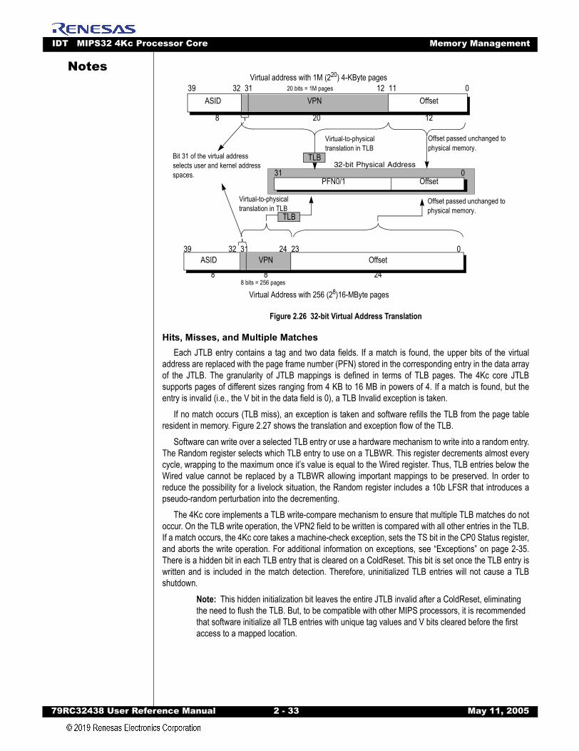
IDT MIPS32 4Kc Processor Core Memory Management
79RC32438 User Refer
Notes
Figure 2.26 32-bit Virtual Address Translation
Hits, Misses, and Multiple MatchesEach JTLB entry contains a tag and two data fields. If a match is found, the upper bits of the virtual
address are replaced with the page frame number (PFN) stored in the corresponding entry in the data arrayof the JTLB. The granularity of JTLB mappings is defined in terms of TLB pages. The 4Kc core JTLBsupports pages of different sizes ranging from 4 KB to 16 MB in powers of 4. If a match is found, but theentry is invalid (i.e., the V bit in the data field is 0), a TLB Invalid exception is taken.
If no match occurs (TLB miss), an exception is taken and software refills the TLB from the page tableresident in memory. Figure 2.27 shows the translation and exception flow of the TLB.
Software can write over a selected TLB entry or use a hardware mechanism to write into a random entry.The Random register selects which TLB entry to use on a TLBWR. This register decrements almost everycycle, wrapping to the maximum once it’s value is equal to the Wired register. Thus, TLB entries below theWired value cannot be replaced by a TLBWR allowing important mappings to be preserved. In order toreduce the possibility for a livelock situation, the Random register includes a 10b LFSR that introduces apseudo-random perturbation into the decrementing.
The 4Kc core implements a TLB write-compare mechanism to ensure that multiple TLB matches do notoccur. On the TLB write operation, the VPN2 field to be written is compared with all other entries in the TLB.If a match occurs, the 4Kc core takes a machine-check exception, sets the TS bit in the CP0 Status register,and aborts the write operation. For additional information on exceptions, see “Exceptions” on page 2-35.There is a hidden bit in each TLB entry that is cleared on a ColdReset. This bit is set once the TLB entry iswritten and is included in the match detection. Therefore, uninitialized TLB entries will not cause a TLBshutdown.
Note: This hidden initialization bit leaves the entire JTLB invalid after a ColdReset, eliminating the need to flush the TLB. But, to be compatible with other MIPS processors, it is recommended that software initialize all TLB entries with unique tag values and V bits cleared before the first access to a mapped location.
11Virtual address with 1M (220) 4-KByte pages
Virtual Address with 256 (28)16-MByte pages8 bits = 256 pages
20 bits = 1M pages
Virtual-to-physicaltranslation in TLB
Bit 31 of the virtual address selects user and kernel address spaces.
Offset passed unchanged to physical memory.
Virtual-to-physicaltranslation in TLB
Offset passed unchanged to physical memory.
32-bit Physical Address
ASID VPN Offset
PFN0/1 Offset
TLB
TLB
ASID VPN Offset0233132 2439
313239 012
031
8 8 24
8 20 12
ence Manual 2 - 33 May 11, 2005

IDT MIPS32 4Kc Processor Core Memory Management
79RC32438 User Refer
Notes
Page Sizes and Replacement AlgorithmTo assist in controlling both the amount of mapped space and the replacement characteristics of variousmemory regions, the 4Kc core provides two mechanisms. First, the page size can be configured, on a perentry basis, to map page sizes ranging from 4 KByte to 16 MByte (in multiples of 4). The CP0 PageMaskregister is loaded with the desired page size, which is then entered into the TLB when a new entry is written.Thus, operating systems can provide special-purpose maps. For example, a typical frame buffer can bememory mapped with only one TLB entry.
The second mechanism controls the replacement algorithm when a TLB miss occurs. To select a TLBentry to be written with a new mapping, the 4Kc core provides a random replacement algorithm. However,the processor also provides a mechanism whereby a programmable number of mappings can be lockedinto the TLB via the CP0 Wired register, thus avoiding random replacement. For additional information, see“Wired Register (CP0 Register 6, Select 0)” on page 2-60.
Figure 2.27 TLB Address Translation Flow in the 4Kc Processor Core
For valid address space, see the section describing Modes of operation in this chapter.
Virtual Address (Input)VPN and
ASID
User Mode?
NoYes
No
Yes
No
Yes
No
No No
No
No
No
No
Yes
Yes Yes
Yes
Yes
Yes
Yes
Exception
Global
Valid
Dirty
Noncacheable
Physical Address (Output)
User Address?
Address Error
Unmapped Address
kseg0/kseg1 Address
VPN Match?
G = 1?
C=010 orC=111?
ASID Match?
V = 1?
D = 1? Write?
TLB Modified
TLB Invalid
TLB Refill
Access Cache
Access Main
Memory
ence Manual 2 - 34 May 11, 2005

IDT MIPS32 4Kc Processor Core Exceptions
79RC32438 User Refer
Notes
TLB InstructionsTable 2.13 lists the 4Kc core’s TLB-related instructions. For additional information on these instructions,see Appendix A, 4Kc Processor Core Instructions.
System Control CoprocessorThe System Control Coprocessor (CP0) is implemented as an integral part of the 4Kc processor core
and supports memory management, address translation, exception handling, and other privileged opera-tions. Certain CP0 registers are used to support memory management. For additional information on theCP0 register set, see the CP0 Registers section later in this chapter.
ExceptionsThe 4Kc processor core receives exceptions from a number of sources, including translation lookaside
buffer (TLB) misses, arithmetic overflows, I/O interrupts, and system calls. When the CPU detects one ofthese exceptions, the normal sequence of instruction execution is suspended and the processor enterskernel mode.
In kernel mode, the core disables interrupts and forces execution of a software exception processor(called a handler) located at a fixed address. The handler saves the context of the processor, including thecontents of the program counter, the current operating mode, and the status of the interrupts (enabled ordisabled). This context is saved so it can be restored when the exception has been serviced.
When an exception occurs, the core loads the Exception Program Counter (EPC) register with a locationwhere execution can restart after the exception has been serviced. The restart location in the EPC registeris the address of the instruction that caused the exception or, if the instruction was executing in a branchdelay slot, the address of the branch instruction immediately preceding the delay slot. To distinguishbetween the two, software must read the BD bit in the CP0 Cause register.
Exception ConditionsWhen an exception condition occurs, the relevant instruction and all those that follow it in the pipeline
are cancelled. Accordingly, all stall conditions and all later exception conditions that may have referencedthis instruction are inhibited; there is no benefit in servicing stalls for a cancelled instruction.
When an exception condition is detected on an instruction fetch, the core aborts that instruction and allinstructions that follow. When this instruction reaches the W stage, the exception flag causes it to writevarious CP0 registers with the exception state, change the current program counter (PC) to the appropriateexception vector address, and clear the exception bits of earlier pipeline stages.
This implementation allows all preceding instructions to complete execution and prevents all subse-quent instructions from completing. Thus, the value in the EPC (ErrorEPC for errors or DEPC for debugexceptions) is sufficient to restart execution. It also ensures that exceptions are taken in the order of execu-tion; an instruction taking an exception may itself be killed by an instruction further down the pipeline thattakes an exception in a later cycle.
Op Code Description of Instructions
TLBP Translation Lookaside Buffer Probe
TLBR Translation Lookaside Buffer Read
TLBWI Translation Lookaside Buffer Write Index
TLBWR Translation Lookaside Buffer Write Random
Table 2.13 TLB Instructions
ence Manual 2 - 35 May 11, 2005
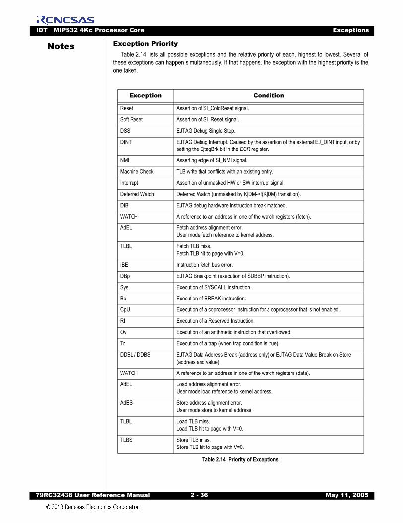
IDT MIPS32 4Kc Processor Core Exceptions
79RC32438 User Refer
Notes
Exception PriorityTable 2.14 lists all possible exceptions and the relative priority of each, highest to lowest. Several ofthese exceptions can happen simultaneously. If that happens, the exception with the highest priority is theone taken.
Exception Condition
Reset Assertion of SI_ColdReset signal.
Soft Reset Assertion of SI_Reset signal.
DSS EJTAG Debug Single Step.
DINT EJTAG Debug Interrupt. Caused by the assertion of the external EJ_DINT input, or by setting the EjtagBrk bit in the ECR register.
NMI Asserting edge of SI_NMI signal.
Machine Check TLB write that conflicts with an existing entry.
Interrupt Assertion of unmasked HW or SW interrupt signal.
Deferred Watch Deferred Watch (unmasked by K|DM->!(K|DM) transition).
DIB EJTAG debug hardware instruction break matched.
WATCH A reference to an address in one of the watch registers (fetch).
AdEL Fetch address alignment error.User mode fetch reference to kernel address.
TLBL Fetch TLB miss.Fetch TLB hit to page with V=0.
IBE Instruction fetch bus error.
DBp EJTAG Breakpoint (execution of SDBBP instruction).
Sys Execution of SYSCALL instruction.
Bp Execution of BREAK instruction.
CpU Execution of a coprocessor instruction for a coprocessor that is not enabled.
RI Execution of a Reserved Instruction.
Ov Execution of an arithmetic instruction that overflowed.
Tr Execution of a trap (when trap condition is true).
DDBL / DDBS EJTAG Data Address Break (address only) or EJTAG Data Value Break on Store (address and value).
WATCH A reference to an address in one of the watch registers (data).
AdEL Load address alignment error.User mode load reference to kernel address.
AdES Store address alignment error.User mode store to kernel address.
TLBL Load TLB miss.Load TLB hit to page with V=0.
TLBS Store TLB miss.Store TLB hit to page with V=0.
Table 2.14 Priority of Exceptions
ence Manual 2 - 36 May 11, 2005
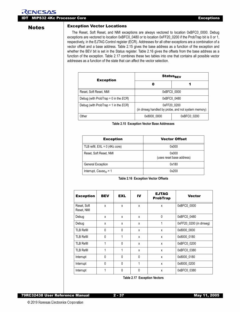
IDT MIPS32 4Kc Processor Core Exceptions
79RC32438 User Refer
Notes
Exception Vector LocationsThe Reset, Soft Reset, and NMI exceptions are always vectored to location 0xBFC0_0000. Debugexceptions are vectored to location 0xBFC0_0480 or to location 0xFF20_0200 if the ProbTrap bit is 0 or 1,respectively, in the EJTAG Control register (ECR). Addresses for all other exceptions are a combination of avector offset and a base address. Table 2.15 gives the base address as a function of the exception andwhether the BEV bit is set in the Status register. Table 2.16 gives the offsets from the base address as afunction of the exception. Table 2.17 combines these two tables into one that contains all possible vectoraddresses as a function of the state that can affect the vector selection.
ExceptionStatusBEV
0 1
Reset, Soft Reset, NMI 0xBFC0_0000
Debug (with ProbTrap = 0 in the ECR) 0xBFC0_0480
Debug (with ProbTrap = 1 in the ECR) 0xFF20_0200(in dmseg handled by probe, and not system memory)
Other 0x8000_0000 0xBFC0_0200
Table 2.15 Exception Vector Base Addresses
Exception Vector Offset
TLB refill, EXL = 0 (4Kc core) 0x000
Reset, Soft Reset, NMI 0x000 (uses reset base address)
General Exception 0x180
Interrupt, CauseIV = 1 0x200
Table 2.16 Exception Vector Offsets
Exception BEV EXL IV EJTAG ProbTrap Vector
Reset, Soft Reset, NMI
x x x x 0xBFC0_0000
Debug x x x 0 0xBFC0_0480
Debug x x x 1 0xFF20_0200 (in dmseg)
TLB Refill 0 0 x x 0x8000_0000
TLB Refill 0 1 x x 0x8000_0180
TLB Refill 1 0 x x 0xBFC0_0200
TLB Refill 1 1 x x 0xBFC0_0380
Interrupt 0 0 0 x 0x8000_0180
Interrupt 0 0 1 x 0x8000_0200
Interrupt 1 0 0 x 0xBFC0_0380
Table 2.17 Exception Vectors
ence Manual 2 - 37 May 11, 2005

IDT MIPS32 4Kc Processor Core Exceptions
79RC32438 User Refer
Notes
General Exception ProcessingWith the exception of Reset, Soft Reset, NMI, and Debug exceptions, which have their own special
processing as described below, exceptions have the same basic processing flow:1. If the EXL bit in the Status register is cleared, the EPC register is loaded with the PC at which execu-
tion will be restarted and the BD bit is set appropriately in the Cause register. If the instruction is notin the delay slot of a branch, the BD bit in Cause will be cleared and the value loaded into the EPCregister is the current PC. If the instruction is in the delay slot of a branch, the BD bit in Cause is setand EPC is loaded with PC-4. If the EXL bit in the Status register is set, the EPC register is notloaded and the BD bit is not changed in the Cause register.
2. The CE and ExcCode fields of the Cause registers are loaded with the values appropriate to theexception. The CE field is loaded, but not defined, for any exception type other than a coprocessorunusable exception.
3. The EXL bit is set in the Status register.4. The processor is started at the exception vector.The value loaded into EPC represents the restart address for the exception and need not be modified by
exception handler software in the normal case. Software need not look at the BD bit in the Cause registerunless is wishes to identify the address of the instruction that actually caused the exception.
Note that individual exception types may load additional information into other registers. This is noted inthe description of each exception type below.
Operation:if StatusEXL = 0 then
if InstructionInBranchDelaySlot thenEPC << PC - 4CauseBD << 1
elseEPC << PCCauseBD << 0
endifif ExceptionType = TLBRefill then
vectorOffset << 0x000elseif (ExceptionType = Interrupt) and(CauseIV = 1) then
vectorOffset << 0x200else
vectorOffset << 0x180endif
elsevectorOffset << 0x180
endifCauseCE << FaultingCoprocessorNumberCauseExcCode << ExceptionTypeStatusEXL << 1if StatusBEV = 1 then
PC << 0xBFC0_0200 + vectorOffsetelse
Interrupt 1 0 1 x 0xBFC0_0400
All others 0 x x x 0x8000_0180
All others 1 x x x 0xBFC0_0380
Exception BEV EXL IV EJTAG ProbTrap Vector
Table 2.17 Exception Vectors
ence Manual 2 - 38 May 11, 2005

IDT MIPS32 4Kc Processor Core Exceptions
79RC32438 User Refer
Notes
PC << 0x8000_0000 + vectorOffsetendifDebug Exception ProcessingAll debug exceptions have the same basic processing flow:1. The DEPC register is loaded with the program counter (PC) value at which execution will be restarted
and the DBD bit is set appropriately in the Debug register. The value loaded into the DEPC registeris the current PC if the instruction is not in the delay slot of a branch, or the PC-4 of the branch if theinstruction is in the delay slot of a branch.
2. The DSS, DBp, DDBL, DDBS, DIB and DINT bits (D* bits at [5:0]) in the Debug register are updatedappropriately depending on the debug exception type.
3. Halt and Doze bits in the Debug register are updated appropriately.4. DM bit in the Debug register is set to 1.5. The processor is started at the debug exception vector.The value loaded into DEPC represents the restart address for the debug exception and need not be
modified by the debug exception handler software in the usual case. Debug software need not look at theDBD bit in the Debug register unless it wishes to identify the address of the instruction that actually causedthe debug exception.
A unique debug exception is indicated through the DSS, DBp, DDBL, DDBS, DIB and DINT bits (D* bitsat [5:0]) in the Debug register.
No other CP0 registers or fields are changed due to the debug exception, thus no additional state issaved.
Operation:if InstructionInBranchDelaySlot then
DEPC << PC-4DebugDBD << 1
elseDEPC << PCDebugDBD << 0
endifDebugD* bits at at [5:0] <- DebugExceptionTypeDebugHalt << HaltStatusAtDebugExceptionDebugDoze << DozeStatusAtDebugExceptionDebugDM << 1if EJTAGControlRegisterProbTrap = 1 then
PC << 0xFF20_0200else
PC << 0xBFC0_0480endif
The same debug exception vector location is used for all debug exceptions. The location is determinedby the ProbTrap bit in the EJTAG Control register (ECR), as shown in Table 2.18.
ExceptionsThe following subsections describe each of the exceptions listed in the same sequence as shown in
Table 2.14.
ProbTrap bit in ECR Register Debug Exception Vector Address
0 0xBFC0_0480
1 0xFF20_0200 in dmseg
Table 2.18 Debug Exception Vector Addresses
ence Manual 2 - 39 May 11, 2005

IDT MIPS32 4Kc Processor Core Exceptions
79RC32438 User Refer
Notes
Reset ExceptionA reset exception occurs when the SI_ColdReset signal is asserted to the processor. This exception isnot maskable. When a Reset exception occurs, the processor performs a full reset initialization, includingaborting state machines, establishing critical state, and generally placing the processor in a state in which itcan execute instructions from uncached, unmapped address space. On a Reset exception, the state of theprocessor in not defined, with the following exceptions:
The Random register is initialized to the number of TLB entries - 1 (4Kc core.The Wired register is initialized to zero (4Kc core)The Config register is initialized with its boot stateThe BEV, TS, SR, NMI, and ERL fields of the Status register are initialized to a specified stateThe I, R, and W fields of the WatchLo register are initialized to 0The ErrorEPC register is loaded with PC-4 if the state of the processor indicates that it was execut-ing an instruction in the delay slot of a branch. Otherwise, the ErrorEPC register is loaded with PC. Note that this value may or may not be predictable.
PC is loaded with 0xBFC0_0000.Cause Register ExcCode Value: NoneAdditional State Saved: NoneEntry Vector Used: Reset (0xBFC0_0000)Operation:
Random << TLBEntries - 1Wired << 0Config << ConfigurationStateStatusBEV << 1StatusTS << 0StatusSR << 0StatusNMI << 0StatusERL << 1WatchLoI << 0WatchLoR << 0WatchLoW << 0if InstructionInBranchDelaySlot then
ErrorEPC << PC - 4else
ErrorEPC << PCendifPC << 0xBFC0_0000
Soft Reset ExceptionA soft reset exception occurs when the SI_Reset signal is asserted to the processor. This exception is
not maskable. When a soft reset exception occurs, the processor performs a subset of the full reset initial-ization. Although a soft reset exception does not unnecessarily change the state of the processor, it may beforced to do so in order to place the processor in a state in which it can execute instructions from uncached,unmapped address space. Since bus, cache, or other operations may be interrupted, portions of the cache,memory, or other processor state may be inconsistent. In addition to any hardware initialization required,the following state is established on a soft reset exception:
The BEV, TS, SR, NMI, and ERL fields of the Status register are initialized to a specified state.
ence Manual 2 - 40 May 11, 2005

IDT MIPS32 4Kc Processor Core Exceptions
79RC32438 User Refer
Notes
The ErrorEPC register is loaded with PC-4 if the state of the processor indicates that it was execut-ing an instruction in the delay slot of a branch. Otherwise, the ErrorEPC register is loaded with PC. Note that this value may or may not be predictable.PC is loaded with 0xBFC0_0000.Cause Register ExcCode Value:NoneAdditional State Saved:NoneEntry Vector Used:Reset (0xBFC0_0000)Operation:
StatusBEV << 1StatusTS << 0StatusSR << 1StatusNMI << 0StatusERL << 1if InstructionInBranchDelaySlot then
ErrorEPC << PC - 4else
ErrorEPC << PCendifPC << 0xBFC0_0000
Debug Single Step ExceptionA debug single step exception occurs after the CPU has executed one/two instructions in non-debug
mode, when returning to non-debug mode after debug mode. One instruction is allowed to execute whenreturning to a non jump/branch instruction, otherwise two instructions are allowed to execute since thejump/branch and the instruction in the delay slot are executed as one step. Debug single step exceptionsare enabled by the SSt bit in the Debug register, and are always disabled for the first one/two instructionsafter a DERET.
The DEPC register points to the instruction on which the debug single step exception occurred, which isalso the next instruction to single step or execute when returning from debug mode. So the DEPC will notpoint to the instruction which has just been single stepped, but rather the following instruction. The DBD bitin the Debug register is never set for a debug single step exception, since the jump/branch and the instruc-tion in the delay slot is executed in one step.
Exceptions occurring on the instruction(s) executed with debug single step exception enabled are takeneven though debug single step was enabled. For a normal exception (other than reset), a debug single stepexception is then taken on the first instruction in the normal exception handler. Debug exceptions are unaf-fected by single step mode, e.g. returning to a SDBBP instruction with debug single step exceptionsenabled causes a debug software breakpoint exception, and the DEPC will point to the SDBBP instruction.However, returning to an instruction (not jump/branch) just before the SDBBP instruction, causes a debugsingle step exception with the DEPC pointing to the SDBBP instruction.
To ensure proper functionality of single step, the debug single step exception has priority over all otherexceptions, except reset and soft reset.
Debug Register Debug Status Bit SetDSSAdditional State SavedNoneEntry Vector Used
ence Manual 2 - 41 May 11, 2005
IDT MIPS32 4Kc Processor Core Exceptions
79RC32438 User Refer
Notes
Debug exception vectorDebug Interrupt ExceptionA debug interrupt exception is either caused by the EjtagBrk bit in the EJTAG Control register (controlled
through the TAP) or caused by the debug interrupt request signal to the CPU. The debug interrupt exception is an asynchronous debug exception which is taken as soon as possible,
but with no specific relation to the executed instructions. The DEPC register is set to the instruction whereexecution should continue after the debug handler is through. The DBD bit is set based on whether theinterrupted instruction was executing in the delay slot of a branch.
Debug Register Debug Status Bit SetDINTAdditional State SavedNoneEntry Vector UsedDebug exception vector
Non-Maskable Interrupt (NMI) ExceptionA non-maskable interrupt exception occurs when the SI_NMI signal is asserted to the processor.
SI_NMI is an edge sensitive signal - only one NMI exception will be taken each time it is asserted. An NMIexception occurs only at instruction boundaries, so it does not cause any reset or other hardware initializa-tion. The state of the cache, memory, and other processor states are consistent and all registers arepreserved, with the following exceptions:
The BEV, TS, SR, NMI, and ERL fields of the Status register are initialized to a specified state.The ErrorEPC register is loaded with PC-4 if the state of the processor indicates that it was execut-ing an instruction in the delay slot of a branch. Otherwise, the ErrorEPC register is loaded with PC.PC is loaded with 0xBFC0_0000.
Cause Register ExcCode Value:NoneAdditional State Saved:NoneEntry Vector Used:Reset (0xBFC0_0000)Operation:
StatusBEV << 1StatusTS << 0StatusSR << 0StatusNMI << 1StatusERL << 1if InstructionInBranchDelaySlot then
ErrorEPC << PC - 4else
ErrorEPC << PCendifPC << 0xBFC0_0000
Machine Check ExceptionA machine check exception occurs when the processor detects an internal inconsistency. The following
condition causes a machine check exception:
ence Manual 2 - 42 May 11, 2005
IDT MIPS32 4Kc Processor Core Exceptions
79RC32438 User Refer
Notes
The detection of multiple matching entries in the TLB in a TLB-based MMU. The core detects this condition on a TLB write and prevents the write from being completed. The TS bit in the Status reg-ister is set to indicate this condition. This bit is only a status flag and does not affect the operation of the device. Software clears this bit at the appropriate time. This condition is resolved by flushing the conflicting TLB entries. The TLB write can then be completed.Cause Register ExcCode Value:MCheckAdditional State Saved:NoneEntry Vector Used:General exception vector (offset 0x180)
Interrupt ExceptionThe interrupt exception occurs when one or more of the eight interrupt requests is enabled by the Status
register and the interrupt input is asserted. The delay from assertion of an unmasked interrupt to fetch of thefirst instructions at the exception vector is a minimum of 5 clock cycles. More may be needed if a committedinstruction has to complete before the exception can be taken. A SYNC instruction which has alreadystarted flushing the cache and write buffers must wait until this is completed before the interrupt exceptioncan be taken.
Register ExcCode Value:IntAdditional State Saved:
Entry Vector Used:General exception vector (offset 0x180) if the IV bit in the Cause register is 0;interrupt vector (offset 0x200) if the IV bit in the Cause register is 1.
Debug Instruction Break ExceptionA debug instruction break exception occurs when an instruction hardware breakpoint matches an
executed instruction. The DEPC register and DBD bit in the Debug register indicates the instruction thatcaused the instruction hardware breakpoint to match. This exception can only occur if instruction hardwarebreakpoints are implemented.
Debug Register Debug Status Bit Set:DIBAdditional State Saved:NoneEntry Vector Used:Debug exception vector
Register State Value
CauseIP Indicates the interrupts that are pending.
Table 2.19 Register States an Interrupt Exception
ence Manual 2 - 43 May 11, 2005
IDT MIPS32 4Kc Processor Core Exceptions
79RC32438 User Refer
Notes
Watch Exception — Instruction Fetch or Data AccessThe Watch facility provides a software debugging vehicle by initiating a watch exception when aninstruction or data reference matches the address information stored in the WatchHi and WatchLo registers.A Watch exception is taken immediately if the EXL and ERL bits of the Status register are both zero and theDM bit of the Debug is also zero. If any of those bits is a one at the time that a watch exception wouldnormally be taken, the WP bit in the Cause register is set, and the exception is deferred until both all threebits are zero. Software may use the WP bit in the Cause register to determine if the EPC register points tothe instruction that caused the watch exception or if the exception actually occurred while in kernel mode.
The Watch exception can occur on either an instruction fetch or a data access. Watch exceptions thatoccur on an instruction fetch have a higher priority than watch exceptions that occur on a data access.
Register ExcCode Value:WATCHAdditional State Saved:
Entry Vector Used:General exception vector (offset 0x180)
Address Error Exception — Instruction Fetch/Data AccessAn address error exception occurs on an instruction or data access when an attempt is made to execute
one of the following:Fetch an instruction, load a word, or store a word that is not aligned on a word boundaryLoad or store a halfword that is not aligned on a halfword boundaryReference the kernel address space from user mode.
Note that in the case of an instruction fetch that is not aligned on a word boundary, PC is updated beforethe condition is detected. Therefore, both EPC and BadVAddr point to the unaligned instruction address. Inthe case of a data access, the exception is taken if either an unaligned address or an address that wasinaccessible in the current processor mode was referenced by a load or store instruction.
Cause Register ExcCode Value:ADEL: Reference was a load or an instruction fetchADES: Reference was a storeAdditional State Saved:
Register State Value
CauseWP Indicates that the watch exception was deferred until after StatusEXL, StatusERL, and DebugDM were zero. This bit directly causes a watch exception, so software must clear this bit as part of the exception handler to prevent a watch exception loop at the end of the current handler execution.
Table 2.20 Register States on a Watch Exception
Register State Value
BadVAddr Failing address
ContextVPN2 UNPREDICTABLE
Table 2.21 CP0 Register States on an Address Exception Error (Part 1 of 2)
ence Manual 2 - 44 May 11, 2005

IDT MIPS32 4Kc Processor Core Exceptions
79RC32438 User Refer
Notes
Entry Vector Used:General exception vector (offset 0x180)
TLB Refill Exception — Instruction Fetch or Data AccessDuring an instruction fetch or data access, a TLB refill exception occurs when no TLB entry in a TLB-
based MMU matches a reference to a mapped address space and the EXL bit is 0 in the Status register.Note that this is distinct from the case in which an entry matches but has the valid bit off. In that case, a TLBInvalid exception occurs.
Cause Register ExcCode Value:TLBL: Reference was a load or an instruction fetchTLBS: Reference was a storeAdditional State Saved:
Entry Vector Used:TLB refill vector (offset 0x000) if StatusEXL = 0 at the time of exception;general exception vector (offset 0x180) if StatusEXL = 1 at the time of exception.
TLB Invalid Exception — Instruction Fetch or Data Access (4Kc core)During an instruction fetch or data access, a TLB invalid exception occurs in one of the following cases:
No TLB entry in a TLB-based MMU matches a reference to a mapped address space; and the EXL bit is 1 in the Status registerA TLB entry in a TLB-based MMU matches a reference to a mapped address space, but the matched entry has the valid bit offThe virtual address is greater than or equal to the bounds address in a FM-based MMU.
Cause Register ExcCode Value:TLBL: Reference was a load or an instruction fetchTLBS: Reference was a storeAdditional State Saved:
EntryHiVPN2 UNPREDICTABLE
EntryLo0 UNPREDICTABLE
EntryLo1 UNPREDICTABLE
Register State Value
BadVAddr Failing address
Context The BadVPN2 fields contains VA31:13 of the failing address.
EntryHi The VPN2 field contains VA31:13 of the failing address; the ASID field contains the ASID of the reference that missed.
EntryLo0 UNPREDICTABLE
EntryLo1 UNPREDICTABLE
Table 2.22 CP0 Register States on a TLB Refill Exception
Register State Value
Table 2.21 CP0 Register States on an Address Exception Error (Part 2 of 2)
ence Manual 2 - 45 May 11, 2005
IDT MIPS32 4Kc Processor Core Exceptions
79RC32438 User Refer
Notes
Entry Vector Used:General exception vector (offset 0x180)
Bus Error Exception — Instruction Fetch or Data AccessA bus error exception occurs when an instruction or data access makes a bus request (due to a cache
miss or an uncacheable reference) and that request terminates in an error. The bus error exception canoccur on either an instruction fetch or a data access. Bus error exceptions that occur on an instruction fetchhave a higher priority than bus error exceptions that occur on a data access.
Bus errors taken on the requested (critical) word of an instruction fetch or data load are precise. Otherbus errors, such as stores or non-critical words of a burst read, can be imprecise. These errors are takenwhen the EB_RBErr or EB_WBErr signals are asserted and may occur on an instruction that was not thesource of the offending bus cycle.
Cause Register ExcCode Value:IBE:Error on an instruction referenceDBE:Error on a data referenceAdditional State Saved:NoneEntry Vector Used:General exception vector (offset 0x180)
Debug Software Breakpoint ExceptionA debug software breakpoint exception occurs when an SDBBP instruction is executed. The DEPC
register and DBD bit in the Debug register will indicate the SDBBP instruction that caused the debug excep-tion.
Debug Register Debug Status Bit Set:DBpAdditional State Saved:NoneEntry Vector Used:Debug exception vector
Execution Exception — System CallThe system call exception is one of the six execution exceptions. All of these exceptions have the same
priority. A system call exception occurs when a SYSCALL instruction is executed.
Register State Value
BadVAddr Failing address
Context The BadVPN2 field contains VA31:13 of the failing address.
EntryHi The VPN2 field contains VA31:13 of the failing address; the ASID field contains the ASID of the reference that missed.
EntryLo0 UNPREDICTABLE
EntryLo1 UNPREDICTABLE
Table 2.23 CP0 Register States on a TLB Invalid Exception
ence Manual 2 - 46 May 11, 2005
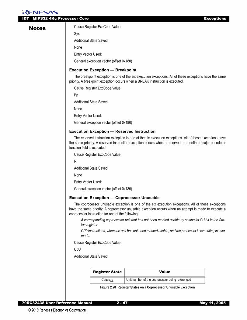
IDT MIPS32 4Kc Processor Core Exceptions
79RC32438 User Refer
Notes
Cause Register ExcCode Value:SysAdditional State Saved:NoneEntry Vector Used:General exception vector (offset 0x180)Execution Exception — BreakpointThe breakpoint exception is one of the six execution exceptions. All of these exceptions have the same
priority. A breakpoint exception occurs when a BREAK instruction is executed.Cause Register ExcCode Value:BpAdditional State Saved:NoneEntry Vector Used:General exception vector (offset 0x180)
Execution Exception — Reserved InstructionThe reserved instruction exception is one of the six execution exceptions. All of these exceptions have
the same priority. A reserved instruction exception occurs when a reserved or undefined major opcode orfunction field is executed.
Cause Register ExcCode Value:RIAdditional State Saved:NoneEntry Vector Used:General exception vector (offset 0x180)
Execution Exception — Coprocessor UnusableThe coprocessor unusable exception is one of the six execution exceptions. All of these exceptions
have the same priority. A coprocessor unusable exception occurs when an attempt is made to execute acoprocessor instruction for one of the following:
A corresponding coprocessor unit that has not been marked usable by setting its CU bit in the Sta-tus registerCP0 instructions, when the unit has not been marked usable, and the processor is executing in user mode.
Cause Register ExcCode Value:CpUAdditional State Saved:
Register State Value
CauseCE Unit number of the coprocessor being referenced
Figure 2.28 Register States on a Coprocessor Unusable Exception
ence Manual 2 - 47 May 11, 2005
IDT MIPS32 4Kc Processor Core Exceptions
79RC32438 User Refer
Notes
Entry Vector Used:General exception vector (offset 0x180)Execution Exception — Integer OverflowThe integer overflow exception is one of the six execution exceptions. All of these exceptions have the
same priority. An integer overflow exception occurs when selected integer instructions result in a 2’scomplement overflow.
Cause Register ExcCode Value:OvAdditional State Saved:NoneEntry Vector Used:General exception vector (offset 0x180)
Execution Exception — TrapThe trap exception is one of the six execution exceptions. All of these exceptions have the same priority.
A trap exception occurs when a trap instruction results in a TRUE value.Cause Register ExcCode Value:TrAdditional State Saved:NoneEntry Vector Used:General exception vector (offset 0x180)
Debug Data Break ExceptionA debug data break exception occurs when a data hardware breakpoint matches the load/store transac-
tion of an executed load/store instruction. The DEPC register and DBD bit in the Debug register will indicatethe load/store instruction that caused the data hardware breakpoint to match. The load/store instruction thatcaused the debug exception has not completed, e.g. not updated the register file, and the instruction can bere-executed after returning from the debug handler.
Debug Register Debug Status Bit Set:DDBL for a load instruction or DDBS for a store instructionAdditional State Saved:NoneEntry Vector Used:Debug exception vector
TLB Modified Exception — Data AccessDuring a data access, a TLB modified exception occurs on a store reference to a mapped address if the
following condition is true:The matching TLB entry in a TLB-based MMU is valid, but not dirty.Cause Register ExcCode Value:ModAdditional State Saved:
ence Manual 2 - 48 May 11, 2005

IDT MIPS32 4Kc Processor Core Exceptions
79RC32438 User Refer
Notes
Entry Vector Used:General exception vector (offset 0x180)
Exception Handling and Servicing FlowchartsThe remainder of this chapter contains flowcharts for the following exceptions and guidelines for their
handlers:General exceptions and their exception handlerTLB miss exceptions and their exception handler (4Kc core)Reset, soft reset and NMI exceptions, and a guideline to their handlerDebug exceptions.
Generally speaking, the exceptions are handled by hardware (HW); the exceptions are then serviced bysoftware (SW). Note that unexpected debug exceptions to the debug exception vector at 0xBFC0_0200may be viewed as a reserved instruction since uncontrolled execution of a SDBBP instruction caused theexception. The DERET instruction must be used at return from the debug exception handler, in order toleave debug mode and return to non-debug mode. The DERET instruction returns to the address in theDEPC register.
Register State Value
BadVAddr Failing address
Context The BadVPN2 field contains VA31:13 of the failing address.
EntryHi The VPN2 field contains VA31:13 of the failing address; the ASID field contains the ASID of the reference that missed.
EntryLo0 UNPREDICTABLE
EntryLo1 UNPREDICTABLE
Table 2.24 Register States on a TLB Modified Exception
ence Manual 2 - 49 May 11, 2005

IDT MIPS32 4Kc Processor Core Exceptions
79RC32438 User Refer
Notes
Figure 2.29 General Exception Handler (HW)
To General Exception Servicing Guidelines
=1 (bootstrap)=0 (normal)Status.BEV
Comments
PC << 0x8000_0000 + 180(unmapped, cached)
PC << 0xBFC0_0200 + 180(unmapped, uncached)
EXL << 1
EPC << (PC - 4) EPC << PC
Instr. in Br.Dly. Slot?
=0
Processor forced to Kernel Mode & interrupt disabled
=0
=1Check if exception within
another exception EXL
EntryHi and Context are set only for TLB Invalid, Modified, & Refill exceptions. BadVA is set only for TLB Invalid, Modified, and Refill exceptions. Note: Not set on Bus Errors.
EntryHi << VPN2, ASIDContext << VPN2
Set Cause EXCCode,CEBadVA << VA
Exceptions other than Reset, Soft Reset, NMI, or first-level TLB miss. Note: Interrupts can be masked by IE or IMs, and Watch is masked if EXL = 1.
ence Manual 2 - 50 May 11, 2005
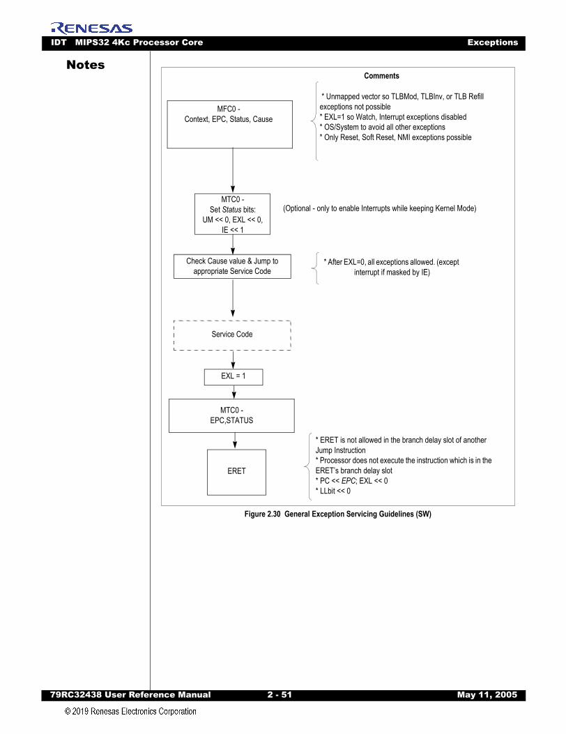
IDT MIPS32 4Kc Processor Core Exceptions
79RC32438 User Refer
Notes
Figure 2.30 General Exception Servicing Guidelines (SW)
ERET
MTC0 -EPC,STATUS
EXL = 1
Service Code
* ERET is not allowed in the branch delay slot of another Jump Instruction* Processor does not execute the instruction which is in the ERET’s branch delay slot* PC << EPC; EXL << 0* LLbit << 0
Check Cause value & Jump to appropriate Service Code
* After EXL=0, all exceptions allowed. (except interrupt if masked by IE)
(Optional - only to enable Interrupts while keeping Kernel Mode)MTC0 -
Set Status bits:UM << 0, EXL << 0,
IE << 1
MFC0 -Context, EPC, Status, Cause
* Unmapped vector so TLBMod, TLBInv, or TLB Refill exceptions not possible* EXL=1 so Watch, Interrupt exceptions disabled* OS/System to avoid all other exceptions* Only Reset, Soft Reset, NMI exceptions possible
Comments
ence Manual 2 - 51 May 11, 2005
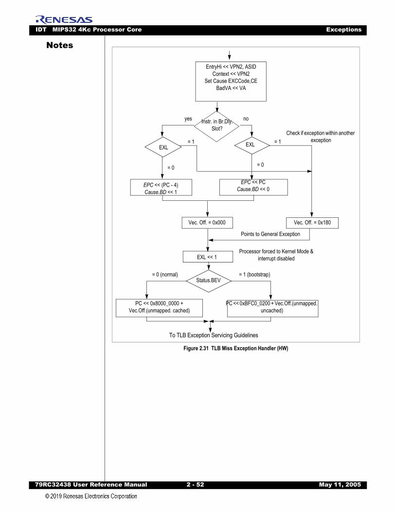
IDT MIPS32 4Kc Processor Core Exceptions
79RC32438 User Refer
Notes
Figure 2.31 TLB Miss Exception Handler (HW)
To TLB Exception Servicing Guidelines
Vec. Off. = 0x180
EPC << (PC - 4)Cause.BD << 1
EPC << PCCause.BD << 0
Vec. Off. = 0x000
EXL << 1
Points to General Exception
Processor forced to Kernel Mode & interrupt disabled
= 0
= 1 (bootstrap)= 0 (normal)
PC << 0x8000_0000 + Vec.Off.(unmapped. cached)
PC << 0xBFC0_0200 + Vec.Off.(unmapped. uncached)
Status.BEV
Check if exception within another exception= 1= 1
= 0
EXL EXL
EntryHi << VPN2, ASIDContext << VPN2
Set Cause EXCCode,CEBadVA << VA
Instr. in Br.Dly. Slot?
noyes
ence Manual 2 - 52 May 11, 2005
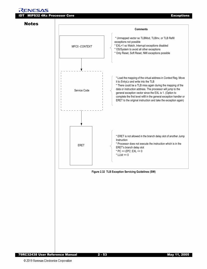
IDT MIPS32 4Kc Processor Core Exceptions
79RC32438 User Refer
Notes
Figure 2.32 TLB Exception Servicing Guidelines (SW)
Comments
ERET
Service Code
MFC0 -CONTEXT
* Unmapped vector so TLBMod, TLBInv, or TLB Refill exceptions not possible* EXL=1 so Watch, Interrupt exceptions disabled* OS/System to avoid all other exceptions* Only Reset, Soft Reset, NMI exceptions possible
* Load the mapping of the virtual address in Context Reg. Move it to EntryLo and write into the TLB* There could be a TLB miss again during the mapping of the data or instruction address. The processor will jump to the general exception vector since the EXL is 1. (Option to complete the first level refill in the general exception handler or ERET to the original instruction and take the exception again)
* ERET is not allowed in the branch delay slot of another Jump Instruction* Processor does not execute the instruction which is in the ERET’s branch delay slot* PC << EPC; EXL << 0* LLbit << 0
ence Manual 2 - 53 May 11, 2005
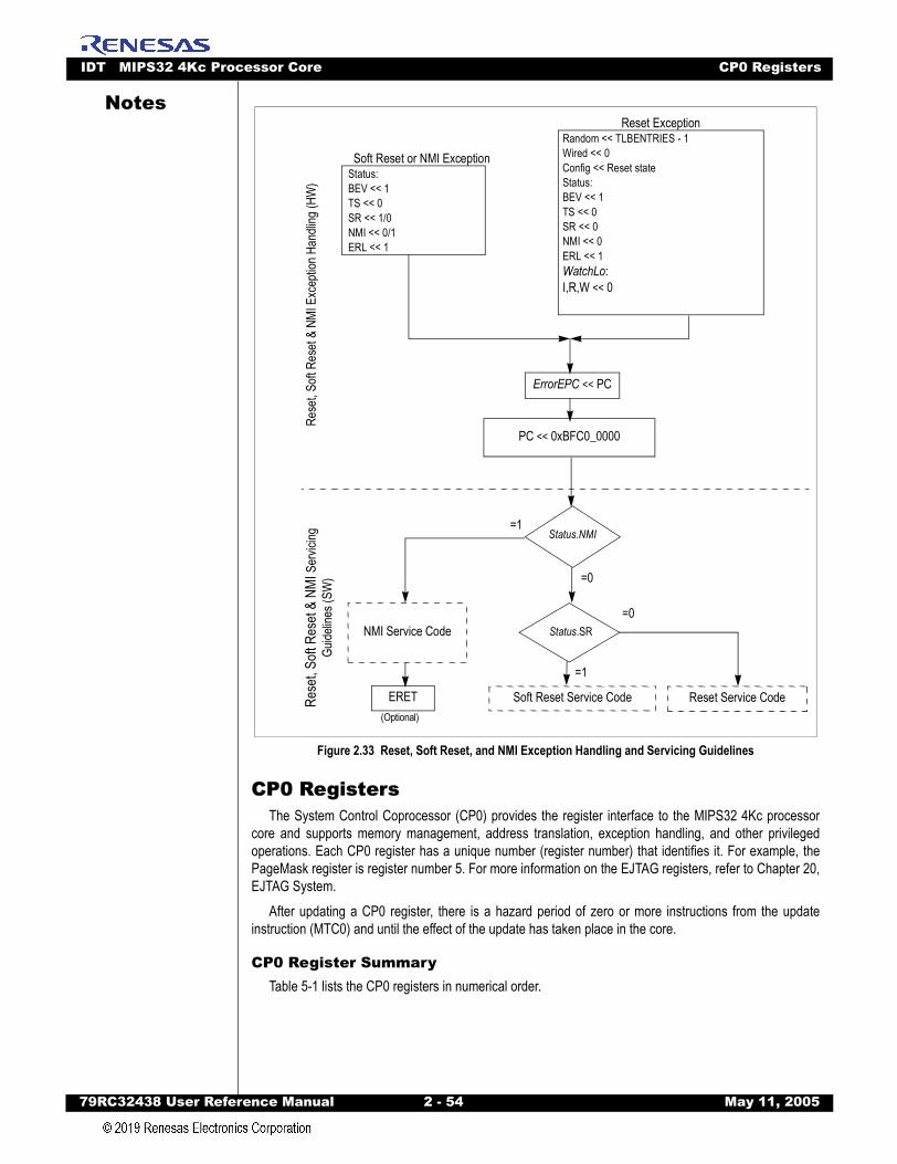
IDT MIPS32 4Kc Processor Core CP0 Registers
79RC32438 User Refer
Notes
Figure 2.33 Reset, Soft Reset, and NMI Exception Handling and Servicing Guidelines
CP0 RegistersThe System Control Coprocessor (CP0) provides the register interface to the MIPS32 4Kc processor
core and supports memory management, address translation, exception handling, and other privilegedoperations. Each CP0 register has a unique number (register number) that identifies it. For example, thePageMask register is register number 5. For more information on the EJTAG registers, refer to Chapter 20,EJTAG System.
After updating a CP0 register, there is a hazard period of zero or more instructions from the updateinstruction (MTC0) and until the effect of the update has taken place in the core.
CP0 Register SummaryTable 5-1 lists the CP0 registers in numerical order.
Status:BEV << 1TS << 0SR << 1/0NMI << 0/1ERL << 1
(Optional)
Reset Service CodeSoft Reset Service Code
NMI Service Code
ERET
=0
=1
=0
=1
Status.SR
Status.NMI
PC << 0xBFC0_0000
ErrorEPC << PC
Random << TLBENTRIES - 1 Wired << 0 Config << Reset stateStatus:BEV << 1TS << 0SR << 0NMI << 0ERL << 1WatchLo:I,R,W << 0
Reset Exception
Soft Reset or NMI Exception
Rese
t, Soft
Res
et &
NMI E
xcep
tion H
andli
ng (H
W)
Rese
t, Soft
Res
et &
NMI S
ervic
ing
Guide
lines
(SW
)
ence Manual 2 - 54 May 11, 2005

IDT MIPS32 4Kc Processor Core CP0 Registers
79RC32438 User Refer
Notes
Register Number Register Name Function0 Index1
1. Registers used in memory management.
Index into the TLB array
1 Random1 Randomly generated index into the TLB array
2 EntryLo01 Low-order portion of the TLB entry for even-num-bered virtual pages
3 EntryLo11 Low-order portion of the TLB entry for odd-num-bered virtual pages
4 Context2
2. Registers used in exception processing.
Pointer to page table entry in memory
5 PageMask1 Controls the variable page sizes in TLB entries
6 Wired1 Controls the number of fixed (“wired”) TLB entries
7 Reserved Reserved
8 BadVAddr2 Reports the address for the most recent address-related exception
9 Count2 Processor cycle count
10 EntryHi1 High-order portion of the TLB entry.
11 Compare2 Timer interrupt control
12 Status2 Processor status and control
13 Cause2 Cause of last exception
14 EPC2 Program counter at last exception
15 PRId Processor identification and revision
16 Config/Config1 Configuration register
17 LLAddr Load linked address
18 WatchLo2 Watchpoint address (low order)
19 WatchHi2 Watchpoint address (high order) and mask
20 - 22 Reserved Reserved
23 Debug3
3. Registers used in debug.
Debug control and exception status
24 DEPC3 Program counter at last debug exception
25 Reserved Reserved
26 ErrCtl Controls access to data and SPRAM arrays for CACHE instruction
27 Reserved Reserved
28 TagLo/DataLo Low-order portion of cache tag interface
29 Reserved Reserved
30 ErrorEPC2 Program counter at last error
31 DESAVE3 Debug handler scratchpad register
Table 2.25 CP0 Registers
ence Manual 2 - 55 May 11, 2005
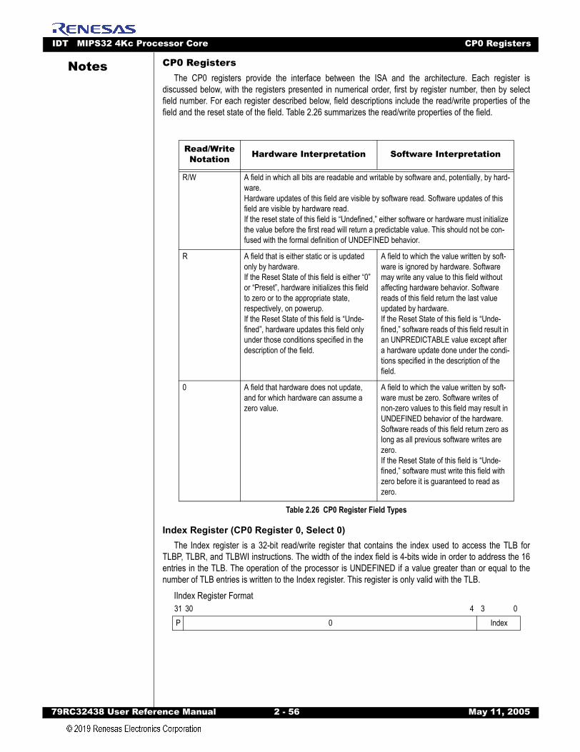
IDT MIPS32 4Kc Processor Core CP0 Registers
79RC32438 User Refer
Notes
CP0 RegistersThe CP0 registers provide the interface between the ISA and the architecture. Each register isdiscussed below, with the registers presented in numerical order, first by register number, then by selectfield number. For each register described below, field descriptions include the read/write properties of thefield and the reset state of the field. Table 2.26 summarizes the read/write properties of the field.
Index Register (CP0 Register 0, Select 0)The Index register is a 32-bit read/write register that contains the index used to access the TLB for
TLBP, TLBR, and TLBWI instructions. The width of the index field is 4-bits wide in order to address the 16entries in the TLB. The operation of the processor is UNDEFINED if a value greater than or equal to thenumber of TLB entries is written to the Index register. This register is only valid with the TLB.
IIndex Register Format
Read/Write Notation Hardware Interpretation Software Interpretation
R/W A field in which all bits are readable and writable by software and, potentially, by hard-ware.Hardware updates of this field are visible by software read. Software updates of this field are visible by hardware read.If the reset state of this field is “Undefined,” either software or hardware must initialize the value before the first read will return a predictable value. This should not be con-fused with the formal definition of UNDEFINED behavior.
R A field that is either static or is updated only by hardware.If the Reset State of this field is either “0” or “Preset”, hardware initializes this field to zero or to the appropriate state, respectively, on powerup.If the Reset State of this field is “Unde-fined”, hardware updates this field only under those conditions specified in the description of the field.
A field to which the value written by soft-ware is ignored by hardware. Software may write any value to this field without affecting hardware behavior. Software reads of this field return the last value updated by hardware.If the Reset State of this field is “Unde-fined,” software reads of this field result in an UNPREDICTABLE value except after a hardware update done under the condi-tions specified in the description of the field.
0 A field that hardware does not update, and for which hardware can assume a zero value.
A field to which the value written by soft-ware must be zero. Software writes of non-zero values to this field may result in UNDEFINED behavior of the hardware. Software reads of this field return zero as long as all previous software writes are zero.If the Reset State of this field is “Unde-fined,” software must write this field with zero before it is guaranteed to read as zero.
Table 2.26 CP0 Register Field Types
31 30 4 3 0P 0 Index
ence Manual 2 - 56 May 11, 2005
IDT MIPS32 4Kc Processor Core CP0 Registers
79RC32438 User Refer
Notes
Random Register (CP0 Register 1, Select 0)The Random register is a read-only register whose value is used to index the TLB during a TLBWR
instruction. The width of the Random field is calculated in the same manner as that described for the Indexregister above.
The value of the register varies between an upper and lower bound as follow:A lower bound is set by the number of TLB entries reserved for exclusive use by the operating sys-tem (the contents of the Wired register). The entry indexed by the Wired register is the first entry available to be written by a TLB Write Random operation.An upper bound is set by the total number of TLB entries minus 1.
The Random register is decremented by one almost every clock wrapping after the value in the Wiredregister is reached. To enhance the level of randomness and reduce the possibility of a live lock condition,an LFSR register is used that prevents the decrement pseudo-randomly.
The processor initializes the Random register to the upper bound on a Reset exception and when theWired register is written.
This register is only valid with the TLB.Random Register Format
EntryLo0, EntryLo1 (CP0 Registers 2 and 3, Select 0)The pair of EntryLo registers act as the interface between the TLB and the TLBR, TLBWI, and TLBWR
instructions. For a TLB-based MMU, EntryLo0 holds the entries for even pages and EntryLo1 holds theentries for odd pages. The contents of the EntryLo0 and EntryLo1 registers are undefined after an addresserror, TLB invalid, TLB modified, or TLB refill exceptions. These registers are only valid with the TLB.
FieldsDescription Read/
WriteReset StateName Bit(s)
P 31 Probe Failure. Set to 1 when the previous TLBProbe (TLBP) instruction failed to find a match in the TLB.
R Undefined
0 30:4 Must be written as zero; returns zero on read. 0 0
Index 3:0 Index to the TLB entry affected by the TLBRead and TLBWrite instructions.
R/W Undefined
Table 2.27 Index Register Field Descriptions
31 4 3 00 Random
FieldsDescription Read/
WriteReset StateName Bit(s)
0 31:4 Must be written as zero; returns zero on read. 0 0
Random 3:0 TLB Random Index R TLB Entries - 1
Table 2.28 Random Register Field Descriptions
ence Manual 2 - 57 May 11, 2005
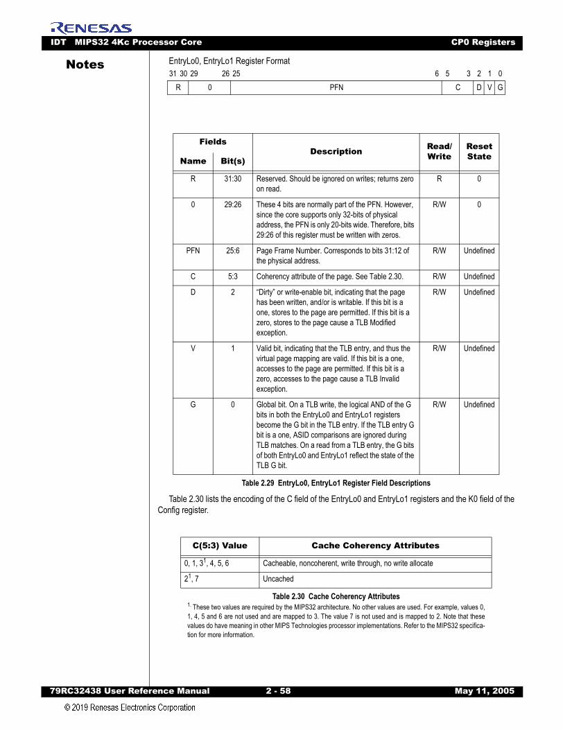
IDT MIPS32 4Kc Processor Core CP0 Registers
79RC32438 User Refer
Notes
EntryLo0, EntryLo1 Register FormatTable 2.30 lists the encoding of the C field of the EntryLo0 and EntryLo1 registers and the K0 field of theConfig register.
31 30 29 26 25 6 5 3 2 1 0R 0 PFN C D V G
FieldsDescription Read/
WriteReset StateName Bit(s)
R 31:30 Reserved. Should be ignored on writes; returns zero on read.
R 0
0 29:26 These 4 bits are normally part of the PFN. However, since the core supports only 32-bits of physical address, the PFN is only 20-bits wide. Therefore, bits 29:26 of this register must be written with zeros.
R/W 0
PFN 25:6 Page Frame Number. Corresponds to bits 31:12 of the physical address.
R/W Undefined
C 5:3 Coherency attribute of the page. See Table 2.30. R/W Undefined
D 2 “Dirty” or write-enable bit, indicating that the page has been written, and/or is writable. If this bit is a one, stores to the page are permitted. If this bit is a zero, stores to the page cause a TLB Modified exception.
R/W Undefined
V 1 Valid bit, indicating that the TLB entry, and thus the virtual page mapping are valid. If this bit is a one, accesses to the page are permitted. If this bit is a zero, accesses to the page cause a TLB Invalid exception.
R/W Undefined
G 0 Global bit. On a TLB write, the logical AND of the G bits in both the EntryLo0 and EntryLo1 registers become the G bit in the TLB entry. If the TLB entry G bit is a one, ASID comparisons are ignored during TLB matches. On a read from a TLB entry, the G bits of both EntryLo0 and EntryLo1 reflect the state of the TLB G bit.
R/W Undefined
Table 2.29 EntryLo0, EntryLo1 Register Field Descriptions
C(5:3) Value Cache Coherency Attributes
0, 1, 31, 4, 5, 6
1. These two values are required by the MIPS32 architecture. No other values are used. For example, values 0,1, 4, 5 and 6 are not used and are mapped to 3. The value 7 is not used and is mapped to 2. Note that thesevalues do have meaning in other MIPS Technologies processor implementations. Refer to the MIPS32 specifica-tion for more information.
Cacheable, noncoherent, write through, no write allocate
21, 7 Uncached
Table 2.30 Cache Coherency Attributes
ence Manual 2 - 58 May 11, 2005
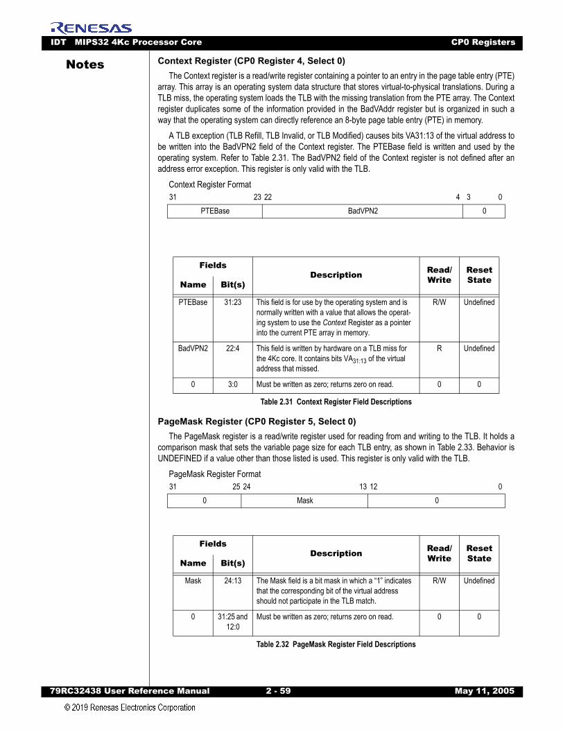
IDT MIPS32 4Kc Processor Core CP0 Registers
79RC32438 User Refer
Notes
Context Register (CP0 Register 4, Select 0)The Context register is a read/write register containing a pointer to an entry in the page table entry (PTE)array. This array is an operating system data structure that stores virtual-to-physical translations. During aTLB miss, the operating system loads the TLB with the missing translation from the PTE array. The Contextregister duplicates some of the information provided in the BadVAddr register but is organized in such away that the operating system can directly reference an 8-byte page table entry (PTE) in memory.
A TLB exception (TLB Refill, TLB Invalid, or TLB Modified) causes bits VA31:13 of the virtual address tobe written into the BadVPN2 field of the Context register. The PTEBase field is written and used by theoperating system. Refer to Table 2.31. The BadVPN2 field of the Context register is not defined after anaddress error exception. This register is only valid with the TLB.
Context Register Format
PageMask Register (CP0 Register 5, Select 0)The PageMask register is a read/write register used for reading from and writing to the TLB. It holds a
comparison mask that sets the variable page size for each TLB entry, as shown in Table 2.33. Behavior isUNDEFINED if a value other than those listed is used. This register is only valid with the TLB.
PageMask Register Format
31 23 22 4 3 0PTEBase BadVPN2 0
FieldsDescription Read/
WriteReset StateName Bit(s)
PTEBase 31:23 This field is for use by the operating system and is normally written with a value that allows the operat-ing system to use the Context Register as a pointer into the current PTE array in memory.
R/W Undefined
BadVPN2 22:4 This field is written by hardware on a TLB miss for the 4Kc core. It contains bits VA31:13 of the virtual address that missed.
R Undefined
0 3:0 Must be written as zero; returns zero on read. 0 0
Table 2.31 Context Register Field Descriptions
31 25 24 13 12 00 Mask 0
FieldsDescription Read/
WriteReset StateName Bit(s)
Mask 24:13 The Mask field is a bit mask in which a “1” indicates that the corresponding bit of the virtual address should not participate in the TLB match.
R/W Undefined
0 31:25 and 12:0
Must be written as zero; returns zero on read. 0 0
Table 2.32 PageMask Register Field Descriptions
ence Manual 2 - 59 May 11, 2005

IDT MIPS32 4Kc Processor Core CP0 Registers
79RC32438 User Refer
Notes
Wired Register (CP0 Register 6, Select 0)The Wired register is a read/write register that specifies the boundary between the wired and random
entries in the TLB as shown in Figure 2.34. The width of the Wired field is calculated in the same manner asthat described for the Index register above. Wired entries are fixed, non-replaceable entries that are notoverwritten by a TLBWR instruction. Wired entries can be overwritten by a TLBWI instruction. The Wiredregister is set to zero by a Reset exception. Writing the Wired register causes the Random register to resetto its upper bound. The operation of the processor is undefined if a value greater than or equal to thenumber of TLB entries is written to the Wired register. This register is only valid with a TLB.
Figure 2.34 Wired and Random Entries in the TLB
Wired Register Format
Page SizeBit
24 23 22 21 20 19 18 17 16 15 14 13
4 KBytes 0 0 0 0 0 0 0 0 0 0 0 0
16 KBytes 0 0 0 0 0 0 0 0 0 0 1 1
64 KBytes 0 0 0 0 0 0 0 0 1 1 1 1
256 KBytes 0 0 0 0 0 0 1 1 1 1 1 1
1 MByte 0 0 0 0 1 1 1 1 1 1 1 1
4 MByte 0 0 1 1 1 1 1 1 1 1 1 1
16 Mbyte 1 1 1 1 1 1 1 1 1 1 1 1
Table 2.33 Values for the Mask Field of the PageMask Register
31 4 3 00 Wired
Entry 0
Entry 10
Entry n-1
10Wired Register
Wire
dRa
ndom
ence Manual 2 - 60 May 11, 2005
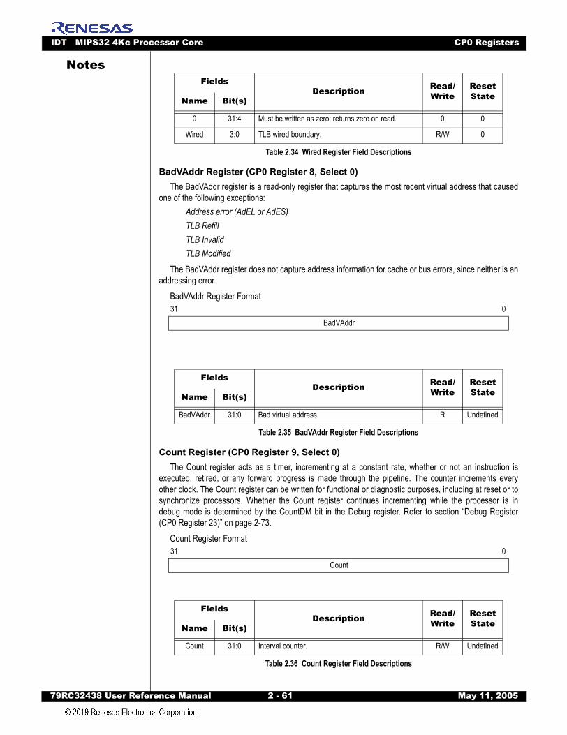
IDT MIPS32 4Kc Processor Core CP0 Registers
79RC32438 User Refer
Notes
BadVAddr Register (CP0 Register 8, Select 0)The BadVAddr register is a read-only register that captures the most recent virtual address that caused
one of the following exceptions:Address error (AdEL or AdES)TLB Refill TLB InvalidTLB Modified
The BadVAddr register does not capture address information for cache or bus errors, since neither is anaddressing error.
BadVAddr Register Format
Count Register (CP0 Register 9, Select 0)The Count register acts as a timer, incrementing at a constant rate, whether or not an instruction is
executed, retired, or any forward progress is made through the pipeline. The counter increments everyother clock. The Count register can be written for functional or diagnostic purposes, including at reset or tosynchronize processors. Whether the Count register continues incrementing while the processor is indebug mode is determined by the CountDM bit in the Debug register. Refer to section “Debug Register(CP0 Register 23)” on page 2-73.
Count Register Format
FieldsDescription Read/
WriteReset StateName Bit(s)
0 31:4 Must be written as zero; returns zero on read. 0 0
Wired 3:0 TLB wired boundary. R/W 0
Table 2.34 Wired Register Field Descriptions
31 0BadVAddr
FieldsDescription Read/
WriteReset StateName Bit(s)
BadVAddr 31:0 Bad virtual address R Undefined
Table 2.35 BadVAddr Register Field Descriptions
31 0Count
FieldsDescription Read/
WriteReset StateName Bit(s)
Count 31:0 Interval counter. R/W Undefined
Table 2.36 Count Register Field Descriptions
ence Manual 2 - 61 May 11, 2005
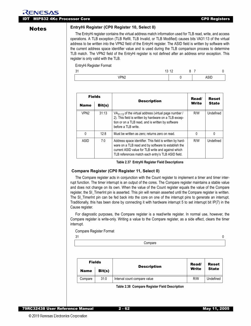
IDT MIPS32 4Kc Processor Core CP0 Registers
79RC32438 User Refer
Notes
EntryHi Register (CP0 Register 10, Select 0)The EntryHi register contains the virtual address match information used for TLB read, write, and accessoperations. A TLB exception (TLB Refill, TLB Invalid, or TLB Modified) causes bits VA31:13 of the virtualaddress to be written into the VPN2 field of the EntryHi register. The ASID field is written by software withthe current address space identifier value and is used during the TLB comparison process to determineTLB match. The VPN2 field of the EntryHi register is not defined after an address error exception. Thisregister is only valid with the TLB.
EntryHi Register Format
Compare Register (CP0 Register 11, Select 0)The Compare register acts in conjunction with the Count register to implement a timer and timer inter-
rupt function. The timer interrupt is an output of the cores. The Compare register maintains a stable valueand does not change on its own. When the value of the Count register equals the value of the Compareregister, the SI_TimerInt pin is asserted. This pin will remain asserted until the Compare register is written.The SI_TimerInt pin can be fed back into the core on one of the interrupt pins to generate an interrupt.Traditionally, this has been done by connecting it with hardware interrupt 5 to set interrupt bit IP(7) in theCause register.
For diagnostic purposes, the Compare register is a read/write register. In normal use, however, theCompare register is write-only. Writing a value to the Compare register, as a side effect, clears the timerinterrupt.
Compare Register Format
31 13 12 8 7 0VPN2 0 ASID
FieldsDescription Read/
WriteReset StateName Bit(s)
VPN2 31:13 VA31:13 of the virtual address (virtual page number / 2). This field is written by hardware on a TLB excep-tion or on a TLB read, and is written by software before a TLB write.
R/W Undefined
0 12:8 Must be written as zero; returns zero on read. 0 0
ASID 7:0 Address space identifier. This field is written by hard-ware on a TLB read and by software to establish the current ASID value for TLB write and against which TLB references match each entry’s TLB ASID field.
R/W Undefined
Table 2.37 EntryHi Register Field Descriptions
31 0Compare
FieldsDescription Read/
WriteReset StateName Bit(s)
Compare 31:0 Interval count compare value R/W Undefined
Table 2.38 Compare Register Field Description
ence Manual 2 - 62 May 11, 2005
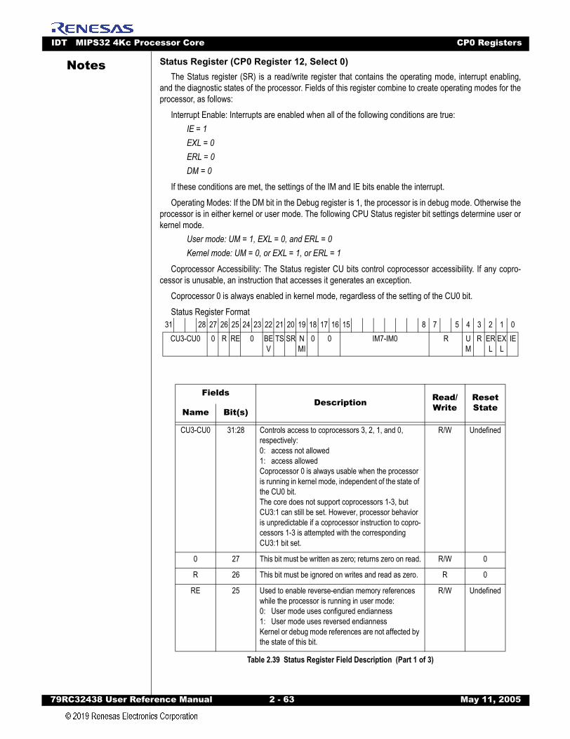
IDT MIPS32 4Kc Processor Core CP0 Registers
79RC32438 User Refer
Notes
Status Register (CP0 Register 12, Select 0)The Status register (SR) is a read/write register that contains the operating mode, interrupt enabling,and the diagnostic states of the processor. Fields of this register combine to create operating modes for theprocessor, as follows:
Interrupt Enable: Interrupts are enabled when all of the following conditions are true:IE = 1EXL = 0ERL = 0DM = 0
If these conditions are met, the settings of the IM and IE bits enable the interrupt. Operating Modes: If the DM bit in the Debug register is 1, the processor is in debug mode. Otherwise the
processor is in either kernel or user mode. The following CPU Status register bit settings determine user orkernel mode.
User mode: UM = 1, EXL = 0, and ERL = 0Kernel mode: UM = 0, or EXL = 1, or ERL = 1
Coprocessor Accessibility: The Status register CU bits control coprocessor accessibility. If any copro-cessor is unusable, an instruction that accesses it generates an exception.
Coprocessor 0 is always enabled in kernel mode, regardless of the setting of the CU0 bit.Status Register Format
31 28 27 26 25 24 23 22 21 20 19 18 17 16 15 8 7 5 4 3 2 1 0CU3-CU0 0 R RE 0 BE
VTS SR N
MI0 0 IM7-IM0 R U
MR ER
LEXL
IE
FieldsDescription Read/
WriteReset StateName Bit(s)
CU3-CU0 31:28 Controls access to coprocessors 3, 2, 1, and 0, respectively:0: access not allowed1: access allowedCoprocessor 0 is always usable when the processor is running in kernel mode, independent of the state of the CU0 bit.The core does not support coprocessors 1-3, but CU3:1 can still be set. However, processor behavior is unpredictable if a coprocessor instruction to copro-cessors 1-3 is attempted with the corresponding CU3:1 bit set.
R/W Undefined
0 27 This bit must be written as zero; returns zero on read. R/W 0
R 26 This bit must be ignored on writes and read as zero. R 0
RE 25 Used to enable reverse-endian memory references while the processor is running in user mode:0: User mode uses configured endianness1: User mode uses reversed endiannessKernel or debug mode references are not affected by the state of this bit.
R/W Undefined
Table 2.39 Status Register Field Description (Part 1 of 3)
ence Manual 2 - 63 May 11, 2005
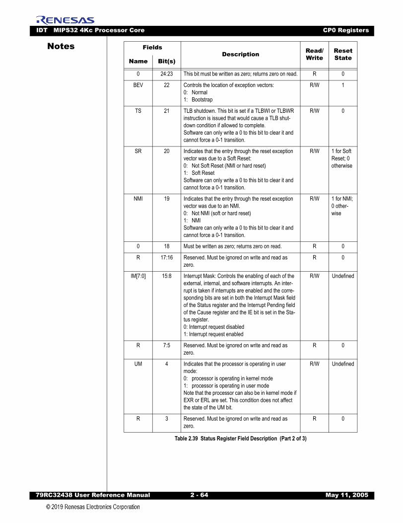
IDT MIPS32 4Kc Processor Core CP0 Registers
79RC32438 User Refer
Notes
0 24:23 This bit must be written as zero; returns zero on read. R 0
BEV 22 Controls the location of exception vectors:0: Normal1: Bootstrap
R/W 1
TS 21 TLB shutdown. This bit is set if a TLBWI or TLBWR instruction is issued that would cause a TLB shut-down condition if allowed to complete.Software can only write a 0 to this bit to clear it and cannot force a 0-1 transition.
R/W 0
SR 20 Indicates that the entry through the reset exception vector was due to a Soft Reset:0: Not Soft Reset (NMI or hard reset)1: Soft ResetSoftware can only write a 0 to this bit to clear it and cannot force a 0-1 transition.
R/W 1 for Soft Reset; 0 otherwise
NMI 19 Indicates that the entry through the reset exception vector was due to an NMI.0: Not NMI (soft or hard reset)1: NMISoftware can only write a 0 to this bit to clear it and cannot force a 0-1 transition.
R/W 1 for NMI; 0 other-wise
0 18 Must be written as zero; returns zero on read. R 0
R 17:16 Reserved. Must be ignored on write and read as zero.
R 0
IM[7:0] 15:8 Interrupt Mask: Controls the enabling of each of the external, internal, and software interrupts. An inter-rupt is taken if interrupts are enabled and the corre-sponding bits are set in both the Interrupt Mask field of the Status register and the Interrupt Pending field of the Cause register and the IE bit is set in the Sta-tus register.0: Interrupt request disabled1: Interrupt request enabled
R/W Undefined
R 7:5 Reserved. Must be ignored on write and read as zero.
R 0
UM 4 Indicates that the processor is operating in user mode:0: processor is operating in kernel mode1: processor is operating in user modeNote that the processor can also be in kernel mode if EXR or ERL are set. This condition does not affect the state of the UM bit.
R/W Undefined
R 3 Reserved. Must be ignored on write and read as zero.
R 0
FieldsDescription Read/
WriteReset StateName Bit(s)
Table 2.39 Status Register Field Description (Part 2 of 3)
ence Manual 2 - 64 May 11, 2005
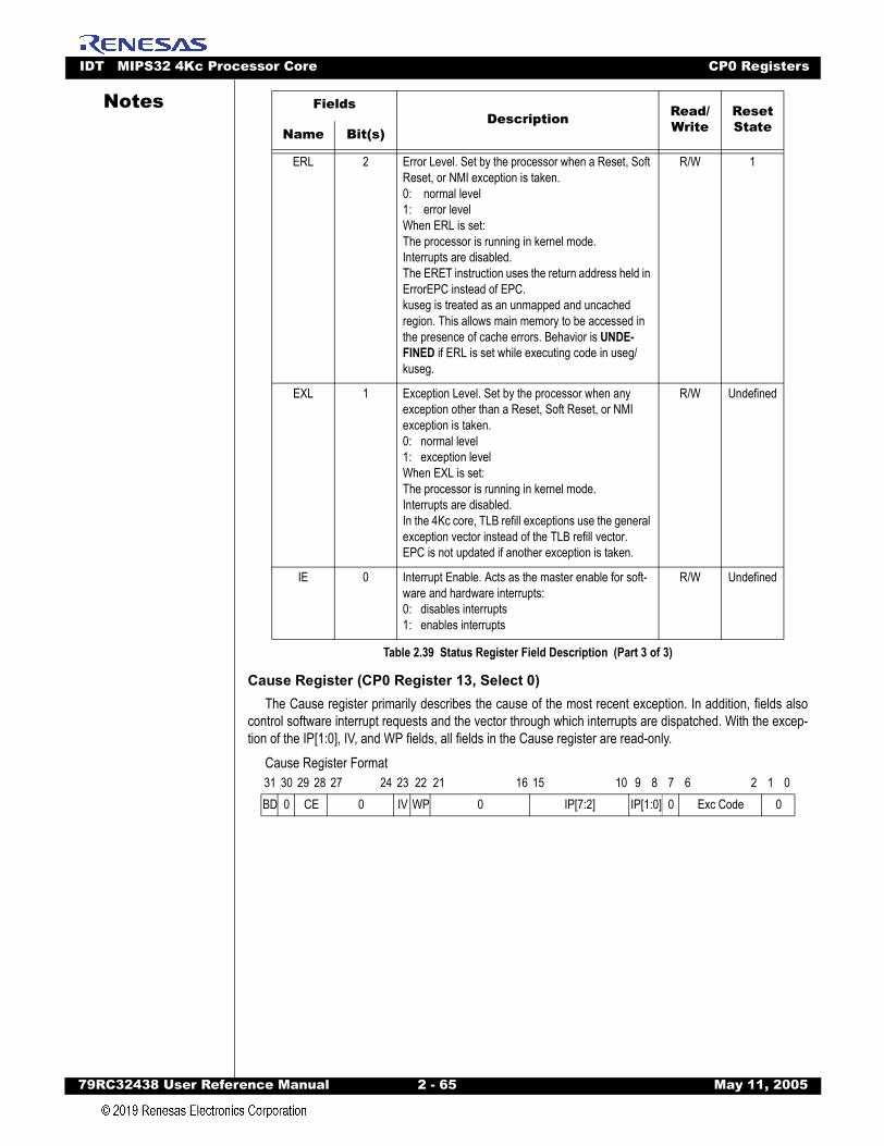
IDT MIPS32 4Kc Processor Core CP0 Registers
79RC32438 User Refer
Notes
Cause Register (CP0 Register 13, Select 0)The Cause register primarily describes the cause of the most recent exception. In addition, fields also
control software interrupt requests and the vector through which interrupts are dispatched. With the excep-tion of the IP[1:0], IV, and WP fields, all fields in the Cause register are read-only.
Cause Register Format
ERL 2 Error Level. Set by the processor when a Reset, Soft Reset, or NMI exception is taken.0: normal level1: error levelWhen ERL is set:The processor is running in kernel mode.Interrupts are disabled.The ERET instruction uses the return address held in ErrorEPC instead of EPC.kuseg is treated as an unmapped and uncached region. This allows main memory to be accessed in the presence of cache errors. Behavior is UNDE-FINED if ERL is set while executing code in useg/kuseg.
R/W 1
EXL 1 Exception Level. Set by the processor when any exception other than a Reset, Soft Reset, or NMI exception is taken.0: normal level1: exception levelWhen EXL is set:The processor is running in kernel mode.Interrupts are disabled.In the 4Kc core, TLB refill exceptions use the general exception vector instead of the TLB refill vector.EPC is not updated if another exception is taken.
R/W Undefined
IE 0 Interrupt Enable. Acts as the master enable for soft-ware and hardware interrupts:0: disables interrupts1: enables interrupts
R/W Undefined
31 30 29 28 27 24 23 22 21 16 15 10 9 8 7 6 2 1 0BD 0 CE 0 IV WP 0 IP[7:2] IP[1:0] 0 Exc Code 0
FieldsDescription Read/
WriteReset StateName Bit(s)
Table 2.39 Status Register Field Description (Part 3 of 3)
ence Manual 2 - 65 May 11, 2005

IDT MIPS32 4Kc Processor Core CP0 Registers
79RC32438 User Refer
Notes
FieldsDescription Read/Write
Reset StateName Bit(s)
BD 31 Indicates whether the last exception taken occurred in a branch delay slot:0: Not in delay slot1: In delay slotNote that the BD bit is not updated on a new excep-tion if the EXL bit is set.
R Undefined
CE 29:28 Coprocessor unit number referenced when a Copro-cessor Unusable exception is taken. This field is loaded by hardware on every exception but is unpre-dictable for all exceptions except for Coprocessor Unusable.
R Undefined
IV 23 Indicates whether an interrupt exception uses the general exception vector or a special interrupt vector:0: Use the general exception vector (0x180)1: Use the special interrupt vector (0x200)
R/W Undefined
WP 22 Indicates that a watch exception was deferred because StatusEXL or StatusERL were a one at the time the watch exception was detected. This bit both indicates that the watch exception was deferred and causes the exception to be initiated once StatusEXL and StatusERL are both zero. As such, software must clear this bit as part of the watch exception handler to prevent a watch exception loop.Software can only write a 0 to this bit to clear it and cannot force a 0-1 transition.
R/W Undefined
IP[7:2] 15:10 Indicates an external interrupt is pending:15: Hardware interrupt 5 or timer interrupt 14: Hardware interrupt 413: Hardware interrupt 312: Hardware interrupt 211: Hardware interrupt 110: Hardware interrupt 0
R Undefined
IP[1:0] 9:8 Controls the request for software interrupts:9: Request software interrupt 18: Request software interrupt 0
R/W Undefined
Exc Code 6:2 Exception code — see Table 2.41. R Undefined
0 30, 27:24, 21:16, 7,
1:0
Must be written as zero; returns zero on read. R 0
Table 2.40 Cause Register Field Descriptions
ence Manual 2 - 66 May 11, 2005
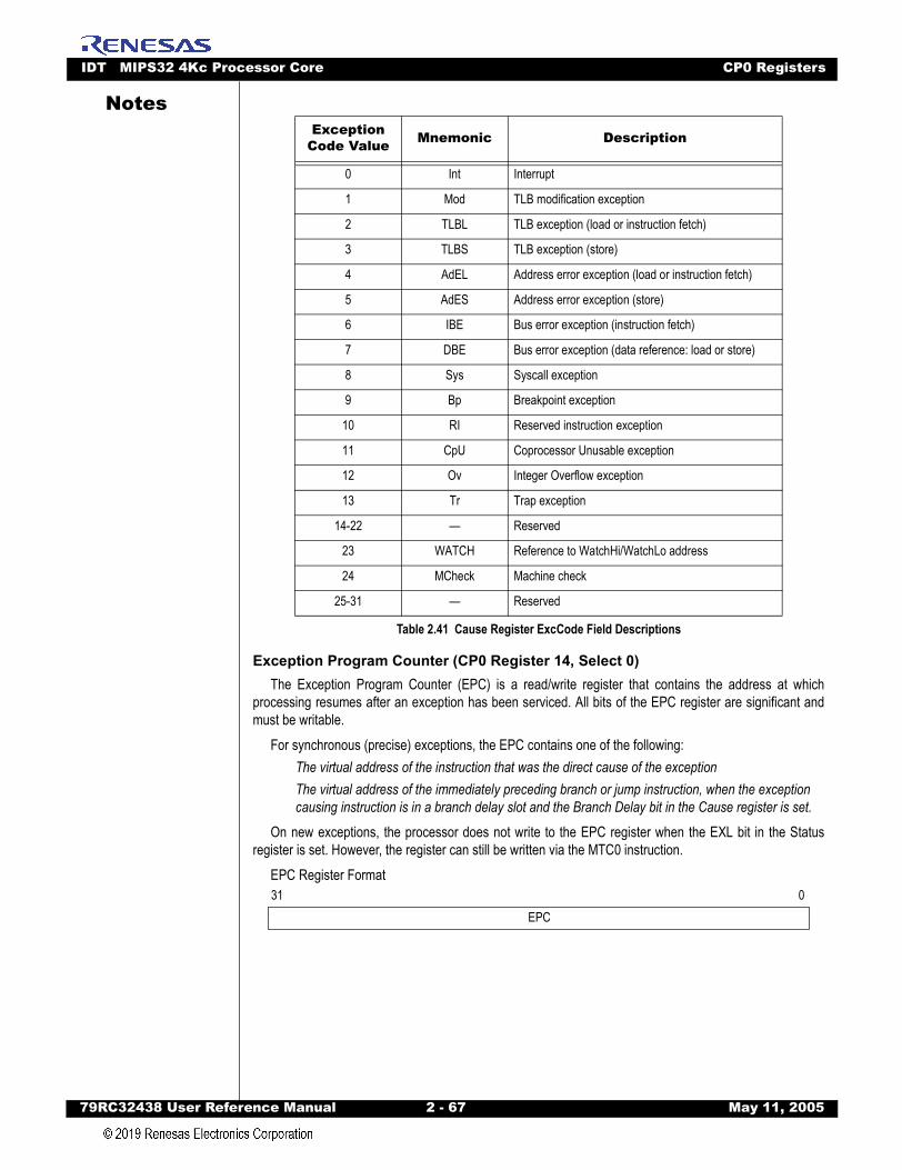
IDT MIPS32 4Kc Processor Core CP0 Registers
79RC32438 User Refer
Notes
Exception Program Counter (CP0 Register 14, Select 0)The Exception Program Counter (EPC) is a read/write register that contains the address at which
processing resumes after an exception has been serviced. All bits of the EPC register are significant andmust be writable.
For synchronous (precise) exceptions, the EPC contains one of the following:The virtual address of the instruction that was the direct cause of the exceptionThe virtual address of the immediately preceding branch or jump instruction, when the exception causing instruction is in a branch delay slot and the Branch Delay bit in the Cause register is set.
On new exceptions, the processor does not write to the EPC register when the EXL bit in the Statusregister is set. However, the register can still be written via the MTC0 instruction.
EPC Register Format
Exception Code Value Mnemonic Description
0 Int Interrupt
1 Mod TLB modification exception
2 TLBL TLB exception (load or instruction fetch)
3 TLBS TLB exception (store)
4 AdEL Address error exception (load or instruction fetch)
5 AdES Address error exception (store)
6 IBE Bus error exception (instruction fetch)
7 DBE Bus error exception (data reference: load or store)
8 Sys Syscall exception
9 Bp Breakpoint exception
10 RI Reserved instruction exception
11 CpU Coprocessor Unusable exception
12 Ov Integer Overflow exception
13 Tr Trap exception
14-22 — Reserved
23 WATCH Reference to WatchHi/WatchLo address
24 MCheck Machine check
25-31 — Reserved
Table 2.41 Cause Register ExcCode Field Descriptions
31 0EPC
ence Manual 2 - 67 May 11, 2005
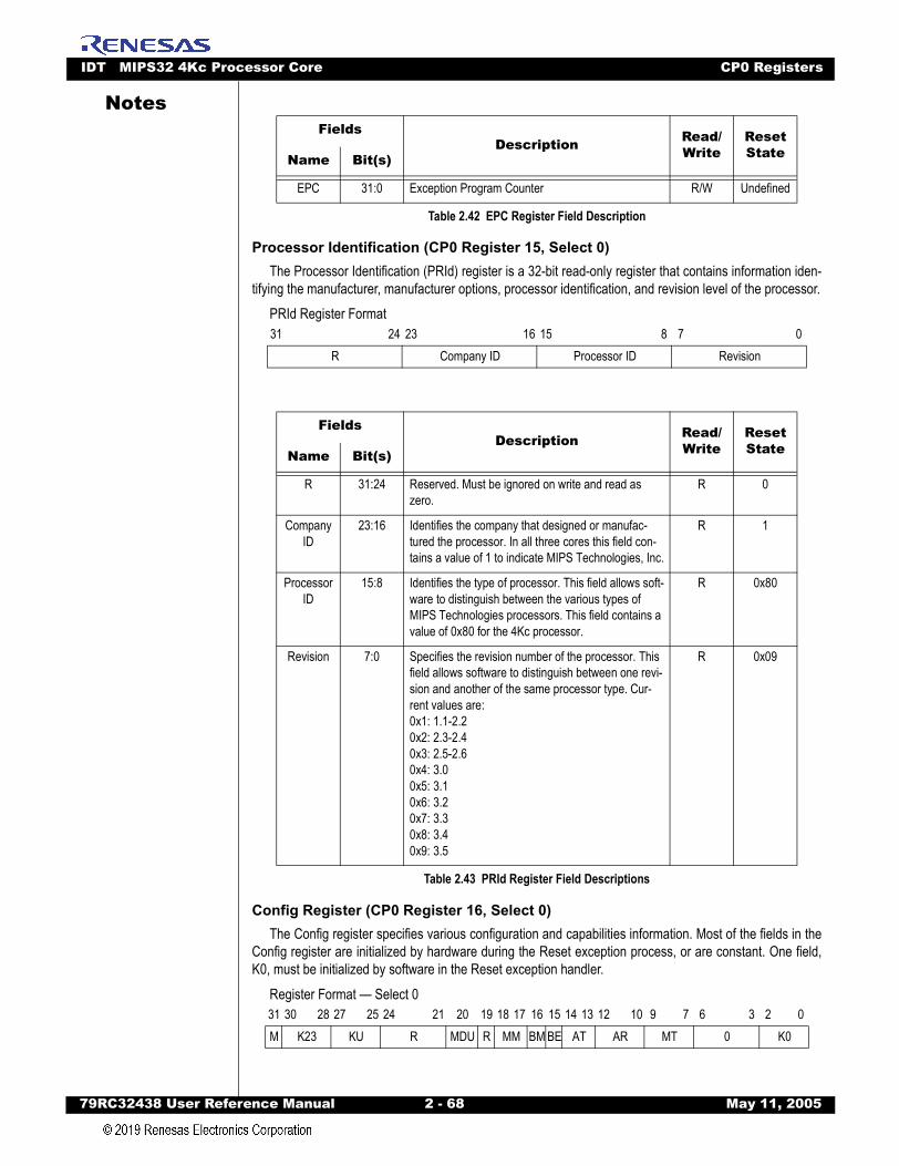
IDT MIPS32 4Kc Processor Core CP0 Registers
79RC32438 User Refer
Notes
Processor Identification (CP0 Register 15, Select 0)The Processor Identification (PRId) register is a 32-bit read-only register that contains information iden-
tifying the manufacturer, manufacturer options, processor identification, and revision level of the processor.PRId Register Format
Config Register (CP0 Register 16, Select 0)The Config register specifies various configuration and capabilities information. Most of the fields in the
Config register are initialized by hardware during the Reset exception process, or are constant. One field,K0, must be initialized by software in the Reset exception handler.
Register Format — Select 0
FieldsDescription Read/
WriteReset StateName Bit(s)
EPC 31:0 Exception Program Counter R/W Undefined
Table 2.42 EPC Register Field Description
31 24 23 16 15 8 7 0R Company ID Processor ID Revision
FieldsDescription Read/
WriteReset StateName Bit(s)
R 31:24 Reserved. Must be ignored on write and read as zero.
R 0
Company ID
23:16 Identifies the company that designed or manufac-tured the processor. In all three cores this field con-tains a value of 1 to indicate MIPS Technologies, Inc.
R 1
Processor ID
15:8 Identifies the type of processor. This field allows soft-ware to distinguish between the various types of MIPS Technologies processors. This field contains a value of 0x80 for the 4Kc processor.
R 0x80
Revision 7:0 Specifies the revision number of the processor. This field allows software to distinguish between one revi-sion and another of the same processor type. Cur-rent values are:0x1: 1.1-2.20x2: 2.3-2.40x3: 2.5-2.60x4: 3.00x5: 3.10x6: 3.20x7: 3.30x8: 3.40x9: 3.5
R 0x09
Table 2.43 PRId Register Field Descriptions
31 30 28 27 25 24 21 20 19 18 17 16 15 14 13 12 10 9 7 6 3 2 0M K23 KU R MDU R MM BM BE AT AR MT 0 K0
ence Manual 2 - 68 May 11, 2005
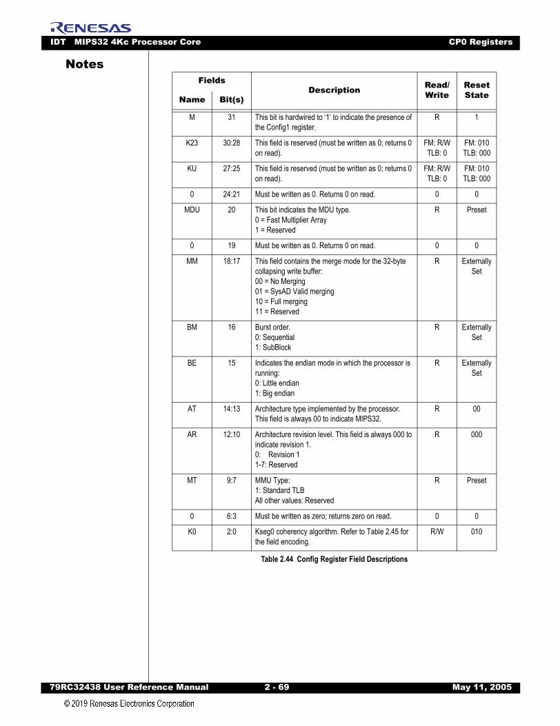
IDT MIPS32 4Kc Processor Core CP0 Registers
79RC32438 User Refer
Notes
FieldsDescription Read/Write
Reset StateName Bit(s)
M 31 This bit is hardwired to ‘1’ to indicate the presence of the Config1 register.
R 1
K23 30:28 This field is reserved (must be written as 0; returns 0 on read).
FM: R/WTLB: 0
FM: 010TLB: 000
KU 27:25 This field is reserved (must be written as 0; returns 0 on read).
FM: R/W TLB: 0
FM: 010TLB: 000
0 24:21 Must be written as 0. Returns 0 on read. 0 0
MDU 20 This bit indicates the MDU type.0 = Fast Multiplier Array1 = Reserved
R Preset
0 19 Must be written as 0. Returns 0 on read. 0 0
MM 18:17 This field contains the merge mode for the 32-byte collapsing write buffer:00 = No Merging01 = SysAD Valid merging10 = Full merging11 = Reserved
R Externally Set
BM 16 Burst order. 0: Sequential1: SubBlock
R Externally Set
BE 15 Indicates the endian mode in which the processor is running:0: Little endian1: Big endian
R Externally Set
AT 14:13 Architecture type implemented by the processor. This field is always 00 to indicate MIPS32.
R 00
AR 12:10 Architecture revision level. This field is always 000 to indicate revision 1.0: Revision 11-7: Reserved
R 000
MT 9:7 MMU Type:1: Standard TLB All other values: Reserved
R Preset
0 6:3 Must be written as zero; returns zero on read. 0 0
K0 2:0 Kseg0 coherency algorithm. Refer to Table 2.45 for the field encoding.
R/W 010
Table 2.44 Config Register Field Descriptions
ence Manual 2 - 69 May 11, 2005
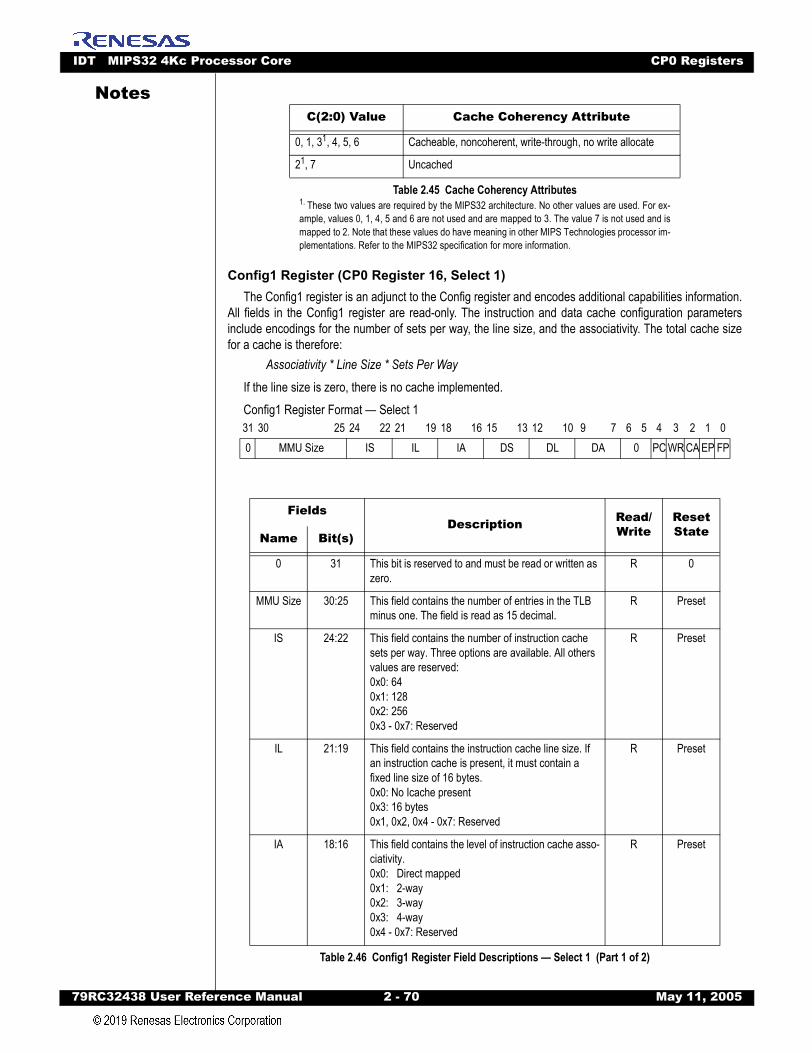
IDT MIPS32 4Kc Processor Core CP0 Registers
79RC32438 User Refer
Notes
Config1 Register (CP0 Register 16, Select 1)The Config1 register is an adjunct to the Config register and encodes additional capabilities information.
All fields in the Config1 register are read-only. The instruction and data cache configuration parametersinclude encodings for the number of sets per way, the line size, and the associativity. The total cache sizefor a cache is therefore:
Associativity * Line Size * Sets Per Way
If the line size is zero, there is no cache implemented.Config1 Register Format — Select 1
C(2:0) Value Cache Coherency Attribute
0, 1, 31, 4, 5, 6
1. These two values are required by the MIPS32 architecture. No other values are used. For ex-ample, values 0, 1, 4, 5 and 6 are not used and are mapped to 3. The value 7 is not used and ismapped to 2. Note that these values do have meaning in other MIPS Technologies processor im-plementations. Refer to the MIPS32 specification for more information.
Cacheable, noncoherent, write-through, no write allocate
21, 7 Uncached
Table 2.45 Cache Coherency Attributes
31 30 25 24 22 21 19 18 16 15 13 12 10 9 7 6 5 4 3 2 1 00 MMU Size IS IL IA DS DL DA 0 PC WR CA EP FP
FieldsDescription Read/
WriteReset StateName Bit(s)
0 31 This bit is reserved to and must be read or written as zero.
R 0
MMU Size 30:25 This field contains the number of entries in the TLB minus one. The field is read as 15 decimal.
R Preset
IS 24:22 This field contains the number of instruction cache sets per way. Three options are available. All others values are reserved:0x0: 640x1: 1280x2: 2560x3 - 0x7: Reserved
R Preset
IL 21:19 This field contains the instruction cache line size. If an instruction cache is present, it must contain a fixed line size of 16 bytes.0x0: No Icache present0x3: 16 bytes0x1, 0x2, 0x4 - 0x7: Reserved
R Preset
IA 18:16 This field contains the level of instruction cache asso-ciativity.0x0: Direct mapped0x1: 2-way0x2: 3-way0x3: 4-way0x4 - 0x7: Reserved
R Preset
Table 2.46 Config1 Register Field Descriptions — Select 1 (Part 1 of 2)
ence Manual 2 - 70 May 11, 2005

IDT MIPS32 4Kc Processor Core CP0 Registers
79RC32438 User Refer
Notes
Load Linked Address (CP0 Register 17, Select 0)The LLAddr register contains the physical address read by the most recent Load Linked (LL) instruction.
This register is for diagnostic purposes only, and serves no function during normal operation.LLAddr Register Format
DS 15:13 This field contains the number of data cache sets per way:0x0: 640x1: 1280x2: 2560x3 - 0x7: Reserved
R Preset
DL 12:10 This field contains the data cache line size. If a data cache is present, it must contain a line size of 16 bytes.0x0: No Dcache present0x3: 16 bytes0x1, 0x2, 0x4 - 0x7: Reserved
R Preset
DA 9:7 This field contains the type of set associativity for the data cache:0x0: Direct mapped0x1: 2-way0x2: 3-way0x3: 4-way0x4 - 0x7: Reserved
R Preset
0 6:5 Must be written as zero; returns zero on read. 0 0
PC 4 Performance Counter registers implemented. Always a 0 since the cores do not implement any.
R 0
WR 3 Watch registers implemented. This bit always reads as 1 since the cores each contain one pair of Watch registers.
R 1
CA 2 Code compression (MIPS16™) implemented. This bit always reads as 0 because MIPS16 is not sup-ported.
R 0
EP 1 EJTAG present: This bit is always set to indicate that the core implements EJTAG.
R 1
FP 0 FPU implemented. This bit is always zero since the core does not contain a floating-point unit.
R 0
31 28 27 00 PAddr[31:4]
FieldsDescription Read/
WriteReset StateName Bit(s)
Table 2.46 Config1 Register Field Descriptions — Select 1 (Part 2 of 2)
ence Manual 2 - 71 May 11, 2005
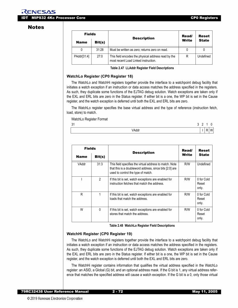
IDT MIPS32 4Kc Processor Core CP0 Registers
79RC32438 User Refer
Notes
WatchLo Register (CP0 Register 18)The WatchLo and WatchHi registers together provide the interface to a watchpoint debug facility that
initiates a watch exception if an instruction or data access matches the address specified in the registers.As such, they duplicate some functions of the EJTAG debug solution. Watch exceptions are taken only ifthe EXL and ERL bits are zero in the Status register. If either bit is a one, the WP bit is set in the Causeregister, and the watch exception is deferred until both the EXL and ERL bits are zero.
The WatchLo register specifies the base virtual address and the type of reference (instruction fetch,load, store) to match.
WatchLo Register Format
WatchHi Register (CP0 Register 19)The WatchLo and WatchHi registers together provide the interface to a watchpoint debug facility that
initiates a watch exception if an instruction or data access matches the address specified in the registers.As such, they duplicate some functions of the EJTAG debug solution. Watch exceptions are taken only ifthe EXL and ERL bits are zero in the Status register. If either bit is a one, the WP bit is set in the Causeregister, and the watch exception is deferred until both the EXL and ERL bits are zero.
The WatchHi register contains information that qualifies the virtual address specified in the WatchLoregister: an ASID, a Global (G) bit, and an optional address mask. If the G bit is 1, any virtual address refer-ence that matches the specified address will cause a watch exception. If the G bit is a 0, only those virtual
FieldsDescription Read/
WriteReset StateName Bit(s)
0 31:28 Must be written as zero; returns zero on read. 0 0
PAddr[31:4] 27:0 This field encodes the physical address read by the most recent Load Linked instruction.
R Undefined
Table 2.47 LLAddr Register Field Descriptions
31 3 2 1 0VAddr I R W
FieldsDescription Read/
WriteReset StateName Bit(s)
VAddr 31:3 This field specifies the virtual address to match. Note that this is a doubleword address, since bits [2:0] are used to control the type of match.
R/W Undefined
I 2 If this bit is set, watch exceptions are enabled for instruction fetches that match the address.
R/W 0 for Cold Reset only.
R 1 If this bit is set, watch exceptions are enabled for loads that match the address.
R/W 0 for Cold Reset only.
W 0 If this bit is set, watch exceptions are enabled for stores that match the address.
R/W 0 for Cold Reset only.
Table 2.48 WatchLo Register Field Descriptions
ence Manual 2 - 72 May 11, 2005
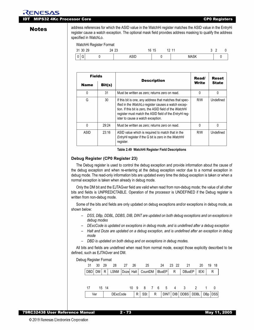
IDT MIPS32 4Kc Processor Core CP0 Registers
79RC32438 User Refer
Notes
address references for which the ASID value in the WatchHi register matches the ASID value in the EntryHiregister cause a watch exception. The optional mask field provides address masking to qualify the addressspecified in WatchLo.WatchHi Register Format
Debug Register (CP0 Register 23)The Debug register is used to control the debug exception and provide information about the cause of
the debug exception and when re-entering at the debug exception vector due to a normal exception indebug mode. The read-only information bits are updated every time the debug exception is taken or when anormal exception is taken when already in debug mode.
Only the DM bit and the EJTAGver field are valid when read from non-debug mode; the value of all otherbits and fields is UNPREDICTABLE. Operation of the processor is UNDEFINED if the Debug register iswritten from non-debug mode.
Some of the bits and fields are only updated on debug exceptions and/or exceptions in debug mode, asshown below:
– DSS, DBp, DDBL, DDBS, DIB, DINT are updated on both debug exceptions and on exceptions indebug modes
– DExcCode is updated on exceptions in debug mode, and is undefined after a debug exception– Halt and Doze are updated on a debug exception, and is undefined after an exception in debug
mode– DBD is updated on both debug and on exceptions in debug modes.
All bits and fields are undefined when read from normal mode, except those explicitly described to bedefined, such as EJTAGver and DM.
Debug Register Format
31 30 29 24 23 16 15 12 11 3 2 00 G 0 ASID 0 MASK 0
FieldsDescription Read/
WriteReset StateName Bit(s)
0 31 Must be written as zero; returns zero on read. 0 0
G 30 If this bit is one, any address that matches that spec-ified in the WatchLo register causes a watch excep-tion. If this bit is zero, the ASID field of the WatchHi register must match the ASID field of the EntryHi reg-ister to cause a watch exception.
R/W Undefined
0 29:24 Must be written as zero; returns zero on read. 0 0
ASID 23:16 ASID value which is required to match that in the EntryHi register if the G bit is zero in the WatchHi register.
R/W Undefined
Table 2.49 WatchHi Register Field Descriptions
31 30 29 28 27 26 25 24 23 22 21 20 19 18DBD DM R LSNM Doze Halt CountDM IBusEP R DBusEP IEXI R
17 15 14 10 9 8 7 6 5 4 3 2 1 0Ver DExcCode R SSt R DINT DIB DDBS DDBL DBp DSS
ence Manual 2 - 73 May 11, 2005

IDT MIPS32 4Kc Processor Core CP0 Registers
79RC32438 User Refer
Notes
FieldsDescription Read/Write
Reset StateName Bit(s)
DBD 31 Indicates whether the last debug exception or excep-tion in debug mode, occurred in a branch delay slot:0: Not in delay slot1: In delay slot
R Undefined
DM 30 Indicates that the processor is operating in debug mode:0: Processor is operating in non-debug mode1: Processor is operating in debug mode
R 0
R 29 Reserved. Must be written as zero; returns zero on read.
R 0
LSNM 28 Controls access of load/store between dseg and main memory:0: Load/stores in dseg address range goes to dseg.1: Load/stores in dseg address range goes to main memory.
R/W 0
Doze 27 Indicates that the processor was in any kind of low power mode when a debug exception occurred:0: Processor not in low power mode when debug exception occurred1: Processor in low power mode when debug excep-tion occurred
R Undefined
Halt 26 Indicates that the internal system bus clock was stopped when the debug exception occurred:0: Internal system bus clock stopped1: Internal system bus clock running
R Undefined
CountDM 25 Indicates the Count register behavior in debug mode. Encoding of the bit is:0: Count register stopped in debug mode1: Count register increments in debug mode
R/W 1
IBusEP 24 Instruction fetch Bus Error exception Pending. Set when an instruction fetch bus error event occurs or if a 1 is written to the bit by software. Cleared when a Bus Error Exception on Instruction Fetch is taken by the processor, and by reset. If IBusEP is set when IEXI is cleared, a Bus Error exception on instruction fetch is taken by the processor, and IBusEP is cleared.
R/W1 0
R 23:22 Reserved. Must be written as zero; returns zero on read.
R 0
DBusEP 21 Data access Bus Error exception Pending. Covers imprecise bus errors on data access, similar to behavior of IBusEP for imprecise bus errors on an instruction fetch.
R/W1 0
Table 2.50 Debug Register Field Descriptions (Part 1 of 2)
ence Manual 2 - 74 May 11, 2005
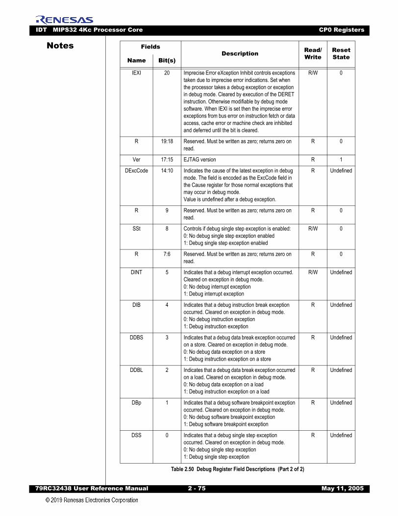
IDT MIPS32 4Kc Processor Core CP0 Registers
79RC32438 User Refer
Notes
IEXI 20 Imprecise Error eXception Inhibit controls exceptions taken due to imprecise error indications. Set when the processor takes a debug exception or exception in debug mode. Cleared by execution of the DERET instruction. Otherwise modifiable by debug mode software. When IEXI is set then the imprecise error exceptions from bus error on instruction fetch or data access, cache error or machine check are inhibited and deferred until the bit is cleared.
R/W 0
R 19:18 Reserved. Must be written as zero; returns zero on read.
R 0
Ver 17:15 EJTAG version R 1
DExcCode 14:10 Indicates the cause of the latest exception in debug mode. The field is encoded as the ExcCode field in the Cause register for those normal exceptions that may occur in debug mode.Value is undefined after a debug exception.
R Undefined
R 9 Reserved. Must be written as zero; returns zero on read.
R 0
SSt 8 Controls if debug single step exception is enabled:0: No debug single step exception enabled1: Debug single step exception enabled
R/W 0
R 7:6 Reserved. Must be written as zero; returns zero on read.
R 0
DINT 5 Indicates that a debug interrupt exception occurred. Cleared on exception in debug mode.0: No debug interrupt exception1: Debug interrupt exception
R/W Undefined
DIB 4 Indicates that a debug instruction break exception occurred. Cleared on exception in debug mode.0: No debug instruction exception1: Debug instruction exception
R Undefined
DDBS 3 Indicates that a debug data break exception occurred on a store. Cleared on exception in debug mode.0: No debug data exception on a store1: Debug instruction exception on a store
R Undefined
DDBL 2 Indicates that a debug data break exception occurred on a load. Cleared on exception in debug mode.0: No debug data exception on a load1: Debug instruction exception on a load
R Undefined
DBp 1 Indicates that a debug software breakpoint exception occurred. Cleared on exception in debug mode.0: No debug software breakpoint exception1: Debug software breakpoint exception
R Undefined
DSS 0 Indicates that a debug single step exception occurred. Cleared on exception in debug mode.0: No debug single step exception1: Debug single step exception
R Undefined
FieldsDescription Read/
WriteReset StateName Bit(s)
Table 2.50 Debug Register Field Descriptions (Part 2 of 2)
ence Manual 2 - 75 May 11, 2005
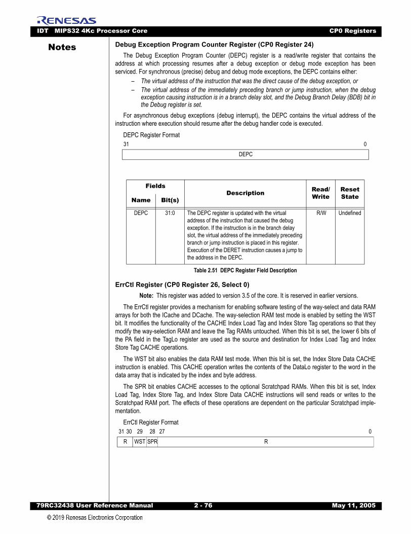
IDT MIPS32 4Kc Processor Core CP0 Registers
79RC32438 User Refer
Notes
Debug Exception Program Counter Register (CP0 Register 24)The Debug Exception Program Counter (DEPC) register is a read/write register that contains theaddress at which processing resumes after a debug exception or debug mode exception has beenserviced. For synchronous (precise) debug and debug mode exceptions, the DEPC contains either:
– The virtual address of the instruction that was the direct cause of the debug exception, or– The virtual address of the immediately preceding branch or jump instruction, when the debug
exception causing instruction is in a branch delay slot, and the Debug Branch Delay (BDB) bit inthe Debug register is set.
For asynchronous debug exceptions (debug interrupt), the DEPC contains the virtual address of theinstruction where execution should resume after the debug handler code is executed.
DEPC Register Format
ErrCtl Register (CP0 Register 26, Select 0)Note: This register was added to version 3.5 of the core. It is reserved in earlier versions.
The ErrCtl register provides a mechanism for enabling software testing of the way-select and data RAMarrays for both the ICache and DCache. The way-selection RAM test mode is enabled by setting the WSTbit. It modifies the functionality of the CACHE Index Load Tag and Index Store Tag operations so that theymodify the way-selection RAM and leave the Tag RAMs untouched. When this bit is set, the lower 6 bits ofthe PA field in the TagLo register are used as the source and destination for Index Load Tag and IndexStore Tag CACHE operations.
The WST bit also enables the data RAM test mode. When this bit is set, the Index Store Data CACHEinstruction is enabled. This CACHE operation writes the contents of the DataLo register to the word in thedata array that is indicated by the index and byte address.
The SPR bit enables CACHE accesses to the optional Scratchpad RAMs. When this bit is set, IndexLoad Tag, Index Store Tag, and Index Store Data CACHE instructions will send reads or writes to theScratchpad RAM port. The effects of these operations are dependent on the particular Scratchpad imple-mentation.
ErrCtl Register Format
31 0DEPC
FieldsDescription Read/
WriteReset StateName Bit(s)
DEPC 31:0 The DEPC register is updated with the virtual address of the instruction that caused the debug exception. If the instruction is in the branch delay slot, the virtual address of the immediately preceding branch or jump instruction is placed in this register. Execution of the DERET instruction causes a jump to the address in the DEPC.
R/W Undefined
Table 2.51 DEPC Register Field Description
31 30 29 28 27 0R WST SPR R
ence Manual 2 - 76 May 11, 2005
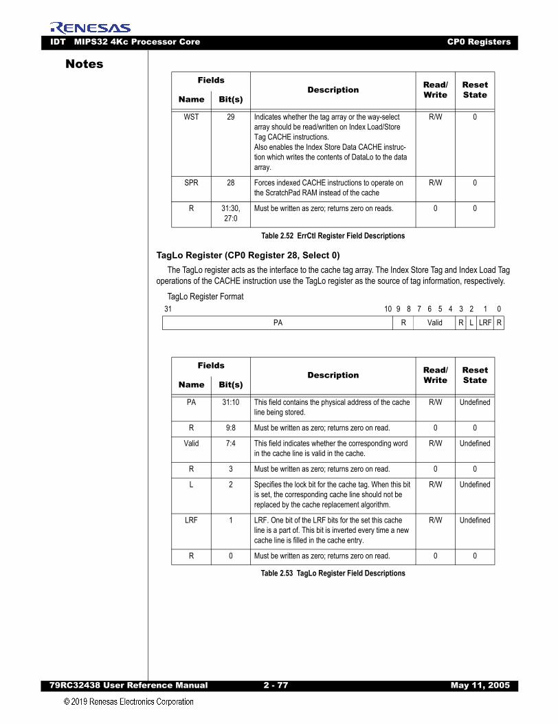
IDT MIPS32 4Kc Processor Core CP0 Registers
79RC32438 User Refer
Notes
TagLo Register (CP0 Register 28, Select 0)The TagLo register acts as the interface to the cache tag array. The Index Store Tag and Index Load Tag
operations of the CACHE instruction use the TagLo register as the source of tag information, respectively.TagLo Register Format
FieldsDescription Read/
WriteReset StateName Bit(s)
WST 29 Indicates whether the tag array or the way-select array should be read/written on Index Load/Store Tag CACHE instructions.Also enables the Index Store Data CACHE instruc-tion which writes the contents of DataLo to the data array.
R/W 0
SPR 28 Forces indexed CACHE instructions to operate on the ScratchPad RAM instead of the cache
R/W 0
R 31:30, 27:0
Must be written as zero; returns zero on reads. 0 0
Table 2.52 ErrCtl Register Field Descriptions
31 10 9 8 7 6 5 4 3 2 1 0PA R Valid R L LRF R
FieldsDescription Read/
WriteReset StateName Bit(s)
PA 31:10 This field contains the physical address of the cache line being stored.
R/W Undefined
R 9:8 Must be written as zero; returns zero on read. 0 0
Valid 7:4 This field indicates whether the corresponding word in the cache line is valid in the cache.
R/W Undefined
R 3 Must be written as zero; returns zero on read. 0 0
L 2 Specifies the lock bit for the cache tag. When this bit is set, the corresponding cache line should not be replaced by the cache replacement algorithm.
R/W Undefined
LRF 1 LRF. One bit of the LRF bits for the set this cache line is a part of. This bit is inverted every time a new cache line is filled in the cache entry.
R/W Undefined
R 0 Must be written as zero; returns zero on read. 0 0
Table 2.53 TagLo Register Field Descriptions
ence Manual 2 - 77 May 11, 2005
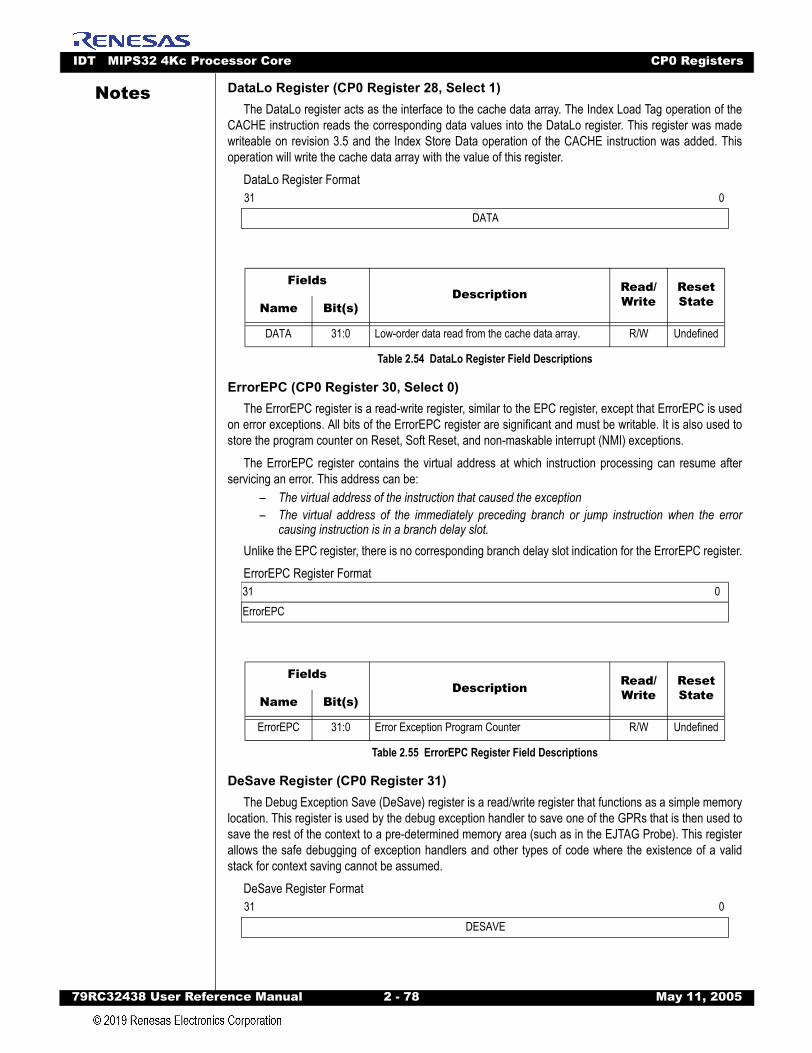
IDT MIPS32 4Kc Processor Core CP0 Registers
79RC32438 User Refer
Notes
DataLo Register (CP0 Register 28, Select 1)The DataLo register acts as the interface to the cache data array. The Index Load Tag operation of theCACHE instruction reads the corresponding data values into the DataLo register. This register was madewriteable on revision 3.5 and the Index Store Data operation of the CACHE instruction was added. Thisoperation will write the cache data array with the value of this register.
DataLo Register Format
ErrorEPC (CP0 Register 30, Select 0)The ErrorEPC register is a read-write register, similar to the EPC register, except that ErrorEPC is used
on error exceptions. All bits of the ErrorEPC register are significant and must be writable. It is also used tostore the program counter on Reset, Soft Reset, and non-maskable interrupt (NMI) exceptions.
The ErrorEPC register contains the virtual address at which instruction processing can resume afterservicing an error. This address can be:
– The virtual address of the instruction that caused the exception– The virtual address of the immediately preceding branch or jump instruction when the error
causing instruction is in a branch delay slot.Unlike the EPC register, there is no corresponding branch delay slot indication for the ErrorEPC register.ErrorEPC Register Format
DeSave Register (CP0 Register 31)The Debug Exception Save (DeSave) register is a read/write register that functions as a simple memory
location. This register is used by the debug exception handler to save one of the GPRs that is then used tosave the rest of the context to a pre-determined memory area (such as in the EJTAG Probe). This registerallows the safe debugging of exception handlers and other types of code where the existence of a validstack for context saving cannot be assumed.
DeSave Register Format
31 0DATA
FieldsDescription Read/
WriteReset StateName Bit(s)
DATA 31:0 Low-order data read from the cache data array. R/W Undefined
Table 2.54 DataLo Register Field Descriptions
31 0ErrorEPC
FieldsDescription Read/
WriteReset StateName Bit(s)
ErrorEPC 31:0 Error Exception Program Counter R/W Undefined
Table 2.55 ErrorEPC Register Field Descriptions
31 0DESAVE
ence Manual 2 - 78 May 11, 2005

IDT MIPS32 4Kc Processor Core Hardware and Software Initialization
79RC32438 User Refer
Notes
Hardware and Software InitializationThe 4Kc processor core is not fully initialized by reset. Only a minimal subset of the processor state is
cleared. This is enough to bring the core up while running in unmapped and uncached code space. All otherprocessor states can then be initialized by software. SI_ColdReset is asserted after power-up to bring thedevice into a known state. Soft reset can be forced by asserting the SI_Reset pin. This can be used whenthe device is already up and running and does not need as much initialization.
Hardware Initialized Processor State
Coprocessor Zero StateMuch of the hardware initialization occurs in Coprocessor Zero.
– Random - set to maximum value on Reset– Wired - set to 0 on Reset– StatusBEV - set to 1 on Reset/SoftReset– StatusTS - cleared to 0 on Reset/SoftReset– StatusSR - cleared to 0 on Reset, set to 1 on SoftReset– StatusNMI - cleared to 0 on Reset/SoftReset– StatusERL - set to 1 on Reset/SoftReset– WatchLoI,R,W - cleared to 0 on Reset– Config fields related to static inputs - set to input value by Reset– ConfigK0 - set to 010 (uncached) on Reset– DebugDM - cleared to 0 on Reset/SoftReset (unless EJTAGBOOT option is used to boot
into DebugMode (see the EJTAG Debug Support section for more information)– DebugLSNM - cleared to 0 on Reset/SoftReset– DebugIBusEP - cleared to 0 on Reset/SoftReset– DebugDBusEP - cleared to 0 on Reset/SoftReset– DebugIEXI - cleared to 0 on Reset/SoftReset– DebugSSt - cleared to 0 on Reset/SoftReset.
TLB InitializationEach TLB entry has a “hidden” state bit which is set by Reset/SoftReset and is cleared when the TLB
entry is written. This bit disables matches and prevents “TLB Shutdown” conditions from being generatedby the power-up values in the TLB array (when two or more TLB entries match on a single address). This bitis not visible to software.
Bus State MachinesAll pending bus transactions are aborted and the state machines in the bus interface unit are reset when
a Reset or SoftReset exception is taken.
Static Configuration InputsAll static configuration inputs (defining the bus mode and cache size for example) should only be
changed during Reset.
FieldsDescription Read/
WriteReset StateName Bit(s)
DESAVE 31:0 Debug exception save contents. R/W Undefined
Table 2.56 DeSave Register Field Descriptions
ence Manual 2 - 79 May 11, 2005

IDT MIPS32 4Kc Processor Core Caches
79RC32438 User Refer
Notes
Fetch AddressUpon Reset/SoftReset, unless the EJTAGBOOT option is used, the fetch is directed to VA 0xBFC00000(PA 0x1FC00000). This address is in kseg1, which is unmapped and uncached, so that the TLB and cachesdo not require hardware unitization.
Software Initialized Processor StateSoftware is required to initialize the following parts of the device.
Register FileThe register file powers up in an unknown state with the exception of r0 which is always 0. Initializing the
rest of the register file is not required for proper operation. Good code will generally not read a registerbefore writing to it, but the boot code can initialize the register file for added safety.
TLBBecause of the hidden bit indicating initialization, the 4Kc processor core does not require TLB initializa-
tion upon ColdReset. This is a feature of the 4Kc core.Note: When initializing the TLB, care must be taken to avoid creating a “TLB Shutdown” condition where two TLB entries could match on a single address. Unique virtual addresses should be written to each TLB entry to avoid this.
CachesThe cache tag and data arrays power up to an unknown state and are not affected by reset. Every tag in
the cache arrays should be initialized to an invalid state using the CACHE instruction (typically the IndexInvalidate function). This can be a long process, especially since the instruction cache initialization needs tobe run in an uncached address region.
Coprocessor Zero StateMiscellaneous Cop0 states need to be initialized prior to leaving the boot code. There are various
exceptions that are blocked by ERL=1 or EXL=1 and that are not cleared by Reset. These can be cleared toavoid taking spurious exceptions when leaving the boot code.
Cause: WP (Watch Pending), SW0/1 (Software Interrupts) should be cleared.Config: K0 should be set to the desired Cache Coherency Algorithm (CCA) prior to accessing kseg0.Count: Should be set to a known value if Timer Interrupts are used.Compare: Should be set to a known value if Timer Interrupts are used. The write to compare will also clear any pending Timer Interrupts (Thus, Count should be set before Compare to avoid any unexpected interrupts).Status: Desired state of the device should be set.Other Cop0 state: Other registers should be written before they are read. Some registers are not explicitly writable, and are only updated as a by-product of instruction execution or a taken excep-tion. Uninitialized bits should be masked off after reading these registers.
CachesThe 4Kc processor core supports separate instruction and data caches which may be flexibly configured
at build time for various sizes, organizations, and set-associativities. The use of separate caches allowsinstruction and data references to proceed simultaneously. Both caches are virtually indexed and physicallytagged, allowing cache access to occur in parallel with virtual-to-physical address translation. The instruc-tion and data caches are independently configured. Each cache is accessed in a single processor cycle.
ence Manual 2 - 80 May 11, 2005
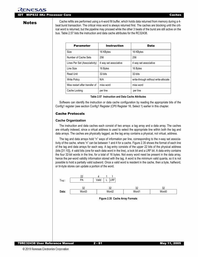
IDT MIPS32 4Kc Processor Core Caches
79RC32438 User Refer
Notes
Cache refills are performed using a 4-word fill buffer, which holds data returned from memory during a 4-beat burst transaction. The critical miss word is always returned first. The caches are blocking until the crit-ical word is returned, but the pipeline may proceed while the other 3 beats of the burst are still active on thebus. Table 2.57 lists the instruction and data cache attributes for the RC32438.Software can identify the instruction or data cache configuration by reading the appropriate bits of theConfig1 register (see section Config1 Register (CP0 Register 16, Select 1) earlier in this chapter.
Cache Protocols
Cache OrganizationThe instruction and data caches each consist of two arrays: a tag array and a data array. The caches
are virtually indexed, since a virtual address is used to select the appropriate line within both the tag anddata arrays. The caches are physically tagged, as the tag array contains a physical, not virtual, address.
The tag and data arrays hold “n” ways of information per line, corresponding to the n-way set associa-tivity of the cache, where “n” can be between 1 and 4 for a cache. Figure 2.35 shows the format of each lineof the tag and data arrays for each way. A tag entry consists of the upper 22 bits of the physical address(bits [31:10]), 4 valid bits (one for each data word in the line), a lock bit and a LRF bit. A data entry containsthe four 32-bit words in the line, for a total of 16 bytes. Not every word need be present in the data array,hence the per-word validity information stored with the tag. A word is the minimum valid quanta, so it is notpossible to hold a partially valid subword. Once a valid word is resident in the cache, then a byte, halfword,or tri-byte stores can update a portion of the word.
Figure 2.35 Cache Array Formats
Parameter Instruction Data
Size 16 KBytes 16 KBytes
Number of Cache Sets 256 256
Lines Per Set (Associativity) 4 way set associative 4 way set associative
Line Size 16 Bytes 16 Bytes
Read Unit 32-bits 32-bits
Write Policy N/A write-through without write-allocate
Miss restart after transfer of miss word miss word
Cache Locking per line per line
Table 2.57 Instruction and Data Cache Attributes
Tag:
Data: Word3 Word2 Word1 Word0
PA Valid L LRF
32 32 32 32
22 4 1 1
ence Manual 2 - 81 May 11, 2005
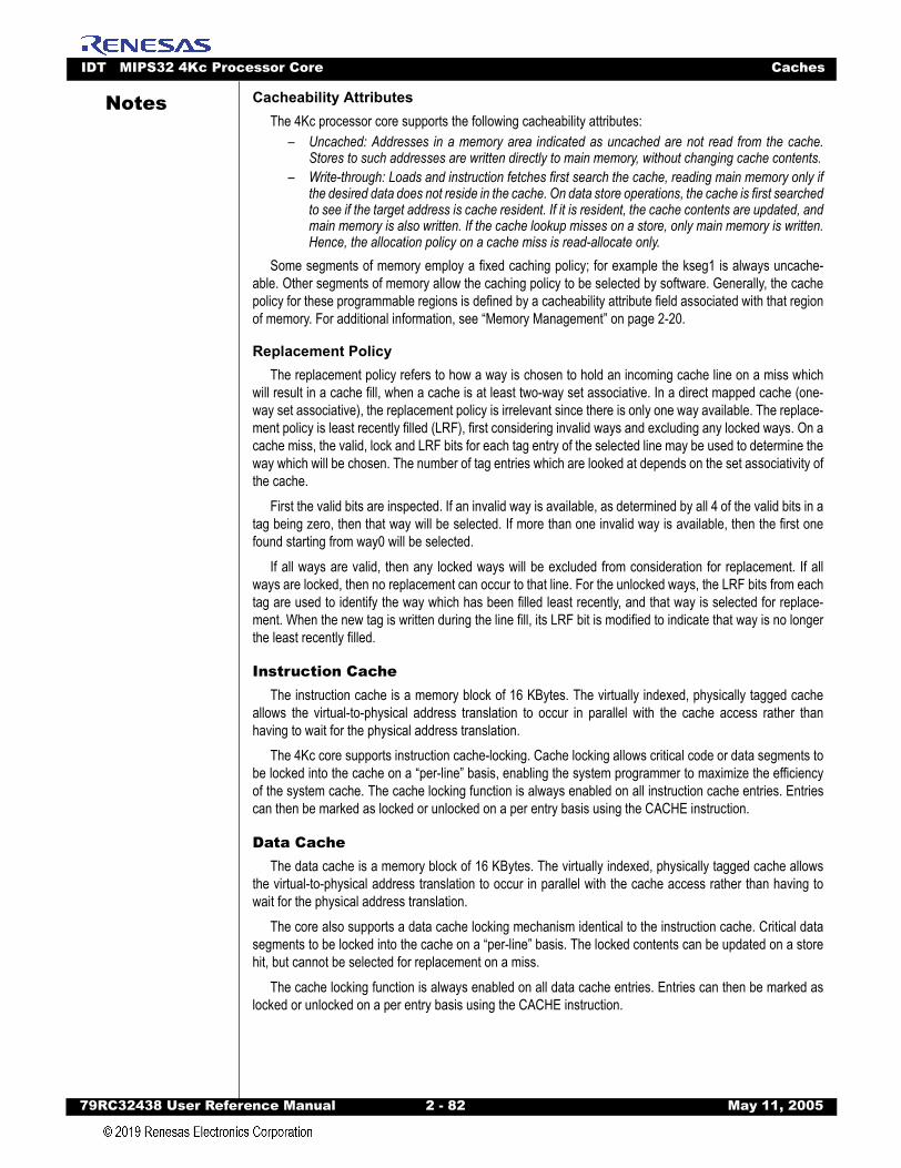
IDT MIPS32 4Kc Processor Core Caches
79RC32438 User Refer
Notes
Cacheability AttributesThe 4Kc processor core supports the following cacheability attributes:– Uncached: Addresses in a memory area indicated as uncached are not read from the cache.Stores to such addresses are written directly to main memory, without changing cache contents.
– Write-through: Loads and instruction fetches first search the cache, reading main memory only ifthe desired data does not reside in the cache. On data store operations, the cache is first searchedto see if the target address is cache resident. If it is resident, the cache contents are updated, andmain memory is also written. If the cache lookup misses on a store, only main memory is written.Hence, the allocation policy on a cache miss is read-allocate only.
Some segments of memory employ a fixed caching policy; for example the kseg1 is always uncache-able. Other segments of memory allow the caching policy to be selected by software. Generally, the cachepolicy for these programmable regions is defined by a cacheability attribute field associated with that regionof memory. For additional information, see “Memory Management” on page 2-20.
Replacement PolicyThe replacement policy refers to how a way is chosen to hold an incoming cache line on a miss which
will result in a cache fill, when a cache is at least two-way set associative. In a direct mapped cache (one-way set associative), the replacement policy is irrelevant since there is only one way available. The replace-ment policy is least recently filled (LRF), first considering invalid ways and excluding any locked ways. On acache miss, the valid, lock and LRF bits for each tag entry of the selected line may be used to determine theway which will be chosen. The number of tag entries which are looked at depends on the set associativity ofthe cache.
First the valid bits are inspected. If an invalid way is available, as determined by all 4 of the valid bits in atag being zero, then that way will be selected. If more than one invalid way is available, then the first onefound starting from way0 will be selected.
If all ways are valid, then any locked ways will be excluded from consideration for replacement. If allways are locked, then no replacement can occur to that line. For the unlocked ways, the LRF bits from eachtag are used to identify the way which has been filled least recently, and that way is selected for replace-ment. When the new tag is written during the line fill, its LRF bit is modified to indicate that way is no longerthe least recently filled.
Instruction CacheThe instruction cache is a memory block of 16 KBytes. The virtually indexed, physically tagged cache
allows the virtual-to-physical address translation to occur in parallel with the cache access rather thanhaving to wait for the physical address translation.
The 4Kc core supports instruction cache-locking. Cache locking allows critical code or data segments tobe locked into the cache on a “per-line” basis, enabling the system programmer to maximize the efficiencyof the system cache. The cache locking function is always enabled on all instruction cache entries. Entriescan then be marked as locked or unlocked on a per entry basis using the CACHE instruction.
Data CacheThe data cache is a memory block of 16 KBytes. The virtually indexed, physically tagged cache allows
the virtual-to-physical address translation to occur in parallel with the cache access rather than having towait for the physical address translation.
The core also supports a data cache locking mechanism identical to the instruction cache. Critical datasegments to be locked into the cache on a “per-line” basis. The locked contents can be updated on a storehit, but cannot be selected for replacement on a miss.
The cache locking function is always enabled on all data cache entries. Entries can then be marked aslocked or unlocked on a per entry basis using the CACHE instruction.
ence Manual 2 - 82 May 11, 2005
IDT MIPS32 4Kc Processor Core Power Management
79RC32438 User Refer
Notes
Memory Coherence IssuesA cache presents coherency issues within the memory hierarchy which must be considered in thesystem design. Since a cache holds a copy of memory data, it is possible for another memory master tomodify a memory location, thus making other copies of that location stale if those copies are still in use. Adetailed discussion of memory coherence is beyond the scope of this document, but following are a fewrelated comments.
The 4Kc processor core contains no direct hardware support for managing coherency with respect to itscaches, so it must be handled via system design or software. The 4Kc caches are write-through, so all datawrites will eventually be sent to memory. Due to write buffers, however, there could be a delay in how long ittakes for the write to memory to actually occur. If another memory master updates cacheable memorywhich could also be in the 4Kc caches, then those locations may need to be flushed from the cache. Theonly way to accomplish this invalidation is by use of the CACHE instruction.
The SYNC instruction may also be useful to software enforcing memory coherence, as it flushes the 4Kcprocessor core’s write buffers.
Power Management
Instruction-Controlled Power ManagementThe mechanism for invoking power down mode is through execution of the WAIT instruction. If the bus
is idle at the time the WAIT instruction reaches the M stage of the pipeline, the internal clocks aresuspended and the pipeline is frozen. However, the internal timer and some of the input pins (SI_Int[5:0],SI_NMI, SI_Reset, SI_ColdReset, and EJ_DINT) continue to run. If the bus is not idle at the time the WAITinstruction reaches the M stage, the pipeline stalls until the bus becomes idle, at which time the clocks arestopped. Once the CPU is in instruction controlled power management mode, any enabled interrupt, NMI,debug interrupt, or reset condition causes the CPU to exit this mode and resume normal operation. Whilethe part is in this low-power mode, the SI_SLEEP signal is asserted to indicate to external agents what thestate of the chip is.
Instruction SetThe 4Kc core processor has 3 instruction set formats — immediate, jump, and register — as shown in
Figure 2.36. Each CPU instruction consists of a single 32-bit word, aligned on a word boundary.
ence Manual 2 - 83 May 11, 2005
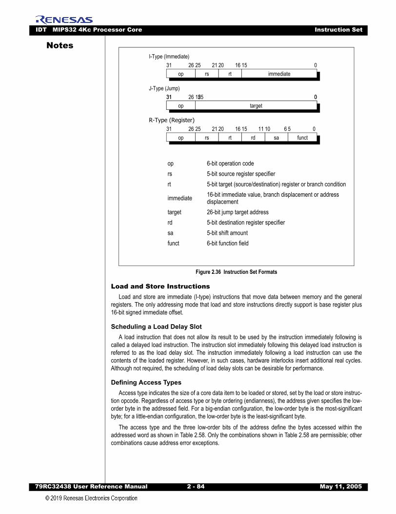
IDT MIPS32 4Kc Processor Core Instruction Set
79RC32438 User Refer
Notes
Figure 2.36 Instruction Set Formats
Load and Store InstructionsLoad and store are immediate (I-type) instructions that move data between memory and the general
registers. The only addressing mode that load and store instructions directly support is base register plus16-bit signed immediate offset.
Scheduling a Load Delay SlotA load instruction that does not allow its result to be used by the instruction immediately following is
called a delayed load instruction. The instruction slot immediately following this delayed load instruction isreferred to as the load delay slot. The instruction immediately following a load instruction can use thecontents of the loaded register. However, in such cases, hardware interlocks insert additional real cycles.Although not required, the scheduling of load delay slots can be desirable for performance.
Defining Access TypesAccess type indicates the size of a core data item to be loaded or stored, set by the load or store instruc-
tion opcode. Regardless of access type or byte ordering (endianness), the address given specifies the low-order byte in the addressed field. For a big-endian configuration, the low-order byte is the most-significantbyte; for a little-endian configuration, the low-order byte is the least-significant byte.
The access type and the three low-order bits of the address define the bytes accessed within theaddressed word as shown in Table 2.58. Only the combinations shown in Table 2.58 are permissible; othercombinations cause address error exceptions.
op 6-bit operation coders 5-bit source register specifierrt 5-bit target (source/destination) register or branch condition
immediate 16-bit immediate value, branch displacement or address displacement
target 26-bit jump target addressrd 5-bit destination register specifiersa 5-bit shift amountfunct 6-bit function field
I-Type (Immediate)
R-Type (Register)
J-Type (Jump)
immediate015
rt1620
op2631
rs2125
target015
op2631
rt1620
op2631
rs2125
sa610
rd1115
funct05
target0 25
op31
ence Manual 2 - 84 May 11, 2005
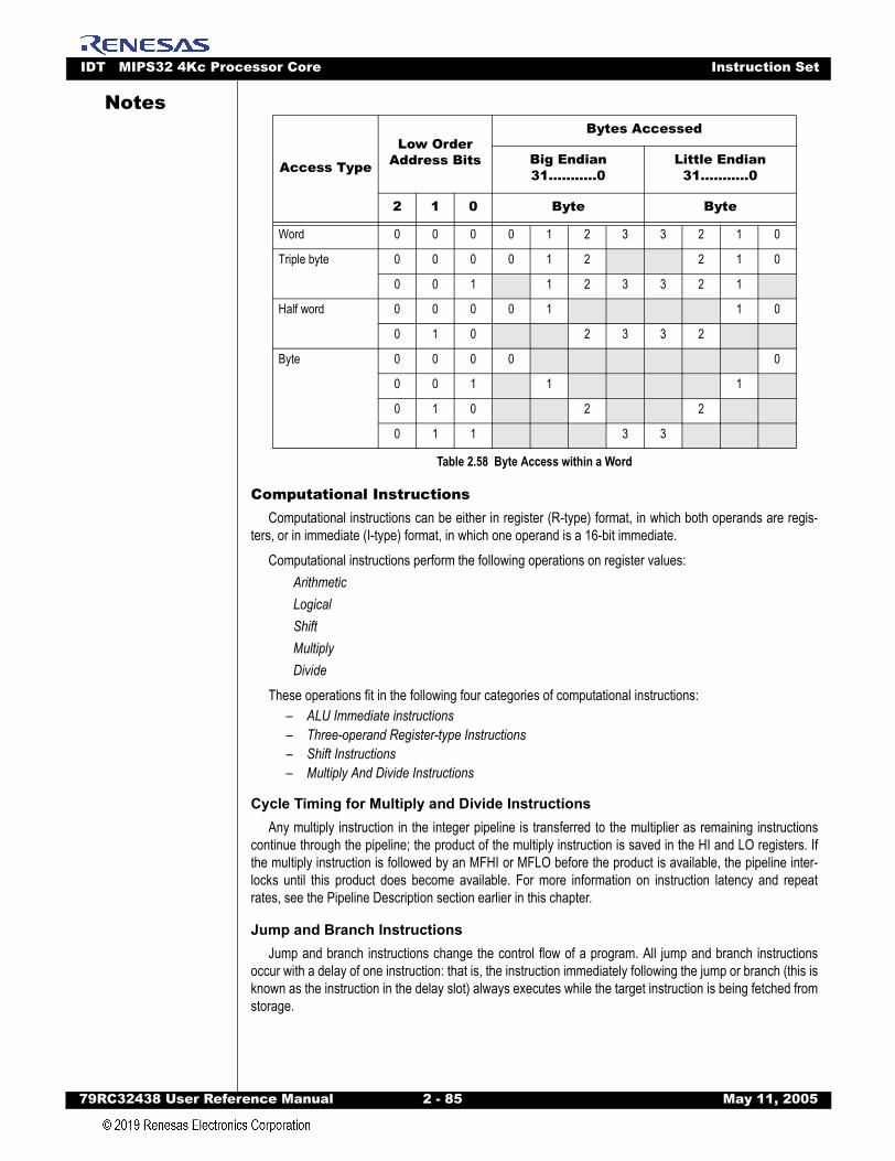
IDT MIPS32 4Kc Processor Core Instruction Set
79RC32438 User Refer
Notes
Computational InstructionsComputational instructions can be either in register (R-type) format, in which both operands are regis-
ters, or in immediate (I-type) format, in which one operand is a 16-bit immediate. Computational instructions perform the following operations on register values:
ArithmeticLogicalShiftMultiplyDivide
These operations fit in the following four categories of computational instructions:– ALU Immediate instructions– Three-operand Register-type Instructions– Shift Instructions– Multiply And Divide Instructions
Cycle Timing for Multiply and Divide InstructionsAny multiply instruction in the integer pipeline is transferred to the multiplier as remaining instructions
continue through the pipeline; the product of the multiply instruction is saved in the HI and LO registers. Ifthe multiply instruction is followed by an MFHI or MFLO before the product is available, the pipeline inter-locks until this product does become available. For more information on instruction latency and repeatrates, see the Pipeline Description section earlier in this chapter.
Jump and Branch InstructionsJump and branch instructions change the control flow of a program. All jump and branch instructions
occur with a delay of one instruction: that is, the instruction immediately following the jump or branch (this isknown as the instruction in the delay slot) always executes while the target instruction is being fetched fromstorage.
Access Type
Low Order Address Bits
Bytes Accessed
Big Endian31...........0
Little Endian31...........0
2 1 0 Byte Byte
Word 0 0 0 0 1 2 3 3 2 1 0
Triple byte 0 0 0 0 1 2 2 1 0
0 0 1 1 2 3 3 2 1
Half word 0 0 0 0 1 1 0
0 1 0 2 3 3 2
Byte 0 0 0 0 0
0 0 1 1 1
0 1 0 2 2
0 1 1 3 3
Table 2.58 Byte Access within a Word
ence Manual 2 - 85 May 11, 2005
IDT MIPS32 4Kc Processor Core Instruction Set
79RC32438 User Refer
Notes
Overview of Jump InstructionsSubroutine calls in high-level languages are usually implemented with Jump or Jump and Link instruc-tions, both of which are J-type instructions. In J-type format, the 26-bit target address shifts left 2 bits andcombines with the high-order 4 bits of the current program counter to form an absolute address. Returns,dispatches, and large cross-page jumps are usually implemented with the Jump Register or Jump and LinkRegister instructions. Both are R-type instructions that take the 32-bit byte address contained in one of thegeneral purpose registers. For more information about jump instructions, see the Instruction Set sectionearlier in this chapter.
Overview of Branch InstructionsAll branch instruction target addresses are computed by adding the address of the instruction in the
delay slot to the 16-bit offset (shifted left 2 bits and sign-extended to 32 bits). All branches occur with adelay of one instruction. If a conditional branch likely is not taken, the instruction in the delay slot is nullified.Branches, jumps, ERET, and DERET instructions should not be placed in the delay slot of a branch or jump.
Control InstructionsControl instructions allow the software to initiate traps; they are always R-type.
Coprocessor InstructionsCP0 instructions perform operations on the System Control Coprocessor registers to manipulate the
memory management and exception handling facilities of the processor. For a listing of CP0 instructions,refer to Appendix A, 4Kc Processor Core Instructions, in this manual.
Enhancements to the MIPS ArchitectureThe core execution unit implements the MIPS32 architecture, which includes the following instructions:
– CLO – Count Leading Ones– CLZ – Count Leading Zeros– MADD – Multiply and Add Word– MADDU – Multiply and Add Unsigned Word– MSUB – Multiply and Subtract Word– MSUBU – Multiply and Subtract Unsigned Word– MUL – Multiply Word to Register– SSNOP – Superscalar Inhibit NOP.
CLO - Count Leading OnesThe CLO instruction counts the number of leading ones in a word. The 32-bit word in the GPR rs is
scanned from most-significant to least-significant bit. The number of leading ones is counted and the resultis written to the GPR rd. If all 32 bits are set in the GPR rs, the result written to the GPR rd is 32.
CLZ - Count Leading ZerosThe CLZ instruction counts the number of leading zeros in a word. The 32-bit word in the GPR rs is
scanned from most-significant to least-significant bit. The number of leading zeros is counted and the resultis written to the GPR rd. If all 32 bits are cleared in the GPR rs, the result written to the GPR rd is 32.
MADD - Multiply and Add WordThe MADD instruction multiplies two words and adds the result to the HI/LO register pair. The 32-bit
word value in the GPR rs is multiplied by the 32-bit value in the GPR rt, treating both operands as signedvalues, to produce a 64-bit result. The product is added to the 64-bit concatenated values in the HI and LOregister pair. The resulting value is then written back to the HI and LO registers. No arithmetic exceptionoccurs under any circumstances.
ence Manual 2 - 86 May 11, 2005
IDT MIPS32 4Kc Processor Core Processor Core Instructions
79RC32438 User Refer
Notes
MADDU - Multiply and Add Unsigned WordThe MADDU instruction multiplies two unsigned words and adds the result to the HI/LO register pair.The 32-bit word value in the GPR rs is multiplied by the 32-bit value in the GPR rt, treating both operandsas unsigned values, to produce a 64-bit result. The product is added to the 64-bit concatenated values inthe HI and LO register pair. The resulting value is then written back to the HI and LO registers. No arithmeticexception occurs under any conditions.
MSUB - Multiply and Subtract WordThe MSUB instruction multiplies two words and subtracts the result from the HI/LO register pair. The 32-
bit word value in the GPR rs is multiplied by the 32-bit value in the GPR rt, treating both operands as signedvalues, to produce a 64-bit result. The product is subtracted from the 64-bit concatenated values in the HIand LO register pair. The resulting value is then written back to the HI and LO registers. No arithmeticexception occurs under any circumstances.
MSUBU - Multiply and Subtract Unsigned WordThe MSUBU instruction multiplies two unsigned words and subtracts the result from the HI/LO register
pair. The 32-bit word value in the GPR rs is multiplied by the 32-bit value in the GPR rt, treating both oper-ands as unsigned values, to produce a 64-bit result. The product is subtracted from the 64-bit concatenatedvalues in the HI and LO register pair. The resulting value is then written back to the HI and LO registers. Noarithmetic exception occurs under any circumstances.
MUL - Multiply WordThe MUL instruction multiplies two words and writes the result to a GPR. The 32-bit word value in the
GPR rs is multiplied by the 32-bit value in the GPR rt, treating both operands as signed values, to producea 64-bit result. The least-significant 32 bits of the product are written to the GPR rd. The contents of the HIand LO register pair are not defined after the operation. No arithmetic exception occurs under any circum-stances.
SSNOP- Superscalar Inhibit NOPThe 4Kc processor core treats this instruction as a regular NOP.
Processor Core InstructionsThe 4Kc Processor Core Instructions are discussed in Appendix A of this user manual.
ence Manual 2 - 87 May 11, 2005

IDT MIPS32 4Kc Processor Core Processor Core Instructions
79RC32438 User Refer
Notes
ence Manual 2 - 88 May 11, 2005
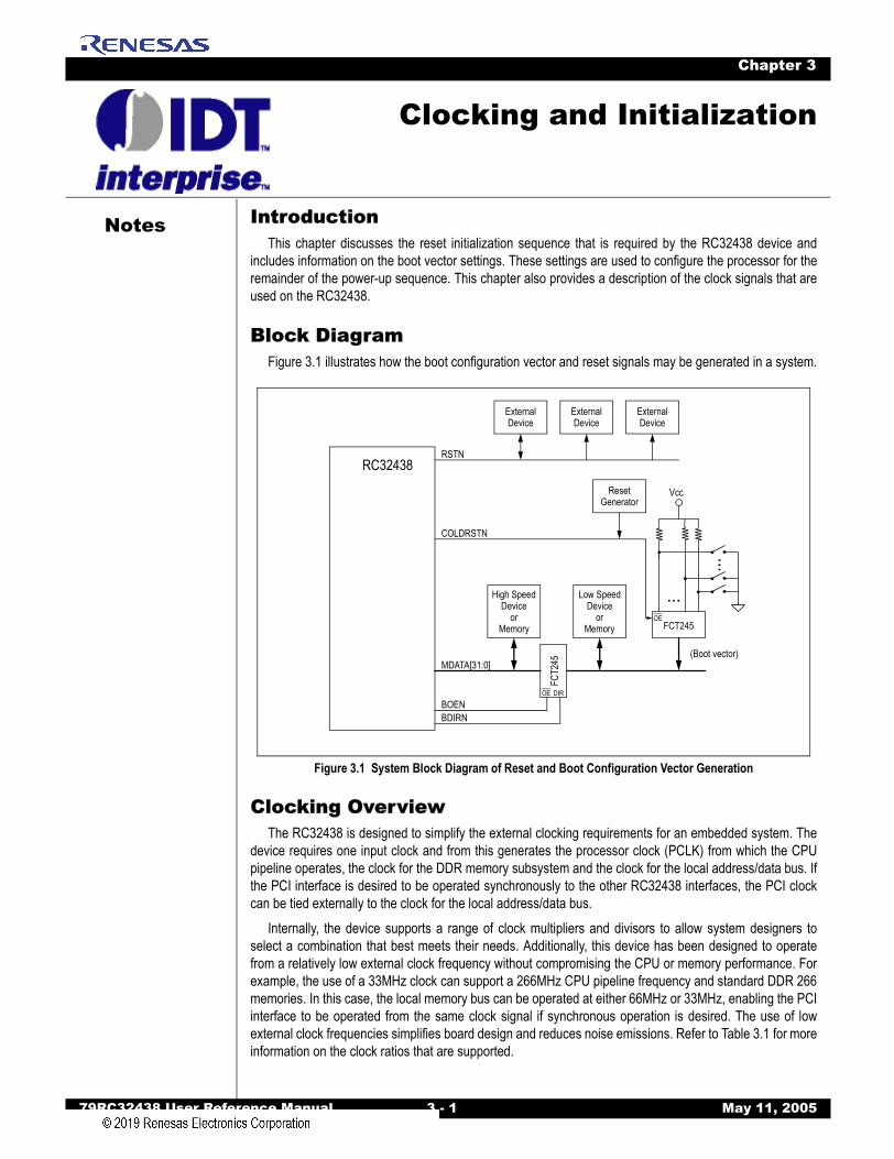
Notes
79RC32438 User Reference Manual 3 - 1 M
Chapter 3
Clocking and Initialization
IntroductionThis chapter discusses the reset initialization sequence that is required by the RC32438 device and
includes information on the boot vector settings. These settings are used to configure the processor for theremainder of the power-up sequence. This chapter also provides a description of the clock signals that areused on the RC32438.
Block DiagramFigure 3.1 illustrates how the boot configuration vector and reset signals may be generated in a system.
Figure 3.1 System Block Diagram of Reset and Boot Configuration Vector Generation
Clocking OverviewThe RC32438 is designed to simplify the external clocking requirements for an embedded system. The
device requires one input clock and from this generates the processor clock (PCLK) from which the CPUpipeline operates, the clock for the DDR memory subsystem and the clock for the local address/data bus. Ifthe PCI interface is desired to be operated synchronously to the other RC32438 interfaces, the PCI clockcan be tied externally to the clock for the local address/data bus.
Internally, the device supports a range of clock multipliers and divisors to allow system designers toselect a combination that best meets their needs. Additionally, this device has been designed to operatefrom a relatively low external clock frequency without compromising the CPU or memory performance. Forexample, the use of a 33MHz clock can support a 266MHz CPU pipeline frequency and standard DDR 266memories. In this case, the local memory bus can be operated at either 66MHz or 33MHz, enabling the PCIinterface to be operated from the same clock signal if synchronous operation is desired. The use of lowexternal clock frequencies simplifies board design and reduces noise emissions. Refer to Table 3.1 for moreinformation on the clock ratios that are supported.
High SpeedDevice
orMemory
FCT2
45
BOENOE DIR
BDIRN
MDATA[31:0]
Low SpeedDevice
orMemory FCT245
OE
...
...
Vcc
COLDRSTN
ResetGenerator
RSTN
ExternalDevice
ExternalDevice
ExternalDevice
RC32438
(Boot vector)
ay 11, 2005

IDT Clocking and Initialization Clocking Overview
79RC32438 User Refer
Notes
A PLL multiplies the master clock input and generates an internal CPU pipeline clock (PCLK) and anIPBus clock (ICLK). The CPU pipeline clock (PCLK) is divided by two to form the IPBus clock (ICLK). All ofthe logic that interfaces to the IPBus use this clock. In addition, the IPBus clock is used to generate theclock signals for the external DDR Memory subsystem. The IPBus clock is further divided by the valueselected in the External Clock Divider field in the boot configuration vector to generate an external clockoutput on the EXTCLK pin. The external clock output (EXTCLK) is used by the memory and peripheral bus.The relationship between CLK, PCLK, ICLK, and the EXTCLK pin are shown in Figure 3.2.Figure 3.2 RC32438 Clocking Architecture
The CPU pipeline clock is equal to the master clock input multiplied by the value selected by the CPUPipeline Clock Multiplier field in the boot configuration vector during a cold reset. Table 3.1 shows thesupported CPU Pipeline Clock Multiplier field modes. Care must be exercised to ensure that the masterclock input frequency falls within the range supported by a selected mode. For example, when multiply by 3is selected, the master clock input frequency must be between 66.6 MHz and 88.6 MHz.
CPU Pipeline Clock Multiplier
CLK PCLK
Min1
1. Frequency in MHz.
Max1 Min1 Max1
PLL Bypass - - - -
Multiply by 3 66.6 88.6 200 266
Multiply by 4 50 66.6 200 266
Multiply by 6 33.3 44.3 200 266
Multiply by 8 25 33.25 200 266
Table 3.1 Processor Clock PLL Multiplier Modes
PLL Divider DividerPCLK ICLK
CPUMost
On-ChipLogic
CPU Pipeline Clock Multiplier(bypass, 3, 4, 6, 8)
External Clock Divider(1, 2, 4)
Constant 2
RC32438
CLK EXTCLK
Clock for DDR Memory
ence Manual 3 - 2 May 11, 2005
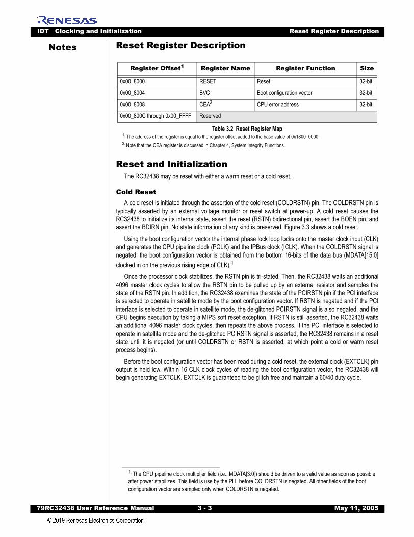
IDT Clocking and Initialization Reset Register Description
79RC32438 User Refer
Notes
Reset Register DescriptionReset and InitializationThe RC32438 may be reset with either a warm reset or a cold reset.
Cold ResetA cold reset is initiated through the assertion of the cold reset (COLDRSTN) pin. The COLDRSTN pin is
typically asserted by an external voltage monitor or reset switch at power-up. A cold reset causes theRC32438 to initialize its internal state, assert the reset (RSTN) bidirectional pin, assert the BOEN pin, andassert the BDIRN pin. No state information of any kind is preserved. Figure 3.3 shows a cold reset.
Using the boot configuration vector the internal phase lock loop locks onto the master clock input (CLK)and generates the CPU pipeline clock (PCLK) and the IPBus clock (ICLK). When the COLDRSTN signal isnegated, the boot configuration vector is obtained from the bottom 16-bits of the data bus (MDATA[15:0]clocked in on the previous rising edge of CLK).1
Once the processor clock stabilizes, the RSTN pin is tri-stated. Then, the RC32438 waits an additional4096 master clock cycles to allow the RSTN pin to be pulled up by an external resistor and samples thestate of the RSTN pin. In addition, the RC32438 examines the state of the PCIRSTN pin if the PCI interfaceis selected to operate in satellite mode by the boot configuration vector. If RSTN is negated and if the PCIinterface is selected to operate in satellite mode, the de-glitched PCIRSTN signal is also negated, and theCPU begins execution by taking a MIPS soft reset exception. If RSTN is still asserted, the RC32438 waitsan additional 4096 master clock cycles, then repeats the above process. If the PCI interface is selected tooperate in satellite mode and the de-glitched PCIRSTN signal is asserted, the RC32438 remains in a resetstate until it is negated (or until COLDRSTN or RSTN is asserted, at which point a cold or warm resetprocess begins).
Before the boot configuration vector has been read during a cold reset, the external clock (EXTCLK) pinoutput is held low. Within 16 CLK clock cycles of reading the boot configuration vector, the RC32438 willbegin generating EXTCLK. EXTCLK is guaranteed to be glitch free and maintain a 60/40 duty cycle.
Register Offset1
1. The address of the register is equal to the register offset added to the base value of 0x1800_0000.
Register Name Register Function Size
0x00_8000 RESET Reset 32-bit
0x00_8004 BVC Boot configuration vector 32-bit
0x00_8008 CEA2
2. Note that the CEA register is discussed in Chapter 4, System Integrity Functions.
CPU error address 32-bit
0x00_800C through 0x00_FFFF Reserved
Table 3.2 Reset Register Map
1. The CPU pipeline clock multiplier field (i.e., MDATA[3:0]) should be driven to a valid value as soon as possible after power stabilizes. This field is use by the PLL before COLDRSTN is negated. All other fields of the boot configuration vector are sampled only when COLDRSTN is negated.
ence Manual 3 - 3 May 11, 2005
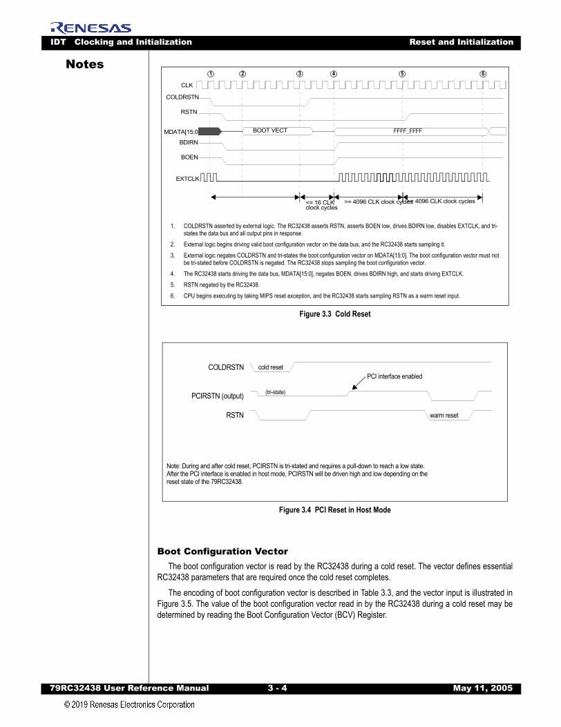
IDT Clocking and Initialization Reset and Initialization
79RC32438 User Refer
Notes
Figure 3.3 Cold Reset
Figure 3.4 PCI Reset in Host Mode
Boot Configuration VectorThe boot configuration vector is read by the RC32438 during a cold reset. The vector defines essential
RC32438 parameters that are required once the cold reset completes.The encoding of boot configuration vector is described in Table 3.3, and the vector input is illustrated in
Figure 3.5. The value of the boot configuration vector read in by the RC32438 during a cold reset may bedetermined by reading the Boot Configuration Vector (BCV) Register.
BOOT VECT
CLK
COLDRSTN
RSTN
MDATA[15:0]
BDIRN
BOEN
>= 4096 CLK clock cycles
1 2 3 4 5 6
FFFF_FFFF
1. COLDRSTN asserted by external logic. The RC32438 asserts RSTN, asserts BOEN low, drives BDIRN low, disables EXTCLK, and tri-states the data bus and all output pins in response.
2. External logic begins driving valid boot configuration vector on the data bus, and the RC32438 starts sampling it.3. External logic negates COLDRSTN and tri-states the boot configuration vector on MDATA[15:0]. The boot configuration vector must not
be tri-stated before COLDRSTN is negated. The RC32438 stops sampling the boot configuration vector.4. The RC32438 starts driving the data bus, MDATA[15:0], negates BOEN, drives BDIRN high, and starts driving EXTCLK.5. RSTN negated by the RC32438.6. CPU begins executing by taking MIPS reset exception, and the RC32438 starts sampling RSTN as a warm reset input.
<= 16 CLKclock cycles
>= 4096 CLK clock cycles
EXTCLK
PCI interface enabledcold reset
warm reset
COLDRSTN
PCIRSTN (output)
RSTN
Note: During and after cold reset, PCIRSTN is tri-stated and requires a pull-down to reach a low state.After the PCI interface is enabled in host mode, PCIRSTN will be driven high and low depending on the
(tri-state)
reset state of the 79RC32438.
ence Manual 3 - 4 May 11, 2005
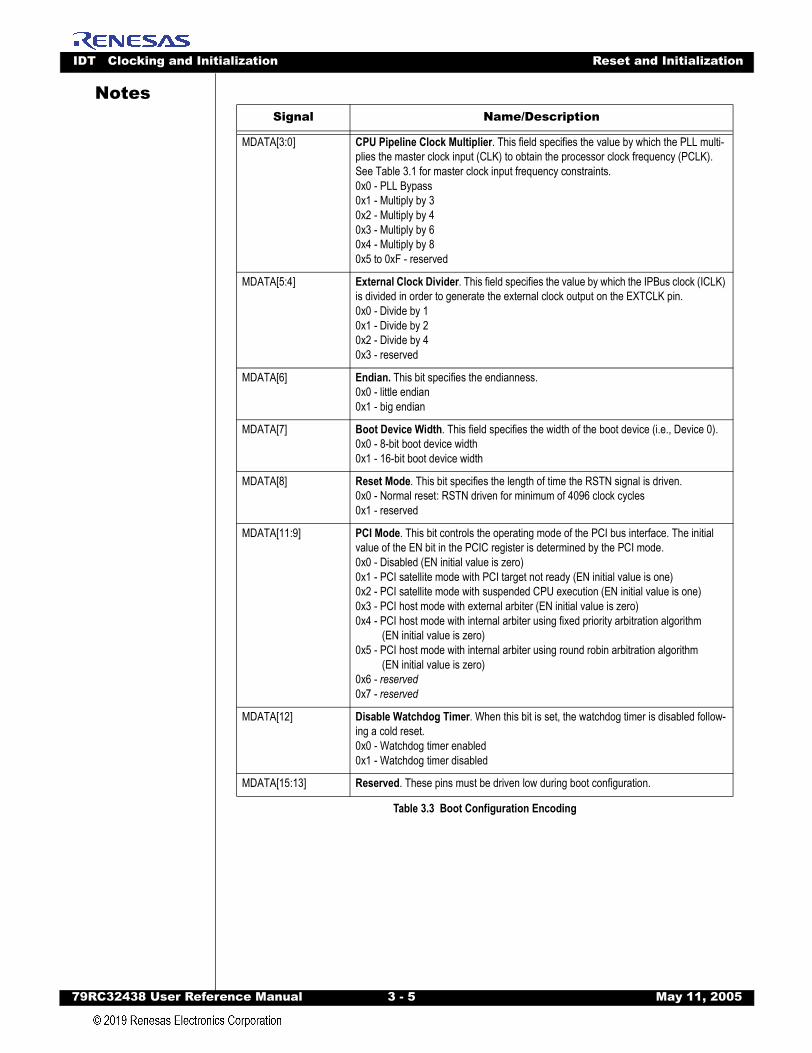
IDT Clocking and Initialization Reset and Initialization
79RC32438 User Refer
Notes
Signal Name/DescriptionMDATA[3:0] CPU Pipeline Clock Multiplier. This field specifies the value by which the PLL multi-plies the master clock input (CLK) to obtain the processor clock frequency (PCLK). See Table 3.1 for master clock input frequency constraints.0x0 - PLL Bypass0x1 - Multiply by 30x2 - Multiply by 40x3 - Multiply by 60x4 - Multiply by 80x5 to 0xF - reserved
MDATA[5:4] External Clock Divider. This field specifies the value by which the IPBus clock (ICLK) is divided in order to generate the external clock output on the EXTCLK pin.0x0 - Divide by 10x1 - Divide by 20x2 - Divide by 40x3 - reserved
MDATA[6] Endian. This bit specifies the endianness.0x0 - little endian0x1 - big endian
MDATA[7] Boot Device Width. This field specifies the width of the boot device (i.e., Device 0).0x0 - 8-bit boot device width0x1 - 16-bit boot device width
MDATA[8] Reset Mode. This bit specifies the length of time the RSTN signal is driven.0x0 - Normal reset: RSTN driven for minimum of 4096 clock cycles0x1 - reserved
MDATA[11:9] PCI Mode. This bit controls the operating mode of the PCI bus interface. The initial value of the EN bit in the PCIC register is determined by the PCI mode.0x0 - Disabled (EN initial value is zero)0x1 - PCI satellite mode with PCI target not ready (EN initial value is one)0x2 - PCI satellite mode with suspended CPU execution (EN initial value is one)0x3 - PCI host mode with external arbiter (EN initial value is zero)0x4 - PCI host mode with internal arbiter using fixed priority arbitration algorithm
(EN initial value is zero)0x5 - PCI host mode with internal arbiter using round robin arbitration algorithm
(EN initial value is zero)0x6 - reserved0x7 - reserved
MDATA[12] Disable Watchdog Timer. When this bit is set, the watchdog timer is disabled follow-ing a cold reset.0x0 - Watchdog timer enabled0x1 - Watchdog timer disabled
MDATA[15:13] Reserved. These pins must be driven low during boot configuration.
Table 3.3 Boot Configuration Encoding
ence Manual 3 - 5 May 11, 2005

IDT Clocking and Initialization Reset/Initialization Registers
79RC32438 User Refer
Notes
Reset/Initialization RegistersBoot Configuration Vector Register
Figure 3.5 Boot Configuration Vector Register (BCV)
Warm ResetA warm reset may be initiated by one of seven conditions:
– Assertion of the reset pin (RSTN) by an external agent– A CPU write of 0x8000_0001 to the Reset (RESET) register– An IPBus transaction timer time-out– A watchdog timer time-out with the WRE bit set in the ERRCS register– A CPU or PCI master write setting the Warm Reset (WR) bit in the PCI Management (PCIMGT)
register in PCI configuration space– Assertion of the PCI reset signal (PCIRSTN) when operating in PCI satellite mode– Generation of a processor reset by EJTAG debug software by setting of the PrRst bit in the EJTAG
control register (i.e., assertion of the EJ_PrRst output signal by the CPU core).When one of these conditions occurs, the RC32438 asserts the RSTN pin for a minimum of 4096 CLK
clock cycles. Then, the RC32438 tri-states RSTN, waits an additional 4096 CLK clock cycles, and exam-ines the state of the RSTN pin. In addition, the RC32438 will examine the state of the PCIRSTN pin if thePCI interface is selected to operate in satellite mode by the boot configuration vector. If RSTN is negatedand if the PCI interface is selected to operate in satellite mode, the de-glitched PCIRSTN signal is alsonegated, and the CPU begins execution by taking a MIPS soft reset exception.1 If RSTN is still asserted,the warm reset procedure above is repeated. If the PCI interface is selected to operate in satellite mode andthe de-glitched PCIRSTN signal is asserted, then the RC32438 remains in a warm reset until it is negated(or until RSTN is asserted again, at which point the warm reset process repeats).
The delay between tri-stating the RSTN pin and then sampling whether it is asserted allows the signal tobe pulled up with a resistor. During a warm reset, all memory and peripheral bus transactions are inhibited.The DDR Controller continues operation across warm resets and may generate a refresh transaction duringa warm reset.
A warm reset causes the following: All blocks within the RC32438 are reset with the exception of the CPU, CPU BIU, and IPBus moni-torThe CPU to take a MIPS soft reset exception
BCV
Description: Boot Configuration Vector. This field contains the boot configuration vector read in by the RC32438 during a cold reset. See Table 3.3 for a description of the encoding of this vector.
Initial Value: Boot configuration vector
Read Value: Boot configuration vector
Write Effect: Read-only
1. The assertion of CSN[0] will occur no sooner than 16 clock cycles after the RC32438 samples RSTN negated.
BCV031
16
0
16
BCV
ence Manual 3 - 6 May 11, 2005

IDT Clocking and Initialization Reset/Initialization Registers
79RC32438 User Refer
Notes
All registers are reset to their initial value, except the following:– BTCOMPARE1, BTADDR, and BTCS registers in the Device Controller– All bits in the PCIC register (except the TNR and IGM bits which are, in fact, reset)– TO bit in the WTC register– EN bit in the WTC register if the warm reset was not caused by the expiration of thewatchdog timer– WTO bit in the ERRCS register– WR bit in the PCIS register– Registers in PCI configuration space– DDR controller registers– Event monitor registers– Contents of on-chip memory.
Note: All PCI registers are reset to their initial value if the warm reset was the result of an assertion of the PCI reset signal when operating in PCI satellite mode. Also, the external clock, EXTCLK, is always driven during any warm reset.
An externally initiated warm reset caused by assertion of RSTN by an external agent is shown in Figure3.6, while an internally initiated warm reset, for example, caused by a write of 0x8000_0001 to the RESETregister is shown in Figure 3.7.
Figure 3.6 Externally Initiated Warm Reset
1. If the warm reset is the result of a bus transaction time-out, the BTCOMPARE field is initialized to 0xFFFF.
1. Warm reset condition caused by assertion of RSTN by an external agent.2. RC32438 tri-states the data bus, MDATA[15:0], negates all memory control signals, and itself asserts RSTN.3. RC32438 negates RSTN after 4096 master clock (CLK) cycles.4. External agent negates RSTN.5. RC32438 samples RSTN negated 4096 master clock (CLK) cycles after step 3 and starts driving the data bus, MDATA[15:0].6. CPU begins executing by taking a MIPS soft reset exception. The assertion of CSN[0] will occur no sooner than 16 clock cycles after the
RC32438 samples RSTN negated (i.e., step 5).
Active Deasserted Active
CLK
COLDRSTN
RSTN
MDATA[15:0]
Mem Control Signals
FFFF_FFFF
1 2 4 5 63
4096Clock Cycles
4096Clock Cycles
ence Manual 3 - 7 May 11, 2005
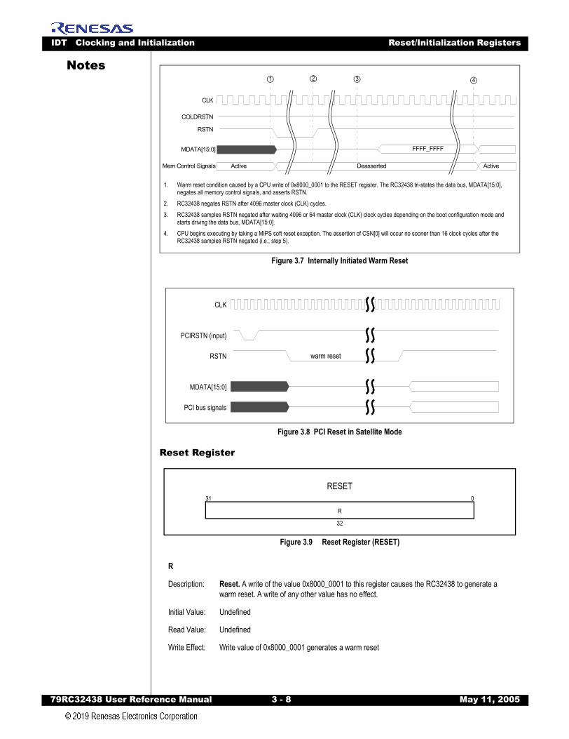
IDT Clocking and Initialization Reset/Initialization Registers
79RC32438 User Refer
Notes
Figure 3.7 Internally Initiated Warm Reset
Figure 3.8 PCI Reset in Satellite Mode
Reset Register
Figure 3.9 Reset Register (RESET)
R
Description: Reset. A write of the value 0x8000_0001 to this register causes the RC32438 to generate a warm reset. A write of any other value has no effect.
Initial Value: Undefined
Read Value: Undefined
Write Effect: Write value of 0x8000_0001 generates a warm reset
1. Warm reset condition caused by a CPU write of 0x8000_0001 to the RESET register. The RC32438 tri-states the data bus, MDATA[15:0], negates all memory control signals, and asserts RSTN.
2. RC32438 negates RSTN after 4096 master clock (CLK) cycles.3. RC32438 samples RSTN negated after waiting 4096 or 64 master clock (CLK) clock cycles depending on the boot configuration mode and
starts driving the data bus, MDATA[15:0].4. CPU begins executing by taking a MIPS soft reset exception. The assertion of CSN[0] will occur no sooner than 16 clock cycles after the
RC32438 samples RSTN negated (i.e., step 5).
Active Deasserted Active
CLK
COLDRSTN
RSTN
MDATA[15:0]
Mem Control Signals
1 3 42
FFFF_FFFF
warm reset
CLK
PCIRSTN (input)
RSTN
MDATA[15:0]
PCI bus signals
RESET031
32
R
ence Manual 3 - 8 May 11, 2005

IDT Clocking and Initialization Pin State During Reset
79RC32438 User Refer
Notes
Pin State During ResetTable 3.4 shows the state of each pin during cold reset (COLDRSTN pin asserted low) and warm reset(RSTN pin asserted low). Because input-only pins are never driven, they are not included in this table.
Function Pin Name Type Cold Reset
Warm Reset
Memory and Peripheral Bus
BDIRN O low low
BGN O high high
BOEN O low low
BWEN[1:0] O high high
CSN[5:0] O high high
MADDR[21:0] O low low
MDATA[15:0] I/O Z Z
OEN O high high
RWN O high high
DDR Bus DDRADDR[13:0] O low low
DDRBA[1:0] O low low
DDRCASN O high high
DDRCKE O low low
DDRCKN[1:0] O high toggle
DDRCKP[1:0] O low toggle
DDRCSN[1:0] O high high
DDRDATA[31:0] I/O Z Z
DDRDM[7:0] I/O high high
DDRDQS[3:0] I/O Z Z
DDROEN[3:0] O high high
DDRRASN O high high
DDRWEN O high high
Table 3.4 Pin State During Reset (Part 1 of 3)
ence Manual 3 - 9 May 11, 2005
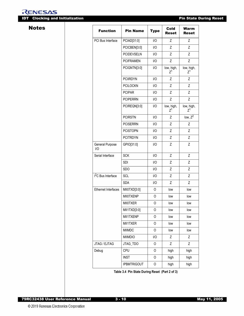
IDT Clocking and Initialization Pin State During Reset
79RC32438 User Refer
Notes
PCI Bus Interface PCIAD[31:0] I/O Z Z
PCICBEN[3:0] I/O Z Z
PCIDEVSELN I/O Z Z
PCIFRAMEN I/O Z Z
PCIGNTN[3:0] I/O low, high, Z1
low, high, Z1
PCIIRDYN I/O Z Z
PCILOCKN I/O Z Z
PCIPAR I/O Z Z
PCIPERRN I/O Z Z
PCIREQN[3:0] I/O low, high, Z1
low, high, Z1
PCIRSTN I/O Z low, Z2
PCISERRN I/O Z Z
PCISTOPN I/O Z Z
PCITRDYN I/O Z Z
General Purpose I/O
GPIO[31:0] I/O Z Z
Serial Interface SCK I/O Z Z
SDI I/O Z Z
SDO I/O Z Z
I2C Bus Interface SCL I/O Z Z
SDA I/O Z Z
Ethernet Interfaces MII0TXD[3:0] O low low
MII0TXENP O low low
MII0TXER O low low
MII1TXD[3:0] O low low
MII1TXENP O low low
MII1TXER O low low
MIIMDC O low low
MIIMDIO I/O Z Z
JTAG / EJTAG JTAG_TDO O Z Z
Debug CPU O high high
INST O high high
IPBMTRIGOUT O high high
Function Pin Name Type Cold Reset
Warm Reset
Table 3.4 Pin State During Reset (Part 2 of 3)
ence Manual 3 - 10 May 11, 2005
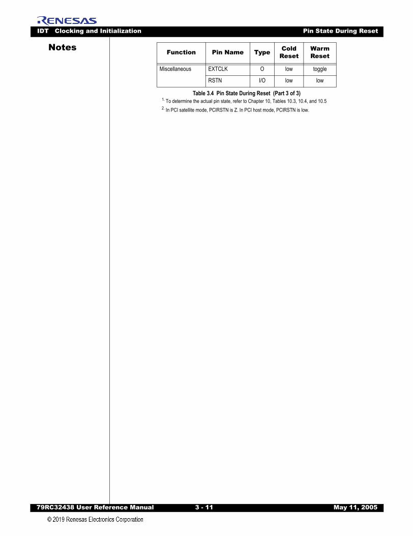
IDT Clocking and Initialization Pin State During Reset
79RC32438 User Refer
Notes
Miscellaneous EXTCLK O low toggle
RSTN I/O low low
1. To determine the actual pin state, refer to Chapter 10, Tables 10.3, 10.4, and 10.5 2. In PCI satellite mode, PCIRSTN is Z. In PCI host mode, PCIRSTN is low.
Function Pin Name Type Cold Reset
Warm Reset
Table 3.4 Pin State During Reset (Part 3 of 3)
ence Manual 3 - 11 May 11, 2005

IDT Clocking and Initialization Pin State During Reset
79RC32438 User Refer
Notes
ence Manual 3 - 12 May 11, 2005
Notes
79RC32438 User Reference Manual 4 - 1 M
Chapter 4
System Integrity Functions
IntroductionThis chapter describes the system integrity functions on the RC32438. The system integrity module
includes several registers that log system activity. These registers can be used to indicate the source ofhardware or software errors.
FeaturesProgrammable bus transaction timer generates warm reset when counter expiresAddress space monitorProgrammable watchdog timer generates NMI when counter expires
Functional OverviewThe RC32438 supports three functions to monitor activity within the system and report potential hard-
ware or software error conditions.The first function is the bus transaction timer. The bus transaction timer times memory and peripheral
bus transactions, generating a warm reset if a transaction does not complete within a specified number ofclock cycles. The bus transaction timer is part of the device controller. For more information on the bustransaction timer, see the Memory and Peripheral Bus Transaction Timer section in Chapter 6.
A second function is the address space monitor. The address space monitor generates an error inresponse to bus transactions with invalid RC32438 local address space addresses. This applies to transac-tions generated by the CPU as well as the PCI and DMA controllers.
A third function is the watchdog timer. The watchdog timer is a general purpose timer that, if not periodi-cally reset by software, generates a nonmaskable interrupt (NMI) exception to the CPU or a warm reset.The watchdog timer is independent from the three general purpose timers described in Chapter 14, CounterTimers.
System integrity functions are controlled, and their status is reported in the Error Control and Status(ERRCS) Register. The bus transaction timer, the address space monitor, and the watchdog are all enabledfollowing a cold reset. The bus timer and watchdog timer can be individually disabled by software.
The address of an undecoded CPU read/write operation or IPBus slave acknowledge error is recordedin the CPU Error Address (CEA) register. This register is only accessible by the CPU since it is located inthe CPU BIU.
System Integrity Register Description
Register Offset1 Register Name Register Function Size
0x03_0000 through 0x03_002C Reserved
0x03_0030 ERRCS Error control and status 32-bit
0x03_0034 WTCOUNT Watchdog timer count 32-bit
Table 4.1 System Integrity Register Map (Part 1 of 2)
ay 11, 2005
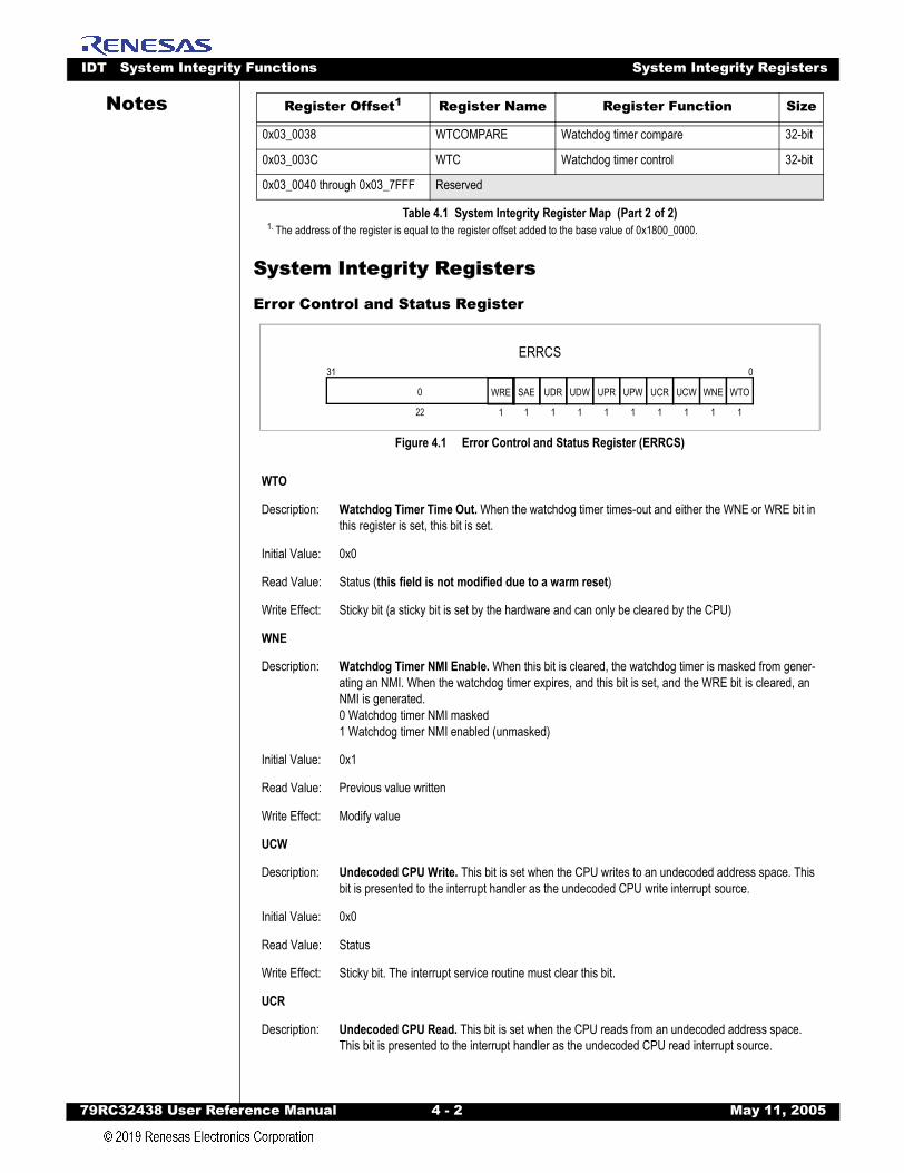
IDT System Integrity Functions System Integrity Registers
79RC32438 User Refer
Notes
System Integrity Registers
Error Control and Status Register
Figure 4.1 Error Control and Status Register (ERRCS)
0x03_0038 WTCOMPARE Watchdog timer compare 32-bit
0x03_003C WTC Watchdog timer control 32-bit
0x03_0040 through 0x03_7FFF Reserved
1. The address of the register is equal to the register offset added to the base value of 0x1800_0000.
WTO
Description: Watchdog Timer Time Out. When the watchdog timer times-out and either the WNE or WRE bit in this register is set, this bit is set.
Initial Value: 0x0
Read Value: Status (this field is not modified due to a warm reset)
Write Effect: Sticky bit (a sticky bit is set by the hardware and can only be cleared by the CPU)
WNE
Description: Watchdog Timer NMI Enable. When this bit is cleared, the watchdog timer is masked from gener-ating an NMI. When the watchdog timer expires, and this bit is set, and the WRE bit is cleared, an NMI is generated.0 Watchdog timer NMI masked1 Watchdog timer NMI enabled (unmasked)
Initial Value: 0x1
Read Value: Previous value written
Write Effect: Modify value
UCW
Description: Undecoded CPU Write. This bit is set when the CPU writes to an undecoded address space. This bit is presented to the interrupt handler as the undecoded CPU write interrupt source.
Initial Value: 0x0
Read Value: Status
Write Effect: Sticky bit. The interrupt service routine must clear this bit.
UCR
Description: Undecoded CPU Read. This bit is set when the CPU reads from an undecoded address space. This bit is presented to the interrupt handler as the undecoded CPU read interrupt source.
Register Offset1 Register Name Register Function Size
Table 4.1 System Integrity Register Map (Part 2 of 2)
ERRCS031
22
0
1
WTO
1
WNE
1
UCW
1
UCR
1
UPW
1
UPR
1
UDW
1
UDR
1
SAE
1
WRE
ence Manual 4 - 2 May 11, 2005
IDT System Integrity Functions System Integrity Registers
79RC32438 User Refer
Notes
Initial Value: 0x0Read Value: Status
Write Effect: Sticky bit. The interrupt service routine must clear this bit.
UPW
Description: Undecoded PCI Write. This bit is set when the PCI interface writes to an undecoded address space. This bit is presented to the interrupt handler as the undecoded PCI write interrupt source.
Initial Value: 0x0
Read Value: Status
Write Effect: Sticky bit. The interrupt service routine must clear this bit.
UPR
Description: Undecoded PCI Read. This bit is set when the PCI interface reads from an undecoded address space. This bit is presented to the interrupt handler as the undecoded PCI read interrupt source.
Initial Value: 0x0
Read Value: Status
Write Effect: Sticky bit. The interrupt service routine must clear this bit.
UDW
Description: Undecoded DMA Write. This bit is set when the DMA writes to an undecoded address space. This bit is presented to the interrupt handler as the undecoded DMA write interrupt source.
Initial Value: 0x0
Read Value: Status
Write Effect: Sticky bit. The interrupt service routine must clear this bit.
UDR
Description: Undecoded DMA Read. This bit is set when the DMA interface reads from an undecoded address space. This bit is presented to the interrupt handler as the undecoded DMA read interrupt source.
Initial Value: 0x0
Read Value: Status
Write Effect: Sticky bit. The interrupt service routine must clear this bit.
SAE
Description: IPBus Slave Acknowledge Error. This bit is set when an IPBus slave signals a slave acknowledge error.
Initial Value: 0x0
Read Value: Status
Write Effect: Sticky bit. The interrupt service routine must clear this bit.
ence Manual 4 - 3 May 11, 2005
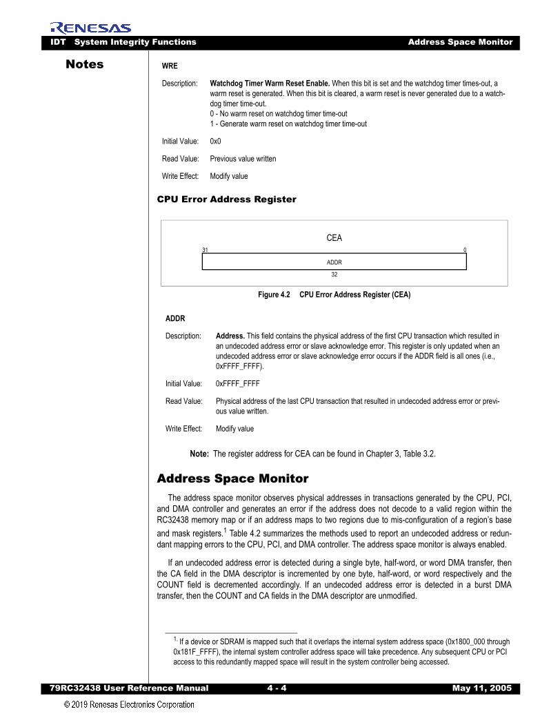
IDT System Integrity Functions Address Space Monitor
79RC32438 User Refer
Notes
CPU Error Address Register
Figure 4.2 CPU Error Address Register (CEA)
Note: The register address for CEA can be found in Chapter 3, Table 3.2.
Address Space MonitorThe address space monitor observes physical addresses in transactions generated by the CPU, PCI,
and DMA controller and generates an error if the address does not decode to a valid region within theRC32438 memory map or if an address maps to two regions due to mis-configuration of a region’s baseand mask registers.1 Table 4.2 summarizes the methods used to report an undecoded address or redun-dant mapping errors to the CPU, PCI, and DMA controller. The address space monitor is always enabled.
If an undecoded address error is detected during a single byte, half-word, or word DMA transfer, thenthe CA field in the DMA descriptor is incremented by one byte, half-word, or word respectively and theCOUNT field is decremented accordingly. If an undecoded address error is detected in a burst DMAtransfer, then the COUNT and CA fields in the DMA descriptor are unmodified.
WRE
Description: Watchdog Timer Warm Reset Enable. When this bit is set and the watchdog timer times-out, a warm reset is generated. When this bit is cleared, a warm reset is never generated due to a watch-dog timer time-out.0 - No warm reset on watchdog timer time-out1 - Generate warm reset on watchdog timer time-out
Initial Value: 0x0
Read Value: Previous value written
Write Effect: Modify value
ADDR
Description: Address. This field contains the physical address of the first CPU transaction which resulted in an undecoded address error or slave acknowledge error. This register is only updated when an undecoded address error or slave acknowledge error occurs if the ADDR field is all ones (i.e., 0xFFFF_FFFF).
Initial Value: 0xFFFF_FFFF
Read Value: Physical address of the last CPU transaction that resulted in undecoded address error or previ-ous value written.
Write Effect: Modify value
1. If a device or SDRAM is mapped such that it overlaps the internal system address space (0x1800_000 through 0x181F_FFFF), the internal system controller address space will take precedence. Any subsequent CPU or PCI access to this redundantly mapped space will result in the system controller being accessed.
CEA031
32
ADDR
ence Manual 4 - 4 May 11, 2005
IDT System Integrity Functions Watchdog Timer
79RC32438 User Refer
Notes
Watchdog TimerWhen the watchdog timer NMI Enable (WNE) bit is set in the ERRCS register, the watchdog timer will
generate an NMI when it times out. In addition, the watchdog timer may be configured to generate a warmreset when it times out by setting the watchdog timer warm reset enable (WRE) bit in the ERRCS register. Ifboth the WNE and WRE bits are cleared, the watchdog timer operates as a general purpose counter timer.
The watchdog timer is enabled by setting the enable (EN) bit in the watchdog timer control (WTC)register. When this occurs, the watchdog timer begins incrementing its current watchdog timer count valuewith each IPBus clock (ICLK) cycle. The CPU may determine the current watchdog timer count value byreading the Watchdog Timer Count Register (WTCOUNT). Writing to this register modifies the watchdogtimer count value. For normal operation, this register should be initialized to zero prior to enabling thewatchdog timer. Following a cold reset, the watchdog timer is normally enabled. The watchdog timer maybe disabled by setting the Disable Watchdog Timer bit in the boot configuration vector.
When the watchdog timer count value matches the value in the Watchdog Timer Compare Register(WTCOMPARE), the timer expires1. When this occurs, the time out (WTO) bit in the Watchdog TimerControl Register (WTC) is set. In addition, if either the Watchdog Timer Warm Reset Enable (WRE) bit orWatchdog Timer NMI Enable (WNE) bit is set in the Error Control and Status Register (ERRCS), theWatchdog Timer Time-Out (WTO) bit is set in the ERRCS register.
Bus Master
Bus Master Operation Undecoded Address Error Reporting Mechanism
CPU CPU read operation CPU bus error exception and Undecoded CPU Read (UCR) bit set in the ERRCS register. The CPU Error Address (CEA) register contains the address of the undecoded read.
CPU write operation CPU core interrupt from UCW bit (Undecoded CPU Write (UCW) bit is set in the ERRCS register. The CPU Error Address (CEA) register con-tains the address of the undecoded write.
PCI PCI read operation PCI transaction terminated with Target Abort and Undecoded PCI Read (UPR) bit set in ERRCS register. For additional information, refer to Chapter 10, section “Target Error Handling” on page 10-38.
PCI write operation PCI transaction terminated with Target Abort and Undecoded PCI Write (UPW) bit set in ERRCS register. If the PCI transaction resulted in a posted write, then a PCI system error is signalled on the PCI bus by asserting the SERRN signal of the SEN bit is set in the PCI COMMAND register. For additional information, refer to Chapter 10, section “Target Error Handling” on page 10-38.
DMA DMA descriptor read Error (E) bit set in corresponding DMA status (DMAxS) register and Undecoded DMA Read (UDR) bit set in ERRCS register.
DMA descriptor write Error (E) bit in set in corresponding DMA status (DMAxS) register and Undecoded DMA Write (UDW) bit set in ERRCS register.
DMA data read The terminated (T) bit is set in the descriptor in which the error was detected. The Undecoded DMA Read (UDR) bit is set in ERRCS regis-ter.
DMA data write The terminated (T) bit is set in the descriptor in which the error was detected. The Undecoded DMA Write (UDW) bit is set in the ERRCS reg-ister.
Table 4.2 Address Space Monitor Undecoded Address Error Reporting
1. The counter timer expires at the point when the value in the WTCOUNT register first equals the value in the WTCOMPARE register (i.e., the rising edge of the master clock, that is, CLK (WTCOUNT == WTCOMPARE)).
ence Manual 4 - 5 May 11, 2005
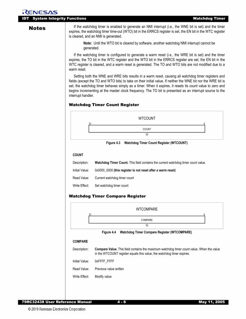
IDT System Integrity Functions Watchdog Timer
79RC32438 User Refer
Notes
If the watchdog timer is enabled to generate an NMI interrupt (i.e., the WNE bit is set) and the timerexpires, the watchdog timer time-out (WTO) bit in the ERRCS register is set, the EN bit in the WTC registeris cleared, and an NMI is generated.Note: Until the WTO bit is cleared by software, another watchdog NMI interrupt cannot be generated.
If the watchdog timer is configured to generate a warm reset (i.e., the WRE bit is set) and the timerexpires, the TO bit in the WTC register and the WTO bit in the ERRCS register are set, the EN bit in theWTC register is cleared, and a warm reset is generated. The TO and WTO bits are not modified due to awarm reset.
Setting both the WNE and WRE bits results in a warm reset, causing all watchdog timer registers andfields (except the TO and WTO bits) to take on their initial value. If neither the WNE bit nor the WRE bit isset, the watchdog timer behaves simply as a timer. When it expires, it resets its count value to zero andbegins incrementing at the master clock frequency. The TO bit is presented as an interrupt source to theinterrupt handler.
Watchdog Timer Count Register
Figure 4.3 Watchdog Timer Count Register (WTCOUNT)
Watchdog Timer Compare Register
Figure 4.4 Watchdog Timer Compare Register (WTCOMPARE)
COUNT
Description: Watchdog Timer Count. This field contains the current watchdog timer count value.
Initial Value: 0x0000_0000 (this register is not reset after a warm reset)
Read Value: Current watchdog timer count
Write Effect: Set watchdog timer count
COMPARE
Description: Compare Value. This field contains the maximum watchdog timer count value. When the value in the WTCOUNT register equals this value, the watchdog timer expires.
Initial Value: 0xFFFF_FFFF
Read Value: Previous value written
Write Effect: Modify value
WTCOUNT031
32
COUNT
WTCOMPARE031
32
COMPARE
ence Manual 4 - 6 May 11, 2005
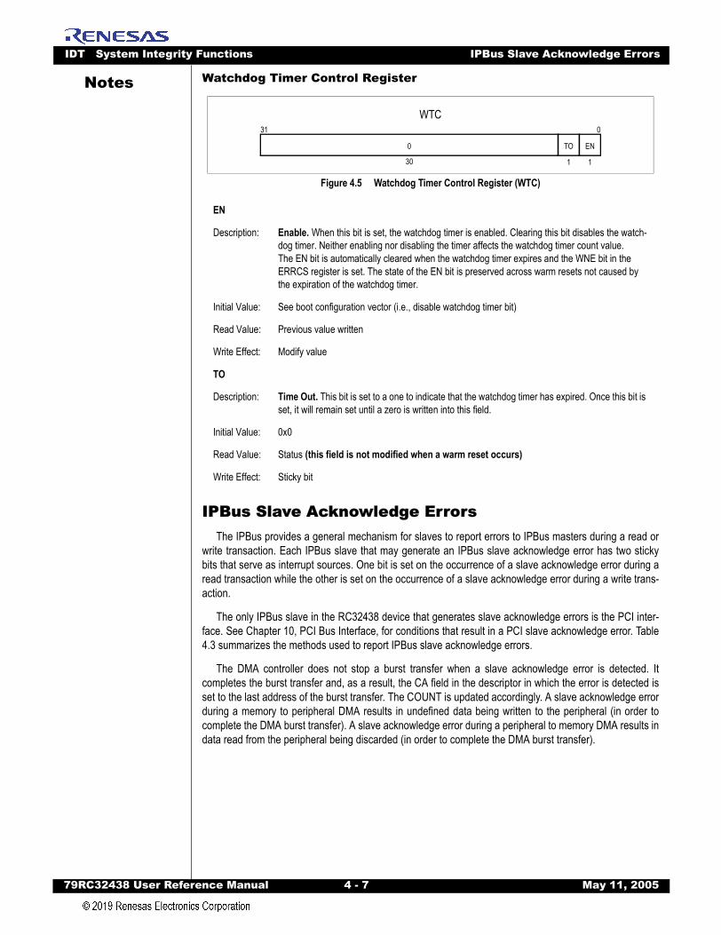
IDT System Integrity Functions IPBus Slave Acknowledge Errors
79RC32438 User Refer
Notes
Watchdog Timer Control RegisterFigure 4.5 Watchdog Timer Control Register (WTC)
IPBus Slave Acknowledge ErrorsThe IPBus provides a general mechanism for slaves to report errors to IPBus masters during a read or
write transaction. Each IPBus slave that may generate an IPBus slave acknowledge error has two stickybits that serve as interrupt sources. One bit is set on the occurrence of a slave acknowledge error during aread transaction while the other is set on the occurrence of a slave acknowledge error during a write trans-action.
The only IPBus slave in the RC32438 device that generates slave acknowledge errors is the PCI inter-face. See Chapter 10, PCI Bus Interface, for conditions that result in a PCI slave acknowledge error. Table4.3 summarizes the methods used to report IPBus slave acknowledge errors.
The DMA controller does not stop a burst transfer when a slave acknowledge error is detected. Itcompletes the burst transfer and, as a result, the CA field in the descriptor in which the error is detected isset to the last address of the burst transfer. The COUNT is updated accordingly. A slave acknowledge errorduring a memory to peripheral DMA results in undefined data being written to the peripheral (in order tocomplete the DMA burst transfer). A slave acknowledge error during a peripheral to memory DMA results indata read from the peripheral being discarded (in order to complete the DMA burst transfer).
EN
Description: Enable. When this bit is set, the watchdog timer is enabled. Clearing this bit disables the watch-dog timer. Neither enabling nor disabling the timer affects the watchdog timer count value.The EN bit is automatically cleared when the watchdog timer expires and the WNE bit in the ERRCS register is set. The state of the EN bit is preserved across warm resets not caused by the expiration of the watchdog timer.
Initial Value: See boot configuration vector (i.e., disable watchdog timer bit)
Read Value: Previous value written
Write Effect: Modify value
TO
Description: Time Out. This bit is set to a one to indicate that the watchdog timer has expired. Once this bit is set, it will remain set until a zero is written into this field.
Initial Value: 0x0
Read Value: Status (this field is not modified when a warm reset occurs)
Write Effect: Sticky bit
WTC031
30
0 TO EN
1 1
ence Manual 4 - 7 May 11, 2005
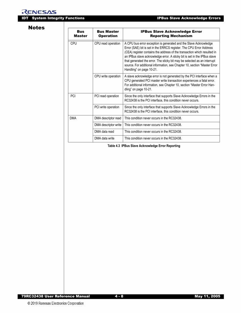
IDT System Integrity Functions IPBus Slave Acknowledge Errors
79RC32438 User Refer
Notes
.Bus Master
Bus Master Operation
IPBus Slave Acknowledge ErrorReporting Mechanism
CPU CPU read operation A CPU bus error exception is generated and the Slave Acknowledge Error (SAE) bit is set in the ERRCS register. The CPU Error Address (CEA) register contains the address of the transaction which resulted in an IPBus slave acknowledge error. A sticky bit is set in the IPBus slave that generated the error. The sticky bit may be selected as an interrupt source. For additional information, see Chapter 10, section “Master Error Handling” on page 10-21.
CPU write operation A slave acknowledge error is not generated by the PCI interface when a CPU generated PCI master write transaction experiences a fatal error. For additional information, see Chapter 10, section “Master Error Han-dling” on page 10-21.
PCI PCI read operation Since the only interface that supports Slave Acknowledge Errors in the RC32438 is the PCI interface, this condition never occurs.
PCI write operation Since the only interface that supports Slave Acknowledge Errors in the RC32438 is the PCI interface, this condition never occurs.
DMA DMA descriptor read This condition never occurs in the RC32438.
DMA descriptor write This condition never occurs in the RC32438.
DMA data read This condition never occurs in the RC32438.
DMA data write This condition never occurs in the RC32438.
Table 4.3 IPBus Slave Acknowledge Error Reporting
ence Manual 4 - 8 May 11, 2005
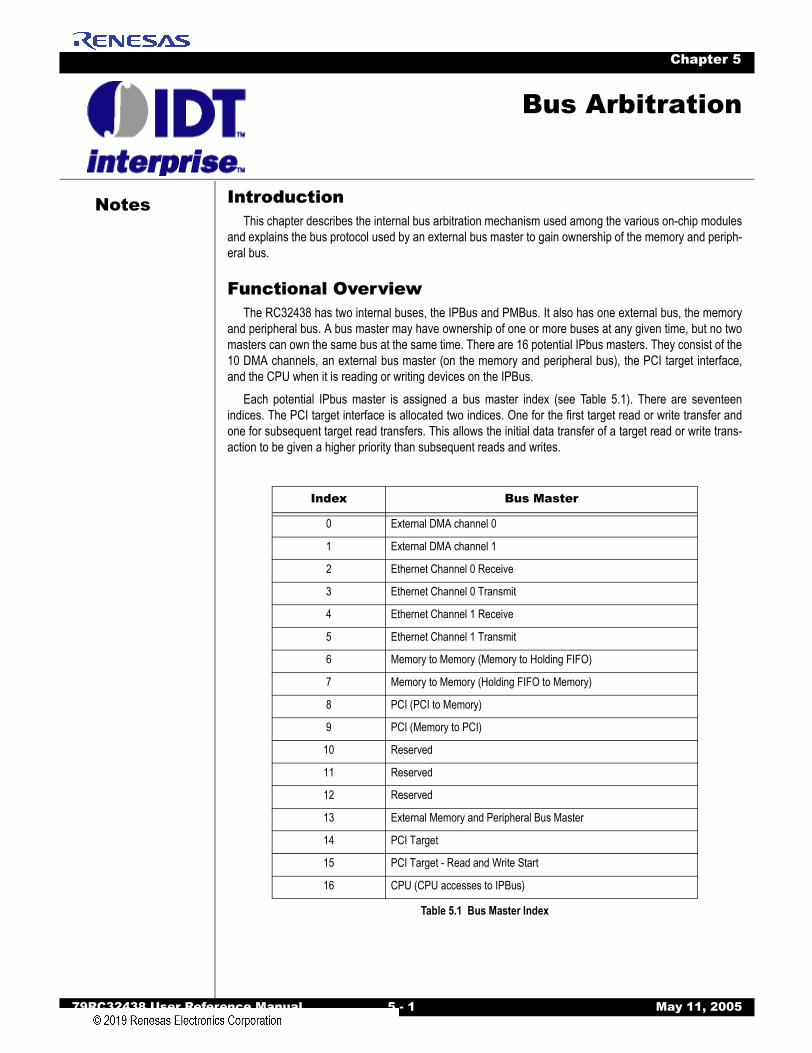
Notes
79RC32438 User Reference Manual 5 - 1 M
Chapter 5
Bus Arbitration
IntroductionThis chapter describes the internal bus arbitration mechanism used among the various on-chip modules
and explains the bus protocol used by an external bus master to gain ownership of the memory and periph-eral bus.
Functional OverviewThe RC32438 has two internal buses, the IPBus and PMBus. It also has one external bus, the memory
and peripheral bus. A bus master may have ownership of one or more buses at any given time, but no twomasters can own the same bus at the same time. There are 16 potential IPbus masters. They consist of the10 DMA channels, an external bus master (on the memory and peripheral bus), the PCI target interface,and the CPU when it is reading or writing devices on the IPBus.
Each potential IPbus master is assigned a bus master index (see Table 5.1). There are seventeenindices. The PCI target interface is allocated two indices. One for the first target read or write transfer andone for subsequent target read transfers. This allows the initial data transfer of a target read or write trans-action to be given a higher priority than subsequent reads and writes.
Index Bus Master
0 External DMA channel 0
1 External DMA channel 1
2 Ethernet Channel 0 Receive
3 Ethernet Channel 0 Transmit
4 Ethernet Channel 1 Receive
5 Ethernet Channel 1 Transmit
6 Memory to Memory (Memory to Holding FIFO)
7 Memory to Memory (Holding FIFO to Memory)
8 PCI (PCI to Memory)
9 PCI (Memory to PCI)
10 Reserved
11 Reserved
12 Reserved
13 External Memory and Peripheral Bus Master
14 PCI Target
15 PCI Target - Read and Write Start
16 CPU (CPU accesses to IPBus)
Table 5.1 Bus Master Index
ay 11, 2005
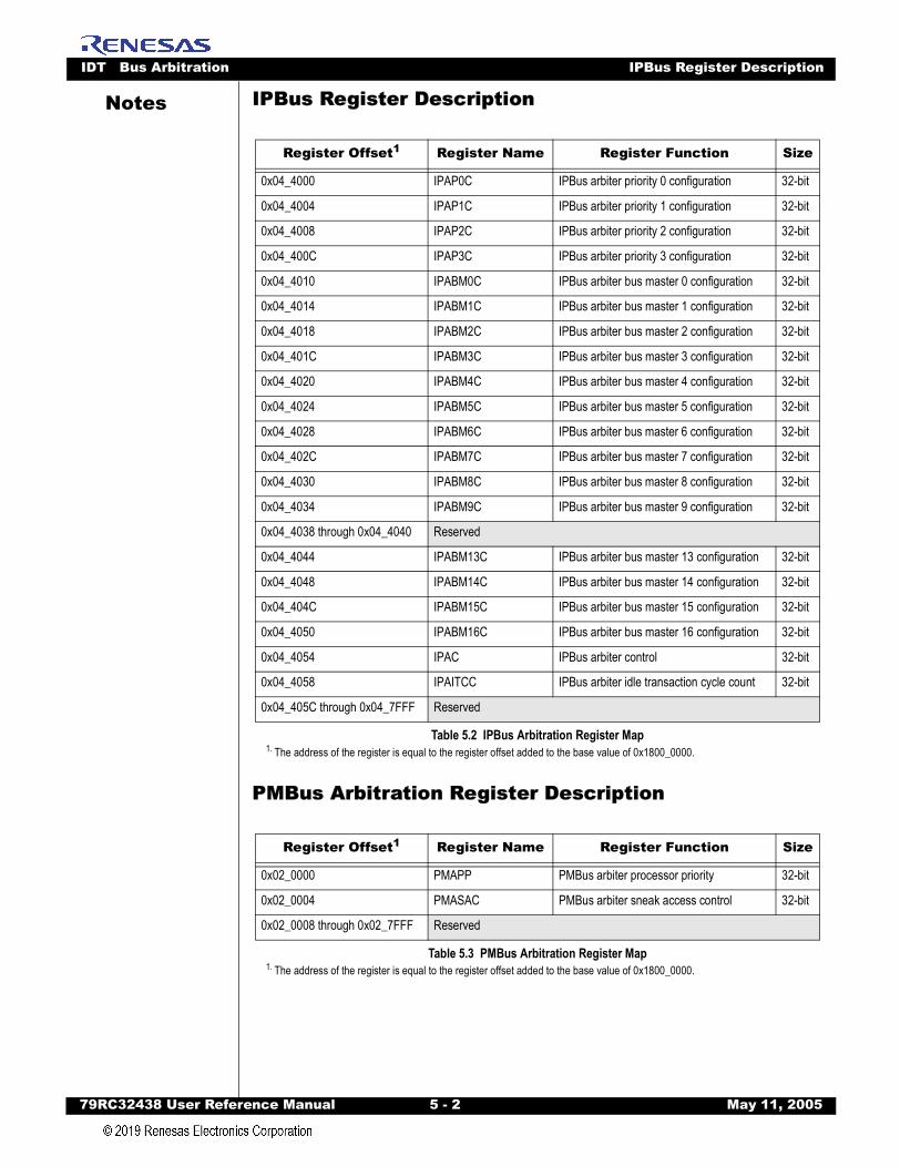
IDT Bus Arbitration IPBus Register Description
79RC32438 User Refer
Notes
IPBus Register DescriptionPMBus Arbitration Register Description
Register Offset1
1. The address of the register is equal to the register offset added to the base value of 0x1800_0000.
Register Name Register Function Size
0x04_4000 IPAP0C IPBus arbiter priority 0 configuration 32-bit
0x04_4004 IPAP1C IPBus arbiter priority 1 configuration 32-bit
0x04_4008 IPAP2C IPBus arbiter priority 2 configuration 32-bit
0x04_400C IPAP3C IPBus arbiter priority 3 configuration 32-bit
0x04_4010 IPABM0C IPBus arbiter bus master 0 configuration 32-bit
0x04_4014 IPABM1C IPBus arbiter bus master 1 configuration 32-bit
0x04_4018 IPABM2C IPBus arbiter bus master 2 configuration 32-bit
0x04_401C IPABM3C IPBus arbiter bus master 3 configuration 32-bit
0x04_4020 IPABM4C IPBus arbiter bus master 4 configuration 32-bit
0x04_4024 IPABM5C IPBus arbiter bus master 5 configuration 32-bit
0x04_4028 IPABM6C IPBus arbiter bus master 6 configuration 32-bit
0x04_402C IPABM7C IPBus arbiter bus master 7 configuration 32-bit
0x04_4030 IPABM8C IPBus arbiter bus master 8 configuration 32-bit
0x04_4034 IPABM9C IPBus arbiter bus master 9 configuration 32-bit
0x04_4038 through 0x04_4040 Reserved
0x04_4044 IPABM13C IPBus arbiter bus master 13 configuration 32-bit
0x04_4048 IPABM14C IPBus arbiter bus master 14 configuration 32-bit
0x04_404C IPABM15C IPBus arbiter bus master 15 configuration 32-bit
0x04_4050 IPABM16C IPBus arbiter bus master 16 configuration 32-bit
0x04_4054 IPAC IPBus arbiter control 32-bit
0x04_4058 IPAITCC IPBus arbiter idle transaction cycle count 32-bit
0x04_405C through 0x04_7FFF Reserved
Table 5.2 IPBus Arbitration Register Map
Register Offset1
1. The address of the register is equal to the register offset added to the base value of 0x1800_0000.
Register Name Register Function Size
0x02_0000 PMAPP PMBus arbiter processor priority 32-bit
0x02_0004 PMASAC PMBus arbiter sneak access control 32-bit
0x02_0008 through 0x02_7FFF Reserved
Table 5.3 PMBus Arbitration Register Map
ence Manual 5 - 2 May 11, 2005
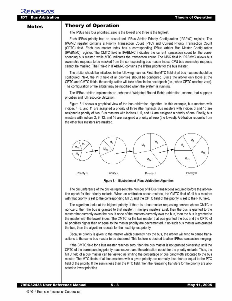
IDT Bus Arbitration Theory of Operation
79RC32438 User Refer
Notes
Theory of OperationThe IPBus has four priorities. Zero is the lowest and three is the highest.Each IPBus priority has an associated IPBus Arbiter Priority Configuration (IPAPxC) register. TheIPAPxC register contains a Priority Transaction Count (PTC) and Current Priority Transaction Count(CPTC) field. Each bus master index has a corresponding IPBus Arbiter Bus Master Configuration(IPABMxC) register. The CMTC field in IPABMxC indicates the current transaction count for the corre-sponding bus master, while MTC indicates the transaction count. The MSK field in IPABMxC allows busownership requests to be masked from the corresponding bus master index. CPU bus ownership requestscannot be masked. The P field in IPABMxC contains the IPBus priority for the bus master.
The arbiter should be initialized in the following manner. First, the MTC field of all bus masters should beconfigured. Next, the PTC field of all priorities should be configured. Since the arbiter only looks at theCPTC and CMTC fields, the configuration will take affect in the next epoch (i.e., when CPTC reaches zero).The configuration of the arbiter may be modified when the system is running.
The IPBus arbiter implements an enhanced Weighted Round Robin arbitration scheme that supportspriorities and full resource utilization.
Figure 5.1 shows a graphical view of the bus arbitration algorithm. In this example, bus masters withindices 4, 8, and 11 are assigned a priority of three (the highest). Bus masters with indices 3 and 15 areassigned a priority of two. Bus masters with indices 1, 5, and 14 are assigned a priority of one. Finally, busmasters with indices 2, 9, 13, and 16 are assigned a priority of zero (the lowest). Arbitration requests fromthe other bus masters are masked.
Figure 5.1 Illustration of IPbus Arbitration Algorithm
The circumference of the circles represent the number of IPBus transactions required before the arbitra-tion epoch for that priority restarts. When an arbitration epoch restarts, the CMTC field of all bus masterswith that priority is set to the corresponding MTC, and the CPTC field of the priority is set to the PTC field.
The algorithm looks at the highest priority. If there is a bus master requesting service whose CMTC isnon-zero, then the bus is granted to that master. If multiple masters exist, then the bus is granted to themaster that currently owns the bus. If none of the masters currently own the bus, then the bus is granted tothe master with the lowest index. The CMTC for the bus master that was granted the bus and the CPTC ofall priorities higher than or equal to the master priority are decremented. If no such bus master was grantedthe bus, then the algorithm repeats for the next highest priority.
Because priority is given to the master which currently has the bus, the arbiter will tend to cause trans-actions to the same bus master to be clustered. This feature is desired to allow IPBus transaction merging.
If the CMTC field for a bus master reaches zero, then the bus master is not granted ownership until theCPTC of the corresponding priority reaches zero and the arbitration epoch for the priority restarts. Thus, theMTC field of a bus master can be viewed as limiting the percentage of bus bandwidth allocated to the busmaster. The MTC fields of all bus masters with a given priority are normally less than or equal to the PTCfield of the priority. If the sum is less than the PTC field, then the remaining transfers for the priority are allo-cated to lower priorities.
M11
M8
M4
M15
M3M1
M14
M5
M13
M2
M9
M16
Priority 3 Priority 1Priority 2 Priority 0
ence Manual 5 - 3 May 11, 2005

IDT Bus Arbitration Theory of Operation
79RC32438 User Refer
Notes
The minimum percentage of bus bandwidth available for a given priority can be calculated as follows forthe above example:Where MTCi is the MTC for the bus master with index i and PTCj is the PTC for priority j.As an example, the percentage of bus bandwidth available to bus masters 3 and 4 may be calculated as
follows:
It should be apparent that these equations approximate bus bandwidth since the IPBus arbiter dealswith transactions and not clock cycles. Despite this fact, the IPBus arbiter provides a mechanism to boundservice delays and provide a guaranteed level of service.
When the CMTC field of all bus masters requesting service is zero, then instead of allowing the IPBus togo idle, the bus is granted in a fair manner to one of the bus master(s) with the highest priority.
IPBus supports transaction merging. This allows burst transfers to the Double Data Rate (DDR)controller that are longer than a maximal length DMA burst (16 words). It also allows the system to limitqueueing delays and hence minimize the size of buffers.
The DDR controller can supply data at twice the data rate required by the IPBus. The IPBus arbiterpasses hints to the DDR controller when IPBus transaction merging may take place. The DDR controlleruses this information to speculatively prefetch data potentially required for the next DMA transaction. Whenthe Disable Prefetching (DP) bit is set in the IPBus Arbiter Control (IPAC) register, DDR prefetching hintsare disabled (i.e., the DDR controller will never speculatively prefetch data).
Figure 5.2 depicts a flow chart of the IPBus arbitration algorithm.
BW available to priority 3 100%=
BW available to priority 2 1MTC8 MTC4 MTC11+ +
PTC3-------------------------------------------------------------------–⎝ ⎠
⎛ ⎞ x100%=
BW available to priority 1 1MTC8 MTC4 MTC11+ +
PTC3-------------------------------------------------------------------–⎝ ⎠
⎛ ⎞ x 1MTC3 MTC15+
PTC2-------------------------------------------–⎝ ⎠
⎛ ⎞ x100%=
BW available to priority 0 1MTC8 MTC4 MTC11+ +
PTC3-------------------------------------------------------------------–⎝ ⎠
⎛ ⎞ x 1MTC3 MTC15+
PTC2-------------------------------------------–⎝ ⎠
⎛ ⎞
1MTC1 MTC5 MTC14+ +
PTC1-------------------------------------------------------------------–⎝ ⎠
⎛ ⎞ x100%
=
BW available to bus master 4MTC4PTC3----------------x100%=
BW available to bus master 3MTC3PTC2----------------x 1
MTC8 MTC4 MTC11+ +PTC3
-------------------------------------------------------------------–⎝ ⎠⎛ ⎞ x100%=
ence Manual 5 - 4 May 11, 2005
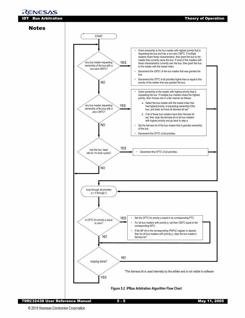
IDT Bus Arbitration Theory of Operation
79RC32438 User Refer
Notes
Figure 5.2 IPBus Arbitration Algorithm Flow Chart
*The fairness bit is used internally by the arbiter and is not visible to software
any bus master requesting ownership of the bus with a
non-zero CMTC?
any bus master requesting ownership of the bus with a
zero CMTC?
• Grant ownership to the master with highest priority that is requesting the bus. If multiple bus masters share the highest priority, then choose one in a fair manner as follows:
a Select the bus master with the lowest index that has highest priority, is requesting ownership of the bus, and does not have its fairness bit set.*
b If all of these bus masters have their fairness bit set, then clear the fairness bit of all bus masters with highest priority and go back to step a.
• Set the fairness bit of the bus master that is granted ownership of the bus.
• Decrement the CPTC of all priorities.
• Decrement the CPTC of all priorities.
looping done?
START
is CPTC for priority p equal to zero?
loop through all priorities p = 0 through 3
• Set the CPTC for priority p equal to its corresponding PTC.• For all bus masters with priority p, set their CMTC equal to the
corresponding MTC.• If the MF bit in the corresponding IPAPxC register is cleared,
then for all bus masters with priority p, clear the bus master’s fairness bit.*
YES
NO
YES
NO
YES
YES
NO
NO
has the bus beenidle for 16 clock cycles?
YES
NO
• Grant ownership to the bus master with highest priority that is requesting the bus and has a non-zero CMTC. If multiple masters share these characteristics, then grant the bus to the master that currently owns the bus. If none of the masters with these characteristics currently own the bus, then grant the bus to the master with the lowest index.
• Decrement the CMTC of the bus master that was granted the bus.
• Decrement the CPTC of all priorities higher than or equal to the priority of the master that was granted the bus.
ence Manual 5 - 5 May 11, 2005
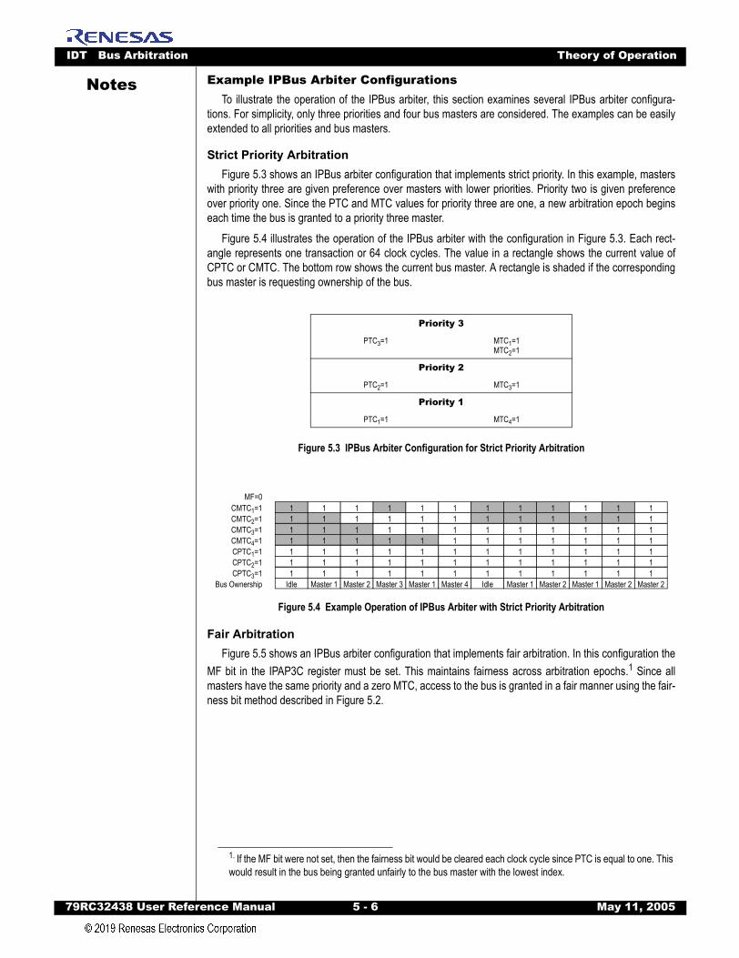
IDT Bus Arbitration Theory of Operation
79RC32438 User Refer
Notes
Example IPBus Arbiter ConfigurationsTo illustrate the operation of the IPBus arbiter, this section examines several IPBus arbiter configura-tions. For simplicity, only three priorities and four bus masters are considered. The examples can be easilyextended to all priorities and bus masters.
Strict Priority ArbitrationFigure 5.3 shows an IPBus arbiter configuration that implements strict priority. In this example, masters
with priority three are given preference over masters with lower priorities. Priority two is given preferenceover priority one. Since the PTC and MTC values for priority three are one, a new arbitration epoch beginseach time the bus is granted to a priority three master.
Figure 5.4 illustrates the operation of the IPBus arbiter with the configuration in Figure 5.3. Each rect-angle represents one transaction or 64 clock cycles. The value in a rectangle shows the current value ofCPTC or CMTC. The bottom row shows the current bus master. A rectangle is shaded if the correspondingbus master is requesting ownership of the bus.
Figure 5.3 IPBus Arbiter Configuration for Strict Priority Arbitration
Figure 5.4 Example Operation of IPBus Arbiter with Strict Priority Arbitration
Fair ArbitrationFigure 5.5 shows an IPBus arbiter configuration that implements fair arbitration. In this configuration the
MF bit in the IPAP3C register must be set. This maintains fairness across arbitration epochs.1 Since allmasters have the same priority and a zero MTC, access to the bus is granted in a fair manner using the fair-ness bit method described in Figure 5.2.
Priority 3
PTC3=1 MTC1=1MTC2=1
Priority 2
PTC2=1 MTC3=1
Priority 1
PTC1=1 MTC4=1
1. If the MF bit were not set, then the fairness bit would be cleared each clock cycle since PTC is equal to one. This would result in the bus being granted unfairly to the bus master with the lowest index.
CMTC1=1CMTC2=1CMTC3=1CMTC4=1CPTC1=1CPTC2=1CPTC3=1
Bus Ownership Idle1111111
Master 11111111
Master 21111111
Master 31111111
Master 11111111
Master 41111111
Idle1111111
Master 11111111
Master 21111111
Master 11111111
Master 21111111
Master 21111111
MF=0
ence Manual 5 - 6 May 11, 2005

IDT Bus Arbitration Theory of Operation
79RC32438 User Refer
Notes
Figure 5.5 IPBus Arbiter Configuration for Fair Arbitration
Figure 5.6 Example Operation of IPBus Arbiter with Fair Arbitration
Priority Arbitration with FairnessA difficulty with strict priority arbitration, presented above, is that it can lead to starvation within a priority.
For the example in Figure 5.4, it is possible for master two to starve since it has a higher index than masterone. If master one continuously requests the bus, master two will starve. Priority arbitration with fairnesswithin a priority eliminates this starvation. As in the fair arbitration example, the MF bit in the IPAP3Cregister must be set. This maintains fairness across arbitration epochs.
Figure 5.7 shows an IPBus arbiter configuration that implements priority arbitration with fairness. Owner-ship is granted to the bus master with the highest priority level which is requesting the bus. If multiple busmasters are requesting ownership and share the same priority level, then ownership is granted in a fairmanner within the priority level.
Figure 5.7 IPBus Arbiter Configuration for Priority Arbitration with Fairness
Priority 3
PTC3=1 MTC1=0MTC2=0MTC3=0MTC4=0
Priority 2
PTC2=0
Priority 1
PTC1=0
Priority 3
PTC3=0 MTC1=0MTC2=0
Priority 2
PTC2=0 MTC3=0
Priority 1
PTC1=0 MTC4=0
CMTC1=0CMTC2=0CMTC3=0CMTC4=0CPTC1=0CPTC2=0CPTC3=1
Bus Ownership Idle1000000
Master 11000000
Master 21000000
Master 31000000
Master 41000000
Master 11000000
Idle1000000
Master 21000000
Master 11000000
Master 210000
00
Master 11000000
Master 21000000
MF=1
ence Manual 5 - 7 May 11, 2005
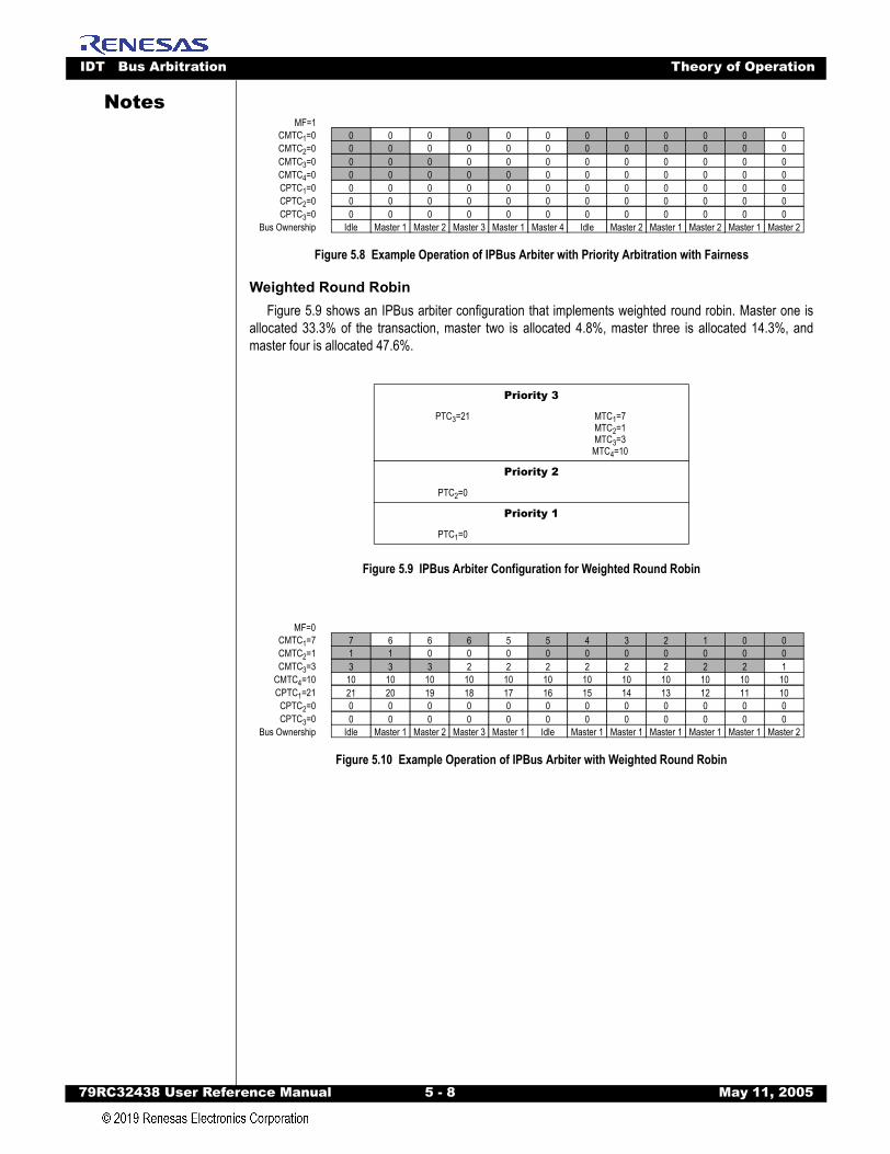
IDT Bus Arbitration Theory of Operation
79RC32438 User Refer
Notes
Figure 5.8 Example Operation of IPBus Arbiter with Priority Arbitration with Fairness
Weighted Round RobinFigure 5.9 shows an IPBus arbiter configuration that implements weighted round robin. Master one is
allocated 33.3% of the transaction, master two is allocated 4.8%, master three is allocated 14.3%, andmaster four is allocated 47.6%.
Figure 5.9 IPBus Arbiter Configuration for Weighted Round Robin
Figure 5.10 Example Operation of IPBus Arbiter with Weighted Round Robin
Priority 3
PTC3=21 MTC1=7MTC2=1MTC3=3
MTC4=10
Priority 2
PTC2=0
Priority 1
PTC1=0
CMTC1=0CMTC2=0CMTC3=0CMTC4=0CPTC1=0CPTC2=0CPTC3=0
Bus Ownership Idle0000000
Master 10000000
Master 20000000
Master 30000000
Master 10000000
Master 40000000
Idle0000000
Master 20000000
Master 10000000
Master 20000000
Master 10000000
Master 20000000
MF=1
CMTC1=7CMTC2=1CMTC3=3
CMTC4=10CPTC1=21
CPTC2=0CPTC3=0
Bus Ownership Idle00
2110317
Master 100
2010316
Master 200
1910306
Master 300
1810206
Master 100
1710205
Idle00
1610205
Master 100
1510204
Master 100
1410203
Master 100
1310202
Master 100
1210201
Master 100
1110200
Master 200
1010100
MF=0
ence Manual 5 - 8 May 11, 2005

IDT Bus Arbitration IPBus Registers
79RC32438 User Refer
Notes
IPBus RegistersIPBus Arbiter Control Register
Figure 5.11 IPBus Arbiter Control Register (IPAC)
DP
Description: Disable Prefetching. When this bit is set, the IPBus arbiter disables prefetching hints passed to the DDR controller (i.e., the DDR controller will never speculatively prefetch data).
Initial Value: 0x0
Read Value: Previous value written
Write Effect: Modify value
DWM
Description: Disable Write Transaction Merging. When this bit is set, write transaction merging is disabled for all IPBus masters.
Initial Value: 0x0
Read Value: Previous value written
Write Effect: Modify value
DRM
Description: Disable Read Transaction Merging. When this bit is set, read transaction merging is disabled for all IPBus masters.
Initial Value: 0x0
Read Value: Previous value written
Write Effect: Modify value
MSK
Description: Mask Bus Ownership Requests. When this bit is set, all bus ownership requests are masked except those from the CPU.
Initial Value: 0x0
Read Value: Previous value written
Write Effect: Modify value
IPAC031
28
0
1
DP
1
0
1
DWM
1
DRM
1
MSK
ence Manual 5 - 9 May 11, 2005
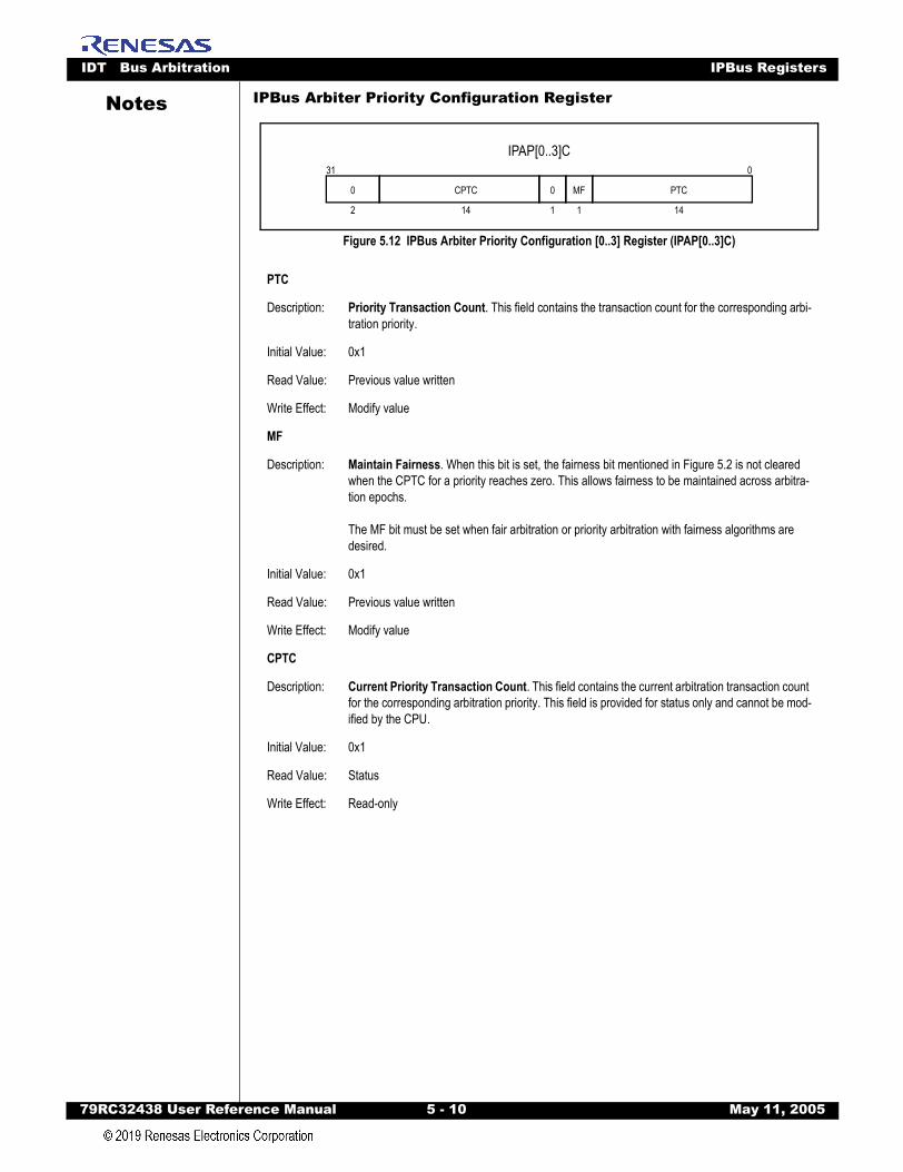
IDT Bus Arbitration IPBus Registers
79RC32438 User Refer
Notes
IPBus Arbiter Priority Configuration RegisterFigure 5.12 IPBus Arbiter Priority Configuration [0..3] Register (IPAP[0..3]C)
PTC
Description: Priority Transaction Count. This field contains the transaction count for the corresponding arbi-tration priority.
Initial Value: 0x1
Read Value: Previous value written
Write Effect: Modify value
MF
Description: Maintain Fairness. When this bit is set, the fairness bit mentioned in Figure 5.2 is not cleared when the CPTC for a priority reaches zero. This allows fairness to be maintained across arbitra-tion epochs.
The MF bit must be set when fair arbitration or priority arbitration with fairness algorithms are desired.
Initial Value: 0x1
Read Value: Previous value written
Write Effect: Modify value
CPTC
Description: Current Priority Transaction Count. This field contains the current arbitration transaction count for the corresponding arbitration priority. This field is provided for status only and cannot be mod-ified by the CPU.
Initial Value: 0x1
Read Value: Status
Write Effect: Read-only
IPAP[0..3]C031
14
PTC
1
0
2
0
1
MF
14
CPTC
ence Manual 5 - 10 May 11, 2005
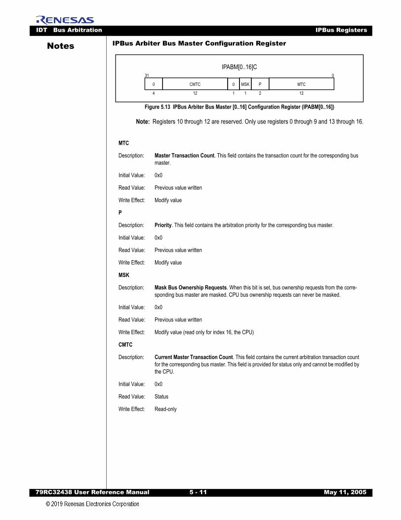
IDT Bus Arbitration IPBus Registers
79RC32438 User Refer
Notes
IPBus Arbiter Bus Master Configuration RegisterFigure 5.13 IPBus Arbiter Bus Master [0..16] Configuration Register (IPABM[0..16])
Note: Registers 10 through 12 are reserved. Only use registers 0 through 9 and 13 through 16.
MTC
Description: Master Transaction Count. This field contains the transaction count for the corresponding bus master.
Initial Value: 0x0
Read Value: Previous value written
Write Effect: Modify value
P
Description: Priority. This field contains the arbitration priority for the corresponding bus master.
Initial Value: 0x0
Read Value: Previous value written
Write Effect: Modify value
MSK
Description: Mask Bus Ownership Requests. When this bit is set, bus ownership requests from the corre-sponding bus master are masked. CPU bus ownership requests can never be masked.
Initial Value: 0x0
Read Value: Previous value written
Write Effect: Modify value (read only for index 16, the CPU)
CMTC
Description: Current Master Transaction Count. This field contains the current arbitration transaction count for the corresponding bus master. This field is provided for status only and cannot be modified by the CPU.
Initial Value: 0x0
Read Value: Status
Write Effect: Read-only
IPABM[0..16]C031
12
CMTC
4
0
12
MTC
2
PMSK
1
0
1
ence Manual 5 - 11 May 11, 2005
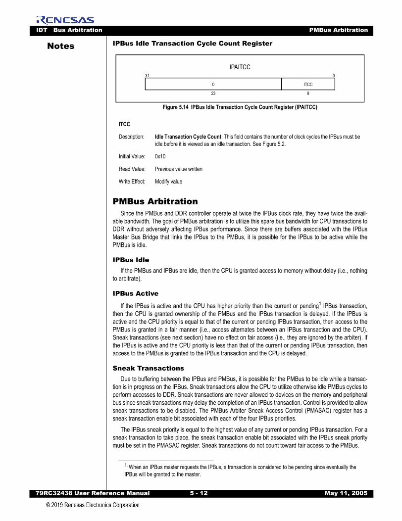
IDT Bus Arbitration PMBus Arbitration
79RC32438 User Refer
Notes
IPBus Idle Transaction Cycle Count RegisterFigure 5.14 IPBus Idle Transaction Cycle Count Register (IPAITCC)
PMBus ArbitrationSince the PMBus and DDR controller operate at twice the IPBus clock rate, they have twice the avail-
able bandwidth. The goal of PMBus arbitration is to utilize this spare bus bandwidth for CPU transactions toDDR without adversely affecting IPBus performance. Since there are buffers associated with the IPBusMaster Bus Bridge that links the IPBus to the PMBus, it is possible for the IPBus to be active while thePMBus is idle.
IPBus IdleIf the PMBus and IPBus are idle, then the CPU is granted access to memory without delay (i.e., nothing
to arbitrate).
IPBus Active
If the IPBus is active and the CPU has higher priority than the current or pending1 IPBus transaction,then the CPU is granted ownership of the PMBus and the IPBus transaction is delayed. If the IPBus isactive and the CPU priority is equal to that of the current or pending IPBus transaction, then access to thePMBus is granted in a fair manner (i.e., access alternates between an IPBus transaction and the CPU).Sneak transactions (see next section) have no effect on fair access (i.e., they are ignored by the arbiter). Ifthe IPBus is active and the CPU priority is less than that of the current or pending IPBus transaction, thenaccess to the PMBus is granted to the IPBus transaction and the CPU is delayed.
Sneak TransactionsDue to buffering between the IPBus and PMBus, it is possible for the PMBus to be idle while a transac-
tion is in progress on the IPBus. Sneak transactions allow the CPU to utilize otherwise idle PMBus cycles toperform accesses to DDR. Sneak transactions are never allowed to devices on the memory and peripheralbus since sneak transactions may delay the completion of an IPBus transaction. Control is provided to allowsneak transactions to be disabled. The PMBus Arbiter Sneak Access Control (PMASAC) register has asneak transaction enable bit associated with each of the four IPBus priorities.
The IPBus sneak priority is equal to the highest value of any current or pending IPBus transaction. For asneak transaction to take place, the sneak transaction enable bit associated with the IPBus sneak prioritymust be set in the PMASAC register. Sneak transactions do not count toward fair access to the PMBus.
ITCC
Description: Idle Transaction Cycle Count. This field contains the number of clock cycles the IPBus must be idle before it is viewed as an idle transaction. See Figure 5.2.
Initial Value: 0x10
Read Value: Previous value written
Write Effect: Modify value
1. When an IPBus master requests the IPBus, a transaction is considered to be pending since eventually the IPBus will be granted to the master.
IPAITCC031
23
0
9
ITCC
ence Manual 5 - 12 May 11, 2005
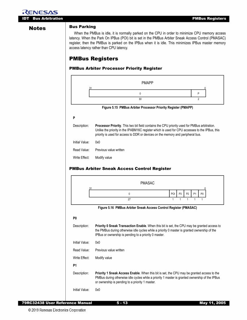
IDT Bus Arbitration PMBus Registers
79RC32438 User Refer
Notes
Bus ParkingWhen the PMBus is idle, it is normally parked on the CPU in order to minimize CPU memory accesslatency. When the Park On IPBus (POI) bit is set in the PMBus Arbiter Sneak Access Control (PMASAC)register, then the PMBus is parked on the IPBus when it is idle. This minimizes IPBus master memoryaccess latency rather than CPU latency.
PMBus Registers
PMBus Arbiter Processor Priority Register
Figure 5.15 PMBus Arbiter Processor Priority Register (PMAPP)
PMBus Arbiter Sneak Access Control Register
Figure 5.16 PMBus Arbiter Sneak Access Control Register (PMASAC)
P
Description: Processor Priority. This two bit field contains the CPU priority used for PMBus arbitration. Unlike the priority in the IPABM16C register which is used for CPU accesses to the IPBus, this priority is used for access to DDR or devices on the memory and peripheral bus.
Initial Value: 0x0
Read Value: Previous value written
Write Effect: Modify value
P0
Description: Priority 0 Sneak Transaction Enable. When this bit is set, the CPU may be granted access to the PMBus during otherwise idle cycles while a priority 0 master is granted ownership of the IPBus or ownership is pending to a priority 0 master.
Initial Value: 0x0
Read Value: Previous value written
Write Effect: Modify value
P1
Description: Priority 1 Sneak Access Enable. When this bit is set, the CPU may be granted access to the PMBus during otherwise idle cycles while a priority 1 master is granted ownership of the IPBus or ownership is pending to a priority 1 master.
Initial Value: 0x0
PMAPP031
2
P
30
0
PMASAC031
1
P1
27
0
1
P2
1
P3
1
P0
1
POI
ence Manual 5 - 13 May 11, 2005
IDT Bus Arbitration Memory and Peripheral Bus Arbitration
79RC32438 User Refer
Notes
Memory and Peripheral Bus ArbitrationThe RC32438 allows external bus masters on the memory and peripheral bus. An external bus master
asserts the bus request (BRN) input to the RC32438 to request ownership of the memory and peripheralbus.1 The RC32438 responds to the assertion of BRN by relinquishing ownership of the memory andperipheral bus by asserting bus grant (BGN) and simultaneously tri-stating2 the following signals:
MADDR[25:0],MDATA[15:0],BWEN[1:0],OEN,RWN,CSN[5:0],BOEN,BDIRN.
Read Value: Previous value written
Write Effect: Modify value
P2
Description: Priority 2 Sneak Transaction Enable. When this bit is set, the CPU may be granted access to the PMBus during otherwise idle cycles while a priority 2 master is granted ownership of the IPBus or ownership is pending to a priority 2 master.
Initial Value: 0x0
Read Value: Previous value written
Write Effect: Modify value
P3
Description: Priority 3 Sneak Transaction Enable. When this bit is set, the CPU may be granted access to the PMBus during otherwise idle cycles while a priority 3 master is granted ownership of the IPBus or ownership is pending to a priority 3 master.
Initial Value: 0x0
Read Value: Previous value written
Write Effect: Modify value
POI
Description: Park On IPBus. When the PMBus is idle, it is normally parked on the CPU. When the PMBus is idle and this bit is set, the PMBus is parked on the IPBus.
Initial Value: 0x0
Read Value: Previous value written
Write Effect: Modify value
1. Once an external bus master has requested the bus by asserting BRN, it must keep BRN asserted until it is granted the bus (i.e., it observes BGN asserted).2. CSN[5:0] and BOEN shall have been in their negated state for at least one EXTCLK clock cycle before being tri-stated. This is true when both the RC32438 or the external bus master relinquish ownership.
ence Manual 5 - 14 May 11, 2005
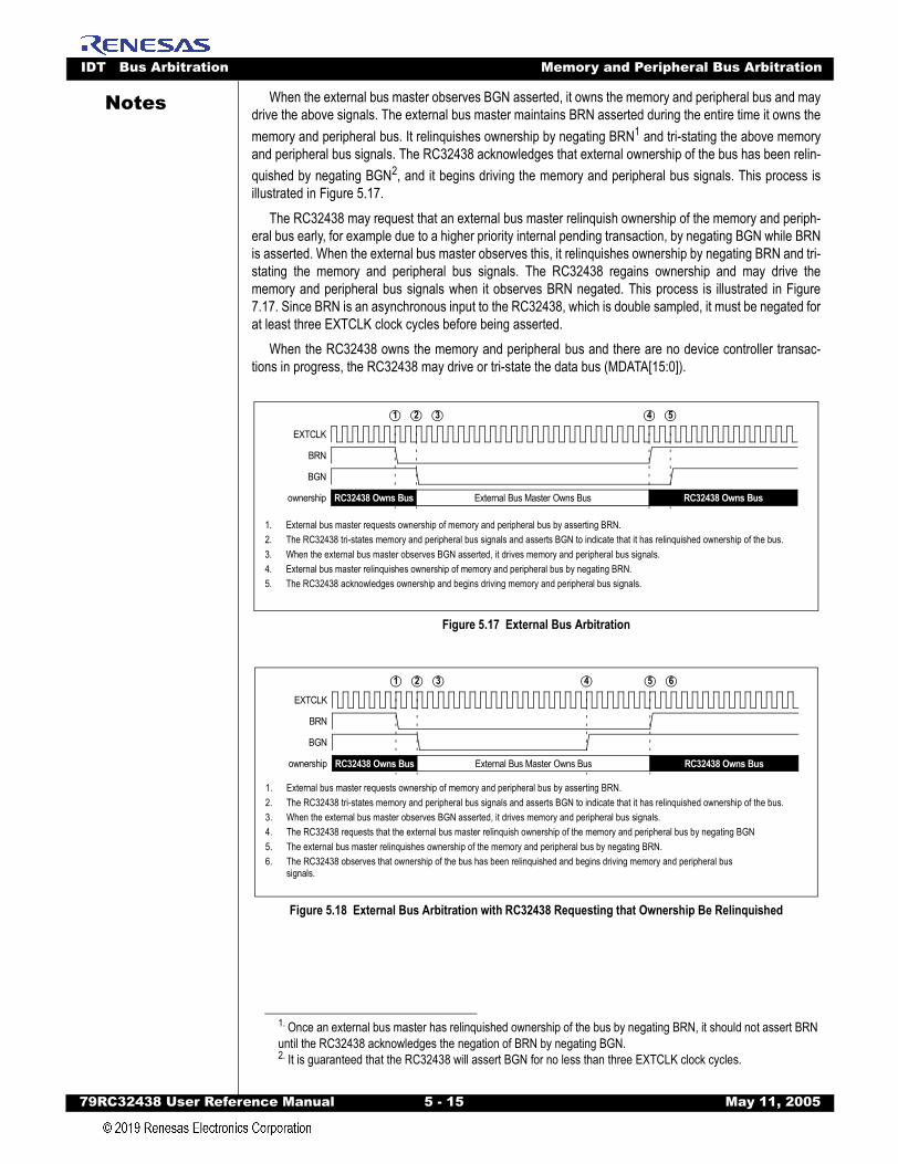
IDT Bus Arbitration Memory and Peripheral Bus Arbitration
79RC32438 User Refer
Notes
When the external bus master observes BGN asserted, it owns the memory and peripheral bus and maydrive the above signals. The external bus master maintains BRN asserted during the entire time it owns thememory and peripheral bus. It relinquishes ownership by negating BRN1 and tri-stating the above memoryand peripheral bus signals. The RC32438 acknowledges that external ownership of the bus has been relin-quished by negating BGN2, and it begins driving the memory and peripheral bus signals. This process isillustrated in Figure 5.17.The RC32438 may request that an external bus master relinquish ownership of the memory and periph-eral bus early, for example due to a higher priority internal pending transaction, by negating BGN while BRNis asserted. When the external bus master observes this, it relinquishes ownership by negating BRN and tri-stating the memory and peripheral bus signals. The RC32438 regains ownership and may drive thememory and peripheral bus signals when it observes BRN negated. This process is illustrated in Figure7.17. Since BRN is an asynchronous input to the RC32438, which is double sampled, it must be negated forat least three EXTCLK clock cycles before being asserted.
When the RC32438 owns the memory and peripheral bus and there are no device controller transac-tions in progress, the RC32438 may drive or tri-state the data bus (MDATA[15:0]).
Figure 5.17 External Bus Arbitration
Figure 5.18 External Bus Arbitration with RC32438 Requesting that Ownership Be Relinquished
1. Once an external bus master has relinquished ownership of the bus by negating BRN, it should not assert BRN until the RC32438 acknowledges the negation of BRN by negating BGN.2. It is guaranteed that the RC32438 will assert BGN for no less than three EXTCLK clock cycles.
EXTCLK
BRN
BGN
ownership
1 4 52 3
RC32438 Owns Bus RC32438 Owns BusExternal Bus Master Owns Bus
1. External bus master requests ownership of memory and peripheral bus by asserting BRN.2. The RC32438 tri-states memory and peripheral bus signals and asserts BGN to indicate that it has relinquished ownership of the bus.3. When the external bus master observes BGN asserted, it drives memory and peripheral bus signals.4. External bus master relinquishes ownership of memory and peripheral bus by negating BRN.5. The RC32438 acknowledges ownership and begins driving memory and peripheral bus signals.
EXTCLK
BRN
BGN
ownership
1 5 62 3
RC32438 Owns Bus RC32438 Owns BusExternal Bus Master Owns Bus
4
1. External bus master requests ownership of memory and peripheral bus by asserting BRN.2. The RC32438 tri-states memory and peripheral bus signals and asserts BGN to indicate that it has relinquished ownership of the bus.3. When the external bus master observes BGN asserted, it drives memory and peripheral bus signals.4. The RC32438 requests that the external bus master relinquish ownership of the memory and peripheral bus by negating BGN5. The external bus master relinquishes ownership of the memory and peripheral bus by negating BRN.6. The RC32438 observes that ownership of the bus has been relinquished and begins driving memory and peripheral bus
signals.
ence Manual 5 - 15 May 11, 2005
IDT Bus Arbitration Memory and Peripheral Bus Arbitration
79RC32438 User Refer
Notes
ence Manual 5 - 16 May 11, 2005

Notes
79RC32438 User Reference Manual 6 - 1 M
Chapter 6
Device Controller
IntroductionThe device controller on the RC32438 device provides a glueless interface to: SRAMs, ROMs/PROMs/
EEPROMs, dual port memories, and many peripheral devices. The device controller generates all of thesignals required to support both Intel and Motorola style peripherals and can directly control up to sixdevices. Additional devices may be supported through external decoding of the address bus.
FeaturesProvides “glueless” interface to standard SRAM, Flash, ROM, dual-port memory, and peripheral devicesDemultiplexed address and data buses
– 16-bit data bus– 26-bit address bus– 6 chip selects– Supports alternate bus masters– Control for external data bus buffers
Supports 8-bit and 16-bit width devices– Automatic byte gathering and scattering
Flexible protocol configuration parameters– Programmable number of wait states (0 to 63)– Programmable postread/postwrite delay (0 to 31)– Supports external wait state generation– Supports Intel and Motorola style peripherals
Write protect capability per chip selectProgrammable bus transaction timer generates warm reset when counter expiresSupports up to 64 MB of memory per chip selectProvides clocking for external devices on the memory and peripheral bus
Device Controller Register Description
Register Offset1 Register Name Register Function Size
0x01_0000 DEV0BASE Device 0 Base 32-bit
0x01_0004 DEV0MASK Device 0 Mask 32-bit
0x01_0008 DEV0C Device 0 Control 32-bit
0x01_000C DEV0TC Device 0 Timing control 32-bit
0x01_0010 DEV1BASE Device 1 Base 32-bit
0x01_0014 DEV1MASK Device 1 Mask 32-bit
0x01_0018 DEV1C Device 1 Control 32-bit
0x01_001C DEV1TC Device 1 Timing control 32-bit
0x01_0020 DEV2BASE Device 2 Base 32-bit
Table 6.1 Device Controller Register Map
ay 11, 2005
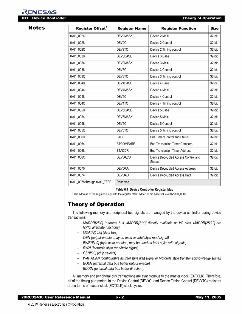
IDT Device Controller Theory of Operation
79RC32438 User Refer
Notes
Theory of OperationThe following memory and peripheral bus signals are managed by the device controller during device
transactions:– MADDR[25:0] (address bus, MADDR[21:0] directly available as I/O pins, MADDR[25:22] are
GPIO alternate functions)– MDATA[15:0] (data bus)– OEN (output enable, may be used as Intel style read signal)– BWEN[1:0] (byte write enables, may be used as Intel style write signals)– RWN (Motorola style read/write signal)– CSN[5:0] (chip selects)– WAITACKN (configurable as Intel style wait signal or Motorola style transfer acknowledge signal)– BOEN (external data bus buffer output enable)– BDIRN (external data bus buffer direction).
All memory and peripheral bus transactions are synchronous to the master clock (EXTCLK). Therefore,all of the timing parameters in the Device Control (DEVxC) and Device Timing Control (DEVxTC) registersare in terms of master clock (EXTCLK) clock cycles.
0x01_0024 DEV2MASK Device 2 Mask 32-bit
0x01_0028 DEV2C Device 2 Control 32-bit
0x01_002C DEV2TC Device 2 Timing control 32-bit
0x01_0030 DEV3BASE Device 3 Base 32-bit
0x01_0034 DEV3MASK Device 3 Mask 32-bit
0x01_0038 DEV3C Device 3 Control 32-bit
0x01_003C DEV3TC Device 3 Timing control 32-bit
0x01_0040 DEV4BASE Device 4 Base 32-bit
0x01_0044 DEV4MASK Device 4 Mask 32-bit
0x01_0048 DEV4C Device 4 Control 32-bit
0x01_004C DEV4TC Device 4 Timing control 32-bit
0x01_0050 DEV5BASE Device 5 Base 32-bit
0x01_0054 DEV5MASK Device 5 Mask 32-bit
0x01_0058 DEV5C Device 5 Control 32-bit
0x01_005C DEV5TC Device 5 Timing control 32-bit
0x01_0060 BTCS Bus Timer Control and Status 32-bit
0x01_0064 BTCOMPARE Bus Transaction Timer Compare 32-bit
0x01_0068 BTADDR Bus Transaction Timer Address 32-bit
0x01_006C DEVDACS Device Decoupled Access Control and Status
32-bit
0x01_0070 DEVDAA Device Decoupled Access Address 32-bit
0x01_0074 DEVDAD Device Decoupled Access Data 32-bit
0x01_0078 through 0x01_7FFF Reserved
1. The address of the register is equal to the register offset added to the base value of 0x1800_0000.
Register Offset1 Register Name Register Function Size
Table 6.1 Device Controller Register Map
ence Manual 6 - 2 May 11, 2005

IDT Device Controller Theory of Operation
79RC32438 User Refer
Notes
The endianess of the RC32438 is selected during boot configuration. Regardless of the selected endi-aness, devices are connected to the RC32438 data bus in a right aligned manner, as shown in Figure 6.1.8-bit device data is read and written on MDATA[7:0] and 16-bit device data is read and written onMDATA[15:0].Figure 6.1 Connecting Devices to the RC32438 Data Bus (Right Aligned)
The width of a device, 8-bits or 16-bits, is configured in the device size (DS) field of the device [0..5]control register (DEV[0..5]C). The RC32438 performs byte gathering during read transactions and bytescattering during write transactions, allowing word and half-word read and write operations to any sizedevice. The RC32438’s address bus is always driven with a byte address. 8-bit devices use MADDR[25:0],and 16-bit devices use MADDR[25:1]. During write transactions to 16-bit, the byte write enable (BWEN[1:0])signals are used to select byte lanes to be written.
The RC32438 supports four transaction types: a device read transaction, a burst device read transac-tion, a device write transaction, and a burst device write transaction. Transaction parameters for eachdevice are programmed in the corresponding device [0..5] control register (DEV[0..5]C) and device [0..5]timing control (DEV[0..5]TC) register. In particular, the wait/ack mode (WAM) bit in the DEVxC registercontrols whether the WAITACKN signal operates as an Intel style wait signal or as a Motorola styleacknowledge signal. Although WAITACKN is classified as an asynchronous input, to support systems thatuse master clock to generate it, asynchronous input setup and hold times are provided. If the setup andhold times are met for the assertion of WAITACKN, then the RC32438 is guaranteed to recognize iton a specific rising edge of the clock.
By configuring the programmable parameters in the DEVxC and DEVxTC registers, Intel and Motorolastyle bus transactions may be generated. Burst read transactions to devices which do not support burstreads may be disabled by clearing the burst read enable (BRE) bit in the corresponding DEVxC register.Burst write transactions to devices which do not support burst writes may be disabled by clearing the burstwrite enable (BWE) bit in the corresponding DEVxC register. All writes to a device may be disabled bysetting the write protect (WP) bit in the corresponding DEVxC register.
Address decoding for each device chip select is controlled by the device [0..5] base (DEV[0..5]BASE)and device [0..5] mask (DEV[0..5]MASK) registers. The device mask register is used to select which bitsare used for address decoding. When a bit in this register is a one, the corresponding address bit is activein address comparisons. If a bit in this register is a zero, then the corresponding address bit does not partic-ipate in address comparisons. All of the active address bits not masked by the device mask register arecompared to the value in the device base register. If they all match, then the corresponding device chipselect is asserted.
The device controller provides the control signals necessary to control external buffers, such as74FCT245s, on the data bus (MDATA[15:0]). The buffer output enable (BOEN) pin is the enable for suchbuffers, while the external buffer direction (BDIRN) pin controls the direction. During device transactions,the BDIRN output is always in the opposite state of the RWN pin. The BOEN output is asserted duringdevice transactions if the buffer enable (BE) bit is set in the DEVxC register.
bit 0
0 1
bit 15
16-bit Device
bit 0
0
bit 7
8-bit Device
Big Endian
bit 0
1 0
bit 15
16-bit Device
bit 0
0
bit 7
8-bit Device
Little Endian
ence Manual 6 - 3 May 11, 2005

IDT Device Controller Theory of Operation
79RC32438 User Refer
Notes
Device zero is the boot device and contains the boot exception vector. Since read operations to thisdevice must take place before software can initialize the system, the DEV0C and DEV0TC registers musthave default values that allow the boot device to be read following a cold reset. Initial values for the DEVxCand DEVxTC registers for all devices are summarized in Table 6.2. These values may be modified duringsystem initialization.The RC32438 only reads data from a memory and peripheral bus device that is actually requested bythe CPU or external DMA. For these transactions, the RC32438 never “reads past” the ending address of atransaction. For example, if the CPU reads a byte from a Memory and Peripheral Bus address, only thatbyte is actually read from memory.
Note: This is not true for PCI masters and general DMA operations; data may be read past the ending address of a transaction.
Table 6.2 shows the default values for the device configuration registers.
Register Field Initial Value Description/Comment
DEVxC DS BootConfiguration
Device Size. Boot configuration vector (Refer to the Boot Configuration Vector section in Chapter 3).
BE 0x1 Buffer Enable. Initial value places the boot device on buffered data bus.
WP 0x1 Write Protect. Initial value disables writes to the boot device.
BRE 0x0 Burst Read Enable. Burst reads are disabled from the boot device.
BWE 0x0 Burst Write Enable. Burst writes are disabled to the boot device.
RWS 0x3F Read Wait States. Initially configured for maximum number of wait states.
WWS 0x3F Write Wait States. Initially configured for maximum number of wait states.
WAM 0x0 Wait/Ack Mode. Initially configured for wait mode.
CSD 0xF Chip Select Delay. Initially configured for maximum delay.
OED 0xF Output Enable Delay. Initially configured for maximum delay.
BWD 0xF Byte Write Enable Delay. Initially configured for maximum delay.
DEVxTC PRD 0xF Postread Delay. Initially configured for maximum delay.
PWD 0xF Postwrite Delay. Initially configured for maximum delay.
WDH 0x7 Write Data Hold. Initially configured for maximum delay.
CSH 0x3 Chip Select Hold. Initially configured for maximum delay.
Table 6.2 Default Values for Device Configuration Registers
ence Manual 6 - 4 May 11, 2005

IDT Device Controller Device Control Registers
79RC32438 User Refer
Notes
Device Control RegistersDevice [0..5] Base Register
Figure 6.2 Device [0..5] Base Register (DEV[0..5]BASE)
Device [0..5] Mask Register
Figure 6.3 Device [0..5] Mask Register (DEV[0..5]MASK)
BASEADDR
Description: Base Address. This field specifies the upper 16-bits of the device space base address.
Initial Value: 0x0 (Device 0 has an initial value of 0x1C00)
Read Value: Previous value written
Write Effect: Modify value
MASK
Description: Address Mask. This field determines which bits of the upper 16-bits of the address participate in address comparisons. When a bit is set in this field, then the corresponding address bit partici-pates in address comparisons. When a bit is cleared in this field, then the corresponding address bit is masked and does not participate in address comparisons.
When the MASK field is zero, the device is disabled and does not appear in the memory map.
Initial Value: 0x0 (Device 0 has an initial value of 0xFC00)
Read Value: Previous value written
Write Effect: Modify value
DEV[0..5]BASE031
16 16
BASEADDR 0
DEV[0..5]MASK031
16 16
MASK 0
ence Manual 6 - 5 May 11, 2005
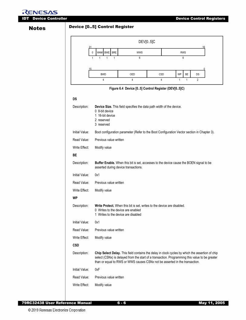
IDT Device Controller Device Control Registers
79RC32438 User Refer
Notes
Device [0..5] Control RegisterFigure 6.4 Device [0..5] Control Register (DEV[0..5]C)
DS
Description: Device Size. This field specifies the data path width of the device.0 8-bit device1 16-bit device2 reserved3 reserved
Initial Value: Boot configuration parameter (Refer to the Boot Configuration Vector section in Chapter 3).
Read Value: Previous value written
Write Effect: Modify value
BE
Description: Buffer Enable. When this bit is set, accesses to the device cause the BOEN signal to be asserted during device transactions.
Initial Value: 0x1
Read Value: Previous value written
Write Effect: Modify value
WP
Description: Write Protect. When this bit is set, writes to the device are disabled.0 Writes to the device are enabled1 Writes to the device are disabled
Initial Value: 0x1
Read Value: Previous value written
Write Effect: Modify value
CSD
Description: Chip Select Delay. This field contains the delay in clock cycles by which the assertion of chip select (CSNx) is delayed from the start of a transaction. Programming this value to be greater than or equal to RWS or WWS causes CSNx not be asserted in the transaction.
Initial Value: 0xF
Read Value: Previous value written
Write Effect: Modify value
DEV[0..5]C1631
RWS
6
015
2
DS
1
BE
4
CSD
1
WP
1
BRE
1
BWE
1
WAM WWS
6
4
OED
4
BWD
1
0
ence Manual 6 - 6 May 11, 2005
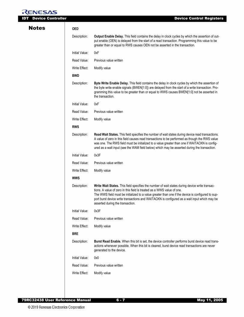
IDT Device Controller Device Control Registers
79RC32438 User Refer
Notes
OEDDescription: Output Enable Delay. This field contains the delay in clock cycles by which the assertion of out-put enable (OEN) is delayed from the start of a read transaction. Programming this value to be greater than or equal to RWS causes OEN not be asserted in the transaction.
Initial Value: 0xF
Read Value: Previous value written
Write Effect: Modify value
BWD
Description: Byte Write Enable Delay. This field contains the delay in clock cycles by which the assertion of the byte write enable signals (BWEN[1:0]) are delayed from the start of a write transaction. Pro-gramming this value to be greater than or equal to WWS causes BWEN[1:0] not be asserted in the transaction.
Initial Value: 0xF
Read Value: Previous value written
Write Effect: Modify value
RWS
Description: Read Wait States. This field specifies the number of wait states during device read transactions. A value of zero in this field causes read transactions to be performed as though the RWS value was one. The RWS field must be initialized to a value greater than one if WAITACKN is config-ured as a wait input (see the WAM field below) which may be asserted during the transaction.
Initial Value: 0x3F
Read Value: Previous value written
Write Effect: Modify value
WWS
Description: Write Wait States. This field specifies the number of wait states during device write transac-tions. A value of zero in this field is treated as a WWS value of one.The WWS field must be initialized to a value greater than one if the device is configured to sup-port burst device write transactions and WAITACKN is configured as a wait input which may be asserted during the transaction.
Initial Value: 0x3F
Read Value: Previous value written
Write Effect: Modify value
BRE
Description: Burst Read Enable. When this bit is set, the device controller performs burst device read trans-actions whenever possible. When this bit is cleared, burst device read transactions are never generated to the device.
Initial Value: 0x0
Read Value: Previous value written
Write Effect: Modify value
ence Manual 6 - 7 May 11, 2005

IDT Device Controller Device Control Registers
79RC32438 User Refer
Notes
Device [0..5] Timing Control Register
Figure 6.5 Device [0..5] Timing Control Register (DEV[0..5]TC)
BWE
Description: Burst Write Enable. When this bit is set, the device controller performs burst device write trans-actions whenever possible. When this bit is cleared, burst device write transactions are never generated to the device.
Initial Value: 0x0
Read Value: Previous value written
Write Effect: Modify value
WAM
Description: Wait/Ack Mode. This bit controls the operation of the WAITACKN signal. When this bit is a one, the WAITACKN signal operates as a Motorola style active low transfer acknowledge signal. When this bit is a zero, the WAITACKN signal operates as an Intel style active low wait signal.
Initial Value: 0x0
Read Value: Previous value written
Write Effect: Modify value
PRD
Description: Postread Delay. This field contains the delay, in clock cycles, from when the RC32438 clocks in data from the data bus during a device read transaction until the start of a new transaction. Pro-gramming this value to zero results in a postread delay of one clock cycle.If PRD or PWD is equal or less than CSH, chip select may remain asserted between transactions to the same device (i.e., back-to-back transactions).
Initial Value: 0xF
Read Value: Previous value written
Write Effect: Modify value
PWD
Description: Postwrite Delay. This field contains the delay, in clock cycles, from when the RC32438 negates the byte write enable signals during a device write transaction until the start of a new transaction. Programming this value to zero results in a postread delay of one clock cycle.If PRD or PWD is equal or less than CSH, chip select may remain asserted between transactions to the same device (i.e., back-to-back transactions).If PWD is equal or less than WDH and BWD is zero, the byte write enable signals may remain asserted between write transactions to the same device (i.e., back-to-back write transactions).
Initial Value: 0xF
Read Value: Previous value written
Write Effect: Modify value
DEV[0..5]TC031
19
0
4
PRD
4
PWD
3
WDH
2
CSH
ence Manual 6 - 8 May 11, 2005

IDT Device Controller Memory And Peripheral Bus Transaction Timer
79RC32438 User Refer
Notes
Memory And Peripheral Bus Transaction TimerWhen enabled, the memory and peripheral bus transaction timer times all the memory and peripheral
bus transactions. The memory and peripheral bus transaction timer is enabled by setting the bus transac-tion timer enable (BTE) bit in the BTCS register.
At the start of each memory and peripheral bus transaction in which the bus transaction timer isenabled, an internal 16-bit counter is initialized to zero. The counter increments with each passing externalclock (EXTCLK) clock cycle until the bus transaction completes. If the counter value ever exceeds the valuein the Compare (COMPARE) field in the Bus Timer Compare (BTCOMPARE) register, then a bus transac-tion timer time-out occurs.
When the bus transaction timer times-out, the following actions occur: – The bus transaction timer time out (BTO) bit in the BTCS register is set– The address of the transaction which caused the time out is recorded in the bus transaction timer
address (BTADDR) register– The type of bus transaction (i.e., read or write) is recorded in the transaction type (TT) field of the
BTCS register– A warm reset is generated– Compare field is initialized to 0xFFFF and the bus transaction timer is enabled.
Only devices on the memory and peripheral bus with an Intel style wait signal or Motorola style transferacknowledge signal can cause the bus transaction timer to time out.
WDH
Description: Write Data Hold. This field contains the delay, in clock cycles, from when the RC32438 negates the byte write enable signals during a device write transaction until the buffer output enable (BOEN) is negated and the data bus (MDATA[15:0]) is tri-stated. Buffer output enable is negated and the data bus is tri-stated when PWD expires regardless of the value of this field.
Initial Value: 0x7
Read Value: Previous value written
Write Effect: Modify value
CSH
Description: Chip Select Hold. This field contains the delay, in clock cycles, from when the RC32438 negates the byte write enable signals during a device write transaction or when output enable is negated during a device read transaction until the chip select signal is negated. Chip select is negated when PRD/PWD expires regardless of the value of this field.
Initial Value: 0x3
Read Value: Previous value written
Write Effect: Modify value
ence Manual 6 - 9 May 11, 2005
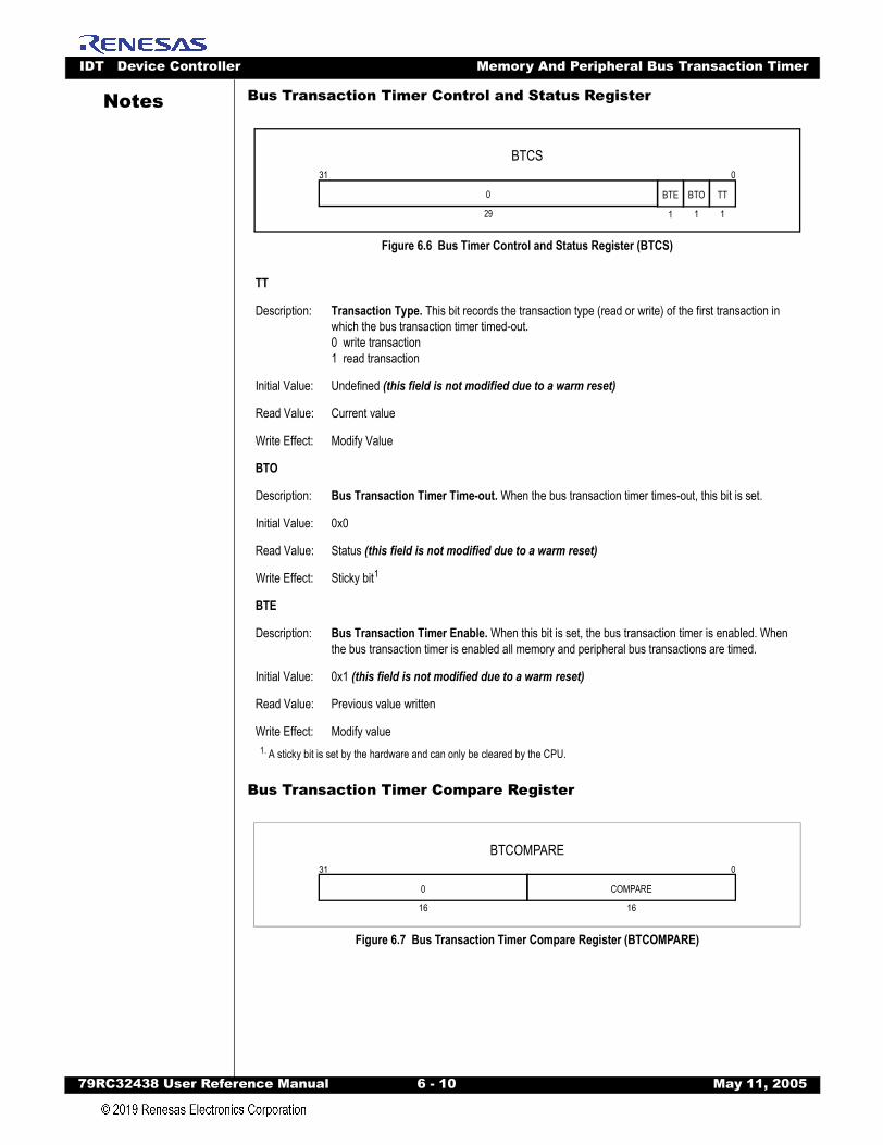
IDT Device Controller Memory And Peripheral Bus Transaction Timer
79RC32438 User Refer
Notes
Bus Transaction Timer Control and Status RegisterFigure 6.6 Bus Timer Control and Status Register (BTCS)
Bus Transaction Timer Compare Register
Figure 6.7 Bus Transaction Timer Compare Register (BTCOMPARE)
TT
Description: Transaction Type. This bit records the transaction type (read or write) of the first transaction in which the bus transaction timer timed-out.0 write transaction1 read transaction
Initial Value: Undefined (this field is not modified due to a warm reset)
Read Value: Current value
Write Effect: Modify Value
BTO
Description: Bus Transaction Timer Time-out. When the bus transaction timer times-out, this bit is set.
Initial Value: 0x0
Read Value: Status (this field is not modified due to a warm reset)
Write Effect: Sticky bit1
1. A sticky bit is set by the hardware and can only be cleared by the CPU.
BTE
Description: Bus Transaction Timer Enable. When this bit is set, the bus transaction timer is enabled. When the bus transaction timer is enabled all memory and peripheral bus transactions are timed.
Initial Value: 0x1 (this field is not modified due to a warm reset)
Read Value: Previous value written
Write Effect: Modify value
BTCS031
29
0
1
TT
1
BTO
1
BTE
BTCOMPARE031
16 16
0 COMPARE
ence Manual 6 - 10 May 11, 2005
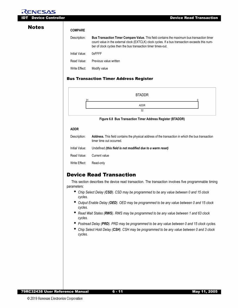
IDT Device Controller Device Read Transaction
79RC32438 User Refer
Notes
Bus Transaction Timer Address Register
Figure 6.8 Bus Transaction Timer Address Register (BTADDR)
Device Read TransactionThis section describes the device read transaction. The transaction involves five programmable timing
parameters:Chip Select Delay (CSD). CSD may be programmed to be any value between 0 and 15 clock cycles.Output Enable Delay (OED). OED may be programmed to be any value between 0 and 15 clock cycles.Read Wait States (RWS). RWS may be programmed to be any value between 1 and 63 clock cycles.Postread Delay (PRD). PRD may be programmed to be any value between 0 and 15 clock cycles.Chip Select Hold Delay (CSH). CSH may be programmed to be any value between 0 and 3 clock cycles.
COMPARE
Description: Bus Transaction Timer Compare Value. This field contains the maximum bus transaction timer count value in the external clock (EXTCLK) clock cycles. If a bus transaction exceeds this num-ber of clock cycles then the bus transaction timer times-out.
Initial Value: 0xFFFF
Read Value: Previous value written
Write Effect: Modify value
ADDR
Description: Address. This field contains the physical address of the transaction in which the bus transaction timer time out occurred.
Initial Value: Undefined (this field is not modified due to a warm reset)
Read Value: Current value
Write Effect: Read-only
BTADDR031
32
ADDR
ence Manual 6 - 11 May 11, 2005
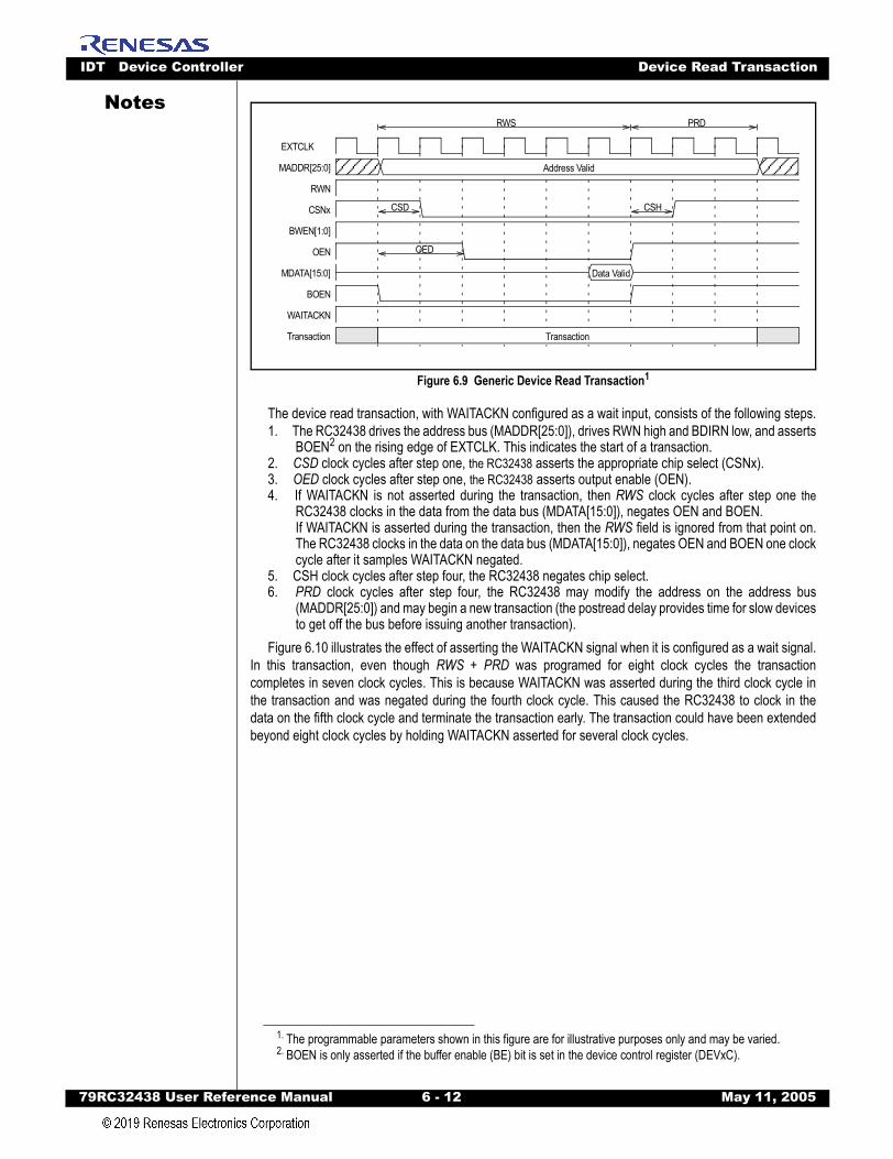
IDT Device Controller Device Read Transaction
79RC32438 User Refer
Notes
Figure 6.9 Generic Device Read Transaction1
The device read transaction, with WAITACKN configured as a wait input, consists of the following steps.1. The RC32438 drives the address bus (MADDR[25:0]), drives RWN high and BDIRN low, and asserts
BOEN2 on the rising edge of EXTCLK. This indicates the start of a transaction.2. CSD clock cycles after step one, the RC32438 asserts the appropriate chip select (CSNx).3. OED clock cycles after step one, the RC32438 asserts output enable (OEN).4. If WAITACKN is not asserted during the transaction, then RWS clock cycles after step one the
RC32438 clocks in the data from the data bus (MDATA[15:0]), negates OEN and BOEN.If WAITACKN is asserted during the transaction, then the RWS field is ignored from that point on.The RC32438 clocks in the data on the data bus (MDATA[15:0]), negates OEN and BOEN one clockcycle after it samples WAITACKN negated.
5. CSH clock cycles after step four, the RC32438 negates chip select.6. PRD clock cycles after step four, the RC32438 may modify the address on the address bus
(MADDR[25:0]) and may begin a new transaction (the postread delay provides time for slow devicesto get off the bus before issuing another transaction).
Figure 6.10 illustrates the effect of asserting the WAITACKN signal when it is configured as a wait signal.In this transaction, even though RWS + PRD was programed for eight clock cycles the transactioncompletes in seven clock cycles. This is because WAITACKN was asserted during the third clock cycle inthe transaction and was negated during the fourth clock cycle. This caused the RC32438 to clock in thedata on the fifth clock cycle and terminate the transaction early. The transaction could have been extendedbeyond eight clock cycles by holding WAITACKN asserted for several clock cycles.
1. The programmable parameters shown in this figure are for illustrative purposes only and may be varied.2. BOEN is only asserted if the buffer enable (BE) bit is set in the device control register (DEVxC).
EXTCLK
MADDR[25:0]
RWN
CSNx
BWEN[1:0]
OEN
MDATA[15:0]
Transaction
CSD
OED
RWS PRD
CSH
Address Valid
Data Valid
Transaction
BOEN
WAITACKN
ence Manual 6 - 12 May 11, 2005
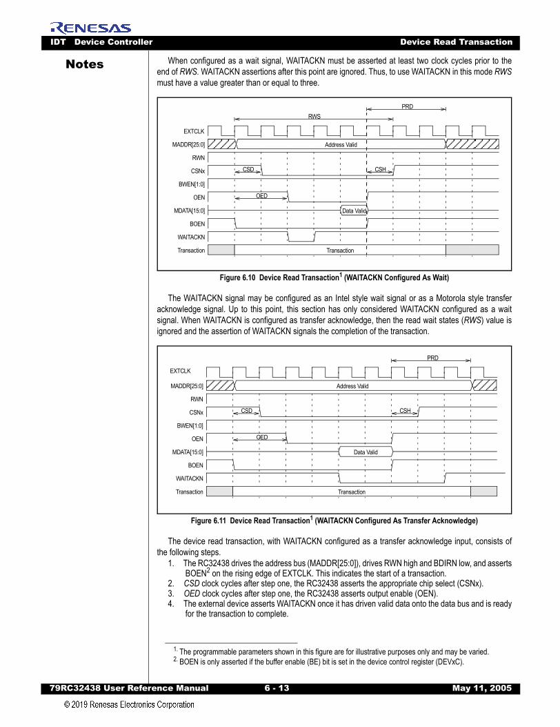
IDT Device Controller Device Read Transaction
79RC32438 User Refer
Notes
When configured as a wait signal, WAITACKN must be asserted at least two clock cycles prior to theend of RWS. WAITACKN assertions after this point are ignored. Thus, to use WAITACKN in this mode RWSmust have a value greater than or equal to three.Figure 6.10 Device Read Transaction1 (WAITACKN Configured As Wait)
The WAITACKN signal may be configured as an Intel style wait signal or as a Motorola style transferacknowledge signal. Up to this point, this section has only considered WAITACKN configured as a waitsignal. When WAITACKN is configured as transfer acknowledge, then the read wait states (RWS) value isignored and the assertion of WAITACKN signals the completion of the transaction.
Figure 6.11 Device Read Transaction1 (WAITACKN Configured As Transfer Acknowledge)
The device read transaction, with WAITACKN configured as a transfer acknowledge input, consists ofthe following steps.
1. The RC32438 drives the address bus (MADDR[25:0]), drives RWN high and BDIRN low, and assertsBOEN2 on the rising edge of EXTCLK. This indicates the start of a transaction.
2. CSD clock cycles after step one, the RC32438 asserts the appropriate chip select (CSNx).3. OED clock cycles after step one, the RC32438 asserts output enable (OEN).4. The external device asserts WAITACKN once it has driven valid data onto the data bus and is ready
for the transaction to complete.
1. The programmable parameters shown in this figure are for illustrative purposes only and may be varied.2. BOEN is only asserted if the buffer enable (BE) bit is set in the device control register (DEVxC).
EXTCLK
MADDR[25:0]
RWN
CSNx
BWEN[1:0]
OEN
MDATA[15:0]
Transaction
CSD
OED
RWS
CSH
Address Valid
Data Valid
Transaction
PRD
BOEN
WAITACKN
EXTCLK
MADDR[25:0]
RWN
CSNx
BWEN[1:0]
OEN
MDATA[15:0]
Transaction
CSD
OED
PRD
CSH
Address Valid
Data Valid
Transaction
BOEN
WAITACKN
ence Manual 6 - 13 May 11, 2005
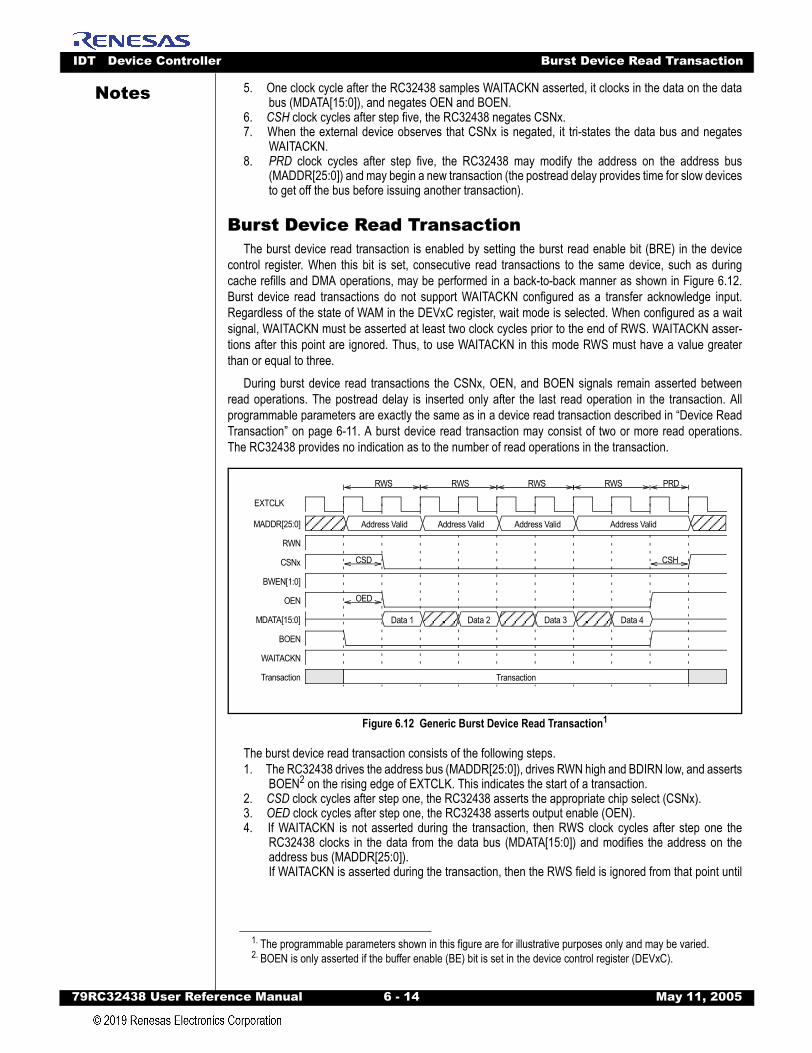
IDT Device Controller Burst Device Read Transaction
79RC32438 User Refer
Notes
5. One clock cycle after the RC32438 samples WAITACKN asserted, it clocks in the data on the databus (MDATA[15:0]), and negates OEN and BOEN.6. CSH clock cycles after step five, the RC32438 negates CSNx.7. When the external device observes that CSNx is negated, it tri-states the data bus and negates
WAITACKN.8. PRD clock cycles after step five, the RC32438 may modify the address on the address bus
(MADDR[25:0]) and may begin a new transaction (the postread delay provides time for slow devicesto get off the bus before issuing another transaction).
Burst Device Read TransactionThe burst device read transaction is enabled by setting the burst read enable bit (BRE) in the device
control register. When this bit is set, consecutive read transactions to the same device, such as duringcache refills and DMA operations, may be performed in a back-to-back manner as shown in Figure 6.12.Burst device read transactions do not support WAITACKN configured as a transfer acknowledge input.Regardless of the state of WAM in the DEVxC register, wait mode is selected. When configured as a waitsignal, WAITACKN must be asserted at least two clock cycles prior to the end of RWS. WAITACKN asser-tions after this point are ignored. Thus, to use WAITACKN in this mode RWS must have a value greaterthan or equal to three.
During burst device read transactions the CSNx, OEN, and BOEN signals remain asserted betweenread operations. The postread delay is inserted only after the last read operation in the transaction. Allprogrammable parameters are exactly the same as in a device read transaction described in “Device ReadTransaction” on page 6-11. A burst device read transaction may consist of two or more read operations.The RC32438 provides no indication as to the number of read operations in the transaction.
Figure 6.12 Generic Burst Device Read Transaction1
The burst device read transaction consists of the following steps.1. The RC32438 drives the address bus (MADDR[25:0]), drives RWN high and BDIRN low, and asserts
BOEN2 on the rising edge of EXTCLK. This indicates the start of a transaction.2. CSD clock cycles after step one, the RC32438 asserts the appropriate chip select (CSNx).3. OED clock cycles after step one, the RC32438 asserts output enable (OEN).4. If WAITACKN is not asserted during the transaction, then RWS clock cycles after step one the
RC32438 clocks in the data from the data bus (MDATA[15:0]) and modifies the address on theaddress bus (MADDR[25:0]).If WAITACKN is asserted during the transaction, then the RWS field is ignored from that point until
1. The programmable parameters shown in this figure are for illustrative purposes only and may be varied.2. BOEN is only asserted if the buffer enable (BE) bit is set in the device control register (DEVxC).
EXTCLK
MADDR[25:0]
RWN
CSNx
BWEN[1:0]
OEN
MDATA[15:0]
Transaction
CSD
RWS PRD
CSH
Address Valid
Data 1
Transaction
OED
RWS
Data 2
RWS
Data 3
RWS
Data 4
Address Valid Address Valid Address Valid
BOEN
WAITACKN
ence Manual 6 - 14 May 11, 2005
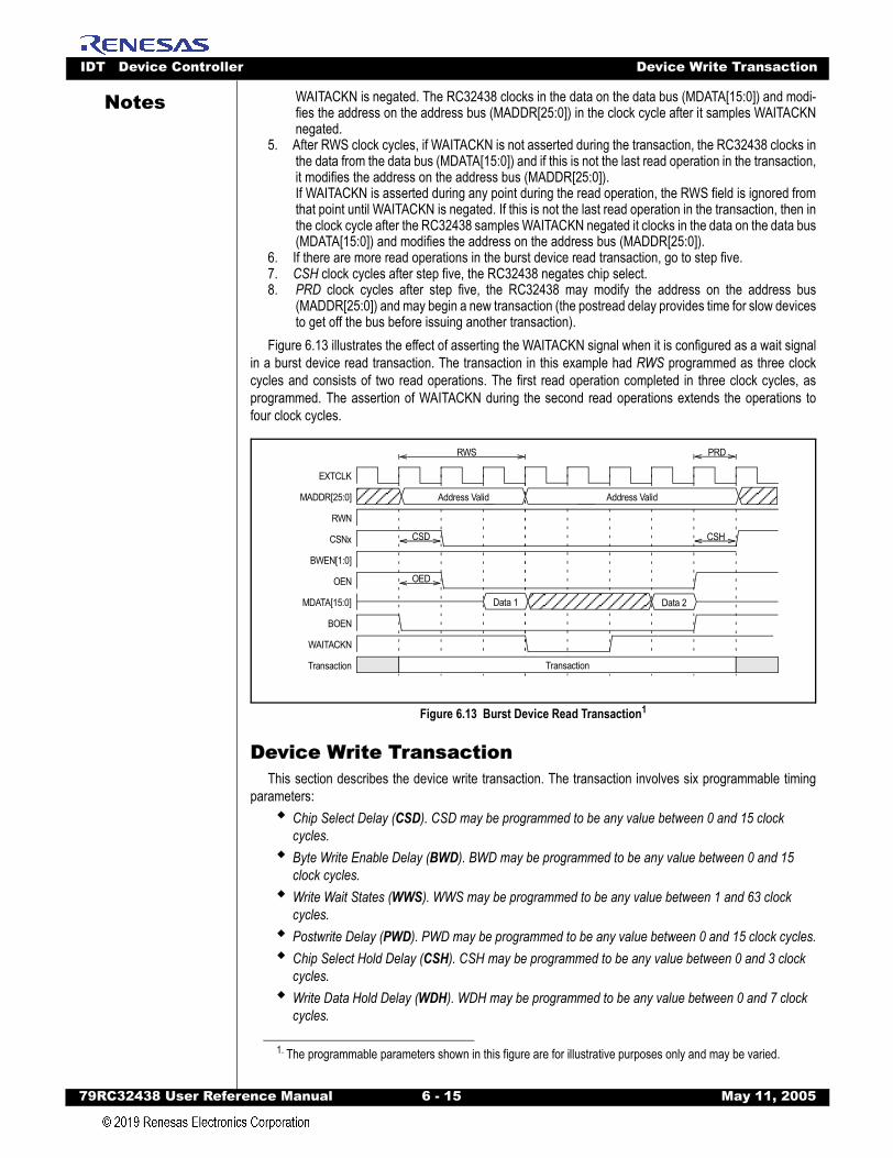
IDT Device Controller Device Write Transaction
79RC32438 User Refer
Notes
WAITACKN is negated. The RC32438 clocks in the data on the data bus (MDATA[15:0]) and modi-fies the address on the address bus (MADDR[25:0]) in the clock cycle after it samples WAITACKNnegated.5. After RWS clock cycles, if WAITACKN is not asserted during the transaction, the RC32438 clocks inthe data from the data bus (MDATA[15:0]) and if this is not the last read operation in the transaction,it modifies the address on the address bus (MADDR[25:0]). If WAITACKN is asserted during any point during the read operation, the RWS field is ignored fromthat point until WAITACKN is negated. If this is not the last read operation in the transaction, then inthe clock cycle after the RC32438 samples WAITACKN negated it clocks in the data on the data bus(MDATA[15:0]) and modifies the address on the address bus (MADDR[25:0]).
6. If there are more read operations in the burst device read transaction, go to step five.7. CSH clock cycles after step five, the RC32438 negates chip select.8. PRD clock cycles after step five, the RC32438 may modify the address on the address bus
(MADDR[25:0]) and may begin a new transaction (the postread delay provides time for slow devicesto get off the bus before issuing another transaction).
Figure 6.13 illustrates the effect of asserting the WAITACKN signal when it is configured as a wait signalin a burst device read transaction. The transaction in this example had RWS programmed as three clockcycles and consists of two read operations. The first read operation completed in three clock cycles, asprogrammed. The assertion of WAITACKN during the second read operations extends the operations tofour clock cycles.
Figure 6.13 Burst Device Read Transaction1
Device Write TransactionThis section describes the device write transaction. The transaction involves six programmable timing
parameters:Chip Select Delay (CSD). CSD may be programmed to be any value between 0 and 15 clock cycles.Byte Write Enable Delay (BWD). BWD may be programmed to be any value between 0 and 15 clock cycles.Write Wait States (WWS). WWS may be programmed to be any value between 1 and 63 clock cycles.Postwrite Delay (PWD). PWD may be programmed to be any value between 0 and 15 clock cycles.Chip Select Hold Delay (CSH). CSH may be programmed to be any value between 0 and 3 clock cycles.Write Data Hold Delay (WDH). WDH may be programmed to be any value between 0 and 7 clock cycles.
1. The programmable parameters shown in this figure are for illustrative purposes only and may be varied.
EXTCLK
MADDR[25:0]
RWN
CSNx
BWEN[1:0]
OEN
MDATA[15:0]
BOEN
Transaction
CSD
PRD
CSH
Address Valid
Transaction
OED
Data 1 Data 2
Address Valid
WAITACKN
RWS
ence Manual 6 - 15 May 11, 2005
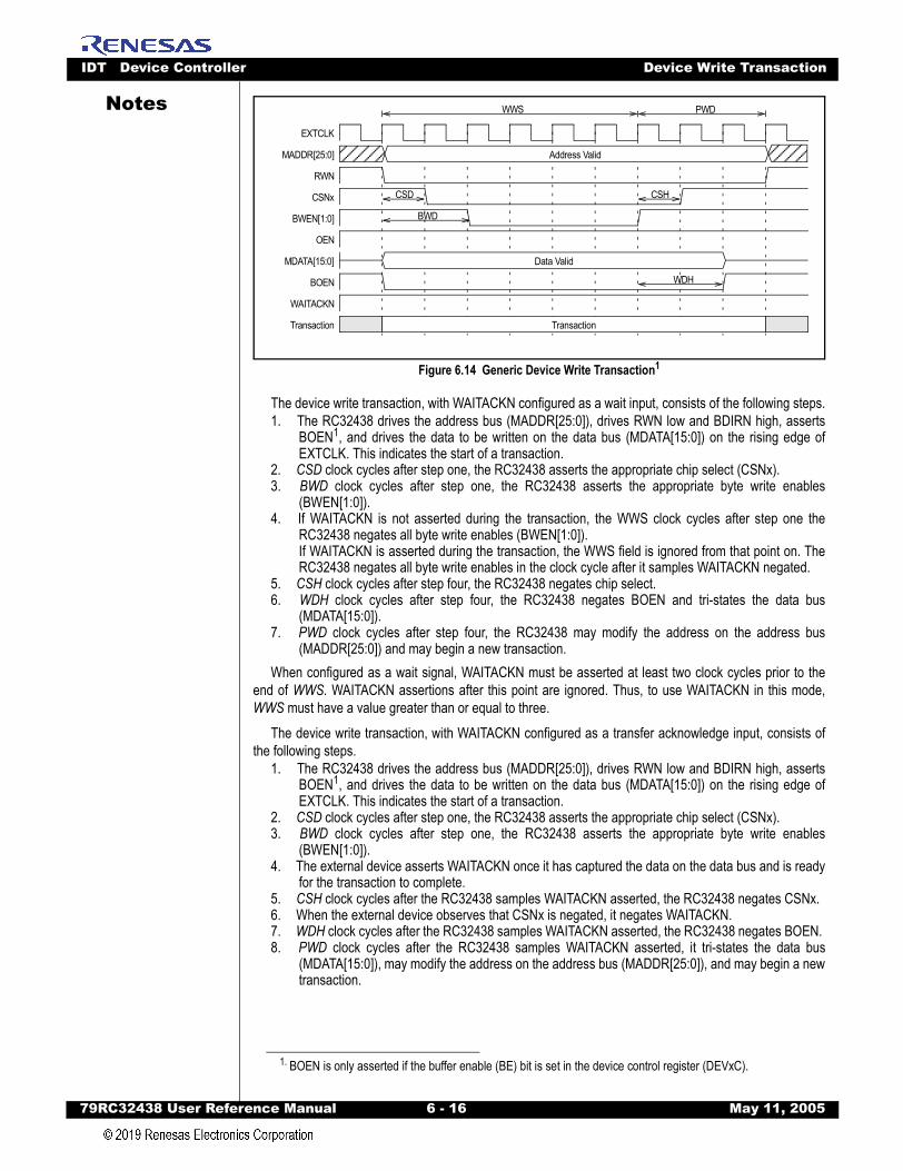
IDT Device Controller Device Write Transaction
79RC32438 User Refer
Notes
Figure 6.14 Generic Device Write Transaction1
The device write transaction, with WAITACKN configured as a wait input, consists of the following steps.1. The RC32438 drives the address bus (MADDR[25:0]), drives RWN low and BDIRN high, asserts
BOEN1, and drives the data to be written on the data bus (MDATA[15:0]) on the rising edge ofEXTCLK. This indicates the start of a transaction.
2. CSD clock cycles after step one, the RC32438 asserts the appropriate chip select (CSNx).3. BWD clock cycles after step one, the RC32438 asserts the appropriate byte write enables
(BWEN[1:0]).4. If WAITACKN is not asserted during the transaction, the WWS clock cycles after step one the
RC32438 negates all byte write enables (BWEN[1:0]).If WAITACKN is asserted during the transaction, the WWS field is ignored from that point on. TheRC32438 negates all byte write enables in the clock cycle after it samples WAITACKN negated.
5. CSH clock cycles after step four, the RC32438 negates chip select.6. WDH clock cycles after step four, the RC32438 negates BOEN and tri-states the data bus
(MDATA[15:0]).7. PWD clock cycles after step four, the RC32438 may modify the address on the address bus
(MADDR[25:0]) and may begin a new transaction.When configured as a wait signal, WAITACKN must be asserted at least two clock cycles prior to the
end of WWS. WAITACKN assertions after this point are ignored. Thus, to use WAITACKN in this mode,WWS must have a value greater than or equal to three.
The device write transaction, with WAITACKN configured as a transfer acknowledge input, consists ofthe following steps.
1. The RC32438 drives the address bus (MADDR[25:0]), drives RWN low and BDIRN high, assertsBOEN1, and drives the data to be written on the data bus (MDATA[15:0]) on the rising edge ofEXTCLK. This indicates the start of a transaction.
2. CSD clock cycles after step one, the RC32438 asserts the appropriate chip select (CSNx).3. BWD clock cycles after step one, the RC32438 asserts the appropriate byte write enables
(BWEN[1:0]).4. The external device asserts WAITACKN once it has captured the data on the data bus and is ready
for the transaction to complete.5. CSH clock cycles after the RC32438 samples WAITACKN asserted, the RC32438 negates CSNx.6. When the external device observes that CSNx is negated, it negates WAITACKN.7. WDH clock cycles after the RC32438 samples WAITACKN asserted, the RC32438 negates BOEN. 8. PWD clock cycles after the RC32438 samples WAITACKN asserted, it tri-states the data bus
(MDATA[15:0]), may modify the address on the address bus (MADDR[25:0]), and may begin a newtransaction.
1. BOEN is only asserted if the buffer enable (BE) bit is set in the device control register (DEVxC).
EXTCLK
MADDR[25:0]
RWN
CSNx
BWEN[1:0]
OEN
MDATA[15:0]
Transaction
CSD
WWS PWD
CSH
Address Valid
Transaction
Data Valid
WDH
BWD
BOEN
WAITACKN
ence Manual 6 - 16 May 11, 2005
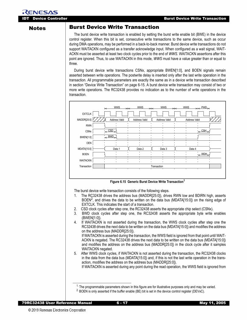
IDT Device Controller Burst Device Write Transaction
79RC32438 User Refer
Notes
Burst Device Write TransactionThe burst device write transaction is enabled by setting the burst write enable bit (BWE) in the devicecontrol register. When this bit is set, consecutive write transactions to the same device, such as occurduring DMA operations, may be performed in a back-to-back manner. Burst device write transactions do notsupport WAITACKN configured as a transfer acknowledge input. When configured as a wait signal, WAIT-ACKN must be asserted at least two clock cycles prior to the end of WWS. WAITACKN assertions after thispoint are ignored. Thus, to use WAITACKN in this mode, WWS must have a value greater than or equal tothree.
During burst device write transactions CSNx, appropriate BWEN[1:0], and BOEN signals remainasserted between write operations. The postwrite delay is inserted only after the last write operation in thetransaction. All programmable parameters are exactly the same as in a device write transaction describedin section “Device Write Transaction” on page 6-15. A burst device write transaction may consist of two ormore write operations. The RC32438 provides no indication as to the number of write operations in thetransaction.
Figure 6.15 Generic Burst Device Write Transaction1
The burst device write transaction consists of the following steps.1. The RC32438 drives the address bus (MADDR[25:0]), drives RWN low and BDIRN high, asserts
BOEN2, and drives the data to be written on the data bus (MDATA[15:0]) on the rising edge ofEXTCLK. This indicates the start of a transaction.
2. CSD clock cycles after step one, the RC32438 asserts the appropriate chip select (CSNx).3. BWD clock cycles after step one, the RC32438 asserts the appropriate byte write enables
(BWEN[1:0]).4. If WAITACKN is not asserted during the transaction, the WWS clock cycles after step one the
RC32438 drives the next data to be written on the data bus (MDATA[15:0]) and modifies the addresson the address bus (MADDR[25:0]). If WAITACKN is asserted during the transaction, the WWS field is ignored from that point until WAIT-ACKN is negated. The RC32438 drives the next data to be written on the data bus (MDATA[15:0])and modifies the address on the address bus (MADDR[25:0]) in the clock cycle after it samplesWAITACKN negated.
5. After WWS clock cycles, if WAITACKN is not asserted during the transaction, the RC32438 clocksin the data from the data bus (MDATA[15:0]) and, if this is not the last write operation in the trans-action, modifies the address on the address bus (MADDR[25:0]). If WAITACKN is asserted during any point during the read operation, the WWS field is ignored from
1. The programmable parameters shown in this figure are for illustrative purposes only and may be varied.2. BOEN is only asserted if the buffer enable (BE) bit is set in the device control register (DEVxC).
EXTCLK
MADDR[25:0]
RWN
CSNx
BWEN[1:0]
OEN
MDATA[15:0]
BOEN
Transaction
CSD
WWS PWD
CSH
Address Valid
Data 1
Transaction
BWD
WWS WWS WWS
Address Valid Address Valid Address Valid
Data 2 Data 3 Data 4
WDH
WAITACKN
ence Manual 6 - 17 May 11, 2005
IDT Device Controller Decoupled CPU Device Transactions
79RC32438 User Refer
Notes
that point until WAITACKN is negated. In the clock cycle after the RC32438 samples WAITACKNnegated, if this is not the last write operation in the transaction, it drives the next data to be writtenon the data bus (MDATA[15:0]) and modifies the address on the address bus (MADDR[25:0]).6. If there are more writes operations in the burst device write transaction, go to step five.7. CSH clock cycles after step five, the RC32438 negates chip select.8. WDH clock cycles after step five, the RC32438 negates BOEN.9. PWD clock cycles after step five, the RC32438 tri-states the data bus (MDATA[15:0]), may modify
the address on the address bus (MADDR[25:0]), and may begin a new transaction.
Decoupled CPU Device TransactionsCPU accesses to a device on the memory and peripheral bus may take a significantly longer time to
complete than normal PMBus transactions. One reason for this is the fact that the memory and peripheralbus can run at one eighth the frequency of the PMBus. Other reasons are wait states, post read delays, andpost write delays.
Locking up the PMBus may have adverse affects on the real-time performance of the system. Forexample, it may lead to Ethernet FIFO overflows and underflows. Since the PMBus does not support splittransactions there is no way to avoid this issue with traditional CPU read and write operations. To avoidlocking up the PMBus, the device controller supports decoupled CPU accesses. Decoupled CPU accessesallow CPU device read and write operations to complete without locking up the PMBus. The CPU encodesthe type of operation (read or write) in the OP field and the size of the operation (byte, halfword, triple-byte,word) in the SIZE field.
All multi-byte decoupled read and write operations must be contained in a single word (e.g., it is invalidto initiate a decoupled read from a byte address of 0x3 or a word read from a non-word aligned address).Initiating a multi-byte decoupled read or write operation that crosses a word boundary results in undefineddata and the Error (ERR) bit being set in the DEVDACS register.
To initiate a read operation, the CPU writes a local address that maps to a device to the DEVDAAregister. The CPU write completes on the PMBus without delay. A read of the size specified in the SIZE fieldis then performed from the device address written. When the read completes, the data read from the deviceupdates the DATA field of the DEVDAD register and the F bit is set.
To initiate a write operation, the CPU writes the data to be written to the DATA field of the DEVDADregister and then writes the address to be written to the DEVDAA register. Both writes complete withoutdelay. A write of the size specified in the SIZE field is then performed to the device using data from theDEVDAD register. When the write completes, the F bit is set. The F bit is presented to the interrupt handleras an interrupt source.
If an error occurs during the device operation or if the address written to the DEVDAA register does notmap to a device on the memory and peripheral bus, then the error (ERR) bit is set in the DEVDACS registerwhen the F bit is set.
Note: It is recommended that direct CPU device accesses be used only to execute code from device space and that CPU device accesses to slow external devices use decoupled CPU device transactions.
ence Manual 6 - 18 May 11, 2005
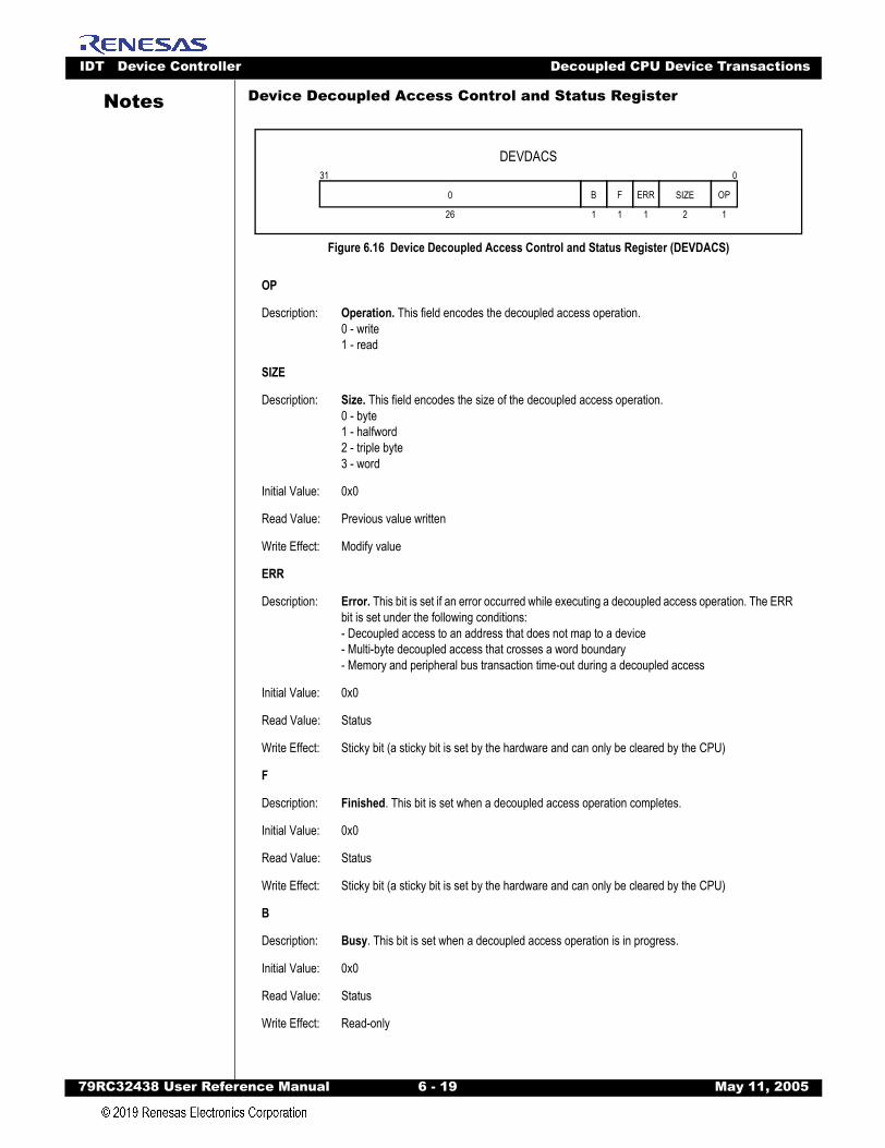
IDT Device Controller Decoupled CPU Device Transactions
79RC32438 User Refer
Notes
Device Decoupled Access Control and Status RegisterFigure 6.16 Device Decoupled Access Control and Status Register (DEVDACS)
OP
Description: Operation. This field encodes the decoupled access operation.0 - write1 - read
SIZE
Description: Size. This field encodes the size of the decoupled access operation.0 - byte1 - halfword2 - triple byte3 - word
Initial Value: 0x0
Read Value: Previous value written
Write Effect: Modify value
ERR
Description: Error. This bit is set if an error occurred while executing a decoupled access operation. The ERR bit is set under the following conditions:- Decoupled access to an address that does not map to a device- Multi-byte decoupled access that crosses a word boundary- Memory and peripheral bus transaction time-out during a decoupled access
Initial Value: 0x0
Read Value: Status
Write Effect: Sticky bit (a sticky bit is set by the hardware and can only be cleared by the CPU)
F
Description: Finished. This bit is set when a decoupled access operation completes.
Initial Value: 0x0
Read Value: Status
Write Effect: Sticky bit (a sticky bit is set by the hardware and can only be cleared by the CPU)
B
Description: Busy. This bit is set when a decoupled access operation is in progress.
Initial Value: 0x0
Read Value: Status
Write Effect: Read-only
DEVDACS031
0
26
OP
1
ERR
1
F
1
SIZE
2
B
1
ence Manual 6 - 19 May 11, 2005
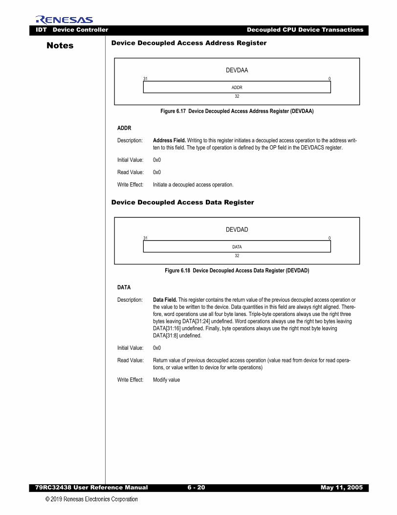
IDT Device Controller Decoupled CPU Device Transactions
79RC32438 User Refer
Notes
Device Decoupled Access Address RegisterFigure 6.17 Device Decoupled Access Address Register (DEVDAA)
Device Decoupled Access Data Register
Figure 6.18 Device Decoupled Access Data Register (DEVDAD)
ADDR
Description: Address Field. Writing to this register initiates a decoupled access operation to the address writ-ten to this field. The type of operation is defined by the OP field in the DEVDACS register.
Initial Value: 0x0
Read Value: 0x0
Write Effect: Initiate a decoupled access operation.
DATA
Description: Data Field. This register contains the return value of the previous decoupled access operation or the value to be written to the device. Data quantities in this field are always right aligned. There-fore, word operations use all four byte lanes. Triple-byte operations always use the right three bytes leaving DATA[31:24] undefined. Word operations always use the right two bytes leaving DATA[31:16] undefined. Finally, byte operations always use the right most byte leaving DATA[31:8] undefined.
Initial Value: 0x0
Read Value: Return value of previous decoupled access operation (value read from device for read opera-tions, or value written to device for write operations)
Write Effect: Modify value
DEVDAA031
ADDR
32
DEVDAD031
DATA
32
ence Manual 6 - 20 May 11, 2005
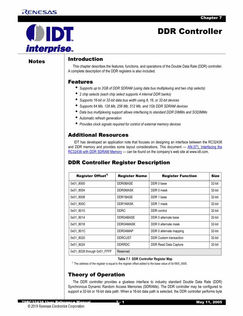
Notes
79RC32438 User Reference Manual 7 - 1 M
Chapter 7
DDR Controller
IntroductionThis chapter describes the features, functions, and operations of the Double Data Rate (DDR) controller.
A complete description of the DDR registers is also included.
FeaturesSupports up to 2GB of DDR SDRAM (using data bus multiplexing and two chip selects)2 chip selects (each chip select supports 4 internal DDR banks)Supports 16-bit or 32-bit data bus width using 8, 16, or 32-bit devices Supports 64 Mb, 128 Mb, 256 Mb, 512 Mb, and 1Gb DDR SDRAM devicesData bus multiplexing support allows interfacing to standard DDR DIMMs and SODIMMsAutomatic refresh generationProvides clock signals required for control of external memory devices
Additional Resources IDT has developed an application note that focuses on designing an interface between the RC32438
and DDR memory and provides some layout considerations. This document — AN-371, Interfacing theRC32438 with DDR SDRAM Memory — can be found on the company’s web site at www.idt.com.
DDR Controller Register Description
Theory of OperationThe DDR controller provides a glueless interface to industry standard Double Data Rate (DDR)
Synchronous Dynamic Random Access Memories (SDRAMs). The DDR controller may be configured tosupport a 32-bit or 16-bit data path. When a 16-bit data path is selected, the DDR controller performs byte
Register Offset1
1. The address of the register is equal to the register offset added to the base value of 0x1800_0000.
Register Name Register Function Size
0x01_8000 DDR0BASE DDR 0 base 32-bit
0x01_8004 DDR0MASK DDR 0 mask 32-bit
0x01_8008 DDR1BASE DDR 1 base 32-bit
0x01_800C DDR1MASK DDR 1 mask 32-bit
0x01_8010 DDRC DDR control 32-bit
0x01_8014 DDR0ABASE DDR 0 alternate base 32-bit
0x01_8018 DDR0AMASK DDR 0 alternate mask 32-bit
0x01_801C DDR0AMAP DDR 0 alternate mapping 32-bit
0x01_8020 DDRCUST DDR Custom transaction 32-bit
0x01_8024 DDRRDC DDR Read Data Capture 32-bit
0x01_8028 through 0x01_FFFF Reserved
Table 7.1 DDR Controller Register Map
ay 11, 2005
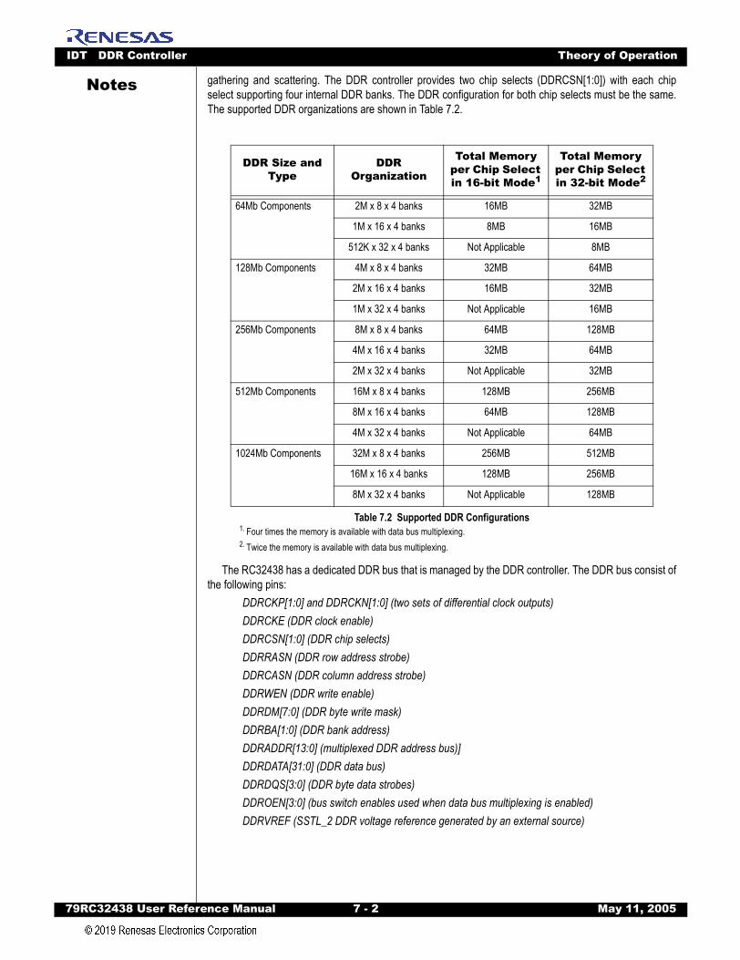
IDT DDR Controller Theory of Operation
79RC32438 User Refer
Notes
gathering and scattering. The DDR controller provides two chip selects (DDRCSN[1:0]) with each chipselect supporting four internal DDR banks. The DDR configuration for both chip selects must be the same.The supported DDR organizations are shown in Table 7.2.The RC32438 has a dedicated DDR bus that is managed by the DDR controller. The DDR bus consist ofthe following pins:
DDRCKP[1:0] and DDRCKN[1:0] (two sets of differential clock outputs)DDRCKE (DDR clock enable)DDRCSN[1:0] (DDR chip selects)DDRRASN (DDR row address strobe)DDRCASN (DDR column address strobe)DDRWEN (DDR write enable)DDRDM[7:0] (DDR byte write mask)DDRBA[1:0] (DDR bank address)DDRADDR[13:0] (multiplexed DDR address bus)]DDRDATA[31:0] (DDR data bus)DDRDQS[3:0] (DDR byte data strobes)DDROEN[3:0] (bus switch enables used when data bus multiplexing is enabled)DDRVREF (SSTL_2 DDR voltage reference generated by an external source)
DDR Size and Type
DDR Organization
Total Memory per Chip Select in 16-bit Mode1
1. Four times the memory is available with data bus multiplexing.
Total Memory per Chip Select in 32-bit Mode2
2. Twice the memory is available with data bus multiplexing.
64Mb Components 2M x 8 x 4 banks 16MB 32MB
1M x 16 x 4 banks 8MB 16MB
512K x 32 x 4 banks Not Applicable 8MB
128Mb Components 4M x 8 x 4 banks 32MB 64MB
2M x 16 x 4 banks 16MB 32MB
1M x 32 x 4 banks Not Applicable 16MB
256Mb Components 8M x 8 x 4 banks 64MB 128MB
4M x 16 x 4 banks 32MB 64MB
2M x 32 x 4 banks Not Applicable 32MB
512Mb Components 16M x 8 x 4 banks 128MB 256MB
8M x 16 x 4 banks 64MB 128MB
4M x 32 x 4 banks Not Applicable 64MB
1024Mb Components 32M x 8 x 4 banks 256MB 512MB
16M x 16 x 4 banks 128MB 256MB
8M x 32 x 4 banks Not Applicable 128MB
Table 7.2 Supported DDR Configurations
ence Manual 7 - 2 May 11, 2005

IDT DDR Controller Theory of Operation
79RC32438 User Refer
Notes
Two sets of differential DDR clocks (DDRCKP[1:0] and DDRCKN[1:0]) are provided to ease loadingconstraints and board design. Both clocks have the same frequency, which is equal to the IPBus clock(ICLK), and phase relationship. All DDR transactions are synchronous to these clocks. Thus, all of thetiming parameters in the DDR Control (DDRC) register are in terms of DDR clock cycles.The DDR controller contains a single control register (DDRC) since DDRs connected to both chipselects must share a common configuration. The DDR controller supports only sequential burst lengths oftwo. This burst length refers to the burst length value programmed in the DDR’s MODE register. By pipe-lining addresses issued to the DDR, the RC32438 can support burst read and write transactions of anylength. The Data Bus Width (DBW) field in this register selects the width of the DDR controller data bus(either 16-bits or 32-bits).
During DDR transactions, the address bus is multiplexed as shown in Table 7.3 for 32-bit data widthmode and in Table 7.4 for 16-bit data width mode. The exact address multiplexing is dependent on the DDRdevice type selected in the device type (DTYPE) field of the DDRC register. Selecting a DTYPE results inthe same multiplexing as that for 64Mb devices organized as 2M x 8 x 4 banks. Address and bank selectsignals connect directly to the corresponding DDR pins in both 16-bit and 32-bit data path modes (i.e., noaddress shifting is required for x16 and x32 DDR organizations).
Each chip select supports four page comparators. Although each page comparator is 14 bits in size, notall bits are used in all DDR configurations. When the CPU performs a read or write operation to DDR space,the page comparator associated with the selected DDR bank is checked. If the bank was left active and thevalue in the comparator matches the DDR row address, then the access can be made without first closingthe currently active page and opening a different page. Otherwise, if the active page in the comparator doesnot match the DDR row address, then the active page must first be closed (i.e., precharged) and the correctpage opened (i.e., made active) before the access may be performed. Finally, if no page is active in thebank, the required page must first be opened (i.e., made active) before the access may be performed.
The DDR controller normally operates with a DDR data strobe per byte lane (i.e., DDRDQS[1:0] in 16-bitdata bus width mode and DDRDQS[3:0] in 32-bit data bus width mode). Some DDR devices have a singledata byte strobe for ALL byte lanes (e.g., x32 DDR devices in a TQFP package). When the Single DataStrobe (SDS) bit is set in the DDRC register, DDRDQS[0] is used for all byte lanes.
DDR Address Multiplexing Scheme
DDR Organization Cycle
DDR Bank DDR Address
1 0 13 12 11 10 9 8 7 6 5 4 3 2 1 0
64Mb 2Mx8x4 banks(9-bit page)
Row a24 a23 x1 x a22 a21 a20 a19 a18 a17 a16 a15 a14 a13 a12 a11
Column a24 a23 x x x AP2 x a10 a9 a8 a7 a6 a5 a4 a3 a2
64Mb 1Mx16x4 banks(8-bit page)
Row a23 a22 x x a21 a20 a19 a18 a17 a16 a15 a14 a13 a12 a11 a10
Column a23 a22 x x x AP x x a9 a8 a7 a6 a5 a4 a3 a2
64Mb 512Kx32x4banks(8-bit page)
Row a22 a21 x x x a20 a19 a18 a17 a16 a15 a14 a13 a12 a11 a10
Column a22 a21 x x x x x AP a9 a8 a7 a6 a5 a4 a3 a2
128Mb 4Mx8x4 banks(10-bit page)
Row a25 a24 x x a23 a22 a21 a20 a19 a18 a17 a16 a15 a14 a13 a12
Column a25 a24 x x x AP a11 a10 a9 a8 a7 a6 a5 a4 a3 a2
128Mb 2Mx16x4 banks(9-bit page)
Row a24 a23 x x a22 a21 a20 a19 a18 a17 a16 a15 a14 a13 a12 a11
Column a24 a23 x x x AP x a10 a9 a8 a7 a6 a5 a4 a3 a2
128Mb 1Mx32x4 banks(8-bit page)
Row a23 a22 x x a21 a20 a19 a18 a17 a16 a15 a14 a13 a12 a11 a10
Column a23 a22 x x x x x AP a9 a8 a7 a6 a5 a4 a3 a2
Table 7.3 DDR Address Multiplexing in 32-bit Mode (Part 1 of 2)
ence Manual 7 - 3 May 11, 2005
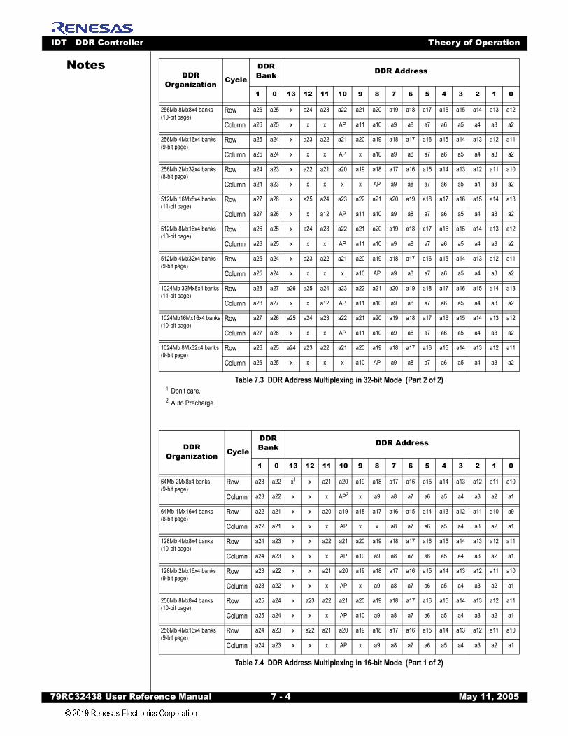
IDT DDR Controller Theory of Operation
79RC32438 User Refer
Notes
256Mb 8Mx8x4 banks(10-bit page)
Row a26 a25 x a24 a23 a22 a21 a20 a19 a18 a17 a16 a15 a14 a13 a12
Column a26 a25 x x x AP a11 a10 a9 a8 a7 a6 a5 a4 a3 a2
256Mb 4Mx16x4 banks(9-bit page)
Row a25 a24 x a23 a22 a21 a20 a19 a18 a17 a16 a15 a14 a13 a12 a11
Column a25 a24 x x x AP x a10 a9 a8 a7 a6 a5 a4 a3 a2
256Mb 2Mx32x4 banks(8-bit page)
Row a24 a23 x a22 a21 a20 a19 a18 a17 a16 a15 a14 a13 a12 a11 a10
Column a24 a23 x x x x x AP a9 a8 a7 a6 a5 a4 a3 a2
512Mb 16Mx8x4 banks(11-bit page)
Row a27 a26 x a25 a24 a23 a22 a21 a20 a19 a18 a17 a16 a15 a14 a13
Column a27 a26 x x a12 AP a11 a10 a9 a8 a7 a6 a5 a4 a3 a2
512Mb 8Mx16x4 banks(10-bit page)
Row a26 a25 x a24 a23 a22 a21 a20 a19 a18 a17 a16 a15 a14 a13 a12
Column a26 a25 x x x AP a11 a10 a9 a8 a7 a6 a5 a4 a3 a2
512Mb 4Mx32x4 banks(9-bit page)
Row a25 a24 x a23 a22 a21 a20 a19 a18 a17 a16 a15 a14 a13 a12 a11
Column a25 a24 x x x x a10 AP a9 a8 a7 a6 a5 a4 a3 a2
1024Mb 32Mx8x4 banks(11-bit page)
Row a28 a27 a26 a25 a24 a23 a22 a21 a20 a19 a18 a17 a16 a15 a14 a13
Column a28 a27 x x a12 AP a11 a10 a9 a8 a7 a6 a5 a4 a3 a2
1024Mb16Mx16x4 banks(10-bit page)
Row a27 a26 a25 a24 a23 a22 a21 a20 a19 a18 a17 a16 a15 a14 a13 a12
Column a27 a26 x x x AP a11 a10 a9 a8 a7 a6 a5 a4 a3 a2
1024Mb 8Mx32x4 banks(9-bit page)
Row a26 a25 a24 a23 a22 a21 a20 a19 a18 a17 a16 a15 a14 a13 a12 a11
Column a26 a25 x x x x a10 AP a9 a8 a7 a6 a5 a4 a3 a2
1. Don’t care.2. Auto Precharge.
DDR Organization Cycle
DDR Bank DDR Address
1 0 13 12 11 10 9 8 7 6 5 4 3 2 1 0
64Mb 2Mx8x4 banks(9-bit page)
Row a23 a22 x1 x a21 a20 a19 a18 a17 a16 a15 a14 a13 a12 a11 a10
Column a23 a22 x x x AP2 x a9 a8 a7 a6 a5 a4 a3 a2 a1
64Mb 1Mx16x4 banks(8-bit page)
Row a22 a21 x x a20 a19 a18 a17 a16 a15 a14 a13 a12 a11 a10 a9
Column a22 a21 x x x AP x x a8 a7 a6 a5 a4 a3 a2 a1
128Mb 4Mx8x4 banks(10-bit page)
Row a24 a23 x x a22 a21 a20 a19 a18 a17 a16 a15 a14 a13 a12 a11
Column a24 a23 x x x AP a10 a9 a8 a7 a6 a5 a4 a3 a2 a1
128Mb 2Mx16x4 banks(9-bit page)
Row a23 a22 x x a21 a20 a19 a18 a17 a16 a15 a14 a13 a12 a11 a10
Column a23 a22 x x x AP x a9 a8 a7 a6 a5 a4 a3 a2 a1
256Mb 8Mx8x4 banks(10-bit page)
Row a25 a24 x a23 a22 a21 a20 a19 a18 a17 a16 a15 a14 a13 a12 a11
Column a25 a24 x x x AP a10 a9 a8 a7 a6 a5 a4 a3 a2 a1
256Mb 4Mx16x4 banks(9-bit page)
Row a24 a23 x a22 a21 a20 a19 a18 a17 a16 a15 a14 a13 a12 a11 a10
Column a24 a23 x x x AP x a9 a8 a7 a6 a5 a4 a3 a2 a1
Table 7.4 DDR Address Multiplexing in 16-bit Mode (Part 1 of 2)
DDR Organization Cycle
DDR Bank DDR Address
1 0 13 12 11 10 9 8 7 6 5 4 3 2 1 0
Table 7.3 DDR Address Multiplexing in 32-bit Mode (Part 2 of 2)
ence Manual 7 - 4 May 11, 2005
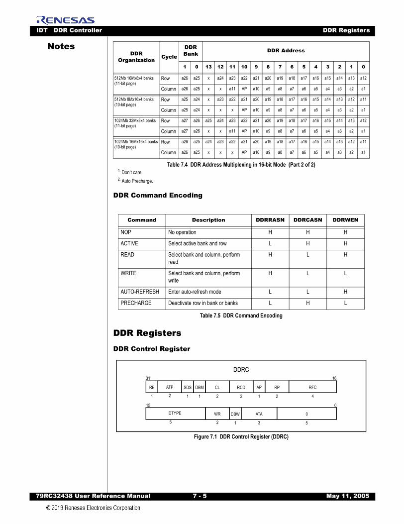
IDT DDR Controller DDR Registers
79RC32438 User Refer
Notes
DDR Command Encoding
DDR Registers
DDR Control Register
Figure 7.1 DDR Control Register (DDRC)
512Mb 16Mx8x4 banks(11-bit page)
Row a26 a25 x a24 a23 a22 a21 a20 a19 a18 a17 a16 a15 a14 a13 a12
Column a26 a25 x x a11 AP a10 a9 a8 a7 a6 a5 a4 a3 a2 a1
512Mb 8Mx16x4 banks(10-bit page)
Row a25 a24 x a23 a22 a21 a20 a19 a18 a17 a16 a15 a14 a13 a12 a11
Column a25 a24 x x x AP a10 a9 a8 a7 a6 a5 a4 a3 a2 a1
1024Mb 32Mx8x4 banks(11-bit page)
Row a27 a26 a25 a24 a23 a22 a21 a20 a19 a18 a17 a16 a15 a14 a13 a12
Column a27 a26 x x a11 AP a10 a9 a8 a7 a6 a5 a4 a3 a2 a1
1024Mb 16Mx16x4 banks(10-bit page)
Row a26 a25 a24 a23 a22 a21 a20 a19 a18 a17 a16 a15 a14 a13 a12 a11
Column a26 a25 x x x AP a10 a9 a8 a7 a6 a5 a4 a3 a2 a1
1. Don’t care.2. Auto Precharge.
Command Description DDRRASN DDRCASN DDRWEN
NOP No operation H H H
ACTIVE Select active bank and row L H H
READ Select bank and column, perform read
H L H
WRITE Select bank and column, perform write
H L L
AUTO-REFRESH Enter auto-refresh mode L L H
PRECHARGE Deactivate row in bank or banks L H L
Table 7.5 DDR Command Encoding
DDR Organization Cycle
DDR Bank DDR Address
1 0 13 12 11 10 9 8 7 6 5 4 3 2 1 0
Table 7.4 DDR Address Multiplexing in 16-bit Mode (Part 2 of 2)
DDRC1631
RE
1
CL
2
RCD
2
AP
1
RP
2
RFC
4
015
0
5
DTYPE DBW
1
2
ATP
2
WR
3
ATA
SDS
1
DBM
1
5
ence Manual 7 - 5 May 11, 2005
IDT DDR Controller DDR Registers
79RC32438 User Refer
Notes
ATADescription: Active to Active/Auto Refresh. This field specifies the minimum number of DDR clock cycles between an Active and a subsequent Active or Auto Refresh command.0 5 clock cycles1 6 clock cycles2 7 clock cycles3 8 clock cycles4 9 clock cycles5 10 clock cycles6 11 clock cycles7 12 clock cycles
Initial Value: 0x3 (this field is not modified due to a warm reset)
Read Value: Previous value written
Write Effect: Modify value
DBW
Description: Data Bus Width. This field specifies the width of the DDR control data bus. 0 16-bit data bus width1 32-bit data bus width
Initial Value: 0x0 (this field is not modified due to a warm reset)
Read Value: Previous value written
Write Effect: Modify value
WR
Description: Write Recovery. This field specifies the minimum number of DDR clock cycles from the comple-tion of a WRITE operation to a PRECHARGE command.0 3 clock cycles1 4 clock cycles2 5 clock cycles3 6 clock cycles
Initial Value: 0x3 (this field is not modified due to a warm reset)
Read Value: Previous value written
Write Effect: Modify value
ence Manual 7 - 6 May 11, 2005
IDT DDR Controller DDR Registers
79RC32438 User Refer
Notes
DTYPEDescription: DDR Device Type. This field selects the DDR device type.0 64Mb, 512K x 32 x 41 64Mb, 1M x 16 x 42 64Mb, 2M x 8 x 43 reserved4 128Mb, 1M x 32 x 45 128Mb, 2M x 16 x 46 128Mb, 4M x 8 x 47 reserved8 256Mb, 2M x 32 x 49 256Mb, 4M x 16 x 410 256Mb, 8M x 8 x 411 reserved12 reserved13 512Mb, 4M x 32 x 414 512Mb, 8M x 16 x 415 512Mb, 16M x 8 x 416 reserved17 1Gb, 8M x 32 x 418 1Gb, 16M x 16 x 419 1Gb, 32M x 8 x 420 reserved...31 reserved
Initial Value: 0x1 (this field is not modified due to a warm reset)
Read Value: Previous value written
Write Effect: Modify value
RFC
Description: Refresh Clock Cycles. This field specifies the AUTO Refresh command period in DDR clock cycles. Permissible values are zero through 15. A value of zero has the same effect as program-ming this field to one.
Initial Value: 0xF (this field is not modified due to a warm reset)
Read Value: Previous value written
Write Effect: Modify value
RP
Description: Precharge Delay. This field specifies the number of DDR clock cycles between a PRECHARGE command and a subsequent row access.0 1 clock cycle1 2 clock cycles2 3 clock cycles3 4 clock cycles
Initial Value: 0x3 (this field is not modified due to a warm reset)
Read Value: Previous value written
Write Effect: Modify value
ence Manual 7 - 7 May 11, 2005
IDT DDR Controller DDR Registers
79RC32438 User Refer
Notes
APDescription: Auto Precharge Enable. This field controls the value driven on Auto Precharge (shown as “AP” in Tables 7.3 and 7.4) bit during DDR transactions. If auto precharge is enabled, the row being accessed is precharged at the completion of a read or write transaction.0 Auto precharge disabled (AP=0).1 Auto precharge enabled (AP=1).
Initial Value: 0x1 (this field is not modified due to a warm reset)
Read Value: Previous value written
Write Effect: Modify value
RCD
Description: Active to Read or Write Delay. This field specifies the minimum number of DDR clock cycles between the issuing of a DDR ACTIVE command and a READ or WRITE command.0 1 clock cycle1 2 clock cycles2 3 clock cycles3 4 clock cycles
Initial Value: 0x2 (this field is not modified due to a warm reset)
Read Value: Previous value written
Write Effect: Modify value
CL
Description: CAS Latency. This field contains the CAS latency value in DDR clock cycles.0 2 clock cycles1 2.5 clock cycles2 3 clock cycles3 4 clock cycles
Initial Value: 0x2 (this field is not modified due to a warm reset)
Read Value: Previous value written
Write Effect: Modify value
DBM
Description: Data Bus Multiplexing. When this bit is set, data bus multiplexing is enabled. For more informa-tion, refer to the DDR Data Bus Multiplexing section in this chapter.
Initial Value: 0x0 (this field is not modified due to a warm reset)
Read Value: Previous value written
Write Effect: Modify value
SDS
Description: Single Data Strobe. The DDR controller normally operates with a DDR data strobe per byte lane (i.e., DDRDQS[1:0] in 16-bit data bus width mode and DDRDQS[3:0] in 32-bit data bus width mode). Some DDR devices have a single data byte strobe for ALL byte lanes. When this bit is set, DDRDQS[0] is used for all byte lanes.
Initial Value: 0x0 (this field is not modified due to a warm reset)
Read Value: Previous value written
Write Effect: Modify value
ence Manual 7 - 8 May 11, 2005
IDT DDR Controller DDR Registers
79RC32438 User Refer
Notes
DDR Read Data Capture Register
Figure 7.2 shows the PCLK1 edges which can be configured for DDR read data capture. The edgesshown correspond to the PCLK edges which will capture the first data word of the read transaction (i.e.,DDRDATA[31:0] = D0). Subsequent data words are captured with subsequent PCLK positive edges. Notethat the capturing edges are relative to the CAS latency (CL) programmed in the DDRC register. Figure 7.2shows the capturing edges when CL = 2. As a rule, the first capture edge (CES=0) is always the positivePCLK edge corresponding to CL + 1/2 DDRCKP edges from the time the first read command is issued(DDRCMD = READ).2
ATP
Description: Active To Precharge. This field specifies the minimum number of DDR clock cycles from an ACTIVE command to READ or WRITE command with auto precharge (this field corresponds to the tRAS(MIN) DDR timing parameter).0 5 clock cycles1 6 clock cycles2 7 clock cycles3 8 clock cycles
Initial Value: 0x3 (this field is not modified due to a warm reset)
Read Value: Previous value written
Write Effect: Modify value
RE
Description: Refresh Enable. When this bit is set and the DDR refresh timer expires, a DDR refresh transac-tion is queued. When this bit is cleared, a DDR refresh transaction is never generated regardless of the state of the refresh timer.
Initial Value: 0x1 (this field is not modified due to a warm reset)
Read Value: Previous value written
Write Value: Modify value
1. PCLK is the internal clock used by the DDR Controller.2. DDRCMD represents the concatenation of DDRRASN, DDRCASN, and DDRWEN.
ence Manual 7 - 9 May 11, 2005
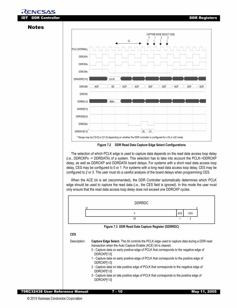
IDT DDR Controller DDR Registers
79RC32438 User Refer
Notes
Yy
Figure 7.2 DDR Read Data Capture Edge Select Configurations
The selection of which PCLK edge is used to capture data depends on the read data access loop delay(i.e., DDRCKPx -> DDRDATA) of a system. This selection has to take into account the PCLK->DDRCKPdelay, as well as DDRCKP and DDRDATA board delays. For systems with a short read data access loopdelay, CES may be configured to 0 or 1. For systems with a long read data access loop delay, CES may beconfigured to 2 or 3. The user must do a careful analysis of the board delays when programming CES.
When the ACE bit is set (recommended), the DDR Controller automatically determines which PCLKedge should be used to capture the read data (i.e., the CES field is ignored). In this mode the user mustonly ensure that the read data access loop delay does not exceed one DDRCKP cycles.
Figure 7.3 DDR Read Data Capture Register (DDRRDC)
CES
Description: Capture Edge Select. This bit controls the PCLK edge used to capture data during a DDR read transaction when the Auto Capture Enable (ACE) bit is cleared.0 - Capture data on early positive edge of PCLK that corresponds to the negative edge of
DDRCKP[1:0]1 - Capture data on early positive edge of PCLK that corresponds to the positive edge of
DDRCKP[1:0]2 - Capture data on late positive edge of PCLK that corresponds to the negative edge of
DDRCKP[1:0]3 - Capture data on late positive edge of PCLK that corresponds to the positive edge of
DDRCKP[1:0]
Col A0
NOP RD NOP NOP NOP NOP NOP NOP NOP
BNKx
D0 D1
PCLK (INTERNAL)
DDRCKPx
DDRCKNx
DDRCSNx
DDRADDR[13:0]
DDRCMD
DDRCKE
DDRBA[1:0]
DDRDM[7:0]
DDROEN[3:0]
DDRDQSx
DDRDATA[Y:0]
0 1 2 3CAPTURE EDGE SELECT (CES)
CL
* Range may be [15:0] or [31:0] depending on whether the DDR controller is configured for x16 or x32 mode.
*
031
DDRRDC
29 2
0 CES
1
ACE
ence Manual 7 - 10 May 11, 2005
IDT DDR Controller DDR Registers
79RC32438 User Refer
Notes
DDR Address Mapping
The DDR banks can be located anywhere in the RC32438’s local address space. The address of theDDR banks corresponding to each DDR chip select can be allocated independently.
Address decoding for each DDR chip select is controlled by the DDR base (DDR[1|0]BASE) and DDRmask (DDR[1|0]MASK) registers. The DDR mask register is used to select which bits are used for addressdecoding. When a bit in this register is a one, the corresponding address bit is active in address compari-sons. If a bit in this register is a zero, then the corresponding address bit does not participate in addresscomparisons. The base address register specifies the base physical address for each DDR chip select. Allof the active address bits not masked by the DDR mask register are compared to the value in the DDR baseregister. If they all match, then the corresponding DDR chip select is asserted.
To facilitate PCI booting from a DDR-only memory system, an alternate address mapping range issupported for DDR chip select zero (see Figure 7.4). The alternate address range is configured using theDDR alternate base (DDR0ABASE) and DDR alternate mask (DDR0AMASK) registers. The DDR alternatemapping (DDR0AMAP) register specifies the value of DDR address bits that are mapped by the DDR maskregister. This allows the DDR address to be offset from the RC32438’s local address.
The normal and alternate base and mask registers for DDR chip select zero allow two RC32438 localaddress ranges to be mapped to the same DDR chip select. Care should be exercised when using thisfeature to ensure data cache coherence.
Initial Value: 0x0 (this field is not modified due to a warm reset)
Read Value: Previous value written
Write Value: Modify value
ACE
Description: Auto Capture Enable. When this bit is set the DDR controller automatically determines the PCLK edge used to capture data during a DDR read transaction.
Initial Value: 0x1 (this field is not modified due to a warm reset)
Read Value: Previous value written
Write Value: Modify value
ence Manual 7 - 11 May 11, 2005
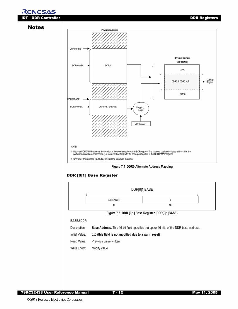
IDT DDR Controller DDR Registers
79RC32438 User Refer
Notes
Figure 7.4 DDR0 Alternate Address Mapping
DDR [0|1] Base Register
Figure 7.5 DDR [0|1] Base Register (DDR[0|1]BASE)
BASEADDR
Description: Base Address. This 16-bit field specifies the upper 16 bits of the DDR base address.
Initial Value: 0x0 (this field is not modified due to a warm reset)
Read Value: Previous value written
Write Effect: Modify value
DDR0BASE
DDR0ABASE
DDR0MASK
DDR0AMASK
DDR0
DDR0 ALTERNATE
Physical Address
Physical MemoryDDRCSN[0]
DDR0
DDR0
DDR0 & DDR0 ALTOverlapRegion
DDR0AMAP
Mapping
NOTES:
1. Register DDR0AMAP controls the location of the overlap region within DDR0 space. The Mapping Logic substitutes address bits that
Logic
participate in address comparison (i.e., non-masked bits) with the corresponding bits in the DDR0AMAP register.
2. Only DDR chip-select 0 (DDRCSN[0]) supports alternate mapping.
DDR[0|1]BASE031
16 16
BASEADDR 0
ence Manual 7 - 12 May 11, 2005
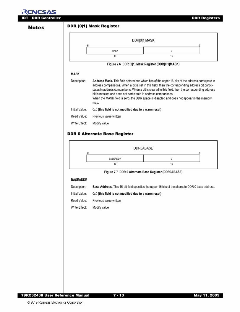
IDT DDR Controller DDR Registers
79RC32438 User Refer
Notes
DDR [0|1] Mask RegisterFigure 7.6 DDR [0|1] Mask Register (DDR[0|1]MASK)
DDR 0 Alternate Base Register
Figure 7.7 DDR 0 Alternate Base Register (DDR0ABASE)
MASK
Description: Address Mask. This field determines which bits of the upper 16-bits of the address participate in address comparisons. When a bit is set in this field, then the corresponding address bit partici-pates in address comparisons. When a bit is cleared in this field, then the corresponding address bit is masked and does not participate in address comparisons.When the MASK field is zero, the DDR space is disabled and does not appear in the memory map.
Initial Value: 0x0 (this field is not modified due to a warm reset)
Read Value: Previous value written
Write Effect: Modify value
BASEADDR
Description: Base Address. This 16-bit field specifies the upper 16 bits of the alternate DDR 0 base address.
Initial Value: 0x0 (this field is not modified due to a warm reset)
Read Value: Previous value written
Write Effect: Modify value
DDR[0|1]MASK031
16
MASK
16
0
DDR0ABASE031
16 16
BASEADDR 0
ence Manual 7 - 13 May 11, 2005

IDT DDR Controller DDR Registers
79RC32438 User Refer
Notes
DDR 0 Alternate Mask RegisterFigure 7.8 DDR 0 Alternate Mask Register (DDR0AMASK)
DDR 0 Alternate Mapping Register
Figure 7.9 DDR 0 Alternate Mapping Register (DDR0AMAP)
DDR Data Bus Multiplexing
The DDR controller supports data bus multiplexing when the Data Bus Multiplexing (DBM) bit is set inthe DDRC register. Data bus multiplexing allows the RC32438’s 16-bit or 32-bit data bus1 to interface toDDR memory systems having a data bus width of 64-bits. This is necessary when interfacing the RC32438to standard DDR memory modules such as DDR DIMMs and SODIMMs.
To support data bus multiplexing, external bus switches must be placed between the RC32438 andexternal DDR memory banks. These bus switches are used to isolate unused data bits and strobes fromthe RC32438 allowing 16-bit or 32-bit data quantities to be read from a 64-bit bus. The RC32438DDROEN[3:0] pins are output enabled for these buffers.
MASK
Description: Address Mask. This field determines which bits of the upper 16-bits of the address participate in address comparisons. When a bit is set in this field, then the corresponding address bit partici-pates in address comparisons. When a bit is cleared in this field, then the corresponding address bit is masked and does not participate in address comparisons.When the MASK field is zero, the alternate DDR space is disabled and does not appear in the memory map.
Initial Value: 0x0 (this field is not modified due to a warm reset)
Read Value: Previous value written
Write Effect: Modify value
MAP
Description: Map Address. This field contains the DDR mapping address for transactions mapped to DDR chip select zero using the alternate address mapping range. Address bits that participated in address comparison are substituted with values in this field.
Initial Value: 0x0 (this field is not modified due to a warm reset)
Read Value: Previous value written
Write Effect: Modify value
1. Mode is determined by the state of the Data Bus Width (DBW) bit in the DDRC register.
DDR0AMASK031
16
MASK
16
0
DDR0AMAP031
16 16
MAP 0
ence Manual 7 - 14 May 11, 2005
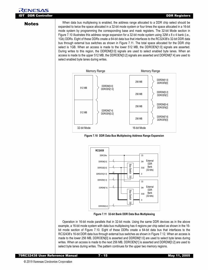
IDT DDR Controller DDR Registers
79RC32438 User Refer
Notes
When data bus multiplexing is enabled, the address range allocated to a DDR chip select should beexpanded to twice the space allocated in a 32-bit mode system or four times the space allocated in a 16-bitmode system by programming the corresponding base and mask registers. The 32-bit Mode section inFigure 7.10 illustrates this address range expansion for a 32-bit mode system using 32M x 8 x 4 bank (i.e.,1Gb) DDRs. Eight of these DDRs create a 64-bit data bus that interfaces to the RC32438’s 32-bit DDR databus through external bus switches as shown in Figure 7.11. The total space allocated for the DDR chipselect is 1GB. When an access is made to the lower 512 MB, the DDROEN[1:0] signals are asserted.During writes to this region, the DDRDM[3:0] signals are used to select enabled byte lanes. When anaccess is made to the upper 512 MB, the DDROEN[3:2] signals are asserted and DDRDM[7:4] are used toselect enabled byte lanes during writes.Memory Range Memory Range
Figure 7.10 DDR Data Bus Multiplexing Address Range Expansion
Figure 7.11 32-bit Bank DDR Data Bus Multiplexing
Operation in 16-bit mode parallels that in 32-bit mode. Using the same DDR devices as in the aboveexample, a 16-bit mode system with data bus multiplexing has 4 regions per chip select as shown in the 16-bit mode section of Figure 7.10. Eight of these DDRs create a 64-bit data bus that interfaces to theRC32438’s 16-bit DDR data bus through external bus switches as shown in Figure 7.12. When an access ismade to the lower 256 MB, DDROEN[0] is asserted and DDRDM[1:0] are used to select byte lanes duringwrites. When an access is made to the next 256 MB, DDROEN[1] is asserted and DDRDM[3:2] are used toselect byte lanes during writes. The pattern continues for the upper two memory regions.
256 MB DDRDM[1:0]DDROEN[0]
256 MB DDRDM[3:2]DDROEN[1]
256 MB DDRDM[5:4]DDROEN[2]
256 MB DDRDM[7:6]DDROEN[3]
512 MB DDRDM[3:0]DDROEN[1:0]
512 MB DDRDM[7:4]DDROEN[3:2]
32-bit Mode 16-bit Mode
ExternalDDRBank
(32-bits)
DM
DQS
D
Bus Switch
OE
Bus Switch
OE
RC32438
4
4
32
4
DDRDM[3:0]
DDRDQS[3:0]
DDRDATA[31:0]
DDRDM[7:4]
DDROEN[1:0]
DDROEN[3:2]
2
2
CS
ExternalDDRBank
(32-bits)
DM
DQS
D
CS
DDRCSNx
ence Manual 7 - 15 May 11, 2005
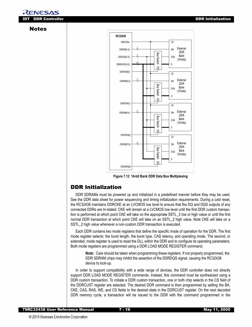
IDT DDR Controller DDR Initialization
79RC32438 User Refer
Notes
Figure 7.12 16-bit Bank DDR Data Bus Multiplexing
DDR InitializationDDR SDRAMs must be powered up and initialized in a predefined manner before they may be used.
See the DDR data sheet for power sequencing and timing initialization requirements. During a cold reset,the RC32438 maintains DDRCKE at an LVCMOS low level to ensure that the DQ and DQS outputs of anyconnected DDRs are tri-stated. CKE will remain at a LVCMOS low level until the first DDR custom transac-tion is performed at which point CKE will take on the appropriate SSTL_2 low or high value or until the firstnormal DDR transaction at which point CKE will take on an SSTL_2 high value. Note CKE will take on aSSTL_2 high value whenever a non-custom DDR transaction is executed.
Each DDR contains two mode registers that define the specific mode of operation for the DDR. The firstmode register selects: the burst length, the burst type, CAS latency, and operating mode. The second, orextended, mode register is used to reset the DLL within the DDR and to configure its operating parameters.Both mode registers are programmed using a DDR LOAD MODE REGISTER command.
Note: Care should be taken when programming these registers. If not properly programmed, the DDR SDRAM chips may inhibit the assertion of the DDRDQS signal, causing the RC32438 device to lock-up.
In order to support compatibility with a wide range of devices, the DDR controller does not directlysupport DDR LOAD MODE REGISTER commands. Instead, this command must be synthesized using aDDR custom transaction. To initiate a DDR custom transaction, one or both chip selects in the CS field ofthe DDRCUST register are selected. The desired DDR command is then programmed by setting the BA,CKE, CAS, RAS, WE, and CS fields to the desired state in the DDRCUST register. On the next decodedDDR memory cycle, a transaction will be issued to the DDR with the command programmed in the
Bus Switch
OE
Bus SwitchOE
RC32438
2
2
16
2
DDRDM[1:0]
DDRDQS[1:0]
DDRDATA[15:0]
DDRDM[3:2]
DDROEN[0]
DDROEN[1]
Bus Switch
OE
Bus Switch
OE
DDROEN[2]
DDROEN[3]
2
2
DDRDM[5:4]
DDRDM[7:6]
ExternalDDRBank
(16-bits)
DM
DQS
D
CS
ExternalDDRBank
(16-bits)
DM
DQS
D
CS
ExternalDDRBank
(16-bits)
DM
DQS
D
CS
ExternalDDRBank
(16-bits)
DM
DQS
D
CS
DDRCSNx
ence Manual 7 - 16 May 11, 2005
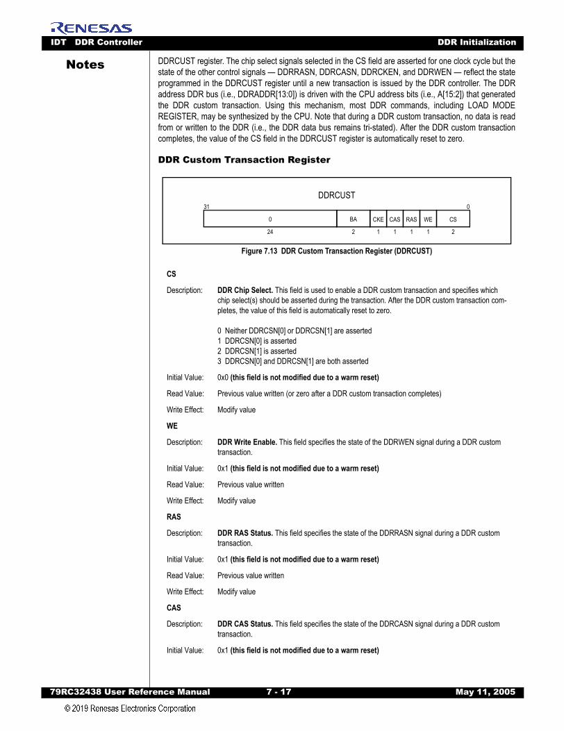
IDT DDR Controller DDR Initialization
79RC32438 User Refer
Notes
DDRCUST register. The chip select signals selected in the CS field are asserted for one clock cycle but thestate of the other control signals — DDRRASN, DDRCASN, DDRCKEN, and DDRWEN — reflect the stateprogrammed in the DDRCUST register until a new transaction is issued by the DDR controller. The DDRaddress DDR bus (i.e., DDRADDR[13:0]) is driven with the CPU address bits (i.e., A[15:2]) that generatedthe DDR custom transaction. Using this mechanism, most DDR commands, including LOAD MODEREGISTER, may be synthesized by the CPU. Note that during a DDR custom transaction, no data is readfrom or written to the DDR (i.e., the DDR data bus remains tri-stated). After the DDR custom transactioncompletes, the value of the CS field in the DDRCUST register is automatically reset to zero.DDR Custom Transaction Register
Figure 7.13 DDR Custom Transaction Register (DDRCUST)
CS
Description: DDR Chip Select. This field is used to enable a DDR custom transaction and specifies which chip select(s) should be asserted during the transaction. After the DDR custom transaction com-pletes, the value of this field is automatically reset to zero.
0 Neither DDRCSN[0] or DDRCSN[1] are asserted1 DDRCSN[0] is asserted2 DDRCSN[1] is asserted3 DDRCSN[0] and DDRCSN[1] are both asserted
Initial Value: 0x0 (this field is not modified due to a warm reset)
Read Value: Previous value written (or zero after a DDR custom transaction completes)
Write Effect: Modify value
WE
Description: DDR Write Enable. This field specifies the state of the DDRWEN signal during a DDR custom transaction.
Initial Value: 0x1 (this field is not modified due to a warm reset)
Read Value: Previous value written
Write Effect: Modify value
RAS
Description: DDR RAS Status. This field specifies the state of the DDRRASN signal during a DDR custom transaction.
Initial Value: 0x1 (this field is not modified due to a warm reset)
Read Value: Previous value written
Write Effect: Modify value
CAS
Description: DDR CAS Status. This field specifies the state of the DDRCASN signal during a DDR custom transaction.
Initial Value: 0x1 (this field is not modified due to a warm reset)
DDRCUST031
24
0 CKE CAS RAS
1
WE CS
2
BA
2 1 1 1
ence Manual 7 - 17 May 11, 2005
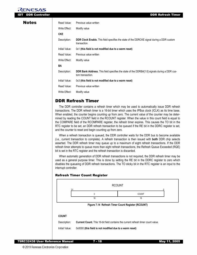
IDT DDR Controller DDR Refresh Timer
79RC32438 User Refer
Notes
DDR Refresh TimerThe DDR controller contains a refresh timer which may be used to automatically issue DDR refresh
transactions. The DDR refresh timer is a 16-bit timer which uses the IPBus clock (ICLK) as its time base.When enabled, the counter begins counting up from zero. The current value of the counter may be deter-mined by reading the COUNT field in the RCOUNT register. When the value in this count field is equal tothe COMPARE field of the RCOMPARE register, the refresh timer expires. This causes the TO bit in theRTC register to be set, an DDR refresh transaction to be queued if the RE bit in the DDRC register is set,and the counter to reset and begin counting up from zero.
When a refresh transaction is queued, the DDR controller waits for the DDR bus to become available(i.e., current transaction to complete). A refresh transaction is then issued with both DDR chip selectsasserted. The DDR refresh timer may queue up to a maximum of eight refresh transactions. If the DDRrefresh timer attempts to queue more than eight refresh transactions, the Refresh Queue Exceeded (RQE)bit is set in the RTC register and the refresh transaction is discarded.
When automatic generation of DDR refresh transactions is not required, the DDR refresh timer may beused as a general purpose timer. This is done by setting the RE bit in the DDRC register to zero whichdisables the queueing of DDR refresh transactions. The TO sticky bit in the RTC register is an input to theinterrupt controller.
Refresh Timer Count Register
Figure 7.14 Refresh Timer Count Register (RCOUNT)
Read Value: Previous value written
Write Effect: Modify value
CKE
Description: DDR Clock Enable. This field specifies the state of the DDRCKE signal during a DDR custom transaction.
Initial Value: 0x1 (this field is not modified due to a warm reset)
Read Value: Previous value written
Write Effect: Modify value
BA
Description: DDR Bank Address. This field specifies the state of the DDRBA[1:0] signals during a DDR cus-tom transaction.
Initial Value: 0x3 (this field is not modified due to a warm reset)
Read Value: Previous value written
Write Effect: Modify value
COUNT
Description: Current Count. This 16-bit field contains the current refresh timer count value.
Initial Value: 0x0000 (this field is not modified due to a warm reset)
RCOUNT031
16 16
0 COUNT
ence Manual 7 - 18 May 11, 2005
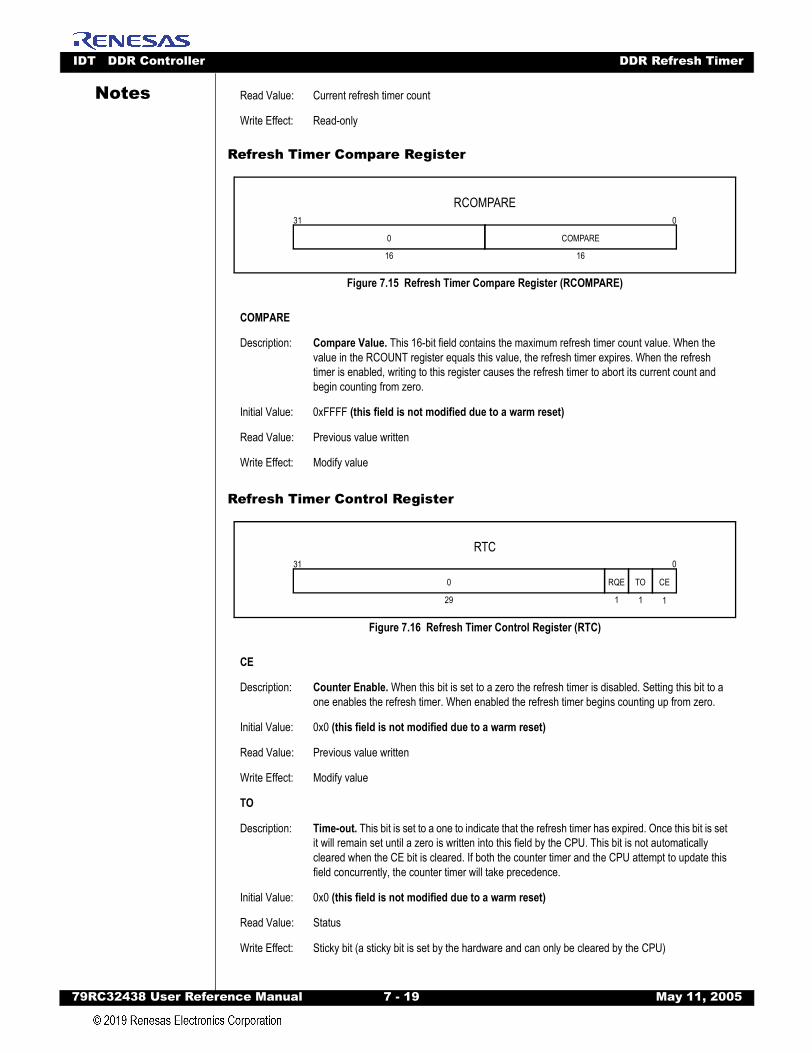
IDT DDR Controller DDR Refresh Timer
79RC32438 User Refer
Notes
Refresh Timer Compare Register
Figure 7.15 Refresh Timer Compare Register (RCOMPARE)
Refresh Timer Control Register
Figure 7.16 Refresh Timer Control Register (RTC)
Read Value: Current refresh timer count
Write Effect: Read-only
COMPARE
Description: Compare Value. This 16-bit field contains the maximum refresh timer count value. When the value in the RCOUNT register equals this value, the refresh timer expires. When the refresh timer is enabled, writing to this register causes the refresh timer to abort its current count and begin counting from zero.
Initial Value: 0xFFFF (this field is not modified due to a warm reset)
Read Value: Previous value written
Write Effect: Modify value
CE
Description: Counter Enable. When this bit is set to a zero the refresh timer is disabled. Setting this bit to a one enables the refresh timer. When enabled the refresh timer begins counting up from zero.
Initial Value: 0x0 (this field is not modified due to a warm reset)
Read Value: Previous value written
Write Effect: Modify value
TO
Description: Time-out. This bit is set to a one to indicate that the refresh timer has expired. Once this bit is set it will remain set until a zero is written into this field by the CPU. This bit is not automatically cleared when the CE bit is cleared. If both the counter timer and the CPU attempt to update this field concurrently, the counter timer will take precedence.
Initial Value: 0x0 (this field is not modified due to a warm reset)
Read Value: Status
Write Effect: Sticky bit (a sticky bit is set by the hardware and can only be cleared by the CPU)
RCOMPARE031
16 16
0 COMPARE
RTC031
29
0 TO CE
1 1
RQE
1
ence Manual 7 - 19 May 11, 2005
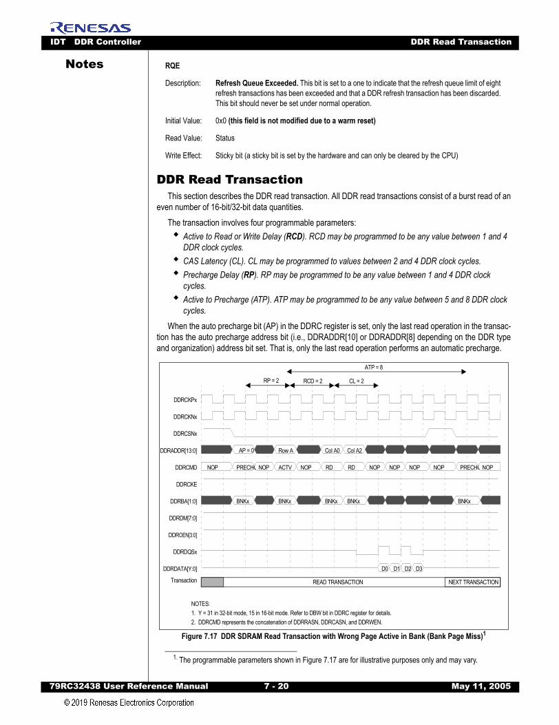
IDT DDR Controller DDR Read Transaction
79RC32438 User Refer
Notes
DDR Read TransactionThis section describes the DDR read transaction. All DDR read transactions consist of a burst read of an
even number of 16-bit/32-bit data quantities. The transaction involves four programmable parameters:
Active to Read or Write Delay (RCD). RCD may be programmed to be any value between 1 and 4 DDR clock cycles.CAS Latency (CL). CL may be programmed to values between 2 and 4 DDR clock cycles.Precharge Delay (RP). RP may be programmed to be any value between 1 and 4 DDR clock cycles.Active to Precharge (ATP). ATP may be programmed to be any value between 5 and 8 DDR clock cycles.
When the auto precharge bit (AP) in the DDRC register is set, only the last read operation in the transac-tion has the auto precharge address bit (i.e., DDRADDR[10] or DDRADDR[8] depending on the DDR typeand organization) address bit set. That is, only the last read operation performs an automatic precharge.
Figure 7.17 DDR SDRAM Read Transaction with Wrong Page Active in Bank (Bank Page Miss)1
RQE
Description: Refresh Queue Exceeded. This bit is set to a one to indicate that the refresh queue limit of eight refresh transactions has been exceeded and that a DDR refresh transaction has been discarded. This bit should never be set under normal operation.
Initial Value: 0x0 (this field is not modified due to a warm reset)
Read Value: Status
Write Effect: Sticky bit (a sticky bit is set by the hardware and can only be cleared by the CPU)
1. The programmable parameters shown in Figure 7.17 are for illustrative purposes only and may vary.
Row A Col A0 Col A2
NOP PRECHG NOP ACTV NOP RD RD NOP NOP NOP NOP PRECHG NOP
BNKx BNKx BNKx BNKx BNKx
D0 D1 D2 D3
DDRCKPx
DDRCKNx
DDRCSNx
DDRADDR[13:0]
DDRCMD
DDRCKE
DDRBA[1:0]
DDRDM[7:0]
DDROEN[3:0]
DDRDQSx
DDRDATA[Y:0]
RP = 2 RCD = 2 CL = 2
ATP = 8
NOTES:1. Y = 31 in 32-bit mode, 15 in 16-bit mode. Refer to DBW bit in DDRC register for details.2. DDRCMD represents the concatenation of DDRRASN, DDRCASN, and DDRWEN.
Transaction READ TRANSACTION
AP = 0
NEXT TRANSACTION
ence Manual 7 - 20 May 11, 2005
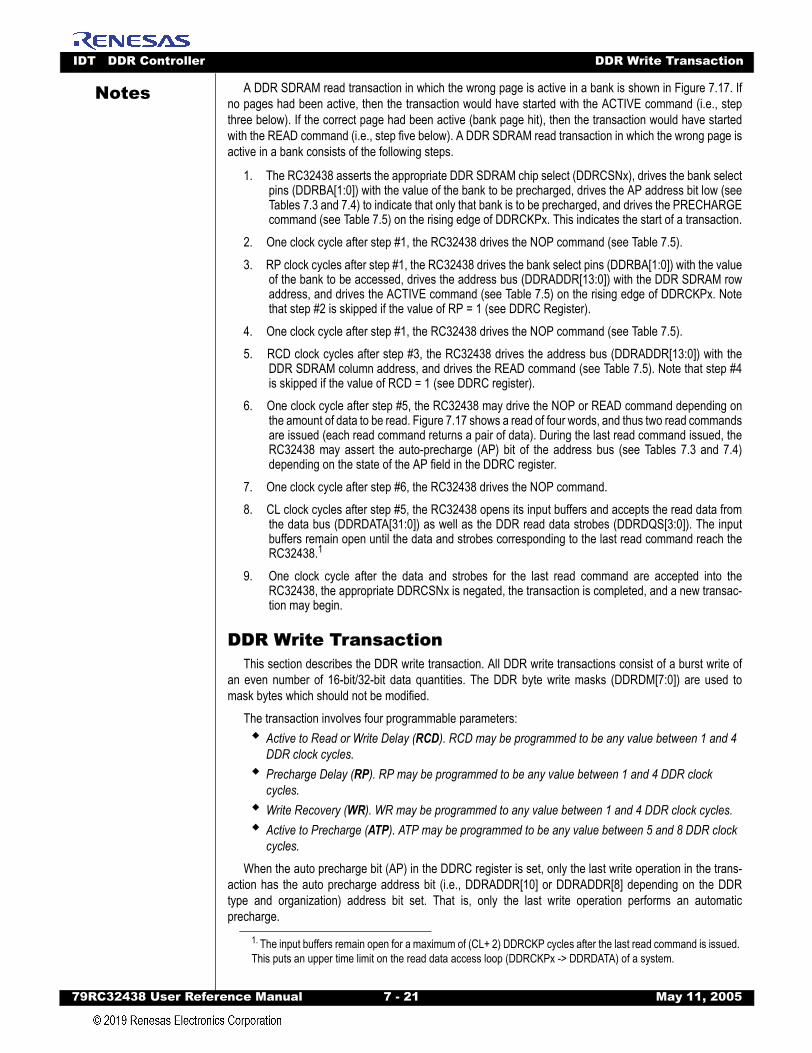
IDT DDR Controller DDR Write Transaction
79RC32438 User Refer
Notes
A DDR SDRAM read transaction in which the wrong page is active in a bank is shown in Figure 7.17. Ifno pages had been active, then the transaction would have started with the ACTIVE command (i.e., stepthree below). If the correct page had been active (bank page hit), then the transaction would have startedwith the READ command (i.e., step five below). A DDR SDRAM read transaction in which the wrong page isactive in a bank consists of the following steps.1. The RC32438 asserts the appropriate DDR SDRAM chip select (DDRCSNx), drives the bank selectpins (DDRBA[1:0]) with the value of the bank to be precharged, drives the AP address bit low (seeTables 7.3 and 7.4) to indicate that only that bank is to be precharged, and drives the PRECHARGEcommand (see Table 7.5) on the rising edge of DDRCKPx. This indicates the start of a transaction.
2. One clock cycle after step #1, the RC32438 drives the NOP command (see Table 7.5).3. RP clock cycles after step #1, the RC32438 drives the bank select pins (DDRBA[1:0]) with the value
of the bank to be accessed, drives the address bus (DDRADDR[13:0]) with the DDR SDRAM rowaddress, and drives the ACTIVE command (see Table 7.5) on the rising edge of DDRCKPx. Notethat step #2 is skipped if the value of RP = 1 (see DDRC Register).
4. One clock cycle after step #1, the RC32438 drives the NOP command (see Table 7.5). 5. RCD clock cycles after step #3, the RC32438 drives the address bus (DDRADDR[13:0]) with the
DDR SDRAM column address, and drives the READ command (see Table 7.5). Note that step #4is skipped if the value of RCD = 1 (see DDRC register).
6. One clock cycle after step #5, the RC32438 may drive the NOP or READ command depending onthe amount of data to be read. Figure 7.17 shows a read of four words, and thus two read commandsare issued (each read command returns a pair of data). During the last read command issued, theRC32438 may assert the auto-precharge (AP) bit of the address bus (see Tables 7.3 and 7.4)depending on the state of the AP field in the DDRC register.
7. One clock cycle after step #6, the RC32438 drives the NOP command.8. CL clock cycles after step #5, the RC32438 opens its input buffers and accepts the read data from
the data bus (DDRDATA[31:0]) as well as the DDR read data strobes (DDRDQS[3:0]). The inputbuffers remain open until the data and strobes corresponding to the last read command reach theRC32438.1
9. One clock cycle after the data and strobes for the last read command are accepted into theRC32438, the appropriate DDRCSNx is negated, the transaction is completed, and a new transac-tion may begin.
DDR Write TransactionThis section describes the DDR write transaction. All DDR write transactions consist of a burst write of
an even number of 16-bit/32-bit data quantities. The DDR byte write masks (DDRDM[7:0]) are used tomask bytes which should not be modified.
The transaction involves four programmable parameters:Active to Read or Write Delay (RCD). RCD may be programmed to be any value between 1 and 4 DDR clock cycles.Precharge Delay (RP). RP may be programmed to be any value between 1 and 4 DDR clock cycles.Write Recovery (WR). WR may be programmed to any value between 1 and 4 DDR clock cycles.Active to Precharge (ATP). ATP may be programmed to be any value between 5 and 8 DDR clock cycles.
When the auto precharge bit (AP) in the DDRC register is set, only the last write operation in the trans-action has the auto precharge address bit (i.e., DDRADDR[10] or DDRADDR[8] depending on the DDRtype and organization) address bit set. That is, only the last write operation performs an automaticprecharge.
1. The input buffers remain open for a maximum of (CL+ 2) DDRCKP cycles after the last read command is issued. This puts an upper time limit on the read data access loop (DDRCKPx -> DDRDATA) of a system.
ence Manual 7 - 21 May 11, 2005
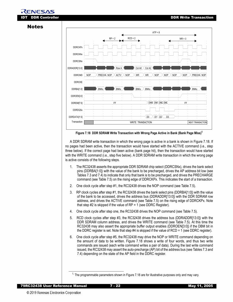
IDT DDR Controller DDR Write Transaction
79RC32438 User Refer
Notes
Figure 7.18 DDR SDRAM Write Transaction with Wrong Page Active in Bank (Bank Page Miss)1
A DDR SDRAM write transaction in which the wrong page is active in a bank is shown in Figure 7.18. Ifno pages had been active, then the transaction would have started with the ACTIVE command (i.e., stepthree below). If the correct page had been active (bank page hit), then the transaction would have startedwith the WRITE command (i.e., step five below). A DDR SDRAM write transaction in which the wrong pageis active consists of the following steps.
1. The RC32438 asserts the appropriate DDR SDRAM chip select (DDRCSNx), drives the bank selectpins (DDRBA[1:0]) with the value of the bank to be precharged, drives the AP address bit low (seeTables 7.3 and 7.4) to indicate that only that bank is to be precharged, and drives the PRECHARGEcommand (see Table 7.5) on the rising edge of DDRCKPx. This indicates the start of a transaction.
2. One clock cycle after step #1, the RC32438 drives the NOP command (see Table 7.5).3. RP clock cycles after step #1, the RC32438 drives the bank select pins (DDRBA[1:0]) with the value
of the bank to be accessed, drives the address bus (DDRADDR[13:0]) with the DDR SDRAM rowaddress, and drives the ACTIVE command (see Table 7.5) on the rising edge of DDRCKPx. Notethat step #2 is skipped if the value of RP = 1 (see DDRC Register).
4. One clock cycle after step one, the RC32438 drives the NOP command (see Table 7.5). 5. RCD clock cycles after step #3, the RC32438 drives the address bus (DDRADDR[13:0]) with the
DDR SDRAM column address, and drives the WRITE command (see Table 7.5). At this time theRC32438 may also assert the appropriate buffer output enables (DDROEN[3:0]) if the DBM bit inthe DDRC register is set. Note that step #4 is skipped if the value of RCD = 1 (see DDRC register).
6. One clock cycle after step #5, the RC32438 may drive the NOP or WRITE command depending onthe amount of data to be written. Figure 7.18 shows a write of four words, and thus two writecommands are issued (each write command writes a pair of data). During the last write commandissued, the RC32438 may assert the auto-precharge (AP) bit of the address bus (see Tables 7.3 and7.4) depending on the state of the AP field in the DDRC register.
1. The programmable parameters shown in Figure 7.18 are for illustrative purposes only and may vary.
RP = 2 RCD = 2 WR = 3
ATP = 8
Row A Col A0 Col A2
NOP PRECHG NOP ACTV NOP WR WR NOP NOP NOP NOP PRECHG NOP
BNKx BNKx BNKx BNKx BNKx
FF DM0 DM1 DM2 DM3 FF
D0 D1 D2 D3
DDRCKPx
DDRCKNx
DDRCSNx
DDRADDR[13:0]
DDRCMD
DDRCKE
DDRBA[1:0]
DDROEN[3:0]
DDRDM[7:0]
DDRDQSx
DDRDATA[Y:0]
WRITE TRANSACTIONTransaction NEXT TRANSACTION
ence Manual 7 - 22 May 11, 2005
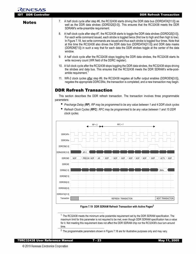
IDT DDR Controller DDR Refresh Transaction
79RC32438 User Refer
Notes
7. A half clock cycle after step #6, the RC32438 starts driving the DDR data bus (DDRDATA[31:0]) aswell as the DDR data strobes (DDRDQS[3:0]). This ensures that the RC32438 meets the DDRSDRAM’s write-preamble requirement.8. A half clock cycle after step #7, the RC32438 starts to toggle the DDR data strobes (DDRDQS[3:0]).For each write command issued, each strobe is toggled twice (first low to high and then high to low).In Figure 7.18, two write commands are issued and thus each strobe is toggled four times. Note thatat this time the RC32438 also drives the DDR data bus (DDRDATA[31:0]) and DDR data masks(DDRDM[7:0]) in such a way that for each data the DDR strobes toggle at the center of the datawindow.
9. A half clock cycle after the RC32438 stops toggling the DDR data strobes, the RC32438 starts itswrite recovery count (WR field of the DDRC register).
10. A full clock cycle after the RC32438 stops toggling the DDR data strobes, the RC32438 stops drivingthe strobes and data bus. This ensures that the RC32438 meets the DDR SDRAM’s write-post-amble requirement.1
11. WR-2 clock cycles after step #9, the RC32438 negates all buffer output enables (DDROEN[3:0]),negates the appropriate DDRCSNx, the transaction is completed, and a new transaction may begin.
DDR Refresh TransactionThis section describes the DDR refresh transaction. The transaction involves three programmable
parameters:Precharge Delay (RP). RP may be programmed to be any value between 1 and 4 DDR clock cyclesRefresh Clock Cycles (RFC). RFC may be programmed to be any value between 1 and 15 DDR clock cycles.
Figure 7.19 DDR SDRAM Refresh Transaction with Active Pages2
1. The RC32438 meets the minimum write postamble requirement set by the DDR SDRAM specification. The maximum limit for this parameter is not required to be met, even though DDR SDRAM specification has a value for it. Not meeting this requirement does not affect the DDR SDRAM chip nor the RC32438’s bus turn-around time.2. The programmable parameters shown in Figure 7.18 are for illustrative purposes only and may vary.
RP = 2 RFC = 7
AP=1
NOP PRECHG NOP AR NOP NOP NOP NOP NOP NOP NOP ACTV NOP
BNKx
DDRCKPx
DDRCKNx
DDRCSN[1:0]
DDRADDR[13:0]
DDRCMD
DDRCKE
DDRBA[1:0]
DDRDM[7:0]
DDROEN[3:0]
DDRDQS[3:0]
DDRDATA[31:0]
Transaction REFRESH TRANSACTION NEXT TRANSACTION
ence Manual 7 - 23 May 11, 2005

IDT DDR Controller DDR Custom Transaction
79RC32438 User Refer
Notes
A DDR SDRAM refresh transaction is queued for execution whenever the DDR Refresh Timer expiresand the refresh enable bit (RE) in the DDRC register is set. If no active pages exists in any of the DDRSDRAM banks, then the refresh transaction simply consists of an auto refresh command followed by RFCclock cycles (i.e., the transaction starts with step three below). If there exists an active page in any of theDDR SDRAMs, then a precharge-all command is first issued to deactivate all banks in all of the DDRs. Thisis then followed by an auto-refresh command followed by RFC clock cycles. A DDR SDRAM refresh trans-action with active pages is shown in Figure 7.19 and consists of the following steps.1. The RC32438 asserts both DDR SDRAM chip selects (DDRCSN[1:0]), drives the AP address bithigh (see Tables 7.3 and 7.4) to indicate that all banks are to be precharged, and drives thePRECHARGE command (see Table 7.5) on the rising edge of DDRCKPx. This indicates the start ofa transaction.
2. One clock cycle after step #1, the RC32438 drives the NOP command (see Table 7.5).3. RP clock cycles after step #1, the RC32438 drives the AUTO-REFRESH command (see Table 7.5).
Note that step two is skipped if the value of RP = 1 (see DDRC register).4. One clock cycle after step #3, the RC32438 drives the NOP command (see Table 7.5). 5. RFC clock cycles after step #4, the RC32438 negates the DDR SDRAM chip selects
(DDRCSN[1:0]), the transaction is completed, and a new transaction may begin.
DDR Custom TransactionThis section describes the SDRAM custom transaction. The transaction involves seven programmable
parameters:DDR Chip Select (CS). CS may be programmed to select DDRCSN[0], DDRDCSN[1] or bothDDR Write Enable Status (WE). WE specifies the state of the DDRWEN pin during a DDR custom transactionDDR RAS Status (RAS). RAS specifies the state of the DDRRASN pin during a DDR custom trans-actionDDR CAS Status (CAS). CAS specifies the state of the DDRCASN signal during a DDR custom transactionDDR Clock Enable Status (CKE). CKE specifies the state of the DDRCKE signal during a DDR cus-tom transaction.DDR Bank Address Status (BA). BA specifies the state of the DDRBA[1:0] signals during a DDR custom transaction.DDR Auto Precharge Enable (AP). AP specifies the state of the auto precharge address bit during a DDR custom transaction.
ence Manual 7 - 24 May 11, 2005
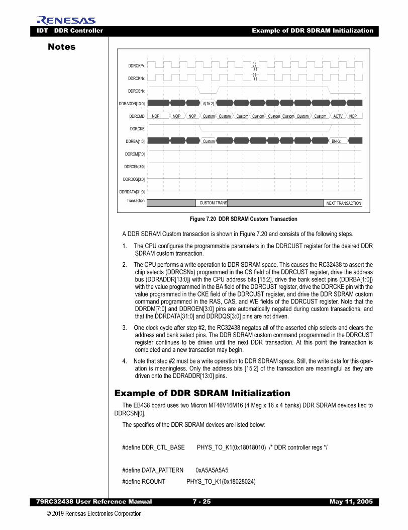
IDT DDR Controller Example of DDR SDRAM Initialization
79RC32438 User Refer
Notes
Figure 7.20 DDR SDRAM Custom Transaction
A DDR SDRAM Custom transaction is shown in Figure 7.20 and consists of the following steps.
1. The CPU configures the programmable parameters in the DDRCUST register for the desired DDRSDRAM custom transaction.
2. The CPU performs a write operation to DDR SDRAM space. This causes the RC32438 to assert thechip selects (DDRCSNx) programmed in the CS field of the DDRCUST register, drive the addressbus (DDRADDR[13:0]) with the CPU address bits [15:2], drive the bank select pins (DDRBA[1:0])with the value programmed in the BA field of the DDRCUST register, drive the DDRCKE pin with thevalue programmed in the CKE field of the DDRCUST register, and drive the DDR SDRAM customcommand programmed in the RAS, CAS, and WE fields of the DDRCUST register. Note that theDDRDM[7:0] and DDROEN[3:0] pins are automatically negated during custom transactions, andthat the DDRDATA[31:0] and DDRDQS[3:0] pins are not driven.
3. One clock cycle after step #2, the RC32438 negates all of the asserted chip selects and clears theaddress and bank select pins. The DDR SDRAM custom command programmed in the DDRCUSTregister continues to be driven until the next DDR transaction. At this point the transaction iscompleted and a new transaction may begin.
4. Note that step #2 must be a write operation to DDR SDRAM space. Still, the write data for this oper-ation is meaningless. Only the address bits [15:2] of the transaction are meaningful as they aredriven onto the DDRADDR[13:0] pins.
Example of DDR SDRAM InitializationThe EB438 board uses two Micron MT46V16M16 (4 Meg x 16 x 4 banks) DDR SDRAM devices tied to
DDRCSN[0]. The specifics of the DDR SDRAM devices are listed below:
#define DDR_CTL_BASE PHYS_TO_K1(0x18018010) /* DDR controller regs */
#define DATA_PATTERN 0xA5A5A5A5#define RCOUNT PHYS_TO_K1(0x18028024)
A[15:2]
NOP NOP NOP Custom Custom Custom Custom Custom Custom Custom Custom ACTV NOP
Custom BNKx
DDRCKPx
DDRCKNx
DDRCSNx
DDRADDR[13:0]
DDRCMD
DDRCKE
DDRBA[1:0]
DDRDM[7:0]
DDROEN[3:0]
DDRDQS[3:0]
DDRDATA[31:0]
Transaction CUSTOM TRANS NEXT TRANSACTION
ence Manual 7 - 25 May 11, 2005
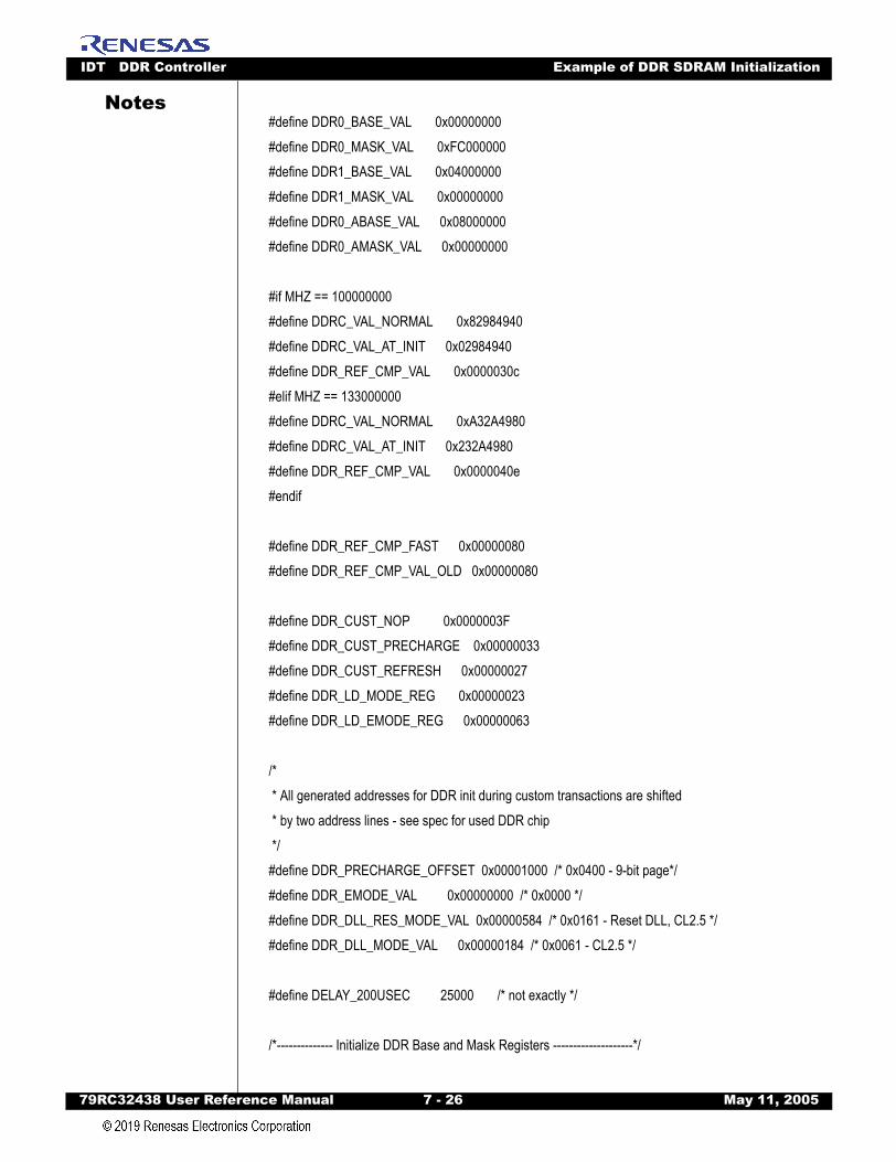
IDT DDR Controller Example of DDR SDRAM Initialization
79RC32438 User Refer
Notes
#define DDR0_BASE_VAL 0x00000000#define DDR0_MASK_VAL 0xFC000000#define DDR1_BASE_VAL 0x04000000#define DDR1_MASK_VAL 0x00000000#define DDR0_ABASE_VAL 0x08000000#define DDR0_AMASK_VAL 0x00000000#if MHZ == 100000000#define DDRC_VAL_NORMAL 0x82984940#define DDRC_VAL_AT_INIT 0x02984940#define DDR_REF_CMP_VAL 0x0000030c#elif MHZ == 133000000#define DDRC_VAL_NORMAL 0xA32A4980#define DDRC_VAL_AT_INIT 0x232A4980#define DDR_REF_CMP_VAL 0x0000040e#endif
#define DDR_REF_CMP_FAST 0x00000080#define DDR_REF_CMP_VAL_OLD 0x00000080
#define DDR_CUST_NOP 0x0000003F#define DDR_CUST_PRECHARGE 0x00000033#define DDR_CUST_REFRESH 0x00000027#define DDR_LD_MODE_REG 0x00000023#define DDR_LD_EMODE_REG 0x00000063
/* * All generated addresses for DDR init during custom transactions are shifted * by two address lines - see spec for used DDR chip */#define DDR_PRECHARGE_OFFSET 0x00001000 /* 0x0400 - 9-bit page*/#define DDR_EMODE_VAL 0x00000000 /* 0x0000 */#define DDR_DLL_RES_MODE_VAL 0x00000584 /* 0x0161 - Reset DLL, CL2.5 */#define DDR_DLL_MODE_VAL 0x00000184 /* 0x0061 - CL2.5 */
#define DELAY_200USEC 25000 /* not exactly */
/*-------------- Initialize DDR Base and Mask Registers --------------------*/
ence Manual 7 - 26 May 11, 2005
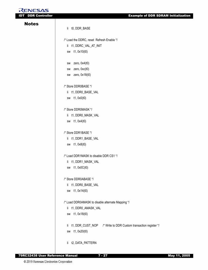
IDT DDR Controller Example of DDR SDRAM Initialization
79RC32438 User Refer
Notes
li t0, DDR_BASE/* Load the DDRC, reset Refresh Enable */ li t1, DDRC_VAL_AT_INIT sw t1, 0x10(t0)
sw zero, 0x4(t0) sw zero, 0xc(t0) sw zero, 0x18(t0)
/* Store DDR0BASE */ li t1, DDR0_BASE_VAL sw t1, 0x0(t0)
/* Store DDR0MASK */ li t1, DDR0_MASK_VAL sw t1, 0x4(t0)
/* Store DDR1BASE */ li t1, DDR1_BASE_VAL sw t1, 0x8(t0)
/* Load DDR1MASK to disable DDR CS1 */ li t1, DDR1_MASK_VAL sw t1, 0x0C(t0)
/* Store DDR0ABASE */ li t1, DDR0_BASE_VAL sw t1, 0x14(t0)
/* Load DDR0AMASK to disable alternate Mapping */ li t1, DDR0_AMASK_VAL sw t1, 0x18(t0)
li t1, DDR_CUST_NOP /* Write to DDR Custom transaction register */ sw t1, 0x20(t0)
li t2, DATA_PATTERN
ence Manual 7 - 27 May 11, 2005
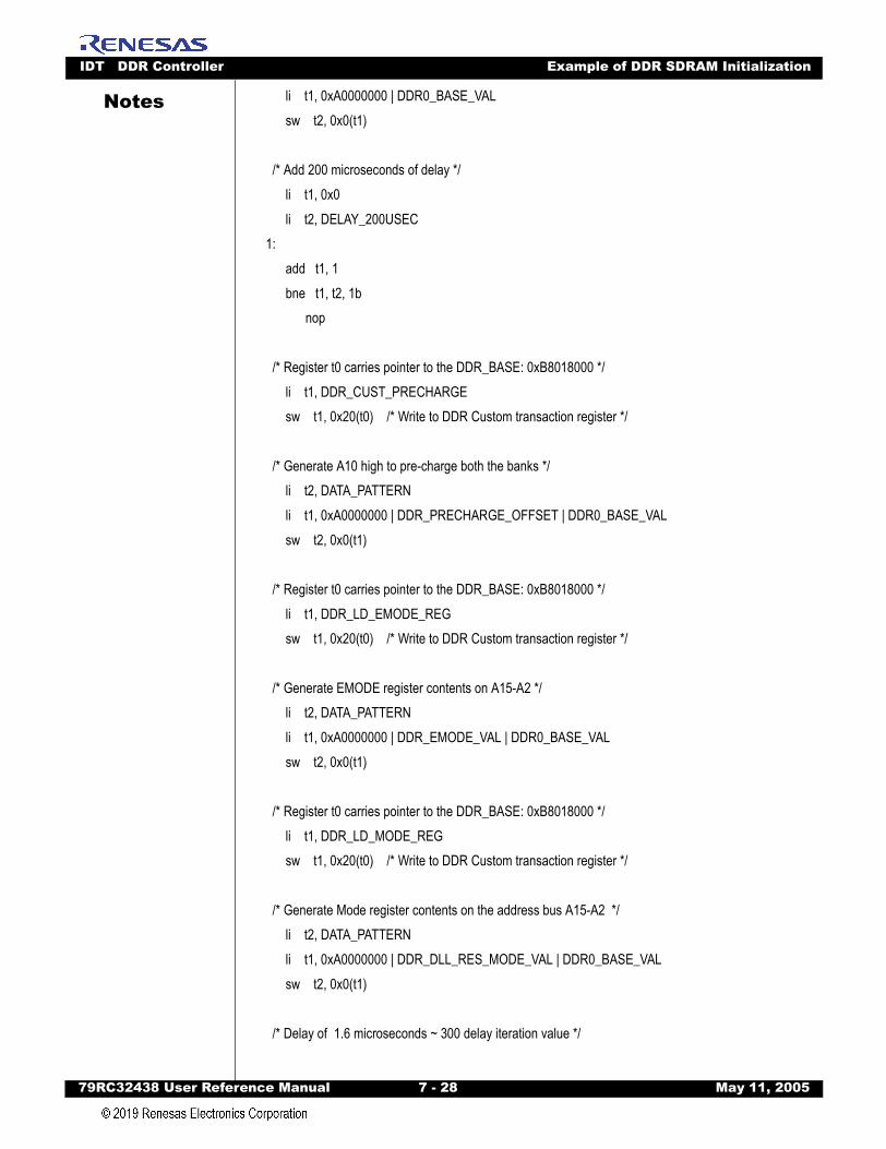
IDT DDR Controller Example of DDR SDRAM Initialization
79RC32438 User Refer
Notes
li t1, 0xA0000000 | DDR0_BASE_VAL sw t2, 0x0(t1)/* Add 200 microseconds of delay */ li t1, 0x0 li t2, DELAY_200USEC1: add t1, 1 bne t1, t2, 1b nop
/* Register t0 carries pointer to the DDR_BASE: 0xB8018000 */ li t1, DDR_CUST_PRECHARGE sw t1, 0x20(t0) /* Write to DDR Custom transaction register */
/* Generate A10 high to pre-charge both the banks */ li t2, DATA_PATTERN li t1, 0xA0000000 | DDR_PRECHARGE_OFFSET | DDR0_BASE_VAL sw t2, 0x0(t1)
/* Register t0 carries pointer to the DDR_BASE: 0xB8018000 */ li t1, DDR_LD_EMODE_REG sw t1, 0x20(t0) /* Write to DDR Custom transaction register */
/* Generate EMODE register contents on A15-A2 */ li t2, DATA_PATTERN li t1, 0xA0000000 | DDR_EMODE_VAL | DDR0_BASE_VAL sw t2, 0x0(t1)
/* Register t0 carries pointer to the DDR_BASE: 0xB8018000 */ li t1, DDR_LD_MODE_REG sw t1, 0x20(t0) /* Write to DDR Custom transaction register */
/* Generate Mode register contents on the address bus A15-A2 */ li t2, DATA_PATTERN li t1, 0xA0000000 | DDR_DLL_RES_MODE_VAL | DDR0_BASE_VAL sw t2, 0x0(t1)
/* Delay of 1.6 microseconds ~ 300 delay iteration value */
ence Manual 7 - 28 May 11, 2005
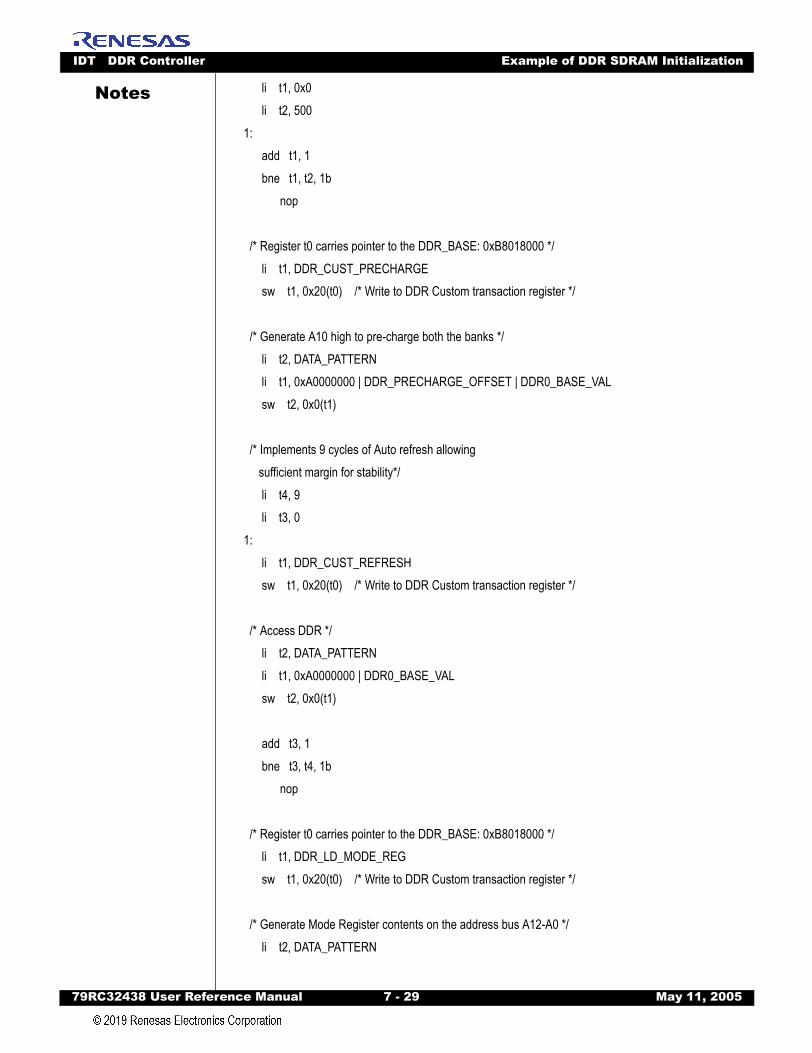
IDT DDR Controller Example of DDR SDRAM Initialization
79RC32438 User Refer
Notes
li t1, 0x0 li t2, 5001: add t1, 1 bne t1, t2, 1b nop/* Register t0 carries pointer to the DDR_BASE: 0xB8018000 */ li t1, DDR_CUST_PRECHARGE sw t1, 0x20(t0) /* Write to DDR Custom transaction register */
/* Generate A10 high to pre-charge both the banks */ li t2, DATA_PATTERN li t1, 0xA0000000 | DDR_PRECHARGE_OFFSET | DDR0_BASE_VAL sw t2, 0x0(t1)
/* Implements 9 cycles of Auto refresh allowing sufficient margin for stability*/ li t4, 9 li t3, 01: li t1, DDR_CUST_REFRESH sw t1, 0x20(t0) /* Write to DDR Custom transaction register */
/* Access DDR */ li t2, DATA_PATTERN li t1, 0xA0000000 | DDR0_BASE_VAL sw t2, 0x0(t1)
add t3, 1 bne t3, t4, 1b nop
/* Register t0 carries pointer to the DDR_BASE: 0xB8018000 */ li t1, DDR_LD_MODE_REG sw t1, 0x20(t0) /* Write to DDR Custom transaction register */
/* Generate Mode Register contents on the address bus A12-A0 */ li t2, DATA_PATTERN
ence Manual 7 - 29 May 11, 2005

IDT DDR Controller Example of DDR SDRAM Initialization
79RC32438 User Refer
Notes
li t1, 0xA0000000 | DDR_DLL_MODE_VAL | DDR0_BASE_VAL sw t2, 0x0(t1)/* Initialize the refresh timer with fast refresh count */ li t0, RCOUNT li t1, DDR_REF_CMP_FAST
/* Set the RCOMPARE register */ sw t1, 0x4(t0)
/* Enable the Refresh timer */ li t1, 0x1 /* CE set to enabled the Refresh counter */ sw t1, 0x8(t0)
/* Enable RE-refresh enable in the DDRC register */ li t0, DDR_BASE li t1, DDRC_VAL_NORMAL sw t1, 0x10(t0)
/* Add 200 microseconds of delay */ li t1, 0x0 li t2, DELAY_200USEC1: add t1, 1 bne t1, t2, 1b nop
li t0, RCOUNT
/* Find Refresh Timer Compare value based on revision - Check for IP7 */ li t2, 0x1 mtc0 t2, C0_COMPARE mtc0 zero, C0_COUNT nop nop mfc0 t1, C0_CAUSE nop li t3, DDR_REF_CMP_VAL andi t1, 0x8000
ence Manual 7 - 30 May 11, 2005

IDT DDR Controller Example of DDR SDRAM Initialization
79RC32438 User Refer
Notes
bnez t1, acacia_zb nop li t3, DDR_REF_CMP_VAL_OLDacacia_zb: /* Disable the refresh counter before changing the compare value */ sw zero, 0x8(t0)/* Set the RCOMPARE register with value gotten above */ sw t3, 0x4(t0)
/* Enable the Refresh timer */ li t1, 0x1 /* CE set to enabled the Refresh counter */ sw t1, 0x8(t0)
ence Manual 7 - 31 May 11, 2005
IDT DDR Controller Example of DDR SDRAM Initialization
79RC32438 User Refer
Notes
ence Manual 7 - 32 May 11, 2005
Notes
79RC32438 User Reference Manual 8 - 1 M
Chapter 8
Interrupt Controller
IntroductionThis chapter describes the operation of the Interrupt Controller which multiplexes all the interrupt
sources from on-chip modules and the GPIO pins onto the five available interrupt sources of the CPU(IP[6:2]). These interrupt inputs correspond to the IP[6:2] bits of the CPU CP0 CAUSE register. (IP[1:0] aresoftware interrupts, and IP[7] is used by the counter timer in the CPU.)
Each of the IP[6:2] bits in the CPU CAUSE Register has three corresponding registers in the InterruptController:
The Interrupt Pending Register, a 32-bit register that indicates the source of the interrupt. The Interrupt Mask Register, a 32-bit register. Each bit in the Interrupt Mask Register corresponds to the equivalent bit in the Interrupt Pending Register. Setting a bit in the Interrupt Mask Register masks the generation of an interrupt for this source.The Interrupt Test Register, a 32-bit register. Each bit in the Interrupt Test Register corresponds to a bit in the Interrupt Pending Register. Setting a bit in the Interrupt Test Register causes the same behavior as an interrupt request from the corresponding interrupt source in the Interrupt Pending Register. This register may be used to test software interrupt handlers without the need to actually generate the condition required to produce an interrupt request.
The Interrupt Controller has no priority levels. All sources have the same priority. If multiple interruptsare pending, it is the responsibility of the software to assign any priority.
The Interrupt Controller multiplexes the interrupt sources to the CPU. The interrupt clearing or assertionmay take several clock cycles to show up in the Interrupt Pending Register, depending on the source of theinterrupt. To clear the interrupt, the software must clear the source.
FeaturesAllows status of all interrupt sources to be readEach interrupt source may be maskedProvides interrupt test capability
ay 11, 2005
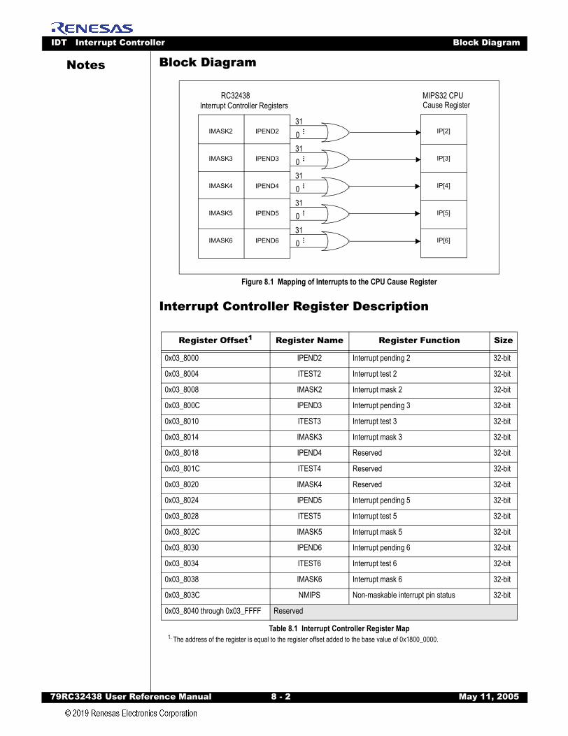
IDT Interrupt Controller Block Diagram
79RC32438 User Refer
Notes
Block DiagramFigure 8.1 Mapping of Interrupts to the CPU Cause Register
Interrupt Controller Register Description
Register Offset1
1. The address of the register is equal to the register offset added to the base value of 0x1800_0000.
Register Name Register Function Size
0x03_8000 IPEND2 Interrupt pending 2 32-bit
0x03_8004 ITEST2 Interrupt test 2 32-bit
0x03_8008 IMASK2 Interrupt mask 2 32-bit
0x03_800C IPEND3 Interrupt pending 3 32-bit
0x03_8010 ITEST3 Interrupt test 3 32-bit
0x03_8014 IMASK3 Interrupt mask 3 32-bit
0x03_8018 IPEND4 Reserved 32-bit
0x03_801C ITEST4 Reserved 32-bit
0x03_8020 IMASK4 Reserved 32-bit
0x03_8024 IPEND5 Interrupt pending 5 32-bit
0x03_8028 ITEST5 Interrupt test 5 32-bit
0x03_802C IMASK5 Interrupt mask 5 32-bit
0x03_8030 IPEND6 Interrupt pending 6 32-bit
0x03_8034 ITEST6 Interrupt test 6 32-bit
0x03_8038 IMASK6 Interrupt mask 6 32-bit
0x03_803C NMIPS Non-maskable interrupt pin status 32-bit
0x03_8040 through 0x03_FFFF Reserved
Table 8.1 Interrupt Controller Register Map
IPEND2
IPEND3
IPEND4
IPEND5
IPEND6
IMASK2
IMASK3
IMASK4
IMASK5
IMASK6
IP[2]
IP[3]
IP[4]
IP[5]
IP[6]
310 ...
310 ...
310 ...
310 ...
310 ...
RC32438 MIPS32 CPUInterrupt Controller Registers Cause Register
ence Manual 8 - 2 May 11, 2005

IDT Interrupt Controller Interrupt Controller Register Description
79RC32438 User Refer
Notes
Interrupt Pending [2..6] RegisterNote: IPEND4 is reserved. Use only IPEND2, IPEND3, IPEND5, and IPEND6.Figure 8.2 Interrupt Pending [2..6] Register (IPEND[2..6])
Interrupt Test [2..6] RegisterNote: ITEST4 is reserved. Do not use.
Figure 8.3 Interrupt Test [2..6] Register (ITEST[2..6])
IPEND
Description: Interrupt Pending. Each bit in this field corresponds to an interrupt source. When a bit is set the corresponding interrupt source is requesting service. Note that this register shows interrupts which are currently requesting service but may be “masked” from actually generating an interrupt exception.
Initial Value: Undefined
Read Value: Status
Write Effect: Read-only
ITEST
Description: Interrupt Test. Each bit in this field corresponds to an interrupt source in the corresponding Inter-rupt Pending (IPEND) register. When a bit in this field is set, it appears to the interrupt controller that the corresponding interrupt source in the IPEND register is requesting service.
Initial Value: 0x0
Read Value: Previous value written
Write Effect: Modify value
IPEND[2..6]031
32
IPEND
ITEST[2..6]031
32
ITEST
ence Manual 8 - 3 May 11, 2005
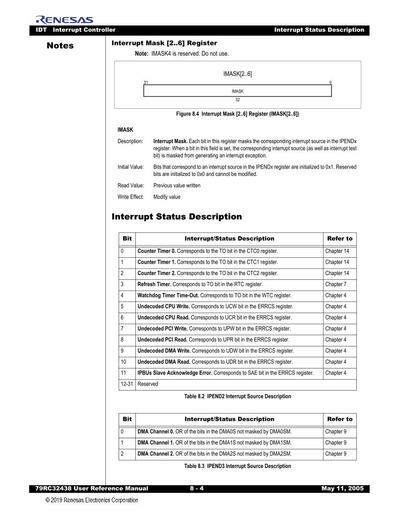
IDT Interrupt Controller Interrupt Status Description
79RC32438 User Refer
Notes
Interrupt Mask [2..6] RegisterNote: IMASK4 is reserved. Do not use.Figure 8.4 Interrupt Mask [2..6] Register (IMASK[2..6])
Interrupt Status Description
IMASK
Description: Interrupt Mask. Each bit in this register masks the corresponding interrupt source in the IPENDx register. When a bit in this field is set, the corresponding interrupt source (as well as interrupt test bit) is masked from generating an interrupt exception.
Initial Value: Bits that correspond to an interrupt source in the IPENDx register are initialized to 0x1. Reserved bits are initialized to 0x0 and cannot be modified.
Read Value: Previous value written
Write Effect: Modify value
Bit Interrupt/Status Description Refer to
0 Counter Timer 0. Corresponds to the TO bit in the CTC0 register. Chapter 14
1 Counter Timer 1. Corresponds to the TO bit in the CTC1 register. Chapter 14
2 Counter Timer 2. Corresponds to the TO bit in the CTC2 register. Chapter 14
3 Refresh Timer. Corresponds to TO bit in the RTC register. Chapter 7
4 Watchdog Timer Time-Out. Corresponds to TO bit in the WTC register. Chapter 4
5 Undecoded CPU Write. Corresponds to UCW bit in the ERRCS register. Chapter 4
6 Undecoded CPU Read. Corresponds to UCR bit in the ERRCS register. Chapter 4
7 Undecoded PCI Write. Corresponds to UPW bit in the ERRCS register. Chapter 4
8 Undecoded PCI Read. Corresponds to UPR bit in the ERRCS register. Chapter 4
9 Undecoded DMA Write. Corresponds to UDW bit in the ERRCS register. Chapter 4
10 Undecoded DMA Read. Corresponds to UDR bit in the ERRCS register. Chapter 4
11 IPBUs Slave Acknowledge Error. Corresponds to SAE bit in the ERRCS register. Chapter 4
12-31 Reserved
Table 8.2 IPEND2 Interrupt Source Description
Bit Interrupt/Status Description Refer to
0 DMA Channel 0. OR of the bits in the DMA0S not masked by DMA0SM. Chapter 9
1 DMA Channel 1. OR of the bits in the DMA1S not masked by DMA1SM. Chapter 9
2 DMA Channel 2. OR of the bits in the DMA2S not masked by DMA2SM. Chapter 9
Table 8.3 IPEND3 Interrupt Source Description
IMASK[2..6]031
32
IMASK
ence Manual 8 - 4 May 11, 2005
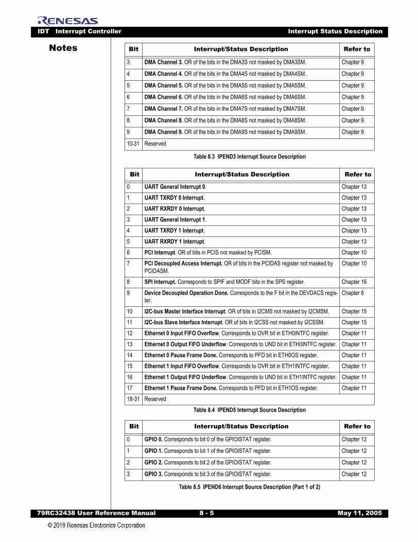
IDT Interrupt Controller Interrupt Status Description
79RC32438 User Refer
Notes
3 DMA Channel 3. OR of the bits in the DMA3S not masked by DMA3SM. Chapter 94 DMA Channel 4. OR of the bits in the DMA4S not masked by DMA4SM. Chapter 9
5 DMA Channel 5. OR of the bits in the DMA5S not masked by DMA5SM. Chapter 9
6 DMA Channel 6. OR of the bits in the DMA6S not masked by DMA6SM. Chapter 9
7 DMA Channel 7. OR of the bits in the DMA7S not masked by DMA7SM. Chapter 9
8 DMA Channel 8. OR of the bits in the DMA8S not masked by DMA8SM. Chapter 9
9 DMA Channel 9. OR of the bits in the DMA9S not masked by DMA9SM. Chapter 9
10-31 Reserved
Bit Interrupt/Status Description Refer to
0 UART General Interrupt 0. Chapter 13
1 UART TXRDY 0 Interrupt. Chapter 13
2 UART RXRDY 0 Interrupt. Chapter 13
3 UART General Interrupt 1. Chapter 13
4 UART TXRDY 1 Interrupt. Chapter 13
5 UART RXRDY 1 Interrupt. Chapter 13
6 PCI Interrupt. OR of bits in PCIS not masked by PCISM. Chapter 10
7 PCI Decoupled Access Interrupt. OR of bits in the PCIDAS register not masked by PCIDASM.
Chapter 10
8 SPI Interrupt. Corresponds to SPIF and MODF bits in the SPS register. Chapter 16
9 Device Decoupled Operation Done. Corresponds to the F bit in the DEVDACS regis-ter.
Chapter 6
10 I2C-bus Master Interface Interrupt. OR of bits in I2CMS not masked by I2CMSM. Chapter 15
11 I2C-bus Slave Interface Interrupt. OR of bits in I2CSS not masked by I2CSSM. Chapter 15
12 Ethernet 0 Input FIFO Overflow. Corresponds to OVR bit in ETH0INTFC register. Chapter 11
13 Ethernet 0 Output FIFO Underflow. Corresponds to UND bit in ETH0INTFC register. Chapter 11
14 Ethernet 0 Pause Frame Done. Corresponds to PFD bit in ETH0OS register. Chapter 11
15 Ethernet 1 Input FIFO Overflow. Corresponds to OVR bit in ETH1INTFC register. Chapter 11
16 Ethernet 1 Output FIFO Underflow. Corresponds to UND bit in ETH1INTFC register. Chapter 11
17 Ethernet 1 Pause Frame Done. Corresponds to PFD bit in ETH1OS register. Chapter 11
18-31 Reserved
Table 8.4 IPEND5 Interrupt Source Description
Bit Interrupt/Status Description Refer to
0 GPIO 0. Corresponds to bit 0 of the GPIOISTAT register. Chapter 12
1 GPIO 1. Corresponds to bit 1 of the GPIOISTAT register. Chapter 12
2 GPIO 2. Corresponds to bit 2 of the GPIOISTAT register. Chapter 12
3 GPIO 3. Corresponds to bit 3 of the GPIOISTAT register. Chapter 12
Table 8.5 IPEND6 Interrupt Source Description (Part 1 of 2)
Bit Interrupt/Status Description Refer to
Table 8.3 IPEND3 Interrupt Source Description
ence Manual 8 - 5 May 11, 2005
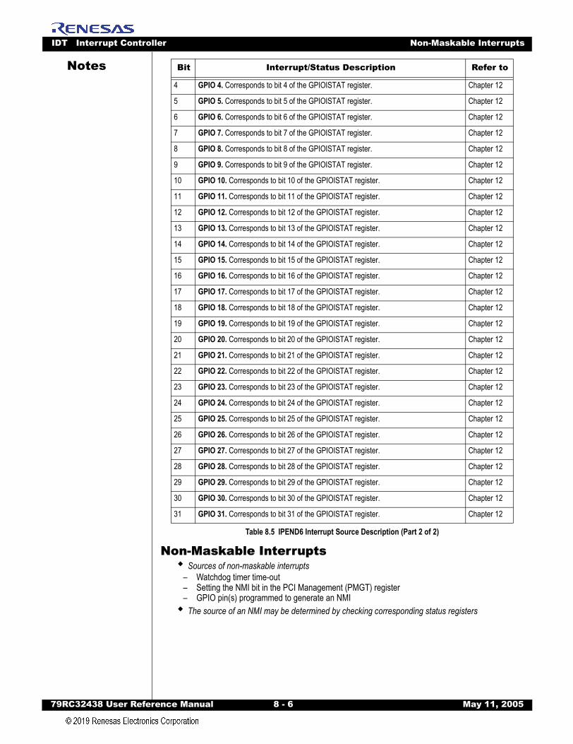
IDT Interrupt Controller Non-Maskable Interrupts
79RC32438 User Refer
Notes
Non-Maskable InterruptsSources of non-maskable interrupts
– Watchdog timer time-out– Setting the NMI bit in the PCI Management (PMGT) register– GPIO pin(s) programmed to generate an NMI
The source of an NMI may be determined by checking corresponding status registers
4 GPIO 4. Corresponds to bit 4 of the GPIOISTAT register. Chapter 12
5 GPIO 5. Corresponds to bit 5 of the GPIOISTAT register. Chapter 12
6 GPIO 6. Corresponds to bit 6 of the GPIOISTAT register. Chapter 12
7 GPIO 7. Corresponds to bit 7 of the GPIOISTAT register. Chapter 12
8 GPIO 8. Corresponds to bit 8 of the GPIOISTAT register. Chapter 12
9 GPIO 9. Corresponds to bit 9 of the GPIOISTAT register. Chapter 12
10 GPIO 10. Corresponds to bit 10 of the GPIOISTAT register. Chapter 12
11 GPIO 11. Corresponds to bit 11 of the GPIOISTAT register. Chapter 12
12 GPIO 12. Corresponds to bit 12 of the GPIOISTAT register. Chapter 12
13 GPIO 13. Corresponds to bit 13 of the GPIOISTAT register. Chapter 12
14 GPIO 14. Corresponds to bit 14 of the GPIOISTAT register. Chapter 12
15 GPIO 15. Corresponds to bit 15 of the GPIOISTAT register. Chapter 12
16 GPIO 16. Corresponds to bit 16 of the GPIOISTAT register. Chapter 12
17 GPIO 17. Corresponds to bit 17 of the GPIOISTAT register. Chapter 12
18 GPIO 18. Corresponds to bit 18 of the GPIOISTAT register. Chapter 12
19 GPIO 19. Corresponds to bit 19 of the GPIOISTAT register. Chapter 12
20 GPIO 20. Corresponds to bit 20 of the GPIOISTAT register. Chapter 12
21 GPIO 21. Corresponds to bit 21 of the GPIOISTAT register. Chapter 12
22 GPIO 22. Corresponds to bit 22 of the GPIOISTAT register. Chapter 12
23 GPIO 23. Corresponds to bit 23 of the GPIOISTAT register. Chapter 12
24 GPIO 24. Corresponds to bit 24 of the GPIOISTAT register. Chapter 12
25 GPIO 25. Corresponds to bit 25 of the GPIOISTAT register. Chapter 12
26 GPIO 26. Corresponds to bit 26 of the GPIOISTAT register. Chapter 12
27 GPIO 27. Corresponds to bit 27 of the GPIOISTAT register. Chapter 12
28 GPIO 28. Corresponds to bit 28 of the GPIOISTAT register. Chapter 12
29 GPIO 29. Corresponds to bit 29 of the GPIOISTAT register. Chapter 12
30 GPIO 30. Corresponds to bit 30 of the GPIOISTAT register. Chapter 12
31 GPIO 31. Corresponds to bit 31 of the GPIOISTAT register. Chapter 12
Bit Interrupt/Status Description Refer to
Table 8.5 IPEND6 Interrupt Source Description (Part 2 of 2)
ence Manual 8 - 6 May 11, 2005
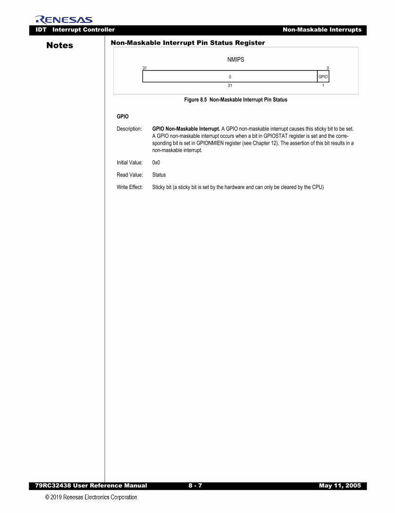
IDT Interrupt Controller Non-Maskable Interrupts
79RC32438 User Refer
Notes
Non-Maskable Interrupt Pin Status RegisterFigure 8.5 Non-Maskable Interrupt Pin Status
GPIO
Description: GPIO Non-Maskable Interrupt. A GPIO non-maskable interrupt causes this sticky bit to be set. A GPIO non-maskable interrupt occurs when a bit in GPIOSTAT register is set and the corre-sponding bit is set in GPIONMIEN register (see Chapter 12). The assertion of this bit results in a non-maskable interrupt.
Initial Value: 0x0
Read Value: Status
Write Effect: Sticky bit (a sticky bit is set by the hardware and can only be cleared by the CPU)
NMIPS031
0
31
GPIO
1
ence Manual 8 - 7 May 11, 2005
IDT Interrupt Controller Non-Maskable Interrupts
79RC32438 User Refer
Notes
ence Manual 8 - 8 May 11, 2005

Notes
79RC32438 User Reference Manual 9 - 1 M
Chapter 9
DMA Controller
IntroductionThe DMA controller consists of 10 independent DMA channels, all of which operate in exactly the same
manner. All DMA channels support fly-by DMA operations between memory and a peripheral device.1 Asingle DMA channel may be multiplexed among two different devices using the device select (DS) field in aDMA descriptor (refer to Table 9.2). The external DMA channels (i.e., DMA channels 0 and 1) use thedevice select field to determine the direction of the DMA transfer (memory to external peripheral or externalperipheral to memory). The DS field is unused by the other DMA channels and must be set to zero.
Features10 DMA channels
– Two channels for PCI (PCI to Memory and Memory to PCI)– Four Ethernet channels — two for each Ethernet interface (transmit/receive)– Two DMA channels for memory to memory DMA operations– Two DMA channels for external DMA operations
Provides flexible descriptor based operationSupports external peripheral DMA operationsSupports unaligned transfers (i.e., source or destination address may be on any byte boundary) with arbitrary byte length
DMA Registers
1. DMA operations are automatically supported across memory regions (for example, across DDR bank 0 and DDR bank 1) as long as the physical addresses are contiguous and the memory regions have a size which is greater than 64 KB.
Register Offset1 Register Name Register Function Size
0x04_0000 DMA0C DMA 0 control 32-bit
0x04_0004 DMA0S DMA 0 status 32-bit
0x04_0008 DMA0SM DMA 0 status mask 32-bit
0x04_000C DMA0DPTR DMA 0 descriptor pointer 32-bit
0x04_0010 DMA0NDPTR DMA 0 next descriptor pointer 32-bit
0x04_0014 DMA1C DMA 1 control 32-bit
0x04_0018 DMA1S DMA 1 status 32-bit
0x04_001C DMA1SM DMA 1 status mask 32-bit
0x04_0020 DMA1DPTR DMA 1 descriptor pointer 32-bit
0x04_0024 DMA1NDPTR DMA 1 next descriptor pointer 32-bit
0x04_0028 DMA2C DMA 2 control 32-bit
0x04_002C DMA2S DMA 2 status 32-bit
Table 9.1 DMA Register Map (Part 1 of 3)
ay 11, 2005

IDT DMA Controller DMA Registers
79RC32438 User Refer
Notes
0x04_0030 DMA2SM DMA 2 status mask 32-bit0x04_0034 DMA2DPTR DMA 2 descriptor pointer 32-bit
0x04_0038 DMA2NDPTR DMA 2 next descriptor pointer 32-bit
0x04_003C DMA3C DMA 3 control 32-bit
0x04_0040 DMA3S DMA 3 status 32-bit
0x04_0044 DMA3SM DMA 3 status mask 32-bit
0x04_0048 DMA3DPTR DMA 3 descriptor pointer 32-bit
0x04_004C DMA3NDPTR DMA 3 next descriptor pointer 32-bit
0x04_0050 DMA4C DMA 4 control 32-bit
0x04_0054 DMA4S DMA 4 status 32-bit
0x04_0058 DMA4SM DMA 4 status mask 32-bit
0x04_005C DMA4DPTR DMA 4 descriptor pointer 32-bit
0x04_0060 DMA4NDPTR DMA 4 next descriptor pointer 32-bit
0x04_0064 DMA5C DMA 5 control 32-bit
0x04_0068 DMA5S DMA 5 status 32-bit
0x04_006C DMA5SM DMA 5 status mask 32-bit
0x04_0070 DMA5DPTR DMA 5 descriptor pointer 32-bit
0x04_0074 DMA5NDPTR DMA 5 next descriptor pointer 32-bit
0x04_0078 DMA6C DMA 6 control 32-bit
0x04_007C DMA6S DMA 6 status 32-bit
0x04_0080 DMA6SM DMA 6 status mask 32-bit
0x04_0084 DMA6DPTR DMA 6 descriptor pointer 32-bit
0x04_0088 DMA6NDPTR DMA 6 next descriptor pointer 32-bit
0x04_008C DMA7C DMA 7 control 32-bit
0x04_0090 DMA7S DMA 7 status 32-bit
0x04_0094 DMA7SM DMA 7 status mask 32-bit
0x04_0098 DMA7DPTR DMA 7 descriptor pointer 32-bit
0x04_009C DMA7NDPTR DMA 7 next descriptor pointer 32-bit
0x04_00A0 DMA8C DMA 8 control 32-bit
0x04_00A4 DMA8S DMA 8 status 32-bit
0x04_00A8 DMA8SM DMA 8 status mask 32-bit
0x04_00AC DMA8DPTR DMA 8 descriptor pointer 32-bit
0x04_00B0 DMA8NDPTR DMA 8 next descriptor pointer 32-bit
0x04_00B4 DMA9C DMA 9 control 32-bit
0x04_00B8 DMA9S DMA 9 status 32-bit
0x04_00BC DMA9SM DMA 9 status mask 32-bit
Register Offset1 Register Name Register Function Size
Table 9.1 DMA Register Map (Part 2 of 3)
ence Manual 9 - 2 May 11, 2005
IDT DMA Controller Data Flow within the RC32438
79RC32438 User Refer
Notes
Data Flow within the RC32438 The RC32438 is primarily an engine designed to efficiently move data between interfaces. Data is
received from one of the interfaces, stored in the main memory, then transferred out on another interface.Thus, understanding the operation data flow within the RC32438 is very important in understanding thebehavior of the device and how to optimize the internal resources to meet the needs of the various applica-tions.
The IPBus™The internal IPBus in the RC32438 is the backbone of the device and is connected to every module in
the RC32438. It is used to transfer all the data within the device and to make the connection between theexternal main memory and the on-chip peripherals. There are two potential bus masters on the IPBus: TheCPU core and the DMA Controller (through one of its DMA channels). The processor core and the DMAController must arbitrate to acquire ownership of the IPBus (as described in Chapter 5, Bus Arbitration).Once the IPBus is granted to a master, data can be transferred within the RC32438. All other interfacesconnected to the IPBus are slaves, including the Device Controller. To transfer data, one of the bus mastersmust request data from or send data to the slave.
None of the on-chip peripherals on the RC32438 have IPBus mastership capability. Rather, each has itsinternal FIFO to buffer the incoming and the outgoing data. The peripheral receives output data from theIPBus (either DMA or CPU) in its transmit FIFO and sends it out the interface bus. Or it receives input datafrom the interface bus in its receive FIFO and requests service from an IPBus master through an interrupt orstatus flag to the CPU or a request to the DMA Controller. The internal FIFOs are only used to compensatefor the IPBus arbitration and access latency. The external memory (DDR or memory/IO) is used as theprimary storage location for the incoming and outgoing data. Thus, all the data movement within theRC32438 must pass through the memory — either DDR through the DDR controller, or SRAM / dual portthrough the Device Controller. The DMA Controller can transfer data between peripherals via externalmemory. As an example, input data from the Ethernet port will be stored in external memory first. The CPUwill then process the data for appropriate protocol conversion. The data will then be transferred from theDDR memory to the PCI interface.
The CPU core can access any of the on-chip peripherals for data transfer and reception. Some periph-erals, like the Ethernet interface and PCI interface, have associated DMA channels that can be used totransfer and receive data.
4Kc Core as Bus MasterWhen the 4Kc processor core is the IPBus master, it can read and write data from or to any peripheral to
transmit and receive the data. This is accomplished through the execution of the standard load and storeinstructions of the 4Kc core. This usually includes several steps: The 4Kc core loads the data from mainmemory into one of its internal registers and then writes it to the peripherals for transmission. The reverseoccurs for the reception of data. Usually, the internal peripherals will be accessed as non-cached entries bythe processor core. However, the use of the Prefetch-with-ignore-Hit instruction enables the processor coreto treat some of the peripherals as cached entries, thus speeding up the processing of the data by the 4Kccore. This usually is used when the 4Kc core needs to process the header of a packet for decision making.For most of the slow peripherals (like I2C), using the processor core is more than adequate to maintain the
0x04_00C0 DMA9DPTR DMA 9 descriptor pointer 32-bit
0x04_00C4 DMA9NDPTR DMA 9 next descriptor pointer 32-bit
0x04_00C8 through 0x04_3FFF Reserved
1. The address of the register is equal to the register offset added to the base value of 0x1800_0000.
Register Offset1 Register Name Register Function Size
Table 9.1 DMA Register Map (Part 3 of 3)
ence Manual 9 - 3 May 11, 2005
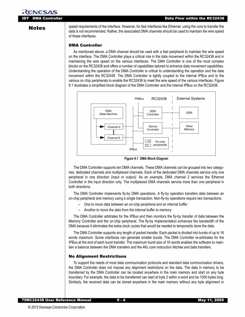
IDT DMA Controller Data Flow within the RC32438
79RC32438 User Refer
Notes
speed requirements of the interface. However, for fast interfaces like Ethernet, using the core to transfer thedata is not recommended. Rather, the associated DMA channels should be used to maintain the wire speedof these interfaces.DMA ControllerAs mentioned above, a DMA channel should be used with a fast peripheral to maintain the wire speed
on the interface. The DMA Controller plays a critical role in the data movement within the RC32438 and inmaintaining the wire speed on the various interfaces. The DMA Controller is one of the most complexblocks on the RC32438 and offers a number of capabilities tailored to enhance data movement capabilities.Understanding the operation of the DMA Controller is critical to understanding the operation and the datamovement within the RC32438. The DMA Controller is tightly coupled to the internal IPBus and to thevarious on chip peripherals to enable the RC32438 to meet the wire speed of the various interfaces. Figure9.1 illustrates a simplified block diagram of the DMA Controller and the internal IPBus on the RC32438.
Figure 9.1 DMA Block Diagram
The DMA Controller supports ten DMA channels. These DMA channels can be grouped into two catego-ries: dedicated channels and multiplexed channels. Each of the dedicated DMA channels service only oneperipheral in one direction (input or output). As an example, DMA channel 2 services the EthernetController in the input direction only. The multiplexed DMA channels service more than one peripheral inboth directions.
The DMA Controller implements fly-by DMA operations. A fly-by operation transfers data between anon-chip peripheral and memory using a single transaction. Non-fly-by operations require two transactions:
– One to move data between an on-chip peripheral and an internal buffer – Another to move the data from the internal buffer to memory.
The DMA Controller arbitrates for the IPBus and then monitors the fly-by transfer of data between theMemory Controller and the on-chip peripheral. The fly-by implementation enhances the bandwidth of theDMA because it eliminates the extra clock cycles that would be needed to temporarily store the data.
The DMA Controller supports any length of packet transfer. Each packet is divided into bursts of up to 16words maximum. Some interfaces can generate smaller bursts. The DMA Controller re-arbitrates for theIPBus at the end of each burst transfer. The maximum burst size of 16 words enables the software to main-tain a balance between the DMA transfers and the 4Kc core instruction fetches and data transfers.
No Alignment RestrictionsTo support the needs of most data communication protocols and standard data communication drivers,
the DMA Controller does not impose any alignment restrictions on the data. The data in memory to betransferred by the DMA Controller can be located anywhere in the main memory and start on any byteboundary. For example, the data to be transferred can start at byte 2 within a word and be 1000 bytes long.Similarly, the received data can be stored anywhere in the main memory without any byte alignment or
DMAState Machine
IPBus
Channel 0
Channel 9
DDRController DDR
On-chipperipherals
DeviceController
OtherMemory
RC32438 External SystemsPMBus
ence Manual 9 - 4 May 11, 2005

IDT DMA Controller Data Flow within the RC32438
79RC32438 User Refer
Notes
length restrictions. Further, there is no relationship required between the alignment or length of the trans-mitted data and the received data. For example, the received data can start at byte 3 within the word and be561 bytes long.Data Flow Using the DMA ControllerThe reception and transmission of data using the DMA Controller follows a series of standard steps. For
the data reception, the following steps highlight the data and control flow within the RC32438.1. The 4Kc processor core initializes the DMA channel for the desired peripheral. 2. The peripheral starts receiving the data in its input FIFO. Depending on the peripheral used, once
the required number of bytes are received in the FIFO or when an “end of packet” is received, theperipheral places a DMA request with its associated DMA channel.
3. The DMA channel transfers the data from the peripheral to memory.4. The DMA Controller can be configured to generate an interrupt to the 4Kc core when it completes
transferring a packet to memory. This signals the 4Kc core to begin executing software for higherlevel protocol processing.
The transmission of the data follows the same steps in reverse order. The following steps highlight thedata and control flow within the RC32438 when data is transmitted.
1. The upper layer software stacks ready the data for transmission. 2. The 4kc core sets up the DMA channel for transmission. 3. The DMA channel transfers the data from memory to the output FIFO of the peripheral. 4. The peripheral transmits the data on its bus. 5. The operation continues until the end of the packet. This usually triggers an interrupt to the 4Kc core
which ends the DMA operation. Figure 9.2 illustrates the simplified data movement operation within the RC32438.
Figure 9.2 Anatomy of DMA Operations
Note: A DMA operation should not be started if the corresponding interface is disabled. Disabling and re-enabling an interface should not be done without first disabling the corresponding DMA channel, otherwise the DMA controller may generate undefined behavior.
Memory-to-Memory TransferThe DMA Controller has a 16-word internal FIFO that is only used during memory-to-memory transfers.
This FIFO is needed to temporarily store the data between transfers. To do a memory-to-memory DMAoperation, the data is read from the source memory, stored in the DMA FIFO, then written in the destinationmemory. Only DMA channels 6 and 7 can be used for memory-to-memory DMA operations.
Note: Memory-to-memory DMA operations using channel 6 will not start until channel 7 is started.
DMAState Machine
IPBus
Channel 0
Channel 9
DDRController DDR
On-chipperipherals
1. Issue request to transfer data
2. Appropriate channel is
3. Load descriptor from DDR
4. Transfer data
5. Storedescriptorto memoryand endthe transfer
selected
ence Manual 9 - 5 May 11, 2005
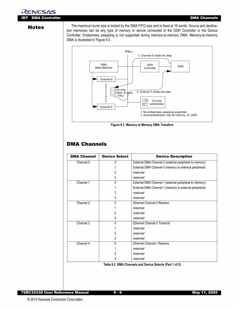
IDT DMA Controller DMA Channels
79RC32438 User Refer
Notes
The maximum burst size is limited by the DMA FIFO size and is fixed at 16 words. Source and destina-tion memories can be any type of memory or device connected to the DDR Controller or the DeviceController. Endianness swapping is not supported during memory-to-memory DMA. Memory-to-memoryDMA is illustrated in Figure 9.3.Figure 9.3 Memory to Memory DMA Transfers
DMA Channels
DMA Channel Device Select Device DescriptionChannel 0 0 External DMA Channel 0 (external peripheral to memory)
1 External DMA Channel 0 (memory to external peripheral)2 reserved3 reserved
Channel 1 0 External DMA Channel 1 (external peripheral to memory)1 External DMA Channel 1 (memory to external peripheral)2 reserved3 reserved
Channel 2 0 Ethernet Channel 0 Receive1 reserved2 reserved3 reserved
Channel 3 0 Ethernet Channel 0 Transmit1 reserved2 reserved3 reserved
Channel 4 0 Ethernet Channel 1 Receive1 reserved2 reserved3 reserved
Table 9.2 DMA Channels and Device Selects (Part 1 of 2)
DMAState Machine
IPBus
Channel 6
Channel 9
DDRController DDR
On-chipperipherals
On-chipDMA 16 word
FIFO
No endianness swapping supportedSource/destination can be memory, IO, DDR
1. Channel 6 reads the data.
2. Channel 7 writes the data.
ence Manual 9 - 6 May 11, 2005
IDT DMA Controller Internal DMA Operation
79RC32438 User Refer
Notes
Internal DMA OperationAll DMA operations are performed by reading DMA descriptors from memory. A DMA descriptor is read
from memory to determine control information when a DMA descriptor operation begins, and is written backto memory with updated status information when a DMA descriptor operation completes. As shown inFigure 9.4, a DMA descriptor consists of four words and must be word aligned.1 The first word of adescriptor contains general DMA control and status information, such as the COUNT field which holds thenumber of bytes to transfer.2 The three bit device command (DEVCMD) field is used to pass device specificcontrol information to a peripheral at the start of a DMA descriptor operation, and to record peripheral statusinformation at the end of a DMA descriptor operation. When a DMA descriptor operation begins, DEVCMDis read from memory and transferred to the selected device. When a DMA descriptor operation completes,updated status information is read from the selected device and written back to the DEVCMD field of theDMA descriptor in memory. The device select (DS) field selects the peripheral device to be used during theDMA descriptor operation. The encoding of this field for each of the ten DMA channels is shown in Table9.2.
The second word of a DMA descriptor, the current address (CA) field, is initialized with the address of adata buffer to which data DMAed from a peripheral is written, or from which data DMAed to a peripheral isread. When a DMA descriptor operation begins, the starting address is loaded into a current addressregister in the DMA controller. After each DMA data transfer, the current address register is modified by thesize of the data transfer. Thus, when a DMA descriptor operation completes, the CA field of the DMAdescriptor in memory contains the address of the next data quantity to be transferred had the DMAdescriptor operation not completed. For example, if CA is initialized to x and COUNT is initialized to y during
Channel 5 0 Ethernet Channel 1 Transmit 1 reserved2 reserved3 reserved
Channel 6 0 Memory to Memory (Memory to Holding FIFO)1 reserved2 reserved3 reserved
Channel 7 0 Memory to Memory (Holding FIFO to Memory)1 reserved2 reserved3 reserved
Channel 8 0 PCI (PCI to Memory)1 reserved2 reserved3 reserved
Channel 9 0 PCI (Memory to PCI)1 reserved2 reserved3 reserved
1. The address 0x0000_0000 is used to indicate the end of a DMA descriptor list. Therefore, a DMA descriptor may begin at any word address except 0x0000_0000.2. The DMA controller supports zero length DMA operations (i.e., descriptors with the COUNT field equal to zero). Zero length DMA operations result in the transfer of DEVCMD and DEVCS as well as the updating of the DMA descriptor but cause no data to be transferred.
DMA Channel Device Select Device Description
Table 9.2 DMA Channels and Device Selects (Part 2 of 2)
ence Manual 9 - 7 May 11, 2005
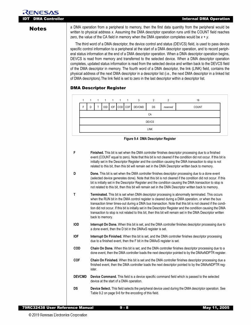
IDT DMA Controller Internal DMA Operation
79RC32438 User Refer
Notes
a DMA operation from a peripheral to memory, then the first data quantity from the peripheral would bewritten to physical address x. Assuming the DMA descriptor operation runs until the COUNT field reacheszero, the value of the CA field in memory when the DMA operation completes would be x + y.The third word of a DMA descriptor, the device control and status (DEVCS) field, is used to pass devicespecific control information to a peripheral at the start of a DMA descriptor operation, and to record periph-eral status information at the end of a DMA descriptor operation. When a DMA descriptor operation begins,DEVCS is read from memory and transferred to the selected device. When a DMA descriptor operationcompletes, updated status information is read from the selected device and written back to the DEVCS fieldof the DMA descriptor in memory. The fourth word of a DMA descriptor, the link (LINK) field, contains thephysical address of the next DMA descriptor in a descriptor list (i.e., the next DMA descriptor in a linked listof DMA descriptors).The link field is set to zero in the last descriptor within a descriptor list.
DMA Descriptor Register
Figure 9.4 DMA Descriptor Register
F Finished. This bit is set when the DMA controller finishes descriptor processing due to a finished event (COUNT equal to zero). Note that this bit is not cleared if the condition did not occur. If this bit is initially set in the Descriptor Register and the condition causing the DMA transaction to stop is not related to this bit, then this bit will remain set in the DMA Descriptor written back to memory.
D Done. This bit is set when the DMA controller finishes descriptor processing due to a done event (selected device generates done). Note that this bit is not cleared if the condition did not occur. If this bit is initially set in the Descriptor Register and the condition causing the DMA transaction to stop is not related to this bit, then this bit will remain set in the DMA Descriptor written back to memory.
T Terminated. This bit is set when DMA descriptor processing is abnormally terminated. This occurs when the RUN bit in the DMA control register is cleared during a DMA operation, or when the bus transaction timer times-out during a DMA bus transaction. Note that this bit is not cleared if the condi-tion did not occur. If this bit is initially set in the Descriptor Register and the condition causing the DMA transaction to stop is not related to this bit, then this bit will remain set in the DMA Descriptor written back to memory.
IOD Interrupt On Done. When this bit is set, and the DMA controller finishes descriptor processing due to a done event, then the D bit in the DMAxS register is set.
IOF Interrupt On Finished. When this bit is set, and the DMA controller finishes descriptor processing due to a finished event, then the F bit in the DMAxS register is set.
COD Chain On Done. When this bit is set, and the DMA controller finishes descriptor processing due to a done event, then the DMA controller loads the next descriptor pointed to by the DMAxNDPTR register.
COF Chain On Finished. When this bit is set and the DMA controller finishes descriptor processing due a finished event, then the DMA controller loads the next descriptor pointed to by the DMAxNDPTR reg-ister.
DEVCMD Device Command. This field is a device specific command field which is passed to the selected device at the start of a DMA operation.
DS Device Select. This field selects the peripheral device used during the DMA descriptor operation. See Table 9.2 on page 9-6 for the encoding of this field.
CA
F D IOD IOF COD COF
1 1 1 1 1 1
DEVCMD DS COUNT
DEVCS
LINK
T
1 183 2
reserved
2
ence Manual 9 - 8 May 11, 2005
IDT DMA Controller Internal DMA Operation
79RC32438 User Refer
Notes
DMA RegistersEach DMA channel has five registers. A channel is controlled by a DMA control (DMA[0..9]C) register,
and the status of a DMA channel is reported in a DMA status (DMA[0..9]S) register. The bits in a DMAstatus register, which are not masked by the corresponding DMA status mask (DMA[0..9]SM) register, areORed together and presented to the interrupt controller. A DMA operation is begun by writing the startingaddress of the first descriptor in a descriptor list into the DMA descriptor pointer (DMA[0..9]DPTR) registerof a DMA channel. As a side effect of writing this register, a DMA operation begins and the run (RUN) bit inthe corresponding DMAxC register is set. The DMA channel performs DMA descriptor processing,executing the dictated DMA descriptor operations until a DMA descriptor is reached with a zero in its LINKfield. This signals the completion of DMA operation and causes the RUN bit in the DMAxC register to becleared and the halt (H) bit in the DMAxS register to be set. During DMA descriptor processing, theDMAxDPTR register may be read to determine the address of the descriptor currently being processed.
DMA Stopping ConditionsA DMA descriptor operation has three stopping conditions: finished, done, and terminated. The stopping
conditions which cause a descriptor operation to complete is recorded in the finished (F), done (D), andterminated (T) bits of the first word in a descriptor. When the DMA controller updates the first word of adescriptor, only the F, D, and T bits are set. For example, if the T bit was initially set in the descriptor and theDMA stopping condition was finished, the T bit would remain set in the descriptor written back to memory.
Finished Condition: When a DMA operation begins, the COUNT field is loaded from the descriptor inmemory into a byte counter associated with the DMA channel. The byte counter is decremented by theDMA transfer size after each data transfer. The finished stopping condition occurs when the byte counterreaches zero (i.e., there are no more bytes to transfer). This causes the F bit in the DMA descriptor to beset. If the interrupt on finished (IOF) bit in the descriptor has been initialized to a one, then the F bit in theDMAxS register is also set. If the chain on finished (COF) bit in the descriptor has been initialized to a one,then a DMA chaining operation takes place.
Done Condition: The done stopping condition occurs when the selected device signals a done event.Done events allow a selected peripheral to terminate a DMA operation at an arbitrary point (for example, atthe end of packet). The done stopping condition occurs when a done event is signalled by the selectedperipheral device. This causes the D bit in the DMA descriptor to be set. If the interrupt on done (IOD) bit inthe descriptor has been initialized to a one, then the D bit in the DMAxS register is also set. If the chain ondone (COD) bit in the descriptor has been initialized to a one, then a DMA chaining operation takes place.
It is possible for a DMA descriptor operation to complete due to multiple stopping conditions. Forexample, it is possible to have a simultaneous finished and done stopping condition which causes both theF and D bits in the DMA descriptor to be set.
Terminated Condition: A DMA operation is halted when the RUN bit in the DMAxC register is cleared.A halted DMA operation results in a terminated stopping condition for the descriptor being processed andcauses the DMA operation to complete. When this occurs, the DMA controller performs the following:discontinues the current DMA descriptor operation, sets the T bit, and updates all other status information inthe descriptor. The descriptor contents are then written back to memory. When the descriptor writecompletes, the halt (H) bit in the DMAxS register is set to acknowledge that the DMA operation has beenhalted. When a DMA operation is halted by clearing the RUN bit, writes to the DMAxDPTR and DMAx-NDPTR should not be performed until the halt (H) bit is set.
COUNT Byte Count. This field specifies the number of bytes to transfer during the DMA descriptor operation.
CA Current Address. This 32-bit field is initialized with the DMA starting address at the start of a DMA operation and is updated when descriptor processing is completed.
DEVCS Device Control and Status. This 32-bit field is initialized with peripheral device specific control infor-mation. When descriptor processing completes, this field is updated with peripheral specific status information.
LINK Link. This 32-bit field points to the next descriptor in the descriptor list.
ence Manual 9 - 9 May 11, 2005
IDT DMA Controller Internal DMA Operation
79RC32438 User Refer
Notes
Note: Under certain conditions the Terminated status bit is not set. An example is when a zero length DMA operation is performed.The DMA controller may be incorrectly programmed with an address which does not map to a validdevice. When this occurs, the address space monitor reports an error to the DMA controller. If the DMAcontroller attempts to read a DMA descriptor from an un-decoded address, the DMA operation is terminatedcausing the error (E) bit and the halt (H) bit to be set in the DMAxS register and the RUN bit to be clearedthe DMAxC register. If the DMA controller attempts to read or write a DMA data buffer that corresponds toan undecoded address, then the DMA operation is terminated. This results in the DMA discontinuing thecurrent DMA descriptor operation, clearing the RUN bit in the DMAxS register, setting the T bit in thedescriptor, and updating all other status information in the descriptor. Once the descriptor contents arewritten back to memory, the halt (H) bit and error (E) bit in the DMAxS register are set.
Clearing the RUN bit in the DMAxC register provides a means of orderly halting a DMA operation butsometimes a need exists to abort a DMA operation without cooperation from the peripheral. For example,resetting a peripheral during a DMA operation may make it impossible to halt a DMA operation since theDMA will wait indefinitely for the peripheral to supply updated DEVCS and DEVCMD values. A DMA opera-tion may be aborted without cooperation from a peripheral by writing a one to the Abort (A) bit in the DMAxCregister. This causes the DMA channel to complete the current DMA transaction on the bus if one is inprogress, write back the descriptor1 with the terminated (T) bit set, set the Halt (H) bit in the DMAxSregister, and clear the run bit. If a DMA operation is aborted while the DMA is in the process of following alink or performing a chaining operation, the terminated bit will not be set in any descriptor.
DMA Request EventA DMA request event causes a data quantum to be transferred by the DMA controller between a periph-
eral device and memory. The amount of data contained in a DMA quantum is defined by the DMA transfersize. The DMA transfer size is specified for each peripheral device and is the amount of data transferred bythe DMA controller when it gains ownership of the IP bus.
The mode field in the DMAxC register allows the DMA to be configured to operate in one of threemodes: auto request, burst request, and transfer request. In auto request mode, DMA request eventsgenerated by the selected peripheral device are ignored, and the DMA controller generates internal requestevents at the maximum possible rate. This causes a block of data to be transferred by the DMA controllerwithout the need for DMA request events to be generated by the peripheral device.
In burst request mode, a DMA request event signalled by the selected peripheral device causes theDMA controller to begin internally generating request events until the DMA operation completes. Thus, inthis mode the first request event generated by the peripheral signals the start of a burst transfer. This modeallows the peripheral device to externally signal the beginning of a burst DMA operation.
In transfer request mode, a DMA request event signalled by the selected peripheral device causes theDMA controller to transfer a single data quantum between the peripheral device and memory. Thus, foreach data quantum of a DMA operation, the peripheral must signal to the DMA controller when the transfershould take place. All of the DMA peripheral devices internal to the RC32438 operate in transfer requestmode. Configuring an internal peripheral device for auto request or burst request modes will produce unde-sirable consequences. External DMA operations, described later in this chapter, support all three modes.
DMA Descriptor List and ChainingA DMA descriptor list consists of a linked list of DMA descriptors, with the LINK field of each descriptor
pointing to the next descriptor in the list. The LINK field of the last descriptor in a descriptor list is zero.Descriptor list processing begins when the address of a DMA descriptor is written to the DMAxDPTRregister. This causes the DMA controller to read a descriptor from memory, performs the specified DMAoperation, update the descriptor status information, and follows the LINK field to the next descriptor in thedescriptor list. The DMAxDPTR register may be read at any time to determine the currently activedescriptor in the descriptor list.
1. Aborting a DMA operation may result in undefined values in the DEVCS and DEVCMD fields.
ence Manual 9 - 10 May 11, 2005
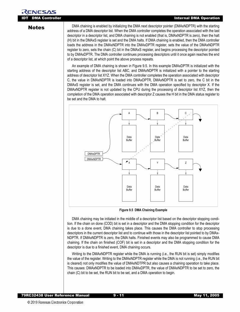
IDT DMA Controller Internal DMA Operation
79RC32438 User Refer
Notes
DMA chaining is enabled by initializing the DMA next descriptor pointer (DMAxNDPTR) with the startingaddress of a DMA descriptor list. When the DMA controller completes the operation associated with the lastdescriptor in a descriptor list, and DMA chaining is not enabled (that is, DMAxNDPTR is zero), then the halt(H) bit in the DMAxS register is set and the DMA halts. If DMA chaining is enabled, then the DMA controllerloads the address in the DMAxNDPTR into the DMAxDPTR register, sets the value of the DMAxNDPTRregister to zero, sets the chain (C) bit in the DMAxS register, and begins processing the descriptor pointedto by DMAxDPTR. The DMA controller continues processing descriptors until it once again reaches the endof a descriptor list, at which point the above process repeats.An example of DMA chaining is shown in Figure 9.5. In this example DMAxDPTR is initialized with thestarting address of the descriptor list ABC, and DMAxNDPTR is initialized with a pointer to the startingaddress of descriptor list XYZ. When the DMA controller completes the operation associated with descriptorC, the value in DMAxNDPTR is loaded into DMAxDPTR, DMAxNDPTR is set to zero, the C bit in theDMAxS register is set, and the DMA continues with the DMA operation specified by descriptor X. If theDMAxNDPTR register is not updated by the CPU during the processing of descriptor list XYZ, then thecompletion of the DMA operation associated with descriptor Z causes the H bit in the DMA status register tobe set and the DMA to halt.
Figure 9.5 DMA Chaining Example
DMA chaining may be initiated in the middle of a descriptor list based on the descriptor stopping condi-tion. If the chain on done (COD) bit is set in a descriptor and the DMA stopping condition for the descriptoris due to a done event, DMA chaining takes place. This causes the DMA controller to stop processingdescriptors in the current descriptor list and to continue with those in the descriptor list pointed to by DMAx-NDPTR. If DMAxNDPTR is zero, the DMA halts. Finished events may also be programmed to cause DMAchaining. If the chain on finished (COF) bit is set in a descriptor and the DMA stopping condition for thedescriptor is due to a finished event, DMA chaining occurs.
Writing to the DMAxNDPTR register while the DMA is running (i.e., the RUN bit is set) simply modifiesthe value of the register. Writing to the DMAxNDPTR register while the DMA is not running (i.e., the RUN bitis cleared) not only modifies the value of DMAxNDTPR but also causes a chaining operation to take place.This causes: DMAxNDPTR to be loaded into DMAxDPTR, the value of DMAxNDPTR to be set to zero, thechain (C) bit to be set, the RUN bit to be set, and a DMA operation to begin.
DMAxNDPTR
A
DMAxDPTR
DataBuffer
B
DataBuffer
C
DataBuffer
X
DataBuffer
Y
DataBuffer
Z
DataBuffer
ence Manual 9 - 11 May 11, 2005
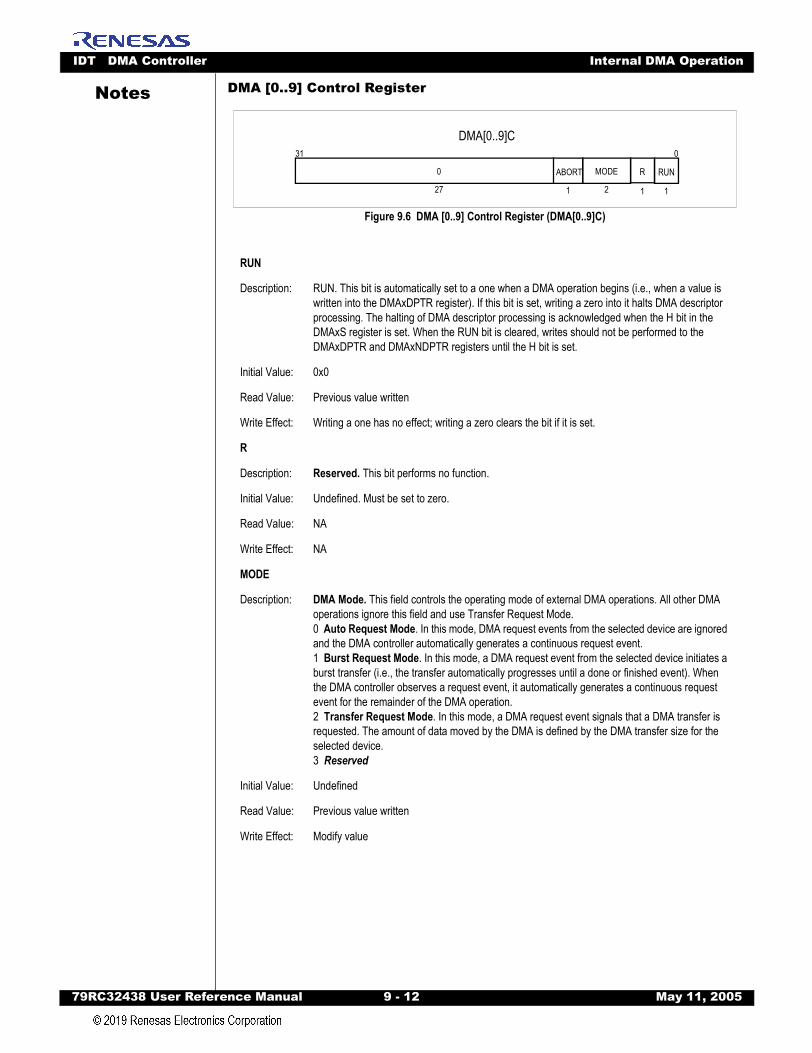
IDT DMA Controller Internal DMA Operation
79RC32438 User Refer
Notes
DMA [0..9] Control RegisterFigure 9.6 DMA [0..9] Control Register (DMA[0..9]C)
RUN
Description: RUN. This bit is automatically set to a one when a DMA operation begins (i.e., when a value is written into the DMAxDPTR register). If this bit is set, writing a zero into it halts DMA descriptor processing. The halting of DMA descriptor processing is acknowledged when the H bit in the DMAxS register is set. When the RUN bit is cleared, writes should not be performed to the DMAxDPTR and DMAxNDPTR registers until the H bit is set.
Initial Value: 0x0
Read Value: Previous value written
Write Effect: Writing a one has no effect; writing a zero clears the bit if it is set.
R
Description: Reserved. This bit performs no function.
Initial Value: Undefined. Must be set to zero.
Read Value: NA
Write Effect: NA
MODE
Description: DMA Mode. This field controls the operating mode of external DMA operations. All other DMA operations ignore this field and use Transfer Request Mode.0 Auto Request Mode. In this mode, DMA request events from the selected device are ignored and the DMA controller automatically generates a continuous request event.1 Burst Request Mode. In this mode, a DMA request event from the selected device initiates a burst transfer (i.e., the transfer automatically progresses until a done or finished event). When the DMA controller observes a request event, it automatically generates a continuous request event for the remainder of the DMA operation.2 Transfer Request Mode. In this mode, a DMA request event signals that a DMA transfer is requested. The amount of data moved by the DMA is defined by the DMA transfer size for the selected device.3 Reserved
Initial Value: Undefined
Read Value: Previous value written
Write Effect: Modify value
DMA[0..9]C031
27
0 R
1
RUN
12
MODEABORT
1
ence Manual 9 - 12 May 11, 2005
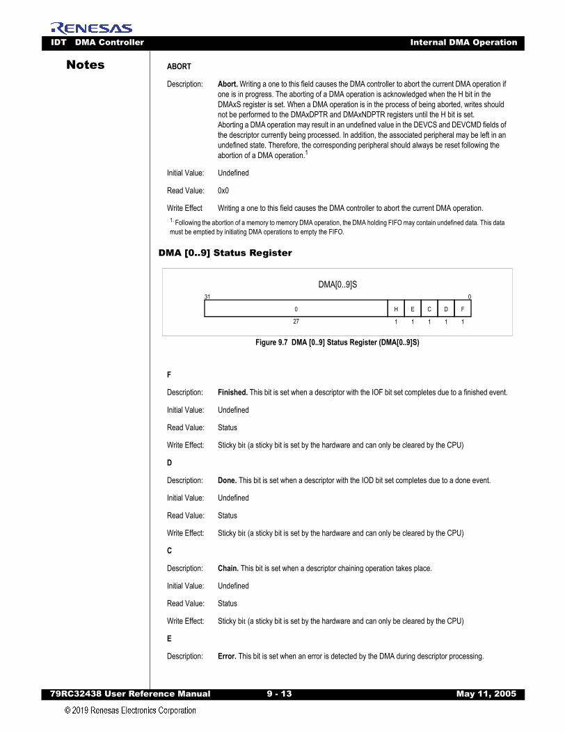
IDT DMA Controller Internal DMA Operation
79RC32438 User Refer
Notes
DMA [0..9] Status Register
Figure 9.7 DMA [0..9] Status Register (DMA[0..9]S)
ABORT
Description: Abort. Writing a one to this field causes the DMA controller to abort the current DMA operation if one is in progress. The aborting of a DMA operation is acknowledged when the H bit in the DMAxS register is set. When a DMA operation is in the process of being aborted, writes should not be performed to the DMAxDPTR and DMAxNDPTR registers until the H bit is set.Aborting a DMA operation may result in an undefined value in the DEVCS and DEVCMD fields of the descriptor currently being processed. In addition, the associated peripheral may be left in an undefined state. Therefore, the corresponding peripheral should always be reset following the abortion of a DMA operation.1
Initial Value: Undefined
Read Value: 0x0
Write Effect Writing a one to this field causes the DMA controller to abort the current DMA operation.1. Following the abortion of a memory to memory DMA operation, the DMA holding FIFO may contain undefined data. This datamust be emptied by initiating DMA operations to empty the FIFO.
F
Description: Finished. This bit is set when a descriptor with the IOF bit set completes due to a finished event.
Initial Value: Undefined
Read Value: Status
Write Effect: Sticky bit (a sticky bit is set by the hardware and can only be cleared by the CPU)
D
Description: Done. This bit is set when a descriptor with the IOD bit set completes due to a done event.
Initial Value: Undefined
Read Value: Status
Write Effect: Sticky bit (a sticky bit is set by the hardware and can only be cleared by the CPU)
C
Description: Chain. This bit is set when a descriptor chaining operation takes place.
Initial Value: Undefined
Read Value: Status
Write Effect: Sticky bit (a sticky bit is set by the hardware and can only be cleared by the CPU)
E
Description: Error. This bit is set when an error is detected by the DMA during descriptor processing.
D
DMA[0..9]S031
27
0 F
1 1
C
1
E
1
H
1
ence Manual 9 - 13 May 11, 2005
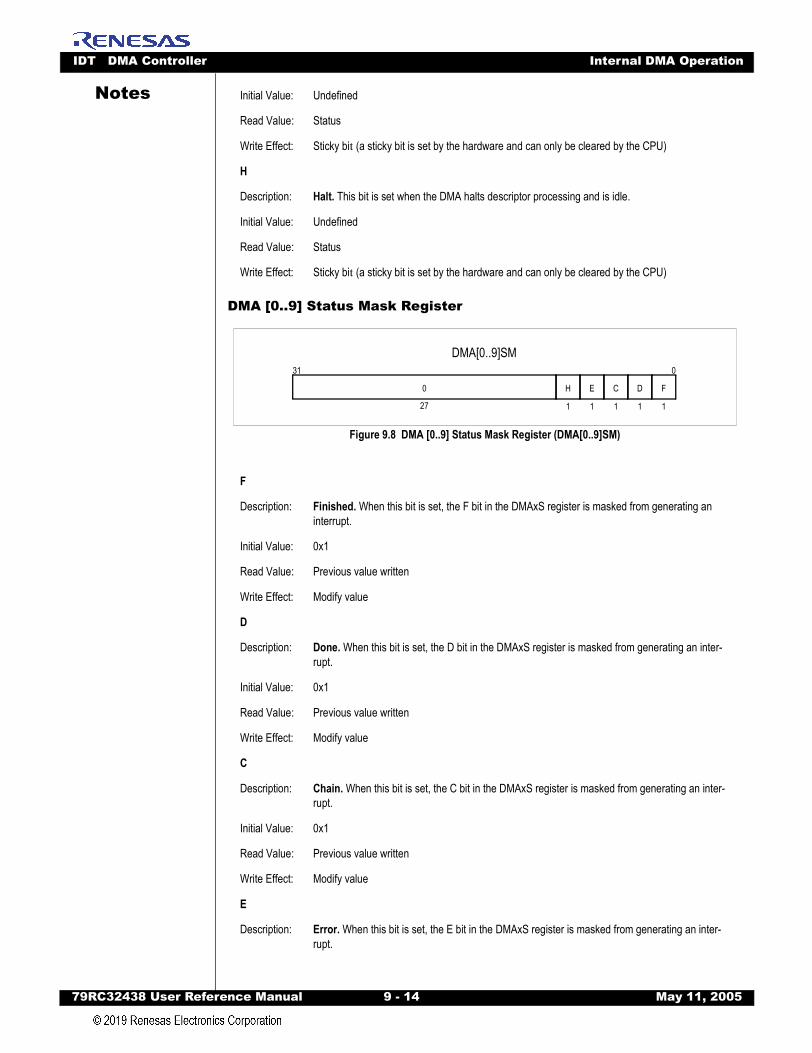
IDT DMA Controller Internal DMA Operation
79RC32438 User Refer
Notes
DMA [0..9] Status Mask Register
Figure 9.8 DMA [0..9] Status Mask Register (DMA[0..9]SM)
Initial Value: Undefined
Read Value: Status
Write Effect: Sticky bit (a sticky bit is set by the hardware and can only be cleared by the CPU)
H
Description: Halt. This bit is set when the DMA halts descriptor processing and is idle.
Initial Value: Undefined
Read Value: Status
Write Effect: Sticky bit (a sticky bit is set by the hardware and can only be cleared by the CPU)
F
Description: Finished. When this bit is set, the F bit in the DMAxS register is masked from generating an interrupt.
Initial Value: 0x1
Read Value: Previous value written
Write Effect: Modify value
D
Description: Done. When this bit is set, the D bit in the DMAxS register is masked from generating an inter-rupt.
Initial Value: 0x1
Read Value: Previous value written
Write Effect: Modify value
C
Description: Chain. When this bit is set, the C bit in the DMAxS register is masked from generating an inter-rupt.
Initial Value: 0x1
Read Value: Previous value written
Write Effect: Modify value
E
Description: Error. When this bit is set, the E bit in the DMAxS register is masked from generating an inter-rupt.
DMA[0..9]SM
D
031
27
0 F
1 1
C
1
E
1
H
1
ence Manual 9 - 14 May 11, 2005
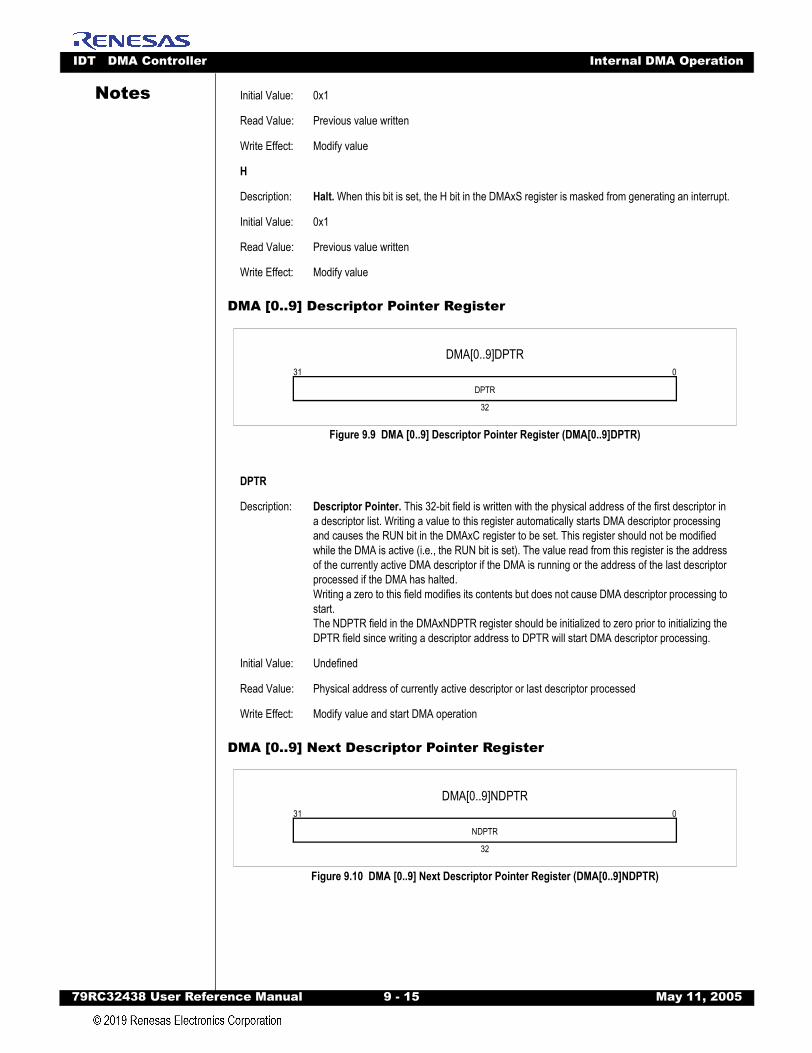
IDT DMA Controller Internal DMA Operation
79RC32438 User Refer
Notes
DMA [0..9] Descriptor Pointer Register
Figure 9.9 DMA [0..9] Descriptor Pointer Register (DMA[0..9]DPTR)
DMA [0..9] Next Descriptor Pointer Register
Figure 9.10 DMA [0..9] Next Descriptor Pointer Register (DMA[0..9]NDPTR)
Initial Value: 0x1
Read Value: Previous value written
Write Effect: Modify value
H
Description: Halt. When this bit is set, the H bit in the DMAxS register is masked from generating an interrupt.
Initial Value: 0x1
Read Value: Previous value written
Write Effect: Modify value
DPTR
Description: Descriptor Pointer. This 32-bit field is written with the physical address of the first descriptor in a descriptor list. Writing a value to this register automatically starts DMA descriptor processing and causes the RUN bit in the DMAxC register to be set. This register should not be modified while the DMA is active (i.e., the RUN bit is set). The value read from this register is the address of the currently active DMA descriptor if the DMA is running or the address of the last descriptor processed if the DMA has halted.Writing a zero to this field modifies its contents but does not cause DMA descriptor processing to start.The NDPTR field in the DMAxNDPTR register should be initialized to zero prior to initializing the DPTR field since writing a descriptor address to DPTR will start DMA descriptor processing.
Initial Value: Undefined
Read Value: Physical address of currently active descriptor or last descriptor processed
Write Effect: Modify value and start DMA operation
DMA[0..9]DPTR031
32
DPTR
DMA[0..9]NDPTR031
32
NDPTR
ence Manual 9 - 15 May 11, 2005
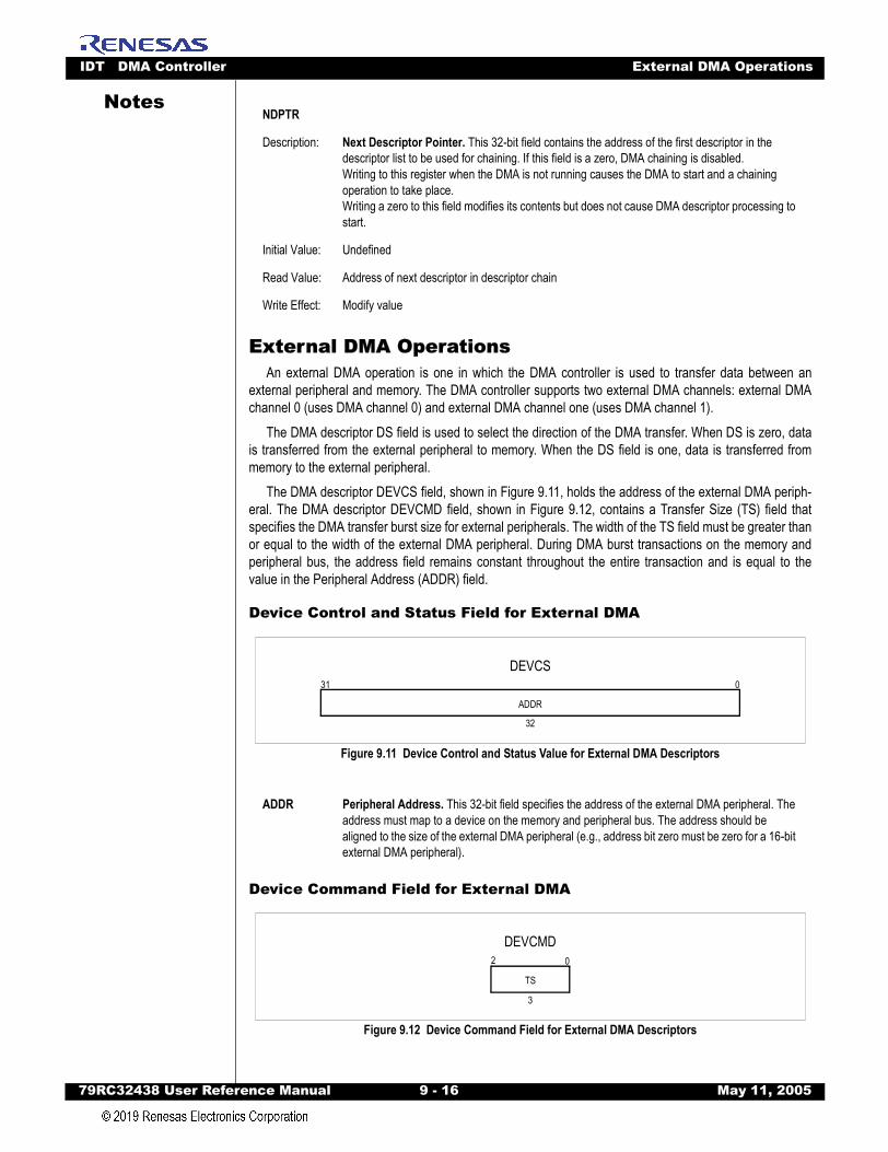
IDT DMA Controller External DMA Operations
79RC32438 User Refer
Notes
External DMA OperationsAn external DMA operation is one in which the DMA controller is used to transfer data between an
external peripheral and memory. The DMA controller supports two external DMA channels: external DMAchannel 0 (uses DMA channel 0) and external DMA channel one (uses DMA channel 1).
The DMA descriptor DS field is used to select the direction of the DMA transfer. When DS is zero, datais transferred from the external peripheral to memory. When the DS field is one, data is transferred frommemory to the external peripheral.
The DMA descriptor DEVCS field, shown in Figure 9.11, holds the address of the external DMA periph-eral. The DMA descriptor DEVCMD field, shown in Figure 9.12, contains a Transfer Size (TS) field thatspecifies the DMA transfer burst size for external peripherals. The width of the TS field must be greater thanor equal to the width of the external DMA peripheral. During DMA burst transactions on the memory andperipheral bus, the address field remains constant throughout the entire transaction and is equal to thevalue in the Peripheral Address (ADDR) field.
Device Control and Status Field for External DMA
Figure 9.11 Device Control and Status Value for External DMA Descriptors
Device Command Field for External DMA
Figure 9.12 Device Command Field for External DMA Descriptors
NDPTR
Description: Next Descriptor Pointer. This 32-bit field contains the address of the first descriptor in the descriptor list to be used for chaining. If this field is a zero, DMA chaining is disabled.Writing to this register when the DMA is not running causes the DMA to start and a chaining operation to take place.Writing a zero to this field modifies its contents but does not cause DMA descriptor processing to start.
Initial Value: Undefined
Read Value: Address of next descriptor in descriptor chain
Write Effect: Modify value
ADDR Peripheral Address. This 32-bit field specifies the address of the external DMA peripheral. The address must map to a device on the memory and peripheral bus. The address should be aligned to the size of the external DMA peripheral (e.g., address bit zero must be zero for a 16-bit external DMA peripheral).
DEVCS031
32
ADDR
DEVCMD2
3
TS
0
ence Manual 9 - 16 May 11, 2005

IDT DMA Controller External DMA Operations
79RC32438 User Refer
Notes
An external peripheral generates a DMA request event by asserting a DMA request (DMAREQNx) input.The DMAREQNx inputs are GPIO alternate functions (see Chapter 12, General Purpose I/O Controller).
Transfer Request: When the DMA is configured to operate in transfer request mode, a DMA requestinstructs the DMA controller to perform one burst transaction to the external peripheral address in DEVCS.The size of the burst transfer is selected in the TS field.
The assertion of chip select to the external peripheral acknowledges the DMA request and causes theexternal peripheral to negate DMAREQNx. When the external peripheral samples chip select negated, itmay once again assert DMAREQNx. An example of a peripheral-to-memory external DMA operation intransfer request mode is shown in Figure 9.13
Figure 9.13 External DMA Operation (Transfer Request Mode)
Burst Request: When the DMA is configured to operate in burst request mode, then the first DMArequest initiates the entire DMA transfer between the external peripheral and memory. An example of aperipheral-to-memory DMA operation in burst request mode is shown in Figure 9.14.
TS Transfer Size. This field specifies the DMA burst transfer size used to access the external peripheral.0 - byte1 - halfword2 - word3 - 2 words4 - 4 words5 - 6 words6 - 8 words7 - 16 words
DMA Request Event Assertion of DMAREQNx pin.
DMA Done Event Assertion of DMADONENx pin.
DMA Terminated Event An external device cannot signal a terminated event.
DMA Transfer Size Value programmed in the transfer size (TS) field of DEVCMD.
Limitations The width of the TS field must be greater than or equal to the width of the external DMA peripheral.
Table 9.3 External DMA Operations
EXTCLK
DMAREQNx
CSNx
Transaction Transactionto Memory
Transactionto External Peripheral
Transactionto External Peripheral
1 2 3 4 5 6 7
1. DMA requests data transfer by asserting DMAREQNx2. The RC32438 acknowledges DMA request by asserting chip select (CSNx) to external peripheral. DMA control-
ler reads a transfer size data quantity from the external peripheral3. External peripheral reacts to acknowledgment of DMA request (i.e., assertion of chip select) by negating
DMAREQNx4. DMA controller writes data quantity read from external peripheral to memory5. DMA requests next data transfer by asserting DMAREQNx6. The RC32438 acknowledges next DMA request by asserting chip select and reading a transfer size data quan-
tity from the external peripheral7. External peripheral reacts to acknowledgement of DMA request by negating DMAREQNx.
ence Manual 9 - 17 May 11, 2005
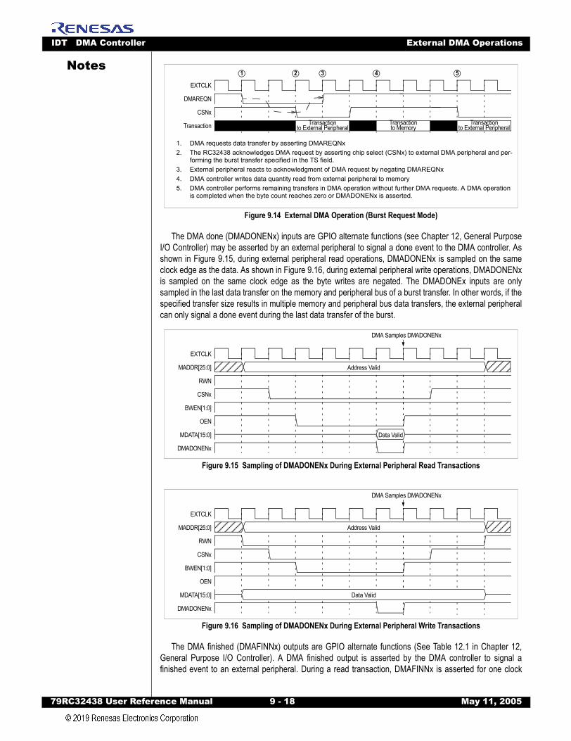
IDT DMA Controller External DMA Operations
79RC32438 User Refer
Notes
Figure 9.14 External DMA Operation (Burst Request Mode)
The DMA done (DMADONENx) inputs are GPIO alternate functions (see Chapter 12, General PurposeI/O Controller) may be asserted by an external peripheral to signal a done event to the DMA controller. Asshown in Figure 9.15, during external peripheral read operations, DMADONENx is sampled on the sameclock edge as the data. As shown in Figure 9.16, during external peripheral write operations, DMADONENxis sampled on the same clock edge as the byte writes are negated. The DMADONEx inputs are onlysampled in the last data transfer on the memory and peripheral bus of a burst transfer. In other words, if thespecified transfer size results in multiple memory and peripheral bus data transfers, the external peripheralcan only signal a done event during the last data transfer of the burst.
Figure 9.15 Sampling of DMADONENx During External Peripheral Read Transactions
Figure 9.16 Sampling of DMADONENx During External Peripheral Write Transactions
The DMA finished (DMAFINNx) outputs are GPIO alternate functions (See Table 12.1 in Chapter 12,General Purpose I/O Controller). A DMA finished output is asserted by the DMA controller to signal afinished event to an external peripheral. During a read transaction, DMAFINNx is asserted for one clock
EXTCLK
DMAREQN
CSNx
Transaction Transactionto Memory
Transactionto External Peripheral
Transactionto External Peripheral
1 2 3 4 5
1. DMA requests data transfer by asserting DMAREQNx2. The RC32438 acknowledges DMA request by asserting chip select (CSNx) to external DMA peripheral and per-
forming the burst transfer specified in the TS field.3. External peripheral reacts to acknowledgment of DMA request by negating DMAREQNx4. DMA controller writes data quantity read from external peripheral to memory5. DMA controller performs remaining transfers in DMA operation without further DMA requests. A DMA operation
is completed when the byte count reaches zero or DMADONENx is asserted.
EXTCLK
MADDR[25:0]
RWN
CSNx
BWEN[1:0]
OEN
MDATA[15:0]
Address Valid
Data Valid
DMADONENx
DMA Samples DMADONENx
EXTCLK
MADDR[25:0]
RWN
CSNx
BWEN[1:0]
OEN
MDATA[15:0]
Address Valid
Data Valid
DMADONENx
DMA Samples DMADONENx
ence Manual 9 - 18 May 11, 2005
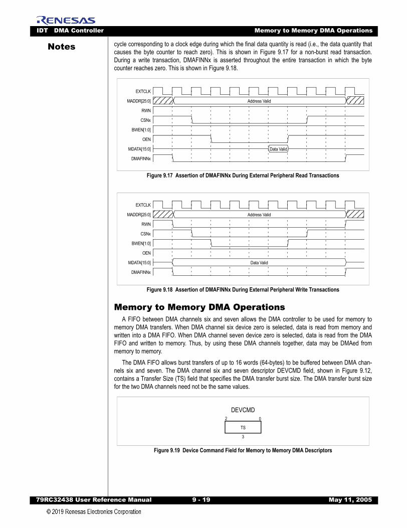
IDT DMA Controller Memory to Memory DMA Operations
79RC32438 User Refer
Notes
cycle corresponding to a clock edge during which the final data quantity is read (i.e., the data quantity thatcauses the byte counter to reach zero). This is shown in Figure 9.17 for a non-burst read transaction.During a write transaction, DMAFINNx is asserted throughout the entire transaction in which the bytecounter reaches zero. This is shown in Figure 9.18.Figure 9.17 Assertion of DMAFINNx During External Peripheral Read Transactions
Figure 9.18 Assertion of DMAFINNx During External Peripheral Write Transactions
Memory to Memory DMA OperationsA FIFO between DMA channels six and seven allows the DMA controller to be used for memory to
memory DMA transfers. When DMA channel six device zero is selected, data is read from memory andwritten into a DMA FIFO. When DMA channel seven device zero is selected, data is read from the DMAFIFO and written to memory. Thus, by using these DMA channels together, data may be DMAed frommemory to memory.
The DMA FIFO allows burst transfers of up to 16 words (64-bytes) to be buffered between DMA chan-nels six and seven. The DMA channel six and seven descriptor DEVCMD field, shown in Figure 9.12,contains a Transfer Size (TS) field that specifies the DMA transfer burst size. The DMA transfer burst sizefor the two DMA channels need not be the same values.
Figure 9.19 Device Command Field for Memory to Memory DMA Descriptors
EXTCLK
MADDR[25:0]
RWN
CSNx
BWEN[1:0]
OEN
MDATA[15:0]
Address Valid
Data Valid
DMAFINNx
EXTCLK
MADDR[25:0]
RWN
CSNx
BWEN[1:0]
OEN
MDATA[15:0]
Address Valid
Data Valid
DMAFINNx
DEVCMD2
3
TS
0
ence Manual 9 - 19 May 11, 2005
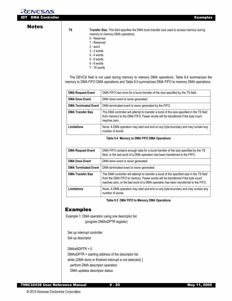
IDT DMA Controller Examples
79RC32438 User Refer
Notes
The DEVCS field is not used during memory to memory DMA operations. Table 9.4 summarizes thememory to DMA FIFO DMA operations and Table 9.5 summarizes DMA FIFO to memory DMA operations.
Examples Example 1: DMA operation using one descriptor list (program DMAxDPTR register)
Set up interrupt controller Set up descriptor
DMAxNDPTR = 0 DMAxDPTR = starting address of the descriptor list while (DMA done or finished interrupt is not detected) perform DMA descriptor operation DMA updates descriptor status
TS Transfer Size. This field specifies the DMA burst transfer size used to access memory during memory to memory DMA operations.0 - Reserved1 - Reserved2 - word3 - 2 words4 - 4 words5 - 6 words6 - 8 words7 - 16 words
DMA Request Event DMA FIFO has room for a burst transfer of the size specified by the TS field.
DMA Done Event DMA done event is never generated.
DMA Terminated Event DMA terminated event is never generated by the FIFO.
DMA Transfer Size The DMA controller will attempt to transfer a burst of the size specified in the TS field from memory to the DMA FIFO. Fewer words will be transferred if the byte count reaches zero.
Limitations None. A DMA operation may start and end on any byte boundary and may contain any number of words.
Table 9.4 Memory to DMA FIFO DMA Operations
DMA Request Event DMA FIFO contains enough data for a burst transfer of the size specified by the TS field, or the last word of a DMA operation has been transferred to the FIFO.
DMA Done Event DMA done event is never generated.
DMA Terminated Event DMA terminated event is never generated.
DMA Transfer Size The DMA controller will attempt to transfer a burst of the specified size in the TS field from the DMA FIFO to memory. Fewer words will be transferred if the byte count reaches zero, or the last word of a DMA operation has been transferred to the FIFO.
Limitations None. A DMA operation may start and end on any byte boundary and may contain any number of words.
Table 9.5 DMA FIFO to Memory DMA Operations
ence Manual 9 - 20 May 11, 2005
IDT DMA Controller Examples
79RC32438 User Refer
Notes
DMA follows LINK field to next DMA descriptorRead the status from DMAxS register and descriptors
Example 2: DMA operation using one descriptor list (program DMAxNDPTR register)
Set up interrupt controller Set up descriptor
DMAxNDPTR = starting address of the descriptor list while (DMA done or finished interrupt is not detected) perform DMA descriptor operation DMA updates descriptor status DMA follows LINK field to next DMA descriptor
Read the status from DMAxS register and descriptors
Example 3: DMA operation using multiple descriptor lists (program DMAxNDPTR register)
Set up interrupt controller Set up descriptors
DMAxNDPTR = starting address of the first descriptor list
while (DMA transfer is not completed) while (DMA chain interrupt is not detected) prepare the next descriptor list
clear the chain bit in DMAxS register DMAxNDPTR = starting address of the next descriptor list
Example 4: DMA operation using multiple descriptor lists (program DMAxDPTR & DMAxNDPTR register)
Set up interrupt controller Set up descriptors
DMAxNDPTR = 0 DMAxDPTR = starting address of the first descriptor list
ence Manual 9 - 21 May 11, 2005
IDT DMA Controller Examples
79RC32438 User Refer
Notes
DMAxNDPTR = starting address of the second descriptor listwhile (DMA transfer is not completed) while (DMA chain interrupt is not detected) prepare the next descriptor list
clear the chain bit in DMAxS register DMAxNDPTR = starting address of the next descriptor list
ence Manual 9 - 22 May 11, 2005
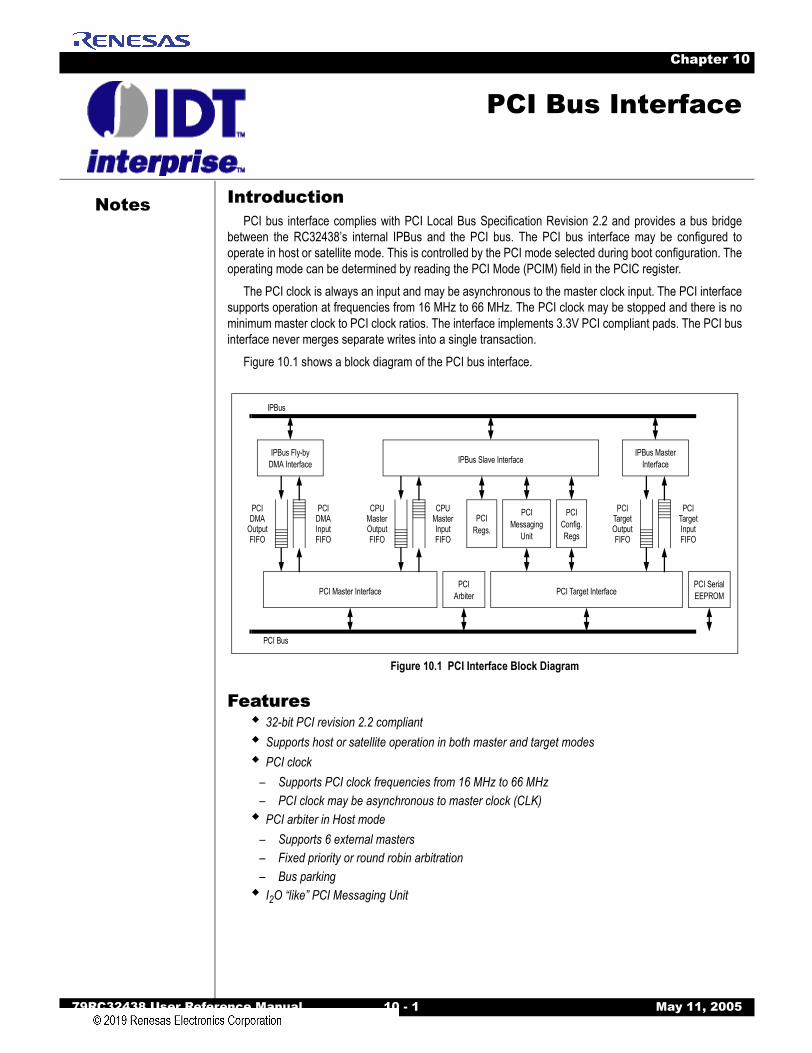
Notes
79RC32438 User Reference Manual 10 - 1 M
Chapter 10
PCI Bus Interface
IntroductionPCI bus interface complies with PCI Local Bus Specification Revision 2.2 and provides a bus bridge
between the RC32438’s internal IPBus and the PCI bus. The PCI bus interface may be configured tooperate in host or satellite mode. This is controlled by the PCI mode selected during boot configuration. Theoperating mode can be determined by reading the PCI Mode (PCIM) field in the PCIC register.
The PCI clock is always an input and may be asynchronous to the master clock input. The PCI interfacesupports operation at frequencies from 16 MHz to 66 MHz. The PCI clock may be stopped and there is nominimum master clock to PCI clock ratios. The interface implements 3.3V PCI compliant pads. The PCI businterface never merges separate writes into a single transaction.
Figure 10.1 shows a block diagram of the PCI bus interface.
Figure 10.1 PCI Interface Block Diagram
Features32-bit PCI revision 2.2 compliantSupports host or satellite operation in both master and target modesPCI clock
– Supports PCI clock frequencies from 16 MHz to 66 MHz– PCI clock may be asynchronous to master clock (CLK)
PCI arbiter in Host mode– Supports 6 external masters– Fixed priority or round robin arbitration– Bus parking
I2O “like” PCI Messaging Unit
PCI Bus
PCIDMA
OutputFIFO
PCIDMAInputFIFO
PCIRegs.
PCIConfig.Regs
PCIMessaging
Unit
CPUMasterOutputFIFO
CPUMasterInputFIFO
PCITargetOutputFIFO
PCITargetInputFIFO
PCI Master Interface PCI Target InterfacePCI
Arbiter
IPBus Fly-byDMA Interface IPBus Slave Interface
IPBus MasterInterface
IPBus
PCI SerialEEPROM
ay 11, 2005

IDT PCI Bus Interface Use of Decoupled PCI Transactions
79RC32438 User Refer
Notes
Use of Decoupled PCI TransactionsThe PCI portion of the system controller sits on the IPBus. Therefore, read and write transactions to andfrom this block consume some of the available IPBus bandwidth and must be factored into the overallsystem bus utilization for a given system. To maximize performance, the number of local IPBus cyclesconsumed for a given transaction should be minimized. The PCI system controller is designed to automati-cally do this for most types of transactions.
In the case of DMA operations to or from the PCI, the transaction is initiated by the DMA. Prior to takingcontrol of the IPBus, the DMA automatically waits for the data to become available in the master read caseor for space to be available in the output FIFO for the master write case. This prevents the DMA fromwasting bandwidth sitting on the IPBus waiting for data to become available. In the case of target reads andtarget writes from an external PCI master to the RC32438 as a PCI target, data is fetched or queued effi-ciently. No user intervention is required.
However, in the case where the CPU core rather than the DMA controller initiates a master read or amaster write, users must be careful not to monopolize the IPBus which will reduce available bandwidth. TheRC32438 contains the following mechanism for decoupling both CPU master reads and CPU master writes.
In the master write case, the CPU core can check the status of the master write FIFO prior to beginningthe write via the OFE (Output FIFO Empty) bit, bit[3], of the PCI Decoupled Access Status Register(PCIDAS). If this bit is set, the FIFO is empty. Then the CPU core can safely initiate a master write or aburst of 4 writes, since enough space is guaranteed for the transaction to be queued immediately withoutstalling the IPBus.
In the master read case, the user can enable the Decoupled Access Mode via the DEN bit in the PCIDecoupled Access Control Register (PCIDAC). When the DEN bit is set, any master read to the PCImemory space will return a "0" immediately. The program can then either rely on polling or use an interruptgenerated from the PCI Decoupled Access Status Register (PCIDAS) Done bit (D) to indicate that the readhas been completed. Upon completion, the data will be available in the PCI Decoupled Access DataRegister (PCIDAD).
If the user opts not to enable this mode, some amount of efficiency will be lost waiting for CPU-initiatedmaster reads to complete. In most applications, this is probably acceptable as the number of CPU-initiatedmaster reads is generally small. However, in the case of PCI bridges, failure to use the decoupled masterread mechanism could result in the read timing out and causing a bus error. This error occurs when theCPU core attempts a master read while the bridge has data queued in its write FIFO and is attempting toinitiate target writes to the RC32438 device to clear the queue. The bridge will pass the read to the deviceon the other side, but when that target PCI device returns the requested read data to the bridge, the bridgewill hold the data until the bridge manages to clear its write FIFO. However, since the CPU core is not usingdecoupled reads, the CPU holds the IPBus until the transaction completes. As long as the CPU is sitting onthe IPBus, the bridge can only do writes until the target write FIFO fills up on the RC32438. When the targetwrite FIFO is full, the RC32438 refuses to take any further target writes. The RC32438 cannot empty thetarget write FIFO — the IPBus must do that — and the CPU continues to wait for the read to complete.Because the RC32438 will not take any more target writes and the bridge will not pass the read datathrough until it completes its writes, the RC32438 and the bridge are now "deadlocked".
The deadlock will only be broken when the RC32438 PCI master transaction retry counter is exceeded.At that point, the system will generate a bus error. The interrupt handler must correct the problem. Thisobviously imposes a significant performance penalty.
Therefore, IDT strongly recommends the use of decoupled master reads and checking the status of theoutput FIFO empty bit prior to generating CPU-initiated master reads or master writes, especially when theRC32438 is being used with a PCI bridge.
IPBus AccessAccess to the IPBus is determined by the IPBus arbiter.
ence Manual 10 - 2 May 11, 2005
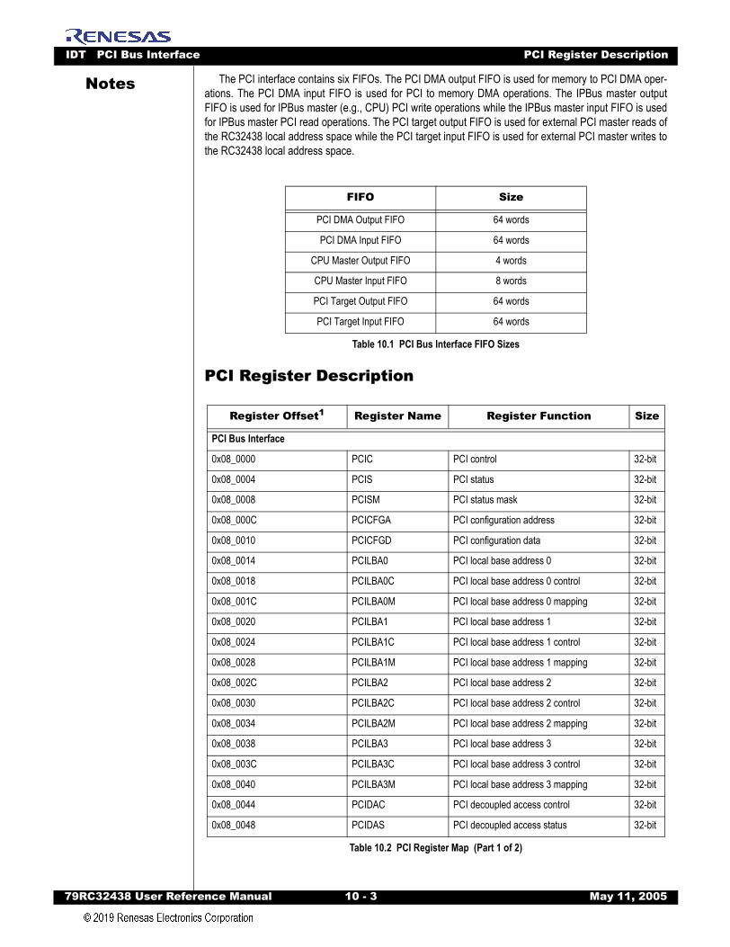
IDT PCI Bus Interface PCI Register Description
79RC32438 User Refer
Notes
The PCI interface contains six FIFOs. The PCI DMA output FIFO is used for memory to PCI DMA oper-ations. The PCI DMA input FIFO is used for PCI to memory DMA operations. The IPBus master outputFIFO is used for IPBus master (e.g., CPU) PCI write operations while the IPBus master input FIFO is usedfor IPBus master PCI read operations. The PCI target output FIFO is used for external PCI master reads ofthe RC32438 local address space while the PCI target input FIFO is used for external PCI master writes tothe RC32438 local address space.PCI Register Description
FIFO Size
PCI DMA Output FIFO 64 words
PCI DMA Input FIFO 64 words
CPU Master Output FIFO 4 words
CPU Master Input FIFO 8 words
PCI Target Output FIFO 64 words
PCI Target Input FIFO 64 words
Table 10.1 PCI Bus Interface FIFO Sizes
Register Offset1 Register Name Register Function Size
PCI Bus Interface
0x08_0000 PCIC PCI control 32-bit
0x08_0004 PCIS PCI status 32-bit
0x08_0008 PCISM PCI status mask 32-bit
0x08_000C PCICFGA PCI configuration address 32-bit
0x08_0010 PCICFGD PCI configuration data 32-bit
0x08_0014 PCILBA0 PCI local base address 0 32-bit
0x08_0018 PCILBA0C PCI local base address 0 control 32-bit
0x08_001C PCILBA0M PCI local base address 0 mapping 32-bit
0x08_0020 PCILBA1 PCI local base address 1 32-bit
0x08_0024 PCILBA1C PCI local base address 1 control 32-bit
0x08_0028 PCILBA1M PCI local base address 1 mapping 32-bit
0x08_002C PCILBA2 PCI local base address 2 32-bit
0x08_0030 PCILBA2C PCI local base address 2 control 32-bit
0x08_0034 PCILBA2M PCI local base address 2 mapping 32-bit
0x08_0038 PCILBA3 PCI local base address 3 32-bit
0x08_003C PCILBA3C PCI local base address 3 control 32-bit
0x08_0040 PCILBA3M PCI local base address 3 mapping 32-bit
0x08_0044 PCIDAC PCI decoupled access control 32-bit
0x08_0048 PCIDAS PCI decoupled access status 32-bit
Table 10.2 PCI Register Map (Part 1 of 2)
ence Manual 10 - 3 May 11, 2005

IDT PCI Bus Interface PCI Register Description
79RC32438 User Refer
Notes
PCI Control Register
Figure 10.2 PCI Control Register (PCIC)
0x08_004C PCIDASM PCI decoupled access status mask 32-bit
0x08_0050 PCIDAD PCI decoupled access data 32-bit
0x08_0054 PCIDMA8C PCI DMA channel 8 configuration 32-bit
0x08_0058 PCIDMA9C PCI DMA channel 9 configuration 32-bit
0x08_005C PCITC PCI target control 32-bit
0x08_0060 through 0x08_7FFF Reserved
PCI Messaging Unit
0x08_8000 through 0x08_800C Reserved
0x08_8010 PCIIM0 PCI Inbound Message 0 32-bit
0x08_8014 PCIIM1 PCI Inbound Message 1 32-bit
0x08_8018 PCIOM0 PCI Outbound Message 0 32-bit
0x08_801C PCIOM1 PCI Outbound Message 1 32-bit
0x08_8020 PCIID PCI Inbound Doorbell 32-bit
0x08_8024 PCIIIC PCI Inbound Interrupt Cause 32-bit
0x08_8028 PCIIIM PCI Inbound Interrupt Mask 32-bit
0x08_802C PCIOD PCI Outbound Doorbell 32-bit
0x08_8030 PCIOIC PCI Outbound Interrupt Cause 32-bit
0x08_8034 PCIOIM PCI Outbound Interrupt Mask 32-bit
0x08_8038 through 0x8_FFFF Reserved
1. The address of the register is equal to the register offset added to the base value of 0x1800_0000.
EN
Description: Enable. When this bit is set, the PCI bus interface is enabled. When this bit is cleared, the PCI bus interface is disabled and enters a benign low power mode. While in this mode, all transac-tions except for configuration accesses will be ignored. Configuration accesses will receive a retry response. Disabling and then re-enabling the PCI bus interface resets all of the logic asso-ciated with the PCI bus interface.
Register Offset1 Register Name Register Function Size
Table 10.2 PCI Register Map (Part 2 of 2)
PCIC031
0
22
EN
13
PCIM TNR
1
SCE
1
IEN
1
AAA
1
EAP
1
IGM
1
ence Manual 10 - 4 May 11, 2005
IDT PCI Bus Interface PCI Register Description
79RC32438 User Refer
Notes
Initial Value: The enable bit is set when the PCI mode boot configuration selects a PCI satellite mode. In all other modes, the enable bit is cleared. See PCI mode boot configuration in Table 3.3 of Chapter 3. (A warm reset does not modify this field except under the following conditions: the warm reset occurs as a result of the assertion of the PCI reset signal and the RC32438 is operat-ing in PCI satellite mode. When a warm reset occurs under the above conditions, this field takes on its initial value.)Read Value: Previous value written
Write Effect: Modify value
TNR
Description: Target Not Ready. When this bit is set, the PCI bus interface issues a retry to all target transac-tions. When this bit is set, delayed reads are never performed.0x0 - Normal operation0x1 - Target not ready (retry all target transactions)
Initial Value: See PCI mode boot configuration inTable 3.3 of Chapter 3.
Read Value: Previous value written
Write Effect: Modify value
SCE
Description: Suspend CPU Execution. When this bit is set, CPU execution is suspended.
Note: Software should never set this bit because it may cause the system to lock-up.
Initial Value: See PCI mode boot configuration in Table 3.3 of Chapter 3.(A warm reset does not modify this field except under the following conditions: the warm reset occurs as a result of the assertion of the PCI reset signal and the RC32438 is operat-ing in PCI satellite mode. When a warm reset occurs under the above conditions, this field takes on its initial value.)
Read Value: Previous value written
Write Effect: Modify value
IEN
Description: IPBus Error Enable. When this bit is set, the PCI interface will signal IPBus slave acknowledge errors during CPU master read transactions when an error occurs. When this bit is cleared, IPBus slave acknowledge errors are masked.
Initial Value: 0x1 (A warm reset does not modify this field except under the following conditions: the warm reset occurs as a result of the assertion of the PCI reset signal and the RC32438 is operat-ing in PCI satellite mode. When a warm reset occurs under the above conditions, this field takes on its initial value.)
Read Value: Previous value written
Write Effect: Modify value
AAA
Description: Arbiter Arbitration Algorithm. When the PCI bus interface is configured to operate in PCI host with internal arbiter mode, this bit selects the arbitration algorithm used by the internal arbiter. This bit has no effect in PCI satellite mode or in PCI host mode using an external arbiter.0x0 - Round robin arbitration algorithm0x1 - Fixed priority arbitration algorithm
ence Manual 10 - 5 May 11, 2005
IDT PCI Bus Interface PCI Register Description
79RC32438 User Refer
Notes
Initial Value: See PCI mode boot configuration in Table 3.3 of Chapter 3.(A warm reset does not modify this field except under the following conditions: the warm reset occurs as a result of the assertion of the PCI reset signal and the RC32438 is operat-ing in PCI satellite mode. When a warm reset occurs under the above conditions, this field takes on its initial value.)Read Value: Previous value written
Write Effect: Modify value
EAP
Description: Enable Arbiter Parking. When this bit is set and the PCI bus interface is configured to operate in PCI host mode with an internal arbiter, then PCI bus parking is enabled. Enabling bus parking causes the internal PCI arbiter to “park” the bus on the last master granted the bus as long as no other master requests the bus.
Initial Value: 0x0 (A warm reset does not modify this field except under the following conditions: the warm reset occurs as a result of the assertion of the PCI reset signal and the RC32438 is operat-ing in PCI satellite mode. When a warm reset occurs under the above conditions, this field takes on its initial value.)
Read Value: Previous value written
Write Effect: Modify value
PCIM
Description: PCI Mode. This field indicates the PCI operating mode selected during boot configuration.0x0 - Disabled (EN bit in PCIC register is cleared)0x1 - PCI satellite mode with PCI target not ready0x2 - PCI satellite mode with suspended CPU execution0x3 - PCI host mode with external arbiter0x4 - PCI host mode with internal arbiter using fixed priority arbitration algorithm0x5 - PCI host mode with internal arbiter using round robin arbitration algorithm0x6 - reserved0x7 - reserved
Initial Value: See PCI mode boot configuration in Table 3.3 of Chapter 3.
Read Value: Status
Write Effect: Read-only
IGM
Description: Idle Grant Mode. This bit controls the operation of the internal arbiter when the PCI interface is configured to operate in a PCI host mode with internal arbiter. When the internal arbiter is used and this bit is cleared, the arbiter operates in a static idle grant mode. This means that once a grant is asserted to a given master, the grant will remain asserted until the requested transaction completes and 16 PCI clock cycles have elapsed. When the internal arbiter is used and this bit is set, the arbiter operates in a dynamic idle grant mode. This means that while the PCI bus is idle, the arbiter may take away a grant from one master and pass it to another. For optimal PCI throughput, this bit should be set to one.
Initial Value: 0x0
Read Value: Previous value written
Write Effect: Modify value
ence Manual 10 - 6 May 11, 2005

IDT PCI Bus Interface PCI Register Description
79RC32438 User Refer
Notes
PCI Status RegisterFigure 10.3 PCI Status Register (PCIS)
EED
Description: PCI Serial EEPROM Done. This bit is set while the PCI bus interface has completed using the PCI serial EEPROM interface. After a cold reset in PCI satellite mode with suspended CPU exe-cution, this bit is cleared and remains cleared until the PCI interface completes loading configura-tion information from the PCI serial EEPROM. This bit is always cleared in the other PCI modes.
Initial Value: 0x0
Read Value: Status
Write Effect: Read only
WR
Description: Warm Reset. This bit is set when a PCI master or the CPU writes a one to the Warm Reset (WR) bit in the PCI Management (PMGT) register. The state of this bit is preserved across warm resets.
Initial Value: 0x0 (A warm reset does not modify this field except under the following conditions: the warm reset occurs as a result of the assertion of the PCI reset signal and the RC32438 is operat-ing in PCI satellite mode. When a warm reset occurs under the above conditions, this field takes on its initial value.)
Read Value: Status
Write Effect: Sticky bit (a sticky bit is set by the hardware and can only be cleared by the CPU)
NMI
Description: Non-maskable Interrupt. This bit is set when a PCI master or the CPU writes a one to the Non-maskable Interrupt (NMI) bit in the PCI Management (PMGT) register.
Initial Value: 0x0
Read Value: Status
Write Effect: Sticky bit (a sticky bit is set by the hardware and can only be cleared by the CPU)
II
Description: Inbound Interrupt. This bit represents the OR of all of the bits in the PCI Inbound Interrupt Cause (PCIIC) register which are not masked in the PCI Inbound Interrupt Mask (PCIIM) register.
Initial Value: 0x0
PCIS1631
0
14
015
NMI WR
1
STA MDPERMA RTAPE SSE
1111111
II
1
EED
1
TAE
1
RLE
1
BME
1
CWE
1
CRE
1
PRD
1
RIP
1
OSE
1
ence Manual 10 - 7 May 11, 2005
IDT PCI Bus Interface PCI Register Description
79RC32438 User Refer
Notes
Read Value: StatusWrite Effect: Read only
CWE
Description: CPU Write Error. This bit is set if a CPU PCI write transaction experienced an error and the IPBus Error Enable (IEN) bit is set in the PCIC register.
Initial Value: 0x0
Read Value: Status
Write Effect: Sticky bit (a sticky bit is set by the hardware and can only be cleared by the CPU)
CRE
Description: CPU Read Error. This bit is set if a CPU PCI read transaction experienced an error and the IPBus Error Enable (IEN) bit is set in the PCIC register.
Initial Value: 0x0
Read Value: Status
Write Effect: Sticky bit (a sticky bit is set by the hardware and can only be cleared by the CPU)
MDPE
Description: Master Data Parity Error Detected. This bit is set whenever the MDPE bit in the PCI Configura-tion STATUS register is set.
Initial Value: 0x0
Read Value: Status
Write Effect: Sticky bit (a sticky bit is set by the hardware and can only be cleared by the CPU)
STA
Description: Signalled Target Abort Status. This bit is set whenever the STA bit in the PCI Configuration STATUS register is set.
Initial Value: 0x0
Read Value: Status
Write Effect: Sticky bit (a sticky bit is set by the hardware and can only be cleared by the CPU)
RTA
Description: Received Target Abort Status. This bit is set whenever the RTA bit in the PCI Configuration STATUS register is set.
Initial Value: 0x0
Read Value: Status
Write Effect: Sticky bit. When set, this bit cannot be cleared until the corresponding bit in the Status Register is cleared.
RMA
Description: Received Master Abort Status. This bit is set whenever the RMA bit in the PCI Configuration STATUS register is set.
Initial Value: 0x0
ence Manual 10 - 8 May 11, 2005
IDT PCI Bus Interface PCI Register Description
79RC32438 User Refer
Notes
Read Value: StatusWrite Effect: Sticky bit. When set, this bit cannot be cleared until the corresponding bit in the Status Register is cleared.
SSE
Description: Signalled System Error. This bit is set whenever the SSE bit in the PCI Configuration STATUS register is set.
Initial Value: 0x0
Read Value: Status
Write Effect: Sticky bit (a sticky bit is set by the hardware and can only be cleared by the CPU)
OSE
Description: Observed System Error. This bit is set whenever a system error is observed on the PCI bus (i.e., the SERRN pin is asserted).
Initial Value: 0x0
Read Value: Status
Write Effect: Sticky bit (a sticky bit is set by the hardware and can only be cleared by the CPU)
PE
Description: Parity Error. This bit is set whenever the PE bit in the PCI Configuration STATUS register is set.
Initial Value: 0x0
Read Value: Status
Write Effect: Sticky bit (a sticky bit is set by the hardware and can only be cleared by the CPU)
TAE
Description: Target Address Error. This bit is set if the PCI bus interface terminates a target transaction with a Target Abort due to an invalid transaction local address reported by the address space monitor.
Initial Value: 0x0
Read Value: Status
Write Effect: Sticky bit (a sticky bit is set by the hardware and can only be cleared by the CPU)
RLE
Description: Retry Limit Exceeded. This bit is set if the PCI bus interface terminated a master transaction with an error because the retry limit specified in the RETRY_LIMIT register in PCI configuration space was exceeded.
Initial Value: 0x0
Read Value: Status
Write Effect: Sticky bit (a sticky bit is set by the hardware and can only be cleared by the CPU)
BME
Description: Bus Master Error. This bit is set if the PCI bus interface terminated a master transaction with an error because the transaction could not be completed since the Bus Master Enable (BM) bit in the COMMAND register in PCI configuration space was not set.
Initial Value: 0x0
ence Manual 10 - 9 May 11, 2005
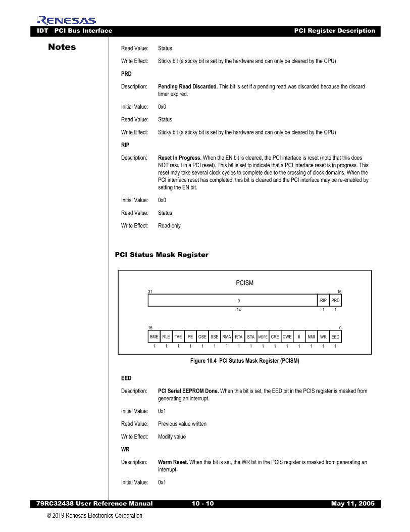
IDT PCI Bus Interface PCI Register Description
79RC32438 User Refer
Notes
PCI Status Mask Register
Figure 10.4 PCI Status Mask Register (PCISM)
Read Value: Status
Write Effect: Sticky bit (a sticky bit is set by the hardware and can only be cleared by the CPU)
PRD
Description: Pending Read Discarded. This bit is set if a pending read was discarded because the discard timer expired.
Initial Value: 0x0
Read Value: Status
Write Effect: Sticky bit (a sticky bit is set by the hardware and can only be cleared by the CPU)
RIP
Description: Reset In Progress. When the EN bit is cleared, the PCI interface is reset (note that this does NOT result in a PCI reset). This bit is set to indicate that a PCI interface reset is in progress. This reset may take several clock cycles to complete due to the crossing of clock domains. When the PCI interface reset has completed, this bit is cleared and the PCI interface may be re-enabled by setting the EN bit.
Initial Value: 0x0
Read Value: Status
Write Effect: Read-only
EED
Description: PCI Serial EEPROM Done. When this bit is set, the EED bit in the PCIS register is masked from generating an interrupt.
Initial Value: 0x1
Read Value: Previous value written
Write Effect: Modify value
WR
Description: Warm Reset. When this bit is set, the WR bit in the PCIS register is masked from generating an interrupt.
Initial Value: 0x1
PCISM1631
0
14
015
NMI WR
1
STA MDPERMA RTAPE SSE
1111111
II
1
EED
1
TAE
1
RLE
1
BME
1
CWE
1
CRE
1
PRD
1
RIP
1
OSE
1
ence Manual 10 - 10 May 11, 2005
IDT PCI Bus Interface PCI Register Description
79RC32438 User Refer
Notes
Read Value: Previous value writtenWrite Effect: Modify value
NMI
Description: Non-maskable Interrupt. When this bit is set, the NMI bit in the PCIS register is masked from generating an interrupt.
Initial Value: 0x1
Read Value: Previous value written
Write Effect: Modify value
II
Description: Inbound Interrupt. When this bit is set, the II bit in the PCIS register is masked from generating an interrupt.
Initial Value: 0x1
Read Value: Previous value written
Write Effect: Modify value
CWE
Description: CPU Write Error. When this bit is set, the CWE bit in the PCIS register is masked from generat-ing an interrupt.
Initial Value: 0x1
Read Value: Previous value written
Write Effect: Modify value
CRE
Description: CPU Read Error. This bit is set if a CPU PCI read transaction experienced an error and the IPBus Error Enable (IEN) bit is set in the PCIC register.
Initial Value: 0x1
Read Value: Previous value written
Write Effect: Modify value
MDPE
Description: Master Data Parity Error. When this bit is set, the MDPE bit in the PCIS register is masked from generating an interrupt.
Initial Value: 0x1
Read Value: Previous value written
Write Effect: Modify value
STA
Description: Signalled Target Abort. When this bit is set, the STA bit in the PCIS register is masked from generating an interrupt.
Initial Value: 0x1
ence Manual 10 - 11 May 11, 2005
IDT PCI Bus Interface PCI Register Description
79RC32438 User Refer
Notes
Read Value: Previous value writtenWrite Effect: Modify value
RTA
Description: Received Target Abort. When this bit is set, the RTA bit in the PCIS register is masked from generating an interrupt.
Initial Value: 0x1
Read Value: Previous value written
Write Effect: Modify value
RMA
Description: Received Master Abort Status. When this bit is set, the RMA bit in the PCIS register is masked from generating an interrupt.
Initial Value: 0x1
Read Value: Previous value written
Write Effect: Modify value
SSE
Description: Signalled System Error. When this bit is set, the SSE bit in the PCIS register is masked from generating an interrupt.
Initial Value: 0x1
Read Value: Previous value written
Write Effect: Modify value
OSE
Description: Observed System Error. When this bit is set, the OSE bit in the PCIS register is masked from generating an interrupt.
Initial Value: 0x1
Read Value: Previous value written
Write Effect: Modify value
PE
Description: Parity Error. When this bit is set, the PE bit in the PCIS register is masked from generating an interrupt.
Initial Value: 0x1
Read Value: Previous value written
Write Effect: Modify value
TAE
Description: Target Address Error. When this bit is set, the TAE bit in the PCIS register is masked from gen-erating an interrupt.
Initial Value: 0x1
ence Manual 10 - 12 May 11, 2005

IDT PCI Bus Interface Reset
79RC32438 User Refer
Notes
ResetUpon assertion of the PCI reset, either a warm or cold reset causes all of the PCI interface pins to be tri-
stated during the reset condition.1 This reaction is asynchronous to the PCI clock or master clock input(CLK) and is immediate.
A warm or cold reset and the subsequent enabling of the PCI interface may result in the PCI bus inter-face being enabled during an active bus (e.g., in the middle of a burst transfer between two other devices).This may also occur due to the delay in locking the PLL following a PCI reset when the RC32438 is used insatellite mode. The PCI bus interface handles this condition. If the RC32438 becomes active during a PCItransaction, the RC32438 will ignore events on the PCI bus until the transaction is completed. For additionalinformation, refer to the Reset Implementation note in section 4.3.2 of PCI Specification 2.2.
Read Value: Previous value written
Write Effect: Modify value
RLE
Description: Retry Limit Exceeded. When this bit is set, the RLE bit in the PCIS register is masked from gen-erating an interrupt.
Initial Value: 0x1
Read Value: Previous value written
Write Effect: Modify value
BME
Description: Bus Master Error. When this bit is set, the BME bit in the PCIS register is masked from generat-ing an interrupt.
Initial Value: 0x1
Read Value: Previous value written
Write Effect: Modify value
PRD
Description: Pending Read Discard. When this bit is set, the PRD bit in the PCIS register is masked from generating an interrupt.
Initial Value: 0x1
Read Value: Previous value written
Write Effect: Modify value
RIP
Description: Reset In Progress. When this bit is set, the RIP bit in the PCIS register is masked from generat-ing an interrupt.
Initial Value: 0x1
Read Value: Previous value written
Write Effect: Modify value
1. An exception to this is the PCI reset signal PCIRSTN. When the RC32438 is configured to operate in PCI host mode, PCIRSTN will be asserted whenever the EN bit is cleared (set to zero).
ence Manual 10 - 13 May 11, 2005

IDT PCI Bus Interface Disabled Mode
79RC32438 User Refer
Notes
During a cold reset, the RC32438’s PCI reset output is tri-stated since it is not yet known if the RC32438will be operating in host or satellite mode. Therefore, system designers should pull the PCI reset signaldown so that it is held low following the application of power to the system.Disabled ModeWhen the EN bit in the PCIC register is cleared, the PCI bus interface is disabled. The PCI bus interface
may be permanently disabled during boot configuration by selecting the disable PCI mode. When disabled,the PCI bus interface enters a benign low-power mode. While in this mode, all transactions except forconfiguration accesses will be ignored. Configuration accesses will receive a retry response. The values onall PCI input pins are ignored. The PCI clock (PCICLK) should be driven to a valid logic level on the board.
When the PCI bus interface is disabled, all of the PCI pins are tri-stated, except PCIGNTN[3:1], and thusshould be held at a valid logic level on the board. PCIGNTN[3:1] signals are driven high when the interfaceis disabled. The PCI bus interface may be disabled at any time after a cold reset by clearing the enable(EN) bit in the PCI configuration (PCIC) register.
Disabling and then re-enabling the PCI bus interface resets all of the logic associated with the PCI businterface and causes all FIFOs to be reset. The states of all status registers are reset to their initial values,but the states of all configuration registers are preserved.
PCI Host Mode
Reset and InitializationIn PCI host mode, the PCI reset pin (PCIRSTN) is an output. The PCIRSTN pin is asserted whenever
the EN bit in the PCIC register is cleared (e.g., as the result of a warm or cold reset). Software shouldensure that the PCIRSTN pin is asserted for a minimum of 1 ms after power has stabilized and 100 µs afterthe PCI clock has stabilized.
After reset, the RC32438 boots from the boot device. The PCI interface is then enabled, causing the PCIreset pin to be de-asserted (i.e., taking the PCI bus out of reset). Initially, the Target Not Ready (TNR) bit isset in the PCIC register. This causes all PCI bus interface target transactions to be retried and allows theRC32438 to initialize the PCI interface and configuration registers. Once the RC32438 device completesthe initialization sequence, it clears the Target Not Ready (TNR) bit, allowing PCI masters to access theRC32438.
A warm reset may be initiated by writing to the Warm Reset (WR) bit in the PCI Management (PMGT)register in PCI configuration space. An NMI to the CPU core may be initiated by writing to the Non-Maskable Interrupt (NMI) bit in the PMGT register. A PCI host may use these features to reset/reboot theRC32438 device.
The CPU core may generate a PCI reset by clearing the EN bit in the PCIC register or by initiating awarm or cold reset. Note that system designers may choose to generate the PCI reset signal using externallogic rather than the RC32438 PCIRSTN signal to reset other external devices. In such a configuration, theexternally generated reset should be configured to generate a warm or cold reset.
Bus ArbitrationPCI arbitration mode in host mode is determined by the PCI mode selected during boot configuration.
The PCI host can be configured to use an external arbiter or internal arbiter. The function of thePCIREQN[5:0] and PCIGNTN[5:0] signals is determined by the PCI mode selected 1 and is dependent onwhether the internal arbiter is used or an external arbiter is selected.
1. PCIREQN[4] is an alternate function of GPIO[24], PCIREQN[5] is an alternate function of GPIO[27], PCIGNTN[4] is an alternate function of GPIO[26], and PCIGNTN[5] is an alternate function of GPIO[28].
ence Manual 10 - 14 May 11, 2005
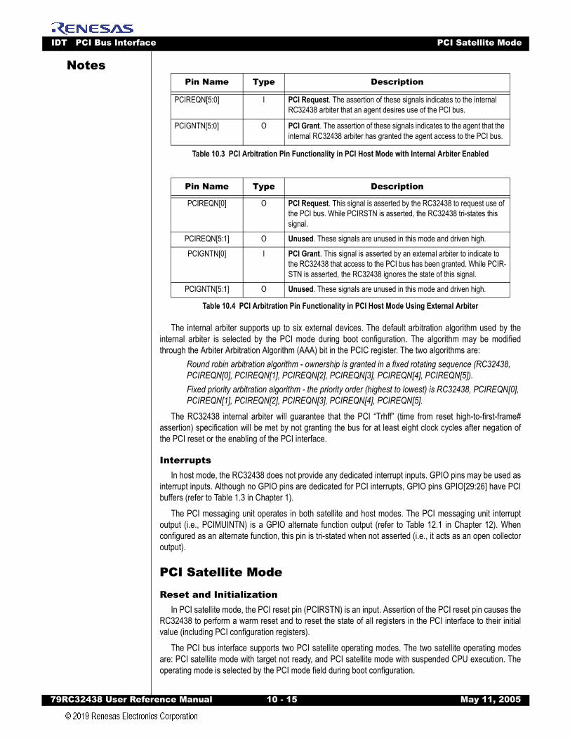
IDT PCI Bus Interface PCI Satellite Mode
79RC32438 User Refer
Notes
The internal arbiter supports up to six external devices. The default arbitration algorithm used by theinternal arbiter is selected by the PCI mode during boot configuration. The algorithm may be modifiedthrough the Arbiter Arbitration Algorithm (AAA) bit in the PCIC register. The two algorithms are:
Round robin arbitration algorithm - ownership is granted in a fixed rotating sequence (RC32438, PCIREQN[0], PCIREQN[1], PCIREQN[2], PCIREQN[3], PCIREQN[4], PCIREQN[5]).Fixed priority arbitration algorithm - the priority order (highest to lowest) is RC32438, PCIREQN[0], PCIREQN[1], PCIREQN[2], PCIREQN[3], PCIREQN[4], PCIREQN[5].
The RC32438 internal arbiter will guarantee that the PCI “Trhff” (time from reset high-to-first-frame#assertion) specification will be met by not granting the bus for at least eight clock cycles after negation ofthe PCI reset or the enabling of the PCI interface.
InterruptsIn host mode, the RC32438 does not provide any dedicated interrupt inputs. GPIO pins may be used as
interrupt inputs. Although no GPIO pins are dedicated for PCI interrupts, GPIO pins GPIO[29:26] have PCIbuffers (refer to Table 1.3 in Chapter 1).
The PCI messaging unit operates in both satellite and host modes. The PCI messaging unit interruptoutput (i.e., PCIMUINTN) is a GPIO alternate function output (refer to Table 12.1 in Chapter 12). Whenconfigured as an alternate function, this pin is tri-stated when not asserted (i.e., it acts as an open collectoroutput).
PCI Satellite Mode
Reset and InitializationIn PCI satellite mode, the PCI reset pin (PCIRSTN) is an input. Assertion of the PCI reset pin causes the
RC32438 to perform a warm reset and to reset the state of all registers in the PCI interface to their initialvalue (including PCI configuration registers).
The PCI bus interface supports two PCI satellite operating modes. The two satellite operating modesare: PCI satellite mode with target not ready, and PCI satellite mode with suspended CPU execution. Theoperating mode is selected by the PCI mode field during boot configuration.
Pin Name Type Description
PCIREQN[5:0] I PCI Request. The assertion of these signals indicates to the internal RC32438 arbiter that an agent desires use of the PCI bus.
PCIGNTN[5:0] O PCI Grant. The assertion of these signals indicates to the agent that the internal RC32438 arbiter has granted the agent access to the PCI bus.
Table 10.3 PCI Arbitration Pin Functionality in PCI Host Mode with Internal Arbiter Enabled
Pin Name Type Description
PCIREQN[0] O PCI Request. This signal is asserted by the RC32438 to request use of the PCI bus. While PCIRSTN is asserted, the RC32438 tri-states this signal.
PCIREQN[5:1] O Unused. These signals are unused in this mode and driven high.
PCIGNTN[0] I PCI Grant. This signal is asserted by an external arbiter to indicate to the RC32438 that access to the PCI bus has been granted. While PCIR-STN is asserted, the RC32438 ignores the state of this signal.
PCIGNTN[5:1] O Unused. These signals are unused in this mode and driven high.
Table 10.4 PCI Arbitration Pin Functionality in PCI Host Mode Using External Arbiter
ence Manual 10 - 15 May 11, 2005
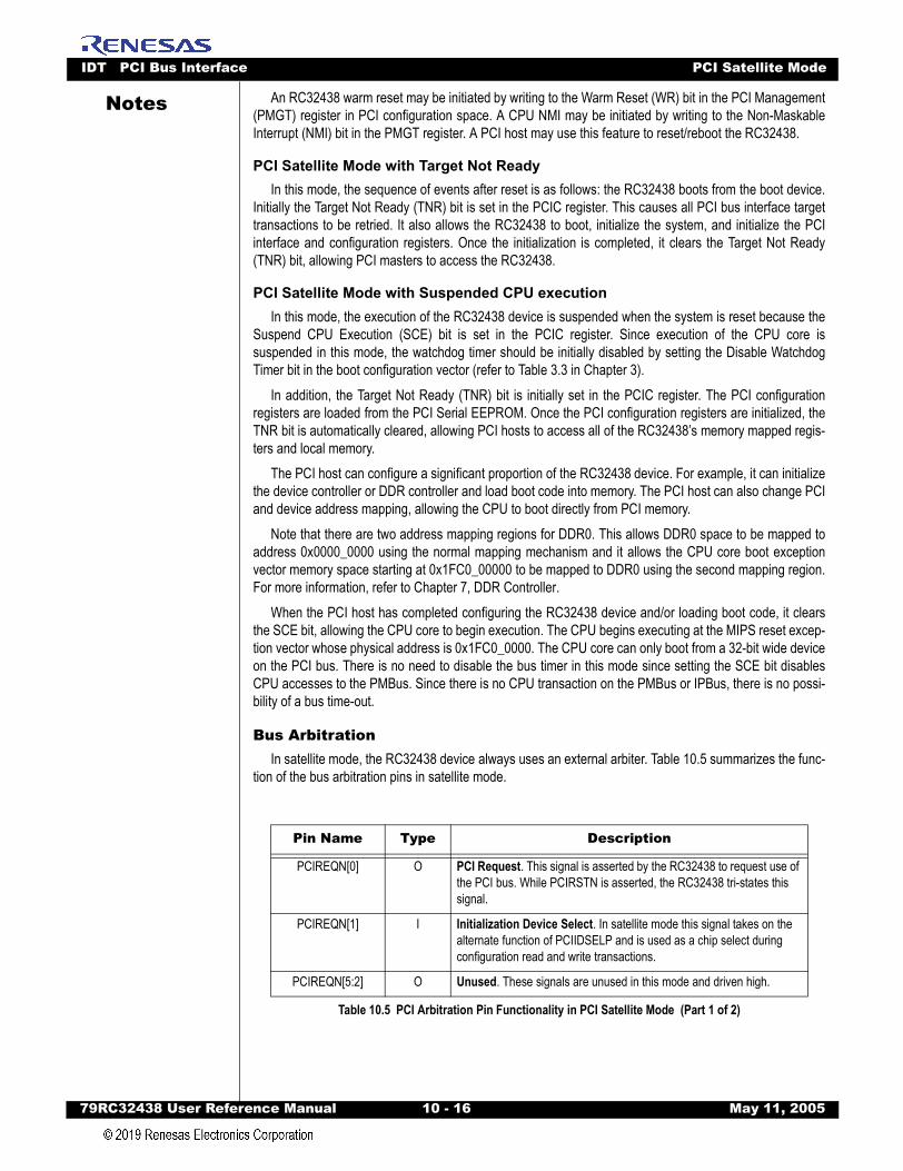
IDT PCI Bus Interface PCI Satellite Mode
79RC32438 User Refer
Notes
An RC32438 warm reset may be initiated by writing to the Warm Reset (WR) bit in the PCI Management(PMGT) register in PCI configuration space. A CPU NMI may be initiated by writing to the Non-MaskableInterrupt (NMI) bit in the PMGT register. A PCI host may use this feature to reset/reboot the RC32438.PCI Satellite Mode with Target Not ReadyIn this mode, the sequence of events after reset is as follows: the RC32438 boots from the boot device.
Initially the Target Not Ready (TNR) bit is set in the PCIC register. This causes all PCI bus interface targettransactions to be retried. It also allows the RC32438 to boot, initialize the system, and initialize the PCIinterface and configuration registers. Once the initialization is completed, it clears the Target Not Ready(TNR) bit, allowing PCI masters to access the RC32438.
PCI Satellite Mode with Suspended CPU executionIn this mode, the execution of the RC32438 device is suspended when the system is reset because the
Suspend CPU Execution (SCE) bit is set in the PCIC register. Since execution of the CPU core issuspended in this mode, the watchdog timer should be initially disabled by setting the Disable WatchdogTimer bit in the boot configuration vector (refer to Table 3.3 in Chapter 3).
In addition, the Target Not Ready (TNR) bit is initially set in the PCIC register. The PCI configurationregisters are loaded from the PCI Serial EEPROM. Once the PCI configuration registers are initialized, theTNR bit is automatically cleared, allowing PCI hosts to access all of the RC32438’s memory mapped regis-ters and local memory.
The PCI host can configure a significant proportion of the RC32438 device. For example, it can initializethe device controller or DDR controller and load boot code into memory. The PCI host can also change PCIand device address mapping, allowing the CPU to boot directly from PCI memory.
Note that there are two address mapping regions for DDR0. This allows DDR0 space to be mapped toaddress 0x0000_0000 using the normal mapping mechanism and it allows the CPU core boot exceptionvector memory space starting at 0x1FC0_00000 to be mapped to DDR0 using the second mapping region.For more information, refer to Chapter 7, DDR Controller.
When the PCI host has completed configuring the RC32438 device and/or loading boot code, it clearsthe SCE bit, allowing the CPU core to begin execution. The CPU begins executing at the MIPS reset excep-tion vector whose physical address is 0x1FC0_0000. The CPU core can only boot from a 32-bit wide deviceon the PCI bus. There is no need to disable the bus timer in this mode since setting the SCE bit disablesCPU accesses to the PMBus. Since there is no CPU transaction on the PMBus or IPBus, there is no possi-bility of a bus time-out.
Bus ArbitrationIn satellite mode, the RC32438 device always uses an external arbiter. Table 10.5 summarizes the func-
tion of the bus arbitration pins in satellite mode.
Pin Name Type Description
PCIREQN[0] O PCI Request. This signal is asserted by the RC32438 to request use of the PCI bus. While PCIRSTN is asserted, the RC32438 tri-states this signal.
PCIREQN[1] I Initialization Device Select. In satellite mode this signal takes on the alternate function of PCIIDSELP and is used as a chip select during configuration read and write transactions.
PCIREQN[5:2] O Unused. These signals are unused in this mode and driven high.
Table 10.5 PCI Arbitration Pin Functionality in PCI Satellite Mode (Part 1 of 2)
ence Manual 10 - 16 May 11, 2005
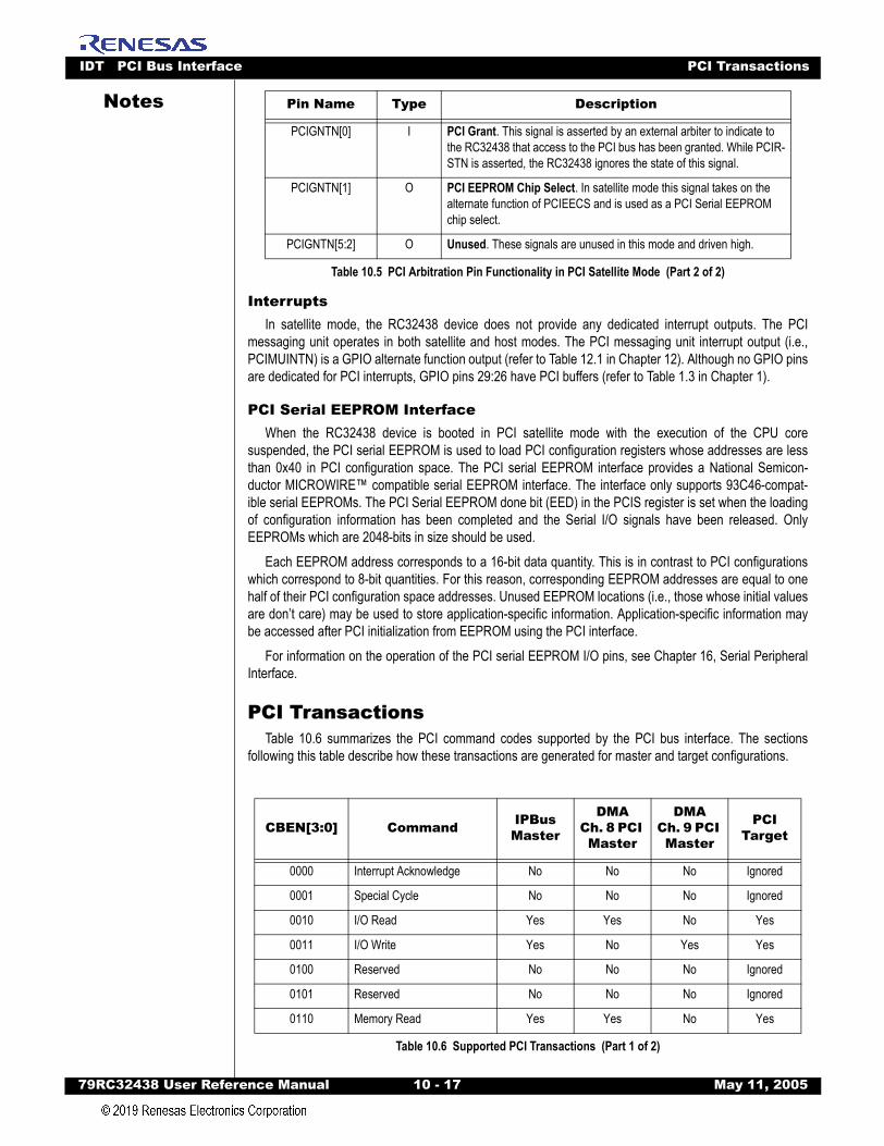
IDT PCI Bus Interface PCI Transactions
79RC32438 User Refer
Notes
InterruptsIn satellite mode, the RC32438 device does not provide any dedicated interrupt outputs. The PCI
messaging unit operates in both satellite and host modes. The PCI messaging unit interrupt output (i.e.,PCIMUINTN) is a GPIO alternate function output (refer to Table 12.1 in Chapter 12). Although no GPIO pinsare dedicated for PCI interrupts, GPIO pins 29:26 have PCI buffers (refer to Table 1.3 in Chapter 1).
PCI Serial EEPROM InterfaceWhen the RC32438 device is booted in PCI satellite mode with the execution of the CPU core
suspended, the PCI serial EEPROM is used to load PCI configuration registers whose addresses are lessthan 0x40 in PCI configuration space. The PCI serial EEPROM interface provides a National Semicon-ductor MICROWIRE™ compatible serial EEPROM interface. The interface only supports 93C46-compat-ible serial EEPROMs. The PCI Serial EEPROM done bit (EED) in the PCIS register is set when the loadingof configuration information has been completed and the Serial I/O signals have been released. OnlyEEPROMs which are 2048-bits in size should be used.
Each EEPROM address corresponds to a 16-bit data quantity. This is in contrast to PCI configurationswhich correspond to 8-bit quantities. For this reason, corresponding EEPROM addresses are equal to onehalf of their PCI configuration space addresses. Unused EEPROM locations (i.e., those whose initial valuesare don’t care) may be used to store application-specific information. Application-specific information maybe accessed after PCI initialization from EEPROM using the PCI interface.
For information on the operation of the PCI serial EEPROM I/O pins, see Chapter 16, Serial PeripheralInterface.
PCI TransactionsTable 10.6 summarizes the PCI command codes supported by the PCI bus interface. The sections
following this table describe how these transactions are generated for master and target configurations.
PCIGNTN[0] I PCI Grant. This signal is asserted by an external arbiter to indicate to the RC32438 that access to the PCI bus has been granted. While PCIR-STN is asserted, the RC32438 ignores the state of this signal.
PCIGNTN[1] O PCI EEPROM Chip Select. In satellite mode this signal takes on the alternate function of PCIEECS and is used as a PCI Serial EEPROM chip select.
PCIGNTN[5:2] O Unused. These signals are unused in this mode and driven high.
CBEN[3:0] Command IPBus Master
DMA Ch. 8 PCI Master
DMA Ch. 9 PCI Master
PCI Target
0000 Interrupt Acknowledge No No No Ignored
0001 Special Cycle No No No Ignored
0010 I/O Read Yes Yes No Yes
0011 I/O Write Yes No Yes Yes
0100 Reserved No No No Ignored
0101 Reserved No No No Ignored
0110 Memory Read Yes Yes No Yes
Table 10.6 Supported PCI Transactions (Part 1 of 2)
Pin Name Type Description
Table 10.5 PCI Arbitration Pin Functionality in PCI Satellite Mode (Part 2 of 2)
ence Manual 10 - 17 May 11, 2005
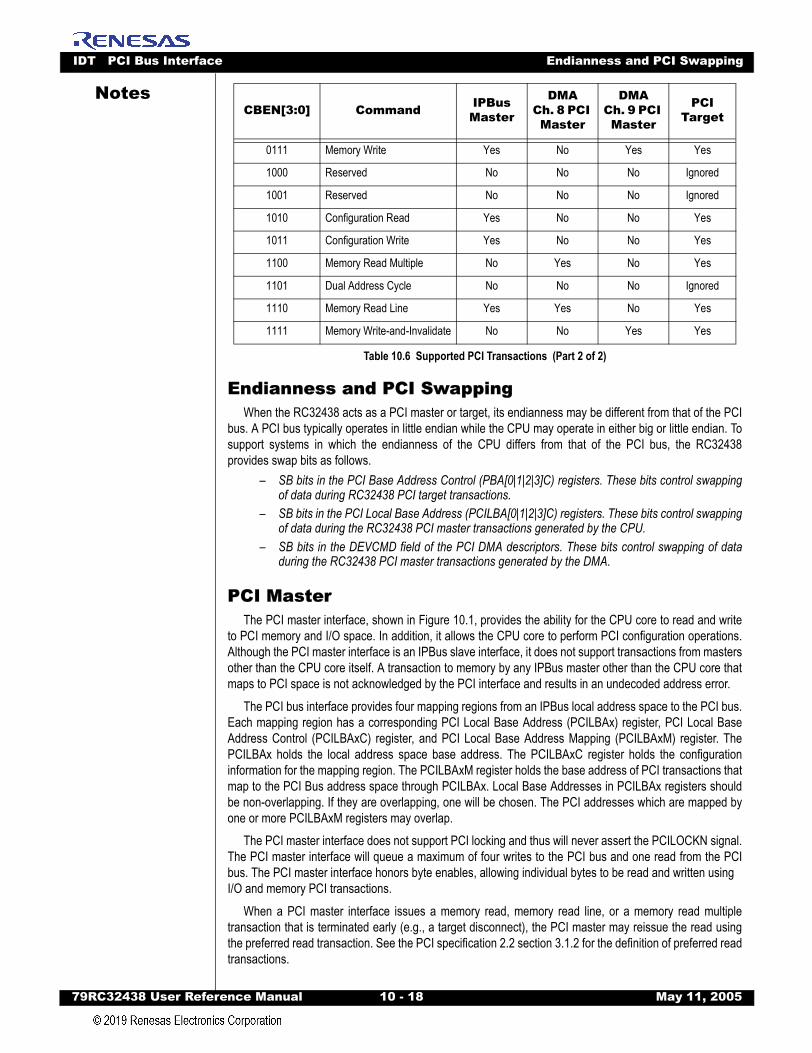
IDT PCI Bus Interface Endianness and PCI Swapping
79RC32438 User Refer
Notes
Endianness and PCI SwappingWhen the RC32438 acts as a PCI master or target, its endianness may be different from that of the PCI
bus. A PCI bus typically operates in little endian while the CPU may operate in either big or little endian. Tosupport systems in which the endianness of the CPU differs from that of the PCI bus, the RC32438provides swap bits as follows.
– SB bits in the PCI Base Address Control (PBA[0|1|2|3]C) registers. These bits control swappingof data during RC32438 PCI target transactions.
– SB bits in the PCI Local Base Address (PCILBA[0|1|2|3]C) registers. These bits control swappingof data during the RC32438 PCI master transactions generated by the CPU.
– SB bits in the DEVCMD field of the PCI DMA descriptors. These bits control swapping of dataduring the RC32438 PCI master transactions generated by the DMA.
PCI MasterThe PCI master interface, shown in Figure 10.1, provides the ability for the CPU core to read and write
to PCI memory and I/O space. In addition, it allows the CPU core to perform PCI configuration operations.Although the PCI master interface is an IPBus slave interface, it does not support transactions from mastersother than the CPU core itself. A transaction to memory by any IPBus master other than the CPU core thatmaps to PCI space is not acknowledged by the PCI interface and results in an undecoded address error.
The PCI bus interface provides four mapping regions from an IPBus local address space to the PCI bus.Each mapping region has a corresponding PCI Local Base Address (PCILBAx) register, PCI Local BaseAddress Control (PCILBAxC) register, and PCI Local Base Address Mapping (PCILBAxM) register. ThePCILBAx holds the local address space base address. The PCILBAxC register holds the configurationinformation for the mapping region. The PCILBAxM register holds the base address of PCI transactions thatmap to the PCI Bus address space through PCILBAx. Local Base Addresses in PCILBAx registers shouldbe non-overlapping. If they are overlapping, one will be chosen. The PCI addresses which are mapped byone or more PCILBAxM registers may overlap.
The PCI master interface does not support PCI locking and thus will never assert the PCILOCKN signal.The PCI master interface will queue a maximum of four writes to the PCI bus and one read from the PCIbus. The PCI master interface honors byte enables, allowing individual bytes to be read and written using I/O and memory PCI transactions.
When a PCI master interface issues a memory read, memory read line, or a memory read multipletransaction that is terminated early (e.g., a target disconnect), the PCI master may reissue the read usingthe preferred read transaction. See the PCI specification 2.2 section 3.1.2 for the definition of preferred readtransactions.
0111 Memory Write Yes No Yes Yes
1000 Reserved No No No Ignored
1001 Reserved No No No Ignored
1010 Configuration Read Yes No No Yes
1011 Configuration Write Yes No No Yes
1100 Memory Read Multiple No Yes No Yes
1101 Dual Address Cycle No No No Ignored
1110 Memory Read Line Yes Yes No Yes
1111 Memory Write-and-Invalidate No No Yes Yes
CBEN[3:0] Command IPBus Master
DMA Ch. 8 PCI Master
DMA Ch. 9 PCI Master
PCI Target
Table 10.6 Supported PCI Transactions (Part 2 of 2)
ence Manual 10 - 18 May 11, 2005
IDT PCI Bus Interface PCI Master
79RC32438 User Refer
Notes
Master I/O ReadAll IPBus read transactions whose addresses match the base address in a PCI Local Base Address(PCILBAx) register configured for I/O space (i.e., the MSI bit is set in the corresponding PCI Local BaseAddress Control (PCILBAxC) register) result in an I/O read transaction on the PCI bus. The value in thecorresponding PCI Local Base Address Map (PCILBAxM) register maps the upper bits of the local IPBusaddress to the PCI I/O read address, as indicated by the SIZE field of the PCILBAxC register. The byteenables on the PCI bus correspond to the size/byte enables of the IPBus read operation (i.e., byte, half-word, triple-byte or word). All IPBus initiated I/O read transactions translate into single data phase PCItransactions even if a burst transaction was generated on the IPBus (i.e., bursts are not supported).
Master I/O WriteAll IPBus write transactions whose addresses match the base address in a PCI Local Base Address
(PCILBAx) register configured for I/O space (i.e., the MSI bit is set in the corresponding PCI Local BaseAddress Control (PCILBAxC) register) result in an I/O write transaction on the PCI bus. The value in thecorresponding PCI Local Base Address Map (PCILBAxM) register maps the upper bits of the local IPBusaddress, as indicated by the SIZE field of the PCILBAxC register, to the PCI I/O read address. The valuewritten on the PCI bus corresponds to the data value of the IPBus write transaction. The byte enables onthe PCI bus correspond to the size/byte enables of the IPBus write operation (i.e., byte, halfword, triple-byte, or word). IPBus initiated I/O write transactions may contain one or more data phases (i.e., bursts aresupported).
Master Memory ReadAn IPBus read transaction will result in a memory read transaction on the PCI Bus when the following
conditions are met: – The address matches the base address in a PCI Local Base Address (PCILBAx) register that is
configured for memory space (i.e., the MSI bit is cleared in the corresponding PCI Local BaseAddress Control (PCILBAxC) register)
– Read Transaction (RT bit in corresponding PCILBAxC) bit is cleared, resulting in a memory readtransaction on the PCI bus.
The value in the corresponding PCI Local Base Address Map (PCILBAxM) register maps the upper bitsof the local IPBus address, as indicated by the SIZE field of the PCILBAxC register, to the PCI memory readaddress. The byte enables on the PCI bus correspond to the size/byte enables of the IPBus read operation(i.e., byte, halfword, triple-byte, or word).
Master Memory WriteAll IPBus write transactions whose addresses match the base address in a PCI Local Base Address
(PCILBAx) register that is configured for memory space (i.e., the MSI bit is cleared in the corresponding PCILocal Base Address Control (PCILBAxC) register) result in a memory write transaction on the PCI bus. Thevalue in the corresponding PCI Local Base Address Map (PCILBAxM) register maps the upper bits of thelocal IPBus address, as indicated by the SIZE field of the PCILBAxC register, to the PCI memory writeaddress. The value written on the PCI bus corresponds to the data value of the IPBus write transaction. Thebyte enables on the PCI bus correspond to the size/byte enables of the IPBus write operation (i.e., byte,halfword, triple-byte, or word).
The PCI bus interface will attempt to perform burst PCI memory write transactions whenever possible.The PCI interface will add a data phase to the memory write transaction in progress if:
– Data exists in the CPU master output FIFO whose address is equal to that of the current dataquantity being transferred plus four
– The Master Latency Timer has not expired.
Master Configuration ReadTo generate a PCI configuration read transaction, an IPBus master (e.g., CPU core) writes the desired
configuration register address to the PCI Configuration Address (PCICFGA) register and performs a readfrom the PCI Configuration Data (PCICFGD) register. The value returned to the IPBus master will be that
ence Manual 10 - 19 May 11, 2005
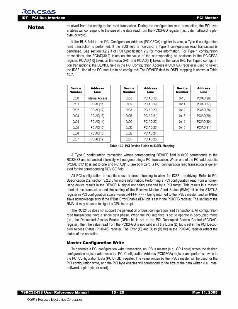
IDT PCI Bus Interface PCI Master
79RC32438 User Refer
Notes
received from the configuration read transaction. During the configuration read transaction, the PCI byteenables will correspond to the size of the data read from the PCICFGD register (i.e., byte, halfword, triple-byte, or word).If the BUS field in the PCI Configuration Address (PCICFGA) register is zero, a Type 0 configurationread transaction is performed. If the BUS field is non-zero, a Type 1 configuration read transaction isperformed. See section 3.2.2.3 of PCI Specification 2.2 for more information. For Type 1 configurationtransactions, the PCIAD[30:2] takes on the value of the corresponding bit positions in the PCICFGAregister. PCIAD[1:0] takes on the value 0x01 and PCIAD[31] takes on the value 0x0. For Type 0 configura-tion transactions, the DEVICE field in the PCI Configuration Address (PCICFGA) register is used to selectthe IDSEL line of the PCI satellite to be configured. The DEVICE field to IDSEL mapping is shown in Table10.7.
A Type 0 configuration transaction whose corresponding DEVICE field is 0x00 corresponds to theRC32438 and is handled internally without generating a PCI transaction. When one of the PCI address bits(PCIAD[31:11]) is set to one and PCIAD[1:0] are both zero, a PCI configuration read transaction is gener-ated for the corresponding DEVICE field.
All PCI configuration transactions use address stepping to allow for IDSEL predriving. Refer to PCISpecification 2.2, section 3.2.2.5 for more information. Performing a PCI configuration read from a nonex-isting device results in the DEVSELN signal not being asserted by a PCI target. This results in a masterabort of the transaction and the setting of the Receive Master Abort Status (RMA) bit in the STATUSregister in PCI configuration space, value 0xFFFF_FFFF being returned to the IPBus master, and an IPBusslave acknowledge error if the IPBus Error Enable (IEN) bit is set in the PCICFG register. The setting of theRMA bit may be used to signal a CPU interrupt.
The RC32438 does not support the generation of burst configuration read transactions. All configurationread transactions have a single data phase. When the PCI interface is set to operate in decoupled mode(i.e., the Decoupled Access Enable (DEN) bit is set in the PCI Decoupled Access Control (PCIDAC)register), then the value read from the PCICFGD is not valid until the Done (D) bit is set in the PCI Decou-pled Access Status (PCIDAS) register. The Error (E) and Busy (B) bits in the PCIDAS register reflect thestatus of the operation.
Master Configuration WriteTo generate a PCI configuration write transaction, an IPBus master (e.g., CPU core) writes the desired
configuration register address to the PCI Configuration Address (PCICFGA) register and performs a write tothe PCI Configuration Data (PCICFGD) register. The value written by the IPBus master will be used for thePCI configuration write, and the PCI byte enables will correspond to the size of the data written (i.e., byte,halfword, triple-byte, or word).
DeviceNumber
AddressLine
DeviceNumber
AddressLine
DeviceNumber
AddressLine
0x00 Internal Access 0x08 PCIAD[18] 0x10 PCIAD[26]0x01 PCIAD[11] 0x09 PCIAD[19] 0x11 PCIAD[27]0x02 PCIAD[12] 0x0A PCIAD[20] 0x12 PCIAD[28]0x03 PCIAD[13] 0x0B PCIAD[21] 0x13 PCIAD[29]0x04 PCIAD[14] 0x0C PCIAD[22] 0x14 PCIAD[30]0x05 PCIAD[15] 0x0D PCIAD[23] 0x15 PCIAD[31]0x06 PCIAD[16] 0x0E PCIAD[24]0x07 PCIAD[17] 0x0F PCIAD[25]
Table 10.7 PCI Device Fields to IDSEL Mapping
ence Manual 10 - 20 May 11, 2005
IDT PCI Bus Interface PCI Master
79RC32438 User Refer
Notes
If the BUS field in the PCI Configuration Address (PCICFGA) register is zero, a Type 0 configurationread transaction is performed. If the BUS field is non-zero, a Type 1 configuration read transaction isperformed. See section 3.2.2.3 of PCI Specification 2.2 for more information. For Type 1 configurationtransactions, the PCIAD[30:2] takes on the value of the corresponding bit positions in the PCICFGAregister. PCIAD[1:0] takes on the value 0x01 and PCIAD[31] takes on the value 0x0. For Type 0 configura-tion transactions, the DEVICE field in the PCI Configuration Address (PCICFGA) register is used to selectthe IDSEL line of the PCI satellite to be configured. The DEVICE field to IDSEL mapping is shown in Table10.7. A Type 0 configuration transaction whose corresponding DEVICE field is 0x00 corresponds to theRC32438 and is handled internally without generating a PCI transaction. When one of the PCI address bits(PCIAD[31:11]) is set to one and PCIAD[1:0] are both zero, a PCI configuration write transaction is gener-ated for the corresponding DEVICE field.All PCI configuration transactions use address stepping to allow for IDSEL predriving. Refer to the PCISpecification 2.2, section 3.2.2.5 for more information. Performing a PCI configuration write to a nonexistingdevice results in the DEVSELN signal not being asserted by a PCI target. This results in a master abort ofthe transaction and the setting of the Receive Master Abort Status (RMA) bit in the STATUS register in PCIconfiguration space. The setting of the RMA bit may be used to signal a CPU interrupt. The RC32438 doesnot support generation of burst configuration write transactions. All configuration write transactions have asingle data phase.
When the PCI interface is set to operate in decoupled mode (i.e., the Decoupled Access Enable (DEN)bit is set in the PCI Decoupled Access Control (PCIDAC) register), then the Done (D), Error (E), and Busy(B) bits in the PCI Decoupled Access Status (PCIDAS) register reflect the status of the operation.
Master Memory Read LineAll IPBus read transactions whose address matches the base address in a PCI Local Base Address
(PCILBAx) register that is configured for memory space (i.e., the MSI bit is cleared in the corresponding PCILocal Base Address Control (PCILBAxC) register) and whose Read Transaction (RT bit in correspondingPCILBAxC) bit is set result in a memory read line transaction on the PCI bus. The value in the corre-sponding PCI Local Base Address Map (PCILBAxM) register maps the upper bits of the local IPBusaddress, as indicated by the SIZE field of the PCILBAxC register, to the PCI memory read address.
Setting the Read Transaction (RT) bit in the corresponding PCILBAxC register indicates to the PCI inter-face that a memory read line transaction should be used to prefetch data when the read transaction mapsto the corresponding PCILBAx register. The PCI bus interface will supply the data quantity requested by theIPBus master read and will queue prefetch data in the IPBus Master PCI input FIFO. Subsequent sequen-tial reads that map to PCILBAx will result in queued data being returned.
The memory read line is used when a PCI master will read more than one word but no more than acache line. Memory read line transactions resulting from IPBus master read transactions will cause the PCIbus interface to issue a memory read line burst transaction that transfers either an entire cache line or eightwords, whichever is smaller. The 8 word limit allows the CACHE_LINE_SIZE register in PCI configurationspace to be set larger than the size of the IPBus master PCI input FIFO. For example, setting theCACHE_LINE_SIZE register to 16 words still results in only 8 words being transferred.
Prefetch data in the CPU master input FIFO is flushed when an IPBus write transaction maps to the PCIbus.
Master Error HandlingIPBus master fatal errors are: target timeout error, PCI target terminates with a Target Abort, transaction
could not be completed because the RETRY_LIMIT was exceeded, parity error, and the transaction couldnot be completed because the BM bit is not set in the COMMAND register.
An IPBus master fatal error is not propagated to the IPBus on prefetched data that is not subsequentlyread by an IPBus master (i.e., if the error occurs on prefetched data, it is ignored unless the data is actuallyused). If a CPU generated PCI master read transaction experiences a fatal error, the CPU master input
ence Manual 10 - 21 May 11, 2005
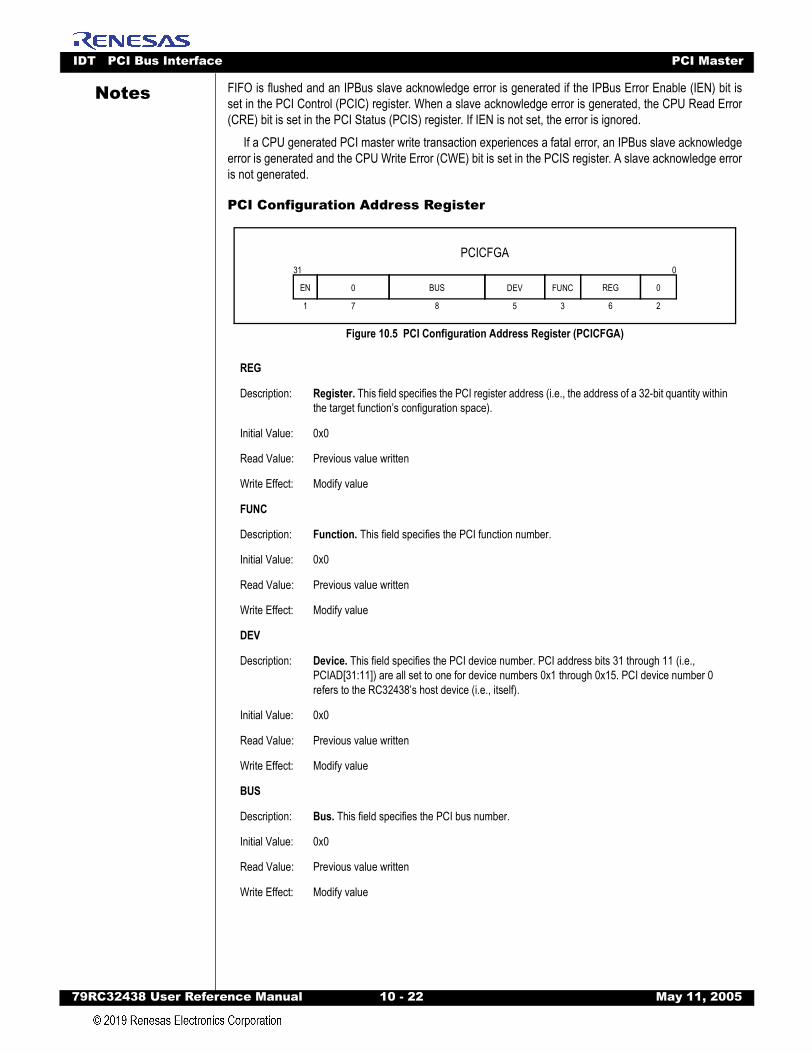
IDT PCI Bus Interface PCI Master
79RC32438 User Refer
Notes
FIFO is flushed and an IPBus slave acknowledge error is generated if the IPBus Error Enable (IEN) bit isset in the PCI Control (PCIC) register. When a slave acknowledge error is generated, the CPU Read Error(CRE) bit is set in the PCI Status (PCIS) register. If IEN is not set, the error is ignored.If a CPU generated PCI master write transaction experiences a fatal error, an IPBus slave acknowledgeerror is generated and the CPU Write Error (CWE) bit is set in the PCIS register. A slave acknowledge erroris not generated.
PCI Configuration Address Register
Figure 10.5 PCI Configuration Address Register (PCICFGA)
REG
Description: Register. This field specifies the PCI register address (i.e., the address of a 32-bit quantity within the target function’s configuration space).
Initial Value: 0x0
Read Value: Previous value written
Write Effect: Modify value
FUNC
Description: Function. This field specifies the PCI function number.
Initial Value: 0x0
Read Value: Previous value written
Write Effect: Modify value
DEV
Description: Device. This field specifies the PCI device number. PCI address bits 31 through 11 (i.e., PCIAD[31:11]) are all set to one for device numbers 0x1 through 0x15. PCI device number 0 refers to the RC32438’s host device (i.e., itself).
Initial Value: 0x0
Read Value: Previous value written
Write Effect: Modify value
BUS
Description: Bus. This field specifies the PCI bus number.
Initial Value: 0x0
Read Value: Previous value written
Write Effect: Modify value
PCICFGA031
8
0
7
EN
1 2
0BUS
5
DEV
3
FUNC
6
REG
ence Manual 10 - 22 May 11, 2005
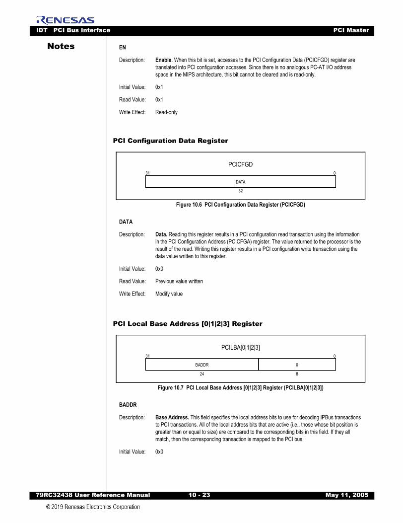
IDT PCI Bus Interface PCI Master
79RC32438 User Refer
Notes
PCI Configuration Data Register
Figure 10.6 PCI Configuration Data Register (PCICFGD)
PCI Local Base Address [0|1|2|3] Register
Figure 10.7 PCI Local Base Address [0|1|2|3] Register (PCILBA[0|1|2|3])
EN
Description: Enable. When this bit is set, accesses to the PCI Configuration Data (PCICFGD) register are translated into PCI configuration accesses. Since there is no analogous PC-AT I/O address space in the MIPS architecture, this bit cannot be cleared and is read-only.
Initial Value: 0x1
Read Value: 0x1
Write Effect: Read-only
DATA
Description: Data. Reading this register results in a PCI configuration read transaction using the information in the PCI Configuration Address (PCICFGA) register. The value returned to the processor is the result of the read. Writing this register results in a PCI configuration write transaction using the data value written to this register.
Initial Value: 0x0
Read Value: Previous value written
Write Effect: Modify value
BADDR
Description: Base Address. This field specifies the local address bits to use for decoding IPBus transactions to PCI transactions. All of the local address bits that are active (i.e., those whose bit position is greater than or equal to size) are compared to the corresponding bits in this field. If they all match, then the corresponding transaction is mapped to the PCI bus.
Initial Value: 0x0
PCICFGD031
32
DATA
PCILBA[0|1|2|3]031
24
BADDR 0
8
ence Manual 10 - 23 May 11, 2005
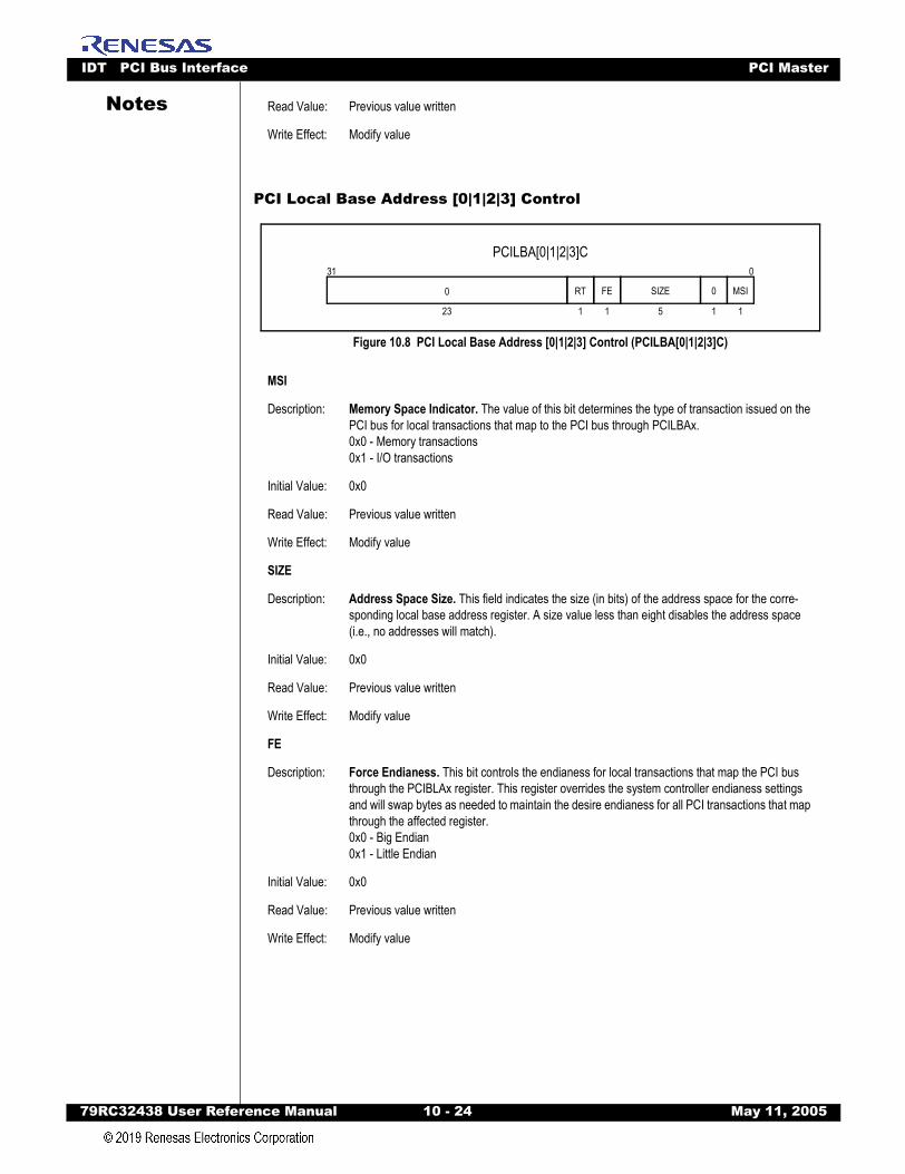
IDT PCI Bus Interface PCI Master
79RC32438 User Refer
Notes
PCI Local Base Address [0|1|2|3] Control
Figure 10.8 PCI Local Base Address [0|1|2|3] Control (PCILBA[0|1|2|3]C)
Read Value: Previous value written
Write Effect: Modify value
MSI
Description: Memory Space Indicator. The value of this bit determines the type of transaction issued on the PCI bus for local transactions that map to the PCI bus through PCILBAx.0x0 - Memory transactions0x1 - I/O transactions
Initial Value: 0x0
Read Value: Previous value written
Write Effect: Modify value
SIZE
Description: Address Space Size. This field indicates the size (in bits) of the address space for the corre-sponding local base address register. A size value less than eight disables the address space (i.e., no addresses will match).
Initial Value: 0x0
Read Value: Previous value written
Write Effect: Modify value
FE
Description: Force Endianess. This bit controls the endianess for local transactions that map the PCI bus through the PCIBLAx register. This register overrides the system controller endianess settings and will swap bytes as needed to maintain the desire endianess for all PCI transactions that map through the affected register.0x0 - Big Endian0x1 - Little Endian
Initial Value: 0x0
Read Value: Previous value written
Write Effect: Modify value
PCILBA[0|1|2|3]C031
1
MSI
1
0SIZE
51
FE
1
RT
23
0
ence Manual 10 - 24 May 11, 2005
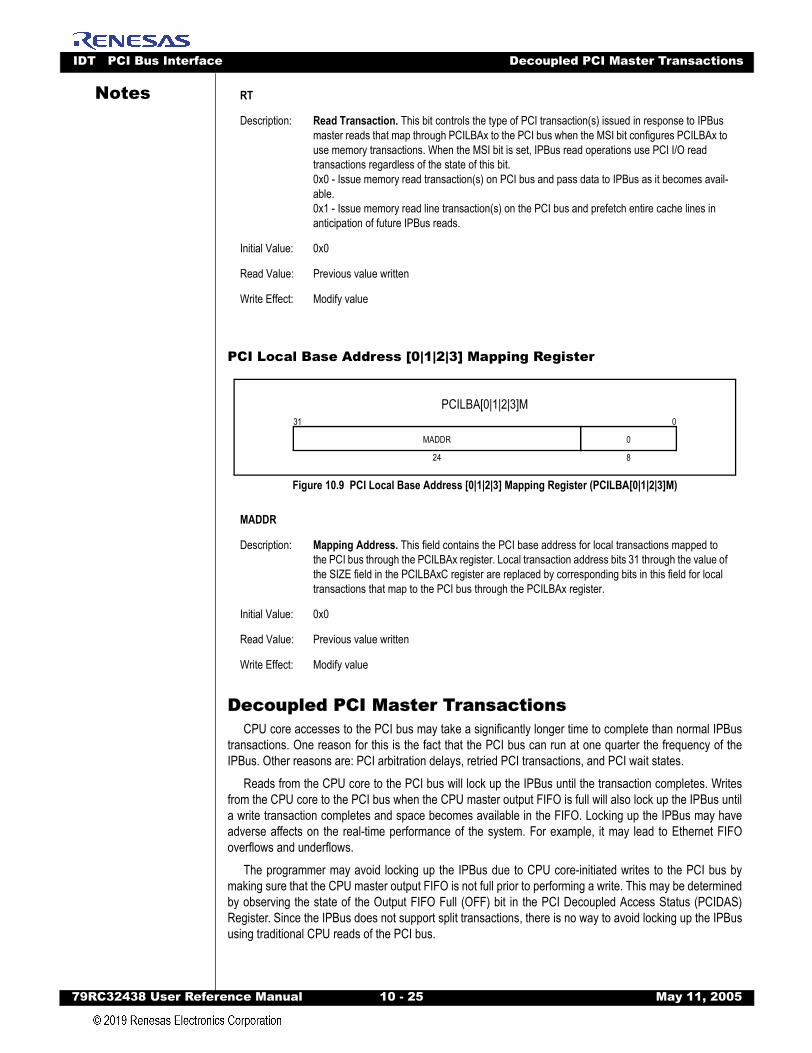
IDT PCI Bus Interface Decoupled PCI Master Transactions
79RC32438 User Refer
Notes
PCI Local Base Address [0|1|2|3] Mapping Register
Figure 10.9 PCI Local Base Address [0|1|2|3] Mapping Register (PCILBA[0|1|2|3]M)
Decoupled PCI Master TransactionsCPU core accesses to the PCI bus may take a significantly longer time to complete than normal IPBus
transactions. One reason for this is the fact that the PCI bus can run at one quarter the frequency of theIPBus. Other reasons are: PCI arbitration delays, retried PCI transactions, and PCI wait states.
Reads from the CPU core to the PCI bus will lock up the IPBus until the transaction completes. Writesfrom the CPU core to the PCI bus when the CPU master output FIFO is full will also lock up the IPBus untila write transaction completes and space becomes available in the FIFO. Locking up the IPBus may haveadverse affects on the real-time performance of the system. For example, it may lead to Ethernet FIFOoverflows and underflows.
The programmer may avoid locking up the IPBus due to CPU core-initiated writes to the PCI bus bymaking sure that the CPU master output FIFO is not full prior to performing a write. This may be determinedby observing the state of the Output FIFO Full (OFF) bit in the PCI Decoupled Access Status (PCIDAS)Register. Since the IPBus does not support split transactions, there is no way to avoid locking up the IPBususing traditional CPU reads of the PCI bus.
RT
Description: Read Transaction. This bit controls the type of PCI transaction(s) issued in response to IPBus master reads that map through PCILBAx to the PCI bus when the MSI bit configures PCILBAx to use memory transactions. When the MSI bit is set, IPBus read operations use PCI I/O read transactions regardless of the state of this bit.0x0 - Issue memory read transaction(s) on PCI bus and pass data to IPBus as it becomes avail-able.0x1 - Issue memory read line transaction(s) on the PCI bus and prefetch entire cache lines in anticipation of future IPBus reads.
Initial Value: 0x0
Read Value: Previous value written
Write Effect: Modify value
MADDR
Description: Mapping Address. This field contains the PCI base address for local transactions mapped to the PCI bus through the PCILBAx register. Local transaction address bits 31 through the value of the SIZE field in the PCILBAxC register are replaced by corresponding bits in this field for local transactions that map to the PCI bus through the PCILBAx register.
Initial Value: 0x0
Read Value: Previous value written
Write Effect: Modify value
PCILBA[0|1|2|3]M031
24
MADDR 0
8
ence Manual 10 - 25 May 11, 2005
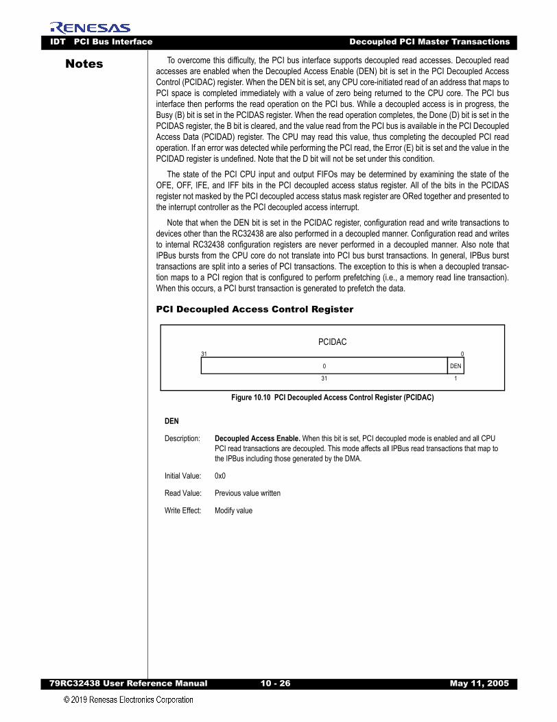
IDT PCI Bus Interface Decoupled PCI Master Transactions
79RC32438 User Refer
Notes
To overcome this difficulty, the PCI bus interface supports decoupled read accesses. Decoupled readaccesses are enabled when the Decoupled Access Enable (DEN) bit is set in the PCI Decoupled AccessControl (PCIDAC) register. When the DEN bit is set, any CPU core-initiated read of an address that maps toPCI space is completed immediately with a value of zero being returned to the CPU core. The PCI businterface then performs the read operation on the PCI bus. While a decoupled access is in progress, theBusy (B) bit is set in the PCIDAS register. When the read operation completes, the Done (D) bit is set in thePCIDAS register, the B bit is cleared, and the value read from the PCI bus is available in the PCI DecoupledAccess Data (PCIDAD) register. The CPU may read this value, thus completing the decoupled PCI readoperation. If an error was detected while performing the PCI read, the Error (E) bit is set and the value in thePCIDAD register is undefined. Note that the D bit will not be set under this condition.The state of the PCI CPU input and output FIFOs may be determined by examining the state of theOFE, OFF, IFE, and IFF bits in the PCI decoupled access status register. All of the bits in the PCIDASregister not masked by the PCI decoupled access status mask register are ORed together and presented tothe interrupt controller as the PCI decoupled access interrupt.
Note that when the DEN bit is set in the PCIDAC register, configuration read and write transactions todevices other than the RC32438 are also performed in a decoupled manner. Configuration read and writesto internal RC32438 configuration registers are never performed in a decoupled manner. Also note thatIPBus bursts from the CPU core do not translate into PCI bus burst transactions. In general, IPBus bursttransactions are split into a series of PCI transactions. The exception to this is when a decoupled transac-tion maps to a PCI region that is configured to perform prefetching (i.e., a memory read line transaction).When this occurs, a PCI burst transaction is generated to prefetch the data.
PCI Decoupled Access Control Register
Figure 10.10 PCI Decoupled Access Control Register (PCIDAC)
DEN
Description: Decoupled Access Enable. When this bit is set, PCI decoupled mode is enabled and all CPU PCI read transactions are decoupled. This mode affects all IPBus read transactions that map to the IPBus including those generated by the DMA.
Initial Value: 0x0
Read Value: Previous value written
Write Effect: Modify value
PCIDAC031
0
31
DEN
1
ence Manual 10 - 26 May 11, 2005
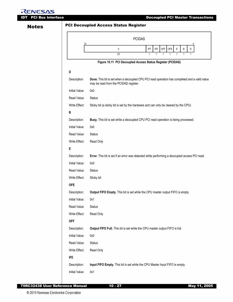
IDT PCI Bus Interface Decoupled PCI Master Transactions
79RC32438 User Refer
Notes
PCI Decoupled Access Status RegisterFigure 10.11 PCI Decoupled Access Status Register (PCIDAS)
D
Description: Done. This bit is set when a decoupled CPU PCI read operation has completed and a valid value may be read from the PCIDAD register.
Initial Value: 0x0
Read Value: Status
Write Effect: Sticky bit (a sticky bit is set by the hardware and can only be cleared by the CPU)
B
Description: Busy. This bit is set while a decoupled CPU PCI read operation is being processed.
Initial Value: 0x0
Read Value: Status
Write Effect: Read Only
E
Description: Error. This bit is set if an error was detected while performing a decoupled access PCI read.
Initial Value: 0x0
Read Value: Status
Write Effect: Sticky bit
OFE
Description: Output FIFO Empty. This bit is set while the CPU master output FIFO is empty.
Initial Value: 0x1
Read Value: Status
Write Effect: Read Only
OFF
Description: Output FIFO Full. This bit is set while the CPU master output FIFO is full.
Initial Value: 0x0
Read Value: Status
Write Effect: Read Only
IFE
Description: Input FIFO Empty. This bit is set while the CPU Master Input FIFO is empty.
Initial Value: 0x1
PCIDAS031
0
25
D
1
B
1
OFE
1
OFF
1
IFE
1
IFF
1
E
1
ence Manual 10 - 27 May 11, 2005
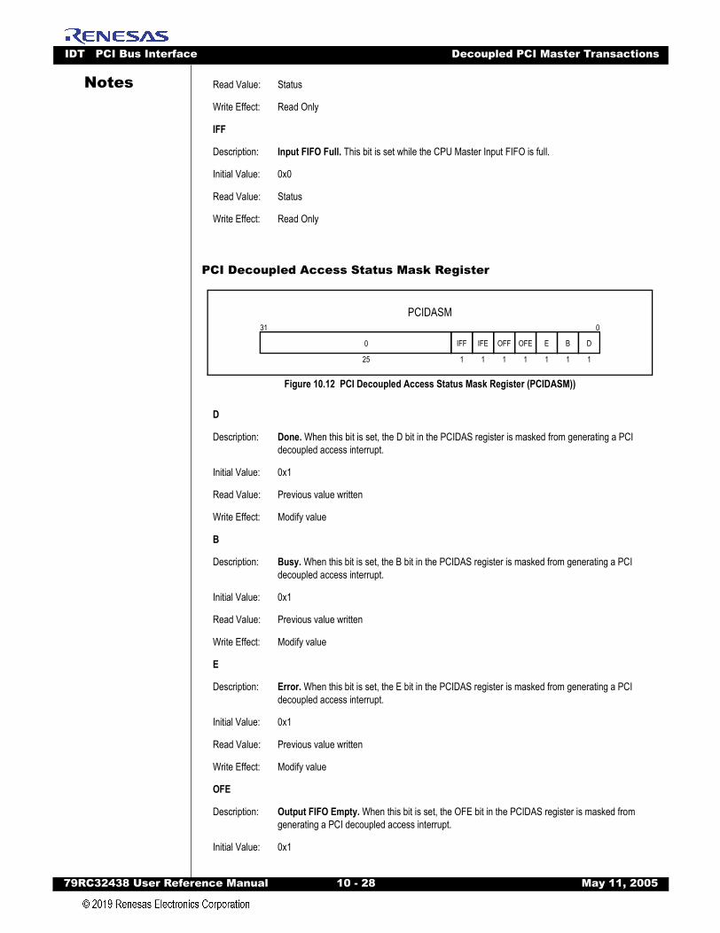
IDT PCI Bus Interface Decoupled PCI Master Transactions
79RC32438 User Refer
Notes
PCI Decoupled Access Status Mask Register
Figure 10.12 PCI Decoupled Access Status Mask Register (PCIDASM))
Read Value: Status
Write Effect: Read Only
IFF
Description: Input FIFO Full. This bit is set while the CPU Master Input FIFO is full.
Initial Value: 0x0
Read Value: Status
Write Effect: Read Only
D
Description: Done. When this bit is set, the D bit in the PCIDAS register is masked from generating a PCI decoupled access interrupt.
Initial Value: 0x1
Read Value: Previous value written
Write Effect: Modify value
B
Description: Busy. When this bit is set, the B bit in the PCIDAS register is masked from generating a PCI decoupled access interrupt.
Initial Value: 0x1
Read Value: Previous value written
Write Effect: Modify value
E
Description: Error. When this bit is set, the E bit in the PCIDAS register is masked from generating a PCI decoupled access interrupt.
Initial Value: 0x1
Read Value: Previous value written
Write Effect: Modify value
OFE
Description: Output FIFO Empty. When this bit is set, the OFE bit in the PCIDAS register is masked from generating a PCI decoupled access interrupt.
Initial Value: 0x1
PCIDASM031
0
25
D
1
B
1
OFE
1
OFF
1
IFE
1
IFF
1
E
1
ence Manual 10 - 28 May 11, 2005

IDT PCI Bus Interface Decoupled PCI Master Transactions
79RC32438 User Refer
Notes
PCI Decoupled Access Data Register
Figure 10.13 PCI Decoupled Access Data Register (PCIDAD)
Read Value: Previous value written
Write Effect: Modify value
OFF
Description: Output FIFO Full. When this bit is set, the OFF bit in the PCIDAS register is masked from gen-erating a PCI decoupled access interrupt.
Initial Value: 0x1
Read Value: Previous value written
Write Effect: Modify value
IFE
Description: Input FIFO Empty. When this bit is set, the IFE bit in the PCIDAS register is masked from gen-erating a PCI decoupled access interrupt.
Initial Value: 0x1
Read Value: Previous value written
Write Effect: Modify value
IFF
Description: Input FIFO Full. When this bit is set, the IFF bit in the PCIDAS register is masked from generat-ing a PCI decoupled access interrupt.
Initial Value: 0x1
Read Value: Previous value written
Write Effect: Modify value
DATA
Description: Data Field. This register contains the return value of a decoupled PCI CPU read operation.
Initial Value: 0x0
Read Value: Return value of previously initiated decoupled PCI CPU read operation
Write Effect: Modify value
PCIDAD031
DATA
32
ence Manual 10 - 29 May 11, 2005
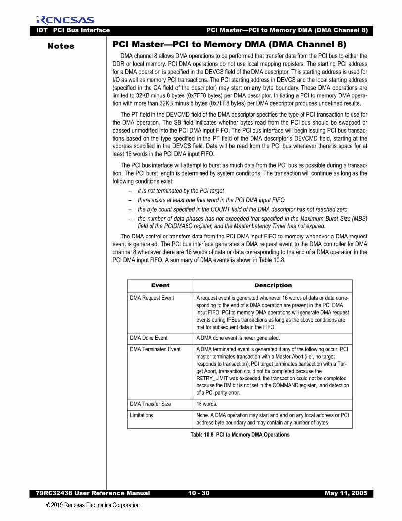
IDT PCI Bus Interface PCI Master—PCI to Memory DMA (DMA Channel 8)
79RC32438 User Refer
Notes
PCI Master—PCI to Memory DMA (DMA Channel 8)DMA channel 8 allows DMA operations to be performed that transfer data from the PCI bus to either theDDR or local memory. PCI DMA operations do not use local mapping registers. The starting PCI addressfor a DMA operation is specified in the DEVCS field of the DMA descriptor. This starting address is used forI/O as well as memory PCI transactions. The PCI starting address in DEVCS and the local starting address(specified in the CA field of the descriptor) may start on any byte boundary. These DMA operations arelimited to 32KB minus 8 bytes (0x7FF8 bytes) per DMA descriptor. Initiating a PCI to memory DMA opera-tion with more than 32KB minus 8 bytes (0x7FF8 bytes) per DMA descriptor produces undefined results.
The PT field in the DEVCMD field of the DMA descriptor specifies the type of PCI transaction to use forthe DMA operation. The SB field indicates whether bytes read from the PCI bus should be swapped orpassed unmodified into the PCI DMA input FIFO. The PCI bus interface will begin issuing PCI bus transac-tions based on the type specified in the PT field of the DMA descriptor’s DEVCMD field, starting at theaddress specified in the DEVCS field. Data will be read from the PCI bus whenever there is space for atleast 16 words in the PCI DMA input FIFO.
The PCI bus interface will attempt to burst as much data from the PCI bus as possible during a transac-tion. The PCI burst length is determined by system conditions. The transaction will continue as long as thefollowing conditions exist:
– it is not terminated by the PCI target – there exists at least one free word in the PCI DMA input FIFO – the byte count specified in the COUNT field of the DMA descriptor has not reached zero– the number of data phases has not exceeded that specified in the Maximum Burst Size (MBS)
field of the PCIDMA8C register, and the Master Latency Timer has not expired.The DMA controller transfers data from the PCI DMA input FIFO to memory whenever a DMA request
event is generated. The PCI bus interface generates a DMA request event to the DMA controller for DMAchannel 8 whenever there are 16 words of data or data corresponding to the end of a DMA operation in thePCI DMA input FIFO. A summary of DMA events is shown in Table 10.8.
Event Description
DMA Request Event A request event is generated whenever 16 words of data or data corre-sponding to the end of a DMA operation are present in the PCI DMA input FIFO. PCI to memory DMA operations will generate DMA request events during IPBus transactions as long as the above conditions are met for subsequent data in the FIFO.
DMA Done Event A DMA done event is never generated.
DMA Terminated Event A DMA terminated event is generated if any of the following occur: PCI master terminates transaction with a Master Abort (i.e., no target responds to transaction), PCI target terminates transaction with a Tar-get Abort, transaction could not be completed because the RETRY_LIMIT was exceeded, the transaction could not be completed because the BM bit is not set in the COMMAND register, and detection of a PCI parity error.
DMA Transfer Size 16 words.
Limitations None. A DMA operation may start and end on any local address or PCI address byte boundary and may contain any number of bytes
Table 10.8 PCI to Memory DMA Operations
ence Manual 10 - 30 May 11, 2005
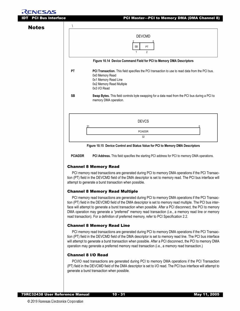
IDT PCI Bus Interface PCI Master—PCI to Memory DMA (DMA Channel 8)
79RC32438 User Refer
Notes
\Figure 10.14 Device Command Field for PCI to Memory DMA Descriptors
Figure 10.15 Device Control and Status Value for PCI to Memory DMA Descriptors
Channel 8 Memory ReadPCI memory read transactions are generated during PCI to memory DMA operations if the PCI Transac-
tion (PT) field in the DEVCMD field of the DMA descriptor is set to memory read. The PCI bus interface willattempt to generate a burst transaction when possible.
Channel 8 Memory Read MultiplePCI memory read transactions are generated during PCI to memory DMA operations if the PCI Transac-
tion (PT) field in the DEVCMD field of the DMA descriptor is set to memory read multiple. The PCI bus inter-face will attempt to generate a burst transaction when possible. After a PCI disconnect, the PCI to memoryDMA operation may generate a “preferred” memory read transaction (i.e., a memory read line or memoryread transaction). For a definition of preferred memory, refer to PCI Specification 2.2.
Channel 8 Memory Read LinePCI memory read transactions are generated during PCI to memory DMA operations if the PCI Transac-
tion (PT) field in the DEVCMD field of the DMA descriptor is set to memory read line. The PCI bus interfacewill attempt to generate a burst transaction when possible. After a PCI disconnect, the PCI to memory DMAoperation may generate a preferred memory read transaction (i.e., a memory read transaction.)
Channel 8 I/O ReadPCI/IO read transactions are generated during PCI to memory DMA operations if the PCI Transaction
(PT) field in the DEVCMD field of the DMA descriptor is set to I/O read. The PCI bus interface will attempt togenerate a burst transaction when possible.
PT PCI Transaction. This field specifies the PCI transaction to use to read data from the PCI bus.0x0 Memory Read0x1 Memory Read Line0x2 Memory Read Multiple0x3 I/O Read
SB Swap Bytes. This field controls byte swapping for a data read from the PCI bus during a PCI to memory DMA operation.
PCIADDR PCI Address. This field specifies the starting PCI address for PCI to memory DMA operations.
DEVCMD2
2
PT
0
1
SB
DEVCS031
32
PCIADDR
ence Manual 10 - 31 May 11, 2005

IDT PCI Bus Interface PCI Master—PCI to Memory DMA (DMA Channel 8)
79RC32438 User Refer
Notes
Channel 8 Error HandlingPCI to memory fatal errors are:– PCI target terminates with a Target Abort– transaction could not be completed because the RETRY_LIMIT was exceeded– transaction could not be completed because the BM bit is not set in the COMMAND register– detection of a PCI parity error.
If any of the above fatal errors are detected during a DMA operation, the DMA operation is halted with aterminated condition (i.e., the T bit is set in the descriptor) and the DMA descriptor’s DEVCS field isupdated with the address of the error. The DMA descriptor’s Current Address (CA) field contains theaddress to which the data (where the error occurred) should have been written. Note that no write actuallytakes place. The COUNT field contains the actual number of bytes transferred. All data queued in the PCIDMA input FIFO before the error occurred is written to memory before the DMA operation is halted.
PCI DMA Channel 8 Configuration Register
Figure 10.16 PCI DMA Channel 8 Configuration Register (PCIDMA8C)
MBS
Description: Maximum Burst Size. This field specifies the maximum number of words allowed in a PCI to memory DMA operation. A value of 0x0 corresponds to 0x1000 (i.e., 4K word transfer).
Initial Value: 0x8
Read Value: Previous value written
Write Effect: Modify value
OUR
Description: Optimize Unaligned Burst Reads. When this bit is cleared, the PCI interface honors byte enables at the start and end of unaligned PCI burst read transfers generated by the DMA control-ler. This results in the PCI interface potentially generating three separate transactions for a sin-gle unaligned DMA burst read transfer; one PCI transaction for the partial byte transfer at the start of the burst, one PCI transaction for the aligned portion of the burst transfer, and one PCI transaction for the partial byte transfer at the end of the burst transfer. These three transactions are treated by the PCI interface as three independent transactions.In most cases, byte enables generated during partial word PCI memory transactions are irrele-vant as they have no side effect. Thus, entire words could simply have been read from memory and unneeded data discarded. When this bit is set during a DMA read transfer that is pro-grammed to generate Memory Read, Memory Read Line, or Memory Read Multiple transactions, then the PCI interface will read complete words and discard unneeded data. This improves unaligned PCI burst read transfer performance as it allows an entire burst read transfer gener-ated by the DMA controller to be serviced as one PCI transaction.
Initial Value: 0x0
Read Value: Previous value written
Write Effect: Modify value
PCIDMA8C031
12
MBS
19
0
1
OUR
ence Manual 10 - 32 May 11, 2005
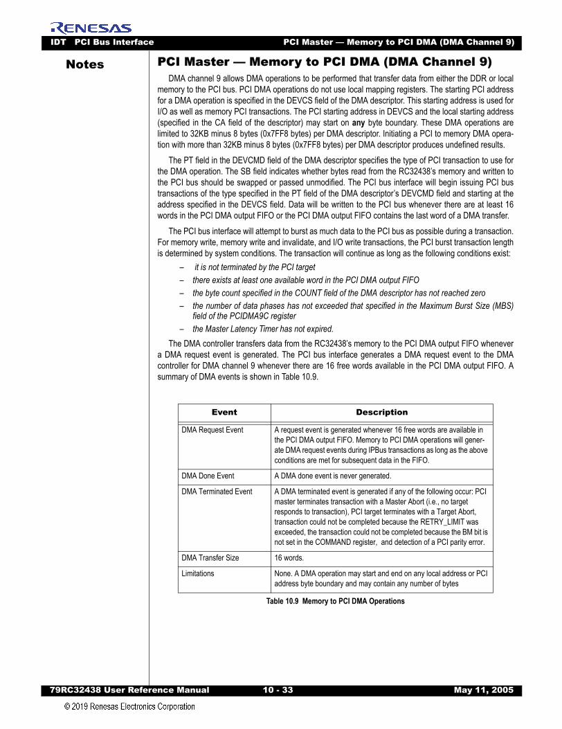
IDT PCI Bus Interface PCI Master — Memory to PCI DMA (DMA Channel 9)
79RC32438 User Refer
Notes
PCI Master — Memory to PCI DMA (DMA Channel 9)DMA channel 9 allows DMA operations to be performed that transfer data from either the DDR or localmemory to the PCI bus. PCI DMA operations do not use local mapping registers. The starting PCI addressfor a DMA operation is specified in the DEVCS field of the DMA descriptor. This starting address is used forI/O as well as memory PCI transactions. The PCI starting address in DEVCS and the local starting address(specified in the CA field of the descriptor) may start on any byte boundary. These DMA operations arelimited to 32KB minus 8 bytes (0x7FF8 bytes) per DMA descriptor. Initiating a PCI to memory DMA opera-tion with more than 32KB minus 8 bytes (0x7FF8 bytes) per DMA descriptor produces undefined results.
The PT field in the DEVCMD field of the DMA descriptor specifies the type of PCI transaction to use forthe DMA operation. The SB field indicates whether bytes read from the RC32438’s memory and written tothe PCI bus should be swapped or passed unmodified. The PCI bus interface will begin issuing PCI bustransactions of the type specified in the PT field of the DMA descriptor’s DEVCMD field and starting at theaddress specified in the DEVCS field. Data will be written to the PCI bus whenever there are at least 16words in the PCI DMA output FIFO or the PCI DMA output FIFO contains the last word of a DMA transfer.
The PCI bus interface will attempt to burst as much data to the PCI bus as possible during a transaction.For memory write, memory write and invalidate, and I/O write transactions, the PCI burst transaction lengthis determined by system conditions. The transaction will continue as long as the following conditions exist:
– it is not terminated by the PCI target– there exists at least one available word in the PCI DMA output FIFO– the byte count specified in the COUNT field of the DMA descriptor has not reached zero– the number of data phases has not exceeded that specified in the Maximum Burst Size (MBS)
field of the PCIDMA9C register– the Master Latency Timer has not expired.
The DMA controller transfers data from the RC32438’s memory to the PCI DMA output FIFO whenevera DMA request event is generated. The PCI bus interface generates a DMA request event to the DMAcontroller for DMA channel 9 whenever there are 16 free words available in the PCI DMA output FIFO. Asummary of DMA events is shown in Table 10.9.
Event Description
DMA Request Event A request event is generated whenever 16 free words are available in the PCI DMA output FIFO. Memory to PCI DMA operations will gener-ate DMA request events during IPBus transactions as long as the above conditions are met for subsequent data in the FIFO.
DMA Done Event A DMA done event is never generated.
DMA Terminated Event A DMA terminated event is generated if any of the following occur: PCI master terminates transaction with a Master Abort (i.e., no target responds to transaction), PCI target terminates with a Target Abort, transaction could not be completed because the RETRY_LIMIT was exceeded, the transaction could not be completed because the BM bit is not set in the COMMAND register, and detection of a PCI parity error.
DMA Transfer Size 16 words.
Limitations None. A DMA operation may start and end on any local address or PCI address byte boundary and may contain any number of bytes
Table 10.9 Memory to PCI DMA Operations
ence Manual 10 - 33 May 11, 2005
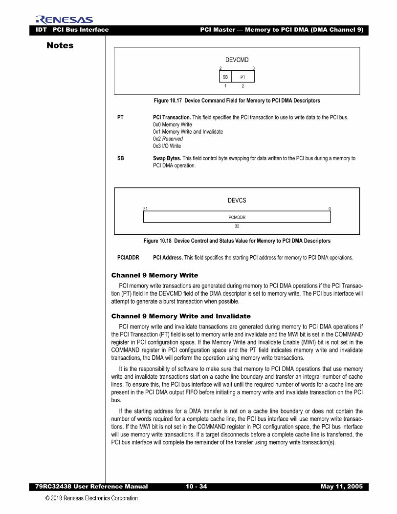
IDT PCI Bus Interface PCI Master — Memory to PCI DMA (DMA Channel 9)
79RC32438 User Refer
Notes
Figure 10.17 Device Command Field for Memory to PCI DMA Descriptors
Figure 10.18 Device Control and Status Value for Memory to PCI DMA Descriptors
Channel 9 Memory WritePCI memory write transactions are generated during memory to PCI DMA operations if the PCI Transac-
tion (PT) field in the DEVCMD field of the DMA descriptor is set to memory write. The PCI bus interface willattempt to generate a burst transaction when possible.
Channel 9 Memory Write and InvalidatePCI memory write and invalidate transactions are generated during memory to PCI DMA operations if
the PCI Transaction (PT) field is set to memory write and invalidate and the MWI bit is set in the COMMANDregister in PCI configuration space. If the Memory Write and Invalidate Enable (MWI) bit is not set in theCOMMAND register in PCI configuration space and the PT field indicates memory write and invalidatetransactions, the DMA will perform the operation using memory write transactions.
It is the responsibility of software to make sure that memory to PCI DMA operations that use memorywrite and invalidate transactions start on a cache line boundary and transfer an integral number of cachelines. To ensure this, the PCI bus interface will wait until the required number of words for a cache line arepresent in the PCI DMA output FIFO before initiating a memory write and invalidate transaction on the PCIbus.
If the starting address for a DMA transfer is not on a cache line boundary or does not contain thenumber of words required for a complete cache line, the PCI bus interface will use memory write transac-tions. If the MWI bit is not set in the COMMAND register in PCI configuration space, the PCI bus interfacewill use memory write transactions. If a target disconnects before a complete cache line is transferred, thePCI bus interface will complete the remainder of the transfer using memory write transaction(s).
PT PCI Transaction. This field specifies the PCI transaction to use to write data to the PCI bus.0x0 Memory Write0x1 Memory Write and Invalidate0x2 Reserved0x3 I/O Write
SB Swap Bytes. This field control byte swapping for data written to the PCI bus during a memory to PCI DMA operation.
PCIADDR PCI Address. This field specifies the starting PCI address for memory to PCI DMA operations.
DEVCMD2
2
PT
0
1
SB
DEVCS031
32
PCIADDR
ence Manual 10 - 34 May 11, 2005
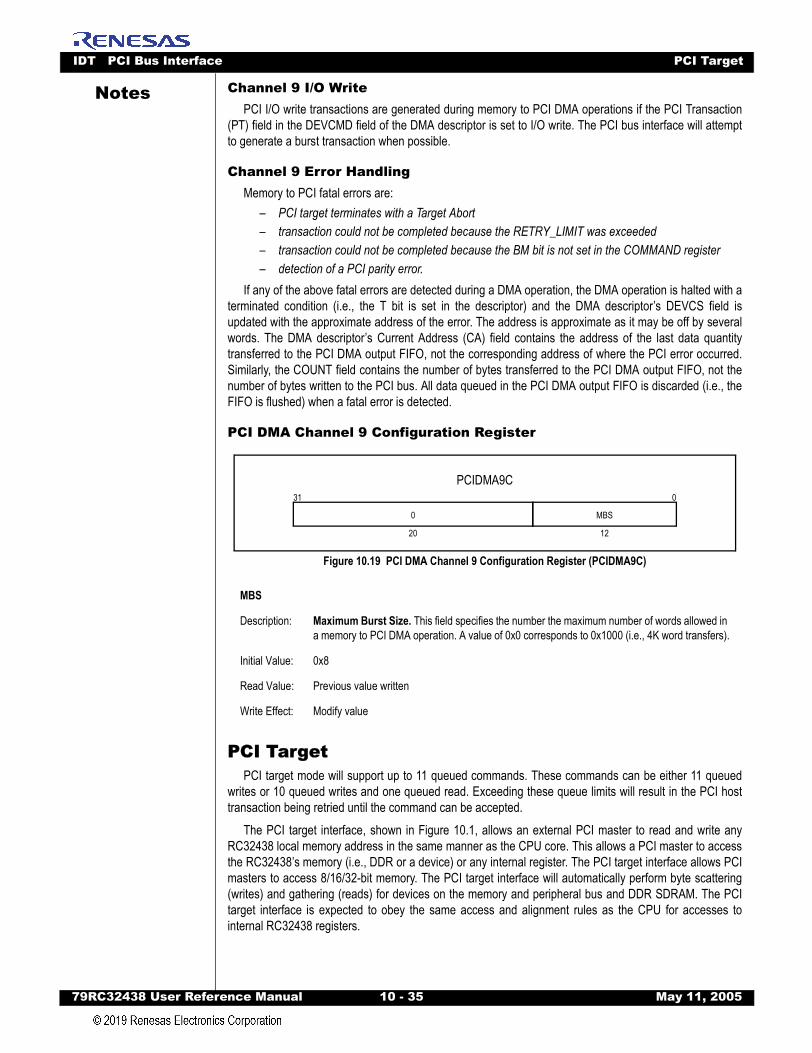
IDT PCI Bus Interface PCI Target
79RC32438 User Refer
Notes
Channel 9 I/O WritePCI I/O write transactions are generated during memory to PCI DMA operations if the PCI Transaction(PT) field in the DEVCMD field of the DMA descriptor is set to I/O write. The PCI bus interface will attemptto generate a burst transaction when possible.
Channel 9 Error HandlingMemory to PCI fatal errors are:
– PCI target terminates with a Target Abort– transaction could not be completed because the RETRY_LIMIT was exceeded– transaction could not be completed because the BM bit is not set in the COMMAND register– detection of a PCI parity error.
If any of the above fatal errors are detected during a DMA operation, the DMA operation is halted with aterminated condition (i.e., the T bit is set in the descriptor) and the DMA descriptor’s DEVCS field isupdated with the approximate address of the error. The address is approximate as it may be off by severalwords. The DMA descriptor’s Current Address (CA) field contains the address of the last data quantitytransferred to the PCI DMA output FIFO, not the corresponding address of where the PCI error occurred.Similarly, the COUNT field contains the number of bytes transferred to the PCI DMA output FIFO, not thenumber of bytes written to the PCI bus. All data queued in the PCI DMA output FIFO is discarded (i.e., theFIFO is flushed) when a fatal error is detected.
PCI DMA Channel 9 Configuration Register
Figure 10.19 PCI DMA Channel 9 Configuration Register (PCIDMA9C)
PCI TargetPCI target mode will support up to 11 queued commands. These commands can be either 11 queued
writes or 10 queued writes and one queued read. Exceeding these queue limits will result in the PCI hosttransaction being retried until the command can be accepted.
The PCI target interface, shown in Figure 10.1, allows an external PCI master to read and write anyRC32438 local memory address in the same manner as the CPU core. This allows a PCI master to accessthe RC32438’s memory (i.e., DDR or a device) or any internal register. The PCI target interface allows PCImasters to access 8/16/32-bit memory. The PCI target interface will automatically perform byte scattering(writes) and gathering (reads) for devices on the memory and peripheral bus and DDR SDRAM. The PCItarget interface is expected to obey the same access and alignment rules as the CPU for accesses tointernal RC32438 registers.
MBS
Description: Maximum Burst Size. This field specifies the number the maximum number of words allowed in a memory to PCI DMA operation. A value of 0x0 corresponds to 0x1000 (i.e., 4K word transfers).
Initial Value: 0x8
Read Value: Previous value written
Write Effect: Modify value
PCIDMA9C031
12
MBS
20
0
ence Manual 10 - 35 May 11, 2005
IDT PCI Bus Interface PCI Target
79RC32438 User Refer
Notes
The PCI bus interface provides four mapping regions from the PCI space to the RC32438’s localaddress space. Each mapping region has a corresponding PCI Base Address (PBAx) register, PCI BaseAddress Control (PBAxC) register, and PCI Base Address Mapping (PBAxM) register. These registers areall part of the PCI configuration. The PBAx registers correspond to the BAR registers in PCI Specification2.2. Their initial values and configuration, however, are controlled by the PBAxC register. The PBAxCregister holds the configuration information for the mapping region.The Memory Space Indicator (MSI) field in a PBAxC controls how space is advertised (I/O or memory).If the space is advertised by the MSI as memory, the Prefetchable (P) bit controls prefetching. If the spaceis advertised as I/O, the Prefetchable bit is inactive. The Swap Bytes (SB) field in a PBAxC controls whetherbytes are swapped or passed unmodified between the IPBus and the PCI bus when the PCI bus interface isaccessed as a target. The PBAxM register holds the local address space base address of PCI transactionsthat map to the local address space through PBAx.
The local address mapped by a PBAxM register may be any valid local address. These local addressesare decoded in the same manner as CPU physical addresses. The local addresses mapped by one or morePBAxM registers may be overlapping. PCI Base Addresses in PBAx registers should be non-overlapping. Ifthey are overlapping, one will be chosen.
PCI target burst transactions which attempt to burst data beyond the address space allocated to a PBAxwill terminate with a target disconnect without data. The PCI address spaces mapped by two PBAx regis-ters may be contiguous. PCI target burst transactions which attempt to burst data across adjacent addressspaces mapped by PBAx registers will terminate with a target disconnect without data. The PCI TargetControl Register (PCITC) contains fields which control the behavior of the PCI bus interface when acting asa PCI target.
The retry timer controls the number of PCI clock cycles the PCI interface will wait for the first data of anaccess before issuing a retry. This is used during read operations (i.e., memory read, memory readmultiple, memory read line, and I/O read) to specify the number of PCI clock cycles the PCI bus interface isallowed (delay supplying the first data quantity of a transaction) before the transaction must be retried.During write operations (i.e., memory write, memory write and invalidate, and I/O write), this field specifiesthe number of PCI clock cycles the PCI bus interface is allowed to wait for space to appear in the PCI targetinput FIFO before a transaction must be retried.
The initial value for the retry timer is specified in the Retry Timer (RTIMER) field of the PCITC register.PCI Specification 2.2 sets the maximum to 16 PCI clock cycles, but the RC32438 allows this limit to beextended to 255 clock cycles. The disconnect timer controls the number of PCI clock cycles the PCI inter-face will wait for between data transfers. If the PCI bus interface is unable to accept data before the timerexpires, it issues a disconnect. PCI Specification 2.2 sets the maximum to 8 PCI clock cycles, but theRC32438 allows this limit to be extended to 255 clock cycles.
The PCI bus interface supports target delayed reads. The PCI bus interface supports only one pendingdelayed read. If a read is attempted while a delayed read is pending, the transaction is retried and adelayed read is not initiated for the transaction. The PCI master that initiates a delayed read is expected toretry the transaction until the read completes. The PCI bus interface contains a discard timer. If the masterdoes not repeat a delayed read request within 215 clock cycles, the discard timer will expire and discard thepending read. This is necessary to ensure that a malfunctioning PCI master (e.g., one which has a pendingdelayed read) does not cause the RC32438 to deadlock. If the discard timer expires and a pending read isdiscarded, the Pending Read Discarded (PRD) bit is set in the PCIS register. The discard timer may bedisabled by setting the Disable Discard Timer (DDT) bit in the PCITC register.
The PCI transaction ordering constraints may be viewed as favoring target write operations since only asingle delayed read is allowed when there are posted writes. By contrast, multiple posted writes are allowedwhen there is a delayed read. In an effort to provide some level of fairness, the PCI bus interface supportsa mode in which all transactions are retried when there is a delayed read. When the Retry when DelayedRead (RDR) bit is set in the PCITC register, all PCI target transactions are retired as long as there is apending delayed read.
ence Manual 10 - 36 May 11, 2005
IDT PCI Bus Interface PCI Target
79RC32438 User Refer
Notes
The PCI bus interface allows normal PCI target transaction ordering constraints to be overridden forimproved efficiency in some system scenarios. For more information, see the Transaction Ordering sectionlater in this chapter. The PCI bus interface supports target locking. Once a lock has been established, allPCI target transactions to the RC32438 are retried until the lock has been released. The RC32438 does notimplement locked operations on the IPBus. Therefore, lock operations are only useful for creating atomicsequences as seen by masters on the PCI bus.The RC32438 does not support IPBus master accesses to PCI addresses that map to its PCI targetinterface. An IPBus master access to a PCI address that maps to the RC32438’s PCI target interfaceresults in a master abort. Also, the RC32438 does not support PCI bus master accesses to the RC32438’slocal memory that maps to PCI space. These operations do not damage hardware, but their results areundefined.
Target I/O ReadPCI I/O read transactions that map to a PCI Base Address (PBAx) register are converted to local IPBus
read operations. Data from an I/O read transaction is translated using the PBAxM register into a local IPBusaddress. PCI I/O read transactions are not allowed to burst.
The PCI memory write maximum completion time limit of 10 microseconds (see section 3.5.3 in PCISpecification 2.2) is met under normal system conditions, but this limit may be violated in some systemconfigurations. For example, setting the RDR bit may violate this specification. Another example is whenPCI target bus requests are masked in the IPBus arbiter. It is the responsibility of the system designer(hardware and software) to guarantee adherence to this requirement.
Target I/O WritePCI I/O write transactions that map to a PCI Base Address (PBAx) register are converted to local IPBus
write operations and posted to the PCI target input FIFO. PCI I/O write transactions are posted to the PCItarget input FIFO and are not allowed to burst.
Target Memory ReadPCI memory read transactions that map to a PCI Base Address (PBAx) register are mapped to local
IPBus read operation(s). The behavior of PCI target memory read operations is determined by the state ofthe Memory Read Behavior (MR) field in the corresponding PBAxC register. If MR field is 0x0, the memoryread behaves as described below. If the MR field is 0x1, the memory read transaction behaves in the samemanner as a memory read line transaction. If the MR field is 0x2, the memory read transaction behaves inthe same manner as a memory read multiple transaction.
PCI memory read transactions that map to a PCI Base Address (PBAx) register are mapped to a localIPBus word read operation. PCI memory read transactions are not allowed to burst unless the memory readis mapped to a memory read line or memory read multiple.
Target Memory WritePCI memory write transactions that map to a PCI Base Address (PBAx) register are mapped to a local
IPBus write operation(s) and posted into the PCI target input FIFO. The PCI bus interface will attempt toextend memory write burst transaction for as long as possible. A burst transaction will be retried by theRC32438 if the PCI target input FIFO is full for a period of time which exceeds the programmed RTIMER/DTIMER value in the PCITC register.
Target Configuration ReadPCI configuration read transactions return the value of the register in PCI configuration space with
address PCIAD[7:2]. The PCI bus interface does not support target burst configuration read transactions. Ifa configuration read transaction consists of more than a single data phase, the target will terminate thetransaction with a disconnect.
ence Manual 10 - 37 May 11, 2005
IDT PCI Bus Interface PCI Target
79RC32438 User Refer
Notes
Target Configuration WritePCI configuration write transactions return the value of the register in PCI configuration space withaddress PCIAD[7:2]. The PCI bus interface will use the byte enables to determine which bytes of the wordaddress by PCIAD[7:2] are being modified. The PCI bus interface does not support target burst configura-tion write transaction. If a configuration write transaction consists of more than a single data phase, thetarget will terminate the transaction with a disconnect.
Target Memory Read MultiplePCI memory read multiple transactions that map to a PCI Base Address (PBAx) register are mapped to
local IPBus read operations. Memory read multiple transactions fetch not only the data requested by thedata phase of the transaction but cause the PCI bus interface to prefetch additional data. The prefetchingbehavior is controlled by the Memory Read Multiple Prefetching Behavior (MRM) bit. If cleared, the PCI businterface performs conservative prefetching. Otherwise, the PCI bus interface performs aggressiveprefetching.
In conservative prefetching, the PCI bus interface will prefetch 16 words whenever a memory readmultiple transaction is in progress and there are less than 8 words available in the PCI target output FIFO.In aggressive prefetching, the PCI bus interface will continue prefetching bursts of 16 words as long asroom exists in the PCI target output FIFO. The PCI target output FIFO will discard prefetched data in theFIFO when a memory read line multiple burst transaction completes.
Target Memory Read LinePCI memory read multiple transactions that map to a PCI Base Address (PBAx) register are mapped to
local IPBus read operations. The prefetching behavior is controlled by the Memory Read Line PrefetchingBehavior (MRL) bit. If cleared, the PCI bus interface will prefetch data to the end of the cache line. If theMRL bit is set, the PCI bus interface will translate a memory read line transaction to a memory read multipletransaction.
Target Memory Write and InvalidatePCI memory write and invalidate transactions that map to a PCI Base Address (PBAx) register are
translated into memory write transactions.
Target Error HandlingData parity errors detected during target transactions are handled as defined in PCI Specification 2.2
(i.e., the PE bit in the STATUS register is set and PERRN is asserted if the PEN bit is set in the COMMANDregister) and the transaction is completed as though no error was detected (i.e., writes are performed andreads deliver possibly corrupted data).
Address parity errors detected during target read transactions result in termination of the transactionwith a Target Abort. An IPbus transaction is not generated when an address parity error is detected during atarget read transaction. Address parity errors detected during target write transactions result in terminationof the transaction with a Target Abort. An IPbus transaction is not generated when an address parity error isdetected during a target write transaction.
The PCI bus interface terminates a target read or write transaction with a Target Abort if the addressspace monitor detects a PCI master attempting to access an invalid local address range. For more informa-tion, refer to the Address Space Monitor section in Chapter 4, System Integrity Functions. If the transactionwas a delayed read, a target abort is signaled when the transaction is retried. If the PCI transaction was aposted write, the transaction is viewed as completed by the PCI bus master and results in the PCI bus inter-face signalling a PCI system error by asserting SERRN for one PCI clock cycle if the System Error Enable(SEN) and Parity Error Enable (PEN) bits are set in the COMMAND register.
An address space monitor error detected during servicing of a posted target write transaction may resultin multiple assertions of SERRN. Data for a posted write transaction is queued in the PCI target input FIFOand segmented into one or more IPBus transactions. Each IPBus transaction is treated independently. If anundecoded address is detected in an IPBus transaction, the remaining IPBus transaction data in the input
ence Manual 10 - 38 May 11, 2005
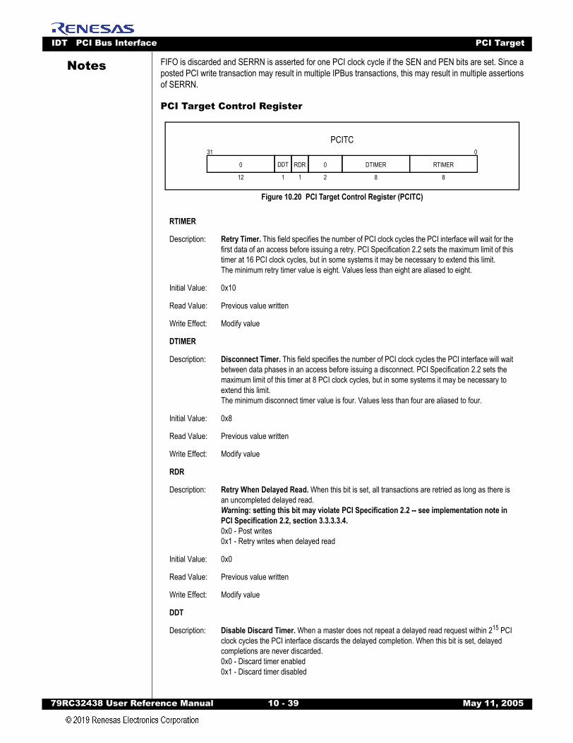
IDT PCI Bus Interface PCI Target
79RC32438 User Refer
Notes
FIFO is discarded and SERRN is asserted for one PCI clock cycle if the SEN and PEN bits are set. Since aposted PCI write transaction may result in multiple IPBus transactions, this may result in multiple assertionsof SERRN.PCI Target Control Register
Figure 10.20 PCI Target Control Register (PCITC)
RTIMER
Description: Retry Timer. This field specifies the number of PCI clock cycles the PCI interface will wait for the first data of an access before issuing a retry. PCI Specification 2.2 sets the maximum limit of this timer at 16 PCI clock cycles, but in some systems it may be necessary to extend this limit.The minimum retry timer value is eight. Values less than eight are aliased to eight.
Initial Value: 0x10
Read Value: Previous value written
Write Effect: Modify value
DTIMER
Description: Disconnect Timer. This field specifies the number of PCI clock cycles the PCI interface will wait between data phases in an access before issuing a disconnect. PCI Specification 2.2 sets the maximum limit of this timer at 8 PCI clock cycles, but in some systems it may be necessary to extend this limit.The minimum disconnect timer value is four. Values less than four are aliased to four.
Initial Value: 0x8
Read Value: Previous value written
Write Effect: Modify value
RDR
Description: Retry When Delayed Read. When this bit is set, all transactions are retried as long as there is an uncompleted delayed read.Warning: setting this bit may violate PCI Specification 2.2 -- see implementation note in PCI Specification 2.2, section 3.3.3.3.4.0x0 - Post writes0x1 - Retry writes when delayed read
Initial Value: 0x0
Read Value: Previous value written
Write Effect: Modify value
DDT
Description: Disable Discard Timer. When a master does not repeat a delayed read request within 215 PCI clock cycles the PCI interface discards the delayed completion. When this bit is set, delayed completions are never discarded.0x0 - Discard timer enabled0x1 - Discard timer disabled
PCITC031
12
0 RTIMER
8
DTIMER
8
DDT
1
RDR
1 2
0
ence Manual 10 - 39 May 11, 2005
IDT PCI Bus Interface Transaction Ordering
79RC32438 User Refer
Notes
Transaction OrderingIPBus master (i.e., CPU) reads and writes to the PCI bus maintain the total ordering defined by the
ordering of transactions on the IPBus. IPBus master PCI read and write transactions are given precedenceover PCI DMA read and write operations.
PCI DMA read and write operations are given fair access to the PCI bus. This means that if PCI toMemory and Memory to PCI DMA operations are in progress, access to the PCI bus will alternate betweenPCI DMA reads and PCI DMA writes. Prefetched data in the CPU master input FIFO is flushed if an IPBusmaster write is performed that maps to the PCI bus. IPBus master writes may be posted in the CPU masteroutput FIFO. A IPBus master read from the PCI bus cannot complete until all posted writes in the CPUmaster output FIFO have completed.
Software may use the IPbus master (i.e., CPU) read/write ordering constraints to flush the CPU masteroutput FIFO. A CPU read will not complete until all writes in the CPU master output FIFO have completed.No ordering constraints are enforced between CPU and DMA transactions. No ordering constraints areenforced between PCI to Memory and Memory to PCI DMA operations.
A PCI to Memory DMA operation completes when the last data quantity of the DMA operation is writtento the RC32438’s local memory (i.e., DDR or device). A Memory to PCI DMA operation completes when thelast data quantity of the DMA operation is written to the PCI. This implies that the PCI DMA output FIFO canonly contain data associated with one DMA operation at a time.
Target writes which are posted by the PCI bus interface must complete in the order in which theyoccurred on the PCI bus. No ordering constraints are enforced between writes posted by an IPBus master(i.e., CPU core) and by an external PCI master to the RC32438’s PCI target interface.
Due to transaction ordering constraints, a PCI target read is not allowed to complete as long as thereare posted writes in the PCI target input FIFO. The RC32438 will retry the read if it cannot be completed inthe allotted time. The PCI target interface supports one delayed read. The delayed read cannot completeuntil all previous posted writes have completed.
The PCI transaction ordering constraints may be viewed as favoring target write operations since only asingle delayed read is allowed when there are posted writes, while multiple posted writes are allowed whenthere is a delayed read. In an effort to provide some level of fairness, the PCI bus interface supports a modein which all transactions are retried when there is a delayed read. When the Retry when Delayed Read(RDR) bit is set in the PCITC register, all PCI target transactions are retired as long as there is a pendingdelayed read.
In some system scenarios, it may be desirable to violate PCI target transaction ordering constraints inorder to improve performance. Normally, a PCI target read is not allowed to complete until all previouslyposted writes to the target have completed. In situations where one can guarantee that input and outputbuffers never overlap, this constraint may be overly restrictive.
When the Target Read Priority (TRP) bit is set in a PCI Base Address Control (PBAxC) register, targetread transactions that map to the RC32438’s local address space using that PCI base address are allowedto complete even if there are posted targeted write transactions. Since the TRP bit only affects target readsthat map using that PCI base address, a synchronization barrier may be implemented by performing atarget read to a different PCI base address that does not have the TRP bit set.
Initial Value: 0x0
Read Value: Previous value written
Write Effect: Modify value
ence Manual 10 - 40 May 11, 2005
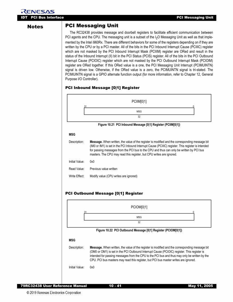
IDT PCI Bus Interface PCI Messaging Unit
79RC32438 User Refer
Notes
PCI Messaging UnitThe RC32438 provides message and doorbell registers to facilitate efficient communication betweenPCI agents and the CPU. The messaging unit is a subset of the I2O Messaging Unit as well as that imple-mented by the Intel i960Rx. There are different behaviors for some of the registers depending on if they arewritten by the CPU or by a PCI master. All of the bits in the PCI Inbound Interrupt Cause (PCIIIC) registerwhich are not masked by the PCI Inbound Interrupt Mask (PCIIIM) register are ORed and result in thestatus of the Inbound Interrupt (II) bit in the PCI Status (PCIS) register. All of the bits in the PCI OutboundInterrupt Cause (PCIOIC) register which are not masked by the PCI Outbound Interrupt Mask (PCIOIM)register are ORed together. If this ORed value is a one, the PCI Messaging Unit Interrupt (PCIMUINTN)signal is driven low. Otherwise, if the ORed value is a zero, the PCIMUINTN signal is tri-stated. ThePCIMUINTN signal is a GPIO alternate function output (for more information, refer to Chapter 12, GeneralPurpose I/O Controller).
PCI Inbound Message [0|1] Register
Figure 10.21 PCI Inbound Message [0|1] Register (PCIIM[0|1])
PCI Outbound Message [0|1] Register
Figure 10.22 PCI Outbound Message [0|1] Register (PCIOM[0|1])
MSG
Description: Message. When written, the value of the register is modified and the corresponding message bit (IM0 or IM1) is set in the PCI Inbound Interrupt Cause (PCIIIC) register. This register is intended for passing messages from the PCI bus to the CPU and thus can only be written by PCI bus masters. The CPU may read this register, but CPU writes are ignored.
Initial Value: 0x0
Read Value: Previous value written
Write Effect: Modify value (CPU writes are ignored)
MSG
Description: Message. When written, the value of the register is modified and the corresponding message bit (OM0 or OM1) is set in the PCI Outbound Interrupt Cause (PCIOIC) register. This register is intended for passing messages from the CPU to the PCI bus and thus may only be written by the CPU. PCI bus masters may read this register, but PCI bus master writes are ignored.
Initial Value: 0x0
PCIIM[0|1]031
32
MSG
PCIOM[0|1]031
32
MSG
ence Manual 10 - 41 May 11, 2005

IDT PCI Bus Interface PCI Messaging Unit
79RC32438 User Refer
Notes
PCI Inbound Doorbell Register
Figure 10.23 PCI Inbound Doorbell Register (PCIID)
PCI Inbound Interrupt Cause Register
Figure 10.24 PCI Inbound Interrupt Cause Register (PCIIIC)
Read Value: Previous value written
Write Effect: Modify value (PCI bus master writes are ignored)
INDOOR
Description: Inbound Doorbell. Writing a one to a bit in this field by a PCI bus master causes the bit to be set. Writing a one to a bit in this field by the CPU clears the bit if it was set. The Inbound Doorbell (ID) bit in the PCI Inbound Interrupt Cause (PCIIIC) register is set if any of the bits in this register are set.
Initial Value: 0x0
Read Value: Previous value written
Write Effect: Modify value (PCI bus master writes one to set bit, CPU writes one to clear bit)
IM0
Description: Inbound Message 0. This bit is set when the PCI Inbound Message 0 (PCIIM0) register is writ-ten by a PCI bus master.
Initial Value: 0x0
Read Value: Status
Write Effect: Sticky, writing a one clears this bit
IM1
Description: Inbound Message 1. This bit is set when the PCI Inbound Message 1 (PCIIM1) register is writ-ten by a PCI bus master.
Initial Value: 0x0
PCIID031
32
INDOOR
PCIIIC031
29
0
1
IM0
1
IM1
1
ID
ence Manual 10 - 42 May 11, 2005

IDT PCI Bus Interface PCI Messaging Unit
79RC32438 User Refer
Notes
PCI Inbound Interrupt Mask Register
Figure 10.25 PCI Inbound Interrupt Mask Register (PCIIIM)
Read Value: Status
Write Effect: Sticky, writing a one clears this bit
ID
Description: Inbound Doorbell. This bit is set when any bit in the PCI Inbound Doorbell (PCIID) register is set. This bit is read-only and simply represents the OR of all the bits in the PCIID register.
Initial Value: 0x0
Read Value: Status
Write Effect: Read-only
IM0
Description: Inbound Message 0. When this bit is set, the IM0 bit in the PCIIC register is masked from set-ting the Inbound Interrupt (II) bit in the PCI Status (PCIS) register.
Initial Value: 0x1
Read Value: Previous value written
Write Effect: Modify value
IM1
Description: Inbound Message 1. When this bit is set, the IM1 bit in the PCIIC register is masked from set-ting the Inbound Interrupt (II) bit in the PCI Status (PCIS) register.
Initial Value: 0x1
Read Value: Previous value written
Write Effect: Modify value
ID
Description: Inbound Doorbell. When this bit is set, the ID bit in the PCIIC register is masked from setting the Inbound Interrupt (II) bit in the PCI Status (PCIS) register.
Initial Value: 0x1
Read Value: Previous value written
Write Effect: Modify value
PCIIIM031
29
0
1
IM0
1
IM1
1
ID
ence Manual 10 - 43 May 11, 2005
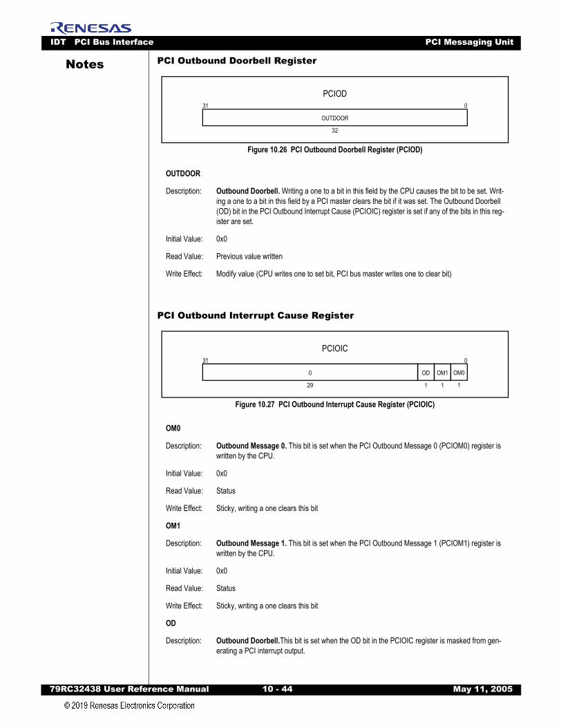
IDT PCI Bus Interface PCI Messaging Unit
79RC32438 User Refer
Notes
PCI Outbound Doorbell RegisterFigure 10.26 PCI Outbound Doorbell Register (PCIOD)
PCI Outbound Interrupt Cause Register
Figure 10.27 PCI Outbound Interrupt Cause Register (PCIOIC)
OUTDOOR
Description: Outbound Doorbell. Writing a one to a bit in this field by the CPU causes the bit to be set. Writ-ing a one to a bit in this field by a PCI master clears the bit if it was set. The Outbound Doorbell (OD) bit in the PCI Outbound Interrupt Cause (PCIOIC) register is set if any of the bits in this reg-ister are set.
Initial Value: 0x0
Read Value: Previous value written
Write Effect: Modify value (CPU writes one to set bit, PCI bus master writes one to clear bit)
OM0
Description: Outbound Message 0. This bit is set when the PCI Outbound Message 0 (PCIOM0) register is written by the CPU.
Initial Value: 0x0
Read Value: Status
Write Effect: Sticky, writing a one clears this bit
OM1
Description: Outbound Message 1. This bit is set when the PCI Outbound Message 1 (PCIOM1) register is written by the CPU.
Initial Value: 0x0
Read Value: Status
Write Effect: Sticky, writing a one clears this bit
OD
Description: Outbound Doorbell.This bit is set when the OD bit in the PCIOIC register is masked from gen-erating a PCI interrupt output.
PCIOD031
32
OUTDOOR
PCIOIC031
29
0
1
OM0
1
OM1
1
OD
ence Manual 10 - 44 May 11, 2005
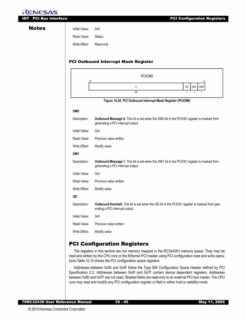
IDT PCI Bus Interface PCI Configuration Registers
79RC32438 User Refer
Notes
PCI Outbound Interrupt Mask Register
Figure 10.28 PCI Outbound Interrupt Mask Register (PCIOIM)
PCI Configuration RegistersThe registers in this section are not memory mapped in the RC32438’s memory space. They may be
read and written by the CPU core or the Ethernet PCI master using PCI configuration read and write opera-tions.Table 10.10 shows the PCI configuration space registers.
Addresses between 0x00 and 0x3F follow the Type 00h Configuration Space Header defined by PCISpecification 2.2. Addresses between 0x40 and 0x7F contain device dependent registers. Addressesbetween 0x80 and 0xFF are not used. Shaded fields are read-only to an external PCI bus master. The CPUcore may read and modify any PCI configuration register or field in either host or satellite mode.
Initial Value: 0x0
Read Value: Status
Write Effect: Read-only
OM0
Description: Outbound Message 0. This bit is set when the OM0 bit in the PCIOIC register is masked from generating a PCI interrupt output.
Initial Value: 0x0
Read Value: Previous value written
Write Effect: Modify value
OM1
Description: Outbound Message 1. This bit is set when the OM1 bit in the PCIOIC register is masked from generating a PCI interrupt output.
Initial Value: 0x0
Read Value: Previous value written
Write Effect: Modify value
OD
Description: Outbound Doorbell. This bit is set when the OD bit in the PCIOIC register is masked from gen-erating a PCI interrupt output.
Initial Value: 0x0
Read Value: Previous value written
Write Effect: Modify value
PCIOIM031
29
0
1
OM0
1
OM1
1
OD
ence Manual 10 - 45 May 11, 2005
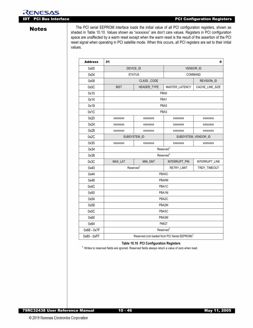
IDT PCI Bus Interface PCI Configuration Registers
79RC32438 User Refer
Notes
The PCI serial EEPROM interface loads the initial value of all PCI configuration registers, shown asshaded in Table 10.10. Values shown as “xxxxxxxx” are don’t care values. Registers in PCI configurationspace are unaffected by a warm reset except when the warm reset is the result of the assertion of the PCIreset signal when operating in PCI satellite mode. When this occurs, all PCI registers are set to their initialvalues.Address 31 0
0x00 DEVICE_ID VENDOR_ID
0x04 STATUS COMMAND
0x08 CLASS _CODE REVISION_ID
0x0C BIST HEADER_TYPE MASTER_LATENCY CACHE_LINE_SIZE
0x10 PBA0
0x14 PBA1
0x18 PBA2
0x1C PBA3
0x20 xxxxxxxx xxxxxxxx xxxxxxxx xxxxxxxx
0x24 xxxxxxxx xxxxxxxx xxxxxxxx xxxxxxxx
0x28 xxxxxxxx xxxxxxxx xxxxxxxx xxxxxxxx
0x2C SUBSYSTEM_ID SUBSYSTEM_VENDOR_ID
0x30 xxxxxxxx xxxxxxxx xxxxxxxx xxxxxxxx
0x34 Reserved1
1. Writes to reserved fields are ignored. Reserved fields always return a value of zero when read.
0x38 Reserved1
0x3C MAX_LAT MIN_GNT INTERRUPT_PIN INTERRUPT_LINE
0x40 Reserved1 RETRY_LIMIT TRDY_TIMEOUT
0x44 PBA0C
0x48 PBA0M
0x4C PBA1C
0x50 PBA1M
0x54 PBA2C
0x58 PBA2M
0x5C PBA3C
0x60 PBA3M
0x64 PMGT
0x68 - 0x7F Reserved1
0x80 - 0xFF Reserved (not loaded from PCI Serial EEPROM)1
Table 10.10 PCI Configuration Registers
ence Manual 10 - 46 May 11, 2005
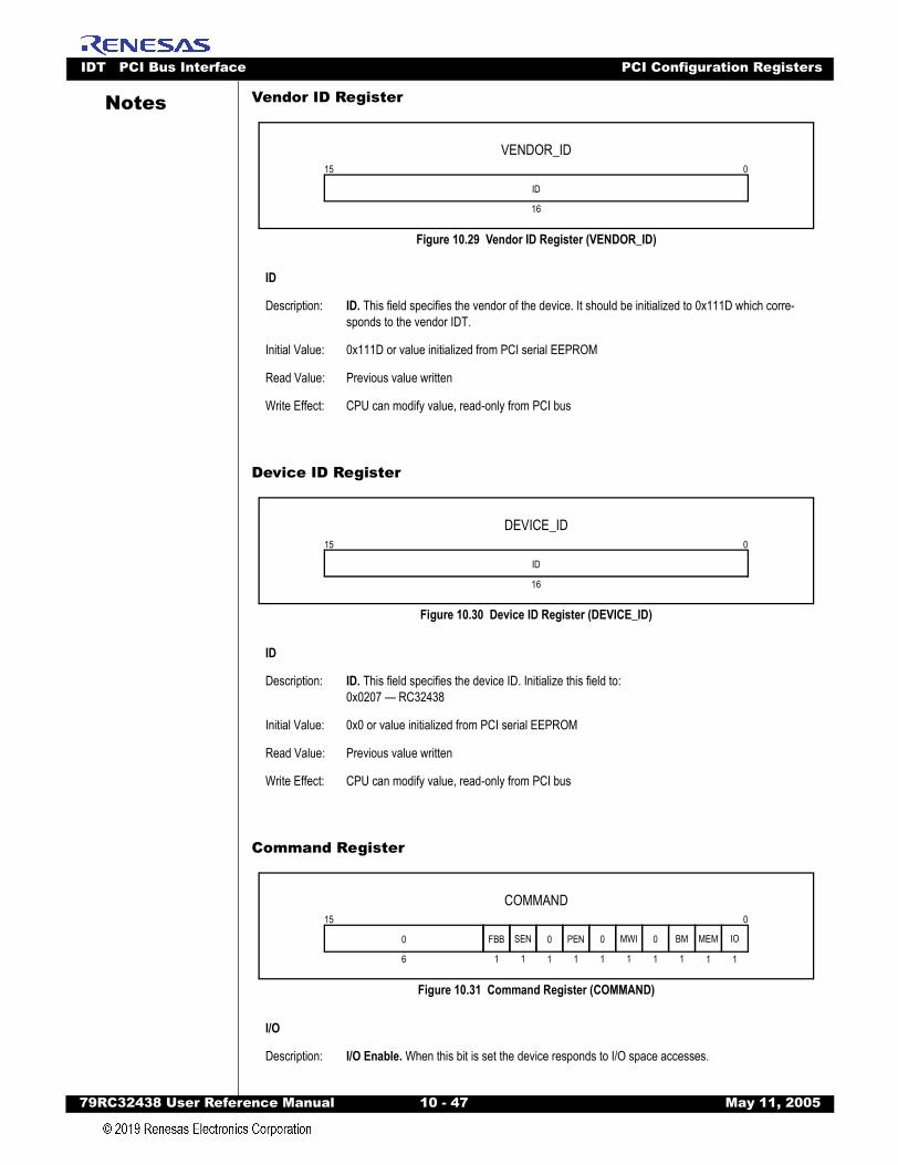
IDT PCI Bus Interface PCI Configuration Registers
79RC32438 User Refer
Notes
Vendor ID RegisterFigure 10.29 Vendor ID Register (VENDOR_ID)
Device ID Register
Figure 10.30 Device ID Register (DEVICE_ID)
Command Register
Figure 10.31 Command Register (COMMAND)
ID
Description: ID. This field specifies the vendor of the device. It should be initialized to 0x111D which corre-sponds to the vendor IDT.
Initial Value: 0x111D or value initialized from PCI serial EEPROM
Read Value: Previous value written
Write Effect: CPU can modify value, read-only from PCI bus
ID
Description: ID. This field specifies the device ID. Initialize this field to:0x0207 — RC32438
Initial Value: 0x0 or value initialized from PCI serial EEPROM
Read Value: Previous value written
Write Effect: CPU can modify value, read-only from PCI bus
I/O
Description: I/O Enable. When this bit is set the device responds to I/O space accesses.
VENDOR_ID015
16
ID
DEVICE_ID015
16
ID
COMMAND
1
IO
1
MEM
1
BM
1
0
1
MWI
1
0
1
PEN
1
0
1
SEN
1
FBB
015
6
0
ence Manual 10 - 47 May 11, 2005
IDT PCI Bus Interface PCI Configuration Registers
79RC32438 User Refer
Notes
Initial Value: 0x0Read Value: Previous value written
Write Effect: Modify value
MEM
Description: Memory Enable. When this bit is set the device responds to memory space accesses.
Initial Value: 0x0
Read Value: Previous value written
Write Effect: Modify value
BM
Description: Bus Master Enable. When this bit is set, the device is allowed to act as a PCI master.
Initial Value: 0x0
Read Value: Previous value written
Write Effect: Modify value
MWI
Description: Memory Write and Invalidate Enable. When this bit is set, the PCI bus interface may generate memory write and invalidate transactions on the PCI bus.
Initial Value: 0x0
Read Value: Previous value written
Write Effect: Modify value
PEN
Description: Parity Error Enable. When this bit is set, the device must take its normal action when a parity error is detected (See PCI Specification 2.2). When this bit is cleared, the devices sets its Parity Error (PE) bit in the PCI STATUS register, does not assert PERRN, and continues normal oper-ation.
Initial Value: 0x0
Read Value: Previous value written
Write Effect: Modify value
SEN
Description: System Error Enable. When this bit is set, the SERRN drive is enabled. When this bit is cleared, the SERRN driver is disabled.This bit and the PEN bit must be set to report address phase parity errors.
Initial Value: 0x0
Read Value: Previous value written
Write Effect: Modify value
ence Manual 10 - 48 May 11, 2005
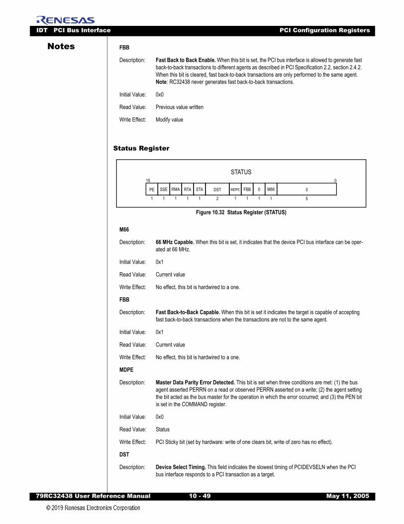
IDT PCI Bus Interface PCI Configuration Registers
79RC32438 User Refer
Notes
Status Register
Figure 10.32 Status Register (STATUS)
FBB
Description: Fast Back to Back Enable. When this bit is set, the PCI bus interface is allowed to generate fast back-to-back transactions to different agents as described in PCI Specification 2.2, section 2.4.2. When this bit is cleared, fast back-to-back transactions are only performed to the same agent.Note: RC32438 never generates fast back-to-back transactions.
Initial Value: 0x0
Read Value: Previous value written
Write Effect: Modify value
M66
Description: 66 MHz Capable. When this bit is set, it indicates that the device PCI bus interface can be oper-ated at 66 MHz.
Initial Value: 0x1
Read Value: Current value
Write Effect: No effect, this bit is hardwired to a one.
FBB
Description: Fast Back-to-Back Capable. When this bit is set it indicates the target is capable of accepting fast back-to-back transactions when the transactions are not to the same agent.
Initial Value: 0x1
Read Value: Current value
Write Effect: No effect, this bit is hardwired to a one.
MDPE
Description: Master Data Parity Error Detected. This bit is set when three conditions are met: (1) the bus agent asserted PERRN on a read or observed PERRN asserted on a write; (2) the agent setting the bit acted as the bus master for the operation in which the error occurred; and (3) the PEN bit is set in the COMMAND register.
Initial Value: 0x0
Read Value: Status
Write Effect: PCI Sticky bit (set by hardware: write of one clears bit, write of zero has no effect).
DST
Description: Device Select Timing. This field indicates the slowest timing of PCIDEVSELN when the PCI bus interface responds to a PCI transaction as a target.
STATUS
5
0
1
M66
1
0
1
FBB
1
MDPE
2
DST
1
STA
1
RTA
1
RMA
1
SSE
015
1
PE
ence Manual 10 - 49 May 11, 2005
IDT PCI Bus Interface PCI Configuration Registers
79RC32438 User Refer
Notes
Initial Value: 0x1Read Value: 0x1
Write Effect: No effect, this field is hardwired to a 0x1.
STA
Description: Signalled Target Abort Status. This bit is set by the PCI bus interface whenever it acts as a PCI target and terminates a transaction with a Target-Abort.
Initial Value: 0x0
Read Value: Status
Write Effect: PCI Sticky bit (set by hardware: write of one clears bit, write of zero has no effect).
RTA
Description: Received Target Abort Status. This bit is set by the PCI bus interface whenever it acts as a master and a transaction is terminated with a Target-Abort.
Initial Value: 0x0
Read Value: Status
Write Effect: PCI Sticky bit (set by hardware: write of one clears bit, write of zero has no effect).
RMA
Description: Received Master Abort Status. This bit is set by the PCI bus interface whenever it acts as a PCI master and terminates a host-to-PCI transaction with a Master Abort.
Initial Value: 0x0
Read Value: Status
Write Effect: PCI Sticky bit (set by hardware: write of one clears bit, write of zero has no effect).
SSE
Description: Signaled System Error. This bit is set by the PCI bus interface whenever it asserts PCISERRN.
Initial Value: 0x0
Read Value: Status
Write Effect: PCI Sticky bit (set by hardware: write of one clears bit, write of zero has no effect).
PE
Description: Parity Error. This bit is set by the device whenever it detects a parity error, even if parity error handling is disabled.
Initial Value: 0x0
Read Value: Status
Write Effect: PCI Sticky bit (set by hardware: write of one clears bit, write of zero has no effect).
ence Manual 10 - 50 May 11, 2005
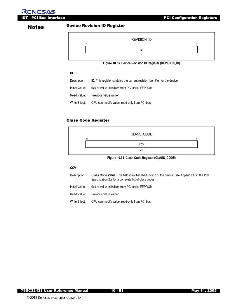
IDT PCI Bus Interface PCI Configuration Registers
79RC32438 User Refer
Notes
Device Revision ID RegisterFigure 10.33 Device Revision ID Register (REVISION_ID)
Class Code Register
Figure 10.34 Class Code Register (CLASS_CODE)
ID
Description: ID. This register contains the current revision identifier for the device.
Initial Value: 0x0 or value initialized from PCI serial EEPROM
Read Value: Previous value written
Write Effect: CPU can modify value, read-only from PCI bus
CCV
Description: Class Code Value. This field identifies the function of the device. See Appendix D in the PCI Specification 2.2 for a complete list of class codes.
Initial Value: 0x0 or value initialized from PCI serial EEPROM
Read Value: Previous value written
Write Effect: CPU can modify value, read-only from PCI bus
REVISION_ID07
8
ID
CLASS_CODE023
24
CCV
ence Manual 10 - 51 May 11, 2005
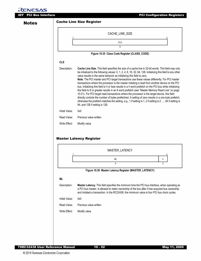
IDT PCI Bus Interface PCI Configuration Registers
79RC32438 User Refer
Notes
Cache Line Size RegisterFigure 10.35 Class Code Register (CLASS_CODE)
Master Latency Register
Figure 10.36 Master Latency Register (MASTER_LATENCY)
CLS
Description: Cache Line Size. This field specifies the size of a cache line in 32-bit words. This field may only be initialized to the following values: 0, 1, 2, 4, 8, 16, 32, 64, 128. Initializing this field to any other value results in the same behavior as initializing this field to zero.Note: The PCI master and PCI target transactions use these values differently. For PCI master transactions where the processor is the master initiating a read from another device on the PCI bus, initializing this field to 4 or less results in a 4 word prefetch on the PCI bus while initializing this field to 8 or greater results in an 8 word prefetch (see “Master Memory Read Line” on page 10-21). For PCI target read transactions where the processor is the target device, this field directly controls the number of bytes prefetched. A setting of zero results in a one byte prefetch, otherwise the prefetch matches the setting, e.g., 1 if setting is 1, 2 if setting is 2 ..... 64 if setting is 64, and 128 if setting is 128.
Initial Value: 0x0
Read Value: Previous value written
Write Effect: Modify value
ML
Description: Master Latency. This field specifies the minimum time the PCI bus interface, when operating as a PCI bus master, is allowed to retain ownership of the bus after it has acquired bus ownership and initiated a transaction. In the RC32438, the minimum value is four PCI bus clock cycles.
Initial Value: 0x0
Read Value: Previous value written
Write Effect: Modify value
CACHE_LINE_SIZE07
8
CLS
MASTER_LATENCY07
6
ML
2
0
ence Manual 10 - 52 May 11, 2005
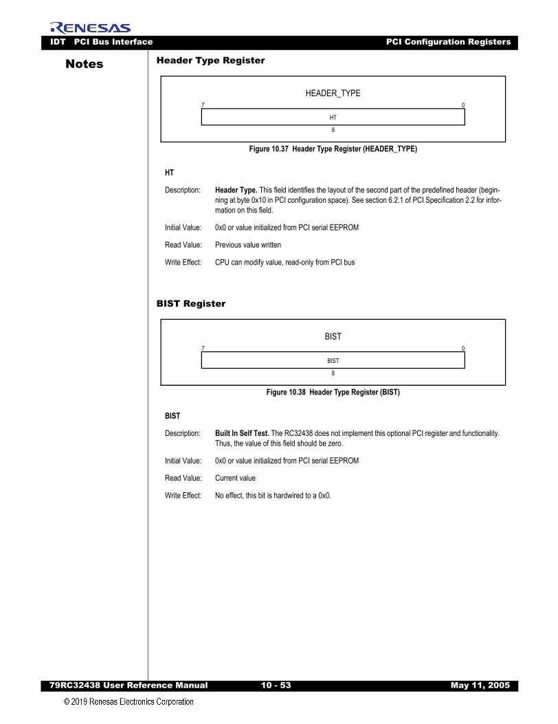
IDT PCI Bus Interface PCI Configuration Registers
79RC32438 User Refer
Notes
Header Type RegisterFigure 10.37 Header Type Register (HEADER_TYPE)
BIST Register
Figure 10.38 Header Type Register (BIST)
HT
Description: Header Type. This field identifies the layout of the second part of the predefined header (begin-ning at byte 0x10 in PCI configuration space). See section 6.2.1 of PCI Specification 2.2 for infor-mation on this field.
Initial Value: 0x0 or value initialized from PCI serial EEPROM
Read Value: Previous value written
Write Effect: CPU can modify value, read-only from PCI bus
BIST
Description: Built In Self Test. The RC32438 does not implement this optional PCI register and functionality. Thus, the value of this field should be zero.
Initial Value: 0x0 or value initialized from PCI serial EEPROM
Read Value: Current value
Write Effect: No effect, this bit is hardwired to a 0x0.
HEADER_TYPE07
8
HT
BIST07
8
BIST
ence Manual 10 - 53 May 11, 2005
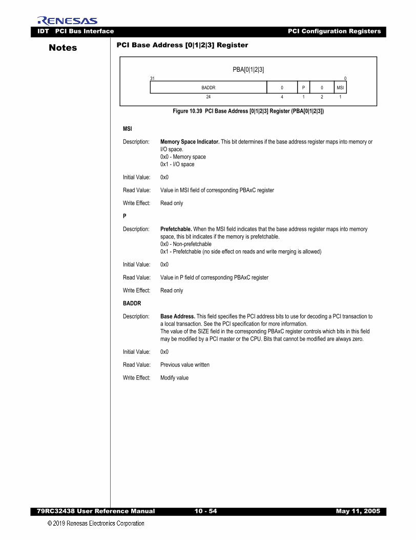
IDT PCI Bus Interface PCI Configuration Registers
79RC32438 User Refer
Notes
PCI Base Address [0|1|2|3] RegisterFigure 10.39 PCI Base Address [0|1|2|3] Register (PBA[0|1|2|3])
MSI
Description: Memory Space Indicator. This bit determines if the base address register maps into memory or I/O space.0x0 - Memory space0x1 - I/O space
Initial Value: 0x0
Read Value: Value in MSI field of corresponding PBAxC register
Write Effect: Read only
P
Description: Prefetchable. When the MSI field indicates that the base address register maps into memory space, this bit indicates if the memory is prefetchable.0x0 - Non-prefetchable0x1 - Prefetchable (no side effect on reads and write merging is allowed)
Initial Value: 0x0
Read Value: Value in P field of corresponding PBAxC register
Write Effect: Read only
BADDR
Description: Base Address. This field specifies the PCI address bits to use for decoding a PCI transaction to a local transaction. See the PCI specification for more information.The value of the SIZE field in the corresponding PBAxC register controls which bits in this field may be modified by a PCI master or the CPU. Bits that cannot be modified are always zero.
Initial Value: 0x0
Read Value: Previous value written
Write Effect: Modify value
PBA[0|1|2|3]031
24
BADDR
1
MSI0
21
P0
4
ence Manual 10 - 54 May 11, 2005
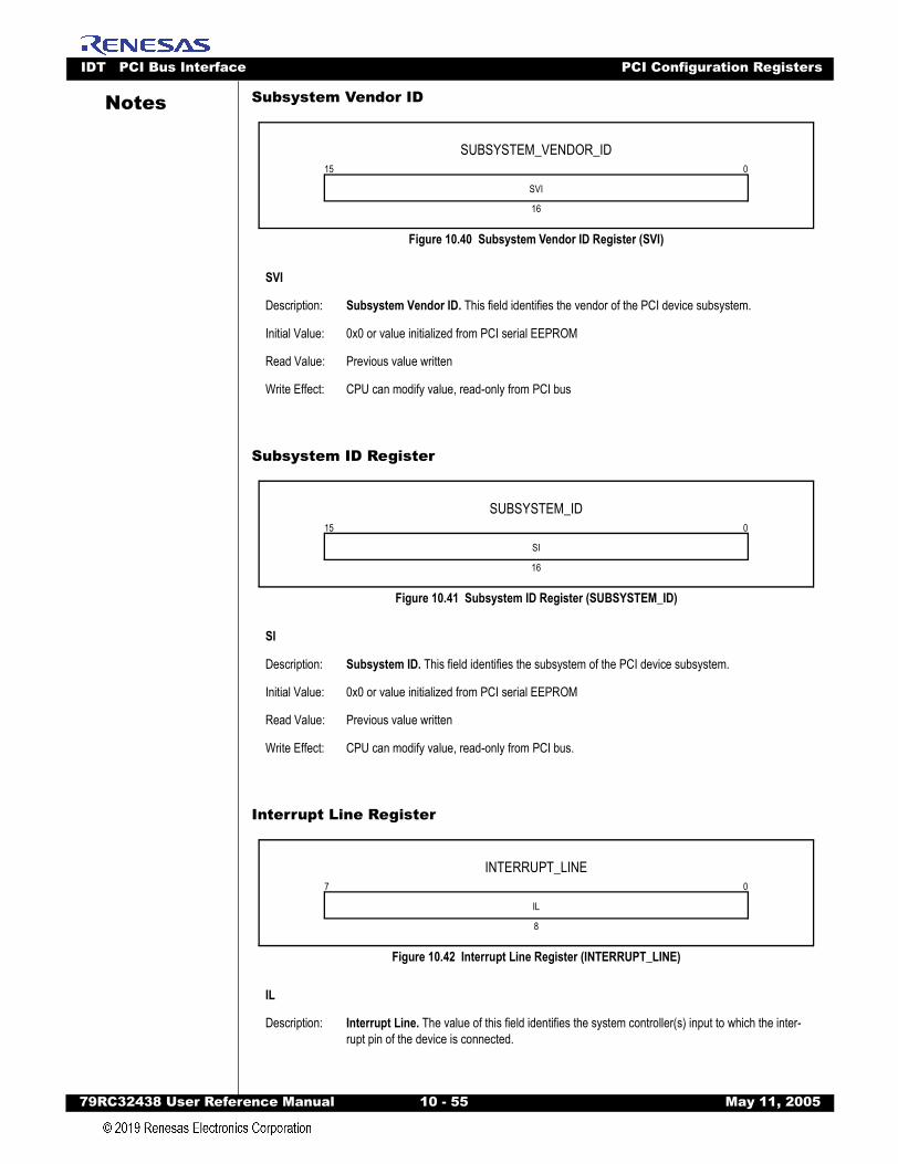
IDT PCI Bus Interface PCI Configuration Registers
79RC32438 User Refer
Notes
Subsystem Vendor IDFigure 10.40 Subsystem Vendor ID Register (SVI)
Subsystem ID Register
Figure 10.41 Subsystem ID Register (SUBSYSTEM_ID)
Interrupt Line Register
Figure 10.42 Interrupt Line Register (INTERRUPT_LINE)
SVI
Description: Subsystem Vendor ID. This field identifies the vendor of the PCI device subsystem.
Initial Value: 0x0 or value initialized from PCI serial EEPROM
Read Value: Previous value written
Write Effect: CPU can modify value, read-only from PCI bus
SI
Description: Subsystem ID. This field identifies the subsystem of the PCI device subsystem.
Initial Value: 0x0 or value initialized from PCI serial EEPROM
Read Value: Previous value written
Write Effect: CPU can modify value, read-only from PCI bus.
IL
Description: Interrupt Line. The value of this field identifies the system controller(s) input to which the inter-rupt pin of the device is connected.
SUBSYSTEM_VENDOR_ID015
16
SVI
SUBSYSTEM_ID015
16
SI
INTERRUPT_LINE07
8
IL
ence Manual 10 - 55 May 11, 2005
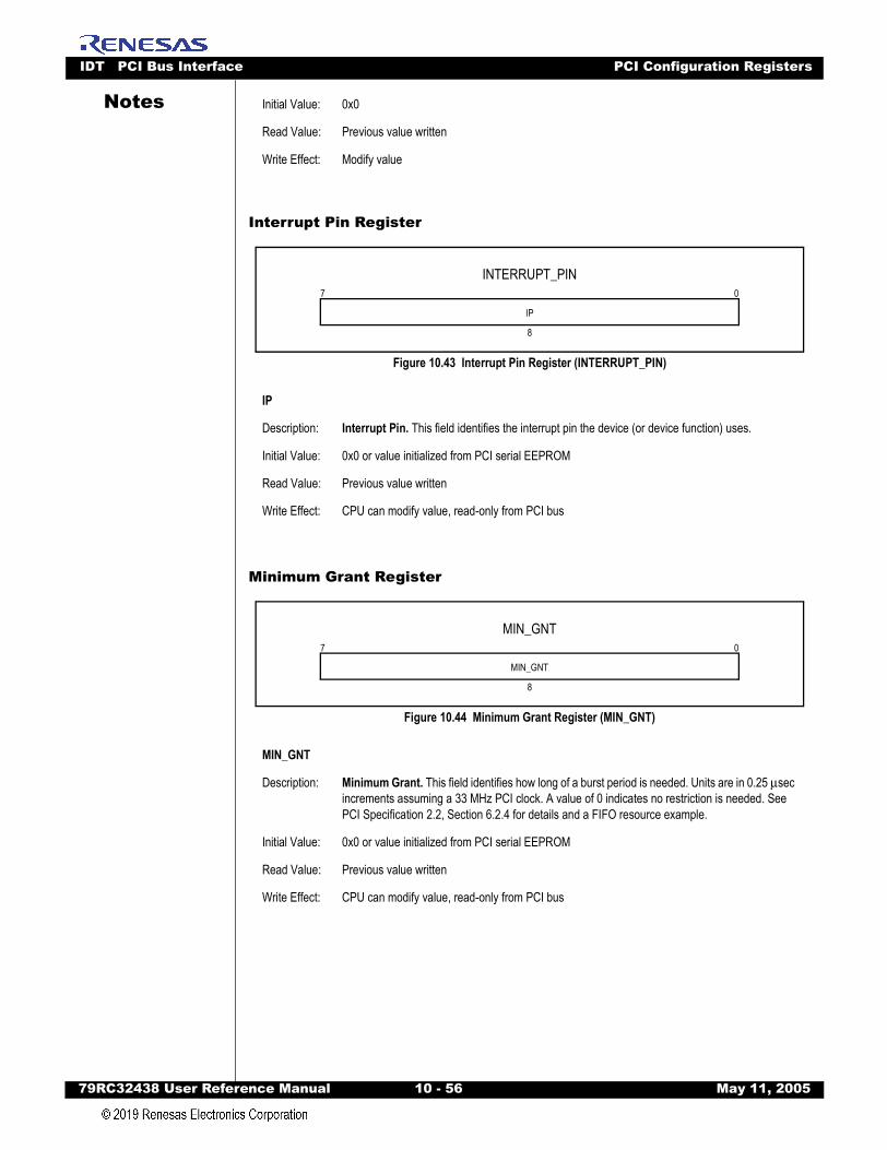
IDT PCI Bus Interface PCI Configuration Registers
79RC32438 User Refer
Notes
Interrupt Pin Register
Figure 10.43 Interrupt Pin Register (INTERRUPT_PIN)
Minimum Grant Register
Figure 10.44 Minimum Grant Register (MIN_GNT)
Initial Value: 0x0
Read Value: Previous value written
Write Effect: Modify value
IP
Description: Interrupt Pin. This field identifies the interrupt pin the device (or device function) uses.
Initial Value: 0x0 or value initialized from PCI serial EEPROM
Read Value: Previous value written
Write Effect: CPU can modify value, read-only from PCI bus
MIN_GNT
Description: Minimum Grant. This field identifies how long of a burst period is needed. Units are in 0.25 µsec increments assuming a 33 MHz PCI clock. A value of 0 indicates no restriction is needed. See PCI Specification 2.2, Section 6.2.4 for details and a FIFO resource example.
Initial Value: 0x0 or value initialized from PCI serial EEPROM
Read Value: Previous value written
Write Effect: CPU can modify value, read-only from PCI bus
INTERRUPT_PIN07
8
IP
MIN_GNT07
8
MIN_GNT
ence Manual 10 - 56 May 11, 2005
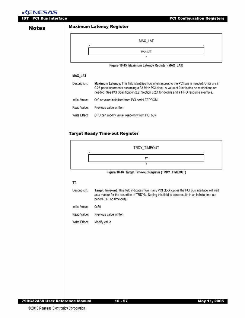
IDT PCI Bus Interface PCI Configuration Registers
79RC32438 User Refer
Notes
Maximum Latency RegisterFigure 10.45 Maximum Latency Register (MAX_LAT)
Target Ready Time-out Register
Figure 10.46 Target Time-out Register (TRDY_TIMEOUT)
MAX_LAT
Description: Maximum Latency. This field identifies how often access to the PCI bus is needed. Units are in 0.25 µsec increments assuming a 33 MHz PCI clock. A value of 0 indicates no restrictions are needed. See PCI Specification 2.2, Section 6.2.4 for details and a FIFO resource example.
Initial Value: 0x0 or value initialized from PCI serial EEPROM
Read Value: Previous value written
Write Effect: CPU can modify value, read-only from PCI bus
TT
Description: Target Time-out. This field indicates how many PCI clock cycles the PCI bus interface will wait as a master for the assertion of TRDYN. Setting this field to zero results in an infinite time-out period (i.e., no time-out).
Initial Value: 0x80
Read Value: Previous value written
Write Effect: Modify value
MAX_LAT07
8
MAX_LAT
TRDY_TIMEOUT07
8
TT
ence Manual 10 - 57 May 11, 2005
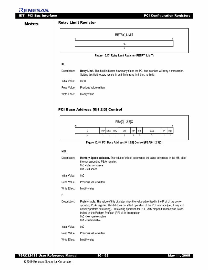
IDT PCI Bus Interface PCI Configuration Registers
79RC32438 User Refer
Notes
Retry Limit RegisterFigure 10.47 Retry Limit Register (RETRY_LIMIT)
PCI Base Address [0|1|2|3] Control
Figure 10.48 PCI Base Address [0|1|2|3] Control (PBA[0|1|2|3]C)
RL
Description: Retry Limit. This field indicates how many times the PCI bus interface will retry a transaction. Setting this field to zero results in an infinite retry limit (i.e., no limit).
Initial Value: 0x80
Read Value: Previous value written
Write Effect: Modify value
MSI
Description: Memory Space Indicator. The value of this bit determines the value advertised in the MSI bit of the corresponding PBAx register.0x0 - Memory space0x1 - I/O space
Initial Value: 0x0
Read Value: Previous value written
Write Effect: Modify value
P
Description: Prefetchable. The value of this bit determines the value advertised in the P bit of the corre-sponding PBAx register. This bit does not affect operation of the PCI interface (i.e., it may not actually perform pefetching). Prefetching operation for PCI PARx mapped transactions is con-trolled by the Perform Prefetch (PP) bit in this register.0x0 - Non-prefetchable0x1 - Prefetchable
Initial Value: 0x0
Read Value: Previous value written
Write Effect: Modify value
RETRY_LIMIT07
8
RL
PBA[0|1|2|3]C031
1
MSI
1
PSIZE
51
SB
1
PP
1
MRL
1
MRM
2
MR
18
0
1
TRP
ence Manual 10 - 58 May 11, 2005
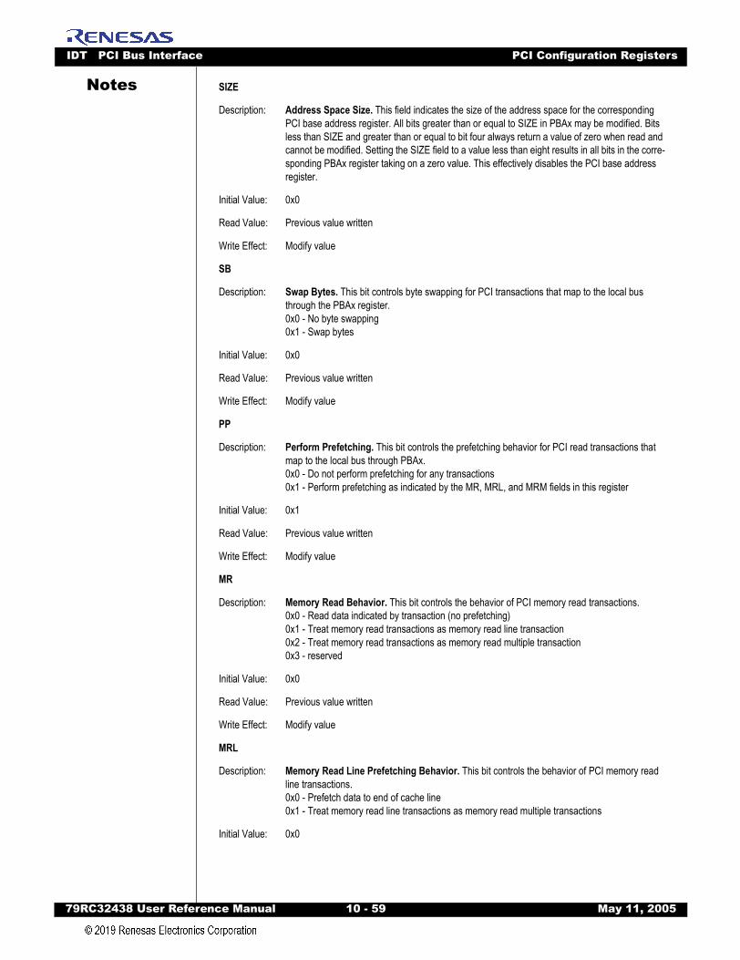
IDT PCI Bus Interface PCI Configuration Registers
79RC32438 User Refer
Notes
SIZEDescription: Address Space Size. This field indicates the size of the address space for the corresponding PCI base address register. All bits greater than or equal to SIZE in PBAx may be modified. Bits less than SIZE and greater than or equal to bit four always return a value of zero when read and cannot be modified. Setting the SIZE field to a value less than eight results in all bits in the corre-sponding PBAx register taking on a zero value. This effectively disables the PCI base address register.
Initial Value: 0x0
Read Value: Previous value written
Write Effect: Modify value
SB
Description: Swap Bytes. This bit controls byte swapping for PCI transactions that map to the local bus through the PBAx register.0x0 - No byte swapping0x1 - Swap bytes
Initial Value: 0x0
Read Value: Previous value written
Write Effect: Modify value
PP
Description: Perform Prefetching. This bit controls the prefetching behavior for PCI read transactions that map to the local bus through PBAx. 0x0 - Do not perform prefetching for any transactions0x1 - Perform prefetching as indicated by the MR, MRL, and MRM fields in this register
Initial Value: 0x1
Read Value: Previous value written
Write Effect: Modify value
MR
Description: Memory Read Behavior. This bit controls the behavior of PCI memory read transactions.0x0 - Read data indicated by transaction (no prefetching)0x1 - Treat memory read transactions as memory read line transaction0x2 - Treat memory read transactions as memory read multiple transaction0x3 - reserved
Initial Value: 0x0
Read Value: Previous value written
Write Effect: Modify value
MRL
Description: Memory Read Line Prefetching Behavior. This bit controls the behavior of PCI memory read line transactions.0x0 - Prefetch data to end of cache line 0x1 - Treat memory read line transactions as memory read multiple transactions
Initial Value: 0x0
ence Manual 10 - 59 May 11, 2005
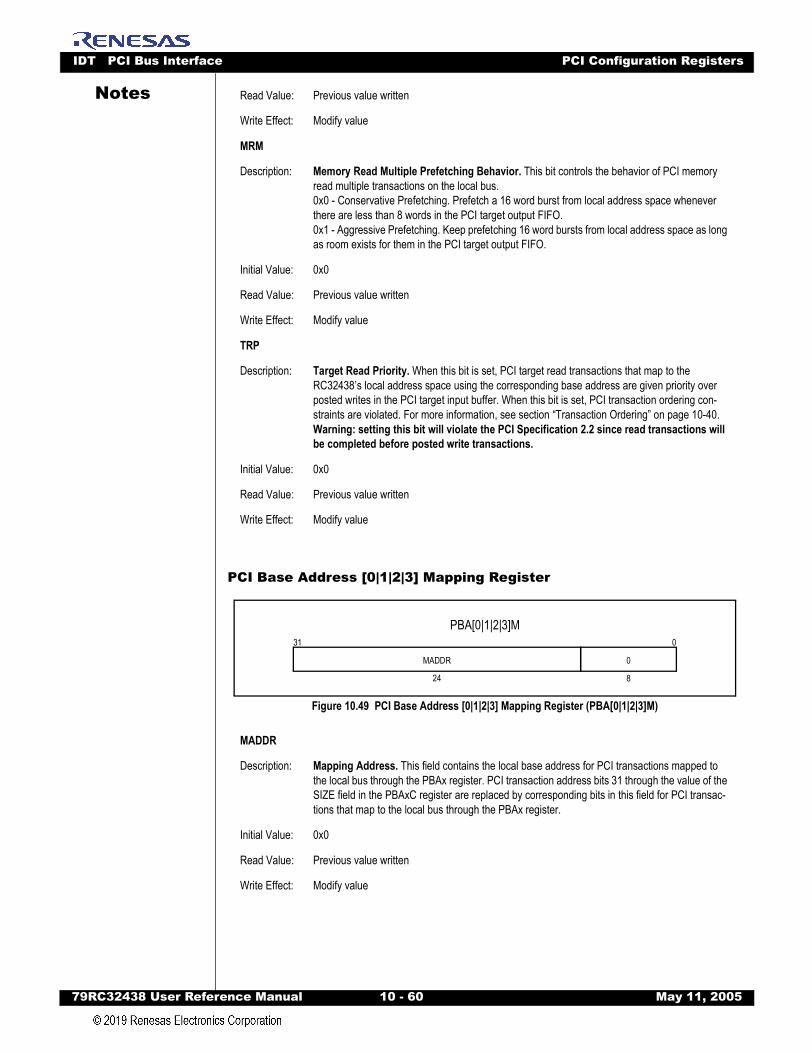
IDT PCI Bus Interface PCI Configuration Registers
79RC32438 User Refer
Notes
PCI Base Address [0|1|2|3] Mapping Register
Figure 10.49 PCI Base Address [0|1|2|3] Mapping Register (PBA[0|1|2|3]M)
Read Value: Previous value written
Write Effect: Modify value
MRM
Description: Memory Read Multiple Prefetching Behavior. This bit controls the behavior of PCI memory read multiple transactions on the local bus.0x0 - Conservative Prefetching. Prefetch a 16 word burst from local address space whenever there are less than 8 words in the PCI target output FIFO.0x1 - Aggressive Prefetching. Keep prefetching 16 word bursts from local address space as long as room exists for them in the PCI target output FIFO.
Initial Value: 0x0
Read Value: Previous value written
Write Effect: Modify value
TRP
Description: Target Read Priority. When this bit is set, PCI target read transactions that map to the RC32438’s local address space using the corresponding base address are given priority over posted writes in the PCI target input buffer. When this bit is set, PCI transaction ordering con-straints are violated. For more information, see section “Transaction Ordering” on page 10-40.Warning: setting this bit will violate the PCI Specification 2.2 since read transactions will be completed before posted write transactions.
Initial Value: 0x0
Read Value: Previous value written
Write Effect: Modify value
MADDR
Description: Mapping Address. This field contains the local base address for PCI transactions mapped to the local bus through the PBAx register. PCI transaction address bits 31 through the value of the SIZE field in the PBAxC register are replaced by corresponding bits in this field for PCI transac-tions that map to the local bus through the PBAx register.
Initial Value: 0x0
Read Value: Previous value written
Write Effect: Modify value
PBA[0|1|2|3]M031
24
MADDR 0
8
ence Manual 10 - 60 May 11, 2005

IDT PCI Bus Interface PCI Configuration Registers
79RC32438 User Refer
Notes
PCI Management RegisterFigure 10.50 PCI Management Register (PMGT)
WR
Description: Warm Reset. Writing a one to this register generates a warm reset.
Initial Value: 0x0
Read Value: Current warm reset state0x0 - normal operation0x1 - warm reset
Write Effect: Writing a one generates a warm reset.
NMI
Description: Non-Maskable Interrupt. Writing a one to this register causes the NMI bit to be set in the PCI Status (PCIS) register and results in a CPU non-maskable interrupt.
Initial Value: 0x0
Read Value: 0x0
Write Effect: Writing a one generates a non-maskable interrupt.
PMGT031
1
WR
30
0
1
NMI
ence Manual 10 - 61 May 11, 2005
IDT PCI Bus Interface PCI Configuration Registers
79RC32438 User Refer
Notes
ence Manual 10 - 62 May 11, 2005

Notes
79RC32438 User Reference Manual 11 - 1 M
Chapter 11
Ethernet Interfaces
IntroductionThis chapter describes the two Ethernet interfaces on the RC32438 device. Both channels are nearly
identical (Ethernet 0 channel has MII management functions; Ethernet 1 channel does not).
Features10 and 100 Mb/s ISO/IEC 8802-3:1996 compliantTwo IEEE 802.3u compatible Media Independent Interfaces (MII) with serial management interfaceMII supports IEEE 802.3u auto-negotiation speed selectionSupports 64 entry hash table based multicast address filtering512 byte transmit and receive FIFOsSupports flow control functions outlined in IEEE Std. 802.3x-1997
Block Diagram
Figure 11.1 Ethernet Interface with Management Feature
Functional OverviewThe RC32438 contains two nearly identical 10/100 Mb/s ISO/IEC 8802-3:1996 compliant Ethernet inter-
faces (only 0 channel has MII management functions). Figure 11.1 shows a block diagram with a manage-ment function. An external Ethernet physical layer device (PHY) connects to each Ethernet interfacethrough an IEEE Std 802.3u-1995 Media Independent Interface (MII). This allows each Ethernet interface tobe used with a multitude of physical layers such as: 10BASE-T, 100BASE-TX, and 100BASE-FX. EachEthernet interface is capable of performing control flow functions outlined in IEEE Std 802.3x-1997.
Management
MII Logic
CSMA/CD MAC
DMAInterface
IPBus™
Media Independent Interface
Ethernet MAC
AddressRecognition
Logic
ay 11, 2005
IDT Ethernet Interfaces Input and Output FIFOs
79RC32438 User Refer
Notes
Since both Ethernet interfaces are nearly identical, the remainder of this chapter describes the function-ality of a single interface. It should be understood that there are two copies of all Ethernet registers, one forEthernet interface zero (denoted by the prefix ETH0 or MII0) and one for interface one (denoted by theprefix ETH1 or MII1).As illustrated in Figure 11.1, an Ethernet interface consists of five major blocks:
– An Ethernet MAC (medium access controller), which includes a CSMA/CD MAC, a managementinterface, and a MII pin level interface
– A 512 byte input FIFO connected to the MAC– A 512 byte output FIFO connected to the MAC– Address recognition logic, which determines if an Ethernet frame received on the MII should be
passed to the input FIFO – DMA interface, which allows the input and output FIFOs to be read and written by the DMA
Controller. The Ethernet interface is enabled by setting the EN bit in the Ethernet interface control (ETH[0|1]INTFC)
register.
Input and Output FIFOsThe input and output FIFOs are not intended to hold entire packets, but merely to compensate for
latency in accessing data by the DMA Controller. Each 512 byte FIFO is organized as 128 32-bit words.During boot configuration, the system may be configured to operate in either big endian or little endianmode. Although Ethernet packet data is packed into words in the FIFOs, packet data is referenced as bytes(also called octets) by the CPU core and Ethernet MAC. Data is always stored in big endian format withinFIFO data words, with endianness conversion taking place as data is transferred between the IPBus andthe FIFOs. Thus, data stored in the FIFOs always appears to the programmer in the endianness selectedduring boot configuration.
Packet data to be transmitted is written by the DMA Controller into the output FIFO. When the amount ofpacket data in the output FIFO exceeds the threshold programmed in the transmit threshold (TTH) field ofthe Ethernet FIFO transmit threshold register (ETH[0|1]FIFOTT), or when the last byte of a packet is writtento the output FIFO, the MAC will check if the line is busy. If the line is not busy, the MAC will begin transmit-ting the preamble, start of frame delimiter, and the packet data.
If a collision is detected during the collision window, the MAC will back off and attempt to retransmit theframe. Attempts are made to retransmit the frame until the collision threshold specified in the maximumretransmissions (MAXRET) field of the ETH[0|1]CLRT register is reached. When this occurs, the excessivecollisions (EC) bit is set in the DEVCS field of the DMA descriptor.
For correct operation, the transmit threshold (TTH) must be set to a value equal to or greater than thevalue selected for the collision window size in the COLWIN field of the Ethernet collision window and retry(ETH[0|1]CLRT) register minus two words or eight bytes (the collision window size includes the preambleand SFD which are generated by the MAC and are not part of a packet).
Ethernet Register Description
Register Offset1 Register Name Register Function Size
0x05_8000 ETH0INTFC Ethernet 0 interface control 32-bit
0x05_8004 ETH0FIFOTT Ethernet 0 FIFO transmit threshold 32-bit
0x05_8008 ETH0ARC Ethernet 0 address recognition control 32-bit
0x05_800C ETH0HASH0 Ethernet 0 hash table 0 32-bit
0x05_8010 ETH0HASH1 Ethernet 0 hash table 1 32-bit
0x05_8014 through 0x05_8020 Reserved
Table 11.1 Ethernet Register Map (Part 1 of 4)
ence Manual 11 - 2 May 11, 2005

IDT Ethernet Interfaces Ethernet Register Description
79RC32438 User Refer
Notes
0x05_8024 ETH0PFS Ethernet 0 pause frame status 32-bit0x05_8028 ETHMCP Ethernet management clock prescalar 32-bit
0x05_802C through 0x05_80FF Reserved
0x05_8100 ETH0SAL0 Ethernet 0 station address 0 low 32-bit
0x05_8104 ETH0SAH0 Ethernet 0 station address 0 high 32-bit
0x05_8108 ETH0SAL1 Ethernet 0 station address 1 low 32-bit
0x05_810C ETH0SAH1 Ethernet 0 station address 1 high 32-bit
0x05_8110 ETH0SAL2 Ethernet 0 station address 2 low 32-bit
0x05_8114 ETH0SAH2 Ethernet 0 station address 2 high 32-bit
0x05_8118 ETH0SAL3 Ethernet 0 station address 3 low 32-bit
0x05_811C ETH0SAH3 Ethernet 0 station address 3 high 32-bit
0x05_8120 ETH0RBC Ethernet 0 receive byte count 32-bit
0x05_8124 ETH0RPC Ethernet 0 receive packet count 32-bit
0x05_8128 ETH0RUPC Ethernet 0 receive undersized packet count 32-bit
0x05_812C ETH0RFC Ethernet 0 receive fragment count 32-bit
0x05_8130 ETH0TBC Ethernet 0 transmit byte count 32-bit
0x05_8134 ETH0GPF Ethernet 0 generate pause frame 32-bit
0x05_8138 through 0x05_81FF Reserved
0x05_8200 ETH0MAC1 Ethernet 0 MAC configuration 1 32-bit
0x05_8204 ETH0MAC2 Ethernet 0 MAC configuration 2 32-bit
0x05_8208 ETH0IPGT Ethernet 0 back-to-back inter-packet gap 32-bit
0x05_820C ETH0IPGR Ethernet 0 non back-to-back inter-packet gap
32-bit
0x05_8210 ETH0CLRT Ethernet 0 collision window retry 32-bit
0x05_8214 ETH0MAXF Ethernet 0 maximum frame length 32-bit
0x05_8218 Reserved
0x05_821C ETH0MTEST Ethernet 0 MAC test 32-bit
0x05_8220 MIIMCFG MII management configuration 32-bit
0x05_8224 MIIMCMD MII management command 32-bit
0x05_8228 MIMMADDR MII management address 32-bit
0x05_822C MIIMWTD MII management write data 32-bit
0x05_8230 MIIMRDD MII management read data 32-bit
0x05_8234 MIIMIND MII management indicators 32-bit
0x05_8238 through 0x05_823c Reserved
0x05_8240 ETH0CFSA0 Ethernet 0 control frame station address 0 32-bit
0x05_8244 ETH0CFSA1 Ethernet 0 control frame station address 1 32-bit
0x05_8244 ETH0CFSA2 Ethernet 0 control frame station address 2 32-bit
Register Offset1 Register Name Register Function Size
Table 11.1 Ethernet Register Map (Part 2 of 4)
ence Manual 11 - 3 May 11, 2005
IDT Ethernet Interfaces Ethernet Register Description
79RC32438 User Refer
Notes
0x05_824C through 0x05_FFFF Reserved0x06_0000 ETH1INTFC Ethernet 1 interface control 32-bit
0x06_0004 ETH1FIFOTT Ethernet 1 FIFO transmit threshold 32-bit
0x06_0008 ETH1ARC Ethernet 1 address recognition control 32-bit
0x06_000C ETH1HASH0 Ethernet 1 hash table 0 32-bit
0x06_0010 ETH1HASH1 Ethernet 1 hash table 1 32-bit
0x06_0014 through 0x06_0020 Reserved
0x06_0024 ETH1PFS Ethernet 1 pause frame status 32-bit
0x06_0028 through 0x6_00FF Reserved
0x06_0100 ETH1SAL0 Ethernet 1 station address 0 low 32-bit
0x06_0104 ETH1SAH0 Ethernet 1 station address 0 high 32-bit
0x06_0108 ETH1SAL1 Ethernet 1 station address 1 low 32-bit
0x06_010C ETH1SAH1 Ethernet 1 station address 1 high 32-bit
0x06_0110 ETH1SAL2 Ethernet 1 station address 2 low 32-bit
0x06_0114 ETH1SAH2 Ethernet 1 station address 2 high 32-bit
0x06_0118 ETH1SAL3 Ethernet 1 station address 3 low 32-bit
0x06_011C ETH1SAH3 Ethernet 1 station address 3 high 32-bit
0x06_0120 ETH1RBC Ethernet 1 receive byte count 32-bit
0x06_0124 ETH1RPC Ethernet 1 receive packet count 32-bit
0x06_0128 ETH1RUPC Ethernet 1 receive undersized packet count 32-bit
0x06_012C ETH1RFC Ethernet 1 receive fragment count 32-bit
0x06_0130 ETH1TBC Ethernet 1 transmit byte count 32-bit
0x06_0134 ETH1GPF Ethernet 1 generate pause frame 32-bit
0x06_0138 through 0x06_01FF Reserved
0x06_0200 ETH1MAC1 Ethernet 1 MAC configuration 1 32-bit
0x06_0204 ETH1MAC2 Ethernet 1 MAC configuration 2 32-bit
0x06_0208 ETH1IPGT Ethernet 1 back-to-back inter-packet gap 32-bit
0x06_020C ETH1IPGR Ethernet 1 non back-to-back inter-packet gap
32-bit
0x06_0210 ETH1CLRT Ethernet 1 collision window retry 32-bit
0x06_0214 ETH1MAXF Ethernet 1 maximum frame length 32-bit
0x06_0218 Reserved
0x06_021C ETH1MTEST Ethernet 1 MAC test 32-bit
0x06_0220 through 0x06_023C Reserved
0x06_0240 ETH1CFSA0 Ethernet 1 control frame station address 0 32-bit
Register Offset1 Register Name Register Function Size
Table 11.1 Ethernet Register Map (Part 3 of 4)
ence Manual 11 - 4 May 11, 2005
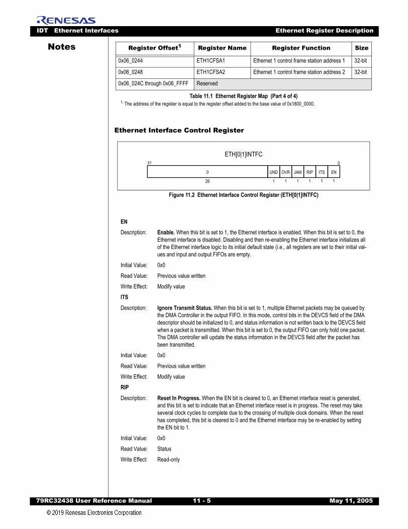
IDT Ethernet Interfaces Ethernet Register Description
79RC32438 User Refer
Notes
Ethernet Interface Control Register
Figure 11.2 Ethernet Interface Control Register (ETH[0|1]INTFC)
0x06_0244 ETH1CFSA1 Ethernet 1 control frame station address 1 32-bit
0x06_0248 ETH1CFSA2 Ethernet 1 control frame station address 2 32-bit
0x06_024C through 0x06_FFFF Reserved
1. The address of the register is equal to the register offset added to the base value of 0x1800_0000.
EN
Description: Enable. When this bit is set to 1, the Ethernet interface is enabled. When this bit is set to 0, the Ethernet interface is disabled. Disabling and then re-enabling the Ethernet interface initializes all of the Ethernet interface logic to its initial default state (i.e., all registers are set to their initial val-ues and input and output FIFOs are empty.
Initial Value: 0x0
Read Value: Previous value written
Write Effect: Modify value
ITS
Description: Ignore Transmit Status. When this bit is set to 1, multiple Ethernet packets may be queued by the DMA Controller in the output FIFO. In this mode, control bits in the DEVCS field of the DMA descriptor should be initialized to 0, and status information is not written back to the DEVCS field when a packet is transmitted. When this bit is set to 0, the output FIFO can only hold one packet. The DMA controller will update the status information in the DEVCS field after the packet has been transmitted.
Initial Value: 0x0
Read Value: Previous value written
Write Effect: Modify value
RIP
Description: Reset In Progress. When the EN bit is cleared to 0, an Ethernet interface reset is generated, and this bit is set to indicate that an Ethernet interface reset is in progress. The reset may take several clock cycles to complete due to the crossing of multiple clock domains. When the reset has completed, this bit is cleared to 0 and the Ethernet interface may be re-enabled by setting the EN bit to 1.
Initial Value: 0x0
Read Value: Status
Write Effect: Read-only
Register Offset1 Register Name Register Function Size
Table 11.1 Ethernet Register Map (Part 4 of 4)
ETH[0|1]INTFC031
EN
1
0
26
ITS
11
RIP
1
JAM
1
OVR
1
UND
ence Manual 11 - 5 May 11, 2005
IDT Ethernet Interfaces Ethernet Register Description
79RC32438 User Refer
Notes
Because the packet portion of the collision window for a frame to be transmitted fits entirely in theoutput FIFO, and remains there until it is transmitted without collision, there is never a need to re-fetch datato be transmitted.
When an output FIFO underflow occurs during packet transmission, then the UND bit is set in theETH[0|1]INTFC register and also in the DEVCS field of the DMA descriptor if the ITS bit is not set in theETH[0|1]INTFC register. The state of the UND bit in the ETH[0|1]INTFC register is presented to the interruptcontroller as an interrupt source.
When the MAC observes a valid preamble and start of frame delimiter, it begins receiving an Ethernetframe. If the destination address in the packet is not rejected by the address recognition logic, the packetdata is written by the MAC into the input FIFO. Once data beyond the collision window is received withouterror, the DMA Controller is signalled that valid packet data exists in the input FIFO. If a collision is detectedwithin the collision window programmed in the COLWIN field, the resulting runt frame is automaticallyflushed from the input FIFO by the MAC.
Note: Collision frames, runt frames, and frames whose destination addresses are not accepted by the address recognition logic are never passed to the DMA Controller.
When an input FIFO overflow occurs during packet reception, the OVR bit is set in the ETH[0|1]INTFCregister. If less than 64-bytes of the packet have been written into the FIFO, then the packet is discardedfrom the input FIFO. If 64-bytes or more have been written into the FIFO, the remaining bytes of the packetare discarded but data already written to the FIFO is not flushed. When the DMA transfers a packet in whichan overflow occurred to memory, the OVR bit is set in the DEVCS field of the DMA descriptor. The state ofthe OVR bit in the ETH[0|1]INTFC register is presented to the interrupt controller as an interrupt source.
JAM
Description: Transmit Half Duplex Flow Control. When this bit is set to 1, the Ethernet MAC transmits a preamble on the wire causing other MACs to defer. This may be used as a means of achieving half duplex flow control. When this bit is set to 0, the preamble is not transmitted.
Initial Value: 0x0
Read Value: Previous value written
Write Effect: Modify value
OVR
Description: Input FIFO Overflow. This bit is set to 1 when the input FIFO overflows. If the overflow occurs before 64-bytes of a packet are received and written into the input FIFO, then the entire contents of the packet are discarded. If more than 64-bytes of the packet are received and written into the input FIFO and an overflow occurs, then the remaining bytes of the packet are discarded and the OVR bit is set in the DMA descriptor when the packet is transferred to memory. Once the input FIFO overflows, all subsequent packets are discarded until space becomes available in the input FIFO. Note that for all other errors, packets are received.
Initial Value: 0x0
Read Value: Status
Write Effect: Sticky bit (a sticky bit is set by the hardware and can only be cleared by the CPU)
UND
Description: Output FIFO Underflow. This bit is set to 1 if frame transmission is aborted due to an output FIFO underflow. An output FIFO underflow condition would typically be due to latencies within the system and should not occur under normal operating conditions. When this condition occurs, the remainder of the data for the current frame is discarded. However, subsequent frames are transmitted properly.
Initial Value: 0x0
Read Value: Status
Write Effect: Sticky bit (a sticky bit is set by the hardware and can only be cleared by the CPU)
ence Manual 11 - 6 May 11, 2005
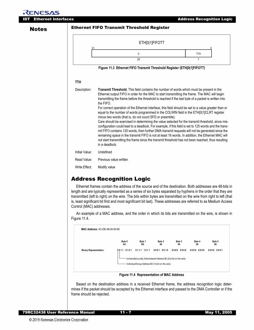
IDT Ethernet Interfaces Address Recognition Logic
79RC32438 User Refer
Notes
Ethernet FIFO Transmit Threshold RegisterFigure 11.3 Ethernet FIFO Transmit Threshold Register (ETH[0|1]FIFOTT)
Address Recognition LogicEthernet frames contain the address of the source and of the destination. Both addresses are 48-bits in
length and are typically represented as a series of six bytes separated by hyphens in the order that they aretransmitted (left to right) on the wire. The bits within bytes are transmitted on the wire from right to left (thatis, least significant bit first and most significant bit last). These addresses are referred to as Medium AccessControl (MAC) addresses.
An example of a MAC address, and the order in which its bits are transmitted on the wire, is shown inFigure 11.4.
Figure 11.4 Representation of MAC Address
Based on the destination address in a received Ethernet frame, the address recognition logic deter-mines if the packet should be accepted by the Ethernet interface and passed to the DMA Controller or if theframe should be rejected.
TTH
Description: Transmit Threshold. This field contains the number of words which must be present in the Ethernet output FIFO in order for the MAC to start transmitting the frame. The MAC will begin transmitting the frame before the threshold is reached if the last byte of a packet is written into the FIFO.For correct operation of the Ethernet interface, this field should be set to a value greater than or equal to the number of words programmed in the COLWIN field in the ETH[0|1]CLRT register minus two words (that is, do not count SFD or preamble).Care should be exercised in determining the value selected for the transmit threshold, since mis-configuration could lead to a deadlock. For example, if this field is set to 125 words and the trans-mit FIFO contains 120 words, then further DMA transmit requests will not be generated since the remaining space in the transmit FIFO is not at least 16 words. In addition, the Ethernet MAC will not start transmitting the frame since the transmit threshold has not been reached, thus resulting in a deadlock.
Initial Value: Undefined
Read Value: Previous value written
Write Effect: Modify value
ETH[0|1]FIFOTT031
TTH
25 7
0
Byte 0AC
Byte 1DE
Byte 248
Byte 300
Byte 400
Byte 580
Binary Representation: 0 0 1 1 0 1 0 1 0 1 1 1 1 0 1 1 0 0 0 1 0 0 1 0 0 0 0 0 0 0 0 0 0 0 0 0 0 0 0 0 0 0 0 0 0 0 0 1
Universally/Locally Administered Address Bit (2nd bit on the wire)
Individual/Group Address Bit (1st bit on the wire)
MAC Address: AC-DE-48-00-00-80
ence Manual 11 - 7 May 11, 2005
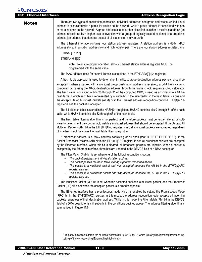
IDT Ethernet Interfaces Address Recognition Logic
79RC32438 User Refer
Notes
There are two types of destination addresses, individual addresses and group addresses. An individualaddress is associated with a particular station on the network, while a group address is associated with oneor more stations on the network. A group address can be further classified as either a multicast address (anaddress associated by a higher level convention with a group of logically related stations) or a broadcastaddress (an address that denotes the set of all stations on a given LAN).The Ethernet interface contains four station address registers. A station address is a 48-bit MACaddress stored in a station address low and high register pair. There are four station address register pairs:
ETHSAL[0|1|2|3]ETHSAH[0|1|2|3]
Note: To ensure proper operation, all four Ethernet station address registers MUST be programmed with the same value.
The MAC address used for control frames is contained in the ETHCFSA[0|1|2] registers.A hash table approach is used to determine if multicast group destination address packets should be
accepted.1 When a packet with a multicast group destination address is received, a 6-bit hash value iscomputed by passing the 48-bit destination address through the frame check sequence CRC calculator.The hash value, consisting of bits 26 through 31 of the computed CRC, is used as an index into a 64 binhash table in which each bin is represented by a single bit. If the selected bit in the hash table is a one andthe Accept Filtered Multicast Packets (AFM) bit in the Ethernet address recognition control (ETH[0|1]ARC)register is set, the packet is accepted.
The 64-bit hash table is stored in the HASH[0|1] registers. HASH0 contains bits 0 through 31 of the hashtable, while HASH1 contains bits 32 through 63 of the hash table.
The hash table filtering algorithm is not perfect, and therefore packets must be further filtered by soft-ware to determine if they do, in fact, match a multicast address that should be accepted. If the Accept AllMulticast Packets (AM) bit in the ETH[0|1]ARC register is set, all multicast packets are accepted regardlessof whether or not they pass the hash table filtering algorithm.
A broadcast address is a MAC address consisting of all ones (that is, FF-FF-FF-FF-FF-FF). If theAccept Broadcast Packets (AB) bit in the ETH[0|1]ARC register is set, all broadcast packets are acceptedby the Ethernet interface. When this bit is cleared, all broadcast packets are rejected. When a packet isaccepted by the Ethernet interface, three bits are updated in the DEVCS field of a DMA descriptor.
The Filter Match (FM) bit is set when one of the following conditions occurs: – The packet matches an individual station address – The packet passes the hash table filtering algorithm described above – The packet is a multicast packet and was accepted because the AM bit in the ETH[0|1]ARC
register was set – The packet is a broadcast packet and was accepted because the AB bit in the ETH[0|1]ARC
register was set. The Multicast Packet (MP) bit is set when the accepted packet is a multicast packet, and the Broadcast
Packet (BP) bit is set when the accepted packet is a broadcast packet.The Ethernet interface has a promiscuous mode which is enabled by setting the Promiscuous Mode
(PRO) bit in the ETH[0|1]ARC register. In this mode, the address recognition logic accepts all incomingpackets regardless of their destination address. While in this mode, the Filter Match (FM) bit in the DEVCSfield of a DMA descriptor is still set only in the conditions outlined above. The address filtering algorithm issummarized in Figure 11.6.
1. The only exception to this is the multicast address 01-80-c2-00-00-01 which is always received regardless of the setting of the corresponding Ethernet hash table entry.
ence Manual 11 - 8 May 11, 2005
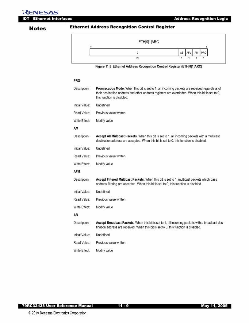
IDT Ethernet Interfaces Address Recognition Logic
79RC32438 User Refer
Notes
Ethernet Address Recognition Control RegisterFigure 11.5 Ethernet Address Recognition Control Register (ETH[0|1]ARC)
PRO
Description: Promiscuous Mode. When this bit is set to 1, all incoming packets are received regardless of their destination address and other address registers are overridden. When this bit is set to 0, this function is disabled.
Initial Value: Undefined
Read Value: Previous value written
Write Effect: Modify value
AM
Description: Accept All Multicast Packets. When this bit is set to 1, all incoming packets with a multicast destination address are accepted. When this bit is set to 0, this function is disabled.
Initial Value: Undefined
Read Value: Previous value written
Write Effect: Modify value
AFM
Description: Accept Filtered Multicast Packets. When this bit is set to 1, multicast packets which pass address filtering are accepted. When this bit is set to 0, this function is disabled.
Initial Value: Undefined
Read Value: Previous value written
Write Effect: Modify value
AB
Description: Accept Broadcast Packets. When this bit is set to 1, all incoming packets with a broadcast des-tination address are received. When this bit is set to 0, this function is disabled.
Initial Value: Undefined
Read Value: Previous value written
Write Effect: Modify value
ETH[0|1]ARC031
28
0 PRO
1
AM
1
AFM
1
AB
1
ence Manual 11 - 9 May 11, 2005
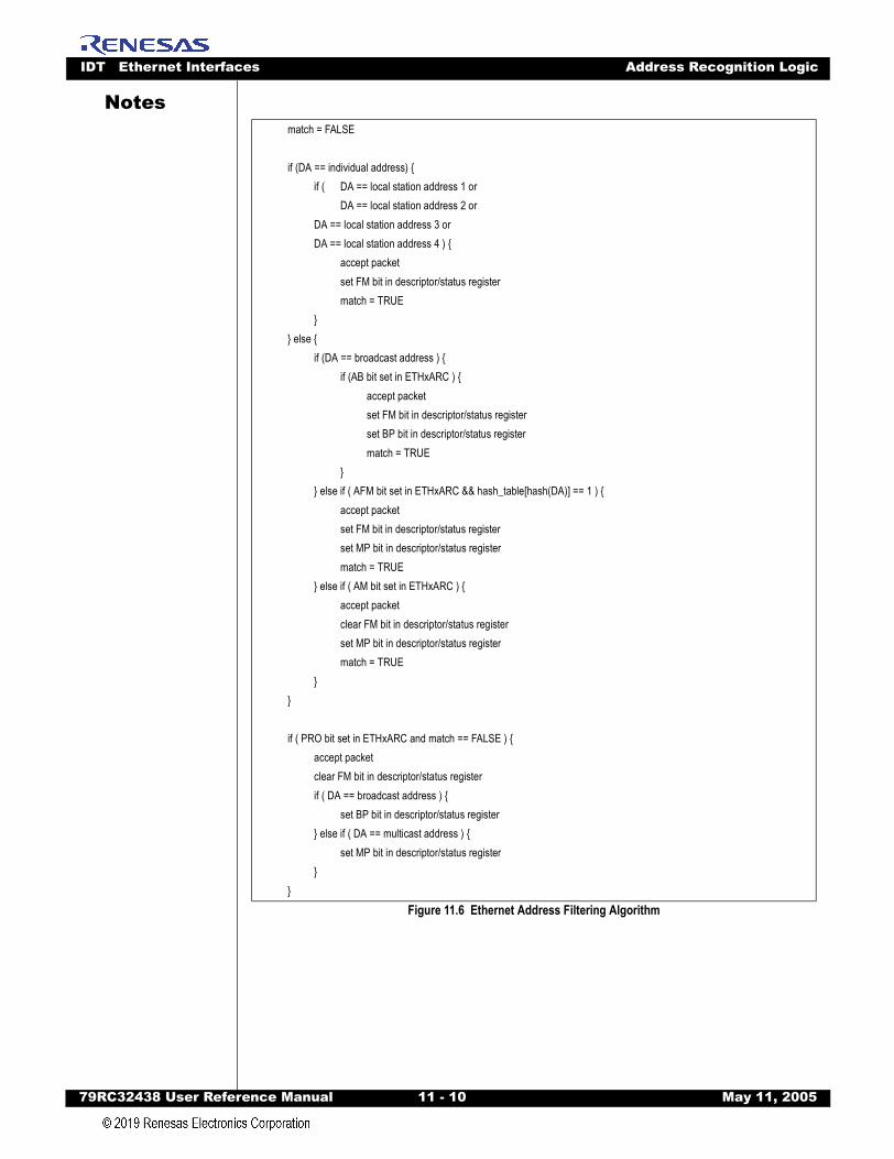
IDT Ethernet Interfaces Address Recognition Logic
79RC32438 User Refer
Notes
match = FALSEif (DA == individual address) if ( DA == local station address 1 or
DA == local station address 2 or DA == local station address 3 or DA == local station address 4 )
accept packetset FM bit in descriptor/status registermatch = TRUE
else
if (DA == broadcast address ) if (AB bit set in ETHxARC )
accept packetset FM bit in descriptor/status registerset BP bit in descriptor/status registermatch = TRUE
else if ( AFM bit set in ETHxARC && hash_table[hash(DA)] == 1 )
accept packetset FM bit in descriptor/status registerset MP bit in descriptor/status registermatch = TRUE
else if ( AM bit set in ETHxARC ) accept packetclear FM bit in descriptor/status registerset MP bit in descriptor/status registermatch = TRUE
if ( PRO bit set in ETHxARC and match == FALSE ) accept packetclear FM bit in descriptor/status registerif ( DA == broadcast address )
set BP bit in descriptor/status register else if ( DA == multicast address )
set MP bit in descriptor/status register
Figure 11.6 Ethernet Address Filtering Algorithm
ence Manual 11 - 10 May 11, 2005
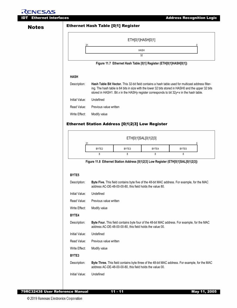
IDT Ethernet Interfaces Address Recognition Logic
79RC32438 User Refer
Notes
Ethernet Hash Table [0|1] RegisterFigure 11.7 Ethernet Hash Table [0|1] Register (ETH[0|1]HASH[0|1])
Ethernet Station Address [0|1|2|3] Low Register
Figure 11.8 Ethernet Station Address [0|1|2|3] Low Register (ETH[0|1]SAL[0|1|2|3])
HASH
Description: Hash Table Bit Vector. This 32-bit field contains a hash table used for multicast address filter-ing. The hash table is 64 bits in size with the lower 32 bits stored in HASH0 and the upper 32 bits stored in HASH1. Bit x in the HASHy register corresponds to bit 32y+x in the hash table.
Initial Value: Undefined
Read Value: Previous value written
Write Effect: Modify value
BYTE5
Description: Byte Five. This field contains byte five of the 48-bit MAC address. For example, for the MAC address AC-DE-48-00-00-80, this field holds the value 80.
Initial Value: Undefined
Read Value: Previous value written
Write Effect: Modify value
BYTE4
Description: Byte Four. This field contains byte four of the 48-bit MAC address. For example, for the MAC address AC-DE-48-00-00-80, this field holds the value 00.
Initial Value: Undefined
Read Value: Previous value written
Write Effect: Modify value
BYTE3
Description: Byte Three. This field contains byte three of the 48-bit MAC address. For example, for the MAC address AC-DE-48-00-00-80, this field holds the value 00.
Initial Value: Undefined
ETH[0|1]HASH[0|1]031
32
HASH
ETH[0|1]SAL[0|1|2|3]031
8
BYTE4
8
BYTE3
8
BYTE2
8
BYTE5
ence Manual 11 - 11 May 11, 2005
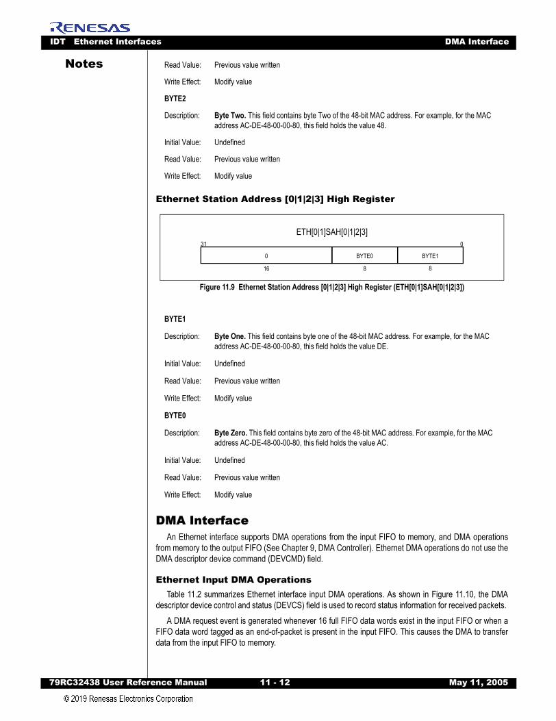
IDT Ethernet Interfaces DMA Interface
79RC32438 User Refer
Notes
Ethernet Station Address [0|1|2|3] High Register
Figure 11.9 Ethernet Station Address [0|1|2|3] High Register (ETH[0|1]SAH[0|1|2|3])
DMA InterfaceAn Ethernet interface supports DMA operations from the input FIFO to memory, and DMA operations
from memory to the output FIFO (See Chapter 9, DMA Controller). Ethernet DMA operations do not use theDMA descriptor device command (DEVCMD) field.
Ethernet Input DMA OperationsTable 11.2 summarizes Ethernet interface input DMA operations. As shown in Figure 11.10, the DMA
descriptor device control and status (DEVCS) field is used to record status information for received packets. A DMA request event is generated whenever 16 full FIFO data words exist in the input FIFO or when a
FIFO data word tagged as an end-of-packet is present in the input FIFO. This causes the DMA to transferdata from the input FIFO to memory.
Read Value: Previous value written
Write Effect: Modify value
BYTE2
Description: Byte Two. This field contains byte Two of the 48-bit MAC address. For example, for the MAC address AC-DE-48-00-00-80, this field holds the value 48.
Initial Value: Undefined
Read Value: Previous value written
Write Effect: Modify value
BYTE1
Description: Byte One. This field contains byte one of the 48-bit MAC address. For example, for the MAC address AC-DE-48-00-00-80, this field holds the value DE.
Initial Value: Undefined
Read Value: Previous value written
Write Effect: Modify value
BYTE0
Description: Byte Zero. This field contains byte zero of the 48-bit MAC address. For example, for the MAC address AC-DE-48-00-00-80, this field holds the value AC.
Initial Value: Undefined
Read Value: Previous value written
Write Effect: Modify value
ETH[0|1]SAH[0|1|2|3]031
16
0
8
BYTE0
8
BYTE1
ence Manual 11 - 12 May 11, 2005
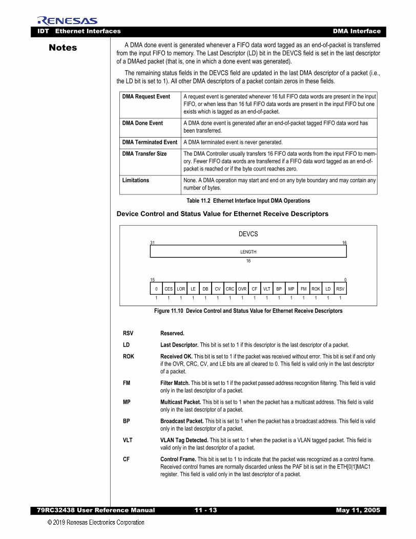
IDT Ethernet Interfaces DMA Interface
79RC32438 User Refer
Notes
A DMA done event is generated whenever a FIFO data word tagged as an end-of-packet is transferredfrom the input FIFO to memory. The Last Descriptor (LD) bit in the DEVCS field is set in the last descriptorof a DMAed packet (that is, one in which a done event was generated).The remaining status fields in the DEVCS field are updated in the last DMA descriptor of a packet (i.e.,the LD bit is set to 1). All other DMA descriptors of a packet contain zeros in these fields.
Device Control and Status Value for Ethernet Receive Descriptors
Figure 11.10 Device Control and Status Value for Ethernet Receive Descriptors
DMA Request Event A request event is generated whenever 16 full FIFO data words are present in the input FIFO, or when less than 16 full FIFO data words are present in the input FIFO but one exists which is tagged as an end-of-packet.
DMA Done Event A DMA done event is generated after an end-of-packet tagged FIFO data word has been transferred.
DMA Terminated Event A DMA terminated event is never generated.
DMA Transfer Size The DMA Controller usually transfers 16 FIFO data words from the input FIFO to mem-ory. Fewer FIFO data words are transferred if a FIFO data word tagged as an end-of-packet is reached or if the byte count reaches zero.
Limitations None. A DMA operation may start and end on any byte boundary and may contain any number of bytes.
Table 11.2 Ethernet Interface Input DMA Operations
RSV Reserved.
LD Last Descriptor. This bit is set to 1 if this descriptor is the last descriptor of a packet.
ROK Received OK. This bit is set to 1 if the packet was received without error. This bit is set if and only if the OVR, CRC, CV, and LE bits are all cleared to 0. This field is valid only in the last descriptor of a packet.
FM Filter Match. This bit is set to 1 if the packet passed address recognition filtering. This field is valid only in the last descriptor of a packet.
MP Multicast Packet. This bit is set to 1 when the packet has a multicast address. This field is valid only in the last descriptor of a packet.
BP Broadcast Packet. This bit is set to 1 when the packet has a broadcast address. This field is valid only in the last descriptor of a packet.
VLT VLAN Tag Detected. This bit is set to 1 when the packet is a VLAN tagged packet. This field is valid only in the last descriptor of a packet.
CF Control Frame. This bit is set to 1 to indicate that the packet was recognized as a control frame. Received control frames are normally discarded unless the PAF bit is set in the ETH[0|1]MAC1 register. This field is valid only in the last descriptor of a packet.
DEVCS1631
16
LENGTH
015
RSV
1
LD
1
ROK
1
FM
1
MP
1
BP
1
VLT
1
CF
1
OVR
1
CRC
1
CV
1
DB
1
LE
1
LOR
1
CES
1
0
1
ence Manual 11 - 13 May 11, 2005
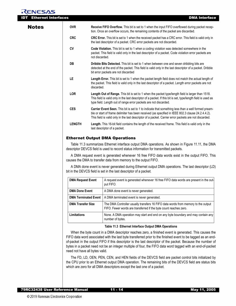
IDT Ethernet Interfaces DMA Interface
79RC32438 User Refer
Notes
Ethernet Output DMA OperationsTable 11.3 summarizes Ethernet interface output DMA operations. As shown in Figure 11.11, the DMA
descriptor DEVCS field is used to record status information for transmitted packets. A DMA request event is generated whenever 16 free FIFO data words exist in the output FIFO. This
causes the DMA to transfer data from memory to the output FIFO. A DMA done event is never generated during Ethernet output DMA operations. The last descriptor (LD)
bit in the DEVCS field is set in the last descriptor of a packet.
When the byte count in a DMA descriptor reaches zero, a finished event is generated. This causes theFIFO data word associated with the last byte transferred prior to the finished event to be tagged as an end-of-packet in the output FIFO if this descriptor is the last descriptor of the packet. Because the number ofbytes in a packet need not be an integer multiple of four, the FIFO data word tagged with an end-of-packetneed not have all bytes valid.
The FD, LD, OEN, PEN, CEN, and HEN fields of the DEVCS field are packet control bits initialized bythe CPU prior to an Ethernet output DMA operation. The remaining bits of the DEVCS field are status bitswhich are zero for all DMA descriptors except the last one of a packet.
OVR Receive FIFO Overflow. This bit is set to 1 when the input FIFO overflowed during packet recep-tion. Once an overflow occurs, the remaining contents of the packet are discarded.
CRC CRC Error. This bit is set to 1 when the received packet has a CRC error. This field is valid only in the last descriptor of a packet. CRC error packets are not discarded.
CV Code Violation. This bit is set to 1 when a coding violation was detected somewhere in the packet. This field is valid only in the last descriptor of a packet. Code violation error packets are not discarded.
DB Dribble Bits Detected. This bit is set to 1 when between one and seven dribbling bits are detected at the end of the packet. This field is valid only in the last descriptor of a packet. Dribble bit error packets are not discarded
LE Length Error. This bit is set to 1 when the packet length field does not match the actual length of the packet. This field is valid only in the last descriptor of a packet. Length error packets are not discarded.
LOR Length Out of Range. This bit is set to 1 when the packet type/length field is larger than 1518. This field is valid only in the last descriptor of a packet. If this bit is set, type/length field is used as type field. Length out of range error packets are not discarded.
CES Carrier Event Seen. This bit is set to 1 to indicate that something less than a well formed pream-ble or start of frame delimiter has been received (as specified in IEEE 802.3 clause 24.2.4.4.2). This field is valid only in the last descriptor of a packet. Carrier error packets are not discarded.
LENGTH Length. This 16-bit field contains the length of the received frame. This field is valid only in the last descriptor of a packet.
DMA Request Event A request event is generated whenever 16 free FIFO data words are present in the out-put FIFO.
DMA Done Event A DMA done event is never generated.
DMA Terminated Event A DMA terminated event is never generated.
DMA Transfer Size The DMA Controller usually transfers 16 FIFO data words from memory to the output FIFO. Fewer words are transferred if the byte count reaches zero.
Limitations None. A DMA operation may start and end on any byte boundary and may contain any number of bytes.
Table 11.3 Ethernet Interface Output DMA Operations
ence Manual 11 - 14 May 11, 2005
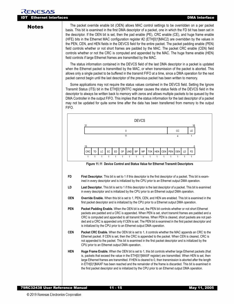
IDT Ethernet Interfaces DMA Interface
79RC32438 User Refer
Notes
The packet override enable bit (OEN) allows MAC control settings to be overridden on a per packetbasis. This bit is examined in the first DMA descriptor of a packet, one in which the FD bit has been set inthe descriptor. If the OEN bit is set, then the pad enable (PE), CRC enable (CE), and huge frame enable(HFE) bits in the Ethernet MAC configuration register #2 (ETH[0|1]MAC2) are overridden by the values inthe PEN, CEN, and HEN fields in the DEVCS field for the entire packet. The packet padding enable (PEN)field controls whether or not short frames are padded by the MAC. The packet CRC enable (CEN) fieldcontrols whether or not the CRC is computed and appended by the MAC. The huge frame enable (HEN)field controls if large Ethernet frames are transmitted by the MAC.The status information contained in the DEVCS field of the last DMA descriptor in a packet is updatedwhen the Ethernet packet is transmitted by the MAC, or when transmission of the packet is aborted. Thisallows only a single packet to be buffered in the transmit FIFO at a time, since a DMA operation for the nextpacket cannot begin until the last descriptor of the previous packet has been written to memory.
Some applications may not require the status values contained in the DEVCS field. Setting the IgnoreTransmit Status (ITS) bit in the ETH[0|1]INTFC register causes the status fields of the DEVCS field in thedescriptor to always be written back to memory with zeros and allows multiple packets to be queued by theDMA Controller in the output FIFO. This implies that the status information for the last descriptor of a packetmay not be updated for quite some time after the data has been transferred from memory to the outputFIFO.
Figure 11.11 Device Control and Status Value for Ethernet Transmit Descriptors
FD First Descriptor. This bit is set to 1 if this descriptor is the first descriptor of a packet. This bit is exam-ined in every descriptor and is initialized by the CPU prior to an Ethernet output DMA operation.
LD Last Descriptor. This bit is set to 1 if this descriptor is the last descriptor of a packet. This bit is examined in every descriptor and is initialized by the CPU prior to an Ethernet output DMA operation.
OEN Override Enable. When this bit is set to 1, PEN, CEN, and HEN are enabled. This bit is examined in the first packet descriptor and is initialized by the CPU prior to a Ethernet output DMA operation.
PEN Packet Padding Enable. When the OEN bit is set, the PEN bit controls whether or not short Ethernet packets are padded and a CRC is appended. When PEN is set, short transmit frames are padded and a CRC is computed and appended to all transmit frames. When PEN is cleared, short packets are not pad-ded and a CRC is appended only if CEN is set. The PEN bit is examined in the first packet descriptor and is initialized by the CPU prior to an Ethernet output DMA operation.
CEN Packet CRC Enable. When the OEN bit is set to 1, it controls whether the MAC appends an CRC to the Ethernet packet. If CEN is set, then the CRC is appended to the packet. When CEN is cleared, CRC is not appended to the packet. This bit is examined in the first packet descriptor and is initialized by the CPU prior to an Ethernet output DMA operation.
HEN Huge Frame Enable. When the OEN bit is set to 1, this bit controls whether large Ethernet packets (that is, packets that exceed the value in the ETH[0|1]MAXF register) are transmitted. When HEN is set, then large Ethernet frames are transmitted. If HEN is cleared to 0, then transmission is aborted after the length in ETH[0|1]MAXF has been reached and the remainder of the frame is discarded. This bit is examined in the first packet descriptor and is initialized by the CPU prior to an Ethernet output DMA operation.
FD
DEVCS1631
11
0
015
1
TOK
1
MP
1
BP
1
UND
1
OF
1
ED
1
EC
1
LC
1
TD
1
CRC
1
LE
1
LD
1
OEN
1
PEN
1
CEN
1
HEN
1
CC
4
ence Manual 11 - 15 May 11, 2005
IDT Ethernet Interfaces Ethernet Statistics
79RC32438 User Refer
Notes
Ethernet StatisticsThe Ethernet interface contains five 32-bit counters which may be used to gather statistics. Each
counter increments by one each time the specified receive or transmit event occurs. The CPU may readthese counters at any time, provided that the MII clocks are supplied and the RIP bit in the ETH[0|1]INTFCregister is not set to 1. The act of reading a counter causes its value to be reset to zero as an atomic opera-tion. This prevents the loss of events due to non-atomic read and clear operations.
Ethernet Receive Byte Count Register
Figure 11.12 Ethernet Receive Byte Count (ETH[0|1]RBC)
TOK Transmit OK. This bit is set to 1 when the packet is transmitted without error. This bit is set if and only if the UND, OF, ED, EC, and LC bits are all cleared. This field is valid only in the last descriptor of a packet.
MP Multicast Packet. This bit is set to 1 when the transmitted packet has a multicast address. This field is valid only in the last descriptor of a packet.
BP Broadcast Packet. This bit is set to 1 when the transmitted packet has a broadcast address. This field is valid only in the last descriptor of a packet.
UND Transmit FIFO Underflow. This bit is set to 1 if frame transmission was aborted due to an output FIFO underflow. This field is valid only in the last descriptor of a packet.
OF Oversized Frame. This bit is set to 1 if transmission was aborted due to an attempt to transmit a frame larger than the value in the ETH[0|1]MAXF register. The contents of the frame beyond ETH[0|1]MAXF are discarded. This field is valid only in the last descriptor of a packet.
ED Excessive Deferral. This bit is set to 1 if transmission was aborted due to excessive deferrals. This field is valid only in the last descriptor of a packet.
EC Excessive Collisions. This bit is set to 1 if transmission was aborted due to excessive collisions. This field is valid only in the last descriptor of a packet.
LC Late Collision. This bit is set to 1 if transmission was aborted due to a collision beyond the collision win-dow. This field is valid only in the last descriptor of a packet.
TD Transmit Deferred. This bit is set to 1 if transmission of the frame was deferred on the first transmission attempt. This field is valid only in the last descriptor of a packet.
CRC CRC Error. This bit is set to 1 if the CRC in the transmitted frame does not match the CRC computed by the MAC. If the MAC is configured to automatically compute and append the CRC to transmitted frames, then the value of this bit should be ignored. This field is valid only in the last descriptor of a packet.
LE Length Error. This bit is set to 1 if the value of the length field of the transmitted frame does not match the actual length. This field is valid only in the last descriptor of a packet.
CC Collision Count. This 4-bit field indicates the number of collisions that the successfully transmitted frame experienced. This field is not valid if frame transmission was aborted due to excessive collisions. This field is valid only in the last descriptor of a packet.
ETHRBC
Description: Ethernet Receive Byte Count. Total number of bytes in all packets received by the Ethernet interface (including bad packets, packets discarded by hardware, and control frames). This value does not include SFD or preamble bytes. Reading this register atomically clears its value to zero.
ETH[0|1]RBC031
32
ETH[0|1]RBC
ence Manual 11 - 16 May 11, 2005
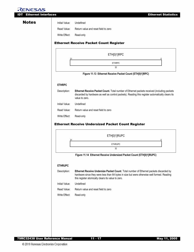
IDT Ethernet Interfaces Ethernet Statistics
79RC32438 User Refer
Notes
Ethernet Receive Packet Count Register
Figure 11.13 Ethernet Receive Packet Count (ETH[0|1]RPC)
Ethernet Receive Undersized Packet Count Register
Figure 11.14 Ethernet Receive Undersized Packet Count (ETH[0|1]RUPC)
Initial Value: Undefined
Read Value: Return value and reset field to zero
Write Effect: Read-only
ETHRPC
Description: Ethernet Receive Packet Count. Total number of Ethernet packets received (including packets discarded by hardware as well as control packets). Reading this register automatically clears its value to zero.
Initial Value: Undefined
Read Value: Return value and reset field to zero
Write Effect: Read-only
ETHRUPC
Description: Ethernet Receive Undersize Packet Count. Total number of Ethernet packets discarded by hardware since they were less than 64 bytes in size but were otherwise well formed. Reading this register atomically clears its value to zero.
Initial Value: Undefined
Read Value: Return value and reset field to zero
Write Effect: Read-only
ETH[0|1]RPC031
32
ETHRPC
ETH[0|1]RUPC031
32
ETHRUPC
ence Manual 11 - 17 May 11, 2005

IDT Ethernet Interfaces PAUSE Control Frames
79RC32438 User Refer
Notes
Ethernet Receive Fragment Count RegisterFigure 11.15 Ethernet Receive Fragment Count (ETH[0|1]RFC)
Ethernet Transmit Byte Count Register
Figure 11.16 Ethernet Transmit Byte Count (ETH[0|1]TBC)
PAUSE Control FramesThe Ethernet interface supports PAUSE control frames as defined by IEEE Std 802.3x-1997. Received
PAUSE control frames are handled by the Ethernet MAC. A control frame is a frame with a type/length fieldthat identifies a control frame (i.e., 0x88_08). Control frames are accepted or rejected in the same manneras all other frames (i.e., using the method specified in the Address Recognition Logic section of thischapter). The only exception to this is the multicast address 01-80-c2-00-00-01 which is always receivedregardless of the setting of the corresponding Ethernet hash table entry.
A PAUSE control frame is a control frame with a multicast address of 01-80-c2-00-00-01 and an opcodefield that corresponds to a PAUSE frame (i.e., 0x00_01). The MAC normally processes PAUSE controlframes but it may be configured to ignore PAUSE control frames by clearing the Receive Flow Control(RFC) bit in the Ethernet MAC 1 (ETH[0|1]MAC1) register. Control frames are normally discarded afterrequired processing by the MAC. However, if the Pass All Frames (PAF) bit is set in the ETH[0|1]MAC
ETHRFC
Description: Ethernet Receive Fragment Count. Total number of Ethernet packets discarded by hardware since they were less than 64 bytes in size and had either a CRC error or an alignment error (that is, not an integral number of bytes). Reading this register atomically clears its value to zero.
Initial Value: Undefined
Read Value: Return value and reset field to zero
Write Effect: Read-only
ETHTBC
Description: Ethernet Transmit Byte Count. Total number of bytes transmitted by the Ethernet interface (includes control frames and retransmissions). This value does not include SFD, preamble, or jam bytes. Reading this register atomically clears its value to zero.
Initial Value: Undefined
Read Value: Return value and reset field to zero
Write Effect: Read-only
ETH[0|1]RFC031
32
ETHRFC
ETH[0|1]TBC031
32
ETHTBC
ence Manual 11 - 18 May 11, 2005
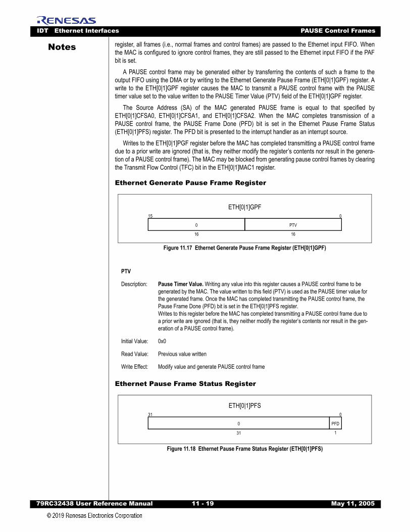
IDT Ethernet Interfaces PAUSE Control Frames
79RC32438 User Refer
Notes
register, all frames (i.e., normal frames and control frames) are passed to the Ethernet input FIFO. Whenthe MAC is configured to ignore control frames, they are still passed to the Ethernet input FIFO if the PAFbit is set.A PAUSE control frame may be generated either by transferring the contents of such a frame to theoutput FIFO using the DMA or by writing to the Ethernet Generate Pause Frame (ETH[0|1]GPF) register. Awrite to the ETH[0|1]GPF register causes the MAC to transmit a PAUSE control frame with the PAUSEtimer value set to the value written to the PAUSE Timer Value (PTV) field of the ETH[0|1]GPF register.
The Source Address (SA) of the MAC generated PAUSE frame is equal to that specified byETH[0|1]CFSA0, ETH[0|1]CFSA1, and ETH[0|1]CFSA2. When the MAC completes transmission of aPAUSE control frame, the PAUSE Frame Done (PFD) bit is set in the Ethernet Pause Frame Status(ETH[0|1]PFS) register. The PFD bit is presented to the interrupt handler as an interrupt source.
Writes to the ETH[0|1]PGF register before the MAC has completed transmitting a PAUSE control framedue to a prior write are ignored (that is, they neither modify the register’s contents nor result in the genera-tion of a PAUSE control frame). The MAC may be blocked from generating pause control frames by clearingthe Transmit Flow Control (TFC) bit in the ETH[0|1]MAC1 register.
Ethernet Generate Pause Frame Register
Figure 11.17 Ethernet Generate Pause Frame Register (ETH[0|1]GPF)
Ethernet Pause Frame Status Register
Figure 11.18 Ethernet Pause Frame Status Register (ETH[0|1]PFS)
PTV
Description: Pause Timer Value. Writing any value into this register causes a PAUSE control frame to be generated by the MAC. The value written to this field (PTV) is used as the PAUSE timer value for the generated frame. Once the MAC has completed transmitting the PAUSE control frame, the Pause Frame Done (PFD) bit is set in the ETH[0|1]PFS register.Writes to this register before the MAC has completed transmitting a PAUSE control frame due to a prior write are ignored (that is, they neither modify the register’s contents nor result in the gen-eration of a PAUSE control frame).
Initial Value: 0x0
Read Value: Previous value written
Write Effect: Modify value and generate PAUSE control frame
ETH[0|1]GPF015
PTV
16
0
16
ETH[0|1]PFS031
31
0 PFD
1
ence Manual 11 - 19 May 11, 2005
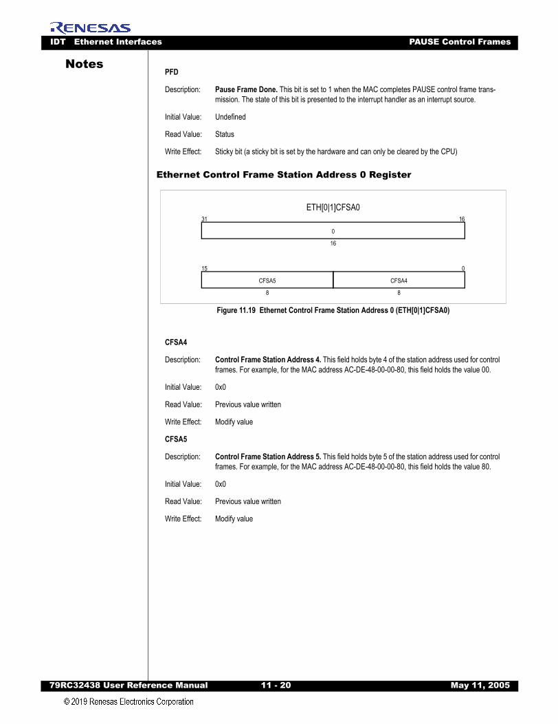
IDT Ethernet Interfaces PAUSE Control Frames
79RC32438 User Refer
Notes
Ethernet Control Frame Station Address 0 Register
Figure 11.19 Ethernet Control Frame Station Address 0 (ETH[0|1]CFSA0)
PFD
Description: Pause Frame Done. This bit is set to 1 when the MAC completes PAUSE control frame trans-mission. The state of this bit is presented to the interrupt handler as an interrupt source.
Initial Value: Undefined
Read Value: Status
Write Effect: Sticky bit (a sticky bit is set by the hardware and can only be cleared by the CPU)
CFSA4
Description: Control Frame Station Address 4. This field holds byte 4 of the station address used for control frames. For example, for the MAC address AC-DE-48-00-00-80, this field holds the value 00.
Initial Value: 0x0
Read Value: Previous value written
Write Effect: Modify value
CFSA5
Description: Control Frame Station Address 5. This field holds byte 5 of the station address used for control frames. For example, for the MAC address AC-DE-48-00-00-80, this field holds the value 80.
Initial Value: 0x0
Read Value: Previous value written
Write Effect: Modify value
ETH[0|1]CFSA0
015
1631
16
0
8 8
CFSA5 CFSA4
ence Manual 11 - 20 May 11, 2005
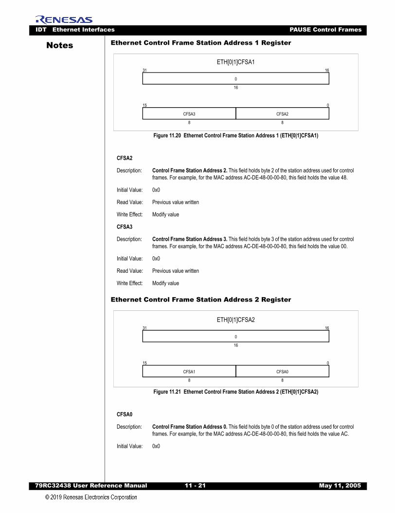
IDT Ethernet Interfaces PAUSE Control Frames
79RC32438 User Refer
Notes
Ethernet Control Frame Station Address 1 RegisterFigure 11.20 Ethernet Control Frame Station Address 1 (ETH[0|1]CFSA1)
Ethernet Control Frame Station Address 2 Register
Figure 11.21 Ethernet Control Frame Station Address 2 (ETH[0|1]CFSA2)
CFSA2
Description: Control Frame Station Address 2. This field holds byte 2 of the station address used for control frames. For example, for the MAC address AC-DE-48-00-00-80, this field holds the value 48.
Initial Value: 0x0
Read Value: Previous value written
Write Effect: Modify value
CFSA3
Description: Control Frame Station Address 3. This field holds byte 3 of the station address used for control frames. For example, for the MAC address AC-DE-48-00-00-80, this field holds the value 00.
Initial Value: 0x0
Read Value: Previous value written
Write Effect: Modify value
CFSA0
Description: Control Frame Station Address 0. This field holds byte 0 of the station address used for control frames. For example, for the MAC address AC-DE-48-00-00-80, this field holds the value AC.
Initial Value: 0x0
ETH[0|1]CFSA1
015
1631
16
0
8 8
CFSA3 CFSA2
ETH[0|1]CFSA2
015
1631
16
0
8 8
CFSA1 CFSA0
ence Manual 11 - 21 May 11, 2005
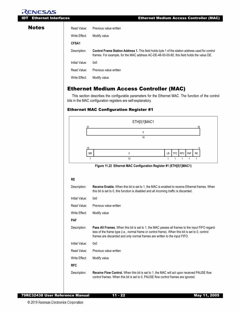
IDT Ethernet Interfaces Ethernet Medium Access Controller (MAC)
79RC32438 User Refer
Notes
Ethernet Medium Access Controller (MAC)This section describes the configurable parameters for the Ethernet MAC. The function of the control
bits in the MAC configuration registers are self-explanatory.
Ethernet MAC Configuration Register #1
Figure 11.22 Ethernet MAC Configuration Register #1 (ETH[0|1]MAC1)
Read Value: Previous value written
Write Effect: Modify value
CFSA1
Description: Control Frame Station Address 1. This field holds byte 1 of the station address used for control frames. For example, for the MAC address AC-DE-48-00-00-80, this field holds the value DE.
Initial Value: 0x0
Read Value: Previous value written
Write Effect: Modify value
RE
Description: Receive Enable. When this bit is set to 1, the MAC is enabled to receive Ethernet frames. When this bit is set to 0, this function is disabled and all incoming traffic is discarded.
Initial Value: 0x0
Read Value: Previous value written
Write Effect: Modify value
PAF
Description: Pass All Frames. When this bit is set to 1, the MAC passes all frames to the input FIFO regard-less of the frame type (i.e., normal frame or control frame). When this bit is set to 0, control frames are discarded and only normal frames are written to the input FIFO.
Initial Value: 0x0
Read Value: Previous value written
Write Effect: Modify value
RFC
Description: Receive Flow Control. When this bit is set to 1, the MAC will act upon received PAUSE flow control frames. When this bit is set to 0, PAUSE flow control frames are ignored.
ETH[0|1]MAC1
PAF
015
RE
1 1
TFC RFC
1 1
LB
1
MR
1
0
10
1631
16
0
ence Manual 11 - 22 May 11, 2005
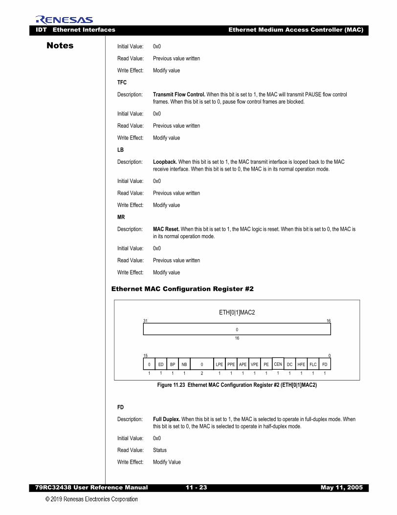
IDT Ethernet Interfaces Ethernet Medium Access Controller (MAC)
79RC32438 User Refer
Notes
Ethernet MAC Configuration Register #2
Figure 11.23 Ethernet MAC Configuration Register #2 (ETH[0|1]MAC2)
Initial Value: 0x0
Read Value: Previous value written
Write Effect: Modify value
TFC
Description: Transmit Flow Control. When this bit is set to 1, the MAC will transmit PAUSE flow control frames. When this bit is set to 0, pause flow control frames are blocked.
Initial Value: 0x0
Read Value: Previous value written
Write Effect: Modify value
LB
Description: Loopback. When this bit is set to 1, the MAC transmit interface is looped back to the MAC receive interface. When this bit is set to 0, the MAC is in its normal operation mode.
Initial Value: 0x0
Read Value: Previous value written
Write Effect: Modify value
MR
Description: MAC Reset. When this bit is set to 1, the MAC logic is reset. When this bit is set to 0, the MAC is in its normal operation mode.
Initial Value: 0x0
Read Value: Previous value written
Write Effect: Modify value
FD
Description: Full Duplex. When this bit is set to 1, the MAC is selected to operate in full-duplex mode. When this bit is set to 0, the MAC is selected to operate in half-duplex mode.
Initial Value: 0x0
Read Value: Status
Write Effect: Modify Value
ETH[0|1]MAC2
FLC
015
FD
1 1
DC HFE
1 1
PE
1
ED
1
APE VPE
1 1
PPE
1
NB LPE
1 1
BP
1
0
1
0
2
1631
16
0
CEN
1
ence Manual 11 - 23 May 11, 2005
IDT Ethernet Interfaces Ethernet Medium Access Controller (MAC)
79RC32438 User Refer
Notes
FLCDescription: Frame Length Checking. When this bit is set to 1, both transmit and receive frame lengths are compared to the length/type field. If the length/type field represents a length, a check is per-formed. When this bit is set to 0, Frame Length Checking is disabled.
Initial Value: 0x0
Read Value: Status
Write Effect: Modify Value
HFE
Description: Huge Frame Enable. When this bit is set to 1, frames of any length may be transmitted and received. When this bit is set to 0, transmission is aborted after the length in ETH[0|1]MAXF has been reached and the remainder of the frame is discarded.
Initial Value: 0x0
Read Value: Status
Write Effect: Modify Value
DC
Description: Delayed CRC. When this bit is set to 1, a four byte proprietary header exists on the front of all IEEE 802.3 frames. CRCs are not computed over the proprietary header. Thus, when this bit is set to 1, CRC calculations are delayed by four bytes. When this bit is set to 0, Delayed CRC is disabled.
Initial Value: 0x0
Read Value: Previous value written
Write Effect: Modify value
CEN
Description: CRC Enable. When this bit is set to 1, the MAC pads all short frames and appends a CRC to every frame. When this bit is cleared to 0, frames passed to the MAC are assumed to have a valid length and CRC (that is, these operations are performed in software). Refer to Table 11.4.
Initial Value: 0x0
Read Value: Previous value written
Write Effect: Modify value
PE
Description: Pad Enable. When this bit is set to 1, the MAC pads short transmit frames and computes and appends a CRC on all transmit frames. When this bit is set to 0, frames are padded prior to being passed to the MAC (i.e., padding operation is performed by software). Refer to Table 11.4.
Initial Value: 0x0
Read Value: Previous value written
Write Effect: Modify value
VPE
Description: VLAN Pad Enable. When this bit is set to 1 and padding is enabled, short transmit frames are padded to 64 bytes. If padding is enabled and this bit is cleared to 0, short transmit frames are padded to 60 bytes. Refer to Table 11.4.
Initial Value: 0x0
ence Manual 11 - 24 May 11, 2005
IDT Ethernet Interfaces Ethernet Medium Access Controller (MAC)
79RC32438 User Refer
Notes
Read Value: Previous value writtenWrite Effect: Modify value
APE
Description: Auto Pad Enable. When this bit is set to 1 and padding is enabled, the MAC automatically detects the frame type, either tagged or untagged, by comparing the two bytes following the source address with 0x1800 (VLAN protocol ID) and pads accordingly. Untagged frames are padded to 60 bytes while tagged frames are padded to 64 bytes. When this bit is set to 0, the Auto Padding function is disabled. Refer to Table 11.4.
Initial Value: 0x0
Read Value: Previous value written
Write Effect: Modify value
PPE
Description: Pure Preamble Enforcement. When this bit is set to 1, the MAC will verify the content of the preamble to ensure it contains 0x55 and is error-free. A frame with an error in the preamble is discarded. When this bit is cleared, no preamble checking is performed.
Initial Value: 0x0
Read Value: Previous value written
Write Effect: Modify value
LPE
Description: Long Preamble Enforcement. When this bit is set to 1, the MAC only allows receive frames which contain preamble fields less than 12 bytes in length. When this bit is cleared to 0, the MAC allows any length preamble.
Initial Value: 0x0
Read Value: Previous value written
Write Effect: Modify value
NB
Description: No Backoff. When this bit is set to 1, the MAC will immediately retransmit following a collision rather than using the Binary Exponential Backoff algorithm. When this bit is set to 0, the MAC will use the Binary Exponential Backoff algorithm.
Initial Value: 0x0
Read Value: Previous value written
Write Effect: Modify value
BP
Description: Back Pressure / No Backoff. When this bit is set to 1, after incidentally causing a collision dur-ing back pressure, the MAC will immediately retransmit without backoff. This reduces the chance of further collisions and ensures that transmit frames get sent.
Initial Value: 0x0
Read Value: Previous value written
Write Effect: Modify value
ence Manual 11 - 25 May 11, 2005
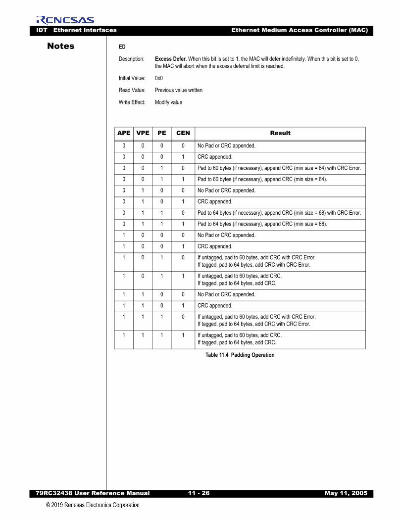
IDT Ethernet Interfaces Ethernet Medium Access Controller (MAC)
79RC32438 User Refer
Notes
EDDescription: Excess Defer. When this bit is set to 1, the MAC will defer indefinitely. When this bit is set to 0, the MAC will abort when the excess deferral limit is reached.
Initial Value: 0x0
Read Value: Previous value written
Write Effect: Modify value
APE VPE PE CEN Result
0 0 0 0 No Pad or CRC appended.
0 0 0 1 CRC appended.
0 0 1 0 Pad to 60 bytes (if necessary), append CRC (min size = 64) with CRC Error.
0 0 1 1 Pad to 60 bytes (if necessary), append CRC (min size = 64).
0 1 0 0 No Pad or CRC appended.
0 1 0 1 CRC appended.
0 1 1 0 Pad to 64 bytes (if necessary), append CRC (min size = 68) with CRC Error.
0 1 1 1 Pad to 64 bytes (if necessary), append CRC (min size = 68).
1 0 0 0 No Pad or CRC appended.
1 0 0 1 CRC appended.
1 0 1 0 If untagged, pad to 60 bytes, add CRC with CRC Error.If tagged, pad to 64 bytes, add CRC with CRC Error.
1 0 1 1 If untagged, pad to 60 bytes, add CRC.If tagged, pad to 64 bytes, add CRC.
1 1 0 0 No Pad or CRC appended.
1 1 0 1 CRC appended.
1 1 1 0 If untagged, pad to 60 bytes, add CRC with CRC Error.If tagged, pad to 64 bytes, add CRC with CRC Error.
1 1 1 1 If untagged, pad to 60 bytes, add CRC.If tagged, pad to 64 bytes, add CRC.
Table 11.4 Padding Operation
ence Manual 11 - 26 May 11, 2005
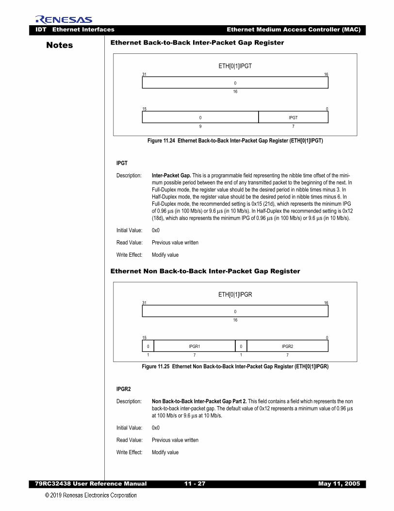
IDT Ethernet Interfaces Ethernet Medium Access Controller (MAC)
79RC32438 User Refer
Notes
Ethernet Back-to-Back Inter-Packet Gap RegisterFigure 11.24 Ethernet Back-to-Back Inter-Packet Gap Register (ETH[0|1]IPGT)
Ethernet Non Back-to-Back Inter-Packet Gap Register
Figure 11.25 Ethernet Non Back-to-Back Inter-Packet Gap Register (ETH[0|1]IPGR)
IPGT
Description: Inter-Packet Gap. This is a programmable field representing the nibble time offset of the mini-mum possible period between the end of any transmitted packet to the beginning of the next. In Full-Duplex mode, the register value should be the desired period in nibble times minus 3. In Half-Duplex mode, the register value should be the desired period in nibble times minus 6. In Full-Duplex mode, the recommended setting is 0x15 (21d), which represents the minimum IPG of 0.96 µs (in 100 Mb/s) or 9.6 µs (in 10 Mb/s). In Half-Duplex the recommended setting is 0x12 (18d), which also represents the minimum IPG of 0.96 µs (in 100 Mb/s) or 9.6 µs (in 10 Mb/s).
Initial Value: 0x0
Read Value: Previous value written
Write Effect: Modify value
IPGR2
Description: Non Back-to-Back Inter-Packet Gap Part 2. This field contains a field which represents the non back-to-back inter-packet gap. The default value of 0x12 represents a minimum value of 0.96 µs at 100 Mb/s or 9.6 µs at 10 Mb/s.
Initial Value: 0x0
Read Value: Previous value written
Write Effect: Modify value
ETH[0|1]IPGT
015
IPGT
7
0
9
1631
16
0
ETH[0|1]IPGR
015
IPGR2
7
0
1
0
1
IPGR1
7
1631
16
0
ence Manual 11 - 27 May 11, 2005
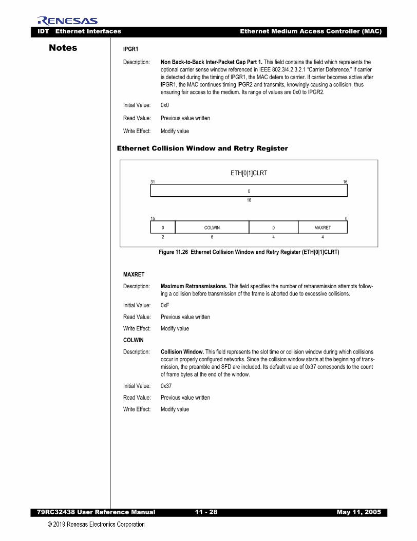
IDT Ethernet Interfaces Ethernet Medium Access Controller (MAC)
79RC32438 User Refer
Notes
Ethernet Collision Window and Retry Register
Figure 11.26 Ethernet Collision Window and Retry Register (ETH[0|1]CLRT)
IPGR1
Description: Non Back-to-Back Inter-Packet Gap Part 1. This field contains the field which represents the optional carrier sense window referenced in IEEE 802.3/4.2.3.2.1 “Carrier Deference.” If carrier is detected during the timing of IPGR1, the MAC defers to carrier. If carrier becomes active after IPGR1, the MAC continues timing IPGR2 and transmits, knowingly causing a collision, thus ensuring fair access to the medium. Its range of values are 0x0 to IPGR2.
Initial Value: 0x0
Read Value: Previous value written
Write Effect: Modify value
MAXRET
Description: Maximum Retransmissions. This field specifies the number of retransmission attempts follow-ing a collision before transmission of the frame is aborted due to excessive collisions.
Initial Value: 0xF
Read Value: Previous value written
Write Effect: Modify value
COLWIN
Description: Collision Window. This field represents the slot time or collision window during which collisions occur in properly configured networks. Since the collision window starts at the beginning of trans-mission, the preamble and SFD are included. Its default value of 0x37 corresponds to the count of frame bytes at the end of the window.
Initial Value: 0x37
Read Value: Previous value written
Write Effect: Modify value
ETH[0|1]CLRT
015
MAXRET
4
0
2
0
4
COLWIN
6
1631
16
0
ence Manual 11 - 28 May 11, 2005
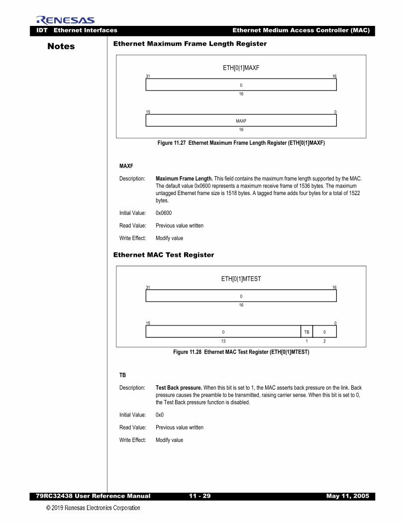
IDT Ethernet Interfaces Ethernet Medium Access Controller (MAC)
79RC32438 User Refer
Notes
Ethernet Maximum Frame Length RegisterFigure 11.27 Ethernet Maximum Frame Length Register (ETH[0|1]MAXF)
Ethernet MAC Test Register
Figure 11.28 Ethernet MAC Test Register (ETH[0|1]MTEST)
MAXF
Description: Maximum Frame Length. This field contains the maximum frame length supported by the MAC. The default value 0x0600 represents a maximum receive frame of 1536 bytes. The maximum untagged Ethernet frame size is 1518 bytes. A tagged frame adds four bytes for a total of 1522 bytes.
Initial Value: 0x0600
Read Value: Previous value written
Write Effect: Modify value
TB
Description: Test Back pressure. When this bit is set to 1, the MAC asserts back pressure on the link. Back pressure causes the preamble to be transmitted, raising carrier sense. When this bit is set to 0, the Test Back pressure function is disabled.
Initial Value: 0x0
Read Value: Previous value written
Write Effect: Modify value
ETH[0|1]MAXF
015
16
MAXF
1631
16
0
0
ETH[0|1]MTEST
015
2
TB
1
0
13
1631
16
0
ence Manual 11 - 29 May 11, 2005
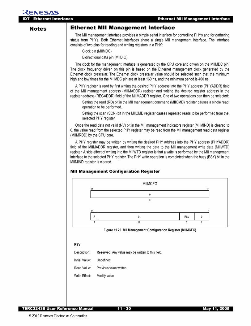
IDT Ethernet Interfaces Ethernet MII Management Interface
79RC32438 User Refer
Notes
Ethernet MII Management InterfaceThe MII management interface provides a simple serial interface for controlling PHYs and for gatheringstatus from PHYs. Both Ethernet interfaces share a single MII management interface. The interfaceconsists of two pins for reading and writing registers in a PHY:
Clock pin (MIIMDC) Bidirectional data pin (MIIDIO)
The clock for the management interface is generated by the CPU core and driven on the MIIMDC pin.The clock frequency driven on this pin is based on the Ethernet management clock generated by theEthernet clock prescalar. The Ethernet clock prescalar value should be selected such that the minimumhigh and low times for the MIIMDC pin are at least 160 ns, and the minimum period is 400 ns.
A PHY register is read by first writing the desired PHY address into the PHY address (PHYADDR) fieldof the MII management address (MIIMADDR) register and writing the desired register address in theregister address (REGADDR) field of the MIIMADDR register. One of two operations can then be selected:
Setting the read (RD) bit in the MII management command (MIICMD) register causes a single read operation to be performed. Setting the scan (SCN) bit in the MIICMD register causes repeated reads to be performed from the selected PHY register.
Once the read data not valid (NV) bit in the MII management indicators register (MIIMIND) is cleared to0, the value read from the selected PHY register may be read from the MII management read data register(MIIMRDD) by the CPU core.
A PHY register may be written by writing the desired PHY address into the PHY address (PHYADDR)field of the MIIMADDR register, and then writing the data to the MII management write data (MIIWTD)register. A side effect of writing into the MIIWTD register is that a write is performed by the MII managementinterface to the selected PHY register. The PHY write operation is completed when the busy (BSY) bit in theMIIMIND register is cleared.
MII Management Configuration Register
Figure 11.29 MII Management Configuration Register (MIIMCFG)
RSV
Description: Reserved. Any value may be written to this field.
Initial Value: Undefined
Read Value: Previous value written
Write Effect: Modify value
MIIMCFG
015
0
2
R
1
0
11
RSV
2
1631
16
0
ence Manual 11 - 30 May 11, 2005
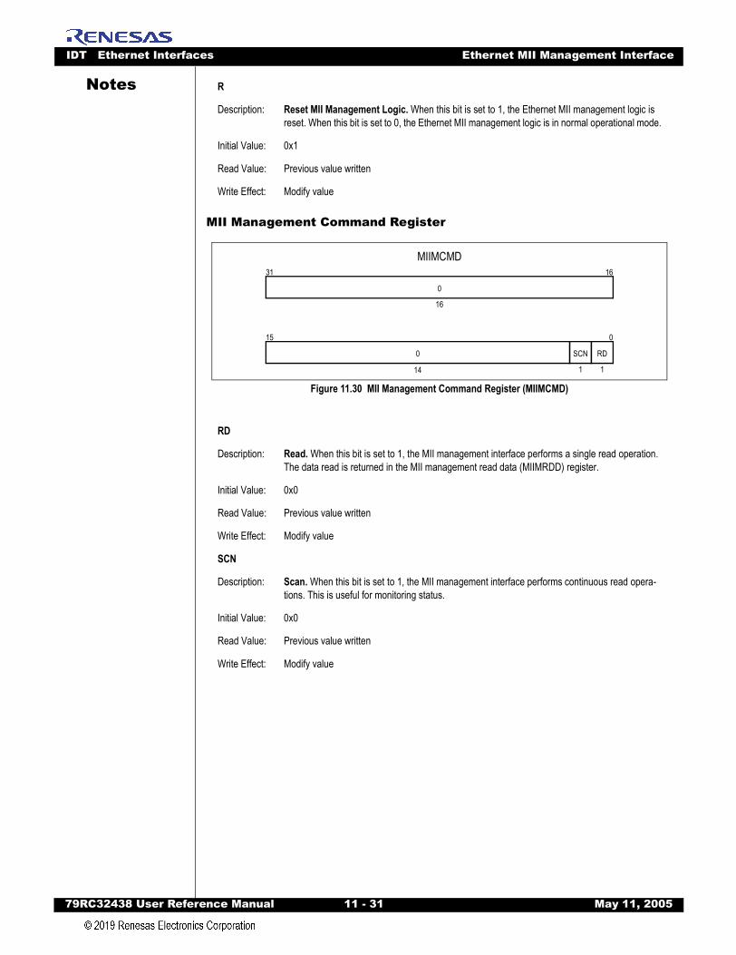
IDT Ethernet Interfaces Ethernet MII Management Interface
79RC32438 User Refer
Notes
MII Management Command Register
Figure 11.30 MII Management Command Register (MIIMCMD)
R
Description: Reset MII Management Logic. When this bit is set to 1, the Ethernet MII management logic is reset. When this bit is set to 0, the Ethernet MII management logic is in normal operational mode.
Initial Value: 0x1
Read Value: Previous value written
Write Effect: Modify value
RD
Description: Read. When this bit is set to 1, the MII management interface performs a single read operation. The data read is returned in the MII management read data (MIIMRDD) register.
Initial Value: 0x0
Read Value: Previous value written
Write Effect: Modify value
SCN
Description: Scan. When this bit is set to 1, the MII management interface performs continuous read opera-tions. This is useful for monitoring status.
Initial Value: 0x0
Read Value: Previous value written
Write Effect: Modify value
MIIMCMD
015
0
14
RD
1
SCN
1
1631
16
0
ence Manual 11 - 31 May 11, 2005
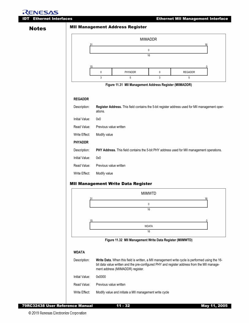
IDT Ethernet Interfaces Ethernet MII Management Interface
79RC32438 User Refer
Notes
MII Management Address RegisterFigure 11.31 MII Management Address Register (MIIMADDR)
MII Management Write Data Register
Figure 11.32 MII Management Write Data Register (MIIMWTD)
REGADDR
Description: Register Address. This field contains the 5-bit register address used for MII management oper-ations.
Initial Value: 0x0
Read Value: Previous value written
Write Effect: Modify value
PHYADDR
Description: PHY Address. This field contains the 5-bit PHY address used for MII management operations.
Initial Value: 0x0
Read Value: Previous value written
Write Effect: Modify value
WDATA
Description: Write Data. When this field is written, a MII management write cycle is performed using the 16-bit data value written and the pre-configured PHY and register address from the MII manage-ment address (MIIMADDR) register.
Initial Value: 0x0000
Read Value: Previous value written
Write Effect: Modify value and initiate a MII management write cycle
MIIMADDR
015
REGADDR
5
0
3
PHYADDR
5
0
3
1631
16
0
MIIMWTD
015
16
WDATA
1631
16
0
ence Manual 11 - 32 May 11, 2005
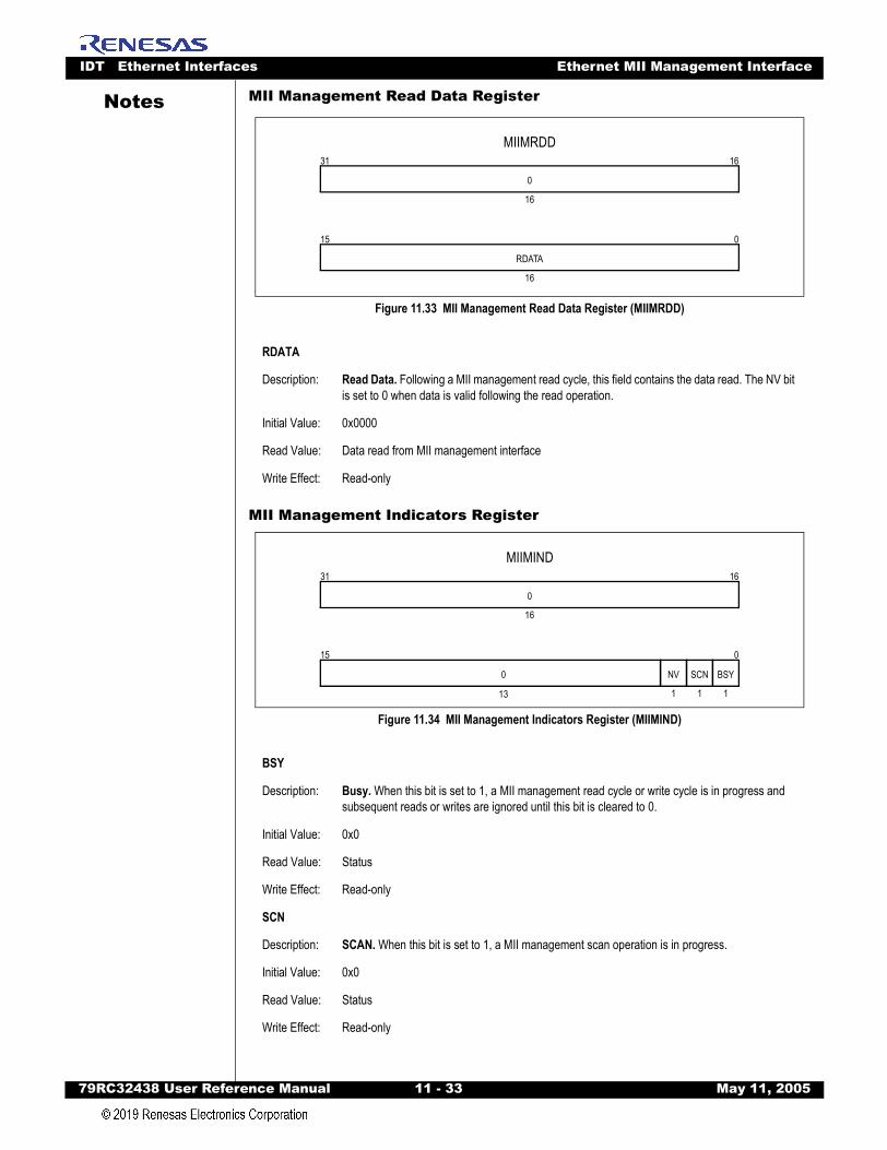
IDT Ethernet Interfaces Ethernet MII Management Interface
79RC32438 User Refer
Notes
MII Management Read Data RegisterFigure 11.33 MII Management Read Data Register (MIIMRDD)
MII Management Indicators Register
Figure 11.34 MII Management Indicators Register (MIIMIND)
RDATA
Description: Read Data. Following a MII management read cycle, this field contains the data read. The NV bit is set to 0 when data is valid following the read operation.
Initial Value: 0x0000
Read Value: Data read from MII management interface
Write Effect: Read-only
BSY
Description: Busy. When this bit is set to 1, a MII management read cycle or write cycle is in progress and subsequent reads or writes are ignored until this bit is cleared to 0.
Initial Value: 0x0
Read Value: Status
Write Effect: Read-only
SCN
Description: SCAN. When this bit is set to 1, a MII management scan operation is in progress.
Initial Value: 0x0
Read Value: Status
Write Effect: Read-only
MIIMRDD
015
16
RDATA
1631
16
0
MIIMIND
015
0
13
BSY
1
SCN
1
NV
1
1631
16
0
ence Manual 11 - 33 May 11, 2005
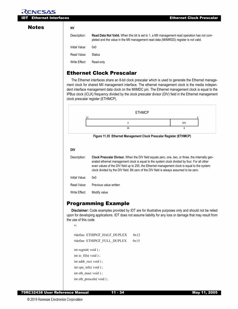
IDT Ethernet Interfaces Ethernet Clock Prescalar
79RC32438 User Refer
Notes
Ethernet Clock PrescalarThe Ethernet interfaces share an 8-bit clock prescalar which is used to generate the Ethernet manage-
ment clock for shared MII management interface. The ethernet management clock is the media indepen-dent interface management data clock on the MIIMDC pin. The Ethernet management clock is equal to theIPBus clock (ICLK) frequency divided by the clock prescalar divisor (DIV) field in the Ethernet managementclock prescalar register (ETHMCP).
Figure 11.35 Ethernet Management Clock Prescalar Register (ETHMCP)
Programming ExampleDisclaimer: Code examples provided by IDT are for illustrative purposes only and should not be relied
upon for developing applications. IDT does not assume liability for any loss or damage that may result fromthe use of this code.
*/
#define ETHIPGT_HALF_DUPLEX 0x12
#define ETHIPGT_FULL_DUPLEX 0x15
int reginit( void ) ;
int io_fifo( void ) ;
int addr_rec( void ) ;
int cpu_infc( void ) ;
int eth_mac( void ) ;
int eth_prescale( void ) ;
NV
Description: Read Data Not Valid. When this bit is set to 1, a MII management read operation has not com-pleted and the value in the MII management read data (MIIMRDD) register is not valid.
Initial Value: 0x0
Read Value: Status
Write Effect: Read-only
DIV
Description: Clock Prescalar Divisor. When the DIV field equals zero, one, two, or three, the internally gen-erated ethernet management clock is equal to the system clock divided by four. For all other even values of the DIV field up to 255, the Ethernet management clock is equal to the system clock divided by the DIV field. Bit zero of the DIV field is always assumed to be zero.
Initial Value: 0x0
Read Value: Previous value written
Write Effect: Modify value
ETHMCP031
DIV0
24 8
ence Manual 11 - 34 May 11, 2005
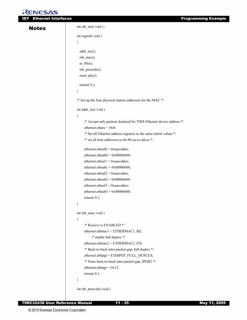
IDT Ethernet Interfaces Programming Example
79RC32438 User Refer
Notes
int eth_mii( void ) ;int reginit( void )
addr_rec();
eth_mac();
io_fifo();
eth_prescale();
reset_phy();
return( 0 );
/* Set up the four physical station addresses for the MAC */
int addr_rec( void )
/* Accept only packets destined for THIS Ethernet device address */
ethernet.etharc = 0x0;
/* Set all Ethernet address registers to the same initial values */
/* set all four addresses to 66-88-aa-cc-dd-ee */
ethernet.ethsal0 = 0xaaccddee;
ethernet.ethsah0 = 0x00006688;
ethernet.ethsal1 = 0xaaccddee;
ethernet.ethsah1 = 0x00006688;
ethernet.ethsal2 = 0xaaccddee;
ethernet.ethsah2 = 0x00006688;
ethernet.ethsal3 = 0xaaccddee;
ethernet.ethsah3 = 0x00006688;
return( 0 );
int eth_mac( void )
/* Receive is ENABLED */
ethernet.ethmac1 = ETHERMAC1_RE;
/* enable full duplex */
ethernet.ethmac2 = ETHERMAC2_FD;
/* Back-to-back inter-packet-gap, full-duplex */
ethernet.ethipgt = ETHIPGT_FULL_DUPLEX;
/* None back-to-back inter-packet-gap, IPGR2 */
ethernet.ethipgr = 0x12;
return( 0 );
int eth_prescale( void )
ence Manual 11 - 35 May 11, 2005
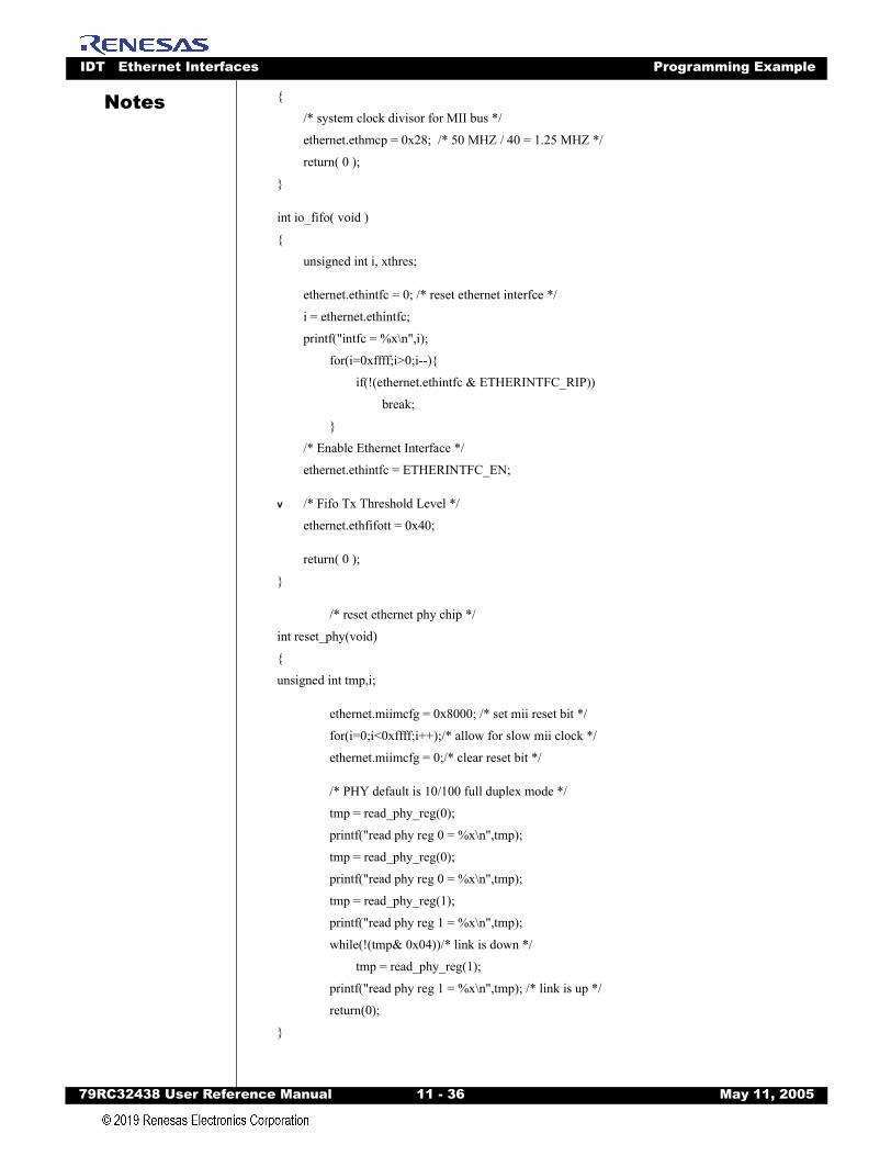
IDT Ethernet Interfaces Programming Example
79RC32438 User Refer
Notes
/* system clock divisor for MII bus */
ethernet.ethmcp = 0x28; /* 50 MHZ / 40 = 1.25 MHZ */
return( 0 );
int io_fifo( void )
unsigned int i, xthres;
ethernet.ethintfc = 0; /* reset ethernet interfce */
i = ethernet.ethintfc;
printf("intfc = %x\n",i);
for(i=0xffff;i>0;i--)
if(!(ethernet.ethintfc & ETHERINTFC_RIP))
break;
/* Enable Ethernet Interface */
ethernet.ethintfc = ETHERINTFC_EN;
v /* Fifo Tx Threshold Level */
ethernet.ethfifott = 0x40;
return( 0 );
/* reset ethernet phy chip */
int reset_phy(void)
unsigned int tmp,i;
ethernet.miimcfg = 0x8000; /* set mii reset bit */
for(i=0;i<0xffff;i++);/* allow for slow mii clock */
ethernet.miimcfg = 0;/* clear reset bit */
/* PHY default is 10/100 full duplex mode */
tmp = read_phy_reg(0);
printf("read phy reg 0 = %x\n",tmp);
tmp = read_phy_reg(0);
printf("read phy reg 0 = %x\n",tmp);
tmp = read_phy_reg(1);
printf("read phy reg 1 = %x\n",tmp);
while(!(tmp& 0x04))/* link is down */
tmp = read_phy_reg(1);
printf("read phy reg 1 = %x\n",tmp); /* link is up */
return(0);
ence Manual 11 - 36 May 11, 2005

IDT Ethernet Interfaces Programming Example
79RC32438 User Refer
Notes
#define MII_TIMEOUT 0xf000int write_phy_reg(int reg, int data)
int i;
i=MII_TIMEOUT;
while((ethernet.miimind & ETHERMIIMIND_BSY) && i)
i--;
if(i == 0)
printf("write phy reg timed out waiting for mii busy\n");
return (1);
ethernet.miimaddr = reg;
i=MII_TIMEOUT;
while((ethernet.miimind & ETHERMIIMIND_BSY) && i)
i--;
if(i == 0)
printf("write phy reg timed out waiting for mii busy\n");
return (2);
ethernet.miimwtd = data;
i=MII_TIMEOUT;
while((ethernet.miimind & ETHERMIIMIND_BSY) && i)
i--;
if(i == 0)
printf("write phy reg timed out waiting for mii busy\n");
return (3);
return(0);
int read_phy_reg(int reg)
int i, data;
i=MII_TIMEOUT;
while((ethernet.miimind & ETHERMIIMIND_BSY) && i)
i--;
if(i == 0)
printf("read phy reg timed out waiting for mii busy\n");
return (0x1);
ethernet.miimaddr = reg;
i=MII_TIMEOUT;
while((ethernet.miimind & ETHERMIIMIND_BSY) && i)
ence Manual 11 - 37 May 11, 2005
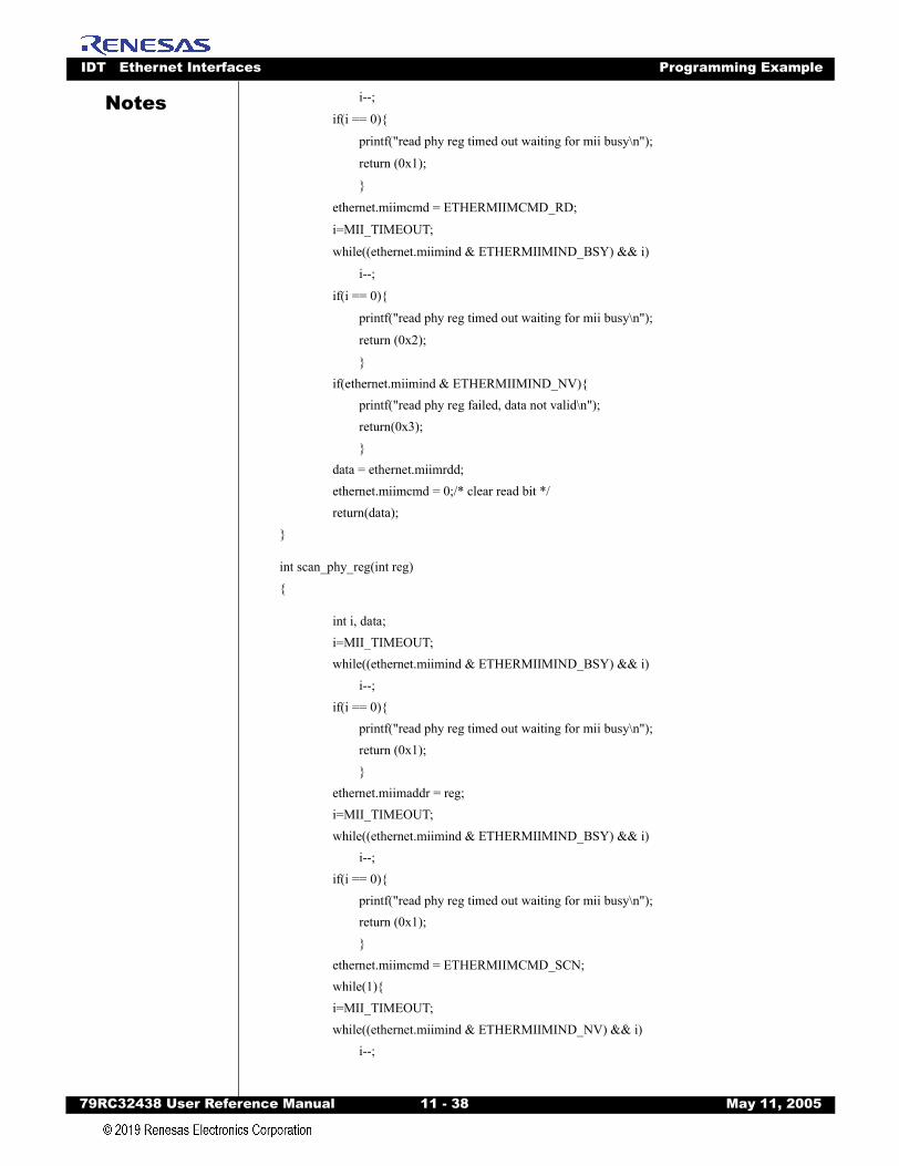
IDT Ethernet Interfaces Programming Example
79RC32438 User Refer
Notes
i--;if(i == 0)
printf("read phy reg timed out waiting for mii busy\n");
return (0x1);
ethernet.miimcmd = ETHERMIIMCMD_RD;
i=MII_TIMEOUT;
while((ethernet.miimind & ETHERMIIMIND_BSY) && i)
i--;
if(i == 0)
printf("read phy reg timed out waiting for mii busy\n");
return (0x2);
if(ethernet.miimind & ETHERMIIMIND_NV)
printf("read phy reg failed, data not valid\n");return(0x3);
data = ethernet.miimrdd;ethernet.miimcmd = 0;/* clear read bit */return(data);
int scan_phy_reg(int reg)
int i, data;i=MII_TIMEOUT; while((ethernet.miimind & ETHERMIIMIND_BSY) && i)
i--;if(i == 0)
printf("read phy reg timed out waiting for mii busy\n");return (0x1);
ethernet.miimaddr = reg;i=MII_TIMEOUT; while((ethernet.miimind & ETHERMIIMIND_BSY) && i)
i--;if(i == 0)
printf("read phy reg timed out waiting for mii busy\n");return (0x1);
ethernet.miimcmd = ETHERMIIMCMD_SCN;while(1)i=MII_TIMEOUT;while((ethernet.miimind & ETHERMIIMIND_NV) && i)
i--;
ence Manual 11 - 38 May 11, 2005
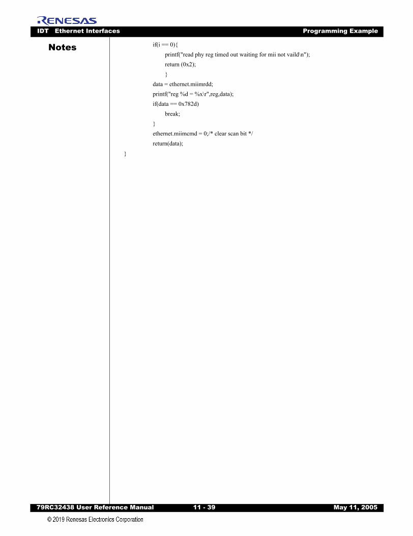
IDT Ethernet Interfaces Programming Example
79RC32438 User Refer
Notes
if(i == 0)printf("read phy reg timed out waiting for mii not vaild\n");return (0x2);data = ethernet.miimrdd;printf("reg %d = %x\r",reg,data);if(data == 0x782d)
break;ethernet.miimcmd = 0;/* clear scan bit */return(data);
ence Manual 11 - 39 May 11, 2005
IDT Ethernet Interfaces Programming Example
79RC32438 User Refer
Notes
ence Manual 11 - 40 May 11, 2005
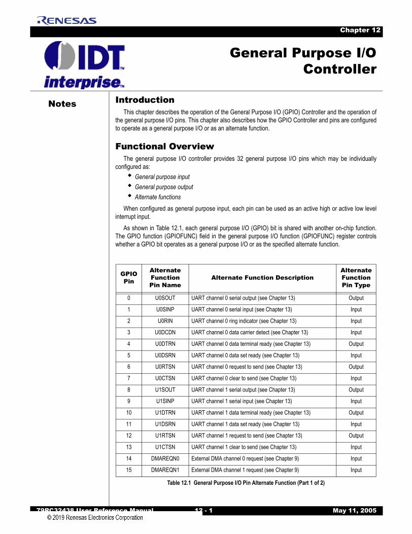
Notes
79RC32438 User Reference Manual 12 - 1 M
Chapter 12
General Purpose I/OController
IntroductionThis chapter describes the operation of the General Purpose I/O (GPIO) Controller and the operation of
the general purpose I/O pins. This chapter also describes how the GPIO Controller and pins are configuredto operate as a general purpose I/O or as an alternate function.
Functional OverviewThe general purpose I/O controller provides 32 general purpose I/O pins which may be individually
configured as: General purpose inputGeneral purpose outputAlternate functions
When configured as general purpose input, each pin can be used as an active high or active low levelinterrupt input.
As shown in Table 12.1, each general purpose I/O (GPIO) bit is shared with another on-chip function.The GPIO function (GPIOFUNC) field in the general purpose I/O function (GPIOFUNC) register controlswhether a GPIO bit operates as a general purpose I/O or as the specified alternate function.
GPIOPin
Alternate FunctionPin Name
Alternate Function DescriptionAlternate FunctionPin Type
0 U0SOUT UART channel 0 serial output (see Chapter 13) Output
1 U0SINP UART channel 0 serial input (see Chapter 13) Input
2 U0RIN UART channel 0 ring indicator (see Chapter 13) Input
3 U0DCDN UART channel 0 data carrier detect (see Chapter 13) Input
4 U0DTRN UART channel 0 data terminal ready (see Chapter 13) Output
5 U0DSRN UART channel 0 data set ready (see Chapter 13) Input
6 U0RTSN UART channel 0 request to send (see Chapter 13) Output
7 U0CTSN UART channel 0 clear to send (see Chapter 13) Input
8 U1SOUT UART channel 1 serial output (see Chapter 13) Output
9 U1SINP UART channel 1 serial input (see Chapter 13) Input
10 U1DTRN UART channel 1 data terminal ready (see Chapter 13) Output
11 U1DSRN UART channel 1 data set ready (see Chapter 13) Input
12 U1RTSN UART channel 1 request to send (see Chapter 13) Output
13 U1CTSN UART channel 1 clear to send (see Chapter 13) Input
14 DMAREQN0 External DMA channel 0 request (see Chapter 9) Input
15 DMAREQN1 External DMA channel 1 request (see Chapter 9) Input
Table 12.1 General Purpose I/O Pin Alternate Function (Part 1 of 2)
ay 11, 2005

IDT General Purpose I/O Controller Theory of Operation
79RC32438 User Refer
Notes
Theory of OperationAfter reset, all GPIO pins default to the GPIO input function. When a GPIO pin is configured for use as a
GPIO pin, the alternate function associated with that pin is held in an inactive state by internal logic. Careshould be exercised when configuring GPIO pins as outputs because an incorrect configuration (forexample, mistakenly configuring an input pin as an output pin) could cause damage to external componentsas well as to the RC32438 device itself.
Each GPIO pin is controlled by its corresponding bit in each GPIO register. For example, GPIO bit [0] iscontrolled by GPIOFUNC[0], GPIOCFG[0], GPIOD[0], GPIOILEVEL[0], GPIOISTAT[0], andGPIONMIEN[0]. In another example, GPIO bit [2] is controlled by GPIOFUNC[2], GPIOCFG[2], GPIOD[2],GPIOILEVEL[2], GPIOISTAT[2], and GPIONMIEN[2].
All GPIO pins except GPIO[24] and GPIO[30:26] have LVTTL I/O buffers. GPIO pins 24 and 26 through30 have PCI I/O buffers which allow these pins to be used for PCI interrupts.
GPIO Pin Configured As Input
When configured as an input in the GPIO configuration register (GPIOCFG) and as a GPIO function inthe GPIO function register (GPIOFUNC), the GPIO pin value will be sampled and registered in the GPIOdata register (GPIOD) each master clock cycle (after double registering to prevent metastability). The valueof the input pin can be determined at any time by reading GPIOD.
GPIO Pin Configured As Output
When configured as an output in GPIOCFG and as a GPIO function in GPIOFUNC, the value writteninto GPIOD will be output at the pin. The value of the output pin can be determined at any time by readingGPIOD.
16 DMADONEN0 External DMA channel 0 done (see Chapter 9) Input
17 DMADONEN1 External DMA channel 1 done (see Chapter 9) Input
18 DMAFINN0 External DMA channel 0 finished (see Chapter 9) Output
19 DMAFINN1 External DMA channel 1 finished (see Chapter 9) Output
20 MADDR[22] Memory and peripheral bus address (see Chapter 6) Output
21 MADDR[23] Memory and peripheral bus address (see Chapter 6) Output
22 MADDR[24] Memory and peripheral bus address (see Chapter 6) Output
23 MADDR[25] Memory and peripheral bus address (see Chapter 6) Output
24 PCIREQN[4] PCI Request 4 (see Chapter 10) Input
25 AFSPARE1 reserved Input
26 PCIGNTN[4] PCI Grant 4 (see Chapter 10) Output
27 PCIREQN[5] PCI Request 5 (see Chapter 10) Input
28 PCIGNTN[5] PCI Grant 5 (see Chapter 10) Output
29-31 Reserved
GPIOPin
Alternate FunctionPin Name
Alternate Function DescriptionAlternate FunctionPin Type
Table 12.1 General Purpose I/O Pin Alternate Function (Part 2 of 2)
ence Manual 12 - 2 May 11, 2005
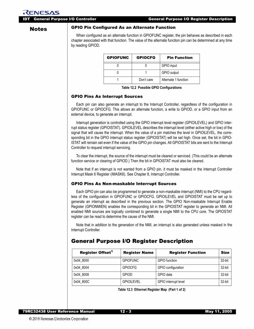
IDT General Purpose I/O Controller General Purpose I/O Register Description
79RC32438 User Refer
Notes
GPIO Pin Configured As an Alternate FunctionWhen configured as an alternate function in GPIOFUNC register, the pin behaves as described in eachchapter associated with that function. The value of the alternate function pin can be determined at any timeby reading GPIOD.
GPIO Pins As Interrupt Sources
Each pin can also generate an interrupt to the Interrupt Controller, regardless of the configuration inGPIOFUNC or GPIOCFG. This allows an alternate function, a write to GPIOD, or a GPIO input from anexternal device, to generate an interrupt.
Interrupt generation is controlled using the GPIO interrupt level register (GPIOILEVEL) and GPIO inter-rupt status register (GPIOISTAT). GPIOILEVEL describes the interrupt level (either active high or low) of thesignal that will cause the interrupt. When the value of a pin matches the level in GPIOILEVEL, the corre-sponding bit in the GPIO interrupt status register (GPIOISTAT) will be set high. Once set, the bit in GPIO-ISTAT will remain set even if the value of the GPIO pin changes. All GPIOISTAT bits are sent to the InterruptController to request interrupt servicing.
To clear the interrupt, the source of the interrupt must be cleared or serviced. (This could be an alternatefunction service or clearing of GPIOD.) Then the bit in GPIOISTAT must also be cleared.
Note that if an interrupt is not wanted from a GPIO pin, it must be masked in the Interrupt ControllerInterrupt Mask 6 Register (IMASK6). See Chapter 8, Interrupt Controller.
GPIO Pins As Non-maskable Interrupt Sources
Each GPIO pin can also be programmed to generate a non-maskable interrupt (NMI) to the CPU regard-less of the configuration in GPIOFUNC or GPIOCFG. GPIOILEVEL and GPIOISTAT must be set up togenerate an interrupt as described in the previous section. The GPIO Non-maskable Interrupt EnableRegister (GPIONMIEN) enables the corresponding bit in the GPIOISTAT register to generate an NMI. Allenabled NMI sources are logically combined to generate a single NMI to the CPU core. The GPIOSTATregister can be read to determine the cause of the NMI.
Note that in addition to the generation of the NMI, an interrupt is also generated unless masked in theInterrupt Controller.
General Purpose I/O Register Description
GPIOFUNC GPIOCFG Pin Function
0 0 GPIO input
0 1 GPIO output
1 Don’t care Alternate 1 function
Table 12.2 Possible GPIO Configurations
Register Offset1 Register Name Register Function Size
0x04_8000 GPIOFUNC GPIO function 32-bit
0x04_8004 GPIOCFG GPIO configuration 32-bit
0x04_8008 GPIOD GPIO data 32-bit
0x04_800C GPIOILEVEL GPIO interrupt level 32-bit
Table 12.3 Ethernet Register Map (Part 1 of 2)
ence Manual 12 - 3 May 11, 2005
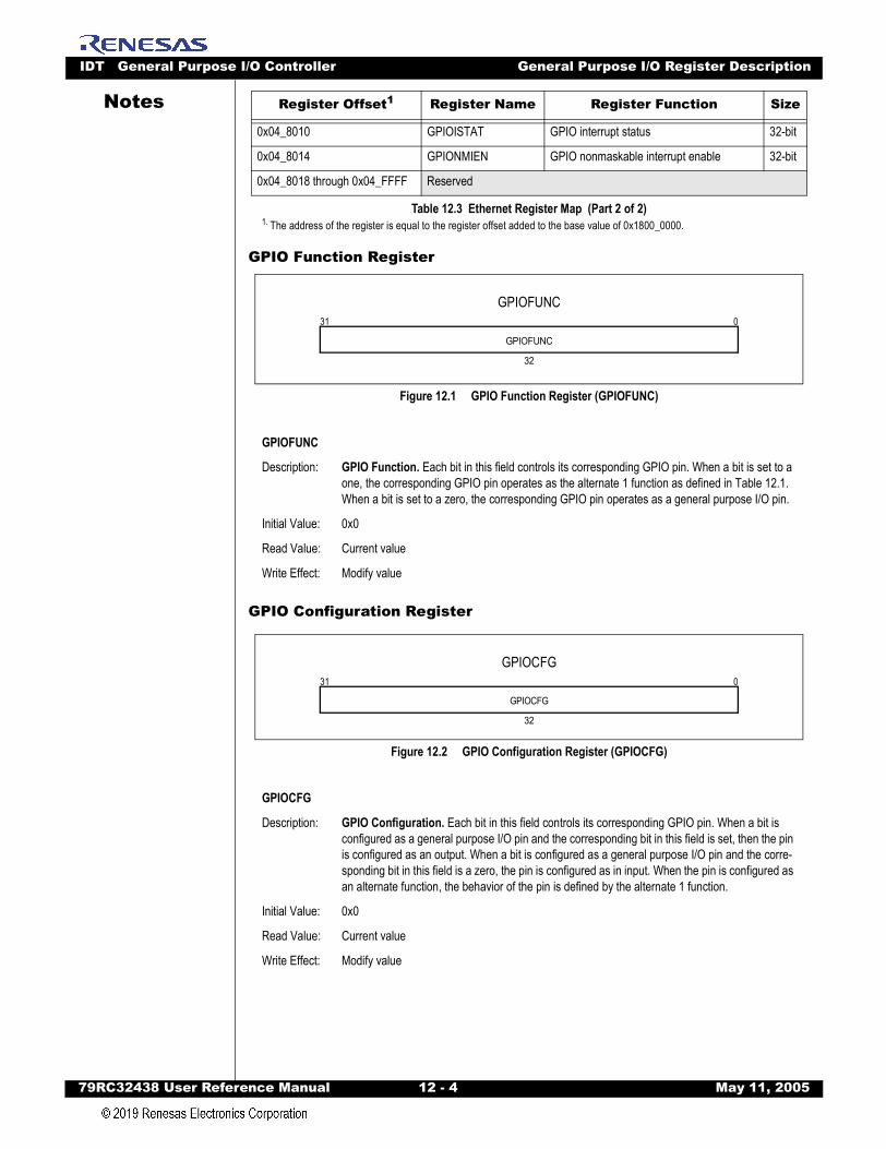
IDT General Purpose I/O Controller General Purpose I/O Register Description
79RC32438 User Refer
Notes
GPIO Function Register
Figure 12.1 GPIO Function Register (GPIOFUNC)
GPIO Configuration Register
Figure 12.2 GPIO Configuration Register (GPIOCFG)
0x04_8010 GPIOISTAT GPIO interrupt status 32-bit
0x04_8014 GPIONMIEN GPIO nonmaskable interrupt enable 32-bit
0x04_8018 through 0x04_FFFF Reserved
1. The address of the register is equal to the register offset added to the base value of 0x1800_0000.
GPIOFUNC
Description: GPIO Function. Each bit in this field controls its corresponding GPIO pin. When a bit is set to a one, the corresponding GPIO pin operates as the alternate 1 function as defined in Table 12.1. When a bit is set to a zero, the corresponding GPIO pin operates as a general purpose I/O pin.
Initial Value: 0x0
Read Value: Current value
Write Effect: Modify value
GPIOCFG
Description: GPIO Configuration. Each bit in this field controls its corresponding GPIO pin. When a bit is configured as a general purpose I/O pin and the corresponding bit in this field is set, then the pin is configured as an output. When a bit is configured as a general purpose I/O pin and the corre-sponding bit in this field is a zero, the pin is configured as in input. When the pin is configured as an alternate function, the behavior of the pin is defined by the alternate 1 function.
Initial Value: 0x0
Read Value: Current value
Write Effect: Modify value
Register Offset1 Register Name Register Function Size
Table 12.3 Ethernet Register Map (Part 2 of 2)
GPIOFUNC031
32
GPIOFUNC
GPIOCFG031
32
GPIOCFG
ence Manual 12 - 4 May 11, 2005

IDT General Purpose I/O Controller General Purpose I/O Register Description
79RC32438 User Refer
Notes
GPIO Data RegisterFigure 12.3 GPIO Data Register (GPIOD)
GPIO Interrupt Level Register
Figure 12.4 GPIO Interrupt Level Register (GPIOILEVEL)
GPIO Interrupt Status Register
Figure 12.5 GPIO Interrupt Status Register (GPIOISTAT)
GPIOD
Description: GPIO Data. Each bit in this field controls its corresponding GPIO pin. Reading this field returns the current value of each GPIO pin. Writing a value to this field causes the corresponding pins which are configured as GPIO outputs to change state to the value written.
Initial Value: Undefined
Read Value: GPIO pin status
Write Effect: Modify GPIO output pin status
GPIOILEVEL
Description: GPIO Interrupt Level. When the value of a GPIO pin matches the value of the corresponding bit in this field, then the corresponding bit is set in the GPIOISTAT field is set.
Initial Value: Undefined
Read Value: Current value
Write Effect: Modify value
GPIOISTAT
Description: GPIO Interrupt Status. Each bit in this field controls its corresponding GPIO pin. When a bit in this field is set to 1, the GPIO pin value matches that of the corresponding bit in the GPIOILEVEL field. Each bit in this field is presented to the interrupt controller as an interrupt input. Bits in this field are typically cleared by an interrupt service routine.
GPIOD031
32
GPIOD
GPIOILEVEL031
32
GPIOILEVEL
GPIOISTAT031
32
GPIOISTAT
ence Manual 12 - 5 May 11, 2005
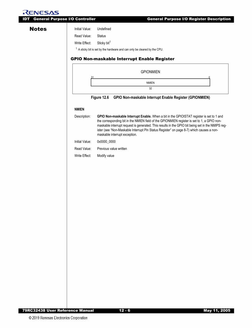
IDT General Purpose I/O Controller General Purpose I/O Register Description
79RC32438 User Refer
Notes
GPIO Non-maskable Interrupt Enable Register
Figure 12.6 GPIO Non-maskable Interrupt Enable Register (GPIONMIEN)
Initial Value: Undefined
Read Value: Status
Write Effect: Sticky bit1
1. A sticky bit is set by the hardware and can only be cleared by the CPU.
NMIEN
Description: GPIO Non-maskable Interrupt Enable. When a bit in the GPIOISTAT register is set to 1 and the corresponding bit in the NMIEN field of the GPIONMIEN register is set to 1, a GPIO non-maskable interrupt request is generated. This results in the GPIO bit being set in the NMIPS reg-ister (see “Non-Maskable Interrupt Pin Status Register” on page 8-7) which causes a non-maskable interrupt exception.
Initial Value: 0x0000_0000
Read Value: Previous value written
Write Effect: Modify value
GPIONMIEN031
32
NMIEN
ence Manual 12 - 6 May 11, 2005
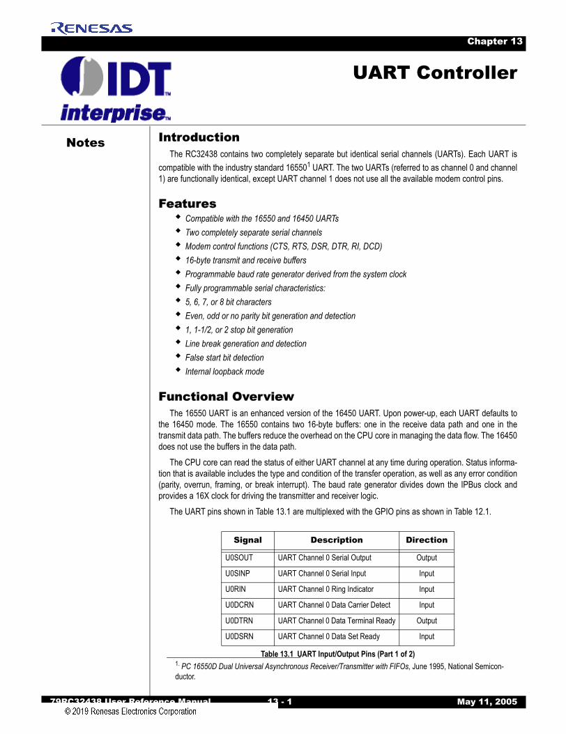
Notes
79RC32438 User Reference Manual 13 - 1 M
Chapter 13
UART Controller
IntroductionThe RC32438 contains two completely separate but identical serial channels (UARTs). Each UART is
compatible with the industry standard 165501 UART. The two UARTs (referred to as channel 0 and channel1) are functionally identical, except UART channel 1 does not use all the available modem control pins.
FeaturesCompatible with the 16550 and 16450 UARTsTwo completely separate serial channelsModem control functions (CTS, RTS, DSR, DTR, RI, DCD)16-byte transmit and receive buffersProgrammable baud rate generator derived from the system clockFully programmable serial characteristics:5, 6, 7, or 8 bit charactersEven, odd or no parity bit generation and detection1, 1-1/2, or 2 stop bit generationLine break generation and detectionFalse start bit detectionInternal loopback mode
Functional OverviewThe 16550 UART is an enhanced version of the 16450 UART. Upon power-up, each UART defaults to
the 16450 mode. The 16550 contains two 16-byte buffers: one in the receive data path and one in thetransmit data path. The buffers reduce the overhead on the CPU core in managing the data flow. The 16450does not use the buffers in the data path.
The CPU core can read the status of either UART channel at any time during operation. Status informa-tion that is available includes the type and condition of the transfer operation, as well as any error condition(parity, overrun, framing, or break interrupt). The baud rate generator divides down the IPBus clock andprovides a 16X clock for driving the transmitter and receiver logic.
The UART pins shown in Table 13.1 are multiplexed with the GPIO pins as shown in Table 12.1.
1. PC 16550D Dual Universal Asynchronous Receiver/Transmitter with FIFOs, June 1995, National Semicon-ductor.
Signal Description Direction
U0SOUT UART Channel 0 Serial Output Output
U0SINP UART Channel 0 Serial Input Input
U0RIN UART Channel 0 Ring Indicator Input
U0DCRN UART Channel 0 Data Carrier Detect Input
U0DTRN UART Channel 0 Data Terminal Ready Output
U0DSRN UART Channel 0 Data Set Ready Input
Table 13.1 UART Input/Output Pins (Part 1 of 2)
ay 11, 2005
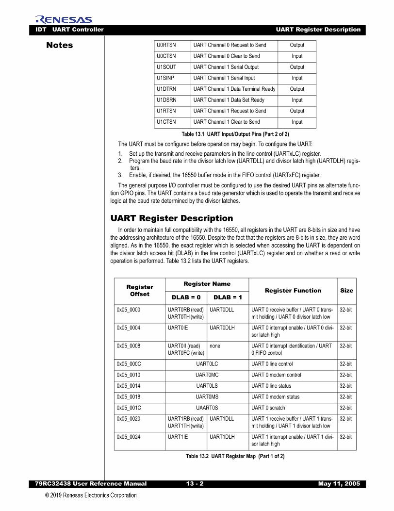
IDT UART Controller UART Register Description
79RC32438 User Refer
Notes
The UART must be configured before operation may begin. To configure the UART:1. Set up the transmit and receive parameters in the line control (UARTxLC) register. 2. Program the baud rate in the divisor latch low (UARTDLL) and divisor latch high (UARTDLH) regis-
ters. 3. Enable, if desired, the 16550 buffer mode in the FIFO control (UARTxFC) register.The general purpose I/O controller must be configured to use the desired UART pins as alternate func-
tion GPIO pins. The UART contains a baud rate generator which is used to operate the transmit and receivelogic at the baud rate determined by the divisor latches.
UART Register DescriptionIn order to maintain full compatibility with the 16550, all registers in the UART are 8-bits in size and have
the addressing architecture of the 16550. Despite the fact that the registers are 8-bits in size, they are wordaligned. As in the 16550, the exact register which is selected when accessing the UART is dependent onthe divisor latch access bit (DLAB) in the line control (UARTxLC) register and on whether a read or writeoperation is performed. Table 13.2 lists the UART registers.
U0RTSN UART Channel 0 Request to Send Output
U0CTSN UART Channel 0 Clear to Send Input
U1SOUT UART Channel 1 Serial Output Output
U1SINP UART Channel 1 Serial Input Input
U1DTRN UART Channel 1 Data Terminal Ready Output
U1DSRN UART Channel 1 Data Set Ready Input
U1RTSN UART Channel 1 Request to Send Output
U1CTSN UART Channel 1 Clear to Send Input
Register Offset
Register NameRegister Function Size
DLAB = 0 DLAB = 1
0x05_0000 UART0RB (read) UART0TH (write)
UART0DLL UART 0 receive buffer / UART 0 trans-mit holding / UART 0 divisor latch low
32-bit
0x05_0004 UART0IE UART0DLH UART 0 interrupt enable / UART 0 divi-sor latch high
32-bit
0x05_0008 UART0II (read)UART0FC (write)
none UART 0 interrupt identification / UART 0 FIFO control
32-bit
0x05_000C UART0LC UART 0 line control 32-bit
0x05_0010 UART0MC UART 0 modem control 32-bit
0x05_0014 UART0LS UART 0 line status 32-bit
0x05_0018 UART0MS UART 0 modem status 32-bit
0x05_001C UAART0S UART 0 scratch 32-bit
0x05_0020 UART1RB (read) UART1TH (write)
UART1DLL UART 1 receive buffer / UART 1 trans-mit holding / UART 1 divisor latch low
32-bit
0x05_0024 UART1IE UART1DLH UART 1 interrupt enable / UART 1 divi-sor latch high
32-bit
Table 13.2 UART Register Map (Part 1 of 2)
Table 13.1 UART Input/Output Pins (Part 2 of 2)
ence Manual 13 - 2 May 11, 2005
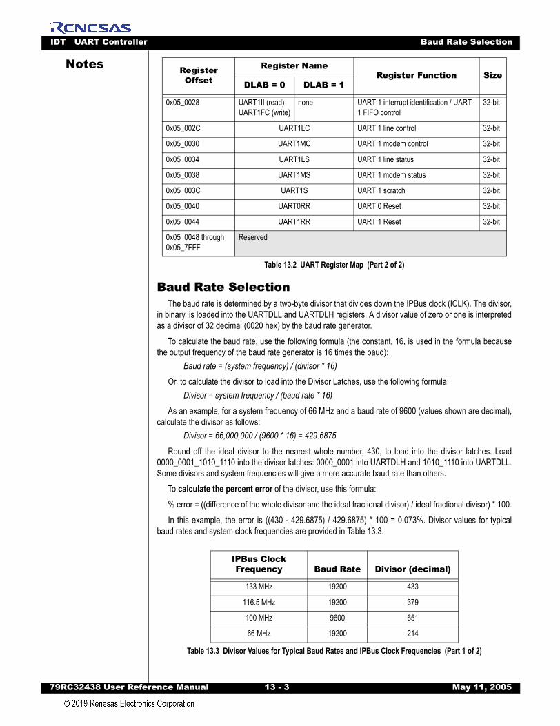
IDT UART Controller Baud Rate Selection
79RC32438 User Refer
Notes
Baud Rate SelectionThe baud rate is determined by a two-byte divisor that divides down the IPBus clock (ICLK). The divisor,
in binary, is loaded into the UARTDLL and UARTDLH registers. A divisor value of zero or one is interpretedas a divisor of 32 decimal (0020 hex) by the baud rate generator.
To calculate the baud rate, use the following formula (the constant, 16, is used in the formula becausethe output frequency of the baud rate generator is 16 times the baud):
Baud rate = (system frequency) / (divisor * 16)
Or, to calculate the divisor to load into the Divisor Latches, use the following formula:Divisor = system frequency / (baud rate * 16)
As an example, for a system frequency of 66 MHz and a baud rate of 9600 (values shown are decimal),calculate the divisor as follows:
Divisor = 66,000,000 / (9600 * 16) = 429.6875
Round off the ideal divisor to the nearest whole number, 430, to load into the divisor latches. Load0000_0001_1010_1110 into the divisor latches: 0000_0001 into UARTDLH and 1010_1110 into UARTDLL.Some divisors and system frequencies will give a more accurate baud rate than others.
To calculate the percent error of the divisor, use this formula:% error = ((difference of the whole divisor and the ideal fractional divisor) / ideal fractional divisor) * 100.In this example, the error is ((430 - 429.6875) / 429.6875) * 100 = 0.073%. Divisor values for typical
baud rates and system clock frequencies are provided in Table 13.3.
0x05_0028 UART1II (read) UART1FC (write)
none UART 1 interrupt identification / UART 1 FIFO control
32-bit
0x05_002C UART1LC UART 1 line control 32-bit
0x05_0030 UART1MC UART 1 modem control 32-bit
0x05_0034 UART1LS UART 1 line status 32-bit
0x05_0038 UART1MS UART 1 modem status 32-bit
0x05_003C UART1S UART 1 scratch 32-bit
0x05_0040 UART0RR UART 0 Reset 32-bit
0x05_0044 UART1RR UART 1 Reset 32-bit
0x05_0048 through 0x05_7FFF
Reserved
IPBus ClockFrequency Baud Rate Divisor (decimal)
133 MHz 19200 433
116.5 MHz 19200 379
100 MHz 9600 651
66 MHz 19200 214
Table 13.3 Divisor Values for Typical Baud Rates and IPBus Clock Frequencies (Part 1 of 2)
Register Offset
Register NameRegister Function Size
DLAB = 0 DLAB = 1
Table 13.2 UART Register Map (Part 2 of 2)
ence Manual 13 - 3 May 11, 2005
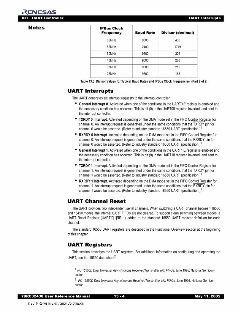
IDT UART Controller UART Interrupts
79RC32438 User Refer
Notes
UART InterruptsThe UART generates six interrupt requests to the interrupt controller:
General Interrupt 0. Activated when one of the conditions in the UART0IE register is enabled and the necessary condition has occurred. This is bit (0) in the UART0II register, inverted, and sent to the interrupt controller.TXRDY 0 Interrupt. Activated depending on the DMA mode set in the FIFO Control Register for channel 0. An interrupt request is generated under the same conditions that the TXRDY pin for channel 0 would be asserted. (Refer to industry standard 16550 UART specification.)1
RXRDY 0 Interrupt. Activated depending on the DMA mode set in the FIFO Control Register for channel 0. An interrupt request is generated under the same conditions that the RXRDY pin for channel 0 would be asserted. (Refer to industry standard 16550 UART specification.)1
General Interrupt 1. Activated when one of the conditions in the UART1IE register is enabled and the necessary condition has occurred. This is bit (0) in the UART1II register, inverted, and sent to the interrupt controller. TXRDY 1 Interrupt. Activated depending on the DMA mode set in the FIFO Control Register for channel 1. An interrupt request is generated under the same conditions that the TXRDY pin for channel 1 would be asserted. (Refer to industry standard 16550 UART specification.)1
RXRDY 1 Interrupt. Activated depending on the DMA mode set in the FIFO Control Register for channel 1. An interrupt request is generated under the same conditions that the RXRDY pin for channel 1 would be asserted. (Refer to industry standard 16550 UART specification.)1
UART Channel ResetThe UART provides two independent serial channels. When switching a UART channel between 16550
and 16450 modes, the internal UART FIFOs are not cleared. To support clean switching between modes, aUART Reset Register (UART[0|1]RR) is added to the standard 16550 UART register definition for eachchannel.
The standard 16550 UART registers are described in the Functional Overview section at the beginningof this chapter.
UART RegistersThis section describes the UART registers. For additional information on configuring and operating the
UART, see the 16550 data sheet2.
66MHz 9600 430
66MHz 2400 1719
50MHz 9600 326
40MHz 9600 260
33MHz 9600 215
25MHz 9600 163
1. PC 16550D Dual Universal Asynchronous Receiver/Transmitter with FIFOs, June 1995, National Semicon-ductor.2. PC 16550D Dual Universal Asynchronous Receiver/Transmitter with FIFOs, June 1995, National Semicon-ductor.
IPBus ClockFrequency Baud Rate Divisor (decimal)
Table 13.3 Divisor Values for Typical Baud Rates and IPBus Clock Frequencies (Part 2 of 2)
ence Manual 13 - 4 May 11, 2005

IDT UART Controller UART Registers
79RC32438 User Refer
Notes
Reset RegisterFigure 13.1 UART [0|1] Reset Register
Receive Buffer Register
Figure 13.2 UART [0|1] Receive Buffer Register (UART[0|1]RB)
Transmit Holding Register
Figure 13.3 UART [0|1] Transmit Holding Register (UART[0|1]TH)
R
Description: Reset. A write of any value to this register causes the corresponding UART channel to be reset.
Initial Value: Undefined
Read Value: Undefined
Write Effect: Write of any value causes UART channel reset
DATA
Description: DATA. Reading this field returns a byte from the UART receive buffer.
Initial Value: Undefined
Read Value: Byte from UART receive buffer
Write Effect: Read-only
DATA
Description: DATA. Writing a byte to this field places the byte into the UART transmit buffer.
Initial Value: Undefined
UART[0|1]RR031
32
R
31UART[0|1]RB
0
8
DATA
24
0
UART[0|1]TH0
8
DATA
31
24
0
ence Manual 13 - 5 May 11, 2005
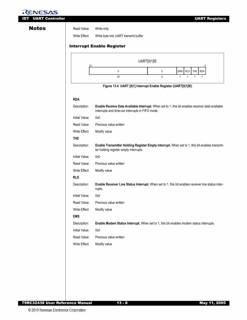
IDT UART Controller UART Registers
79RC32438 User Refer
Notes
Interrupt Enable Register
Figure 13.4 UART [0|1] Interrupt Enable Register (UART[0|1]IE)
Read Value: Write-only
Write Effect: Write byte into UART transmit buffer
RDA
Description: Enable Receive Data Available Interrupt. When set to 1, this bit enables receiver data available interrupts and time-out interrupts in FIFO mode.
Initial Value: 0x0
Read Value: Previous value written
Write Effect: Modify value
THE
Description: Enable Transmitter Holding Register Empty Interrupt. When set to 1, this bit enables transmit-ter holding register empty interrupts.
Initial Value: 0x0
Read Value: Previous value written
Write Effect: Modify value
RLS
Description: Enable Receiver Line Status Interrupt. When set to 1, this bit enables receiver line status inter-rupts.
Initial Value: 0x0
Read Value: Previous value written
Write Effect: Modify value
EMS
Description: Enable Modem Status Interrupt. When set to 1, this bit enables modem status interrupts.
Initial Value: 0x0
Read Value: Previous value written
Write Effect: Modify value
UART[0|1]IE0
4
0
1
RDA
1
THE
1
RLS
1
EMS
31
24
0
ence Manual 13 - 6 May 11, 2005
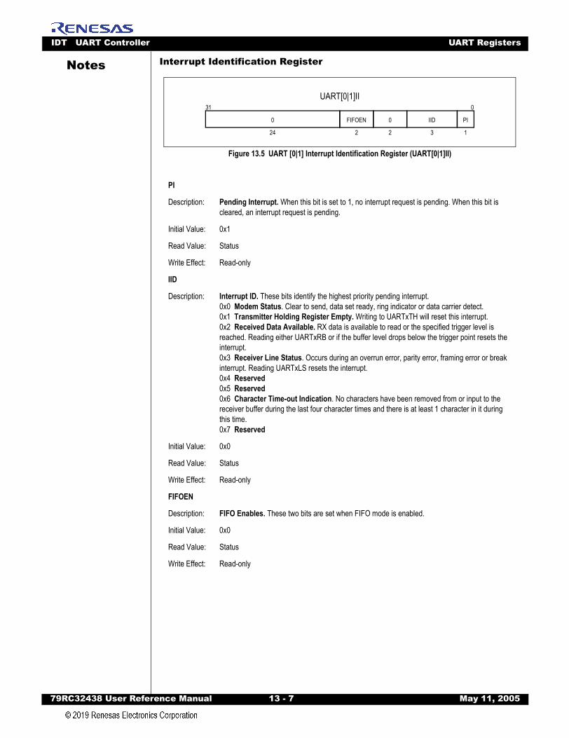
IDT UART Controller UART Registers
79RC32438 User Refer
Notes
Interrupt Identification RegisterFigure 13.5 UART [0|1] Interrupt Identification Register (UART[0|1]II)
PI
Description: Pending Interrupt. When this bit is set to 1, no interrupt request is pending. When this bit is cleared, an interrupt request is pending.
Initial Value: 0x1
Read Value: Status
Write Effect: Read-only
IID
Description: Interrupt ID. These bits identify the highest priority pending interrupt.0x0 Modem Status. Clear to send, data set ready, ring indicator or data carrier detect.0x1 Transmitter Holding Register Empty. Writing to UARTxTH will reset this interrupt.0x2 Received Data Available. RX data is available to read or the specified trigger level is reached. Reading either UARTxRB or if the buffer level drops below the trigger point resets the interrupt.0x3 Receiver Line Status. Occurs during an overrun error, parity error, framing error or break interrupt. Reading UARTxLS resets the interrupt.0x4 Reserved0x5 Reserved0x6 Character Time-out Indication. No characters have been removed from or input to the receiver buffer during the last four character times and there is at least 1 character in it during this time. 0x7 Reserved
Initial Value: 0x0
Read Value: Status
Write Effect: Read-only
FIFOEN
Description: FIFO Enables. These two bits are set when FIFO mode is enabled.
Initial Value: 0x0
Read Value: Status
Write Effect: Read-only
UART[0|1]II0
2
0
1
PI
3
IID
2
FIFOEN
31
24
0
ence Manual 13 - 7 May 11, 2005

IDT UART Controller UART Registers
79RC32438 User Refer
Notes
FIFO Control RegisterFigure 13.6 UART [0|1] FIFO Control Register (UART[0|1]FC)
EN
Description: FIFO Enable. When this bit is set, the transmit and receive FIFOs are enabled for 16550 mode. When switching between 16550 and 16450, always reset the buffers.
Initial Value: 0x0
Read Value: Write-only
Write Effect: Modify value
RR
Description: Reset Receive FIFO. Writing a 1 into this bit position resets the receive FIFO.
Initial Value: 0x0
Read Value: Write-only
Write Effect: Modify value
TR
Description: Reset Transmit FIFO. Writing a 1 into this bit position resets the transmit FIFO.
Initial Value: 0x0
Read Value: Write-only
Write Effect: Modify value
DMS
Description: DMA Mode Select. Writing a 1 into this bit position changes the DMA mode. The TXRDY and RXRDY signals of the 16550 go to the interrupt controller as an interrupt source. (Refer to indus-try standard 16550 UART specification.)1
Initial Value: 0x0
Read Value: Write-only
Write Effect: Modify value
RT
Description: Receiver Trigger. This field designates the interrupt trigger level. When the number of bytes in the receive FIFO equals the designated interrupt level, a receive data available interrupt is acti-vated. 0x0 1-byte in the receive buffer0x1 4-bytes in the receive buffer0x2 8-bytes in the receive buffer0x3 14-bytes in the receive buffer
Initial Value: 0x0
UART[0|1]FC0
2
0
1
EN
2
RT
1
RR
1
TR
1
DMS
31
24
0
ence Manual 13 - 8 May 11, 2005
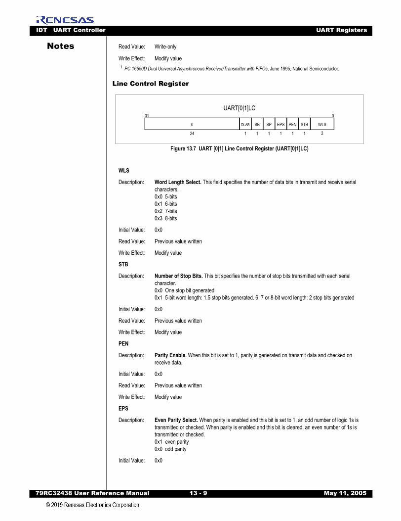
IDT UART Controller UART Registers
79RC32438 User Refer
Notes
Line Control Register
Figure 13.7 UART [0|1] Line Control Register (UART[0|1]LC)
Read Value: Write-only
Write Effect: Modify value1. PC 16550D Dual Universal Asynchronous Receiver/Transmitter with FIFOs, June 1995, National Semiconductor.
WLS
Description: Word Length Select. This field specifies the number of data bits in transmit and receive serial characters.0x0 5-bits0x1 6-bits0x2 7-bits0x3 8-bits
Initial Value: 0x0
Read Value: Previous value written
Write Effect: Modify value
STB
Description: Number of Stop Bits. This bit specifies the number of stop bits transmitted with each serial character. 0x0 One stop bit generated0x1 5-bit word length: 1.5 stop bits generated. 6, 7 or 8-bit word length: 2 stop bits generated
Initial Value: 0x0
Read Value: Previous value written
Write Effect: Modify value
PEN
Description: Parity Enable. When this bit is set to 1, parity is generated on transmit data and checked on receive data.
Initial Value: 0x0
Read Value: Previous value written
Write Effect: Modify value
EPS
Description: Even Parity Select. When parity is enabled and this bit is set to 1, an odd number of logic 1s is transmitted or checked. When parity is enabled and this bit is cleared, an even number of 1s is transmitted or checked. 0x1 even parity0x0 odd parity
Initial Value: 0x0
UART[0|1]LC0
2
WLS
1
STB
1
PEN
1
EPS
1
SP
1
SB
1
DLAB
31
24
0
ence Manual 13 - 9 May 11, 2005
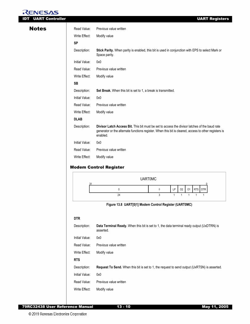
IDT UART Controller UART Registers
79RC32438 User Refer
Notes
Modem Control Register
Figure 13.8 UART[0|1] Modem Control Register (UART0MC)
Read Value: Previous value written
Write Effect: Modify value
SP
Description: Stick Parity. When parity is enabled, this bit is used in conjunction with EPS to select Mark or Space parity.
Initial Value: 0x0
Read Value: Previous value written
Write Effect: Modify value
SB
Description: Set Break. When this bit is set to 1, a break is transmitted.
Initial Value: 0x0
Read Value: Previous value written
Write Effect: Modify value
DLAB
Description: Divisor Latch Access Bit. This bit must be set to access the divisor latches of the baud rate generator or the alternate functions register. When this bit is cleared, access to other registers is enabled.
Initial Value: 0x0
Read Value: Previous value written
Write Effect: Modify value
DTR
Description: Data Terminal Ready. When this bit is set to 1, the data terminal ready output (UxDTRN) is asserted.
Initial Value: 0x0
Read Value: Previous value written
Write Effect: Modify value
RTS
Description: Request To Send. When this bit is set to 1, the request to send output (UxRTSN) is asserted.
Initial Value: 0x0
Read Value: Previous value written
Write Effect: Modify value
UART0MC0
1
O1
1
O2
1
LP
3
0
1
DTR
1
RTS
31
24
0
ence Manual 13 - 10 May 11, 2005
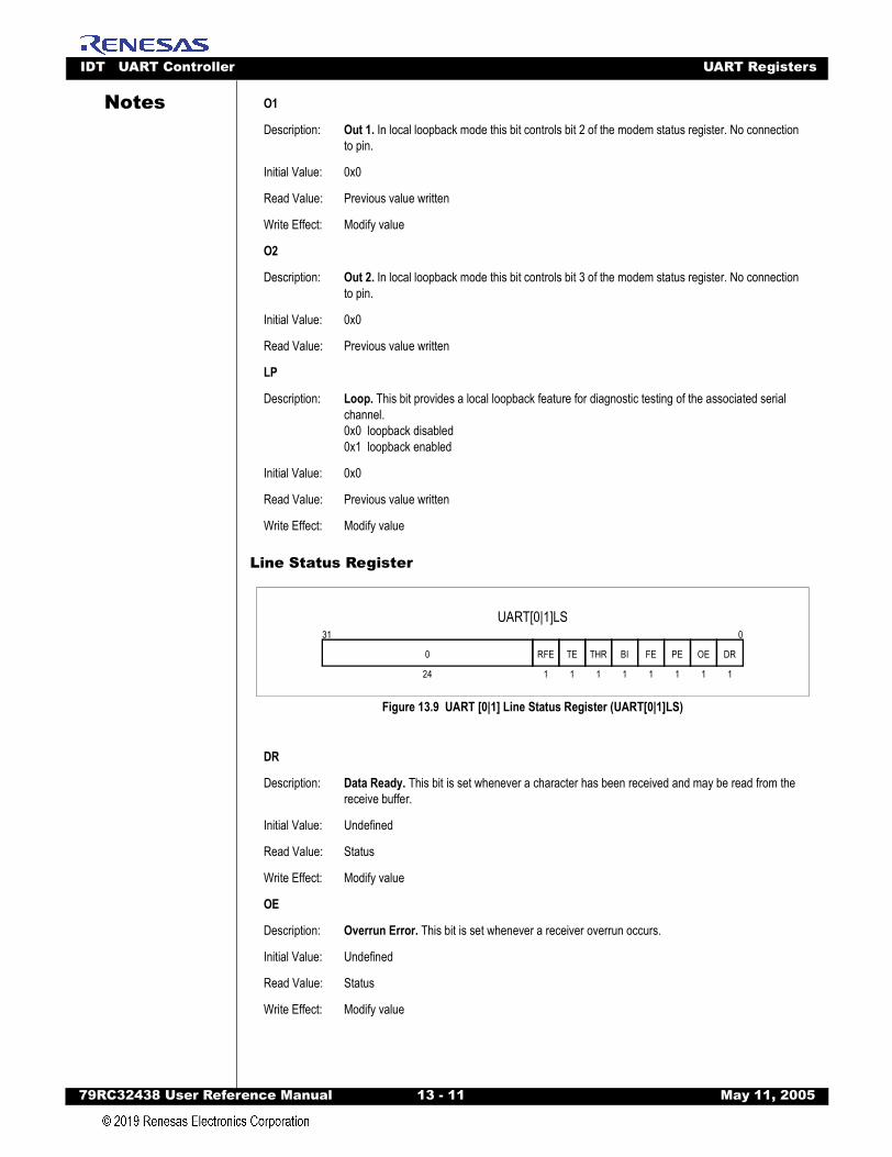
IDT UART Controller UART Registers
79RC32438 User Refer
Notes
Line Status Register
Figure 13.9 UART [0|1] Line Status Register (UART[0|1]LS)
O1
Description: Out 1. In local loopback mode this bit controls bit 2 of the modem status register. No connection to pin.
Initial Value: 0x0
Read Value: Previous value written
Write Effect: Modify value
O2
Description: Out 2. In local loopback mode this bit controls bit 3 of the modem status register. No connection to pin.
Initial Value: 0x0
Read Value: Previous value written
LP
Description: Loop. This bit provides a local loopback feature for diagnostic testing of the associated serial channel. 0x0 loopback disabled0x1 loopback enabled
Initial Value: 0x0
Read Value: Previous value written
Write Effect: Modify value
DR
Description: Data Ready. This bit is set whenever a character has been received and may be read from the receive buffer.
Initial Value: Undefined
Read Value: Status
Write Effect: Modify value
OE
Description: Overrun Error. This bit is set whenever a receiver overrun occurs.
Initial Value: Undefined
Read Value: Status
Write Effect: Modify value
UART[0|1]LS0
1
PE
1
FE
1
BI
1
DR
1
OE
1
THR
1
TE
1
RFE
31
24
0
ence Manual 13 - 11 May 11, 2005
IDT UART Controller UART Registers
79RC32438 User Refer
Notes
PEDescription: Parity Error. This bit is set when a character with incorrect parity is received.
Initial Value: Undefined
Read Value: Status
Write Effect: Modify value
FE
Description: Framing Error. This bit is set whenever a received character does not have a valid stop bit.
Initial Value: Undefined
Read Value: Status
Write Effect: Modify value
BI
Description: Break Interrupt. This bit is set when a break is received.
Initial Value: Undefined
Read Value: Status
Write Effect: Modify value
THR
Description: Transmitter Holding Register. This bit is set to indicate that the serial channel is ready to accept a new character for transmission.
Initial Value: Undefined
Read Value: Status
Write Effect: Read-only
TE
Description: Transmitter Empty. This bit is set when both the transmitter holding register and the transmitter shift register are empty.
Initial Value: Undefined
Read Value: Status
Write Effect: Modify value
RFE
Description: Receive FIFO Error. This bit is set when there is a character with a parity error or a framing error, or there is a break indication in the FIFO.
Initial Value: Undefined
Read Value: Status
Write Effect: Read-only
ence Manual 13 - 12 May 11, 2005
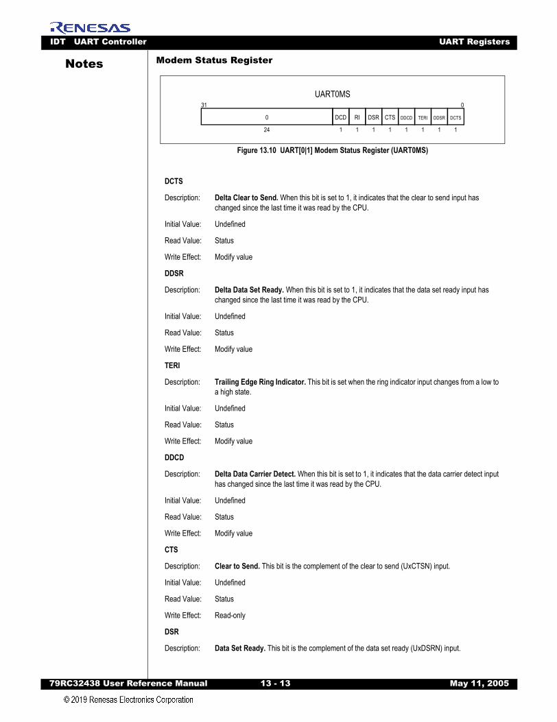
IDT UART Controller UART Registers
79RC32438 User Refer
Notes
Modem Status RegisterFigure 13.10 UART[0|1] Modem Status Register (UART0MS)
DCTS
Description: Delta Clear to Send. When this bit is set to 1, it indicates that the clear to send input has changed since the last time it was read by the CPU.
Initial Value: Undefined
Read Value: Status
Write Effect: Modify value
DDSR
Description: Delta Data Set Ready. When this bit is set to 1, it indicates that the data set ready input has changed since the last time it was read by the CPU.
Initial Value: Undefined
Read Value: Status
Write Effect: Modify value
TERI
Description: Trailing Edge Ring Indicator. This bit is set when the ring indicator input changes from a low to a high state.
Initial Value: Undefined
Read Value: Status
Write Effect: Modify value
DDCD
Description: Delta Data Carrier Detect. When this bit is set to 1, it indicates that the data carrier detect input has changed since the last time it was read by the CPU.
Initial Value: Undefined
Read Value: Status
Write Effect: Modify value
CTS
Description: Clear to Send. This bit is the complement of the clear to send (UxCTSN) input.
Initial Value: Undefined
Read Value: Status
Write Effect: Read-only
DSR
Description: Data Set Ready. This bit is the complement of the data set ready (UxDSRN) input.
UART0MS0
1
TERI
1
DDCD
1
CTS
1
DCTS
1
DDSR
1
DSR
1
RI
1
DCD
31
24
0
ence Manual 13 - 13 May 11, 2005

IDT UART Controller UART Registers
79RC32438 User Refer
Notes
Scratch Register
Figure 13.11 UART [0|1] Scratch Register (UART[0|1]S)
Divisor Latch Low Register
Figure 13.12 UART [0|1] Divisor Latch Low Register (UART[0|1]DLL)
Initial Value: Undefined
Read Value: Status
Write Effect: Read-only
RI
Description: Ring Indicator. The bit is the complement of the ring indicator (U0RIN) input for UART channel 0. UART channel 1 does not implement a ring indicator input. Thus, this field is undefined forUART channel 1.
Initial Value: Undefined
Read Value: Status
Write Effect: Read-only
DCD
Description: Data Carrier Detect. This bit is the complement of the data carrier detect (U0DCRN) input for UART channel 0. UART channel 1 does not implement a data carrier detect input. Thus, this field is undefined for UART channel 1.
Initial Value: Undefined
Read Value: Status
Write Effect: Read-only
DATA
Description: DATA. This register may be used by the programmer to hold temporary data and does not con-trol the serial channel in any way.
Initial Value: Undefined
Read Value: Previous value written
Write Effect: Modify value
UART[0|1]S0
8
DATA
31
24
0
UART[0|1]DLL0
8
DATA
31
24
0
ence Manual 13 - 14 May 11, 2005
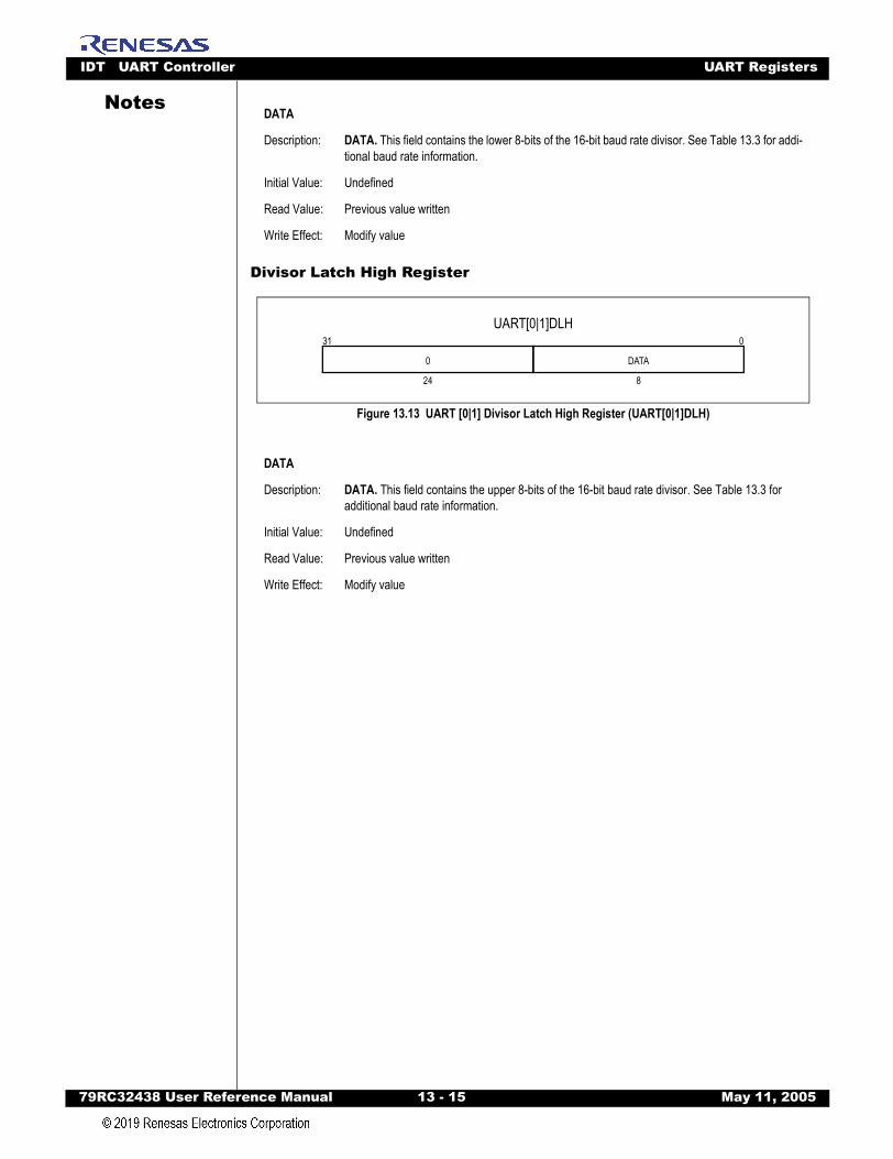
IDT UART Controller UART Registers
79RC32438 User Refer
Notes
Divisor Latch High Register
Figure 13.13 UART [0|1] Divisor Latch High Register (UART[0|1]DLH)
DATA
Description: DATA. This field contains the lower 8-bits of the 16-bit baud rate divisor. See Table 13.3 for addi-tional baud rate information.
Initial Value: Undefined
Read Value: Previous value written
Write Effect: Modify value
DATA
Description: DATA. This field contains the upper 8-bits of the 16-bit baud rate divisor. See Table 13.3 for additional baud rate information.
Initial Value: Undefined
Read Value: Previous value written
Write Effect: Modify value
UART[0|1]DLH0
8
DATA
31
24
0
ence Manual 13 - 15 May 11, 2005
IDT UART Controller UART Registers
79RC32438 User Refer
Notes
ence Manual 13 - 16 May 11, 2005
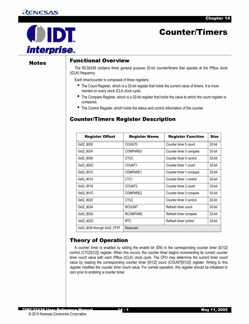
Notes
79RC32438 User Reference Manual 14 - 1 M
Chapter 14
Counter/Timers
Functional OverviewThe RC32438 contains three general purpose 32-bit counter/timers that operate at the IPBus clock
(ICLK) frequency.Each timer/counter is composed of three registers:
The Count Register, which is a 32-bit register that holds the current value of timers. It is incre-mented on every clock ICLK clock cycle.The Compare Register, which is a 32-bit register that holds the value to which the count register is compared.The Control Register, which holds the status and control information of the counter.
Counter/Timers Register Description
Theory of OperationA counter timer is enabled by setting the enable bit (EN) in the corresponding counter timer [0|1|2]
control (CTC[0|1|2]) register. When this occurs, the counter timer begins incrementing its current countertimer count value with each IPBus (ICLK) clock cycle. The CPU may determine the current timer countvalue by reading the corresponding counter timer [0|1|2] count (COUNT[0|1|2]) register. Writing to thisregister modifies the counter timer count value. For normal operation, this register should be initialized tozero prior to enabling a counter timer.
Register Offset Register Name Register Function Size
0x02_8000 COUNT0 Counter timer 0 count 32-bit
0x02_8004 COMPARE0 Counter timer 0 compare 32-bit
0x02_8008 CTC0 Counter timer 0 control 32-bit
0x02_800C COUNT1 Counter timer 1 count 32-bit
0x02_8010 COMPARE1 Counter timer 1 compare 32-bit
0x02_8014 CTC1 Counter timer 1 control 32-bit
0x02_8018 COUNT2 Counter timer 2 count 32-bit
0x02_801C COMPARE2 Counter timer 2 compare 32-bit
0x02_8020 CTC2 Counter timer 2 control 32-bit
0x02_8024 RCOUNT Refresh timer count 32-bit
0x02_8028 RCOMPARE Refresh timer compare 32-bit
0x02_802C RTC Refresh timer control 32-bit
0x02_8030 through 0x02_FFFF Reserved
ay 11, 2005
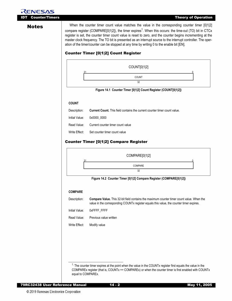
IDT Counter/Timers Theory of Operation
79RC32438 User Refer
Notes
When the counter timer count value matches the value in the corresponding counter timer [0|1|2]compare register (COMPARE[0|1|2]), the timer expires1. When this occurs: the time-out (TO) bit in CTCxregister is set, the counter timer count value is reset to zero, and the counter begins incrementing at themaster clock frequency. The TO bit is presented as an interrupt source to the interrupt controller. The oper-ation of the timer/counter can be stopped at any time by writing 0 to the enable bit [EN].Counter Timer [0|1|2] Count Register
Figure 14.1 Counter Timer [0|1|2] Count Register (COUNT[0|1|2])
Counter Timer [0|1|2] Compare Register
Figure 14.2 Counter Timer [0|1|2] Compare Register (COMPARE[0|1|2])
1. The counter timer expires at the point when the value in the COUNTx register first equals the value in the COMPAREx register (that is, COUNTx == COMPAREx) or when the counter timer is first enabled with COUNTx equal to COMPAREx.
COUNT
Description: Current Count. This field contains the current counter timer count value.
Initial Value: 0x0000_0000
Read Value: Current counter timer count value
Write Effect: Set counter timer count value
COMPARE
Description: Compare Value. This 32-bit field contains the maximum counter timer count value. When the value in the corresponding COUNTx register equals this value, the counter timer expires.
Initial Value: 0xFFFF_FFFF
Read Value: Previous value written
Write Effect: Modify value
COUNT[0|1|2]031
32
COUNT
COMPARE[0|1|2]031
32
COMPARE
ence Manual 14 - 2 May 11, 2005
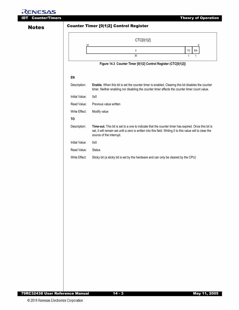
IDT Counter/Timers Theory of Operation
79RC32438 User Refer
Notes
Counter Timer [0|1|2] Control RegisterFigure 14.3 Counter Timer [0|1|2] Control Register (CTC[0|1|2])
EN
Description: Enable. When this bit is set the counter timer is enabled. Clearing this bit disables the counter timer. Neither enabling nor disabling the counter timer affects the counter timer count value.
Initial Value: 0x0
Read Value: Previous value written
Write Effect: Modify value
TO
Description: Time-out. This bit is set to a one to indicate that the counter timer has expired. Once this bit is set, it will remain set until a zero is written into this field. Writing 0 to this value will to clear the source of the interrupt.
Initial Value: 0x0
Read Value: Status
Write Effect: Sticky bit (a sticky bit is set by the hardware and can only be cleared by the CPU)
CTC[0|1|2]031
30
0 TO EN
1 1
ence Manual 14 - 3 May 11, 2005
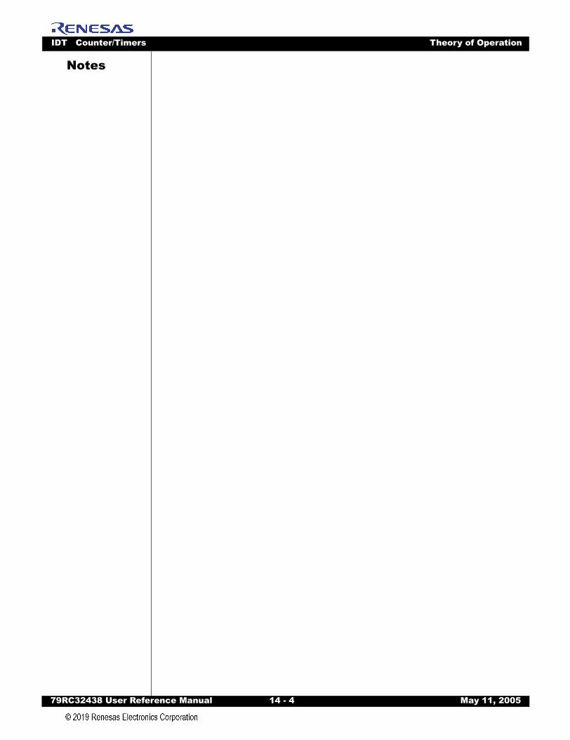
IDT Counter/Timers Theory of Operation
79RC32438 User Refer
Notes
ence Manual 14 - 4 May 11, 2005
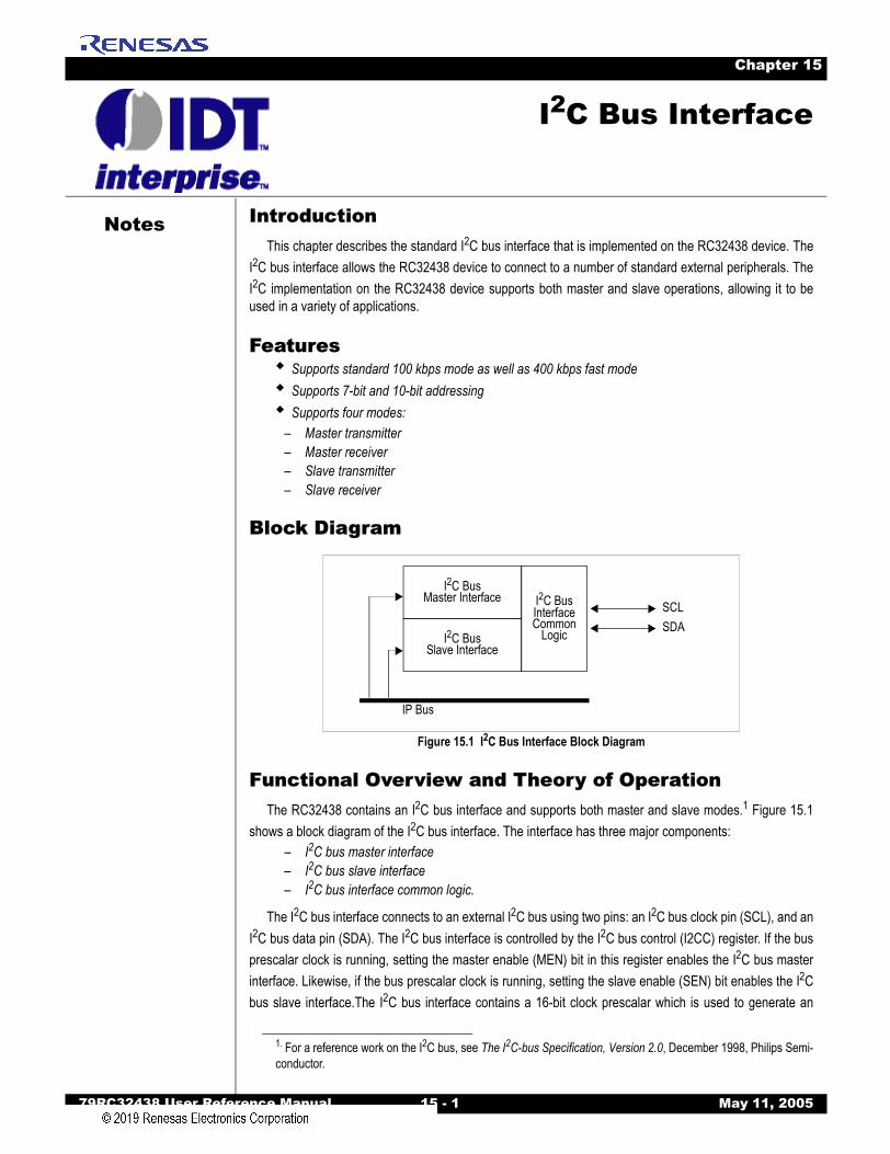
Notes
79RC32438 User Reference Manual 15 - 1 M
Chapter 15
I2C Bus Interface
IntroductionThis chapter describes the standard I2C bus interface that is implemented on the RC32438 device. The
I2C bus interface allows the RC32438 device to connect to a number of standard external peripherals. TheI2C implementation on the RC32438 device supports both master and slave operations, allowing it to beused in a variety of applications.
FeaturesSupports standard 100 kbps mode as well as 400 kbps fast modeSupports 7-bit and 10-bit addressingSupports four modes:
– Master transmitter– Master receiver– Slave transmitter– Slave receiver
Block Diagram
Figure 15.1 I2C Bus Interface Block Diagram
Functional Overview and Theory of OperationThe RC32438 contains an I2C bus interface and supports both master and slave modes.1 Figure 15.1
shows a block diagram of the I2C bus interface. The interface has three major components: – I2C bus master interface – I2C bus slave interface – I2C bus interface common logic.
The I2C bus interface connects to an external I2C bus using two pins: an I2C bus clock pin (SCL), and anI2C bus data pin (SDA). The I2C bus interface is controlled by the I2C bus control (I2CC) register. If the busprescalar clock is running, setting the master enable (MEN) bit in this register enables the I2C bus masterinterface. Likewise, if the bus prescalar clock is running, setting the slave enable (SEN) bit enables the I2Cbus slave interface.The I2C bus interface contains a 16-bit clock prescalar which is used to generate an
1. For a reference work on the I2C bus, see The I2C-bus Specification, Version 2.0, December 1998, Philips Semi-conductor.
IP Bus
I2C BusMaster Interface
I2C BusSlave Interface
SDASCLI2C Bus
InterfaceCommon
Logic
ay 11, 2005
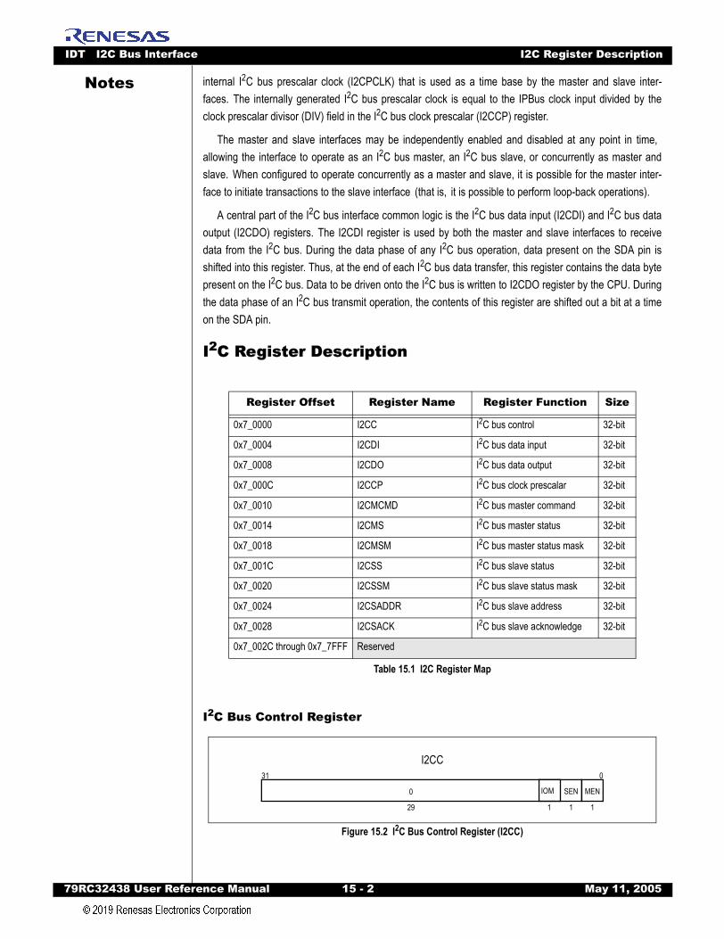
IDT I2C Bus Interface I2C Register Description
79RC32438 User Refer
Notes
internal I2C bus prescalar clock (I2CPCLK) that is used as a time base by the master and slave inter-faces.2The internally generated I2C bus prescalar clock is equal to the IPBus clock input divided by theclock prescalar divisor (DIV) field in the I2C bus clock prescalar (I2CCP) register. 2The master and slave interfaces may be independently enabled and disabled at any point in time,2
allowing the interface to operate as an I2C bus master, an I2C bus slave, or concurrently as master andslave.2When configured to operate concurrently as a master and slave, it is possible for the master inter-face to initiate transactions to the slave interface2(that is,2it is possible to perform loop-back operations).2
A central part of the I2C bus interface common logic is the I2C bus data input (I2CDI) and I2C bus dataoutput (I2CDO) registers.2The I2CDI register is used by both the master and slave interfaces to receivedata from the I2C bus. During the data phase of any I2C bus operation, data present on the SDA pin isshifted into this register. Thus, at the end of each I2C bus data transfer, this register contains the data bytepresent on the I2C bus. Data to be driven onto the I2C bus is written to I2CDO register by the CPU. Duringthe data phase of an I2C bus transmit operation, the contents of this register are shifted out a bit at a timeon the SDA pin. 2
I2C Register Description
I2C Bus Control Register
Figure 15.2 I2C Bus Control Register (I2CC)
Register Offset Register Name Register Function Size
0x7_0000 I2CC I2C bus control 32-bit
0x7_0004 I2CDI I2C bus data input 32-bit
0x7_0008 I2CDO I2C bus data output 32-bit
0x7_000C I2CCP I2C bus clock prescalar 32-bit
0x7_0010 I2CMCMD I2C bus master command 32-bit
0x7_0014 I2CMS I2C bus master status 32-bit
0x7_0018 I2CMSM I2C bus master status mask 32-bit
0x7_001C I2CSS I2C bus slave status 32-bit
0x7_0020 I2CSSM I2C bus slave status mask 32-bit
0x7_0024 I2CSADDR I2C bus slave address 32-bit
0x7_0028 I2CSACK I2C bus slave acknowledge 32-bit
0x7_002C through 0x7_7FFF Reserved
Table 15.1 I2C Register Map
I2CC031
MEN0
29 1
SEN
1
IOM
1
ence Manual 15 - 2 May 11, 2005
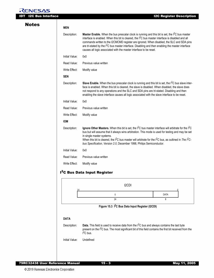
IDT I2C Bus Interface I2C Register Description
79RC32438 User Refer
Notes
I2C Bus Data Input Register
Figure 15.3 I2C Bus Data Input Register (I2CDI)
MEN
Description: Master Enable. When the bus prescalar clock is running and this bit is set, the I2C bus master interface is enabled. When this bit is cleared, the I2C bus master interface is disabled and all commands written to the I2CMCMD register are ignored. When disabled, the SLC and SDA pins are tri-stated by the I2C bus master interface. Disabling and then enabling the master interface causes all logic associated with the master interface to be reset.
Initial Value: 0x0
Read Value: Previous value written
Write Effect: Modify value
SEN
Description: Slave Enable. When the bus prescalar clock is running and this bit is set, the I2C bus slave inter-face is enabled. When this bit is cleared, the slave is disabled. When disabled, the slave does not respond to any operations and the SLC and SDA pins are tri-stated. Disabling and then enabling the slave interface causes all logic associated with the slave interface to be reset.
Initial Value: 0x0
Read Value: Previous value written
Write Effect: Modify value
IOM
Description: Ignore Other Masters. When this bit is set, the I2C bus master interface will arbitrate for the I2C bus but will assume that it always wins arbitration. This mode is used for testing and may be set in single master systems.When this bit is cleared, the I2C bus master will arbitrate for the I2C bus, as outlined in The I2C-bus Specification, Version 2.0, December 1998, Philips Semiconductor.
Initial Value: 0x0
Read Value: Previous value written
Write Effect: Modify value
DATA
Description: Data. This field is used to receive data from the I2C bus and always contains the last byte present on the I2C bus. The most significant bit of this field contains the first bit received from the I2C bus.
Initial Value: Undefined
I2CDI031
DATA0
24 8
ence Manual 15 - 3 May 11, 2005
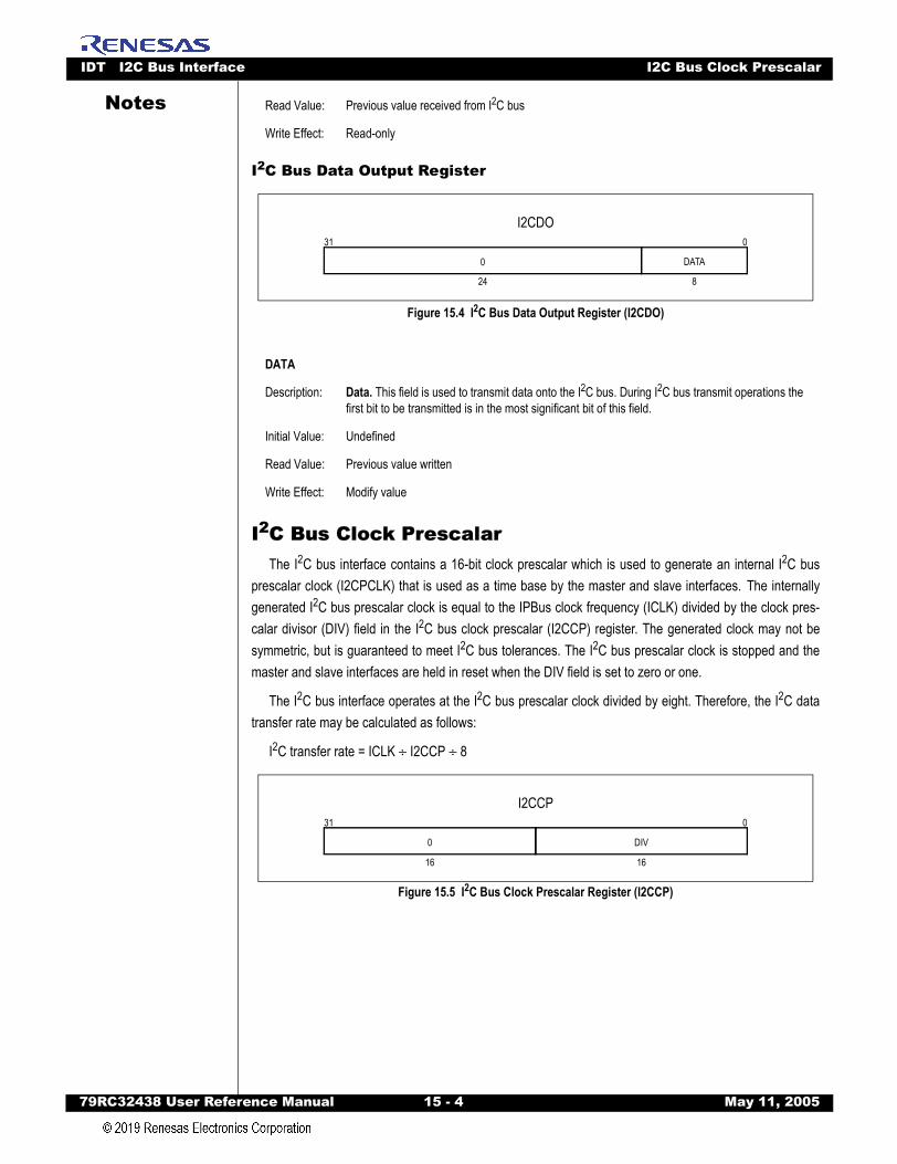
IDT I2C Bus Interface I2C Bus Clock Prescalar
79RC32438 User Refer
Notes
I2C Bus Data Output Register
Figure 15.4 I2C Bus Data Output Register (I2CDO)
I2C Bus Clock PrescalarThe I2C bus interface contains a 16-bit clock prescalar which is used to generate an internal I2C bus
prescalar clock (I2CPCLK) that is used as a time base by the master and slave interfaces.2The internallygenerated I2C bus prescalar clock is equal to the IPBus clock frequency (ICLK) divided by the clock pres-calar divisor (DIV) field in the I2C bus clock prescalar (I2CCP) register. The generated clock may not besymmetric, but is guaranteed to meet I2C bus tolerances. The I2C bus prescalar clock is stopped and themaster and slave interfaces are held in reset when the DIV field is set to zero or one. 2 2
The I2C bus interface operates at the I2C bus prescalar clock divided by eight. Therefore, the I2C datatransfer rate may be calculated as follows: 2
I2C transfer rate = ICLK ÷ I2CCP ÷ 8
Figure 15.5 I2C Bus Clock Prescalar Register (I2CCP)
Read Value: Previous value received from I2C bus
Write Effect: Read-only
DATA
Description: Data. This field is used to transmit data onto the I2C bus. During I2C bus transmit operations the first bit to be transmitted is in the most significant bit of this field.
Initial Value: Undefined
Read Value: Previous value written
Write Effect: Modify value
I2CDO031
DATA0
24 8
I2CCP031
DIV0
16 16
ence Manual 15 - 4 May 11, 2005
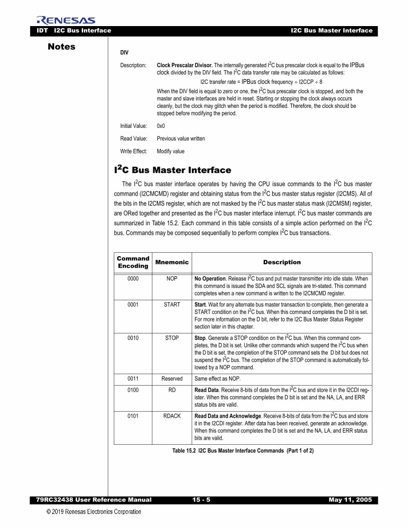
IDT I2C Bus Interface I2C Bus Master Interface
79RC32438 User Refer
Notes
I2C Bus Master InterfaceThe I2C bus master interface operates by having the CPU issue commands to the I2C bus master
command (I2CMCMD) register and obtaining status from the I2C bus master status register (I2CMS). All ofthe bits in the I2CMS register, which are not masked by the I2C bus master status mask (I2CMSM) register,are ORed together and presented as the I2C bus master interface interrupt. I2C bus master commands aresummarized in Table 15.2.2Each command in this table consists of a simple action performed on the I2Cbus. Commands may be composed sequentially to perform complex I2C bus transactions.2
DIV
Description: Clock Prescalar Divisor. The internally generated I2C bus prescalar clock is equal to the IPBus clock divided by the DIV field. The I2C data transfer rate may be calculated as follows:
I2C transfer rate = IPBus clock frequency ÷ I2CCP ÷ 8When the DIV field is equal to zero or one, the I2C bus prescalar clock is stopped, and both the master and slave interfaces are held in reset. Starting or stopping the clock always occurs cleanly, but the clock may glitch when the period is modified. Therefore, the clock should be stopped before modifying the period.
Initial Value: 0x0
Read Value: Previous value written
Write Effect: Modify value
Command Encoding Mnemonic Description
0000 NOP No Operation. Release I2C bus and put master transmitter into idle state. When this command is issued the SDA and SCL signals are tri-stated. This command completes when a new command is written to the I2CMCMD register.
0001 START Start. Wait for any alternate bus master transaction to complete, then generate a START condition on the I2C bus. When this command completes the D bit is set. For more information on the D bit, refer to the I2C Bus Master Status Register section later in this chapter.
0010 STOP Stop. Generate a STOP condition on the I2C bus. When this command com-pletes, the D bit is set. Unlike other commands which suspend the I2C bus when the D bit is set, the completion of the STOP command sets the2D bit but does not suspend the I2C bus. The completion of the STOP command is automatically fol-lowed by a NOP command.
0011 Reserved Same effect as NOP.
0100 RD Read Data. Receive 8-bits of data from the I2C bus and store it in the I2CDI reg-ister. When this command completes the D bit is set and the NA, LA, and ERR status bits are valid.
0101 RDACK Read Data and Acknowledge. Receive 8-bits of data from the I2C bus and store it in the I2CDI register. After data has been received, generate an acknowledge. When this command completes the D bit is set and the NA, LA, and ERR status bits are valid.
Table 15.2 I2C Bus Master Interface Commands (Part 1 of 2)
ence Manual 15 - 5 May 11, 2005

IDT I2C Bus Interface I2C Bus Master Interface
79RC32438 User Refer
Notes
The I2C bus SCL and SDA signals are wired-AND, allowing the clock signal to be used as a synchroni-zation mechanism. A device on the I2C bus can slow down, or stop, the I2C bus clock at any point byextending the low period of the clock.2This can be done after each bit, or after a complete operation isperformed.2Thus, the speed of the master is automatically adapted to the operating rate of the slowestdevice. This is illustrated in Figure 15.6. 2
Figure 15.6 Using the I2C Bus Clock (SCL) to Adapt the Operating Rate
When a command is written to the I2CMCMD register, the specified action is initiated on the I2C bus. Forcommands other than NOP, this consists of generating the I2C bus clock (SCL) and possibly driving the I2Cbus data pin (SDA).2 The completion of the command is signaled to the CPU by setting the done (D) bit inthe I2CMS register.2Depending on the command, other status bits in this register may also becomevalid.2When the done bit is set, the master interface holds the SCL signal low, allowing the CPU core torespond to the received status information and issue the next command1. All of the status bits in the I2CMSregister,2including the done bit,2are automatically cleared and SCL signal is released when a command iswritten to the I2CMCMD2register.2
The2Read Data (RD), Read Data with Acknowledge (RDACK), Write Data (WD), and Write Data withAcknowledge (WDACK) commands all participate in I2C bus arbitration. When one of these commands isissued, the master interface observes the state of SDA. Arbitration is lost when a master I2C bus interfacestransmits a high value but observes a low value on the SDA signal. When this occurs the master I2C bus
0110 WD Write Data. Transmit 8-bits of data from the I2CDO register onto the I2C bus. When this command completes the D bit is set and the NA, LA, and ERR status bits are valid.
0111 WDACK Write Data and Acknowledge. (This command is for debug purposes only.) Transmit 8-bits of data from the I2CDO register onto the I2C bus. After the data has been transmitted, generate an acknowledge. When this command com-pletes the D bit is set and the NA, LA, and ERR status bits are valid.
1000 through 1111
Reserved Same effect as NOP.
1. This is true for all commands except the STOP command. At the completion of the STOP command, the D bit is set, the I2C bus is released by tri-stating the SDA and SCL signals, and the master goes into an idle state.
Command Encoding Mnemonic Description
Table 15.2 I2C Bus Master Interface Commands (Part 2 of 2)
I2CPCLK
SCL
1 5 6
1. A slave becomes not-ready, so it pulls SCL low. Since SCL is wired-AND, it is held low as long as the slave is not-ready. The I2C bus master is suspended.
2. Slave becomes ready and releases SCL. This allows the clock to progress.3. A device may pull SCL low even before I2CPCLK (the internally generated I2C bus prescalar clock) goes low. This may
occur for example during I2C bus arbitration when multiple masters drive the bus.4. An external device can release SCL at any point. The master interface must make sure that “runt” clocks are not gener-
ated which have a period smaller than that programmed in the I2CCP register. This may mean that the master interface stretches the clock and waits for the next rising edge of I2CPCLK.
5. A slave becomes not-ready.6. A slave becomes ready.
2 3 4
ence Manual 15 - 6 May 11, 2005
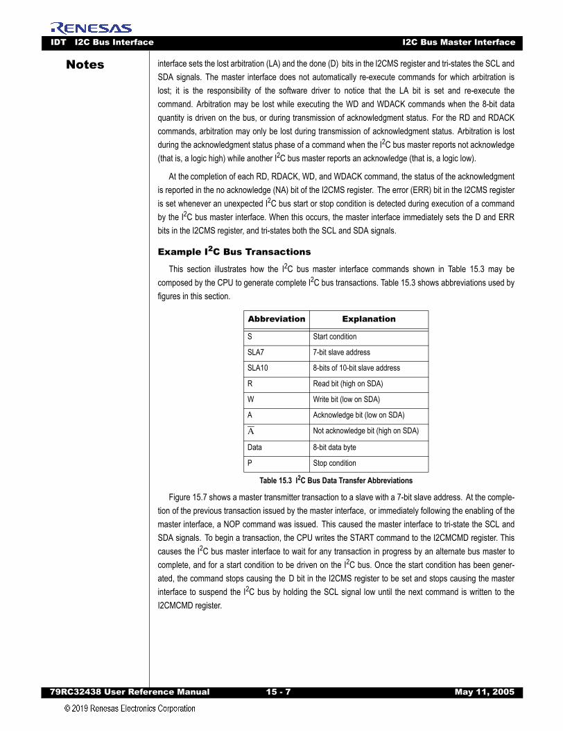
IDT I2C Bus Interface I2C Bus Master Interface
79RC32438 User Refer
Notes
interface sets the lost arbitration (LA) and the done (D)2bits in the I2CMS register and tri-states the SCL andSDA signals.2The master interface does not automatically re-execute commands for which arbitration islost; it is the responsibility of the2software driver to notice that the LA bit is set and re-execute thecommand.2Arbitration may be lost while executing the WD and WDACK commands when the 8-bit dataquantity is driven on the bus, or during transmission of acknowledgment status.2For the RD and RDACKcommands, arbitration may only be lost during transmission of acknowledgment status.2Arbitration is lostduring the acknowledgment status phase of a command when the I2C bus master reports not acknowledge(that is, a logic high) while another I2C bus master reports an acknowledge (that is, a logic low).At the completion of each RD, RDACK, WD, and WDACK command, the status of the acknowledgmentis reported in the no acknowledge (NA) bit of the I2CMS register.2The error (ERR) bit in the I2CMS registeris set whenever an unexpected I2C bus start or stop condition is detected during execution of a commandby the I2C bus master interface. When this occurs, the master interface immediately sets the D and ERRbits in the I2CMS register, and tri-states both the SCL and SDA signals.2
Example I2C Bus Transactions
This section illustrates how the I2C bus master interface commands shown in Table 15.3 may becomposed by the CPU to generate complete I2C bus transactions. Table 15.3 shows abbreviations used byfigures in this section..22
Figure 15.7 shows a master transmitter transaction to a slave with a 7-bit slave address.2At the comple-tion of the previous transaction issued by the master interface,2or immediately following the enabling of themaster interface, a NOP command was issued.2This caused the master interface to tri-state the SCL andSDA signals.2To begin a transaction, the CPU writes the START command to the I2CMCMD register. Thiscauses the I2C bus master interface to wait for any transaction in progress by an alternate bus master tocomplete, and for a start condition to be driven on the I2C bus. Once the start condition has been gener-ated, the command stops causing the2D bit in the I2CMS register to be set and stops causing the masterinterface to suspend the I2C bus by holding the SCL signal low until the next command is written to theI2CMCMD register.2
Abbreviation Explanation
S Start condition
SLA7 7-bit slave address
SLA10 8-bits of 10-bit slave address
R Read bit (high on SDA)
W Write bit (low on SDA)
A Acknowledge bit (low on SDA)
A Not acknowledge bit (high on SDA)
Data 8-bit data byte
P Stop condition
Table 15.3 I2C Bus Data Transfer Abbreviations
ence Manual 15 - 7 May 11, 2005
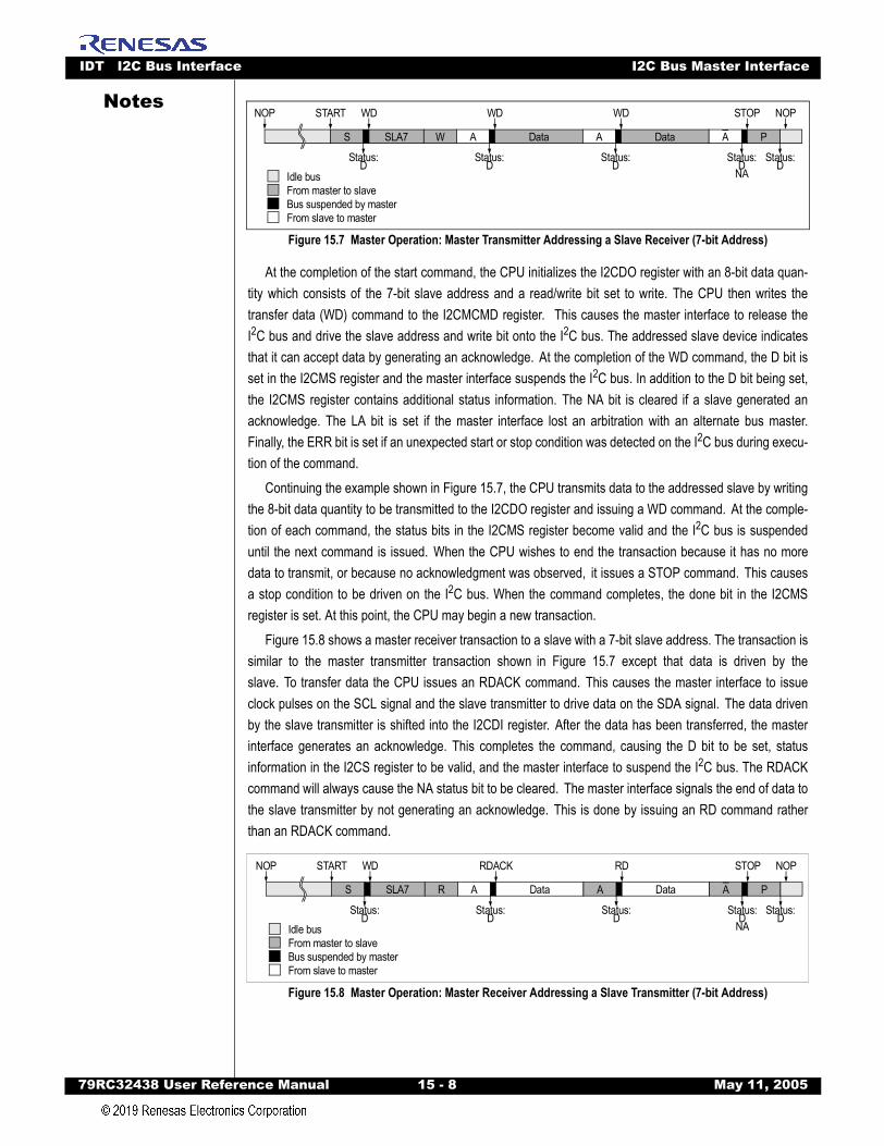
IDT I2C Bus Interface I2C Bus Master Interface
79RC32438 User Refer
Notes
Figure 15.7 Master Operation: Master Transmitter Addressing a Slave Receiver (7-bit Address)
At the completion of the start command, the CPU initializes the I2CDO register with an 8-bit data quan-tity which consists of the 7-bit slave address and a read/write bit set to write.2The CPU then writes thetransfer data (WD) command to the I2CMCMD register.2 This causes the master interface to release theI2C bus and drive the slave address and write bit onto the I2C bus. The addressed slave device indicatesthat it can accept data by generating an acknowledge.2At the completion of the WD command, the D bit isset in the I2CMS register and the master interface suspends the I2C bus. In addition to the D bit being set,the I2CMS register contains additional status information.2The NA bit is cleared if a slave generated anacknowledge.2The LA bit is set if the master interface lost an arbitration with an alternate bus master.Finally, the ERR bit is set if an unexpected start or stop condition was detected on the I2C bus during execu-tion of the command.2
Continuing the example shown in Figure 15.7, the CPU transmits data to the addressed slave by writingthe 8-bit data quantity to be transmitted to the I2CDO register and issuing a WD command.2At the comple-tion of each command, the status bits in the I2CMS register become valid and the I2C bus is suspendeduntil the next command is issued.2When the CPU wishes to end the transaction because it has no moredata to transmit, or because no acknowledgment was observed,2it issues a STOP command.2This causesa stop condition to be driven on the I2C bus. When the command completes, the done bit in the I2CMSregister is set. At this point, the CPU may begin a new transaction.2
Figure 15.8 shows a master receiver transaction to a slave with a 7-bit slave address. The transaction issimilar to the master transmitter transaction shown2in Figure 15.7 except that data is driven by theslave.2To transfer data the CPU issues an RDACK command.2This causes the master interface to issueclock pulses on the SCL signal and the slave transmitter to drive data on the SDA signal.2The data drivenby the slave transmitter is shifted into the I2CDI register.2After the data has been transferred, the masterinterface generates an acknowledge.2This completes the command, causing the D bit to be set, statusinformation in the I2CS register to be valid, and the master interface to suspend the I2C bus. The RDACKcommand will always cause the NA status bit to be cleared.2The master interface signals the end of data tothe slave transmitter by not generating an acknowledge.2This is done by issuing an RD command ratherthan an RDACK command.2
Figure 15.8 Master Operation: Master Receiver Addressing a Slave Transmitter (7-bit Address)
S SLA7
NOP START WD
W A
Status:D
Status:D
Data A
Status:D
WD WD
Data A P
Status:D
NA
STOP
Status:D
NOP
Idle busFrom master to slaveBus suspended by masterFrom slave to master
S SLA7
NOP START WD
R A
Status:D
Status:D
Data A
Status:D
RDACK RD
Data A P
Status:D
NA
STOP
Status:D
NOP
Idle busFrom master to slaveBus suspended by masterFrom slave to master
ence Manual 15 - 8 May 11, 2005
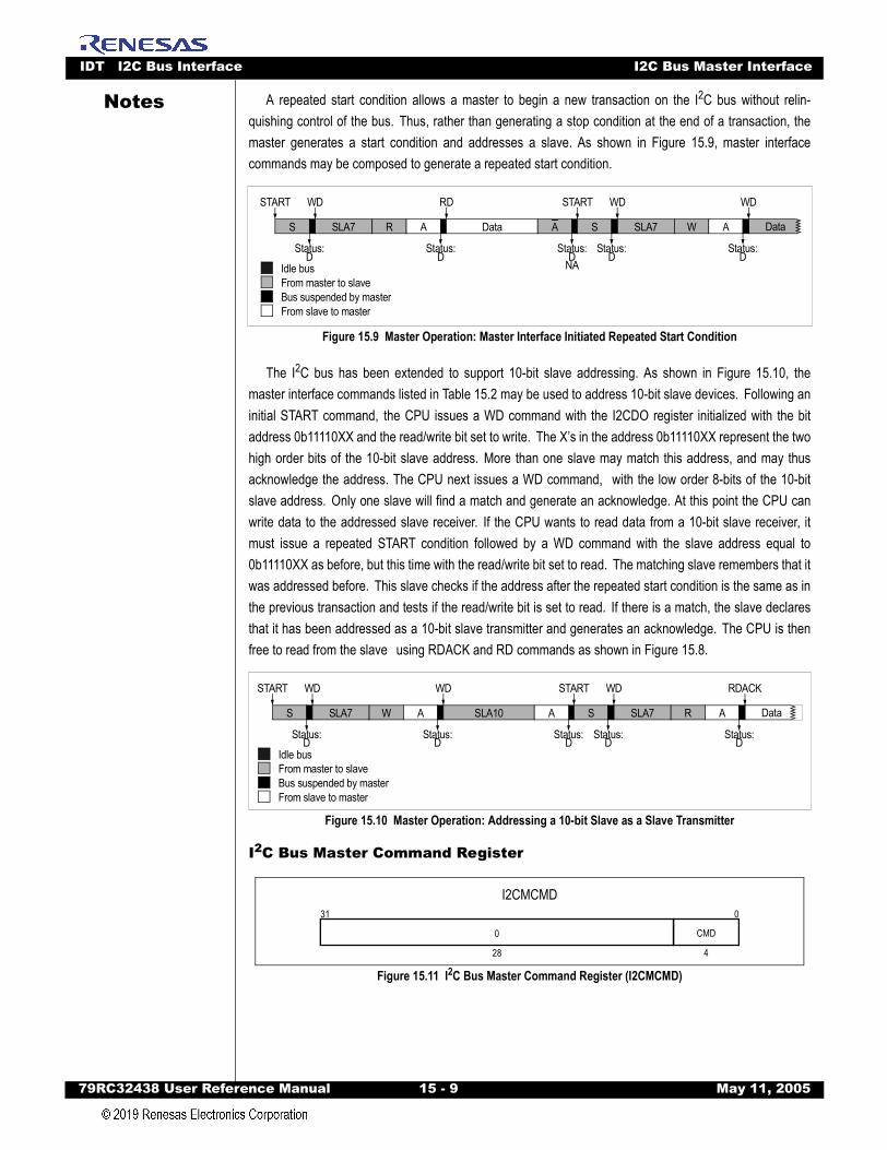
IDT I2C Bus Interface I2C Bus Master Interface
79RC32438 User Refer
Notes
A repeated start condition allows a master to begin a new transaction on the I2C bus without relin-quishing control of the bus.2Thus, rather than generating a stop condition at the end of a transaction, themaster generates a start condition and addresses a slave.2As shown in Figure 15.9, master interfacecommands may be composed to generate a repeated start condition.2Figure 15.9 Master Operation: Master Interface Initiated Repeated Start Condition
The I2C bus has been extended to support 10-bit slave addressing. As shown in Figure 15.10, themaster interface commands listed in Table 15.2 may be used to address 10-bit slave devices.2Following aninitial START command,2the CPU issues a WD command with the I2CDO register initialized with the bitaddress 0b11110XX and the read/write bit set to write.2The X’s in the address 0b11110XX represent the twohigh order bits of the 10-bit slave address.2More than one slave may match this address, and may thusacknowledge the address. The CPU next issues a WD command, 2with the low order 8-bits of the 10-bitslave address.2Only one slave will find a match and generate an acknowledge. At this point the CPU canwrite data to the addressed slave receiver.2If the CPU wants to read data from a 10-bit slave receiver, itmust issue a repeated START2condition followed by a WD command with the slave address equal to0b11110XX as before, but this time with the read/write bit set to read.2The matching slave remembers that itwas addressed before.2This slave checks if the address after the repeated start condition is the same as inthe previous transaction and tests if the read/write bit is set to read.2If there is a match, the slave declaresthat it has been addressed as a 10-bit slave transmitter and generates an acknowledge.2The CPU is thenfree to read from the slave 2using RDACK and RD commands as shown in Figure 15.8.2
Figure 15.10 Master Operation: Addressing a 10-bit Slave as a Slave Transmitter
I2C Bus Master Command Register
Figure 15.11 I2C Bus Master Command Register (I2CMCMD)
S SLA7
START WD
R A
Status:D
Status:D
RD
Data A
Status:D
NAIdle busFrom master to slaveBus suspended by masterFrom slave to master
S SLA7
START WD
W A
Status:D
Status:D
Data
WD
S SLA7
START WD
W A
Status:D
Status:D
WD
Status:D
Idle busFrom master to slaveBus suspended by masterFrom slave to master
S SLA7
START WD
R A
Status:D
Status:D
Data
RDACK
SLA10 A
I2CMCMD031
CMD0
28 4
ence Manual 15 - 9 May 11, 2005
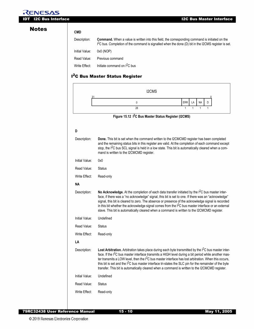
IDT I2C Bus Interface I2C Bus Master Interface
79RC32438 User Refer
Notes
I2C Bus Master Status Register
Figure 15.12 I2C Bus Master Status Register (I2CMS)
CMD
Description: Command. When a value is written into this field, the corresponding command is initiated on the I2C bus. Completion of the command is signalled when the done (D) bit in the I2CMS register is set.
Initial Value: 0x0 (NOP)
Read Value: Previous command
Write Effect: Initiate command on I2C bus
D
Description: Done. This bit is set when the command written to the I2CMCMD register has been completed and the remaining status bits in this register are valid. At the completion of each command except stop, the I2C bus SCL signal is held in a low state. This bit is automatically cleared when a com-mand is written to the I2CMCMD register.
Initial Value: 0x0
Read Value: Status
Write Effect: Read-only
NA
Description: No Acknowledge. At the completion of each data transfer initiated by the I2C bus master inter-face, if there was a “no acknowledge” signal, this bit is set to one. If there was an “acknowledge” signal, this bit is cleared to zero. The absence or presence of the acknowledge signal is recorded in this bit whether the acknowledge signal comes from the I2C bus master interface or an external slave. This bit is automatically cleared when a command is written to the I2CMCMD register.
Initial Value: Undefined
Read Value: Status
Write Effect: Read-only
LA
Description: Lost Arbitration. Arbitration takes place during each byte transmitted by the I2C bus master inter-face. If the I2C bus master interface transmits a HIGH level during a bit period while another mas-ter transmits a LOW level, then the I2C bus master interface has lost arbitration. When this occurs, this bit is set and the I2C bus master interface tri-states the SLC pin for the remainder of the byte transfer. This bit is automatically cleared when a command is written to the I2CMCMD register.
Initial Value: Undefined
Read Value: Status
Write Effect: Read-only
I2CMS031
D0
28 1
NA
1
LA
1
ERR
1
ence Manual 15 - 10 May 11, 2005

IDT I2C Bus Interface I2C Bus Master Interface
79RC32438 User Refer
Notes
I2C Bus Master Status Mask Register
Figure 15.13 I2C Bus Master Status Mask Register (I2CMSM)
ERR
Description: Error. This bit is set if a misplaced START or STOP condition is detected during execution of a command by the I2C bus master interface. This bit is automatically cleared when a command is written to the I2CMCMD register.
Initial Value: Undefined
Read Value: Status
Write Effect: Read-only
D
Description: Done. When this bit is set, the D bit in the I2CMS register is masked from generating an interrupt.
Initial Value: 0x1
Read Value: Previous value written
Write Effect: Modify value
NA
Description: No Acknowledge. When this bit is set, the NA bit in the I2CMS register is masked from generat-ing an interrupt.
Initial Value: 0x1
Read Value: Previous value written
Write Effect: Modify value
LA
Description: Lost Arbitration. When this bit is set, the LA bit in the I2CMS register is masked from generating an interrupt.
Initial Value: 0x1
Read Value: Previous value written
Write Effect: Modify value
ERR
Description: Error. When this bit is set, the ERR bit in the I2CMS register is masked from generating an inter-rupt.
Initial Value: 0x1
Read Value: Previous value written
Write Effect: Modify value
I2CMSM031
D0
28 1
NA
1
LA
1
ERR
1
ence Manual 15 - 11 May 11, 2005
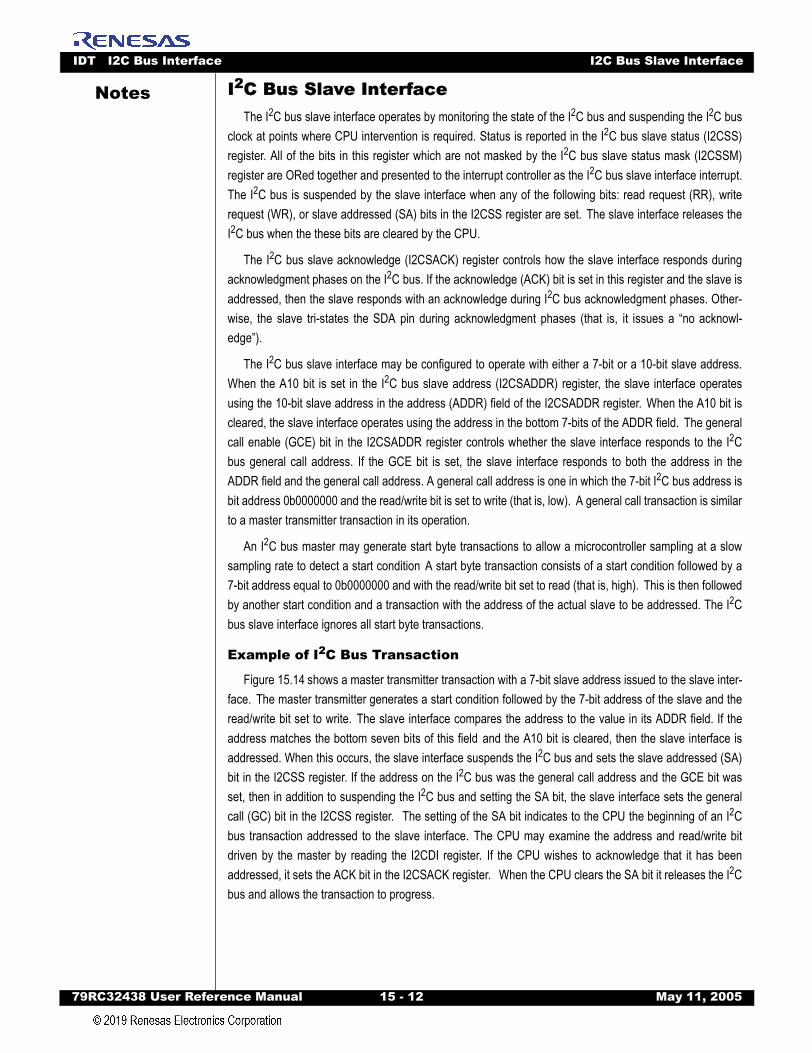
IDT I2C Bus Interface I2C Bus Slave Interface
79RC32438 User Refer
Notes
I2C Bus Slave InterfaceThe I2C bus slave interface operates by monitoring the state of the I2C bus and suspending the I2C busclock at points where CPU intervention is required. Status is reported in the I2C bus slave status (I2CSS)register. All of the bits in this register which are not masked by the I2C bus slave status mask (I2CSSM)register are ORed together and presented to the interrupt controller as the I2C bus slave interface interrupt.The I2C bus is suspended by the slave interface when any of the following bits: read request (RR), writerequest (WR), or slave addressed (SA) bits in the I2CSS register are set.2The slave interface releases theI2C bus when the these bits are cleared by the CPU.
The I2C bus slave acknowledge (I2CSACK) register controls how the slave interface responds duringacknowledgment phases on the I2C bus. If the acknowledge (ACK) bit is set in this register and the slave isaddressed, then the slave responds with an acknowledge during I2C bus acknowledgment phases. Other-wise, the slave tri-states the SDA pin during acknowledgment phases (that is,2it issues a “no acknowl-edge”).2
The I2C bus slave interface may be configured to operate with either a 7-bit or a 10-bit slave address.When the A10 bit is set in the I2C bus slave address (I2CSADDR) register, the slave interface operatesusing the 10-bit slave address in the address (ADDR) field of the I2CSADDR register.2When the A10 bit iscleared, the slave interface operates using the address in the bottom 7-bits of the ADDR field.2The generalcall enable (GCE) bit in the I2CSADDR register controls whether the slave interface responds to the I2Cbus general call address.2If the GCE bit is set, the slave interface responds to both the address in theADDR field and the general call address. A general call address is one in which the 7-bit I2C bus address isbit address 0b0000000 and the read/write bit is set to write (that is, low).2A general call transaction is similarto a master transmitter transaction in its operation.2
An I2C bus master may generate start byte transactions to allow a microcontroller sampling at a slowsampling rate to detect a start condition2A start byte transaction consists of a start condition followed by a7-bit address equal to 0b0000000 and with the read/write bit set to read (that is, high).2This is then followedby another start condition and a transaction with the address of the actual slave to be addressed. The I2Cbus slave interface ignores all start byte transactions.2
Example of I2C Bus Transaction
Figure 15.14 shows a master transmitter transaction with a 7-bit slave address issued to the slave inter-face.2The master transmitter generates a start condition followed by the 7-bit address of the slave and theread/write bit set to write.2The slave interface compares the address to the value in its ADDR field. If theaddress matches the bottom seven bits of this field2and the A10 bit is cleared, then the slave interface isaddressed. When this occurs, the slave interface suspends the I2C bus and sets the slave addressed (SA)bit in the I2CSS register. If the address on the I2C bus was the general call address and the GCE bit wasset, then in addition to suspending the I2C bus and setting the SA bit, the slave interface sets the generalcall (GC) bit in the I2CSS register.2 The setting of the SA bit indicates to the CPU the beginning of an I2Cbus transaction addressed to the slave interface.2The CPU may examine the address and read/write bitdriven by the master by reading the I2CDI register.2If the CPU wishes to acknowledge that it has beenaddressed, it sets the ACK bit in the I2CSACK register. 2When the CPU clears the SA bit it releases the I2Cbus and allows the transaction to progress.2
ence Manual 15 - 12 May 11, 2005
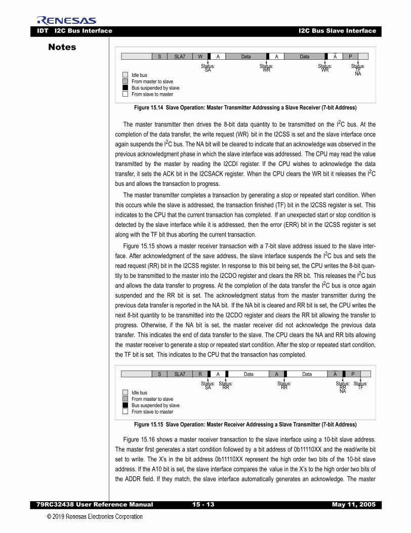
IDT I2C Bus Interface I2C Bus Slave Interface
79RC32438 User Refer
Notes
Figure 15.14 Slave Operation: Master Transmitter Addressing a Slave Receiver (7-bit Address)
The master transmitter then drives the 8-bit data quantity to be transmitted on the I2C bus. At thecompletion of the data transfer, the write request (WR)2bit in the I2CSS is set and the slave interface onceagain suspends the I2C bus. The NA bit will be cleared to indicate that an acknowledge was observed in theprevious acknowledgment phase in which the slave interface was addressed.2The CPU may read the valuetransmitted by the master by reading the I2CDI register.2If the CPU wishes to acknowledge the datatransfer, it sets the ACK bit in the I2CSACK register.2When the CPU clears the WR bit it releases the I2Cbus and allows the transaction to progress.2
The master transmitter completes a transaction by generating a stop or repeated start condition. Whenthis occurs while the slave is addressed, the transaction finished (TF) bit in the I2CSS register is set.2Thisindicates to the CPU that the current transaction has completed.2If an unexpected start or stop condition isdetected by the slave interface while it is addressed,2then the error (ERR) bit in the I2CSS register is setalong with the TF bit thus aborting the current transaction.2
Figure 15.15 shows a master receiver transaction with a 7-bit slave address issued to the slave inter-face. After acknowledgment of the save address, the slave interface suspends the I2C bus and sets theread request (RR) bit in the I2CSS register. In response to2this bit being set, the CPU writes the 8-bit quan-tity to be transmitted to the master into the I2CDO register and clears the RR bit.2This releases the I2C busand allows the data transfer to progress. At the completion of the data transfer the I2C bus is once againsuspended and the RR bit is set.2The acknowledgment status from the master transmitter during theprevious data transfer is reported in the NA bit.2If the NA bit is cleared and RR bit is set, the CPU writes thenext 8-bit quantity to2be transmitted into the I2CDO register and clears the RR bit allowing the transfer toprogress. Otherwise,2if the NA bit is set, the master receiver did not acknowledge the previous datatransfer.2This indicates the end of data transfer to the slave. The CPU clears the NA and RR bits allowingthe2master receiver to generate a stop or repeated start condition. After the stop or repeated start condition,the TF bit is set.2This indicates to the CPU that the transaction has completed.2
Figure 15.15 Slave Operation: Master Receiver Addressing a Slave Transmitter (7-bit Address)
Figure 15.16 shows a master receiver transaction to the slave interface using a 10-bit slave address.The master first generates a start condition followed by2a bit address of 0b11110XX and the read/write bitset to write.2The X’s in the bit address 0b11110XX represent the high order two bits of the 10-bit slaveaddress. If the A10 bit is set, the slave interface compares the2value in the X’s to the high order two bits ofthe ADDR field. If they match, the slave interface automatically generates an acknowledge.2The master
S SLA7 W A
Status:SA
Status:WR
Data A Data A P
Idle busFrom master to slaveBus suspended by slaveFrom slave to master
Status:WR
Status:TFNA
S SLA7 R A
Status:SA
Status:RR
Data A
Status:RR
Data A P
Idle busFrom master to slaveBus suspended by slaveFrom slave to master
Status:RR
Status:TF
NA
ence Manual 15 - 13 May 11, 2005
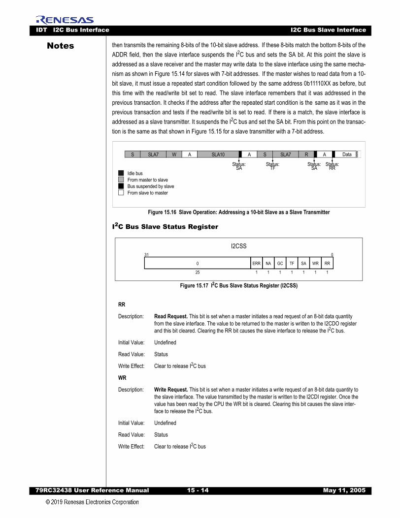
IDT I2C Bus Interface I2C Bus Slave Interface
79RC32438 User Refer
Notes
then transmits the remaining 8-bits of the 10-bit slave address.2If these 8-bits match the bottom 8-bits of theADDR field, then the slave interface suspends the I2C bus and sets the SA bit. At this point the slave isaddressed as a slave receiver and the master may write data2to the slave interface using the same mecha-nism as shown in Figure 15.14 for slaves with 7-bit addresses.2If the master wishes to read data from a 10-bit slave, it must issue a repeated start condition followed by2the same address 0b11110XX as before, butthis time with the read/write bit set to read.2The slave interface remembers that it was addressed in theprevious transaction. It checks if the address after the repeated start condition is the2same as it was in theprevious transaction and tests if the read/write bit is set to read.2If there is a match, the slave interface isaddressed as a slave transmitter. It suspends the I2C bus and set the SA bit. From this point on the transac-tion is the same as that shown in Figure 15.15 for a slave transmitter with a 7-bit address.2Figure 15.16 Slave Operation: Addressing a 10-bit Slave as a Slave Transmitter
I2C Bus Slave Status Register
Figure 15.17 I2C Bus Slave Status Register (I2CSS)
RR
Description: Read Request. This bit is set when a master initiates a read request of an 8-bit data quantity from the slave interface. The value to be returned to the master is written to the I2CDO register and this bit cleared. Clearing the RR bit causes the slave interface to release the I2C bus.
Initial Value: Undefined
Read Value: Status
Write Effect: Clear to release I2C bus
WR
Description: Write Request. This bit is set when a master initiates a write request of an 8-bit data quantity to the slave interface. The value transmitted by the master is written to the I2CDI register. Once the value has been read by the CPU the WR bit is cleared. Clearing this bit causes the slave inter-face to release the I2C bus.
Initial Value: Undefined
Read Value: Status
Write Effect: Clear to release I2C bus
S SLA7 W A
Idle busFrom master to slaveBus suspended by slaveFrom slave to master
S SLA7 R A DataSLA10 A
Status:SA
Status:RR
Status:SA
Status:TF
I2CSS031
RR0
25 1
WR
1
TF
1
NA
1
ERR
1
SA
1
GC
1
ence Manual 15 - 14 May 11, 2005
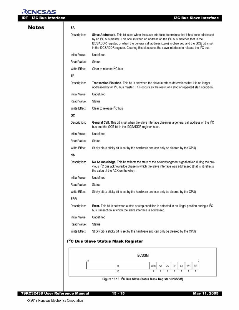
IDT I2C Bus Interface I2C Bus Slave Interface
79RC32438 User Refer
Notes
I2C Bus Slave Status Mask Register
Figure 15.18 I2C Bus Slave Status Mask Register (I2CSSM)
SA
Description: Slave Addressed. This bit is set when the slave interface determines that it has been addressed by an I2C bus master. This occurs when an address on the I2C bus matches that in the I2CSADDR register, or when the general call address (zero) is observed and the GCE bit is set in the I2CSADDR register. Clearing this bit causes the slave interface to release the I2C bus.
Initial Value: Undefined
Read Value: Status
Write Effect: Clear to release I2C bus
TF
Description: Transaction Finished. This bit is set when the slave interface determines that it is no longer addressed by an I2C bus master. This occurs as the result of a stop or repeated start condition.
Initial Value: Undefined
Read Value: Status
Write Effect: Clear to release I2C bus
GC
Description: General Call. This bit is set when the slave interface observes a general call address on the I2C bus and the GCE bit in the I2CSADDR register is set.
Initial Value: Undefined
Read Value: Status
Write Effect: Sticky bit (a sticky bit is set by the hardware and can only be cleared by the CPU)
NA
Description: No Acknowledge. This bit reflects the state of the acknowledgment signal driven during the pre-vious I2C bus acknowledge phase in which the slave interface was addressed (that is, it reflects the value of the ACK on the wire).
Initial Value: Undefined
Read Value: Status
Write Effect: Sticky bit (a sticky bit is set by the hardware and can only be cleared by the CPU)
ERR
Description: Error. This bit is set when a start or stop condition is detected in an illegal position during a I2C bus transaction in which the slave interface is addressed.
Initial Value: Undefined
Read Value: Status
Write Effect: Sticky bit (a sticky bit is set by the hardware and can only be cleared by the CPU)
I2CSSM031
RR0
25 1
WR
1
TF
1
NA
1
ERR
1
SA
1
GC
1
ence Manual 15 - 15 May 11, 2005
IDT I2C Bus Interface I2C Bus Slave Interface
79RC32438 User Refer
Notes
RRDescription: Read Request. When this bit is set to 1, the RR bit in the I2CSS register is masked from gener-ating an interrupt.
Initial Value: 0x1
Read Value: Previous value written
Write Effect: Modify value
WR
Description: Write Request. When this bit is set to 1, the WR bit in the I2CSS register is masked from gener-ating an interrupt.
Initial Value: 0x1
Read Value: Previous value written
Write Effect: Modify value
SA
Description: Slave Addressed. When this bit is set to 1, the SA bit in the I2CSS register is masked from gen-erating an interrupt.
Initial Value: 0x1
Read Value: Previous value written
Write Effect: Modify value
TF
Description: Transaction Finished. When this bit is set to 1, the TF bit in the I2CSS register is masked from generating an interrupt.
Initial Value: 0x1
Read Value: Previous value written
Write Effect: Modify value
GC
Description: General Call. When this bit is set to 1, the GC bit in the I2CSS register is masked from generat-ing an interrupt.
Initial Value: 0x1
Read Value: Previous value written
Write Effect: Modify value
NA
Description: No Acknowledge. When this bit is set to 1, the NA bit in the I2CSS register is masked from gen-erating an interrupt.
Initial Value: 0x1
Read Value: Previous value written
Write Effect: Modify value
ence Manual 15 - 16 May 11, 2005
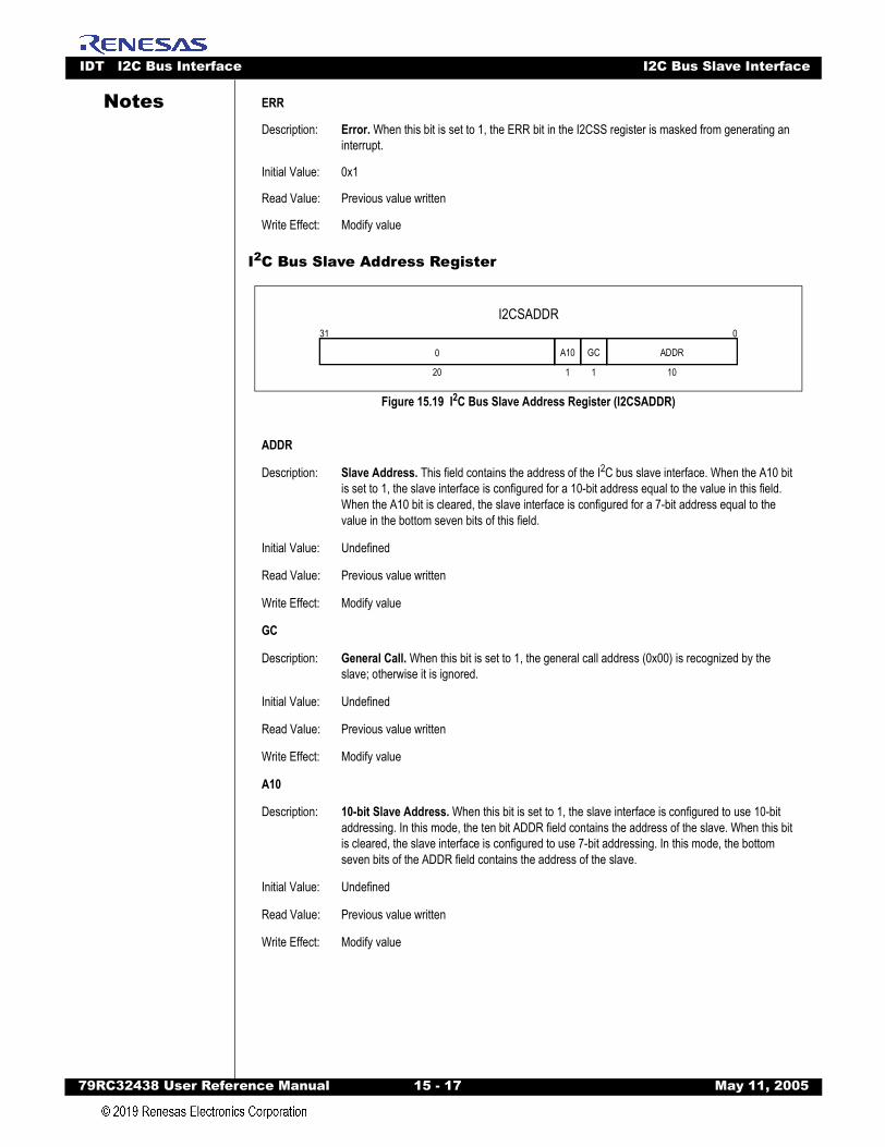
IDT I2C Bus Interface I2C Bus Slave Interface
79RC32438 User Refer
Notes
I2C Bus Slave Address Register
Figure 15.19 I2C Bus Slave Address Register (I2CSADDR)
ERR
Description: Error. When this bit is set to 1, the ERR bit in the I2CSS register is masked from generating an interrupt.
Initial Value: 0x1
Read Value: Previous value written
Write Effect: Modify value
ADDR
Description: Slave Address. This field contains the address of the I2C bus slave interface. When the A10 bit is set to 1, the slave interface is configured for a 10-bit address equal to the value in this field. When the A10 bit is cleared, the slave interface is configured for a 7-bit address equal to the value in the bottom seven bits of this field.
Initial Value: Undefined
Read Value: Previous value written
Write Effect: Modify value
GC
Description: General Call. When this bit is set to 1, the general call address (0x00) is recognized by the slave; otherwise it is ignored.
Initial Value: Undefined
Read Value: Previous value written
Write Effect: Modify value
A10
Description: 10-bit Slave Address. When this bit is set to 1, the slave interface is configured to use 10-bit addressing. In this mode, the ten bit ADDR field contains the address of the slave. When this bit is cleared, the slave interface is configured to use 7-bit addressing. In this mode, the bottom seven bits of the ADDR field contains the address of the slave.
Initial Value: Undefined
Read Value: Previous value written
Write Effect: Modify value
I2CSADDR031
ADDR0
20 10
GC
1
A10
1
ence Manual 15 - 17 May 11, 2005
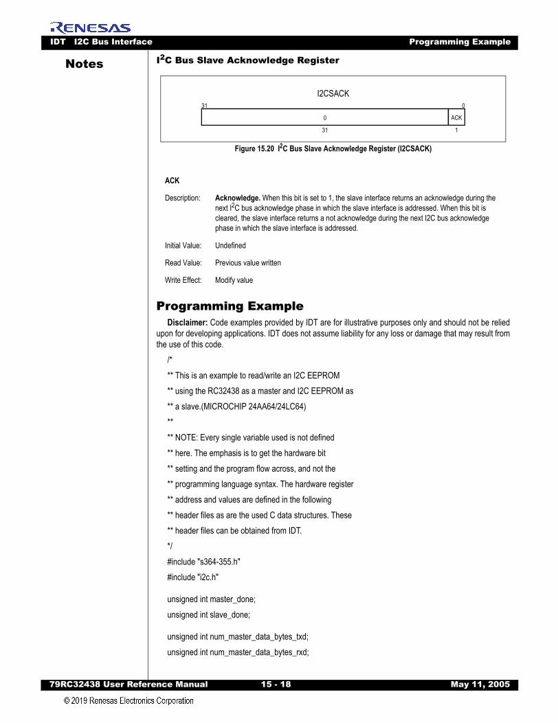
IDT I2C Bus Interface Programming Example
79RC32438 User Refer
Notes
I2C Bus Slave Acknowledge RegisterFigure 15.20 I2C Bus Slave Acknowledge Register (I2CSACK)
Programming ExampleDisclaimer: Code examples provided by IDT are for illustrative purposes only and should not be relied
upon for developing applications. IDT does not assume liability for any loss or damage that may result fromthe use of this code.
/*** This is an example to read/write an I2C EEPROM** using the RC32438 as a master and I2C EEPROM as** a slave.(MICROCHIP 24AA64/24LC64)**** NOTE: Every single variable used is not defined** here. The emphasis is to get the hardware bit ** setting and the program flow across, and not the** programming language syntax. The hardware register** address and values are defined in the following** header files as are the used C data structures. These** header files can be obtained from IDT.*/#include "s364-355.h"#include "i2c.h"
unsigned int master_done;unsigned int slave_done;
unsigned int num_master_data_bytes_txd;unsigned int num_master_data_bytes_rxd;
ACK
Description: Acknowledge. When this bit is set to 1, the slave interface returns an acknowledge during the next I2C bus acknowledge phase in which the slave interface is addressed. When this bit is cleared, the slave interface returns a not acknowledge during the next I2C bus acknowledge phase in which the slave interface is addressed.
Initial Value: Undefined
Read Value: Previous value written
Write Effect: Modify value
I2CSACK031
ACK0
31 1
ence Manual 15 - 18 May 11, 2005
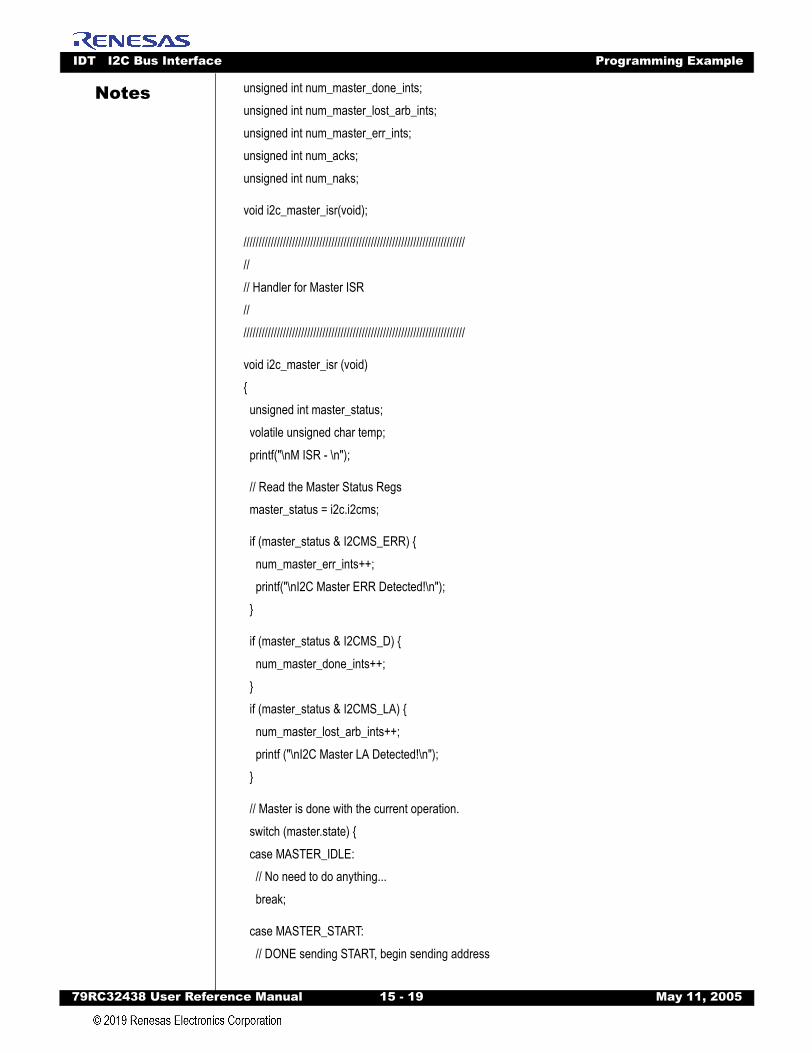
IDT I2C Bus Interface Programming Example
79RC32438 User Refer
Notes
unsigned int num_master_done_ints;unsigned int num_master_lost_arb_ints;unsigned int num_master_err_ints;unsigned int num_acks;unsigned int num_naks;void i2c_master_isr(void);
///////////////////////////////////////////////////////////////////////////// Handler for Master ISR///////////////////////////////////////////////////////////////////////////
void i2c_master_isr (void) unsigned int master_status; volatile unsigned char temp; printf("\nM ISR - \n");
// Read the Master Status Regs master_status = i2c.i2cms;
if (master_status & I2CMS_ERR) num_master_err_ints++; printf("\nI2C Master ERR Detected!\n");
if (master_status & I2CMS_D) num_master_done_ints++; if (master_status & I2CMS_LA) num_master_lost_arb_ints++; printf ("\nI2C Master LA Detected!\n");
// Master is done with the current operation. switch (master.state) case MASTER_IDLE: // No need to do anything... break;
case MASTER_START: // DONE sending START, begin sending address
ence Manual 15 - 19 May 11, 2005
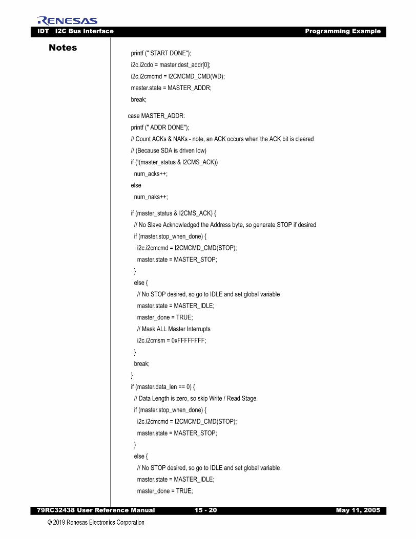
IDT I2C Bus Interface Programming Example
79RC32438 User Refer
Notes
printf (" START DONE"); i2c.i2cdo = master.dest_addr[0]; i2c.i2cmcmd = I2CMCMD_CMD(WD); master.state = MASTER_ADDR; break;
case MASTER_ADDR: printf (" ADDR DONE"); // Count ACKs & NAKs - note, an ACK occurs when the ACK bit is cleared // (Because SDA is driven low) if (!(master_status & I2CMS_ACK)) num_acks++; else num_naks++;
if (master_status & I2CMS_ACK) // No Slave Acknowledged the Address byte, so generate STOP if desired if (master.stop_when_done) i2c.i2cmcmd = I2CMCMD_CMD(STOP); master.state = MASTER_STOP; else // No STOP desired, so go to IDLE and set global variable master.state = MASTER_IDLE; master_done = TRUE; // Mask ALL Master Interrupts i2c.i2cmsm = 0xFFFFFFFF; break; if (master.data_len == 0) // Data Length is zero, so skip Write / Read Stage if (master.stop_when_done) i2c.i2cmcmd = I2CMCMD_CMD(STOP); master.state = MASTER_STOP; else // No STOP desired, so go to IDLE and set global variable master.state = MASTER_IDLE; master_done = TRUE;
ence Manual 15 - 20 May 11, 2005
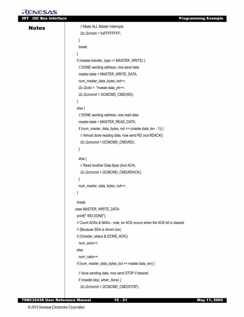
IDT I2C Bus Interface Programming Example
79RC32438 User Refer
Notes
// Mask ALL Master Interrupts i2c.i2cmsm = 0xFFFFFFFF; break; if (master.transfer_type == MASTER_WRITE) // DONE sending address, now send data master.state = MASTER_WRITE_DATA; num_master_data_bytes_txd++; i2c.i2cdo = *master.data_ptr++; i2c.i2cmcmd = I2CMCMD_CMD(WD); else // DONE sending address, now read data master.state = MASTER_READ_DATA; if (num_master_data_bytes_rxd == (master.data_len - 1)) // Almost done reading data, now send RD (not RDACK!) i2c.i2cmcmd = I2CMCMD_CMD(RD);else // Read Another Data Byte (And ACK) i2c.i2cmcmd = I2CMCMD_CMD(RDACK); num_master_data_bytes_rxd++;
break; case MASTER_WRITE_DATA: printf(" WD DONE"); // Count ACKs & NAKs - note, an ACK occurs when the ACK bit is cleared // (Because SDA is driven low) if (!(master_status & I2CMS_ACK)) num_acks++; else num_naks++; if (num_master_data_bytes_txd >= master.data_len)
// done sending data, now send STOP if desired. if (master.stop_when_done) i2c.i2cmcmd = I2CMCMD_CMD(STOP);
ence Manual 15 - 21 May 11, 2005
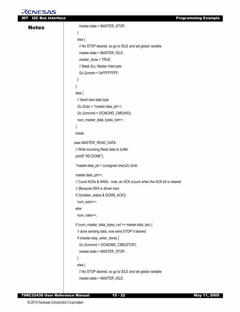
IDT I2C Bus Interface Programming Example
79RC32438 User Refer
Notes
master.state = MASTER_STOP; else // No STOP desired, so go to IDLE and set global variable master.state = MASTER_IDLE; master_done = TRUE; // Mask ALL Master Interrupts i2c.i2cmsm = 0xFFFFFFFF; else // Send next data byte i2c.i2cdo = *master.data_ptr++; i2c.i2cmcmd = I2CMCMD_CMD(WD); num_master_data_bytes_txd++; break;case MASTER_READ_DATA: // Write Incoming Read data to buffer printf(" RD DONE");
*master.data_ptr = (unsigned char)i2c.i2cdi;
master.data_ptr++; // Count ACKs & NAKs - note, an ACK occurs when the ACK bit is cleared // (Because SDA is driven low) if (!(master_status & I2CMS_ACK)) num_acks++; else num_naks++;
if (num_master_data_bytes_rxd >= master.data_len) // done sending data, now send STOP if desired. if (master.stop_when_done) i2c.i2cmcmd = I2CMCMD_CMD(STOP); master.state = MASTER_STOP; else // No STOP desired, so go to IDLE and set global variable master.state = MASTER_IDLE;
ence Manual 15 - 22 May 11, 2005
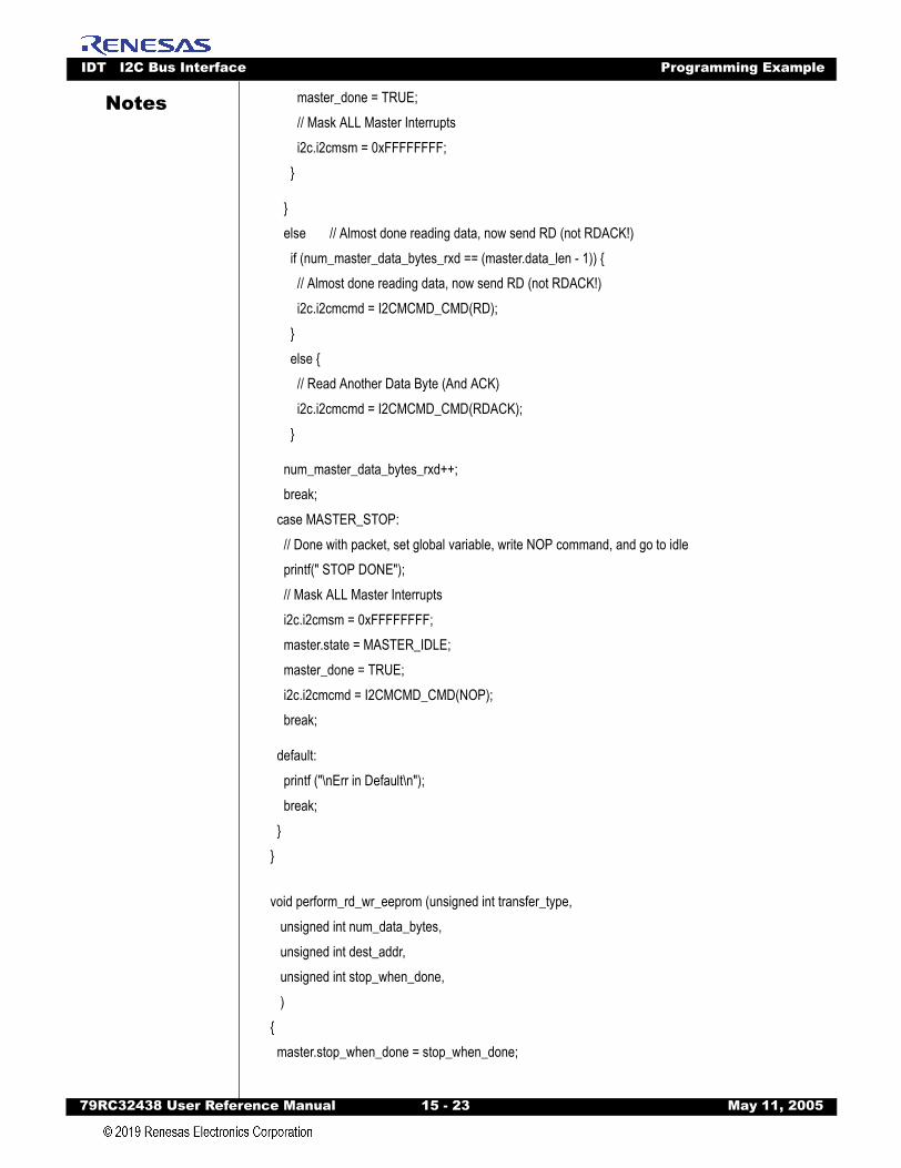
IDT I2C Bus Interface Programming Example
79RC32438 User Refer
Notes
master_done = TRUE; // Mask ALL Master Interrupts i2c.i2cmsm = 0xFFFFFFFF;else // Almost done reading data, now send RD (not RDACK!) if (num_master_data_bytes_rxd == (master.data_len - 1)) // Almost done reading data, now send RD (not RDACK!) i2c.i2cmcmd = I2CMCMD_CMD(RD); else // Read Another Data Byte (And ACK) i2c.i2cmcmd = I2CMCMD_CMD(RDACK);
num_master_data_bytes_rxd++; break; case MASTER_STOP: // Done with packet, set global variable, write NOP command, and go to idle printf(" STOP DONE"); // Mask ALL Master Interrupts i2c.i2cmsm = 0xFFFFFFFF; master.state = MASTER_IDLE; master_done = TRUE; i2c.i2cmcmd = I2CMCMD_CMD(NOP); break;
default: printf ("\nErr in Default\n"); break;
void perform_rd_wr_eeprom (unsigned int transfer_type, unsigned int num_data_bytes, unsigned int dest_addr, unsigned int stop_when_done, ) master.stop_when_done = stop_when_done;
ence Manual 15 - 23 May 11, 2005
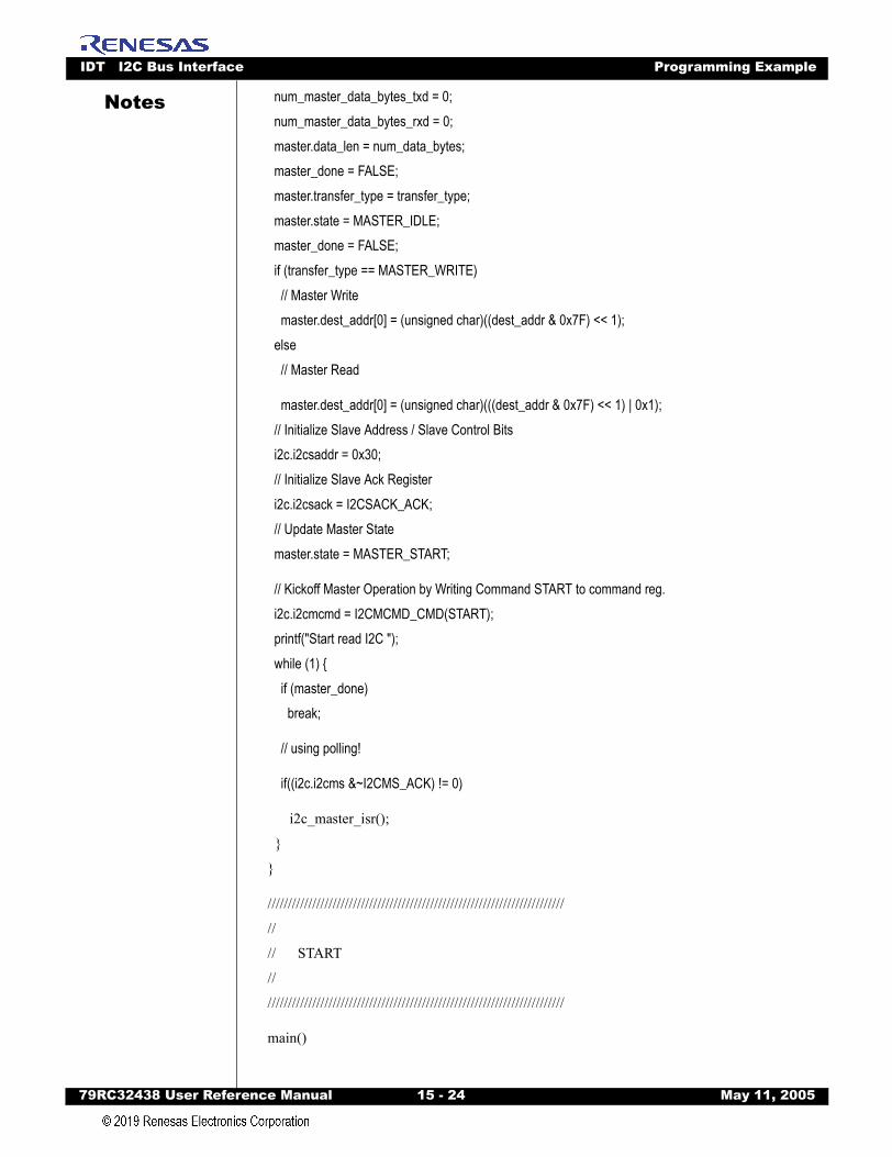
IDT I2C Bus Interface Programming Example
79RC32438 User Refer
Notes
num_master_data_bytes_txd = 0; num_master_data_bytes_rxd = 0; master.data_len = num_data_bytes; master_done = FALSE; master.transfer_type = transfer_type; master.state = MASTER_IDLE; master_done = FALSE; if (transfer_type == MASTER_WRITE) // Master Write master.dest_addr[0] = (unsigned char)((dest_addr & 0x7F) << 1); else // Master Readmaster.dest_addr[0] = (unsigned char)(((dest_addr & 0x7F) << 1) | 0x1); // Initialize Slave Address / Slave Control Bits i2c.i2csaddr = 0x30; // Initialize Slave Ack Register i2c.i2csack = I2CSACK_ACK; // Update Master State master.state = MASTER_START;
// Kickoff Master Operation by Writing Command START to command reg. i2c.i2cmcmd = I2CMCMD_CMD(START); printf("Start read I2C "); while (1) if (master_done) break;
// using polling!
if((i2c.i2cms &~I2CMS_ACK) != 0)
i2c_master_isr();
/////////////////////////////////////////////////////////////////////////
//
// START
//
/////////////////////////////////////////////////////////////////////////
main()
ence Manual 15 - 24 May 11, 2005

IDT I2C Bus Interface Programming Example
79RC32438 User Refer
Notes
unsigned int i;
unsigned int slave_addr;
unsigned int dest_addr;
unsigned int divisor;
unsigned int num_data_bytes;
unsigned char data[1024];
unsigned int prescaler_value;
// Enable Master & Slave interfaces
i2c.i2cc = I2CC_MEN;
// Make sure to mask all unused bits.
// Prescalar value is programmed for 800KHz clock.
prescaler_value = 84;
i2c.i2ccp = prescaler_value;
//I2C Bus Master status Mask register is masked
//from generating an interrrupt.
i2c.i2cmsm = 0xF;
//slave address is set here.
slave_addr = 0x30;
//I2C bus slave is masked from generating interrupt.
i2c.i2cssm = 0x7F;
num_data_bytes = 8;
// The 1st and 2nd data byte is set to the address
// where data is located within the I2C NVRAM.
data[0] = 0;
data[1] = 0;
for (i = 2; i<8; i++)
data[i] = 0x33;
master.data_ptr = data;
printf("\nWrite:");
perform_rd_wr_eeprom (MASTER_WRITE,
// Trans. Type
num_data_bytes,
// # Data Bytes
slave_addr,
ence Manual 15 - 25 May 11, 2005
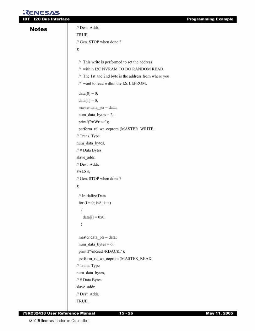
IDT I2C Bus Interface Programming Example
79RC32438 User Refer
Notes
// Dest. Addr.TRUE,
// Gen. STOP when done ?
);
// This write is performed to set the address
// within I2C NVRAM TO DO RANDOM READ.
// The 1st and 2nd byte is the address from where you
// want to read within the I2c EEPROM.
data[0] = 0;
data[1] = 0;
master.data_ptr = data;
num_data_bytes = 2;
printf("\nWrite:");
perform_rd_wr_eeprom (MASTER_WRITE,
// Trans. Type
num_data_bytes,
// # Data Bytes
slave_addr,
// Dest. Addr.
FALSE,
// Gen. STOP when done ?
);
// Initialize Data
for (i = 0; i<8; i++)
data[i] = 0x0;
master.data_ptr = data;
num_data_bytes = 6;
printf("\nRead /RDACK:");
perform_rd_wr_eeprom (MASTER_READ,
// Trans. Type
num_data_bytes,
// # Data Bytes
slave_addr,
// Dest. Addr.
TRUE,
ence Manual 15 - 26 May 11, 2005
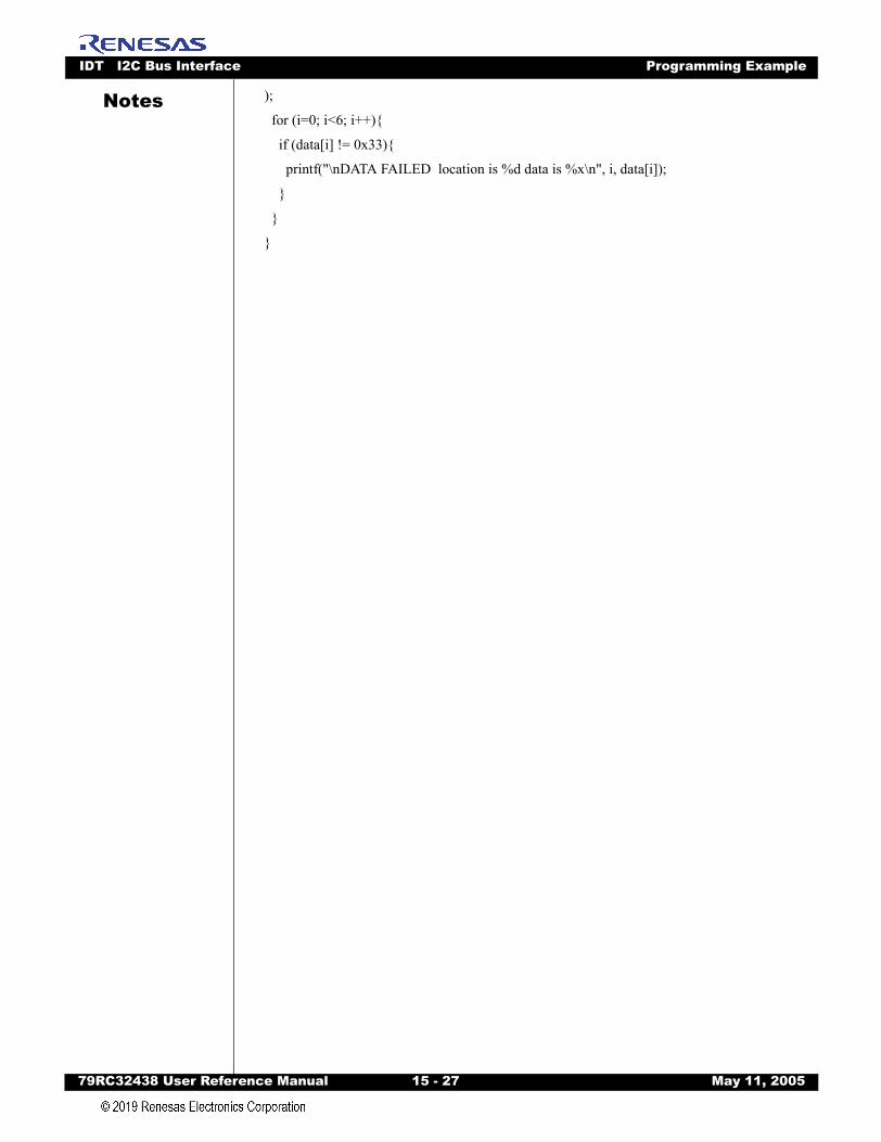
IDT I2C Bus Interface Programming Example
79RC32438 User Refer
Notes
);for (i=0; i<6; i++)
if (data[i] != 0x33)
printf("\nDATA FAILED location is %d data is %x\n", i, data[i]);
ence Manual 15 - 27 May 11, 2005
IDT I2C Bus Interface Programming Example
79RC32438 User Refer
Notes
ence Manual 15 - 28 May 11, 2005
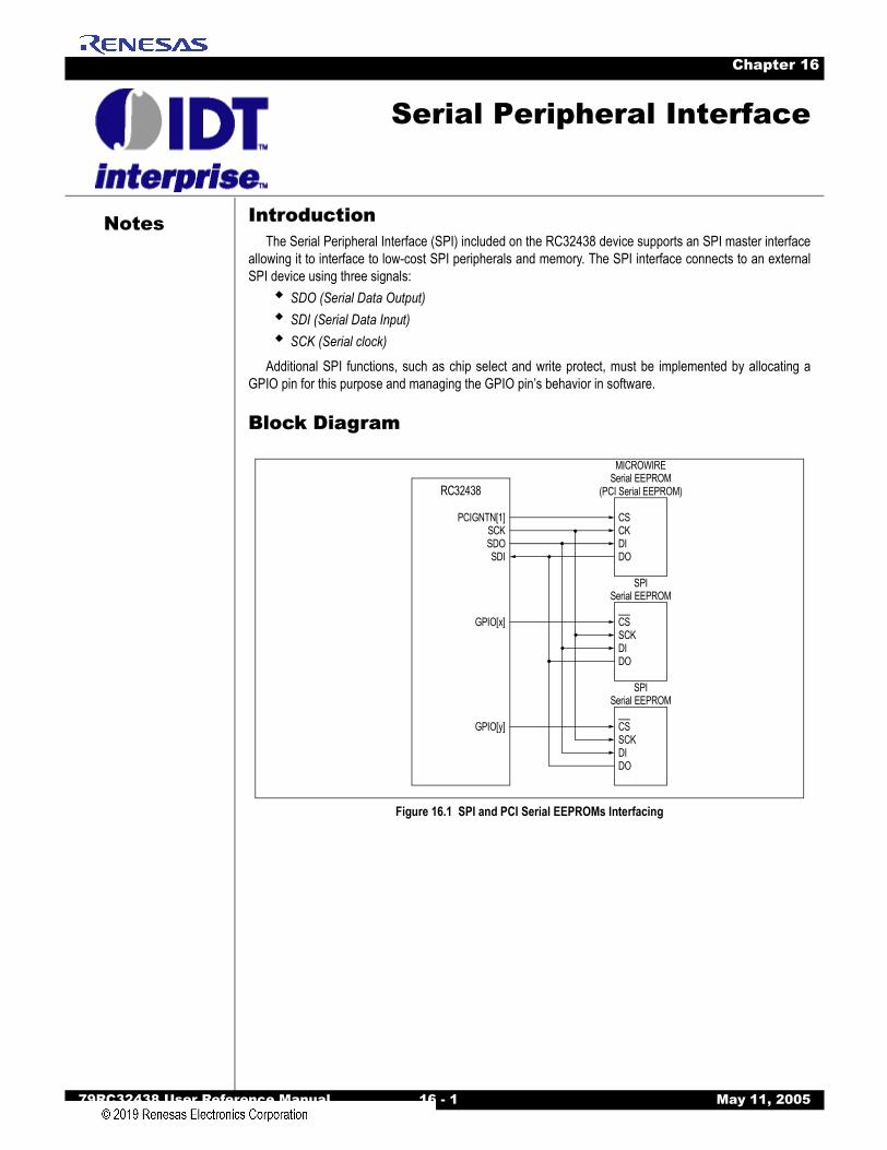
Notes
79RC32438 User Reference Manual 16 - 1 M
Chapter 16
Serial Peripheral Interface
IntroductionThe Serial Peripheral Interface (SPI) included on the RC32438 device supports an SPI master interface
allowing it to interface to low-cost SPI peripherals and memory. The SPI interface connects to an externalSPI device using three signals:
SDO (Serial Data Output)SDI (Serial Data Input)SCK (Serial clock)
Additional SPI functions, such as chip select and write protect, must be implemented by allocating aGPIO pin for this purpose and managing the GPIO pin’s behavior in software.
Block Diagram
Figure 16.1 SPI and PCI Serial EEPROMs Interfacing
MICROWIRE
CS
Serial EEPROM
CKDIDO
RC32438
SPI
CS
Serial EEPROM
SCKDIDO
SPI
CS
Serial EEPROM
SCKDIDO
PCIGNTN[1]SCKSDOSDI
GPIO[x]
GPIO[y]
(PCI Serial EEPROM)
ay 11, 2005
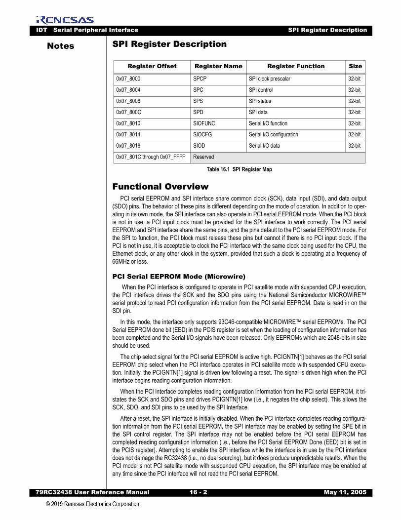
IDT Serial Peripheral Interface SPI Register Description
79RC32438 User Refer
Notes
SPI Register DescriptionFunctional OverviewPCI serial EEPROM and SPI interface share common clock (SCK), data input (SDI), and data output
(SDO) pins. The behavior of these pins is different depending on the mode of operation. In addition to oper-ating in its own mode, the SPI interface can also operate in PCI serial EEPROM mode. When the PCI blockis not in use, a PCI input clock must be provided for the SPI interface to work correctly. The PCI serialEEPROM and SPI interface share the same pins, and the pins default to the PCI serial EEPROM mode. Forthe SPI to function, the PCI block must release these pins but cannot if there is no PCI input clock. If thePCI is not in use, it is acceptable to clock the PCI interface with the same clock being used for the CPU, theEthernet clock, or any other clock in the system, provided that such a clock is operating at a frequency of66MHz or less.
PCI Serial EEPROM Mode (Microwire) When the PCI interface is configured to operate in PCI satellite mode with suspended CPU execution,
the PCI interface drives the SCK and the SDO pins using the National Semiconductor MICROWIRE™serial protocol to read PCI configuration information from the PCI serial EEPROM. Data is read in on theSDI pin.
In this mode, the interface only supports 93C46-compatible MICROWIRE™ serial EEPROMs. The PCISerial EEPROM done bit (EED) in the PCIS register is set when the loading of configuration information hasbeen completed and the Serial I/O signals have been released. Only EEPROMs which are 2048-bits in sizeshould be used.
The chip select signal for the PCI serial EEPROM is active high. PCIGNTN[1] behaves as the PCI serialEEPROM chip select when the PCI interface operates in PCI satellite mode with suspended CPU execu-tion. Initially, the PCIGNTN[1] signal is driven low following a reset. The signal is driven high when the PCIinterface begins reading configuration information.
When the PCI interface completes reading configuration information from the PCI serial EEPROM, it tri-states the SCK and SDO pins and drives PCIGNTN[1] low (i.e., it negates the chip select). This allows theSCK, SDO, and SDI pins to be used by the SPI Interface.
After a reset, the SPI interface is initially disabled. When the PCI interface completes reading configura-tion information from the PCI serial EEPROM, the SPI interface may be enabled by setting the SPE bit inthe SPI control register. The SPI interface may not be enabled before the PCI serial EEPROM hascompleted reading configuration information (i.e., before the PCI Serial EEPROM Done (EED) bit is set inthe PCIS register). Attempting to enable the SPI interface while the interface is in use by the PCI interfacedoes not damage the RC32438 (i.e., no dual sourcing), but it does produce unpredictable results. When thePCI mode is not PCI satellite mode with suspended CPU execution, the SPI interface may be enabled atany time since the PCI interface will not read the PCI serial EEPROM.
Register Offset Register Name Register Function Size
0x07_8000 SPCP SPI clock prescalar 32-bit
0x07_8004 SPC SPI control 32-bit
0x07_8008 SPS SPI status 32-bit
0x07_800C SPD SPI data 32-bit
0x07_8010 SIOFUNC Serial I/O function 32-bit
0x07_8014 SIOCFG Serial I/O configuration 32-bit
0x07_8018 SIOD Serial I/O data 32-bit
0x07_801C through 0x07_FFFF Reserved
Table 16.1 SPI Register Map
ence Manual 16 - 2 May 11, 2005
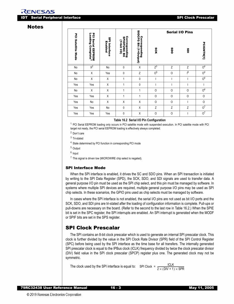
IDT Serial Peripheral Interface SPI Clock Prescalar
79RC32438 User Refer
Notes
SPI Interface ModeWhen the SPI interface is enabled, it drives the SC and SDO pins. When an SPI transaction is initiated
by writing to the SPI Data Register (SPD), the SCK, SDO, and SDI signals are used to transfer data. Ageneral purpose I/O pin must be used as the SPI chip select, and this pin must be managed by software. Insystems where multiple SPI devices are required, multiple general purpose I/O pins may be used as SPIchip selects. In these scenarios, the GPIO pins used as chip selects must be managed by software.
In cases where the SPI interface is not enabled, the serial I/O pins are not used as bit I/O ports and theSCK, SDO, and SDI pins are tri-stated after the loading of configuration information is complete. Pull-ups orpull-downs are necessary on the board. (Refer to the second to the last row in Table 16.2.) When the SPIEbit is set in the SPC register, the SPI interrupts are enabled. An SPI interrupt is generated when the MODFor SPIF bits are set in the SPS register.
SPI Clock PrescalarThe SPI contains an 8-bit clock prescalar which is used to generate an internal SPI prescalar clock. This
clock is further divided by the value in the SPI Clock Rate Divisor (SPR) field of the SPI Control Register(SPC) before being used by the SPI interface as the time base for all transfers. The internally generatedSPI prescalar clock is equal to the IPBus clock (ICLK) frequency divided by twice the clock prescalar divisor(DIV) field value in the SPI clock prescalar (SPCP) register plus one. The generated clock may not besymmetric.
The clock used by the SPI interface is equal to:
PC
I Satellite M
ode
PC
I Serial E
EP
RO
MLoading C
omplete
1
1. PCI Serial EEPROM loading only occurs in PCI satellite mode with suspended execution. In PCI satellite mode with PCItarget not ready, the PCI serial EEPROM loading is effectively always completed.
SP
I InterfaceE
nabled
Corresponding
SP
IOFU
NC
Bit
(1=bit I/O)
Corresponding
SIO
CFG
Bit (1=O
utput)
Serial I/O Pins
SC
K
SD
O
SD
I
PC
IGN
TN
[1]
No X2
2. Don’t care
No 0 X Z3
3. Tri-stated
Z Z O4
4. State determined by PCI function in corresponding PCI mode
No X Yes 0 Z O5
5. Output
O I6
6. Input
O4
No X X 1 0 I I I O4
Yes Yes X 1 0 I I I I
No X X 1 1 O O O O4
Yes Yes X 1 1 O O O O
Yes No X X X O O I O
Yes Yes No 0 X Z Z Z O7
7. This signal is driven low (MICROWIRE chip select is negated).
Yes Yes Yes 0 X O O I O7
Table 16.2 Serial I/O Pin Configuration
SPI Clock ICLK2 DIV 1+( ) SPR××---------------------------------------------------------=
ence Manual 16 - 3 May 11, 2005
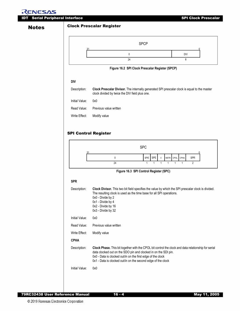
IDT Serial Peripheral Interface SPI Clock Prescalar
79RC32438 User Refer
Notes
Clock Prescalar RegisterFigure 16.2 SPI Clock Prescalar Register (SPCP)
SPI Control Register
Figure 16.3 SPI Control Register (SPC)
DIV
Description: Clock Prescalar Divisor. The internally generated SPI prescalar clock is equal to the master clock divided by twice the DIV field plus one.
Initial Value: 0x0
Read Value: Previous value written
Write Effect: Modify value
SPR
Description: Clock Divisor. This two bit field specifies the value by which the SPI prescalar clock is divided. The resulting clock is used as the time base for all SPI operations.0x0 - Divide by 20x1 - Divide by 40x2 - Divide by 160x3 - Divide by 32
Initial Value: 0x0
Read Value: Previous value written
Write Effect: Modify value
CPHA
Description: Clock Phase. This bit together with the CPOL bit control the clock and data relationship for serial data clocked out on the SDO pin and clocked in on the SDI pin.0x0 - Data is clocked out/in on the first edge of the clock0x1 - Data is clocked out/in on the second edge of the clock
Initial Value: 0x0
SPCP031
DIV0
24 8
SPC031
0
24
SPR
2
CPHA
1
CPOL
1
SPE
1
SPIE
1
0
1
MSTR
1
ence Manual 16 - 4 May 11, 2005

IDT Serial Peripheral Interface SPI Clock Prescalar
79RC32438 User Refer
Notes
Read Value: Previous value writtenWrite Effect: Modify value
CPOL
Description: Clock Polarity. This bit specifies the polarity of the clock. When this bit is set to zero (cleared), the SPI clock (SPCLK) is held in a low state during SPI idle periods (i.e., between transactions when the bus is idle). When this bit is set to one, the SPI clock is held in a high state during SPI idle periods.
Initial Value: 0x0
Read Value: Previous value written
Write Effect: Modify value
MSTR
Description: Master/Slave Mode. Since the SPI interface only supports master mode, this bit should always be set. It is provided for software compatibility only.
Initial Value: 0x1
Read Value: Previous value written
Write Effect: Modify value
SPE
Description: Enable. When this bit is set to one, the serial peripheral interface is enabled. When this bit is set to zero (cleared), the serial peripheral interface is disabled and held in a low power state. Dis-abling and then re-enabling the SPI initializes all SPI interface logic to a known state. When the SPI is disabled, writes to the SPD register will produce undefined results.
Initial Value: 0x0
Read Value: Previous value written
Write Effect: Modify value
SPIE
Description: SPI Interrupt Enable. When this bit is set to zero (cleared), SPI Transfer Complete (SPIF) and Master Error Flag (MODF) bits in the SPS register are masked from generating an interrupt.
Initial Value: 0x0
Read Value: Previous value written
Write Effect: Modify value
ence Manual 16 - 5 May 11, 2005

IDT Serial Peripheral Interface SPI Clock Prescalar
79RC32438 User Refer
Notes
Figure 16.4 Serial Peripheral Interface (SPI) Clock/Data Timing
SPI Status Register
Figure 16.5 SPI Status Register (SPS)
MODF
Description: Master Error Flag. This bit is asserted if a write is performed to the SPD register while the SPI interface is in non-master mode (i.e., slave mode). This bit is provided for software compatibility.
Initial Value: 0x0
Read Value: Status
Write Effect: No effect. This bit is automatically set to zero when the SPS register is read and then a write is performed to the SPC register with the MSTR bit set.
WCOL
Description: Write Collision. This bit is set if a write collision occurs (i.e., the CPU writes to the SPD register during an SPI transaction).
Initial Value: 0x0
Read Value: Status
Write Effect: No effect. This bit is automatically set to zero when the SPS register is read and then the SPD register is written.
SPIF
Description: SPI Transfer Complete. This bit is set when an SPI transaction completes.
Initial Value: 0x1
MSB BIT 6 BIT 5 BIT 4 BIT 3 BIT 2 BIT 1 LSB
MSB BIT 6 BIT 5 BIT 4 BIT 3 BIT 2 BIT 1 LSB
SCK (CPOL=0)
SCK (CPOL=1)
Sample InputData Output(CPHA=1)
Sample InputData Output(CPHA=0)
GPIO(x) (Chip select)
SPS031
0
24
0
4
WCOL
1
SPIF
1 1
MODF
1
0
ence Manual 16 - 6 May 11, 2005

IDT Serial Peripheral Interface SPI Setup
79RC32438 User Refer
Notes
SPI Data Register
Figure 16.6 SPI Data Register (SPD)
SPI SetupThe following describes the typical setup of the SPI interface which occurs during boot time:
1. As the SPI interface shares data and clock pins with the PCI EEPROM, the SPI module must firstpoll the PCI EEPROM EED bit in the PCI Status register of the PCI Controller to determine if thePCI module has finished loading data from the PCI EEPROM. The RC32438 device automaticallyswitches the functionality of the pins for use as an SPI interface when the loading of configurationdata from the PCI EEPROM is completed.
2. As the SPI signal functions are routed via the PIO Controller, the PIO Controller will generally beinitialized to the Effect Mode and establish the correct direction for each SPI pin. At reset time, thedefault Effect Mode and Direction are set up for the PCI EEPROM and also for the SPI.
3. The SPI Clock Prescalar Register, SPCP, is programmed.4. The SPI Control Register (SPC), including the SPE Enable Bit, is programmed.5. The data being sent to the SPI Slave is written into the SPI Data Register (SPD).6. The SPI Controller will initiate the hardware protocol on the SPI pins. The RC32438 device will
receive data from the Slave at the same time it is sending data to the Slave.7. System either with:
– Wait for an SPI Interrupt. After receiving an SPI Interrupt via the Interrupt Controller, the SPIStatus Register SPIF and MODF Flags can be read.
– Poll the SPI Status Register SPIF and MODF Flags.
Read Value: Status
Write Effect: No effect. This bit is automatically set to zero when the SPS register is read and then the SPD register is read.
DATA
Description: DATA. A write to this field results in an SPI transaction in which the value written to this register is shifted out on the SDO pin while data is simultaneously shifted into this field from the SDI pin. At the completion of the transaction, the SPIF bit in the SPS register is set to one and this field contains the 8-bit quantity read from the SDI pin.
Initial Value: 0x0
Read Value: Value shifted in from SDI pin during the previous transaction
Write Effect: Initiate an SPI transaction. After an initial transaction, subsequent SPI transactions can only be initiated when the SPIF bit is set in the SPS register and a read of the register is performed before a write to the SPD register.
SPD031
0
24
DATA
8
ence Manual 16 - 7 May 11, 2005

IDT Serial Peripheral Interface Serial Bit I/O Pins
79RC32438 User Refer
Notes
8. If the SPIF Flag is set, indicating the transaction is complete, reading the SPI Status Register resetsthe SPIF Flag.9. Read the data from the SPI Data Register.10. Repeat Steps 5 through 10, as needed.
Serial Bit I/O PinsThe serial I/O signals SCK, SDO, SDI, and PCIGNTN[1] may be used as bit I/O ports that operate in
basically the same way as GPIO pins. For additional information on the GPIO pins, refer to Chapter 12,General Purpose I/O Controller.
The PCI serial EEPROM may be read to and written from when loading to the PCI Configuration regis-ters has completed. This is achieved by disabling the SPI interface and synthesizing (via software)MICROWIRE transactions on the serial I/O pins.
When the PCI interface operates in PCI satellite mode, the state of the PCIGNTN pin may be controlledby writing the desired pin state value into the Serial I/O Data (SIOD) register.
Serial I/O Function Register
Figure 16.7 Serial I/O Function Register (SIOFUNC)
SDO
Description: Serial Data Output. When this bit is set to one, the SDO pin operates as a bit I/O port regardless of the state of the SPI or PCI interfaces.
Initial Value: 0x0
Read Value: Previous value written
Write Effect: Modify value
SDI
Description: Serial Data Input. When this bit is set to one, the SDI pin operates as a bit I/O port regardless of the state of the SPI or PCI interfaces.
Initial Value: 0x0
Read Value: Previous value written
Write Effect: Modify value
SCK
Description: Serial Clock. When this bit is set to one, the SCK pin operates as a bit I/O port regardless of the state of the SPI or PCI interfaces.
Initial Value: 0x0
Read Value: Previous value written
Write Effect: Modify value
SIOFUNC031
0
28
SDO
1
SDI
1
SCK
1
PCI
1
ence Manual 16 - 8 May 11, 2005
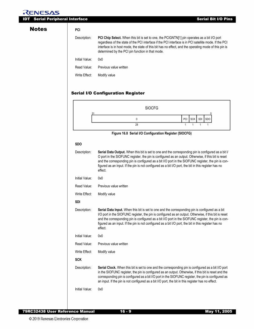
IDT Serial Peripheral Interface Serial Bit I/O Pins
79RC32438 User Refer
Notes
Serial I/O Configuration Register
Figure 16.8 Serial I/O Configuration Register (SIOCFG)
PCI
Description: PCI Chip Select. When this bit is set to one, the PCIGNTN[1] pin operates as a bit I/O port regardless of the state of the PCI interface if the PCI interface is in PCI satellite mode. If the PCI interface is in host mode, the state of this bit has no effect, and the operating mode of this pin is determined by the PCI pin function in that mode.
Initial Value: 0x0
Read Value: Previous value written
Write Effect: Modify value
SDO
Description: Serial Data Output. When this bit is set to one and the corresponding pin is configured as a bit I/O port in the SIOFUNC register, the pin is configured as an output. Otherwise, if this bit is reset and the corresponding pin is configured as a bit I/O port in the SIOFUNC register, the pin is con-figured as an input. If the pin is not configured as a bit I/O port, the bit in this register has no effect.
Initial Value: 0x0
Read Value: Previous value written
Write Effect: Modify value
SDI
Description: Serial Data Input. When this bit is set to one and the corresponding pin is configured as a bitI/O port in the SIOFUNC register, the pin is configured as an output. Otherwise, if this bit is reset and the corresponding pin is configured as a bit I/O port in the SIOFUNC register, the pin is con-figured as an input. If the pin is not configured as a bit I/O port, the bit in this register has no effect.
Initial Value: 0x0
Read Value: Previous value written
Write Effect: Modify value
SCK
Description: Serial Clock. When this bit is set to one and the corresponding pin is configured as a bit I/O port in the SIOFUNC register, the pin is configured as an output. Otherwise, if this bit is reset and the corresponding pin is configured as a bit I/O port in the SIOFUNC register, the pin is configured as an input. If the pin is not configured as a bit I/O port, the bit in this register has no effect.
Initial Value: 0x0
SIOCFG031
0
28
SDO
1
SDI
1
SCK
1
PCI
1
ence Manual 16 - 9 May 11, 2005

IDT Serial Peripheral Interface Serial Bit I/O Pins
79RC32438 User Refer
Notes
Serial I/O Data Register
Figure 16.9 Serial I/O Data Register (SIOD)
Read Value: Previous value written
Write Effect: Modify value
PCI
Description: PCI Chip Select. When this bit is set to one and the corresponding pin is configured as a bitI/O port in the SIOFUNC register, the pin is configured as an output. Otherwise, if this bit is reset and the corresponding pin is configured as a bit I/O port in the SIOFUNC register, the pin is con-figured as an input. If the pin is not configured as a bit I/O port, the bit in this register has no effect.
Initial Value: 0x0
Read Value: Previous value written
Write Effect: Modify value
SDO
Description: Serial Data Output. Reading this bit returns the state of the SDO pin. Writing a value to this bit causes the SDO pin to take on the corresponding value if it is configured to be a bit I/O output port in the SIOFUNC and SIOCFG registers.
Initial Value: SDO pin value
Read Value: Previous value written
Write Effect: Modify value
SDI
Description: Serial Data Input. Reading this bit returns the state of the SDI pin. Writing a value to this bit causes the SDI pin to take on the corresponding value if it is configured to be a bit I/O output port in the SIOFUNC and SIOCFG registers.
Initial Value: SDI pin value
Read Value: Previous value written
Write Effect: Modify value
SCK
Description: Serial Clock. Reading this bit returns the state of the SCK pin. Writing a value to this bit causes the SCK pin to take on the corresponding value if it is configured to be a bit I/O output port in the SIOFUNC and SIOCFG registers.
Initial Value: SCK pin value
SIOD031
0
28
SDO
1
SDI
1
SCK
1
PCI
1
ence Manual 16 - 10 May 11, 2005
IDT Serial Peripheral Interface Master Programming Example
79RC32438 User Refer
Notes
Master Programming Example
SPI Initialization1. If the PCI interface is configured to operate in PCI satellite mode with suspended CPU execution,
wait until PCI Serial EEPROM Done (EED) bit is set in the PCIS register.2. Based on operating IPBus clock frequency and desired SPI clock frequency, write SPCP register
(i.e., 0x0C for 100 MHz IPBus clock, 2 MHz SPI clock and SPR = 0 in SPC).3. Write SPIC register with 0x0000_00D0. SPIE = 1 - Interrupt enable, SPE = 1 - Enable interface,
MSTR = 1 - Master mode, SPOL = 0 - Idle clock polarity low, CPHA = 0 - Data clocked on first edge,SPR = 0 - Clock divisor is 2.
4. Write IMASK6 register to disable GPIO Interrupt, GPIOx = 0, where "x" is used GPIO pin for SPI chipselect. If you have more than one device, disable all interrupts for used GPIO pins.
5. Write GPIOFUNC register to set GPIOx = 0 — not alternate function.6. Write GPIOCFG register to set GPIOx = 1 — output.7. Write GPIOD register to de-assert chip select(s) GPIOx = 1.8. Read SPS and then SPD to clear SPIF bit.9. Write IMASK5 register SPI = 0 — enable SPI interrupts.10. Write GPIOD register to assert chip select GPIOx = 0 for the device to be accessed.11. Write SPID register with data to transmit over SPI interface to start the transmission process.12. Wait until the SPI interrupt occurs. The interrupt routine will perform the following steps:
– · Read SPS register and check for errors.– · Mandatory read SPD register, to get input data and clear SPIF bit in SPS register.– · If finished with (multi-)byte command sequence (i.e., a read sequence: command; address byte
1; address byte 2; 4 data bytes) de-assert chip select writing GPIOD register with GPIOx = 1.
13. Repeat steps 10 - 12 as needed.
Read Value: Previous value written
Write Effect: Modify value
PCI
Description: PCI Chip Select. Reading this bit returns the state of the PCIGNTN[1] pin. Writing a value to this bit causes the PCIGNTN[1] pin to take on the corresponding value if it is configured to be a bit I/O output port in the SIOFUNC and SIOCFG registers and the PCI interface is operating in PCI satellite mode.
Initial Value: PCIGNTN[1] pin value
Read Value: Previous value written
Write Effect: Modify value
ence Manual 16 - 11 May 11, 2005
IDT Serial Peripheral Interface Master Programming Example
79RC32438 User Refer
Notes
ence Manual 16 - 12 May 11, 2005
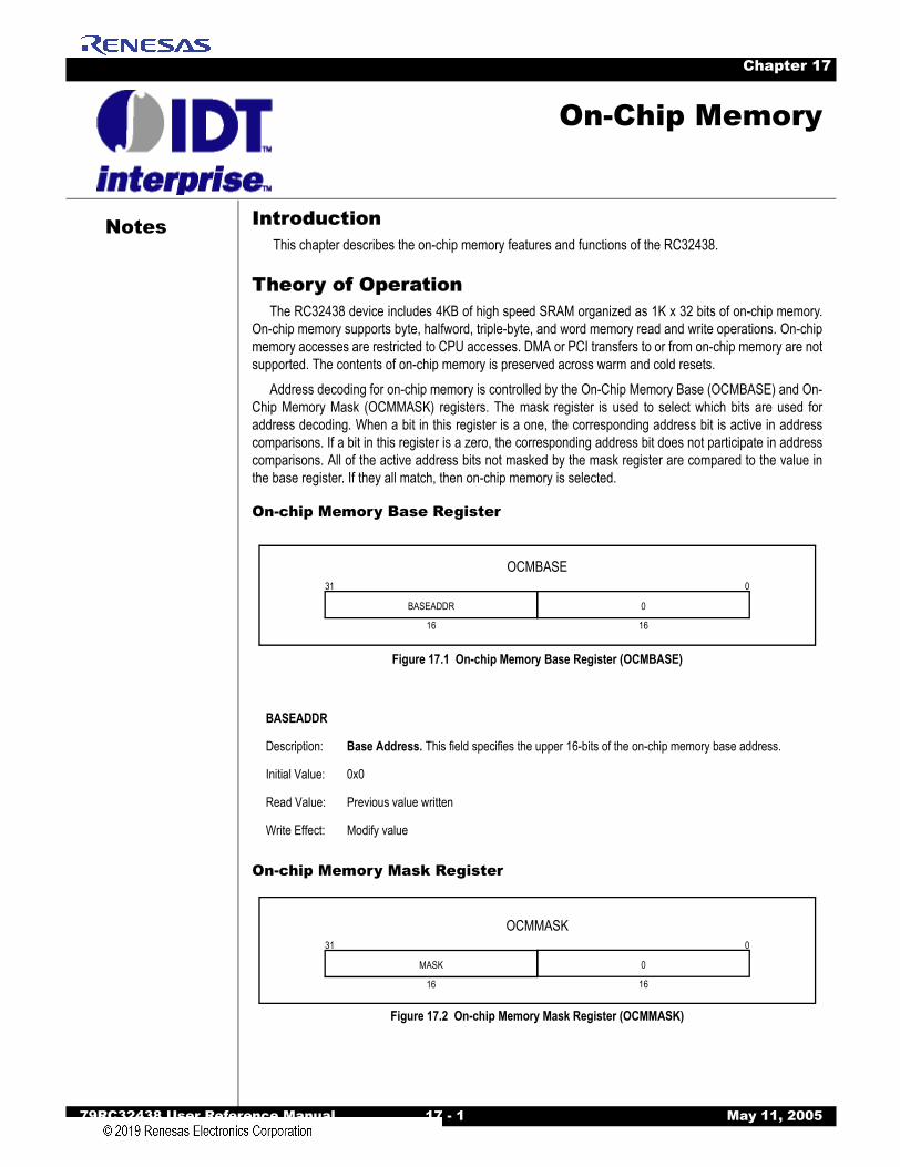
Notes
79RC32438 User Reference Manual 17 - 1 M
Chapter 17
On-Chip Memory
Introduction This chapter describes the on-chip memory features and functions of the RC32438.
Theory of OperationThe RC32438 device includes 4KB of high speed SRAM organized as 1K x 32 bits of on-chip memory.
On-chip memory supports byte, halfword, triple-byte, and word memory read and write operations. On-chipmemory accesses are restricted to CPU accesses. DMA or PCI transfers to or from on-chip memory are notsupported. The contents of on-chip memory is preserved across warm and cold resets.
Address decoding for on-chip memory is controlled by the On-Chip Memory Base (OCMBASE) and On-Chip Memory Mask (OCMMASK) registers. The mask register is used to select which bits are used foraddress decoding. When a bit in this register is a one, the corresponding address bit is active in addresscomparisons. If a bit in this register is a zero, the corresponding address bit does not participate in addresscomparisons. All of the active address bits not masked by the mask register are compared to the value inthe base register. If they all match, then on-chip memory is selected.
On-chip Memory Base Register
Figure 17.1 On-chip Memory Base Register (OCMBASE)
On-chip Memory Mask Register
Figure 17.2 On-chip Memory Mask Register (OCMMASK)
BASEADDR
Description: Base Address. This field specifies the upper 16-bits of the on-chip memory base address.
Initial Value: 0x0
Read Value: Previous value written
Write Effect: Modify value
OCMBASE031
16 16
BASEADDR 0
OCMMASK031
16
MASK
16
0
ay 11, 2005

IDT On-Chip Memory Theory of Operation
79RC32438 User Refer
Notes
MASKDescription: Address Mask. This field determines which bits of the upper 16-bits of the address participate in address comparisons. When a bit is set to one in this field, then the corresponding address bit participates in address comparisons. When a bit is set to zero in this field, then the correspond-ing address bit is masked and does not participate in address comparisons.When the MASK field is zero, the on-chip memory does not appear in the memory map.
Initial Value: 0x0
Read Value: Previous value written
Write Effect: Modify value
ence Manual 17 - 2 May 11, 2005
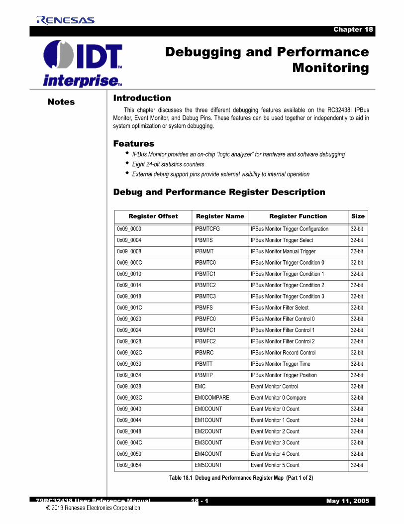
Notes
79RC32438 User Reference Manual 18 - 1 M
Chapter 18
Debugging and PerformanceMonitoring
Introduction This chapter discusses the three different debugging features available on the RC32438: IPBus
Monitor, Event Monitor, and Debug Pins. These features can be used together or independently to aid insystem optimization or system debugging.
FeaturesIPBus Monitor provides an on-chip “logic analyzer” for hardware and software debuggingEight 24-bit statistics countersExternal debug support pins provide external visibility to internal operation
Debug and Performance Register Description
Register Offset Register Name Register Function Size
0x09_0000 IPBMTCFG IPBus Monitor Trigger Configuration 32-bit
0x09_0004 IPBMTS IPBus Monitor Trigger Select 32-bit
0x09_0008 IPBMMT IPBus Monitor Manual Trigger 32-bit
0x09_000C IPBMTC0 IPBus Monitor Trigger Condition 0 32-bit
0x09_0010 IPBMTC1 IPBus Monitor Trigger Condition 1 32-bit
0x09_0014 IPBMTC2 IPBus Monitor Trigger Condition 2 32-bit
0x09_0018 IPBMTC3 IPBus Monitor Trigger Condition 3 32-bit
0x09_001C IPBMFS IPBus Monitor Filter Select 32-bit
0x09_0020 IPBMFC0 IPBus Monitor Filter Control 0 32-bit
0x09_0024 IPBMFC1 IPBus Monitor Filter Control 1 32-bit
0x09_0028 IPBMFC2 IPBus Monitor Filter Control 2 32-bit
0x09_002C IPBMRC IPBus Monitor Record Control 32-bit
0x09_0030 IPBMTT IPBus Monitor Trigger Time 32-bit
0x09_0034 IPBMTP IPBus Monitor Trigger Position 32-bit
0x09_0038 EMC Event Monitor Control 32-bit
0x09_003C EM0COMPARE Event Monitor 0 Compare 32-bit
0x09_0040 EM0COUNT Event Monitor 0 Count 32-bit
0x09_0044 EM1COUNT Event Monitor 1 Count 32-bit
0x09_0048 EM2COUNT Event Monitor 2 Count 32-bit
0x09_004C EM3COUNT Event Monitor 3 Count 32-bit
0x09_0050 EM4COUNT Event Monitor 4 Count 32-bit
0x09_0054 EM5COUNT Event Monitor 5 Count 32-bit
Table 18.1 Debug and Performance Register Map (Part 1 of 2)
ay 11, 2005

IDT Debugging and Performance Monitoring IPBus Monitor
79RC32438 User Refer
Notes
IPBus MonitorThe IPBus monitor provides on-chip “logic analyzer” functionality for debugging hardware and software.
It provides sophisticated support for debugging transactions on the internal IPBus that would otherwise notbe available to the user. Unlike most other blocks in the RC32438, the IPBus Monitor is not reset during awarm reset. This allows the IPBus monitor to be used to debug across a warm reset.
The IPBus monitor allows IPBus transaction information to be recorded in on-chip memory for later anal-ysis (for additional information, refer to Chapter 17, On-Chip Memory). The on-chip memory region used bythe IPBus monitor is determined by the IPBMBASE field of the IPBMRC register. As shown in Figure 18.1,the IPBus monitor uses memory starting at IPBMBASE to the end of on-chip memory to record transac-tions. Memory below IPBMBASE is available for other uses.
Figure 18.1 IPBus Monitor On-Chip Memory Usage
Transaction information is stored using two types of double word (i.e., 64-bit) records. A clock cyclerecord is stored in on-chip memory during each clock cycle of a transaction. A transaction summary recordis stored in on-chip memory at the end of each transaction (refer to the IPBus Monitor Trigger Time sectionlater in this chapter). Records are stored in on-chip memory in a circular fashion. When the end of on-chipmemory is reached, recording continues starting at IPBMBASE.
When the IPBus monitor is enabled (i.e., the EN bit is set in the IPBMTCFG register), it begins recordingeach IPBus transaction in on-chip memory. Recording stops shortly after a final trigger event occurs. Oncea final trigger event occurs the IPBus monitor continues storing transactions records in on-chip memoryuntil the space allocated by the Final Trigger Record Length (FTRL) field in the IPBMRC register isexhausted. The FTRL field provides control over how many transactions are recorded before and after afinal trigger event. When a final trigger event occurs the FT bit is set in the IPBMTCFG register. This bit ispresented to the interrupt controller as an interrupt source.
When the EJTAG Debug Interrupt Enable (DIE) bit is set in the IPBMTCFG register, an EJTAG debuginterrupt request is generated to the CPU core whenever the FT bit is set in the IPBMTCFG register. Thisallows synchronization between the IPBus monitor and an external EJTAG ICE. When the IPBus monitorcompletes storing transaction records in on-chip memory (i.e., the space allocated by the FTRL field isexhausted) the Recording Completed (RC) bit is set in the IPBMTCFG register. This bit is presented to theinterrupt controller as an interrupt source.
0x09_0058 EM6COUNT Event Monitor 6 Count 32-bit
0x09_005C EM7COUNT Event Monitor 7 Count 32-bit
0x09_0060 through 0x09_7FFF Reserved
Register Offset Register Name Register Function Size
Table 18.1 Debug and Performance Register Map (Part 2 of 2)
0x0000
0x0FFF
IPBu
s Mon
itor S
pace
IPBMBASE
ence Manual 18 - 2 May 11, 2005
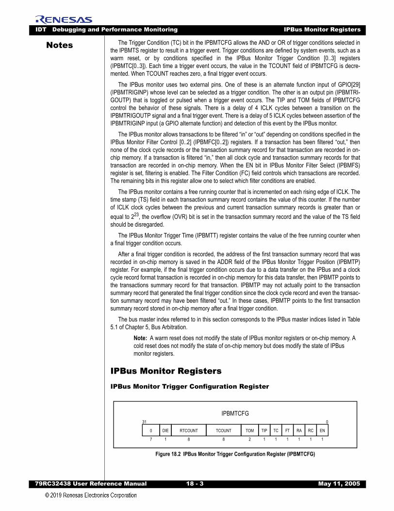
IDT Debugging and Performance Monitoring IPBus Monitor Registers
79RC32438 User Refer
Notes
The Trigger Condition (TC) bit in the IPBMTCFG allows the AND or OR of trigger conditions selected inthe IPBMTS register to result in a trigger event. Trigger conditions are defined by system events, such as awarm reset, or by conditions specified in the IPBus Monitor Trigger Condition [0..3] registers(IPBMTC[0..3]). Each time a trigger event occurs, the value in the TCOUNT field of IPBMTCFG is decre-mented. When TCOUNT reaches zero, a final trigger event occurs.The IPBus monitor uses two external pins. One of these is an alternate function input of GPIO[29](IPBMTRIGINP) whose level can be selected as a trigger condition. The other is an output pin (IPBMTRI-GOUTP) that is toggled or pulsed when a trigger event occurs. The TIP and TOM fields of IPBMTCFGcontrol the behavior of these signals. There is a delay of 4 ICLK cycles between a transition on theIPBMTRIGOUTP signal and a final trigger event. There is a delay of 5 ICLK cycles between assertion of theIPBMTRIGINP input (a GPIO alternate function) and detection of this event by the IPBus monitor.
The IPBus monitor allows transactions to be filtered “in” or “out” depending on conditions specified in theIPBus Monitor Filter Control [0..2] (IPBMFC[0..2]) registers. If a transaction has been filtered “out,” thennone of the clock cycle records or the transaction summary record for that transaction are recorded in on-chip memory. If a transaction is filtered “in,” then all clock cycle and transaction summary records for thattransaction are recorded in on-chip memory. When the EN bit in IPBus Monitor Filter Select (IPBMFS)register is set, filtering is enabled. The Filter Condition (FC) field controls which transactions are recorded.The remaining bits in this register allow one to select which filter conditions are enabled.
The IPBus monitor contains a free running counter that is incremented on each rising edge of ICLK. Thetime stamp (TS) field in each transaction summary record contains the value of this counter. If the numberof ICLK clock cycles between the previous and current transaction summary records is greater than orequal to 223, the overflow (OVR) bit is set in the transaction summary record and the value of the TS fieldshould be disregarded.
The IPBus Monitor Trigger Time (IPBMTT) register contains the value of the free running counter whena final trigger condition occurs.
After a final trigger condition is recorded, the address of the first transaction summary record that wasrecorded in on-chip memory is saved in the ADDR field of the IPBus Monitor Trigger Position (IPBMTP)register. For example, if the final trigger condition occurs due to a data transfer on the IPBus and a clockcycle record format transaction is recorded in on-chip memory for this data transfer, then IPBMTP points tothe transactions summary record for that transaction. IPBMTP may not actually point to the transactionsummary record that generated the final trigger condition since the clock cycle record and even the transac-tion summary record may have been filtered “out.” In these cases, IPBMTP points to the first transactionsummary record stored in on-chip memory after a final trigger condition.
The bus master index referred to in this section corresponds to the IPBus master indices listed in Table5.1 of Chapter 5, Bus Arbitration.
Note: A warm reset does not modify the state of IPBus monitor registers or on-chip memory. A cold reset does not modify the state of on-chip memory but does modify the state of IPBus monitor registers.
IPBus Monitor Registers
IPBus Monitor Trigger Configuration Register
Figure 18.2 IPBus Monitor Trigger Configuration Register (IPBMTCFG)
IPBMTCFG031
TIP
1
TCOUNT
8
TOM
2
EN
1
TC
1
FT
1
RA
1
RC
1
RTCOUNT
8
0
7
DIE
1
ence Manual 18 - 3 May 11, 2005
IDT Debugging and Performance Monitoring IPBus Monitor Registers
79RC32438 User Refer
Notes
ENDescription: Enable. When this bit is set to one, the IPBus monitor is armed. Each time the trigger condition specified by the TC field and the IPBus Monitor Trigger Select (IPBMTS) register are satisfied the Trigger Count (TCOUNT) field is decremented. When the TCOUNT field reaches zero, the enable bit is set to zero (cleared) and a final trigger event occurs.Note: When this bit is set, the IPBus records transactions until a final trigger event occurs or until this bit is cleared by software.
Initial Value: 0x0
Read Value: Previous value written
Write Effect: Modify value
RC
Description: Recording Completed. When the IPBus monitor completes storing transaction records in on-chip memory (i.e., the space allocated by the FTRL field is exhausted) this bit is set.
Initial Value: 0x0
Read Value: Status
Write Effect: Sticky bit (a sticky bit is set by the hardware and can only be cleared by the CPU)
RA
Description: Rearm. When this bit is set to one, the IPBus monitor is automatically rearmed (i.e., the enable bit is set) after a final trigger event occurs. When the IPBus monitor is rearmed, the value in the RTCOUNT field is loaded into the TCOUNT field.
Initial Value: 0x0
Read Value: Previous value written
Write Effect: Modify value
FT
Description: Final Trigger. This bit is set to one when a final trigger event occurs.
Initial Value: 0x0
Read Value: Status
Write Effect: Sticky bit (a sticky bit is set by the hardware and can only be cleared by the CPU)
TC
Description: Trigger Condition. When this bit is set to one, the IPBus monitor triggers when all of the selected trigger conditions selected in the IPBMTS register are satisfied (i.e., AND of all enabled trigger conditions). When this bit is cleared, the IPBus monitor triggers when any of the selected trigger conditions are satisfied (i.e., OR of all enabled trigger conditions).
Initial Value: 0x0
Read Value: Previous value written
Write Effect: Modify value
ence Manual 18 - 4 May 11, 2005
IDT Debugging and Performance Monitoring IPBus Monitor Registers
79RC32438 User Refer
Notes
TIPDescription: IPBus Monitor Trigger Input Polarity. This bit selects the active polarity of the IPBus Monitor Trigger Input (IPBMTRIGINP). IPBMTRIGINP is a GPIO alternate function and is sampled by EXTCLK.0 - IPBMTRIGINP is active low (trigger when signal transitions from 1 to 0)1 - IPBMTRIGINP is active high (trigger when signal transitions from 0 to 1)
Initial Value: 0x0
Read Value: Previous value written
Write Effect: Modify value
TOM
Description: IPBus Monitor Trigger Output Mode. This bit selects the operating mode of the IPBus Monitor Trigger Output (IPBMTRIGOUT).0 - IPBMTRIGOUT is driven low for one EXTCLK clock cycle when final trigger occurs1 - IPBMTRIGOUT is driven high for one EXTCLK clock cycle when final trigger occurs2 - IPBMTRIGOUT is inverted (i.e., toggled) when final trigger event occurs3 - reserved
Initial Value: 0x0
Read Value: Previous value written
Write Effect: Modify value
TCOUNT
Description: Trigger Count. This field contains a trigger count which is decremented each time a trigger event occurs.
Initial Value: 0x0
Read Value: Previous value written
Write Effect: Modify value
RTCOUNT
Description: Rearm Trigger Count. This field contains the rearm trigger count value which is loaded into the TCOUNT field whenever the IPBus monitor is automatically rearmed (i.e., when the RA bit is set and the final trigger event occurs).
Initial Value: 0x0
Read Value: Previous value written
Write Effect: Modify value
DIE
Description: Debug Interrupt Enable. When this bit is set in the IPBMTCFG register, an EJTAG debug inter-rupt request is generated to the CPU core whenever the FT bit is set. This allows synchroniza-tion between the IPBus monitor and an external EJTAG ICE.
Initial Value: 0x0
Read Value: Previous value written
Write Effect: Modify value
ence Manual 18 - 5 May 11, 2005
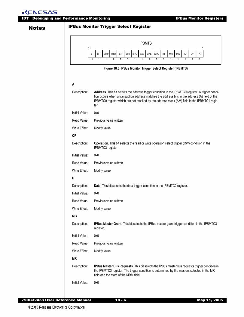
IDT Debugging and Performance Monitoring IPBus Monitor Registers
79RC32438 User Refer
Notes
IPBus Monitor Trigger Select RegisterFigure 18.3 IPBus Monitor Trigger Select Register (IPBMTS)
A
Description: Address. This bit selects the address trigger condition in the IPBMTC0 register. A trigger condi-tion occurs when a transaction address matches the address bits in the address (A) field of the IPBMTC0 register which are not masked by the address mask (AM) field in the IPBMTC1 regis-ter.
Initial Value: 0x0
Read Value: Previous value written
Write Effect: Modify value
OP
Description: Operation. This bit selects the read or write operation select trigger (RW) condition in the IPBMTC3 register.
Initial Value: 0x0
Read Value: Previous value written
Write Effect: Modify value
D
Description: Data. This bit selects the data trigger condition in the IPBMTC2 register.
Initial Value: 0x0
Read Value: Previous value written
Write Effect: Modify value
MG
Description: IPBus Master Grant. This bit selects the IPBus master grant trigger condition in the IPBMTC3 register.
Initial Value: 0x0
Read Value: Previous value written
Write Effect: Modify value
MR
Description: IPBus Master Bus Requests. This bit selects the IPBus master bus requests trigger condition in the IPBMTC3 register. The trigger condition is determined by the masters selected in the MR field and the state of the MRM field.
Initial Value: 0x0
IPBMTS031
OP
1
A
1
D
1
MG
1
MR
1
IR
1
WTO
1
WR
1
ET
1
BTO
1
TRW
1
UAE
1
EM0
1
0
17
MT
1
SAE
1
ence Manual 18 - 6 May 11, 2005
IDT Debugging and Performance Monitoring IPBus Monitor Registers
79RC32438 User Refer
Notes
Read Value: Previous value writtenWrite Effect: Modify value
IR
Description: Interrupt Request. This bit selects the interrupt request trigger condition in the IPBMTC3 regis-ter.
Initial Value: 0x0
Read Value: Previous value written
Write Effect: Modify value
WTO
Description: Watchdog Timer Time-out. This bit selects the watchdog timer time-out trigger condition (see the Functional Overview section in Chapter 4, System Integrity Functions).
Initial Value: 0x0
Read Value: Previous value written
Write Effect: Modify value
UAE
Description: Undecoded Address Error. This bit selects the undecoded address error trigger condition which is reported by the address space monitor (see the Functional Overview section in Chapter 4, System Integrity Functions).
Initial Value: 0x0
Read Value: Previous value written
Write Effect: Modify value
SAE
Description: IPBus Slave Acknowledge Error. This bit selects the IPBus slave acknowledge error trigger condition (see the Functional Overview section in Chapter 4, System Integrity Functions).
Initial Value: 0x0
Read Value: Previous value written
Write Effect: Modify value
BTO
Description: Bus Transaction Timer Time-out. This bit selects the transaction timer time-out trigger condi-tion which is reported by the memory and peripheral bus transaction timer (see the Theory of Operation section in Chapter 6, Device Controller).
Initial Value: 0x0
Read Value: Previous value written
Write Effect: Modify value
WR
Description: Warm Reset. This bit selects the warm reset trigger condition.
Initial Value: 0x0
ence Manual 18 - 7 May 11, 2005
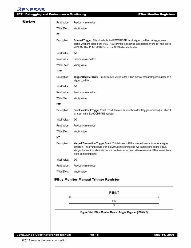
IDT Debugging and Performance Monitoring IPBus Monitor Registers
79RC32438 User Refer
Notes
IPBus Monitor Manual Trigger Register
Figure 18.4 IPBus Monitor Manual Trigger Register (IPBMMT)
Read Value: Previous value written
Write Effect: Modify value
ET
Description: External Trigger. This bit selects the IPBMTRIGINP input trigger condition. A trigger event occurs when the state of the IPBMTRIGINP input is asserted (as specified by the TIP field in IPB-MTCFG). The IPBMTRIGINP input is a GPIO alternate function.
Initial Value: 0x0
Read Value: Previous value written
Write Effect: Modify value
TRW
Description: Trigger Register Write. This bit selects writes to the IPBus monitor manual trigger register as a trigger condition.
Initial Value: 0x0
Read Value: Previous value written
Write Effect: Modify value
EM0
Description: Event Monitor 0 Trigger Event. This bit selects an event monitor 0 trigger condition (i.e, when T bit is set in the EM0COMPARE register).
Initial Value: 0x0
Read Value: Previous value written
Write Effect: Modify value
MT
Description: Merged Transaction Trigger Event. This bit selects IPBus merged transactions as a trigger condition. This event occurs with the DMA controller merges two transactions on the IPBus. Merged transactions eliminate the bus overhead associated with consecutive IPBus transactions to the same peripheral.
Initial Value: 0x0
Read Value: Previous value written
Write Effect: Modify value
IPBMMT031
TRIG
32
ence Manual 18 - 8 May 11, 2005
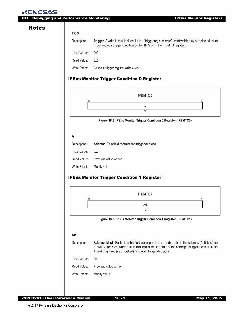
IDT Debugging and Performance Monitoring IPBus Monitor Registers
79RC32438 User Refer
Notes
IPBus Monitor Trigger Condition 0 Register
Figure 18.5 IPBus Monitor Trigger Condition 0 Register (IPBMTC0)
IPBus Monitor Trigger Condition 1 Register
Figure 18.6 IPBus Monitor Trigger Condition 1 Register (IPBMTC1)
TRIG
Description: Trigger. A write to this field results in a “trigger register write” event which may be selected as an IPBus monitor trigger condition by the TRW bit in the IPBMTS register.
Initial Value: 0x0
Read Value: 0x0
Write Effect: Cause a trigger register write event
A
Description: Address. This field contains the trigger address.
Initial Value: 0x0
Read Value: Previous value written
Write Effect: Modify value
AM
Description: Address Mask. Each bit in this field corresponds to an address bit in the Address (A) field of the IPBMTC0 register. When a bit in this field is set, the state of the corresponding address bit in the A field is ignored (i.e., masked) in making trigger decisions.
Initial Value: 0x0
Read Value: Previous value written
Write Effect: Modify value
IPBMTC0031
A
32
IPBMTC1031
AM
32
ence Manual 18 - 9 May 11, 2005
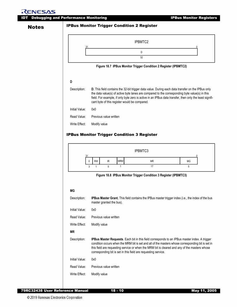
IDT Debugging and Performance Monitoring IPBus Monitor Registers
79RC32438 User Refer
Notes
IPBus Monitor Trigger Condition 2 RegisterFigure 18.7 IPBus Monitor Trigger Condition 2 Register (IPBMTC2)
IPBus Monitor Trigger Condition 3 Register
Figure 18.8 IPBus Monitor Trigger Condition 3 Register (IPBMTC3)
D
Description: D. This field contains the 32-bit trigger data value. During each data transfer on the IPBus only the data value(s) of active byte lanes are compared to the corresponding byte value(s) in this field. For example, if only byte zero is active in an IPBus data transfer, then only the least signifi-cant byte of this register would be compared.
Initial Value: 0x0
Read Value: Previous value written
Write Effect: Modify value
MG
Description: IPBus Master Grant. This field contains the IPBus master trigger index (i.e., the index of the bus master granted the bus).
Initial Value: 0x0
Read Value: Previous value written
Write Effect: Modify value
MR
Description: IPBus Master Requests. Each bit in this field corresponds to an IPBus master index. A trigger condition occurs when the MRM bit is set and all of the masters whose corresponding bit is set in this field are requesting service or when the MRM bit is cleared and any of the masters whose corresponding bit is set in this field are requesting service.
Initial Value: 0x0
Read Value: Previous value written
Write Effect: Modify value
IPBMTC2031
D
32
IPBMTC3031
MG
5
MR
17
IR
5
0
3
MRM
1
RW
1
ence Manual 18 - 10 May 11, 2005
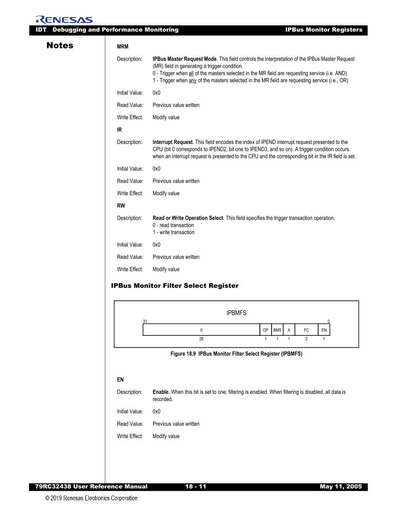
IDT Debugging and Performance Monitoring IPBus Monitor Registers
79RC32438 User Refer
Notes
IPBus Monitor Filter Select Register
Figure 18.9 IPBus Monitor Filter Select Register (IPBMFS)
MRM
Description: IPBus Master Request Mode. This field controls the interpretation of the IPBus Master Request (MR) field in generating a trigger condition.0 - Trigger when all of the masters selected in the MR field are requesting service (i.e. AND)1 - Trigger when any of the masters selected in the MR field are requesting service (i.e., OR)
Initial Value: 0x0
Read Value: Previous value written
Write Effect: Modify value
IR
Description: Interrupt Request. This field encodes the index of IPEND interrupt request presented to the CPU (bit 0 corresponds to IPEND2, bit one to IPEND3, and so on). A trigger condition occurs when an interrupt request is presented to the CPU and the corresponding bit in the IR field is set.
Initial Value: 0x0
Read Value: Previous value written
Write Effect: Modify value
RW
Description: Read or Write Operation Select. This field specifies the trigger transaction operation.0 - read transaction1 - write transaction
Initial Value: 0x0
Read Value: Previous value written
Write Effect: Modify value
EN
Description: Enable. When this bit is set to one, filtering is enabled. When filtering is disabled, all data is recorded.
Initial Value: 0x0
Read Value: Previous value written
Write Effect: Modify value
IPBMFS031
FC
2
EN
1
A
1
BMS
1
OP
1
0
26
ence Manual 18 - 11 May 11, 2005
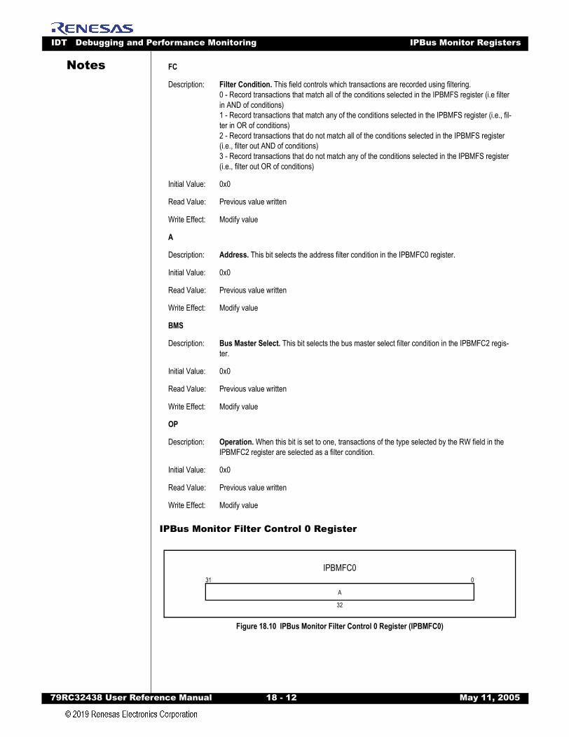
IDT Debugging and Performance Monitoring IPBus Monitor Registers
79RC32438 User Refer
Notes
IPBus Monitor Filter Control 0 Register
Figure 18.10 IPBus Monitor Filter Control 0 Register (IPBMFC0)
FC
Description: Filter Condition. This field controls which transactions are recorded using filtering.0 - Record transactions that match all of the conditions selected in the IPBMFS register (i.e filter in AND of conditions)1 - Record transactions that match any of the conditions selected in the IPBMFS register (i.e., fil-ter in OR of conditions)2 - Record transactions that do not match all of the conditions selected in the IPBMFS register (i.e., filter out AND of conditions)3 - Record transactions that do not match any of the conditions selected in the IPBMFS register (i.e., filter out OR of conditions)
Initial Value: 0x0
Read Value: Previous value written
Write Effect: Modify value
A
Description: Address. This bit selects the address filter condition in the IPBMFC0 register.
Initial Value: 0x0
Read Value: Previous value written
Write Effect: Modify value
BMS
Description: Bus Master Select. This bit selects the bus master select filter condition in the IPBMFC2 regis-ter.
Initial Value: 0x0
Read Value: Previous value written
Write Effect: Modify value
OP
Description: Operation. When this bit is set to one, transactions of the type selected by the RW field in the IPBMFC2 register are selected as a filter condition.
Initial Value: 0x0
Read Value: Previous value written
Write Effect: Modify value
IPBMFC0031
A
32
ence Manual 18 - 12 May 11, 2005

IDT Debugging and Performance Monitoring IPBus Monitor Registers
79RC32438 User Refer
Notes
IPBus Monitor Filter Control 1 Register
Figure 18.11 IPBus Monitor Filter Control 1 Register (IPBMFC1
IPBus Monitor Filter Control 2 Registerr
Figure 18.12 IPBus Monitor Filter Control 2 Register (IPBMFC2)
A
Description: Address. This field contains the filter address. A transaction is considered to match the filter condition if its starting address matches unmasked bits (i.e., bits not masked by the AM field in the IPBMFC1 register) in this field.
Initial Value: 0x0
Read Value: Previous value written
Write Effect: Modify value
AM
Description: Address Mask. Each bit in this field corresponds to an address bit in the address (A) field of the IPBMFC0 register. When a bit in this field is set to one, the state of the corresponding address bit in the A field is ignored in making filtering decisions.
Initial Value: 0x0
Read Value: Previous value written
Write Effect: Modify value
BMS
Description: Bus Master Select. Each bit in this field corresponds to a bus master index. When a transaction is generated (i.e., the bus has been granted) from a bus master whose corresponding bit is set in this field, then the transaction is considered to match the filter.
Initial Value: 0x0
IPBMFC1031
AM
32
IPBMFC2031
BMS
17
0
14
RW
1
ence Manual 18 - 13 May 11, 2005
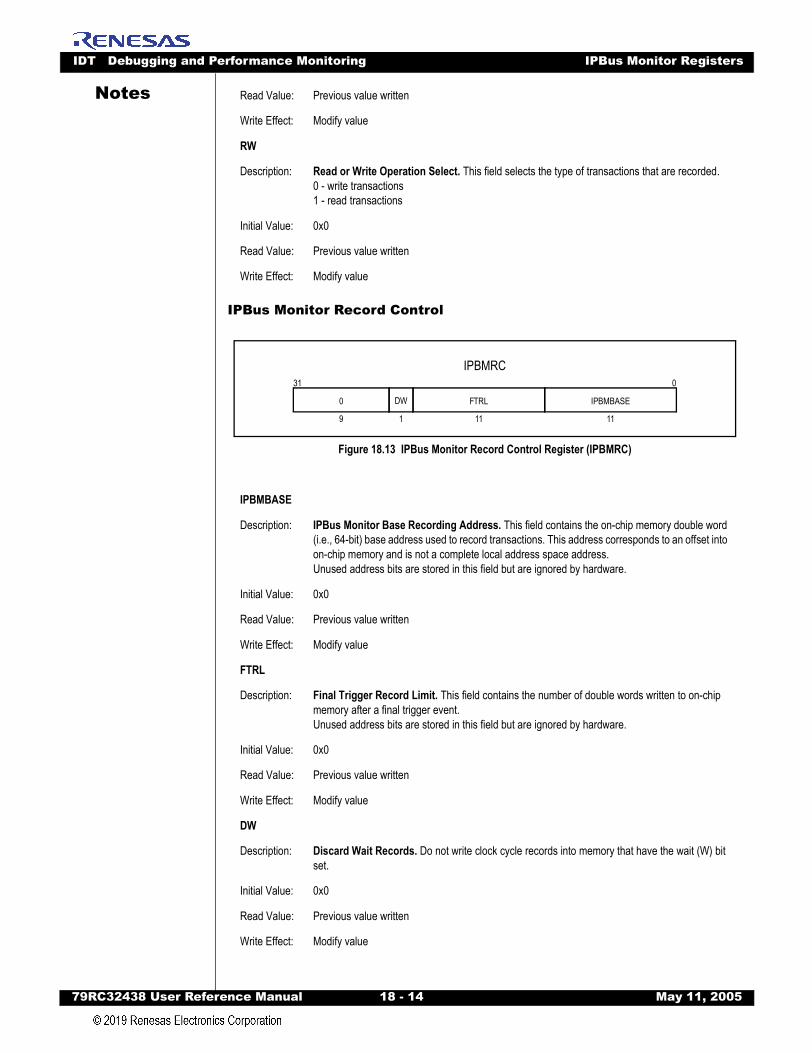
IDT Debugging and Performance Monitoring IPBus Monitor Registers
79RC32438 User Refer
Notes
IPBus Monitor Record Control
Figure 18.13 IPBus Monitor Record Control Register (IPBMRC)
Read Value: Previous value written
Write Effect: Modify value
RW
Description: Read or Write Operation Select. This field selects the type of transactions that are recorded.0 - write transactions1 - read transactions
Initial Value: 0x0
Read Value: Previous value written
Write Effect: Modify value
IPBMBASE
Description: IPBus Monitor Base Recording Address. This field contains the on-chip memory double word (i.e., 64-bit) base address used to record transactions. This address corresponds to an offset into on-chip memory and is not a complete local address space address.Unused address bits are stored in this field but are ignored by hardware.
Initial Value: 0x0
Read Value: Previous value written
Write Effect: Modify value
FTRL
Description: Final Trigger Record Limit. This field contains the number of double words written to on-chip memory after a final trigger event.Unused address bits are stored in this field but are ignored by hardware.
Initial Value: 0x0
Read Value: Previous value written
Write Effect: Modify value
DW
Description: Discard Wait Records. Do not write clock cycle records into memory that have the wait (W) bit set.
Initial Value: 0x0
Read Value: Previous value written
Write Effect: Modify value
IPBMRC031
IPBMBASE
11
FTRL
11
0
9
DW
1
ence Manual 18 - 14 May 11, 2005
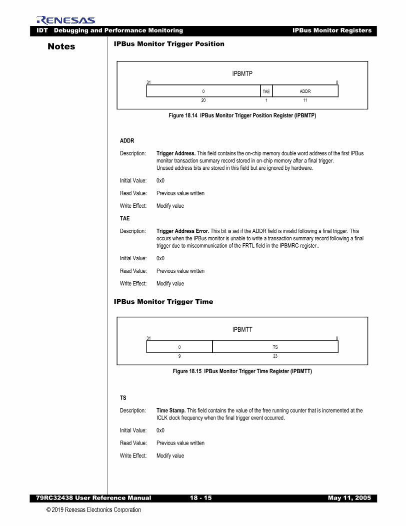
IDT Debugging and Performance Monitoring IPBus Monitor Registers
79RC32438 User Refer
Notes
IPBus Monitor Trigger PositionFigure 18.14 IPBus Monitor Trigger Position Register (IPBMTP)
IPBus Monitor Trigger Time
Figure 18.15 IPBus Monitor Trigger Time Register (IPBMTT)
ADDR
Description: Trigger Address. This field contains the on-chip memory double word address of the first IPBus monitor transaction summary record stored in on-chip memory after a final trigger.Unused address bits are stored in this field but are ignored by hardware.
Initial Value: 0x0
Read Value: Previous value written
Write Effect: Modify value
TAE
Description: Trigger Address Error. This bit is set if the ADDR field is invalid following a final trigger. This occurs when the IPBus monitor is unable to write a transaction summary record following a final trigger due to miscommunication of the FRTL field in the IPBMRC register..
Initial Value: 0x0
Read Value: Previous value written
Write Effect: Modify value
TS
Description: Time Stamp. This field contains the value of the free running counter that is incremented at the ICLK clock frequency when the final trigger event occurred.
Initial Value: 0x0
Read Value: Previous value written
Write Effect: Modify value
IPBMTP031
ADDR
11
0
20
TAE
1
IPBMTT031
TS
23
0
9
ence Manual 18 - 15 May 11, 2005
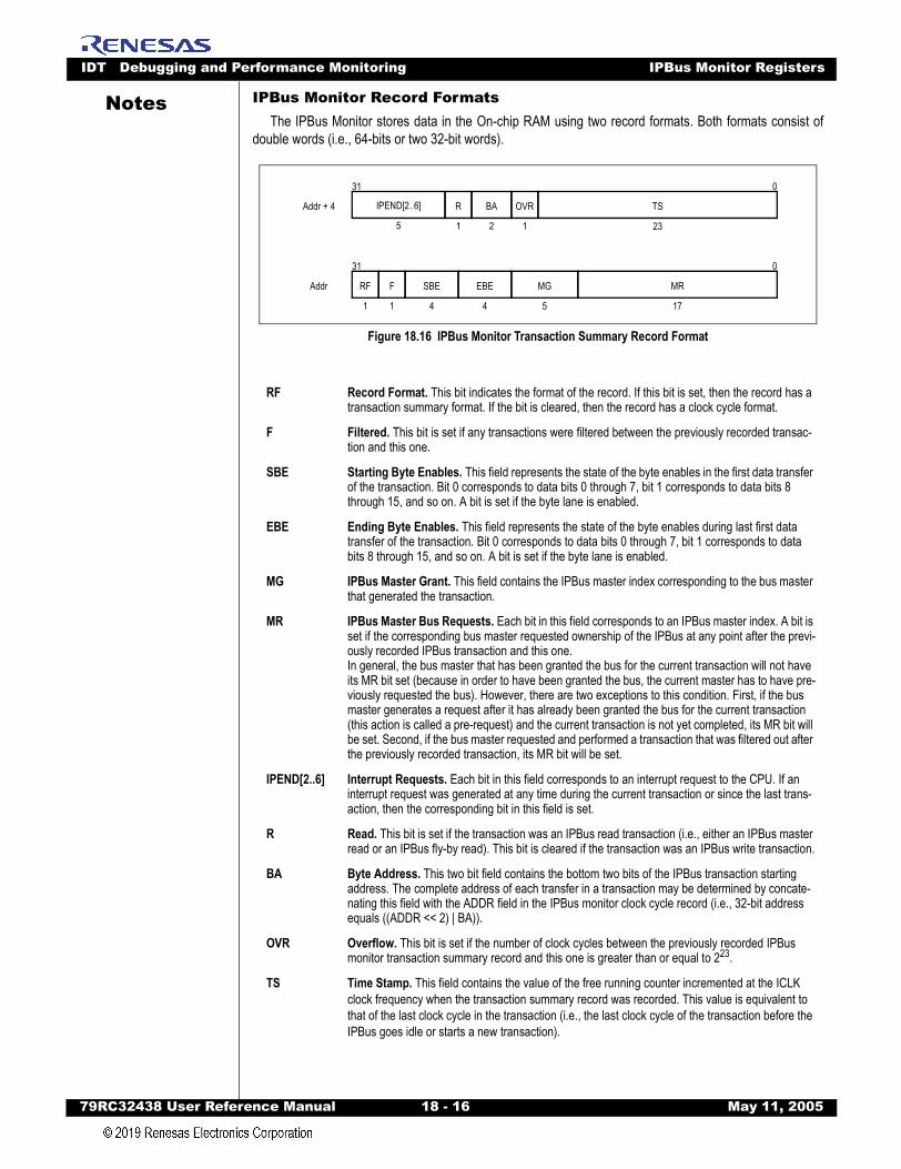
IDT Debugging and Performance Monitoring IPBus Monitor Registers
79RC32438 User Refer
Notes
IPBus Monitor Record FormatsThe IPBus Monitor stores data in the On-chip RAM using two record formats. Both formats consist ofdouble words (i.e., 64-bits or two 32-bit words).
Figure 18.16 IPBus Monitor Transaction Summary Record Format
RF Record Format. This bit indicates the format of the record. If this bit is set, then the record has a transaction summary format. If the bit is cleared, then the record has a clock cycle format.
F Filtered. This bit is set if any transactions were filtered between the previously recorded transac-tion and this one.
SBE Starting Byte Enables. This field represents the state of the byte enables in the first data transfer of the transaction. Bit 0 corresponds to data bits 0 through 7, bit 1 corresponds to data bits 8 through 15, and so on. A bit is set if the byte lane is enabled.
EBE Ending Byte Enables. This field represents the state of the byte enables during last first data transfer of the transaction. Bit 0 corresponds to data bits 0 through 7, bit 1 corresponds to data bits 8 through 15, and so on. A bit is set if the byte lane is enabled.
MG IPBus Master Grant. This field contains the IPBus master index corresponding to the bus master that generated the transaction.
MR IPBus Master Bus Requests. Each bit in this field corresponds to an IPBus master index. A bit is set if the corresponding bus master requested ownership of the IPBus at any point after the previ-ously recorded IPBus transaction and this one. In general, the bus master that has been granted the bus for the current transaction will not have its MR bit set (because in order to have been granted the bus, the current master has to have pre-viously requested the bus). However, there are two exceptions to this condition. First, if the bus master generates a request after it has already been granted the bus for the current transaction (this action is called a pre-request) and the current transaction is not yet completed, its MR bit will be set. Second, if the bus master requested and performed a transaction that was filtered out after the previously recorded transaction, its MR bit will be set.
IPEND[2..6] Interrupt Requests. Each bit in this field corresponds to an interrupt request to the CPU. If an interrupt request was generated at any time during the current transaction or since the last trans-action, then the corresponding bit in this field is set.
R Read. This bit is set if the transaction was an IPBus read transaction (i.e., either an IPBus master read or an IPBus fly-by read). This bit is cleared if the transaction was an IPBus write transaction.
BA Byte Address. This two bit field contains the bottom two bits of the IPBus transaction starting address. The complete address of each transfer in a transaction may be determined by concate-nating this field with the ADDR field in the IPBus monitor clock cycle record (i.e., 32-bit address equals ((ADDR << 2) | BA)).
OVR Overflow. This bit is set if the number of clock cycles between the previously recorded IPBus monitor transaction summary record and this one is greater than or equal to 223.
TS Time Stamp. This field contains the value of the free running counter incremented at the ICLK clock frequency when the transaction summary record was recorded. This value is equivalent to that of the last clock cycle in the transaction (i.e., the last clock cycle of the transaction before the IPBus goes idle or starts a new transaction).
031
RF
1
F
1
SBE
4
EBE
4
MG
5
MR
17
IPEND[2..6]
5
TS
23
031
Addr + 4
Addr
R
1
BA
2
OVR
1
ence Manual 18 - 16 May 11, 2005
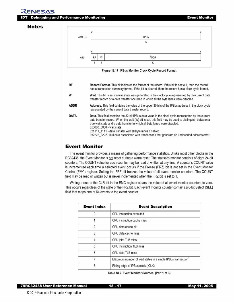
IDT Debugging and Performance Monitoring Event Monitor
79RC32438 User Refer
Notes
Figure 18.17 IPBus Monitor Clock Cycle Record Format
Event MonitorThe event monitor provides a means of gathering performance statistics. Unlike most other blocks in the
RC32438, the Event Monitor is not reset during a warm reset. The statistics monitor consists of eight 24-bitcounters. The COUNT value for each counter may be read or written at any time. A counter’s COUNT valueis incremented each time a selected event occurs if the Freeze (FRZ) bit is not set in the Event MonitorControl (EMC) register. Setting the FRZ bit freezes the value of all event monitor counters. The COUNTfield may be read or written but is never incremented when the FRZ bit is set to 1.
Writing a one to the CLR bit in the EMC register clears the value of all event monitor counters to zero.This occurs regardless of the state of the FRZ bit. Each event monitor counter contains a 6-bit Select (SEL)field that maps one of 64 events to the event counter.
RF Record Format. This bit indicates the format of the record. If this bit is set to 1, then the record has a transaction summary format. If the bit is cleared, then the record has a clock cycle format.
W Wait. This bit is set if a wait state was generated in the clock cycle represented by the current data transfer record or a data transfer occurred in which all the byte lanes were disabled.
ADDR Address. This field contains the value of the upper 30 bits of the IPBus address in the clock cycle represented by the current data transfer record.
DATA Data. This field contains the 32-bit IPBus data value in the clock cycle represented by the current data transfer record. When the wait (W) bit is set, this field may be used to distinguish between a true wait state and a data transfer in which all byte lanes were disabled.0x0000_0000 - wait state0x1111_1111 - data transfer with all byte lanes disabled0x2222_2222 - null data associated with transactions that generate an undecoded address error.
Event Index Event Description
0 CPU instruction executed
1 CPU instruction cache miss
2 CPU data cache hit
3 CPU data cache miss
4 CPU joint TLB miss
5 CPU instruction TLB miss
6 CPU data TLB miss
7 Maximum number of wait states in a single IPBus transaction1
8 Rising edge of IPBus clock (ICLK)
Table 18.2 Event Monitor Sources (Part 1 of 3)
031
RF
1
W
1
ADDR
30
DATA
32
031
Addr + 4
Addr
ence Manual 18 - 17 May 11, 2005
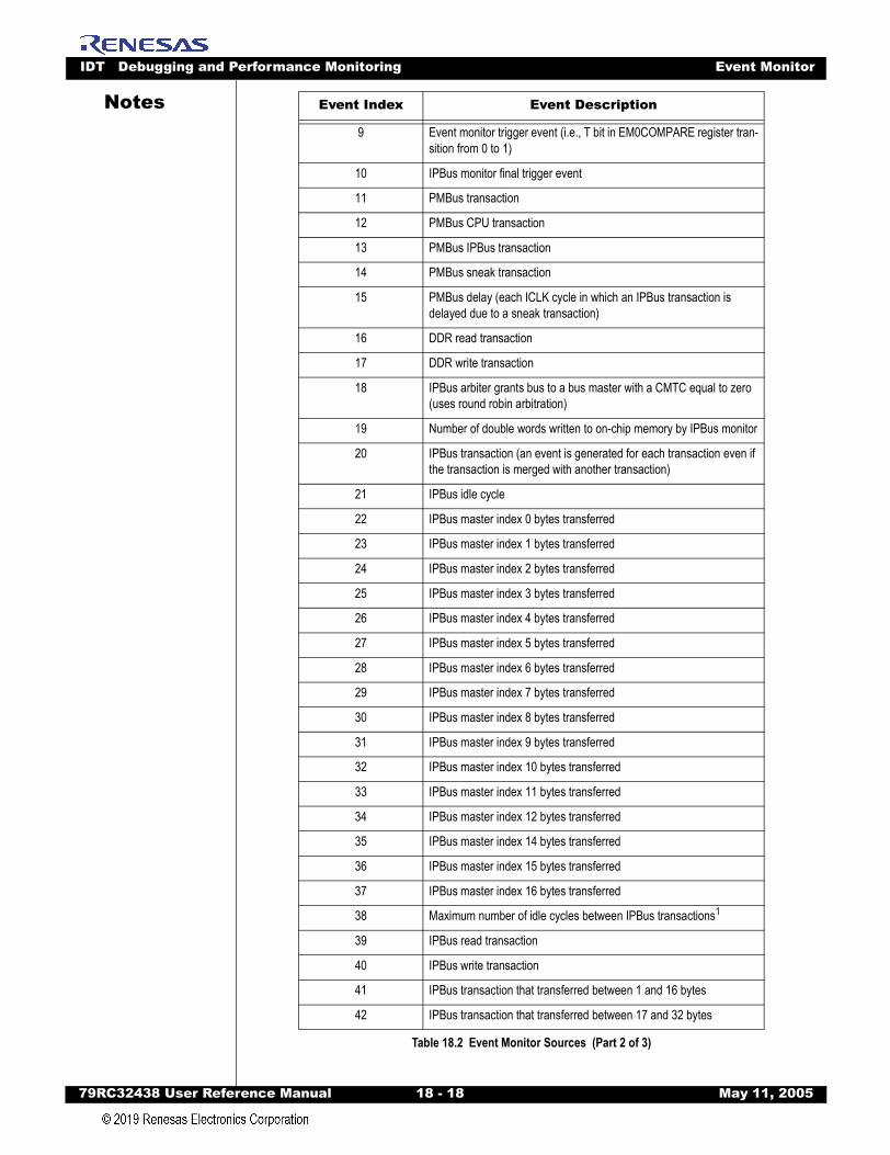
IDT Debugging and Performance Monitoring Event Monitor
79RC32438 User Refer
Notes
9 Event monitor trigger event (i.e., T bit in EM0COMPARE register tran-sition from 0 to 1)
10 IPBus monitor final trigger event
11 PMBus transaction
12 PMBus CPU transaction
13 PMBus IPBus transaction
14 PMBus sneak transaction
15 PMBus delay (each ICLK cycle in which an IPBus transaction is delayed due to a sneak transaction)
16 DDR read transaction
17 DDR write transaction
18 IPBus arbiter grants bus to a bus master with a CMTC equal to zero (uses round robin arbitration)
19 Number of double words written to on-chip memory by IPBus monitor
20 IPBus transaction (an event is generated for each transaction even if the transaction is merged with another transaction)
21 IPBus idle cycle
22 IPBus master index 0 bytes transferred
23 IPBus master index 1 bytes transferred
24 IPBus master index 2 bytes transferred
25 IPBus master index 3 bytes transferred
26 IPBus master index 4 bytes transferred
27 IPBus master index 5 bytes transferred
28 IPBus master index 6 bytes transferred
29 IPBus master index 7 bytes transferred
30 IPBus master index 8 bytes transferred
31 IPBus master index 9 bytes transferred
32 IPBus master index 10 bytes transferred
33 IPBus master index 11 bytes transferred
34 IPBus master index 12 bytes transferred
35 IPBus master index 14 bytes transferred
36 IPBus master index 15 bytes transferred
37 IPBus master index 16 bytes transferred
38 Maximum number of idle cycles between IPBus transactions1
39 IPBus read transaction
40 IPBus write transaction
41 IPBus transaction that transferred between 1 and 16 bytes
42 IPBus transaction that transferred between 17 and 32 bytes
Event Index Event Description
Table 18.2 Event Monitor Sources (Part 2 of 3)
ence Manual 18 - 18 May 11, 2005
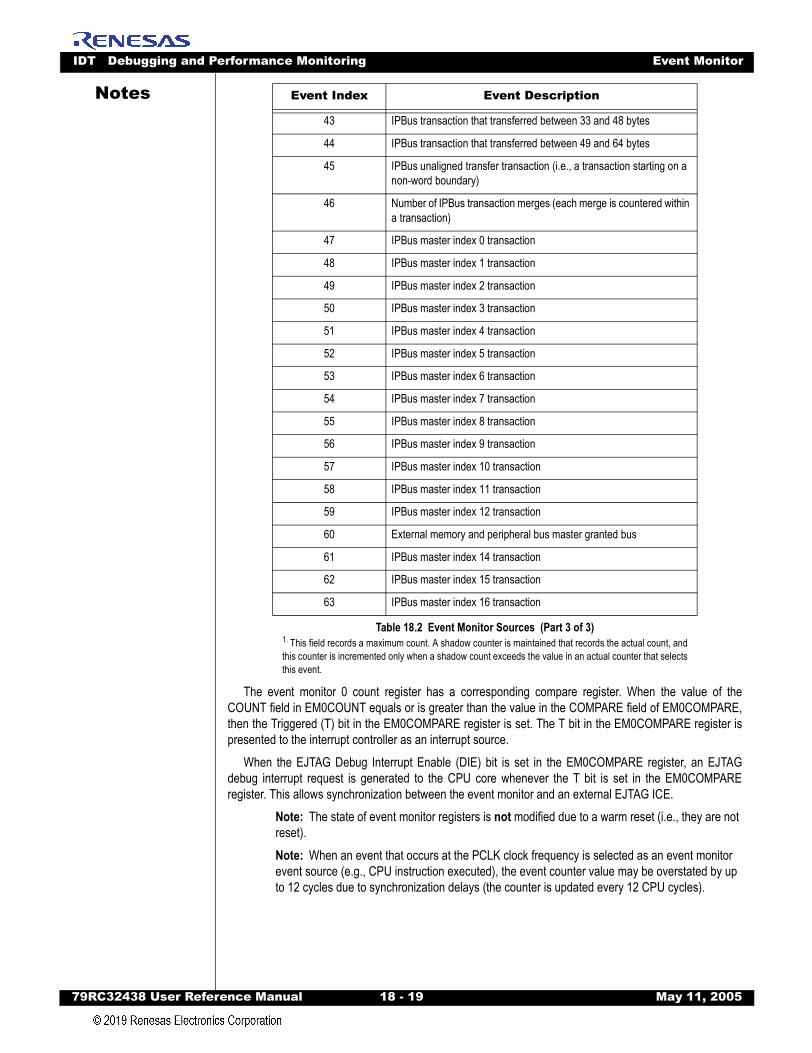
IDT Debugging and Performance Monitoring Event Monitor
79RC32438 User Refer
Notes
The event monitor 0 count register has a corresponding compare register. When the value of theCOUNT field in EM0COUNT equals or is greater than the value in the COMPARE field of EM0COMPARE,then the Triggered (T) bit in the EM0COMPARE register is set. The T bit in the EM0COMPARE register ispresented to the interrupt controller as an interrupt source.
When the EJTAG Debug Interrupt Enable (DIE) bit is set in the EM0COMPARE register, an EJTAGdebug interrupt request is generated to the CPU core whenever the T bit is set in the EM0COMPAREregister. This allows synchronization between the event monitor and an external EJTAG ICE.
Note: The state of event monitor registers is not modified due to a warm reset (i.e., they are not reset).Note: When an event that occurs at the PCLK clock frequency is selected as an event monitor event source (e.g., CPU instruction executed), the event counter value may be overstated by up to 12 cycles due to synchronization delays (the counter is updated every 12 CPU cycles).
43 IPBus transaction that transferred between 33 and 48 bytes
44 IPBus transaction that transferred between 49 and 64 bytes
45 IPBus unaligned transfer transaction (i.e., a transaction starting on a non-word boundary)
46 Number of IPBus transaction merges (each merge is countered within a transaction)
47 IPBus master index 0 transaction
48 IPBus master index 1 transaction
49 IPBus master index 2 transaction
50 IPBus master index 3 transaction
51 IPBus master index 4 transaction
52 IPBus master index 5 transaction
53 IPBus master index 6 transaction
54 IPBus master index 7 transaction
55 IPBus master index 8 transaction
56 IPBus master index 9 transaction
57 IPBus master index 10 transaction
58 IPBus master index 11 transaction
59 IPBus master index 12 transaction
60 External memory and peripheral bus master granted bus
61 IPBus master index 14 transaction
62 IPBus master index 15 transaction
63 IPBus master index 16 transaction
1. This field records a maximum count. A shadow counter is maintained that records the actual count, andthis counter is incremented only when a shadow count exceeds the value in an actual counter that selectsthis event.
Event Index Event Description
Table 18.2 Event Monitor Sources (Part 3 of 3)
ence Manual 18 - 19 May 11, 2005

IDT Debugging and Performance Monitoring Event Monitor
79RC32438 User Refer
Notes
Event Monitor Control RegisterFigure 18.18 Event Monitor Control Register (EMC)
Event Monitor [0..7] Count Register
Figure 18.19 Event Monitor [0..7] Count Register (EM[0..7]COUNT)
FRZ
Description: Freeze. When this bit is set to zero (cleared), event monitor count registers are incremented when the selected event occurs. When this bit is set to one, events are ignored and the event monitor count registers remain “frozen.”
Initial Value: 0x1
Read Value: Previous value written
Write Effect: Modify value
CLR
Description: Clear Counters. Writing a one to this bit causes the COUNT field in all Event Monitor [0..7] Count (EM[0..7]COUNT) registers to be set to zero (cleared).
Initial Value: 0x0
Read Value: 0x0
Write Effect: Writing a one clears all event monitor counters, writing a zero has no effect
ZOR
Description: Zero On Read. When this bit is set to one, reading an event monitor count (EMxCOUNT) regis-ter causes it to be automatically cleared as a side effect of the read. Note: zero on read works only when the FRZ bit is not set to 1.
Initial Value: 0x0
Read Value: Previous value written
Write Effect: Modify value
EMC031
0
29
FRZ
1
CLR
1
ZOR
1
EM[0..7]COUNT031
6
SEL
24
COUNT
1
0
1
OVR
ence Manual 18 - 20 May 11, 2005
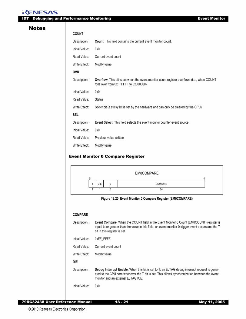
IDT Debugging and Performance Monitoring Event Monitor
79RC32438 User Refer
Notes
Event Monitor 0 Compare Register
Figure 18.20 Event Monitor 0 Compare Register (EM0COMPARE)
COUNT
Description: Count. This field contains the current event monitor count.
Initial Value: 0x0
Read Value: Current event count
Write Effect: Modify value
OVR
Description: Overflow. This bit is set when the event monitor count register overflows (i.e., when COUNT rolls over from 0xFFFFFF to 0x000000).
Initial Value: 0x0
Read Value: Status
Write Effect: Sticky bit (a sticky bit is set by the hardware and can only be cleared by the CPU)
SEL
Description: Event Select. This field selects the event monitor counter event source.
Initial Value: 0x0
Read Value: Previous value written
Write Effect: Modify value
COMPARE
Description: Event Compare. When the COUNT field in the Event Monitor 0 Count (EM0COUNT) register is equal to or greater than the value in this field, an event monitor 0 trigger event occurs and the T bit in this register is set.
Initial Value: 0xFF_FFFF
Read Value: Current event count
Write Effect: Modify value
DIE
Description: Debug Interrupt Enable. When this bit is set to 1, an EJTAG debug interrupt request is gener-ated to the CPU core whenever the T bit is set. This allows synchronization between the event monitor and an external EJTAG ICE.
Initial Value: 0x0
EM0COMPARE031
24
COMPARE
6
0T
1
DIE
1
ence Manual 18 - 21 May 11, 2005
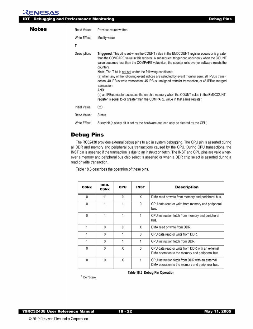
IDT Debugging and Performance Monitoring Debug Pins
79RC32438 User Refer
Notes
Debug PinsThe RC32438 provides external debug pins to aid in system debugging. The CPU pin is asserted during
all DDR and memory and peripheral bus transactions caused by the CPU. During CPU transactions, theINST pin is asserted if the transaction is due to an instruction fetch. The INST and CPU pins are valid when-ever a memory and peripheral bus chip select is asserted or when a DDR chip select is asserted during aread or write transaction.
Table 18.3 describes the operation of these pins.
Read Value: Previous value written
Write Effect: Modify value
T
Description: Triggered. This bit is set when the COUNT value in the EM0COUNT register equals or is greater than the COMPARE value in this register. A subsequent trigger can occur only when the COUNT value becomes less than the COMPARE value (i.e., the counter rolls over or software resets the counter).Note: The T bit is not set under the following conditions:(a) when any of the following event indices are selected by event monitor zero: 20 IPBus trans-action, 40 IPBus write transaction, 45 IPBus unaligned transfer transaction, or 46 IPBus merged transaction AND(b) an IPBus master accesses the on-chip memory when the COUNT value in the EM0COUNT register is equal to or greater than the COMPARE value in that same register.
Initial Value: 0x0
Read Value: Status
Write Effect: Sticky bit (a sticky bit is set by the hardware and can only be cleared by the CPU)
CSNx DDR-CSNx CPU INST Description
0 11
1. Don’t care.
0 X DMA read or write from memory and peripheral bus.
0 1 1 0 CPU data read or write from memory and peripheral bus.
0 1 1 1 CPU instruction fetch from memory and peripheral bus.
1 0 0 X DMA read or write from DDR.
1 0 1 0 CPU data read or write from DDR.
1 0 1 1 CPU instruction fetch from DDR.
0 0 X 0 CPU data read or write from DDR with an external DMA operation to the memory and peripheral bus.
0 0 X 1 CPU instruction fetch from DDR with an external DMA operation to the memory and peripheral bus.
Table 18.3 Debug Pin Operation
ence Manual 18 - 22 May 11, 2005
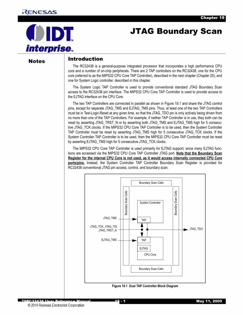
Notes
79RC32438 User Reference Manual 19 - 1 M
Chapter 19
JTAG Boundary Scan
IntroductionThe RC32438 is a general-purpose integrated processor that incorporates a high performance CPU
core and a number of on-chip peripherals. There are 2 TAP controllers on the RC32438, one for the CPUcore (referred to as the MIPS32 CPU Core TAP Controller), described in the next chapter (Chapter 20), andone for System Logic controller, described in this chapter.
The System Logic TAP Controller is used to provide conventional standard JTAG Boundary Scanaccess to the RC32438 pin interface. The MIPS32 CPU Core TAP Controller is used to provide access tothe EJTAG interface on the CPU Core.
The two TAP Controllers are connected in parallel as shown in Figure 19.1 and share the JTAG controlpins, except for separate JTAG_TMS and EJTAG_TMS pins. Thus, at least one of the two TAP Controllersmust be in Test-Logic-Reset at any given time, so that the JTAG_TDO pin is only actively being driven fromno more than one of the TAP Controllers. For example, if neither TAP Controller is in use, they both can bereset by asserting JTAG_TRST_N or by asserting both JTAG_TMS and EJTAG_TMS high for 5 consecu-tive JTAG_TCK clocks. If the MIPS32 CPU Core TAP Controller is to be used, then the System ControllerTAP Controller must be reset by asserting JTAG_TMS high for 5 consecutive JTAG_TCK clocks. If theSystem Controller TAP Controller is to be used, then the MIPS32 CPU Core TAP Controller must be resetby asserting EJTAG_TMS high for 5 consecutive JTAG_TCK clocks.
The MIPS32 CPU Core TAP Controller is used primarily for EJTAG support, since many EJTAG func-tions are accessed via the MIPS32 CPU Core TAP Controller JTAG port. Note that the Boundary ScanRegister for the internal CPU Core is not used, as it would access internally connected CPU Coreports/pins. Instead, the System Controller TAP Controller Boundary Scan Register is provided forRC32438 conventional JTAG pin access, control, and boundary scan.
Figure 19.1 Dual TAP Controller Block Diagram
Boundary Scan Cells
System Controller
TAP
CPU Core
TAP
EJTAG
JTAG_TCK, JTAG_TDI,
JTAG_TMS
EJTAG_TMS
JTAG_TDO
Boundary Scan Cells
Boun
dary
Sca
n Ce
lls
Boun
dary
Sca
n Ce
lls
JTAG_TRST_N
ay 11, 2005
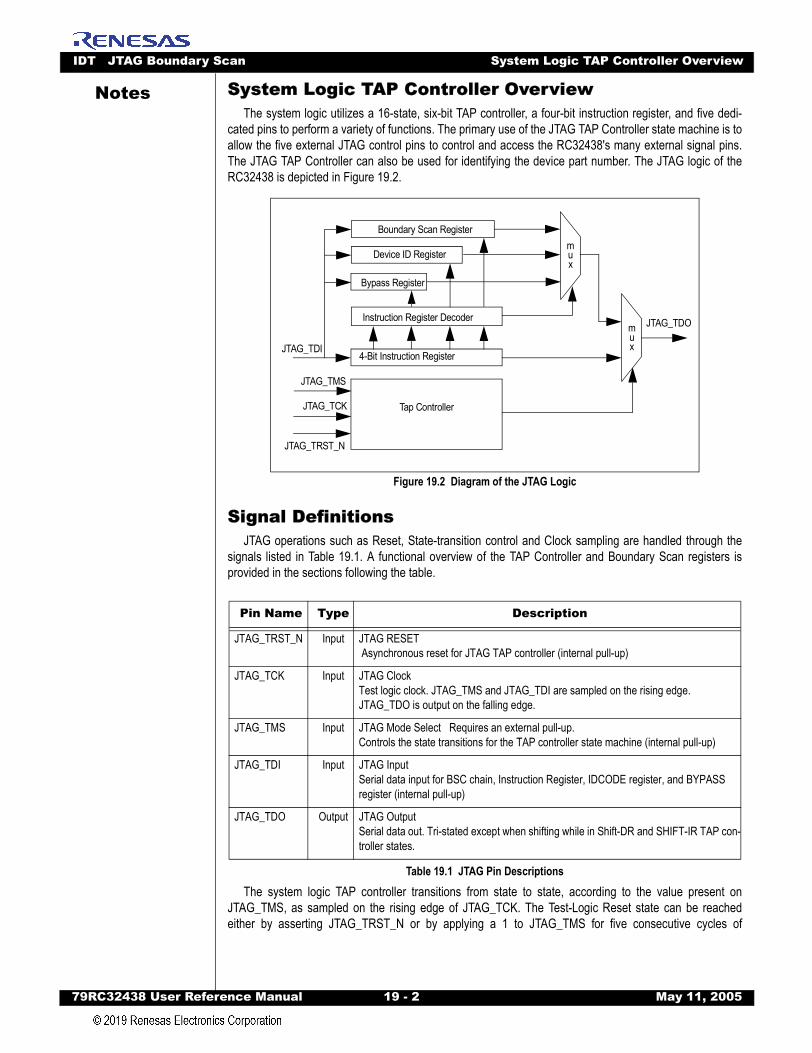
IDT JTAG Boundary Scan System Logic TAP Controller Overview
79RC32438 User Refer
Notes
System Logic TAP Controller OverviewThe system logic utilizes a 16-state, six-bit TAP controller, a four-bit instruction register, and five dedi-cated pins to perform a variety of functions. The primary use of the JTAG TAP Controller state machine is toallow the five external JTAG control pins to control and access the RC32438's many external signal pins.The JTAG TAP Controller can also be used for identifying the device part number. The JTAG logic of theRC32438 is depicted in Figure 19.2.
Figure 19.2 Diagram of the JTAG Logic
Signal DefinitionsJTAG operations such as Reset, State-transition control and Clock sampling are handled through the
signals listed in Table 19.1. A functional overview of the TAP Controller and Boundary Scan registers isprovided in the sections following the table.
The system logic TAP controller transitions from state to state, according to the value present onJTAG_TMS, as sampled on the rising edge of JTAG_TCK. The Test-Logic Reset state can be reachedeither by asserting JTAG_TRST_N or by applying a 1 to JTAG_TMS for five consecutive cycles of
Pin Name Type Description
JTAG_TRST_N Input JTAG RESET Asynchronous reset for JTAG TAP controller (internal pull-up)
JTAG_TCK Input JTAG ClockTest logic clock. JTAG_TMS and JTAG_TDI are sampled on the rising edge. JTAG_TDO is output on the falling edge.
JTAG_TMS Input JTAG Mode Select Requires an external pull-up.Controls the state transitions for the TAP controller state machine (internal pull-up)
JTAG_TDI Input JTAG InputSerial data input for BSC chain, Instruction Register, IDCODE register, and BYPASS register (internal pull-up)
JTAG_TDO Output JTAG OutputSerial data out. Tri-stated except when shifting while in Shift-DR and SHIFT-IR TAP con-troller states.
Table 19.1 JTAG Pin Descriptions
Bypass Register
Instruction Register Decoder
4-Bit Instruction Register
Tap Controller
mux
mux
Device ID Register
Boundary Scan Register
JTAG_TDI
JTAG_TMS
JTAG_TCK
JTAG_TRST_N
JTAG_TDO
ence Manual 19 - 2 May 11, 2005
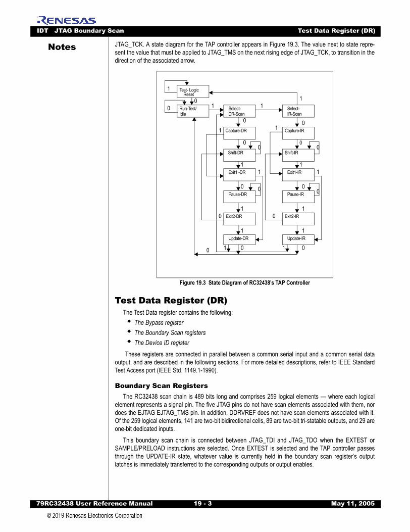
IDT JTAG Boundary Scan Test Data Register (DR)
79RC32438 User Refer
Notes
JTAG_TCK. A state diagram for the TAP controller appears in Figure 19.3. The value next to state repre-sent the value that must be applied to JTAG_TMS on the next rising edge of JTAG_TCK, to transition in thedirection of the associated arrow.Figure 19.3 State Diagram of RC32438’s TAP Controller
Test Data Register (DR)The Test Data register contains the following:
The Bypass registerThe Boundary Scan registers The Device ID register
These registers are connected in parallel between a common serial input and a common serial dataoutput, and are described in the following sections. For more detailed descriptions, refer to IEEE StandardTest Access port (IEEE Std. 1149.1-1990).
Boundary Scan RegistersThe RC32438 scan chain is 489 bits long and comprises 259 logical elements — where each logical
element represents a signal pin. The five JTAG pins do not have scan elements associated with them, nordoes the EJTAG EJTAG_TMS pin. In addition, DDRVREF does not have scan elements associated with it.Of the 259 logical elements, 141 are two-bit bidirectional cells, 89 are two-bit tri-statable outputs, and 29 areone-bit dedicated inputs.
This boundary scan chain is connected between JTAG_TDI and JTAG_TDO when the EXTEST orSAMPLE/PRELOAD instructions are selected. Once EXTEST is selected and the TAP controller passesthrough the UPDATE-IR state, whatever value is currently held in the boundary scan register’s outputlatches is immediately transferred to the corresponding outputs or output enables.
Test- LogicReset
Run-Test/Idle
Select-DR-Scan
Capture-DR
Shift-DR
Exit1 -DR
Pause-DR
Exit2-DR
Select-IR-Scan
Capture-IR
Shift-IR
Exit1-IR
Pause-IR
Exit2-IR
Update-DR Update-IR
1 10 00
11
0
0
1
1
01
0
1
0
0
1
1
1
00
1 1
0
1
0
1
1
0
0 0
0
ence Manual 19 - 3 May 11, 2005
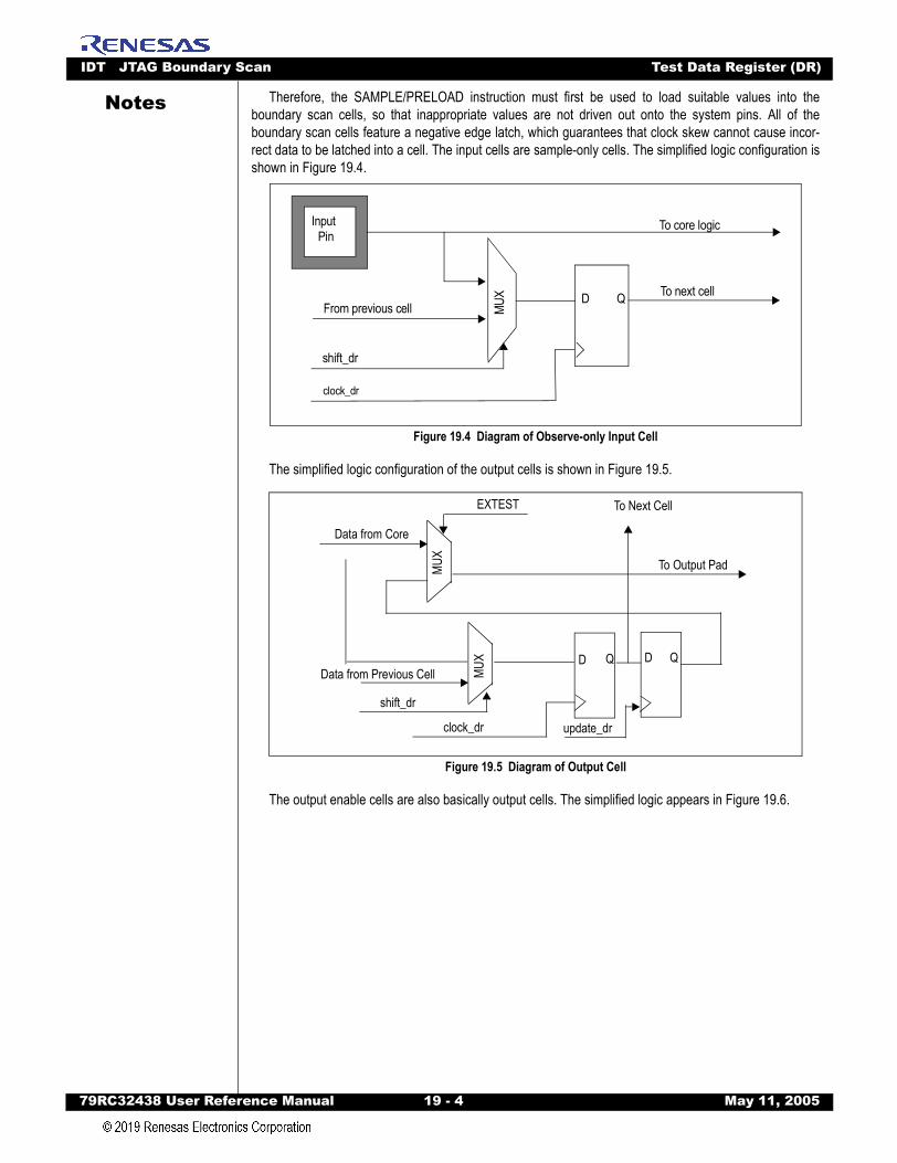
IDT JTAG Boundary Scan Test Data Register (DR)
79RC32438 User Refer
Notes
Therefore, the SAMPLE/PRELOAD instruction must first be used to load suitable values into theboundary scan cells, so that inappropriate values are not driven out onto the system pins. All of theboundary scan cells feature a negative edge latch, which guarantees that clock skew cannot cause incor-rect data to be latched into a cell. The input cells are sample-only cells. The simplified logic configuration isshown in Figure 19.4.Figure 19.4 Diagram of Observe-only Input Cell
The simplified logic configuration of the output cells is shown in Figure 19.5.
Figure 19.5 Diagram of Output Cell
The output enable cells are also basically output cells. The simplified logic appears in Figure 19.6.
InputPin
shift_dr
From previous cell
clock_dr
D Q To next cell
To core logic
MUX
Data from Core
Data from Previous Cell
shift_dr
To Next Cell
To Output Pad
clock_dr update_dr
MUX
D Q D Q
EXTEST
MUX
ence Manual 19 - 4 May 11, 2005
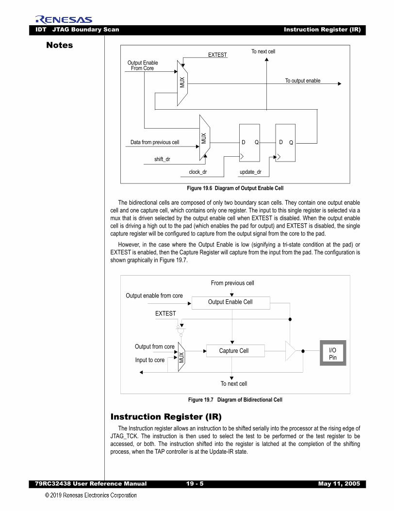
IDT JTAG Boundary Scan Instruction Register (IR)
79RC32438 User Refer
Notes
Figure 19.6 Diagram of Output Enable Cell
The bidirectional cells are composed of only two boundary scan cells. They contain one output enablecell and one capture cell, which contains only one register. The input to this single register is selected via amux that is driven selected by the output enable cell when EXTEST is disabled. When the output enablecell is driving a high out to the pad (which enables the pad for output) and EXTEST is disabled, the singlecapture register will be configured to capture from the output signal from the core to the pad.
However, in the case where the Output Enable is low (signifying a tri-state condition at the pad) orEXTEST is enabled, then the Capture Register will capture from the input from the pad. The configuration isshown graphically in Figure 19.7.
Figure 19.7 Diagram of Bidirectional Cell
Instruction Register (IR)The Instruction register allows an instruction to be shifted serially into the processor at the rising edge of
JTAG_TCK. The instruction is then used to select the test to be performed or the test register to beaccessed, or both. The instruction shifted into the register is latched at the completion of the shiftingprocess, when the TAP controller is at the Update-IR state.
D Q D Q
From Core
Data from previous cell
EXTEST
To output enable
clock_dr
shift_dr
update_dr
Output Enable
To next cell
MUX
MUX
From previous cell
Output Enable CellOutput enable from core
EXTEST
Output from core
Input to coreCapture Cell
To next cell
I/OPinMU
X
ence Manual 19 - 5 May 11, 2005
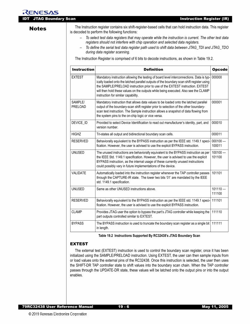
IDT JTAG Boundary Scan Instruction Register (IR)
79RC32438 User Refer
Notes
The Instruction register contains six shift-register-based cells that can hold instruction data. This registeris decoded to perform the following functions:– To select test data registers that may operate while the instruction is current. The other test dataregisters should not interfere with chip operation and selected data registers.
– To define the serial test data register path used to shift data between JTAG_TDI and JTAG_TDOduring data register scanning.
The Instruction Register is comprised of 6 bits to decode instructions, as shown in Table 19.2.
EXTESTThe external test (EXTEST) instruction is used to control the boundary scan register, once it has been
initialized using the SAMPLE/PRELOAD instruction. Using EXTEST, the user can then sample inputs fromor load values onto the external pins of the RC32438. Once this instruction is selected, the user then usesthe SHIFT-DR TAP controller state to shift values into the boundary scan chain. When the TAP controllerpasses through the UPDATE-DR state, these values will be latched onto the output pins or into the outputenables.
Instruction Definition Opcode
EXTEST Mandatory instruction allowing the testing of board level interconnections. Data is typ-ically loaded onto the latched parallel outputs of the boundary scan shift register using the SAMPLE/PRELOAD instruction prior to use of the EXTEST instruction. EXTEST will then hold these values on the outputs while being executed. Also see the CLAMP instruction for similar capability.
000000
SAMPLE/PRELOAD
Mandatory instruction that allows data values to be loaded onto the latched parallel output of the boundary-scan shift register prior to selection of the other boundary-scan test instruction. The Sample instruction allows a snapshot of data flowing from the system pins to the on-chip logic or vice versa.
000001
DEVICE_ID Provided to select Device Identification to read out manufacturer’s identity, part, and version number.
000010
HIGHZ Tri-states all output and bidirectional boundary scan cells. 000011
RESERVED Behaviorally equivalent to the BYPASS instruction as per the IEEE std. 1149.1 speci-fication. However, the user is advised to use the explicit BYPASS instruction.
000100 — 100011
UNUSED The unused instructions are behaviorally equivalent to the BYPASS instruction as per the IEEE Std. 1149.1 specification. However, the user is advised to use the explicit BYPASS instruction, as the internal usage of these currently unused instructions could possibly vary in future implementations of the device.
100100 — 101100
VALIDATE Automatically loaded into the instruction register whenever the TAP controller passes through the CAPTURE-IR state. The lower two bits ’01’ are mandated by the IEEE std. 1149.1 specification.
101101
UNUSED Same as other UNUSED instructions above. 101110 — 111100
RESERVED Behaviorally equivalent to the BYPASS instruction as per the IEEE std. 1149.1 speci-fication. However, the user is advised to use the explicit BYPASS instruction.
111101
CLAMP Provides JTAG user the option to bypass the part’s JTAG controller while keeping the part outputs controlled similar to EXTEST.
111110
BYPASS The BYPASS instruction is used to truncate the boundary scan register as a single bit in length.
111111
Table 19.2 Instructions Supported By RC32438’s JTAG Boundary Scan
ence Manual 19 - 6 May 11, 2005
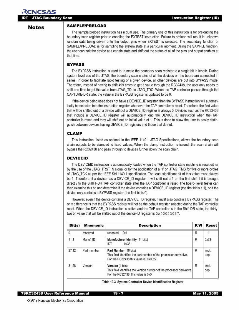
IDT JTAG Boundary Scan Instruction Register (IR)
79RC32438 User Refer
Notes
SAMPLE/PRELOADThe sample/preload instruction has a dual use. The primary use of this instruction is for preloading theboundary scan register prior to enabling the EXTEST instruction. Failure to preload will result in unknownrandom data being driven onto the output pins when EXTEST is selected. The secondary function ofSAMPLE/PRELOAD is for sampling the system state at a particular moment. Using the SAMPLE function,the user can halt the device at a certain state and shift out the status of all of the pins and output enables atthat time.
BYPASSThe BYPASS instruction is used to truncate the boundary scan register to a single bit in length. During
system level use of the JTAG, the boundary scan chains of all the devices on the board are connected inseries. In order to facilitate rapid testing of a given device, all other devices are put into BYPASS mode.Therefore, instead of having to shift 499 times to get a value through the RC32438, the user only needs toshift one time to get the value from JTAG_TDI to JTAG_TDO. When the TAP controller passes through theCAPTURE-DR state, the value in the BYPASS register is updated to be 0.
If the device being used does not have a DEVICE_ID register, then the BYPASS instruction will automat-ically be selected into the instruction register whenever the TAP controller is reset. Therefore, the first valuethat will be shifted out of a device without a DEVICE_ID register is always 0. Devices such as the RC32438that include a DEVICE_ID register will automatically load the DEVICE_ID instruction when the TAPcontroller is reset, and they will shift out an initial value of 1. This is done to allow the user to easily distin-guish between devices having DEVICE_ID registers and those that do not.
CLAMPThis instruction, listed as optional in the IEEE 1149.1 JTAG Specifications, allows the boundary scan
chain outputs to be clamped to fixed values. When the clamp instruction is issued, the scan chain willbypass the RC32438 and pass through to devices further down the scan chain.
DEVICEIDThe DEVICEID instruction is automatically loaded when the TAP controller state machine is reset either
by the use of the JTAG_TRST_N signal or by the application of a ‘1’ on JTAG_TMS for five or more cyclesof JTAG_TCK as per the IEEE Std 1149.1 specification. The least significant bit of this value must alwaysbe 1. Therefore, if a device has a DEVICE_ID register, it will shift out a 1 on the first shift if it is broughtdirectly to the SHIFT-DR TAP controller state after the TAP controller is reset. The board- level tester canthen examine this bit and determine if the device contains a DEVICE_ID register (the first bit is a 1), or if thedevice only contains a BYPASS register (the first bit is 0).
However, even if the device contains a DEVICE_ID register, it must also contain a BYPASS register. Theonly difference is that the BYPASS register will not be the default register selected during the TAP controllerreset. When the DEVICE_ID instruction is active and the TAP controller is in the Shift-DR state, the thirty-two bit value that will be shifted out of the device-ID register is 0x00022067.
Bit(s) Mnemonic Description R/W Reset
0 reserved reserved 0x1 R 1
11:1 Manuf_ID Manufacturer Identity (11 bits)IDT 0x33
R 0x33
27:12 Part_number Part Number (16 bits)This field identifies the part number of the processor derivative.For the RC32438 this value is: 0x0022
R impl.dep.
31:28 Version Version (4 bits)This field identifies the version number of the processor derivative.For the RC32438, this value is 0x0
R impl.dep.
Table 19.3 System Controller Device Identification Register
ence Manual 19 - 7 May 11, 2005
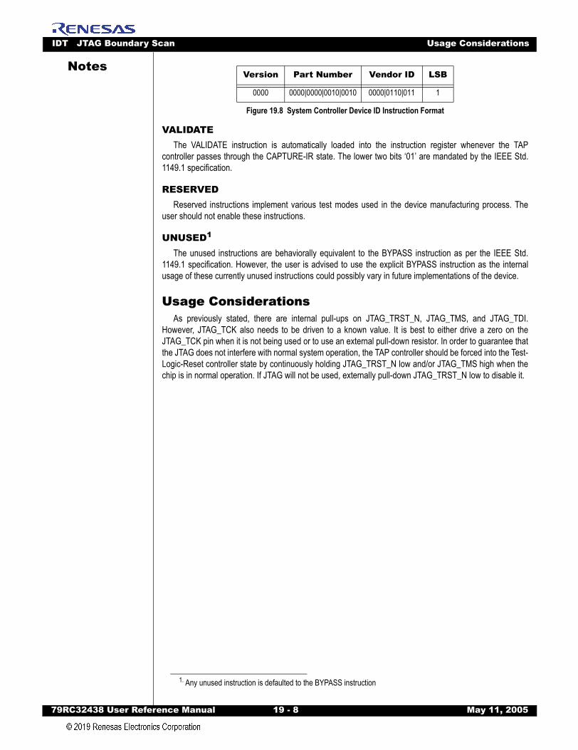
IDT JTAG Boundary Scan Usage Considerations
79RC32438 User Refer
Notes
VALIDATEThe VALIDATE instruction is automatically loaded into the instruction register whenever the TAP
controller passes through the CAPTURE-IR state. The lower two bits ‘01’ are mandated by the IEEE Std.1149.1 specification.
RESERVEDReserved instructions implement various test modes used in the device manufacturing process. The
user should not enable these instructions.
UNUSED1
The unused instructions are behaviorally equivalent to the BYPASS instruction as per the IEEE Std.1149.1 specification. However, the user is advised to use the explicit BYPASS instruction as the internalusage of these currently unused instructions could possibly vary in future implementations of the device.
Usage ConsiderationsAs previously stated, there are internal pull-ups on JTAG_TRST_N, JTAG_TMS, and JTAG_TDI.
However, JTAG_TCK also needs to be driven to a known value. It is best to either drive a zero on theJTAG_TCK pin when it is not being used or to use an external pull-down resistor. In order to guarantee thatthe JTAG does not interfere with normal system operation, the TAP controller should be forced into the Test-Logic-Reset controller state by continuously holding JTAG_TRST_N low and/or JTAG_TMS high when thechip is in normal operation. If JTAG will not be used, externally pull-down JTAG_TRST_N low to disable it.
Version Part Number Vendor ID LSB
0000 0000|0000|0010|0010 0000|0110|011 1
Figure 19.8 System Controller Device ID Instruction Format
1. Any unused instruction is defaulted to the BYPASS instruction
ence Manual 19 - 8 May 11, 2005
Notes
79RC32438 User Reference Manual 20 - 1 M
Chapter 20
EJTAG System
IntroductionThis chapter describes the behavior and organization of on-chip EJTAG hardware resources on the
RC32438 device. EJTAG is a hardware/software subsystem that provides comprehensive debugging andperformance tuning capabilities to system-on-a-chip components that include a MIPS CPU core. It exploitsthe infrastructure provided by the IEEE 1149.1 JTAG Test Access Port (TAP) standard to provide anexternal interface, and it extends the MIPS instruction set and privileged resource architectures to provide astandard software architecture for integrated system debugging.
The EJTAG probe consists of third party hardware and software that connects to the standard JTAGport. The probe will provide software drivers to handle breakpoints, single step, register inquiries, etc.
Functional DescriptionEJTAG provides a standard debug I/O interface, enabling the use of traditional MIPS debug facilities on
system-on-a-chip components. In addition, EJTAG provides the following new capabilities for software andsystem debug:
Off-board EJTAG MemoryEJTAG allows the RC32438 device, when in Debug Mode, to reference instructions or data that are not resident on the system. This EJTAG memory is mapped to the processor as if it were physical memory, and references to it are converted into transactions on the TAP interface. Both instructions and data can be accessed in EJTAG memory, which allows debugging of systems without requiring the presence of a ROM monitor or debugger scratchpad RAM. It also provides a communications channel between debug software executing on the processor and an external debugging agent.Hardware BreakpointsEJTAG introduces two types of hardware breakpoints, which can be configured to cause a debug exception on:
– an instruction fetch from a specific virtual address– a memory reference from a specific virtual address, which additionally can be qualified by a data
value.These breakpoints can be used to implement watchpoints and breakpoints in programs executing out of ROM or RAM.Single-Step ExecutionEJTAG provides support for single-step execution of programs and operating systems, without requiring that the code reside in RAM.System Access via the EJTAG TAPEJTAG allows an external debugging agent connected to the EJTAG TAP to obtain information about the configuration and state of the processor under test and to force processor entry into Debug Mode. Debug software can then provide further system access via EJTAG memory.Debug Breakpoint InstructionEJTAG introduces a new breakpoint instruction, SDBBP, which differs from the MIPS32 and MIPS64 BREAK instruction in that the resulting exception, like the single-step and hardware break-point debug exceptions described above, places the processor in Debug Mode and can fetch its associated handler code from EJTAG memory.
ay 11, 2005

IDT EJTAG System Functional Description
79RC32438 User Refer
Notes
EJTAG ComponentsEJTAG hardware support consists of several distinct components: extensions to the MIPS processorcore, the EJTAG Test Access Port, the Debug Control Register, and the Hardware Breakpoint Unit. Figure20.1 shows the relationship between these components on the RC32438 device.
Figure 20.1 Simplified EJTAG Block Diagram
Debug Control RegisterThe Debug Control Register (DCR) is a memory-mapped register that is implemented as part of the
processor core and indicates the availability and status of EJTAG features. The memory-mapped regioncontaining the DCR is available to software only in Debug Mode.
Hardware Breakpoint UnitThe Hardware Breakpoint Unit implements memory-mapped registers that control the instruction and
data hardware breakpoints. The memory-mapped region containing the hardware breakpoint registers isaccessible to software only in Debug Mode.
EJTAG hardware breakpoint support is implemented with the following functionality:Supports 4 instructionsSupports 2 data hardware breakpointsBreakpoint address comparisons for instruction and data hardware breakpoints optionally qualified with a comparison of the MMU ASIDData hardware breakpoints optionally qualified with a data value comparison
The presence or absence of hardware breakpoint capability is indicated to debug software in the DCR.The number of breakpoints and the availability of optional qualifiers is indicated to debug software in theinstruction and data breakpoint status registers.
Processor
Coprocessor 0
MMU(TLB) Cache
Controller
Bus InterfaceUnit (BIU)
MemorySystemInterfaceand
HardwareBreakpoint
Unit
PCADDRASIDTYPEBYTELANEDATA
Debug ControlRegister (DCR)
DebugException
Interrupt andNMI Control, etc.
drsegaccessbus
EJTAGTAP
Debug exception control, debug interrupt request, etc.
dmsegaccessbus
TAP
EJTAG features Non-EJTAG features
ence Manual 20 - 2 May 11, 2005

IDT EJTAG System Functional Description
79RC32438 User Refer
Notes
Register and Memory Map OverviewThis section summarizes the registers and special memory that are used for the EJTAG debug solution.Coprocessor 0 RegisterTable Table 20.1 summarizes the Coprocessor 0 (CP0) registers. These registers are accessible by the
debug software executed on the processor; they provide debug control and status information. Generalinformation about the debug CP0 registers is found in section “EJTAG Coprocessor 0 Registers” on page20-24.
Memory Mapped EJTAG RegisterThe memory-mapped EJTAG registers are located in the debug register segment (drseg), which is a
subsegment of the debug segment (dseg). They are accessible by the debug software when the processoris executing in Debug Mode. These registers provide both miscellaneous debug control and control of hard-ware breakpoints. General information about the debug segment and registers is found in section “DebugMode Address Space” on page 20-7.
Debug Control RegisterTable 20.2 summarizes the Debug Control Register (DCR) which provides miscellaneous debug control.
Instruction Hardware Breakpoint RegisterTable 20.3 summarizes the instruction hardware breakpoint registers, which are controlled through a
number of memory-mapped registers. Certain registers are provided for each implemented instruction hard-ware breakpoint, as indicated with an “n”. General information about the instruction hardware breakpointregisters is found in section “Instruction Breakpoint Registers” on page 20-43.
Register Name
Register Mnemonic Functional Description Reference
Debug Debug Debug indications and controls for the processor, including information about recent debug exception.
Refer to section “Debug Register (CP0 Register 23, Select 0)” on page 20-25.
Debug ExceptionProgram Counter
DEPC Program counter at last debug excep-tion or exception in Debug Mode.
Refer to section “Debug Exception Program Counter Register (CP0 Register 24, Select 0)” on page 20-29.
Debug Excep-tion Save
DESAVE Scratchpad register available for the debug handler.
Refer to section “Debug Exception Save Register (CP0 Register 31, Select 0)” on page 20-30.
Table 20.1 Overview of Coprocessor 0 Registers for EJTAG
Register Name
Register Mnemonic Functional Description Reference
Debug Control Register
DCR Indicates available EJTAG memory, and controls enable of interrupts and NMI in Non-Debug Mode.
Refer to section “Debug Control Register” on page 20-30.
Table 20.2 Overview of Debug Control Register as Memory-mapped Register for EJTAG
ence Manual 20 - 3 May 11, 2005

IDT EJTAG System Functional Description
79RC32438 User Refer
Notes
Data Hardware Breakpoint RegisterTable 20.4 summarizes the data hardware breakpoints, which are controlled through a number of
memory-mapped registers. Certain registers are provided for each implemented data hardware breakpoint,as indicated with an “n”. General information about the data hardware breakpoint registers is found insection “Data Breakpoint Registers” on page 20-47.
Register Name
Register Mnemonic Functional Description Reference
Instruction Breakpoint Status
IBS Indicates number of instruction hard-ware breakpoints and status on a previ-ous match.
See section “Instruction Breakpoint Status (IBS) Register” on page 20-43.
Instruction Breakpoint Address n
IBAn Address to compare for breakpoint n. See section “Instruction Breakpoint Address n (IBAn) Register” on page 20-44.
Instruction Breakpoint Address Mask n
IBMn Mask for address comparison for breakpoint n.
See section “Instruction Breakpoint Address Mask n (IBMn) Register” on page 20-45.
Instruction Breakpoint ASID n
IBASIDn ASID value to compare for breakpoint n.
See section “Instruction Breakpoint ASID n (IBASIDn) Register” on page 20-45.
Instruction Breakpoint Con-trol n
IBCn Control of breakpoint n comparison of ASID and generated event on match.
See section “Instruction Breakpoint Control n (IBCn) Register” on page 20-46.
Table 20.3 Overview of Instruction Hardware Breakpoint Registers
Register Name
Register Mnemonic Functional Description Reference
Data Breakpoint Status
DBS Indicates number of data hardware breakpoints and status on a previous match.
See section “Data Break-point Status (DBS) Register” on page 20-47.
Data Breakpoint Address n
DBAn Address to compare for breakpoint n. See section “Data Break-point Address n (DBAn) Register” on page 20-48.
Data Breakpoint Address Mask n
DBMn Mask for address comparison for breakpoint n.
See section “Data Break-point Address Mask n (DBMn) Register” on page 20-49.
Table 20.4 Overview of Data Hardware Breakpoint Registers (Part 1 of 2)
ence Manual 20 - 4 May 11, 2005
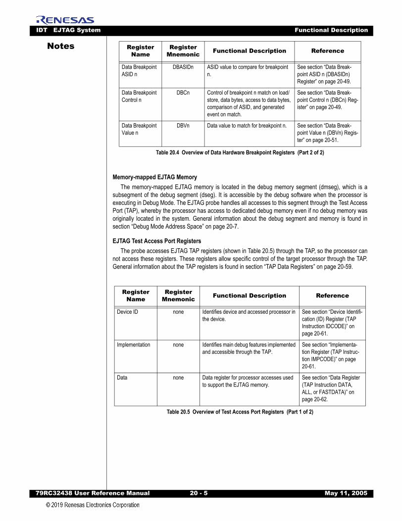
IDT EJTAG System Functional Description
79RC32438 User Refer
Notes
Memory-mapped EJTAG MemoryThe memory-mapped EJTAG memory is located in the debug memory segment (dmseg), which is a
subsegment of the debug segment (dseg). It is accessible by the debug software when the processor isexecuting in Debug Mode. The EJTAG probe handles all accesses to this segment through the Test AccessPort (TAP), whereby the processor has access to dedicated debug memory even if no debug memory wasoriginally located in the system. General information about the debug segment and memory is found insection “Debug Mode Address Space” on page 20-7.
EJTAG Test Access Port RegistersThe probe accesses EJTAG TAP registers (shown in Table 20.5) through the TAP, so the processor can
not access these registers. These registers allow specific control of the target processor through the TAP.General information about the TAP registers is found in section “TAP Data Registers” on page 20-59.
Data Breakpoint ASID n
DBASIDn ASID value to compare for breakpoint n.
See section “Data Break-point ASID n (DBASIDn) Register” on page 20-49.
Data Breakpoint Control n
DBCn Control of breakpoint n match on load/store, data bytes, access to data bytes, comparison of ASID, and generated event on match.
See section “Data Break-point Control n (DBCn) Reg-ister” on page 20-49.
Data Breakpoint Value n
DBVn Data value to match for breakpoint n. See section “Data Break-point Value n (DBVn) Regis-ter” on page 20-51.
Register Name
Register Mnemonic Functional Description Reference
Device ID none Identifies device and accessed processor in the device.
See section “Device Identifi-cation (ID) Register (TAP Instruction IDCODE)” on page 20-61.
Implementation none Identifies main debug features implemented and accessible through the TAP.
See section “Implementa-tion Register (TAP Instruc-tion IMPCODE)” on page 20-61.
Data none Data register for processor accesses used to support the EJTAG memory.
See section “Data Register (TAP Instruction DATA, ALL, or FASTDATA)” on page 20-62.
Table 20.5 Overview of Test Access Port Registers (Part 1 of 2)
Register Name
Register Mnemonic Functional Description Reference
Table 20.4 Overview of Data Hardware Breakpoint Registers (Part 2 of 2)
ence Manual 20 - 5 May 11, 2005
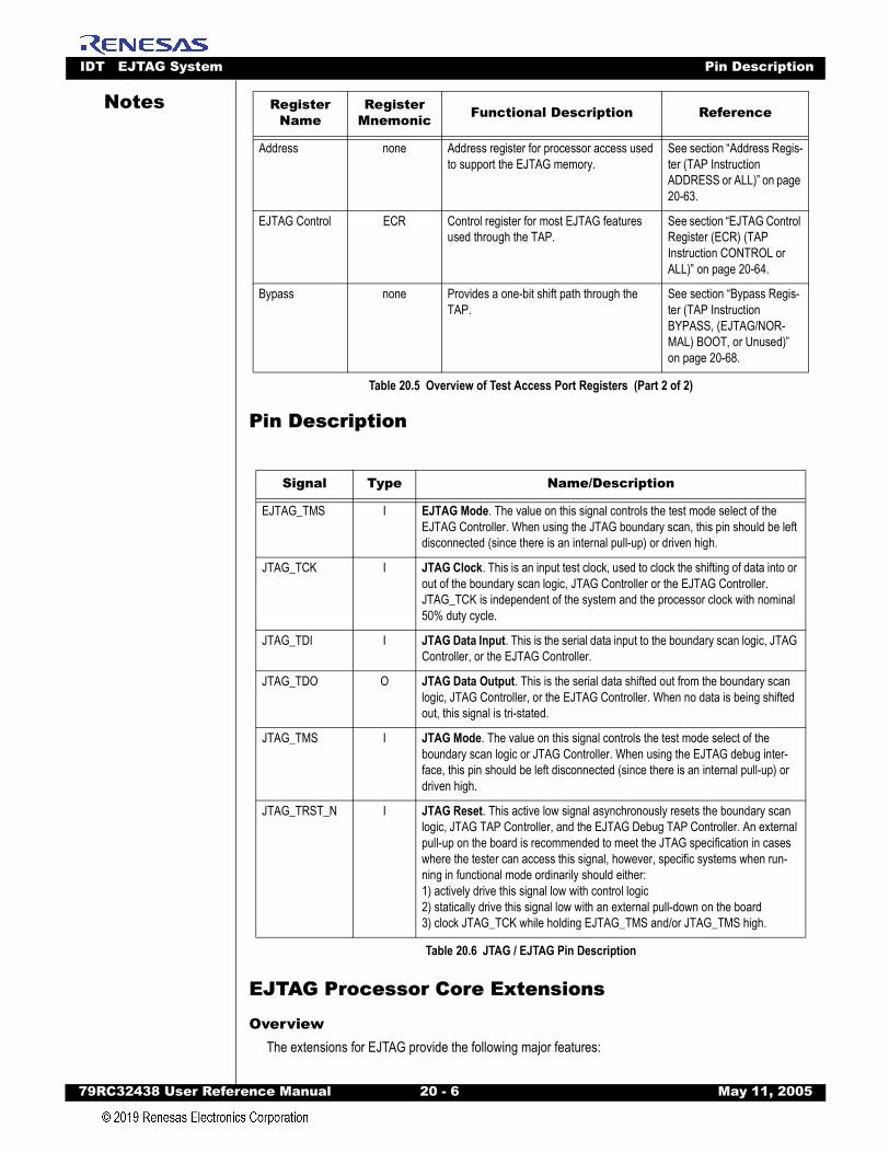
IDT EJTAG System Pin Description
79RC32438 User Refer
Notes
Pin Description
EJTAG Processor Core Extensions
OverviewThe extensions for EJTAG provide the following major features:
Address none Address register for processor access used to support the EJTAG memory.
See section “Address Regis-ter (TAP Instruction ADDRESS or ALL)” on page 20-63.
EJTAG Control ECR Control register for most EJTAG features used through the TAP.
See section “EJTAG Control Register (ECR) (TAP Instruction CONTROL or ALL)” on page 20-64.
Bypass none Provides a one-bit shift path through the TAP.
See section “Bypass Regis-ter (TAP Instruction BYPASS, (EJTAG/NOR-MAL) BOOT, or Unused)” on page 20-68.
Signal Type Name/Description
EJTAG_TMS I EJTAG Mode. The value on this signal controls the test mode select of the EJTAG Controller. When using the JTAG boundary scan, this pin should be left disconnected (since there is an internal pull-up) or driven high.
JTAG_TCK I JTAG Clock. This is an input test clock, used to clock the shifting of data into or out of the boundary scan logic, JTAG Controller or the EJTAG Controller. JTAG_TCK is independent of the system and the processor clock with nominal 50% duty cycle.
JTAG_TDI I JTAG Data Input. This is the serial data input to the boundary scan logic, JTAG Controller, or the EJTAG Controller.
JTAG_TDO O JTAG Data Output. This is the serial data shifted out from the boundary scan logic, JTAG Controller, or the EJTAG Controller. When no data is being shifted out, this signal is tri-stated.
JTAG_TMS I JTAG Mode. The value on this signal controls the test mode select of the boundary scan logic or JTAG Controller. When using the EJTAG debug inter-face, this pin should be left disconnected (since there is an internal pull-up) or driven high.
JTAG_TRST_N I JTAG Reset. This active low signal asynchronously resets the boundary scan logic, JTAG TAP Controller, and the EJTAG Debug TAP Controller. An external pull-up on the board is recommended to meet the JTAG specification in cases where the tester can access this signal, however, specific systems when run-ning in functional mode ordinarily should either:1) actively drive this signal low with control logic2) statically drive this signal low with an external pull-down on the board3) clock JTAG_TCK while holding EJTAG_TMS and/or JTAG_TMS high.
Table 20.6 JTAG / EJTAG Pin Description
Register Name
Register Mnemonic Functional Description Reference
Table 20.5 Overview of Test Access Port Registers (Part 2 of 2)
ence Manual 20 - 6 May 11, 2005
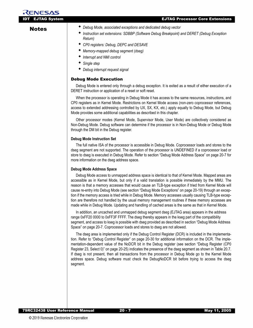
IDT EJTAG System EJTAG Processor Core Extensions
79RC32438 User Refer
Notes
Debug Mode, associated exceptions and dedicated debug vectorInstruction set extensions: SDBBP (Software Debug Breakpoint) and DERET (Debug Exception Return)CP0 registers: Debug, DEPC and DESAVEMemory-mapped debug segment (dseg)Interrupt and NMI controlSingle stepDebug interrupt request signalDebug Mode ExecutionDebug Mode is entered only through a debug exception. It is exited as a result of either execution of a
DERET instruction or application of a reset or soft reset.When the processor is operating in Debug Mode it has access to the same resources, instructions, and
CP0 registers as in Kernel Mode. Restrictions on Kernel Mode access (non-zero coprocessor references,access to extended addressing controlled by UX, SX, KX, etc.) apply equally to Debug Mode, but DebugMode provides some additional capabilities as described in this chapter.
Other processor modes (Kernel Mode, Supervisor Mode, User Mode) are collectively considered asNon-Debug Mode. Debug software can determine if the processor is in Non-Debug Mode or Debug Modethrough the DM bit in the Debug register.
Debug Mode Instruction SetThe full native ISA of the processor is accessible in Debug Mode. Coprocessor loads and stores to the
dseg segment are not supported. The operation of the processor is UNDEFINED if a coprocessor load orstore to dseg is executed in Debug Mode. Refer to section “Debug Mode Address Space” on page 20-7 formore information on the dseg address space.
Debug Mode Address SpaceDebug Mode access to unmapped address space is identical to that of Kernel Mode. Mapped areas are
accessible as in Kernel Mode, but only if a valid translation is possible immediately by the MMU. Thereason is that a memory accesses that would cause an TLB-type exception if tried from Kernel Mode willcause re-entry into Debug Mode (see section “Debug Mode Exceptions” on page 20-19) through an excep-tion if the memory access is tried while in Debug Mode. Memory accesses usually causing TLB-type excep-tion are therefore not handled by the usual memory management routines if these memory accesses aremade while in Debug Mode. Updating and handling of cached areas is the same as that in Kernel Mode.
In addition, an uncached and unmapped debug segment dseg (EJTAG area) appears in the address range 0xFF20 0000 to 0xFF3F FFFF. The dseg thereby appears in the kseg part of the compatibility segment, and access to kseg is possible with dseg provided as described in section “Debug Mode Address Space” on page 20-7. Coprocessor loads and stores to dseg are not allowed.
The dseg area is implemented only if the Debug Control Register (DCR) is included in the implementa-tion. Refer to “Debug Control Register” on page 20-30 for additional information on the DCR. The imple-mentation-dependent value of the NoDCR bit in the Debug register (see section “Debug Register (CP0Register 23, Select 0)” on page 20-25) indicates the presence of the dseg segment as shown in Table 20.7.If dseg is not present, then all transactions from the processor in Debug Mode go to the Kernel Modeaddress space. Debug software must check the DebugNoDCR bit before trying to access the dsegsegment.
ence Manual 20 - 7 May 11, 2005
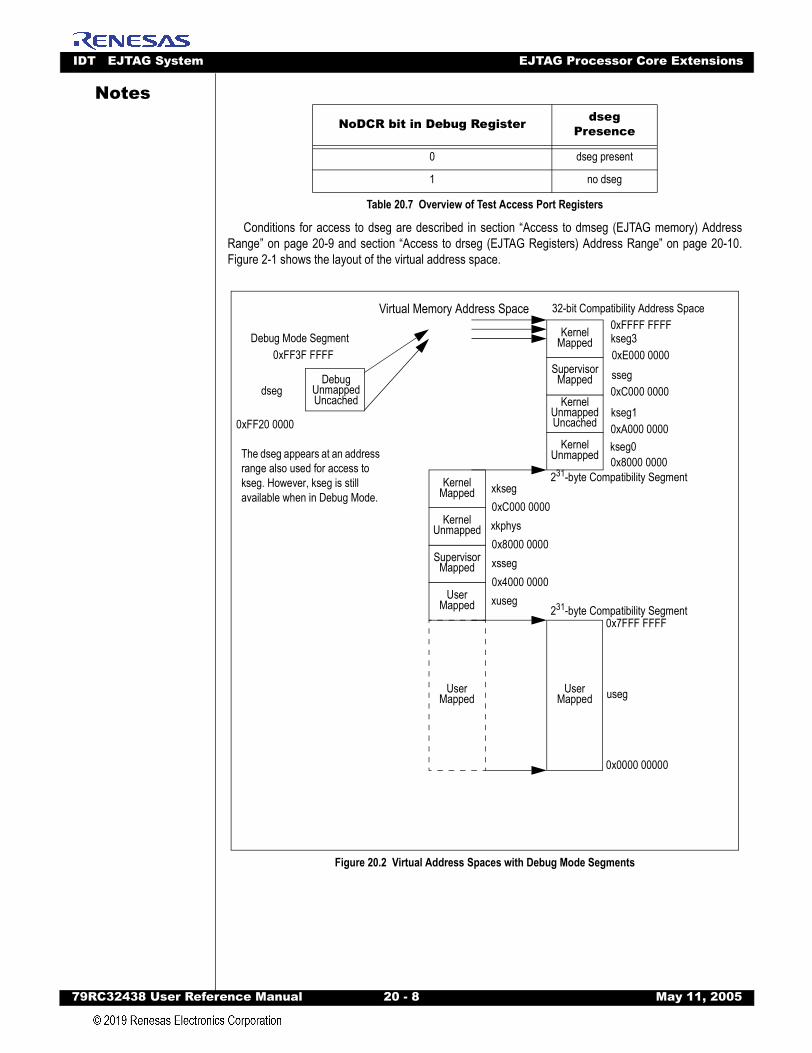
IDT EJTAG System EJTAG Processor Core Extensions
79RC32438 User Refer
Notes
Conditions for access to dseg are described in section “Access to dmseg (EJTAG memory) AddressRange” on page 20-9 and section “Access to drseg (EJTAG Registers) Address Range” on page 20-10.Figure 2-1 shows the layout of the virtual address space.
Figure 20.2 Virtual Address Spaces with Debug Mode Segments
NoDCR bit in Debug Register dseg Presence
0 dseg present
1 no dseg
Table 20.7 Overview of Test Access Port Registers
0x4000 0000
0x8000 0000
Virtual Memory Address Space 32-bit Compatibility Address Space0xFFFF FFFF
0xE000 0000
0xC000 0000
0xA000 0000
0x8000 0000
0x7FFF FFFF
0x0000 00000
0xC000 0000 xkseg
xkphys
xsseg
xuseg
useg
kseg0
kseg1
sseg
kseg3
KernelUnmapped
KernelMapped
SupervisorMapped
KernelUnmappedUncached
UserMapped
KernelMapped
SupervisorMapped
KernelUnmapped
UserMapped 231-byte Compatibility Segment
231-byte Compatibility Segment
UserMapped
DebugUnmappedUncached
0xFF3F FFFF
dseg
0xFF20 0000
Debug Mode Segment
The dseg appears at an address range also used for access to kseg. However, kseg is still available when in Debug Mode.
ence Manual 20 - 8 May 11, 2005

IDT EJTAG System EJTAG Processor Core Extensions
79RC32438 User Refer
Notes
The dseg segment is subdivided into dmseg (EJTAG memory) segment and the drseg (EJTAG regis-ters) segment. The dmseg segment is used when the probe services the memory segment. The drsegsegment is used when the memory-mapped debug registers are accessed. Table 20.8 shows the subdivi-sion and attributes for the segments.The SYNC instruction, followed by appropriate spacing (as described in section “SYNC InstructionBehavior” on page 20-11 and section “CP0 and dseg Hazards” on page 20-12) must be executed to ensurethat an access to dseg is committed (for example, after writing to dseg and before leaving Debug Mode).This procedure ensures that locations in dseg are fully updated for Non-Debug Mode, otherwise behavior ofthe processor is UNDEFINED.
Access to dmseg (EJTAG memory) Address RangeTable 20.9 shows the behavior of processor accesses in Debug Mode to the dmseg address range from
0xFF20 0000 to 0xFF2F FFFF.
Segment Name
Subseg-ment Name
Virtual Address Reference Address Cache
Attribute
dseg dmsg 0xFF20 0000to
0xFF2F FFFF
Because the dseg address range is serviced exclusively by the EJTAG features, there are no physical address per se. Instead the lower 21 bits of the virtual address select the appropriate reference in either EJTAG mem-ory or registers.References are not mapped through the TLB, nor do the accesses appear on the external system memory interface.
Uncached
dreg 0xFF30 0000to
0xFF3F FFFF
Table 20.8 Physical Address and Cache Attribute for dseg’s dmsg and drseg
NoDCR bit in
Debug Register
Trans-action
ProbEn bit in DCR
Register
LSNM bit in Debug
RegisterAccess
1 x1
1. x = don’t care
(Not present) 0 (read only) Kernel Mode address space
0 Fetch 1 x dmseg
0 x See note below table on ProbEn behavior
Load/Store 1 0 dmseg
1 Kernel Mode address space
0 1 Kernel Mode address space
0 See note below table on ProbEn behavior
Table 20.9 Access to dmseg Address Range
ence Manual 20 - 9 May 11, 2005
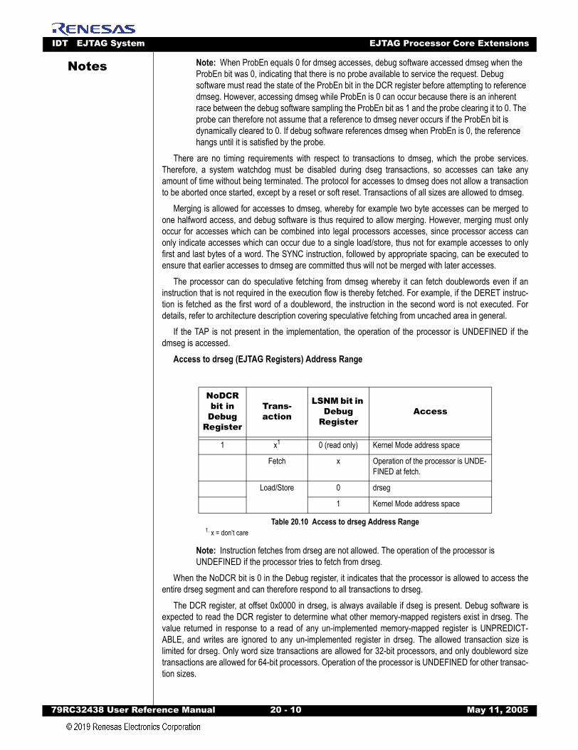
IDT EJTAG System EJTAG Processor Core Extensions
79RC32438 User Refer
Notes
Note: When ProbEn equals 0 for dmseg accesses, debug software accessed dmseg when the ProbEn bit was 0, indicating that there is no probe available to service the request. Debug software must read the state of the ProbEn bit in the DCR register before attempting to reference dmseg. However, accessing dmseg while ProbEn is 0 can occur because there is an inherent race between the debug software sampling the ProbEn bit as 1 and the probe clearing it to 0. The probe can therefore not assume that a reference to dmseg never occurs if the ProbEn bit is dynamically cleared to 0. If debug software references dmseg when ProbEn is 0, the reference hangs until it is satisfied by the probe.There are no timing requirements with respect to transactions to dmseg, which the probe services.Therefore, a system watchdog must be disabled during dseg transactions, so accesses can take anyamount of time without being terminated. The protocol for accesses to dmseg does not allow a transactionto be aborted once started, except by a reset or soft reset. Transactions of all sizes are allowed to dmseg.
Merging is allowed for accesses to dmseg, whereby for example two byte accesses can be merged toone halfword access, and debug software is thus required to allow merging. However, merging must onlyoccur for accesses which can be combined into legal processors accesses, since processor access canonly indicate accesses which can occur due to a single load/store, thus not for example accesses to onlyfirst and last bytes of a word. The SYNC instruction, followed by appropriate spacing, can be executed toensure that earlier accesses to dmseg are committed thus will not be merged with later accesses.
The processor can do speculative fetching from dmseg whereby it can fetch doublewords even if aninstruction that is not required in the execution flow is thereby fetched. For example, if the DERET instruc-tion is fetched as the first word of a doubleword, the instruction in the second word is not executed. Fordetails, refer to architecture description covering speculative fetching from uncached area in general.
If the TAP is not present in the implementation, the operation of the processor is UNDEFINED if thedmseg is accessed.
Access to drseg (EJTAG Registers) Address Range
Note: Instruction fetches from drseg are not allowed. The operation of the processor is UNDEFINED if the processor tries to fetch from drseg.
When the NoDCR bit is 0 in the Debug register, it indicates that the processor is allowed to access theentire drseg segment and can therefore respond to all transactions to drseg.
The DCR register, at offset 0x0000 in drseg, is always available if dseg is present. Debug software isexpected to read the DCR register to determine what other memory-mapped registers exist in drseg. Thevalue returned in response to a read of any un-implemented memory-mapped register is UNPREDICT-ABLE, and writes are ignored to any un-implemented register in drseg. The allowed transaction size islimited for drseg. Only word size transactions are allowed for 32-bit processors, and only doubleword sizetransactions are allowed for 64-bit processors. Operation of the processor is UNDEFINED for other transac-tion sizes.
NoDCR bit in
Debug Register
Trans-action
LSNM bit in Debug
RegisterAccess
1 x1
1. x = don’t care
0 (read only) Kernel Mode address space
Fetch x Operation of the processor is UNDE-FINED at fetch.
Load/Store 0 drseg
1 Kernel Mode address space
Table 20.10 Access to drseg Address Range
ence Manual 20 - 10 May 11, 2005
IDT EJTAG System EJTAG Processor Core Extensions
79RC32438 User Refer
Notes
Debug Mode Handling of Processor ResourcesUnless otherwise specified, the processor resources in Debug Mode are handled identically to those inKernel Mode. Some identical cases are described in the following sections for emphasis. In addition, seethe following related sections for more information:
“Debug Mode Exceptions” on page 20-19 covering exception handling in Debug Mode.“Interrupts and NMIs” on page 20-21 for handling in both Debug and Non-Debug Modes. “Reset and Soft Reset of Processor” on page 20-22 for handling in both Debug and Non-Debug Modes.CoprocessorsA Debug Mode Coprocessor Unusable exception is raised under the same conditions as for a Copro-
cessor Unusable exception in Kernel Mode (see section “Exceptions Taken in Debug Mode” on page 20-19). Therefore, Debug Mode software cannot reference Coprocessors 1 through 2 without first setting therespective enable in the Status register.
Random RegisterThe Random register (CP0 register 1, select 0) can be frozen in Debug Mode, whereby execution with
and without debug exceptions are identical with respect to TLB exception handling. If the values that theRandom register provides cannot be identical in behavior to the case where debug exceptions do not occur,then freezing the Random register has no effect, because execution with and without debug exceptions willnot be identical. Stalls when entering Debug Mode (for example, due to pending scheduled loads resolvedat context save in the debug handler) can make it impossible in some implementations to ensure that theRandom register will provide the same set of values when running with and without debug exceptions.
There is no bit to indicate or control if the Random register is frozen in Debug Mode, so the user mustconsult system documentation.
Counter RegisterThe Count register (CP0 register 9) operation in Debug Mode depends on the state of the CountDM bit
in the Debug register (see section “Debug Register (CP0 Register 23, Select 0)” on page 20-25). The CountRegister has three possible configurations, depending on the implementation:
– Count register runs in Debug Mode the same as in Non-Debug Mode– Count register is stopped in Debug Mode but is running in Non-Debug Mode– The CountDM bit controls the Count register behavior in Debug Mode whereby it can be either
running or stopped.Stopping of the Count register in Debug Mode is allowed in order to prevent generation of an interrupt at
every return to Non-Debug Mode, if the debug handler takes so long to execute that the Count/Compareregisters request an interrupt. In this case, system timing behavior might not be the same as if no debugexception occurred.
WatchLo/WatchHi RegistersThe WatchLo/WatchHi registers (CP0 Registers 18 and 19) are inhibited from matching any instruction
executed in Debug Mode.Load Linked (LL/LLD) and Store Conditional (SC/SCD) Instruction PairA DERET instruction does not clear the LLbit (see section “DERET Instruction” on page 20-24), neither
does the occurrence of a debug exception. Loads and stores to uncacheable locations that do not matchthe physical address of the previous LL instruction do not affect the result of SC instruction. The value of theLLbit is not directly visible by software.
SYNC Instruction BehaviorThe SYNC instruction is used to request the hardware to commit certain operations before proceeding.
For example, a SYNC is required to remove memory hazards on reference to dseg. Also, the SYNC instruc-tion ensures that status bits in the Debug register and the hardware breakpoint registers are fully updated
ence Manual 20 - 11 May 11, 2005
IDT EJTAG System EJTAG Processor Core Extensions
79RC32438 User Refer
Notes
before the debug handler accesses them and before Debug Mode is exited. Similarly, a SYNC combinedwith appropriate spacing is used to remove Coprocessor 0 (CP0) hazards (see the next section, CP0 anddseg Hazards). The SYNC instruction must provide specific behavior as described in Table 20.11.The SYNC instruction must be executed before leaving Debug Mode in order to commit all accesses todseg, such as accesses to set up hardware breakpoints. It may be necessary to remove hazards in relationto the SYNC instruction. Other requirements of the SYNC instruction is described in the MIPS32 andMIPS64 specifications.
CP0 and dseg HazardsBecause resources controlled via Coprocessor 0 and EJTAG memory and registers in dseg affect the
operation of various pipeline stages of the processor, manipulation of these resources may produce resultsthat are not detectable by subsequent instructions for some number of execution cycles. When no hard-ware interlock exists between one instruction that causes an effect that is visible to a second instruction, aCP0 or dseg hazard exists.
Implementations can place the entire burden on the debug software to pad the instruction stream insuch a way that the second instruction is spaced far enough from the first that the effects of the first areseen by the second. Otherwise, the implementations can add full hardware interlocks such that the debugsoftware need not pad. The trade-off is between debug software changes for each new processor vs. morecomplex hardware interlocks required in the processor. The EJTAG Architecture does not dictate the solu-tion that is required for a compatible implementation. The choice of implementation ranges from full hard-ware interlocks to full dependence on debug software padding, to some combination of the two. For animplementation choice that relies on debug software padding, see Table 20.12 which lists the “typical”spacing required to allow the consumer to eliminate the hazard. The “required” values shown in this tablerepresent spacing that is required to be used by debug software. An implementation which requires lessspacing to clear the hazard (including one which has full hardware interlocking) should operate correctlywith the debug software that uses this hazard table. An implementation which requires more spacing toclear the hazard incurs the burden of validating debug software against the new hazard requirements.
Behavior References
Commit accesses to dseg See section “Debug Mode Address Space” on page 20-7.
Update the DDBLImpr and DDBSImpr bits in the Debug register
See section “Debug Data Break Load/Store Imprecise Exception” on page 20-17 and section “Debug Register (CP0 Register 23, Select 0)” on page 20-25.
Update the BS bits in the IBS and DBS registers in drseg
See section “Debug Exception by Data Breakpoint” on page 20-40.
Update the IBusEP, DBusEP, CacheEP, and MCheckP bits in the Debug register
See section “Exceptions on Impre-cise Errors” on page 20-20 and section “Debug Register (CP0 Register 23, Select 0)” on page 20-25.
Table 20.11 SYNC Instruction References
ence Manual 20 - 12 May 11, 2005

IDT EJTAG System EJTAG Processor Core Extensions
79RC32438 User Refer
Notes
Dependencies from the SYNC instruction as producer takes effect since specific updates of dsegmemory and resolving of pending imprecise exception indications are triggered by the SYNC instruction.This is described in the SYNC Instruction Behavior section. Note that, for superscalar MIPS implementa-tions, the number of instructions issued per cycle may be greater than one, and thus that the duration of thehazard in instructions may be greater than the duration in cycles. For this reason, the SSNOP instruction isdefined to convert instruction issues to cycles in a superscalar design.
SSNOP Instruction BehaviorThe SSNOP instruction ensures that instructions are executed and not eliminated by processors during
optimization. The SSNOP instruction can be used, for example, with execution of the SYNC and MTC0/DMTC0 instruction to remove CP0 and dseg hazards.
Debug ExceptionsDebug exceptions bring the processor from Non-Debug Mode into Debug Mode. Implementations need
only support those debug exceptions that are applicable to that implementation. Exceptions can occur inDebug Mode, and these are denoted as debug mode exceptions. These exceptions are handled differentlyfrom exceptions that occur in Non-Debug Mode, as described in section “Debug Mode Exceptions” on page20-19.
Debug Exception PrioritiesTable 20.13 lists the exceptions that can occur in Non-Debug Mode in order of priority, from highest to
lowest. The table also categorizes each exception with respect to type (debug or non-debug). Each debugexception has an associated status bit in the Debug register (indicated in the table in parentheses). Foradditional information, refer to section “Debug Register (CP0 Register 23, Select 0)” on page 20-25.
Producer → Consumer Hazard On“Required”
spacing (cycles)
SYNC → DERET dseg memory locations 2
SYNC → Load/Store BS bits in the IBS and DBS registers in drseg
2
SYNC → MFCO Debug DebugDDBSImpr DebugDDBLImpr DebugIBusEP DebugDBusEP DebugCacheEP DebugMCheckP
2
MTCO DEPC → DEPC 2
MTCO Debug → DERET Debug 2
MTCO Debug[LSNM] → lOAD/sTORE IN DSEG
Debug[LSNM] 3
MTCO Debug[IEXI] → Instructions that can cause an imprecise exception
Debug[IEXI] 3
Table 20.12 “Required” CP0 and dseg Hazard Spacing
ence Manual 20 - 13 May 11, 2005

IDT EJTAG System EJTAG Processor Core Extensions
79RC32438 User Refer
Notes
The specific implementation determines which exceptions can occur and the priority of asynchronousexceptions, such as interrupts.
Debug Exception Vector LocationThe same debug exception vector location is used for all debug exceptions. The ProbTrap bit in the
EJTAG Control Register (ECR) in the optional Test Access Port (TAP) determines the vector location.
Priority Exception Exception Type
Highest Reset Non-Debug
Soft Reset
Debug Single Step Debug
Debug Interrupt; by external signal (DINT), from EjtagBrk in TAP, or through use of EJTAG Boot.
Debug Data Break Load/Store Imprecise (DDBLImpr/DDBSImpr).
Nonmaskable Interrupt (NMI) Non-Debug
Machine Check
Interrupt
Deferred Watch
Debug Instruction Break Debug
Watch on instruction fetch Non-Debug
Address error on instruction fetch
TLB refill on instruction Ifetch
TLB Invalid on instruction Ifetch
Cache error on instruction Ifetch
Bus error on instruction Ifetch
Debug Breakpoint; execution of SDBBP instruc-tion
Debug
Other execution-based exceptions Non-Debug
Debug Data Break on Load/Store address match only or Debug Data Break on Store address+data value match
Debug
Watch on data access Non-Debug
Address error on data access
TLB Refill on data access
TLB Invalid on data access
TLB Modified on data access
Cache error on data access
Bus error on data access
Lowest Debug Data Break on Load address+data match Debug
Table 20.13 Priority of Non-Debug and Debug Exceptions
ence Manual 20 - 14 May 11, 2005

IDT EJTAG System EJTAG Processor Core Extensions
79RC32438 User Refer
Notes
General Debug Exception ProcessingAll debug exceptions have the same basic processing flow:
The DEPC register is loaded with the PC at which execution can be restarted, and the DBD bit is set to indicate whether the last debug exception occurred in a branch delay slot. The value loaded into the DEPC register is either the current PC (if the instruction is not in the delay slot of a branch) or the PC of the branch or jump (if the instruction is in the delay slot of a branch or jump).The DSS, DBp, DDBL, DDBS, DIB, DINT, DDBLImpr, and DDBSImpr bits in the Debug register are updated appropriately depending on the debug exception.DExcCode field in the Debug register is undefined.Halt and Doze bits in the Debug register are updated appropriately.IEXI bit is set to inhibit imprecise exceptions in the start of the debug handler.DM bit in the Debug register is set to 1.The processor begins fetching instructions from the debug exception vector.
The value loaded into the DEPC register represents the restart address from the debug exception anddoes not need to be modified by the debug exception handler software. Debug software need only look atthe DBD bit in the Debug register if it wishes to identify the address of the instruction that actually caused aprecise debug exception.
The DSS, DBp, DDBL, DDBS, DIB, DINT, DDBLImpr, and DDBSImpr bits in the Debug register indicatethe occurrence of distinct debug exceptions, except when a Debug Data Break Load/Store Impreciseexception occurs (see section “Debug Data Break Load/Store Imprecise Exception” on page 20-17). Notethat occurrence of an exception while in Debug mode will clear these bits. The handler can thereby deter-mine whether an debug exception or an exception in Debug Mode occurred. No other CP0 registers orfields are changed due to the debug exception, thus no additional state is saved. The overall exceptionprocessing flow is shown below:
Operation:if (InstructionInBranchDelaySlot) then
DEPC ¨ BranchInstructionPCDebugDBD ¨ 1
elseDEPC ¨ PCDebugDBD ¨ 0
endifDebugDSS, DBp, DDBL, DDBS, DIB, DINT, DDBLImpr and DDBSImpr ¨ DebugExceptionType
DebugDExcCode ¨ UNPREDICTABLEDebugHalt ¨ HaltStatusAtDebugExceptionDebugDoze ¨ DozeStatusAtDebugExceptionDebugIEXI ¨ 1
ProbTrap bit in ECR Register
Debug Exception Vector Address
0 0xBFC0 0480
1 0xFF20 0200 in dmseg
Table 20.14 Debug Exception Vector Location
ence Manual 20 - 15 May 11, 2005
IDT EJTAG System EJTAG Processor Core Extensions
79RC32438 User Refer
Notes
DebugDM ¨ 1if ECRProbTrap = 1 thenPC ¨ 0xFF20 0200else
PC ¨ 0xBFC0 0480endif
Debug Breakpoint ExceptionA Debug Breakpoint exception occurs when an SDBBP instruction is executed. The contents of the
DEPC register and the DBD bit in the Debug register indicate that the SDBBP instruction caused the debugexception.
Debug Register Debug Status Bit SetDBpAdditional State SavedNoneEntry Vector UsedDebug exception vector
Debug Instruction Break ExceptionA Debug Instruction Break exception occurs when an instruction hardware breakpoint matches an
executed instruction. The DEPC register and DBD bit in the Debug register indicate the instruction thatcaused the instruction hardware breakpoint match.
Debug Register Debug Status Bit SetDIBAdditional State SavedNoneEntry Vector UsedDebug exception vector
Debug Data Break Load/Store ExceptionA Debug Data Break Load/Store exception occurs when a data hardware breakpoint matches the load/
store address of an executed load/store instruction. The DEPC register and DBD bit in the Debug registerindicate the load/store instruction that caused the data hardware breakpoint to match, as this is a precisedebug exception. The load/store instruction that caused the debug exception has not completed (it has notupdated the destination register or memory location), and the instruction therefore is executed on returnfrom the debug handler.
Debug Register Debug Status Bit SetDDBL for a load instruction or DDBS for a store instructionAdditional State SavedNoneEntry Vector UsedDebug exception vector
ence Manual 20 - 16 May 11, 2005

IDT EJTAG System EJTAG Processor Core Extensions
79RC32438 User Refer
Notes
Debug Data Break Load/Store Imprecise ExceptionA Debug Data Break Load/Store Imprecise exception occurs when a data hardware breakpoint matchesa load/store access of an executed load/store instruction, if it is not possible to take a precise debug excep-tion on the instruction. This case occurs when a data hardware breakpoint was set up with a valuecompare, and a load access did not return data until after the load instruction had left the pipeline as fornon-blocking loads. The DEPC register and the DBD bit in the Debug register indicate an instruction later inthe execution flow instead of the load/store instruction that caused the data hardware breakpoint to match.The DDBLImpr/DDBSImpr bits in the Debug register indicate that a Debug Data Break Load/Store Impre-cise exception occurred. The instruction that caused the Debug Data Break Load/Store Imprecise excep-tion will have completed. It updates its destination register, and is not executed on return from the debughandler.
Imprecise debug exceptions from data hardware breakpoints are indicated together with another debugexception if the load/store transaction that made the data hardware breakpoint match did not complete untilafter another debug exception occurred. In this case, the other debug exception was the cause of enteringDebug Mode, so the DEPC register and the DBD bit in Debug register point to this instruction. DDBLImpr/DDBSImpr are set concurrently with the status bit for that debug exception.
The SYNC instruction, followed by appropriate spacing (as described in section “SYNC InstructionBehavior” on page 20-11 and section “CP0 and dseg Hazards” on page 20-12), must be executed in DebugMode before the DDBLImpr and DDBSImpr bits in the Debug register and the BS bits for the data hardwarebreakpoint are read in order to ensure that all imprecise breaks are resolved and the bits are fully updated.A match of the data hardware breakpoint is indicated in DDBLImpr/DDBSImpr so the debug handler canhandle this together with the debug exception.
This scheme ensures that all breakpoints matching due to code executed before the debug exceptionare indicated by the DDBLImpr, DDBSImpr, and BS bits for the following debug handler. Matches areneither queued nor do they cause debug exceptions at a later point. A debug exception occurring later thanthe debug exception handler is therefor caused by code executed in Non-Debug Mode after the debugexception handler.
Debug Register Debug Status Bit SetDDBLImpr for a load instruction or DDBSImpr for a store instructionAdditional State SavedNoneEntry Vector UsedDebug exception vector
Debug Single Step ExceptionWhen single-step mode is enabled, a Debug Single Step exception occurs each time the processor has
taken a single execution step in Non-Debug Mode. An execution step is a single instruction, or an instruc-tion pair consisting of a jump/branch instruction and the instruction in the associated delay slot. The SSt bitin the Debug register enables Debug Single Step exceptions. They are disabled on the first execution stepafter a DERET.
The DEPC register points to the instruction on which the Debug Single Step exception occurred, whichis also the next instruction to execute when returning from Debug Mode. The debug software can examinethe system state before this instruction is executed. Thus, the DEPC will not point to the instruction(s) thathave just executed in the execution step, but rather the instruction following the execution step. The DebugSingle Step exception never occurs on an instruction in a jump/branch delay slot, because the jump/branchand the instruction in the delay slot are always executed in one execution step; thus the DBD bit in theDebug register is never set for a Debug Single Step exception.
ence Manual 20 - 17 May 11, 2005
IDT EJTAG System EJTAG Processor Core Extensions
79RC32438 User Refer
Notes
Exceptions occurring on the instruction(s) in the execution step are taken regardless, so if a non-debugexception occurs (other than reset or soft reset), a Debug Single Step exception is taken on the first instruc-tion in the non-debug exception handler. The non-debug exception occurs during the execution step, andthe instruction(s) that received a non-debug exception counts as the execution step.Debug exceptions are unaffected by single-step mode; returning to an SDBBP instruction with singlestep enabled causes a Debug Breakpoint exception with the DEPC register pointing to the SDBBP instruc-tion. Also, returning to an instruction (not jump/branch) just before the SDBBP instruction causes a DebugSingle Step exception with the DEPC register pointing to the SDBBP instruction.
To ensure proper functionality of single-step execution, the Debug Single Step exception has priorityover all exceptions, except resets and soft resets.
Debug Single Step exception is only possible when the NoSSt bit in the Debug register is 0 (see section“Debug Register (CP0 Register 23, Select 0)” on page 20-25).
Debug Register Debug Status Bit SetDSSAdditional State SavedNoneEntry Vector UsedDebug exception vector
Debug Interrupt ExceptionThe Debug Interrupt exception is an asynchronous debug exception that is taken as soon as possible,
but with no specific relation to the executed instructions. The DEPC register and the DBD bit in the Debugregister reference the instruction at which execution can be resumed after Debug Interrupt exceptionservice.
Debug interrupt requests are ignored when the processor is in Debug Mode, and pending requests arecleared when the processor takes any debug exception, including debug exceptions other than DebugInterrupt exceptions.
A debug interrupt restarts the pipeline if stopped by a WAIT instruction and the processor clock isrestarted if it was stopped due to a low-power mode.
Debug Register Debug Status Bit SetDINTAdditional State SavedNoneEntry Vector UsedDebug exception vectorThe possible sources for debug interrupts depend on the implementation. The following sources can
cause Debug Interrupt exceptions:The DINT signal from the probe
Note: This signal is not connected on the RC32438.The EjtagBrk Bit in the EJTAG Control RegisterThe EjtagBrk bit in the EJTAG Control register requests a Debug Interrupt exception when set (see section “EJTAG Control Register (ECR) (TAP Instruction CONTROL or ALL)” on page 20-64).A debug boot by EJTAGBOOTThe EJTAGBOOT feature allows a debug interrupt to be requested immediately after a reset or soft reset has occurred (see section “EJTAGBOOT Feature” on page 20-22 and section “EJTAGBOOT and NORMALBOOT Instructions” on page 20-59).
ence Manual 20 - 18 May 11, 2005
IDT EJTAG System EJTAG Processor Core Extensions
79RC32438 User Refer
Notes
An implementation-specific debug interrupt signal to the processor Through the availability of an optional debug interrupt request signal to the processor system, an external device can request a Debug Interrupt exception, for example, when a signal goes from deasserted to asserted.Debug Mode ExceptionsThe handling of exceptions generated in Debug Mode, other than through resets and soft resets, differs
from those exceptions generated in Non-Debug Mode in that only the Debug and DEPC registers areupdated. All other CP0 registers are unchanged by an exception taken in Debug Mode. The exceptionvector is equal to the debug exception vector (see section “Debug Exception Vector Location” on page 20-14), and the processor stays in Debug Mode.
Reset and soft reset are handled as when occurring in Non-Debug Mode (see section “Reset and SoftReset of Processor” on page 20-22).
Exceptions Taken in Debug ModeOnly some Non-Debug Mode exception events cause exceptions while in Debug Mode. Remaining
events are blocked. Exceptions occurring in Debug Mode have the same relative priorities as the Non-Debug Mode exceptions for the same exception event. These exceptions are called Debug Mode <Non-Debug Mode exception name>. For example, a Debug Mode Breakpoint exception is caused by executionof a BREAK instruction in Debug Mode, and a Debug Mode Address Error exception is caused by anaddress error due to an instruction executed in Debug Mode.
Table 20.15 lists all the Debug Mode exceptions with their corresponding non-debug exception eventnames, priorities, and handling.
Priority Event in Debug Mode Debug Mode Handling
Highest Reset Reset and soft reset handled as for Non-Debug Mode, see sec-tion “Reset and Soft Reset of Processor” on page 20-22.
Soft Reset
Debug Single Step Blocked
Debug Interrupt
Debug Data Break Load/Store Imprecise
NMI
Machine Check Re-enter Debug Mode
Interrupt Blocked
Deferred Watch
Debug Instruction Break, DIB
Watch on instruction fetch
Address error on instruction Ifetch Re-enter Debug Mode
TLB refill on instruction Ifetch
TLB Invalid on instruction Ifetch
Cache error on instruction Ifetch
Bus error on instruction Ifetch
Table 20.15 Priority of Non-Debug and Debug Exceptions (Part 1 of 2)
ence Manual 20 - 19 May 11, 2005
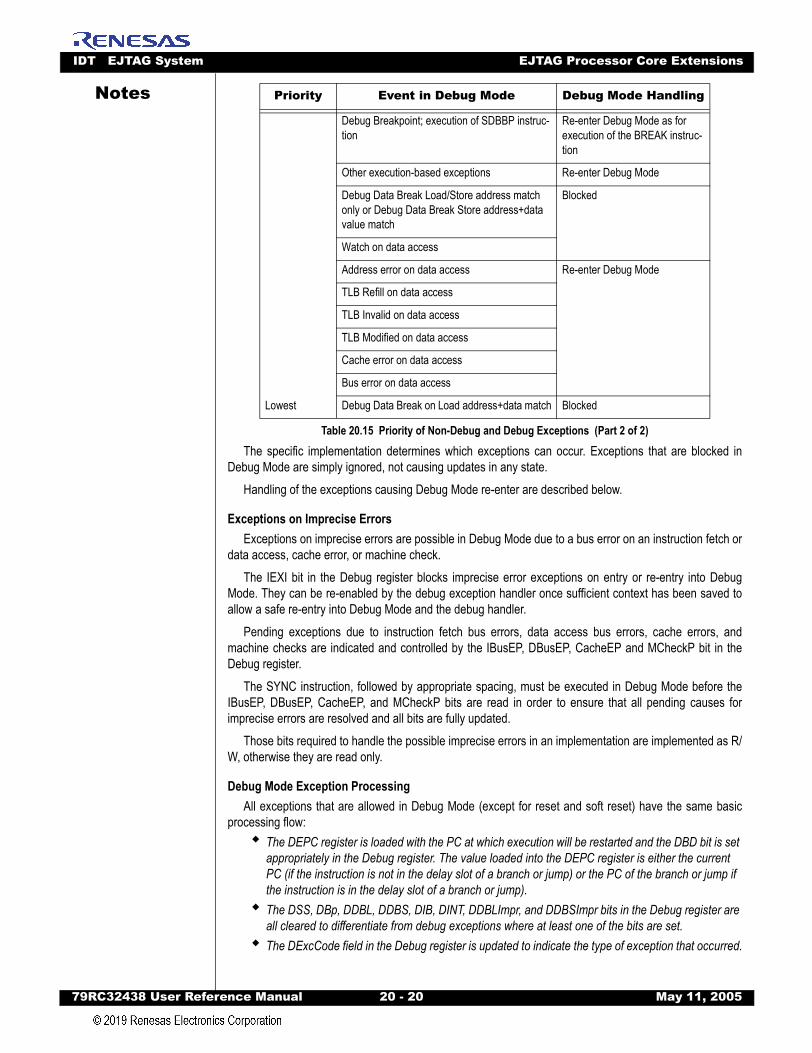
IDT EJTAG System EJTAG Processor Core Extensions
79RC32438 User Refer
Notes
The specific implementation determines which exceptions can occur. Exceptions that are blocked inDebug Mode are simply ignored, not causing updates in any state.
Handling of the exceptions causing Debug Mode re-enter are described below.
Exceptions on Imprecise ErrorsExceptions on imprecise errors are possible in Debug Mode due to a bus error on an instruction fetch or
data access, cache error, or machine check. The IEXI bit in the Debug register blocks imprecise error exceptions on entry or re-entry into Debug
Mode. They can be re-enabled by the debug exception handler once sufficient context has been saved toallow a safe re-entry into Debug Mode and the debug handler.
Pending exceptions due to instruction fetch bus errors, data access bus errors, cache errors, andmachine checks are indicated and controlled by the IBusEP, DBusEP, CacheEP and MCheckP bit in theDebug register.
The SYNC instruction, followed by appropriate spacing, must be executed in Debug Mode before theIBusEP, DBusEP, CacheEP, and MCheckP bits are read in order to ensure that all pending causes forimprecise errors are resolved and all bits are fully updated.
Those bits required to handle the possible imprecise errors in an implementation are implemented as R/W, otherwise they are read only.
Debug Mode Exception ProcessingAll exceptions that are allowed in Debug Mode (except for reset and soft reset) have the same basic
processing flow:The DEPC register is loaded with the PC at which execution will be restarted and the DBD bit is set appropriately in the Debug register. The value loaded into the DEPC register is either the current PC (if the instruction is not in the delay slot of a branch or jump) or the PC of the branch or jump if the instruction is in the delay slot of a branch or jump).The DSS, DBp, DDBL, DDBS, DIB, DINT, DDBLImpr, and DDBSImpr bits in the Debug register are all cleared to differentiate from debug exceptions where at least one of the bits are set.The DExcCode field in the Debug register is updated to indicate the type of exception that occurred.
Debug Breakpoint; execution of SDBBP instruc-tion
Re-enter Debug Mode as for execution of the BREAK instruc-tion
Other execution-based exceptions Re-enter Debug Mode
Debug Data Break Load/Store address match only or Debug Data Break Store address+data value match
Blocked
Watch on data access
Address error on data access Re-enter Debug Mode
TLB Refill on data access
TLB Invalid on data access
TLB Modified on data access
Cache error on data access
Bus error on data access
Lowest Debug Data Break on Load address+data match Blocked
Priority Event in Debug Mode Debug Mode Handling
Table 20.15 Priority of Non-Debug and Debug Exceptions (Part 2 of 2)
ence Manual 20 - 20 May 11, 2005
IDT EJTAG System EJTAG Processor Core Extensions
79RC32438 User Refer
Notes
The Halt and Doze bits in the Debug register are UNPREDICTABLE.The IEXI bit is set to inhibit imprecise exceptions at the start of the debug handler.The DM bit in the Debug register is unchanged, leaving the processor in Debug Mode.The processor is started at the debug exception vector, specified in section “Debug Exception Vec-tor Location” on page 20-14.The value loaded into the DEPC register represents the restart address for the exception. Typically,debug software does not need to modify this value at the location of the debug exception. Debug softwareneed not look at the DBD bit in the Debug register unless it wishes to identify the address of the instructionthat actually caused the exception in Debug Mode.
It is the responsibility of the debug handler to save the contents of the Debug, DEPC, and DESAVEregisters before nested entries into the handler at the debug exception vector can occur. The handlerreturns to the debug exception handler by a jump instruction, not a DERET, in order to kept the processor inDebug Mode.
The cause of the exception in Debug Mode is indicated through the DExcCode field in the Debugregister, and the same codes are used for the exceptions as those for the ExcCode field in the Causeregister when the exceptions with the same names occur in Non-Debug Mode, with addition of the code 30(decimal) with the mnemonic CacheErr for cache errors.
No other CP0 registers or fields are changed due to the exception in Debug Mode. The overallprocessing flow for exceptions in Debug Mode is shown below:
Operation:if (InstructionInBranchDelaySlot) then
DEPC ¨ BranchInstructionPCDebugDBD ¨ 1
elseDEPC ¨ PCDebugDBD ¨ 0
endifDebugDSS, DBp, DDBL, DDBS, DIB, DINT, DDBLImpr and DDBSImpr ¨ 0
DebugDExcCode ¨ DebugExceptionTypeDebugHalt ¨ UNPREDICTABLEDebugDoze ¨ UNPREDICTABLEDebugIEXI ¨ 1if ECRProbTrap = 1 then
PC ¨ 0xFF20 0200else
PC ¨ 0xBFC0 0480endif
Interrupts and NMIs
InterruptsInterrupts are requested through either asserted external hardware signals or internal software-control-
lable bits. Interrupt exceptions are disabled when any of the following conditions are true:The processor is operating in Debug ModeThe Interrupt Enable (IntE) bit in the Debug Control Register (DCR) is cleared (see section “Debug
ence Manual 20 - 21 May 11, 2005
IDT EJTAG System EJTAG Processor Core Extensions
79RC32438 User Refer
Notes
Control Register” on page 20-30)A non-EJTAG related mechanism disables the interrupt exception.A pending interrupt is indicated through the Cause register, even if Interrupt exceptions are disabled.
NMIsAn NMI is requested on the asserting edge of the NMI signal to the processor, and an internal indicator
holds the NMI request until the NMI exception is actually taken. NMI exceptions are disabled when either ofthe following is true:
The Processor is operating in Debug ModeThe NMI Enable (NMIE) bit in the Debug Control Register (DCR) is cleared (see section “Debug Control Register” on page 20-30).
If an asserting edge on the NMI signal to the processor is detected while NMI exception is disabled, thenthe NMI request is held pending and is deferred until NMI exceptions are no longer disabled. A pending NMIis indicated in the NMIpend bit in the DCR even if NMI exceptions are disabled.
Reset and Soft Reset of ProcessorFor EJTAG features, there are no differences between a reset and a soft reset occurring to the CPU
core; they behave identically in both Debug Mode and Non-Debug Mode. In this section, references to resetinclude both reset (hard reset) and soft reset,
EJTAGBOOT FeatureThe EJTAGBOOT feature allows a debug interrupt to be requested as a result of a reset, whereby a
Debug Interrupt exception is taken right after reset, and before any of the instructions from the Resetexception handler are executed. The debug exception handler is, in this case, provided by the probethrough dmseg, even if no instructions can be fetched from the Reset exception handler. Control and detailsof EJTAGBOOT are described in section “EJTAGBOOT and NORMALBOOT Instructions” on page 20-59.
Reset from ProbeWhile asserted, the RST* signal from the probe is required to generate a cold (hard) reset or soft (warm)
reset to the system. The SRstE bit in the Debug Control Register does not mask this source. For more infor-mation on connecting RST*, see section “Using the EJTAG Probe” on page 20-74.
Processor Reset by Probe through Test Access PortThe PrRst bit in the EJTAG Control register causes a soft (warm) reset to the entire RC32438 device.
Reset Occurred Indication through Test Access PortThe Rocc bit in the EJTAG Control register is set at both reset and soft reset in order to indicate the
event to the probe. Refer to section “EJTAG Control Register (ECR) (TAP Instruction CONTROL or ALL)”on page 20-64 for more information on the EJTAG Control Register.
Soft Reset EnableThe optional Soft Reset Enable (SRstE) bit in the Debug Control Register (DCR) can mask the soft reset
signal outside the processor. Because SRstE masks the soft reset signal before it arrives at the processor,there is no masking of soft reset within the processor itself.
Reset of Other Debug FeaturesThe operation of processor resets and soft resets also apply to resets of the following:
Debug Control Register (DCR)Hardware BreakpointTest Access Port (TAP) EJTAG Control Register, (see “EJTAG Test Access Port” on page 20-54.)
ence Manual 20 - 22 May 11, 2005
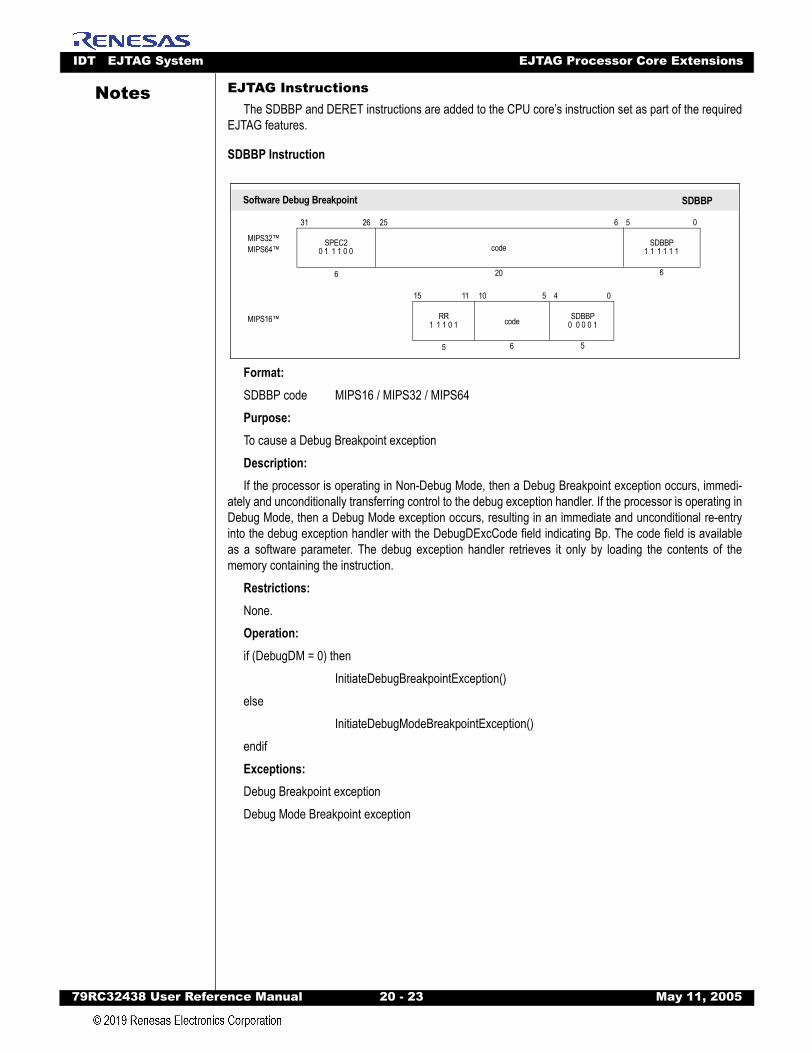
IDT EJTAG System EJTAG Processor Core Extensions
79RC32438 User Refer
Notes
EJTAG InstructionsThe SDBBP and DERET instructions are added to the CPU core’s instruction set as part of the requiredEJTAG features.
SDBBP Instruction
Format: SDBBP code MIPS16 / MIPS32 / MIPS64Purpose:To cause a Debug Breakpoint exceptionDescription:If the processor is operating in Non-Debug Mode, then a Debug Breakpoint exception occurs, immedi-
ately and unconditionally transferring control to the debug exception handler. If the processor is operating inDebug Mode, then a Debug Mode exception occurs, resulting in an immediate and unconditional re-entryinto the debug exception handler with the DebugDExcCode field indicating Bp. The code field is availableas a software parameter. The debug exception handler retrieves it only by loading the contents of thememory containing the instruction.
Restrictions:None.Operation:if (DebugDM = 0) then
InitiateDebugBreakpointException()else
InitiateDebugModeBreakpointException()endifExceptions:Debug Breakpoint exceptionDebug Mode Breakpoint exception
Software Debug Breakpoint SDBBP
31 0
6 20
SPEC2
26 25
SDBBP
6
6 5
MIPS32™MIPS64™
15 0
5
RR
11 10
SDBBP
5
5 4
MIPS16™
6
code
0 1 1 1 0 0 1 1 1 1 1 1code
0 0 0 0 11 1 1 0 1
ence Manual 20 - 23 May 11, 2005
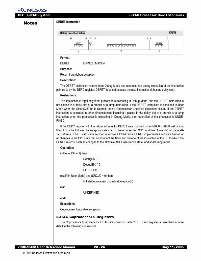
IDT EJTAG System EJTAG Processor Core Extensions
79RC32438 User Refer
Notes
DERET InstructionFormat:DERET MIPS32 / MIPS64Purpose:Return from debug exceptionDescription:The DERET instruction returns from Debug Mode and resumes non-debug execution at the instruction
pointed to by the DEPC register. DERET does not execute the next instruction (it has no delay slot).Restrictions:This instruction is legal only if the processor is executing in Debug Mode, and the DERET instruction is
not placed in a delay slot of a branch or a jump instruction. If the DERET instruction is executed in UserMode when the StatusCU0 bit is cleared, then a Coprocessor Unusable exception occurs. If the DERETinstruction is executed in other circumstances including if placed in the delay slot of a branch or a jumpinstruction when the processor is executing in Debug Mode, then operation of the processor is UNDE-FINED.
If the DEPC register with the return address for DERET was modified by an MTC0/DMTC0 instruction,then it must be followed by an appropriate spacing (refer to section “CP0 and dseg Hazards” on page 20-12) before a DERET instruction in order to remove CP0 hazards. DERET implements a software barrier forall changes in the CP0 state that could affect the fetch and decode of the instruction at the PC to which theDERET returns, such as changes to the effective ASID, user-mode state, and addressing mode.
Operation:if (DebugDM = 1) then
DebugDM ¨ 0DebugIEXI ¨ 0PC ¨ DEPC
elseif (in User Mode) and (SRCU0 = 0) then InitiateCoprocessorUnusableException(0)
elseUNDEFINED
endifExceptions:Coprocessor Unusable exception.
EJTAG Coprocessor 0 RegistersThe Coprocessor 0 registers for EJTAG are shown in Table 20.16. Each register is described in more
detail in the following subsections.
Debug Exception Return DERET
31 0
6 1 19
COP0 CO
2426 25
DERET0
6
6 5
0 1 1 1 1 10 0 0 0 0 0 0 0 0 0 0 0 0 0 0 0 0 0 010 1 0 0 0 0
ence Manual 20 - 24 May 11, 2005
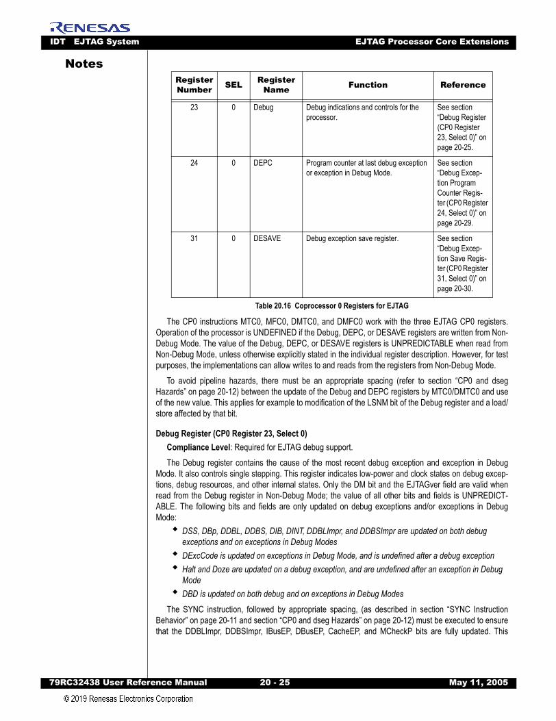
IDT EJTAG System EJTAG Processor Core Extensions
79RC32438 User Refer
Notes
The CP0 instructions MTC0, MFC0, DMTC0, and DMFC0 work with the three EJTAG CP0 registers.Operation of the processor is UNDEFINED if the Debug, DEPC, or DESAVE registers are written from Non-Debug Mode. The value of the Debug, DEPC, or DESAVE registers is UNPREDICTABLE when read fromNon-Debug Mode, unless otherwise explicitly stated in the individual register description. However, for testpurposes, the implementations can allow writes to and reads from the registers from Non-Debug Mode.
To avoid pipeline hazards, there must be an appropriate spacing (refer to section “CP0 and dsegHazards” on page 20-12) between the update of the Debug and DEPC registers by MTC0/DMTC0 and useof the new value. This applies for example to modification of the LSNM bit of the Debug register and a load/store affected by that bit.
Debug Register (CP0 Register 23, Select 0)Compliance Level: Required for EJTAG debug support.The Debug register contains the cause of the most recent debug exception and exception in Debug
Mode. It also controls single stepping. This register indicates low-power and clock states on debug excep-tions, debug resources, and other internal states. Only the DM bit and the EJTAGver field are valid whenread from the Debug register in Non-Debug Mode; the value of all other bits and fields is UNPREDICT-ABLE. The following bits and fields are only updated on debug exceptions and/or exceptions in DebugMode:
DSS, DBp, DDBL, DDBS, DIB, DINT, DDBLImpr, and DDBSImpr are updated on both debug exceptions and on exceptions in Debug ModesDExcCode is updated on exceptions in Debug Mode, and is undefined after a debug exceptionHalt and Doze are updated on a debug exception, and are undefined after an exception in Debug ModeDBD is updated on both debug and on exceptions in Debug Modes
The SYNC instruction, followed by appropriate spacing, (as described in section “SYNC InstructionBehavior” on page 20-11 and section “CP0 and dseg Hazards” on page 20-12) must be executed to ensurethat the DDBLImpr, DDBSImpr, IBusEP, DBusEP, CacheEP, and MCheckP bits are fully updated. This
Register Number SEL Register
Name Function Reference
23 0 Debug Debug indications and controls for the processor.
See section “Debug Register (CP0 Register 23, Select 0)” on page 20-25.
24 0 DEPC Program counter at last debug exception or exception in Debug Mode.
See section “Debug Excep-tion Program Counter Regis-ter (CP0 Register 24, Select 0)” on page 20-29.
31 0 DESAVE Debug exception save register. See section “Debug Excep-tion Save Regis-ter (CP0 Register 31, Select 0)” on page 20-30.
Table 20.16 Coprocessor 0 Registers for EJTAG
ence Manual 20 - 25 May 11, 2005
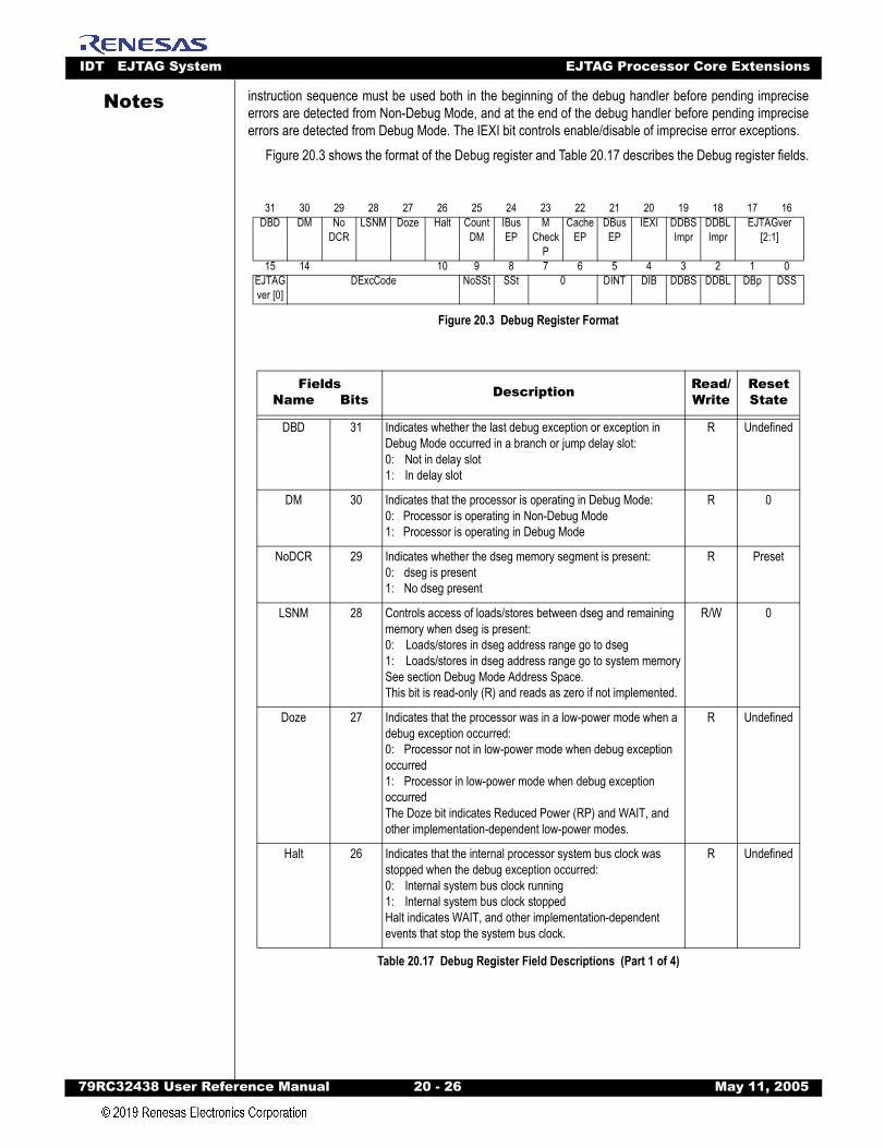
IDT EJTAG System EJTAG Processor Core Extensions
79RC32438 User Refer
Notes
instruction sequence must be used both in the beginning of the debug handler before pending impreciseerrors are detected from Non-Debug Mode, and at the end of the debug handler before pending impreciseerrors are detected from Debug Mode. The IEXI bit controls enable/disable of imprecise error exceptions.Figure 20.3 shows the format of the Debug register and Table 20.17 describes the Debug register fields.
Figure 20.3 Debug Register Format
31 30 29 28 27 26 25 24 23 22 21 20 19 18 17 16DBD DM No
DCRLSNM Doze Halt Count
DMIBusEP
MCheck
P
CacheEP
DBusEP
IEXI DDBSImpr
DDBLImpr
EJTAGver[2:1]
15 14 10 9 8 7 6 5 4 3 2 1 0EJTAGver [0]
DExcCode NoSSt SSt 0 DINT DIB DDBS DDBL DBp DSS
Fields Name Bits Description Read/
WriteReset State
DBD 31 Indicates whether the last debug exception or exception in Debug Mode occurred in a branch or jump delay slot:0: Not in delay slot1: In delay slot
R Undefined
DM 30 Indicates that the processor is operating in Debug Mode:0: Processor is operating in Non-Debug Mode1: Processor is operating in Debug Mode
R 0
NoDCR 29 Indicates whether the dseg memory segment is present:0: dseg is present1: No dseg present
R Preset
LSNM 28 Controls access of loads/stores between dseg and remaining memory when dseg is present:0: Loads/stores in dseg address range go to dseg1: Loads/stores in dseg address range go to system memorySee section Debug Mode Address Space.This bit is read-only (R) and reads as zero if not implemented.
R/W 0
Doze 27 Indicates that the processor was in a low-power mode when a debug exception occurred:0: Processor not in low-power mode when debug exception occurred1: Processor in low-power mode when debug exception occurredThe Doze bit indicates Reduced Power (RP) and WAIT, and other implementation-dependent low-power modes.
R Undefined
Halt 26 Indicates that the internal processor system bus clock was stopped when the debug exception occurred:0: Internal system bus clock running1: Internal system bus clock stoppedHalt indicates WAIT, and other implementation-dependent events that stop the system bus clock.
R Undefined
Table 20.17 Debug Register Field Descriptions (Part 1 of 4)
ence Manual 20 - 26 May 11, 2005
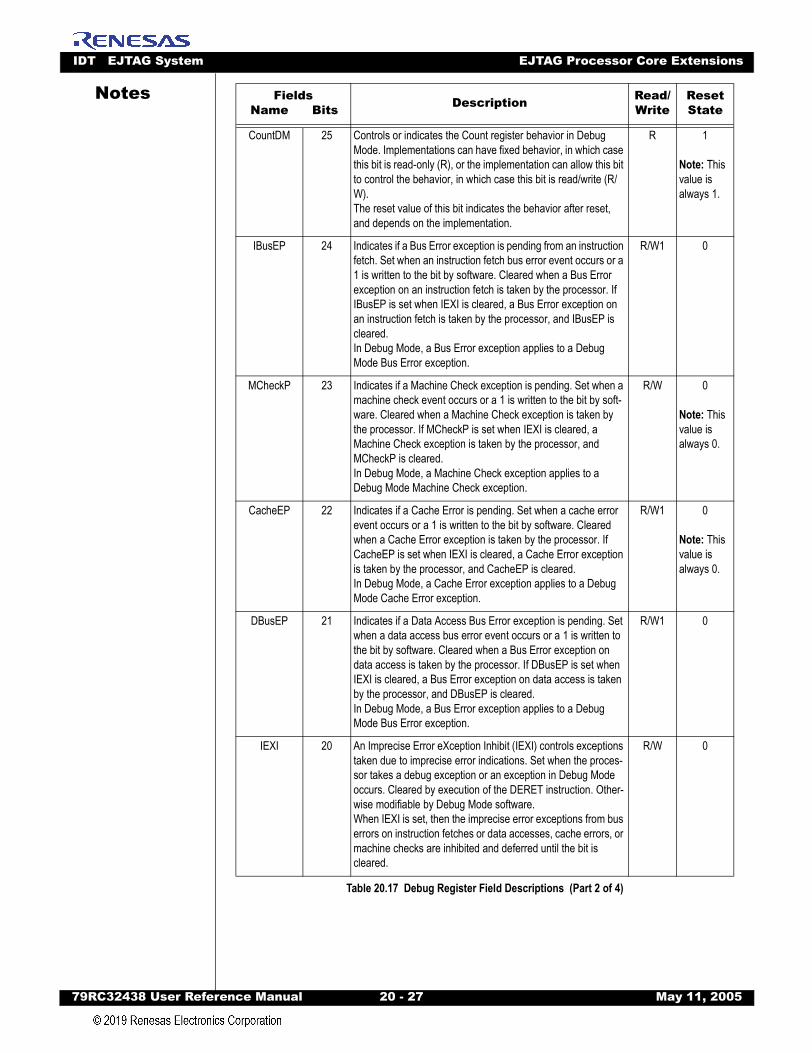
IDT EJTAG System EJTAG Processor Core Extensions
79RC32438 User Refer
Notes
CountDM 25 Controls or indicates the Count register behavior in Debug Mode. Implementations can have fixed behavior, in which case this bit is read-only (R), or the implementation can allow this bit to control the behavior, in which case this bit is read/write (R/W).The reset value of this bit indicates the behavior after reset, and depends on the implementation.
R 1
Note: This value is always 1.
IBusEP 24 Indicates if a Bus Error exception is pending from an instruction fetch. Set when an instruction fetch bus error event occurs or a 1 is written to the bit by software. Cleared when a Bus Error exception on an instruction fetch is taken by the processor. If IBusEP is set when IEXI is cleared, a Bus Error exception on an instruction fetch is taken by the processor, and IBusEP is cleared.In Debug Mode, a Bus Error exception applies to a Debug Mode Bus Error exception.
R/W1 0
MCheckP 23 Indicates if a Machine Check exception is pending. Set when a machine check event occurs or a 1 is written to the bit by soft-ware. Cleared when a Machine Check exception is taken by the processor. If MCheckP is set when IEXI is cleared, a Machine Check exception is taken by the processor, and MCheckP is cleared. In Debug Mode, a Machine Check exception applies to a Debug Mode Machine Check exception.
R/W 0
Note: This value is always 0.
CacheEP 22 Indicates if a Cache Error is pending. Set when a cache error event occurs or a 1 is written to the bit by software. Cleared when a Cache Error exception is taken by the processor. If CacheEP is set when IEXI is cleared, a Cache Error exception is taken by the processor, and CacheEP is cleared.In Debug Mode, a Cache Error exception applies to a Debug Mode Cache Error exception.
R/W1 0
Note: This value is always 0.
DBusEP 21 Indicates if a Data Access Bus Error exception is pending. Set when a data access bus error event occurs or a 1 is written to the bit by software. Cleared when a Bus Error exception on data access is taken by the processor. If DBusEP is set when IEXI is cleared, a Bus Error exception on data access is taken by the processor, and DBusEP is cleared. In Debug Mode, a Bus Error exception applies to a Debug Mode Bus Error exception.
R/W1 0
IEXI 20 An Imprecise Error eXception Inhibit (IEXI) controls exceptions taken due to imprecise error indications. Set when the proces-sor takes a debug exception or an exception in Debug Mode occurs. Cleared by execution of the DERET instruction. Other-wise modifiable by Debug Mode software. When IEXI is set, then the imprecise error exceptions from bus errors on instruction fetches or data accesses, cache errors, or machine checks are inhibited and deferred until the bit is cleared.
R/W 0
Fields Name Bits Description Read/
WriteReset State
Table 20.17 Debug Register Field Descriptions (Part 2 of 4)
ence Manual 20 - 27 May 11, 2005
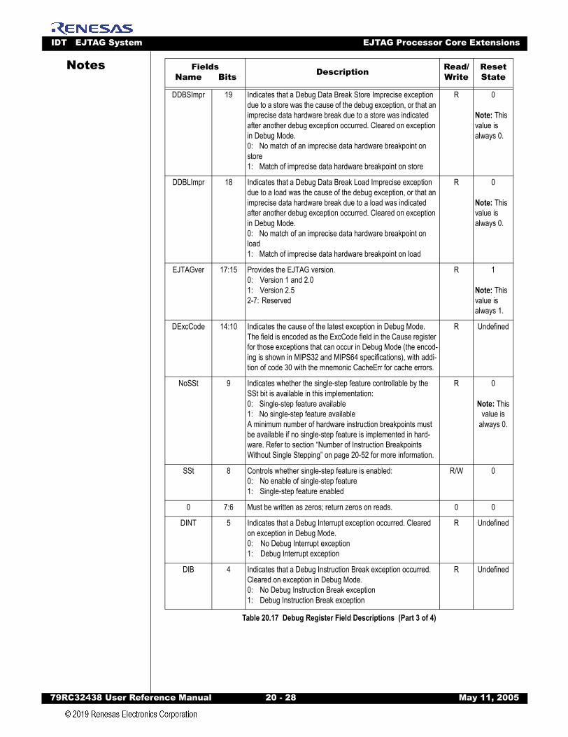
IDT EJTAG System EJTAG Processor Core Extensions
79RC32438 User Refer
Notes
DDBSImpr 19 Indicates that a Debug Data Break Store Imprecise exception due to a store was the cause of the debug exception, or that an imprecise data hardware break due to a store was indicated after another debug exception occurred. Cleared on exception in Debug Mode. 0: No match of an imprecise data hardware breakpoint on store1: Match of imprecise data hardware breakpoint on store
R 0
Note: This value is always 0.
DDBLImpr 18 Indicates that a Debug Data Break Load Imprecise exception due to a load was the cause of the debug exception, or that an imprecise data hardware break due to a load was indicated after another debug exception occurred. Cleared on exception in Debug Mode. 0: No match of an imprecise data hardware breakpoint on load1: Match of imprecise data hardware breakpoint on load
R 0
Note: This value is always 0.
EJTAGver 17:15 Provides the EJTAG version.0: Version 1 and 2.01: Version 2.52-7: Reserved
R 1
Note: This value is always 1.
DExcCode 14:10 Indicates the cause of the latest exception in Debug Mode. The field is encoded as the ExcCode field in the Cause register for those exceptions that can occur in Debug Mode (the encod-ing is shown in MIPS32 and MIPS64 specifications), with addi-tion of code 30 with the mnemonic CacheErr for cache errors.
R Undefined
NoSSt 9 Indicates whether the single-step feature controllable by the SSt bit is available in this implementation:0: Single-step feature available1: No single-step feature availableA minimum number of hardware instruction breakpoints must be available if no single-step feature is implemented in hard-ware. Refer to section “Number of Instruction Breakpoints Without Single Stepping” on page 20-52 for more information.
R 0
Note: This value is
always 0.
SSt 8 Controls whether single-step feature is enabled:0: No enable of single-step feature1: Single-step feature enabled
R/W 0
0 7:6 Must be written as zeros; return zeros on reads. 0 0
DINT 5 Indicates that a Debug Interrupt exception occurred. Cleared on exception in Debug Mode.0: No Debug Interrupt exception1: Debug Interrupt exception
R Undefined
DIB 4 Indicates that a Debug Instruction Break exception occurred. Cleared on exception in Debug Mode.0: No Debug Instruction Break exception1: Debug Instruction Break exception
R Undefined
Fields Name Bits Description Read/
WriteReset State
Table 20.17 Debug Register Field Descriptions (Part 3 of 4)
ence Manual 20 - 28 May 11, 2005

IDT EJTAG System EJTAG Processor Core Extensions
79RC32438 User Refer
Notes
Debug Exception Program Counter Register (CP0 Register 24, Select 0)The Debug Exception Program Counter (DEPC) register is a read/write register that contains the
address at which processing resumes after the exception has been serviced. The size of this register is 32bits for 32-bit processors and 64 bits for 64-bit processors, even with only 32-bit virtual addressing enabled.All bits of the DEPC register are significant and writable. A DMFC0 from the DEPC register returns the full64-bit DEPC on 64-bit processors. Hardware updates this register on debug exceptions and exceptions inDebug Mode.
For precise debug exceptions and precise exceptions in Debug Mode, the DEPC register containseither:
The virtual address of the instruction that was the direct cause of the exception, orThe virtual address of the immediately preceding branch or jump instruction, when the exception-causing instruction is in a branch delay slot, and the Debug Branch Delay (BDB) bit in the Debug register is set.
For imprecise debug exceptions and imprecise exceptions in Debug Mode, the DEPC register containsthe address at which execution is resumed when returning to Non-Debug Mode. Figure 20.4 shows theformat of the DEPC register and Table 20.18 describes the DEPC register field.
Figure 20.4 DEPC Register Forma
DDBS 3 Indicates that a Debug Data Break Store exception occurred on a store due to a precise data hardware break. Cleared on exception in Debug Mode.0: No Debug Data Break Store Exception1: Debug Data Break Store Exception
R Undefined
DDBL 2 Indicates that a Debug Data Break Load exception occurred on a load due to a precise data hardware break. Cleared on exception in Debug Mode.0: No Debug Data Break Store Exception1: Debug Data Break Store Exception
R Undefined
DBp 1 Indicates that a Debug Breakpoint exception occurred. Cleared on exception in Debug Mode.0: No Debug Breakpoint exception1: Debug Breakpoint exception
R Undefined
DSS 0 Indicates that a Debug Single Step exception occurred. Cleared on exception in Debug Mode.0: No debug single-step exception1: Debug single-step exception
R Undefined
31 0DEPC
Fields Name Bits Description Read/
WriteReset State
Table 20.17 Debug Register Field Descriptions (Part 4 of 4)
ence Manual 20 - 29 May 11, 2005

IDT EJTAG System Debug Control Register
79RC32438 User Refer
Notes
Table 20.18 DEPC Register Field Description
Debug Exception Save Register (CP0 Register 31, Select 0)The Debug Exception Save (DESAVE) register is a read/write register that functions as a simple
scratchpad register. The size of this register is 32 bits for 32-bit processors and 64 bits for 64-bit processor.The debug exception handler uses this to save one of the GPRs, which is then used to save the rest of
the context to a pre-determined memory area, for example, in the dmseg. This register allows the safedebugging of exception handlers and other types of code where the existence of a valid stack for contextsaving cannot be assumed.
Figure 2-4 shows the format of the DESAVE register; Table 2-13 describes the DESAVE register field.
Figure 20.5 DESAVE Register Format
Debug Control RegisterThe Debug Control Register (DCR) controls and provides information about debug issues. The width of
the register is 32 bits for 32-bit processors, and 64 bits for 64-bit processors. The DCR is located in thedrseg at offset 0x0000. The Debug Control Register (DCR) provides the following key features:
Interrupt and NMI control when in Non-Debug ModeNMI pending indicationAvailability indicator of instruction and data hardware breakpoints.
For EJTAG features, there are no difference between a reset and a soft reset occurring to the processor;they behave identically in both Debug Mode and Non-Debug Mode. References to reset in the followingtherefore refers to both reset (hard reset) and soft reset. The DataBrk and InstBrk bits within the DCR indi-cate the types of hardware breakpoints implemented. Debug software is expected to read hardware break-point registers for additional information on the number of implemented breakpoints. Refer to section“Hardware Breakpoints” on page 20-32 for a description of the hardware breakpoint registers.
Hardware and software interrupts can be disabled in Non-Debug Mode using the DCR’s IntE bit. This bitis a global interrupt enable used along with several other interrupt enables that enable specific mecha-nisms. The NMI interrupt can be disabled in Non-Debug Mode using the DCR’s NMIE bit; a pending NMI isindicated through the NMIpend bit. Pending interrupts are indicated in the Cause register, and pending
FieldsDescription Read/
WriteReset State
Compli-ance
Name Bits
DEPC MSB:0 Debug Exception Program Counter R/W Undefined Required
31 0DESAVE
FieldsDescription Read/
WriteReset State
Compli-ance
Name Bits
DESAVE MSB:0 Debug Exception Save contents R/W Undefined Required
Table 20.19 DESAVE Register Field Description
ence Manual 20 - 30 May 11, 2005
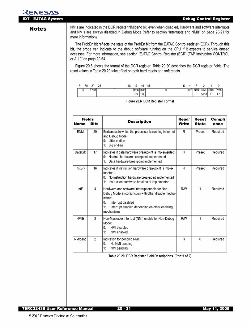
IDT EJTAG System Debug Control Register
79RC32438 User Refer
Notes
NMIs are indicated in the DCR register NMIpend bit, even when disabled. Hardware and software interruptsand NMIs are always disabled in Debug Mode (refer to section “Interrupts and NMIs” on page 20-21 formore information).The ProbEn bit reflects the state of the ProbEn bit from the EJTAG Control register (ECR). Through thisbit, the probe can indicate to the debug software running on the CPU if it expects to service dmsegaccesses. For more information, see section “EJTAG Control Register (ECR) (TAP Instruction CONTROLor ALL)” on page 20-64.
Figure 20.6 shows the format of the DCR register; Table 20.20 describes the DCR register fields. Thereset values in Table 20.20 take effect on both hard resets and soft resets.
Figure 20.6 DCR Register Format
31 30 29 28 18 17 16 15 5 4 3 2 1 00 ENM 0 Data
BrkInstBrk
0 IntE NMIE
NMIpend
SRstE
ProbEn
FieldsName Bits Description Read/
WriteReset State
Compliance
ENM 29 Endianess in which the processor is running in kernel and Debug Mode:0: Little endian1: Big endian
R Preset Required
DataBrk 17 Indicates if data hardware breakpoint is implemented:0: No data hardware breakpoint implemented1: Data hardware breakpoint implemented
R Preset Required
InstBrk 16 Indicates if instruction hardware breakpoint is imple-mented:0: No instruction hardware breakpoint implemented1: Instruction hardware breakpoint implemented
R Preset Required
IntE 4 Hardware and software interrupt enable for Non-Debug Mode, in conjunction with other disable mecha-nisms:0: Interrupt disabled1: Interrupt enabled depending on other enabling mechanisms
R/W 1 Required
NMIE 3 Non-Maskable Interrupt (NMI) enable for Non-Debug Mode:0: NMI disabled1: NMI enabled
R/W 1 Required
NMIpend 2 Indication for pending NMI:0: No NMI pending1: NMI pending
R 0 Required
Table 20.20 DCR Register Field Descriptions (Part 1 of 2)
ence Manual 20 - 31 May 11, 2005

IDT EJTAG System Hardware Breakpoints
79RC32438 User Refer
Notes
Hardware BreakpointsHardware breakpoints compare addresses and data of executed instructions, including data load/store
accesses. Instruction breakpoints can be set even on addresses in ROM areas, and data breakpoints cancause debug exceptions on specific data accesses. Instruction and data hardware breakpoints are alike inmany aspects, and are described in parallel in the following sections. When the term “breakpoint” is used inthis chapter, then the reference is to a “hardware breakpoint”, unless otherwise explicitly noted.
The breakpoints provide the following key features:From zero to 15 instruction breakpoints can be implemented to cause debug exceptions on exe-cuted instructions, both in ROM and RAM. Bit masking is provided for virtual address compares, and masking of compares with ASID (optional) is also provided.From zero to 15 data breakpoints can be implemented to cause debug exceptions on data accesses. Bit masking is provided for virtual address compares, masking of compares with ASID (optional) is provided, optional data value compares allows masking at byte level, and qualification on byte access and access type is possible.Registers for setup and control are memory mapped in drseg, accessible in Debug Mode only.Breakpoints have several implementation options to ease integration with various microarchitec-tures.
Hardware breakpoints require the implementation of the Debug Control Register (DCR). Several addi-tional options are possible for breakpoints, as described in the following subsections. For EJTAG features,there are no difference between a reset and a soft reset occurring to the processor; they behave identicallyin both Debug Mode and Non-Debug Mode. References to reset in the following therefore refers to bothreset (hard reset) and soft reset.
Instruction Breakpoint FeaturesFigure 20.7 shows an overview of the instruction breakpoint feature. The feature compares the virtual
address (PC) and the ASID of the executed instructions with each instruction breakpoint, applying maskingon address and ASID. When an enabled instruction breakpoint matches the PC and ASID, a debug excep-tion and/or a trigger is generated, and an internal bit in an instruction breakpoint register is set to indicatethat a match occurred.
SRstE 1 Controls soft reset enable:Not used. All soft (warm) resets are always enabled.
R/W 1 Optional
ProbEn 0 Indicates value of the ProbEn value in the ECR regis-ter:0: No access should occur to dmseg1: Probe services accesses to dmseg
R Same value as ProbEn in ECR
Required of EJTAG TAP is present, otherwise not imple-mented
0 MSB:30, 28:18, 15:5
Must be written as zeros; return zeros on reads. 0 0 Reserved
FieldsName Bits Description Read/
WriteReset State
Compliance
Table 20.20 DCR Register Field Descriptions (Part 2 of 2)
ence Manual 20 - 32 May 11, 2005
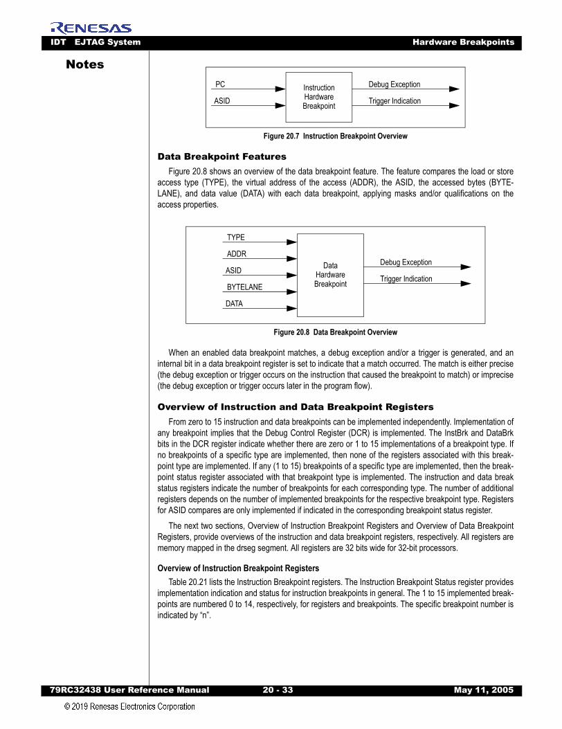
IDT EJTAG System Hardware Breakpoints
79RC32438 User Refer
Notes
Figure 20.7 Instruction Breakpoint Overview
Data Breakpoint FeaturesFigure 20.8 shows an overview of the data breakpoint feature. The feature compares the load or store
access type (TYPE), the virtual address of the access (ADDR), the ASID, the accessed bytes (BYTE-LANE), and data value (DATA) with each data breakpoint, applying masks and/or qualifications on theaccess properties.
Figure 20.8 Data Breakpoint Overview
When an enabled data breakpoint matches, a debug exception and/or a trigger is generated, and aninternal bit in a data breakpoint register is set to indicate that a match occurred. The match is either precise(the debug exception or trigger occurs on the instruction that caused the breakpoint to match) or imprecise(the debug exception or trigger occurs later in the program flow).
Overview of Instruction and Data Breakpoint RegistersFrom zero to 15 instruction and data breakpoints can be implemented independently. Implementation of
any breakpoint implies that the Debug Control Register (DCR) is implemented. The InstBrk and DataBrkbits in the DCR register indicate whether there are zero or 1 to 15 implementations of a breakpoint type. Ifno breakpoints of a specific type are implemented, then none of the registers associated with this break-point type are implemented. If any (1 to 15) breakpoints of a specific type are implemented, then the break-point status register associated with that breakpoint type is implemented. The instruction and data breakstatus registers indicate the number of breakpoints for each corresponding type. The number of additionalregisters depends on the number of implemented breakpoints for the respective breakpoint type. Registersfor ASID compares are only implemented if indicated in the corresponding breakpoint status register.
The next two sections, Overview of Instruction Breakpoint Registers and Overview of Data BreakpointRegisters, provide overviews of the instruction and data breakpoint registers, respectively. All registers arememory mapped in the drseg segment. All registers are 32 bits wide for 32-bit processors.
Overview of Instruction Breakpoint RegistersTable 20.21 lists the Instruction Breakpoint registers. The Instruction Breakpoint Status register provides
implementation indication and status for instruction breakpoints in general. The 1 to 15 implemented break-points are numbered 0 to 14, respectively, for registers and breakpoints. The specific breakpoint number isindicated by “n”.
InstructionHardwareBreakpoint
Debug Exception
Trigger IndicationASID
PC
DataHardwareBreakpoint
TYPE
ASIDDebug Exception
Trigger Indication
ADDR
DATA
BYTELANE
ence Manual 20 - 33 May 11, 2005
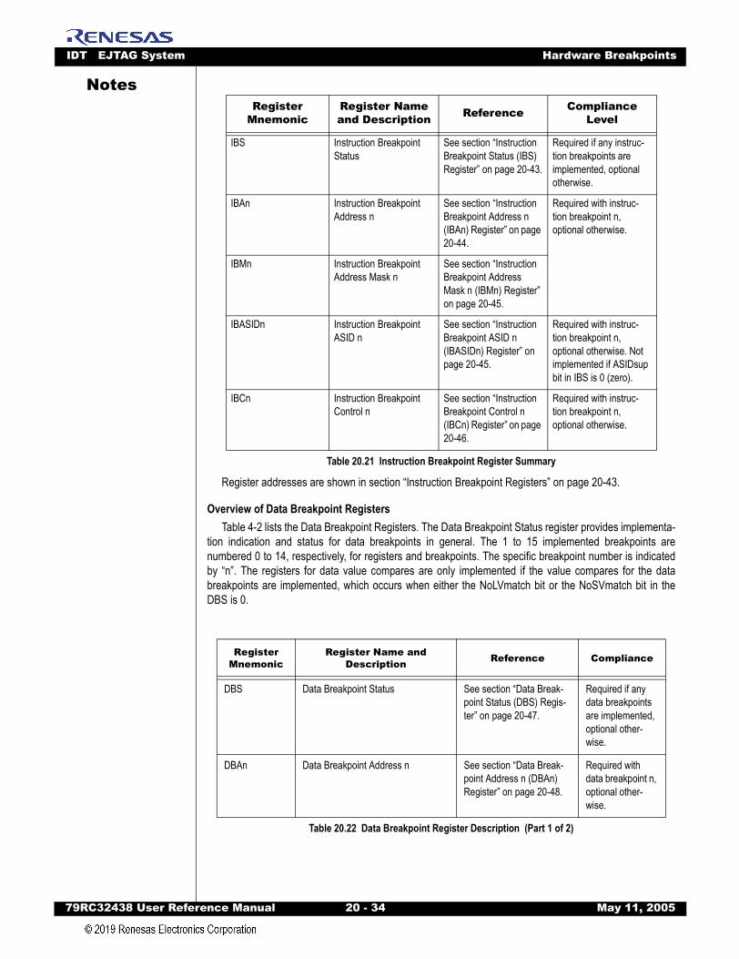
IDT EJTAG System Hardware Breakpoints
79RC32438 User Refer
Notes
Register addresses are shown in section “Instruction Breakpoint Registers” on page 20-43.
Overview of Data Breakpoint RegistersTable 4-2 lists the Data Breakpoint Registers. The Data Breakpoint Status register provides implementa-
tion indication and status for data breakpoints in general. The 1 to 15 implemented breakpoints arenumbered 0 to 14, respectively, for registers and breakpoints. The specific breakpoint number is indicatedby “n”. The registers for data value compares are only implemented if the value compares for the databreakpoints are implemented, which occurs when either the NoLVmatch bit or the NoSVmatch bit in theDBS is 0.
Register Mnemonic
Register Name and Description Reference Compliance
Level
IBS Instruction Breakpoint Status
See section “Instruction Breakpoint Status (IBS) Register” on page 20-43.
Required if any instruc-tion breakpoints are implemented, optional otherwise.
IBAn Instruction Breakpoint Address n
See section “Instruction Breakpoint Address n (IBAn) Register” on page 20-44.
Required with instruc-tion breakpoint n, optional otherwise.
IBMn Instruction Breakpoint Address Mask n
See section “Instruction Breakpoint Address Mask n (IBMn) Register” on page 20-45.
IBASIDn Instruction Breakpoint ASID n
See section “Instruction Breakpoint ASID n (IBASIDn) Register” on page 20-45.
Required with instruc-tion breakpoint n, optional otherwise. Not implemented if ASIDsup bit in IBS is 0 (zero).
IBCn Instruction Breakpoint Control n
See section “Instruction Breakpoint Control n (IBCn) Register” on page 20-46.
Required with instruc-tion breakpoint n, optional otherwise.
Table 20.21 Instruction Breakpoint Register Summary
Register Mnemonic
Register Name and Description Reference Compliance
DBS Data Breakpoint Status See section “Data Break-point Status (DBS) Regis-ter” on page 20-47.
Required if any data breakpoints are implemented, optional other-wise.
DBAn Data Breakpoint Address n See section “Data Break-point Address n (DBAn) Register” on page 20-48.
Required with data breakpoint n, optional other-wise.
Table 20.22 Data Breakpoint Register Description (Part 1 of 2)
ence Manual 20 - 34 May 11, 2005
IDT EJTAG System Hardware Breakpoints
79RC32438 User Refer
Notes
Conditions for Matching BreakpointsA number of conditions must be fulfilled in order for a breakpoint to match on an executed instruction or
a data access. These conditions are described in the following subsections. A breakpoint only matches forinstructions executed in Non-Debug Mode, never due to instructions executed in Debug Mode.
The match of an enabled breakpoint generates a debug exception as described in section “DebugExceptions from Breakpoints” on page 20-40 and/or a trigger indication as described in section “Break-points Used as Triggerpoints” on page 20-42. The BE and/or TE bits in the IBCn or DBCn registers enablethe breakpoints for breaks and triggers, respectively.
It is implementation dependent whether or not a breakpoint stalls the processor in order to evaluate thematch expression; for example, if required for timing reasons or in order to wait on a scheduled load toreturn for evaluation of a data breakpoint with a data value compare. In some cases, stalling is avoided withimprecise data breakpoints, as described in section “Debug Exception by Data Breakpoint” on page 20-40.
Conditions for Matching Instruction BreakpointsWhen an instruction breakpoint is enabled, that breakpoint is evaluated in Non-Debug Mode with the
instruction boundary address (the lowest address of a byte in the instruction) of every executed instruction.The instruction breakpoint is also evaluated on addresses usually causing an Address Error exception, aTLB exception, or other exceptions. It is thereby possible to cause a Debug Instruction Break exception onthe destination address of a jump, even if a jump to that address would cause an Address Error exception.The breakpoint is not evaluated on instructions from speculative fetches or execution.
A match of an instruction breakpoint depends on a number of parameters, shown in Table 20.23. Thefields in the instruction breakpoint registers are in the form REGFIELD.
DBMn Data Breakpoint Address Mask n See section “Data Break-point Address Mask n (DBMn) Register” on page 20-49.
DBASIDn Data Breakpoint ASID n See section “Data Break-point ASID n (DBASIDn) Register” on page 20-49.
Required with data breakpoint n, optional other-wise. Not imple-mented if ASIDsup bit in DBS is 0 (zero).
DBCn Data Breakpoint Control n See section “Data Break-point Control n (DBCn) Register” on page 20-49.
Required with data breakpoint n, optional other-wise.
DBVn Data Breakpoint Value n See section “Data Break-point Value n (DBVn) Reg-ister” on page 20-51.
Required with data breakpoint n, optional other-wise. Only imple-mented with value compares, shown in DBS.
Register Mnemonic
Register Name and Description Reference Compliance
Table 20.22 Data Breakpoint Register Description (Part 2 of 2)
ence Manual 20 - 35 May 11, 2005
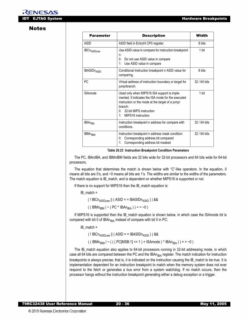
IDT EJTAG System Hardware Breakpoints
79RC32438 User Refer
Notes
The PC, IBAnIBA, and IBMnIBM fields are 32 bits wide for 32-bit processors and 64 bits wide for 64-bitprocessors.
The equation that determines the match is shown below with “C”-like operators. In the equation, 0means all bits are 0’s, and ~0 means all bits are 1’s. The widths are similar to the widths of the parameters.The match equation is IB_match, and is dependent on whether MIPS16 is supported or not.
If there is no support for MIPS16 then the IB_match equation is:IB_match =
( ! IBCnASIDuse || ( ASID = = IBASIDnASID ) ) &&
( ( IBMnIBM | ~ ( PC ^ IBAnIBA ) ) = = ~0 )
If MIPS16 is supported then the IB_match equation is shown below, in which case the ISAmode bit iscompared with bit 0 of IBAnIBA instead of compare with bit 0 in PC:
IB_match =( ! IBCnASIDuse || ( ASID = = IBASIDnASID ) ) &&
( ( IBMnIBM | ~ ( ( ( PC[MSB:1] << 1 ) + ISAmode ) ^ IBAnIBA ) ) = = ~0 )
The IB_match equation also applies to 64-bit processors running in 32-bit addressing mode, in whichcase all 64 bits are compared between the PC and the IBAnIBA register. The match indication for instructionbreakpoints is always precise; that is, it is indicated on the instruction causing the IB_match to be true. It isimplementation dependent for an instruction breakpoint to match when the memory system does not everrespond to the fetch or generates a bus error from a system watchdog. If no match occurs, then theprocessor hangs without the instruction breakpoint generating either a debug exception or a trigger.
Parameter Description Width
ASID ASID field in EntryHi CP0 register. 8 bits
IBCnASIDuse Use ASID value in compare for instruction breakpoint n:0: Do not use ASID value in compare1: Use ASID value in compare
1 bit
IBASIDnASID Conditional Instruction breakpoint n ASID value for comparing.
8 bits
PC Virtual address of instruction boundary or target for jump/branch.
32 / 64 bits
ISAmode Used only when MIPS16 ISA support is imple-mented. It indicates the ISA mode for the executed instruction or the mode at the target of a jump/branch:0: 32-bit MIPS instruction1: MIPS16 instruction
1 bit
IBAnIBA Instruction breakpoint n address for compare with conditions.
32 / 64 bits
IBMnIBM Instruction breakpoint n address mask condition:0: Corresponding address bit compared1: Corresponding address bit masked
32 / 64 bits
Table 20.23 Instruction Breakpoint Condition Parameters
ence Manual 20 - 36 May 11, 2005
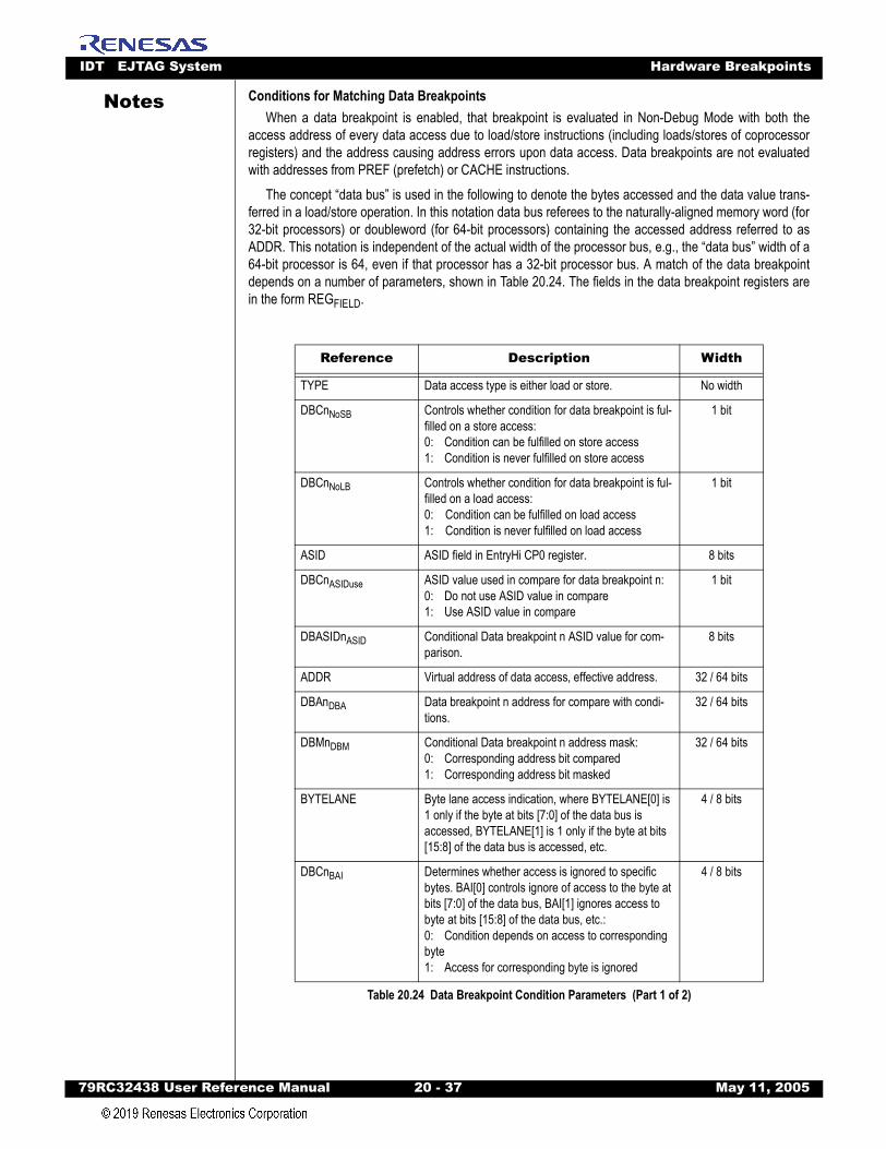
IDT EJTAG System Hardware Breakpoints
79RC32438 User Refer
Notes
Conditions for Matching Data BreakpointsWhen a data breakpoint is enabled, that breakpoint is evaluated in Non-Debug Mode with both theaccess address of every data access due to load/store instructions (including loads/stores of coprocessorregisters) and the address causing address errors upon data access. Data breakpoints are not evaluatedwith addresses from PREF (prefetch) or CACHE instructions.
The concept “data bus” is used in the following to denote the bytes accessed and the data value trans-ferred in a load/store operation. In this notation data bus referees to the naturally-aligned memory word (for32-bit processors) or doubleword (for 64-bit processors) containing the accessed address referred to asADDR. This notation is independent of the actual width of the processor bus, e.g., the “data bus” width of a64-bit processor is 64, even if that processor has a 32-bit processor bus. A match of the data breakpointdepends on a number of parameters, shown in Table 20.24. The fields in the data breakpoint registers arein the form REGFIELD.
Reference Description Width
TYPE Data access type is either load or store. No width
DBCnNoSB Controls whether condition for data breakpoint is ful-filled on a store access:0: Condition can be fulfilled on store access1: Condition is never fulfilled on store access
1 bit
DBCnNoLB Controls whether condition for data breakpoint is ful-filled on a load access:0: Condition can be fulfilled on load access1: Condition is never fulfilled on load access
1 bit
ASID ASID field in EntryHi CP0 register. 8 bits
DBCnASIDuse ASID value used in compare for data breakpoint n:0: Do not use ASID value in compare1: Use ASID value in compare
1 bit
DBASIDnASID Conditional Data breakpoint n ASID value for com-parison.
8 bits
ADDR Virtual address of data access, effective address. 32 / 64 bits
DBAnDBA Data breakpoint n address for compare with condi-tions.
32 / 64 bits
DBMnDBM Conditional Data breakpoint n address mask:0: Corresponding address bit compared1: Corresponding address bit masked
32 / 64 bits
BYTELANE Byte lane access indication, where BYTELANE[0] is 1 only if the byte at bits [7:0] of the data bus is accessed, BYTELANE[1] is 1 only if the byte at bits [15:8] of the data bus is accessed, etc.
4 / 8 bits
DBCnBAI Determines whether access is ignored to specific bytes. BAI[0] controls ignore of access to the byte at bits [7:0] of the data bus, BAI[1] ignores access to byte at bits [15:8] of the data bus, etc.:0: Condition depends on access to corresponding byte1: Access for corresponding byte is ignored
4 / 8 bits
Table 20.24 Data Breakpoint Condition Parameters (Part 1 of 2)
ence Manual 20 - 37 May 11, 2005
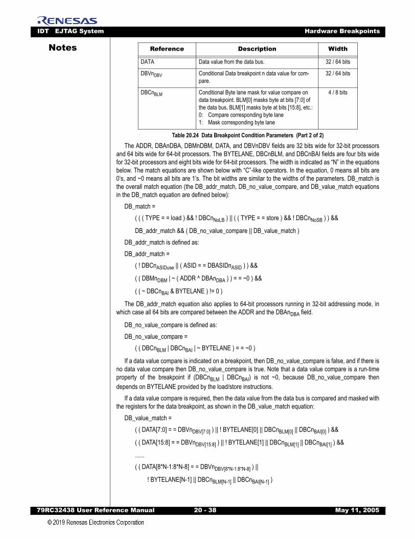
IDT EJTAG System Hardware Breakpoints
79RC32438 User Refer
Notes
The ADDR, DBAnDBA, DBMnDBM, DATA, and DBVnDBV fields are 32 bits wide for 32-bit processorsand 64 bits wide for 64-bit processors. The BYTELANE, DBCnBLM, and DBCnBAI fields are four bits widefor 32-bit processors and eight bits wide for 64-bit processors. The width is indicated as “N” in the equationsbelow. The match equations are shown below with “C”-like operators. In the equation, 0 means all bits are0’s, and ~0 means all bits are 1’s. The bit widths are similar to the widths of the parameters. DB_match isthe overall match equation (the DB_addr_match, DB_no_value_compare, and DB_value_match equationsin the DB_match equation are defined below):
DB_match =( ( ( TYPE = = load ) && ! DBCnNoLB ) || ( ( TYPE = = store ) && ! DBCnNoSB ) ) &&
DB_addr_match && ( DB_no_value_compare || DB_value_match )DB_addr_match is defined as:DB_addr_match =
( ! DBCnASIDuse || ( ASID = = DBASIDnASID ) ) &&
( ( DBMnDBM | ~ ( ADDR ^ DBAnDBA ) ) = = ~0 ) &&
( ( ~ DBCnBAI & BYTELANE ) != 0 )
The DB_addr_match equation also applies to 64-bit processors running in 32-bit addressing mode, inwhich case all 64 bits are compared between the ADDR and the DBAnDBA field.
DB_no_value_compare is defined as:DB_no_value_compare =
( ( DBCnBLM | DBCnBAI | ~ BYTELANE ) = = ~0 )
If a data value compare is indicated on a breakpoint, then DB_no_value_compare is false, and if there isno data value compare then DB_no_value_compare is true. Note that a data value compare is a run-timeproperty of the breakpoint if (DBCnBLM | DBCnBAI) is not ~0, because DB_no_value_compare thendepends on BYTELANE provided by the load/store instructions.
If a data value compare is required, then the data value from the data bus is compared and masked withthe registers for the data breakpoint, as shown in the DB_value_match equation:
DB_value_match = ( ( DATA[7:0] = = DBVnDBV[7:0] ) || ! BYTELANE[0] || DBCnBLM[0] || DBCnBAI[0] ) &&
( ( DATA[15:8] = = DBVnDBV[15:8] ) || ! BYTELANE[1] || DBCnBLM[1] || DBCnBAI[1] ) &&
......( ( DATA[8*N-1:8*N-8] = = DBVnDBV[8*N-1:8*N-8] ) ||
! BYTELANE[N-1] || DBCnBLM[N-1] || DBCnBAI[N-1] )
DATA Data value from the data bus. 32 / 64 bits
DBVnDBV Conditional Data breakpoint n data value for com-pare.
32 / 64 bits
DBCnBLM Conditional Byte lane mask for value compare on data breakpoint. BLM[0] masks byte at bits [7:0] of the data bus, BLM[1] masks byte at bits [15:8], etc.:0: Compare corresponding byte lane1: Mask corresponding byte lane
4 / 8 bits
Reference Description Width
Table 20.24 Data Breakpoint Condition Parameters (Part 2 of 2)
ence Manual 20 - 38 May 11, 2005
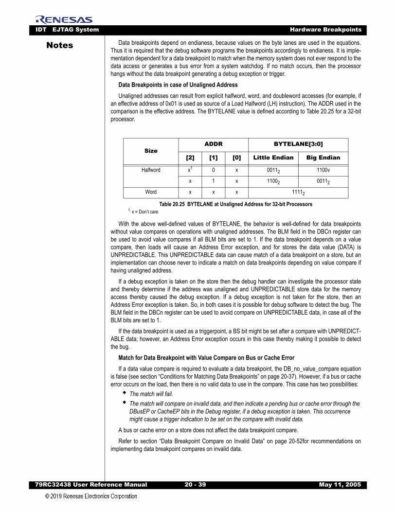
IDT EJTAG System Hardware Breakpoints
79RC32438 User Refer
Notes
Data breakpoints depend on endianess, because values on the byte lanes are used in the equations.Thus it is required that the debug software programs the breakpoints accordingly to endianess. It is imple-mentation dependent for a data breakpoint to match when the memory system does not ever respond to thedata access or generates a bus error from a system watchdog. If no match occurs, then the processorhangs without the data breakpoint generating a debug exception or trigger.Data Breakpoints in case of Unaligned AddressUnaligned addresses can result from explicit halfword, word, and doubleword accesses (for example, if
an effective address of 0x01 is used as source of a Load Halfword (LH) instruction). The ADDR used in thecomparison is the effective address. The BYTELANE value is defined according to Table 20.25 for a 32-bitprocessor.
With the above well-defined values of BYTELANE, the behavior is well-defined for data breakpointswithout value compares on operations with unaligned addresses. The BLM field in the DBCn register canbe used to avoid value compares if all BLM bits are set to 1. If the data breakpoint depends on a valuecompare, then loads will cause an Address Error exception, and for stores the data value (DATA) isUNPREDICTABLE. This UNPREDICTABLE data can cause match of a data breakpoint on a store, but animplementation can choose never to indicate a match on data breakpoints depending on value compare ifhaving unaligned address.
If a debug exception is taken on the store then the debug handler can investigate the processor stateand thereby determine if the address was unaligned and UNPREDICTABLE store data for the memoryaccess thereby caused the debug exception. If a debug exception is not taken for the store, then anAddress Error exception is taken. So, in both cases it is possible for debug software to detect the bug. TheBLM field in the DBCn register can be used to avoid compare on UNPREDICTABLE data, in case all of theBLM bits are set to 1.
If the data breakpoint is used as a triggerpoint, a BS bit might be set after a compare with UNPREDICT-ABLE data; however, an Address Error exception occurs in this case thereby making it possible to detectthe bug.
Match for Data Breakpoint with Value Compare on Bus or Cache ErrorIf a data value compare is required to evaluate a data breakpoint, the DB_no_value_compare equation
is false (see section “Conditions for Matching Data Breakpoints” on page 20-37). However, if a bus or cacheerror occurs on the load, then there is no valid data to use in the compare. This case has two possibilities:
The match will fail.The match will compare on invalid data, and then indicate a pending bus or cache error through the DBusEP or CacheEP bits in the Debug register, if a debug exception is taken. This occurrence might cause a trigger indication to be set on the compare with invalid data.
A bus or cache error on a store does not affect the data breakpoint compare.Refer to section “Data Breakpoint Compare on Invalid Data” on page 20-52for recommendations on
implementing data breakpoint compares on invalid data.
SizeADDR BYTELANE[3:0]
[2] [1] [0] Little Endian Big Endian
Halfword x1
1. x = Don’t care
0 x 00112 1100v
x 1 x 11002 00112
Word x x x 11112
Table 20.25 BYTELANE at Unaligned Address for 32-bit Processors
ence Manual 20 - 39 May 11, 2005
IDT EJTAG System Hardware Breakpoints
79RC32438 User Refer
Notes
Precise Match for Data BreakpointsA precise match for a data breakpoint occurs when the match equation can be fully evaluated at the timethe load/store instruction is executed. A true DB_match can thereby be indicated on the very same instruc-tion causing the DB_match equation to be true. Matches on data breakpoints without data value comparesare always precise. Accesses using data value compares are either imprecise or precise depending on theimplementation and specific access.
Imprecise Match for Data BreakpointsAn imprecise match for a data breakpoint occurs when the match equation cannot be fully evaluated at
the time the load/store instruction is executed. This case occurs when the processor is not stalled on ascheduled load and a data breakpoint must compare on the data value returned by the load. If the break-point matches, then the DB_match equation is true later in the execution flow rather than at the same timeas load/store instruction that caused the load/store access to match. Only data breakpoints with valuecompares can be imprecise, in which case the breakpoints can be imprecise for all or some of thoseaccesses depending on the implementation.
Debug Exceptions from BreakpointsThis section describes how to set up instruction and data breakpoints to generate debug exceptions
when the match conditions are true.
Debug Exception Caused by Instruction BreakpointThe BE bit in the IBCn register must be set for an instruction breakpoint to be enabled. A Debug Instruc-
tion Break exception occurs when the IB_match equation is true (see section“Conditions for MatchingInstruction Breakpoints” on page 20-35). The corresponding BS bit in the IBS register is set when thebreakpoint generates the debug exception. The Debug Instruction Break exception is precise, so the DEPCregister and DBD bit in the Debug register point to the instruction that caused the IB_match equation to betrue. The instruction receiving the debug exception only updates the debug related registers. That instruc-tion will not cause any loads/stores to occur. Thus a debug exception from a data breakpoint cannot occurat the same time an instruction receives a Debug Instruction Break exception.
The debug handler usually returns to the instruction causing the Debug Instruction Break exception,whereby the instruction is executed. Debug software must disable the breakpoint when returning to theinstruction, otherwise the Debug Instruction Break exception will reoccur. An alternative is for debug soft-ware to emulate the instruction(s) in software and change the DEPC accordingly.
Debug Exception by Data BreakpointThe BE bit in the DBCn register must be set for a data breakpoint to be enabled. A debug exception
occurs when the DB_match condition is true. A matching data breakpoint generates either a precise or animprecise debug exception (see section “Precise / Imprecise Debug Exceptions on Data Breakpoints withData Value Compares” on page 20-52).
Debug Data Break Load/Store Exception as a Precise Debug ExceptionA Debug Data Break Load/Store exception occurs when a data breakpoint indicates a precise match. In
this case, the DEPC register and DBD bit in the Debug register point to the load/store instruction thatcaused the DB_match equation to be true, and the corresponding BS bit in the DBS register is set. Detailsabout behavior of the instruction causing the debug exception is shown in Table 20.26.
ence Manual 20 - 40 May 11, 2005
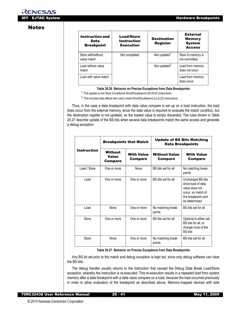
IDT EJTAG System Hardware Breakpoints
79RC32438 User Refer
Notes
Thus, in the case a data breakpoint with data value compare is set up on a load instruction, the loaddoes occur from the external memory, since the data value is required to evaluate the match condition, butthe destination register is not updated, so the loaded value is simply discarded. The rules shown in Table20.27 describe update of the BS bits when several data breakpoints match the same access and generatea debug exception
Any BS bit set prior to the match and debug exception is kept set, since only debug software can clearthe BS bits.
The debug handler usually returns to the instruction that caused the Debug Data Break Load/Storeexception, whereby the instruction is re-executed. This re-execution results in a repeated load from systemmemory after a data breakpoint with a data value compare on a load, because the load occurred previouslyin order to allow evaluation of the breakpoint as described above. Memory-mapped devices with side
Instruction and Data
Breakpoint
Load/Store Instruction Execution
Destination Register
External Memory System Access
Store with/without value match
Not completed Not updated1
1. This applies to the Store Conditional Word/Doubleword (SC/SCD instructions.
Store to memory is not committed
Load without value match
Not updated2
2. This includes side effects like Load Linked Word/Doubleword (LL/LLD) instructions.
Load from memory does not occur
Loan with value match Load from memory does occur
Table 20.26 Behavior on Precise Exceptions from Data Breakpoints
Instruction
Breakpoints that Match Update of BS Bits Matching Data Breakpoints
Without Value
Compare
With Value Compare
Without Value Compare
With Value Compare
Load / Store One or more None BS bits set for all No matching break-points
Load One or more One or more BS bits set for all Unchanged BS bits since load of data value does not occur, so match of the breakpoint cant be determined
Load None One or more No matching break-points
BS bits set for all
Store One or more One or more BS bits set for all Optional to either set BS bits for all, or change none of the BS bits
Store None One or more No matching break-points
BS bits set for all
Table 20.27 Behavior on Precise Exceptions from Data Breakpoints
ence Manual 20 - 41 May 11, 2005
IDT EJTAG System Hardware Breakpoints
79RC32438 User Refer
Notes
effects on loads must allow such reloads, or debug software should alternatively avoid setting data break-points with data value compares on the address of such devices. Debug software must disable breakpointswhen returning to the instruction, otherwise the Debug Data Break Load/Store exception will reoccur. Analternative is for debug software to emulate the instruction in software and change the DEPC accordingly.Debug Data Break Load/Store Exception as an Imprecise Debug ExceptionA Debug Data Break Load/Store Imprecise exception occurs when a data breakpoint indicates an
imprecise match. In this case, the DEPC register and DBD bit in the Debug register point to an instructionlater in the execution flow rather than at the load/store instruction that caused the DB_match equation to betrue. The load/store instruction causing the Debug Data Break Load/Store Imprecise exception alwaysupdates the destination register and completes the access to the external memory system. Therefore thisload/store instruction is not re-executed on return from the debug handler, because the DEPC register andDBD bit do not point to that instruction.
Several imprecise data breakpoints can be pending at a given time, if the bus system supports multipleoutstanding data accesses. The breakpoints are evaluated as the accesses finalize, and a Debug DataBreak Load/Store Imprecise exception is generated only for the first one matching. Both the first andsucceeding matches cause corresponding BS bits and DDBLImpr/DDBSImpr to be set, but no debugexception is generated for succeeding matches because the processor is already in Debug Mode. Similarly,if a debug exception had already occurred at the time of the first match (for example, due to a precisedebug exception), then all matches cause the corresponding BS bits and DDBLImpr/DDBSImpr to be set,but no debug exception is generated because the processor is already in Debug Mode.
The SYNC instruction, followed by appropriate spacing must be executed before the BS bits andDDBLImpr/DDBSImpr bits are accessed for read or write. This delay ensures that these bits are fullyupdated. Any BS bit set prior to the match and debug exception are kept set, because only debug softwarecan clear the BS bits.
Breakpoints Used as TriggerpointsSoftware can set up both instruction and data breakpoints such that a matching breakpoint does not
generate a debug exception, but sends an indication through the BS bit only. The TE bit in the IBCn orDBCn register controls whether an instruction or data breakpoint, respectively, is used as a triggerpoint.Triggerpoints are evaluated for matches under the same criteria as breakpoints. The BS bit in the IBS orDBS register is set for a triggerpoint when the respective IB_match condition (see section “Conditions forMatching Instruction Breakpoints” on page 20-35) or DB_match condition (see section “Conditions forMatching Data Breakpoints” on page 20-37) is true. For the BS bit to be set for an instruction triggerpoint,either the instruction must be fully executed or an exception must occur on the instruction.
The BS bit for a data triggerpoint can only be set if no exception with higher priority than the Debug DataBreak Load/Store exception with address match only occurred on the load/store instruction. For exceptionswith equal or lower priority than the Debug Data Break Load/Store exception with address match only, theBS bits are still set for a matching triggerpoint. For example, the BS bit is set even if a TLB or Bus Errorexception occurred on the load/store instruction. Data triggerpoints with value compares require the datavalue to be valid for the BS bit to be set, which is not the case if, for example, a TLB or Bus Error exceptionoccurs on a load instruction. However, for stores, the trigger may compare on UNPREDICTABLE data asdescribed in section “Data Breakpoints in case of Unaligned Address” on page 20-39. The rules for updateof the BS bits are shown in Table 20.28.
ence Manual 20 - 42 May 11, 2005
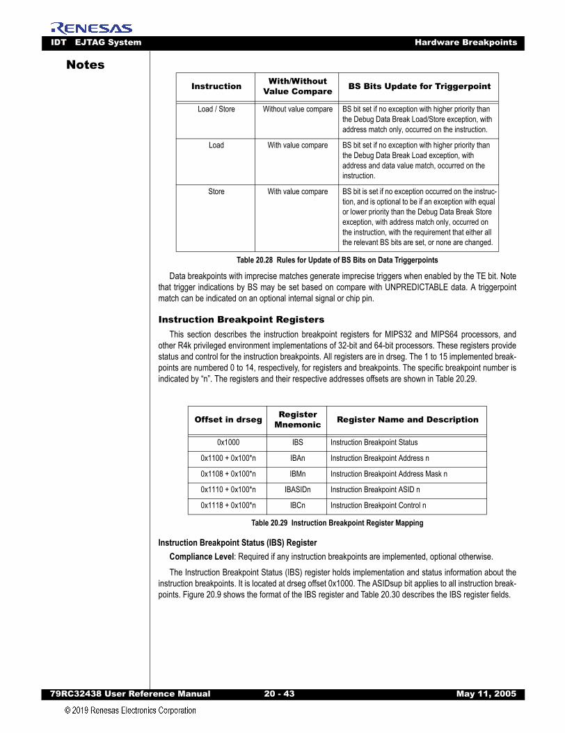
IDT EJTAG System Hardware Breakpoints
79RC32438 User Refer
Notes
Data breakpoints with imprecise matches generate imprecise triggers when enabled by the TE bit. Notethat trigger indications by BS may be set based on compare with UNPREDICTABLE data. A triggerpointmatch can be indicated on an optional internal signal or chip pin.
Instruction Breakpoint RegistersThis section describes the instruction breakpoint registers for MIPS32 and MIPS64 processors, and
other R4k privileged environment implementations of 32-bit and 64-bit processors. These registers providestatus and control for the instruction breakpoints. All registers are in drseg. The 1 to 15 implemented break-points are numbered 0 to 14, respectively, for registers and breakpoints. The specific breakpoint number isindicated by “n”. The registers and their respective addresses offsets are shown in Table 20.29.
Instruction Breakpoint Status (IBS) RegisterCompliance Level: Required if any instruction breakpoints are implemented, optional otherwise.The Instruction Breakpoint Status (IBS) register holds implementation and status information about the
instruction breakpoints. It is located at drseg offset 0x1000. The ASIDsup bit applies to all instruction break-points. Figure 20.9 shows the format of the IBS register and Table 20.30 describes the IBS register fields.
Instruction With/Without Value Compare BS Bits Update for Triggerpoint
Load / Store Without value compare BS bit set if no exception with higher priority than the Debug Data Break Load/Store exception, with address match only, occurred on the instruction.
Load With value compare BS bit set if no exception with higher priority than the Debug Data Break Load exception, with address and data value match, occurred on the instruction.
Store With value compare BS bit is set if no exception occurred on the instruc-tion, and is optional to be if an exception with equal or lower priority than the Debug Data Break Store exception, with address match only, occurred on the instruction, with the requirement that either all the relevant BS bits are set, or none are changed.
Table 20.28 Rules for Update of BS Bits on Data Triggerpoints
Offset in drseg Register Mnemonic Register Name and Description
0x1000 IBS Instruction Breakpoint Status
0x1100 + 0x100*n IBAn Instruction Breakpoint Address n
0x1108 + 0x100*n IBMn Instruction Breakpoint Address Mask n
0x1110 + 0x100*n IBASIDn Instruction Breakpoint ASID n
0x1118 + 0x100*n IBCn Instruction Breakpoint Control n
Table 20.29 Instruction Breakpoint Register Mapping
ence Manual 20 - 43 May 11, 2005
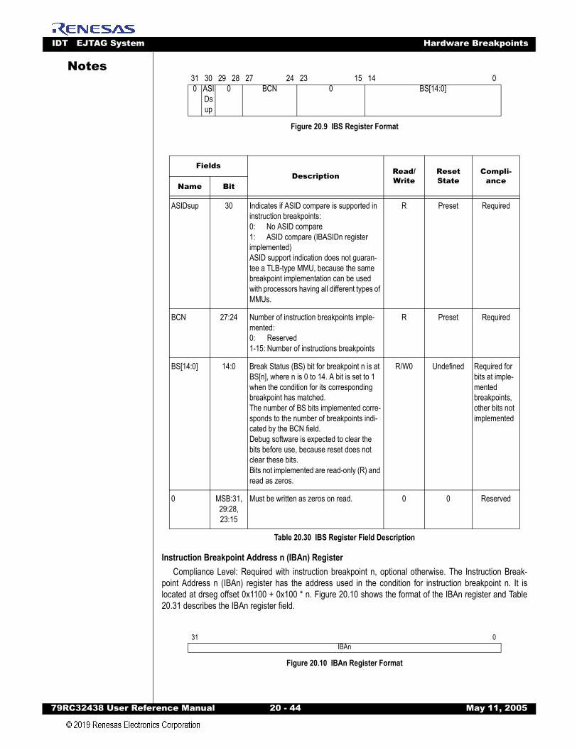
IDT EJTAG System Hardware Breakpoints
79RC32438 User Refer
Notes
Figure 20.9 IBS Register Format
Instruction Breakpoint Address n (IBAn) Register Compliance Level: Required with instruction breakpoint n, optional otherwise. The Instruction Break-
point Address n (IBAn) register has the address used in the condition for instruction breakpoint n. It islocated at drseg offset 0x1100 + 0x100 * n. Figure 20.10 shows the format of the IBAn register and Table20.31 describes the IBAn register field.
Figure 20.10 IBAn Register Format
31 30 29 28 27 24 23 15 14 00 ASI
Dsup
0 BCN 0 BS[14:0]
FieldsDescription Read/
WriteReset State
Compli-ance
Name Bit
ASIDsup 30 Indicates if ASID compare is supported in instruction breakpoints:0: No ASID compare1: ASID compare (IBASIDn register implemented)ASID support indication does not guaran-tee a TLB-type MMU, because the same breakpoint implementation can be used with processors having all different types of MMUs.
R Preset Required
BCN 27:24 Number of instruction breakpoints imple-mented:0: Reserved1-15: Number of instructions breakpoints
R Preset Required
BS[14:0] 14:0 Break Status (BS) bit for breakpoint n is at BS[n], where n is 0 to 14. A bit is set to 1 when the condition for its corresponding breakpoint has matched.The number of BS bits implemented corre-sponds to the number of breakpoints indi-cated by the BCN field.Debug software is expected to clear the bits before use, because reset does not clear these bits. Bits not implemented are read-only (R) and read as zeros.
R/W0 Undefined Required for bits at imple-mented breakpoints, other bits not implemented
0 MSB:31, 29:28, 23:15
Must be written as zeros on read. 0 0 Reserved
Table 20.30 IBS Register Field Description
31 0IBAn
ence Manual 20 - 44 May 11, 2005
IDT EJTAG System Hardware Breakpoints
79RC32438 User Refer
Notes
Instruction Breakpoint Address Mask n (IBMn) Register Compliance Level: Required with instruction breakpoint n, optional otherwise.The Instruction Breakpoint Address Mask n (IBMn) register has the address compare mask used in the
condition for instruction breakpoint n. The address that is masked is in the IBAn register. The IBMn registeris located at drseg offset 0x1108 + 0x100 * n. Figure 20.11 shows the format of the IBMn register and Table20.32 describes the IBMn register field.
Figure 20.11 IBMn Register Format
Instruction Breakpoint ASID n (IBASIDn) Register Compliance Level: Required with instruction breakpoint n if the ASIDsup bit in the IBS register is 1,
optional otherwise.The Instruction Breakpoint ASID n (IBASIDn) register has the ASID value used in the compare for
instruction breakpoint n. It is located at drseg offset 0x1110 + 0x100 * n. Figure 20.12 shows the format ofthe IBASIDn register and Table 20.33 describes the IBASIDn register fields. The width of the ASID field forthe compare is 8 bits. It is identical to the width of the ASID field in the EntryHi register used with the TLB-type MMU.
Figure 20.12 IBASIDn Register Format
FieldsDescription Read/
WriteReset State
Compli-ance
Name Bit
IBA MSB:0 Instruction breakpoint address for condi-tion.
R/W Undefined Required
Table 20.31 IBAn Register Field Description
31 0IBMn
FieldsDescription Read/
WriteReset State
Compli-ance
Name Bit
IBM MSB:0 Instruction breakpoint address mask for condition:0: Corresponding address bit compared1: Corresponding address bit masked.
R/W Undefined Required
Table 20.32 IBMn Register Field Description
31 8 7 00 ASID
ence Manual 20 - 45 May 11, 2005
IDT EJTAG System Hardware Breakpoints
79RC32438 User Refer
Notes
Instruction Breakpoint Control n (IBCn) RegisterCompliance Level: Required with instruction breakpoint n, optional otherwise.The Instruction Breakpoint Control n (IBCn) register determines what constitutes instruction breakpoint
n: triggerpoint, breakpoint, ASID value inclusion. This register is located at drseg offset 0x1118 + 0x100 * n.Figure 20.13 shows the format of the IBCn register and Table 20.34 describes the IBCn register fields.
Figure 20.13 IBCn Register Format
FieldsDescription Read/
WriteReset State
Compli-ance
Name Bit
ASID 7:0 Instruction breakpoint ASID value for com-pare.
R/W Undefined Required
0 MSB:8 Must be written as zeros; return zeros on read.
0 0 Reserved
Table 20.33 IBASIDn Register Field Description
31 24 23 22 3 2 1 00 ASID
use0 TE 0 BE
FieldsDescription Read/
WriteReset State
Compli-ance
Name Bit
ASIDuse 23 Use ASID value in compare for instruction breakpoint n:0: Do not use ASID value in compare1: Use ASID value in compareDebug software should only set the ASI-Duse if a TLB in the implementation is used by the application software.This bit is read-only and reads as zero, if not implemented.
R/W Undefined Required if ASIDsup in IBS register is 1, otherwise not imple-mented
TE 2 Use instruction breakpoint n as trigger-point:0: Do not use it as triggerpoint1: Use it as triggerpoint
R/W 0 Required
BE 0 Use instruction breakpoint n as breakpoint:0: Do not use it as breakpoint1: Use it as breakpoint
R/W 0 Required
0 MSB:24, 22:3, 1
Must be written as zeros; return zeros on read
0 0 Required
Table 20.34 IBCn Register Field Description
ence Manual 20 - 46 May 11, 2005
IDT EJTAG System Hardware Breakpoints
79RC32438 User Refer
Notes
Data Breakpoint RegistersThis section describes the data breakpoint registers for MIPS32 and MIPS64 processors, and other R4kprivileged environment implementations of 32-bit and 64-bit processors. These registers provide status andcontrol for the data breakpoints. All registers are in drseg. The 1 to 15 implemented breakpoints arenumbered 0 to 14, respectively, for registers and breakpoints. The specific breakpoint number is indicatedby “n”. The registers and their respective addresses offsets are shown in Table 20.35.
Data Breakpoint Status (DBS) Register Compliance Level: Required if any data breakpoints are implemented, optional otherwise.The Data Breakpoint Status (DBS) register holds implementation and status information about the data
breakpoints. It is located at drseg offset 0x2000. The ASIDsup, NoSVmatch, and NoLVmatch fields apply toall data breakpoints. Figure 20.14 shows the format of the DBS register and Table 20.36 describes the DBSregister fields
Figure 20.14 DBS Register Format
Offset in drseg
Register Mnemonic Register Name and Description
0x2000 DBS Data Breakpoint Status
0x2100 + 0x100*n DBAn Data Breakpoint Address n
0x2108 + 0x100*n DBMn Data Breakpoint Address Mask n
0x2110 + 0x100*n DBASIDn Data Breakpoint ASID n
0x2118 + 0x100*n DBCn Data Breakpoint Control n
0x2120 + 0x100*n DBVn Data Breakpoint Value n
Table 20.35 Data Breakpoint Register Mapping
31 30 29 28 27 24 23 15 14 00 ASID
supNoSVmatch
NoLV-match
BCN 0 BS[14:0]
FieldsDescription Read/
WriteReset State
Compli-ance
Name Bit
ASIDsup 30 Indicates if ASID compare is supported in data breakpoints:0: No ASID compare1: ASID compare (DBASIDn register implemented)ASID support indication does not guaran-tee a TLB-type MMU, because the same breakpoint implementation can be used with processors having all different types of MMUs.
R Preset Required
Table 20.36 DBS Register Field Description (Part 1 of 2)
ence Manual 20 - 47 May 11, 2005
IDT EJTAG System Hardware Breakpoints
79RC32438 User Refer
Notes
Data Breakpoint Address n (DBAn) RegisterCompliance Level: Required with data breakpoint n, optional otherwise.The Data Breakpoint Address n (DBAn) register has the address used in the condition for data break-
point n. This register is located at drseg offset 0x2100 + 0x100 * n. Figure 20.15 shows the format of theDBAn register and Table 20.37 describes the DBAn register field.
Figure 20.15 DBAn Register Format
NoSV-match
29 Indicates if a value compare on a store is supported in data breakpoints:0: Data value and address in condition on store1: Address compare only in condition on store
R Preset Required
NoLVmatch 28 Indicates if a value compare on a load is supported in data breakpoints:0: Data value and address in condition on load1: Address compare only in condition on load
R Preset Required
BCN 27:24 Number of data breakpoints implemented:0: Reserved1-15:Number of data breakpoints
R Preset Required
BS[14:0] 14:0 Break Status (BS) bit for breakpoint n is at BS[n], where n is 0 to 14. The bit is set to 1 when the condition for its corresponding breakpoint has matched.The number of BS bits implemented corre-sponds to the number of breakpoints indi-cated by the BCN bit.Debug software is expected to clear the bits before use, since these are not cleared by reset.Bits not implemented are read-only (R) and read as zeros.
R/W0 Undefined Required for bits at imple-mented breakpoints, other bits not implemented
0 MSB:31, 23:15
Must be written as zeros; return zeros on read.
0 0 Reserved
31 0DBAn
FieldsDescription Read/
WriteReset State
Compli-ance
Name Bit
DBA MSB:0 Data breakpoint address for condition. R/W Undefined Required
Table 20.37 DBAn Register Field Description
FieldsDescription Read/
WriteReset State
Compli-ance
Name Bit
Table 20.36 DBS Register Field Description (Part 2 of 2)
ence Manual 20 - 48 May 11, 2005
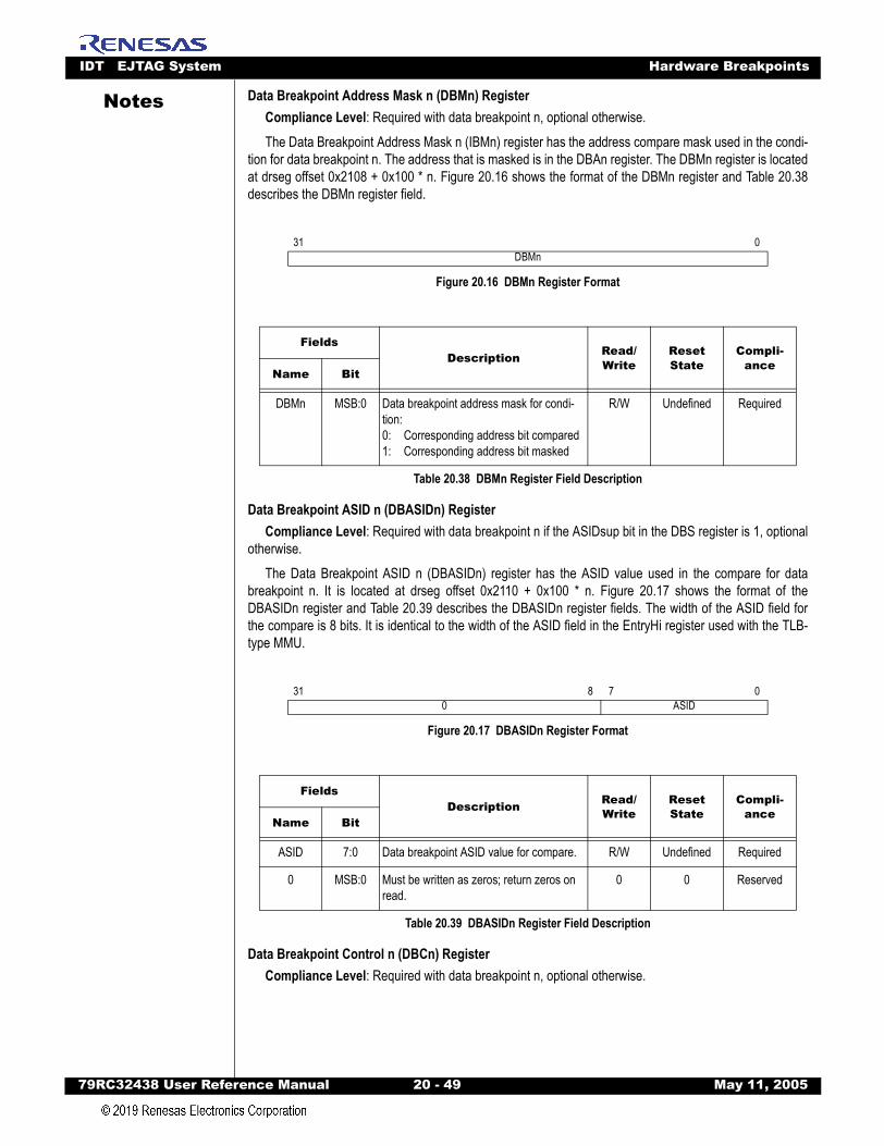
IDT EJTAG System Hardware Breakpoints
79RC32438 User Refer
Notes
Data Breakpoint Address Mask n (DBMn) RegisterCompliance Level: Required with data breakpoint n, optional otherwise.The Data Breakpoint Address Mask n (IBMn) register has the address compare mask used in the condi-tion for data breakpoint n. The address that is masked is in the DBAn register. The DBMn register is locatedat drseg offset 0x2108 + 0x100 * n. Figure 20.16 shows the format of the DBMn register and Table 20.38describes the DBMn register field.
Figure 20.16 DBMn Register Format
Data Breakpoint ASID n (DBASIDn) RegisterCompliance Level: Required with data breakpoint n if the ASIDsup bit in the DBS register is 1, optional
otherwise.The Data Breakpoint ASID n (DBASIDn) register has the ASID value used in the compare for data
breakpoint n. It is located at drseg offset 0x2110 + 0x100 * n. Figure 20.17 shows the format of theDBASIDn register and Table 20.39 describes the DBASIDn register fields. The width of the ASID field forthe compare is 8 bits. It is identical to the width of the ASID field in the EntryHi register used with the TLB-type MMU.
Figure 20.17 DBASIDn Register Format
Data Breakpoint Control n (DBCn) RegisterCompliance Level: Required with data breakpoint n, optional otherwise.
31 0DBMn
FieldsDescription Read/
WriteReset State
Compli-ance
Name Bit
DBMn MSB:0 Data breakpoint address mask for condi-tion:0: Corresponding address bit compared1: Corresponding address bit masked
R/W Undefined Required
Table 20.38 DBMn Register Field Description
31 8 7 00 ASID
FieldsDescription Read/
WriteReset State
Compli-ance
Name Bit
ASID 7:0 Data breakpoint ASID value for compare. R/W Undefined Required
0 MSB:0 Must be written as zeros; return zeros on read.
0 0 Reserved
Table 20.39 DBASIDn Register Field Description
ence Manual 20 - 49 May 11, 2005
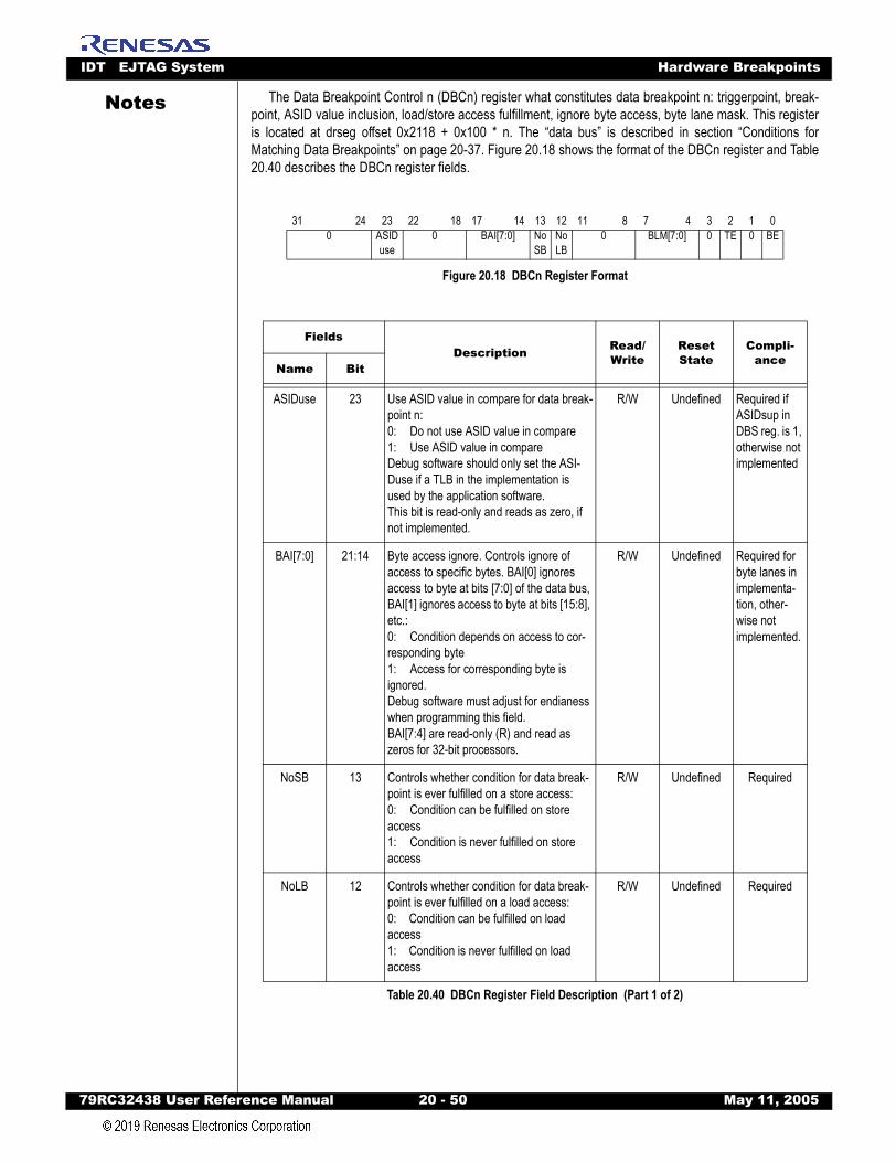
IDT EJTAG System Hardware Breakpoints
79RC32438 User Refer
Notes
The Data Breakpoint Control n (DBCn) register what constitutes data breakpoint n: triggerpoint, break-point, ASID value inclusion, load/store access fulfillment, ignore byte access, byte lane mask. This registeris located at drseg offset 0x2118 + 0x100 * n. The “data bus” is described in section “Conditions forMatching Data Breakpoints” on page 20-37. Figure 20.18 shows the format of the DBCn register and Table20.40 describes the DBCn register fields.Figure 20.18 DBCn Register Format
31 24 23 22 18 17 14 13 12 11 8 7 4 3 2 1 00 ASID
use0 BAI[7:0] No
SBNoLB
0 BLM[7:0] 0 TE 0 BE
FieldsDescription Read/
WriteReset State
Compli-ance
Name Bit
ASIDuse 23 Use ASID value in compare for data break-point n:0: Do not use ASID value in compare1: Use ASID value in compareDebug software should only set the ASI-Duse if a TLB in the implementation is used by the application software.This bit is read-only and reads as zero, if not implemented.
R/W Undefined Required if ASIDsup in DBS reg. is 1, otherwise not implemented
BAI[7:0] 21:14 Byte access ignore. Controls ignore of access to specific bytes. BAI[0] ignores access to byte at bits [7:0] of the data bus, BAI[1] ignores access to byte at bits [15:8], etc.:0: Condition depends on access to cor-responding byte1: Access for corresponding byte is ignored. Debug software must adjust for endianess when programming this field.BAI[7:4] are read-only (R) and read as zeros for 32-bit processors.
R/W Undefined Required for byte lanes in implementa-tion, other-wise not implemented.
NoSB 13 Controls whether condition for data break-point is ever fulfilled on a store access:0: Condition can be fulfilled on store access1: Condition is never fulfilled on store access
R/W Undefined Required
NoLB 12 Controls whether condition for data break-point is ever fulfilled on a load access:0: Condition can be fulfilled on load access1: Condition is never fulfilled on load access
R/W Undefined Required
Table 20.40 DBCn Register Field Description (Part 1 of 2)
ence Manual 20 - 50 May 11, 2005
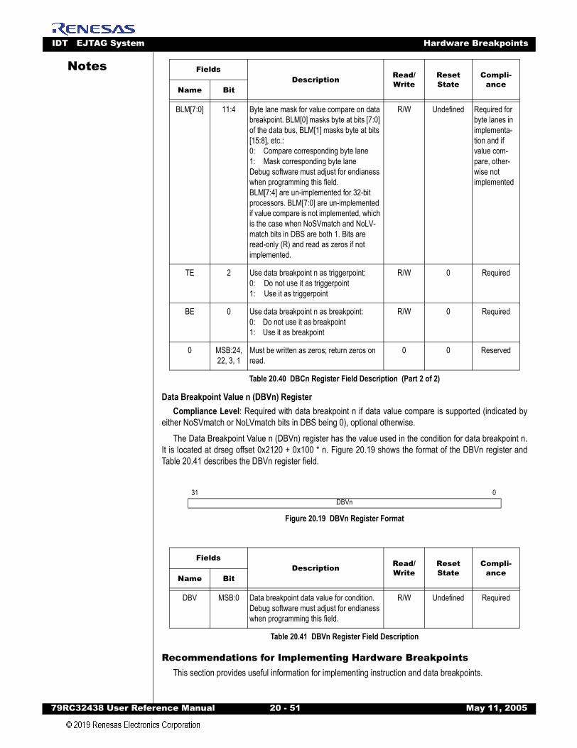
IDT EJTAG System Hardware Breakpoints
79RC32438 User Refer
Notes
Data Breakpoint Value n (DBVn) RegisterCompliance Level: Required with data breakpoint n if data value compare is supported (indicated by
either NoSVmatch or NoLVmatch bits in DBS being 0), optional otherwise.The Data Breakpoint Value n (DBVn) register has the value used in the condition for data breakpoint n.
It is located at drseg offset 0x2120 + 0x100 * n. Figure 20.19 shows the format of the DBVn register andTable 20.41 describes the DBVn register field.
Figure 20.19 DBVn Register Format
Recommendations for Implementing Hardware BreakpointsThis section provides useful information for implementing instruction and data breakpoints.
BLM[7:0] 11:4 Byte lane mask for value compare on data breakpoint. BLM[0] masks byte at bits [7:0] of the data bus, BLM[1] masks byte at bits [15:8], etc.:0: Compare corresponding byte lane1: Mask corresponding byte laneDebug software must adjust for endianess when programming this field.BLM[7:4] are un-implemented for 32-bit processors. BLM[7:0] are un-implemented if value compare is not implemented, which is the case when NoSVmatch and NoLV-match bits in DBS are both 1. Bits are read-only (R) and read as zeros if not implemented.
R/W Undefined Required for byte lanes in implementa-tion and if value com-pare, other-wise not implemented
TE 2 Use data breakpoint n as triggerpoint:0: Do not use it as triggerpoint1: Use it as triggerpoint
R/W 0 Required
BE 0 Use data breakpoint n as breakpoint:0: Do not use it as breakpoint1: Use it as breakpoint
R/W 0 Required
0 MSB:24, 22, 3, 1
Must be written as zeros; return zeros on read.
0 0 Reserved
31 0DBVn
FieldsDescription Read/
WriteReset State
Compli-ance
Name Bit
DBV MSB:0 Data breakpoint data value for condition. Debug software must adjust for endianess when programming this field.
R/W Undefined Required
Table 20.41 DBVn Register Field Description
FieldsDescription Read/
WriteReset State
Compli-ance
Name Bit
Table 20.40 DBCn Register Field Description (Part 2 of 2)
ence Manual 20 - 51 May 11, 2005
IDT EJTAG System Hardware Breakpoints
79RC32438 User Refer
Notes
Number of Instruction Breakpoints Without Single SteppingIf hardware single stepping is not implemented, then at least two instruction breakpoints are required.Four instruction hardware breakpoints are recommended.
Data Breakpoints with Data Value ComparesData breakpoints should be implemented with data value compares. Also, data value compares should
be implemented even if it is not possible to break on loads with precise data value compares. For moreinformation on precise exceptions, refer to section “Precise / Imprecise Debug Exceptions on Data Break-points with Data Value Compares” on page 20-52.
Data Breakpoint Compare on Invalid DataData breakpoints should only compare on valid data, meaning they only generate debug exceptions
based on valid data in the compare. This does also apply to compare on store data for a store to anunaligned address. For example, no debug exception should be generated for a bus error on a load thathas a pending data breakpoint to compare on the data returned by the load. However, in some cases, theindication of invalid data is late relative to the data, for example, for a cache error as a result of a complexerror detection. In this case, data breakpoints can indicate a debug exception because the data wasbelieved to be valid at the time of the compare, and the pending error is then indicated to the debug handlerthrough the DBusEP or CacheEP bit in the Debug register, because the error occurred after the debugexception. Note that for bus errors due to external events, the bus error indication usually is available whenthe compare in the data breakpoint would take place. Thus, it is possible to avoid a debug exception.
Precise / Imprecise Debug Exceptions on Data Breakpoints with Data Value ComparesData breakpoints are recommended to generate precise debug exceptions, if possible in the implemen-
tation. Thus the DEPC register and DBD bit in the Debug register point to the load/store that caused thedebug exception to occur. This instruction can then be re-executed when execution resumes after thedebug handler. However, data breakpoints are allowed to cause imprecise debug exceptions when thebreakpoint is set up with data value compares; for example, if data breakpoints with compares on loadeddata values cannot be made precise due to a non-blocking load. In this case, the DEPC register and DBDbit in the Debug register point to an instruction in the execution flow after the load/store that caused theimprecise debug exception. The BS bit can be updated when the match is detected, even though a debugexception is not taken until later due to internal stalls (for example, a nulled instruction in the pipeline at thetime the match is detected). It is implementation specific as to which cases a data breakpoint can cause animprecise debug exception. It is recommended that the data breakpoints cause imprecise matches in asfew cases as possible.
Implementations can require imprecise debug exceptions from data breakpoints on loads with valuecompares in a specific address range, if re-execution of a load in this range is not acceptable. This case ispossible if the load has side effects such as removing an entry on a queue. Imprecise debug exceptions forvalue compares ensure that the destination register is properly updated with the loaded value, whereby re-execution of the load is avoided.
Breakpoint Examples
Instruction Breakpoint ExamplesThis section provides examples that illustrate using an instruction break.Instruction Break in Small Range of Instructions with ASIDThis example shows how to set up an instruction breakpoint to break on the fetch of any one of the four
instructions in the virtual address range shown below:0x0000 0010 J L1 // ASID = 0x50x0000 0014 NOP0x0000 0018 J L20x0000 001C NOP
ence Manual 20 - 52 May 11, 2005
IDT EJTAG System Hardware Breakpoints
79RC32438 User Refer
Notes
The break registers must be set up as follows:– IBA0 = 0x0000 0010– IBM0 = 0x0000 000C– IBC0: BE=1, ASIDuse=1, ASID = 0x5, other bits zero.Note that IBA0 has the starting address, and IBM0 has the address mask. Instruction Break on 32-bit MIPS16™ InstructionIn this example, instruction breakpoint 0 needs to be set up to break on the range 0x0000 0030 to
0x0000 0036, which starts with the second part of an extended MIPS16 instruction:0x0000 002e EXT // (1st part of MIPS16 inst.)0x0000 0030 ADD // (2nd part)0x0000 0032 SUB0x0000 0034 SUB0x0000 0036 SUB
The break registers must be set up as follows:– IBA0 = 0x0000 0031– IBM0 = 0x0000 0006– IBC0: BE = 1, ASIDuse = 0, other bits zero
The CPU does not take a debug exception when fetching the second part of the ADD instruction,because it does not constitute a whole instruction. The first break is on the SUB instruction at 0x0000 0032.
Data BreakpointThis section provides three examples of data breakpoints.Data Break on Load Access with ASIDThis example shows how to perform a break on data breakpoint 0 when the CPU loads data 0xAAAA
0000 from memory location 0x0000 0100 in ASID=0x7:LW $2, 0x100($0) // ASID = 0x7
The break registers must be set up as follows:– DBA0 = 0x0000 0100– DBM0 = 0x0– DBV0 = 0xAAAA 0000– DBC0: BE = 1, NoLB = 0, NoSB = 1, BLM = 0, BAI = 0, ASIDuse = 1, ASID = 0x7, other bits zero
In this example, DBA0 contains the breakpoint address; DBM0 has the address mask; DBV0 has thedata value; and DBC0 indicates a breakpoint condition might be fulfilled on a load but not on a store, thereis a value compare for a corresponding byte, and an ASID is used.
Data Break on Store(s) to Halfword in MemoryThis example shows a break on data breakpoint 0 when the CPU stores data in a specific halfword in
memory. Stores to the other halfword at the same address can be ignored. The data word is illustrated inFigure 20.20; the halfword for bits 31:16 is shaded. The store instructions shown in Figure 20.20 alter theshaded halfword and cause a break if the breakpoint registers are set up as shown below.
ence Manual 20 - 53 May 11, 2005
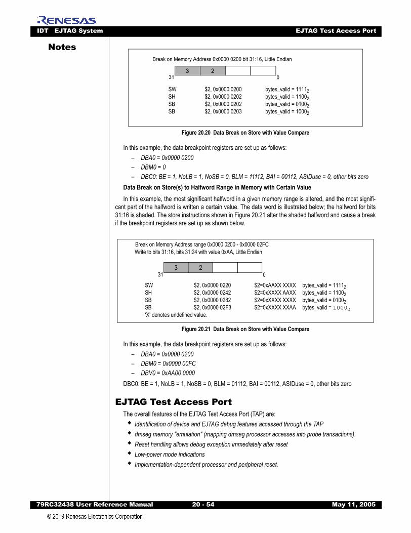
IDT EJTAG System EJTAG Test Access Port
79RC32438 User Refer
Notes
Figure 20.20 Data Break on Store with Value Compare
In this example, the data breakpoint registers are set up as follows: – DBA0 = 0x0000 0200– DBM0 = 0– DBC0: BE = 1, NoLB = 1, NoSB = 0, BLM = 11112, BAI = 00112, ASIDuse = 0, other bits zero
Data Break on Store(s) to Halfword Range in Memory with Certain ValueIn this example, the most significant halfword in a given memory range is altered, and the most signifi-
cant part of the halfword is written a certain value. The data word is illustrated below; the halfword for bits31:16 is shaded. The store instructions shown in Figure 20.21 alter the shaded halfword and cause a breakif the breakpoint registers are set up as shown below.
Figure 20.21 Data Break on Store with Value Compare
In this example, the data breakpoint registers are set up as follows:– DBA0 = 0x0000 0200– DBM0 = 0x0000 00FC– DBV0 = 0xAA00 0000
DBC0: BE = 1, NoLB = 1, NoSB = 0, BLM = 01112, BAI = 00112, ASIDuse = 0, other bits zero
EJTAG Test Access PortThe overall features of the EJTAG Test Access Port (TAP) are:
Identification of device and EJTAG debug features accessed through the TAPdmseg memory "emulation" (mapping dmseg processor accesses into probe transactions).Reset handling allows debug exception immediately after resetLow-power mode indicationsImplementation-dependent processor and peripheral reset.
3 2
Break on Memory Address 0x0000 0200 bit 31:16, Little Endian
31 0
SW $2, 0x0000 0200 bytes_valid = 11112SH $2, 0x0000 0202 bytes_valid = 11002SB $2, 0x0000 0202 bytes_valid = 01002SB $2, 0x0000 0203 bytes_valid = 10002
Break on Memory Address range 0x0000 0200 - 0x0000 02FC Write to bits 31:16, bits 31:24 with value 0xAA, Little Endian
SW $2, 0x0000 0220 $2=0xAAXX XXXX bytes_valid = 11112SH $2, 0x0000 0242 $2=0xXXXX AAXX bytes_valid = 11002SB $2, 0x0000 0282 $2=0xXXXX XXXX bytes_valid = 01002SB $2, 0x0000 02F3 $2=0xXXXX XXAA bytes_valid = 10002‘X’ denotes undefined value.
3 231 0
ence Manual 20 - 54 May 11, 2005
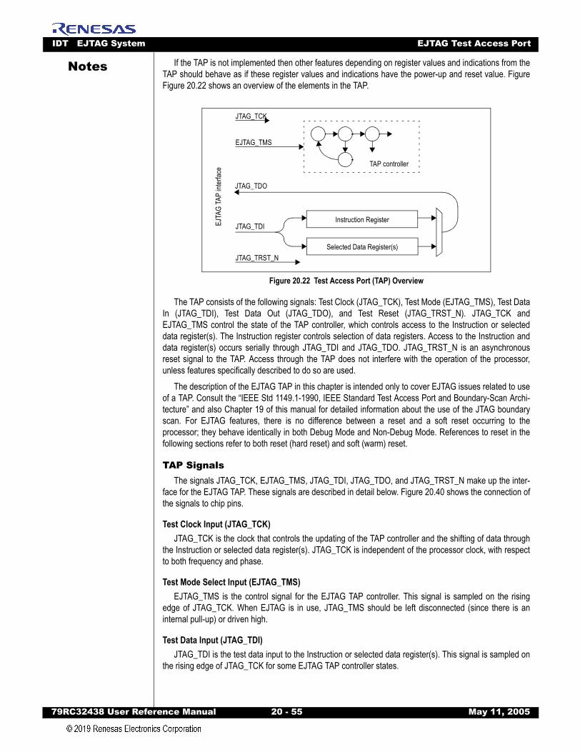
IDT EJTAG System EJTAG Test Access Port
79RC32438 User Refer
Notes
If the TAP is not implemented then other features depending on register values and indications from theTAP should behave as if these register values and indications have the power-up and reset value. FigureFigure 20.22 shows an overview of the elements in the TAP.Figure 20.22 Test Access Port (TAP) Overview
The TAP consists of the following signals: Test Clock (JTAG_TCK), Test Mode (EJTAG_TMS), Test DataIn (JTAG_TDI), Test Data Out (JTAG_TDO), and Test Reset (JTAG_TRST_N). JTAG_TCK andEJTAG_TMS control the state of the TAP controller, which controls access to the Instruction or selecteddata register(s). The Instruction register controls selection of data registers. Access to the Instruction anddata register(s) occurs serially through JTAG_TDI and JTAG_TDO. JTAG_TRST_N is an asynchronousreset signal to the TAP. Access through the TAP does not interfere with the operation of the processor,unless features specifically described to do so are used.
The description of the EJTAG TAP in this chapter is intended only to cover EJTAG issues related to useof a TAP. Consult the “IEEE Std 1149.1-1990, IEEE Standard Test Access Port and Boundary-Scan Archi-tecture” and also Chapter 19 of this manual for detailed information about the use of the JTAG boundaryscan. For EJTAG features, there is no difference between a reset and a soft reset occurring to theprocessor; they behave identically in both Debug Mode and Non-Debug Mode. References to reset in thefollowing sections refer to both reset (hard reset) and soft (warm) reset.
TAP SignalsThe signals JTAG_TCK, EJTAG_TMS, JTAG_TDI, JTAG_TDO, and JTAG_TRST_N make up the inter-
face for the EJTAG TAP. These signals are described in detail below. Figure 20.40 shows the connection ofthe signals to chip pins.
Test Clock Input (JTAG_TCK)JTAG_TCK is the clock that controls the updating of the TAP controller and the shifting of data through
the Instruction or selected data register(s). JTAG_TCK is independent of the processor clock, with respectto both frequency and phase.
Test Mode Select Input (EJTAG_TMS)EJTAG_TMS is the control signal for the EJTAG TAP controller. This signal is sampled on the rising
edge of JTAG_TCK. When EJTAG is in use, JTAG_TMS should be left disconnected (since there is aninternal pull-up) or driven high.
Test Data Input (JTAG_TDI)JTAG_TDI is the test data input to the Instruction or selected data register(s). This signal is sampled on
the rising edge of JTAG_TCK for some EJTAG TAP controller states.
Instruction Register
Selected Data Register(s)
JTAG_TDI
JTAG_TDO
EJTA
G TA
P int
erfac
e
JTAG_TCK
EJTAG_TMS
JTAG_TRST_N
TAP controller
ence Manual 20 - 55 May 11, 2005
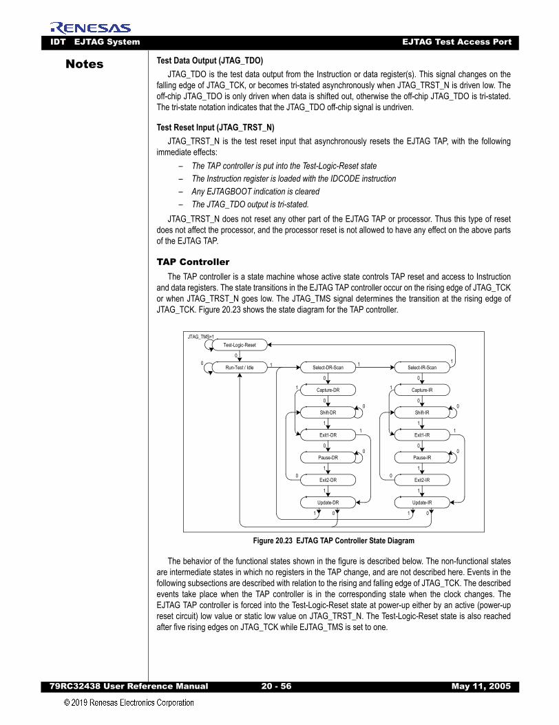
IDT EJTAG System EJTAG Test Access Port
79RC32438 User Refer
Notes
Test Data Output (JTAG_TDO)JTAG_TDO is the test data output from the Instruction or data register(s). This signal changes on thefalling edge of JTAG_TCK, or becomes tri-stated asynchronously when JTAG_TRST_N is driven low. Theoff-chip JTAG_TDO is only driven when data is shifted out, otherwise the off-chip JTAG_TDO is tri-stated.The tri-state notation indicates that the JTAG_TDO off-chip signal is undriven.
Test Reset Input (JTAG_TRST_N)JTAG_TRST_N is the test reset input that asynchronously resets the EJTAG TAP, with the following
immediate effects:– The TAP controller is put into the Test-Logic-Reset state– The Instruction register is loaded with the IDCODE instruction– Any EJTAGBOOT indication is cleared– The JTAG_TDO output is tri-stated.
JTAG_TRST_N does not reset any other part of the EJTAG TAP or processor. Thus this type of resetdoes not affect the processor, and the processor reset is not allowed to have any effect on the above partsof the EJTAG TAP.
TAP ControllerThe TAP controller is a state machine whose active state controls TAP reset and access to Instruction
and data registers. The state transitions in the EJTAG TAP controller occur on the rising edge of JTAG_TCKor when JTAG_TRST_N goes low. The JTAG_TMS signal determines the transition at the rising edge ofJTAG_TCK. Figure 20.23 shows the state diagram for the TAP controller.
Figure 20.23 EJTAG TAP Controller State Diagram
The behavior of the functional states shown in the figure is described below. The non-functional statesare intermediate states in which no registers in the TAP change, and are not described here. Events in thefollowing subsections are described with relation to the rising and falling edge of JTAG_TCK. The describedevents take place when the TAP controller is in the corresponding state when the clock changes. TheEJTAG TAP controller is forced into the Test-Logic-Reset state at power-up either by an active (power-upreset circuit) low value or static low value on JTAG_TRST_N. The Test-Logic-Reset state is also reachedafter five rising edges on JTAG_TCK while EJTAG_TMS is set to one.
Test-Logic-ResetJTAG_TMS=1
Run-Test / Idle
0
Select-DR-Scan10
Capture-DR
0
0
Shift-DR
1
Exit1-DR
0
Pause-DR
1
Exit2-DR
1
Update-DR
0
0
01
1
0
1
Select-IR-Scan
Capture-IR
0
0
Shift-IR
1
Exit1-IR
0
Pause-IR
1
Exit2-IR
1
Update-IR
0
0
01
1
0
1
1 1
ence Manual 20 - 56 May 11, 2005

IDT EJTAG System EJTAG Test Access Port
79RC32438 User Refer
Notes
Test-Logic-Reset StateWhen the Test-Logic-Reset state is entered, the Instruction register is loaded with the IDCODE instruc-tion, and any EJTAGBOOT indication is cleared. This state ensures that the TAP does not interfere with thenormal operation of the CPU core. The TAP controller always reaches this state after five rising edges onJTAG_TCK when EJTAG_TMS is set to 1. A low value on JTAG_TRST_N immediately places the TAPcontroller in this state asynchronous to JTAG_TCK.
Capture-IR StateIn the Capture-IR state, the two LSBs of the Instruction register are loaded with the value 012, and the
upper MSBs are loaded with implementation-dependent values. Both values are loaded on the rising edgeof JTAG_TCK.
Shift-IR StateIn the Shift-IR state, the LSB of the Instruction register is output on JTAG_TDO on the falling edge of
JTAG_TCK. The Instruction register is shifted one position from MSB to LSB on the rising edge ofJTAG_TCK, with the MSB shifted in from JTAG_TDI. The value in the Instruction register does not takeeffect until the Update-IR state. Figure 20.24 shows the shifting direction for the Instruction register.
Figure 20.24 JTAG_TDI to JTAG_TDO Path in Shift Mode State
The length of the Instruction register is specified in section “Instruction Register and Special Instruc-tions” on page 20-58. The value loaded in the Capture-IR state is used as the initial value for the Instructionregister when shifting starts. Thus, it is not possible to read out the previous value of the Instruction register.
Update-IR StateIn the Update-IR state, the value in the Instruction register takes effect on the rising or falling edge of
JTAG_TCK.
Capture-DR StateIn the Capture-DR state, the value of the selected data register(s) is captured on the rising edge of
JTAG_TCK for shifting out in the Shift-DR state. The Capture-DR state reads the data, in order to outputthis read value in the Shift-DR state. The Instruction register controls the selection of the following dataregister(s): Bypass, Device ID, Implementation, EJTAG Control, Address, and Data register(s).
Shift-DR StateIn the Shift-DR state, the LSB of the selected data register(s) is output on JTAG_TDO on the falling edge
of JTAG_TCK. The selected data register(s) is shifted one position from MSB to LSB on the rising edge ofJTAG_TCK, with JTAG_TDI shifted in at the MSB. The value(s) shifted into the register(s) does not takeeffect until the Update-DR state. Figure 20.25 shows the shifting direction for the selected data register.
Figure 20.25 JTAG_TDI to JTAG_TDO Path for Selected Data Register(s) in Shift-DR State
The length of the shift path depends on the selected data register(s).
Update-DR StateIn the Update-DR state, the update of the selected data register(s) with the value from the Shift-DR state
occurs on the falling or rising edge of JTAG_TCK. This update writes the selected register(s).
JTAG_TDI Instruction RegisterMSB 0 / LSB
JTAG_TDO
MSB 0 / LSB
JTAG_TDI JTAG_TDOSelected Data Register(s)
ence Manual 20 - 57 May 11, 2005

IDT EJTAG System EJTAG Test Access Port
79RC32438 User Refer
Notes
Instruction Register and Special InstructionsThe Instruction register controls selection of accessed data register(s), and controls the setting andclearing of the EJTAGBOOT indication. The Instruction register is five or more bits wide when used withEJTAG. Table 20.42 shows the allocation of the TAP instruction.
The instructions IDCODE, IMPCODE, ADDRESS, DATA, CONTROL, and BYPASS select a single dataregister, as indicated in the table. The unused instructions reserved for EJTAG select the Bypass register.The ALL, EJTAGBOOT, NORMALBOOT, and FASTDATA instructions are described in the followingsubsections. The instructions that are related to trace registers in the trace control block (TCB) aredescribed in the Trace Control Block Specification document. Any EJTAGBOOT indication is cleared atpower-up either by a low value on the JTAG_TRST_N or by a power-up reset circuit, and the Instructionregister is loaded with the IDCODE instruction.
ALL InstructionThe Address, Data, and EJTAG Control data registers are selected at once with the ALL instruction, as
shown in Figure 20.26.
Code Instruction Function
All 0’s (Free for other use) Free for other use, such as JTAG boundary scan
0x01 IDCODE Selects Device Identification (ID) register
0x02 (Free for other use) Free for other use, such as JTAG boundary scan
0x03 IMPCODE Selects Implementation register
0x04 — 0x07 (Free for other use) Free for other use, such as JTAG boundary scan
0x08 ADDRESS Selects Address register
0x09 DATA Selects Data register
0x0A CONTROL Selects EJTAG Control register
0x0B ALL Selects the Address, Data and EJTAG Control registers
0x0C EJTAGBOOT Makes the processor take a debug exception after reset
0x0D NORMALBOOT Makes the processor execute the reset handler after reset
0x0E FASTDATA Selects the Data and Fastdata registers
0x0F (EJTAG reserved) Reserved for future EJTAG use
0x010 TCBCONTROLA Selects the control register TCBTraceControl in the Trace Control Block
0x011 TCBCONTROLB Selects another trace control block register
0x012 TCBADDRESS Selects the address register used in the trace control block
0x013 — 0x1B (EJTAG reserved) Reserved for future EJTAG use
0x01C — All 1’s (Free for other use) Free for other use, such as JTAG boundary scan
All 1’s BYPASS Select Bypass register
Table 20.42 EJTAG TAP Instruction Overview
ence Manual 20 - 58 May 11, 2005

IDT EJTAG System EJTAG Test Access Port
79RC32438 User Refer
Notes
Figure 20.26 JTAG_TDI to JTAG_TDO Path in Shft-DR State and ALL Instruction is Selected
EJTAGBOOT and NORMALBOOT InstructionsThe EJTAGBOOT and NORMALBOOT instructions control whether a debug interrupt is requested as a
result of a reset. If EJTAGBOOT is indicated then a debug interrupt is requested at reset, and a DebugInterrupt exception is taken right after the Reset exception. The debug exception handler is in this casefetched from the probe through dmseg. It is possible to take the debug exception and execute the debughandler from the probe even if no instructions can be fetched from the reset handler. This condition guaran-tees that the system will not hang at reset when the EJTAGBOOT feature is used, not even if the normalmemory system does not work properly.
An internal EJTAGBOOT indication holds information on the action to take at a processor reset, and thisis set when the EJTAGBOOT instruction takes effect in the Update-IR state. The indication is cleared whenthe NORMALBOOT instruction takes effect in the Update-IR state, or when the Test-Logic-Reset state isentered, for example, when JTAG_TRST_N is asserted low. The requirement of clearing the internalEJTAGBOOT indication when the Test-Logic-Reset state is entered, and not on a JTAG_TCK clock when inthe state, ensures that the indication can be cleared with five clocks on JTAG_TCK when EJTAG_TMS ishigh.
The internal EJTAGBOOT indication is cleared at power-up either by a low value on the JTAG_TRST_Nor by a power-up reset circuit. Thus, the processor executes the reset handler after power-up unless theEJTAGBOOT instruction is given through the EJTAG TAP. The Bypass register is selected when theEJTAGBOOT or NORMALBOOT instruction is given. The EjtagBrk, ProbEn, and ProbTrap bits in theEJTAG Control register follow the internal EJTAGBOOT indication. They are all set at processor reset if aDebug Interrupt exception is to be generated, with execution of the debug handler from the probe.
FASTDATA InstructionThis selects the Data and the Fastdata registers at once, as shown in Figure 20.27.
Figure 20.27 JTAG_TDI to JTAG_TDO Path in Shift-DR State and FASTDATA Instruction is Selected
TAP Data RegistersTable 20.43 summarizes the data registers in the EJTAG TAP. Complete descriptions of these registers
are given in the following sections.
Instruction Used to Access Register
Register Name Function Reference Compli-
ance
IDCODE Device ID Identifies device and accessed processor in the device.
“Device Identification (ID) Register (TAP Instruction IDCODE)” on page 20-61
Required
Table 20.43 EJTAG TAP Data Registers (Part 1 of 2)
JTAG_TDIAddress register EJTAG Control registerData register
JTAG_TDO
MSB 0 / LSBMSB 0 / LSB MSB 0 / LSB
JTAG_TDI Fastdata registerData registerJTAG_TDO
MSB 0 / LSB 0
ence Manual 20 - 59 May 11, 2005
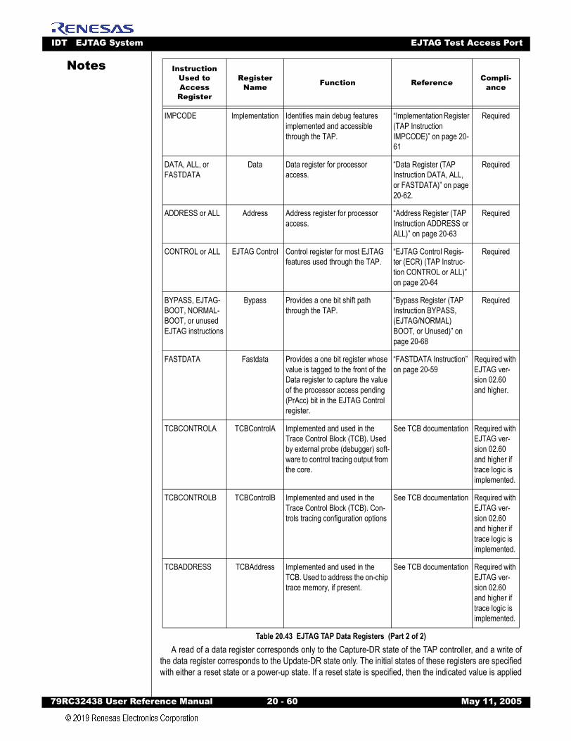
IDT EJTAG System EJTAG Test Access Port
79RC32438 User Refer
Notes
A read of a data register corresponds only to the Capture-DR state of the TAP controller, and a write ofthe data register corresponds to the Update-DR state only. The initial states of these registers are specifiedwith either a reset state or a power-up state. If a reset state is specified, then the indicated value is applied
IMPCODE Implementation Identifies main debug features implemented and accessible through the TAP.
“Implementation Register (TAP Instruction IMPCODE)” on page 20-61
Required
DATA, ALL, or FASTDATA
Data Data register for processor access.
“Data Register (TAP Instruction DATA, ALL, or FASTDATA)” on page 20-62.
Required
ADDRESS or ALL Address Address register for processor access.
“Address Register (TAP Instruction ADDRESS or ALL)” on page 20-63
Required
CONTROL or ALL EJTAG Control Control register for most EJTAG features used through the TAP.
“EJTAG Control Regis-ter (ECR) (TAP Instruc-tion CONTROL or ALL)” on page 20-64
Required
BYPASS, EJTAG-BOOT, NORMAL-BOOT, or unused EJTAG instructions
Bypass Provides a one bit shift path through the TAP.
“Bypass Register (TAP Instruction BYPASS, (EJTAG/NORMAL) BOOT, or Unused)” on page 20-68
Required
FASTDATA Fastdata Provides a one bit register whose value is tagged to the front of the Data register to capture the value of the processor access pending (PrAcc) bit in the EJTAG Control register.
“FASTDATA Instruction” on page 20-59
Required with EJTAG ver-sion 02.60 and higher.
TCBCONTROLA TCBControlA Implemented and used in the Trace Control Block (TCB). Used by external probe (debugger) soft-ware to control tracing output from the core.
See TCB documentation Required with EJTAG ver-sion 02.60 and higher if trace logic is implemented.
TCBCONTROLB TCBControlB Implemented and used in the Trace Control Block (TCB). Con-trols tracing configuration options
See TCB documentation Required with EJTAG ver-sion 02.60 and higher if trace logic is implemented.
TCBADDRESS TCBAddress Implemented and used in the TCB. Used to address the on-chip trace memory, if present.
See TCB documentation Required with EJTAG ver-sion 02.60 and higher if trace logic is implemented.
Instruction Used to Access Register
Register Name Function Reference Compli-
ance
Table 20.43 EJTAG TAP Data Registers (Part 2 of 2)
ence Manual 20 - 60 May 11, 2005
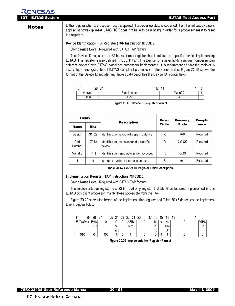
IDT EJTAG System EJTAG Test Access Port
79RC32438 User Refer
Notes
to the register when a processor reset is applied. If a power-up state is specified, then the indicated value isapplied at power-up reset. JTAG_TCK does not have to be running in order for a processor reset to resetthe registers.Device Identification (ID) Register (TAP Instruction IDCODE)Compliance Level: Required with EJTAG TAP feature.The Device ID register is a 32-bit read-only register that identifies the specific device implementing
EJTAG. This register is also defined in IEEE 1149.1. The Device ID register holds a unique number amongdifferent devices with EJTAG compliant processors implemented. It is recommended that the register isalso unique amongst different EJTAG compliant processors in the same device. Figure 20.28 shows theformat of the Device ID register and Table 20.44 describes the Device ID register fields
Implementation Register (TAP Instruction IMPCODE)Compliance Level: Required with EJTAG TAP feature.The Implementation register is a 32-bit read-only register that identifies features implemented in this
EJTAG compliant processor, mainly those accessible from the TAP.Figure 20.29 shows the format of the Implementation register and Table 20.45 describes the Implemen-
tation register fields.
31 28 27 12 11 1 0Version PartNumber ManufID 1
0000 0022 033
Figure 20.28 Device ID Register Format
FieldsDescription Read/
WritePower-up
StateCompli-
anceName Bits
Version 31_28 Identifies the version of a specific device. R 0x0 Required
Part Number
27:12 Identifies the part number of a specific device.
R 0x0022 Required
ManufID 11:1 Identifies the manufacturer identity code. R 0x33 Required
1 0 Ignored on write; returns one on read. R 0x1 Required
Table 20.44 Device ID Register Field Description
31 29 28 27 25 24 23 22 21 20 17 16 15 14 13 1 0EJTAGver R4k/
R3k0 DI
NTsup
0 ASIDsize
0 MIPS16
0 NoDMA
0 MIPS32
010 0 000 0 0 0 0 0 0 1 0 0
Figure 20.29 Implementation Register Format
ence Manual 20 - 61 May 11, 2005
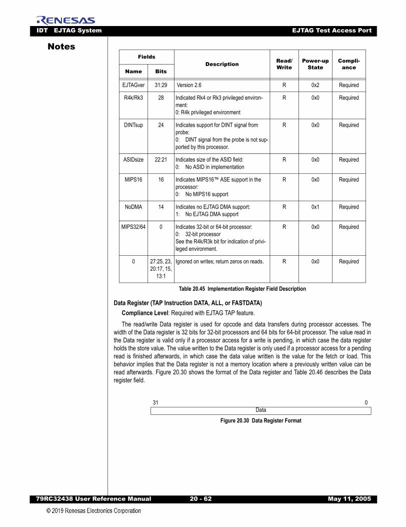
IDT EJTAG System EJTAG Test Access Port
79RC32438 User Refer
Notes
Data Register (TAP Instruction DATA, ALL, or FASTDATA)Compliance Level: Required with EJTAG TAP feature.The read/write Data register is used for opcode and data transfers during processor accesses. The
width of the Data register is 32 bits for 32-bit processors and 64 bits for 64-bit processor. The value read inthe Data register is valid only if a processor access for a write is pending, in which case the data registerholds the store value. The value written to the Data register is only used if a processor access for a pendingread is finished afterwards, in which case the data value written is the value for the fetch or load. Thisbehavior implies that the Data register is not a memory location where a previously written value can beread afterwards. Figure 20.30 shows the format of the Data register and Table 20.46 describes the Dataregister field.
FieldsDescription Read/
WritePower-up
StateCompli-
anceName Bits
EJTAGver 31:29 Version 2.6 R 0x2 Required
R4k/Rk3 28 Indicated Rk4 or Rk3 privileged environ-ment:0: R4k privileged environment
R 0x0 Required
DINTsup 24 Indicates support for DINT signal from probe:0: DINT signal from the probe is not sup-ported by this processor.
R 0x0 Required
ASIDsize 22:21 Indicates size of the ASID field:0: No ASID in implementation
R 0x0 Required
MIPS16 16 Indicates MIPS16™ ASE support in the processor:0: No MIPS16 support
R 0x0 Required
NoDMA 14 Indicates no EJTAG DMA support:1: No EJTAG DMA support
R 0x1 Required
MIPS32/64 0 Indicates 32-bit or 64-bit processor:0: 32-bit processorSee the R4k/R3k bit for indication of privi-leged environment.
R 0x0 Required
0 27:25, 23, 20:17, 15,
13:1
Ignored on writes; return zeros on reads. R 0x0 Required
Table 20.45 Implementation Register Field Description
31 0Data
Figure 20.30 Data Register Format
ence Manual 20 - 62 May 11, 2005
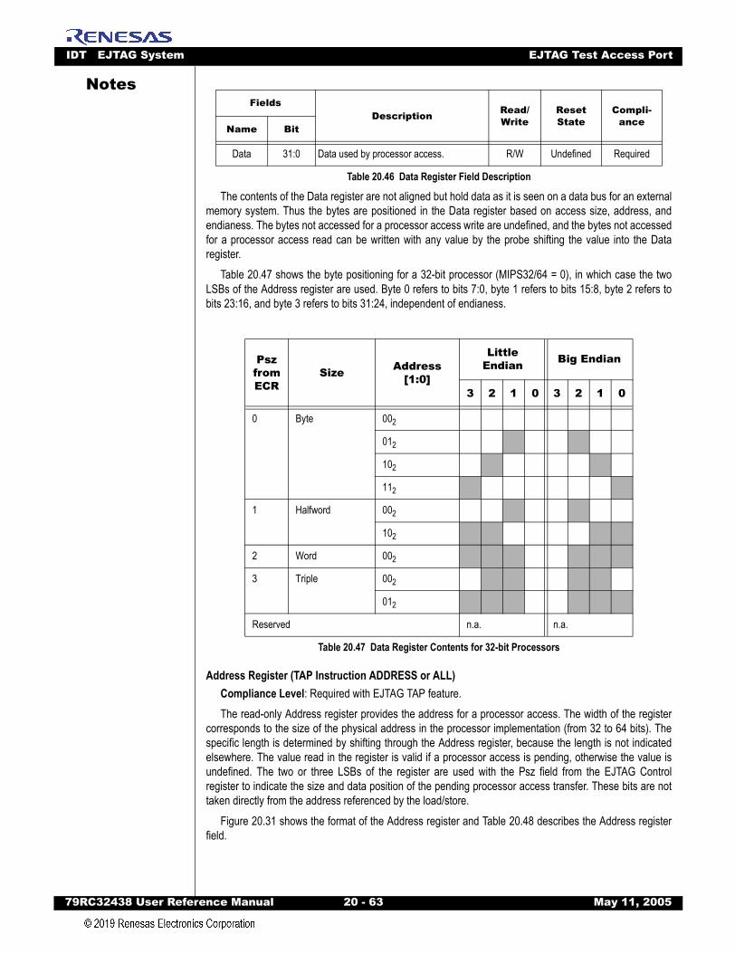
IDT EJTAG System EJTAG Test Access Port
79RC32438 User Refer
Notes
The contents of the Data register are not aligned but hold data as it is seen on a data bus for an externalmemory system. Thus the bytes are positioned in the Data register based on access size, address, andendianess. The bytes not accessed for a processor access write are undefined, and the bytes not accessedfor a processor access read can be written with any value by the probe shifting the value into the Dataregister.
Table 20.47 shows the byte positioning for a 32-bit processor (MIPS32/64 = 0), in which case the twoLSBs of the Address register are used. Byte 0 refers to bits 7:0, byte 1 refers to bits 15:8, byte 2 refers tobits 23:16, and byte 3 refers to bits 31:24, independent of endianess.
Address Register (TAP Instruction ADDRESS or ALL)Compliance Level: Required with EJTAG TAP feature.The read-only Address register provides the address for a processor access. The width of the register
corresponds to the size of the physical address in the processor implementation (from 32 to 64 bits). Thespecific length is determined by shifting through the Address register, because the length is not indicatedelsewhere. The value read in the register is valid if a processor access is pending, otherwise the value isundefined. The two or three LSBs of the register are used with the Psz field from the EJTAG Controlregister to indicate the size and data position of the pending processor access transfer. These bits are nottaken directly from the address referenced by the load/store.
Figure 20.31 shows the format of the Address register and Table 20.48 describes the Address registerfield.
FieldsDescription Read/
WriteReset State
Compli-ance
Name Bit
Data 31:0 Data used by processor access. R/W Undefined Required
Table 20.46 Data Register Field Description
PszfromECR
Size Address[1:0]
Little Endian Big Endian
3 2 1 0 3 2 1 0
0 Byte 002
012
102
112
1 Halfword 002
102
2 Word 002
3 Triple 002
012
Reserved n.a. n.a.
Table 20.47 Data Register Contents for 32-bit Processors
ence Manual 20 - 63 May 11, 2005
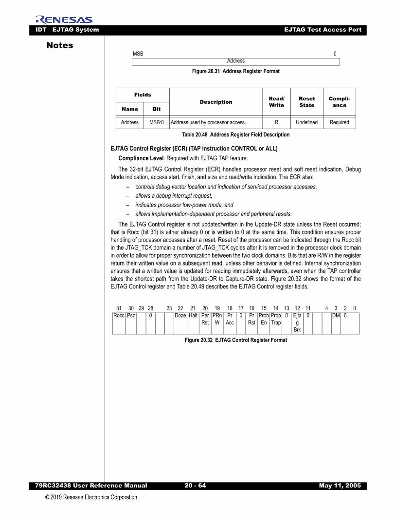
IDT EJTAG System EJTAG Test Access Port
79RC32438 User Refer
Notes
EJTAG Control Register (ECR) (TAP Instruction CONTROL or ALL)Compliance Level: Required with EJTAG TAP feature.The 32-bit EJTAG Control Register (ECR) handles processor reset and soft reset indication, Debug
Mode indication, access start, finish, and size and read/write indication. The ECR also:– controls debug vector location and indication of serviced processor accesses, – allows a debug interrupt request, – indicates processor low-power mode, and – allows implementation-dependent processor and peripheral resets.
The EJTAG Control register is not updated/written in the Update-DR state unless the Reset occurred;that is Rocc (bit 31) is either already 0 or is written to 0 at the same time. This condition ensures properhandling of processor accesses after a reset. Reset of the processor can be indicated through the Rocc bitin the JTAG_TCK domain a number of JTAG_TCK cycles after it is removed in the processor clock domainin order to allow for proper synchronization between the two clock domains. Bits that are R/W in the registerreturn their written value on a subsequent read, unless other behavior is defined. Internal synchronizationensures that a written value is updated for reading immediately afterwards, even when the TAP controllertakes the shortest path from the Update-DR to Capture-DR state. Figure 20.32 shows the format of theEJTAG Control register and Table 20.49 describes the EJTAG Control register fields.
MSB 0Address
Figure 20.31 Address Register Format
FieldsDescription Read/
WriteReset State
Compli-ance
Name Bit
Address MSB:0 Address used by processor access. R Undefined Required
Table 20.48 Address Register Field Description
31 30 29 28 23 22 21 20 19 18 17 16 15 14 13 12 11 4 3 2 0Rocc Psz 0 Doze Halt Per
RstPRnW
PrAcc
0 PrRst
ProbEn
ProbTrap
0 Ejtag
Brk
0 DM 0
Figure 20.32 EJTAG Control Register Format
ence Manual 20 - 64 May 11, 2005
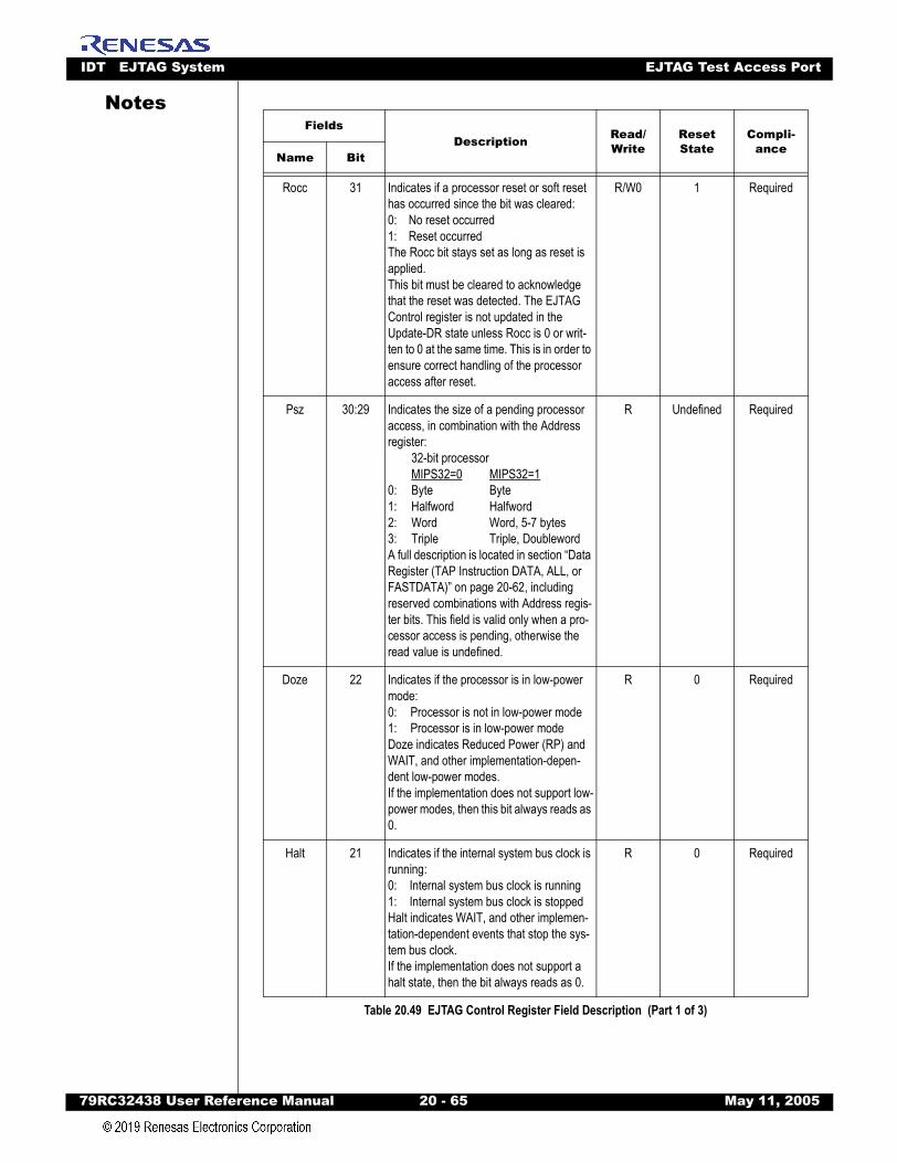
IDT EJTAG System EJTAG Test Access Port
79RC32438 User Refer
Notes
FieldsDescription Read/Write
Reset State
Compli-ance
Name Bit
Rocc 31 Indicates if a processor reset or soft reset has occurred since the bit was cleared:0: No reset occurred 1: Reset occurred The Rocc bit stays set as long as reset is applied.This bit must be cleared to acknowledge that the reset was detected. The EJTAG Control register is not updated in the Update-DR state unless Rocc is 0 or writ-ten to 0 at the same time. This is in order to ensure correct handling of the processor access after reset.
R/W0 1 Required
Psz 30:29 Indicates the size of a pending processor access, in combination with the Address register:
32-bit processorMIPS32=0 MIPS32=1
0: Byte Byte1: Halfword Halfword2: Word Word, 5-7 bytes3: Triple Triple, DoublewordA full description is located in section “Data Register (TAP Instruction DATA, ALL, or FASTDATA)” on page 20-62, including reserved combinations with Address regis-ter bits. This field is valid only when a pro-cessor access is pending, otherwise the read value is undefined.
R Undefined Required
Doze 22 Indicates if the processor is in low-power mode:0: Processor is not in low-power mode1: Processor is in low-power modeDoze indicates Reduced Power (RP) and WAIT, and other implementation-depen-dent low-power modes.If the implementation does not support low-power modes, then this bit always reads as 0.
R 0 Required
Halt 21 Indicates if the internal system bus clock is running:0: Internal system bus clock is running1: Internal system bus clock is stoppedHalt indicates WAIT, and other implemen-tation-dependent events that stop the sys-tem bus clock.If the implementation does not support a halt state, then the bit always reads as 0.
R 0 Required
Table 20.49 EJTAG Control Register Field Description (Part 1 of 3)
ence Manual 20 - 65 May 11, 2005
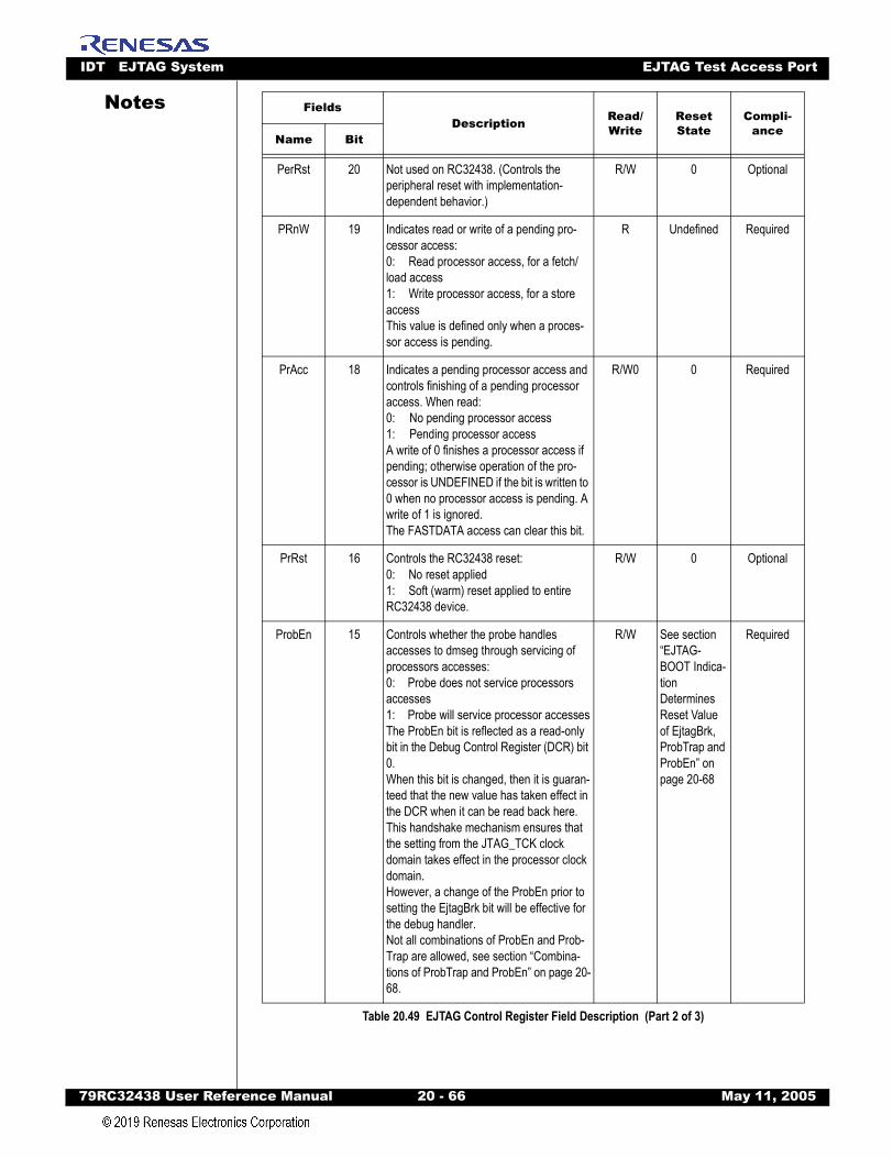
IDT EJTAG System EJTAG Test Access Port
79RC32438 User Refer
Notes
PerRst 20 Not used on RC32438. (Controls the peripheral reset with implementation-dependent behavior.)
R/W 0 Optional
PRnW 19 Indicates read or write of a pending pro-cessor access:0: Read processor access, for a fetch/load access1: Write processor access, for a store accessThis value is defined only when a proces-sor access is pending.
R Undefined Required
PrAcc 18 Indicates a pending processor access and controls finishing of a pending processor access. When read:0: No pending processor access1: Pending processor accessA write of 0 finishes a processor access if pending; otherwise operation of the pro-cessor is UNDEFINED if the bit is written to 0 when no processor access is pending. A write of 1 is ignored.The FASTDATA access can clear this bit.
R/W0 0 Required
PrRst 16 Controls the RC32438 reset:0: No reset applied1: Soft (warm) reset applied to entire RC32438 device.
R/W 0 Optional
ProbEn 15 Controls whether the probe handles accesses to dmseg through servicing of processors accesses:0: Probe does not service processors accesses1: Probe will service processor accessesThe ProbEn bit is reflected as a read-only bit in the Debug Control Register (DCR) bit 0.When this bit is changed, then it is guaran-teed that the new value has taken effect in the DCR when it can be read back here. This handshake mechanism ensures that the setting from the JTAG_TCK clock domain takes effect in the processor clock domain. However, a change of the ProbEn prior to setting the EjtagBrk bit will be effective for the debug handler. Not all combinations of ProbEn and Prob-Trap are allowed, see section “Combina-tions of ProbTrap and ProbEn” on page 20-68.
R/W See section “EJTAG-BOOT Indica-tion Determines Reset Value of EjtagBrk, ProbTrap and ProbEn” on page 20-68
Required
FieldsDescription Read/
WriteReset State
Compli-ance
Name Bit
Table 20.49 EJTAG Control Register Field Description (Part 2 of 3)
ence Manual 20 - 66 May 11, 2005
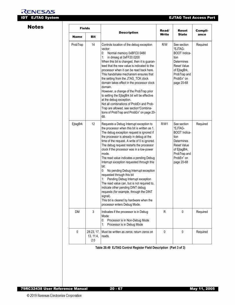
IDT EJTAG System EJTAG Test Access Port
79RC32438 User Refer
Notes
ProbTrap 14 Controls location of the debug exception vector:0: Normal memory 0xBFC0 04801: in dmseg at 0xFF20 0200When this bit is changed, then it is guaran-teed that the new value is indicated to the processor when it can be read back here. This handshake mechanism ensures that the setting from the JTAG_TCK clock domain takes effect in the processor clock domain. However, a change of the ProbTrap prior to setting the EjtagBrk bit will be effective at the debug exception.Not all combinations of ProbEn and Prob-Trap are allowed, see section“Combina-tions of ProbTrap and ProbEn” on page 20-68.
R/W See section “EJTAG-BOOT Indica-tion Determines Reset Value of EjtagBrk, ProbTrap and ProbEn” on page 20-68
Required
EjtagBrk 12 Requests a Debug Interrupt exception to the processor when this bit is written as 1. The debug exception request is ignored if the processor is already in debug at the time of the request. A write of 0 is ignored. The debug request restarts the processor clock if the processor was in a low-power mode.The read value indicates a pending Debug Interrupt exception requested through this bit:0: No pending Debug Interrupt exception requested through this bit1: Pending Debug Interrupt exceptionThe read value can, but is not required to, indicate other pending DINT debug requests (for example, through the DINT signal).This bit is cleared by hardware when the processor enters Debug Mode.
R/W1 See section “EJTAG-BOOT Indica-tion Determines Reset Value of EjtagBrk, ProbTrap and ProbEn” on page 20-68
Required
DM 3 Indicates if the processor is in Debug Mode:0: Processor is in Non-Debug Mode1: Processor is in Debug Mode
R 0 Required
0 28:23, 17, 13, 11:4,
2:0
Must be written as zeros; return zeros on reads.
0 0 Required
FieldsDescription Read/
WriteReset State
Compli-ance
Name Bit
Table 20.49 EJTAG Control Register Field Description (Part 3 of 3)
ence Manual 20 - 67 May 11, 2005
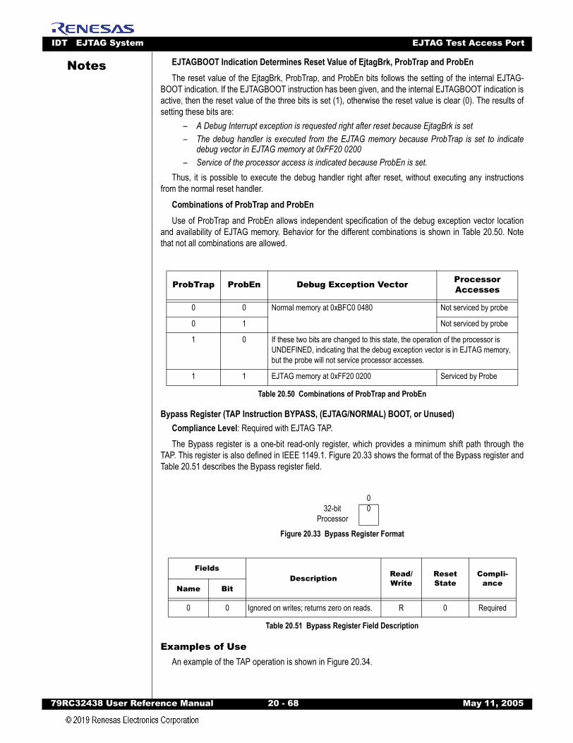
IDT EJTAG System EJTAG Test Access Port
79RC32438 User Refer
Notes
EJTAGBOOT Indication Determines Reset Value of EjtagBrk, ProbTrap and ProbEnThe reset value of the EjtagBrk, ProbTrap, and ProbEn bits follows the setting of the internal EJTAG-BOOT indication. If the EJTAGBOOT instruction has been given, and the internal EJTAGBOOT indication isactive, then the reset value of the three bits is set (1), otherwise the reset value is clear (0). The results ofsetting these bits are:
– A Debug Interrupt exception is requested right after reset because EjtagBrk is set– The debug handler is executed from the EJTAG memory because ProbTrap is set to indicate
debug vector in EJTAG memory at 0xFF20 0200– Service of the processor access is indicated because ProbEn is set.
Thus, it is possible to execute the debug handler right after reset, without executing any instructionsfrom the normal reset handler.
Combinations of ProbTrap and ProbEn Use of ProbTrap and ProbEn allows independent specification of the debug exception vector location
and availability of EJTAG memory. Behavior for the different combinations is shown in Table 20.50. Notethat not all combinations are allowed.
Bypass Register (TAP Instruction BYPASS, (EJTAG/NORMAL) BOOT, or Unused)Compliance Level: Required with EJTAG TAP.The Bypass register is a one-bit read-only register, which provides a minimum shift path through the
TAP. This register is also defined in IEEE 1149.1. Figure 20.33 shows the format of the Bypass register andTable 20.51 describes the Bypass register field.
Examples of UseAn example of the TAP operation is shown in Figure 20.34.
ProbTrap ProbEn Debug Exception Vector Processor Accesses
0 0 Normal memory at 0xBFC0 0480 Not serviced by probe
0 1 Not serviced by probe
1 0 If these two bits are changed to this state, the operation of the processor is UNDEFINED, indicating that the debug exception vector is in EJTAG memory, but the probe will not service processor accesses.
1 1 EJTAG memory at 0xFF20 0200 Serviced by Probe
Table 20.50 Combinations of ProbTrap and ProbEn
032-bit
Processor0
Figure 20.33 Bypass Register Format
FieldsDescription Read/
WriteReset State
Compli-ance
Name Bit
0 0 Ignored on writes; returns zero on reads. R 0 Required
Table 20.51 Bypass Register Field Description
ence Manual 20 - 68 May 11, 2005
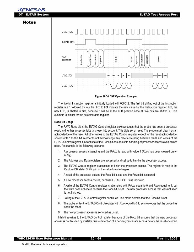
IDT EJTAG System EJTAG Test Access Port
79RC32438 User Refer
Notes
Figure 20.34 TAP Operation Example
The five-bit Instruction register is initially loaded with 000012. The first bit shifted out of the Instructionregister is a 1 followed by four 0’s. IR0 to IR4 indicate the new value for the Instruction register. IR0, thenew LSB, is shifted in first, because it will be at the LSB position once all five bits are shifted in. Thisexample is similar for the selected data register.
Rocc Bit UsageThe R/W0 Rocc bit in the EJTAG Control register acknowledges that the probe has seen a processor
reset, and further accesses take this reset into account. This bit is set at reset. The probe must clear it as anacknowledge of the reset. All other writes to the EJTAG Control register, except for the reset acknowledge,should write 1 to this bit in order to not acknowledge any resets occurring between reads and writes of theEJTAG Control register. Correct use of the Rocc bit ensures safe handling of processor access even acrossreset. An example is the following scenario:
1. A processor access is pending and the PrAcc is read with value 1 (Rocc has been cleared previ-ously).
2. The Address and Data registers are accessed and set up to handle the processor access.3. The EJTAG Control register is accessed to finish the processor access. The register is read in the
Capture-DR state. Shifting in of the value to write begins.4. A reset of the processor occurs, the Rocc bit is set, and the PrAcc bit is cleared.5. A new processor access occurs, because EJTAGBOOT was indicated.6. A write of the EJTAG Control register is attempted with PrAcc equal to 0 and Rocc equal to 1, but
the write does not occur because the Rocc bit is set. The new processor access that was not seenis not finished.
7. Polling of the EJTAG Control register continues. The probe detects that the Rocc bit is set.8. The probe writes the EJTAG Control register with Rocc equal to 0 to acknowledge that the probe has
seen the reset.9. The new processor access is serviced as usual.Inhibiting writes to the EJTAG Control register because of the Rocc bit ensures that the new processor
access is not finished by mistake due to detection of a pending processor access before the reset occurred.
Run-
Test/
Idle
JTAG_TCK
Selec
t-DR-
Scan
Captu
re-IR
Shift-
IR
Exit1
-IR
Upda
te-IR
Selec
t-DR-
Scan
Captu
re-D
R
Shift-
DR
Selec
t-IR-
Scan
EJTAG_TMS
JTAG_TDI
JTAG_TDO
TAPcontroller
IR0 IR1 IR2 IR3 IR4 DR0 DR1 DR2
ence Manual 20 - 69 May 11, 2005
IDT EJTAG System EJTAG Test Access Port
79RC32438 User Refer
Notes
EJTAG Memory Access Through Processor AccessThe processor access feature makes it possible for the probe to handle accesses from the processor tothe specific EJTAG memory area (dmseg). The processor can execute a debug handler from EJTAGmemory, whereby applications that are not prepared with EJTAG code in the system memory can still bedebugged. The probe can get information about the access through the TAP, as shown in Table 20.52.
The servicing of processor accesses works with a polling scheme, where the PrAcc bit is polled until apending processor access is indicated by PrAcc equal to 1. Then the Address register is read to get theaddress of the transaction, and the Data register is accessed to get the write data or provide the read data.Finally the PrAcc bit is cleared, in order to finish the access from the processor.
In addition, the ProbTrap and ProbEn bits control the debug exception vector location and the indicationto the processor that the probe will service accesses to the EJTAG memory through processor accesses.Handling of processor access in relation to reset requires specific handling. A pending processor access iscleared at reset. At the same time, the Rocc bit is set, thereby inhibiting any processor accesses to befinished until Rocc is cleared. Thus, the probe will have to acknowledge that a reset occurred, preventing itfrom accidentally finishing a processor access that occurred before the reset. A pending processor accesscan only finish if the probe clears PrAcc or a processor reset occurs.
The width of the Address register is 32 to 64 bits. The specific length is determined by shifting a knownbit pattern through the register. The following sections show examples of servicing read and write processoraccesses.
Write Processor AccessFigure 20.35 shows a possible flow for servicing a write processor access. The example implements a
32-bit processor with 32-bit Address register, running in little-endian mode. A halfword store is performed toaddress 0xFF20 1232 of value 0x5678.
Information Field and Register
Pending processor access PrAcc field in the EJTAG Control register
Read or write access PRnW field in the EJTAG Control register
Size and data location Psz field in EJTAG Control register, and two or three LSBs in the Address register
Address Address register
Data Data register
Table 20.52 Information Provided to Probe at Processor Access
ence Manual 20 - 70 May 11, 2005

IDT EJTAG System EJTAG Test Access Port
79RC32438 User Refer
Notes
Figure 20.35 Write Processor Access Example
The different probe actions shown on the figure are described below:
1. The EJTAG Control register is polled to get the indication for a pending PrAcc bit. The PrAcc bit iswritten to 1 when polling, in order to prevent a processor access from finishing before beingserviced. The values of PRnW and Psz are saved when PrAcc indicates a pending processoraccess.
2. The Address register is read. It contains the address of the store resulting in the write processoraccess.
3. The Data register is read, which contains the data from the store resulting in the write processoraccess.
4. The PrAcc bit is written to 0, in order to finish the processor access.The probe must update the appropriate bytes in its internal memory used for EJTAG memory with the
value of the write. Note that the two lower bytes of the Data register are undefined, and that the two lowerbytes of the saved register are shifted up on the two high bytes in the Data register as on a data bus for anexternal memory system. The Address register in this case contains the address from the store; however,for some accesses, this is not the case because the two LSBs (32-bit processor) are modified for someaccesses depending on size and address.
Read Processor AccessFigure 20.36 shows a possible flow for servicing a read processor access. The example implements a
64-bit processor with 36-bit Address register. A doubleword load/fetch from address 0xFF20 3450 is shownin the figure.
PrAcc
Probeaction
PRnW
Psz
Address
Data
1 1
Data = = 0x5678 XXXX
Address = = 0xFF20 1232
Size = 1
2 3 41 1
ence Manual 20 - 71 May 11, 2005
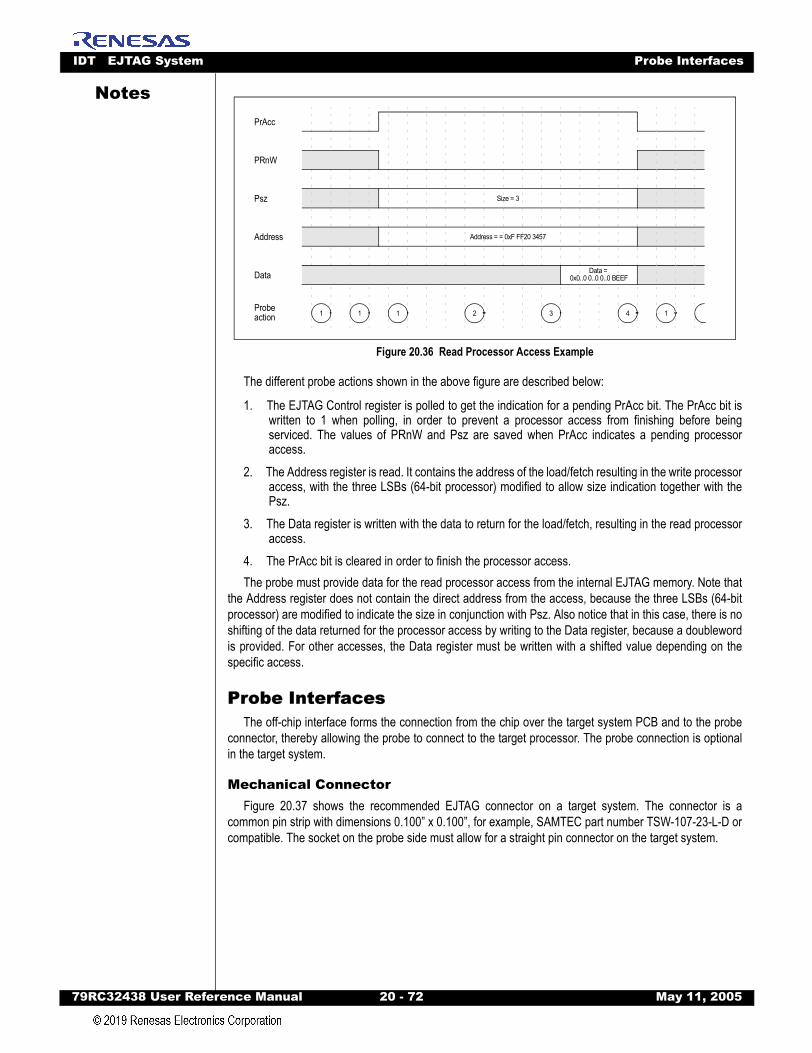
IDT EJTAG System Probe Interfaces
79RC32438 User Refer
Notes
Figure 20.36 Read Processor Access Example
The different probe actions shown in the above figure are described below:
1. The EJTAG Control register is polled to get the indication for a pending PrAcc bit. The PrAcc bit iswritten to 1 when polling, in order to prevent a processor access from finishing before beingserviced. The values of PRnW and Psz are saved when PrAcc indicates a pending processoraccess.
2. The Address register is read. It contains the address of the load/fetch resulting in the write processoraccess, with the three LSBs (64-bit processor) modified to allow size indication together with thePsz.
3. The Data register is written with the data to return for the load/fetch, resulting in the read processoraccess.
4. The PrAcc bit is cleared in order to finish the processor access.The probe must provide data for the read processor access from the internal EJTAG memory. Note that
the Address register does not contain the direct address from the access, because the three LSBs (64-bitprocessor) are modified to indicate the size in conjunction with Psz. Also notice that in this case, there is noshifting of the data returned for the processor access by writing to the Data register, because a doublewordis provided. For other accesses, the Data register must be written with a shifted value depending on thespecific access.
Probe InterfacesThe off-chip interface forms the connection from the chip over the target system PCB and to the probe
connector, thereby allowing the probe to connect to the target processor. The probe connection is optionalin the target system.
Mechanical ConnectorFigure 20.37 shows the recommended EJTAG connector on a target system. The connector is a
common pin strip with dimensions 0.100” x 0.100”, for example, SAMTEC part number TSW-107-23-L-D orcompatible. The socket on the probe side must allow for a straight pin connector on the target system.
PrAcc
Probeaction
PRnW
Psz
Address
Data
1 1
Data =
Address = = 0xF FF20 3457
Size = 3
2 3 41 1
0x0..0 0..0 0..0 BEEF
ence Manual 20 - 72 May 11, 2005

IDT EJTAG System Probe Interfaces
79RC32438 User Refer
Notes
Figure 20.37 EJTAG Connector Mechanical Dimensions
Table 20.53 shows the pin assignments for the connector.
Note: Pin 12 on the target system connector should be removed to provide keying, thus ensuring the probe is correctly connected to the target system.
Target System PCB DesignThis section provides guidelines for using the EJTAG connector on a target system.
Electrical ConnectionThe IEEE 1149.1 specification requires that the JTAG and EJTAG TAP controllers be reset at power-up
whether or not the interfaces are used for a boundary scan or a probe. Reset can occur through a pull-downresistor on JTAG_TRST_N if the probe is not connected. However, on-chip pull-up resistors are imple-mented on the RC32438 due to an IEEE 1149.1 requirement. Having on-chip pull-up and external pull-down resistors for the JTAG_TRST_N signal requires special care in the design to ensure that a validlogical level is provided to JTAG_TRST_N, such as using a small external pull-down resistor to ensure thislevel overrides the on-chip pull-up. An alternative is to use an active power-up reset circuit forJTAG_TRST_N, which drives JTAG_TRST_N low only at power-up and then holds JTAG_TRST_N highafterwards with a pull-up resistor. Figure 20.38 shows the electrical connection of the target systemconnector.
Pin Signal Direction Pin Signal Direction
1 JTAG_TRST_NTest reset input
Input 2 Ground Gnd
3 JTAG_TDITest data input
Input 4 Ground Gnd
5 JTAG_TDOTest data output
Output 6 Ground Gnd
7 EJTAG_TMSTest mode select input
Input 8 Ground Gnd
9 JTAG_TCKTest clock input
Input 10 Ground Gnd
11 RST*System reset
Input 12 key - pin removed on connector
NA
13 DINT (no connect)Debug interrupt
Input 14 VSENSE Voltage Sense for I/O
Output
Table 20.53 EJTAG Connector Pinout
2.54 mm
Top view on PCB
2.54 mm
1 2
13 14Pin 12 removedto allow for key
0.64 mm
5.84 mm
Side view on PCB
GND
Signal Positions
1
GNDGNDGNDGNDkeyVSENSE
JTAG_TRST_NJTAG_TDI
JTAG_TDOEJTAG_TMS
JTAG_TCKRST*
(no connect) DINT
ence Manual 20 - 73 May 11, 2005
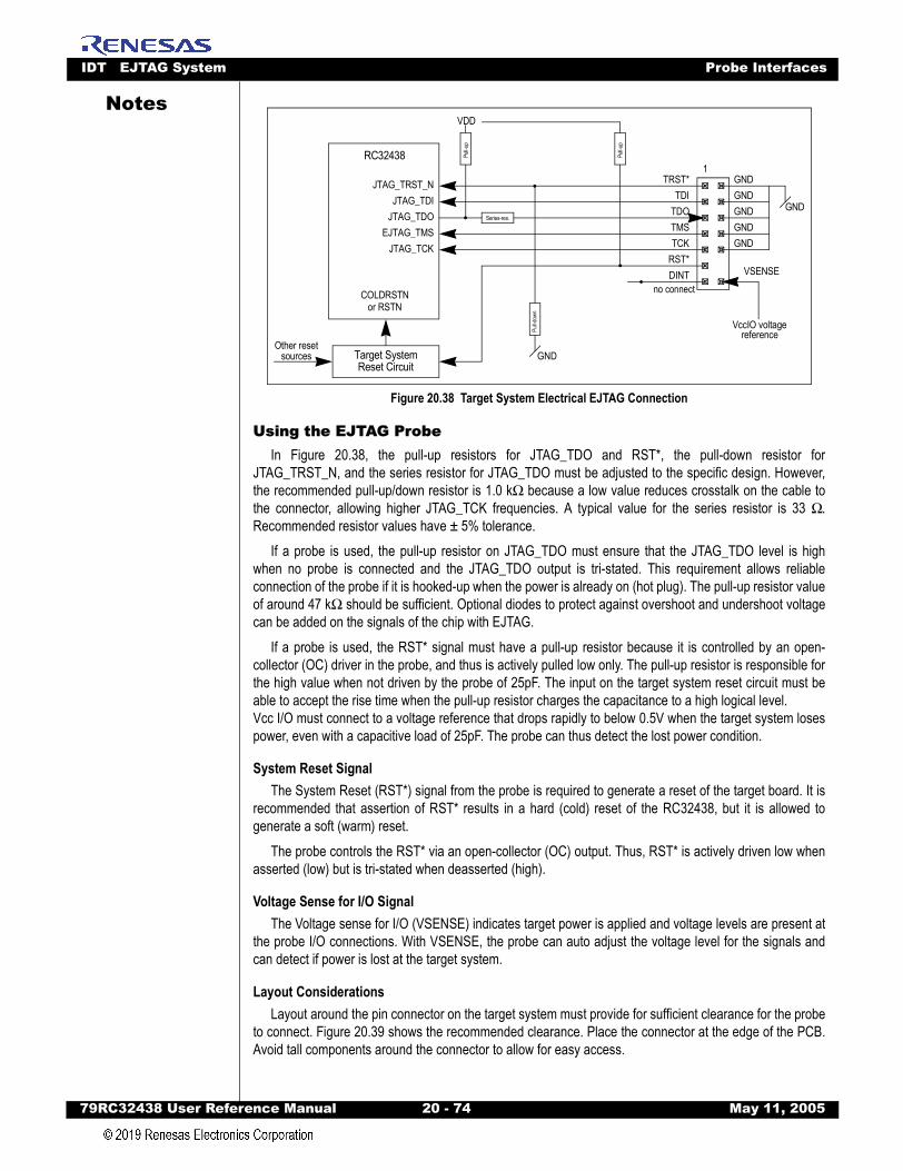
IDT EJTAG System Probe Interfaces
79RC32438 User Refer
Notes
Figure 20.38 Target System Electrical EJTAG Connection
Using the EJTAG ProbeIn Figure 20.38, the pull-up resistors for JTAG_TDO and RST*, the pull-down resistor for
JTAG_TRST_N, and the series resistor for JTAG_TDO must be adjusted to the specific design. However,the recommended pull-up/down resistor is 1.0 kΩ because a low value reduces crosstalk on the cable tothe connector, allowing higher JTAG_TCK frequencies. A typical value for the series resistor is 33 Ω.Recommended resistor values have ± 5% tolerance.
If a probe is used, the pull-up resistor on JTAG_TDO must ensure that the JTAG_TDO level is highwhen no probe is connected and the JTAG_TDO output is tri-stated. This requirement allows reliableconnection of the probe if it is hooked-up when the power is already on (hot plug). The pull-up resistor valueof around 47 kΩ should be sufficient. Optional diodes to protect against overshoot and undershoot voltagecan be added on the signals of the chip with EJTAG.
If a probe is used, the RST* signal must have a pull-up resistor because it is controlled by an open-collector (OC) driver in the probe, and thus is actively pulled low only. The pull-up resistor is responsible forthe high value when not driven by the probe of 25pF. The input on the target system reset circuit must beable to accept the rise time when the pull-up resistor charges the capacitance to a high logical level. Vcc I/O must connect to a voltage reference that drops rapidly to below 0.5V when the target system losespower, even with a capacitive load of 25pF. The probe can thus detect the lost power condition.
System Reset SignalThe System Reset (RST*) signal from the probe is required to generate a reset of the target board. It is
recommended that assertion of RST* results in a hard (cold) reset of the RC32438, but it is allowed togenerate a soft (warm) reset.
The probe controls the RST* via an open-collector (OC) output. Thus, RST* is actively driven low whenasserted (low) but is tri-stated when deasserted (high).
Voltage Sense for I/O SignalThe Voltage sense for I/O (VSENSE) indicates target power is applied and voltage levels are present at
the probe I/O connections. With VSENSE, the probe can auto adjust the voltage level for the signals andcan detect if power is lost at the target system.
Layout ConsiderationsLayout around the pin connector on the target system must provide for sufficient clearance for the probe
to connect. Figure 20.39 shows the recommended clearance. Place the connector at the edge of the PCB.Avoid tall components around the connector to allow for easy access.
GND1
GNDGNDGNDGND
TRST*TDI
TDOTMSTCK
RST*DINT
JTAG_TRST_NJTAG_TDI
JTAG_TDOEJTAG_TMS
JTAG_TCK
GND
VDD
GND
VccIO voltagereference
Pull-u
p
Pull-d
own
Series-res.
COLDRSTN
Target SystemReset Circuit
Pull-u
p
Other resetsources
RC32438
no connect
or RSTN
VSENSE
ence Manual 20 - 74 May 11, 2005
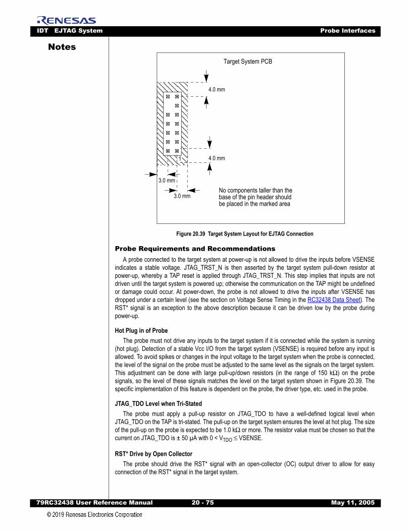
IDT EJTAG System Probe Interfaces
79RC32438 User Refer
Notes
Figure 20.39 Target System Layout for EJTAG Connection
Probe Requirements and RecommendationsA probe connected to the target system at power-up is not allowed to drive the inputs before VSENSE
indicates a stable voltage. JTAG_TRST_N is then asserted by the target system pull-down resistor atpower-up, whereby a TAP reset is applied through JTAG_TRST_N. This step implies that inputs are notdriven until the target system is powered up; otherwise the communication on the TAP might be undefinedor damage could occur. At power-down, the probe is not allowed to drive the inputs after VSENSE hasdropped under a certain level (see the section on Voltage Sense Timing in the RC32438 Data Sheet). TheRST* signal is an exception to the above description because it can be driven low by the probe duringpower-up.
Hot Plug in of ProbeThe probe must not drive any inputs to the target system if it is connected while the system is running
(hot plug). Detection of a stable Vcc I/O from the target system (VSENSE) is required before any input isallowed. To avoid spikes or changes in the input voltage to the target system when the probe is connected,the level of the signal on the probe must be adjusted to the same level as the signals on the target system.This adjustment can be done with large pull-up/down resistors (in the range of 150 kΩ) on the probesignals, so the level of these signals matches the level on the target system shown in Figure 20.39. Thespecific implementation of this feature is dependent on the probe, the driver type, etc. used in the probe.
JTAG_TDO Level when Tri-StatedThe probe must apply a pull-up resistor on JTAG_TDO to have a well-defined logical level when
JTAG_TDO on the TAP is tri-stated. The pull-up on the target system ensures the level at hot plug. The sizeof the pull-up on the probe is expected to be 1.0 kΩ or more. The resistor value must be chosen so that thecurrent on JTAG_TDO is ± 50 µA with 0 < VTDO ≤ VSENSE.
RST* Drive by Open CollectorThe probe should drive the RST* signal with an open-collector (OC) output driver to allow for easy
connection of the RST* signal in the target system.
Target System PCB
4.0 mm
4.0 mm
3.0 mm
3.0 mmNo components taller than thebase of the pin header shouldbe placed in the marked area
1
ence Manual 20 - 75 May 11, 2005
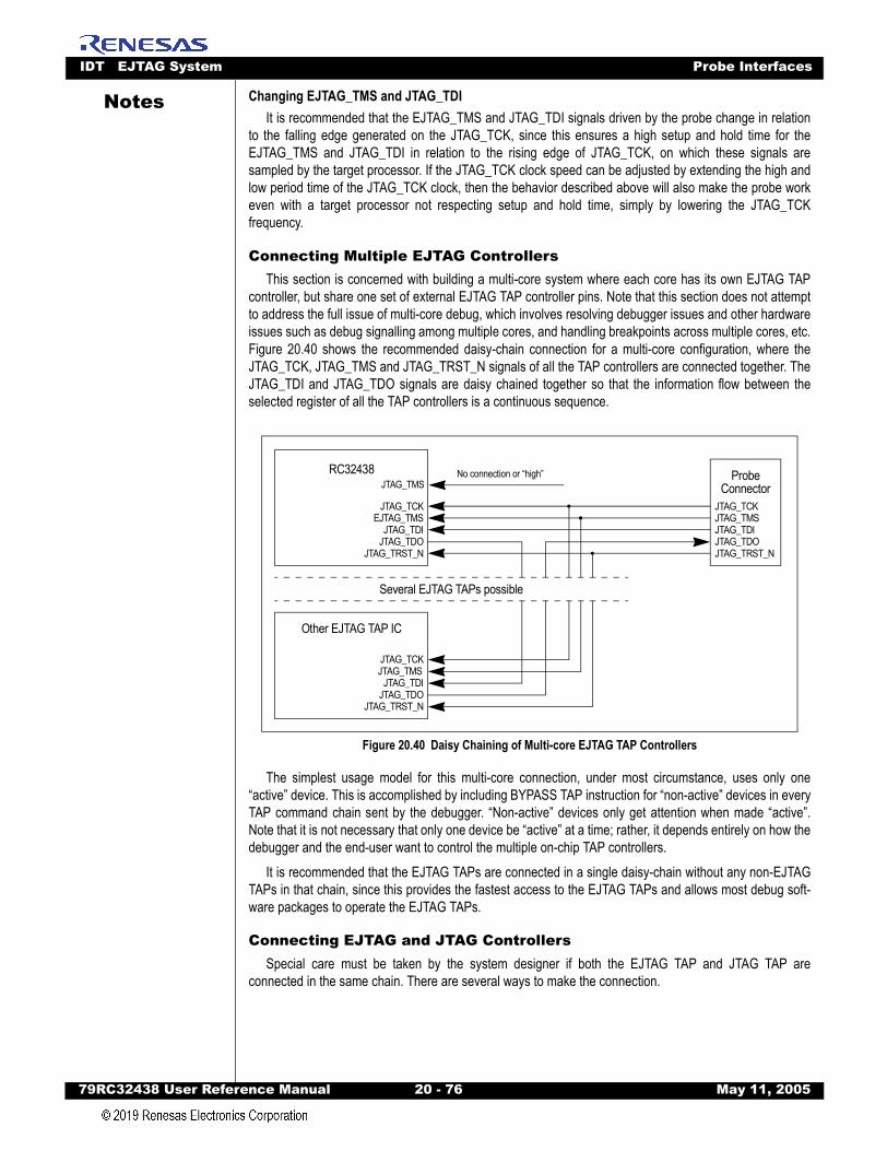
IDT EJTAG System Probe Interfaces
79RC32438 User Refer
Notes
Changing EJTAG_TMS and JTAG_TDIIt is recommended that the EJTAG_TMS and JTAG_TDI signals driven by the probe change in relationto the falling edge generated on the JTAG_TCK, since this ensures a high setup and hold time for theEJTAG_TMS and JTAG_TDI in relation to the rising edge of JTAG_TCK, on which these signals aresampled by the target processor. If the JTAG_TCK clock speed can be adjusted by extending the high andlow period time of the JTAG_TCK clock, then the behavior described above will also make the probe workeven with a target processor not respecting setup and hold time, simply by lowering the JTAG_TCKfrequency.
Connecting Multiple EJTAG ControllersThis section is concerned with building a multi-core system where each core has its own EJTAG TAP
controller, but share one set of external EJTAG TAP controller pins. Note that this section does not attemptto address the full issue of multi-core debug, which involves resolving debugger issues and other hardwareissues such as debug signalling among multiple cores, and handling breakpoints across multiple cores, etc.Figure 20.40 shows the recommended daisy-chain connection for a multi-core configuration, where theJTAG_TCK, JTAG_TMS and JTAG_TRST_N signals of all the TAP controllers are connected together. TheJTAG_TDI and JTAG_TDO signals are daisy chained together so that the information flow between theselected register of all the TAP controllers is a continuous sequence.
Figure 20.40 Daisy Chaining of Multi-core EJTAG TAP Controllers
The simplest usage model for this multi-core connection, under most circumstance, uses only one“active” device. This is accomplished by including BYPASS TAP instruction for “non-active” devices in everyTAP command chain sent by the debugger. “Non-active” devices only get attention when made “active”.Note that it is not necessary that only one device be “active” at a time; rather, it depends entirely on how thedebugger and the end-user want to control the multiple on-chip TAP controllers.
It is recommended that the EJTAG TAPs are connected in a single daisy-chain without any non-EJTAGTAPs in that chain, since this provides the fastest access to the EJTAG TAPs and allows most debug soft-ware packages to operate the EJTAG TAPs.
Connecting EJTAG and JTAG ControllersSpecial care must be taken by the system designer if both the EJTAG TAP and JTAG TAP are
connected in the same chain. There are several ways to make the connection.
Probe
JTAG_TCKJTAG_TMS
JTAG_TDOJTAG_TDI
JTAG_TRST_N
ConnectorJTAG_TCK
EJTAG_TMS
JTAG_TDOJTAG_TDI
JTAG_TRST_N
RC32438
JTAG_TCKJTAG_TMS
JTAG_TDOJTAG_TDI
JTAG_TRST_N
Other EJTAG TAP IC
Several EJTAG TAPs possible
JTAG_TMSNo connection or “high”
ence Manual 20 - 76 May 11, 2005
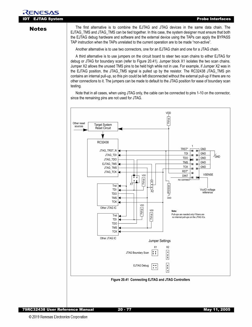
IDT EJTAG System Probe Interfaces
79RC32438 User Refer
Notes
The first alternative is to combine the EJTAG and JTAG devices in the same data chain. TheEJTAG_TMS and JTAG_TMS can be tied together. In this case, the system designer must ensure that boththe EJTAG debug hardware and software and the external device using the TAPs can apply the BYPASSTAP instruction when the TAPs unrelated to the current operation are to be made “non-active”.Another alternative is to use two connectors, one for an EJTAG chain and one for a JTAG chain. A third alternative is to use jumpers on the circuit board to steer two scan chains to either EJTAG for
debug or JTAG for boundary scan (refer to Figure 20.41). Jumper block X1 isolates the two scan chains.Jumper X2 allows the unused TMS pins to be held high while not in use. For example, if Jumper X2 was inthe EJTAG position, the JTAG_TMS signal is pulled up by the resistor. The RC32438 JTAG_TMS pincontains an internal pull-up, so this pin could be left disconnected without the external pull-up if there are noother connections to it. The jumpers can be made to default to the JTAG position for ease of boundary scantesting.
Note that in all cases, when using JTAG only, the cable can be connected to pins 1-10 on the connector,since the remaining pins are not used for JTAG.
Figure 20.41 Connecting EJTAG and JTAG Controllers
GND1
GNDGNDGNDGND
TRST*TDI
TDOTMSTCK
RST*DINT
JTAG_TRST_NJTAG_TDI
JTAG_TDOEJTAG_TMS
JTAG_TCK
GND
VDD
VccIO voltagereference
Pull-u
p
Target SystemReset Circuit
Pull-u
p
Other resetsources
RC32438
no connect
VSENSE
Pull-d
own
GND
TrstTDI
TDOTMSTCK
TrstTDI
TDOTMSTCK
Other JTAG IC
Other JTAG IC
JTAG_TMS
X2
X1
VDD
Jumper Settings
JTAG Boundary Scan
X1 X2
EJTAG Debug
Pull-u
p
VDD
Pull-u
p
VDD
Pull-ups are needed only if there areno internal pull-ups on the JTAG ICs.
Note:
ence Manual 20 - 77 May 11, 2005

IDT EJTAG System Probe Interfaces
79RC32438 User Refer
Notes
ence Manual 20 - 78 May 11, 2005
Notes
79RC32438 User Reference Manual A - 1 M
Appendix A
4Kc Processor CoreInstructions
IntroductionThis Appendix contains additional information about the 4Kc processor core instruction set. Chapter 2 of
this manual contains a description of the processor core and its operation.
Understanding the Instruction SetFigure A.1 shows an example instruction.
ay 11, 2005
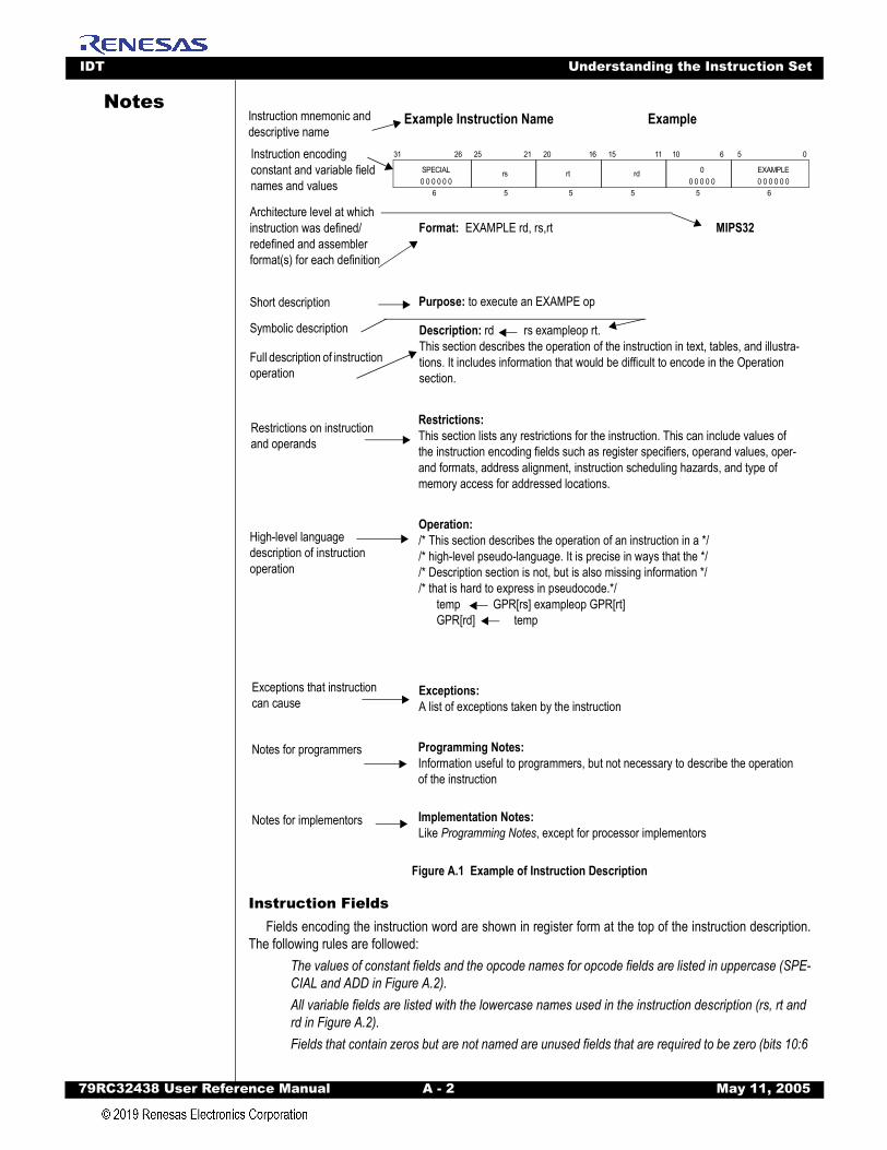
IDT Understanding the Instruction Set
79RC32438 User Refer
Notes
Figure A.1 Example of Instruction Description
Instruction FieldsFields encoding the instruction word are shown in register form at the top of the instruction description.
The following rules are followed:The values of constant fields and the opcode names for opcode fields are listed in uppercase (SPE-CIAL and ADD in Figure A.2).All variable fields are listed with the lowercase names used in the instruction description (rs, rt and rd in Figure A.2).Fields that contain zeros but are not named are unused fields that are required to be zero (bits 10:6
Instruction mnemonic and descriptive nameInstruction encoding constant and variable field names and values
Architecture level at which instruction was defined/redefined and assembler format(s) for each definition
Short description
Symbolic description
Full description of instruction operation
Restrictions on instruction and operands
High-level language description of instruction operation
Exceptions that instruction can cause
Notes for programmers
Notes for implementors
Example Instruction Name Example
31 2526 2021 1516
SPECIAL rs rt
6 5 5
rd 0 EXAMPLE
5 5 6
11 10 6 5 0
0 0 0 0 0 0 0 0 0 0 0 0 0 0 0 0 0
Format: EXAMPLE rd, rs,rt MIPS32
Purpose: to execute an EXAMPE op
Description: rd rs exampleop rt.This section describes the operation of the instruction in text, tables, and illustra-tions. It includes information that would be difficult to encode in the Operation section.
Restrictions:This section lists any restrictions for the instruction. This can include values of the instruction encoding fields such as register specifiers, operand values, oper-and formats, address alignment, instruction scheduling hazards, and type of memory access for addressed locations.
Operation:/* This section describes the operation of an instruction in a *//* high-level pseudo-language. It is precise in ways that the *//* Description section is not, but is also missing information *//* that is hard to express in pseudocode.*/ temp GPR[rs] exampleop GPR[rt] GPR[rd] temp
Exceptions:A list of exceptions taken by the instruction
Programming Notes:Information useful to programmers, but not necessary to describe the operation of the instruction
Implementation Notes:Like Programming Notes, except for processor implementors
ence Manual A - 2 May 11, 2005
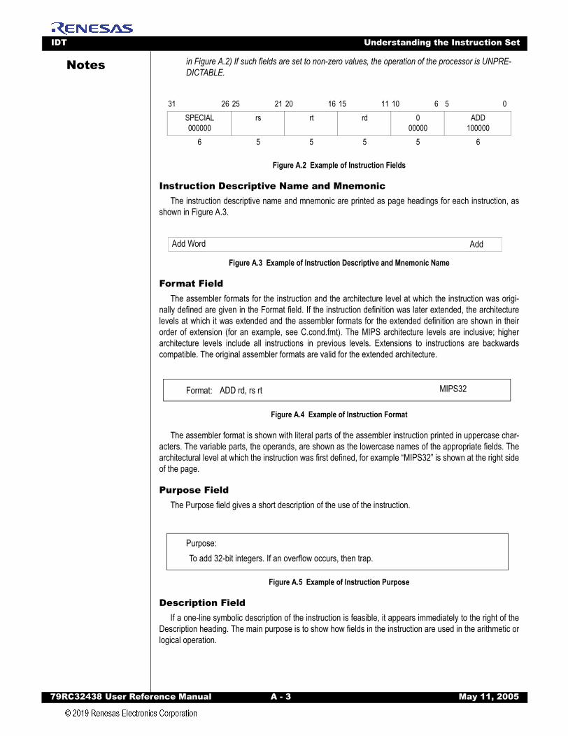
IDT Understanding the Instruction Set
79RC32438 User Refer
Notes
in Figure A.2) If such fields are set to non-zero values, the operation of the processor is UNPRE-DICTABLE.Figure A.2 Example of Instruction Fields
Instruction Descriptive Name and MnemonicThe instruction descriptive name and mnemonic are printed as page headings for each instruction, as
shown in Figure A.3.
Figure A.3 Example of Instruction Descriptive and Mnemonic Name
Format FieldThe assembler formats for the instruction and the architecture level at which the instruction was origi-
nally defined are given in the Format field. If the instruction definition was later extended, the architecturelevels at which it was extended and the assembler formats for the extended definition are shown in theirorder of extension (for an example, see C.cond.fmt). The MIPS architecture levels are inclusive; higherarchitecture levels include all instructions in previous levels. Extensions to instructions are backwardscompatible. The original assembler formats are valid for the extended architecture.
Figure A.4 Example of Instruction Format
The assembler format is shown with literal parts of the assembler instruction printed in uppercase char-acters. The variable parts, the operands, are shown as the lowercase names of the appropriate fields. Thearchitectural level at which the instruction was first defined, for example “MIPS32” is shown at the right sideof the page.
Purpose FieldThe Purpose field gives a short description of the use of the instruction.
Figure A.5 Example of Instruction Purpose
Description FieldIf a one-line symbolic description of the instruction is feasible, it appears immediately to the right of the
Description heading. The main purpose is to show how fields in the instruction are used in the arithmetic orlogical operation.
31 26 25 21 20 16 15 11 10 6 5 0SPECIAL000000
rs rt rd 000000
ADD100000
6 5 5 5 5 6
Add Word Add
Format: ADD rd, rs rt MIPS32
Purpose:To add 32-bit integers. If an overflow occurs, then trap.
ence Manual A - 3 May 11, 2005
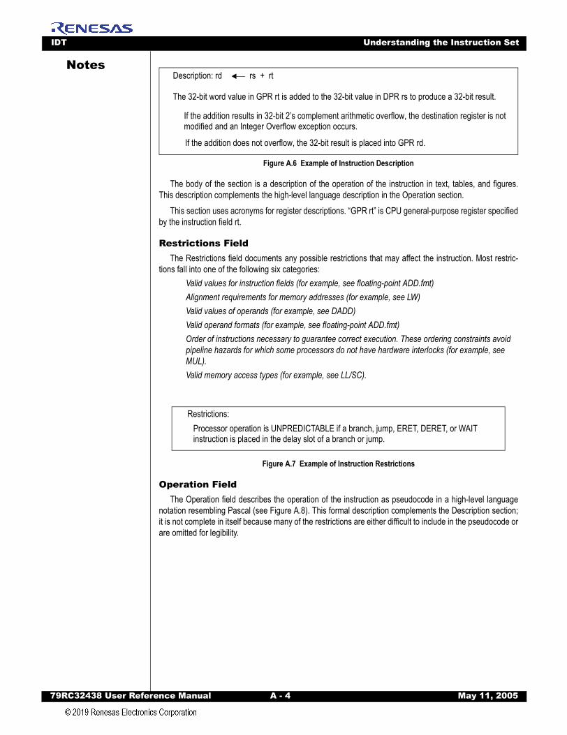
IDT Understanding the Instruction Set
79RC32438 User Refer
Notes
Figure A.6 Example of Instruction Description
The body of the section is a description of the operation of the instruction in text, tables, and figures.This description complements the high-level language description in the Operation section.
This section uses acronyms for register descriptions. “GPR rt” is CPU general-purpose register specifiedby the instruction field rt.
Restrictions FieldThe Restrictions field documents any possible restrictions that may affect the instruction. Most restric-
tions fall into one of the following six categories:Valid values for instruction fields (for example, see floating-point ADD.fmt)Alignment requirements for memory addresses (for example, see LW)Valid values of operands (for example, see DADD)Valid operand formats (for example, see floating-point ADD.fmt)Order of instructions necessary to guarantee correct execution. These ordering constraints avoid pipeline hazards for which some processors do not have hardware interlocks (for example, see MUL).Valid memory access types (for example, see LL/SC).
Figure A.7 Example of Instruction Restrictions
Operation FieldThe Operation field describes the operation of the instruction as pseudocode in a high-level language
notation resembling Pascal (see Figure A.8). This formal description complements the Description section;it is not complete in itself because many of the restrictions are either difficult to include in the pseudocode orare omitted for legibility.
Description: rd rs + rt
The 32-bit word value in GPR rt is added to the 32-bit value in DPR rs to produce a 32-bit result.
If the addition results in 32-bit 2’s complement arithmetic overflow, the destination register is not modified and an Integer Overflow exception occurs.
If the addition does not overflow, the 32-bit result is placed into GPR rd.
Restrictions:
Processor operation is UNPREDICTABLE if a branch, jump, ERET, DERET, or WAITinstruction is placed in the delay slot of a branch or jump.
ence Manual A - 4 May 11, 2005

IDT Operation Section Notation and Functions
79RC32438 User Refer
Notes
Figure A.8 Sample Instruction Operation
Exceptions FieldThe Exceptions field lists the exceptions that can be caused by Operation of the instruction. It omits
exceptions that can be caused by the instruction fetch, for instance, TLB Refill, and also omits exceptionsthat can be caused by asynchronous external events such as an Interrupt. Although a Bus Error exceptionmay be caused by the operation of a load or store instruction, this section does not list Bus Error for loadand store instructions because the relationship between load and store instructions and external error indi-cations, like Bus Error, are dependent upon the implementation.
Figure A.9 Sample Instruction Exception
An instruction may cause implementation-dependent exceptions that are not present in the Exceptionssection.
Programming Notes and Implementation Notes FieldsThe Notes sections contain material that is useful for programmers and implementors, respectively, but
that is not necessary to describe the instruction and does not belong in the description sections.
Figure A.10 Sample Instruction Programming Notes
Operation Section Notation and FunctionsIn an instruction description, the Operation section uses a high-level language notation to describe the
operation performed by each instruction. The contents of the Operation section are described here,including the special symbols and functions that are used.
Instruction Execution OrderingEach of the high-level language statements in the Operations section are executed sequentially (except
as constrained by conditional and loop constructs).
Operation:
temp (GPR[rs]31||GPR[rs]31..0) + (GPR[rt]31||GPR[rt]31..0)
if temp32 ≠ temp31 thenSignalException(IntergerOverflow)elseGPR[rd] tempendif
Exceptions:
Integer Overflow
Programming Notes:
ADDU performs the same arithmetic operation but does not trap on overflow.
ence Manual A - 5 May 11, 2005

IDT Operation Section Notation and Functions
79RC32438 User Refer
Notes
Special Symbols in Pseudocode NotationSpecial symbols used in the pseudocode notation are listed in Table A.1.Symbol Meaning
← Assignment
=, ≠ Tests for equality and Inequality
|| Bit string concatenation
xy A y-bit string formed by y copies of the single-bit value x
b#n A constant value n in base b. For instance 10#100 represents the decimal value 100, 2#100 represents the binary value 100 (decimal 4), and 16#100 represents the hexadecimal value 100 (decimal 256). If the "b#" prefix is omitted, the default base is 10.
xy..z Selection of bits y through z of bit string x. Little-endian bit notation (rightmost bit is 0) is used. If y is less than z, this expression is an empty (zero length) bit string.
+, − 2’s complement or floating-point arithmetic: addition, subtraction
∗, × 2’s complement or floating point multiplication (both used for either)
div 2’s complement integer division
mod 2’s complement modulo
/ Floating-point division
< 2’s complement less-than comparison
> 2’s complement greater-than comparison
≤ 2’s complement less-than or equal comparison
≥ 2’s complement greater-than or equal comparison
nor Bitwise logical NOR
xor Bitwise logical XOR
and Bitwise logical AND
or Bitwise logical OR
GPRLEN The length in bits (32 or 64) of the CPU general-purpose registers
GPR[x] CPU general-purpose register x. The content of GPR[0] is always zero.
CPR[z,x,s] Coprocessor unit z, general register x, select s
CCR[z,x] Coprocessor unit z, control register x
Xlat[x] Translation of the MIPS16 GPR number x into the corresponding 32-bit GPR num-ber
BigEndianMem Endian mode as configured at chip reset (0 →Little-Endian, 1 → Big-Endian). Specifies the endianness of the memory interface (see LoadMemory and Store-Memory sections in this chapter), and the endianness of Kernel and Supervisor mode execution.
BigEndianCPU The endianness for load and store instructions (0 → Little-Endian, 1 → Big-Endian). In User mode, this endianness may be switched by setting the RE bit in the Status register. Thus, BigEndianCPU may be computed as (BigEndianMem XOR ReverseEndian).
Table A.1 Symbols Used in Instruction Operation Statements (Part 1 of 2)
ence Manual A - 6 May 11, 2005
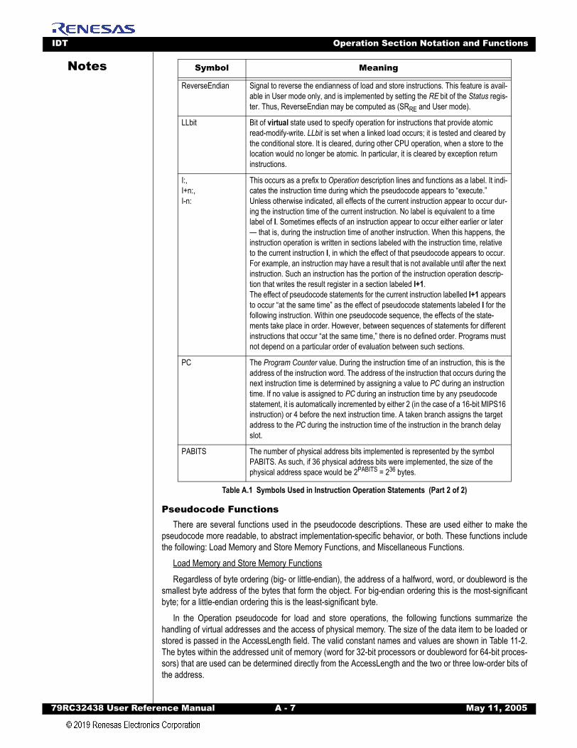
IDT Operation Section Notation and Functions
79RC32438 User Refer
Notes
Pseudocode FunctionsThere are several functions used in the pseudocode descriptions. These are used either to make the
pseudocode more readable, to abstract implementation-specific behavior, or both. These functions includethe following: Load Memory and Store Memory Functions, and Miscellaneous Functions.
Load Memory and Store Memory FunctionsRegardless of byte ordering (big- or little-endian), the address of a halfword, word, or doubleword is the
smallest byte address of the bytes that form the object. For big-endian ordering this is the most-significantbyte; for a little-endian ordering this is the least-significant byte.
In the Operation pseudocode for load and store operations, the following functions summarize thehandling of virtual addresses and the access of physical memory. The size of the data item to be loaded orstored is passed in the AccessLength field. The valid constant names and values are shown in Table 11-2.The bytes within the addressed unit of memory (word for 32-bit processors or doubleword for 64-bit proces-sors) that are used can be determined directly from the AccessLength and the two or three low-order bits ofthe address.
ReverseEndian Signal to reverse the endianness of load and store instructions. This feature is avail-able in User mode only, and is implemented by setting the RE bit of the Status regis-ter. Thus, ReverseEndian may be computed as (SRRE and User mode).
LLbit Bit of virtual state used to specify operation for instructions that provide atomic read-modify-write. LLbit is set when a linked load occurs; it is tested and cleared by the conditional store. It is cleared, during other CPU operation, when a store to the location would no longer be atomic. In particular, it is cleared by exception return instructions.
I:,I+n:,I-n:
This occurs as a prefix to Operation description lines and functions as a label. It indi-cates the instruction time during which the pseudocode appears to “execute.” Unless otherwise indicated, all effects of the current instruction appear to occur dur-ing the instruction time of the current instruction. No label is equivalent to a time label of I. Sometimes effects of an instruction appear to occur either earlier or later — that is, during the instruction time of another instruction. When this happens, the instruction operation is written in sections labeled with the instruction time, relative to the current instruction I, in which the effect of that pseudocode appears to occur. For example, an instruction may have a result that is not available until after the next instruction. Such an instruction has the portion of the instruction operation descrip-tion that writes the result register in a section labeled I+1.The effect of pseudocode statements for the current instruction labelled I+1 appears to occur “at the same time” as the effect of pseudocode statements labeled I for the following instruction. Within one pseudocode sequence, the effects of the state-ments take place in order. However, between sequences of statements for different instructions that occur “at the same time,” there is no defined order. Programs must not depend on a particular order of evaluation between such sections.
PC The Program Counter value. During the instruction time of an instruction, this is the address of the instruction word. The address of the instruction that occurs during the next instruction time is determined by assigning a value to PC during an instruction time. If no value is assigned to PC during an instruction time by any pseudocode statement, it is automatically incremented by either 2 (in the case of a 16-bit MIPS16 instruction) or 4 before the next instruction time. A taken branch assigns the target address to the PC during the instruction time of the instruction in the branch delay slot.
PABITS The number of physical address bits implemented is represented by the symbol PABITS. As such, if 36 physical address bits were implemented, the size of the physical address space would be 2PABITS = 236 bytes.
Symbol Meaning
Table A.1 Symbols Used in Instruction Operation Statements (Part 2 of 2)
ence Manual A - 7 May 11, 2005
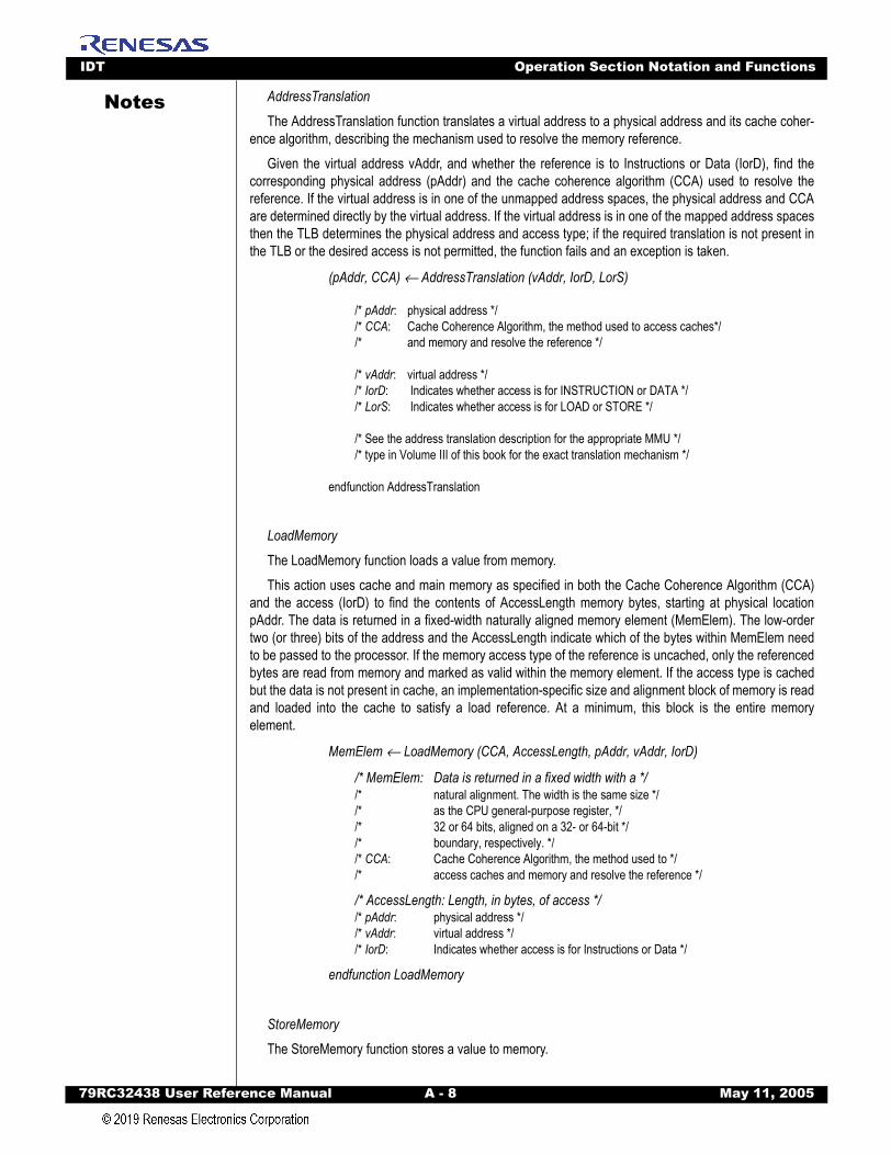
IDT Operation Section Notation and Functions
79RC32438 User Refer
Notes
AddressTranslationThe AddressTranslation function translates a virtual address to a physical address and its cache coher-ence algorithm, describing the mechanism used to resolve the memory reference.
Given the virtual address vAddr, and whether the reference is to Instructions or Data (IorD), find thecorresponding physical address (pAddr) and the cache coherence algorithm (CCA) used to resolve thereference. If the virtual address is in one of the unmapped address spaces, the physical address and CCAare determined directly by the virtual address. If the virtual address is in one of the mapped address spacesthen the TLB determines the physical address and access type; if the required translation is not present inthe TLB or the desired access is not permitted, the function fails and an exception is taken.
(pAddr, CCA) ← AddressTranslation (vAddr, IorD, LorS)
/* pAddr: physical address *//* CCA: Cache Coherence Algorithm, the method used to access caches*//* and memory and resolve the reference */
/* vAddr: virtual address *//* IorD: Indicates whether access is for INSTRUCTION or DATA *//* LorS: Indicates whether access is for LOAD or STORE */
/* See the address translation description for the appropriate MMU *//* type in Volume III of this book for the exact translation mechanism */
endfunction AddressTranslation
LoadMemory
The LoadMemory function loads a value from memory.This action uses cache and main memory as specified in both the Cache Coherence Algorithm (CCA)
and the access (IorD) to find the contents of AccessLength memory bytes, starting at physical locationpAddr. The data is returned in a fixed-width naturally aligned memory element (MemElem). The low-ordertwo (or three) bits of the address and the AccessLength indicate which of the bytes within MemElem needto be passed to the processor. If the memory access type of the reference is uncached, only the referencedbytes are read from memory and marked as valid within the memory element. If the access type is cachedbut the data is not present in cache, an implementation-specific size and alignment block of memory is readand loaded into the cache to satisfy a load reference. At a minimum, this block is the entire memoryelement.
MemElem ← LoadMemory (CCA, AccessLength, pAddr, vAddr, IorD)
/* MemElem: Data is returned in a fixed width with a *//* natural alignment. The width is the same size *//* as the CPU general-purpose register, *//* 32 or 64 bits, aligned on a 32- or 64-bit *//* boundary, respectively. *//* CCA: Cache Coherence Algorithm, the method used to *//* access caches and memory and resolve the reference */
/* AccessLength: Length, in bytes, of access *//* pAddr: physical address *//* vAddr: virtual address *//* IorD: Indicates whether access is for Instructions or Data */
endfunction LoadMemory
StoreMemory
The StoreMemory function stores a value to memory.
ence Manual A - 8 May 11, 2005
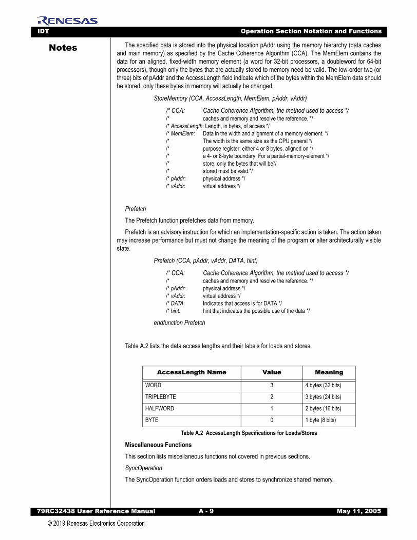
IDT Operation Section Notation and Functions
79RC32438 User Refer
Notes
The specified data is stored into the physical location pAddr using the memory hierarchy (data cachesand main memory) as specified by the Cache Coherence Algorithm (CCA). The MemElem contains thedata for an aligned, fixed-width memory element (a word for 32-bit processors, a doubleword for 64-bitprocessors), though only the bytes that are actually stored to memory need be valid. The low-order two (orthree) bits of pAddr and the AccessLength field indicate which of the bytes within the MemElem data shouldbe stored; only these bytes in memory will actually be changed.StoreMemory (CCA, AccessLength, MemElem, pAddr, vAddr)
/* CCA: Cache Coherence Algorithm, the method used to access *//* caches and memory and resolve the reference. *//* AccessLength: Length, in bytes, of access *//* MemElem: Data in the width and alignment of a memory element. *//* The width is the same size as the CPU general *//* purpose register, either 4 or 8 bytes, aligned on *//* a 4- or 8-byte boundary. For a partial-memory-element */ /* store, only the bytes that will be*//* stored must be valid.*//* pAddr: physical address *//* vAddr: virtual address */
Prefetch
The Prefetch function prefetches data from memory.Prefetch is an advisory instruction for which an implementation-specific action is taken. The action taken
may increase performance but must not change the meaning of the program or alter architecturally visiblestate.
Prefetch (CCA, pAddr, vAddr, DATA, hint)
/* CCA: Cache Coherence Algorithm, the method used to access *//* caches and memory and resolve the reference. *//* pAddr: physical address *//* vAddr: virtual address *//* DATA: Indicates that access is for DATA *//* hint: hint that indicates the possible use of the data */
endfunction Prefetch
Table A.2 lists the data access lengths and their labels for loads and stores.
Miscellaneous FunctionsThis section lists miscellaneous functions not covered in previous sections.SyncOperation
The SyncOperation function orders loads and stores to synchronize shared memory.
AccessLength Name Value Meaning
WORD 3 4 bytes (32 bits)
TRIPLEBYTE 2 3 bytes (24 bits)
HALFWORD 1 2 bytes (16 bits)
BYTE 0 1 byte (8 bits)
Table A.2 AccessLength Specifications for Loads/Stores
ence Manual A - 9 May 11, 2005

IDT Operation Section Notation and Functions
79RC32438 User Refer
Notes
This action makes the effects of the synchronizable loads and stores indicated by type occur in thesame order for all processors.SyncOperation(stype)
/* stype: Type of load/store ordering to perform. */
/* Perform implementation-dependent operation to complete the *//* required synchronization operation */
endfunction SyncOperation
SignalException
The SignalException function signals an exception condition.This action results in an exception that aborts the instruction. The instruction operation pseudocode
never sees a return from this function call.
SignalException(Exception, argument)
/* Exception: The exception condition that exists. *//* argument: An exception-dependent argument, if any */
endfunction SignalException
NullifyCurrentInstruction
The NullifyCurrentInstruction function nullifies the current instruction.The instruction is aborted. For branch-likely instructions, nullification kills the instruction in the delay slot
during its execution.
NullifyCurrentInstruction()
endfunction NullifyCurrentInstruction
CoprocessorOperation
The CoprocessorOperation function performs the specified Coprocessor operation.
CoprocessorOperation (z, cop_fun)
/* z: Coprocessor unit number *//* cop_fun: Coprocessor function from function field of instruction */
/* Transmit the cop_fun value to coprocessor z */
endfunction CoprocessorOperation
JumpDelaySlot
The JumpDelaySlot function is used in the pseudocode for the four PC-relative instructions. The func-tion returns TRUE if the instruction at vAddr is executed in a jump delay slot. A jump delay slot alwaysimmediately follows a JR, JAL, JALR, or JALX instruction.
JumpDelaySlot(vAddr)
/* vAddr: Virtual address */
endfunction JumpDelaySlot
ence Manual A - 10 May 11, 2005
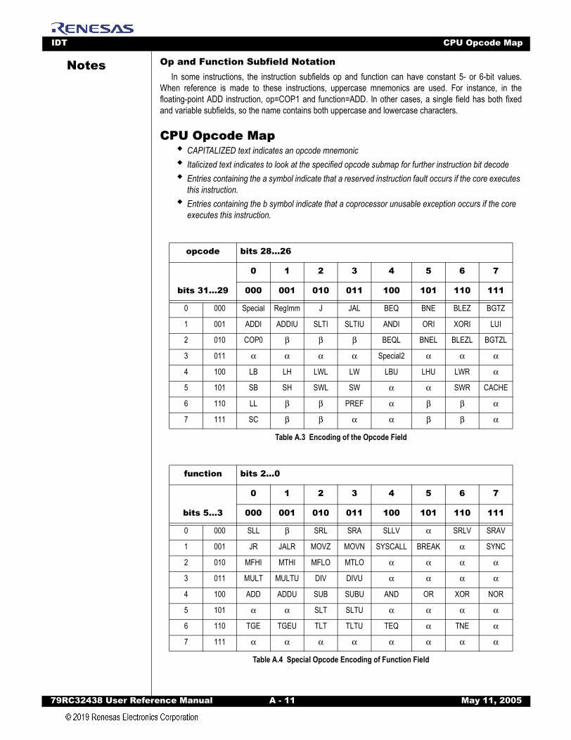
IDT CPU Opcode Map
79RC32438 User Refer
Notes
Op and Function Subfield NotationIn some instructions, the instruction subfields op and function can have constant 5- or 6-bit values.When reference is made to these instructions, uppercase mnemonics are used. For instance, in thefloating-point ADD instruction, op=COP1 and function=ADD. In other cases, a single field has both fixedand variable subfields, so the name contains both uppercase and lowercase characters.
CPU Opcode MapCAPITALIZED text indicates an opcode mnemonicItalicized text indicates to look at the specified opcode submap for further instruction bit decodeEntries containing the a symbol indicate that a reserved instruction fault occurs if the core executes this instruction.Entries containing the b symbol indicate that a coprocessor unusable exception occurs if the core executes this instruction.
opcode bits 28...26
0 1 2 3 4 5 6 7
bits 31...29 000 001 010 011 100 101 110 111
0 000 Special RegImm J JAL BEQ BNE BLEZ BGTZ
1 001 ADDI ADDIU SLTI SLTIU ANDI ORI XORI LUI
2 010 COP0 β β β BEQL BNEL BLEZL BGTZL
3 011 α α α α Special2 α α α
4 100 LB LH LWL LW LBU LHU LWR α
5 101 SB SH SWL SW α α SWR CACHE
6 110 LL β β PREF α β β α
7 111 SC β β α α β β α
Table A.3 Encoding of the Opcode Field
function bits 2...0
0 1 2 3 4 5 6 7
bits 5...3 000 001 010 011 100 101 110 111
0 000 SLL β SRL SRA SLLV α SRLV SRAV
1 001 JR JALR MOVZ MOVN SYSCALL BREAK α SYNC
2 010 MFHI MTHI MFLO MTLO α α α α
3 011 MULT MULTU DIV DIVU α α α α
4 100 ADD ADDU SUB SUBU AND OR XOR NOR
5 101 α α SLT SLTU α α α α
6 110 TGE TGEU TLT TLTU TEQ α TNE α
7 111 α α α α α α α α
Table A.4 Special Opcode Encoding of Function Field
ence Manual A - 11 May 11, 2005

IDT CPU Opcode Map
79RC32438 User Refer
Notes
function bits 2...00 1 2 3 4 5 6 7
bits 5...3 000 001 010 011 100 101 110 111
0 000 MADD MADDU MUL α MSUB MSUBU α α
1 001 α α α α α α α α
2 010 α α α α α α α α
3 011 α α α α α α α α
4 100 CLZ CLO α α α α α α
5 101 α α α α α α α α
6 110 α α α α α α α α
7 111 α α α α α α α SDBBP
Table A.5 Special2 Opcode Encoding of Function Field
rt bits 18...16
0 1 2 3 4 5 6 7
bits 20...19 000 001 010 011 100 101 110 111
0 BLTZ BGEZ BLTZL BGEZL α α α α α
1 TGEI TGEIU TLTI TLTIU TEQI α TNEI α α
2 BLTZAL BGEZAL BLTZALL BGEZALL α α α α α
3 α α α α α α α α α
Table A.6 RegImm Encoding of rt Field
rs bits 23...21
0 1 2 3 4 5 6 7
bits 25...24 000 001 010 011 100 101 110 111
0 00 MFCO α α α MTCO α α α
1 01 α α α α α α α α
2 10 CO
3 11
Table A.7 COP0 Encoding of rs Field
ence Manual A - 12 May 11, 2005
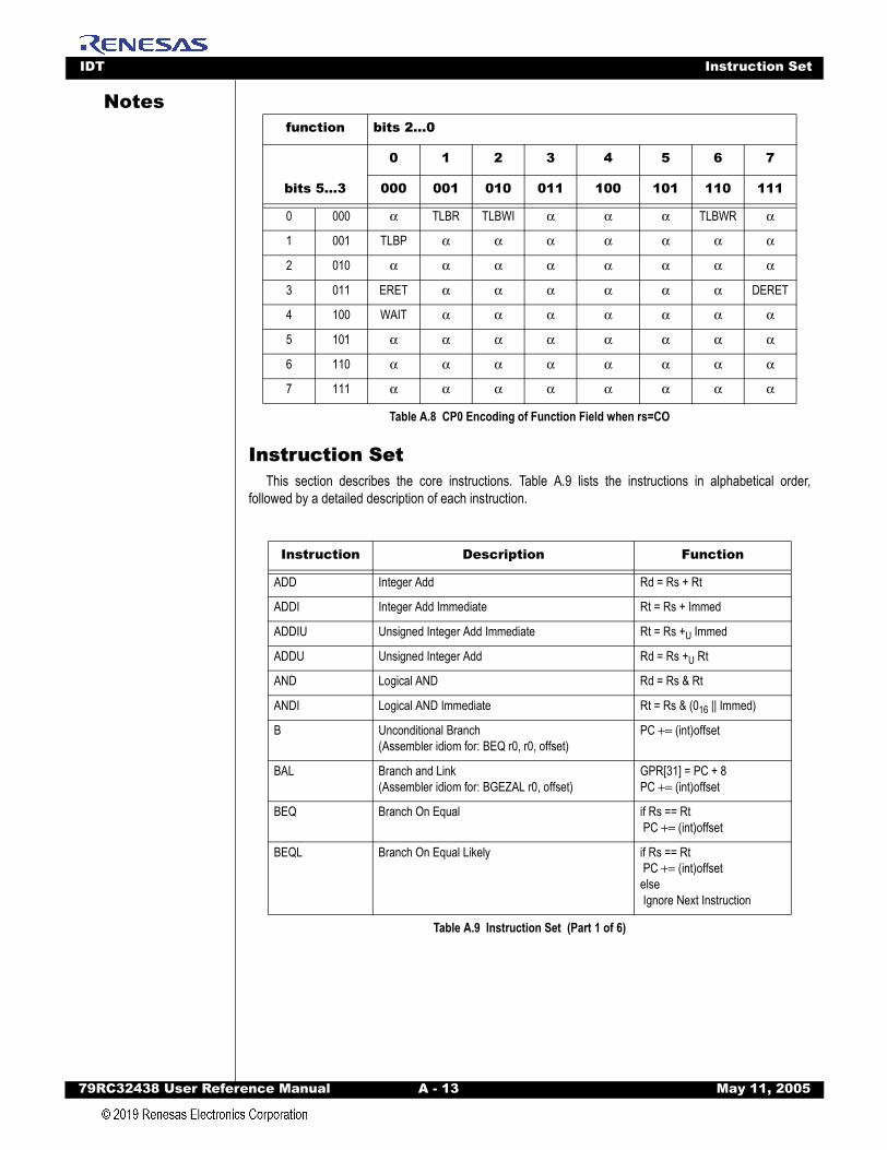
IDT Instruction Set
79RC32438 User Refer
Notes
Instruction SetThis section describes the core instructions. Table A.9 lists the instructions in alphabetical order,
followed by a detailed description of each instruction.
function bits 2...0
0 1 2 3 4 5 6 7
bits 5...3 000 001 010 011 100 101 110 111
0 000 α TLBR TLBWI α α α TLBWR α
1 001 TLBP α α α α α α α
2 010 α α α α α α α α
3 011 ERET α α α α α α DERET
4 100 WAIT α α α α α α α
5 101 α α α α α α α α
6 110 α α α α α α α α
7 111 α α α α α α α α
Table A.8 CP0 Encoding of Function Field when rs=CO
Instruction Description Function
ADD Integer Add Rd = Rs + Rt
ADDI Integer Add Immediate Rt = Rs + Immed
ADDIU Unsigned Integer Add Immediate Rt = Rs +U Immed
ADDU Unsigned Integer Add Rd = Rs +U Rt
AND Logical AND Rd = Rs & Rt
ANDI Logical AND Immediate Rt = Rs & (016 || Immed)
B Unconditional Branch(Assembler idiom for: BEQ r0, r0, offset)
PC += (int)offset
BAL Branch and Link(Assembler idiom for: BGEZAL r0, offset)
GPR[31] = PC + 8PC += (int)offset
BEQ Branch On Equal if Rs == Rt PC += (int)offset
BEQL Branch On Equal Likely if Rs == Rt PC += (int)offsetelse Ignore Next Instruction
Table A.9 Instruction Set (Part 1 of 6)
ence Manual A - 13 May 11, 2005
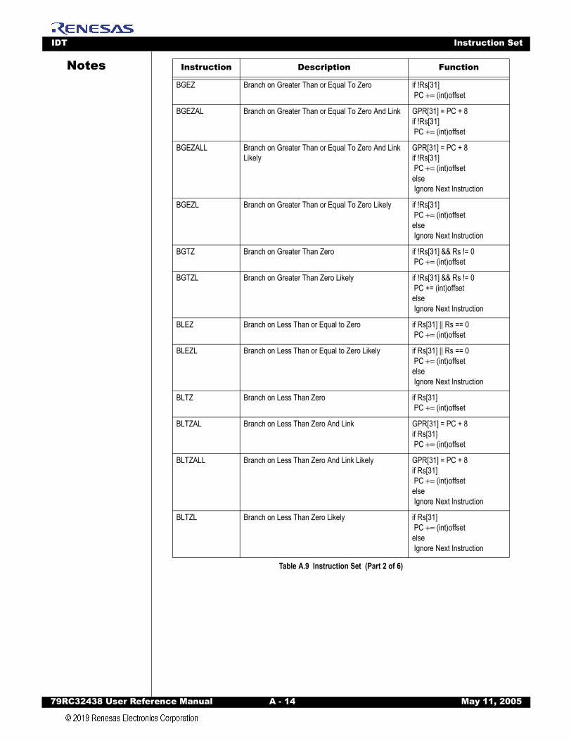
IDT Instruction Set
79RC32438 User Refer
Notes
BGEZ Branch on Greater Than or Equal To Zero if !Rs[31]PC += (int)offset
BGEZAL Branch on Greater Than or Equal To Zero And Link GPR[31] = PC + 8if !Rs[31] PC += (int)offset
BGEZALL Branch on Greater Than or Equal To Zero And Link Likely
GPR[31] = PC + 8if !Rs[31] PC += (int)offsetelse Ignore Next Instruction
BGEZL Branch on Greater Than or Equal To Zero Likely if !Rs[31] PC += (int)offsetelse Ignore Next Instruction
BGTZ Branch on Greater Than Zero if !Rs[31] && Rs != 0 PC += (int)offset
BGTZL Branch on Greater Than Zero Likely if !Rs[31] && Rs != 0 PC += (int)offsetelse Ignore Next Instruction
BLEZ Branch on Less Than or Equal to Zero if Rs[31] || Rs == 0 PC += (int)offset
BLEZL Branch on Less Than or Equal to Zero Likely if Rs[31] || Rs == 0 PC += (int)offsetelse Ignore Next Instruction
BLTZ Branch on Less Than Zero if Rs[31] PC += (int)offset
BLTZAL Branch on Less Than Zero And Link GPR[31] = PC + 8if Rs[31] PC += (int)offset
BLTZALL Branch on Less Than Zero And Link Likely GPR[31] = PC + 8if Rs[31] PC += (int)offsetelse Ignore Next Instruction
BLTZL Branch on Less Than Zero Likely if Rs[31] PC += (int)offsetelse Ignore Next Instruction
Instruction Description Function
Table A.9 Instruction Set (Part 2 of 6)
ence Manual A - 14 May 11, 2005
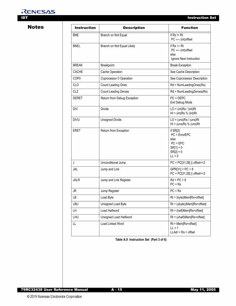
IDT Instruction Set
79RC32438 User Refer
Notes
BNE Branch on Not Equal if Rs != RtPC += (int)offset
BNEL Branch on Not Equal Likely if Rs != Rt PC += (int)offsetelse Ignore Next Instruction
BREAK Breakpoint Break Exception
CACHE Cache Operation See Cache Description
COP0 Coprocessor 0 Operation See Coprocessor Description
CLO Count Leading Ones Rd = NumLeadingOnes(Rs)
CLZ Count Leading Zeroes Rd = NumLeadingZeroes(Rs)
DERET Return from Debug Exception PC = DEPCExit Debug Mode
DIV Divide LO = (int)Rs / (int)RtHI = (int)Rs % (int)Rt
DIVU Unsigned Divide LO = (uns)Rs / (uns)RtHI = (uns)Rs % (uns)Rt
ERET Return from Exception if SR[2] PC = ErrorEPCelse PC = EPCSR[1] = 0SR[2] = 0LL = 0
J Unconditional Jump PC = PC[31:28] || offset<<2
JAL Jump and Link GPR[31] = PC + 8PC = PC[31:28] || offset<<2
JALR Jump and Link Register Rd = PC + 8PC = Rs
JR Jump Register PC = Rs
LB Load Byte Rt = (byte)Mem[Rs+offset]
LBU Unsigned Load Byte Rt = (ubyte))Mem[Rs+offset]
LH Load Halfword Rt = (half)Mem[Rs+offset]
LHU Unsigned Load Halfword Rt = (uhalf)Mem[Rs+offset]
LL Load Linked Word Rt = Mem[Rs+offset]LL = 1LLAdr = Rs + offset
Instruction Description Function
Table A.9 Instruction Set (Part 3 of 6)
ence Manual A - 15 May 11, 2005

IDT Instruction Set
79RC32438 User Refer
Notes
LUI Load Upper Immediate Rt = immediate << 16LW Load Word Rt = Mem[Rs+offset]
LWL Load Word Left See LWL instruction on page A-53.
LWR Load Word Right See LWR instruction on page A-55.
MADD Multiply - Add HI, LO += (int)Rs * (int)Rt
MADDU Multiply - Add Unsigned HI, LO += (uns)Rs * (uns)Rt
MFC0 Move From Coprocessor 0 Rt = CPR[0, n, sel] = Rt
MFHI Move From HI Rd = HI
MFLO Move From LO Rd = LO
MOVN Move Conditional on Not Zero if GPR[rt] ≠ 0 then GPR[rd] ← GPR[rs]
MOVZ Move Conditional on Zero if GPR[rt] = 0 then GPR[rd] ← GPR[rs]
MSUB Multiply-Subtract HI, LO −= (int)Rs * (int)Rt
MSUBU Multiply-Subtract Unsigned HI, LO −= (uns)Rs * (uns)Rt
MTC0 Move To Coprocessor 0 CPR[0, n] = Rt SEL
MTHI Move To HI HI = Rs
MTLO Move To LO LO = Rs
MUL Multiply with register write HI | LO =UnpredictableRd = LO
MULT Integer Multiply HI | LO = (int)Rs * (int)Rd
MULTU Unsigned Multiply HI | LO = (uns)Rs * (uns)Rd
NOP No Operation(Assembler idiom for: SLL r0, r0, r0)
NOR Logical NOR Rd = ∼(Rs | Rt)
OR Logical OR Rd = Rs | Rt
ORI Logical OR Immediate Rt = Rs | Immed
PREF Prefetch Load Specified Line into Cache
SB Store Byte (byte)Mem[Rs+offset] = Rt
Instruction Description Function
Table A.9 Instruction Set (Part 4 of 6)
ence Manual A - 16 May 11, 2005

IDT Instruction Set
79RC32438 User Refer
Notes
SC Store Conditional Word if LL =1mem[Rxoffs] = RtRt = LL
SDBBP Software Debug Break Point Trap to SW Debug Handler
SH Store Half (half)Mem[Rs+offset] = Rt
SLL Shift Left Logical Rd = Rt << sa
SLLV Shift Left Logical Variable Rd = Rt << Rs[4:0]
SLT Set on Less Than if (int)Rs < (int)Rt Rd = 1else Rd = 0
SLTI Set on Less Than Immediate if (int)Rs < (int)Immed Rt = 1else Rt = 0
SLTIU Set on Less Than Immediate Unsigned if (uns)Rs < (uns)Immed Rt = 1else Rt = 0
SLTU Set on Less Than Unsigned if (uns)Rs < (uns)Immed Rd = 1else Rd = 0
SRA Shift Right Arithmetic Rd = (int)Rt >> sa
SRAV Shift Right Arithmetic Variable Rd = (int)Rt >> Rs[4:0]
SRL Shift Right Logical Rd = (uns)Rt >> sa
SRLV Shift Right Logical Variable Rd = (uns)Rt >> Rs[4:0]
SSNOP Superscalar Inhibit No Operation
SUB Integer Subtract Rt = (int)Rs - (int)Rd
SUBU Unsigned Subtract Rt = (uns)Rs - (uns)Rd
SW Store Word Mem[Rs+offset] = Rt
SWL Store Word Left See Store Word Left instruc-tion on
SWR Store Word Right SeeStore Word Right instruc-tion on
SYNC Synchronize See SYNC instruction on page A-88
Instruction Description Function
Table A.9 Instruction Set (Part 5 of 6)
ence Manual A - 17 May 11, 2005
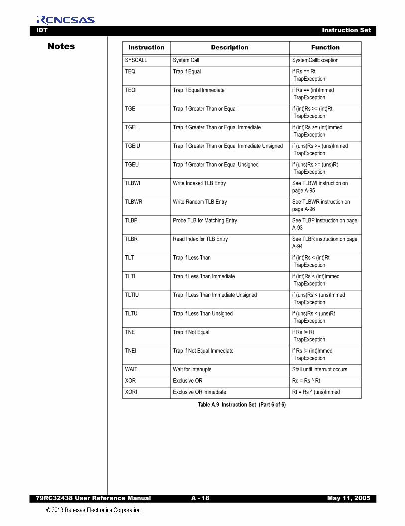
IDT Instruction Set
79RC32438 User Refer
Notes
SYSCALL System Call SystemCallExceptionTEQ Trap if Equal if Rs == Rt TrapException
TEQI Trap if Equal Immediate if Rs == (int)Immed TrapException
TGE Trap if Greater Than or Equal if (int)Rs >= (int)Rt TrapException
TGEI Trap if Greater Than or Equal Immediate if (int)Rs >= (int)Immed TrapException
TGEIU Trap if Greater Than or Equal Immediate Unsigned if (uns)Rs >= (uns)Immed TrapException
TGEU Trap if Greater Than or Equal Unsigned if (uns)Rs >= (uns)Rt TrapException
TLBWI Write Indexed TLB Entry See TLBWI instruction on page A-95
TLBWR Write Random TLB Entry See TLBWR instruction on page A-96
TLBP Probe TLB for Matching Entry See TLBP instruction on page A-93
TLBR Read Index for TLB Entry See TLBR instruction on page A-94
TLT Trap if Less Than if (int)Rs < (int)Rt TrapException
TLTI Trap if Less Than Immediate if (int)Rs < (int)Immed TrapException
TLTIU Trap if Less Than Immediate Unsigned if (uns)Rs < (uns)Immed TrapException
TLTU Trap if Less Than Unsigned if (uns)Rs < (uns)Rt TrapException
TNE Trap if Not Equal if Rs != Rt TrapException
TNEI Trap if Not Equal Immediate if Rs != (int)Immed TrapException
WAIT Wait for Interrupts Stall until interrupt occurs
XOR Exclusive OR Rd = Rs ^ Rt
XORI Exclusive OR Immediate Rt = Rs ^ (uns)Immed
Instruction Description Function
Table A.9 Instruction Set (Part 6 of 6)
ence Manual A - 18 May 11, 2005

IDT Instruction Set
79RC32438 User Refer
Notes
DDFormat: ADD rd, rs, rt MIPS32
Purpose: To add 32-bit integers. If an overflow occurs, then trap.
Description: rd ← rs + rt
The 32-bit word value in GPR rt is added to the 32-bit value in GPR rs to produce a 32-bit result.
• If the addition results in 32-bit 2’s complement arithmetic overflow, the destination register is not modified and an Integer Overflow exception occurs.
• If the addition does not overflow, the 32-bit result is placed into GPR rd.
Restrictions: None
Operation:temp ← (GPR[rs]31||GPR[rs]31..0) + (GPR[rt]31||GPR[rt]31..0)if temp32 ≠ temp31 then
SignalException(IntegerOverflow)else
GPR[rd] ← tempendif
Exceptions: Integer Overflow
Programming Notes:ADDU performs the same arithmetic operation but does not trap on overflow.
ADDI
Format: ADDI rt, rs, immediate MIPS32
Purpose: To add a constant to a 32-bit integer. If overflow occurs, then trap.
31 26 25 21 20 16 15 11 10 6 5 0SPECIAL
000000rs rt rd
0
00000
ADD
1000006 5 5 5 5 6
31 26 25 21 20 16 15 0ADDI
001000rs rt immediate
6 5 5 16
Add Word ADD
Add Immediate Word ADDI
ence Manual A - 19 May 11, 2005
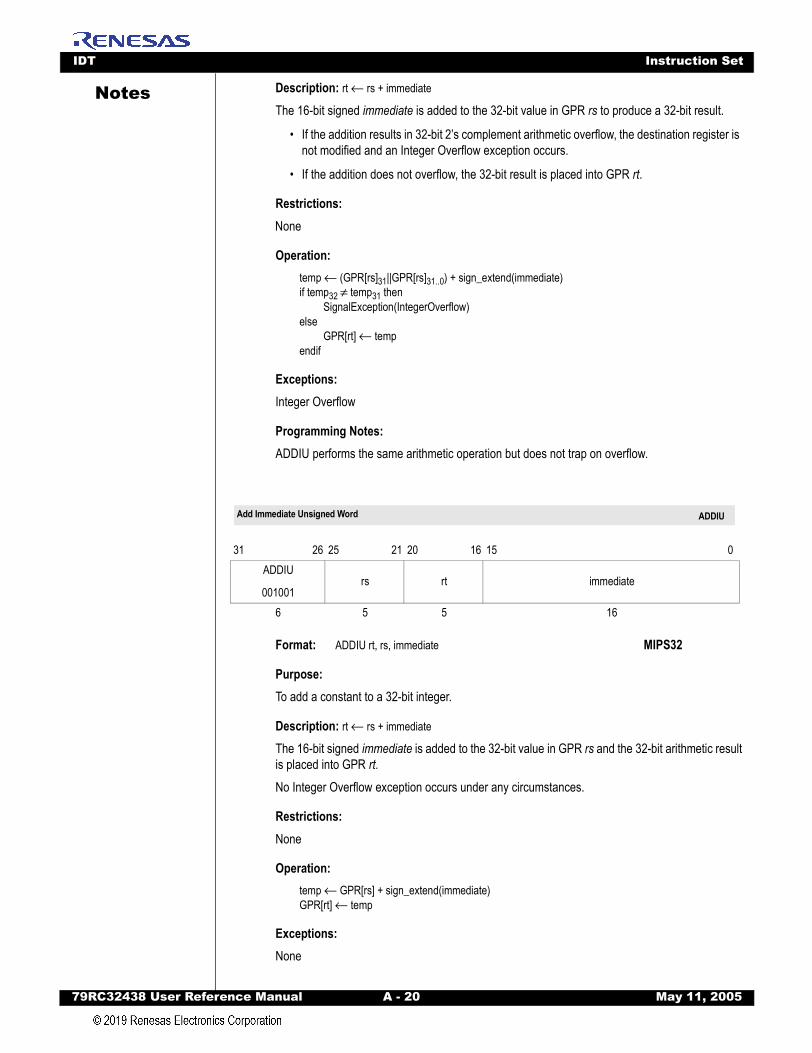
IDT Instruction Set
79RC32438 User Refer
Notes
Description: rt ← rs + immediateThe 16-bit signed immediate is added to the 32-bit value in GPR rs to produce a 32-bit result.
• If the addition results in 32-bit 2’s complement arithmetic overflow, the destination register is not modified and an Integer Overflow exception occurs.
• If the addition does not overflow, the 32-bit result is placed into GPR rt.
Restrictions: None
Operation:temp ← (GPR[rs]31||GPR[rs]31..0) + sign_extend(immediate)if temp32 ≠ temp31 then
SignalException(IntegerOverflow)else
GPR[rt] ← tempendif
Exceptions: Integer Overflow
Programming Notes: ADDIU performs the same arithmetic operation but does not trap on overflow.
ADDIU
Format: ADDIU rt, rs, immediate MIPS32
Purpose: To add a constant to a 32-bit integer.
Description: rt ← rs + immediate
The 16-bit signed immediate is added to the 32-bit value in GPR rs and the 32-bit arithmetic resultis placed into GPR rt.No Integer Overflow exception occurs under any circumstances.
Restrictions: None
Operation:temp ← GPR[rs] + sign_extend(immediate)GPR[rt] ← temp
Exceptions: None
31 26 25 21 20 16 15 0ADDIU
001001rs rt immediate
6 5 5 16
Add Immediate Unsigned Word ADDIU
ence Manual A - 20 May 11, 2005

IDT Instruction Set
79RC32438 User Refer
Notes
Programming Notes: The term “unsigned” in the instruction name is a misnomer; this operation is 32-bit modulo arith-metic that does not trap on overflow. This instruction is appropriate for unsigned arithmetic, suchas address arithmetic, or integer arithmetic environments that ignore overflow, such as C lan-guage arithmetic.ADDU
Format: ADDU rd, rs, rt MIPS32
Purpose: To add 32-bit integers.
Description: rd ← rs + rt
The 32-bit word value in GPR rt is added to the 32-bit value in GPR rs and the 32-bit arithmeticresult is placed into GPR rd.No Integer Overflow exception occurs under any circumstances.
Restrictions: None
Operation:temp ← GPR[rs] + GPR[rt]GPR[rd] ← temp
Exceptions: None
Programming Notes: The term “unsigned” in the instruction name is a misnomer; this operation is 32-bit modulo arith-metic that does not trap on overflow. This instruction is appropriate for unsigned arithmetic, suchas address arithmetic, or integer arithmetic environments that ignore overflow, such as C lan-guage arithmetic.
31 26 25 21 20 16 15 11 10 6 5 0SPECIAL
000000rs rt rd
0
00000
ADDU
1000016 5 5 5 5 6
Add Unsigned Word ADDU
ence Manual A - 21 May 11, 2005
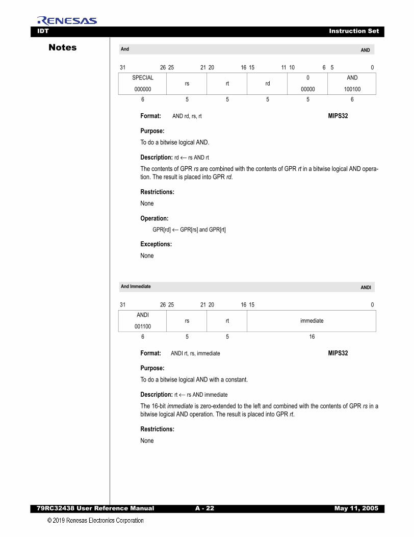
IDT Instruction Set
79RC32438 User Refer
Notes
ANDFormat: AND rd, rs, rt MIPS32
Purpose: To do a bitwise logical AND.
Description: rd ← rs AND rt
The contents of GPR rs are combined with the contents of GPR rt in a bitwise logical AND opera-tion. The result is placed into GPR rd.
Restrictions: None
Operation:GPR[rd] ← GPR[rs] and GPR[rt]
Exceptions: None
ANDI
Format: ANDI rt, rs, immediate MIPS32
Purpose: To do a bitwise logical AND with a constant.
Description: rt ← rs AND immediate
The 16-bit immediate is zero-extended to the left and combined with the contents of GPR rs in abitwise logical AND operation. The result is placed into GPR rt.
Restrictions: None
31 26 25 21 20 16 15 11 10 6 5 0SPECIAL
000000rs rt rd
0
00000
AND
1001006 5 5 5 5 6
31 26 25 21 20 16 15 0ANDI
001100rs rt immediate
6 5 5 16
And AND
And Immediate ANDI
ence Manual A - 22 May 11, 2005
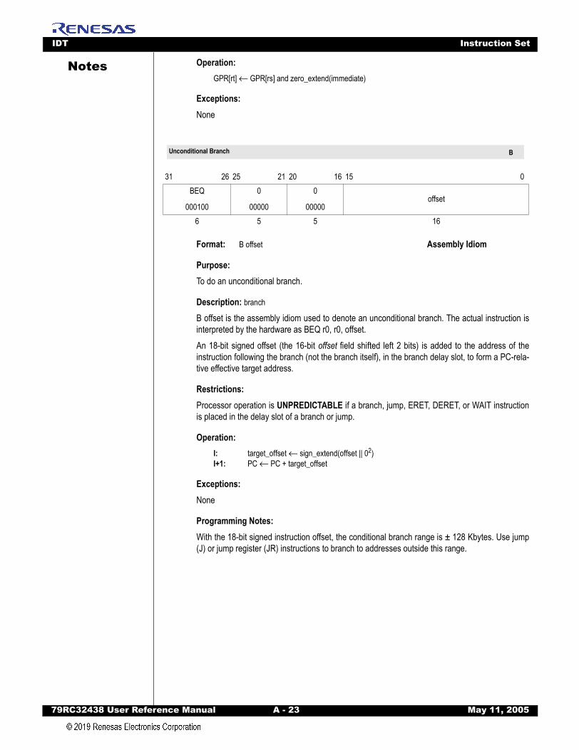
IDT Instruction Set
79RC32438 User Refer
Notes
Operation:GPR[rt] ← GPR[rs] and zero_extend(immediate)Exceptions: None
B
Format: B offset Assembly Idiom
Purpose: To do an unconditional branch.
Description: branch
B offset is the assembly idiom used to denote an unconditional branch. The actual instruction isinterpreted by the hardware as BEQ r0, r0, offset.An 18-bit signed offset (the 16-bit offset field shifted left 2 bits) is added to the address of theinstruction following the branch (not the branch itself), in the branch delay slot, to form a PC-rela-tive effective target address.
Restrictions:Processor operation is UNPREDICTABLE if a branch, jump, ERET, DERET, or WAIT instructionis placed in the delay slot of a branch or jump.
Operation:I: target_offset ← sign_extend(offset || 02)I+1: PC ← PC + target_offset
Exceptions: None
Programming Notes: With the 18-bit signed instruction offset, the conditional branch range is ± 128 Kbytes. Use jump(J) or jump register (JR) instructions to branch to addresses outside this range.
31 26 25 21 20 16 15 0BEQ
000100
0
00000
0
00000offset
6 5 5 16
Unconditional Branch B
ence Manual A - 23 May 11, 2005

IDT Instruction Set
79RC32438 User Refer
Notes
BALFormat: BAL rs, offset Assembly Idiom
Purpose: To do an unconditional PC-relative procedure call.
Description: procedure_call
BAL offset is the assembly idiom used to denote an unconditional branch. The actual instructionis interpreted by the hardware as BGEZAL r0, offset.Place the return address link in GPR 31. The return link is the address of the second instructionfollowing the branch, where execution continues after a procedure call.An 18-bit signed offset (the 16-bit offset field shifted left 2 bits) is added to the address of theinstruction following the branch (not the branch itself), in the branch delay slot, to form a PC-rela-tive effective target address.
Restrictions: Processor operation is UNPREDICTABLE if a branch, jump, ERET, DERET, or WAIT instructionis placed in the delay slot of a branch or jump.GPR 31 must not be used for the source register rs, because such an instruction does not havethe same effect when re-executed. The result of executing such an instruction is UNPREDICT-ABLE. This restriction permits an exception handler to resume execution by re-executing thebranch when an exception occurs in the branch delay slot.
Operation:I: target_offset ← sign_extend(offset || 02)
GPR[31] ← PC + 8I+1: PC ← PC + target_offset
Exceptions:None
Programming Notes: With the 18-bit signed instruction offset, the conditional branch range is ± 128 KBytes. Use jumpand link (JAL) or jump and link register (JALR) instructions for procedure calls to addresses out-side this range.
31 26 25 21 20 16 15 0REGIMM
000001
0
00000
BGEZAL
10001offset
6 5 5 16
Branch and Link BAL
ence Manual A - 24 May 11, 2005
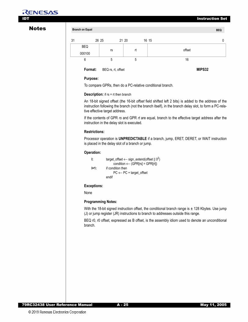
IDT Instruction Set
79RC32438 User Refer
Notes
BEQFormat: BEQ rs, rt, offset MIPS32
Purpose: To compare GPRs, then do a PC-relative conditional branch.
Description: if rs = rt then branch
An 18-bit signed offset (the 16-bit offset field shifted left 2 bits) is added to the address of theinstruction following the branch (not the branch itself), in the branch delay slot, to form a PC-rela-tive effective target address.If the contents of GPR rs and GPR rt are equal, branch to the effective target address after theinstruction in the delay slot is executed.
Restrictions: Processor operation is UNPREDICTABLE if a branch, jump, ERET, DERET, or WAIT instructionis placed in the delay slot of a branch or jump.
Operation:I: target_offset ← sign_extend(offset || 02)
condition ← (GPR[rs] = GPR[rt])I+1: if condition then
PC ← PC + target_offsetendif
Exceptions: None
Programming Notes: With the 18-bit signed instruction offset, the conditional branch range is ± 128 Kbytes. Use jump(J) or jump register (JR) instructions to branch to addresses outside this range. BEQ r0, r0 offset, expressed as B offset, is the assembly idiom used to denote an unconditionalbranch.
31 26 25 21 20 16 15 0BEQ
000100rs rt offset
6 5 5 16
Branch on Equal BEQ
ence Manual A - 25 May 11, 2005

IDT Instruction Set
79RC32438 User Refer
Notes
BEQLFormat: BEQL rs, rt, offset MIPS32
Purpose: To compare GPRs, then do a PC-relative conditional branch; execute the delay slot only if thebranch is taken.
Description: if rs = rt then branch_likely
An 18-bit signed offset (the 16-bit offset field shifted left 2 bits) is added to the address of theinstruction following the branch (not the branch itself), in the branch delay slot, to form a PC-rela-tive effective target address.If the contents of GPR rs and GPR rt are equal, branch to the target address after the instructionin the delay slot is executed. If the branch is not taken, the instruction in the delay slot is not exe-cuted.
Restrictions: Processor operation is UNPREDICTABLE if a branch, jump, ERET, DERET, or WAIT instructionis placed in the delay slot of a branch or jump.
Operation:I: target_offset ← sign_extend(offset || 02)
condition ← (GPR[rs] = GPR[rt])I+1: if condition then
PC ← PC + target_offsetelse
NullifyCurrentInstruction()endif
Exceptions: None
Programming Notes: With the 18-bit signed instruction offset, the conditional branch range is ± 128 KBytes. Use jump(J) or jump register (JR) instructions to branch to addresses outside this range.Software is strongly encouraged to avoid the use of the Branch Likely instructions, as they will beremoved from a future revision of the MIPS Architecture.
31 26 25 21 20 16 15 0BEQL
010100rs rt offset
6 5 5 16
Branch on Equal Likely BEQL
ence Manual A - 26 May 11, 2005

IDT Instruction Set
79RC32438 User Refer
Notes
BGEZFormat: BGEZ rs, offset MIPS32
Purpose: To test a GPR, then do a PC-relative conditional branch.
Description: if rs ≥ 0 then branch
An 18-bit signed offset (the 16-bit offset field shifted left 2 bits) is added to the address of theinstruction following the branch (not the branch itself), in the branch delay slot, to form a PC-rela-tive effective target address.If the contents of GPR rs are greater than or equal to zero (sign bit is 0), branch to the effectivetarget address after the instruction in the delay slot is executed.
Restrictions: Processor operation is UNPREDICTABLE if a branch, jump, ERET, DERET, or WAIT instructionis placed in the delay slot of a branch or jump.
Operation:I: target_offset ← sign_extend(offset || 02)
condition ← GPR[rs] ≥ 0GPRLEN
I+1: if condition thenPC ← PC + target_offset
endif
Exceptions: None
Programming Notes: With the 18-bit signed instruction offset, the conditional branch range is ± 128 KBytes. Use jump(J) or jump register (JR) instructions to branch to addresses outside this range.
BGEZAL
Format: BGEZAL rs, offset MIPS32
Purpose: To test a GPR, then do a PC-relative conditional procedure call.
31 26 25 21 20 16 15 0REGIMM
000001rs
BGEZ
00001offset
6 5 5 16
31 26 25 21 20 16 15 0REGIMM
000001rs
BGEZAL
10001offset
6 5 5 16
Branch on Greater Than or Equal to Zero BGEZ
Branch on Greater Than or Equal to Zero and Link BGEZAL
ence Manual A - 27 May 11, 2005
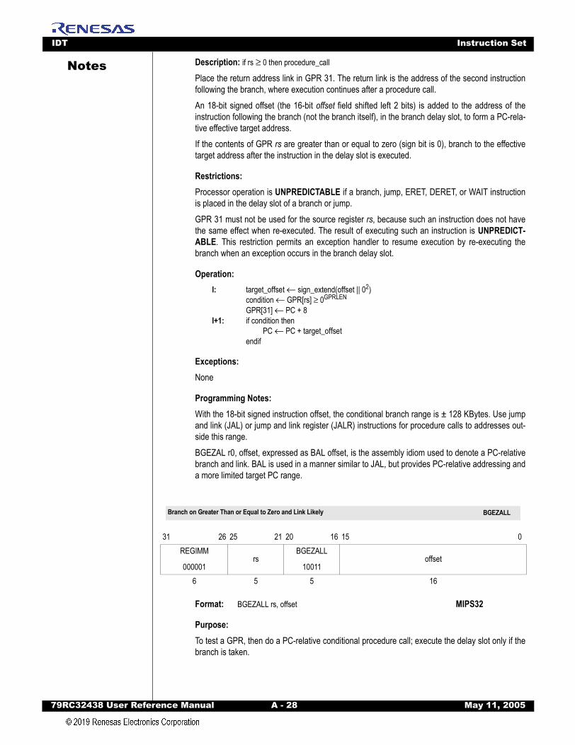
IDT Instruction Set
79RC32438 User Refer
Notes
Description: if rs ≥ 0 then procedure_callPlace the return address link in GPR 31. The return link is the address of the second instructionfollowing the branch, where execution continues after a procedure call.An 18-bit signed offset (the 16-bit offset field shifted left 2 bits) is added to the address of theinstruction following the branch (not the branch itself), in the branch delay slot, to form a PC-rela-tive effective target address.If the contents of GPR rs are greater than or equal to zero (sign bit is 0), branch to the effectivetarget address after the instruction in the delay slot is executed.
Restrictions: Processor operation is UNPREDICTABLE if a branch, jump, ERET, DERET, or WAIT instructionis placed in the delay slot of a branch or jump.GPR 31 must not be used for the source register rs, because such an instruction does not havethe same effect when re-executed. The result of executing such an instruction is UNPREDICT-ABLE. This restriction permits an exception handler to resume execution by re-executing thebranch when an exception occurs in the branch delay slot.
Operation:I: target_offset ← sign_extend(offset || 02)
condition ← GPR[rs] ≥ 0GPRLEN
GPR[31] ← PC + 8I+1: if condition then
PC ← PC + target_offsetendif
Exceptions: None
Programming Notes: With the 18-bit signed instruction offset, the conditional branch range is ± 128 KBytes. Use jumpand link (JAL) or jump and link register (JALR) instructions for procedure calls to addresses out-side this range.BGEZAL r0, offset, expressed as BAL offset, is the assembly idiom used to denote a PC-relativebranch and link. BAL is used in a manner similar to JAL, but provides PC-relative addressing anda more limited target PC range.
BGEZALL
Format: BGEZALL rs, offset MIPS32
Purpose: To test a GPR, then do a PC-relative conditional procedure call; execute the delay slot only if thebranch is taken.
31 26 25 21 20 16 15 0REGIMM
000001rs
BGEZALL
10011offset
6 5 5 16
Branch on Greater Than or Equal to Zero and Link Likely BGEZALL
ence Manual A - 28 May 11, 2005
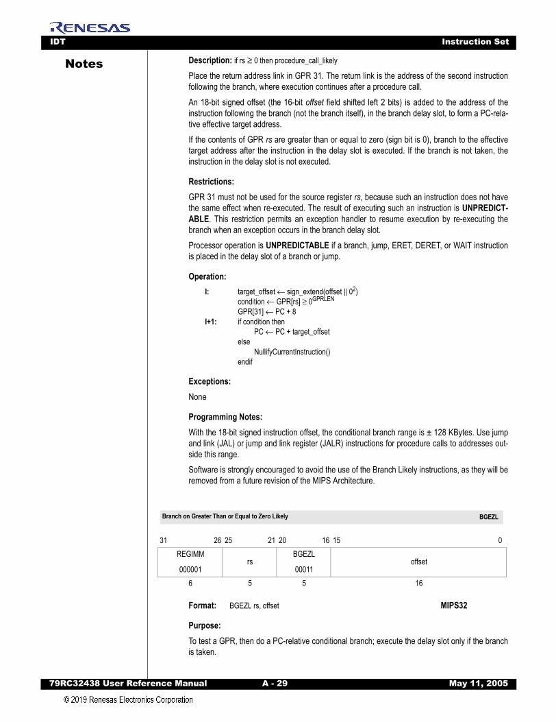
IDT Instruction Set
79RC32438 User Refer
Notes
Description: if rs ≥ 0 then procedure_call_likelyPlace the return address link in GPR 31. The return link is the address of the second instructionfollowing the branch, where execution continues after a procedure call.An 18-bit signed offset (the 16-bit offset field shifted left 2 bits) is added to the address of theinstruction following the branch (not the branch itself), in the branch delay slot, to form a PC-rela-tive effective target address.If the contents of GPR rs are greater than or equal to zero (sign bit is 0), branch to the effectivetarget address after the instruction in the delay slot is executed. If the branch is not taken, theinstruction in the delay slot is not executed.
Restrictions:GPR 31 must not be used for the source register rs, because such an instruction does not havethe same effect when re-executed. The result of executing such an instruction is UNPREDICT-ABLE. This restriction permits an exception handler to resume execution by re-executing thebranch when an exception occurs in the branch delay slot.Processor operation is UNPREDICTABLE if a branch, jump, ERET, DERET, or WAIT instructionis placed in the delay slot of a branch or jump.
Operation:I: target_offset ← sign_extend(offset || 02)
condition ← GPR[rs] ≥ 0GPRLEN
GPR[31] ← PC + 8I+1: if condition then
PC ← PC + target_offsetelse
NullifyCurrentInstruction()endif
Exceptions: None
Programming Notes: With the 18-bit signed instruction offset, the conditional branch range is ± 128 KBytes. Use jumpand link (JAL) or jump and link register (JALR) instructions for procedure calls to addresses out-side this range.Software is strongly encouraged to avoid the use of the Branch Likely instructions, as they will beremoved from a future revision of the MIPS Architecture.
BGEZL
Format: BGEZL rs, offset MIPS32
Purpose: To test a GPR, then do a PC-relative conditional branch; execute the delay slot only if the branchis taken.
31 26 25 21 20 16 15 0REGIMM
000001rs
BGEZL
00011offset
6 5 5 16
Branch on Greater Than or Equal to Zero Likely BGEZL
ence Manual A - 29 May 11, 2005
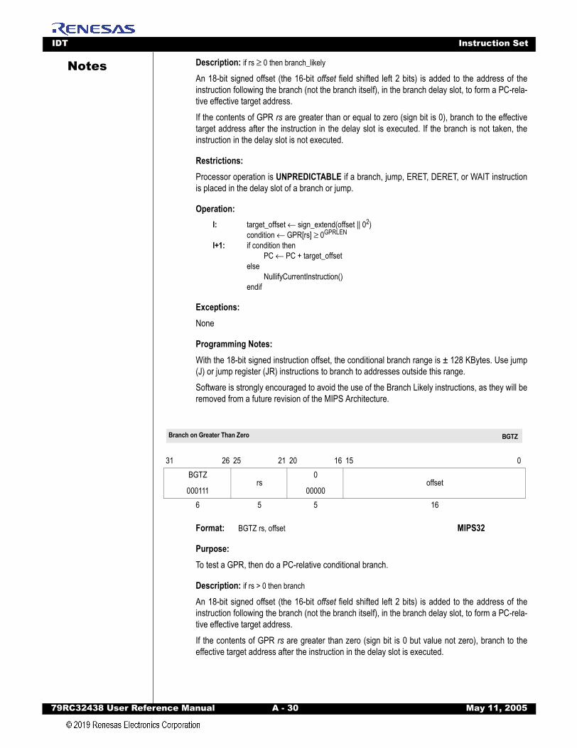
IDT Instruction Set
79RC32438 User Refer
Notes
Description: if rs ≥ 0 then branch_likelyAn 18-bit signed offset (the 16-bit offset field shifted left 2 bits) is added to the address of theinstruction following the branch (not the branch itself), in the branch delay slot, to form a PC-rela-tive effective target address.If the contents of GPR rs are greater than or equal to zero (sign bit is 0), branch to the effectivetarget address after the instruction in the delay slot is executed. If the branch is not taken, theinstruction in the delay slot is not executed.
Restrictions: Processor operation is UNPREDICTABLE if a branch, jump, ERET, DERET, or WAIT instructionis placed in the delay slot of a branch or jump.
Operation:I: target_offset ← sign_extend(offset || 02)
condition ← GPR[rs] ≥ 0GPRLEN
I+1: if condition thenPC ← PC + target_offset
elseNullifyCurrentInstruction()
endif
Exceptions: None
Programming Notes: With the 18-bit signed instruction offset, the conditional branch range is ± 128 KBytes. Use jump(J) or jump register (JR) instructions to branch to addresses outside this range.Software is strongly encouraged to avoid the use of the Branch Likely instructions, as they will beremoved from a future revision of the MIPS Architecture.
BGTZ
Format: BGTZ rs, offset MIPS32
Purpose: To test a GPR, then do a PC-relative conditional branch.
Description: if rs > 0 then branch
An 18-bit signed offset (the 16-bit offset field shifted left 2 bits) is added to the address of theinstruction following the branch (not the branch itself), in the branch delay slot, to form a PC-rela-tive effective target address.If the contents of GPR rs are greater than zero (sign bit is 0 but value not zero), branch to theeffective target address after the instruction in the delay slot is executed.
31 26 25 21 20 16 15 0BGTZ
000111rs
0
00000offset
6 5 5 16
Branch on Greater Than Zero BGTZ
ence Manual A - 30 May 11, 2005
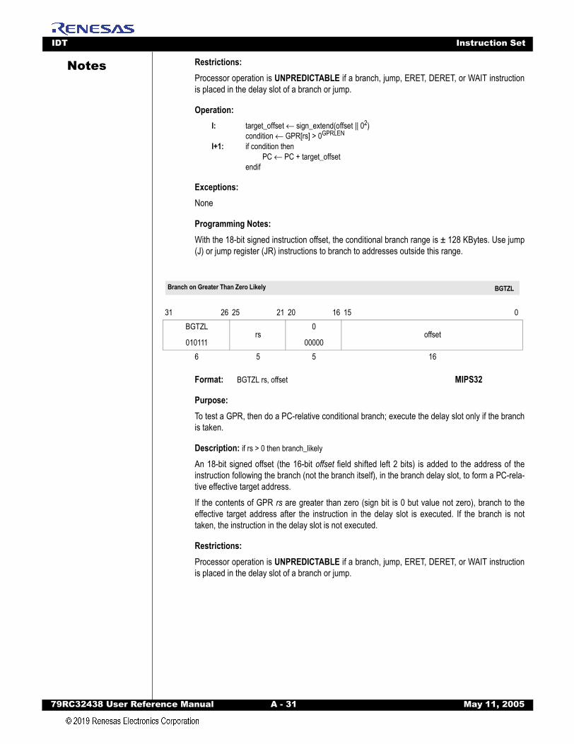
IDT Instruction Set
79RC32438 User Refer
Notes
Restrictions: Processor operation is UNPREDICTABLE if a branch, jump, ERET, DERET, or WAIT instructionis placed in the delay slot of a branch or jump.Operation:I: target_offset ← sign_extend(offset || 02)
condition ← GPR[rs] > 0GPRLEN
I+1: if condition thenPC ← PC + target_offset
endif
Exceptions: None
Programming Notes:With the 18-bit signed instruction offset, the conditional branch range is ± 128 KBytes. Use jump(J) or jump register (JR) instructions to branch to addresses outside this range.
BGTZL
Format: BGTZL rs, offset MIPS32
Purpose:To test a GPR, then do a PC-relative conditional branch; execute the delay slot only if the branchis taken.
Description: if rs > 0 then branch_likely
An 18-bit signed offset (the 16-bit offset field shifted left 2 bits) is added to the address of theinstruction following the branch (not the branch itself), in the branch delay slot, to form a PC-rela-tive effective target address.If the contents of GPR rs are greater than zero (sign bit is 0 but value not zero), branch to theeffective target address after the instruction in the delay slot is executed. If the branch is nottaken, the instruction in the delay slot is not executed.
Restrictions: Processor operation is UNPREDICTABLE if a branch, jump, ERET, DERET, or WAIT instructionis placed in the delay slot of a branch or jump.
31 26 25 21 20 16 15 0BGTZL
010111rs
0
00000offset
6 5 5 16
Branch on Greater Than Zero Likely BGTZL
ence Manual A - 31 May 11, 2005
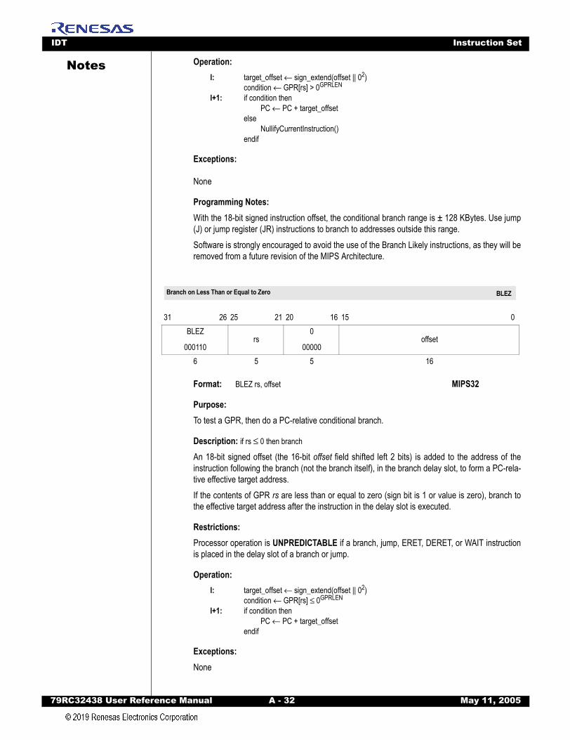
IDT Instruction Set
79RC32438 User Refer
Notes
Operation:I: target_offset ← sign_extend(offset || 02)condition ← GPR[rs] > 0GPRLEN
I+1: if condition thenPC ← PC + target_offset
elseNullifyCurrentInstruction()
endif
Exceptions:
None
Programming Notes: With the 18-bit signed instruction offset, the conditional branch range is ± 128 KBytes. Use jump(J) or jump register (JR) instructions to branch to addresses outside this range.Software is strongly encouraged to avoid the use of the Branch Likely instructions, as they will beremoved from a future revision of the MIPS Architecture.
BLEZ
Format: BLEZ rs, offset MIPS32
Purpose: To test a GPR, then do a PC-relative conditional branch.
Description: if rs ≤ 0 then branch
An 18-bit signed offset (the 16-bit offset field shifted left 2 bits) is added to the address of theinstruction following the branch (not the branch itself), in the branch delay slot, to form a PC-rela-tive effective target address.If the contents of GPR rs are less than or equal to zero (sign bit is 1 or value is zero), branch tothe effective target address after the instruction in the delay slot is executed.
Restrictions: Processor operation is UNPREDICTABLE if a branch, jump, ERET, DERET, or WAIT instructionis placed in the delay slot of a branch or jump.
Operation:I: target_offset ← sign_extend(offset || 02)
condition ← GPR[rs] ≤ 0GPRLEN
I+1: if condition thenPC ← PC + target_offset
endif
Exceptions: None
31 26 25 21 20 16 15 0BLEZ
000110rs
0
00000offset
6 5 5 16
Branch on Less Than or Equal to Zero BLEZ
ence Manual A - 32 May 11, 2005
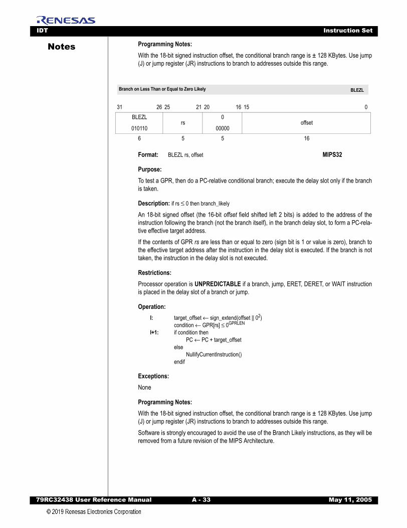
IDT Instruction Set
79RC32438 User Refer
Notes
Programming Notes:With the 18-bit signed instruction offset, the conditional branch range is ± 128 KBytes. Use jump(J) or jump register (JR) instructions to branch to addresses outside this range.BLEZL
Format: BLEZL rs, offset MIPS32
Purpose: To test a GPR, then do a PC-relative conditional branch; execute the delay slot only if the branchis taken.
Description: if rs ≤ 0 then branch_likely
An 18-bit signed offset (the 16-bit offset field shifted left 2 bits) is added to the address of theinstruction following the branch (not the branch itself), in the branch delay slot, to form a PC-rela-tive effective target address.If the contents of GPR rs are less than or equal to zero (sign bit is 1 or value is zero), branch tothe effective target address after the instruction in the delay slot is executed. If the branch is nottaken, the instruction in the delay slot is not executed.
Restrictions: Processor operation is UNPREDICTABLE if a branch, jump, ERET, DERET, or WAIT instructionis placed in the delay slot of a branch or jump.
Operation:I: target_offset ← sign_extend(offset || 02)
condition ← GPR[rs] ≤ 0GPRLEN
I+1: if condition thenPC ← PC + target_offset
elseNullifyCurrentInstruction()
endif
Exceptions: None
Programming Notes: With the 18-bit signed instruction offset, the conditional branch range is ± 128 KBytes. Use jump(J) or jump register (JR) instructions to branch to addresses outside this range.Software is strongly encouraged to avoid the use of the Branch Likely instructions, as they will beremoved from a future revision of the MIPS Architecture.
31 26 25 21 20 16 15 0BLEZL
010110rs
0
00000offset
6 5 5 16
Branch on Less Than or Equal to Zero Likely BLEZL
ence Manual A - 33 May 11, 2005
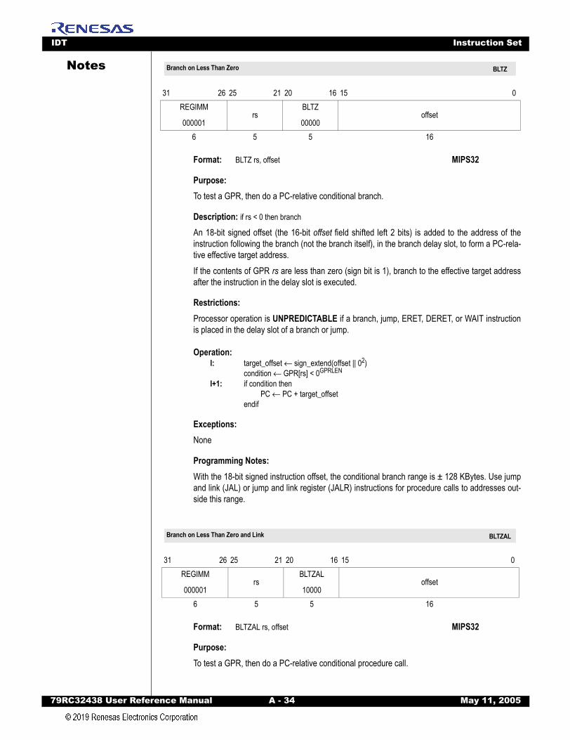
IDT Instruction Set
79RC32438 User Refer
Notes
BLTZFormat: BLTZ rs, offset MIPS32
Purpose: To test a GPR, then do a PC-relative conditional branch.
Description: if rs < 0 then branch
An 18-bit signed offset (the 16-bit offset field shifted left 2 bits) is added to the address of theinstruction following the branch (not the branch itself), in the branch delay slot, to form a PC-rela-tive effective target address.If the contents of GPR rs are less than zero (sign bit is 1), branch to the effective target addressafter the instruction in the delay slot is executed.
Restrictions: Processor operation is UNPREDICTABLE if a branch, jump, ERET, DERET, or WAIT instructionis placed in the delay slot of a branch or jump.
Operation:I: target_offset ← sign_extend(offset || 02)
condition ← GPR[rs] < 0GPRLEN
I+1: if condition thenPC ← PC + target_offset
endif
Exceptions: None
Programming Notes: With the 18-bit signed instruction offset, the conditional branch range is ± 128 KBytes. Use jumpand link (JAL) or jump and link register (JALR) instructions for procedure calls to addresses out-side this range.
BLTZAL
Format: BLTZAL rs, offset MIPS32
Purpose: To test a GPR, then do a PC-relative conditional procedure call.
31 26 25 21 20 16 15 0REGIMM
000001rs
BLTZ
00000offset
6 5 5 16
31 26 25 21 20 16 15 0REGIMM
000001rs
BLTZAL
10000offset
6 5 5 16
Branch on Less Than Zero BLTZ
Branch on Less Than Zero and Link BLTZAL
ence Manual A - 34 May 11, 2005
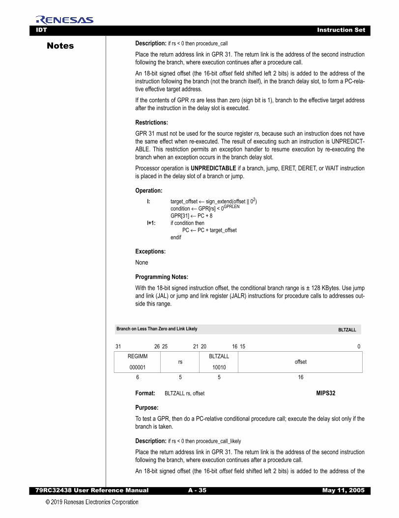
IDT Instruction Set
79RC32438 User Refer
Notes
Description: if rs < 0 then procedure_callPlace the return address link in GPR 31. The return link is the address of the second instructionfollowing the branch, where execution continues after a procedure call.An 18-bit signed offset (the 16-bit offset field shifted left 2 bits) is added to the address of theinstruction following the branch (not the branch itself), in the branch delay slot, to form a PC-rela-tive effective target address.If the contents of GPR rs are less than zero (sign bit is 1), branch to the effective target addressafter the instruction in the delay slot is executed.
Restrictions: GPR 31 must not be used for the source register rs, because such an instruction does not havethe same effect when re-executed. The result of executing such an instruction is UNPREDICT-ABLE. This restriction permits an exception handler to resume execution by re-executing thebranch when an exception occurs in the branch delay slot.Processor operation is UNPREDICTABLE if a branch, jump, ERET, DERET, or WAIT instructionis placed in the delay slot of a branch or jump.
Operation:I: target_offset ← sign_extend(offset || 02)
condition ← GPR[rs] < 0GPRLEN
GPR[31] ← PC + 8I+1: if condition then
PC ← PC + target_offsetendif
Exceptions: None
Programming Notes:With the 18-bit signed instruction offset, the conditional branch range is ± 128 KBytes. Use jumpand link (JAL) or jump and link register (JALR) instructions for procedure calls to addresses out-side this range.
BLTZALL
Format: BLTZALL rs, offset MIPS32
Purpose: To test a GPR, then do a PC-relative conditional procedure call; execute the delay slot only if thebranch is taken.
Description: if rs < 0 then procedure_call_likely
Place the return address link in GPR 31. The return link is the address of the second instructionfollowing the branch, where execution continues after a procedure call.An 18-bit signed offset (the 16-bit offset field shifted left 2 bits) is added to the address of the
31 26 25 21 20 16 15 0REGIMM
000001rs
BLTZALL
10010offset
6 5 5 16
Branch on Less Than Zero and Link Likely BLTZALL
ence Manual A - 35 May 11, 2005

IDT Instruction Set
79RC32438 User Refer
Notes
instruction following the branch (not the branch itself), in the branch delay slot, to form a PC-rela-tive effective target address.If the contents of GPR rs are less than zero (sign bit is 1), branch to the effective target addressafter the instruction in the delay slot is executed. If the branch is not taken, the instruction in thedelay slot is not executed.Restrictions: GPR 31 must not be used for the source register rs, because such an instruction does not havethe same effect when re-executed. The result of executing such an instruction is UNPREDICT-ABLE. This restriction permits an exception handler to resume execution by re-executing thebranch when an exception occurs in the branch delay slot.Processor operation is UNPREDICTABLE if a branch, jump, ERET, DERET, or WAIT instructionis placed in the delay slot of a branch or jump.
Operation:I: target_offset ← sign_extend(offset || 02)
condition ← GPR[rs] < 0GPRLEN
GPR[31] ← PC + 8I+1: if condition then
PC ← PC + target_offsetelse
NullifyCurrentInstruction()endif
Exceptions: None
Programming Notes: With the 18-bit signed instruction offset, the conditional branch range is ± 128 KBytes. Use jumpand link (JAL) or jump and link register (JALR) instructions for procedure calls to addresses out-side this range.Software is strongly encouraged to avoid the use of the Branch Likely instructions, as they will beremoved from a future revision of the MIPS Architecture.
BLTZL
Format: BLTZL rs, offset MIPS32
Purpose: To test a GPR, then do a PC-relative conditional branch; execute the delay slot only if the branchis taken.
Description: if rs < 0 then branch_likely
An 18-bit signed offset (the 16-bit offset field shifted left 2 bits) is added to the address of theinstruction following the branch (not the branch itself), in the branch delay slot, to form a PC-rela-
31 26 25 21 20 16 15 0REGIMM
000001rs
BLTZL
00010offset
6 5 5 16
Branch on Less Than Zero Likely BLTZL
ence Manual A - 36 May 11, 2005
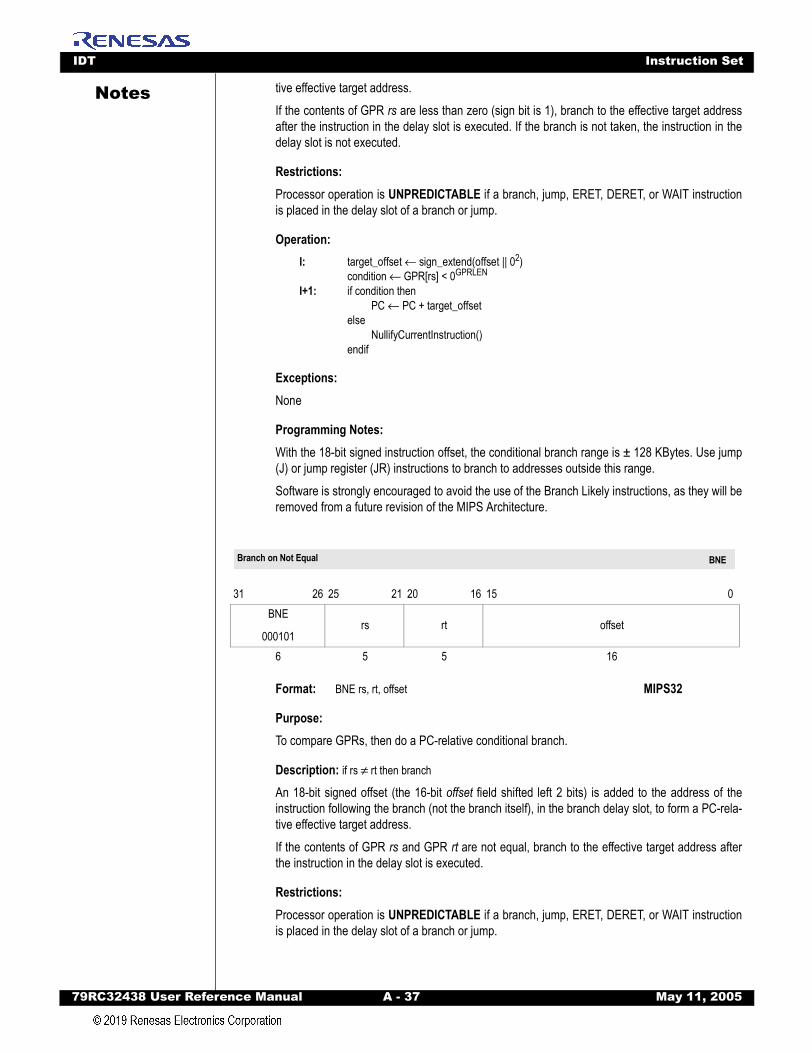
IDT Instruction Set
79RC32438 User Refer
Notes
tive effective target address.If the contents of GPR rs are less than zero (sign bit is 1), branch to the effective target addressafter the instruction in the delay slot is executed. If the branch is not taken, the instruction in thedelay slot is not executed.Restrictions:Processor operation is UNPREDICTABLE if a branch, jump, ERET, DERET, or WAIT instructionis placed in the delay slot of a branch or jump.
Operation:I: target_offset ← sign_extend(offset || 02)
condition ← GPR[rs] < 0GPRLEN
I+1: if condition thenPC ← PC + target_offset
elseNullifyCurrentInstruction()
endif
Exceptions: None
Programming Notes: With the 18-bit signed instruction offset, the conditional branch range is ± 128 KBytes. Use jump(J) or jump register (JR) instructions to branch to addresses outside this range.Software is strongly encouraged to avoid the use of the Branch Likely instructions, as they will beremoved from a future revision of the MIPS Architecture.
BNE
Format: BNE rs, rt, offset MIPS32
Purpose: To compare GPRs, then do a PC-relative conditional branch.
Description: if rs ≠ rt then branch
An 18-bit signed offset (the 16-bit offset field shifted left 2 bits) is added to the address of theinstruction following the branch (not the branch itself), in the branch delay slot, to form a PC-rela-tive effective target address.If the contents of GPR rs and GPR rt are not equal, branch to the effective target address afterthe instruction in the delay slot is executed.
Restrictions: Processor operation is UNPREDICTABLE if a branch, jump, ERET, DERET, or WAIT instructionis placed in the delay slot of a branch or jump.
31 26 25 21 20 16 15 0BNE
000101rs rt offset
6 5 5 16
Branch on Not Equal BNE
ence Manual A - 37 May 11, 2005
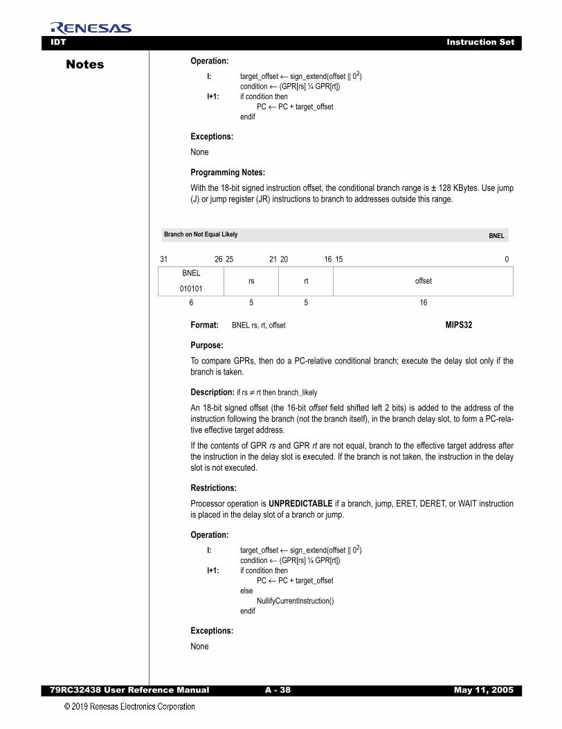
IDT Instruction Set
79RC32438 User Refer
Notes
Operation:I: target_offset ← sign_extend(offset || 02)condition ← (GPR[rs] ¼ GPR[rt])I+1: if condition then
PC ← PC + target_offsetendif
Exceptions: None
Programming Notes:With the 18-bit signed instruction offset, the conditional branch range is ± 128 KBytes. Use jump(J) or jump register (JR) instructions to branch to addresses outside this range.
BNEL
Format: BNEL rs, rt, offset MIPS32
Purpose: To compare GPRs, then do a PC-relative conditional branch; execute the delay slot only if thebranch is taken.
Description: if rs ≠ rt then branch_likely
An 18-bit signed offset (the 16-bit offset field shifted left 2 bits) is added to the address of theinstruction following the branch (not the branch itself), in the branch delay slot, to form a PC-rela-tive effective target address.If the contents of GPR rs and GPR rt are not equal, branch to the effective target address afterthe instruction in the delay slot is executed. If the branch is not taken, the instruction in the delayslot is not executed.
Restrictions: Processor operation is UNPREDICTABLE if a branch, jump, ERET, DERET, or WAIT instructionis placed in the delay slot of a branch or jump.
Operation:I: target_offset ← sign_extend(offset || 02)
condition ← (GPR[rs] ¼ GPR[rt])I+1: if condition then
PC ← PC + target_offsetelse
NullifyCurrentInstruction()endif
Exceptions: None
31 26 25 21 20 16 15 0BNEL
010101rs rt offset
6 5 5 16
Branch on Not Equal Likely BNEL
ence Manual A - 38 May 11, 2005
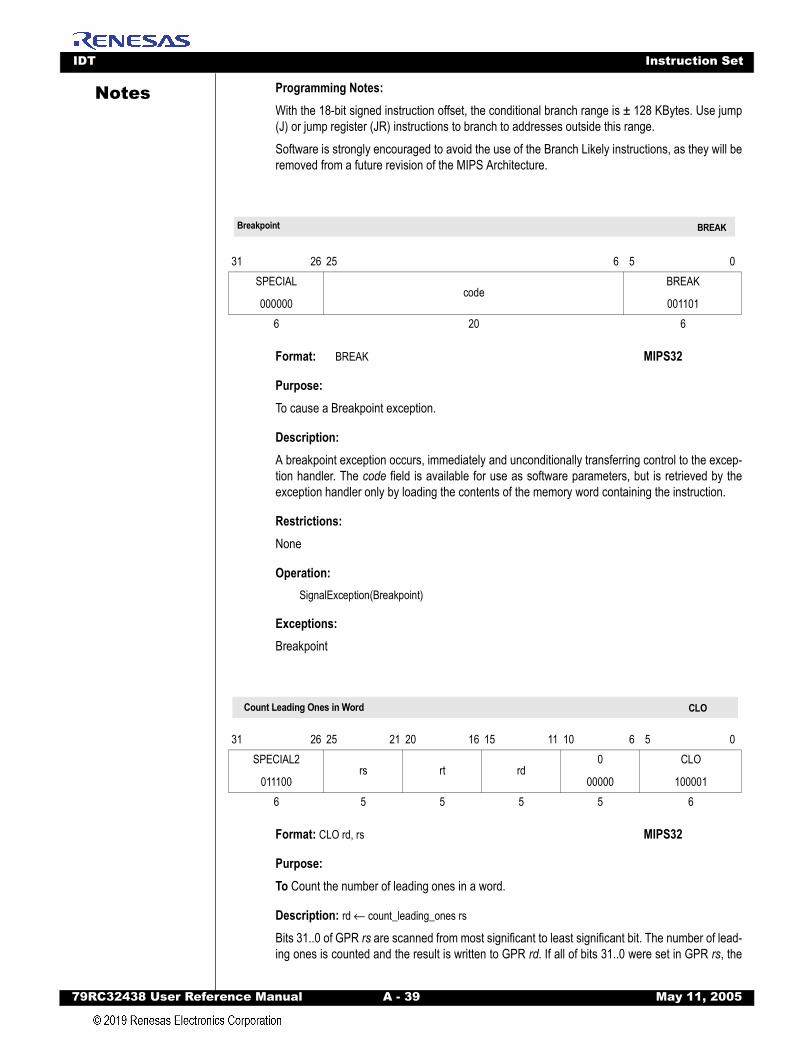
IDT Instruction Set
79RC32438 User Refer
Notes
Programming Notes: With the 18-bit signed instruction offset, the conditional branch range is ± 128 KBytes. Use jump(J) or jump register (JR) instructions to branch to addresses outside this range.Software is strongly encouraged to avoid the use of the Branch Likely instructions, as they will beremoved from a future revision of the MIPS Architecture.BREAK
Format: BREAK MIPS32
Purpose: To cause a Breakpoint exception.
Description:A breakpoint exception occurs, immediately and unconditionally transferring control to the excep-tion handler. The code field is available for use as software parameters, but is retrieved by theexception handler only by loading the contents of the memory word containing the instruction.
Restrictions: None
Operation:SignalException(Breakpoint)
Exceptions: Breakpoint
CLO
Format: CLO rd, rs MIPS32
Purpose: To Count the number of leading ones in a word.
Description: rd ← count_leading_ones rs
Bits 31..0 of GPR rs are scanned from most significant to least significant bit. The number of lead-ing ones is counted and the result is written to GPR rd. If all of bits 31..0 were set in GPR rs, the
31 26 25 6 5 0SPECIAL
000000code
BREAK
0011016 20 6
31 26 25 21 20 16 15 11 10 6 5 0SPECIAL2
011100rs rt rd
0
00000
CLO
1000016 5 5 5 5 6
Breakpoint BREAK
Count Leading Ones in Word CLO
ence Manual A - 39 May 11, 2005
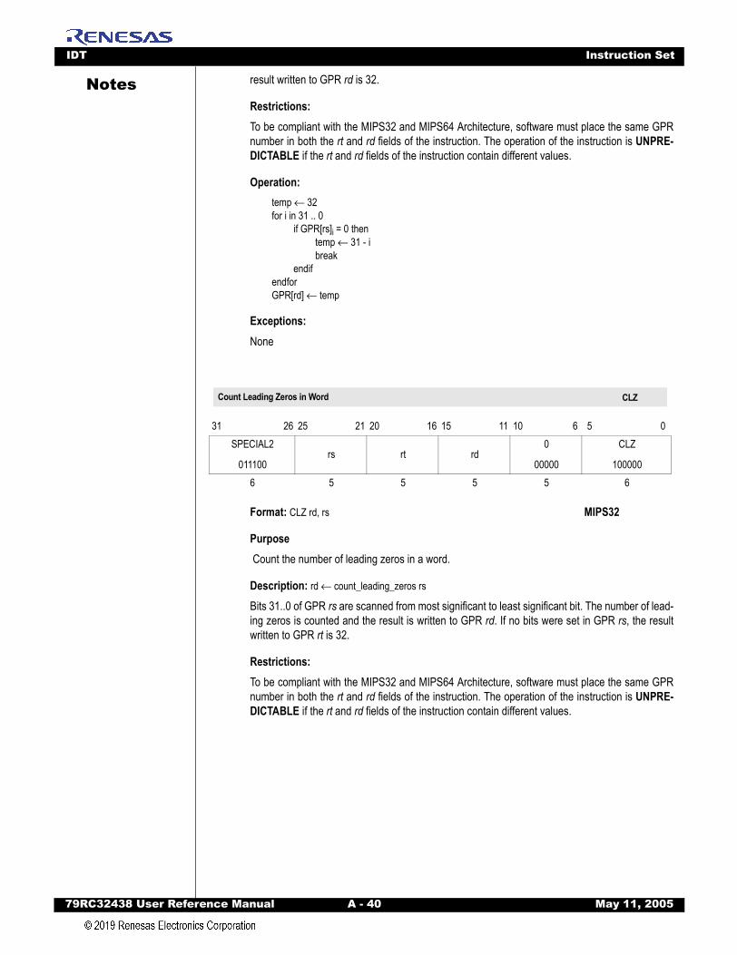
IDT Instruction Set
79RC32438 User Refer
Notes
result written to GPR rd is 32.Restrictions:To be compliant with the MIPS32 and MIPS64 Architecture, software must place the same GPRnumber in both the rt and rd fields of the instruction. The operation of the instruction is UNPRE-DICTABLE if the rt and rd fields of the instruction contain different values.
Operation:temp ← 32for i in 31 .. 0
if GPR[rs]i = 0 thentemp ← 31 - ibreak
endifendforGPR[rd] ← temp
Exceptions:None
CLZ
Format: CLZ rd, rs MIPS32
Purpose Count the number of leading zeros in a word.
Description: rd ← count_leading_zeros rs
Bits 31..0 of GPR rs are scanned from most significant to least significant bit. The number of lead-ing zeros is counted and the result is written to GPR rd. If no bits were set in GPR rs, the resultwritten to GPR rt is 32.
Restrictions:To be compliant with the MIPS32 and MIPS64 Architecture, software must place the same GPRnumber in both the rt and rd fields of the instruction. The operation of the instruction is UNPRE-DICTABLE if the rt and rd fields of the instruction contain different values.
31 26 25 21 20 16 15 11 10 6 5 0SPECIAL2
011100rs rt rd
0
00000
CLZ
1000006 5 5 5 5 6
Count Leading Zeros in Word CLZ
ence Manual A - 40 May 11, 2005
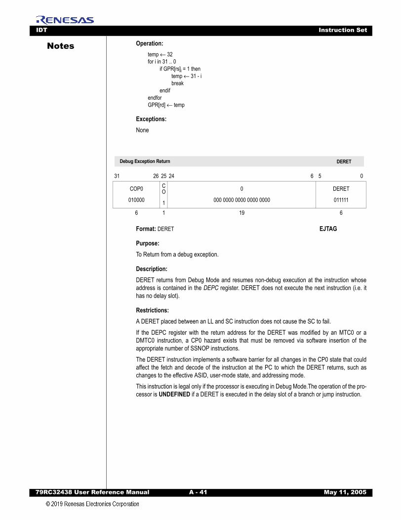
IDT Instruction Set
79RC32438 User Refer
Notes
Operation:temp ← 32for i in 31 .. 0if GPR[rs]i = 1 thentemp ← 31 - ibreak
endifendforGPR[rd] ← temp
Exceptions:None
DERET
Format: DERET EJTAG
Purpose: To Return from a debug exception.
Description:DERET returns from Debug Mode and resumes non-debug execution at the instruction whoseaddress is contained in the DEPC register. DERET does not execute the next instruction (i.e. ithas no delay slot).
Restrictions:A DERET placed between an LL and SC instruction does not cause the SC to fail.If the DEPC register with the return address for the DERET was modified by an MTC0 or aDMTC0 instruction, a CP0 hazard exists that must be removed via software insertion of theappropriate number of SSNOP instructions.The DERET instruction implements a software barrier for all changes in the CP0 state that couldaffect the fetch and decode of the instruction at the PC to which the DERET returns, such aschanges to the effective ASID, user-mode state, and addressing mode.This instruction is legal only if the processor is executing in Debug Mode.The operation of the pro-cessor is UNDEFINED if a DERET is executed in the delay slot of a branch or jump instruction.
31 26 25 24 6 5 0
COP0
010000
CO
1
0
000 0000 0000 0000 0000
DERET
011111
6 1 19 6
Debug Exception Return DERET
ence Manual A - 41 May 11, 2005
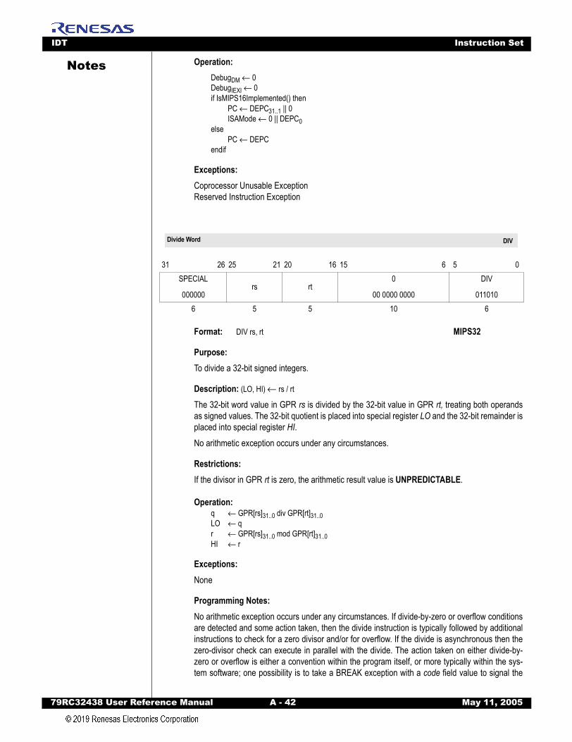
IDT Instruction Set
79RC32438 User Refer
Notes
Operation:DebugDM ← 0DebugIEXI ← 0if IsMIPS16Implemented() thenPC ← DEPC31..1 || 0ISAMode ← 0 || DEPC0
elsePC ← DEPC
endif
Exceptions:Coprocessor Unusable ExceptionReserved Instruction Exception
DIV
Format: DIV rs, rt MIPS32
Purpose: To divide a 32-bit signed integers.
Description: (LO, HI) ← rs / rt
The 32-bit word value in GPR rs is divided by the 32-bit value in GPR rt, treating both operandsas signed values. The 32-bit quotient is placed into special register LO and the 32-bit remainder isplaced into special register HI.No arithmetic exception occurs under any circumstances.
Restrictions: If the divisor in GPR rt is zero, the arithmetic result value is UNPREDICTABLE.
Operation:q ← GPR[rs]31..0 div GPR[rt]31..0LO ← qr ← GPR[rs]31..0 mod GPR[rt]31..0HI ← r
Exceptions: None
Programming Notes:No arithmetic exception occurs under any circumstances. If divide-by-zero or overflow conditionsare detected and some action taken, then the divide instruction is typically followed by additionalinstructions to check for a zero divisor and/or for overflow. If the divide is asynchronous then thezero-divisor check can execute in parallel with the divide. The action taken on either divide-by-zero or overflow is either a convention within the program itself, or more typically within the sys-tem software; one possibility is to take a BREAK exception with a code field value to signal the
31 26 25 21 20 16 15 6 5 0SPECIAL
000000rs rt
0
00 0000 0000
DIV
0110106 5 5 10 6
Divide Word DIV
ence Manual A - 42 May 11, 2005
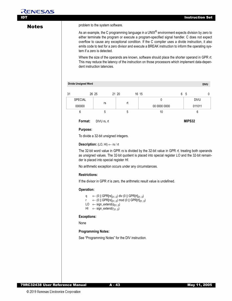
IDT Instruction Set
79RC32438 User Refer
Notes
problem to the system software.As an example, the C programming language in a UNIX® environment expects division by zero toeither terminate the program or execute a program-specified signal handler. C does not expectoverflow to cause any exceptional condition. If the C compiler uses a divide instruction, it alsoemits code to test for a zero divisor and execute a BREAK instruction to inform the operating sys-tem if a zero is detected.Where the size of the operands are known, software should place the shorter operand in GPR rt.This may reduce the latency of the instruction on those processors which implement data-depen-dent instruction latencies.
DIVU
Format: DIVU rs, rt MIPS32
Purpose: To divide a 32-bit unsigned integers.
Description: (LO, HI) ← rs / rt
The 32-bit word value in GPR rs is divided by the 32-bit value in GPR rt, treating both operandsas unsigned values. The 32-bit quotient is placed into special register LO and the 32-bit remain-der is placed into special register HI.No arithmetic exception occurs under any circumstances.
Restrictions: If the divisor in GPR rt is zero, the arithmetic result value is undefined.
Operation:q ← (0 || GPR[rs]31..0) div (0 || GPR[rt]31..0)r ← (0 || GPR[rs]31..0) mod (0 || GPR[rt]31..0)LO ← sign_extend(q31..0)HI ← sign_extend(r31..0)
Exceptions: None
Programming Notes:See “Programming Notes” for the DIV instruction.
31 26 25 21 20 16 15 6 5 0SPECIAL
000000rs rt
0
00 0000 0000
DIVU
0110116 5 5 10 6
Divide Unsigned Word DIVU
ence Manual A - 43 May 11, 2005
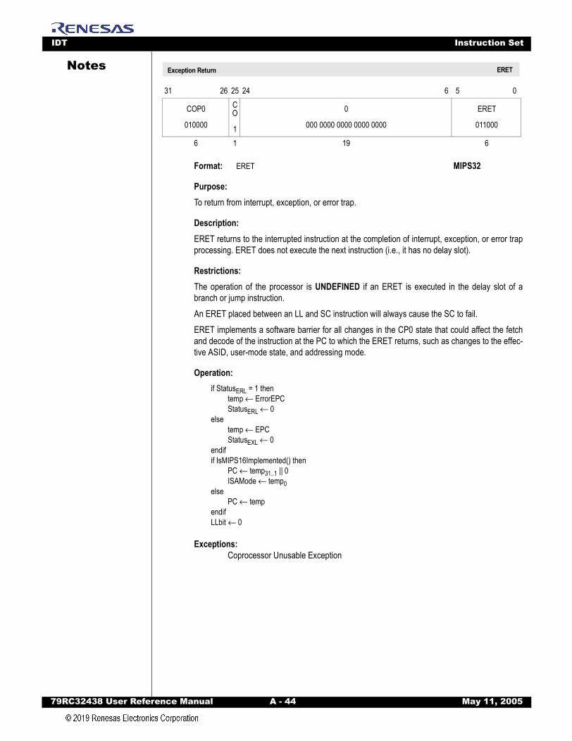
IDT Instruction Set
79RC32438 User Refer
Notes
ERETFormat: ERET MIPS32
Purpose: To return from interrupt, exception, or error trap.
Description:ERET returns to the interrupted instruction at the completion of interrupt, exception, or error trapprocessing. ERET does not execute the next instruction (i.e., it has no delay slot).
Restrictions:The operation of the processor is UNDEFINED if an ERET is executed in the delay slot of abranch or jump instruction.An ERET placed between an LL and SC instruction will always cause the SC to fail.ERET implements a software barrier for all changes in the CP0 state that could affect the fetchand decode of the instruction at the PC to which the ERET returns, such as changes to the effec-tive ASID, user-mode state, and addressing mode.
Operation:if StatusERL = 1 then
temp ← ErrorEPCStatusERL ← 0
elsetemp ← EPCStatusEXL ← 0
endifif IsMIPS16Implemented() then
PC ← temp31..1 || 0ISAMode ← temp0
elsePC ← temp
endifLLbit ← 0
Exceptions:Coprocessor Unusable Exception
31 26 25 24 6 5 0
COP0
010000
CO
1
0
000 0000 0000 0000 0000
ERET
011000
6 1 19 6
Exception Return ERET
ence Manual A - 44 May 11, 2005
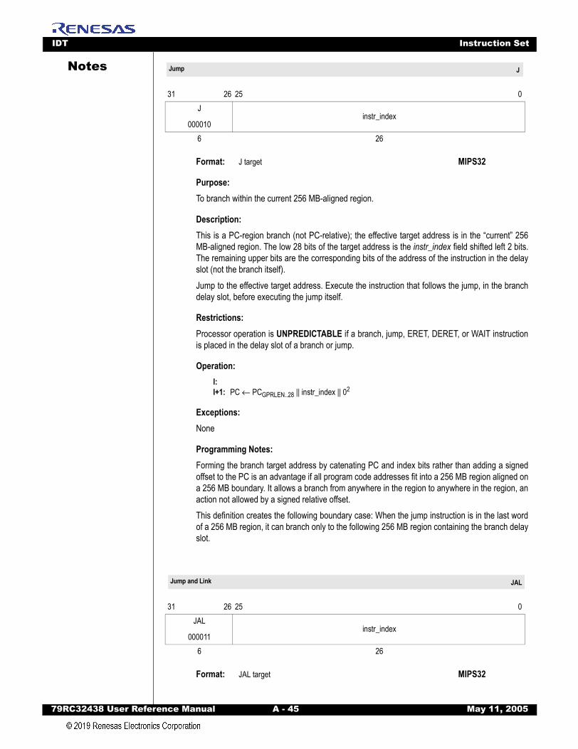
IDT Instruction Set
79RC32438 User Refer
Notes
JFormat: J target MIPS32
Purpose: To branch within the current 256 MB-aligned region.
Description: This is a PC-region branch (not PC-relative); the effective target address is in the “current” 256MB-aligned region. The low 28 bits of the target address is the instr_index field shifted left 2 bits.The remaining upper bits are the corresponding bits of the address of the instruction in the delayslot (not the branch itself). Jump to the effective target address. Execute the instruction that follows the jump, in the branchdelay slot, before executing the jump itself.
Restrictions: Processor operation is UNPREDICTABLE if a branch, jump, ERET, DERET, or WAIT instructionis placed in the delay slot of a branch or jump.
Operation:I:I+1: PC ← PCGPRLEN..28 || instr_index || 02
Exceptions: None
Programming Notes:Forming the branch target address by catenating PC and index bits rather than adding a signedoffset to the PC is an advantage if all program code addresses fit into a 256 MB region aligned ona 256 MB boundary. It allows a branch from anywhere in the region to anywhere in the region, anaction not allowed by a signed relative offset.This definition creates the following boundary case: When the jump instruction is in the last wordof a 256 MB region, it can branch only to the following 256 MB region containing the branch delayslot.
JAL
Format: JAL target MIPS32
31 26 25 0J
000010instr_index
6 26
31 26 25 0JAL
000011instr_index
6 26
Jump J
Jump and Link JAL
ence Manual A - 45 May 11, 2005
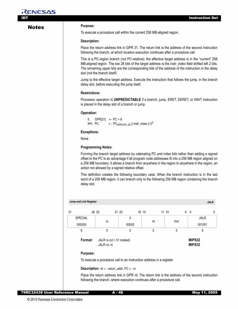
IDT Instruction Set
79RC32438 User Refer
Notes
Purpose: To execute a procedure call within the current 256 MB-aligned region.Description: Place the return address link in GPR 31. The return link is the address of the second instructionfollowing the branch, at which location execution continues after a procedure call.This is a PC-region branch (not PC-relative); the effective target address is in the “current” 256MB-aligned region. The low 28 bits of the target address is the instr_index field shifted left 2 bits.The remaining upper bits are the corresponding bits of the address of the instruction in the delayslot (not the branch itself). Jump to the effective target address. Execute the instruction that follows the jump, in the branchdelay slot, before executing the jump itself.
Restrictions: Processor operation is UNPREDICTABLE if a branch, jump, ERET, DERET, or WAIT instructionis placed in the delay slot of a branch or jump.
Operation:I: GPR[31] ← PC + 8I+1: PC ← PCGPRLEN..28 || instr_index || 02
Exceptions: None
Programming Notes:Forming the branch target address by catenating PC and index bits rather than adding a signedoffset to the PC is an advantage if all program code addresses fit into a 256 MB region aligned ona 256 MB boundary. It allows a branch from anywhere in the region to anywhere in the region, anaction not allowed by a signed relative offset.This definition creates the following boundary case: When the branch instruction is in the lastword of a 256 MB region, it can branch only to the following 256 MB region containing the branchdelay slot.
JALR
Format: JALR rs (rd = 31 implied) MIPS32JALR rd, rs MIPS32
Purpose: To execute a procedure call to an instruction address in a register
Description: rd ← return_addr, PC ← rs
Place the return address link in GPR rd. The return link is the address of the second instructionfollowing the branch, where execution continues after a procedure call.
31 26 25 21 20 16 15 11 10 6 5 0SPECIAL
000000rs
0
00000rd hint
JALR
0010016 5 5 5 5 6
Jump and Link Register JALR
ence Manual A - 46 May 11, 2005
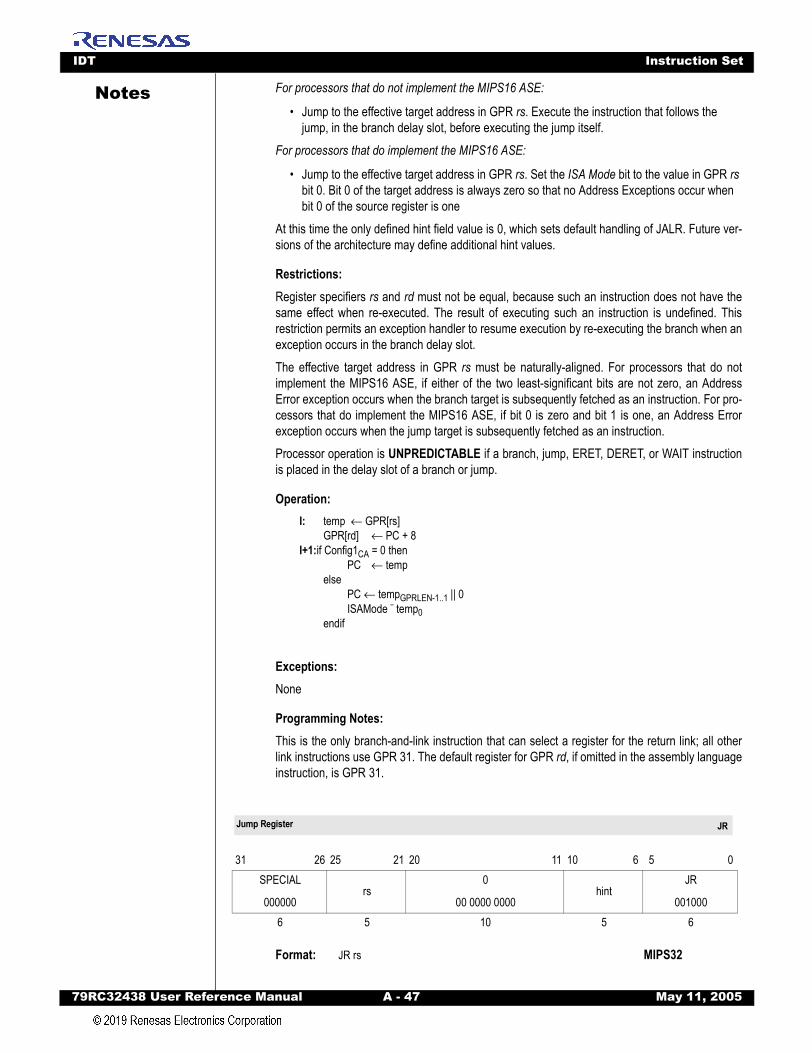
IDT Instruction Set
79RC32438 User Refer
Notes
For processors that do not implement the MIPS16 ASE:• Jump to the effective target address in GPR rs. Execute the instruction that follows the jump, in the branch delay slot, before executing the jump itself.
For processors that do implement the MIPS16 ASE:
• Jump to the effective target address in GPR rs. Set the ISA Mode bit to the value in GPR rs bit 0. Bit 0 of the target address is always zero so that no Address Exceptions occur when bit 0 of the source register is one
At this time the only defined hint field value is 0, which sets default handling of JALR. Future ver-sions of the architecture may define additional hint values.
Restrictions: Register specifiers rs and rd must not be equal, because such an instruction does not have thesame effect when re-executed. The result of executing such an instruction is undefined. Thisrestriction permits an exception handler to resume execution by re-executing the branch when anexception occurs in the branch delay slot.The effective target address in GPR rs must be naturally-aligned. For processors that do notimplement the MIPS16 ASE, if either of the two least-significant bits are not zero, an AddressError exception occurs when the branch target is subsequently fetched as an instruction. For pro-cessors that do implement the MIPS16 ASE, if bit 0 is zero and bit 1 is one, an Address Errorexception occurs when the jump target is subsequently fetched as an instruction.Processor operation is UNPREDICTABLE if a branch, jump, ERET, DERET, or WAIT instructionis placed in the delay slot of a branch or jump.
Operation:I: temp ← GPR[rs]
GPR[rd] ← PC + 8I+1:if Config1CA = 0 then
PC ← tempelse
PC ← tempGPRLEN-1..1 || 0ISAMode ¨ temp0
endif
Exceptions: None
Programming Notes:This is the only branch-and-link instruction that can select a register for the return link; all otherlink instructions use GPR 31. The default register for GPR rd, if omitted in the assembly languageinstruction, is GPR 31.
JR
Format: JR rs MIPS32
31 26 25 21 20 11 10 6 5 0SPECIAL
000000rs
0
00 0000 0000hint
JR
0010006 5 10 5 6
Jump Register JR
ence Manual A - 47 May 11, 2005
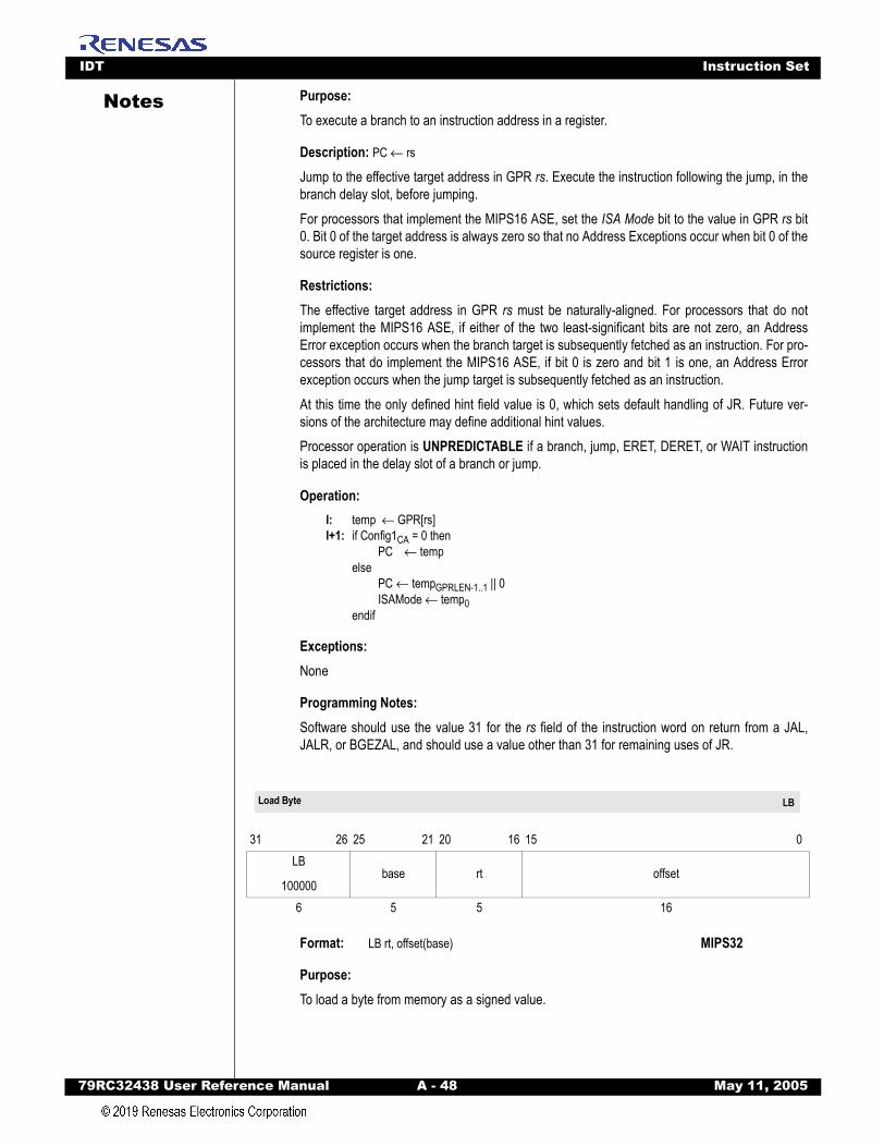
IDT Instruction Set
79RC32438 User Refer
Notes
Purpose: To execute a branch to an instruction address in a register.Description: PC ← rs
Jump to the effective target address in GPR rs. Execute the instruction following the jump, in thebranch delay slot, before jumping.For processors that implement the MIPS16 ASE, set the ISA Mode bit to the value in GPR rs bit0. Bit 0 of the target address is always zero so that no Address Exceptions occur when bit 0 of thesource register is one.
Restrictions: The effective target address in GPR rs must be naturally-aligned. For processors that do notimplement the MIPS16 ASE, if either of the two least-significant bits are not zero, an AddressError exception occurs when the branch target is subsequently fetched as an instruction. For pro-cessors that do implement the MIPS16 ASE, if bit 0 is zero and bit 1 is one, an Address Errorexception occurs when the jump target is subsequently fetched as an instruction.At this time the only defined hint field value is 0, which sets default handling of JR. Future ver-sions of the architecture may define additional hint values.Processor operation is UNPREDICTABLE if a branch, jump, ERET, DERET, or WAIT instructionis placed in the delay slot of a branch or jump.
Operation:I: temp ← GPR[rs]I+1: if Config1CA = 0 then
PC ← tempelse
PC ← tempGPRLEN-1..1 || 0ISAMode ← temp0
endif
Exceptions: None
Programming Notes:Software should use the value 31 for the rs field of the instruction word on return from a JAL,JALR, or BGEZAL, and should use a value other than 31 for remaining uses of JR.
LB
Format: LB rt, offset(base) MIPS32
Purpose: To load a byte from memory as a signed value.
31 26 25 21 20 16 15 0LB
100000base rt offset
6 5 5 16
Load Byte LB
ence Manual A - 48 May 11, 2005
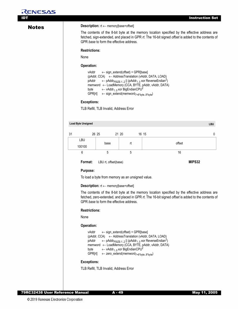
IDT Instruction Set
79RC32438 User Refer
Notes
Description: rt ← memory[base+offset]The contents of the 8-bit byte at the memory location specified by the effective address arefetched, sign-extended, and placed in GPR rt. The 16-bit signed offset is added to the contents ofGPR base to form the effective address.
Restrictions: None
Operation:vAddr ← sign_extend(offset) + GPR[base](pAddr, CCA) ← AddressTranslation (vAddr, DATA, LOAD)pAddr ← pAddrPSIZE-1..2 || (pAddr1..0 xor ReverseEndian2)memword ← LoadMemory (CCA, BYTE, pAddr, vAddr, DATA)byte ← vAddr1..0 xor BigEndianCPU2
GPR[rt] ← sign_extend(memword7+8*byte..8*byte)
Exceptions: TLB Refill, TLB Invalid, Address Error
LBU
Format: LBU rt, offset(base) MIPS32
Purpose:To load a byte from memory as an unsigned value.
Description: rt ← memory[base+offset]
The contents of the 8-bit byte at the memory location specified by the effective address arefetched, zero-extended, and placed in GPR rt. The 16-bit signed offset is added to the contents ofGPR base to form the effective address.
Restrictions: None
Operation:vAddr ← sign_extend(offset) + GPR[base](pAddr, CCA) ← AddressTranslation (vAddr, DATA, LOAD)pAddr ← pAddrPSIZE-1..2 || (pAddr1..0 xor ReverseEndian2)memword ← LoadMemory (CCA, BYTE, pAddr, vAddr, DATA)byte ← vAddr1..0 xor BigEndianCPU2
GPR[rt] ← zero_extend(memword7+8*byte..8*byte)
Exceptions: TLB Refill, TLB Invalid, Address Error
31 26 25 21 20 16 15 0LBU
100100base rt offset
6 5 5 16
Load Byte Unsigned LBU
ence Manual A - 49 May 11, 2005
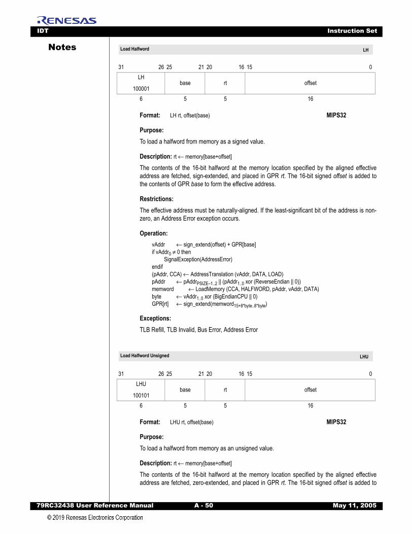
IDT Instruction Set
79RC32438 User Refer
Notes
LHFormat: LH rt, offset(base) MIPS32
Purpose: To load a halfword from memory as a signed value.
Description: rt ← memory[base+offset]
The contents of the 16-bit halfword at the memory location specified by the aligned effectiveaddress are fetched, sign-extended, and placed in GPR rt. The 16-bit signed offset is added tothe contents of GPR base to form the effective address.
Restrictions: The effective address must be naturally-aligned. If the least-significant bit of the address is non-zero, an Address Error exception occurs.
Operation:vAddr ← sign_extend(offset) + GPR[base]if vAddr0 ≠ 0 then
SignalException(AddressError)endif(pAddr, CCA) ← AddressTranslation (vAddr, DATA, LOAD)pAddr ← pAddrPSIZE–1..2 || (pAddr1..0 xor (ReverseEndian || 0))memword ← LoadMemory (CCA, HALFWORD, pAddr, vAddr, DATA)byte ← vAddr1..0 xor (BigEndianCPU || 0)GPR[rt] ← sign_extend(memword15+8*byte..8*byte)
Exceptions: TLB Refill, TLB Invalid, Bus Error, Address Error
LHU
Format: LHU rt, offset(base) MIPS32
Purpose: To load a halfword from memory as an unsigned value.
Description: rt ← memory[base+offset]
The contents of the 16-bit halfword at the memory location specified by the aligned effectiveaddress are fetched, zero-extended, and placed in GPR rt. The 16-bit signed offset is added to
31 26 25 21 20 16 15 0LH
100001base rt offset
6 5 5 16
31 26 25 21 20 16 15 0LHU
100101base rt offset
6 5 5 16
Load Halfword LH
Load Halfword Unsigned LHU
ence Manual A - 50 May 11, 2005
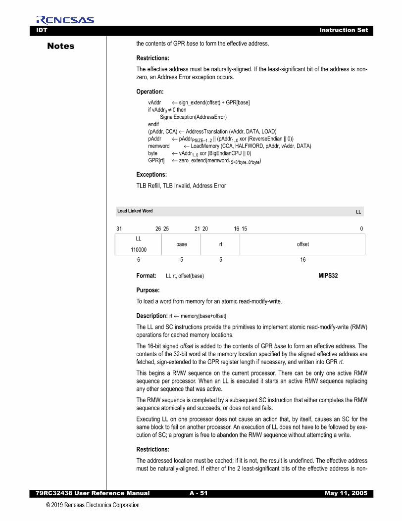
IDT Instruction Set
79RC32438 User Refer
Notes
the contents of GPR base to form the effective address.Restrictions: The effective address must be naturally-aligned. If the least-significant bit of the address is non-zero, an Address Error exception occurs.
Operation:vAddr ← sign_extend(offset) + GPR[base]if vAddr0 ≠ 0 then
SignalException(AddressError)endif(pAddr, CCA) ← AddressTranslation (vAddr, DATA, LOAD)pAddr ← pAddrPSIZE–1..2 || (pAddr1..0 xor (ReverseEndian || 0))memword ← LoadMemory (CCA, HALFWORD, pAddr, vAddr, DATA)byte ← vAddr1..0 xor (BigEndianCPU || 0)GPR[rt] ← zero_extend(memword15+8*byte..8*byte)
Exceptions: TLB Refill, TLB Invalid, Address Error
LL
Format: LL rt, offset(base) MIPS32
Purpose: To load a word from memory for an atomic read-modify-write.
Description: rt ← memory[base+offset]
The LL and SC instructions provide the primitives to implement atomic read-modify-write (RMW)operations for cached memory locations.The 16-bit signed offset is added to the contents of GPR base to form an effective address. Thecontents of the 32-bit word at the memory location specified by the aligned effective address arefetched, sign-extended to the GPR register length if necessary, and written into GPR rt. This begins a RMW sequence on the current processor. There can be only one active RMWsequence per processor. When an LL is executed it starts an active RMW sequence replacingany other sequence that was active.The RMW sequence is completed by a subsequent SC instruction that either completes the RMWsequence atomically and succeeds, or does not and fails.Executing LL on one processor does not cause an action that, by itself, causes an SC for thesame block to fail on another processor. An execution of LL does not have to be followed by exe-cution of SC; a program is free to abandon the RMW sequence without attempting a write.
Restrictions: The addressed location must be cached; if it is not, the result is undefined. The effective addressmust be naturally-aligned. If either of the 2 least-significant bits of the effective address is non-
31 26 25 21 20 16 15 0LL
110000base rt offset
6 5 5 16
Load Linked Word LL
ence Manual A - 51 May 11, 2005
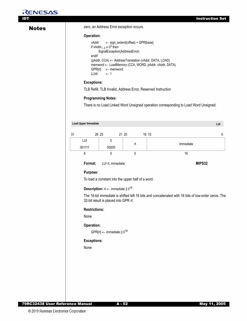
IDT Instruction Set
79RC32438 User Refer
Notes
zero, an Address Error exception occurs.Operation:vAddr ← sign_extend(offset) + GPR[base]if vAddr1..0 ≠ 02 then
SignalException(AddressError)endif(pAddr, CCA) ← AddressTranslation (vAddr, DATA, LOAD)memword ← LoadMemory (CCA, WORD, pAddr, vAddr, DATA)GPR[rt] ← memwordLLbit ← 1
Exceptions: TLB Refill, TLB Invalid, Address Error, Reserved Instruction
Programming Notes:There is no Load Linked Word Unsigned operation corresponding to Load Word Unsigned.
LUI
Format: LUI rt, immediate MIPS32
Purpose: To load a constant into the upper half of a word.
Description: rt ← immediate || 016
The 16-bit immediate is shifted left 16 bits and concatenated with 16 bits of low-order zeros. The32-bit result is placed into GPR rt.
Restrictions: None
Operation:GPR[rt] ← immediate || 016
Exceptions: None
31 26 25 21 20 16 15 0LUI
001111
0
00000rt immediate
6 5 5 16
Load Upper Immediate LUI
ence Manual A - 52 May 11, 2005

IDT Instruction Set
79RC32438 User Refer
Notes
LWFormat: LW rt, offset(base) MIPS32
Purpose: To load a word from memory as a signed value.
Description: rt ← memory[base+offset]
The contents of the 32-bit word at the memory location specified by the aligned effective addressare fetched, sign-extended to the GPR register length if necessary, and placed in GPR rt. The16-bit signed offset is added to the contents of GPR base to form the effective address.
Restrictions: The effective address must be naturally-aligned. If either of the 2 least-significant bits of theaddress is non-zero, an Address Error exception occurs.
Operation:vAddr ← sign_extend(offset) + GPR[base]if vAddr1..0 ≠ 02 then
SignalException(AddressError)endif(pAddr, CCA) ← AddressTranslation (vAddr, DATA, LOAD)memword ← LoadMemory (CCA, WORD, pAddr, vAddr, DATA)GPR[rt] ← memword
Exceptions: TLB Refill, TLB Invalid, Bus Error, Address Error
LWL
Format: LWL rt, offset(base) MIPS32
Purpose: To load the most-significant part of a word as a signed value from an unaligned memory address.
Description: rt ← rt MERGE memory[base+offset]
The 16-bit signed offset is added to the contents of GPR base to form an effective address(EffAddr). EffAddr is the address of the most-significant of 4 consecutive bytes forming a word(W) in memory starting at an arbitrary byte boundary.
31 26 25 21 20 16 15 0LW
100011base rt offset
6 5 5 16
31 26 25 21 20 16 15 0LWL
100010base rt offset
6 5 5 16
Load Word LW
Load Word Left LWL
ence Manual A - 53 May 11, 2005
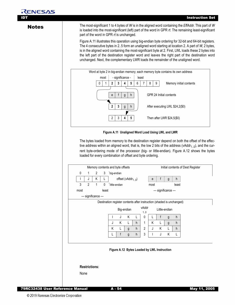
IDT Instruction Set
79RC32438 User Refer
Notes
The most-significant 1 to 4 bytes of W is in the aligned word containing the EffAddr. This part of Wis loaded into the most-significant (left) part of the word in GPR rt. The remaining least-significantpart of the word in GPR rt is unchanged.Figure A.11 illustrates this operation using big-endian byte ordering for 32-bit and 64-bit registers.The 4 consecutive bytes in 2..5 form an unaligned word starting at location 2. A part of W, 2 bytes,is in the aligned word containing the most-significant byte at 2. First, LWL loads these 2 bytes intothe left part of the destination register word and leaves the right part of the destination wordunchanged. Next, the complementary LWR loads the remainder of the unaligned word.Figure A.11 Unaligned Word Load Using LWL and LWR
The bytes loaded from memory to the destination register depend on both the offset of the effec-tive address within an aligned word, that is, the low 2 bits of the address (vAddr1..0), and the cur-rent byte-ordering mode of the processor (big- or little-endian). Figure A.12 shows the bytesloaded for every combination of offset and byte ordering.
Figure A.12 Bytes Loaded by LWL Instruction
Restrictions:None
Memory contents and byte offsets Initial contents of Dest Register0 1 2 3 ¨big-endian
I J K L offset (vAddr1..0) e f g h3 2 1 0 ¨little-endian most least
most least — significance —— significance —
Destination register contents after instruction (shaded is unchanged)
Big-endian vAddr1..0
Little-endian
I J K L 0 L f g hJ K L h 1 K L g hK L g h 2 J K L hL f g h 3 I J K L
Word at byte 2 in big-endian memory; each memory byte contains its own address most - significance - least0 1 2 3 4 5 6 7 8 9 Memory initial contents
e f g h GPR 24 Initial contents
2 3 g h After executing LWL $24,2($0)
2 3 4 5 Then after LWR $24,5($0)
ence Manual A - 54 May 11, 2005
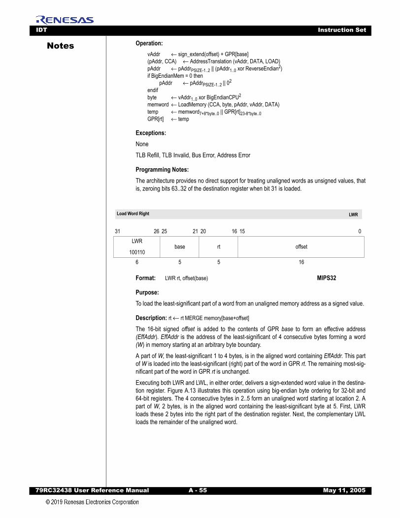
IDT Instruction Set
79RC32438 User Refer
Notes
Operation:vAddr ← sign_extend(offset) + GPR[base](pAddr, CCA) ← AddressTranslation (vAddr, DATA, LOAD)pAddr ← pAddrPSIZE-1..2 || (pAddr1..0 xor ReverseEndian2)if BigEndianMem = 0 thenpAddr ← pAddrPSIZE-1..2 || 02
endifbyte ← vAddr1..0 xor BigEndianCPU2
memword ← LoadMemory (CCA, byte, pAddr, vAddr, DATA)temp ← memword7+8*byte..0 || GPR[rt]23-8*byte..0GPR[rt] ← temp
Exceptions: NoneTLB Refill, TLB Invalid, Bus Error, Address Error
Programming Notes:The architecture provides no direct support for treating unaligned words as unsigned values, thatis, zeroing bits 63..32 of the destination register when bit 31 is loaded.
Format: LWR rt, offset(base) MIPS32
Purpose: To load the least-significant part of a word from an unaligned memory address as a signed value.
Description: rt ← rt MERGE memory[base+offset]
The 16-bit signed offset is added to the contents of GPR base to form an effective address(EffAddr). EffAddr is the address of the least-significant of 4 consecutive bytes forming a word(W) in memory starting at an arbitrary byte boundary. A part of W, the least-significant 1 to 4 bytes, is in the aligned word containing EffAddr. This partof W is loaded into the least-significant (right) part of the word in GPR rt. The remaining most-sig-nificant part of the word in GPR rt is unchanged.Executing both LWR and LWL, in either order, delivers a sign-extended word value in the destina-tion register. Figure A.13 illustrates this operation using big-endian byte ordering for 32-bit and64-bit registers. The 4 consecutive bytes in 2..5 form an unaligned word starting at location 2. Apart of W, 2 bytes, is in the aligned word containing the least-significant byte at 5. First, LWRloads these 2 bytes into the right part of the destination register. Next, the complementary LWLloads the remainder of the unaligned word.
31 26 25 21 20 16 15 0LWR
100110base rt offset
6 5 5 16
Load Word Right LWR
ence Manual A - 55 May 11, 2005
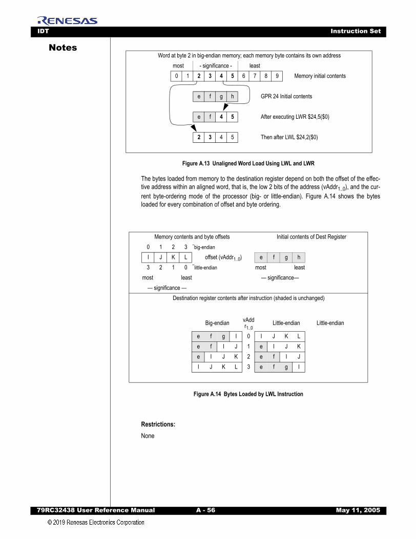
IDT Instruction Set
79RC32438 User Refer
Notes
Figure A.13 Unaligned Word Load Using LWL and LWR
The bytes loaded from memory to the destination register depend on both the offset of the effec-tive address within an aligned word, that is, the low 2 bits of the address (vAddr1..0), and the cur-rent byte-ordering mode of the processor (big- or little-endian). Figure A.14 shows the bytesloaded for every combination of offset and byte ordering.
Figure A.14 Bytes Loaded by LWL Instruction
Restrictions:None
Memory contents and byte offsets Initial contents of Dest Register0 1 2 3 ¨big-endian
I J K L offset (vAddr1..0) e f g h3 2 1 0 ¨little-endian most least
most least — significance—— significance —
Destination register contents after instruction (shaded is unchanged)
Big-endian vAddr1..0
Little-endian Little-endian
e f g I 0 I J K Le f I J 1 e I J Ke I J K 2 e f I JI J K L 3 e f g I
Word at byte 2 in big-endian memory; each memory byte contains its own address most - significance - least
0 1 2 3 4 5 6 7 8 9 Memory initial contents
e f g h GPR 24 Initial contents
e f 4 5 After executing LWR $24,5($0)
2 3 4 5 Then after LWL $24,2($0)
ence Manual A - 56 May 11, 2005
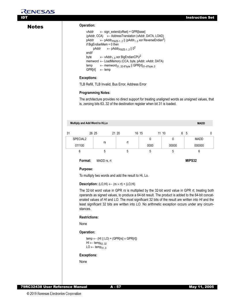
IDT Instruction Set
79RC32438 User Refer
Notes
Operation:vAddr ← sign_extend(offset) + GPR[base](pAddr, CCA) ← AddressTranslation (vAddr, DATA, LOAD)pAddr ← pAddrPSIZE-1..2 || (pAddr1..0 xor ReverseEndian2)if BigEndianMem = 0 thenpAddr ← pAddrPSIZE-1..2 || 02
endifbyte ← vAddr1..0 xor BigEndianCPU2
memword ← LoadMemory (CCA, byte, pAddr, vAddr, DATA)temp ← memword31..32-8*byte || GPR[rt]31–8*byte..0GPR[rt] ← temp
Exceptions: TLB Refill, TLB Invalid, Bus Error, Address Error
Programming Notes:The architecture provides no direct support for treating unaligned words as unsigned values, thatis, zeroing bits 63..32 of the destination register when bit 31 is loaded.
MADD
Format: MADD rs, rt MIPS32
Purpose: To multiply two words and add the result to Hi, Lo.
Description: (LO,HI) ← (rs × rt) + (LO,HI)
The 32-bit word value in GPR rs is multiplied by the 32-bit word value in GPR rt, treating bothoperands as signed values, to produce a 64-bit result. The product is added to the 64-bit concat-enated values of HI and LO. The most significant 32 bits of the result are written into HI and theleast significant 32 bits are written into LO. No arithmetic exception occurs under any circum-stances.
Restrictions: None
Operation:temp ← (HI || LO) + (GPR[rs] × GPR[rt])HI ← temp63..32LO ← temp31..0
Exceptions: None
31 26 25 21 20 16 15 11 10 6 5 0SPECIAL2
011100rs rt
0
0000
0
00000
MADD
0000006 5 5 5 5 6
Multiply and Add Word to Hi,Lo MADD
ence Manual A - 57 May 11, 2005
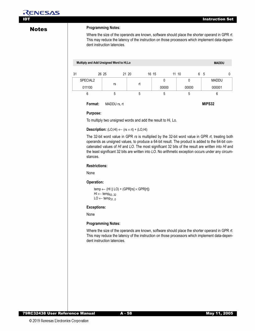
IDT Instruction Set
79RC32438 User Refer
Notes
Programming Notes:Where the size of the operands are known, software should place the shorter operand in GPR rt.This may reduce the latency of the instruction on those processors which implement data-depen-dent instruction latencies.Format: MADDU rs, rt MIPS32
Purpose: To multiply two unsigned words and add the result to Hi, Lo.
Description: (LO,HI) ← (rs × rt) + (LO,HI)
The 32-bit word value in GPR rs is multiplied by the 32-bit word value in GPR rt, treating bothoperands as unsigned values, to produce a 64-bit result. The product is added to the 64-bit con-catenated values of HI and LO. The most significant 32 bits of the result are written into HI andthe least significant 32 bits are written into LO. No arithmetic exception occurs under any circum-stances.
Restrictions: None
Operation:temp ← (HI || LO) + (GPR[rs] × GPR[rt])HI ← temp63..32LO ← temp31..0
Exceptions:None
Programming Notes:Where the size of the operands are known, software should place the shorter operand in GPR rt.This may reduce the latency of the instruction on those processors which implement data-depen-dent instruction latencies.
31 26 25 21 20 16 15 11 10 6 5 0SPECIAL2
011100rs rt
0
00000
0
00000
MADDU
0000016 5 5 5 5 6
Multiply and Add Unsigned Word to Hi,Lo MADDU
ence Manual A - 58 May 11, 2005

IDT Instruction Set
79RC32438 User Refer
Notes
MFC0Format: MFC0 rt, rd MIPS32MFC0 rt, rd, sel MIPS32
Purpose: To move the contents of a coprocessor 0 register to a general register.
Description: rt ← CPR[0,rd,sel]
The contents of the coprocessor 0 register specified by the combination of rd and sel are loadedinto general register rt. Note that not all coprocessor 0 registers support the sel field. In thoseinstances, the sel field must be zero.
Restrictions:The results are UNDEFINED if coprocessor 0 does not contain a register as specified by rd andsel.
Operation:data ← CPR[0,rd,sel]GPR[rt] ← data
Exceptions:Coprocessor UnusableReserved Instruction
I
Format: MFHI rd MIPS32
Purpose: To copy the special purpose HI register to a GPR.
Description: rd ← HI
The contents of special register HI are loaded into GPR rd.
Restrictions: None
31 26 25 21 20 16 15 11 10 3 2 0COP0
010000
MF
00000rt rd
0
00000000sel
6 5 5 5 8 3
31 26 25 16 15 11 10 6 5 0SPECIAL
000000
0
00 0000 0000rd
0
00000
MFHI
0100006 10 5 5 6
Move from Coprocessor 0 MFC0
Move From HI Register MFHI
ence Manual A - 59 May 11, 2005
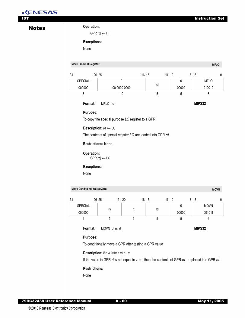
IDT Instruction Set
79RC32438 User Refer
Notes
Operation:GPR[rd] ← HIExceptions: None
Format: MFLO rd MIPS32
Purpose: To copy the special purpose LO register to a GPR.
Description: rd ← LO
The contents of special register LO are loaded into GPR rd.
Restrictions: None
Operation:GPR[rd] ← LO
Exceptions: None
Format: MOVN rd, rs, rt MIPS32
Purpose: To conditionally move a GPR after testing a GPR value
Description: if rt ≠ 0 then rd ← rs
If the value in GPR rt is not equal to zero, then the contents of GPR rs are placed into GPR rd.
Restrictions: None
31 26 25 16 15 11 10 6 5 0SPECIAL
000000
0
00 0000 0000rd
0
00000
MFLO
0100106 10 5 5 6
31 26 25 21 20 16 15 11 10 6 5 0SPECIAL
000000rs rt rd
0
00000
MOVN
0010116 5 5 5 5 6
Move From LO Register MFLO
Move Conditional on Not Zero MOVN
ence Manual A - 60 May 11, 2005
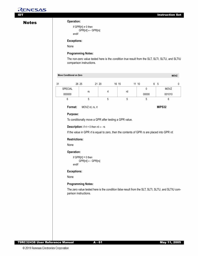
IDT Instruction Set
79RC32438 User Refer
Notes
Operation:if GPR[rt] ≠ 0 thenGPR[rd] ← GPR[rs]endif
Exceptions: None
Programming Notes:The non-zero value tested here is the condition true result from the SLT, SLTI, SLTU, and SLTIUcomparison instructions.
Format: MOVZ rd, rs, rt MIPS32
Purpose: To conditionally move a GPR after testing a GPR value.
Description: if rt = 0 then rd ← rs
If the value in GPR rt is equal to zero, then the contents of GPR rs are placed into GPR rd.
Restrictions: None
Operation:if GPR[rt] = 0 then
GPR[rd] ← GPR[rs]endif
Exceptions: None
Programming Notes:The zero value tested here is the condition false result from the SLT, SLTI, SLTU, and SLTIU com-parison instructions.
31 26 25 21 20 16 15 11 10 6 5 0SPECIAL
000000rs rt rd
0
00000
MOVZ
0010106 5 5 5 5 6
Move Conditional on Zero MOVZ
ence Manual A - 61 May 11, 2005

IDT Instruction Set
79RC32438 User Refer
Notes
MSUBFormat: MSUB rs, rt MIPS32
Purpose: To multiply two words and subtract the result from Hi, Lo.
Description: (LO,HI) ← (rs × rt) - (LO,HI)
The 32-bit word value in GPR rs is multiplied by the 32-bit value in GPR rt, treating both operandsas signed values, to produce a 64-bit result. The product is subtracted from the 64-bit concate-nated values of HI and LO. The most significant 32 bits of the result are written into HI and theleast significant 32 bits are written into LO. No arithmetic exception occurs under any circum-stances.
Restrictions: None
Operation:temp ← (HI || LO) - (GPR[rs] × GPR[rt])HI ← temp63..32LO ← temp31..0
Exceptions: None
Programming Notes:Where the size of the operands are known, software should place the shorter operand in GPR rt.This may reduce the latency of the instruction on those processors which implement data-depen-dent instruction latencies.
Format: MSUBU rs, rt MIPS32
Purpose:To multiply two words and subtract the result from Hi, Lo.
31 26 25 21 20 16 15 11 10 6 5 0SPECIAL2
011100rs rt
0
00000
0
00000
MSUB
0001006 5 5 5 5 6
31 26 25 21 20 16 15 11 10 6 5 0SPECIAL2
011100rs rt
0
00000
0
00000
MSUBU
0001016 5 5 5 5 6
Multiply and Subtract Word to Hi,Lo MSUB
Multiply and Subtract Word to Hi,Lo MSUBU
ence Manual A - 62 May 11, 2005
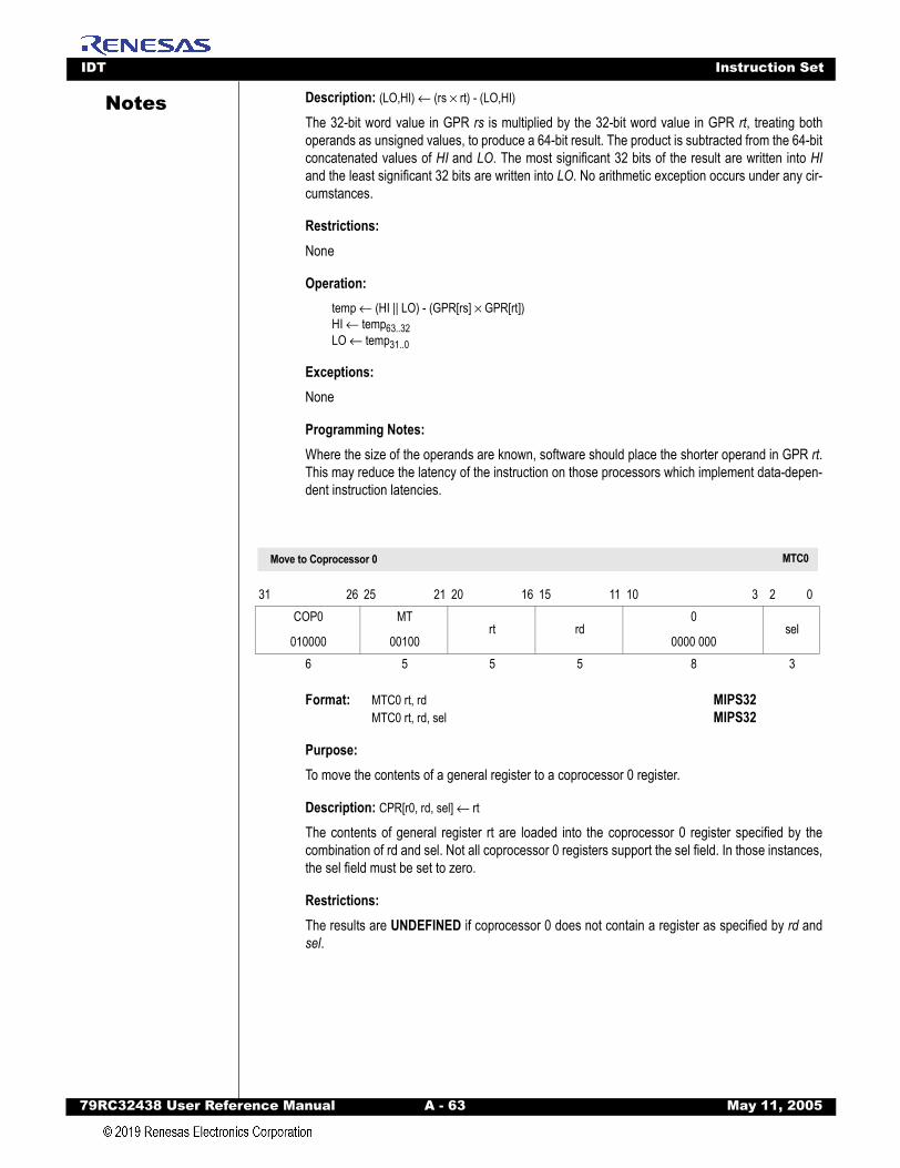
IDT Instruction Set
79RC32438 User Refer
Notes
Description: (LO,HI) ← (rs × rt) - (LO,HI)The 32-bit word value in GPR rs is multiplied by the 32-bit word value in GPR rt, treating bothoperands as unsigned values, to produce a 64-bit result. The product is subtracted from the 64-bitconcatenated values of HI and LO. The most significant 32 bits of the result are written into HIand the least significant 32 bits are written into LO. No arithmetic exception occurs under any cir-cumstances.
Restrictions:None
Operation:temp ← (HI || LO) - (GPR[rs] × GPR[rt])HI ← temp63..32LO ← temp31..0
Exceptions:None
Programming Notes:Where the size of the operands are known, software should place the shorter operand in GPR rt.This may reduce the latency of the instruction on those processors which implement data-depen-dent instruction latencies.
Format: MTC0 rt, rd MIPS32MTC0 rt, rd, sel MIPS32
Purpose:To move the contents of a general register to a coprocessor 0 register.
Description: CPR[r0, rd, sel] ← rt
The contents of general register rt are loaded into the coprocessor 0 register specified by thecombination of rd and sel. Not all coprocessor 0 registers support the sel field. In those instances,the sel field must be set to zero.
Restrictions:The results are UNDEFINED if coprocessor 0 does not contain a register as specified by rd andsel.
31 26 25 21 20 16 15 11 10 3 2 0COP0
010000
MT
00100rt rd
0
0000 000sel
6 5 5 5 8 3
Move to Coprocessor 0 MTC0
ence Manual A - 63 May 11, 2005
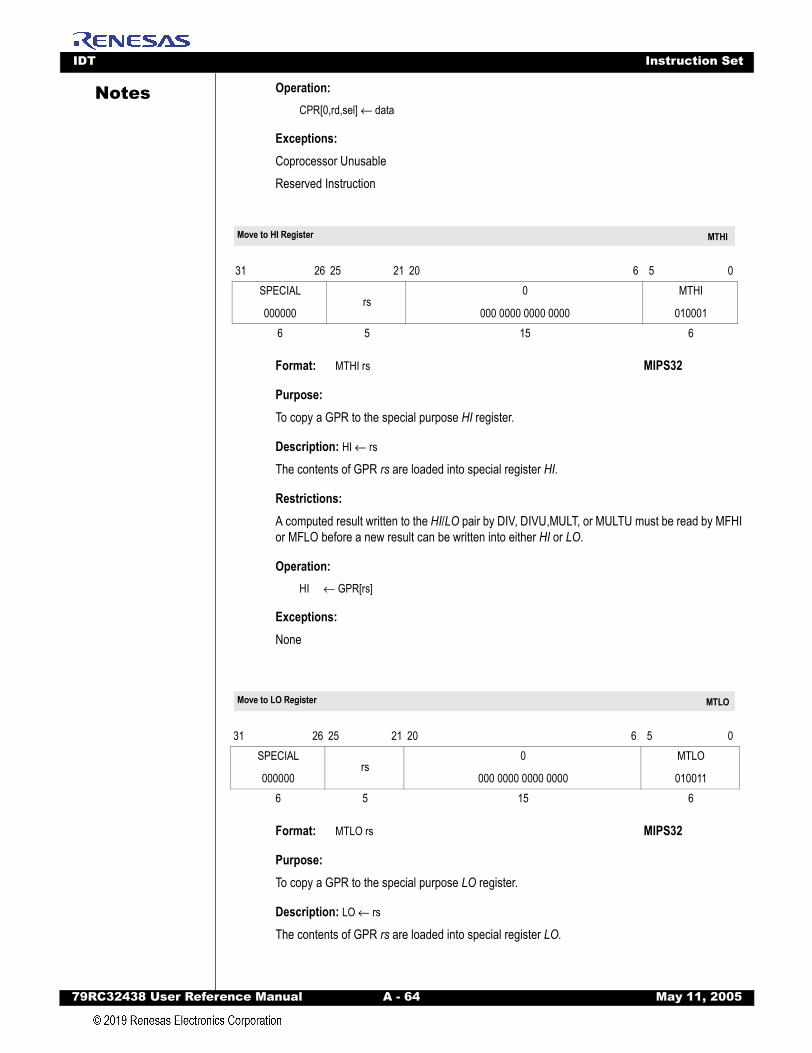
IDT Instruction Set
79RC32438 User Refer
Notes
Operation:CPR[0,rd,sel] ← dataExceptions:Coprocessor UnusableReserved Instruction
Format: MTHI rs MIPS32
Purpose: To copy a GPR to the special purpose HI register.
Description: HI ← rs
The contents of GPR rs are loaded into special register HI.
Restrictions: A computed result written to the HI/LO pair by DIV, DIVU,MULT, or MULTU must be read by MFHIor MFLO before a new result can be written into either HI or LO.
Operation:HI ← GPR[rs]
Exceptions: None
Format: MTLO rs MIPS32
Purpose: To copy a GPR to the special purpose LO register.
Description: LO ← rs
The contents of GPR rs are loaded into special register LO.
31 26 25 21 20 6 5 0SPECIAL
000000rs
0
000 0000 0000 0000
MTHI
0100016 5 15 6
31 26 25 21 20 6 5 0SPECIAL
000000rs
0
000 0000 0000 0000
MTLO
0100116 5 15 6
Move to HI Register MTHI
Move to LO Register MTLO
ence Manual A - 64 May 11, 2005

IDT Instruction Set
79RC32438 User Refer
Notes
Restrictions: A computed result written to the HI/LO pair by DIV, DIVU, MULT, or MULTU must be read byMFHI or MFLO before a new result can be written into either HI or LO.Operation:LO ← GPR[rs]
Exceptions: None
Format: MUL rd, rs, rt MIPS32
Purpose:To multiply two words and write the result to a GPR.
Description: rd ← rs × rt
The 32-bit word value in GPR rs is multiplied by the 32-bit value in GPR rt, treating both operandsas signed values, to produce a 64-bit result. The least significant 32 bits of the product are writtento GPR rd. The contents of HI and LO are UNPREDICTABLE after the operation. No arithmeticexception occurs under any circumstances.
Restrictions:Note that this instruction does not provide the capability of writing the result to the HI and LO reg-isters.
Operation:temp ← GPR[rs] × GPR[rt]GPR[RD] ← GPR31..0HI ← UPPREDICTABLELO ← UNPREDICTABLE
Exceptions:None
Programming Notes:Programs that require overflow detection must check for it explicitly.Where the size of the operands are known, software should place the shorter operand in GPR rt.This may reduce the latency of the instruction on those processors which implement data-depen-dent instruction latencies.
31 26 25 21 20 16 15 11 10 6 5 0SPECIAL2
011100rs rt rd
0
00000
MUL
0000106 5 5 5 5 6
Multiply Word to GPR MUL
ence Manual A - 65 May 11, 2005
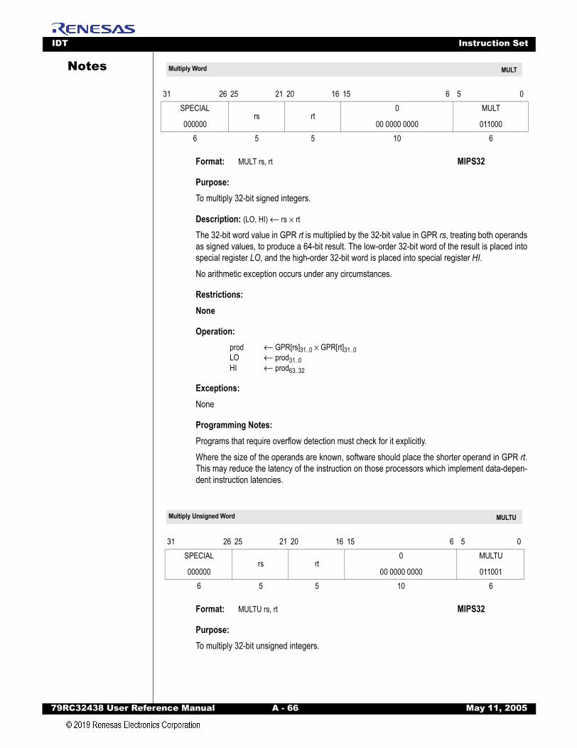
IDT Instruction Set
79RC32438 User Refer
Notes
MULTFormat: MULT rs, rt MIPS32
Purpose: To multiply 32-bit signed integers.
Description: (LO, HI) ← rs × rtThe 32-bit word value in GPR rt is multiplied by the 32-bit value in GPR rs, treating both operandsas signed values, to produce a 64-bit result. The low-order 32-bit word of the result is placed intospecial register LO, and the high-order 32-bit word is placed into special register HI.No arithmetic exception occurs under any circumstances.
Restrictions: None
Operation:prod ← GPR[rs]31..0 × GPR[rt]31..0LO ← prod31..0HI ← prod63..32
Exceptions: None
Programming Notes:Programs that require overflow detection must check for it explicitly.Where the size of the operands are known, software should place the shorter operand in GPR rt.This may reduce the latency of the instruction on those processors which implement data-depen-dent instruction latencies.
MULTU
Format: MULTU rs, rt MIPS32
Purpose: To multiply 32-bit unsigned integers.
31 26 25 21 20 16 15 6 5 0SPECIAL
000000rs rt
0
00 0000 0000
MULT
0110006 5 5 10 6
31 26 25 21 20 16 15 6 5 0SPECIAL
000000rs rt
0
00 0000 0000
MULTU
0110016 5 5 10 6
Multiply Word MULT
Multiply Unsigned Word MULTU
ence Manual A - 66 May 11, 2005
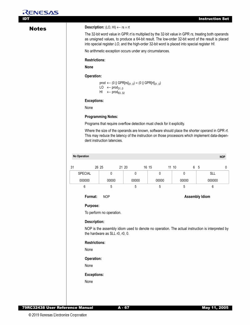
IDT Instruction Set
79RC32438 User Refer
Notes
Description: (LO, HI) ← rs × rtThe 32-bit word value in GPR rt is multiplied by the 32-bit value in GPR rs, treating both operandsas unsigned values, to produce a 64-bit result. The low-order 32-bit word of the result is placedinto special register LO, and the high-order 32-bit word is placed into special register HI.No arithmetic exception occurs under any circumstances.
Restrictions: None
Operation:prod ← (0 || GPR[rs]31..0) × (0 || GPR[rt]31..0)LO ← prod31..0HI ← prod63..32
Exceptions: None
Programming Notes:Programs that require overflow detection must check for it explicitly.Where the size of the operands are known, software should place the shorter operand in GPR rt.This may reduce the latency of the instruction on those processors which implement data-depen-dent instruction latencies.
Format: NOP Assembly Idiom
Purpose: To perform no operation.
Description: NOP is the assembly idiom used to denote no operation. The actual instruction is interpreted bythe hardware as SLL r0, r0, 0.
Restrictions: None
Operation:None
Exceptions: None
31 26 25 21 20 16 15 11 10 6 5 0SPECIAL
000000
0
00000
0
00000
0
00000
0
00000
SLL
0000006 5 5 5 5 6
No Operation NOP
ence Manual A - 67 May 11, 2005

IDT Instruction Set
79RC32438 User Refer
Notes
Programming Notes:The zero instruction word, which represents SLL, r0, r0, 0, is the preferred NOP for software touse to fill branch and jump delay slots and to pad out alignment sequences.Format: NOR rd, rs, rt MIPS32
Purpose:To do a bitwise logical NOT OR.
Description: rd ← rs NOR rt
The contents of GPR rs are combined with the contents of GPR rt in a bitwise logical NOR opera-tion. The result is placed into GPR rd.
Restrictions: None
Operation:GPR[rd] ← GPR[rs] nor GPR[rt]
Exceptions: None
OR
Format: OR rd, rs, rt MIPS32
Purpose: To do a bitwise logical OR.
Description: rd ← rs or rt
The contents of GPR rs are combined with the contents of GPR rt in a bitwise logical OR opera-tion. The result is placed into GPR rd.
Restrictions: None
31 26 25 21 20 16 15 11 10 6 5 0SPECIAL
000000rs rt rd
0
00000
NOR
1001116 5 5 5 5 6
31 26 25 21 20 16 15 11 10 6 5 0SPECIAL
000000rs rt rd
0
00000
OR
1001016 5 5 5 5 6
Not Or NOR
Or OR
ence Manual A - 68 May 11, 2005
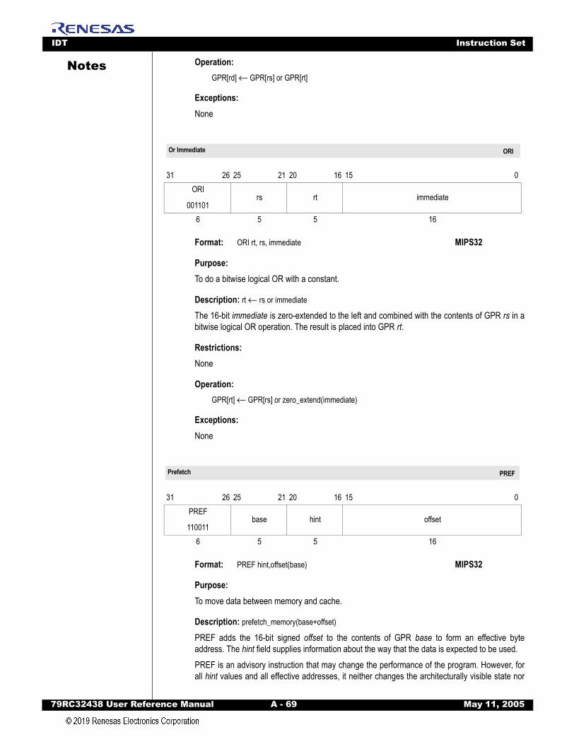
IDT Instruction Set
79RC32438 User Refer
Notes
Operation:GPR[rd] ← GPR[rs] or GPR[rt]Exceptions: None
I
Format: ORI rt, rs, immediate MIPS32
Purpose: To do a bitwise logical OR with a constant.
Description: rt ← rs or immediate
The 16-bit immediate is zero-extended to the left and combined with the contents of GPR rs in abitwise logical OR operation. The result is placed into GPR rt.
Restrictions: None
Operation:GPR[rt] ← GPR[rs] or zero_extend(immediate)
Exceptions: None
Format: PREF hint,offset(base) MIPS32
Purpose: To move data between memory and cache.
Description: prefetch_memory(base+offset)
PREF adds the 16-bit signed offset to the contents of GPR base to form an effective byteaddress. The hint field supplies information about the way that the data is expected to be used.PREF is an advisory instruction that may change the performance of the program. However, forall hint values and all effective addresses, it neither changes the architecturally visible state nor
31 26 25 21 20 16 15 0ORI
001101rs rt immediate
6 5 5 16
31 26 25 21 20 16 15 0PREF
110011base hint offset
6 5 5 16
Or Immediate ORI
Prefetch PREF
ence Manual A - 69 May 11, 2005

IDT Instruction Set
79RC32438 User Refer
Notes
does it alter the meaning of the program.PREF does not cause addressing-related exceptions. If the address specified would cause anaddressing exception, the exception condition is ignored and no data movement occurs. Howevereven if no data is prefetched, some action that is not architecturally visible, such as writeback of adirty cache line, can take place.PREF never generates a memory operation for a location with an uncached memory access type.If PREF results in a memory operation, the memory access type used for the operation is deter-mined by the memory access type of the effective address, just as it would be if the memory oper-ation had been caused by a load or store to the effective address. The hint field supplies information about the way the data is expected to be used. A hint valuecannot cause an action to modify architecturally visible state.Any of the following conditions causes the 4Kc core to treat a PREF instruction as a NOP.– A reserved hint value is used– Writeback-invalidate (25) hint value is used– The address has a translation error– The address maps to an uncacheable page– The data is already in the cache– There is already another load/prefetch outstanding
In all other cases, except when hint equals 25, execution of the PREF instruction initiates an externalbus read transaction. PREF is a non-blocking operation and does not cause the pipeline to stall whilewaiting for the data to be returned.
Value Name Data Use and Desired Prefetch Action
0 load Use: Prefetched data is expected to be read (not modified).Action: Fetch data as if for a load.
1 store Use: Prefetched data is expected to be stored or modified.Action: Fetch data as if for a store.
2-3 Reserved Reserved - treated as a NOP
4 load_streamed Use: Prefetched data is expected to be read (not modified) but not reused extensively; it “streams” through cache.Action: Fetch data as if for a load and place it in the cache so that it does not displace data prefetched as “retained.”
5 store_streamed Use: Prefetched data is expected to be stored or modified but not reused extensively; it “streams” through cache.Action: Fetch data as if for a store and place it in the cache so that it does not displace data prefetched as “retained.”
6 load_retained Use: Prefetched data is expected to be read (not modified) and reused extensively; it should be “retained” in the cache.Action: Fetch data as if for a load and place it in the cache so that it is not displaced by data prefetched as “streamed.”
7 store_retained Use: Prefetched data is expected to be stored or modified and reused extensively; it should be “retained” in the cache.Action: Fetch data as if for a store and place it in the cache so that it is not displaced by data prefetched as “streamed.”
8-24 Reserved Reserved - treated as a NOP.
Table A.10 Values of the hint Field for the PREF Instruction (Part 1 of 2)
ence Manual A - 70 May 11, 2005

IDT Instruction Set
79RC32438 User Refer
Notes
Restrictions:None
Operation:vAddr ← GPR[base] + sign_extend(offset)(pAddr, CCA) ← AddressTranslation(vAddr, DATA, LOAD)Prefetch(CCA, pAddr, vAddr, DATA, hint)
Exceptions:Prefetch does not take any TLB-related or address-related exceptions under any circumstances.
Programming Notes:Prefetch cannot prefetch data from a mapped location unless the translation for that location ispresent in the TLB. Locations in memory pages that have not been accessed recently may nothave translations in the TLB, so prefetch may not be effective for such locations.Prefetch does not cause addressing exceptions. It does not cause an exception to prefetch usingan address pointer value before the validity of a pointer is determined.
SB
Format: SB rt, offset(base) MIPS32
Purpose: To store a byte to memory.
Description: memory[base+offset] ← rt
The least-significant 8-bit byte of GPR rt is stored in memory at the location specified by the effec-tive address. The 16-bit signed offset is added to the contents of GPR base to form the effectiveaddress.
25 writeback_invalidate (also known as “nudge”)
Use: Data is no longer expected to be used.Treated as a NOP.
26-29 Implementation Depen-dent
Reserved - treated as a NOP.
30 PrepareForStore Use: Prepare the cache for writing an entire line, without the overhead involved in filling the line from memory.Reserved - treated as a NOP.
31 Implementation Depen-dent
Reserved - treated as a NOP.
31 26 25 21 20 16 15 0SB
101000base rt offset
6 5 5 16
Value Name Data Use and Desired Prefetch Action
Table A.10 Values of the hint Field for the PREF Instruction (Part 2 of 2)
Store Byte SB
ence Manual A - 71 May 11, 2005
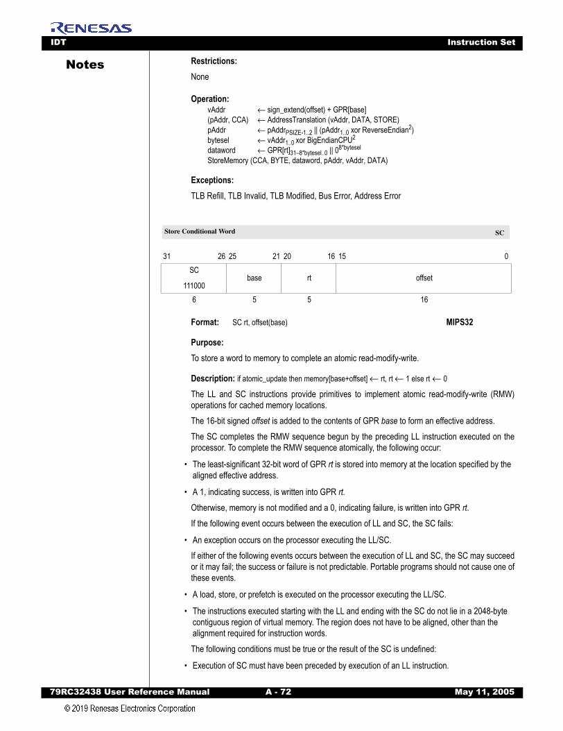
IDT Instruction Set
79RC32438 User Refer
Notes
Restrictions: NoneOperation:vAddr ← sign_extend(offset) + GPR[base](pAddr, CCA) ← AddressTranslation (vAddr, DATA, STORE)pAddr ← pAddrPSIZE-1..2 || (pAddr1..0 xor ReverseEndian2)bytesel ← vAddr1..0 xor BigEndianCPU2
dataword ← GPR[rt]31–8*bytesel..0 || 08*bytesel
StoreMemory (CCA, BYTE, dataword, pAddr, vAddr, DATA)
Exceptions: TLB Refill, TLB Invalid, TLB Modified, Bus Error, Address Error
SC
Format: SC rt, offset(base) MIPS32
Purpose: To store a word to memory to complete an atomic read-modify-write.
Description: if atomic_update then memory[base+offset] ← rt, rt ← 1 else rt ← 0The LL and SC instructions provide primitives to implement atomic read-modify-write (RMW)operations for cached memory locations.The 16-bit signed offset is added to the contents of GPR base to form an effective address.The SC completes the RMW sequence begun by the preceding LL instruction executed on theprocessor. To complete the RMW sequence atomically, the following occur:
• The least-significant 32-bit word of GPR rt is stored into memory at the location specified by the aligned effective address.
• A 1, indicating success, is written into GPR rt.
Otherwise, memory is not modified and a 0, indicating failure, is written into GPR rt.If the following event occurs between the execution of LL and SC, the SC fails:
• An exception occurs on the processor executing the LL/SC.If either of the following events occurs between the execution of LL and SC, the SC may succeedor it may fail; the success or failure is not predictable. Portable programs should not cause one ofthese events.
• A load, store, or prefetch is executed on the processor executing the LL/SC.
• The instructions executed starting with the LL and ending with the SC do not lie in a 2048-byte contiguous region of virtual memory. The region does not have to be aligned, other than the alignment required for instruction words.The following conditions must be true or the result of the SC is undefined:
• Execution of SC must have been preceded by execution of an LL instruction.
31 26 25 21 20 16 15 0SC
111000base rt offset
6 5 5 16
Store Conditional Word SC
ence Manual A - 72 May 11, 2005
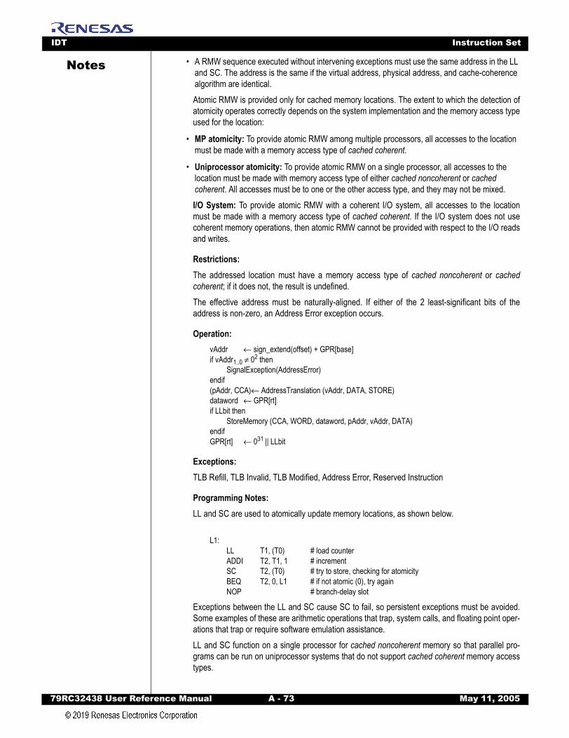
IDT Instruction Set
79RC32438 User Refer
Notes
• A RMW sequence executed without intervening exceptions must use the same address in the LL and SC. The address is the same if the virtual address, physical address, and cache-coherence algorithm are identical.Atomic RMW is provided only for cached memory locations. The extent to which the detection ofatomicity operates correctly depends on the system implementation and the memory access typeused for the location:• MP atomicity: To provide atomic RMW among multiple processors, all accesses to the location must be made with a memory access type of cached coherent.
• Uniprocessor atomicity: To provide atomic RMW on a single processor, all accesses to the location must be made with memory access type of either cached noncoherent or cached coherent. All accesses must be to one or the other access type, and they may not be mixed.I/O System: To provide atomic RMW with a coherent I/O system, all accesses to the locationmust be made with a memory access type of cached coherent. If the I/O system does not usecoherent memory operations, then atomic RMW cannot be provided with respect to the I/O readsand writes.
Restrictions: The addressed location must have a memory access type of cached noncoherent or cachedcoherent; if it does not, the result is undefined.The effective address must be naturally-aligned. If either of the 2 least-significant bits of theaddress is non-zero, an Address Error exception occurs.
Operation:vAddr ← sign_extend(offset) + GPR[base]if vAddr1..0 ≠ 02 then
SignalException(AddressError)endif(pAddr, CCA)← AddressTranslation (vAddr, DATA, STORE)dataword ← GPR[rt]if LLbit then
StoreMemory (CCA, WORD, dataword, pAddr, vAddr, DATA)endifGPR[rt] ← 031 || LLbit
Exceptions: TLB Refill, TLB Invalid, TLB Modified, Address Error, Reserved Instruction
Programming Notes:LL and SC are used to atomically update memory locations, as shown below.
L1:LL T1, (T0) # load counterADDI T2, T1, 1 # incrementSC T2, (T0) # try to store, checking for atomicityBEQ T2, 0, L1 # if not atomic (0), try againNOP # branch-delay slot
Exceptions between the LL and SC cause SC to fail, so persistent exceptions must be avoided.Some examples of these are arithmetic operations that trap, system calls, and floating point oper-ations that trap or require software emulation assistance.LL and SC function on a single processor for cached noncoherent memory so that parallel pro-grams can be run on uniprocessor systems that do not support cached coherent memory accesstypes.
ence Manual A - 73 May 11, 2005
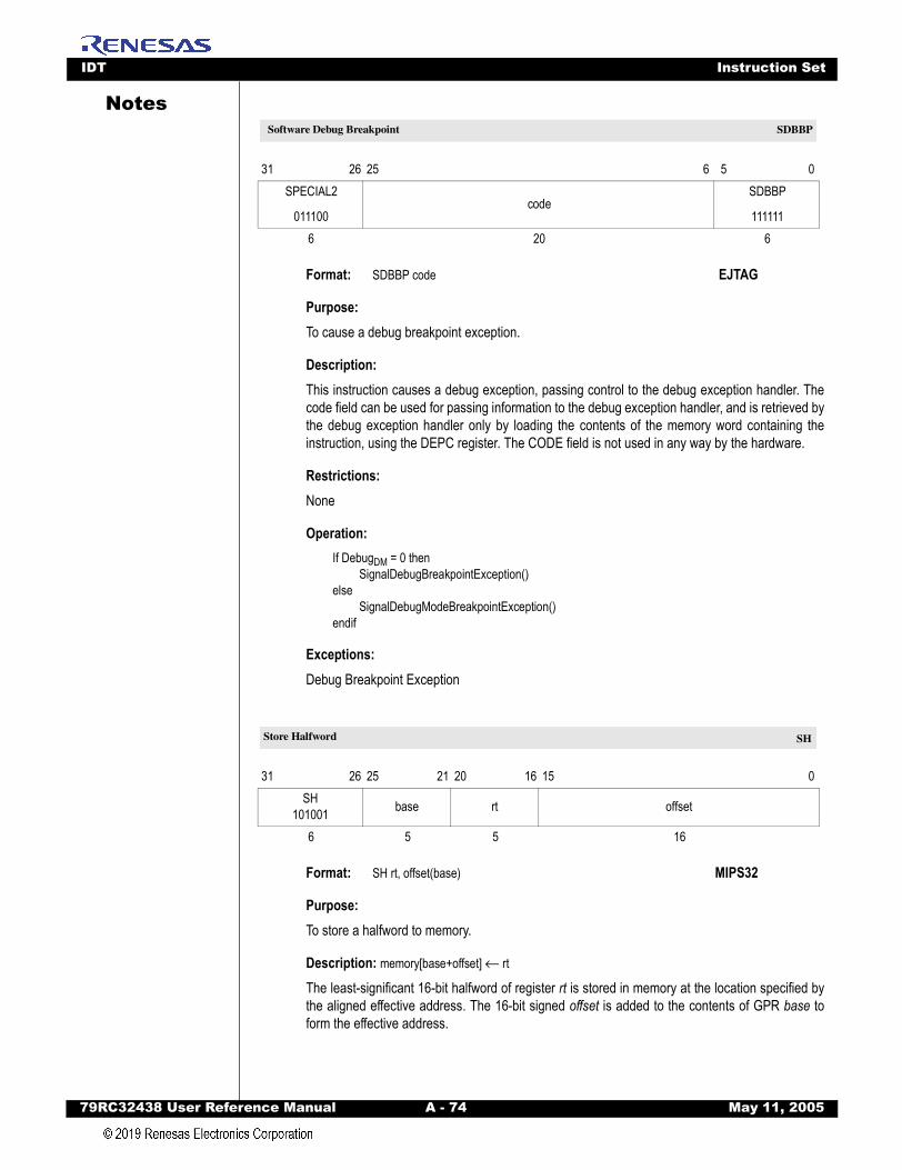
IDT Instruction Set
79RC32438 User Refer
Notes
SDBBPFormat: SDBBP code EJTAG
Purpose:To cause a debug breakpoint exception.
Description:This instruction causes a debug exception, passing control to the debug exception handler. Thecode field can be used for passing information to the debug exception handler, and is retrieved bythe debug exception handler only by loading the contents of the memory word containing theinstruction, using the DEPC register. The CODE field is not used in any way by the hardware.
Restrictions:None
Operation:If DebugDM = 0 then
SignalDebugBreakpointException()else
SignalDebugModeBreakpointException()endif
Exceptions:Debug Breakpoint Exception
SH
Format: SH rt, offset(base) MIPS32
Purpose: To store a halfword to memory.
Description: memory[base+offset] ← rt
The least-significant 16-bit halfword of register rt is stored in memory at the location specified bythe aligned effective address. The 16-bit signed offset is added to the contents of GPR base toform the effective address.
31 26 25 6 5 0SPECIAL2
011100code
SDBBP
1111116 20 6
31 26 25 21 20 16 15 0SH
101001 base rt offset
6 5 5 16
Software Debug Breakpoint SDBBP
Store Halfword SH
ence Manual A - 74 May 11, 2005
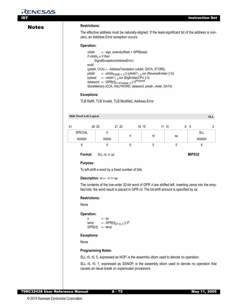
IDT Instruction Set
79RC32438 User Refer
Notes
Restrictions: The effective address must be naturally-aligned. If the least-significant bit of the address is non-zero, an Address Error exception occurs.Operation: vAddr ← sign_extend(offset) + GPR[base]if vAddr0 ≠ 0 then
SignalException(AddressError)endif(pAddr, CCA) ← AddressTranslation (vAddr, DATA, STORE)pAddr ← pAddrPSIZE-1..2 || (pAddr11..0 xor (ReverseEndian || 0))bytesel ← vAddr11..0 xor (BigEndianCPU || 0)dataword ← GPR[rt]31–8*bytesel..0 || 08*bytesel
StoreMemory (CCA, HALFWORD, dataword, pAddr, vAddr, DATA)
Exceptions: TLB Refill, TLB Invalid, TLB Modified, Address Error
SLL
Format: SLL rd, rt, sa MIPS32
Purpose: To left-shift a word by a fixed number of bits.
Description: rd ← rt << sa
The contents of the low-order 32-bit word of GPR rt are shifted left, inserting zeros into the emp-tied bits; the word result is placed in GPR rd. The bit-shift amount is specified by sa.
Restrictions: None
Operation:s ← satemp ← GPR[rt](31-s)..0 || 0s
GPR[rd] ← temp
Exceptions: None
Programming Notes:SLL r0, r0, 0, expressed as NOP, is the assembly idiom used to denote no operation. SLL r0, r0, 1, expressed as SSNOP, is the assembly idiom used to denote no operation thatcauses an issue break on superscalar processors.
31 26 25 21 20 16 15 11 10 6 5 0SPECIAL
000000
0
00000rt rd sa
SLL
0000006 5 5 5 5 6
Shift Word Left Logical SLL
ence Manual A - 75 May 11, 2005

IDT Instruction Set
79RC32438 User Refer
Notes
SLLVFormat: SLLV rd, rt, rs MIPS32
Purpose: To left-shift a word by a variable number of bits.
Description: rd ← rt << rs
The contents of the low-order 32-bit word of GPR rt are shifted left, inserting zeros into the emp-tied bits; the result word is placed in GPR rd. The bit-shift amount is specified by the low-order 5bits of GPR rs.
Restrictions: None
Operation:s ← GPR[rs]4..0temp ← GPR[rt](31-s)..0 || 0s
GPR[rd] ← temp
Exceptions: None
Programming Notes:None
SLT
Format: SLT rd, rs, rt MIPS32
Purpose: To record the result of a less-than comparison.
Description: rd ← (rs < rt)
Compare the contents of GPR rs and GPR rt as signed integers and record the Boolean result ofthe comparison in GPR rd. If GPR rs is less than GPR rt, the result is 1 (true); otherwise, it is 0(false).The arithmetic comparison does not cause an Integer Overflow exception.
Restrictions: None
31 26 25 21 20 16 15 11 10 6 5 0SPECIAL
000000rs rt rd
0
00000
SLLV
0001006 5 5 5 5 6
31 26 25 21 20 16 15 11 10 6 5 0SPECIAL
000000rs rt rd
0
00000
SLT
1010106 5 5 5 5 6
Shift Word Left Logical Variable SLLV
Set on Less Than SLT
ence Manual A - 76 May 11, 2005
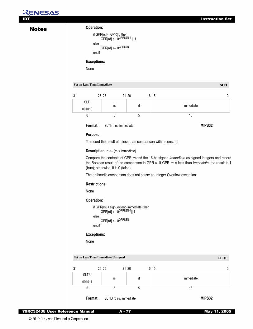
IDT Instruction Set
79RC32438 User Refer
Notes
Operation:if GPR[rs] < GPR[rt] thenGPR[rd] ← 0GPRLEN-1 || 1else
GPR[rd] ← 0GPRLEN
endif
Exceptions: None
SLTI
Format: SLTI rt, rs, immediate MIPS32
Purpose: To record the result of a less-than comparison with a constant
Description: rt ← (rs < immediate)
Compare the contents of GPR rs and the 16-bit signed immediate as signed integers and recordthe Boolean result of the comparison in GPR rt. If GPR rs is less than immediate, the result is 1(true); otherwise, it is 0 (false).The arithmetic comparison does not cause an Integer Overflow exception.
Restrictions: None
Operation:if GPR[rs] < sign_extend(immediate) then
GPR[rd] ← 0GPRLEN-1|| 1else
GPR[rd] ← 0GPRLEN
endif
Exceptions:None
SLTIU
Format: SLTIU rt, rs, immediate MIPS32
31 26 25 21 20 16 15 0SLTI
001010rs rt immediate
6 5 5 16
31 26 25 21 20 16 15 0SLTIU
001011rs rt immediate
6 5 5 16
Set on Less Than Immediate SLTI
Set on Less Than Immediate Unsigned SLTIU
ence Manual A - 77 May 11, 2005
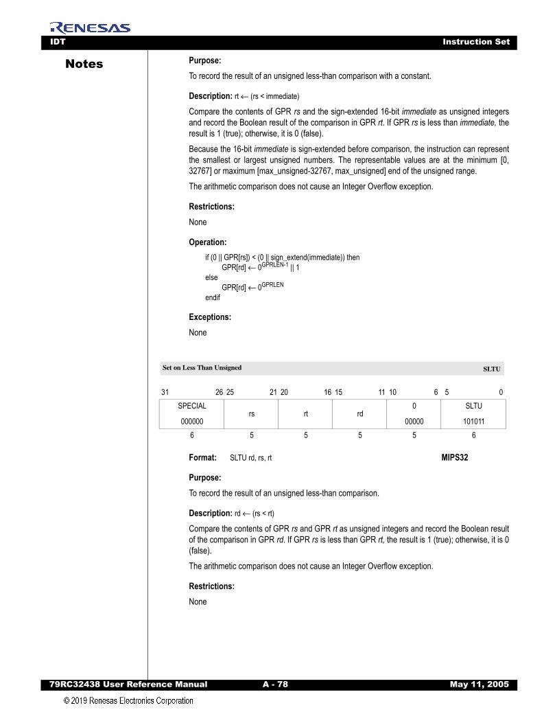
IDT Instruction Set
79RC32438 User Refer
Notes
Purpose: To record the result of an unsigned less-than comparison with a constant.Description: rt ← (rs < immediate)
Compare the contents of GPR rs and the sign-extended 16-bit immediate as unsigned integersand record the Boolean result of the comparison in GPR rt. If GPR rs is less than immediate, theresult is 1 (true); otherwise, it is 0 (false).Because the 16-bit immediate is sign-extended before comparison, the instruction can representthe smallest or largest unsigned numbers. The representable values are at the minimum [0,32767] or maximum [max_unsigned-32767, max_unsigned] end of the unsigned range.The arithmetic comparison does not cause an Integer Overflow exception.
Restrictions: None
Operation:if (0 || GPR[rs]) < (0 || sign_extend(immediate)) then
GPR[rd] ← 0GPRLEN-1 || 1else
GPR[rd] ← 0GPRLEN
endif
Exceptions: None
SLTU
Format: SLTU rd, rs, rt MIPS32
Purpose: To record the result of an unsigned less-than comparison.
Description: rd ← (rs < rt)
Compare the contents of GPR rs and GPR rt as unsigned integers and record the Boolean resultof the comparison in GPR rd. If GPR rs is less than GPR rt, the result is 1 (true); otherwise, it is 0(false).The arithmetic comparison does not cause an Integer Overflow exception.
Restrictions: None
31 26 25 21 20 16 15 11 10 6 5 0SPECIAL
000000rs rt rd
0
00000
SLTU
1010116 5 5 5 5 6
Set on Less Than Unsigned SLTU
ence Manual A - 78 May 11, 2005

IDT Instruction Set
79RC32438 User Refer
Notes
Operation:if (0 || GPR[rs]) < (0 || GPR[rt]) thenGPR[rd] ← 0GPRLEN-1 || 1else
GPR[rd] ← 0GPRLEN
endif
Exceptions: None
SRA
Format: SRA rd, rt, sa MIPS32
Purpose: To execute an arithmetic right-shift of a word by a fixed number of bits.
Description: rd ← rt >> sa (arithmetic)
The contents of the low-order 32-bit word of GPR rt are shifted right, duplicating the sign-bit (bit31) in the emptied bits; the word result is placed in GPR rd. The bit-shift amount is specified bysa.
Restrictions: None
Operation:s ← satemp ← (GPR[rt]31)s || GPR[rt]31..sGPR[rd] ← temp
Exceptions:None
SRAV
Format: SRAV rd, rt, rs MIPS32
Purpose: To execute an arithmetic right-shift of a word by a variable number of bits.
31 26 25 21 20 16 15 11 10 6 5 0SPECIAL
000000
0
00000rt rd sa
SRA
0000116 5 5 5 5 6
31 26 25 21 20 16 15 11 10 6 5 0SPECIAL
000000rs rt rd
0
00000
SRAV
0001116 5 5 5 5 6
Shift Word Right Arithmetic SRA
Shift Word Right Arithmetic Variable SRAV
ence Manual A - 79 May 11, 2005
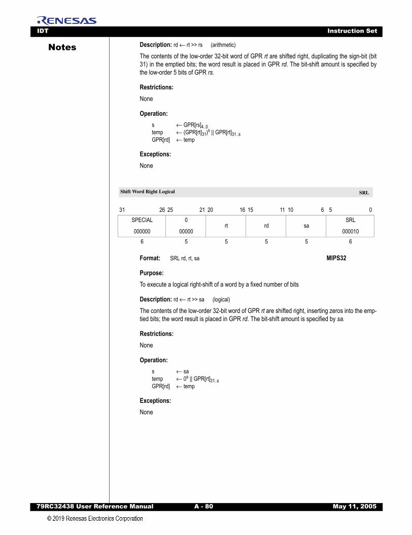
IDT Instruction Set
79RC32438 User Refer
Notes
Description: rd ← rt >> rs (arithmetic)The contents of the low-order 32-bit word of GPR rt are shifted right, duplicating the sign-bit (bit31) in the emptied bits; the word result is placed in GPR rd. The bit-shift amount is specified bythe low-order 5 bits of GPR rs.
Restrictions: None
Operation:s ← GPR[rs]4..0temp ← (GPR[rt]31)s || GPR[rt]31..sGPR[rd] ← temp
Exceptions: None
SRL
Format: SRL rd, rt, sa MIPS32
Purpose: To execute a logical right-shift of a word by a fixed number of bits
Description: rd ← rt >> sa (logical)
The contents of the low-order 32-bit word of GPR rt are shifted right, inserting zeros into the emp-tied bits; the word result is placed in GPR rd. The bit-shift amount is specified by sa.
Restrictions: None
Operation:s ← satemp ← 0s || GPR[rt]31..sGPR[rd] ← temp
Exceptions: None
31 26 25 21 20 16 15 11 10 6 5 0SPECIAL
000000
0
00000rt rd sa
SRL
0000106 5 5 5 5 6
Shift Word Right Logical SRL
ence Manual A - 80 May 11, 2005
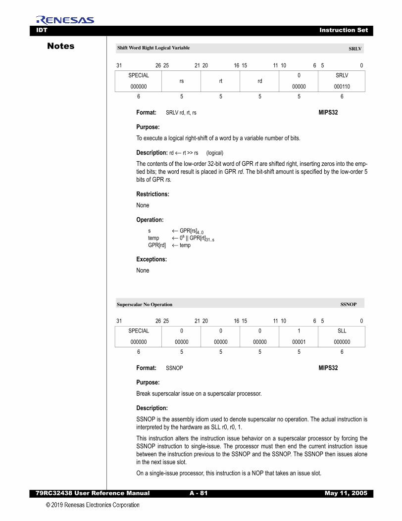
IDT Instruction Set
79RC32438 User Refer
Notes
SRLVFormat: SRLV rd, rt, rs MIPS32
Purpose: To execute a logical right-shift of a word by a variable number of bits.
Description: rd ← rt >> rs (logical)
The contents of the low-order 32-bit word of GPR rt are shifted right, inserting zeros into the emp-tied bits; the word result is placed in GPR rd. The bit-shift amount is specified by the low-order 5bits of GPR rs.
Restrictions: None
Operation:s ← GPR[rs]4..0temp ← 0s || GPR[rt]31..sGPR[rd] ← temp
Exceptions: None
SSNOP
Format: SSNOP MIPS32
Purpose: Break superscalar issue on a superscalar processor.
Description: SSNOP is the assembly idiom used to denote superscalar no operation. The actual instruction isinterpreted by the hardware as SLL r0, r0, 1.This instruction alters the instruction issue behavior on a superscalar processor by forcing theSSNOP instruction to single-issue. The processor must then end the current instruction issuebetween the instruction previous to the SSNOP and the SSNOP. The SSNOP then issues alonein the next issue slot.On a single-issue processor, this instruction is a NOP that takes an issue slot.
31 26 25 21 20 16 15 11 10 6 5 0SPECIAL
000000rs rt rd
0
00000
SRLV
0001106 5 5 5 5 6
31 26 25 21 20 16 15 11 10 6 5 0SPECIAL
000000
0
00000
0
00000
0
00000
1
00001
SLL
0000006 5 5 5 5 6
Shift Word Right Logical Variable SRLV
Superscalar No Operation SSNOP
ence Manual A - 81 May 11, 2005
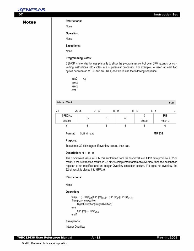
IDT Instruction Set
79RC32438 User Refer
Notes
Restrictions: NoneOperation: None
Exceptions: None
Programming Notes:SSNOP is intended for use primarily to allow the programmer control over CP0 hazards by con-verting instructions into cycles in a superscalar processor. For example, to insert at least twocycles between an MTC0 and an ERET, one would use the following sequence:
mtc0 x,yssnopssnoperet
SUB
Format: SUB rd, rs, rt MIPS32
Purpose: To subtract 32-bit integers. If overflow occurs, then trap.
Description: rd ← rs - rt
The 32-bit word value in GPR rt is subtracted from the 32-bit value in GPR rs to produce a 32-bitresult. If the subtraction results in 32-bit 2’s complement arithmetic overflow, then the destinationregister is not modified and an Integer Overflow exception occurs. If it does not overflow, the32-bit result is placed into GPR rd.
Restrictions:
None
Operation:temp ← (GPR[rs]31||GPR[rs]31..0) - (GPR[rt]31||GPR[rt]31..0)if temp32 ≠ temp31 then
SignalException(IntegerOverflow)else
GPR[rd] ← temp31..0endif
Exceptions: Integer Overflow
31 26 25 21 20 16 15 11 10 6 5 0SPECIAL
000000rs rt rd
0
00000
SUB
1000106 5 5 5 5 6
Subtract Word SUB
ence Manual A - 82 May 11, 2005
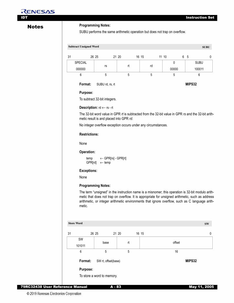
IDT Instruction Set
79RC32438 User Refer
Notes
Programming Notes:SUBU performs the same arithmetic operation but does not trap on overflow.SUBU
Format: SUBU rd, rs, rt MIPS32
Purpose: To subtract 32-bit integers.
Description: rd ← rs - rt
The 32-bit word value in GPR rt is subtracted from the 32-bit value in GPR rs and the 32-bit arith-metic result is and placed into GPR rd.No integer overflow exception occurs under any circumstances.
Restrictions:
None
Operation:temp ← GPR[rs] - GPR[rt]GPR[rd] ← temp
Exceptions: None
Programming Notes:The term “unsigned” in the instruction name is a misnomer; this operation is 32-bit modulo arith-metic that does not trap on overflow. It is appropriate for unsigned arithmetic, such as addressarithmetic, or integer arithmetic environments that ignore overflow, such as C language arith-metic.
SW
Format: SW rt, offset(base) MIPS32
Purpose: To store a word to memory.
31 26 25 21 20 16 15 11 10 6 5 0SPECIAL
000000rs rt rd
0
00000
SUBU
1000116 5 5 5 5 6
31 26 25 21 20 16 15 0SW
101011base rt offset
6 5 5 16
Subtract Unsigned Word SUBU
Store Word SW
ence Manual A - 83 May 11, 2005
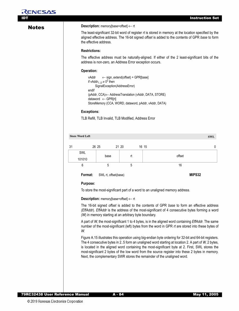
IDT Instruction Set
79RC32438 User Refer
Notes
Description: memory[base+offset] ← rtThe least-significant 32-bit word of register rt is stored in memory at the location specified by thealigned effective address. The 16-bit signed offset is added to the contents of GPR base to formthe effective address.
Restrictions: The effective address must be naturally-aligned. If either of the 2 least-significant bits of theaddress is non-zero, an Address Error exception occurs.
Operation:vAddr ← sign_extend(offset) + GPR[base]if vAddr1..0 ≠ 02 then
SignalException(AddressError)endif(pAddr, CCA)← AddressTranslation (vAddr, DATA, STORE)dataword ← GPR[rt]StoreMemory (CCA, WORD, dataword, pAddr, vAddr, DATA)
Exceptions: TLB Refill, TLB Invalid, TLB Modified, Address Error
SWL
Format: SWL rt, offset(base) MIPS32
Purpose:To store the most-significant part of a word to an unaligned memory address.
Description: memory[base+offset] ← rt
The 16-bit signed offset is added to the contents of GPR base to form an effective address(EffAddr). EffAddr is the address of the most-significant of 4 consecutive bytes forming a word(W) in memory starting at an arbitrary byte boundary. A part of W, the most-significant 1 to 4 bytes, is in the aligned word containing EffAddr. The samenumber of the most-significant (left) bytes from the word in GPR rt are stored into these bytes ofW.Figure A.15 illustrates this operation using big-endian byte ordering for 32-bit and 64-bit registers.The 4 consecutive bytes in 2..5 form an unaligned word starting at location 2. A part of W, 2 bytes,is located in the aligned word containing the most-significant byte at 2. First, SWL stores themost-significant 2 bytes of the low word from the source register into these 2 bytes in memory.Next, the complementary SWR stores the remainder of the unaligned word.
31 26 25 21 20 16 15 0SWL
101010base rt offset
6 5 5 16
Store Word Left SWL
ence Manual A - 84 May 11, 2005
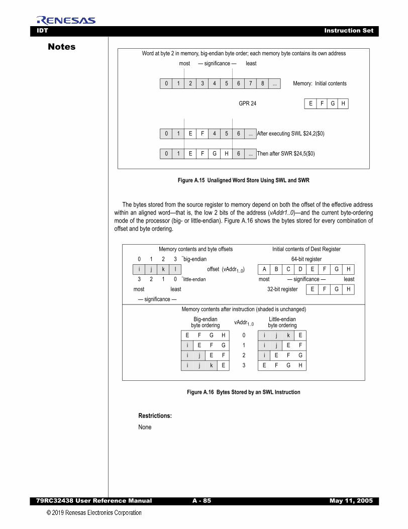
IDT Instruction Set
79RC32438 User Refer
Notes
Figure A.15 Unaligned Word Store Using SWL and SWR
The bytes stored from the source register to memory depend on both the offset of the effective addresswithin an aligned word—that is, the low 2 bits of the address (vAddr1..0)—and the current byte-orderingmode of the processor (big- or little-endian). Figure A.16 shows the bytes stored for every combination ofoffset and byte ordering.
Figure A.16 Bytes Stored by an SWL Instruction
Restrictions: None
Word at byte 2 in memory, big-endian byte order; each memory byte contains its own addressmost — significance — least
0 1 2 3 4 5 6 7 8 ... Memory: Initial contents
GPR 24 E F G H
0 1 E F 4 5 6 ... After executing SWL $24,2($0)
0 1 E F G H 6 ... Then after SWR $24,5($0)
Memory contents and byte offsets Initial contents of Dest Register0 1 2 3 ¨big-endian 64-bit registeri j k l offset (vAddr1..0) A B C D E F G H3 2 1 0 ¨little-endian most — significance — least
most least 32-bit register E F G H— significance —
Memory contents after instruction (shaded is unchanged)Big-endian
byte ordering vAddr1..0Little-endian byte ordering
E F G H 0 i j k Ei E F G 1 i j E Fi j E F 2 i E F Gi j k E 3 E F G H
ence Manual A - 85 May 11, 2005
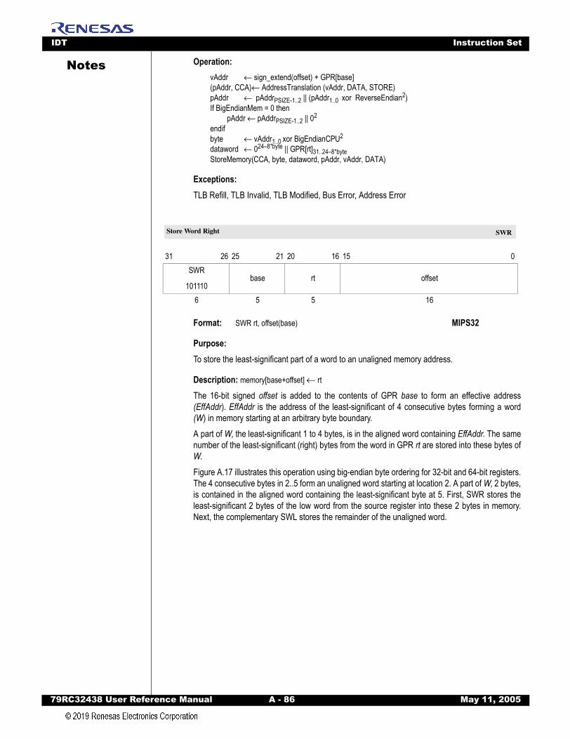
IDT Instruction Set
79RC32438 User Refer
Notes
Operation:vAddr ← sign_extend(offset) + GPR[base](pAddr, CCA)← AddressTranslation (vAddr, DATA, STORE)pAddr ← pAddrPSIZE-1..2 || (pAddr1..0 xor ReverseEndian2)If BigEndianMem = 0 thenpAddr ← pAddrPSIZE-1..2 || 02
endifbyte ← vAddr1..0 xor BigEndianCPU2
dataword ← 024–8*byte || GPR[rt]31..24–8*byteStoreMemory(CCA, byte, dataword, pAddr, vAddr, DATA)
Exceptions: TLB Refill, TLB Invalid, TLB Modified, Bus Error, Address Error
SWR
Format: SWR rt, offset(base) MIPS32
Purpose: To store the least-significant part of a word to an unaligned memory address.
Description: memory[base+offset] ← rt
The 16-bit signed offset is added to the contents of GPR base to form an effective address(EffAddr). EffAddr is the address of the least-significant of 4 consecutive bytes forming a word(W) in memory starting at an arbitrary byte boundary. A part of W, the least-significant 1 to 4 bytes, is in the aligned word containing EffAddr. The samenumber of the least-significant (right) bytes from the word in GPR rt are stored into these bytes ofW.Figure A.17 illustrates this operation using big-endian byte ordering for 32-bit and 64-bit registers.The 4 consecutive bytes in 2..5 form an unaligned word starting at location 2. A part of W, 2 bytes,is contained in the aligned word containing the least-significant byte at 5. First, SWR stores theleast-significant 2 bytes of the low word from the source register into these 2 bytes in memory.Next, the complementary SWL stores the remainder of the unaligned word.
31 26 25 21 20 16 15 0SWR
101110base rt offset
6 5 5 16
Store Word Right SWR
ence Manual A - 86 May 11, 2005

IDT Instruction Set
79RC32438 User Refer
Notes
Figure A.17 Unaligned Word Store Using SWR and SW
The bytes stored from the source register to memory depend on both the offset of the effective addresswithin an aligned word—that is, the low 2 bits of the address (vAddr1..0)—and the current byte-orderingmode of the processor (big- or little-endian). Figure A.18 shows the bytes stored for every combination ofoffset and byte-ordering.
Figure A.18 Bytes Stored by SWR Instruction
Restrictions: None
Word at byte 2 in memory, big-endian byte order, each mem byte contains its addressleast — significance — least
0 1 2 3 4 5 6 7 8 ... Memory: Initial contents
GPR 24 E F G H
0 1 2 3 G H 6 ... After executing SWR $24,5($0)
0 1 E F G H 6 ... Then after SWL $24,2($0)
Memory contents and byte offsets Initial contents of Dest Register0 1 2 3 ¨ big-endian 64-bit registeri j k l offset (vAddr1..0) A B C D E F G H3 2 1 0 ¨ little-endian most — significance — least
most least 32-bit register E F G H— significance —
Memory contents after instruction (shaded is unchanged)Big-endian
byte ordering vAddr1..0Little-endian byte
orderingH j k l 0 E F G HG H k l 1 F G H lF G H l 2 G H k lE F G H 3 H j k l
ence Manual A - 87 May 11, 2005

IDT Instruction Set
79RC32438 User Refer
Notes
Operation:vAddr ← sign_extend(offset) + GPR[base](pAddr, CCA)← AddressTranslation (vAddr, DATA, STORE)pAddr ← pAddrPSIZE-1..2 || (pAddr1..0 xor ReverseEndian2)If BigEndianMem = 0 thenpAddr ← pAddrPSIZE-1..2 || 02
endifbyte ← vAddr1..0 xor BigEndianCPU2
dataword ← GPR[rt]31–8*byte || 08*byte
StoreMemory(CCA, WORD-byte, dataword, pAddr, vAddr, DATA)
Exceptions: TLB Refill, TLB Invalid, TLB Modified, Bus Error, Address Error
SYNC
Format: SYNC (stype = 0 implied) MIPS32
Purpose: To order loads and stores.
Description: Simple Description:
• SYNC affects only uncached and cached coherent loads and stores. The loads and stores that occur before the SYNC must be completed before the loads and stores after the SYNC are allowed to start.
• Loads are completed when the destination register is written. Stores are completed when the stored value is visible to every other processor in the system.
• SYNC is required, potentially in conjunction with SSNOP, to guarantee that memory reference results are visible across operating mode changes. For example, a SYNC is required on some implementations on entry to and exit from Debug Mode to guarantee that memory affects are handled correctly.Detailed Description:
• SYNC does not guarantee the order in which instruction fetches are performed. The stype values 1-31 are reserved; they produce the same result as the value zero.
• Executing the SYNC instruction causes the write-through buffer to be flushed. The SYNC instruction stalls until all loads and stores are completed.
• The information presented here refers to the MIPS 4Kc core implementation of the SYNC instruction. For a more detailed description of the programming effects of SYNC on a generic MIPS32 processor, refer to the MIPS32 Architecture Reference Manual.Restrictions: The effect of SYNC on the global order of loads and stores for memory access types other thanuncached and cached coherent is UNPREDICTABLE.
31 26 25 21 20 16 15 11 10 6 5 0SPECIAL
000000
0
00 0000 0000 0000 0stype
SYNC
0011116 15 5 6
Synchronize Shared Memory SYNC
ence Manual A - 88 May 11, 2005
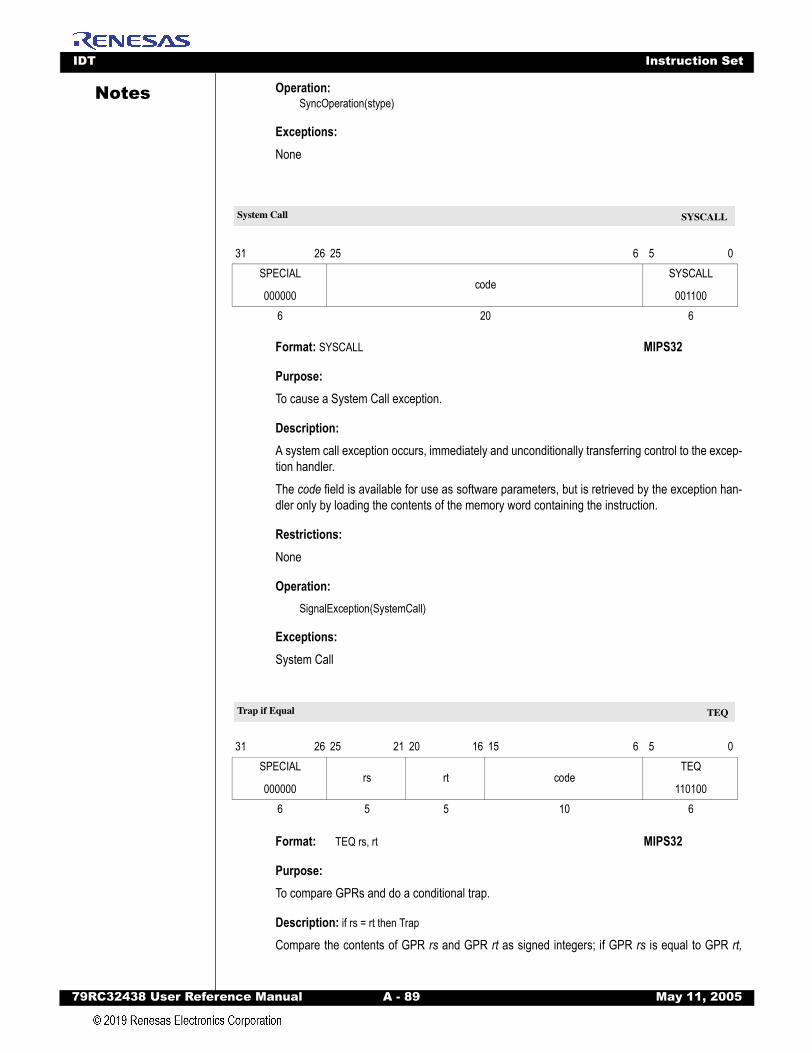
IDT Instruction Set
79RC32438 User Refer
Notes
Operation:SyncOperation(stype)Exceptions: None
SYSCALL
Format: SYSCALL MIPS32
Purpose: To cause a System Call exception.
Description: A system call exception occurs, immediately and unconditionally transferring control to the excep-tion handler. The code field is available for use as software parameters, but is retrieved by the exception han-dler only by loading the contents of the memory word containing the instruction.
Restrictions: None
Operation:SignalException(SystemCall)
Exceptions: System Call
TEQ
Format: TEQ rs, rt MIPS32
Purpose: To compare GPRs and do a conditional trap.
Description: if rs = rt then Trap
Compare the contents of GPR rs and GPR rt as signed integers; if GPR rs is equal to GPR rt,
31 26 25 6 5 0SPECIAL
000000code
SYSCALL
0011006 20 6
31 26 25 21 20 16 15 6 5 0SPECIAL
000000rs rt code
TEQ
1101006 5 5 10 6
System Call SYSCALL
Trap if Equal TEQ
ence Manual A - 89 May 11, 2005
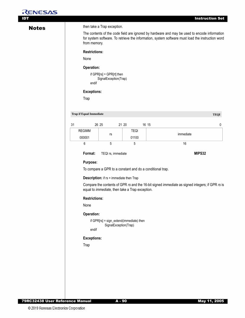
IDT Instruction Set
79RC32438 User Refer
Notes
then take a Trap exception.The contents of the code field are ignored by hardware and may be used to encode informationfor system software. To retrieve the information, system software must load the instruction wordfrom memory.Restrictions: None
Operation:if GPR[rs] = GPR[rt] then
SignalException(Trap) endif
Exceptions: Trap
TEQI
Format: TEQI rs, immediate MIPS32
Purpose: To compare a GPR to a constant and do a conditional trap.
Description: if rs = immediate then Trap
Compare the contents of GPR rs and the 16-bit signed immediate as signed integers; if GPR rs isequal to immediate, then take a Trap exception.
Restrictions: None
Operation:if GPR[rs] = sign_extend(immediate) then
SignalException(Trap) endif
Exceptions: Trap
31 26 25 21 20 16 15 0REGIMM
000001rs
TEQI
01100immediate
6 5 5 16
Trap if Equal Immediate TEQI
ence Manual A - 90 May 11, 2005
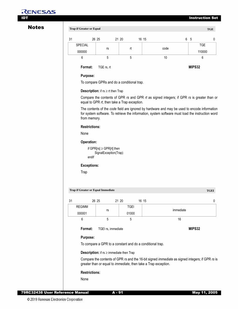
IDT Instruction Set
79RC32438 User Refer
Notes
TGEFormat: TGE rs, rt MIPS32
Purpose: To compare GPRs and do a conditional trap.
Description: if rs ≥ rt then Trap
Compare the contents of GPR rs and GPR rt as signed integers; if GPR rs is greater than orequal to GPR rt, then take a Trap exception.The contents of the code field are ignored by hardware and may be used to encode informationfor system software. To retrieve the information, system software must load the instruction wordfrom memory.
Restrictions: None
Operation:if GPR[rs] ≥ GPR[rt] then
SignalException(Trap) endif
Exceptions: Trap
TGEI
Format: TGEI rs, immediate MIPS32
Purpose: To compare a GPR to a constant and do a conditional trap.
Description: if rs ≥ immediate then Trap
Compare the contents of GPR rs and the 16-bit signed immediate as signed integers; if GPR rs isgreater than or equal to immediate, then take a Trap exception.
Restrictions: None
31 26 25 21 20 16 15 6 5 0SPECIAL
000000rs rt code
TGE
1100006 5 5 10 6
31 26 25 21 20 16 15 0REGIMM
000001rs
TGEI
01000immediate
6 5 5 16
Trap if Greater or Equal TGE
Trap if Greater or Equal Immediate TGEI
ence Manual A - 91 May 11, 2005
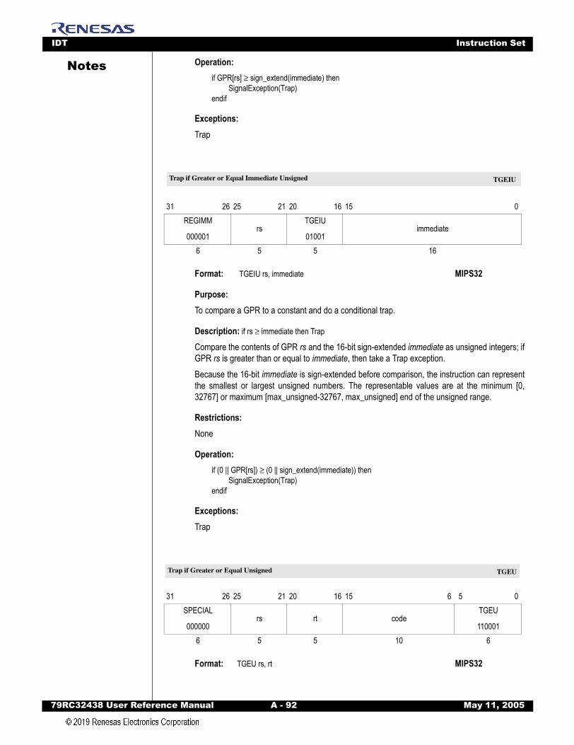
IDT Instruction Set
79RC32438 User Refer
Notes
Operation:if GPR[rs] ≥ sign_extend(immediate) thenSignalException(Trap) endif
Exceptions: Trap
TGEIU
Format: TGEIU rs, immediate MIPS32
Purpose: To compare a GPR to a constant and do a conditional trap.
Description: if rs ≥ immediate then Trap
Compare the contents of GPR rs and the 16-bit sign-extended immediate as unsigned integers; ifGPR rs is greater than or equal to immediate, then take a Trap exception.Because the 16-bit immediate is sign-extended before comparison, the instruction can representthe smallest or largest unsigned numbers. The representable values are at the minimum [0,32767] or maximum [max_unsigned-32767, max_unsigned] end of the unsigned range.
Restrictions: None
Operation:if (0 || GPR[rs]) ≥ (0 || sign_extend(immediate)) then
SignalException(Trap) endif
Exceptions: Trap
TGEU
Format: TGEU rs, rt MIPS32
31 26 25 21 20 16 15 0REGIMM
000001rs
TGEIU
01001immediate
6 5 5 16
31 26 25 21 20 16 15 6 5 0SPECIAL
000000rs rt code
TGEU
1100016 5 5 10 6
Trap if Greater or Equal Immediate Unsigned TGEIU
Trap if Greater or Equal Unsigned TGEU
ence Manual A - 92 May 11, 2005
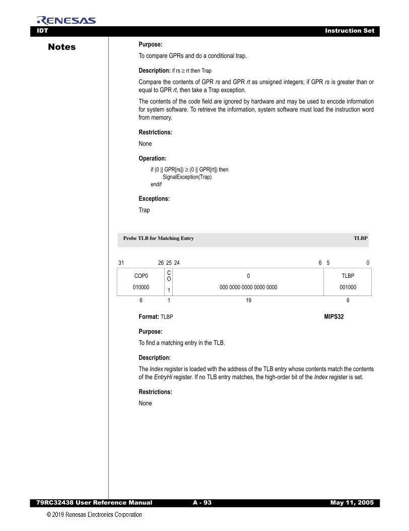
IDT Instruction Set
79RC32438 User Refer
Notes
Purpose: To compare GPRs and do a conditional trap.Description: if rs ≥ rt then Trap
Compare the contents of GPR rs and GPR rt as unsigned integers; if GPR rs is greater than orequal to GPR rt, then take a Trap exception.The contents of the code field are ignored by hardware and may be used to encode informationfor system software. To retrieve the information, system software must load the instruction wordfrom memory.
Restrictions: None
Operation:if (0 || GPR[rs]) ≥ (0 || GPR[rt]) then
SignalException(Trap) endif
Exceptions: Trap
TLBP
Format: TLBP MIPS32
Purpose:To find a matching entry in the TLB.
Description:The Index register is loaded with the address of the TLB entry whose contents match the contentsof the EntryHi register. If no TLB entry matches, the high-order bit of the Index register is set.
Restrictions:None
31 26 25 24 6 5 0
COP0
010000
CO
1
0
000 0000 0000 0000 0000
TLBP
001000
6 1 19 6
Probe TLB for Matching Entry TLBP
ence Manual A - 93 May 11, 2005
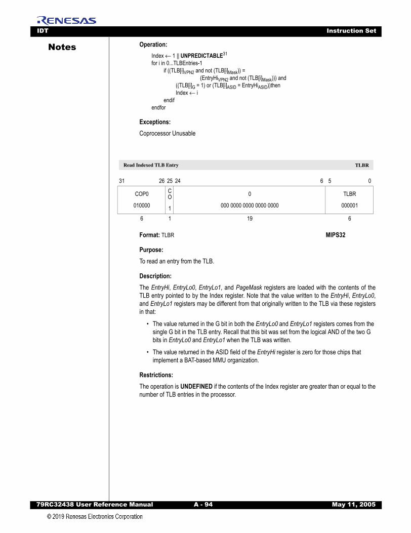
IDT Instruction Set
79RC32438 User Refer
Notes
Operation:Index ← 1 || UNPREDICTABLE31for i in 0...TLBEntries-1if ((TLB[i]VPN2 and not (TLB[i]Mask)) =
(EntryHiVPN2 and not (TLB[i]Mask))) and((TLB[i]G = 1) or (TLB[i]ASID = EntryHiASID))thenIndex ← i
endifendfor
Exceptions:Coprocessor Unusable
TLBR
Format: TLBR MIPS32
Purpose:To read an entry from the TLB.
Description:The EntryHi, EntryLo0, EntryLo1, and PageMask registers are loaded with the contents of theTLB entry pointed to by the Index register. Note that the value written to the EntryHi, EntryLo0,and EntryLo1 registers may be different from that originally written to the TLB via these registersin that:
• The value returned in the G bit in both the EntryLo0 and EntryLo1 registers comes from the single G bit in the TLB entry. Recall that this bit was set from the logical AND of the two G bits in EntryLo0 and EntryLo1 when the TLB was written.
• The value returned in the ASID field of the EntryHi register is zero for those chips that implement a BAT-based MMU organization.
Restrictions:The operation is UNDEFINED if the contents of the Index register are greater than or equal to thenumber of TLB entries in the processor.
31 26 25 24 6 5 0
COP0
010000
CO
1
0
000 0000 0000 0000 0000
TLBR
000001
6 1 19 6
Read Indexed TLB Entry TLBR
ence Manual A - 94 May 11, 2005

IDT Instruction Set
79RC32438 User Refer
Notes
Operation:i ← Indexif i > (TLBEntries - 1) thenUNDEFINEDendifPageMaskMask ← TLB[i]MaskEntryHi ←
TLB[i]VPN2 ||05 || TLB[i]ASID
EntryLo1 ← 02 ||TLB[i]PFN1 ||TLB[i]C1 || TLB[i]D1 || TLB[i]V1 || TLB[i]G
EntryLo0 ← 02 ||TLB[i]PFN0 ||TLB[i]C0 || TLB[i]D0 || TLB[i]V0 || TLB[i]G
Exceptions:Coprocessor Unusable
TLBWI
Format: TLBWI MIPS32
Purpose:To write a TLB entry indexed by the Index register.
Description:The TLB entry pointed to by the Index register is written from the contents of the EntryHi,EntryLo0, EntryLo1, and PageMask registers. The information written to the TLB entry may bedifferent from that in the EntryHi, EntryLo0, and EntryLo1 registers, in that:
• The single G bit in the TLB entry is set from the logical AND of the G bits in the EntryLo0 and EntryLo1 registers.
Restrictions:The operation is UNDEFINED if the contents of the Index register are greater than or equal to thenumber of TLB entries in the processor.
31 26 25 24 6 5 0
COP0
010000
CO
1
0
000 0000 0000 0000 0000
TLBWI
000010
6 1 19 6
Write Indexed TLB Entry TLBWI
ence Manual A - 95 May 11, 2005
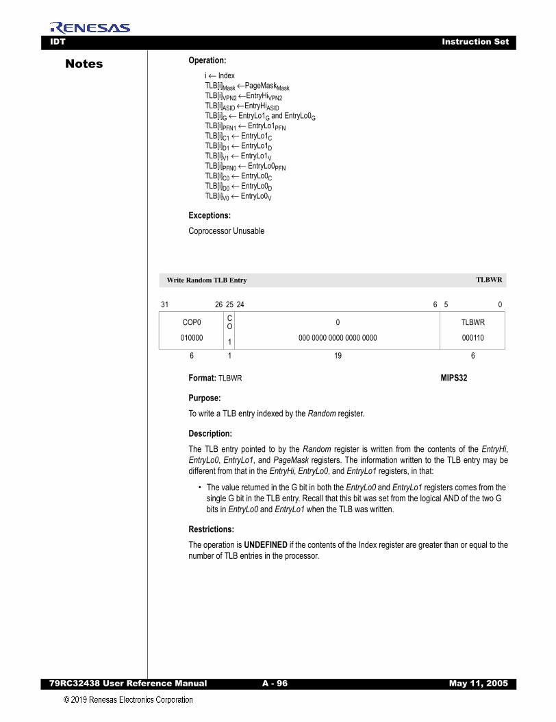
IDT Instruction Set
79RC32438 User Refer
Notes
Operation:i ← IndexTLB[i]Mask ←PageMaskMaskTLB[i]VPN2 ←EntryHiVPN2 TLB[i]ASID ←EntryHiASIDTLB[i]G ← EntryLo1G and EntryLo0GTLB[i]PFN1 ← EntryLo1PFN TLB[i]C1 ← EntryLo1CTLB[i]D1 ← EntryLo1DTLB[i]V1 ← EntryLo1VTLB[i]PFN0 ← EntryLo0PFN TLB[i]C0 ← EntryLo0CTLB[i]D0 ← EntryLo0DTLB[i]V0 ← EntryLo0VExceptions:Coprocessor Unusable
TLBWR
Format: TLBWR MIPS32
Purpose:To write a TLB entry indexed by the Random register.
Description:The TLB entry pointed to by the Random register is written from the contents of the EntryHi,EntryLo0, EntryLo1, and PageMask registers. The information written to the TLB entry may bedifferent from that in the EntryHi, EntryLo0, and EntryLo1 registers, in that:
• The value returned in the G bit in both the EntryLo0 and EntryLo1 registers comes from the single G bit in the TLB entry. Recall that this bit was set from the logical AND of the two G bits in EntryLo0 and EntryLo1 when the TLB was written.
Restrictions:The operation is UNDEFINED if the contents of the Index register are greater than or equal to thenumber of TLB entries in the processor.
31 26 25 24 6 5 0
COP0
010000
CO
1
0
000 0000 0000 0000 0000
TLBWR
000110
6 1 19 6
Write Random TLB Entry TLBWR
ence Manual A - 96 May 11, 2005
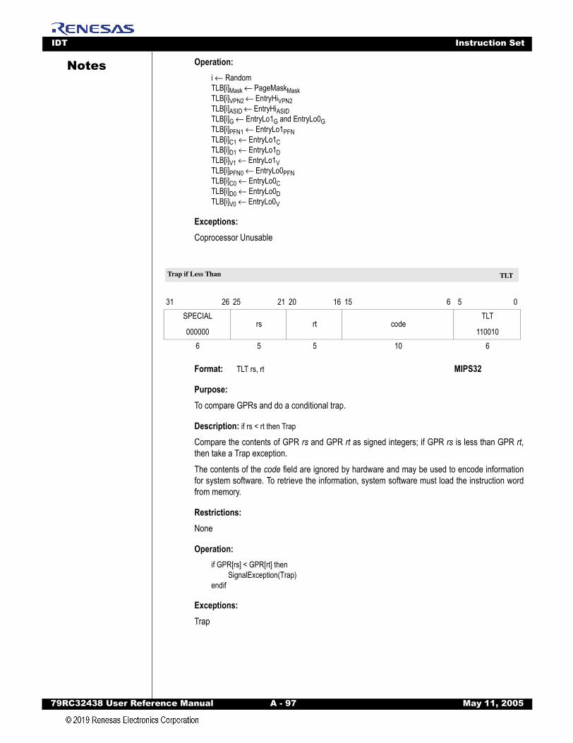
IDT Instruction Set
79RC32438 User Refer
Notes
Operation:i ← RandomTLB[i]Mask ← PageMaskMaskTLB[i]VPN2 ← EntryHiVPN2 TLB[i]ASID ← EntryHiASIDTLB[i]G ← EntryLo1G and EntryLo0GTLB[i]PFN1 ← EntryLo1PFN TLB[i]C1 ← EntryLo1CTLB[i]D1 ← EntryLo1DTLB[i]V1 ← EntryLo1VTLB[i]PFN0 ← EntryLo0PFN TLB[i]C0 ← EntryLo0CTLB[i]D0 ← EntryLo0DTLB[i]V0 ← EntryLo0VExceptions:Coprocessor Unusable
TLT
Format: TLT rs, rt MIPS32
Purpose: To compare GPRs and do a conditional trap.
Description: if rs < rt then Trap
Compare the contents of GPR rs and GPR rt as signed integers; if GPR rs is less than GPR rt,then take a Trap exception.The contents of the code field are ignored by hardware and may be used to encode informationfor system software. To retrieve the information, system software must load the instruction wordfrom memory.
Restrictions: None
Operation:if GPR[rs] < GPR[rt] then
SignalException(Trap) endif
Exceptions: Trap
31 26 25 21 20 16 15 6 5 0SPECIAL
000000rs rt code
TLT
1100106 5 5 10 6
Trap if Less Than TLT
ence Manual A - 97 May 11, 2005
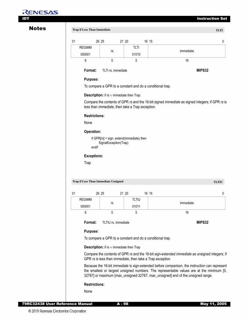
IDT Instruction Set
79RC32438 User Refer
Notes
TLTIFormat: TLTI rs, immediate MIPS32
Purpose: To compare a GPR to a constant and do a conditional trap.
Description: if rs < immediate then Trap
Compare the contents of GPR rs and the 16-bit signed immediate as signed integers; if GPR rs isless than immediate, then take a Trap exception.
Restrictions: None
Operation:if GPR[rs] < sign_extend(immediate) then
SignalException(Trap) endif
Exceptions: Trap
TLTIU
Format: TLTIU rs, immediate MIPS32
Purpose: To compare a GPR to a constant and do a conditional trap.
Description: if rs < immediate then Trap
Compare the contents of GPR rs and the 16-bit sign-extended immediate as unsigned integers; ifGPR rs is less than immediate, then take a Trap exception.Because the 16-bit immediate is sign-extended before comparison, the instruction can representthe smallest or largest unsigned numbers. The representable values are at the minimum [0,32767] or maximum [max_unsigned-32767, max_unsigned] end of the unsigned range.
Restrictions: None
31 26 25 21 20 16 15 0REGIMM
000001rs
TLTI
01010immediate
6 5 5 16
31 26 25 21 20 16 15 0REGIMM
000001rs
TLTIU
01011immediate
6 5 5 16
Trap if Less Than Immediate TLTI
Trap if Less Than Immediate Unsigned TLTIU
ence Manual A - 98 May 11, 2005
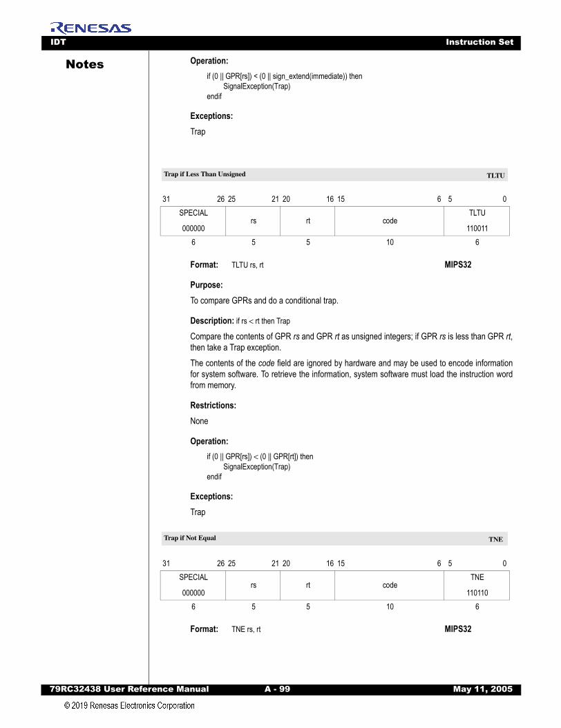
IDT Instruction Set
79RC32438 User Refer
Notes
Operation:if (0 || GPR[rs]) < (0 || sign_extend(immediate)) thenSignalException(Trap) endif
Exceptions: Trap
TLTU
Format: TLTU rs, rt MIPS32
Purpose: To compare GPRs and do a conditional trap.
Description: if rs < rt then Trap
Compare the contents of GPR rs and GPR rt as unsigned integers; if GPR rs is less than GPR rt,then take a Trap exception.The contents of the code field are ignored by hardware and may be used to encode informationfor system software. To retrieve the information, system software must load the instruction wordfrom memory.
Restrictions: None
Operation:if (0 || GPR[rs]) < (0 || GPR[rt]) then
SignalException(Trap) endif
Exceptions: Trap
TNE
Format: TNE rs, rt MIPS32
31 26 25 21 20 16 15 6 5 0SPECIAL
000000rs rt code
TLTU
1100116 5 5 10 6
31 26 25 21 20 16 15 6 5 0SPECIAL
000000rs rt code
TNE
1101106 5 5 10 6
Trap if Less Than Unsigned TLTU
Trap if Not Equal TNE
ence Manual A - 99 May 11, 2005
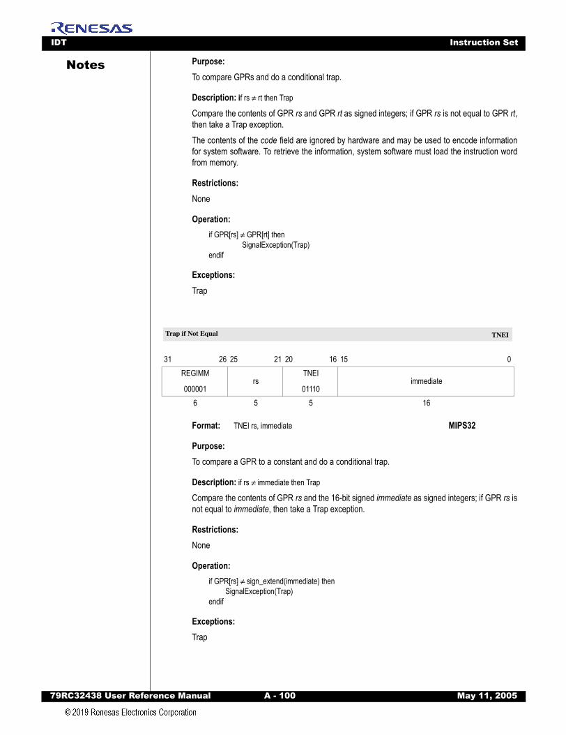
IDT Instruction Set
79RC32438 User Refer
Notes
Purpose: To compare GPRs and do a conditional trap.Description: if rs ≠ rt then Trap
Compare the contents of GPR rs and GPR rt as signed integers; if GPR rs is not equal to GPR rt,then take a Trap exception.The contents of the code field are ignored by hardware and may be used to encode informationfor system software. To retrieve the information, system software must load the instruction wordfrom memory.
Restrictions: None
Operation:if GPR[rs] ≠ GPR[rt] then
SignalException(Trap) endif
Exceptions: Trap
TNEI
Format: TNEI rs, immediate MIPS32
Purpose: To compare a GPR to a constant and do a conditional trap.
Description: if rs ≠ immediate then Trap
Compare the contents of GPR rs and the 16-bit signed immediate as signed integers; if GPR rs isnot equal to immediate, then take a Trap exception.
Restrictions: None
Operation:if GPR[rs] ≠ sign_extend(immediate) then
SignalException(Trap) endif
Exceptions: Trap
31 26 25 21 20 16 15 0REGIMM
000001rs
TNEI
01110immediate
6 5 5 16
Trap if Not Equal TNEI
ence Manual A - 100 May 11, 2005
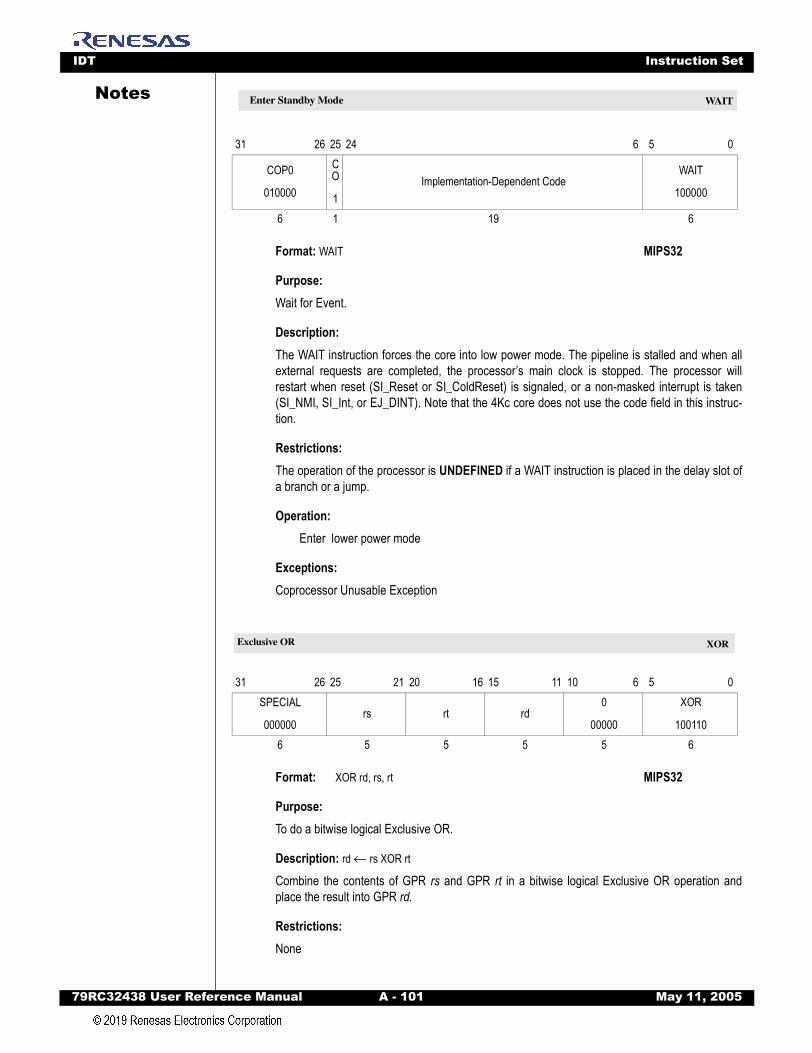
IDT Instruction Set
79RC32438 User Refer
Notes
WAITFormat: WAIT MIPS32
Purpose:Wait for Event.
Description:The WAIT instruction forces the core into low power mode. The pipeline is stalled and when allexternal requests are completed, the processor’s main clock is stopped. The processor willrestart when reset (SI_Reset or SI_ColdReset) is signaled, or a non-masked interrupt is taken(SI_NMI, SI_Int, or EJ_DINT). Note that the 4Kc core does not use the code field in this instruc-tion.
Restrictions:The operation of the processor is UNDEFINED if a WAIT instruction is placed in the delay slot ofa branch or a jump.
Operation:Enter lower power mode
Exceptions:Coprocessor Unusable Exception
XOR
Format: XOR rd, rs, rt MIPS32
Purpose: To do a bitwise logical Exclusive OR.
Description: rd ← rs XOR rt
Combine the contents of GPR rs and GPR rt in a bitwise logical Exclusive OR operation andplace the result into GPR rd.
Restrictions: None
31 26 25 24 6 5 0
COP0
010000
CO
1Implementation-Dependent Code
WAIT
100000
6 1 19 6
31 26 25 21 20 16 15 11 10 6 5 0SPECIAL
000000rs rt rd
0
00000
XOR
1001106 5 5 5 5 6
Enter Standby Mode WAIT
Exclusive OR XOR
ence Manual A - 101 May 11, 2005
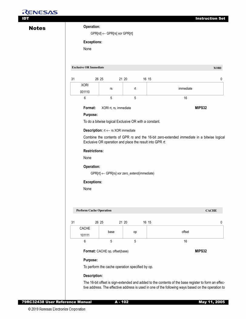
IDT Instruction Set
79RC32438 User Refer
Notes
Operation:GPR[rd] ← GPR[rs] xor GPR[rt]Exceptions: None
XORI
Format: XORI rt, rs, immediate MIPS32Purpose: To do a bitwise logical Exclusive OR with a constant.
Description: rt ← rs XOR immediate
Combine the contents of GPR rs and the 16-bit zero-extended immediate in a bitwise logicalExclusive OR operation and place the result into GPR rt.
Restrictions:None
Operation:GPR[rt] ← GPR[rs] xor zero_extend(immediate)
Exceptions: None
CACHE
Format: CACHE op, offset(base) MIPS32
Purpose: To perform the cache operation specified by op.
Description:The 16-bit offset is sign-extended and added to the contents of the base register to form an effec-tive address. The effective address is used in one of the following ways based on the operation to
31 26 25 21 20 16 15 0XORI
001110rs rt immediate
6 5 5 16
31 26 25 21 20 16 15 0CACHE
101111base op offset
6 5 5 16
Exclusive OR Immediate XORI
Perform Cache Operation CACHE
ence Manual A - 102 May 11, 2005
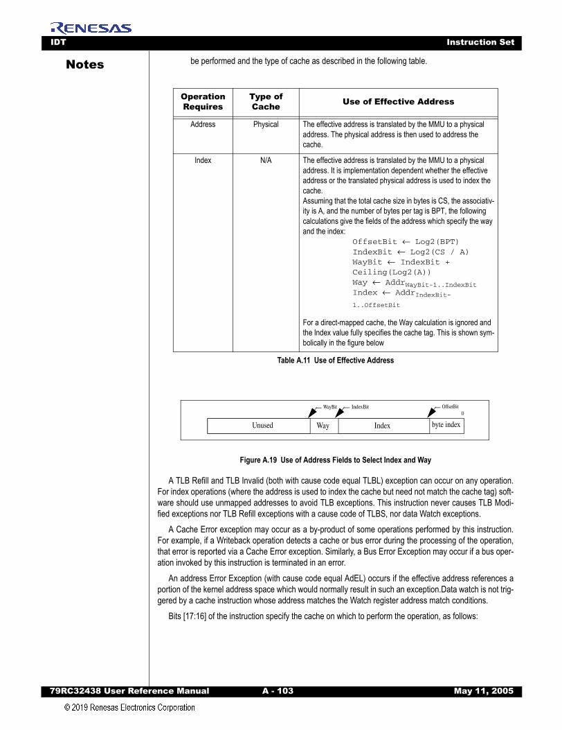
IDT Instruction Set
79RC32438 User Refer
Notes
be performed and the type of cache as described in the following table.Figure A.19 Use of Address Fields to Select Index and Way
A TLB Refill and TLB Invalid (both with cause code equal TLBL) exception can occur on any operation.For index operations (where the address is used to index the cache but need not match the cache tag) soft-ware should use unmapped addresses to avoid TLB exceptions. This instruction never causes TLB Modi-fied exceptions nor TLB Refill exceptions with a cause code of TLBS, nor data Watch exceptions.
A Cache Error exception may occur as a by-product of some operations performed by this instruction.For example, if a Writeback operation detects a cache or bus error during the processing of the operation,that error is reported via a Cache Error exception. Similarly, a Bus Error Exception may occur if a bus oper-ation invoked by this instruction is terminated in an error.
An address Error Exception (with cause code equal AdEL) occurs if the effective address references aportion of the kernel address space which would normally result in such an exception.Data watch is not trig-gered by a cache instruction whose address matches the Watch register address match conditions.
Bits [17:16] of the instruction specify the cache on which to perform the operation, as follows:
Operation Requires
Type of Cache Use of Effective Address
Address Physical The effective address is translated by the MMU to a physical address. The physical address is then used to address the cache.
Index N/A The effective address is translated by the MMU to a physical address. It is implementation dependent whether the effective address or the translated physical address is used to index the cache.Assuming that the total cache size in bytes is CS, the associativ-ity is A, and the number of bytes per tag is BPT, the following calculations give the fields of the address which specify the way and the index:
OffsetBit ← Log2(BPT)IndexBit ← Log2(CS / A)WayBit ← IndexBit + Ceiling(Log2(A))Way ← AddrWayBit-1..IndexBitIndex ← AddrIndexBit-1..OffsetBit
For a direct-mapped cache, the Way calculation is ignored and the Index value fully specifies the cache tag. This is shown sym-bolically in the figure below
Table A.11 Use of Effective Address
Way
0
Index
OffsetBitIndexBitWayBit
Unused byte index
ence Manual A - 103 May 11, 2005
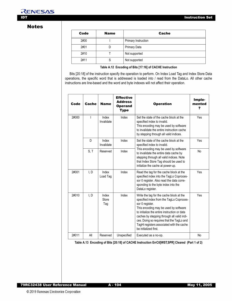
IDT Instruction Set
79RC32438 User Refer
Notes
Bits [20:18] of the instruction specify the operation to perform. On Index Load Tag and Index Store Dataoperations, the specific word that is addressed is loaded into / read from the DataLo. All other cacheinstructions are line-based and the word and byte indexes will not affect their operation.
Code Name Cache
2#00 I Primary Instruction
2#01 D Primary Data
2#10 T Not supported
2#11 S Not supported
Table A.12 Encoding of Bits [17:16] of CACHE Instruction
Code Cache Name
Effective Address Operand
Type
OperationImple-
mented?
2#000 I Index Invalidate
Index Set the state of the cache block at the specified index to invalid.This encoding may be used by software to invalidate the entire instruction cache by stepping through all valid indices.
Yes
D Index Invalidate
Index Set the state of the cache block at the specified index to invalid.This encoding may be used by software to invalidate the entire data cache by stepping through all valid indices. Note that Index Store Tag should be used to initialize the cache at power-up.
Yes
S, T Reserved Index No
2#001 I, D Index Load Tag
Index Read the tag for the cache block at the specified index into the TagLo Coproces-sor 0 register. Also read the data corre-sponding to the byte index into the DataLo register.
Yes
2#010 I, D Index Store Tag
Index Write the tag for the cache block at the specified index from the TagLo Coproces-sor 0 register.This encoding may be used by software to initialize the entire instruction or data caches by stepping through all valid indi-ces. Doing so requires that the TagLo and TagHi registers associated with the cache be initialized first.
Yes
2#011 All Reserved Unspecified Executed as a no-op. No
Table A.13 Encoding of Bits [20:18] of CACHE Instruction ErrCtl[WST,SPR] Cleared (Part 1 of 2)
ence Manual A - 104 May 11, 2005
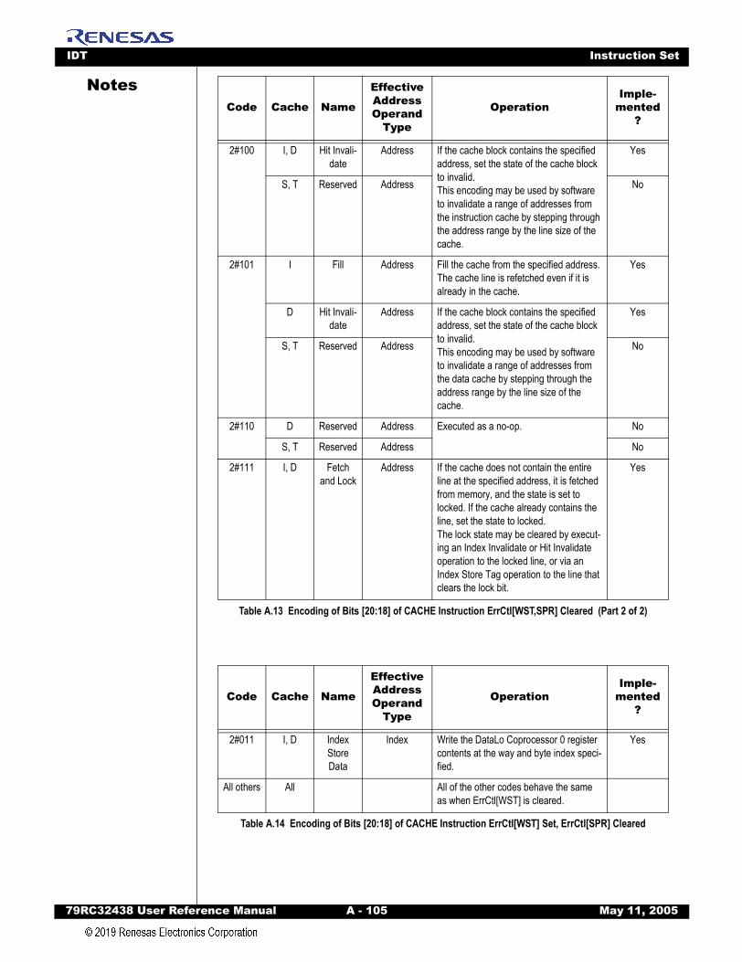
IDT Instruction Set
79RC32438 User Refer
Notes
2#100 I, D Hit Invali-date
Address If the cache block contains the specified address, set the state of the cache block to invalid.This encoding may be used by software to invalidate a range of addresses from the instruction cache by stepping through the address range by the line size of the cache.
Yes
S, T Reserved Address No
2#101 I Fill Address Fill the cache from the specified address.The cache line is refetched even if it is already in the cache.
Yes
D Hit Invali-date
Address If the cache block contains the specified address, set the state of the cache block to invalid.This encoding may be used by software to invalidate a range of addresses from the data cache by stepping through the address range by the line size of the cache.
Yes
S, T Reserved Address No
2#110 D Reserved Address Executed as a no-op. No
S, T Reserved Address No
2#111 I, D Fetch and Lock
Address If the cache does not contain the entire line at the specified address, it is fetched from memory, and the state is set to locked. If the cache already contains the line, set the state to locked.The lock state may be cleared by execut-ing an Index Invalidate or Hit Invalidate operation to the locked line, or via an Index Store Tag operation to the line that clears the lock bit.
Yes
Code Cache Name
Effective Address Operand
Type
OperationImple-
mented?
2#011 I, D Index Store Data
Index Write the DataLo Coprocessor 0 register contents at the way and byte index speci-fied.
Yes
All others All All of the other codes behave the same as when ErrCtl[WST] is cleared.
Table A.14 Encoding of Bits [20:18] of CACHE Instruction ErrCtl[WST] Set, ErrCtl[SPR] Cleared
Code Cache Name
Effective Address Operand
Type
OperationImple-
mented?
Table A.13 Encoding of Bits [20:18] of CACHE Instruction ErrCtl[WST,SPR] Cleared (Part 2 of 2)
ence Manual A - 105 May 11, 2005

IDT Instruction Set
79RC32438 User Refer
Notes
Restrictions:The operation of this instruction is UNDEFINED for any operation/cache combination that is notimplemented.The operation of this instruction is UNDEFINED if the operation requires an address, and thataddress is uncacheable.
Operation:vAddr ← GPR[base] + sign_extend(offset)(pAddr, uncached) ← AddressTranslation(vAddr, DataReadReference)CacheOp(op, vAddr, pAddr)
Exceptions:TLB Refill Exception.TLB Invalid ExceptionCoprocessor Unusable ExceptionAddress Error ExceptionBus Error Exception
Code Cache Name
Effective Address Operand
Type
OperationImple-
mented?
2#001 I, D Index Load Tag
Index Read the SPRAM tag at the specified index into the TagLo Coprocessor 0 regis-ter.
Yes
2#010 I, D Index Store Tag
Index Update the SPRAM tag at the specified index from the TagLo Coprocessor 0 reg-ister.
Yes
2#011 I, D Index Store Data
Index Write the DataLo Coprocessor 0 register contents into the SPRAM at the word index specified.
Yes
All others All All of the other codes behave the same as when ErrCtl[SPR] is cleared
Table A.15 Encoding of Bits [20:18] of CACHE Instruction ErrCtl[SPR] Set
ence Manual A - 106 May 11, 2005
Index
Aactive-high .................................................................................... iiactive-low...................................................................................... iiaddress
recognition logic ...............................................................11-7space monitor ................................................................... 4-4
Bboot configuration vector .......................................................... 3-4bus arbitration algorithm ........................................................... 5-3BYPASS instruction ................................................................ 19-8byte ordering..............................................................................1-iiCclock prescalar.......................................................................11-30cold reset .................................................................................. 3-3control frames ........................................................................11-18conventions
big endian, little endian ......................................................... iibytes ..................................................................................... iicompressed notation............................................................. iidefining buses....................................................................... iimost and least significant bits ............................................... ii
Counter TimerCompare Register........................................................... 14-2Control Register .............................................................. 14-1Count Register ................................................................ 14-2
counter timers, general purpose ............................................. 14-1CPU pipeline clock.................................................................... 3-2Ddata flow within RC32438 ......................................................... 9-3DDR
address mapping .............................................................7-11address multiplexing scheme............................................ 7-3clocks ................................................................................ 7-3data bus multiplexing ...................................................... 7-14initialization ..................................................................... 7-16refresh timer.................................................................... 7-18
DMA ControllerControl Register5-10, 5-11, 5-12, 10-4, 10-7, 10-10, 10-22, 10-
23, 10-24, 10-26, 10-27, 10-28, 10-29, 10-39, 10-41, 10-42, 10-43, 10-44, 10-45, 10-47, 10-49, 10-51, 10-52, 10-53, 10-54, 10-55, 10-56, 10-57, 10-58, 10-60, ........... 10-61, 16-4, 16-6, 16-8, 16-9, 16-10, 18-14
DMA interface ........................................................................11-12DMA operations
external ........................................................................... 9-16internal .............................................................................. 9-7memory to memory ......................................................... 9-19
79RC32438 User Reference Manual I - 1
EEthernet
padding operation.......................................................... 11-26register description .......................................................... 11-2
Ethernet interface.................................................................... 11-1address recognition logic................................................. 11-7clock prescalar .............................................................. 11-30DMA Controller....................................................... 11-2, 11-7DMA interface................................................................ 11-12input and output FIFOs.................................................... 11-2input DMA operations.................................................... 11-12MAC (Medium Access Controller) ............. 11-2, 11-18, 11-22management clock ........................................................ 11-34MII management interface and registers....................... 11-30PAUSE control frames................................................... 11-18PHY...................................................................... 11-1, 11-30
ethernet management clock.................................................. 11-34EXTCLK - external clock ......................................................... 6-11GGPIO Controller.......................................................................12-1GPIO pins............................................................. 12-1, 13-1–13-2Hhalfword......................................................................................... iII2C bus interface
clock prescalar .......................................................15-1, 15-4clock prescalar (I2CCP) register .....................................15-4commands............................................................15-3, 15-11control (I2CC) register .....................................................15-2loop-back operations .......................................................15-2master command (I2CMCMD) register ...........................15-5master interface...............................................................15-5master status (I2CMS) register .......................................15-5master status mask (I2CMSM) register................15-5, 15-11prescalar clock .......................................................15-2, 15-4SCLP and SDAP signals .................................................15-6slave acknowledge (I2CSACK) register ........................15-18slave status (I2CSS) register.........................................15-14speed of the master.........................................................15-6
IEEE 1149.1 (JTAG) ................................................................19-2IEEE 802 ..................................... 11-1, 11-14, 11-18, 11-24, 11-28internal buses............................................................................5-1Internal Register Map..............................................................1-21Interrupt Controller
interrupt sources to the IPEND registers....................8-4–8-5IPBus arbiter .............................................................................5-3IPBus arbitration
fair .....................................................................................5-6priority................................................................................5-6
May 11, 2005
IDT Index
IPBus clock ............................................................................... 3-2JJTAG Instruction Register ....................................................... 19-6LLogic Diagram........................................................................... 1-7MMAC (Medium Access Controller) .....................11-2, 11-18, 11-22master clock See CLKP.Memory Map........................................................................... 1-20MII management interface and registers ...............................11-30most significant bit ........................................................................ iiPPAUSE control frames ...........................................................11-18PCI
configuration registers................................................... 10-46endianness.................................................................... 10-18master error handling.................................................... 10-21reset .............................................................................. 10-13swapping....................................................................... 10-18target error handling...................................................... 10-38
PHY .......................................................................................11-30Pin Characteristics.................................................................... 1-8Pin Description.........................................................................1-11pin descriptions......................................................................... 1-7PMBus arbitration ................................................................... 5-12prescalar clock............................................................... 15-2, 15-4pseudocode
SignalException ..............................................................A-10SyncOperation ................................................................A-10
RRegister Map .......................................................................... 1-21registers
Boundary-Scan Register................................................. 19-3Bypass Register.............................................................. 19-3Counter Timer Compare Register................................... 14-2Counter Timer Control Register ...................................... 14-1Counter Timer Count Register ........................................ 14-2Device Identification Register ......................................... 19-3DMA Control Register5-10, 5-11, 5-12, 10-4, 10-7, 10-10, 10-
22, 10-23, 10-24, 10-26, 10-27, 10-28, 10-29, 10-39, 10-41, 10-42, 10-43, 10-44, 10-45, 10-47, 10-49, 10-51, 10-52, 10-53, 10-54, 10-55, 10-56, 10-57, 10-58, 10-60, 10-61, 16-4, 16-6, 16-8, 16-9, 16-10, 18-14
Instruction Register ......................................................... 19-6MII management registers .............................................11-30Test Data Register .......................................................... 19-3UART Reset Register ..................................................... 13-4Watchdog Timer Compare Register (WTCOMPARE)....... 4-5Watchdog Timer Control Register (WTC) ......................... 4-5Watchdog Timer Count Register (WTCOUNT) ................. 4-5
ReverseEndian symbol.............................................................A-7Ssignal assertion............................................................................. iisignal negation.............................................................................. ii
79RC32438 User Reference Manual I - 2
signal terminology ........................................................................iiiSignalException pseudocode................................................. A-10symbol
ReverseEndian................................................................. A-7SyncOperation pseudocode................................................... A-10SYSID register ..........................................................................1-5system clock.......................................................................3-6, 3-8system identification..................................................................1-5TTest.............................. 1-1, 2-1, 3-1, 4-1, 5-1, 7-1, 9-1, 12-1, 19-1triple-byte ..................................................................................... iiUUART.......................................................................................13-1
baud rate generator................................................13-1–13-2configuring.......................................................................13-2interrupts .........................................................................13-4pins..................................................................................13-1registers...........................................................................13-2status...............................................................................13-1switching between 16550 and 16450 modes ..................13-4
undecoded address error ..........................................................4-4Wwarm reset ................................................................................3-6Watchdog Timer
Compare Register (WTCOMPARE) ..................................4-5Control Register (WTC).....................................................4-5Count Register (WTCOUNT).............................................4-5
May 11, 2005
Corporate HeadquartersTOYOSU FORESIA, 3-2-24 Toyosu,Koto-ku, Tokyo 135-0061, Japanwww.renesas.com
Contact InformationFor further information on a product, technology, the most up-to-date version of a document, or your nearest sales office, please visit:www.renesas.com/contact/
TrademarksRenesas and the Renesas logo are trademarks of Renesas Electronics Corporation. All trademarks and registered trademarks are the property of their respective owners.
IMPORTANT NOTICE AND DISCLAIMER
RENESAS ELECTRONICS CORPORATION AND ITS SUBSIDIARIES (“RENESAS”) PROVIDES TECHNICAL SPECIFICATIONS AND RELIABILITY DATA (INCLUDING DATASHEETS), DESIGN RESOURCES (INCLUDING REFERENCE DESIGNS), APPLICATION OR OTHER DESIGN ADVICE, WEB TOOLS, SAFETY INFORMATION, AND OTHER RESOURCES “AS IS” AND WITH ALL FAULTS, AND DISCLAIMS ALL WARRANTIES, EXPRESS OR IMPLIED, INCLUDING, WITHOUT LIMITATION, ANY IMPLIED WARRANTIES OF MERCHANTABILITY, FITNESS FOR A PARTICULAR PURPOSE, OR NON-INFRINGEMENT OF THIRD PARTY INTELLECTUAL PROPERTY RIGHTS.
These resources are intended for developers skilled in the art designing with Renesas products. You are solely responsible for (1) selecting the appropriate products for your application, (2) designing, validating, and testing your application, and (3) ensuring your application meets applicable standards, and any other safety, security, or other requirements. These resources are subject to change without notice. Renesas grants you permission to use these resources only for development of an application that uses Renesas products. Other reproduction or use of these resources is strictly prohibited. No license is granted to any other Renesas intellectual property or to any third party intellectual property. Renesas disclaims responsibility for, and you will fully indemnify Renesas and its representatives against, any claims, damages, costs, losses, or liabilities arising out of your use of these resources. Renesas' products are provided only subject to Renesas' Terms and Conditions of Sale or other applicable terms agreed to in writing. No use of any Renesas resources expands or otherwise alters any applicable warranties or warranty disclaimers for these products.
(Rev.1.0 Mar 2020)
© 2020 Renesas Electronics Corporation. All rights reserved.
Related Documents


