© Copyright 2011 WIZnet Co., Inc. All rights reserved. Ver. 1.12 1 Internet Embedded MCU W7100A Datasheet Internet Embedded MCU W7100A Datasheet Version 1.12 © 2011 WIZnet Co., Inc. All Rights Reserved. For more information, visit our website at Uhttp://www.wiznet.co.krU

Internet_Embedded_MCU_W7100A_Datasheet_v1.12_en.pdf
Dec 15, 2015
Welcome message from author
This document is posted to help you gain knowledge. Please leave a comment to let me know what you think about it! Share it to your friends and learn new things together.
Transcript
© Copyright 2011 WIZnet Co., Inc. All rights reserved. Ver. 1.12 1
Intern
et Em
bed
ded
MC
U W
7100A D
atasheet
Internet Embedded MCU W7100A Datasheet
Version 1.12
© 2011 WIZnet Co., Inc. All Rights Reserved.
For more information, visit our website at Uhttp://www.wiznet.co.krU

© Copyright 2011 WIZnet Co., Inc. All rights reserved. Ver. 1.12 2
Intern
et Em
bed
ded
MC
U W
7100A D
atasheet
Table of Contents
1 Overview ..................................................................................... 11
1.1 Introduction .................................................................................. 11
1.2 W7100A Features ............................................................................ 11
1.3 W7100A Block Diagram & Features ....................................................... 12
1.3.1 ALU (Arithmetic Logic Unit) ....................................................... 12
1.3.2 TCPIPCore ............................................................................ 14
1.4 Pin Description .............................................................................. 16
1.4.1 Pin Layout ............................................................................ 16
1.4.2 Pin Description ....................................................................... 17
1.4.2.1 Configuration ................................................................... 18
1.4.2.2 Timer ............................................................................ 19
1.4.2.3 UART ............................................................................. 19
1.4.2.4 DoCD™ Compatible Debugger ................................................ 19
1.4.2.5 Interrupt / Clock .............................................................. 19
1.4.2.6 GPIO ............................................................................. 20
1.4.2.7 Media Interface ................................................................ 21
1.4.2.8 Network Indicator LED ........................................................ 22
1.4.2.9 Power Supply Signal ........................................................... 22
1.5 64pin package description ................................................................. 24
1.5.1 Difference between 100 and 64pin package .................................... 24
2 Memory ....................................................................................... 26
2.1 Code Memory ................................................................................ 26
2.1.1 Code Memory Wait States .......................................................... 28
2.2 Data Memory ................................................................................. 29
2.2.1 Data Memory Wait States .......................................................... 29
2.3 External Data Memory Access ............................................................. 29
2.3.1 Standard 8051 Interface ............................................................ 30
2.3.2 Direct Interface ...................................................................... 31
2.4 Internal Data Memory and SFR ............................................................ 32
2.5 SFR definition ................................................................................ 33
2.5.1 Program Code Memory Write Enable Bit ......................................... 33
2.5.2 Program Code Memory Wait States Register .................................... 33
2.5.3 Data Pointer Extended Registers .................................................. 35
2.5.4 Data Pointer Registers .............................................................. 35
2.5.5 Clock Control Register .............................................................. 36
2.5.6 Internal Memory Wait States Register ............................................ 37

© Copyright 2011 WIZnet Co., Inc. All rights reserved. Ver. 1.12 3
Intern
et Em
bed
ded
MC
U W
7100A D
atasheet
2.5.7 Address Latch Enable Register .................................................... 38
2.5.8 External Memory Wait States Register ........................................... 38
2.5.9 Stack Pointer ......................................................................... 39
2.5.10 New & Extended SFR ................................................................ 39
2.5.11 Peripheral Registers ................................................................. 41
3 Interrupt ...................................................................................... 43
4 I/O Ports ...................................................................................... 47
5 Timers ......................................................................................... 50
5.1 Timers 0, 1 ................................................................................... 50
5.1.1 Overview .............................................................................. 50
5.1.2 Interrupts ............................................................................. 51
5.1.3 Timer0 – Mode0 ...................................................................... 52
5.1.4 Timer0 – Mode1 ...................................................................... 53
5.1.5 Timer0 – Mode2 ...................................................................... 53
5.1.6 Timer0 – Mode3 ...................................................................... 54
5.1.7 Timer1 – Mode0 ...................................................................... 55
5.1.8 Timer1 – Mode1 ...................................................................... 55
5.1.9 Timer1 – Mode2 ...................................................................... 56
5.1.10 Timer1 – Mode3 ...................................................................... 56
5.2 Timer2 ........................................................................................ 57
5.2.1 Overview .............................................................................. 57
5.2.2 Interrupts ............................................................................. 58
6 UART .......................................................................................... 61
6.1 Interrupts ..................................................................................... 62
6.2 Mode0, Synchronous ........................................................................ 63
6.3 Mode1, 8-Bit UART, Variable Baud Rate, Timer 1 or 2 Clock Source ................ 64
6.4 Mode2, 9-Bit UART, Fixed Baud Rate ..................................................... 64
6.5 Mode3, 9-Bit UART, Variable Baud Rate, Timer1 or 2 Clock Source ................. 65
6.6 Examples of Baud Rate Setting ........................................................... 65
7 Watchdog Timer ............................................................................. 66
7.1 Overview ..................................................................................... 66
7.2 Interrupts ..................................................................................... 66
7.3 Watchdog Timer Reset ...................................................................... 67
7.4 Simple Timer ................................................................................. 68
7.5 System Monitor .............................................................................. 68
7.6 Watchdog Related Registers ............................................................... 68
7.7 Watchdog Control ........................................................................... 69
7.7.1 Clock Control ......................................................................... 70

© Copyright 2011 WIZnet Co., Inc. All rights reserved. Ver. 1.12 4
Intern
et Em
bed
ded
MC
U W
7100A D
atasheet
7.8 Timed Access Registers ..................................................................... 70
8 TCPIPCore .................................................................................... 71
8.1 Memory Map ................................................................................. 71
8.2 Registers list ................................................................................. 71
8.2.1 Common Registers ................................................................... 71
8.2.2 SOCKET Registers .................................................................... 73
8.3 Register Description ........................................................................ 84
8.3.1 Mode Register ........................................................................ 84
8.3.2 SOCKET Registers .................................................................... 90
9 Functional Description ................................................................... 108
9.1 Initialization ............................................................................... 108
9.2 Data Communication ..................................................................... 113
9.2.1 TCP .................................................................................. 113
9.2.1.1 TCP SERVER ................................................................... 114
9.2.1.2 TCP CLIENT ................................................................... 121
9.2.2 UDP .................................................................................. 122
9.2.2.1 Unicast & Broadcast ......................................................... 122
9.2.2.2 Multicast ...................................................................... 127
9.2.3 IPRAW ............................................................................... 130
9.2.4 MACRAW ............................................................................. 132
10 Electrical Specification .................................................................. 139
10.1 Absolute Maximum Ratings .............................................................. 139
10.2 DC Characteristics ........................................................................ 139
10.3 Power consumption(Driving voltage 3.3V) ............................................ 139
10.4 AC Characteristics ........................................................................ 140
10.5 Crystal Characteristics ................................................................... 140
10.6 Transformer Characteristics ............................................................. 141
11 IR Reflow Temperature Profile (Lead-Free) ........................................... 142
12 Package Descriptions ..................................................................... 143
12.1 Package type: LQFP 100 .................................................................. 143
12.2 Package type: QFN 64 .................................................................... 145
13 Appendix:Performance Improvement about W7100A ................................ 147
13.1 Summary .................................................................................... 147
13.2 8–Bit Arithmetic Functions ............................................................... 147
13.2.1 Addition ............................................................................. 147
13.2.2 Subtraction ......................................................................... 149
13.2.3 Multiplication ...................................................................... 150
13.2.4 Division .............................................................................. 150
© Copyright 2011 WIZnet Co., Inc. All rights reserved. Ver. 1.12 5
Intern
et Em
bed
ded
MC
U W
7100A D
atasheet
13.3 16-Bit Arithmetic Functions ............................................................. 150
13.3.1 Addition ............................................................................. 150
13.3.2 Subtraction ......................................................................... 151
13.3.3 Multiplication ...................................................................... 151
13.4 32-bit Arithmetic Functions ............................................................. 152
13.4.1 Addition ............................................................................. 152
13.4.2 Subtraction ......................................................................... 153
13.4.3 Multiplication ...................................................................... 153
© Copyright 2011 WIZnet Co., Inc. All rights reserved. Ver. 1.12 6
Intern
et Em
bed
ded
MC
U W
7100A D
atasheet
List of Figures
Figure 1.1 W7100A Block Diagram ....................................................................... 12
Figure 1.2 Accumulator A Register ....................................................................... 13
Figure 1.3 B Register ....................................................................................... 13
Figure 1.4 Program Status Word Register ............................................................... 13
Figure 1.5 PSW Register ................................................................................... 13
Figure 1.6 TCPIPCore Block Diagram .................................................................... 14
Figure 1.7 W7100A Pin Layout ............................................................................ 16
Figure 1.8 W7100A QFN 64 Pin Layout ................................................................... 17
Figure 1.9 Power Design ................................................................................... 24
Figure 2.1 Code / Data Memory Connections .......................................................... 26
Figure 2.2. Boot Sequence Flowchart ................................................................... 27
Figure 2.3 APP Entry Process .............................................................................. 27
Figure 2.4 Changing the code memory Status at RB = ‘0’ ........................................... 28
Figure 2.5 Data Memory Map ............................................................................. 29
Figure 2.6 Standard 8051 External Pin Access Mode (EM[2:0] = “001”) ............................ 30
Figure 2.7 Standard 8051 External Pin Access Mode (EM[2:0] = “011”) ............................ 30
Figure 2.8 Direct 8051 External Pin Access Mode (EM[2:0] = “101”) ............................... 31
Figure 2.9 Direct 8051 External Pin Access Mode (EM[2:0] = “111”) ............................... 31
Figure 2.10 Internal Memory Map ........................................................................ 32
Figure 2.11 SFR Memory Map ............................................................................. 32
Figure 2.13 PWE bit of PCON Register ................................................................... 33
Figure 2.14 Code memory Wait States Register ........................................................ 33
Figure 2.12 Waveform for code memory Synchronous Read Cycle with Minimal Wait States
(WTST = ‘3’) ................................................................................. 34
Figure 2.13 Waveform for code memory Synchronous Write Cycle with Minimal Wait
States(WTST = ‘3’) .......................................................................... 34
Figure 2.17 Data Pointer Extended Register ............................................................ 35
Figure 2.18 Data Pointer Extended Register ............................................................ 35
Figure 2.19 MOVX @RI Extended Register ............................................................... 35
Figure 2.20 Data Pointer Register DPTR0 ............................................................... 35
Figure 2.21 Data Pointer 1 Register DPTR1 ............................................................. 35
Figure 2.22 Data Pointer Select Register ............................................................... 36
Figure 2.23 Clock Control Register – STRETCH bits .................................................... 36
Figure 2.24 Internal Memory Wait States Register .................................................... 37
Figure 2.25 Internal Memory Wait States Register .................................................... 38
Figure 2.26 First Byte of Internal Memory Wait States Register .................................... 38

© Copyright 2011 WIZnet Co., Inc. All rights reserved. Ver. 1.12 7
Intern
et Em
bed
ded
MC
U W
7100A D
atasheet
Figure 2.27 Second Byte of Internal Memory Wait States Register ................................. 38
Figure 2.28 Stack Pointer Register ....................................................................... 39
Figure 2.29 PHY Status Register .......................................................................... 39
Figure 2.30 Internal PHY Configuration Register ...................................................... 39
Figure 2.31 W7100A Configuration Register ............................................................ 40
Figure 2.32 Core clock count register ................................................................... 40
Figure 2.33 Core clock count register ................................................................... 41
Figure 2.34 Core clock count register ................................................................... 41
Figure 2.35 Core clock count register ................................................................... 41
Figure 3.1 Interrupt Enable Register .................................................................... 44
Figure 3.2 Interrupt Priority Register .................................................................... 44
Figure 3.3 Timer0, 1 Configuration Register ........................................................... 44
Figure 3.4 UART Configuration Register ................................................................. 45
Figure 3.5 Extended Interrupt Enable Register ........................................................ 45
Figure 3.6 Extended Interrupt Priority Register ....................................................... 45
Figure 3.7 Extended Interrupt Flag Register ........................................................... 46
Figure 3.8 Watchdog Control Register ................................................................... 46
Figure 4.1 Port0 Register .................................................................................. 47
Figure 4.2 Port1 Register .................................................................................. 47
Figure 4.3 Port2 Register .................................................................................. 47
Figure 4.4 Port3 Register .................................................................................. 47
Figure 4.5 Port0 Pull-down register ..................................................................... 48
Figure 4.6 Port1 Pull-down register ..................................................................... 48
Figure 4.7 Port2 Pull-down register ..................................................................... 48
Figure 4.8 Port3 Pull-down register ..................................................................... 49
Figure 4.9 Port0 Pull-up register ......................................................................... 49
Figure 4.10 Port1 Pull-up register ........................................................................ 49
Figure 4.11 Port2 Pull-up register ........................................................................ 49
Figure 4.12 Port3 Pull-up register ........................................................................ 49
Figure 5.1 Timer0, 1 Control Mode Register ............................................................ 51
Figure 5.2 Timer0, 1 Configuration Register ........................................................... 51
Figure 5.3 Interrupt Enable Register .................................................................... 51
Figure 5.4 Interrupt Priority Register .................................................................... 52
Figure 5.5 Timer0, 1 Configuration Register ........................................................... 52
Figure 5.6 Timer Counter0, Mode0: 13-Bit Timer/Counter .......................................... 53
Figure 5.7 Timer/Counter0, Mode1: 16-Bit Timer/Counter .......................................... 53
Figure 5.8 Timer/Counter0, Mode2: 8-Bit Timer/Counter with Auto-Reload ..................... 54
Figure 5.9 Timer/Counter0, Mode3: Two 8-Bit Timers/Counters ................................... 54

© Copyright 2011 WIZnet Co., Inc. All rights reserved. Ver. 1.12 8
Intern
et Em
bed
ded
MC
U W
7100A D
atasheet
Figure 5.10 Timer/Counter1, Mode0: 13-Bit Timer/Counter ........................................ 55
Figure 5.11 Timer/Counter1, Mode1: 16-Bit Timers/Counters ...................................... 55
Figure 5.12 Timer/Counter1, Mode2: 8-Bit Timer/Counter with Auto-Reload .................... 56
Figure 5.13 Timer2 Configuration Register ............................................................. 57
Figure 5.14 Timer/Counter2, 16-Bit Timer/Counter with Auto-Reload ............................ 58
Figure 5.15 Interrupt Enable Register — Timer2 ....................................................... 58
Figure 5.16 Interrupt Priority Register — Timer2 ...................................................... 59
Figure 5.17 Timer2 Configuration Register — TF2 ..................................................... 59
Figure 5.18 Timer/Counter2, 16-Bit Timer/Counter with Capture Mode .......................... 59
Figure 5.19 Timer2 for Baud Rate Generator Mode ................................................... 60
Figure 6.1 UART Buffer Register .......................................................................... 61
Figure 6.2 UART Configuration Register ................................................................. 61
Figure 6.3 UART Bits in Power Configuration Register ................................................ 62
Figure 6.4 UART Bits in Interrupt Enable Register ..................................................... 63
Figure 6.5 UART Bits in Interrupt Priority Register .................................................... 63
Figure 6.6 UART Configuration Register ................................................................. 63
Figure 6.7 Timing Diagram for UART Transmission Mode0 (clk = 88.4736 MHz) ................... 64
Figure 6.8 Timing Diagram for UART Transmission Mode1 ............................................ 64
Figure 6.9 Timing Diagram for UART Transmission Mode2 ............................................ 64
Figure 6.10 Timing Diagram for UART Transmission Mode3 .......................................... 65
Figure 7.1 Watchdog Timer Structure ................................................................... 66
Figure 7.2 Interrupt Enable Register .................................................................... 66
Figure 7.3 Extended Interrupt Enable Register ........................................................ 66
Figure 7.4 Extended interrupt Priority Register ....................................................... 67
Figure 7.5 Watchdog Control Register ................................................................... 67
Figure 7.6 Watchdog Control Register ................................................................... 69
Figure 7.7 Clock Control register – Watchdog bits..................................................... 70
Figure 8.1 TCPIPCore Memory Map ...................................................................... 71
Figure 8.2 SOCKET n Status transition................................................................... 98
Figure 8.3 Calculate Physical Address ................................................................. 105
Figure 9.1 Allocation Internal TX/RX memory of SOCKET n ........................................ 112
Figure 9.2 TCP SERVER & TCP CLIENT ................................................................. 113
Figure 9.3 “TCP SERVER” Operation Flow ............................................................ 114
Figure 9.4 “TCP CLIENT” Operation Flow ............................................................. 121
Figure 9.5 UDP Operation Flow ......................................................................... 122
Figure 9.6 The received UDP data format ............................................................ 124
Figure 9.7 IPRAW Operation Flow ...................................................................... 131
Figure 9.8 The received IPRAW data format ......................................................... 132

© Copyright 2011 WIZnet Co., Inc. All rights reserved. Ver. 1.12 9
Intern
et Em
bed
ded
MC
U W
7100A D
atasheet
Figure 9.9 MACRAW Operation Flow ................................................................... 133
Figure 9.10 The received MACRAW data format ..................................................... 134

© Copyright 2011 WIZnet Co., Inc. All rights reserved. Ver. 1.12 10
Intern
et Em
bed
ded
MC
U W
7100A D
atasheet
List of Tables
Table 2.1 External memory access mode ............................................................... 29
Table 2.2 WTST Register Values .......................................................................... 33
Table 2.3 DPTR0, DPTR1 Operations ..................................................................... 36
Table 2.4 MD[2:0] Bit Values .............................................................................. 37
Table 2.5 Ram WTST Bit Values ........................................................................... 37
Table 2.6 TCPIPCore / Flash WTST Bit Values .......................................................... 37
Table 3.1 External Interrupt Pin Description ........................................................... 43
Table 3.2 W7100A Interrupt Summary ................................................................... 43
Table 4.1 I/O Ports Pin Description ...................................................................... 47
Table 4.2 Read-Modify-Write Instructions ............................................................... 48
Table 5.1 Timers 0, 1 Pin Description ................................................................... 50
Table 5.2 Timers 0, 1 Mode ............................................................................... 50
Table 5.3 Timer0, 1 interrupts ............................................................................ 52
Table 5.4 Timer2 Pin Description ......................................................................... 57
Table 5.5 Timer2 Modes ................................................................................... 57
Table 5.6 Timer2 Interrupt ................................................................................ 60
Table 6.1 UART Pin Description ........................................................................... 61
Table 6.2 UART Modes...................................................................................... 62
Table 6.3 UART Baud Rates................................................................................ 62
Table 6.4 UART Interrupt .................................................................................. 63
Table 6.5 Examples of Baud Rate Setting ............................................................... 65
Table 7.1 Watchdog Interrupt ............................................................................ 67
Table 7.2 Summary for Watchdog Related Bits ......................................................... 68
Table 7.3 Watchdog Bits and Actions .................................................................... 69
Table 7.4 Watchdog Intervals ............................................................................. 70
Table 7.5 Timed Access Registers ........................................................................ 70
Table 9.1 Timer / Counter Mode ....................................................................... 109
Table 9.2 Baud rate ...................................................................................... 109
Table 9.3 Mode of UART ................................................................................. 109

© Copyright 2011 WIZnet Co., Inc. All rights reserved. Ver. 1.12 11
Intern
et Em
bed
ded
MC
U W
7100A D
atasheet
1 Overview
1.1 Introduction iMCU W7100A is the one-chip solution which integrates an 8051 compatible microcontroller,
64KB SRAM and hardwired TCP/IP Core for high performance and easy development.
The TCP/IP core is a market-proven hardwired TCP/IP stack with an integrated Ethernet
MAC & PHY. The Hardwired TCP/IP stack supports the TCP, UDP, IPv4, ICMP, ARP, IGMP and
PPPoE which has been used in various applications for years.
1.2 W7100A Features • Fully software compatible with industrial standard 8051
• Pipelined architecture which enables execution of instructions 4~5 times faster than a
standard 8051
• 10BaseT/100BaseTX Ethernet PHY embedded
• Power down mode supported for saving power consumption
• Hardwired TCP/IP Protocols: TCP, UDP, ICMP, IPv4 ARP, IGMP, PPPoE, Ethernet
• Auto Negotiation (Full-duplex and half duplex), Auto MDI/MDIX
• ADSL connection with PPPoE Protocol with PAP/CHAP Authentication mode support
• 8 independent sockets which are running simultaneously
• 32Kbytes Data buffer for the Network
• Network status LED outputs (TX, RX, Full/Half duplex, Collision, Link, and Speed)
• Not supports IP fragmentation
• 2 Data Pointers (DPTRs) for fast memory blocks processing
Advanced INC & DEC modes
Auto-switch of current DPTR
• 64KBytes Data Memory (RAM)
• 255Bytes data FLASH, 64KBytes Code Memory, 2KBytes Boot Code Memory
• Up to 16M bytes of external (off-chip) data memory
• Interrupt controller
2 priority levels
4 external interrupt sources
1 Watchdog interrupt
• Four 8-bit I/O Ports
• Three timers/counters
• Full-duplex UART
• Programmable Watchdog Timer
• DoCD™ compatible debugger
© Copyright 2011 WIZnet Co., Inc. All rights reserved. Ver. 1.12 12
Intern
et Em
bed
ded
MC
U W
7100A D
atasheet
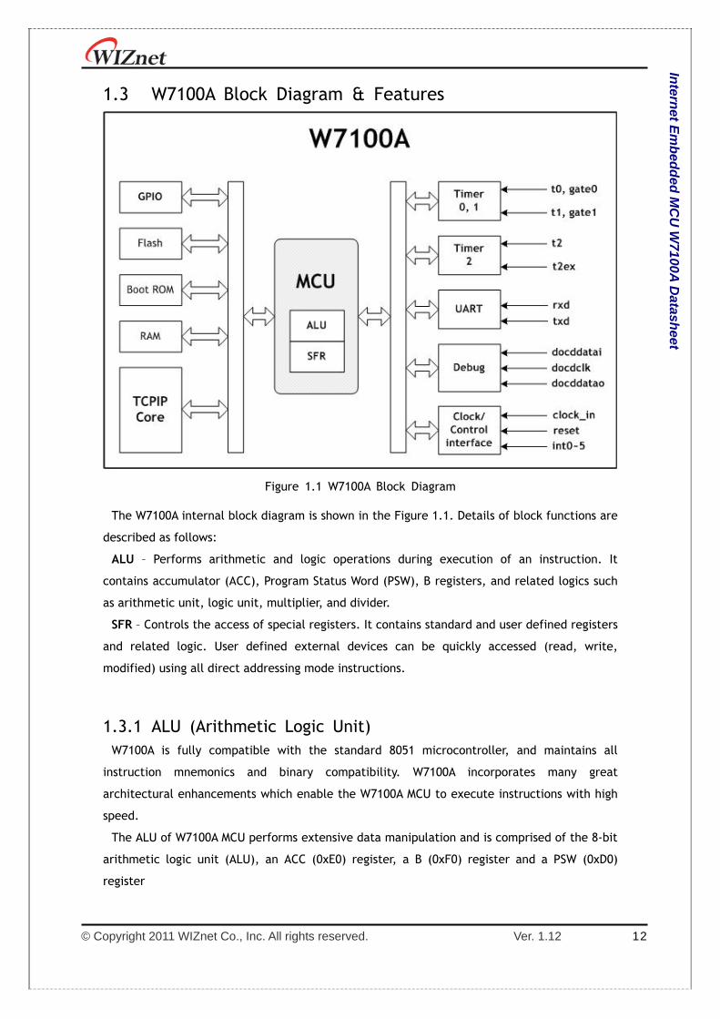
1.3 W7100A Block Diagram & Features
Figure 1.1 W7100A Block Diagram
The W7100A internal block diagram is shown in the Figure 1.1. Details of block functions are
described as follows:
ALU – Performs arithmetic and logic operations during execution of an instruction. It
contains accumulator (ACC), Program Status Word (PSW), B registers, and related logics such
as arithmetic unit, logic unit, multiplier, and divider.
SFR – Controls the access of special registers. It contains standard and user defined registers
and related logic. User defined external devices can be quickly accessed (read, write,
modified) using all direct addressing mode instructions.
1.3.1 ALU (Arithmetic Logic Unit) W7100A is fully compatible with the standard 8051 microcontroller, and maintains all
instruction mnemonics and binary compatibility. W7100A incorporates many great
architectural enhancements which enable the W7100A MCU to execute instructions with high
speed.
The ALU of W7100A MCU performs extensive data manipulation and is comprised of the 8-bit
arithmetic logic unit (ALU), an ACC (0xE0) register, a B (0xF0) register and a PSW (0xD0)
register

© Copyright 2011 WIZnet Co., Inc. All rights reserved. Ver. 1.12 13
Intern
et Em
bed
ded
MC
U W
7100A D
atasheet
ACC (0xE0)
7 6 5 4 3 2 1 0 Reset
ACC.7 ACC.6 ACC.5 ACC.4 ACC.3 ACC.2 ACC.1 ACC.0 0x00
Figure 1.2 Accumulator A Register
The B register is used during multiplication and division operations. In other cases, this
register is used as normal SFR.
B (0xF0)
7 6 5 4 3 2 1 0 Reset
B.7 B.6 B.5 B.4 B.3 B.2 B.1 B.0 0x00
Figure 1.3 B Register
The ALU performs arithmetic operations such as addition, subtraction, multiplication, and
division, and other operations such as increment, decrement, BCD-decimal-add-adjust, and
compare. Logic unit uses AND, OR, Exclusive OR, complement, and rotation to perform
different operations. The Boolean processor performs bit operations such as set, clear,
complement, jump-if-not-set, jump-if-set-and-clear, and move to/from carry.
PSW (0xD0)
7 6 5 4 3 2 1 0 Reset
CY AC F0 RS1 RS0 OV F1 P 0x00
Figure 1.4 Program Status Word Register
CY Carry flag
AC Auxiliary carry
F0 General purpose flag 0
RS[1:0]
Register bank select bits
RS[1:0] Function Description
00 -Bank 0, data address 0x00 - 0x07
01 -Bank 1, data address 0x08 - 0x0F
10 -Bank 2, data address 0x10 - 0x17
11 -Bank 3, data address 0x18 - 0x1F
OV Overflow flag
F1 General purpose flag 1
P Parity flag
Figure 1.5 PSW Register
The PSW register contains several bits that can reflect the current state of MCU.

© Copyright 2011 WIZnet Co., Inc. All rights reserved. Ver. 1.12 14
Intern
et Em
bed
ded
MC
U W
7100A D
atasheet
1.3.2 TCPIPCore
Figure 1.6 TCPIPCore Block Diagram
Ethernet PHY
The W7100A includes 10BaseT/100BaseTX Ethernet PHY. It supports half-duplex/full-duplex,
auto-negotiation and auto-MDI/MDIX. It also supports 6 network indicator LED outputs such as
Link, TX, RX status, Collision, speed and duplex.
TCPIP Engine
TCPIP Engine is a hardwired logic based network protocol which contains technology of
WIZnet.
- 802.3 Ethernet MAC(Media Access Control)
This controls Ethernet access of CSMA/CD(Carrier Sense Multiple Access with Collision
Detect). The protocol is based on a 48-bit source/destination MAC address.
- PPPoE(Point-To-Point Protocol over Ethernet)
This protocol uses PPP service over Ethernet. The payload (PPP frame) is encapsulated
inside an Ethernet frame during a transmission. When receiving, it de-capsulates the
PPP frame. PPPoE supports PPP communication with PPPoE server and PAP/CHAP
authentications.
- ARP(Address Resolution Protocol)
ARP is the MAC address resolution protocol by using IP address. This protocol exchanges
ARP-reply and ARP-request from peers to determine the MAC address of each other
© Copyright 2011 WIZnet Co., Inc. All rights reserved. Ver. 1.12 15
Intern
et Em
bed
ded
MC
U W
7100A D
atasheet
- IP (Internet Protocol)
This protocol operates in the IP layer and provides data communication. IP
fragmentation is not supported. It is not possible to receive the fragmented packets. All
protocol number is supported except for TCP or UDP. In case of TCP or UDP, use the
hardwired embedded TCPIP stack.
- ICMP(Internet Control Message Protocol)
ICMP is a protocol which provides information, unreachable destination. When a Ping-
request ICMP packet is received, a Ping-reply ICMP packet is sent.
- IGMPv1/v2(Internet Group Management Protocol version 1/2)
This protocol processes IGMP messages such as the IGMP Join/Leave. The IGMP is only
enabled in UDP multicast mode. Only version 1 and 2 of IGMP logic is supported. When
using a newer version of IGMP, IGMP should be manually implemented in the IP layer.
- UDP(User Datagram Protocol)
It is a protocol which supports data communication at the UDP layer. User datagram
such as unicast, multicast, and broadcast are supported
- TCP(Transmission Control Protocol)
This protocol operates in the TCP layer and provides data communication. Both TCP
server and client modes are supported.

© Copyright 2011 WIZnet Co., Inc. All rights reserved. Ver. 1.12 16
Intern
et Em
bed
ded
MC
U W
7100A D
atasheet
1.4 Pin Description
1.4.1 Pin Layout
Package type: LQFP 100
VCC3V3
P2.7/A15
P2.6/A14
P2.5/A13
P2.4/A12
P2.3/A11
P2.2/A10
P2.1/A9
GND
P2.0/A8
P0.7/AD7
P0.6/AD6
P0.5/AD5
VCC3V3
P0.4/AD4
P0.3/AD3
P0.2/AD2
VCC1V8
P0.1/AD1
P0.0/AD0
P1.0/A0
P1.1/A1
P1.2/A2
P1.3/A3
P1.4/A4
P1.5/A5
P1.6/A6
P1.7/A7
P3.0/A16
P3.1/A17
GND
P3.2/A18
VCC3V3
P3.3/A19
P3.4/A20
P3.5/A21
P3.6/A22
P3.7/A23
VCC1V8
SPDLED
41
42
43
44
45
46
47
48
49
50
80
79
78
77
76
26
27
28
29
30
31
32
33
34
35
36
37
38
39
40
85
84
83
82
81
100
99
98
97
96
95
94
93
92
91
90
89
88
87
86
FDXLED
COLLED
RXLED
TXLED
LINKLED
nRD
nWR
ALE
PLOCK
GNDA
iMCU W7100A
Figure 1.7 W7100A Pin Layout
© Copyright 2011 WIZnet Co., Inc. All rights reserved. Ver. 1.12 17
Intern
et Em
bed
ded
MC
U W
7100A D
atasheet
Package type: QFN 64
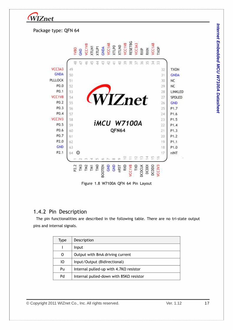
Figure 1.8 W7100A QFN 64 Pin Layout
1.4.2 Pin Description The pin functionalities are described in the following table. There are no tri-state output
pins and internal signals.
Type Description
I Input
O Output with 8mA driving current
IO Input/Output (Bidirectional)
Pu Internal pulled-up with 4.7KΩ resistor
Pd Internal pulled-down with 85KΩ resistor

© Copyright 2011 WIZnet Co., Inc. All rights reserved. Ver. 1.12 18
Intern
et Em
bed
ded
MC
U W
7100A D
atasheet
1.4.2.1 Configuration
Pin name Pin number I/O Pu/P
d
Description
100pin 64pin
nRST 8 9 I - Global asynchronous reset, Active low
TM3-0 1,2,
3,4
2,3,
4,5
I Pd Must be connected to GND; value ‘0000’
PM2 - 0 70,
71,
72
- I Pd PHY Mode
PM Description
2 1 0
0 0 0
Normal Operation Mode
Auto-negotiation enabled with all
functionalities
0 0 1 Auto-negotiation with 100 BASE-TX
FDX/HDX ability
0 1 0 Auto-negotiation with 10 BASE-T
FDX/HDX ability
0 1 1 Reserved
1 0 0 Manual selection of 100 BASE-TX FDX
1 0 1 Manual selection of 100 BASE-TX HDX
1 1 0 Manual selection of 10 BASE-T FDX
1 1 1 Manual selection of 10 BASE-T HDX
FDX : Full-Duplex, HDX : Half-Duplex
BOOTEN 5 6 I Pd Boot Enable/Disable
0 – Enable User Application mode
Jump to 0x0000, the start address of user Code
FLASH.
1- Enable Boot mode
Run boot code in Boot ROM
PLOCK 77 - O - PLL Lock line, It notifies when internal PLL is
locked

© Copyright 2011 WIZnet Co., Inc. All rights reserved. Ver. 1.12 19
Intern
et Em
bed
ded
MC
U W
7100A D
atasheet
1.4.2.2 Timer
Pin name Pin number I/O Pu/Pd Description
100pin 64pin
Timer0, 1 Interface
T0 9 - I - Timer0 external clock input
T1 10 - I - Timer1 external clock input
GATE0 11 - I - Timer0 gate control
GATE1 12 - I - Timer1 gate control
Timer2 Interface
T2 13 - I - Timer2 external clock input
T2EX 14 - I - Timer2 Capture/Reload trigger
1.4.2.3 UART
Pin name Pin number I/O Pu/Pd Description
100pin 64pin
RXD 15 10 I - Serial receiver
TXD 17 12 O - Serial transmitter
1.4.2.4 DoCD™ Compatible Debugger
Pin name Pin number I/O Pu/Pd Description
100pin 64pin
DCDCLK 18 13 O - DoCD clock
DCDDI 19 14 I - DoCD data input
DCDDO 20 15 O DoCD data output
1.4.2.5 Interrupt / Clock
Pin name Pin number I/O Pu/Pd Description
100pin 64pin
nINT0 22 17 I - External interrupt0
nINT1 23 - I - External interrupt1
nINT2 24 - I - External interrupt2
nINT3 25 - I - External interrupt3
XTLN0 61 40 O - Crystal output for WIZnet Core, A parallel-
resonant 25MHz crystal or ceramic is connected.
If use oscillator, this pin can be floated.
XTLP0 62 41 I - Crystal input for WIZnet Core, A parallel-

© Copyright 2011 WIZnet Co., Inc. All rights reserved. Ver. 1.12 20
Intern
et Em
bed
ded
MC
U W
7100A D
atasheet
resonant 25MHz crystal or ceramic is connected.
If use oscillator, this pin connected with 1.8V
output of OSC.
XTLN1 67 45 O - Crystal output for MCU core, A parallel-resonant
11.0592MHz crystal or ceramic is connected. If
oscillator is uesd, this pin can be floated.
XTLP1 66 44 I - Crystal input for MCU core, A parallel-resonant
11.0592MHz crystal or ceramic is connected. If
oscillator is used, this pin is connected with 1.8V
output of OSC.
1.4.2.6 GPIO
Pin name Pin number I/O Pu/Pd Description
100pin 64pin
P0.0 81 52 IO - Port0 input/output, Ext Memory Data0, Addr0
P0.1 82 53 IO - Port0 input/output, Ext Memory Data1, Addr1
P0.2 84 55 IO - Port0 input/output, Ext Memory Data2, Addr2
P0.3 85 56 IO - Port0 input/output, Ext Memory Data3, Addr3
P0.4 86 57 IO - Port0 input/output, Ext Memory Data4, Addr4
P0.5 87 59 IO - Port0 input/output, Ext Memory Data5, Addr5
P0.6 89 60 IO - Port0 input/output, Ext Memory Data6, Addr6
P0.7 90 61 IO - Port0 input/output, Ext Memory Data7, Addr7
P1.0 26 18 IO - Port1 input/output, Ext Memory Addr0
P1.1 27 19 IO - Port1 input/output, Ext Memory Addr1
P1.2 28 20 IO - Port1 input/output, Ext Memory Addr2
P1.3 29 21 IO - Port1 input/output, Ext Memory Addr3
P1.4 30 22 IO - Port1 input/output, Ext Memory Addr4
P1.5 31 23 IO - Port1 input/output, Ext Memory Addr5
P1.6 32 24 IO - Port1 input/output, Ext Memory Addr6
P1.7 33 25 IO - Port1 input/output, Ext Memory Addr7
P2.0 91 62 IO - Port2 input/output, Ext Memory Addr8
P2.1 93 64 IO - Port2 input/output, Ext Memory Addr9
P2.2 94 1 IO - Port2 input/output, Ext Memory Addr10
P2.3 95 - IO - Port2 input/output, Ext Memory Addr11
P2.4 96 - IO - Port2 input/output, Ext Memory Addr12
P2.5 97 - IO - Port2 input/output, Ext Memory Addr13
P2.6 98 - IO - Port2 input/output, Ext Memory Addr14
© Copyright 2011 WIZnet Co., Inc. All rights reserved. Ver. 1.12 21
Intern
et Em
bed
ded
MC
U W
7100A D
atasheet
P2.7 99 - IO - Port2 input/output, Ext Memory Addr15
P3.0 34 - IO - Port3 input/output, Ext Memory Addr16
P3.1 35 - IO - Port3 input/output, Ext Memory Addr17
P3.2 37 - IO - Port3 input/output, Ext Memory Addr18
P3.3 39 - IO - Port3 input/output, Ext Memory Addr19
P3.4 40 - IO - Port3 input/output, Ext Memory Addr20
P3.5 41 - IO - Port3 input/output, Ext Memory Addr21
P3.6 42 - IO - Port3 input/output, Ext Memory Addr22
P3.7 43 - IO - Port3 input/output, Ext Memory Addr23
Note: User can control the GPIO I/O driving voltage using PxPU/PxPD SFR.
Note: In that case, GPIO0~3 is used to transfer External memory address and data. Please
refer to the ‘2.3 External Data Memory Access’
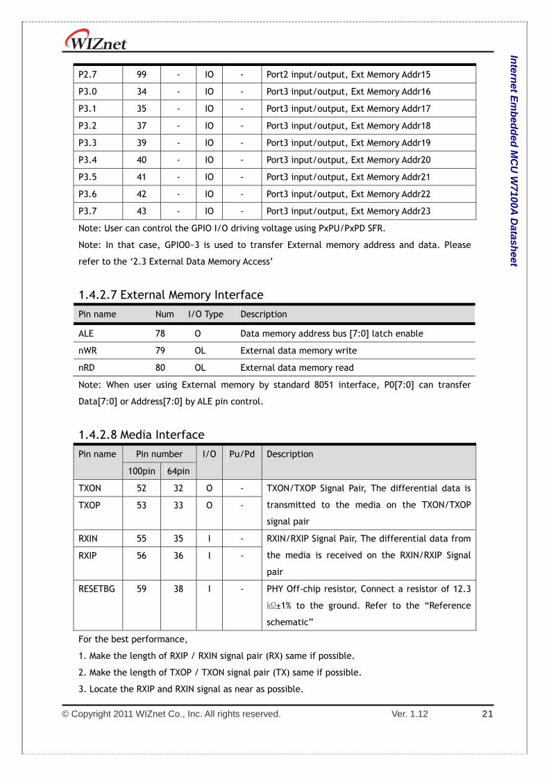
1.4.2.7 External Memory Interface
Pin name Num I/O Type Description
ALE 78 O Data memory address bus [7:0] latch enable
nWR 79 OL External data memory write
nRD 80 OL External data memory read
Note: When user using External memory by standard 8051 interface, P0[7:0] can transfer
Data[7:0] or Address[7:0] by ALE pin control.
1.4.2.8 Media Interface
Pin name Pin number I/O Pu/Pd Description
100pin 64pin
TXON 52 32 O - TXON/TXOP Signal Pair, The differential data is
transmitted to the media on the TXON/TXOP
signal pair
TXOP 53 33 O -
RXIN 55 35 I - RXIN/RXIP Signal Pair, The differential data from
the media is received on the RXIN/RXIP Signal
pair
RXIP 56 36 I -
RESETBG 59 38 I - PHY Off-chip resistor, Connect a resistor of 12.3
±1% to the ground. Refer to the “Reference
schematic”
For the best performance,
1. Make the length of RXIP / RXIN signal pair (RX) same if possible.
2. Make the length of TXOP / TXON signal pair (TX) same if possible.
3. Locate the RXIP and RXIN signal as near as possible.

© Copyright 2011 WIZnet Co., Inc. All rights reserved. Ver. 1.12 22
Intern
et Em
bed
ded
MC
U W
7100A D
atasheet
4. Locate the TXOP and TXON signal as near as possible.
5. Locate the RX and TX signal pairs far from noisy signals such as bias resistor or
crystal.
6. Keep regular between TX/RX signal pair.
For more details, refer to “W5100 Layout Guide.pdf.”
1.4.2.9 Network Indicator LED
Pin name Pin number I/O Pu/Pd Description
100pin 64pin
SPDLED 45 27 O - Link speed LED
Low: 100Mbps
High: 10Mbps
FDXLED 46 - O - Full duplex LED
Low: Full-duplex
High: Half-duplex
COLLED 47 - O - Collision LED
Low: Collision detected (only half-duplex)
RXLED 48 - O - Receive activity LED
Low: Receive signal detected on RXIP/RXIN
TXLED 49 - O - Transmit activity LED
Low: Transmit signal detected on TXOP/TXON
LINKLED 50 28 O - Link LED
Low: Link (10/100M) is detected
1.4.2.10 Power Supply Signal
Pin
name
Pin number I/O Pu/
Pd
Description
100pin 64pin
VCC3A3 58, 75 37, 49 Power - Analog 3.3V power supply
Be sure to connect a 10uF tantalum capacitor
between VCC3A3 and GNDA in order to prevent
power compensation
VCC3V3 21,
38,
73,
87,
100
16, 58 Power - Digital 3.3V power supply
A 0.1uF decoupling capacitor should be connected
between each pair of VCC and GND. A 1uH ferrite
bead should be used to separate the VCC3V3 and
VCC3A3
VCC1A8 54, 34, 42 Power - Analog 1.8V power supply

© Copyright 2011 WIZnet Co., Inc. All rights reserved. Ver. 1.12 23
Intern
et Em
bed
ded
MC
U W
7100A D
atasheet
60,
64
A 10uF tantalum capacitor and a 0.1uF capacitor
should be connected between VCC1A8 and GNDA
to filter out core power noise
VCC1V8 16,
44,
68, 83
39,
46,
54, 11
Power - Digital 1.8V power supply
Between each pair of VCC and GND, a 0.1uF
decoupling capacitor should be connected
GNDA 51,
57,
63,
65,
76
31,
43, 50
Power - Analog ground
Design the analog ground plane as wide as
possible during PCB layout
GND 6, 7,
36,
69, 92
7, 8,
26,
47, 63
Power - Digital ground
Design the digital ground plane as wide as
possible during PCB layout
1V8O 74 48 Power - 1.8V regulated output voltage
1.8V/150mA power generated by internal power
regulator which is used for core operation power
(VCC1A8, VCC1V8).
Between the 1V8O and GND, Be sure to connect a
3.3uF tantalum capacitor for output frequency
compensation and a 0.1uF capacitor for high
frequency noise decoupling.
1V8O is connected to VCC1V8, separated to 1uH
inductor and connected to VCC1A8.
<Notice> 1V8O is the power supply for W7100A use
only. This supply should not be connected with
any other devices.
© Copyright 2011 WIZnet Co., Inc. All rights reserved. Ver. 1.12 24
Intern
et Em
bed
ded
MC
U W
7100A D
atasheet
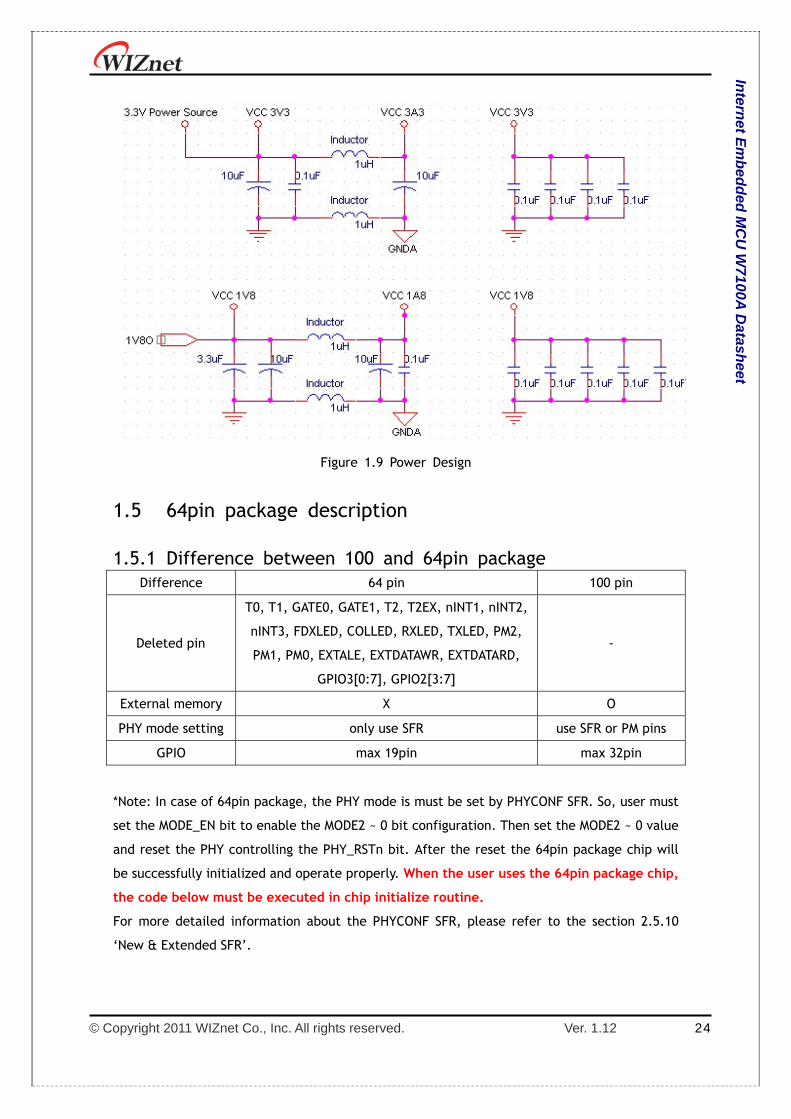
Figure 1.9 Power Design
1.5 64pin package description
1.5.1 Difference between 100 and 64pin package Difference 64 pin 100 pin
Deleted pin
T0, T1, GATE0, GATE1, T2, T2EX, nINT1, nINT2,
nINT3, FDXLED, COLLED, RXLED, TXLED, PM2,
PM1, PM0, EXTALE, EXTDATAWR, EXTDATARD,
GPIO3[0:7], GPIO2[3:7]
-
External memory X O
PHY mode setting only use SFR use SFR or PM pins
GPIO max 19pin max 32pin
*Note: In case of 64pin package, the PHY mode is must be set by PHYCONF SFR. So, user must
set the MODE_EN bit to enable the MODE2 ~ 0 bit configuration. Then set the MODE2 ~ 0 value
and reset the PHY controlling the PHY_RSTn bit. After the reset the 64pin package chip will
be successfully initialized and operate properly. When the user uses the 64pin package chip,
the code below must be executed in chip initialize routine.
For more detailed information about the PHYCONF SFR, please refer to the section 2.5.10
‘New & Extended SFR’.

© Copyright 2011 WIZnet Co., Inc. All rights reserved. Ver. 1.12 25
Intern
et Em
bed
ded
MC
U W
7100A D
atasheet
PHYCONF |= 0x08; // MODE_EN bit enable
PHYCONF &= 0xF8; // MODE2 ~ 0 value is 0 (normal mode); Auto configuration mode
PHYCONF |= 0x20; // Set the PHY_RSTn bit (reset bit)
Delay(); // Delay for reset timing (refer to the section 10 ‘Reset Timing’)
PHYCONF &= ~(0x20); // Clear the PHY_RSTn bit
© Copyright 2011 WIZnet Co., Inc. All rights reserved. Ver. 1.12 26
Intern
et Em
bed
ded
MC
U W
7100A D
atasheet
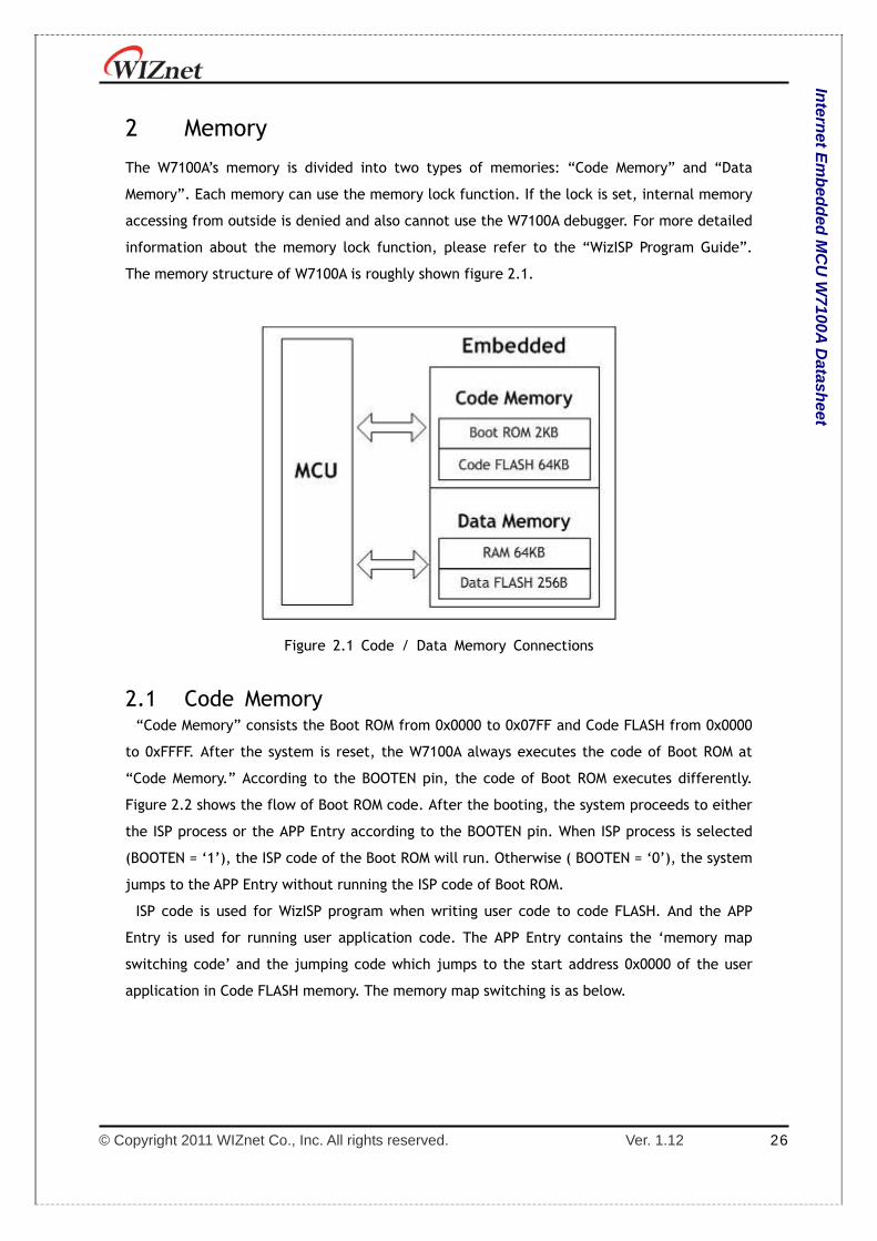
2 Memory
The W7100A’s memory is divided into two types of memories: “Code Memory” and “Data
Memory”. Each memory can use the memory lock function. If the lock is set, internal memory
accessing from outside is denied and also cannot use the W7100A debugger. For more detailed
information about the memory lock function, please refer to the “WizISP Program Guide”.
The memory structure of W7100A is roughly shown figure 2.1.
Figure 2.1 Code / Data Memory Connections
2.1 Code Memory “Code Memory” consists the Boot ROM from 0x0000 to 0x07FF and Code FLASH from 0x0000
to 0xFFFF. After the system is reset, the W7100A always executes the code of Boot ROM at
“Code Memory.” According to the BOOTEN pin, the code of Boot ROM executes differently.
Figure 2.2 shows the flow of Boot ROM code. After the booting, the system proceeds to either
the ISP process or the APP Entry according to the BOOTEN pin. When ISP process is selected
(BOOTEN = ‘1’), the ISP code of the Boot ROM will run. Otherwise ( BOOTEN = ‘0’), the system
jumps to the APP Entry without running the ISP code of Boot ROM.
ISP code is used for WizISP program when writing user code to code FLASH. And the APP
Entry is used for running user application code. The APP Entry contains the ‘memory map
switching code’ and the jumping code which jumps to the start address 0x0000 of the user
application in Code FLASH memory. The memory map switching is as below.

© Copyright 2011 WIZnet Co., Inc. All rights reserved. Ver. 1.12 27
Intern
et Em
bed
ded
MC
U W
7100A D
atasheet
Figure 2.2. Boot Sequence Flowchart
The initial state of W7100A has both ‘Boot ROM / APP Entry’ and FLASH as shown in Figure
2.3. But since the addresses of ‘Boot ROM / APP Entry’ and FLASH are overlapped, they use
same address at 0x0000 ~ 0x07FF / 0xFFF7 ~ 0xFFFF. The iMCU W7100A respectively maps the
‘Boot ROM / APP Entry’ and FLASH(64K) to the code and data memory.
The user application code can be written to the FLASH(mapped to data memory). But in this
state, the FLASH cannot be used as a code memory because this state is for writing user
application code. To use the FLASH as a code memory, the memory map needs to be switched.
To do this, user should select APP Mode by setting the BOOTEN pin to ‘0’, and then the Boot
ROM code jumps to APP Entry immediately. Next, the APP Entry un-maps the Boot ROM and
maps the Code FLASH to code memory. After switching the code memory map, the APP Entry
Figure 2.3 APP Entry Process

© Copyright 2011 WIZnet Co., Inc. All rights reserved. Ver. 1.12 28
Intern
et Em
bed
ded
MC
U W
7100A D
atasheet
jumps to start address of Code FLASH (0x0000). This flow is shown in Figure 2.3.
If the APP Mode is selected, the Code FLASH 64KB can be used as a code memory. But both
FLASH and APP Entry are still overlapped at the same address. Therefore, to use all FLASH
64KB, the APP Entry must be un-mapped from “Code Memory.” To un-map APP Entry, user
should set RB bit in WCONF(0xFF) to ‘0’ at the user startup code. Then the APP Entry is un-
mapped as shown below.
Figure 2.4 Changing the code memory Status at RB = ‘0’
WCONF (0xFF)
7 6 5 4 3 2 1 0 Reset
RB ISPEN EM2 EM1 EM0 Reserved FB BE 0x00
When the Code FLASH takes more than 0xFFF7, the below code must be inserted into startup
code. If using this method, the W7100A immediately disables the APP Entry address after its
system reset.
ANL 0FFH, #07FH ; Clear Reboot flag
Set the BOOTEN pin to ‘0’ and clear the RB bit of WCONF register at the startup code. Then
the embedded Code FLASH 64KB memory of the W7100A can be completely used as a code
memory.
2.1.1 Code Memory Wait States The wait states are managed by internal WTST(0x92) register. The number of wait states is
fixed by the value stored in the WTST register. Please refer to the section 2.5.10 ‘New &
Extended SFR’ for more details.

© Copyright 2011 WIZnet Co., Inc. All rights reserved. Ver. 1.12 29
Intern
et Em
bed
ded
MC
U W
7100A D
atasheet
2.2 Data Memory The W7100A contains 64KB of embedded RAM, 64KB of TCPIPCore and the 255Byte of the
Data FLASH. The Data FLASH can be used for saving user IP, MAC, subnet mask or port number.
Also the W7100A can address up to 16M bytes of external Data Memory. The figure below
shows the Data Memory map. This memory is accessed by MOVX instructions only. The
external memory can be extended by user.
Figure 2.5 Data Memory Map
2.2.1 Data Memory Wait States The Data Memory wait states are managed by CKCON(0x8E). The number of wait states is
fixed to the value stored inside CKCON register. Please refer to the section 2.5.10 ‘New &
Extended SFR’ for more detailed information.
2.3 External Data Memory Access The external address pin and data pin has two access modes. The first mode is to use latch
to address line in standard 8051. And the second method is directly connecting all lines to
address line. Also user can use address pin and data pin as GPIO (General Purpose I/O). Please
refer to the section 10 ‘Electrical specification’ for the speed of external memory accessing.
Table 2.1 External memory access mode
Mode EM[2:0] P0 P1 P2 P3
Standard 1 001 Addr[7:0]/Data[7:0] GPIO Addr[15:8] GPIO
Standard 2 011 Addr[7:0]/Data[7:0] GPIO Addr[15:8] Addr[23:16]
Direct 1 101 Data[7:0] Addr[7:0] Addr[15:8] GPIO
Direct 2 111 Data[7:0] Addr[7:0] Addr[15:8] Addr[23:16]
© Copyright 2011 WIZnet Co., Inc. All rights reserved. Ver. 1.12 30
Intern
et Em
bed
ded
MC
U W
7100A D
atasheet
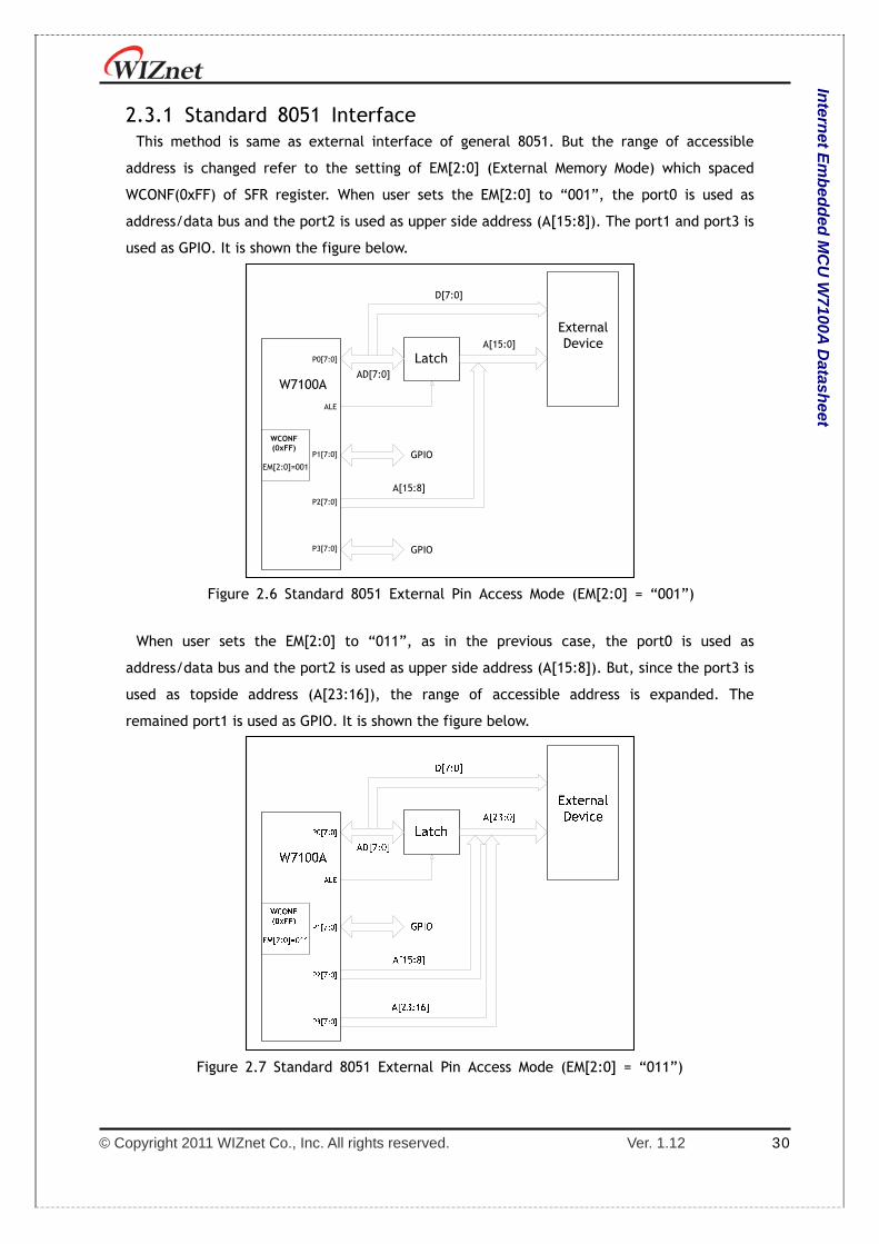
2.3.1 Standard 8051 Interface This method is same as external interface of general 8051. But the range of accessible
address is changed refer to the setting of EM[2:0] (External Memory Mode) which spaced
WCONF(0xFF) of SFR register. When user sets the EM[2:0] to “001”, the port0 is used as
address/data bus and the port2 is used as upper side address (A[15:8]). The port1 and port3 is
used as GPIO. It is shown the figure below.
W7100A
A[15:0]
AD[7:0]
D[7:0]
Latch
ALE
P0[7:0]
ExternalDevice
P1[7:0]
P2[7:0]
EM[2:0]=001
WCONF(0xFF)
GPIO
GPIO
A[15:8]
P3[7:0]
Figure 2.6 Standard 8051 External Pin Access Mode (EM[2:0] = “001”)
When user sets the EM[2:0] to “011”, as in the previous case, the port0 is used as
address/data bus and the port2 is used as upper side address (A[15:8]). But, since the port3 is
used as topside address (A[23:16]), the range of accessible address is expanded. The
remained port1 is used as GPIO. It is shown the figure below.
Figure 2.7 Standard 8051 External Pin Access Mode (EM[2:0] = “011”)

© Copyright 2011 WIZnet Co., Inc. All rights reserved. Ver. 1.12 31
Intern
et Em
bed
ded
MC
U W
7100A D
atasheet
In the Standard 8051 External pin access mode, MCU controls the ALE (Address Latch Enable)
signal to classify the address and data signal. User can configure the duration of ALE signal
using the ALECON(0x9F) SFR. For more detailed information about ALECON, please refer to
the section 2.5.10 ‘New & Extended SFR’.
2.3.2 Direct Interface This method is directly connecting the data line to address line. When user sets the EM[2:0]
to “101”, the port0 is used as data line (D[7:0]) and the port1 is lower side address (A[7:0])
and the port2 is used as upper side address (A[15:8]). The remained port3 can be used as
GPIO. Using this method, user can connect data line to address line without latch. It is shown
the figure 2.8 as below.
W7100AA[7:0]
D[7:0]
P1[7:0]
P0[7:0]
ExternalDevice
P2[7:0]
P3[7:0] GPIO
A[15:8]
A[15:0]
EM[2:0]=101
WCONF(0xFF)
Figure 2.8 Direct 8051 External Pin Access Mode (EM[2:0] = “101”)
When user sets the EM[2:0] to “111”, the port0, port1 and port2 has same usage in the
previous case and the port3 is used as topside address (A[23:16]). In this method, there is no
port to use GPIO. It is shown the figure below.
Figure 2.9 Direct 8051 External Pin Access Mode (EM[2:0] = “111”)

© Copyright 2011 WIZnet Co., Inc. All rights reserved. Ver. 1.12 32
Intern
et Em
bed
ded
MC
U W
7100A D
atasheet
2.4 Internal Data Memory and SFR The Figure below shows the Internal Memory and Special Function Registers (SFR) map.
Figure 2.10 Internal Memory Map
The lower internal RAM consists of four register banks with eight registers each, a bit-
addressable segment with 128 bits (16 bytes) that begins at 0x20, and a scratchpad area with
208 bytes is embedded. With indirect addressing mode ranging from 0x80 to 0xFF, the highest
128 bytes is accessed as an internal memory. But with direct addressing mode ranging from
0x80 to 0xFF, this area is accessed as a SFR memory.
Figure 2.11 SFR Memory Map
New SFR – New additional SFR, described in this section
Extended SFR – Extended from standard 8051, described in this section
Standard – standard 8051 SFR, described in this section
All of the SFR in the left hand side column ending with 0 or 8 are bit addressable.

© Copyright 2011 WIZnet Co., Inc. All rights reserved. Ver. 1.12 33
Intern
et Em
bed
ded
MC
U W
7100A D
atasheet
2.5 SFR definition The following section describes SFR of W7100A and its functions. For more detailed
information about peripheral SFR, please refer to the section 2.5.11 ‘Peripheral SFR’.
2.5.1 Program Code Memory Write Enable Bit Inside the PCON register, the Program Write Enable (PWE) bit is used to enable/disable
Program Write signal activity during MOVX instructions.
When the PWE bit is set to logic ‘1', the “MOVX @DPTR, A” instruction writes the data from
the accumulator register into the code memory addressed by using the DPTR register (active
DPH:DPL)
The “MOVX @Rx, A” instruction writes the data from the accumulator register into code
memory addressed by using the P2 register (bits 15:8) and Rx register (bits 7:0).
PCON (0x87)
7 6 5 4 3 2 1 0 Reset
SMOD0 - - PWE - 0 0 0 0x00
Figure 2.13 PWE bit of PCON Register
Note: 1. PCON.2 ~ PCON.0 bits are reserved. They must be set to ‘0’
2.5.2 Program Code Memory Wait States Register Wait states register provides the information for code memory access time.
WTST (0x92)
7 6 5 4 3 2 1 0 Reset
- - - - - WTST.2 WTST.1 WTST.0 0x07
Figure 2.14 Code memory Wait States Register
Note: 1. These bits are considered during program fetches and MOVC instructions only.
Since code memory write are performed by MOVX instruction, CKCON
register regulates the CODE-WR pulse width.
2. Read cycle takes minimal 4 clock period and maximal 8 clock periods.
Table 2.2 WTST Register Values
WTST[2:0] Access Time [clk]
7 8
6 7
5 6
4 5
3 4
2 Not Used
© Copyright 2011 WIZnet Co., Inc. All rights reserved. Ver. 1.12 34
Intern
et Em
bed
ded
MC
U W
7100A D
atasheet
1 Not Used
0 Not Used
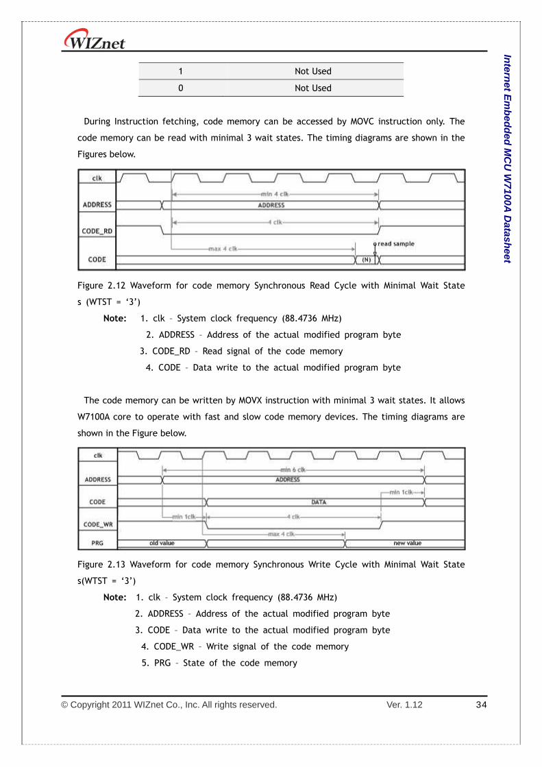
During Instruction fetching, code memory can be accessed by MOVC instruction only. The
code memory can be read with minimal 3 wait states. The timing diagrams are shown in the
Figures below.
Figure 2.12 Waveform for code memory Synchronous Read Cycle with Minimal Wait State
s (WTST = ‘3’)
Note: 1. clk – System clock frequency (88.4736 MHz)
2. ADDRESS – Address of the actual modified program byte
3. CODE_RD – Read signal of the code memory
4. CODE – Data write to the actual modified program byte
The code memory can be written by MOVX instruction with minimal 3 wait states. It allows
W7100A core to operate with fast and slow code memory devices. The timing diagrams are
shown in the Figure below.
Figure 2.13 Waveform for code memory Synchronous Write Cycle with Minimal Wait State
s(WTST = ‘3’)
Note: 1. clk – System clock frequency (88.4736 MHz)
2. ADDRESS – Address of the actual modified program byte
3. CODE – Data write to the actual modified program byte
4. CODE_WR – Write signal of the code memory
5. PRG – State of the code memory
© Copyright 2011 WIZnet Co., Inc. All rights reserved. Ver. 1.12 35
Intern
et Em
bed
ded
MC
U W
7100A D
atasheet
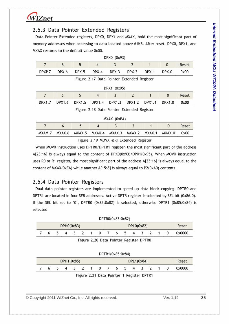
2.5.3 Data Pointer Extended Registers Data Pointer Extended registers, DPX0, DPX1 and MXAX, hold the most significant part of
memory addresses when accessing to data located above 64KB. After reset, DPX0, DPX1, and
MXAX restores to the default value 0x00.
DPX0 (0x93)
7 6 5 4 3 2 1 0 Reset
DPXP.7 DPX.6 DPX.5 DPX.4 DPX.3 DPX.2 DPX.1 DPX.0 0x00
Figure 2.17 Data Pointer Extended Register
DPX1 (0x95)
7 6 5 4 3 2 1 0 Reset
DPX1.7 DPX1.6 DPX1.5 DPX1.4 DPX1.3 DPX1.2 DPX1.1 DPX1.0 0x00
Figure 2.18 Data Pointer Extended Register
MXAX (0xEA)
7 6 5 4 3 2 1 0 Reset
MXAM.7 MXAX.6 MXAX.5 MXAX.4 MXAX.3 MXAX.2 MXAX.1 MXAX.0 0x00
Figure 2.19 MOVX @RI Extended Register
When MOVX instruction uses DPTR0/DPTR1 register, the most significant part of the address
A[23:16] is always equal to the content of DPX0(0x93)/DPX1(0x95). When MOVX instruction
uses R0 or R1 register, the most significant part of the address A[23:16] is always equal to the
content of MXAX(0xEA) while another A[15:8] is always equal to P2(0xA0) contents.
2.5.4 Data Pointer Registers Dual data pointer registers are implemented to speed up data block copying. DPTR0 and
DPTR1 are located in four SFR addresses. Active DPTR register is selected by SEL bit (0x86.0).
If the SEL bit set to ‘0’, DPTR0 (0x83:0x82) is selected, otherwise DPTR1 (0x85:0x84) is
selected.
DPTR0(0x83:0x82)
DPH0(0x83) DPL0(0x82) Reset
7 6 5 4 3 2 1 0 7 6 5 4 3 2 1 0 0x0000
Figure 2.20 Data Pointer Register DPTR0
DPTR1(0x85:0x84)
DPH1(0x85) DPL1(0x84) Reset
7 6 5 4 3 2 1 0 7 6 5 4 3 2 1 0 0x0000
Figure 2.21 Data Pointer 1 Register DPTR1

© Copyright 2011 WIZnet Co., Inc. All rights reserved. Ver. 1.12 36
Intern
et Em
bed
ded
MC
U W
7100A D
atasheet
DPS (0x86)
7 6 5 4 3 2 1 0 Reset
ID1 ID0 TSL - - - - SEL 0x00
Figure 2.22 Data Pointer Select Register
Note: TSL - Toggle select enable. When TSL is set, this bit toggles the SEL bit by exec
uting the following instructions.
INC DPTR
MOV DPTR, #data16
MOVC A, @A + DPTR
MOVX @DPTR, A
MOVX A, @DPTR
When TSL = 0, DPTR related instructions will not affect the state of the SEL
bit.
Unimplemented bit - Read as 0 or 1.
Table 2.3 DPTR0, DPTR1 Operations
ID1 ID0 SEL = 0 SEL = 1
0 0 INC DPTR INC DPTR1
0 1 DEC DPTR INC DPTR1
1 0 INC DPTR DEC DPTR1
1 1 DEC DPTR DEC DPTR1
Selected data pointer register is used in the following instructions:
MOVX @DPTR, A
MOVX A, @DPTR
MOVC A, @A + DPTR
JMP @A + DPTR
INC DPTR
MOV DPTR, #data16
2.5.5 Clock Control Register Clock control register CKCON (0x8E) contains MD [2:0] bits which provide the information for
the dedicated data memory read/write signal pulses width.
CKCON (0x8E)
7 6 5 4 3 2 1 0 Reset
WD1 WD0 - - - MD2 MD1 MD0 0x07
Figure 2.23 Clock Control Register – STRETCH bits
The dedicated data memory read/write signals are activated during MOVX instruction. The
purpose of MD[2:0] is to adjust the communication speed with I/O devices such as slow RAM,

© Copyright 2011 WIZnet Co., Inc. All rights reserved. Ver. 1.12 37
Intern
et Em
bed
ded
MC
U W
7100A D
atasheet
LCD displays, etc. After reset, MD[2:0] will be restored to the default value of 0x07, which
means that slow devices work properly. Users can change the MD[2:0] value to speed up/slow
down the software execution. The value of MD[2:0] can be changed any time during program
execution (e.g. between MOVX and different speed devices).
Table 2.4 MD[2:0] Bit Values
MD[2:0] Pulse Width[clock]
7 8
… …
2 3
1 Not Used
0 Not Used
This read/write pulse width must have a minimum of 3 clock cycle and a maximum of 8
clock cycle.
2.5.6 Internal Memory Wait States Register Internal Memory Wait States Register INTWTST(0x9C) is used for setting the access time of
internal 64KB RAM, TCPIPCore and 255Byte internal flash.
INTWTST (0x9C)
7 6 5 4 3 2 1 0 Reset
Ram WTST TCPIPCore WTST Flash WTST 0xFF
Figure 2.24 Internal Memory Wait States Register
- Ram WTST: Set the 64Kbytes RAM access time, has two 2bit value 0 ~ 3.
- TCPIPCore WTST: Set the TCPIPCore access time, has 3bit value 0 ~ 7.
- Flash WTST: Set the internal flash access time, has 3bit value 0 ~ 7.
Internal ram WTST value means below access time in table 2.3.
Table 2.5 Ram WTST Bit Values
WTST Pulse Width[clock]
3 5
2 4
1 3
0 2
TCPIPCore, Internal flash WTST value means below access time in table 2.4.
Table 2.6 TCPIPCore / Flash WTST Bit Values
© Copyright 2011 WIZnet Co., Inc. All rights reserved. Ver. 1.12 38
Intern
et Em
bed
ded
MC
U W
7100A D
atasheet
WTST Pulse Width[clock]
7 10
6 9
5 8
4 7
3 6
2 5
1 4
0 3
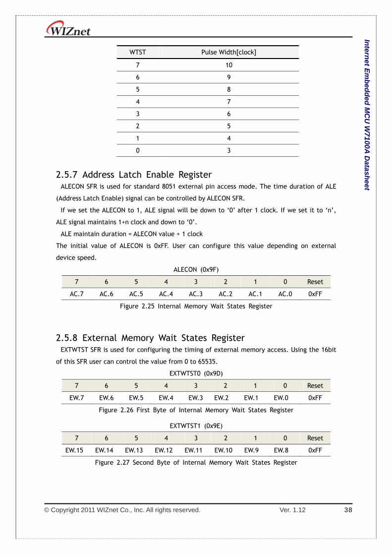
2.5.7 Address Latch Enable Register ALECON SFR is used for standard 8051 external pin access mode. The time duration of ALE
(Address Latch Enable) signal can be controlled by ALECON SFR.
If we set the ALECON to 1, ALE signal will be down to ‘0’ after 1 clock. If we set it to ‘n’,
ALE signal maintains 1+n clock and down to ‘0’.
ALE maintain duration = ALECON value + 1 clock
The initial value of ALECON is 0xFF. User can configure this value depending on external
device speed.
ALECON (0x9F)
7 6 5 4 3 2 1 0 Reset
AC.7 AC.6 AC.5 AC.4 AC.3 AC.2 AC.1 AC.0 0xFF
Figure 2.25 Internal Memory Wait States Register
2.5.8 External Memory Wait States Register EXTWTST SFR is used for configuring the timing of external memory access. Using the 16bit
of this SFR user can control the value from 0 to 65535.
EXTWTST0 (0x9D)
7 6 5 4 3 2 1 0 Reset
EW.7 EW.6 EW.5 EW.4 EW.3 EW.2 EW.1 EW.0 0xFF
Figure 2.26 First Byte of Internal Memory Wait States Register
EXTWTST1 (0x9E)
7 6 5 4 3 2 1 0 Reset
EW.15 EW.14 EW.13 EW.12 EW.11 EW.10 EW.9 EW.8 0xFF
Figure 2.27 Second Byte of Internal Memory Wait States Register
© Copyright 2011 WIZnet Co., Inc. All rights reserved. Ver. 1.12 39
Intern
et Em
bed
ded
MC
U W
7100A D
atasheet
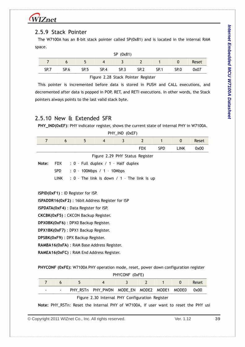
2.5.9 Stack Pointer The W7100A has an 8-bit stack pointer called SP(0x81) and is located in the internal RAM
space.
SP (0x81)
7 6 5 4 3 2 1 0 Reset
SP.7 SP.6 SP.5 SP.4 SP.3 SP.2 SP.1 SP.0 0x07
Figure 2.28 Stack Pointer Register
This pointer is incremented before data is stored in PUSH and CALL executions, and
decremented after data is popped in POP, RET, and RETI executions. In other words, the Stack
pointers always points to the last valid stack byte.
2.5.10 New & Extended SFR PHY_IND(0xEF): PHY indicator register, shows the current state of internal PHY in W7100A.
PHY_IND (0xEF)
7 6 5 4 3 2 1 0 Reset
FDX SPD LINK 0x00
Figure 2.29 PHY Status Register
Note: FDX : 0 – Full duplex / 1 – Half duplex
SPD : 0 – 100Mbps / 1 – 10Mbps
LINK : 0 – The link is down / 1 – The link is up
ISPID(0xF1) : ID Register for ISP.
ISPADDR16(0xF2) : 16bit Address Register for ISP
ISPDATA(0xF4) : Data Register for ISP.
CKCBK(0xF5) : CKCON Backup Register.
DPX0BK(0xF6) : DPX0 Backup Register.
DPX1BK(0xF7) : DPX1 Backup Register.
DPSBK(0xF9) : DPX Backup Register.
RAMBA16(0xFA) : RAM Base Address Register.
RAMEA16(0xFC) : RAM End Address Register.
PHYCONF (0xFE): W7100A PHY operation mode, reset, power down configuration register
PHYCONF (0xFE)
7 6 5 4 3 2 1 0 Reset
- - PHY_RSTn PHY_PWDN MODE_EN MODE2 MODE1 MODE0 0x00
Figure 2.30 Internal PHY Configuration Register
Note: PHY_RSTn: Reset the Internal PHY of W7100A, if user want to reset the PHY usi

© Copyright 2011 WIZnet Co., Inc. All rights reserved. Ver. 1.12 40
Intern
et Em
bed
ded
MC
U W
7100A D
atasheet
ng this bit, set this bit ‘1’ first, then manually clear to ‘0’ after the
reset time. About the reset time please refer to the section 10 ‘Elec
trical Specification’.
PHY_PWDN: 1- Power down mode: turn off the embedded Ethernet PHY to save
power consumption
0 – Normal operation mode.
MODE_EN : 1 – Configure W7100A operation mode using the MODE2 ~ 0 bit / 0 – d
on’t use MODE2 ~ 0 bit. In the QFN 64pin package, must use this bit
and MODE2 ~ 0 bits to configure the operation mode of W7100A
MODE2 ~ 0: Please refer to the section 1.4.2 ‘Pin Description’ PM2 ~ 0 pin settin
g value, MODE2 ~ 0 bit are same as PM2 ~ 0 pin.
- : Reserved, must be set to ‘0’
ex> usage of mode selection using MODE2 ~ 0
PHYCONF |= 0x08; // MODE_EN bit enable
PHYCONF &= 0xF8; // MODE2 ~ 0 value is 0 (normal mode); Auto configuration mode
PHYCONF |= 0x20; // Set the PHY_RSTn bit (reset bit)
Delay(); // Delay for reset timing(refer to the section 10 ‘Electrical Specification’)
PHYCONF &= ~(0x20); // Clear the PHY_RSTn bit
WCONF(0xFF): W7100A configuration register
WCONF (0xFF)
7 6 5 4 3 2 1 0 Reset
RB ISPEN EM2 EM1 EM0 Reserved FB BE 0x00
Figure 2.31 W7100A Configuration Register
Note: RB : 0 – No Reboot / 1 – Reboot after the ISP done (APP Entry(0xFFF7 ~
0xFFFF) RD/WR Enable)
ISPEN : 0 – Enable ISP in Boot built in W7100A / 1 – Disable
EM[2:0] : External memory mode, please refer to the section 2.3 ‘External Data
Memory Access’.
FB : FLASH Busy Flag for ISP. Read only.
BE : Boot Enable (1 – Boot Running / 0 – Apps Running). Read only.
CLKCNT0(0xDC): W7100A core clock count register bit0 ~ 7.
CLK_CNT0 (0xDC)
7 6 5 4 3 2 1 0 Reset
Bit7 Bit6 Bit5 Bit4 Bit3 Bit2 Bit1 Bit0 0x00
Figure 2.32 Core clock count register
Note: CLK_CNT is 32bit SFR, reset value is 0, increase its value at every core clock. T

© Copyright 2011 WIZnet Co., Inc. All rights reserved. Ver. 1.12 41
Intern
et Em
bed
ded
MC
U W
7100A D
atasheet
his SFR is used for counting core clock or measuring time or clock.
ex> 1 second = about 88000000 clock count (core clock is about 88MHz)
CLKCNT0(0xDD): W7100A core clock count register bit8 ~ 15.
CLK_CNT1 (0xDD)
7 6 5 4 3 2 1 0 Reset
Bit15 Bit14 Bit13 Bit12 Bit11 Bit10 Bit9 Bit8 0x00
Figure 2.33 Core clock count register
CLKCNT0(0xDE): W7100A core clock count register bit16 ~ 23.
CLK_CNT2 (0xDE)
7 6 5 4 3 2 1 0 Reset
Bit23 Bit22 Bit21 Bit20 Bit19 Bit18 Bit17 Bit16 0x00
Figure 2.34 Core clock count register
CLKCNT0(0xDF): W7100A core clock count register bit24 ~ 31.
CLK_CNT3 (0xDF)
7 6 5 4 3 2 1 0 Reset
Bit31 Bit30 Bit29 Bit28 Bit27 Bit26 Bit25 Bit24 0x00
Figure 2.35 Core clock count register
2.5.11 Peripheral Registers P0, P1, P2, P3 : Port register. For detail information, please refer to the section 4 ‘I/O
Ports’ for the Functionality of I/O Ports.
TCON(0x88) : Timer0, 1 configuration register. For detail information, please refer to the
section 5.1 ‘Timer 0, 1’ for the Functionality of Timer0 and Timer 1.
TMOD(0x89) : Timer0, 1 control mode register. For detail information, please refer to the
section 5.1 ‘Timer 0, 1’ for the Functionality of Timer0 and Timer 1.
TH0(0x8C), TL0(0x8A) : Counter register of timer 0. For detail information, please refer to
the section 5.1 ‘Timer 0, 1’ for the Functionality of Timer0 and
Timer 1.
TH1(0x8D), TL1(0x8B) : Counter register of timer 1. For detail information, please refer to
the section 5.1 ‘Timer 0, 1’ for the Functionality of Timer0 and
Timer 1.
SCON(0x98) : UART Configuration Register. For detail information, please refer to the
section 6 ‘UART’ for the Functionality of UART.
SBUF(0x99) : UART Buffer Register. For detail information, please refer to the section 6

© Copyright 2011 WIZnet Co., Inc. All rights reserved. Ver. 1.12 42
Intern
et Em
bed
ded
MC
U W
7100A D
atasheet
‘UART’ for the Functionality of UART.
IE(0xA8) : UART Bits in Interrupt Enable Register. For detail information, please refer to the
section 6 ‘UART’ for the Functionality of UART.
IP(0xB8) : UART Bits in Interrupt Priority Register. For detail information, please refer to the
section 6 ‘UART’ for the Functionality of UART.
TA(0xC7) : Timed Access Register. For detail information, please refer to the section 7
‘Watchdog Timer’ for Timed Access Registers of Watchdog Timer.
T2CON(0xC8) : Timer 2 Configuration Register. For detail information, please refer to the
section 5.2 ‘Timer 2’ for the Functionality of Timer 2.
RLDH(0xCB), RLDL(0xCA) : Capture Registers of Timer 2. For detail information, please
refer to the section 5.2 ‘Timer 2’ for the Functionality of Timer
2.
TH2(0xCD), TL2(0xCC) : Counter Register of Timer 2. For detail information, please refer to
the section 5.2 ‘Timer 2’ for the Functionality of Timer 2.
PSW(0xD0) : Program Status Word Register. For detail information, please refer to the
section 1.3.1 ‘ALU’.
WDCON(0xD8) : Watchdog Control Register. For detail information, please refer to the
section 7 ‘Watchdog Timer’.

© Copyright 2011 WIZnet Co., Inc. All rights reserved. Ver. 1.12 43
Intern
et Em
bed
ded
MC
U W
7100A D
atasheet
3 Interrupt
The functions of interrupt pins are described in the table below. All pins are unidirectional.
There are no tri-state signals.
Table 3.1 External Interrupt Pin Description
Pin Active Type Pu/Pd Description
nINT0/FA6 Low/Falling I - External interrupt 0
nINT1/FA7 Low/Falling I - External interrupt 1
nINT2/FA8 Falling I - External interrupt 2
nINT3/FA9 Falling I - External interrupt 3
nINT4 - Reserved
TCPIPCore
(nINT5)
Falling I - Interrupt Request Signal for TCPIPCore
The W7100A core is implemented with two levels of interrupt priority control. Each external
interrupt can be in high or low level priority group by setting or clearing a bit in the IP(0xB8)
and EIP(0xF8) registers. External interrupt pins are activated by a falling edge signal.
Interrupt requests are sampled at the rising edge of the system’s clock.
Table 3.2 W7100A Interrupt Summary
Interrupt
Flag
Function Active
Level/Edge
Flag Reset Vector Interrupt
Number
Natural
Priority
IE0 Device pin INT0 Low/Falling Hardware 0x03 0 1
TF0 Internal, Timer0 - Hardware 0x0B 1 2
IE1 Device pin INT1 Low/Falling Hardware 0x13 2 3
TF1 Internal, Timer1 - Hardware 0x1B 3 4
TI & RI Internal, UART - Software 0x23 4 5
TF2 Internal, Timer2 - Software 0x2B 5 6
INT2F Device Pin INT2 Falling Software 0x43 8 7
INT3F Device Pin INT3 Falling Software 0x4B 9 8
INT4F Reserved
INT5F
TCPIPCore
Interrupt for
TCPIPCore
Falling Software 0x5B 11 10
WDIF Internal,
WATCHDOG
- Software 0x63 12 11
Each interrupt vector can be individually enabled or disabled by changing the corresponding
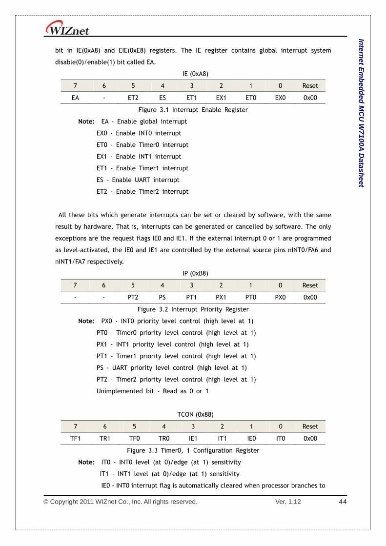
© Copyright 2011 WIZnet Co., Inc. All rights reserved. Ver. 1.12 44
Intern
et Em
bed
ded
MC
U W
7100A D
atasheet
bit in IE(0xA8) and EIE(0xE8) registers. The IE register contains global interrupt system
disable(0)/enable(1) bit called EA.
IE (0xA8)
7 6 5 4 3 2 1 0 Reset
EA - ET2 ES ET1 EX1 ET0 EX0 0x00
Figure 3.1 Interrupt Enable Register
Note: EA - Enable global interrupt
EX0 - Enable INT0 interrupt
ET0 - Enable Timer0 interrupt
EX1 - Enable INT1 interrupt
ET1 - Enable Timer1 interrupt
ES – Enable UART interrupt
ET2 - Enable Timer2 interrupt
All these bits which generate interrupts can be set or cleared by software, with the same
result by hardware. That is, interrupts can be generated or cancelled by software. The only
exceptions are the request flags IE0 and IE1. If the external interrupt 0 or 1 are programmed
as level-activated, the IE0 and IE1 are controlled by the external source pins nINT0/FA6 and
nINT1/FA7 respectively.
IP (0xB8)
7 6 5 4 3 2 1 0 Reset
- - PT2 PS PT1 PX1 PT0 PX0 0x00
Figure 3.2 Interrupt Priority Register
Note: PX0 - INT0 priority level control (high level at 1)
PT0 - Timer0 priority level control (high level at 1)
PX1 - INT1 priority level control (high level at 1)
PT1 - Timer1 priority level control (high level at 1)
PS - UART priority level control (high level at 1)
PT2 – Timer2 priority level control (high level at 1)
Unimplemented bit - Read as 0 or 1
TCON (0x88)
7 6 5 4 3 2 1 0 Reset
TF1 TR1 TF0 TR0 IE1 IT1 IE0 IT0 0x00
Figure 3.3 Timer0, 1 Configuration Register
Note: IT0 - INT0 level (at 0)/edge (at 1) sensitivity
IT1 - INT1 level (at 0)/edge (at 1) sensitivity
IE0 - INT0 interrupt flag is automatically cleared when processor branches to

© Copyright 2011 WIZnet Co., Inc. All rights reserved. Ver. 1.12 45
Intern
et Em
bed
ded
MC
U W
7100A D
atasheet
interrupt routine
IE1 – INT1 interrupt flag is automatically cleared when processor branches to
interrupt routine
TF0 - Timer0 interrupt (overflow) flag. Automatically cleared when processor
branches to interrupt routine
TF1 – Timer 1 interrupt (overflow) flag. Automatically cleared when processor
branches to interrupt routine
SCON (0x98)
7 6 5 4 3 2 1 0 Reset
SM0 SM1 SM2 REN TB8 RB8 TI RI 0x00
Figure 3.4 UART Configuration Register
Note: RI - UART receiver interrupt flag
TI - UART transmitter interrupt flag
EIE (0xE8)
7 6 5 4 3 2 1 0 Reset
- - - EWDI EINT5 EINT4 EINT3 EINT2 0x00
Figure 3.5 Extended Interrupt Enable Register
Note: EINT2 - Enable external INT2 Interrupt
EINT3 - Enable external INT3 Interrupt
EINT4 – Must be ‘0’, if use the EIE register
EINT5 - Enable TCPIPCore Interrupt
EWDI - Enable WATCHDOG Interrupt
EIP (0xF8)
7 6 5 4 3 2 1 0 Reset
- - - PWDI PINT5 PINT4 PINT3 PINT2 0x00
Figure 3.6 Extended Interrupt Priority Register
Note: PINT2 - INT2 priority level control (high level at 1)
PINT3 - INT3 priority level control (high level at 1)
PINT4 – Must be set to ‘0’, if use the EIP register
PINT5 - TCPIPCore Interrupt priority level control (high level at 1)
PWDI - WATCHDOG priority level control (high level at 1)

© Copyright 2011 WIZnet Co., Inc. All rights reserved. Ver. 1.12 46
Intern
et Em
bed
ded
MC
U W
7100A D
atasheet
EIF (0x91)
7 6 5 4 3 2 1 0 Reset
- - - - INT5F INT4F INT3F INT2F 0x00
Figure 3.7 Extended Interrupt Flag Register
Note: INT2F - INT2 interrupt flag. Must be cleared by software
INT3F – INT3 interrupt flag. Must be cleared by software
INT4F – Must be set to ‘0’. if use the EIF register
INT5F - TCPIPCore Interrupt flag. Must be cleared by software
WDCON (0xD8)
7 6 5 4 3 2 1 0 Reset
- - - - WDIF WTRF EWT RWT 0x00
Figure 3.8 Watchdog Control Register
Note: WDIF - Watchdog Interrupt Flag. WDIF in conjunction with the Enable Wat
chdog Interrupt bit (EIE.4) and EWT provides information such as
whether the Watchdog Timer event has been encountered or not
and what action should be taken. This bit must be cleared by sof
tware before exiting the interrupt service routine. By using softwa
re to enable the WDIF, a Watchdog interrupt is generated. Enable
d software-set WDIF will generate a Watchdog interrupt. Timed Ac
cess Register procedure can be used to modify this bit.

© Copyright 2011 WIZnet Co., Inc. All rights reserved. Ver. 1.12 47
Intern
et Em
bed
ded
MC
U W
7100A D
atasheet
4 I/O Ports
The I/O port pin functionalities are described in the following table.
Table 4.1 I/O Ports Pin Description
Pin Active Type Pu/Pd Description
P0[7:0] - IO - Port0 input / output
P1[7:0] - IO - Port1 input / output
P2[7:0] - IO - Port2 input / output
P3[7:0] - IO - Port3 input / output
P0 (0x80)
7 6 5 4 3 2 1 0 Reset
P0.7 P0.6 P0.5 P0.4 P0.3 P0.2 P0.1 P0.0 0xFF
Figure 4.1 Port0 Register
P1 (0x90)
7 6 5 4 3 2 1 0 Reset
P1.7 P1.6 P1.5 P1.4 P1.3 P1.2 P1.1 P1.0 0xFF
Figure 4.2 Port1 Register
P2 (0xA0)
7 6 5 4 3 2 1 0 Reset
P2.7 P2.6 P2.5 P2.4 P2.3 P2.2 P2.1 P2.0 0xFF
Figure 4.3 Port2 Register
P3 (0xB0)
7 6 5 4 3 2 1 0 Reset
P3.7 P3.6 P3.5 P3.4 P3.3 P3.2 P3.1 P3.0 0xFF
Figure 4.4 Port3 Register
Read and write accesses are performed in the I/O ports via their corresponding SFR: P0
(0x80), P1 (0x90), P2 (0xA0), and P3 (0xB0). Some port-reading instructions read from the
data registers while others read from the port pin. The “Read-Modify-Write” instructions are
directed to the data registers as shown below.

© Copyright 2011 WIZnet Co., Inc. All rights reserved. Ver. 1.12 48
Intern
et Em
bed
ded
MC
U W
7100A D
atasheet
Table 4.2 Read-Modify-Write Instructions
Instruction Function Description
ANL Logic AND
ORL Logic OR
XRL Logic exclusive OR
JBC Jump if bit is set and cleared
CPL Complement bit
INC, DEC Increment, decrement byte
DJNZ Decrement and jump if not zero
MOV Px.y, C Move carry bit to bit y of port x
CLR Px.y Clear bit y of port x
SETB Px.y Set bit y of port x
All other instructions read from a port exclusively through the port pins. All ports pin can be
used as GPIO (General Purpose Input Output). The GPIO of W7100A is shown in the Figure
below. The output driving voltage of GPIO is 0V or 3.3V according to the Px_PD/PU SFR value.
P0_PD(0xE3): GPIO0 Pull-down register, the value ‘1’ pull-down the related pin.
P0_PD (0xE3)
7 6 5 4 3 2 1 0 Reset
Port0[7] Port0[6] Port0[5] Port0[4] Port0[3] Port0[2] Port0[1] Port0[0] 0x00
Figure 4.5 Port0 Pull-down register
P1_PD(0xE4): GPIO1 Pull-down register, the value ‘1’ pull-down the related pin.
P1_PD (0xE4)
7 6 5 4 3 2 1 0 Reset
Port1[7] Port1[6] Port1[5] Port1[4] Port1[3] Port1[2] Port1[1] Port1[0] 0x00
Figure 4.6 Port1 Pull-down register
P2_PD(0xE5): GPIO2 Pull-down register, the value ‘1’ pull-down the related pin.
P2_PD (0xE5)
7 6 5 4 3 2 1 0 Reset
Port2[7] Port2[6] Port2[5] Port2[4] Port2[3] Port2[2] Port2[1] Port2[0] 0x00
Figure 4.7 Port2 Pull-down register
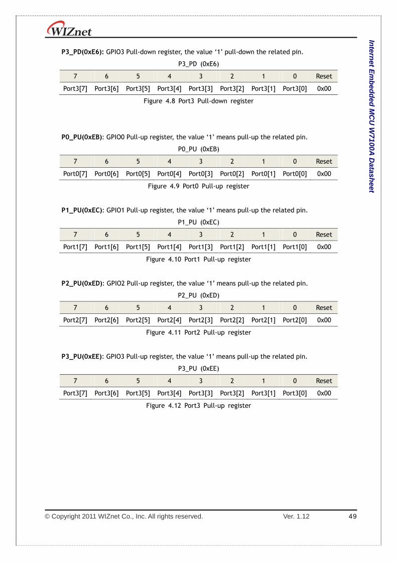
© Copyright 2011 WIZnet Co., Inc. All rights reserved. Ver. 1.12 49
Intern
et Em
bed
ded
MC
U W
7100A D
atasheet
P3_PD(0xE6): GPIO3 Pull-down register, the value ‘1’ pull-down the related pin.
P3_PD (0xE6)
7 6 5 4 3 2 1 0 Reset
Port3[7] Port3[6] Port3[5] Port3[4] Port3[3] Port3[2] Port3[1] Port3[0] 0x00
Figure 4.8 Port3 Pull-down register
P0_PU(0xEB): GPIO0 Pull-up register, the value ‘1’ means pull-up the related pin.
P0_PU (0xEB)
7 6 5 4 3 2 1 0 Reset
Port0[7] Port0[6] Port0[5] Port0[4] Port0[3] Port0[2] Port0[1] Port0[0] 0x00
Figure 4.9 Port0 Pull-up register
P1_PU(0xEC): GPIO1 Pull-up register, the value ‘1’ means pull-up the related pin.
P1_PU (0xEC)
7 6 5 4 3 2 1 0 Reset
Port1[7] Port1[6] Port1[5] Port1[4] Port1[3] Port1[2] Port1[1] Port1[0] 0x00
Figure 4.10 Port1 Pull-up register
P2_PU(0xED): GPIO2 Pull-up register, the value ‘1’ means pull-up the related pin.
P2_PU (0xED)
7 6 5 4 3 2 1 0 Reset
Port2[7] Port2[6] Port2[5] Port2[4] Port2[3] Port2[2] Port2[1] Port2[0] 0x00
Figure 4.11 Port2 Pull-up register
P3_PU(0xEE): GPIO3 Pull-up register, the value ‘1’ means pull-up the related pin.
P3_PU (0xEE)
7 6 5 4 3 2 1 0 Reset
Port3[7] Port3[6] Port3[5] Port3[4] Port3[3] Port3[2] Port3[1] Port3[0] 0x00
Figure 4.12 Port3 Pull-up register

© Copyright 2011 WIZnet Co., Inc. All rights reserved. Ver. 1.12 50
Intern
et Em
bed
ded
MC
U W
7100A D
atasheet
5 Timers
The W7100A contains two 16-bit timers/counters, Timer0 and Timer 1. In the ‘timer mode’,
the timer registers are incremented by every 12 CLK periods. In “counter mode”, the timer
registers are incremented during the falling transition on their corresponding input pins: T0 or
T1. The input pins are sampled at every CLK period.
5.1 Timers 0, 1
5.1.1 Overview The Timer0, 1 pin functionalities are described in the following table. All pins are
unidirectional. There are no tri-state output pins and internal signals.
Table 5.1 Timers 0, 1 Pin Description
Pin Active Type Pu/Pd Description
T0/FCS Falling I - Timer0 clock
GATE0/FOE High I - Timer0 clock gate control
T1/FAE Falling I - Timer1 clock
GATE1/FA0 High I - Timer1 clock gate control
Timer0 and Timer 1 are fully compatible with the standard 8051 timers. Each timer consists
of two 8-bit registers, TH0 (0x8C) and TL0 (0x8A), TH1 (0x8D) and TL1 (0x8B). The timers
work in four modes which are described below.
Table 5.2 Timers 0, 1 Mode
M1 M0 Mode Function Description
0 0 0 THx operates as a 8-bit timer/counter with a divided-by-32
prescaler served by lower 5-bit of TLx
0 1 1 16-bit timer/counter. THx and TLx are cascaded.
1 0 2 TLx operates as a 8-bit timer/counter with 8bit auto-reload by
THx.
1 1 3 TL0 is configured as a 8-bit timer/counter controlled by the
standard Timer0 bits. TH0 is a 8-bit timer controlled by Timer 1
control bits. Timer 1 holds its count.

© Copyright 2011 WIZnet Co., Inc. All rights reserved. Ver. 1.12 51
Intern
et Em
bed
ded
MC
U W
7100A D
atasheet
TMOD (0x89)
Timer1 Timer0
7 6 5 4 3 2 1 0 Reset
GATE CT M1 M0 GATE CT M1 M0 0x00
Figure 5.1 Timer0, 1 Control Mode Register
Note: GATE - Gating control
1: Timer x is enabled while GATEx pin is at high and TRx control b
it is set
0: Timer x is enabled while TRx control bit is set
CT - Counter or timer select bit
1: Counter mode, Timer x clock source from Tx pin
0: Timer mode, internally clocked
M1, M0 – Mode select bits
TCON (0x88)
7 6 5 4 3 2 1 0 Reset
TF1 TR1 TF0 TR0 IE1 IT1 IE0 IT0 0x00
Figure 5.2 Timer0, 1 Configuration Register
Note: TR0 - Timer0 run control bit
1: Enabled
0: Disabled
TR1 - Timer 1 run control bit
1: Enabled
0: Disabled
External input pins, GATE0 and GATE1, can be programmed to function as a gate to
facilitate pulse width measurements.
5.1.2 Interrupts Timer0, 1 interrupt related bits are shown below. An interrupt can be toggled by the IE
register, and priorities can be configured in the IP register.
IE (0xA8)
7 6 5 4 3 2 1 0 Reset
EA - ET2 ES ET1 EX1 ET0 EX0 0x00
Figure 5.3 Interrupt Enable Register
Note: EA - Enable global interrupts
ET0 - Enable Timer0 interrupts
ET1- Enable Timer1 interrupts

© Copyright 2011 WIZnet Co., Inc. All rights reserved. Ver. 1.12 52
Intern
et Em
bed
ded
MC
U W
7100A D
atasheet
IP (0xB8)
7 6 5 4 3 2 1 0 Reset
- - PT2 PS PT1 PX1 PT0 PX0 0x00
Figure 5.4 Interrupt Priority Register
Note: PT0 - Enable global interrupts
PT1 - Enable Timer0 interrupts
Unimplemented bit - Read as 0 or 1
TCON (0x88)
7 6 5 4 3 2 1 0 Reset
TF1 TR1 TF0 TR0 IE1 IT1 IE0 IT0 0x00
Figure 5.5 Timer0, 1 Configuration Register
Note: TF0 - Timer0 interrupt (overflow) flag. Automatically cleared when proce
ssor branches to interrupt routine
TF1 - Timer1 interrupt (overflow) flag. Automatically cleared when proces
sor branches to interrupt routine
All of the bits which generate interrupts can be set or cleared by software, with the same
result by hardware. That is, interrupts can be generated or cancelled by software.
Table 5.3 Timer0, 1 interrupts
Interrupt
Flag
Function Active
Level/Edge
Flag Resets Vector Natural Priority
TF0 Internal, Timer0 - Hardware 0x0B 2
TF1 Internal, Timer1 - Hardware 0x1B 4
5.1.3 Timer0 – Mode0 The Timer0 register is configured as a 13-bit register (8bit: Timer, 5bit: prescaler). As the all
counts (valid bits) roll over from 1 to 0, Timer0 interrupt flag TF0 is set. The timer starts
counting when TCON.4 =1 and either TMOD.3 = 0 or GATE0 = 1. By setting TMOD.3 = 1, the
external input GATE0 can control Timer0 to manage the pulse width measurements. The 13-
bit register consists of 8 bits TH0 and 5 bits of TL0. The upper 3 bits of TL0 should be ignored.
Refer to the following Figure for details.
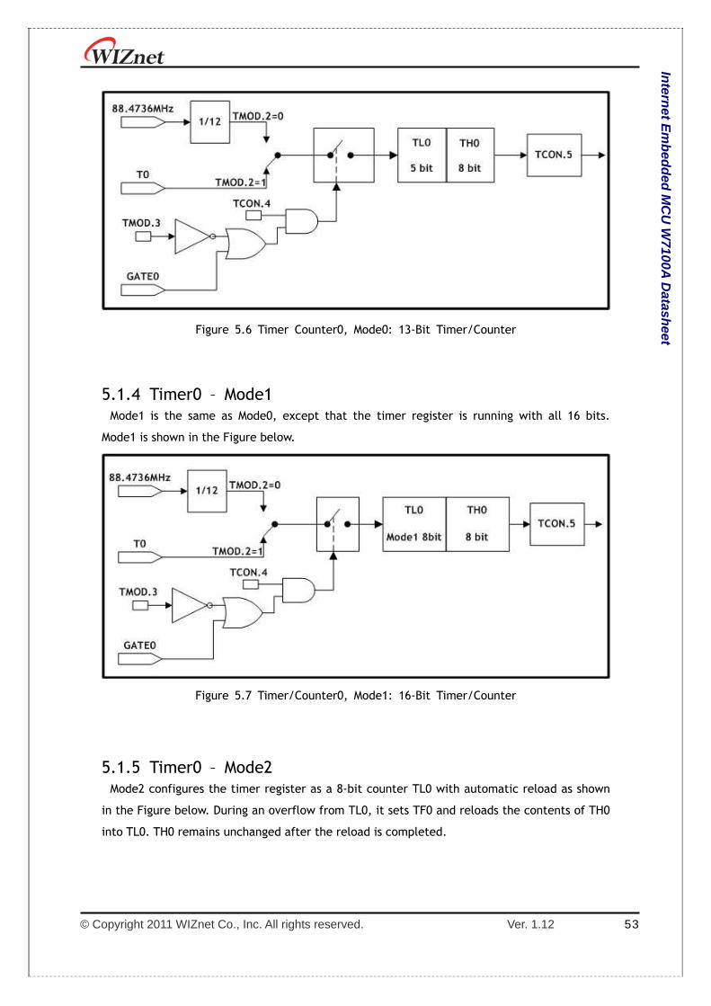
© Copyright 2011 WIZnet Co., Inc. All rights reserved. Ver. 1.12 53
Intern
et Em
bed
ded
MC
U W
7100A D
atasheet
Figure 5.6 Timer Counter0, Mode0: 13-Bit Timer/Counter
5.1.4 Timer0 – Mode1 Mode1 is the same as Mode0, except that the timer register is running with all 16 bits.
Mode1 is shown in the Figure below.
Figure 5.7 Timer/Counter0, Mode1: 16-Bit Timer/Counter
5.1.5 Timer0 – Mode2 Mode2 configures the timer register as a 8-bit counter TL0 with automatic reload as shown
in the Figure below. During an overflow from TL0, it sets TF0 and reloads the contents of TH0
into TL0. TH0 remains unchanged after the reload is completed.

© Copyright 2011 WIZnet Co., Inc. All rights reserved. Ver. 1.12 54
Intern
et Em
bed
ded
MC
U W
7100A D
atasheet
Figure 5.8 Timer/Counter0, Mode2: 8-Bit Timer/Counter with Auto-Reload
5.1.6 Timer0 – Mode3 In this mode, the TL0 and TH0 are divided into two separate counters. The following Figure
shows the logic for Timer0 running in Mode3. The TL0 uses the Timer0 control bits: C/T, GATE,
TR0, GATE0 and TF0. And the TH0 is locked into a timer function and uses TR1 and TF1 flags
from Timer 1 and controls Timer 1 interrupt. Mode3 is used in applications which require an
extra 8-bit timer/counter. When Timer0 is in Mode3, Timer 1 can be turned on/off by
switching itself into Mode3, or can still be used by the serial channel as a baud rate generator,
or in any application where interrupt from Timer 1 is not required.
Figure 5.9 Timer/Counter0, Mode3: Two 8-Bit Timers/Counters

© Copyright 2011 WIZnet Co., Inc. All rights reserved. Ver. 1.12 55
Intern
et Em
bed
ded
MC
U W
7100A D
atasheet
5.1.7 Timer1 – Mode0 In this mode, the Timer1 register is configured as a 13-bit register (8bit: Timer, 5bit:
prescaler). As the all counts (valid bits) roll over from 1 to 0, Timer 1 interrupt flag TF1 is set.
The counted input is enabled to Timer 1 when TCON.6 = 1 and either TMOD.6 = 0 or GATE1 = 1.
(Setting TMOD.7 = 1 allows Timer 1 controlled by external input GATE1, to facilitate pulse
width measurements). The 13-bit register consists of 8 bits TH1 and the lower 5 bits of TL1.
The upper 3 bits of TL1 are indeterminate and should be ignored. Refer to the following
Figure for detail.
Figure 5.10 Timer/Counter1, Mode0: 13-Bit Timer/Counter
5.1.8 Timer1 – Mode1 Mode1 is the same as Mode0, except that the timer register is running with all 16 bits.
Mode1 is shown in the Figure below.
Figure 5.11 Timer/Counter1, Mode1: 16-Bit Timers/Counters

© Copyright 2011 WIZnet Co., Inc. All rights reserved. Ver. 1.12 56
Intern
et Em
bed
ded
MC
U W
7100A D
atasheet
5.1.9 Timer1 – Mode2 Mode2 configures timer register as 8-bit counter TL1, with automatic reload as shown in
Figure below. Overflow from TL1 only sets TF1, but also automatically reloads TL1 with the
contents of TH1. The reload leaves TH1 unchanged.
Figure 5.12 Timer/Counter1, Mode2: 8-Bit Timer/Counter with Auto-Reload
5.1.10 Timer1 – Mode3 Timer1 in Mode3 holds counting. The effect is the same as setting TR1 = 0 because it is used
for Timer0-Mode3. For more detail, please refer to the section 5.1.6 ‘Timer0-Mode3’.
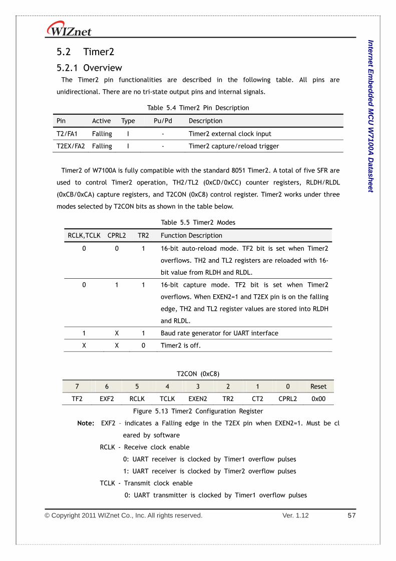
© Copyright 2011 WIZnet Co., Inc. All rights reserved. Ver. 1.12 57
Intern
et Em
bed
ded
MC
U W
7100A D
atasheet
5.2 Timer2
5.2.1 Overview The Timer2 pin functionalities are described in the following table. All pins are
unidirectional. There are no tri-state output pins and internal signals.
Table 5.4 Timer2 Pin Description
Pin Active Type Pu/Pd Description
T2/FA1 Falling I - Timer2 external clock input
T2EX/FA2 Falling I - Timer2 capture/reload trigger
Timer2 of W7100A is fully compatible with the standard 8051 Timer2. A total of five SFR are
used to control Timer2 operation, TH2/TL2 (0xCD/0xCC) counter registers, RLDH/RLDL
(0xCB/0xCA) capture registers, and T2CON (0xC8) control register. Timer2 works under three
modes selected by T2CON bits as shown in the table below.
Table 5.5 Timer2 Modes
RCLK,TCLK CPRL2 TR2 Function Description
0 0 1 16-bit auto-reload mode. TF2 bit is set when Timer2
overflows. TH2 and TL2 registers are reloaded with 16-
bit value from RLDH and RLDL.
0 1 1 16-bit capture mode. TF2 bit is set when Timer2
overflows. When EXEN2=1 and T2EX pin is on the falling
edge, TH2 and TL2 register values are stored into RLDH
and RLDL.
1 X 1 Baud rate generator for UART interface
X X 0 Timer2 is off.
T2CON (0xC8)
7 6 5 4 3 2 1 0 Reset
TF2 EXF2 RCLK TCLK EXEN2 TR2 CT2 CPRL2 0x00
Figure 5.13 Timer2 Configuration Register
Note: EXF2 – indicates a Falling edge in the T2EX pin when EXEN2=1. Must be cl
eared by software
RCLK - Receive clock enable
0: UART receiver is clocked by Timer1 overflow pulses
1: UART receiver is clocked by Timer2 overflow pulses
TCLK - Transmit clock enable
0: UART transmitter is clocked by Timer1 overflow pulses
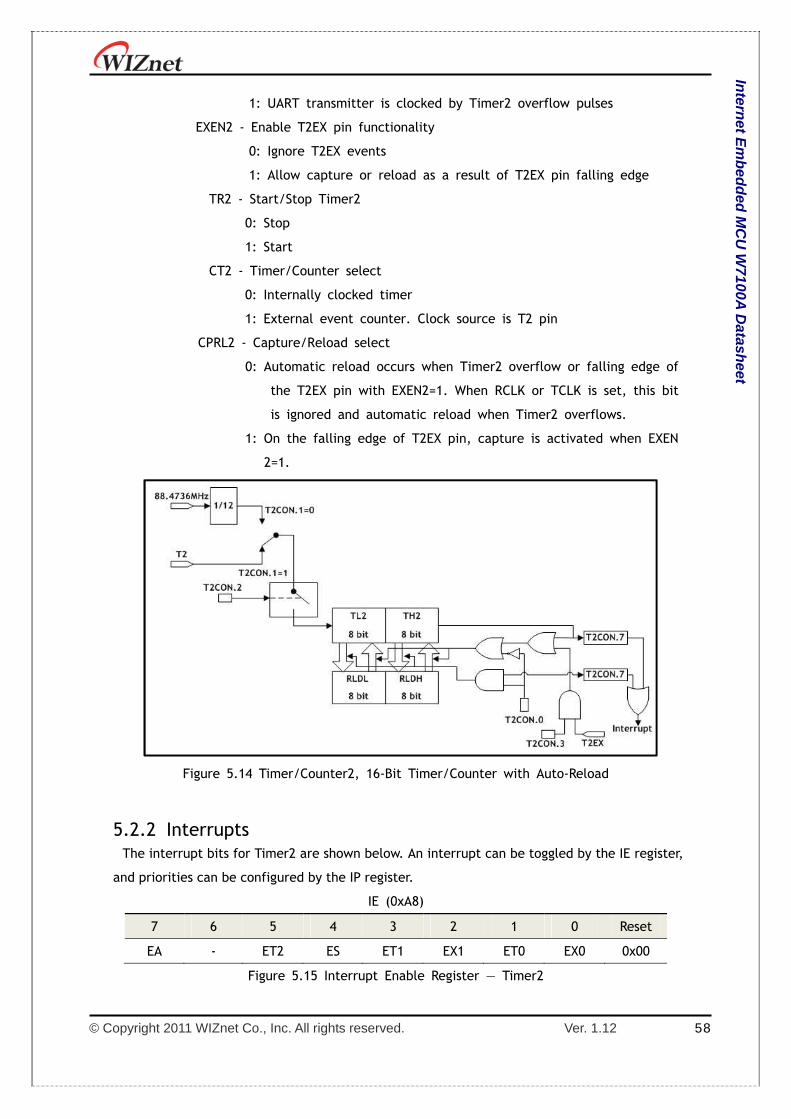
© Copyright 2011 WIZnet Co., Inc. All rights reserved. Ver. 1.12 58
Intern
et Em
bed
ded
MC
U W
7100A D
atasheet
1: UART transmitter is clocked by Timer2 overflow pulses
EXEN2 - Enable T2EX pin functionality
0: Ignore T2EX events
1: Allow capture or reload as a result of T2EX pin falling edge
TR2 - Start/Stop Timer2
0: Stop
1: Start
CT2 - Timer/Counter select
0: Internally clocked timer
1: External event counter. Clock source is T2 pin
CPRL2 - Capture/Reload select
0: Automatic reload occurs when Timer2 overflow or falling edge of
the T2EX pin with EXEN2=1. When RCLK or TCLK is set, this bit
is ignored and automatic reload when Timer2 overflows.
1: On the falling edge of T2EX pin, capture is activated when EXEN
2=1.
Figure 5.14 Timer/Counter2, 16-Bit Timer/Counter with Auto-Reload
5.2.2 Interrupts The interrupt bits for Timer2 are shown below. An interrupt can be toggled by the IE register,
and priorities can be configured by the IP register.
IE (0xA8)
7 6 5 4 3 2 1 0 Reset
EA - ET2 ES ET1 EX1 ET0 EX0 0x00
Figure 5.15 Interrupt Enable Register — Timer2
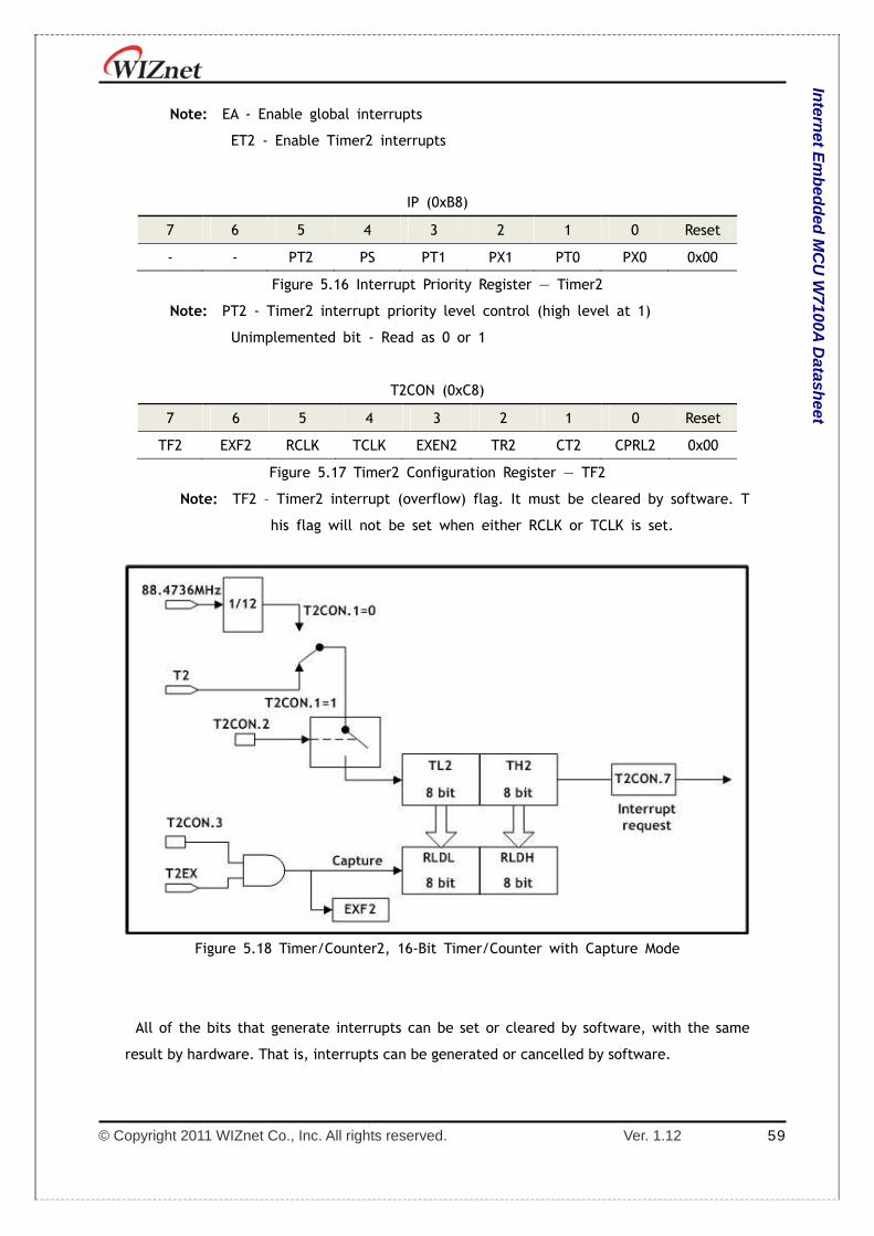
© Copyright 2011 WIZnet Co., Inc. All rights reserved. Ver. 1.12 59
Intern
et Em
bed
ded
MC
U W
7100A D
atasheet
Note: EA - Enable global interrupts
ET2 - Enable Timer2 interrupts
IP (0xB8)
7 6 5 4 3 2 1 0 Reset
- - PT2 PS PT1 PX1 PT0 PX0 0x00
Figure 5.16 Interrupt Priority Register — Timer2
Note: PT2 - Timer2 interrupt priority level control (high level at 1)
Unimplemented bit - Read as 0 or 1
T2CON (0xC8)
7 6 5 4 3 2 1 0 Reset
TF2 EXF2 RCLK TCLK EXEN2 TR2 CT2 CPRL2 0x00
Figure 5.17 Timer2 Configuration Register — TF2
Note: TF2 – Timer2 interrupt (overflow) flag. It must be cleared by software. T
his flag will not be set when either RCLK or TCLK is set.
Figure 5.18 Timer/Counter2, 16-Bit Timer/Counter with Capture Mode
All of the bits that generate interrupts can be set or cleared by software, with the same
result by hardware. That is, interrupts can be generated or cancelled by software.

© Copyright 2011 WIZnet Co., Inc. All rights reserved. Ver. 1.12 60
Intern
et Em
bed
ded
MC
U W
7100A D
atasheet
Table 5.6 Timer2 Interrupt
Interrupt
Flag
Function Active
Level/Edge
Flag Resets Vector Natural Priority
TF2 Internal, Timer2 - Software 0x2B 6
Interrupt is generated at the falling edge of T2EX pin with EXEN2 bit enabled.
Using the 0x2B vector, EXF2 is set by this interrupt, but the TF2 flag remains unchanged.
Figure 5.19 Timer2 for Baud Rate Generator Mode

© Copyright 2011 WIZnet Co., Inc. All rights reserved. Ver. 1.12 61
Intern
et Em
bed
ded
MC
U W
7100A D
atasheet
6 UART
The UART of W7100A operates in full duplex mode which is capable of receiving and
transmitting at the same time. Since the W7100A is double-buffered, the receiver is capable
of receiving data while the first byte of the buffer is not read. During a read operation, the
SBUF reads from the receive register. On the other hand, SBUF loads the data into the
transmit register during a send operation. The UART has 4 different modes which include one
in synchronous mode and three in asynchronous modes. Modes 2 and 3 include a special
feature for multiprocessor communication. This feature is enabled by setting the SM2 bit in
the SCON register. The master processor sends out the first address byte which identifies the
target slave. An address byte differs from a data byte in that the 9th bit is 1 in an address byte
and 0 in a data byte. With SM2 = 1, no slave will be interrupted by a data byte, while an
address byte will interrupt all slaves. The addressed slave will clear its SM2 bit and prepare to
receive the data bytes that will be coming. The slaves that were not being addressed leave
their SM2 set and ignore the incoming data.
The pin functionalities of UART are described in the following table.
Table 6.1 UART Pin Description
Pin Active Type Pu/Pd Description
RXD - I Pu Serial receiver input / output
TXD - O - Serial transmitter
The UART of W7100A is fully compatible with the standard 8051 UART. The UART related
registers are: SBUF (0x99), SCON (0x98), PCON (0x87), IE (0xA8) and IP (0xB8). The UART data
buffer (SBUF) consists of two registers: transmit and receive. When data is written into the
SBUF transmit register, the sending process begins. Similarly, data is read from the receive
register during the receiving process.
SBUF (0x99)
7 6 5 4 3 2 1 0 Reset
SB7 SB6 SB5 SB4 SB3 SB2 SB1 SB0 0x00
Figure 6.1 UART Buffer Register
SCON (0x98)
7 6 5 4 3 2 1 0 Reset
SM0 SM1 SM2 REN TB8 RB8 TI RI 0x00
Figure 6.2 UART Configuration Register
Note: SM2 - Enable a multiprocessor communication feature
SM1 - Set baud rate
SM0 - Set baud rate

© Copyright 2011 WIZnet Co., Inc. All rights reserved. Ver. 1.12 62
Intern
et Em
bed
ded
MC
U W
7100A D
atasheet
REN – ‘1’ : enable serial receive
‘0’: disable serial receive
TB8 - The 9th transmitted data bit in Modes 2 and 3. This bit is enabled
depending on the MCU’s operation (parity check, multiprocessor
communication, etc.),
RB8 - In Modes 2 and 3, it is the 9th bit of data received. In Mode1, if S
M2 is 0, RB08 is a stop bit. In Mode0, this bit is not used.
The UART modes are presented in the table below.
Table 6.2 UART Modes
SM0 SM1 Mode Description Baud Rate
0 0 0 Shift register fosc/12
0 1 1 8-bit UART Variable
1 0 2 9-bit UART fosc/32 or /64
1 1 3 9-bit UART Variable
The UART baud rates are presented below.
Table 6.3 UART Baud Rates
Mode Baud Rate
Mode0 fosc/12
Mode1,3 Time1 overflow rate or Timer2 overflow rate
Mode2 SMOD0 = 0 fosc/64
SMOD0 = 1 fosc/32
The SMOD0 bit is located in the PCON register.
PCON (0x87)
7 6 5 4 3 2 1 0 Reset
SMOD0 SMOD1 - PWE - 0 0 0 0x00
Figure 6.3 UART Bits in Power Configuration Register
Note: SMOD0 - Bit for UART baud rate
Unimplemented bit - Read as 0 or 1
Bits 2-0 must be written as 0
6.1 Interrupts UART interrupt related bits are shown below. An interrupt can be toggled by the IE register,
and priorities can be configured by the IP register.

© Copyright 2011 WIZnet Co., Inc. All rights reserved. Ver. 1.12 63
Intern
et Em
bed
ded
MC
U W
7100A D
atasheet
IE (0xA8)
7 6 5 4 3 2 1 0 Reset
EA - ET2 ES ET1 EX1 ET0 EX0 0x00
Figure 6.4 UART Bits in Interrupt Enable Register
Note: ES - RI & TI interrupt enable flag
IP (0xB8)
7 6 5 4 3 2 1 0 Reset
- - PT2 PS PT1 PX1 PT0 PX0 0x00
Figure 6.5 UART Bits in Interrupt Priority Register
Note: SMOD0 - Bit for UART baud rate
Unimplemented bit - Read as 0 or 1
SCON (0x98)
7 6 5 4 3 2 1 0 Reset
SM0 SM1 SM2 REN TB08 RB08 TI RI 0x00
Figure 6.6 UART Configuration Register
Note: TI – Transmit interrupt flag, automatically set after completion of a serial
transfer. It must be cleared by software.
RI – Receive interrupt flag, automatically set after completion of a serial
reception. It must be cleared by software.
All of the bits that generate interrupts can be set or cleared by software, with the same
result by hardware. That is, interrupts can be generated or cancelled by software.
Table 6.4 UART Interrupt
Interrupt
Flag
Function Active
Level/Edge
Flag Resets Vector Natural Priority
TI & RI Internal, UART - software 0x23 5
6.2 Mode0, Synchronous TXD output is a shift clock. The baud rate is fixed at 1/12 of the CLK clock frequency. Eight
bits are transmitted with LSB first. Reception is initialized by setting the flags in SCON as
follows: RI = 0 and REN = 1.
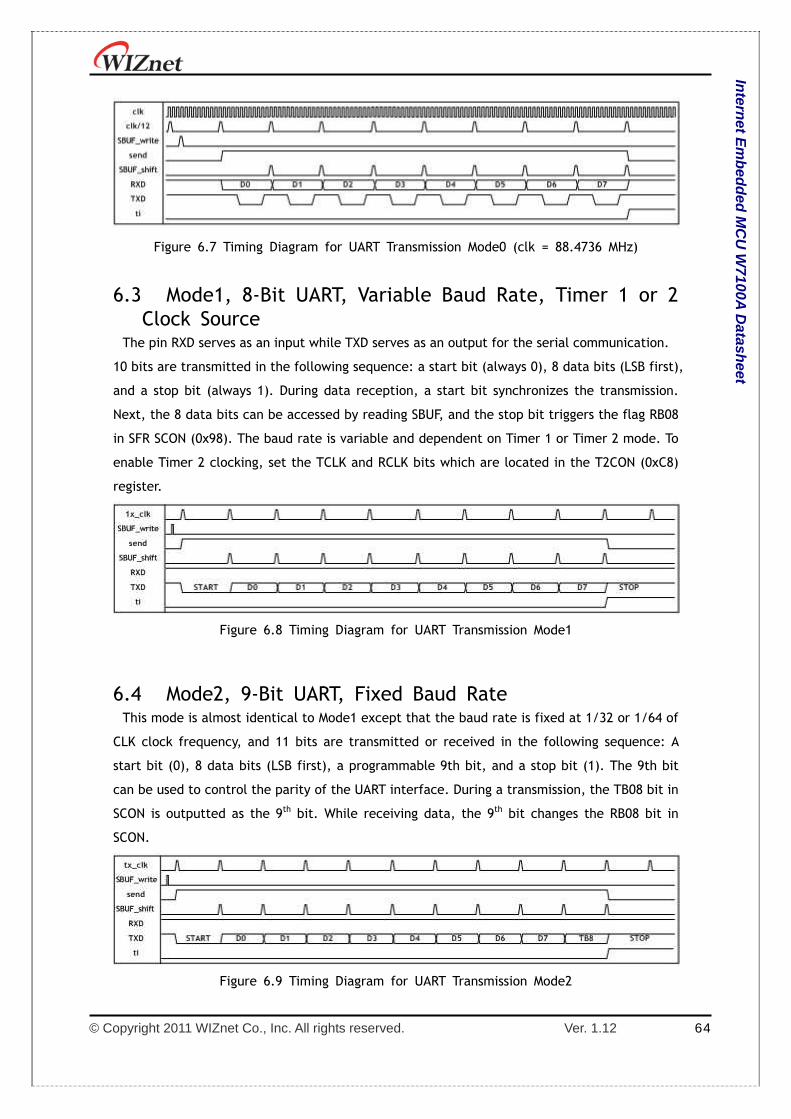
© Copyright 2011 WIZnet Co., Inc. All rights reserved. Ver. 1.12 64
Intern
et Em
bed
ded
MC
U W
7100A D
atasheet
Figure 6.7 Timing Diagram for UART Transmission Mode0 (clk = 88.4736 MHz)
6.3 Mode1, 8-Bit UART, Variable Baud Rate, Timer 1 or 2 Clock Source
The pin RXD serves as an input while TXD serves as an output for the serial communication.
10 bits are transmitted in the following sequence: a start bit (always 0), 8 data bits (LSB first),
and a stop bit (always 1). During data reception, a start bit synchronizes the transmission.
Next, the 8 data bits can be accessed by reading SBUF, and the stop bit triggers the flag RB08
in SFR SCON (0x98). The baud rate is variable and dependent on Timer 1 or Timer 2 mode. To
enable Timer 2 clocking, set the TCLK and RCLK bits which are located in the T2CON (0xC8)
register.
Figure 6.8 Timing Diagram for UART Transmission Mode1
6.4 Mode2, 9-Bit UART, Fixed Baud Rate This mode is almost identical to Mode1 except that the baud rate is fixed at 1/32 or 1/64 of
CLK clock frequency, and 11 bits are transmitted or received in the following sequence: A
start bit (0), 8 data bits (LSB first), a programmable 9th bit, and a stop bit (1). The 9th bit
can be used to control the parity of the UART interface. During a transmission, the TB08 bit in
SCON is outputted as the 9th bit. While receiving data, the 9th bit changes the RB08 bit in
SCON.
Figure 6.9 Timing Diagram for UART Transmission Mode2
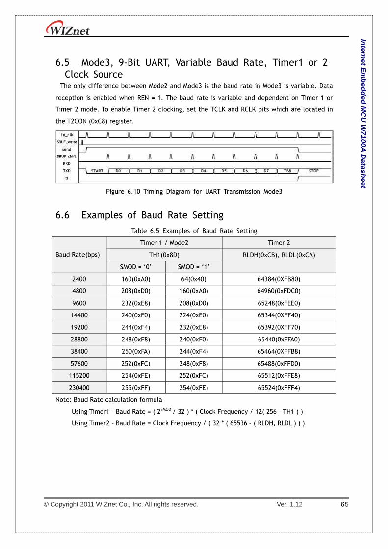
© Copyright 2011 WIZnet Co., Inc. All rights reserved. Ver. 1.12 65
Intern
et Em
bed
ded
MC
U W
7100A D
atasheet
6.5 Mode3, 9-Bit UART, Variable Baud Rate, Timer1 or 2 Clock Source
The only difference between Mode2 and Mode3 is the baud rate in Mode3 is variable. Data
reception is enabled when REN = 1. The baud rate is variable and dependent on Timer 1 or
Timer 2 mode. To enable Timer 2 clocking, set the TCLK and RCLK bits which are located in
the T2CON (0xC8) register.
Figure 6.10 Timing Diagram for UART Transmission Mode3
6.6 Examples of Baud Rate Setting
Table 6.5 Examples of Baud Rate Setting
Baud Rate(bps)
Timer 1 / Mode2 Timer 2
TH1(0x8D) RLDH(0xCB), RLDL(0xCA)
SMOD = ‘0’ SMOD = ‘1’
2400 160(0xA0) 64(0x40) 64384(0XFB80)
4800 208(0xD0) 160(0xA0) 64960(0xFDC0)
9600 232(0xE8) 208(0xD0) 65248(0xFEE0)
14400 240(0xF0) 224(0xE0) 65344(0XFF40)
19200 244(0xF4) 232(0xE8) 65392(0XFF70)
28800 248(0xF8) 240(0xF0) 65440(0xFFA0)
38400 250(0xFA) 244(0xF4) 65464(0XFFB8)
57600 252(0xFC) 248(0xF8) 65488(0xFFD0)
115200 254(0xFE) 252(0xFC) 65512(0xFFE8)
230400 255(0xFF) 254(0xFE) 65524(0xFFF4)
Note: Baud Rate calculation formula
Using Timer1 – Baud Rate = ( 2SMOD / 32 ) * ( Clock Frequency / 12( 256 – TH1 ) )
Using Timer2 – Baud Rate = Clock Frequency / ( 32 * ( 65536 – ( RLDH, RLDL ) ) )

© Copyright 2011 WIZnet Co., Inc. All rights reserved. Ver. 1.12 66
Intern
et Em
bed
ded
MC
U W
7100A D
atasheet
7 Watchdog Timer
7.1 Overview The Watchdog Timer is driven by the main system clock that is supplied by a series of dividers
as shown in the Figure below. The divider output is selectable and determines the timeout
intervals. When the timeout is reached, an interrupt flag will be set, and if enabled, a reset
will be occurred. When interrupt enable bit and global interrupt are enabled, the interrupt
flag will activate the interrupts. The reset and interrupt are completely discrete functions
that may be acknowledged separately, together or even ignored depending on the application.
Figure 7.1 Watchdog Timer Structure
7.2 Interrupts Watchdog interrupt related bits are shown below. An interrupt can be turned on/off by the
IE (0xA8) and EIE (0xE8) registers, and high/low priorities can be set in the EIP EIP (0xF8)
register. The IE contains global interrupt system disable (0) / enable (1) bit called EA.
IE (0xA8)
7 6 5 4 3 2 1 0 Reset
EA - ET2 ES ET1 EX1 ET0 EX0 0x00
Figure 7.2 Interrupt Enable Register
EIE (0xE8)
7 6 5 4 3 2 1 0 Reset
- - - EWDI EINT5 EINT4 EINT3 EINT2 0x00
Figure 7.3 Extended Interrupt Enable Register
Note: EA - Enable global interrupt
EWDI - Enable Watchdog interrupt
© Copyright 2011 WIZnet Co., Inc. All rights reserved. Ver. 1.12 67
Intern
et Em
bed
ded
MC
U W
7100A D
atasheet
EIP (0xF8)
7 6 5 4 3 2 1 0 Reset
- - - PWDI PINT5 PINT4 PINT3 PINT2 0x00
Figure 7.4 Extended interrupt Priority Register
Note: PWDI - Watchdog priority level control (high level at 1)
Unimplemented bit - Read as 0 or 1
WDCON (0xD8)
7 6 5 4 3 2 1 0 Reset
- - - - WDIF WTRF EWT RWT 0x00
Figure 7.5 Watchdog Control Register
Note: WDIF - Watchdog Interrupt Flag. WDIF in conjunction with Enable Watchd
og Interrupt bit (EIE.4) and EWT, indicates if a watchdog timer e
vent has occurred and what action should be taken. This bit mu
st be cleared by software before exiting the interrupt service ro
utine or another interrupt is generated. Setting WDIF in software
will generate a watchdog interrupt if enabled. User must use ‘Ti
med Access Register’ when clear this WDIF bit. Please refer to
the section 7.8 ‘Timed Access’ procedure.
All of the bits that generate interrupts can be set or cleared by software, with the same
result by hardware. That is, interrupts can be generated or cancelled by software.
Table 7.1 Watchdog Interrupt
Interrupt Flag Function Active Level/Edge Flag Reset Vector Natural Priority
WDIF Internal,
Watchdog
- Software 0x63 11
7.3 Watchdog Timer Reset The Watchdog Timer reset operates as follows. Once the timeout interval is initialized, the
system restarts the Watchdog first by using RWT. Then, the reset mode is enabled by the EWT
(Enable Watchdog Timer reset = WDCON.1) bit. Before the timer reaches the user selected
terminal value, the software can set the RWT (Reset Watchdog Timer = WDCON.0) bit. If RWT
is set before the timeout is reached, the timer will start over. If the timeout is reached
without RWT being set, the Watchdog will reset the MCU. The Hardware automatically clears
RWT after sets the RWT by software. When a reset occurs, the WTRF (Watchdog Timer reset
Flag = WDCON.2) will automatically set to indicate the cause of the reset; however, software
must clear this bit manually.

© Copyright 2011 WIZnet Co., Inc. All rights reserved. Ver. 1.12 68
Intern
et Em
bed
ded
MC
U W
7100A D
atasheet
7.4 Simple Timer The Watchdog Timer is a free running timer. In timer mode with reset disabled (EWT = 0)
and interrupt functions disabled (EWDI = 0), the timer counts up to pre-programmed interval
in WD[1:0] which will enable the Watchdog interrupt flag. By resetting the RWT bit, this timer
can operate in polled timeout mode. The WDIF bit can be cleared by software or reset. The
Watchdog interrupt is available for application which requires a long timer. The interrupt is
enabled by using the EWDI (Enable WatchDog timer Interrupt = EIE.4) bit. When a timeout
occurs, the Watchdog Timer will set the WDIF bit (WDCON.3), and an interrupt will occur if
the global interrupt enable (EA) is set. Note that WDIF is set to 512 clocks before a
potential Watchdog reset. The Watchdog interrupt flag indicates the source of the interrupt,
and must be cleared by software. When the Watchdog interrupt is used properly, the
Watchdog reset allows the interrupt software to monitor the system for any errors.
7.5 System Monitor If the EWT bit of WDCON was set, W7100A will reset when a Watchdog timeout occurs. User
can use the Watchdog timer as a system monitor using this function. For example, assuming
that an unexpected code was running, there is no RWT clear routine because this code is not
designed by user; resulting a Watchdog timeout to occur, and the W7100A will reset. User can
escape unexpected state by using this method.
7.6 Watchdog Related Registers The Watchdog Timer has several SFR bits that are used during its operation. These bits can
be utilized as a reset source, interrupt source, software polled timer or any combination of
the three. Both the reset and interrupt have status flags. The Watchdog also has a bit which
restarts the timer. The table below shows the bit locations with descriptions.
Table 7.2 Summary for Watchdog Related Bits
Bit Name Register Bit Position Description
EWDI EIE EIE.4 Enable Watchdog Timer Interrupt
PWDI EIP EIP.4 Priority of Watchdog Timer Interrupt
WD[1:0] CKCON CKCON.7-6 Watchdog Interval
RWT WDCON WDCON.0 Reset Watchdog Timer
EWT WDCON.1 Enable Watchdog Timer reset
WTRF WDCON.2 Watchdog Timer reset flag
WDIF WDCON.3 Watchdog Interrupt flag
The Watchdog Timer is not disabled during a Watchdog timeout reset, but it restarts the
timer. Control bits that support Watchdog operation are described in next subsections.

© Copyright 2011 WIZnet Co., Inc. All rights reserved. Ver. 1.12 69
Intern
et Em
bed
ded
MC
U W
7100A D
atasheet
7.7 Watchdog Control Watchdog control bits are described below. Please note that access (write) to this register
has to be performed using ‘7.8 Timed Access Registers’ procedure.
WDCON (0xD8)
7 6 5 4 3 2 1 0 Reset
- - - - WDIF WTRF EWT RWT 0x00
Figure 7.6 Watchdog Control Register
Note: WTRF - Watchdog Timer reset Flag. A Watchdog Timer reset has occurred
when this flag is enabled; however, when using software to enable
this flag, the Watchdog timer reset is not triggered. During a res
et, this flag is cleared otherwise it should be cleared by software.
The Watchdog Timer has no effect on this bit if EWT bit is clear
ed.
EWT – Enable the Watchdog Timer reset. This bit controls the Watchdog
Timer to reset the microcontroller, and has no effect on the abil
ity of the Watchdog Timer to generate a Watchdog interrupt. Tim
ed Access procedure must be used to modify this bit.
0 : Watchdog Timer timeout does not reset microcontroller
1 : Watchdog Timer timeout resets microcontroller
RWT – Reset the Watchdog Timer. Setting RWT resets the Watchdog Timer
count. Timed Access procedure must be followed to enable this
bit before the Watchdog Timer expires, reset or interrupt will be
generated if the RWT is enabled.
Unimplemented bit - Read as 0 or 1
The table below summarizes Watchdog control bits and the functions.
Table 7.3 Watchdog Bits and Actions
EWT EWDI WDIF Result
X X 0 No Watchdog event.
0 0 1 Watchdog timeout has expired. No interrupt has been generated.
0 1 1 Watchdog interrupt has occurred.
1 0 1 Watchdog timeout has expired. No interrupt has been generated.
Watchdog Timer reset will occur in 512 clock periods (CLK pin) if
RWT is not strobed.
1 1 1 Watchdog interrupt has occurred. Watchdog Timer reset will
occur in 512 clock periods (CLK pin) if RWT is not set using Timed
Access procedure.

© Copyright 2011 WIZnet Co., Inc. All rights reserved. Ver. 1.12 70
Intern
et Em
bed
ded
MC
U W
7100A D
atasheet
7.7.1 Clock Control
The Watchdog timeout selection is made using bits WD[1:0] as shown in the Figure below.
CKCON (0x8E)
7 6 5 4 3 2 1 0 Reset
WD1 WD0 - - - MD2 MD1 MD0 0x03
Figure 7.7 Clock Control register – Watchdog bits
Clock control register CKCON(0x8E) contains WD[1:0] bits to select Watchdog Timer timeout
period. The Watchdog is clocked directly from the CLK pin. The Watchdog has four timeout
selections based on the input CLK clock frequency as shown in the Figure 7.1. The selections
are a pre-selected number of clocks.
*W7100A clock frequency = 88.4736MHz
Table 7.4 Watchdog Intervals
WD[1:0] Watchdog Interval Number of Clocks
00 217 131072
01 220 1048576
10 223 8388608
11 226 67108864
Note that the time period shown above is for the interrupt events. When the reset is
enabled, it will activate 512 clocks later regardless of the interrupt. Therefore, the actual
Watchdog timeout is the number of clocks chosen from Watchdog intervals plus 512 clocks
(always CLK pin).
7.8 Timed Access Registers Since the WDCON is timed access register, user must use following procedure when set a
value to WDCON. TA is an SFR addressed 0xC7.
MOV TA, #0xAA
MOV TA, #0x55
;Any direct addressing instruction writing timed access register
User always use this sequence every setting the WDCON
Table 7.5 Timed Access Registers
Register name Description
WDCON(0xD8) Watchdog configuration

© Copyright 2011 WIZnet Co., Inc. All rights reserved. Ver. 1.12 71
Intern
et Em
bed
ded
MC
U W
7100A D
atasheet
8 TCPIPCore
8.1 Memory Map TCPIPCore is composed of Common Register, SOCKET Register, TX Memory, and RX Memory as
shown below.
Figure 8.1 TCPIPCore Memory Map
8.2 Registers list
8.2.1 Common Registers
Address offset Symbol Description
0xFE0000 MR Mode Register
0xFE0001 GAR0
GAR (Gateway Address Register) 0xFE0002 GAR1
0xFE0003 GAR2
0xFE0004 GAR3
0xFE0005 SUBR0 SUBR (Subnet Mask Register)
0xFE0006 SUBR1

© Copyright 2011 WIZnet Co., Inc. All rights reserved. Ver. 1.12 72
Intern
et Em
bed
ded
MC
U W
7100A D
atasheet
0xFE0007 SUBR2
0xFE0008 SUBR3
0xFE0009 SHAR0
SHAR (Source Hardware Address Register)
0xFE000A SHAR1
0xFE000B SHAR2
0xFE000C SHAR3
0xFE000D SHAR4
0xFE000E SHAR5
0xFE000F SIPR0
SIPR (Source IP Address Register) 0xFE0010 SIPR1
0xFE0011 SIPR2
0xFE0012 SIPR3
0xFE0013 Reserved
0xFE0014
0xFE0015 IR Interrupt Register
0xFE0016 IMR Interrupt Mask Register
0xFE0017 RTR0 RTR (Retransmission Timeout-value Register)
0xFE0018 RTR1
0xFE0019 RCR RCR (Retransmission Retry-count Register)
0xFE001A Reserved
0xFE001B
0xFE001C PATR0 PART (PPPoE Authentication Register)
0xFE001D PATR1
0xFE001E PPPALGO PPPoE Authentication Algorithm Register
0xFE001F VERSIONR W7100A Version Register
0xFE0020
~
0xFE0027
Reserved
0xFE0028 PTIMER PPP Link Control Protocol Request Timer Register
0xFE0029 PMAGIC PPP LCP Magic Number Register
0xFE002A
~
0xFE002F
Reserved
0xFE0030 INTLEVEL0 INTLEVEL (Interrupt Low Level Timer Register)
0xFE0031 INTLEVEL1

© Copyright 2011 WIZnet Co., Inc. All rights reserved. Ver. 1.12 73
Intern
et Em
bed
ded
MC
U W
7100A D
atasheet
0xFE0032 Reserved
0xFE0033
0xFE0034 IR2 SOCKET Interrupt Register
8.2.2 SOCKET Registers Address offset Symbol Description
0xFE4000 S0_MR SOCKET 0 Mode Register
0xFE4001 S0_CR SOCKET 0 Command Register
0xFE4002 S0_IR SOCKET 0 Interrupt Register
0xFE4003 S0_SR SOCKET 0 SOCKET Status Register
0xFE4004 S0_PORT0 S0_PORT (SOCKET 0 Source Port Register)
0xFE4005 S0_PORT1
0xFE4006 S0_DHAR0
S0_DHAR (SOCKET 0 Destination Hardware Address Register)
0xFE4007 S0_DHAR1
0xFE4008 S0_DHAR2
0xFE4009 S0_DHAR3
0xFE400A S0_DHAR4
0xFE400B S0_DHAR5
0xFE400C S0_DIPR0
S0_DIPR (SOCKET 0 Destination IP Address Register) 0xFE400D S0_DIPR1
0xFE400E S0_DIPR2
0xFE400F S0_DIPR3
0xFE4010 S0_DPORT0 S0_DPORT (SOCKET 0 Destination Port Register)
0xFE4011 S0_DPORT1
0xFE4012 S0_MSSR0 S0_MSSR (SOCKET 0 Maximum Segment Size Register)
0xFE4013 S0_MSSR1
0xFE4014 S0_PROTO SOCKET 0 Protocol of IP Header Field Register in IP raw
mode
0xFE4015 S0_TOS SOCKET 0 IP Type of Service(TOS) Register
0xFE4016 S0_TTL SOCKET 0 IP Time to Live(TTL) Register
0xFE4017
~
0xFE401D
Reserved

© Copyright 2011 WIZnet Co., Inc. All rights reserved. Ver. 1.12 74
Intern
et Em
bed
ded
MC
U W
7100A D
atasheet
0xFE401E S0_RXMEM_SIZE SOCKET 0 Receive Memory Size Register
0xFE401F S0_TXMEM_SIZE SOCKET 0 Transmit Memory Size Register
0xFE4020 S0_TX_FSR0 S0_TX_FSR (SOCKET 0 Transmit Free Memory Size Register)
0xFE4021 S0_TX_FSR1
0xFE4022 S0_TX_RD0 S0_TX_RD0
(SOCKET 0 Transmit Memory Read Pointer Register) 0xFE4023 S0_TX_RD1
0xFE4024 S0_TX_WR0 S0_TX_WR
(SOCKET 0 Transmit Memory Write Pointer Register) 0xFE4025 S0_TX_WR1
0xFE4026 S0_RX_RSR0 S0_RX_RSR
(SOCKET 0 Received Data Size Register) 0xFE4027 S0_RX_RSR1
0xFE4028 S0_RX_RD S0_RX_RD
(SOCKET 0 Receive Memory Read Pointer Register) 0xFE4029 S0_RX_RD1
0xFE402A S0_RX_WR S0_RX_WR
(SOCKET 0 Receive Memory Write Pointer Register) 0xFE402B S0_RX_WR1
0xFE402C S0_IMR SOCKET 0 Interrupt Mask Register
0xFE402D S0_FRAG0 S0_FRAG
(SOCKET 0 Fragment Field Value in IP Header Register) 0xFE402E S0_FRAG1
0xFE402F
~
0xFE40FF
Reserved
0xFE4100 S1_MR SOCKET 1 Mode Register
0xFE4101 S1_CR SOCKET 1 Command Register
0xFE4102 S1_IR SOCKET 1 Interrupt Register
0xFE4103 S1_SR SOCKET 1 SOCKET Status Register
0xFE4104 S1_PORT0 S1_PORT (SOCKET 1 Source Port Register)
0xFE4105 S1_PORT1
0xFE4106 S1_DHAR0
S1_DHAR (SOCKET 1 Destination Hardware Address Register)
0xFE4107 S1_DHAR1
0xFE4108 S1_DHAR2
0xFE4109 S1_DHAR3
0xFE410A S1_DHAR4
0xFE410B S1_DHAR5
0xFE410C S1_DIPR0 S1_DIPR (SOCKET 1 Destination IP Address Register)
0xFE410D S1_DIPR1

© Copyright 2011 WIZnet Co., Inc. All rights reserved. Ver. 1.12 75
Intern
et Em
bed
ded
MC
U W
7100A D
atasheet
0xFE410E S1_DIPR2
0xFE410F S1_DIPR3
0xFE4110 S1_DPORT0 S1_DPORT (SOCKET 1 Destination Port Register)
0xFE4111 S1_DPORT1
0xFE4112 S1_MSSR0 S1_MSSR (SOCKET 1 Maximum Segment Size Register)
0xFE4113 S1_MSSR1
0xFE4114 S1_PROTO SOCKET 1 Protocol of IP Header Field Register in IP raw
mode
0xFE4115 S1_TOS SOCKET 1 IP Type of Service(TOS) Register
0xFE4116 S1_TTL SOCKET 1 IP Time to Live(TTL) Register
0xFE4117
~
0xFE411D
Reserved
0xFE411E S1_RXMEM_SIZE SOCKET 1 Receive Memory Size Register
0xFE411F S1_TXMEM_SIZE SOCKET 1 Transmit Memory Size Register
0xFE4120 S1_TX_FSR0 S1_TX_FSR (SOCKET 1 Transmit Free Memory Size Register)
0xFE4121 S1_TX_FSR1
0xFE4122 S1_TX_RD0 S1_TX_RD
(SOCKET 1 Transmit Memory Read Pointer Register) 0xFE4123 S1_TX_RD1
0xFE4124 S1_TX_WR0 S1_TX_WR
(SOCKET 1 Transmit Memory Write Pointer Register) 0xFE4125 S1_TX_WR1
0xFE4126 S1_RX_RSR0 S1_RX_RSR
(SOCKET 1 Received Data Size Register) 0xFE4127 S1_RX_RSR1
0xFE4128 S1_RX_RD0 S1_RX_RD
(SOCKET 1 Receive Memory Read Pointer Register) 0xFE4129 S1_RX_RD1
0xFE412A S1_RX_WR0 S1_RX_WR (SOCKET 1 Receive Memory Write Pointer
Register) 0xFE412B S1_RX_WR1
0xFE412C S1_IMR SOCKET 1 Interrupt Mask Register
0xFE412D S1_FRAG0 S1_FRAG
(SOCKET 1 Fragment Field Value in IP Header Register) 0xFE412E S1_FRAG1
0xFE412F
~
0xFE41FF
Reserved
0xFE4200 S2_MR SOCKET 2 Mode Register
0xFE4201 S2_CR SOCKET 2 Command Register
0xFE4202 S2_IR SOCKET 2 Interrupt Register
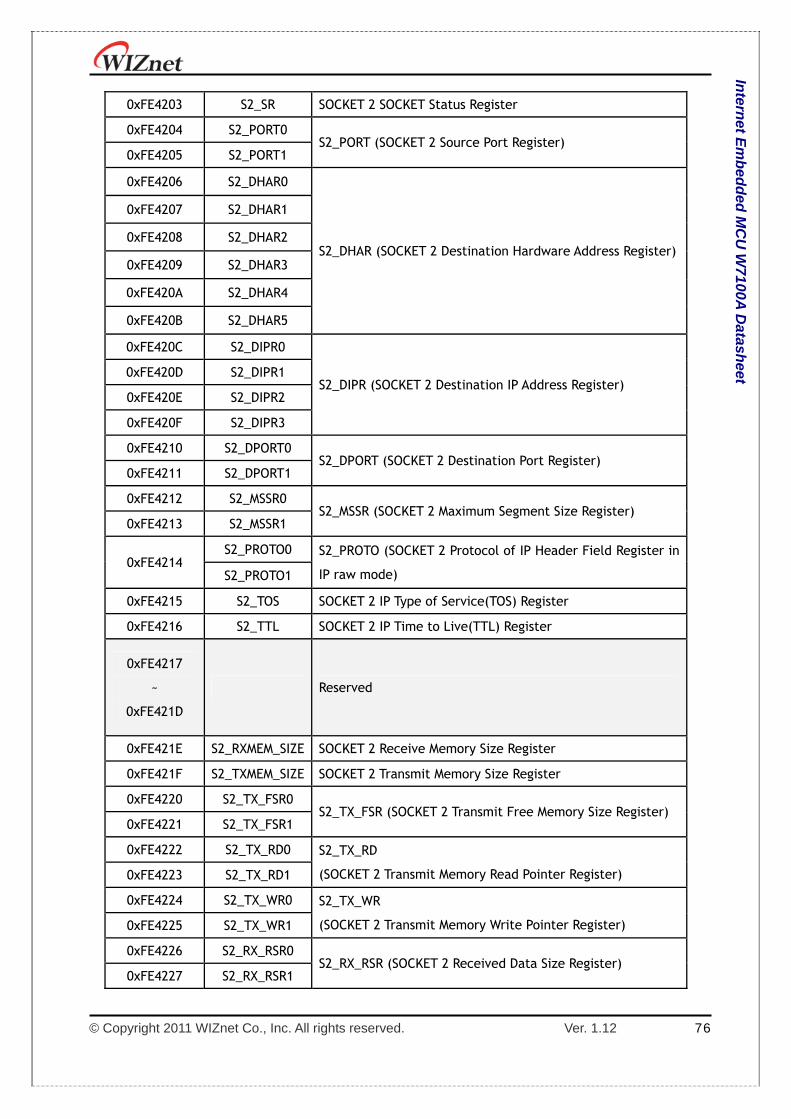
© Copyright 2011 WIZnet Co., Inc. All rights reserved. Ver. 1.12 76
Intern
et Em
bed
ded
MC
U W
7100A D
atasheet
0xFE4203 S2_SR SOCKET 2 SOCKET Status Register
0xFE4204 S2_PORT0 S2_PORT (SOCKET 2 Source Port Register)
0xFE4205 S2_PORT1
0xFE4206 S2_DHAR0
S2_DHAR (SOCKET 2 Destination Hardware Address Register)
0xFE4207 S2_DHAR1
0xFE4208 S2_DHAR2
0xFE4209 S2_DHAR3
0xFE420A S2_DHAR4
0xFE420B S2_DHAR5
0xFE420C S2_DIPR0
S2_DIPR (SOCKET 2 Destination IP Address Register) 0xFE420D S2_DIPR1
0xFE420E S2_DIPR2
0xFE420F S2_DIPR3
0xFE4210 S2_DPORT0 S2_DPORT (SOCKET 2 Destination Port Register)
0xFE4211 S2_DPORT1
0xFE4212 S2_MSSR0 S2_MSSR (SOCKET 2 Maximum Segment Size Register)
0xFE4213 S2_MSSR1
0xFE4214 S2_PROTO0 S2_PROTO (SOCKET 2 Protocol of IP Header Field Register in
IP raw mode) S2_PROTO1
0xFE4215 S2_TOS SOCKET 2 IP Type of Service(TOS) Register
0xFE4216 S2_TTL SOCKET 2 IP Time to Live(TTL) Register
0xFE4217
~
0xFE421D
Reserved
0xFE421E S2_RXMEM_SIZE SOCKET 2 Receive Memory Size Register
0xFE421F S2_TXMEM_SIZE SOCKET 2 Transmit Memory Size Register
0xFE4220 S2_TX_FSR0 S2_TX_FSR (SOCKET 2 Transmit Free Memory Size Register)
0xFE4221 S2_TX_FSR1
0xFE4222 S2_TX_RD0 S2_TX_RD
(SOCKET 2 Transmit Memory Read Pointer Register) 0xFE4223 S2_TX_RD1
0xFE4224 S2_TX_WR0 S2_TX_WR
(SOCKET 2 Transmit Memory Write Pointer Register) 0xFE4225 S2_TX_WR1
0xFE4226 S2_RX_RSR0 S2_RX_RSR (SOCKET 2 Received Data Size Register)
0xFE4227 S2_RX_RSR1

© Copyright 2011 WIZnet Co., Inc. All rights reserved. Ver. 1.12 77
Intern
et Em
bed
ded
MC
U W
7100A D
atasheet
0xFE4228 S2_RX_RD0 S2_RX_RD
(SOCKET 2 Receive Memory Read Pointer Register) 0xFE4229 S2_RX_RD1
0xFE422A S2_RX_WR0 S2_RX_WR
(SOCKET 2 Receive Memory Write Pointer Register) 0xFE422B S2_RX_WR1
0xFE422C S2_IMR SOCKET 2 Interrupt Mask Register
0xFE422D S2_FRAG0 SOCKET 2 Fragment Field Value in IP Header Register
0xFE422E S2_FRAG1
0xFE422F
~
0xFE42FF
Reserved
0xFE4300 S3_MR SOCKET 3 Mode Register
0xFE4301 S3_CR SOCKET 3 Command Register
0xFE4302 S3_IR SOCKET 3 Interrupt Register
0xFE4303 S3_SR SOCKET 3 SOCKET Status Register
0xFE4304 S3_PORT0 S3_PORT (SOCKET 3 Source Port Register)
0xFE4305 S3_PORT1
0xFE4306 S3_DHAR0
S3_DHAR (SOCKET 3 Destination Hardware Address Register)
S3_DHAR (SOCKET 3 Destination Hardware Address Register)
0xFE4307 S3_DHAR1
0xFE4308 S3_DHAR2
0xFE4309 S3_DHAR3
0xFE430A S3_DHAR4
0xFE430B S3_DHAR5
0xFE430C S3_DIPR0
S3_DIPR (SOCKET 3 Destination IP Address Register) 0xFE430D S3_DIPR1
0xFE430E S3_DIPR2
0xFE430F S3_DIPR3
0xFE4310 S3_DPORT0 S3_DPORT (SOCKET 3 Destination Port Register)
0xFE4311 S3_DPORT1
0xFE4312 S3_MSSR0 S3_MSSR (SOCKET 3 Maximum Segment Size Register)
0xFE4313 S3_MSSR1
0xFE4314 S3_PROTO SOCKET 3 Protocol of IP Header Field Register in IP raw
mode
0xFE4315 S3_TOS SOCKET 3 IP Type of Service(TOS) Register
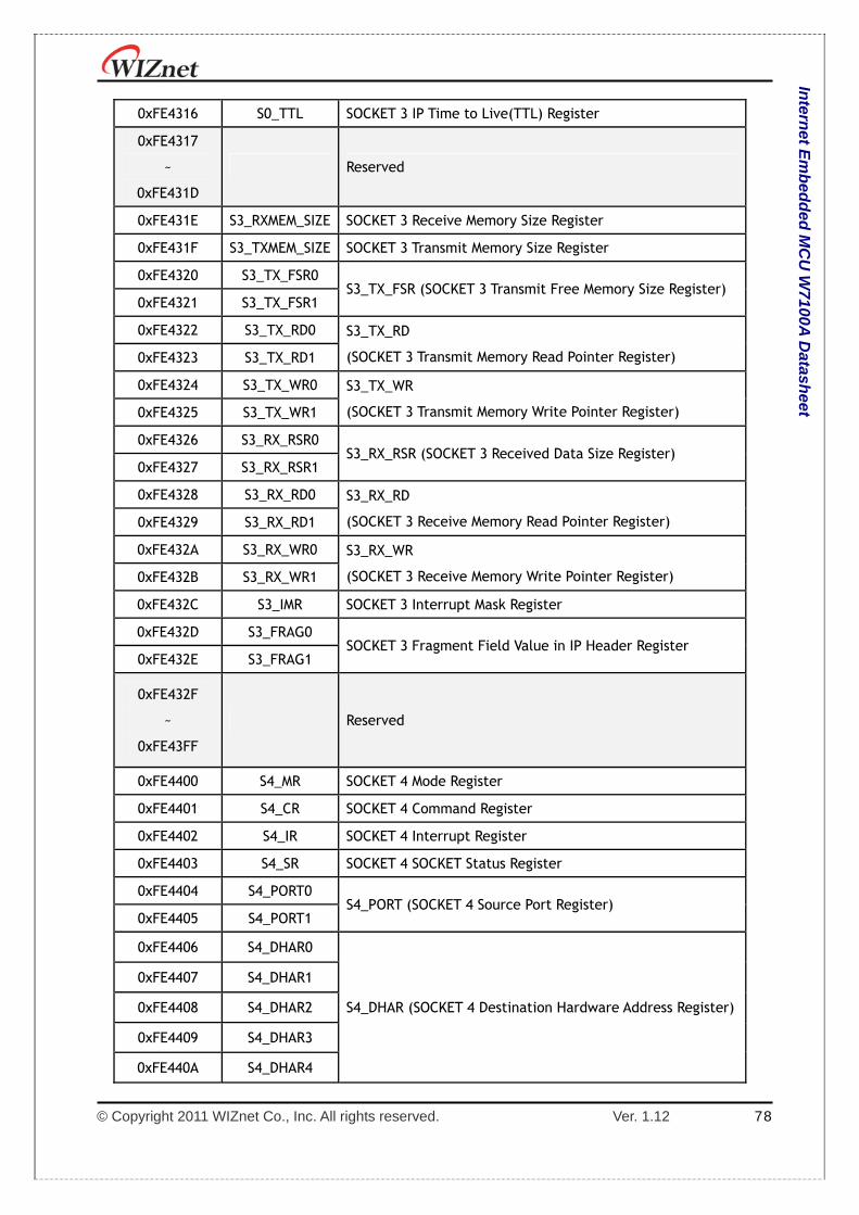
© Copyright 2011 WIZnet Co., Inc. All rights reserved. Ver. 1.12 78
Intern
et Em
bed
ded
MC
U W
7100A D
atasheet
0xFE4316 S0_TTL SOCKET 3 IP Time to Live(TTL) Register
0xFE4317
~
0xFE431D
Reserved
0xFE431E S3_RXMEM_SIZE SOCKET 3 Receive Memory Size Register
0xFE431F S3_TXMEM_SIZE SOCKET 3 Transmit Memory Size Register
0xFE4320 S3_TX_FSR0 S3_TX_FSR (SOCKET 3 Transmit Free Memory Size Register)
0xFE4321 S3_TX_FSR1
0xFE4322 S3_TX_RD0 S3_TX_RD
(SOCKET 3 Transmit Memory Read Pointer Register) 0xFE4323 S3_TX_RD1
0xFE4324 S3_TX_WR0 S3_TX_WR
(SOCKET 3 Transmit Memory Write Pointer Register) 0xFE4325 S3_TX_WR1
0xFE4326 S3_RX_RSR0 S3_RX_RSR (SOCKET 3 Received Data Size Register)
0xFE4327 S3_RX_RSR1
0xFE4328 S3_RX_RD0 S3_RX_RD
(SOCKET 3 Receive Memory Read Pointer Register) 0xFE4329 S3_RX_RD1
0xFE432A S3_RX_WR0 S3_RX_WR
(SOCKET 3 Receive Memory Write Pointer Register) 0xFE432B S3_RX_WR1
0xFE432C S3_IMR SOCKET 3 Interrupt Mask Register
0xFE432D S3_FRAG0 SOCKET 3 Fragment Field Value in IP Header Register
0xFE432E S3_FRAG1
0xFE432F
~
0xFE43FF
Reserved
0xFE4400 S4_MR SOCKET 4 Mode Register
0xFE4401 S4_CR SOCKET 4 Command Register
0xFE4402 S4_IR SOCKET 4 Interrupt Register
0xFE4403 S4_SR SOCKET 4 SOCKET Status Register
0xFE4404 S4_PORT0 S4_PORT (SOCKET 4 Source Port Register)
0xFE4405 S4_PORT1
0xFE4406 S4_DHAR0
S4_DHAR (SOCKET 4 Destination Hardware Address Register)
0xFE4407 S4_DHAR1
0xFE4408 S4_DHAR2
0xFE4409 S4_DHAR3
0xFE440A S4_DHAR4
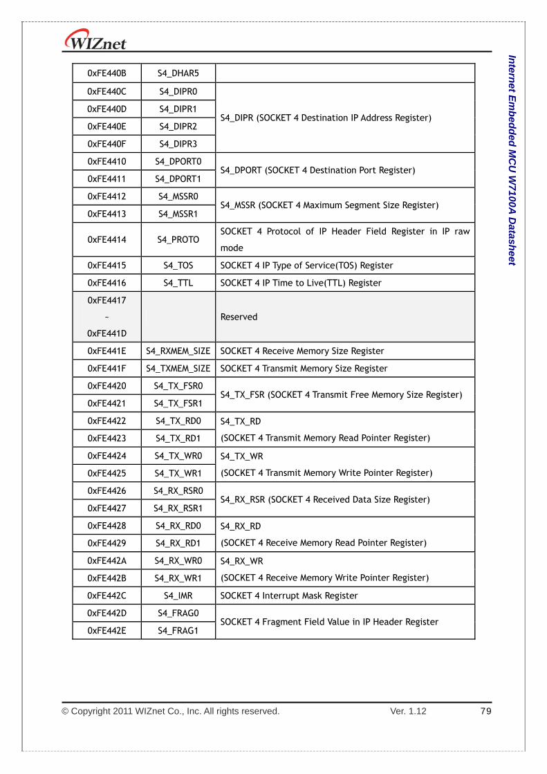
© Copyright 2011 WIZnet Co., Inc. All rights reserved. Ver. 1.12 79
Intern
et Em
bed
ded
MC
U W
7100A D
atasheet
0xFE440B S4_DHAR5
0xFE440C S4_DIPR0
S4_DIPR (SOCKET 4 Destination IP Address Register) 0xFE440D S4_DIPR1
0xFE440E S4_DIPR2
0xFE440F S4_DIPR3
0xFE4410 S4_DPORT0 S4_DPORT (SOCKET 4 Destination Port Register)
0xFE4411 S4_DPORT1
0xFE4412 S4_MSSR0 S4_MSSR (SOCKET 4 Maximum Segment Size Register)
0xFE4413 S4_MSSR1
0xFE4414 S4_PROTO SOCKET 4 Protocol of IP Header Field Register in IP raw
mode
0xFE4415 S4_TOS SOCKET 4 IP Type of Service(TOS) Register
0xFE4416 S4_TTL SOCKET 4 IP Time to Live(TTL) Register
0xFE4417
~
0xFE441D
Reserved
0xFE441E S4_RXMEM_SIZE SOCKET 4 Receive Memory Size Register
0xFE441F S4_TXMEM_SIZE SOCKET 4 Transmit Memory Size Register
0xFE4420 S4_TX_FSR0 S4_TX_FSR (SOCKET 4 Transmit Free Memory Size Register)
0xFE4421 S4_TX_FSR1
0xFE4422 S4_TX_RD0 S4_TX_RD
(SOCKET 4 Transmit Memory Read Pointer Register) 0xFE4423 S4_TX_RD1
0xFE4424 S4_TX_WR0 S4_TX_WR
(SOCKET 4 Transmit Memory Write Pointer Register) 0xFE4425 S4_TX_WR1
0xFE4426 S4_RX_RSR0 S4_RX_RSR (SOCKET 4 Received Data Size Register)
0xFE4427 S4_RX_RSR1
0xFE4428 S4_RX_RD0 S4_RX_RD
(SOCKET 4 Receive Memory Read Pointer Register) 0xFE4429 S4_RX_RD1
0xFE442A S4_RX_WR0 S4_RX_WR
(SOCKET 4 Receive Memory Write Pointer Register) 0xFE442B S4_RX_WR1
0xFE442C S4_IMR SOCKET 4 Interrupt Mask Register
0xFE442D S4_FRAG0 SOCKET 4 Fragment Field Value in IP Header Register
0xFE442E S4_FRAG1
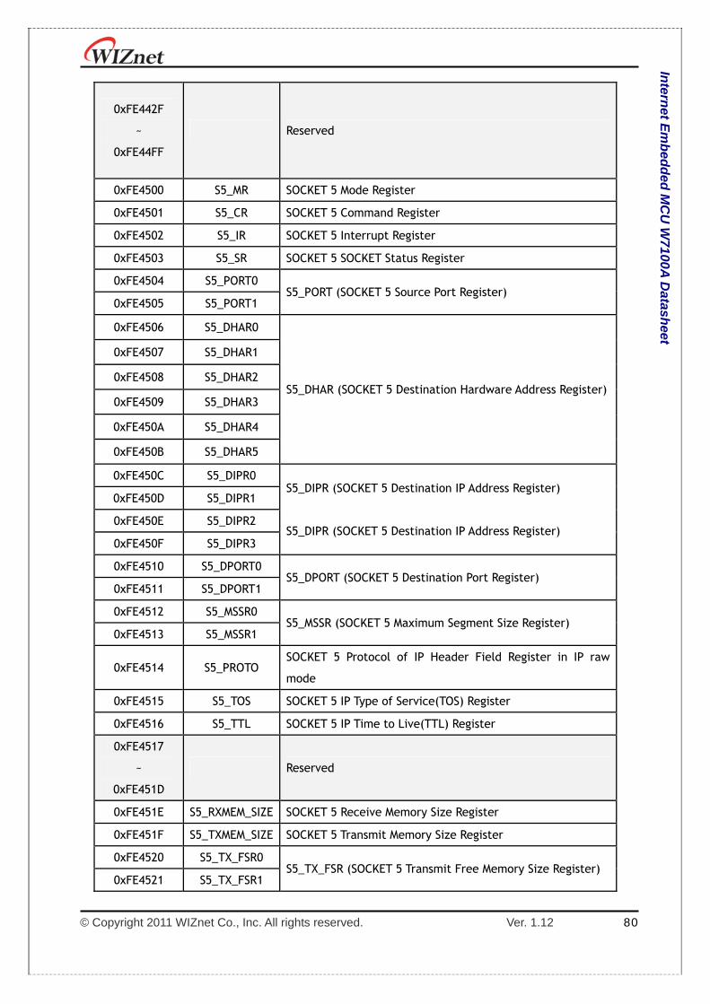
© Copyright 2011 WIZnet Co., Inc. All rights reserved. Ver. 1.12 80
Intern
et Em
bed
ded
MC
U W
7100A D
atasheet
0xFE442F
~
0xFE44FF
Reserved
0xFE4500 S5_MR SOCKET 5 Mode Register
0xFE4501 S5_CR SOCKET 5 Command Register
0xFE4502 S5_IR SOCKET 5 Interrupt Register
0xFE4503 S5_SR SOCKET 5 SOCKET Status Register
0xFE4504 S5_PORT0 S5_PORT (SOCKET 5 Source Port Register)
0xFE4505 S5_PORT1
0xFE4506 S5_DHAR0
S5_DHAR (SOCKET 5 Destination Hardware Address Register)
0xFE4507 S5_DHAR1
0xFE4508 S5_DHAR2
0xFE4509 S5_DHAR3
0xFE450A S5_DHAR4
0xFE450B S5_DHAR5
0xFE450C S5_DIPR0 S5_DIPR (SOCKET 5 Destination IP Address Register)
S5_DIPR (SOCKET 5 Destination IP Address Register)
0xFE450D S5_DIPR1
0xFE450E S5_DIPR2
0xFE450F S5_DIPR3
0xFE4510 S5_DPORT0 S5_DPORT (SOCKET 5 Destination Port Register)
0xFE4511 S5_DPORT1
0xFE4512 S5_MSSR0 S5_MSSR (SOCKET 5 Maximum Segment Size Register)
0xFE4513 S5_MSSR1
0xFE4514 S5_PROTO SOCKET 5 Protocol of IP Header Field Register in IP raw
mode
0xFE4515 S5_TOS SOCKET 5 IP Type of Service(TOS) Register
0xFE4516 S5_TTL SOCKET 5 IP Time to Live(TTL) Register
0xFE4517
~
0xFE451D
Reserved
0xFE451E S5_RXMEM_SIZE SOCKET 5 Receive Memory Size Register
0xFE451F S5_TXMEM_SIZE SOCKET 5 Transmit Memory Size Register
0xFE4520 S5_TX_FSR0 S5_TX_FSR (SOCKET 5 Transmit Free Memory Size Register)
0xFE4521 S5_TX_FSR1
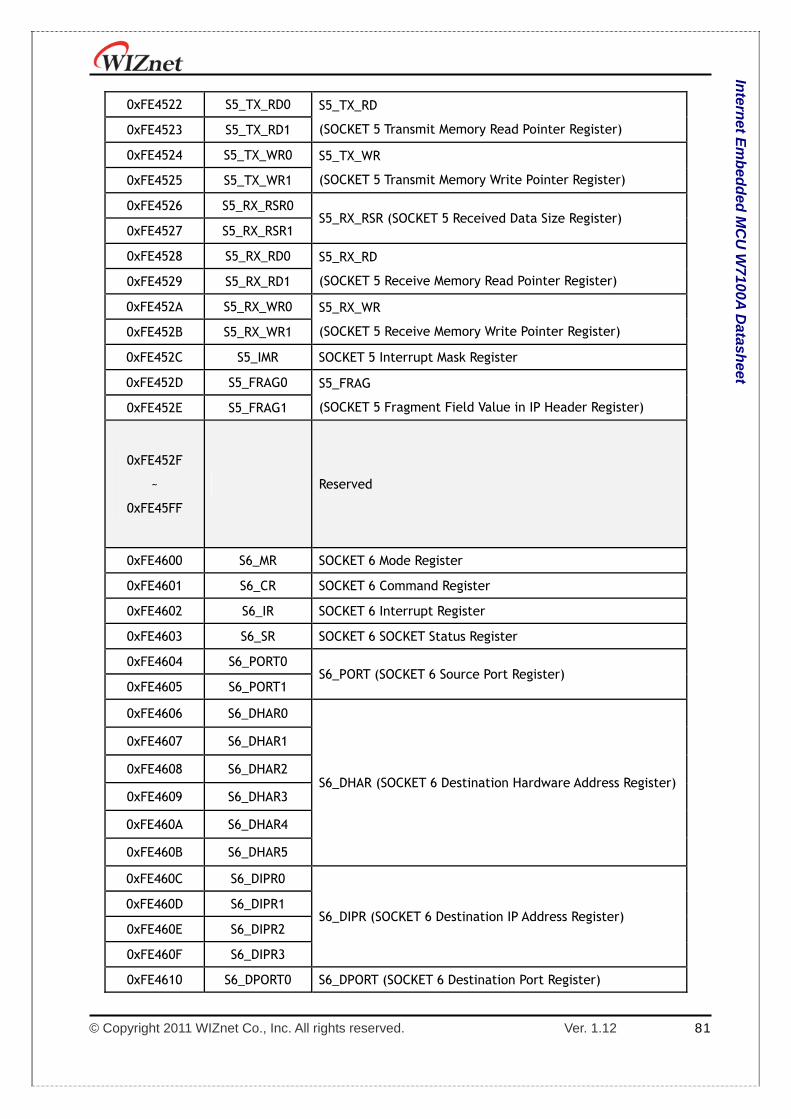
© Copyright 2011 WIZnet Co., Inc. All rights reserved. Ver. 1.12 81
Intern
et Em
bed
ded
MC
U W
7100A D
atasheet
0xFE4522 S5_TX_RD0 S5_TX_RD
(SOCKET 5 Transmit Memory Read Pointer Register) 0xFE4523 S5_TX_RD1
0xFE4524 S5_TX_WR0 S5_TX_WR
(SOCKET 5 Transmit Memory Write Pointer Register) 0xFE4525 S5_TX_WR1
0xFE4526 S5_RX_RSR0 S5_RX_RSR (SOCKET 5 Received Data Size Register)
0xFE4527 S5_RX_RSR1
0xFE4528 S5_RX_RD0 S5_RX_RD
(SOCKET 5 Receive Memory Read Pointer Register) 0xFE4529 S5_RX_RD1
0xFE452A S5_RX_WR0 S5_RX_WR
(SOCKET 5 Receive Memory Write Pointer Register) 0xFE452B S5_RX_WR1
0xFE452C S5_IMR SOCKET 5 Interrupt Mask Register
0xFE452D S5_FRAG0 S5_FRAG
(SOCKET 5 Fragment Field Value in IP Header Register) 0xFE452E S5_FRAG1
0xFE452F
~
0xFE45FF
Reserved
0xFE4600 S6_MR SOCKET 6 Mode Register
0xFE4601 S6_CR SOCKET 6 Command Register
0xFE4602 S6_IR SOCKET 6 Interrupt Register
0xFE4603 S6_SR SOCKET 6 SOCKET Status Register
0xFE4604 S6_PORT0 S6_PORT (SOCKET 6 Source Port Register)
0xFE4605 S6_PORT1
0xFE4606 S6_DHAR0
S6_DHAR (SOCKET 6 Destination Hardware Address Register)
0xFE4607 S6_DHAR1
0xFE4608 S6_DHAR2
0xFE4609 S6_DHAR3
0xFE460A S6_DHAR4
0xFE460B S6_DHAR5
0xFE460C S6_DIPR0
S6_DIPR (SOCKET 6 Destination IP Address Register) 0xFE460D S6_DIPR1
0xFE460E S6_DIPR2
0xFE460F S6_DIPR3
0xFE4610 S6_DPORT0 S6_DPORT (SOCKET 6 Destination Port Register)

© Copyright 2011 WIZnet Co., Inc. All rights reserved. Ver. 1.12 82
Intern
et Em
bed
ded
MC
U W
7100A D
atasheet
0xFE4611 S6_DPORT1
0xFE4612 S6_MSSR0 S6_MSSR (SOCKET 6 Maximum Segment Size Register)
0xFE4613 S6_MSSR1
0xFE4614 S6_PROTO SOCKET 6 Protocol of IP Header Field Register in IP raw
mode
0xFE4615 S6_TOS SOCKET 6 IP Type of Service(TOS) Register
0xFE4616 S6_TTL SOCKET 6 IP Time to Live(TTL) Register
0xFE4617
~
0xFE461D
Reserved
0xFE461E S6_RXMEM_SIZE SOCKET 6 Receive Memory Size Register
0xFE461F S6_TXMEM_SIZE SOCKET 6 Transmit Memory Size Register
0xFE4620 S6_TX_FSR0 S6_TX_FSR (SOCKET 6 Transmit Free Memory Size Register)
0xFE4621 S6_TX_FSR1
0xFE4622 S6_TX_RD0 S6_TX_RD
(SOCKET 6 Transmit Memory Read Pointer Register) 0xFE4623 S6_TX_RD1
0xFE4624 S6_TX_WR0 S6_TX_WR
(SOCKET 6 Transmit Memory Write Pointer Register) 0xFE4625 S6_TX_WR1
0xFE4626 S6_RX_RSR0 S6_RX_RSR (SOCKET 6 Received Data Size Register)
0xFE4627 S6_RX_RSR1
0xFE4628 S6_RX_RD0 S6_RX_RD
(SOCKET 6 Receive Memory Read Pointer Register) 0xFE4629 S6_RX_RD1
0xFE462A S6_RX_WR0 S6_RX_WR
(SOCKET 6 Receive Memory Write Pointer Register) 0xFE462B S6_RX_WR1
0xFE462C S6_IMR SOCKET 6 Interrupt Mask Register
0xFE462D S6_FRAG0 S6_FRAG
(SOCKET 6 Fragment Field Value in IP Header Register) 0xFE462E S6_FRAG1
0xFE462F
~
0xFE46FF
Reserved
0xFE4700 S7_MR SOCKET 7 Mode Register
0xFE4701 S7_CR SOCKET 7 Command Register
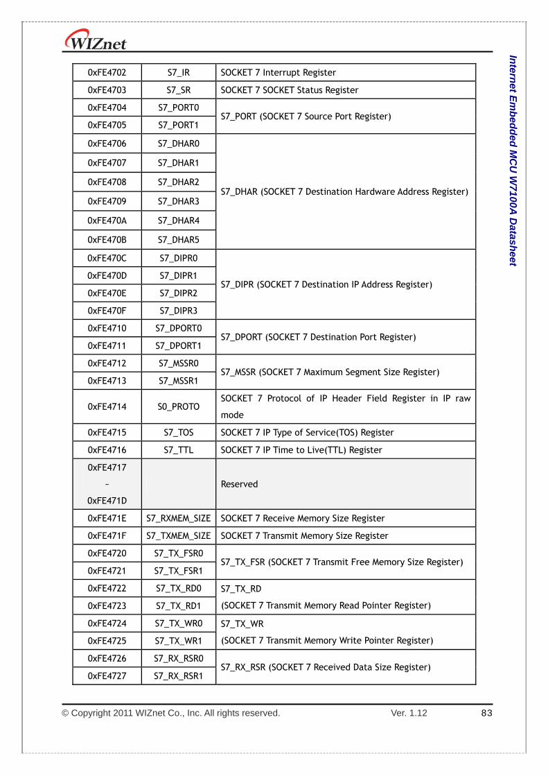
© Copyright 2011 WIZnet Co., Inc. All rights reserved. Ver. 1.12 83
Intern
et Em
bed
ded
MC
U W
7100A D
atasheet
0xFE4702 S7_IR SOCKET 7 Interrupt Register
0xFE4703 S7_SR SOCKET 7 SOCKET Status Register
0xFE4704 S7_PORT0 S7_PORT (SOCKET 7 Source Port Register)
0xFE4705 S7_PORT1
0xFE4706 S7_DHAR0
S7_DHAR (SOCKET 7 Destination Hardware Address Register)
0xFE4707 S7_DHAR1
0xFE4708 S7_DHAR2
0xFE4709 S7_DHAR3
0xFE470A S7_DHAR4
0xFE470B S7_DHAR5
0xFE470C S7_DIPR0
S7_DIPR (SOCKET 7 Destination IP Address Register) 0xFE470D S7_DIPR1
0xFE470E S7_DIPR2
0xFE470F S7_DIPR3
0xFE4710 S7_DPORT0 S7_DPORT (SOCKET 7 Destination Port Register)
0xFE4711 S7_DPORT1
0xFE4712 S7_MSSR0 S7_MSSR (SOCKET 7 Maximum Segment Size Register)
0xFE4713 S7_MSSR1
0xFE4714 S0_PROTO SOCKET 7 Protocol of IP Header Field Register in IP raw
mode
0xFE4715 S7_TOS SOCKET 7 IP Type of Service(TOS) Register
0xFE4716 S7_TTL SOCKET 7 IP Time to Live(TTL) Register
0xFE4717
~
0xFE471D
Reserved
0xFE471E S7_RXMEM_SIZE SOCKET 7 Receive Memory Size Register
0xFE471F S7_TXMEM_SIZE SOCKET 7 Transmit Memory Size Register
0xFE4720 S7_TX_FSR0 S7_TX_FSR (SOCKET 7 Transmit Free Memory Size Register)
0xFE4721 S7_TX_FSR1
0xFE4722 S7_TX_RD0 S7_TX_RD
(SOCKET 7 Transmit Memory Read Pointer Register) 0xFE4723 S7_TX_RD1
0xFE4724 S7_TX_WR0 S7_TX_WR
(SOCKET 7 Transmit Memory Write Pointer Register) 0xFE4725 S7_TX_WR1
0xFE4726 S7_RX_RSR0 S7_RX_RSR (SOCKET 7 Received Data Size Register)
0xFE4727 S7_RX_RSR1
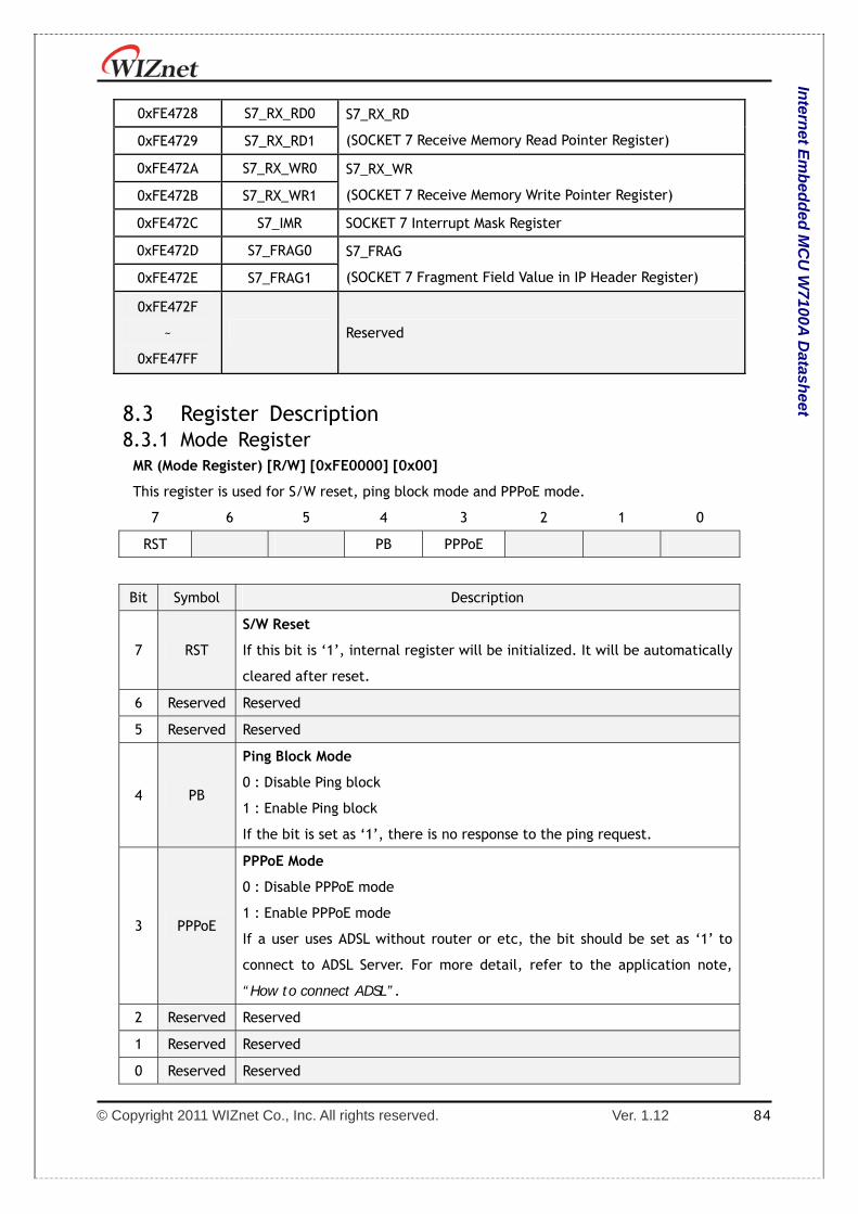
© Copyright 2011 WIZnet Co., Inc. All rights reserved. Ver. 1.12 84
Intern
et Em
bed
ded
MC
U W
7100A D
atasheet
0xFE4728 S7_RX_RD0 S7_RX_RD
(SOCKET 7 Receive Memory Read Pointer Register) 0xFE4729 S7_RX_RD1
0xFE472A S7_RX_WR0 S7_RX_WR
(SOCKET 7 Receive Memory Write Pointer Register) 0xFE472B S7_RX_WR1
0xFE472C S7_IMR SOCKET 7 Interrupt Mask Register
0xFE472D S7_FRAG0 S7_FRAG
(SOCKET 7 Fragment Field Value in IP Header Register) 0xFE472E S7_FRAG1
0xFE472F
~
0xFE47FF
Reserved
8.3 Register Description 8.3.1 Mode Register
MR (Mode Register) [R/W] [0xFE0000] [0x00]
This register is used for S/W reset, ping block mode and PPPoE mode.
7 6 5 4 3 2 1 0
RST PB PPPoE
Bit Symbol Description
7 RST
S/W Reset
If this bit is ‘1’, internal register will be initialized. It will be automatically
cleared after reset.
6 Reserved Reserved
5 Reserved Reserved
4 PB
Ping Block Mode
0 : Disable Ping block
1 : Enable Ping block
If the bit is set as ‘1’, there is no response to the ping request.
3 PPPoE
PPPoE Mode
0 : Disable PPPoE mode
1 : Enable PPPoE mode
If a user uses ADSL without router or etc, the bit should be set as ‘1’ to
connect to ADSL Server. For more detail, refer to the application note,
“How to connect ADSL”.
2 Reserved Reserved
1 Reserved Reserved
0 Reserved Reserved
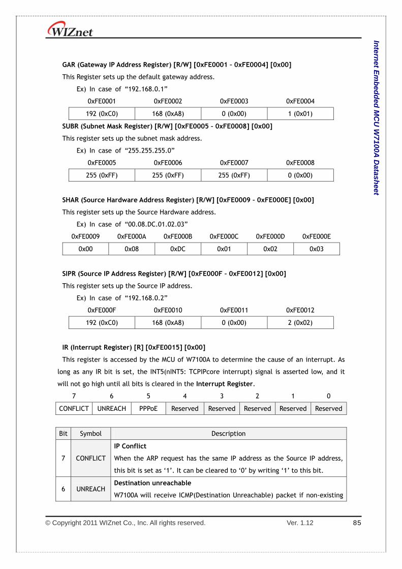
© Copyright 2011 WIZnet Co., Inc. All rights reserved. Ver. 1.12 85
Intern
et Em
bed
ded
MC
U W
7100A D
atasheet
GAR (Gateway IP Address Register) [R/W] [0xFE0001 – 0xFE0004] [0x00]
This Register sets up the default gateway address.
Ex) In case of “192.168.0.1”
0xFE0001 0xFE0002 0xFE0003 0xFE0004
192 (0xC0) 168 (0xA8) 0 (0x00) 1 (0x01)
SUBR (Subnet Mask Register) [R/W] [0xFE0005 – 0xFE0008] [0x00]
This register sets up the subnet mask address.
Ex) In case of “255.255.255.0”
0xFE0005 0xFE0006 0xFE0007 0xFE0008
255 (0xFF) 255 (0xFF) 255 (0xFF) 0 (0x00)
SHAR (Source Hardware Address Register) [R/W] [0xFE0009 – 0xFE000E] [0x00]
This register sets up the Source Hardware address.
Ex) In case of “00.08.DC.01.02.03”
0xFE0009 0xFE000A 0xFE000B 0xFE000C 0xFE000D 0xFE000E
0x00 0x08 0xDC 0x01 0x02 0x03
SIPR (Source IP Address Register) [R/W] [0xFE000F – 0xFE0012] [0x00]
This register sets up the Source IP address.
Ex) In case of “192.168.0.2”
0xFE000F 0xFE0010 0xFE0011 0xFE0012
192 (0xC0) 168 (0xA8) 0 (0x00) 2 (0x02)
IR (Interrupt Register) [R] [0xFE0015] [0x00]
This register is accessed by the MCU of W7100A to determine the cause of an interrupt. As
long as any IR bit is set, the INT5(nINT5: TCPIPcore interrupt) signal is asserted low, and it
will not go high until all bits is cleared in the Interrupt Register.
7 6 5 4 3 2 1 0
CONFLICT UNREACH PPPoE Reserved Reserved Reserved Reserved Reserved
Bit Symbol Description
7 CONFLICT
IP Conflict
When the ARP request has the same IP address as the Source IP address,
this bit is set as ‘1’. It can be cleared to ‘0’ by writing ‘1’ to this bit.
6 UNREACH Destination unreachable
W7100A will receive ICMP(Destination Unreachable) packet if non-existing
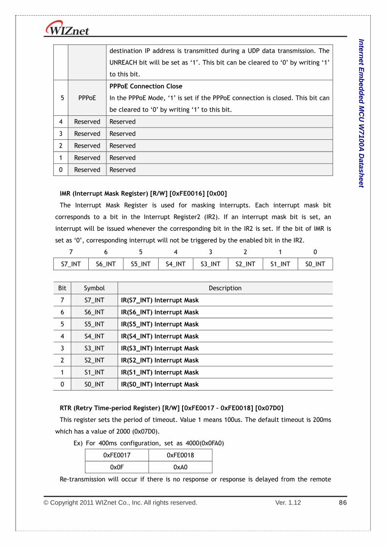
© Copyright 2011 WIZnet Co., Inc. All rights reserved. Ver. 1.12 86
Intern
et Em
bed
ded
MC
U W
7100A D
atasheet
destination IP address is transmitted during a UDP data transmission. The
UNREACH bit will be set as ‘1’. This bit can be cleared to ‘0’ by writing ‘1’
to this bit.
5 PPPoE
PPPoE Connection Close
In the PPPoE Mode, ‘1’ is set if the PPPoE connection is closed. This bit can
be cleared to ‘0’ by writing ‘1’ to this bit.
4 Reserved Reserved
3 Reserved Reserved
2 Reserved Reserved
1 Reserved Reserved
0 Reserved Reserved
IMR (Interrupt Mask Register) [R/W] [0xFE0016] [0x00]
The Interrupt Mask Register is used for masking interrupts. Each interrupt mask bit
corresponds to a bit in the Interrupt Register2 (IR2). If an interrupt mask bit is set, an
interrupt will be issued whenever the corresponding bit in the IR2 is set. If the bit of IMR is
set as ‘0’, corresponding interrupt will not be triggered by the enabled bit in the IR2.
7 6 5 4 3 2 1 0
S7_INT S6_INT S5_INT S4_INT S3_INT S2_INT S1_INT S0_INT
Bit Symbol Description
7 S7_INT IR(S7_INT) Interrupt Mask
6 S6_INT IR(S6_INT) Interrupt Mask
5 S5_INT IR(S5_INT) Interrupt Mask
4 S4_INT IR(S4_INT) Interrupt Mask
3 S3_INT IR(S3_INT) Interrupt Mask
2 S2_INT IR(S2_INT) Interrupt Mask
1 S1_INT IR(S1_INT) Interrupt Mask
0 S0_INT IR(S0_INT) Interrupt Mask
RTR (Retry Time-period Register) [R/W] [0xFE0017 – 0xFE0018] [0x07D0]
This register sets the period of timeout. Value 1 means 100us. The default timeout is 200ms
which has a value of 2000 (0x07D0).
Ex) For 400ms configuration, set as 4000(0x0FA0)
0xFE0017 0xFE0018
0x0F 0xA0
Re-transmission will occur if there is no response or response is delayed from the remote

© Copyright 2011 WIZnet Co., Inc. All rights reserved. Ver. 1.12 87
Intern
et Em
bed
ded
MC
U W
7100A D
atasheet
peer.
RCR (Retry Count Register) [R/W] [0xFE0019] [0x08]
This register sets the number of re-transmission. If retransmission occurs more than the
number of retries recorded in RCR, a Timeout Interrupt will occur. (TIMEOUT bit of SOCKET n
Interrupt Register (Sn_IR) is set as ‘1’)
In TCP communication, the value of Sn_SR is changed to ‘SOCK_CLOSED’ at the same time
with Sn_IR(TIMEOUT) = ‘1’. Not in TCP communication, only Sn_IR(TIMEOUT) = ‘1’.
The timeout of W7100A can be configurable with RTR and RCR. W7100A’s timeout has ARP
and TCP retransmission timeout.
At the ARP(Refer to RFC 826, http://www.ietf.org/rfc.html) retransmission timeout,
W7100A automatically sends ARP-request to the peer’s IP address in order to acquire MAC
address information (used for communication of IP, UDP, or TCP). As waiting for ARP-response
from the peer, if there is no response during the time set in RTR, timeout occurs and ARP-
request is re-transmitted. It is repeated as many as ‘RCR + 1’ times.
Even after ARP-request retransmissions are repeated ‘RCR + 1’ times, if there is no ARP-
response, the final timeout occurs and Sn_IR(TIMEOUT) becomes ‘1’.
The value of final timeout (ARPTO) of ARP-request is as below.
During the TCP packet retransmission timeout, W7100A transmits TCP packets (SYN, FIN, RST,
DATA packets) and waits for the acknowledgement (ACK) during the time set in RTR and RCR.
If there is no ACK from the peer, timeout occurs and TCP packets (sent earlier) are
retransmitted. The retransmissions are repeated as many as ‘RCR + 1’ times. Even after TCP
packet retransmissions are repeated ‘RCR +1’ times, if there is no ACK from the peer, final
timeout occurs and Sn_SSR is changed to ‘SOCK_CLOSED” at the same time with
Sn_IR(TIMEOUT) = ‘1’
The value of final timeout (TCPTO) of TCP packet retransmission can be calculated as below,
Ex) When RTR = 2000(0x07D0), RCR = 8(0x0008),
ARPTO = 2000 X 0.1ms X 9 = 1800ms = 1.8s
ARPTO = ( RTR X 0.1ms ) X ( RCR + 1 )
M
TCPTO = ( Σ(RTR X 2N ) + ((RCR-M) X RTRMAX) ) X 0.1ms N=0
N : Retransmission count, 0 <= N <= M M : Minimum value when RTR X 2(M+1) > 65535 and 0 <= M <= RCR RTRMAX : RTR X 2M

© Copyright 2011 WIZnet Co., Inc. All rights reserved. Ver. 1.12 88
Intern
et Em
bed
ded
MC
U W
7100A D
atasheet
TCPTO = (0x07D0 + 0x0FA0 + 0x1F40 + 0x3E80 + 0x7D00 + 0xFA00 + 0xFA00 + 0xFA00 + 0xFA00) X 0.1ms
= (2000 + 4000 + 8000 + 16000 + 32000 + ((8 - 4) X 64000)) X 0.1ms
= 318000 X 0.1ms = 31.8s
PATR (Authentication Type in PPPoE mode) [R] [0xFE001C-0xFE001D] [0x0000]
This register notifies the type of authentication used to establish the PPPoE connection.
W7100A supports two types of Authentication method - PAP and CHAP.
Value Authentication Type
0xC023 PAP
0xC223 CHAP
PPPALGO (Authentication Algorithm in PPPoE mode)[R][0xFE001E][0x00]
This register notifies the authentication algorithm used for the PPPoE connection. For detail
information, please refer to PPPoE application note.
PTIMER (PPP Link Control Protocol Request Timer Register) [R/W] [0xFE0028] [0x28]
This register indicates the duration of LCP Echo Request being sent. Value 1 is about 25ms.
Ex) in case that PTIMER is 200,
200 * 25(ms) = 5000(ms) = 5 seconds
PMAGIC (PPP Link Control Protocol Magic number Register) [R/W] [0xFE0029][0x00]
This register is used in the Magic number option during LCP negotiation. Refer to the
application note of W5100, “How to connect ADSL”.
VERSIONR (W7100A Chip Version Register)[R][0xFE001F][0x02]
This register is W7100A chip version register.
INTLEVEL (Interrupt Low Level Timer Register)[R/W][0xFE0030 – 0xFE0031][0x0000]
The INTLEVEL register sets the Interrupt Assert wait time(IAWT). It configures internal INT5
signal Low Assert waiting time until next interrupt. If user wants to use TCP/IP Core interrupt,
INTLEVEL register must be set higher than 0x2B00. Or the TCP/IP Core interrupt can be
ignored.
IAWT = (INTLEVEL0 + 1) * PLL_CLK (when INTLEVEL0 > 0)

© Copyright 2011 WIZnet Co., Inc. All rights reserved. Ver. 1.12 89
Intern
et Em
bed
ded
MC
U W
7100A D
atasheet
a. At the socket 0, assume an interrupt occurs (S0_IR(3) = ‘1’) and corresponding IR2 bit is
set as ‘1’ (IR(S0_IR) = ‘1’). Then the internal INT5 signal is asserted low.
b. Also assume an interrupt continually occurs (S1_IR(0) = ‘1’) on the socket1 and
corresponding IR bit set as ‘1’ (IR(S1_IR) = ‘1’).
c. When the Host clears S0_IR(S0_IR = 0x00), the corresponding IR2 bit is also cleared
(IR(S0_IR) = ‘0’). Internal INT5 signal will be de-asserted high(deactivated) from
low(activaed).
d. When the S1_IR is cleared, but the corresponding IR2 is not 0x00 because of socket1
interrupt, internal INT5 signal should be asserted low.
However, as INTLEVEL is 0x000F, the internal INT5 signal is asserted after the IAWT(16
PLL_CLK) time.
IR2 (W7100A SOCKET Interrupt Register)[R/W][0xFE0034][0x00]
IR2 is a Register which notifies the host that a W7100A SOCKET interrupt has occurred. When
an interrupt occurs, the related bit in IR2 is enabled. In this case, the INT5 (nINT5: TCPIPcore
interrupt) signal is asserted low until all of the bits of IR2 is ‘0’. Once the IR2 register is
cleared out by using the Sn_IR bits, the INT5 signal is asserted high.
7 6 5 4 3 2 1 0
S7_INT S6_INT S5_INT S4_INT S3_INT S2_INT S1_INT S0_INT
Bit Symbol Description
7 S7_INT
Occurrence of SOCKET 7 Interrupt
When an interrupt occurs at SOCKET 7, it becomes ‘1’. This interrupt
information is applied to S7_IR. This bit is automatically cleared when
S7_IR is cleared to 0x00 by host.
6 S6_INT Occurrence of SOCKET 6 Interrupt
When an interrupt occurs at SOCKET 6, it becomes ‘1’. This interrupt

© Copyright 2011 WIZnet Co., Inc. All rights reserved. Ver. 1.12 90
Intern
et Em
bed
ded
MC
U W
7100A D
atasheet
information is applied to S6_IR. This bit is automatically cleared when
S6_IR is cleared to 0x00 by host.
5 S5_INT
Occurrence of SOCKET 5 Interrupt
When an interrupt occurs at SOCKET 5, it becomes ‘1’. This interrupt
information is applied to S5_IR. This bit is automatically cleared when
S5_IR is cleared to 0x00 by host.
4 S4_INT
Occurrence of SOCKET 4 Interrupt
When an interrupt occurs at SOCKET 4, it becomes ‘1’. This interrupt
information is applied to S4_IR. This bit is automatically cleared when
S4_IR is cleared to 0x00 by host.
3 S3_INT
Occurrence of SOCKET 3 Interrupt
When an interrupt occurs at SOCKET 3, it becomes ‘1’. This interrupt
information is applied to S3_IR. This bit is automatically cleared when
S3_IR is cleared to 0x00 by host.
2 S2_INT
Occurrence of SOCKET 2 Interrupt
When an interrupt occurs at SOCKET 2, it becomes ‘1’. This interrupt
information is applied to S2_IR. This bit is automatically cleared when
S2_IR is cleared to 0x00 by host.
1 S1_INT
Occurrence of SOCKET 1 Interrupt
When an interrupt occurs at SOCKET 1, it becomes ‘1’. This interrupt
information is applied to S1_IR. This bit is automatically cleared when
S1_IR is cleared to 0x00 by host.
0 S0_INT
Occurrence of SOCKET 0 Interrupt
When an interrupt occurs at SOCKET 0, it becomes ‘0’. This interrupt
information is applied to S0_IR. This bit is automatically cleared when
S0_IR is cleared to 0x00 by host.
8.3.2 SOCKET Registers Sn_MR (SOCKET n Mode Register)[R/W][0xFE4000 + 0x100n][0x0000]
This register configures the protocol type or option of SOCKET n.
7 6 5 4 3 2 1 0
MULTI ND / MC P3 P2 P1 P0
Bit Symbol Description
7 MULTI
Multicasting
0 : disable Multicasting
1 : enable Multicasting
© Copyright 2011 WIZnet Co., Inc. All rights reserved. Ver. 1.12 91
Intern
et Em
bed
ded
MC
U W
7100A D
atasheet
This only applies to UDP case(P3-P0 : “0010”)
To use multicasting, write multicast group address and port number to
SOCKET n destination IP and port register respectively before using the
OPEN command.
6 MF
MAC Filter
0: disable MAC filtering
1: enable MAC filtering
Filters the MAC addresses except own MAC and broadcasting MAC address.
5 ND/MC
Use No Delayed ACK
0 : Disable No Delayed ACK option
1 : Enable No Delayed ACK option,
This only applies to TCP case (P3-P0 : “0001”)
If this bit is set as ‘1’, ACK packet is immediately transmitted after
receiving data packet from a peer. If this bit is cleared, ACK packet is
transmitted according to internal timeout mechanism.
Multicast
0 : using IGMP version 2
1 : using IGMP version 1
This bit is valid when MULTI bit is enabled and UDP mode is used (P3-P0 :
“0010”).
In addition, multicast can be used to send out the version number in IGMP
messages such as Join/Leave/Report to multicast-group
4 Reserved Reserved
3 P3
Protocol
Sets up corresponding SOCKET as TCP, UDP, or IP RAW mode
Symbol P3 P2 P1 P0 Meaning
Sn_MR_CLOSE 0 0 0 0 Closed
Sn_MR_TCP 0 0 0 1 TCP
Sn_MR_UDP 0 0 1 0 UDP
Sn_MR_IPRAW 0 0 1 1 IPRAW
S0_MR_MACRAW 0 1 0 0 MAC RAW
S0_MR_PPPoE 0 1 0 1 PPPoE
S0_MR_MACRAW and S0_MR_PPPoE are valid only in SOCKET 0.
S0_MR_PPPoE is temporarily used for PPPoE server connection/Termination.
After connection is established, it can be utilized as another protocol.
2 P2
1 P1
0 P0

© Copyright 2011 WIZnet Co., Inc. All rights reserved. Ver. 1.12 92
Intern
et Em
bed
ded
MC
U W
7100A D
atasheet
Sn_CR (SOCKET n Command Register)[R/W][0xFE4001 + 0x100n][0x00]
This is used to set the command for SOCKET n such as OPEN, CLOSE, CONNECT, LISTEN, SEND,
and RECEIVE. After W7100A identifies the command, the Sn_CR register is automatically
cleared to 0x00. Even though Sn_CR is cleared to 0x00, the command is still being processed.
To verify whether the command is completed or not, please check the Sn_IR or Sn_SR
registers.
Value Symbol Description
0x01 OPEN
SOCKET n is initialized and opened according to the protocol selected in
Sn_MR (P3:P0). The table below shows the value of Sn_SR corresponding
to Sn_MR
Sn_MR(P3:P0) Sn_SR
Sn_MR_CLOSE(0x00) -
Sn_MR_TCP(0x01) SOCK_INIT(0x13)
Sn_MR_UDP(0x02) SOCK_UDP(0x22)
Sn_MR_IPRAW(0x03) SOCK_IPRAW(0x32)
S0_MR_MACRAW(0x04) SOCK_MACRAW(0x42)
S0_MR_PPPoE(0x05) SOCK_PPPoE(0x5F)
0x02 LISTEN
This is valid only in TCP mode (Sn_MR(P3:P0) = Sn_MR_TCP).
In this mode, the SOCKET n is configured as a TCP server which is
waiting for connection-request (SYN packet) from any “TCP CLIENT”.
The Sn_SR register changes the state from SOCK_INIT to
SOCKET_LISTEN.
When a client’s connection request is successfully established, the
Sn_SR changes from SOCK_LISTEN to SOCK_ESTABLIESHED and the
Sn_IR(0) becomes ‘1’. On the other hand, Sn_IR(3) is set as ‘1’ and
Sn_SR changes to SOCK_CLOSED during a connection failure(SYN/ACK
packet failed to transfer)
cf> If the destination port of the TCP Client does not exist during a
connection request, W7100A will transmit a RST packet and Sn_SR is
unchanged.
0x04 CONNECT
This mode is only valid in TCP mode and operates the SOCKET n as a
TCP client.
A connect-request (SYN packet) is sent to the TCP server by connecting
to the IP address and port stored in destination address and port
registers (Sn_DIPR0 and Sn_DPORT0)
When a client’s connection request is successfully established, the
© Copyright 2011 WIZnet Co., Inc. All rights reserved. Ver. 1.12 93
Intern
et Em
bed
ded
MC
U W
7100A D
atasheet
Sn_SR register is changed to SOCK_ESTABLIESHED and the Sn_IR(0)
becomes ‘1’.
In the following cases, the connect-request fails
- When a ARP timeout occurs (Sn_IR(s)=‘1’) because the
Destination Hardware Address is not acquired through the ARP
process
- When a SYN/ACK packet is not received and TCP timeout
(Sn_IR(3)) is’1’
- When a RST packet is received instead of a SYN/ACK packet
Above three cases, Sn_SR is changed to SOCK_CLOSED.
0x08 DISCON
Only valid in TCP mode
Regardless of “TCP SERVER” or “TCP CLIENT”, this disconnect the
process
- Active close : it transmits disconnect-request(FIN packet) to
the connected peer
- Passive close : When FIN packet is received from peer, a FIN
packet is replied back to the peer
when FIN/ACK packet is received, Sn_SR is changed to SOCK_CLOSED.
When a disconnect request is not received, TCPTO occurs (Sn_IR(3)=’1’)
and Sn_SR is changed to SOCK_CLOSED.
cf> If CLOSE is used instead of DISCON, only Sn_SR is changed to
SOCK_CLOSED without disconnect-process(disconnect-request). If a RST
packet is received from a peer during communication, Sn_SR is
unconditionally changed to SOCK_CLOSED.
0x10 CLOSE Closes SOCKET n.
Sn_SR is changed to SOCK_CLOSED.
0x20 SEND
SEND command transmits remained (not transmitted) data buffered in
the TX memory. For more details, please refer to SOCKET n TX Free Size
Register (Sn_TX_FSR), SOCKET n TX Write Pointer Register(Sn_TX_WR),
and SOCKET n TX Read Pointer Register(Sn_TX_RD).
0x21 SEND_MAC
Used in UDP mode only
The basic operation is same as SEND. Normally SEND operation needs
Destination Hardware Address which can be retrieved by the ARP
(Address Resolution Protocol) process. SEND_MAC uses SOCKET n
Destination Hardware Address(Sn_DHAR) that is chosen by the user
without going through the ARP process.
0x22 SEND_KEEP Used in TCP mode

© Copyright 2011 WIZnet Co., Inc. All rights reserved. Ver. 1.12 94
Intern
et Em
bed
ded
MC
U W
7100A D
atasheet
It checks the connection status by sending the keep alive packet. If the
connection has no response from peers or is terminated, the Timeout
interrupt will occur.
0x40 RECV
RECV processes the data received by using a RX read pointer
register(Sn_RX_RD).
For more detail, please refer to 9.2.1.1 SERVER mode Receiving Process
with SOCKET n RX Received Size Register (Sn_RX_RSR), SOCKET n RX
Write Pointer Register(Sn_RX_WR), and SOCKET n RX Read Pointer
Register(Sn_RX_RD).
Below commands are only valid for SOCKET 0 and S0_MR(P3:P0) = S0_MR_PPPoE.
For more detail refer to the W5100 application note “How to use ADSL”.
Value Symbol Description
0x23 PCON ADSL connection begins by transmitting PPPoE Discovery Packet
0x24 PDISCON Closes ADSL connection
0x25 PCR In each phase, it transmits REQ message
0x26 PCN In each phase, it transmits NAK message
0x27 PCJ In each phase, it transmits REJECT message
Sn_IR (SOCKET n Interrupt Register)[R/W][0xFE4002 + 0x100n][0x00]
Sn_IR register provides information such as the type of interrupt (establishment,
termination, receiving data, timeout) used in SOCKET n. When an interrupt occurs and the
mask bit of Sn_IMR is ‘1’, the interrupt bit of Sn_IR becomes ‘1’.
In order to clear the Sn_IR bit, the host should write the bit as ‘1’. When all the bits of
Sn_IR is cleared (‘0’), IR(n) is automatically cleared. It occurs the INT5 signal (nINT5:
TCPIPCore interrupt) to MCU.
7 6 5 4 3 2 1 0
PRECV PFAIL PNEXT SEND_OK TIMEOUT RECV DISCON CON
Bit Symbol Description
7 PRECV PPP Receive Interrupt, when the option which is not supported is
received
6 PFAIL PPP Fail Interrupt, when PAP Authentication is failed
5 PNEXT PPP Next Phase Interrupt, when the phase is changed during ADSL
connection process
4 SENDOK SEND OK Interrupt, when the SEND command is completed

© Copyright 2011 WIZnet Co., Inc. All rights reserved. Ver. 1.12 95
Intern
et Em
bed
ded
MC
U W
7100A D
atasheet
3 TIMEOUT TIMEOUT Interrupt, when ARP timeout or TCP timeout occurs
2 RECV Receive Interrupt, whenever data packet is received from a peer
1 DISCON Disconnect Interrupt, when FIN of FIN/ACK packet is received from a
peer
0 CON Connect Interrupt occurs only one time when changing the SOCKET
status to SOCK_Established
Sn_IMR (SOCKET n Interrupt Mask Register)[R/W][0xFE402C + 0x100n][0xFF]
It configures the interrupt of SOCKET n so as to notify to the host. Interrupt mask bit of
Sn_IMR corresponds to interrupt bit of Sn_IR. If interrupt occurs in any SOCKET and the bit is
set as ‘1’, its corresponding bit of Sn_IR is set as ‘1’. When the bits of Sn_IMR and Sn_IR are
‘1’, IR(n) becomes ‘1’. At this time, if IMR(n) is ‘1’, the interrupt is issued to the host. (‘/INT’
signal is asserted low)
7 6 5 4 3 2 1 0
PRECV PFAIL PNEXT SEND_OK TIMEOUT RECV DISCON CON
Bit Symbol Description
7 PRECV Sn_IR(PRECV) Interrupt Mask
Valid only in case of ‘SOCKET = 0’ & ‘S0_MR(P3:P0) = S0_MR_PPPoE’
6 PFAIL Sn_IR(PFAIL) Interrupt Mask
Valid only in case of ‘SOCKET = 0’ & ‘S0_MR(P3:P0) = S0_MR_PPPoE’
5 PNEXT Sn_IR(PNEXT) Interrupt Mask
Valid only in case of ‘SOCKET = 0’ & ‘S0_MR(P3:P0) = S0_MR_PPPoE’
4 SENDOK Sn_IR(SENDOK) Interrupt Mask
3 TIMEOUT Sn_IR(TIMEOUT) Interrupt Mask
2 RECV Sn_IR(RECV) Interrupt Mask
1 DISCON Sn_IR(DISCON) Interrupt Mask
0 CON Sn_IR(CON) Interrupt Mask
Sn_SR (SOCKET n Status Register)[R][0xFE4003 + 0x100n][0x00]
This register provides the status of SOCKET n. SOCKET status are changed when using the
Sn_CR register or during packet transmission/reception.
The table below describes the different states of SOCKET n
Value Symbol Description
0x00 SOCK_CLOSED When DISCON or CLOSE command is used, or ARPTO, or TCPTO
occurs, the state changes to SOCK_CLOSED regardless of
previous value.
© Copyright 2011 WIZnet Co., Inc. All rights reserved. Ver. 1.12 96
Intern
et Em
bed
ded
MC
U W
7100A D
atasheet
0x13 SOCK_INIT In this state, the SOCKET n is opened in TCP mode and
initialized the first step of TCP connection establishment.
Now, the user can use the LISTEN and CONNECT commands.
When Sn_MR(P3:P0) is Sn_MR_TCP and the OPEN command is
used, the stage changes to SOCK_INIT.
0x14 SOCK_LISTEN SOCKET n operates in TCP Server Mode and waits for a
connection-request (SYN packet) from a “TCP CLIENT”.
When the LISTEN command is used, the stage changes to
SOCK_LISTEN
Once the connection is established, the SOCKET state
changes from SOCK_LISTEN to SOCK_ESTABLISHED;however,
if the connection fails, TCPTO occurs (Sn_IR(TIME_OUT) = ‘1’)
and the state changes to SOCK_CLOSED.
0x17 SOCK_ESTABLISHED When a SYN packet is received from a TCP client, the socket
changes from the SOCK_LISTEN or CONNECTS state to the
SOCK_ESTABLISHED state. At this stage, DATA packets can be
exchanged by using the SEND or RECV command.
0x1C SOCK_CLOSE_WAIT In this case, a disconnect-request (FIN packet) is received
from a peer. Although the TCP connection is half-closed,
data packet can still be transferred. In order to complete
the TCP disconnection, the DISCON command should be
used. When a socket is closed without going through the
disconnection-process, the CLOSE command should be used.
0x22 SOCK_UDP The socket is opened in UDP mode. The SOCKET status is
changed to SOCK_UDP when Sn_MR(P3:P0) is Sn_MR_UDP
and OPEN command is used. Unlike TCP mode, the SOCKET
in UDP mode can transfer data without establishing a
connection (3 way handshake)
0x32 SOCK_IPRAW The socket is opened in IPRAW mode. The SOCKET status is
change to SOCK_IPRAW when Sn_MR(P3:P0) is Sn_MR_IPRAW
and OPEN command is used. IP Packet can be transferred
without a connection similar to the UDP mode.
0x42 SOCK_MACRAW SOCKET0 is opened in MACRAW mode. The SOCKET status is
change to SOCK_MACRAW when S0_IMR(P3:P0) is
S0_MR_MACRAW and S0_CR = OPEN. MAC packet(Ethernet
frame) can be transferred similar to UDP mode.
0x5F SOCK_PPPOE SOCKET 0 is opened in PPPoE mode. The SOCKET status is
© Copyright 2011 WIZnet Co., Inc. All rights reserved. Ver. 1.12 97
Intern
et Em
bed
ded
MC
U W
7100A D
atasheet
changed to SOCK_PPPoE when S0_MR(P3:P0) = S0_MR_PPPoE
and S0_CR = OPEN.
Below table shows the temporary status which can be observed when changing the Sn_SR.
Value Symbol Description
0x15 SOCK_SYNSENT This status indicates that a connect-request(SYN packet) is
sent to a "TCP SERVER".
SYNSENT is an intermediate state between SOCK_INT and
SOCK_ESTABLISHED. If connect-accept(SYN/ACK packet) is
received from a "TCP SERVER", the SOCKET status
automatically changes to SOCK_ESTBLISHED. However, if
SYN/ACK packet is not received before TCP timeout occurs
(Sn_IR(TIMEOUT)=‘1’), the status is changed to
SOCK_CLOSED.
0x16 SOCK_SYNRECV This status indicate that a connect-request(SYN packet) is
received from a "TCP CLIENT".
The socket status changes to SOCK_ESTABLISHED when
W7100A successfully transmits connect-accept (SYN/ACK
packet) to a "TCP CLIENT". If W7100A fails to send and TCPTO
occurs (Sn_IR(TIMEOUT)=‘1’), the status is changed to
SOCK_CLOSED.
0x18 SOCK_FIN_WAIT These statues show the process of terminating a connection.
If the termination succeeds or Timeout interrupt is asserted,
the socket status is changed to SOCK_CLOSED.
0x1A SOCK_CLOSING
0X1B SOCK_TIME_WAIT
0X1D SOCK_LAST_ACK
0x01 SOCK_ARP This status indicates an ARP-request is being transmitted to
a peer in order to acquire destination hardware address.
It appears when the SEND command is used in UDP, IP RAW,
and TCP mode, the socket status changes to SOCK_ARP.
If the hardware address is successfully acquired from the
destination (ARP-response is received), the socket status
changes to SOCK_UDP, SOCK_IPRAW or SOCK_SYNSENT.
On the other hand, when W7100A fails to acquire the
hardware address and an ARP timeout occurs
(Sn_IR(TIMEOUT)= ‘1’), the socket status returns to the
previous state in UDP mode and IP RAW mode. In TCP mode,
the socket status goes to the SOCK_CLOSED state.
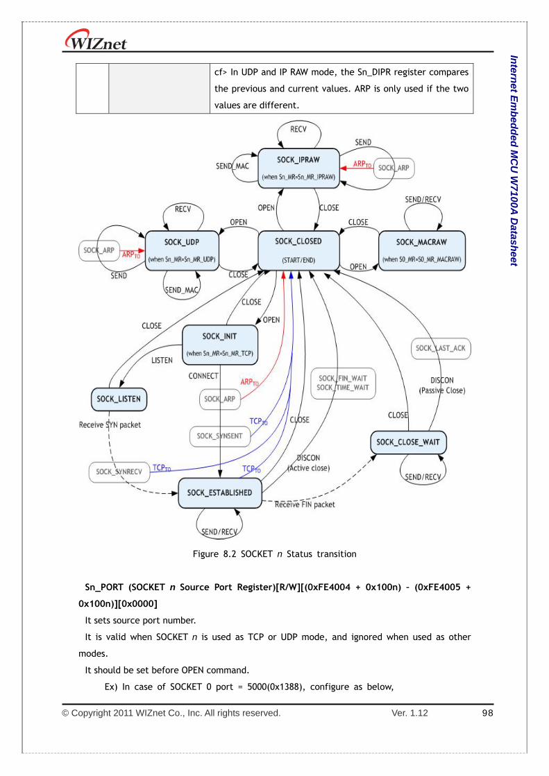
© Copyright 2011 WIZnet Co., Inc. All rights reserved. Ver. 1.12 98
Intern
et Em
bed
ded
MC
U W
7100A D
atasheet
cf> In UDP and IP RAW mode, the Sn_DIPR register compares
the previous and current values. ARP is only used if the two
values are different.
Figure 8.2 SOCKET n Status transition
Sn_PORT (SOCKET n Source Port Register)[R/W][(0xFE4004 + 0x100n) – (0xFE4005 +
0x100n)][0x0000]
It sets source port number.
It is valid when SOCKET n is used as TCP or UDP mode, and ignored when used as other
modes.
It should be set before OPEN command.
Ex) In case of SOCKET 0 port = 5000(0x1388), configure as below,

© Copyright 2011 WIZnet Co., Inc. All rights reserved. Ver. 1.12 99
Intern
et Em
bed
ded
MC
U W
7100A D
atasheet
0xFE4004 0xFE4005
0x13 0x88
Sn_DHAR (SOCKET n Destination Hardware Address Register)[R/W][(0xFE4006 + 0x100n)
– (0xFE400B + 0x100n)][FF.FF.FF.FF.FF.FF]
It sets or is set as destination hardware address of SOCKET n. Also, if SOCKET 0 is used for
PPPoE mode, S0_DHAR sets as PPPoE server hardware an address that is already known.
When using SEND_MAC command at the UDP or IPRAW mode, it sets the destination
hardware address of SOCKET n. At the TCP, UDP and IPRAW mode, Sn_DHAR is set as
destination hardware address that is acquired by ARP-process of CONNECT or SEND command.
The host can acquire the destination hardware address through Sn_DHAR after successfully
performing CONNET or SEND command.
When using PPPoE-process of W7100A, PPPoE server hardware address is not required to be
set.
However, even if PPPoE-process of W7100A is not used, but implemented by yourself with
MACRAW mode, in order to transmit or receive the PPPoE packet, PPPoE server hardware
address(acquired by your PPPoE-process), PPPoE server IP address, and PPP session ID should
be set, and MR(PPPoE) also should be set as '1'.
S0_DHAR sets the PPPoE server hardware address before the OPEN command. PPPoE server
hardware address which is set by S0_DHAR is applied to PDHAR after performing the OPEN
command. The configured PPPoE information is internally valid even after the CLOSE
command.
EX) In case of SOCKET 0 Destination Hardware address = 00.08.DC.01.02.10, config
uration is as below,
0xFE4006 0xFE4007 0xFE4008 0xFE4009 0xFE400A 0xFE400B
0x00 0x08 0xDC 0x01 0x02 0x10
Sn_DIPR (SOCKET n Destination IP Address Register)[R/W][(0xFE400C + 0x100n) –
(0xFE400F + 0x100n)][00.00.00.00]
It sets or is set as destination IP address of SOCKET n. If SOCKET 0 is used as PPPoE mode,
S0_DIPR0 sets PPPoE server with an IP address that is already known.
It is valid only in TCP, UDP, IPRAW or PPPoE mode, but ignored in MACRAW mode.
In the TCP mode, when operating as "TCP CLIENT" it sets the IP address of the "TCP SERVER"
before performing the CONNECT command and when operating as "TCP SERVER", it internally
sets the IP address of the "TCP CLIENT" after successfully establishing connection.
In UDP or IPRAW mode, set the destination IP address in the Sn_DIPR for transmitting UDP or
IPRAW DATA packets before performing SEND or SEND_MAC command. At the PPPoE mode,
S0_DIPR sets as PPPoE server IP address that is already known.

© Copyright 2011 WIZnet Co., Inc. All rights reserved. Ver. 1.12 100
Intern
et Em
bed
ded
MC
U W
7100A D
atasheet
Ex) In case of SOCKET 0 Destination IP address = 192.168.0.11, configure as below,
0xFE400C 0xFE400D 0xFE400E 0xFE400F
192 (0xC0) 168 (0xA8) 0 (0x00) 11 (0x0B)
Sn_DPORT (SOCKET n Destination Port Register)[R/W][(0xFE4010 + 0x100n) – (0xFE4011
+ 0x100n)][0x0000]
The destination port number is set in the Sn_DPORT of SOCKET n. If SOCKET 0 is used as
PPPoE mode, S0_DPORT0 sets PPP session ID that is already known.
It is valid only in TCP, UDP or PPPoE mode, and ignored in other modes.
At the TCP mode, when operating as "TCP CLIENT", it listens for the port number of the "TCP
SERVER" before performing the CONNECT command.
At the UDP mode, the destination port number is set in the Sn_DPORT to be used for
transmitting UDP DATA packets before performing SEND or SEND_MAC command.
At the PPPoE mode, the PPP session ID that is already known is set in the S0_DPORT. PPP
session ID (set by S0_DPORT0) is applied to PSIDR after performing the OPEN command.
Ex) In case of SOCKET 0 Destination Port = 5000(0x1388), configure as below,
0xFE4010 0xFE4011
0x13 0x88
Sn_MSSR (SOCKET n Maximum Segment Size Register)[R/W][(0xFE4012 + 0x100n) –
(0xFE4013 + 0x100n)][0x0000]
It sets the MTU (Maximum Transfer Unit) of SOCKET n or notifies the MTU that is already set.
It supports TCP or UDP mode. When using PPPoE (MR(PPPoE)=‘1’), the MTU of the TCP or UDP
mode is assigned in the range of the MTU of PPPoE.
At the IPRAW or MACRAW, MTU is not processed internally, but the default MTU is used.
Therefore, when transmitting data bigger than the default MTU, the host should manually
divide the data into the default MTU unit.
Reset value is 0 in the SOCKET initialization process, but the MSSR is changed to the smaller
value between the user setting value and default value. If there is no user setting value, MSSR
is changed to default value.
At the TCP or UDP mode, if transmitting data is bigger than the MTU, W7100A automatically
divides the data into the MTU unit.
MTU is known as MSS in the TCP mode. By selecting from the Host-Written-Value and the
peer's MSS, MSS is automatically set as the smaller value through the TCP connection process.
At the UDP mode, there is no connection-process of TCP mode, and Host-Written-Value is
just used. When communicating with the peer having a different MTU, W7100A is able to
receive ICMP (Fragment MTU) packets. So, the user should close the SOCKET, set FMTU as

© Copyright 2011 WIZnet Co., Inc. All rights reserved. Ver. 1.12 101
Intern
et Em
bed
ded
MC
U W
7100A D
atasheet
Sn_MSSR and retry the communication with the OPEN command.
Mode Normal (MR(PPPoE)=‘0’) PPPoE (MR(PPPoE)=‘1’)
Default MTU Range Default MTU Range
TCP 1460 1 ~ 1460 1452 1 ~ 1452
UDP 1472 1 ~ 1472 1464 1 ~ 1464
IPRAW 1480 1472
MACRAW 1514
Ex) In case of SOCKET 0 MSS = 1460(0x05B4), configure as below,
0xFE4012 0xFE4013
0x05 0xB4
Sn_PROTO (SOCKET n Protocol Number Register)[R/W][0xFE4014 + 0x100n][0x00]
It is a 1 byte register that sets the protocol number field of the IP header at the IP layer. It
is valid only in IPRAW mode, and ignored in other modes. Sn_PROTO is set before OPEN
command. When SOCKET n is opened in IPRAW mode, it transmits and receives the data of the
protocol number set in Sn_PROTO. Sn_PROTO can be assigned in the range of 0x00 ~ 0xFF, but
W7100A does not support TCP(0x06) and UDP(0x11) protocol number
Protocol number is defined in IANA(Internet assigned numbers authority). For the detail,
refer to online document (Uhttp://www.iana.org/assignments/protocol-numbersU).
Ex) Internet Control Message Protocol(ICMP) = 0x01, Internet Group Management Pr
otocol = 0x02
Sn_TOS (SOCKET n TOS Register)[R/W][0xFE4015 + 0x100n][0x00]
It sets the TOS(Type of Service) field of the IP header at the IP layer. It should be set before
the OPEN command. Refer to Uhttp://www.iana.org/assignments/ip-parametersU.
Sn_TTL (SOCKET n TTL Register)[R/W][0xFE4016 + 0x100n][0x80]
It sets the TTL(Time To Live) field of the IP header at the IP layer. It should be set before
the OPEN command. Refer to Uhttp://www.iana.org/assignments/ip-parametersU.
Sn_RXMEM_SIZE (SOCKET n Receive Memory Size Register)[R/W][0xFE401E +
0x100n][0x02]
It configures the internal RX Memory size of each SOCKET. RX Memory size of each SOCKET is
configurable in the size of 1, 2, 4, 8, 16Kbytes. 2Kbytes is assigned when reset.
Sn_RXMEM_SIZESUM(sum of Sn_RXMEM_SIZE) of each SOCKET should be 16KB.
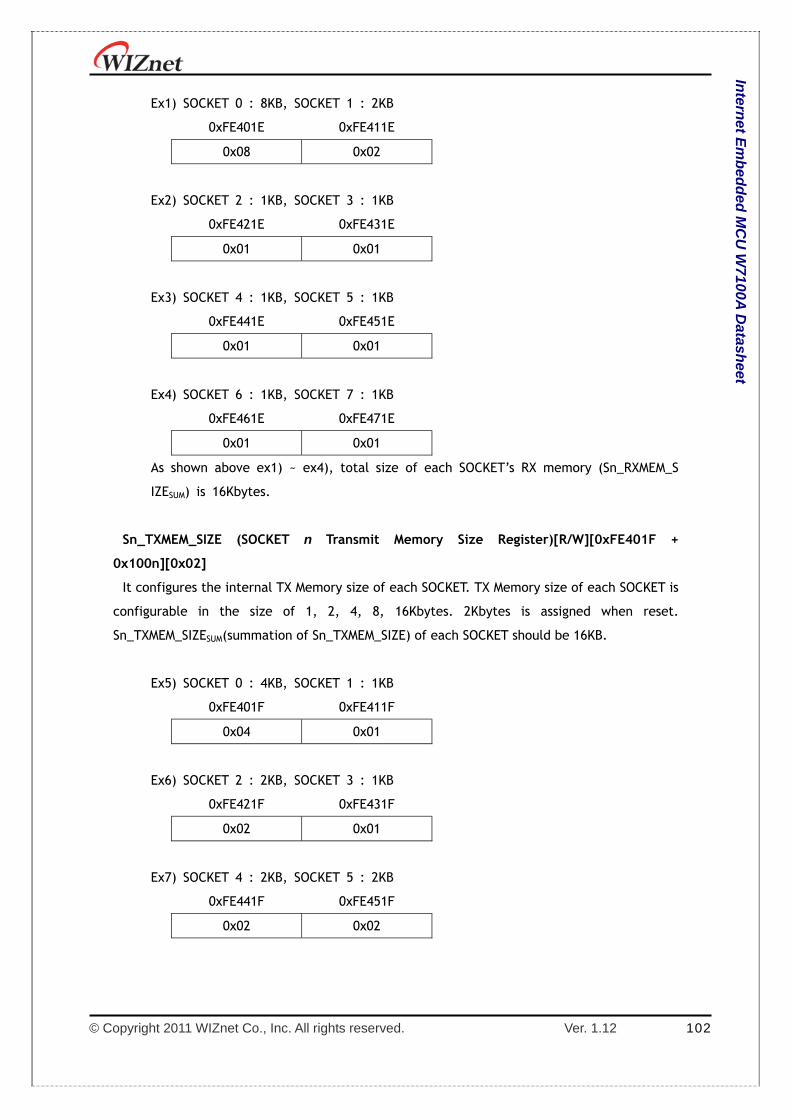
© Copyright 2011 WIZnet Co., Inc. All rights reserved. Ver. 1.12 102
Intern
et Em
bed
ded
MC
U W
7100A D
atasheet
Ex1) SOCKET 0 : 8KB, SOCKET 1 : 2KB
0xFE401E 0xFE411E
0x08 0x02
Ex2) SOCKET 2 : 1KB, SOCKET 3 : 1KB
0xFE421E 0xFE431E
0x01 0x01
Ex3) SOCKET 4 : 1KB, SOCKET 5 : 1KB
0xFE441E 0xFE451E
0x01 0x01
Ex4) SOCKET 6 : 1KB, SOCKET 7 : 1KB
0xFE461E 0xFE471E
0x01 0x01
As shown above ex1) ~ ex4), total size of each SOCKET’s RX memory (Sn_RXMEM_S
IZESUM) is 16Kbytes.
Sn_TXMEM_SIZE (SOCKET n Transmit Memory Size Register)[R/W][0xFE401F +
0x100n][0x02]
It configures the internal TX Memory size of each SOCKET. TX Memory size of each SOCKET is
configurable in the size of 1, 2, 4, 8, 16Kbytes. 2Kbytes is assigned when reset.
Sn_TXMEM_SIZESUM(summation of Sn_TXMEM_SIZE) of each SOCKET should be 16KB.
Ex5) SOCKET 0 : 4KB, SOCKET 1 : 1KB
0xFE401F 0xFE411F
0x04 0x01
Ex6) SOCKET 2 : 2KB, SOCKET 3 : 1KB
0xFE421F 0xFE431F
0x02 0x01
Ex7) SOCKET 4 : 2KB, SOCKET 5 : 2KB
0xFE441F 0xFE451F
0x02 0x02

© Copyright 2011 WIZnet Co., Inc. All rights reserved. Ver. 1.12 103
Intern
et Em
bed
ded
MC
U W
7100A D
atasheet
Ex8) SOCKET 6 : 2KB, SOCKET 7 : 2KB
0xFE461F 0xFE471F
0x02 0x02
As shown above ex5) ~ ex8), total size of each SOCKET’s TX memory (Sn_TXMEM_S
IZESUM) is 16Kbytes.
Sn_TX_FSR (SOCKET n TX Free Size Register)[R][(0xFE4020 + 0x100n) – (0xFE4021 +
100n)][0x0000]
It notifies the available size of the internal TX memory (the byte size of transmittable data)
of SOCKET n. The host can’t write data as a size bigger than Sn_TX_FSR. Therefore, be sure to
check Sn_TX_FSR before transmitting data, and if your data size is smaller than or the same
as Sn_TX_FSR, transmit the data with SEND or SEND_MAC command after copying the data.
At the TCP mode, if the peer checks the transmitted DATA packet (if DATA/ACK packet is
received from the peer), Sn_TX_FSR is automatically increased by the size of that transmitted
DATA packet. At the other modes, when Sn_IR(SENDOK) is ‘1’, Sn_TX_FSR is automatically
increased by the size of the transmitted data.
Ex) In case of 2048(0x8000) in S0_TX_FSR0
0xFE4020 0xFE4021
0x08 0x00
Sn_TX_RD (SOCKET n TX Read Pointer Register)[R][(0xFE4022 + 0x100n) – (0xFE4023 +
0x100n)][0x0000]
This register shows the address of the last transmission finishing in the TX memory. With the
SEND command of SOCKET n Command Register, it transmits data from the current Sn_TX_RD
to the Sn_TX_WR and automatically updates after transmission is finished. Therefore, after
transmission is finished, Sn_TX_RD and Sn_TX_WR will have the same value. When reading this
register, the user should read the upper bytes (0xFE4022, 0xFE4122, 0xFE4222, 0xFE4322,
0xFE4422, 0xFE4522, 0xFE4622, 0xFE4722) first and lower bytes (0xFE4023, 0xFE4123,
0xFE4223, 0xFE4323, 0xFE4423, 0xFE4523, 0xFE4623, 0xFE4723) later to get the correct value.
Sn_TX_WR (SOCKET n TX Write Pointer Register)[R/W][(0xFE4024 + 0x100n) – (0xFE4025
+ 0x100n)][0x0000]
This register offers the location information of where the transmission data should be
written. When reading this register, the user should read the upper bytes (0xFE4024,
0xFE4124, 0xFE4224, 0xFE4324, 0xFE4424, 0xFE4524, 0xFE4624, 0xFE4724) first and the lower
bytes (0xFE4025, 0xFE4125, 0xFE4225, 0xFE4325, 0xFE4425, 0xFE4525, 0xFE4625, 0xFE4725)
later to get the correct value.

© Copyright 2011 WIZnet Co., Inc. All rights reserved. Ver. 1.12 104
Intern
et Em
bed
ded
MC
U W
7100A D
atasheet
Ex) In case of 2048(0x0800) in S0_TX_WR,
0xFE4024 0xFE4025
0x08 0x00
But this value itself is not the physical address to write. So, the physical address should be
calculated as follows: (Refer to the W7100A Driver code)
1. SOCKET n TX Base Address (SBUFBASEADDRESS(n)) and SOCKETn TX Mask Address
(SMASK(n)) are calculated on Sn_TXMEM_SIZE(n) value. Refer to the Pseudo code of the
Initialization if detail is needed.
2. The bitwise-AND operation of two values and Sn_TX_WR and SMASK(n) gives the result
of the offset address (dst_mask) in TX memory range of the SOCKET.
3. Two values dst_mask and SBUFBASEADDRESS(n) are added together to give the result of
the physical address (dst_ptr).
Now, write the transmission data to dst_ptr as large as the user wants. (* There may be a
case where it exceeds the TX memory of the upper-bound of the SOCKET while writing. In this
case, write the transmission data to the upper-bound, and change the physical address to the
SBUFBASEADDRESS(n). Next, write the rest of the transmission data.)
After that, be sure to increase the Sn_TX_WR value by the size of writing data. Finally, give
the SEND command to Sn_CR (SOCKET n Command Register). Refer to the pseudo code of the
transmission part on TCP Server mode if the detail is needed.

© Copyright 2011 WIZnet Co., Inc. All rights reserved. Ver. 1.12 105
Intern
et Em
bed
ded
MC
U W
7100A D
atasheet
Figure 8.3 Calculate Physical Address
Sn_RX_RSR (SOCKET n RX Received Size Register)[R][(0xFE4026 + 0x100n) – (0xFE4027
+ 0x100n)][0x0000]
It informs the user of the byte size of the received data in Internal RX Memory of SOCKET n.
As this value is internally calculated with the values of Sn_RX_RD and Sn_RX_WR, it is
automatically changed by RECV command of SOCKET n Command Register(Sn_CR) and
receives data from the remote peer. When reading this register, the user should read the
upper byte(0xFE4026, 0xFE4126, 0xFE4226, 0xFE4326, 0xFE4426, 0xFE4526, 0xFE4626,

© Copyright 2011 WIZnet Co., Inc. All rights reserved. Ver. 1.12 106
Intern
et Em
bed
ded
MC
U W
7100A D
atasheet
0xFE4726) first and lower byte(0xFE4027, 0xFE4127, 0xFE4227, 0xFE4327, 0xFE4427,
0xFE4527, 0xFE4627, 0xFE4727) later to get the correct value.
Ex) In case of 2048(0x0800) in S0_RX_RSR,
0xFE4026 0xFE4027
0x08 0x00
The total size of this value can be decided according to the value of RX Memory Size Register.
Sn_RX_RD (SOCKET n Read Pointer Register)[R/W][(0xFE4028 + 0x100n) – (0xFE4029 +
0x100n)][0x0000]
This register offers the location information to read the receiving data. When reading this
register, user should read the upper byte (0xFE4028, 0xFE4128, 0xFE4228, 0xFE4328,
0xFE4428, 0xFE4528, 0xFE4628, 0xFE4728) first and lower byte (0xFE4029, 0xFE4129,
0xFE4229, 0xFE4329, 0xFE4429, 0xFE4529, 0xFE4629, 0xFE4729) later to get the correct value.
Ex) In case of 2048(0x0800) in S0_RX_RD,
0x0428 0x0429
0x08 0x00
But this value itself is not the physical address to read. So, the physical address should be
calculated as follows: (Refer to the W7100A Driver code)
1. SOCKET n RX Base Address (RBUFBASEADDRESS(n)) and SOCKET n RX Mask Address
(RMASK(n)) are calculated on Sn_RXMEM_SIZE(n) value.
2. The bitwise-AND operation of two values, Sn_RX_RD and RMASK(n) gives the result of
the offset address (src_mask), in the RX memory range of the SOCKET.
3. Two values src_mask and RBUFBASEADDRESS(n) are added together to give the result of
the physical address(src_ptr).
Now, read the receiving data from src_ptr as large as the user wants. (* There may be a case
where it exceeds the RX memory upper-bound of the SOCKET while reading. In this case, read
the receiving data to the upper-bound, and change the physical address to the
RBUFBASEADDRESS(n). Next, read the rest of the receiving data.)
After that, be sure to increase the Sn_RX_RD value by the size of the reading data. (* Must
not increase more than the size of received data. So must check Sn_RX_RSR before receiving
process.) Finally, give RECV command to Sn_CR(SOCKET n Command Register).
Refer to the pseudo code of the receiving part on TCP Server mode if the detail is needed.
Sn_RX_WR (SOCKET n RX Write Pointer Register)[R/W][(0xFE402A + 0x100n) – (0xFE402B
+ 0x100n)][0x0000]
This register offers the location information to write the receive data. When reading this
register, the user should read upper bytes (0xFE402A, 0xFE412A, 0xFE422A, 0xFE432A,
© Copyright 2011 WIZnet Co., Inc. All rights reserved. Ver. 1.12 107
Intern
et Em
bed
ded
MC
U W
7100A D
atasheet
0xFE442A, 0xFE452A, 0xFE462A, 0xFE472A) first and lower bytes (0xFE402B, 0xFE412B,
0xFE422B, 0xFE432B, 0xFE442B, 0xFE452B, 0xFE462B, 0xFE472B) later to get the correct
value.
Ex) In case of 2048(0x0800) in S0_RX_WR,
0xFE402A 0xFE402B
0x08 0x00
Sn_FRAG (SOCKET n Fragment Register)[R/W][(0xFE402D + 0x100n) – (0xFE402E +
0x100n)][0x4000]
It sets the Fragment field of the IP header at the IP layer. W7100A does not support the
packet fragment at the IP layer. Even though Sn_FRAG is configured, IP data is not fragmented,
and not recommended either. It should be configured before performing OPEN command.
Ex) Sn_FRAG0 = 0x4000 (Don’t Fragment)
0xFE402D 0xFE402E
0x40 0x00

© Copyright 2011 WIZnet Co., Inc. All rights reserved. Ver. 1.12 108
Intern
et Em
bed
ded
MC
U W
7100A D
atasheet
9 Functional Description
Since the W7100A internally contains the 8051 compatible MCU and TCP/IP core, it can run
standalone without other devices to Ethernet application. In this section, both the
initialization of the W7100A and the communication method for each protocol (TCP, UDP,
IPRAW and MACRAW) based on Pseudo code will be introduced.
9.1 Initialization The initialization of W7100A has three steps which setup the 8051 MCU, the network
information and the internal TX/RX memory.
STEP 1 : Initializes MCU
1. Interrupt setting
Set the enable / disable state of interrupt such as the general 8051. Detail information
of the setting refers to the section 3 ‘Interrupt’.
2. Memory Access timing setting
The memory access timing can be set by using two registers which are CKCON (0x8E) and
WTST (0x92) registers. The CKCON (0x8E) can control the data memory access timing and
the WTST (0x92) can control the code memory access timing. Both two registers can set
their value from 0 to 7. But in the W7100A, CKCON can set the value 1~7 and WTST can
set the value 4~7 only. The other values of both registers are not used. If the user sets
the value to an unused value, the W7100A cannot run properly. Detail information can be
found in the section 2.5 ‘SFR definition’.
Ex) Setting: interrupt disabled, 2 clocks access time with data memory, 7 clocks
access time with code memory.
EA = 0; // Disable all interrupts
CKCON = 0x01; // Set data memory access time
WTST = 0x06; // Set code memory access time
3. Serial baud rate, register and interrupt setting for serial communication
1) For the serial communication, related registers of W7100A should be set.
The registers of W7100A for serial communication are TMOD, PCON and SCON as below.
① TMOD(89H): Decide the timer/counter mode for serial communication.
GATE C/T M1 M0 GATE C/T M1 M0

© Copyright 2011 WIZnet Co., Inc. All rights reserved. Ver. 1.12 109
Intern
et Em
bed
ded
MC
U W
7100A D
atasheet
Table 9.1 Timer / Counter Mode
M1 M0 Mode
0 0 0
0 1 1
1 0 2
1 1 3
② PCON(87H): Decide the SMOD bit which is the control flag of the serial transmission
rate.
SMOD - - - - - - -
Table 9.2 Baud rate
Mode SMOD = ‘0’ SMOD = ‘1’
1, 3 A half of Overflow of the
Timer/Counter 1
Overflow of the
Timer/Counter 1
2 A quarter of the XTAL A half of the XTAL
③ SCON(98H): For control and observe the UART.
SM0 SM1 SM2 REN TB8 RB8 TI RI
Table 9.3 Mode of UART
SM0 SM1 Mode
0 0 0
0 1 1
1 0 2
1 1 3
SM2: Used in Mode2, 3. Assume that this bit set to 1, if the 9th bit of received data
bit is ‘1’, receive the data. Or the bit is ‘0’ ignore the data.
REN: Receive enable bit (‘1’; Receive enable).
TB8: In the mode2, 3, 8th bit of transmitted data.
RB8: In the mode2, 3, 8th bit of received data.
TI: Transmission complete interrupt flag.
RI: Reception complete interrupt flag.
2) Interrupt state should be set when initializing the serial communication.
Since the serial communication uses interrupt, user must disable the related interrupts
when initializing the serial communication.
3) The baud rate should be set to the value which the user will use. Baud rate value for the

© Copyright 2011 WIZnet Co., Inc. All rights reserved. Ver. 1.12 110
Intern
et Em
bed
ded
MC
U W
7100A D
atasheet
timer of W7100A refers to the section 6.6 ‘Examples of Baud Rate Setting’.
The calculation of baud rate for the timer is as below
① Calculation formula of timer1
TH1 = 256 – ((K * 88.4736MHz) / (384 * baud rate))
K = ‘1’ at SMOD = ‘0’, K = ‘2’ at SMOD = ‘1’
② Calculation formula of timer2
(RCAP2H, RCAP2L) = 65536 – (88.4736MHz / (32 * baud rate))
Ex) Using timer mode2, SMOD = 1, Clock speed = 88.4736MHz, Baud rate = 115200.
ET1= 0; // Timer1 INT disable
TMOD = 0x20; // TIMER MODE2
PCON |= 0x80; // SMOD = 1
TH1 = 0xFC; // x2 115200(SMOD = 1) at 88.4736MHz
TR1 = 1; // Start the TIMER1
SCON = 0x50; // Serial MODE1, REN = 1, TI = 0, RI = 0
ES = 0; // Serial interrupt disable
RI = 0; // Receive interrupt disable
TI = 0; // Transmit interrupt disable
4) If user uses TCPIP Core interrupt, the INTLEVEL register must be set to the value more than
0x2B00 because of internal TCPIP Core interrupt routine.
Ex) Set the INTLEVEL register to 0x2B00
IINCHIP_WRITE (INTLEVEL0, 0x2B); //write high byte of INTLEVEL TCPIPCore register
IINCHIP_WRITE (INTLEVEL0 + 1, 0x00);//write low byte of INTLEVEL TCPIPCore register
STEP 2 : Setting Network Information
1. Basic network information setting for communication:
It must be set the basic network information.
① SHAR(Source Hardware Address Register)
It is prescribed that the source hardware addresses, which is set by SHAR, use
unique hardware addresses (Ethernet MAC address) in the Ethernet MAC layer. The
IEEE manages the MAC address allocation. The manufacturer which produces the
network device allocates the MAC address to product.
Details on MAC address allocation refer to the website as below.
Uhttp://www.ieee.org/U, Uhttp://standards.ieee.org/regauth/oui/index.shtmlU
② GAR(Gateway Address Register)
③ SUBR(Subnet Mask Register)
④ SIPR(Source IP Address Register)

© Copyright 2011 WIZnet Co., Inc. All rights reserved. Ver. 1.12 111
Intern
et Em
bed
ded
MC
U W
7100A D
atasheet
2. Set the retransmission time & count when the packet transmission fails.
To set the retransmission time, the registers should be set as below.
① RTR(Retry Time-value Register), In the RTR, ‘1’ means ‘100us’.
② RCR(Retry Count Register)
STEP 3 : Allocation Internal TX/RX Memory for SOCKET n
Total configurable maximum size of TX, RX memory is 16 Kbytes. User can freely set the
memory size to 1KB, 2KB, 4KB, 8KB and 16KB within 16Kbytes each 8 sockets. But the
sum of TX or RX memory cannot be set more than 16Kbytes. (TXmax = 16KB, RXmax = 16KB)
In case of, assign 2KB rx, tx memory per SOCKET
gS0_RX_BASE = 0xFE0000(Chip base address) + 0xFEC000(Internal RX buffer address); // Set
base address of RX memory for SOCKET 0
Sn_RXMEM_SIZE(ch) = (uint8 *) 2; // Assign 2K rx memory per SOCKET
gS0_RX_MASK = 2K – 1; // 0x07FF, for getting offset address within assigned SOCKET 0 RX
memory
gS1_RX_BASE = gS0_RX_BASE + (gS0_RX_MASK + 1);
gS1_RX_MASK = 2K – 1;
gS2_RX_BASE = gS1_RX_BASE + (gS1_RX_MASK + 1);
gS2_RX_MASK = 2K – 1;
gS3_RX_BASE = gS2_RX_BASE + (gS2_RX_MASK + 1);
gS3_RX_MASK = 2K – 1;
gS4_RX_BASE = gS3_RX_BASE + (gS3_RX_MASK + 1);
gS4_RX_MASK = 2K – 1;
gS5_RX_BASE = gS4_RX_BASE + (gS4_RX_MASK + 1);
gS5_RX_MASK = 2K – 1;
gS6_RX_BASE = gS5_RX_BASE + (gS5_RX_MASK + 1);
gS6_RX_MASK = 2K – 1;
gS7_RX_BASE = gS6_RX_BASE + (gS6_RX_MASK + 1);
gS7_RX_MASK = 2K – 1;
gS0_TX_BASE = 0xFE0000(Chip base address) + 0xFE8000(Internal TX buffer address); // Set
base address of TX memory for SOCKET 0
Sn_TXMEM_SIZE(ch) = (uint8 *) 2; // Assign 2K rx memory per SOCKET
gS0_TX_MASK = 2K – 1;
Same method, set gS1_TX_BASE, gS1_TX_MASK, gS2_TX_BASE, gS2_TX_MASK, gS3_TX_BASE,
gS3_TX_MASK, gS4_TX_BASE, gS4_TX_MASK, gS5_TX_BASE, gS5_TX_MASK, gS6_TX_BASE,
gS6_tx_MASK, gS7_TX_BASE, gS7_TX_MASK.
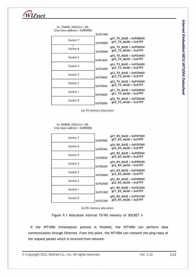
© Copyright 2011 WIZnet Co., Inc. All rights reserved. Ver. 1.12 112
Intern
et Em
bed
ded
MC
U W
7100A D
atasheet
Figure 9.1 Allocation Internal TX/RX memory of SOCKET n
If the W7100A initialization process is finished, the W7100A can perform data
communication through Ethernet. From this point, the W7100A can transmit the ping-reply of
the request packet which is received from network.

© Copyright 2011 WIZnet Co., Inc. All rights reserved. Ver. 1.12 113
Intern
et Em
bed
ded
MC
U W
7100A D
atasheet
9.2 Data Communication After the W7100A initialization process, open the SOCKET to TCP or UDP or IPRAW or
MACRAW mode. W7100A can transmit and receive the data with others by ‘open’ the SOCKET.
The W7100A supports the independently and simultaneously usable 8 SOCKETS. In this section,
the communication method for each mode will be introduced.
9.2.1 TCP The TCP is a connection-oriented protocol. The TCP make the connection SOCKET by using
its own IP address, port number and destination IP address, port number. Then transmits and
receives the data by using this SOCKET.
Methods of making the connection to SOCKET are “TCP SERVER” and “TCP CLIENT”. It is
divided by transmitting the connect-request (SYN packet).
The “TCP SERVER” listens to the connect-request from the “TCP CLIENT”, and makes
connection SOCKET by accepting the transmitted connect-request (Passive-open).
The “TCP CLIENT” transmits the connect-request first to “TCP SERVER” to make the
connection (Active-open).
Figure 9.2 TCP SERVER & TCP CLIENT

© Copyright 2011 WIZnet Co., Inc. All rights reserved. Ver. 1.12 114
Intern
et Em
bed
ded
MC
U W
7100A D
atasheet
9.2.1.1 TCP SERVER
Figure 9.3 “TCP SERVER” Operation Flow
SOCKET Initialization
SOCKET initialization is required for TCP data communication. The initialization is opening
the SOCKET. The SOCKET opening process selects one SOCKET from 8 SOCKETS of the W7100A,
and sets the protocol mode (Sn_MR(P3:P0)) and Sn_PORT0 which is source port number (Listen
port number in “TCP SERVER”) in the selected SOCKET, and then executes OPEN command.
After the OPEN command, if the status of Sn_SR is changed to SOCK_INIT, the SOCKET
initialization process is completed.
The SOCKET initialization process is identically applied in “TCP SEVER” and “TCP CLIENT”.
The Initialization process of SOCKET n in TCP mode is shown below.
START:
Sn_MR = 0x0001; // sets TCP mode
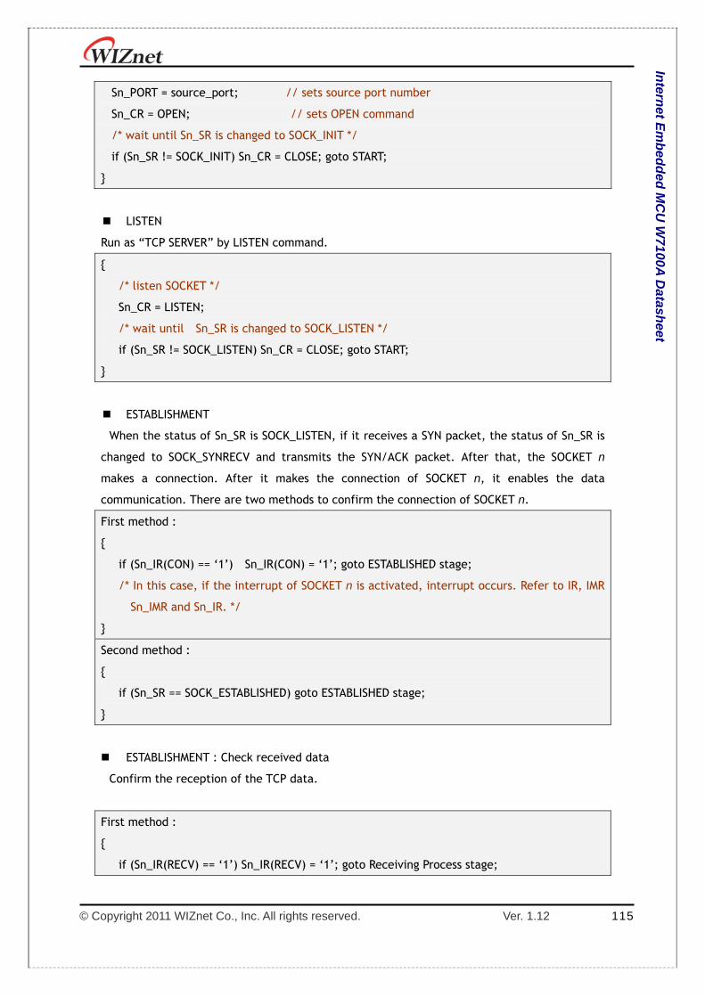
© Copyright 2011 WIZnet Co., Inc. All rights reserved. Ver. 1.12 115
Intern
et Em
bed
ded
MC
U W
7100A D
atasheet
Sn_PORT = source_port; // sets source port number
Sn_CR = OPEN; // sets OPEN command
/* wait until Sn_SR is changed to SOCK_INIT */
if (Sn_SR != SOCK_INIT) Sn_CR = CLOSE; goto START;
LISTEN
Run as “TCP SERVER” by LISTEN command.
/* listen SOCKET */
Sn_CR = LISTEN;
/* wait until Sn_SR is changed to SOCK_LISTEN */
if (Sn_SR != SOCK_LISTEN) Sn_CR = CLOSE; goto START;
ESTABLISHMENT
When the status of Sn_SR is SOCK_LISTEN, if it receives a SYN packet, the status of Sn_SR is
changed to SOCK_SYNRECV and transmits the SYN/ACK packet. After that, the SOCKET n
makes a connection. After it makes the connection of SOCKET n, it enables the data
communication. There are two methods to confirm the connection of SOCKET n.
First method :
if (Sn_IR(CON) == ‘1’) Sn_IR(CON) = ‘1’; goto ESTABLISHED stage;
/* In this case, if the interrupt of SOCKET n is activated, interrupt occurs. Refer to IR, IMR
Sn_IMR and Sn_IR. */
Second method :
if (Sn_SR == SOCK_ESTABLISHED) goto ESTABLISHED stage;
ESTABLISHMENT : Check received data
Confirm the reception of the TCP data.
First method :
if (Sn_IR(RECV) == ‘1’) Sn_IR(RECV) = ‘1’; goto Receiving Process stage;
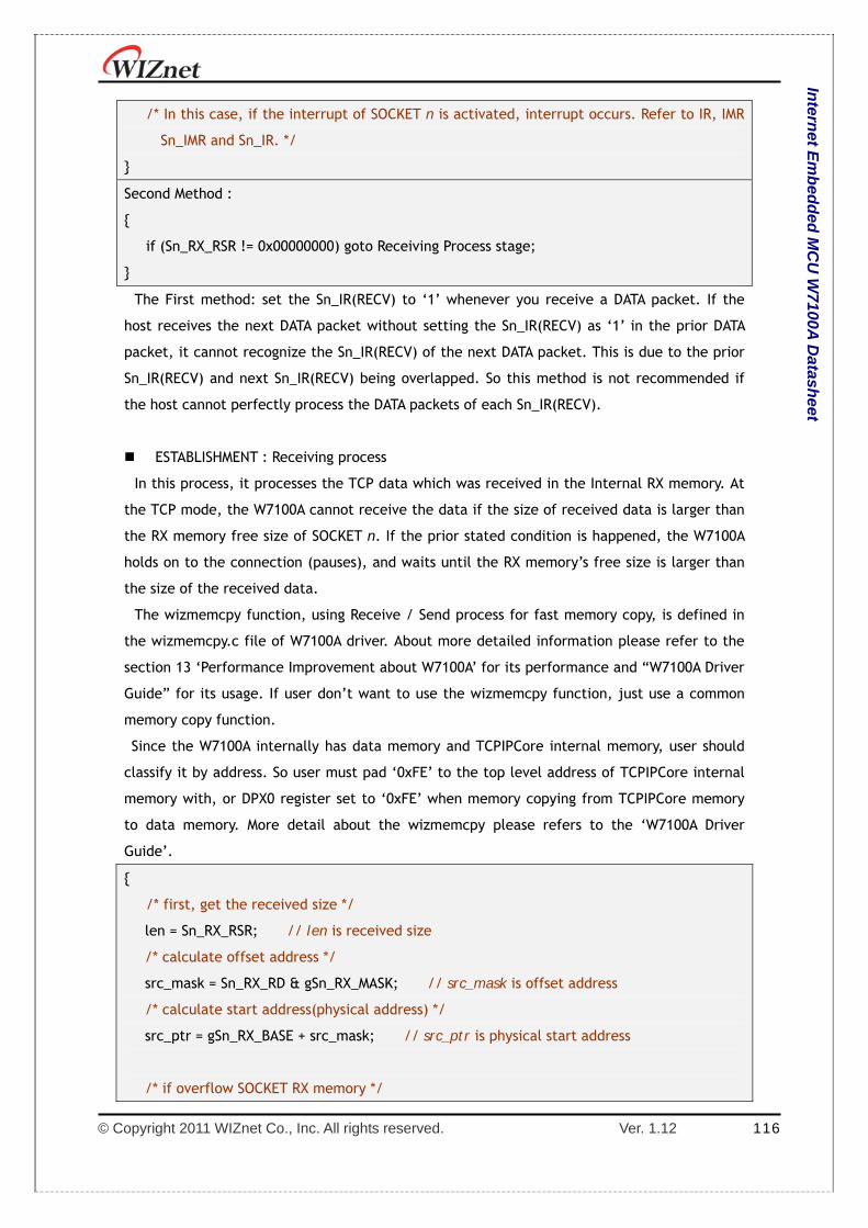
© Copyright 2011 WIZnet Co., Inc. All rights reserved. Ver. 1.12 116
Intern
et Em
bed
ded
MC
U W
7100A D
atasheet
/* In this case, if the interrupt of SOCKET n is activated, interrupt occurs. Refer to IR, IMR
Sn_IMR and Sn_IR. */
Second Method :
if (Sn_RX_RSR != 0x00000000) goto Receiving Process stage;
The First method: set the Sn_IR(RECV) to ‘1’ whenever you receive a DATA packet. If the
host receives the next DATA packet without setting the Sn_IR(RECV) as ‘1’ in the prior DATA
packet, it cannot recognize the Sn_IR(RECV) of the next DATA packet. This is due to the prior
Sn_IR(RECV) and next Sn_IR(RECV) being overlapped. So this method is not recommended if
the host cannot perfectly process the DATA packets of each Sn_IR(RECV).
ESTABLISHMENT : Receiving process
In this process, it processes the TCP data which was received in the Internal RX memory. At
the TCP mode, the W7100A cannot receive the data if the size of received data is larger than
the RX memory free size of SOCKET n. If the prior stated condition is happened, the W7100A
holds on to the connection (pauses), and waits until the RX memory’s free size is larger than
the size of the received data.
The wizmemcpy function, using Receive / Send process for fast memory copy, is defined in
the wizmemcpy.c file of W7100A driver. About more detailed information please refer to the
section 13 ‘Performance Improvement about W7100A’ for its performance and “W7100A Driver
Guide” for its usage. If user don’t want to use the wizmemcpy function, just use a common
memory copy function.
Since the W7100A internally has data memory and TCPIPCore internal memory, user should
classify it by address. So user must pad ‘0xFE’ to the top level address of TCPIPCore internal
memory with, or DPX0 register set to ‘0xFE’ when memory copying from TCPIPCore memory
to data memory. More detail about the wizmemcpy please refers to the ‘W7100A Driver
Guide’.
/* first, get the received size */
len = Sn_RX_RSR; // len is received size
/* calculate offset address */
src_mask = Sn_RX_RD & gSn_RX_MASK; // src_mask is offset address
/* calculate start address(physical address) */
src_ptr = gSn_RX_BASE + src_mask; // src_ptr is physical start address
/* if overflow SOCKET RX memory */
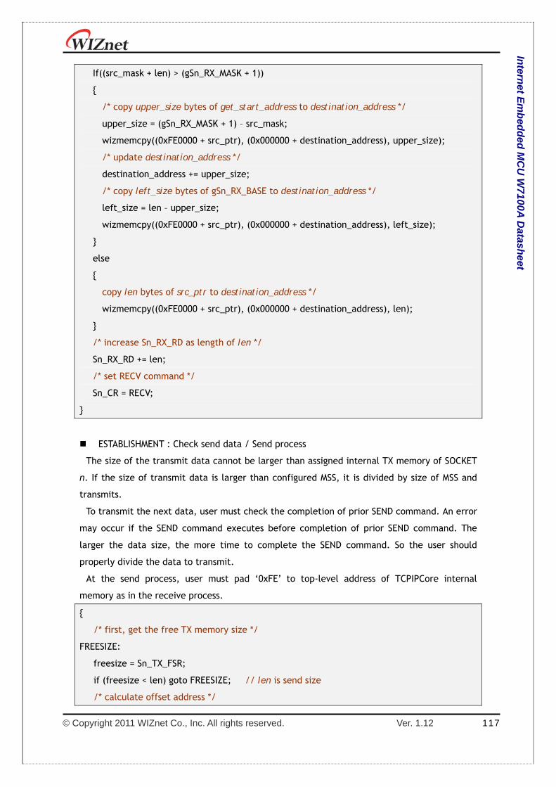
© Copyright 2011 WIZnet Co., Inc. All rights reserved. Ver. 1.12 117
Intern
et Em
bed
ded
MC
U W
7100A D
atasheet
If((src_mask + len) > (gSn_RX_MASK + 1))
/* copy upper_size bytes of get_start_address to destination_address */
upper_size = (gSn_RX_MASK + 1) – src_mask;
wizmemcpy((0xFE0000 + src_ptr), (0x000000 + destination_address), upper_size);
/* update destination_address */
destination_address += upper_size;
/* copy left_size bytes of gSn_RX_BASE to destination_address */
left_size = len – upper_size;
wizmemcpy((0xFE0000 + src_ptr), (0x000000 + destination_address), left_size);
else
copy len bytes of src_ptr to destination_address */
wizmemcpy((0xFE0000 + src_ptr), (0x000000 + destination_address), len);
/* increase Sn_RX_RD as length of len */
Sn_RX_RD += len;
/* set RECV command */
Sn_CR = RECV;
ESTABLISHMENT : Check send data / Send process
The size of the transmit data cannot be larger than assigned internal TX memory of SOCKET
n. If the size of transmit data is larger than configured MSS, it is divided by size of MSS and
transmits.
To transmit the next data, user must check the completion of prior SEND command. An error
may occur if the SEND command executes before completion of prior SEND command. The
larger the data size, the more time to complete the SEND command. So the user should
properly divide the data to transmit.
At the send process, user must pad ‘0xFE’ to top-level address of TCPIPCore internal
memory as in the receive process.
/* first, get the free TX memory size */
FREESIZE:
freesize = Sn_TX_FSR;
if (freesize < len) goto FREESIZE; // len is send size
/* calculate offset address */
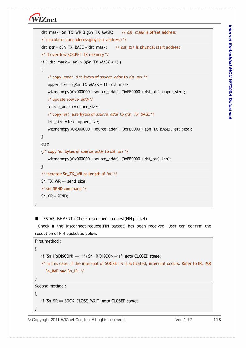
© Copyright 2011 WIZnet Co., Inc. All rights reserved. Ver. 1.12 118
Intern
et Em
bed
ded
MC
U W
7100A D
atasheet
dst_mask= Sn_TX_WR & gSn_TX_MASK; // dst_mask is offset address
/* calculate start address(physical address) */
dst_ptr = gSn_TX_BASE + dst_mask; // dst_ptr is physical start address
/* if overflow SOCKET TX memory */
if ( (dst_mask + len) > (gSn_TX_MASK + 1) )
/* copy upper_size bytes of source_addr to dst_ptr */
upper_size = (gSn_TX_MASK + 1) – dst_mask;
wizmemcpy((0x000000 + source_addr), (0xFE0000 + dst_ptr), upper_size);
/* update source_addr*/
source_addr += upper_size;
/* copy left_size bytes of source_addr to gSn_TX_BASE */
left_size = len – upper_size;
wizmemcpy((0x000000 + source_addr), (0xFE0000 + gSn_TX_BASE), left_size);
else
/* copy len bytes of source_addr to dst_ptr */
wizmemcpy((0x000000 + source_addr), (0xFE0000 + dst_ptr), len);
/* increase Sn_TX_WR as length of len */
Sn_TX_WR += send_size;
/* set SEND command */
Sn_CR = SEND;
ESTABLISHMENT : Check disconnect-request(FIN packet)
Check if the Disconnect-request(FIN packet) has been received. User can confirm the
reception of FIN packet as below.
First method :
if (Sn_IR(DISCON) == ‘1’) Sn_IR(DISCON)=‘1’; goto CLOSED stage;
/* In this case, if the interrupt of SOCKET n is activated, interrupt occurs. Refer to IR, IMR
Sn_IMR and Sn_IR. */
Second method :
if (Sn_SR == SOCK_CLOSE_WAIT) goto CLOSED stage;
© Copyright 2011 WIZnet Co., Inc. All rights reserved. Ver. 1.12 119
Intern
et Em
bed
ded
MC
U W
7100A D
atasheet
ESTABLISHMENT : Check disconnect / disconnecting process
When the user does not need data communication with others, or receives a FIN packet,
disconnect the connection SOCKET.
/* set DISCON command */
Sn_CR = DISCON;
ESTABLISHMENT : Check closed
Confirm that the SOCKET n is disconnected or closed by DISCON or close command.
First method :
if (Sn_IR(DISCON) == ‘1’) goto CLOSED stage;
/* In this case, if the interrupt of SOCKET n is activated, interrupt occurs. Refer to IR, IMR
Sn_IMR and Sn_IR. */
Second method :
if (Sn_SR == SOCK_CLOSED) goto CLOSED stage;
ESTABLISHMENT : Timeout
The timeout can occur by Connect-request(SYN packet) or its response(SYN/ACK packet),
the DATA packet or its response(DATA/ACK packet), the Disconnect-request(FIN packet) or its
response(FIN/ACK packet) and transmission all TCP packet. If it cannot transmit the above
packets within ‘timeout’ which is configured at RTR and RCR, the TCP final timeout(TCPTO)
occurs and the state of Sn_SR is changed to SOCK_CLOSED. Confirming method of the TCPTO is
as below:
First method :
if (Sn_IR(TIMEOUT bit) == ‘1’) Sn_IR(TIMEOUT)=‘1’; goto CLOSED stage;
/* In this case, if the interrupt of SOCKET n is activated, interrupt occurs. Refer to IR, IMR
Sn_IMR and Sn_IR. */
Second method :
if (Sn_SR == SOCK_CLOSED) goto CLOSED stage;

© Copyright 2011 WIZnet Co., Inc. All rights reserved. Ver. 1.12 120
Intern
et Em
bed
ded
MC
U W
7100A D
atasheet
SOCKET close
It can be used to close the SOCKET n, which disconnected by disconnect-process, or closed
by TCPTO or closed by host’s need without disconnect-process.
/* clear the remained interrupts of SOCKET n*/
Sn_IR = 0x00FF;
IR(n) = ‘1’;
/* set CLOSE command */
Sn_CR = CLOSE;
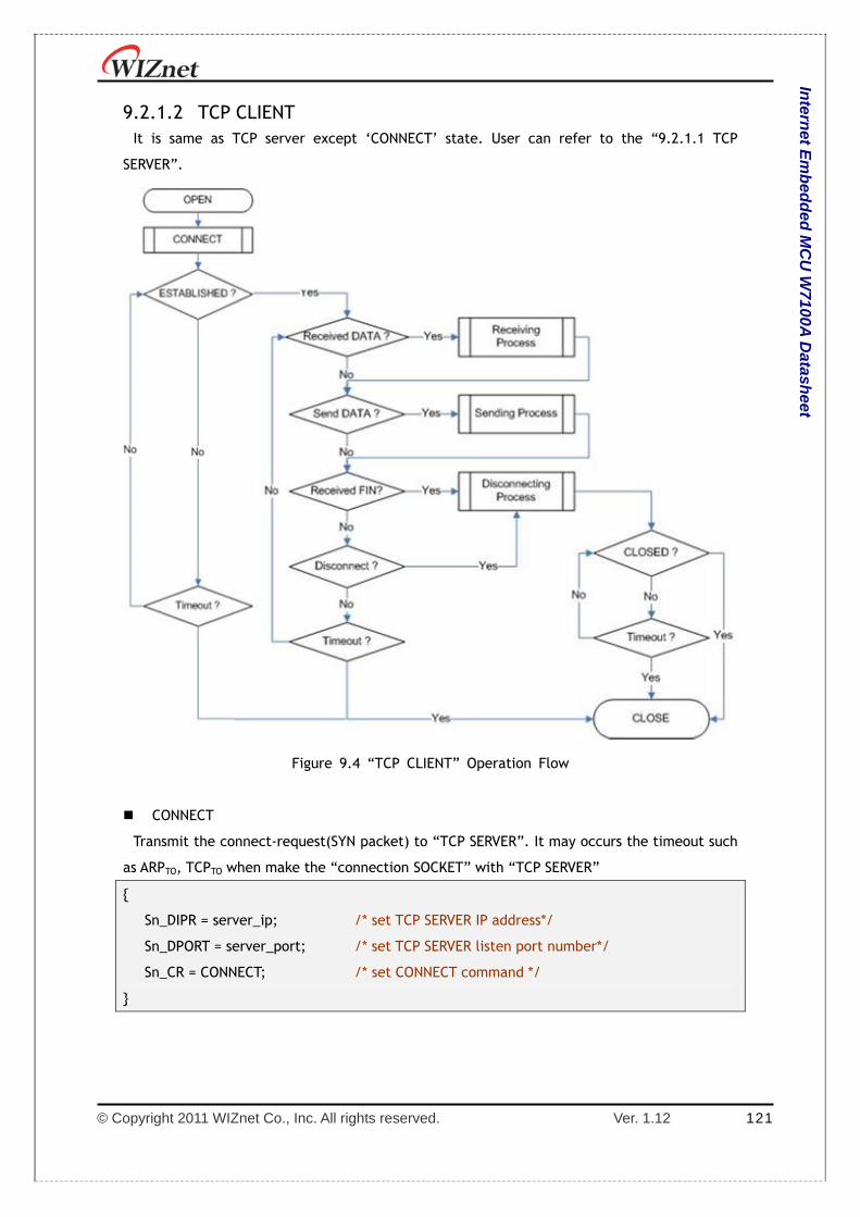
© Copyright 2011 WIZnet Co., Inc. All rights reserved. Ver. 1.12 121
Intern
et Em
bed
ded
MC
U W
7100A D
atasheet
9.2.1.2 TCP CLIENT It is same as TCP server except ‘CONNECT’ state. User can refer to the “9.2.1.1 TCP
SERVER”.
Figure 9.4 “TCP CLIENT” Operation Flow
CONNECT
Transmit the connect-request(SYN packet) to “TCP SERVER”. It may occurs the timeout such
as ARPTO, TCPTO when make the “connection SOCKET” with “TCP SERVER”
Sn_DIPR = server_ip; /* set TCP SERVER IP address*/
Sn_DPORT = server_port; /* set TCP SERVER listen port number*/
Sn_CR = CONNECT; /* set CONNECT command */
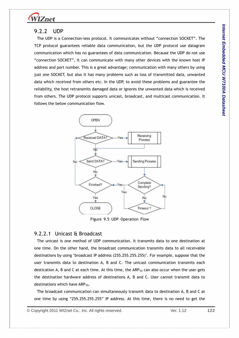
© Copyright 2011 WIZnet Co., Inc. All rights reserved. Ver. 1.12 122
Intern
et Em
bed
ded
MC
U W
7100A D
atasheet
9.2.2 UDP The UDP is a Connection-less protocol. It communicates without “connection SOCKET”. The
TCP protocol guarantees reliable data communication, but the UDP protocol use datagram
communication which has no guarantees of data communication. Because the UDP do not use
“connection SOCKET”, it can communicate with many other devices with the known host IP
address and port number. This is a great advantage; communication with many others by using
just one SOCKET, but also it has many problems such as loss of transmitted data, unwanted
data which received from others etc. In the UDP, to avoid these problems and guarantee the
reliability, the host retransmits damaged data or ignores the unwanted data which is received
from others. The UDP protocol supports unicast, broadcast, and multicast communication. It
follows the below communication flow.
Figure 9.5 UDP Operation Flow
9.2.2.1 Unicast & Broadcast The unicast is one method of UDP communication. It transmits data to one destination at
one time. On the other hand, the broadcast communication transmits data to all receivable
destinations by using ‘broadcast IP address (255.255.255.255)’. For example, suppose that the
user transmits data to destination A, B and C. The unicast communication transmits each
destication A, B and C at each time. At this time, the ARPTO can also occur when the user gets
the destination hardware address of destinations A, B and C. User cannot transmit data to
destinations which have ARPTO.
The broadcast communication can simultaneously transmit data to destination A, B and C at
one time by using “255.255.255.255” IP address. At this time, there is no need to get the
© Copyright 2011 WIZnet Co., Inc. All rights reserved. Ver. 1.12 123
Intern
et Em
bed
ded
MC
U W
7100A D
atasheet
destination hardware address about destination A, B and C, and also ARPTO is not occurred.
How to make broadcast IP?
The broadcast IP address can be obtained by performing a bitwise logical OR operation
between the bit complement of the subnet mask and the host IP address.
ex> IP: 222.98.173.123, Subnet Mask: 255.255.255.0 then broadcast IP: 222.98.173.255
Description Decimal Binary
HOST IP 222.098.173.123 11011110.01100010.10101101.01111011
Bit Complement Subnet mask 000.000.000.255 00000000.00000000.00000000.11111111
Bitwise OR - -
Broadcast IP 222.098.173.255 11011110.01100010.10101101.11111111
SOCKET Initialization
For the UDP data communication, SOCKET initialization is needed. It is opening the SOCKET.
The SOCKET open process is as follows. At first choose the one SOCKET among the 8 SOCKETS
of W7100A, then set the protocol mode(Sn_MR(P3:P0)) of the chosen SOCKET and set the
source port number Sn_PORT0 for communication. Finally execute the OPEN command. After
the OPEN command, the state of Sn_SR is changed to SOCK_UDP. Then the SOCKET
initialization is complete.
START:
Sn_MR = 0x02; /* sets UDP mode */
Sn_PORT = source_port; /* sets source port number */
Sn_CR = OPEN; /* sets OPEN command */
/* wait until Sn_SR is changed to SOCK_UDP */
if (Sn_SR != SOCK_UDP) Sn_CR = CLOSE; goto START;
Check received data
Check the reception of UDP data from destination. User can also check for received data via
TCP communication. It is strongly recommended that the TCP method is used because of the
same reason ing TCP. Please refer to the “9.2.1.1 TCP SERVER”.
First method :
if (Sn_IR(RECV) == ‘1’) Sn_IR(RECV) = ‘1’; goto Receiving Process stage;
/* In this case, if the interrupt of SOCKET n is activated, interrupt occurs. Refer to IR, IMR
Sn_IMR and Sn_IR. */

© Copyright 2011 WIZnet Co., Inc. All rights reserved. Ver. 1.12 124
Intern
et Em
bed
ded
MC
U W
7100A D
atasheet
Second Method :
if (Sn_RX_RSR != 0x00000000) goto Receiving Process stage;
Receiving process
Process the received UDP data in Internal RX memory. The structure of received UDP data is
as below.
Figure 9.6 The received UDP data format
The received UDP data consists of 8bytes PACKET-INFO, and DATA packet. The PACKET-INFO
contains transmitter’s information (IP address, Port number) and the length of DATA packet.
The UDP can receive UDP data from many others. User can classify the transmitter by
transmitter’s information of PACKET-INFO. It also receives broadcast SOCKET by using
“255.255.255.255” IP address. So the host should ignore unwanted reception by analysis of
transmitter’s information.
If the DATA size of SOCKET n is larger than Internal RX memory free size, user cannot receive
that DATA and also cannot receive fragmented DATA.
/* first, get the received size */
len = Sn_RX_RSR; // len is received size
/* calculate offset address */
src_mask = Sn_RX_RD & gSn_RX_MASK; // src_mask is offset address
/* calculate start address(physical address) */
src_ptr = gSn_RX_BASE + src_mask; // src_ptr is physical start address
/* read head information (8 bytes) */
header_size = 8;
/* if overflow SOCKET RX memory */
if ( (src_mask + header_size) > (gSn_RX_MASK + 1) )
/* copy upper_size bytes of src_ptr to header_addr */
upper_size = (gSn_RX_MASK + 1) – src_mask;
wizmemcpy((0xFE0000 + src_ptr), (0x000000 + header_addr), upper_size);
/* update header_addr*/

© Copyright 2011 WIZnet Co., Inc. All rights reserved. Ver. 1.12 125
Intern
et Em
bed
ded
MC
U W
7100A D
atasheet
header_addr += upper_size;
/* copy left_size bytes of gSn_RX_BASE to header_addr */
left_size = header_size – upper_size;
wizmemcpy((0xFE0000 + gSn_RX_BASE), (0x000000 + header_addr), left_size);
/* update src_mask */
src_mask = left_size;
else
/* copy header_size bytes of get_start_address to header_addr */
wizmemcpy((0xFE0000 + src_ptr), (0x000000 + header_addr), header_size);
/* update src_mask */
src_mask += header_size;
/* update src_ptr */
src_ptr = gSn_RX_BASE + src_mask;
/* save remote peer information & received data size */
peer_ip = header[0 to 3];
peer_port = header[4 to 5];
get_size = header[6 to 7];
/* if overflow SOCKET RX memory */
if ( (src_mask + get_size) > (gSn_RX_MASK + 1) )
/* copy upper_size bytes of src_ptr to destination_addr */
upper_size = (gSn_RX_MASK + 1) – src_mask;
wizmemcpy((0xFE0000 + src_ptr), (0x000000 + destination_addr), upper_size);
/* update destination_addr*/
destination_addr += upper_size;
/* copy left_size bytes of gSn_RX_BASE to destination_addr */
left_size = get_size – upper_size;
wizmemcpy((0xFE0000 + gSn_RX_BASE), (0x000000 + destination_addr), left_size);
else
/* copy len bytes of src_ptr to destination_addr */
wizmemcpy((0xFE0000 + src_ptr), (0x000000 + destination_addr), get_size);
/* increase Sn_RX_RD as length of len + header_size */
Sn_RX_RD = Sn_RX_RD + get_size + header_size;
/* set RECV command */
Sn_CR = RECV;
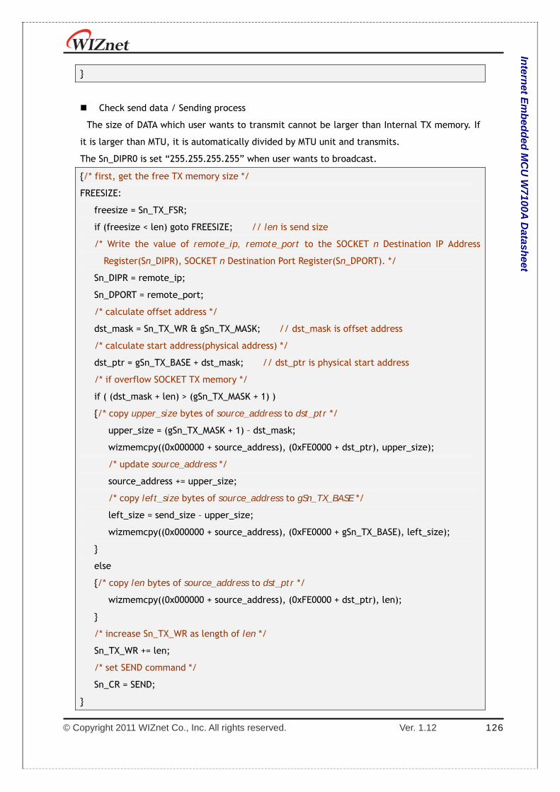
© Copyright 2011 WIZnet Co., Inc. All rights reserved. Ver. 1.12 126
Intern
et Em
bed
ded
MC
U W
7100A D
atasheet
Check send data / Sending process
The size of DATA which user wants to transmit cannot be larger than Internal TX memory. If
it is larger than MTU, it is automatically divided by MTU unit and transmits.
The Sn_DIPR0 is set “255.255.255.255” when user wants to broadcast.
/* first, get the free TX memory size */
FREESIZE:
freesize = Sn_TX_FSR;
if (freesize < len) goto FREESIZE; // len is send size
/* Write the value of remote_ip, remote_port to the SOCKET n Destination IP Address
Register(Sn_DIPR), SOCKET n Destination Port Register(Sn_DPORT). */
Sn_DIPR = remote_ip;
Sn_DPORT = remote_port;
/* calculate offset address */
dst_mask = Sn_TX_WR & gSn_TX_MASK; // dst_mask is offset address
/* calculate start address(physical address) */
dst_ptr = gSn_TX_BASE + dst_mask; // dst_ptr is physical start address
/* if overflow SOCKET TX memory */
if ( (dst_mask + len) > (gSn_TX_MASK + 1) )
/* copy upper_size bytes of source_address to dst_ptr */
upper_size = (gSn_TX_MASK + 1) – dst_mask;
wizmemcpy((0x000000 + source_address), (0xFE0000 + dst_ptr), upper_size);
/* update source_address */
source_address += upper_size;
/* copy left_size bytes of source_address to gSn_TX_BASE */
left_size = send_size – upper_size;
wizmemcpy((0x000000 + source_address), (0xFE0000 + gSn_TX_BASE), left_size);
else
/* copy len bytes of source_address to dst_ptr */
wizmemcpy((0x000000 + source_address), (0xFE0000 + dst_ptr), len);
/* increase Sn_TX_WR as length of len */
Sn_TX_WR += len;
/* set SEND command */
Sn_CR = SEND;
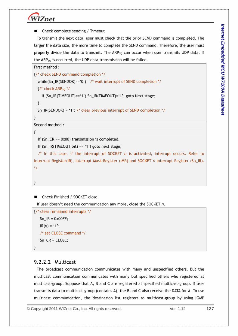
© Copyright 2011 WIZnet Co., Inc. All rights reserved. Ver. 1.12 127
Intern
et Em
bed
ded
MC
U W
7100A D
atasheet
Check complete sending / Timeout
To transmit the next data, user must check that the prior SEND command is completed. The
larger the data size, the more time to complete the SEND command. Therefore, the user must
properly divide the data to transmit. The ARPTO can occur when user transmits UDP data. If
the ARPTO is occurred, the UDP data transmission will be failed.
First method :
/* check SEND command completion */
while(Sn_IR(SENDOK)==‘0’) /* wait interrupt of SEND completion */
/* check ARPTO */
if (Sn_IR(TIMEOUT)==‘1’) Sn_IR(TIMEOUT)=‘1’; goto Next stage;
Sn_IR(SENDOK) = ‘1’; /* clear previous interrupt of SEND completion */
Second method :
If (Sn_CR == 0x00) transmission is completed.
If (Sn_IR(TIMEOUT bit) == ‘1’) goto next stage;
/* In this case, if the interrupt of SOCKET n is activated, interrupt occurs. Refer to
Interrupt Register(IR), Interrupt Mask Register (IMR) and SOCKET n Interrupt Register (Sn_IR).
*/
Check Finished / SOCKET close
If user doesn’t need the communication any more, close the SOCKET n.
/* clear remained interrupts */
Sn_IR = 0x00FF;
IR(n) = ‘1’;
/* set CLOSE command */
Sn_CR = CLOSE;
9.2.2.2 Multicast The broadcast communication communicates with many and unspecified others. But the
multicast communication communicates with many but specified others who registered at
multicast-group. Suppose that A, B and C are registered at specified multicast-group. If user
transmits data to multicast-group (contains A), the B and C also receive the DATA for A. To use
multicast communication, the destination list registers to multicast-group by using IGMP
© Copyright 2011 WIZnet Co., Inc. All rights reserved. Ver. 1.12 128
Intern
et Em
bed
ded
MC
U W
7100A D
atasheet
protocol. The multicast-group consists of ‘Group hardware address’, ‘Group IP address’ and
‘Group port number’. User cannot change the ‘Group hardware address’ and ‘Group IP
address’. But the ‘Group port number’ can be changed to what user wants.
The ‘Group hardware address’ is selected at the assigned range (From “01:00:5e:00:00:00”
to “01:00:5e:7f:ff:ff”) and the ‘Group IP address’ is selected in D-class IP address (From
“224.0.0.0” to “239.255.255.255”, please refer to the website;
Uhttp://www.iana.org/assignments/multicast-addressesU). When selecting, the upper 23bit of
6bytes ‘Group hardware address’ and the 4bytes ‘Group IP address’ must be the same. For
example, if the user selects the ‘Group IP address’ to “244.1.1.11”, the ‘Group hardware
address’ is selected to “01:00:5e:01:01:0b”. Please refer to the “RFC1112”
(Uhttp://www.ietf.org/rfc.htmlU).
In the W7100A, IGMP processing to register the multicast-group is internally (automatically)
processed. When the user opens the SOCKET n with multicast mode, the “Join” message is
internally transmitted. If the user closes it, the “Leave” message is internally transmitted.
After the SOCKET opens, the “Report” message is periodically and internally transmitted
when the user communicates.
The W7100A support IGMP version 1 and version 2 only. If user wants use an updated version,
the host processes IGMP directly by using the IPRAW mode SOCKET.
SOCKET Initialization
Choose one SOCKET for multicast communication among 8 SOCKETS of W7100A. Then set the
Sn_DHAR0 to ‘Multicast-group hardware address’ and set the Sn_DIPR0 to ‘Multicast-group IP
address’. Then set the Sn_PORT0 and Sn_DPORT0 to ‘Multicast-group port number’. Then set
the Sn_MR(P3:P0) to UDP and set the Sn_MR(MULTI) to ‘1’. Finally execute OPEN command. If
the state of Sn_SR is changed to SOCK_UDP after the OPEN command, the SOCKET
initialization is completed.
START:
/* set Multicast-Group information */
Sn_DHAR0 = 0x01; /* set Multicast-Group H/W address(01:00:5e:01:01:0b) */
Sn_DHAR1 = 0x00;
Sn_DHAR2 = 0x5E;
Sn_DHAR3 = 0x01;
Sn_DHAR4 = 0x01;
Sn_DHAR5 = 0x0B;
Sn_DIPR0 = 211; /* set Multicast-Group IP address(211.1.1.11) */
Sn_DIPR1 = 1;
Sn_DIPR2 = 1;

© Copyright 2011 WIZnet Co., Inc. All rights reserved. Ver. 1.12 129
Intern
et Em
bed
ded
MC
U W
7100A D
atasheet
Sn_DIRP3 = 11;
Sn_DPORT = 0x0BB8; /* set Multicast-Group Port number(3000) */
Sn_PORT = 0x0BB8; /* set Source Port number(3000) */
Sn_MR = 0x02 | 0x80; /* set UDP mode & Multicast on SOCKET n Mode Register */
Sn_CR = OPEN; /* set OPEN command */
/* wait until Sn_SR is changed to SOCK_UDP */
if (Sn_SR != SOCK_UDP) Sn_CR = CLOSE; goto START;
Check received data
Refer to the section 9.2.2.1 ‘Unicast & Broadcast’.
Receiving process
Refer to the section 9.2.2.1 ‘Unicast & Broadcast’.
Check send data / Sending Process
Since the user sets the information about multicast-group at SOCKET initialization, user does
not need to set IP address and port number for destination any more. Therefore, copy the
transmission data to internal TX memory and executes SEND command.
/* first, get the free TX memory size */
FREESIZE:
freesize = Sn_TX_FSR;
if (freesize < len) goto FREESIZE; // len is send size
/* calculate offset address */
dst_mask = Sn_TX_WR & gSn_TX_MASK; // dst_mask is offset address
/* calculate start address(physical address) */
dst_ptr = gSn_TX_BASE + dst_mask; // dst_ptr is physical start address
/* if overflow SOCKET TX memory */
if ( (dst_mask + len) > (gSn_TX_MASK + 1) )
/* copy upper_size bytes of source_addr to dst_ptr */
upper_size = (gSn_TX_MASK + 1) – dst_mask;
wizmemcpy((0x000000 + source_addr), (0xFE0000 + dst_ptr), upper_size);
/* update source_addr*/
source_addr += upper_size;
/* copy left_size bytes of source_addr to gSn_TX_BASE */
left_size = len – upper_size;
wizmemcpy((0x000000 + source_addr), (0xFE0000 + gSn_TX_BASE), left_size);
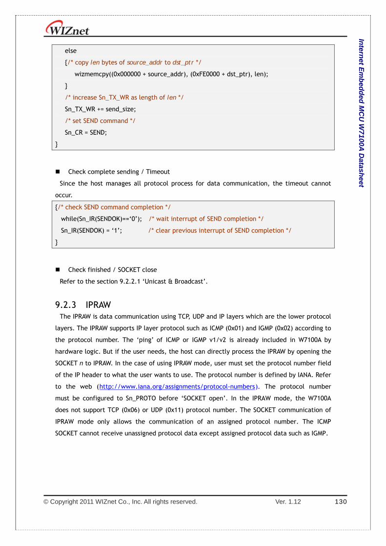
© Copyright 2011 WIZnet Co., Inc. All rights reserved. Ver. 1.12 130
Intern
et Em
bed
ded
MC
U W
7100A D
atasheet
else
/* copy len bytes of source_addr to dst_ptr */
wizmemcpy((0x000000 + source_addr), (0xFE0000 + dst_ptr), len);
/* increase Sn_TX_WR as length of len */
Sn_TX_WR += send_size;
/* set SEND command */
Sn_CR = SEND;
Check complete sending / Timeout
Since the host manages all protocol process for data communication, the timeout cannot
occur.
/* check SEND command completion */
while(Sn_IR(SENDOK)==‘0’); /* wait interrupt of SEND completion */
Sn_IR(SENDOK) = ‘1’; /* clear previous interrupt of SEND completion */
Check finished / SOCKET close
Refer to the section 9.2.2.1 ‘Unicast & Broadcast’.
9.2.3 IPRAW The IPRAW is data communication using TCP, UDP and IP layers which are the lower protocol
layers. The IPRAW supports IP layer protocol such as ICMP (0x01) and IGMP (0x02) according to
the protocol number. The ‘ping’ of ICMP or IGMP v1/v2 is already included in W7100A by
hardware logic. But if the user needs, the host can directly process the IPRAW by opening the
SOCKET n to IPRAW. In the case of using IPRAW mode, user must set the protocol number field
of the IP header to what the user wants to use. The protocol number is defined by IANA. Refer
to the web (Uhttp://www.iana.org/assignments/protocol-numbersU). The protocol number
must be configured to Sn_PROTO before ‘SOCKET open’. In the IPRAW mode, the W7100A
does not support TCP (0x06) or UDP (0x11) protocol number. The SOCKET communication of
IPRAW mode only allows the communication of an assigned protocol number. The ICMP
SOCKET cannot receive unassigned protocol data except assigned protocol data such as IGMP.

© Copyright 2011 WIZnet Co., Inc. All rights reserved. Ver. 1.12 131
Intern
et Em
bed
ded
MC
U W
7100A D
atasheet
Figure 9.7 IPRAW Operation Flow
SOCKET Initialization
Select the SOCKET and set the protocol number. Then set the Sn_MR(P3:P0) to IPRAW mode
and execute ‘OPEN’ command. If the Sn_SR is changed to SOCK_IPRAW after the ‘OPEN’
command, the SOCKET initialization is completed.
START:
/* sets Protocol number, the protocol number is used in Protocol Field of IP Header. */
Sn_PROTO = protocol_num;
/* sets IP raw mode */
Sn_MR = 0x03;
/* sets OPEN command */
Sn_CR = OPEN;
/* wait until Sn_SR is changed to SOCK_IPRAW */
if (Sn_SR != SOCK_IPRAW) Sn_CR = CLOSE; goto START;
Check received data
Refer to the section 9.2.2.1 ‘Unicast & Broadcast’.
Receiving process
Process the IPRAW data which is received in internal RX memory. The structure of received
IPRAW data is as below.
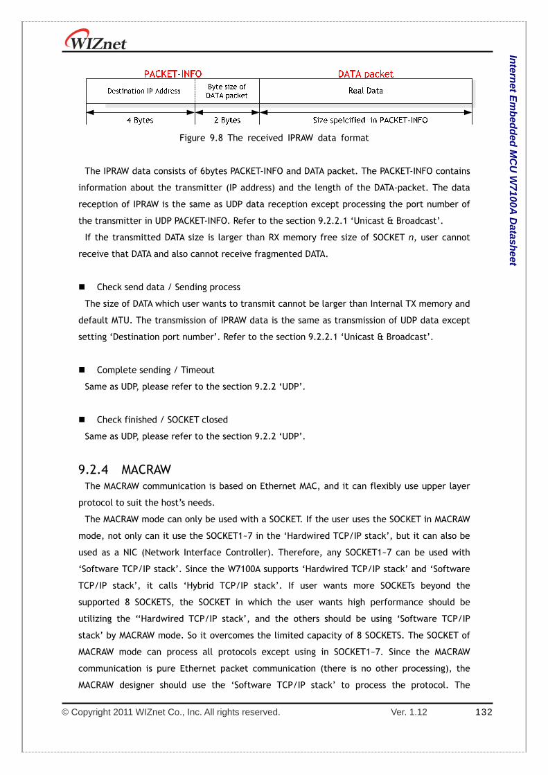
© Copyright 2011 WIZnet Co., Inc. All rights reserved. Ver. 1.12 132
Intern
et Em
bed
ded
MC
U W
7100A D
atasheet
Figure 9.8 The received IPRAW data format
The IPRAW data consists of 6bytes PACKET-INFO and DATA packet. The PACKET-INFO contains
information about the transmitter (IP address) and the length of the DATA-packet. The data
reception of IPRAW is the same as UDP data reception except processing the port number of
the transmitter in UDP PACKET-INFO. Refer to the section 9.2.2.1 ‘Unicast & Broadcast’.
If the transmitted DATA size is larger than RX memory free size of SOCKET n, user cannot
receive that DATA and also cannot receive fragmented DATA.
Check send data / Sending process
The size of DATA which user wants to transmit cannot be larger than Internal TX memory and
default MTU. The transmission of IPRAW data is the same as transmission of UDP data except
setting ‘Destination port number’. Refer to the section 9.2.2.1 ‘Unicast & Broadcast’.
Complete sending / Timeout
Same as UDP, please refer to the section 9.2.2 ‘UDP’.
Check finished / SOCKET closed
Same as UDP, please refer to the section 9.2.2 ‘UDP’.
9.2.4 MACRAW The MACRAW communication is based on Ethernet MAC, and it can flexibly use upper layer
protocol to suit the host’s needs.
The MACRAW mode can only be used with a SOCKET. If the user uses the SOCKET in MACRAW
mode, not only can it use the SOCKET1~7 in the ‘Hardwired TCP/IP stack’, but it can also be
used as a NIC (Network Interface Controller). Therefore, any SOCKET1~7 can be used with
‘Software TCP/IP stack’. Since the W7100A supports ‘Hardwired TCP/IP stack’ and ‘Software
TCP/IP stack’, it calls ‘Hybrid TCP/IP stack’. If user wants more SOCKETs beyond the
supported 8 SOCKETS, the SOCKET in which the user wants high performance should be
utilizing the ‘‘Hardwired TCP/IP stack’, and the others should be using ‘Software TCP/IP
stack’ by MACRAW mode. So it overcomes the limited capacity of 8 SOCKETS. The SOCKET of
MACRAW mode can process all protocols except using in SOCKET1~7. Since the MACRAW
communication is pure Ethernet packet communication (there is no other processing), the
MACRAW designer should use the ‘Software TCP/IP stack’ to process the protocol. The

© Copyright 2011 WIZnet Co., Inc. All rights reserved. Ver. 1.12 133
Intern
et Em
bed
ded
MC
U W
7100A D
atasheet
MACRAW data should basically contain the 6bytes of ‘Source hardware address’, 6bytes of
‘destination hardware address’ and 2bytes of ‘Ethernet type’ because it is based on Ethernet
MAC.
Figure 9.9 MACRAW Operation Flow
SOCKET Initialization
Select the SOCKET and set the SN_MR(P3:P0) to MACRAW mode. Then execute the ‘OPEN’
command. After the ‘OPEN’ command, if the Sn_SR is successfully changed to
‘SOCK_MACRAW’, the SOCKET initialization is completed. Since all information about
communication (Source hardware address, Source IP address, Source port number, Destination
hardware address, Destination IP address, Destination port number, Protocol header, etc.) is
in the ‘MACRAW data’, there is no more register setting.
START:
/* sets MAC raw mode */
S0_MR = 0x04;
/* sets OPEN command */
S0_CR = OPEN;
/* wait until Sn_SR is changed to SOCK_MACRAW */
if (S0_SR != SOCK_MACRAW) S0_CR = CLOSE; goto START;
Check received data
Refer to the section 9.2.2.1 ‘Unicast & Broadcast’.

© Copyright 2011 WIZnet Co., Inc. All rights reserved. Ver. 1.12 134
Intern
et Em
bed
ded
MC
U W
7100A D
atasheet
Receiving process
Process the MACRAW data of the SOCKET which received it in internal RX memory. The
structure of the MACRAW data is as below:
Figure 9.10 The received MACRAW data format
The MACRAW data consists of ‘PACKET-INFO’, ‘DATA packet’ and 4bytes CRC. The ‘PACKET-
INFO’ is the length of the DATA packet. The ‘DATA packet’ consists of 6bytes ‘Destination MAC
address’, 6bytes ‘Source MAC address’ and 2bytes ‘Type’, 46~1500 bytes ‘Payload’. The
‘Payload’ of DATA packet consists of Internet protocol such as ARP, IP according to the ‘Type’.
The details of ‘Type’ please refer to the web:
(Uhttp://www.iana.org/assignments/ethernet-numbersU)
/* calculate offset address */
src_mask = S0_RX_RD & gS0_RX_MASK; // src_mask is offset address
/* calculate start address(physical address) */
src_ptr = gS0_RX_BASE + src_mask; // src_ptr is physical start address
/* get the size of packet */
len = get_Byte_sizeof_DATA_packet(); // Read the 2bytes PACKET-INFO
/* if overflow SOCKET RX memory */
If((src_mask + len) > (gS0_RX_MASK + 1))
/* copy upper_size bytes of get_start_address to destination_address */
upper_size = (gS0_RX_MASK + 1) – src_mask;
wizmemcpy((0xFE0000 + src_ptr), (0x000000 + destination_address), upper_size);
/* update destination_address */
destination_address += upper_size;
/* copy left_size bytes of gSn_RX_BASE to destination_address */
left_size = len – upper_size;
wizmemcpy((0xFE0000 + src_ptr), (0x000000 + destination_address), left_size);
else
/* copy len bytes of src_ptr to destination_address */
wizmemcpy((0xFE0000 + src_ptr), (0x000000 + destination_address), len);
/* increase Sn_RX_RD as length of len */

© Copyright 2011 WIZnet Co., Inc. All rights reserved. Ver. 1.12 135
Intern
et Em
bed
ded
MC
U W
7100A D
atasheet
S0_RX_RD += len;
/* extract 4 bytes CRC from internal RX memory and then ignore it */
wizmemcpy((0xFE0000 + src_ptr), (0x000000 + dummy), len);
/* set RECV command */
S0_CR = RECV;
<Notice>
If the free size of the internal RX memory is smaller than the MACRAW data, a problem may
occasionally occur where some parts of that PACKET-INFO and DATA packet are stored to the
internal RX memory. Since the problem occurs as an analysis error for PACKET-INFO, it cannot
process the MACRAW data correctly. The closer the internal RX memory is to being full, the
higher the probability is for an error to occur. This problem can be resolved if user allows
some loss of the MACRAW data.
The solution is as follows:
Process the internal RX memory as fast as possible to prevent that it closes to full.
Reduce the receiving load by reception only its MACRAW data by setting the MF (MAC Filter)
bit of S0_MR in sample code of SOCKET initialization.
START:
/* sets MAC raw mode with enabling MAC filter */
S0_MR = 0x44;
/* sets OPEN command */
S0_CR = OPEN;
/* wait until Sn_SR is changed to SOCK_MACRAW */
if (Sn_SR != SOCK_MACRAW) S0_CR = CLOSE; goto START;
If the free size of the internal RX memory is smaller than ‘1528 - Default
MTU(1514)+PACKET-INFO(2) + DATA packet(8) + CRC(4)’, close the SOCKET and process all
received data. Then reopen the SOCKET. After closing the SOCKET, the received MACRAW
data from closing time can be lost.
/* check the free size of internal RX memory */
if((S0_RXMEM_SIZE(0) * 1024) – S0_RX_RSR(0) < 1528)
received_size = S0_RX_RSR(0); /* backup Sn_RX_RSR */
S0_CR = CLOSE; /* SOCKET Closed */
while(S0_SR != SOCK_CLOSED); /* wait until SOCKET is closed */

© Copyright 2011 WIZnet Co., Inc. All rights reserved. Ver. 1.12 136
Intern
et Em
bed
ded
MC
U W
7100A D
atasheet
/* process all data remained in internal RX memory */
while(recved_size > 0)
/* calculate offset address */
src_mask = S0_RX_RD & gS0_RX_MASK; // src_mask is offset address
/* calculate start address(physical address) */
src_ptr = gS0_RX_BASE + src_mask; // src_ptr is physical start address
/* if overflow SOCKET RX memory */
If((src_mask + len) > (gS0_RX_MASK + 1))
/* copy upper_size bytes of get_start_address to destination_address */
upper_size = (gS0_RX_MASK + 1) – src_mask;
wizmemcpy((0xFE0000 + src_ptr), (0x000000 + destination_address), upper_size);
/* update destination_address */
destination_address += upper_size;
/* copy left_size bytes of gSn_RX_BASE to destination_address */
left_size = len – upper_size;
wizmemcpy((0xFE0000 + src_ptr), (0x000000 + destination_address), left_size);
else
/* copy len bytes of src_ptr to destination_address */
wizmemcpy((0xFE0000 + src_ptr), (0x000000 + destination_address), len);
/* increase Sn_RX_RD as length of len */
S0_RX_RD += len;
/* extract 4 bytes CRC from internal RX memory and then ignore it */
wizmemcpy((0xFE0000 + src_ptr), (0x000000 + dummy), len);
/* calculate the size of remained data in internal RX memory*/
recved_size = recved_size – 2 – len – 4;
/* Reopen the SOCKET */
/* sets MAC raw mode with enabling MAC filter */
S0_MR = 0x44; /* or S0_MR = 0x04 */
/* sets OPEN command */
S0_CR = OPEN;
/* wait until Sn_SR is changed to SOCK_MACRAW */
while (S0_SR != SOCK_MACRAW);
else /* process normally the DATA packet from internal RX memory */
/* This block is same as the code of “Receiving process” stage*/

© Copyright 2011 WIZnet Co., Inc. All rights reserved. Ver. 1.12 137
Intern
et Em
bed
ded
MC
U W
7100A D
atasheet
Check send data / Sending process
The size of the data which the user wants to transmit cannot be larger than the internal TX
memory and default MTU. The host generates the MACRAW data in the same format as the
“Receiving process” data packet, and transmits it. At this time, if the size of the generated
data is smaller than 60bytes, the transmitted Ethernet packet internally fills to 60bytes by
“Zero padding” and then it is transmitted.
/* first, get the free TX memory size */
FREESIZE:
freesize = S0_TX_FSR;
if (freesize < send_size) goto FREESIZE;
/* calculate offset address */
dst_mask = Sn_TX_WR & gSn_TX_MASK; // dst_mask is offset address
/* calculate start address(physical address) */
dst_ptr = gSn_TX_BASE + dst_mask; // dst_ptr is physical start address
/* if overflow SOCKET TX memory */
if ( (dst_mask + len) > (gSn_TX_MASK + 1) )
/* copy upper_size bytes of source_addr to dst_ptr */
upper_size = (gSn_TX_MASK + 1) – dst_mask;
wizmemcpy((0x000000 + source_addr), (0xFE0000 + dst_ptr), upper_size);
/* update source_addr*/
source_addr += upper_size;
/* copy left_size bytes of source_addr to gSn_TX_BASE */
left_size = len – upper_size;
wizmemcpy((0x000000 + source_addr), (0xFE0000 + gS0_TX_BASE), left_size);
else
/* copy len bytes of source_addr to dst_ptr */
wizmemcpy((0x000000 + source_addr), (0xFE0000 + dst_ptr), len);
/* increase Sn_TX_WR as length of len */
S0_TX_WR += send_size;
/* set SEND command */
S0_CR = SEND;
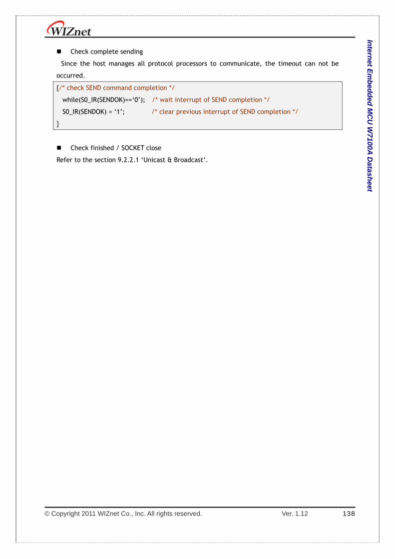
© Copyright 2011 WIZnet Co., Inc. All rights reserved. Ver. 1.12 138
Intern
et Em
bed
ded
MC
U W
7100A D
atasheet
Check complete sending
Since the host manages all protocol processors to communicate, the timeout can not be
occurred.
/* check SEND command completion */
while(S0_IR(SENDOK)==‘0’); /* wait interrupt of SEND completion */
S0_IR(SENDOK) = ‘1’; /* clear previous interrupt of SEND completion */
Check finished / SOCKET close
Refer to the section 9.2.2.1 ‘Unicast & Broadcast’.
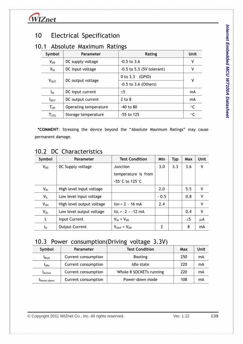
© Copyright 2011 WIZnet Co., Inc. All rights reserved. Ver. 1.12 139
Intern
et Em
bed
ded
MC
U W
7100A D
atasheet
10 Electrical Specification
10.1 Absolute Maximum Ratings Symbol Parameter Rating Unit
VDD DC supply voltage -0.5 to 3.6 V
VIN DC input voltage -0.5 to 5.5 (5V tolerant) V
VOUT DC output voltage 0 to 3.3 (GPIO)
V -0.5 to 3.6 (Others)
IIN DC input current 5 mA
IOUT DC output current 2 to 8 mA
TOP Operating temperature -40 to 80 C
TSTG Storage temperature -55 to 125 C
*COMMENT: Stressing the device beyond the “Absolute Maximum Ratings” may cause
permanent damage.
10.2 DC Characteristics Symbol Parameter Test Condition Min Typ Max Unit
VDD DC Supply voltage Junction
temperature is from
-55°C to 125°C
3.0 3.3 3.6 V
VIH High level input voltage 2.0 5.5 V
VIL Low level input voltage - 0.5 0.8 V
VOH High level output voltage IOH = 2 ~ 16 mA 2.4 V
VOL Low level output voltage IOL = -2 ~ -12 mA 0.4 V
II Input Current VIN = VDD 5 A
IO Output Current VOUT = VDD 2 8 mA
10.3 Power consumption(Driving voltage 3.3V)
Symbol Parameter Test Condition Max Unit
IBoot Current consumption Booting 250 mA
IIdle Current consumption Idle state 220 mA
IActive Current consumption Whole 8 SOCKETs running 220 mA
IPower-down Current consumption Power-down mode 108 mA

© Copyright 2011 WIZnet Co., Inc. All rights reserved. Ver. 1.12 140
Intern
et Em
bed
ded
MC
U W
7100A D
atasheet
10.4 AC Characteristics Reset Timing
Description Min Max
1 Reset Cycle Time 2 us -
2 PLL Lock-in Time 50 us 10 ms
External memory access timing
Description Min Max
tALE ALE signal duration = ALECON register value + 1
clock (clock speed = 88.4736MHz) 1 clock 256 clock
Taccess External memory access period = 3us + EXTWTST
register value 3 us 744us
10.5 Crystal Characteristics
Parameter Range
Frequency 25 MHz
Frequency Tolerance (at 25) ±30 ppm
Shunt Capacitance 7pF Max
Drive Level 1 ~ 500uW (100uW typical)
Load Capacitance 18pF
Aging (at 25) ±3ppm / year Max

© Copyright 2011 WIZnet Co., Inc. All rights reserved. Ver. 1.12 141
Intern
et Em
bed
ded
MC
U W
7100A D
atasheet
10.6 Transformer Characteristics Parameter Transmit End Receive End
Turn Ratio 1:1 1:1
Inductance 350 uH 350 uH
In the case of using the internal PHY mode, be sure to use symmetric transformer in order to
support Auto MDI/MDIX (Crossover).
In the case of using the External PHY mode, use the transformer which is suitable for external
PHY specification.
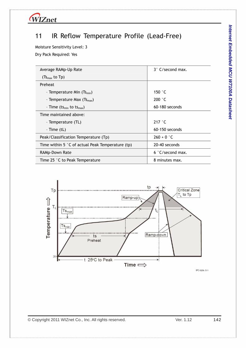
© Copyright 2011 WIZnet Co., Inc. All rights reserved. Ver. 1.12 142
Intern
et Em
bed
ded
MC
U W
7100A D
atasheet
11 IR Reflow Temperature Profile (Lead-Free)
Moisture Sensitivity Level: 3
Dry Pack Required: Yes
Average RAMp-Up Rate
(Tsmax to Tp)
3° C/second max.
Preheat
– Temperature Min (Tsmin)
– Temperature Max (Tsmax)
– Time (tsmin to tsmax)
150 °C
200 °C
60-180 seconds
Time maintained above:
– Temperature (TL)
– Time (tL)
217 °C
60-150 seconds
Peak/Classification Temperature (Tp) 260 + 0 °C
Time within 5 °C of actual Peak Temperature (tp) 20-40 seconds
RAMp-Down Rate 6 °C/second max.
Time 25 °C to Peak Temperature 8 minutes max.
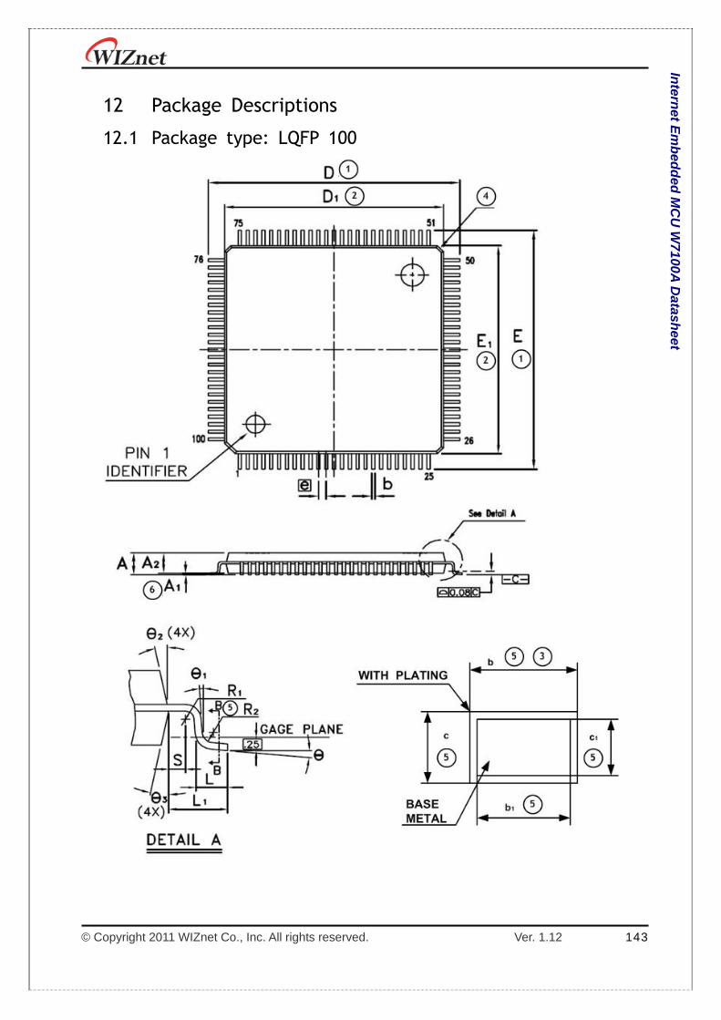
© Copyright 2011 WIZnet Co., Inc. All rights reserved. Ver. 1.12 143
Intern
et Em
bed
ded
MC
U W
7100A D
atasheet
12 Package Descriptions
12.1 Package type: LQFP 100
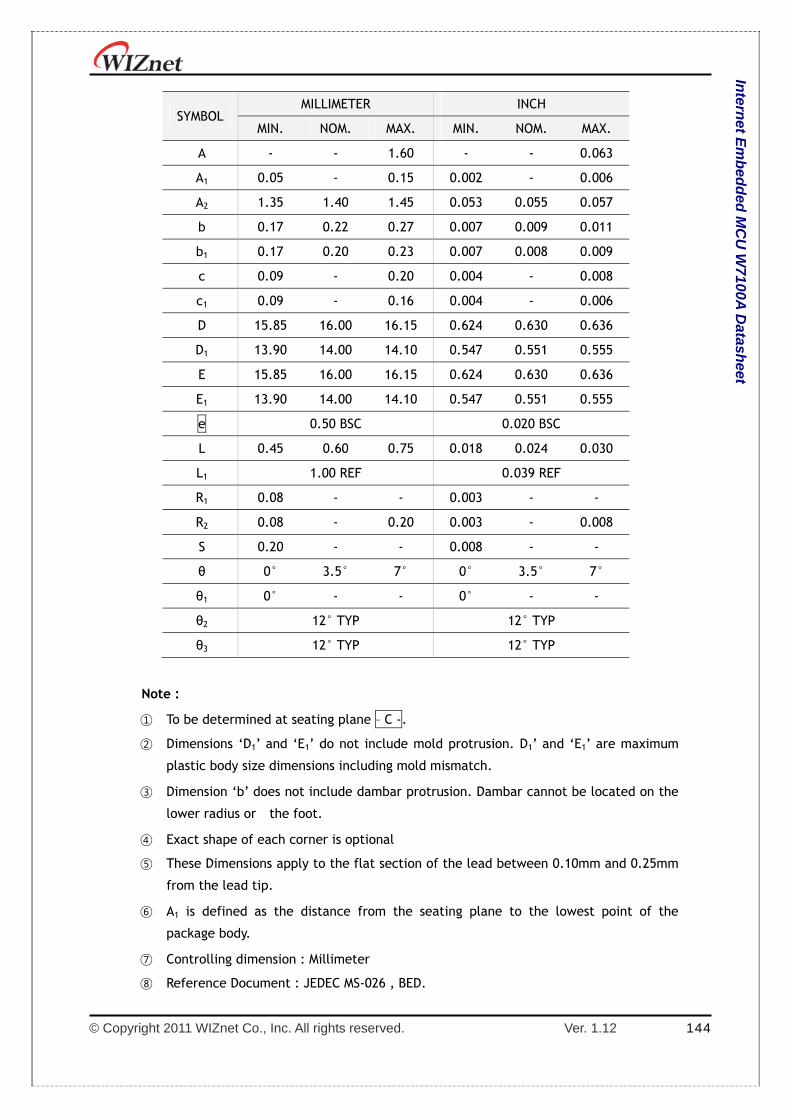
© Copyright 2011 WIZnet Co., Inc. All rights reserved. Ver. 1.12 144
Intern
et Em
bed
ded
MC
U W
7100A D
atasheet
SYMBOL MILLIMETER INCH
MIN. NOM. MAX. MIN. NOM. MAX.
A - - 1.60 - - 0.063
A1 0.05 - 0.15 0.002 - 0.006
A2 1.35 1.40 1.45 0.053 0.055 0.057
b 0.17 0.22 0.27 0.007 0.009 0.011
b1 0.17 0.20 0.23 0.007 0.008 0.009
c 0.09 - 0.20 0.004 - 0.008
c1 0.09 - 0.16 0.004 - 0.006
D 15.85 16.00 16.15 0.624 0.630 0.636
D1 13.90 14.00 14.10 0.547 0.551 0.555
E 15.85 16.00 16.15 0.624 0.630 0.636
E1 13.90 14.00 14.10 0.547 0.551 0.555
e 0.50 BSC 0.020 BSC
L 0.45 0.60 0.75 0.018 0.024 0.030
L1 1.00 REF 0.039 REF
R1 0.08 - - 0.003 - -
R2 0.08 - 0.20 0.003 - 0.008
S 0.20 - - 0.008 - -
θ 0° 3.5° 7° 0° 3.5° 7°
θ1 0° - - 0° - -
θ2 12° TYP 12° TYP
θ3 12° TYP 12° TYP
Note :
① To be determined at seating plane – C -.
② Dimensions ‘D1’ and ‘E1’ do not include mold protrusion. D1’ and ‘E1’ are maximum
plastic body size dimensions including mold mismatch.
③ Dimension ‘b’ does not include dambar protrusion. Dambar cannot be located on the
lower radius or the foot.
④ Exact shape of each corner is optional
⑤ These Dimensions apply to the flat section of the lead between 0.10mm and 0.25mm
from the lead tip.
⑥ A1 is defined as the distance from the seating plane to the lowest point of the
package body.
⑦ Controlling dimension : Millimeter
⑧ Reference Document : JEDEC MS-026 , BED.

© Copyright 2011 WIZnet Co., Inc. All rights reserved. Ver. 1.12 145
Intern
et Em
bed
ded
MC
U W
7100A D
atasheet
12.2 Package type: QFN 64
* CONTROLLING DIMENSION: mm

© Copyright 2011 WIZnet Co., Inc. All rights reserved. Ver. 1.12 146
Intern
et Em
bed
ded
MC
U W
7100A D
atasheet
SYMBOL MILLIMETER INCH
MIN. NOM. MAX. MIN. NOM. MAX.
A - - 0.90 - - 0.035
A1 - - 0.05 - - 0.002
A2 - 0.65 0.70 - 0.026 0.028
A3 0.200 REF. 0.008 REF.
b 0.18 0.25 0.30 0.007 0.010 0.012
D 15.85 16.00 16.15 0.624 0.630 0.636
D 9.00 bsc 0.354 bsc
D2 5.90 6.00 6.10 0.232 0.236 0.240
E 9.00 bsc 0.354 bsc
E2 5.90 6.00 6.10 0.232 0.236 0.240
L 0.35 0.40 0.45 0.014 0.016 0.018
e 0.50 bsc 0.020 bsc
R 0.09 - - 0.004 - -
TOLERANCES OF FORM AND POSITION
aaa 0.10 0.004
bbb 0.10 0.004
ccc 0.05 0.002
Note:
① All dimensions are in millimeters.
② Die thickness allowable is 0.305mm maximum (0.012 inches maximum).
③ Dimensioning & tolerances conform to ASME Y14.5M. -1994.
④ The pin #1 identifier must be placed on the top surface of the package by using
indentation mark of other feature of package body.
⑤ Exact shape and size of this feature is optional.
⑥ Package WARPAGE max 0.08mm.
⑦ Applied for exposed pad and terminals, exclude embedding part of exposed pad from
measuring.
⑧ Applied to terminals.

© Copyright 2011 WIZnet Co., Inc. All rights reserved. Ver. 1.12 147
Intern
et Em
bed
ded
MC
U W
7100A D
atasheet
13 Appendix:Performance Improvement about W7100A
This section presents the benefits gained about calculation by using W7100A over standard
8051 family.
13.1 Summary
The 8-bit operation cycles of the 80C51 and W7100A with addition, subtraction,
multiplication and division are as below. It is briefly shows its performance. The W7100A with
‘wizmemcpy’ (supported by WIZnet) function is almost 9 times faster than the 80C51.
80C51 cycle W7100A cycle / with
user code
W7100A cycle / with
wizmemcpy
ADD 36 12 4
SUB 36 12 4
MUL 96 12 6
DIV 96 20 10
In the succeeded section shows more detail performance.
13.2 8–Bit Arithmetic Functions
13.2.1 Addition Immediate data
The following code performs immediate data (constant) addition to an 8-bit register.
RX = RX + #n
Mnemonic Opcode Byte 80C51 Cycle W7100A Cycle
ISP /
wizmemcpy
FLASH /
user code
MOV A, Rx E8h – EFh 1 12 1 4
ADD A, #n 24h 2 12 2 4
MOV Rx, A F8h – FFh 1 12 1 4
Sum : 36 4 12
Note. ‘wizmemcpy’ function are built-in inside Boot ROM in W7100A. Refer to the ‘Driver
Guide.’
Direct addressing
The following code performs direct addressing addition to an 8-bit register.
Rx = Rx + (dir)
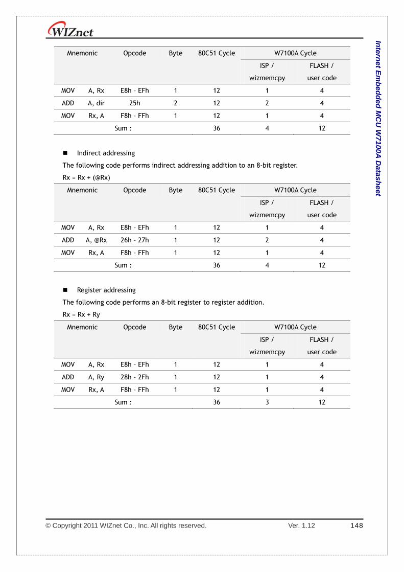
© Copyright 2011 WIZnet Co., Inc. All rights reserved. Ver. 1.12 148
Intern
et Em
bed
ded
MC
U W
7100A D
atasheet
Mnemonic Opcode Byte 80C51 Cycle W7100A Cycle
ISP /
wizmemcpy
FLASH /
user code
MOV A, Rx E8h – EFh 1 12 1 4
ADD A, dir 25h 2 12 2 4
MOV Rx, A F8h – FFh 1 12 1 4
Sum : 36 4 12
Indirect addressing
The following code performs indirect addressing addition to an 8-bit register.
Rx = Rx + (@Rx)
Mnemonic Opcode Byte 80C51 Cycle W7100A Cycle
ISP /
wizmemcpy
FLASH /
user code
MOV A, Rx E8h – EFh 1 12 1 4
ADD A, @Rx 26h – 27h 1 12 2 4
MOV Rx, A F8h – FFh 1 12 1 4
Sum : 36 4 12
Register addressing
The following code performs an 8-bit register to register addition.
Rx = Rx + Ry
Mnemonic Opcode Byte 80C51 Cycle W7100A Cycle
ISP /
wizmemcpy
FLASH /
user code
MOV A, Rx E8h – EFh 1 12 1 4
ADD A, Ry 28h – 2Fh 1 12 1 4
MOV Rx, A F8h – FFh 1 12 1 4
Sum : 36 3 12
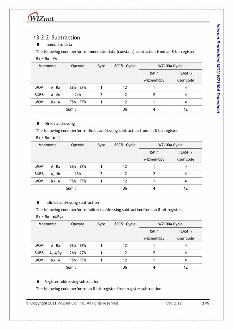
© Copyright 2011 WIZnet Co., Inc. All rights reserved. Ver. 1.12 149
Intern
et Em
bed
ded
MC
U W
7100A D
atasheet
13.2.2 Subtraction Immediate data
The following code performs immediate data (constant) subtraction from an 8-bit register.
Rx = Rx - #n
Mnemonic Opcode Byte 80C51 Cycle W7100A Cycle
ISP /
wizmemcpy
FLASH /
user code
MOV A, Rx E8h – EFh 1 12 1 4
SUBB A, #n 24h 2 12 2 4
MOV Rx, A F8h – FFh 1 12 1 4
Sum : 36 4 12
Direct addressing
The following code performs direct addressing subtraction from an 8-bit register.
Rx = Rx – (dir)
Mnemonic Opcode Byte 80C51 Cycle W7100A Cycle
ISP /
wizmemcpy
FLASH /
user code
MOV A, Rx E8h – EFh 1 12 1 4
SUBB A, dir 25h 2 12 2 4
MOV Rx, A F8h – FFh 1 12 1 4
Sum : 36 4 12
Indirect addressing subtraction
The following code performs indirect addressing subtraction from an 8-bit register.
Rx = Rx – (@Ry)
Mnemonic Opcode Byte 80C51 Cycle W7100A Cycle
ISP /
wizmemcpy
FLASH /
user code
MOV A, Rx E8h – EFh 1 12 1 4
SUBB A, @Ry 26h – 27h 1 12 2 4
MOV Rx, A F8h – FFh 1 12 1 4
Sum : 36 4 12
Register addressing subtraction
The following code performs an 8-bit register from register subtraction.

© Copyright 2011 WIZnet Co., Inc. All rights reserved. Ver. 1.12 150
Intern
et Em
bed
ded
MC
U W
7100A D
atasheet
Rx = Rx - Ry
Mnemonic Opcode Byte 80C51 Cycle W7100A Cycle
ISP /
wizmemcpy
FLASH /
user code
MOV A, Rx E8h – EFh 1 12 1 4
SUBB A, Ry 28h – 2Fh 1 12 1 4
MOV Rx, A F8h – FFh 1 12 1 4
Sum : 36 3 12
13.2.3 Multiplication The following code performs the 8-bit register multiplication.
Rx = Rx * Ry
Mnemonic Opcode Byte 80C51 Cycle W7100A Cycle
ISP /
wizmemcpy
FLASH /
user code
MOV A, Rx E8h – EFh 1 12 1 4
MOV B, Ry 88h – 8Fh 2 24 2 4
MUL AB A4h 1 48 2 4
MOV Rx, A F8h – FFh 1 12 1 4
Sum : 96 6 12
13.2.4 Division The following code performs the 8-bit register division.
Rx = Rx / Ry
Mnemonic Opcode Byte 80C51 Cycle W7100A Cycle
ISP /
wizmemcpy
FLASH /
user code
MOV A, Rx E8h – EFh 1 12 1 4
MOV B, Ry 88h – 8Fh 2 24 2 4
DIV AB 84h 1 48 6 8
MOV Rx, A F8h – FFh 1 12 1 4
Sum : 96 10 20
13.3 16-Bit Arithmetic Functions
13.3.1 Addition The following code performs 16-bit addition. The first operand and result are located in
registers pair RaRb. The second operand is located in registers pair RxRy.

© Copyright 2011 WIZnet Co., Inc. All rights reserved. Ver. 1.12 151
Intern
et Em
bed
ded
MC
U W
7100A D
atasheet
RaRb = RaRb + RxRy
Mnemonic Opcode Byte 80C51 Cycle W7100A Cycle
ISP /
wizmemcpy
FLASH /
user code
MOV A, Rb E8h – EFh 1 12 1 4
ADD A, Ry 28h – 2Fh 1 12 1 4
MOV Rb, A F8h – FFh 1 12 1 4
MOV A, Ra E8h – EFh 1 12 1 4
ADDC A, Rx 38h – 3Fh 1 12 1 4
MOV Ra, A F8h – FFh 1 12 1 4
Sum : 72 6 24
13.3.2 Subtraction
The following code performs 16-bit subtraction. The first operand and result are located in
registers pair RaRb. The second operand is located in registers pair RxRy.
RaRb = RaRb – RxRy
Mnemonic Opcode Byte 80C51 Cycle W7100A Cycle
ISP /
wizmemcpy
FLASH /
user code
CLR C C3h 1 12 1 4
MOV A, Rb E8h – EFh 1 12 1 4
SUBB A, Ry 98h – 9Fh 1 12 1 4
MOV Rb, A F8h – FFh 1 12 1 4
MOV A, Ra E8h – EFh 1 12 1 4
SUBB A, Rx 98h – 9Fh 1 12 1 4
MOV Ra, A F8h – FFh 1 12 1 4
Sum : 84 7 28
13.3.3 Multiplication
The following code performs 16-bit multiplication. The first operand and result are located
in registers pair RaRb. The second operand is located in registers pair RxRy.
RaRb = RaRb * RxRy
Mnemonic Opcode Byte 80C51 Cycle W7100A Cycle
ISP /
wizmemcpy
FLASH /
user code
MOV A, Rb E8h – EFh 1 12 1 4

© Copyright 2011 WIZnet Co., Inc. All rights reserved. Ver. 1.12 152
Intern
et Em
bed
ded
MC
U W
7100A D
atasheet
MOV B, Ry 88h – 8Fh 2 24 2 4
MUL AB A4h 1 48 2 4
MOV Rz, B A8h – AFh 2 24 3 4
XCH A, Rb C8h – CFh 1 12 2 4
MOV B, Rx 88h – 8Fh 2 24 2 4
MUL AB A4h 1 48 2 4
ADD A, Rz 28h - 2Fh 1 12 1 4
XCH A, Ra C8h – CFh 1 12 2 4
MOV B, Ry 88h – 8Fh 2 24 2 4
MUL AB A4h 1 48 2 4
ADD A, Ra 28h – 2Fh 1 12 1 4
MOV Ra, A F8h – FFh 1 12 1 4
Sum : 312 23 52
13.4 32-bit Arithmetic Functions
13.4.1 Addition
The following code performs 32-bit addition. The first operand and result are located in four
registers RaRbRcRd. The second operand is located in four registers RvRxRyRz.
RaRbRcRd = RaRbRcRd + RvRxRyRz
Mnemonic Opcode Byte 80C51 Cycle W7100A Cycle
ISP /
wizmemcpy
FLASH /
user code
MOV A, Rd E8h – EFh 1 12 1 4
ADD A, Rz 28h – 2Fh 1 12 1 4
MOV Rd, A F8h – FFh 1 12 1 4
MOV A, Rc E8h – EFh 1 12 1 4
ADDC A, Ry 38h – 3Fh 1 12 1 4
MOV Rc, A F8h – FFh 1 12 1 4
MOV A, Rb E8h – EFh 1 12 1 4
ADDC A, Rx 38h – 3Fh 1 12 1 4
MOV Rb, A F8h – FFh 1 12 1 4
MOV A, Ra E8h – EFh 1 12 1 4
ADDC A, Rv 38h – 3Fh 1 12 1 4
MOV Ra, A F8h – FFh 1 12 1 4
Sum : 144 12 48

© Copyright 2011 WIZnet Co., Inc. All rights reserved. Ver. 1.12 153
Intern
et Em
bed
ded
MC
U W
7100A D
atasheet
13.4.2 Subtraction The following code performs 32-bit subtraction. The first operand and result are located in
four registers RaRbRcRd. The second operand is located in four registers RvRxRyRz.
RaRbRcRd = RaRbRcRd – RvRxRyRz
Mnemonic Opcode Byte 80C51 Cycle W7100A Cycle
ISP /
wizmemcpy
FLASH /
user code
CLR C C3h 1 12 1 4
MOV A, Rd E8h – EFh 1 12 1 4
SUBB A, Rz 98h – 9Fh 1 12 1 4
MOV Rd, A F8h – FFh 1 12 2 4
MOV A, Rc E8h – EFh 1 12 1 4
SUBB A, Ry 98h – 9Fh 1 12 2 4
MOV Rc, A F8h – FFh 1 12 2 4
MOV A, Rb E8h – EFh 1 12 1 4
SUBB A, Rx 98h – 9Fh 1 12 1 4
MOV Rb, A F8h – FFh 1 12 1 4
MOV A, Ra E8h – EFh 1 12 1 4
SUBB A, Rv 98h – 9Fh 1 12 1 4
MOV Ra, A F8h – FFh 1 12 1 4
Sum : 156 13 52
13.4.3 Multiplication The following code performs 32-bit multiplication. The first operand and result are located
in four registers RaRbRcRd. The second operand is located in four registers RvRxRyRz.
RaRbRcRd = RaRbRcRd * RvRxRyRz
Mnemonic Opcode Byte 80C51 Cycle W7100A Cycle
ISP /
wizmemcpy
FLASH /
user code
MOV A, R0 E8h – EFh 1 12 1 4
MOV B, R7 88h – 8Fh 2 24 2 4
MUL AB A4h 1 48 2 4
XCH A, R4 C8h – CFh 1 12 2 4
MOV B, R3 88h – 8Fh 2 24 2 4
MUL AB A4h 1 48 2 4
ADD A, R4 28h – 2Fh 1 12 1 4
MOV R4, A F8h – FFh 1 12 1 4

© Copyright 2011 WIZnet Co., Inc. All rights reserved. Ver. 1.12 154
Intern
et Em
bed
ded
MC
U W
7100A D
atasheet
MOV A, R1 E8h – EFh 1 12 1 4
MOV B, R6 88h – 8Fh 2 24 2 4
MUL AB A4h 1 48 2 4
ADD A, R4 28h – 2Fh 1 12 1 4
MOV R4, A F8h – FFh 1 12 1 4
MOV B, R2 88h – 8Fh 2 24 2 4
MOV A, R5 E8h – EFh 1 12 2 4
MUL AB A4h 1 48 2 4
ADD A, R4 28h – 2Fh 1 12 1 4
MOV R4, A F8h – FFh 1 12 1 4
MOV A, R2 E8h – EFh 1 12 1 4
MOV B, R6 88h – 8Fh 2 24 2 4
MUL AB A4h 1 48 2 4
XCH A, R5 C8h – CFh 1 12 2 4
MOV R0, B A8h – AFh 2 24 3 4
MOV B, R3 88h – 8Fh 2 24 2 4
MUL AB A4h 1 48 2 4
ADD A, R5 28h – 2Fh 1 12 1 4
XCH A, R4 C8h – CFh 1 12 2 4
ADDC A, R0 38h – 3Fh 1 12 1 4
ADD A, B 25h 2 12 2 4
MOV R5, A F8h – FFh 1 12 1 4
MOV A, R1 E8h – EFh 1 12 1 4
MOV B, R7 88h – 8Fh 2 24 2 4
MUL AB A4h 1 48 2 4
ADD A, R4 28h – 2Fh 1 12 1 4
XCH A, R5 C8h – CFh 1 12 2 4
ADDC A, B 35h 2 12 2 4
MOV R4, A F8h – FFh 1 12 1 4
MOV A, R3 E8h – EFh 1 12 1 4
MOV B, R6 88h – 8Fh 2 24 2 4
MUL AB A4h 1 48 2 4
MOV R6, A F8h – FFh 1 12 1 4
MOV R1, B A8h – AFh 2 24 3 4
MOV A, R3 E8h – EFh 1 12 1 4
MOV B, R7 88h – 8Fh 2 24 2 4
MUL AB A4h 1 48 2 4

© Copyright 2011 WIZnet Co., Inc. All rights reserved. Ver. 1.12 155
Intern
et Em
bed
ded
MC
U W
7100A D
atasheet
XCH A, R7 C8h – CFh 1 12 2 4
XCH A, B C5h 2 12 3 4
ADD A, R6 28h – 2Fh 1 12 1 4
XCH A, R5 C8h – CFh 1 12 2 4
ADDC A, R1 38h – 3Fh 1 12 1 4
MOV R6, A F8h – FFh 1 12 1 4
CLR A E4h 1 12 1 4
ADDC A, R4 38h – 3Fh 1 12 1 4
MOV R4, A F8h – FFH 1 12 1 4
MOV A, R2 E8h – EFh 1 12 1 4
MUL AB A4h 1 48 2 4
ADD A, R5 28h – 2Fh 1 12 1 4
XCH A, R6 C8h – CFh 1 12 2 4
ADDC A, B 38h – 3Fh 2 12 2 4
MOV R5, A F8h – FFh 1 12 1 4
CLR A E4h 1 12 1 4
ADDC A, R4 38h – 3Fh 1 12 1 4
MOV R4, A F8h – FFh 1 12 1 4
Sum : 1248 99 252
© Copyright 2011 WIZnet Co., Inc. All rights reserved. Ver. 1.12 156
Intern
et Em
bed
ded
MC
U W
7100A D
atasheet
Document History Information
Version Date Descriptions
Ver.0.9 βeta Sep. 2009 Release with W7100A launching
Ver.0.9.2 Dec. 2009 Delete about “How to program FLASH memory in W7100”
document
Section 2.4.7, “APP Entry RD/WR Enable” => “APP
Entry(0xFFF7 ~ 0xFFFF) RD/WR Enable”
Section 3 I/O Ports, Delete about tri-state signals in I/O pins
Ver.0.9.3 Feb. 2010 Modify the XTLP0 and XTLP1 explaination
Ver.0.9.4 Apr. 2010 Modify the Sn_IMR initial value 0x00 => 0xFF
Add the INTLEVEL register to TCPIPCore common register
Ver.0.9.5 May. 2010 Delete about PPPoE protocol cause of errata
Ver.0.9.6 Jan. 2011 Add new SFR definition, modify the GPIO in/out voltage,
delete the UIPR and UPORT register for W7100A
Ver.1.0 Mar. 2011 Remove information about external memory accessing
Added 64pin number information to “Pin Description” section
Ver.1.1 May. 2011 Define voltage of OSC (clock source) input, modify the
Package description of QFN 64
Ver.1.11 May. 2011 Modify the Pin Layout(nWR, nRD) and Add the External
Memory Interface to Pin Description
Add the Description details of GPIO Pin Description
Ver.1.12 May. 2011 Correct the GPIO pull-up, pull-down resistor value
Copyright Notice Copyright 2011 WIZnet, Inc. All Rights Reserved. Technical Support: [email protected] Sales & Distribution: [email protected] For more information, visit our website at Uhttp://www.wiznet.co.krU