© Copyright 2013 International Journal of Microwave and Optical Technology (IJMOT), IAMOT ISSN 1553-0396 MARCH 2013 VOLUME 8 NUMBER 2 ISSN 1553-0396 Editorial Board and Message from Editor-in-Chief List of Papers: Analysis of Coupled Microstrip Lines Separated by an Embedded Metamaterial Region pp: 45-52 Using Dispersive FDTD Method Debdeep Sarkar, Rowdra Ghatak, Chiranjib Goswami and Dipak R Poddar A Comparative Study of Microstrip Bandstop Filters Loaded With Various Dumbbell-Shaped pp: 53-60 Defected Ground Structure (DGS) Arjun Kumar, Jagannath Malik and M.V. Kartikeyan Analysis, Design and Simulation of Metal PBG Waveguide pp: 61-68 M.Thottappan and P.K.Jain Slot Loaded and Pin Shorted Equilateral Triangular Microstrip Antenna. pp: 69-77 Rajeev Kumar Singh, Rajarshi Sanyal,Geetali Chakrabarty, Sekhar Rana and Sudarshan Chakravorty A Wing Stub Circular Microstrip Patch Antenna (WSCMPA) with Stable Return Loss pp: 78-85 and Radiation Pattern M.A.Sulaiman, M.T.Ali and I. Pasya 2-GHz Dual Diode Dipole Rectenna For Wireless Power Transmission pp: 86-92 Shailendra Singh Ojha, P.K. Singhal, Anshul Agarwal and Akhilesh Kumar Gupta Compact Multi-Band Square Complementary Split Ring Resonator Antenna For Wireless pp: 93-98 Communications Iman Ben Issa and Mohamed Essaaidi INTERNATIONAL JOURNAL OF MICROWAVE AND OPTICAL TECHNOLOGY A Publication of the International Academy of Microwave and Optical Technology (IAMOT), a Scientific/Technical Non-Profit Organization Department of Electrical and Biomedical Engineering, University of Nevada, Reno, NV 89557, U.S.A. Tel: 775-784-1457; Fax: 775-784-6627; email: [email protected]

Welcome message from author
This document is posted to help you gain knowledge. Please leave a comment to let me know what you think about it! Share it to your friends and learn new things together.
Transcript

© Copyright 2013 International Journal of Microwave and Optical Technology (IJMOT), IAMOT ISSN 1553-0396
MARCH 2013 VOLUME 8 NUMBER 2 ISSN 1553-0396 Editorial Board and Message from Editor-in-Chief
List of Papers: Analysis of Coupled Microstrip Lines Separated by an Embedded Metamaterial Region pp: 45-52 Using Dispersive FDTD Method Debdeep Sarkar, Rowdra Ghatak, Chiranjib Goswami and Dipak R Poddar
A Comparative Study of Microstrip Bandstop Filters Loaded With Various Dumbbell-Shaped pp: 53-60 Defected Ground Structure (DGS) Arjun Kumar, Jagannath Malik and M.V. Kartikeyan Analysis, Design and Simulation of Metal PBG Waveguide pp: 61-68 M.Thottappan and P.K.Jain
Slot Loaded and Pin Shorted Equilateral Triangular Microstrip Antenna. pp: 69-77 Rajeev Kumar Singh, Rajarshi Sanyal,Geetali Chakrabarty, Sekhar Rana and Sudarshan Chakravorty A Wing Stub Circular Microstrip Patch Antenna (WSCMPA) with Stable Return Loss pp: 78-85 and Radiation Pattern M.A.Sulaiman, M.T.Ali and I. Pasya 2-GHz Dual Diode Dipole Rectenna For Wireless Power Transmission pp: 86-92 Shailendra Singh Ojha, P.K. Singhal, Anshul Agarwal and Akhilesh Kumar Gupta Compact Multi-Band Square Complementary Split Ring Resonator Antenna For Wireless pp: 93-98 Communications Iman Ben Issa and Mohamed Essaaidi
INTERNATIONAL JOURNAL OF
MICROWAVE AND OPTICAL TECHNOLOGY
A Publication of the International Academy of Microwave and Optical Technology (IAMOT), a Scientific/Technical Non-Profit Organization
Department of Electrical and Biomedical Engineering,
University of Nevada, Reno, NV 89557, U.S.A. Tel: 775-784-1457; Fax: 775-784-6627; email: [email protected]

Editorial Advisory Board Prof. Banmali S. Rawat Editor-in-Chief, U.S.A Dr. Alaudin Bhanji, U.S.A. Prof. Reinhard Bruch, U.S.A. Prof. J.N. Dahiya, U.S.A. Prof. Dr. Thomas Ge�ner, GERMANY Prof. Franco Giannini, Associate Editor, ITALY Prof. Teresa M. Martin-Guerrero, SPAIN Prof. George V. Jandieri, GEORGIA Prof. Girish Kumar, INDIA Prof. Jean Le Bihan Associate Editor, FRANCE Prof. Le-Wei Li, CHINA Prof. Ernesto Limiti, ITALY Prof. N. Morita, JAPAN Prof. Juan E. Page Associate Editor, SPAIN Prof. Jaromir Pistora Associate Editor, CZECH REPUBLIC Prof. Sheila Prasad, U.S.A. Prof. B.M.A. Rahman, U.K. Prof. Yun-Jiang Rao, CHINA Prof. David A. Rogers, U.S.A. Prof. Jianping Yao Associate Editor, CANADA Prof. Kiyotoshi Yasumoto Associate Editor, JAPAN
Message from the Editor-in-Chief Banmali S. Rawat
It gives me great pleasure to bring out the 2nd issue of the InternationalJournal of Microwave and Optical Technology (IJMOT) for the year 2013. Once again I would like to apologize to you all for publishing this issue late due to backlog problem. We hope to be upto date by next issue. This issue contains good mixture of papers in the areas of: various types of microstrip antennas, microstrip bandstop filters, slot loaded antenna, diode dipole rectenna, split ring resonator antenna and analysis of metal PBG waveguide. If your current research paper submitted to IJMOT or any other journal is in similar area as published previously in IJMOT, please make sure to cite the reference of IJMOT. This would help in improving the impact factor of IJMOT.
As you all know that now we collect flat fee $100 per published paper up to 8 pages. For additional pages beyond 8 pages we would charge $30 per page. Once the paper is accepted for publication, the authors would be asked to pay publication/page charges as per invoice before the paper is published. If the page charges are not paid until the date of next issue, the paper would be removed from IJMOT data base. However, in order to help the authors, we have also decided that if the authors’ organization/university/institution is an annual subscriber of IJMOT during that period, the publication fee up to 8 pages would be waived off. It means, if the authors would like to have publication fee waived off (up to 8 pages), they should request their organization/university/institution to subscribe IJMOT without any delay. You can also present your papers in the ISMOT conferences and get published in IJMOT as a full length papers if selected by the technical program committee. All these papers also go through normal review process before being finally accepted for publication. The 14th ISMOT is going to be organized in Kuala Lumpur, Malaysia from October 28-31, 2013 under the leadership of Profs. Le-Wei Li of Monash University and Chuah Hean Teik of Universiti Tunku Abdul Rahman, Malaysia. For details please visit the ISMOT-2013 website at: www.utar.edu.my/ismot2013.Other future conferences are tentatively scheduled as: ISMOT-2015- Guadalajara, Mexico and ISMOT-2017 – Dresden, Germany. We hope to see many of you participating ISMOT-2013 and future ISMOT conferences. I am very pleased to inform our authors/subscribers that IJMOT is now indexed by SCOPUS, Google, EI-Compendex, EBSCO, ISI and Media Finder. We are contacting other indexing agencies also in this regard.
I would like to thank all the editorial board members and reviewers for their continued help and support for IJMOT. My special thanks to our web manager Mr. Syam Challa for improving the IJMOT website and helping in the publication of every issue since 2007.

Analysis of Coupled Microstrip Lines Separated by an
Embedded Metamaterial Region Using Dispersive FDTD
Method
Debdeep Sarkar1, Rowdra Ghatak2, Chiranjib Goswami3, Dipak R Poddar1
1ETCE Dept, Jadavpur University, Kolkata, West Bengal, India [email protected], [email protected]
2Microwave and Antenna Research Laboratory, ECE Dept., National Institute of Technology Durgapur, West Bengal, India
[email protected] 3AEIE dept., Asansol Engg College,West Bengal, India
Abstract-Full-wave analysis of metamaterial
based microwave circuit is performed using two
different FDTD formulations for dispersive
medium. Both Mobius-transform technique and
hybrid Mobius-ADE algorithm are employed to
model media characterized by negative
permittivity (Drude Model) and negative
permeability (Lorenz Model) over a certain
frequency range. The formulations are used to
determine the effect of a homogeneous isotropic
metamaterial slab sandwiched between two
coupled microstrip lines on forward and backward
coupling. Similar observations are obtained for
both full-wave analysis techniques, which indicate
reduction in forward coupling over the range
where the slab behaves as a Double Negative
(DNG) media. A parallel version of the developed
algorithm is also tested with reduction in
computational effort.
Index Terms- Dispersive FDTD, metamaterial,
effective medium approach, Mobius Transform,
ADE, and coupled microstrip lines.
I. INTRODUCTION
Metamaterials and its application to microwave circuits is a rigorously researched area for little over a decade with the ignition coming from initial work by Smith et al. [1]. It was shown by Pendry et al. [2] that, artificially negative effective permeability can be realized using conglomeration of periodically spaced sub-wavelength structures like split ring resonators
(SRR). Likewise an array of wires can effectively produce negative permittivity. A unit cell as well as an array of SRR and wire in planar domain is illustrated in Fig. 1. With the development of metamaterials the design of coupled lines in conjunction with metamaterials saw renewed interest among microwave engineers. Enhanced coupling was reported by Itoh et al. [3] for couplers. Some design aspects of metamaterial inclusion focused on improved coupling for mode splitting hence resulting in dual band coupler design [4]. Though most of the initial application was easily analyzed using equivalent circuit models but full-wave analysis of complex array of these sub-wavelength structures in conjunction with microwave circuit and antenna posed a computation challenge. The obvious reason behind this is that the mesh size of the minute metamaterial particles resulted in huge meshing in the entire problem domain that often includes few wavelengths size circuits. However in the FDTD method, wave propagation in dispersive materials have been solved using recursive convolution [5], auxiliary differential equations (ADE) [5], z-transform [5] and Mobius transform [6] methods as applied to the Drude and Lorentz model. Incorporating piecewise linear recursive convolution (PLRC) for Lorenz media and simple treatment using auxiliary variables of Drude media, effective medium simulation of wave propagation in metamaterials was reported in [7]. It is discussed in [7] that PLRC could not be applied to Drude model
INTERNATIONAL JOURNAL OF MICROWAVE AND OPTICAL TECHNOLOGY,
VOL. , NO.2, MARCH 201
45
IJMOT-2012-11-368 © 2013 IAMOT

Fig. 2. A parallel coupled microstrip line separated by a DNG metamaterial slab.
Fig. 1. Illustration of unit cell of SRR and wire and a block of DNG media formed by an array of these sub-wavelength structures. (a) 2d view (b) 3D isometric view
because of the difficulty to obtain inverse Fourier transform due to presence of poles in the susceptibility of the effective permittivity function on the imaginary axis. This problem was removed in [8] and PLRC was applied to model both the effective media. A unified FDTD approach was proposed in [9] for general dispersive media where coordinate stretched Maxwell's curl equation in time domain was first deduced and then FDTD update formulas were combined with the semi-analytical recursive convolution (SARC) using Digital Signal Processing (DSP) technique. A higher order recursive convolution scheme based on trapezoidal rule was reported in [10].
In this work dispersive medium property of left-handed material is modeled using Mobius FDTD and a hybrid of Mobius as well as auxiliary differential equation (ADE) FDTD. These two different dispersive FDTD strategies improve computational efficiency and removes complexity in use of PLRC technique in modeling bulk effective metamaterial medium in conjunction with microwave circuits. The formulation is tested for the case of a DNG metamaterial slab is sandwiched between a pair of coupled microstrip lines as illustrated in Fig. 2. The Drude model for negative permittivity is formulated by Mobius transform method and Lorenz model for negative permeability is implemented by ADE as well as Mobius transform technique. Apart from the use of the hybrid-model for metamaterials, this work introduces vectorized-FDTD algorithm which gives considerable speed-up compared to the serial FDTD code. The full wave analysis shows enhancement of forward coupling and reduction of backward coupling between coupled microstrip lines due to inclusion of metamaterials.
The rest of the paper is organized as follows. Section-II deals with the mathematical formulation of the Mobius-FDTD algorithm for analysis of DNG media. Section-III presents the results which illustrate the effect of a DNG metamaterial slab on forward and backward
mutual coupling between adjacent microstrip lines. A comparison between both computer simulation statistics for both formulations namely Mobius-FDTD algorithm and hybrid (Mobius-ADE) FDTD algorithm is also given. In Section-IV, a parallel version of the code is reported and much computational effort is discussed. This is followed by concluding remarks in Section V.
II. MATHEMATICAL FORMULATION OF MOBIUS-FDTD AND MOBIUS-ADE-FDTD
ALGORITHM
The Maxwell’s curl equations in Laplace domain (s-domain) normalized by Gaussian unit convention are given by:
sD( r ,s)=1
0 0( H( r ,s)) (1)
INTERNATIONAL JOURNAL OF MICROWAVE AND OPTICAL TECHNOLOGY,
VOL. , NO.2, MARCH 201
46
IJMOT-2012-11-368 © 2013 IAMOT

sB( r ,s)=1
0 0( E( r ,s)) (2)
The normalized s-domain constitutive relationships interconnecting the electric and magnetic field and flux densities in a general dispersive media are given by: D( r ,s)= r(s)E( r ,s) (3)
B( r ,s)= r(s)H( r ,s) (4)
Drude and Lorentz models respectively are considered for characterizing the dispersive permittivity and permeability functions of a homogeneous double negative (DNG) metamaterial media as illustrated in the equations below [11]:
r(s)= +
2pe
s( ce+s) (5)
r(s)= +( s )
2pm
2pm
+s +s2 (6)
In Drude model Eq (5) for permittivity, pe and
ce denote the electric plasma frequency (angular) and electric damping frequency respectively and is the high frequency limit of permittivity. In the Lorenz model Eq (6) for permeability, there is magnetic radial resonant angular frequency ( pm), magnetic damping
frequency ( ) along with the high and low frequency limits for permeability ( and s
respectively).
The analysis of the curl equations (1) and (2) can be done by using standard FDTD update equations [5], but formulation of suitable difference equations for calculation of fields (E,H) from flux densities (D,B) needs some efficient mathematical treatment. It is observed that r(s)
and r(s) can be treated as s-domain transfer functions, which are indeed invertible. So one can construct their respective inverse functions
denoted by G (s)=[ r(s)] 1 and G (s)=[ r(s)] 1.Following this, z-domain equivalent transfer functions G (z) and G (z) are obtained by applying standard z-transform or Mobius transform on the inverse functions G (s) and G (s). The conversion from s-domain to z-domain is crucial because it allows us to utilize the digital filter theory on these transfer functions to obtain the corresponding time-domain equations. The Lorenzian permeability function as shown in (6) cannot be converted to z-domain
using standard z-domain mapping (1
s
t
1 z 1),
and so Auxiliary Differential Equation (ADE) method can be applied to get time domain update equations [12].
A. Mobius-FDTD Method
In this section the Mobius transform formulation of FDTD-update equations for both the constitutive relations (3) and (4) are given. It is well-known that Mobius transform is mathematically similar to the bilinear transform, where the well-known mapping equation [6] is given in (7).
s=2t
1 z 1
1+z 1 (7)
Hence the equations (3) and (4) can be rewritten in the z-domain as: E( r ,z)=G (z)D( r ,z) (8) H( r ,z)=G (z)B( r ,z) (9) where
G (z)=be0+be1z 1+be2z 2
1+ae1z 1+ae2z 2 (10)
G (z)=bh0+bh1z 1+bh2z 2
1+ah1z 1+ah2z 2 (11)
INTERNATIONAL JOURNAL OF MICROWAVE AND OPTICAL TECHNOLOGY,
VOL. , NO.2, MARCH 201
47
IJMOT-2012-11-368 © 2013 IAMOT

The quantities bei,bhi,aej,ahj (i=0, 1, 2; j=1, 2) along with new variables de0,dh0 can be calculated for the DNG medium parameters
, pe, ce, , s, pm and using the equations below.
de0=(4
t2+
2 ce
t+
2pe
0) (12)
be0=1
de0(
2t( ce+
2t)) (13)
be1=1
de0(
4t) (14)
be2=1
de0(
2t( ce
2t)) (15)
ae1=1
de0(
8
t2+
22pe
0) (16)
ae2=1
de0(
4
t22 ce
t+
2pe
0) (17)
dh0= s2pm
+2
t+
4
t2 (18)
bh0=1
dh0(
2pm
+2
t+
4t2
) (19)
bh1=2
dh0(
2pm
4t2
) (20)
bh0=1
dh0(
2pm
2t+
4t2
) (21)
ah1=2
dh0( s
2pm
4
t2) (22)
ah2=1
dh0( s
2pm
2
t+
4
t2) (23)
Now (10) and (11) can be interpreted as infinite-impulse response digital filters which can be implemented by using the transposed direct form as given in [13]. New fictitious vectors We1,We2,Wh1 and Wh2 are introduced for this purpose. The resulting time-update equations for
En+12 and Hn+1 are shown in the following
equations.
En+12=be0.Dn+
12+W
n12
e1 (24)
Wn+
12
e1=be1.Dn+
12 ae1.En+
12+W
n12
e2 (25)
Wn+
12
e2=be2.Dn+
12 ae2.En+
12 (26)
Hn+1=bh0.Bn+1+Wn
h1 (27)
Wn+1h1 =bh1.Bn+1 ah1.Hn+1+W
n
h2 (28)
Wn+1h2 =bh2.Bn+1 ah2.Hn+1 (29)
Since a particular problem space comprising of homogeneous DNG MTM media as well as standard double positive (DPS) materials like dielectrics, conductors and free-space is to be analyzed, so it is desirable to compute the values of the parameters bei,bhi,aej,ahj (i=0,1,2; j=1,2)for DPS medium also. In this way one can treat equations (24) to (29) as generalized update equations, compatible for both DNG and DPS media. It is known that standard lossy dielectrics can be considered that has the relative permittivity and permeability functions of the form.
r(s)= r+s 0
(30)
r(s)=1 (31)
For free space we have 1,0 res . For simulation of conducting patches we make the tangential component of electric field zero by making m (where m=x, y or z) at the necessary planes. Following similar procedure as for dispersive metamaterials, we get the following parameter-expressions for characterizing DPS media in Mobius formulation scheme.
INTERNATIONAL JOURNAL OF MICROWAVE AND OPTICAL TECHNOLOGY,
VOL. , NO.2, MARCH 201
48
IJMOT-2012-11-368 © 2013 IAMOT

be0=2
2 r+t
0
(32)
be1= be0 (33)
ae1=
t
02 r
t
0+2 r
(34)
bh0=1 (35)be2=ae2=bh1=bh2=ah1=ah2=0 (36)
B. Mobius-ADE-FDTD Method
Next the hybrid algorithm that deals with Drude model Eq (5) using Mobius transform method and Lorentz model Eq (6) using ADE method is discussed here. The ADE formulation technique (introducing a fictitious vector-quantity Sm) as explained in [12] is used for obtaining Hn+1
from Bn+1. The final update equations and new parameter-set (C1,C2,C3) are shown in (37) to (41).
Ch1=
( s )2
pmt2
0.5 t+1 (37)
Ch2=2
2pm
t2
0.5 t+1 (38)
Ch3=0.5 t 10.5 t+1 (39)
Smn+1=Ch1.Hn+Ch2.Smn+Ch3.Smn 1 (40)
Hn+1=1
(Bn+1 Smn+1) (41)
Equations (24) to (26) and corresponding parameters (be0,be1,be2,ae1 and ae1) calculate
and update values of En+12 from Dn+
12 as in the
complete Mobius-FDTD method.
III. RESULTS AND DISCUSSION
The dispersive FDTD formulation for metamaterial media was tested for parallel coupled microstrip lines separated by a metamaterial slab as indicated in Fig.2. Parallel coupled microstrip lines are indispensable elements in many microwave circuits like couplers and filters [14, 15] and also in printed circuit boards (PCBs). The coupling between two identical parallel microstrip lines mounted on the same dielectric substrate is dependent of their relative spacing that has to be pre-specified for any problem of compact system design. The degree of forward mutual coupling between two microstrip lines as shown in Fig.2 can be quantitatively determined by the scattering parameter S31(dB), since S31 is the measure of the power coupled to port-3 (receiving port for adjacent line) from port-1 (transmitting port for main line). In general, when the relative line spacing is fixed, S31(dB) increases as the frequency of operation is increased. This can yield serious problems of cross-talk if the parallel lines are used as independent information-channels of signals at microwave frequencies. Analysis shows that a DNG medium slab of suitable parameter specifications can be placed in between the adjacent lines for crosstalk elimination at a particular frequency.
INTERNATIONAL JOURNAL OF MICROWAVE AND OPTICAL TECHNOLOGY,
VOL. , NO.2, MARCH 201
49
IJMOT-2012-11-368 © 2013 IAMOT

Fig. 3. Variation of real and imaginary parts of r
with frequency.
Fig. 4. Variation of real and imaginary parts of
r with frequency.
Fig. 5. Variation of forward mutual coupling with frequency; A dip in the frequency range where the slab acts as perfect DNG slab is observed.
In the coupled microstrip line system as shown in Fig. 2, each line having length Ls of 36 mm, width Ws of 2.334 mm and characteristic
impedance of 50 . The spacing between the lines is d=3.89 mm. The substrate used is of height hsub as 0.795 mm and dielectric constant
sub=2.2. The ports 1, 2, 3 and 4 are numbered accordingly as illustrated in Fig.2. A DNG metamaterial slab having height and length same as the substrate and width 1.556 mm is sandwiched between the two adjacent microstrip lines. The metamaterial slab is considered to possess material properties specified by the equivalent extracted parameters in [11]. The metamaterial slab is characterized by
pe=2 14.63 GHz, ce=30.69 MHz,
pm=2 9.67 GHz, =1.24 GHz, =1.62,
s=1.26 and =1.12. With the given specifications, the value of relative permittivity remains negative over the frequency range 5-11 GHz as illustrated in Fig.3, whereas the permeability is negative for a smaller range 9.69-10.24 GHz as shown in Fig.4. So the slab acts as a proper DNG medium within that narrow range, as enclosed by dashed lines.
The problem space is analyzed first by Mobius-FDTD and then the hybrid Mobius-ADE-FDTD method. The grid sizes taken are x=0.389 mm,
y=0.4 mm and z=0.265 mm. The sampling time t is 0.441 ps. After discretizing the geometry a first derivative Gaussian pulse is launched in port one to extract time domain information. The time-domain samples of the z-component of the electric field are calculated at all the port terminal planes. The scattering matricesS11, S21, S31 and S41 in dB are computed using Fourier transform of the time domain samples. The variation of S11 and S21, not shown here, indicate that the input port 1 is matched and that forward transmission to port 2 is possible without losses. It is seen from the plots of S31(dB) versus frequency (GHz), as given in Fig 5, the mutual coupling without the DNG slabs exhibit a smooth variation. A sharp
INTERNATIONAL JOURNAL OF MICROWAVE AND OPTICAL TECHNOLOGY,
VOL. , NO.2, MARCH 201
50
IJMOT-2012-11-368 © 2013 IAMOT

Fig.6. Variation of backward coupling with frequency.
reduction of mutual coupling just above the frequency range where the metamaterial slab behaves as perfect DNG media is observed. In equivalent circuit theoretic terms it can be interpreted that resonant notch filter-type characteristics have been incorporated in the coupled microstripline system by introduction of DNG slab. The DNG material parameters can be tuned for manipulating the cross-talk rejection frequency.
From full-wave analysis it is observed that there is no drastic change in the backward coupling S41(dB) when DNG medium is used, although the levels of coupling gets reduced by 3-5 dB at the characteristic frequencies as indicated in Fig.6. This phenomenon is mainly due to the absorption induced by the DNG metamaterial slab. Finally it is to be noted that simulation-results for pure Mobius-FDTD codes and hybrid FDTD codes come out to be the same, although the time taken for execution is lesser for the pure Mobius-FDTD code by 20 secs. The reason behind this is presence of fewer numbers of intermediate matrices that are updated during the execution of main FDTD iterative loop.
IV. NOTE ON COMPUTATIONAL EFFORT
The serial FDTD code, with the algorithm as prescribed in [5] was implemented using MATLAB™ for analysis purpose. For the FDTD
mesh size pertaining to the problem formulation, as illustrated in Fig. 2, took a computational time (starting from initialization of different parameter values to storage of calculated time-domain E and H-field data for further computation in frequency domain) of 4000 seconds. The large computational time was mainly due to the fact that the pseudo-code description of the FDTD algorithm in [5] involves the sequential repetition of nested for loops, especially during the calculation of field matrices.
To overcome this difficulty, a vectorized version of the code was developed which is much concise and utilizes the advantage of MATLAB™ optimization for vector and matrix operations, hence ensures faster execution. The same code was run in machines of different processor configurations and the run-time was observed. It was seen that Pentium-IV processor took 2500 secs (approx.) of run-time, whereas dual-core and quad-core processors exhibited considerable speed-up with simulation time of 1500 secs and 845 secs respectively.
V. CONCLUSIONS
In this work Mobius-transform technique and a hybrid Mobius-ADE FDTD algorithm to model electromagnetic wave propagation in metamaterial is presented. The negative effective permittivity and negative effective permeability is modeled as Drude and Lorentz medium respectively. The formulation is tested by full wave analysis of a metamaterial embedded parallel coupled microstrip line. The effect on coupling are studied which reveals reduction in forward coupling over the range where the slab behaves as a Double Negative (DNG) media. A parallel version of the full wave FDTD formulation for metamaterial is also developed which exhibits reduced run-time.
ACKNOWLEDGMENT
One of the authors Dipak R Poddar is grateful to All India council for Technical Education (AICTE) for awarding him Emeritus Fellow and
INTERNATIONAL JOURNAL OF MICROWAVE AND OPTICAL TECHNOLOGY,
VOL. , NO.2, MARCH 201
51
IJMOT-2012-11-368 © 2013 IAMOT

supporting this research via grant no.1-51/RID/EF (04)/2009-10 dated 06.01.2010.
REFERENCES
[1] D. R. Smith, W. J. Padilla, D. C. Vier, S. C Nemat-Nasser and S. Schultz, “Composite medium with simultaneously negative permeability and permittivity," Phys. Rev. Lett., vol.84, no.18, pp.4184-4187., May 2000.
[2] J. B. Pendry, A. J. Holden, D. J. Robins and W. J. Stewart, “Magnetism from conductors and enhanced non-linear phenomena," IEEE Transactions on
Microwave Theory and Technique, vol47, no.11, pp.2075-2084, Nov. 1999.
[3] C Caloz, A sanada and T Itoh, “A novel composite right/left handed coupled line directional coupler with arbitrary coupling level and broad bandwidth," IEEE Trans. Microwave Theory and Techniques,vol52, no.3, pp.980-992, March 2004.
[4] Lin, C. Caloz, and T. Itoh, “A branch-line coupler with two arbitrary operating frequencies using left-handed transmission lines," IEEE-MTT Int. Symp.
Dig., Philadelphia, PA, vol. 1, pp. 325â“327, 2003. [5] Denis M. Sullivan, “Electromagnetic Simulation
using the FDTD Method", IEEE Press Series on RF
and Microwave Technology, 2000. [6] José A. Pereda, Ana Grande, Oscar González, and
Ángel Vegas, “FDTD Modeling of Chiral Media by Using the Mobius Transformation Technique," IEEE
Antennas and Wireless Propagation Letters, Vol. 5, pp.327-330, 2006.
[7] Jung-Yub Lee, Jeong-Hae Lee, Hyeong-Seok Kim, No-Weon Kang, and Hyun-Kyo Jung, “Effective Medium Approach of Left-Handed Material Using a Dispersive FDTD Method," IEEE Transactions on
Magnetics, vol. 41, no. 5, pp.1484-1487, May 2005. [8] Hossein Mosallaei, “FDTD-PLRC Technique for
Modeling of Anisotropic-Dispersive Media and Metamaterial Devices," IEEE Transactions on
Electromagnetic Compatibility, vol. 49, no. 3, pp.649-660, August 2007.
[9] Y.-Q. Zhang y and D.-B. Ge, “A Uunified FDTD Aapproach for Electromagnatic Analysis of Dispersive Object,” Progress In Electromagnetics
Research, PIER 96, pp.155-172, 2009.
[10] Riaz Siushansian and Joe Lo Vetri, “A comparison of Numerical Techniques for Modeling Electromagnetic Dispersive Media," IEEE
Microwave and Guided Wave Letters, vol.5, no.12, pp.425-428, Dec 1995.
[11] G. Lubkowski, R. Schuhmann, and T. Weiland, “Extraction of effective metamaterial parameters by parameter fitting of dispersive models", Microwave
and Optical Technology Letters, vol. 49, no. 2, pp. 285 February 2007.
[12] D Sarkar, S Sahu, R Ghatak, R K Mishra, D R Poddar, “FDTD Analysis of Coupled Microstrip Lines Separated by a DNG Slab", Loughborough
Antenna and Propagation Conference (IEEE), UK, 2010.
[13] J.G. Proakis and D.G. Manolakis, Digital Signal
Processing: Principles, Algorithms and Applications,New York: Macmillan, 1992.
[14] D M Pozar, Microwave Engineering, John Wiley, 2nd Edition, 2004.
[15] Stephen C. Thierauf, High-Speed Circuit Board
Signal Integrity, Boston, Artech House, Inc., 2004.
INTERNATIONAL JOURNAL OF MICROWAVE AND OPTICAL TECHNOLOGY,
VOL. , NO.2, MARCH 201
52
IJMOT-2012-11-368 © 2013 IAMOT

A Comparative Study of Microstrip Bandstop Filters Loaded With Various Dumbbell-Shaped Defected Ground
Structure (DGS)
Arjun Kumar, Jagannath Malik and M.V. Kartikeyan
Millimeter Wave Laboratory, Department of Electronics and Computer Engineering Indian Institute of Technology Roorkee, Roorkee-247667, India
E-mail: [email protected], [email protected], [email protected]
Abstract- In this paper, a comparative performance of microstrip filters loaded with various dumbbell-shaped defected ground structures (DB-DGS) has been studied in terms of their bandstop characteristics. During this course, a new dumbbell shaped DGS having transmetal slit in the connecting slot of the square head in the ground plane has been proposed. This proposed design provides an improved bandstop response. For comparative analysis, all the filter characteristics have been simulated and studied at a fixed cutoff frequency using HFSS and co-simulation has been carried out with ADS-EM. In addition, a microstrip bandstop filter with the proposed DGS has been fabricated and tested. Measurements are in close agreement with the simulated results.
Index Terms- DB-DGS, Transmetal slit, Bandstop filter.
I. INTRODUCTION
In the modern era of wireless communications, various technologies are available in RF and microwave/millimeter wave circuits for compactness, low cost and high performance. These techniques are low-temperature co-fired ceramic technology (LTCC) [1], low-temperature co-fired ferrite (LTCF) [1], photonic band gap structures (PBG) or electromagnetic band gap structures (EBG) [2], ground plane aperture (GPA) [3-4], defected ground structure (DGS), defected microstrip structure (DMS) [5-6], substrate integrated waveguide (SIW) [7] and metamaterials or CSRR structures [8-9]. These new techniques have been applied in the designing of microwave circuits/components such as filters, couplers, antennas , etc. Due to
low weight, compact size and low cost, these types of technologies are used in the aircrafts, spacecrafts, satellites and missiles [10]. Some techniques, namely, DGS, DMS, PBG and CSRR are very much popular in size reduction or enhancing the performance of the microwave components in microstrip technology. A lot of research work has been done on the DGS as bandstop filters; and still some scope is there to improve the bandstop characteristics. The DGS technique is playing a key role in reducing the size of the component, suppressing the harmonics and enhancing the bandwidth in designing of various microwave components such as tunable filters [11], power dividers [12], amplifiers [13-14], oscillators [15], frequency doublers [16], directional couplers [17], dual-band filters [18-21], UWB bandpass filters [22-27] and tri-band filters [28-29]. Enough literature is available based on DGS techniques for reducing the size of filters [30-33].
In this paper, the bandstop characteristics of various dumbbell-shaped defected ground structure (DB-DGS) are studied with the effect of DB-DGS structures in terms of inductance, capacitance and their sharpness factor. All the different DGS shapes are etched in the ground plane of 50 microstrip line. In this paper, conventional dumbbell shaped DGS structures are compared and a new dumbbell-shaped DGS is proposed with metal strip in the connecting slot of DGS. All the structures are simulated in the HFSS EM simulator while keeping the cutoff frequency constant for all structure. The width (W) of the microstrip line is 3.6 mm to achieve
INTERNATIONAL JOURNAL OF MICROWAVE AND OPTICAL TECHNOLOGY,
VOL. , NO.2, MARCH 201
53
IJMOT-2012-10-358 © 2013 IAMOT

50 line impedance. Design goals and specifications are given in the Table 1.
Table-1: Design Goals and Specifications
Cutoff frequency 4 GHz
Insertion Loss (S21) < -0.3 dB
Reflection coefficient (S11) < -10 dB
r Neltec NH9332 3.2 Height of the Substrate 1.524 mm Thickness of the conducting strip 0.07 mm Loss tangent 0.0024
II. VARIUOS DESIGN CONFIGURATION OF DB-DGS
Various conventional DB-DGS configurations are shown in Fig.1 with the proposed metal strip loaded DB-DGS. The corresponding geometrical parameters have been computed taking a cutoff frequency of 4 GHz which are listed in Table 2. For all DB-DGS topologies, a 50 microstrip line is considered with the same width (W = 3.6 mm) and length (L = 19.5 mm) of the conducting strip. In these topologies, Fig. 1 (b) -1 (d) are the variants of Fig. 1 (a), whereas Fig. 1 (f) -Fig.1 (h) are the variants of Fig. 1 (e) and these DB-DGS structures are well reported in [34-36]. Conversely, we have proposed a modified square transmetal slit DB-DGS bandstop filter at 4 GHz cutoff frequency with enhanced sharpness shown in Fig. 1 (i).
III. L-C MODELLING OF DB-DGS
The DB-DGS can be modeled in L-C equivalent circuits in parallel combination, also can be seen in [10]. The value of effective inductance (L), effective capacitance (C) and sharpness of the filter can be computed by using formulas [34-36]:
2 2
5[ ]
c
o c
fC pf
f f (1)
2
250( )o
L nHC f
(2)
c
o
fSharpnessfactor
f (3)
Where fc is the cutoff frequency and fo is the resonant frequency. The cutoff frequency and resonant frequency can be extracted from the simulated S-parameter of the designs.
IV. STUDY OF BANDSTOP CHARACTERSITICS OF DB-DGS
Fig.2 shows the simulated S-parameter (S21) of all the DB-DGS structures that are shown in Fig.1. The performance of all the type of DB-DGS including proposed transmetal shape DB-DGS are shown in Table 3. In all the cases the cutoff frequency is kept constant by the optimization of dimensions of the DB-DGS. The square, circular, triangular and hexagonal DB-DGS structures have less sharpness as compared to the transmetal shape structure. The sharpness of filters depends on the effective capacitance which is responsible for enhancing the sharpness of the microstrip filter. In the case of transmetal DB-DGS, the effective capacitance is more as compared to other DB-DGS which can be seen in Table 3. Further, to improve the sharpness of the bandstop filter, the modified square transmetal DB-DGS are proposed as shown in Fig. 1(i). Using this proposed design configuration the highest sharpness factor close to 0.93 is achieved among all the type of DB-DGS structure. The effective inductance, capacitance and sharpness of the proposed microstrip filter can be computed using the formulas given in equations (1) and (2). In the some research papers [34-36], the researchers proposed that if the area of the head in dumbbell shaped DGS is modified, the effective inductance can be controlled which is responsible for the cutoff frequency shifting and if the connecting head slot gap is modified then the effective capacitance can be controlled which
INTERNATIONAL JOURNAL OF MICROWAVE AND OPTICAL TECHNOLOGY,
VOL. , NO.2, MARCH 201
54
IJMOT-2012-10-358 © 2013 IAMOT

is responsible for sharpness or resonance frequency [1]. But there is limitation to modify the slot gap to enhance sharpness, so the transmetal slit is indeed helpful to enhance the
effective capacitance or sharpness of the bandstop filter.
(a) (b) (c) (d)
(e)
(f) (g) (h) (i)
Fig. 1: Design configuration of DB-DGS: (a) Triangular DB-DGS[34,35] (b) Square DB-DGS [34,36] (c) Circular DB-DGS[36] (d) Hexagonal DB-DGS[36] (e) Square transmetal slit DB-DGS (f) Circular transmetal slit DB-DGS (g) Triangular transmetal slit DB-DGS (h) Hexagonal transmetal slit DB-DGS[36] (i) modified square transmetal slit DB-DGS.
w
INTERNATIONAL JOURNAL OF MICROWAVE AND OPTICAL TECHNOLOGY,
VOL. , NO.2, MARCH 201
55
IJMOT-2012-10-358 © 2013 IAMOT
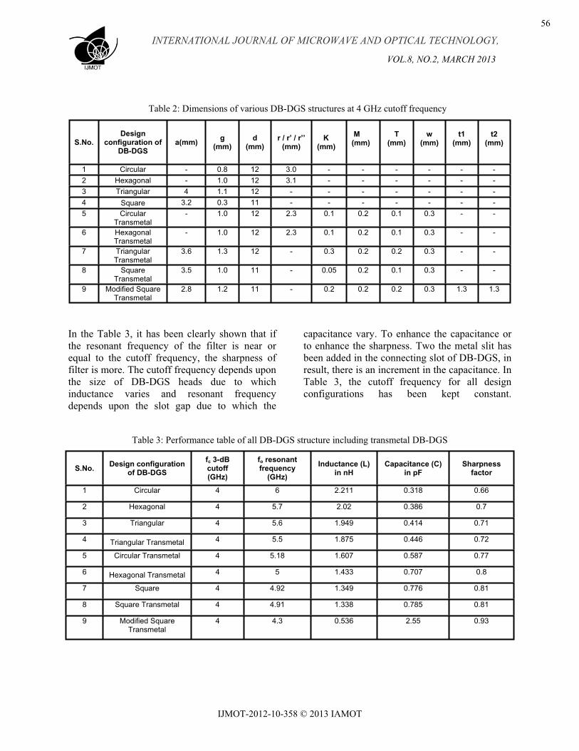
Table 2: Dimensions of various DB-DGS structures at 4 GHz cutoff frequency
S.No. Design
configuration of DB-DGS
a(mm) g(mm)
d(mm)
r / r’ / r’’ (mm)
K (mm)
M (mm)
T(mm)
w(mm)
t1(mm)
t2(mm)
1 Circular - 0.8 12 3.0 - - - - - - 2 Hexagonal - 1.0 12 3.1 - - - - - - 3 Triangular 4 1.1 12 - - - - - - - 4 Square 3.2 0.3 11 - - - - - - - 5 Circular
Transmetal - 1.0 12 2.3 0.1 0.2 0.1 0.3 - -
6 Hexagonal Transmetal
- 1.0 12 2.3 0.1 0.2 0.1 0.3 - -
7 Triangular Transmetal
3.6 1.3 12 - 0.3 0.2 0.2 0.3 - -
8 Square Transmetal
3.5 1.0 11 - 0.05 0.2 0.1 0.3 - -
9 Modified Square Transmetal
2.8 1.2 11 - 0.2 0.2 0.2 0.3 1.3 1.3
In the Table 3, it has been clearly shown that if the resonant frequency of the filter is near or equal to the cutoff frequency, the sharpness of filter is more. The cutoff frequency depends upon the size of DB-DGS heads due to which inductance varies and resonant frequency depends upon the slot gap due to which the
capacitance vary. To enhance the capacitance or to enhance the sharpness. Two the metal slit has been added in the connecting slot of DB-DGS, in result, there is an increment in the capacitance. In Table 3, the cutoff frequency for all design configurations has been kept constant.
Table 3: Performance table of all DB-DGS structure including transmetal DB-DGS
S.No. Design configuration of DB-DGS
fc 3-dB cutoff (GHz)
fo resonant frequency
(GHz)
Inductance (L) in nH
Capacitance (C) in pF
Sharpness factor
1 Circular 4 6 2.211 0.318 0.66
2 Hexagonal 4 5.7 2.02 0.386 0.7
3 Triangular 4 5.6 1.949 0.414 0.71
4 Triangular Transmetal 4 5.5 1.875 0.446 0.72
5 Circular Transmetal 4 5.18 1.607 0.587 0.77
6 Hexagonal Transmetal 4 5 1.433 0.707 0.8
7 Square 4 4.92 1.349 0.776 0.81
8 Square Transmetal 4 4.91 1.338 0.785 0.81
9 Modified Square Transmetal
4 4.3 0.536 2.55 0.93
INTERNATIONAL JOURNAL OF MICROWAVE AND OPTICAL TECHNOLOGY,
VOL. , NO.2, MARCH 201
56
IJMOT-2012-10-358 © 2013 IAMOT

Fig. 2: Simulated S-Parameter (S21) of DB-DGS
V. FABRICATION, MEASUREMENT AND CO-SIMULATION IN ADS
In Fig.3, the modified square transmetal DB-DGS has been fabricated to the dimensions which have been shown in Table 2. After the fabrication, the dimensions of the fabricated microstrip filter are: a = 2.9 mm, g = 1.3 mm, M = 0.3 mm, K = 0.3 mm, T = 0.3 mm, w = 0.3 mm, t1 = 1.3 mm, t2 = 1.3 mm. This fabricated filter has been tested in 1127.8500.60 Vector Network Analyzer of Rohde & Schwarz. Fig. 3 (c) shows the simulated as well as measured S-parameter. The resonant frequency and cutoff frequency of both the simulated and measured S-parameters are almost same. The resonant frequency is 4.3 GHz and 3-dB cutoff frequency is 4.0 in the simulation. And the measure resonant frequency is also 4.3 GHz and the 3-dB
cutoff is 4.0 GHz. The measured results are almost same as simulated one.
(a)
INTERNATIONAL JOURNAL OF MICROWAVE AND OPTICAL TECHNOLOGY,
VOL. , NO.2, MARCH 201
57
IJMOT-2012-10-358 © 2013 IAMOT

(b) (c)
Fig. 3: Modified square transmetal DB-DGS (a) Bottom view (b) Top view (c) Measured and simulated S-parameter of proposed DB-DGS
For more verification of results, the circuit simulation also has been done as shown in Fig. 4. For the proposed filter can be modeled as LC resonator circuit. The values of these L and C can be extracted by using the formulas given in equations (1) and (2). The extracted value of L and C has been shown in Table 3. These extracted values are used for designing L-C model prototype terminated with 50 ohm source and load as shown in Fig.4. This L-C model is co-simulated in ADS2006A. The simulated results have been shown in Fig.4 (b) which is the good in agreement with simulated results in HFSS V10 in Fig. 2 for the modified square transmetal DB-DGS.
(a)
(b)
Fig. 4: (a) L-C equivalent circuit (b) Simulated S-parameters of modified square transmetal DB-DGS
VI. CONCLUSION
In this paper, Various DB-DGS configurations have been designed and simulated with a comparison of their bandstop characteristics. The modified square transmetal DB-DGS have been proposed and fabricated. After the fabrication, simulated results and measured results in terms of S-parameters are almost same. In measured and simulated results, the 3-dB cutoff frequency is 4.0 GHz and the resonant frequency is 4.3 GHz. In both cases the sharpness factors are
INTERNATIONAL JOURNAL OF MICROWAVE AND OPTICAL TECHNOLOGY,
VOL. , NO.2, MARCH 201
58
IJMOT-2012-10-358 © 2013 IAMOT

nearly equal. In the measured result the sharpness factor is 0.93 which is close to the simulated results as shown in Table 3. The sharpness factor is calculated by the formula given in equation (3). The simulated result has been verified by co-simulation results. The measurement results are in close agreement with simulation results with acceptable tolerance in error. All the simulations are carried out in EM full wave simulator HFSS V10 and Agilent ADS2006A.
REFERENCES
[1] L.H. Weng, Y.C. Guo, X.W. Shi, and X. Q. Chen, “An Overview of Defected Ground Structure”, Progress in Electromagnetic Research B, Vol. 7, pp. 173-189, 2008.
[2] Jia-Sheng Hong, and Bindu M Karyamapudi, “ A General circuit model for defected ground structure in planar transmission lines,” IEEE Microwave Wireless Comp. Lett., Vol.10, No.10, pp. 706-708, Oct. 2005.
[3] R. Sharma, T. Chakarvarty, S. Bhooshan, et al., “Characteristic impedance of microstrip-like interconnect line in presence of ground plane aperture,” International Journal of Microwave Science and Technology, Vol.1, pp. 1-5, 2007.
[4] L. G. Maloratsky, “Microstrip Circuits with a Modified Ground Plane,” High Frequency Electronics, pp. 38- 47, November 2008.
[5] A. T. Mendez, H. J. Aguilar, and R.F. Leal, et. al, “Improving frequency response of Microstrip filters using defected ground and defected microstrip structures,” Progress in Electromagnetic Research C, Vol.13, pp. 77-90, 2010.
[6] YANG Xue-xia, and XUE Yu-jie, “Design of a compact low –pass filter with wide stopband,” Journal of Shanghai University, Vol. 12, No.6, 495-497, 2008.
[7] Y.L Zhang, W. Hong, K. Wu, J.X. Chen and H.J. Tang, “Novel substrate integrated waveguide cavity filter with defected ground structure,” IEEETrans. Microwave Theory Tech, Vol. 53, No.4, pp. 1280-1287, 2005.
[8] Ying Xu, and A. Alphones, “Novel DGS-CSRR-based microstrip low pass filter with ultra wide suppression,” International Journal of Ultra wideband Communications and Systems, Vol.1, No.3, pp. 169-172, 2010.
[9] F. Martin, F. Falcone, J. Bonache, R. Marques, and M. Sorolla, “Miniaturization coplanar waveguide stop band filters based on multiple tuned split ring resonators”, IEEE Microwave
Wireless Compon. Lett., Vol.13, pp. 511-513, December 2003.
[10] Ashwini K. Arya, M.V. Kartikeyan and A. Patnaik, “Defected ground structure in the perspective of Microstrip Antennas: A Review”, Frequenz-Journal of RF Engineering and Telecommunication, Vol.64, pp.79-84, 2010.
[11] G. Huynen, D. Gogilo, Vanhoenacker, and A. Vander Vorst, “A Novel Nanosturctured Microstrip Devices for Tunable Stopband Filtering Applications at Microwaves”, IEEE Microwave Guided Wave Lett., Vol. 9, No.10, pp.401-403, Oct.1999.
[12] J. S. Lim, S. W. Lee, C. S. Kim, J.S. Park, Dal Ahn, and S.W. Nam, “A 4:1 unequal Wilkinson power divider,” IEEE Microwave Wireless Compon. Lett., Vol. 11, No. 3, 124– 126, March 2001.
[13] J. S. Lim, H. S. Kim, J. S. Park, Dal Ahn, and S. Nam, “A power amplifier with efficiency improved using defected ground structure,” IEEE Microwave Wireless Compon. Lett., Vol. 11 , No.4, pp. 170-172, April 2001.
[14] J. S. Lim, J. S. Park, Y.T. Lee, Dal Ahn, and S. Nam, “Application of defected ground structure in reducing the size of amplifiers,” IEEE Microwave Wireless Compon. Lett., Vol.12, No.7, pp.261.-263, July 2002.
[15] Y.T. Lee, J. S. Lim, J. S. Park, Dal Ahn, and S. Nam, “A novel phase noise reduction techniques in oscillators using defected ground structure,” IEEE Microwave Wireless Compon. Lett., Vol. 12, No. 02, pp.39-41, Feb. 2002.
[16] Y. C. Jeong, and J. S. Lim, “A Novel Frequency Doubler Using Feedforward Technique and Defected Ground Structure”, IEEE Microwave Wireless Compon. Lett., Vol.14, No.12, December 2004.
[17] D. J. Kim, Y. Jeong, J. H. Kang, J.H. Kim, C.S. Kim, J. S. Lim, and Dal Ahn, “ A Novel Design of High Directivity CPW Directional Coupler Design by Using DGS”, Microwave Symposium Digest, IEEE MTT-S International, pp-1239-1242, 2005.
[18] K. M. Ho, H. K. Pang, and K. W. Tam, “Dual-band bandpass filter using defected ground structure”, Microwave Opt. Tech. Lett., Vol.48, No.11, pp. 2259-2261, November 2006.
[19] X. H. Wang, and B. Z. Wang, “Compact broadband dual-band bandpass filters using slotted ground structures”, Progress in Electromagnetics Research, PIER 82, pp. 151-166, 2008.
[20] Akhilesh Mohan, and Animesh Biswas, “Dual-band bandpass filter using defected ground structure”, Microwave Opt. Tech. Lett., Vol. 51, No.2, pp. 475-479, February 2009.
[21] H. W. Liu, Z. C. Zhang, S. Wang, L. Zhu, X. H. Guan, J. S. Lim, and D. Ahn, “Compact dual-band bandpass filter using defected microstrip structure
INTERNATIONAL JOURNAL OF MICROWAVE AND OPTICAL TECHNOLOGY,
VOL. , NO.2, MARCH 201
59
IJMOT-2012-10-358 © 2013 IAMOT

for GPS and WLAN applications”, Electronics Lett., Vol.46, No.21, October 2010.
[22] H. B. El.,Shaarawy, F. Coccetti, Robert Plana, M. El. Said, and E. A. Hashish, “Compact Bandpaas Ring Resonator filter with enhanced wide-band rejection characteristics using defected ground structures”, IEEE Microwave Wireless Compon. Lett., Vol.18, No.8, pp. 500-502, August 2008.
[23] A.K. Arya, M. V. Kartikeyan, and A. Patnaik, “Efficiency enhancement of microstrip patch antennas with Defected Ground Structure,” Proc.Conf., Recent Advanced in Microwave theory and applications (MICROWAVE-08), pp.729-731 November 2008.
[24] F. D. Mbairi, and H. Hesselbom, “Microwave bandpass filter using novel artificial periodic substrate electromagnetic band gap structures”, IEEE Trans. Components and Packaging Technologies, Vol.32, No.2, pp. 273-282, June 2009.
[25] Z. C. Hao, J. S. Hong, J. P. Parry, and D. P. Hand, “Ultra-wideband bandpass filter with multiple notch bands using non-uniform periodical slotted ground structure”, IEEE Microwave Wireless Compon. Lett., Vol.57, No.12, pp. 3080-3088, December 2009.
[26] W. J. Lin, J. Y. Li, L. S. Chen, D. B. Lin, and M. P. Houng, “Investigation in open circuited metal lines embedded in defected ground structure and its applications to UWB filters”, IEEE Microwave Wireless Compon. Lett., Vol.20, No.3, pp.148-150, March 2010.
[27] J. K. Lee, and Y. S. Kim, “Ultra-wideband bandpass filter with improved upper stopband performance using defected ground structure”, IEEE Microwave Wireless Compon. Lett., Vol.20, No.6, pp.316-318, June 2010.
[28] L.Y. Ren, “Tri-band bandpass filters based on dual-plane microstrip/DGS slot structure”, IEEE Microwave Wireless Compon. Lett., Vol.20, No.8, pp. 429-431, August 2010.
[29] Y. Liu, W. B. Dou, and Y. J. Zhao, “A tri-band bandpass filter realized using tri-mode T-shape branches”, Progress in Electromagnetic Research,PIER 105, 425-444, 2010.
[30] Y. Chung, S. S. Jeon, S. Kim, Dal Ahn, J. I. Choi, and T. Itoh, “Multifunctional microstrip lines integrated with Defected Ground Structure for RF application”, IEEE Trans. Microwave Theory Tech., Vol. 52, No.5, pp. 1425-1432, May 2004.
[31] H. Liu, Z. Li, and X. Sun, “Compact defected ground structure in microstrip technology”, IEEEElectronics Lett., Vol. 41, No. 3, February 2005.
[32] H. W. Wu, and C. Y. Hung, “Equivalent circuit Model of the slotted ground structure (SGSs) underneath the microstrip line”, Proc.International Multi Conference Engineers and Computer Scientist, IMECS-2010, Hong-Kong, Vol.2, 2010.
[33] A. A. Rahman, A. K. Verma, A. Boutejdar, and A. S. Omar, “Compact stub type microstrip bandpass filter using defected ground structure”, IEEE Microwave Wireless Compon. Lett., Vol.14, No.4, pp. 136-138, April 2004.
[34] A. B. Abdel-Rahman, A. K. Verma, A. Boutejdar, and A. S. Omar, “Control of Bandstop Response of Hi-Lo Microstrip Low-Pass Filter using slot in the ground plane”, IEEE Trans. Microwave Theory Tech. , Vol. 52, No.3, pp. 1008-1013, March 2004.
[35] Ashwani Kumar, and A. K. Verma, “Design of compact seven poles low pass filter using defected ground structure”, Proc. International Conf. on Emerging Trends in Electronic and Photonic Devices & Systems, ELECTRO-2009, Varanasi, India, pp. 349-352, 2009.
[36] P. Kumar , R. Mahmood, J. Kishor , and A.K. Shrivastav, “Control of Band stop responses of very compact size microstrip filter of improved Q-factor & sharp transition by using hexagonal transmetal DGS”, Proc. International Conf. on Emerging Trends in Electronic and Photonic Devices & Systems, ELECTRO-2009,Varanasi, India, pp. 383-386, 2009.
INTERNATIONAL JOURNAL OF MICROWAVE AND OPTICAL TECHNOLOGY,
VOL. , NO.2, MARCH 201
60
IJMOT-2012-10-358 © 2013 IAMOT

Analysis, Design and Simulation of Metal PBG Waveguide
M.Thottappan*, P.K.Jain**
Centre of Research in Microwave Tubes, Department of Electronics Engineering, Indian Institute of Technology (Banaras Hindu University),
Varanasi– 221 005, INDIA. Tel: +91-542-6701282; Email: [email protected]*
Abstract- This article deals with analysis, design, modeling and simulation of a metal photonic band gap (MPBG) waveguide for TE mode of operation. The finite difference time domain (FDTD) technique has been used to analyze and obtain the global band gap regions of the MPBG structures having 2-D triangular array. A mode map diagram has been developed for the MPBG waveguide in order to study the propagation characteristics of the guide. The designed waveguide structure has been cold characterized using a 3-D electromagnetic code for the desired TE01 mode. This study shows that nearby competing modes, like, TE21 and TE31 have been suppressed and ensures that the MPBG is been preponderant for waveguide applications and also it addresses the mode competition, miniaturization and the power handling issues which generally appears at the short wavelengths. The transmission loss over the guide has been estimated through its scattering coefficients as 1.01 dB /cm at the operating frequency.
Index Terms- Waveguide, Mode competition, Photonic band gap structure, Transmission loss, FDTD.
I. INTRODUCTION
The waveguide transverse dimension is proportional to its cutoff wavelength and at millimeter and sub-millimeter waves frequencies waveguide dimension becomes so small that they are not capable of handling very high powers. To vercome this problem, overmoded waveguides are used for high power millimeter/sub-millimeter waves systems and devices. This leads to mode competition followed by higher structure ohmic losses [1]. There is also practical
limitation in fabricating such tiny structures with precision tolerance.
To acheive the frequency selective operation without mode competion, the transmission line must be selective with respect to the operating mode. The photonic band gap (PBG) structures have proved very promising to meet such requirements and have drawn extensive attention of researchers for its used in passive and active devices both [2]. The PBG structures are lattices of periodic arrangement of dielectric, metal or complex inclusions. Such structures can assist the propagation of EM waves in certain frequency band, called as the pass band and no waves exist in the forbidden band is referred as stop band [3]. The dielectric PBG structures have been successfully used in microwave devices for copious applications. Nevertheless, the metal photonic band gap (MPBG) structures have been also finding vast applications due to their higher power handling capability over its dielectric counterpart. The problem of breakdown and charging of dielectric materials restrict its applications. Conversely, these phenomena do not happen with metallic PBG (MPBG) structures due to their distinction in conductibility and act as a nearly perfect reflector at high frequency which also minimizes the problems of absorption [4-5]. Moreover, in the vacuum electronic devices, operating temperature is very high which necessitates the interaction structure's material to sustain this temperature with sufficient mechanical strength [6]. Photonic crystal linear waveguide has been studied by Johnson et al. [7] and the analysis MPBG rectangular waveguide for THz application has been demonstrated by Degirmenci et al. [8].
INTERNATIONAL JOURNAL OF MICROWAVE AND OPTICAL TECHNOLOGY,
VOL. , NO.2, MARCH 201
61
IJMOT-2012-11-368 © 2013 IAMOT

More recently, the millimeter wave MPBG cylindrical waveguide has been developed at MIT by Nanni et al. [9], however its analysis and design procedure are not reported. In this paper, we extend work for the analysis and realization of cylindrical waveguide using MPBG structures for Ka-band applications.
The remainder of this article is organized as follows. In Section II, the dispersion characteristics of a 2-D MPBG structure having triangular lattice operating in the TE mode of propagation using FDTD method is discussed. In Section III, the global band gap diagram which is required for the design of waveguides is described and then a detailed design procedure for the MPBG waveguide is presented. In section IV, the cold (electron beam absent) electromagnetic characterization of the designed MPBG waveguide is performed using a commercial code “CST Microwave Studio” and the transmission loss and cutoff frequency are also observed. The conclusion is drawn based on the work performed here in Section V.
II. NUMERICAL ANALYSIS OF MPBG STRUCTURES WITH FDTD TECHNIQUE
A. Modeling of MPBG structures
The unit cell of triangular/rhombic lattice has been considered here in TE polarization for calculating the band structure. Since, the triangular lattice structure is azimuthally symmetric and provides more global band gaps compared to the square lattice. Dispersion diagram, i. e., band structure is required to determine the forbidden and pass bands of the PBG structures. The triangular lattice PBG structure using cylindrical metal rods is shown in Fig. 1(a). The Brillouin zone shown in Fig. 1(b),
where the wave vector x x y yk k e k e⊥ = +� ��� ���
at Г, X,
and J is read as (0, 0), 2π/a (0, 1/√3), and 2π/a (1/3, 1/√3), respectively [10]. The EM boundary conditions for the TE mode is given by ∂Ψ/∂n is zero at the surface of the metal rods and ‘n’ is a vector normal to the metallic surface. In order to obtain solution in the region of interest has to be
discretized in accordance with Courant stability condition [6]. The considered modified unit cell for calculating the band structure is discretized into uniform rectangular grids with the length of
unit cell along y-axis is 3 / 2 times the length along the x-axis in the unit cell. Hence, if the number of grid points along x-axis (Nx) is 100, then the number of grid points along y-axis (Ny) would be 87, i. e., Ny = (√3/2)Nx, as shown in Fig. 1 (c).
Fig.1. (a) Cross section of a 2-D MPBG triangular lattice in real space (b) in reciprocal space the dashed lines illustrate the unit cell and the shaded region is Brillouin zone and (c) discretized MPBG unit cell with Nx =100 and Ny =87.
The uniform Yee’s cell based discretization has been used for a skew lattice computational domain and each grid point is specified by appropriate material property. In Fig. 1(c), where half metal cylinders is at middle of one side along x-direction and two quarter portion of metal cylinder on the other side of opposite corners. The unit cell element is metallic rods
(a) (b)
(c) Nx
Ny
INTERNATIONAL JOURNAL OF MICROWAVE AND OPTICAL TECHNOLOGY,
VOL. , NO.2, MARCH 201
62
IJMOT-2012-11-368 © 2013 IAMOT

and in the modeling, rods material is taken as copper with relative permittivity εr = 1 and conductivity σ = 5.8x 10⁷ S/m. The background has been considered as vacuum which has relative permittivity and permeability as unity and conductivity as zero [6].
B. Field equations in FDTD analysis
At millimeter and sub-millimeter wave frequencies, current is well confined within a small depth of the metal rods. Therefore, we can consider that the electric filed inside the metallic rods as zero i.e. E = 0. So in the unit cell region, Maxwell’s equations for time varying fields are written as
HX E
tµ ∂
∇ = −∂
���
��
(1)
EX H
tε ∂
∇ =∂
��
���
(2)
Here, TE modes of propagation are considered for the potential application in gyro devices where the energy exchange is mainly concentrated on the transverse component of electric field. Based on 2-D Yee’s mesh and central difference algorithm, equations (1) and (2) are discretized in both time and space domains as
{ , } { 1/ 2, } { 1/ 2, }n n nF i j F i j F i j
x δ∂ + − −
=∂
(3)
1/2 1/2{ , } { , } { , }n n nF i j F i j F i j
t t
+ −∂ −=
∂ ∆ (4)
Electric (Ex, Ey) and Magnetic (Hz) fields components for TE mode are given in equation (5), (6), and (7), respectively [6]
1 2 { } ∆ { }{ } { }
2 { } ∆ { }n nx x
i, j - t i, j E i, j E i, j
i , j t i, j
ε σε σ
+ ⎛ ⎞= × +⎜ ⎟+⎝ ⎠
1/2 1/22∆ { } { 1}
2 { } ∆ { } ∆
n nz zt H i, j H i, j -
i, j t i, j yε σ
+ +⎛ ⎞⎛ ⎞ −×⎜ ⎟⎜ ⎟+⎝ ⎠ ⎝ ⎠
(5)
1 2 { } ∆ { }{ } { }
2 { } ∆ { }n ny y
i , j - t i, j E i, j E i, j
i, j t i, j
ε σε σ
+ ⎛ ⎞= × −⎜ ⎟+⎝ ⎠
1 2 1 22∆ { } { 1 }
2 { } ∆ { } ∆
n nz zt H i, j H i - , j
i, j t i, j xε σ
+ +⎛ ⎞⎛ ⎞ −×⎜ ⎟⎜ ⎟+⎝ ⎠ ⎝ ⎠
(6)
1 2 1 2 ∆{ } { }
{ }n nz z
t H i, j H i, j
i, j µ+ − ⎛ ⎞
= + ×⎜ ⎟⎝ ⎠{ 1 } { }{ 1} { }
∆ ∆
n nn ny yx x
E i , j E i, j E i, j E i, j
y x
⎛ ⎞+ −+ −−⎜ ⎟
⎝ ⎠ (7)
where, ε and µ are the permittivity and permeability of the medium. Here, the fields are sampled at discrete points by Courant-Friedrichs-Lewy (CFL) condition to maintain accuracy [6]
( ) ( )1
2 2 2
max
x yt t
c
−− −⎡ ⎤∆ + ∆⎣ ⎦∆ ≤ ∆ = (8)
where, c is the velocity of light. ∆x and ∆y are the controlling factor to have maximum allowed time step. The time step must always be smaller than the maximum time step.
C. Dispersion curves and global band gap diagrams of MPBG structures
The EM fields at every half space steps are monitored and the temporal results have been processed using the Fourier transform and each ‘k’ vector values for the corresponding frequencies are recorded and plotted against the ‘k’ vector. This is shown in Fig. 2(a) for r/a = 0.39 (first seven lower order modes) and in which each line represents the mode. For r/a=0.39, there are two band gaps occurring. The lower one between 0.94 and 1.02 times the normalized frequency (fa/c) and the centre frequency and the width of the gap is 0.98 and 0.08 times (c/a), respectively.
INTERNATIONAL JOURNAL OF MICROWAVE AND OPTICAL TECHNOLOGY,
VOL. , NO.2, MARCH 201
63
IJMOT-2012-11-368 © 2013 IAMOT
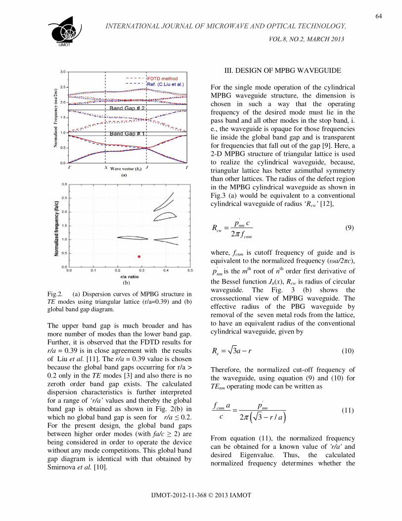
Fig.2. (a) Dispersion curves of MPBG structure in TE modes using triangular lattice (r/a=0.39) and (b) global band gap diagram.
The upper band gap is much broader and has more number of modes than the lower band gap. Further, it is observed that the FDTD results for r/a = 0.39 is in close agreement with the results of Liu et al. [11]. The r/a = 0.39 value is chosen because the global band gaps occurring for r/a > 0.2 only in the TE modes [3] and also there is no zeroth order band gap exists. The calculated dispersion characteristics is further interpreted for a range of ‘r/a’ values and thereby the global band gap is obtained as shown in Fig. 2(b) in which no global band gap is seen for r/a ≤ 0.2. For the present design, the global band gaps between higher order modes (with fa/c ≥ 2) are being considered in order to operate the device without any mode competitions. This global band gap diagram is identical with that obtained by Smirnova et al. [10].
III. DESIGN OF MPBG WAVEGUIDE
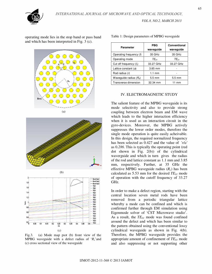
For the single mode operation of the cylindrical MPBG waveguide structure, the dimension is chosen in such a way that the operating frequency of the desired mode must lie in the pass band and all other modes in the stop band, i. e., the waveguide is opaque for those frequencies lie inside the global band gap and is transparent for frequencies that fall out of the gap [9]. Here, a 2-D MPBG structure of triangular lattice is used to realize the cylindrical waveguide, because, triangular lattice has better azimuthal symmetry than other lattices. The radius of the defect region in the MPBG cylindrical waveguide as shown in Fig.3 (a) would be equivalent to a conventional cylindrical waveguide of radius ‘Rcw’ [12],
'
2nm
cwcnm
p cR
fπ= (9)
where, fcnm is cutoff frequency of guide and is equivalent to the normalized frequency (ωa/2πc),
'nmp is the mth root of nth order first derivative of
the Bessel function Jn(x), Rcw is radius of circular waveguide. The Fig. 3 (b) shows the crosssectional view of MPBG waveguide. The effective radius of the PBG waveguide by removal of the seven metal rods from the lattice, to have an equivalent radius of the conventional cylindrical waveguide, given by
3eR a r= − (10)
Therefore, the normalized cut-off frequency of the waveguide, using equation (9) and (10) for TEnm operating mode can be written as
( )'
2 3 /cnm nmf a p
c r aπ=
− (11)
From equation (11), the normalized frequency can be obtained for a known value of 'r/a' and desired Eigenvalue. Thus, the calculated normalized frequency determines whether the
(b)
INTERNATIONAL JOURNAL OF MICROWAVE AND OPTICAL TECHNOLOGY,
VOL. , NO.2, MARCH 201
64
IJMOT-2012-11-368 © 2013 IAMOT
operating mode lies in the stop band or pass band and which has been interpreted in Fig. 3 (c).
Fig.3. (a) Mode map plot (b) front view of the MPBG waveguide with a defect radius of ‘Re’and (c) cross sectional view of the waveguide
Table 1: Design parameters of MPBG waveguide
Parameter PBG
waveguide
Conventional
waveguide
Operating frequency (f) 35 GHz 35 GHz
Operating mode TE01 TE01
Cut off frequency (fc) 33.27 GHz 33.27 GHz
Lattice constant (a) 3.85 mm -
Rod radius (r) 1.1 mm -
Waveguide radius (Re) 5.5 mm 5.5 mm
Transverse dimension 32.34 mm 11 mm
IV. ELECTROMAGNETIC STUDY
The salient feature of the MPBG waveguide is its mode selectivity and also to provide strong coupling between electron beam and EM wave which leads to the higher interaction efficiency when it is used as an interaction circuit in the gyro-devices. Moreover, the MPBG actively suppresses the lower order modes, therefore the single mode operation is quite easily acheivable. In this design, the required normalized frequency has been selected as 0.427 and the value of 'r/a' as 0.286. This is typically the operating point (red dot shown in Fig. 2(b)) of the cylindrical waverguide and which in turn gives the radius of the rod and lattice constant as 1.1 mm and 3.85 mm, respectively. Further, at 35 GHz the effective MPBG waveguide radius (Re) has been calculated as 5.53 mm for the desired TE01 mode of operation with the cutoff frequency of 33.27 GHz. In order to make a defect region, starting with the central location seven metal rods have been removed from a periodic triangular lattice whereby a mode can be confined and which is confirmed further through EM simulation using Eigenmode solver of ‘CST Microwave studio’. As a result, the TE01 mode was found confined around the defect and which has been similar to the pattern obtained using the conventional lossy cylindrical waveguide as shown in Fig. 4(b). Therefore, the MPBG waveguide provides the appropriate amount of confinement of TE01 mode and also suppressing or not supporting other
(b)
(a)
(c)
INTERNATIONAL JOURNAL OF MICROWAVE AND OPTICAL TECHNOLOGY,
VOL. , NO.2, MARCH 201
65
IJMOT-2012-11-368 © 2013 IAMOT

modes, like, TE31, TE41 and TE21. The radius of the MPBG guide is approximately equal to as same as the conventional waveguide and also the strength of the field can be matched by having the MPBG volume as 8.6 times of the conventional guide volume as shown in Fig. 4 (a) and 4 (b). This feature relaxes the fabrication difficulties of the interaction structure which arises at milliliter wave operation of the high power devices. The advantage of the expanded transverse dimension of the MPBG waveguide over a conventional metal cylindrical waveguide is to lower the Ohmic loss and hence improved power handling capability. The Fig. 4 (c) shows the propagation of desired TE01 mode through the axial direction of the MPBG waveguide.
Fig.4. Comparison of the magnitude of the E-field for TE01 mode confined in (a) conventional waveguide (b) MPBG waveguide (c) TE01 mode propagation inside the PBG waveguide
V. RESULTS AND DISCUSSION
A. Scattering parameters
The transient analysis of MPBG waveguide has been also performed using ‘CST Microwave studio’ in order to observe the pass band and stop band properties by plotting its scattering parameters. Fig. 5(a) shows the transmission and reflection properties of metal PBG guide and in which the transmission coefficient (S21) has been observed maximum over the frequency range of 3 GHz and the reflection parameter (S11) is minimum beyond the cut-off frequency which is an essential characteristics of a waveguide. This confirms that the existence of a propagating mode at the desired operating frequency.
Fig.5. (a) Scattering parameters (b) comparison of transmission coefficient of various modes in MPBG waveguide
(a)
32 33 34 35 36 37 38-40
-35
-30
-25
-20
-15
-10
-5
0
5
Frequency, f(GHz)
Tra
nsm
issi
on
an
d R
efle
ctio
n C
oef
fici
ent
(dB
)
S11
S21
(b)
32 33 34 35 36 37 38-140
-120
-100
-80
-60
-40
-20
0
Frequency, f(GHz)
Tra
nsm
issi
on
Co
effi
cien
t, S
21 (
dB
)
TE21
TE12
TE01
TE31
TE41
(c)
(a) (b)
INTERNATIONAL JOURNAL OF MICROWAVE AND OPTICAL TECHNOLOGY,
VOL. , NO.2, MARCH 201
66
IJMOT-2012-11-368 © 2013 IAMOT

The Fig. 5(b) shows transmission coefficient of the desired mode and its nearby competing modes as the wave propagating down the MPBG guide and it is observed that the transmission characteristics of the desired TE01 mode has maximum than all other spurious (TE21, TE31, TE41, and TE12) modes. Unlike the traditional waveguides, the MPBG waveguide provides high attenuation (diffraction losses) for the spurious modes due to its structure and hence the desired mode always been well separated from other unwanted modes.
B. Transmission loss in an MPBG waveguide
The MPBG waveguide has been tested for the transmission properties at 35 GHz with the circuit length of 50 mm for the desired TE01
mode of operation. Unlike the conventional waveguide, transmission losses in an MPBG waveguide are due to the diffractive radiation through the tiny nature of the elements in the lattice. Therefore in MPBG waveguide, amount of ohmic heating on the metallic rods is significantly reduced. The cold simulated parameters have been utilized to calculate the transmission loss and which has been observed at 35 GHz as 1.01dB /cm as shown in Fig. 6.
Fig.6. Calculated transmission loss in a 35 GHz MPBG waveguide
C. Cut-off frequency of an MPBG waveguide
The radius of waveguide interaction structure has been obtained by equation (8) for desired cutoff
frequency and mode of operation. The cutoff frequency of the guide has been calculated by varying the ‘r/a’ ratio for TE01 mode using equation (10) as shown in Fig. 7. Theoretical and simulation results have been compared and found that they are in close agreement and it is also observed that the field pattern (TE01 mode) of MPBG waveguide (as shown in Fig. 4), near the metal posts, EM fields are not perfectly confined in the defect and slightly penetrates into the rods region and hence, the waveguide radius is being considered theoretically smaller than effective guide radius. Consequently, the simulated cutoff frequencies is always less than the theoretical values.
Fig.7. Cutoff frequency variation with the ratio of rod radius to lattice constant
VI. CONCLUSION
Overmoded waveguides are often used for high power millimeter/sub-millimeter waves devices and systems. Overmoded structures are plagued with mode competition and high losses problems. The photonic band gap (PBG) structures are very promising for freqeuency selective operation. Metal PBG structures are capable of handling higher power compared to its dielectric counterpart.
A defect in photonic crystals making a cylindrical waveguide and which would provide an effective pass band characteristic as like in a conventional waveguides. This has been
Frequency, f(GHz)
Tra
nsm
issi
on
Lo
ss, αα αα
(d
B/c
m)
33 33.5 34 34.5 35 35.5 36 36.5 37 37.5 38-6
-5.5
-5
-4.5
-4
-3.5
-3
-2.5
-2
-1.5
-1
-0.5
0
INTERNATIONAL JOURNAL OF MICROWAVE AND OPTICAL TECHNOLOGY,
VOL. , NO.2, MARCH 201
67
IJMOT-2012-11-368 © 2013 IAMOT

investigated, designed and simulated by considering a 2-D metal PBG structure comprising of triangular lattice. The analysis of MPBG structure was made using the Yee’s FDTD technique, because which is more comfortable in respect of conceptually simple and dynamic algorithm, flexible computation, applicable to wider frequency band and minimizing the computational error greatly than any other numerical methods. The universal global band gap curves for MPBG structures in TE modes have been developed. In order to ensure the high mode purity, the TE polarizationhas been selected and which is required for fast wave gyro devices and these kinds of MPBG structures also having the tendency to handle higher power than its counterpart (dielectric PBG). By selecting the appropriate point in the pass band of the global band gap diagram the 35 GHz MPBG waveguide has been designed.
To validate the analysis and design, after calculating effective radius of the guide, with seven metallic rods removed from the periodic triangular lattice structure, so as to realize it, and which has been simulated using a commercially available 3-D electromagnetic code “CST Microwave studio”. The eigenmode analysis confirms propagation of such potential TE01
mode and the transient analysis ensures the propagation characteristics of the cylindrical waveguide. Further, the transmission loss and the cutoff frequency of the waveguide have been estimated from its scattering coefficients.
Hence, it is hope that the present analysis and design of the MPBG cylindrical waveguide would be useful as RF circuit for both the active and passive microwave/millimeter wave device applications where one desires to suppress the potentially competing unwanted modes in order to ensure a single mode device operation.
REFERENCES
[1] K.R. Chu, “The electron cyclotron maser”, Reviews of Modern Physics, 76 (2), pp. 489-540,
2004.
[2] Joannopoulos J. D., R. D. Meade, and J. N. Winn, “Photonic Crystals: Molding the Flow of Light”,
Princeton Univ. Press, Princeton, NJ, 1995. [3] Sirigiri J. R., K. E. Kreischer, J. Macuhzak, I.
Mastovsky, M. A. Shapiro, and R. J. Temkin, “Photonic Band Gap Resonator Gyrotron,” Phys. Rev. Lett., Vol. 86, pp. 5628 – 5631, 2001.
[4] Gao, X., Z. Yang, Y. Xu, L. Qi, D. Li, Z. Shi, F. Lan, and Z. Liang, “Dispersion characteristic of a slow wave structure with metal photonic band gap cells”, Nuclear Instruments and Methods in Physics Research A, Vol. 592, pp. 292-296, May 2008.
[5] McCalmont, J. S., M. M. Sigalas, G. Tuttle, K. M. Ho, and C. M. Soukolis, “A layer-by-layer metallic photonic band-gap structure”, Appl. Phys. Lett., Vol. 68, pp. 2759-2761, 1996.
[6] Ashutosh, P. K. Jain, “FDTD Analysis of the Dispersion Characteristics of the Metal PBG Structures”, Progress In Electromagnetics Research B, Vol. 39, pp. 71-88, 2012.
[7] Steven G. Johnson, Pierre R. Villeneuve, Shanhui Fan, and J. D. Joannopoulos, “Linear waveguides in photonic-crystal slabs”, Physical Review B, Vol. 62, No. 12, 2000.
[8] E. Degirmenci, F. Surre, and P. Landais, “2-D Numerical Analysis of Metallic Band-Gap Crystal Waveguide in THz”, IEEE International Conf. IRMMW-THz 2009 , pp. 1-2, 2009.
[9] Emilio A. Nanni, Michael A. Shapiro, Jagadishwar R. Sirigiri and Richard J. Temkin, “Design of a 250 GHz Photonic Band Gap Gyrotron Amplifier”, Vacuum Electronics Conference (IVEC), 2010 IEEE International, pp. 317-318, 2010.
[10] E. I. Smirnova, C. Chen, M. A. Shapiro, J. R. Sirigiri, and R. J. Temkin, “Simulation of Photonic Band Gaps in Metal Rod Lattices for Microwave Applications”, J. App. Phys., Vol. 91, No. 3, pp. 960-968, 2002.
[11] Chang Liu, Yaotian Luo, Changjian Tang, and Pukun Liu, “Electromagnetic mode analysis on photonic band gap resonant cavity in a gyrotron”, Int. Journal of Electronics, Vol. 97, No. 2, pp. 207-216, February 2010.
[12] Ashutosh, P. K. Jain, “Design and Analysis of Metallic Photonic Band Gap Cavity for a Gyrotron”, Journal of Microwaves, Optoelectronics and Electromagnetic Applications, Vol. 11, No. 2, pp. 242-251, December 2012.
INTERNATIONAL JOURNAL OF MICROWAVE AND OPTICAL TECHNOLOGY,
VOL. , NO.2, MARCH 201
68
IJMOT-2012-11-368 © 2013 IAMOT

Slot Loaded and Pin Shorted Equilateral Triangular Microstrip Antenna.
Rajeev Kumar Singh*, Rajarshi Sanyal1, Geetali Chakrabarty2, Sekhar Rana3, Sudarshan Chakravorty4
*Student B.Tech (ECE Dept.), MCKVIE, Howrah, West Bengal, INDIA.Ph.: 91-9038999607; E-mail:[email protected],,[email protected]
1Assistant Professor, ECE Department, MCKVIE, Howrah, West Bengal, INDIA.2Student M.tech (ECE Dept.), MCKVIE, Howrah, West Bengal, INDIA.
3Assistant Professor, ECE Department, MCKVIE, Howrah, West Bengal, INDIA.4
Abstract- In this paper the analysis of circular slot and triangular slot loaded equilateral triangular microstrip antenna (ETMSA) is shown. It is observed that two shorted pin nearer to the two vertexes of ETMSA produces dual resonance frequencies with circular polarization (CP). Circular slot loading in between probe position and one shorted vertex widened the gap between two resonance frequencies. The variation of frequency gap between two resonance frequencies becomes nonlinear in character when the radius of circular slot is increases beyond 2.5mm.This nonlinearity is also demonstrated using a triangular slot of varied arm length. A comparative study is shown fordifferent substrate permittivity.
Index Terms- Circular and triangular slot, circular polarization, dual band, ETMSA, nonlinear, two pin shorting.
I. INTRODUCTION
Associate Professor, ECE Department, MCKVIE, Howrah, West Bengal, INDIA.
Dual-frequency operations of microstrip patch antennas have received much attention in modern wireless communication systems [1]. Stub loaded, Slit-loaded, slot-loaded, shorting pin and circuitry-loaded patch antennas are some of the methods to form a dual frequency operation [2-4]. One study presenting two shorting pin-loaded equilateral triangular patch antenna [5].Loading a triangular microstrip antenna with a shorting pin can also reduce the antenna size [4].Here in this paper circular and triangular slot is also inserted along with the two shorting pin, which reduced the patch size of ETMSA with dual resonance frequency. The circular slot
widens the band gap between two resonant frequencies. A comparative study has also been done for two standard thicknesses on various substrates permittivity, which shows significant results.
Theoretically the resonant frequency [6-7] for an ETMSA can be calculated as,
……………….. (1)
Where, c=speed of light, r=substrate permittivity, ae=effective arm length, which is given by,
. (2)
Where a= arm length, h= substrate thickness.The theoretical value of resonant frequency (fr
Basic parameters of ETMSA are substrate permittivity (
)for the proposed antenna is 4.3259GHz.
II. ANTENNA DESIGN AND SIMULATED RESULTS.
r) =2.2 (RT Duroid); substrate height (h) =1.6 mm, loss tangent ( ) =0.0004and length of each arm of ETMSA (L) =30 mm is taken. The co-axial feed is at (-1, 0), which shows the resonant frequency of 4.2468GHz as shown in fig.1a and fig.1b. The gain value is
INTERNATIONAL JOURNAL OF MICROWAVE AND OPTICAL TECHNOLOGY,
VOL. , NO.2, MARCH 201
69
IJMOT-2013-2-399 © 2013 IAMOT

6.85dBi (approx.). Simulation has been done by the method of moment based IE3D EM Design System (V: 14) simulator [8].
A. Effect of single pin shorting.
When Pin (P1) is shorted between vertex and co-axial feed point as shown in fig.1a.the resonant frequency shifted from 4.2468GHz to 5.23GHz as shown in fig.1b.In proposed antenna theposition of P1 from vertex is 0.65mm. The corresponding directive gain is 4.6dbi.
B. Effect of two pin shorting.
Shorting an additional Pin (P2) nearer to any of the other vertices, results in dual band effect as shown in fig.1a. The two resonant frequencies are 4.727GHz and 5.56GHz as shown in fig.1b.The dual band effect can be produced either by LHCP (left hand circular polarization) or RHCP (right hand circular polarization).Both structure produced almost same return loss performance. The corresponding gains of both the resonant frequencies are 5.49dBi and 3.99dBi.
Fig.1a. Single pin and dual pin shorted patch.
2.0 2.5 3.0 3.5 4.0 4.5 5.0 5.5 6.0 6.5 7.0 7.5
-35
-30
-25
-20
-15
-10
-5
0
S11
(dB
)
Frequency (GHz)
No Pin Single Pin Dual Pin
Fig.1b. Return loss performance of single pin and dual pin shorting.
C. Effect of circular slot loading.
A circular slot is inserted between probe feed and pin shorted vertex. As a result the frequency gap between two resonant frequencies is changing. Two different types of effects have been shown. In first case the radius of the circular slot is varied up to 4mm keeping the center at (5,0).In the second case the position of the slot is varied and is shifted towards the pin shorted vertex keeping the radius constant.
The effect is also tested on different substrate r=2.2, r=2.6, r=4.4.
C.1. Effect of changing the radius of circularslot.
It is observed that as we are increasing the radius of the slot, the frequency gap (f2-f1) increases in two different manners. The increase is almost linear up to R=2.5mm (radius of circular slot), and it is becoming nonlinear in character after radius is increased from 2.5mm to 4mm for different values of r (substrate permittivity) as shown in fig.2c for substrate thickness (h)=1.6mm.
INTERNATIONAL JOURNAL OF MICROWAVE AND OPTICAL TECHNOLOGY,
VOL. , NO.2, MARCH 201
70
IJMOT-2013-2-399 © 2013 IAMOT

Fig.2a. Circular slot loaded patch.
The return loss (dB) is also increases for the secondary resonant frequency. The values for R=0mm is almost same as that for R=1mm. Therefore corresponding values are not shown here. It should be noted that R=0mm, corresponds to absence of circular slot i.e. without circular slot.
Table 1: Resonant frequencies (f1 & f2) for different values of circular slot radius (R).
R=0mmr
R=2mm R=3mm R=4mm
f f1 f2 f1 f2 f1 f2 f1 2
2.2 4.73 5.56 4.77 5.73 4.74 5.79 4.73 6.07
2.33 4.61 5.41 4.64 5.58 4.62 5.64 4.61 5.92
2.4 4.54 5.34 4.52 5.43 4.55 5.55 4.56 5.83
2.6 4.38 5.15 4.42 5.29 4.40 5.35 4.38 5.61
3.2 3.97 4.66 4.01 4.78 3.99 4.84 3.99 5.07
3.6 3.97 4.66 3.8 4.53 3.77 4.58 3.77 4.8
4.4 3.42 4.01 3.44 4.11 3.43 4.15 3.43 4.37
6.4 2.86 3.17 2.88 3.43 2.86 3.51 2.85 3.63
4 5 6 7
-35
-30
-25
-20
-15
-10
-5
0
Ret
urn
Loss
(dB
)
Frequency (GHz)
R=4mm R=3mm R=2mm R=0mm
Fig.2b. Return loss performance of circular slot loaded patch at r=2.2 and h=1.6.
From fig.2b it should be noted that, though position of primary resonant frequency is fixed up to certain limit the position of secondary resonant frequency is changing significantly. This ultimately contributes to the nonlinearity in the frequency differences between two resonant frequencies.
From fig.2c it can be shown that the band gap variation rate is less for high substrate permittivity ( r=6.4) as compared with low substrate permittivity ( r=2.2).
Same type of characteristics is encountered when the substrate height (h) =1.1mm, though it has more non-linearity for R>2.5mm and increased band gap (f2-f1) as shown in fig.2d.
INTERNATIONAL JOURNAL OF MICROWAVE AND OPTICAL TECHNOLOGY,
VOL. , NO.2, MARCH 201
71
IJMOT-2013-2-399 © 2013 IAMOT
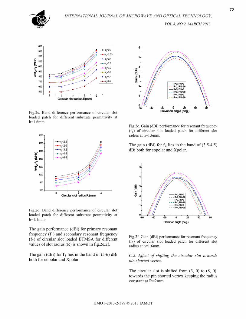
0 1 2 3 4
500
600
700
800
900
1000
1100
1200
1300
1400
f=f 2
-f1
(MH
z)
Circular slot radius R(mm)
r=2.2
r=2.33
r=2.4
r=2.6
r=3.2
r=3.6
r=4.4
r=6.4
Fig.2c. Band difference performance of circular slot loaded patch for different substrate permittivity at h=1.6mm.
0 2 4600
800
1000
1200
1400
1600
1800
2000
f=f 2
-f 1 (M
Hz)
Circular slot radius,R (mm)
r=2.2
r=2.6
r=3.2
r=4.4
r=6.4
Fig.2d. Band difference performance of circular slot loaded patch for different substrate permittivity at h=1.1mm.
The gain performance (dBi) for primary resonant frequency (f1) and secondary resonant frequency (f2) of circular slot loaded ETMSA for different values of slot radius (R) is shown in fig.2e,2f.
The gain (dBi) for f1
-60 -40 -20 0 20 40 600
1
2
3
4
5
6
Gai
n (d
Bi)
Elevation angle (deg.)
R=2, Phi=0 R=2, Phi=90 R=3, Phi=0 R=3, Phi=90 R=4, Phi=0 R=4, Phi=90
lies in the band of (5-6) dBi both for copolar and Xpolar.
Fig.2e. Gain (dBi) performance for resonant frequency (f1) of circular slot loaded patch for different slot radius at h=1.6mm.
The gain (dBi) for f2
-60 -40 -20 0 20 40 600
1
2
3
4
5
Gai
n (d
Bi)
Elevation angle (deg.)
R=2,Phi=0 R=2,Phi=90 R=3,Phi=0 R=3,Phi=90 R=4,Phi=0 R=4,Phi=90
lies in the band of (3.5-4.5) dBi both for copolar and Xpolar.
Fig.2f. Gain (dBi) performance for resonant frequency (f2) of circular slot loaded patch for different slot radius at h=1.6mm.
C.2. Effect of shifting the circular slot towards pin shorted vertex.
The circular slot is shifted from (3, 0) to (8, 0), towards the pin shorted vertex keeping the radius constant at R=2mm.
INTERNATIONAL JOURNAL OF MICROWAVE AND OPTICAL TECHNOLOGY,
VOL. , NO.2, MARCH 201
72
IJMOT-2013-2-399 © 2013 IAMOT

It is observed that the maximum resonance frequency gap (f2-f1) occurred when the circular slot centered at (6.5, 0) and r=2.2. The effect is also shown for r=2.2, r=2.6, r=4.4 as shown in table2 and fig.3c.
Table 2: Resonant frequencies (f1 & f2
Slot Position
) for different position (D) of circular slot.
r=2.2 r=2.6 r=4.4
D=3mm f 4.7351
4.39 3.43
f 5.5972 5.17 4.03
D=4mm f 4.741
4.39 3.44
f 5.622 5.2 4.04
D=5mm f 4.7514.39 3.43
f 5.6425.21 4.042
D=6mm f 4.751
4.39 3.43
f 5.642
5.22 4.06
D=6.5mm f 4.751
4.39 3.44
f 5.652 5.22 4.069
D=7mm f 4.751
4.39 3.43
f 5.652 5.218 4.06
D=8mm f 4.731
4.39 3.43
f 5.632
5.2 4.04
Fig.3a. Triangular patch with different position (D) of circular slot of radius (R) =2mm.
From fig.3b it should be noted that, though position of primary resonant frequency is fixed, the position of secondary resonant frequency is changing with varying the position of circular slot. This ultimately contributes to the nonlinearity in the frequency differences between two resonant frequencies.
From fig.3c and 3d it is clear that the resonant frequency gap (f2-f1) first increases till D=6.5mm and then decreases. It is maximum at D=6.5mm. Also it is noticed that the rate of change of (f2-f1)is greater for low permittivity ( r=2.2) as
r=2.6 r
4.5 5.0 5.5 6.0-30
-25
-20
-15
-10
-5
S11
(dB
)
Frequency (GHz)
D=3mm D=4mm D=5mm D=6mm D=6.5mm D=7mm D=8mm
=4.4).
Fig.3b. Return loss performance of circular slot loaded patch at r=2.2 and h=1.6.
INTERNATIONAL JOURNAL OF MICROWAVE AND OPTICAL TECHNOLOGY,
VOL. , NO.2, MARCH 201
73
IJMOT-2013-2-399 © 2013 IAMOT

3 4 5 6 7 8
600
650
700
750
800
850
900
Freq
uenc
y ga
p (f 2
-f 1) (
GH
z)
Different slot position (D in mm)
r=2.2
r=2.6
r=4.4
Fig.3c. Band difference performance of circular slot loaded patch for different substrate permittivity at h=1.6mm.
2.0 2.5 3.0 3.5 4.0 4.5
600
650
700
750
800
850
900
950
Freq
uenc
y di
ffer
ence
(f2-
f 1) (G
Hz)
Substrate permittivity r)
D=3mm D=4mm D=5mm D=6mm D=6.5mm D=7mm D=8mm
Fig.3d. Band difference performance of circular slot loaded patch for different substrate permittivity at h=1.6mm
The gain performance (dBi) for primary resonant frequency (f1) and secondary resonant frequency (f2) of circular slot loaded ETMSA for different values of slot position (D) is shown in fig.3e,3f.
The gain (dBi) for f1
-60 -40 -20 0 20 40 600
1
2
3
4
5
6
Gai
n (d
Bi)
Elevation angle (deg.)
D=3,phi=0 D=3,phi=90 D=4,phi=0 D=4,phi=90 D=5,phi=0 D=5,phi=90 D=6,phi=0 D=6,phi=90 D=6.5,phi=0 D=6.5,phi=90 D=7,phi=0 D=7,phi=90 D=8,phi=0 D=8,phi=90
lies in the band of (5-5.5) dBi both for copolar and Xpolar.
Fig.3e. Gain (dBi) performance for resonant frequency (f1) of circular slot loaded patch for different slot position at h=1.6mm.
The gain (dBi) for f2
-60 -40 -20 0 20 40 600.0
0.5
1.0
1.5
2.0
2.5
3.0
3.5
4.0
4.5
Gai
n (d
Bi)
Elevation angle (deg.)
D=3,phi=0 D=3,phi=90 D=4,phi=0 D=4,phi=90 D=5,phi=0 D=5,phi=90 D=6,phi=0 D=6,phi=90 D=6.5,phi=0 D=6.5,phi=90 D=7,phi=0 D=7,phi=90 D=8,phi=0 D=8,phi=90
lies in the band of (3.8-4.6) dBi both for copolar and Xpolar.
Fig.3f. Gain (dBi) performance for resonant frequency (f2) of circular slot loaded patch for different slot position at h=1.6mm.
D. Effect of triangular slot loading.
INTERNATIONAL JOURNAL OF MICROWAVE AND OPTICAL TECHNOLOGY,
VOL. , NO.2, MARCH 201
74
IJMOT-2013-2-399 © 2013 IAMOT

Three different types of triangular slots are inserted on ETMSA between probe feed and pin shorted vertex as shown in fig.4a.
Fig.4a. Triangular patch with different position (D) of circular slot of radius (R) =2mm.
The parameters of different slots are shown in table 3(i).
Table 3(i): Parameters of different slots.
Slots A (mm) H (mm)Slot-3 10.4 9Slot-2 6.9 6Slot-1 5.2 4.5
The resonant frequencies (f1 & f2) for different slots loading at different substrate permittivity ( r) for substrate height (h) =1.6mm and 1.1mm is shown in table 3(ii).
Table 3(ii): Resonant frequencies (f1 & f2
h
) for different triangular slot.
Slotsr f f1 2
A H
1.6
2.2 5.2 4.5 4.75 5.626.9 6 4.75 5.6910.4 9 4.75 5.93
2.6 5.2 4.5 4.391 5.2026.9 6 4.408 5.25710.4 9 4.41 5.49
4.45.2 4.5 3.435 4.048
6.9 6 3.435 4.102
10.4 9 3.452 4.283
1.1
2.25.2 4.5 4.77 5.656.9 6 4.788 5.73
10.4 9 4.79 6.03
2.65.2 4.5 4.43 5.22
6.9 6 4.427 5.29310.4 9 4.427 5.58
4.45.2 4.5 3.45 4.07
6.9 6 3.45 4.14
10.4 9 3.47 4.36
From fig.4b it can be shown that the band gap variation rate is less for high substrate permittivity ( r=6.4) as compared with low substrate permittivity ( r=2.2). Same type of characteristics is encountered when the substrate height (h) =1.1mm, though it has more non-linearity, as in case for circular slots.
The gain performance (dBi) for primary resonantfrequency (f1) and secondary resonant frequency (f2) of triangular slot loaded ETMSA for different substrate h r)shown in fig.4c,4d.
The gain (dBi) for f1 and f2
Slot-1 Slot-2 Slot-3
0.60
0.65
0.70
0.75
0.80
0.85
0.90
0.95
1.00
1.05
1.10
1.15
1.20
1.25
Different slots
Freq
uenc
y di
ffer
ence
(f2-
f 1) (G
Hz)
r=2.2,h=1.1
r=2.6,h=1.1
r=4.4,h=1.1
r=2.2,h=1.6
r=2.6,h=1.6
r=4.4,h=1.6
lies in the band of (5.5-6) dBi and (4.5-5) dBi respectively, both for copolar and Xpolar for h=1.1mm. Gain is slightly lower when h=1.6mm.
INTERNATIONAL JOURNAL OF MICROWAVE AND OPTICAL TECHNOLOGY,
VOL. , NO.2, MARCH 201
75
IJMOT-2013-2-399 © 2013 IAMOT

Fig.4b. Band difference performance of triangular slot loaded patch for different substrate permittivity at h=1.6mm.
Slot-1-f1 Slot-2-f1 Slot-3-f13.0
3.5
4.0
4.5
5.0
5.5
6.0
h=1.1, r=2.2
h=1.1, r=2.6
h=1.1, r=4.4
h=1.6, r=2.2
h=1.6, r=2.6
h=1.6, r=4.4
Gai
n (dB
i)
Different slots.
Fig.4c. Gain (dBi) performance for resonant frequency (f1) of triangular slot loaded patch for different substrate height (h) and permittivity ( r
Slot-1-f2 Slot-2-f2 Slot-3-f21.5
2.0
2.5
3.0
3.5
4.0
4.5
h=1.1, r=2.2
h=1.1, r=2.6
h=1.1, r=4.4
h=1.6, r=2.2
h=1.6, r=2.6
h=1.6, r=4.4
Gai
n (d
Bi)
Different slots
).
Fig.4d. Gain (dBi) performance for resonant frequency (f1) of triangular slot loaded patch for different substrate height (h) and permittivity ( r
Different aspect of equilateral triangular microstrip antenna (ETMSA) has been studied
and special attention is given on the performance enhancement of ETMSA including the reduction of size of patch. It is observed that the two pin shorting effect produces dual resonant frequencies with circular polarization (CP). Inserting a circular slot between probe feed and pin shorted vertex with radius (R) of 4mm centered at (5, 0) shows highest value of gain (dBi) for both resonant frequencies. Also it shows highest band gap of about 1.35GHz at
).
III. CONCLUSION
r=2.2. It is shown that decreasing the substrate height (h) to 1.1mm enhances the band gap performance. It is noted to be 1.9GHz for slot radius (R) =4mm at r=2.2. Inserting a triangular slot between probe feed and pin shorted vertex results in highest gain (dBi) of 5.75dBi for f1 and 4.625dBi for f2 when substrate height (h) is 1.1mm. So gain (dBi) can be increased by decreasing the substrate height. For h=1.6mm gain (dBi) is 5.325dBi for f1 and 4dBi for f2
[6] J. S. Dahele and K. F. Lee, “On the resonant frequencies of the triangular patch antenna” IEEE
.
ACKNOWLEDGMENT
The authors would like to thanks Principal andH.O.D, Electronics and Communication Engineering Department of MCKV Institute of Engineering, Howrah, West Bengal for their support and encouragements, and for giventesting and development facility for this work.
REFERENCES
[1] K. L. Wong and W. S. Chen, “Compact microstrip antenna with dual frequency operation,” Electron. Letter, vol. 33, pp. 646–647, Apr. 1997.
[2]. Ayd³n, E., \Computation of a tunable-slot loaded equilateral triangular microstrip antenna," Journal of Electromagnetic Waves and Applications, Vol. 23, Nos. 14{15, 2001{2009, 2009.
[3]. Pan, S. C. and K. L. Wong, Design of dual-frequency microstrip antennas with a shorting pinloading," Antennas and Propagation Society International Symposium, Vol. 1, 312{315, 1998.
[4]. Wong, K. L. and S. C. Pan ,”Compact triangular microstrip antenna," Electronics Letters Vol. 33, No. 6, 433{434, 1997.
[5] Row, J.-S. and K.-W. Lin, “Low-profile design of dual frequency and dual polarized triangularmicrostrip antennas.", Electronics Letters, Vol. 40, No. 3, 156{157, Feb. 5, 2004.
INTERNATIONAL JOURNAL OF MICROWAVE AND OPTICAL TECHNOLOGY,
VOL. , NO.2, MARCH 201
76
IJMOT-2013-2-399 © 2013 IAMOT

Trans. Antennas Propagation, vol. AP-35, pp. 100-101, Jan. 1987.
[7]. R. Garg & S. A. Long, “An Improved Formula for the Resonant Frequencies of the Triangular Microstrip Patch Antenna”, IEEE Trans. Vol. AP-36, 570, 1988.
[8] Zeland Software Inc. IE3D: MoM-Based EM Simulator. http://www.zeland.com.
INTERNATIONAL JOURNAL OF MICROWAVE AND OPTICAL TECHNOLOGY,
VOL. , NO.2, MARCH 201
77
IJMOT-2013-2-399 © 2013 IAMOT

A Wing Stub Circular Microstrip Patch Antenna
(WSCMPA) with Stable Return Loss and Radiation Pattern
M.A.Sulaiman, M.T.Ali, I. Pasya
Faculty of Electrical Engineering Universiti Teknologi MARA Malaysia 40450 Shah Alam, Selangor, Malaysia
Tel: +6012-3263010; E-mail: [email protected], [email protected], [email protected]
Abstract-A novel compact designed for Wing Stub
Circular Microstrip Patch Antenna (WSCMPA)
with stable return loss and radiation pattern is
presented in this paper. There are 3 structures of
UWB antenna which bandwidth ranging from 3.37
GHz to 10.44 GHz was presented. The
conventional method in achieving a UWB
compatible microstrip antenna is the utilization of
circular monopole topology with a partial ground
plane. However these structures produced unstable
return loss and radiation pattern over the
radiating frequency. Open stubs are added in the
second design to further improve the antenna
return loss characteristics. Furthermore, a wing
stub is introduced to induce enhanced return loss
characteristics and a stable radiation pattern in the
last design. All the antennas were designed on
Rogers 5880 printed circuit board (PCB) with
overall size of 26 × 40 × 0.787 mm3
and dielectric
r = 2.2. The performance of the
designed antenna was analyzed in terms of
bandwidth, gain, return loss, radiation pattern,
group delay, and verified through actual
measurement of the fabricated antenna.
Index Terms- Microstrip Antenna, Partial Ground
Plane, Stable Return Loss, Stub Loaded, UWB
I. INTRODUCTION
In 2002, the Federal Communication Commission (FCC) of the United States [1] was authorized of its unlicensed operation of frequency band from 3.1GHz to 10.6GHz for indoor wireless communications. With the development of the Ultra Wideband (UWB) technology, UWB antennas have been studied intensively for communications and radar system.
The uniqueness of UWB antenna that differsfrom the conventional antenna is the ability to transmit large amounts of digital data with very short pulses (in nanosecond or less) over a wide spectrum of frequency bands with very low power utilization. In order to run a stable antenna with a compact, portable system, radiation efficient, lower return loss at the desired frequency, a stable omni-directional printed antenna are desired. There are many different techniques were proposed to satisfy these requirements within UWB bandwidth. Large slot techniques are used in [2] to get a bandwidth enhancement and for the size reduction they usedan L- or T-shaped bending. Wide aperture technique created multiple resonances that modified the microstrip feed [3]. A rotated slot was proposed in [4], where a microstrip feed line excited the two modes of a closed resonance. Another technique using a tapered slot feeding structure was proposed to transform the guided wave to free space wave without causing any reflection to the structure [5-6].Recent studies of UWB antenna structures arespecifically focused on the design rules and optimization technique [7-10]. The antenna was designed and fabricated on microstrip structure.The advantages of printed microstrip antenna are listed in [11-12], however, microstrip antennas also have several disadvantages [12-13].
The above mentioned techniques were developed to obtain wider effective bandwidth. However, a stable radiation pattern throughout the UWB frequency band is critical in some application.Some of the advantages are; in obtaining an
INTERNATIONAL JOURNAL OF MICROWAVE AND OPTICAL TECHNOLOGY,
VOL. , NO.2, MARCH 201
78
IJMOT-2013-3-414 © 2013 IAMOT

V
8
=
=
88787
7 7
INTERNATIONAL JOURNAL OF MICROWAVE AND OPTICAL TECHNOLOGY,
VOL. , NO.2, MARCH 201
79
IJMOT-2013-3-414 © 2013 IAMOT

8 8
8 8
7
88787
V
INTERNATIONAL JOURNAL OF MICROWAVE AND OPTICAL TECHNOLOGY,
VOL. , NO.2, MARCH 201
80
IJMOT-2013-3-414 © 2013 IAMOT

= 0 = 0= 0= 0 = 8 == = 0 = 8= = =
= = = 0
Parameter LabelDesign 1 (mm)
Design 2 (mm)
Design 3 (mm)
Patch Radius Rp 8 7.76 7.76
Feedline Width
Wf 1.46 2.28 2.48
Feedline Length
Lf 16 13.2 13.2
Step Width Wstep - 1.5 1.7
Step Length Lstep - 5 5.3
GroundWidth
Wg 32 31.16 26
GroundLength
Lg 16 18 18
Block Length1
Lb1 - 20 24
Block Length2
Lb2 - 20 22
Block Length3
Lb3 - - 20
Block Width Wb - 2 2
Block Spacing
Bs - 1 0.5
Substrate Width
Ws 32 31.16 26
Substrate Length
Ls 32 40 40
Substrate Thickness
h 0.8 0.787 0.787
Dielectric constant rs 4.7 2.2 2.2
SMA Impedance
50 50 50
A. Return loss, S11
7
V8
R A A R A R A A A ,
. , . , AR 1
81
IJMOT-2013-3-414 © 2013 IAMOT
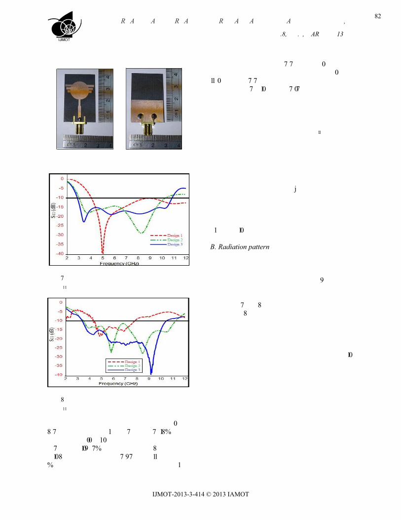
711
811
08 7 1 7 7 18%
00 107 109 7% 8108 7 97 11
% 1
7 7 00
11 0 7 77 10 7 07
11
j
1 10
B. Radiation pattern
9
7 88
10
R A A R A R A A A ,
. , . , AR 1
82
IJMOT-2013-3-414 © 2013 IAMOT

C. Group Delay
11
10
7
8
9 80 0
10
2
Frequency (GHz)
Main Lobe Magnitude (dB)
Design 1 Design 2 Design 3
3 1.7 2.4 2.4
4 2 3 2.9
5 2.5 3.7 3.7
6 2.8 3.4 4.1
7 2.7 2.3 3.2
8 1.3 1.4 2.3
Frequency (GHz)
Main Lobe Direction (angle)
3 180o
180o
180o
4 180o
180o
180o
R A A R A CR A A D CA C G ,
. , . , ARC 1
83
IJMOT-2013-3-414 © 2013 IAMOT
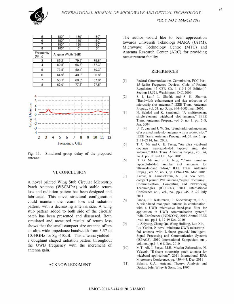
5 180o
180o
180o
6 180o
180o
180o
7 180o
180o
180o
8 180o
0o
0o
Frequency (GHz)
Angular Width (3dB)
3 85.2o
79.6o
79.8o
4 80.5o
66.8o
67.3o
5 73.5o
50.4o
50.3o
6 64.9o
40.0o
36.8o
7 56.1o
60.6o
67.6o
8 62.0o
77.3o
97.5o
Fig. 11. Simulated group delay of the proposed antenna.
VI. CONCLUSION
A novel printed Wing Stub Circular Microstrip Patch Antenna (WSCMPA) with stable return loss and radiation pattern has been designed and fabricated. This novel structural configuration could maintain the return loss and radiation pattern, with a decreasing antenna size. A wing stub pattern added to both side of the circular patch has been presented and discussed. Both simulated and measured results of return loss shows that the small compact size antenna offers an ultra wide impedance bandwidth from 3.37 to 10.44GHz for S11 <-10dB. This antenna yielded a doughnut shaped radiation pattern throughout the UWB frequency with the increment of antenna gain.
ACKNOWLEDGMENT
The author would like to bear appreciation towards Universiti Teknologi MARA (UiTM), Microwave Technology Centre (MTC) and Antenna Research Center (ARC) for providing measurement facility.
REFERENCES
[1] Federal Communications Commission, "FCC Part 15 Radio Frequency Devices, Code of Federal Regulation 47 CFR Ch. 1 (10-1-09 Edition)", Section 15.521, Washington, D.C, 2009.
[2] S. I. Latif, L. Shafai, and S. K. Sharma,
Propag., vol. 53, no. 3, pp. 994 1003, mar. 2005.[3] multiresonant
single-Trans. Antennas Propag., vol. 3, no. 1, pp. 5 8,Jan. 2004.
[4]of a printed wide-IEEE Trans. Antennas Propag., vol. 53, no. 6, pp. 2111 2114, Jun. 2005.
[5] coplanar waveguide-fed tapered ring slot
no. 4, pp. 1105 1111, Apr. 2006.[6] ture
tapered-slot-fed annular slot antennas for ultrawide-Propag., vol. 53, no. 3, pp. 1194 1202, Mar. 2005.
[7] Kumar, K. Gunasekaran, N. , "A new novel compact planar UWB antenna," Signal Processing, Communication, Computing and Networking Technologies (ICSCCN), 2011 International Conference on , vol., no., pp.41-45, 21-22 July 2011
[8] Panda, J.R. Kakumanu, P. Kshetrimayum, R.S. , "A wide-band monopole antenna in combination with a UWB microwave band-pass filter for application in UWB communication system," India Conference (INDICON), 2010 Annual IEEE , vol., no., pp.1-4, 17-19 Dec. 2010
[9] Li Zhiyong, Zhang Qian, Wang Huilong, Luo Xin, Liu Yunlin, "A novel miniature UWB microstrip-fed antenna with L-shape ground," Intelligent Signal Processing and Communication Systems (ISPACS), 2010 International Symposium on , vol., no., pp.1-4, 6-8 Dec. 2010
[10] M.T. Ali, I. Pasya, M.H. Mazlan Zaharuddin, N. -shape microstrip patch antenna for
International RF& Microwave Conference, pg. 439-443, Dec. 2011
[11] Balanis, C.A., Antenna Theory: Analysis and Design, John Wiley & Sons, Inc, 1997.
INTERNATIONAL JOURNAL OF MICROWAVE AND OPTICAL TECHNOLOGY,
VOL. , NO.2, MARCH 201
84
IJMOT-2013-3-414 © 2013 IAMOT

122003
13
200114
4 3 1 3 92010
1
24 2 2007 8991
1 ; ; ;
10302 30 2011
INTERNATIONAL JOURNAL OF MICROWAVE AND OPTICAL TECHNOLOGY,
VOL. , NO.2, MARCH 201
85
IJMOT-2013-3-414 © 2013 IAMOT

2-GHz Dual Diode Dipole Rectenna For Wireless Power
Transmission
Shailendra Singh Ojha1*, P.K. Singhal2, Anshul Agarwal3, Akhilesh Kumar Gupta4
1,2,3,4Department of Electronics, Madhav Institute of technology and Science Gwalior, IndiaE-mail: ssojha20@gmail. com
Abstract- This paper presents the rectenna design
at 2 GHz for wireless microwave power
transmission and analysis using various schottky
diodes used for rectifier purpose. Proposed
rectenna is a combination of dipole antenna,
followed by 3rd
order stepped impedance Low Pass
Filter and rectifier essential for high microwave
power DC power (RF-DC) conversion efficiency.
Maximum efficiency of around 82 % is
accomplished by MA4E1317 diode which use as a
anti parallel dual detector series configuration by
.
Index Terms- Dipole, Detectors, Rectenna, Power
Conversion, Wireless Power transmission (WPT),
Low Pass Filter (LPF).
I. INTRODUCTION
Wireless power transmission is an important issue since it has broad technology impact in many areas which require electrical batteries such as mobile phones, MP3, toys, computer peripheral devices, remote monitoring units, medical devices, electric cars, satellites and so on [1]. The key component for this type of wireless power transfer is the rectenna. A rectenna is a combination of a rectifying circuit and an antenna. The antenna receives the electromagnetic power and the rectifying circuit converts it to electric power [2]. Rectennaoperating at mm-wave frequencies have the advantages of compact size and overall higher system efficiency for long distance transmission. The rectifying circuit consists of schottky diode,DC pass filter (smoothing capacitor) and load resistance. There are many type of rectennas such as dipole, patch, monopole rectenna. These types of rectenna have been reviewed in terms of
power conversion efficiency, flexibility and fabrication requirements [3-5].
Dipole rectenna [2] was designed on a flexible cellulose membrane having efficiency of 56 %using MA4E2054-1141T schottky diode as rectifier. In this paper, rectenna is made on PCB and having much higher efficiency as compare to above and this rectenna is analysed using various diodes. Various antennas used in [3-5] having low radiation efficiency as compared to the dipole antenna designed in this paper.
The rectenna element shown in Figure 1 consists dipole antenna, 3rd order stepped impedance low pass filter, two rectifying diode for RF-to-DC conversion and a load resistance (RL In rectenna design, the harmonic problem arises due to the radiation of unwanted harmonics which decreases the efficiency of the system. When RF power is received by a rectenna, a nonlinear Schottky barrier diode produces direct current (dc) output and harmonics of the fundamental frequency of the incoming energy. These harmonics leak through the antenna at its high-order resonant modes to the air, causing electromagnetic interference (EMI) problems and reducing the efficiency of the rectifier during process of rectification, harmonics are generated[6]. These harmonics are reradiated back through antenna. Thus significant energy is lost. To suppress re-radiation and to maximize the power conversion, low pass filter is placed between antenna and rectifier setup. The cut-off frequency for low Pass Filter has been selected such that second order and higher order harmonics signals are rejected. After the filter, matching circuit is put which provide the impedance matching between the low pass filter and antennas input
INTERNATIONAL JOURNAL OF MICROWAVE AND OPTICAL TECHNOLOGY,
VOL. , NO.2, MARCH 201
86
IJMOT-2013-4-425 © 2013 IAMOT

impedance by which rectifier setup provides the maximum conversion, i.e. maximum power transmission. After this match circuit the rectifying diode is placed for rectification followed by DC pass filter which consists of capacitor for reducing ripples also called smoothing capacitor followed by load. The conversion efficiency depends on this DC pass filter set up i.e. its value and position [7].
For testing the design, rectenna total efficiency and conversion efficiency are given by equation (1) and (2), [7]The total efficiency is
(1)
and conversion efficiency is defined by
c (2)
To design the printed rectenna, CST Microwave Studio software [8] is used to design the dipole antenna, low pass filter, match circuit. Computer Simulation Technology (CST) MICROWAVE STUDIO is a fully featured software package for electromagnetic analysis and design in the high frequency range. The software contains four different simulation techniques (transient solver, frequency domain solver, Eigen mode solver, modal analysis solver) which best fit their particular applications. The most flexible tool is the transient solver, which can obtain the entire broadband frequency behaviour of the simulated device. The properties of the antenna such as return loss S11 and Gain are determined with the help of CST Software.
Figure1: Rectenna block diagram
II. RECTENNA ELEMETS THEORY OF OPERATION
Figure 1 shows the main components of the rectenna element. A Dipole antenna is attached to a low-pass filter, which rejects higher order diode harmonics from radiating through the dipole antenna and a matching circuit is placed between the low pass filer and rectifier for good matching which ensures the maximum power transmission. Two anti-parallel Schottky diodes are used for the rectifier as shown in figure 2.
The DC pass filter effectively shorts the RF energy and passes the dc power and gives better results consist of a capacitor. The distance between the diode and output capacitor is used to resonate the capacitive reactance of the diode [7]. Both input and output filters are used to store RF energy during the off period of the diode. A resistor is then placed across the output terminals to act as the load for measuring the output dc power.
INTERNATIONAL JOURNAL OF MICROWAVE AND OPTICAL TECHNOLOGY,
VOL. , NO.2, MARCH 201
87
IJMOT-2013-4-425 © 2013 IAMOT

Figure 2: Series rectenna configurations with impedance matching network [6].
The rectenna conversion efficiency depends on the diode electrical parameters and the value ofcapacitor selected as well as its distance from diode and load [7], it also depends on time for which rectification occurs i.e. if we use one diode it gives less efficiency and two anti parallel diodes give better efficiency as shown in figure 2.
Figure 3: Front view of Rectenna element printed on glassy epoxy (FR-4 lossy) substrate.
Figure 4: Top view of rectenna
III.RECTENNA ELEMENTS DESIGN
The 2-GHz printed rectenna element developed is shown in Figure 3-4. Figure 3 shows the frontview of rectenna and figure 4 shows the top view of rectenna. The rectenna circuit is printed on a FR4 substrate of 1.6 mm thickness and refractive index of r=4.3.
The dipole antenna [9] is made up of copper wire having 67 mm length and 4 mm diameter. The return loss of proposed design is shown in figure 5 having bandwidth of 450 MHz and efficiency of 99.5%. Radiation pattern of dipole antenna at 2- GHz is shown in figure 6 having main lobe magnitude 2.6 dB, main lobe direction 56.0 degree, and 3- dB angular width of 74.1 degree.
INTERNATIONAL JOURNAL OF MICROWAVE AND OPTICAL TECHNOLOGY,
VOL. , NO.2, MARCH 201
88
IJMOT-2013-4-425 © 2013 IAMOT

Figure 5: simulated return loss for dipole antenna.
Figure 6: Radiation pattern of dipole antenna.
One end of dipole antenna feed directly into a low pass filter. LPF rejects the higher order harmonics produced by the diode. The Stepped impedance low-pass filters geometry is used for low pass filter design [10-11]. The response of 2 GHz LPF is shown in figure 7. It is clear fromfigure that this structure will rejects the higher order harmonics.
Figure 7: S-parameters result of LPF
After the LPF, a matching circuit is placed which provides the matching between the LPF and input impedance of diode to reduce the reflections, and increase the efficiency [7].Various schottky diodes are used for the rectifying device having different junction capacitance and series resistance as shown in table 1.
Table 1.various schottky diodes.
S. NO. DIODE CJ(PF) RS
1 MZBD9161 0.035 20
2 MA40150-119 0.12 8
3 MA4E1317 0.02 4
A 1.2 pF chip capacitor is used for the DC pass filter which effectively shorts the RF energy and pass the dc power to a resistive load. The load resistance as well as distance between the capacitor and diode play important role in the rectifier efficiency. For this set up three diodes are used and maximum efficiency is achieved for different diodes with different loads.
INTERNATIONAL JOURNAL OF MICROWAVE AND OPTICAL TECHNOLOGY,
VOL. , NO.2, MARCH 201
89
IJMOT-2013-4-425 © 2013 IAMOT

IV. RESULT
Figure 8 shows the simulated return loss of the proposed rectenna using various diodes. For comparison point of view, the response of rectenna with MA4E1317, MZBD9161 and MA40150-119 schottky diode is -57 dB, -60dBand -65 dB respectively at 2 GHz it is quite similar to the results of previous paper [7].
Figure 8: Simulated Return loss for Rectenna using various diodes
Figure 9 shows the variation on efficiency with different resistive load and MZBD9161 schottky diode. The maximum efficiency of 60% is achieved at 2 GHz frequency when the load
Figure 10 shows the variation on efficiency with different resistive load and MA40150-119schottky diode. The maximum efficiency of 70 % is obtained at 2 GHz when the load resistance of
Figure 9: Comparison of efficiency at different resistive loads with MZBD9161 diode.
Figure 10: Comparison of efficiency at different loads with MA40150-113 diode.
Figure 11 shows the variation of efficiency with different resistive load and and MA4E1317 schottky diode. The maximum efficiency of 82% is obtained at 2 GHz when the load resistance of
. Above results are similar to the
INTERNATIONAL JOURNAL OF MICROWAVE AND OPTICAL TECHNOLOGY,
VOL. , NO.2, MARCH 201
90
IJMOT-2013-4-425 © 2013 IAMOT

previous paper [7] but here achieved much better efficiency, bandwidth and return loss using anti parallel dual diode detector configuration.
Figure 11: Comparison of efficiency at different loads with MA4E 1317 diode.
Figure 12: Comparison of efficiency with different diodes at optimum resistive load.
Figure 12 shows the variation on efficiency with different diode. These efficiencies are obtained at optimum loads and optimum loads are different for each diode.
Figure 13: comparison of gain with differentdiodes.
For frequency up to 3 GHz, the rectenna gain is analysed with different diodes is shown in figure 13. The antenna gain is increases up to 2 GHz and after that its decreases on increment in frequencies. The maximum rectenna gain with is 2.5 dB, 3 dB and 3.5 dB with MZBD9161,MA40150-119 and MA4E1317 at a frequency of 2-GHz with optimum loads.
V. CONCLUSION
A proposed rectenna has been developed which has the highest efficiency of 82% and gain of 3.5 dB at 2- GHz with the loaand MA4E1317 diode is used as rectifier. It is investigated that as the junction capacitance of rectifying diode decreases, better efficiency is obtained.
VI. REFRENCES
[1] Low Z.N., Chinga Design and test of a highpower high-efficiency loosely
INTERNATIONAL JOURNAL OF MICROWAVE AND OPTICAL TECHNOLOGY,
VOL. , NO.2, MARCH 201
91
IJMOT-2013-4-425 © 2013 IAMOT

coupled planar wireless powertransfer IEEE Trans. Ind. Electron., 2009, 56, pp. 1801 1811
[2] Wireless power transmission
using dipole rectennas made on flexible cellulose
membrane
Vol. 6, Iss. 7, pp. 756 760.[3] Park, Y.H., Yo A
study on the analysis of rectenna efficiency for . IEEE TENCON 99,
Proc. IEEE Region 10 Conf., South Korea, 1999, vol. 2, pp. 1423 1426
[4] 5.8 GHz circularly polarized dual-diode rectenna and rectenna array for microwave
, IEEE Trans. Microw. Theory Tech., 2006, 54, (4), pp. 1495 1502
[5] G. Monti*, F. Congedo, D. De Donno, and L. Tarricone Monopole-based Rectenna for Microwave Energ Progress
In Electromagnetics Research C, Vol. 31, 109-121,
2012
[6] Fu-Jhuan Huang, Tzong-Chee Yo, Chien-Ming Lee, and Ching-Hsing Luo, Design of CircularsPolarization Antenna With Harmonic Suppression for Rectenna ApplicatPropagation Letters, vol. 11, 2012
[7] Shailendra Singh Ojha, P.K. Singhal, Anshul -GHz Rectenna For
Engineering, Science and Technology (CREST) Journals [ ISSN 2320-706X ], Vol 01 , Issue 01 , 24-29March 2013.
[8] CST microwave studio software 2010.[9] nd edition
2011.[10] Jia-Sheng Hong, M. J. Lancaster,
2001 John Wiley &Sons, Inc.
[11] rd edition 2010.
INTERNATIONAL JOURNAL OF MICROWAVE AND OPTICAL TECHNOLOGY,
VOL. , NO.2, MARCH 201
92
IJMOT-2013-4-425 © 2013 IAMOT

Compact Multi-BResonator Patch
Information Systems and Abdelmalek
E-mail:
Abstract-In this paper, a comsquare complementary split antenna is presented. The antecompact (35mm × 35mm × 1.6mcan be integrated easily withicircuits in mobile handsets. operating at 2.4GHz (WiFi), 3.5UWB band respecting the Communications Commission (FCfor the unlicensed use of UWB range from 3.1 to 10.6 GHz, rangup to 9.1GHz and in two other first one ranging from 10.9 GHzand the second one ranging from17.8GHz. The gain and pattern plare included in the paper.
Index Terms- Compact, ComplemResonator (CSRR), Meta-Mateantenna.
I. INTRODUCTIO
Small-size multi-band microstri(MPA) have attracted much attelast two decades due to the dramobile and wireless communimarket. Most techniques propothe size of MPA are reported eliterature and are based mainlytechniques such as: capacitive lothe chip capacitor is used to resize [2], LC resonator [3], mean[4], and reactive loading [5,achieved through etched slots element. However, these techniqoff the antenna bandwidth anachieve the size reduction. Mfractal antennas have been promulti-band operation [7, 8]. Ho
Band Square ComplementarAntenna For Wireless Com
Iman Ben Issa and Mohamed Essaaidi
Telecommunications Laboratory, Electronics and MicEssaadi University, Faculty of Science, Tetuan, [email protected] ; [email protected]
mpact multi-band ring resonator
enna size is very mm), and thus, it in RF front-end The antenna is
5 (WiMAX), in a U.S. Federal
CC) requirements in the frequency
ging from 7.7GHz large bands, the
z up to 11.5 GHz, m 17.2GHz up to lots of the antenna
mentary Split Ring erial, Multi-band
ON
p patch antennas ention during the amatic growth in ications handsets osed for reducing extensively in the y on the use of oading [1], where duce the antenna der configuration 6], which are in the radiating
ques usually trade nd efficiency to
Moreover, several oposed to obtain owever, different
other techniques [9] hachieve multiband MPhave been extensively pusuch as adding parasitic eadditional resonant frequradiating elements sharedground [11, 12]. Theseincrease the physical sizdesired multiband perfthere is another tradeoffoperating frequency bandThe square complementantenna has very good and multiband charactpermittivity complement(CSRR), which is a dualresonator (SRR) originall[13], has been loaded inis composed of two concwith slits etched in each rApart from double negnegative materials whereparameters has a negativinteresting properties andnovel devices. In particusplit ring resonator (CSRnegative-permittivity at rexample of a single negcan be used to make m[15]. The properties omanipulated to increasimprove filter rejection aantennas to reduce thincrease antenna gain anThis paper presents a comcomplementary split rinpatch antenna that cocommunication standardhas a compact size (i.e.
,
ry Split Ring munications
crowaves Group.occo
have been adopted to PA antennas and which ublished in the literature, elements [6, 10] to create uencies or adding more d with the same feed and e techniques inevitably ze in order to create the formance. Furthermore, between the number of
ds and antenna size.tary split ring resonator features like small size
teristics. A negative tary split ring resonator counterpart of split ring ly proposed by J. Pendry
nto the patch. The CSRR centric metallic ring slots ring at its opposite sides. gative materials, single
e only one of the material ve real value also possess d can be used to produce ular, the complementary RR) which establishes a resonant frequency, is an gative media (SNG) that microwave devices [14]-of SNG can also be se filter shape factor,
and can also be applied to he spurious effect and nd to reduce its size [16]. mpact multi-band square ng resonator microstrip overs several wireless s. The proposed antenna 35 mm x 35 mm x 1.6
INTERNATIONAL JOURNAL OF MICROWAVE AND OPTICAL TECHNOLOGY,
VOL. , NO.2, MARCH 201
93
IJMOT-2012-10-361 © 2013 IAMOT
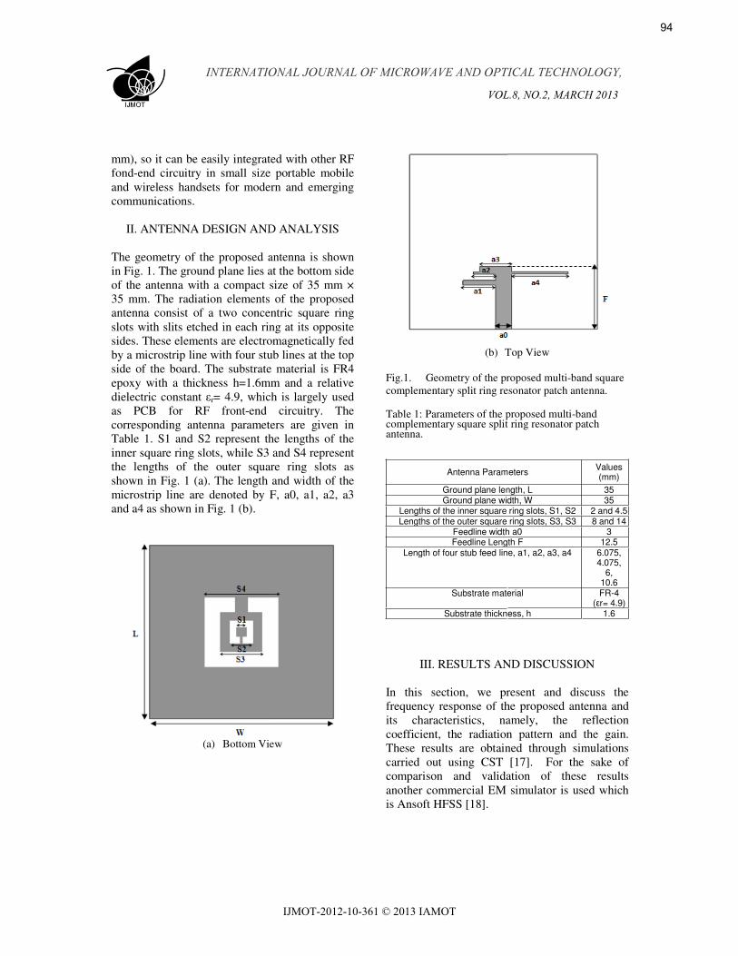
mm), so it can be easily integratfond-end circuitry in small sizeand wireless handsets for modecommunications.
II. ANTENNA DESIGN AND
The geometry of the proposed ain Fig. 1. The ground plane lies aof the antenna with a compact 35 mm. The radiation elementsantenna consist of a two conceslots with slits etched in each rinsides. These elements are electroby a microstrip line with four stuside of the board. The substrateepoxy with a thickness h=1.6mdielectric constant εr= 4.9, whicas PCB for RF front-end corresponding antenna parametTable 1. S1 and S2 represent thinner square ring slots, while S3 the lengths of the outer squashown in Fig. 1 (a). The length microstrip line are denoted by and a4 as shown in Fig. 1 (b).
(a) Bottom Vi
ted with other RF e portable mobile ern and emerging
D ANALYSIS
antenna is shown at the bottom side size of 35 mm ×
s of the proposed entric square ring ng at its opposite omagnetically fed ub lines at the top e material is FR4
mm and a relative ch is largely used
circuitry. The ters are given in he lengths of the and S4 represent
are ring slots as and width of the F, a0, a1, a2, a3
ew
(b) T
Fig.1. Geometry of the prcomplementary split ring re
Table 1: Parameters of the pcomplementary square splitantenna.
Antenna Param
Ground plane lenGround plane wid
Lengths of the inner square Lengths of the outer square
Feedline widthFeedline Leng
Length of four stub feed lin
Substrate mate
Substrate thickn
III. RESULTS AN
In this section, we prfrequency response of thits characteristics, nacoefficient, the radiationThese results are obtaincarried out using CST comparison and validaanother commercial EM is Ansoft HFSS [18].
Top View
roposed multi-band square esonator patch antenna.
proposed multi-band t ring resonator patch
meters Values (mm)
ngth, L 35dth, W 35ring slots, S1, S2 2 and 4.5ring slots, S3, S3 8 and 14
h a0 3 th F 12.5e, a1, a2, a3, a4 6.075,
4.075, 6,
10.6 erial FR-4
(εr= 4.9)ess, h 1.6
ND DISCUSSION
resent and discuss the he proposed antenna and amely, the reflection n pattern and the gain. ned through simulations [17]. For the sake of
ation of these results simulator is used which
INTERNATIONAL JOURNAL OF MICROWAVE AND OPTICAL TECHNOLOGY,
VOL. , NO.2, MARCH 201
94
IJMOT-2012-10-361 © 2013 IAMOT

A. Reflection Coefficients
To get adequate information aboperation mechanics, the effectsfeed line parameters on antcoefficients are investigated firsthe parameters a1, a2, a3 aimpedance bandwidth are plottedFig. 2 (a) shows that when the pa3 and a4 are zero, the antenndifferent frequency bands loc(WIFI), 6.8 GHz, and at a wifrom 16.5 to 19 GHz. Fig. 2 (b)the stub a1, a2, a3, a4, in this operating at 2.4GHz (WiFi), 3.5and presents other three wide-ba7.8 to 9.1GHz, 10.9 to 11.5G17.8GHz. The first wide-band Federal Communications Comrequirements for the unlicensedthe frequency range from 3.1 toBased on the results presented inappears to give rise to other freqthe final prototype of the remultiband antenna is better optim
(a)
bout the antenna of the geometric tenna Reflection st. The effects ofand a4 on the d in Fig. 2(a)-(b). parameters a1, a2, na is operating at cated at 2.4GHz ide band ranging ) shows that with case the antenna
5GHz (WiMAX), ands ranging from Hz, and 17.2 to fulfills the U.S.
mmission (FCC) d use of UWB in o 10.6 GHz [19]. n Fig. 2, the stub
quency bands and esulting compact mized.
(b
Fig.2. The reflection comulti-band antenna (a) with
B. Radiation Patterns
Fig. 3 shows the simula2.4, 3.5, 8.4, 11.2, 17.5shown in Fig. 3(a) and 3is nearly omni-directionathe radiation pattern is bphi = 90°, as shown in radiation pattern is bi-dirthe radiation pattern is But for Fig. 3(d), 3(e) multidirectional.
C. Gain
Fig. 4 shows the gain of antenna throughout all bands. According to thethis antenna can be usedwireless communications
b)
oefficients of the proposed hout stub and (b) with stub.
ated radiation patterns at 5. In E-plane phi=0°, as 3(c), the radiation patternal. However, in Fig. 3(b) bi-directional. In E-plane
Fig. 3(a) and 3(c), the rectional and in Fig. 3(b) nearly omni-directional. the radiation pattern is
the proposed multi-band the available frequency e obtained gain values,
d for indoor and outdoor s.
INTERNATIONAL JOURNAL OF MICROWAVE AND OPTICAL TECHNOLOGY,
VOL. , NO.2, MARCH 201
95
IJMOT-2012-10-361 © 2013 IAMOT

(a)
(b)
(c)
(d
(e
Fig.3. Radiation pattern oantenna. E-plane at (a) 2.4GGHz, (d) 11.2GHz, (e) 17.5
d)
e)
of the proposed multi-band GHz, (b) 3.5GHz, (c) 8.4 5GHz.
INTERNATIONAL JOURNAL OF MICROWAVE AND OPTICAL TECHNOLOGY,
VOL. , NO.2, MARCH 201
96
IJMOT-2012-10-361 © 2013 IAMOT

(a)
(b)
(c)
(d
(e
Fig.4. Gain of the propos(a) 2.4, (b) 3.5, (c) 8.4, (d) 1frequency bands.
IV. CONC
This paper presents complementary split rinwireless communicationshas a compact size (35 mso it can be easily inte
d)
e)
sed multi-band antenna for 11.2, (e) 17.5 GHz
CLUSION
a multi-band square ng resonator antenna for s. The proposed antenna
mm x 35 mm x 1.6 mm), egrated within other RF
INTERNATIONAL JOURNAL OF MICROWAVE AND OPTICAL TECHNOLOGY,
VOL. , NO.2, MARCH 201
97
IJMOT-2012-10-361 © 2013 IAMOT

frond–end circuitry of mobilhandsets. Computer simulatiocommercial simulators, namely, HFSS have indicated that it can several frequency bands communication standards, nam(WiFi), 3.5GHz (WiMax), 7.8-and 10.9-11.5GHz, and 17.2-17bands. Furthermore, its gain useful for both indoor and ocommunications.
REFERENCES
[1] Rowell, C. R. and R. D. Muloaded PIFA for compacthandsets," IEEE Trans. Anten837-842, May 1997.
[2] C.-S. Hong, Small annulcapacitor loading, Electron L111.
[3] Lui, G. K. H. and R. D. Mufrequency PIFA designs usIEEE Trans. Antennas Prop1019, July 2001.
[4] Jung, M., Y. Kim, and B. Lmeandered PIFA for blueapplications," Proc. IEEE AnInt. Symp., Vol. 2, 958-961, Ju
[5] Deshpande, M. D. and M. C. stub loaded microstrip patcIEEE Antennas Propag. Soc.916-919, July 1997.
[6] Cho, Y. J., S. H. Hwang, and band internal antenna with amobile handsets and the chandset case and battery,Wireless Propag. Lett., Vol. 4
[7] R.V.H. Prasad, Y. PurushottaN. Ashok, Microstrip fractamulti-band communication, (2000), 1179–1180.
[8] Z. Du, K. Gong, J.S. Fu, andmicrostrip fractal patch antecommunication, Electron Lett
[9] Ciais, P., R. Staraj, G. Kossi“Compact internal multibandphone and WLAN standards,"40, 920-921, July 2004.
[10] Rowell, C., A. Mak, and C.between multiband antennAPS/URSI/AMEREM Int. Albuquerque, July 2006.
[11] Song, C. T., C. K. Mak, R. DWong, “Compact low cost du
le and wireless ons using both
CST and Ansoft effectively cover
and wireless mely, 2.4GHz -9.1GHz (UWB), .8GHz frequency values make it
outdoor wireless
S
urch, “A capacitively t mobile telephone nnas Propag., Vol. 45,
lar slot antenna with Lett 36 (2000), 110–
urch, “Compact dual sing LC resonator," pag., Vol. 49, 1016-
Lee, “Dual frequency etooth and WLAN ntennas Propag. Soc. une 2003.Bailey, “Analysis of
ch antennas," Proc. . Int. Symp., Vol. 2,
S.-O. Park, “A dual-a parasitic patch for consideration of the ," IEEE Antennas , 429{432, 2005.am, V.C. Mistra, and al patch antenna for
Electron Lett 36
B. Gao, Analysis of enna for multi-band 37 (2001), 805–806.
iavas, and C. Luxey, d antenna for mobile " Electron. Lett., Vol.
. L. Mak, “Isolation nas," Proc. IEEE
Symp., 551-559,
D. Murch, and P. B. ual polarized adaptive
planar phased arrayAntennas Propag., V2005.
[12] Faraone, A. and Cmulti-band antenna concept," Proc. IEESymp., 561, Albuque
[ 13] J. B. Pendry, A. J. HoJ. Stewart, IEEE Tran47, 2075 (1999).
[14] F. Falcone, T. LopetF. Martin, and M. Band Microstrip LinSplit-Ring ResonatoCompon. Lett, 14, N
[15] J. Garcia-Garcia, , Bonache, J.D. Beanwith Improved StWavelength ResonaTheory Tech, 53, N2005.
[16] J.J. Max, Y. Cao aReduction Patch Complementary Spl2010 proceedings.
[17] ‘Computer SimulaSTUDIO SUITE 200
[18] ‘High Frequency SAnsoft LLC, 2009. [O
[19] Y. P. Nakache andShaping of Uwb Impulse Radio,” IEEof Communications, 744.
y for WLAN," IEEE Trans. Vol. 53, 2406-2416, August
C. D. Nallo, “Mobile phone employing a volume re-use
EE APS/URSI/AMEREM Int. erque, July 2006.olden, D. J. Robbins, and W. ns. Microwave Theory Tech.
tegi, J.D. Baena, R. Marques, Sorolla, “Negative- E Stop-
nes Based on Complementary ors”, IEEE Microw. Wireless o. 6, pp. 280-282, Jun. 2004.
F. Martin, F. Falcone, J. no, et.al, “Microwave Filters top Band Based on Sub ators” IEEE Trans. Microw. No. 6, pp. 1997-2006, June.
and T. Liu, “Design the Size Antenna Based on
it Ring Resonator, “ICMMT
ation Technology’, CST 08 [Online] www.cst.com Structure Simulator v 12’, Online] www.ansys.com d A. F. Molisch, “Spectral Signals for Time-Hopping
EE Journal of Selected Areas Vol. 24, No. 4, 2006, pp. 738-
INTERNATIONAL JOURNAL OF MICROWAVE AND OPTICAL TECHNOLOGY,
VOL. , NO.2, MARCH 201
98
IJMOT-2012-10-361 © 2013 IAMOT

ISMOT 2013 in Kuala Lumpur 14th International Symposium in Microwave and Optical
Technology28-31 October, 2013, Kuala Lumpur, MALAYSIA
CALL FOR PAPERS
The 14th International Symposium on Microwave and Optical Technology (ISMOT-2013) will be held at Kuala Lumpur, Malaysia from 28-31, October 2013. The research fields covered by ISMOT are in the area of microwave components and circuits, optical components, microwave and optical communication systems, electromagnetic theory, antennas, microwave photonics, and all other topics concerning the microwave and optical community. The fundamental goal of ISMOT is to offer an international forum for the exchange of new ideas, thoughts, and realizations on physics, technologies, and applications of microwave, optoelectronics, and related fields. We will be pleased to welcome you to ISMOT-2013 and will be grateful for your contributions at the symposium.
CONFERENCE TOPICS:
1 Microwave components and systems 2 Millimeter-wave components and systems 3 Solid-state devices &Circuits 4 MICs/MMICs 5 Microwave materials 6 Microwave superconductivity applications 7 Communication systems 8 Antennas and radar technologies 9 Numerical methods and CADtechniques 10 Propagation/scattering and measurements
11 Electromagnetic theory 12 Optoelectronics 13 Optical fibers and waveguides 14 Optical solutions 15 Optical communications/networks and sensors 16 Optical multiplexing/demultiplexing 17 Laser technology 18 Metamaterials in microwave and photonics 19 Microwave photonics 20 Remote sensing 21 Signal processing 22 Biological effects and applications 23 Industry and environmental effects 24 Microwave/optical education 25 EMI/EMC 26 Embedded Systems 27 Satellite &Wireless Communication Systems 28 MEMS 29 Packing, Interconnects &MCMs 30 Any other relevant topics
IMPORTANT DATES & REGISTRATION Submission of full papers: March 31, 2013Notification of accepted papers: May 31, 2013Deadline for pre-registration: August 15, 2013Symposium registration: October 27, 2013Symposium dates: October 28 to 31, 2013
All participants to ISMOT 2013 are required to pre-register and pay the non-refundable registration fee. Author registration and payment must be made by September 15, 2013. Papers without a registered author or co-author will not be included in the Conference Proceedings.
Early-bird registration fees (payment by August 15, 2013):Regular participant: USD 550/- Student participant: USD 300/-
Pre-registration fees (payment by September 15, 2013)Regular participant: USD 630/- Student participant: USD 350/-

The registration fee includes: the conference kit, attendance in the technical sessions, lunch and refreshments to all the participants. Each presenting author is limited to presenting no more than two papers in oral and/or poster sessions.
Updated and detail information will be posted at http://www.utar.edu.my/ismot2013
The City
Kuala Lumpur (often abbreviated as KL) is the capital and the largest city of Malaysia in terms of population. The city proper, consists of 244 sq kms (94 sq mi), has an estimated population of 1.8 million in 2010. Greater KL, also known as the Klang Valley, is an urban agglomeration of 7.2 million. It is the fastest growing metropolitan region in the country, in terms of population and economy.
Since the 1990s, the city has played host to many international sporting, political and cultural events including the 1998 Commonwealth Games and the Formula One World Championship. In addition, Kuala Lumpur is home to the tallest twin buildings in the world, the Petronas Twin Towers, which have become a symbol of Malaysia's development.
The Venue
A mere 25 minutes from KL City Centre, this award winning 800 acre "Sunway Integrated Resort City" landmark presents a host of choices of five hotels with over 10,000 square metres of functional space including 55 functional rooms, a convention centre, multiple break-out rooms, the pillar-free Grand Lagoon Ballroom, auditoriums, an amphitheatre, outdoor themed venues, food and beverage outlets, a Balinese inspired spa, London's super dance music club Ministry of Sound-EUPHORIA, a theme park, an upscale shopping and entertainment mall, medical centre,

educational facilities and a multitude of distinctive convention, business and leisure facilities.
Travel
In terms of air connectivity, KL is served by KL International Airport (KLIA) at Sepang, Selangor, which is also the aviation hub of Malaysia. KLIA connects the city with direct flights to destinations in six continents around the world, and is the main hub for the national carrier, Malaysia Airlines and low-cost carrier, AirAsia. KLIA can be reached using the KLIA Express high-speed train service from KL Sentral, located at the city center, which takes twenty-eight minutes, while travelling by car via highway will take about an hour. Air Asia flights do not fly out of KLIA main terminal but from the Low Cost Carrier terminal, located adjacent to KLIA, which is served by
buses and taxi. It is about an hour’s drive from KL Sentral.
Further details can be found at http://www.utar.edu.my/ismot2013.
Related Documents


![ALL-OPTICAL MICROWAVE SIGNAL PROCESSING€¦ · Microwave photonics is an interdisciplinary field that investigates the interaction between microwave and optical signals [1]-[3] for](https://static.cupdf.com/doc/110x72/60833e506ba8f8072e7ce524/all-optical-microwave-signal-processing-microwave-photonics-is-an-interdisciplinary.jpg)


