INTERFACIAL REACTION OF SN-BASED SOLDER JOINT IN THE PACKAGE SYSTEM by HUANDI GU Presented to the Faculty of the Graduate School of The University of Texas at Arlington in Partial Fulfillment of the Requirements for the Degree of MASTER OF SCIENCE IN MATERIALS SCIENCE AND ENGINEERING THE UNIVERSITY OF TEXAS AT ARLINGTON August 2014

Welcome message from author
This document is posted to help you gain knowledge. Please leave a comment to let me know what you think about it! Share it to your friends and learn new things together.
Transcript

INTERFACIAL REACTION OF SN-BASED SOLDER JOINT IN
THE PACKAGE SYSTEM
by
HUANDI GU
Presented to the Faculty of the Graduate School of
The University of Texas at Arlington in Partial Fulfillment
of the Requirements
for the Degree of
MASTER OF SCIENCE IN MATERIALS SCIENCE AND ENGINEERING
THE UNIVERSITY OF TEXAS AT ARLINGTON
August 2014

ii
Copyright © by Huandi Gu
All Rights Reserved

iii
Acknowledgements
I would like to thanks my advisor, Dr. Choong-un Kim for his
guidance and inspiration throughout the research and my master’s
program. I also appreciate Dr. Nancy Michael and Dr. Kyungsuk Yum for
serving in my thesis committee.
A special thanks to Dr. Minyoung Kim for his help throughout the
research. And thanks for his instruction for my presentation.
Thanks to my group mate Patricia Rodrigues, Po-cheng Lu,
Eunmee Kim, Yoonki Sa, Uribe Silvano and Akanksha Pandey for their
help and encourage in my research.
Thanks to my friends and my husband for understanding and
supporting me during my work and study.
July 25th, 2014

iv
Abstract
INTERFACIAL REACTION OF SN-BASED SOLDER JOINT IN
THE PACKAGE SYSTEM
Huandi Gu, M.S.
The University of Texas at Arlington, 2014
Supervising Professor: Choong-un Kim
Now a day in electronic industry, as the trend of requiring smaller
package size with better electronic performance, lead-free solder joints
are always required to decrease their sizes. As a result, the reliability of
smaller size solder joints has became a critical issue. The primary factor
causing the reliability issue of lead-free solder joints is intermetallic
compound (IMCs) formation which forming during soldering process and
thermal aging process and can significantly affect the mechanical
properties of solder joint. In this study, two different size solder joints with
same composition (SAC305 with 96.5%Sn, 3.0Ag, 0.5%Cu) are subjected
to isothermal aging treatment in 150℃ for 0-500 h to evaluate the effect of
the solder size on IMC formation. Interfacial reaction in the Cu/Sn and
Cu/Ni/Sn interface are observed. Two different phases of IMCs including
Cu6Sn5 (η phase) and Cu3Sn (ε phase) were founded in the Cu/solder

v
interface. The morphology of the IMC layer was analyzed by scanning
electron microscopy (SEM). Growth thickness and growth kinetics of the
intermetallic compound were studied. The result showed that during solid
state aging treatment, the IMCs forming in both small and large solder
joints are diffusion-controlled. The growth rate of IMCs in small solder joint
is faster at early aging period, and then its growth rate decreases and
becomes slower than large size solder joint. The different of the IMCs
growth rate can be explained by the Cu-Saturation in the solder reflowing
process. Furthermore, Ni layer acts as a very effective diffusion barrier
which decreases the growth rate of Cu/Solder IMCs.

vi
Table of Contents
Acknowledgements ................................................................................... iii
Abstract ..................................................................................................... iv
List of Illustrations .................................................................................... viii
List of Tables ............................................................................................. xi
Chapter 1 Introduction ............................................................................... 1
Chapter 2 Background ............................................................................... 3
2.1 Solder Joint Technology .................................................................. 3
2.1.1 Lead-free Solder Joint ............................................................... 3
2.1.2 Surface Mount Technology ........................................................ 6
2.1.3 Pin-Through Technology ........................................................... 8
2.1.4 Flip Chip Technology ................................................................. 9
2.2 IMC Formation in Pb-Free Solder Joint (or Copper-Tin
Reactions) ............................................................................................ 11
2.2.1 Wetting Reaction ..................................................................... 12
2.2.2 IMC Formation in Wetting Reactions ....................................... 15
2.2.3. IMC formation in Solid-State Reactions .................................. 19
Chapter 3 Experimental Procedure ......................................................... 24
Chapter 4 Morphology Change of Solder Joint during Thermal
Aging ....................................................................................................... 27

vii
4.1 Morphology Change in Small Solder Joint in Thermal
Aging .................................................................................................... 27
4.2 Morphology Change in Large Solder Joint in Thermal
Aging .................................................................................................... 29
Chapter 5 Discussion .............................................................................. 32
5.1 Growth Mechanism of IMC In Cu/IMC Interface ............................. 32
5.2 Growth Mechanism of IMC in Ni/IMC Interface .............................. 35
5.3 Total Growth of IMC in Large and Small Solder Joint .................... 39
5.4 Kirkendall Void Formation .............................................................. 40
5.5 Growth Kinetics of IMC in Large and Small Solder Joint ................ 42
5.6 Growth Mechanism of Cu3Sn (Future Works) ................................ 43
References .............................................................................................. 45
Biographical Information .......................................................................... 48

viii
List of Illustrations
Figure 2- 1 Schematic Diagram of Wire Bonding Between A Si Chip and A
Leadframe [10]. ........................................................................................... 6
Figure 2- 2 Schematic Diagram of a Surface Mount Solder Joint
Connecting a Leg and a Substrate [10]. ...................................................... 7
Figure 2- 3 Cross-Sectional Image of Through Holes Plated with Cu And
Immersion Sn. ........................................................................................... 9
Figure 2- 4 An Area Array of Solder Balls on The Si Chip ....................... 10
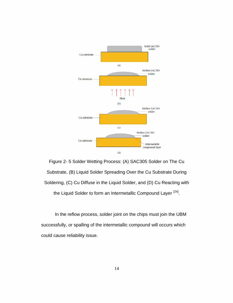
Figure 2- 5 Solder Wetting Process: (A) SAC305 Solder on The Cu
Substrate, (B) Liquid Solder Spreading Over the Cu Substrate During
Soldering, (C) Cu Diffuse in the Liquid Solder, and (D) Cu Reacting with
the Liquid Solder to form an Intermetallic Compound Layer [24]. .............. 14
Figure 2- 6 Scheme of the Interfacial Reaction of SAC305/Cu During
Solder Reflow: (A) Dissolution of the Cu Substrate, (B) Supersaturating of
the Molten Solder Layer with Cu, (C) Formation of the Scallop-Type
Cu6Sn5 at the Interface, and (D) Cu3Sn Emerges Between Cu6Sn5/Cu with
Prolonged Soldering. ............................................................................... 16
Figure 2- 7 Growth Mechanisms of IMC Layer during Soldering Process 17
Figure 2- 8 Schematic Diagram of Cross Section of Two Neighboring
Scallops. .................................................................................................. 18
ix
Figure 2- 9 Comparison of Gibbs Free Energy of Cu6Sn5 and Cu3Sn. .... 23
Figure 3- 1 Microstructure of Small (A) and Large (B) Solder Bump. ...... 25
Figure 4- 1 Microstructure Change of the Small Bump by Aging (A) 0hr (B)
48h (C) 72h (D) 150h (E) 250h (F) 500h ................................................. 28
Figure 4- 2 The Growth Behavior of Cu6Sn5 and Cu3Sn during Aging Time
................................................................................................................ 29
Figure 4- 3 Top Layer IMC Forming in (A) 0h (B) 150h (C) 500h (D) 2000h
Aging Time .............................................................................................. 30
Figure 4- 4 Bottom Layer IMC Forming in (A) 0h (B) 150h (C) 500h (D)
2000h Aging Time ................................................................................... 31
Figure 5- 1 Reaction Between Cu/Sn-based Solder in Solid State Aging. 32
Figure 5- 2 Cu6Sn5 Growth Curve with Aging Time in Large and Small
Solder Joint.............................................................................................. 33
Figure 5- 3 Cu/Ni/Sn IMC and Cu/Sn IMC Growth Curve with Aging Time
in (A) Large Solder and (B) Small Solder ................................................ 36
Figure 5- 4 Cu/Ni/Sn IMC Growth Curve of Small and Large Solder Joint
with Aging Time ....................................................................................... 37
Figure 5- 5 Whole IMC Growth Curve of Small and Large Solder Joints
with Aging Time. ...................................................................................... 39
Figure 5- 6 Kirkendall Void Formation in (A) Small Solder Joint and (B)
Large Solder Joint after 500h Aging Time. .............................................. 40

x
Figure 5- 7 Cu/Sn IMC and Cu/Ni/Sn IMC Growth Thickness With Square
Root of Aging Time. ................................................................................. 42
Figure 5- 8 Growth Curves of Cu3Sn in Large and Small Solder Joint. ... 44

xi
List of Tables
Table 2-1 Binary Pb-free Eutectic Solders ................................................. 5
1
Chapter 1
Introduction
Solder joint plays an important role in electronic packages of
electronic customer products, acting both as electrical interconnections
between chip and components, and also as mechanical support for
components. In nowadays, as the industry want to provide smaller
products with higher electrical performance, which means higher I/0-
density and smaller solder size, fine pitch solder joints are required, and
therefore, the reliability of smaller solder joint becomes an serious issue. A
very important factor that can influence the reliability of solder joint is the
intermetallic compound (IMCs) forms at the interface of solder and its
substrate. Usually, intermetallic compound begin to form at the reflowing
process when the solder is forming. It continues to growth to thicker during
room temperature storage and more rapidly in the thermal annealing. The
growth of IMC can have a significant impact on the properties of solder
joint, influence the strength and result in mechanical failure of the joint [1-5]
For example, P. L. Tu and Y. C. Chan reported that fatigue lifetime of
solder joint decrease linearly ith the increasing square root of IMCs layer
thickness [6].

2
With the reduction of solder volume and solder height,
microstructure changes in the solder joint and the growth mechanism of
intermetallic compound become highlighted. Many related questions need
to be answer, such as are different size solder grow in different rate? Do
IMCs in solder joint of different size grow in the same kinetics? In previous
research, IMC growth rate and its impact have been deeply invest in “as-
reflowed ” solder joint. Bo Wang and Fengshun Wu have reported that the
solder joints with lower solder height have a faster IMC growth rate [7].
While B. Salam and N. Ekere reported that the increasing solder size does
not significantly affect the growth of the intermetallic layer thickness [8].
In this thesis, I report a study on the effect of the solder size on
intermetallic layer formation by comparing the morphology change and
growth rate of two different size solder joint aged at a same temperature
for different aging time. The layer thickness and microstructure were
analyzed using scanning electron microscopy (SEM). Photoshop was
used to measure the thickness of intermetallic compound. Two different
size of solder joints with composition of Sn-Ag-Cu (305) were used.

3
Chapter 2
Background
In this chapter, fundamental knowledge of solder joint technology,
including lead-free solder joint, surface mounted technology, pin-through-
hole technology, flip chip technology and their application are first included.
Then, reactions of intermetallic compound formation happened in
lead-free solder joint during both wetting reaction and solid state reaction
are introduced.
2.1 Solder Joint Technology
2.1.1 Lead-free Solder Joint
Solder joint technology has been used in electronic packaging industry
for making the interconnection between electronic components for long
time. The process that solder joint accomplish is to joining the solder with
copper parts by forming intermetallic compounds in a chemical reaction.
Tin/lead alloy used to be the primary materials of solder joint. Tin-
lead (SnPb) solder is a eutectic alloy, which has melting temperature of
183℃.It can form a metallic bond with Cu at such a low temperature,
which make SnPb to be a ideal solder material used widely. However, the
toxicity of Pb which make the use and disposal of Pb containing electronic
product become a serious environmental issue [9]. In United State, for anti-
Pb bills are pending in the congress, including one from the Environmental

4
Protection Agency. In European, the agency of Waste from electrical and
Electronic Equipment (WEEE) issued a directive calls for a ban of Pb-
containing solder in all electronic consumer products from July, 2006 [10].
China, Korea and Japan has also proof related rules of elimination Pb
from electronic industry. Environmental concerns of the use of Pb-Sn
solders provide a strong driving force of study of the environmental
friendly materials, Pb-free solder joint [11,12].
Most of the eutectic Pb-free solders are Sn-based. There have
been some candidate include alloys consisting of Sn and noble metals
such as Au, Ag, Cu and Bi, Cd, In, Sb or Zn [13,14]. Several studies has
been reported, but there are still no ideal replacement materials with
respect to reflow temperature, reliability of solder joint, and assembly cost
[15]. Eutectic Sn-noble metal alloys always have a high melting point which
leads to high reflowing temperature, as shown in Table-2.1, causing
thicker IMC formation and larger strain at the joint during assembling
process. These can cause very serious reliability issue such as
delamination and fatigue the solder joint.
Zinc (Zn) is cheap and easy to find. Eutectic Sn-Zn has a relatively
low melting point compare with other Pb-free solder alloy, which is closest
to eutectic Sn-Pb. But Sn-Zn alloy cause too many difficulties in soldering
process because it can forms a very stable oxide rapidly. Bismuth (Bi) has

5
very good wetting properties while it is hard to get because the main
source of Bi is a by-product in Pb refining. Indium (In) is too expensive.
Antimony (Sb) has been recognized as a toxic metal by the United Nations
Environment Program. Sn-Ag has too large two phase regions. Sn-0.9Cu,
Sn-3.5Ag, and Sn-Ag-Cu. has been looking as promising solder alloys
based on the selection criteria. The most promising one is the ternary Sn-
Ag-Cu eutectic (217℃) as its relatively low melting temperature, good
quality solder joint forming with Cu substrate, superior mechanical
properties and good compatibility with other components [16]. The
international Printed Circuit Association has suggest that 96.5Sn-3.0Ag-
0.5Cu (SAC305) will be the most widely used alloys in the future [17].
Table 2-1 Binary Pb-free Eutectic Solders

6
2.1.2 Surface Mount Technology
Wire bonding technology has been widely used to connect Si chip
to leadframe substrate in most of the portable electronic consumer product
such as mobile phone and computers. In wire bonding technology, solder
joints are used to join the bond pads on a packaging circuit board to the
legs of the leadframe. Figure 2.1 shows the wire bonding between a Si
chip and a Cu leadframe substrate.
Figure 2- 1 Schematic Diagram of Wire Bonding Between A Si Chip and A
Leadframe [10].
Solder joint in surface mount technology is fabricated by printing a
pattern of a lots of solder paste on a bond pads, the legs of leadframe are
placed on a printed paste mount. Then the assembly will be putted on a

7
belt which can move in a tube furnace. The joint will be formed in melting
temperature and a forming gas ambient.
Figure 2- 2 Schematic Diagram of a Surface Mount Solder Joint
Connecting a Leg and a Substrate [10].
Solder joint in surface mount technology between a leg and a
substrate board can be showed by Figure 2-2.The “reflow” in solder
forming means the heating process, the temperature is above the melting
point of the solder alloy by 30 to 40 ℃ for about half minutes. In this period,
the solder joint get melted and react with the substrate and the bond pad
to form a metallic joint. The leadframe will be coated with a thin layer of
eutectic SnPb for easier achieving the joining of all the legs in the half
minute reflowing time. While due to the environment problem causing by
Pb, the coating has been alternate by Pb-Free material as pure Sn or Sn-
Cu eutectic alloy. However, Sn whiskers which can cause electrical shorts
between legs have been found on these coating. Other reliability issues

8
such as cracks happen on the solder and leg interface have also been
found.
2.1.3 Pin-Through Technology
Pin- through-Hole technology can provide better mechanical
reliability by using straight legs so that the legs can act like pins that can
be inserted into holes drilled in the board. The holes on the board is plated
with immersion Sn and Cu, so that in reflowing process, the molten solder
can wet the immersion Sn and rise along the holes by capillary force.
Then the pins can be soldered on the board through the holes. Although
Pin-through-Hole technology can provide better mechanical reliability, its
application is limited for the high cost. Figure 0-3 shows the cross-section
area of through holes plated with Cu and immersion Sn.

9
Figure 2- 3 Cross-Sectional Image of Through Holes Plated with Cu And
Immersion Sn.
2.1.4 Flip Chip Technology
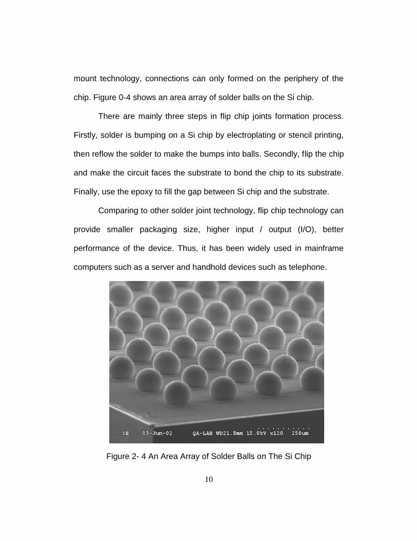
Flip chip technology is a method of forming electronic connections
between Si chip and printed circuit board or ceramic module. The
electronic connections can be achieved through an area array of solder
joints between the Si chip and the substrate by flip the Si chip and make
the circuit faces the substrate. The solder joint in flip chip technology can
cover all or at least a large area of the surface of the chip, while in surface
10
mount technology, connections can only formed on the periphery of the
chip. Figure 0-4 shows an area array of solder balls on the Si chip.
There are mainly three steps in flip chip joints formation process.
Firstly, solder is bumping on a Si chip by electroplating or stencil printing,
then reflow the solder to make the bumps into balls. Secondly, flip the chip
and make the circuit faces the substrate to bond the chip to its substrate.
Finally, use the epoxy to fill the gap between Si chip and the substrate.
Comparing to other solder joint technology, flip chip technology can
provide smaller packaging size, higher input / output (I/O), better
performance of the device. Thus, it has been widely used in mainframe
computers such as a server and handhold devices such as telephone.
Figure 2- 4 An Area Array of Solder Balls on The Si Chip
11
2.2 IMC Formation in Pb-Free Solder Joint (or Copper-Tin Reactions)
The presence of IMCs between solders and conductor metals is
desirable because it results in good metallurgical bonding. A thin,
continuous, and uniform IMC layer is an essential requirement for good
bonding. Without IMCs, the solder/conductor joint is weak because no
metallurgical interaction occurs in the bonding, which is disastrous to
electronic packaging. However, a thick IMC layer at the solder/conductor
metal interface may degrade the reliability of the solder joints because of
their inherent brittle nature and their tendency to generate structural
defects caused by mismatches of the physical properties (such as elastic
modulus and coefficient of thermal expansion). A thick IMC layer should
be avoided during the process. Thus, knowledge of the solder/conductor
metal interactions and phase evolution in the solder interconnections is
important to understand the reliability of solder interconnections from a
metallurgical viewpoint and to optimize the soldering process.
Usually, the sample has been reflowed for several times before
solid-state aging test. So there must be certain scallops-type Cu6Sn5
formed before aging. In solid state aging process, the morphology of
Cu6Sn5 changes from scallop-type to layer-type. The IMC formed in solid-

12
sate aging need to be determined by subtracting the amount of IMC
formed during reflow process. The average thickness of IMC layer can be
obtained by dividing the total cross-sectional area of the IMC by the total
length.
In solid-state reactions, the IMC has layer-type morphology. The
kinetics of the IMC growth can be diffusion-controlled or interfacial-
reaction controlled. In high enough temperature, all the IMCs obey a
diffusion-controlled growth, so the ratio of thickness among the layers is
proportional to the ratio of the square root of the interdiffusion coefficient in
each layer.
While in wetting reaction, the Cu6Sn5 has scallop-type morphology,
and the growth thickness is found to be t1/3 dependent on time. Which
means the kinetics of the scallop-type Cu6Sn5 is not diffusion-controlled or
interfacial-reaction-controlled. It is indicated to be a ripening reaction and
obey the kinetics named as supply-controlled growth kinetics.
2.2.1 Wetting Reaction
Soldering is a metallurgical joining process that bonding solder to a
metal substrate in a certain temperature. For lead-free solder joints, which
usually have high concentration of Sn, the soldering reaction is basically
between Sn and the Cu substrate. For SAC305 solder alloy, during

13
soldering process, SAC305 melts and meet Cu substrate, Sn from the
melting solder get react with Cu and forming intermetallic compound (IMC)
at the interface of Cu and Sn. Thus, the IMC layer bond Cu and Sn
together [18-23].
Generally, the wetting process can be divided into three stages
(see Figure 2-5.).
Spreading;
When heated, solder melted and spread out on Cu substrate to
form a cap on it.
Base metal dissolution;
In this process, Cu atoms from the substrate dissolve into molten
solder, substrate remain to be solid and does not change its
microstructure.
Formation of an IMC layer.
The dissolved Cu atoms and liquid solder react and form an
intermetallic layer. The liquid solder phase transformed to some solid
phases when the joints get cooled. The kinds of solid phases forming in
this process are related to the properties of achieved solder joint.
14
Figure 2- 5 Solder Wetting Process: (A) SAC305 Solder on The Cu
Substrate, (B) Liquid Solder Spreading Over the Cu Substrate During
Soldering, (C) Cu Diffuse in the Liquid Solder, and (D) Cu Reacting with
the Liquid Solder to form an Intermetallic Compound Layer [24].
In the reflow process, solder joint on the chips must join the UBM
successfully, or spalling of the intermetallic compound will occurs which
could cause reliability issue.

15
2.2.2 IMC Formation in Wetting Reactions
During wetting process, solder is heated to melting temperature, Cu
from the substrate dissolves into molten solder very fast. The Cu dissolve
in a non-equilibrium process, Cu with a very high concentration quickly
localize in the interface of Cu substrate and molten solder until the solder
getting supersaturated with Cu. After Cu saturated in the interface of
Cu/molten solder, a large driving force for the chemical reaction between
Cu and Sn exist in the interface, a thin layer of Cu6Sn5 IMC start to form.
The Cu6Sn5 formed in wetting process has scallop-type morphology and
the rate of formation is very fast comparing with the Cu6Sn5 forming in
solid state aging process [25]. The growth kinetics of Cu6Sn5 in this process
is a unique one, we will discuss it later. If the reflow time is long enough,
layer-like IMC Cu3Sn can be found between Cu6Sn5 and Cu substrate by
diffusion and reaction type growth [26]. The IMC growth mechanism can be
schematically illustrates by Fig 2-7.

16
Figure 2- 6 Scheme of the Interfacial Reaction of SAC305/Cu During
Solder Reflow: (A) Dissolution of the Cu Substrate, (B) Supersaturating of
the Molten Solder Layer with Cu, (C) Formation of the Scallop-Type
Cu6Sn5 at the Interface, and (D) Cu3Sn Emerges Between Cu6Sn5/Cu with
Prolonged Soldering.
Now let’s briefly talk about the growth kinetics of IMC growth in
wetting reaction. There are several different opinions about the dominant
growth kinetics of Cu6Sn5 during the time of reflow.

17
Figure 2- 7 Growth Mechanisms of IMC Layer during Soldering Process
Additionally, King-Ning Tu concluded that the growth of Cu6Sn5 is
dominant by neither diffusion-controlled nor interfacial reaction controlled
kinetics. It obeys a kinetics which is named supply-controlled growth
kinetics. It was indicate that the thickness of the scallops has a t1/3
dependence on time, with the time increasing, the scallop IMC growth
bigger but fewer. So it does not obey the diffusion-controlled or interfacial-
controlled kinetics. A non-conservative ripening reaction is happened
among the scallop-type Cu6Sn5 grains.

18
Figure 2- 8 Schematic Diagram of Cross Section of Two Neighboring
Scallops.
Figure 2-8 shows a schematic diagram of the cross section of two
scallop Cu6Sn5 forming in wetting reaction. For simplified the discussion,
we assume there is no Cu3Sn forming in between Cu6Sn5 and Cu
substrate. In wetting process, when solder is heated to over 200℃, molten
solder turns to liquid phase. The diffusivity of Cu in liquid solder is about
10-5 cm2/sec. The Cu flux (showed by the vertical arrow) diffuses through
the valley between the two Cu6Sn5 scallops rapidly and then reacts with
Sn in front of the scallops (showed by the horizontal arrow.). The diffusion
of Cu through the valley of scallops is very fast, on the order of 10-5

19
cm2/sec, and the diffusion distance is very small, Cu diffusion is not a
rate-limiting step. However, the Cu atoms under the valley can be
consumed very soon, then a lateral diffusion from the Cu nearby will
happen. The diffusion rate is very fast too, and it is not a rate-limiting
diffusion too. The activation energy was found to be 0.2 to 0.3 eV/atom,
which is very low compare to the activation energy of the growth of
Cu6Sn5 in solid state reaction. Due to the experiment reported by King-
Ning Tu, to achieve same thickness (a few centimeters) of Cu6Sn5, in the
wetting reaction in 200℃, it only takes a few minutes, but in solid-state
aging process in 170℃, it took 1000hr. Showing that wetting reaction is
four orders of magnitude faster than the solid state aging although there is
a temperature difference of 30℃ which is not very big. Thus, the wetting
reaction is a much faster kinetics process, which has been defined to be
supply-controlled growth kinetics
2.2.3. IMC formation in Solid-State Reactions
Although we want the growth of the intermetallic compounds to stop
right after the wetting reaction, because the thick IMC layer can have a
negative impact to the reliability of the Pb-free solder. But the device is
always working in a high operation temperature, that solid-state reaction
will happen and influence the thickness and morphology of the IMC layer.

20
So it is very necessary to study the mechanism and kinetics of IMC layer
growth in the solid-state aging reaction.
In solid-state aging reaction, two layer of intermetallic compound
could be formed, Cu6Sn5 near solder and Cu3Sn near Cu substrate. The
kinetics of IMC layer growth can be diffusion controlled or interfacial
reaction controlled. Generally, the growth kinetics of IMC layer can be
determined by plotting the measured IMC layer thickness against the
exposure time at a certain annealing temperature. The thickness can be
expressed as a function of aging time using the time power law equation
as [27]:
x = x0 + A·tn (1)
Where x is the IMC layer thickness at time t, x0 is the layer
thickness after reflow process, n is a constant or called time exponent that
indicate intermetallic compound growth mechanism, A is the temperature
dependent growth constant, which can be describe by Arrhenius type
equation as shown below:
A = A0·exp (-
) (2)
Where A0 is a pre-exponential factor, Q is the activation energy of
the growth, T is the absolute temperature and R is the universal gas
constant (8.314 J/K·mol)
Combining (1) and (2) together, IMC thickness becomes:

21
x = x0 + A0·tn·exp (-
) (3)
If the growth of IMC layer is a diffusion controlled process, n is on
the order of 0.5 [28], the IMC layer kinetics can be described by the square
root time law. The thickness of IMC layer can be measured a d plotted
against the exposure time, at any given temperature. Vianco et al [29] has
found that for the total intermetallic layer pure Sn, Pb-Sn, and two kinds of
Sn-riches solders (96.5Sn-3.5Ag and 95Sn-5Sb), the time exponent is
about 0.5 in lower annealing temperatures (below 135℃) and close to 0.4
at higher (more than 170℃) annealing temperatures.
In the solid-state aging process of Sn-based Pb-free solder alloy,
there can be two main species of IMC layer formed, Cu6Sn5 (η phase)
and Cu3Sn (ε phase). The mechanisms of IMC formation are influenced
by the interdiffusion characteristics of Cu and Sn. Some experiment on
Cu-Sn system has showed that interstitial of Cu is dominant in lower
temperature (below 170℃) and vacancy diffusion of Sn is dominant in
higher temperature (over 170℃)[30,31]. Which means Cu diffuse faster than
Sn when the annealing temperature is below 170℃. In that condition, in
the Sn-Cu interface, Cu can react with diffusion Sn to form Cu6Sn5and
Cu3Sn. Cu can also react with Cu6Sn5to form Cu3Sn. Which means the

22
growth of the two IMC layer is influenced by the synergy function which
means Cu3Sn forms at an expense of Cu6Sn5.
The solid state interfacial reactions occurring in Sn-Cu interface can
be describe as:
6Cu + 5Sn → Cu6Sn5 (1)
3Cu + Sn → Cu3Sn (2)
9Cu + Cu6Sn5 → Cu3Sn (3)
As we can see in Figure.2-9, Cu6Sn5 (η phase) has a lower Gibbs
free energy than Cu3Sn, showing that Cu3Sn has a higher activation
energy and less driving force than Cu6Sn5, so Cu6Sn5 can forms earlier
Cu6Sn5r than Cu3Sn in lower solid state aging temperature (below 170
℃). .

23
Figure 2- 9 Comparison of Gibbs Free Energy of Cu6Sn5 and Cu3Sn.

24
Chapter 3
Experimental Procedure
In this study, two different size solder joints with the same
composition (SAC305 with 96.5%Sn, 3.0% Ag, 0.5%Cu) were used. The
large solder joint has a ball shape with Cu/Ni/Sn/Cu structure. The small
solder joint has a pillar shape with Cu/Ni/Sn/Cu structure. The stand-off
height of large solder bump is around 343μm and small bump around
12.5μm. The ratio of height to length of the solder joint is 1.27 in large,
while 0.04 in small. The size difference between small and large
specimens is very significant.

25
(a)
(b)
Figure 3- 1 Microstructure of Small (A) and Large (B) Solder Bump.
The two pictures in figure 3-1 show the microstructure of small
solder joint and large solder joint. Samples were subjected to isothermal
aging treatment in 150℃ for 500h. After the aging treatment, samples
were mounted by epoxy and very fine polished to detect the cross section
area. To better identify the IMC layer, sample were etched by 97per cent

26
methanol and 3 per cent HCl (vol.%) solution for about 5 s to selectively
remove the Sn solder alloy.
Scanning electron microscopy (SEM) in the back scattered electron
(BSE) mode was used to observe the microstructure of the samples.
Energy dispersive X-ray spectroscopy was used to analyze the
composition of the IMC and solder joint. Software “PHOTOSHOP7” was
used to measure the average thickness of IMC, based on the BSE images.

27
Chapter 4
Morphology Change of Solder Joint during Thermal Aging
4.1 Morphology Change in Small Solder Joint in Thermal Aging
Figure 4-1 shows the BSE pictures taken for small solder joints
during different aging times. As we can see from the pictures, the IMC
layers at both top and bottom side grow thicker as aging time increasing.
The shape of the IMC goes from scallop-type to planer-type.

28
(A) (B)
(C) (D)
(E) (F)
Figure 4- 1 Microstructure Change of the Small Bump by Aging (A) 0hr (B)
48h (C) 72h (D) 150h (E) 250h (F) 500h

29
The BSE pictures in Figure 4-2 are taken in larger magnification
which show more detail of the surface morphology. As we can see in the
pictures, two different IMC have formed during aging period. Cu6Sn5 forms
at the early aging period, which continues growing thicker as the aging
time increasing. When the aging time get longer, Cu3Sn forms in the
interface of Cu6Sn5 and Cu substrate at the bottom IMC layer.
Figure 4- 2 The Growth Behavior of Cu6Sn5 and Cu3Sn during Aging Time
4.2 Morphology Change in Large Solder Joint in Thermal Aging
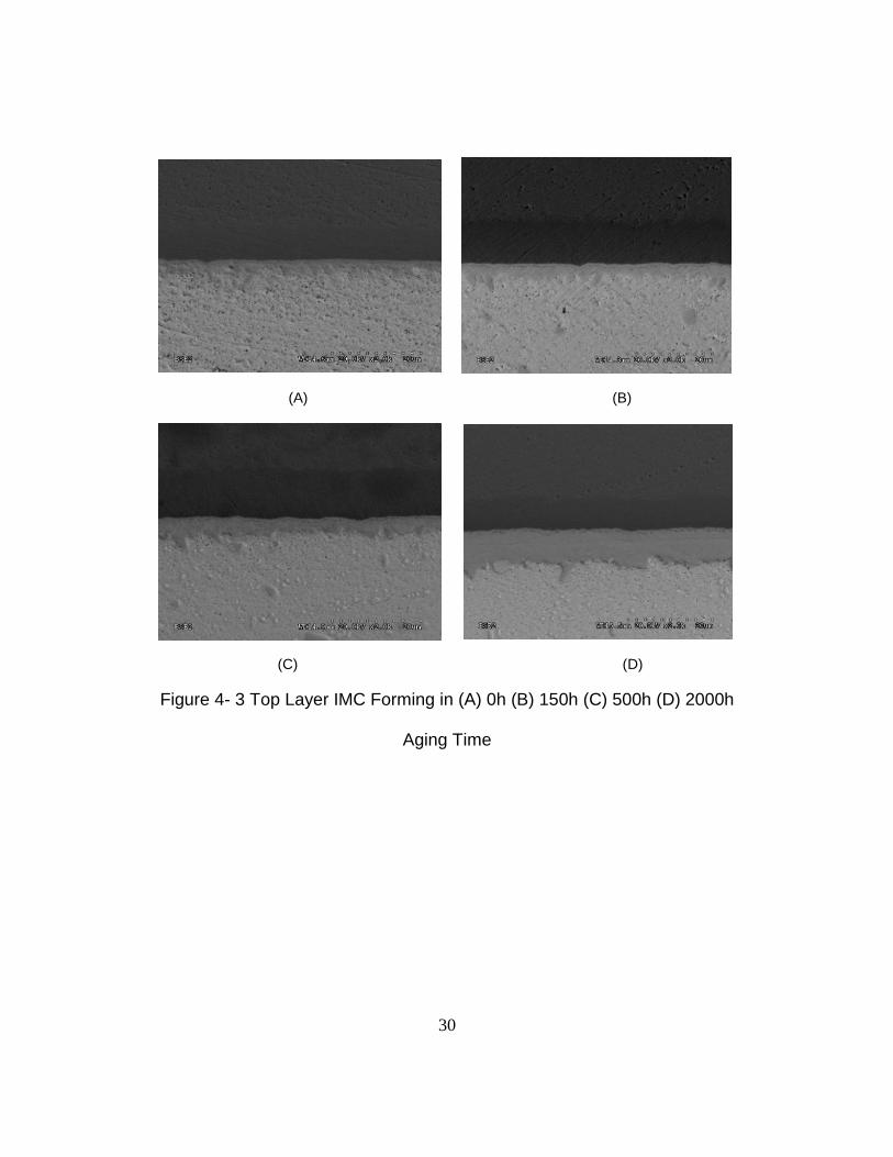
Figure 4-3 shows the BSE pictures taken for the top layer of large
solder joints during different aging times. As we can see from the pictures,
the IMC layers at top side get thicker during increasing aging time. The
shape of the IMC goes from scallop-type to planer-type.
30
(A) (B)
(C) (D)
Figure 4- 3 Top Layer IMC Forming in (A) 0h (B) 150h (C) 500h (D) 2000h
Aging Time

31
(A) (B)
(C) (D)
Figure 4- 4 Bottom Layer IMC Forming in (A) 0h (B) 150h (C) 500h (D)
2000h Aging Time
Figure 4-4 shows the BSE pictures taken for the bottom layer of
large solder joints during different aging times. The IMC layers at bottom
side get thicker during increasing aging time. The shape of the IMC goes
from scallop-type to planer-type. Cu6Sn5 forms after reflowing reaction
then continue to grow and gets thicker during thermal aging. Cu3Sn forms
in between Cu6Sn5 and Cu substrate after certain aging time.

32
Chapter 5
Discussion
5.1 Growth Mechanism of IMC In Cu/IMC Interface
During the solid state aging process, what happened at the
Cu/solder interface is basically Cu diffuse from substrate to Sn solder,
meet the Sn atoms at the interface, forming IMC layer. If the Ni layer was
added between the substrate and solder, Cu atoms need to diffuse
through the Ni layer and meet Sn at the interface of Ni/Sn. Figure.5-1 is
the schematic diagram shows the reactions happen between Cu substrate
and SAC solder.
Figure 5- 1 Reaction Between Cu/Sn-based Solder in Solid State Aging.
Figure 5-1 (1) shows the structure of solder before aging (IMC
formed in reflow process is ignored temporarily for the convenience). As
aging time increased, at early period of solid state aging, a thin layer of
Cu6Sn5 can be detected at the interface of Cu/Sn. The thickness of

33
Cu6Sn5 continue to increase as the aging time increase, in the bottom
interface without Ni barrier, the thickness of Cu6Sn5 is larger than the one
formed near the Ni barrier. After long enough aging time, the Cu3Sn can
be found at the interface of Cu6Sn5 and Cu in the bottom IMC layer. No
Cu3Sn can be found in the top IMC layer.
The thickness of Cu6Sn5 in both large and small solder joint was
measured. The relationship between Cu6Sn5 thickness and aging time is
showing by Figure 5-2.
Figure 5- 2 Cu6Sn5 Growth Curve with Aging Time in Large and Small
Solder Joint
As showing by Figure 5-2, in the early aging time, Cu6Sn5 in small
bump growth faster than large bump, while after 250hrs, the thickness of
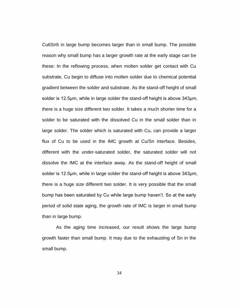
34
Cu6Sn5 in large bump becomes larger than in small bump. The possible
reason why small bump has a larger growth rate at the early stage can be
these: In the reflowing process, when molten solder get contact with Cu
substrate, Cu begin to diffuse into molten solder due to chemical potential
gradient between the solder and substrate. As the stand-off height of small
solder is 12.5μm, while in large solder the stand-off height is above 343μm,
there is a huge size different two solder. It takes a much shorter time for a
solder to be saturated with the dissolved Cu in the small solder than in
large solder. The solder which is saturated with Cu, can provide a larger
flux of Cu to be used in the IMC growth at Cu/Sn interface. Besides,
different with the under-saturated solder, the saturated solder will not
dissolve the IMC at the interface away. As the stand-off height of small
solder is 12.5μm, while in large solder the stand-off height is above 343μm,
there is a huge size different two solder. It is very possible that the small
bump has been saturated by Cu while large bump haven’t. So at the early
period of solid state aging, the growth rate of IMC is larger in small bump
than in large bump.
As the aging time increased, our result shows the large bump
growth faster than small bump. It may due to the exhausting of Sn in the
small bump.

35
5.2 Growth Mechanism of IMC in Ni/IMC Interface
In both large and small solder, the top side structure is Cu/Ni/Sn
which is different from the bottom side Sn/Cu structure. Figure 5-3 shows
the obvious impact of Ni layer on the top side IMC growth. As we can see,
in case of both large and small solder joint, Sn/Cu IMC growth much faster
than Sn/Ni/Cu IMC, which means Ni layer act as a very effective barrier
that prevents the formation of Cu-Sn IMC. The reason why Ni can inhibit
Cu-Sn IMC formation are: Ni has a very slow Sn-Ni intermetallic growth
rate, and Ni layer can inhibits Sn diffusion and Cu-Sn IMC formation,
furthermore, Ni3Sn4 can replace Cu-Sn IMC so that decrease the CU-Sn
IMC growth rate and improve the reliability of solder joint.

36
(a)
(b)
Figure 5- 3 Cu/Ni/Sn IMC and Cu/Sn IMC Growth Curve with Aging Time
in (A) Large Solder and (B) Small Solder

37
Figure 5- 4 Cu/Ni/Sn IMC Growth Curve of Small and Large Solder Joint
with Aging Time
When compare the thickness of Cu/Ni/Sn top IMC layer in small
and large solder joint, as showing in Figure 5-4, at the very beginning, the
top layer thickness of small bump is 2.670μm, the thickness of large bump
is 2.503μm, which is pretty similar with the small bump. However as the
aging time increases, the Cu/Ni/Sn IMC layer in large bump growth much
faster than in small bump. At 500 aging time, the thickness of the IMC in
large bump come to 3.81μm; while in the small bump only 3.2μm. This
result can not been explained by the thickness different of Ni barrier
between large and small bump because large bump has a thicker Ni
barrier which is around 8μm, while in small bump, Ni barrier is around 2μm.

38
A thicker Ni barrier should be more effective to avoid Cu diffusion and lead
to slower IMC growth rate.
One possible explanation for this result is related to the Cu
saturation in the reflow period. In the small bump, as we mentioned before,
Cu get saturated much faster than in large bump. In aging period, as
temperature decrease from reflowing temperature, Cu gets supersaturated
in solder alloy. Both top and bottom IMC growth comparably fast. However,
in bottom area, without Ni barrier, Cu/Sn IMC growth much faster than
Cu/Ni/Sn IMC in top area. Cu atoms in the solder are absorbed by fast
growth Cu6Sn5, after certain aging time, Cu near top area becomes
unsaturated result in Cu/Ni/Sn IMC dissolution. While in large solder joint,
as top area and bottom area are comparably far away from each other,
the IMC growth in bottom layer will not impact Cu concentration in top
layer. It’s possible that Cu in the solder alloy gets saturated after reflow
process, Cu/Ni/Sn IMC grows neither significant Cu concentration
decrease nor IMC dissolution. So Cu/Ni/Sn IMC growth in large solder
joint can grows faster than in the small joint.

39
5.3 Total Growth of IMC in Large and Small Solder Joint
Figure 5- 5 Whole IMC Growth Curve of Small and Large Solder Joints
with Aging Time.
Figure 5-5 shows the comparison of whole IMC thickness between
small and large solder joint. As we can see at early aging stage, the whole
IMC thickness in small bump is larger than large bump, then its growth
rate decreases and thickness becomes smaller comparing to large bump.
The explanation of these can be: In reflowing process, it takes much
shorter time for Cu to get saturated in molten solder alloy. So in the early
stage, Cu flux in small solder is much higher than in large solder. Higher
Cu flux result in faster IMC growth rate. While as the aging time increasing,
in small solder joint, the IMC growth in top layer was negatively impact by
40
IMC growth in bottom layer, never the less, Sn get exhausted much faster
as the small amount of storage at the very beginning.
Although the IMC thickness in small solder joint is thinner compares
to large bump in long aging time, the ratio of IMC thickness with solder
height is larger and results in a more dramatic microstructural change in
small solder joint. So the impact of IMC thickness on the solder reliability
is more seriously in small solder joint.
5.4 Kirkendall Void Formation
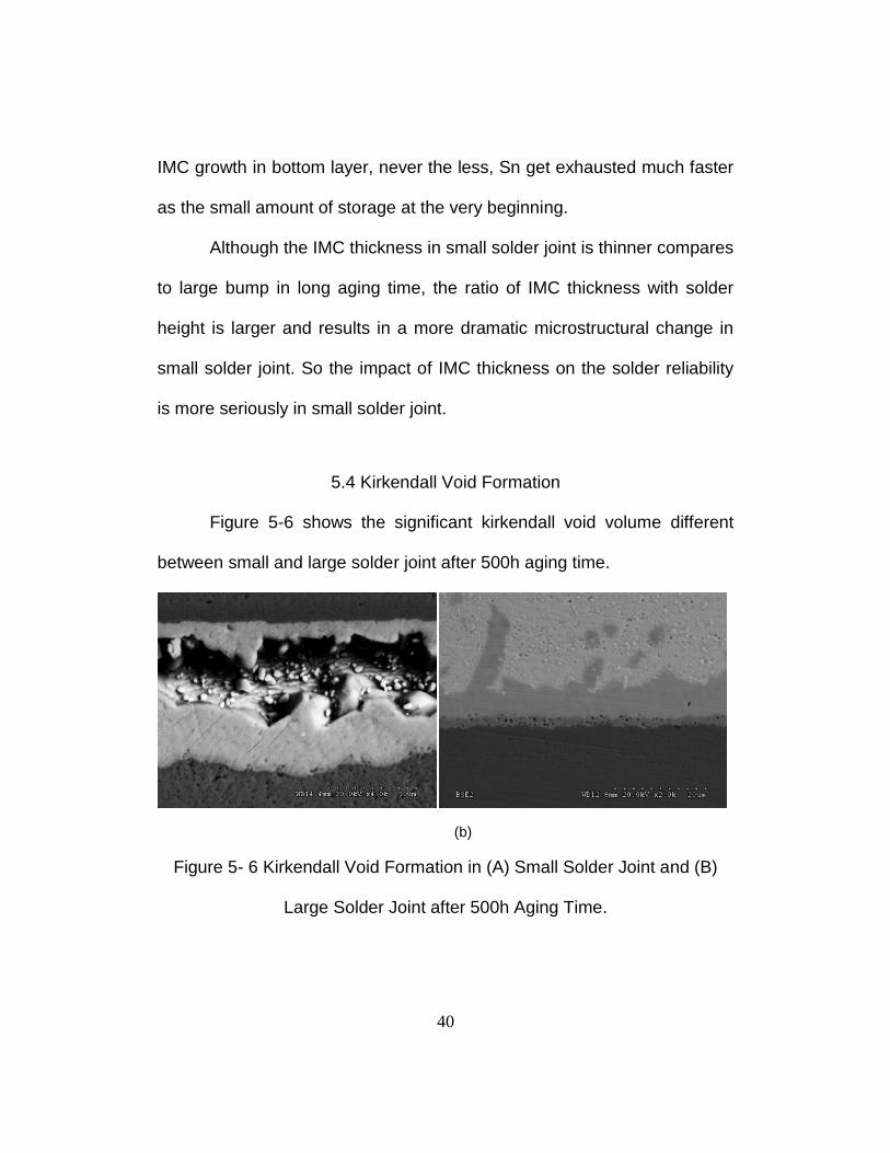
Figure 5-6 shows the significant kirkendall void volume different
between small and large solder joint after 500h aging time.
(b)
Figure 5- 6 Kirkendall Void Formation in (A) Small Solder Joint and (B)
Large Solder Joint after 500h Aging Time.

41
The kirkendall void forming in solid state aging is caused by the
difference between the diffusion rate of Cu and Sn. The diffusion flux of
Cu is higher than that of Sn in Cu3Sn phase, so that the excess vacancies
would generate behind the Cu3Sn phase [32-34]. During same aging time,
as showed by Figure 5-7, there are less amount of Cu3Sn forming in small
solder joint, so the difference between Cu and Sn flux is smaller, thus, the
kirkendall void volume is smaller.
Additionally, some researchers have pointed out that kirkendall void
may not be the only void type forming in the Cu3Sn area. The formation of
the void may also related to the impurities in the solder and Cu substrate.
So the impurity different may also be a reason why void volume is
significantly different between small and large solder joint.
42
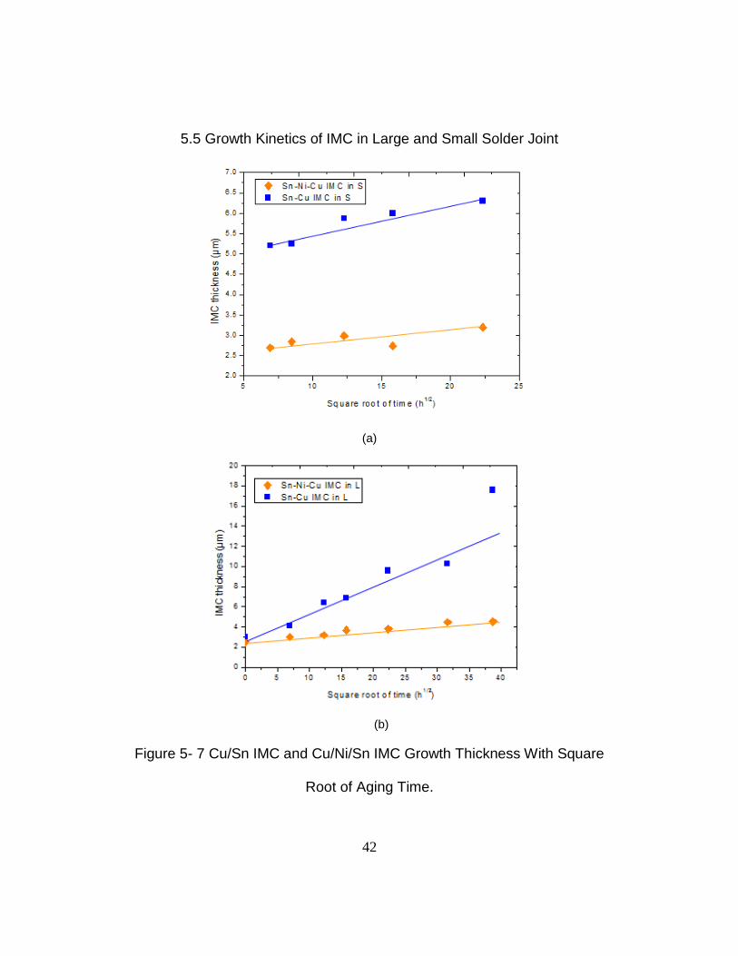
5.5 Growth Kinetics of IMC in Large and Small Solder Joint
(a)
(b)
Figure 5- 7 Cu/Sn IMC and Cu/Ni/Sn IMC Growth Thickness With Square
Root of Aging Time.

43
Figure 5-7 shows the curve of IMC thickness changing with square
root of time. For small solder bump: Sn-Ni-Cu: n≈0.5; A=0.025, Sn-Cu:
n≈0.5; A1=0.300; A2=0.07, means the growth of small solder bump is
diffusion controlled. For large solder bump: Sn-Ni-Cu: n≈0.5; A=0.076,
Sn-Cu: n≈0.5; A=0.245, means the growth of small solder bump is
diffusion controlled.
5.6 Growth Mechanism of Cu3Sn (Future Works)
The Cu3Sn growth curve with aging time of small and large solder
joint is shown in Figure 5-8. The thickness of Cu3Sn in large solder joint is
much bigger than that in small solder joint. What is the major reason of the
thickness different should be study in the future works.

44
Figure 5- 8 Growth Curves of Cu3Sn in Large and Small Solder Joint.

45
References
[1]. R. J.Geckle. Metallurgical Changes in Tin-Lead Platings due to Heat Aging. IEEE Transactions on Components, Hybrids and Manufacturing Technology 1991; 4(4): 691–697. [2]. R. J. K. Wassink. Book Soldering in Electronics, Electrochemical Publications, Isle of Man, UK, 1989 [3]. W. Yujing and J. A. Sees et al. The formation and growth of intermetallics in composite solder. J. Electron. Mater 1993; 22(7): 769–777. [4]. R. E. Pratt, E. I. Stromswold, and D. J. Quesnel. Effect of solid-state intermetallic growth on the fracture toughness of Cu/63Sn–37Pb solder joints. IEEE Transactions on Components Packaging and Manufacturing Technology 1995; 19(1): 134–141. [5]. M. Abtew and G. Selvaduray. Lead-free solders in microelectronics. Materials Science and Engineering R 2000; 27(5): 95–141. [6]. PL Tu, YC Chan, KC Hung, JKL Lai. Growth kinetics of intermetallic compounds in chip scale package solder joint. Scripta materialia 2001; 44(2): 317-323. [7]. Bo Wang, Fengshun Wu, Yiping Wu, Liping Mo, Weisheng Xia. Microstruchural evolution of the intermetallic compounds in the high density solder interconnects with reduced stand-off height. Soldering & Surface Mount Technology 2011; 23(4): 229-234. [8]. B.Salam, N.N.Ekere, D. Rajkumar. Study of the interface microstructure of Sn-Ag-Cu lead-free solders and the effect of solder volume on intermetallic layer formation. 2001, 471 – 447, 0569-5503 [9]. S. W. Chen, C. H. Wang, S. K. Lin, and C. N. Chiu. Phase diagrams of Pb-free solders and their related materials systems. Journal of Materials Science 2007; 18(1-3): 19–37. [10]. King-Ning Tu. Solder Joint Technology. Springer Science & Business Media, Jul 27, 2007 [11]. J Glazer. Microstructure and mechanical properties of lead-free solder alloys for low-cost electronic assembly: A review. J Electron Mater 1994; 23(8): 670-693. [12]. E.P. Wood, K.L. Nimmo. In search of new lead-free electronic solders. J Electron Mater 1994; 23(8): 709– 713. [13]. M McCormack, S Jin. Improved mechanical properties in new lead-free solder alloys. J Electron Mater 1994; 23(8): 715–720. [14]. I. Artaki, A. M. Jackson, and P. T. Vianco. Evaluation of Lead-free Solder Joints inElectronic Assemblies. J. Electron. Mater 1994; 23(8): 757 – 764. [15]. X. Deng, G. Piotrowski, J. J. Williams, N. Chawla. Influence of Initial Morphology and Thickness of Cu6Sn5 and Cu3Sn Intermetallics on Growth and Evolution during Thermal Aging of Sn-Ag Solder/Cu Joints. Journal of Electronic Materials 2003; 32(12): 1403-1413.

46
[16]. K. S. Kim, S. H. Huh, and K. Suganuma. Effects of intermetallic compounds on properties of Sn-Ag-Cu lead-free soldered joints. Journal of Alloys and Compounds 2003; 352(1-2): 226–236. [17]. C. M. L. Wu, D. Q. Yu, C. M. T. Law, and L.Wang. Properties of lead-free solder alloys with rare earth element additions. Materials Science and Engineering R 2004; 44(1): 1–44. [18]. R. J. K. Wassink. Book Soldering in Electronics. Electrochemical Publications, Isle of Man, UK, 1989. [19]. M. Abtew and G. Selvaduray. Lead-free solders in microelectronics. Materials Science and Engineering R 2000; 27(5): 95–141. [20]. T. Laurila, V. Vuorinen, and J. K. Kivilahti. Interfacial reactions between lead-free solders and common base materials. Materials Science and Engineering R 2005; 49(1-2): 1–60. [21]. H. H. Manko. Book Solders and Soldering: Materials, Design, Production, and Analysis for Reliable Bonding. McGraw-Hill, New York, NY, USA, 2001. [22]. L. M. Lee, H. Haliman, and A. A. Mohamad. Interfacial reaction of a Sn-3.0Ag-0.5Cu thin film during solder reflow. Soldering & Surface Mount Technology 2013; 25(1): 15–23. [23]. J. W. Yoon, S. W. Kim, and S.-B. Jung. IMC morphology, interfacial reaction and joint reliability of Pb-free Sn-Ag-Cu solder on electrolytic Ni BGA substrate. Journal of Alloys and Compounds 2005; 392(1-2): 247–252. [24]. Thomas Young. An Essay on the Cohesion of Fluids. Philosophical Transactions of the Royal Society of London 1805; 95: 65-87. [25]. J. W. Yoon, B. I. Noh, B.-K. Kim, C.-C. Shur, and S.-B. Jung. Wettability and interfacial reactions of Sn-Ag-Cu/Cu and Sn-Ag-Ni/Cu solder joints. Journal of Alloys and Compounds 2009; 486(1-2): 142–147. [26]. M. Schaefer, et al. Evaluation of Intermetallic Phase Formation and Concurrent Dissolution of Intermetallic During Reflow Soldering. Design and reliability of solders and solder interconnects, the minerals metals and materials society 1997; 247-257. [27]. A. J. Sunwoo, J. W. Morris, Jr., and G. K. Lucey, Jr. The growth of Cu-Sn intermetallics at a pretended copper-solder interface. J Metall. Trans 1992; 23(1): 1323-1332. [28]. Vianco, P and Rejent, J. A methodology to Establish Baseline Metrics for assessing the isothermal Aging of Sn-Pb Solder interconnects. Soldering and surface Mount technology 2002; 14: 26. [29]. M. Onishi and H. Fujibuchi: Trans. JIM 16 1975; 539-547. [30]. K. N. Tu, R. D. Thompson. Kinetics of Interfacial Reaction in Bimetallic Cu-Sn Thin Films. Acta Met 1982; 30: 947. [31]. B.F. Dyson, T.R. Anthony and D. Turnbull. Interstitial diffusion of copper in tin. Journal of Applied Physics 1967; 38: 3408.

47
[32]. Minho O, George Vakanas, Nele Moelans, Masanori Kajihara, Wenqi Zhang. Formation of compounds and Kirkendall vacancy in the Cu-Sn system. Microelectronic Engineering 2014; 120: 133-137. [33]. M.Y. Tsai, S.C. Yang, Y.W. Wang and C.R. Kao. Grain growth sequence of Cu3Sn in the Cu/Sn and Cu/Sn–Zn systems. Journal: Journal of Alloys and Compounds 2010; 494(1-2): 123.

48
Biographical Information
Huandi Gu was born in Nei Mongel province, China. She got her
B.S. degree in China University of Geosciences in 2010. She start her
master program in Materials Science and Engineering in University of
Texas at Arlington from 2012. She was working as a research assistant in
Dr. Choong-un Kim’s group. During her master education, she was a
member of SRC. She also served as a volunteer for summer camps in
2013 and 2014. Her research field was related to the interfacial reactions
in electronic lead-free solder joint. As a master graduate student, she is
able to analyze different microstructures by using different techniques
such as scanning electron microscopy (SEM), X-ray diffraction (XRD),
energy dispersive spectrometer (EDS) and transmission electron
microscopy (TEM).
Related Documents


![NS -SOLDER D aste SNI OOCYV— 71J— SNIOOC …nihonsuperior.co.jp/jp/wp-content/themes/nihonsuperior/...NS -SOLDER D aste SNI OOCYV— 71J— SNIOOC P810 D4 SN OOC Z] NIHON SUPERIOR](https://static.cupdf.com/doc/110x72/5e7581f399edbf7be157d779/ns-solder-d-aste-sni-oocyva-71ja-sniooc-ns-solder-d-aste-sni-oocyva.jpg)
![1 Interfacial Rheology System. 2 Background of Interfacial Rheology Interfacial Shear Stress Interfacial Shear Viscosity = [ ]](https://static.cupdf.com/doc/110x72/56649d1f5503460f949f3d29/1-interfacial-rheology-system-2-background-of-interfacial-rheology-interfacial.jpg)


