Interface Application Development of an Electrometer using LabVIEW Programming to Study Current-Voltage Characteristics of Semiconductor Devices Thesis submitted to The Department of Mathematics and Natural Sciences, BRAC University in partial fulfilment of the requirements of the award of the degree of Bachelor of Science in Applied Physics and Electronics By KhondkerJeaulKarim ID: 11215002 Department of Mathematics and Natural Sciences BRAC University February, 2017

Welcome message from author
This document is posted to help you gain knowledge. Please leave a comment to let me know what you think about it! Share it to your friends and learn new things together.
Transcript

Interface Application Development of an Electrometer using LabVIEW Programming to Study Current-Voltage Characteristics of Semiconductor
Devices
Thesis submitted to
The Department of Mathematics and Natural Sciences, BRAC University
in partial fulfilment of the requirements of the award of the degree of
Bachelor of Science in Applied Physics and Electronics
By
KhondkerJeaulKarim
ID: 11215002
Department of Mathematics and Natural Sciences
BRAC University
February, 2017

Declaration
I do hereby declare that the thesis titled “Interface Application Development of an Electrometer
using LabVIEW Programming to Study Current-Voltage Characteristics of Semiconductor
Devices” is submitted to the Department of Mathematics and Natural Sciences of BRAC
University in partial fulfilment of the Bachelor of Science in Applied Physics and Electronics.
This is my original work and has not been submitted elsewhere for the award of any other degree
or any other publication. Every work that has been used as reference for this work has been cited
properly.
Date:
_________________________
Candidate
KhondkerJeaulKarim
ID: 11215002
_________________________ _________________________
Certified Certified
Dr. Firoze H. Haque Md.LutforRahman
Assistant Professor Senior Lecturer
Department of Mathematics and Natural Sciences MNS
BRAC University BRAC University

Acknowledgment
It is with great honour and respect that I acknowledge all the people who have helped and
supported me while I was conducting my work on the thesis.
I would like to thank our respected Chairperson Professor A. A. Ziauddin Ahmed, my thesis
supervisor Dr.Firoze H. Haque, Mr. MuhammadLutforRahman, Senior Lecturer, and Mr.
MahbubulHoq, Director, Institute of Electronics (IE) of Atomic Energy Research Establishment
(AERE), Savar, Dhaka. Their guidance and assistance have proved to be crucial in undertaking
andcompleting my thesis work.
I also express my special thanks to the entire staff of IE, in particular the research officers of the
VLSI laboratory, whose guidance and knowledge were invaluablethroughout the course of my
thesis work.

Abstract
A transistor is an electrical device made of semiconductor material that is used for operations
such as amplification and switching of electronic signals and electrical power. Transistors, such
as Bipolar Junction Transistor (BJT) and Metal-Oxide Semiconductor Field-Effect Transistor
(MOSFET), are used extensively in electrical circuits in applications for a diverse range of
electrical devices and systems from mobile phones to computers. In order for a transistor to be
used effectively and perform functions as amplifiers and switches, it is important to know its
electrical properties and operational specifications as it needs to be adaptable to the circuit’s
current/voltage limits and other operating conditions. An electrometer, which is in fact a
specialized measuring instrument with numerous applications, can be used to measure the
current readings of a transistor subjected to different levels of voltages. For the electrometer to
function most efficiently, an application is made using LabVIEW software which allows for its
remote access to accomplish functions such as conducting a voltage sweep (applying incremental
voltages after short delays and recording the current). This simultaneously decreases the data
acquisition time drastically and eliminates the factor of human error completely while taking
readings, as the electrometer is software-controlled. Such an application, coupled with the
electrometer itself,promotes an efficient way of making a voltage sweep and displaying a graph
of the input and output from the data obtained simultaneously. This enables the characterization
of the transistors and the data can be used to identify whether the transistor, with its own
specifications and boundaries, can be used in a particular system or circuit.

List of Figures
Fig 1.1: PNP symbol and structure ................................................................................................. 3 Fig 1.2: Internal structure of a MOSFET ........................................................................................ 5 Fig 1.3: Electrical connections and structure of a MOSFET .......................................................... 6 Fig 1.4: Basic construction of n-channel and p-channel MOSFETS for both enhancement and depletion mode ................................................................................................................................ 7 Fig 1.5: Front panel of my LabVIEW program ............................................................................ 10 Fig 2.1: Obtained data for two silicon wafers, emphasizing their resistance values .................... 13 Fig 2.2: Resistance values of the silicon wafers before and after heating in the furnace ............. 14 Fig 2.3: Microscope glass slide thickness at various points ......................................................... 15 Fig 2.4: Cover slip thickness at various points ............................................................................. 16 Fig 2.5: Comparison between the sizes of a microscope slide (top) and a cover slip (bottom) ... 16 Fig 2.6: Cover slips prepared with mask of aluminum foil and copper wire................................ 17 Fig 2.7: Labeled diagram of the Tectra mini-coater ..................................................................... 20 Fig 2.8: The mini-coater cooling system after necessary modifications ...................................... 23 Fig 2.9: Zoomed-in photo showing the bell jar............................................................................. 24 Fig 2.10: The Tectra mini-coater in full display ........................................................................... 25 Fig 2.11: Cover slips after deposition of aluminium using mini-coater ....................................... 28 Fig 2.12: Front panel of Keithley 6517b electrometer.................................................................. 31 Fig 2.13: Basic connection (top) and equivalent circuit (bottom) created due to meter-connect feature............................................................................................................................................ 33 Fig 2.14: Circuit showing test fixture connected to interlock....................................................... 34 Fig 2.15: Interlock connector with pins 1 and 3 shorted (left)...................................................... 35 and the back panel showing interlock section (right) ................................................................... 35 Fig 2.16: A basic looped VI utilizing a shift register (UP and DOWN symbols in orange) ........ 37 Fig 2.17: Back panel of the LabVIEW program ........................................................................... 40 Fig 2.18: Common-emitter configuration circuit for a PNP BJT ................................................. 42 Fig 2.19: IC against VCC graph of A1015 (PNP) .......................................................................... 43 Fig 2.20: IC against VCC graph of A1015 (PNP) for lower source voltage .................................. 45 Fig 2.21: IC against VCE graph for A1015 PNP............................................................................ 47 Fig 2.22: eMOSFET characteristic graph with circuit symbols ................................................... 49 Fig 2.23: ID against VCC for lower voltages of the 2N7000 MOSFET ........................................ 50 Fig 2.24: ID against VCC for the 2N7000 MOSFET ..................................................................... 52 Fig 2.25: ID against VDS for the 2N7000 eMOSFET ................................................................... 55 Fig 3.1: IC against VCE for A1015 PNP........................................................................................ 57 Fig 3.2: Reference data taken from A1015 datasheet ................................................................... 58 Fig 3.3: IC, IB, IE , β, α for A1015 PNP at VCE = 6V .................................................................... 59

Table of Contents Chapter-1: Introduction .......................................................................................................................1
1.1 PNP ........................................................................................................................................2
1.2 MOSFET ................................................................................................................................4
1.3.1 Electrometer .......................................................................................................................8
1.3.2 LabVIEW...........................................................................................................................9
Chapter-2: Experimental Design ........................................................................................................12
2.1 Introduction to Micro-device Fabrication ................................................................................13
2.1.1 Base Medium Selection: Silicon.........................................................................................13
2.1.2 Base Medium Selection: Glass ...........................................................................................15
2.1.3 Deposition Masking ..........................................................................................................16
2.2 Mini-Coater ..........................................................................................................................19
2.2.1 Introduction ......................................................................................................................19
2.2.2 Specifications ...................................................................................................................20
2.2.3 Components .....................................................................................................................22
2.2.4 Operation and Working Principle .......................................................................................26
2.3 Electrometer..........................................................................................................................29
2.3.1 Specifications ...................................................................................................................29
2.3.2 Basic Connections.............................................................................................................31
2.3.3 Interfacing and LabVIEW .................................................................................................36
2.4 Transistor Characterization.....................................................................................................41
2.4.1 Introduction ......................................................................................................................41
2.4.2 PNP .................................................................................................................................42
2.4.3 MOSFET .........................................................................................................................48
Chapter-3: Results and Discussions....................................................................................................56
References .......................................................................................................................................61

Chapter-1: Introduction
A transistor is a semiconductor device used to amplify or switch electronic signals
and electrical power, as stated previously. It is composed of semiconductor material usually with
at least three terminals for connection to an external circuit. A voltage or current applied to one
pair of the transistor's terminals controls the current through another pair of terminals. Because
the controlled (output) power can be higher than the controlling (input) power, a transistor
can amplify a signal.
Such transistors are used mainly at higher currents than the electrometer I used for taking
measurements allows, whose upper current limit is about 10-11 mA. Thus I focused on
identifying transistor properties at lower currents. This allowed for higher accuracy and precision
for lower ranges of current, and so the amplifying and/or switching operations of each transistor
could be monitored more thoroughly just as the transistor is switched to the “ON” state. So, my
work was focused on how the transistors behave right at the initial stages where only a little
current has started to flow, as opposed to higher current ranges. This proved to be especially
useful since the amplifying and switching actions can be identified from a much earlier stage, so
specifications for more sensitive circuits can be made more accurately; which cannot be made as
effectively for low-current circuits using conventional measuring instruments.
1

Transistors of different types (JBT, JFET, MOSFET, etc.) come with different
specifications and different working conditions and methods. So learning how each specific
transistor behaves under different conditions is critical to identify its operational parameters and
boundaries. With that knowledge, one can wisely choose which transistors are more suitable to
be elements in a specific circuit. This increases that circuit’s overall effectiveness in performing
tasks like switching and amplifying signals/input, which are critical in most operations.
The transistors used for my study are PNP BJT (Bipolar Junction Transistor), and
MOSFET (Metal-Oxide Semiconductor Field-Effect Transistor) – whose characterization and
graphs are shown and explained further on.
1.1 PNP
PNP is one of two forms of BJT (Bipolar Junction Transistor), the other being NPN.
BJTs are special in that conduction occurs through both majority and minority carriers. A PNP
transistor is formed by placing a n-type semiconductor in between two p-type semiconductors,
thus forming a p-n-p junction. This construction produces two p–n junctions: a base–emitter
junction and a base–collector junction, separated by a thin region of semiconductor known as the
base region.
2

Fig 1.1 : PNP symbo l and structure
BJTs have three terminals, corresponding to the three layers of semiconductor—
an emitter, a base, and a collector. They are useful in amplifiers because the currents at the
emitter and collector are controllable by a relatively small base current. This is essentially the
basis of my work in the characterization of such semiconductor devices – to find the change in
output current due to input voltage, for certain incremental levels of base current/voltage
supplied. Following the figure above, connections were made to the collector and emitter with
the electrometer’s combined source-meter (reading current and supplying voltage
simultaneously). The base voltage was controlled using a simple DC voltage source. Also from
the figure, we can see that change in the base current has a direct effect on the output current to
be measured. This base current is dependent on the base voltage applied across it, as well as the
barrier voltage (VBE) required to allow current to flow through the base terminal. The barrier
voltage is the amount of electromotive force required to start current through the p-n junction.
This barrier voltage can be obtained from a device’s specific datasheet, or can be assumed to be
0.7V in the case of silicon. This suggests that the collector current (IC) can only pass through if a
3
base voltage is provided that is greater than 0.7V. Essentially, the base-emitter acts as a basic
silicon diode. This was further proved experimentally, as the I-V curves for base voltages below
0.7V showed close to zero current at all source voltages (VCC). [1]
The data obtained from the electrometer through the software developed would shed light
on the characteristics of a given semiconductor device by analyzing its I-V graph for different
applied base voltage/current. Essentially, it should give an idea as to whether a given device can
be used as an effective amplifier or switch, if its operation is adjustable with a very small base
current.
1.2 MOSFET
A MOSFET, or Metal-Oxide Semiconductor Field-Effect Transistor, is a type
of transistor used for amplifying or switching electronic signals which has an insulated gate
whose voltage determines the conductivity of the device. The MOSFET is effectively a four-
terminal device, whose terminals are – source (S), gate (G), drain (D), and body (B). The body
(or substrate) is often connected to the source terminal, making the MOSFET a three-terminal
device similar to other field-effect transistors.
4

Fig 1.2 : Interna l st ructure o f a MOSFET
MOSFETs are unipolar transistors, and act as voltage-controlled current devices. The
electrode gate, as can be seen from the figure above, has a thin metal-oxide layer sandwiched
between a semiconductor and a metal. When a gate voltage is applied, and electric field is
created which in turn controls the amount of current can pass through the drain to source. The
gate input is electrically insulated from the main current carrying channel. In other words, this
metal-oxide gate electrode is insulated from the main semiconductor n-channel or p-channel by a
thin layer of insulating material, most commonly silicon dioxide (or glass). This is the main
difference between a MOSFET and a junction FET (JFET). [2]
5

This thin insulated metal gate electrode can be thought of as one plate of a capacitor. The
isolation of the controlling Gate makes the input resistance of the MOSFET extremely high way
up in the Mega-ohms (MΩ) region thereby making it almost infinite.
Fig 1.3 : Elec tr ica l connec t ions and structure o f a MOSF ET
As the gate terminal is isolated from the main current carrying channel no current flows
into the gate and just like the JFET, the MOSFET also acts like a voltage controlled resistor were
the current flowing through the main channel between the drain and source is proportional to the
input voltage.
As mentioned previously, the “field-effect” in the name refers to the fact that the electric
field created at the gate affects the passage of current through the drain-to-source (D-S) channel.
Other than amplifying this channel current (ID), the field also dictates whether any current can
6

pass through or not; effectively making the MOSFET act as a switch. In terms of how this
switching works, MOSFETS are of two types:
• Depletion Type – the transistor requires the Gate-Source voltage, (VGS) to switch the
device “OFF”. The depletion mode MOSFET is equivalent to a “Normally Closed”
switch.
• Enhancement Type – the transistor requires a Gate-Source voltage, (VGS) to switch the
device “ON”. The enhancement mode MOSFET is equivalent to a “Normally Open”
switch.
The symbols and basic construction for both configurations of MOSFETs are shown below:
Fig 1.4 : Bas ic construct ion o f n-channe l and p-channe l MOSF ETS for both enhancement and dep le t ion mode
7

For my particular study I chose an n-channel enhancement mode MOSFET, whose
properties are going to be further described. [3]
Both the Depletion and Enhancement type MOSFETs use an electrical field produced by
a gate voltage to alter the flow of charge carriers, electrons for n-channel or holes for p-channel,
through the semiconductive drain-source channel. The gate electrode is placed on top of a very
thin insulating layer and there are a pair of small n-type regions just under the drain and source
electrodes.
1.3.1 Electrometer
An electrometer was quite necessary for the work at hand, specifically for the
characterization and identification of the electrical properties of a given sample of material, or a
specific type of transistor. The electrometer I made use of was the Keithley 6517b high-
resistance source-meter. In its basic application, it works similar to a conventional multi-meter.
By making proper connections it can measure current, voltage, resistance, charge, etc. from a
closed circuit. However it sets itself apart from other simpler measuring instruments due to its
complexity. This specific model allowed me to measure very low currents for a given voltage
through a highly resistive material. In fact it can measure currents as low as 10-12 A, or 1 pico-
ampere. This sensitivity to detect low currents precisely was essentially the reason due to which
8

an electrometer was an essential part to the overall setup of my work. It is also important to note
that the electrometer has its own built- in voltage source for measurement purposes, eliminating
the need for an external supply.
Other than being a highly sensitive and precise measuring tool, the electrometer is able to
scan a multiple number of readings it has made and store it for further inspection. It was due to
this, and the fact that the electrometer is programmable through a computer interface, that I
worked on creating a PC software. This software would allow me to give specific instructions to
the electrometer to apply different voltages and measure the current subsequently, effectively
performing a voltage sweep, and then recording all the data regarding the voltage, current, and
resistance. Depending on the material or device being studied, this data provides an insight into
its electrical properties. Understanding these properties are vital to know exactly the kind of
applications it can be utilized. A detailed work behind the software development will be
discussed later on.
1.3.2 LabVIEW
LabVIEW, short for Laboratory Virtual Instrument Engineering Workbench, is a
development platform that creates an environment to accomplish tasks such as data acquisition,
instrument control, industrial control and automation. There are two main ways of creating a
9

program in LabView – dataflow programming, and graphical programming. The former involves
the use of the programming language named “G”. Execution is determined by the structure of a
graphical block diagram (the LabVIEW-source code) on which the programmer connects
different function-nodes by drawing wires. These wires propagate variables and any node can
execute as soon as all its input data become available. The graphical programming aspect of the
software is related to the creation of user interfaces (front panels) into the development cycle.
The front panel is essentially what the end-user interacts with to give commands to the
connected instruments, once the program is completed. It houses all the buttons, numeric boxes,
graphs, etc. that anyone other than the developer can use and understand. Each of the front
panel’s elements either takes data to be processed for giving instructions to the electrometer, or
to display obtained data from the instrument to the user. Thus, the front panel is merely a user-
friendly interface for users, and the actual functions and operations of the program are created on
the back panel.
Fig 1.5 : Front pane l o f my LabVIEW program
10

All of the objects placed on the front panel will appear on the back panel as terminals.
The back panel also contains structures and functions which perform operations on controls and
supply data to indicators. All these elements have to be created on the back panel and then
calibrated, and then the corresponding element will appear on the front panel in the forms shown
in the figure above. Each of these structures has to be connected to each other in a logical
manner for a specific task to be performed. Irrespective of size, each of these programs is called
a VI, and a larger VI may be composed of multiple smaller VIs, also called sub-VIs.
11

Chapter-2: Experimental Design
The first stage of the studies was utilized on setting up the experiment and the relevant
apparatus for it. This included careful understanding of the mini-coater and then using it to
fabricate a layer of thin metal film on the glass slide. This fabricated slide with its electrodes
would later be used to characterize the electronic properties of a sample material. Application of
silver solder paste on the slide had to done meticulously in order to make direct connection of a
wire to the slide’s electrodes, making sure that the process does not allow the film on the slide to
be scraped off. These wires, which are fixed to each of the slide’s electrodes, are then connected
to the electrometer to allow measurements to be taken. The electrometer was a feature of the
studies that took the bulk of the time; as setting it up to take measurements, preparing it to allow
computer interfacing, and then directly controlling the components via software created
specifically for the purpose at hand proved to be challenging and time-consuming. The details
will be discussed below.
12

2.1 Introduction to Micro-device Fabrication
2.1.1 Base Medium Selection: Silicon
For the purposes of the experiment, a thin slide of very high resistance was required
which would serve as the base on which the electrode films were to be placed. At first, I started
work on thin shiny silicon wafers. It would have been more convenient to use silicon slides
rather than anything else, since the deposition of metal on it can be carried out more easily and
without much difficulties. However, upon further testing and current-voltage measurement
analysis, the silicon wafers were deemed to not have the levels of resistance that was necessary
for me. Data was recorded for two sample silicon wafers, taking note of its mass, dimensions and
resistance values for low voltages:
Wafer-1 Wafer-2
Mass 0.96 g 0.81 g
Length 5.5 cm 4.8 cm
Width 4 cm 4 cm
Thickness 206 µm 200 µm
Resistance 2.2 kΩ 3.5 kΩ
Fig 2.1 : Obta ined data for two s ilicon wafers, emphas izing the ir res istance va lues
13

My supervisor recommended the resistance of the base should be about 1 GΩ. But as we
can see the resistance is not appreciable enough for the voltage levels that we are going to
operate with.
A workaround for this would be if the silicon slides could be oxidized, as silicon dioxide
is the main constituent of glass and possess significantly more resistance compared to silicon.
Many trials were done comprising of putting the silicon slides in a rapid thermal annealing
(RTA) furnace to achieve oxidization. In the RTA process, the sample is heated to a high
temperature and then cooled rapidly. Factors like heating duration, peak temperature, and
pressure were tweaked in order to find the suitable conditions for oxidization of the silicon
wafers. A suitable condition was found to be around a temperature of 850oC and a heating
duration of about 2 hours. But the trials proved to be unsuccessful as the data obtained gave
mixed results, with resistance from different slides varying drastically. A possible reasoning
behind this was thought to be impurities in the vacuum chamber of the furnace diffusing into the
silicon wafer to create regions of varying resistances. The data showing the change in resistance
before after heating in furnace is given below:
Wafer-1 Wafer-2
Before heating 2.2 kΩ 3.5 kΩ
After heating 2.1 kΩ 1.8 kΩ
Fig 2.2 : Res istance va lues o f the s il icon wafers be fore and a fte r heat ing in the furnace
14

2.1.2 Base Medium Selection: Glass
Since the silicon slides could not serve the purpose, I moved on to thin microscope glass
slides. It was chosen owing to its convenience in availability and having negligible electrical
conductance. Another factor to take into account for the base was its thickness. For the gate
voltage to be supplied to the underside of the slide, its thickness would have to be appreciable
thin. A mechanical thickness meter was used to measure the thickness at different points and an
average was obtained, whose data are given below:
Middle Left end Right end Average
988 µm 989 µm 985 µm 987.33 µm
Fig 2.3 : Microscope glass s lide thickness a t var ious po ints
Having consulted with my supervisor, it was decided that I would have to use a much
thinner specimen compared to the microscope slides. After carefully looking at the alternatives, I
decided on making use of cover slips. These are slides of glass much thinner than microscope
slides, and are usually placed over an object to be viewed by a microscope. These slides had to
be handled even more carefully owing to their significantly minuscule thickness. Before
deposition of the metal film on it could be started, measurements of its thickness were taken for
future reference:
15

Middle Left end Right end Average
148 µm 149 µm 148 µm 148.33 µm
Fig 2.4 : Cover s lip thickness at va r ious po ints
Fig 2.5 : Comparison be tween the s izes o f a microscope s lide (top ) and a cover s lip (bottom)
2.1.3 Deposition Masking
After having selected cover slips to serve as the base of our transistor, I proceeded to
work on the mask that would be placed over the slides, to create the desired metal pattern on it
after evaporation. It was important to cover the sides of the cover slips since its opposite surfaces
would have to be kept separate to prevent electrical connectivity between them. This was done
using folded aluminium foil, which would prevent the deposition of metal along the sides.
16

For the purpose at hand, it was also required for the actual metal deposition on the slide
to act as electrodes. This is done by attaching two thin wires separated by a substantial distance
to the aluminium foil. The purpose behind this was to allow the metal to be deposited all over the
slide except for the sides (due to aluminium foil) and two thin regions due to being covered by
the thin wires. With the preparation made, the metal film that would be produced on the slide
would look like three electrodes separated by narrow straight gaps. A fully prepared cover slip
after the heating process in the mini-coater is shown below:
Fig 2.6 : Cover s lips p repared with mask o f a luminum fo il and copper wire
17

The specimen, whose electrical characteristics are required for analysis, is to be placed in
these spacings. By making connections to the electrodes on either side of the spacing and then
applying the specimen over the aforementioned spacing, an electrical circuit is formed where the
load is the specimen itself. This is how the specimen itself can be analyzed for its electrical
characteristics; by measuring the current through this circuit for different voltage levels applied,
and therefore computing the resistance in each instance. This resistance is directly related to the
specimen’s impedance, neglecting certain errors, which helps in identifying the electrical nature
and properties of said specimen.
When the material to be studied is placed in between two of the deposited electrodes,
which in turn are connected to a voltage source, an electrical circuit is created. Depending on the
polarity of the connections to the voltage source, one of the electrodes will behave as the source
and the other as the drain of a field-effect transistor (FET). By placing a metal surface under the
cover slip and connecting it to another source, a gate is formed with its own fixed gate voltage.
The details are covered more thoroughly in Chapter-1. Implementing the gate will be covered
later on, as we can first move on to creating the source and drain for the circuit using the mini-
coater to deposit aluminium on the cover slip.
18

2.2 Mini-Coater
2.2.1 Introduction
The exact model used for our procedure was the Tectra Mini-Coaterhigh vacuum coating
system. It is essentially a system of modular components working together to create the
necessary conditions required for a given sample of metal to be evaporated onto a surface placed
above it. This can be done through various processes other than thermal evaporation. An e-beam
gun can be fitted to directly shoot electrons to a given target and allow deposition; magnetron
spluttering and plasma decomposition (RF, microwave, DC) can be demonstrated using the
relevant components of the system. I preferred to use the more straight-forward path of thermal
evaporation. Before work could begin, however, a thorough understanding behind the working
principle of the system was essential to get the desired results. A labeled diagram of the coating
system is given in the next page:
19

Fig 2.7 : Labe led d iagram o f the Tectra mini-coater
2.2.2 Specifications
The specifications of the mini-coater are given below:
• Corning Pyrex bell jar
• Feedthrough collar with four NW35CF (2.75" OD) ports.
• Recipient size: diameter 300 mm, height 450 mm
• Bell jar safety-guard
20

• Bell jar base-plate
• Internal frame for sample mounting
• Quartz microbalance (water-cooled)
• Boat evaporator (thermal evaporation) mounted on high current feedthrough
• Evaporator power supply. 1.5 kW (manual control)
• User selectable transformer taps
• 70 l/s turbo pump with automatic venting valve
• Membrane roughing pump
• Balzers Compact full range pressure gauge and display
• Automatic current shutoff to evaporators and filaments
• User-definable pressure set-points
• System fully contained in and on a 19” rack cabinet [4]
21

2.2.3 Components
The most essential part of the coating system is the turbo pump. This allows the air to be
evacuated from the vacuum chamber rapidly once the bell jar has been sealed shut. The
evacuation process can be initiated using the controller located on the front panel of the support
frame. Starting from atmospheric pressure (about 1 bar), vacuum is created to a high degree as
the pressure falls to about 10-8 bar at it minimum point. The current pressure reading can also be
accessed from the front panel’s display. As long as the pressure does not reach the minimum
level, the overpressure indicator remains lit to indicate that thermal evaporation cannot be
allowed to be initiated. Only when this level of vacuum is reached can the next step finally
commence.
It was also necessary to modify and improve the water cooling system for the mini-
coater. Such a cooling system was essential especially for regulating the temperature of the
system during high activity (evaporation process) by letting in cool water and letting out warmed
water, taking the heat away gradually. In order to maintain this workable temperature the chiller
had to be improved by fitting a larger fan to supply cooler water into the mini-coater.
22

Fig 2.8 : The mini-coater coo ling system a fter necessa ry mod ifica t ions
The vacuum chamber needs to be covered by a bell jar meeting the specifications, to keep
the chamber isolated during the degassing process. This jar sits on top of the feedthrough collar,
as it was seen in the labelled diagram previously. The chamber within contains other components
that warrant further explanation for the mini-coater’s overall performance. A photo is given
below, showing the jar closely:
23

Fig 2.9 : Zoomed- in photo showing the be ll jar
The internal frame has a connected platform where the cover slips that I chose would be
mounted. The angle of the mounted slide needs to be adjusted such that it is vertically above the
base of the chamber, specifically the evaporator feedthrough, to maximize exposure to the
evaporating atoms of which the thin film is to be made of.
The feedthrough mentioned above is composed of a small curved surface on which
powdered metal has to be placed. After evaluating the merits of which metal to use, it was
decided that the film should be of aluminium instead of copper. The clearest reasoning behind
this is the fact that upon deposition, aluminium takes much longer to be oxidized compared to
copper when exposed to air. This allowed for a larger window of time for me to use each batch
24

of fabricated slide in my studies. A photo showing the support frame, feedthrough collar and bell
jar is given below:
Fig 2.10 : The Tectra mini-coa ter in full d isp lay
The front panel, mentioned previously, also contains controls for adjusting and
monitoring several aspects of the whole process. This includes display of current chamber
pressure, overpressure status and, most importantly, regulation of voltage for the evaporator
power supply. The latter is adjusted by increasing the current percentage voltage compared to the
25
maximum possible, and stopping only when the powdered metal in the feedthrough starts to
glow brightly.
2.2.4 Operation and Working Principle
With all things considered, the first batch of slides was mounted for deposition of metal
on it and adjustments and improvements were made upon further trials. Judging by the size of
the holder we used to clasp the slides in place, I could use 3 slides for every batch. The mask
which consists of aluminium foil (for the sides) and the 2 thin wires (for creating space between
electrode-shaped metal films) was connected to the slide, and the whole thing to the holder,
using medical tape. It was observed that the bulk of the time taken was due to the creation of
vacuum inside the chamber, which sometimes took upwards of 3 hours. But once vacuum was
established at a pressure of about 10-8 bar, the evaporation of the metal to be deposited took
considerably less time (about a minute) for each cycle. At this point, the powdered aluminium
was ready to be heated in the feedthrough. The evaporation process was initiated using the
buttons on the front panel, which turns on the evaporator power supply. After that, the voltage
level is adjusted as mentioned previously. It was seen that the powdered sample of aluminium
started glowing brightly at about 50% of maximum voltage. This signals the metal being heated
to the point where aluminium atoms begin to escape and radiate. This deposition of one atom at a
time through thermal evaporation lack directionality as it spreads in all directions; this makes it
important for the slide to be positioned close and at the correct angle to the feedthrough.
26

Evaporation of powdered metal inside the chamber, in turn, increases the internal
pressure. So the actual heating of the metal to release its atoms cannot occur for too long before
the overpressure indicator is lit again. Once this happens, the feedthrough heating dissipates as
the turbo pump begins to work again to reestablish the vacuum inside the chamber, at which
point the feedthrough heating to allow deposition can resume. This is, in general, how I have
found the mini-coater to work in practice. The entire process consists of long periods of vacuum
generation; and in between these times we have the necessary conditions to heat the feedthrough
such that the aluminium melts and then glows brightly. At such a high temperature and low
pressure the aluminium atoms are deposited on the slide placed over it through evaporation,
making a largely even metal coating on it. This cycle was repeated twice or thrice before we
could assume that the coating on the slide was substantial. Once I made sure, the evaporator
power supply was cut out and the turbo pump switched off. This allowed air to rush back into the
chamber and slowly raised the chamber pressure up to 1 bar (atmospheric pressure), as indicated
the front display. Once pressure is high enough, the bell jar can finally be lifted and the holder
containing the slides can be taken out very carefully. The slides are then cautiously pulled out of
the holder by undoing the tape and placed in a sealed box until it is used in the experiment, in
order to prevent dust and/or moisture build-up over its surface. A batch of prepared slides still
clamped to the holder after evaporation is shown in the next page:
27

Fig 2.11 : Cover s lips a fte r depos it ion o f a lumin ium us ing mini- coate r
With the device created, having the electrode-shaped pattern on it, work was done on
trying to figure out how to take accurate measurements from the device efficiently once the
sample material was used with it. It was decided beforehand that the Keithley 6517b
electrometer was to be used to take necessary measurements. Due to its interfacing capabilities it
would be convenient to develop software that can communicate with the electrometer to conduct
its different operations that only needs to be initiated once, as opposed to manually controlling
the electrometer using its buttons every time a measurement needs to be taken. This would save
time and reduce human error while measurements are taken, making it the convenient choice
when it comes to reading and analyzing a large number of data. The work done with the software
and the electrometer itself is going to be further described in the next section.
28

2.3 Electrometer
2.3.1 Specifications
The Model 6517B is a 6½-digit electrometer/high-resistance test and measurement
system with the following measurement capabilities:
• DC voltage measurements from 1μV to 210V.
• DC current measurements from 10aA to 21mA.
• Charge measurements from 10fC to 2.1μC.
• Resistance measurements from 10Ω to 210PΩ.
• Surface resistivity measurements.
•Volume resistivity measurements.
• External temperature measurements from -25°C to 150°C using the supplied Model
6517-TP thermocouple.
• Relative humidity measurements (0 to 100%) using the optional Model 6517-RH probe.
Some additional capabilities of the Model 6517B include:
• Built- in V-Source. The 100V range provides up to ±100V at 10mA, while the 1000V range
29
provides up to ±1000V at 1mA.
• Data storage (50,000 points).
• Single button zeroing (REL).
• Built- in math functions.
• Filtering, averaging, and median.
• Built- in test sequences.
• Remote operation using the IEEE-488 (GPIB) bus or the RS-232 interface.
• Scan (measure) channels of an external scanner.
• Scan (measure) channels of an internal scanner card
As mentioned before that the most important aspect of this instrument is that it can be
controlled remotely. For this purpose either IEEE-488 GPIB interface or RS-232 interface can be
used. I used IEEE-488 GPIB for interfacing. The IEEE-488 GPIB (General Purpose Interface
Bus) connects the 6517B electrometer to the computer using standard IEEE-488 connectors.
30

Fig 2.12 : Front pane l o f Ke ithley 6517b e lec tromete r
2.3.2 Basic Connections
• Meter-Connect –
Before making necessary connections from the electrometer to the PC for interfacing,
some steps had to be taken to make sure of proper working conditions. It was ensured that the
electrometer itself was grounded properly to prevent charge build-up as a basic safety measure.
31
There was also a meter-connect feature that proved useful to me. Since the electrometer
has a HI and LO to be connected at each end of the specimen to be measured and a voltage
source supplying into the circuit, the cable configuration can get quite complicated. To
circumvent this difficulty I configured the electrometer to enable the meter-connect feature. The
resistance to be measured is connected to the center conductor of the input triax connector and
the V-Source HI binding post. This configuration allows the V-source LO to be internally
connected to ammeter LO.
As a result the connections are simplified greatly – the ammeter HI is connected to one
end of the load, and the source HI is connected to the other end to complete the circuit. The
application of the meter-connect and its equivalent circuit is given in the next page:
32

Fig 2.13 : Bas ic connect ion (top ) and equiva lent c ircuit (bot tom) crea ted due to meter-connec t fea ture
In the diagram above, the “R” represents the load of the specimen to be measured for its
electrical properties.
• Interlock –
The electrometer has a safety interlocking feature. Essentially, it prevents damaging the
user due to high levels of voltage supply. Keithley 6517b is best used with a test fixture
added to its apparatus. The test fixture is basically a protective box that shields sensitive
33

parts of the circuit, like the load, from being affected due to external influences by having
those elements to be placed inside it and closed with a lid. The electrometer’s interlock
feature is designed such that the internal voltage source will not supply unless the lid is
fixed shut. It was impossible to apply any voltage to a given circuit in that particular
configuration, and an error message was displayed on the front panel signifying the
interlock violation.
Fig 2.14 : C ircuit showing tes t fixture connected to inter lock
Since I did not have a test fixture in my setup, I had to prevent the interlocking featuring
from interfering with my method. To achieve this I was to make appropriate connections
in the interlock section of the back panel, which has four pins:
• Pin 1: Interlock safe
• Pin 2: Ground
• Pin 3: +5 VDC output
• Pin 4: Surface/volume select[5]
34

As is clear from the circuit diagram above, I would have to short pins 1 and 3 to replicate
the situation where the test fixture lid is closed and the interlock is connected. Making
necessary connections I was able to engage the interlock and allow the voltage source to
supply to my circuit.
Fig 2.15 : Inter lock connecto r with p ins 1 and 3 sho rted ( le ft)
and the back pane l showing inter lock sec t ion ( r ight)
Lastly, I was to establish direct connectivity from the electrometer to a computer. The
interface used as industry standards is the IEEE-488, commonly known as GPIB. I managed to
procure a GPIB-USB connector for remote access through PC, without needing adaptors or other
ports.
35
2.3.3 Interfacing and LabVIEW
Through the GPIB interface, the electrometer was finally linked to a computer. The
software required to access and control the electrometer through GPIB is created by National
Instruments. Some basic software was required to check the link status and the basic
specifications of the electrometer. Once the connection was firmly established, I started work on
learning and understanding the mechanics of LabVIEW software, also created by National
Instruments. With this program, it is possible to create an application that can control the
electrometer remotely and be utilized to give it specific instructions.
I was to develop a VI program on LabVIEW to conduct a voltage sweep for the material
to be analyzed. The two most basic and essential VIs I needed for the program consisted of one
that can take voltage to be applied as input (WRITE) from the user and apply said voltage, and a
another that can display the electrometer’s reading to the same user (READ). It was found that
creating these sub-VIs from scratch would be unnecessary and time-consuming, since such basic
operational VIs are supplied by the manufacturer in their website. My entire work on LabVIEW
revolved around calibrating the WRITE VI to take various input parameters from the user other
than just voltage and issue these commands to the electrometer, and observe the data obtained
from the electrometer using the READ VI.
Since the main objective of the program was to conduct a voltage sweep, it had to first
instruct the electrometer to provide incremental voltages at intervals across the circuit. At the
36

core of my program I made use of a shift register, which functions exactly like those found in
digital circuits. The basic idea was to create a loop inside which we have the sub-VIs (WRITE
and READ), and the specific conditions were given for the loop to continue on. An initial value
had to provided which was used by the WRITE, and the result recorded by READ. After each
cycle this value was increased by a given amount (increment). When the current value reached a
specific given final value, the loop would end. Here, the shift register technique allowed this
value to be moved from one side of the loop to the other, increasing each time. The basic VI
created is given below:
Fig 2.16 : A bas ic looped VI ut il izing a shift registe r (UP and DOWN symbo ls in orange)
As we can see from the figure, an input of -2 is given into the loop which is used by the
WRITE and the result from electrometer displayed on the front panel by READ. The input is
then added by +0.1 each time a loop is finished. This value then goes back to the start of the
loop, and this cycle continues until the input is equal to or greater than 1. This is connected to the
red circle that activates the end of the loop, and the program terminates.
37

With the backbone of the program having made, I proceeded on improving it. As
mentioned previously, the back panel is a schematic block diagram for development purpose and
the front panel of the software is what the user is meant to use. So I had to create connections to
allow for data input to be made from the front panel in numerical boxes, providing a user-
friendly environment to users not directly connected in the development. In the earlier versions
of my program only basic input could be made. This included initial, incremental, and final
voltage. But with subsequent versions I made several changes and additions to the back panel
block diagram to make the program as intuitive as possible. Options were added to change
directly the voltage limit of the source, current range of the meter, and a universal GPIB address
input to call each VI on command all at once such that the electrometer address for each VI to
function does not have to be specified one at a time for each of them.
As mentioned previously, I exploited the meter-connect feature to make physical
connections to the circuit more manageable. This feature is no longer activated manually as I
have added a switch in my program which, when turned on, engages a VI to control the
electrometer hardware guided by a few lines of code.
Lastly, in the final version, I have also added a graphing system. This makes analysis of
data obtained easier and swifter. From the VIs WRITE and READ, I have made connections
such that the current voltage input given (x-axis) and the current reading made (y-axis) are sent
one at a time to a dynamic library. This feeds a graphing tool with data each time a loop is
completed, which then plots the point on a graph that can be viewed on the front panel. As a
38

result the graph plotting is procedural, meaning that the user does not have to wait for all the data
to be stored for the graph to appear since each point is plotted following each data WRITE and
READ cycle. [6]
Also in the final version, I connected the graphing tool to a file storage system. This
allowed me store all the data I needed (voltage, current, resistance) for each reading awaiting
further analysis. This VI depended directly on the dynamic data library, so its creation is also
procedural as it stores data in the file one reading at a time instead of awaiting the termination of
the program.
This resulted is a program that is intuitive for any new user not involved in its
development, to be used in applications like voltage sweep. The front panel that the user will see
has already been shown. The back panel, containing all my actual work on the program is shown
in the next page:
39

Fig 2.17 : Back pane l o f the LabVIEW program
40

2.4 Transistor Characterization
2.4.1 Introduction
Having completed my work on making the micro-device using the evaporator, and the
software to be used to remotely control the electrometer, the next logical step was to use a
material with the micro-device for analysis by looking into its electrical characteristics. A
conducting polymer was seen to be ideal for characterization, but it was not possible to procure a
sample within due time. So it was decided by my supervisor that it would be more beneficial to
use the complete set-up I have designed to characterize different transistors. It was especially
important to characterize a MOSFET, since the device I was trying to create was basically
supposed to work as one. The device had two electrodes which can be considered as the drain
and source, with the insulating layer of glass underneath being the gate. The material was
required to serve as the body, placed in between the drain and source, for electrical
characterization with changing gate voltage. Since this is quite similar to the operation of a
MOSFET, it seemed to be the most suitable option moving forward.
41
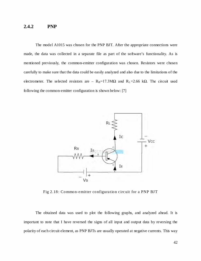
2.4.2 PNP
The model A1015 was chosen for the PNP BJT. After the appropriate connections were
made, the data was collected in a separate file as part of the software’s functionality. As is
mentioned previously, the common-emitter configuration was chosen. Resistors were chosen
carefully to make sure that the data could be easily analyzed and also due to the limitations of the
electrometer. The selected resistors are – RB=17.3MΩ and RL=2.66 kΩ. The circuit used
following the common-emitter configuration is shown below: [7]
Fig 2.18 : Common-emit ter configura t ion c ircuit for a PNP BJT
The obtained data was used to plot the following graphs, and analyzed ahead. It is
important to note that I have reversed the signs of all input and output data by reversing the
polarity of each circuit element, as PNP BJTs are usually operated at negative currents. This way
42

we can work with absolute values of the current and voltage at each stage, which is more
convenient for graphical data analysis.
Fig 2.19 : IC aga inst VCC graph o f A1015 (PNP)
As we can see from the figure above, regulating the base voltage (VB) has an immediate
effect on the collector current (IC) for different levels of source voltage applied (VCC). After an
immediate “jump” as the source voltage from electrometer is applied, the curves follow a similar
trajectory as expected. It can be seen that the magnitude of this initial “jump” for the collector
current is largely dependent on the base voltage, with higher base voltages promoting the current
43

to rise even higher in the lower ends of 1V-2V. For reference, base voltages less than 1V was
also selected for data acquisition. However that promoted hardly any current to pass through as
the barrier voltage had to be overcome (VBE=0.7V for Si). So instead of a curve, the graph was
essentially a straight line travelling on and parallel to the horizontal axis, due to no change in
current. For base voltages shown, the curves proceeded to rise after the initial jump. The curve
for VB=12V is seen to rise at a higher rate compared to that of 8V or 4V, meaning the change in
gradient of this region is also depending on the base voltage applied. This is the amplification of
input current for changing base voltages, a property that is used extensively in electrical circuits.
The currents for the different VB were seen to peak off at around 70V-80V for this
particular circuit. After this stage, the current levels reached higher than that allowed by the
electrometer, so the limit up to which data could be taken was reached.
Since we are working with lower current at around mA to µA range, we can also see the
switching operation of the PNP BJT. For the specific circuit that I designed, the transistor
theoretically remained in the “OFF” state till the curves began to rise drastically around 70V,
before that very little current was allowed to pass through. We can also see that this rise is also
dependent on the base voltage, since higher values promoted the sudden rise to occur at lower
source voltages VCC. So this transistor, other than being an amplifier, can also be used as a
switch that will let substantial current pass through only after a certain critical voltage is applied,
and that specific critical voltage can also be regulated using varying base voltages.
44

For clarity, a closer look at the PNP curves at lower voltages is given below:
Fig 2.20 : IC aga inst VCC graph o f A1015 (PNP) fo r lower source vo ltage
From this figure, the rapid rise in current initially can be easily seen. Before applied
voltage 1V is reached, the curve stops rising as rapidly and increases at rates depending on its
corresponding base voltage used.
45

In order to make the characterization more comprehensive, it was important to compare
the IC graphs obtained for different base voltages to the junction voltage (VCE). This potential
largely depends on collector current IC for different base voltage VB, as this VCE is equal to the
applied voltage VCC minus the drop at the load resistor RL. [8]
VCE = VCC – (IC*RL)
Using the above equation, data was obtained for junction voltage and graph of collector
current IC against junction voltage VCE was plotted:
46

Fig 2.21 : IC aga inst VCE graph for A1015 PNP
47

2.4.3 MOSFET
The enhancement-mode MOSFET, or eMOSFET, is the reverse of the depletion-mode
type. Here the conducting channel is lightly doped or even undoped making it non-conductive.
This results in the device being normally “OFF” (non-conducting) when the gate bias
voltage, VGS is equal to zero. For the n-channel enhancement MOS transistor a drain current will
only flow when a gate voltage (VGS) is applied to the gate terminal greater than the threshold
voltage (VTH) level in which conductance takes place making it a transconductance device. The
application of a positive (+ve) gate voltage to a n-type eMOSFET attracts more electrons
towards the oxide layer around the gate thereby increasing or enhancing (hence its name) the
thickness of the channel allowing more current to flow. This is why this kind of transistor is
called an enhancement mode device as the application of a gate voltage enhances the channel.
Increasing this positive gate voltage will cause the channel resistance to decrease further causing
an increase in the drain current, ID through the channel. In other words, for an n-channel
enhancement mode MOSFET: +VGS turns the transistor “ON”, while a zero or -VGS turns the
transistor “OFF”. Then, the enhancement-mode MOSFET is equivalent to a “normally-open”
switch. A generic characteristic graph of the drain current (ID) to the drain-source potential (VDS)
is shown in the next page. [9]
48

Fig 2.22 : eMOSFET cha racte r is t ic graph with c ircuit symbo ls
Taking into account the overall concept and working principle of MOSFETs, I used a
model 2N7000 n-channel eMOSFET and recorded the drain currents at increasing source
voltages, for particular gate voltage applied. The results are given in the next page:
49

Fig 2.23 : I D aga ins t VCC for lower vo ltages o f the 2N7000 MOSFET
To check the overall consistency of the data obtained, the 2N7000 MOSFET’s datasheet
was consulted extensively. Like the PNP data in the previous section, this analysis is restricted to
currents lower than 10mA due to the electrometer’s limitation. However, adjustments made to
the resistors at the gate and main channel were sufficient to make the data analyzable even at
lower currents than the device is supposed to operate at usually. This meant that low-current
analysis of the transistor device operation was possible, just like in the case for the PNP BJT.
50

From 0V to 1V of VCC, we can see that the device is operating as expected. With
increasing gate voltage, the curve is rising significantly. This is the amplification process
mentioned previously, as a relatively low current from the gate is amplifying the drain current ID
to a larger degree. After an early jump from 0V to 0.05V of source voltage VCC, the current
increases at a reduced rate. Also from this graph, we can see that the change in the curve height
between gate voltage of 3V-6V or 6V-9V is much greater than that created between 9V-14V.
This is because the device is limited to have a maximum gate-source potential VGS of about 10V,
as increasing this further would create very little effect on the drain current. Due to this, the
curves for 9V and 14V are quite similar. This is a direct consequence of the n-channel itself.
With increasing gate voltage, more and more electrons are being attracted towards the
oxide layer around the gate, increasing the thickness of the n-channel. This makes the n-channel
wider with increasing gate voltage such that more current is allowed to pass through. In this way,
we can amplify the output current of the n-channel simply by regulating the gate voltage, which
directly affects the rate at which charge carriers can pass through. This is highlighted in the way
the curves are raised higher for higher gate voltages.
It can also be seen that the curves for 9V is very similar compared to that for 14V of gate
voltage VGS. After further inspection, it was apparent that the maximum gate voltage allowed for
the specific MOSFET was around 10V. From this stage, increasing the gate voltage causes
comparatively few electrons to move towards the oxide layer of the gate. This means that at
VGS=10V, the n-channel is as thick as it can possibly be, so there is little to no change in the I-V
51

graph for increasing the gate voltage any further. This clearly means that the transistor operates
most effectively and efficiently from 0V to 10V of gate voltage VGS.
Next, I took data of drain current ID for further increase in source voltage.
Fig 2.24 : I D aga ins t VCC fo r the 2N7000 MOSFET
Upon further increase of input voltage for varying gate voltage, we can see the trends for the
different curves. After about 3.5V of input voltage, we can see that the curve for VGS=3V begins
52

to flatline, while the other curves continued onwards. From the expected data from the datasheet,
we can categorize the different regions of the graph. The three main regions are:
• 1. Cut-off Region – with VGS < VTH the gate-source voltage is lower than the threshold
voltage so the MOSFET transistor is switched “fully-OFF” and IDS = 0, the transistor acts
as an open circuit
• 2. Linear (Ohmic) Region – with VGS > VTH and VDS < VGS the transistor is in its
constant resistance region and behaves as a voltage-controlled resistor whose resistive
value is determined by the gate voltage, VGS
• 3. Saturation Region – with VGS > VTH the transistor is in its constant current region and
is switched “fully-ON”. The current IDS = maximum as the transistor acts as a closed
circuit [10]
Comparing the data obtained to the datasheet, I was able to separate the regions. According
to the datasheet, the MOSFET has a maximum threshold voltage of about 3V. This falls in line
with the data obtained, as the applied VGS which are at or less than 3V gave curves where the
drain current ID stopped increasing starting from a relatively low source voltage of about 3.5V.
So we can accurately deduce that the threshold voltage VTH is somewhere about 3V. On the
other hand, for VGS> VTH, we can see that the drain current keeps on increasing.
For the VGS=3V we can see that the curve is at the end of its ohmic region at about 3.5V of
VCC, and entering the saturation region where we have the flatline. For the region below this
53
curve, it is referred to as the cut-off region. In this region, we have relatively small ID as the
switch that the transistor is operating as is technically “OFF”. We can clearly see how such a
MOSFET can be used as a switch, as a small increase in current at the gate can promote a
comparatively large increase in the drain current. For this specific transistor, the switch works as
follows:
• OFF – for VGS<3V
• ON – for VGS>3V
The curves for VGS>3V extends onwards as the current keeps on rising in the ohmic
region. Those curves will reach their own saturation region when the drain current will stop
increasing at currents much higher than 10mA, due to which I was only able to focus on the
lower-current high-resistance region. Also given below are the characteristic curves of drain
current ID against the drain-source voltage (VDS). The data for the VDS for its respective ID
values were obtained similar to the PNP, using the equation below:
VDS = VCC – (ID*RL)
With the obtained dataset, a graph of ID against VDS was plotted showing similar trends
to that for the input voltage VCC.
54

Fig 2.25 : ID aga ins t VD S for the 2N7000 eMOSFET
55

Chapter-3: Results and Discussions
With the data for the two transistors obtained and analyzed, I was able to come up with
the results of my work dealing with the transistors’ individual characteristics and electrical
properties. The results should enable the proper operation of such transistors in circuits
pertaining to different electrical applications.
First of all, I made sure that the application that I made using LabVIEW was functioning
correctly using simple silicon diodes and resistors and plotting current-voltage graphs for each
case. After making necessary adjustments and enhancements to the application, I went ahead to
prepare circuits using the transistors which were to be analyzed graphically.
• PNP:
As stated previously it was more convenient to work with reversed polarity for all circuit
elements to obtain the absolute value of the input and output data. The results obtained were first
analyzed for critical values and trends, and then compared to expected data using the model
A1015 PNP datasheet. [11]
Comparing my data to the reference graphs in the datasheet,increasing the base voltage
(and subsequently the base current) we see amplification in the output current IC for the same
source voltage VCC or same junction voltage VCE. Differing from this graph is the fact that it has
56

been plotted for relatively higher current ranges, and thus the saturation region where the
curveflatlines can be seen. However it was possible to determine amplification and switching
actions from a very low current range, making the data ideal for low-current circuits.
From the data obtained for low voltage range, we can also see that the results matches for
those outlined in the datasheet. The base voltages (VB)are replaced with its corresponding base
currents (IB), which is required for determining transistor parameters.
Fig 3.1 : IC aga inst VCE fo r A1015 PNP
57

From the graph, we see that base-emitter saturation begins at around 0.3V. Also, it was
found that base voltages at or below 1V did not promote any collector current IC irrespective of
source voltage. This matches the reference value from the datasheet, as well as the theoretical
value for the barrier voltage for silicon (0.7V). The values from the datasheet are given below for
reference.
Fig 3.2 : Reference data taken from A1015 datasheet
I could also compare transistor parameters from my data to that given in the reference
sheet. The datasheet provides the DC current gain hFE (or β) value for VCE = -6V at room
temperature of 25ºC. The ideal value of β is somewhere around 250 according to the reference
datasheet.
This gain β is the ratio of collector current IC to the base current IB. Another parameter
worth taking into account is α, which is the ratio between collector current IC and emitter current
IE. Since IE = IC + IB, and IB<< IC, the ratio α is usually close to, and less than, unity. Again, we
compare the current values at VCE = 6V (reversed). Using the following equations, it is possible
to find the experimental value of β and α:
58

β = IC / IB
α = IC / IE
The following values for the ratio are obtained using the equation for VCE = 6V:
IC (µA) IB (µA) IE (µA) hFE / β α
VB = 4V 53 0.23 53.23 230 0.9957
VB = 8V 118 0.46 118.46 256 0.9961
VB = 12V 186 0.69 186.69 269 0.9963
Fig 3.3 : I C , IB , IE , β, α fo r A1015 PNP at VCE = 6V
This gives us estimated values(averaged) for α and β at VCE = 6:
α = 0.99603
β = 252
• MOSFET:
As in the case of the PNP BJT, the results obtained for the MOSFET 2N7000 was referred to
the model-specific datasheet for consistency. [12]
59

The graph provided is mostly for high-current circuits, so the data from my work is able
to distinguish the transition from “OFF” to “ON” state to a finer degree at lower currents.
Comparing this to the graph I made from the data obtained, we can see similar trends
assuming operation at room temperature of 25ºC. Increasing the gate voltage, and
subsequently VGS, we see an amplification effect on the output current ID. It is also
identifiable from the graph that gate voltage of 3V can be considered to be the maximum
voltage (threshold voltage) upto which the MOSFET can be considered to be in the “OFF”
state as barely any current is allowed to flow through the drain-source n-channel. This aligns
greatly to my findings, giving us a result for the maximum threshold voltage for the
MOSFET:
VTH(max) = 3V
Comparing the graph I obtained to the reference graph, we also see that the limiting gate
voltage is at VGS = 10V, since there is hardly any change to the curve for 9V compared to that
for 14V. This also falls in line to the MOSFET’s expected characteristics from referencesince at
VGS = 10V, the n-channel is almost as thick as it can be and there is little to no increase in output
current for increasing the gate voltage any further. So using the system employed here, we can
safely estimate the proper working parameters of such specific transistor devices in terms of
efficiency and effectiveness. Summarizing all the data, we find that the MOSFET is turned “ON”
after 3V, and amplification occurs by increasing the gate voltage upto 10V:
• OFF: for VGS< 3V (maximum threshold voltage)
• ON: for 3V < VGS< 10V, since amplification is greatly reduced after VGS = 10V
60

References
[1] Ma, H. (2005). Fundamentals of electronic circuit design. Retrieved fromhttp://www-
mdp.eng.cam.ac.uk/web/library/enginfo/electrical/hong1.pdf
[2] Floyd, Thomas L. (2005). Electronic devices, 7th Edition. Pearson Education
[3] Boylestad, Robert L., Nashelsky, Louis. (1999).Electronic devices and circuit theory, 7th
edition.Prentice Hall
[4] Mini-Coater - high vacuum coating system for thin film deposition. Retrieved
fromhttp://www.tectra.de/mico.htm
[5] (2009). Keithley model 6517B reference manual.Retrieved from
http://www.keithley.com
[6] LabVIEWtutotials. Retrieved from
https://www.labviewmakerhub.com/doku.php?id=learn:tutorials:labview:start
[7] (2015). PNP transistor. Retrieved from
http://www.electronicshub.org/pnp-transistor/
[8] Hayt, William H. (2010). Engineering circuit analysis, 7th edition.McGraw-Hill
[9] (2014). The MOSFET. Retrieved fromhttp://www.electronics-
tutorials.ws/transistor/tran_6.html
[10] nMOSFET (enhancement) characteristic curves. Retrieved from
http://www.physics.csbsju.edu/trace/nMOSFET.CC.html
[11] (2006). A1015 datasheet. Retrieved from http://www.weitron.com.tw
[12] (1997). 2N7000 datasheet. Retrieved from
http://www.alldatasheet.com/datasheet-pdf/pdf/2842/MOTOROLA/2N7000.html
61
Related Documents