Inter-Integrated Circuit (I 2 C) Interface By: Surya Teja Gunukula Hawzhin Raoof Mohammed 1

Welcome message from author
This document is posted to help you gain knowledge. Please leave a comment to let me know what you think about it! Share it to your friends and learn new things together.
Transcript

Inter-Integrated Circuit (I2C) Interface
By:Surya Teja Gunukula
Hawzhin Raoof Mohammed
1

Contents1. The I2C Protocol2. Characteristics of I2C Protocol3. I2C Data Transfer Signal Components4. Data Transfer Format5. Registers for I2C Operation6. Programming the I2C Module7. I2C Data Transfer Mode
8. Interface with the real-time-clock chipDS13079. Interface with DS1631A to measure the ambient temperature10.Store and retrieve data in/from the serial EEPROM chip 24LC08B 2

Networks Connection Type
3

I2C Serial Bus
2 µC on same bus
4

The I2C Protocol• The inter-integrated circuit (I2C) serial interface protocol was developed by Philips in the late 1980s.
• Version 1.0 was published in 1992. This version support:
1. Both 100 kbps (standard mode) and the 400 kbps (fast mode) data rate;
2. 7-bit and 10-bit addressing;
3. Slope control to improve electromagnetic compatibility (EMC) behavior
• Version 2.0 was published in 1998. This version support:
1. 3.4 Mbps (high-speed mode) [is not supported by Gragon12-Plus2 board]
What is the I2C Bus? An Introduction from NXP
(https://www.youtube.com/watch?v=BcWixZcZ6JY)5

Characteristics of I2C Protocol
• Synchronous in nature: A data transfer is always initiated by a master device. A clock signal (SCL)
synchronizes the data transfer. The clock rate can vary without disrupting the data. The data rate will simply
change along with the changes in the clock rate.
• Master/slave model: The master device controls the clock line (SCL). This line dictates the timing of all data
transfers on the I2C bus.
• Bidirectional data transfer: Data can flow in any direction on the I2C bus.
• Serial interface method: I2C uses only signals SCL and SDA. The SCL signal is the serial clock signal; the
SDA signal is known as serial data. In reality, the SDA signal can carry both the address and data.
6

I2C Data Transfer Signal Components
• Start (S)• Stop (P)• Repeated start (R)• Data• Acknowledge (A)
7

I2C Data Transfer Signal Components
START (S) CONDITION:
A start condition indicates that a device would like to transfer data on the I2C bus. As shown in Figure
below, a start condition is represented by the SDA line going low when the clock (SCL) signal is high. The start
condition will initialize the I2C bus. The timing details for the start condition will be taken care of by the
microcontroller that implements the I2C bus.
I2C start condition 8

I2C Data Transfer Signal Components
STOP (P) CONDITION:
A stop condition indicates that a device wants to release the I2C bus. Once released, other devices may
use the bus to transmit data. As shown in Figure below, a stop condition is represented by the SDA signal going
high when the clock (SCL) signal is high. Once the stop condition completes, both the SCL and the SDA signals
will be high. This is considered to be an idle bus. After the bus is idle, a start condition can be used to send more
data.
Stop (P) condition9

I2C Data Transfer Signal ComponentsREPEATED START (R) CONDITION:
A repeated start signal is a start signal generated without first generating a stop signal to terminate the
communication. This is used by the master to communicate with another slave or with the same slave in a different
mode (transmit/receive mode) without releasing the bus. A repeated start condition indicates that a device would like
to send more data instead of releasing the line. This is done when a start must be sent but a stop has not occurred. It
prevents other devices from grabbing the bus between transfers. The timing diagram of a repeated start condition is
shown in Figure below. The repeated start condition is also called a restart condition. In the figure, there is no stop
condition occurring between the start condition and the restart condition.
Fig: Restart condition
10

I2C Data Transfer Signal Components
Data:
The data block represents the transfer of 8 bits of information. The data is sent on the SDA line,
whereas clock pulses are carried on the SCL line. The clock can be aligned with the data to indicate whether
each bit is a 1 or a 0. Data on the SDA line is considered valid only when the SCL signal is high. When SCL is
not high, the data is permitted to change. This is how the timing of each bit works. Data bytes are used to
transfer all kinds of information. When communicating with another I2C device, the 8 bits of data may be a
control code, an address, or data. An example of 8-bit data is shown in Figure below.
I2C bus data elements11

I2C Data Transfer Signal Components
Acknowledge (ACK) Condition
Data transfer in the I2C protocol needs to be acknowledged either positively (A) or negatively
(NACK). As shown in Figure below left, a device can acknowledge (A) the transfer of each byte by bringing
the SDA line low during the 9th clock pulse of SCL. If the device does not pull the SDA line to low and
instead allows the SDA line to float high, it is transmitting a negative acknowledge (NACK). This situation
is shown in Figure below right.
ACK condition NACK condition 12

Data Transfer Format• Master transmitter to slave receiver.• Master reads slave immediately after the first byte (address byte).• Combined format.
13

Data Transfer Format
• Master transmitter to slave receiver: The transfer direction is not changed. An example of this format usingthe 7-bit addressing is shown in Figure below.
Fig : A master transmitter addressing a slave receiver with a 7-bit address
14

Data Transfer Format• Master reads slave immediately after the first byte (address byte): At the moment of the first
acknowledgement, the master transmitter becomes a master receiver and the slave receiver becomes a slave transmitter.
• The first acknowledgement is still generated by the slave. The stop condition is generated by the master,which has previously sent a negative acknowledgement (A).
• An example of this format using the 7-bit addressing is shown in Figure below.
Fig : A master reading a slave immediately after the first byte
15
Data Transfer Format• Combined format: During a change of direction within a transfer, both the start condition and the slave
address are repeated, but with the R/W bit reversed. • If a master receiver sends a repeated start condition, it has previously sent a negative acknowledgement. • An example of this format in the 7-bit addressing is shown in Figure below.
Fig: Combined format
16

Serial clock (SCL)—PJ7/SCL
Dragon12 – Plus2 Development Board
Serial data (SDA)—PJ6/SDA
17

Dragon12 – Plus2 Development Board
Serial clock (SCL)—PJ7/SCL
Serial data (SDA)—PJ6/SDA
XBee wireless module
LCD Display
µC A µC B
18

Registers for I2C OperationThe I2C module has five registers to support its operation.
• I2C address register (IBAD)• I2C control register (IBCR)• I2C status register (IBSR)• I2C data I/O register (IBDR)• I2C frequency divider register (IBFD)
19

Registers for I2C OperationI2C Address Register (IBAD)• The IBAD register contains the address to which the I2C module will respond when it is addressed as a slave.
The contents of this register are shown in Figure below.
I2C address register (IBAD)
20

Registers for I2C Operation
I2C Control Register (IBCR)• This register controls all the operation parameters except the baud rate of the I2C module. • When the MS/SL bit is changed from 0 to 1, a start signal is generated on the bus and the master
mode is selected. • When this bit is changed from 1 to 0, a stop signal is generated and the operation mode changes
from master to slave.
I2C control register (IBCR)
21
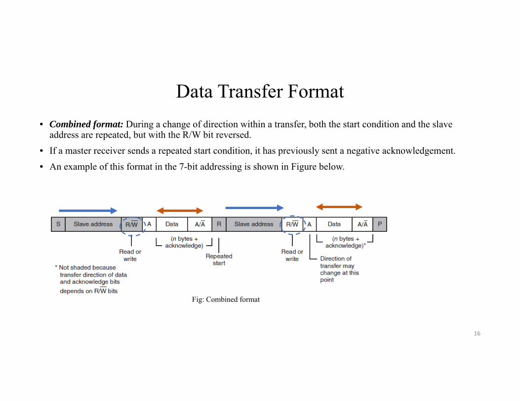
Registers for I2C Operation
I2C Control Register (IBCR)• IBEN: I2C bus enable
0 = I2C module is reset and disabled.1 = I2C module is enabled. This bit must be set before any other IBCR bits have any effect.
• IBIE: I2C bus interrupt enable0 = interrupts from the I2C module are disabled.1 = interrupts from the I2C module enabled.
• MS/SL: master/slave mode select0 = slave mode.1 = master mode.
• Tx/Rx: transmit/receive mode select0 = receive.1 = transmit.
I2C control register (IBCR)
22

Registers for I2C Operation
I2C Control Register (IBCR)• TxAK: transmit acknowledge
0 = an acknowledge signal will be sent out to the I2C bus on the 9th clock bit after receiving 1 byte of data.
1 = no acknowledge signal response is sent.• RSTA: repeat start
0 = no action.1 = generate a repeat start cycle.
• IBSWAI: I2C bus stop in wait mode0 = I2C module clock operates normally.1 = stop generating I2C module clock in wait mode.
I2C control register (IBCR)
23

Registers for I2C Operation
I2C status register (IBSR)This register records the status of all I2C data transmission/reception activities. The contents of this
register are shown in Figure below.
I2C status register (IBSR)
24

Registers for I2C OperationI2C status register (IBSR)• TCF: data transferring bit
0 = I2C transfer in progress.
1 = I2C transfer complete.
• IAAS: addressed as a slave0 = not addressed.
1 = addressed as a slave.
• IBB: bus busy bit0 = the bus enters idle state.
1 = I2C bus is busy.
• IBAL: arbitration lost0 = arbitration is not lost.
1 = arbitration is lost.
I2C status register (IBSR)
25

Registers for I2C Operation
I2C status register (IBSR)SRW: slave read/write
0 = slave receive, master writing to slave.
1 = slave transmit, master reading from slave.
IBIF: I2C bus interrupt0 = no bus interrupt.
1 = bus interrupt.
RXAK: receive acknowledgeThis bit reflects the value of SDA during the acknowledge bit of a cycle.
0 = acknowledge received.
1 = no acknowledge received.
I2C status register (IBSR)
26

Registers for I2C Operation
I2C data I/O register (IBDR)• In master transmit mode (the TxRx bit of the IBCR register set to 1), when data is written into the IBDR
register a data transfer is initiated. • The most significant bit is sent out first. In master receive mode, reading this register initiates the reception of
the next byte. • Nine clock pulses will be sent out on the SCL pin to shift in 8 data bits and send out the acknowledge bit. • In slave mode, the same functions are available after an address match has occurred.
27

Registers for I2C Operation
• I2C frequency divider register (IBFD)The most important design consideration of the I2C module is to meet the timing requirements for the start and stop conditions so that data can be correctly transmitted over the bus line. As illustrated in Figure below, there are four timing requirements to be met.• SCL divider• SDA hold time• SCL hold time for start condition• SCL hold time for stop condition
SCL divider and SDA hold
28

Registers for I2C Operation
• I2C frequency divider register (IBFD)The requirements of these four parameters are listed in Table below. The SCL divider is equal to the bus frequency of the MCU divided by the SCL clock frequency.
I2C bus timing requirements
29

Registers for I2C OperationI2C frequency divider register (IBFD)
The I2C timing parameters are set by programming the I2C frequency divider register (IBFD). The contents of this register are shown in Figure below. The contents of this register are used to pre-scale the bus clock for bit rate selection.The use of these 8 bits is as follows:• IBC7-IBC6: multiply factor.• IBC5-IBC3: pre-scaler divider.• IBC2-IBC0: shift register tap points.
I2C frequency divider register (IBFD)
30

Registers for I2C Operation
I2C frequency divider register (IBFD)• IBC7-IBC6: multiply factor.
Multiply factor table
31

Registers for I2C Operation
I2C frequency divider register (IBFD)• IBC5-IBC3: pre-scaler divider.
Pre-scaler divider table
32

Registers for I2C Operation
I2C frequency divider register (IBFD)• IBC2-IBC0: shift register tap points.
I2C bus tap and pre-scale values
33

Registers for I2C Operation
I2C frequency divider register (IBFD)• The equation for generating the divider value from the IBFD bits is:
SCL divider = MUL x 2 x {scl2tap + [(SCL_tap - 1) x tap2tap] + 2}
• The SDA hold delay is equal to the bus clock period multiplied by the SDA hold value. The equation used to generate the SDA hold value from the IBFD bits is:
SDA hold = MUL x {scl2tap + [(SDA_tap - 1) x tap2tap] + 3)}
• The equations for HCL hold values to generate the start and stop conditions from IBFD bits are as follows:SCL hold (start) = MUL x [scl2start + (SCL_tap - 1) x tap2tap]SCL hold (stop) = MUL x [scl2stop + (SCL_tap - 1) x tap2tap]
34

Programming the I2C Module
Initializing I2C moduleBefore the I2C module can transmit and receive data correctly, it must be initialized properly. The initialization procedure is as follows:
Step1: Compute the value that can obtain the SCL frequency from the E-clock and use it to update the IBFD register.
Step 2: Load the IBAD register to define its slave address.
Step 3: Set the IBEN bit of the IBCR (Control) register to enable the I2C system.
Step 4: Modify the bits of the IBCR register to select master/slave mode, transmit/receive mode, and interruptenable mode.
35

Programming the I2C ModuleInitializing I2C module• The subroutine that performs the I2C initialization
openI2C : bset IBCR, IBEN ; enable I2C modulestaa IBFD ; establish SCL frequencystab IBAD ; establish I2C module slave addressbclr IBCR, IBIE ; disable I2C interruptbset IBCR, IBSWAI ; disable I2C in wait moderts
Generation of the Start Condition:
• If the MCU is connected to a multi-master bus system, the state of the IBB bit of the IBSR register must be tested
to check whether the serial bus is busy. If the bus is idle (IBB = 0), the start condition and the first byte can be sent.36

I2C Data Transfer Mode
I2C Data Transfer in Master Mode
• When the HCS12 I2C module is configured as a master, it is responsible for initiating the data transmission
and reception. By writing a byte into the IBDR register, nine clock pulses are generated to shift out 8 bits of
data and shift in the acknowledgement bit.
• After sending the slave ID and receiving the acknowledgement from the slave, the I2C module can send out a byte by performing
staa IBDRbrclr IBSR, IBIF, * ; wait until IBIF flag is set to 1movb #IBIF, IBSR ; clear the IBIF flag
• To send multiple bytes to the slave, we have to place these three instructions in a loop and use an index
register to point to the data to be sent. 37

I2C Data Transfer in Master ModeFor Master receiving:Step 1 Clear the Tx/Rx bit of the IBCR register to 0 for data reception.
1. Clear TxAk bit; if user wants to acknowledge multiple bytes2. Set TxAk bit; if user wants to read only one byte
Step 2 Perform a dummy read. This action will trigger nine clock pulses to be sent out on the SCL pin to shift in 8 data bits and send out acknowledgement.
Step 3 Wait until the IBIF flag is set to 1.Step 4 Clear the IBIF flag by writing a 1 to it.
bclr IBCR, TXRX+TXAK ; prepare to receive and acknowledge
ldaa IBDR ; a dummy read to trigger nine clock pulses
brclr IBSR, IBIF, * ; wait until the data byte is shifted in
movb #IBIF, IBSR ; clear the IBIF flag
ldaa IBDR ; place the received byte in A and also initiate the next read sequence38

I2C Data Transfer in Slave Mode
In slave mode, the I2C module cannot initiate any data transfer. Once the I2C module is enabled in
slave mode, it waits for a start condition to occur. Following the start condition, 8 bits are shifted into the IBDR
register. The value of the upper 7 bits of the received byte is compared with the IBAD register. If the address
matches, the following events occur:
• The bit 0 of the address byte is copied into the SRW bit of the IBSR register.• The IAAS bit is set to indicate address match.• An ACK pulse is generated regardless of the value of the TxAK bit.• The IBIF flag is set.
39

I2C Data Transfer in Slave ModeInstruction sequence for data transfer:
brset IBSR, IAAS, addr_match ; is address matched?
….
addr_match brclr IBSR, SRW, slave_rd
bset IBCR, TXRX ; prepare to transmit data
movb tx_buf, IBDR ; place data in IBDR to wait for SCL to shift it out
brclr IBSR, IBIF,* ; wait for data to be shifted out
…..
slave_rd bclr IBCR, TXAK+TXRX ; prepare to receive and send ACK
brclr IBSR,IBIF,* ; wait for data byte to shift in
movb #IBIF,IBSR ; clear the IBIF flag
movb IBDR,rcv_buf ; save the received data
• Data transmission and reception in I2C protocol can also be made interrupt-driven using the interrupt
mechanism to control; while other tasks during the waiting period. 40

Contents
1. Interface with the real-time-clock chipDS1307
2. Interface with DS1631A to measure the ambient temperature
3. Store and retrieve data in/from the serial EEPROM chip 24LC08
41

Interface with Serial Real-Time Clock DS1307
• VCC, GND: DC power input. VCC is the +5 V input. When a 5-V
voltage is applied to this pin, the device is fully accessible and data can
be written and read.
• SQWOUT: square wave output driver. When enabled (by setting the
SQWE bit of the control byte to 1. The SQWOUT pin is open drain
and requires an external pull-up resistor.
• X1, X2: crystal connection. These two pins are used for connections to
a standard
32,768-Hz quartz crystal.
42

DS1307 Control Register
• The time and calendar are set or initialized by writing the appropriate register bytes, and the contents of the registers are in the BCD format.
• Bit 7 of register 0 is the clock halt (CH) bit. When this bit is set to 1, the oscillator is disabled.
• When this bit is a 0, the oscillator is enabled. This bit should be cleared to 0 after reset.
• The initial power-on states of all registers are not defined.
• Bit 6 of the hours register is defined as the 12- or 24-hour mode-select bit. if bit 6 is high – 12hrs mode if bit 6 is low - 24hrs mode
• In the 12-hour mode, bit 5 is the AM/PM bit, with logic high being PM. In the 24-hour mode, bit 5 is the second 10-hour bit (20,23 hours).
43

DS1307 Control Register• Bit 7 controls the output level of the SQWOUT pin when the square output is disabled (SQWE=0).
• When bit 7 is 1, the SQWOUT output level is 1 when bit 4 (the SQWE bit) is set to 0.
• Otherwise, the SQWOUT output level is 0. The SQWE bit enables the SQWOUT pin (oscillator) output.
• The frequency of the SQWOUT output depends on the values of the RS1, RS0 bits.
44

Data TransferThe device address of the DS1307 is %1101000.
There are two types of data transfer between the DS1307 and an MCU: slave receiver mode and slave transmitter mode.
Slave Receiver Mode : In this mode, the MCU sends the device address of the DS1307, the address of the register to be accessed, and one or multiple data bytes to the DS1307. The following events occur:
• The MCU generates a start condition.
• The MCU sends a device address byte to the DS1307 with the direction bit (R/W) set to 0.
• DS1307 acknowledges the address byte.
• The MCU sends the address of the register to be accessed to the DS1307. This value sets the register pointer. Only the address of the first register needs to be sent to the DS1307 during a multiple-byte transfer.
• The MCU generates the stop condition to terminate the data write.
45

Slave Transmitter Mode:
In this mode, the MCU sends the device address of the DS1307 and the address of the register to be read to the
DS1307.
• The MCU generates a start condition.
• The MCU sends a device address byte to the DS1307 with the direction bit (R/W) set to 0.
• DS1307 acknowledges the address byte.
• The MCU sends the address of the register to be accessed to the DS1307. This value sets the register pointer. The
register pointer is incremented by 1 after each register transfer.
• The DS1307 acknowledges the register address byte.
• The MCU generates a restart condition
Data Transfer
46

Ex: Program a function to configure the DS1307 to operate SQWOUT output set to 1 Hz & SQWOUT idle high when it is disabled.• The user needs to send the following bytes to the DS1307:• Address byte $D0 (bit 0 is 0 to select write operation)• Register address $07• Control byte $90 (passed in accumulator B)
openDS1307: ldaa #$D0 ; place DS1307 ID in Ajsr sendSlaveIDbrclr IBSR, RXAK, sndRegAdr ; did
;DS1307 acknowledge?ldab #$FF ; return 21 as error coderts
sndRegAdr: movb #$07, IBDR ; send out the control register address
brclr IBSR, IBIF, * ; wait until the register address is shifted out
movb #IBIF, IBSR ; clear the IBIF flagbrclr IBSR, RXAK, sndok ; did DS1307
acknowledge?ldab #$FFrts
sndok : stab IBDR ; send out control bytebrclr IBSR,IBIF,* ; wait until the control
byte is shifted outmovb #IBIF,IBSRbclr IBCR,MSSL ; generate stop conditionrts
Configure the DS1307
47

char readTime(char cx)
{ char i, temp;
sendSlaveID(0xD0); /* generate a start condition and send DS1307’s ID */
if (IBSR & RXAK)
return ‐1; /* if DS1307 did not respond, return error code */
IBDR = cx; /* send address of seconds register */
while(!(IBSR & IBIF));
IBSR = IBIF; /* clear the IBIF flag */
if (IBSR & RXAK)
return ‐1; /* if DS1307 did not respond, return error code */
IBCR |= RSTA; /* generate a restart condition */
IBDR = 0xD1; /* send ID and set R/W flag to read */
while(!(IBSR & IBIF));
IBSR = IBIF;
if (IBSR & RXAK)
return ‐1; /* if DS1307 did not respond, return error code */
IBCR &= ~(TXRX + TXAK); /* prepare to receive and acknowledge */temp = IBDR; /* a dummy read to trigger nine clock pulses */
for (i = 0; i < 5; i++) {
while(!(IBSR & IBIF)); /* wait for a byte to shift in */
IBSR = IBIF; /* clear the IBIF flag */
cur_time[i] = IBDR; } /* save the current time in buffer */ /* also initiate the next read */
while (!(IBSR & IBIF)); /* wait for the receipt of cur_time[5] */
IBSR = IBIF; /* clear IBIF flag */
IBCR |= TXAK; /* not to acknowledge cur_time[6] */
cur_time[5] = IBDR; /* save cur_time[5] and initiate next read */
while (!(IBSR & IBIF));
IBSR = IBIF;
IBCR &= ~MSSL; /* generate stop condition */
cur_time[6] = IBDR;
return 0;} 48

Contents
1. Interface with the real-time-clock chipDS1307
2. Interface with DS1631A to measure the ambient temperature
3. Store and retrieve data in/from the serial EEPROM chip 24LC08
49
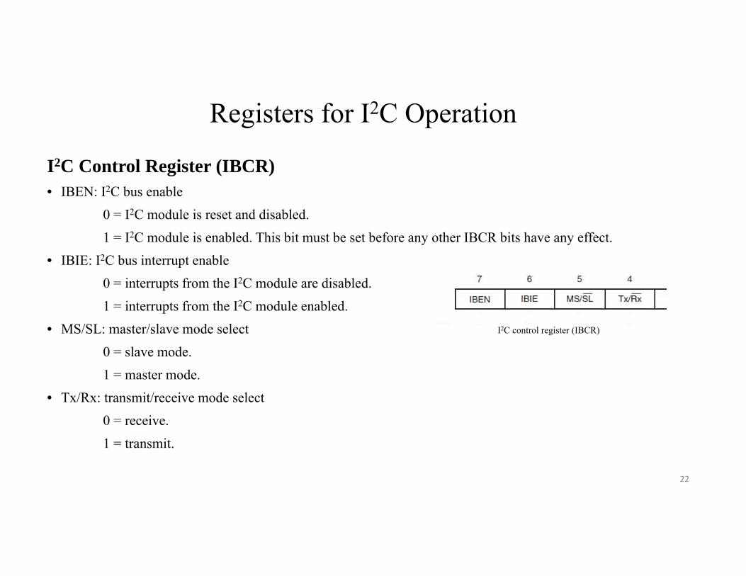
The Digital Thermometer and Thermostat (DS1631A)Many embedded products, such as network routers and switches, are used in larger systems, and their
failures due to overheating could severely damage the functioning or even cause the total failure of the larger system. Using a thermostat to warn of potential overheating is indispensable for the proper functioning of many embedded systems. The digital thermostat device DS1631A from Dallas Semiconductor is one such product. The DS1631A will assert a signal (TOUT) whenever the ambient temperature exceeds the trip point pre-established by the user. • The SDA and SCL pins are used as the data and clock lines so that the DS1631A can be connected to an I2C bus.• Pins A2, A0 are address inputs to the DS1631A. • And the TOUT pin is the thermostat output.
50

Functional Description:• The DS1631A converts the ambient temperature
into 9-, 10-, 11-, or 12-bit readings over a range of -55 to +125°C.
• The thermometer accuracy is +/- 0.5°C from 0 to +70°C with 3.0 V <=VDD <= 5.5 V.
• The thermostat output TOUT is asserted whenever the converted ambient temperature is equal to or higher than the value stored in the TH register.
The Digital Thermometer
51

• The SRAM-based Temperature register is a 2-byte register that holds the converted temperature value in two’s complement format.
• The converted temperature is stored in the upper bits of the Temperature register with lower bits filled with 0s. When the most significant bit of this register is 1, the temperature is negative.
• Both the TH and TL are EEPROM-based 2-byte registers. Where, TH & TL holds the upper alarm temperature value in two’s complement format.
if i/p ≥ TH ; then TOUT is asserted.• TOUT can be de-asserted only when the converted temperature is lower than the value in the TL register.
DS1631A Registers
52

DS1631A RegistersConfig Register:• The lower 2 bits of the configuration register are EEPROM based, whereas the upper 6 bits are SRAM-based.• This register can be read from and written into using the Access Config[0xAC] command. • When writing to the Config register, conversions should first be stopped using the Stop Convert T[0x22]
command if the device is in continuous conversion mode. Since the POL and 1SHOT bits are stored in EEPROM, they can be programmed prior to installation if desired.
POL: TOUT polarity (read/write)0 = TOUT active low.1 = TOUT active high.
1SHOT: conversion mode (read/write)
0 = continuous conversion mode. The Start Convert T command initiatescontinuous temperature conversions.
1 = one-shot mode. The Start Convert T command initiates a single temperatureconversion and then the device enters a low-power standby mode.
53

• Done: temperature conversion done (read-only)0 = temperature conversion is in progress.1 = temperature conversion is complete. Will be cleared when the Temperature register is read.
• THF: temperature high flag (read/write)0 = the measured temperature has not exceeded the value in TH register.1 = the measured temperature has exceeded the value in TH register. THF remains at 1 until it is
overwritten with a 0 by the user, the power is recycled, or a software POR command is issued.• TLF: temperature low flag (read/write)
0 = the measured temperature has not been lower than the value in TL register.1 = at some point after power-up, the measured temperature is lower than the value stored in the TL
register. TLF remains at 1 until it is overwritten with a 0 by the user, the power is recycled, or a software POR command is issued.
• NVB: nonvolatile memory busy (read only)0 = NV memory is not busy.1 = A write to EEPROM memory is in progress
DS1631A Registers
54

• The DS1631A begins conversions automatically at power-up.• The default resolution of the DS1631A is 12-bit which can be changed via the R1:R0 bits of the Config register.• TH & TL registers resolutions match the output temperature resolution and are determined by the R1:R0 bits.• Writing to and reading from these two registers are achieved by using the Access TH[0xA1] and
Access TL[0xA2] commands. • When making changes to the TH and TL registers, conversions should first be stopped using the Stop Convert T
command if the device is in continuous conversion mode.
• The conversion result cannot be higher than 0x7D00 or lower than 0xC900 because the range of temperature that can be handled by DS1631A cannot be higher than 125°C or lower than 255°C.
DS1631A Operation
55

POSITIVE CONVERSION RESULTStep 1 - Remove the lowest 4 bits.Step 2 - Divide the upper 12 bits by 16.
• For example, the conversion result 0x7000 corresponds to 0x700/16 = 112°C. The conversion result 0x6040 corresponds to 0x604/16 = 96.25°C.
NEGATIVE CONVERSION RESULTStep 1 - Compute the two’s complement of the conversion result.Step 2 - Remove the lowest 4 bits.Step 3 - Divide the upper 12 bits of the two’s complement of the conversion result by 16.
• For example, the conversion result 0xE280 corresponds to 20x1D8/16 5 229.5°C.
DS1631A Command Set
• Read Temperature [0xAA]. This command reads the last converted temperature value from the 2-byte Temperature
register.
• Software POR [0x54]. This command initiates a software power-on-reset operation, which stops temperature
conversions and resets all registers and logic to their power-up states. The software POR allows the designer to simulate
cycling the power without actually powering down the device.
DS1631A Operation
56

I2C Communication with DS1631A
• To initiate I2C communication, the HCS12 MCU asserts a start condition followed by a control byte containing the DS1631A device ID.
• The R/W bit of the control byte must be a 0 since the HCS12 MCU next will write a command byte to the DS1631A.
HCS12 DS1631A
1 R/W = 0Command Byte
2 Ack
3 Command Byte Type of operation
4 Ack
Stop Convert T5 Start convert T (or)
Communication b/w HCS12 & DS1631A57

WRITE DATA TO DS1631A • The master can write data to the DS1631A by issuing an Access Config, Access TH, or Access TL command.• After receiving an ACK in response to the command byte, the master device can immediately begin
transmitting data. • After receiving each data byte, the DS1631A responds with an ACK, and the transaction is finished with a
stop from the master.
READ DATA FROM DS1631A• The master can read data from the DS1631A by issuing an Access Config, Access TH, Access TL, or Read
Temperature command following the control byte.• After receiving an ACK in response to the command, the master must generate a Restart condition followed
by a control byte with the same slave ID with R/W = 1 to read data.• After sending an ACK in response to this control byte, the DS1631A begins transmitting the requested data on
the next clock cycle.• If only the most significant byte of data is needed, the master can issue a NACK followed by a stop condition
after reading the first data byte.
I2C Communication with DS1631A
58

DS1631A Example Program#include <hidef.h> /* common defines and macros */#include "derivative.h" /* derivative-specific definitions */void MSDelay(unsigned int);
void main(void) { /* put your own code here */DDRB = 0xFF; //PORTB as outputDDRJ = 0xFF; //PTJ as output for Dragon12+ LEDsPTJ=0x0; //Allow the LEDs to dsiplay data on PORTB pins
ATD0CTL2 = 0x80; //Turn on ADC,..No InterruptMSDelay(5);ATD0CTL3 = 0x08; //one conversion, no FIFOATD0CTL4 = 0xEB; //8-bit resolu, 16-clock for 2nd phase,
// prescaler of 24 for Conversion Freq=1MHz for(;;){ ATD0CTL5 = 0x85; //Channel 5 (right justified, unsigned, single-conver,one chan only) while(!(ATD0STAT0 & 0x80));PORTB = ATD0DR0L; //dump it on LEDs
MSDelay(2); //optional} }
void MSDelay(unsigned int itime){ unsigned int i; unsigned int j;
for(i=0;i<itime;i++)for(j=0;j<4000;j++); } 59

Contents
1. Interface with the real-time-clock chipDS1307
2. Interface with DS1631A to measure the ambient temperature
3. Store and retrieve data in/from the serial EEPROM chip 24LC08
60

Interfacing the Serial EEPROM 24LC08B with I2C
• Many applications require the use of a large amount of nonvolatile memory because these applications are powered by
batteries and may be used in the field for an extended period of time.
• In our Dragon Board we are having 24LC08B. It is a serial EEPROM from Microchip with the I2C interface.
• This device is an 8-kbit EEPROM organized as four blocks of 256 * 8-bit memory.
• Low-voltage design permits operation down to 2.5 V with standby and active currents of only 1 μA and 1 mA,
respectively. The 24LC08B also has a page-write capability for up to 16 bytes of data.
• The SCL and SDA pins are for I2C bus communications.
• The frequency of the SCL input can be as high as 400kHz.
• The WP pin is used as the write protection input. When this pin is high, the 24LC08B cannot be written into.
• A0,A1,A2 are not used. 61

Device Addressing
• Like any other I2C slave, the first byte sent to the 24LC08B after the
start condition is the control byte.
• The upper 4 bits are the device ID of the 24LC08B, and the value
represented by bits B1,B0 is the block address of the memory
location to be accessed.
• For any access to the 24LC08B, the master must also send an 8-bit
byte address after the control byte.
• There is an address pointer inside the 24LC08B. After the access of
each byte, the address pointer is incremented by 1.
62

Write Operation• The 24LC08B supports byte write and page-write operations. i) In a byte write operation,
Master EEPROM24LC08B
1 Start condition & Control byte
2 ACK
4 ACK
6 ACK
3 Byte Address
5 Data Byte
7 Stop Condition
Communication b/w Master & EEPROM 63

ii) In a page-write operation,
• The master can send up to 16 bytes of data to the 24LC08B. The write control byte, byte address, and the first
data byte are transmitted to the 24LC08B in the same direction.
• But instead of asserting a stop condition, the master transmits up to 16 data bytes to the 24LC08B that are
temporarily stored in the on-chip page buffer.
• These 16 data bytes will be written into the memory after the master has asserted a stop condition.
• After the receipt of each byte, the 4 lower address pointer bits are internally incremented by 1. The highest 6
bits of the byte address remain constant.
• The master should transmit more than 16 bytes prior to generating the stop condition, so the address counter
will roll over and the previously received data will be overwritten.
Write Operation
64

• 24LC08B supports three types of read operations: current address read, random read, and sequential read.i) Current Address Read
• The internal address counter is incremented by 1 after each access (read or write). • The current address read allows the master to read the byte immediately following the location accessed by the
previous read or write operation. • On receipt of the slave address with the R/W bit set to 1, the 24LC08B issues an acknowledgement and transmits an
8-bit data byte. • The master will not acknowledge the transfer but asserts a stop condition and the 24LC08B discontinues transmission.ii) Random Read
• Random read operations allow the master to access any memory location in a randommanner.
I2CMaster
EEPROM24LC08B
Start condition control signal R/W = 0
1
3
4
5
6
7
8
9
2 ACK
ACK
ACK
Address of byte to read
repeated start condition
Control byte with R/W = 1
ACK & sends data to master
NACK & Stop Condition
Read Operation
65

iii) Sequential Read
• If the master acknowledges the data byte returned by the random read operation, the 24LC08B transmits the
next sequentially addressed byte as long as the master provides the clock signal on the SCL line.
• The master can read the whole chip using sequential read.
• Sequential read is performed in a block read operation. When the MCU saves the contents of the IBDR register, it also initiates a sequential read if the MCU acknowledges the previously received byte.
Read Operation
66

Thank You
Questions ?67
Related Documents