1 1 Intel’s High Intel’s High - - k/Metal Gate k/Metal Gate Announcement Announcement November 4th, 2003 November 4th, 2003

Welcome message from author
This document is posted to help you gain knowledge. Please leave a comment to let me know what you think about it! Share it to your friends and learn new things together.
Transcript
11
Intel’s HighIntel’s High--k/Metal Gate k/Metal Gate AnnouncementAnnouncement
November 4th, 2003November 4th, 2003
22
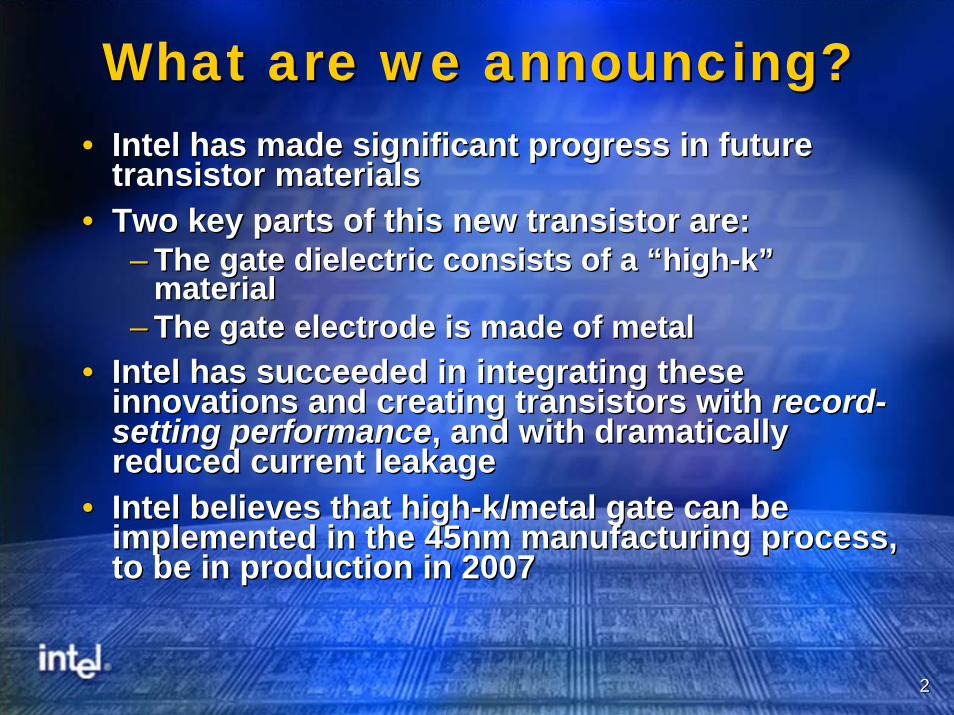
What are we announcing?What are we announcing?•• Intel has made significant progress in future Intel has made significant progress in future
transistor materialstransistor materials•• Two key parts of this new transistor are:Two key parts of this new transistor are:
–– The gate dielectric consists of a “highThe gate dielectric consists of a “high--k” k” materialmaterial
–– The gate electrode is made of metalThe gate electrode is made of metal•• Intel has succeeded in integrating these Intel has succeeded in integrating these
innovations and creating transistors with innovations and creating transistors with recordrecord--setting performancesetting performance, and with , and with dramatically dramatically reduced current leakagereduced current leakage
•• Intel believes that highIntel believes that high--k/metal gate can be k/metal gate can be implemented in the 45nm manufacturing process, implemented in the 45nm manufacturing process, to be in production in 2007to be in production in 2007
33
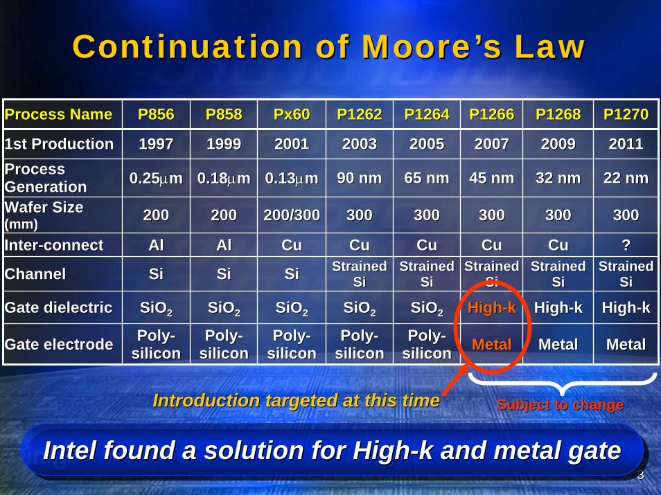
Continuation of Moore’s LawContinuation of Moore’s Law
Process NameProcess Name P856P856 P858P858 Px60Px60 P1262P1262 P1264P1264 P1266P1266 P1268P1268 P1270P1270
ChannelChannel SiSi SiSi SiSi Strained Strained SiSi
Strained Strained SiSi
Strained Strained SiSi
Strained Strained SiSi
Strained Strained SiSi
1st Production1st Production 19971997 19991999 20012001 20032003 20052005 20072007 20092009 20112011Process Process GenerationGeneration 0.250.25µµmm 0.180.18µµmm 0.130.13µµmm 90 nm90 nm 65 nm65 nm 45 nm45 nm 32 nm32 nm 22 nm22 nm
Wafer Size Wafer Size (mm)(mm) 200200 200200 200/300200/300 300300 300300 300300 300300 300300
InterInter--connectconnect AlAl AlAl CuCu CuCu CuCu CuCu CuCu ??
Gate dielectricGate dielectric SiOSiO22 SiOSiO22 SiOSiO22 SiOSiO22 SiOSiO22 HighHigh--kk HighHigh--kk HighHigh--kk
Gate electrodeGate electrode PolyPoly--siliconsilicon
PolyPoly--siliconsilicon
PolyPoly--siliconsilicon
PolyPoly--siliconsilicon
PolyPoly--siliconsilicon MetalMetal MetalMetal MetalMetal
Introduction targeted at this timeIntroduction targeted at this time Subject to change Subject to change
Intel found a solution for High-k and metal gateIntel found a solution for HighIntel found a solution for High--k and metal gatek and metal gate

44
Why is this important?Why is this important?•• These steps are necessary if transistors These steps are necessary if transistors
are to continue shrinking and delivering are to continue shrinking and delivering better performance, while containing better performance, while containing power consumptionpower consumption
•• Many others have been working on the Many others have been working on the same problem for some time, but no same problem for some time, but no company is as far along as Intelcompany is as far along as Intel
•• These steps will enable the continuation These steps will enable the continuation of Moore’s Law, ultimately leading to vast, of Moore’s Law, ultimately leading to vast, lower costlower cost computing power and enabling computing power and enabling applications that cannot even be imagined applications that cannot even be imagined todaytoday
55
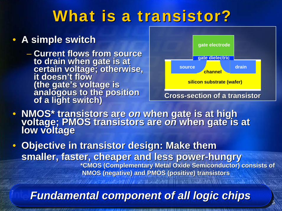
What is a transistor?What is a transistor?•• A simple switchA simple switch
–– Current flows from sourceCurrent flows from sourceto drain when gate is at to drain when gate is at certain voltage; otherwise,certain voltage; otherwise,it doesn’t flow it doesn’t flow (the gate’s voltage is (the gate’s voltage is analogous to the position analogous to the position of a lightof a light switch)switch)
•• NMOS* transistors are NMOS* transistors are onon when gate is at high when gate is at high voltage; PMOS transistors are voltage; PMOS transistors are onon when gate is at when gate is at low voltagelow voltage
•• Objective in transistor design: Make them Objective in transistor design: Make them smaller, faster, cheaper and less powersmaller, faster, cheaper and less power--hungryhungry
*CMOS (Complementary Metal Oxide Semiconductor) consists of *CMOS (Complementary Metal Oxide Semiconductor) consists of NMOS (negative) and PMOS (positive) transistorsNMOS (negative) and PMOS (positive) transistors
silicon substrate (wafer)
gate electrode
source drain
gate dielectric
channel
CrossCross--section of a transistorsection of a transistor
Fundamental component of all logic chipsFundamental component of all logic chipsFundamental component of all logic chips

66
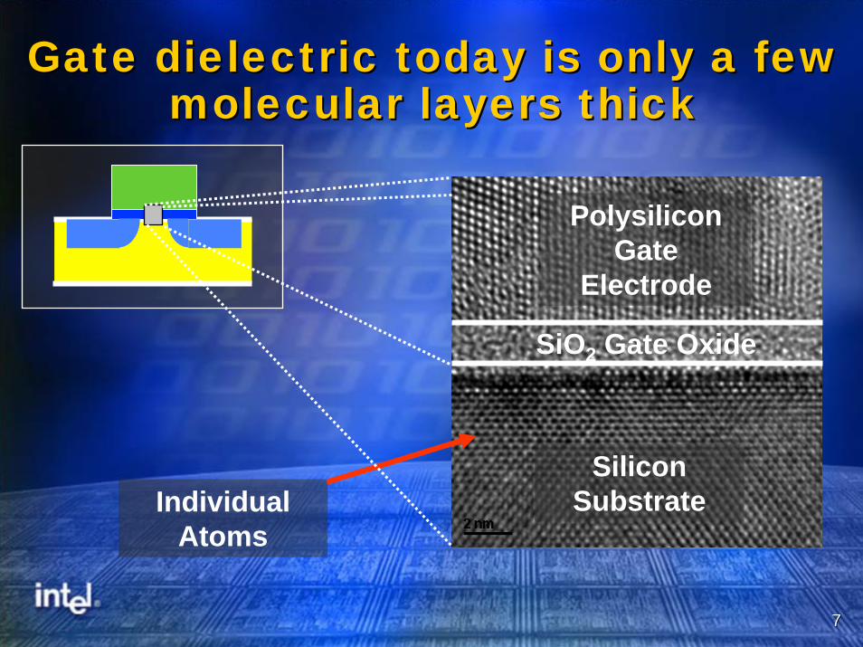
What’s the problem as transistors What’s the problem as transistors are made smaller?are made smaller?
•• Smaller transistors are faster Smaller transistors are faster and cheaper, but … and cheaper, but … –– Gate dielectrics, traditionallyGate dielectrics, traditionally
made with Silicon Dioxidemade with Silicon Dioxide(SiO(SiO22)), are only a few , are only a few atomic layers thickatomic layers thick
•• SiOSiO22 is ideally an insulator,is ideally an insulator,but at this thinness, current but at this thinness, current leaks throughleaks through–– Think of a faucet that drips Think of a faucet that drips
when it should be offwhen it should be off
A new material is needed to reduce leakageA new material is needed to reduce leakageA new material is needed to reduce leakage
77
Gate dielectric today is only a few Gate dielectric today is only a few molecular layers thickmolecular layers thick
Polysilicon Gate
Electrode
Silicon Substrate
SiO2 Gate Oxide
Individual Atoms

88
Seeking new materials Seeking new materials to drive Moore‘s Lawto drive Moore‘s Law
“SiO2 is at the very heart of the transistor, and replacing it is like performing a heart transplant,” said Robin Degraeve, a researcher at the Interuniversity Microelectronics Center (IMEC) based in Leuven, Belgium.EE Times. 4/8/03, “High-k insulators line up at the gate”
"Failure to address leakage current could make the problem the big stumbling block to Moore's Law. Today's approaches to the problem are only getting the industry half way home, and the solutions to handle the rest of the job haven't been invented yet,"University of Tokyo professor Takayasu Sakurai told the International Solid-State Circuits Conference in a keynote address.EE Times. 2/10/2003, “Leakage current called obstacle to chip complexity”
“As the scaling of classical bulk Si CMOS transistors approaches its fundamental limits, innovative device structures and new materials must be considered to continue the historic progress in information processing and transmission.”IEEE Electron Device Letters, Vol. 23, No. 8, August 2002: “Germanium MOs Capacitors Incorporating Ultrathin High-k Gate Dielectric”
“High-k is a very tough problem,” he [BijanDavari, vice president of tech development at IBM Microelectronics] said. “People have started working on it, but not enough attention has been paid to it. Silicon dioxide is this amazing material, the interface with silicon is so good, it will take more time to develop alternatives.”EE Times, 6/11/02, “Technologist sketches IBM’s silicon road map”
Power issue is huge - industry recognizes that high-k is neededPower issue is huge Power issue is huge -- industry recognizes that highindustry recognizes that high--k is neededk is needed

99
What is HighWhat is High--k?k?
•• The industry is searching for an SiOThe industry is searching for an SiO22replacementreplacement–– Intel has led SiOIntel has led SiO22 gate oxide scaling gate oxide scaling
for over a decadefor over a decade•• This material should be thicker (to reduce This material should be thicker (to reduce
leakage) but should have a high “k” value leakage) but should have a high “k” value –– “k”, the dielectric constant of a material, “k”, the dielectric constant of a material,
relates directly to the transistor’s relates directly to the transistor’s performanceperformance
–– When the faucet is turned on, water should When the faucet is turned on, water should gush outgush out

1010
HighHigh--k Dielectric reduces leakage k Dielectric reduces leakage substantiallysubstantially
Silicon substrate
Gate
3.0nm High-k
Silicon substrate
1.2nm SiO2
Gate
Benefits compared to current process technologiesBenefits compared to current process technologies
HighHigh--k vs. SiOk vs. SiO22 BenefitBenefit
CapacitanceCapacitance 60% greater60% greater Much faster Much faster transistorstransistors
Gate dielectric Gate dielectric leakageleakage > 100x reduction> 100x reduction Far coolerFar cooler
1111
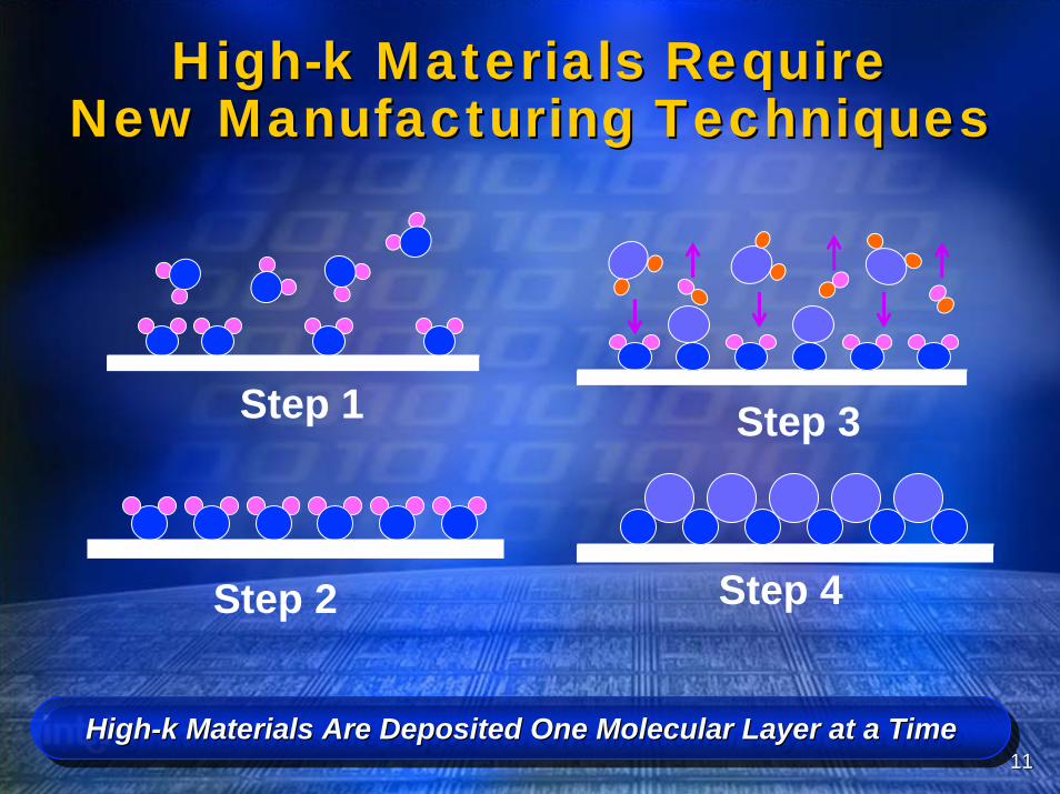
HighHigh--k Materials Require k Materials Require New Manufacturing TechniquesNew Manufacturing Techniques
Step 1 Step 3
Step 4Step 2
High-k Materials Are Deposited One Molecular Layer at a TimeHighHigh--k Materials Are Deposited One Molecular Layer at a Timek Materials Are Deposited One Molecular Layer at a Time

1212
What’s so hard about What’s so hard about using highusing high--k?k?
Replacing SiOReplacing SiO22 with highwith high--k materials leads to k materials leads to two problems due to interaction with the two problems due to interaction with the polysilicon gate electrode:polysilicon gate electrode:1.1. Threshold voltage pinning Threshold voltage pinning –– defects that arise defects that arise
at the gate dielectric / gate electrode boundary at the gate dielectric / gate electrode boundary cause the voltage at which the transistor cause the voltage at which the transistor switches to be too highswitches to be too high
2.2. Phonon scattering Phonon scattering –– electrons are made less electrons are made less mobile (they slow down)mobile (they slow down)
Both of these problems limit the transistor’s switching speed
Both of these problems limit the Both of these problems limit the transistor’s switching speedtransistor’s switching speed

1313
Solution: Use Metal GatesSolution: Use Metal Gates
•• Conventional gate electrode is Conventional gate electrode is polycrystalline siliconpolycrystalline silicon
•• By using a specific metal for By using a specific metal for NMOS transistors, and a NMOS transistors, and a different one with PMOS different one with PMOS transistors, and combining transistors, and combining with a specific process with a specific process recipe, the two problems go awayrecipe, the two problems go away
•• With this combination, Intel has achieved With this combination, Intel has achieved record performance with a transistor record performance with a transistor design that can scale according to design that can scale according to Moore’s LawMoore’s Law

1414
Intel’s AnnouncementIntel’s Announcement•• Intel is announcing that after 5 years of Intel is announcing that after 5 years of
research, it has found the right highresearch, it has found the right high--k k materialmaterial
•• Intel has also identified Intel has also identified compatible gate electrode compatible gate electrode materials for both NMOS materials for both NMOS and PMOSand PMOS
•• Intel has succeeded in integrating these Intel has succeeded in integrating these and has achieved record transistor and has achieved record transistor performanceperformance
Moore’s Law continuesMoore’s Law continuesMoore’s Law continues
1515
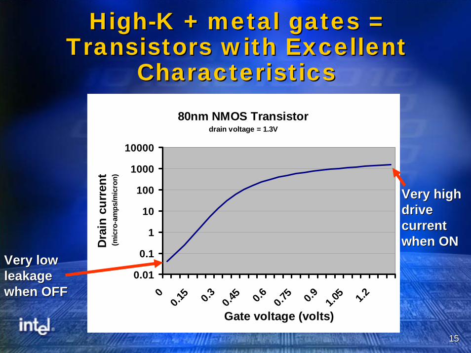
HighHigh--K + metal gates = K + metal gates = Transistors with Excellent Transistors with Excellent
CharacteristicsCharacteristics80nm NMOS Transistor
drain voltage = 1.3V
0.01
0.1
1
10
100
1000
10000
00.1
5 0.3 0.45 0.6 0.75 0.9 1.05 1.2
Gate voltage (volts)
Dra
in c
urre
nt(m
icro
-am
ps/m
icro
n)
Very low Very low leakage leakage when OFFwhen OFF
Very high Very high drive drive current current when ONwhen ON
1616
SummarySummary•• Intel researchers have removed the industry’s most Intel researchers have removed the industry’s most
challenging roadblock to ensuring Moore’s Law challenging roadblock to ensuring Moore’s Law spans into the next decade, ultimately leading to spans into the next decade, ultimately leading to vast, lowervast, lower--cost computing power and enabling cost computing power and enabling applications that cannot be imagined todayapplications that cannot be imagined today
•• The power and heat issue is huge and industry has The power and heat issue is huge and industry has been searching for solutions for a long time. Intel been searching for solutions for a long time. Intel has solved a major part of the problem by has solved a major part of the problem by integrating new materials into transistors.integrating new materials into transistors.
•• Intel has achieved world record performance at Intel has achieved world record performance at dramatically reduced leakage with its new dramatically reduced leakage with its new transistortransistor
•• Intel is on track to put this new transistor design Intel is on track to put this new transistor design into production in 2007 into production in 2007
Moore’s Law continuesMoore’s Law continuesMoore’s Law continues

1717
Additional details on Intel’s high-K/metal-gate
transistors were presented at the International
Workshop on Gate Insulator 2003 in Tokyo, Japan
on Nov 6, 2003 by Robert Chau, Intel Fellow
For further information on Intel's silicon
technology, please visit the Silicon Showcase at
www.intel.com/research/silicon
Related Documents