Intel’s Haswell CPU Microarchitecture www.realworldtech.com /haswell-cpu/ David Kanter Over the last 5 years, high performance microprocessors have changed dramatically. One of the most significant influences is the increasing level of integration that is enabled by Moore’s Law. In the context of semiconductors, integration is an ever-present fact of life, reducing system power consumption and cost and increasing performance. The latest incarnation of this trend is the System-on-a-Chip (SoC) philosophy and design approach. SoCs have been the preferred solution for extremely low power systems, such as 1W mobile phone chips. However, high performance microprocessors span a much wider design space, from 15W notebook chips to 150W server sockets and the adoption of SoCs has been slower because of the more diverse market. Sandy Bridge was a dawn of a new era for Intel, and the first high-end x86 microprocessor that could truly be described as an SoC, integrating the CPU, GPU, Last Level Cache and system I/O. However, Sandy Bridge largely targets conventional PC markets, such as notebooks, desktops, workstations and servers, with a smattering of embedded applications. The competition for Sandy Bridge is largely AMD’s Bulldozer family, which has suffered from poor performance in the first few iterations. The 32nm Sandy Bridge CPU introduced AVX, a new instruction extension for floating point (FP) workloads and fundamentally changed almost every aspect of the pipeline, from instruction fetching to memory accesses. The system architecture was radically revamped, with a coherent ring interconnect for on-chip communication, a higher bandwidth Last Level Cache (LLC), integrated graphics and I/O, and comprehensive power management. The Sandy Bridge GPU was also new architecture that delivered acceptable performance for the first time. The server- oriented Sandy Bridge-EP started with the same building blocks, but eliminated the graphics, while adding more cores, more memory controllers, more PCI-E 3.0 I/O and coherent QPI links. Haswell is the first family of SoCs that have been tailored to take advantage of Intel’s 22nm FinFET process technology. While Ivy Bridge is also 22nm, Intel’s circuit design team sacrificed power and performance in favor of a swift migration to a process with a radically new transistor architecture. The Haswell family features a new CPU core, new graphics and substantial changes to the platform in terms of memory and power delivery and power management. All of these areas are significant from a technical and economic perspective and interact in various ways. However, the Haswell family represents a menu of options that are available for SoCs tailored to certain markets. Not every product requires graphics (e.g. servers), nor is a new power architecture desirable for cost optimized products (e.g. desktops). Architects will pick and choose from the menu of options, based on a variety of technical and business factors. The heart of the Haswell family is the eponymous CPU. The Haswell CPU core pushes beyond the PC market into new areas, such as the high-end of the emerging tablet market. Haswell SoCs are aimed at 10W, potentially with further power reductions in the future. The 22nm node enables this wider range, but Haswell’s design and architecture play critical roles in fully exploiting the benefits of the new process technology. The Haswell CPU boasts a huge number of architectural enhancements, with four extensions that touch every aspect of the x86 instruction set architecture (ISA). AVX2 brings integer SIMD to 256-bit vectors, and adds a gather instruction for sparse memory accesses. The fused multiply-add extensions improve performance for floating point (FP) workloads, such as scientific computing, and nicely synergize with the new gather instructions. A small number of bit manipulation instructions aid cryptography, networking and certain search operations. Last, Intel has introduced TSX, or transactional memory, an incredibly powerful programming model for concurrency and multi- threaded programming. TSX improves performance and efficiency of software by better utilizing the underlying 1/2

Welcome message from author
This document is posted to help you gain knowledge. Please leave a comment to let me know what you think about it! Share it to your friends and learn new things together.
Transcript

Intel’s Haswell CPU Microarchitecture
www.realworldtech.com /haswell-cpu/
David Kanter
Over the last 5 years, high performance microprocessors have changed dramatically. One of the most significant
influences is the increasing level of integration that is enabled by Moore’s Law. In the context of semiconductors,
integration is an ever-present fact of life, reducing system power consumption and cost and increasing performance.
The latest incarnation of this trend is the System-on-a-Chip (SoC) philosophy and design approach. SoCs have
been the preferred solution for extremely low power systems, such as 1W mobile phone chips. However, high
performance microprocessors span a much wider design space, from 15W notebook chips to 150W server sockets
and the adoption of SoCs has been slower because of the more diverse market.
Sandy Bridge was a dawn of a new era for Intel, and the first high-end x86 microprocessor that could truly be
described as an SoC, integrating the CPU, GPU, Last Level Cache and system I/O. However, Sandy Bridge largely
targets conventional PC markets, such as notebooks, desktops, workstations and servers, with a smattering of
embedded applications. The competition for Sandy Bridge is largely AMD’s Bulldozer family, which has suffered
from poor performance in the first few iterations.
The 32nm Sandy Bridge CPU introduced AVX, a new instruction extension for floating point (FP) workloads and
fundamentally changed almost every aspect of the pipeline, from instruction fetching to memory accesses. The
system architecture was radically revamped, with a coherent ring interconnect for on-chip communication, a higher
bandwidth Last Level Cache (LLC), integrated graphics and I/O, and comprehensive power management. The
Sandy Bridge GPU was also new architecture that delivered acceptable performance for the first time. The server-
oriented Sandy Bridge-EP started with the same building blocks, but eliminated the graphics, while adding more
cores, more memory controllers, more PCI-E 3.0 I/O and coherent QPI links.
Haswell is the first family of SoCs that have been tailored to take advantage of Intel’s 22nm FinFET process
technology. While Ivy Bridge is also 22nm, Intel’s circuit design team sacrificed power and performance in favor of a
swift migration to a process with a radically new transistor architecture.
The Haswell family features a new CPU core, new graphics and substantial changes to the platform in terms of
memory and power delivery and power management. All of these areas are significant from a technical and
economic perspective and interact in various ways. However, the Haswell family represents a menu of options that
are available for SoCs tailored to certain markets. Not every product requires graphics (e.g. servers), nor is a new
power architecture desirable for cost optimized products (e.g. desktops). Architects will pick and choose from the
menu of options, based on a variety of technical and business factors.
The heart of the Haswell family is the eponymous CPU. The Haswell CPU core pushes beyond the PC market into
new areas, such as the high-end of the emerging tablet market. Haswell SoCs are aimed at 10W, potentially with
further power reductions in the future. The 22nm node enables this wider range, but Haswell’s design and
architecture play critical roles in fully exploiting the benefits of the new process technology.
The Haswell CPU boasts a huge number of architectural enhancements, with four extensions that touch every
aspect of the x86 instruction set architecture (ISA). AVX2 brings integer SIMD to 256-bit vectors, and adds a gather
instruction for sparse memory accesses. The fused multiply-add extensions improve performance for floating point
(FP) workloads, such as scientific computing, and nicely synergize with the new gather instructions. A small number
of bit manipulation instructions aid cryptography, networking and certain search operations. Last, Intel has
introduced TSX, or transactional memory, an incredibly powerful programming model for concurrency and multi-
threaded programming. TSX improves performance and efficiency of software by better utilizing the underlying
1/2

multi-core hardware.
Intel’s design philosophy emphasizes superb single core performance with low power. The new Haswell core
achieves even higher performance than Sandy Bridge. The improvements in Haswell are concentrated in the out-of-
order scheduling, execution units and especially the memory hierarchy. It is a testament to the excellent front-end in
Sandy Bridge that relatively few changes were necessary. The Haswell microarchitecture is a dual-threaded, out-of-
order microprocessor that is capable of decoding 5 instructions, issuing 4 fused uops and dispatching 8 uops each
cycle. The Haswell core is the basis of Intel’s upcoming generation of SoCs and will be used from tablets to servers,
competing with AMD and a variety of ARM-based SoC vendors.
2/2
Intel’s Haswell CPU Microarchitecture
www.realworldtech.com /haswell-cpu/2
David Kanter
Haswell Instruction Set and Front-end
Haswell introduces a huge number of new instructions for the x86 ISA, that fall into four general families. The first is
AVX2, which promotes integer SIMD instructions from 128-bits wide in SSE to 256-bits wide. The original AVX was
a 256-bit extension using the YMM registers, but largely for floating point instructions. AVX2 is the complement and
brings integer SIMD to the full YMM registers, along with some enhancements for 128-bit operation. AVX2 also adds
more robust and generalized support for vector permutes and shifts. Perhaps more importantly, AVX2 includes 16
new gather instructions, loads that can fetch 4 or 8 non-contiguous data elements using special vector addressing
for both integer and floating point (FP) SIMD. Gather is crucial for wider SIMD and substantially simplifies
vectorizing code. Note that AVX2 does not include scatter instructions (i.e., vector addressed stores), because of
complications with the x86 memory ordering model and the load/store buffers.
While AVX2 emphasizes integer SIMD, Haswell has huge benefits for floating point code. In addition to gather,
Intel’s Fused Multiply Add (FMA) includes 36 FP instructions for performing 256-bit computations and 60 instructions
for 128-bit vectors. As announced in early 2008, Intel’s FMA was originally architected for 4-operand instructions.
However, the 22nm Ivy Bridge can perform register move instructions in the front-end through register renaming
tricks, without issuing any uops. Intel’s architects determined that MOV elimination with FMA3 provides about the
same performance as FMA4, but using denser and easier to decode instructions; hence the abrupt about face in late
2008.
The third extension is 15 scalar bit manipulation instructions (known as BMI) that operate on general integer
registers. These instructions fall into three general areas: bit field manipulations such as insert, shift and extract; bit
counting such as leading zero count; and arbitrary precision integer multiply and rotation. The latter is particularly
useful for cryptography. As an aside, Haswell also adds a big-endian move instruction (MOVBE) that can convert to
and from traditional x86 little-endian format. MOVBE was introduced for Intel’s Atom, and is quite useful for
embedded applications that deal with storage and networking, since TCP/IP is big-endian.
The last and most powerful of Intel’s ISA extensions is TSX, which has been extensively discussed in a previous
article on Haswell’s transactional memory. In short, TSX enables programmers to write parallel code that focuses on
using synchronization for correctness, while the hardware optimizes the execution for performance and concurrency.
Hardware Lock Elision (HLE) transparently provides the performance and throughput of fine-grained locking, even
when programmers use coarse-grained locks. Most importantly, the hint prefixes are compatible with older
processors.
Restricted Transactional Memory (RTM) is an entirely new programmer interface that provides transactional memory
to x86 developers. TM is far more useful than traditional lock-based synchronization, because transactions can
protect more complex data structures and be composed across functions, modules and even applications. However,
it does require linking new libraries using RTM and possibly rewriting software to get the full benefits.
Both variants of TSX are tracked at 64B cache line granularity. Excessive conflicts due to transaction limits, false
sharing, or data races can actually harm performance, so developers must judiciously adopt TSX. However, future
implementations will most likely have fewer conflicts and be more flexible.
Of these new instructions, the vast majority are simple instructions that decode into a single uop. However, the more
complex ones such as gather and the TSX commit and abort are microcoded.
1/3

Fundamentally, x86 is quite similar to RISC architectures in a number of dimensions. ALU operations are largely the
same; there are only so many ways to do addition, subtraction and multiplication. However, the front-end is quite
different and one of the most challenging aspects of modern x86 CPUs. The instruction caches are kept coherent
with data caches, and the variable length instructions make decoding quite complex. x86 instructions range in size
from 1-15 bytes, with length-changing prefixes, inconsistent operand positions and complex microcoded
instructions. Since the P6, these instructions have been transformed into more tractable fixed length uops that can
be tracked by an out-of-order core. As with all architectures, the instruction stream is frequently interrupted by
control flow such as conditional branches, jumps, calls and returns, which potentially redirect the instruction fetching
and introduce bubbles into the pipeline.
Sandy Bridge made tremendous strides in improving the front-end and ensuring the smooth delivery of uops to the
rest of the pipeline. The biggest improvement was a uop cache that essentially acts as an L0 instruction cache, but
contains fixed length decoded uops. The uop cache is virtually addressed and included in the L1 instruction cache.
Hitting in the uop cache has several benefits, including reducing the pipeline length by eliminating power hungry
instruction decoding stages and enabling an effective throughput of 32B of instructions per cycle. For newer SIMD
instructions, the 16B fetch limit was problematic, so the uop cache synergizes nicely with extensions such as AVX.
The most
significant
difference in
Haswell’s front-end
is undoubtedly
support for the
various instruction
set extensions
outlined above. At
a high level,
instruction fetch
and decode
microarchitecture is
largely similar to
Sandy Bridge, as
shown in Figure 1.
There are a
number of subtle
enhancements, but
the concepts and
many of the details
are the same.
As to be expected,
the branch
prediction for
Haswell has
improved.
Unfortunately, Intel
was unwilling to
share the details or
results of these
optimizations. The
instruction cache is
2/3

Figure 1. Haswell and Sandy Bridge Front-end
still 8-way
associative, 32KB
and dynamically
shared by the two
threads. The
instruction TLBs
are also
unchanged, with
128 entries for 4KB
page translations;
the 4KB
translations are
statically
partitioned
between the two
threads and 4-way
associative. The
2MB page array is
8 entries, fully
associative and
replicated for each
thread. Instruction fetching from the instruction cache continues to be 16B per cycle. The fetched instructions are
deposited into a 20 entry instruction queue that is replicated for each thread, in both Sandy Bridge and Haswell.
The Haswell instruction cache was optimized for handling misses faster. Speculative ITLB and cache accesses are
supported with better timing to improve the benefits of prefetching, and the cache controller is much more efficient
about handling instruction cache misses in parallel.
As with previous generations, the decoding is performed by a complex decoder that emits 1-4 fused uops and three
simple decoders that emit a single fused uop in parallel. Alternatively, instructions requiring more than 4 uops are
handled by microcode and block the conventional decoders. Macro-fusion can combine adjacent compare and
branch instructions into a single uop, improving the potential throughput to 5 instructions per cycle. The decoding
also contains the stack engine, which resolves push/pop and call/return pairs without sending uops further down the
pipeline.
The Haswell uop cache is the same size and organization as in Sandy Bridge. The uop cache lines hold upto 6
uops, and the cache is organized into 32 sets of 8 cache lines (i.e., 8 way associative). A 32B window of fetched x86
instructions can map to 3 lines within a single way. Hits in the uop cache can deliver 4 uops/cycle and those 4 uops
can correspond to 32B of instructions, whereas the traditional front-end cannot process more than 16B/cycle. For
performance, the uop cache can hold microcoded instructions as a pointer to microcode, but partial hits are not
supported. As with the instruction cache, the decoded uop cache is shared by the active threads.
One difference in Haswell’s decoding path is the uop queue, which receives uops from the decoders or uop cache
and also functions as a loop cache. In Sandy Bridge, the 28 entry uop queue was replicated for each thread.
However, in Ivy Bridge the uop queue was combined into a single 56 entry structure that is statically partitioned
when two threads are active. The distinction is that when a single thread is executing on Ivy Bridge or Haswell, the
entire 56 entry uop buffer is available for loop caching and queuing, making better use of the available resources.
3/3

Intel’s Haswell CPU Microarchitecture
www.realworldtech.com /haswell-cpu/3
David Kanter
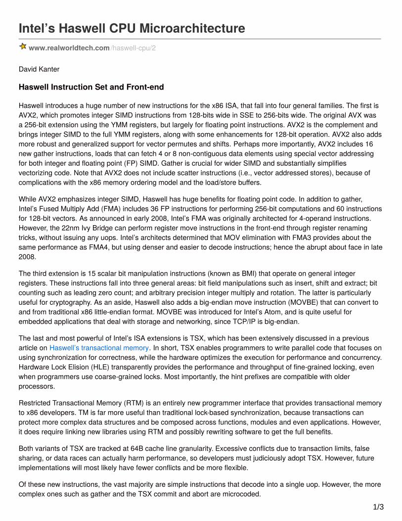
Haswell Out-of-Order Scheduling
Haswell’s out-of-order execution is where the microarchitecture becomes quite interesting and many changes are
visible. Haswell is substantially wider than Sandy Bridge with more resources for dynamic scheduling, although the
overall design is fairly similar, as shown in Figure 2.
The first part of out-of-order execution is renaming. The renamer will map architectural source and destination x86
registers onto the underlying physical register files (PRFs) and allocates other resources, such as load, store and
branch buffer entries and scheduler entries. Lastly, uops are bound to particular ports for downstream execution.
The renamer can take 4 fused uops out of the uop queue for a single thread, allocating the appropriate resources
and renaming registers to eliminate false dependencies. Crucially, these 4 fused uops can map to more than just 4
execution pipelines. For example, 4 fused load+execute uops might map to 8 actual uops, 4 loads and 4 dependent
ALU operations.
Unlike Sandy Bridge, the renamer in Haswell and Ivy Bridge does not have to handle all register to register move
uops. The front-end was enhanced to handle certain register move uops, which saves resources in the actual out-of-
order execution by removing these uops altogether.
The Haswell and Sandy Bridge core has unified integer and vector renaming, scheduling and execution resources.
Most out-of-order resources are partitioned between two active threads, so that if one thread stalls, the other can
continue to make substantial forward progress. In contrast, AMD’s Bulldozer splits the vector and integer pipelines.
Each Bulldozer module includes two complete integer cores, but shares a single large vector core between the two.
Conceptually, Bulldozer is dynamically sharing the floating point and vector unit, while having dedicated integer
cores.
The most performance critical resources in Haswell have all been expanded. The ROB contains status information
about uops and has grown from 168 uops to 192, increasing the out-of-order window by around 15%. Each fused
uop occupies a single ROB entry, so the Haswell scheduling window is effectively over 300 operations considering
fused loads and stores. The ROB is statically split between two threads, whereas other structures are dynamically
shared.
The physical register files hold the actual input and output operands for uops. The integer PRF added a modest 8
registers, bringing the total to 168. Given that AVX2 was a major change to Haswell, it should be no surprise that the
number of 256-bit AVX registers grew substantially to accommodate the new integer SIMD instructions. Haswell
features 24 extra physical registers for renaming YMM and XMM architectural registers. The branch order buffer,
which is used to rollback to known good architectural state in the case of a misprediction is still 48 entries, as with
Sandy Bridge. The load and store buffers, which are necessary for any memory accesses have grown by 8 and 6
entries respectively, bringing the total to 72 loads and 42 stores in-flight.
Unlike AMD’s Bulldozer, Haswell continues to use a unified scheduler that holds all different types of uops. The
scheduler in Haswell is now 60 entries, up from 54 in Sandy Bridge, those entries are dynamically shared between
the active threads. The scheduler holds uops that are waiting to execute due to resource or operand contraints.
Once ready, uops are issued to the execution units through dispatch ports. While fused uops occupy a single entry
in the ROB, execution ports can handle a single un-fused uop. So a fused load+ALU uop will occupy two ports to
1/3
execute.
Haswell and Sandy Bridge both retire upto 4 fused uops/cycle, once all the constituent uops have been successfully
executed. Retirement occurs in-order and clears out resources such as the ROB, physical register files and branch
order buffer.
Two of the new instruction set extensions place new burdens on the out-of-order machine. TSX creates a new class
of potential pipeline flushes. As we predicted in the earlier article on Haswell’s TM, when a transaction aborts, the
pipeline is cleared and the architectural state is rolled back. This looks largely similar to a branch misprediction.
TSX also supports multiple nested transactions, which requires hardware resources to track and disambiguate
different levels of nesting. Specifically, Haswell can have 7 nested transactions in flight. Any subsequent
transactions will abort as soon as they begin. It is important to note that this limit is microarchitectural and may
increase in future generations. Presumably this is linked to some hardware structure with 7 speculative entries and
the last entry is for the rollback state.
Gather instructions are microcoded and introduce additional complexity to the microarchitecture. As to be expected,
Intel’s approach to gather emphasizes simplicity and correctness. This leaves performance on the table relative to a
more sophisticated implementation, but is less likely to result in project delays due to risky design choices.
The number of uops executed by gather instruction depend on the number of elements. Each element is fetched by
a load uop that consumes a load buffer entry, while ALU uops calculate the vector addressing and merge the
gathered data into a single register. The uops that execute a gather have full access to the hardware and semantics
that are quite different from conventional x86 load and ALU instructions, so the implementation of gather is more
efficient than what a programmer could create.
2/3

Figure 2. Haswell and Sandy Bridge Out-of-Order Scheduling
3/3

Intel’s Haswell CPU Microarchitecture
www.realworldtech.com /haswell-cpu/4
David Kanter
Haswell Execution Units
The execution units in Haswell are tremendously improved over Sandy Bridge, with far more changes than the out-
of-order execution mechanism. Intel’s microarchitectures from Merom through Sandy Bridge could all dispatch 6
uops/cycle to the execution units. Three dispatch ports were dedicated for arithmetic operations and three ports for
memory accesses. One of the most significant improvements in Haswell is the addition of a new integer dispatch
port and a new memory port, bringing the execution to 8 uops/cycle. Furthermore, the execution units that are
attached to each dispatch port have been rebalanced and augmented with single cycle 256-bit integer SIMD
execution. Last, with the new FMA instructions, Haswell can perform 16 double precision or 32 single precision
FLOP/cycle, plus a 256-bit shuffle and a basic integer ALU operation. The theoretical peak performance for Haswell
is over double that of Sandy Bridge.
Every cycle, the 8 oldest, non-conflicting uops that are ready for execution are sent from the unified scheduler to the
dispatch ports. As shown in Figure 3, computational uops are dispatched to ports 0, 1, 5 and 6 and executed on the
associated execution units. The execution units are arranged into three stacks: integer, SIMD integer and FP (both
scalar and SIMD). Note that Figure 3 does not show every execution unit, due to space limitations.
The three stacks do not need to be tightly coupled because they operate independently of each other. It is quite
unusual that an FP operation would need a scalar integer input operand. Each stack has different data types,
different result forwarding networks and potentially different registers. The data path for accessing registers and
forwarding results only connect within a given stack (and register file). The data path consists of a huge number of
wires (256 wires to send 128-bits of data) and the power and area savings of this arrangement are quite significant.
The downside is that forwarding between different networks may incurs an extra cycle to move between different
stacks. The load and store units on ports 2-4 and 7 sit on the integer bypass network, to reduce latency for
forwarding and access to the general purpose registers (GPRs).
The new port 6 on Haswell is a scalar integer port. It only accesses the GPRs and the integer bypass network. The
execution unit can handle standard ALU operations, and contains a shifter and branch unit that were previously on
port 5. One of the advantages of the new integer port is that it can handle many instructions while the SIMD dispatch
ports are fully utilized. For example, when the Sandy Bridge core executes a tight loop, branches dispatch on port 5,
which prevent a shuffle or blend from dispatching. With Haswell, this is no longer a problem.
The port 0 integer units carry over an ALU and shifter from Sandy Bridge, losing a fast LEA unit that moved to port 5
and gaining a brand new branch unit. The integer units on port 1 are unchanged, with an ALU, fast and slow LEA,
and integer MUL. Port 5 has significantly changed and includes an ALU and a fast LEA unit, while losing the shift
and branch units. Overall, the number of integer ALUs and branch units increased by 1, doubling the throughput for
branches.
The Sandy Bridge bypass networks are 64-bit for integer, 128-bit for SIMD integer and 128-bit for FPU. Crucially, a
port could forward a result to each of the three bypass networks every cycle. To forward full 256-bit AVX results, the
FPU and SIMD networks were used simultaneously to send the lower and upper 128-bits. To support the FP-only
AVX instructions and uops, Sandy Bridge merely added FP execution capabilities to the 128-bit SIMD stacks,
without adding any expensive wiring for the bypass network.
AVX2 is largely an integer SIMD extension, so Intel’s architects applied the same conceptual technique to achieve
1/3

Figure 3. Haswell and Sandy Bridge Execution Units
single cycle 256-bit SIMD integer execution. Haswell adds 128-bit integer SIMD execution capabilities to the
existing 128-bit FP stack, while re-using the FP bypass network to forward half of the 256-bit results; again saving
area and power. This means that Figure 3 is more representative of the logical view of the execution units, rather
than the underlying physical implementation. In essence, the FP and SIMD stacks are now identical, forming the
lower and upper halves of the data path. Both stacks are 128-bits wide and have the same FP and SIMD execution
units.
Turning to the SIMD execution units, Haswell boasts a wide variety of improvements for AVX2 that roughly double
the throughput. The SIMD ALU, multiplier and shifter on port 0 are all 256-bit wide, while the divider, string and AES
unit remain at 128-bits (these latter units are not shown in Figure 3). Port 1 extended two execution units to 256-bit
SIMD, specifically the vector ALU and blend unit (the blend unit is not shown for Sandy Bridge due to space
considerations). The shuffle unit on port 1 in Sandy Bridge was removed from Haswell. However, it was not a full
shuffle, but executed a limited sub-set, mitigating the performance impact of this change. The ALU, shuffle and
blend units on port 5 were all extended to 256-bits, with no other changes (the vector blend is not shown for Sandy
Bridge or Haswell). Generally, the SIMD integer performance doubled due to wider 256-bit AVX2 instructions,
although the throughput for certain shuffles is the same and may decrease in some corner cases (e.g. 128-bit
shuffles that could issue on port 1 and 5 in Sandy Bridge).
The new FMA instructions also required significant changes for the floating point units in Haswell. Intel’s architects
opted for a fully pipelined fused multiply-add that keeps the latency at 5 cycles, the same as FMUL, so that the extra
add in the FMA is essentially free
from a latency perspective.
The port 0 FPU gained a fully
pipelined 256-bit FMA unit, and
can still be used for multiply, blend
and divide uops. Note that the
128-bit divider on port 0 is not
fully pipelined and is shared by
both all uops (integer, SIMD
integer and FP). Port 1 added a
256-bit fully pipelined FMA unit
that can also be used for 256-bit
multiplies and a 256-bit blend
unit, while retaining the existing
FP add and conversion units (the
FP blend and conversion units are
not shown in Figure 3). Lastly, the
floating point units on port 5 are
unchanged from Sandy Bridge,
with a 256-bit shuffle and blend.
One interesting point is that while
Haswell can execute two 256-bit
FMAs or FMULs per cycle, there
is still only a single 256-bit FADD.
The motivation for this is primarily
latency. Based on extensive
performance modeling, Intel’s
architects found that most
workloads were more heavily dependent on FADD latency, rather than bandwidth. Simulations showed that two
2/3

FADD units with higher latency were inferior to a single FADD unit with 3 cycle latency on port 1. Of course, clever
assembly programmers can use the FMA unit on port 0 to perform a 5 cycle FADD, although the code scheduling
would be rather complex. For recompiled code, the floating point performance has basically doubled by virtue of the
FMA instructions, yielding 16 DP FLOP/cycle for each Haswell core. Existing code that depends on FMUL
throughput will also get substantially faster.
3/3
Intel’s Haswell CPU Microarchitecture
www.realworldtech.com /haswell-cpu/5/
David Kanter
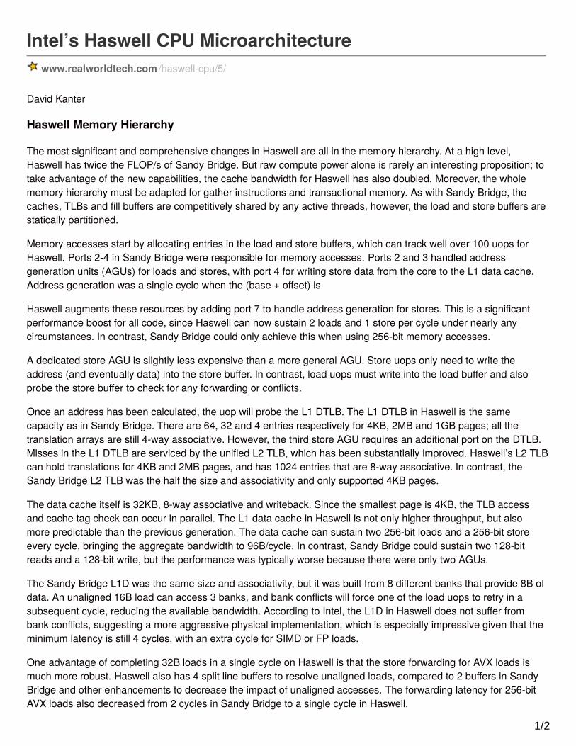
Haswell Memory Hierarchy
The most significant and comprehensive changes in Haswell are all in the memory hierarchy. At a high level,
Haswell has twice the FLOP/s of Sandy Bridge. But raw compute power alone is rarely an interesting proposition; to
take advantage of the new capabilities, the cache bandwidth for Haswell has also doubled. Moreover, the whole
memory hierarchy must be adapted for gather instructions and transactional memory. As with Sandy Bridge, the
caches, TLBs and fill buffers are competitively shared by any active threads, however, the load and store buffers are
statically partitioned.
Memory accesses start by allocating entries in the load and store buffers, which can track well over 100 uops for
Haswell. Ports 2-4 in Sandy Bridge were responsible for memory accesses. Ports 2 and 3 handled address
generation units (AGUs) for loads and stores, with port 4 for writing store data from the core to the L1 data cache.
Address generation was a single cycle when the (base + offset) is
Haswell augments these resources by adding port 7 to handle address generation for stores. This is a significant
performance boost for all code, since Haswell can now sustain 2 loads and 1 store per cycle under nearly any
circumstances. In contrast, Sandy Bridge could only achieve this when using 256-bit memory accesses.
A dedicated store AGU is slightly less expensive than a more general AGU. Store uops only need to write the
address (and eventually data) into the store buffer. In contrast, load uops must write into the load buffer and also
probe the store buffer to check for any forwarding or conflicts.
Once an address has been calculated, the uop will probe the L1 DTLB. The L1 DTLB in Haswell is the same
capacity as in Sandy Bridge. There are 64, 32 and 4 entries respectively for 4KB, 2MB and 1GB pages; all the
translation arrays are still 4-way associative. However, the third store AGU requires an additional port on the DTLB.
Misses in the L1 DTLB are serviced by the unified L2 TLB, which has been substantially improved. Haswell’s L2 TLB
can hold translations for 4KB and 2MB pages, and has 1024 entries that are 8-way associative. In contrast, the
Sandy Bridge L2 TLB was the half the size and associativity and only supported 4KB pages.
The data cache itself is 32KB, 8-way associative and writeback. Since the smallest page is 4KB, the TLB access
and cache tag check can occur in parallel. The L1 data cache in Haswell is not only higher throughput, but also
more predictable than the previous generation. The data cache can sustain two 256-bit loads and a 256-bit store
every cycle, bringing the aggregate bandwidth to 96B/cycle. In contrast, Sandy Bridge could sustain two 128-bit
reads and a 128-bit write, but the performance was typically worse because there were only two AGUs.
The Sandy Bridge L1D was the same size and associativity, but it was built from 8 different banks that provide 8B of
data. An unaligned 16B load can access 3 banks, and bank conflicts will force one of the load uops to retry in a
subsequent cycle, reducing the available bandwidth. According to Intel, the L1D in Haswell does not suffer from
bank conflicts, suggesting a more aggressive physical implementation, which is especially impressive given that the
minimum latency is still 4 cycles, with an extra cycle for SIMD or FP loads.
One advantage of completing 32B loads in a single cycle on Haswell is that the store forwarding for AVX loads is
much more robust. Haswell also has 4 split line buffers to resolve unaligned loads, compared to 2 buffers in Sandy
Bridge and other enhancements to decrease the impact of unaligned accesses. The forwarding latency for 256-bit
AVX loads also decreased from 2 cycles in Sandy Bridge to a single cycle in Haswell.
1/2

Figure 4. Haswell and Sandy Bridge Memory Hierarchy
Haswell and Sandy Bridge track cache misses using 10 line fill buffers for cache lines that are being provided from
other caches or memory. The outstanding requests are sent to the unified L2 cache. The L2 cache is a 256KB, 8-
way associative and writeback design with ECC protection. The L2 is neither inclusive nor exclusive of the L1 data
cache. The L2 bandwidth has doubled for Haswell so that it can provide a full 64B line to the data or instruction
cache every cycle, while maintaining the same 11 cycle minimum latency and 16 outstanding misses.
As we speculated, Haswell’s transactional memory retains the write-set and read-set of a transaction in the L1 data
cache, rather than using the store buffer. The L2 cache is non-transactional, so if a write-set cache line is evicted,
the transaction will abort. Intriguingly, it appears that in some circumstances read-set lines can be safely evicted
from the L1 and are tracked using another hardware mechanism. One possibility is a small on-chip transactional
victim buffer, or some sort of storage in memory. In the case of an abort, all the write-set lines are flushed from the
L1D, while a commit will make all write-set lines atomically visible. On top of the throughput benefits of TSX, the
minimum lock latency on Haswell is down to roughly 12 cycles, little more than two dependent L1D hits, compared
to 16 cycles on Sandy Bridge.
As previously mentioned, gather instructions are executed as multiple load uops, one for every element of the
gather. Each load uop requires a load buffer entry and will access the L1 DTLB and L1 data cache, even in the
scenario where there is locality between gather elements. Each cache line that must be fetched from the L2, L3 or
memory to satisfy the gather will consume a line fill buffer. Over time the implementation should become
substantially more efficient, e.g. reducing the number of TLB or cache accesses for gather instructions with good
locality.
2/2

Intel’s Haswell CPU Microarchitecture
www.realworldtech.com /haswell-cpu/6
David Kanter
Haswell System Architecture
There will be a number of implementations built around the Haswell core, ranging from low power SoCs to servers.
The majority of the system architecture is product specific and was not described. The interconnect is still a wide
ring bus, with 32B/cycle for every stop, and there are a few other general details available.
First, Haswell’s Last Level Cache (LLC) has been enhanced for performance. Each slice of the LLC contains two tag
arrays, one for data accesses and one for prefetching and coherency requests. The data bandwidth is still
32B/cycle, since the ring bus has not widened. The memory controller also has a larger re-ordering window, yielding
better throughput for write data.
Second, the ring and LLC are on a separate frequency domain from the CPU cores. This enables the ring and LLC
to run at high performance for the GPU, while keeping the CPUs in a low power state. This was not possible with
Sandy Bridge, since the cores, ring and LLC shared a PLL, and wasted power on some graphics heavy workloads.
Virtualization has improved for Haswell, with a particular emphasis on eliminating VM exits. The extended page
tables incorporate accessed and dirty bits, which reduce VM transitions and the new VMFUNC instruction enables
VMs to use hypervisor functions without an exit. The round-trip latency for VM transitions is now below 500 cycles,
and the I/O virtualization page tables are a full 4-level structure.
While Intel has demonstrated substantial improvements in idle and active power for Haswell, there was not sufficient
detail for a comprehensive discussion. It is likely that this information will only be available when products come to
market, since power management is implementation specific.
Conclusions and Analysis
Looking back over several generations of Intel microprocessors, the changes are remarkable. Merom marked Intel’s
‘right hand turn’, acknowledging that the Pentium 4 was not a viable long term solution because power efficiency is
crucial to success. Starting from Merom, Intel’s design teams embarked upon a relentless journey of continuous
improvement with each major architectural change.
Intel’s Sandy Bridge core served as an impressive starting point, with unmatched performance in the x86
ecosystem. Haswell builds on this foundation, with powerful ISA extensions and a substantially more aggressive
execution core and cache hierarchy. Moreover, Haswell is the first Intel core that will take full advantage of the 22nm
FinFET process technology. While the Ivy Bridge graphics architecture is new, the CPU core was mostly
unchanged. More importantly, the circuit design was focused on a low-risk and faster migration to a new process,
rather than achieving peak performance, efficiency or density.
1/4

2/4

3/4

Figure 5. Haswell and Sandy Bridge Microarchitectures
AVX2 doubles integer SIMD to 256-bits, while FMA doubles the number of operations for FP by chaining a multiply
and add. Crucially, AVX2 also encompasses instructions for gathering non-contiguous data from memory, which aids
compilers and programmers using the x86 SIMD extensions.
Intel’s Transactional Synchronization Extension has a less obvious impact on performance, but is more powerful and
pervasive in the long run. The Hardware Lock Elision separates functional correctness from performance, so that
programmers can focus on correctness while the hardware optimizes for performance. On the other hand,
Restricted Transactional Memory offers developers a new programming paradigm for concurrency that is far easier
and more intuitive, while improving performance for multi-threaded software.
Turning to the microarchitecture, the Haswell core has a modestly larger out-of-order window, with a substantial
increase in dispatch ports and execution resources. Together with the ISA extensions, the theoretical FLOPs and
integer operations per core have doubled. More significantly, the bandwidth for the cache hierarchy, including the
L1D and L2 has doubled, while reducing utilization bottlenecks. Compared to Nehalem, the Haswell core offers 4×
the peak FLOPs, 3× the cache bandwidth, and nearly 2× the re-ordering window.
Overall, we estimate that a Haswell core will offer around 10% greater performance for existing software, compared
to Sandy Bridge. For workloads using the new extensions, the gains could be significantly higher. In theory, AVX2
and FMA can boost performance by 2×, but the impact on most vectorizable workloads will be much lower.
Research from AMD has shown that lock elision gains 30% for the right workloads, although the benefits depend
strongly on the actual concurrency.
Competitively speaking, Intel is already far ahead of AMD in terms of CPU performance. In 2013, Haswell will be
matched up against the Steamroller core, which is a heavily redesigned derivative of Bulldozer. Steamroller still
shares the instruction fetching, FP/vector cluster, and L2 cache between cores, but has dedicated decoders that are
wider. Realistically, the performance gap should narrow given the scope of opportunities for AMD to improve, but
Haswell will continue to have significant advantages.
Haswell will be the first big x86 core to compete against ARM-based cores in tablets. While the performance will be
dramatically higher, the power budgets are very different. Haswell SoCs will reach 10W, while competing solutions
are often closer to 4W. The real question is the relative efficiency of Haswell SoCs, and the advantage of the
massive x86 software ecosystem. Fortunately, Windows 8 provides an opportunity to accurately measure
performance and efficiency. The results will inject some hard data into discussions that have been otherwise
vacuous and largely driven by marketing.
In summary, Haswell is a superb new architecture that will carry Intel into new markets and a new era of
competition, not only from AMD, but also the ARM ecosystem. Ultimately, products will reveal the performance and
efficiency advantages of the Haswell family, but the architecture looks quite promising, a testament to Intel’s design
team.
4/4
Related Documents


