DE0-Nano-SoC Computer System with ARM* Cortex* A9 For Quartus ® Prime 17.1 1 Introduction This document describes a computer system that can be implemented on the Intel ® DE0-Nano-SoC development and education board. This system, called the DE0-Nano-SoC Computer, is intended for use in experiments on computer organization and embedded systems. To support such experiments, the system contains embedded processors, memory, and various I/O peripherals. The FPGA programming file that implements this system, as well as its design source files, can be obtained from the University Program section of Intel’s web site. 2 DE0-Nano-SoC Computer Contents A block diagram of the DE0-Nano-SoC Computer system is shown in Figure 1. As indicated in the figure, the com- ponents in this system are implemented utilizing the Hard Processor System (HPS) and FPGA inside the Cyclone ® V SoC chip. The HPS comprises an ARM* Cortex* A9 dual-core processor, a DDR3 memory port, and a set of peripheral devices. The FPGA implements two Intel Nios ® II processors and several peripheral ports: memory, timer modules, analog-to-digital, parallel ports connected to switches and lights, and expansion ports. 2.1 Hard Processor System The hard processor system (HPS), as shown in Figure 1, includes an ARM Cortex A9 dual-core processor. The A9 dual-core processor features two 32-bit CPUs and associated subsystems that are implemented as hardware circuits in the Intel Cyclone V SoC chip. An overview of the ARM A9 processor can be found in the document Introduction to the ARM Processor, which is provided in Intel’s FPGA University Program web site. All of the I/O peripherals in the DE0-Nano-SoC Computer are accessible by the processor as memory mapped devices, using the address ranges that are given in this document. A summary of the address map can be found in Section 6. A good way to begin working with the DE0-Nano-SoC Computer and the ARM A9 processor is to make use of a utility called the Intel ® FPGA Monitor Program. It provides an easy way to assemble/compile ARM A9 programs written in either assembly language or the C language. The Monitor Program, which can be downloaded from Intel’s web site, is an application program that runs on the host computer connected to the DE0-Nano-SoC board. The Monitor Program can be used to control the execution of code on the ARM A9, list (and edit) the contents of processor registers, display/edit the contents of memory on the DE0-Nano-SoC board, and similar operations. The Monitor Program includes the DE0-Nano-SoC Computer as a pre-designed system that can be downloaded onto the DE0-Nano-SoC board, as well as several sample programs in assembly language and C that show how to use the DE0-Nano-SoC Computer’s peripherals. Section 7 describes how the DE0-Nano-SoC Computer is integrated Intel Corporation - FPGA University Program November 2017 1

Welcome message from author
This document is posted to help you gain knowledge. Please leave a comment to let me know what you think about it! Share it to your friends and learn new things together.
Transcript

DE0-Nano-SoC Computer Systemwith ARM* Cortex* A9
For Quartus® Prime 17.1
1 Introduction
This document describes a computer system that can be implemented on the Intel® DE0-Nano-SoC development andeducation board. This system, called the DE0-Nano-SoC Computer, is intended for use in experiments on computerorganization and embedded systems.
To support such experiments, the system contains embedded processors, memory, and various I/O peripherals. TheFPGA programming file that implements this system, as well as its design source files, can be obtained from theUniversity Program section of Intel’s web site.
2 DE0-Nano-SoC Computer Contents
A block diagram of the DE0-Nano-SoC Computer system is shown in Figure 1. As indicated in the figure, the com-ponents in this system are implemented utilizing the Hard Processor System (HPS) and FPGA inside the Cyclone®
V SoC chip. The HPS comprises an ARM* Cortex* A9 dual-core processor, a DDR3 memory port, and a set ofperipheral devices. The FPGA implements two Intel Nios® II processors and several peripheral ports: memory,timer modules, analog-to-digital, parallel ports connected to switches and lights, and expansion ports.
2.1 Hard Processor System
The hard processor system (HPS), as shown in Figure 1, includes an ARM Cortex A9 dual-core processor. The A9dual-core processor features two 32-bit CPUs and associated subsystems that are implemented as hardware circuitsin the Intel Cyclone V SoC chip. An overview of the ARM A9 processor can be found in the document Introductionto the ARM Processor, which is provided in Intel’s FPGA University Program web site. All of the I/O peripherals inthe DE0-Nano-SoC Computer are accessible by the processor as memory mapped devices, using the address rangesthat are given in this document. A summary of the address map can be found in Section 6.
A good way to begin working with the DE0-Nano-SoC Computer and the ARM A9 processor is to make use of autility called the Intel® FPGA Monitor Program. It provides an easy way to assemble/compile ARM A9 programswritten in either assembly language or the C language. The Monitor Program, which can be downloaded fromIntel’s web site, is an application program that runs on the host computer connected to the DE0-Nano-SoC board.The Monitor Program can be used to control the execution of code on the ARM A9, list (and edit) the contents ofprocessor registers, display/edit the contents of memory on the DE0-Nano-SoC board, and similar operations. TheMonitor Program includes the DE0-Nano-SoC Computer as a pre-designed system that can be downloaded ontothe DE0-Nano-SoC board, as well as several sample programs in assembly language and C that show how to usethe DE0-Nano-SoC Computer’s peripherals. Section 7 describes how the DE0-Nano-SoC Computer is integrated
Intel Corporation - FPGA University ProgramNovember 2017
1

DE0-NANO-SOC COMPUTER SYSTEM WITH ARM CORTEX* A9 For Quartus® Prime 17.1
with the Monitor Program. An overview of the Monitor Program is available in the document Intel® FPGA MonitorProgram Tutorial, which is provided in the University Program web site.
Expansionports
Cyclone VFPGA
Timers
SW3-0LEDG7-0
Parallelports
Parallelports
KEY1-0
On-chipmemory
Host computer
USBBlasterPeripherals
DE0-Nano-SoC
DDR3port
DDR3chips
JTAGports
Parallelports
ARM
MPCore
Cortex A9
TimersCyclone VHPS
Ports
. . .
Board
Nios II
FPGA Bridges
LEDG
Port
KEY ADC
Port
(2)
G-Sensor
Port
Parallelports
Arduinoport
Figure 1. Block diagram of the DE0-Nano-SoC Computer.
2.2 Memory
The HPS includes a memory port that connects the ARM MPCORE* to a 1 GB DDR3 memory. This memory isnormally used as the storage location of programs and data used by the ARM processors. The memory is organizedas 256M x 32-bits, and is accessible using word accesses (32 bits), halfwords, and bytes. The DDR3 memory ismapped to the address space 0x00000000 to 0x3FFFFFFF. There is also a 64 KB on-chip memory available insideeach ARM A9 processor. This small memory is organized as 16K x 32-bits, and is mapped to the address space0xFFFF0000 to 0xFFFFFFFF.
2.3 Pushbutton KEY and LED Port
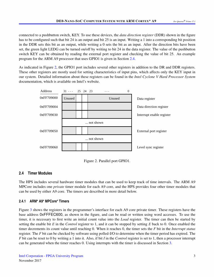
The HPS includes a general purpose I/O port, called GPIO1, that is accessible by the ARM A9 processor. Asillustrated in Figure 2, this parallel port is assigned the Base address 0xFF709000, and includes several 32-bitregisters. These registers can be read or written using word accesses. Only two bit locations in GPIO1 are used forthe DE0-Nano-SoC Computer. Bit 24 of the data register (DR) is connected to a green light, LEDG, and bit 25 is
2 Intel Corporation - FPGA University ProgramNovember 2017
DE0-NANO-SOC COMPUTER SYSTEM WITH ARM CORTEX* A9 For Quartus® Prime 17.1
connected to a pushbutton switch, KEY. To use these devices, the data direction register (DDR) shown in the figurehas to be configured such that bit 24 is an output and bit 25 is an input. Writing a 1 into a corresponding bit positionin the DDR sets this bit as an output, while writing a 0 sets the bit as an input. After the direction bits have beenset, the green light LEDG can be turned on/off by writing to bit 24 in the data register. The value of the pushbuttonswitch KEY can be obtained by reading the external port register and checking the value of bit 25. An exampleprogram for the ARM A9 processor that uses GPIO1 is given in Section 2.4.
As indicated in Figure 2, the GPIO1 port includes several other registers in addition to the DR and DDR registers.These other registers are mostly used for setting characteristics of input pins, which affects only the KEY input inour system. Detailed information about these registers can be found in the Intel Cyclone V Hard Processor Systemdocumentation, which is available on Intel’s website.
Address 02431 25. . .
0xFF709000
0xFF709050
0xFF709004
Unused Data register
External port register
Unused
Data direction register
... not shown
23 . . .
0xFF709030 Interrupt enable register
0xFF709060 Level sync register
... not shown
Figure 2. Parallel port GPIO1.
2.4 Timer Modules
The HPS includes several hardware timer modules that can be used to keep track of time intervals. The ARM A9MPCore includes one private timer module for each A9 core, and the HPS provides four other timer modules thatcan be used by either A9 core. The timers are described in more detail below.
2.4.1 ARM* A9* MPCore* Timers
Figure 3 shows the registers in the programmer’s interface for each A9 core private timer. These registers have thebase address 0xFFFEC600, as shown in the figure, and can be read or written using word accesses. To use thetimer, it is necessary to first write an initial count value into the Load register. The timer can then be started bysetting the enable bit E in the Control register to 1, and it can be stopped by setting E back to 0. Once enabled thetimer decrements its count value until reaching 0. When it reaches 0, the timer sets the F bit in the Interrupt statusregister. The F bit can be checked by software using polled-I/O to determine when the timer period has expired. TheF bit can be reset to 0 by writing a 1 into it. Also, if bit I in the Control register is set to 1, then a processor interruptcan be generated when the timer reaches 0. Using interrupts with the timer is discussed in Section 3.
Intel Corporation - FPGA University ProgramNovember 2017
3

DE0-NANO-SOC COMPUTER SYSTEM WITH ARM CORTEX* A9 For Quartus® Prime 17.1
When it reaches 0, the timer will stop if the auto bit (A) in the control register is set to 0. But if bit A is set to 1, thenthe timer will automatically reload the value in the Load register and continue decrementing. The current value ofthe timer is available to software in the Counter register shown in Figure 3. The timer uses a clock frequency of 200MHz. The Prescaler field in the Control register can be used to slow down the counting rate, as follows. The timerdecrements each Prescaler +1 clock cycle. Therefore, if Prescaler = 0, then the timer decrements every clock cycle,if Prescaler = 1, the timer decrements every second clock cycle, and so on.
EAI
F
Address 01531 . . . . . . 116 2
Load value 0xFFFEC600
Current value0xFFFEC604
Unused0xFFFEC608
Unused0xFFFEC60C
7
Control
Interrupt status
Prescaler
8
Counter
Load
Unused
3 Register name
Figure 3. ARM A9 private timer port.
2.4.2 HPS Timers
Figure 4 shows the registers in the programmer’s interface for one of the HPS timers. These registers have the baseaddress 0xFFC08000, as shown in the figure, and can be read or written using word accesses. To configure thetimer, it is necessary to ensure that it is stopped by setting the enable bit E in the Control register to 0. A startingcount value for the timer can then be written into the Load register. To instruct the timer to use the specified startingcount value, the M in the Control register should be set to 1, and the timer can be started by setting E = 1. The timercounts down to 0, and then sets both bit F in the End-of-interrupt register and bit S in the Interrupt status register to1. Software can poll the value of S to determine when the timer period has expired. The S bit, and the F bit can bereset to 0 by reading the contents of the End-of-Interrupt register. Also, if bit I , the interrupt mask bit, in the Controlregister is set to 0, then an interrupt can be generated when the timer reaches 0 (note that bit I in the ARM A9 privatetimer shown in Figure 3 has the opposite polarity). The use of interrupts with the timer is discussed in Section 3.
The current value of the timer is available to software in the Counter register shown in Figure 4. The timer uses aclock frequency of 100 MHz.
There are three other identical timers in the HPS, with the following base addresses: 0xFFC09000, 0xFFD00000,and 0xFFD01000. The first of these timers uses a 100 MHz clock, and the last two timers use a 25 MHz clock.
We should mention that other timer modules also exist in the HPS. The ARM A9 MPCore has a global timer that isshared by both A9 cores, as well as a watchdog timer for each processor. Also, the HPS has two additional watchdogtimers. Documentation about the global timer and watchdog timers is available in the ARM Cortex A9 MPCoreTechnical Reference Manual, and in the Intel Cyclone V Hard Processor System Technical Reference Manual.
4 Intel Corporation - FPGA University ProgramNovember 2017

DE0-NANO-SOC COMPUTER SYSTEM WITH ARM CORTEX* A9 For Quartus® Prime 17.1
EMI
F
Address 01531 . . . . . . 116 2
Load value 0xFFC08000
Current value0xFFC08004
Unused0xFFC08008
Unused0xFFC0800C
Control
End-of-Interrupt
Counter
Load
Register name
SUnused0xFFC08010 Interrupt status
Figure 4. HPS timer port.
2.4.3 Using a Timer with Assembly Language Code
An example of ARM A9 assembly language code is included in the Appendix in Listing 1. The code configures theprivate timer for the A9 core so that it produces one-second timeouts. An infinite loop is used to flash the green lightconnected to GPIO1, discussed in Section 2.3. The light is turned on for one second, then off, and so on.
An example of C code is also included in Listing 2. This code performs the same actions as the assembly languageprogram in Listing 1—it flashes on/off the green light connected to GPIO1 at one-second intervals.
The source code files shown in Listings 2 and 1 are distributed as part of the Intel® FPGA Monitor Program. Thefiles can be found under the heading sample programs, and are identified by the name Timer Lights.
2.5 FPGA Bridges
The FPGA bridges depicted in Figure 1 provide connections between the HPS and FPGA in the Cyclone V SoCdevice. The bridges are enabled, or disabled, by using the Bridge reset register, which is illustrated in Figure 5 andhas the address 0xFFD0501C. Three distinct bridges exist, called HPS-to-FPGA, lightweight HPS-to-FPGA, andFPGA-to-HPS. In the DE0-Nano-SoC Computer the first two of these bridges are used to connect the ARM A9processor to the FPGA. As indicated in Figure 5 the bridges are enabled/disabled by bits 0−2 of the Bridge resetregister. To use the memory-mapped peripherals in the FPGA, software running on the ARM A9 must enable theHPS-to-FPGA and lightweight HPS-to-FPGA bridges by setting bits #0 and #1 of the Bridge reset register to 0.We should note that if a user program is downloaded and run on the ARM A9 by using the Intel® FPGA MonitorProgram, described in Section 7, then these bridges are automatically enabled before the user program is started.
In addition to the components described above, the HPS also provides a number of other peripheral devices, such asUSB, Ethernet, and a 3-D accelerometer (G-sensor). The G-sensor is described in the tutorial Using the DE0-Nano-SoC Accelerometer with ARM, available from Intel’s FPGA University Program website. Documentation about theother devices connected to the HPS can be found in the Intel Cyclone V Hard Processor System Technical ReferenceManual, as well as in the DE0-Nano-SoC Board User Manual.
Intel Corporation - FPGA University ProgramNovember 2017
5

DE0-NANO-SOC COMPUTER SYSTEM WITH ARM CORTEX* A9 For Quartus® Prime 17.1
Address 031 1
0xFFD0501C Unused Bridge reset
. . . 2
HPS2FPGA
Lightweight HPS2FPGA
FPGA2HPS
Figure 5. FPGA bridge reset register.
2.6 FPGA Components
As shown in Figure 1 many of the components in the DE0-Nano-SoC Computer are implemented inside the FPGAin the Cyclone® V SoC chip. Several of these components are described in this section.
2.7 Nios® II Processor
The Intel Nios II processor is a 32-bit CPU that can be implemented in an Intel FPGA device. Two versions ofthe Nios II processor are available, designated economy (/e) and fast (/f). The DE0-Nano-SoC Computer includestwo instances of the Nios II/f version, configured with floating-point hardware support. Instructions for using theNios II processors in the DE0-Nano-SoC Computer are provided in a separate document, called DE0-Nano-SoCComputer with Nios II.
2.8 On-Chip Memory
The DE0-Nano-SoC Computer includes a 32-Kbyte memory that is implemented inside the FPGA. This memoryis organized as 8K x 32 bits, and spans addresses in the range 0xC8000000 to 0xC8007FFF. This memory isaccessible by the ARM processor as well as both Nios II processors.
2.9 Parallel Ports
There are several parallel ports implemented in the FPGA that support input, output, and bidirectional transfers ofdata between the ARM A9 processor and I/O peripherals. As illustrated in Figure 6, each parallel port is assigneda Base address and contains up to four 32-bit registers. Ports that have output capability include a writable Dataregister, and ports with input capability have a readable Data register. Bidirectional parallel ports also include aDirection register that has the same bit-width as the Data register. Each bit in the Data register can be configuredas an input by setting the corresponding bit in the Direction register to 0, or as an output by setting this bit positionto 1. The Direction register is assigned the address Base + 4.
Some of the parallel ports in the DE0-Nano-SoC Computer have registers at addresses Base + 8 and Base + C, asindicated in Figure 6. These registers are discussed in Section 3.
6 Intel Corporation - FPGA University ProgramNovember 2017

DE0-NANO-SOC COMPUTER SYSTEM WITH ARM CORTEX* A9 For Quartus® Prime 17.1
Address 02 14 331 30 . . .
Base
Base + 8
Base + C
Base + 4
Input or output data bits
Direction bits
Edge bits
Mask bits
Data register
Direction register
Interruptmask register
Edgecapture register
Direction bits
Figure 6. Parallel port registers in the DE0-Nano-SoC Computer.
2.9.1 Green LED Parallel Port
The green lights LED7−0 on the DE0-Nano-SoC board are driven by an output parallel port, as illustrated in Figure 7.The port contains an 8-bit Data register, which has the address 0xFF200000. This register can be written or readby the processor using word accesses, and the upper bits not used in the registers are ignored.
0xFF200000
LED0LED7
Address
031 78 . . .Unused Data register
Figure 7. Output parallel port for LED.
2.9.2 Slider Switch Parallel Port
The SW3−0 slider switches on the DE0-Nano-SoC board are connected to an input parallel port. As illustrated inFigure 8, this port comprises a 4-bit read-only Data register, which is mapped to address 0xFF200040.
0xFF200040
SW0SW3
Address
Data register031 34 . . .Unused
Figure 8. Data register in the slider switch parallel port.
Intel Corporation - FPGA University ProgramNovember 2017
7

DE0-NANO-SOC COMPUTER SYSTEM WITH ARM CORTEX* A9 For Quartus® Prime 17.1
2.9.3 Pushbutton Key Parallel Port
The parallel port connected to the KEY1−0 pushbutton switches on the DE0-Nano-SoC board comprises three 2-bitregisters, as shown in Figure 9. These registers have the base address 0xFF200050 and can be accessed using wordoperations. The read-only Data register provides the values of the switches KEY1−0. The other two registers shownin Figure 9, at addresses 0xFF200058 and 0xFF20005C, are discussed in Section 3.
Address 02 14 331 30 . . .
0xFF200050
0xFF200058
0xFF20005C
Unused
KEY1-0
Edge bits
Mask bits
Unused
Unused
Unused
Data register
Interruptmask register
Edgecapture register
Unused
Figure 9. Registers used in the pushbutton parallel port.
2.9.4 Expansion Parallel Port
The DE0-Nano-SoC Computer includes two bidirectional parallel ports that are connected to the JP1 and JP7 40-pin headers on the DE0-Nano-SoC board. These parallel ports include the four 32-bit registers that were describedpreviously for Figure 6. The base address of the port for JP1 is 0xFF200060, and for JP7 is 0xFF200070. Figure 10gives a diagram of the 40-pin connectors on the DE0-Nano-SoC board, and shows how the respective parallel portData register bits, D31−0, are assigned to the pins on the connector. The figure shows that bit D0 of the parallel portis assigned to the pin at the top right corner of the connector, bit D1 is assigned below this, and so on. Note thatsome of the pins on the 40-pin header are not usable as input/output connections, and are therefore not used by theparallel ports. Also, only 32 of the 36 data pins that appear on each connector can be used.
2.9.5 Arduino* Expansion Parallel Port
The DE0-Nano-SoC Computer includes a bidirectional parallel port that is connected to the Arduino* Uno R3 ex-pansion header on the DE0-Nano-SoC board. This parallel port includes the four 32-bit registers that were describedpreviously for Figure 6. The base address of the port is 0xFF200100. The Data register bits in this port are con-nected to the Arduino expansion header User I/O. Thus, bit 0 in the Data register connects to the signal Arduino_IO0,bit 1 to Arduino_IO1, and so on.
The DE0-Nano-SoC Computer also includes a one-bit output port that is connected to the Arduino Uno R3 expansionheader on the DE0-Nano-SoC board. This one-bit port has a data register that is connected to the Arduino_Reset_Nsignal on the DE0-Nano-SoC board. The address of this port is 0xFF200110.
More details about the Arduino Uno R3 expansion header can be found in the DE0-Nano-SoC Board User Manual.
8 Intel Corporation - FPGA University ProgramNovember 2017

DE0-NANO-SOC COMPUTER SYSTEM WITH ARM CORTEX* A9 For Quartus® Prime 17.1
D0D1
D2 D3D4 D5D6 D7Unused
D10 D11D12 D13
D14D15
D16 D17D18 D19
D22 D23D24 D25D26 D27D28 D29D30 D31
Unused
JP1 JP2
Pin 1 Pin 1
Pin 40 Pin 40
D8 D9
D20 D21
D0D1
D2 D3D4 D5D6 D7Unused
D10 D11D12 D13
D14D15
D16 D17D18 D19
D22 D23D24 D25D26 D27D28 D29D30 D31
Unused
D8 D9
D20 D21
Figure 10. Assignment of parallel port bits to pins on JP1 and JP7.
2.9.6 Using the Parallel Ports with Assembly Language Code and C Code
The DE0-Nano-SoC Computer provides a convenient platform for experimenting with ARM A9 assembly languagecode, or C code. A simple example of such code is provided in the Appendix in Listings 3 and 4. Both programsperform the same operations, and illustrate the use of parallel ports by using either assembly language or C code.
The code in the figures displays the values of the SW switches on the LED lights. A rotating pattern is displayedon the LEDs. This pattern is rotated to the left by using an ARM A9 rotate instruction, and a delay loop is used tomake the shifting slow enough to observe. The pattern can be changed to the values of the SW switches by pressinga pushbutton KEY. When a pushbutton key is pressed, the program waits in a loop until the key is released.
The source code files shown in Listings 3 and 4 are distributed as part of the Intel® FPGA Monitor Program. Thefiles can be found under the heading sample programs, and are identified by the name Getting Started.
2.10 JTAG* Port
The JTAG* port implements a communication link between the DE0-Nano-SoC board and its host computer. Thislink can be used by the Intel Quartus® Prime software to transfer FPGA programming files into the DE0-Nano-SoC board, and by the Intel® FPGA Monitor Program, discussed in Section 7. The JTAG port also includes a UART,which can be used to transfer character data between the host computer and programs that are executing on the ARMA9 processor. If the Intel® FPGA Monitor Program is used on the host computer, then this character data is sentand received through its Terminal Window. The programming interface of the JTAG UART consists of two 32-bit
Intel Corporation - FPGA University ProgramNovember 2017
9

DE0-NANO-SOC COMPUTER SYSTEM WITH ARM CORTEX* A9 For Quartus® Prime 17.1
registers, as shown in Figure 11. The register mapped to address 0xFF201000 is called the Data register and theregister mapped to address 0xFF201004 is called the Control register.
Address 0731 16. . .
0xFF201000
0xFF201004
DATARAVAIL
14 8. . . . . .
WSPACE Unused WI RI WE RE
1
RVALID
AC
10 911
Unused
15
Data register
Control register
Figure 11. JTAG UART registers.
When character data from the host computer is received by the JTAG UART it is stored in a 64-character FIFO.The number of characters currently stored in this FIFO is indicated in the field RAVAIL, which are bits 31−16 of theData register. If the receive FIFO overflows, then additional data is lost. When data is present in the receive FIFO,then the value of RAVAIL will be greater than 0 and the value of bit 15, RVALID, will be 1. Reading the characterat the head of the FIFO, which is provided in bits 7−0, decrements the value of RAVAIL by one and returns thisdecremented value as part of the read operation. If no data is present in the receive FIFO, then RVALID will be setto 0 and the data in bits 7−0 is undefined.
The JTAG UART also includes a 64-character FIFO that stores data waiting to be transmitted to the host computer.Character data is loaded into this FIFO by performing a write to bits 7−0 of the Data register in Figure 11. Notethat writing into this register has no effect on received data. The amount of space, WSPACE, currently available inthe transmit FIFO is provided in bits 31−16 of the Control register. If the transmit FIFO is full, then any characterswritten to the Data register will be lost.
Bit 10 in the Control register, called AC, has the value 1 if the JTAG UART has been accessed by the host computer.This bit can be used to check if a working connection to the host computer has been established. The AC bit can becleared to 0 by writing a 1 into it.
The Control register bits RE, WE, RI, and WI are described in Section 3.
2.10.1 Using the JTAG* UART with Assembly Language Code and C Code
Listings 5 and 6 give simple examples of assembly language and C code, respectively, that use the JTAG UART.Both versions of the code perform the same function, which is to first send an ASCII string to the JTAG UART, andthen enter an endless loop. In the loop, the code reads character data that has been received by the JTAG UART, andechoes this data back to the UART for transmission. If the program is executed by using the Intel® FPGA MonitorProgram, then any keyboard character that is typed into the Terminal Window of the Monitor Program will be echoedback, causing the character to appear in the Terminal Window.
The source code files shown in Listings 5 and 6 are made available as part of the Intel® FPGA Monitor Program.The files can be found under the heading sample programs, and are identified by the name JTAG UART.
10 Intel Corporation - FPGA University ProgramNovember 2017

DE0-NANO-SOC COMPUTER SYSTEM WITH ARM CORTEX* A9 For Quartus® Prime 17.1
2.10.2 Second JTAG* UART
The DE0-Nano-SoC Computer includes a second JTAG UART that is accessible by the ARM A9 MPCORE. Thissecond UART is mapped to the base address 0xFF201008, and operates as described above. The reason that twoJTAG UARTs are provided is to allow each processor in the ARM A9 MPCORE to have access to a separate UART.
2.11 Interval Timers
The DE0-Nano-SoC Computer includes a timer module implemented in the FPGA that can be used by the ARMA9 processor. This timer can be loaded with a preset value, and then counts down to zero using a 100-MHz clock.The programming interface for the timer includes six 16-bit registers, as illustrated in Figure 12. The 16-bit registerat address 0xFF202000 provides status information about the timer, and the register at address 0xFF202004 allowscontrol settings to be made. The bit fields in these registers are described below:
• TO provides a timeout signal which is set to 1 by the timer when it has reached a count value of zero. The TObit can be reset by writing a 0 into it.
• RUN is set to 1 by the timer whenever it is currently counting. Write operations to the status halfword do notaffect the value of the RUN bit.
• ITO is used for generating interrupts, which are discussed in section 3.
Address 01531 . . .
0xFF202000
0xFF202004
. . .
Unused RUN TO
1
START CONT ITOSTOP
16 217
Unused
Counter start value (low) 0xFF202008
Counter start value (high)0xFF20200C
Counter snapshot (low)0xFF202010
Counter snapshot (high)0xFF202014
3
Not present(interval timer has16-bit registers)
Status register
Control register
Figure 12. Interval timer registers.
• CONT affects the continuous operation of the timer. When the timer reaches a count value of zero it auto-matically reloads the specified starting count value. If CONT is set to 1, then the timer will continue countingdown automatically. But if CONT = 0, then the timer will stop after it has reached a count value of 0.
• (START/STOP) is used to commence/suspend the operation of the timer by writing a 1 into the respective bit.
The two 16-bit registers at addresses 0xFF202008 and 0xFF20200C allow the period of the timer to be changed bysetting the starting count value. The default setting provided in the DE0-Nano-SoC Computer gives a timer period
Intel Corporation - FPGA University ProgramNovember 2017
11

DE0-NANO-SOC COMPUTER SYSTEM WITH ARM CORTEX* A9 For Quartus® Prime 17.1
of 125 msec. To achieve this period, the starting value of the count is 100 MHz × 125 msec = 12.5× 10⁶. It ispossible to capture a snapshot of the counter value at any time by performing a write to address 0xFF202010. Thiswrite operation causes the current 32-bit counter value to be stored into the two 16-bit timer registers at addresses0xFF202010 and 0xFF202014. These registers can then be read to obtain the count value.
A second interval timer, which has an identical interface to the one described above, is also available in the FPGA,starting at the base address 0xFF202020.
2.12 Analog-to-Digital Conversion Port
The Analog-to-Digital Conversion (ADC) Port provides access to the eight-channel, 12-bit analog-to-digital con-verter on the DE0-Nano-SoC board. As illustrated in Figure 13, the ADC port comprises eight 12-bit registersstarting at the base address 0xFF204000. The first two registers have dual purposes, acting as both data and controlregisters. By default, the ADC port updates the A-to-D conversion results for all ports only when instructed to do so.Writing to the control register at address 0xFF204000 causes this update to occur. Reading from the register at ad-dress 0xFF204000 provides the conversion data for channel 0. Reading from the other seven registers provides theconversion data for the corresponding channels. It is also possible to have the ADC port continually request A-to-Dconversion data for all channels. This is done by writing the value 1 to the control register at address 0xFF204004.The R bit of each channel register in Figure 13 is used in Auto-update mode. R is set to 1 when its correspondingchannel is refreshed and set to 0 when the channel is read.
Address 031 . . .
0xFF204000
0xFF20401C
0xFF204004
Unused Channel 0 / Update
Channel 7
Channel 1 / Auto-update
... not shown
0xFF204008 Channel 2
11
Unused
Unused
Unused
16 15 12
Unused
Unused
Unused
Unused
14 . . .
R
R
R
R
Figure 13. ADC port registers.
Figure 14 shows the connector on the DE0-Nano-SoC board that is used with the ADC port. Analog signals in therange of 0 V to the VCC 5 power-supply voltage can be connected to the pins for channels 0 to 7.
2.13 System ID
The system ID module provides a unique value that identifies the DE0-Nano-SoC Computer system. The hostcomputer connected to the DE0-Nano-SoC board can query the system ID module by performing a read operationthrough the JTAG port. The host computer can then check the value of the returned identifier to confirm that the DE0-Nano-SoC Computer has been properly downloaded onto the DE0-Nano-SoC board. This process allows debuggingtools on the host computer, such as the Intel® FPGA Monitor Program, to verify that the DE0-Nano-SoC boardcontains the required computer system before attempting to execute code that has been compiled for this system.
12 Intel Corporation - FPGA University ProgramNovember 2017

DE0-NANO-SOC COMPUTER SYSTEM WITH ARM CORTEX* A9 For Quartus® Prime 17.1
Gnd Ch7Ch6 Ch5Ch4 Ch3Ch2 Ch1Ch0 V
JP15
cc5
Figure 14. ADC connector.
3 Exceptions and Interrupts
The A9 processor supports eight types of exceptions, including the reset exception and the interrupt request (IRQ)exception, as well a number of exceptions related to error conditions. All of the exception types are described inthe document Introduction to the ARM Processor, which is provided in Intel’s FPGA University Program web site.Exception processing uses a table in memory, called the vector table. This table comprises eight words in memoryand has one entry for each type of exception. The contents of the vector table have to be set up by software, whichtypically places a branch instruction in each word of the table, where the branch target is the desired exceptionservice routine. When an exception occurs, the A9 processor stops the execution of the program that is currentlyrunning, and then fetches the instruction stored at the corresponding vector table entry. The vector table usuallystarts at the address 0x00000000 in memory. The first entry in the table corresponds to the reset vector, and theIRQ vector uses the seventh entry in the table, at the address 0x00000018.
The IRQ exception allows I/O peripherals to generate interrupts for the A9 processor. All interrupt signals from theperipherals are connected to a module in the processor called the generic interrupt controller (GIC). The GIC allowsindividual interrupts for each peripheral to be either enabled or disabled. When an enabled interrupt happens, the GICcauses an IRQ exception in the A9 processor. Since the same vector table entry is used for all interrupts, the softwarefor the interrupt service routine must determine the source of the interrupt by querying the GIC. Each peripheral isidentified in the GIC by an interrupt identification (ID) number. Table 1 gives the assignment of interrupt IDs foreach of the I/O peripherals in the DE0-Nano-SoC Computer. The rest of this section describes the interrupt behaviorassociated with the timers and parallel ports.
3.1 Interrupts from the ARM* A9* Private Timer
Figure 3, in Section 2.4.1, shows four registers that are associated with the A9 private timer. As we said in Section2.4.1, bit F in the Interrupt status register is set to 1 when the timer reaches a count value of 0. It is possible togenerate an A9 interrupt when this occurs, by using bit I of the Control register. Setting bit I to 1 causes the timer tosend an interrupt signal to the GIC whenever the timer reaches a count value of 0. The F bit can be cleared to 0 bywriting writing a 1 into the Interrupt status register.
Intel Corporation - FPGA University ProgramNovember 2017
13

DE0-NANO-SOC COMPUTER SYSTEM WITH ARM CORTEX* A9 For Quartus® Prime 17.1
I/O Peripheral Interrupt ID #
A9 Private Timer 29HPS GPIO1 197HPS Timer 0 199HPS Timer 1 200HPS Timer 2 201HPS Timer 3 202FPGA Interval Timer 72FPGA Pushbutton KEYs 73FPGA Second Interval Timer 74FPGA JTAG 80FPGA JP1 Expansion 83FPGA JP7 Expansion 84FPGA Arduino Expansion 85
Table 1. Interrupt IDs in the DE0-Nano-SoC Computer.
3.2 Interrupts from the HPS Timers
Figure 4, in Section 2.4.2, shows five registers that are associated with each HPS timer. As we said in Section 2.4.2,when the timer reaches a count value of zero, bit F in the End-of-Interrupt register is set to 1. The value of the F bitis also reflected in the S bit in the Interrupt status register. It is possible to generate an A9 interrupt when the F bitbecomes 1, by using the I bit of the Control register. Setting bit I to 0 unmasks the interrupt signal, and causes thetimer to send an interrupt signal to the GIC whenever the F bit is 1. After an interrupt occurs, it can be cleared byreading the End-of-Interrupt register.
3.3 Interrupts from the FPGA Interval Timer
Figure 12, in Section 2.11, shows six registers that are associated with the interval timer. As we said in Section 2.11,the TO bit in the Status register is set to 1 when the timer reaches a count value of 0. It is possible to generate aninterrupt when this occurs, by using the ITO bit in the Control register. Setting the ITO bit to 1 causes an interruptrequest to be sent to the GIC whenever TO becomes 1. After an interrupt occurs, it can be cleared by writing anyvalue into the Status register.
3.4 Interrupts from Parallel Ports
Parallel ports implemented in the FPGA in the DE0-Nano-SoC Computer were illustrated in Figure 6, which isreproduced as Figure 15. As the figure shows, parallel ports that support interrupts include two related registers atthe addresses Base + 8 and Base + C. The Interruptmask register, which has the address Base + 8, specifies whetheror not an interrupt signal should be sent to the GIC when the data present at an input port changes value. Setting a bitlocation in this register to 1 allows interrupts to be generated, while setting the bit to 0 prevents interrupts. Finally,the parallel port may contain an Edgecapture register at address Base + C. Each bit in this register has the value 1 if
14 Intel Corporation - FPGA University ProgramNovember 2017

DE0-NANO-SOC COMPUTER SYSTEM WITH ARM CORTEX* A9 For Quartus® Prime 17.1
the corresponding bit location in the parallel port has changed its value from 0 to 1 since it was last read. Performinga write operation to the Edgecapture register sets all bits in the register to 0, and clears any associated interrupts.
Address 02 14 331 30 . . .
Base
Base + 8
Base + C
Base + 4
Input or output data bits
Direction bits
Data register
Direction register
Interruptmask register
Edgecapture register Edge bits
Mask bits
Direction bits
Figure 15. Registers used for interrupts from the parallel ports.
3.4.1 Interrupts from the Pushbutton Keys
Figure 9, reproduced as Figure 16, shows the registers associated with the pushbutton parallel port. The Interrupt-mask register allows processor interrupts to be generated when a key is pressed. Each bit in the Edgecapture registeris set to 1 by the parallel port when the corresponding key is pressed. The Nios II processor can read this registerto determine which key has been pressed, in addition to receiving an interrupt request if the corresponding bit inthe interrupt mask register is set to 1. Writing any value to the Edgecapture register deasserts the Nios II interruptrequest and sets all bits of the Edgecapture register to zero.
Address 02 14 331 30 . . .
0xFF200050
0xFF200058
0xFF20005C
Unused
KEY1-0
Edge bits
Mask bits
Unused
Unused
Unused
Data register
Interruptmask register
Edgecapture register
Unused
Figure 16. Registers used for interrupts from the pushbutton parallel port.
3.5 Interrupts from the JTAG* UART
Figure 11, reproduced as Figure 17, shows the data and Control registers of the JTAG UART. As we said in Section2.10, RAVAIL in the Data register gives the number of characters that are stored in the receive FIFO, and WSPACEgives the amount of unused space that is available in the transmit FIFO. The RE and WE bits in Figure 17 are used toenable processor interrupts associated with the receive and transmit FIFOs. When enabled, interrupts are generatedwhen RAVAIL for the receive FIFO, or WSPACE for the transmit FIFO, exceeds 7. Pending interrupts are indicatedin the Control register’s RI and WI bits, and can be cleared by writing or reading data to/from the JTAG UART.
Intel Corporation - FPGA University ProgramNovember 2017
15

DE0-NANO-SOC COMPUTER SYSTEM WITH ARM CORTEX* A9 For Quartus® Prime 17.1
Address 0731 16. . .
0xFF201000
0xFF201004
DATARAVAIL
14 8. . . . . .
WSPACE Unused WI RI WE RE
1
RVALID
AC
10 911
Unused
15
Data register
Control register
Figure 17. Interrupt bits in the JTAG UART registers.
3.6 Using Interrupts with Assembly Language Code
An example of assembly language code for the DE0-Nano-SoC Computer that uses interrupts is shown in Listing7, which has three main parts. The beginning part of the code sets up the exception vector table. This code mustbe in a special assembler section called .section, as shown. The entries in the table provide branches to the variousexception service routines; they are discussed later in this section.
When this code is executed on the DE0-Nano-SoC board it displays a rotating pattern on the LEDs. The pattern’srotation can be toggled through pressing the pushbutton KEYs. Different types of interrupts are used in the code. TheLEDs are controlled by interrupts from the FPGA interval timer, and the KEYs are also handled through interrupts.
The main program initializes the A9 banked stack pointer (sp) registers for interrupt (IRQ) mode and supervisor(SVC) mode, because these are the processor modes that are used in the program. The code then calls subroutinesto initialize the HPS timer, FPGA interval timer, and FPGA pushbutton KEYs. Finally, the code initializes the HPSGPIO1 port, enables IRQ interrupts in the A9 processor, and then enters an infinite loop. The loop code turns on andoff a green light whenever the global variable named tick is set to 1. This variable is set to 1 by the exception serviceroutine for the HPS timer, which is described later in this section.
Following are the subroutines used to initialize the timers and pushbutton KEYs. The CONFIG_HPS_TIMERroutine sets up the HPS timer 0 so that it will produce an interrupt every one second. Since this timer uses a 100MHz clock, the timer load register is initialized to the value 100×106. The CONFIG_INTERVAL_TIMER routineconfigures the FPGA interval timer to produce interrupts every 50 msec. Since this timer uses a 100 MHz clock,the required starting count value is 5×10⁶. The CONFIG_KEYS routine sets up the FPGA KEYs parallel port toproduce an interrupt when any KEY is pressed.
The last portion of the code shows the global data used by the program. It includes the tick variable that was discussedfor the code earlier, and other variables. The pattern variable holds the bit-pattern that is written, the key_pressedvariable indicates which FPGA KEY has been recently pressed, and the shift_dir variable specifies the direction ofshifting for the HEX displays.
Also included in part c of Listing 7 is the subroutine that initializes the GIC. This code performs the minimum-required steps needed to configure the three interrupts used in the program, by writing to the processor targets(ICDIPTRn) registers in the GIC, and the set enable (ICDISERn) registers. For the HPS timer, the registers usedhave addresses 0xFFFED8C4 and 0xFFFED118, as shown in the listing. For the FPGA interval timer and KEYs,the register addresses are 0xFFFED848 and 0xFFFED108. Instructions for calculating these addresses, and de-termining the bit patterns to write into them can be found in the tutorial Using the Generic Interrupt Controller,
16 Intel Corporation - FPGA University ProgramNovember 2017

DE0-NANO-SOC COMPUTER SYSTEM WITH ARM CORTEX* A9 For Quartus® Prime 17.1
available in Intel’s FPGA University Program website. The last part of the code in this section enables the CPUInterface and Distributor in the GIC.
The exception service routines for the main program in Listing 7 are given in Listing 8. The first part of the listinggives the IRQ exception handler. This routine first reads from the interrupt acknowledge register in the GIC todetermine the interrupt ID of the peripheral that caused the interrupt. The code then checks which of the threepossible sources of interrupt has occurred, and calls the corresponding interrupt service routine for the HPS timer,FPGA interval timer, or FPGA KEY parallel port. These interrupt service routine are shown in Listings 9 to 10.
Finally, the exception handler in Listing 8 writes to the end-of-interrupt register in the GIC to clear the interrupt, andthen returns to the main program by using the instruction “SUBS PC, LR, #4”.
The latter part of Listing 8 shows handlers for exceptions that correspond to the reset exception, various typesof error conditions, and the FIQ interrupt. The reset handler shows a branch to the start of the main program inListing 7. This handler is just an indicator of the result of performing a reset of the A9 processor—the actual resetprocess involves executing code from a special boot ROM on the processor, and then executing a program calledthe pre-loader before actually starting the main program. More information about the reset process for the A9processor can be found in the document “Using the Pre-loader Software for the A9 Processor,” which is availablefrom Intel’s FPGA University Program website. The other handlers in the latter part of Listing 8, which are justloops that branch to themselves, are intended to serve as placeholders for code that would handle the correspondingexceptions. More information about each of these types of exceptions can be found in the document Introduction tothe ARM Processor, also available in Intel’s FPGA University Program web site.
3.7 Using Interrupts with C Code
An example of C code for the DE0-Nano-SoC Computer that uses interrupts is shown in Figure 12. This codeperforms exactly the same operations as the code described in Listing 7.
Before it call subroutines to configure the generic interrupt controller (GIC), timers, and pushbutton KEY port, themain program first initializes the IRQ mode stack pointer by calling the routine set_A9_IRQ_stack(). The code forthis routine uses in-line assembly language instructions, as shown in Part b of the listing. This step is necessarybecause the C compiler generates code to set only the supervisor mode stack, which is used for running the mainprogram, but the compiler does not produce code for setting the IRQ mode stack. To enable IRQ interrupts in the A9processor the main program uses the in-line assembly code shown in the subroutine called enable_A9_interrupts().
The exception handlers for the main program in Listing 12 are given in Listing 13. These routines have unique namesthat are meaningful to the C compiler and linker tools, and they are declared with the special type of __attribute__called interrupt. These mechanisms cause the C compiler and linker to use the addresses of these routines as thecontents of the exception vector table.
The function with the name __cs3_isr_irq is the IRQ exception handler. As discussed for the assembly languagecode in Listing 8 this routine first reads from the interrupt acknowledge register in the GIC to determine the interruptID of the peripheral that caused the interrupt, and then calls the corresponding interrupt service routine for eitherthe HPS timer, FPGA interval timer, or FPGA KEY parallel port. These interrupt service routines are shown inListings 14 to 15.
Intel Corporation - FPGA University ProgramNovember 2017
17

DE0-NANO-SOC COMPUTER SYSTEM WITH ARM CORTEX* A9 For Quartus® Prime 17.1
Listing 13 also shows handlers for exceptions that correspond to the various types of error conditions and the FIQinterrupt. These handlers are just loops that are meant to serve as place-holders for code that would handle thecorresponding exceptions.
The source code files shown in Listing 7 to Listing 16 are distributed as part of the Intel® FPGA Monitor Program.The files can be found under the heading sample programs, and are identified by the name Interrupt Example.
4 Modifying the DE0-Nano-SoC Computer
It is possible to modify the DE0-Nano-SoC Computer by using Intel’s Quartus® Prime software and Qsys tool.Tutorials that introduce this software are provided in the University Program section of Intel’s web site. To modifythe system it is first necessary to make an editable copy of the DE0-Nano-SoC Computer. The files for this systemare installed as part of the Monitor Program installation. Locate these files, copy them to a working directory, andthen use the Quartus Prime and Qsys software to make any desired changes.
Table 2 lists the names of the Qsys IP cores that are used in this system. When the DE0-Nano-SoC Computer designfiles are opened in the Quartus Prime software, these cores can be examined using the Qsys System Integration tool.Each core has a number of settings that are selectable in the Qsys System Integration tool, and includes a datasheetthat provides detailed documentation.
The steps needed to modify the system are:
1. Install the University Program IP Cores from Intel’s FPGA University Program web site
2. Copy the design source files for the DE0-Nano-SoC Computer from the University Program web site. Thesefiles can be found in the Design Examples section of the web site
3. Open the DE0-Nano-SoC_Computer.qpf project in the Quartus Prime software
4. Open the Qsys System Integration tool in the Quartus Prime software, and modify the system as desired
5. Generate the modified system by using the Qsys System Integration tool
6. It may be necessary to modify the Verilog or VHDL code in the top-level module, DE0-Nano-SoC_Computer.v/vhd,if any I/O peripherals have been added or removed from the system
7. Compile the project in the Quartus Prime software
8. Download the modified system into the DE0-Nano-SoC board
The DE0-Nano-SoC Computer includes a Nios II/f processor. When using the Quartus Prime Web Edition, com-piling a design with a Nios II/s or Nios II/f processor will produce a time-limited SOF file. As a result, the boardmust remain connected to the host computer, and the design cannot be set as the default configuration, as discussedin Section 5. Designs using only Nios II/e processors and designs compiled using the Quartus Prime SubscriptionEdition do not have this restriction.
18 Intel Corporation - FPGA University ProgramNovember 2017

DE0-NANO-SOC COMPUTER SYSTEM WITH ARM CORTEX* A9 For Quartus® Prime 17.1
I/O Peripheral Qsys CoreSDRAM SDRAM ControllerOn-chip Memory On-Chip Memory (RAM or ROM)SD Card SD Card InterfaceGreen LED parallel port Parallel PortExpansion parallel ports Parallel PortSlider switch parallel port Parallel PortPushbutton parallel port Parallel PortJTAG port JTAG UARTInterval timer Interval timerAnalog-to-Digital Converter ADC ControllerSystem ID System ID Peripheral
Table 2. Qsys cores used in the DE0-Nano-SoC Computer.
5 Making the System the Default Configuration
The DE0-Nano-SoC Computer can be loaded into the nonvolatile FPGA configuration memory on the DE0-Nano-SoC board, so that it becomes the default system whenever the board is powered on. Instructions for configuring theDE0-Nano-SoC board in this manner can be found in the tutorial Introduction to the Quartus Prime Software, whichis available from Intel’s FPGA University Program.
Intel Corporation - FPGA University ProgramNovember 2017
19

DE0-NANO-SOC COMPUTER SYSTEM WITH ARM CORTEX* A9 For Quartus® Prime 17.1
6 Memory Layout
Table 3 summarizes the memory map used in the DE0-Nano-SoC Computer.
Base Address End Address I/O Peripheral
0x00000000 0x3FFFFFFF DDR3 Memory0xFFFF0000 0xFFFFFFFF A9 On-chip Memory0xC8000000 0xC8007FFF FPGA On-chip Memory0xFF200000 0xFF20000F Green LEDs0xFF200040 0xFF20004F Slider Switches0xFF200050 0xFF20005F Pushbutton KEYs0xFF200060 0xFF20006F JP1 Expansion0xFF200070 0xFF20007F JP7 Expansion0xFF200100 0xFF20010F Arduino Expansion0xFF200110 0xFF20011F Arduino Reset0xFF201000 0xFF201007 JTAG UART0xFF201008 0xFF20100F Second JTAG UART0xFF202000 0xFF20201F Interval Timer0xFF202020 0xFF20202F Second Interval Timer0xFF204000 0xFF20401F ADC0xFF709000 0xFF709063 HPS GPIO10xFFC04000 0xFFC040FC HPS I2C00xFFC08000 0xFFC08013 HPS Timer00xFFC09000 0xFFC09013 HPS Timer10xFFD00000 0xFFD00013 HPS Timer20xFFD01000 0xFFD01013 HPS Timer30xFFD0501C 0xFFD0501F FPGA Bridge0xFFFEC100 0xFFFEC1FC GIC CPU Interface0xFFFED000 0xFFFEDFFC GIC Distributor Interface0xFFFEC600 0xFFFEC60F ARM A9 Private Timer
Table 3. Memory layout used in the DE0-Nano-SoC Computer.
20 Intel Corporation - FPGA University ProgramNovember 2017

DE0-NANO-SOC COMPUTER SYSTEM WITH ARM CORTEX* A9 For Quartus® Prime 17.1
7 Intel® FPGA Monitor Program Integration
As we mentioned earlier, the DE0-Nano-SoC Computer system, and the sample programs described in this docu-ment, are made available as part of the Intel® FPGA Monitor Program. Figures 18 to 21 show a series of windowsthat are used in the Monitor Program to create a new project. In the first screen, shown in Figure 18, the user specifiesa file system folder where the project will be stored, gives the project a name, and specifies the type of processorthat is being used. Pressing Next opens the window in Figure 19. Here, the user can select the DE0-Nano-SoCComputer as a pre-designed system. The Monitor Program then fills in the relevant information in the System de-tails box, which includes the appropriate system info and fpga configuration files, and preloader. The first of thesefiles specifies to the Monitor Program information about the components that are available in the DE0-Nano-SoCComputer, such as the type of processor and memory components, and the address map. The second file is an FPGAprogramming bitstream for the DE0-Nano-SoC Computer, which can downloaded by the Monitor Program into theDE0-Nano-SoC board. Any system which contains a Hard Processor System (HPS) component must also specifythe preloader to be run immediately following the circuit being downloaded. This preloader is used to configure thecomponents within the HPS with the setting required for the specific board.
Figure 18. Specifying the project folder and project name.
Intel Corporation - FPGA University ProgramNovember 2017
21

DE0-NANO-SOC COMPUTER SYSTEM WITH ARM CORTEX* A9 For Quartus® Prime 17.1
Pressing Next again opens the window in Figure 20. Here the user selects the type of program that will be used,such as Assembly language, or C. Then, the check box shown in the figure can be used to display the list of sampleprograms for the DE0-Nano-SoC Computer that are described in this document. When a sample program is selectedin this list, its source files, and other settings, can be copied into the project folder in subsequent screens of theMonitor Program.
Figure 21 gives the final screen that is used to create a new project in the Monitor Program. This screen shows thedefault addresses of compiler and linker sections that will be used for the assembly language or C program associ-ated with the Monitor Program project. In the figure, the drop-down menu called Linker Section Presets has beenset to Exceptions. With this setting the Monitor Program uses specific compiler and linker sections for the selectedprocessor. For the Nios II processor, these sections are for reset and exceptions code, and another section for themain program, called .text. For the A9 processor, it has a section for the exception table, called .vectors, and anothersection for the main program, called .text. It also shows the initial value used to set the main stack pointer for Cprograms, which is the starting address of the .stack section.
Figure 19. Specifying the DE0-Nano-SoC Computer system.
22 Intel Corporation - FPGA University ProgramNovember 2017

DE0-NANO-SOC COMPUTER SYSTEM WITH ARM CORTEX* A9 For Quartus® Prime 17.1
Figure 20. Selecting sample programs.
Figure 21. Setting offsets for .text and .data.
Intel Corporation - FPGA University ProgramNovember 2017
23

DE0-NANO-SOC COMPUTER SYSTEM WITH ARM CORTEX* A9 For Quartus® Prime 17.1
8 Appendix
This section contains all of the source code files mentioned in the document.
8.1 Timers
.include "address_map_arm.s"
.equ bit_24_pattern, 0x01000000/* This program provides a simple example of code for the ARM A9. The program
* performs the following:
* 1. starts the ARM A9 private timer
* 2. loops forever, toggling the HPS green light LEDG when the timer expires
*/.text.global _start_start:
LDR R0, =HPS_GPIO1_BASE // GPIO1 base addressLDR R1, =MPCORE_PRIV_TIMER // MPCore private timer base address
LDR R2, =bit_24_pattern // value to turn on the HPS green light LEDGSTR R2, [R0, #0x4] // write to the data direction register to
// set bit 24 (LEDG) of GPIO1 to be anoutput
LDR R3, =200000000 // timeout = 1/(200 MHz) x 200x10^6 = 1 secSTR R3, [R1] // write to timer load registerMOV R3, #0b011 // set bits: mode = 1 (auto), enable = 1STR R3, [R1, #0x8] // write to timer control register
LOOP:STR R2, [R0] // turn on/off LEDG
WAIT:LDR R3, [R1, #0xC] // read timer statusCMP R3, #0BEQ WAIT // wait for timer to expire
STR R3, [R1, #0xC] // reset timer flag bitEOR R2, R2, #bit_24_pattern // toggle LEDG valueB LOOP
.end
Listing 1. An example of assembly language code that uses a timer.
24 Intel Corporation - FPGA University ProgramNovember 2017

DE0-NANO-SOC COMPUTER SYSTEM WITH ARM CORTEX* A9 For Quartus® Prime 17.1
#include "address_map_arm.h"
#define bit_24_pattern 0x01000000
/* This program provides a simple example of code for the ARM A9. The
* program performs the following:
* 1. starts the ARM A9 private timer
* 2. loops indefinitely, toggling the green light LEDG when the timer expires
*/int main(void){
/* Declare volatile pointers to I/O registers (volatile means that the
* locations will not be cached, even in registers) */volatile int * HPS_GPIO1_ptr = (int *)HPS_GPIO1_BASE;volatile int * MPcore_private_timer_ptr = (int *)MPCORE_PRIV_TIMER;
int HPS_LEDG = bit_24_pattern; // value to turn on the HPS green light LEDGint counter = 200000000; // timeout = 1/(200 MHz) x 200x10^6 = 1 sec
*(HPS_GPIO1_ptr + 1) =bit_24_pattern; // write to the data direction register to set
// bit 24 (LEDG) of GPIO1 to be an output
*(MPcore_private_timer_ptr) = counter; // write to timer load register
*(MPcore_private_timer_ptr + 2) = 0b011; // mode = 1 (auto), enable = 1
while (1){
*HPS_GPIO1_ptr = HPS_LEDG; // turn on/off LEDGwhile (*(MPcore_private_timer_ptr + 3) == 0)
; // wait for timer to expire
*(MPcore_private_timer_ptr + 3) = 1; // reset timer flag bitHPS_LEDG ^= bit_24_pattern; // toggle bit that controls LEDG
}}
Listing 2. An example of C code that uses a timer.
Intel Corporation - FPGA University ProgramNovember 2017
25

DE0-NANO-SOC COMPUTER SYSTEM WITH ARM CORTEX* A9 For Quartus® Prime 17.1
8.2 Parallel Ports
.include "address_map_arm.s"
/********************************************************************************* This program demonstrates use of parallel ports in the Computer System
** It performs the following:
* 1. displays a rotating pattern on the LEDs
* 2. if a KEY is pressed, uses SW switches as the pattern
********************************************************************************/.text /* executable code follows */.global _start_start:
MOV R0, #31 // used to rotate a bit pattern: 31 positions to the// right is equivalent to 1 position to the left
LDR R1, =LED_BASE // base address of LED lightsLDR R2, =SW_BASE // base address of SW switchesLDR R3, =KEY_BASE // base address of KEY pushbuttonsLDR R4, LED_bits
DO_DISPLAY:LDR R5, [R2] // load SW switches
LDR R6, [R3] // load pushbutton keysCMP R6, #0 // check if any key is presssedBEQ NO_BUTTON
MOV R4, R5 // copy SW switch values onto LED displaysROR R5, R5, #8 // the SW values are copied into the upper three
// bytes of the pattern registerORR R4, R4, R5 // needed to make pattern consistent as all 32-bits
// of a register are rotatedROR R5, R5, #8 // but only the lowest 8-bits are displayed on LEDsORR R4, R4, R5ROR R5, R5, #8ORR R4, R4, R5
WAIT:LDR R6, [R3] // load pushbuttonsCMP R6, #0BNE WAIT // wait for button release
NO_BUTTON:STR R4, [R1] // store pattern to the LED displaysROR R4, R0 // rotate the displayed pattern to the left
LDR R6, =50000000 // delay counterDELAY:
SUBS R6, R6, #1BNE DELAY
26 Intel Corporation - FPGA University ProgramNovember 2017

DE0-NANO-SOC COMPUTER SYSTEM WITH ARM CORTEX* A9 For Quartus® Prime 17.1
B DO_DISPLAY
LED_bits:.word 0x0F0F0F0F
.end
Listing 3. An example of ARM A9 assembly language code that uses parallel ports.
Intel Corporation - FPGA University ProgramNovember 2017
27

DE0-NANO-SOC COMPUTER SYSTEM WITH ARM CORTEX* A9 For Quartus® Prime 17.1
#include "address_map_arm.h"/* This program demonstrates use of parallel ports in the Computer System
** It performs the following:
* 1. displays a rotating pattern on the green LED
* 2. if a KEY is pressed, uses the SW switches as the pattern
*/int main(void) {
/* Declare volatile pointers to I/O registers (volatile means that IO load
* and store instructions will be used to access these pointer locations,
* instead of regular memory loads and stores)
*/volatile int * LED_ptr = (int *)LED_BASE; // LED addressvolatile int * SW_switch_ptr = (int *)SW_BASE; // SW slider switch addressvolatile int * KEY_ptr = (int *)KEY_BASE; // pushbutton KEY address
int LED_bits = 0x0F0F0F0F; // pattern for LED lightsint SW_value, KEY_value;volatile int
delay_count; // volatile so the C compiler doesn’t remove the loop
while (1) {SW_value = *(SW_switch_ptr); // read the SW slider (DIP) switch values
KEY_value = *(KEY_ptr); // read the pushbutton KEY valuesif (KEY_value != 0) // check if any KEY was pressed{
/* set pattern using SW values */LED_bits = SW_value | (SW_value << 8) | (SW_value << 16) |
(SW_value << 24);while (*KEY_ptr)
; // wait for pushbutton KEY release}
*(LED_ptr) = LED_bits; // light up the LEDs
/* rotate the pattern shown on the LEDs */if (LED_bits & 0x80000000)
LED_bits = (LED_bits << 1) | 1;else
LED_bits = LED_bits << 1;
for (delay_count = 350000; delay_count != 0; --delay_count); // delay loop
}}
Listing 4. An example of C code that uses parallel ports.
28 Intel Corporation - FPGA University ProgramNovember 2017

DE0-NANO-SOC COMPUTER SYSTEM WITH ARM CORTEX* A9 For Quartus® Prime 17.1
8.3 JTAG* UART
.include "address_map_arm.s"/********************************************************************************* This program demonstrates use of the JTAG UART port in the DE1-SoC Computer
* It performs the following:
* 1. sends an example text string to the JTAG UART
* 2. reads and echos character data from/to the JTAG UART
********************************************************************************/.text /* executable code follows */.global _start_start:/* set up stack pointer */
MOV SP, #DDR_END - 3 // highest memory word address
/* print a text string */LDR R4, =TEXT_STRING
LOOP:LDRB R0, [R4]CMP R0, #0BEQ CONT // string is null-terminated
BL PUT_JTAG // send the character in R0 to UARTADD R4, R4, #1B LOOP
/* read and echo characters */CONT:
BL GET_JTAG // read from the JTAG UARTCMP R0, #0 // check if a character was readBEQ CONTBL PUT_JTAGB CONT
/********************************************************************************* Subroutine to send a character to the JTAG UART
* R0 = character to send
********************************************************************************/.global PUT_JTAGPUT_JTAG:
LDR R1, =JTAG_UART_BASE // JTAG UART base addressLDR R2, [R1, #4] // read the JTAG UART control registerLDR R3, =0xFFFF0000ANDS R2, R2, R3 // check for write spaceBEQ END_PUT // if no space, ignore the characterSTR R0, [R1] // send the character
END_PUT:BX LR
Listing 5. An example of assembly language code that uses the JTAG UART (Part a).
Intel Corporation - FPGA University ProgramNovember 2017
29

DE0-NANO-SOC COMPUTER SYSTEM WITH ARM CORTEX* A9 For Quartus® Prime 17.1
/********************************************************************************* Subroutine to get a character from the JTAG UART
* returns the character read in R0
********************************************************************************/.global GET_JTAGGET_JTAG:
LDR R1, =JTAG_UART_BASE // JTAG UART base addressLDR R0, [R1] // read the JTAG UART data registerANDS R2, R0, #0x8000 // check if there is new dataBEQ RET_NULL // if no data, return 0AND R0, R0, #0x00FF // return the characterB END_GET
RET_NULL:MOV R0, #0
END_GET:BX LR
Listing 5. An example of assembly language code that uses the JTAG UART (Part b).
30 Intel Corporation - FPGA University ProgramNovember 2017

DE0-NANO-SOC COMPUTER SYSTEM WITH ARM CORTEX* A9 For Quartus® Prime 17.1
#include "JTAG_UART.h"
/******************************************************************************** Subroutine to send a character to the JTAG UART
******************************************************************************/void put_jtag(volatile int * JTAG_UART_ptr, char c) {
int control;control = *(JTAG_UART_ptr + 1); // read the JTAG_UART control registerif (control & 0xFFFF0000) // if space, echo character, else ignore
*(JTAG_UART_ptr) = c;}
/******************************************************************************** Subroutine to read a character from the JTAG UART
* Returns \0 if no character, otherwise returns the character
******************************************************************************/char get_jtag(volatile int * JTAG_UART_ptr) {
int data;data = *(JTAG_UART_ptr); // read the JTAG_UART data registerif (data & 0x00008000) // check RVALID to see if there is new data
return ((char)data & 0xFF);else
return (’\0’);}
Listing 6. An example of C code that uses the JTAG UART (Part a).
Intel Corporation - FPGA University ProgramNovember 2017
31

DE0-NANO-SOC COMPUTER SYSTEM WITH ARM CORTEX* A9 For Quartus® Prime 17.1
#include "JTAG_UART.h"#include "address_map_arm.h"
/******************************************************************************** This program demonstrates use of the JTAG UART port
** It performs the following:
* 1. sends a text string to the JTAG UART
* 2. reads character data from the JTAG UART
* 3. echos the character data back to the JTAG UART
******************************************************************************/int main(void) {
/* Declare volatile pointers to I/O registers (volatile means that IO loadand store instructions will be used to access these pointer locations,instead of regular memory loads and stores) */
volatile int * JTAG_UART_ptr = (int *)JTAG_UART_BASE; // JTAG UART address
char text_string[] = "\nJTAG UART example code\n> \0";char *str, c;
/* print a text string */for (str = text_string; *str != 0; ++str)
put_jtag(JTAG_UART_ptr, *str);
/* read and echo characters */while (1) {
c = get_jtag(JTAG_UART_ptr);if (c != ’\0’)
put_jtag(JTAG_UART_ptr, c);}
}
Listing 6. An example of C code that uses the JTAG UART (Part b).
32 Intel Corporation - FPGA University ProgramNovember 2017

DE0-NANO-SOC COMPUTER SYSTEM WITH ARM CORTEX* A9 For Quartus® Prime 17.1
8.4 Interrupts
/********************************************************************************** Initialize the exception vector table
********************************************************************************/.section .vectors, "ax"
B _start // reset vectorB SERVICE_UND // undefined instruction vectorB SERVICE_SVC // software interrrupt vectorB SERVICE_ABT_INST // aborted prefetch vectorB SERVICE_ABT_DATA // aborted data vector
.word 0 // unused vectorB SERVICE_IRQ // IRQ interrupt vectorB SERVICE_FIQ // FIQ interrupt vector
Listing 7. An example of assembly language code that uses interrupts (Part a).
/********************************************************************************** This program demonstrates use of interrupts with assembly code. It first starts
* two timers: an HPS timer, and the Altera interval timer (in the FPGA). The
* program responds to interrupts from these timers in addition to the pushbutton
* KEYs in the FPGA.
** The interrupt service routine for the HPS timer causes the main program to flash
* the green light connected to the HPS GPIO1 port.
** The interrupt service routine for the interval timer displays a pattern on
* the LED lights, and shifts this pattern either left or right. The shifting
* direction is set in the pushbutton interrupt service routine; it is reversed
* each time a KEY is pressed
********************************************************************************/.text.global _start_start:/* Set up stack pointers for IRQ and SVC processor modes */
MOV R1, #INT_DISABLE | IRQ_MODEMSR CPSR_c, R1 // change to IRQ modeLDR SP, =A9_ONCHIP_END - 3 // set IRQ stack to top of A9 onchip
// memory
/* Change to SVC (supervisor) mode with interrupts disabled */MOV R1, #INT_DISABLE | SVC_MODEMSR CPSR_c, R1 // change to supervisor modeLDR SP, =DDR_END - 3 // set SVC stack to top of DDR3 memory
BL CONFIG_GIC // configure the ARM generic interrupt// controller
BL CONFIG_HPS_TIMER // configure the HPS timerBL CONFIG_INTERVAL_TIMER // configure the Altera interval timerBL CONFIG_KEYS // configure the pushbutton KEYs
Intel Corporation - FPGA University ProgramNovember 2017
33

DE0-NANO-SOC COMPUTER SYSTEM WITH ARM CORTEX* A9 For Quartus® Prime 17.1
/* initialize the GPIO1 port */LDR R0, =HPS_GPIO1_BASE // GPIO1 base addressMOV R4, #0x01000000 // value to turn on the HPS green light
// LEDGSTR R4, [R0, #0x4] // write to the data direction register
// to set// bit 24 (LEDG) to be an output
/* enable IRQ interrupts in the processor */MOV R1, #INT_ENABLE | SVC_MODE // IRQ unmasked, MODE = SVCMSR CPSR_c, R1LDR R3, =TICK // global variable
LOOP:LDR R5, [R3] // read tick variableCMP R5, #0 // HPS timer expired?BEQ LOOPMOV R5, #0STR R5, [R3] // reset tick variableSTR R4, [R0] // turn on/off LEDGEOR R4, R4, #0x01000000 // toggle bit that controls LEDGB LOOP
/* Configure the HPS timer to create interrupts at one-second intervals */CONFIG_HPS_TIMER:/* initialize the HPS timer */
LDR R0, =HPS_TIMER0_BASE // base addressMOV R1, #0 // used to stop the timerSTR R1, [R0, #0x8] // write to timer control registerLDR R1, =100000000 // period = 1/(100 MHz) x (100 x 10^6)
// = 1 secSTR R1, [R0] // write to timer load registerMOV R1, #0b011 // int mask = 0, mode = 1, enable = 1STR R1, [R0, #0x8] // write to timer control registerBX LR
/* Configure the Altera interval timer to create interrupts at 50-msec intervals */CONFIG_INTERVAL_TIMER:
LDR R0, =TIMER_BASE/* set the interval timer period for scrolling the LED displays */
LDR R1, =5000000 // 1/(100 MHz) x 5x10^6 = 50 msecSTR R1, [R0, #0x8] // store the low half word of counter
// start valueLSR R1, R1, #16STR R1, [R0, #0xC] // high half word of counter start value
// start the interval timer, enable itsinterrupts
MOV R1, #0x7 // START = 1, CONT = 1, ITO = 1STR R1, [R0, #0x4]BX LR
34 Intel Corporation - FPGA University ProgramNovember 2017

DE0-NANO-SOC COMPUTER SYSTEM WITH ARM CORTEX* A9 For Quartus® Prime 17.1
/* Configure the pushbutton KEYS to generate interrupts */CONFIG_KEYS:
// write to the pushbutton portinterrupt mask register
LDR R0, =KEY_BASE // pushbutton key base addressMOV R1, #0x3 // set interrupt mask bitsSTR R1, [R0, #0x8] // interrupt mask register is (base + 8)BX LR
/* Global variables */.global TICKTICK:.word 0x0 // used by HPS timer.global PATTERNPATTERN:.word 0x0F0F0F0F // pattern to show on the LED lights.global KEY_DIRKEY_DIR:.word 0.end
Listing 7. An example of assembly language code that uses interrupts (Part b).
/** Configure the Generic Interrupt Controller (GIC)
*/.global CONFIG_GICCONFIG_GIC:/* configure the HPS timer interrupt */
LDR R0, =0xFFFED8C4 // ICDIPTRn: processor targets registerLDR R1, =0x01000000 // set target to cpu0STR R1, [R0]
LDR R0, =0xFFFED118 // ICDISERn: set enable registerLDR R1, =0x00000080 // set interrupt enableSTR R1, [R0]
/* configure the FPGA IRQ0 (interval timer) and IRQ1 (KEYs) interrupts */LDR R0, =0xFFFED848 // ICDIPTRn: processor targets registerLDR R1, =0x00000101 // set targets to cpu0STR R1, [R0]
LDR R0, =0xFFFED108 // ICDISERn: set enable registerLDR R1, =0x00000300 // set interrupt enableSTR R1, [R0]
/* configure the GIC CPU interface */LDR R0, =MPCORE_GIC_CPUIF // base address of CPU interface
/* Set Interrupt Priority Mask Register (ICCPMR) */
Intel Corporation - FPGA University ProgramNovember 2017
35

DE0-NANO-SOC COMPUTER SYSTEM WITH ARM CORTEX* A9 For Quartus® Prime 17.1
LDR R1, =0xFFFF // 0xFFFF enables interrupts of all// priorities levels
STR R1, [R0, #ICCPMR]/* Set the enable bit in the CPU Interface Control Register (ICCICR). This bit
* allows interrupts to be forwarded to the CPU(s) */MOV R1, #ENABLESTR R1, [R0, #ICCICR]
/* Set the enable bit in the Distributor Control Register (ICDDCR). This bit
* allows the distributor to forward interrupts to the CPU interface(s) */LDR R0, =MPCORE_GIC_DISTSTR R1, [R0, #ICDDCR]BX LR
Listing 7. An example of assembly language code that uses interrupts (Part c).
36 Intel Corporation - FPGA University ProgramNovember 2017

DE0-NANO-SOC COMPUTER SYSTEM WITH ARM CORTEX* A9 For Quartus® Prime 17.1
/*--- IRQ ---------------------------------------------------------------------*/.global SERVICE_IRQSERVICE_IRQ:
PUSH {R0-R7, LR}
/* Read the ICCIAR from the CPU interface */LDR R4, =MPCORE_GIC_CPUIFLDR R5, [R4, #ICCIAR] // read the interrupt ID
HPS_TIMER_CHECK:CMP R5, #HPS_TIMER0_IRQ // check for HPS timer interruptBNE INTERVAL_TIMER_CHECK
BL HPS_TIMER_ISRB EXIT_IRQ
INTERVAL_TIMER_CHECK:CMP R5, #INTERVAL_TIMER_IRQ // check for FPGA timer interruptBNE KEYS_CHECK
BL TIMER_ISRB EXIT_IRQ
KEYS_CHECK:CMP R5, #KEYS_IRQ
UNEXPECTED:BNE UNEXPECTED // if not recognized, stop here
BL KEY_ISREXIT_IRQ:/* Write to the End of Interrupt Register (ICCEOIR) */
STR R5, [R4, #ICCEOIR]
POP {R0-R7, LR}SUBS PC, LR, #4
/*--- Undefined instructions --------------------------------------------------*/.global SERVICE_UNDSERVICE_UND:
B SERVICE_UND
/*--- Software interrupts -----------------------------------------------------*/.global SERVICE_SVCSERVICE_SVC:
B SERVICE_SVC
/*--- Aborted data reads ------------------------------------------------------*/.global SERVICE_ABT_DATASERVICE_ABT_DATA:
B SERVICE_ABT_DATA
Intel Corporation - FPGA University ProgramNovember 2017
37

DE0-NANO-SOC COMPUTER SYSTEM WITH ARM CORTEX* A9 For Quartus® Prime 17.1
/*--- Aborted instruction fetch -----------------------------------------------*/.global SERVICE_ABT_INSTSERVICE_ABT_INST:
B SERVICE_ABT_INST
/*--- FIQ ---------------------------------------------------------------------*/.global SERVICE_FIQSERVICE_FIQ:
B SERVICE_FIQ
Listing 8. Exception handlers assembly language code.
38 Intel Corporation - FPGA University ProgramNovember 2017

DE0-NANO-SOC COMPUTER SYSTEM WITH ARM CORTEX* A9 For Quartus® Prime 17.1
.include "address_map_arm.s"
.extern TICK
/******************************************************************************* HPS timer0 interrupt service routine
** This code increments the TICK global variable, and clears the interrupt
*****************************************************************************/
.global HPS_TIMER_ISRHPS_TIMER_ISR:
LDR R0, =HPS_TIMER0_BASE // base address of timerLDR R1, =TICK // used by main program
LDR R2, [R1]ADD R2, R2, #1STR R2, [R1] // ++tick
LDR R0, [R0, #0xC] // read timer end of interrupt register to// clear the interrupt
BX LR.end
Listing 9. Interrupt service routine for the HPS timer.
Intel Corporation - FPGA University ProgramNovember 2017
39

DE0-NANO-SOC COMPUTER SYSTEM WITH ARM CORTEX* A9 For Quartus® Prime 17.1
.include "address_map_arm.s"
.include "defines.s"/* externally defined variables */.extern KEY_DIR.extern PATTERN
/****************************************************************************** Interval timer interrupt service routine
** Shifts a PATTERN being displayed on the LED lights. The shift direction
* is determined by the external variable KEY_PRESSED.
*******************************************************************************/
.global TIMER_ISRTIMER_ISR:
PUSH {R4-R7}LDR R1, =TIMER_BASE // interval timer base addressMOVS R0, #0STR R0, [R1] // clear the interrupt
LDR R1, =LED_BASE // LED base addressLDR R2, =PATTERN // set up a pointer to the pattern for LED displaysLDR R7, =KEY_DIR // set up a pointer to the shift direction variable
LDR R6, [R2] // load pattern for LED displaysSTR R6, [R1] // store to LEDs
SHIFT:LDR R5, [R7] // get shift directionCMP R5, #RIGHTBNE SHIFT_LMOVS R5, #1 // used to rotate right by 1 positionRORS R6, R5 // rotate right for KEY1B END_TIMER_ISR
SHIFT_L:MOVS R5, #31 // used to rotate left by 1 positionRORS R6, R5
END_TIMER_ISR:STR R6, [R2] // store LED display patternPOP {R4-R7}BX LR
.end
Listing 10. Interrupt service routine for the interval timer.
40 Intel Corporation - FPGA University ProgramNovember 2017

DE0-NANO-SOC COMPUTER SYSTEM WITH ARM CORTEX* A9 For Quartus® Prime 17.1
.include "address_map_arm.s"
.include "defines.s"
.extern KEY_DIR /* externally defined variable *//**************************************************************************************** Pushbutton KEY - Interrupt Service Routine
** This routine toggles the KEY_DIR variable from 0 <-> 1
****************************************************************************************/.global KEY_ISRKEY_ISR:
LDR R0, =KEY_BASE // base address of pushbutton KEY parallel port/* KEY[1] is the only key configured for interrupts, so just clear it. */
LDR R1, [R0, #0xC] // read edge capture registerSTR R1, [R0, #0xC] // clear the interrupt
LDR R1, =KEY_DIR // set up a pointer to the shift direction variableLDR R2, [R1] // load value of shift direction variableEOR R2, R2, #1 // toggle the shift directionSTR R2, [R1]
END_KEY_ISR:BX LR
.end
Listing 11. Interrupt service routine for the pushbutton KEYs.
Intel Corporation - FPGA University ProgramNovember 2017
41

DE0-NANO-SOC COMPUTER SYSTEM WITH ARM CORTEX* A9 For Quartus® Prime 17.1
void set_A9_IRQ_stack(void);void config_GIC(void);void config_HPS_timer(void);void config_HPS_GPIO1(void);void config_interval_timer(void);void config_KEYs(void);void enable_A9_interrupts(void);/* key_dir and pattern are written by interrupt service routines; we have to
* declare these as volatile to avoid the compiler caching their values in
* registers */volatile int tick = 0; // set to 1 every time the HPS timer expiresvolatile int key_dir = 0;volatile int pattern = 0x0F0F0F0F; // pattern for LED lights
/* ********************************************************************************* This program demonstrates use of interrupts with C code. It first starts
* two timers: an HPS timer, and the FPGA interval timer. The program responds
* to interrupts from these timers in addition to the pushbutton KEYs in the
* FPGA.
** The interrupt service routine for the HPS timer causes the main program to
* flash the green light connected to the HPS GPIO1 port.
** The interrupt service routine for the interval timer displays a pattern on
* the LED lights, and shifts this pattern either left or right. The shifting
* direction is reversed when KEY[1] is pressed
********************************************************************************/int main(void){
volatile int * HPS_GPIO1_ptr = (int *)HPS_GPIO1_BASE; // GPIO1 base addressvolatile int HPS_timer_LEDG =
0x01000000; // value to turn on the HPS green light LEDG
set_A9_IRQ_stack(); // initialize the stack pointer for IRQ modeconfig_GIC(); // configure the general interrupt controllerconfig_HPS_timer(); // configure the HPS timerconfig_HPS_GPIO1(); // configure the HPS GPIO1 interfaceconfig_interval_timer(); // configure Altera interval timer to generate
// interruptsconfig_KEYs(); // configure pushbutton KEYs to generate interrupts
enable_A9_interrupts(); // enable interrupts
while (1){
if (tick){
tick = 0;
*HPS_GPIO1_ptr = HPS_timer_LEDG; // turn on/off the green light LEDGHPS_timer_LEDG ^= 0x01000000; // toggle the bit that controls LEDG
}
42 Intel Corporation - FPGA University ProgramNovember 2017

DE0-NANO-SOC COMPUTER SYSTEM WITH ARM CORTEX* A9 For Quartus® Prime 17.1
}}
/* setup HPS timer */void config_HPS_timer(){
volatile int * HPS_timer_ptr = (int *)HPS_TIMER0_BASE; // timer base address
*(HPS_timer_ptr + 0x2) = 0; // write to control register to stop timer/* set the timer period */int counter = 100000000; // period = 1/(100 MHz) x (100 x 10^6) = 1 sec
*(HPS_timer_ptr) = counter; // write to timer load register
/* write to control register to start timer, with interrupts */
*(HPS_timer_ptr + 2) = 0b011; // int mask = 0, mode = 1, enable = 1}
/* setup HPS GPIO1. The GPIO1 port has one green light (LEDG) and one pushbutton
* KEY connected for the DE1-SoC Computer. The KEY is connected to GPIO1[25],
* and is not used here. The green LED is connected to GPIO1[24]. */void config_HPS_GPIO1(){
volatile int * HPS_GPIO1_ptr = (int *)HPS_GPIO1_BASE; // GPIO1 base address
*(HPS_GPIO1_ptr + 0x1) =0x01000000; // write to the data direction register to set
// bit 24 (LEDG) to be an output// Other possible actions include setting up GPIO1 to use the KEY, including// setting the debounce option and causing the KEY to generate an interrupt.// We do not use the KEY in this example.
}
/* setup the interval timer interrupts in the FPGA */void config_interval_timer(){
volatile int * interval_timer_ptr =(int *)TIMER_BASE; // interal timer base address
/* set the interval timer period for scrolling the HEX displays */int counter = 5000000; // 1/(100 MHz) x 5x10^6 = 50 msec
*(interval_timer_ptr + 0x2) = (counter & 0xFFFF);
*(interval_timer_ptr + 0x3) = (counter >> 16) & 0xFFFF;
/* start interval timer, enable its interrupts */
*(interval_timer_ptr + 1) = 0x7; // STOP = 0, START = 1, CONT = 1, ITO = 1}
/* setup the KEY interrupts in the FPGA */void config_KEYs(){
volatile int * KEY_ptr = (int *)KEY_BASE; // pushbutton KEY address
Intel Corporation - FPGA University ProgramNovember 2017
43

DE0-NANO-SOC COMPUTER SYSTEM WITH ARM CORTEX* A9 For Quartus® Prime 17.1
*(KEY_ptr + 2) = 0x3; // enable interrupts for KEY[1]}
/** Initialize the banked stack pointer register for IRQ mode
*/void set_A9_IRQ_stack(void){
int stack, mode;stack = A9_ONCHIP_END - 7; // top of A9 onchip memory, aligned to 8 bytes/* change processor to IRQ mode with interrupts disabled */mode = INT_DISABLE | IRQ_MODE;asm("msr cpsr, %[ps]" : : [ps] "r"(mode));/* set banked stack pointer */asm("mov sp, %[ps]" : : [ps] "r"(stack));
/* go back to SVC mode before executing subroutine return! */mode = INT_DISABLE | SVC_MODE;asm("msr cpsr, %[ps]" : : [ps] "r"(mode));
}
/** Turn on interrupts in the ARM processor
*/void enable_A9_interrupts(void){
int status = SVC_MODE | INT_ENABLE;asm("msr cpsr, %[ps]" : : [ps] "r"(status));
}
/** Configure the Generic Interrupt Controller (GIC)
*/void config_GIC(void){
int address; // used to calculate register addresses
/* configure the HPS timer interrupt */
*((int *)0xFFFED8C4) = 0x01000000;
*((int *)0xFFFED118) = 0x00000080;
/* configure the FPGA interval timer and KEYs interrupts */
*((int *)0xFFFED848) = 0x00000101;
*((int *)0xFFFED108) = 0x00000300;
// Set Interrupt Priority Mask Register (ICCPMR). Enable interrupts of all// prioritiesaddress = MPCORE_GIC_CPUIF + ICCPMR;
*((int *)address) = 0xFFFF;
44 Intel Corporation - FPGA University ProgramNovember 2017

DE0-NANO-SOC COMPUTER SYSTEM WITH ARM CORTEX* A9 For Quartus® Prime 17.1
// Set CPU Interface Control Register (ICCICR). Enable signaling of// interruptsaddress = MPCORE_GIC_CPUIF + ICCICR;
*((int *)address) = ENABLE;
// Configure the Distributor Control Register (ICDDCR) to send pending// interrupts to CPUsaddress = MPCORE_GIC_DIST + ICDDCR;
*((int *)address) = ENABLE;}
Listing 12. An example of C code that uses interrupts.
Intel Corporation - FPGA University ProgramNovember 2017
45

DE0-NANO-SOC COMPUTER SYSTEM WITH ARM CORTEX* A9 For Quartus® Prime 17.1
void HPS_timer_ISR(void);void interval_timer_ISR(void);void pushbutton_ISR(void);
// Define the IRQ exception handlervoid __attribute__((interrupt)) __cs3_isr_irq(void){
// Read the ICCIAR from the processor interfaceint address = MPCORE_GIC_CPUIF + ICCIAR;int int_ID = *((int *)address);
if (int_ID == HPS_TIMER0_IRQ) // check if interrupt is from the HPS timerHPS_timer_ISR();
else if (int_ID ==INTERVAL_TIMER_IRQ) // check if interrupt is from the Altera timer
interval_timer_ISR();else if (int_ID == KEYS_IRQ) // check if interrupt is from the KEYs
pushbutton_ISR();else
while (1); // if unexpected, then stay here
// Write to the End of Interrupt Register (ICCEOIR)address = MPCORE_GIC_CPUIF + ICCEOIR;
*((int *)address) = int_ID;
return;}
// Define the remaining exception handlersvoid __attribute__((interrupt)) __cs3_reset(void){
while (1);
}
void __attribute__((interrupt)) __cs3_isr_undef(void){
while (1);
}
void __attribute__((interrupt)) __cs3_isr_swi(void){
while (1);
}
void __attribute__((interrupt)) __cs3_isr_pabort(void){
while (1)
46 Intel Corporation - FPGA University ProgramNovember 2017

DE0-NANO-SOC COMPUTER SYSTEM WITH ARM CORTEX* A9 For Quartus® Prime 17.1
;}
void __attribute__((interrupt)) __cs3_isr_dabort(void){
while (1);
}
void __attribute__((interrupt)) __cs3_isr_fiq(void){
while (1);
}
Listing 13. Exception handlers C code.
Intel Corporation - FPGA University ProgramNovember 2017
47

DE0-NANO-SOC COMPUTER SYSTEM WITH ARM CORTEX* A9 For Quartus® Prime 17.1
#include "address_map_arm.h"
extern volatile int tick;
/******************************************************************************* HPS timer0 interrupt service routine
** This code increments the tick variable, and clears the interrupt
*****************************************************************************/void HPS_timer_ISR(){
volatile int * HPS_timer_ptr = (int *)HPS_TIMER0_BASE; // HPS timer address
++tick; // used by main program
*(HPS_timer_ptr + 3); // Read timer end of interrupt register to// clear the interrupt
return;}
Listing 14. Interrupt service routine for the HPS timer.
48 Intel Corporation - FPGA University ProgramNovember 2017

DE0-NANO-SOC COMPUTER SYSTEM WITH ARM CORTEX* A9 For Quartus® Prime 17.1
#include "address_map_arm.h"
extern volatile int key_dir;extern volatile int pattern;/****************************************************************************** Interval timer interrupt service routine
** Shifts a PATTERN being displayed on the LED lights. The shift direction
* is determined by the external variable key_dir.
*******************************************************************************/void interval_timer_ISR(){
volatile int * interval_timer_ptr = (int *)TIMER_BASE;volatile int * LED_ptr = (int *)LED_BASE; // LED address
*(interval_timer_ptr) = 0; // Clear the interrupt
*(LED_ptr) = pattern; // Display pattern on LED
/* rotate the pattern shown on the LED lights */if (key_dir == 0) // for 0 rotate left
if (pattern & 0x80000000)pattern = (pattern << 1) | 1;
elsepattern = pattern << 1;
else // rotate rightif (pattern & 0x00000001)pattern = (pattern >> 1) | 0x80000000;
elsepattern = (pattern >> 1) & 0x7FFFFFFF;
return;}
Listing 15. Interrupt service routine for the interval timer.
Intel Corporation - FPGA University ProgramNovember 2017
49

DE0-NANO-SOC COMPUTER SYSTEM WITH ARM CORTEX* A9 For Quartus® Prime 17.1
#include "address_map_arm.h"
extern volatile int key_dir;extern volatile int pattern;/**************************************************************************************** Pushbutton - Interrupt Service Routine
** This routine toggles the key_dir variable from 0 <-> 1
****************************************************************************************/void pushbutton_ISR(void){
volatile int * KEY_ptr = (int *)KEY_BASE;int press;
press = *(KEY_ptr + 3); // read the pushbutton interrupt register
*(KEY_ptr + 3) = press; // Clear the interrupt
key_dir ^= 1; // Toggle key_dir value
return;}
Listing 16. Interrupt service routine for the pushbutton KEYs.
50 Intel Corporation - FPGA University ProgramNovember 2017

DE0-NANO-SOC COMPUTER SYSTEM WITH ARM CORTEX* A9 For Quartus® Prime 17.1
Copyright © Intel Corporation. All rights reserved. Intel, the Intel logo, Altera, Arria, Avalon, Cyclone, Enpirion,MAX, Nios, Quartus and Stratix words and logos are trademarks of Intel Corporation or its subsidiaries in the U.S.and/or other countries. Intel warrants performance of its FPGA and semiconductor products to current specificationsin accordance with Intel’s standard warranty, but reserves the right to make changes to any products and servicesat any time without notice. Intel assumes no responsibility or liability arising out of the application or use of anyinformation, product, or service described herein except as expressly agreed to in writing by Intel. Intel customersare advised to obtain the latest version of device specifications before relying on any published information andbefore placing orders for products or services.
*Other names and brands may be claimed as the property of others.
Intel Corporation - FPGA University ProgramNovember 2017
51
Related Documents