Intel® 64 and IA-32 Architectures Software Developer’s Manual Volume 2C: Instruction Set Reference NOTE: The Intel ® 64 and IA-32 Architectures Software Developer's Manual consists of seven volumes: Basic Architecture, Order Number 253665; Instruction Set Reference A-L, Order Number 253666; Instruction Set Reference M-Z, Order Number 253667; Instruction Set Reference, Order Number 326018; System Programming Guide, Part 1, Order Number 253668; System Programming Guide, Part 2, Order Number 253669; System Programming Guide, Part 3, Order Number 326019. Refer to all seven volumes when evaluating your design needs. Order Number: 326018-044US August 2012

Welcome message from author
This document is posted to help you gain knowledge. Please leave a comment to let me know what you think about it! Share it to your friends and learn new things together.
Transcript
Intel® 64 and IA-32 ArchitecturesSoftware Developer’s Manual
Volume 2C:Instruction Set Reference
NOTE: The Intel® 64 and IA-32 Architectures Software Developer's Manual consists of seven volumes:Basic Architecture, Order Number 253665; Instruction Set Reference A-L, Order Number 253666;Instruction Set Reference M-Z, Order Number 253667; Instruction Set Reference, Order Number326018; System Programming Guide, Part 1, Order Number 253668; System Programming Guide, Part2, Order Number 253669; System Programming Guide, Part 3, Order Number 326019. Refer to all sevenvolumes when evaluating your design needs.
Order Number: 326018-044USAugust 2012

INFORMATION IN THIS DOCUMENT IS PROVIDED IN CONNECTION WITH INTEL PRODUCTS. NO LICENSE, EXPRESS OR IMPLIED, BY ESTOPPELOR OTHERWISE, TO ANY INTELLECTUAL PROPERTY RIGHTS IS GRANTED BY THIS DOCUMENT. EXCEPT AS PROVIDED IN INTEL'S TERMS ANDCONDITIONS OF SALE FOR SUCH PRODUCTS, INTEL ASSUMES NO LIABILITY WHATSOEVER AND INTEL DISCLAIMS ANY EXPRESS OR IMPLIEDWARRANTY, RELATING TO SALE AND/OR USE OF INTEL PRODUCTS INCLUDING LIABILITY OR WARRANTIES RELATING TO FITNESS FOR A PARTIC-ULAR PURPOSE, MERCHANTABILITY, OR INFRINGEMENT OF ANY PATENT, COPYRIGHT OR OTHER INTELLECTUAL PROPERTY RIGHT.
A "Mission Critical Application" is any application in which failure of the Intel Product could result, directly or indirectly, in personal injury or death.SHOULD YOU PURCHASE OR USE INTEL'S PRODUCTS FOR ANY SUCH MISSION CRITICAL APPLICATION, YOU SHALL INDEMNIFY AND HOLD INTELAND ITS SUBSIDIARIES, SUBCONTRACTORS AND AFFILIATES, AND THE DIRECTORS, OFFICERS, AND EMPLOYEES OF EACH, HARMLESS AGAINSTALL CLAIMS COSTS, DAMAGES, AND EXPENSES AND REASONABLE ATTORNEYS' FEES ARISING OUT OF, DIRECTLY OR INDIRECTLY, ANY CLAIM OFPRODUCT LIABILITY, PERSONAL INJURY, OR DEATH ARISING IN ANY WAY OUT OF SUCH MISSION CRITICAL APPLICATION, WHETHER OR NOTINTEL OR ITS SUBCONTRACTOR WAS NEGLIGENT IN THE DESIGN, MANUFACTURE, OR WARNING OF THE INTEL PRODUCT OR ANY OF ITS PARTS.
Intel may make changes to specifications and product descriptions at any time, without notice. Designers must not rely on the absence or char-acteristics of any features or instructions marked "reserved" or "undefined". Intel reserves these for future definition and shall have no responsi-bility whatsoever for conflicts or incompatibilities arising from future changes to them. The information here is subject to change without notice.Do not finalize a design with this information.
The products described in this document may contain design defects or errors known as errata which may cause the product to deviate frompublished specifications. Current characterized errata are available on request.
Intel® AES-NI requires a computer system with an AES-NI enabled processor, as well as non-Intel software to execute the instructions in thecorrect sequence. AES-NI is available on select Intel® processors. For availability, consult your reseller or system manufacturer. For more in-formation, see http://software.intel.com/en-us/articles/intel-advanced-encryption-standard-instructions-aes-ni/.
Intel® Hyper-Threading Technology (Intel® HT Technology) is available on select Intel® Core™ processors. Requires an Intel® HT Technology-enabled system. Consult your PC manufacturer. Performance will vary depending on the specific hardware and software used. For more infor-mation including details on which processors support HT Technology, visit http://www.intel.com/info/hyperthreading.
Intel® Virtualization Technology requires a computer system with an enabled Intel® processor, BIOS, and virtual machine monitor (VMM). Func-tionality, performance or other benefits will vary depending on hardware and software configurations. Software applications may not be com-patible with all operating systems. Consult your PC manufacturer. For more information, visit http://www.intel.com/go/virtualization.
Intel® 64 architecture Requires a system with a 64-bit enabled processor, chipset, BIOS and software. Performance will vary depending on thespecific hardware and software you use. Consult your PC manufacturer for more information. For more information, visit http://www.in-tel.com/info/em64t.
Enabling Execute Disable Bit functionality requires a PC with a processor with Execute Disable Bit capability and a supporting operating system.Check with your PC manufacturer on whether your system delivers Execute Disable Bit functionality.
Intel, the Intel logo, Pentium, Xeon, Intel NetBurst, Intel Core, Intel Core Solo, Intel Core Duo, Intel Core 2 Duo, Intel Core 2 Extreme, IntelPentium D, Itanium, Intel SpeedStep, MMX, Intel Atom, and VTune are trademarks of Intel Corporation in the U.S. and/or other countries.
*Other names and brands may be claimed as the property of others.
Contact your local Intel sales office or your distributor to obtain the latest specifications and before placing your product order.
Copies of documents which have an order number and are referenced in this document, or other Intel literature, may be obtained by calling 1-800-548-4725, or go to: http://www.intel.com/design/literature.htm
Copyright © 1997-2012 Intel Corporation. All rights reserved.
CHAPTER 5SAFER MODE EXTENSIONS REFERENCE
5.1 OVERVIEWThis chapter describes the Safer Mode Extensions (SMX) for the Intel 64 and IA-32 architectures. Safer Mode Extensions (SMX) provide a programming interface for system software to establish a measured environment within the platform to support trust decisions by end users. The measured environment includes:• Measured launch of a system executive, referred to as a Measured Launched Environment (MLE)1. The system
executive may be based on a Virtual Machine Monitor (VMM), a measured VMM is referred to as MVMM2.• Mechanisms to ensure the above measurement is protected and stored in a secure location in the platform.• Protection mechanisms that allow the VMM to control attempts to modify the VMM
The measurement and protection mechanisms used by a measured environment are supported by the capabilities of an Intel® Trusted Execution Technology (Intel® TXT) platform: • The SMX are the processor’s programming interface in an Intel TXT platform; • The chipset in an Intel TXT platform provides enforcement of the protection mechanisms; • Trusted Platform Module (TPM) 1.2 in the platform provides platform configuration registers (PCRs) to store
software measurement values.
5.2 SMX FUNCTIONALITYSMX functionality is provided in an Intel 64 processor through the GETSEC instruction via leaf functions. The GETSEC instruction supports multiple leaf functions. Leaf functions are selected by the value in EAX at the time GETSEC is executed. Each GETSEC leaf function is documented separately in the reference pages with a unique mnemonic (even though these mnemonics share the same opcode, 0F 37).
5.2.1 Detecting and Enabling SMXSoftware can detect support for SMX operation using the CPUID instruction. If software executes CPUID with 1 in EAX, a value of 1 in bit 6 of ECX indicates support for SMX operation (GETSEC is available), see CPUID instruction for the layout of feature flags of reported by CPUID.01H:ECX.
System software enables SMX operation by setting CR4.SMXE[Bit 14] = 1 before attempting to execute GETSEC. Otherwise, execution of GETSEC results in the processor signaling an invalid opcode exception (#UD).
If the CPUID SMX feature flag is clear (CPUID.01H.ECX[Bit 6] = 0), attempting to set CR4.SMXE[Bit 14] results in a general protection exception.
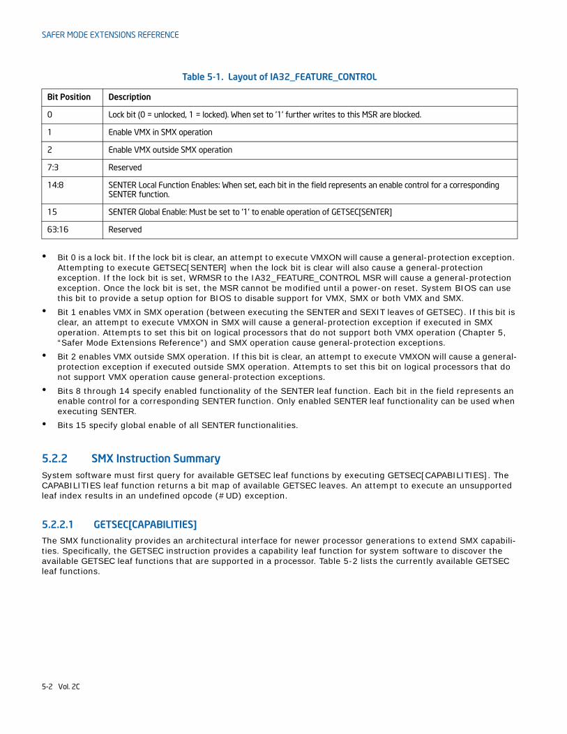
The IA32_FEATURE_CONTROL MSR (at address 03AH) provides feature control bits that configure operation of VMX and SMX. These bits are documented in Table 5-1.
1. See Intel® Trusted Execution Technology Measured Launched Environment Programming Guide.
2. An MVMM is sometimes referred to as a measured launched environment (MLE). See Intel® Trusted Execution Technology Measured Launched Environment Programming Guide
Vol. 2C 5-1
SAFER MODE EXTENSIONS REFERENCE
• Bit 0 is a lock bit. If the lock bit is clear, an attempt to execute VMXON will cause a general-protection exception. Attempting to execute GETSEC[SENTER] when the lock bit is clear will also cause a general-protection exception. If the lock bit is set, WRMSR to the IA32_FEATURE_CONTROL MSR will cause a general-protection exception. Once the lock bit is set, the MSR cannot be modified until a power-on reset. System BIOS can use this bit to provide a setup option for BIOS to disable support for VMX, SMX or both VMX and SMX.
• Bit 1 enables VMX in SMX operation (between executing the SENTER and SEXIT leaves of GETSEC). If this bit is clear, an attempt to execute VMXON in SMX will cause a general-protection exception if executed in SMX operation. Attempts to set this bit on logical processors that do not support both VMX operation (Chapter 5, “Safer Mode Extensions Reference”) and SMX operation cause general-protection exceptions.
• Bit 2 enables VMX outside SMX operation. If this bit is clear, an attempt to execute VMXON will cause a general-protection exception if executed outside SMX operation. Attempts to set this bit on logical processors that do not support VMX operation cause general-protection exceptions.
• Bits 8 through 14 specify enabled functionality of the SENTER leaf function. Each bit in the field represents an enable control for a corresponding SENTER function. Only enabled SENTER leaf functionality can be used when executing SENTER.
• Bits 15 specify global enable of all SENTER functionalities.
5.2.2 SMX Instruction SummarySystem software must first query for available GETSEC leaf functions by executing GETSEC[CAPABILITIES]. The CAPABILITIES leaf function returns a bit map of available GETSEC leaves. An attempt to execute an unsupported leaf index results in an undefined opcode (#UD) exception.
5.2.2.1 GETSEC[CAPABILITIES]The SMX functionality provides an architectural interface for newer processor generations to extend SMX capabili-ties. Specifically, the GETSEC instruction provides a capability leaf function for system software to discover the available GETSEC leaf functions that are supported in a processor. Table 5-2 lists the currently available GETSEC leaf functions.
Table 5-1. Layout of IA32_FEATURE_CONTROL
Bit Position Description
0 Lock bit (0 = unlocked, 1 = locked). When set to '1' further writes to this MSR are blocked.
1 Enable VMX in SMX operation
2 Enable VMX outside SMX operation
7:3 Reserved
14:8 SENTER Local Function Enables: When set, each bit in the field represents an enable control for a corresponding SENTER function.
15 SENTER Global Enable: Must be set to ‘1’ to enable operation of GETSEC[SENTER]
63:16 Reserved
5-2 Vol. 2C

SAFER MODE EXTENSIONS REFERENCE
.
5.2.2.2 GETSEC[ENTERACCS]The GETSEC[ENTERACCS] leaf enables authenticated code execution mode. The ENTERACCS leaf function performs an authenticated code module load using the chipset public key as the signature verification. ENTERACCS requires the existence of an Intel® Trusted Execution Technology capable chipset since it unlocks the chipset private configuration register space after successful authentication of the loaded module. The physical base address and size of the authenticated code module are specified as input register values in EBX and ECX, respec-tively.
While in the authenticated code execution mode, certain processor state properties change. For this reason, the time in which the processor operates in authenticated code execution mode should be limited to minimize impact on external system events.
Upon entry into , the previous paging context is disabled (since the authenticated code module image is specified with physical addresses and can no longer rely upon external memory-based page-table structures).
Prior to executing the GETSEC[ENTERACCS] leaf, system software must ensure the logical processor issuing GETSEC[ENTERACCS] is the boot-strap processor (BSP), as indicated by IA32_APIC_BASE.BSP = 1. System soft-ware must ensure other logical processors are in a suitable idle state and not marked as BSP.
The GETSEC[ENTERACCS] leaf may be used by different agents to load different authenticated code modules to perform functions related to different aspects of a measured environment, for example system software and Intel® TXT enabled BIOS may use more than one authenticated code modules.
5.2.2.3 GETSEC[EXITAC]GETSEC[EXITAC] takes the processor out of . When this instruction leaf is executed, the contents of the authenti-cated code execution area are scrubbed and control is transferred to the non-authenticated context defined by a near pointer passed with the GETSEC[EXITAC] instruction.
The authenticated code execution area is no longer accessible after completion of GETSEC[EXITAC]. RBX (or EBX) holds the address of the near absolute indirect target to be taken.
5.2.2.4 GETSEC[SENTER]The GETSEC[SENTER] leaf function is used by the initiating logical processor (ILP) to launch an MLE. GETSEC[SENTER] can be considered a superset of the ENTERACCS leaf, because it enters as part of the measured environment launch.
Measured environment startup consists of the following steps:
Table 5-2. GETSEC Leaf Functions
Index (EAX) Leaf function Description
0 CAPABILITIES Returns the available leaf functions of the GETSEC instruction
1 Undefined Reserved
2 ENTERACCS Enter
3 EXITAC Exit
4 SENTER Launch an MLE
5 SEXIT Exit the MLE
6 PARAMETERS Return SMX related parameter information
7 SMCTRL SMX mode control
8 WAKEUP Wake up sleeping processors in safer mode
9 - (4G-1) Undefined Reserved
Vol. 2C 5-3
SAFER MODE EXTENSIONS REFERENCE
• the ILP rendezvous the responding logical processors (RLPs) in the platform into a controlled state (At the completion of this handshake, all the RLPs except for the ILP initiating the measured environment launch are placed in a newly defined SENTER sleep state).
• Load and authenticate the authenticated code module required by the measured environment, and enter authenticated code execution mode.
• Verify and lock certain system configuration parameters.• Measure the dynamic root of trust and store into the PCRs in TPM. • Transfer control to the MLE with interrupts disabled.
Prior to executing the GETSEC[SENTER] leaf, system software must ensure the platform’s TPM is ready for access and the ILP is the boot-strap processor (BSP), as indicated by IA32_APIC_BASE.BSP. System software must ensure other logical processors (RLPs) are in a suitable idle state and not marked as BSP.
System software launching a measurement environment is responsible for providing a proper authenticate code module address when executing GETSEC[SENTER]. The AC module responsible for the launch of a measured envi-ronment and loaded by GETSEC[SENTER] is referred to as SINIT. See Intel® Trusted Execution Technology Measured Launched Environment Programming Guide for additional information on system software requirements prior to executing GETSEC[SENTER].
5.2.2.5 GETSEC[SEXIT]System software exits the measured environment by executing the instruction GETSEC[SEXIT] on the ILP. This instruction rendezvous the responding logical processors in the platform for exiting from the measured environ-ment. External events (if left masked) are unmasked and Intel® TXT-capable chipset’s private configuration space is re-locked.
5.2.2.6 GETSEC[PARAMETERS]The GETSEC[PARAMETERS] leaf function is used to report attributes, options and limitations of SMX operation. Software uses this leaf to identify operating limits or additional options.
The information reported by GETSEC[PARAMETERS] may require executing the leaf multiple times using EBX as an index. If the GETSEC[PARAMETERS] instruction leaf or if a specific parameter field is not available, then SMX oper-ation should be interpreted to use the default limits of respective GETSEC leaves or parameter fields defined in the GETSEC[PARAMETERS] leaf.
5.2.2.7 GETSEC[SMCTRL]The GETSEC[SMCTRL] leaf function is used for providing additional control over specific conditions associated with the SMX architecture. An input register is supported for selecting the control operation to be performed. See the specific leaf description for details on the type of control provided.
5.2.2.8 GETSEC[WAKEUP]Responding logical processors (RLPs) are placed in the SENTER sleep state after the initiating logical processor executes GETSEC[SENTER]. The ILP can wake up RLPs to join the measured environment by using GETSEC[WAKEUP].When the RLPs in SENTER sleep state wake up, these logical processors begin execution at the entry point defined in a data structure held in system memory (pointed to by an chipset register LT.MLE.JOIN) in TXT configuration space.
5.2.3 Measured Environment and SMXThis section gives a simplified view of a representative life cycle of a measured environment that is launched by a system executive using SMX leaf functions. Intel® Trusted Execution Technology Measured Launched Environment Programming Guide provides more detailed examples of using SMX and chipset resources (including chipset regis-ters, Trusted Platform Module) to launch an MVMM.
5-4 Vol. 2C
SAFER MODE EXTENSIONS REFERENCE
The life cycle starts with the system executive (an OS, an OS loader, and so forth) loading the MLE and SINIT AC module into available system memory. The system executive must validate and prepare the platform for the measured launch. When the platform is properly configured, the system executive executes GETSEC[SENTER] on the initiating logical processor (ILP) to rendezvous the responding logical processors into an SENTER sleep state, the ILP then enters into using the SINIT AC module. In a multi-threaded or multi-processing environment, the system executive must ensure that other logical processors are already in an idle loop, or asleep (such as after executing HLT) before executing GETSEC[SENTER].
After the GETSEC[SENTER] rendezvous handshake is performed between all logical processors in the platform, the ILP loads the chipset authenticated code module (SINIT) and performs an authentication check. If the check passes, the processor hashes the SINIT AC module and stores the result into TPM PCR 17. It then switches execu-tion context to the SINIT AC module. The SINIT AC module will perform a number of platform operations, including: verifying the system configuration, protecting the system memory used by the MLE from I/O devices capable of DMA, producing a hash of the MLE, storing the hash value in TPM PCR 18, and various other operations. When SINIT completes execution, it executes the GETSEC[EXITAC] instruction and transfers control the MLE at the designated entry point.
Upon receiving control from the SINIT AC module, the MLE must establish its protection and isolation controls before enabling DMA and interrupts and transferring control to other software modules. It must also wakeup the RLPs from their SENTER sleep state using the GETSEC[WAKEUP] instruction and bring them into its protection and isolation environment.
While executing in a measured environment, the MVMM can access the Trusted Platform Module (TPM) in locality 2. The MVMM has complete access to all TPM commands and may use the TPM to report current measurement values or use the measurement values to protect information such that only when the platform configuration registers (PCRs) contain the same value is the information released from the TPM. This protection mechanism is known as sealing.
A measured environment shutdown is ultimately completed by executing GETSEC[SEXIT]. Prior to this step system software is responsible for scrubbing sensitive information left in the processor caches, system memory.
5.3 GETSEC LEAF FUNCTIONSThis section provides detailed descriptions of each leaf function of the GETSEC instruction. GETSEC is available only if CPUID.01H:ECX[Bit 6] = 1. This indicates the availability of SMX and the GETSEC instruction. Before GETSEC can be executed, SMX must be enabled by setting CR4.SMXE[Bit 14] = 1.
A GETSEC leaf can only be used if it is shown to be available as reported by the GETSEC[CAPABILITIES] function. Attempts to access a GETSEC leaf index not supported by the processor, or if CR4.SMXE is 0, results in the signaling of an undefined opcode exception.
All GETSEC leaf functions are available in protected mode, including the compatibility sub-mode of IA-32e mode and the 64-bit sub-mode of IA-32e mode. Unless otherwise noted, the behavior of all GETSEC functions and inter-actions related to the measured environment are independent of IA-32e mode. This also applies to the interpreta-tion of register widths1 passed as input parameters to GETSEC functions and to register results returned as output parameters.
The GETSEC functions ENTERACCS, SENTER, SEXIT, and WAKEUP require a Intel® TXT capable-chipset to be present in the platform. The GETSEC[CAPABILITIES] returned bit vector in position 0 indicates an Intel® TXT-capable chipset has been sampled present2 by the processor.
The processor's operating mode also affects the execution of the following GETSEC leaf functions: SMCTRL, ENTER-ACCS, EXITAC, SENTER, SEXIT, and WAKEUP. These functions are only allowed in protected mode at CPL = 0. They
1. This chapter uses the 64-bit notation RAX, RIP, RSP, RFLAGS, etc. for processor registers because processors that support SMX also support Intel 64 Architecture. The MVMM can be launched in IA-32e mode or outside IA-32e mode. The 64-bit notation of processor registers also refer to its 32-bit forms if SMX is used in 32-bit environment. In some places, notation such as EAX is used to refer specifically to lower 32 bits of the indicated register
2. Sampled present means that the processor sent a message to the chipset and the chipset responded that it (a) knows about the message and (b) is capable of executing SENTER. This means that the chipset CAN support Intel® TXT, and is configured and WILLING to support it.
Vol. 2C 5-5
SAFER MODE EXTENSIONS REFERENCE
are not allowed while in SMM in order to prevent potential intra-mode conflicts. Further execution qualifications exist to prevent potential architectural conflicts (for example: nesting of the measured environment or authenti-cated code execution mode). See the definitions of the GETSEC leaf functions for specific requirements.
For the purpose of performance monitor counting, the execution of GETSEC functions is counted as a single instruc-tion with respect to retired instructions. The response by a responding logical processor (RLP) to messages associ-ated with GETSEC[SENTER] or GTSEC[SEXIT] is transparent to the retired instruction count on the ILP.
5-6 Vol. 2C
SAFER MODE EXTENSIONS REFERENCE
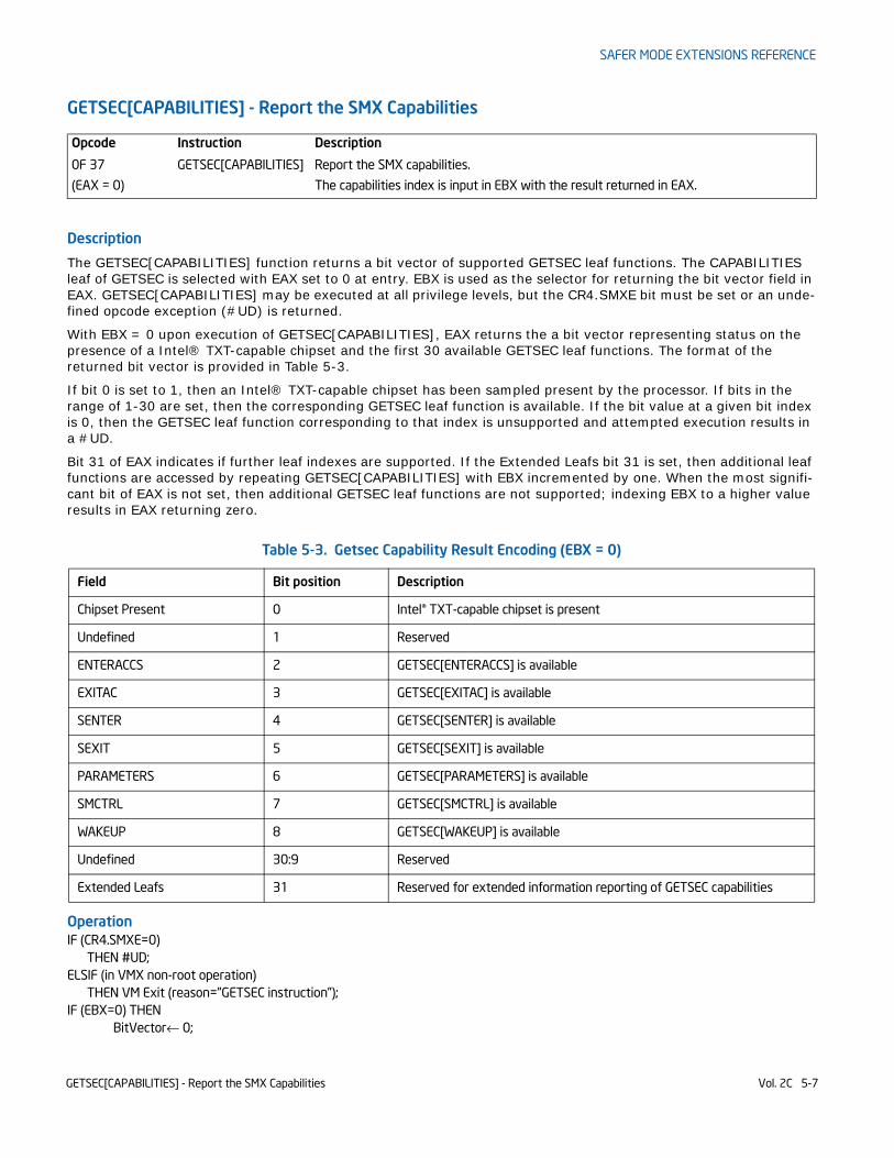
GETSEC[CAPABILITIES] - Report the SMX Capabilities
Description
The GETSEC[CAPABILITIES] function returns a bit vector of supported GETSEC leaf functions. The CAPABILITIES leaf of GETSEC is selected with EAX set to 0 at entry. EBX is used as the selector for returning the bit vector field in EAX. GETSEC[CAPABILITIES] may be executed at all privilege levels, but the CR4.SMXE bit must be set or an unde-fined opcode exception (#UD) is returned.
With EBX = 0 upon execution of GETSEC[CAPABILITIES], EAX returns the a bit vector representing status on the presence of a Intel® TXT-capable chipset and the first 30 available GETSEC leaf functions. The format of the returned bit vector is provided in Table 5-3.
If bit 0 is set to 1, then an Intel® TXT-capable chipset has been sampled present by the processor. If bits in the range of 1-30 are set, then the corresponding GETSEC leaf function is available. If the bit value at a given bit index is 0, then the GETSEC leaf function corresponding to that index is unsupported and attempted execution results in a #UD.
Bit 31 of EAX indicates if further leaf indexes are supported. If the Extended Leafs bit 31 is set, then additional leaf functions are accessed by repeating GETSEC[CAPABILITIES] with EBX incremented by one. When the most signifi-cant bit of EAX is not set, then additional GETSEC leaf functions are not supported; indexing EBX to a higher value results in EAX returning zero.
OperationIF (CR4.SMXE=0)
THEN #UD;ELSIF (in VMX non-root operation)
THEN VM Exit (reason=”GETSEC instruction”);IF (EBX=0) THEN
BitVector← 0;
Opcode Instruction Description
0F 37
(EAX = 0)
GETSEC[CAPABILITIES] Report the SMX capabilities.
The capabilities index is input in EBX with the result returned in EAX.
Table 5-3. Getsec Capability Result Encoding (EBX = 0)
Field Bit position Description
Chipset Present 0 Intel® TXT-capable chipset is present
Undefined 1 Reserved
ENTERACCS 2 GETSEC[ENTERACCS] is available
EXITAC 3 GETSEC[EXITAC] is available
SENTER 4 GETSEC[SENTER] is available
SEXIT 5 GETSEC[SEXIT] is available
PARAMETERS 6 GETSEC[PARAMETERS] is available
SMCTRL 7 GETSEC[SMCTRL] is available
WAKEUP 8 GETSEC[WAKEUP] is available
Undefined 30:9 Reserved
Extended Leafs 31 Reserved for extended information reporting of GETSEC capabilities
GETSEC[CAPABILITIES] - Report the SMX Capabilities Vol. 2C 5-7

SAFER MODE EXTENSIONS REFERENCE
IF (TXT chipset present)BitVector[Chipset present]← 1;
IF (ENTERACCS Available)THEN BitVector[ENTERACCS]← 1;
IF (EXITAC Available)THEN BitVector[EXITAC]← 1;
IF (SENTER Available)THEN BitVector[SENTER]← 1;
IF (SEXIT Available)THEN BitVector[SEXIT]← 1;
IF (PARAMETERS Available)THEN BitVector[PARAMETERS]← 1;
IF (SMCTRL Available)THEN BitVector[SMCTRL]← 1;
IF (WAKEUP Available)THEN BitVector[WAKEUP]← 1;
EAX← BitVector;ELSE
EAX← 0;END;;
Flags AffectedNone
Use of PrefixesLOCK Causes #UDREP* Cause #UD (includes REPNE/REPNZ and REP/REPE/REPZ)Operand size Causes #UDSegment overrides IgnoredAddress size IgnoredREX Ignored
Protected Mode Exceptions#UD IF CR4.SMXE = 0.
Real-Address Mode Exceptions#UD IF CR4.SMXE = 0.
Virtual-8086 Mode Exceptions#UD IF CR4.SMXE = 0.
Compatibility Mode Exceptions#UD IF CR4.SMXE = 0.
64-Bit Mode Exceptions#UD IF CR4.SMXE = 0.
VM-exit ConditionReason (GETSEC) IF in VMX non-root operation.
GETSEC[CAPABILITIES] - Report the SMX Capabilities5-8 Vol. 2C

SAFER MODE EXTENSIONS REFERENCE
GETSEC[ENTERACCS] - Execute Authenticated Chipset Code
Description
The GETSEC[ENTERACCS] function loads, authenticates and executes an authenticated code module using an Intel® TXT platform chipset's public key. The ENTERACCS leaf of GETSEC is selected with EAX set to 2 at entry.
There are certain restrictions enforced by the processor for the execution of the GETSEC[ENTERACCS] instruction: • Execution is not allowed unless the processor is in protected mode or IA-32e mode with CPL = 0 and
EFLAGS.VM = 0. • Processor cache must be available and not disabled, that is, CR0.CD and CR0.NW bits must be 0. • For processor packages containing more than one logical processor, CR0.CD is checked to ensure consistency
between enabled logical processors. • For enforcing consistency of operation with numeric exception reporting using Interrupt 16, CR0.NE must be
set. • An Intel TXT-capable chipset must be present as communicated to the processor by sampling of the power-on
configuration capability field after reset. • The processor can not already be in authenticated code execution mode as launched by a previous
GETSEC[ENTERACCS] or GETSEC[SENTER] instruction without a subsequent exiting using GETSEC[EXITAC]). • To avoid potential operability conflicts between modes, the processor is not allowed to execute this instruction
if it currently is in SMM or VMX operation. • To insure consistent handling of SIPI messages, the processor executing the GETSEC[ENTERACCS] instruction
must also be designated the BSP (boot-strap processor) as defined by A32_APIC_BASE.BSP (Bit 8).
Failure to conform to the above conditions results in the processor signaling a general protection exception.
Prior to execution of the ENTERACCS leaf, other logical processors, i.e. RLPs, in the platform must be:• idle in a wait-for-SIPI state (as initiated by an INIT assertion or through reset for non-BSP designated
processors), or • in the SENTER sleep state as initiated by a GETSEC[SENTER] from the initiating logical processor (ILP).
If other logical processor(s) in the same package are not idle in one of these states, execution of ENTERACCS signals a general protection exception. The same requirement and action applies if the other logical processor(s) of the same package do not have CR0.CD = 0.
A successful execution of ENTERACCS results in the ILP entering an authenticated code execution mode. Prior to reaching this point, the processor performs several checks. These include: • Establish and check the location and size of the specified authenticated code module to be executed by the
processor.• Inhibit the ILP’s response to the external events: INIT, A20M, NMI and SMI.• Broadcast a message to enable protection of memory and I/O from other processor agents.• Load the designated code module into an authenticated code execution area.• Isolate the contents of the authenticated code execution area from further state modification by external
agents.• Authenticate the authenticated code module.• Initialize the initiating logical processor state based on information contained in the authenticated code module
header.• Unlock the Intel® TXT-capable chipset private configuration space and TPM locality 3 space.
Opcode Instruction Description
0F 37
(EAX = 2)
GETSEC[ENTERACCS] Enter authenticated code execution mode.
EBX holds the authenticated code module physical base address. ECX holds the authenticated code module size (bytes).
GETSEC[ENTERACCS] - Execute Authenticated Chipset Code Vol. 2C 5-9
SAFER MODE EXTENSIONS REFERENCE
• Begin execution in the authenticated code module at the defined entry point.
The GETSEC[ENTERACCS] function requires two additional input parameters in the general purpose registers EBX and ECX. EBX holds the authenticated code (AC) module physical base address (the AC module must reside below 4 GBytes in physical address space) and ECX holds the AC module size (in bytes). The physical base address and size are used to retrieve the code module from system memory and load it into the internal authenticated code execution area. The base physical address is checked to verify it is on a modulo-4096 byte boundary. The size is verified to be a multiple of 64, that it does not exceed the internal authenticated code execution area capacity (as reported by GETSEC[CAPABILITIES]), and that the top address of the AC module does not exceed 32 bits. An error condition results in an abort of the authenticated code execution launch and the signaling of a general protection exception.
As an integrity check for proper processor hardware operation, execution of GETSEC[ENTERACCS] will also check the contents of all the machine check status registers (as reported by the MSRs IA32_MCi_STATUS) for any valid uncorrectable error condition. In addition, the global machine check status register IA32_MCG_STATUS MCIP bit must be cleared and the IERR processor package pin (or its equivalent) must not be asserted, indicating that no machine check exception processing is currently in progress. These checks are performed prior to initiating the load of the authenticated code module. Any outstanding valid uncorrectable machine check error condition present in these status registers at this point will result in the processor signaling a general protection violation.
The ILP masks the response to the assertion of the external signals INIT#, A20M, NMI#, and SMI#. This masking remains active until optionally unmasked by GETSEC[EXITAC] (this defined unmasking behavior assumes GETSEC[ENTERACCS] was not executed by a prior GETSEC[SENTER]). The purpose of this masking control is to prevent exposure to existing external event handlers that may not be under the control of the authenticated code module.
The ILP sets an internal flag to indicate it has entered authenticated code execution mode. The state of the A20M pin is likewise masked and forced internally to a de-asserted state so that any external assertion is not recognized during authenticated code execution mode.
To prevent other (logical) processors from interfering with the ILP operating in authenticated code execution mode, memory (excluding implicit write-back transactions) access and I/O originating from other processor agents are blocked. This protection starts when the ILP enters into authenticated code execution mode. Only memory and I/O transactions initiated from the ILP are allowed to proceed. Exiting authenticated code execution mode is done by executing GETSEC[EXITAC]. The protection of memory and I/O activities remains in effect until the ILP executes GETSEC[EXITAC].
Prior to launching the authenticated execution module using GETSEC[ENTERACCS] or GETSEC[SENTER], the processor’s MTRRs (Memory Type Range Registers) must first be initialized to map out the authenticated RAM addresses as WB (writeback). Failure to do so may affect the ability for the processor to maintain isolation of the loaded authenticated code module. If the processor detected this requirement is not met, it will signal an Intel® TXT reset condition with an error code during the loading of the authenticated code module.
While physical addresses within the load module must be mapped as WB, the memory type for locations outside of the module boundaries must be mapped to one of the supported memory types as returned by GETSEC[PARAME-TERS] (or UC as default).
To conform to the minimum granularity of MTRR MSRs for specifying the memory type, authenticated code RAM (ACRAM) is allocated to the processor in 4096 byte granular blocks. If an AC module size as specified in ECX is not a multiple of 4096 then the processor will allocate up to the next 4096 byte boundary for mapping as ACRAM with indeterminate data. This pad area will not be visible to the authenticated code module as external memory nor can it depend on the value of the data used to fill the pad area.
At the successful completion of GETSEC[ENTERACCS], the architectural state of the processor is partially initialized from contents held in the header of the authenticated code module. The processor GDTR, CS, and DS selectors are initialized from fields within the authenticated code module. Since the authenticated code module must be relocat-able, all address references must be relative to the authenticated code module base address in EBX. The processor GDTR base value is initialized to the AC module header field GDTBasePtr + module base address held in EBX and the GDTR limit is set to the value in the GDTLimit field. The CS selector is initialized to the AC module header SegSel field, while the DS selector is initialized to CS + 8. The segment descriptor fields are implicitly initialized to BASE=0, LIMIT=FFFFFh, G=1, D=1, P=1, S=1, read/write access for DS, and execute/read access for CS. The processor begins the authenticated code module execution with the EIP set to the AC module header EntryPoint field + module base address (EBX). The AC module based fields used for initializing the processor state are checked for consistency and any failure results in a shutdown condition.
GETSEC[ENTERACCS] - Execute Authenticated Chipset Code5-10 Vol. 2C
SAFER MODE EXTENSIONS REFERENCE
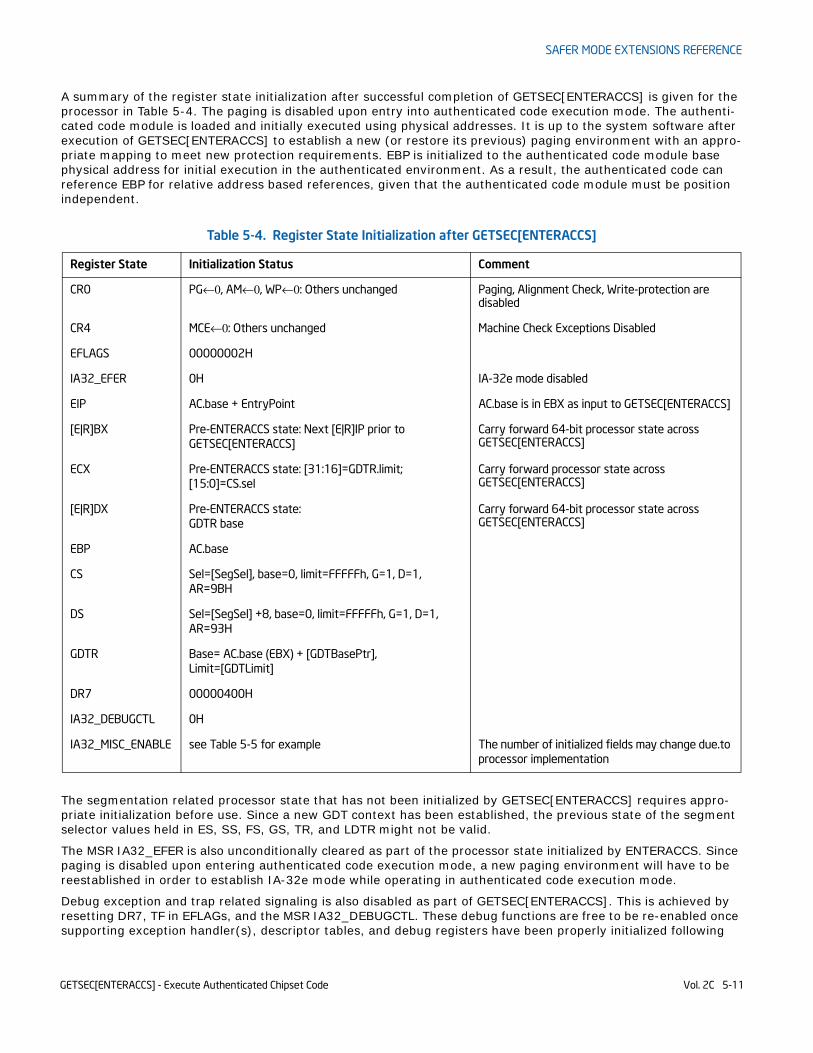
A summary of the register state initialization after successful completion of GETSEC[ENTERACCS] is given for the processor in Table 5-4. The paging is disabled upon entry into authenticated code execution mode. The authenti-cated code module is loaded and initially executed using physical addresses. It is up to the system software after execution of GETSEC[ENTERACCS] to establish a new (or restore its previous) paging environment with an appro-priate mapping to meet new protection requirements. EBP is initialized to the authenticated code module base physical address for initial execution in the authenticated environment. As a result, the authenticated code can reference EBP for relative address based references, given that the authenticated code module must be position independent.
The segmentation related processor state that has not been initialized by GETSEC[ENTERACCS] requires appro-priate initialization before use. Since a new GDT context has been established, the previous state of the segment selector values held in ES, SS, FS, GS, TR, and LDTR might not be valid.
The MSR IA32_EFER is also unconditionally cleared as part of the processor state initialized by ENTERACCS. Since paging is disabled upon entering authenticated code execution mode, a new paging environment will have to be reestablished in order to establish IA-32e mode while operating in authenticated code execution mode.
Debug exception and trap related signaling is also disabled as part of GETSEC[ENTERACCS]. This is achieved by resetting DR7, TF in EFLAGs, and the MSR IA32_DEBUGCTL. These debug functions are free to be re-enabled once supporting exception handler(s), descriptor tables, and debug registers have been properly initialized following
Table 5-4. Register State Initialization after GETSEC[ENTERACCS]
Register State Initialization Status Comment
CR0 PG←0, AM←0, WP←0: Others unchanged Paging, Alignment Check, Write-protection are disabled
CR4 MCE←0: Others unchanged Machine Check Exceptions Disabled
EFLAGS 00000002H
IA32_EFER 0H IA-32e mode disabled
EIP AC.base + EntryPoint AC.base is in EBX as input to GETSEC[ENTERACCS]
[E|R]BX Pre-ENTERACCS state: Next [E|R]IP prior to GETSEC[ENTERACCS]
Carry forward 64-bit processor state across GETSEC[ENTERACCS]
ECX Pre-ENTERACCS state: [31:16]=GDTR.limit; [15:0]=CS.sel
Carry forward processor state across GETSEC[ENTERACCS]
[E|R]DX Pre-ENTERACCS state: GDTR base
Carry forward 64-bit processor state across GETSEC[ENTERACCS]
EBP AC.base
CS Sel=[SegSel], base=0, limit=FFFFFh, G=1, D=1, AR=9BH
DS Sel=[SegSel] +8, base=0, limit=FFFFFh, G=1, D=1, AR=93H
GDTR Base= AC.base (EBX) + [GDTBasePtr], Limit=[GDTLimit]
DR7 00000400H
IA32_DEBUGCTL 0H
IA32_MISC_ENABLE see Table 5-5 for example The number of initialized fields may change due.to processor implementation
GETSEC[ENTERACCS] - Execute Authenticated Chipset Code Vol. 2C 5-11
SAFER MODE EXTENSIONS REFERENCE
entry into authenticated code execution mode. Also, any pending single-step trap condition will have been cleared upon entry into this mode.
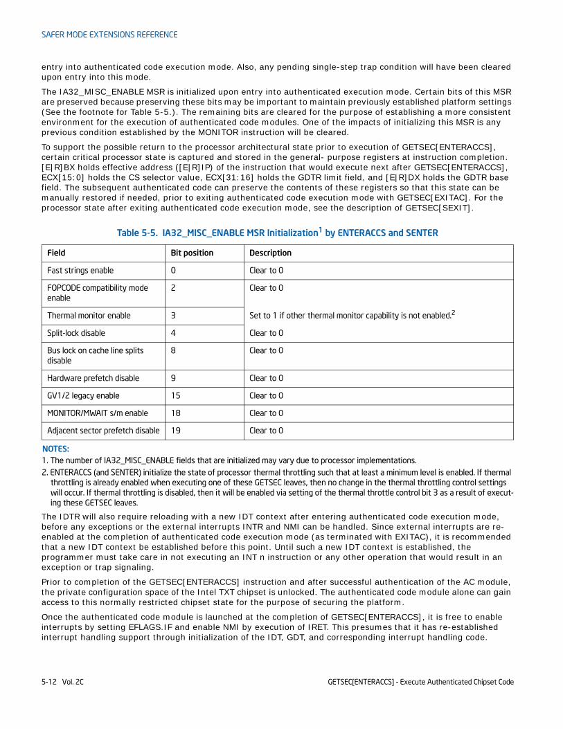
The IA32_MISC_ENABLE MSR is initialized upon entry into authenticated execution mode. Certain bits of this MSR are preserved because preserving these bits may be important to maintain previously established platform settings (See the footnote for Table 5-5.). The remaining bits are cleared for the purpose of establishing a more consistent environment for the execution of authenticated code modules. One of the impacts of initializing this MSR is any previous condition established by the MONITOR instruction will be cleared.
To support the possible return to the processor architectural state prior to execution of GETSEC[ENTERACCS], certain critical processor state is captured and stored in the general- purpose registers at instruction completion. [E|R]BX holds effective address ([E|R]IP) of the instruction that would execute next after GETSEC[ENTERACCS], ECX[15:0] holds the CS selector value, ECX[31:16] holds the GDTR limit field, and [E|R]DX holds the GDTR base field. The subsequent authenticated code can preserve the contents of these registers so that this state can be manually restored if needed, prior to exiting authenticated code execution mode with GETSEC[EXITAC]. For the processor state after exiting authenticated code execution mode, see the description of GETSEC[SEXIT].
The IDTR will also require reloading with a new IDT context after entering authenticated code execution mode, before any exceptions or the external interrupts INTR and NMI can be handled. Since external interrupts are re-enabled at the completion of authenticated code execution mode (as terminated with EXITAC), it is recommended that a new IDT context be established before this point. Until such a new IDT context is established, the programmer must take care in not executing an INT n instruction or any other operation that would result in an exception or trap signaling.
Prior to completion of the GETSEC[ENTERACCS] instruction and after successful authentication of the AC module, the private configuration space of the Intel TXT chipset is unlocked. The authenticated code module alone can gain access to this normally restricted chipset state for the purpose of securing the platform.
Once the authenticated code module is launched at the completion of GETSEC[ENTERACCS], it is free to enable interrupts by setting EFLAGS.IF and enable NMI by execution of IRET. This presumes that it has re-established interrupt handling support through initialization of the IDT, GDT, and corresponding interrupt handling code.
Table 5-5. IA32_MISC_ENABLE MSR Initialization1 by ENTERACCS and SENTER
NOTES:1. The number of IA32_MISC_ENABLE fields that are initialized may vary due to processor implementations.
Field Bit position Description
Fast strings enable 0 Clear to 0
FOPCODE compatibility mode enable
2 Clear to 0
Thermal monitor enable 3 Set to 1 if other thermal monitor capability is not enabled.2
2. ENTERACCS (and SENTER) initialize the state of processor thermal throttling such that at least a minimum level is enabled. If thermal throttling is already enabled when executing one of these GETSEC leaves, then no change in the thermal throttling control settings will occur. If thermal throttling is disabled, then it will be enabled via setting of the thermal throttle control bit 3 as a result of execut-ing these GETSEC leaves.
Split-lock disable 4 Clear to 0
Bus lock on cache line splits disable
8 Clear to 0
Hardware prefetch disable 9 Clear to 0
GV1/2 legacy enable 15 Clear to 0
MONITOR/MWAIT s/m enable 18 Clear to 0
Adjacent sector prefetch disable 19 Clear to 0
GETSEC[ENTERACCS] - Execute Authenticated Chipset Code5-12 Vol. 2C
SAFER MODE EXTENSIONS REFERENCE
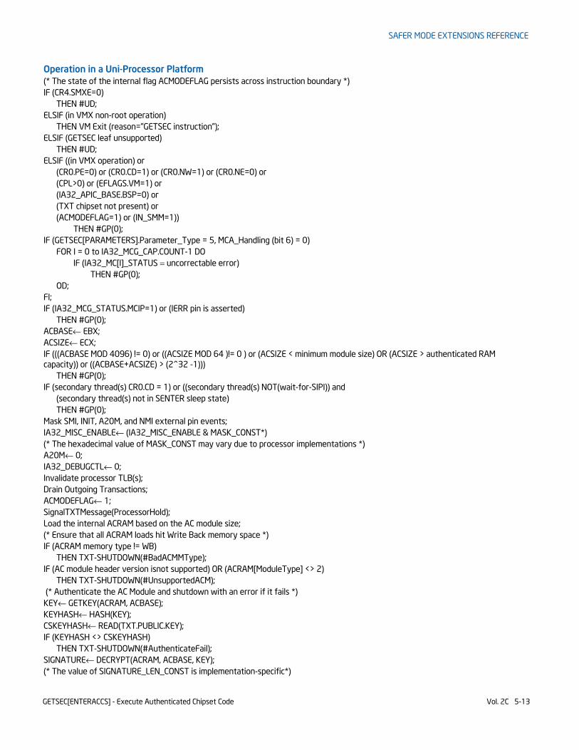
Operation in a Uni-Processor Platform(* The state of the internal flag ACMODEFLAG persists across instruction boundary *)IF (CR4.SMXE=0)
THEN #UD;ELSIF (in VMX non-root operation)
THEN VM Exit (reason=”GETSEC instruction”);ELSIF (GETSEC leaf unsupported)
THEN #UD;ELSIF ((in VMX operation) or
(CR0.PE=0) or (CR0.CD=1) or (CR0.NW=1) or (CR0.NE=0) or(CPL>0) or (EFLAGS.VM=1) or(IA32_APIC_BASE.BSP=0) or(TXT chipset not present) or(ACMODEFLAG=1) or (IN_SMM=1))
THEN #GP(0);IF (GETSEC[PARAMETERS].Parameter_Type = 5, MCA_Handling (bit 6) = 0)
FOR I = 0 to IA32_MCG_CAP.COUNT-1 DOIF (IA32_MC[I]_STATUS = uncorrectable error)
THEN #GP(0);OD;
FI;IF (IA32_MCG_STATUS.MCIP=1) or (IERR pin is asserted)
THEN #GP(0);ACBASE← EBX;ACSIZE← ECX;IF (((ACBASE MOD 4096) != 0) or ((ACSIZE MOD 64 )!= 0 ) or (ACSIZE < minimum module size) OR (ACSIZE > authenticated RAM capacity)) or ((ACBASE+ACSIZE) > (2^32 -1)))
THEN #GP(0);IF (secondary thread(s) CR0.CD = 1) or ((secondary thread(s) NOT(wait-for-SIPI)) and
(secondary thread(s) not in SENTER sleep state)THEN #GP(0);
Mask SMI, INIT, A20M, and NMI external pin events;IA32_MISC_ENABLE← (IA32_MISC_ENABLE & MASK_CONST*)(* The hexadecimal value of MASK_CONST may vary due to processor implementations *)A20M← 0;IA32_DEBUGCTL← 0;Invalidate processor TLB(s);Drain Outgoing Transactions;ACMODEFLAG← 1;SignalTXTMessage(ProcessorHold);Load the internal ACRAM based on the AC module size;(* Ensure that all ACRAM loads hit Write Back memory space *)IF (ACRAM memory type != WB)
THEN TXT-SHUTDOWN(#BadACMMType);IF (AC module header version isnot supported) OR (ACRAM[ModuleType] <> 2)
THEN TXT-SHUTDOWN(#UnsupportedACM); (* Authenticate the AC Module and shutdown with an error if it fails *)KEY← GETKEY(ACRAM, ACBASE);KEYHASH← HASH(KEY);CSKEYHASH← READ(TXT.PUBLIC.KEY);IF (KEYHASH <> CSKEYHASH)
THEN TXT-SHUTDOWN(#AuthenticateFail);SIGNATURE← DECRYPT(ACRAM, ACBASE, KEY);(* The value of SIGNATURE_LEN_CONST is implementation-specific*)
GETSEC[ENTERACCS] - Execute Authenticated Chipset Code Vol. 2C 5-13
SAFER MODE EXTENSIONS REFERENCE
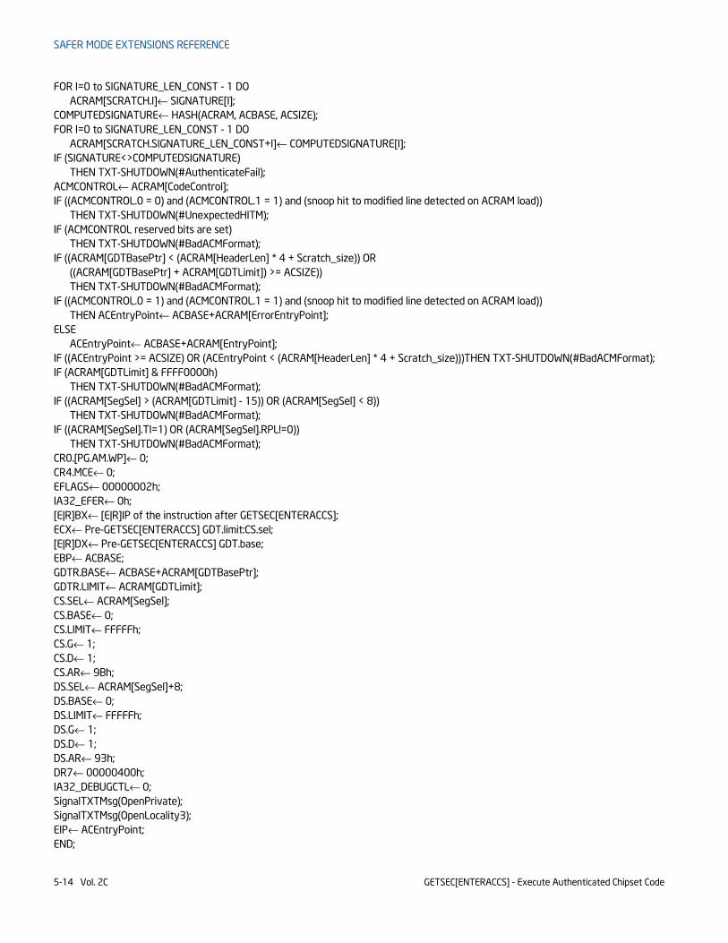
FOR I=0 to SIGNATURE_LEN_CONST - 1 DOACRAM[SCRATCH.I]← SIGNATURE[I];
COMPUTEDSIGNATURE← HASH(ACRAM, ACBASE, ACSIZE);FOR I=0 to SIGNATURE_LEN_CONST - 1 DO
ACRAM[SCRATCH.SIGNATURE_LEN_CONST+I]← COMPUTEDSIGNATURE[I];IF (SIGNATURE<>COMPUTEDSIGNATURE)
THEN TXT-SHUTDOWN(#AuthenticateFail);ACMCONTROL← ACRAM[CodeControl];IF ((ACMCONTROL.0 = 0) and (ACMCONTROL.1 = 1) and (snoop hit to modified line detected on ACRAM load))
THEN TXT-SHUTDOWN(#UnexpectedHITM);IF (ACMCONTROL reserved bits are set)
THEN TXT-SHUTDOWN(#BadACMFormat);IF ((ACRAM[GDTBasePtr] < (ACRAM[HeaderLen] * 4 + Scratch_size)) OR
((ACRAM[GDTBasePtr] + ACRAM[GDTLimit]) >= ACSIZE))THEN TXT-SHUTDOWN(#BadACMFormat);
IF ((ACMCONTROL.0 = 1) and (ACMCONTROL.1 = 1) and (snoop hit to modified line detected on ACRAM load))THEN ACEntryPoint← ACBASE+ACRAM[ErrorEntryPoint];
ELSEACEntryPoint← ACBASE+ACRAM[EntryPoint];
IF ((ACEntryPoint >= ACSIZE) OR (ACEntryPoint < (ACRAM[HeaderLen] * 4 + Scratch_size)))THEN TXT-SHUTDOWN(#BadACMFormat);IF (ACRAM[GDTLimit] & FFFF0000h)
THEN TXT-SHUTDOWN(#BadACMFormat);IF ((ACRAM[SegSel] > (ACRAM[GDTLimit] - 15)) OR (ACRAM[SegSel] < 8))
THEN TXT-SHUTDOWN(#BadACMFormat);IF ((ACRAM[SegSel].TI=1) OR (ACRAM[SegSel].RPL!=0))
THEN TXT-SHUTDOWN(#BadACMFormat);CR0.[PG.AM.WP]← 0;CR4.MCE← 0;EFLAGS← 00000002h;IA32_EFER← 0h;[E|R]BX← [E|R]IP of the instruction after GETSEC[ENTERACCS];ECX← Pre-GETSEC[ENTERACCS] GDT.limit:CS.sel;[E|R]DX← Pre-GETSEC[ENTERACCS] GDT.base;EBP← ACBASE;GDTR.BASE← ACBASE+ACRAM[GDTBasePtr];GDTR.LIMIT← ACRAM[GDTLimit];CS.SEL← ACRAM[SegSel];CS.BASE← 0;CS.LIMIT← FFFFFh;CS.G← 1;CS.D← 1;CS.AR← 9Bh;DS.SEL← ACRAM[SegSel]+8;DS.BASE← 0;DS.LIMIT← FFFFFh;DS.G← 1;DS.D← 1;DS.AR← 93h;DR7← 00000400h;IA32_DEBUGCTL← 0;SignalTXTMsg(OpenPrivate);SignalTXTMsg(OpenLocality3);EIP← ACEntryPoint;END;
GETSEC[ENTERACCS] - Execute Authenticated Chipset Code5-14 Vol. 2C
SAFER MODE EXTENSIONS REFERENCE
Flags AffectedAll flags are cleared.
Use of PrefixesLOCK Causes #UDREP* Cause #UD (includes REPNE/REPNZ and REP/REPE/REPZ)Operand size Causes #UDSegment overrides IgnoredAddress size IgnoredREX Ignored
Protected Mode Exceptions#UD If CR4.SMXE = 0.
If GETSEC[ENTERACCS] is not reported as supported by GETSEC[CAPABILITIES].#GP(0) If CR0.CD = 1 or CR0.NW = 1 or CR0.NE = 0 or CR0.PE = 0 or CPL > 0 or EFLAGS.VM = 1.
If a Intel® TXT-capable chipset is not present.If in VMX root operation.If the initiating processor is not designated as the bootstrap processor via the MSR bit IA32_APIC_BASE.BSP.If the processor is already in authenticated code execution mode.If the processor is in SMM.If a valid uncorrectable machine check error is logged in IA32_MC[I]_STATUS.If the authenticated code base is not on a 4096 byte boundary.If the authenticated code size > processor internal authenticated code area capacity.If the authenticated code size is not modulo 64.If other enabled logical processor(s) of the same package CR0.CD = 1.If other enabled logical processor(s) of the same package are not in the wait-for-SIPI or SENTER sleep state.
Real-Address Mode Exceptions#UD If CR4.SMXE = 0.
If GETSEC[ENTERACCS] is not reported as supported by GETSEC[CAPABILITIES].#GP(0) GETSEC[ENTERACCS] is not recognized in real-address mode.
Virtual-8086 Mode Exceptions#UD If CR4.SMXE = 0.
If GETSEC[ENTERACCS] is not reported as supported by GETSEC[CAPABILITIES].#GP(0) GETSEC[ENTERACCS] is not recognized in virtual-8086 mode.
Compatibility Mode ExceptionsAll protected mode exceptions apply.#GP IF AC code module does not reside in physical address below 2^32 -1.
64-Bit Mode ExceptionsAll protected mode exceptions apply.#GP IF AC code module does not reside in physical address below 2^32 -1.
GETSEC[ENTERACCS] - Execute Authenticated Chipset Code Vol. 2C 5-15

SAFER MODE EXTENSIONS REFERENCE
VM-exit ConditionReason (GETSEC) IF in VMX non-root operation.
GETSEC[ENTERACCS] - Execute Authenticated Chipset Code5-16 Vol. 2C
SAFER MODE EXTENSIONS REFERENCE
GETSEC[EXITAC]—Exit Authenticated Code Execution Mode
Description
The GETSEC[EXITAC] leaf function exits the ILP out of authenticated code execution mode established by GETSEC[ENTERACCS] or GETSEC[SENTER]. The EXITAC leaf of GETSEC is selected with EAX set to 3 at entry. EBX (or RBX, if in 64-bit mode) holds the near jump target offset for where the processor execution resumes upon exiting authenticated code execution mode. EDX contains additional parameter control information. Currently only an input value of 0 in EDX is supported. All other EDX settings are considered reserved and result in a general protection violation.
GETSEC[EXITAC] can only be executed if the processor is in protected mode with CPL = 0 and EFLAGS.VM = 0. The processor must also be in authenticated code execution mode. To avoid potential operability conflicts between modes, the processor is not allowed to execute this instruction if it is in SMM or in VMX operation. A violation of these conditions results in a general protection violation.
Upon completion of the GETSEC[EXITAC] operation, the processor unmasks responses to external event signals INIT#, NMI#, and SMI#. This unmasking is performed conditionally, based on whether the authenticated code execution mode was entered via execution of GETSEC[SENTER] or GETSEC[ENTERACCS]. If the processor is in authenticated code execution mode due to the execution of GETSEC[SENTER], then these external event signals will remain masked. In this case, A20M is kept disabled in the measured environment until the measured environ-ment executes GETSEC[SEXIT]. INIT# is unconditionally unmasked by EXITAC. Note that any events that are pending, but have been blocked while in authenticated code execution mode, will be recognized at the completion of the GETSEC[EXITAC] instruction if the pin event is unmasked.
The intent of providing the ability to optionally leave the pin events SMI#, and NMI# masked is to support the completion of a measured environment bring-up that makes use of VMX. In this envisioned security usage scenario, these events will remain masked until an appropriate virtual machine has been established in order to field servicing of these events in a safer manner. Details on when and how events are masked and unmasked in VMX operation are described in Intel® 64 and IA-32 Architectures Software Developer’s Manual, Volume 3C. It should be cautioned that if no VMX environment is to be activated following GETSEC[EXITAC], that these events will remain masked until the measured environment is exited with GETSEC[SEXIT]. If this is not desired then the GETSEC function SMCTRL(0) can be used for unmasking SMI# in this context. NMI# can be correspondingly unmasked by execution of IRET.
A successful exit of the authenticated code execution mode requires the ILP to perform additional steps as outlined below:• Invalidate the contents of the internal authenticated code execution area. • Invalidate processor TLBs. • Clear the internal processor AC Mode indicator flag. • Re-lock the TPM locality 3 space. • Unlock the Intel® TXT-capable chipset memory and I/O protections to allow memory and I/O activity by other
processor agents. • Perform a near absolute indirect jump to the designated instruction location.
The content of the authenticated code execution area is invalidated by hardware in order to protect it from further use or visibility. This internal processor storage area can no longer be used or relied upon after GETSEC[EXITAC]. Data structures need to be re-established outside of the authenticated code execution area if they are to be refer-enced after EXITAC. Since addressed memory content formerly mapped to the authenticated code execution area may no longer be coherent with external system memory after EXITAC, processor TLBs in support of linear to phys-ical address translation are also invalidated.
Upon completion of GETSEC[EXITAC] a near absolute indirect transfer is performed with EIP loaded with the contents of EBX (based on the current operating mode size). In 64-bit mode, all 64 bits of RBX are loaded into RIP
Opcode Instruction Description
0F 37
(EAX=3)
GETSEC[EXITAC] Exit authenticated code execution mode.
RBX holds the Near Absolute Indirect jump target and EDX hold the exit parameter flags
GETSEC[EXITAC]—Exit Authenticated Code Execution Mode Vol. 2C 5-17
SAFER MODE EXTENSIONS REFERENCE
if REX.W precedes GETSEC[EXITAC]. Otherwise RBX is treated as 32 bits even while in 64-bit mode. Conventional CS limit checking is performed as part of this control transfer. Any exception conditions generated as part of this control transfer will be directed to the existing IDT; thus it is recommended that an IDTR should also be established prior to execution of the EXITAC function if there is a need for fault handling. In addition, any segmentation related (and paging) data structures to be used after EXITAC should be re-established or validated by the authenticated code prior to EXITAC.
In addition, any segmentation related (and paging) data structures to be used after EXITAC need to be re-estab-lished and mapped outside of the authenticated RAM designated area by the authenticated code prior to EXITAC. Any data structure held within the authenticated RAM allocated area will no longer be accessible after completion by EXITAC.
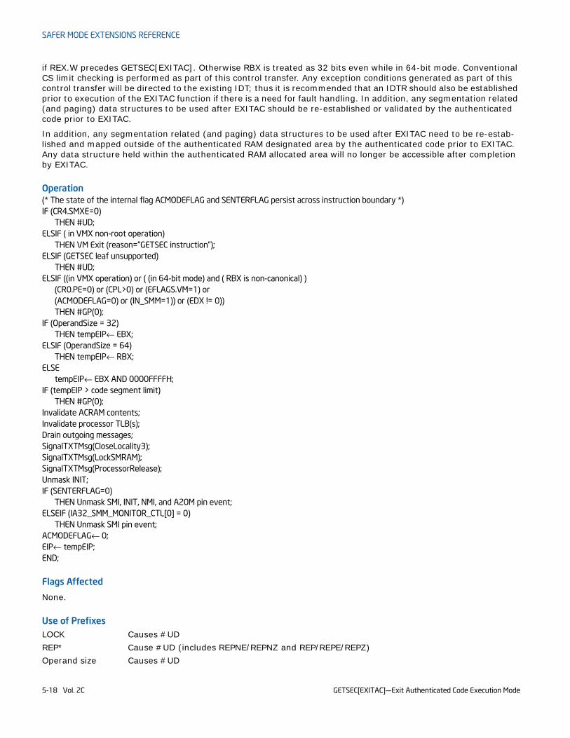
Operation(* The state of the internal flag ACMODEFLAG and SENTERFLAG persist across instruction boundary *)IF (CR4.SMXE=0)
THEN #UD;ELSIF ( in VMX non-root operation)
THEN VM Exit (reason=”GETSEC instruction”);ELSIF (GETSEC leaf unsupported)
THEN #UD;ELSIF ((in VMX operation) or ( (in 64-bit mode) and ( RBX is non-canonical) )
(CR0.PE=0) or (CPL>0) or (EFLAGS.VM=1) or(ACMODEFLAG=0) or (IN_SMM=1)) or (EDX != 0))THEN #GP(0);
IF (OperandSize = 32)THEN tempEIP← EBX;
ELSIF (OperandSize = 64)THEN tempEIP← RBX;
ELSEtempEIP← EBX AND 0000FFFFH;
IF (tempEIP > code segment limit)THEN #GP(0);
Invalidate ACRAM contents;Invalidate processor TLB(s);Drain outgoing messages;SignalTXTMsg(CloseLocality3);SignalTXTMsg(LockSMRAM);SignalTXTMsg(ProcessorRelease);Unmask INIT;IF (SENTERFLAG=0)
THEN Unmask SMI, INIT, NMI, and A20M pin event;ELSEIF (IA32_SMM_MONITOR_CTL[0] = 0)
THEN Unmask SMI pin event;ACMODEFLAG← 0;EIP← tempEIP;END;
Flags Affected
None.
Use of PrefixesLOCK Causes #UDREP* Cause #UD (includes REPNE/REPNZ and REP/REPE/REPZ)Operand size Causes #UD
GETSEC[EXITAC]—Exit Authenticated Code Execution Mode5-18 Vol. 2C
SAFER MODE EXTENSIONS REFERENCE
Segment overrides IgnoredAddress size IgnoredREX.W Sets 64-bit mode Operand size attribute
Protected Mode Exceptions#UD If CR4.SMXE = 0.
If GETSEC[EXITAC] is not reported as supported by GETSEC[CAPABILITIES].#GP(0) If CR0.PE = 0 or CPL>0 or EFLAGS.VM =1.
If in VMX root operation.If the processor is not currently in authenticated code execution mode.If the processor is in SMM.If any reserved bit position is set in the EDX parameter register.
Real-Address Mode Exceptions#UD If CR4.SMXE = 0.
If GETSEC[EXITAC] is not reported as supported by GETSEC[CAPABILITIES].#GP(0) GETSEC[EXITAC] is not recognized in real-address mode.
Virtual-8086 Mode Exceptions#UD If CR4.SMXE = 0.
If GETSEC[EXITAC] is not reported as supported by GETSEC[CAPABILITIES].#GP(0) GETSEC[EXITAC] is not recognized in virtual-8086 mode.
Compatibility Mode ExceptionsAll protected mode exceptions apply.
64-Bit Mode ExceptionsAll protected mode exceptions apply.#GP(0) If the target address in RBX is not in a canonical form.
VM-Exit ConditionReason (GETSEC) IF in VMX non-root operation.
GETSEC[EXITAC]—Exit Authenticated Code Execution Mode Vol. 2C 5-19
SAFER MODE EXTENSIONS REFERENCE
GETSEC[SENTER]—Enter a Measured Environment
Description
The GETSEC[SENTER] instruction initiates the launch of a measured environment and places the initiating logical processor (ILP) into the authenticated code execution mode. The SENTER leaf of GETSEC is selected with EAX set to 4 at execution. The physical base address of the AC module to be loaded and authenticated is specified in EBX. The size of the module in bytes is specified in ECX. EDX controls the level of functionality supported by the measured environment launch. To enable the full functionality of the protected environment launch, EDX must be initialized to zero.
The authenticated code base address and size parameters (in bytes) are passed to the GETSEC[SENTER] instruc-tion using EBX and ECX respectively. The ILP evaluates the contents of these registers according to the rules for the AC module address in GETSEC[ENTERACCS]. AC module execution follows the same rules, as set by GETSEC[ENTERACCS].
The launching software must ensure that the TPM.ACCESS_0.activeLocality bit is clear before executing the GETSEC[SENTER] instruction.
There are restrictions enforced by the processor for execution of the GETSEC[SENTER] instruction: • Execution is not allowed unless the processor is in protected mode or IA-32e mode with CPL = 0 and
EFLAGS.VM = 0. • Processor cache must be available and not disabled using the CR0.CD and NW bits. • For enforcing consistency of operation with numeric exception reporting using Interrupt 16, CR0.NE must be
set. • An Intel TXT-capable chipset must be present as communicated to the processor by sampling of the power-on
configuration capability field after reset. • The processor can not be in authenticated code execution mode or already in a measured environment (as
launched by a previous GETSEC[ENTERACCS] or GETSEC[SENTER] instruction). • To avoid potential operability conflicts between modes, the processor is not allowed to execute this instruction
if it currently is in SMM or VMX operation. • To insure consistent handling of SIPI messages, the processor executing the GETSEC[SENTER] instruction must
also be designated the BSP (boot-strap processor) as defined by A32_APIC_BASE.BSP (Bit 8). • EDX must be initialized to a setting supportable by the processor. Unless enumeration by the GETSEC[PARAM-
ETERS] leaf reports otherwise, only a value of zero is supported.
Failure to abide by the above conditions results in the processor signaling a general protection violation.
This instruction leaf starts the launch of a measured environment by initiating a rendezvous sequence for all logical processors in the platform. The rendezvous sequence involves the initiating logical processor sending a message (by executing GETSEC[SENTER]) and other responding logical processors (RLPs) acknowledging the message, thus synchronizing the RLP(s) with the ILP.
In response to a message signaling the completion of rendezvous, RLPs clear the bootstrap processor indicator flag (IA32_APIC_BASE.BSP) and enter an SENTER sleep state. In this sleep state, RLPs enter an idle processor condi-tion while waiting to be activated after a measured environment has been established by the system executive. RLPs in the SENTER sleep state can only be activated by the GETSEC leaf function WAKEUP in a measured environ-ment.
A successful launch of the measured environment results in the initiating logical processor entering the authenti-cated code execution mode. Prior to reaching this point, the ILP performs the following steps internally: • Inhibit processor response to the external events: INIT, A20M, NMI, and SMI.
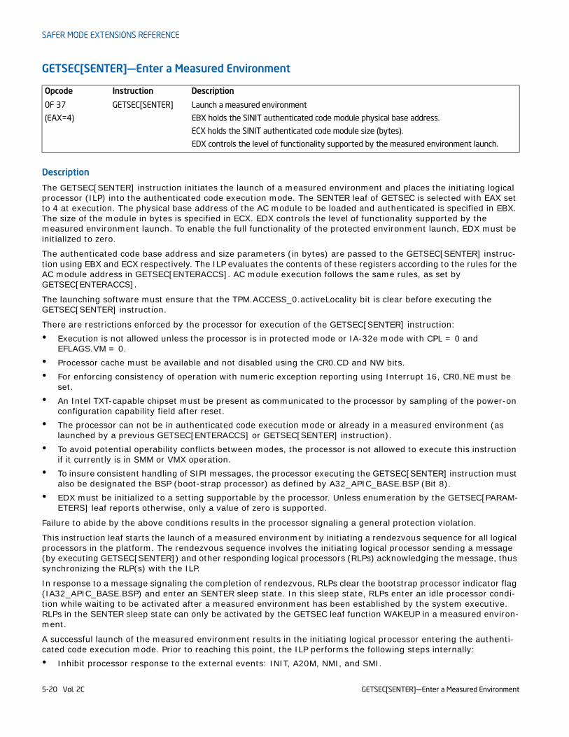
Opcode Instruction Description
0F 37
(EAX=4)
GETSEC[SENTER] Launch a measured environment
EBX holds the SINIT authenticated code module physical base address.
ECX holds the SINIT authenticated code module size (bytes).
EDX controls the level of functionality supported by the measured environment launch.
GETSEC[SENTER]—Enter a Measured Environment5-20 Vol. 2C
SAFER MODE EXTENSIONS REFERENCE
• Establish and check the location and size of the authenticated code module to be executed by the ILP. • Check for the existence of an Intel® TXT-capable chipset. • Verify the current power management configuration is acceptable. • Broadcast a message to enable protection of memory and I/O from activities from other processor agents. • Load the designated AC module into authenticated code execution area. • Isolate the content of authenticated code execution area from further state modification by external agents.• Authenticate the AC module.• Updated the Trusted Platform Module (TPM) with the authenticated code module's hash. • Initialize processor state based on the authenticated code module header information. • Unlock the Intel® TXT-capable chipset private configuration register space and TPM locality 3 space. • Begin execution in the authenticated code module at the defined entry point.
As an integrity check for proper processor hardware operation, execution of GETSEC[SENTER] will also check the contents of all the machine check status registers (as reported by the MSRs IA32_MCi_STATUS) for any valid uncorrectable error condition. In addition, the global machine check status register IA32_MCG_STATUS MCIP bit must be cleared and the IERR processor package pin (or its equivalent) must be not asserted, indicating that no machine check exception processing is currently in-progress. These checks are performed twice: once by the ILP prior to the broadcast of the rendezvous message to RLPs, and later in response to RLPs acknowledging the rendezvous message. Any outstanding valid uncorrectable machine check error condition present in the machine check status registers at the first check point will result in the ILP signaling a general protection violation. If an outstanding valid uncorrectable machine check error condition is present at the second check point, then this will result in the corresponding logical processor signaling the more severe TXT-shutdown condition with an error code of 12.
Before loading and authentication of the target code module is performed, the processor also checks that the current voltage and bus ratio encodings correspond to known good values supportable by the processor. The MSR IA32_PERF_STATUS values are compared against either the processor supported maximum operating target setting, system reset setting, or the thermal monitor operating target. If the current settings do not meet any of these criteria then the SENTER function will attempt to change the voltage and bus ratio select controls in a processor-specific manner. This adjustment may be to the thermal monitor, minimum (if different), or maximum operating target depending on the processor.
This implies that some thermal operating target parameters configured by BIOS may be overridden by SENTER. The measured environment software may need to take responsibility for restoring such settings that are deemed to be safe, but not necessarily recognized by SENTER. If an adjustment is not possible when an out of range setting is discovered, then the processor will abort the measured launch. This may be the case for chipset controlled settings of these values or if the controllability is not enabled on the processor. In this case it is the responsibility of the external software to program the chipset voltage ID and/or bus ratio select settings to known good values recognized by the processor, prior to executing SENTER.
NOTEFor a mobile processor, an adjustment can be made according to the thermal monitor operating target. For a quad-core processor the SENTER adjustment mechanism may result in a more conser-vative but non-uniform voltage setting, depending on the pre-SENTER settings per core.
The ILP and RLPs mask the response to the assertion of the external signals INIT#, A20M, NMI#, and SMI#. The purpose of this masking control is to prevent exposure to existing external event handlers until a protected handler has been put in place to directly handle these events. Masked external pin events may be unmasked conditionally or unconditionally via the GETSEC[EXITAC], GETSEC[SEXIT], GETSEC[SMCTRL] or for specific VMX related opera-tions such as a VM entry or the VMXOFF instruction (see respective GETSEC leaves and Intel® 64 and IA-32 Archi-tectures Software Developer’s Manual, Volume 3C for more details).The state of the A20M pin is masked and forced internally to a de-asserted state so that external assertion is not recognized. A20M masking as set by GETSEC[SENTER] is undone only after taking down the measured environment with the GETSEC[SEXIT] instruc-tion or processor reset. INTR is masked by simply clearing the EFLAGS.IF bit. It is the responsibility of system soft-ware to control the processor response to INTR through appropriate management of EFLAGS.
GETSEC[SENTER]—Enter a Measured Environment Vol. 2C 5-21

SAFER MODE EXTENSIONS REFERENCE
To prevent other (logical) processors from interfering with the ILP operating in authenticated code execution mode, memory (excluding implicit write-back transactions) and I/O activities originating from other processor agents are blocked. This protection starts when the ILP enters into authenticated code execution mode. Only memory and I/O transactions initiated from the ILP are allowed to proceed. Exiting authenticated code execution mode is done by executing GETSEC[EXITAC]. The protection of memory and I/O activities remains in effect until the ILP executes GETSEC[EXITAC].
Once the authenticated code module has been loaded into the authenticated code execution area, it is protected against further modification from external bus snoops. There is also a requirement that the memory type for the authenticated code module address range be WB (via initialization of the MTRRs prior to execution of this instruc-tion). If this condition is not satisfied, it is a violation of security and the processor will force a TXT system reset (after writing an error code to the chipset LT.ERRORCODE register). This action is referred to as a Intel® TXT reset condition. It is performed when it is considered unreliable to signal an error through the conventional exception reporting mechanism.
To conform to the minimum granularity of MTRR MSRs for specifying the memory type, authenticated code RAM (ACRAM) is allocated to the processor in 4096 byte granular blocks. If an AC module size as specified in ECX is not a multiple of 4096 then the processor will allocate up to the next 4096 byte boundary for mapping as ACRAM with indeterminate data. This pad area will not be visible to the authenticated code module as external memory nor can it depend on the value of the data used to fill the pad area.
Once successful authentication has been completed by the ILP, the computed hash is stored in the TPM at PCR17 after this register is implicitly reset. PCR17 is a dedicated register for holding the computed hash of the authenti-cated code module loaded and subsequently executed by the GETSEC[SENTER]. As part of this process, the dynamic PCRs 18-22 are reset so they can be utilized by subsequently software for registration of code and data modules. After successful execution of SENTER, PCR17 contains the measurement of AC code and the SENTER launching parameters.
After authentication is completed successfully, the private configuration space of the Intel® TXT-capable chipset is unlocked so that the authenticated code module and measured environment software can gain access to this normally restricted chipset state. The Intel® TXT-capable chipset private configuration space can be locked later by software writing to the chipset LT.CMD.CLOSE-PRIVATE register or unconditionally using the GETSEC[SEXIT] instruction.
The SENTER leaf function also initializes some processor architecture state for the ILP from contents held in the header of the authenticated code module. Since the authenticated code module is relocatable, all address refer-ences are relative to the base address passed in via EBX. The ILP GDTR base value is initialized to EBX + [GDTBasePtr] and GDTR limit set to [GDTLimit]. The CS selector is initialized to the value held in the AC module header field SegSel, while the DS, SS, and ES selectors are initialized to CS+8. The segment descriptor fields are initialized implicitly with BASE=0, LIMIT=FFFFFh, G=1, D=1, P=1, S=1, read/write/accessed for DS, SS, and ES, while execute/read/accessed for CS. Execution in the authenticated code module for the ILP begins with the EIP set to EBX + [EntryPoint]. AC module defined fields used for initializing processor state are consistency checked with a failure resulting in an TXT-shutdown condition.
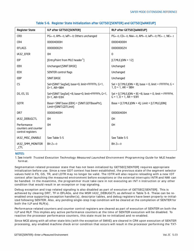
Table 5-6 provides a summary of processor state initialization for the ILP and RLP(s) after successful completion of GETSEC[SENTER]. For both ILP and RLP(s), paging is disabled upon entry to the measured environment. It is up to the ILP to establish a trusted paging environment, with appropriate mappings, to meet protection requirements established during the launch of the measured environment. RLP state initialization is not completed until a subse-quent wake-up has been signaled by execution of the GETSEC[WAKEUP] function by the ILP.
GETSEC[SENTER]—Enter a Measured Environment5-22 Vol. 2C
SAFER MODE EXTENSIONS REFERENCE
Segmentation related processor state that has not been initialized by GETSEC[SENTER] requires appropriate initialization before use. Since a new GDT context has been established, the previous state of the segment selector values held in FS, GS, TR, and LDTR may no longer be valid. The IDTR will also require reloading with a new IDT context after launching the measured environment before exceptions or the external interrupts INTR and NMI can be handled. In the meantime, the programmer must take care in not executing an INT n instruction or any other condition that would result in an exception or trap signaling.
Debug exception and trap related signaling is also disabled as part of execution of GETSEC[SENTER]. This is achieved by clearing DR7, TF in EFLAGs, and the MSR IA32_DEBUGCTL as defined in Table 5-6. These can be re-enabled once supporting exception handler(s), descriptor tables, and debug registers have been properly re-initial-ized following SENTER. Also, any pending single-step trap condition will be cleared at the completion of SENTER for both the ILP and RLP(s).
Performance related counters and counter control registers are cleared as part of execution of SENTER on both the ILP and RLP. This implies any active performance counters at the time of SENTER execution will be disabled. To reactive the processor performance counters, this state must be re-initialized and re-enabled.
Since MCE along with all other state bits (with the exception of SMXE) are cleared in CR4 upon execution of SENTER processing, any enabled machine check error condition that occurs will result in the processor performing the TXT-
Table 5-6. Register State Initialization after GETSEC[SENTER] and GETSEC[WAKEUP]
Register State ILP after GETSEC[SENTER] RLP after GETSEC[WAKEUP]
CR0 PG←0, AM←0, WP←0; Others unchanged PG←0, CD←0, NW←0, AM←0, WP←0; PE←1, NE←1
CR4 00004000H 00004000H
EFLAGS 00000002H 00000002H
IA32_EFER 0H 0
EIP [EntryPoint from MLE header1] [LT.MLE.JOIN + 12]
EBX Unchanged [SINIT.BASE] Unchanged
EDX SENTER control flags Unchanged
EBP SINIT.BASE Unchanged
CS Sel=[SINIT SegSel], base=0, limit=FFFFFh, G=1, D=1, AR=9BH
Sel = [LT.MLE.JOIN + 8], base = 0, limit = FFFFFH, G = 1, D = 1, AR = 9BH
DS, ES, SS Sel=[SINIT SegSel] +8, base=0, limit=FFFFFh, G=1, D=1, AR=93H
Sel = [LT.MLE.JOIN + 8] +8, base = 0, limit = FFFFFH, G = 1, D = 1, AR = 93H
GDTR Base= SINIT.base (EBX) + [SINIT.GDTBasePtr], Limit=[SINIT.GDTLimit]
Base = [LT.MLE.JOIN + 4], Limit = [LT.MLE.JOIN]
DR7 00000400H 00000400H
IA32_DEBUGCTL 0H 0H
Performance counters and counter control registers
0H 0H
IA32_MISC_ENABLE See Table 5-5 See Table 5-5
IA32_SMM_MONITOR_CTL
Bit 2←0 Bit 2←0
NOTES:1. See Intel® Trusted Execution Technology Measured Launched Environment Programming Guide for MLE header
format.
GETSEC[SENTER]—Enter a Measured Environment Vol. 2C 5-23
SAFER MODE EXTENSIONS REFERENCE
shutdown action. This also applies to an RLP while in the SENTER sleep state. For each logical processor CR4.MCE must be reestablished with a valid machine check exception handler to otherwise avoid an TXT-shutdown under such conditions.
The MSR IA32_EFER is also unconditionally cleared as part of the processor state initialized by SENTER for both the ILP and RLP. Since paging is disabled upon entering authenticated code execution mode, a new paging environment will have to be re-established if it is desired to enable IA-32e mode while operating in authenticated code execution mode.
The miscellaneous feature control MSR, IA32_MISC_ENABLE, is initialized as part of the measured environment launch. Certain bits of this MSR are preserved because preserving these bits may be important to maintain previ-ously established platform settings. See the footnote for Table 5-5 The remaining bits are cleared for the purpose of establishing a more consistent environment for the execution of authenticated code modules. Among the impact of initializing this MSR, any previous condition established by the MONITOR instruction will be cleared.
Effect of MSR IA32_FEATURE_CONTROL MSR
Bits 15:8 of the IA32_FEATURE_CONTROL MSR affect the execution of GETSEC[SENTER]. These bits consist of two fields: • Bit 15: a global enable control for execution of SENTER.• Bits 14:8: a parameter control field providing the ability to qualify SENTER execution based on the level of
functionality specified with corresponding EDX parameter bits 6:0.
The layout of these fields in the IA32_FEATURE_CONTROL MSR is shown in Table 5-1.
Prior to the execution of GETSEC[SENTER], the lock bit of IA32_FEATURE_CONTROL MSR must be bit set to affirm the settings to be used. Once the lock bit is set, only a power-up reset condition will clear this MSR. The IA32_FEATURE_CONTROL MSR must be configured in accordance to the intended usage at platform initialization. Note that this MSR is only available on SMX or VMX enabled processors. Otherwise, IA32_FEATURE_CONTROL is treated as reserved.
The Intel® Trusted Execution Technology Measured Launched Environment Programming Guide provides additional details and requirements for programming measured environment software to launch in an Intel TXT platform.
Operation in a Uni-Processor Platform(* The state of the internal flag ACMODEFLAG and SENTERFLAG persist across instruction boundary *)GETSEC[SENTER] (ILP only):IF (CR4.SMXE=0)
THEN #UD;ELSE IF (in VMX non-root operation)
THEN VM Exit (reason=”GETSEC instruction”);ELSE IF (GETSEC leaf unsupported)
THEN #UD;ELSE IF ((in VMX root operation) or
(CR0.PE=0) or (CR0.CD=1) or (CR0.NW=1) or (CR0.NE=0) or(CPL>0) or (EFLAGS.VM=1) or(IA32_APIC_BASE.BSP=0) or (TXT chipset not present) or(SENTERFLAG=1) or (ACMODEFLAG=1) or (IN_SMM=1) or(TPM interface is not present) or(EDX != (SENTER_EDX_support_mask & EDX)) or(IA32_CR_FEATURE_CONTROL[0]=0) or (IA32_CR_FEATURE_CONTROL[15]=0) or((IA32_CR_FEATURE_CONTROL[14:8] & EDX[6:0]) != EDX[6:0]))
THEN #GP(0);IF (GETSEC[PARAMETERS].Parameter_Type = 5, MCA_Handling (bit 6) = 0)
FOR I = 0 to IA32_MCG_CAP.COUNT-1 DOIF IA32_MC[I]_STATUS = uncorrectable error
THEN #GP(0);FI;
OD;
GETSEC[SENTER]—Enter a Measured Environment5-24 Vol. 2C
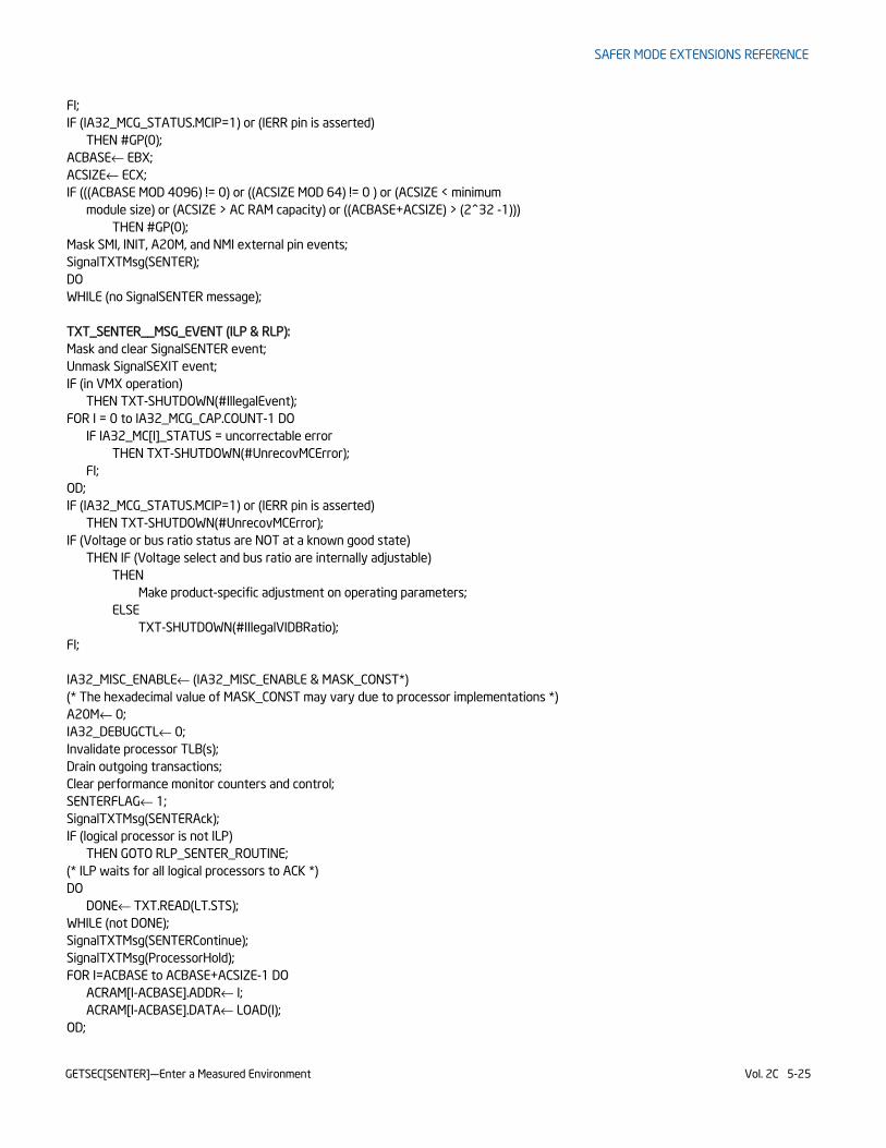
SAFER MODE EXTENSIONS REFERENCE
FI;IF (IA32_MCG_STATUS.MCIP=1) or (IERR pin is asserted)
THEN #GP(0);ACBASE← EBX;ACSIZE← ECX;IF (((ACBASE MOD 4096) != 0) or ((ACSIZE MOD 64) != 0 ) or (ACSIZE < minimum
module size) or (ACSIZE > AC RAM capacity) or ((ACBASE+ACSIZE) > (2^32 -1)))THEN #GP(0);
Mask SMI, INIT, A20M, and NMI external pin events;SignalTXTMsg(SENTER);DOWHILE (no SignalSENTER message);
TXT_SENTER__MSG_EVENT (ILP & RLP):Mask and clear SignalSENTER event;Unmask SignalSEXIT event;IF (in VMX operation)
THEN TXT-SHUTDOWN(#IllegalEvent);FOR I = 0 to IA32_MCG_CAP.COUNT-1 DO
IF IA32_MC[I]_STATUS = uncorrectable errorTHEN TXT-SHUTDOWN(#UnrecovMCError);
FI;OD;IF (IA32_MCG_STATUS.MCIP=1) or (IERR pin is asserted)
THEN TXT-SHUTDOWN(#UnrecovMCError);IF (Voltage or bus ratio status are NOT at a known good state)
THEN IF (Voltage select and bus ratio are internally adjustable)THEN
Make product-specific adjustment on operating parameters;ELSE
TXT-SHUTDOWN(#IIlegalVIDBRatio);FI;
IA32_MISC_ENABLE← (IA32_MISC_ENABLE & MASK_CONST*)(* The hexadecimal value of MASK_CONST may vary due to processor implementations *)A20M← 0;IA32_DEBUGCTL← 0;Invalidate processor TLB(s);Drain outgoing transactions;Clear performance monitor counters and control;SENTERFLAG← 1;SignalTXTMsg(SENTERAck);IF (logical processor is not ILP)
THEN GOTO RLP_SENTER_ROUTINE;(* ILP waits for all logical processors to ACK *)DO
DONE← TXT.READ(LT.STS);WHILE (not DONE);SignalTXTMsg(SENTERContinue);SignalTXTMsg(ProcessorHold);FOR I=ACBASE to ACBASE+ACSIZE-1 DO
ACRAM[I-ACBASE].ADDR← I;ACRAM[I-ACBASE].DATA← LOAD(I);
OD;
GETSEC[SENTER]—Enter a Measured Environment Vol. 2C 5-25
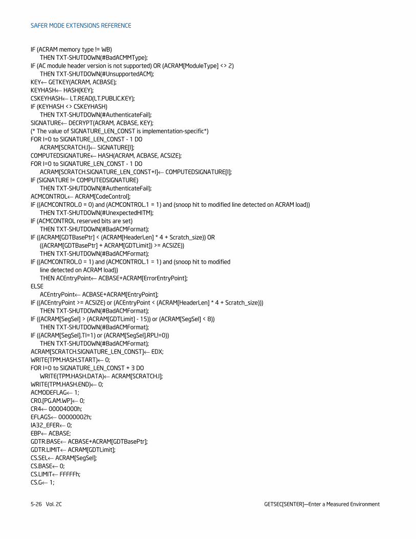
SAFER MODE EXTENSIONS REFERENCE
IF (ACRAM memory type != WB)THEN TXT-SHUTDOWN(#BadACMMType);
IF (AC module header version is not supported) OR (ACRAM[ModuleType] <> 2)THEN TXT-SHUTDOWN(#UnsupportedACM);
KEY← GETKEY(ACRAM, ACBASE);KEYHASH← HASH(KEY);CSKEYHASH← LT.READ(LT.PUBLIC.KEY);IF (KEYHASH <> CSKEYHASH)
THEN TXT-SHUTDOWN(#AuthenticateFail);SIGNATURE← DECRYPT(ACRAM, ACBASE, KEY);(* The value of SIGNATURE_LEN_CONST is implementation-specific*)FOR I=0 to SIGNATURE_LEN_CONST - 1 DO
ACRAM[SCRATCH.I]← SIGNATURE[I];COMPUTEDSIGNATURE← HASH(ACRAM, ACBASE, ACSIZE);FOR I=0 to SIGNATURE_LEN_CONST - 1 DO
ACRAM[SCRATCH.SIGNATURE_LEN_CONST+I]← COMPUTEDSIGNATURE[I];IF (SIGNATURE != COMPUTEDSIGNATURE)
THEN TXT-SHUTDOWN(#AuthenticateFail);ACMCONTROL← ACRAM[CodeControl];IF ((ACMCONTROL.0 = 0) and (ACMCONTROL.1 = 1) and (snoop hit to modified line detected on ACRAM load))
THEN TXT-SHUTDOWN(#UnexpectedHITM);IF (ACMCONTROL reserved bits are set)
THEN TXT-SHUTDOWN(#BadACMFormat);IF ((ACRAM[GDTBasePtr] < (ACRAM[HeaderLen] * 4 + Scratch_size)) OR
((ACRAM[GDTBasePtr] + ACRAM[GDTLimit]) >= ACSIZE))THEN TXT-SHUTDOWN(#BadACMFormat);
IF ((ACMCONTROL.0 = 1) and (ACMCONTROL.1 = 1) and (snoop hit to modified line detected on ACRAM load)) THEN ACEntryPoint← ACBASE+ACRAM[ErrorEntryPoint];
ELSEACEntryPoint← ACBASE+ACRAM[EntryPoint];
IF ((ACEntryPoint >= ACSIZE) or (ACEntryPoint < (ACRAM[HeaderLen] * 4 + Scratch_size)))THEN TXT-SHUTDOWN(#BadACMFormat);
IF ((ACRAM[SegSel] > (ACRAM[GDTLimit] - 15)) or (ACRAM[SegSel] < 8))THEN TXT-SHUTDOWN(#BadACMFormat);
IF ((ACRAM[SegSel].TI=1) or (ACRAM[SegSel].RPL!=0))THEN TXT-SHUTDOWN(#BadACMFormat);
ACRAM[SCRATCH.SIGNATURE_LEN_CONST]← EDX;WRITE(TPM.HASH.START)← 0;FOR I=0 to SIGNATURE_LEN_CONST + 3 DO
WRITE(TPM.HASH.DATA)← ACRAM[SCRATCH.I];WRITE(TPM.HASH.END)← 0;ACMODEFLAG← 1;CR0.[PG.AM.WP]← 0;CR4← 00004000h;EFLAGS← 00000002h;IA32_EFER← 0;EBP← ACBASE;GDTR.BASE← ACBASE+ACRAM[GDTBasePtr];GDTR.LIMIT← ACRAM[GDTLimit];CS.SEL← ACRAM[SegSel];CS.BASE← 0;CS.LIMIT← FFFFFh;CS.G← 1;
GETSEC[SENTER]—Enter a Measured Environment5-26 Vol. 2C
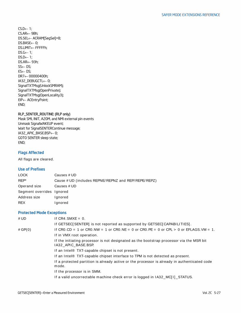
SAFER MODE EXTENSIONS REFERENCE
CS.D← 1;CS.AR← 9Bh;DS.SEL← ACRAM[SegSel]+8;DS.BASE← 0;DS.LIMIT← FFFFFh;DS.G← 1;DS.D← 1;DS.AR← 93h;SS← DS;ES← DS;DR7← 00000400h;IA32_DEBUGCTL← 0;SignalTXTMsg(UnlockSMRAM);SignalTXTMsg(OpenPrivate);SignalTXTMsg(OpenLocality3);EIP← ACEntryPoint;END;
RLP_SENTER_ROUTINE: (RLP only)Mask SMI, INIT, A20M, and NMI external pin eventsUnmask SignalWAKEUP event;Wait for SignalSENTERContinue message;IA32_APIC_BASE.BSP← 0;GOTO SENTER sleep state;END;
Flags Affected
All flags are cleared.
Use of PrefixesLOCK Causes #UDREP* Cause #UD (includes REPNE/REPNZ and REP/REPE/REPZ)Operand size Causes #UDSegment overrides IgnoredAddress size IgnoredREX Ignored
Protected Mode Exceptions#UD If CR4.SMXE = 0.
If GETSEC[SENTER] is not reported as supported by GETSEC[CAPABILITIES].#GP(0) If CR0.CD = 1 or CR0.NW = 1 or CR0.NE = 0 or CR0.PE = 0 or CPL > 0 or EFLAGS.VM = 1.
If in VMX root operation.If the initiating processor is not designated as the bootstrap processor via the MSR bit IA32_APIC_BASE.BSP.If an Intel® TXT-capable chipset is not present.If an Intel® TXT-capable chipset interface to TPM is not detected as present.If a protected partition is already active or the processor is already in authenticated code mode.If the processor is in SMM.If a valid uncorrectable machine check error is logged in IA32_MC[I]_STATUS.
GETSEC[SENTER]—Enter a Measured Environment Vol. 2C 5-27
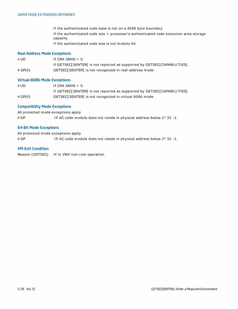
SAFER MODE EXTENSIONS REFERENCE
If the authenticated code base is not on a 4096 byte boundary.If the authenticated code size > processor's authenticated code execution area storage capacity.If the authenticated code size is not modulo 64.
Real-Address Mode Exceptions#UD If CR4.SMXE = 0.
If GETSEC[SENTER] is not reported as supported by GETSEC[CAPABILITIES].#GP(0) GETSEC[SENTER] is not recognized in real-address mode.
Virtual-8086 Mode Exceptions#UD If CR4.SMXE = 0.
If GETSEC[SENTER] is not reported as supported by GETSEC[CAPABILITIES].#GP(0) GETSEC[SENTER] is not recognized in virtual-8086 mode.
Compatibility Mode ExceptionsAll protected mode exceptions apply.#GP IF AC code module does not reside in physical address below 2^32 -1.
64-Bit Mode ExceptionsAll protected mode exceptions apply.#GP IF AC code module does not reside in physical address below 2^32 -1.
VM-Exit ConditionReason (GETSEC) IF in VMX non-root operation.
GETSEC[SENTER]—Enter a Measured Environment5-28 Vol. 2C
SAFER MODE EXTENSIONS REFERENCE
GETSEC[SEXIT]—Exit Measured Environment
Description
The GETSEC[SEXIT] instruction initiates an exit of a measured environment established by GETSEC[SENTER]. The SEXIT leaf of GETSEC is selected with EAX set to 5 at execution. This instruction leaf sends a message to all logical processors in the platform to signal the measured environment exit.
There are restrictions enforced by the processor for the execution of the GETSEC[SEXIT] instruction: • Execution is not allowed unless the processor is in protected mode (CR0.PE = 1) with CPL = 0 and EFLAGS.VM
= 0. • The processor must be in a measured environment as launched by a previous GETSEC[SENTER] instruction,
but not still in authenticated code execution mode. • To avoid potential inter-operability conflicts between modes, the processor is not allowed to execute this
instruction if it currently is in SMM or in VMX operation. • To insure consistent handling of SIPI messages, the processor executing the GETSEC[SEXIT] instruction must
also be designated the BSP (bootstrap processor) as defined by the register bit IA32_APIC_BASE.BSP (bit 8).
Failure to abide by the above conditions results in the processor signaling a general protection violation.
This instruction initiates a sequence to rendezvous the RLPs with the ILP. It then clears the internal processor flag indicating the processor is operating in a measured environment.
In response to a message signaling the completion of rendezvous, all RLPs restart execution with the instruction that was to be executed at the time GETSEC[SEXIT] was recognized. This applies to all processor conditions, with the following exceptions: • If an RLP executed HLT and was in this halt state at the time of the message initiated by GETSEC[SEXIT], then
execution resumes in the halt state. • If an RLP was executing MWAIT, then a message initiated by GETSEC[SEXIT] causes an exit of the MWAIT
state, falling through to the next instruction. • If an RLP was executing an intermediate iteration of a string instruction, then the processor resumes execution
of the string instruction at the point which the message initiated by GETSEC[SEXIT] was recognized. • If an RLP is still in the SENTER sleep state (never awakened with GETSEC[WAKEUP]), it will be sent to the wait-
for-SIPI state after first clearing the bootstrap processor indicator flag (IA32_APIC_BASE.BSP) and any pending SIPI state. In this case, such RLPs are initialized to an architectural state consistent with having taken a soft reset using the INIT# pin.
Prior to completion of the GETSEC[SEXIT] operation, both the ILP and any active RLPs unmask the response of the external event signals INIT#, A20M, NMI#, and SMI#. This unmasking is performed unconditionally to recognize pin events which are masked after a GETSEC[SENTER]. The state of A20M is unmasked, as the A20M pin is not recognized while the measured environment is active.
On a successful exit of the measured environment, the ILP re-locks the Intel® TXT-capable chipset private config-uration space. GETSEC[SEXIT] does not affect the content of any PCR.
At completion of GETSEC[SEXIT] by the ILP, execution proceeds to the next instruction. Since EFLAGS and the debug register state are not modified by this instruction, a pending trap condition is free to be signaled if previously enabled.
Operation in a Uni-Processor Platform(* The state of the internal flag ACMODEFLAG and SENTERFLAG persist across instruction boundary *)GETSEC[SEXIT] (ILP only):IF (CR4.SMXE=0)
Opcode Instruction Description
0F 37
(EAX=5)
GETSEC[SEXIT] Exit measured environment
GETSEC[SEXIT]—Exit Measured Environment Vol. 2C 5-29
SAFER MODE EXTENSIONS REFERENCE
THEN #UD;ELSE IF (in VMX non-root operation)
THEN VM Exit (reason=”GETSEC instruction”);ELSE IF (GETSEC leaf unsupported)
THEN #UD;ELSE IF ((in VMX root operation) or
(CR0.PE=0) or (CPL>0) or (EFLAGS.VM=1) or(IA32_APIC_BASE.BSP=0) or(TXT chipset not present) or(SENTERFLAG=0) or (ACMODEFLAG=1) or (IN_SMM=1))
THEN #GP(0);SignalTXTMsg(SEXIT);DOWHILE (no SignalSEXIT message);
TXT_SEXIT_MSG_EVENT (ILP & RLP):Mask and clear SignalSEXIT event;Clear MONITOR FSM;Unmask SignalSENTER event;IF (in VMX operation)
THEN TXT-SHUTDOWN(#IllegalEvent);SignalTXTMsg(SEXITAck);IF (logical processor is not ILP)
THEN GOTO RLP_SEXIT_ROUTINE;(* ILP waits for all logical processors to ACK *)DO
DONE← READ(LT.STS);WHILE (NOT DONE);SignalTXTMsg(SEXITContinue);SignalTXTMsg(ClosePrivate);SENTERFLAG← 0;Unmask SMI, INIT, A20M, and NMI external pin events;END;
RLP_SEXIT_ROUTINE (RLPs only):Wait for SignalSEXITContinue message;Unmask SMI, INIT, A20M, and NMI external pin events;IF (prior execution state = HLT)
THEN reenter HLT state;IF (prior execution state = SENTER sleep)
THENIA32_APIC_BASE.BSP← 0;Clear pending SIPI state;Call INIT_PROCESSOR_STATE;Unmask SIPI event;GOTO WAIT-FOR-SIPI;
FI;END;
Flags AffectedILP: None. RLPs: all flags are modified for an RLP. returning to wait-for-SIPI state, none otherwise
GETSEC[SEXIT]—Exit Measured Environment5-30 Vol. 2C
SAFER MODE EXTENSIONS REFERENCE
Use of PrefixesLOCK Causes #UDREP* Cause #UD (includes REPNE/REPNZ and REP/REPE/REPZ)Operand size Causes #UDSegment overrides IgnoredAddress size IgnoredREX Ignored
Protected Mode Exceptions#UD If CR4.SMXE = 0.
If GETSEC[SEXIT] is not reported as supported by GETSEC[CAPABILITIES].#GP(0) If CR0.PE = 0 or CPL > 0 or EFLAGS.VM = 1.
If in VMX root operation.If the initiating processor is not designated as the via the MSR bit IA32_APIC_BASE.BSP.If an Intel® TXT-capable chipset is not present.If a protected partition is not already active or the processor is already in authenticated code mode.If the processor is in SMM.
Real-Address Mode Exceptions#UD If CR4.SMXE = 0.
If GETSEC[SEXIT] is not reported as supported by GETSEC[CAPABILITIES].#GP(0) GETSEC[SEXIT] is not recognized in real-address mode.
Virtual-8086 Mode Exceptions#UD If CR4.SMXE = 0.
If GETSEC[SEXIT] is not reported as supported by GETSEC[CAPABILITIES].#GP(0) GETSEC[SEXIT] is not recognized in virtual-8086 mode.
Compatibility Mode ExceptionsAll protected mode exceptions apply.
64-Bit Mode ExceptionsAll protected mode exceptions apply.
VM-Exit ConditionReason (GETSEC) IF in VMX non-root operation.
GETSEC[SEXIT]—Exit Measured Environment Vol. 2C 5-31
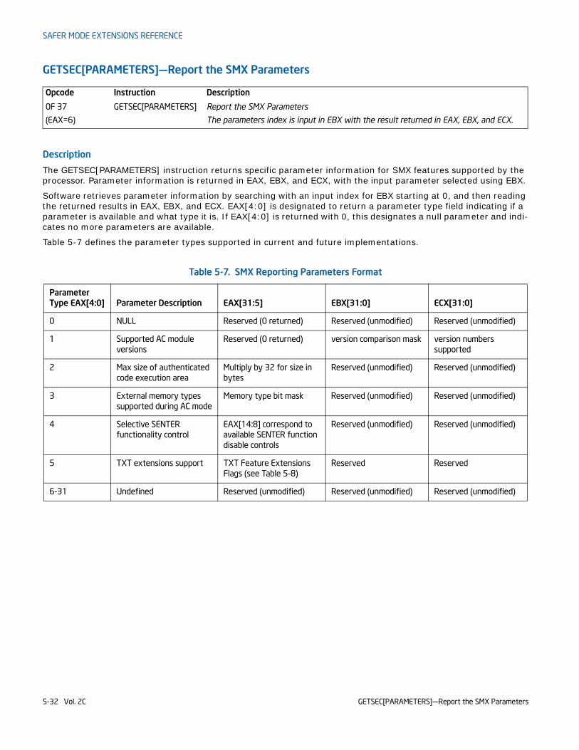
SAFER MODE EXTENSIONS REFERENCE
GETSEC[PARAMETERS]—Report the SMX Parameters
Description
The GETSEC[PARAMETERS] instruction returns specific parameter information for SMX features supported by the processor. Parameter information is returned in EAX, EBX, and ECX, with the input parameter selected using EBX.
Software retrieves parameter information by searching with an input index for EBX starting at 0, and then reading the returned results in EAX, EBX, and ECX. EAX[4:0] is designated to return a parameter type field indicating if a parameter is available and what type it is. If EAX[4:0] is returned with 0, this designates a null parameter and indi-cates no more parameters are available.
Table 5-7 defines the parameter types supported in current and future implementations.
Opcode Instruction Description
0F 37
(EAX=6)
GETSEC[PARAMETERS] Report the SMX Parameters
The parameters index is input in EBX with the result returned in EAX, EBX, and ECX.
Table 5-7. SMX Reporting Parameters Format
Parameter Type EAX[4:0] Parameter Description EAX[31:5] EBX[31:0] ECX[31:0]
0 NULL Reserved (0 returned) Reserved (unmodified) Reserved (unmodified)
1 Supported AC module versions
Reserved (0 returned) version comparison mask version numbers supported
2 Max size of authenticated code execution area
Multiply by 32 for size in bytes
Reserved (unmodified) Reserved (unmodified)
3 External memory types supported during AC mode
Memory type bit mask Reserved (unmodified) Reserved (unmodified)
4 Selective SENTER functionality control
EAX[14:8] correspond to available SENTER function disable controls
Reserved (unmodified) Reserved (unmodified)
5 TXT extensions support TXT Feature Extensions Flags (see Table 5-8)
Reserved Reserved
6-31 Undefined Reserved (unmodified) Reserved (unmodified) Reserved (unmodified)
GETSEC[PARAMETERS]—Report the SMX Parameters5-32 Vol. 2C
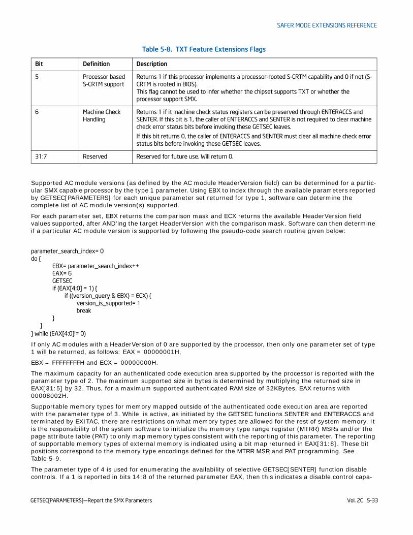
SAFER MODE EXTENSIONS REFERENCE
Table 5-8. TXT Feature Extensions Flags
Supported AC module versions (as defined by the AC module HeaderVersion field) can be determined for a partic-ular SMX capable processor by the type 1 parameter. Using EBX to index through the available parameters reported by GETSEC[PARAMETERS] for each unique parameter set returned for type 1, software can determine the complete list of AC module version(s) supported.
For each parameter set, EBX returns the comparison mask and ECX returns the available HeaderVersion field values supported, after AND'ing the target HeaderVersion with the comparison mask. Software can then determine if a particular AC module version is supported by following the pseudo-code search routine given below:
parameter_search_index= 0do {
EBX= parameter_search_index++EAX= 6GETSECif (EAX[4:0] = 1) {
if ((version_query & EBX) = ECX) {version_is_supported= 1break
}}
} while (EAX[4:0]!= 0)
If only AC modules with a HeaderVersion of 0 are supported by the processor, then only one parameter set of type 1 will be returned, as follows: EAX = 00000001H,
EBX = FFFFFFFFH and ECX = 00000000H.
The maximum capacity for an authenticated code execution area supported by the processor is reported with the parameter type of 2. The maximum supported size in bytes is determined by multiplying the returned size in EAX[31:5] by 32. Thus, for a maximum supported authenticated RAM size of 32KBytes, EAX returns with 00008002H.
Supportable memory types for memory mapped outside of the authenticated code execution area are reported with the parameter type of 3. While is active, as initiated by the GETSEC functions SENTER and ENTERACCS and terminated by EXITAC, there are restrictions on what memory types are allowed for the rest of system memory. It is the responsibility of the system software to initialize the memory type range register (MTRR) MSRs and/or the page attribute table (PAT) to only map memory types consistent with the reporting of this parameter. The reporting of supportable memory types of external memory is indicated using a bit map returned in EAX[31:8]. These bit positions correspond to the memory type encodings defined for the MTRR MSR and PAT programming. See Table 5-9.
The parameter type of 4 is used for enumerating the availability of selective GETSEC[SENTER] function disable controls. If a 1 is reported in bits 14:8 of the returned parameter EAX, then this indicates a disable control capa-
Bit Definition Description
5 Processor based S-CRTM support
Returns 1 if this processor implements a processor-rooted S-CRTM capability and 0 if not (S-CRTM is rooted in BIOS).This flag cannot be used to infer whether the chipset supports TXT or whether the processor support SMX.
6 Machine Check Handling
Returns 1 if it machine check status registers can be preserved through ENTERACCS and SENTER. If this bit is 1, the caller of ENTERACCS and SENTER is not required to clear machine check error status bits before invoking these GETSEC leaves.
If this bit returns 0, the caller of ENTERACCS and SENTER must clear all machine check error status bits before invoking these GETSEC leaves.
31:7 Reserved Reserved for future use. Will return 0.
GETSEC[PARAMETERS]—Report the SMX Parameters Vol. 2C 5-33
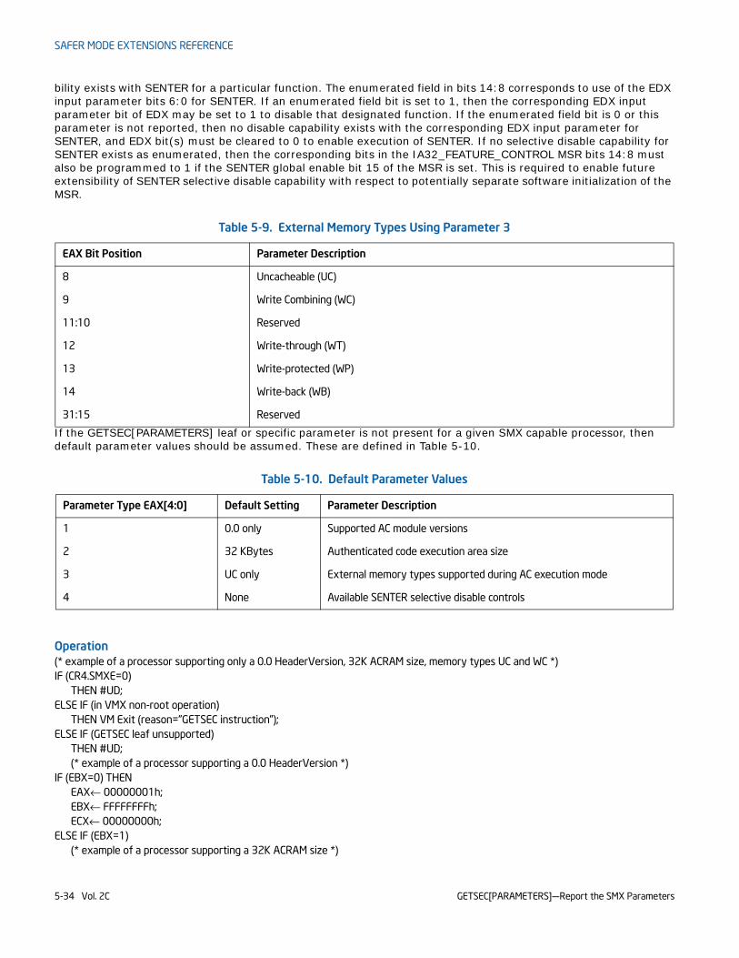
SAFER MODE EXTENSIONS REFERENCE
bility exists with SENTER for a particular function. The enumerated field in bits 14:8 corresponds to use of the EDX input parameter bits 6:0 for SENTER. If an enumerated field bit is set to 1, then the corresponding EDX input parameter bit of EDX may be set to 1 to disable that designated function. If the enumerated field bit is 0 or this parameter is not reported, then no disable capability exists with the corresponding EDX input parameter for SENTER, and EDX bit(s) must be cleared to 0 to enable execution of SENTER. If no selective disable capability for SENTER exists as enumerated, then the corresponding bits in the IA32_FEATURE_CONTROL MSR bits 14:8 must also be programmed to 1 if the SENTER global enable bit 15 of the MSR is set. This is required to enable future extensibility of SENTER selective disable capability with respect to potentially separate software initialization of the MSR.
If the GETSEC[PARAMETERS] leaf or specific parameter is not present for a given SMX capable processor, then default parameter values should be assumed. These are defined in Table 5-10.
Operation(* example of a processor supporting only a 0.0 HeaderVersion, 32K ACRAM size, memory types UC and WC *)IF (CR4.SMXE=0)
THEN #UD;ELSE IF (in VMX non-root operation)
THEN VM Exit (reason=”GETSEC instruction”);ELSE IF (GETSEC leaf unsupported)
THEN #UD;(* example of a processor supporting a 0.0 HeaderVersion *)
IF (EBX=0) THENEAX← 00000001h;EBX← FFFFFFFFh;ECX← 00000000h;
ELSE IF (EBX=1)(* example of a processor supporting a 32K ACRAM size *)
Table 5-9. External Memory Types Using Parameter 3
EAX Bit Position Parameter Description
8 Uncacheable (UC)
9 Write Combining (WC)
11:10 Reserved
12 Write-through (WT)
13 Write-protected (WP)
14 Write-back (WB)
31:15 Reserved
Table 5-10. Default Parameter Values
Parameter Type EAX[4:0] Default Setting Parameter Description
1 0.0 only Supported AC module versions
2 32 KBytes Authenticated code execution area size
3 UC only External memory types supported during AC execution mode
4 None Available SENTER selective disable controls
GETSEC[PARAMETERS]—Report the SMX Parameters5-34 Vol. 2C
SAFER MODE EXTENSIONS REFERENCE
THEN EAX← 00008002h;ESE IF (EBX= 2)
(* example of a processor supporting external memory types of UC and WC *)THEN EAX← 00000303h;
ESE IF (EBX= other value(s) less than unsupported index value)(* EAX value varies. Consult Table 5-7 and Table 5-8*)
ELSE (* unsupported index*)EAX¨ 00000000h;
END;
Flags Affected
None.
Use of PrefixesLOCK Causes #UDREP* Cause #UD (includes REPNE/REPNZ and REP/REPE/REPZ)Operand size Causes #UDSegment overrides IgnoredAddress size IgnoredREX Ignored
Protected Mode Exceptions#UD If CR4.SMXE = 0.
If GETSEC[PARAMETERS] is not reported as supported by GETSEC[CAPABILITIES].
Real-Address Mode Exceptions#UD If CR4.SMXE = 0.
If GETSEC[PARAMETERS] is not reported as supported by GETSEC[CAPABILITIES].
Virtual-8086 Mode Exceptions#UD If CR4.SMXE = 0.
If GETSEC[PARAMETERS] is not reported as supported by GETSEC[CAPABILITIES].
Compatibility Mode ExceptionsAll protected mode exceptions apply.
64-Bit Mode ExceptionsAll protected mode exceptions apply.
VM-Exit ConditionReason (GETSEC) IF in VMX non-root operation.
GETSEC[PARAMETERS]—Report the SMX Parameters Vol. 2C 5-35
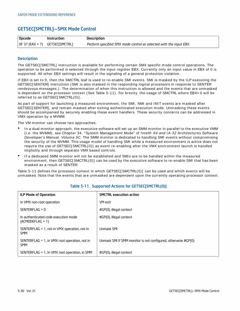
SAFER MODE EXTENSIONS REFERENCE
GETSEC[SMCTRL]—SMX Mode Control
Description
The GETSEC[SMCTRL] instruction is available for performing certain SMX specific mode control operations. The operation to be performed is selected through the input register EBX. Currently only an input value in EBX of 0 is supported. All other EBX settings will result in the signaling of a general protection violation.
If EBX is set to 0, then the SMCTRL leaf is used to re-enable SMI events. SMI is masked by the ILP executing the GETSEC[SENTER] instruction (SMI is also masked in the responding logical processors in response to SENTER rendezvous messages.). The determination of when this instruction is allowed and the events that are unmasked is dependent on the processor context (See Table 5-11). For brevity, the usage of SMCTRL where EBX=0 will be referred to as GETSEC[SMCTRL(0)].
As part of support for launching a measured environment, the SMI, NMI and INIT events are masked after GETSEC[SENTER], and remain masked after exiting authenticated execution mode. Unmasking these events should be accompanied by securely enabling these event handlers. These security concerns can be addressed in VMX operation by a MVMM.
The VM monitor can choose two approaches:• In a dual monitor approach, the executive software will set up an SMM monitor in parallel to the executive VMM
(i.e. the MVMM), see Chapter 34, “System Management Mode” of Intel® 64 and IA-32 Architectures Software Developer’s Manual, Volume 3C. The SMM monitor is dedicated to handling SMI events without compromising the security of the MVMM. This usage model of handling SMI while a measured environment is active does not require the use of GETSEC[SMCTRL(0)] as event re-enabling after the VMX environment launch is handled implicitly and through separate VMX based controls.
• If a dedicated SMM monitor will not be established and SMIs are to be handled within the measured environment, then GETSEC[SMCTRL(0)] can be used by the executive software to re-enable SMI that has been masked as a result of SENTER.
Table 5-11 defines the processor context in which GETSEC[SMCTRL(0)] can be used and which events will be unmasked. Note that the events that are unmasked are dependent upon the currently operating processor context.
Opcode Instruction Description
0F 37 (EAX = 7) GETSEC[SMCTRL] Perform specified SMX mode control as selected with the input EBX.
Table 5-11. Supported Actions for GETSEC[SMCTRL(0)]
ILP Mode of Operation SMCTRL execution action
In VMX non-root operation VM exit
SENTERFLAG = 0 #GP(0), illegal context
In authenticated code execution mode (ACMODEFLAG = 1)
#GP(0), illegal context
SENTERFLAG = 1, not in VMX operation, not in SMM
Unmask SMI
SENTERFLAG = 1, in VMX root operation, not in SMM
Unmask SMI if SMM monitor is not configured, otherwise #GP(0)
SENTERFLAG = 1, In VMX root operation, in SMM #GP(0), illegal context
GETSEC[SMCTRL]—SMX Mode Control5-36 Vol. 2C
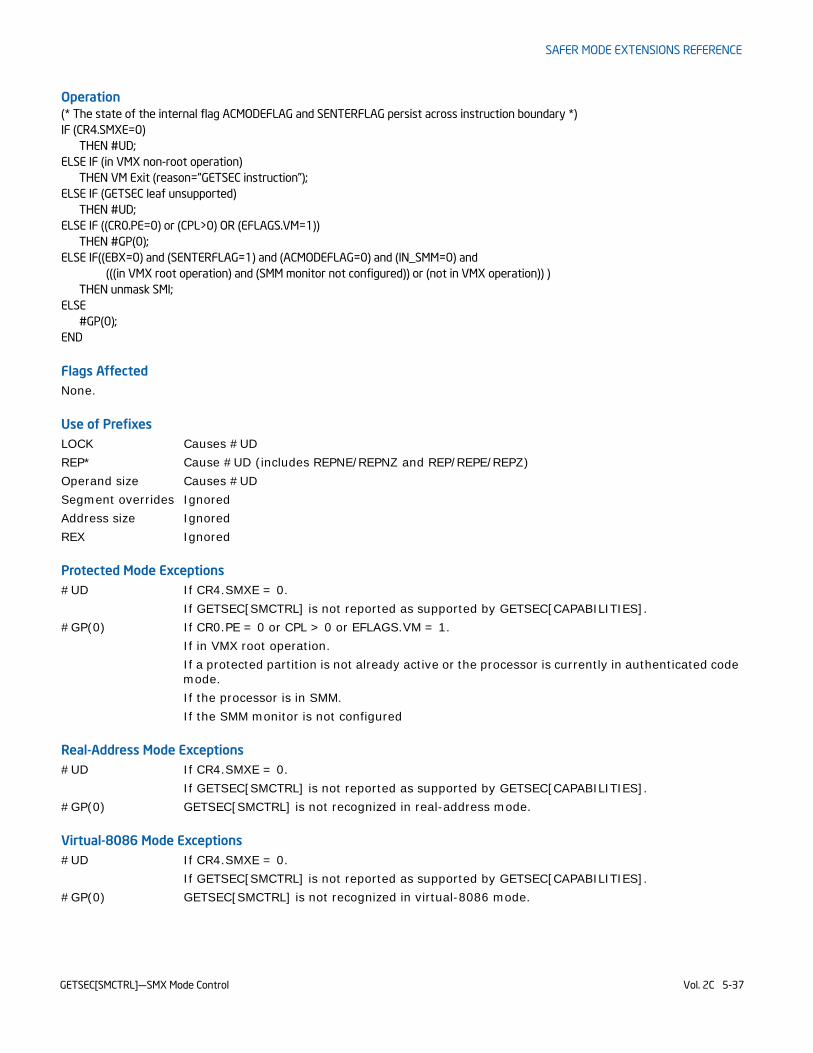
SAFER MODE EXTENSIONS REFERENCE
Operation(* The state of the internal flag ACMODEFLAG and SENTERFLAG persist across instruction boundary *)IF (CR4.SMXE=0)
THEN #UD;ELSE IF (in VMX non-root operation)
THEN VM Exit (reason=”GETSEC instruction”);ELSE IF (GETSEC leaf unsupported)
THEN #UD;ELSE IF ((CR0.PE=0) or (CPL>0) OR (EFLAGS.VM=1))
THEN #GP(0);ELSE IF((EBX=0) and (SENTERFLAG=1) and (ACMODEFLAG=0) and (IN_SMM=0) and
(((in VMX root operation) and (SMM monitor not configured)) or (not in VMX operation)) )THEN unmask SMI;
ELSE#GP(0);
END
Flags AffectedNone.
Use of PrefixesLOCK Causes #UDREP* Cause #UD (includes REPNE/REPNZ and REP/REPE/REPZ)Operand size Causes #UDSegment overrides IgnoredAddress size IgnoredREX Ignored
Protected Mode Exceptions#UD If CR4.SMXE = 0.
If GETSEC[SMCTRL] is not reported as supported by GETSEC[CAPABILITIES].#GP(0) If CR0.PE = 0 or CPL > 0 or EFLAGS.VM = 1.
If in VMX root operation.If a protected partition is not already active or the processor is currently in authenticated code mode.If the processor is in SMM.If the SMM monitor is not configured
Real-Address Mode Exceptions#UD If CR4.SMXE = 0.
If GETSEC[SMCTRL] is not reported as supported by GETSEC[CAPABILITIES].#GP(0) GETSEC[SMCTRL] is not recognized in real-address mode.
Virtual-8086 Mode Exceptions#UD If CR4.SMXE = 0.
If GETSEC[SMCTRL] is not reported as supported by GETSEC[CAPABILITIES].#GP(0) GETSEC[SMCTRL] is not recognized in virtual-8086 mode.
GETSEC[SMCTRL]—SMX Mode Control Vol. 2C 5-37

SAFER MODE EXTENSIONS REFERENCE
Compatibility Mode ExceptionsAll protected mode exceptions apply.
64-Bit Mode ExceptionsAll protected mode exceptions apply.
VM-exit ConditionReason (GETSEC) IF in VMX non-root operation.
GETSEC[SMCTRL]—SMX Mode Control5-38 Vol. 2C
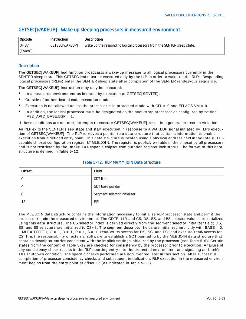
SAFER MODE EXTENSIONS REFERENCE
GETSEC[WAKEUP]—Wake up sleeping processors in measured environment
Description
The GETSEC[WAKEUP] leaf function broadcasts a wake-up message to all logical processors currently in the SENTER sleep state. This GETSEC leaf must be executed only by the ILP, in order to wake-up the RLPs. Responding logical processors (RLPs) enter the SENTER sleep state after completion of the SENTER rendezvous sequence.
The GETSEC[WAKEUP] instruction may only be executed: • In a measured environment as initiated by execution of GETSEC[SENTER]. • Outside of authenticated code execution mode. • Execution is not allowed unless the processor is in protected mode with CPL = 0 and EFLAGS.VM = 0. • In addition, the logical processor must be designated as the boot-strap processor as configured by setting
IA32_APIC_BASE.BSP = 1.
If these conditions are not met, attempts to execute GETSEC[WAKEUP] result in a general protection violation.
An RLP exits the SENTER sleep state and start execution in response to a WAKEUP signal initiated by ILP’s execu-tion of GETSEC[WAKEUP]. The RLP retrieves a pointer to a data structure that contains information to enable execution from a defined entry point. This data structure is located using a physical address held in the Intel® TXT-capable chipset configuration register LT.MLE.JOIN. The register is publicly writable in the chipset by all processors and is not restricted by the Intel® TXT-capable chipset configuration register lock status. The format of this data structure is defined in Table 5-12.
The MLE JOIN data structure contains the information necessary to initialize RLP processor state and permit the processor to join the measured environment. The GDTR, LIP, and CS, DS, SS, and ES selector values are initialized using this data structure. The CS selector index is derived directly from the segment selector initializer field; DS, SS, and ES selectors are initialized to CS+8. The segment descriptor fields are initialized implicitly with BASE = 0, LIMIT = FFFFFH, G = 1, D = 1, P = 1, S = 1; read/write/access for DS, SS, and ES; and execute/read/access for CS. It is the responsibility of external software to establish a GDT pointed to by the MLE JOIN data structure that contains descriptor entries consistent with the implicit settings initialized by the processor (see Table 5-6). Certain states from the content of Table 5-12 are checked for consistency by the processor prior to execution. A failure of any consistency check results in the RLP aborting entry into the protected environment and signaling an Intel® TXT shutdown condition. The specific checks performed are documented later in this section. After successful completion of processor consistency checks and subsequent initialization, RLP execution in the measured environ-ment begins from the entry point at offset 12 (as indicated in Table 5-12).
Opcode Instruction Description
0F 37
(EAX=8)
GETSEC[WAKEUP] Wake up the responding logical processors from the SENTER sleep state.
Table 5-12. RLP MVMM JOIN Data Structure
Offset Field
0 GDT limit
4 GDT base pointer
8 Segment selector initializer
12 EIP
GETSEC[WAKEUP]—Wake up sleeping processors in measured environment Vol. 2C 5-39
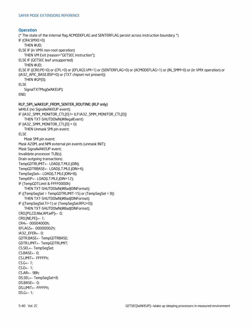
SAFER MODE EXTENSIONS REFERENCE
Operation(* The state of the internal flag ACMODEFLAG and SENTERFLAG persist across instruction boundary *)IF (CR4.SMXE=0)
THEN #UD;ELSE IF (in VMX non-root operation)
THEN VM Exit (reason=”GETSEC instruction”);ELSE IF (GETSEC leaf unsupported)
THEN #UD;ELSE IF ((CR0.PE=0) or (CPL>0) or (EFLAGS.VM=1) or (SENTERFLAG=0) or (ACMODEFLAG=1) or (IN_SMM=0) or (in VMX operation) or (IA32_APIC_BASE.BSP=0) or (TXT chipset not present))
THEN #GP(0);ELSE
SignalTXTMsg(WAKEUP);END;
RLP_SIPI_WAKEUP_FROM_SENTER_ROUTINE: (RLP only)WHILE (no SignalWAKEUP event);IF (IA32_SMM_MONITOR_CTL[0] != ILP.IA32_SMM_MONITOR_CTL[0])
THEN TXT-SHUTDOWN(#IllegalEvent)IF (IA32_SMM_MONITOR_CTL[0] = 0)
THEN Unmask SMI pin event;ELSE
Mask SMI pin event;Mask A20M, and NMI external pin events (unmask INIT);Mask SignalWAKEUP event;Invalidate processor TLB(s);Drain outgoing transactions;TempGDTRLIMIT← LOAD(LT.MLE.JOIN);TempGDTRBASE← LOAD(LT.MLE.JOIN+4);TempSegSel← LOAD(LT.MLE.JOIN+8);TempEIP← LOAD(LT.MLE.JOIN+12);IF (TempGDTLimit & FFFF0000h)
THEN TXT-SHUTDOWN(#BadJOINFormat);IF ((TempSegSel > TempGDTRLIMIT-15) or (TempSegSel < 8))
THEN TXT-SHUTDOWN(#BadJOINFormat);IF ((TempSegSel.TI=1) or (TempSegSel.RPL!=0))
THEN TXT-SHUTDOWN(#BadJOINFormat);CR0.[PG,CD,NW,AM,WP]← 0;CR0.[NE,PE]← 1;CR4← 00004000h;EFLAGS← 00000002h;IA32_EFER← 0;GDTR.BASE← TempGDTRBASE;GDTR.LIMIT← TempGDTRLIMIT;CS.SEL← TempSegSel;CS.BASE← 0;CS.LIMIT← FFFFFh;CS.G← 1;CS.D← 1;CS.AR← 9Bh;DS.SEL← TempSegSel+8;DS.BASE← 0;DS.LIMIT← FFFFFh;DS.G← 1;
GETSEC[WAKEUP]—Wake up sleeping processors in measured environment5-40 Vol. 2C
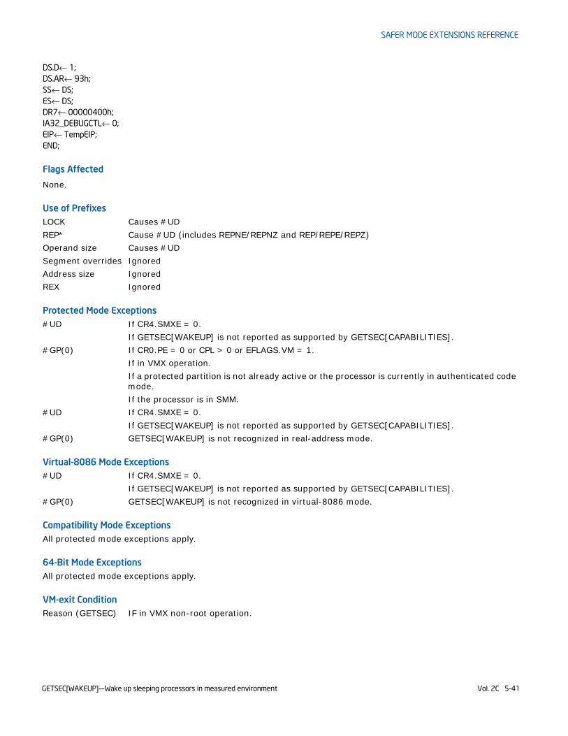
SAFER MODE EXTENSIONS REFERENCE
DS.D← 1;DS.AR← 93h;SS← DS;ES← DS;DR7← 00000400h;IA32_DEBUGCTL← 0;EIP← TempEIP;END;
Flags Affected
None.
Use of PrefixesLOCK Causes #UDREP* Cause #UD (includes REPNE/REPNZ and REP/REPE/REPZ)Operand size Causes #UDSegment overrides IgnoredAddress size IgnoredREX Ignored
Protected Mode Exceptions#UD If CR4.SMXE = 0.
If GETSEC[WAKEUP] is not reported as supported by GETSEC[CAPABILITIES].#GP(0) If CR0.PE = 0 or CPL > 0 or EFLAGS.VM = 1.
If in VMX operation.If a protected partition is not already active or the processor is currently in authenticated code mode.If the processor is in SMM.
#UD If CR4.SMXE = 0.If GETSEC[WAKEUP] is not reported as supported by GETSEC[CAPABILITIES].
#GP(0) GETSEC[WAKEUP] is not recognized in real-address mode.
Virtual-8086 Mode Exceptions#UD If CR4.SMXE = 0.
If GETSEC[WAKEUP] is not reported as supported by GETSEC[CAPABILITIES].#GP(0) GETSEC[WAKEUP] is not recognized in virtual-8086 mode.
Compatibility Mode ExceptionsAll protected mode exceptions apply.
64-Bit Mode ExceptionsAll protected mode exceptions apply.
VM-exit ConditionReason (GETSEC) IF in VMX non-root operation.
GETSEC[WAKEUP]—Wake up sleeping processors in measured environment Vol. 2C 5-41
APPENDIX AOPCODE MAP
Use the opcode tables in this chapter to interpret IA-32 and Intel 64 architecture object code. Instructions are divided into encoding groups:• 1-byte, 2-byte and 3-byte opcode encodings are used to encode integer, system, MMX technology,
SSE/SSE2/SSE3/SSSE3/SSE4, and VMX instructions. Maps for these instructions are given in Table A-2 through Table A-6.
• Escape opcodes (in the format: ESC character, opcode, ModR/M byte) are used for floating-point instructions. The maps for these instructions are provided in Table A-7 through Table A-22.
NOTE
All blanks in opcode maps are reserved and must not be used. Do not depend on the operation of undefined or blank opcodes.
A.1 USING OPCODE TABLESTables in this appendix list opcodes of instructions (including required instruction prefixes, opcode extensions in associated ModR/M byte). Blank cells in the tables indicate opcodes that are reserved or undefined.
The opcode map tables are organized by hex values of the upper and lower 4 bits of an opcode byte. For 1-byte encodings (Table A-2), use the four high-order bits of an opcode to index a row of the opcode table; use the four low-order bits to index a column of the table. For 2-byte opcodes beginning with 0FH (Table A-3), skip any instruc-tion prefixes, the 0FH byte (0FH may be preceded by 66H, F2H, or F3H) and use the upper and lower 4-bit values of the next opcode byte to index table rows and columns. Similarly, for 3-byte opcodes beginning with 0F38H or 0F3AH (Table A-4), skip any instruction prefixes, 0F38H or 0F3AH and use the upper and lower 4-bit values of the third opcode byte to index table rows and columns. See Section A.2.4, “Opcode Look-up Examples for One, Two, and Three-Byte Opcodes.”
When a ModR/M byte provides opcode extensions, this information qualifies opcode execution. For information on how an opcode extension in the ModR/M byte modifies the opcode map in Table A-2 and Table A-3, see Section A.4.
The escape (ESC) opcode tables for floating point instructions identify the eight high order bits of opcodes at the top of each page. See Section A.5. If the accompanying ModR/M byte is in the range of 00H-BFH, bits 3-5 (the top row of the third table on each page) along with the reg bits of ModR/M determine the opcode. ModR/M bytes outside the range of 00H-BFH are mapped by the bottom two tables on each page of the section.
A.2 KEY TO ABBREVIATIONSOperands are identified by a two-character code of the form Zz. The first character, an uppercase letter, specifies the addressing method; the second character, a lowercase letter, specifies the type of operand.
A.2.1 Codes for Addressing MethodThe following abbreviations are used to document addressing methods:
A Direct address: the instruction has no ModR/M byte; the address of the operand is encoded in the instruc-tion. No base register, index register, or scaling factor can be applied (for example, far JMP (EA)).
B The VEX.vvvv field of the VEX prefix selects a general purpose register.
C The reg field of the ModR/M byte selects a control register (for example, MOV (0F20, 0F22)).
Vol. 2C A-1
OPCODE MAP
D The reg field of the ModR/M byte selects a debug register (for example, MOV (0F21,0F23)).
E A ModR/M byte follows the opcode and specifies the operand. The operand is either a general-purpose register or a memory address. If it is a memory address, the address is computed from a segment register and any of the following values: a base register, an index register, a scaling factor, a displacement.
F EFLAGS/RFLAGS Register.
G The reg field of the ModR/M byte selects a general register (for example, AX (000)).
H The VEX.vvvv field of the VEX prefix selects a 128-bit XMM register or a 256-bit YMM register, determined by operand type. For legacy SSE encodings this operand does not exist, changing the instruction to destructive form.
I Immediate data: the operand value is encoded in subsequent bytes of the instruction.
J The instruction contains a relative offset to be added to the instruction pointer register (for example, JMP (0E9), LOOP).
L The upper 4 bits of the 8-bit immediate selects a 128-bit XMM register or a 256-bit YMM register, deter-mined by operand type. (the MSB is ignored in 32-bit mode)
M The ModR/M byte may refer only to memory (for example, BOUND, LES, LDS, LSS, LFS, LGS, CMPXCHG8B).
N The R/M field of the ModR/M byte selects a packed-quadword, MMX technology register.
O The instruction has no ModR/M byte. The offset of the operand is coded as a word or double word (depending on address size attribute) in the instruction. No base register, index register, or scaling factor can be applied (for example, MOV (A0–A3)).
P The reg field of the ModR/M byte selects a packed quadword MMX technology register.
Q A ModR/M byte follows the opcode and specifies the operand. The operand is either an MMX technology register or a memory address. If it is a memory address, the address is computed from a segment register and any of the following values: a base register, an index register, a scaling factor, and a displacement.
R The R/M field of the ModR/M byte may refer only to a general register (for example, MOV (0F20-0F23)).
S The reg field of the ModR/M byte selects a segment register (for example, MOV (8C,8E)).
U The R/M field of the ModR/M byte selects a 128-bit XMM register or a 256-bit YMM register, determined by operand type.
V The reg field of the ModR/M byte selects a 128-bit XMM register or a 256-bit YMM register, determined by operand type.
W A ModR/M byte follows the opcode and specifies the operand. The operand is either a 128-bit XMM register, a 256-bit YMM register (determined by operand type), or a memory address. If it is a memory address, the address is computed from a segment register and any of the following values: a base register, an index register, a scaling factor, and a displacement.
X Memory addressed by the DS:rSI register pair (for example, MOVS, CMPS, OUTS, or LODS).
Y Memory addressed by the ES:rDI register pair (for example, MOVS, CMPS, INS, STOS, or SCAS).
A.2.2 Codes for Operand TypeThe following abbreviations are used to document operand types:
a Two one-word operands in memory or two double-word operands in memory, depending on operand-size attribute (used only by the BOUND instruction).
b Byte, regardless of operand-size attribute.
c Byte or word, depending on operand-size attribute.
d Doubleword, regardless of operand-size attribute.
dq Double-quadword, regardless of operand-size attribute.
A-2 Vol. 2C
OPCODE MAP
p 32-bit, 48-bit, or 80-bit pointer, depending on operand-size attribute.
pd 128-bit or 256-bit packed double-precision floating-point data.
pi Quadword MMX technology register (for example: mm0).
ps 128-bit or 256-bit packed single-precision floating-point data.
q Quadword, regardless of operand-size attribute.
qq Quad-Quadword (256-bits), regardless of operand-size attribute.
s 6-byte or 10-byte pseudo-descriptor.
sd Scalar element of a 128-bit double-precision floating data.
ss Scalar element of a 128-bit single-precision floating data.
si Doubleword integer register (for example: eax).
v Word, doubleword or quadword (in 64-bit mode), depending on operand-size attribute.
w Word, regardless of operand-size attribute.
x dq or qq based on the operand-size attribute.
y Doubleword or quadword (in 64-bit mode), depending on operand-size attribute.
z Word for 16-bit operand-size or doubleword for 32 or 64-bit operand-size.
A.2.3 Register CodesWhen an opcode requires a specific register as an operand, the register is identified by name (for example, AX, CL, or ESI). The name indicates whether the register is 64, 32, 16, or 8 bits wide.
A register identifier of the form eXX or rXX is used when register width depends on the operand-size attribute. eXX is used when 16 or 32-bit sizes are possible; rXX is used when 16, 32, or 64-bit sizes are possible. For example: eAX indicates that the AX register is used when the operand-size attribute is 16 and the EAX register is used when the operand-size attribute is 32. rAX can indicate AX, EAX or RAX.
When the REX.B bit is used to modify the register specified in the reg field of the opcode, this fact is indicated by adding “/x” to the register name to indicate the additional possibility. For example, rCX/r9 is used to indicate that the register could either be rCX or r9. Note that the size of r9 in this case is determined by the operand size attribute (just as for rCX).
A.2.4 Opcode Look-up Examples for One, Two, and Three-Byte Opcodes
This section provides examples that demonstrate how opcode maps are used.
A.2.4.1 One-Byte Opcode InstructionsThe opcode map for 1-byte opcodes is shown in Table A-2. The opcode map for 1-byte opcodes is arranged by row (the least-significant 4 bits of the hexadecimal value) and column (the most-significant 4 bits of the hexadecimal value). Each entry in the table lists one of the following types of opcodes:• Instruction mnemonics and operand types using the notations listed in Section A.2• Opcodes used as an instruction prefix
For each entry in the opcode map that corresponds to an instruction, the rules for interpreting the byte following the primary opcode fall into one of the following cases:• A ModR/M byte is required and is interpreted according to the abbreviations listed in Section A.1 and Chapter
2, “Instruction Format,” of the Intel® 64 and IA-32 Architectures Software Developer’s Manual, Volume 2A. Operand types are listed according to notations listed in Section A.2.
Vol. 2C A-3
OPCODE MAP
• A ModR/M byte is required and includes an opcode extension in the reg field in the ModR/M byte. Use Table A-6 when interpreting the ModR/M byte.
• Use of the ModR/M byte is reserved or undefined. This applies to entries that represent an instruction prefix or entries for instructions without operands that use ModR/M (for example: 60H, PUSHA; 06H, PUSH ES).
Example A-1. Look-up Example for 1-Byte Opcodes
Opcode 030500000000H for an ADD instruction is interpreted using the 1-byte opcode map (Table A-2) as follows:• The first digit (0) of the opcode indicates the table row and the second digit (3) indicates the table column. This
locates an opcode for ADD with two operands. • The first operand (type Gv) indicates a general register that is a word or doubleword depending on the operand-
size attribute. The second operand (type Ev) indicates a ModR/M byte follows that specifies whether the operand is a word or doubleword general-purpose register or a memory address.
• The ModR/M byte for this instruction is 05H, indicating that a 32-bit displacement follows (00000000H). The reg/opcode portion of the ModR/M byte (bits 3-5) is 000, indicating the EAX register.
The instruction for this opcode is ADD EAX, mem_op, and the offset of mem_op is 00000000H.
Some 1- and 2-byte opcodes point to group numbers (shaded entries in the opcode map table). Group numbers indicate that the instruction uses the reg/opcode bits in the ModR/M byte as an opcode extension (refer to Section A.4).
A.2.4.2 Two-Byte Opcode InstructionsThe two-byte opcode map shown in Table A-3 includes primary opcodes that are either two bytes or three bytes in length. Primary opcodes that are 2 bytes in length begin with an escape opcode 0FH. The upper and lower four bits of the second opcode byte are used to index a particular row and column in Table A-3.
Two-byte opcodes that are 3 bytes in length begin with a mandatory prefix (66H, F2H, or F3H) and the escape opcode (0FH). The upper and lower four bits of the third byte are used to index a particular row and column in Table A-3 (except when the second opcode byte is the 3-byte escape opcodes 38H or 3AH; in this situation refer to Section A.2.4.3).
For each entry in the opcode map, the rules for interpreting the byte following the primary opcode fall into one of the following cases:• A ModR/M byte is required and is interpreted according to the abbreviations listed in Section A.1 and Chapter
2, “Instruction Format,” of the Intel® 64 and IA-32 Architectures Software Developer’s Manual, Volume 2A. The operand types are listed according to notations listed in Section A.2.
• A ModR/M byte is required and includes an opcode extension in the reg field in the ModR/M byte. Use Table A-6 when interpreting the ModR/M byte.
• Use of the ModR/M byte is reserved or undefined. This applies to entries that represent an instruction without operands that are encoded using ModR/M (for example: 0F77H, EMMS).
Example A-2. Look-up Example for 2-Byte Opcodes
Look-up opcode 0FA4050000000003H for a SHLD instruction using Table A-3.• The opcode is located in row A, column 4. The location indicates a SHLD instruction with operands Ev, Gv, and
Ib. Interpret the operands as follows:
— Ev: The ModR/M byte follows the opcode to specify a word or doubleword operand.
— Gv: The reg field of the ModR/M byte selects a general-purpose register.
— Ib: Immediate data is encoded in the subsequent byte of the instruction.• The third byte is the ModR/M byte (05H). The mod and opcode/reg fields of ModR/M indicate that a 32-bit
displacement is used to locate the first operand in memory and eAX as the second operand.• The next part of the opcode is the 32-bit displacement for the destination memory operand (00000000H). The
last byte stores immediate byte that provides the count of the shift (03H).
A-4 Vol. 2C
OPCODE MAP
• By this breakdown, it has been shown that this opcode represents the instruction: SHLD DS:00000000H, EAX, 3.
A.2.4.3 Three-Byte Opcode InstructionsThe three-byte opcode maps shown in Table A-4 and Table A-5 includes primary opcodes that are either 3 or 4 bytes in length. Primary opcodes that are 3 bytes in length begin with two escape bytes 0F38H or 0F3A. The upper and lower four bits of the third opcode byte are used to index a particular row and column in Table A-4 or Table A-5.
Three-byte opcodes that are 4 bytes in length begin with a mandatory prefix (66H, F2H, or F3H) and two escape bytes (0F38H or 0F3AH). The upper and lower four bits of the fourth byte are used to index a particular row and column in Table A-4 or Table A-5.
For each entry in the opcode map, the rules for interpreting the byte following the primary opcode fall into the following case:• A ModR/M byte is required and is interpreted according to the abbreviations listed in A.1 and Chapter 2,
“Instruction Format,” of the Intel® 64 and IA-32 Architectures Software Developer’s Manual, Volume 2A. The operand types are listed according to notations listed in Section A.2.
Example A-3. Look-up Example for 3-Byte Opcodes
Look-up opcode 660F3A0FC108H for a PALIGNR instruction using Table A-5.• 66H is a prefix and 0F3AH indicate to use Table A-5. The opcode is located in row 0, column F indicating a
PALIGNR instruction with operands Vdq, Wdq, and Ib. Interpret the operands as follows:
— Vdq: The reg field of the ModR/M byte selects a 128-bit XMM register.
— Wdq: The R/M field of the ModR/M byte selects either a 128-bit XMM register or memory location.
— Ib: Immediate data is encoded in the subsequent byte of the instruction.• The next byte is the ModR/M byte (C1H). The reg field indicates that the first operand is XMM0. The mod shows
that the R/M field specifies a register and the R/M indicates that the second operand is XMM1.• The last byte is the immediate byte (08H).• By this breakdown, it has been shown that this opcode represents the instruction: PALIGNR XMM0, XMM1, 8.
A.2.4.4 VEX Prefix InstructionsInstructions that include a VEX prefix are organized relative to the 2-byte and 3-byte opcode maps, based on the VEX.mmmmm field encoding of implied 0F, 0F38H, 0F3AH, respectively. Each entry in the opcode map of a VEX-encoded instruction is based on the value of the opcode byte, similar to non-VEX-encoded instructions.
A VEX prefix includes several bit fields that encode implied 66H, F2H, F3H prefix functionality (VEX.pp) and operand size/opcode information (VEX.L). See chapter 4 for details.
Opcode tables A2-A6 include both instructions with a VEX prefix and instructions without a VEX prefix. Many entries are only made once, but represent both the VEX and non-VEX forms of the instruction. If the VEX prefix is present all the operands are valid and the mnemonic is usually prefixed with a “v”. If the VEX prefix is not present the VEX.vvvv operand is not available and the prefix “v” is dropped from the mnemonic.
A few instructions exist only in VEX form and these are marked with a superscript “v”.
Operand size of VEX prefix instructions can be determined by the operand type code. 128-bit vectors are indicated by 'dq', 256-bit vectors are indicated by 'qq', and instructions with operands supporting either 128 or 256-bit, determined by VEX.L, are indicated by 'x'. For example, the entry "VMOVUPD Vx,Wx" indicates both VEX.L=0 and VEX.L=1 are supported.
Vol. 2C A-5

OPCODE MAP
A.2.5 Superscripts Utilized in Opcode TablesTable A-1 contains notes on particular encodings. These notes are indicated in the following opcode maps by super-scripts. Gray cells indicate instruction groupings.
A.3 ONE, TWO, AND THREE-BYTE OPCODE MAPSSee Table A-2 through Table A-5 below. The tables are multiple page presentations. Rows and columns with sequential relationships are placed on facing pages to make look-up tasks easier. Note that table footnotes are not presented on each page. Table footnotes for each table are presented on the last page of the table.
Table A-1. Superscripts Utilized in Opcode TablesSuperscriptSymbol
Meaning of Symbol
1A Bits 5, 4, and 3 of ModR/M byte used as an opcode extension (refer to Section A.4, “Opcode Extensions For One-Byte And Two-byte Opcodes”).
1B Use the 0F0B opcode (UD2 instruction) or the 0FB9H opcode when deliberately trying to generate an invalid opcode exception (#UD).
1C Some instructions use the same two-byte opcode. If the instruction has variations, or the opcode represents different instructions, the ModR/M byte will be used to differentiate the instruction. For the value of the ModR/M byte needed to decode the instruction, see Table A-6.
i64 The instruction is invalid or not encodable in 64-bit mode. 40 through 4F (single-byte INC and DEC) are REX prefix combinations when in 64-bit mode (use FE/FF Grp 4 and 5 for INC and DEC).
o64 Instruction is only available when in 64-bit mode.
d64 When in 64-bit mode, instruction defaults to 64-bit operand size and cannot encode 32-bit operand size.
f64 The operand size is forced to a 64-bit operand size when in 64-bit mode (prefixes that change operand size are ignored for this instruction in 64-bit mode).
v VEX form only exists. There is no legacy SSE form of the instruction. For Integer GPR instructions it means VEX prefix required.
v1 VEX128 & SSE forms only exist (no VEX256), when can’t be inferred from the data size.
A-6 Vol. 2C

OPCODE MAP
This page was
intentionally left
blank.
Vol. 2C A-7
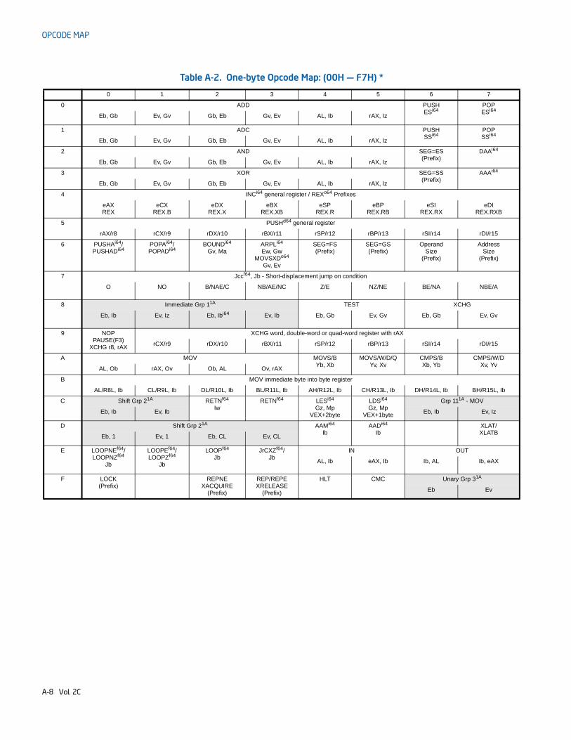
OPCODE MAP
Table A-2. One-byte Opcode Map: (00H — F7H) *
0 1 2 3 4 5 6 7
0 ADD PUSHESi64
POPESi64
Eb, Gb Ev, Gv Gb, Eb Gv, Ev AL, Ib rAX, Iz
1 ADC PUSHSSi64
POPSSi64
Eb, Gb Ev, Gv Gb, Eb Gv, Ev AL, Ib rAX, Iz
2 AND SEG=ES(Prefix)
DAAi64
Eb, Gb Ev, Gv Gb, Eb Gv, Ev AL, Ib rAX, Iz
3 XOR SEG=SS(Prefix)
AAAi64
Eb, Gb Ev, Gv Gb, Eb Gv, Ev AL, Ib rAX, Iz
4 INCi64 general register / REXo64 Prefixes
eAXREX
eCXREX.B
eDXREX.X
eBXREX.XB
eSPREX.R
eBPREX.RB
eSIREX.RX
eDIREX.RXB
5 PUSHd64 general register
rAX/r8 rCX/r9 rDX/r10 rBX/r11 rSP/r12 rBP/r13 rSI/r14 rDI/r15
6 PUSHAi64/PUSHADi64
POPAi64/POPADi64
BOUNDi64
Gv, MaARPLi64
Ew, GwMOVSXDo64
Gv, Ev
SEG=FS(Prefix)
SEG=GS(Prefix)
OperandSize
(Prefix)
AddressSize
(Prefix)
7 Jccf64, Jb - Short-displacement jump on condition
O NO B/NAE/C NB/AE/NC Z/E NZ/NE BE/NA NBE/A
8 Immediate Grp 11A TEST XCHG
Eb, Ib Ev, Iz Eb, Ibi64 Ev, Ib Eb, Gb Ev, Gv Eb, Gb Ev, Gv
9 NOP PAUSE(F3)
XCHG r8, rAX
XCHG word, double-word or quad-word register with rAX
rCX/r9 rDX/r10 rBX/r11 rSP/r12 rBP/r13 rSI/r14 rDI/r15
A MOV MOVS/BYb, Xb
MOVS/W/D/QYv, Xv
CMPS/BXb, Yb
CMPS/W/DXv, Yv
AL, Ob rAX, Ov Ob, AL Ov, rAX
B MOV immediate byte into byte register
AL/R8L, Ib CL/R9L, Ib DL/R10L, Ib BL/R11L, Ib AH/R12L, Ib CH/R13L, Ib DH/R14L, Ib BH/R15L, Ib
C Shift Grp 21A RETNf64
IwRETNf64 LESi64
Gz, Mp VEX+2byte
LDSi64
Gz, Mp VEX+1byte
Grp 111A - MOV
Eb, Ib Ev, Ib Eb, Ib Ev, Iz
D Shift Grp 21A AAMi64
IbAADi64
IbXLAT/XLATB
Eb, 1 Ev, 1 Eb, CL Ev, CL
E LOOPNEf64/LOOPNZf64
Jb
LOOPEf64/LOOPZf64
Jb
LOOPf64
Jb JrCXZf64/
Jb IN OUT
AL, Ib eAX, Ib Ib, AL Ib, eAX
F LOCK(Prefix)
REPNEXACQUIRE
(Prefix)
REP/REPE XRELEASE
(Prefix)
HLT CMC Unary Grp 31A
Eb Ev
A-8 Vol. 2C
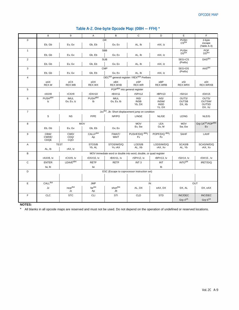
OPCODE MAP
Table A-2. One-byte Opcode Map: (08H — FFH) *
8 9 A B C D E F
0 OR PUSHCSi64
2-byteescape
(Table A-3) Eb, Gb Ev, Gv Gb, Eb Gv, Ev AL, Ib rAX, Iz
1 SBB PUSHDSi64
POPDSi64
Eb, Gb Ev, Gv Gb, Eb Gv, Ev AL, Ib rAX, Iz
2 SUB SEG=CS (Prefix)
DASi64
Eb, Gb Ev, Gv Gb, Eb Gv, Ev AL, Ib rAX, Iz
3 CMP SEG=DS (Prefix)
AASi64
Eb, Gb Ev, Gv Gb, Eb Gv, Ev AL, Ib rAX, Iz
4 DECi64 general register / REXo64 Prefixes
eAXREX.W
eCXREX.WB
eDXREX.WX
eBXREX.WXB
eSPREX.WR
eBPREX.WRB
eSIREX.WRX
eDI REX.WRXB
5 POPd64 into general register
rAX/r8 rCX/r9 rDX/r10 rBX/r11 rSP/r12 rBP/r13 rSI/r14 rDI/r15
6 PUSHd64
IzIMUL
Gv, Ev, IzPUSHd64
IbIMUL
Gv, Ev, IbINS/INSB
Yb, DX
INS/INSW/INSD
Yz, DX
OUTS/OUTSBDX, Xb
OUTS/OUTSW/OUTSDDX, Xz
7 Jccf64, Jb- Short displacement jump on condition
S NS P/PE NP/PO L/NGE NL/GE LE/NG NLE/G
8 MOV MOVEv, Sw
LEAGv, M
MOVSw, Ew
Grp 1A1A POPd64
EvEb, Gb Ev, Gv Gb, Eb Gv, Ev
9 CBW/CWDE/CDQE
CWD/CDQ/CQO
CALLFi64
ApFWAIT/WAIT
PUSHF/D/Q d64/Fv
POPF/D/Q d64/Fv
SAHF LAHF
A TEST STOS/BYb, AL
STOS/W/D/QYv, rAX
LODS/BAL, Xb
LODS/W/D/QrAX, Xv
SCAS/BAL, Yb
SCAS/W/D/QrAX, Xv
AL, Ib rAX, Iz
B MOV immediate word or double into word, double, or quad register
rAX/r8, Iv rCX/r9, Iv rDX/r10, Iv rBX/r11, Iv rSP/r12, Iv rBP/r13, Iv rSI/r14, Iv rDI/r15 , Iv
C ENTER LEAVEd64 RETF RETF INT 3 INT INTOi64 IRET/D/Q
Iw, Ib Iw Ib
D ESC (Escape to coprocessor instruction set)
E CALLf64 JMP IN OUT
Jz nearf64
Jzfari64
Apshortf64
JbAL, DX eAX, DX DX, AL DX, eAX
F CLC STC CLI STI CLD STD INC/DEC INC/DEC
Grp 41A Grp 51A
NOTES:
* All blanks in all opcode maps are reserved and must not be used. Do not depend on the operation of undefined or reserved locations.
Vol. 2C A-9
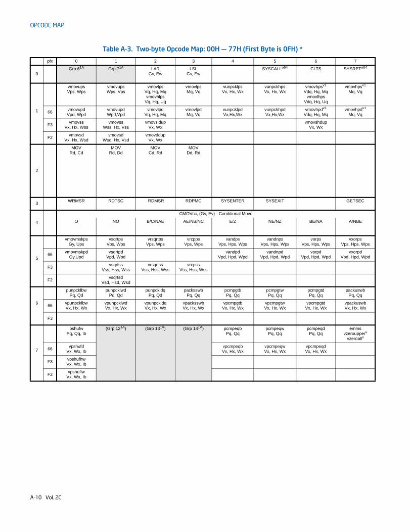
OPCODE MAP
Table A-3. Two-byte Opcode Map: 00H — 77H (First Byte is 0FH) *
pfx 0 1 2 3 4 5 6 7
0Grp 61A Grp 71A LAR
Gv, Ew LSL
Gv, Ew SYSCALLo64 CLTS SYSRETo64
1
vmovupsVps, Wps
vmovupsWps, Vps
vmovlpsVq, Hq, Mqvmovhlps
Vq, Hq, Uq
vmovlpsMq, Vq
vunpcklpsVx, Hx, Wx
vunpckhpsVx, Hx, Wx
vmovhpsv1
Vdq, Hq, Mq vmovlhps
Vdq, Hq, Uq
vmovhpsv1
Mq, Vq
66vmovupdVpd, Wpd
vmovupdWpd,Vpd
vmovlpdVq, Hq, Mq
vmovlpdMq, Vq
vunpcklpdVx,Hx,Wx
vunpckhpdVx,Hx,Wx
vmovhpdv1
Vdq, Hq, Mqvmovhpdv1
Mq, Vq
F3vmovss
Vx, Hx, Wssvmovss
Wss, Hx, Vssvmovsldup
Vx, Wxvmovshdup
Vx, Wx
F2vmovsd
Vx, Hx, Wsdvmovsd
Wsd, Hx, Vsdvmovddup
Vx, Wx
2
MOVRd, Cd
MOVRd, Dd
MOVCd, Rd
MOVDd, Rd
3WRMSR RDTSC RDMSR RDPMC SYSENTER SYSEXIT GETSEC
4
CMOVcc, (Gv, Ev) - Conditional Move
O NO B/C/NAE AE/NB/NC E/Z NE/NZ BE/NA A/NBE
5
vmovmskpsGy, Ups
vsqrtpsVps, Wps
vrsqrtpsVps, Wps
vrcppsVps, Wps
vandpsVps, Hps, Wps
vandnpsVps, Hps, Wps
vorpsVps, Hps, Wps
vxorpsVps, Hps, Wps
66vmovmskpd
Gy,Updvsqrtpd
Vpd, Wpdvandpd
Vpd, Hpd, Wpdvandnpd
Vpd, Hpd, Wpdvorpd
Vpd, Hpd, Wpdvxorpd
Vpd, Hpd, Wpd
F3vsqrtss
Vss, Hss, Wssvrsqrtss
Vss, Hss, Wssvrcpss
Vss, Hss, Wss
F2vsqrtsd
Vsd, Hsd, Wsd
6
punpcklbwPq, Qd
punpcklwdPq, Qd
punpckldqPq, Qd
packsswbPq, Qq
pcmpgtbPq, Qq
pcmpgtwPq, Qq
pcmpgtdPq, Qq
packuswbPq, Qq
66vpunpcklbwVx, Hx, Wx
vpunpcklwdVx, Hx, Wx
vpunpckldqVx, Hx, Wx
vpacksswbVx, Hx, Wx
vpcmpgtbVx, Hx, Wx
vpcmpgtwVx, Hx, Wx
vpcmpgtdVx, Hx, Wx
vpackuswbVx, Hx, Wx
F3
7
pshufwPq, Qq, Ib
(Grp 121A) (Grp 131A) (Grp 141A) pcmpeqbPq, Qq
pcmpeqwPq, Qq
pcmpeqdPq, Qq
emms vzeroupperv
vzeroallv
66vpshufd
Vx, Wx, IbvpcmpeqbVx, Hx, Wx
vpcmpeqwVx, Hx, Wx
vpcmpeqdVx, Hx, Wx
F3vpshufhwVx, Wx, Ib
F2vpshuflw
Vx, Wx, Ib
A-10 Vol. 2C
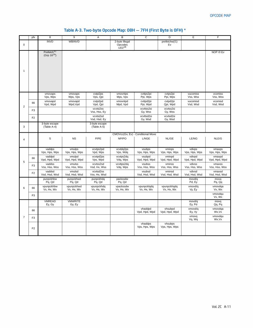
OPCODE MAP
Table A-3. Two-byte Opcode Map: 08H — 7FH (First Byte is 0FH) *
pfx 8 9 A B C D E F
0 INVD WBINVD 2-byte Illegal
OpcodesUD21B
prefetchw(/1)Ev
1
Prefetch1C
(Grp 161A)NOP /0 Ev
2
vmovapsVps, Wps
vmovapsWps, Vps
cvtpi2psVps, Qpi
vmovntpsMps, Vps
cvttps2piPpi, Wps
cvtps2piPpi, Wps
vucomissVss, Wss
vcomissVss, Wss
66vmovapdVpd, Wpd
vmovapdWpd,Vpd
cvtpi2pdVpd, Qpi
vmovntpdMpd, Vpd
cvttpd2piPpi, Wpd
cvtpd2piQpi, Wpd
vucomisdVsd, Wsd
vcomisdVsd, Wsd
F3vcvtsi2ss
Vss, Hss, Eyvcvttss2siGy, Wss
vcvtss2siGy, Wss
F2vcvtsi2sd
Vsd, Hsd, Ey vcvttsd2siGy, Wsd
vcvtsd2siGy, Wsd
3 3-byte escape
(Table A-4) 3-byte escape
(Table A-5)
4
CMOVcc(Gv, Ev) - Conditional Move
S NS P/PE NP/PO L/NGE NL/GE LE/NG NLE/G
5
vaddpsVps, Hps, Wps
vmulpsVps, Hps, Wps
vcvtps2pdVpd, Wps
vcvtdq2psVps, Wdq
vsubps Vps, Hps, Wps
vminpsVps, Hps, Wps
vdivpsVps, Hps, Wps
vmaxpsVps, Hps, Wps
66vaddpd
Vpd, Hpd, Wpdvmulpd
Vpd, Hpd, Wpdvcvtpd2psVps, Wpd
vcvtps2dqVdq, Wps
vsubpdVpd, Hpd, Wpd
vminpdVpd, Hpd, Wpd
vdivpdVpd, Hpd, Wpd
vmaxpdVpd, Hpd, Wpd
F3vaddss
Vss, Hss, Wssvmulss
Vss, Hss, Wssvcvtss2sd
Vsd, Hx, Wssvcvttps2dqVdq, Wps
vsubssVss, Hss, Wss
vminssVss, Hss, Wss
vdivssVss, Hss, Wss
vmaxssVss, Hss, Wss
F2vaddsd
Vsd, Hsd, Wsd vmulsd
Vsd, Hsd, Wsd vcvtsd2ss
Vss, Hx, Wsd vsubsd
Vsd, Hsd, Wsd vminsd
Vsd, Hsd, Wsd vdivsd
Vsd, Hsd, Wsd vmaxsd
Vsd, Hsd, Wsd
6
punpckhbwPq, Qd
punpckhwdPq, Qd
punpckhdqPq, Qd
packssdwPq, Qd
movd/qPd, Ey
movqPq, Qq
66vpunpckhbwVx, Hx, Wx
vpunpckhwdVx, Hx, Wx
vpunpckhdqVx, Hx, Wx
vpackssdwVx, Hx, Wx
vpunpcklqdqVx, Hx, Wx
vpunpckhqdqVx, Hx, Wx
vmovd/qVy, Ey
vmovdqa
Vx, Wx
F3vmovdquVx, Wx
7
VMREADEy, Gy
VMWRITEGy, Ey
movd/qEy, Pd
movqQq, Pq
66vhaddpd
Vpd, Hpd, Wpdvhsubpd
Vpd, Hpd, Wpdvmovd/qEy, Vy
vmovdqaWx,Vx
F3vmovqVq, Wq
vmovdquWx,Vx
F2
vhaddpsVps, Hps, Wps
vhsubpsVps, Hps, Wps
Vol. 2C A-11
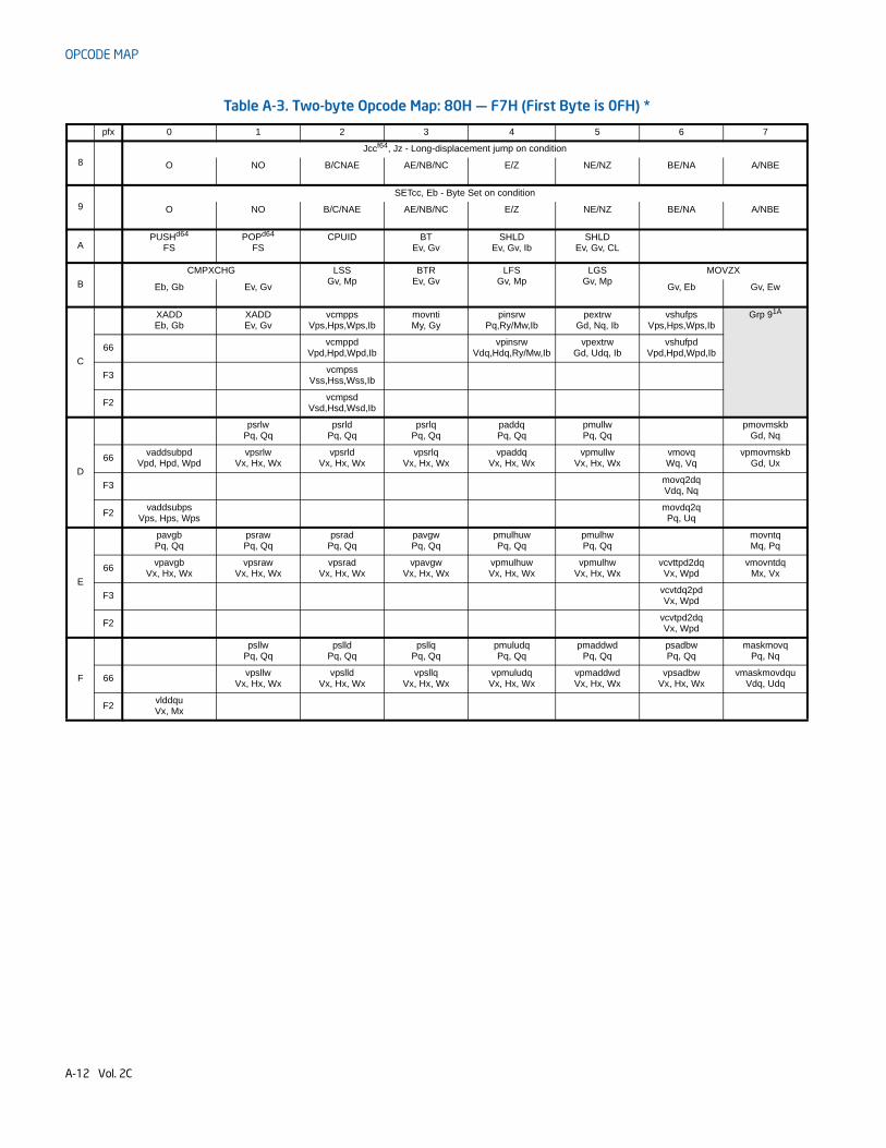
OPCODE MAP
Table A-3. Two-byte Opcode Map: 80H — F7H (First Byte is 0FH) *
pfx 0 1 2 3 4 5 6 7
8
Jccf64, Jz - Long-displacement jump on condition
O NO B/CNAE AE/NB/NC E/Z NE/NZ BE/NA A/NBE
9
SETcc, Eb - Byte Set on condition
O NO B/C/NAE AE/NB/NC E/Z NE/NZ BE/NA A/NBE
APUSHd64
FSPOPd64
FSCPUID BT
Ev, Gv SHLD
Ev, Gv, Ib SHLD
Ev, Gv, CL
B
CMPXCHG LSSGv, Mp
BTREv, Gv
LFSGv, Mp
LGSGv, Mp
MOVZX
Eb, Gb Ev, Gv Gv, Eb Gv, Ew
C
XADDEb, Gb
XADDEv, Gv
vcmppsVps,Hps,Wps,Ib
movntiMy, Gy
pinsrwPq,Ry/Mw,Ib
pextrwGd, Nq, Ib
vshufpsVps,Hps,Wps,Ib
Grp 91A
66vcmppd
Vpd,Hpd,Wpd,Ibvpinsrw
Vdq,Hdq,Ry/Mw,Ibvpextrw
Gd, Udq, Ibvshufpd
Vpd,Hpd,Wpd,Ib
F3vcmpss
Vss,Hss,Wss,Ib
F2vcmpsd
Vsd,Hsd,Wsd,Ib
D
psrlwPq, Qq
psrldPq, Qq
psrlqPq, Qq
paddqPq, Qq
pmullwPq, Qq
pmovmskbGd, Nq
66vaddsubpd
Vpd, Hpd, Wpdvpsrlw
Vx, Hx, Wxvpsrld
Vx, Hx, Wxvpsrlq
Vx, Hx, Wxvpaddq
Vx, Hx, Wxvpmullw
Vx, Hx, WxvmovqWq, Vq
vpmovmskb Gd, Ux
F3movq2dqVdq, Nq
F2vaddsubps
Vps, Hps, Wpsmovdq2qPq, Uq
E
pavgbPq, Qq
psrawPq, Qq
psradPq, Qq
pavgwPq, Qq
pmulhuwPq, Qq
pmulhwPq, Qq
movntqMq, Pq
66vpavgb
Vx, Hx, Wxvpsraw
Vx, Hx, Wxvpsrad
Vx, Hx, Wxvpavgw
Vx, Hx, WxvpmulhuwVx, Hx, Wx
vpmulhwVx, Hx, Wx
vcvttpd2dqVx, Wpd
vmovntdqMx, Vx
F3vcvtdq2pdVx, Wpd
F2vcvtpd2dqVx, Wpd
F
psllwPq, Qq
pslldPq, Qq
psllqPq, Qq
pmuludqPq, Qq
pmaddwdPq, Qq
psadbwPq, Qq
maskmovqPq, Nq
66vpsllw
Vx, Hx, Wxvpslld
Vx, Hx, Wxvpsllq
Vx, Hx, Wxvpmuludq
Vx, Hx, Wxvpmaddwd Vx, Hx, Wx
vpsadbwVx, Hx, Wx
vmaskmovdquVdq, Udq
F2vlddquVx, Mx
A-12 Vol. 2C
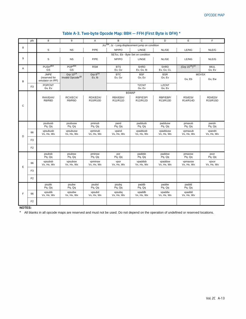
OPCODE MAP
Table A-3. Two-byte Opcode Map: 88H — FFH (First Byte is 0FH) *
pfx 8 9 A B C D E F
8 Jccf64, Jz - Long-displacement jump on condition
S NS P/PE NP/PO L/NGE NL/GE LE/NG NLE/G
9
SETcc, Eb - Byte Set on condition
S NS P/PE NP/PO L/NGE NL/GE LE/NG NLE/G
A PUSHd64
GSPOPd64
GSRSM BTS
Ev, Gv SHRD
Ev, Gv, Ib SHRD
Ev, Gv, CL (Grp 151A)1C IMUL
Gv, Ev
B
JMPE
(reserved for emulator on IPF)
Grp 101A
Invalid Opcode1BGrp 81A
Ev, IbBTC
Ev, GvBSF
Gv, EvBSR
Gv, EvMOVSX
Gv, Eb Gv, Ew
F3POPCNT
Gv, EvTZCNT Gv, Ev
LZCNT Gv, Ev
C
BSWAP
RAX/EAX/R8/R8D
RCX/ECX/ R9/R9D
RDX/EDX/ R10/R10D
RBX/EBX/ R11/R11D
RSP/ESP/ R12/R12D
RBP/EBP/ R13/R13D
RSI/ESI/ R14/R14D
RDI/EDI/ R15/R15D
D
psubusbPq, Qq
psubuswPq, Qq
pminubPq, Qq
pandPq, Qq
paddusbPq, Qq
padduswPq, Qq
pmaxubPq, Qq
pandnPq, Qq
66vpsubusb
Vx, Hx, WxvpsubuswVx, Hx, Wx
vpminubVx, Hx, Wx
vpandVx, Hx, Wx
vpaddusbVx, Hx, Wx
vpadduswVx, Hx, Wx
vpmaxubVx, Hx, Wx
vpandnVx, Hx, Wx
F3
F2
E
psubsbPq, Qq
psubswPq, Qq
pminswPq, Qq
porPq, Qq
paddsbPq, Qq
paddswPq, Qq
pmaxswPq, Qq
pxorPq, Qq
66vpsubsb
Vx, Hx, Wxvpsubsw
Vx, Hx, Wxvpminsw
Vx, Hx, Wxvpor
Vx, Hx, Wxvpaddsb
Vx, Hx, Wxvpaddsw
Vx, Hx, Wxvpmaxsw
Vx, Hx, Wxvpxor
Vx, Hx, Wx
F3
F2
F
psubbPq, Qq
psubwPq, Qq
psubdPq, Qq
psubqPq, Qq
paddbPq, Qq
paddwPq, Qq
padddPq, Qq
66vpsubb
Vx, Hx, Wxvpsubw
Vx, Hx, Wx vpsubd
Vx, Hx, Wxvpsubq
Vx, Hx, Wxvpaddb
Vx, Hx, Wxvpaddw
Vx, Hx, Wx vpaddd
Vx, Hx, Wx
F2
NOTES:
* All blanks in all opcode maps are reserved and must not be used. Do not depend on the operation of undefined or reserved locations.
Vol. 2C A-13
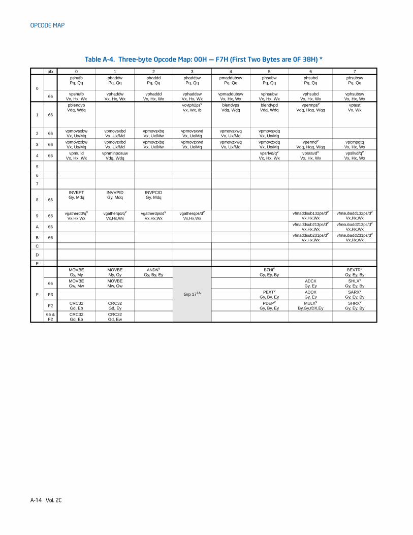
OPCODE MAP
Table A-4. Three-byte Opcode Map: 00H — F7H (First Two Bytes are 0F 38H) *
pfx 0 1 2 3 4 5 6 7
0
pshufbPq, Qq
phaddwPq, Qq
phadddPq, Qq
phaddswPq, Qq
pmaddubswPq, Qq
phsubwPq, Qq
phsubdPq, Qq
phsubswPq, Qq
66vpshufb
Vx, Hx, Wxvphaddw
Vx, Hx, Wxvphaddd
Vx, Hx, WxvphaddswVx, Hx, Wx
vpmaddubswVx, Hx, Wx
vphsubwVx, Hx, Wx
vphsubdVx, Hx, Wx
vphsubswVx, Hx, Wx
1 66
pblendvbVdq, Wdq
vcvtph2psv
Vx, Wx, IbblendvpsVdq, Wdq
blendvpdVdq, Wdq
vpermpsv
Vqq, Hqq, WqqvptestVx, Wx
2 66vpmovsxbwVx, Ux/Mq
vpmovsxbdVx, Ux/Md
vpmovsxbqVx, Ux/Mw
vpmovsxwdVx, Ux/Mq
vpmovsxwqVx, Ux/Md
vpmovsxdqVx, Ux/Mq
3 66vpmovzxbwVx, Ux/Mq
vpmovzxbdVx, Ux/Md
vpmovzxbqVx, Ux/Mw
vpmovzxwdVx, Ux/Mq
vpmovzxwqVx, Ux/Md
vpmovzxdqVx, Ux/Mq
vpermdv
Vqq, Hqq, Wqqvpcmpgtq
Vx, Hx, Wx
4 66vpmulld
Vx, Hx, Wxvphminposuw
Vdq, Wdqvpsrlvd/qv
Vx, Hx, Wxvpsravdv
Vx, Hx, Wxvpsllvd/qv
Vx, Hx, Wx
5
6
7
8 66
INVEPT Gy, Mdq
INVVPID Gy, Mdq
INVPCID Gy, Mdq
9 66vgatherdd/qv
Vx,Hx,Wxvgatherqd/qv
Vx,Hx,Wxvgatherdps/dv
Vx,Hx,Wxvgatherqps/dv
Vx,Hx,Wxvfmaddsub132ps/dv
Vx,Hx,Wxvfmsubadd132ps/dv
Vx,Hx,Wx
A 66vfmaddsub213ps/dv
Vx,Hx,Wxvfmsubadd213ps/dv
Vx,Hx,Wx
B 66vfmaddsub231ps/dv
Vx,Hx,Wxvfmsubadd231ps/dv
Vx,Hx,Wx
C
D
E
F
MOVBE Gy, My
MOVBE My, Gy
ANDNv
Gy, By, Ey
Grp 171A
BZHIv
Gy, Ey, ByBEXTRv
Gy, Ey, By
66MOVBE Gw, Mw
MOVBE Mw, Gw
ADCXGy, Ey
SHLXv
Gy, Ey, By
F3PEXTv
Gy, By, EyADOXGy, Ey
SARXv
Gy, Ey, By
F2CRC32 Gd, Eb
CRC32 Gd, Ey
PDEPv
Gy, By, EyMULXv
By,Gy,rDX,EySHRXv
Gy, Ey, By
66 & F2
CRC32 Gd, Eb
CRC32 Gd, Ew
A-14 Vol. 2C
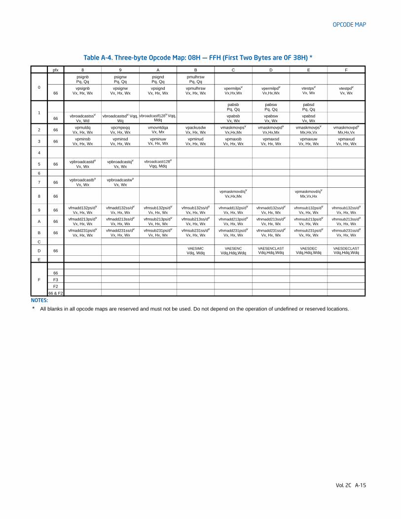
OPCODE MAP
Table A-4. Three-byte Opcode Map: 08H — FFH (First Two Bytes are 0F 38H) *
pfx 8 9 A B C D E F
0
psignbPq, Qq
psignwPq, Qq
psigndPq, Qq
pmulhrswPq, Qq
66vpsignb
Vx, Hx, Wxvpsignw
Vx, Hx, Wxvpsignd
Vx, Hx, Wxvpmulhrsw Vx, Hx, Wx
vpermilpsv Vx,Hx,Wx
vpermilpdv Vx,Hx,Wx
vtestpsv Vx, Wx
vtestpdv Vx, Wx
1
pabsbPq, Qq
pabswPq, Qq
pabsdPq, Qq
66vbroadcastssv
Vx, Wdvbroadcastsdv Vqq,
Wqvbroadcastf128v Vqq,
MdqvpabsbVx, Wx
vpabswVx, Wx
vpabsdVx, Wx
2 66vpmuldq
Vx, Hx, WxvpcmpeqqVx, Hx, Wx
vmovntdqaVx, Mx
vpackusdwVx, Hx, Wx
vmaskmovpsv Vx,Hx,Mx
vmaskmovpdv Vx,Hx,Mx
vmaskmovpsv Mx,Hx,Vx
vmaskmovpdv Mx,Hx,Vx
3 66vpminsb
Vx, Hx, Wxvpminsd
Vx, Hx, Wxvpminuw
Vx, Hx, Wxvpminud
Vx, Hx, Wxvpmaxsb
Vx, Hx, Wxvpmaxsd
Vx, Hx, Wxvpmaxuw
Vx, Hx, Wxvpmaxud
Vx, Hx, Wx
4
5 66vpbroadcastdv
Vx, Wxvpbroadcastqv
Vx, Wxvbroadcasti128v
Vqq, Mdq
6
7 66vpbroadcastbv
Vx, Wxvpbroadcastwv
Vx, Wx
8 66vpmaskmovd/qv
Vx,Hx,Mxvpmaskmovd/qv
Mx,Vx,Hx
9 66 vfmadd132ps/dv Vx, Hx, Wx
vfmadd132ss/dv Vx, Hx, Wx
vfmsub132ps/dv Vx, Hx, Wx
vfmsub132ss/dv Vx, Hx, Wx
vfnmadd132ps/dv Vx, Hx, Wx
vfnmadd132ss/dv Vx, Hx, Wx
vfnmsub132ps/dv Vx, Hx, Wx
vfnmsub132ss/dv Vx, Hx, Wx
A 66vfmadd213ps/dv
Vx, Hx, Wxvfmadd213ss/dv
Vx, Hx, Wxvfmsub213ps/dv
Vx, Hx, Wxvfmsub213ss/dv
Vx, Hx, Wxvfnmadd213ps/dv
Vx, Hx, Wxvfnmadd213ss/dv
Vx, Hx, Wxvfnmsub213ps/dv
Vx, Hx, Wxvfnmsub213ss/dv
Vx, Hx, Wx
B 66vfmadd231ps/dv
Vx, Hx, Wxvfmadd231ss/dv
Vx, Hx, Wxvfmsub231ps/dv
Vx, Hx, Wxvfmsub231ss/dv
Vx, Hx, Wxvfnmadd231ps/dv
Vx, Hx, Wxvfnmadd231ss/dv
Vx, Hx, Wxvfnmsub231ps/dv
Vx, Hx, Wxvfnmsub231ss/dv
Vx, Hx, Wx
C
D 66VAESIMC Vdq, Wdq
VAESENC Vdq,Hdq,Wdq
VAESENCLAST Vdq,Hdq,Wdq
VAESDEC Vdq,Hdq,Wdq
VAESDECLAST Vdq,Hdq,Wdq
E
F
66
F3
F2
66 & F2
NOTES:
* All blanks in all opcode maps are reserved and must not be used. Do not depend on the operation of undefined or reserved locations.
Vol. 2C A-15
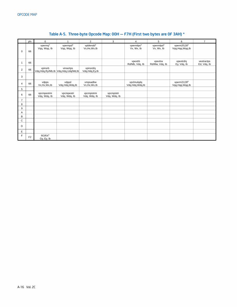
OPCODE MAP
Table A-5. Three-byte Opcode Map: 00H — F7H (First two bytes are 0F 3AH) *
pfx 0 1 2 3 4 5 6 7
0 66
vpermqv
Vqq, Wqq, Ibvpermpdv
Vqq, Wqq, Ibvpblenddv
Vx,Hx,Wx,Ibvpermilpsv Vx, Wx, Ib
vpermilpdv Vx, Wx, Ib
vperm2f128v Vqq,Hqq,Wqq,Ib
1 66vpextrb
Rd/Mb, Vdq, Ibvpextrw
Rd/Mw, Vdq, Ibvpextrd/q
Ey, Vdq, Ib vextractps Ed, Vdq, Ib
2 66vpinsrb
Vdq,Hdq,Ry/Mb,Ibvinsertps
Vdq,Hdq,Udq/Md,Ibvpinsrd/q
Vdq,Hdq,Ey,Ib
3
4 66vdpps
Vx,Hx,Wx,Ibvdppd
Vdq,Hdq,Wdq,Ibvmpsadbw
Vx,Hx,Wx,Ibvpclmulqdq
Vdq,Hdq,Wdq,Ibvperm2i128v
Vqq,Hqq,Wqq,Ib
5
6 66vpcmpestrmVdq, Wdq, Ib
vpcmpestri Vdq, Wdq, Ib
vpcmpistrm Vdq, Wdq, Ib
vpcmpistriVdq, Wdq, Ib
7
8
9
A
B
C
D
E
FF2
RORXv
Gy, Ey, Ib
A-16 Vol. 2C
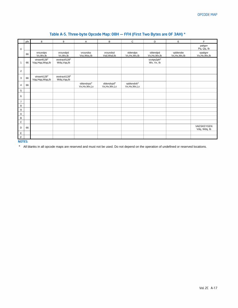
OPCODE MAP
Table A-5. Three-byte Opcode Map: 08H — FFH (First Two Bytes are 0F 3AH) *
pfx 8 9 A B C D E F
0palignr
Pq, Qq, Ib
66vroundpsVx,Wx,Ib
vroundpdVx,Wx,Ib
vroundssVss,Wss,Ib
vroundsdVsd,Wsd,Ib
vblendpsVx,Hx,Wx,Ib
vblendpdVx,Hx,Wx,Ib
vpblendwVx,Hx,Wx,Ib
vpalignrVx,Hx,Wx,Ib
1 66vinsertf128v
Vqq,Hqq,Wqq,Ibvextractf128v Wdq,Vqq,Ib
vcvtps2phv
Wx, Vx, Ib
2
3 66vinserti128v
Vqq,Hqq,Wqq,Ibvextracti128v Wdq,Vqq,Ib
4 66vblendvpsv
Vx,Hx,Wx,Lxvblendvpdv
Vx,Hx,Wx,Lxvpblendvbv
Vx,Hx,Wx,Lx
5
6
7
8
9
A
B
C
D 66VAESKEYGEN Vdq, Wdq, Ib
E
F
NOTES:
* All blanks in all opcode maps are reserved and must not be used. Do not depend on the operation of undefined or reserved locations.
Vol. 2C A-17
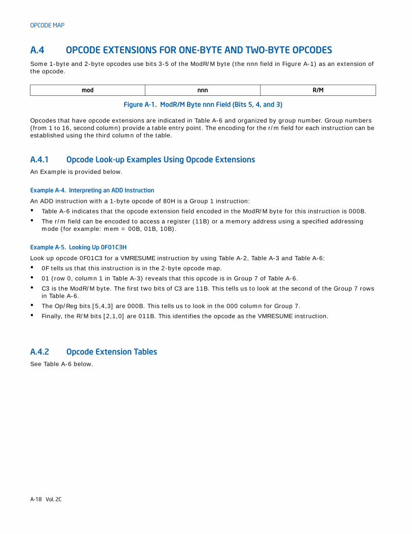
OPCODE MAP
A.4 OPCODE EXTENSIONS FOR ONE-BYTE AND TWO-BYTE OPCODESSome 1-byte and 2-byte opcodes use bits 3-5 of the ModR/M byte (the nnn field in Figure A-1) as an extension of the opcode.
Opcodes that have opcode extensions are indicated in Table A-6 and organized by group number. Group numbers (from 1 to 16, second column) provide a table entry point. The encoding for the r/m field for each instruction can be established using the third column of the table.
A.4.1 Opcode Look-up Examples Using Opcode ExtensionsAn Example is provided below.
Example A-4. Interpreting an ADD Instruction
An ADD instruction with a 1-byte opcode of 80H is a Group 1 instruction:• Table A-6 indicates that the opcode extension field encoded in the ModR/M byte for this instruction is 000B. • The r/m field can be encoded to access a register (11B) or a memory address using a specified addressing
mode (for example: mem = 00B, 01B, 10B).
Example A-5. Looking Up 0F01C3H
Look up opcode 0F01C3 for a VMRESUME instruction by using Table A-2, Table A-3 and Table A-6:• 0F tells us that this instruction is in the 2-byte opcode map.• 01 (row 0, column 1 in Table A-3) reveals that this opcode is in Group 7 of Table A-6.• C3 is the ModR/M byte. The first two bits of C3 are 11B. This tells us to look at the second of the Group 7 rows
in Table A-6.• The Op/Reg bits [5,4,3] are 000B. This tells us to look in the 000 column for Group 7.• Finally, the R/M bits [2,1,0] are 011B. This identifies the opcode as the VMRESUME instruction.
A.4.2 Opcode Extension TablesSee Table A-6 below.
mod nnn R/M
Figure A-1. ModR/M Byte nnn Field (Bits 5, 4, and 3)
A-18 Vol. 2C
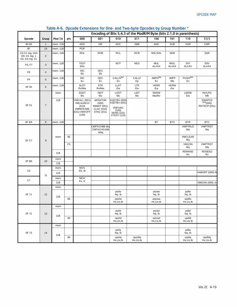
OPCODE MAP
Table A-6. Opcode Extensions for One- and Two-byte Opcodes by Group Number *
Opcode Group Mod 7,6 pfx
Encoding of Bits 5,4,3 of the ModR/M Byte (bits 2,1,0 in parenthesis)000 001 010 011 100 101 110 111
80-83 1 mem, 11B ADD OR ADC SBB AND SUB XOR CMP
8F 1A mem, 11B POP
C0,C1 reg, immD0, D1 reg, 1
D2, D3 reg, CL2
mem, 11B ROL ROR RCL RCR SHL/SAL SHR SAR
F6, F7 3mem, 11B TEST
Ib/IzNOT NEG MUL
AL/rAXIMUL
AL/rAXDIV
AL/rAXIDIV
AL/rAX
FE 4mem, 11B INC
EbDECEb
FF 5mem, 11B INC
EvDECEv
CALLNf64
EvCALLF
Ep JMPNf64
EvJMPF
MpPUSHd64
Ev
0F 00 6mem, 11B SLDT
Rv/MwSTR
Rv/MwLLDTEw
LTREw
VERREw
VERWEw
0F 01 7
mem SGDTMs
SIDTMs
LGDTMs
LIDTMs
SMSWMw/Rv
LMSWEw
INVLPGMb
11B VMCALL (001) VMLAUNCH
(010) VMRESUME
(011) VMXOFF (100)
MONITOR (000)
MWAIT (001)CLAC (010)STAC (011)
XGETBV (000)XSETBV (001)
VMFUNC (100)
XEND (101)XTEST (110)
SWAPGSo64(000)
RDTSCP (001)
0F BA 8 mem, 11B BT BTS BTR BTC
0F C7 9
mem
CMPXCH8B MqCMPXCHG16B
Mdq
VMPTRLDMq
VMPTRSTMq
66 VMCLEARMq
F3 VMXONMq
VMPTRSTMq
11BRDRAND
RvRDSEED
Rv
0F B9 10mem
11B
C6
11
mem MOVEb, Ib
11B XABORT (000) Ib
C7mem MOV
Ev, Iz11B XBEGIN (000) Jz
0F 71 12
mem
11B
psrlwNq, Ib
psrawNq, Ib
psllwNq, Ib
66 vpsrlwHx,Ux,Ib
vpsrawHx,Ux,Ib
vpsllwHx,Ux,Ib
0F 72 13
mem
11B
psrldNq, Ib
psradNq, Ib
pslldNq, Ib
66 vpsrldHx,Ux,Ib
vpsradHx,Ux,Ib
vpslldHx,Ux,Ib
0F 73 14
mem
11B
psrlqNq, Ib
psllqNq, Ib
66 vpsrlqHx,Ux,Ib
vpsrldqHx,Ux,Ib
vpsllqHx,Ux,Ib
vpslldqHx,Ux,Ib
Vol. 2C A-19
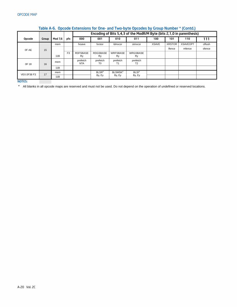
OPCODE MAP
Opcode Group Mod 7,6 pfx
Encoding of Bits 5,4,3 of the ModR/M Byte (bits 2,1,0 in parenthesis)000 001 010 011 100 101 110 111
0F AE 15
mem fxsave fxrstor ldmxcsr stmxcsr XSAVE XRSTOR XSAVEOPT clflush
11B
lfence mfence sfence
F3 RDFSBASE Ry
RDGSBASE Ry
WRFSBASE Ry
WRGSBASE Ry
0F 18 16mem
prefetchNTA
prefetchT0
prefetchT1
prefetchT2
11B
VEX.0F38 F3 17mem BLSRv
By, EyBLSMSKv
By, EyBLSIv
By, Ey11B
NOTES:
* All blanks in all opcode maps are reserved and must not be used. Do not depend on the operation of undefined or reserved locations.
Table A-6. Opcode Extensions for One- and Two-byte Opcodes by Group Number * (Contd.)
A-20 Vol. 2C
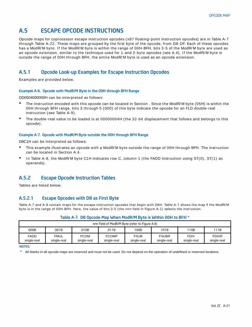
OPCODE MAP
A.5 ESCAPE OPCODE INSTRUCTIONSOpcode maps for coprocessor escape instruction opcodes (x87 floating-point instruction opcodes) are in Table A-7 through Table A-22. These maps are grouped by the first byte of the opcode, from D8-DF. Each of these opcodes has a ModR/M byte. If the ModR/M byte is within the range of 00H-BFH, bits 3-5 of the ModR/M byte are used as an opcode extension, similar to the technique used for 1-and 2-byte opcodes (see A.4). If the ModR/M byte is outside the range of 00H through BFH, the entire ModR/M byte is used as an opcode extension.
A.5.1 Opcode Look-up Examples for Escape Instruction OpcodesExamples are provided below.
Example A-6. Opcode with ModR/M Byte in the 00H through BFH Range
DD0504000000H can be interpreted as follows:• The instruction encoded with this opcode can be located in Section . Since the ModR/M byte (05H) is within the
00H through BFH range, bits 3 through 5 (000) of this byte indicate the opcode for an FLD double-real instruction (see Table A-9).
• The double-real value to be loaded is at 00000004H (the 32-bit displacement that follows and belongs to this opcode).
Example A-7. Opcode with ModR/M Byte outside the 00H through BFH Range
D8C1H can be interpreted as follows:• This example illustrates an opcode with a ModR/M byte outside the range of 00H through BFH. The instruction
can be located in Section A.4. • In Table A-8, the ModR/M byte C1H indicates row C, column 1 (the FADD instruction using ST(0), ST(1) as
operands).
A.5.2 Escape Opcode Instruction TablesTables are listed below.
A.5.2.1 Escape Opcodes with D8 as First ByteTable A-7 and A-8 contain maps for the escape instruction opcodes that begin with D8H. Table A-7 shows the map if the ModR/M byte is in the range of 00H-BFH. Here, the value of bits 3-5 (the nnn field in Figure A-1) selects the instruction.
Table A-7. D8 Opcode Map When ModR/M Byte is Within 00H to BFH *nnn Field of ModR/M Byte (refer to Figure A.4)
000B 001B 010B 011B 100B 101B 110B 111B
FADDsingle-real
FMULsingle-real
FCOMsingle-real
FCOMPsingle-real
FSUBsingle-real
FSUBRsingle-real
FDIVsingle-real
FDIVRsingle-real
NOTES:
* All blanks in all opcode maps are reserved and must not be used. Do not depend on the operation of undefined or reserved locations.
Vol. 2C A-21
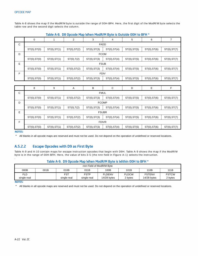
OPCODE MAP
Table A-8 shows the map if the ModR/M byte is outside the range of 00H-BFH. Here, the first digit of the ModR/M byte selects the table row and the second digit selects the column.
A.5.2.2 Escape Opcodes with D9 as First ByteTable A-9 and A-10 contain maps for escape instruction opcodes that begin with D9H. Table A-9 shows the map if the ModR/M byte is in the range of 00H-BFH. Here, the value of bits 3-5 (the nnn field in Figure A-1) selects the instruction..
Table A-8. D8 Opcode Map When ModR/M Byte is Outside 00H to BFH *0 1 2 3 4 5 6 7
C FADD
ST(0),ST(0) ST(0),ST(1) ST(0),ST(2) ST(0),ST(3) ST(0),ST(4) ST(0),ST(5) ST(0),ST(6) ST(0),ST(7)
D FCOM
ST(0),ST(0) ST(0),ST(1) ST(0),T(2) ST(0),ST(3) ST(0),ST(4) ST(0),ST(5) ST(0),ST(6) ST(0),ST(7)
E FSUB
ST(0),ST(0) ST(0),ST(1) ST(0),ST(2) ST(0),ST(3) ST(0),ST(4) ST(0),ST(5) ST(0),ST(6) ST(0),ST(7)
F FDIV
ST(0),ST(0) ST(0),ST(1) ST(0),ST(2) ST(0),ST(3) ST(0),ST(4) ST(0),ST(5) ST(0),ST(6) ST(0),ST(7)
8 9 A B C D E F
C FMUL
ST(0),ST(0) ST(0),ST(1) ST(0),ST(2) ST(0),ST(3) ST(0),ST(4) ST(0),ST(5) ST(0),ST(6) ST(0),ST(7)
D FCOMP
ST(0),ST(0) ST(0),ST(1) ST(0),T(2) ST(0),ST(3) ST(0),ST(4) ST(0),ST(5) ST(0),ST(6) ST(0),ST(7)
E FSUBR
ST(0),ST(0) ST(0),ST(1) ST(0),ST(2) ST(0),ST(3) ST(0),ST(4) ST(0),ST(5) ST(0),ST(6) ST(0),ST(7)
F FDIVR
ST(0),ST(0) ST(0),ST(1) ST(0),ST(2) ST(0),ST(3) ST(0),ST(4) ST(0),ST(5) ST(0),ST(6) ST(0),ST(7)
NOTES:
* All blanks in all opcode maps are reserved and must not be used. Do not depend on the operation of undefined or reserved locations.
Table A-9. D9 Opcode Map When ModR/M Byte is Within 00H to BFH *nnn Field of ModR/M Byte
000B 001B 010B 011B 100B 101B 110B 111B
FLDsingle-real
FSTsingle-real
FSTPsingle-real
FLDENV14/28 bytes
FLDCW2 bytes
FSTENV14/28 bytes
FSTCW2 bytes
NOTES:
* All blanks in all opcode maps are reserved and must not be used. Do not depend on the operation of undefined or reserved locations.
A-22 Vol. 2C
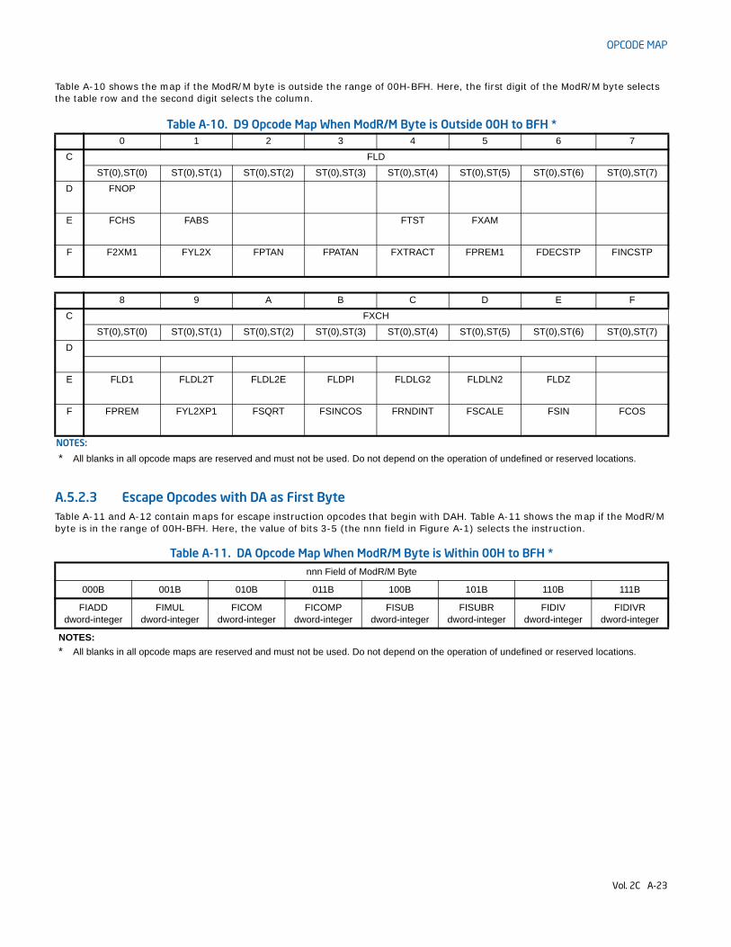
OPCODE MAP
Table A-10 shows the map if the ModR/M byte is outside the range of 00H-BFH. Here, the first digit of the ModR/M byte selects the table row and the second digit selects the column.
A.5.2.3 Escape Opcodes with DA as First ByteTable A-11 and A-12 contain maps for escape instruction opcodes that begin with DAH. Table A-11 shows the map if the ModR/M byte is in the range of 00H-BFH. Here, the value of bits 3-5 (the nnn field in Figure A-1) selects the instruction.
Table A-10. D9 Opcode Map When ModR/M Byte is Outside 00H to BFH *0 1 2 3 4 5 6 7
C FLD
ST(0),ST(0) ST(0),ST(1) ST(0),ST(2) ST(0),ST(3) ST(0),ST(4) ST(0),ST(5) ST(0),ST(6) ST(0),ST(7)
D FNOP
E FCHS FABS FTST FXAM
F F2XM1 FYL2X FPTAN FPATAN FXTRACT FPREM1 FDECSTP FINCSTP
8 9 A B C D E F
C FXCH
ST(0),ST(0) ST(0),ST(1) ST(0),ST(2) ST(0),ST(3) ST(0),ST(4) ST(0),ST(5) ST(0),ST(6) ST(0),ST(7)
D
E FLD1 FLDL2T FLDL2E FLDPI FLDLG2 FLDLN2 FLDZ
F FPREM FYL2XP1 FSQRT FSINCOS FRNDINT FSCALE FSIN FCOS
NOTES:
* All blanks in all opcode maps are reserved and must not be used. Do not depend on the operation of undefined or reserved locations.
Table A-11. DA Opcode Map When ModR/M Byte is Within 00H to BFH *nnn Field of ModR/M Byte
000B 001B 010B 011B 100B 101B 110B 111B
FIADDdword-integer
FIMULdword-integer
FICOMdword-integer
FICOMPdword-integer
FISUBdword-integer
FISUBRdword-integer
FIDIVdword-integer
FIDIVRdword-integer
NOTES:
* All blanks in all opcode maps are reserved and must not be used. Do not depend on the operation of undefined or reserved locations.
Vol. 2C A-23
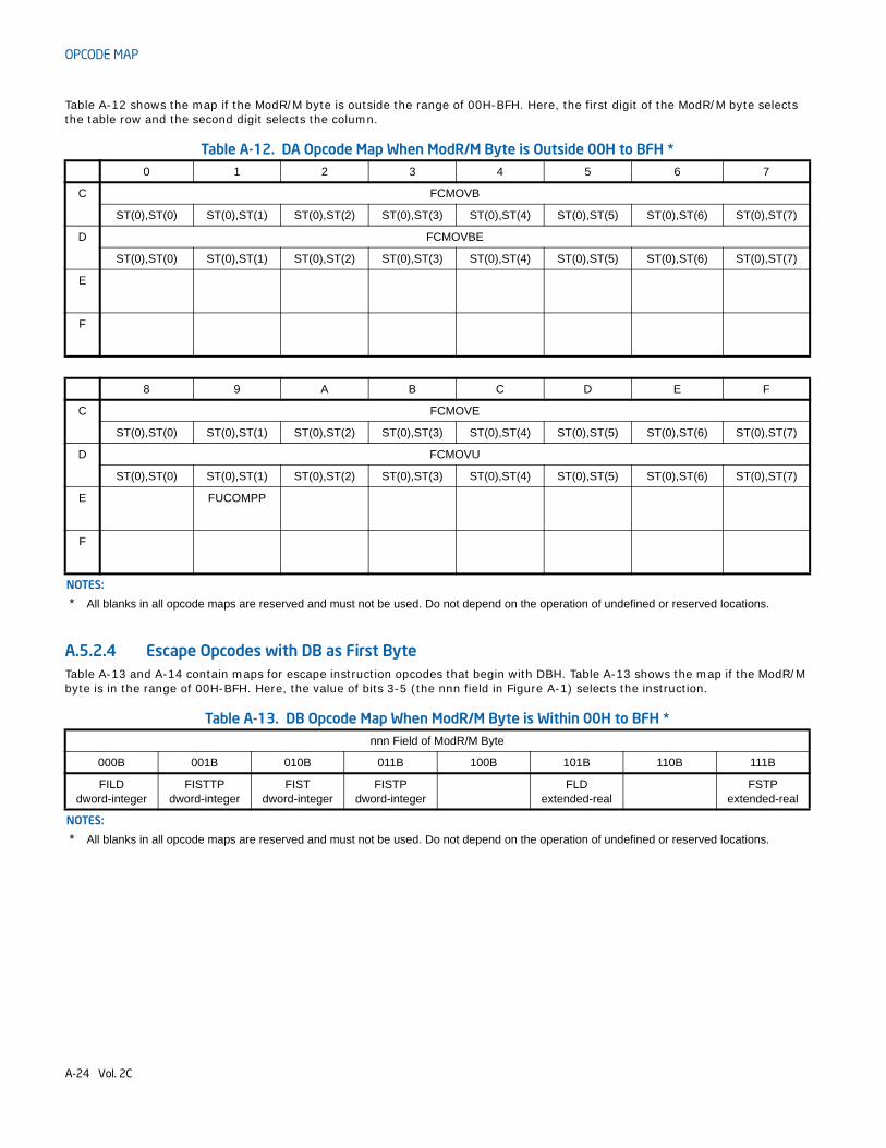
OPCODE MAP
Table A-12 shows the map if the ModR/M byte is outside the range of 00H-BFH. Here, the first digit of the ModR/M byte selects the table row and the second digit selects the column.
A.5.2.4 Escape Opcodes with DB as First ByteTable A-13 and A-14 contain maps for escape instruction opcodes that begin with DBH. Table A-13 shows the map if the ModR/M byte is in the range of 00H-BFH. Here, the value of bits 3-5 (the nnn field in Figure A-1) selects the instruction.
Table A-12. DA Opcode Map When ModR/M Byte is Outside 00H to BFH *0 1 2 3 4 5 6 7
C FCMOVB
ST(0),ST(0) ST(0),ST(1) ST(0),ST(2) ST(0),ST(3) ST(0),ST(4) ST(0),ST(5) ST(0),ST(6) ST(0),ST(7)
D FCMOVBE
ST(0),ST(0) ST(0),ST(1) ST(0),ST(2) ST(0),ST(3) ST(0),ST(4) ST(0),ST(5) ST(0),ST(6) ST(0),ST(7)
E
F
8 9 A B C D E F
C FCMOVE
ST(0),ST(0) ST(0),ST(1) ST(0),ST(2) ST(0),ST(3) ST(0),ST(4) ST(0),ST(5) ST(0),ST(6) ST(0),ST(7)
D FCMOVU
ST(0),ST(0) ST(0),ST(1) ST(0),ST(2) ST(0),ST(3) ST(0),ST(4) ST(0),ST(5) ST(0),ST(6) ST(0),ST(7)
E FUCOMPP
F
NOTES:
* All blanks in all opcode maps are reserved and must not be used. Do not depend on the operation of undefined or reserved locations.
Table A-13. DB Opcode Map When ModR/M Byte is Within 00H to BFH *nnn Field of ModR/M Byte
000B 001B 010B 011B 100B 101B 110B 111B
FILDdword-integer
FISTTP dword-integer
FISTdword-integer
FISTPdword-integer
FLDextended-real
FSTPextended-real
NOTES:
* All blanks in all opcode maps are reserved and must not be used. Do not depend on the operation of undefined or reserved locations.
A-24 Vol. 2C
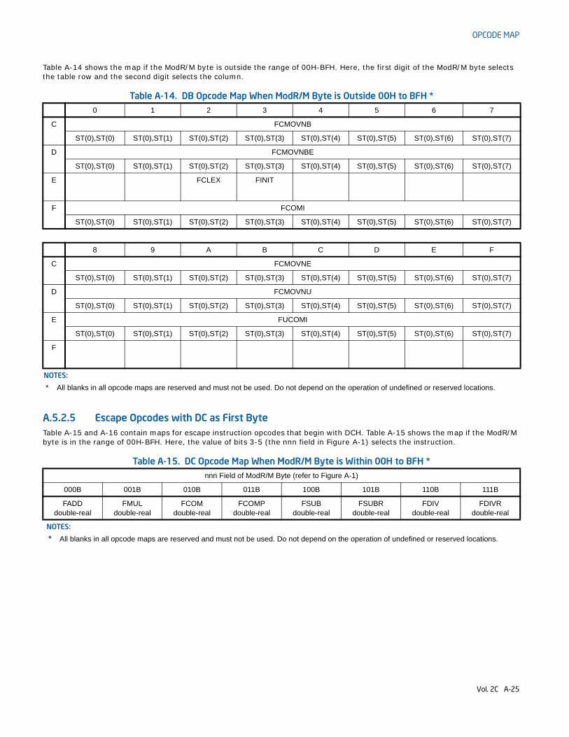
OPCODE MAP
Table A-14 shows the map if the ModR/M byte is outside the range of 00H-BFH. Here, the first digit of the ModR/M byte selects the table row and the second digit selects the column.
A.5.2.5 Escape Opcodes with DC as First ByteTable A-15 and A-16 contain maps for escape instruction opcodes that begin with DCH. Table A-15 shows the map if the ModR/M byte is in the range of 00H-BFH. Here, the value of bits 3-5 (the nnn field in Figure A-1) selects the instruction.
Table A-14. DB Opcode Map When ModR/M Byte is Outside 00H to BFH *0 1 2 3 4 5 6 7
C FCMOVNB
ST(0),ST(0) ST(0),ST(1) ST(0),ST(2) ST(0),ST(3) ST(0),ST(4) ST(0),ST(5) ST(0),ST(6) ST(0),ST(7)
D FCMOVNBE
ST(0),ST(0) ST(0),ST(1) ST(0),ST(2) ST(0),ST(3) ST(0),ST(4) ST(0),ST(5) ST(0),ST(6) ST(0),ST(7)
E FCLEX FINIT
F FCOMI
ST(0),ST(0) ST(0),ST(1) ST(0),ST(2) ST(0),ST(3) ST(0),ST(4) ST(0),ST(5) ST(0),ST(6) ST(0),ST(7)
8 9 A B C D E F
C FCMOVNE
ST(0),ST(0) ST(0),ST(1) ST(0),ST(2) ST(0),ST(3) ST(0),ST(4) ST(0),ST(5) ST(0),ST(6) ST(0),ST(7)
D FCMOVNU
ST(0),ST(0) ST(0),ST(1) ST(0),ST(2) ST(0),ST(3) ST(0),ST(4) ST(0),ST(5) ST(0),ST(6) ST(0),ST(7)
E FUCOMI
ST(0),ST(0) ST(0),ST(1) ST(0),ST(2) ST(0),ST(3) ST(0),ST(4) ST(0),ST(5) ST(0),ST(6) ST(0),ST(7)
F
NOTES:
* All blanks in all opcode maps are reserved and must not be used. Do not depend on the operation of undefined or reserved locations.
Table A-15. DC Opcode Map When ModR/M Byte is Within 00H to BFH *nnn Field of ModR/M Byte (refer to Figure A-1)
000B 001B 010B 011B 100B 101B 110B 111B
FADD double-real
FMUL double-real
FCOM double-real
FCOMP double-real
FSUB double-real
FSUBR double-real
FDIV double-real
FDIVR double-real
NOTES:
* All blanks in all opcode maps are reserved and must not be used. Do not depend on the operation of undefined or reserved locations.
Vol. 2C A-25
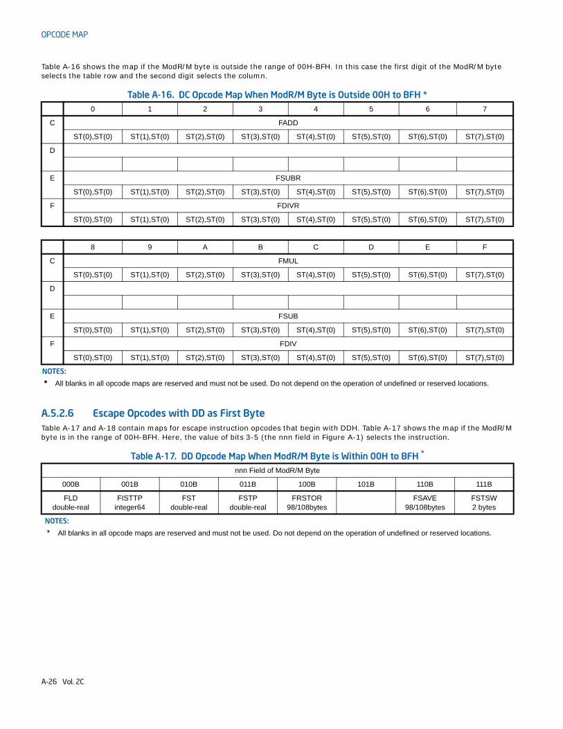
OPCODE MAP
Table A-16 shows the map if the ModR/M byte is outside the range of 00H-BFH. In this case the first digit of the ModR/M byte selects the table row and the second digit selects the column.
A.5.2.6 Escape Opcodes with DD as First ByteTable A-17 and A-18 contain maps for escape instruction opcodes that begin with DDH. Table A-17 shows the map if the ModR/M byte is in the range of 00H-BFH. Here, the value of bits 3-5 (the nnn field in Figure A-1) selects the instruction.
Table A-16. DC Opcode Map When ModR/M Byte is Outside 00H to BFH *0 1 2 3 4 5 6 7
C FADD
ST(0),ST(0) ST(1),ST(0) ST(2),ST(0) ST(3),ST(0) ST(4),ST(0) ST(5),ST(0) ST(6),ST(0) ST(7),ST(0)
D
E FSUBR
ST(0),ST(0) ST(1),ST(0) ST(2),ST(0) ST(3),ST(0) ST(4),ST(0) ST(5),ST(0) ST(6),ST(0) ST(7),ST(0)
F FDIVR
ST(0),ST(0) ST(1),ST(0) ST(2),ST(0) ST(3),ST(0) ST(4),ST(0) ST(5),ST(0) ST(6),ST(0) ST(7),ST(0)
8 9 A B C D E F
C FMUL
ST(0),ST(0) ST(1),ST(0) ST(2),ST(0) ST(3),ST(0) ST(4),ST(0) ST(5),ST(0) ST(6),ST(0) ST(7),ST(0)
D
E FSUB
ST(0),ST(0) ST(1),ST(0) ST(2),ST(0) ST(3),ST(0) ST(4),ST(0) ST(5),ST(0) ST(6),ST(0) ST(7),ST(0)
F FDIV
ST(0),ST(0) ST(1),ST(0) ST(2),ST(0) ST(3),ST(0) ST(4),ST(0) ST(5),ST(0) ST(6),ST(0) ST(7),ST(0)
NOTES:
* All blanks in all opcode maps are reserved and must not be used. Do not depend on the operation of undefined or reserved locations.
Table A-17. DD Opcode Map When ModR/M Byte is Within 00H to BFH *
nnn Field of ModR/M Byte
000B 001B 010B 011B 100B 101B 110B 111B
FLD double-real
FISTTP integer64
FST double-real
FSTP double-real
FRSTOR 98/108bytes
FSAVE 98/108bytes
FSTSW 2 bytes
NOTES:
* All blanks in all opcode maps are reserved and must not be used. Do not depend on the operation of undefined or reserved locations.
A-26 Vol. 2C
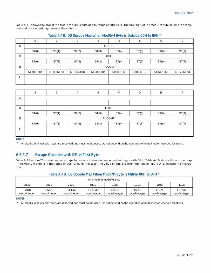
OPCODE MAP
Table A-18 shows the map if the ModR/M byte is outside the range of 00H-BFH. The first digit of the ModR/M byte selects the table row and the second digit selects the column.
A.5.2.7 Escape Opcodes with DE as First ByteTable A-19 and A-20 contain opcode maps for escape instruction opcodes that begin with DEH. Table A-19 shows the opcode map if the ModR/M byte is in the range of 00H-BFH. In this case, the value of bits 3-5 (the nnn field in Figure A-1) selects the instruc-tion.
Table A-18. DD Opcode Map When ModR/M Byte is Outside 00H to BFH *0 1 2 3 4 5 6 7
C FFREE
ST(0) ST(1) ST(2) ST(3) ST(4) ST(5) ST(6) ST(7)
D FST
ST(0) ST(1) ST(2) ST(3) ST(4) ST(5) ST(6) ST(7)
E FUCOM
ST(0),ST(0) ST(1),ST(0) ST(2),ST(0) ST(3),ST(0) ST(4),ST(0) ST(5),ST(0) ST(6),ST(0) ST(7),ST(0)
F
8 9 A B C D E F
C
D FSTP
ST(0) ST(1) ST(2) ST(3) ST(4) ST(5) ST(6) ST(7)
E FUCOMP
ST(0) ST(1) ST(2) ST(3) ST(4) ST(5) ST(6) ST(7)
F
NOTES:
* All blanks in all opcode maps are reserved and must not be used. Do not depend on the operation of undefined or reserved locations.
Table A-19. DE Opcode Map When ModR/M Byte is Within 00H to BFH *nnn Field of ModR/M Byte
000B 001B 010B 011B 100B 101B 110B 111B
FIADD word-integer
FIMUL word-integer
FICOM word-integer
FICOMP word-integer
FISUB word-integer
FISUBR word-integer
FIDIV word-integer
FIDIVR word-integer
NOTES:
* All blanks in all opcode maps are reserved and must not be used. Do not depend on the operation of undefined or reserved locations.
Vol. 2C A-27
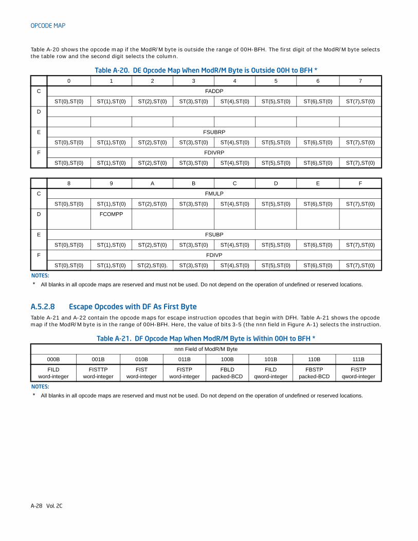
OPCODE MAP
Table A-20 shows the opcode map if the ModR/M byte is outside the range of 00H-BFH. The first digit of the ModR/M byte selects the table row and the second digit selects the column.
A.5.2.8 Escape Opcodes with DF As First ByteTable A-21 and A-22 contain the opcode maps for escape instruction opcodes that begin with DFH. Table A-21 shows the opcode map if the ModR/M byte is in the range of 00H-BFH. Here, the value of bits 3-5 (the nnn field in Figure A-1) selects the instruction.
Table A-20. DE Opcode Map When ModR/M Byte is Outside 00H to BFH *0 1 2 3 4 5 6 7
C FADDP
ST(0),ST(0) ST(1),ST(0) ST(2),ST(0) ST(3),ST(0) ST(4),ST(0) ST(5),ST(0) ST(6),ST(0) ST(7),ST(0)
D
E FSUBRP
ST(0),ST(0) ST(1),ST(0) ST(2),ST(0) ST(3),ST(0) ST(4),ST(0) ST(5),ST(0) ST(6),ST(0) ST(7),ST(0)
F FDIVRP
ST(0),ST(0) ST(1),ST(0) ST(2),ST(0) ST(3),ST(0) ST(4),ST(0) ST(5),ST(0) ST(6),ST(0) ST(7),ST(0)
8 9 A B C D E F
C FMULP
ST(0),ST(0) ST(1),ST(0) ST(2),ST(0) ST(3),ST(0) ST(4),ST(0) ST(5),ST(0) ST(6),ST(0) ST(7),ST(0)
D FCOMPP
E FSUBP
ST(0),ST(0) ST(1),ST(0) ST(2),ST(0) ST(3),ST(0) ST(4),ST(0) ST(5),ST(0) ST(6),ST(0) ST(7),ST(0)
F FDIVP
ST(0),ST(0) ST(1),ST(0) ST(2),ST(0). ST(3),ST(0) ST(4),ST(0) ST(5),ST(0) ST(6),ST(0) ST(7),ST(0)
NOTES:
* All blanks in all opcode maps are reserved and must not be used. Do not depend on the operation of undefined or reserved locations.
Table A-21. DF Opcode Map When ModR/M Byte is Within 00H to BFH *nnn Field of ModR/M Byte
000B 001B 010B 011B 100B 101B 110B 111B
FILDword-integer
FISTTPword-integer
FIST word-integer
FISTP word-integer
FBLD packed-BCD
FILD qword-integer
FBSTP packed-BCD
FISTP qword-integer
NOTES:
* All blanks in all opcode maps are reserved and must not be used. Do not depend on the operation of undefined or reserved locations.
A-28 Vol. 2C

OPCODE MAP
Table A-22 shows the opcode map if the ModR/M byte is outside the range of 00H-BFH. The first digit of the ModR/M byte selects the table row and the second digit selects the column.
Table A-22. DF Opcode Map When ModR/M Byte is Outside 00H to BFH *
0 1 2 3 4 5 6 7
C
D
E FSTSWAX
F FCOMIP
ST(0),ST(0) ST(0),ST(1) ST(0),ST(2) ST(0),ST(3) ST(0),ST(4) ST(0),ST(5) ST(0),ST(6) ST(0),ST(7)
8 9 A B C D E F
C
D
E FUCOMIP
ST(0),ST(0) ST(0),ST(1) ST(0),ST(2) ST(0),ST(3) ST(0),ST(4) ST(0),ST(5) ST(0),ST(6) ST(0),ST(7)
F
NOTES:
* All blanks in all opcode maps are reserved and must not be used. Do not depend on the operation of undefined or reserved locations.
Vol. 2C A-29
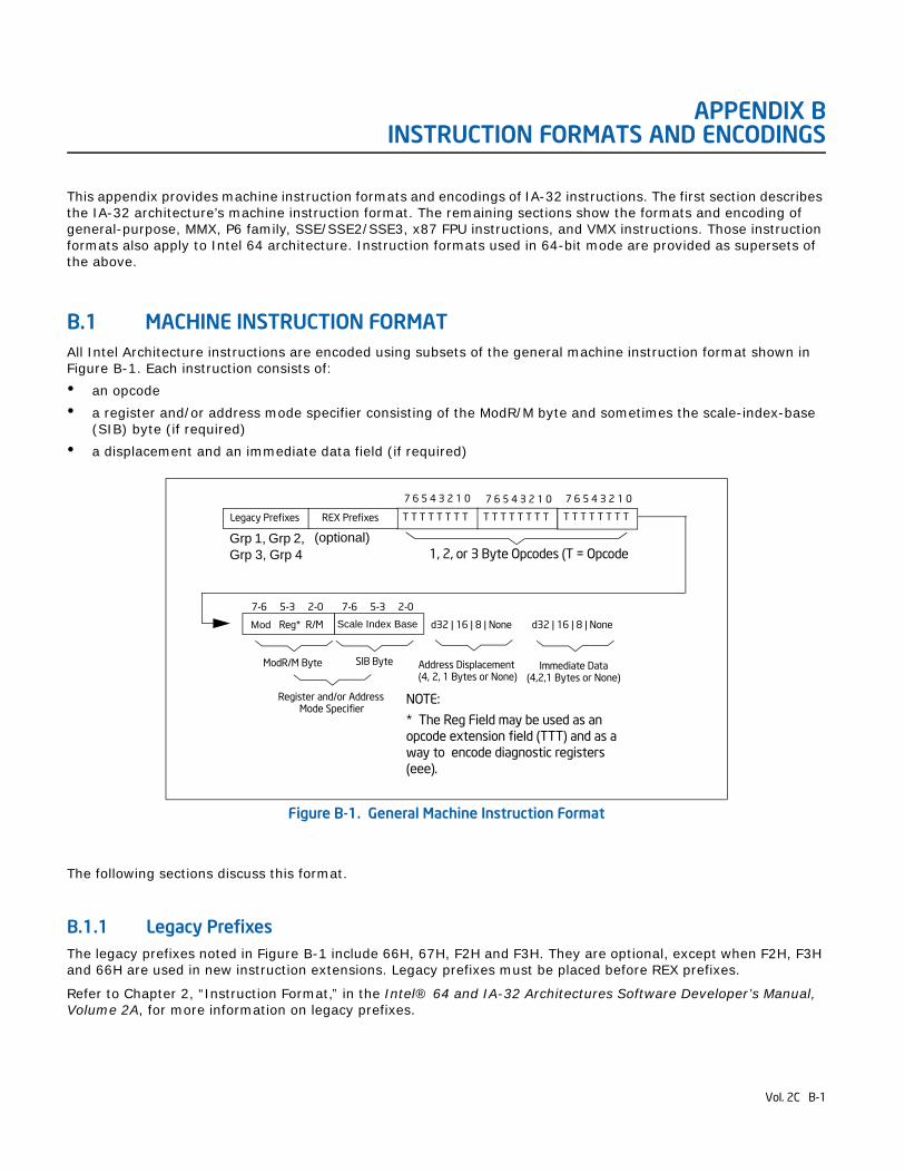
APPENDIX BINSTRUCTION FORMATS AND ENCODINGS
This appendix provides machine instruction formats and encodings of IA-32 instructions. The first section describes the IA-32 architecture’s machine instruction format. The remaining sections show the formats and encoding of general-purpose, MMX, P6 family, SSE/SSE2/SSE3, x87 FPU instructions, and VMX instructions. Those instruction formats also apply to Intel 64 architecture. Instruction formats used in 64-bit mode are provided as supersets of the above.
B.1 MACHINE INSTRUCTION FORMATAll Intel Architecture instructions are encoded using subsets of the general machine instruction format shown in Figure B-1. Each instruction consists of:• an opcode• a register and/or address mode specifier consisting of the ModR/M byte and sometimes the scale-index-base
(SIB) byte (if required) • a displacement and an immediate data field (if required)
The following sections discuss this format.
B.1.1 Legacy PrefixesThe legacy prefixes noted in Figure B-1 include 66H, 67H, F2H and F3H. They are optional, except when F2H, F3H and 66H are used in new instruction extensions. Legacy prefixes must be placed before REX prefixes.
Refer to Chapter 2, “Instruction Format,” in the Intel® 64 and IA-32 Architectures Software Developer’s Manual, Volume 2A, for more information on legacy prefixes.
Figure B-1. General Machine Instruction Format
ModR/M Byte
7 6 5 4 3 2 1 0 7 6 5 4 3 2 1 0
7-6 5-3 2-07-6 5-3 2-0
T T T T T T T T T T T T T T T T
Mod Reg* R/M Scale Index Base d32 | 16 | 8 | Noned32 | 16 | 8 | None
SIB Byte Address Displacement(4, 2, 1 Bytes or None)
Immediate Data(4,2,1 Bytes or None)
Register and/or AddressMode Specifier
Legacy Prefixes REX Prefixes
7 6 5 4 3 2 1 0
T T T T T T T T
(optional)Grp 1, Grp 2, Grp 3, Grp 4
NOTE:
* The Reg Field may be used as an opcode extension field (TTT) and as a way to encode diagnostic registers (eee).
1, 2, or 3 Byte Opcodes (T = Opcode
Vol. 2C B-1
INSTRUCTION FORMATS AND ENCODINGS
B.1.2 REX PrefixesREX prefixes are a set of 16 opcodes that span one row of the opcode map and occupy entries 40H to 4FH. These opcodes represent valid instructions (INC or DEC) in IA-32 operating modes and in compatibility mode. In 64-bit mode, the same opcodes represent the instruction prefix REX and are not treated as individual instructions.
Refer to Chapter 2, “Instruction Format,” in the Intel® 64 and IA-32 Architectures Software Developer’s Manual, Volume 2A, for more information on REX prefixes.
B.1.3 Opcode FieldsThe primary opcode for an instruction is encoded in one to three bytes of the instruction. Within the primary opcode, smaller encoding fields may be defined. These fields vary according to the class of operation being performed.
Almost all instructions that refer to a register and/or memory operand have a register and/or address mode byte following the opcode. This byte, the ModR/M byte, consists of the mod field (2 bits), the reg field (3 bits; this field is sometimes an opcode extension), and the R/M field (3 bits). Certain encodings of the ModR/M byte indicate that a second address mode byte, the SIB byte, must be used.
If the addressing mode specifies a displacement, the displacement value is placed immediately following the ModR/M byte or SIB byte. Possible sizes are 8, 16, or 32 bits. If the instruction specifies an immediate value, the immediate value follows any displacement bytes. The immediate, if specified, is always the last field of the instruc-tion.
Refer to Chapter 2, “Instruction Format,” in the Intel® 64 and IA-32 Architectures Software Developer’s Manual, Volume 2A, for more information on opcodes.
B.1.4 Special FieldsTable B-1 lists bit fields that appear in certain instructions, sometimes within the opcode bytes. All of these fields (except the d bit) occur in the general-purpose instruction formats in Table B-13.
B.1.4.1 Reg Field (reg) for Non-64-Bit ModesThe reg field in the ModR/M byte specifies a general-purpose register operand. The group of registers specified is modified by the presence and state of the w bit in an encoding (refer to Section B.1.4.3). Table B-2 shows the encoding of the reg field when the w bit is not present in an encoding; Table B-3 shows the encoding of the reg field when the w bit is present.
Table B-1. Special Fields Within Instruction Encodings
Field Name DescriptionNumber of
Bits
reg General-register specifier (see Table B-4 or B-5) 3
w Specifies if data is byte or full-sized, where full-sized is 16 or 32 bits (see Table B-6) 1
s Specifies sign extension of an immediate field (see Table B-7) 1
sreg2 Segment register specifier for CS, SS, DS, ES (see Table B-8) 2
sreg3 Segment register specifier for CS, SS, DS, ES, FS, GS (see Table B-8) 3
eee Specifies a special-purpose (control or debug) register (see Table B-9)
3
tttn For conditional instructions, specifies a condition asserted or negated (see Table B-12) 4
d Specifies direction of data operation (see Table B-11) 1
B-2 Vol. 2C
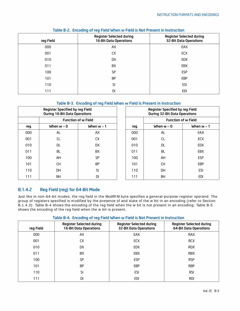
INSTRUCTION FORMATS AND ENCODINGS
B.1.4.2 Reg Field (reg) for 64-Bit ModeJust like in non-64-bit modes, the reg field in the ModR/M byte specifies a general-purpose register operand. The group of registers specified is modified by the presence of and state of the w bit in an encoding (refer to Section B.1.4.3). Table B-4 shows the encoding of the reg field when the w bit is not present in an encoding; Table B-5 shows the encoding of the reg field when the w bit is present.
Table B-2. Encoding of reg Field When w Field is Not Present in Instruction
reg FieldRegister Selected during16-Bit Data Operations
Register Selected during32-Bit Data Operations
000 AX EAX
001 CX ECX
010 DX EDX
011 BX EBX
100 SP ESP
101 BP EBP
110 SI ESI
111 DI EDI
Table B-3. Encoding of reg Field When w Field is Present in Instruction
Register Specified by reg FieldDuring 16-Bit Data Operations
Register Specified by reg FieldDuring 32-Bit Data Operations
Function of w Field Function of w Field
reg When w = 0 When w = 1 reg When w = 0 When w = 1
000 AL AX 000 AL EAX
001 CL CX 001 CL ECX
010 DL DX 010 DL EDX
011 BL BX 011 BL EBX
100 AH SP 100 AH ESP
101 CH BP 101 CH EBP
110 DH SI 110 DH ESI
111 BH DI 111 BH EDI
Table B-4. Encoding of reg Field When w Field is Not Present in Instruction
reg FieldRegister Selected during16-Bit Data Operations
Register Selected during32-Bit Data Operations
Register Selected during64-Bit Data Operations
000 AX EAX RAX
001 CX ECX RCX
010 DX EDX RDX
011 BX EBX RBX
100 SP ESP RSP
101 BP EBP RBP
110 SI ESI RSI
111 DI EDI RDI
Vol. 2C B-3
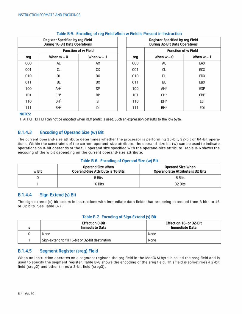
INSTRUCTION FORMATS AND ENCODINGS
B.1.4.3 Encoding of Operand Size (w) Bit The current operand-size attribute determines whether the processor is performing 16-bit, 32-bit or 64-bit opera-tions. Within the constraints of the current operand-size attribute, the operand-size bit (w) can be used to indicate operations on 8-bit operands or the full operand size specified with the operand-size attribute. Table B-6 shows the encoding of the w bit depending on the current operand-size attribute.
B.1.4.4 Sign-Extend (s) Bit The sign-extend (s) bit occurs in instructions with immediate data fields that are being extended from 8 bits to 16 or 32 bits. See Table B-7.
B.1.4.5 Segment Register (sreg) Field When an instruction operates on a segment register, the reg field in the ModR/M byte is called the sreg field and is used to specify the segment register. Table B-8 shows the encoding of the sreg field. This field is sometimes a 2-bit field (sreg2) and other times a 3-bit field (sreg3).
Table B-5. Encoding of reg Field When w Field is Present in Instruction
Register Specified by reg FieldDuring 16-Bit Data Operations
Register Specified by reg FieldDuring 32-Bit Data Operations
Function of w Field Function of w Field
reg When w = 0 When w = 1 reg When w = 0 When w = 1
000 AL AX 000 AL EAX
001 CL CX 001 CL ECX
010 DL DX 010 DL EDX
011 BL BX 011 BL EBX
100 AH1 SP 100 AH* ESP
101 CH1 BP 101 CH* EBP
110 DH1 SI 110 DH* ESI
111 BH1 DI 111 BH* EDI
NOTES:1. AH, CH, DH, BH can not be encoded when REX prefix is used. Such an expression defaults to the low byte.
Table B-6. Encoding of Operand Size (w) Bit
w BitOperand Size When
Operand-Size Attribute is 16 BitsOperand Size When
Operand-Size Attribute is 32 Bits
0 8 Bits 8 Bits
1 16 Bits 32 Bits
Table B-7. Encoding of Sign-Extend (s) Bit
sEffect on 8-Bit
Immediate DataEffect on 16- or 32-Bit
Immediate Data
0 None None
1 Sign-extend to fill 16-bit or 32-bit destination None
B-4 Vol. 2C
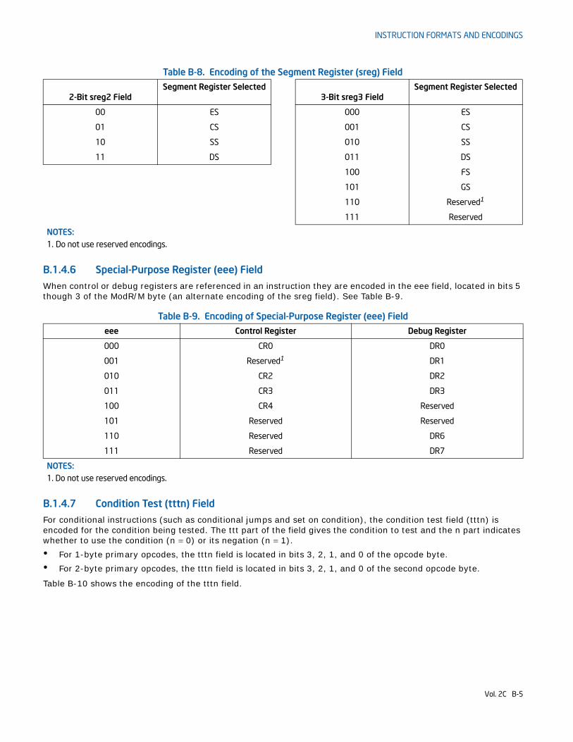
INSTRUCTION FORMATS AND ENCODINGS
B.1.4.6 Special-Purpose Register (eee) Field When control or debug registers are referenced in an instruction they are encoded in the eee field, located in bits 5 though 3 of the ModR/M byte (an alternate encoding of the sreg field). See Table B-9.
B.1.4.7 Condition Test (tttn) Field For conditional instructions (such as conditional jumps and set on condition), the condition test field (tttn) is encoded for the condition being tested. The ttt part of the field gives the condition to test and the n part indicates whether to use the condition (n = 0) or its negation (n = 1).• For 1-byte primary opcodes, the tttn field is located in bits 3, 2, 1, and 0 of the opcode byte. • For 2-byte primary opcodes, the tttn field is located in bits 3, 2, 1, and 0 of the second opcode byte.
Table B-10 shows the encoding of the tttn field.
Table B-8. Encoding of the Segment Register (sreg) Field
2-Bit sreg2 FieldSegment Register Selected
3-Bit sreg3 FieldSegment Register Selected
00 ES 000 ES
01 CS 001 CS
10 SS 010 SS
11 DS 011 DS
100 FS
101 GS
110 Reserved1
111 Reserved
NOTES:1. Do not use reserved encodings.
Table B-9. Encoding of Special-Purpose Register (eee) Field
eee Control Register Debug Register
000 CR0 DR0
001 Reserved1 DR1
010 CR2 DR2
011 CR3 DR3
100 CR4 Reserved
101 Reserved Reserved
110 Reserved DR6
111 Reserved DR7
NOTES:1. Do not use reserved encodings.
Vol. 2C B-5
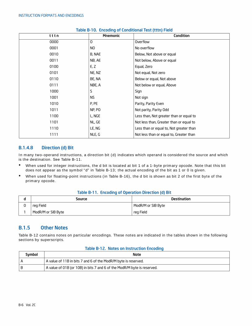
INSTRUCTION FORMATS AND ENCODINGS
B.1.4.8 Direction (d) Bit In many two-operand instructions, a direction bit (d) indicates which operand is considered the source and which is the destination. See Table B-11. • When used for integer instructions, the d bit is located at bit 1 of a 1-byte primary opcode. Note that this bit
does not appear as the symbol “d” in Table B-13; the actual encoding of the bit as 1 or 0 is given. • When used for floating-point instructions (in Table B-16), the d bit is shown as bit 2 of the first byte of the
primary opcode.
B.1.5 Other NotesTable B-12 contains notes on particular encodings. These notes are indicated in the tables shown in the following sections by superscripts.
Table B-10. Encoding of Conditional Test (tttn) Fieldt t t n Mnemonic Condition
0000 O Overflow
0001 NO No overflow
0010 B, NAE Below, Not above or equal
0011 NB, AE Not below, Above or equal
0100 E, Z Equal, Zero
0101 NE, NZ Not equal, Not zero
0110 BE, NA Below or equal, Not above
0111 NBE, A Not below or equal, Above
1000 S Sign
1001 NS Not sign
1010 P, PE Parity, Parity Even
1011 NP, PO Not parity, Parity Odd
1100 L, NGE Less than, Not greater than or equal to
1101 NL, GE Not less than, Greater than or equal to
1110 LE, NG Less than or equal to, Not greater than
1111 NLE, G Not less than or equal to, Greater than
Table B-11. Encoding of Operation Direction (d) Bit
d Source Destination
0 reg Field ModR/M or SIB Byte
1 ModR/M or SIB Byte reg Field
Table B-12. Notes on Instruction EncodingSymbol Note
A A value of 11B in bits 7 and 6 of the ModR/M byte is reserved.
B A value of 01B (or 10B) in bits 7 and 6 of the ModR/M byte is reserved.
B-6 Vol. 2C
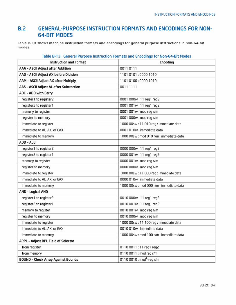
INSTRUCTION FORMATS AND ENCODINGS
B.2 GENERAL-PURPOSE INSTRUCTION FORMATS AND ENCODINGS FOR NON-64-BIT MODES
Table B-13 shows machine instruction formats and encodings for general purpose instructions in non-64-bit modes.
Table B-13. General Purpose Instruction Formats and Encodings for Non-64-Bit Modes
Instruction and Format Encoding
AAA – ASCII Adjust after Addition 0011 0111
AAD – ASCII Adjust AX before Division 1101 0101 : 0000 1010
AAM – ASCII Adjust AX after Multiply 1101 0100 : 0000 1010
AAS – ASCII Adjust AL after Subtraction 0011 1111
ADC – ADD with Carry
register1 to register2 0001 000w : 11 reg1 reg2
register2 to register1 0001 001w : 11 reg1 reg2
memory to register 0001 001w : mod reg r/m
register to memory 0001 000w : mod reg r/m
immediate to register 1000 00sw : 11 010 reg : immediate data
immediate to AL, AX, or EAX 0001 010w : immediate data
immediate to memory 1000 00sw : mod 010 r/m : immediate data
ADD – Add
register1 to register2 0000 000w : 11 reg1 reg2
register2 to register1 0000 001w : 11 reg1 reg2
memory to register 0000 001w : mod reg r/m
register to memory 0000 000w : mod reg r/m
immediate to register 1000 00sw : 11 000 reg : immediate data
immediate to AL, AX, or EAX 0000 010w : immediate data
immediate to memory 1000 00sw : mod 000 r/m : immediate data
AND – Logical AND
register1 to register2 0010 000w : 11 reg1 reg2
register2 to register1 0010 001w : 11 reg1 reg2
memory to register 0010 001w : mod reg r/m
register to memory 0010 000w : mod reg r/m
immediate to register 1000 00sw : 11 100 reg : immediate data
immediate to AL, AX, or EAX 0010 010w : immediate data
immediate to memory 1000 00sw : mod 100 r/m : immediate data
ARPL – Adjust RPL Field of Selector
from register 0110 0011 : 11 reg1 reg2
from memory 0110 0011 : mod reg r/m
BOUND – Check Array Against Bounds 0110 0010 : modA reg r/m
Vol. 2C B-7
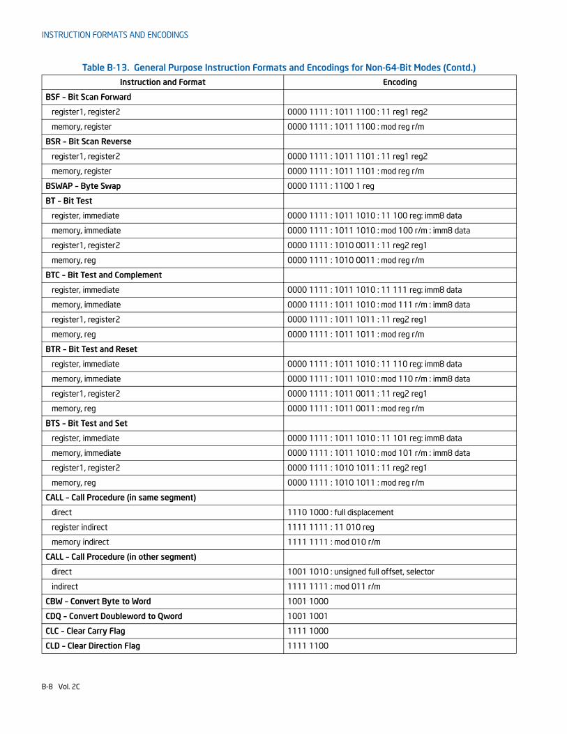
INSTRUCTION FORMATS AND ENCODINGS
BSF – Bit Scan Forward
register1, register2 0000 1111 : 1011 1100 : 11 reg1 reg2
memory, register 0000 1111 : 1011 1100 : mod reg r/m
BSR – Bit Scan Reverse
register1, register2 0000 1111 : 1011 1101 : 11 reg1 reg2
memory, register 0000 1111 : 1011 1101 : mod reg r/m
BSWAP – Byte Swap 0000 1111 : 1100 1 reg
BT – Bit Test
register, immediate 0000 1111 : 1011 1010 : 11 100 reg: imm8 data
memory, immediate 0000 1111 : 1011 1010 : mod 100 r/m : imm8 data
register1, register2 0000 1111 : 1010 0011 : 11 reg2 reg1
memory, reg 0000 1111 : 1010 0011 : mod reg r/m
BTC – Bit Test and Complement
register, immediate 0000 1111 : 1011 1010 : 11 111 reg: imm8 data
memory, immediate 0000 1111 : 1011 1010 : mod 111 r/m : imm8 data
register1, register2 0000 1111 : 1011 1011 : 11 reg2 reg1
memory, reg 0000 1111 : 1011 1011 : mod reg r/m
BTR – Bit Test and Reset
register, immediate 0000 1111 : 1011 1010 : 11 110 reg: imm8 data
memory, immediate 0000 1111 : 1011 1010 : mod 110 r/m : imm8 data
register1, register2 0000 1111 : 1011 0011 : 11 reg2 reg1
memory, reg 0000 1111 : 1011 0011 : mod reg r/m
BTS – Bit Test and Set
register, immediate 0000 1111 : 1011 1010 : 11 101 reg: imm8 data
memory, immediate 0000 1111 : 1011 1010 : mod 101 r/m : imm8 data
register1, register2 0000 1111 : 1010 1011 : 11 reg2 reg1
memory, reg 0000 1111 : 1010 1011 : mod reg r/m
CALL – Call Procedure (in same segment)
direct 1110 1000 : full displacement
register indirect 1111 1111 : 11 010 reg
memory indirect 1111 1111 : mod 010 r/m
CALL – Call Procedure (in other segment)
direct 1001 1010 : unsigned full offset, selector
indirect 1111 1111 : mod 011 r/m
CBW – Convert Byte to Word 1001 1000
CDQ – Convert Doubleword to Qword 1001 1001
CLC – Clear Carry Flag 1111 1000
CLD – Clear Direction Flag 1111 1100
Table B-13. General Purpose Instruction Formats and Encodings for Non-64-Bit Modes (Contd.)
Instruction and Format Encoding
B-8 Vol. 2C
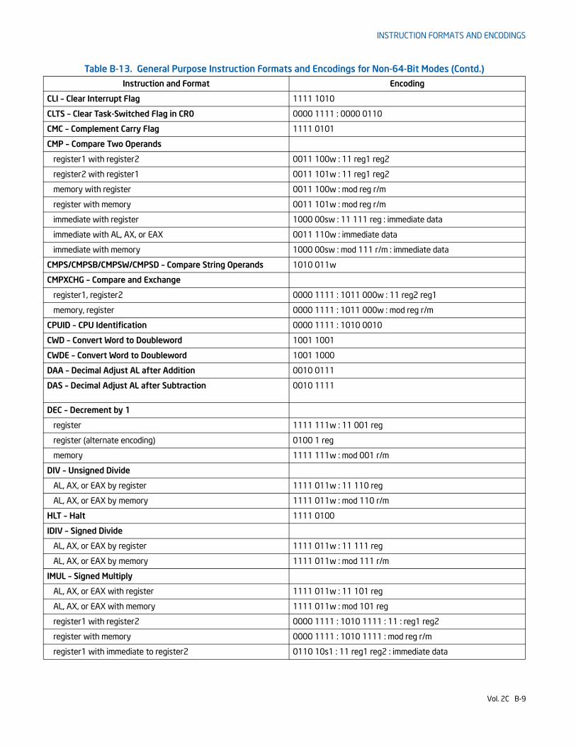
INSTRUCTION FORMATS AND ENCODINGS
CLI – Clear Interrupt Flag 1111 1010
CLTS – Clear Task-Switched Flag in CR0 0000 1111 : 0000 0110
CMC – Complement Carry Flag 1111 0101
CMP – Compare Two Operands
register1 with register2 0011 100w : 11 reg1 reg2
register2 with register1 0011 101w : 11 reg1 reg2
memory with register 0011 100w : mod reg r/m
register with memory 0011 101w : mod reg r/m
immediate with register 1000 00sw : 11 111 reg : immediate data
immediate with AL, AX, or EAX 0011 110w : immediate data
immediate with memory 1000 00sw : mod 111 r/m : immediate data
CMPS/CMPSB/CMPSW/CMPSD – Compare String Operands 1010 011w
CMPXCHG – Compare and Exchange
register1, register2 0000 1111 : 1011 000w : 11 reg2 reg1
memory, register 0000 1111 : 1011 000w : mod reg r/m
CPUID – CPU Identification 0000 1111 : 1010 0010
CWD – Convert Word to Doubleword 1001 1001
CWDE – Convert Word to Doubleword 1001 1000
DAA – Decimal Adjust AL after Addition 0010 0111
DAS – Decimal Adjust AL after Subtraction 0010 1111
DEC – Decrement by 1
register 1111 111w : 11 001 reg
register (alternate encoding) 0100 1 reg
memory 1111 111w : mod 001 r/m
DIV – Unsigned Divide
AL, AX, or EAX by register 1111 011w : 11 110 reg
AL, AX, or EAX by memory 1111 011w : mod 110 r/m
HLT – Halt 1111 0100
IDIV – Signed Divide
AL, AX, or EAX by register 1111 011w : 11 111 reg
AL, AX, or EAX by memory 1111 011w : mod 111 r/m
IMUL – Signed Multiply
AL, AX, or EAX with register 1111 011w : 11 101 reg
AL, AX, or EAX with memory 1111 011w : mod 101 reg
register1 with register2 0000 1111 : 1010 1111 : 11 : reg1 reg2
register with memory 0000 1111 : 1010 1111 : mod reg r/m
register1 with immediate to register2 0110 10s1 : 11 reg1 reg2 : immediate data
Table B-13. General Purpose Instruction Formats and Encodings for Non-64-Bit Modes (Contd.)
Instruction and Format Encoding
Vol. 2C B-9
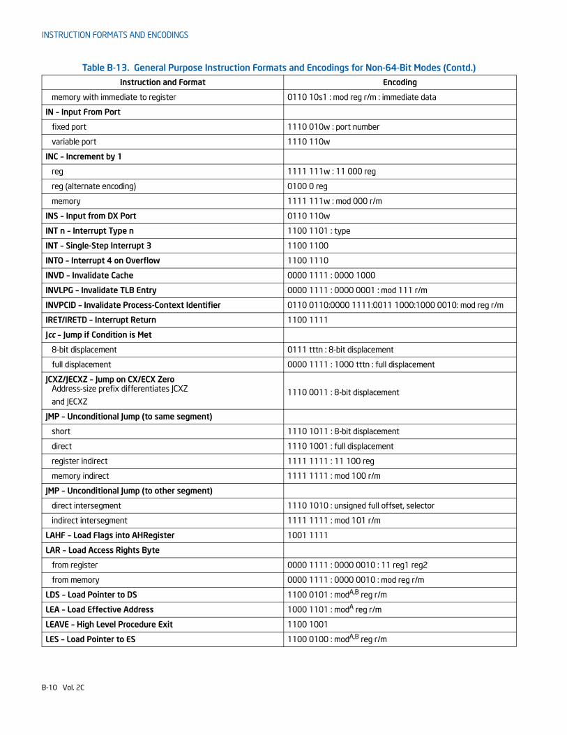
INSTRUCTION FORMATS AND ENCODINGS
memory with immediate to register 0110 10s1 : mod reg r/m : immediate data
IN – Input From Port
fixed port 1110 010w : port number
variable port 1110 110w
INC – Increment by 1
reg 1111 111w : 11 000 reg
reg (alternate encoding) 0100 0 reg
memory 1111 111w : mod 000 r/m
INS – Input from DX Port 0110 110w
INT n – Interrupt Type n 1100 1101 : type
INT – Single-Step Interrupt 3 1100 1100
INTO – Interrupt 4 on Overflow 1100 1110
INVD – Invalidate Cache 0000 1111 : 0000 1000
INVLPG – Invalidate TLB Entry 0000 1111 : 0000 0001 : mod 111 r/m
INVPCID – Invalidate Process-Context Identifier 0110 0110:0000 1111:0011 1000:1000 0010: mod reg r/m
IRET/IRETD – Interrupt Return 1100 1111
Jcc – Jump if Condition is Met
8-bit displacement 0111 tttn : 8-bit displacement
full displacement 0000 1111 : 1000 tttn : full displacement
JCXZ/JECXZ – Jump on CX/ECX Zero Address-size prefix differentiates JCXZ
and JECXZ1110 0011 : 8-bit displacement
JMP – Unconditional Jump (to same segment)
short 1110 1011 : 8-bit displacement
direct 1110 1001 : full displacement
register indirect 1111 1111 : 11 100 reg
memory indirect 1111 1111 : mod 100 r/m
JMP – Unconditional Jump (to other segment)
direct intersegment 1110 1010 : unsigned full offset, selector
indirect intersegment 1111 1111 : mod 101 r/m
LAHF – Load Flags into AHRegister 1001 1111
LAR – Load Access Rights Byte
from register 0000 1111 : 0000 0010 : 11 reg1 reg2
from memory 0000 1111 : 0000 0010 : mod reg r/m
LDS – Load Pointer to DS 1100 0101 : modA,B reg r/m
LEA – Load Effective Address 1000 1101 : modA reg r/m
LEAVE – High Level Procedure Exit 1100 1001
LES – Load Pointer to ES 1100 0100 : modA,B reg r/m
Table B-13. General Purpose Instruction Formats and Encodings for Non-64-Bit Modes (Contd.)
Instruction and Format Encoding
B-10 Vol. 2C
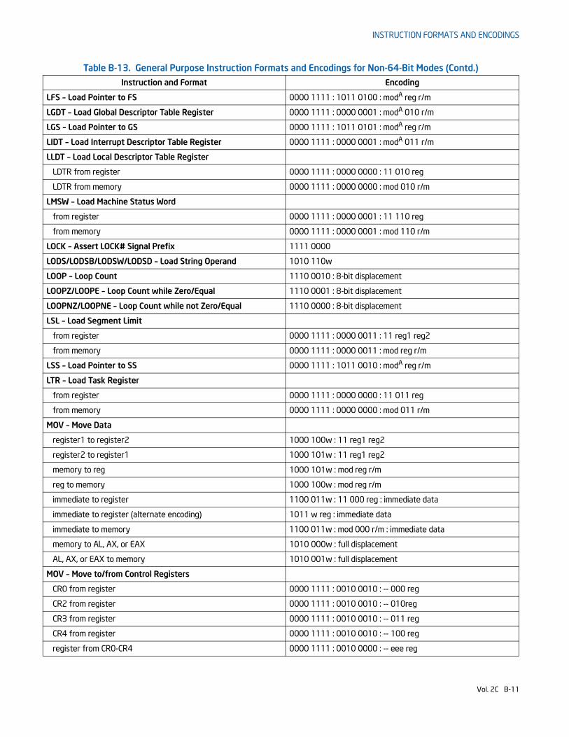
INSTRUCTION FORMATS AND ENCODINGS
LFS – Load Pointer to FS 0000 1111 : 1011 0100 : modA reg r/m
LGDT – Load Global Descriptor Table Register 0000 1111 : 0000 0001 : modA 010 r/m
LGS – Load Pointer to GS 0000 1111 : 1011 0101 : modA reg r/m
LIDT – Load Interrupt Descriptor Table Register 0000 1111 : 0000 0001 : modA 011 r/m
LLDT – Load Local Descriptor Table Register
LDTR from register 0000 1111 : 0000 0000 : 11 010 reg
LDTR from memory 0000 1111 : 0000 0000 : mod 010 r/m
LMSW – Load Machine Status Word
from register 0000 1111 : 0000 0001 : 11 110 reg
from memory 0000 1111 : 0000 0001 : mod 110 r/m
LOCK – Assert LOCK# Signal Prefix 1111 0000
LODS/LODSB/LODSW/LODSD – Load String Operand 1010 110w
LOOP – Loop Count 1110 0010 : 8-bit displacement
LOOPZ/LOOPE – Loop Count while Zero/Equal 1110 0001 : 8-bit displacement
LOOPNZ/LOOPNE – Loop Count while not Zero/Equal 1110 0000 : 8-bit displacement
LSL – Load Segment Limit
from register 0000 1111 : 0000 0011 : 11 reg1 reg2
from memory 0000 1111 : 0000 0011 : mod reg r/m
LSS – Load Pointer to SS 0000 1111 : 1011 0010 : modA reg r/m
LTR – Load Task Register
from register 0000 1111 : 0000 0000 : 11 011 reg
from memory 0000 1111 : 0000 0000 : mod 011 r/m
MOV – Move Data
register1 to register2 1000 100w : 11 reg1 reg2
register2 to register1 1000 101w : 11 reg1 reg2
memory to reg 1000 101w : mod reg r/m
reg to memory 1000 100w : mod reg r/m
immediate to register 1100 011w : 11 000 reg : immediate data
immediate to register (alternate encoding) 1011 w reg : immediate data
immediate to memory 1100 011w : mod 000 r/m : immediate data
memory to AL, AX, or EAX 1010 000w : full displacement
AL, AX, or EAX to memory 1010 001w : full displacement
MOV – Move to/from Control Registers
CR0 from register 0000 1111 : 0010 0010 : -- 000 reg
CR2 from register 0000 1111 : 0010 0010 : -- 010reg
CR3 from register 0000 1111 : 0010 0010 : -- 011 reg
CR4 from register 0000 1111 : 0010 0010 : -- 100 reg
register from CR0-CR4 0000 1111 : 0010 0000 : -- eee reg
Table B-13. General Purpose Instruction Formats and Encodings for Non-64-Bit Modes (Contd.)
Instruction and Format Encoding
Vol. 2C B-11

INSTRUCTION FORMATS AND ENCODINGS
MOV – Move to/from Debug Registers
DR0-DR3 from register 0000 1111 : 0010 0011 : -- eee reg
DR4-DR5 from register 0000 1111 : 0010 0011 : -- eee reg
DR6-DR7 from register 0000 1111 : 0010 0011 : -- eee reg
register from DR6-DR7 0000 1111 : 0010 0001 : -- eee reg
register from DR4-DR5 0000 1111 : 0010 0001 : -- eee reg
register from DR0-DR3 0000 1111 : 0010 0001 : -- eee reg
MOV – Move to/from Segment Registers
register to segment register 1000 1110 : 11 sreg3 reg
register to SS 1000 1110 : 11 sreg3 reg
memory to segment reg 1000 1110 : mod sreg3 r/m
memory to SS 1000 1110 : mod sreg3 r/m
segment register to register 1000 1100 : 11 sreg3 reg
segment register to memory 1000 1100 : mod sreg3 r/m
MOVBE – Move data after swapping bytes
memory to register 0000 1111 : 0011 1000:1111 0000 : mod reg r/m
register to memory 0000 1111 : 0011 1000:1111 0001 : mod reg r/m
MOVS/MOVSB/MOVSW/MOVSD – Move Data from String to String
1010 010w
MOVSX – Move with Sign-Extend
memory to reg 0000 1111 : 1011 111w : mod reg r/m
MOVZX – Move with Zero-Extend
register2 to register1 0000 1111 : 1011 011w : 11 reg1 reg2
memory to register 0000 1111 : 1011 011w : mod reg r/m
MUL – Unsigned Multiply
AL, AX, or EAX with register 1111 011w : 11 100 reg
AL, AX, or EAX with memory 1111 011w : mod 100 r/m
NEG – Two's Complement Negation
register 1111 011w : 11 011 reg
memory 1111 011w : mod 011 r/m
NOP – No Operation 1001 0000
NOP – Multi-byte No Operation1
register 0000 1111 0001 1111 : 11 000 reg
memory 0000 1111 0001 1111 : mod 000 r/m
NOT – One's Complement Negation
register 1111 011w : 11 010 reg
memory 1111 011w : mod 010 r/m
Table B-13. General Purpose Instruction Formats and Encodings for Non-64-Bit Modes (Contd.)
Instruction and Format Encoding
B-12 Vol. 2C
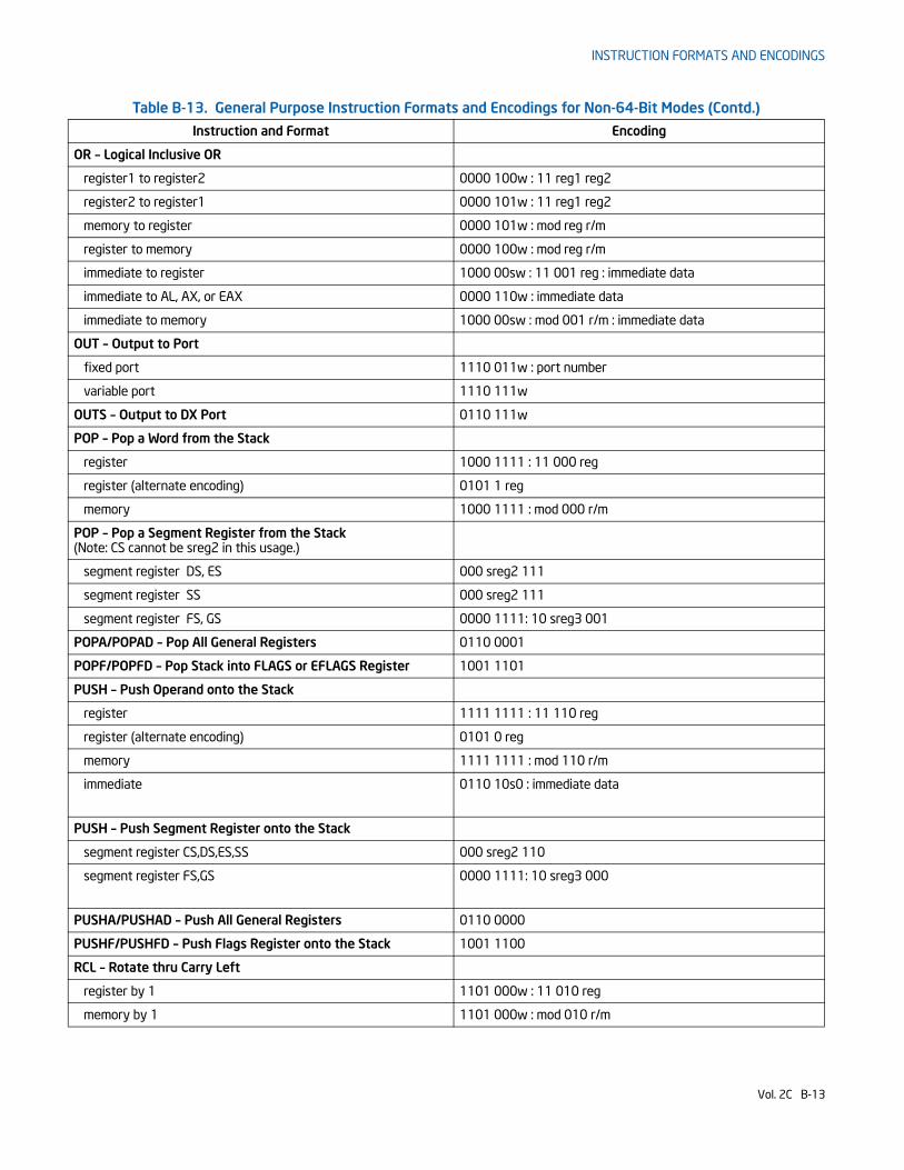
INSTRUCTION FORMATS AND ENCODINGS
OR – Logical Inclusive OR
register1 to register2 0000 100w : 11 reg1 reg2
register2 to register1 0000 101w : 11 reg1 reg2
memory to register 0000 101w : mod reg r/m
register to memory 0000 100w : mod reg r/m
immediate to register 1000 00sw : 11 001 reg : immediate data
immediate to AL, AX, or EAX 0000 110w : immediate data
immediate to memory 1000 00sw : mod 001 r/m : immediate data
OUT – Output to Port
fixed port 1110 011w : port number
variable port 1110 111w
OUTS – Output to DX Port 0110 111w
POP – Pop a Word from the Stack
register 1000 1111 : 11 000 reg
register (alternate encoding) 0101 1 reg
memory 1000 1111 : mod 000 r/m
POP – Pop a Segment Register from the Stack(Note: CS cannot be sreg2 in this usage.)
segment register DS, ES 000 sreg2 111
segment register SS 000 sreg2 111
segment register FS, GS 0000 1111: 10 sreg3 001
POPA/POPAD – Pop All General Registers 0110 0001
POPF/POPFD – Pop Stack into FLAGS or EFLAGS Register 1001 1101
PUSH – Push Operand onto the Stack
register 1111 1111 : 11 110 reg
register (alternate encoding) 0101 0 reg
memory 1111 1111 : mod 110 r/m
immediate 0110 10s0 : immediate data
PUSH – Push Segment Register onto the Stack
segment register CS,DS,ES,SS 000 sreg2 110
segment register FS,GS 0000 1111: 10 sreg3 000
PUSHA/PUSHAD – Push All General Registers 0110 0000
PUSHF/PUSHFD – Push Flags Register onto the Stack 1001 1100
RCL – Rotate thru Carry Left
register by 1 1101 000w : 11 010 reg
memory by 1 1101 000w : mod 010 r/m
Table B-13. General Purpose Instruction Formats and Encodings for Non-64-Bit Modes (Contd.)
Instruction and Format Encoding
Vol. 2C B-13

INSTRUCTION FORMATS AND ENCODINGS
register by CL 1101 001w : 11 010 reg
memory by CL 1101 001w : mod 010 r/m
register by immediate count 1100 000w : 11 010 reg : imm8 data
memory by immediate count 1100 000w : mod 010 r/m : imm8 data
RCR – Rotate thru Carry Right
register by 1 1101 000w : 11 011 reg
memory by 1 1101 000w : mod 011 r/m
register by CL 1101 001w : 11 011 reg
memory by CL 1101 001w : mod 011 r/m
register by immediate count 1100 000w : 11 011 reg : imm8 data
memory by immediate count 1100 000w : mod 011 r/m : imm8 data
RDMSR – Read from Model-Specific Register 0000 1111 : 0011 0010
RDPMC – Read Performance Monitoring Counters 0000 1111 : 0011 0011
RDTSC – Read Time-Stamp Counter 0000 1111 : 0011 0001
RDTSCP – Read Time-Stamp Counter and Processor ID 0000 1111 : 0000 0001: 1111 1001
REP INS – Input String 1111 0011 : 0110 110w
REP LODS – Load String 1111 0011 : 1010 110w
REP MOVS – Move String 1111 0011 : 1010 010w
REP OUTS – Output String 1111 0011 : 0110 111w
REP STOS – Store String 1111 0011 : 1010 101w
REPE CMPS – Compare String 1111 0011 : 1010 011w
REPE SCAS – Scan String 1111 0011 : 1010 111w
REPNE CMPS – Compare String 1111 0010 : 1010 011w
REPNE SCAS – Scan String 1111 0010 : 1010 111w
RET – Return from Procedure (to same segment)
no argument 1100 0011
adding immediate to SP 1100 0010 : 16-bit displacement
RET – Return from Procedure (to other segment)
intersegment 1100 1011
adding immediate to SP 1100 1010 : 16-bit displacement
ROL – Rotate Left
register by 1 1101 000w : 11 000 reg
memory by 1 1101 000w : mod 000 r/m
register by CL 1101 001w : 11 000 reg
memory by CL 1101 001w : mod 000 r/m
register by immediate count 1100 000w : 11 000 reg : imm8 data
memory by immediate count 1100 000w : mod 000 r/m : imm8 data
Table B-13. General Purpose Instruction Formats and Encodings for Non-64-Bit Modes (Contd.)
Instruction and Format Encoding
B-14 Vol. 2C
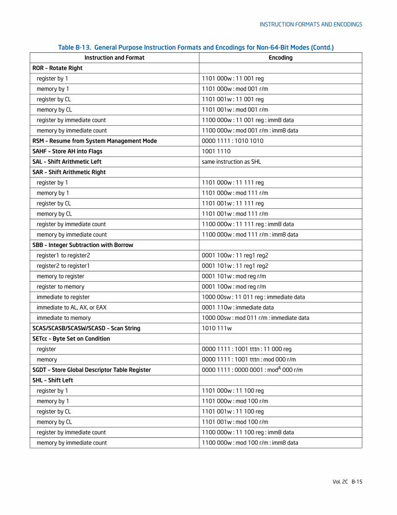
INSTRUCTION FORMATS AND ENCODINGS
ROR – Rotate Right
register by 1 1101 000w : 11 001 reg
memory by 1 1101 000w : mod 001 r/m
register by CL 1101 001w : 11 001 reg
memory by CL 1101 001w : mod 001 r/m
register by immediate count 1100 000w : 11 001 reg : imm8 data
memory by immediate count 1100 000w : mod 001 r/m : imm8 data
RSM – Resume from System Management Mode 0000 1111 : 1010 1010
SAHF – Store AH into Flags 1001 1110
SAL – Shift Arithmetic Left same instruction as SHL
SAR – Shift Arithmetic Right
register by 1 1101 000w : 11 111 reg
memory by 1 1101 000w : mod 111 r/m
register by CL 1101 001w : 11 111 reg
memory by CL 1101 001w : mod 111 r/m
register by immediate count 1100 000w : 11 111 reg : imm8 data
memory by immediate count 1100 000w : mod 111 r/m : imm8 data
SBB – Integer Subtraction with Borrow
register1 to register2 0001 100w : 11 reg1 reg2
register2 to register1 0001 101w : 11 reg1 reg2
memory to register 0001 101w : mod reg r/m
register to memory 0001 100w : mod reg r/m
immediate to register 1000 00sw : 11 011 reg : immediate data
immediate to AL, AX, or EAX 0001 110w : immediate data
immediate to memory 1000 00sw : mod 011 r/m : immediate data
SCAS/SCASB/SCASW/SCASD – Scan String 1010 111w
SETcc – Byte Set on Condition
register 0000 1111 : 1001 tttn : 11 000 reg
memory 0000 1111 : 1001 tttn : mod 000 r/m
SGDT – Store Global Descriptor Table Register 0000 1111 : 0000 0001 : modA 000 r/m
SHL – Shift Left
register by 1 1101 000w : 11 100 reg
memory by 1 1101 000w : mod 100 r/m
register by CL 1101 001w : 11 100 reg
memory by CL 1101 001w : mod 100 r/m
register by immediate count 1100 000w : 11 100 reg : imm8 data
memory by immediate count 1100 000w : mod 100 r/m : imm8 data
Table B-13. General Purpose Instruction Formats and Encodings for Non-64-Bit Modes (Contd.)
Instruction and Format Encoding
Vol. 2C B-15
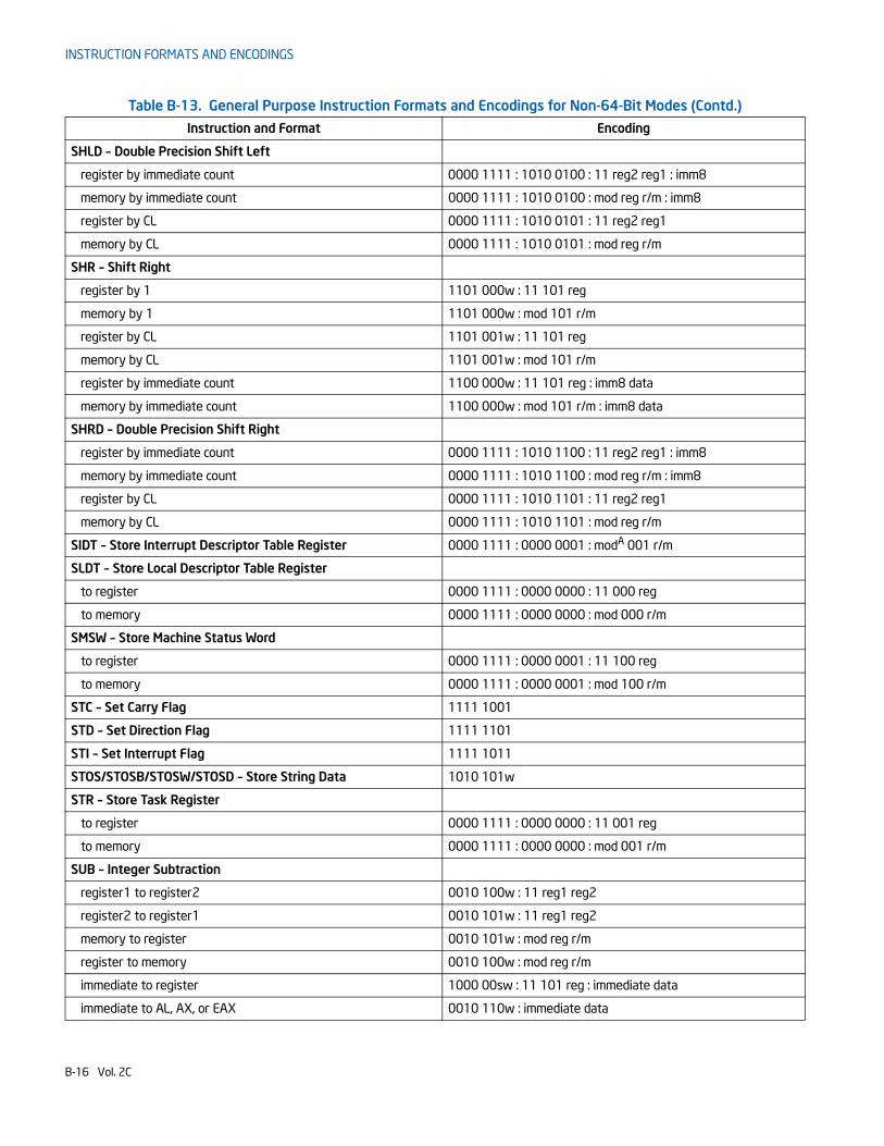
INSTRUCTION FORMATS AND ENCODINGS
SHLD – Double Precision Shift Left
register by immediate count 0000 1111 : 1010 0100 : 11 reg2 reg1 : imm8
memory by immediate count 0000 1111 : 1010 0100 : mod reg r/m : imm8
register by CL 0000 1111 : 1010 0101 : 11 reg2 reg1
memory by CL 0000 1111 : 1010 0101 : mod reg r/m
SHR – Shift Right
register by 1 1101 000w : 11 101 reg
memory by 1 1101 000w : mod 101 r/m
register by CL 1101 001w : 11 101 reg
memory by CL 1101 001w : mod 101 r/m
register by immediate count 1100 000w : 11 101 reg : imm8 data
memory by immediate count 1100 000w : mod 101 r/m : imm8 data
SHRD – Double Precision Shift Right
register by immediate count 0000 1111 : 1010 1100 : 11 reg2 reg1 : imm8
memory by immediate count 0000 1111 : 1010 1100 : mod reg r/m : imm8
register by CL 0000 1111 : 1010 1101 : 11 reg2 reg1
memory by CL 0000 1111 : 1010 1101 : mod reg r/m
SIDT – Store Interrupt Descriptor Table Register 0000 1111 : 0000 0001 : modA 001 r/m
SLDT – Store Local Descriptor Table Register
to register 0000 1111 : 0000 0000 : 11 000 reg
to memory 0000 1111 : 0000 0000 : mod 000 r/m
SMSW – Store Machine Status Word
to register 0000 1111 : 0000 0001 : 11 100 reg
to memory 0000 1111 : 0000 0001 : mod 100 r/m
STC – Set Carry Flag 1111 1001
STD – Set Direction Flag 1111 1101
STI – Set Interrupt Flag 1111 1011
STOS/STOSB/STOSW/STOSD – Store String Data 1010 101w
STR – Store Task Register
to register 0000 1111 : 0000 0000 : 11 001 reg
to memory 0000 1111 : 0000 0000 : mod 001 r/m
SUB – Integer Subtraction
register1 to register2 0010 100w : 11 reg1 reg2
register2 to register1 0010 101w : 11 reg1 reg2
memory to register 0010 101w : mod reg r/m
register to memory 0010 100w : mod reg r/m
immediate to register 1000 00sw : 11 101 reg : immediate data
immediate to AL, AX, or EAX 0010 110w : immediate data
Table B-13. General Purpose Instruction Formats and Encodings for Non-64-Bit Modes (Contd.)
Instruction and Format Encoding
B-16 Vol. 2C
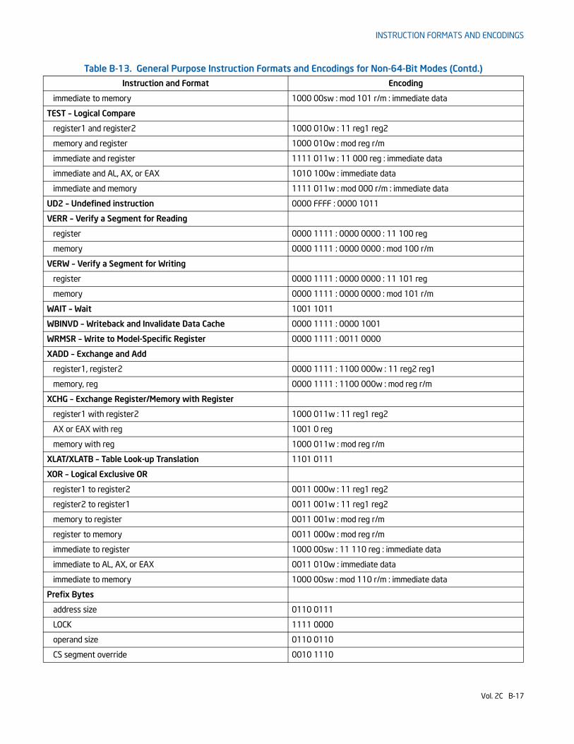
INSTRUCTION FORMATS AND ENCODINGS
immediate to memory 1000 00sw : mod 101 r/m : immediate data
TEST – Logical Compare
register1 and register2 1000 010w : 11 reg1 reg2
memory and register 1000 010w : mod reg r/m
immediate and register 1111 011w : 11 000 reg : immediate data
immediate and AL, AX, or EAX 1010 100w : immediate data
immediate and memory 1111 011w : mod 000 r/m : immediate data
UD2 – Undefined instruction 0000 FFFF : 0000 1011
VERR – Verify a Segment for Reading
register 0000 1111 : 0000 0000 : 11 100 reg
memory 0000 1111 : 0000 0000 : mod 100 r/m
VERW – Verify a Segment for Writing
register 0000 1111 : 0000 0000 : 11 101 reg
memory 0000 1111 : 0000 0000 : mod 101 r/m
WAIT – Wait 1001 1011
WBINVD – Writeback and Invalidate Data Cache 0000 1111 : 0000 1001
WRMSR – Write to Model-Specific Register 0000 1111 : 0011 0000
XADD – Exchange and Add
register1, register2 0000 1111 : 1100 000w : 11 reg2 reg1
memory, reg 0000 1111 : 1100 000w : mod reg r/m
XCHG – Exchange Register/Memory with Register
register1 with register2 1000 011w : 11 reg1 reg2
AX or EAX with reg 1001 0 reg
memory with reg 1000 011w : mod reg r/m
XLAT/XLATB – Table Look-up Translation 1101 0111
XOR – Logical Exclusive OR
register1 to register2 0011 000w : 11 reg1 reg2
register2 to register1 0011 001w : 11 reg1 reg2
memory to register 0011 001w : mod reg r/m
register to memory 0011 000w : mod reg r/m
immediate to register 1000 00sw : 11 110 reg : immediate data
immediate to AL, AX, or EAX 0011 010w : immediate data
immediate to memory 1000 00sw : mod 110 r/m : immediate data
Prefix Bytes
address size 0110 0111
LOCK 1111 0000
operand size 0110 0110
CS segment override 0010 1110
Table B-13. General Purpose Instruction Formats and Encodings for Non-64-Bit Modes (Contd.)
Instruction and Format Encoding
Vol. 2C B-17
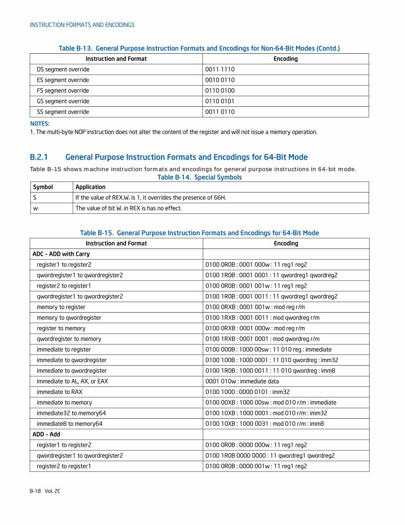
INSTRUCTION FORMATS AND ENCODINGS
B.2.1 General Purpose Instruction Formats and Encodings for 64-Bit ModeTable B-15 shows machine instruction formats and encodings for general purpose instructions in 64-bit mode.
DS segment override 0011 1110
ES segment override 0010 0110
FS segment override 0110 0100
GS segment override 0110 0101
SS segment override 0011 0110
NOTES:1. The multi-byte NOP instruction does not alter the content of the register and will not issue a memory operation.
Table B-14. Special SymbolsSymbol Application
S If the value of REX.W. is 1, it overrides the presence of 66H.
w The value of bit W. in REX is has no effect.
Table B-15. General Purpose Instruction Formats and Encodings for 64-Bit Mode
Instruction and Format Encoding
ADC – ADD with Carry
register1 to register2 0100 0R0B : 0001 000w : 11 reg1 reg2
qwordregister1 to qwordregister2 0100 1R0B : 0001 0001 : 11 qwordreg1 qwordreg2
register2 to register1 0100 0R0B : 0001 001w : 11 reg1 reg2
qwordregister1 to qwordregister2 0100 1R0B : 0001 0011 : 11 qwordreg1 qwordreg2
memory to register 0100 0RXB : 0001 001w : mod reg r/m
memory to qwordregister 0100 1RXB : 0001 0011 : mod qwordreg r/m
register to memory 0100 0RXB : 0001 000w : mod reg r/m
qwordregister to memory 0100 1RXB : 0001 0001 : mod qwordreg r/m
immediate to register 0100 000B : 1000 00sw : 11 010 reg : immediate
immediate to qwordregister 0100 100B : 1000 0001 : 11 010 qwordreg : imm32
immediate to qwordregister 0100 1R0B : 1000 0011 : 11 010 qwordreg : imm8
immediate to AL, AX, or EAX 0001 010w : immediate data
immediate to RAX 0100 1000 : 0000 0101 : imm32
immediate to memory 0100 00XB : 1000 00sw : mod 010 r/m : immediate
immediate32 to memory64 0100 10XB : 1000 0001 : mod 010 r/m : imm32
immediate8 to memory64 0100 10XB : 1000 0031 : mod 010 r/m : imm8
ADD – Add
register1 to register2 0100 0R0B : 0000 000w : 11 reg1 reg2
qwordregister1 to qwordregister2 0100 1R0B 0000 0000 : 11 qwordreg1 qwordreg2
register2 to register1 0100 0R0B : 0000 001w : 11 reg1 reg2
Table B-13. General Purpose Instruction Formats and Encodings for Non-64-Bit Modes (Contd.)
Instruction and Format Encoding
B-18 Vol. 2C
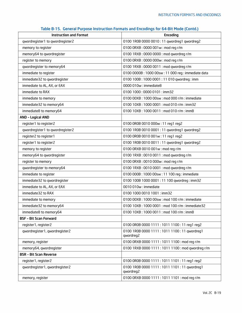
INSTRUCTION FORMATS AND ENCODINGS
qwordregister1 to qwordregister2 0100 1R0B 0000 0010 : 11 qwordreg1 qwordreg2
memory to register 0100 0RXB : 0000 001w : mod reg r/m
memory64 to qwordregister 0100 1RXB : 0000 0000 : mod qwordreg r/m
register to memory 0100 0RXB : 0000 000w : mod reg r/m
qwordregister to memory64 0100 1RXB : 0000 0011 : mod qwordreg r/m
immediate to register 0100 0000B : 1000 00sw : 11 000 reg : immediate data
immediate32 to qwordregister 0100 100B : 1000 0001 : 11 010 qwordreg : imm
immediate to AL, AX, or EAX 0000 010w : immediate8
immediate to RAX 0100 1000 : 0000 0101 : imm32
immediate to memory 0100 00XB : 1000 00sw : mod 000 r/m : immediate
immediate32 to memory64 0100 10XB : 1000 0001 : mod 010 r/m : imm32
immediate8 to memory64 0100 10XB : 1000 0011 : mod 010 r/m : imm8
AND – Logical AND
register1 to register2 0100 0R0B 0010 000w : 11 reg1 reg2
qwordregister1 to qwordregister2 0100 1R0B 0010 0001 : 11 qwordreg1 qwordreg2
register2 to register1 0100 0R0B 0010 001w : 11 reg1 reg2
register1 to register2 0100 1R0B 0010 0011 : 11 qwordreg1 qwordreg2
memory to register 0100 0RXB 0010 001w : mod reg r/m
memory64 to qwordregister 0100 1RXB : 0010 0011 : mod qwordreg r/m
register to memory 0100 0RXB : 0010 000w : mod reg r/m
qwordregister to memory64 0100 1RXB : 0010 0001 : mod qwordreg r/m
immediate to register 0100 000B : 1000 00sw : 11 100 reg : immediate
immediate32 to qwordregister 0100 100B 1000 0001 : 11 100 qwordreg : imm32
immediate to AL, AX, or EAX 0010 010w : immediate
immediate32 to RAX 0100 1000 0010 1001 : imm32
immediate to memory 0100 00XB : 1000 00sw : mod 100 r/m : immediate
immediate32 to memory64 0100 10XB : 1000 0001 : mod 100 r/m : immediate32
immediate8 to memory64 0100 10XB : 1000 0011 : mod 100 r/m : imm8
BSF – Bit Scan Forward
register1, register2 0100 0R0B 0000 1111 : 1011 1100 : 11 reg1 reg2
qwordregister1, qwordregister2 0100 1R0B 0000 1111 : 1011 1100 : 11 qwordreg1 qwordreg2
memory, register 0100 0RXB 0000 1111 : 1011 1100 : mod reg r/m
memory64, qwordregister 0100 1RXB 0000 1111 : 1011 1100 : mod qwordreg r/m
BSR – Bit Scan Reverse
register1, register2 0100 0R0B 0000 1111 : 1011 1101 : 11 reg1 reg2
qwordregister1, qwordregister2 0100 1R0B 0000 1111 : 1011 1101 : 11 qwordreg1 qwordreg2
memory, register 0100 0RXB 0000 1111 : 1011 1101 : mod reg r/m
Table B-15. General Purpose Instruction Formats and Encodings for 64-Bit Mode (Contd.)
Instruction and Format Encoding
Vol. 2C B-19
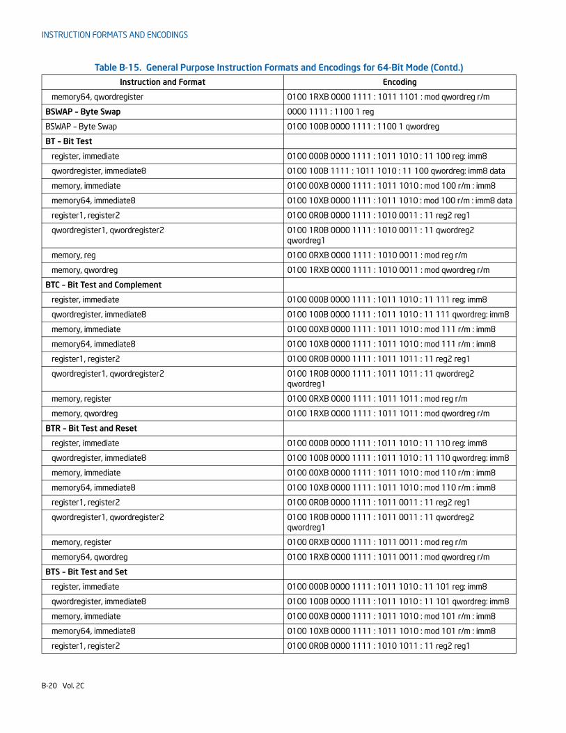
INSTRUCTION FORMATS AND ENCODINGS
memory64, qwordregister 0100 1RXB 0000 1111 : 1011 1101 : mod qwordreg r/m
BSWAP – Byte Swap 0000 1111 : 1100 1 reg
BSWAP – Byte Swap 0100 100B 0000 1111 : 1100 1 qwordreg
BT – Bit Test
register, immediate 0100 000B 0000 1111 : 1011 1010 : 11 100 reg: imm8
qwordregister, immediate8 0100 100B 1111 : 1011 1010 : 11 100 qwordreg: imm8 data
memory, immediate 0100 00XB 0000 1111 : 1011 1010 : mod 100 r/m : imm8
memory64, immediate8 0100 10XB 0000 1111 : 1011 1010 : mod 100 r/m : imm8 data
register1, register2 0100 0R0B 0000 1111 : 1010 0011 : 11 reg2 reg1
qwordregister1, qwordregister2 0100 1R0B 0000 1111 : 1010 0011 : 11 qwordreg2 qwordreg1
memory, reg 0100 0RXB 0000 1111 : 1010 0011 : mod reg r/m
memory, qwordreg 0100 1RXB 0000 1111 : 1010 0011 : mod qwordreg r/m
BTC – Bit Test and Complement
register, immediate 0100 000B 0000 1111 : 1011 1010 : 11 111 reg: imm8
qwordregister, immediate8 0100 100B 0000 1111 : 1011 1010 : 11 111 qwordreg: imm8
memory, immediate 0100 00XB 0000 1111 : 1011 1010 : mod 111 r/m : imm8
memory64, immediate8 0100 10XB 0000 1111 : 1011 1010 : mod 111 r/m : imm8
register1, register2 0100 0R0B 0000 1111 : 1011 1011 : 11 reg2 reg1
qwordregister1, qwordregister2 0100 1R0B 0000 1111 : 1011 1011 : 11 qwordreg2 qwordreg1
memory, register 0100 0RXB 0000 1111 : 1011 1011 : mod reg r/m
memory, qwordreg 0100 1RXB 0000 1111 : 1011 1011 : mod qwordreg r/m
BTR – Bit Test and Reset
register, immediate 0100 000B 0000 1111 : 1011 1010 : 11 110 reg: imm8
qwordregister, immediate8 0100 100B 0000 1111 : 1011 1010 : 11 110 qwordreg: imm8
memory, immediate 0100 00XB 0000 1111 : 1011 1010 : mod 110 r/m : imm8
memory64, immediate8 0100 10XB 0000 1111 : 1011 1010 : mod 110 r/m : imm8
register1, register2 0100 0R0B 0000 1111 : 1011 0011 : 11 reg2 reg1
qwordregister1, qwordregister2 0100 1R0B 0000 1111 : 1011 0011 : 11 qwordreg2 qwordreg1
memory, register 0100 0RXB 0000 1111 : 1011 0011 : mod reg r/m
memory64, qwordreg 0100 1RXB 0000 1111 : 1011 0011 : mod qwordreg r/m
BTS – Bit Test and Set
register, immediate 0100 000B 0000 1111 : 1011 1010 : 11 101 reg: imm8
qwordregister, immediate8 0100 100B 0000 1111 : 1011 1010 : 11 101 qwordreg: imm8
memory, immediate 0100 00XB 0000 1111 : 1011 1010 : mod 101 r/m : imm8
memory64, immediate8 0100 10XB 0000 1111 : 1011 1010 : mod 101 r/m : imm8
register1, register2 0100 0R0B 0000 1111 : 1010 1011 : 11 reg2 reg1
Table B-15. General Purpose Instruction Formats and Encodings for 64-Bit Mode (Contd.)
Instruction and Format Encoding
B-20 Vol. 2C
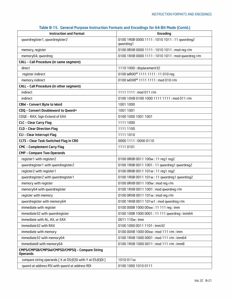
INSTRUCTION FORMATS AND ENCODINGS
qwordregister1, qwordregister2 0100 1R0B 0000 1111 : 1010 1011 : 11 qwordreg2 qwordreg1
memory, register 0100 0RXB 0000 1111 : 1010 1011 : mod reg r/m
memory64, qwordreg 0100 1RXB 0000 1111 : 1010 1011 : mod qwordreg r/m
CALL – Call Procedure (in same segment)
direct 1110 1000 : displacement32
register indirect 0100 WR00w 1111 1111 : 11 010 reg
memory indirect 0100 W0XBw 1111 1111 : mod 010 r/m
CALL – Call Procedure (in other segment)
indirect 1111 1111 : mod 011 r/m
indirect 0100 10XB 0100 1000 1111 1111 : mod 011 r/m
CBW – Convert Byte to Word 1001 1000
CDQ – Convert Doubleword to Qword+ 1001 1001
CDQE – RAX, Sign-Extend of EAX 0100 1000 1001 1001
CLC – Clear Carry Flag 1111 1000
CLD – Clear Direction Flag 1111 1100
CLI – Clear Interrupt Flag 1111 1010
CLTS – Clear Task-Switched Flag in CR0 0000 1111 : 0000 0110
CMC – Complement Carry Flag 1111 0101
CMP – Compare Two Operands
register1 with register2 0100 0R0B 0011 100w : 11 reg1 reg2
qwordregister1 with qwordregister2 0100 1R0B 0011 1001 : 11 qwordreg1 qwordreg2
register2 with register1 0100 0R0B 0011 101w : 11 reg1 reg2
qwordregister2 with qwordregister1 0100 1R0B 0011 101w : 11 qwordreg1 qwordreg2
memory with register 0100 0RXB 0011 100w : mod reg r/m
memory64 with qwordregister 0100 1RXB 0011 1001 : mod qwordreg r/m
register with memory 0100 0RXB 0011 101w : mod reg r/m
qwordregister with memory64 0100 1RXB 0011 101w1 : mod qwordreg r/m
immediate with register 0100 000B 1000 00sw : 11 111 reg : imm
immediate32 with qwordregister 0100 100B 1000 0001 : 11 111 qwordreg : imm64
immediate with AL, AX, or EAX 0011 110w : imm
immediate32 with RAX 0100 1000 0011 1101 : imm32
immediate with memory 0100 00XB 1000 00sw : mod 111 r/m : imm
immediate32 with memory64 0100 1RXB 1000 0001 : mod 111 r/m : imm64
immediate8 with memory64 0100 1RXB 1000 0011 : mod 111 r/m : imm8
CMPS/CMPSB/CMPSW/CMPSD/CMPSQ – Compare String Operands
compare string operands [ X at DS:(E)SI with Y at ES:(E)DI ] 1010 011w
qword at address RSI with qword at address RDI 0100 1000 1010 0111
Table B-15. General Purpose Instruction Formats and Encodings for 64-Bit Mode (Contd.)
Instruction and Format Encoding
Vol. 2C B-21
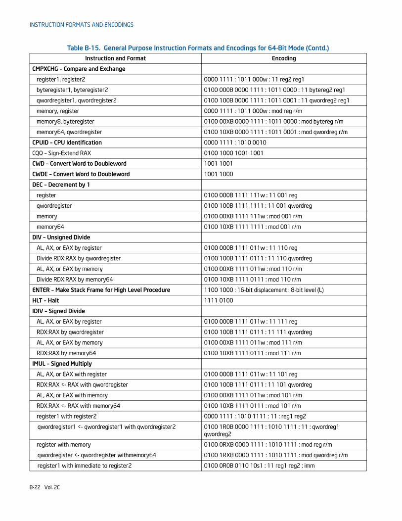
INSTRUCTION FORMATS AND ENCODINGS
CMPXCHG – Compare and Exchange
register1, register2 0000 1111 : 1011 000w : 11 reg2 reg1
byteregister1, byteregister2 0100 000B 0000 1111 : 1011 0000 : 11 bytereg2 reg1
qwordregister1, qwordregister2 0100 100B 0000 1111 : 1011 0001 : 11 qwordreg2 reg1
memory, register 0000 1111 : 1011 000w : mod reg r/m
memory8, byteregister 0100 00XB 0000 1111 : 1011 0000 : mod bytereg r/m
memory64, qwordregister 0100 10XB 0000 1111 : 1011 0001 : mod qwordreg r/m
CPUID – CPU Identification 0000 1111 : 1010 0010
CQO – Sign-Extend RAX 0100 1000 1001 1001
CWD – Convert Word to Doubleword 1001 1001
CWDE – Convert Word to Doubleword 1001 1000
DEC – Decrement by 1
register 0100 000B 1111 111w : 11 001 reg
qwordregister 0100 100B 1111 1111 : 11 001 qwordreg
memory 0100 00XB 1111 111w : mod 001 r/m
memory64 0100 10XB 1111 1111 : mod 001 r/m
DIV – Unsigned Divide
AL, AX, or EAX by register 0100 000B 1111 011w : 11 110 reg
Divide RDX:RAX by qwordregister 0100 100B 1111 0111 : 11 110 qwordreg
AL, AX, or EAX by memory 0100 00XB 1111 011w : mod 110 r/m
Divide RDX:RAX by memory64 0100 10XB 1111 0111 : mod 110 r/m
ENTER – Make Stack Frame for High Level Procedure 1100 1000 : 16-bit displacement : 8-bit level (L)
HLT – Halt 1111 0100
IDIV – Signed Divide
AL, AX, or EAX by register 0100 000B 1111 011w : 11 111 reg
RDX:RAX by qwordregister 0100 100B 1111 0111 : 11 111 qwordreg
AL, AX, or EAX by memory 0100 00XB 1111 011w : mod 111 r/m
RDX:RAX by memory64 0100 10XB 1111 0111 : mod 111 r/m
IMUL – Signed Multiply
AL, AX, or EAX with register 0100 000B 1111 011w : 11 101 reg
RDX:RAX <- RAX with qwordregister 0100 100B 1111 0111 : 11 101 qwordreg
AL, AX, or EAX with memory 0100 00XB 1111 011w : mod 101 r/m
RDX:RAX <- RAX with memory64 0100 10XB 1111 0111 : mod 101 r/m
register1 with register2 0000 1111 : 1010 1111 : 11 : reg1 reg2
qwordregister1 <- qwordregister1 with qwordregister2 0100 1R0B 0000 1111 : 1010 1111 : 11 : qwordreg1 qwordreg2
register with memory 0100 0RXB 0000 1111 : 1010 1111 : mod reg r/m
qwordregister <- qwordregister withmemory64 0100 1RXB 0000 1111 : 1010 1111 : mod qwordreg r/m
register1 with immediate to register2 0100 0R0B 0110 10s1 : 11 reg1 reg2 : imm
Table B-15. General Purpose Instruction Formats and Encodings for 64-Bit Mode (Contd.)
Instruction and Format Encoding
B-22 Vol. 2C
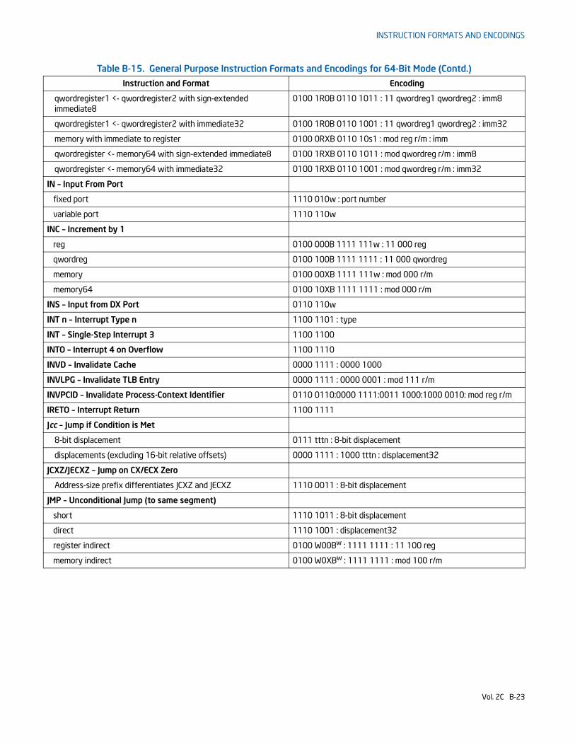
INSTRUCTION FORMATS AND ENCODINGS
qwordregister1 <- qwordregister2 with sign-extended immediate8
0100 1R0B 0110 1011 : 11 qwordreg1 qwordreg2 : imm8
qwordregister1 <- qwordregister2 with immediate32 0100 1R0B 0110 1001 : 11 qwordreg1 qwordreg2 : imm32
memory with immediate to register 0100 0RXB 0110 10s1 : mod reg r/m : imm
qwordregister <- memory64 with sign-extended immediate8 0100 1RXB 0110 1011 : mod qwordreg r/m : imm8
qwordregister <- memory64 with immediate32 0100 1RXB 0110 1001 : mod qwordreg r/m : imm32
IN – Input From Port
fixed port 1110 010w : port number
variable port 1110 110w
INC – Increment by 1
reg 0100 000B 1111 111w : 11 000 reg
qwordreg 0100 100B 1111 1111 : 11 000 qwordreg
memory 0100 00XB 1111 111w : mod 000 r/m
memory64 0100 10XB 1111 1111 : mod 000 r/m
INS – Input from DX Port 0110 110w
INT n – Interrupt Type n 1100 1101 : type
INT – Single-Step Interrupt 3 1100 1100
INTO – Interrupt 4 on Overflow 1100 1110
INVD – Invalidate Cache 0000 1111 : 0000 1000
INVLPG – Invalidate TLB Entry 0000 1111 : 0000 0001 : mod 111 r/m
INVPCID – Invalidate Process-Context Identifier 0110 0110:0000 1111:0011 1000:1000 0010: mod reg r/m
IRETO – Interrupt Return 1100 1111
Jcc – Jump if Condition is Met
8-bit displacement 0111 tttn : 8-bit displacement
displacements (excluding 16-bit relative offsets) 0000 1111 : 1000 tttn : displacement32
JCXZ/JECXZ – Jump on CX/ECX Zero
Address-size prefix differentiates JCXZ and JECXZ 1110 0011 : 8-bit displacement
JMP – Unconditional Jump (to same segment)
short 1110 1011 : 8-bit displacement
direct 1110 1001 : displacement32
register indirect 0100 W00Bw : 1111 1111 : 11 100 reg
memory indirect 0100 W0XBw : 1111 1111 : mod 100 r/m
Table B-15. General Purpose Instruction Formats and Encodings for 64-Bit Mode (Contd.)
Instruction and Format Encoding
Vol. 2C B-23
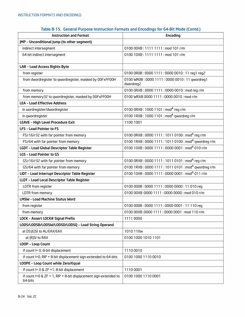
INSTRUCTION FORMATS AND ENCODINGS
JMP – Unconditional Jump (to other segment)
indirect intersegment 0100 00XB : 1111 1111 : mod 101 r/m
64-bit indirect intersegment 0100 10XB : 1111 1111 : mod 101 r/m
LAR – Load Access Rights Byte
from register 0100 0R0B : 0000 1111 : 0000 0010 : 11 reg1 reg2
from dwordregister to qwordregister, masked by 00FxFF00H 0100 WR0B : 0000 1111 : 0000 0010 : 11 qwordreg1 dwordreg2
from memory 0100 0RXB : 0000 1111 : 0000 0010 : mod reg r/m
from memory32 to qwordregister, masked by 00FxFF00H 0100 WRXB 0000 1111 : 0000 0010 : mod r/m
LEA – Load Effective Address
in wordregister/dwordregister 0100 0RXB : 1000 1101 : modA reg r/m
in qwordregister 0100 1RXB : 1000 1101 : modA qwordreg r/m
LEAVE – High Level Procedure Exit 1100 1001
LFS – Load Pointer to FS
FS:r16/r32 with far pointer from memory 0100 0RXB : 0000 1111 : 1011 0100 : modA reg r/m
FS:r64 with far pointer from memory 0100 1RXB : 0000 1111 : 1011 0100 : modA qwordreg r/m
LGDT – Load Global Descriptor Table Register 0100 10XB : 0000 1111 : 0000 0001 : modA 010 r/m
LGS – Load Pointer to GS
GS:r16/r32 with far pointer from memory 0100 0RXB : 0000 1111 : 1011 0101 : modA reg r/m
GS:r64 with far pointer from memory 0100 1RXB : 0000 1111 : 1011 0101 : modA qwordreg r/m
LIDT – Load Interrupt Descriptor Table Register 0100 10XB : 0000 1111 : 0000 0001 : modA 011 r/m
LLDT – Load Local Descriptor Table Register
LDTR from register 0100 000B : 0000 1111 : 0000 0000 : 11 010 reg
LDTR from memory 0100 00XB :0000 1111 : 0000 0000 : mod 010 r/m
LMSW – Load Machine Status Word
from register 0100 000B : 0000 1111 : 0000 0001 : 11 110 reg
from memory 0100 00XB :0000 1111 : 0000 0001 : mod 110 r/m
LOCK – Assert LOCK# Signal Prefix 1111 0000
LODS/LODSB/LODSW/LODSD/LODSQ – Load String Operand
at DS:(E)SI to AL/EAX/EAX 1010 110w
at (R)SI to RAX 0100 1000 1010 1101
LOOP – Loop Count
if count != 0, 8-bit displacement 1110 0010
if count !=0, RIP + 8-bit displacement sign-extended to 64-bits 0100 1000 1110 0010
LOOPE – Loop Count while Zero/Equal
if count != 0 & ZF =1, 8-bit displacement 1110 0001
if count !=0 & ZF = 1, RIP + 8-bit displacement sign-extended to 64-bits
0100 1000 1110 0001
Table B-15. General Purpose Instruction Formats and Encodings for 64-Bit Mode (Contd.)
Instruction and Format Encoding
B-24 Vol. 2C
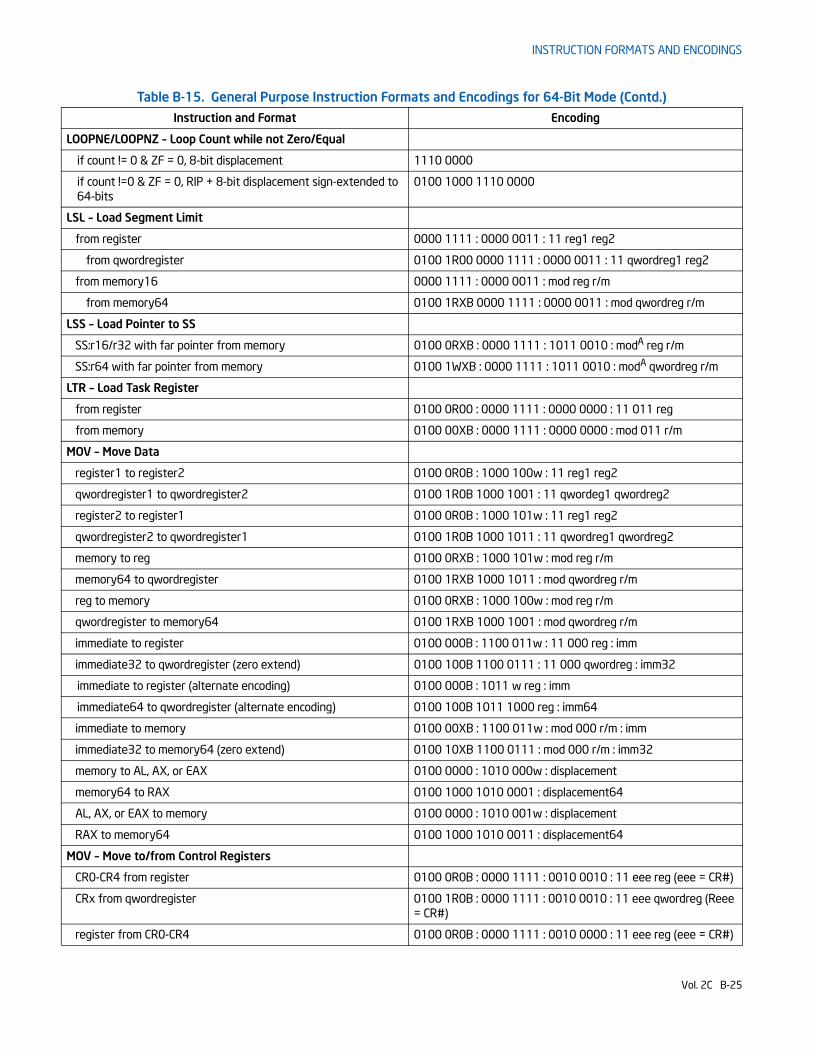
INSTRUCTION FORMATS AND ENCODINGS
LOOPNE/LOOPNZ – Loop Count while not Zero/Equal
if count != 0 & ZF = 0, 8-bit displacement 1110 0000
if count !=0 & ZF = 0, RIP + 8-bit displacement sign-extended to 64-bits
0100 1000 1110 0000
LSL – Load Segment Limit
from register 0000 1111 : 0000 0011 : 11 reg1 reg2
from qwordregister 0100 1R00 0000 1111 : 0000 0011 : 11 qwordreg1 reg2
from memory16 0000 1111 : 0000 0011 : mod reg r/m
from memory64 0100 1RXB 0000 1111 : 0000 0011 : mod qwordreg r/m
LSS – Load Pointer to SS
SS:r16/r32 with far pointer from memory 0100 0RXB : 0000 1111 : 1011 0010 : modA reg r/m
SS:r64 with far pointer from memory 0100 1WXB : 0000 1111 : 1011 0010 : modA qwordreg r/m
LTR – Load Task Register
from register 0100 0R00 : 0000 1111 : 0000 0000 : 11 011 reg
from memory 0100 00XB : 0000 1111 : 0000 0000 : mod 011 r/m
MOV – Move Data
register1 to register2 0100 0R0B : 1000 100w : 11 reg1 reg2
qwordregister1 to qwordregister2 0100 1R0B 1000 1001 : 11 qwordeg1 qwordreg2
register2 to register1 0100 0R0B : 1000 101w : 11 reg1 reg2
qwordregister2 to qwordregister1 0100 1R0B 1000 1011 : 11 qwordreg1 qwordreg2
memory to reg 0100 0RXB : 1000 101w : mod reg r/m
memory64 to qwordregister 0100 1RXB 1000 1011 : mod qwordreg r/m
reg to memory 0100 0RXB : 1000 100w : mod reg r/m
qwordregister to memory64 0100 1RXB 1000 1001 : mod qwordreg r/m
immediate to register 0100 000B : 1100 011w : 11 000 reg : imm
immediate32 to qwordregister (zero extend) 0100 100B 1100 0111 : 11 000 qwordreg : imm32
immediate to register (alternate encoding) 0100 000B : 1011 w reg : imm
immediate64 to qwordregister (alternate encoding) 0100 100B 1011 1000 reg : imm64
immediate to memory 0100 00XB : 1100 011w : mod 000 r/m : imm
immediate32 to memory64 (zero extend) 0100 10XB 1100 0111 : mod 000 r/m : imm32
memory to AL, AX, or EAX 0100 0000 : 1010 000w : displacement
memory64 to RAX 0100 1000 1010 0001 : displacement64
AL, AX, or EAX to memory 0100 0000 : 1010 001w : displacement
RAX to memory64 0100 1000 1010 0011 : displacement64
MOV – Move to/from Control Registers
CR0-CR4 from register 0100 0R0B : 0000 1111 : 0010 0010 : 11 eee reg (eee = CR#)
CRx from qwordregister 0100 1R0B : 0000 1111 : 0010 0010 : 11 eee qwordreg (Reee = CR#)
register from CR0-CR4 0100 0R0B : 0000 1111 : 0010 0000 : 11 eee reg (eee = CR#)
Table B-15. General Purpose Instruction Formats and Encodings for 64-Bit Mode (Contd.)
Instruction and Format Encoding
Vol. 2C B-25
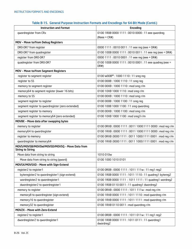
INSTRUCTION FORMATS AND ENCODINGS
qwordregister from CRx 0100 1R0B 0000 1111 : 0010 0000 : 11 eee qwordreg
(Reee = CR#)
MOV – Move to/from Debug Registers
DR0-DR7 from register 0000 1111 : 0010 0011 : 11 eee reg (eee = DR#)
DR0-DR7 from quadregister 0100 10OB 0000 1111 : 0010 0011 : 11 eee reg (eee = DR#)
register from DR0-DR7 0000 1111 : 0010 0001 : 11 eee reg (eee = DR#)
quadregister from DR0-DR7 0100 10OB 0000 1111 : 0010 0001 : 11 eee quadreg (eee = DR#)
MOV – Move to/from Segment Registers
register to segment register 0100 W00Bw : 1000 1110 : 11 sreg reg
register to SS 0100 000B : 1000 1110 : 11 sreg reg
memory to segment register 0100 00XB : 1000 1110 : mod sreg r/m
memory64 to segment register (lower 16 bits) 0100 10XB 1000 1110 : mod sreg r/m
memory to SS 0100 00XB : 1000 1110 : mod sreg r/m
segment register to register 0100 000B : 1000 1100 : 11 sreg reg
segment register to qwordregister (zero extended) 0100 100B 1000 1100 : 11 sreg qwordreg
segment register to memory 0100 00XB : 1000 1100 : mod sreg r/m
segment register to memory64 (zero extended) 0100 10XB 1000 1100 : mod sreg3 r/m
MOVBE – Move data after swapping bytes
memory to register 0100 0RXB : 0000 1111 : 0011 1000:1111 0000 : mod reg r/m
memory64 to qwordregister 0100 1RXB : 0000 1111 : 0011 1000:1111 0000 : mod reg r/m
register to memory 0100 0RXB :0000 1111 : 0011 1000:1111 0001 : mod reg r/m
qwordregister to memory64 0100 1RXB :0000 1111 : 0011 1000:1111 0001 : mod reg r/m
MOVS/MOVSB/MOVSW/MOVSD/MOVSQ – Move Data from String to String
Move data from string to string 1010 010w
Move data from string to string (qword) 0100 1000 1010 0101
MOVSX/MOVSXD – Move with Sign-Extend
register2 to register1 0100 0R0B : 0000 1111 : 1011 111w : 11 reg1 reg2
byteregister2 to qwordregister1 (sign-extend) 0100 1R0B 0000 1111 : 1011 1110 : 11 quadreg1 bytereg2
wordregister2 to qwordregister1 0100 1R0B 0000 1111 : 1011 1111 : 11 quadreg1 wordreg2
dwordregister2 to qwordregister1 0100 1R0B 0110 0011 : 11 quadreg1 dwordreg2
memory to register 0100 0RXB : 0000 1111 : 1011 111w : mod reg r/m
memory8 to qwordregister (sign-extend) 0100 1RXB 0000 1111 : 1011 1110 : mod qwordreg r/m
memory16 to qwordregister 0100 1RXB 0000 1111 : 1011 1111 : mod qwordreg r/m
memory32 to qwordregister 0100 1RXB 0110 0011 : mod qwordreg r/m
MOVZX – Move with Zero-Extend
register2 to register1 0100 0R0B : 0000 1111 : 1011 011w : 11 reg1 reg2
dwordregister2 to qwordregister1 0100 1R0B 0000 1111 : 1011 0111 : 11 qwordreg1 dwordreg2
Table B-15. General Purpose Instruction Formats and Encodings for 64-Bit Mode (Contd.)
Instruction and Format Encoding
B-26 Vol. 2C

INSTRUCTION FORMATS AND ENCODINGS
memory to register 0100 0RXB : 0000 1111 : 1011 011w : mod reg r/m
memory32 to qwordregister 0100 1RXB 0000 1111 : 1011 0111 : mod qwordreg r/m
MUL – Unsigned Multiply
AL, AX, or EAX with register 0100 000B : 1111 011w : 11 100 reg
RAX with qwordregister (to RDX:RAX) 0100 100B 1111 0111 : 11 100 qwordreg
AL, AX, or EAX with memory 0100 00XB 1111 011w : mod 100 r/m
RAX with memory64 (to RDX:RAX) 0100 10XB 1111 0111 : mod 100 r/m
NEG – Two's Complement Negation
register 0100 000B : 1111 011w : 11 011 reg
qwordregister 0100 100B 1111 0111 : 11 011 qwordreg
memory 0100 00XB : 1111 011w : mod 011 r/m
memory64 0100 10XB 1111 0111 : mod 011 r/m
NOP – No Operation 1001 0000
NOT – One's Complement Negation
register 0100 000B : 1111 011w : 11 010 reg
qwordregister 0100 000B 1111 0111 : 11 010 qwordreg
memory 0100 00XB : 1111 011w : mod 010 r/m
memory64 0100 1RXB 1111 0111 : mod 010 r/m
OR – Logical Inclusive OR
register1 to register2 0000 100w : 11 reg1 reg2
byteregister1 to byteregister2 0100 0R0B 0000 1000 : 11 bytereg1 bytereg2
qwordregister1 to qwordregister2 0100 1R0B 0000 1001 : 11 qwordreg1 qwordreg2
register2 to register1 0000 101w : 11 reg1 reg2
byteregister2 to byteregister1 0100 0R0B 0000 1010 : 11 bytereg1 bytereg2
qwordregister2 to qwordregister1 0100 0R0B 0000 1011 : 11 qwordreg1 qwordreg2
memory to register 0000 101w : mod reg r/m
memory8 to byteregister 0100 0RXB 0000 1010 : mod bytereg r/m
memory8 to qwordregister 0100 0RXB 0000 1011 : mod qwordreg r/m
register to memory 0000 100w : mod reg r/m
byteregister to memory8 0100 0RXB 0000 1000 : mod bytereg r/m
qwordregister to memory64 0100 1RXB 0000 1001 : mod qwordreg r/m
immediate to register 1000 00sw : 11 001 reg : imm
immediate8 to byteregister 0100 000B 1000 0000 : 11 001 bytereg : imm8
immediate32 to qwordregister 0100 000B 1000 0001 : 11 001 qwordreg : imm32
immediate8 to qwordregister 0100 000B 1000 0011 : 11 001 qwordreg : imm8
immediate to AL, AX, or EAX 0000 110w : imm
immediate64 to RAX 0100 1000 0000 1101 : imm64
immediate to memory 1000 00sw : mod 001 r/m : imm
Table B-15. General Purpose Instruction Formats and Encodings for 64-Bit Mode (Contd.)
Instruction and Format Encoding
Vol. 2C B-27
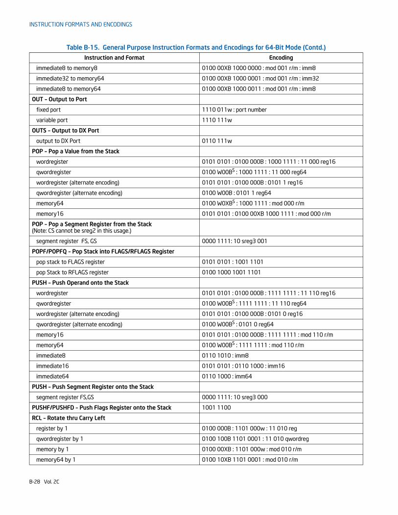
INSTRUCTION FORMATS AND ENCODINGS
immediate8 to memory8 0100 00XB 1000 0000 : mod 001 r/m : imm8
immediate32 to memory64 0100 00XB 1000 0001 : mod 001 r/m : imm32
immediate8 to memory64 0100 00XB 1000 0011 : mod 001 r/m : imm8
OUT – Output to Port
fixed port 1110 011w : port number
variable port 1110 111w
OUTS – Output to DX Port
output to DX Port 0110 111w
POP – Pop a Value from the Stack
wordregister 0101 0101 : 0100 000B : 1000 1111 : 11 000 reg16
qwordregister 0100 W00BS : 1000 1111 : 11 000 reg64
wordregister (alternate encoding) 0101 0101 : 0100 000B : 0101 1 reg16
qwordregister (alternate encoding) 0100 W00B : 0101 1 reg64
memory64 0100 W0XBS : 1000 1111 : mod 000 r/m
memory16 0101 0101 : 0100 00XB 1000 1111 : mod 000 r/m
POP – Pop a Segment Register from the Stack(Note: CS cannot be sreg2 in this usage.)
segment register FS, GS 0000 1111: 10 sreg3 001
POPF/POPFQ – Pop Stack into FLAGS/RFLAGS Register
pop stack to FLAGS register 0101 0101 : 1001 1101
pop Stack to RFLAGS register 0100 1000 1001 1101
PUSH – Push Operand onto the Stack
wordregister 0101 0101 : 0100 000B : 1111 1111 : 11 110 reg16
qwordregister 0100 W00BS : 1111 1111 : 11 110 reg64
wordregister (alternate encoding) 0101 0101 : 0100 000B : 0101 0 reg16
qwordregister (alternate encoding) 0100 W00BS : 0101 0 reg64
memory16 0101 0101 : 0100 000B : 1111 1111 : mod 110 r/m
memory64 0100 W00BS : 1111 1111 : mod 110 r/m
immediate8 0110 1010 : imm8
immediate16 0101 0101 : 0110 1000 : imm16
immediate64 0110 1000 : imm64
PUSH – Push Segment Register onto the Stack
segment register FS,GS 0000 1111: 10 sreg3 000
PUSHF/PUSHFD – Push Flags Register onto the Stack 1001 1100
RCL – Rotate thru Carry Left
register by 1 0100 000B : 1101 000w : 11 010 reg
qwordregister by 1 0100 100B 1101 0001 : 11 010 qwordreg
memory by 1 0100 00XB : 1101 000w : mod 010 r/m
memory64 by 1 0100 10XB 1101 0001 : mod 010 r/m
Table B-15. General Purpose Instruction Formats and Encodings for 64-Bit Mode (Contd.)
Instruction and Format Encoding
B-28 Vol. 2C
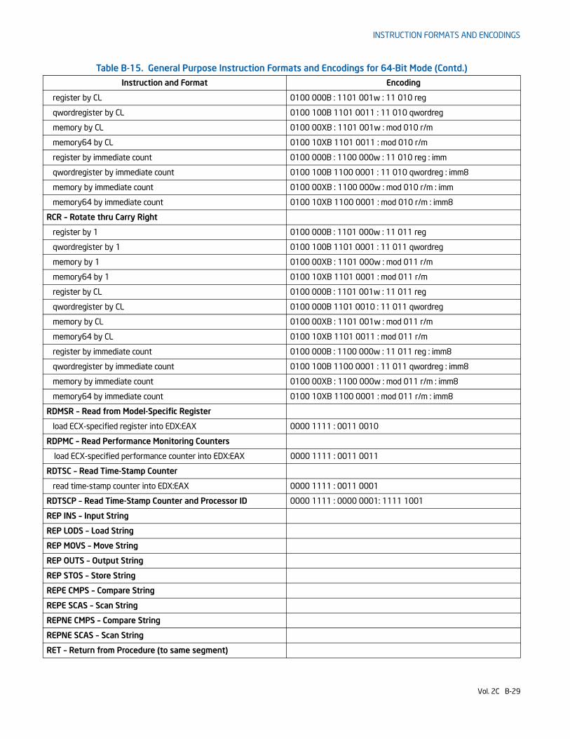
INSTRUCTION FORMATS AND ENCODINGS
register by CL 0100 000B : 1101 001w : 11 010 reg
qwordregister by CL 0100 100B 1101 0011 : 11 010 qwordreg
memory by CL 0100 00XB : 1101 001w : mod 010 r/m
memory64 by CL 0100 10XB 1101 0011 : mod 010 r/m
register by immediate count 0100 000B : 1100 000w : 11 010 reg : imm
qwordregister by immediate count 0100 100B 1100 0001 : 11 010 qwordreg : imm8
memory by immediate count 0100 00XB : 1100 000w : mod 010 r/m : imm
memory64 by immediate count 0100 10XB 1100 0001 : mod 010 r/m : imm8
RCR – Rotate thru Carry Right
register by 1 0100 000B : 1101 000w : 11 011 reg
qwordregister by 1 0100 100B 1101 0001 : 11 011 qwordreg
memory by 1 0100 00XB : 1101 000w : mod 011 r/m
memory64 by 1 0100 10XB 1101 0001 : mod 011 r/m
register by CL 0100 000B : 1101 001w : 11 011 reg
qwordregister by CL 0100 000B 1101 0010 : 11 011 qwordreg
memory by CL 0100 00XB : 1101 001w : mod 011 r/m
memory64 by CL 0100 10XB 1101 0011 : mod 011 r/m
register by immediate count 0100 000B : 1100 000w : 11 011 reg : imm8
qwordregister by immediate count 0100 100B 1100 0001 : 11 011 qwordreg : imm8
memory by immediate count 0100 00XB : 1100 000w : mod 011 r/m : imm8
memory64 by immediate count 0100 10XB 1100 0001 : mod 011 r/m : imm8
RDMSR – Read from Model-Specific Register
load ECX-specified register into EDX:EAX 0000 1111 : 0011 0010
RDPMC – Read Performance Monitoring Counters
load ECX-specified performance counter into EDX:EAX 0000 1111 : 0011 0011
RDTSC – Read Time-Stamp Counter
read time-stamp counter into EDX:EAX 0000 1111 : 0011 0001
RDTSCP – Read Time-Stamp Counter and Processor ID 0000 1111 : 0000 0001: 1111 1001
REP INS – Input String
REP LODS – Load String
REP MOVS – Move String
REP OUTS – Output String
REP STOS – Store String
REPE CMPS – Compare String
REPE SCAS – Scan String
REPNE CMPS – Compare String
REPNE SCAS – Scan String
RET – Return from Procedure (to same segment)
Table B-15. General Purpose Instruction Formats and Encodings for 64-Bit Mode (Contd.)
Instruction and Format Encoding
Vol. 2C B-29
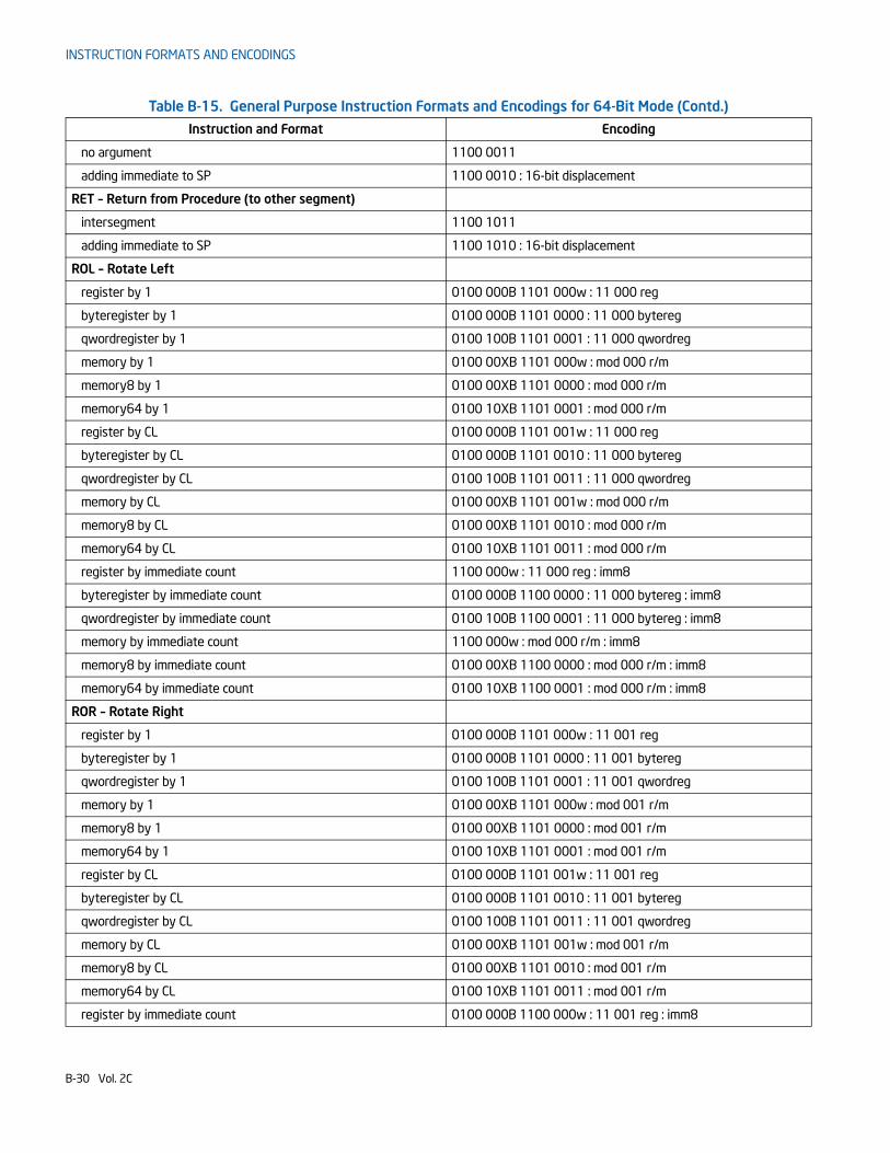
INSTRUCTION FORMATS AND ENCODINGS
no argument 1100 0011
adding immediate to SP 1100 0010 : 16-bit displacement
RET – Return from Procedure (to other segment)
intersegment 1100 1011
adding immediate to SP 1100 1010 : 16-bit displacement
ROL – Rotate Left
register by 1 0100 000B 1101 000w : 11 000 reg
byteregister by 1 0100 000B 1101 0000 : 11 000 bytereg
qwordregister by 1 0100 100B 1101 0001 : 11 000 qwordreg
memory by 1 0100 00XB 1101 000w : mod 000 r/m
memory8 by 1 0100 00XB 1101 0000 : mod 000 r/m
memory64 by 1 0100 10XB 1101 0001 : mod 000 r/m
register by CL 0100 000B 1101 001w : 11 000 reg
byteregister by CL 0100 000B 1101 0010 : 11 000 bytereg
qwordregister by CL 0100 100B 1101 0011 : 11 000 qwordreg
memory by CL 0100 00XB 1101 001w : mod 000 r/m
memory8 by CL 0100 00XB 1101 0010 : mod 000 r/m
memory64 by CL 0100 10XB 1101 0011 : mod 000 r/m
register by immediate count 1100 000w : 11 000 reg : imm8
byteregister by immediate count 0100 000B 1100 0000 : 11 000 bytereg : imm8
qwordregister by immediate count 0100 100B 1100 0001 : 11 000 bytereg : imm8
memory by immediate count 1100 000w : mod 000 r/m : imm8
memory8 by immediate count 0100 00XB 1100 0000 : mod 000 r/m : imm8
memory64 by immediate count 0100 10XB 1100 0001 : mod 000 r/m : imm8
ROR – Rotate Right
register by 1 0100 000B 1101 000w : 11 001 reg
byteregister by 1 0100 000B 1101 0000 : 11 001 bytereg
qwordregister by 1 0100 100B 1101 0001 : 11 001 qwordreg
memory by 1 0100 00XB 1101 000w : mod 001 r/m
memory8 by 1 0100 00XB 1101 0000 : mod 001 r/m
memory64 by 1 0100 10XB 1101 0001 : mod 001 r/m
register by CL 0100 000B 1101 001w : 11 001 reg
byteregister by CL 0100 000B 1101 0010 : 11 001 bytereg
qwordregister by CL 0100 100B 1101 0011 : 11 001 qwordreg
memory by CL 0100 00XB 1101 001w : mod 001 r/m
memory8 by CL 0100 00XB 1101 0010 : mod 001 r/m
memory64 by CL 0100 10XB 1101 0011 : mod 001 r/m
register by immediate count 0100 000B 1100 000w : 11 001 reg : imm8
Table B-15. General Purpose Instruction Formats and Encodings for 64-Bit Mode (Contd.)
Instruction and Format Encoding
B-30 Vol. 2C
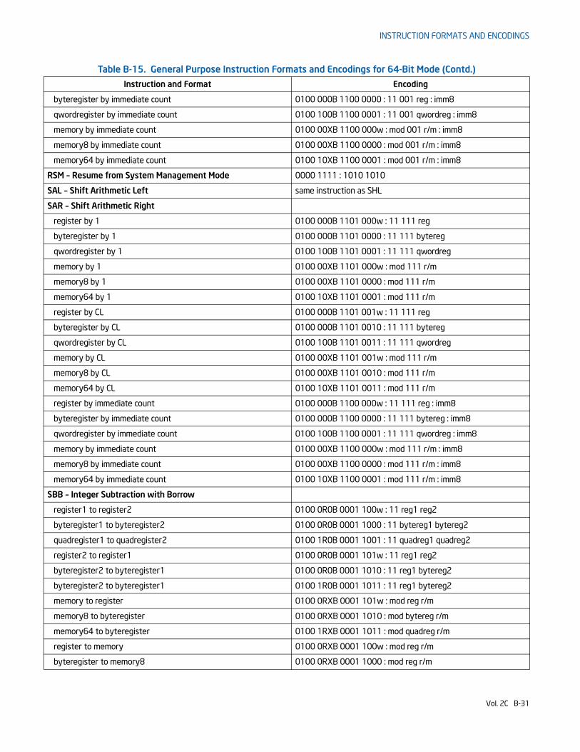
INSTRUCTION FORMATS AND ENCODINGS
byteregister by immediate count 0100 000B 1100 0000 : 11 001 reg : imm8
qwordregister by immediate count 0100 100B 1100 0001 : 11 001 qwordreg : imm8
memory by immediate count 0100 00XB 1100 000w : mod 001 r/m : imm8
memory8 by immediate count 0100 00XB 1100 0000 : mod 001 r/m : imm8
memory64 by immediate count 0100 10XB 1100 0001 : mod 001 r/m : imm8
RSM – Resume from System Management Mode 0000 1111 : 1010 1010
SAL – Shift Arithmetic Left same instruction as SHL
SAR – Shift Arithmetic Right
register by 1 0100 000B 1101 000w : 11 111 reg
byteregister by 1 0100 000B 1101 0000 : 11 111 bytereg
qwordregister by 1 0100 100B 1101 0001 : 11 111 qwordreg
memory by 1 0100 00XB 1101 000w : mod 111 r/m
memory8 by 1 0100 00XB 1101 0000 : mod 111 r/m
memory64 by 1 0100 10XB 1101 0001 : mod 111 r/m
register by CL 0100 000B 1101 001w : 11 111 reg
byteregister by CL 0100 000B 1101 0010 : 11 111 bytereg
qwordregister by CL 0100 100B 1101 0011 : 11 111 qwordreg
memory by CL 0100 00XB 1101 001w : mod 111 r/m
memory8 by CL 0100 00XB 1101 0010 : mod 111 r/m
memory64 by CL 0100 10XB 1101 0011 : mod 111 r/m
register by immediate count 0100 000B 1100 000w : 11 111 reg : imm8
byteregister by immediate count 0100 000B 1100 0000 : 11 111 bytereg : imm8
qwordregister by immediate count 0100 100B 1100 0001 : 11 111 qwordreg : imm8
memory by immediate count 0100 00XB 1100 000w : mod 111 r/m : imm8
memory8 by immediate count 0100 00XB 1100 0000 : mod 111 r/m : imm8
memory64 by immediate count 0100 10XB 1100 0001 : mod 111 r/m : imm8
SBB – Integer Subtraction with Borrow
register1 to register2 0100 0R0B 0001 100w : 11 reg1 reg2
byteregister1 to byteregister2 0100 0R0B 0001 1000 : 11 bytereg1 bytereg2
quadregister1 to quadregister2 0100 1R0B 0001 1001 : 11 quadreg1 quadreg2
register2 to register1 0100 0R0B 0001 101w : 11 reg1 reg2
byteregister2 to byteregister1 0100 0R0B 0001 1010 : 11 reg1 bytereg2
byteregister2 to byteregister1 0100 1R0B 0001 1011 : 11 reg1 bytereg2
memory to register 0100 0RXB 0001 101w : mod reg r/m
memory8 to byteregister 0100 0RXB 0001 1010 : mod bytereg r/m
memory64 to byteregister 0100 1RXB 0001 1011 : mod quadreg r/m
register to memory 0100 0RXB 0001 100w : mod reg r/m
byteregister to memory8 0100 0RXB 0001 1000 : mod reg r/m
Table B-15. General Purpose Instruction Formats and Encodings for 64-Bit Mode (Contd.)
Instruction and Format Encoding
Vol. 2C B-31
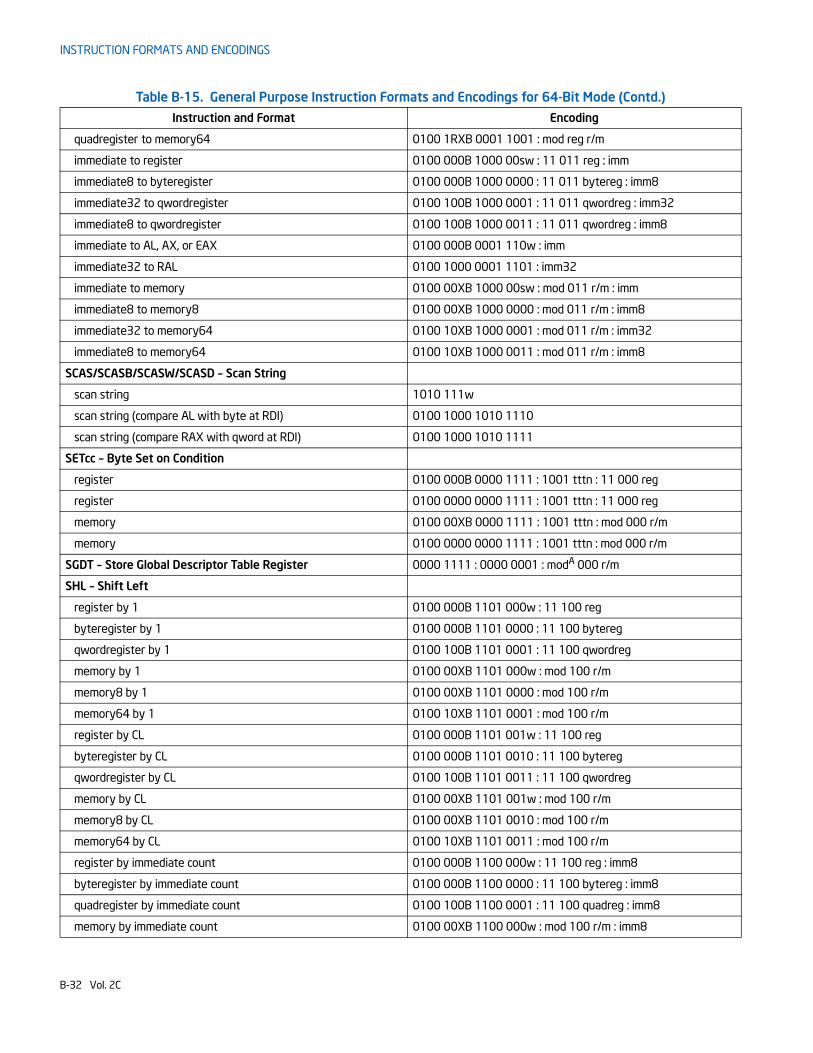
INSTRUCTION FORMATS AND ENCODINGS
quadregister to memory64 0100 1RXB 0001 1001 : mod reg r/m
immediate to register 0100 000B 1000 00sw : 11 011 reg : imm
immediate8 to byteregister 0100 000B 1000 0000 : 11 011 bytereg : imm8
immediate32 to qwordregister 0100 100B 1000 0001 : 11 011 qwordreg : imm32
immediate8 to qwordregister 0100 100B 1000 0011 : 11 011 qwordreg : imm8
immediate to AL, AX, or EAX 0100 000B 0001 110w : imm
immediate32 to RAL 0100 1000 0001 1101 : imm32
immediate to memory 0100 00XB 1000 00sw : mod 011 r/m : imm
immediate8 to memory8 0100 00XB 1000 0000 : mod 011 r/m : imm8
immediate32 to memory64 0100 10XB 1000 0001 : mod 011 r/m : imm32
immediate8 to memory64 0100 10XB 1000 0011 : mod 011 r/m : imm8
SCAS/SCASB/SCASW/SCASD – Scan String
scan string 1010 111w
scan string (compare AL with byte at RDI) 0100 1000 1010 1110
scan string (compare RAX with qword at RDI) 0100 1000 1010 1111
SETcc – Byte Set on Condition
register 0100 000B 0000 1111 : 1001 tttn : 11 000 reg
register 0100 0000 0000 1111 : 1001 tttn : 11 000 reg
memory 0100 00XB 0000 1111 : 1001 tttn : mod 000 r/m
memory 0100 0000 0000 1111 : 1001 tttn : mod 000 r/m
SGDT – Store Global Descriptor Table Register 0000 1111 : 0000 0001 : modA 000 r/m
SHL – Shift Left
register by 1 0100 000B 1101 000w : 11 100 reg
byteregister by 1 0100 000B 1101 0000 : 11 100 bytereg
qwordregister by 1 0100 100B 1101 0001 : 11 100 qwordreg
memory by 1 0100 00XB 1101 000w : mod 100 r/m
memory8 by 1 0100 00XB 1101 0000 : mod 100 r/m
memory64 by 1 0100 10XB 1101 0001 : mod 100 r/m
register by CL 0100 000B 1101 001w : 11 100 reg
byteregister by CL 0100 000B 1101 0010 : 11 100 bytereg
qwordregister by CL 0100 100B 1101 0011 : 11 100 qwordreg
memory by CL 0100 00XB 1101 001w : mod 100 r/m
memory8 by CL 0100 00XB 1101 0010 : mod 100 r/m
memory64 by CL 0100 10XB 1101 0011 : mod 100 r/m
register by immediate count 0100 000B 1100 000w : 11 100 reg : imm8
byteregister by immediate count 0100 000B 1100 0000 : 11 100 bytereg : imm8
quadregister by immediate count 0100 100B 1100 0001 : 11 100 quadreg : imm8
memory by immediate count 0100 00XB 1100 000w : mod 100 r/m : imm8
Table B-15. General Purpose Instruction Formats and Encodings for 64-Bit Mode (Contd.)
Instruction and Format Encoding
B-32 Vol. 2C
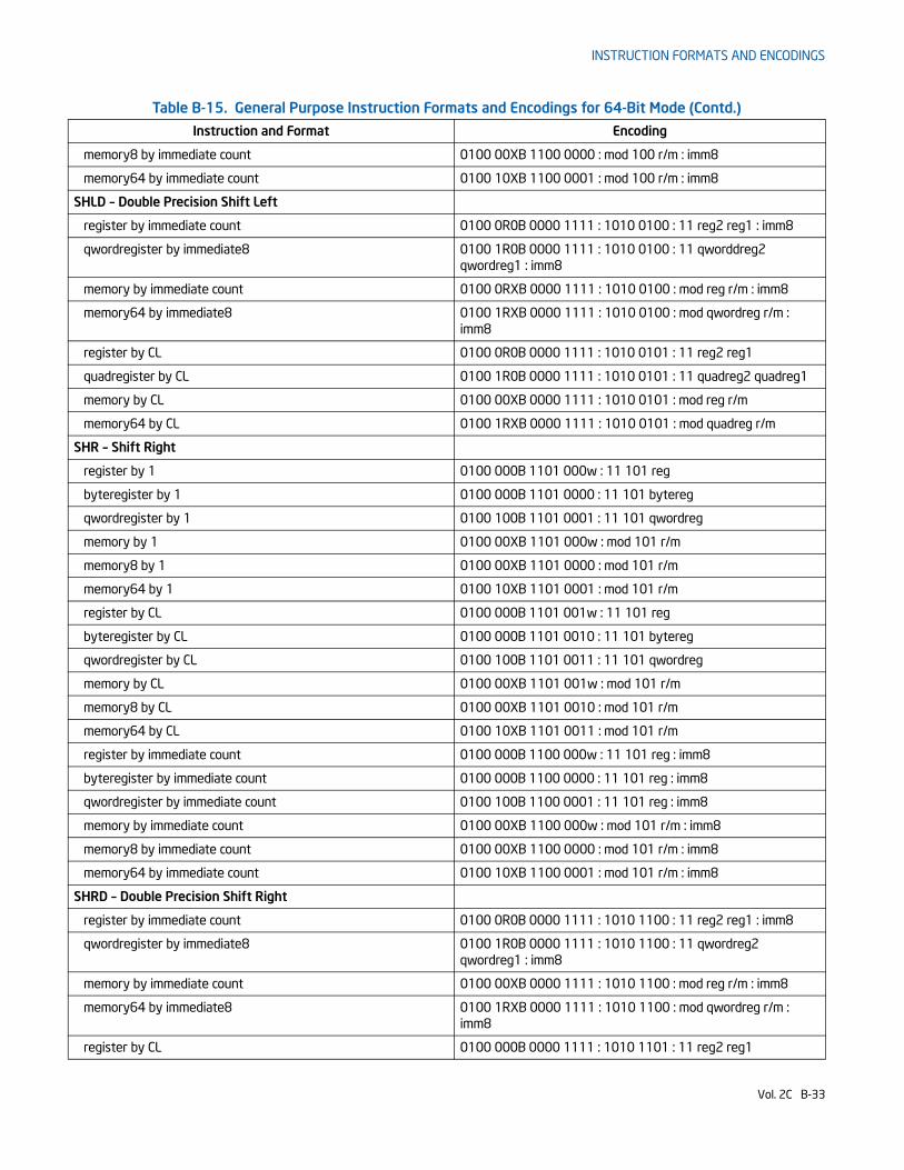
INSTRUCTION FORMATS AND ENCODINGS
memory8 by immediate count 0100 00XB 1100 0000 : mod 100 r/m : imm8
memory64 by immediate count 0100 10XB 1100 0001 : mod 100 r/m : imm8
SHLD – Double Precision Shift Left
register by immediate count 0100 0R0B 0000 1111 : 1010 0100 : 11 reg2 reg1 : imm8
qwordregister by immediate8 0100 1R0B 0000 1111 : 1010 0100 : 11 qworddreg2 qwordreg1 : imm8
memory by immediate count 0100 0RXB 0000 1111 : 1010 0100 : mod reg r/m : imm8
memory64 by immediate8 0100 1RXB 0000 1111 : 1010 0100 : mod qwordreg r/m : imm8
register by CL 0100 0R0B 0000 1111 : 1010 0101 : 11 reg2 reg1
quadregister by CL 0100 1R0B 0000 1111 : 1010 0101 : 11 quadreg2 quadreg1
memory by CL 0100 00XB 0000 1111 : 1010 0101 : mod reg r/m
memory64 by CL 0100 1RXB 0000 1111 : 1010 0101 : mod quadreg r/m
SHR – Shift Right
register by 1 0100 000B 1101 000w : 11 101 reg
byteregister by 1 0100 000B 1101 0000 : 11 101 bytereg
qwordregister by 1 0100 100B 1101 0001 : 11 101 qwordreg
memory by 1 0100 00XB 1101 000w : mod 101 r/m
memory8 by 1 0100 00XB 1101 0000 : mod 101 r/m
memory64 by 1 0100 10XB 1101 0001 : mod 101 r/m
register by CL 0100 000B 1101 001w : 11 101 reg
byteregister by CL 0100 000B 1101 0010 : 11 101 bytereg
qwordregister by CL 0100 100B 1101 0011 : 11 101 qwordreg
memory by CL 0100 00XB 1101 001w : mod 101 r/m
memory8 by CL 0100 00XB 1101 0010 : mod 101 r/m
memory64 by CL 0100 10XB 1101 0011 : mod 101 r/m
register by immediate count 0100 000B 1100 000w : 11 101 reg : imm8
byteregister by immediate count 0100 000B 1100 0000 : 11 101 reg : imm8
qwordregister by immediate count 0100 100B 1100 0001 : 11 101 reg : imm8
memory by immediate count 0100 00XB 1100 000w : mod 101 r/m : imm8
memory8 by immediate count 0100 00XB 1100 0000 : mod 101 r/m : imm8
memory64 by immediate count 0100 10XB 1100 0001 : mod 101 r/m : imm8
SHRD – Double Precision Shift Right
register by immediate count 0100 0R0B 0000 1111 : 1010 1100 : 11 reg2 reg1 : imm8
qwordregister by immediate8 0100 1R0B 0000 1111 : 1010 1100 : 11 qwordreg2 qwordreg1 : imm8
memory by immediate count 0100 00XB 0000 1111 : 1010 1100 : mod reg r/m : imm8
memory64 by immediate8 0100 1RXB 0000 1111 : 1010 1100 : mod qwordreg r/m : imm8
register by CL 0100 000B 0000 1111 : 1010 1101 : 11 reg2 reg1
Table B-15. General Purpose Instruction Formats and Encodings for 64-Bit Mode (Contd.)
Instruction and Format Encoding
Vol. 2C B-33
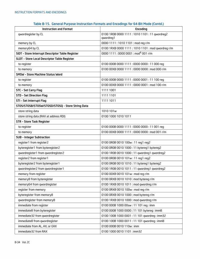
INSTRUCTION FORMATS AND ENCODINGS
qwordregister by CL 0100 1R0B 0000 1111 : 1010 1101 : 11 qwordreg2 qwordreg1
memory by CL 0000 1111 : 1010 1101 : mod reg r/m
memory64 by CL 0100 1RXB 0000 1111 : 1010 1101 : mod qwordreg r/m
SIDT – Store Interrupt Descriptor Table Register 0000 1111 : 0000 0001 : modA 001 r/m
SLDT – Store Local Descriptor Table Register
to register 0100 000B 0000 1111 : 0000 0000 : 11 000 reg
to memory 0100 00XB 0000 1111 : 0000 0000 : mod 000 r/m
SMSW – Store Machine Status Word
to register 0100 000B 0000 1111 : 0000 0001 : 11 100 reg
to memory 0100 00XB 0000 1111 : 0000 0001 : mod 100 r/m
STC – Set Carry Flag 1111 1001
STD – Set Direction Flag 1111 1101
STI – Set Interrupt Flag 1111 1011
STOS/STOSB/STOSW/STOSD/STOSQ – Store String Data
store string data 1010 101w
store string data (RAX at address RDI) 0100 1000 1010 1011
STR – Store Task Register
to register 0100 000B 0000 1111 : 0000 0000 : 11 001 reg
to memory 0100 00XB 0000 1111 : 0000 0000 : mod 001 r/m
SUB – Integer Subtraction
register1 from register2 0100 0R0B 0010 100w : 11 reg1 reg2
byteregister1 from byteregister2 0100 0R0B 0010 1000 : 11 bytereg1 bytereg2
qwordregister1 from qwordregister2 0100 1R0B 0010 1000 : 11 qwordreg1 qwordreg2
register2 from register1 0100 0R0B 0010 101w : 11 reg1 reg2
byteregister2 from byteregister1 0100 0R0B 0010 1010 : 11 bytereg1 bytereg2
qwordregister2 from qwordregister1 0100 1R0B 0010 1011 : 11 qwordreg1 qwordreg2
memory from register 0100 00XB 0010 101w : mod reg r/m
memory8 from byteregister 0100 0RXB 0010 1010 : mod bytereg r/m
memory64 from qwordregister 0100 1RXB 0010 1011 : mod qwordreg r/m
register from memory 0100 0RXB 0010 100w : mod reg r/m
byteregister from memory8 0100 0RXB 0010 1000 : mod bytereg r/m
qwordregister from memory8 0100 1RXB 0010 1000 : mod qwordreg r/m
immediate from register 0100 000B 1000 00sw : 11 101 reg : imm
immediate8 from byteregister 0100 000B 1000 0000 : 11 101 bytereg : imm8
immediate32 from qwordregister 0100 100B 1000 0001 : 11 101 qwordreg : imm32
immediate8 from qwordregister 0100 100B 1000 0011 : 11 101 qwordreg : imm8
immediate from AL, AX, or EAX 0100 000B 0010 110w : imm
immediate32 from RAX 0100 1000 0010 1101 : imm32
Table B-15. General Purpose Instruction Formats and Encodings for 64-Bit Mode (Contd.)
Instruction and Format Encoding
B-34 Vol. 2C
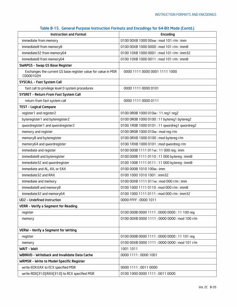
INSTRUCTION FORMATS AND ENCODINGS
immediate from memory 0100 00XB 1000 00sw : mod 101 r/m : imm
immediate8 from memory8 0100 00XB 1000 0000 : mod 101 r/m : imm8
immediate32 from memory64 0100 10XB 1000 0001 : mod 101 r/m : imm32
immediate8 from memory64 0100 10XB 1000 0011 : mod 101 r/m : imm8
SWAPGS – Swap GS Base Register
Exchanges the current GS base register value for value in MSR C0000102H
0000 1111 0000 0001 1111 1000
SYSCALL – Fast System Call
fast call to privilege level 0 system procedures 0000 1111 0000 0101
SYSRET – Return From Fast System Call
return from fast system call 0000 1111 0000 0111
TEST – Logical Compare
register1 and register2 0100 0R0B 1000 010w : 11 reg1 reg2
byteregister1 and byteregister2 0100 0R0B 1000 0100 : 11 bytereg1 bytereg2
qwordregister1 and qwordregister2 0100 1R0B 1000 0101 : 11 qwordreg1 qwordreg2
memory and register 0100 0R0B 1000 010w : mod reg r/m
memory8 and byteregister 0100 0RXB 1000 0100 : mod bytereg r/m
memory64 and qwordregister 0100 1RXB 1000 0101 : mod qwordreg r/m
immediate and register 0100 000B 1111 011w : 11 000 reg : imm
immediate8 and byteregister 0100 000B 1111 0110 : 11 000 bytereg : imm8
immediate32 and qwordregister 0100 100B 1111 0111 : 11 000 bytereg : imm8
immediate and AL, AX, or EAX 0100 000B 1010 100w : imm
immediate32 and RAX 0100 1000 1010 1001 : imm32
immediate and memory 0100 00XB 1111 011w : mod 000 r/m : imm
immediate8 and memory8 0100 1000 1111 0110 : mod 000 r/m : imm8
immediate32 and memory64 0100 1000 1111 0111 : mod 000 r/m : imm32
UD2 – Undefined instruction 0000 FFFF : 0000 1011
VERR – Verify a Segment for Reading
register 0100 000B 0000 1111 : 0000 0000 : 11 100 reg
memory 0100 00XB 0000 1111 : 0000 0000 : mod 100 r/m
VERW – Verify a Segment for Writing
register 0100 000B 0000 1111 : 0000 0000 : 11 101 reg
memory 0100 00XB 0000 1111 : 0000 0000 : mod 101 r/m
WAIT – Wait 1001 1011
WBINVD – Writeback and Invalidate Data Cache 0000 1111 : 0000 1001
WRMSR – Write to Model-Specific Register
write EDX:EAX to ECX specified MSR 0000 1111 : 0011 0000
write RDX[31:0]:RAX[31:0] to RCX specified MSR 0100 1000 0000 1111 : 0011 0000
Table B-15. General Purpose Instruction Formats and Encodings for 64-Bit Mode (Contd.)
Instruction and Format Encoding
Vol. 2C B-35
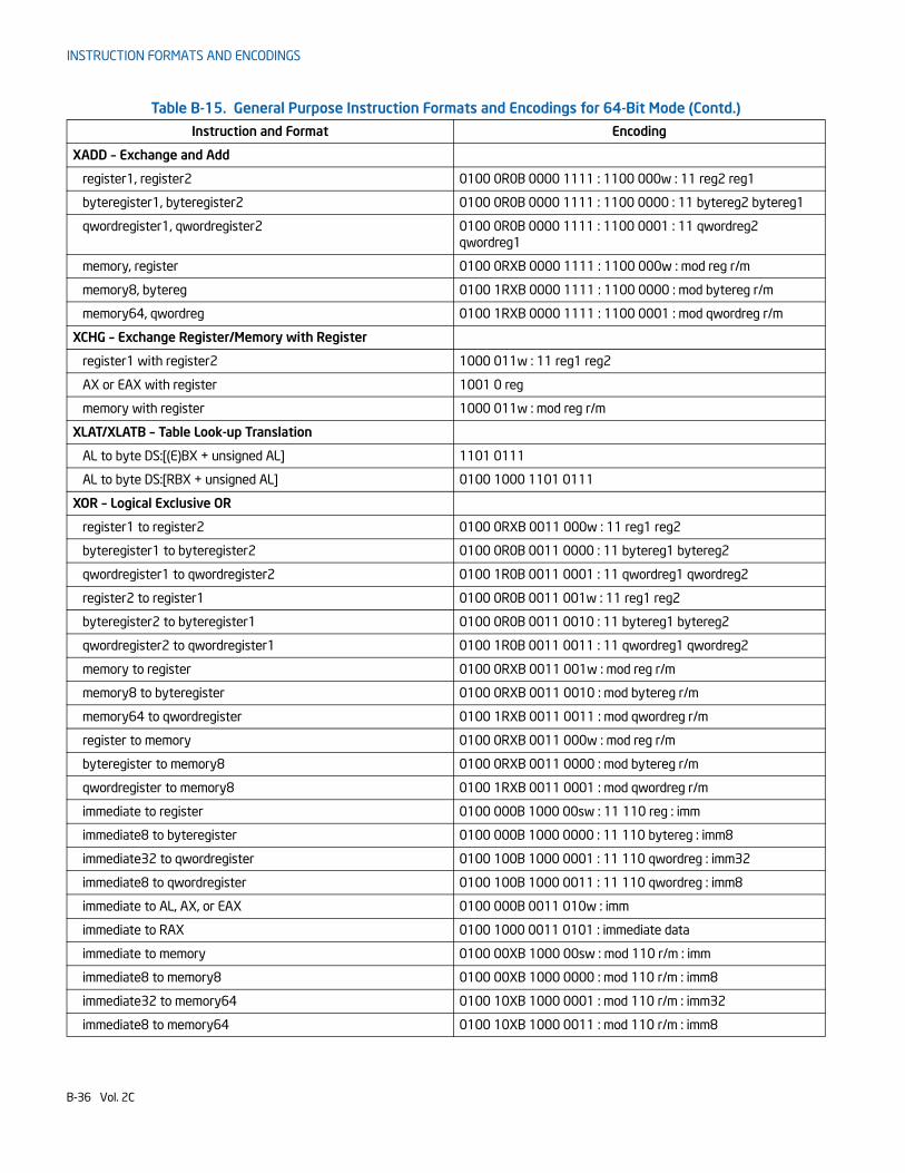
INSTRUCTION FORMATS AND ENCODINGS
XADD – Exchange and Add
register1, register2 0100 0R0B 0000 1111 : 1100 000w : 11 reg2 reg1
byteregister1, byteregister2 0100 0R0B 0000 1111 : 1100 0000 : 11 bytereg2 bytereg1
qwordregister1, qwordregister2 0100 0R0B 0000 1111 : 1100 0001 : 11 qwordreg2 qwordreg1
memory, register 0100 0RXB 0000 1111 : 1100 000w : mod reg r/m
memory8, bytereg 0100 1RXB 0000 1111 : 1100 0000 : mod bytereg r/m
memory64, qwordreg 0100 1RXB 0000 1111 : 1100 0001 : mod qwordreg r/m
XCHG – Exchange Register/Memory with Register
register1 with register2 1000 011w : 11 reg1 reg2
AX or EAX with register 1001 0 reg
memory with register 1000 011w : mod reg r/m
XLAT/XLATB – Table Look-up Translation
AL to byte DS:[(E)BX + unsigned AL] 1101 0111
AL to byte DS:[RBX + unsigned AL] 0100 1000 1101 0111
XOR – Logical Exclusive OR
register1 to register2 0100 0RXB 0011 000w : 11 reg1 reg2
byteregister1 to byteregister2 0100 0R0B 0011 0000 : 11 bytereg1 bytereg2
qwordregister1 to qwordregister2 0100 1R0B 0011 0001 : 11 qwordreg1 qwordreg2
register2 to register1 0100 0R0B 0011 001w : 11 reg1 reg2
byteregister2 to byteregister1 0100 0R0B 0011 0010 : 11 bytereg1 bytereg2
qwordregister2 to qwordregister1 0100 1R0B 0011 0011 : 11 qwordreg1 qwordreg2
memory to register 0100 0RXB 0011 001w : mod reg r/m
memory8 to byteregister 0100 0RXB 0011 0010 : mod bytereg r/m
memory64 to qwordregister 0100 1RXB 0011 0011 : mod qwordreg r/m
register to memory 0100 0RXB 0011 000w : mod reg r/m
byteregister to memory8 0100 0RXB 0011 0000 : mod bytereg r/m
qwordregister to memory8 0100 1RXB 0011 0001 : mod qwordreg r/m
immediate to register 0100 000B 1000 00sw : 11 110 reg : imm
immediate8 to byteregister 0100 000B 1000 0000 : 11 110 bytereg : imm8
immediate32 to qwordregister 0100 100B 1000 0001 : 11 110 qwordreg : imm32
immediate8 to qwordregister 0100 100B 1000 0011 : 11 110 qwordreg : imm8
immediate to AL, AX, or EAX 0100 000B 0011 010w : imm
immediate to RAX 0100 1000 0011 0101 : immediate data
immediate to memory 0100 00XB 1000 00sw : mod 110 r/m : imm
immediate8 to memory8 0100 00XB 1000 0000 : mod 110 r/m : imm8
immediate32 to memory64 0100 10XB 1000 0001 : mod 110 r/m : imm32
immediate8 to memory64 0100 10XB 1000 0011 : mod 110 r/m : imm8
Table B-15. General Purpose Instruction Formats and Encodings for 64-Bit Mode (Contd.)
Instruction and Format Encoding
B-36 Vol. 2C

INSTRUCTION FORMATS AND ENCODINGS
B.3 PENTIUM® PROCESSOR FAMILY INSTRUCTION FORMATS AND ENCODINGSThe following table shows formats and encodings introduced by the Pentium processor family.
B.4 64-BIT MODE INSTRUCTION ENCODINGS FOR SIMD INSTRUCTION EXTENSIONS
Non-64-bit mode instruction encodings for MMX Technology, SSE, SSE2, and SSE3 are covered by applying these rules to Table B-19 through Table B-31. Table B-34 lists special encodings (instructions that do not follow the rules below).
1. The REX instruction has no effect:
• On immediates
• If both operands are MMX registers
• On MMX registers and XMM registers
• If an MMX register is encoded in the reg field of the ModR/M byte
2. If a memory operand is encoded in the r/m field of the ModR/M byte, REX.X and REX.B may be used for encoding the memory operand.
Prefix Bytes
address size 0110 0111
LOCK 1111 0000
operand size 0110 0110
CS segment override 0010 1110
DS segment override 0011 1110
ES segment override 0010 0110
FS segment override 0110 0100
GS segment override 0110 0101
SS segment override 0011 0110
Table B-16. Pentium Processor Family Instruction Formats and Encodings, Non-64-Bit Modes
Instruction and Format Encoding
CMPXCHG8B – Compare and Exchange 8 Bytes
EDX:EAX with memory64 0000 1111 : 1100 0111 : mod 001 r/m
Table B-17. Pentium Processor Family Instruction Formats and Encodings, 64-Bit Mode
Instruction and Format Encoding
CMPXCHG8B/CMPXCHG16B – Compare and Exchange Bytes
EDX:EAX with memory64 0000 1111 : 1100 0111 : mod 001 r/m
RDX:RAX with memory128 0100 10XB 0000 1111 : 1100 0111 : mod 001 r/m
Table B-15. General Purpose Instruction Formats and Encodings for 64-Bit Mode (Contd.)
Instruction and Format Encoding
Vol. 2C B-37
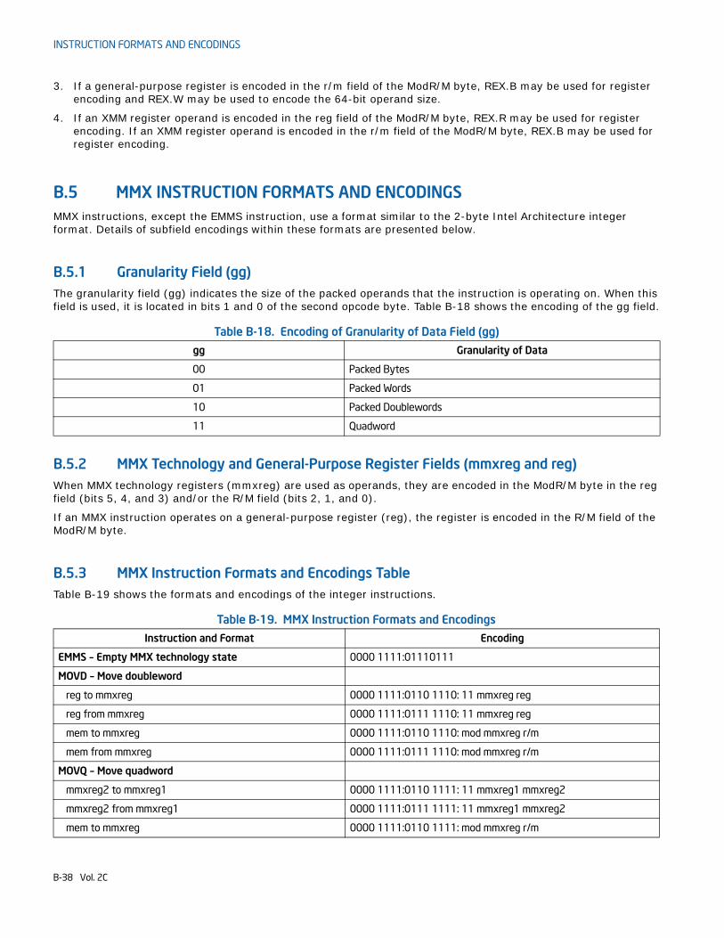
INSTRUCTION FORMATS AND ENCODINGS
3. If a general-purpose register is encoded in the r/m field of the ModR/M byte, REX.B may be used for register encoding and REX.W may be used to encode the 64-bit operand size.
4. If an XMM register operand is encoded in the reg field of the ModR/M byte, REX.R may be used for register encoding. If an XMM register operand is encoded in the r/m field of the ModR/M byte, REX.B may be used for register encoding.
B.5 MMX INSTRUCTION FORMATS AND ENCODINGSMMX instructions, except the EMMS instruction, use a format similar to the 2-byte Intel Architecture integer format. Details of subfield encodings within these formats are presented below.
B.5.1 Granularity Field (gg)The granularity field (gg) indicates the size of the packed operands that the instruction is operating on. When this field is used, it is located in bits 1 and 0 of the second opcode byte. Table B-18 shows the encoding of the gg field.
B.5.2 MMX Technology and General-Purpose Register Fields (mmxreg and reg)When MMX technology registers (mmxreg) are used as operands, they are encoded in the ModR/M byte in the reg field (bits 5, 4, and 3) and/or the R/M field (bits 2, 1, and 0).
If an MMX instruction operates on a general-purpose register (reg), the register is encoded in the R/M field of the ModR/M byte.
B.5.3 MMX Instruction Formats and Encodings TableTable B-19 shows the formats and encodings of the integer instructions.
Table B-18. Encoding of Granularity of Data Field (gg)
gg Granularity of Data
00 Packed Bytes
01 Packed Words
10 Packed Doublewords
11 Quadword
Table B-19. MMX Instruction Formats and Encodings
Instruction and Format Encoding
EMMS – Empty MMX technology state 0000 1111:01110111
MOVD – Move doubleword
reg to mmxreg 0000 1111:0110 1110: 11 mmxreg reg
reg from mmxreg 0000 1111:0111 1110: 11 mmxreg reg
mem to mmxreg 0000 1111:0110 1110: mod mmxreg r/m
mem from mmxreg 0000 1111:0111 1110: mod mmxreg r/m
MOVQ – Move quadword
mmxreg2 to mmxreg1 0000 1111:0110 1111: 11 mmxreg1 mmxreg2
mmxreg2 from mmxreg1 0000 1111:0111 1111: 11 mmxreg1 mmxreg2
mem to mmxreg 0000 1111:0110 1111: mod mmxreg r/m
B-38 Vol. 2C
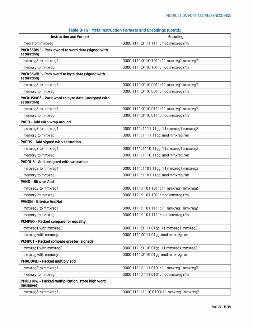
INSTRUCTION FORMATS AND ENCODINGS
mem from mmxreg 0000 1111:0111 1111: mod mmxreg r/m
PACKSSDW1 – Pack dword to word data (signed with saturation)
mmxreg2 to mmxreg1 0000 1111:0110 1011: 11 mmxreg1 mmxreg2
memory to mmxreg 0000 1111:0110 1011: mod mmxreg r/m
PACKSSWB1 – Pack word to byte data (signed with saturation)
mmxreg2 to mmxreg1 0000 1111:0110 0011: 11 mmxreg1 mmxreg2
memory to mmxreg 0000 1111:0110 0011: mod mmxreg r/m
PACKUSWB1 – Pack word to byte data (unsigned with saturation)
mmxreg2 to mmxreg1 0000 1111:0110 0111: 11 mmxreg1 mmxreg2
memory to mmxreg 0000 1111:0110 0111: mod mmxreg r/m
PADD – Add with wrap-around
mmxreg2 to mmxreg1 0000 1111: 1111 11gg: 11 mmxreg1 mmxreg2
memory to mmxreg 0000 1111: 1111 11gg: mod mmxreg r/m
PADDS – Add signed with saturation
mmxreg2 to mmxreg1 0000 1111: 1110 11gg: 11 mmxreg1 mmxreg2
memory to mmxreg 0000 1111: 1110 11gg: mod mmxreg r/m
PADDUS – Add unsigned with saturation
mmxreg2 to mmxreg1 0000 1111: 1101 11gg: 11 mmxreg1 mmxreg2
memory to mmxreg 0000 1111: 1101 11gg: mod mmxreg r/m
PAND – Bitwise And
mmxreg2 to mmxreg1 0000 1111:1101 1011: 11 mmxreg1 mmxreg2
memory to mmxreg 0000 1111:1101 1011: mod mmxreg r/m
PANDN – Bitwise AndNot
mmxreg2 to mmxreg1 0000 1111:1101 1111: 11 mmxreg1 mmxreg2
memory to mmxreg 0000 1111:1101 1111: mod mmxreg r/m
PCMPEQ – Packed compare for equality
mmxreg1 with mmxreg2 0000 1111:0111 01gg: 11 mmxreg1 mmxreg2
mmxreg with memory 0000 1111:0111 01gg: mod mmxreg r/m
PCMPGT – Packed compare greater (signed)
mmxreg1 with mmxreg2 0000 1111:0110 01gg: 11 mmxreg1 mmxreg2
mmxreg with memory 0000 1111:0110 01gg: mod mmxreg r/m
PMADDWD – Packed multiply add
mmxreg2 to mmxreg1 0000 1111:1111 0101: 11 mmxreg1 mmxreg2
memory to mmxreg 0000 1111:1111 0101: mod mmxreg r/m
PMULHUW – Packed multiplication, store high word (unsigned)
mmxreg2 to mmxreg1 0000 1111: 1110 0100: 11 mmxreg1 mmxreg2
Table B-19. MMX Instruction Formats and Encodings (Contd.)
Instruction and Format Encoding
Vol. 2C B-39
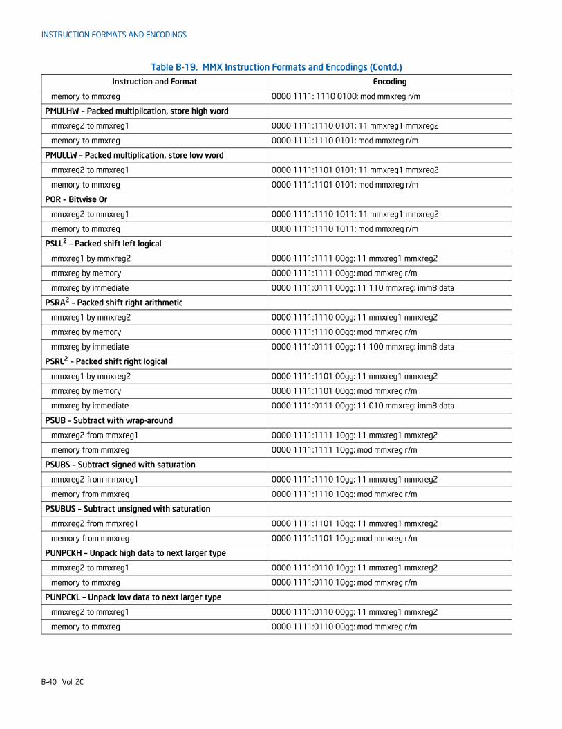
INSTRUCTION FORMATS AND ENCODINGS
memory to mmxreg 0000 1111: 1110 0100: mod mmxreg r/m
PMULHW – Packed multiplication, store high word
mmxreg2 to mmxreg1 0000 1111:1110 0101: 11 mmxreg1 mmxreg2
memory to mmxreg 0000 1111:1110 0101: mod mmxreg r/m
PMULLW – Packed multiplication, store low word
mmxreg2 to mmxreg1 0000 1111:1101 0101: 11 mmxreg1 mmxreg2
memory to mmxreg 0000 1111:1101 0101: mod mmxreg r/m
POR – Bitwise Or
mmxreg2 to mmxreg1 0000 1111:1110 1011: 11 mmxreg1 mmxreg2
memory to mmxreg 0000 1111:1110 1011: mod mmxreg r/m
PSLL2 – Packed shift left logical
mmxreg1 by mmxreg2 0000 1111:1111 00gg: 11 mmxreg1 mmxreg2
mmxreg by memory 0000 1111:1111 00gg: mod mmxreg r/m
mmxreg by immediate 0000 1111:0111 00gg: 11 110 mmxreg: imm8 data
PSRA2 – Packed shift right arithmetic
mmxreg1 by mmxreg2 0000 1111:1110 00gg: 11 mmxreg1 mmxreg2
mmxreg by memory 0000 1111:1110 00gg: mod mmxreg r/m
mmxreg by immediate 0000 1111:0111 00gg: 11 100 mmxreg: imm8 data
PSRL2 – Packed shift right logical
mmxreg1 by mmxreg2 0000 1111:1101 00gg: 11 mmxreg1 mmxreg2
mmxreg by memory 0000 1111:1101 00gg: mod mmxreg r/m
mmxreg by immediate 0000 1111:0111 00gg: 11 010 mmxreg: imm8 data
PSUB – Subtract with wrap-around
mmxreg2 from mmxreg1 0000 1111:1111 10gg: 11 mmxreg1 mmxreg2
memory from mmxreg 0000 1111:1111 10gg: mod mmxreg r/m
PSUBS – Subtract signed with saturation
mmxreg2 from mmxreg1 0000 1111:1110 10gg: 11 mmxreg1 mmxreg2
memory from mmxreg 0000 1111:1110 10gg: mod mmxreg r/m
PSUBUS – Subtract unsigned with saturation
mmxreg2 from mmxreg1 0000 1111:1101 10gg: 11 mmxreg1 mmxreg2
memory from mmxreg 0000 1111:1101 10gg: mod mmxreg r/m
PUNPCKH – Unpack high data to next larger type
mmxreg2 to mmxreg1 0000 1111:0110 10gg: 11 mmxreg1 mmxreg2
memory to mmxreg 0000 1111:0110 10gg: mod mmxreg r/m
PUNPCKL – Unpack low data to next larger type
mmxreg2 to mmxreg1 0000 1111:0110 00gg: 11 mmxreg1 mmxreg2
memory to mmxreg 0000 1111:0110 00gg: mod mmxreg r/m
Table B-19. MMX Instruction Formats and Encodings (Contd.)
Instruction and Format Encoding
B-40 Vol. 2C
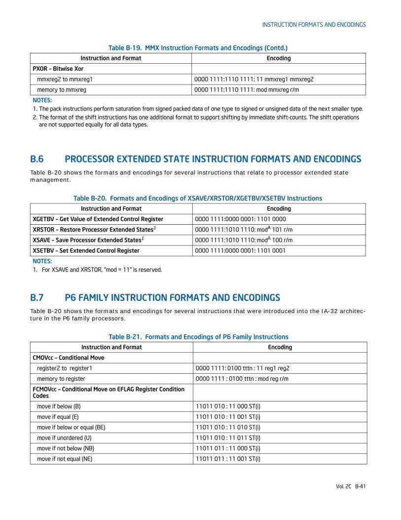
INSTRUCTION FORMATS AND ENCODINGS
B.6 PROCESSOR EXTENDED STATE INSTRUCTION FORMATS AND ENCODINGS Table B-20 shows the formats and encodings for several instructions that relate to processor extended state management.
B.7 P6 FAMILY INSTRUCTION FORMATS AND ENCODINGS Table B-20 shows the formats and encodings for several instructions that were introduced into the IA-32 architec-ture in the P6 family processors.
PXOR – Bitwise Xor
mmxreg2 to mmxreg1 0000 1111:1110 1111: 11 mmxreg1 mmxreg2
memory to mmxreg 0000 1111:1110 1111: mod mmxreg r/m
NOTES:1. The pack instructions perform saturation from signed packed data of one type to signed or unsigned data of the next smaller type.2. The format of the shift instructions has one additional format to support shifting by immediate shift-counts. The shift operations
are not supported equally for all data types.
Table B-20. Formats and Encodings of XSAVE/XRSTOR/XGETBV/XSETBV Instructions
Instruction and Format Encoding
XGETBV – Get Value of Extended Control Register 0000 1111:0000 0001: 1101 0000
XRSTOR – Restore Processor Extended States1 0000 1111:1010 1110: modA 101 r/m
XSAVE – Save Processor Extended States1 0000 1111:1010 1110: modA 100 r/m
XSETBV – Set Extended Control Register 0000 1111:0000 0001: 1101 0001
NOTES:1. For XSAVE and XRSTOR, “mod = 11” is reserved.
Table B-21. Formats and Encodings of P6 Family Instructions
Instruction and Format Encoding
CMOVcc – Conditional Move
register2 to register1 0000 1111: 0100 tttn : 11 reg1 reg2
memory to register 0000 1111 : 0100 tttn : mod reg r/m
FCMOVcc – Conditional Move on EFLAG Register Condition Codes
move if below (B) 11011 010 : 11 000 ST(i)
move if equal (E) 11011 010 : 11 001 ST(i)
move if below or equal (BE) 11011 010 : 11 010 ST(i)
move if unordered (U) 11011 010 : 11 011 ST(i)
move if not below (NB) 11011 011 : 11 000 ST(i)
move if not equal (NE) 11011 011 : 11 001 ST(i)
Table B-19. MMX Instruction Formats and Encodings (Contd.)
Instruction and Format Encoding
Vol. 2C B-41
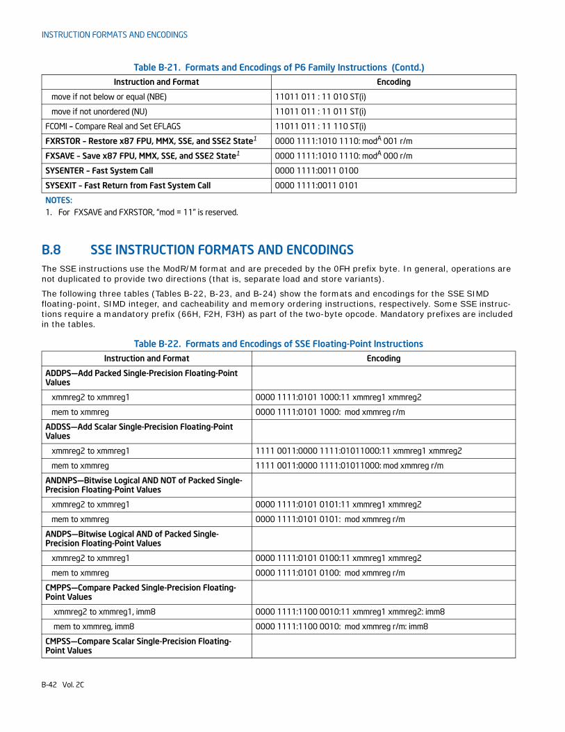
INSTRUCTION FORMATS AND ENCODINGS
B.8 SSE INSTRUCTION FORMATS AND ENCODINGS The SSE instructions use the ModR/M format and are preceded by the 0FH prefix byte. In general, operations are not duplicated to provide two directions (that is, separate load and store variants).
The following three tables (Tables B-22, B-23, and B-24) show the formats and encodings for the SSE SIMD floating-point, SIMD integer, and cacheability and memory ordering instructions, respectively. Some SSE instruc-tions require a mandatory prefix (66H, F2H, F3H) as part of the two-byte opcode. Mandatory prefixes are included in the tables.
move if not below or equal (NBE) 11011 011 : 11 010 ST(i)
move if not unordered (NU) 11011 011 : 11 011 ST(i)
FCOMI – Compare Real and Set EFLAGS 11011 011 : 11 110 ST(i)
FXRSTOR – Restore x87 FPU, MMX, SSE, and SSE2 State1 0000 1111:1010 1110: modA 001 r/m
FXSAVE – Save x87 FPU, MMX, SSE, and SSE2 State1 0000 1111:1010 1110: modA 000 r/m
SYSENTER – Fast System Call 0000 1111:0011 0100
SYSEXIT – Fast Return from Fast System Call 0000 1111:0011 0101
NOTES:1. For FXSAVE and FXRSTOR, “mod = 11” is reserved.
Table B-22. Formats and Encodings of SSE Floating-Point Instructions
Instruction and Format Encoding
ADDPS—Add Packed Single-Precision Floating-Point Values
xmmreg2 to xmmreg1 0000 1111:0101 1000:11 xmmreg1 xmmreg2
mem to xmmreg 0000 1111:0101 1000: mod xmmreg r/m
ADDSS—Add Scalar Single-Precision Floating-Point Values
xmmreg2 to xmmreg1 1111 0011:0000 1111:01011000:11 xmmreg1 xmmreg2
mem to xmmreg 1111 0011:0000 1111:01011000: mod xmmreg r/m
ANDNPS—Bitwise Logical AND NOT of Packed Single-Precision Floating-Point Values
xmmreg2 to xmmreg1 0000 1111:0101 0101:11 xmmreg1 xmmreg2
mem to xmmreg 0000 1111:0101 0101: mod xmmreg r/m
ANDPS—Bitwise Logical AND of Packed Single-Precision Floating-Point Values
xmmreg2 to xmmreg1 0000 1111:0101 0100:11 xmmreg1 xmmreg2
mem to xmmreg 0000 1111:0101 0100: mod xmmreg r/m
CMPPS—Compare Packed Single-Precision Floating-Point Values
xmmreg2 to xmmreg1, imm8 0000 1111:1100 0010:11 xmmreg1 xmmreg2: imm8
mem to xmmreg, imm8 0000 1111:1100 0010: mod xmmreg r/m: imm8
CMPSS—Compare Scalar Single-Precision Floating-Point Values
Table B-21. Formats and Encodings of P6 Family Instructions (Contd.)
Instruction and Format Encoding
B-42 Vol. 2C
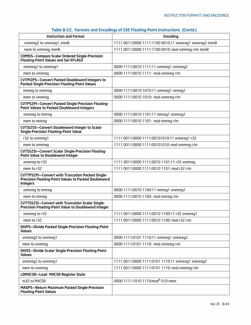
INSTRUCTION FORMATS AND ENCODINGS
xmmreg2 to xmmreg1, imm8 1111 0011:0000 1111:1100 0010:11 xmmreg1 xmmreg2: imm8
mem to xmmreg, imm8 1111 0011:0000 1111:1100 0010: mod xmmreg r/m: imm8
COMISS—Compare Scalar Ordered Single-Precision Floating-Point Values and Set EFLAGS
xmmreg2 to xmmreg1 0000 1111:0010 1111:11 xmmreg1 xmmreg2
mem to xmmreg 0000 1111:0010 1111: mod xmmreg r/m
CVTPI2PS—Convert Packed Doubleword Integers to Packed Single-Precision Floating-Point Values
mmreg to xmmreg 0000 1111:0010 1010:11 xmmreg1 mmreg1
mem to xmmreg 0000 1111:0010 1010: mod xmmreg r/m
CVTPS2PI—Convert Packed Single-Precision Floating-Point Values to Packed Doubleword Integers
xmmreg to mmreg 0000 1111:0010 1101:11 mmreg1 xmmreg1
mem to mmreg 0000 1111:0010 1101: mod mmreg r/m
CVTSI2SS—Convert Doubleword Integer to Scalar Single-Precision Floating-Point Value
r32 to xmmreg1 1111 0011:0000 1111:00101010:11 xmmreg1 r32
mem to xmmreg 1111 0011:0000 1111:00101010: mod xmmreg r/m
CVTSS2SI—Convert Scalar Single-Precision Floating-Point Value to Doubleword Integer
xmmreg to r32 1111 0011:0000 1111:0010 1101:11 r32 xmmreg
mem to r32 1111 0011:0000 1111:0010 1101: mod r32 r/m
CVTTPS2PI—Convert with Truncation Packed Single-Precision Floating-Point Values to Packed Doubleword Integers
xmmreg to mmreg 0000 1111:0010 1100:11 mmreg1 xmmreg1
mem to mmreg 0000 1111:0010 1100: mod mmreg r/m
CVTTSS2SI—Convert with Truncation Scalar Single-Precision Floating-Point Value to Doubleword Integer
xmmreg to r32 1111 0011:0000 1111:0010 1100:11 r32 xmmreg1
mem to r32 1111 0011:0000 1111:0010 1100: mod r32 r/m
DIVPS—Divide Packed Single-Precision Floating-Point Values
xmmreg2 to xmmreg1 0000 1111:0101 1110:11 xmmreg1 xmmreg2
mem to xmmreg 0000 1111:0101 1110: mod xmmreg r/m
DIVSS—Divide Scalar Single-Precision Floating-Point Values
xmmreg2 to xmmreg1 1111 0011:0000 1111:0101 1110:11 xmmreg1 xmmreg2
mem to xmmreg 1111 0011:0000 1111:0101 1110: mod xmmreg r/m
LDMXCSR—Load MXCSR Register State
m32 to MXCSR 0000 1111:1010 1110:modA 010 mem
MAXPS—Return Maximum Packed Single-Precision Floating-Point Values
Table B-22. Formats and Encodings of SSE Floating-Point Instructions (Contd.)
Instruction and Format Encoding
Vol. 2C B-43
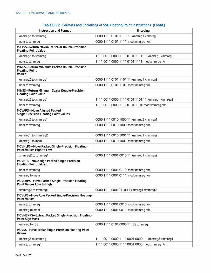
INSTRUCTION FORMATS AND ENCODINGS
xmmreg2 to xmmreg1 0000 1111:0101 1111:11 xmmreg1 xmmreg2
mem to xmmreg 0000 1111:0101 1111: mod xmmreg r/m
MAXSS—Return Maximum Scalar Double-Precision Floating-Point Value
xmmreg2 to xmmreg1 1111 0011:0000 1111:0101 1111:11 xmmreg1 xmmreg2
mem to xmmreg 1111 0011:0000 1111:0101 1111: mod xmmreg r/m
MINPS—Return Minimum Packed Double-Precision Floating-Point Values
xmmreg2 to xmmreg1 0000 1111:0101 1101:11 xmmreg1 xmmreg2
mem to xmmreg 0000 1111:0101 1101: mod xmmreg r/m
MINSS—Return Minimum Scalar Double-Precision Floating-Point Value
xmmreg2 to xmmreg1 1111 0011:0000 1111:0101 1101:11 xmmreg1 xmmreg2
mem to xmmreg 1111 0011:0000 1111:0101 1101: mod xmmreg r/m
MOVAPS—Move Aligned Packed Single-Precision Floating-Point Values
xmmreg2 to xmmreg1 0000 1111:0010 1000:11 xmmreg2 xmmreg1
mem to xmmreg1 0000 1111:0010 1000: mod xmmreg r/m
xmmreg1 to xmmreg2 0000 1111:0010 1001:11 xmmreg1 xmmreg2
xmmreg1 to mem 0000 1111:0010 1001: mod xmmreg r/m
MOVHLPS—Move Packed Single-Precision Floating-Point Values High to Low
xmmreg2 to xmmreg1 0000 1111:0001 0010:11 xmmreg1 xmmreg2
MOVHPS—Move High Packed Single-Precision Floating-Point Values
mem to xmmreg 0000 1111:0001 0110: mod xmmreg r/m
xmmreg to mem 0000 1111:0001 0111: mod xmmreg r/m
MOVLHPS—Move Packed Single-Precision Floating-Point Values Low to High
xmmreg2 to xmmreg1 0000 1111:00010110:11 xmmreg1 xmmreg2
MOVLPS—Move Low Packed Single-Precision Floating-Point Values
mem to xmmreg 0000 1111:0001 0010: mod xmmreg r/m
xmmreg to mem 0000 1111:0001 0011: mod xmmreg r/m
MOVMSKPS—Extract Packed Single-Precision Floating-Point Sign Mask
xmmreg to r32 0000 1111:0101 0000:11 r32 xmmreg
MOVSS—Move Scalar Single-Precision Floating-Point Values
xmmreg2 to xmmreg1 1111 0011:0000 1111:0001 0000:11 xmmreg2 xmmreg1
mem to xmmreg1 1111 0011:0000 1111:0001 0000: mod xmmreg r/m
Table B-22. Formats and Encodings of SSE Floating-Point Instructions (Contd.)
Instruction and Format Encoding
B-44 Vol. 2C
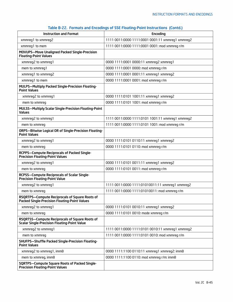
INSTRUCTION FORMATS AND ENCODINGS
xmmreg1 to xmmreg2 1111 0011:0000 1111:0001 0001:11 xmmreg1 xmmreg2
xmmreg1 to mem 1111 0011:0000 1111:0001 0001: mod xmmreg r/m
MOVUPS—Move Unaligned Packed Single-Precision Floating-Point Values
xmmreg2 to xmmreg1 0000 1111:0001 0000:11 xmmreg2 xmmreg1
mem to xmmreg1 0000 1111:0001 0000: mod xmmreg r/m
xmmreg1 to xmmreg2 0000 1111:0001 0001:11 xmmreg1 xmmreg2
xmmreg1 to mem 0000 1111:0001 0001: mod xmmreg r/m
MULPS—Multiply Packed Single-Precision Floating-Point Values
xmmreg2 to xmmreg1 0000 1111:0101 1001:11 xmmreg1 xmmreg2
mem to xmmreg 0000 1111:0101 1001: mod xmmreg r/m
MULSS—Multiply Scalar Single-Precision Floating-Point Values
xmmreg2 to xmmreg1 1111 0011:0000 1111:0101 1001:11 xmmreg1 xmmreg2
mem to xmmreg 1111 0011:0000 1111:0101 1001: mod xmmreg r/m
ORPS—Bitwise Logical OR of Single-Precision Floating-Point Values
xmmreg2 to xmmreg1 0000 1111:0101 0110:11 xmmreg1 xmmreg2
mem to xmmreg 0000 1111:0101 0110: mod xmmreg r/m
RCPPS—Compute Reciprocals of Packed Single-Precision Floating-Point Values
xmmreg2 to xmmreg1 0000 1111:0101 0011:11 xmmreg1 xmmreg2
mem to xmmreg 0000 1111:0101 0011: mod xmmreg r/m
RCPSS—Compute Reciprocals of Scalar Single-Precision Floating-Point Value
xmmreg2 to xmmreg1 1111 0011:0000 1111:01010011:11 xmmreg1 xmmreg2
mem to xmmreg 1111 0011:0000 1111:01010011: mod xmmreg r/m
RSQRTPS—Compute Reciprocals of Square Roots of Packed Single-Precision Floating-Point Values
xmmreg2 to xmmreg1 0000 1111:0101 0010:11 xmmreg1 xmmreg2
mem to xmmreg 0000 1111:0101 0010: mode xmmreg r/m
RSQRTSS—Compute Reciprocals of Square Roots of Scalar Single-Precision Floating-Point Value
xmmreg2 to xmmreg1 1111 0011:0000 1111:0101 0010:11 xmmreg1 xmmreg2
mem to xmmreg 1111 0011:0000 1111:0101 0010: mod xmmreg r/m
SHUFPS—Shuffle Packed Single-Precision Floating-Point Values
xmmreg2 to xmmreg1, imm8 0000 1111:1100 0110:11 xmmreg1 xmmreg2: imm8
mem to xmmreg, imm8 0000 1111:1100 0110: mod xmmreg r/m: imm8
SQRTPS—Compute Square Roots of Packed Single-Precision Floating-Point Values
Table B-22. Formats and Encodings of SSE Floating-Point Instructions (Contd.)
Instruction and Format Encoding
Vol. 2C B-45
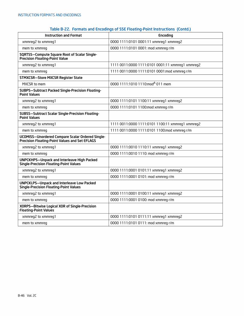
INSTRUCTION FORMATS AND ENCODINGS
xmmreg2 to xmmreg1 0000 1111:0101 0001:11 xmmreg1 xmmreg2
mem to xmmreg 0000 1111:0101 0001: mod xmmreg r/m
SQRTSS—Compute Square Root of Scalar Single-Precision Floating-Point Value
xmmreg2 to xmmreg1 1111 0011:0000 1111:0101 0001:11 xmmreg1 xmmreg2
mem to xmmreg 1111 0011:0000 1111:0101 0001:mod xmmreg r/m
STMXCSR—Store MXCSR Register State
MXCSR to mem 0000 1111:1010 1110:modA 011 mem
SUBPS—Subtract Packed Single-Precision Floating-Point Values
xmmreg2 to xmmreg1 0000 1111:0101 1100:11 xmmreg1 xmmreg2
mem to xmmreg 0000 1111:0101 1100:mod xmmreg r/m
SUBSS—Subtract Scalar Single-Precision Floating-Point Values
xmmreg2 to xmmreg1 1111 0011:0000 1111:0101 1100:11 xmmreg1 xmmreg2
mem to xmmreg 1111 0011:0000 1111:0101 1100:mod xmmreg r/m
UCOMISS—Unordered Compare Scalar Ordered Single-Precision Floating-Point Values and Set EFLAGS
xmmreg2 to xmmreg1 0000 1111:0010 1110:11 xmmreg1 xmmreg2
mem to xmmreg 0000 1111:0010 1110: mod xmmreg r/m
UNPCKHPS—Unpack and Interleave High Packed Single-Precision Floating-Point Values
xmmreg2 to xmmreg1 0000 1111:0001 0101:11 xmmreg1 xmmreg2
mem to xmmreg 0000 1111:0001 0101: mod xmmreg r/m
UNPCKLPS—Unpack and Interleave Low Packed Single-Precision Floating-Point Values
xmmreg2 to xmmreg1 0000 1111:0001 0100:11 xmmreg1 xmmreg2
mem to xmmreg 0000 1111:0001 0100: mod xmmreg r/m
XORPS—Bitwise Logical XOR of Single-Precision Floating-Point Values
xmmreg2 to xmmreg1 0000 1111:0101 0111:11 xmmreg1 xmmreg2
mem to xmmreg 0000 1111:0101 0111: mod xmmreg r/m
Table B-22. Formats and Encodings of SSE Floating-Point Instructions (Contd.)
Instruction and Format Encoding
B-46 Vol. 2C
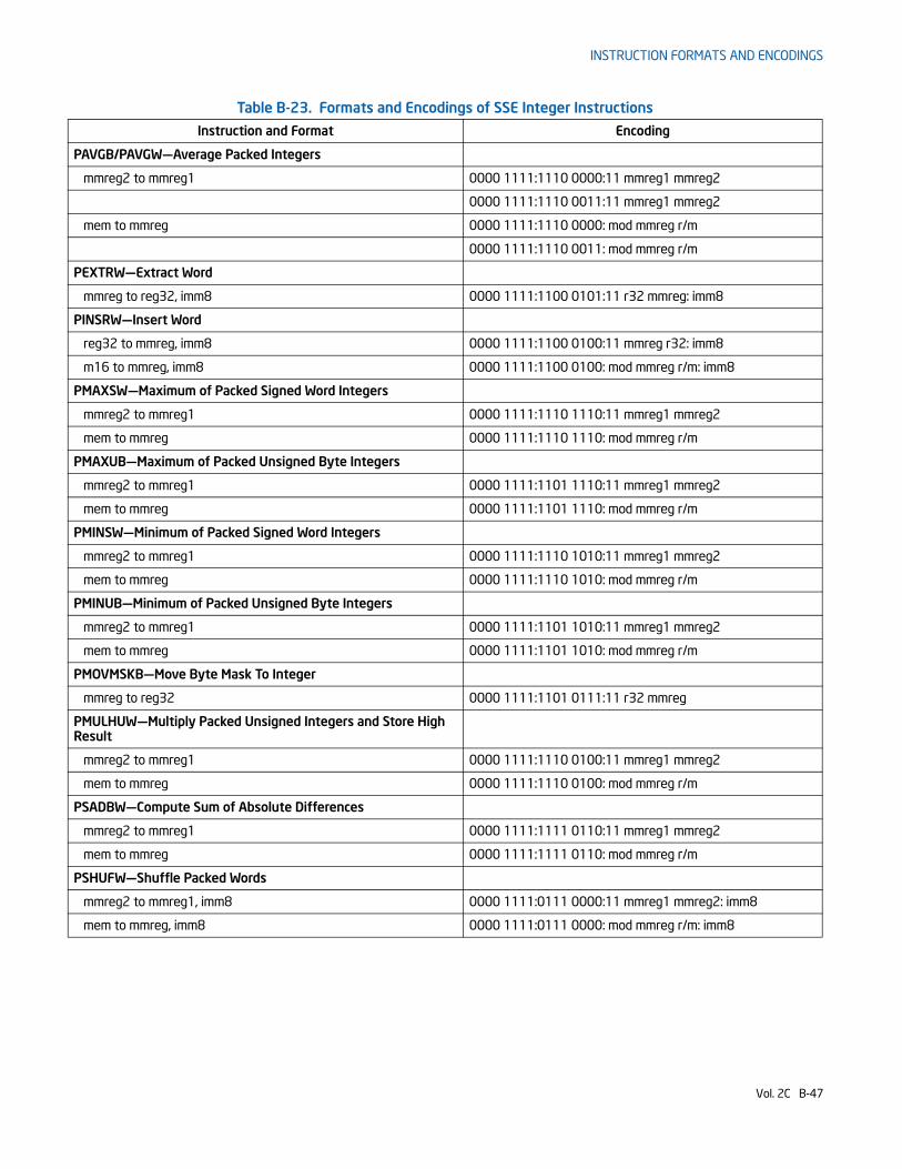
INSTRUCTION FORMATS AND ENCODINGS
Table B-23. Formats and Encodings of SSE Integer Instructions
Instruction and Format Encoding
PAVGB/PAVGW—Average Packed Integers
mmreg2 to mmreg1 0000 1111:1110 0000:11 mmreg1 mmreg2
0000 1111:1110 0011:11 mmreg1 mmreg2
mem to mmreg 0000 1111:1110 0000: mod mmreg r/m
0000 1111:1110 0011: mod mmreg r/m
PEXTRW—Extract Word
mmreg to reg32, imm8 0000 1111:1100 0101:11 r32 mmreg: imm8
PINSRW—Insert Word
reg32 to mmreg, imm8 0000 1111:1100 0100:11 mmreg r32: imm8
m16 to mmreg, imm8 0000 1111:1100 0100: mod mmreg r/m: imm8
PMAXSW—Maximum of Packed Signed Word Integers
mmreg2 to mmreg1 0000 1111:1110 1110:11 mmreg1 mmreg2
mem to mmreg 0000 1111:1110 1110: mod mmreg r/m
PMAXUB—Maximum of Packed Unsigned Byte Integers
mmreg2 to mmreg1 0000 1111:1101 1110:11 mmreg1 mmreg2
mem to mmreg 0000 1111:1101 1110: mod mmreg r/m
PMINSW—Minimum of Packed Signed Word Integers
mmreg2 to mmreg1 0000 1111:1110 1010:11 mmreg1 mmreg2
mem to mmreg 0000 1111:1110 1010: mod mmreg r/m
PMINUB—Minimum of Packed Unsigned Byte Integers
mmreg2 to mmreg1 0000 1111:1101 1010:11 mmreg1 mmreg2
mem to mmreg 0000 1111:1101 1010: mod mmreg r/m
PMOVMSKB—Move Byte Mask To Integer
mmreg to reg32 0000 1111:1101 0111:11 r32 mmreg
PMULHUW—Multiply Packed Unsigned Integers and Store High Result
mmreg2 to mmreg1 0000 1111:1110 0100:11 mmreg1 mmreg2
mem to mmreg 0000 1111:1110 0100: mod mmreg r/m
PSADBW—Compute Sum of Absolute Differences
mmreg2 to mmreg1 0000 1111:1111 0110:11 mmreg1 mmreg2
mem to mmreg 0000 1111:1111 0110: mod mmreg r/m
PSHUFW—Shuffle Packed Words
mmreg2 to mmreg1, imm8 0000 1111:0111 0000:11 mmreg1 mmreg2: imm8
mem to mmreg, imm8 0000 1111:0111 0000: mod mmreg r/m: imm8
Vol. 2C B-47
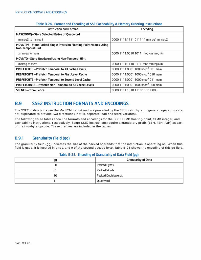
INSTRUCTION FORMATS AND ENCODINGS
B.9 SSE2 INSTRUCTION FORMATS AND ENCODINGS The SSE2 instructions use the ModR/M format and are preceded by the 0FH prefix byte. In general, operations are not duplicated to provide two directions (that is, separate load and store variants).
The following three tables show the formats and encodings for the SSE2 SIMD floating-point, SIMD integer, and cacheability instructions, respectively. Some SSE2 instructions require a mandatory prefix (66H, F2H, F3H) as part of the two-byte opcode. These prefixes are included in the tables.
B.9.1 Granularity Field (gg)The granularity field (gg) indicates the size of the packed operands that the instruction is operating on. When this field is used, it is located in bits 1 and 0 of the second opcode byte. Table B-25 shows the encoding of this gg field.
Table B-24. Format and Encoding of SSE Cacheability & Memory Ordering Instructions
Instruction and Format Encoding
MASKMOVQ—Store Selected Bytes of Quadword
mmreg2 to mmreg1 0000 1111:1111 0111:11 mmreg1 mmreg2
MOVNTPS—Store Packed Single-Precision Floating-Point Values Using Non-Temporal Hint
xmmreg to mem 0000 1111:0010 1011: mod xmmreg r/m
MOVNTQ—Store Quadword Using Non-Temporal Hint
mmreg to mem 0000 1111:1110 0111: mod mmreg r/m
PREFETCHT0—Prefetch Temporal to All Cache Levels 0000 1111:0001 1000:modA 001 mem
PREFETCHT1—Prefetch Temporal to First Level Cache 0000 1111:0001 1000:modA 010 mem
PREFETCHT2—Prefetch Temporal to Second Level Cache 0000 1111:0001 1000:modA 011 mem
PREFETCHNTA—Prefetch Non-Temporal to All Cache Levels 0000 1111:0001 1000:modA 000 mem
SFENCE—Store Fence 0000 1111:1010 1110:11 111 000
Table B-25. Encoding of Granularity of Data Field (gg)
gg Granularity of Data
00 Packed Bytes
01 Packed Words
10 Packed Doublewords
11 Quadword
B-48 Vol. 2C
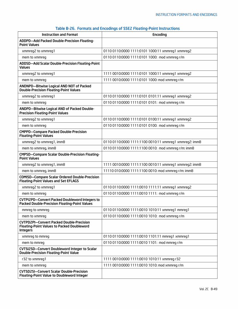
INSTRUCTION FORMATS AND ENCODINGS
Table B-26. Formats and Encodings of SSE2 Floating-Point Instructions
Instruction and Format Encoding
ADDPD—Add Packed Double-Precision Floating-Point Values
xmmreg2 to xmmreg1 0110 0110:0000 1111:0101 1000:11 xmmreg1 xmmreg2
mem to xmmreg 0110 0110:0000 1111:0101 1000: mod xmmreg r/m
ADDSD—Add Scalar Double-Precision Floating-Point Values
xmmreg2 to xmmreg1 1111 0010:0000 1111:0101 1000:11 xmmreg1 xmmreg2
mem to xmmreg 1111 0010:0000 1111:0101 1000: mod xmmreg r/m
ANDNPD—Bitwise Logical AND NOT of Packed Double-Precision Floating-Point Values
xmmreg2 to xmmreg1 0110 0110:0000 1111:0101 0101:11 xmmreg1 xmmreg2
mem to xmmreg 0110 0110:0000 1111:0101 0101: mod xmmreg r/m
ANDPD—Bitwise Logical AND of Packed Double-Precision Floating-Point Values
xmmreg2 to xmmreg1 0110 0110:0000 1111:0101 0100:11 xmmreg1 xmmreg2
mem to xmmreg 0110 0110:0000 1111:0101 0100: mod xmmreg r/m
CMPPD—Compare Packed Double-Precision Floating-Point Values
xmmreg2 to xmmreg1, imm8 0110 0110:0000 1111:1100 0010:11 xmmreg1 xmmreg2: imm8
mem to xmmreg, imm8 0110 0110:0000 1111:1100 0010: mod xmmreg r/m: imm8
CMPSD—Compare Scalar Double-Precision Floating-Point Values
xmmreg2 to xmmreg1, imm8 1111 0010:0000 1111:1100 0010:11 xmmreg1 xmmreg2: imm8
mem to xmmreg, imm8 11110 010:0000 1111:1100 0010: mod xmmreg r/m: imm8
COMISD—Compare Scalar Ordered Double-Precision Floating-Point Values and Set EFLAGS
xmmreg2 to xmmreg1 0110 0110:0000 1111:0010 1111:11 xmmreg1 xmmreg2
mem to xmmreg 0110 0110:0000 1111:0010 1111: mod xmmreg r/m
CVTPI2PD—Convert Packed Doubleword Integers to Packed Double-Precision Floating-Point Values
mmreg to xmmreg 0110 0110:0000 1111:0010 1010:11 xmmreg1 mmreg1
mem to xmmreg 0110 0110:0000 1111:0010 1010: mod xmmreg r/m
CVTPD2PI—Convert Packed Double-Precision Floating-Point Values to Packed Doubleword Integers
xmmreg to mmreg 0110 0110:0000 1111:0010 1101:11 mmreg1 xmmreg1
mem to mmreg 0110 0110:0000 1111:0010 1101: mod mmreg r/m
CVTSI2SD—Convert Doubleword Integer to Scalar Double-Precision Floating-Point Value
r32 to xmmreg1 1111 0010:0000 1111:0010 1010:11 xmmreg r32
mem to xmmreg 1111 0010:0000 1111:0010 1010: mod xmmreg r/m
CVTSD2SI—Convert Scalar Double-Precision Floating-Point Value to Doubleword Integer
Vol. 2C B-49
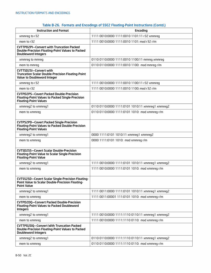
INSTRUCTION FORMATS AND ENCODINGS
xmmreg to r32 1111 0010:0000 1111:0010 1101:11 r32 xmmreg
mem to r32 1111 0010:0000 1111:0010 1101: mod r32 r/m
CVTTPD2PI—Convert with Truncation Packed Double-Precision Floating-Point Values to Packed Doubleword Integers
xmmreg to mmreg 0110 0110:0000 1111:0010 1100:11 mmreg xmmreg
mem to mmreg 0110 0110:0000 1111:0010 1100: mod mmreg r/m
CVTTSD2SI—Convert with Truncation Scalar Double-Precision Floating-Point Value to Doubleword Integer
xmmreg to r32 1111 0010:0000 1111:0010 1100:11 r32 xmmreg
mem to r32 1111 0010:0000 1111:0010 1100: mod r32 r/m
CVTPD2PS—Covert Packed Double-Precision Floating-Point Values to Packed Single-Precision Floating-Point Values
xmmreg2 to xmmreg1 0110 0110:0000 1111:0101 1010:11 xmmreg1 xmmreg2
mem to xmmreg 0110 0110:0000 1111:0101 1010: mod xmmreg r/m
CVTPS2PD—Covert Packed Single-Precision Floating-Point Values to Packed Double-Precision Floating-Point Values
xmmreg2 to xmmreg1 0000 1111:0101 1010:11 xmmreg1 xmmreg2
mem to xmmreg 0000 1111:0101 1010: mod xmmreg r/m
CVTSD2SS—Covert Scalar Double-Precision Floating-Point Value to Scalar Single-Precision Floating-Point Value
xmmreg2 to xmmreg1 1111 0010:0000 1111:0101 1010:11 xmmreg1 xmmreg2
mem to xmmreg 1111 0010:0000 1111:0101 1010: mod xmmreg r/m
CVTSS2SD—Covert Scalar Single-Precision Floating-Point Value to Scalar Double-Precision Floating-Point Value
xmmreg2 to xmmreg1 1111 0011:0000 1111:0101 1010:11 xmmreg1 xmmreg2
mem to xmmreg 1111 0011:00001 111:0101 1010: mod xmmreg r/m
CVTPD2DQ—Convert Packed Double-Precision Floating-Point Values to Packed Doubleword Integers
xmmreg2 to xmmreg1 1111 0010:0000 1111:1110 0110:11 xmmreg1 xmmreg2
mem to xmmreg 1111 0010:0000 1111:1110 0110: mod xmmreg r/m
CVTTPD2DQ—Convert With Truncation Packed Double-Precision Floating-Point Values to Packed Doubleword Integers
xmmreg2 to xmmreg1 0110 0110:0000 1111:1110 0110:11 xmmreg1 xmmreg2
mem to xmmreg 0110 0110:0000 1111:1110 0110: mod xmmreg r/m
Table B-26. Formats and Encodings of SSE2 Floating-Point Instructions (Contd.)
Instruction and Format Encoding
B-50 Vol. 2C
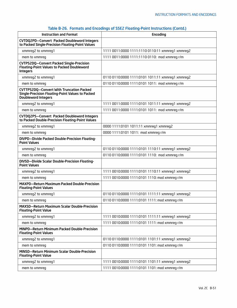
INSTRUCTION FORMATS AND ENCODINGS
CVTDQ2PD—Convert Packed Doubleword Integers to Packed Single-Precision Floating-Point Values
xmmreg2 to xmmreg1 1111 0011:0000 1111:1110 0110:11 xmmreg1 xmmreg2
mem to xmmreg 1111 0011:0000 1111:1110 0110: mod xmmreg r/m
CVTPS2DQ—Convert Packed Single-Precision Floating-Point Values to Packed Doubleword Integers
xmmreg2 to xmmreg1 0110 0110:0000 1111:0101 1011:11 xmmreg1 xmmreg2
mem to xmmreg 0110 0110:0000 1111:0101 1011: mod xmmreg r/m
CVTTPS2DQ—Convert With Truncation Packed Single-Precision Floating-Point Values to Packed Doubleword Integers
xmmreg2 to xmmreg1 1111 0011:0000 1111:0101 1011:11 xmmreg1 xmmreg2
mem to xmmreg 1111 0011:0000 1111:0101 1011: mod xmmreg r/m
CVTDQ2PS—Convert Packed Doubleword Integers to Packed Double-Precision Floating-Point Values
xmmreg2 to xmmreg1 0000 1111:0101 1011:11 xmmreg1 xmmreg2
mem to xmmreg 0000 1111:0101 1011: mod xmmreg r/m
DIVPD—Divide Packed Double-Precision Floating-Point Values
xmmreg2 to xmmreg1 0110 0110:0000 1111:0101 1110:11 xmmreg1 xmmreg2
mem to xmmreg 0110 0110:0000 1111:0101 1110: mod xmmreg r/m
DIVSD—Divide Scalar Double-Precision Floating-Point Values
xmmreg2 to xmmreg1 1111 0010:0000 1111:0101 1110:11 xmmreg1 xmmreg2
mem to xmmreg 1111 0010:0000 1111:0101 1110: mod xmmreg r/m
MAXPD—Return Maximum Packed Double-Precision Floating-Point Values
xmmreg2 to xmmreg1 0110 0110:0000 1111:0101 1111:11 xmmreg1 xmmreg2
mem to xmmreg 0110 0110:0000 1111:0101 1111: mod xmmreg r/m
MAXSD—Return Maximum Scalar Double-Precision Floating-Point Value
xmmreg2 to xmmreg1 1111 0010:0000 1111:0101 1111:11 xmmreg1 xmmreg2
mem to xmmreg 1111 0010:0000 1111:0101 1111: mod xmmreg r/m
MINPD—Return Minimum Packed Double-Precision Floating-Point Values
xmmreg2 to xmmreg1 0110 0110:0000 1111:0101 1101:11 xmmreg1 xmmreg2
mem to xmmreg 0110 0110:0000 1111:0101 1101: mod xmmreg r/m
MINSD—Return Minimum Scalar Double-Precision Floating-Point Value
xmmreg2 to xmmreg1 1111 0010:0000 1111:0101 1101:11 xmmreg1 xmmreg2
mem to xmmreg 1111 0010:0000 1111:0101 1101: mod xmmreg r/m
Table B-26. Formats and Encodings of SSE2 Floating-Point Instructions (Contd.)
Instruction and Format Encoding
Vol. 2C B-51
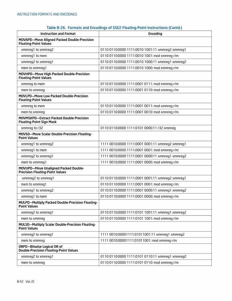
INSTRUCTION FORMATS AND ENCODINGS
MOVAPD—Move Aligned Packed Double-Precision Floating-Point Values
xmmreg1 to xmmreg2 0110 0110:0000 1111:0010 1001:11 xmmreg2 xmmreg1
xmmreg1 to mem 0110 0110:0000 1111:0010 1001: mod xmmreg r/m
xmmreg2 to xmmreg1 0110 0110:0000 1111:0010 1000:11 xmmreg1 xmmreg2
mem to xmmreg1 0110 0110:0000 1111:0010 1000: mod xmmreg r/m
MOVHPD—Move High Packed Double-Precision Floating-Point Values
xmmreg to mem 0110 0110:0000 1111:0001 0111: mod xmmreg r/m
mem to xmmreg 0110 0110:0000 1111:0001 0110: mod xmmreg r/m
MOVLPD—Move Low Packed Double-Precision Floating-Point Values
xmmreg to mem 0110 0110:0000 1111:0001 0011: mod xmmreg r/m
mem to xmmreg 0110 0110:0000 1111:0001 0010: mod xmmreg r/m
MOVMSKPD—Extract Packed Double-Precision Floating-Point Sign Mask
xmmreg to r32 0110 0110:0000 1111:0101 0000:11 r32 xmmreg
MOVSD—Move Scalar Double-Precision Floating-Point Values
xmmreg1 to xmmreg2 1111 0010:0000 1111:0001 0001:11 xmmreg2 xmmreg1
xmmreg1 to mem 1111 0010:0000 1111:0001 0001: mod xmmreg r/m
xmmreg2 to xmmreg1 1111 0010:0000 1111:0001 0000:11 xmmreg1 xmmreg2
mem to xmmreg1 1111 0010:0000 1111:0001 0000: mod xmmreg r/m
MOVUPD—Move Unaligned Packed Double-Precision Floating-Point Values
xmmreg2 to xmmreg1 0110 0110:0000 1111:0001 0001:11 xmmreg2 xmmreg1
mem to xmmreg1 0110 0110:0000 1111:0001 0001: mod xmmreg r/m
xmmreg1 to xmmreg2 0110 0110:0000 1111:0001 0000:11 xmmreg1 xmmreg2
xmmreg1 to mem 0110 0110:0000 1111:0001 0000: mod xmmreg r/m
MULPD—Multiply Packed Double-Precision Floating-Point Values
xmmreg2 to xmmreg1 0110 0110:0000 1111:0101 1001:11 xmmreg1 xmmreg2
mem to xmmreg 0110 0110:0000 1111:0101 1001: mod xmmreg r/m
MULSD—Multiply Scalar Double-Precision Floating-Point Values
xmmreg2 to xmmreg1 1111 0010:00001111:01011001:11 xmmreg1 xmmreg2
mem to xmmreg 1111 0010:00001111:01011001: mod xmmreg r/m
ORPD—Bitwise Logical OR of Double-Precision Floating-Point Values
xmmreg2 to xmmreg1 0110 0110:0000 1111:0101 0110:11 xmmreg1 xmmreg2
mem to xmmreg 0110 0110:0000 1111:0101 0110: mod xmmreg r/m
Table B-26. Formats and Encodings of SSE2 Floating-Point Instructions (Contd.)
Instruction and Format Encoding
B-52 Vol. 2C
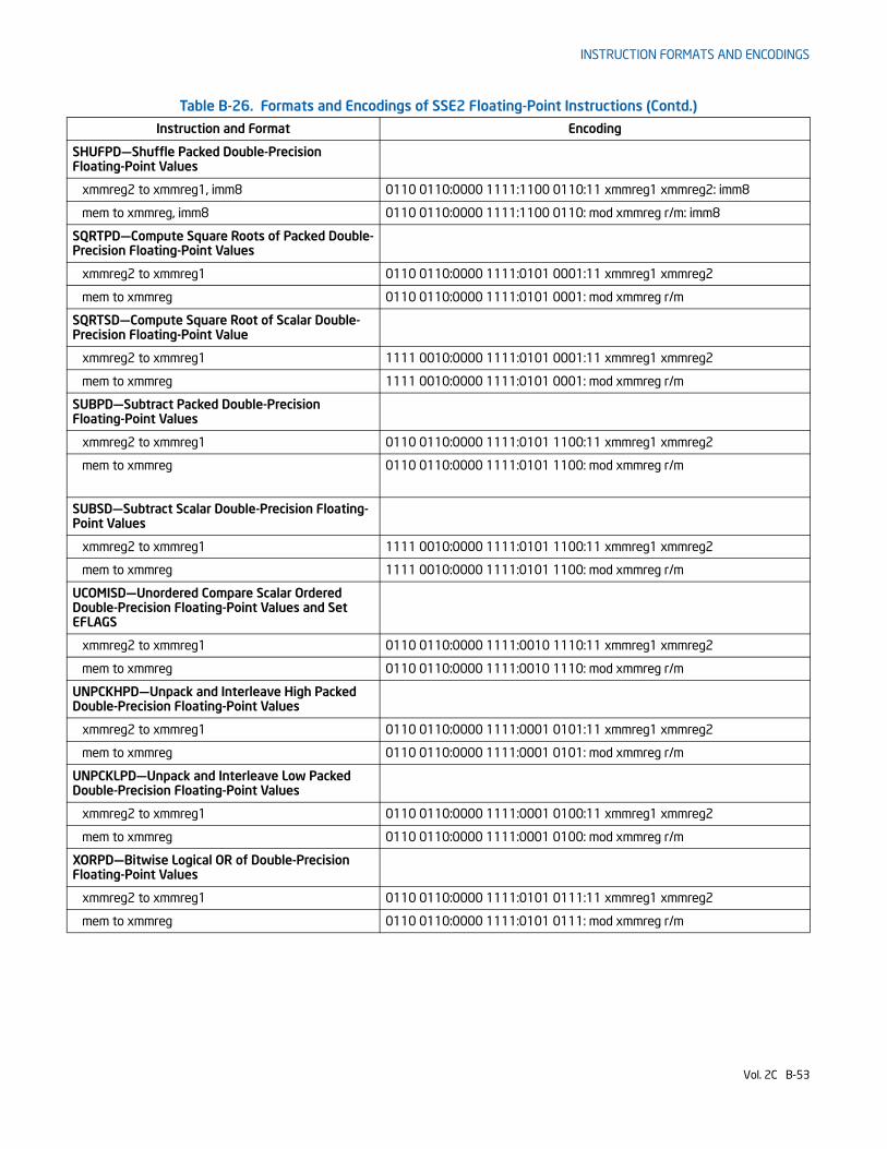
INSTRUCTION FORMATS AND ENCODINGS
SHUFPD—Shuffle Packed Double-Precision Floating-Point Values
xmmreg2 to xmmreg1, imm8 0110 0110:0000 1111:1100 0110:11 xmmreg1 xmmreg2: imm8
mem to xmmreg, imm8 0110 0110:0000 1111:1100 0110: mod xmmreg r/m: imm8
SQRTPD—Compute Square Roots of Packed Double-Precision Floating-Point Values
xmmreg2 to xmmreg1 0110 0110:0000 1111:0101 0001:11 xmmreg1 xmmreg2
mem to xmmreg 0110 0110:0000 1111:0101 0001: mod xmmreg r/m
SQRTSD—Compute Square Root of Scalar Double-Precision Floating-Point Value
xmmreg2 to xmmreg1 1111 0010:0000 1111:0101 0001:11 xmmreg1 xmmreg2
mem to xmmreg 1111 0010:0000 1111:0101 0001: mod xmmreg r/m
SUBPD—Subtract Packed Double-Precision Floating-Point Values
xmmreg2 to xmmreg1 0110 0110:0000 1111:0101 1100:11 xmmreg1 xmmreg2
mem to xmmreg 0110 0110:0000 1111:0101 1100: mod xmmreg r/m
SUBSD—Subtract Scalar Double-Precision Floating-Point Values
xmmreg2 to xmmreg1 1111 0010:0000 1111:0101 1100:11 xmmreg1 xmmreg2
mem to xmmreg 1111 0010:0000 1111:0101 1100: mod xmmreg r/m
UCOMISD—Unordered Compare Scalar Ordered Double-Precision Floating-Point Values and Set EFLAGS
xmmreg2 to xmmreg1 0110 0110:0000 1111:0010 1110:11 xmmreg1 xmmreg2
mem to xmmreg 0110 0110:0000 1111:0010 1110: mod xmmreg r/m
UNPCKHPD—Unpack and Interleave High Packed Double-Precision Floating-Point Values
xmmreg2 to xmmreg1 0110 0110:0000 1111:0001 0101:11 xmmreg1 xmmreg2
mem to xmmreg 0110 0110:0000 1111:0001 0101: mod xmmreg r/m
UNPCKLPD—Unpack and Interleave Low Packed Double-Precision Floating-Point Values
xmmreg2 to xmmreg1 0110 0110:0000 1111:0001 0100:11 xmmreg1 xmmreg2
mem to xmmreg 0110 0110:0000 1111:0001 0100: mod xmmreg r/m
XORPD—Bitwise Logical OR of Double-Precision Floating-Point Values
xmmreg2 to xmmreg1 0110 0110:0000 1111:0101 0111:11 xmmreg1 xmmreg2
mem to xmmreg 0110 0110:0000 1111:0101 0111: mod xmmreg r/m
Table B-26. Formats and Encodings of SSE2 Floating-Point Instructions (Contd.)
Instruction and Format Encoding
Vol. 2C B-53
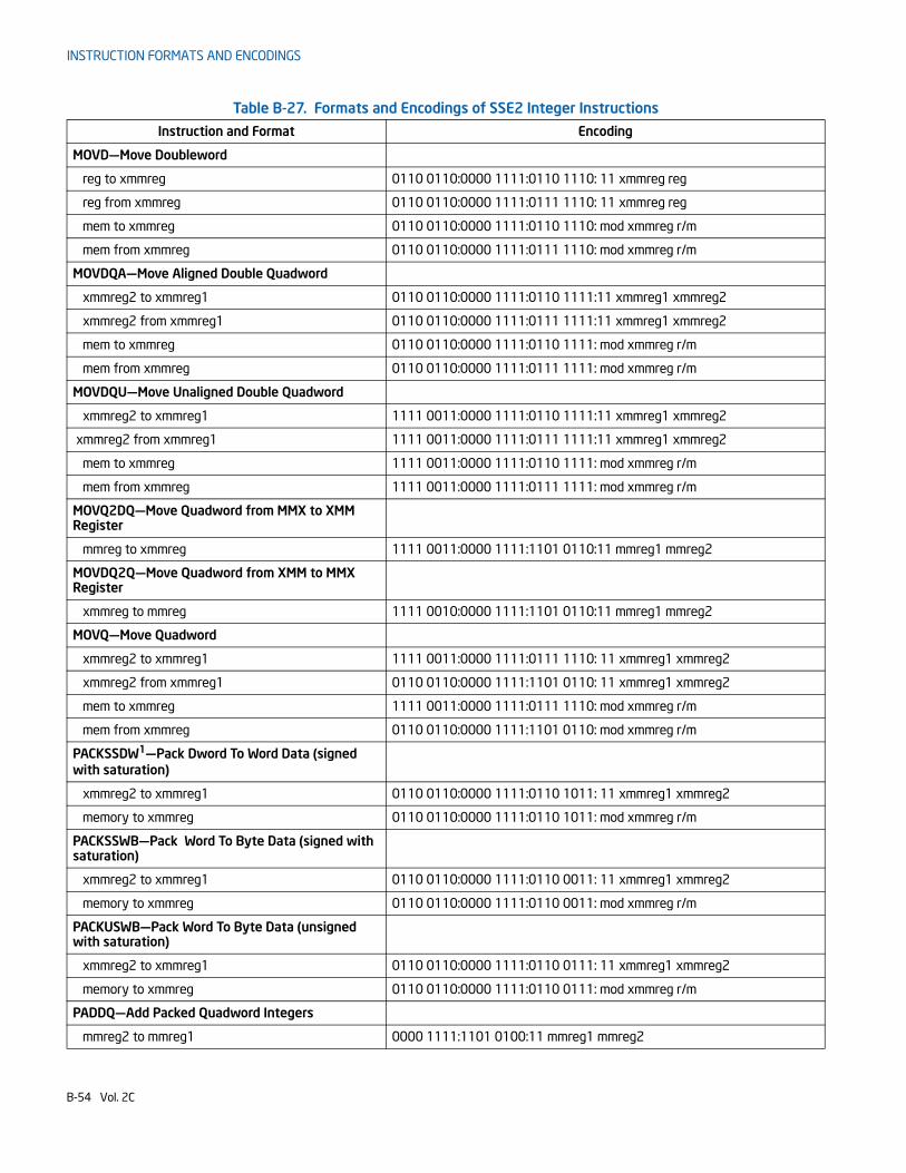
INSTRUCTION FORMATS AND ENCODINGS
Table B-27. Formats and Encodings of SSE2 Integer Instructions
Instruction and Format Encoding
MOVD—Move Doubleword
reg to xmmreg 0110 0110:0000 1111:0110 1110: 11 xmmreg reg
reg from xmmreg 0110 0110:0000 1111:0111 1110: 11 xmmreg reg
mem to xmmreg 0110 0110:0000 1111:0110 1110: mod xmmreg r/m
mem from xmmreg 0110 0110:0000 1111:0111 1110: mod xmmreg r/m
MOVDQA—Move Aligned Double Quadword
xmmreg2 to xmmreg1 0110 0110:0000 1111:0110 1111:11 xmmreg1 xmmreg2
xmmreg2 from xmmreg1 0110 0110:0000 1111:0111 1111:11 xmmreg1 xmmreg2
mem to xmmreg 0110 0110:0000 1111:0110 1111: mod xmmreg r/m
mem from xmmreg 0110 0110:0000 1111:0111 1111: mod xmmreg r/m
MOVDQU—Move Unaligned Double Quadword
xmmreg2 to xmmreg1 1111 0011:0000 1111:0110 1111:11 xmmreg1 xmmreg2
xmmreg2 from xmmreg1 1111 0011:0000 1111:0111 1111:11 xmmreg1 xmmreg2
mem to xmmreg 1111 0011:0000 1111:0110 1111: mod xmmreg r/m
mem from xmmreg 1111 0011:0000 1111:0111 1111: mod xmmreg r/m
MOVQ2DQ—Move Quadword from MMX to XMM Register
mmreg to xmmreg 1111 0011:0000 1111:1101 0110:11 mmreg1 mmreg2
MOVDQ2Q—Move Quadword from XMM to MMX Register
xmmreg to mmreg 1111 0010:0000 1111:1101 0110:11 mmreg1 mmreg2
MOVQ—Move Quadword
xmmreg2 to xmmreg1 1111 0011:0000 1111:0111 1110: 11 xmmreg1 xmmreg2
xmmreg2 from xmmreg1 0110 0110:0000 1111:1101 0110: 11 xmmreg1 xmmreg2
mem to xmmreg 1111 0011:0000 1111:0111 1110: mod xmmreg r/m
mem from xmmreg 0110 0110:0000 1111:1101 0110: mod xmmreg r/m
PACKSSDW1—Pack Dword To Word Data (signed with saturation)
xmmreg2 to xmmreg1 0110 0110:0000 1111:0110 1011: 11 xmmreg1 xmmreg2
memory to xmmreg 0110 0110:0000 1111:0110 1011: mod xmmreg r/m
PACKSSWB—Pack Word To Byte Data (signed with saturation)
xmmreg2 to xmmreg1 0110 0110:0000 1111:0110 0011: 11 xmmreg1 xmmreg2
memory to xmmreg 0110 0110:0000 1111:0110 0011: mod xmmreg r/m
PACKUSWB—Pack Word To Byte Data (unsigned with saturation)
xmmreg2 to xmmreg1 0110 0110:0000 1111:0110 0111: 11 xmmreg1 xmmreg2
memory to xmmreg 0110 0110:0000 1111:0110 0111: mod xmmreg r/m
PADDQ—Add Packed Quadword Integers
mmreg2 to mmreg1 0000 1111:1101 0100:11 mmreg1 mmreg2
B-54 Vol. 2C
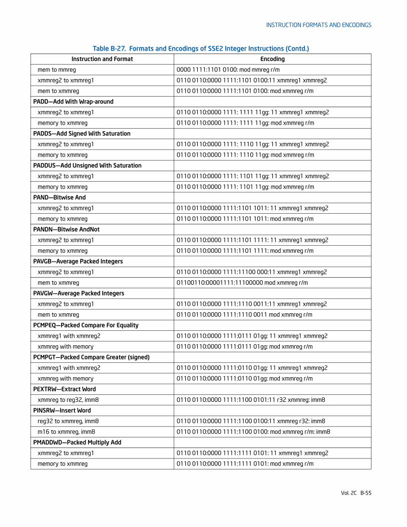
INSTRUCTION FORMATS AND ENCODINGS
mem to mmreg 0000 1111:1101 0100: mod mmreg r/m
xmmreg2 to xmmreg1 0110 0110:0000 1111:1101 0100:11 xmmreg1 xmmreg2
mem to xmmreg 0110 0110:0000 1111:1101 0100: mod xmmreg r/m
PADD—Add With Wrap-around
xmmreg2 to xmmreg1 0110 0110:0000 1111: 1111 11gg: 11 xmmreg1 xmmreg2
memory to xmmreg 0110 0110:0000 1111: 1111 11gg: mod xmmreg r/m
PADDS—Add Signed With Saturation
xmmreg2 to xmmreg1 0110 0110:0000 1111: 1110 11gg: 11 xmmreg1 xmmreg2
memory to xmmreg 0110 0110:0000 1111: 1110 11gg: mod xmmreg r/m
PADDUS—Add Unsigned With Saturation
xmmreg2 to xmmreg1 0110 0110:0000 1111: 1101 11gg: 11 xmmreg1 xmmreg2
memory to xmmreg 0110 0110:0000 1111: 1101 11gg: mod xmmreg r/m
PAND—Bitwise And
xmmreg2 to xmmreg1 0110 0110:0000 1111:1101 1011: 11 xmmreg1 xmmreg2
memory to xmmreg 0110 0110:0000 1111:1101 1011: mod xmmreg r/m
PANDN—Bitwise AndNot
xmmreg2 to xmmreg1 0110 0110:0000 1111:1101 1111: 11 xmmreg1 xmmreg2
memory to xmmreg 0110 0110:0000 1111:1101 1111: mod xmmreg r/m
PAVGB—Average Packed Integers
xmmreg2 to xmmreg1 0110 0110:0000 1111:11100 000:11 xmmreg1 xmmreg2
mem to xmmreg 01100110:00001111:11100000 mod xmmreg r/m
PAVGW—Average Packed Integers
xmmreg2 to xmmreg1 0110 0110:0000 1111:1110 0011:11 xmmreg1 xmmreg2
mem to xmmreg 0110 0110:0000 1111:1110 0011 mod xmmreg r/m
PCMPEQ—Packed Compare For Equality
xmmreg1 with xmmreg2 0110 0110:0000 1111:0111 01gg: 11 xmmreg1 xmmreg2
xmmreg with memory 0110 0110:0000 1111:0111 01gg: mod xmmreg r/m
PCMPGT—Packed Compare Greater (signed)
xmmreg1 with xmmreg2 0110 0110:0000 1111:0110 01gg: 11 xmmreg1 xmmreg2
xmmreg with memory 0110 0110:0000 1111:0110 01gg: mod xmmreg r/m
PEXTRW—Extract Word
xmmreg to reg32, imm8 0110 0110:0000 1111:1100 0101:11 r32 xmmreg: imm8
PINSRW—Insert Word
reg32 to xmmreg, imm8 0110 0110:0000 1111:1100 0100:11 xmmreg r32: imm8
m16 to xmmreg, imm8 0110 0110:0000 1111:1100 0100: mod xmmreg r/m: imm8
PMADDWD—Packed Multiply Add
xmmreg2 to xmmreg1 0110 0110:0000 1111:1111 0101: 11 xmmreg1 xmmreg2
memory to xmmreg 0110 0110:0000 1111:1111 0101: mod xmmreg r/m
Table B-27. Formats and Encodings of SSE2 Integer Instructions (Contd.)
Instruction and Format Encoding
Vol. 2C B-55
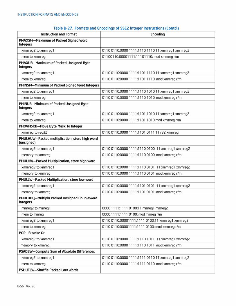
INSTRUCTION FORMATS AND ENCODINGS
PMAXSW—Maximum of Packed Signed Word Integers
xmmreg2 to xmmreg1 0110 0110:0000 1111:1110 1110:11 xmmreg1 xmmreg2
mem to xmmreg 01100110:00001111:11101110: mod xmmreg r/m
PMAXUB—Maximum of Packed Unsigned Byte Integers
xmmreg2 to xmmreg1 0110 0110:0000 1111:1101 1110:11 xmmreg1 xmmreg2
mem to xmmreg 0110 0110:0000 1111:1101 1110: mod xmmreg r/m
PMINSW—Minimum of Packed Signed Word Integers
xmmreg2 to xmmreg1 0110 0110:0000 1111:1110 1010:11 xmmreg1 xmmreg2
mem to xmmreg 0110 0110:0000 1111:1110 1010: mod xmmreg r/m
PMINUB—Minimum of Packed Unsigned Byte Integers
xmmreg2 to xmmreg1 0110 0110:0000 1111:1101 1010:11 xmmreg1 xmmreg2
mem to xmmreg 0110 0110:0000 1111:1101 1010 mod xmmreg r/m
PMOVMSKB—Move Byte Mask To Integer
xmmreg to reg32 0110 0110:0000 1111:1101 0111:11 r32 xmmreg
PMULHUW—Packed multiplication, store high word (unsigned)
xmmreg2 to xmmreg1 0110 0110:0000 1111:1110 0100: 11 xmmreg1 xmmreg2
memory to xmmreg 0110 0110:0000 1111:1110 0100: mod xmmreg r/m
PMULHW—Packed Multiplication, store high word
xmmreg2 to xmmreg1 0110 0110:0000 1111:1110 0101: 11 xmmreg1 xmmreg2
memory to xmmreg 0110 0110:0000 1111:1110 0101: mod xmmreg r/m
PMULLW—Packed Multiplication, store low word
xmmreg2 to xmmreg1 0110 0110:0000 1111:1101 0101: 11 xmmreg1 xmmreg2
memory to xmmreg 0110 0110:0000 1111:1101 0101: mod xmmreg r/m
PMULUDQ—Multiply Packed Unsigned Doubleword Integers
mmreg2 to mmreg1 0000 1111:1111 0100:11 mmreg1 mmreg2
mem to mmreg 0000 1111:1111 0100: mod mmreg r/m
xmmreg2 to xmmreg1 0110 0110:00001111:1111 0100:11 xmmreg1 xmmreg2
mem to xmmreg 0110 0110:00001111:1111 0100: mod xmmreg r/m
POR—Bitwise Or
xmmreg2 to xmmreg1 0110 0110:0000 1111:1110 1011: 11 xmmreg1 xmmreg2
memory to xmmreg 0110 0110:0000 1111:1110 1011: mod xmmreg r/m
PSADBW—Compute Sum of Absolute Differences
xmmreg2 to xmmreg1 0110 0110:0000 1111:1111 0110:11 xmmreg1 xmmreg2
mem to xmmreg 0110 0110:0000 1111:1111 0110: mod xmmreg r/m
PSHUFLW—Shuffle Packed Low Words
Table B-27. Formats and Encodings of SSE2 Integer Instructions (Contd.)
Instruction and Format Encoding
B-56 Vol. 2C
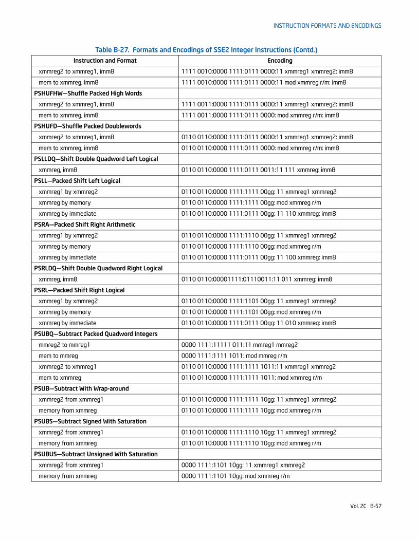
INSTRUCTION FORMATS AND ENCODINGS
xmmreg2 to xmmreg1, imm8 1111 0010:0000 1111:0111 0000:11 xmmreg1 xmmreg2: imm8
mem to xmmreg, imm8 1111 0010:0000 1111:0111 0000:11 mod xmmreg r/m: imm8
PSHUFHW—Shuffle Packed High Words
xmmreg2 to xmmreg1, imm8 1111 0011:0000 1111:0111 0000:11 xmmreg1 xmmreg2: imm8
mem to xmmreg, imm8 1111 0011:0000 1111:0111 0000: mod xmmreg r/m: imm8
PSHUFD—Shuffle Packed Doublewords
xmmreg2 to xmmreg1, imm8 0110 0110:0000 1111:0111 0000:11 xmmreg1 xmmreg2: imm8
mem to xmmreg, imm8 0110 0110:0000 1111:0111 0000: mod xmmreg r/m: imm8
PSLLDQ—Shift Double Quadword Left Logical
xmmreg, imm8 0110 0110:0000 1111:0111 0011:11 111 xmmreg: imm8
PSLL—Packed Shift Left Logical
xmmreg1 by xmmreg2 0110 0110:0000 1111:1111 00gg: 11 xmmreg1 xmmreg2
xmmreg by memory 0110 0110:0000 1111:1111 00gg: mod xmmreg r/m
xmmreg by immediate 0110 0110:0000 1111:0111 00gg: 11 110 xmmreg: imm8
PSRA—Packed Shift Right Arithmetic
xmmreg1 by xmmreg2 0110 0110:0000 1111:1110 00gg: 11 xmmreg1 xmmreg2
xmmreg by memory 0110 0110:0000 1111:1110 00gg: mod xmmreg r/m
xmmreg by immediate 0110 0110:0000 1111:0111 00gg: 11 100 xmmreg: imm8
PSRLDQ—Shift Double Quadword Right Logical
xmmreg, imm8 0110 0110:00001111:01110011:11 011 xmmreg: imm8
PSRL—Packed Shift Right Logical
xmmreg1 by xmmreg2 0110 0110:0000 1111:1101 00gg: 11 xmmreg1 xmmreg2
xmmreg by memory 0110 0110:0000 1111:1101 00gg: mod xmmreg r/m
xmmreg by immediate 0110 0110:0000 1111:0111 00gg: 11 010 xmmreg: imm8
PSUBQ—Subtract Packed Quadword Integers
mmreg2 to mmreg1 0000 1111:11111 011:11 mmreg1 mmreg2
mem to mmreg 0000 1111:1111 1011: mod mmreg r/m
xmmreg2 to xmmreg1 0110 0110:0000 1111:1111 1011:11 xmmreg1 xmmreg2
mem to xmmreg 0110 0110:0000 1111:1111 1011: mod xmmreg r/m
PSUB—Subtract With Wrap-around
xmmreg2 from xmmreg1 0110 0110:0000 1111:1111 10gg: 11 xmmreg1 xmmreg2
memory from xmmreg 0110 0110:0000 1111:1111 10gg: mod xmmreg r/m
PSUBS—Subtract Signed With Saturation
xmmreg2 from xmmreg1 0110 0110:0000 1111:1110 10gg: 11 xmmreg1 xmmreg2
memory from xmmreg 0110 0110:0000 1111:1110 10gg: mod xmmreg r/m
PSUBUS—Subtract Unsigned With Saturation
xmmreg2 from xmmreg1 0000 1111:1101 10gg: 11 xmmreg1 xmmreg2
memory from xmmreg 0000 1111:1101 10gg: mod xmmreg r/m
Table B-27. Formats and Encodings of SSE2 Integer Instructions (Contd.)
Instruction and Format Encoding
Vol. 2C B-57
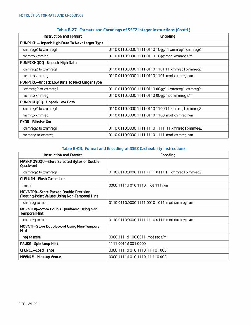
INSTRUCTION FORMATS AND ENCODINGS
PUNPCKH—Unpack High Data To Next Larger Type
xmmreg2 to xmmreg1 0110 0110:0000 1111:0110 10gg:11 xmmreg1 xmmreg2
mem to xmmreg 0110 0110:0000 1111:0110 10gg: mod xmmreg r/m
PUNPCKHQDQ—Unpack High Data
xmmreg2 to xmmreg1 0110 0110:0000 1111:0110 1101:11 xmmreg1 xmmreg2
mem to xmmreg 0110 0110:0000 1111:0110 1101: mod xmmreg r/m
PUNPCKL—Unpack Low Data To Next Larger Type
xmmreg2 to xmmreg1 0110 0110:0000 1111:0110 00gg:11 xmmreg1 xmmreg2
mem to xmmreg 0110 0110:0000 1111:0110 00gg: mod xmmreg r/m
PUNPCKLQDQ—Unpack Low Data
xmmreg2 to xmmreg1 0110 0110:0000 1111:0110 1100:11 xmmreg1 xmmreg2
mem to xmmreg 0110 0110:0000 1111:0110 1100: mod xmmreg r/m
PXOR—Bitwise Xor
xmmreg2 to xmmreg1 0110 0110:0000 1111:1110 1111: 11 xmmreg1 xmmreg2
memory to xmmreg 0110 0110:0000 1111:1110 1111: mod xmmreg r/m
Table B-28. Format and Encoding of SSE2 Cacheability Instructions
Instruction and Format Encoding
MASKMOVDQU—Store Selected Bytes of Double Quadword
xmmreg2 to xmmreg1 0110 0110:0000 1111:1111 0111:11 xmmreg1 xmmreg2
CLFLUSH—Flush Cache Line
mem 0000 1111:1010 1110: mod 111 r/m
MOVNTPD—Store Packed Double-Precision Floating-Point Values Using Non-Temporal Hint
xmmreg to mem 0110 0110:0000 1111:0010 1011: mod xmmreg r/m
MOVNTDQ—Store Double Quadword Using Non-Temporal Hint
xmmreg to mem 0110 0110:0000 1111:1110 0111: mod xmmreg r/m
MOVNTI—Store Doubleword Using Non-Temporal Hint
reg to mem 0000 1111:1100 0011: mod reg r/m
PAUSE—Spin Loop Hint 1111 0011:1001 0000
LFENCE—Load Fence 0000 1111:1010 1110: 11 101 000
MFENCE—Memory Fence 0000 1111:1010 1110: 11 110 000
Table B-27. Formats and Encodings of SSE2 Integer Instructions (Contd.)
Instruction and Format Encoding
B-58 Vol. 2C
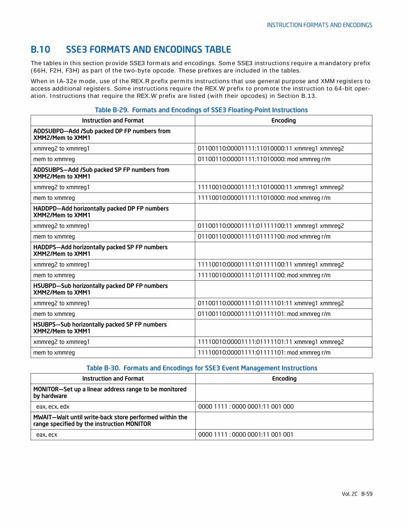
INSTRUCTION FORMATS AND ENCODINGS
B.10 SSE3 FORMATS AND ENCODINGS TABLEThe tables in this section provide SSE3 formats and encodings. Some SSE3 instructions require a mandatory prefix (66H, F2H, F3H) as part of the two-byte opcode. These prefixes are included in the tables.
When in IA-32e mode, use of the REX.R prefix permits instructions that use general purpose and XMM registers to access additional registers. Some instructions require the REX.W prefix to promote the instruction to 64-bit oper-ation. Instructions that require the REX.W prefix are listed (with their opcodes) in Section B.13.
Table B-29. Formats and Encodings of SSE3 Floating-Point Instructions
Instruction and Format Encoding
ADDSUBPD—Add /Sub packed DP FP numbers from XMM2/Mem to XMM1
xmmreg2 to xmmreg1 01100110:00001111:11010000:11 xmmreg1 xmmreg2
mem to xmmreg 01100110:00001111:11010000: mod xmmreg r/m
ADDSUBPS—Add /Sub packed SP FP numbers from XMM2/Mem to XMM1
xmmreg2 to xmmreg1 11110010:00001111:11010000:11 xmmreg1 xmmreg2
mem to xmmreg 11110010:00001111:11010000: mod xmmreg r/m
HADDPD—Add horizontally packed DP FP numbers XMM2/Mem to XMM1
xmmreg2 to xmmreg1 01100110:00001111:01111100:11 xmmreg1 xmmreg2
mem to xmmreg 01100110:00001111:01111100: mod xmmreg r/m
HADDPS—Add horizontally packed SP FP numbers XMM2/Mem to XMM1
xmmreg2 to xmmreg1 11110010:00001111:01111100:11 xmmreg1 xmmreg2
mem to xmmreg 11110010:00001111:01111100: mod xmmreg r/m
HSUBPD—Sub horizontally packed DP FP numbers XMM2/Mem to XMM1
xmmreg2 to xmmreg1 01100110:00001111:01111101:11 xmmreg1 xmmreg2
mem to xmmreg 01100110:00001111:01111101: mod xmmreg r/m
HSUBPS—Sub horizontally packed SP FP numbers XMM2/Mem to XMM1
xmmreg2 to xmmreg1 11110010:00001111:01111101:11 xmmreg1 xmmreg2
mem to xmmreg 11110010:00001111:01111101: mod xmmreg r/m
Table B-30. Formats and Encodings for SSE3 Event Management Instructions
Instruction and Format Encoding
MONITOR—Set up a linear address range to be monitored by hardware
eax, ecx, edx 0000 1111 : 0000 0001:11 001 000
MWAIT—Wait until write-back store performed within the range specified by the instruction MONITOR
eax, ecx 0000 1111 : 0000 0001:11 001 001
Vol. 2C B-59
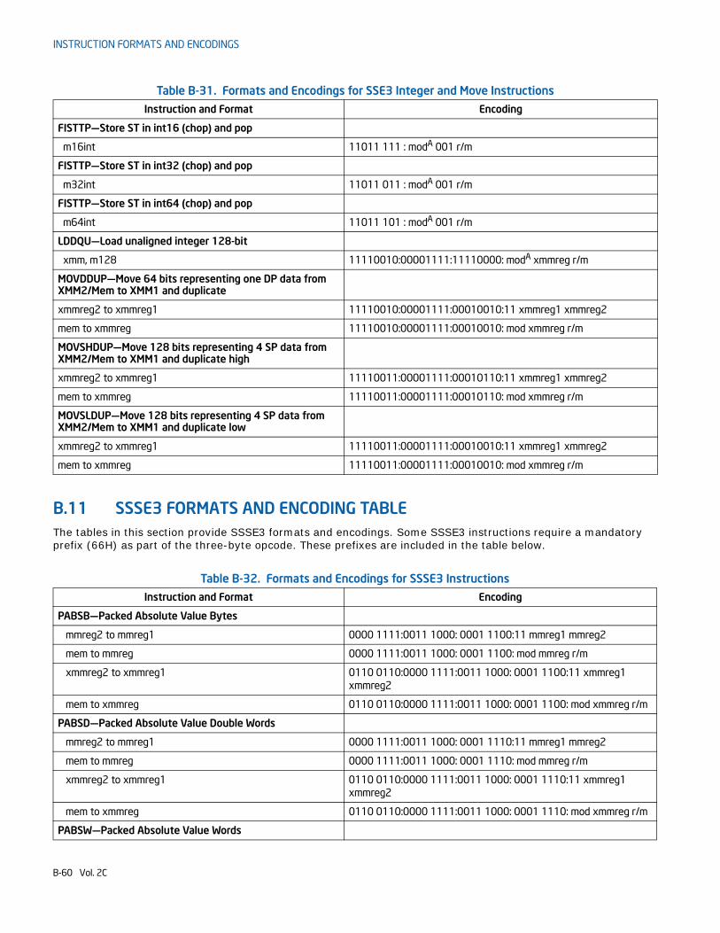
INSTRUCTION FORMATS AND ENCODINGS
B.11 SSSE3 FORMATS AND ENCODING TABLEThe tables in this section provide SSSE3 formats and encodings. Some SSSE3 instructions require a mandatory prefix (66H) as part of the three-byte opcode. These prefixes are included in the table below.
Table B-31. Formats and Encodings for SSE3 Integer and Move Instructions
Instruction and Format Encoding
FISTTP—Store ST in int16 (chop) and pop
m16int 11011 111 : modA 001 r/m
FISTTP—Store ST in int32 (chop) and pop
m32int 11011 011 : modA 001 r/m
FISTTP—Store ST in int64 (chop) and pop
m64int 11011 101 : modA 001 r/m
LDDQU—Load unaligned integer 128-bit
xmm, m128 11110010:00001111:11110000: modA xmmreg r/m
MOVDDUP—Move 64 bits representing one DP data from XMM2/Mem to XMM1 and duplicate
xmmreg2 to xmmreg1 11110010:00001111:00010010:11 xmmreg1 xmmreg2
mem to xmmreg 11110010:00001111:00010010: mod xmmreg r/m
MOVSHDUP—Move 128 bits representing 4 SP data from XMM2/Mem to XMM1 and duplicate high
xmmreg2 to xmmreg1 11110011:00001111:00010110:11 xmmreg1 xmmreg2
mem to xmmreg 11110011:00001111:00010110: mod xmmreg r/m
MOVSLDUP—Move 128 bits representing 4 SP data from XMM2/Mem to XMM1 and duplicate low
xmmreg2 to xmmreg1 11110011:00001111:00010010:11 xmmreg1 xmmreg2
mem to xmmreg 11110011:00001111:00010010: mod xmmreg r/m
Table B-32. Formats and Encodings for SSSE3 Instructions
Instruction and Format Encoding
PABSB—Packed Absolute Value Bytes
mmreg2 to mmreg1 0000 1111:0011 1000: 0001 1100:11 mmreg1 mmreg2
mem to mmreg 0000 1111:0011 1000: 0001 1100: mod mmreg r/m
xmmreg2 to xmmreg1 0110 0110:0000 1111:0011 1000: 0001 1100:11 xmmreg1 xmmreg2
mem to xmmreg 0110 0110:0000 1111:0011 1000: 0001 1100: mod xmmreg r/m
PABSD—Packed Absolute Value Double Words
mmreg2 to mmreg1 0000 1111:0011 1000: 0001 1110:11 mmreg1 mmreg2
mem to mmreg 0000 1111:0011 1000: 0001 1110: mod mmreg r/m
xmmreg2 to xmmreg1 0110 0110:0000 1111:0011 1000: 0001 1110:11 xmmreg1 xmmreg2
mem to xmmreg 0110 0110:0000 1111:0011 1000: 0001 1110: mod xmmreg r/m
PABSW—Packed Absolute Value Words
B-60 Vol. 2C
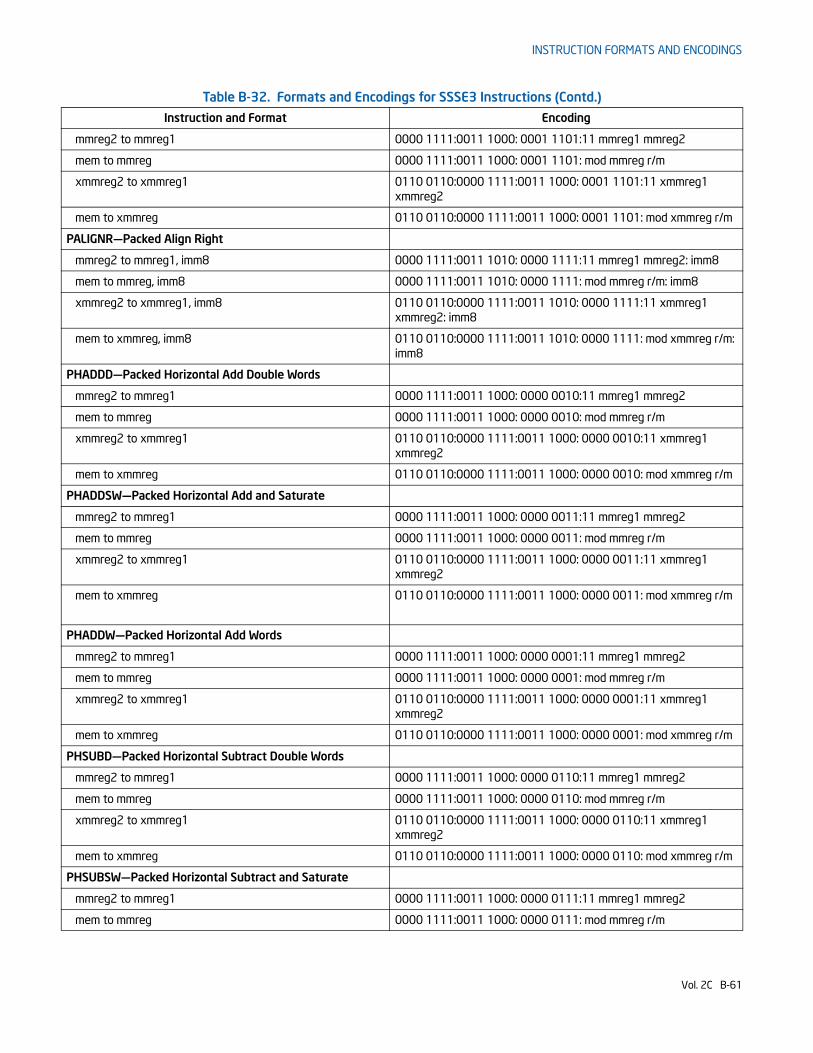
INSTRUCTION FORMATS AND ENCODINGS
mmreg2 to mmreg1 0000 1111:0011 1000: 0001 1101:11 mmreg1 mmreg2
mem to mmreg 0000 1111:0011 1000: 0001 1101: mod mmreg r/m
xmmreg2 to xmmreg1 0110 0110:0000 1111:0011 1000: 0001 1101:11 xmmreg1 xmmreg2
mem to xmmreg 0110 0110:0000 1111:0011 1000: 0001 1101: mod xmmreg r/m
PALIGNR—Packed Align Right
mmreg2 to mmreg1, imm8 0000 1111:0011 1010: 0000 1111:11 mmreg1 mmreg2: imm8
mem to mmreg, imm8 0000 1111:0011 1010: 0000 1111: mod mmreg r/m: imm8
xmmreg2 to xmmreg1, imm8 0110 0110:0000 1111:0011 1010: 0000 1111:11 xmmreg1 xmmreg2: imm8
mem to xmmreg, imm8 0110 0110:0000 1111:0011 1010: 0000 1111: mod xmmreg r/m: imm8
PHADDD—Packed Horizontal Add Double Words
mmreg2 to mmreg1 0000 1111:0011 1000: 0000 0010:11 mmreg1 mmreg2
mem to mmreg 0000 1111:0011 1000: 0000 0010: mod mmreg r/m
xmmreg2 to xmmreg1 0110 0110:0000 1111:0011 1000: 0000 0010:11 xmmreg1 xmmreg2
mem to xmmreg 0110 0110:0000 1111:0011 1000: 0000 0010: mod xmmreg r/m
PHADDSW—Packed Horizontal Add and Saturate
mmreg2 to mmreg1 0000 1111:0011 1000: 0000 0011:11 mmreg1 mmreg2
mem to mmreg 0000 1111:0011 1000: 0000 0011: mod mmreg r/m
xmmreg2 to xmmreg1 0110 0110:0000 1111:0011 1000: 0000 0011:11 xmmreg1 xmmreg2
mem to xmmreg 0110 0110:0000 1111:0011 1000: 0000 0011: mod xmmreg r/m
PHADDW—Packed Horizontal Add Words
mmreg2 to mmreg1 0000 1111:0011 1000: 0000 0001:11 mmreg1 mmreg2
mem to mmreg 0000 1111:0011 1000: 0000 0001: mod mmreg r/m
xmmreg2 to xmmreg1 0110 0110:0000 1111:0011 1000: 0000 0001:11 xmmreg1 xmmreg2
mem to xmmreg 0110 0110:0000 1111:0011 1000: 0000 0001: mod xmmreg r/m
PHSUBD—Packed Horizontal Subtract Double Words
mmreg2 to mmreg1 0000 1111:0011 1000: 0000 0110:11 mmreg1 mmreg2
mem to mmreg 0000 1111:0011 1000: 0000 0110: mod mmreg r/m
xmmreg2 to xmmreg1 0110 0110:0000 1111:0011 1000: 0000 0110:11 xmmreg1 xmmreg2
mem to xmmreg 0110 0110:0000 1111:0011 1000: 0000 0110: mod xmmreg r/m
PHSUBSW—Packed Horizontal Subtract and Saturate
mmreg2 to mmreg1 0000 1111:0011 1000: 0000 0111:11 mmreg1 mmreg2
mem to mmreg 0000 1111:0011 1000: 0000 0111: mod mmreg r/m
Table B-32. Formats and Encodings for SSSE3 Instructions (Contd.)
Instruction and Format Encoding
Vol. 2C B-61
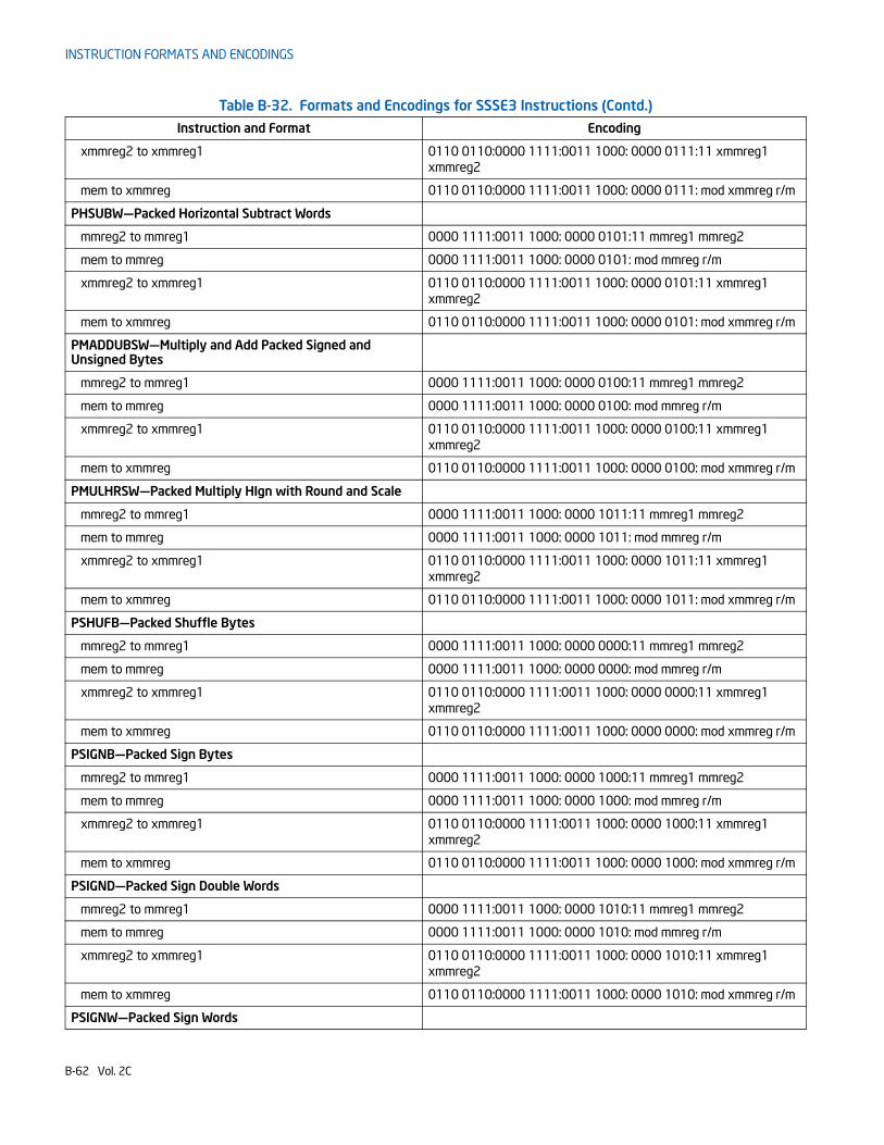
INSTRUCTION FORMATS AND ENCODINGS
xmmreg2 to xmmreg1 0110 0110:0000 1111:0011 1000: 0000 0111:11 xmmreg1 xmmreg2
mem to xmmreg 0110 0110:0000 1111:0011 1000: 0000 0111: mod xmmreg r/m
PHSUBW—Packed Horizontal Subtract Words
mmreg2 to mmreg1 0000 1111:0011 1000: 0000 0101:11 mmreg1 mmreg2
mem to mmreg 0000 1111:0011 1000: 0000 0101: mod mmreg r/m
xmmreg2 to xmmreg1 0110 0110:0000 1111:0011 1000: 0000 0101:11 xmmreg1 xmmreg2
mem to xmmreg 0110 0110:0000 1111:0011 1000: 0000 0101: mod xmmreg r/m
PMADDUBSW—Multiply and Add Packed Signed and Unsigned Bytes
mmreg2 to mmreg1 0000 1111:0011 1000: 0000 0100:11 mmreg1 mmreg2
mem to mmreg 0000 1111:0011 1000: 0000 0100: mod mmreg r/m
xmmreg2 to xmmreg1 0110 0110:0000 1111:0011 1000: 0000 0100:11 xmmreg1 xmmreg2
mem to xmmreg 0110 0110:0000 1111:0011 1000: 0000 0100: mod xmmreg r/m
PMULHRSW—Packed Multiply HIgn with Round and Scale
mmreg2 to mmreg1 0000 1111:0011 1000: 0000 1011:11 mmreg1 mmreg2
mem to mmreg 0000 1111:0011 1000: 0000 1011: mod mmreg r/m
xmmreg2 to xmmreg1 0110 0110:0000 1111:0011 1000: 0000 1011:11 xmmreg1 xmmreg2
mem to xmmreg 0110 0110:0000 1111:0011 1000: 0000 1011: mod xmmreg r/m
PSHUFB—Packed Shuffle Bytes
mmreg2 to mmreg1 0000 1111:0011 1000: 0000 0000:11 mmreg1 mmreg2
mem to mmreg 0000 1111:0011 1000: 0000 0000: mod mmreg r/m
xmmreg2 to xmmreg1 0110 0110:0000 1111:0011 1000: 0000 0000:11 xmmreg1 xmmreg2
mem to xmmreg 0110 0110:0000 1111:0011 1000: 0000 0000: mod xmmreg r/m
PSIGNB—Packed Sign Bytes
mmreg2 to mmreg1 0000 1111:0011 1000: 0000 1000:11 mmreg1 mmreg2
mem to mmreg 0000 1111:0011 1000: 0000 1000: mod mmreg r/m
xmmreg2 to xmmreg1 0110 0110:0000 1111:0011 1000: 0000 1000:11 xmmreg1 xmmreg2
mem to xmmreg 0110 0110:0000 1111:0011 1000: 0000 1000: mod xmmreg r/m
PSIGND—Packed Sign Double Words
mmreg2 to mmreg1 0000 1111:0011 1000: 0000 1010:11 mmreg1 mmreg2
mem to mmreg 0000 1111:0011 1000: 0000 1010: mod mmreg r/m
xmmreg2 to xmmreg1 0110 0110:0000 1111:0011 1000: 0000 1010:11 xmmreg1 xmmreg2
mem to xmmreg 0110 0110:0000 1111:0011 1000: 0000 1010: mod xmmreg r/m
PSIGNW—Packed Sign Words
Table B-32. Formats and Encodings for SSSE3 Instructions (Contd.)
Instruction and Format Encoding
B-62 Vol. 2C
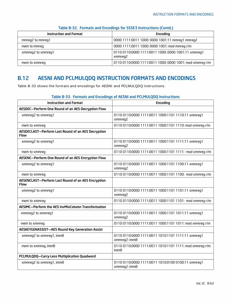
INSTRUCTION FORMATS AND ENCODINGS
B.12 AESNI AND PCLMULQDQ INSTRUCTION FORMATS AND ENCODINGS Table B-33 shows the formats and encodings for AESNI and PCLMULQDQ instructions.
mmreg2 to mmreg1 0000 1111:0011 1000: 0000 1001:11 mmreg1 mmreg2
mem to mmreg 0000 1111:0011 1000: 0000 1001: mod mmreg r/m
xmmreg2 to xmmreg1 0110 0110:0000 1111:0011 1000: 0000 1001:11 xmmreg1 xmmreg2
mem to xmmreg 0110 0110:0000 1111:0011 1000: 0000 1001: mod xmmreg r/m
Table B-33. Formats and Encodings of AESNI and PCLMULQDQ Instructions
Instruction and Format Encoding
AESDEC—Perform One Round of an AES Decryption Flow
xmmreg2 to xmmreg1 0110 0110:0000 1111:0011 1000:1101 1110:11 xmmreg1 xmmreg2
mem to xmmreg 0110 0110:0000 1111:0011 1000:1101 1110: mod xmmreg r/m
AESDECLAST—Perform Last Round of an AES Decryption Flow
xmmreg2 to xmmreg1 0110 0110:0000 1111:0011 1000:1101 1111:11 xmmreg1 xmmreg2
mem to xmmreg 0110 0110:0000 1111:0011 1000:1101 1111: mod xmmreg r/m
AESENC—Perform One Round of an AES Encryption Flow
xmmreg2 to xmmreg1 0110 0110:0000 1111:0011 1000:1101 1100:11 xmmreg1 xmmreg2
mem to xmmreg 0110 0110:0000 1111:0011 1000:1101 1100: mod xmmreg r/m
AESENCLAST—Perform Last Round of an AES Encryption Flow
xmmreg2 to xmmreg1 0110 0110:0000 1111:0011 1000:1101 1101:11 xmmreg1 xmmreg2
mem to xmmreg 0110 0110:0000 1111:0011 1000:1101 1101: mod xmmreg r/m
AESIMC—Perform the AES InvMixColumn Transformation
xmmreg2 to xmmreg1 0110 0110:0000 1111:0011 1000:1101 1011:11 xmmreg1 xmmreg2
mem to xmmreg 0110 0110:0000 1111:0011 1000:1101 1011: mod xmmreg r/m
AESKEYGENASSIST—AES Round Key Generation Assist
xmmreg2 to xmmreg1, imm8 0110 0110:0000 1111:0011 1010:1101 1111:11 xmmreg1 xmmreg2: imm8
mem to xmmreg, imm8 0110 0110:0000 1111:0011 1010:1101 1111: mod xmmreg r/m: imm8
PCLMULQDQ—Carry-Less Multiplication Quadword
xmmreg2 to xmmreg1, imm8 0110 0110:0000 1111:0011 1010:0100 0100:11 xmmreg1 xmmreg2: imm8
Table B-32. Formats and Encodings for SSSE3 Instructions (Contd.)
Instruction and Format Encoding
Vol. 2C B-63
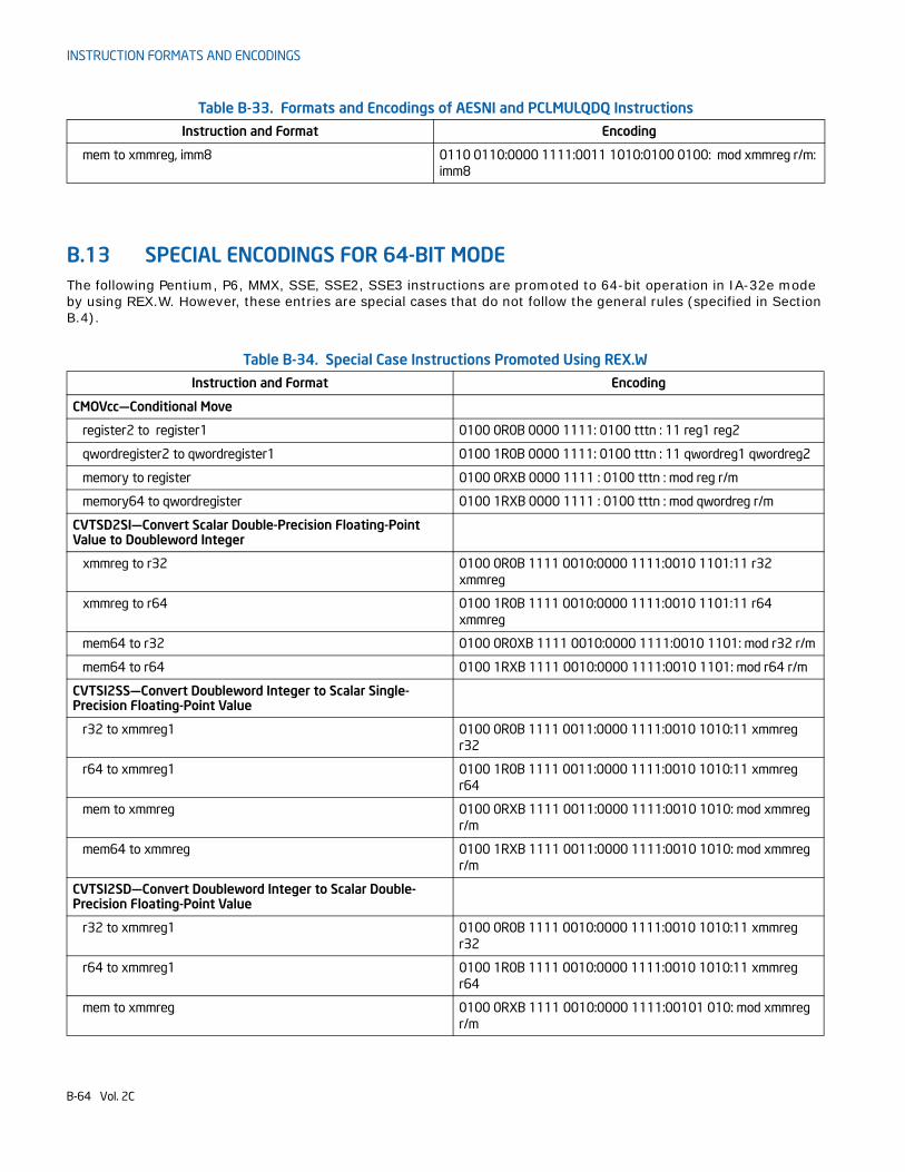
INSTRUCTION FORMATS AND ENCODINGS
B.13 SPECIAL ENCODINGS FOR 64-BIT MODEThe following Pentium, P6, MMX, SSE, SSE2, SSE3 instructions are promoted to 64-bit operation in IA-32e mode by using REX.W. However, these entries are special cases that do not follow the general rules (specified in Section B.4).
mem to xmmreg, imm8 0110 0110:0000 1111:0011 1010:0100 0100: mod xmmreg r/m: imm8
Table B-34. Special Case Instructions Promoted Using REX.W
Instruction and Format Encoding
CMOVcc—Conditional Move
register2 to register1 0100 0R0B 0000 1111: 0100 tttn : 11 reg1 reg2
qwordregister2 to qwordregister1 0100 1R0B 0000 1111: 0100 tttn : 11 qwordreg1 qwordreg2
memory to register 0100 0RXB 0000 1111 : 0100 tttn : mod reg r/m
memory64 to qwordregister 0100 1RXB 0000 1111 : 0100 tttn : mod qwordreg r/m
CVTSD2SI—Convert Scalar Double-Precision Floating-Point Value to Doubleword Integer
xmmreg to r32 0100 0R0B 1111 0010:0000 1111:0010 1101:11 r32 xmmreg
xmmreg to r64 0100 1R0B 1111 0010:0000 1111:0010 1101:11 r64 xmmreg
mem64 to r32 0100 0R0XB 1111 0010:0000 1111:0010 1101: mod r32 r/m
mem64 to r64 0100 1RXB 1111 0010:0000 1111:0010 1101: mod r64 r/m
CVTSI2SS—Convert Doubleword Integer to Scalar Single-Precision Floating-Point Value
r32 to xmmreg1 0100 0R0B 1111 0011:0000 1111:0010 1010:11 xmmreg r32
r64 to xmmreg1 0100 1R0B 1111 0011:0000 1111:0010 1010:11 xmmreg r64
mem to xmmreg 0100 0RXB 1111 0011:0000 1111:0010 1010: mod xmmreg r/m
mem64 to xmmreg 0100 1RXB 1111 0011:0000 1111:0010 1010: mod xmmreg r/m
CVTSI2SD—Convert Doubleword Integer to Scalar Double-Precision Floating-Point Value
r32 to xmmreg1 0100 0R0B 1111 0010:0000 1111:0010 1010:11 xmmreg r32
r64 to xmmreg1 0100 1R0B 1111 0010:0000 1111:0010 1010:11 xmmreg r64
mem to xmmreg 0100 0RXB 1111 0010:0000 1111:00101 010: mod xmmreg r/m
Table B-33. Formats and Encodings of AESNI and PCLMULQDQ Instructions
Instruction and Format Encoding
B-64 Vol. 2C
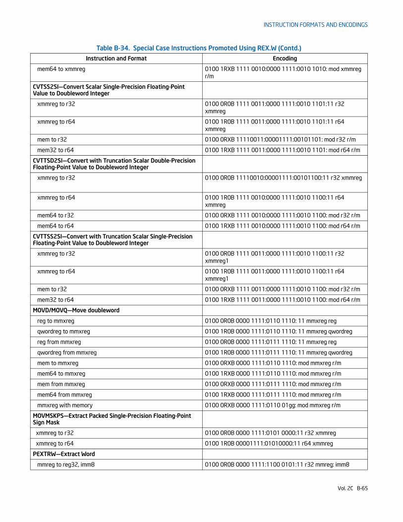
INSTRUCTION FORMATS AND ENCODINGS
mem64 to xmmreg 0100 1RXB 1111 0010:0000 1111:0010 1010: mod xmmreg r/m
CVTSS2SI—Convert Scalar Single-Precision Floating-Point Value to Doubleword Integer
xmmreg to r32 0100 0R0B 1111 0011:0000 1111:0010 1101:11 r32 xmmreg
xmmreg to r64 0100 1R0B 1111 0011:0000 1111:0010 1101:11 r64 xmmreg
mem to r32 0100 0RXB 11110011:00001111:00101101: mod r32 r/m
mem32 to r64 0100 1RXB 1111 0011:0000 1111:0010 1101: mod r64 r/m
CVTTSD2SI—Convert with Truncation Scalar Double-Precision Floating-Point Value to Doubleword Integer
xmmreg to r32 0100 0R0B 11110010:00001111:00101100:11 r32 xmmreg
xmmreg to r64 0100 1R0B 1111 0010:0000 1111:0010 1100:11 r64 xmmreg
mem64 to r32 0100 0RXB 1111 0010:0000 1111:0010 1100: mod r32 r/m
mem64 to r64 0100 1RXB 1111 0010:0000 1111:0010 1100: mod r64 r/m
CVTTSS2SI—Convert with Truncation Scalar Single-Precision Floating-Point Value to Doubleword Integer
xmmreg to r32 0100 0R0B 1111 0011:0000 1111:0010 1100:11 r32 xmmreg1
xmmreg to r64 0100 1R0B 1111 0011:0000 1111:0010 1100:11 r64 xmmreg1
mem to r32 0100 0RXB 1111 0011:0000 1111:0010 1100: mod r32 r/m
mem32 to r64 0100 1RXB 1111 0011:0000 1111:0010 1100: mod r64 r/m
MOVD/MOVQ—Move doubleword
reg to mmxreg 0100 0R0B 0000 1111:0110 1110: 11 mmxreg reg
qwordreg to mmxreg 0100 1R0B 0000 1111:0110 1110: 11 mmxreg qwordreg
reg from mmxreg 0100 0R0B 0000 1111:0111 1110: 11 mmxreg reg
qwordreg from mmxreg 0100 1R0B 0000 1111:0111 1110: 11 mmxreg qwordreg
mem to mmxreg 0100 0RXB 0000 1111:0110 1110: mod mmxreg r/m
mem64 to mmxreg 0100 1RXB 0000 1111:0110 1110: mod mmxreg r/m
mem from mmxreg 0100 0RXB 0000 1111:0111 1110: mod mmxreg r/m
mem64 from mmxreg 0100 1RXB 0000 1111:0111 1110: mod mmxreg r/m
mmxreg with memory 0100 0RXB 0000 1111:0110 01gg: mod mmxreg r/m
MOVMSKPS—Extract Packed Single-Precision Floating-Point Sign Mask
xmmreg to r32 0100 0R0B 0000 1111:0101 0000:11 r32 xmmreg
xmmreg to r64 0100 1R0B 00001111:01010000:11 r64 xmmreg
PEXTRW—Extract Word
mmreg to reg32, imm8 0100 0R0B 0000 1111:1100 0101:11 r32 mmreg: imm8
Table B-34. Special Case Instructions Promoted Using REX.W (Contd.)
Instruction and Format Encoding
Vol. 2C B-65
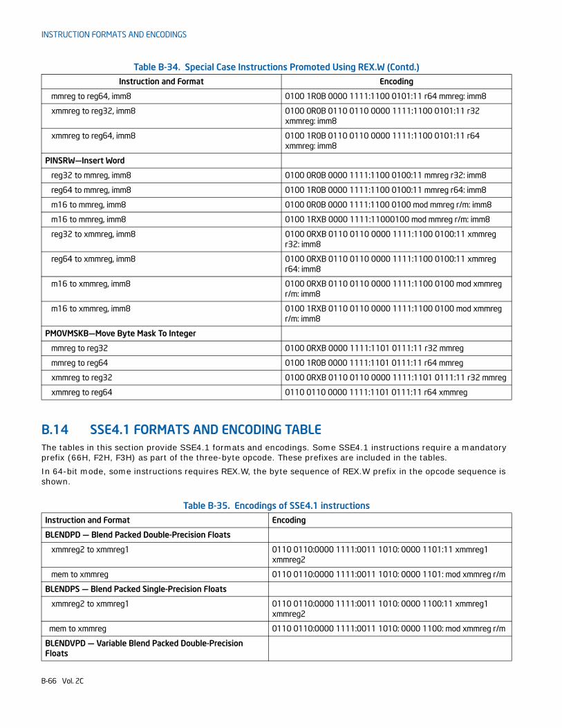
INSTRUCTION FORMATS AND ENCODINGS
B.14 SSE4.1 FORMATS AND ENCODING TABLEThe tables in this section provide SSE4.1 formats and encodings. Some SSE4.1 instructions require a mandatory prefix (66H, F2H, F3H) as part of the three-byte opcode. These prefixes are included in the tables. In 64-bit mode, some instructions requires REX.W, the byte sequence of REX.W prefix in the opcode sequence is shown.
mmreg to reg64, imm8 0100 1R0B 0000 1111:1100 0101:11 r64 mmreg: imm8
xmmreg to reg32, imm8 0100 0R0B 0110 0110 0000 1111:1100 0101:11 r32 xmmreg: imm8
xmmreg to reg64, imm8 0100 1R0B 0110 0110 0000 1111:1100 0101:11 r64 xmmreg: imm8
PINSRW—Insert Word
reg32 to mmreg, imm8 0100 0R0B 0000 1111:1100 0100:11 mmreg r32: imm8
reg64 to mmreg, imm8 0100 1R0B 0000 1111:1100 0100:11 mmreg r64: imm8
m16 to mmreg, imm8 0100 0R0B 0000 1111:1100 0100 mod mmreg r/m: imm8
m16 to mmreg, imm8 0100 1RXB 0000 1111:11000100 mod mmreg r/m: imm8
reg32 to xmmreg, imm8 0100 0RXB 0110 0110 0000 1111:1100 0100:11 xmmreg r32: imm8
reg64 to xmmreg, imm8 0100 0RXB 0110 0110 0000 1111:1100 0100:11 xmmreg r64: imm8
m16 to xmmreg, imm8 0100 0RXB 0110 0110 0000 1111:1100 0100 mod xmmreg r/m: imm8
m16 to xmmreg, imm8 0100 1RXB 0110 0110 0000 1111:1100 0100 mod xmmreg r/m: imm8
PMOVMSKB—Move Byte Mask To Integer
mmreg to reg32 0100 0RXB 0000 1111:1101 0111:11 r32 mmreg
mmreg to reg64 0100 1R0B 0000 1111:1101 0111:11 r64 mmreg
xmmreg to reg32 0100 0RXB 0110 0110 0000 1111:1101 0111:11 r32 mmreg
xmmreg to reg64 0110 0110 0000 1111:1101 0111:11 r64 xmmreg
Table B-35. Encodings of SSE4.1 instructions
Instruction and Format Encoding
BLENDPD — Blend Packed Double-Precision Floats
xmmreg2 to xmmreg1 0110 0110:0000 1111:0011 1010: 0000 1101:11 xmmreg1 xmmreg2
mem to xmmreg 0110 0110:0000 1111:0011 1010: 0000 1101: mod xmmreg r/m
BLENDPS — Blend Packed Single-Precision Floats
xmmreg2 to xmmreg1 0110 0110:0000 1111:0011 1010: 0000 1100:11 xmmreg1 xmmreg2
mem to xmmreg 0110 0110:0000 1111:0011 1010: 0000 1100: mod xmmreg r/m
BLENDVPD — Variable Blend Packed Double-Precision Floats
Table B-34. Special Case Instructions Promoted Using REX.W (Contd.)
Instruction and Format Encoding
B-66 Vol. 2C
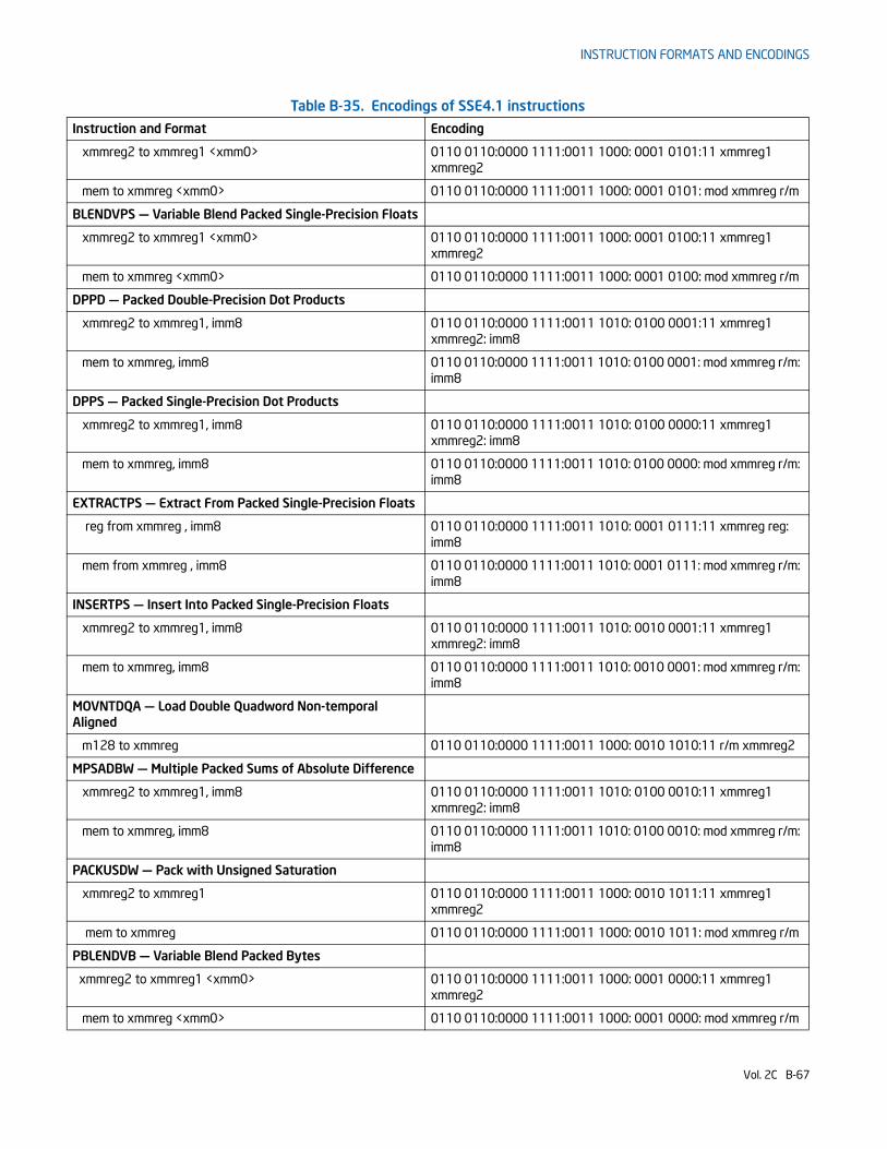
INSTRUCTION FORMATS AND ENCODINGS
xmmreg2 to xmmreg1 <xmm0> 0110 0110:0000 1111:0011 1000: 0001 0101:11 xmmreg1 xmmreg2
mem to xmmreg <xmm0> 0110 0110:0000 1111:0011 1000: 0001 0101: mod xmmreg r/m
BLENDVPS — Variable Blend Packed Single-Precision Floats
xmmreg2 to xmmreg1 <xmm0> 0110 0110:0000 1111:0011 1000: 0001 0100:11 xmmreg1 xmmreg2
mem to xmmreg <xmm0> 0110 0110:0000 1111:0011 1000: 0001 0100: mod xmmreg r/m
DPPD — Packed Double-Precision Dot Products
xmmreg2 to xmmreg1, imm8 0110 0110:0000 1111:0011 1010: 0100 0001:11 xmmreg1 xmmreg2: imm8
mem to xmmreg, imm8 0110 0110:0000 1111:0011 1010: 0100 0001: mod xmmreg r/m: imm8
DPPS — Packed Single-Precision Dot Products
xmmreg2 to xmmreg1, imm8 0110 0110:0000 1111:0011 1010: 0100 0000:11 xmmreg1 xmmreg2: imm8
mem to xmmreg, imm8 0110 0110:0000 1111:0011 1010: 0100 0000: mod xmmreg r/m: imm8
EXTRACTPS — Extract From Packed Single-Precision Floats
reg from xmmreg , imm8 0110 0110:0000 1111:0011 1010: 0001 0111:11 xmmreg reg: imm8
mem from xmmreg , imm8 0110 0110:0000 1111:0011 1010: 0001 0111: mod xmmreg r/m: imm8
INSERTPS — Insert Into Packed Single-Precision Floats
xmmreg2 to xmmreg1, imm8 0110 0110:0000 1111:0011 1010: 0010 0001:11 xmmreg1 xmmreg2: imm8
mem to xmmreg, imm8 0110 0110:0000 1111:0011 1010: 0010 0001: mod xmmreg r/m: imm8
MOVNTDQA — Load Double Quadword Non-temporal Aligned
m128 to xmmreg 0110 0110:0000 1111:0011 1000: 0010 1010:11 r/m xmmreg2
MPSADBW — Multiple Packed Sums of Absolute Difference
xmmreg2 to xmmreg1, imm8 0110 0110:0000 1111:0011 1010: 0100 0010:11 xmmreg1 xmmreg2: imm8
mem to xmmreg, imm8 0110 0110:0000 1111:0011 1010: 0100 0010: mod xmmreg r/m: imm8
PACKUSDW — Pack with Unsigned Saturation
xmmreg2 to xmmreg1 0110 0110:0000 1111:0011 1000: 0010 1011:11 xmmreg1 xmmreg2
mem to xmmreg 0110 0110:0000 1111:0011 1000: 0010 1011: mod xmmreg r/m
PBLENDVB — Variable Blend Packed Bytes
xmmreg2 to xmmreg1 <xmm0> 0110 0110:0000 1111:0011 1000: 0001 0000:11 xmmreg1 xmmreg2
mem to xmmreg <xmm0> 0110 0110:0000 1111:0011 1000: 0001 0000: mod xmmreg r/m
Table B-35. Encodings of SSE4.1 instructions
Instruction and Format Encoding
Vol. 2C B-67
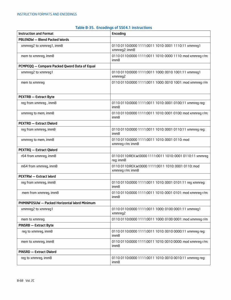
INSTRUCTION FORMATS AND ENCODINGS
PBLENDW — Blend Packed Words
xmmreg2 to xmmreg1, imm8 0110 0110:0000 1111:0011 1010: 0001 1110:11 xmmreg1 xmmreg2: imm8
mem to xmmreg, imm8 0110 0110:0000 1111:0011 1010: 0000 1110: mod xmmreg r/m: imm8
PCMPEQQ — Compare Packed Qword Data of Equal
xmmreg2 to xmmreg1 0110 0110:0000 1111:0011 1000: 0010 1001:11 xmmreg1 xmmreg2
mem to xmmreg 0110 0110:0000 1111:0011 1000: 0010 1001: mod xmmreg r/m
PEXTRB — Extract Byte
reg from xmmreg , imm8 0110 0110:0000 1111:0011 1010: 0001 0100:11 xmmreg reg: imm8
xmmreg to mem, imm8 0110 0110:0000 1111:0011 1010: 0001 0100: mod xmmreg r/m: imm8
PEXTRD — Extract DWord
reg from xmmreg, imm8 0110 0110:0000 1111:0011 1010: 0001 0110:11 xmmreg reg: imm8
xmmreg to mem, imm8 0110 0110:0000 1111:0011 1010: 0001 0110: mod xmmreg r/m: imm8
PEXTRQ — Extract QWord
r64 from xmmreg, imm8 0110 0110:REX.W:0000 1111:0011 1010: 0001 0110:11 xmmreg reg: imm8
m64 from xmmreg, imm8 0110 0110:REX.W:0000 1111:0011 1010: 0001 0110: mod xmmreg r/m: imm8
PEXTRW — Extract Word
reg from xmmreg, imm8 0110 0110:0000 1111:0011 1010: 0001 0101:11 reg xmmreg: imm8
mem from xmmreg, imm8 0110 0110:0000 1111:0011 1010: 0001 0101: mod xmmreg r/m: imm8
PHMINPOSUW — Packed Horizontal Word Minimum
xmmreg2 to xmmreg1 0110 0110:0000 1111:0011 1000: 0100 0001:11 xmmreg1 xmmreg2
mem to xmmreg 0110 0110:0000 1111:0011 1000: 0100 0001: mod xmmreg r/m
PINSRB — Extract Byte
reg to xmmreg, imm8 0110 0110:0000 1111:0011 1010: 0010 0000:11 xmmreg reg: imm8
mem to xmmreg, imm8 0110 0110:0000 1111:0011 1010: 0010 0000: mod xmmreg r/m: imm8
PINSRD — Extract DWord
reg to xmmreg, imm8 0110 0110:0000 1111:0011 1010: 0010 0010:11 xmmreg reg: imm8
Table B-35. Encodings of SSE4.1 instructions
Instruction and Format Encoding
B-68 Vol. 2C

INSTRUCTION FORMATS AND ENCODINGS
mem to xmmreg, imm8 0110 0110:0000 1111:0011 1010: 0010 0010: mod xmmreg r/m: imm8
PINSRQ — Extract QWord
r64 to xmmreg, imm8 0110 0110:REX.W:0000 1111:0011 1010: 0010 0010:11 xmmreg reg: imm8
m64 to xmmreg, imm8 0110 0110:REX.W:0000 1111:0011 1010: 0010 0010: mod xmmreg r/m: imm8
PMAXSB — Maximum of Packed Signed Byte Integers
xmmreg2 to xmmreg1 0110 0110:0000 1111:0011 1000: 0011 1100:11 xmmreg1 xmmreg2
mem to xmmreg 0110 0110:0000 1111:0011 1000: 0011 1100: mod xmmreg r/m
PMAXSD — Maximum of Packed Signed Dword Integers
xmmreg2 to xmmreg1 0110 0110:0000 1111:0011 1000: 0011 1101:11 xmmreg1 xmmreg2
mem to xmmreg 0110 0110:0000 1111:0011 1000: 0011 1101: mod xmmreg r/m
PMAXUD — Maximum of Packed Unsigned Dword Integers
xmmreg2 to xmmreg1 0110 0110:0000 1111:0011 1000: 0011 1111:11 xmmreg1 xmmreg2
mem to xmmreg 0110 0110:0000 1111:0011 1000: 0011 1111: mod xmmreg r/m
PMAXUW — Maximum of Packed Unsigned Word Integers
xmmreg2 to xmmreg1 0110 0110:0000 1111:0011 1000: 0011 1110:11 xmmreg1 xmmreg2
mem to xmmreg 0110 0110:0000 1111:0011 1000: 0011 1110: mod xmmreg r/m
PMINSB — Minimum of Packed Signed Byte Integers
xmmreg2 to xmmreg1 0110 0110:0000 1111:0011 1000: 0011 1000:11 xmmreg1 xmmreg2
mem to xmmreg 0110 0110:0000 1111:0011 1000: 0011 1000: mod xmmreg r/m
PMINSD — Minimum of Packed Signed Dword Integers
xmmreg2 to xmmreg1 0110 0110:0000 1111:0011 1000: 0011 1001:11 xmmreg1 xmmreg2
mem to xmmreg 0110 0110:0000 1111:0011 1000: 0011 1001: mod xmmreg r/m
PMINUD — Minimum of Packed Unsigned Dword Integers
xmmreg2 to xmmreg1 0110 0110:0000 1111:0011 1000: 0011 1011:11 xmmreg1 xmmreg2
mem to xmmreg 0110 0110:0000 1111:0011 1000: 0011 1011: mod xmmreg r/m
PMINUW — Minimum of Packed Unsigned Word Integers
xmmreg2 to xmmreg1 0110 0110:0000 1111:0011 1000: 0011 1010:11 xmmreg1 xmmreg2
mem to xmmreg 0110 0110:0000 1111:0011 1000: 0011 1010: mod xmmreg r/m
PMOVSXBD — Packed Move Sign Extend - Byte to Dword
xmmreg2 to xmmreg1 0110 0110:0000 1111:0011 1000: 0010 0001:11 xmmreg1 xmmreg2
Table B-35. Encodings of SSE4.1 instructions
Instruction and Format Encoding
Vol. 2C B-69
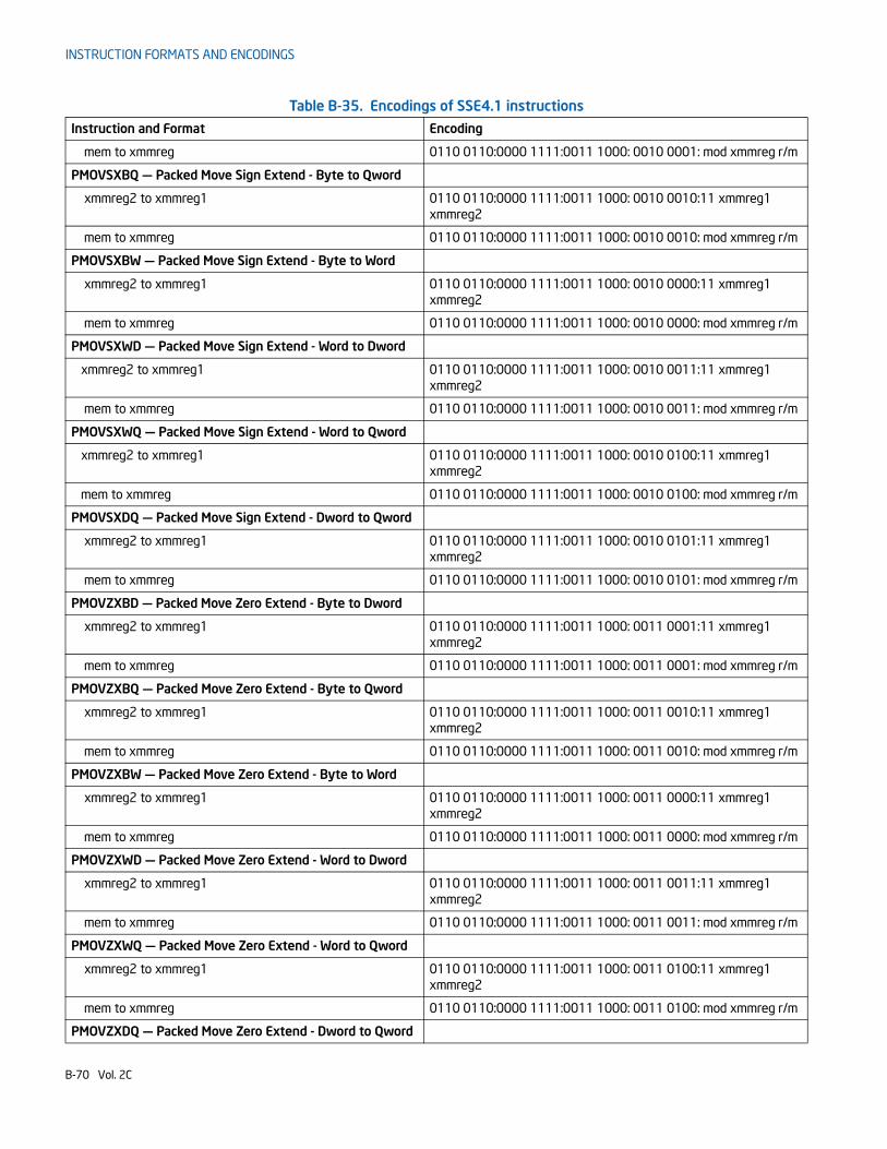
INSTRUCTION FORMATS AND ENCODINGS
mem to xmmreg 0110 0110:0000 1111:0011 1000: 0010 0001: mod xmmreg r/m
PMOVSXBQ — Packed Move Sign Extend - Byte to Qword
xmmreg2 to xmmreg1 0110 0110:0000 1111:0011 1000: 0010 0010:11 xmmreg1 xmmreg2
mem to xmmreg 0110 0110:0000 1111:0011 1000: 0010 0010: mod xmmreg r/m
PMOVSXBW — Packed Move Sign Extend - Byte to Word
xmmreg2 to xmmreg1 0110 0110:0000 1111:0011 1000: 0010 0000:11 xmmreg1 xmmreg2
mem to xmmreg 0110 0110:0000 1111:0011 1000: 0010 0000: mod xmmreg r/m
PMOVSXWD — Packed Move Sign Extend - Word to Dword
xmmreg2 to xmmreg1 0110 0110:0000 1111:0011 1000: 0010 0011:11 xmmreg1 xmmreg2
mem to xmmreg 0110 0110:0000 1111:0011 1000: 0010 0011: mod xmmreg r/m
PMOVSXWQ — Packed Move Sign Extend - Word to Qword
xmmreg2 to xmmreg1 0110 0110:0000 1111:0011 1000: 0010 0100:11 xmmreg1 xmmreg2
mem to xmmreg 0110 0110:0000 1111:0011 1000: 0010 0100: mod xmmreg r/m
PMOVSXDQ — Packed Move Sign Extend - Dword to Qword
xmmreg2 to xmmreg1 0110 0110:0000 1111:0011 1000: 0010 0101:11 xmmreg1 xmmreg2
mem to xmmreg 0110 0110:0000 1111:0011 1000: 0010 0101: mod xmmreg r/m
PMOVZXBD — Packed Move Zero Extend - Byte to Dword
xmmreg2 to xmmreg1 0110 0110:0000 1111:0011 1000: 0011 0001:11 xmmreg1 xmmreg2
mem to xmmreg 0110 0110:0000 1111:0011 1000: 0011 0001: mod xmmreg r/m
PMOVZXBQ — Packed Move Zero Extend - Byte to Qword
xmmreg2 to xmmreg1 0110 0110:0000 1111:0011 1000: 0011 0010:11 xmmreg1 xmmreg2
mem to xmmreg 0110 0110:0000 1111:0011 1000: 0011 0010: mod xmmreg r/m
PMOVZXBW — Packed Move Zero Extend - Byte to Word
xmmreg2 to xmmreg1 0110 0110:0000 1111:0011 1000: 0011 0000:11 xmmreg1 xmmreg2
mem to xmmreg 0110 0110:0000 1111:0011 1000: 0011 0000: mod xmmreg r/m
PMOVZXWD — Packed Move Zero Extend - Word to Dword
xmmreg2 to xmmreg1 0110 0110:0000 1111:0011 1000: 0011 0011:11 xmmreg1 xmmreg2
mem to xmmreg 0110 0110:0000 1111:0011 1000: 0011 0011: mod xmmreg r/m
PMOVZXWQ — Packed Move Zero Extend - Word to Qword
xmmreg2 to xmmreg1 0110 0110:0000 1111:0011 1000: 0011 0100:11 xmmreg1 xmmreg2
mem to xmmreg 0110 0110:0000 1111:0011 1000: 0011 0100: mod xmmreg r/m
PMOVZXDQ — Packed Move Zero Extend - Dword to Qword
Table B-35. Encodings of SSE4.1 instructions
Instruction and Format Encoding
B-70 Vol. 2C
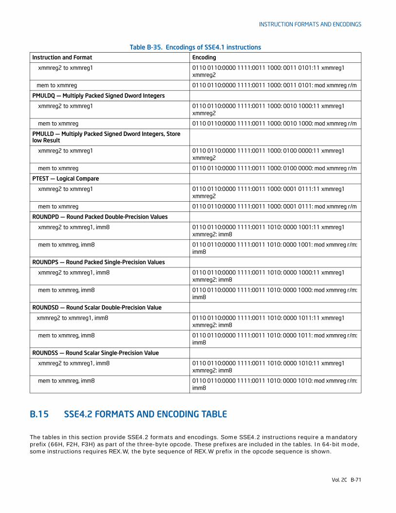
INSTRUCTION FORMATS AND ENCODINGS
B.15 SSE4.2 FORMATS AND ENCODING TABLE
The tables in this section provide SSE4.2 formats and encodings. Some SSE4.2 instructions require a mandatory prefix (66H, F2H, F3H) as part of the three-byte opcode. These prefixes are included in the tables. In 64-bit mode, some instructions requires REX.W, the byte sequence of REX.W prefix in the opcode sequence is shown.
xmmreg2 to xmmreg1 0110 0110:0000 1111:0011 1000: 0011 0101:11 xmmreg1 xmmreg2
mem to xmmreg 0110 0110:0000 1111:0011 1000: 0011 0101: mod xmmreg r/m
PMULDQ — Multiply Packed Signed Dword Integers
xmmreg2 to xmmreg1 0110 0110:0000 1111:0011 1000: 0010 1000:11 xmmreg1 xmmreg2
mem to xmmreg 0110 0110:0000 1111:0011 1000: 0010 1000: mod xmmreg r/m
PMULLD — Multiply Packed Signed Dword Integers, Store low Result
xmmreg2 to xmmreg1 0110 0110:0000 1111:0011 1000: 0100 0000:11 xmmreg1 xmmreg2
mem to xmmreg 0110 0110:0000 1111:0011 1000: 0100 0000: mod xmmreg r/m
PTEST — Logical Compare
xmmreg2 to xmmreg1 0110 0110:0000 1111:0011 1000: 0001 0111:11 xmmreg1 xmmreg2
mem to xmmreg 0110 0110:0000 1111:0011 1000: 0001 0111: mod xmmreg r/m
ROUNDPD — Round Packed Double-Precision Values
xmmreg2 to xmmreg1, imm8 0110 0110:0000 1111:0011 1010: 0000 1001:11 xmmreg1 xmmreg2: imm8
mem to xmmreg, imm8 0110 0110:0000 1111:0011 1010: 0000 1001: mod xmmreg r/m: imm8
ROUNDPS — Round Packed Single-Precision Values
xmmreg2 to xmmreg1, imm8 0110 0110:0000 1111:0011 1010: 0000 1000:11 xmmreg1 xmmreg2: imm8
mem to xmmreg, imm8 0110 0110:0000 1111:0011 1010: 0000 1000: mod xmmreg r/m: imm8
ROUNDSD — Round Scalar Double-Precision Value
xmmreg2 to xmmreg1, imm8 0110 0110:0000 1111:0011 1010: 0000 1011:11 xmmreg1 xmmreg2: imm8
mem to xmmreg, imm8 0110 0110:0000 1111:0011 1010: 0000 1011: mod xmmreg r/m: imm8
ROUNDSS — Round Scalar Single-Precision Value
xmmreg2 to xmmreg1, imm8 0110 0110:0000 1111:0011 1010: 0000 1010:11 xmmreg1 xmmreg2: imm8
mem to xmmreg, imm8 0110 0110:0000 1111:0011 1010: 0000 1010: mod xmmreg r/m: imm8
Table B-35. Encodings of SSE4.1 instructions
Instruction and Format Encoding
Vol. 2C B-71
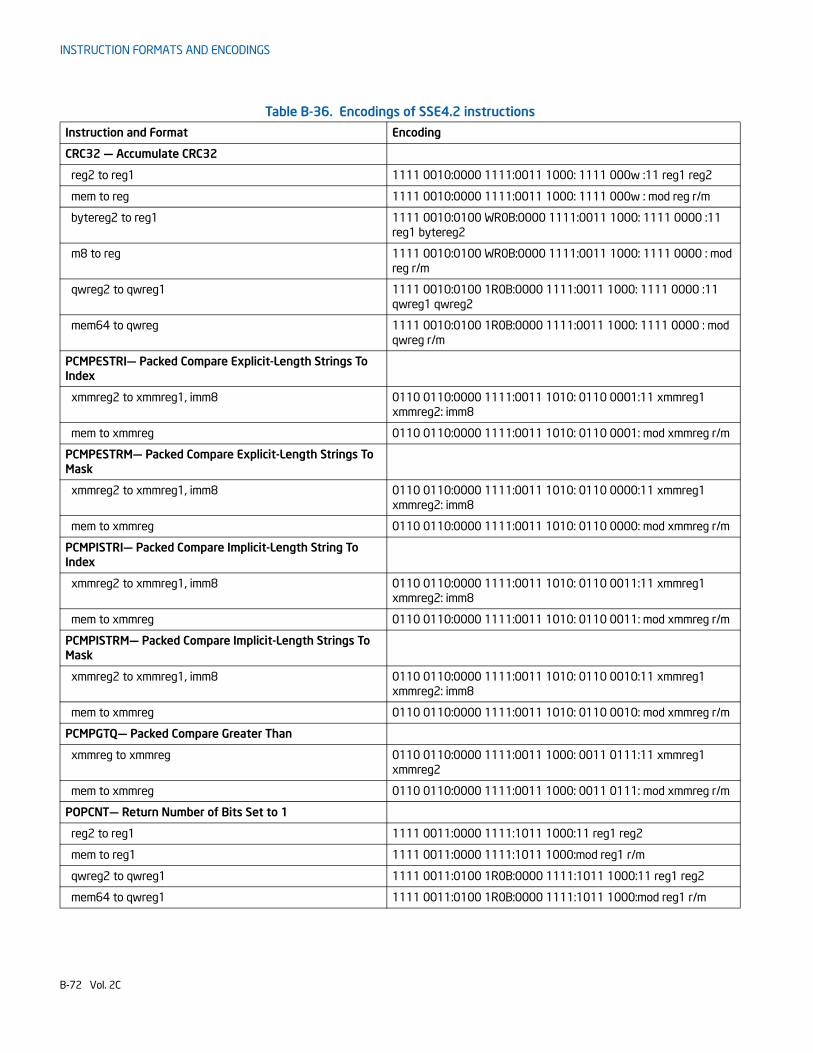
INSTRUCTION FORMATS AND ENCODINGS
Table B-36. Encodings of SSE4.2 instructions
Instruction and Format Encoding
CRC32 — Accumulate CRC32
reg2 to reg1 1111 0010:0000 1111:0011 1000: 1111 000w :11 reg1 reg2
mem to reg 1111 0010:0000 1111:0011 1000: 1111 000w : mod reg r/m
bytereg2 to reg1 1111 0010:0100 WR0B:0000 1111:0011 1000: 1111 0000 :11 reg1 bytereg2
m8 to reg 1111 0010:0100 WR0B:0000 1111:0011 1000: 1111 0000 : mod reg r/m
qwreg2 to qwreg1 1111 0010:0100 1R0B:0000 1111:0011 1000: 1111 0000 :11 qwreg1 qwreg2
mem64 to qwreg 1111 0010:0100 1R0B:0000 1111:0011 1000: 1111 0000 : mod qwreg r/m
PCMPESTRI— Packed Compare Explicit-Length Strings To Index
xmmreg2 to xmmreg1, imm8 0110 0110:0000 1111:0011 1010: 0110 0001:11 xmmreg1 xmmreg2: imm8
mem to xmmreg 0110 0110:0000 1111:0011 1010: 0110 0001: mod xmmreg r/m
PCMPESTRM— Packed Compare Explicit-Length Strings To Mask
xmmreg2 to xmmreg1, imm8 0110 0110:0000 1111:0011 1010: 0110 0000:11 xmmreg1 xmmreg2: imm8
mem to xmmreg 0110 0110:0000 1111:0011 1010: 0110 0000: mod xmmreg r/m
PCMPISTRI— Packed Compare Implicit-Length String To Index
xmmreg2 to xmmreg1, imm8 0110 0110:0000 1111:0011 1010: 0110 0011:11 xmmreg1 xmmreg2: imm8
mem to xmmreg 0110 0110:0000 1111:0011 1010: 0110 0011: mod xmmreg r/m
PCMPISTRM— Packed Compare Implicit-Length Strings To Mask
xmmreg2 to xmmreg1, imm8 0110 0110:0000 1111:0011 1010: 0110 0010:11 xmmreg1 xmmreg2: imm8
mem to xmmreg 0110 0110:0000 1111:0011 1010: 0110 0010: mod xmmreg r/m
PCMPGTQ— Packed Compare Greater Than
xmmreg to xmmreg 0110 0110:0000 1111:0011 1000: 0011 0111:11 xmmreg1 xmmreg2
mem to xmmreg 0110 0110:0000 1111:0011 1000: 0011 0111: mod xmmreg r/m
POPCNT— Return Number of Bits Set to 1
reg2 to reg1 1111 0011:0000 1111:1011 1000:11 reg1 reg2
mem to reg1 1111 0011:0000 1111:1011 1000:mod reg1 r/m
qwreg2 to qwreg1 1111 0011:0100 1R0B:0000 1111:1011 1000:11 reg1 reg2
mem64 to qwreg1 1111 0011:0100 1R0B:0000 1111:1011 1000:mod reg1 r/m
B-72 Vol. 2C
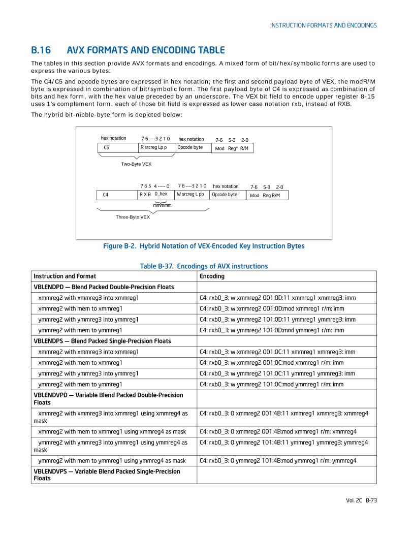
INSTRUCTION FORMATS AND ENCODINGS
B.16 AVX FORMATS AND ENCODING TABLEThe tables in this section provide AVX formats and encodings. A mixed form of bit/hex/symbolic forms are used to express the various bytes:
The C4/C5 and opcode bytes are expressed in hex notation; the first and second payload byte of VEX, the modR/M byte is expressed in combination of bit/symbolic form. The first payload byte of C4 is expressed as combination of bits and hex form, with the hex value preceded by an underscore. The VEX bit field to encode upper register 8-15 uses 1’s complement form, each of those bit field is expressed as lower case notation rxb, instead of RXB.
The hybrid bit-nibble-byte form is depicted below:
Table B-37. Encodings of AVX instructions
Figure B-2. Hybrid Notation of VEX-Encoded Key Instruction Bytes
Instruction and Format Encoding
VBLENDPD — Blend Packed Double-Precision Floats
xmmreg2 with xmmreg3 into xmmreg1 C4: rxb0_3: w xmmreg2 001:0D:11 xmmreg1 xmmreg3: imm
xmmreg2 with mem to xmmreg1 C4: rxb0_3: w xmmreg2 001:0D:mod xmmreg1 r/m: imm
ymmreg2 with ymmreg3 into ymmreg1 C4: rxb0_3: w ymmreg2 101:0D:11 ymmreg1 ymmreg3: imm
ymmreg2 with mem to ymmreg1 C4: rxb0_3: w ymmreg2 101:0D:mod ymmreg1 r/m: imm
VBLENDPS — Blend Packed Single-Precision Floats
xmmreg2 with xmmreg3 into xmmreg1 C4: rxb0_3: w xmmreg2 001:0C:11 xmmreg1 xmmreg3: imm
xmmreg2 with mem to xmmreg1 C4: rxb0_3: w xmmreg2 001:0C:mod xmmreg1 r/m: imm
ymmreg2 with ymmreg3 into ymmreg1 C4: rxb0_3: w ymmreg2 101:0C:11 ymmreg1 ymmreg3: imm
ymmreg2 with mem to ymmreg1 C4: rxb0_3: w ymmreg2 101:0C:mod ymmreg1 r/m: imm
VBLENDVPD — Variable Blend Packed Double-Precision Floats
xmmreg2 with xmmreg3 into xmmreg1 using xmmreg4 as mask
C4: rxb0_3: 0 xmmreg2 001:4B:11 xmmreg1 xmmreg3: xmmreg4
xmmreg2 with mem to xmmreg1 using xmmreg4 as mask C4: rxb0_3: 0 xmmreg2 001:4B:mod xmmreg1 r/m: xmmreg4
ymmreg2 with ymmreg3 into ymmreg1 using ymmreg4 as mask
C4: rxb0_3: 0 ymmreg2 101:4B:11 ymmreg1 ymmreg3: ymmreg4
ymmreg2 with mem to ymmreg1 using ymmreg4 as mask C4: rxb0_3: 0 ymmreg2 101:4B:mod ymmreg1 r/m: ymmreg4
VBLENDVPS — Variable Blend Packed Single-Precision Floats
7 6 ----3 2 1 0 hex notation 7-6 5-3 2-0R srcreg Lp p Opcode byte Mod Reg* R/MC5
7 6 ----3 2 1 0
W srcreg L pp
Two-Byte VEX
hex notation
7 6 5 hex notation 7-6 5-3 2-0
R X B Opcode byte Mod Reg R/MC4
4 ----- 0
0_hex
mmmmm
Three-Byte VEX
Vol. 2C B-73
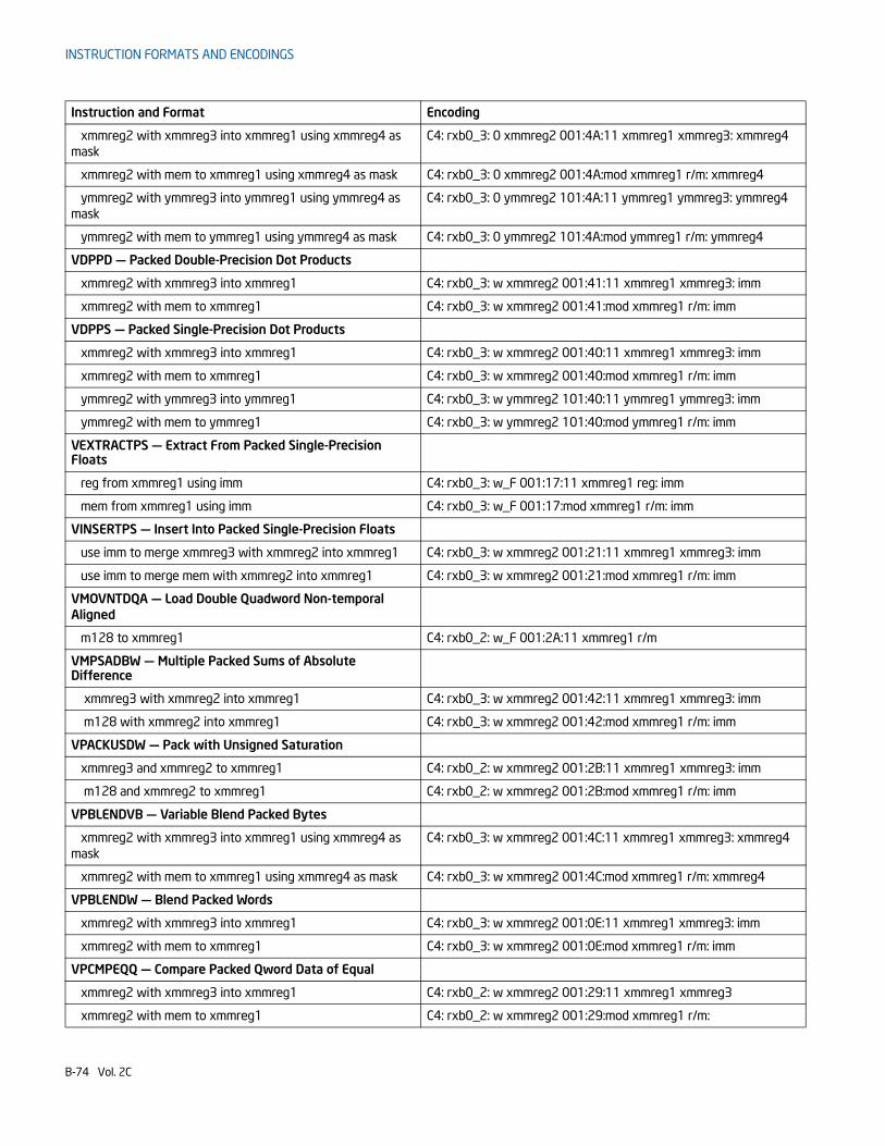
INSTRUCTION FORMATS AND ENCODINGS
xmmreg2 with xmmreg3 into xmmreg1 using xmmreg4 as mask
C4: rxb0_3: 0 xmmreg2 001:4A:11 xmmreg1 xmmreg3: xmmreg4
xmmreg2 with mem to xmmreg1 using xmmreg4 as mask C4: rxb0_3: 0 xmmreg2 001:4A:mod xmmreg1 r/m: xmmreg4
ymmreg2 with ymmreg3 into ymmreg1 using ymmreg4 as mask
C4: rxb0_3: 0 ymmreg2 101:4A:11 ymmreg1 ymmreg3: ymmreg4
ymmreg2 with mem to ymmreg1 using ymmreg4 as mask C4: rxb0_3: 0 ymmreg2 101:4A:mod ymmreg1 r/m: ymmreg4
VDPPD — Packed Double-Precision Dot Products
xmmreg2 with xmmreg3 into xmmreg1 C4: rxb0_3: w xmmreg2 001:41:11 xmmreg1 xmmreg3: imm
xmmreg2 with mem to xmmreg1 C4: rxb0_3: w xmmreg2 001:41:mod xmmreg1 r/m: imm
VDPPS — Packed Single-Precision Dot Products
xmmreg2 with xmmreg3 into xmmreg1 C4: rxb0_3: w xmmreg2 001:40:11 xmmreg1 xmmreg3: imm
xmmreg2 with mem to xmmreg1 C4: rxb0_3: w xmmreg2 001:40:mod xmmreg1 r/m: imm
ymmreg2 with ymmreg3 into ymmreg1 C4: rxb0_3: w ymmreg2 101:40:11 ymmreg1 ymmreg3: imm
ymmreg2 with mem to ymmreg1 C4: rxb0_3: w ymmreg2 101:40:mod ymmreg1 r/m: imm
VEXTRACTPS — Extract From Packed Single-Precision Floats
reg from xmmreg1 using imm C4: rxb0_3: w_F 001:17:11 xmmreg1 reg: imm
mem from xmmreg1 using imm C4: rxb0_3: w_F 001:17:mod xmmreg1 r/m: imm
VINSERTPS — Insert Into Packed Single-Precision Floats
use imm to merge xmmreg3 with xmmreg2 into xmmreg1 C4: rxb0_3: w xmmreg2 001:21:11 xmmreg1 xmmreg3: imm
use imm to merge mem with xmmreg2 into xmmreg1 C4: rxb0_3: w xmmreg2 001:21:mod xmmreg1 r/m: imm
VMOVNTDQA — Load Double Quadword Non-temporal Aligned
m128 to xmmreg1 C4: rxb0_2: w_F 001:2A:11 xmmreg1 r/m
VMPSADBW — Multiple Packed Sums of Absolute Difference
xmmreg3 with xmmreg2 into xmmreg1 C4: rxb0_3: w xmmreg2 001:42:11 xmmreg1 xmmreg3: imm
m128 with xmmreg2 into xmmreg1 C4: rxb0_3: w xmmreg2 001:42:mod xmmreg1 r/m: imm
VPACKUSDW — Pack with Unsigned Saturation
xmmreg3 and xmmreg2 to xmmreg1 C4: rxb0_2: w xmmreg2 001:2B:11 xmmreg1 xmmreg3: imm
m128 and xmmreg2 to xmmreg1 C4: rxb0_2: w xmmreg2 001:2B:mod xmmreg1 r/m: imm
VPBLENDVB — Variable Blend Packed Bytes
xmmreg2 with xmmreg3 into xmmreg1 using xmmreg4 as mask
C4: rxb0_3: w xmmreg2 001:4C:11 xmmreg1 xmmreg3: xmmreg4
xmmreg2 with mem to xmmreg1 using xmmreg4 as mask C4: rxb0_3: w xmmreg2 001:4C:mod xmmreg1 r/m: xmmreg4
VPBLENDW — Blend Packed Words
xmmreg2 with xmmreg3 into xmmreg1 C4: rxb0_3: w xmmreg2 001:0E:11 xmmreg1 xmmreg3: imm
xmmreg2 with mem to xmmreg1 C4: rxb0_3: w xmmreg2 001:0E:mod xmmreg1 r/m: imm
VPCMPEQQ — Compare Packed Qword Data of Equal
xmmreg2 with xmmreg3 into xmmreg1 C4: rxb0_2: w xmmreg2 001:29:11 xmmreg1 xmmreg3
xmmreg2 with mem to xmmreg1 C4: rxb0_2: w xmmreg2 001:29:mod xmmreg1 r/m:
Instruction and Format Encoding
B-74 Vol. 2C
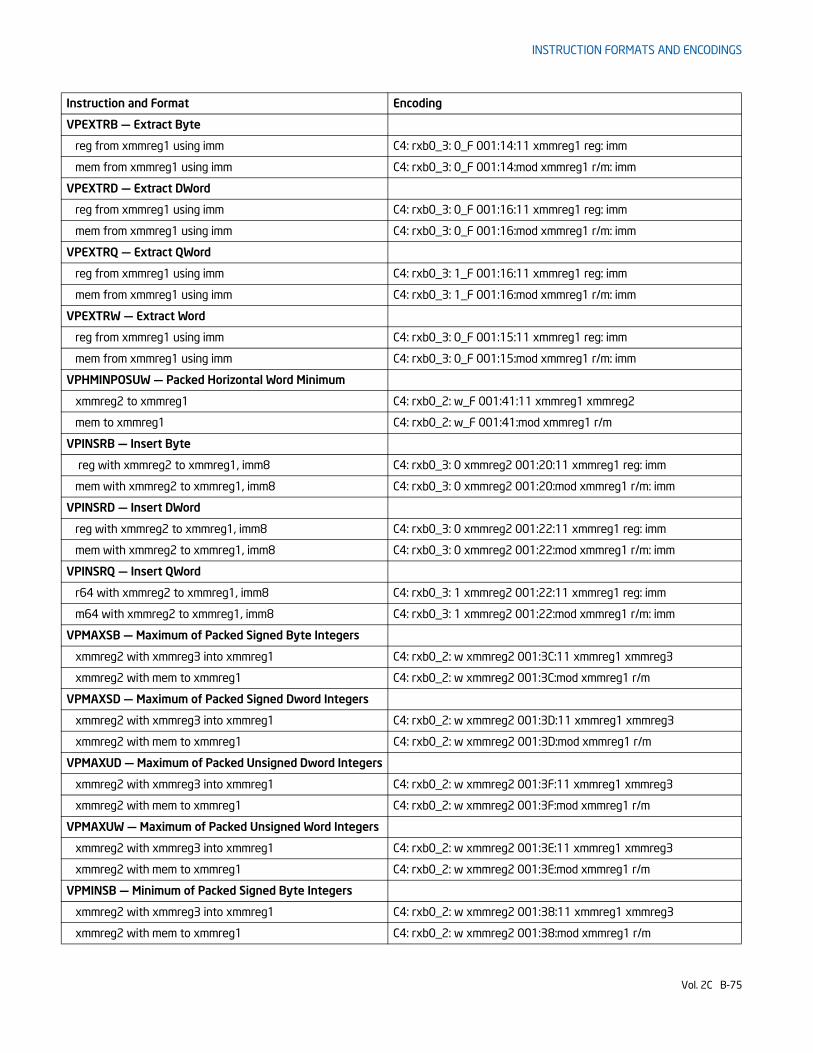
INSTRUCTION FORMATS AND ENCODINGS
VPEXTRB — Extract Byte
reg from xmmreg1 using imm C4: rxb0_3: 0_F 001:14:11 xmmreg1 reg: imm
mem from xmmreg1 using imm C4: rxb0_3: 0_F 001:14:mod xmmreg1 r/m: imm
VPEXTRD — Extract DWord
reg from xmmreg1 using imm C4: rxb0_3: 0_F 001:16:11 xmmreg1 reg: imm
mem from xmmreg1 using imm C4: rxb0_3: 0_F 001:16:mod xmmreg1 r/m: imm
VPEXTRQ — Extract QWord
reg from xmmreg1 using imm C4: rxb0_3: 1_F 001:16:11 xmmreg1 reg: imm
mem from xmmreg1 using imm C4: rxb0_3: 1_F 001:16:mod xmmreg1 r/m: imm
VPEXTRW — Extract Word
reg from xmmreg1 using imm C4: rxb0_3: 0_F 001:15:11 xmmreg1 reg: imm
mem from xmmreg1 using imm C4: rxb0_3: 0_F 001:15:mod xmmreg1 r/m: imm
VPHMINPOSUW — Packed Horizontal Word Minimum
xmmreg2 to xmmreg1 C4: rxb0_2: w_F 001:41:11 xmmreg1 xmmreg2
mem to xmmreg1 C4: rxb0_2: w_F 001:41:mod xmmreg1 r/m
VPINSRB — Insert Byte
reg with xmmreg2 to xmmreg1, imm8 C4: rxb0_3: 0 xmmreg2 001:20:11 xmmreg1 reg: imm
mem with xmmreg2 to xmmreg1, imm8 C4: rxb0_3: 0 xmmreg2 001:20:mod xmmreg1 r/m: imm
VPINSRD — Insert DWord
reg with xmmreg2 to xmmreg1, imm8 C4: rxb0_3: 0 xmmreg2 001:22:11 xmmreg1 reg: imm
mem with xmmreg2 to xmmreg1, imm8 C4: rxb0_3: 0 xmmreg2 001:22:mod xmmreg1 r/m: imm
VPINSRQ — Insert QWord
r64 with xmmreg2 to xmmreg1, imm8 C4: rxb0_3: 1 xmmreg2 001:22:11 xmmreg1 reg: imm
m64 with xmmreg2 to xmmreg1, imm8 C4: rxb0_3: 1 xmmreg2 001:22:mod xmmreg1 r/m: imm
VPMAXSB — Maximum of Packed Signed Byte Integers
xmmreg2 with xmmreg3 into xmmreg1 C4: rxb0_2: w xmmreg2 001:3C:11 xmmreg1 xmmreg3
xmmreg2 with mem to xmmreg1 C4: rxb0_2: w xmmreg2 001:3C:mod xmmreg1 r/m
VPMAXSD — Maximum of Packed Signed Dword Integers
xmmreg2 with xmmreg3 into xmmreg1 C4: rxb0_2: w xmmreg2 001:3D:11 xmmreg1 xmmreg3
xmmreg2 with mem to xmmreg1 C4: rxb0_2: w xmmreg2 001:3D:mod xmmreg1 r/m
VPMAXUD — Maximum of Packed Unsigned Dword Integers
xmmreg2 with xmmreg3 into xmmreg1 C4: rxb0_2: w xmmreg2 001:3F:11 xmmreg1 xmmreg3
xmmreg2 with mem to xmmreg1 C4: rxb0_2: w xmmreg2 001:3F:mod xmmreg1 r/m
VPMAXUW — Maximum of Packed Unsigned Word Integers
xmmreg2 with xmmreg3 into xmmreg1 C4: rxb0_2: w xmmreg2 001:3E:11 xmmreg1 xmmreg3
xmmreg2 with mem to xmmreg1 C4: rxb0_2: w xmmreg2 001:3E:mod xmmreg1 r/m
VPMINSB — Minimum of Packed Signed Byte Integers
xmmreg2 with xmmreg3 into xmmreg1 C4: rxb0_2: w xmmreg2 001:38:11 xmmreg1 xmmreg3
xmmreg2 with mem to xmmreg1 C4: rxb0_2: w xmmreg2 001:38:mod xmmreg1 r/m
Instruction and Format Encoding
Vol. 2C B-75
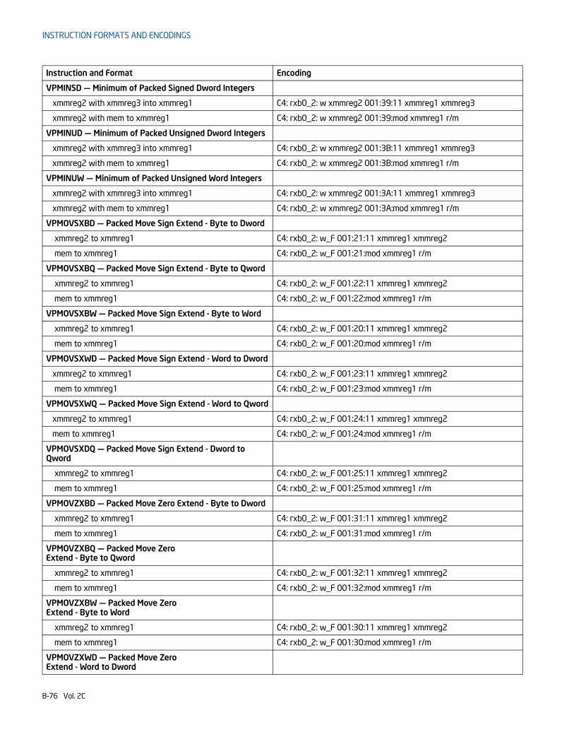
INSTRUCTION FORMATS AND ENCODINGS
VPMINSD — Minimum of Packed Signed Dword Integers
xmmreg2 with xmmreg3 into xmmreg1 C4: rxb0_2: w xmmreg2 001:39:11 xmmreg1 xmmreg3
xmmreg2 with mem to xmmreg1 C4: rxb0_2: w xmmreg2 001:39:mod xmmreg1 r/m
VPMINUD — Minimum of Packed Unsigned Dword Integers
xmmreg2 with xmmreg3 into xmmreg1 C4: rxb0_2: w xmmreg2 001:3B:11 xmmreg1 xmmreg3
xmmreg2 with mem to xmmreg1 C4: rxb0_2: w xmmreg2 001:3B:mod xmmreg1 r/m
VPMINUW — Minimum of Packed Unsigned Word Integers
xmmreg2 with xmmreg3 into xmmreg1 C4: rxb0_2: w xmmreg2 001:3A:11 xmmreg1 xmmreg3
xmmreg2 with mem to xmmreg1 C4: rxb0_2: w xmmreg2 001:3A:mod xmmreg1 r/m
VPMOVSXBD — Packed Move Sign Extend - Byte to Dword
xmmreg2 to xmmreg1 C4: rxb0_2: w_F 001:21:11 xmmreg1 xmmreg2
mem to xmmreg1 C4: rxb0_2: w_F 001:21:mod xmmreg1 r/m
VPMOVSXBQ — Packed Move Sign Extend - Byte to Qword
xmmreg2 to xmmreg1 C4: rxb0_2: w_F 001:22:11 xmmreg1 xmmreg2
mem to xmmreg1 C4: rxb0_2: w_F 001:22:mod xmmreg1 r/m
VPMOVSXBW — Packed Move Sign Extend - Byte to Word
xmmreg2 to xmmreg1 C4: rxb0_2: w_F 001:20:11 xmmreg1 xmmreg2
mem to xmmreg1 C4: rxb0_2: w_F 001:20:mod xmmreg1 r/m
VPMOVSXWD — Packed Move Sign Extend - Word to Dword
xmmreg2 to xmmreg1 C4: rxb0_2: w_F 001:23:11 xmmreg1 xmmreg2
mem to xmmreg1 C4: rxb0_2: w_F 001:23:mod xmmreg1 r/m
VPMOVSXWQ — Packed Move Sign Extend - Word to Qword
xmmreg2 to xmmreg1 C4: rxb0_2: w_F 001:24:11 xmmreg1 xmmreg2
mem to xmmreg1 C4: rxb0_2: w_F 001:24:mod xmmreg1 r/m
VPMOVSXDQ — Packed Move Sign Extend - Dword to Qword
xmmreg2 to xmmreg1 C4: rxb0_2: w_F 001:25:11 xmmreg1 xmmreg2
mem to xmmreg1 C4: rxb0_2: w_F 001:25:mod xmmreg1 r/m
VPMOVZXBD — Packed Move Zero Extend - Byte to Dword
xmmreg2 to xmmreg1 C4: rxb0_2: w_F 001:31:11 xmmreg1 xmmreg2
mem to xmmreg1 C4: rxb0_2: w_F 001:31:mod xmmreg1 r/m
VPMOVZXBQ — Packed Move Zero Extend - Byte to Qword
xmmreg2 to xmmreg1 C4: rxb0_2: w_F 001:32:11 xmmreg1 xmmreg2
mem to xmmreg1 C4: rxb0_2: w_F 001:32:mod xmmreg1 r/m
VPMOVZXBW — Packed Move Zero Extend - Byte to Word
xmmreg2 to xmmreg1 C4: rxb0_2: w_F 001:30:11 xmmreg1 xmmreg2
mem to xmmreg1 C4: rxb0_2: w_F 001:30:mod xmmreg1 r/m
VPMOVZXWD — Packed Move Zero Extend - Word to Dword
Instruction and Format Encoding
B-76 Vol. 2C
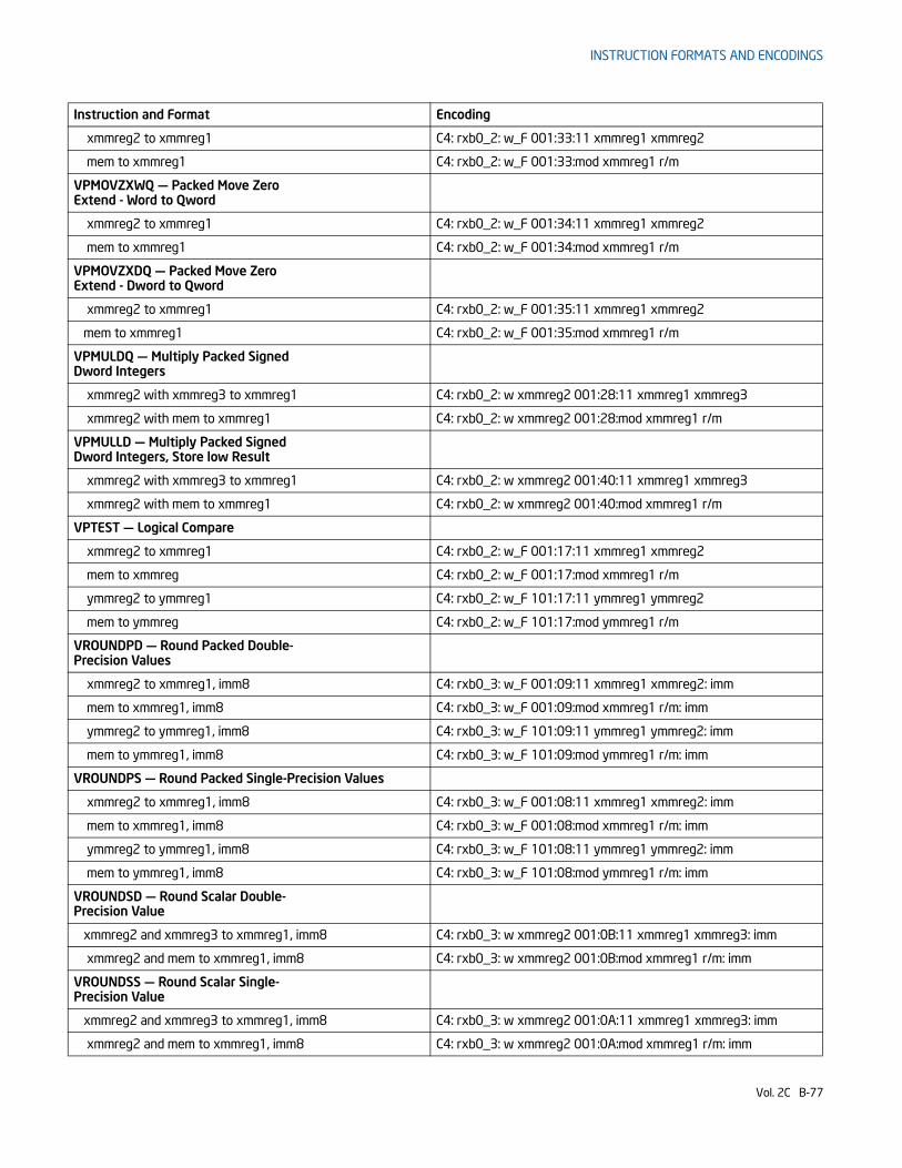
INSTRUCTION FORMATS AND ENCODINGS
xmmreg2 to xmmreg1 C4: rxb0_2: w_F 001:33:11 xmmreg1 xmmreg2
mem to xmmreg1 C4: rxb0_2: w_F 001:33:mod xmmreg1 r/m
VPMOVZXWQ — Packed Move Zero Extend - Word to Qword
xmmreg2 to xmmreg1 C4: rxb0_2: w_F 001:34:11 xmmreg1 xmmreg2
mem to xmmreg1 C4: rxb0_2: w_F 001:34:mod xmmreg1 r/m
VPMOVZXDQ — Packed Move Zero Extend - Dword to Qword
xmmreg2 to xmmreg1 C4: rxb0_2: w_F 001:35:11 xmmreg1 xmmreg2
mem to xmmreg1 C4: rxb0_2: w_F 001:35:mod xmmreg1 r/m
VPMULDQ — Multiply Packed Signed Dword Integers
xmmreg2 with xmmreg3 to xmmreg1 C4: rxb0_2: w xmmreg2 001:28:11 xmmreg1 xmmreg3
xmmreg2 with mem to xmmreg1 C4: rxb0_2: w xmmreg2 001:28:mod xmmreg1 r/m
VPMULLD — Multiply Packed Signed Dword Integers, Store low Result
xmmreg2 with xmmreg3 to xmmreg1 C4: rxb0_2: w xmmreg2 001:40:11 xmmreg1 xmmreg3
xmmreg2 with mem to xmmreg1 C4: rxb0_2: w xmmreg2 001:40:mod xmmreg1 r/m
VPTEST — Logical Compare
xmmreg2 to xmmreg1 C4: rxb0_2: w_F 001:17:11 xmmreg1 xmmreg2
mem to xmmreg C4: rxb0_2: w_F 001:17:mod xmmreg1 r/m
ymmreg2 to ymmreg1 C4: rxb0_2: w_F 101:17:11 ymmreg1 ymmreg2
mem to ymmreg C4: rxb0_2: w_F 101:17:mod ymmreg1 r/m
VROUNDPD — Round Packed Double-Precision Values
xmmreg2 to xmmreg1, imm8 C4: rxb0_3: w_F 001:09:11 xmmreg1 xmmreg2: imm
mem to xmmreg1, imm8 C4: rxb0_3: w_F 001:09:mod xmmreg1 r/m: imm
ymmreg2 to ymmreg1, imm8 C4: rxb0_3: w_F 101:09:11 ymmreg1 ymmreg2: imm
mem to ymmreg1, imm8 C4: rxb0_3: w_F 101:09:mod ymmreg1 r/m: imm
VROUNDPS — Round Packed Single-Precision Values
xmmreg2 to xmmreg1, imm8 C4: rxb0_3: w_F 001:08:11 xmmreg1 xmmreg2: imm
mem to xmmreg1, imm8 C4: rxb0_3: w_F 001:08:mod xmmreg1 r/m: imm
ymmreg2 to ymmreg1, imm8 C4: rxb0_3: w_F 101:08:11 ymmreg1 ymmreg2: imm
mem to ymmreg1, imm8 C4: rxb0_3: w_F 101:08:mod ymmreg1 r/m: imm
VROUNDSD — Round Scalar Double-Precision Value
xmmreg2 and xmmreg3 to xmmreg1, imm8 C4: rxb0_3: w xmmreg2 001:0B:11 xmmreg1 xmmreg3: imm
xmmreg2 and mem to xmmreg1, imm8 C4: rxb0_3: w xmmreg2 001:0B:mod xmmreg1 r/m: imm
VROUNDSS — Round Scalar Single-Precision Value
xmmreg2 and xmmreg3 to xmmreg1, imm8 C4: rxb0_3: w xmmreg2 001:0A:11 xmmreg1 xmmreg3: imm
xmmreg2 and mem to xmmreg1, imm8 C4: rxb0_3: w xmmreg2 001:0A:mod xmmreg1 r/m: imm
Instruction and Format Encoding
Vol. 2C B-77

INSTRUCTION FORMATS AND ENCODINGS
VPCMPESTRI — Packed Compare Explicit Length Strings, Return Index
xmmreg2 with xmmreg1, imm8 C4: rxb0_3: w_F 001:61:11 xmmreg1 xmmreg2: imm
mem with xmmreg1, imm8 C4: rxb0_3: w_F 001:61:mod xmmreg1 r/m: imm
VPCMPESTRM — Packed Compare Explicit Length Strings, Return Mask
xmmreg2 with xmmreg1, imm8 C4: rxb0_3: w_F 001:60:11 xmmreg1 xmmreg2: imm
mem with xmmreg1, imm8 C4: rxb0_3: w_F 001:60:mod xmmreg1 r/m: imm
VPCMPGTQ — Compare Packed Data for Greater Than
xmmreg2 with xmmreg3 to xmmreg1 C4: rxb0_2: w xmmreg2 001:28:11 xmmreg1 xmmreg3
xmmreg2 with mem to xmmreg1 C4: rxb0_2: w xmmreg2 001:28:mod xmmreg1 r/m
VPCMPISTRI — Packed Compare Implicit Length Strings, Return Index
xmmreg2 with xmmreg1, imm8 C4: rxb0_3: w_F 001:63:11 xmmreg1 xmmreg2: imm
mem with xmmreg1, imm8 C4: rxb0_3: w_F 001:63:mod xmmreg1 r/m: imm
VPCMPISTRM — Packed Compare Implicit Length Strings, Return Mask
xmmreg2 with xmmreg1, imm8 C4: rxb0_3: w_F 001:62:11 xmmreg1 xmmreg2: imm
mem with xmmreg, imm8 C4: rxb0_3: w_F 001:62:mod xmmreg1 r/m: imm
VAESDEC — Perform One Round of an AES Decryption Flow
xmmreg2 with xmmreg3 to xmmreg1 C4: rxb0_2: w xmmreg2 001:DE:11 xmmreg1 xmmreg3
xmmreg2 with mem to xmmreg1 C4: rxb0_2: w xmmreg2 001:DE:mod xmmreg1 r/m
VAESDECLAST — Perform Last Round of an AES Decryption Flow
xmmreg2 with xmmreg3 to xmmreg1 C4: rxb0_2: w xmmreg2 001:DF:11 xmmreg1 xmmreg3
xmmreg2 with mem to xmmreg1 C4: rxb0_2: w xmmreg2 001:DF:mod xmmreg1 r/m
VAESENC — Perform One Round of an AES Encryption Flow
xmmreg2 with xmmreg3 to xmmreg1 C4: rxb0_2: w xmmreg2 001:DC:11 xmmreg1 xmmreg3
xmmreg2 with mem to xmmreg1 C4: rxb0_2: w xmmreg2 001:DC:mod xmmreg1 r/m
VAESENCLAST — Perform Last Round of an AES Encryption Flow
xmmreg2 with xmmreg3 to xmmreg1 C4: rxb0_2: w xmmreg2 001:DD:11 xmmreg1 xmmreg3
xmmreg2 with mem to xmmreg1 C4: rxb0_2: w xmmreg2 001:DD:mod xmmreg1 r/m
VAESIMC — Perform the AES InvMixColumn Transformation
xmmreg2 to xmmreg1 C4: rxb0_2: w_F 001:DB:11 xmmreg1 xmmreg2
mem to xmmreg1 C4: rxb0_2: w_F 001:DB:mod xmmreg1 r/m
VAESKEYGENASSIST — AES Round Key Generation Assist
xmmreg2 to xmmreg1, imm8 C4: rxb0_3: w_F 001:DF:11 xmmreg1 xmmreg2: imm
mem to xmmreg, imm8 C4: rxb0_3: w_F 001:DF:mod xmmreg1 r/m: imm
VPABSB — Packed Absolute Value
xmmreg2 to xmmreg1 C4: rxb0_2: w_F 001:1C:11 xmmreg1 xmmreg2
Instruction and Format Encoding
B-78 Vol. 2C
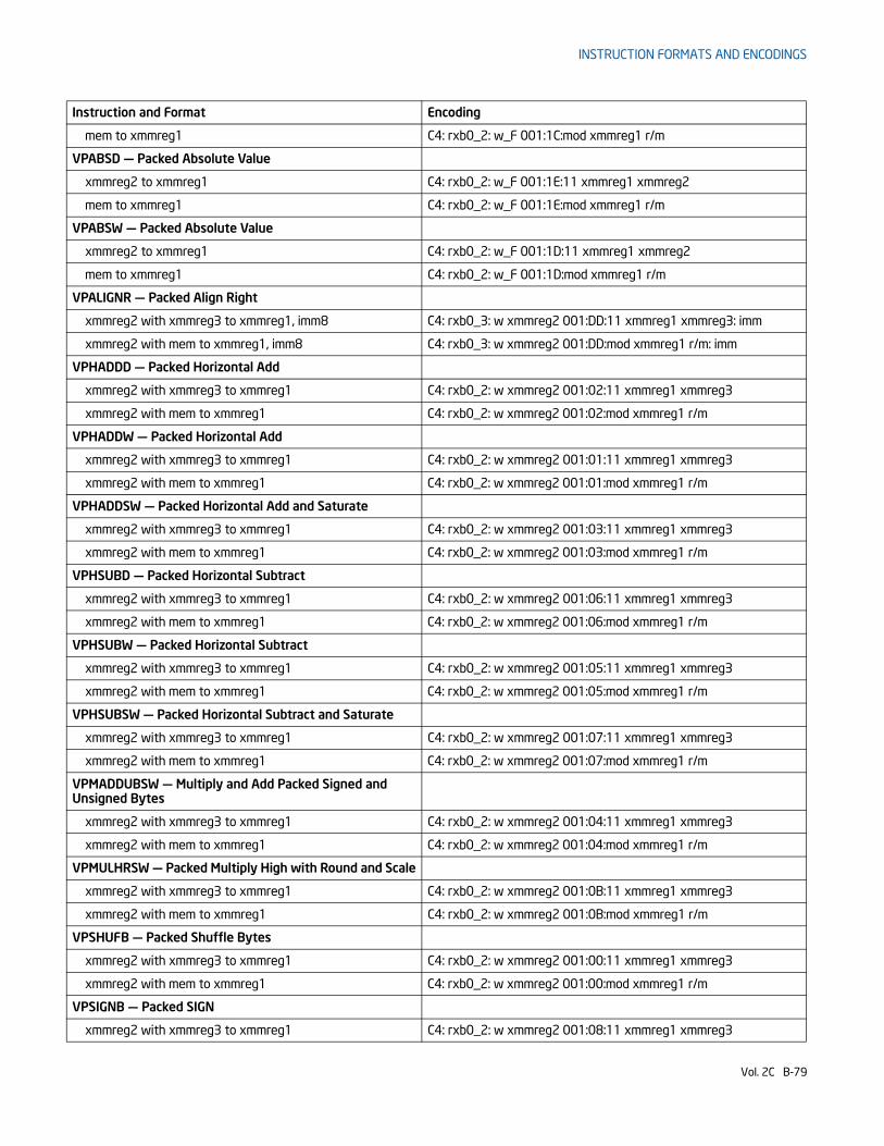
INSTRUCTION FORMATS AND ENCODINGS
mem to xmmreg1 C4: rxb0_2: w_F 001:1C:mod xmmreg1 r/m
VPABSD — Packed Absolute Value
xmmreg2 to xmmreg1 C4: rxb0_2: w_F 001:1E:11 xmmreg1 xmmreg2
mem to xmmreg1 C4: rxb0_2: w_F 001:1E:mod xmmreg1 r/m
VPABSW — Packed Absolute Value
xmmreg2 to xmmreg1 C4: rxb0_2: w_F 001:1D:11 xmmreg1 xmmreg2
mem to xmmreg1 C4: rxb0_2: w_F 001:1D:mod xmmreg1 r/m
VPALIGNR — Packed Align Right
xmmreg2 with xmmreg3 to xmmreg1, imm8 C4: rxb0_3: w xmmreg2 001:DD:11 xmmreg1 xmmreg3: imm
xmmreg2 with mem to xmmreg1, imm8 C4: rxb0_3: w xmmreg2 001:DD:mod xmmreg1 r/m: imm
VPHADDD — Packed Horizontal Add
xmmreg2 with xmmreg3 to xmmreg1 C4: rxb0_2: w xmmreg2 001:02:11 xmmreg1 xmmreg3
xmmreg2 with mem to xmmreg1 C4: rxb0_2: w xmmreg2 001:02:mod xmmreg1 r/m
VPHADDW — Packed Horizontal Add
xmmreg2 with xmmreg3 to xmmreg1 C4: rxb0_2: w xmmreg2 001:01:11 xmmreg1 xmmreg3
xmmreg2 with mem to xmmreg1 C4: rxb0_2: w xmmreg2 001:01:mod xmmreg1 r/m
VPHADDSW — Packed Horizontal Add and Saturate
xmmreg2 with xmmreg3 to xmmreg1 C4: rxb0_2: w xmmreg2 001:03:11 xmmreg1 xmmreg3
xmmreg2 with mem to xmmreg1 C4: rxb0_2: w xmmreg2 001:03:mod xmmreg1 r/m
VPHSUBD — Packed Horizontal Subtract
xmmreg2 with xmmreg3 to xmmreg1 C4: rxb0_2: w xmmreg2 001:06:11 xmmreg1 xmmreg3
xmmreg2 with mem to xmmreg1 C4: rxb0_2: w xmmreg2 001:06:mod xmmreg1 r/m
VPHSUBW — Packed Horizontal Subtract
xmmreg2 with xmmreg3 to xmmreg1 C4: rxb0_2: w xmmreg2 001:05:11 xmmreg1 xmmreg3
xmmreg2 with mem to xmmreg1 C4: rxb0_2: w xmmreg2 001:05:mod xmmreg1 r/m
VPHSUBSW — Packed Horizontal Subtract and Saturate
xmmreg2 with xmmreg3 to xmmreg1 C4: rxb0_2: w xmmreg2 001:07:11 xmmreg1 xmmreg3
xmmreg2 with mem to xmmreg1 C4: rxb0_2: w xmmreg2 001:07:mod xmmreg1 r/m
VPMADDUBSW — Multiply and Add Packed Signed and Unsigned Bytes
xmmreg2 with xmmreg3 to xmmreg1 C4: rxb0_2: w xmmreg2 001:04:11 xmmreg1 xmmreg3
xmmreg2 with mem to xmmreg1 C4: rxb0_2: w xmmreg2 001:04:mod xmmreg1 r/m
VPMULHRSW — Packed Multiply High with Round and Scale
xmmreg2 with xmmreg3 to xmmreg1 C4: rxb0_2: w xmmreg2 001:0B:11 xmmreg1 xmmreg3
xmmreg2 with mem to xmmreg1 C4: rxb0_2: w xmmreg2 001:0B:mod xmmreg1 r/m
VPSHUFB — Packed Shuffle Bytes
xmmreg2 with xmmreg3 to xmmreg1 C4: rxb0_2: w xmmreg2 001:00:11 xmmreg1 xmmreg3
xmmreg2 with mem to xmmreg1 C4: rxb0_2: w xmmreg2 001:00:mod xmmreg1 r/m
VPSIGNB — Packed SIGN
xmmreg2 with xmmreg3 to xmmreg1 C4: rxb0_2: w xmmreg2 001:08:11 xmmreg1 xmmreg3
Instruction and Format Encoding
Vol. 2C B-79
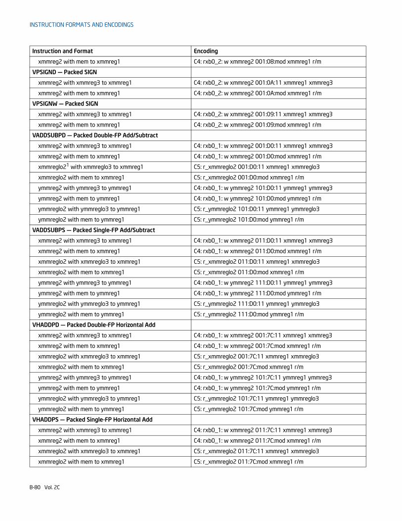
INSTRUCTION FORMATS AND ENCODINGS
xmmreg2 with mem to xmmreg1 C4: rxb0_2: w xmmreg2 001:08:mod xmmreg1 r/m
VPSIGND — Packed SIGN
xmmreg2 with xmmreg3 to xmmreg1 C4: rxb0_2: w xmmreg2 001:0A:11 xmmreg1 xmmreg3
xmmreg2 with mem to xmmreg1 C4: rxb0_2: w xmmreg2 001:0A:mod xmmreg1 r/m
VPSIGNW — Packed SIGN
xmmreg2 with xmmreg3 to xmmreg1 C4: rxb0_2: w xmmreg2 001:09:11 xmmreg1 xmmreg3
xmmreg2 with mem to xmmreg1 C4: rxb0_2: w xmmreg2 001:09:mod xmmreg1 r/m
VADDSUBPD — Packed Double-FP Add/Subtract
xmmreg2 with xmmreg3 to xmmreg1 C4: rxb0_1: w xmmreg2 001:D0:11 xmmreg1 xmmreg3
xmmreg2 with mem to xmmreg1 C4: rxb0_1: w xmmreg2 001:D0:mod xmmreg1 r/m
xmmreglo21 with xmmreglo3 to xmmreg1 C5: r_xmmreglo2 001:D0:11 xmmreg1 xmmreglo3
xmmreglo2 with mem to xmmreg1 C5: r_xmmreglo2 001:D0:mod xmmreg1 r/m
ymmreg2 with ymmreg3 to ymmreg1 C4: rxb0_1: w ymmreg2 101:D0:11 ymmreg1 ymmreg3
ymmreg2 with mem to ymmreg1 C4: rxb0_1: w ymmreg2 101:D0:mod ymmreg1 r/m
ymmreglo2 with ymmreglo3 to ymmreg1 C5: r_ymmreglo2 101:D0:11 ymmreg1 ymmreglo3
ymmreglo2 with mem to ymmreg1 C5: r_ymmreglo2 101:D0:mod ymmreg1 r/m
VADDSUBPS — Packed Single-FP Add/Subtract
xmmreg2 with xmmreg3 to xmmreg1 C4: rxb0_1: w xmmreg2 011:D0:11 xmmreg1 xmmreg3
xmmreg2 with mem to xmmreg1 C4: rxb0_1: w xmmreg2 011:D0:mod xmmreg1 r/m
xmmreglo2 with xmmreglo3 to xmmreg1 C5: r_xmmreglo2 011:D0:11 xmmreg1 xmmreglo3
xmmreglo2 with mem to xmmreg1 C5: r_xmmreglo2 011:D0:mod xmmreg1 r/m
ymmreg2 with ymmreg3 to ymmreg1 C4: rxb0_1: w ymmreg2 111:D0:11 ymmreg1 ymmreg3
ymmreg2 with mem to ymmreg1 C4: rxb0_1: w ymmreg2 111:D0:mod ymmreg1 r/m
ymmreglo2 with ymmreglo3 to ymmreg1 C5: r_ymmreglo2 111:D0:11 ymmreg1 ymmreglo3
ymmreglo2 with mem to ymmreg1 C5: r_ymmreglo2 111:D0:mod ymmreg1 r/m
VHADDPD — Packed Double-FP Horizontal Add
xmmreg2 with xmmreg3 to xmmreg1 C4: rxb0_1: w xmmreg2 001:7C:11 xmmreg1 xmmreg3
xmmreg2 with mem to xmmreg1 C4: rxb0_1: w xmmreg2 001:7C:mod xmmreg1 r/m
xmmreglo2 with xmmreglo3 to xmmreg1 C5: r_xmmreglo2 001:7C:11 xmmreg1 xmmreglo3
xmmreglo2 with mem to xmmreg1 C5: r_xmmreglo2 001:7C:mod xmmreg1 r/m
ymmreg2 with ymmreg3 to ymmreg1 C4: rxb0_1: w ymmreg2 101:7C:11 ymmreg1 ymmreg3
ymmreg2 with mem to ymmreg1 C4: rxb0_1: w ymmreg2 101:7C:mod ymmreg1 r/m
ymmreglo2 with ymmreglo3 to ymmreg1 C5: r_ymmreglo2 101:7C:11 ymmreg1 ymmreglo3
ymmreglo2 with mem to ymmreg1 C5: r_ymmreglo2 101:7C:mod ymmreg1 r/m
VHADDPS — Packed Single-FP Horizontal Add
xmmreg2 with xmmreg3 to xmmreg1 C4: rxb0_1: w xmmreg2 011:7C:11 xmmreg1 xmmreg3
xmmreg2 with mem to xmmreg1 C4: rxb0_1: w xmmreg2 011:7C:mod xmmreg1 r/m
xmmreglo2 with xmmreglo3 to xmmreg1 C5: r_xmmreglo2 011:7C:11 xmmreg1 xmmreglo3
xmmreglo2 with mem to xmmreg1 C5: r_xmmreglo2 011:7C:mod xmmreg1 r/m
Instruction and Format Encoding
B-80 Vol. 2C
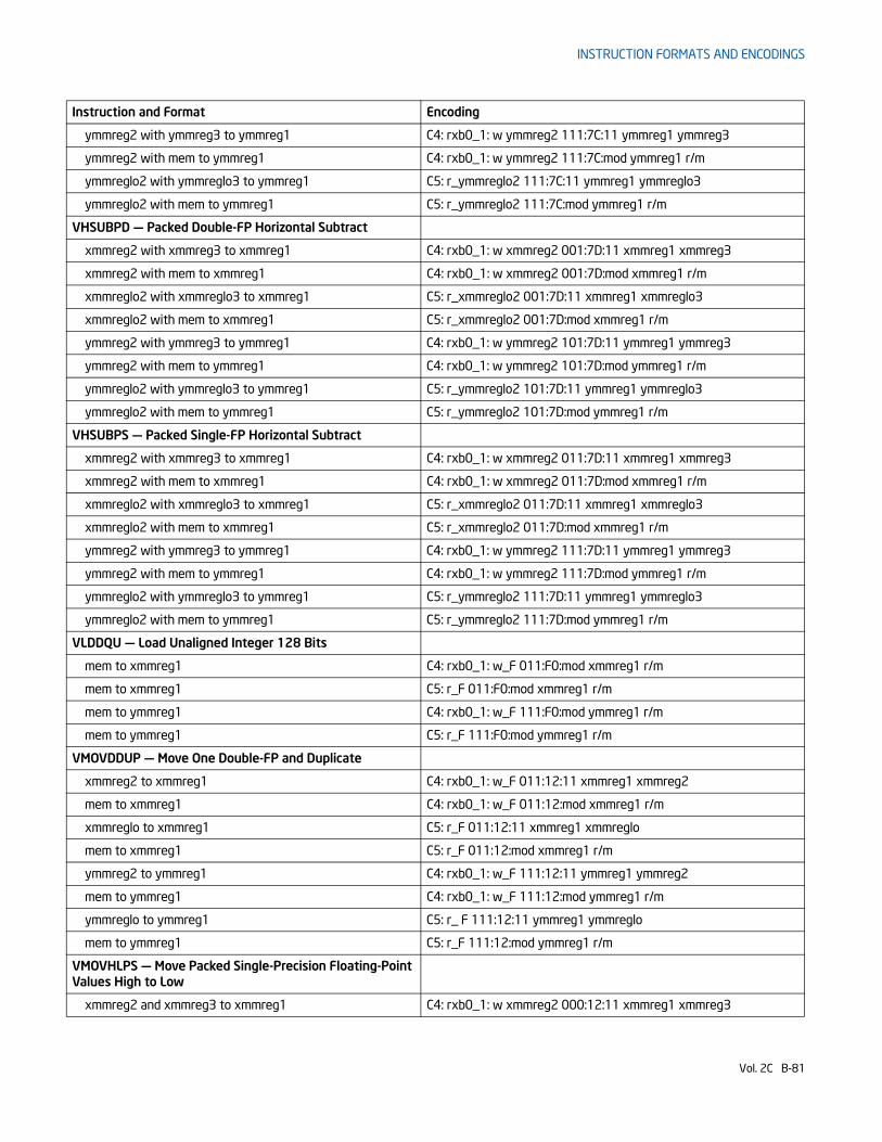
INSTRUCTION FORMATS AND ENCODINGS
ymmreg2 with ymmreg3 to ymmreg1 C4: rxb0_1: w ymmreg2 111:7C:11 ymmreg1 ymmreg3
ymmreg2 with mem to ymmreg1 C4: rxb0_1: w ymmreg2 111:7C:mod ymmreg1 r/m
ymmreglo2 with ymmreglo3 to ymmreg1 C5: r_ymmreglo2 111:7C:11 ymmreg1 ymmreglo3
ymmreglo2 with mem to ymmreg1 C5: r_ymmreglo2 111:7C:mod ymmreg1 r/m
VHSUBPD — Packed Double-FP Horizontal Subtract
xmmreg2 with xmmreg3 to xmmreg1 C4: rxb0_1: w xmmreg2 001:7D:11 xmmreg1 xmmreg3
xmmreg2 with mem to xmmreg1 C4: rxb0_1: w xmmreg2 001:7D:mod xmmreg1 r/m
xmmreglo2 with xmmreglo3 to xmmreg1 C5: r_xmmreglo2 001:7D:11 xmmreg1 xmmreglo3
xmmreglo2 with mem to xmmreg1 C5: r_xmmreglo2 001:7D:mod xmmreg1 r/m
ymmreg2 with ymmreg3 to ymmreg1 C4: rxb0_1: w ymmreg2 101:7D:11 ymmreg1 ymmreg3
ymmreg2 with mem to ymmreg1 C4: rxb0_1: w ymmreg2 101:7D:mod ymmreg1 r/m
ymmreglo2 with ymmreglo3 to ymmreg1 C5: r_ymmreglo2 101:7D:11 ymmreg1 ymmreglo3
ymmreglo2 with mem to ymmreg1 C5: r_ymmreglo2 101:7D:mod ymmreg1 r/m
VHSUBPS — Packed Single-FP Horizontal Subtract
xmmreg2 with xmmreg3 to xmmreg1 C4: rxb0_1: w xmmreg2 011:7D:11 xmmreg1 xmmreg3
xmmreg2 with mem to xmmreg1 C4: rxb0_1: w xmmreg2 011:7D:mod xmmreg1 r/m
xmmreglo2 with xmmreglo3 to xmmreg1 C5: r_xmmreglo2 011:7D:11 xmmreg1 xmmreglo3
xmmreglo2 with mem to xmmreg1 C5: r_xmmreglo2 011:7D:mod xmmreg1 r/m
ymmreg2 with ymmreg3 to ymmreg1 C4: rxb0_1: w ymmreg2 111:7D:11 ymmreg1 ymmreg3
ymmreg2 with mem to ymmreg1 C4: rxb0_1: w ymmreg2 111:7D:mod ymmreg1 r/m
ymmreglo2 with ymmreglo3 to ymmreg1 C5: r_ymmreglo2 111:7D:11 ymmreg1 ymmreglo3
ymmreglo2 with mem to ymmreg1 C5: r_ymmreglo2 111:7D:mod ymmreg1 r/m
VLDDQU — Load Unaligned Integer 128 Bits
mem to xmmreg1 C4: rxb0_1: w_F 011:F0:mod xmmreg1 r/m
mem to xmmreg1 C5: r_F 011:F0:mod xmmreg1 r/m
mem to ymmreg1 C4: rxb0_1: w_F 111:F0:mod ymmreg1 r/m
mem to ymmreg1 C5: r_F 111:F0:mod ymmreg1 r/m
VMOVDDUP — Move One Double-FP and Duplicate
xmmreg2 to xmmreg1 C4: rxb0_1: w_F 011:12:11 xmmreg1 xmmreg2
mem to xmmreg1 C4: rxb0_1: w_F 011:12:mod xmmreg1 r/m
xmmreglo to xmmreg1 C5: r_F 011:12:11 xmmreg1 xmmreglo
mem to xmmreg1 C5: r_F 011:12:mod xmmreg1 r/m
ymmreg2 to ymmreg1 C4: rxb0_1: w_F 111:12:11 ymmreg1 ymmreg2
mem to ymmreg1 C4: rxb0_1: w_F 111:12:mod ymmreg1 r/m
ymmreglo to ymmreg1 C5: r_ F 111:12:11 ymmreg1 ymmreglo
mem to ymmreg1 C5: r_F 111:12:mod ymmreg1 r/m
VMOVHLPS — Move Packed Single-Precision Floating-Point Values High to Low
xmmreg2 and xmmreg3 to xmmreg1 C4: rxb0_1: w xmmreg2 000:12:11 xmmreg1 xmmreg3
Instruction and Format Encoding
Vol. 2C B-81
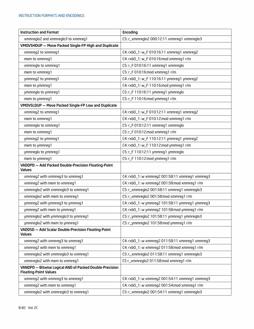
INSTRUCTION FORMATS AND ENCODINGS
xmmreglo2 and xmmreglo3 to xmmreg1 C5: r_xmmreglo2 000:12:11 xmmreg1 xmmreglo3
VMOVSHDUP — Move Packed Single-FP High and Duplicate
xmmreg2 to xmmreg1 C4: rxb0_1: w_F 010:16:11 xmmreg1 xmmreg2
mem to xmmreg1 C4: rxb0_1: w_F 010:16:mod xmmreg1 r/m
xmmreglo to xmmreg1 C5: r_F 010:16:11 xmmreg1 xmmreglo
mem to xmmreg1 C5: r_F 010:16:mod xmmreg1 r/m
ymmreg2 to ymmreg1 C4: rxb0_1: w_F 110:16:11 ymmreg1 ymmreg2
mem to ymmreg1 C4: rxb0_1: w_F 110:16:mod ymmreg1 r/m
ymmreglo to ymmreg1 C5: r_F 110:16:11 ymmreg1 ymmreglo
mem to ymmreg1 C5: r_F 110:16:mod ymmreg1 r/m
VMOVSLDUP — Move Packed Single-FP Low and Duplicate
xmmreg2 to xmmreg1 C4: rxb0_1: w_F 010:12:11 xmmreg1 xmmreg2
mem to xmmreg1 C4: rxb0_1: w_F 010:12:mod xmmreg1 r/m
xmmreglo to xmmreg1 C5: r_F 010:12:11 xmmreg1 xmmreglo
mem to xmmreg1 C5: r_F 010:12:mod xmmreg1 r/m
ymmreg2 to ymmreg1 C4: rxb0_1: w_F 110:12:11 ymmreg1 ymmreg2
mem to ymmreg1 C4: rxb0_1: w_F 110:12:mod ymmreg1 r/m
ymmreglo to ymmreg1 C5: r_F 110:12:11 ymmreg1 ymmreglo
mem to ymmreg1 C5: r_F 110:12:mod ymmreg1 r/m
VADDPD — Add Packed Double-Precision Floating-Point Values
xmmreg2 with xmmreg3 to xmmreg1 C4: rxb0_1: w xmmreg2 001:58:11 xmmreg1 xmmreg3
xmmreg2 with mem to xmmreg1 C4: rxb0_1: w xmmreg2 001:58:mod xmmreg1 r/m
xmmreglo2 with xmmreglo3 to xmmreg1 C5: r_xmmreglo2 001:58:11 xmmreg1 xmmreglo3
xmmreglo2 with mem to xmmreg1 C5: r_xmmreglo2 001:58:mod xmmreg1 r/m
ymmreg2 with ymmreg3 to ymmreg1 C4: rxb0_1: w ymmreg2 101:58:11 ymmreg1 ymmreg3
ymmreg2 with mem to ymmreg1 C4: rxb0_1: w ymmreg2 101:58:mod ymmreg1 r/m
ymmreglo2 with ymmreglo3 to ymmreg1 C5: r_ymmreglo2 101:58:11 ymmreg1 ymmreglo3
ymmreglo2 with mem to ymmreg1 C5: r_ymmreglo2 101:58:mod ymmreg1 r/m
VADDSD — Add Scalar Double-Precision Floating-Point Values
xmmreg2 with xmmreg3 to xmmreg1 C4: rxb0_1: w xmmreg2 011:58:11 xmmreg1 xmmreg3
xmmreg2 with mem to xmmreg1 C4: rxb0_1: w xmmreg2 011:58:mod xmmreg1 r/m
xmmreglo2 with xmmreglo3 to xmmreg1 C5: r_xmmreglo2 011:58:11 xmmreg1 xmmreglo3
xmmreglo2 with mem to xmmreg1 C5 r_xmmreglo2 011:58:mod xmmreg1 r/m
VANDPD — Bitwise Logical AND of Packed Double-Precision Floating-Point Values
xmmreg2 with xmmreg3 to xmmreg1 C4: rxb0_1: w xmmreg2 001:54:11 xmmreg1 xmmreg3
xmmreg2 with mem to xmmreg1 C4: rxb0_1: w xmmreg2 001:54:mod xmmreg1 r/m
xmmreglo2 with xmmreglo3 to xmmreg1 C5: r_xmmreglo2 001:54:11 xmmreg1 xmmreglo3
Instruction and Format Encoding
B-82 Vol. 2C
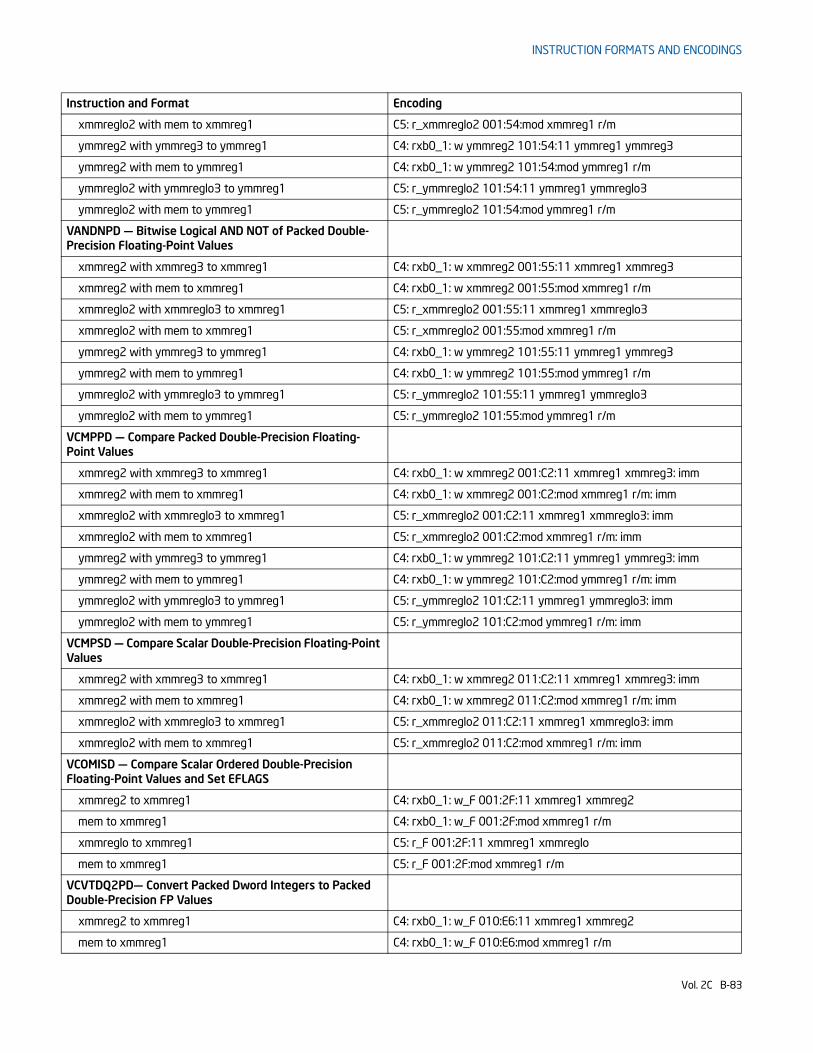
INSTRUCTION FORMATS AND ENCODINGS
xmmreglo2 with mem to xmmreg1 C5: r_xmmreglo2 001:54:mod xmmreg1 r/m
ymmreg2 with ymmreg3 to ymmreg1 C4: rxb0_1: w ymmreg2 101:54:11 ymmreg1 ymmreg3
ymmreg2 with mem to ymmreg1 C4: rxb0_1: w ymmreg2 101:54:mod ymmreg1 r/m
ymmreglo2 with ymmreglo3 to ymmreg1 C5: r_ymmreglo2 101:54:11 ymmreg1 ymmreglo3
ymmreglo2 with mem to ymmreg1 C5: r_ymmreglo2 101:54:mod ymmreg1 r/m
VANDNPD — Bitwise Logical AND NOT of Packed Double-Precision Floating-Point Values
xmmreg2 with xmmreg3 to xmmreg1 C4: rxb0_1: w xmmreg2 001:55:11 xmmreg1 xmmreg3
xmmreg2 with mem to xmmreg1 C4: rxb0_1: w xmmreg2 001:55:mod xmmreg1 r/m
xmmreglo2 with xmmreglo3 to xmmreg1 C5: r_xmmreglo2 001:55:11 xmmreg1 xmmreglo3
xmmreglo2 with mem to xmmreg1 C5: r_xmmreglo2 001:55:mod xmmreg1 r/m
ymmreg2 with ymmreg3 to ymmreg1 C4: rxb0_1: w ymmreg2 101:55:11 ymmreg1 ymmreg3
ymmreg2 with mem to ymmreg1 C4: rxb0_1: w ymmreg2 101:55:mod ymmreg1 r/m
ymmreglo2 with ymmreglo3 to ymmreg1 C5: r_ymmreglo2 101:55:11 ymmreg1 ymmreglo3
ymmreglo2 with mem to ymmreg1 C5: r_ymmreglo2 101:55:mod ymmreg1 r/m
VCMPPD — Compare Packed Double-Precision Floating-Point Values
xmmreg2 with xmmreg3 to xmmreg1 C4: rxb0_1: w xmmreg2 001:C2:11 xmmreg1 xmmreg3: imm
xmmreg2 with mem to xmmreg1 C4: rxb0_1: w xmmreg2 001:C2:mod xmmreg1 r/m: imm
xmmreglo2 with xmmreglo3 to xmmreg1 C5: r_xmmreglo2 001:C2:11 xmmreg1 xmmreglo3: imm
xmmreglo2 with mem to xmmreg1 C5: r_xmmreglo2 001:C2:mod xmmreg1 r/m: imm
ymmreg2 with ymmreg3 to ymmreg1 C4: rxb0_1: w ymmreg2 101:C2:11 ymmreg1 ymmreg3: imm
ymmreg2 with mem to ymmreg1 C4: rxb0_1: w ymmreg2 101:C2:mod ymmreg1 r/m: imm
ymmreglo2 with ymmreglo3 to ymmreg1 C5: r_ymmreglo2 101:C2:11 ymmreg1 ymmreglo3: imm
ymmreglo2 with mem to ymmreg1 C5: r_ymmreglo2 101:C2:mod ymmreg1 r/m: imm
VCMPSD — Compare Scalar Double-Precision Floating-Point Values
xmmreg2 with xmmreg3 to xmmreg1 C4: rxb0_1: w xmmreg2 011:C2:11 xmmreg1 xmmreg3: imm
xmmreg2 with mem to xmmreg1 C4: rxb0_1: w xmmreg2 011:C2:mod xmmreg1 r/m: imm
xmmreglo2 with xmmreglo3 to xmmreg1 C5: r_xmmreglo2 011:C2:11 xmmreg1 xmmreglo3: imm
xmmreglo2 with mem to xmmreg1 C5: r_xmmreglo2 011:C2:mod xmmreg1 r/m: imm
VCOMISD — Compare Scalar Ordered Double-Precision Floating-Point Values and Set EFLAGS
xmmreg2 to xmmreg1 C4: rxb0_1: w_F 001:2F:11 xmmreg1 xmmreg2
mem to xmmreg1 C4: rxb0_1: w_F 001:2F:mod xmmreg1 r/m
xmmreglo to xmmreg1 C5: r_F 001:2F:11 xmmreg1 xmmreglo
mem to xmmreg1 C5: r_F 001:2F:mod xmmreg1 r/m
VCVTDQ2PD— Convert Packed Dword Integers to Packed Double-Precision FP Values
xmmreg2 to xmmreg1 C4: rxb0_1: w_F 010:E6:11 xmmreg1 xmmreg2
mem to xmmreg1 C4: rxb0_1: w_F 010:E6:mod xmmreg1 r/m
Instruction and Format Encoding
Vol. 2C B-83
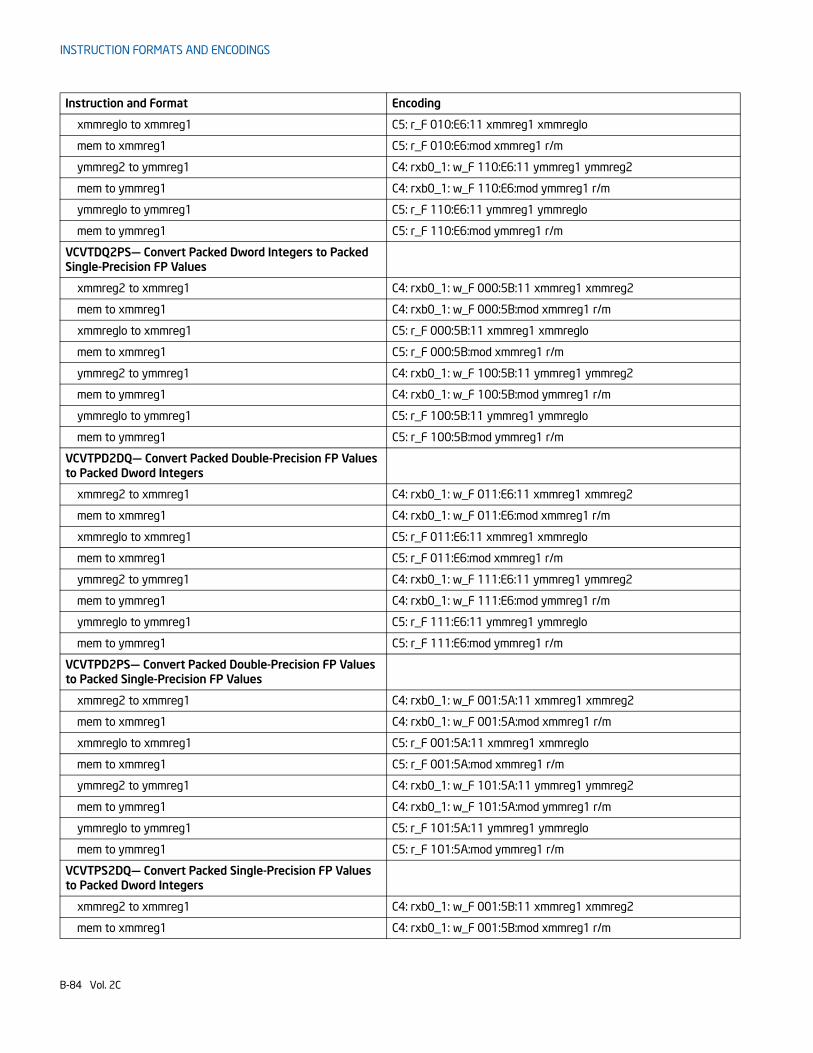
INSTRUCTION FORMATS AND ENCODINGS
xmmreglo to xmmreg1 C5: r_F 010:E6:11 xmmreg1 xmmreglo
mem to xmmreg1 C5: r_F 010:E6:mod xmmreg1 r/m
ymmreg2 to ymmreg1 C4: rxb0_1: w_F 110:E6:11 ymmreg1 ymmreg2
mem to ymmreg1 C4: rxb0_1: w_F 110:E6:mod ymmreg1 r/m
ymmreglo to ymmreg1 C5: r_F 110:E6:11 ymmreg1 ymmreglo
mem to ymmreg1 C5: r_F 110:E6:mod ymmreg1 r/m
VCVTDQ2PS— Convert Packed Dword Integers to Packed Single-Precision FP Values
xmmreg2 to xmmreg1 C4: rxb0_1: w_F 000:5B:11 xmmreg1 xmmreg2
mem to xmmreg1 C4: rxb0_1: w_F 000:5B:mod xmmreg1 r/m
xmmreglo to xmmreg1 C5: r_F 000:5B:11 xmmreg1 xmmreglo
mem to xmmreg1 C5: r_F 000:5B:mod xmmreg1 r/m
ymmreg2 to ymmreg1 C4: rxb0_1: w_F 100:5B:11 ymmreg1 ymmreg2
mem to ymmreg1 C4: rxb0_1: w_F 100:5B:mod ymmreg1 r/m
ymmreglo to ymmreg1 C5: r_F 100:5B:11 ymmreg1 ymmreglo
mem to ymmreg1 C5: r_F 100:5B:mod ymmreg1 r/m
VCVTPD2DQ— Convert Packed Double-Precision FP Values to Packed Dword Integers
xmmreg2 to xmmreg1 C4: rxb0_1: w_F 011:E6:11 xmmreg1 xmmreg2
mem to xmmreg1 C4: rxb0_1: w_F 011:E6:mod xmmreg1 r/m
xmmreglo to xmmreg1 C5: r_F 011:E6:11 xmmreg1 xmmreglo
mem to xmmreg1 C5: r_F 011:E6:mod xmmreg1 r/m
ymmreg2 to ymmreg1 C4: rxb0_1: w_F 111:E6:11 ymmreg1 ymmreg2
mem to ymmreg1 C4: rxb0_1: w_F 111:E6:mod ymmreg1 r/m
ymmreglo to ymmreg1 C5: r_F 111:E6:11 ymmreg1 ymmreglo
mem to ymmreg1 C5: r_F 111:E6:mod ymmreg1 r/m
VCVTPD2PS— Convert Packed Double-Precision FP Values to Packed Single-Precision FP Values
xmmreg2 to xmmreg1 C4: rxb0_1: w_F 001:5A:11 xmmreg1 xmmreg2
mem to xmmreg1 C4: rxb0_1: w_F 001:5A:mod xmmreg1 r/m
xmmreglo to xmmreg1 C5: r_F 001:5A:11 xmmreg1 xmmreglo
mem to xmmreg1 C5: r_F 001:5A:mod xmmreg1 r/m
ymmreg2 to ymmreg1 C4: rxb0_1: w_F 101:5A:11 ymmreg1 ymmreg2
mem to ymmreg1 C4: rxb0_1: w_F 101:5A:mod ymmreg1 r/m
ymmreglo to ymmreg1 C5: r_F 101:5A:11 ymmreg1 ymmreglo
mem to ymmreg1 C5: r_F 101:5A:mod ymmreg1 r/m
VCVTPS2DQ— Convert Packed Single-Precision FP Values to Packed Dword Integers
xmmreg2 to xmmreg1 C4: rxb0_1: w_F 001:5B:11 xmmreg1 xmmreg2
mem to xmmreg1 C4: rxb0_1: w_F 001:5B:mod xmmreg1 r/m
Instruction and Format Encoding
B-84 Vol. 2C
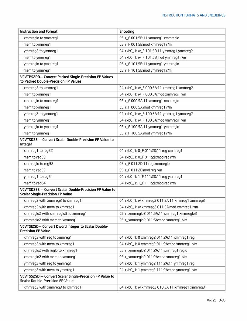
INSTRUCTION FORMATS AND ENCODINGS
xmmreglo to xmmreg1 C5: r_F 001:5B:11 xmmreg1 xmmreglo
mem to xmmreg1 C5: r_F 001:5B:mod xmmreg1 r/m
ymmreg2 to ymmreg1 C4: rxb0_1: w_F 101:5B:11 ymmreg1 ymmreg2
mem to ymmreg1 C4: rxb0_1: w_F 101:5B:mod ymmreg1 r/m
ymmreglo to ymmreg1 C5: r_F 101:5B:11 ymmreg1 ymmreglo
mem to ymmreg1 C5: r_F 101:5B:mod ymmreg1 r/m
VCVTPS2PD— Convert Packed Single-Precision FP Values to Packed Double-Precision FP Values
xmmreg2 to xmmreg1 C4: rxb0_1: w_F 000:5A:11 xmmreg1 xmmreg2
mem to xmmreg1 C4: rxb0_1: w_F 000:5A:mod xmmreg1 r/m
xmmreglo to xmmreg1 C5: r_F 000:5A:11 xmmreg1 xmmreglo
mem to xmmreg1 C5: r_F 000:5A:mod xmmreg1 r/m
ymmreg2 to ymmreg1 C4: rxb0_1: w_F 100:5A:11 ymmreg1 ymmreg2
mem to ymmreg1 C4: rxb0_1: w_F 100:5A:mod ymmreg1 r/m
ymmreglo to ymmreg1 C5: r_F 100:5A:11 ymmreg1 ymmreglo
mem to ymmreg1 C5: r_F 100:5A:mod ymmreg1 r/m
VCVTSD2SI— Convert Scalar Double-Precision FP Value to Integer
xmmreg1 to reg32 C4: rxb0_1: 0_F 011:2D:11 reg xmmreg1
mem to reg32 C4: rxb0_1: 0_F 011:2D:mod reg r/m
xmmreglo to reg32 C5: r_F 011:2D:11 reg xmmreglo
mem to reg32 C5: r_F 011:2D:mod reg r/m
ymmreg1 to reg64 C4: rxb0_1: 1_F 111:2D:11 reg ymmreg1
mem to reg64 C4: rxb0_1: 1_F 111:2D:mod reg r/m
VCVTSD2SS — Convert Scalar Double-Precision FP Value to Scalar Single-Precision FP Value
xmmreg2 with xmmreg3 to xmmreg1 C4: rxb0_1: w xmmreg2 011:5A:11 xmmreg1 xmmreg3
xmmreg2 with mem to xmmreg1 C4: rxb0_1: w xmmreg2 011:5A:mod xmmreg1 r/m
xmmreglo2 with xmmreglo3 to xmmreg1 C5: r_xmmreglo2 011:5A:11 xmmreg1 xmmreglo3
xmmreglo2 with mem to xmmreg1 C5: r_xmmreglo2 011:5A:mod xmmreg1 r/m
VCVTSI2SD— Convert Dword Integer to Scalar Double-Precision FP Value
xmmreg2 with reg to xmmreg1 C4: rxb0_1: 0 xmmreg2 011:2A:11 xmmreg1 reg
xmmreg2 with mem to xmmreg1 C4: rxb0_1: 0 xmmreg2 011:2A:mod xmmreg1 r/m
xmmreglo2 with reglo to xmmreg1 C5: r_xmmreglo2 011:2A:11 xmmreg1 reglo
xmmreglo2 with mem to xmmreg1 C5: r_xmmreglo2 011:2A:mod xmmreg1 r/m
ymmreg2 with reg to ymmreg1 C4: rxb0_1: 1 ymmreg2 111:2A:11 ymmreg1 reg
ymmreg2 with mem to ymmreg1 C4: rxb0_1: 1 ymmreg2 111:2A:mod ymmreg1 r/m
VCVTSS2SD — Convert Scalar Single-Precision FP Value to Scalar Double-Precision FP Value
xmmreg2 with xmmreg3 to xmmreg1 C4: rxb0_1: w xmmreg2 010:5A:11 xmmreg1 xmmreg3
Instruction and Format Encoding
Vol. 2C B-85
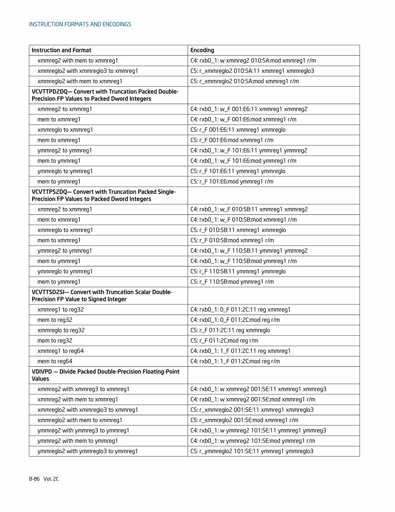
INSTRUCTION FORMATS AND ENCODINGS
xmmreg2 with mem to xmmreg1 C4: rxb0_1: w xmmreg2 010:5A:mod xmmreg1 r/m
xmmreglo2 with xmmreglo3 to xmmreg1 C5: r_xmmreglo2 010:5A:11 xmmreg1 xmmreglo3
xmmreglo2 with mem to xmmreg1 C5: r_xmmreglo2 010:5A:mod xmmreg1 r/m
VCVTTPD2DQ— Convert with Truncation Packed Double-Precision FP Values to Packed Dword Integers
xmmreg2 to xmmreg1 C4: rxb0_1: w_F 001:E6:11 xmmreg1 xmmreg2
mem to xmmreg1 C4: rxb0_1: w_F 001:E6:mod xmmreg1 r/m
xmmreglo to xmmreg1 C5: r_F 001:E6:11 xmmreg1 xmmreglo
mem to xmmreg1 C5: r_F 001:E6:mod xmmreg1 r/m
ymmreg2 to ymmreg1 C4: rxb0_1: w_F 101:E6:11 ymmreg1 ymmreg2
mem to ymmreg1 C4: rxb0_1: w_F 101:E6:mod ymmreg1 r/m
ymmreglo to ymmreg1 C5: r_F 101:E6:11 ymmreg1 ymmreglo
mem to ymmreg1 C5: r_F 101:E6:mod ymmreg1 r/m
VCVTTPS2DQ— Convert with Truncation Packed Single-Precision FP Values to Packed Dword Integers
xmmreg2 to xmmreg1 C4: rxb0_1: w_F 010:5B:11 xmmreg1 xmmreg2
mem to xmmreg1 C4: rxb0_1: w_F 010:5B:mod xmmreg1 r/m
xmmreglo to xmmreg1 C5: r_F 010:5B:11 xmmreg1 xmmreglo
mem to xmmreg1 C5: r_F 010:5B:mod xmmreg1 r/m
ymmreg2 to ymmreg1 C4: rxb0_1: w_F 110:5B:11 ymmreg1 ymmreg2
mem to ymmreg1 C4: rxb0_1: w_F 110:5B:mod ymmreg1 r/m
ymmreglo to ymmreg1 C5: r_F 110:5B:11 ymmreg1 ymmreglo
mem to ymmreg1 C5: r_F 110:5B:mod ymmreg1 r/m
VCVTTSD2SI— Convert with Truncation Scalar Double-Precision FP Value to Signed Integer
xmmreg1 to reg32 C4: rxb0_1: 0_F 011:2C:11 reg xmmreg1
mem to reg32 C4: rxb0_1: 0_F 011:2C:mod reg r/m
xmmreglo to reg32 C5: r_F 011:2C:11 reg xmmreglo
mem to reg32 C5: r_F 011:2C:mod reg r/m
xmmreg1 to reg64 C4: rxb0_1: 1_F 011:2C:11 reg xmmreg1
mem to reg64 C4: rxb0_1: 1_F 011:2C:mod reg r/m
VDIVPD — Divide Packed Double-Precision Floating-Point Values
xmmreg2 with xmmreg3 to xmmreg1 C4: rxb0_1: w xmmreg2 001:5E:11 xmmreg1 xmmreg3
xmmreg2 with mem to xmmreg1 C4: rxb0_1: w xmmreg2 001:5E:mod xmmreg1 r/m
xmmreglo2 with xmmreglo3 to xmmreg1 C5: r_xmmreglo2 001:5E:11 xmmreg1 xmmreglo3
xmmreglo2 with mem to xmmreg1 C5: r_xmmreglo2 001:5E:mod xmmreg1 r/m
ymmreg2 with ymmreg3 to ymmreg1 C4: rxb0_1: w ymmreg2 101:5E:11 ymmreg1 ymmreg3
ymmreg2 with mem to ymmreg1 C4: rxb0_1: w ymmreg2 101:5E:mod ymmreg1 r/m
ymmreglo2 with ymmreglo3 to ymmreg1 C5: r_ymmreglo2 101:5E:11 ymmreg1 ymmreglo3
Instruction and Format Encoding
B-86 Vol. 2C
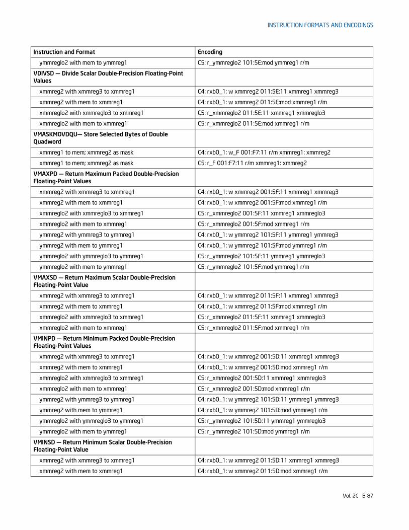
INSTRUCTION FORMATS AND ENCODINGS
ymmreglo2 with mem to ymmreg1 C5: r_ymmreglo2 101:5E:mod ymmreg1 r/m
VDIVSD — Divide Scalar Double-Precision Floating-Point Values
xmmreg2 with xmmreg3 to xmmreg1 C4: rxb0_1: w xmmreg2 011:5E:11 xmmreg1 xmmreg3
xmmreg2 with mem to xmmreg1 C4: rxb0_1: w xmmreg2 011:5E:mod xmmreg1 r/m
xmmreglo2 with xmmreglo3 to xmmreg1 C5: r_xmmreglo2 011:5E:11 xmmreg1 xmmreglo3
xmmreglo2 with mem to xmmreg1 C5: r_xmmreglo2 011:5E:mod xmmreg1 r/m
VMASKMOVDQU— Store Selected Bytes of Double Quadword
xmmreg1 to mem; xmmreg2 as mask C4: rxb0_1: w_F 001:F7:11 r/m xmmreg1: xmmreg2
xmmreg1 to mem; xmmreg2 as mask C5: r_F 001:F7:11 r/m xmmreg1: xmmreg2
VMAXPD — Return Maximum Packed Double-Precision Floating-Point Values
xmmreg2 with xmmreg3 to xmmreg1 C4: rxb0_1: w xmmreg2 001:5F:11 xmmreg1 xmmreg3
xmmreg2 with mem to xmmreg1 C4: rxb0_1: w xmmreg2 001:5F:mod xmmreg1 r/m
xmmreglo2 with xmmreglo3 to xmmreg1 C5: r_xmmreglo2 001:5F:11 xmmreg1 xmmreglo3
xmmreglo2 with mem to xmmreg1 C5: r_xmmreglo2 001:5F:mod xmmreg1 r/m
ymmreg2 with ymmreg3 to ymmreg1 C4: rxb0_1: w ymmreg2 101:5F:11 ymmreg1 ymmreg3
ymmreg2 with mem to ymmreg1 C4: rxb0_1: w ymmreg2 101:5F:mod ymmreg1 r/m
ymmreglo2 with ymmreglo3 to ymmreg1 C5: r_ymmreglo2 101:5F:11 ymmreg1 ymmreglo3
ymmreglo2 with mem to ymmreg1 C5: r_ymmreglo2 101:5F:mod ymmreg1 r/m
VMAXSD — Return Maximum Scalar Double-Precision Floating-Point Value
xmmreg2 with xmmreg3 to xmmreg1 C4: rxb0_1: w xmmreg2 011:5F:11 xmmreg1 xmmreg3
xmmreg2 with mem to xmmreg1 C4: rxb0_1: w xmmreg2 011:5F:mod xmmreg1 r/m
xmmreglo2 with xmmreglo3 to xmmreg1 C5: r_xmmreglo2 011:5F:11 xmmreg1 xmmreglo3
xmmreglo2 with mem to xmmreg1 C5: r_xmmreglo2 011:5F:mod xmmreg1 r/m
VMINPD — Return Minimum Packed Double-Precision Floating-Point Values
xmmreg2 with xmmreg3 to xmmreg1 C4: rxb0_1: w xmmreg2 001:5D:11 xmmreg1 xmmreg3
xmmreg2 with mem to xmmreg1 C4: rxb0_1: w xmmreg2 001:5D:mod xmmreg1 r/m
xmmreglo2 with xmmreglo3 to xmmreg1 C5: r_xmmreglo2 001:5D:11 xmmreg1 xmmreglo3
xmmreglo2 with mem to xmmreg1 C5: r_xmmreglo2 001:5D:mod xmmreg1 r/m
ymmreg2 with ymmreg3 to ymmreg1 C4: rxb0_1: w ymmreg2 101:5D:11 ymmreg1 ymmreg3
ymmreg2 with mem to ymmreg1 C4: rxb0_1: w ymmreg2 101:5D:mod ymmreg1 r/m
ymmreglo2 with ymmreglo3 to ymmreg1 C5: r_ymmreglo2 101:5D:11 ymmreg1 ymmreglo3
ymmreglo2 with mem to ymmreg1 C5: r_ymmreglo2 101:5D:mod ymmreg1 r/m
VMINSD — Return Minimum Scalar Double-Precision Floating-Point Value
xmmreg2 with xmmreg3 to xmmreg1 C4: rxb0_1: w xmmreg2 011:5D:11 xmmreg1 xmmreg3
xmmreg2 with mem to xmmreg1 C4: rxb0_1: w xmmreg2 011:5D:mod xmmreg1 r/m
Instruction and Format Encoding
Vol. 2C B-87

INSTRUCTION FORMATS AND ENCODINGS
xmmreglo2 with xmmreglo3 to xmmreg1 C5: r_xmmreglo2 011:5D:11 xmmreg1 xmmreglo3
xmmreglo2 with mem to xmmreg1 C5: r_xmmreglo2 011:5D:mod xmmreg1 r/m
VMOVAPD — Move Aligned Packed Double-Precision Floating-Point Values
xmmreg2 to xmmreg1 C4: rxb0_1: w_F 001:28:11 xmmreg1 xmmreg2
mem to xmmreg1 C4: rxb0_1: w_F 001:28:mod xmmreg1 r/m
xmmreglo to xmmreg1 C5: r_F 001:28:11 xmmreg1 xmmreglo
mem to xmmreg1 C5: r_F 001:28:mod xmmreg1 r/m
xmmreg1 to xmmreg2 C4: rxb0_1: w_F 001:29:11 xmmreg2 xmmreg1
xmmreg1 to mem C4: rxb0_1: w_F 001:29:mod r/m xmmreg1
xmmreg1 to xmmreglo C5: r_F 001:29:11 xmmreglo xmmreg1
xmmreg1 to mem C5: r_F 001:29:mod r/m xmmreg1
ymmreg2 to ymmreg1 C4: rxb0_1: w_F 101:28:11 ymmreg1 ymmreg2
mem to ymmreg1 C4: rxb0_1: w_F 101:28:mod ymmreg1 r/m
ymmreglo to ymmreg1 C5: r_F 101:28:11 ymmreg1 ymmreglo
mem to ymmreg1 C5: r_F 101:28:mod ymmreg1 r/m
ymmreg1 to ymmreg2 C4: rxb0_1: w_F 101:29:11 ymmreg2 ymmreg1
ymmreg1 to mem C4: rxb0_1: w_F 101:29:mod r/m ymmreg1
ymmreg1 to ymmreglo C5: r_F 101:29:11 ymmreglo ymmreg1
ymmreg1 to mem C5: r_F 101:29:mod r/m ymmreg1
VMOVD — Move Doubleword
reg32 to xmmreg1 C4: rxb0_1: 0_F 001:6E:11 xmmreg1 reg32
mem32 to xmmreg1 C4: rxb0_1: 0_F 001:6E:mod xmmreg1 r/m
reg32 to xmmreg1 C5: r_F 001:6E:11 xmmreg1 reg32
mem32 to xmmreg1 C5: r_F 001:6E:mod xmmreg1 r/m
xmmreg1 to reg32 C4: rxb0_1: 0_F 001:7E:11 reg32 xmmreg1
xmmreg1 to mem32 C4: rxb0_1: 0_F 001:7E:mod mem32 xmmreg1
xmmreglo to reg32 C5: r_F 001:7E:11 reg32 xmmreglo
xmmreglo to mem32 C5: r_F 001:7E:mod mem32 xmmreglo
VMOVQ — Move Quadword
reg64 to xmmreg1 C4: rxb0_1: 1_F 001:6E:11 xmmreg1 reg64
mem64 to xmmreg1 C4: rxb0_1: 1_F 001:6E:mod xmmreg1 r/m
xmmreg1 to reg64 C4: rxb0_1: 1_F 001:7E:11 reg64 xmmreg1
xmmreg1 to mem64 C4: rxb0_1: 1_F 001:7E:mod r/m xmmreg1
VMOVDQA — Move Aligned Double Quadword
xmmreg2 to xmmreg1 C4: rxb0_1: w_F 001:6F:11 xmmreg1 xmmreg2
mem to xmmreg1 C4: rxb0_1: w_F 001:6F:mod xmmreg1 r/m
xmmreglo to xmmreg1 C5: r_F 001:6F:11 xmmreg1 xmmreglo
mem to xmmreg1 C5: r_F 001:6F:mod xmmreg1 r/m
Instruction and Format Encoding
B-88 Vol. 2C
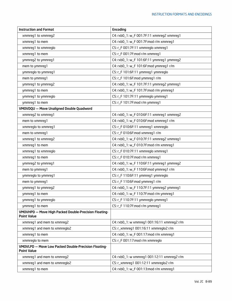
INSTRUCTION FORMATS AND ENCODINGS
xmmreg1 to xmmreg2 C4: rxb0_1: w_F 001:7F:11 xmmreg2 xmmreg1
xmmreg1 to mem C4: rxb0_1: w_F 001:7F:mod r/m xmmreg1
xmmreg1 to xmmreglo C5: r_F 001:7F:11 xmmreglo xmmreg1
xmmreg1 to mem C5: r_F 001:7F:mod r/m xmmreg1
ymmreg2 to ymmreg1 C4: rxb0_1: w_F 101:6F:11 ymmreg1 ymmreg2
mem to ymmreg1 C4: rxb0_1: w_F 101:6F:mod ymmreg1 r/m
ymmreglo to ymmreg1 C5: r_F 101:6F:11 ymmreg1 ymmreglo
mem to ymmreg1 C5: r_F 101:6F:mod ymmreg1 r/m
ymmreg1 to ymmreg2 C4: rxb0_1: w_F 101:7F:11 ymmreg2 ymmreg1
ymmreg1 to mem C4: rxb0_1: w_F 101:7F:mod r/m ymmreg1
ymmreg1 to ymmreglo C5: r_F 101:7F:11 ymmreglo ymmreg1
ymmreg1 to mem C5: r_F 101:7F:mod r/m ymmreg1
VMOVDQU — Move Unaligned Double Quadword
xmmreg2 to xmmreg1 C4: rxb0_1: w_F 010:6F:11 xmmreg1 xmmreg2
mem to xmmreg1 C4: rxb0_1: w_F 010:6F:mod xmmreg1 r/m
xmmreglo to xmmreg1 C5: r_F 010:6F:11 xmmreg1 xmmreglo
mem to xmmreg1 C5: r_F 010:6F:mod xmmreg1 r/m
xmmreg1 to xmmreg2 C4: rxb0_1: w_F 010:7F:11 xmmreg2 xmmreg1
xmmreg1 to mem C4: rxb0_1: w_F 010:7F:mod r/m xmmreg1
xmmreg1 to xmmreglo C5: r_F 010:7F:11 xmmreglo xmmreg1
xmmreg1 to mem C5: r_F 010:7F:mod r/m xmmreg1
ymmreg2 to ymmreg1 C4: rxb0_1: w_F 110:6F:11 ymmreg1 ymmreg2
mem to ymmreg1 C4: rxb0_1: w_F 110:6F:mod ymmreg1 r/m
ymmreglo to ymmreg1 C5: r_F 110:6F:11 ymmreg1 ymmreglo
mem to ymmreg1 C5: r_F 110:6F:mod ymmreg1 r/m
ymmreg1 to ymmreg2 C4: rxb0_1: w_F 110:7F:11 ymmreg2 ymmreg1
ymmreg1 to mem C4: rxb0_1: w_F 110:7F:mod r/m ymmreg1
ymmreg1 to ymmreglo C5: r_F 110:7F:11 ymmreglo ymmreg1
ymmreg1 to mem C5: r_F 110:7F:mod r/m ymmreg1
VMOVHPD — Move High Packed Double-Precision Floating-Point Value
xmmreg1 and mem to xmmreg2 C4: rxb0_1: w xmmreg1 001:16:11 xmmreg2 r/m
xmmreg1 and mem to xmmreglo2 C5: r_xmmreg1 001:16:11 xmmreglo2 r/m
xmmreg1 to mem C4: rxb0_1: w_F 001:17:mod r/m xmmreg1
xmmreglo to mem C5: r_F 001:17:mod r/m xmmreglo
VMOVLPD — Move Low Packed Double-Precision Floating-Point Value
xmmreg1 and mem to xmmreg2 C4: rxb0_1: w xmmreg1 001:12:11 xmmreg2 r/m
xmmreg1 and mem to xmmreglo2 C5: r_xmmreg1 001:12:11 xmmreglo2 r/m
xmmreg1 to mem C4: rxb0_1: w_F 001:13:mod r/m xmmreg1
Instruction and Format Encoding
Vol. 2C B-89
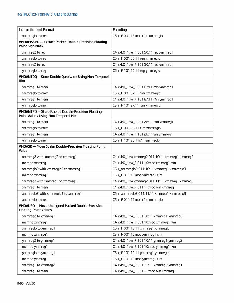
INSTRUCTION FORMATS AND ENCODINGS
xmmreglo to mem C5: r_F 001:13:mod r/m xmmreglo
VMOVMSKPD — Extract Packed Double-Precision Floating-Point Sign Mask
xmmreg2 to reg C4: rxb0_1: w_F 001:50:11 reg xmmreg1
xmmreglo to reg C5: r_F 001:50:11 reg xmmreglo
ymmreg2 to reg C4: rxb0_1: w_F 101:50:11 reg ymmreg1
ymmreglo to reg C5: r_F 101:50:11 reg ymmreglo
VMOVNTDQ — Store Double Quadword Using Non-Temporal Hint
xmmreg1 to mem C4: rxb0_1: w_F 001:E7:11 r/m xmmreg1
xmmreglo to mem C5: r_F 001:E7:11 r/m xmmreglo
ymmreg1 to mem C4: rxb0_1: w_F 101:E7:11 r/m ymmreg1
ymmreglo to mem C5: r_F 101:E7:11 r/m ymmreglo
VMOVNTPD — Store Packed Double-Precision Floating-Point Values Using Non-Temporal Hint
xmmreg1 to mem C4: rxb0_1: w_F 001:2B:11 r/m xmmreg1
xmmreglo to mem C5: r_F 001:2B:11 r/m xmmreglo
ymmreg1 to mem C4: rxb0_1: w_F 101:2B:11r/m ymmreg1
ymmreglo to mem C5: r_F 101:2B:11r/m ymmreglo
VMOVSD — Move Scalar Double-Precision Floating-Point Value
xmmreg2 with xmmreg3 to xmmreg1 C4: rxb0_1: w xmmreg2 011:10:11 xmmreg1 xmmreg3
mem to xmmreg1 C4: rxb0_1: w_F 011:10:mod xmmreg1 r/m
xmmreglo2 with xmmreglo3 to xmmreg1 C5: r_xmmreglo2 011:10:11 xmmreg1 xmmreglo3
mem to xmmreg1 C5: r_F 011:10:mod xmmreg1 r/m
xmmreg2 with xmmreg3 to xmmreg1 C4: rxb0_1: w xmmreg2 011:11:11 xmmreg1 xmmreg3
xmmreg1 to mem C4: rxb0_1: w_F 011:11:mod r/m xmmreg1
xmmreglo2 with xmmreglo3 to xmmreg1 C5: r_xmmreglo2 011:11:11 xmmreg1 xmmreglo3
xmmreglo to mem C5: r_F 011:11:mod r/m xmmreglo
VMOVUPD — Move Unaligned Packed Double-Precision Floating-Point Values
xmmreg2 to xmmreg1 C4: rxb0_1: w_F 001:10:11 xmmreg1 xmmreg2
mem to xmmreg1 C4: rxb0_1: w_F 001:10:mod xmmreg1 r/m
xmmreglo to xmmreg1 C5: r_F 001:10:11 xmmreg1 xmmreglo
mem to xmmreg1 C5: r_F 001:10:mod xmmreg1 r/m
ymmreg2 to ymmreg1 C4: rxb0_1: w_F 101:10:11 ymmreg1 ymmreg2
mem to ymmreg1 C4: rxb0_1: w_F 101:10:mod ymmreg1 r/m
ymmreglo to ymmreg1 C5: r_F 101:10:11 ymmreg1 ymmreglo
mem to ymmreg1 C5: r_F 101:10:mod ymmreg1 r/m
xmmreg1 to xmmreg2 C4: rxb0_1: w_F 001:11:11 xmmreg2 xmmreg1
xmmreg1 to mem C4: rxb0_1: w_F 001:11:mod r/m xmmreg1
Instruction and Format Encoding
B-90 Vol. 2C
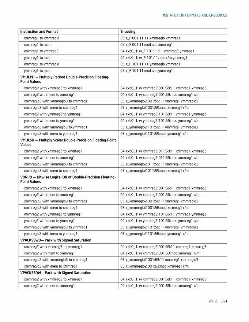
INSTRUCTION FORMATS AND ENCODINGS
xmmreg1 to xmmreglo C5: r_F 001:11:11 xmmreglo xmmreg1
xmmreg1 to mem C5: r_F 001:11:mod r/m xmmreg1
ymmreg1 to ymmreg2 C4: rxb0_1: w_F 101:11:11 ymmreg2 ymmreg1
ymmreg1 to mem C4: rxb0_1: w_F 101:11:mod r/m ymmreg1
ymmreg1 to ymmreglo C5: r_F 101:11:11 ymmreglo ymmreg1
ymmreg1 to mem C5: r_F 101:11:mod r/m ymmreg1
VMULPD — Multiply Packed Double-Precision Floating-Point Values
xmmreg2 with xmmreg3 to xmmreg1 C4: rxb0_1: w xmmreg2 001:59:11 xmmreg1 xmmreg3
xmmreg2 with mem to xmmreg1 C4: rxb0_1: w xmmreg2 001:59:mod xmmreg1 r/m
xmmreglo2 with xmmreglo3 to xmmreg1 C5: r_xmmreglo2 001:59:11 xmmreg1 xmmreglo3
xmmreglo2 with mem to xmmreg1 C5: r_xmmreglo2 001:59:mod xmmreg1 r/m
ymmreg2 with ymmreg3 to ymmreg1 C4: rxb0_1: w ymmreg2 101:59:11 ymmreg1 ymmreg3
ymmreg2 with mem to ymmreg1 C4: rxb0_1: w ymmreg2 101:59:mod ymmreg1 r/m
ymmreglo2 with ymmreglo3 to ymmreg1 C5: r_ymmreglo2 101:59:11 ymmreg1 ymmreglo3
ymmreglo2 with mem to ymmreg1 C5: r_ymmreglo2 101:59:mod ymmreg1 r/m
VMULSD — Multiply Scalar Double-Precision Floating-Point Values
xmmreg2 with xmmreg3 to xmmreg1 C4: rxb0_1: w xmmreg2 011:59:11 xmmreg1 xmmreg3
xmmreg2 with mem to xmmreg1 C4: rxb0_1: w xmmreg2 011:59:mod xmmreg1 r/m
xmmreglo2 with xmmreglo3 to xmmreg1 C5: r_xmmreglo2 011:59:11 xmmreg1 xmmreglo3
xmmreglo2 with mem to xmmreg1 C5: r_xmmreglo2 011:59:mod xmmreg1 r/m
VORPD — Bitwise Logical OR of Double-Precision Floating-Point Values
xmmreg2 with xmmreg3 to xmmreg1 C4: rxb0_1: w xmmreg2 001:56:11 xmmreg1 xmmreg3
xmmreg2 with mem to xmmreg1 C4: rxb0_1: w xmmreg2 001:56:mod xmmreg1 r/m
xmmreglo2 with xmmreglo3 to xmmreg1 C5: r_xmmreglo2 001:56:11 xmmreg1 xmmreglo3
xmmreglo2 with mem to xmmreg1 C5: r_xmmreglo2 001:56:mod xmmreg1 r/m
ymmreg2 with ymmreg3 to ymmreg1 C4: rxb0_1: w ymmreg2 101:56:11 ymmreg1 ymmreg3
ymmreg2 with mem to ymmreg1 C4: rxb0_1: w ymmreg2 101:56:mod ymmreg1 r/m
ymmreglo2 with ymmreglo3 to ymmreg1 C5: r_ymmreglo2 101:56:11 ymmreg1 ymmreglo3
ymmreglo2 with mem to ymmreg1 C5: r_ymmreglo2 101:56:mod ymmreg1 r/m
VPACKSSWB— Pack with Signed Saturation
xmmreg2 with xmmreg3 to xmmreg1 C4: rxb0_1: w xmmreg2 001:63:11 xmmreg1 xmmreg3
xmmreg2 with mem to xmmreg1 C4: rxb0_1: w xmmreg2 001:63:mod xmmreg1 r/m
xmmreglo2 with xmmreglo3 to xmmreg1 C5: r_xmmreglo2 001:63:11 xmmreg1 xmmreglo3
xmmreglo2 with mem to xmmreg1 C5: r_xmmreglo2 001:63:mod xmmreg1 r/m
VPACKSSDW— Pack with Signed Saturation
xmmreg2 with xmmreg3 to xmmreg1 C4: rxb0_1: w xmmreg2 001:6B:11 xmmreg1 xmmreg3
xmmreg2 with mem to xmmreg1 C4: rxb0_1: w xmmreg2 001:6B:mod xmmreg1 r/m
Instruction and Format Encoding
Vol. 2C B-91
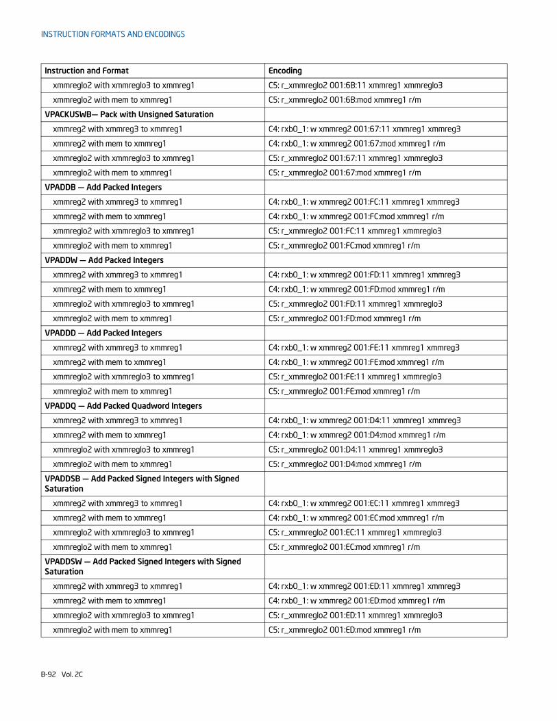
INSTRUCTION FORMATS AND ENCODINGS
xmmreglo2 with xmmreglo3 to xmmreg1 C5: r_xmmreglo2 001:6B:11 xmmreg1 xmmreglo3
xmmreglo2 with mem to xmmreg1 C5: r_xmmreglo2 001:6B:mod xmmreg1 r/m
VPACKUSWB— Pack with Unsigned Saturation
xmmreg2 with xmmreg3 to xmmreg1 C4: rxb0_1: w xmmreg2 001:67:11 xmmreg1 xmmreg3
xmmreg2 with mem to xmmreg1 C4: rxb0_1: w xmmreg2 001:67:mod xmmreg1 r/m
xmmreglo2 with xmmreglo3 to xmmreg1 C5: r_xmmreglo2 001:67:11 xmmreg1 xmmreglo3
xmmreglo2 with mem to xmmreg1 C5: r_xmmreglo2 001:67:mod xmmreg1 r/m
VPADDB — Add Packed Integers
xmmreg2 with xmmreg3 to xmmreg1 C4: rxb0_1: w xmmreg2 001:FC:11 xmmreg1 xmmreg3
xmmreg2 with mem to xmmreg1 C4: rxb0_1: w xmmreg2 001:FC:mod xmmreg1 r/m
xmmreglo2 with xmmreglo3 to xmmreg1 C5: r_xmmreglo2 001:FC:11 xmmreg1 xmmreglo3
xmmreglo2 with mem to xmmreg1 C5: r_xmmreglo2 001:FC:mod xmmreg1 r/m
VPADDW — Add Packed Integers
xmmreg2 with xmmreg3 to xmmreg1 C4: rxb0_1: w xmmreg2 001:FD:11 xmmreg1 xmmreg3
xmmreg2 with mem to xmmreg1 C4: rxb0_1: w xmmreg2 001:FD:mod xmmreg1 r/m
xmmreglo2 with xmmreglo3 to xmmreg1 C5: r_xmmreglo2 001:FD:11 xmmreg1 xmmreglo3
xmmreglo2 with mem to xmmreg1 C5: r_xmmreglo2 001:FD:mod xmmreg1 r/m
VPADDD — Add Packed Integers
xmmreg2 with xmmreg3 to xmmreg1 C4: rxb0_1: w xmmreg2 001:FE:11 xmmreg1 xmmreg3
xmmreg2 with mem to xmmreg1 C4: rxb0_1: w xmmreg2 001:FE:mod xmmreg1 r/m
xmmreglo2 with xmmreglo3 to xmmreg1 C5: r_xmmreglo2 001:FE:11 xmmreg1 xmmreglo3
xmmreglo2 with mem to xmmreg1 C5: r_xmmreglo2 001:FE:mod xmmreg1 r/m
VPADDQ — Add Packed Quadword Integers
xmmreg2 with xmmreg3 to xmmreg1 C4: rxb0_1: w xmmreg2 001:D4:11 xmmreg1 xmmreg3
xmmreg2 with mem to xmmreg1 C4: rxb0_1: w xmmreg2 001:D4:mod xmmreg1 r/m
xmmreglo2 with xmmreglo3 to xmmreg1 C5: r_xmmreglo2 001:D4:11 xmmreg1 xmmreglo3
xmmreglo2 with mem to xmmreg1 C5: r_xmmreglo2 001:D4:mod xmmreg1 r/m
VPADDSB — Add Packed Signed Integers with Signed Saturation
xmmreg2 with xmmreg3 to xmmreg1 C4: rxb0_1: w xmmreg2 001:EC:11 xmmreg1 xmmreg3
xmmreg2 with mem to xmmreg1 C4: rxb0_1: w xmmreg2 001:EC:mod xmmreg1 r/m
xmmreglo2 with xmmreglo3 to xmmreg1 C5: r_xmmreglo2 001:EC:11 xmmreg1 xmmreglo3
xmmreglo2 with mem to xmmreg1 C5: r_xmmreglo2 001:EC:mod xmmreg1 r/m
VPADDSW — Add Packed Signed Integers with Signed Saturation
xmmreg2 with xmmreg3 to xmmreg1 C4: rxb0_1: w xmmreg2 001:ED:11 xmmreg1 xmmreg3
xmmreg2 with mem to xmmreg1 C4: rxb0_1: w xmmreg2 001:ED:mod xmmreg1 r/m
xmmreglo2 with xmmreglo3 to xmmreg1 C5: r_xmmreglo2 001:ED:11 xmmreg1 xmmreglo3
xmmreglo2 with mem to xmmreg1 C5: r_xmmreglo2 001:ED:mod xmmreg1 r/m
Instruction and Format Encoding
B-92 Vol. 2C
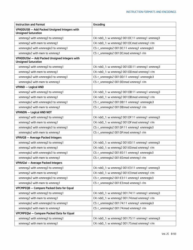
INSTRUCTION FORMATS AND ENCODINGS
VPADDUSB — Add Packed Unsigned Integers with Unsigned Saturation
xmmreg2 with xmmreg3 to xmmreg1 C4: rxb0_1: w xmmreg2 001:DC:11 xmmreg1 xmmreg3
xmmreg2 with mem to xmmreg1 C4: rxb0_1: w xmmreg2 001:DC:mod xmmreg1 r/m
xmmreglo2 with xmmreglo3 to xmmreg1 C5: r_xmmreglo2 001:DC:11 xmmreg1 xmmreglo3
xmmreglo2 with mem to xmmreg1 C5: r_xmmreglo2 001:DC:mod xmmreg1 r/m
VPADDUSW — Add Packed Unsigned Integers with Unsigned Saturation
xmmreg2 with xmmreg3 to xmmreg1 C4: rxb0_1: w xmmreg2 001:DD:11 xmmreg1 xmmreg3
xmmreg2 with mem to xmmreg1 C4: rxb0_1: w xmmreg2 001:DD:mod xmmreg1 r/m
xmmreglo2 with xmmreglo3 to xmmreg1 C5: r_xmmreglo2 001:DD:11 xmmreg1 xmmreglo3
xmmreglo2 with mem to xmmreg1 C5: r_xmmreglo2 001:DD:mod xmmreg1 r/m
VPAND — Logical AND
xmmreg2 with xmmreg3 to xmmreg1 C4: rxb0_1: w xmmreg2 001:DB:11 xmmreg1 xmmreg3
xmmreg2 with mem to xmmreg1 C4: rxb0_1: w xmmreg2 001:DB:mod xmmreg1 r/m
xmmreglo2 with xmmreglo3 to xmmreg1 C5: r_xmmreglo2 001:DB:11 xmmreg1 xmmreglo3
xmmreglo2 with mem to xmmreg1 C5: r_xmmreglo2 001:DB:mod xmmreg1 r/m
VPANDN — Logical AND NOT
xmmreg2 with xmmreg3 to xmmreg1 C4: rxb0_1: w xmmreg2 001:DF:11 xmmreg1 xmmreg3
xmmreg2 with mem to xmmreg1 C4: rxb0_1: w xmmreg2 001:DF:mod xmmreg1 r/m
xmmreglo2 with xmmreglo3 to xmmreg1 C5: r_xmmreglo2 001:DF:11 xmmreg1 xmmreglo3
xmmreglo2 with mem to xmmreg1 C5: r_xmmreglo2 001:DF:mod xmmreg1 r/m
VPAVGB — Average Packed Integers
xmmreg2 with xmmreg3 to xmmreg1 C4: rxb0_1: w xmmreg2 001:E0:11 xmmreg1 xmmreg3
xmmreg2 with mem to xmmreg1 C4: rxb0_1: w xmmreg2 001:E0:mod xmmreg1 r/m
xmmreglo2 with xmmreglo3 to xmmreg1 C5: r_xmmreglo2 001:E0:11 xmmreg1 xmmreglo3
xmmreglo2 with mem to xmmreg1 C5: r_xmmreglo2 001:E0:mod xmmreg1 r/m
VPAVGW — Average Packed Integers
xmmreg2 with xmmreg3 to xmmreg1 C4: rxb0_1: w xmmreg2 001:E3:11 xmmreg1 xmmreg3
xmmreg2 with mem to xmmreg1 C4: rxb0_1: w xmmreg2 001:E3:mod xmmreg1 r/m
xmmreglo2 with xmmreglo3 to xmmreg1 C5: r_xmmreglo2 001:E3:11 xmmreg1 xmmreglo3
xmmreglo2 with mem to xmmreg1 C5: r_xmmreglo2 001:E3:mod xmmreg1 r/m
VPCMPEQB — Compare Packed Data for Equal
xmmreg2 with xmmreg3 to xmmreg1 C4: rxb0_1: w xmmreg2 001:74:11 xmmreg1 xmmreg3
xmmreg2 with mem to xmmreg1 C4: rxb0_1: w xmmreg2 001:74:mod xmmreg1 r/m
xmmreglo2 with xmmreglo3 to xmmreg1 C5: r_xmmreglo2 001:74:11 xmmreg1 xmmreglo3
xmmreglo2 with mem to xmmreg1 C5: r_xmmreglo2 001:74:mod xmmreg1 r/m
VPCMPEQW — Compare Packed Data for Equal
xmmreg2 with xmmreg3 to xmmreg1 C4: rxb0_1: w xmmreg2 001:75:11 xmmreg1 xmmreg3
xmmreg2 with mem to xmmreg1 C4: rxb0_1: w xmmreg2 001:75:mod xmmreg1 r/m
Instruction and Format Encoding
Vol. 2C B-93
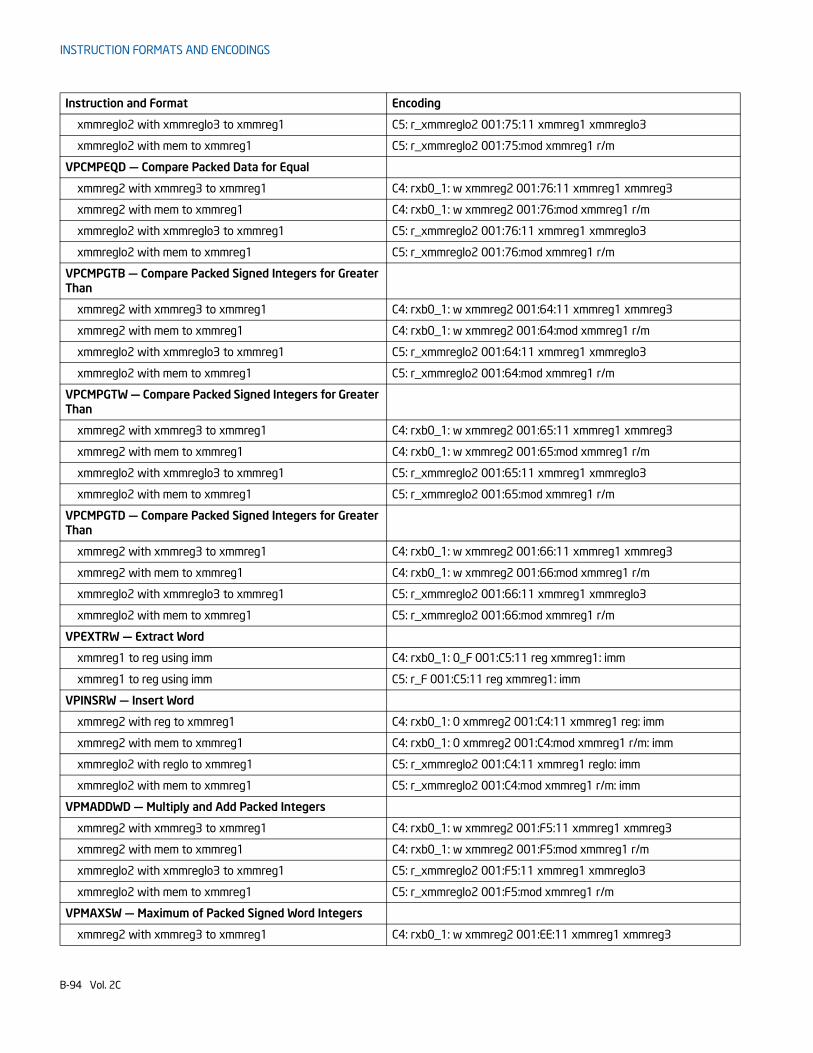
INSTRUCTION FORMATS AND ENCODINGS
xmmreglo2 with xmmreglo3 to xmmreg1 C5: r_xmmreglo2 001:75:11 xmmreg1 xmmreglo3
xmmreglo2 with mem to xmmreg1 C5: r_xmmreglo2 001:75:mod xmmreg1 r/m
VPCMPEQD — Compare Packed Data for Equal
xmmreg2 with xmmreg3 to xmmreg1 C4: rxb0_1: w xmmreg2 001:76:11 xmmreg1 xmmreg3
xmmreg2 with mem to xmmreg1 C4: rxb0_1: w xmmreg2 001:76:mod xmmreg1 r/m
xmmreglo2 with xmmreglo3 to xmmreg1 C5: r_xmmreglo2 001:76:11 xmmreg1 xmmreglo3
xmmreglo2 with mem to xmmreg1 C5: r_xmmreglo2 001:76:mod xmmreg1 r/m
VPCMPGTB — Compare Packed Signed Integers for Greater Than
xmmreg2 with xmmreg3 to xmmreg1 C4: rxb0_1: w xmmreg2 001:64:11 xmmreg1 xmmreg3
xmmreg2 with mem to xmmreg1 C4: rxb0_1: w xmmreg2 001:64:mod xmmreg1 r/m
xmmreglo2 with xmmreglo3 to xmmreg1 C5: r_xmmreglo2 001:64:11 xmmreg1 xmmreglo3
xmmreglo2 with mem to xmmreg1 C5: r_xmmreglo2 001:64:mod xmmreg1 r/m
VPCMPGTW — Compare Packed Signed Integers for Greater Than
xmmreg2 with xmmreg3 to xmmreg1 C4: rxb0_1: w xmmreg2 001:65:11 xmmreg1 xmmreg3
xmmreg2 with mem to xmmreg1 C4: rxb0_1: w xmmreg2 001:65:mod xmmreg1 r/m
xmmreglo2 with xmmreglo3 to xmmreg1 C5: r_xmmreglo2 001:65:11 xmmreg1 xmmreglo3
xmmreglo2 with mem to xmmreg1 C5: r_xmmreglo2 001:65:mod xmmreg1 r/m
VPCMPGTD — Compare Packed Signed Integers for Greater Than
xmmreg2 with xmmreg3 to xmmreg1 C4: rxb0_1: w xmmreg2 001:66:11 xmmreg1 xmmreg3
xmmreg2 with mem to xmmreg1 C4: rxb0_1: w xmmreg2 001:66:mod xmmreg1 r/m
xmmreglo2 with xmmreglo3 to xmmreg1 C5: r_xmmreglo2 001:66:11 xmmreg1 xmmreglo3
xmmreglo2 with mem to xmmreg1 C5: r_xmmreglo2 001:66:mod xmmreg1 r/m
VPEXTRW — Extract Word
xmmreg1 to reg using imm C4: rxb0_1: 0_F 001:C5:11 reg xmmreg1: imm
xmmreg1 to reg using imm C5: r_F 001:C5:11 reg xmmreg1: imm
VPINSRW — Insert Word
xmmreg2 with reg to xmmreg1 C4: rxb0_1: 0 xmmreg2 001:C4:11 xmmreg1 reg: imm
xmmreg2 with mem to xmmreg1 C4: rxb0_1: 0 xmmreg2 001:C4:mod xmmreg1 r/m: imm
xmmreglo2 with reglo to xmmreg1 C5: r_xmmreglo2 001:C4:11 xmmreg1 reglo: imm
xmmreglo2 with mem to xmmreg1 C5: r_xmmreglo2 001:C4:mod xmmreg1 r/m: imm
VPMADDWD — Multiply and Add Packed Integers
xmmreg2 with xmmreg3 to xmmreg1 C4: rxb0_1: w xmmreg2 001:F5:11 xmmreg1 xmmreg3
xmmreg2 with mem to xmmreg1 C4: rxb0_1: w xmmreg2 001:F5:mod xmmreg1 r/m
xmmreglo2 with xmmreglo3 to xmmreg1 C5: r_xmmreglo2 001:F5:11 xmmreg1 xmmreglo3
xmmreglo2 with mem to xmmreg1 C5: r_xmmreglo2 001:F5:mod xmmreg1 r/m
VPMAXSW — Maximum of Packed Signed Word Integers
xmmreg2 with xmmreg3 to xmmreg1 C4: rxb0_1: w xmmreg2 001:EE:11 xmmreg1 xmmreg3
Instruction and Format Encoding
B-94 Vol. 2C
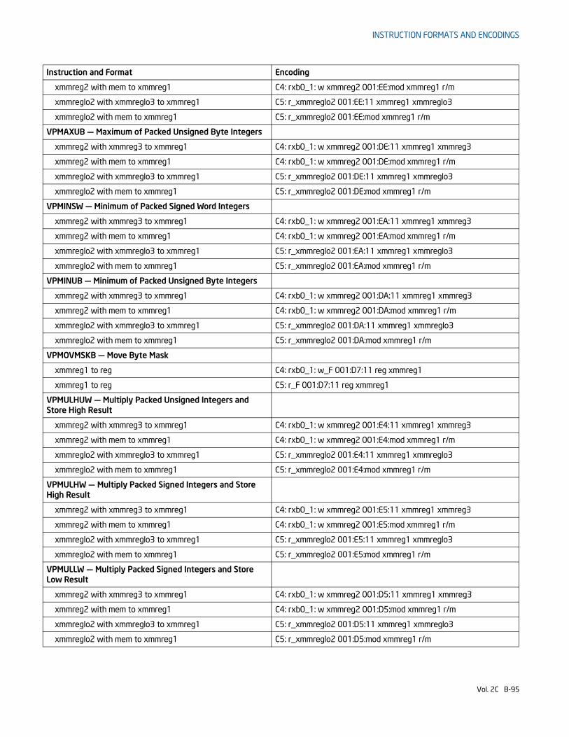
INSTRUCTION FORMATS AND ENCODINGS
xmmreg2 with mem to xmmreg1 C4: rxb0_1: w xmmreg2 001:EE:mod xmmreg1 r/m
xmmreglo2 with xmmreglo3 to xmmreg1 C5: r_xmmreglo2 001:EE:11 xmmreg1 xmmreglo3
xmmreglo2 with mem to xmmreg1 C5: r_xmmreglo2 001:EE:mod xmmreg1 r/m
VPMAXUB — Maximum of Packed Unsigned Byte Integers
xmmreg2 with xmmreg3 to xmmreg1 C4: rxb0_1: w xmmreg2 001:DE:11 xmmreg1 xmmreg3
xmmreg2 with mem to xmmreg1 C4: rxb0_1: w xmmreg2 001:DE:mod xmmreg1 r/m
xmmreglo2 with xmmreglo3 to xmmreg1 C5: r_xmmreglo2 001:DE:11 xmmreg1 xmmreglo3
xmmreglo2 with mem to xmmreg1 C5: r_xmmreglo2 001:DE:mod xmmreg1 r/m
VPMINSW — Minimum of Packed Signed Word Integers
xmmreg2 with xmmreg3 to xmmreg1 C4: rxb0_1: w xmmreg2 001:EA:11 xmmreg1 xmmreg3
xmmreg2 with mem to xmmreg1 C4: rxb0_1: w xmmreg2 001:EA:mod xmmreg1 r/m
xmmreglo2 with xmmreglo3 to xmmreg1 C5: r_xmmreglo2 001:EA:11 xmmreg1 xmmreglo3
xmmreglo2 with mem to xmmreg1 C5: r_xmmreglo2 001:EA:mod xmmreg1 r/m
VPMINUB — Minimum of Packed Unsigned Byte Integers
xmmreg2 with xmmreg3 to xmmreg1 C4: rxb0_1: w xmmreg2 001:DA:11 xmmreg1 xmmreg3
xmmreg2 with mem to xmmreg1 C4: rxb0_1: w xmmreg2 001:DA:mod xmmreg1 r/m
xmmreglo2 with xmmreglo3 to xmmreg1 C5: r_xmmreglo2 001:DA:11 xmmreg1 xmmreglo3
xmmreglo2 with mem to xmmreg1 C5: r_xmmreglo2 001:DA:mod xmmreg1 r/m
VPMOVMSKB — Move Byte Mask
xmmreg1 to reg C4: rxb0_1: w_F 001:D7:11 reg xmmreg1
xmmreg1 to reg C5: r_F 001:D7:11 reg xmmreg1
VPMULHUW — Multiply Packed Unsigned Integers and Store High Result
xmmreg2 with xmmreg3 to xmmreg1 C4: rxb0_1: w xmmreg2 001:E4:11 xmmreg1 xmmreg3
xmmreg2 with mem to xmmreg1 C4: rxb0_1: w xmmreg2 001:E4:mod xmmreg1 r/m
xmmreglo2 with xmmreglo3 to xmmreg1 C5: r_xmmreglo2 001:E4:11 xmmreg1 xmmreglo3
xmmreglo2 with mem to xmmreg1 C5: r_xmmreglo2 001:E4:mod xmmreg1 r/m
VPMULHW — Multiply Packed Signed Integers and Store High Result
xmmreg2 with xmmreg3 to xmmreg1 C4: rxb0_1: w xmmreg2 001:E5:11 xmmreg1 xmmreg3
xmmreg2 with mem to xmmreg1 C4: rxb0_1: w xmmreg2 001:E5:mod xmmreg1 r/m
xmmreglo2 with xmmreglo3 to xmmreg1 C5: r_xmmreglo2 001:E5:11 xmmreg1 xmmreglo3
xmmreglo2 with mem to xmmreg1 C5: r_xmmreglo2 001:E5:mod xmmreg1 r/m
VPMULLW — Multiply Packed Signed Integers and Store Low Result
xmmreg2 with xmmreg3 to xmmreg1 C4: rxb0_1: w xmmreg2 001:D5:11 xmmreg1 xmmreg3
xmmreg2 with mem to xmmreg1 C4: rxb0_1: w xmmreg2 001:D5:mod xmmreg1 r/m
xmmreglo2 with xmmreglo3 to xmmreg1 C5: r_xmmreglo2 001:D5:11 xmmreg1 xmmreglo3
xmmreglo2 with mem to xmmreg1 C5: r_xmmreglo2 001:D5:mod xmmreg1 r/m
Instruction and Format Encoding
Vol. 2C B-95
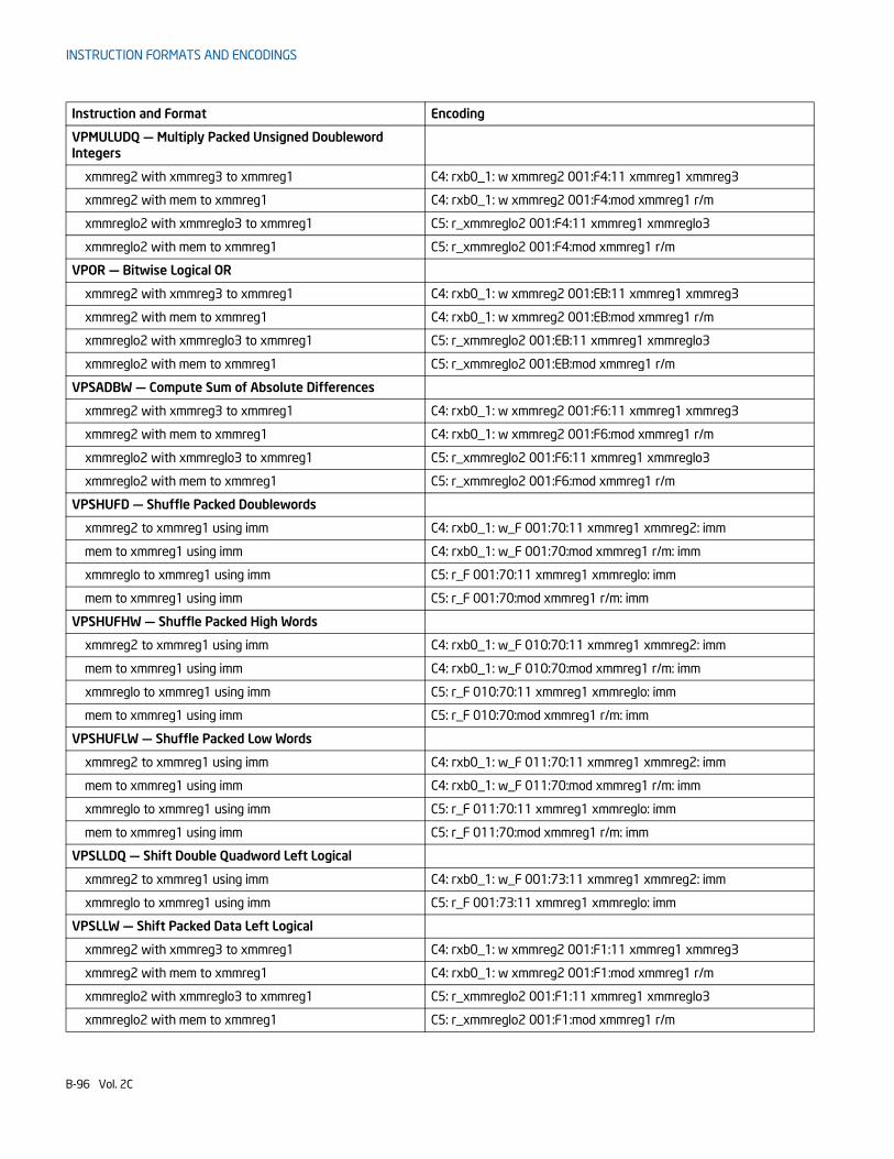
INSTRUCTION FORMATS AND ENCODINGS
VPMULUDQ — Multiply Packed Unsigned Doubleword Integers
xmmreg2 with xmmreg3 to xmmreg1 C4: rxb0_1: w xmmreg2 001:F4:11 xmmreg1 xmmreg3
xmmreg2 with mem to xmmreg1 C4: rxb0_1: w xmmreg2 001:F4:mod xmmreg1 r/m
xmmreglo2 with xmmreglo3 to xmmreg1 C5: r_xmmreglo2 001:F4:11 xmmreg1 xmmreglo3
xmmreglo2 with mem to xmmreg1 C5: r_xmmreglo2 001:F4:mod xmmreg1 r/m
VPOR — Bitwise Logical OR
xmmreg2 with xmmreg3 to xmmreg1 C4: rxb0_1: w xmmreg2 001:EB:11 xmmreg1 xmmreg3
xmmreg2 with mem to xmmreg1 C4: rxb0_1: w xmmreg2 001:EB:mod xmmreg1 r/m
xmmreglo2 with xmmreglo3 to xmmreg1 C5: r_xmmreglo2 001:EB:11 xmmreg1 xmmreglo3
xmmreglo2 with mem to xmmreg1 C5: r_xmmreglo2 001:EB:mod xmmreg1 r/m
VPSADBW — Compute Sum of Absolute Differences
xmmreg2 with xmmreg3 to xmmreg1 C4: rxb0_1: w xmmreg2 001:F6:11 xmmreg1 xmmreg3
xmmreg2 with mem to xmmreg1 C4: rxb0_1: w xmmreg2 001:F6:mod xmmreg1 r/m
xmmreglo2 with xmmreglo3 to xmmreg1 C5: r_xmmreglo2 001:F6:11 xmmreg1 xmmreglo3
xmmreglo2 with mem to xmmreg1 C5: r_xmmreglo2 001:F6:mod xmmreg1 r/m
VPSHUFD — Shuffle Packed Doublewords
xmmreg2 to xmmreg1 using imm C4: rxb0_1: w_F 001:70:11 xmmreg1 xmmreg2: imm
mem to xmmreg1 using imm C4: rxb0_1: w_F 001:70:mod xmmreg1 r/m: imm
xmmreglo to xmmreg1 using imm C5: r_F 001:70:11 xmmreg1 xmmreglo: imm
mem to xmmreg1 using imm C5: r_F 001:70:mod xmmreg1 r/m: imm
VPSHUFHW — Shuffle Packed High Words
xmmreg2 to xmmreg1 using imm C4: rxb0_1: w_F 010:70:11 xmmreg1 xmmreg2: imm
mem to xmmreg1 using imm C4: rxb0_1: w_F 010:70:mod xmmreg1 r/m: imm
xmmreglo to xmmreg1 using imm C5: r_F 010:70:11 xmmreg1 xmmreglo: imm
mem to xmmreg1 using imm C5: r_F 010:70:mod xmmreg1 r/m: imm
VPSHUFLW — Shuffle Packed Low Words
xmmreg2 to xmmreg1 using imm C4: rxb0_1: w_F 011:70:11 xmmreg1 xmmreg2: imm
mem to xmmreg1 using imm C4: rxb0_1: w_F 011:70:mod xmmreg1 r/m: imm
xmmreglo to xmmreg1 using imm C5: r_F 011:70:11 xmmreg1 xmmreglo: imm
mem to xmmreg1 using imm C5: r_F 011:70:mod xmmreg1 r/m: imm
VPSLLDQ — Shift Double Quadword Left Logical
xmmreg2 to xmmreg1 using imm C4: rxb0_1: w_F 001:73:11 xmmreg1 xmmreg2: imm
xmmreglo to xmmreg1 using imm C5: r_F 001:73:11 xmmreg1 xmmreglo: imm
VPSLLW — Shift Packed Data Left Logical
xmmreg2 with xmmreg3 to xmmreg1 C4: rxb0_1: w xmmreg2 001:F1:11 xmmreg1 xmmreg3
xmmreg2 with mem to xmmreg1 C4: rxb0_1: w xmmreg2 001:F1:mod xmmreg1 r/m
xmmreglo2 with xmmreglo3 to xmmreg1 C5: r_xmmreglo2 001:F1:11 xmmreg1 xmmreglo3
xmmreglo2 with mem to xmmreg1 C5: r_xmmreglo2 001:F1:mod xmmreg1 r/m
Instruction and Format Encoding
B-96 Vol. 2C

INSTRUCTION FORMATS AND ENCODINGS
xmmreg2 to xmmreg1 using imm8 C4: rxb0_1: w_F 001:71:11 xmmreg1 xmmreg2: imm
xmmreglo to xmmreg1 using imm8 C5: r_F 001:71:11 xmmreg1 xmmreglo: imm
VPSLLD — Shift Packed Data Left Logical
xmmreg2 with xmmreg3 to xmmreg1 C4: rxb0_1: w xmmreg2 001:F2:11 xmmreg1 xmmreg3
xmmreg2 with mem to xmmreg1 C4: rxb0_1: w xmmreg2 001:F2:mod xmmreg1 r/m
xmmreglo2 with xmmreglo3 to xmmreg1 C5: r_xmmreglo2 001:F2:11 xmmreg1 xmmreglo3
xmmreglo2 with mem to xmmreg1 C5: r_xmmreglo2 001:F2:mod xmmreg1 r/m
xmmreg2 to xmmreg1 using imm8 C4: rxb0_1: w_F 001:72:11 xmmreg1 xmmreg2: imm
xmmreglo to xmmreg1 using imm8 C5: r_F 001:72:11 xmmreg1 xmmreglo: imm
VPSLLQ — Shift Packed Data Left Logical
xmmreg2 with xmmreg3 to xmmreg1 C4: rxb0_1: w xmmreg2 001:F3:11 xmmreg1 xmmreg3
xmmreg2 with mem to xmmreg1 C4: rxb0_1: w xmmreg2 001:F3:mod xmmreg1 r/m
xmmreglo2 with xmmreglo3 to xmmreg1 C5: r_xmmreglo2 001:F3:11 xmmreg1 xmmreglo3
xmmreglo2 with mem to xmmreg1 C5: r_xmmreglo2 001:F3:mod xmmreg1 r/m
xmmreg2 to xmmreg1 using imm8 C4: rxb0_1: w_F 001:73:11 xmmreg1 xmmreg2: imm
xmmreglo to xmmreg1 using imm8 C5: r_F 001:73:11 xmmreg1 xmmreglo: imm
VPSRAW — Shift Packed Data Right Arithmetic
xmmreg2 with xmmreg3 to xmmreg1 C4: rxb0_1: w xmmreg2 001:E1:11 xmmreg1 xmmreg3
xmmreg2 with mem to xmmreg1 C4: rxb0_1: w xmmreg2 001:E1:mod xmmreg1 r/m
xmmreglo2 with xmmreglo3 to xmmreg1 C5: r_xmmreglo2 001:E1:11 xmmreg1 xmmreglo3
xmmreglo2 with mem to xmmreg1 C5: r_xmmreglo2 001:E1:mod xmmreg1 r/m
xmmreg2 to xmmreg1 using imm8 C4: rxb0_1: w_F 001:71:11 xmmreg1 xmmreg2: imm
xmmreglo to xmmreg1 using imm8 C5: r_F 001:71:11 xmmreg1 xmmreglo: imm
VPSRAD — Shift Packed Data Right Arithmetic
xmmreg2 with xmmreg3 to xmmreg1 C4: rxb0_1: w xmmreg2 001:E2:11 xmmreg1 xmmreg3
xmmreg2 with mem to xmmreg1 C4: rxb0_1: w xmmreg2 001:E2:mod xmmreg1 r/m
xmmreglo2 with xmmreglo3 to xmmreg1 C5: r_xmmreglo2 001:E2:11 xmmreg1 xmmreglo3
xmmreglo2 with mem to xmmreg1 C5: r_xmmreglo2 001:E2:mod xmmreg1 r/m
xmmreg2 to xmmreg1 using imm8 C4: rxb0_1: w_F 001:72:11 xmmreg1 xmmreg2: imm
xmmreglo to xmmreg1 using imm8 C5: r_F 001:72:11 xmmreg1 xmmreglo: imm
VPSRLDQ — Shift Double Quadword Right Logical
xmmreg2 to xmmreg1 using imm8 C4: rxb0_1: w_F 001:73:11 xmmreg1 xmmreg2: imm
xmmreglo to xmmreg1 using imm8 C5: r_F 001:73:11 xmmreg1 xmmreglo: imm
VPSRLW — Shift Packed Data Right Logical
xmmreg2 with xmmreg3 to xmmreg1 C4: rxb0_1: w xmmreg2 001:D1:11 xmmreg1 xmmreg3
xmmreg2 with mem to xmmreg1 C4: rxb0_1: w xmmreg2 001:D1:mod xmmreg1 r/m
xmmreglo2 with xmmreglo3 to xmmreg1 C5: r_xmmreglo2 001:D1:11 xmmreg1 xmmreglo3
xmmreglo2 with mem to xmmreg1 C5: r_xmmreglo2 001:D1:mod xmmreg1 r/m
xmmreg2 to xmmreg1 using imm8 C4: rxb0_1: w_F 001:71:11 xmmreg1 xmmreg2: imm
Instruction and Format Encoding
Vol. 2C B-97
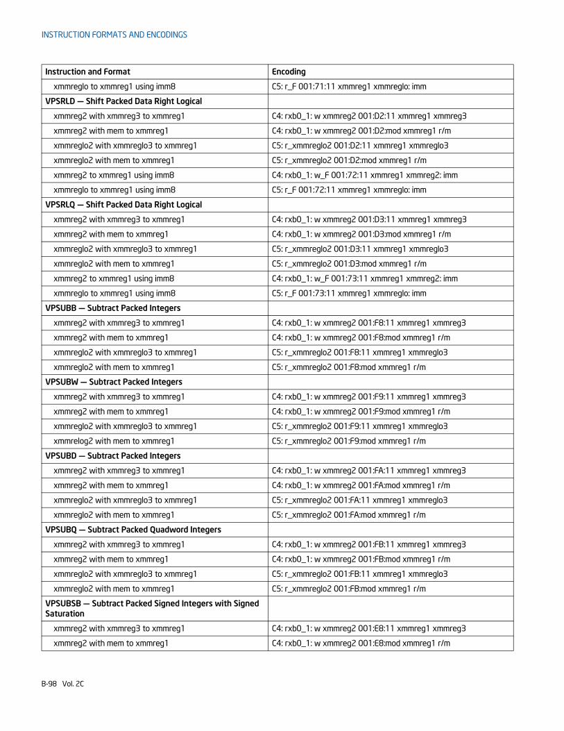
INSTRUCTION FORMATS AND ENCODINGS
xmmreglo to xmmreg1 using imm8 C5: r_F 001:71:11 xmmreg1 xmmreglo: imm
VPSRLD — Shift Packed Data Right Logical
xmmreg2 with xmmreg3 to xmmreg1 C4: rxb0_1: w xmmreg2 001:D2:11 xmmreg1 xmmreg3
xmmreg2 with mem to xmmreg1 C4: rxb0_1: w xmmreg2 001:D2:mod xmmreg1 r/m
xmmreglo2 with xmmreglo3 to xmmreg1 C5: r_xmmreglo2 001:D2:11 xmmreg1 xmmreglo3
xmmreglo2 with mem to xmmreg1 C5: r_xmmreglo2 001:D2:mod xmmreg1 r/m
xmmreg2 to xmmreg1 using imm8 C4: rxb0_1: w_F 001:72:11 xmmreg1 xmmreg2: imm
xmmreglo to xmmreg1 using imm8 C5: r_F 001:72:11 xmmreg1 xmmreglo: imm
VPSRLQ — Shift Packed Data Right Logical
xmmreg2 with xmmreg3 to xmmreg1 C4: rxb0_1: w xmmreg2 001:D3:11 xmmreg1 xmmreg3
xmmreg2 with mem to xmmreg1 C4: rxb0_1: w xmmreg2 001:D3:mod xmmreg1 r/m
xmmreglo2 with xmmreglo3 to xmmreg1 C5: r_xmmreglo2 001:D3:11 xmmreg1 xmmreglo3
xmmreglo2 with mem to xmmreg1 C5: r_xmmreglo2 001:D3:mod xmmreg1 r/m
xmmreg2 to xmmreg1 using imm8 C4: rxb0_1: w_F 001:73:11 xmmreg1 xmmreg2: imm
xmmreglo to xmmreg1 using imm8 C5: r_F 001:73:11 xmmreg1 xmmreglo: imm
VPSUBB — Subtract Packed Integers
xmmreg2 with xmmreg3 to xmmreg1 C4: rxb0_1: w xmmreg2 001:F8:11 xmmreg1 xmmreg3
xmmreg2 with mem to xmmreg1 C4: rxb0_1: w xmmreg2 001:F8:mod xmmreg1 r/m
xmmreglo2 with xmmreglo3 to xmmreg1 C5: r_xmmreglo2 001:F8:11 xmmreg1 xmmreglo3
xmmreglo2 with mem to xmmreg1 C5: r_xmmreglo2 001:F8:mod xmmreg1 r/m
VPSUBW — Subtract Packed Integers
xmmreg2 with xmmreg3 to xmmreg1 C4: rxb0_1: w xmmreg2 001:F9:11 xmmreg1 xmmreg3
xmmreg2 with mem to xmmreg1 C4: rxb0_1: w xmmreg2 001:F9:mod xmmreg1 r/m
xmmreglo2 with xmmreglo3 to xmmreg1 C5: r_xmmreglo2 001:F9:11 xmmreg1 xmmreglo3
xmmrelog2 with mem to xmmreg1 C5: r_xmmreglo2 001:F9:mod xmmreg1 r/m
VPSUBD — Subtract Packed Integers
xmmreg2 with xmmreg3 to xmmreg1 C4: rxb0_1: w xmmreg2 001:FA:11 xmmreg1 xmmreg3
xmmreg2 with mem to xmmreg1 C4: rxb0_1: w xmmreg2 001:FA:mod xmmreg1 r/m
xmmreglo2 with xmmreglo3 to xmmreg1 C5: r_xmmreglo2 001:FA:11 xmmreg1 xmmreglo3
xmmreglo2 with mem to xmmreg1 C5: r_xmmreglo2 001:FA:mod xmmreg1 r/m
VPSUBQ — Subtract Packed Quadword Integers
xmmreg2 with xmmreg3 to xmmreg1 C4: rxb0_1: w xmmreg2 001:FB:11 xmmreg1 xmmreg3
xmmreg2 with mem to xmmreg1 C4: rxb0_1: w xmmreg2 001:FB:mod xmmreg1 r/m
xmmreglo2 with xmmreglo3 to xmmreg1 C5: r_xmmreglo2 001:FB:11 xmmreg1 xmmreglo3
xmmreglo2 with mem to xmmreg1 C5: r_xmmreglo2 001:FB:mod xmmreg1 r/m
VPSUBSB — Subtract Packed Signed Integers with Signed Saturation
xmmreg2 with xmmreg3 to xmmreg1 C4: rxb0_1: w xmmreg2 001:E8:11 xmmreg1 xmmreg3
xmmreg2 with mem to xmmreg1 C4: rxb0_1: w xmmreg2 001:E8:mod xmmreg1 r/m
Instruction and Format Encoding
B-98 Vol. 2C

INSTRUCTION FORMATS AND ENCODINGS
xmmreglo2 with xmmreglo3 to xmmreg1 C5: r_xmmreglo2 001:E8:11 xmmreg1 xmmreglo3
xmmreglo2 with mem to xmmreg1 C5: r_xmmreglo2 001:E8:mod xmmreg1 r/m
VPSUBSW — Subtract Packed Signed Integers with Signed Saturation
xmmreg2 with xmmreg3 to xmmreg1 C4: rxb0_1: w xmmreg2 001:E9:11 xmmreg1 xmmreg3
xmmreg2 with mem to xmmreg1 C4: rxb0_1: w xmmreg2 001:E9:mod xmmreg1 r/m
xmmreglo2 with xmmreglo3 to xmmreg1 C5: r_xmmreglo2 001:E9:11 xmmreg1 xmmreglo3
xmmreglo2 with mem to xmmreg1 C5: r_xmmreglo2 001:E9:mod xmmreg1 r/m
VPSUBUSB — Subtract Packed Unsigned Integers with Unsigned Saturation
xmmreg2 with xmmreg3 to xmmreg1 C4: rxb0_1: w xmmreg2 001:D8:11 xmmreg1 xmmreg3
xmmreg2 with mem to xmmreg1 C4: rxb0_1: w xmmreg2 001:D8:mod xmmreg1 r/m
xmmreglo2 with xmmreglo3 to xmmreg1 C5: r_xmmreglo2 001:D8:11 xmmreg1 xmmreglo3
xmmreglo2 with mem to xmmreg1 C5: r_xmmreglo2 001:D8:mod xmmreg1 r/m
VPSUBUSW — Subtract Packed Unsigned Integers with Unsigned Saturation
xmmreg2 with xmmreg3 to xmmreg1 C4: rxb0_1: w xmmreg2 001:D9:11 xmmreg1 xmmreg3
xmmreg2 with mem to xmmreg1 C4: rxb0_1: w xmmreg2 001:D9:mod xmmreg1 r/m
xmmreglo2 with xmmreglo3 to xmmreg1 C5: r_xmmreglo2 001:D9:11 xmmreg1 xmmreglo3
xmmreglo2 with mem to xmmreg1 C5: r_xmmreglo2 001:D9:mod xmmreg1 r/m
VPUNPCKHBW — Unpack High Data
xmmreg2 with xmmreg3 to xmmreg1 C4: rxb0_1: w xmmreg2 001:68:11 xmmreg1 xmmreg3
xmmreg2 with mem to xmmreg1 C4: rxb0_1: w xmmreg2 001:68:mod xmmreg1 r/m
xmmreglo2 with xmmreglo3 to xmmreg1 C5: r_xmmreglo2 001:68:11 xmmreg1 xmmreglo3
xmmreglo2 with mem to xmmreg1 C5: r_xmmreglo2 001:68:mod xmmreg1 r/m
VPUNPCKHWD — Unpack High Data
xmmreg2 with xmmreg3 to xmmreg1 C4: rxb0_1: w xmmreg2 001:69:11 xmmreg1 xmmreg3
xmmreg2 with mem to xmmreg1 C4: rxb0_1: w xmmreg2 001:69:mod xmmreg1 r/m
xmmreglo2 with xmmreglo3 to xmmreg1 C5: r_xmmreglo2 001:69:11 xmmreg1 xmmreglo3
xmmreglo2 with mem to xmmreg1 C5: r_xmmreglo2 001:69:mod xmmreg1 r/m
VPUNPCKHDQ — Unpack High Data
xmmreg2 with xmmreg3 to xmmreg1 C4: rxb0_1: w xmmreg2 001:6A:11 xmmreg1 xmmreg3
xmmreg2 with mem to xmmreg1 C4: rxb0_1: w xmmreg2 001:6A:mod xmmreg1 r/m
xmmreglo2 with xmmreglo3 to xmmreg1 C5: r_xmmreglo2 001:6A:11 xmmreg1 xmmreglo3
xmmreglo2 with mem to xmmreg1 C5: r_xmmreglo2 001:6A:mod xmmreg1 r/m
VPUNPCKHQDQ — Unpack High Data
xmmreg2 with xmmreg3 to xmmreg1 C4: rxb0_1: w xmmreg2 001:6D:11 xmmreg1 xmmreg3
xmmreg2 with mem to xmmreg1 C4: rxb0_1: w xmmreg2 001:6D:mod xmmreg1 r/m
xmmreglo2 with xmmreglo3 to xmmreg1 C5: r_xmmreglo2 001:6D:11 xmmreg1 xmmreglo3
xmmreglo2 with mem to xmmreg1 C5: r_xmmreglo2 001:6D:mod xmmreg1 r/m
Instruction and Format Encoding
Vol. 2C B-99
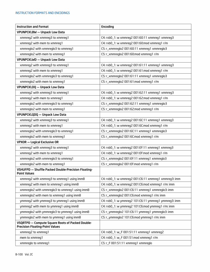
INSTRUCTION FORMATS AND ENCODINGS
VPUNPCKLBW — Unpack Low Data
xmmreg2 with xmmreg3 to xmmreg1 C4: rxb0_1: w xmmreg2 001:60:11 xmmreg1 xmmreg3
xmmreg2 with mem to xmmreg1 C4: rxb0_1: w xmmreg2 001:60:mod xmmreg1 r/m
xmmreglo2 with xmmreglo3 to xmmreg1 C5: r_xmmreglo2 001:60:11 xmmreg1 xmmreglo3
xmmreglo2 with mem to xmmreg1 C5: r_xmmreglo2 001:60:mod xmmreg1 r/m
VPUNPCKLWD — Unpack Low Data
xmmreg2 with xmmreg3 to xmmreg1 C4: rxb0_1: w xmmreg2 001:61:11 xmmreg1 xmmreg3
xmmreg2 with mem to xmmreg1 C4: rxb0_1: w xmmreg2 001:61:mod xmmreg1 r/m
xmmreglo2 with xmmreglo3 to xmmreg1 C5: r_xmmreglo2 001:61:11 xmmreg1 xmmreglo3
xmmreglo2 with mem to xmmreg1 C5: r_xmmreglo2 001:61:mod xmmreg1 r/m
VPUNPCKLDQ — Unpack Low Data
xmmreg2 with xmmreg3 to xmmreg1 C4: rxb0_1: w xmmreg2 001:62:11 xmmreg1 xmmreg3
xmmreg2 with mem to xmmreg1 C4: rxb0_1: w xmmreg2 001:62:mod xmmreg1 r/m
xmmreglo2 with xmmreglo3 to xmmreg1 C5: r_xmmreglo2 001:62:11 xmmreg1 xmmreglo3
xmmreglo2 with mem to xmmreg1 C5: r_xmmreglo2 001:62:mod xmmreg1 r/m
VPUNPCKLQDQ — Unpack Low Data
xmmreg2 with xmmreg3 to xmmreg1 C4: rxb0_1: w xmmreg2 001:6C:11 xmmreg1 xmmreg3
xmmreg2 with mem to xmmreg1 C4: rxb0_1: w xmmreg2 001:6C:mod xmmreg1 r/m
xmmreglo2 with xmmreglo3 to xmmreg1 C5: r_xmmreglo2 001:6C:11 xmmreg1 xmmreglo3
xmmreglo2 with mem to xmmreg1 C5: r_xmmreglo2 001:6C:mod xmmreg1 r/m
VPXOR — Logical Exclusive OR
xmmreg2 with xmmreg3 to xmmreg1 C4: rxb0_1: w xmmreg2 001:EF:11 xmmreg1 xmmreg3
xmmreg2 with mem to xmmreg1 C4: rxb0_1: w xmmreg2 001:EF:mod xmmreg1 r/m
xmmreglo2 with xmmreglo3 to xmmreg1 C5: r_xmmreglo2 001:EF:11 xmmreg1 xmmreglo3
xmmreglo2 with mem to xmmreg1 C5: r_xmmreglo2 001:EF:mod xmmreg1 r/m
VSHUFPD — Shuffle Packed Double-Precision Floating-Point Values
xmmreg2 with xmmreg3 to xmmreg1 using imm8 C4: rxb0_1: w xmmreg2 001:C6:11 xmmreg1 xmmreg3: imm
xmmreg2 with mem to xmmreg1 using imm8 C4: rxb0_1: w xmmreg2 001:C6:mod xmmreg1 r/m: imm
xmmreglo2 with xmmreglo3 to xmmreg1 using imm8 C5: r_xmmreglo2 001:C6:11 xmmreg1 xmmreglo3: imm
xmmreglo2 with mem to xmmreg1 using imm8 C5: r_xmmreglo2 001:C6:mod xmmreg1 r/m: imm
ymmreg2 with ymmreg3 to ymmreg1 using imm8 C4: rxb0_1: w ymmreg2 101:C6:11 ymmreg1 ymmreg3: imm
ymmreg2 with mem to ymmreg1 using imm8 C4: rxb0_1: w ymmreg2 101:C6:mod ymmreg1 r/m: imm
ymmreglo2 with ymmreglo3 to ymmreg1 using imm8 C5: r_ymmreglo2 101:C6:11 ymmreg1 ymmreglo3: imm
ymmreglo2 with mem to ymmreg1 using imm8 C5: r_ymmreglo2 101:C6:mod ymmreg1 r/m: imm
VSQRTPD — Compute Square Roots of Packed Double-Precision Floating-Point Values
xmmreg2 to xmmreg1 C4: rxb0_1: w_F 001:51:11 xmmreg1 xmmreg2
mem to xmmreg1 C4: rxb0_1: w_F 001:51:mod xmmreg1 r/m
xmmreglo to xmmreg1 C5: r_F 001:51:11 xmmreg1 xmmreglo
Instruction and Format Encoding
B-100 Vol. 2C
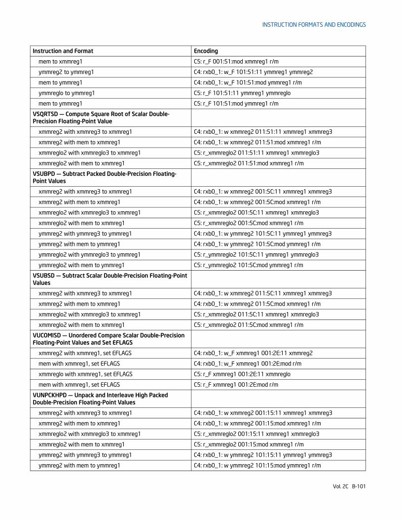
INSTRUCTION FORMATS AND ENCODINGS
mem to xmmreg1 C5: r_F 001:51:mod xmmreg1 r/m
ymmreg2 to ymmreg1 C4: rxb0_1: w_F 101:51:11 ymmreg1 ymmreg2
mem to ymmreg1 C4: rxb0_1: w_F 101:51:mod ymmreg1 r/m
ymmreglo to ymmreg1 C5: r_F 101:51:11 ymmreg1 ymmreglo
mem to ymmreg1 C5: r_F 101:51:mod ymmreg1 r/m
VSQRTSD — Compute Square Root of Scalar Double-Precision Floating-Point Value
xmmreg2 with xmmreg3 to xmmreg1 C4: rxb0_1: w xmmreg2 011:51:11 xmmreg1 xmmreg3
xmmreg2 with mem to xmmreg1 C4: rxb0_1: w xmmreg2 011:51:mod xmmreg1 r/m
xmmreglo2 with xmmreglo3 to xmmreg1 C5: r_xmmreglo2 011:51:11 xmmreg1 xmmreglo3
xmmreglo2 with mem to xmmreg1 C5: r_xmmreglo2 011:51:mod xmmreg1 r/m
VSUBPD — Subtract Packed Double-Precision Floating-Point Values
xmmreg2 with xmmreg3 to xmmreg1 C4: rxb0_1: w xmmreg2 001:5C:11 xmmreg1 xmmreg3
xmmreg2 with mem to xmmreg1 C4: rxb0_1: w xmmreg2 001:5C:mod xmmreg1 r/m
xmmreglo2 with xmmreglo3 to xmmreg1 C5: r_xmmreglo2 001:5C:11 xmmreg1 xmmreglo3
xmmreglo2 with mem to xmmreg1 C5: r_xmmreglo2 001:5C:mod xmmreg1 r/m
ymmreg2 with ymmreg3 to ymmreg1 C4: rxb0_1: w ymmreg2 101:5C:11 ymmreg1 ymmreg3
ymmreg2 with mem to ymmreg1 C4: rxb0_1: w ymmreg2 101:5C:mod ymmreg1 r/m
ymmreglo2 with ymmreglo3 to ymmreg1 C5: r_ymmreglo2 101:5C:11 ymmreg1 ymmreglo3
ymmreglo2 with mem to ymmreg1 C5: r_ymmreglo2 101:5C:mod ymmreg1 r/m
VSUBSD — Subtract Scalar Double-Precision Floating-Point Values
xmmreg2 with xmmreg3 to xmmreg1 C4: rxb0_1: w xmmreg2 011:5C:11 xmmreg1 xmmreg3
xmmreg2 with mem to xmmreg1 C4: rxb0_1: w xmmreg2 011:5C:mod xmmreg1 r/m
xmmreglo2 with xmmreglo3 to xmmreg1 C5: r_xmmreglo2 011:5C:11 xmmreg1 xmmreglo3
xmmreglo2 with mem to xmmreg1 C5: r_xmmreglo2 011:5C:mod xmmreg1 r/m
VUCOMISD — Unordered Compare Scalar Double-Precision Floating-Point Values and Set EFLAGS
xmmreg2 with xmmreg1, set EFLAGS C4: rxb0_1: w_F xmmreg1 001:2E:11 xmmreg2
mem with xmmreg1, set EFLAGS C4: rxb0_1: w_F xmmreg1 001:2E:mod r/m
xmmreglo with xmmreg1, set EFLAGS C5: r_F xmmreg1 001:2E:11 xmmreglo
mem with xmmreg1, set EFLAGS C5: r_F xmmreg1 001:2E:mod r/m
VUNPCKHPD — Unpack and Interleave High Packed Double-Precision Floating-Point Values
xmmreg2 with xmmreg3 to xmmreg1 C4: rxb0_1: w xmmreg2 001:15:11 xmmreg1 xmmreg3
xmmreg2 with mem to xmmreg1 C4: rxb0_1: w xmmreg2 001:15:mod xmmreg1 r/m
xmmreglo2 with xmmreglo3 to xmmreg1 C5: r_xmmreglo2 001:15:11 xmmreg1 xmmreglo3
xmmreglo2 with mem to xmmreg1 C5: r_xmmreglo2 001:15:mod xmmreg1 r/m
ymmreg2 with ymmreg3 to ymmreg1 C4: rxb0_1: w ymmreg2 101:15:11 ymmreg1 ymmreg3
ymmreg2 with mem to ymmreg1 C4: rxb0_1: w ymmreg2 101:15:mod ymmreg1 r/m
Instruction and Format Encoding
Vol. 2C B-101
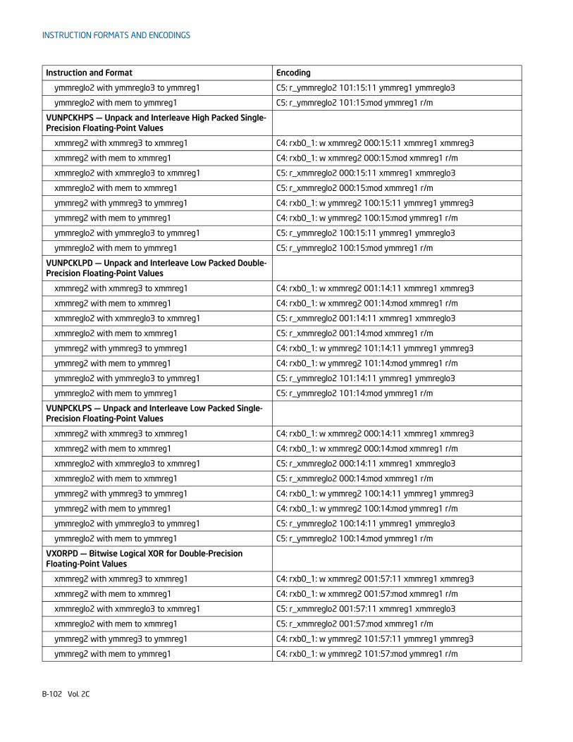
INSTRUCTION FORMATS AND ENCODINGS
ymmreglo2 with ymmreglo3 to ymmreg1 C5: r_ymmreglo2 101:15:11 ymmreg1 ymmreglo3
ymmreglo2 with mem to ymmreg1 C5: r_ymmreglo2 101:15:mod ymmreg1 r/m
VUNPCKHPS — Unpack and Interleave High Packed Single-Precision Floating-Point Values
xmmreg2 with xmmreg3 to xmmreg1 C4: rxb0_1: w xmmreg2 000:15:11 xmmreg1 xmmreg3
xmmreg2 with mem to xmmreg1 C4: rxb0_1: w xmmreg2 000:15:mod xmmreg1 r/m
xmmreglo2 with xmmreglo3 to xmmreg1 C5: r_xmmreglo2 000:15:11 xmmreg1 xmmreglo3
xmmreglo2 with mem to xmmreg1 C5: r_xmmreglo2 000:15:mod xmmreg1 r/m
ymmreg2 with ymmreg3 to ymmreg1 C4: rxb0_1: w ymmreg2 100:15:11 ymmreg1 ymmreg3
ymmreg2 with mem to ymmreg1 C4: rxb0_1: w ymmreg2 100:15:mod ymmreg1 r/m
ymmreglo2 with ymmreglo3 to ymmreg1 C5: r_ymmreglo2 100:15:11 ymmreg1 ymmreglo3
ymmreglo2 with mem to ymmreg1 C5: r_ymmreglo2 100:15:mod ymmreg1 r/m
VUNPCKLPD — Unpack and Interleave Low Packed Double-Precision Floating-Point Values
xmmreg2 with xmmreg3 to xmmreg1 C4: rxb0_1: w xmmreg2 001:14:11 xmmreg1 xmmreg3
xmmreg2 with mem to xmmreg1 C4: rxb0_1: w xmmreg2 001:14:mod xmmreg1 r/m
xmmreglo2 with xmmreglo3 to xmmreg1 C5: r_xmmreglo2 001:14:11 xmmreg1 xmmreglo3
xmmreglo2 with mem to xmmreg1 C5: r_xmmreglo2 001:14:mod xmmreg1 r/m
ymmreg2 with ymmreg3 to ymmreg1 C4: rxb0_1: w ymmreg2 101:14:11 ymmreg1 ymmreg3
ymmreg2 with mem to ymmreg1 C4: rxb0_1: w ymmreg2 101:14:mod ymmreg1 r/m
ymmreglo2 with ymmreglo3 to ymmreg1 C5: r_ymmreglo2 101:14:11 ymmreg1 ymmreglo3
ymmreglo2 with mem to ymmreg1 C5: r_ymmreglo2 101:14:mod ymmreg1 r/m
VUNPCKLPS — Unpack and Interleave Low Packed Single-Precision Floating-Point Values
xmmreg2 with xmmreg3 to xmmreg1 C4: rxb0_1: w xmmreg2 000:14:11 xmmreg1 xmmreg3
xmmreg2 with mem to xmmreg1 C4: rxb0_1: w xmmreg2 000:14:mod xmmreg1 r/m
xmmreglo2 with xmmreglo3 to xmmreg1 C5: r_xmmreglo2 000:14:11 xmmreg1 xmmreglo3
xmmreglo2 with mem to xmmreg1 C5: r_xmmreglo2 000:14:mod xmmreg1 r/m
ymmreg2 with ymmreg3 to ymmreg1 C4: rxb0_1: w ymmreg2 100:14:11 ymmreg1 ymmreg3
ymmreg2 with mem to ymmreg1 C4: rxb0_1: w ymmreg2 100:14:mod ymmreg1 r/m
ymmreglo2 with ymmreglo3 to ymmreg1 C5: r_ymmreglo2 100:14:11 ymmreg1 ymmreglo3
ymmreglo2 with mem to ymmreg1 C5: r_ymmreglo2 100:14:mod ymmreg1 r/m
VXORPD — Bitwise Logical XOR for Double-Precision Floating-Point Values
xmmreg2 with xmmreg3 to xmmreg1 C4: rxb0_1: w xmmreg2 001:57:11 xmmreg1 xmmreg3
xmmreg2 with mem to xmmreg1 C4: rxb0_1: w xmmreg2 001:57:mod xmmreg1 r/m
xmmreglo2 with xmmreglo3 to xmmreg1 C5: r_xmmreglo2 001:57:11 xmmreg1 xmmreglo3
xmmreglo2 with mem to xmmreg1 C5: r_xmmreglo2 001:57:mod xmmreg1 r/m
ymmreg2 with ymmreg3 to ymmreg1 C4: rxb0_1: w ymmreg2 101:57:11 ymmreg1 ymmreg3
ymmreg2 with mem to ymmreg1 C4: rxb0_1: w ymmreg2 101:57:mod ymmreg1 r/m
Instruction and Format Encoding
B-102 Vol. 2C
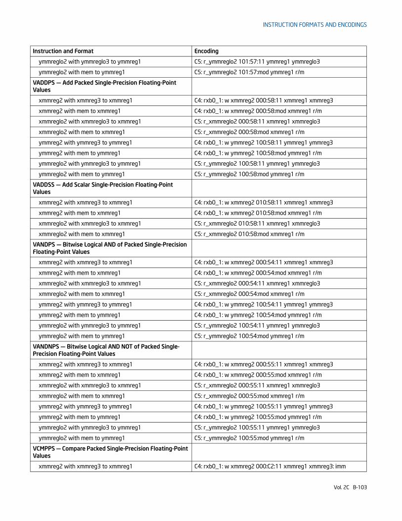
INSTRUCTION FORMATS AND ENCODINGS
ymmreglo2 with ymmreglo3 to ymmreg1 C5: r_ymmreglo2 101:57:11 ymmreg1 ymmreglo3
ymmreglo2 with mem to ymmreg1 C5: r_ymmreglo2 101:57:mod ymmreg1 r/m
VADDPS — Add Packed Single-Precision Floating-Point Values
xmmreg2 with xmmreg3 to xmmreg1 C4: rxb0_1: w xmmreg2 000:58:11 xmmreg1 xmmreg3
xmmreg2 with mem to xmmreg1 C4: rxb0_1: w xmmreg2 000:58:mod xmmreg1 r/m
xmmreglo2 with xmmreglo3 to xmmreg1 C5: r_xmmreglo2 000:58:11 xmmreg1 xmmreglo3
xmmreglo2 with mem to xmmreg1 C5: r_xmmreglo2 000:58:mod xmmreg1 r/m
ymmreg2 with ymmreg3 to ymmreg1 C4: rxb0_1: w ymmreg2 100:58:11 ymmreg1 ymmreg3
ymmreg2 with mem to ymmreg1 C4: rxb0_1: w ymmreg2 100:58:mod ymmreg1 r/m
ymmreglo2 with ymmreglo3 to ymmreg1 C5: r_ymmreglo2 100:58:11 ymmreg1 ymmreglo3
ymmreglo2 with mem to ymmreg1 C5: r_ymmreglo2 100:58:mod ymmreg1 r/m
VADDSS — Add Scalar Single-Precision Floating-Point Values
xmmreg2 with xmmreg3 to xmmreg1 C4: rxb0_1: w xmmreg2 010:58:11 xmmreg1 xmmreg3
xmmreg2 with mem to xmmreg1 C4: rxb0_1: w xmmreg2 010:58:mod xmmreg1 r/m
xmmreglo2 with xmmreglo3 to xmmreg1 C5: r_xmmreglo2 010:58:11 xmmreg1 xmmreglo3
xmmreglo2 with mem to xmmreg1 C5: r_xmmreglo2 010:58:mod xmmreg1 r/m
VANDPS — Bitwise Logical AND of Packed Single-Precision Floating-Point Values
xmmreg2 with xmmreg3 to xmmreg1 C4: rxb0_1: w xmmreg2 000:54:11 xmmreg1 xmmreg3
xmmreg2 with mem to xmmreg1 C4: rxb0_1: w xmmreg2 000:54:mod xmmreg1 r/m
xmmreglo2 with xmmreglo3 to xmmreg1 C5: r_xmmreglo2 000:54:11 xmmreg1 xmmreglo3
xmmreglo2 with mem to xmmreg1 C5: r_xmmreglo2 000:54:mod xmmreg1 r/m
ymmreg2 with ymmreg3 to ymmreg1 C4: rxb0_1: w ymmreg2 100:54:11 ymmreg1 ymmreg3
ymmreg2 with mem to ymmreg1 C4: rxb0_1: w ymmreg2 100:54:mod ymmreg1 r/m
ymmreglo2 with ymmreglo3 to ymmreg1 C5: r_ymmreglo2 100:54:11 ymmreg1 ymmreglo3
ymmreglo2 with mem to ymmreg1 C5: r_ymmreglo2 100:54:mod ymmreg1 r/m
VANDNPS — Bitwise Logical AND NOT of Packed Single-Precision Floating-Point Values
xmmreg2 with xmmreg3 to xmmreg1 C4: rxb0_1: w xmmreg2 000:55:11 xmmreg1 xmmreg3
xmmreg2 with mem to xmmreg1 C4: rxb0_1: w xmmreg2 000:55:mod xmmreg1 r/m
xmmreglo2 with xmmreglo3 to xmmreg1 C5: r_xmmreglo2 000:55:11 xmmreg1 xmmreglo3
xmmreglo2 with mem to xmmreg1 C5: r_xmmreglo2 000:55:mod xmmreg1 r/m
ymmreg2 with ymmreg3 to ymmreg1 C4: rxb0_1: w ymmreg2 100:55:11 ymmreg1 ymmreg3
ymmreg2 with mem to ymmreg1 C4: rxb0_1: w ymmreg2 100:55:mod ymmreg1 r/m
ymmreglo2 with ymmreglo3 to ymmreg1 C5: r_ymmreglo2 100:55:11 ymmreg1 ymmreglo3
ymmreglo2 with mem to ymmreg1 C5: r_ymmreglo2 100:55:mod ymmreg1 r/m
VCMPPS — Compare Packed Single-Precision Floating-Point Values
xmmreg2 with xmmreg3 to xmmreg1 C4: rxb0_1: w xmmreg2 000:C2:11 xmmreg1 xmmreg3: imm
Instruction and Format Encoding
Vol. 2C B-103
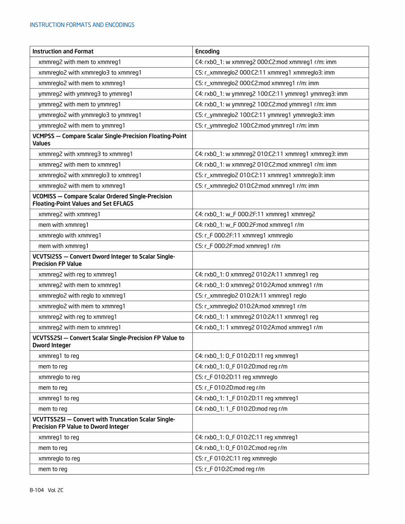
INSTRUCTION FORMATS AND ENCODINGS
xmmreg2 with mem to xmmreg1 C4: rxb0_1: w xmmreg2 000:C2:mod xmmreg1 r/m: imm
xmmreglo2 with xmmreglo3 to xmmreg1 C5: r_xmmreglo2 000:C2:11 xmmreg1 xmmreglo3: imm
xmmreglo2 with mem to xmmreg1 C5: r_xmmreglo2 000:C2:mod xmmreg1 r/m: imm
ymmreg2 with ymmreg3 to ymmreg1 C4: rxb0_1: w ymmreg2 100:C2:11 ymmreg1 ymmreg3: imm
ymmreg2 with mem to ymmreg1 C4: rxb0_1: w ymmreg2 100:C2:mod ymmreg1 r/m: imm
ymmreglo2 with ymmreglo3 to ymmreg1 C5: r_ymmreglo2 100:C2:11 ymmreg1 ymmreglo3: imm
ymmreglo2 with mem to ymmreg1 C5: r_ymmreglo2 100:C2:mod ymmreg1 r/m: imm
VCMPSS — Compare Scalar Single-Precision Floating-Point Values
xmmreg2 with xmmreg3 to xmmreg1 C4: rxb0_1: w xmmreg2 010:C2:11 xmmreg1 xmmreg3: imm
xmmreg2 with mem to xmmreg1 C4: rxb0_1: w xmmreg2 010:C2:mod xmmreg1 r/m: imm
xmmreglo2 with xmmreglo3 to xmmreg1 C5: r_xmmreglo2 010:C2:11 xmmreg1 xmmreglo3: imm
xmmreglo2 with mem to xmmreg1 C5: r_xmmreglo2 010:C2:mod xmmreg1 r/m: imm
VCOMISS — Compare Scalar Ordered Single-Precision Floating-Point Values and Set EFLAGS
xmmreg2 with xmmreg1 C4: rxb0_1: w_F 000:2F:11 xmmreg1 xmmreg2
mem with xmmreg1 C4: rxb0_1: w_F 000:2F:mod xmmreg1 r/m
xmmreglo with xmmreg1 C5: r_F 000:2F:11 xmmreg1 xmmreglo
mem with xmmreg1 C5: r_F 000:2F:mod xmmreg1 r/m
VCVTSI2SS — Convert Dword Integer to Scalar Single-Precision FP Value
xmmreg2 with reg to xmmreg1 C4: rxb0_1: 0 xmmreg2 010:2A:11 xmmreg1 reg
xmmreg2 with mem to xmmreg1 C4: rxb0_1: 0 xmmreg2 010:2A:mod xmmreg1 r/m
xmmreglo2 with reglo to xmmreg1 C5: r_xmmreglo2 010:2A:11 xmmreg1 reglo
xmmreglo2 with mem to xmmreg1 C5: r_xmmreglo2 010:2A:mod xmmreg1 r/m
xmmreg2 with reg to xmmreg1 C4: rxb0_1: 1 xmmreg2 010:2A:11 xmmreg1 reg
xmmreg2 with mem to xmmreg1 C4: rxb0_1: 1 xmmreg2 010:2A:mod xmmreg1 r/m
VCVTSS2SI — Convert Scalar Single-Precision FP Value to Dword Integer
xmmreg1 to reg C4: rxb0_1: 0_F 010:2D:11 reg xmmreg1
mem to reg C4: rxb0_1: 0_F 010:2D:mod reg r/m
xmmreglo to reg C5: r_F 010:2D:11 reg xmmreglo
mem to reg C5: r_F 010:2D:mod reg r/m
xmmreg1 to reg C4: rxb0_1: 1_F 010:2D:11 reg xmmreg1
mem to reg C4: rxb0_1: 1_F 010:2D:mod reg r/m
VCVTTSS2SI — Convert with Truncation Scalar Single-Precision FP Value to Dword Integer
xmmreg1 to reg C4: rxb0_1: 0_F 010:2C:11 reg xmmreg1
mem to reg C4: rxb0_1: 0_F 010:2C:mod reg r/m
xmmreglo to reg C5: r_F 010:2C:11 reg xmmreglo
mem to reg C5: r_F 010:2C:mod reg r/m
Instruction and Format Encoding
B-104 Vol. 2C

INSTRUCTION FORMATS AND ENCODINGS
xmmreg1 to reg C4: rxb0_1: 1_F 010:2C:11 reg xmmreg1
mem to reg C4: rxb0_1: 1_F 010:2C:mod reg r/m
VDIVPS — Divide Packed Single-Precision Floating-Point Values
xmmreg2 with xmmreg3 to xmmreg1 C4: rxb0_1: w xmmreg2 000:5E:11 xmmreg1 xmmreg3
xmmreg2 with mem to xmmreg1 C4: rxb0_1: w xmmreg2 000:5E:mod xmmreg1 r/m
xmmreglo2 with xmmreglo3 to xmmreg1 C5: r_xmmreglo2 000:5E:11 xmmreg1 xmmreglo3
xmmreglo2 with mem to xmmreg1 C5: r_xmmreglo2 000:5E:mod xmmreg1 r/m
ymmreg2 with ymmreg3 to ymmreg1 C4: rxb0_1: w ymmreg2 100:5E:11 ymmreg1 ymmreg3
ymmreg2 with mem to ymmreg1 C4: rxb0_1: w ymmreg2 100:5E:mod ymmreg1 r/m
ymmreglo2 with ymmreglo3 to ymmreg1 C5: r_ymmreglo2 100:5E:11 ymmreg1 ymmreglo3
ymmreglo2 with mem to ymmreg1 C5: r_ymmreglo2 100:5E:mod ymmreg1 r/m
VDIVSS — Divide Scalar Single-Precision Floating-Point Values
xmmreg2 with xmmreg3 to xmmreg1 C4: rxb0_1: w xmmreg2 010:5E:11 xmmreg1 xmmreg3
xmmreg2 with mem to xmmreg1 C4: rxb0_1: w xmmreg2 010:5E:mod xmmreg1 r/m
xmmreglo2 with xmmreglo3 to xmmreg1 C5: r_xmmreglo2 010:5E:11 xmmreg1 xmmreglo3
xmmreglo2 with mem to xmmreg1 C5: r_xmmreglo2 010:5E:mod xmmreg1 r/m
VLDMXCSR — Load MXCSR Register
mem to MXCSR reg C4: rxb0_1: w_F 000:AEmod 011 r/m
mem to MXCSR reg C5: r_F 000:AEmod 011 r/m
VMAXPS — Return Maximum Packed Single-Precision Floating-Point Values
xmmreg2 with xmmreg3 to xmmreg1 C4: rxb0_1: w xmmreg2 000:5F:11 xmmreg1 xmmreg3
xmmreg2 with mem to xmmreg1 C4: rxb0_1: w xmmreg2 000:5F:mod xmmreg1 r/m
xmmreglo2 with xmmreglo3 to xmmreg1 C5: r_xmmreglo2 000:5F:11 xmmreg1 xmmreglo3
xmmreglo2 with mem to xmmreg1 C5: r_xmmreglo2 000:5F:mod xmmreg1 r/m
ymmreg2 with ymmreg3 to ymmreg1 C4: rxb0_1: w ymmreg2 100:5F:11 ymmreg1 ymmreg3
ymmreg2 with mem to ymmreg1 C4: rxb0_1: w ymmreg2 100:5F:mod ymmreg1 r/m
ymmreglo2 with ymmreglo3 to ymmreg1 C5: r_ymmreglo2 100:5F:11 ymmreg1 ymmreglo3
ymmreglo2 with mem to ymmreg1 C5: r_ymmreglo2 100:5F:mod ymmreg1 r/m
VMAXSS — Return Maximum Scalar Single-Precision Floating-Point Value
xmmreg2 with xmmreg3 to xmmreg1 C4: rxb0_1: w xmmreg2 010:5F:11 xmmreg1 xmmreg3
xmmreg2 with mem to xmmreg1 C4: rxb0_1: w xmmreg2 010:5F:mod xmmreg1 r/m
xmmreglo2 with xmmreglo3 to xmmreg1 C5: r_xmmreglo2 010:5F:11 xmmreg1 xmmreglo3
xmmreglo2 with mem to xmmreg1 C5: r_xmmreglo2 010:5F:mod xmmreg1 r/m
VMINPS — Return Minimum Packed Single-Precision Floating-Point Values
xmmreg2 with xmmreg3 to xmmreg1 C4: rxb0_1: w xmmreg2 000:5D:11 xmmreg1 xmmreg3
xmmreg2 with mem to xmmreg1 C4: rxb0_1: w xmmreg2 000:5D:mod xmmreg1 r/m
Instruction and Format Encoding
Vol. 2C B-105
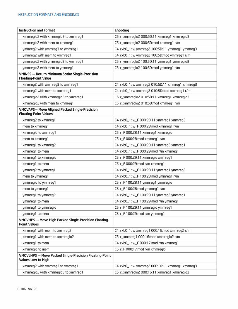
INSTRUCTION FORMATS AND ENCODINGS
xmmreglo2 with xmmreglo3 to xmmreg1 C5: r_xmmreglo2 000:5D:11 xmmreg1 xmmreglo3
xmmreglo2 with mem to xmmreg1 C5: r_xmmreglo2 000:5D:mod xmmreg1 r/m
ymmreg2 with ymmreg3 to ymmreg1 C4: rxb0_1: w ymmreg2 100:5D:11 ymmreg1 ymmreg3
ymmreg2 with mem to ymmreg1 C4: rxb0_1: w ymmreg2 100:5D:mod ymmreg1 r/m
ymmreglo2 with ymmreglo3 to ymmreg1 C5: r_ymmreglo2 100:5D:11 ymmreg1 ymmreglo3
ymmreglo2 with mem to ymmreg1 C5: r_ymmreglo2 100:5D:mod ymmreg1 r/m
VMINSS — Return Minimum Scalar Single-Precision Floating-Point Value
xmmreg2 with xmmreg3 to xmmreg1 C4: rxb0_1: w xmmreg2 010:5D:11 xmmreg1 xmmreg3
xmmreg2 with mem to xmmreg1 C4: rxb0_1: w xmmreg2 010:5D:mod xmmreg1 r/m
xmmreglo2 with xmmreglo3 to xmmreg1 C5: r_xmmreglo2 010:5D:11 xmmreg1 xmmreglo3
xmmreglo2 with mem to xmmreg1 C5: r_xmmreglo2 010:5D:mod xmmreg1 r/m
VMOVAPS— Move Aligned Packed Single-Precision Floating-Point Values
xmmreg2 to xmmreg1 C4: rxb0_1: w_F 000:28:11 xmmreg1 xmmreg2
mem to xmmreg1 C4: rxb0_1: w_F 000:28:mod xmmreg1 r/m
xmmreglo to xmmreg1 C5: r_F 000:28:11 xmmreg1 xmmreglo
mem to xmmreg1 C5: r_F 000:28:mod xmmreg1 r/m
xmmreg1 to xmmreg2 C4: rxb0_1: w_F 000:29:11 xmmreg2 xmmreg1
xmmreg1 to mem C4: rxb0_1: w_F 000:29:mod r/m xmmreg1
xmmreg1 to xmmreglo C5: r_F 000:29:11 xmmreglo xmmreg1
xmmreg1 to mem C5: r_F 000:29:mod r/m xmmreg1
ymmreg2 to ymmreg1 C4: rxb0_1: w_F 100:28:11 ymmreg1 ymmreg2
mem to ymmreg1 C4: rxb0_1: w_F 100:28:mod ymmreg1 r/m
ymmreglo to ymmreg1 C5: r_F 100:28:11 ymmreg1 ymmreglo
mem to ymmreg1 C5: r_F 100:28:mod ymmreg1 r/m
ymmreg1 to ymmreg2 C4: rxb0_1: w_F 100:29:11 ymmreg2 ymmreg1
ymmreg1 to mem C4: rxb0_1: w_F 100:29:mod r/m ymmreg1
ymmreg1 to ymmreglo C5: r_F 100:29:11 ymmreglo ymmreg1
ymmreg1 to mem C5: r_F 100:29:mod r/m ymmreg1
VMOVHPS — Move High Packed Single-Precision Floating-Point Values
xmmreg1 with mem to xmmreg2 C4: rxb0_1: w xmmreg1 000:16:mod xmmreg2 r/m
xmmreg1 with mem to xmmreglo2 C5: r_xmmreg1 000:16:mod xmmreglo2 r/m
xmmreg1 to mem C4: rxb0_1: w_F 000:17:mod r/m xmmreg1
xmmreglo to mem C5: r_F 000:17:mod r/m xmmreglo
VMOVLHPS — Move Packed Single-Precision Floating-Point Values Low to High
xmmreg2 with xmmreg3 to xmmreg1 C4: rxb0_1: w xmmreg2 000:16:11 xmmreg1 xmmreg3
xmmreglo2 with xmmreglo3 to xmmreg1 C5: r_xmmreglo2 000:16:11 xmmreg1 xmmreglo3
Instruction and Format Encoding
B-106 Vol. 2C
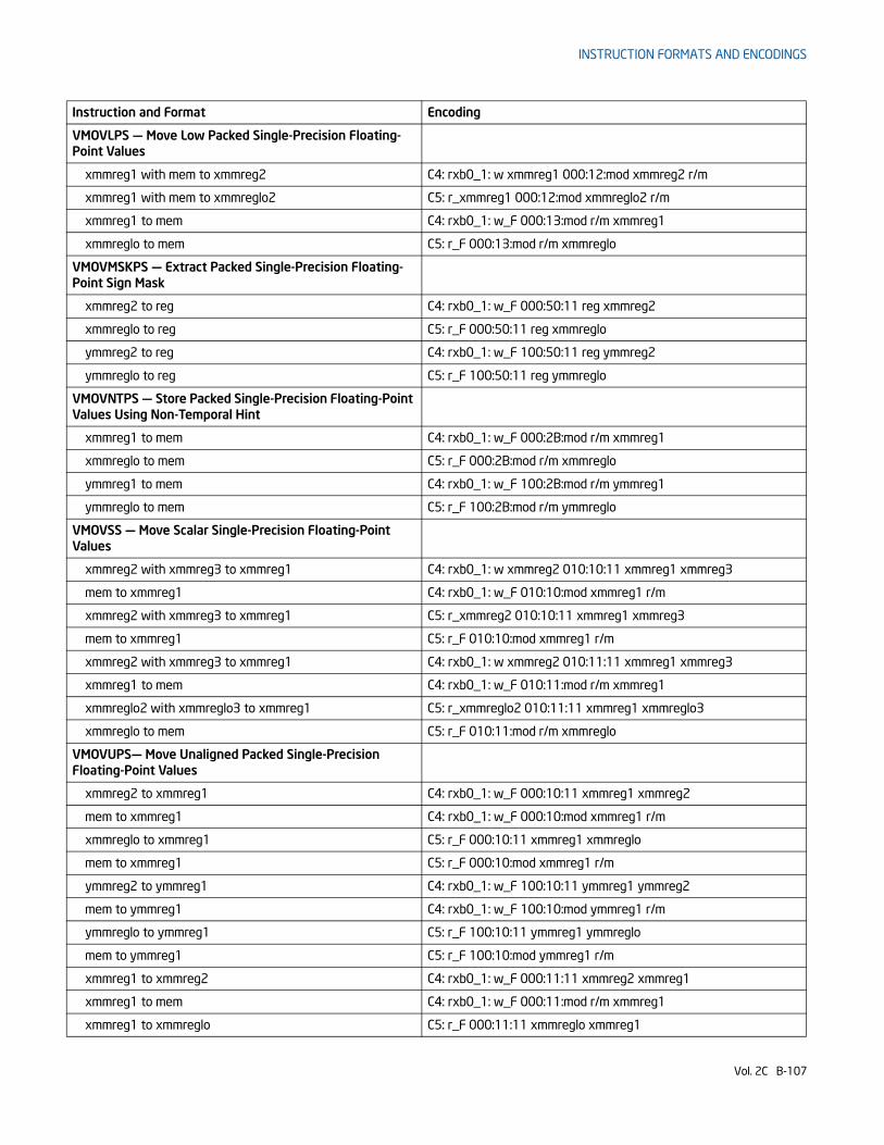
INSTRUCTION FORMATS AND ENCODINGS
VMOVLPS — Move Low Packed Single-Precision Floating-Point Values
xmmreg1 with mem to xmmreg2 C4: rxb0_1: w xmmreg1 000:12:mod xmmreg2 r/m
xmmreg1 with mem to xmmreglo2 C5: r_xmmreg1 000:12:mod xmmreglo2 r/m
xmmreg1 to mem C4: rxb0_1: w_F 000:13:mod r/m xmmreg1
xmmreglo to mem C5: r_F 000:13:mod r/m xmmreglo
VMOVMSKPS — Extract Packed Single-Precision Floating-Point Sign Mask
xmmreg2 to reg C4: rxb0_1: w_F 000:50:11 reg xmmreg2
xmmreglo to reg C5: r_F 000:50:11 reg xmmreglo
ymmreg2 to reg C4: rxb0_1: w_F 100:50:11 reg ymmreg2
ymmreglo to reg C5: r_F 100:50:11 reg ymmreglo
VMOVNTPS — Store Packed Single-Precision Floating-Point Values Using Non-Temporal Hint
xmmreg1 to mem C4: rxb0_1: w_F 000:2B:mod r/m xmmreg1
xmmreglo to mem C5: r_F 000:2B:mod r/m xmmreglo
ymmreg1 to mem C4: rxb0_1: w_F 100:2B:mod r/m ymmreg1
ymmreglo to mem C5: r_F 100:2B:mod r/m ymmreglo
VMOVSS — Move Scalar Single-Precision Floating-Point Values
xmmreg2 with xmmreg3 to xmmreg1 C4: rxb0_1: w xmmreg2 010:10:11 xmmreg1 xmmreg3
mem to xmmreg1 C4: rxb0_1: w_F 010:10:mod xmmreg1 r/m
xmmreg2 with xmmreg3 to xmmreg1 C5: r_xmmreg2 010:10:11 xmmreg1 xmmreg3
mem to xmmreg1 C5: r_F 010:10:mod xmmreg1 r/m
xmmreg2 with xmmreg3 to xmmreg1 C4: rxb0_1: w xmmreg2 010:11:11 xmmreg1 xmmreg3
xmmreg1 to mem C4: rxb0_1: w_F 010:11:mod r/m xmmreg1
xmmreglo2 with xmmreglo3 to xmmreg1 C5: r_xmmreglo2 010:11:11 xmmreg1 xmmreglo3
xmmreglo to mem C5: r_F 010:11:mod r/m xmmreglo
VMOVUPS— Move Unaligned Packed Single-Precision Floating-Point Values
xmmreg2 to xmmreg1 C4: rxb0_1: w_F 000:10:11 xmmreg1 xmmreg2
mem to xmmreg1 C4: rxb0_1: w_F 000:10:mod xmmreg1 r/m
xmmreglo to xmmreg1 C5: r_F 000:10:11 xmmreg1 xmmreglo
mem to xmmreg1 C5: r_F 000:10:mod xmmreg1 r/m
ymmreg2 to ymmreg1 C4: rxb0_1: w_F 100:10:11 ymmreg1 ymmreg2
mem to ymmreg1 C4: rxb0_1: w_F 100:10:mod ymmreg1 r/m
ymmreglo to ymmreg1 C5: r_F 100:10:11 ymmreg1 ymmreglo
mem to ymmreg1 C5: r_F 100:10:mod ymmreg1 r/m
xmmreg1 to xmmreg2 C4: rxb0_1: w_F 000:11:11 xmmreg2 xmmreg1
xmmreg1 to mem C4: rxb0_1: w_F 000:11:mod r/m xmmreg1
xmmreg1 to xmmreglo C5: r_F 000:11:11 xmmreglo xmmreg1
Instruction and Format Encoding
Vol. 2C B-107
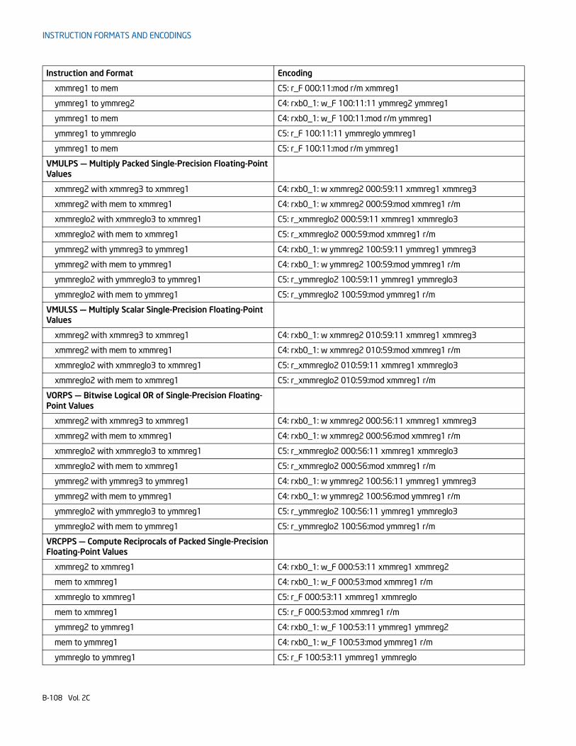
INSTRUCTION FORMATS AND ENCODINGS
xmmreg1 to mem C5: r_F 000:11:mod r/m xmmreg1
ymmreg1 to ymmreg2 C4: rxb0_1: w_F 100:11:11 ymmreg2 ymmreg1
ymmreg1 to mem C4: rxb0_1: w_F 100:11:mod r/m ymmreg1
ymmreg1 to ymmreglo C5: r_F 100:11:11 ymmreglo ymmreg1
ymmreg1 to mem C5: r_F 100:11:mod r/m ymmreg1
VMULPS — Multiply Packed Single-Precision Floating-Point Values
xmmreg2 with xmmreg3 to xmmreg1 C4: rxb0_1: w xmmreg2 000:59:11 xmmreg1 xmmreg3
xmmreg2 with mem to xmmreg1 C4: rxb0_1: w xmmreg2 000:59:mod xmmreg1 r/m
xmmreglo2 with xmmreglo3 to xmmreg1 C5: r_xmmreglo2 000:59:11 xmmreg1 xmmreglo3
xmmreglo2 with mem to xmmreg1 C5: r_xmmreglo2 000:59:mod xmmreg1 r/m
ymmreg2 with ymmreg3 to ymmreg1 C4: rxb0_1: w ymmreg2 100:59:11 ymmreg1 ymmreg3
ymmreg2 with mem to ymmreg1 C4: rxb0_1: w ymmreg2 100:59:mod ymmreg1 r/m
ymmreglo2 with ymmreglo3 to ymmreg1 C5: r_ymmreglo2 100:59:11 ymmreg1 ymmreglo3
ymmreglo2 with mem to ymmreg1 C5: r_ymmreglo2 100:59:mod ymmreg1 r/m
VMULSS — Multiply Scalar Single-Precision Floating-Point Values
xmmreg2 with xmmreg3 to xmmreg1 C4: rxb0_1: w xmmreg2 010:59:11 xmmreg1 xmmreg3
xmmreg2 with mem to xmmreg1 C4: rxb0_1: w xmmreg2 010:59:mod xmmreg1 r/m
xmmreglo2 with xmmreglo3 to xmmreg1 C5: r_xmmreglo2 010:59:11 xmmreg1 xmmreglo3
xmmreglo2 with mem to xmmreg1 C5: r_xmmreglo2 010:59:mod xmmreg1 r/m
VORPS — Bitwise Logical OR of Single-Precision Floating-Point Values
xmmreg2 with xmmreg3 to xmmreg1 C4: rxb0_1: w xmmreg2 000:56:11 xmmreg1 xmmreg3
xmmreg2 with mem to xmmreg1 C4: rxb0_1: w xmmreg2 000:56:mod xmmreg1 r/m
xmmreglo2 with xmmreglo3 to xmmreg1 C5: r_xmmreglo2 000:56:11 xmmreg1 xmmreglo3
xmmreglo2 with mem to xmmreg1 C5: r_xmmreglo2 000:56:mod xmmreg1 r/m
ymmreg2 with ymmreg3 to ymmreg1 C4: rxb0_1: w ymmreg2 100:56:11 ymmreg1 ymmreg3
ymmreg2 with mem to ymmreg1 C4: rxb0_1: w ymmreg2 100:56:mod ymmreg1 r/m
ymmreglo2 with ymmreglo3 to ymmreg1 C5: r_ymmreglo2 100:56:11 ymmreg1 ymmreglo3
ymmreglo2 with mem to ymmreg1 C5: r_ymmreglo2 100:56:mod ymmreg1 r/m
VRCPPS — Compute Reciprocals of Packed Single-Precision Floating-Point Values
xmmreg2 to xmmreg1 C4: rxb0_1: w_F 000:53:11 xmmreg1 xmmreg2
mem to xmmreg1 C4: rxb0_1: w_F 000:53:mod xmmreg1 r/m
xmmreglo to xmmreg1 C5: r_F 000:53:11 xmmreg1 xmmreglo
mem to xmmreg1 C5: r_F 000:53:mod xmmreg1 r/m
ymmreg2 to ymmreg1 C4: rxb0_1: w_F 100:53:11 ymmreg1 ymmreg2
mem to ymmreg1 C4: rxb0_1: w_F 100:53:mod ymmreg1 r/m
ymmreglo to ymmreg1 C5: r_F 100:53:11 ymmreg1 ymmreglo
Instruction and Format Encoding
B-108 Vol. 2C
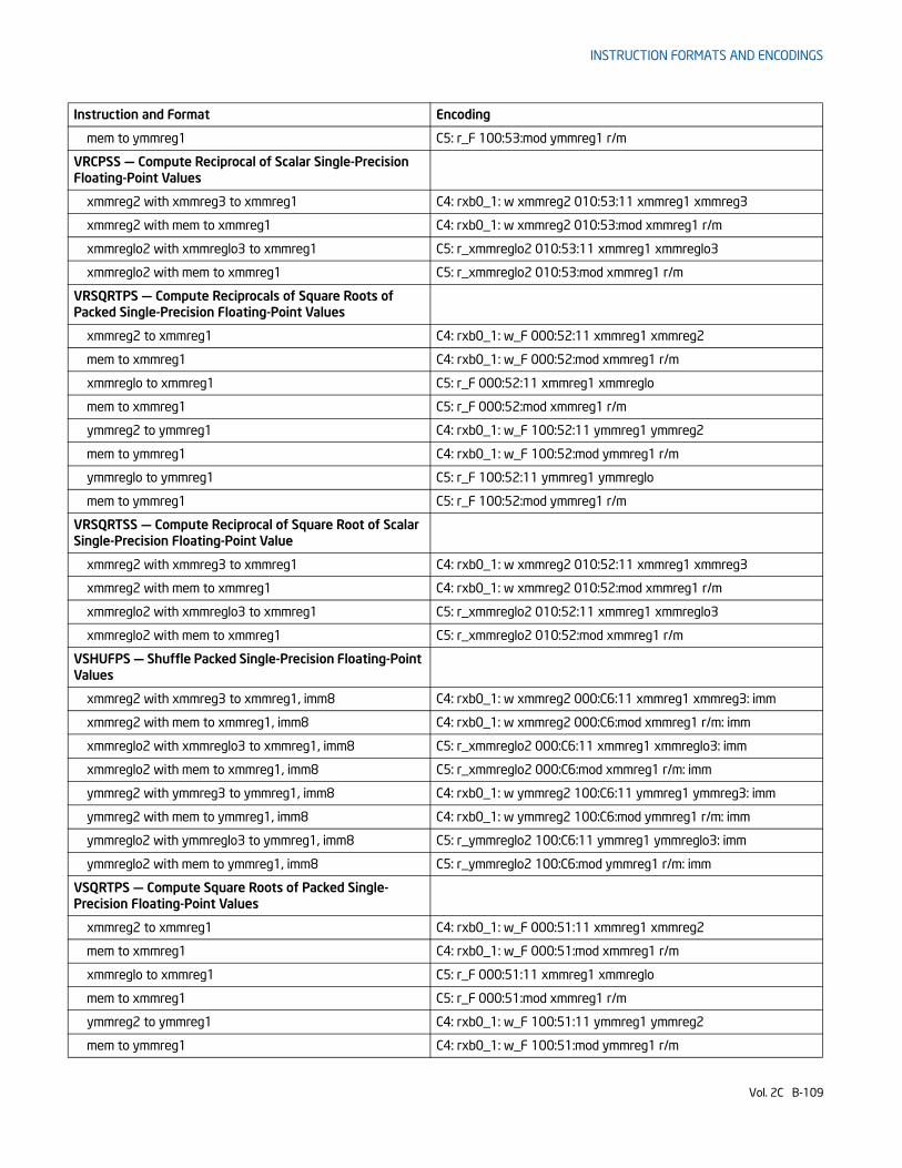
INSTRUCTION FORMATS AND ENCODINGS
mem to ymmreg1 C5: r_F 100:53:mod ymmreg1 r/m
VRCPSS — Compute Reciprocal of Scalar Single-Precision Floating-Point Values
xmmreg2 with xmmreg3 to xmmreg1 C4: rxb0_1: w xmmreg2 010:53:11 xmmreg1 xmmreg3
xmmreg2 with mem to xmmreg1 C4: rxb0_1: w xmmreg2 010:53:mod xmmreg1 r/m
xmmreglo2 with xmmreglo3 to xmmreg1 C5: r_xmmreglo2 010:53:11 xmmreg1 xmmreglo3
xmmreglo2 with mem to xmmreg1 C5: r_xmmreglo2 010:53:mod xmmreg1 r/m
VRSQRTPS — Compute Reciprocals of Square Roots of Packed Single-Precision Floating-Point Values
xmmreg2 to xmmreg1 C4: rxb0_1: w_F 000:52:11 xmmreg1 xmmreg2
mem to xmmreg1 C4: rxb0_1: w_F 000:52:mod xmmreg1 r/m
xmmreglo to xmmreg1 C5: r_F 000:52:11 xmmreg1 xmmreglo
mem to xmmreg1 C5: r_F 000:52:mod xmmreg1 r/m
ymmreg2 to ymmreg1 C4: rxb0_1: w_F 100:52:11 ymmreg1 ymmreg2
mem to ymmreg1 C4: rxb0_1: w_F 100:52:mod ymmreg1 r/m
ymmreglo to ymmreg1 C5: r_F 100:52:11 ymmreg1 ymmreglo
mem to ymmreg1 C5: r_F 100:52:mod ymmreg1 r/m
VRSQRTSS — Compute Reciprocal of Square Root of Scalar Single-Precision Floating-Point Value
xmmreg2 with xmmreg3 to xmmreg1 C4: rxb0_1: w xmmreg2 010:52:11 xmmreg1 xmmreg3
xmmreg2 with mem to xmmreg1 C4: rxb0_1: w xmmreg2 010:52:mod xmmreg1 r/m
xmmreglo2 with xmmreglo3 to xmmreg1 C5: r_xmmreglo2 010:52:11 xmmreg1 xmmreglo3
xmmreglo2 with mem to xmmreg1 C5: r_xmmreglo2 010:52:mod xmmreg1 r/m
VSHUFPS — Shuffle Packed Single-Precision Floating-Point Values
xmmreg2 with xmmreg3 to xmmreg1, imm8 C4: rxb0_1: w xmmreg2 000:C6:11 xmmreg1 xmmreg3: imm
xmmreg2 with mem to xmmreg1, imm8 C4: rxb0_1: w xmmreg2 000:C6:mod xmmreg1 r/m: imm
xmmreglo2 with xmmreglo3 to xmmreg1, imm8 C5: r_xmmreglo2 000:C6:11 xmmreg1 xmmreglo3: imm
xmmreglo2 with mem to xmmreg1, imm8 C5: r_xmmreglo2 000:C6:mod xmmreg1 r/m: imm
ymmreg2 with ymmreg3 to ymmreg1, imm8 C4: rxb0_1: w ymmreg2 100:C6:11 ymmreg1 ymmreg3: imm
ymmreg2 with mem to ymmreg1, imm8 C4: rxb0_1: w ymmreg2 100:C6:mod ymmreg1 r/m: imm
ymmreglo2 with ymmreglo3 to ymmreg1, imm8 C5: r_ymmreglo2 100:C6:11 ymmreg1 ymmreglo3: imm
ymmreglo2 with mem to ymmreg1, imm8 C5: r_ymmreglo2 100:C6:mod ymmreg1 r/m: imm
VSQRTPS — Compute Square Roots of Packed Single-Precision Floating-Point Values
xmmreg2 to xmmreg1 C4: rxb0_1: w_F 000:51:11 xmmreg1 xmmreg2
mem to xmmreg1 C4: rxb0_1: w_F 000:51:mod xmmreg1 r/m
xmmreglo to xmmreg1 C5: r_F 000:51:11 xmmreg1 xmmreglo
mem to xmmreg1 C5: r_F 000:51:mod xmmreg1 r/m
ymmreg2 to ymmreg1 C4: rxb0_1: w_F 100:51:11 ymmreg1 ymmreg2
mem to ymmreg1 C4: rxb0_1: w_F 100:51:mod ymmreg1 r/m
Instruction and Format Encoding
Vol. 2C B-109

INSTRUCTION FORMATS AND ENCODINGS
ymmreglo to ymmreg1 C5: r_F 100:51:11 ymmreg1 ymmreglo
mem to ymmreg1 C5: r_F 100:51:mod ymmreg1 r/m
VSQRTSS — Compute Square Root of Scalar Single-Precision Floating-Point Value
xmmreg2 with xmmreg3 to xmmreg1 C4: rxb0_1: w xmmreg2 010:51:11 xmmreg1 xmmreg3
xmmreg2 with mem to xmmreg1 C4: rxb0_1: w xmmreg2 010:51:mod xmmreg1 r/m
xmmreglo2 with xmmreglo3 to xmmreg1 C5: r_xmmreglo2 010:51:11 xmmreg1 xmmreglo3
xmmreglo2 with mem to xmmreg1 C5: r_xmmreglo2 010:51:mod xmmreg1 r/m
VSTMXCSR — Store MXCSR Register State
MXCSR to mem C4: rxb0_1: w_F 000:AE:mod 011 r/m
MXCSR to mem C5: r_F 000:AE:mod 011 r/m
VSUBPS — Subtract Packed Single-Precision Floating-Point Values
xmmreg2 with xmmreg3 to xmmreg1 C4: rxb0_1: w xmmreg2 000:5C:11 xmmreg1 xmmreg3
xmmreg2 with mem to xmmreg1 C4: rxb0_1: w xmmreg2 000:5C:mod xmmreg1 r/m
xmmreglo2 with xmmreglo3 to xmmreg1 C5: r_xmmreglo2 000:5C:11 xmmreg1 xmmreglo3
xmmreglo2 with mem to xmmreg1 C5: r_xmmreglo2 000:5C:mod xmmreg1 r/m
ymmreg2 with ymmreg3 to ymmreg1 C4: rxb0_1: w ymmreg2 100:5C:11 ymmreg1 ymmreg3
ymmreg2 with mem to ymmreg1 C4: rxb0_1: w ymmreg2 100:5C:mod ymmreg1 r/m
ymmreglo2 with ymmreglo3 to ymmreg1 C5: r_ymmreglo2 100:5C:11 ymmreg1 ymmreglo3
ymmreglo2 with mem to ymmreg1 C5: r_ymmreglo2 100:5C:mod ymmreg1 r/m
VSUBSS — Subtract Scalar Single-Precision Floating-Point Values
xmmreg2 with xmmreg3 to xmmreg1 C4: rxb0_1: w xmmreg2 010:5C:11 xmmreg1 xmmreg3
xmmreg2 with mem to xmmreg1 C4: rxb0_1: w xmmreg2 010:5C:mod xmmreg1 r/m
xmmreglo2 with xmmreglo3 to xmmreg1 C5: r_xmmreglo2 010:5C:11 xmmreg1 xmmreglo3
xmmreglo2 with mem to xmmreg1 C5: r_xmmreglo2 010:5C:mod xmmreg1 r/m
VUCOMISS — Unordered Compare Scalar Single-Precision Floating-Point Values and Set EFLAGS
xmmreg2 with xmmreg1 C4: rxb0_1: w_F 000:2E:11 xmmreg1 xmmreg2
mem with xmmreg1 C4: rxb0_1: w_F 000:2E:mod xmmreg1 r/m
xmmreglo with xmmreg1 C5: r_F 000:2E:11 xmmreg1 xmmreglo
mem with xmmreg1 C5: r_F 000:2E:mod xmmreg1 r/m
UNPCKHPS — Unpack and Interleave High Packed Single-Precision Floating-Point Values
xmmreg2 with xmmreg3 to xmmreg1 C4: rxb0_1: w xmmreg2 000:15:11 xmmreg1 xmmreg3
xmmreg2 with mem to xmmreg1 C4: rxb0_1: w xmmreg2 000:15mod xmmreg1 r/m
ymmreg2 with ymmreg3 to ymmreg1 C4: rxb0_1: w ymmreg2 100:15:11 ymmreg1 ymmreg3
ymmreg2 with mem to ymmreg1 C4: rxb0_1: w ymmreg2 100:15mod ymmreg1 r/m
UNPCKLPS — Unpack and Interleave Low Packed Single-Precision Floating-Point Value
Instruction and Format Encoding
B-110 Vol. 2C

INSTRUCTION FORMATS AND ENCODINGS
xmmreg2 with xmmreg3 to xmmreg1 C4: rxb0_1: w xmmreg2 000:14:11 xmmreg1 xmmreg3
xmmreg2 with mem to xmmreg1 C4: rxb0_1: w xmmreg2 000:14mod xmmreg1 r/m
ymmreg2 with ymmreg3 to ymmreg1 C4: rxb0_1: w ymmreg2 100:14:11 ymmreg1 ymmreg3
ymmreg2 with mem to ymmreg1 C4: rxb0_1: w ymmreg2 100:14mod ymmreg1 r/m
VXORPS — Bitwise Logical XOR for Single-Precision Floating-Point Values
xmmreg2 with xmmreg3 to xmmreg1 C4: rxb0_1: w xmmreg2 000:57:11 xmmreg1 xmmreg3
xmmreg2 with mem to xmmreg1 C4: rxb0_1: w xmmreg2 000:57:mod xmmreg1 r/m
xmmreglo2 with xmmreglo3 to xmmreg1 C5: r_xmmreglo2 000:57:11 xmmreg1 xmmreglo3
xmmreglo2 with mem to xmmreg1 C5: r_xmmreglo2 000:57:mod xmmreg1 r/m
ymmreg2 with ymmreg3 to ymmreg1 C4: rxb0_1: w ymmreg2 100:57:11 ymmreg1 ymmreg3
ymmreg2 with mem to ymmreg1 C4: rxb0_1: w ymmreg2 100:57:mod ymmreg1 r/m
ymmreglo2 with ymmreglo3 to ymmreg1 C5: r_ymmreglo2 100:57:11 ymmreg1 ymmreglo3
ymmreglo2 with mem to ymmreg1 C5: r_ymmreglo2 100:57:mod ymmreg1 r/m
VBROADCAST —Load with Broadcast
mem to xmmreg1 C4: rxb0_2: 0_F 001:18:mod xmmreg1 r/m
mem to ymmreg1 C4: rxb0_2: 0_F 101:18:mod ymmreg1 r/m
mem to ymmreg1 C4: rxb0_2: 0_F 101:19:mod ymmreg1 r/m
mem to ymmreg1 C4: rxb0_2: 0_F 101:1A:mod ymmreg1 r/m
VEXTRACTF128 — Extract Packed Floating-Point Values
ymmreg2 to xmmreg1, imm8 C4: rxb0_3: 0_F 001:19:11 xmmreg1 ymmreg2: imm
ymmreg2 to mem, imm8 C4: rxb0_3: 0_F 001:19:mod r/m ymmreg2: imm
VINSERTF128 — Insert Packed Floating-Point Values
xmmreg3 and merge with ymmreg2 to ymmreg1, imm8 C4: rxb0_3: 0 ymmreg2101:18:11 ymmreg1 xmmreg3: imm
mem and merge with ymmreg2 to ymmreg1, imm8 C4: rxb0_3: 0 ymmreg2 101:18:mod ymmreg1 r/m: imm
VPERMILPD — Permute Double-Precision Floating-Point Values
xmmreg2 with xmmreg3 to xmmreg1 C4: rxb0_2: 0 xmmreg2 001:0D:11 xmmreg1 xmmreg3
xmmreg2 with mem to xmmreg1 C4: rxb0_2: 0 xmmreg2 001:0D:mod xmmreg1 r/m
ymmreg2 with ymmreg3 to ymmreg1 C4: rxb0_2: 0 ymmreg2 101:0D:11 ymmreg1 ymmreg3
ymmreg2 with mem to ymmreg1 C4: rxb0_2: 0 ymmreg2 101:0D:mod ymmreg1 r/m
xmmreg2 to xmmreg1, imm C4: rxb0_3: 0_F 001:05:11 xmmreg1 xmmreg2: imm
mem to xmmreg1, imm C4: rxb0_3: 0_F 001:05:mod xmmreg1 r/m: imm
ymmreg2 to ymmreg1, imm C4: rxb0_3: 0_F 101:05:11 ymmreg1 ymmreg2: imm
mem to ymmreg1, imm C4: rxb0_3: 0_F 101:05:mod ymmreg1 r/m: imm
VPERMILPS — Permute Single-Precision Floating-Point Values
xmmreg2 with xmmreg3 to xmmreg1 C4: rxb0_2: 0 xmmreg2 001:0C:11 xmmreg1 xmmreg3
xmmreg2 with mem to xmmreg1 C4: rxb0_2: 0 xmmreg2 001:0C:mod xmmreg1 r/m
xmmreg2 to xmmreg1, imm C4: rxb0_3: 0_F 001:04:11 xmmreg1 xmmreg2: imm
Instruction and Format Encoding
Vol. 2C B-111
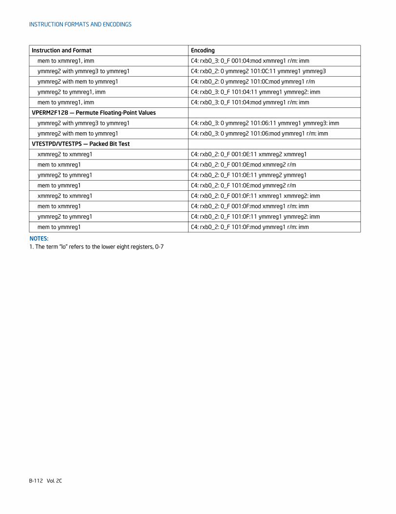
INSTRUCTION FORMATS AND ENCODINGS
mem to xmmreg1, imm C4: rxb0_3: 0_F 001:04:mod xmmreg1 r/m: imm
ymmreg2 with ymmreg3 to ymmreg1 C4: rxb0_2: 0 ymmreg2 101:0C:11 ymmreg1 ymmreg3
ymmreg2 with mem to ymmreg1 C4: rxb0_2: 0 ymmreg2 101:0C:mod ymmreg1 r/m
ymmreg2 to ymmreg1, imm C4: rxb0_3: 0_F 101:04:11 ymmreg1 ymmreg2: imm
mem to ymmreg1, imm C4: rxb0_3: 0_F 101:04:mod ymmreg1 r/m: imm
VPERM2F128 — Permute Floating-Point Values
ymmreg2 with ymmreg3 to ymmreg1 C4: rxb0_3: 0 ymmreg2 101:06:11 ymmreg1 ymmreg3: imm
ymmreg2 with mem to ymmreg1 C4: rxb0_3: 0 ymmreg2 101:06:mod ymmreg1 r/m: imm
VTESTPD/VTESTPS — Packed Bit Test
xmmreg2 to xmmreg1 C4: rxb0_2: 0_F 001:0E:11 xmmreg2 xmmreg1
mem to xmmreg1 C4: rxb0_2: 0_F 001:0E:mod xmmreg2 r/m
ymmreg2 to ymmreg1 C4: rxb0_2: 0_F 101:0E:11 ymmreg2 ymmreg1
mem to ymmreg1 C4: rxb0_2: 0_F 101:0E:mod ymmreg2 r/m
xmmreg2 to xmmreg1 C4: rxb0_2: 0_F 001:0F:11 xmmreg1 xmmreg2: imm
mem to xmmreg1 C4: rxb0_2: 0_F 001:0F:mod xmmreg1 r/m: imm
ymmreg2 to ymmreg1 C4: rxb0_2: 0_F 101:0F:11 ymmreg1 ymmreg2: imm
mem to ymmreg1 C4: rxb0_2: 0_F 101:0F:mod ymmreg1 r/m: imm
NOTES:1. The term “lo” refers to the lower eight registers, 0-7
Instruction and Format Encoding
B-112 Vol. 2C
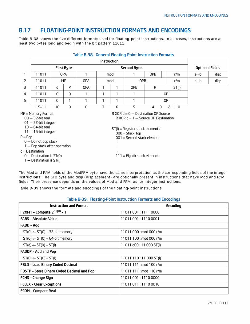
INSTRUCTION FORMATS AND ENCODINGS
B.17 FLOATING-POINT INSTRUCTION FORMATS AND ENCODINGSTable B-38 shows the five different formats used for floating-point instructions. In all cases, instructions are at least two bytes long and begin with the bit pattern 11011.
The Mod and R/M fields of the ModR/M byte have the same interpretation as the corresponding fields of the integer instructions. The SIB byte and disp (displacement) are optionally present in instructions that have Mod and R/M fields. Their presence depends on the values of Mod and R/M, as for integer instructions.
Table B-39 shows the formats and encodings of the floating-point instructions.
Table B-38. General Floating-Point Instruction Formats
Instruction
First Byte Second Byte Optional Fields
1 11011 OPA 1 mod 1 OPB r/m s-i-b disp
2 11011 MF OPA mod OPB r/m s-i-b disp
3 11011 d P OPA 1 1 OPB R ST(i)
4 11011 0 0 1 1 1 1 OP
5 11011 0 1 1 1 1 1 OP
15–11 10 9 8 7 6 5 4 3 2 1 0
MF = Memory Format00 — 32-bit real01 — 32-bit integer10 — 64-bit real11 — 16-bit integer
P = Pop0 — Do not pop stack1 — Pop stack after operation
d = Destination0 — Destination is ST(0)1 — Destination is ST(i)
R XOR d = 0 — Destination OP SourceR XOR d = 1 — Source OP Destination
ST(i) = Register stack element i000 = Stack Top001 = Second stack element ⋅ ⋅ ⋅111 = Eighth stack element
Table B-39. Floating-Point Instruction Formats and Encodings
Instruction and Format Encoding
F2XM1 – Compute 2ST(0) – 1 11011 001 : 1111 0000
FABS – Absolute Value 11011 001 : 1110 0001
FADD – Add
ST(0) ← ST(0) + 32-bit memory 11011 000 : mod 000 r/m
ST(0) ← ST(0) + 64-bit memory 11011 100 : mod 000 r/m
ST(d) ← ST(0) + ST(i) 11011 d00 : 11 000 ST(i)
FADDP – Add and Pop
ST(0) ← ST(0) + ST(i) 11011 110 : 11 000 ST(i)
FBLD – Load Binary Coded Decimal 11011 111 : mod 100 r/m
FBSTP – Store Binary Coded Decimal and Pop 11011 111 : mod 110 r/m
FCHS – Change Sign 11011 001 : 1110 0000
FCLEX – Clear Exceptions 11011 011 : 1110 0010
FCOM – Compare Real
Vol. 2C B-113
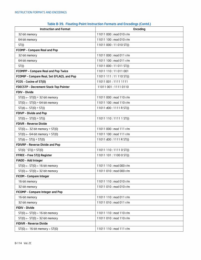
INSTRUCTION FORMATS AND ENCODINGS
32-bit memory 11011 000 : mod 010 r/m
64-bit memory 11011 100 : mod 010 r/m
ST(i) 11011 000 : 11 010 ST(i)
FCOMP – Compare Real and Pop
32-bit memory 11011 000 : mod 011 r/m
64-bit memory 11011 100 : mod 011 r/m
ST(i) 11011 000 : 11 011 ST(i)
FCOMPP – Compare Real and Pop Twice 11011 110 : 11 011 001
FCOMIP – Compare Real, Set EFLAGS, and Pop 11011 111 : 11 110 ST(i)
FCOS – Cosine of ST(0) 11011 001 : 1111 1111
FDECSTP – Decrement Stack-Top Pointer 11011 001 : 1111 0110
FDIV – Divide
ST(0) ← ST(0) ÷ 32-bit memory 11011 000 : mod 110 r/m
ST(0) ← ST(0) ÷ 64-bit memory 11011 100 : mod 110 r/m
ST(d) ← ST(0) ÷ ST(i) 11011 d00 : 1111 R ST(i)
FDIVP – Divide and Pop
ST(0) ← ST(0) ÷ ST(i) 11011 110 : 1111 1 ST(i)
FDIVR – Reverse Divide
ST(0) ← 32-bit memory ÷ ST(0) 11011 000 : mod 111 r/m
ST(0) ← 64-bit memory ÷ ST(0) 11011 100 : mod 111 r/m
ST(d) ← ST(i) ÷ ST(0) 11011 d00 : 1111 R ST(i)
FDIVRP – Reverse Divide and Pop
ST(0) ¨ ST(i) ÷ ST(0) 11011 110 : 1111 0 ST(i)
FFREE – Free ST(i) Register 11011 101 : 1100 0 ST(i)
FIADD – Add Integer
ST(0) ← ST(0) + 16-bit memory 11011 110 : mod 000 r/m
ST(0) ← ST(0) + 32-bit memory 11011 010 : mod 000 r/m
FICOM – Compare Integer
16-bit memory 11011 110 : mod 010 r/m
32-bit memory 11011 010 : mod 010 r/m
FICOMP – Compare Integer and Pop
16-bit memory 11011 110 : mod 011 r/m
32-bit memory 11011 010 : mod 011 r/m
FIDIV – Divide
ST(0) ← ST(0) ÷ 16-bit memory 11011 110 : mod 110 r/m
ST(0) ← ST(0) ÷ 32-bit memory 11011 010 : mod 110 r/m
FIDIVR – Reverse Divide
ST(0) ← 16-bit memory ÷ ST(0) 11011 110 : mod 111 r/m
Table B-39. Floating-Point Instruction Formats and Encodings (Contd.)
Instruction and Format Encoding
B-114 Vol. 2C
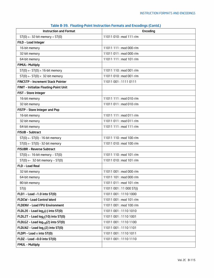
INSTRUCTION FORMATS AND ENCODINGS
ST(0) ← 32-bit memory ÷ ST(0) 11011 010 : mod 111 r/m
FILD – Load Integer
16-bit memory 11011 111 : mod 000 r/m
32-bit memory 11011 011 : mod 000 r/m
64-bit memory 11011 111 : mod 101 r/m
FIMUL– Multiply
ST(0) ← ST(0) × 16-bit memory 11011 110 : mod 001 r/m
ST(0) ← ST(0) × 32-bit memory 11011 010 : mod 001 r/m
FINCSTP – Increment Stack Pointer 11011 001 : 1111 0111
FINIT – Initialize Floating-Point Unit
FIST – Store Integer
16-bit memory 11011 111 : mod 010 r/m
32-bit memory 11011 011 : mod 010 r/m
FISTP – Store Integer and Pop
16-bit memory 11011 111 : mod 011 r/m
32-bit memory 11011 011 : mod 011 r/m
64-bit memory 11011 111 : mod 111 r/m
FISUB – Subtract
ST(0) ← ST(0) - 16-bit memory 11011 110 : mod 100 r/m
ST(0) ← ST(0) - 32-bit memory 11011 010 : mod 100 r/m
FISUBR – Reverse Subtract
ST(0) ← 16-bit memory − ST(0) 11011 110 : mod 101 r/m
ST(0) ← 32-bit memory − ST(0) 11011 010 : mod 101 r/m
FLD – Load Real
32-bit memory 11011 001 : mod 000 r/m
64-bit memory 11011 101 : mod 000 r/m
80-bit memory 11011 011 : mod 101 r/m
ST(i) 11011 001 : 11 000 ST(i)
FLD1 – Load +1.0 into ST(0) 11011 001 : 1110 1000
FLDCW – Load Control Word 11011 001 : mod 101 r/m
FLDENV – Load FPU Environment 11011 001 : mod 100 r/m
FLDL2E – Load log2(ε) into ST(0) 11011 001 : 1110 1010
FLDL2T – Load log2(10) into ST(0) 11011 001 : 1110 1001
FLDLG2 – Load log10(2) into ST(0) 11011 001 : 1110 1100
FLDLN2 – Load logε(2) into ST(0) 11011 001 : 1110 1101
FLDPI – Load π into ST(0) 11011 001 : 1110 1011
FLDZ – Load +0.0 into ST(0) 11011 001 : 1110 1110
FMUL – Multiply
Table B-39. Floating-Point Instruction Formats and Encodings (Contd.)
Instruction and Format Encoding
Vol. 2C B-115
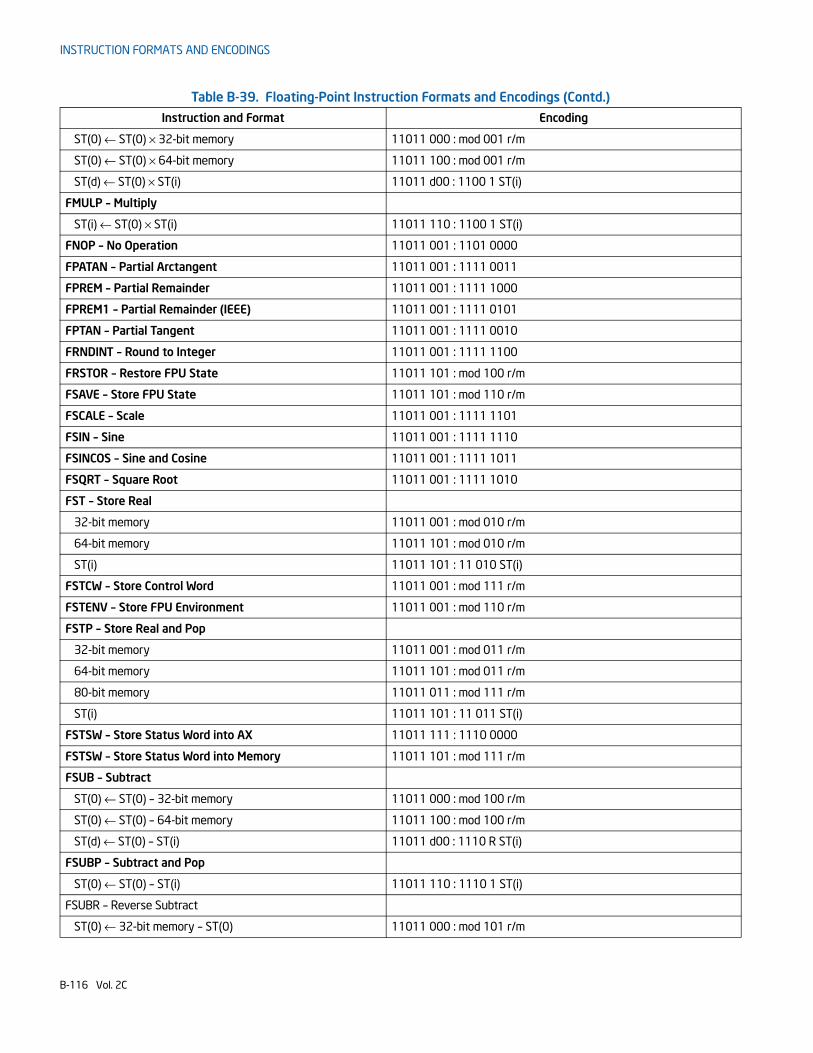
INSTRUCTION FORMATS AND ENCODINGS
ST(0) ← ST(0) × 32-bit memory 11011 000 : mod 001 r/m
ST(0) ← ST(0) × 64-bit memory 11011 100 : mod 001 r/m
ST(d) ← ST(0) × ST(i) 11011 d00 : 1100 1 ST(i)
FMULP – Multiply
ST(i) ← ST(0) × ST(i) 11011 110 : 1100 1 ST(i)
FNOP – No Operation 11011 001 : 1101 0000
FPATAN – Partial Arctangent 11011 001 : 1111 0011
FPREM – Partial Remainder 11011 001 : 1111 1000
FPREM1 – Partial Remainder (IEEE) 11011 001 : 1111 0101
FPTAN – Partial Tangent 11011 001 : 1111 0010
FRNDINT – Round to Integer 11011 001 : 1111 1100
FRSTOR – Restore FPU State 11011 101 : mod 100 r/m
FSAVE – Store FPU State 11011 101 : mod 110 r/m
FSCALE – Scale 11011 001 : 1111 1101
FSIN – Sine 11011 001 : 1111 1110
FSINCOS – Sine and Cosine 11011 001 : 1111 1011
FSQRT – Square Root 11011 001 : 1111 1010
FST – Store Real
32-bit memory 11011 001 : mod 010 r/m
64-bit memory 11011 101 : mod 010 r/m
ST(i) 11011 101 : 11 010 ST(i)
FSTCW – Store Control Word 11011 001 : mod 111 r/m
FSTENV – Store FPU Environment 11011 001 : mod 110 r/m
FSTP – Store Real and Pop
32-bit memory 11011 001 : mod 011 r/m
64-bit memory 11011 101 : mod 011 r/m
80-bit memory 11011 011 : mod 111 r/m
ST(i) 11011 101 : 11 011 ST(i)
FSTSW – Store Status Word into AX 11011 111 : 1110 0000
FSTSW – Store Status Word into Memory 11011 101 : mod 111 r/m
FSUB – Subtract
ST(0) ← ST(0) – 32-bit memory 11011 000 : mod 100 r/m
ST(0) ← ST(0) – 64-bit memory 11011 100 : mod 100 r/m
ST(d) ← ST(0) – ST(i) 11011 d00 : 1110 R ST(i)
FSUBP – Subtract and Pop
ST(0) ← ST(0) – ST(i) 11011 110 : 1110 1 ST(i)
FSUBR – Reverse Subtract
ST(0) ← 32-bit memory – ST(0) 11011 000 : mod 101 r/m
Table B-39. Floating-Point Instruction Formats and Encodings (Contd.)
Instruction and Format Encoding
B-116 Vol. 2C
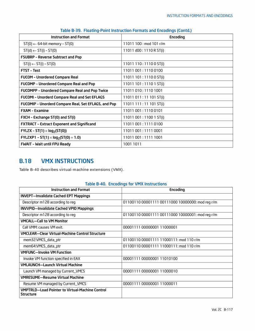
INSTRUCTION FORMATS AND ENCODINGS
B.18 VMX INSTRUCTIONSTable B-40 describes virtual-machine extensions (VMX).
ST(0) ← 64-bit memory – ST(0) 11011 100 : mod 101 r/m
ST(d) ← ST(i) – ST(0) 11011 d00 : 1110 R ST(i)
FSUBRP – Reverse Subtract and Pop
ST(i) ← ST(i) – ST(0) 11011 110 : 1110 0 ST(i)
FTST – Test 11011 001 : 1110 0100
FUCOM – Unordered Compare Real 11011 101 : 1110 0 ST(i)
FUCOMP – Unordered Compare Real and Pop 11011 101 : 1110 1 ST(i)
FUCOMPP – Unordered Compare Real and Pop Twice 11011 010 : 1110 1001
FUCOMI – Unorderd Compare Real and Set EFLAGS 11011 011 : 11 101 ST(i)
FUCOMIP – Unorderd Compare Real, Set EFLAGS, and Pop 11011 111 : 11 101 ST(i)
FXAM – Examine 11011 001 : 1110 0101
FXCH – Exchange ST(0) and ST(i) 11011 001 : 1100 1 ST(i)
FXTRACT – Extract Exponent and Significand 11011 001 : 1111 0100
FYL2X – ST(1) × log2(ST(0)) 11011 001 : 1111 0001
FYL2XP1 – ST(1) × log2(ST(0) + 1.0) 11011 001 : 1111 1001
FWAIT – Wait until FPU Ready 1001 1011
Table B-40. Encodings for VMX InstructionsInstruction and Format Encoding
INVEPT—Invalidate Cached EPT Mappings
Descriptor m128 according to reg 01100110 00001111 00111000 10000000: mod reg r/m
INVVPID—Invalidate Cached VPID Mappings
Descriptor m128 according to reg 01100110 00001111 00111000 10000001: mod reg r/m
VMCALL—Call to VM Monitor
Call VMM: causes VM exit. 00001111 00000001 11000001
VMCLEAR—Clear Virtual-Machine Control Structure
mem32:VMCS_data_ptr 01100110 00001111 11000111: mod 110 r/m
mem64:VMCS_data_ptr 01100110 00001111 11000111: mod 110 r/m
VMFUNC—Invoke VM Function
Invoke VM function specified in EAX 00001111 00000001 11010100
VMLAUNCH—Launch Virtual Machine
Launch VM managed by Current_VMCS 00001111 00000001 11000010
VMRESUME—Resume Virtual Machine
Resume VM managed by Current_VMCS 00001111 00000001 11000011
VMPTRLD—Load Pointer to Virtual-Machine Control Structure
Table B-39. Floating-Point Instruction Formats and Encodings (Contd.)
Instruction and Format Encoding
Vol. 2C B-117
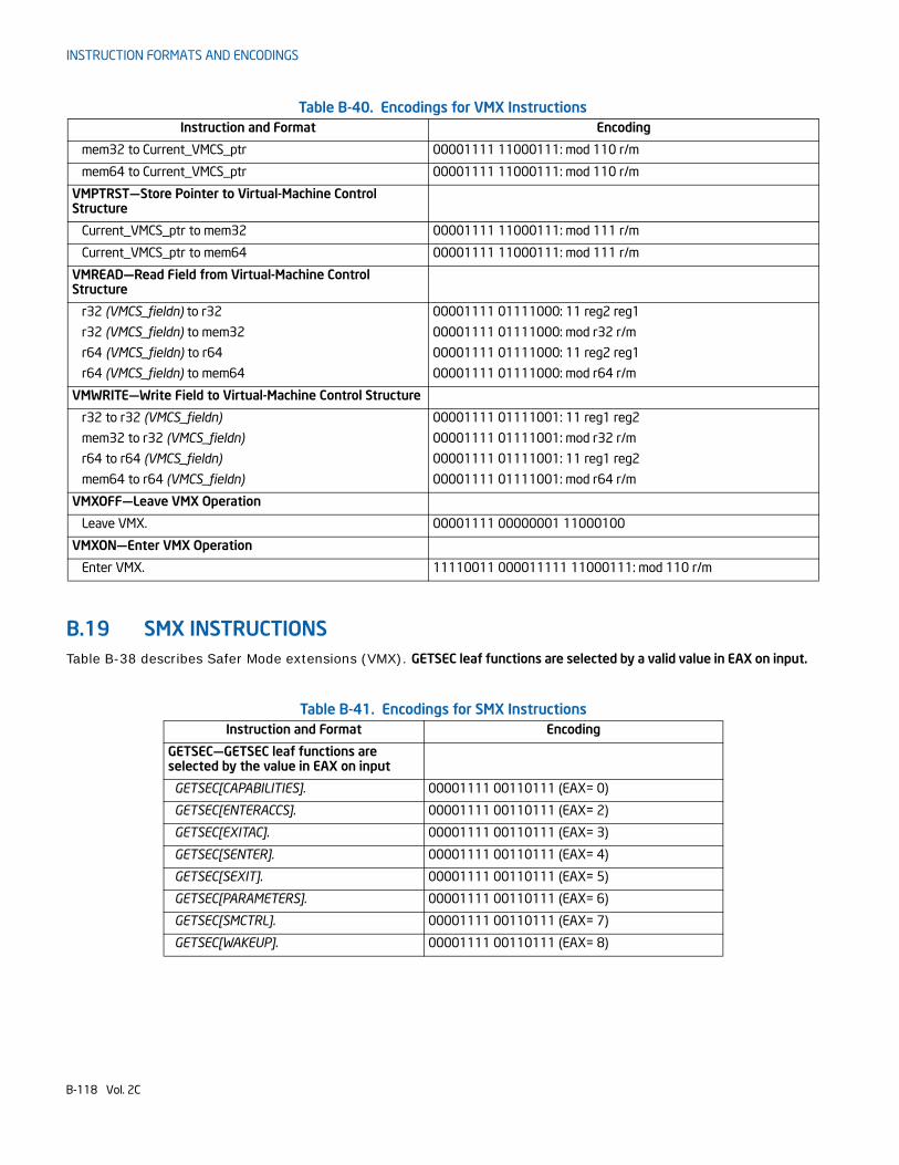
INSTRUCTION FORMATS AND ENCODINGS
B.19 SMX INSTRUCTIONSTable B-38 describes Safer Mode extensions (VMX). GETSEC leaf functions are selected by a valid value in EAX on input.
mem32 to Current_VMCS_ptr 00001111 11000111: mod 110 r/m
mem64 to Current_VMCS_ptr 00001111 11000111: mod 110 r/m
VMPTRST—Store Pointer to Virtual-Machine Control Structure
Current_VMCS_ptr to mem32 00001111 11000111: mod 111 r/m
Current_VMCS_ptr to mem64 00001111 11000111: mod 111 r/m
VMREAD—Read Field from Virtual-Machine Control Structure
r32 (VMCS_fieldn) to r32
r32 (VMCS_fieldn) to mem32
r64 (VMCS_fieldn) to r64
r64 (VMCS_fieldn) to mem64
00001111 01111000: 11 reg2 reg1
00001111 01111000: mod r32 r/m
00001111 01111000: 11 reg2 reg1
00001111 01111000: mod r64 r/m
VMWRITE—Write Field to Virtual-Machine Control Structure
r32 to r32 (VMCS_fieldn)
mem32 to r32 (VMCS_fieldn)
r64 to r64 (VMCS_fieldn)
mem64 to r64 (VMCS_fieldn)
00001111 01111001: 11 reg1 reg2
00001111 01111001: mod r32 r/m
00001111 01111001: 11 reg1 reg2
00001111 01111001: mod r64 r/m
VMXOFF—Leave VMX Operation
Leave VMX. 00001111 00000001 11000100
VMXON—Enter VMX Operation
Enter VMX. 11110011 000011111 11000111: mod 110 r/m
Table B-41. Encodings for SMX InstructionsInstruction and Format Encoding
GETSEC—GETSEC leaf functions are selected by the value in EAX on input
GETSEC[CAPABILITIES]. 00001111 00110111 (EAX= 0)
GETSEC[ENTERACCS]. 00001111 00110111 (EAX= 2)
GETSEC[EXITAC]. 00001111 00110111 (EAX= 3)
GETSEC[SENTER]. 00001111 00110111 (EAX= 4)
GETSEC[SEXIT]. 00001111 00110111 (EAX= 5)
GETSEC[PARAMETERS]. 00001111 00110111 (EAX= 6)
GETSEC[SMCTRL]. 00001111 00110111 (EAX= 7)
GETSEC[WAKEUP]. 00001111 00110111 (EAX= 8)
Table B-40. Encodings for VMX InstructionsInstruction and Format Encoding
B-118 Vol. 2C
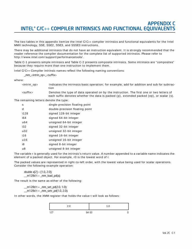
APPENDIX CINTEL® C/C++ COMPILER INTRINSICS AND FUNCTIONAL EQUIVALENTS
The two tables in this appendix itemize the Intel C/C++ compiler intrinsics and functional equivalents for the Intel MMX technology, SSE, SSE2, SSE3, and SSSE3 instructions.
There may be additional intrinsics that do not have an instruction equivalent. It is strongly recommended that the reader reference the compiler documentation for the complete list of supported intrinsics. Please refer to http://www.intel.com/support/performancetools/.
Table C-1 presents simple intrinsics and Table C-2 presents composite intrinsics. Some intrinsics are “composites” because they require more than one instruction to implement them.
Intel C/C++ Compiler intrinsic names reflect the following naming conventions:_mm_<intrin_op>_<suffix>
where:<intrin_op> Indicates the intrinsics basic operation; for example, add for addition and sub for subtrac-
tion<suffix> Denotes the type of data operated on by the instruction. The first one or two letters of
each suffix denotes whether the data is packed (p), extended packed (ep), or scalar (s). The remaining letters denote the type:
s single-precision floating pointd double-precision floating pointi128 signed 128-bit integeri64 signed 64-bit integeru64 unsigned 64-bit integeri32 signed 32-bit integeru32 unsigned 32-bit integeri16 signed 16-bit integeru16 unsigned 16-bit integeri8 signed 8-bit integeru8 unsigned 8-bit integer
The variable r is generally used for the intrinsic's return value. A number appended to a variable name indicates the element of a packed object. For example, r0 is the lowest word of r.
The packed values are represented in right-to-left order, with the lowest value being used for scalar operations. Consider the following example operation:
double a[2] = {1.0, 2.0};__m128d t = _mm_load_pd(a);
The result is the same as either of the following:
__m128d t = _mm_set_pd(2.0, 1.0);__m128d t = _mm_setr_pd(1.0, 2.0);
In other words, the XMM register that holds the value t will look as follows:
0127 64 63
2.0 1.0
Vol. 2C C-1
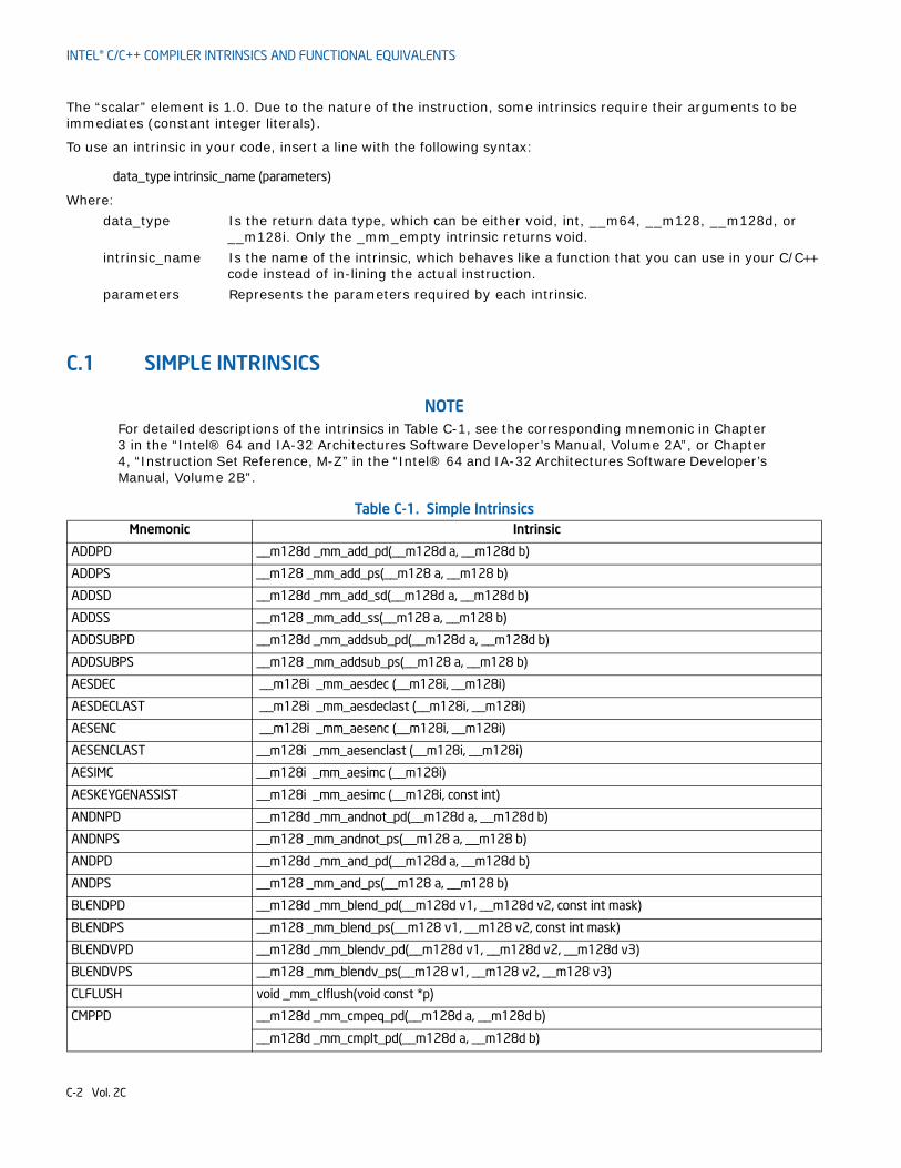
INTEL® C/C++ COMPILER INTRINSICS AND FUNCTIONAL EQUIVALENTS
The “scalar” element is 1.0. Due to the nature of the instruction, some intrinsics require their arguments to be immediates (constant integer literals).
To use an intrinsic in your code, insert a line with the following syntax:
data_type intrinsic_name (parameters)
Where:data_type Is the return data type, which can be either void, int, __m64, __m128, __m128d, or
__m128i. Only the _mm_empty intrinsic returns void.intrinsic_name Is the name of the intrinsic, which behaves like a function that you can use in your C/C++
code instead of in-lining the actual instruction.parameters Represents the parameters required by each intrinsic.
C.1 SIMPLE INTRINSICS
NOTEFor detailed descriptions of the intrinsics in Table C-1, see the corresponding mnemonic in Chapter 3 in the “Intel® 64 and IA-32 Architectures Software Developer’s Manual, Volume 2A”, or Chapter 4, “Instruction Set Reference, M-Z” in the “Intel® 64 and IA-32 Architectures Software Developer’s Manual, Volume 2B”.
Table C-1. Simple IntrinsicsMnemonic Intrinsic
ADDPD __m128d _mm_add_pd(__m128d a, __m128d b)
ADDPS __m128 _mm_add_ps(__m128 a, __m128 b)
ADDSD __m128d _mm_add_sd(__m128d a, __m128d b)
ADDSS __m128 _mm_add_ss(__m128 a, __m128 b)
ADDSUBPD __m128d _mm_addsub_pd(__m128d a, __m128d b)
ADDSUBPS __m128 _mm_addsub_ps(__m128 a, __m128 b)
AESDEC __m128i _mm_aesdec (__m128i, __m128i)
AESDECLAST __m128i _mm_aesdeclast (__m128i, __m128i)
AESENC __m128i _mm_aesenc (__m128i, __m128i)
AESENCLAST __m128i _mm_aesenclast (__m128i, __m128i)
AESIMC __m128i _mm_aesimc (__m128i)
AESKEYGENASSIST __m128i _mm_aesimc (__m128i, const int)
ANDNPD __m128d _mm_andnot_pd(__m128d a, __m128d b)
ANDNPS __m128 _mm_andnot_ps(__m128 a, __m128 b)
ANDPD __m128d _mm_and_pd(__m128d a, __m128d b)
ANDPS __m128 _mm_and_ps(__m128 a, __m128 b)
BLENDPD __m128d _mm_blend_pd(__m128d v1, __m128d v2, const int mask)
BLENDPS __m128 _mm_blend_ps(__m128 v1, __m128 v2, const int mask)
BLENDVPD __m128d _mm_blendv_pd(__m128d v1, __m128d v2, __m128d v3)
BLENDVPS __m128 _mm_blendv_ps(__m128 v1, __m128 v2, __m128 v3)
CLFLUSH void _mm_clflush(void const *p)
CMPPD __m128d _mm_cmpeq_pd(__m128d a, __m128d b)
__m128d _mm_cmplt_pd(__m128d a, __m128d b)
C-2 Vol. 2C
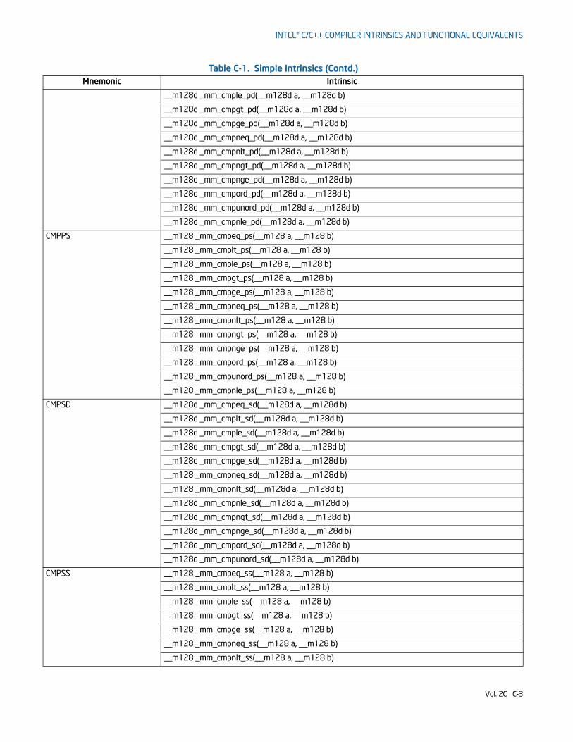
INTEL® C/C++ COMPILER INTRINSICS AND FUNCTIONAL EQUIVALENTS
__m128d _mm_cmple_pd(__m128d a, __m128d b)
__m128d _mm_cmpgt_pd(__m128d a, __m128d b)
__m128d _mm_cmpge_pd(__m128d a, __m128d b)
__m128d _mm_cmpneq_pd(__m128d a, __m128d b)
__m128d _mm_cmpnlt_pd(__m128d a, __m128d b)
__m128d _mm_cmpngt_pd(__m128d a, __m128d b)
__m128d _mm_cmpnge_pd(__m128d a, __m128d b)
__m128d _mm_cmpord_pd(__m128d a, __m128d b)
__m128d _mm_cmpunord_pd(__m128d a, __m128d b)
__m128d _mm_cmpnle_pd(__m128d a, __m128d b)
CMPPS __m128 _mm_cmpeq_ps(__m128 a, __m128 b)
__m128 _mm_cmplt_ps(__m128 a, __m128 b)
__m128 _mm_cmple_ps(__m128 a, __m128 b)
__m128 _mm_cmpgt_ps(__m128 a, __m128 b)
__m128 _mm_cmpge_ps(__m128 a, __m128 b)
__m128 _mm_cmpneq_ps(__m128 a, __m128 b)
__m128 _mm_cmpnlt_ps(__m128 a, __m128 b)
__m128 _mm_cmpngt_ps(__m128 a, __m128 b)
__m128 _mm_cmpnge_ps(__m128 a, __m128 b)
__m128 _mm_cmpord_ps(__m128 a, __m128 b)
__m128 _mm_cmpunord_ps(__m128 a, __m128 b)
__m128 _mm_cmpnle_ps(__m128 a, __m128 b)
CMPSD __m128d _mm_cmpeq_sd(__m128d a, __m128d b)
__m128d _mm_cmplt_sd(__m128d a, __m128d b)
__m128d _mm_cmple_sd(__m128d a, __m128d b)
__m128d _mm_cmpgt_sd(__m128d a, __m128d b)
__m128d _mm_cmpge_sd(__m128d a, __m128d b)
__m128 _mm_cmpneq_sd(__m128d a, __m128d b)
__m128 _mm_cmpnlt_sd(__m128d a, __m128d b)
__m128d _mm_cmpnle_sd(__m128d a, __m128d b)
__m128d _mm_cmpngt_sd(__m128d a, __m128d b)
__m128d _mm_cmpnge_sd(__m128d a, __m128d b)
__m128d _mm_cmpord_sd(__m128d a, __m128d b)
__m128d _mm_cmpunord_sd(__m128d a, __m128d b)
CMPSS __m128 _mm_cmpeq_ss(__m128 a, __m128 b)
__m128 _mm_cmplt_ss(__m128 a, __m128 b)
__m128 _mm_cmple_ss(__m128 a, __m128 b)
__m128 _mm_cmpgt_ss(__m128 a, __m128 b)
__m128 _mm_cmpge_ss(__m128 a, __m128 b)
__m128 _mm_cmpneq_ss(__m128 a, __m128 b)
__m128 _mm_cmpnlt_ss(__m128 a, __m128 b)
Table C-1. Simple Intrinsics (Contd.)Mnemonic Intrinsic
Vol. 2C C-3
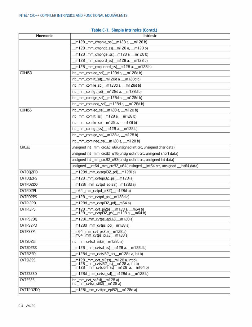
INTEL® C/C++ COMPILER INTRINSICS AND FUNCTIONAL EQUIVALENTS
__m128 _mm_cmpnle_ss(__m128 a, __m128 b)
__m128 _mm_cmpngt_ss(__m128 a, __m128 b)
__m128 _mm_cmpnge_ss(__m128 a, __m128 b)
__m128 _mm_cmpord_ss(__m128 a, __m128 b)
__m128 _mm_cmpunord_ss(__m128 a, __m128 b)
COMISD int _mm_comieq_sd(__m128d a, __m128d b)
int _mm_comilt_sd(__m128d a, __m128d b)
int _mm_comile_sd(__m128d a, __m128d b)
int _mm_comigt_sd(__m128d a, __m128d b)
int _mm_comige_sd(__m128d a, __m128d b)
int _mm_comineq_sd(__m128d a, __m128d b)
COMISS int _mm_comieq_ss(__m128 a, __m128 b)
int _mm_comilt_ss(__m128 a, __m128 b)
int _mm_comile_ss(__m128 a, __m128 b)
int _mm_comigt_ss(__m128 a, __m128 b)
int _mm_comige_ss(__m128 a, __m128 b)
int _mm_comineq_ss(__m128 a, __m128 b)
CRC32 unsigned int _mm_crc32_u8(unsigned int crc, unsigned char data)
unsigned int _mm_crc32_u16(unsigned int crc, unsigned short data)
unsigned int _mm_crc32_u32(unsigned int crc, unsigned int data)
unsigned __int64 _mm_crc32_u64(unsinged __int64 crc, unsigned __int64 data)
CVTDQ2PD __m128d _mm_cvtepi32_pd(__m128i a)
CVTDQ2PS __m128 _mm_cvtepi32_ps(__m128i a)
CVTPD2DQ __m128i _mm_cvtpd_epi32(__m128d a)
CVTPD2PI __m64 _mm_cvtpd_pi32(__m128d a)
CVTPD2PS __m128 _mm_cvtpd_ps(__m128d a)
CVTPI2PD __m128d _mm_cvtpi32_pd(__m64 a)
CVTPI2PS __m128 _mm_cvt_pi2ps(__m128 a, __m64 b)__m128 _mm_cvtpi32_ps(__m128 a, __m64 b)
CVTPS2DQ __m128i _mm_cvtps_epi32(__m128 a)
CVTPS2PD __m128d _mm_cvtps_pd(__m128 a)
CVTPS2PI __m64 _mm_cvt_ps2pi(__m128 a)__m64 _mm_cvtps_pi32(__m128 a)
CVTSD2SI int _mm_cvtsd_si32(__m128d a)
CVTSD2SS __m128 _mm_cvtsd_ss(__m128 a, __m128d b)
CVTSI2SD __m128d _mm_cvtsi32_sd(__m128d a, int b)
CVTSI2SS __m128 _mm_cvt_si2ss(__m128 a, int b)__m128 _mm_cvtsi32_ss(__m128 a, int b)__m128 _mm_cvtsi64_ss(__m128 a, __int64 b)
CVTSS2SD __m128d _mm_cvtss_sd(__m128d a, __m128 b)
CVTSS2SI int _mm_cvt_ss2si(__m128 a)int _mm_cvtss_si32(__m128 a)
CVTTPD2DQ __m128i _mm_cvttpd_epi32(__m128d a)
Table C-1. Simple Intrinsics (Contd.)Mnemonic Intrinsic
C-4 Vol. 2C
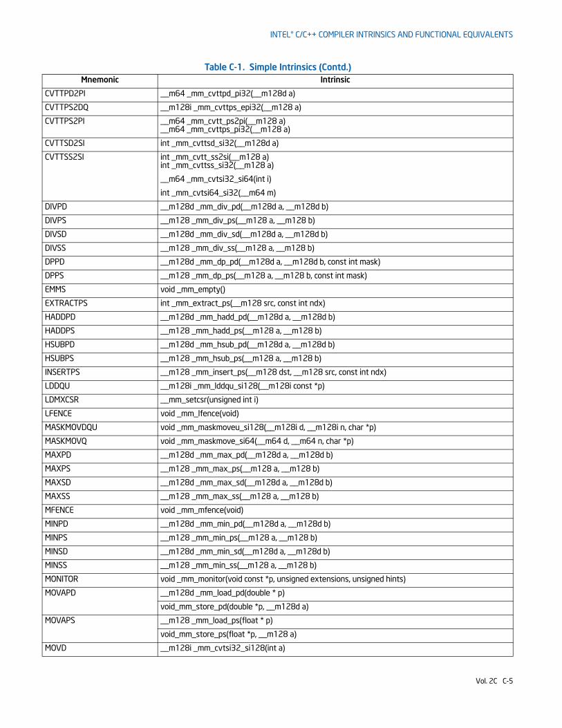
INTEL® C/C++ COMPILER INTRINSICS AND FUNCTIONAL EQUIVALENTS
CVTTPD2PI __m64 _mm_cvttpd_pi32(__m128d a)
CVTTPS2DQ __m128i _mm_cvttps_epi32(__m128 a)
CVTTPS2PI __m64 _mm_cvtt_ps2pi(__m128 a)__m64 _mm_cvttps_pi32(__m128 a)
CVTTSD2SI int _mm_cvttsd_si32(__m128d a)
CVTTSS2SI int _mm_cvtt_ss2si(__m128 a)int _mm_cvttss_si32(__m128 a)
__m64 _mm_cvtsi32_si64(int i)
int _mm_cvtsi64_si32(__m64 m)
DIVPD __m128d _mm_div_pd(__m128d a, __m128d b)
DIVPS __m128 _mm_div_ps(__m128 a, __m128 b)
DIVSD __m128d _mm_div_sd(__m128d a, __m128d b)
DIVSS __m128 _mm_div_ss(__m128 a, __m128 b)
DPPD __m128d _mm_dp_pd(__m128d a, __m128d b, const int mask)
DPPS __m128 _mm_dp_ps(__m128 a, __m128 b, const int mask)
EMMS void _mm_empty()
EXTRACTPS int _mm_extract_ps(__m128 src, const int ndx)
HADDPD __m128d _mm_hadd_pd(__m128d a, __m128d b)
HADDPS __m128 _mm_hadd_ps(__m128 a, __m128 b)
HSUBPD __m128d _mm_hsub_pd(__m128d a, __m128d b)
HSUBPS __m128 _mm_hsub_ps(__m128 a, __m128 b)
INSERTPS __m128 _mm_insert_ps(__m128 dst, __m128 src, const int ndx)
LDDQU __m128i _mm_lddqu_si128(__m128i const *p)
LDMXCSR __mm_setcsr(unsigned int i)
LFENCE void _mm_lfence(void)
MASKMOVDQU void _mm_maskmoveu_si128(__m128i d, __m128i n, char *p)
MASKMOVQ void _mm_maskmove_si64(__m64 d, __m64 n, char *p)
MAXPD __m128d _mm_max_pd(__m128d a, __m128d b)
MAXPS __m128 _mm_max_ps(__m128 a, __m128 b)
MAXSD __m128d _mm_max_sd(__m128d a, __m128d b)
MAXSS __m128 _mm_max_ss(__m128 a, __m128 b)
MFENCE void _mm_mfence(void)
MINPD __m128d _mm_min_pd(__m128d a, __m128d b)
MINPS __m128 _mm_min_ps(__m128 a, __m128 b)
MINSD __m128d _mm_min_sd(__m128d a, __m128d b)
MINSS __m128 _mm_min_ss(__m128 a, __m128 b)
MONITOR void _mm_monitor(void const *p, unsigned extensions, unsigned hints)
MOVAPD __m128d _mm_load_pd(double * p)
void_mm_store_pd(double *p, __m128d a)
MOVAPS __m128 _mm_load_ps(float * p)
void_mm_store_ps(float *p, __m128 a)
MOVD __m128i _mm_cvtsi32_si128(int a)
Table C-1. Simple Intrinsics (Contd.)Mnemonic Intrinsic
Vol. 2C C-5

INTEL® C/C++ COMPILER INTRINSICS AND FUNCTIONAL EQUIVALENTS
int _mm_cvtsi128_si32(__m128i a)
__m64 _mm_cvtsi32_si64(int a)
int _mm_cvtsi64_si32(__m64 a)
MOVDDUP __m128d _mm_movedup_pd(__m128d a)
__m128d _mm_loaddup_pd(double const * dp)
MOVDQA __m128i _mm_load_si128(__m128i * p)
void_mm_store_si128(__m128i *p, __m128i a)
MOVDQU __m128i _mm_loadu_si128(__m128i * p)
void_mm_storeu_si128(__m128i *p, __m128i a)
MOVDQ2Q __m64 _mm_movepi64_pi64(__m128i a)
MOVHLPS __m128 _mm_movehl_ps(__m128 a, __m128 b)
MOVHPD __m128d _mm_loadh_pd(__m128d a, double * p)
void _mm_storeh_pd(double * p, __m128d a)
MOVHPS __m128 _mm_loadh_pi(__m128 a, __m64 * p)
void _mm_storeh_pi(__m64 * p, __m128 a)
MOVLPD __m128d _mm_loadl_pd(__m128d a, double * p)
void _mm_storel_pd(double * p, __m128d a)
MOVLPS __m128 _mm_loadl_pi(__m128 a, __m64 *p)
void_mm_storel_pi(__m64 * p, __m128 a)
MOVLHPS __m128 _mm_movelh_ps(__m128 a, __m128 b)
MOVMSKPD int _mm_movemask_pd(__m128d a)
MOVMSKPS int _mm_movemask_ps(__m128 a)
MOVNTDQA __m128i _mm_stream_load_si128(__m128i *p)
MOVNTDQ void_mm_stream_si128(__m128i * p, __m128i a)
MOVNTPD void_mm_stream_pd(double * p, __m128d a)
MOVNTPS void_mm_stream_ps(float * p, __m128 a)
MOVNTI void_mm_stream_si32(int * p, int a)
MOVNTQ void_mm_stream_pi(__m64 * p, __m64 a)
MOVQ __m128i _mm_loadl_epi64(__m128i * p)
void_mm_storel_epi64(_m128i * p, __m128i a)
__m128i _mm_move_epi64(__m128i a)
MOVQ2DQ __m128i _mm_movpi64_epi64(__m64 a)
MOVSD __m128d _mm_load_sd(double * p)
void_mm_store_sd(double * p, __m128d a)
__m128d _mm_move_sd(__m128d a, __m128d b)
MOVSHDUP __m128 _mm_movehdup_ps(__m128 a)
MOVSLDUP __m128 _mm_moveldup_ps(__m128 a)
MOVSS __m128 _mm_load_ss(float * p)
void_mm_store_ss(float * p, __m128 a)
__m128 _mm_move_ss(__m128 a, __m128 b)
MOVUPD __m128d _mm_loadu_pd(double * p)
Table C-1. Simple Intrinsics (Contd.)Mnemonic Intrinsic
C-6 Vol. 2C
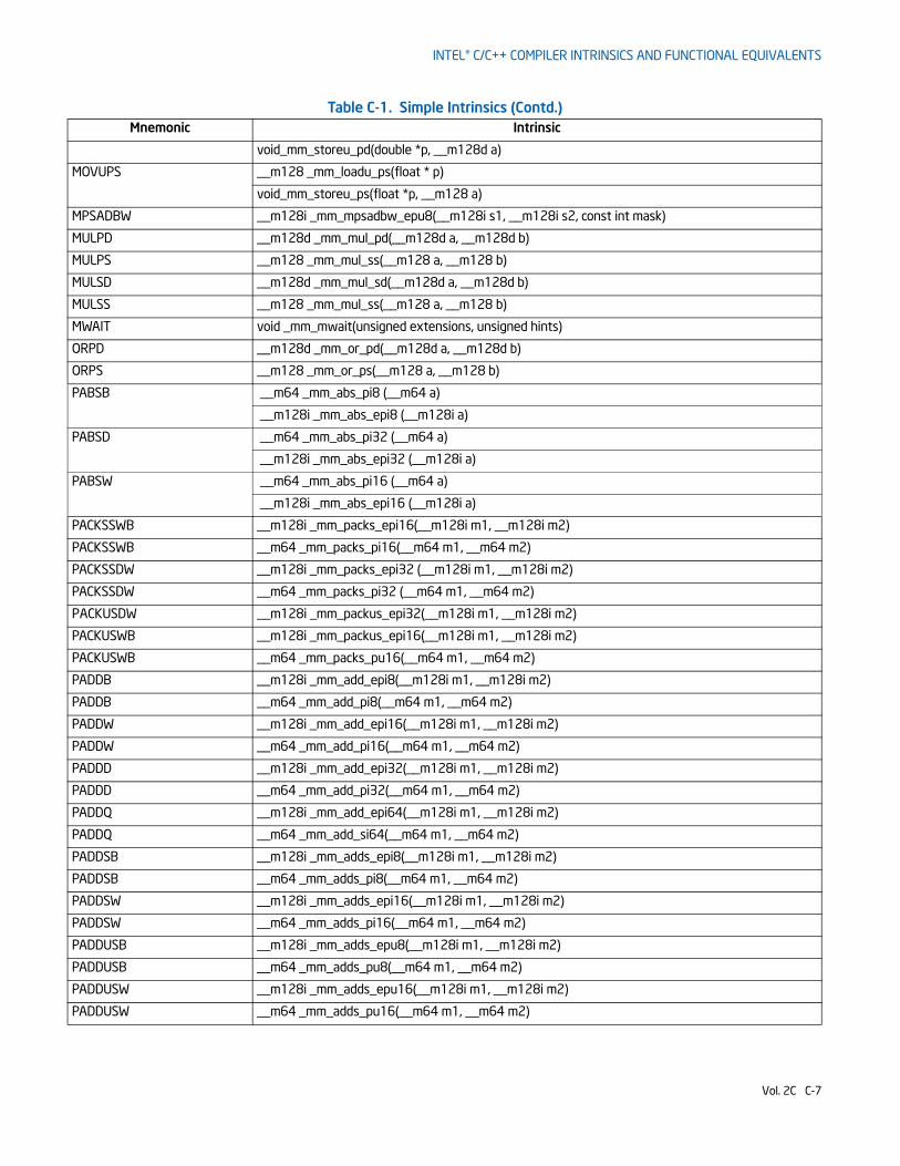
INTEL® C/C++ COMPILER INTRINSICS AND FUNCTIONAL EQUIVALENTS
void_mm_storeu_pd(double *p, __m128d a)
MOVUPS __m128 _mm_loadu_ps(float * p)
void_mm_storeu_ps(float *p, __m128 a)
MPSADBW __m128i _mm_mpsadbw_epu8(__m128i s1, __m128i s2, const int mask)
MULPD __m128d _mm_mul_pd(__m128d a, __m128d b)
MULPS __m128 _mm_mul_ss(__m128 a, __m128 b)
MULSD __m128d _mm_mul_sd(__m128d a, __m128d b)
MULSS __m128 _mm_mul_ss(__m128 a, __m128 b)
MWAIT void _mm_mwait(unsigned extensions, unsigned hints)
ORPD __m128d _mm_or_pd(__m128d a, __m128d b)
ORPS __m128 _mm_or_ps(__m128 a, __m128 b)
PABSB __m64 _mm_abs_pi8 (__m64 a)
__m128i _mm_abs_epi8 (__m128i a)
PABSD __m64 _mm_abs_pi32 (__m64 a)
__m128i _mm_abs_epi32 (__m128i a)
PABSW __m64 _mm_abs_pi16 (__m64 a)
__m128i _mm_abs_epi16 (__m128i a)
PACKSSWB __m128i _mm_packs_epi16(__m128i m1, __m128i m2)
PACKSSWB __m64 _mm_packs_pi16(__m64 m1, __m64 m2)
PACKSSDW __m128i _mm_packs_epi32 (__m128i m1, __m128i m2)
PACKSSDW __m64 _mm_packs_pi32 (__m64 m1, __m64 m2)
PACKUSDW __m128i _mm_packus_epi32(__m128i m1, __m128i m2)
PACKUSWB __m128i _mm_packus_epi16(__m128i m1, __m128i m2)
PACKUSWB __m64 _mm_packs_pu16(__m64 m1, __m64 m2)
PADDB __m128i _mm_add_epi8(__m128i m1, __m128i m2)
PADDB __m64 _mm_add_pi8(__m64 m1, __m64 m2)
PADDW __m128i _mm_add_epi16(__m128i m1, __m128i m2)
PADDW __m64 _mm_add_pi16(__m64 m1, __m64 m2)
PADDD __m128i _mm_add_epi32(__m128i m1, __m128i m2)
PADDD __m64 _mm_add_pi32(__m64 m1, __m64 m2)
PADDQ __m128i _mm_add_epi64(__m128i m1, __m128i m2)
PADDQ __m64 _mm_add_si64(__m64 m1, __m64 m2)
PADDSB __m128i _mm_adds_epi8(__m128i m1, __m128i m2)
PADDSB __m64 _mm_adds_pi8(__m64 m1, __m64 m2)
PADDSW __m128i _mm_adds_epi16(__m128i m1, __m128i m2)
PADDSW __m64 _mm_adds_pi16(__m64 m1, __m64 m2)
PADDUSB __m128i _mm_adds_epu8(__m128i m1, __m128i m2)
PADDUSB __m64 _mm_adds_pu8(__m64 m1, __m64 m2)
PADDUSW __m128i _mm_adds_epu16(__m128i m1, __m128i m2)
PADDUSW __m64 _mm_adds_pu16(__m64 m1, __m64 m2)
Table C-1. Simple Intrinsics (Contd.)Mnemonic Intrinsic
Vol. 2C C-7
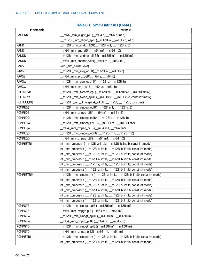
INTEL® C/C++ COMPILER INTRINSICS AND FUNCTIONAL EQUIVALENTS
PALIGNR __m64 _mm_alignr_pi8 (__m64 a, __m64 b, int n)
__m128i _mm_alignr_epi8 (__m128i a, __m128i b, int n)
PAND __m128i _mm_and_si128(__m128i m1, __m128i m2)
PAND __m64 _mm_and_si64(__m64 m1, __m64 m2)
PANDN __m128i _mm_andnot_si128(__m128i m1, __m128i m2)
PANDN __m64 _mm_andnot_si64(__m64 m1, __m64 m2)
PAUSE void _mm_pause(void)
PAVGB __m128i _mm_avg_epu8(__m128i a, __m128i b)
PAVGB __m64 _mm_avg_pu8(__m64 a, __m64 b)
PAVGW __m128i _mm_avg_epu16(__m128i a, __m128i b)
PAVGW __m64 _mm_avg_pu16(__m64 a, __m64 b)
PBLENDVB __m128i _mm_blendv_epi (__m128i v1, __m128i v2, __m128i mask)
PBLENDW __m128i _mm_blend_epi16(__m128i v1, __m128i v2, const int mask)
PCLMULQDQ __m128i _mm_clmulepi64_si128 (__m128i, __m128i, const int)
PCMPEQB __m128i _mm_cmpeq_epi8(__m128i m1, __m128i m2)
PCMPEQB __m64 _mm_cmpeq_pi8(__m64 m1, __m64 m2)
PCMPEQQ __m128i _mm_cmpeq_epi64(__m128i a, __m128i b)
PCMPEQW __m128i _mm_cmpeq_epi16 (__m128i m1, __m128i m2)
PCMPEQW __m64 _mm_cmpeq_pi16 (__m64 m1, __m64 m2)
PCMPEQD __m128i _mm_cmpeq_epi32(__m128i m1, __m128i m2)
PCMPEQD __m64 _mm_cmpeq_pi32(__m64 m1, __m64 m2)
PCMPESTRI int _mm_cmpestri (__m128i a, int la, __m128i b, int lb, const int mode)
int _mm_cmpestra (__m128i a, int la, __m128i b, int lb, const int mode)
int _mm_cmpestrc (__m128i a, int la, __m128i b, int lb, const int mode)
int _mm_cmpestro (__m128i a, int la, __m128i b, int lb, const int mode)
int _mm_cmpestrs (__m128i a, int la, __m128i b, int lb, const int mode)
int _mm_cmpestrz (__m128i a, int la, __m128i b, int lb, const int mode)
PCMPESTRM __m128i _mm_cmpestrm (__m128i a, int la, __m128i b, int lb, const int mode)
int _mm_cmpestra (__m128i a, int la, __m128i b, int lb, const int mode)
int _mm_cmpestrc (__m128i a, int la, __m128i b, int lb, const int mode)
int _mm_cmpestro (__m128i a, int la, __m128i b, int lb, const int mode)
int _mm_cmpestrs (__m128i a, int la, __m128i b, int lb, const int mode)
int _mm_cmpestrz (__m128i a, int la, __m128i b, int lb, const int mode)
PCMPGTB __m128i _mm_cmpgt_epi8 (__m128i m1, __m128i m2)
PCMPGTB __m64 _mm_cmpgt_pi8 (__m64 m1, __m64 m2)
PCMPGTW __m128i _mm_cmpgt_epi16(__m128i m1, __m128i m2)
PCMPGTW __m64 _mm_cmpgt_pi16 (__m64 m1, __m64 m2)
PCMPGTD __m128i _mm_cmpgt_epi32(__m128i m1, __m128i m2)
PCMPGTD __m64 _mm_cmpgt_pi32(__m64 m1, __m64 m2)
PCMPISTRI __m128i _mm_cmpestrm (__m128i a, int la, __m128i b, int lb, const int mode)
int _mm_cmpestra (__m128i a, int la, __m128i b, int lb, const int mode)
Table C-1. Simple Intrinsics (Contd.)Mnemonic Intrinsic
C-8 Vol. 2C
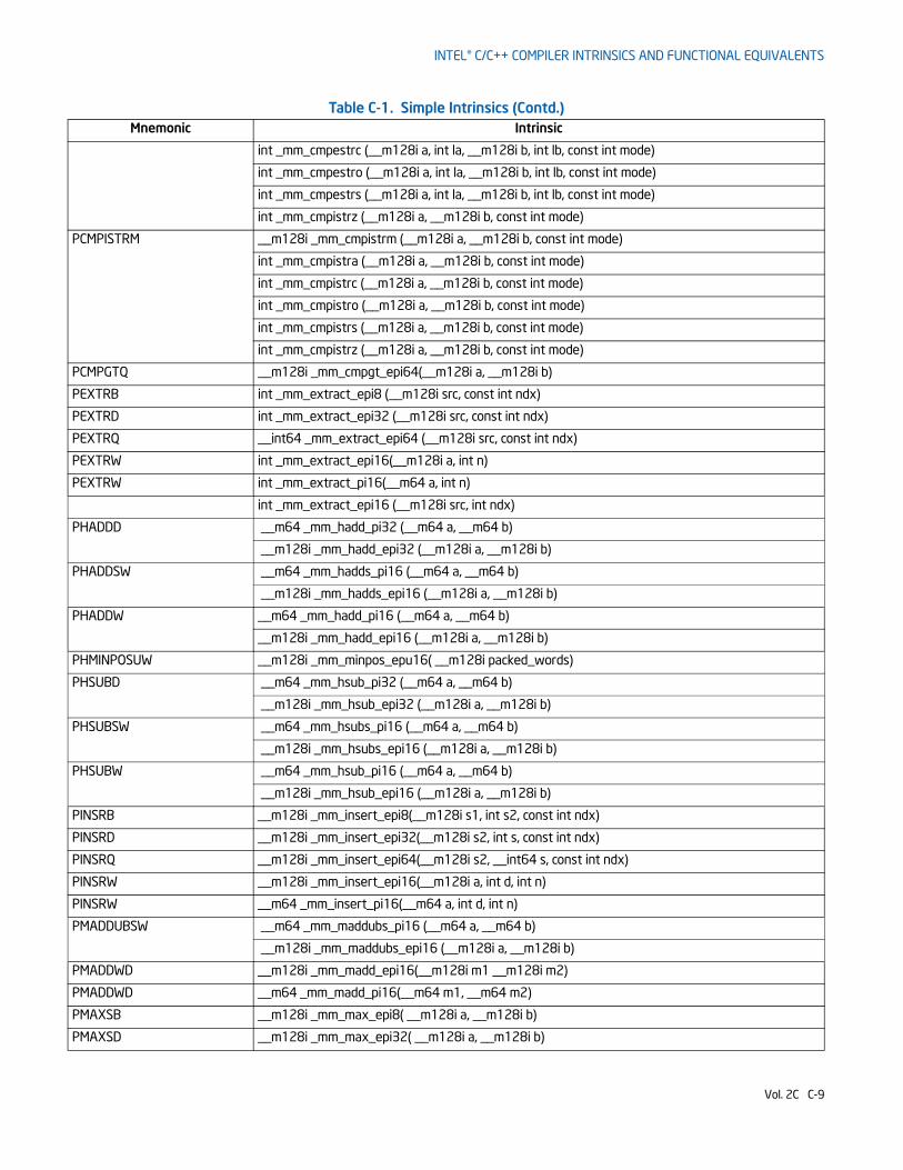
INTEL® C/C++ COMPILER INTRINSICS AND FUNCTIONAL EQUIVALENTS
int _mm_cmpestrc (__m128i a, int la, __m128i b, int lb, const int mode)
int _mm_cmpestro (__m128i a, int la, __m128i b, int lb, const int mode)
int _mm_cmpestrs (__m128i a, int la, __m128i b, int lb, const int mode)
int _mm_cmpistrz (__m128i a, __m128i b, const int mode)
PCMPISTRM __m128i _mm_cmpistrm (__m128i a, __m128i b, const int mode)
int _mm_cmpistra (__m128i a, __m128i b, const int mode)
int _mm_cmpistrc (__m128i a, __m128i b, const int mode)
int _mm_cmpistro (__m128i a, __m128i b, const int mode)
int _mm_cmpistrs (__m128i a, __m128i b, const int mode)
int _mm_cmpistrz (__m128i a, __m128i b, const int mode)
PCMPGTQ __m128i _mm_cmpgt_epi64(__m128i a, __m128i b)
PEXTRB int _mm_extract_epi8 (__m128i src, const int ndx)
PEXTRD int _mm_extract_epi32 (__m128i src, const int ndx)
PEXTRQ __int64 _mm_extract_epi64 (__m128i src, const int ndx)
PEXTRW int _mm_extract_epi16(__m128i a, int n)
PEXTRW int _mm_extract_pi16(__m64 a, int n)
int _mm_extract_epi16 (__m128i src, int ndx)
PHADDD __m64 _mm_hadd_pi32 (__m64 a, __m64 b)
__m128i _mm_hadd_epi32 (__m128i a, __m128i b)
PHADDSW __m64 _mm_hadds_pi16 (__m64 a, __m64 b)
__m128i _mm_hadds_epi16 (__m128i a, __m128i b)
PHADDW __m64 _mm_hadd_pi16 (__m64 a, __m64 b)
__m128i _mm_hadd_epi16 (__m128i a, __m128i b)
PHMINPOSUW __m128i _mm_minpos_epu16( __m128i packed_words)
PHSUBD __m64 _mm_hsub_pi32 (__m64 a, __m64 b)
__m128i _mm_hsub_epi32 (__m128i a, __m128i b)
PHSUBSW __m64 _mm_hsubs_pi16 (__m64 a, __m64 b)
__m128i _mm_hsubs_epi16 (__m128i a, __m128i b)
PHSUBW __m64 _mm_hsub_pi16 (__m64 a, __m64 b)
__m128i _mm_hsub_epi16 (__m128i a, __m128i b)
PINSRB __m128i _mm_insert_epi8(__m128i s1, int s2, const int ndx)
PINSRD __m128i _mm_insert_epi32(__m128i s2, int s, const int ndx)
PINSRQ __m128i _mm_insert_epi64(__m128i s2, __int64 s, const int ndx)
PINSRW __m128i _mm_insert_epi16(__m128i a, int d, int n)
PINSRW __m64 _mm_insert_pi16(__m64 a, int d, int n)
PMADDUBSW __m64 _mm_maddubs_pi16 (__m64 a, __m64 b)
__m128i _mm_maddubs_epi16 (__m128i a, __m128i b)
PMADDWD __m128i _mm_madd_epi16(__m128i m1 __m128i m2)
PMADDWD __m64 _mm_madd_pi16(__m64 m1, __m64 m2)
PMAXSB __m128i _mm_max_epi8( __m128i a, __m128i b)
PMAXSD __m128i _mm_max_epi32( __m128i a, __m128i b)
Table C-1. Simple Intrinsics (Contd.)Mnemonic Intrinsic
Vol. 2C C-9
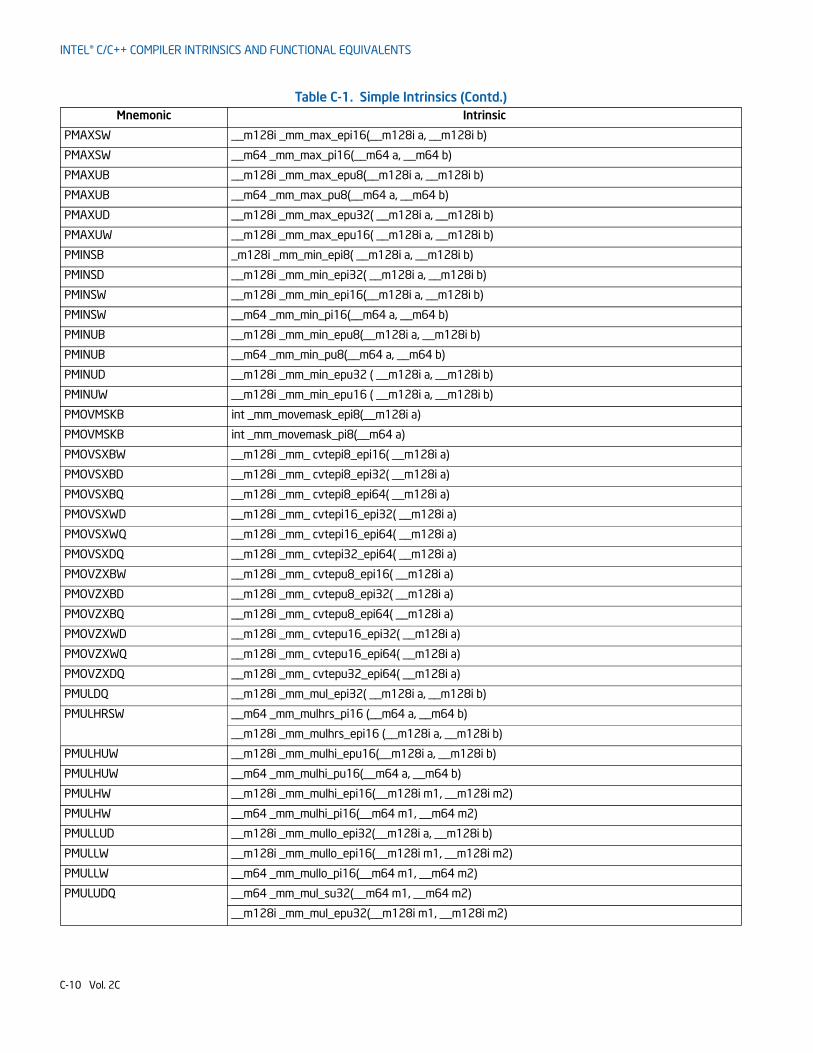
INTEL® C/C++ COMPILER INTRINSICS AND FUNCTIONAL EQUIVALENTS
PMAXSW __m128i _mm_max_epi16(__m128i a, __m128i b)
PMAXSW __m64 _mm_max_pi16(__m64 a, __m64 b)
PMAXUB __m128i _mm_max_epu8(__m128i a, __m128i b)
PMAXUB __m64 _mm_max_pu8(__m64 a, __m64 b)
PMAXUD __m128i _mm_max_epu32( __m128i a, __m128i b)
PMAXUW __m128i _mm_max_epu16( __m128i a, __m128i b)
PMINSB _m128i _mm_min_epi8( __m128i a, __m128i b)
PMINSD __m128i _mm_min_epi32( __m128i a, __m128i b)
PMINSW __m128i _mm_min_epi16(__m128i a, __m128i b)
PMINSW __m64 _mm_min_pi16(__m64 a, __m64 b)
PMINUB __m128i _mm_min_epu8(__m128i a, __m128i b)
PMINUB __m64 _mm_min_pu8(__m64 a, __m64 b)
PMINUD __m128i _mm_min_epu32 ( __m128i a, __m128i b)
PMINUW __m128i _mm_min_epu16 ( __m128i a, __m128i b)
PMOVMSKB int _mm_movemask_epi8(__m128i a)
PMOVMSKB int _mm_movemask_pi8(__m64 a)
PMOVSXBW __m128i _mm_ cvtepi8_epi16( __m128i a)
PMOVSXBD __m128i _mm_ cvtepi8_epi32( __m128i a)
PMOVSXBQ __m128i _mm_ cvtepi8_epi64( __m128i a)
PMOVSXWD __m128i _mm_ cvtepi16_epi32( __m128i a)
PMOVSXWQ __m128i _mm_ cvtepi16_epi64( __m128i a)
PMOVSXDQ __m128i _mm_ cvtepi32_epi64( __m128i a)
PMOVZXBW __m128i _mm_ cvtepu8_epi16( __m128i a)
PMOVZXBD __m128i _mm_ cvtepu8_epi32( __m128i a)
PMOVZXBQ __m128i _mm_ cvtepu8_epi64( __m128i a)
PMOVZXWD __m128i _mm_ cvtepu16_epi32( __m128i a)
PMOVZXWQ __m128i _mm_ cvtepu16_epi64( __m128i a)
PMOVZXDQ __m128i _mm_ cvtepu32_epi64( __m128i a)
PMULDQ __m128i _mm_mul_epi32( __m128i a, __m128i b)
PMULHRSW __m64 _mm_mulhrs_pi16 (__m64 a, __m64 b)
__m128i _mm_mulhrs_epi16 (__m128i a, __m128i b)
PMULHUW __m128i _mm_mulhi_epu16(__m128i a, __m128i b)
PMULHUW __m64 _mm_mulhi_pu16(__m64 a, __m64 b)
PMULHW __m128i _mm_mulhi_epi16(__m128i m1, __m128i m2)
PMULHW __m64 _mm_mulhi_pi16(__m64 m1, __m64 m2)
PMULLUD __m128i _mm_mullo_epi32(__m128i a, __m128i b)
PMULLW __m128i _mm_mullo_epi16(__m128i m1, __m128i m2)
PMULLW __m64 _mm_mullo_pi16(__m64 m1, __m64 m2)
PMULUDQ __m64 _mm_mul_su32(__m64 m1, __m64 m2)
__m128i _mm_mul_epu32(__m128i m1, __m128i m2)
Table C-1. Simple Intrinsics (Contd.)Mnemonic Intrinsic
C-10 Vol. 2C
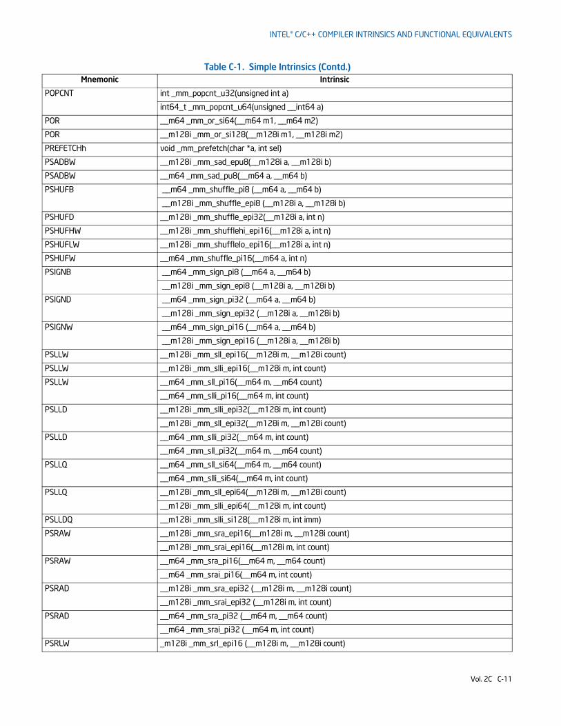
INTEL® C/C++ COMPILER INTRINSICS AND FUNCTIONAL EQUIVALENTS
POPCNT int _mm_popcnt_u32(unsigned int a)
int64_t _mm_popcnt_u64(unsigned __int64 a)
POR __m64 _mm_or_si64(__m64 m1, __m64 m2)
POR __m128i _mm_or_si128(__m128i m1, __m128i m2)
PREFETCHh void _mm_prefetch(char *a, int sel)
PSADBW __m128i _mm_sad_epu8(__m128i a, __m128i b)
PSADBW __m64 _mm_sad_pu8(__m64 a, __m64 b)
PSHUFB __m64 _mm_shuffle_pi8 (__m64 a, __m64 b)
__m128i _mm_shuffle_epi8 (__m128i a, __m128i b)
PSHUFD __m128i _mm_shuffle_epi32(__m128i a, int n)
PSHUFHW __m128i _mm_shufflehi_epi16(__m128i a, int n)
PSHUFLW __m128i _mm_shufflelo_epi16(__m128i a, int n)
PSHUFW __m64 _mm_shuffle_pi16(__m64 a, int n)
PSIGNB __m64 _mm_sign_pi8 (__m64 a, __m64 b)
__m128i _mm_sign_epi8 (__m128i a, __m128i b)
PSIGND __m64 _mm_sign_pi32 (__m64 a, __m64 b)
__m128i _mm_sign_epi32 (__m128i a, __m128i b)
PSIGNW __m64 _mm_sign_pi16 (__m64 a, __m64 b)
__m128i _mm_sign_epi16 (__m128i a, __m128i b)
PSLLW __m128i _mm_sll_epi16(__m128i m, __m128i count)
PSLLW __m128i _mm_slli_epi16(__m128i m, int count)
PSLLW __m64 _mm_sll_pi16(__m64 m, __m64 count)
__m64 _mm_slli_pi16(__m64 m, int count)
PSLLD __m128i _mm_slli_epi32(__m128i m, int count)
__m128i _mm_sll_epi32(__m128i m, __m128i count)
PSLLD __m64 _mm_slli_pi32(__m64 m, int count)
__m64 _mm_sll_pi32(__m64 m, __m64 count)
PSLLQ __m64 _mm_sll_si64(__m64 m, __m64 count)
__m64 _mm_slli_si64(__m64 m, int count)
PSLLQ __m128i _mm_sll_epi64(__m128i m, __m128i count)
__m128i _mm_slli_epi64(__m128i m, int count)
PSLLDQ __m128i _mm_slli_si128(__m128i m, int imm)
PSRAW __m128i _mm_sra_epi16(__m128i m, __m128i count)
__m128i _mm_srai_epi16(__m128i m, int count)
PSRAW __m64 _mm_sra_pi16(__m64 m, __m64 count)
__m64 _mm_srai_pi16(__m64 m, int count)
PSRAD __m128i _mm_sra_epi32 (__m128i m, __m128i count)
__m128i _mm_srai_epi32 (__m128i m, int count)
PSRAD __m64 _mm_sra_pi32 (__m64 m, __m64 count)
__m64 _mm_srai_pi32 (__m64 m, int count)
PSRLW _m128i _mm_srl_epi16 (__m128i m, __m128i count)
Table C-1. Simple Intrinsics (Contd.)Mnemonic Intrinsic
Vol. 2C C-11
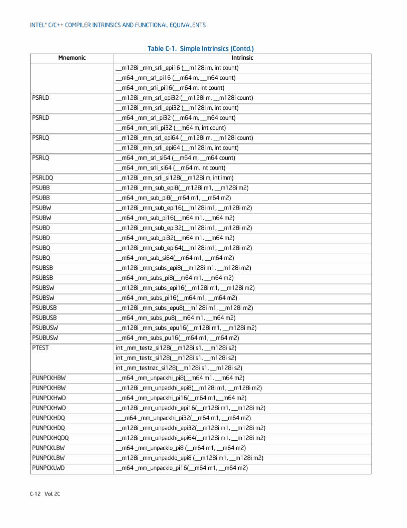
INTEL® C/C++ COMPILER INTRINSICS AND FUNCTIONAL EQUIVALENTS
__m128i _mm_srli_epi16 (__m128i m, int count)
__m64 _mm_srl_pi16 (__m64 m, __m64 count)
__m64 _mm_srli_pi16(__m64 m, int count)
PSRLD __m128i _mm_srl_epi32 (__m128i m, __m128i count)
__m128i _mm_srli_epi32 (__m128i m, int count)
PSRLD __m64 _mm_srl_pi32 (__m64 m, __m64 count)
__m64 _mm_srli_pi32 (__m64 m, int count)
PSRLQ __m128i _mm_srl_epi64 (__m128i m, __m128i count)
__m128i _mm_srli_epi64 (__m128i m, int count)
PSRLQ __m64 _mm_srl_si64 (__m64 m, __m64 count)
__m64 _mm_srli_si64 (__m64 m, int count)
PSRLDQ __m128i _mm_srli_si128(__m128i m, int imm)
PSUBB __m128i _mm_sub_epi8(__m128i m1, __m128i m2)
PSUBB __m64 _mm_sub_pi8(__m64 m1, __m64 m2)
PSUBW __m128i _mm_sub_epi16(__m128i m1, __m128i m2)
PSUBW __m64 _mm_sub_pi16(__m64 m1, __m64 m2)
PSUBD __m128i _mm_sub_epi32(__m128i m1, __m128i m2)
PSUBD __m64 _mm_sub_pi32(__m64 m1, __m64 m2)
PSUBQ __m128i _mm_sub_epi64(__m128i m1, __m128i m2)
PSUBQ __m64 _mm_sub_si64(__m64 m1, __m64 m2)
PSUBSB __m128i _mm_subs_epi8(__m128i m1, __m128i m2)
PSUBSB __m64 _mm_subs_pi8(__m64 m1, __m64 m2)
PSUBSW __m128i _mm_subs_epi16(__m128i m1, __m128i m2)
PSUBSW __m64 _mm_subs_pi16(__m64 m1, __m64 m2)
PSUBUSB __m128i _mm_subs_epu8(__m128i m1, __m128i m2)
PSUBUSB __m64 _mm_subs_pu8(__m64 m1, __m64 m2)
PSUBUSW __m128i _mm_subs_epu16(__m128i m1, __m128i m2)
PSUBUSW __m64 _mm_subs_pu16(__m64 m1, __m64 m2)
PTEST int _mm_testz_si128(__m128i s1, __m128i s2)
int _mm_testc_si128(__m128i s1, __m128i s2)
int _mm_testnzc_si128(__m128i s1, __m128i s2)
PUNPCKHBW __m64 _mm_unpackhi_pi8(__m64 m1, __m64 m2)
PUNPCKHBW __m128i _mm_unpackhi_epi8(__m128i m1, __m128i m2)
PUNPCKHWD __m64 _mm_unpackhi_pi16(__m64 m1,__m64 m2)
PUNPCKHWD __m128i _mm_unpackhi_epi16(__m128i m1, __m128i m2)
PUNPCKHDQ ___m64 _mm_unpackhi_pi32(__m64 m1, __m64 m2)
PUNPCKHDQ __m128i _mm_unpackhi_epi32(__m128i m1, __m128i m2)
PUNPCKHQDQ __m128i _mm_unpackhi_epi64(__m128i m1, __m128i m2)
PUNPCKLBW __m64 _mm_unpacklo_pi8 (__m64 m1, __m64 m2)
PUNPCKLBW __m128i _mm_unpacklo_epi8 (__m128i m1, __m128i m2)
PUNPCKLWD __m64 _mm_unpacklo_pi16(__m64 m1, __m64 m2)
Table C-1. Simple Intrinsics (Contd.)Mnemonic Intrinsic
C-12 Vol. 2C
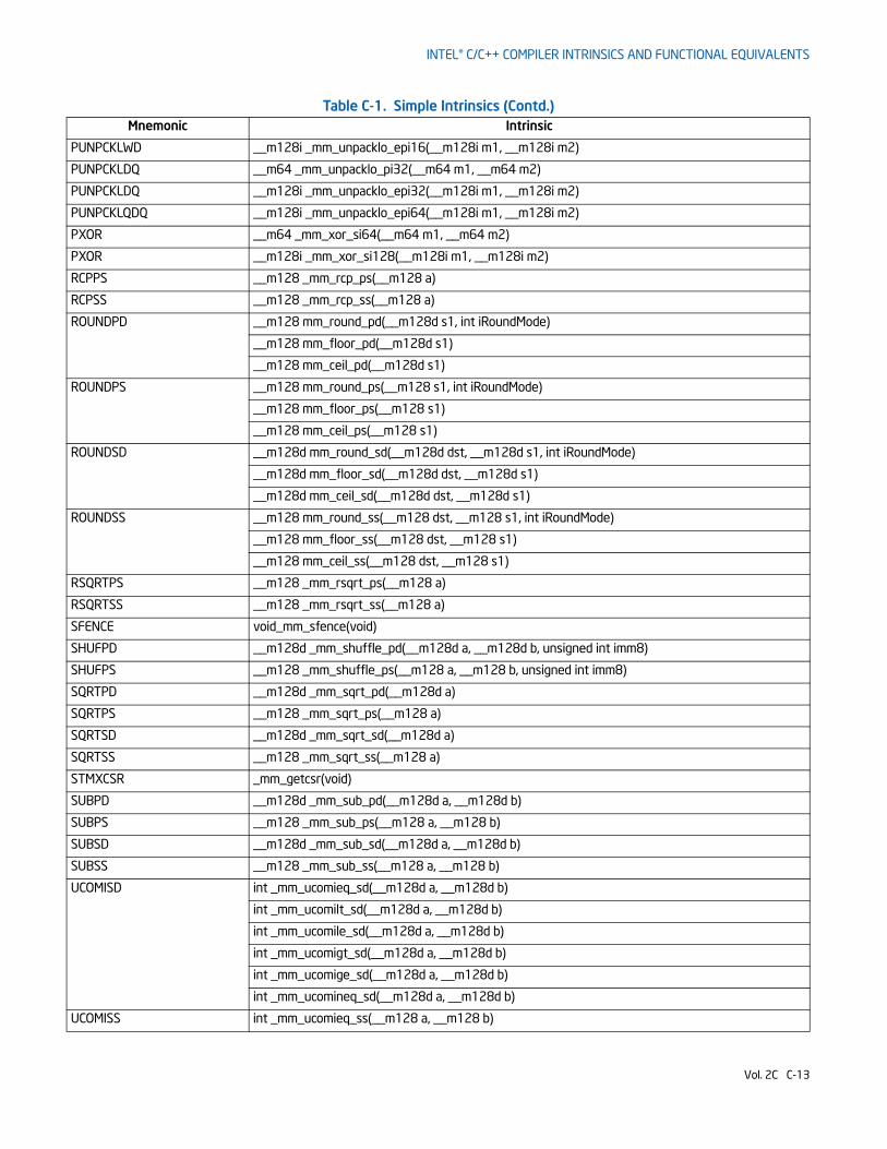
INTEL® C/C++ COMPILER INTRINSICS AND FUNCTIONAL EQUIVALENTS
PUNPCKLWD __m128i _mm_unpacklo_epi16(__m128i m1, __m128i m2)
PUNPCKLDQ __m64 _mm_unpacklo_pi32(__m64 m1, __m64 m2)
PUNPCKLDQ __m128i _mm_unpacklo_epi32(__m128i m1, __m128i m2)
PUNPCKLQDQ __m128i _mm_unpacklo_epi64(__m128i m1, __m128i m2)
PXOR __m64 _mm_xor_si64(__m64 m1, __m64 m2)
PXOR __m128i _mm_xor_si128(__m128i m1, __m128i m2)
RCPPS __m128 _mm_rcp_ps(__m128 a)
RCPSS __m128 _mm_rcp_ss(__m128 a)
ROUNDPD __m128 mm_round_pd(__m128d s1, int iRoundMode)
__m128 mm_floor_pd(__m128d s1)
__m128 mm_ceil_pd(__m128d s1)
ROUNDPS __m128 mm_round_ps(__m128 s1, int iRoundMode)
__m128 mm_floor_ps(__m128 s1)
__m128 mm_ceil_ps(__m128 s1)
ROUNDSD __m128d mm_round_sd(__m128d dst, __m128d s1, int iRoundMode)
__m128d mm_floor_sd(__m128d dst, __m128d s1)
__m128d mm_ceil_sd(__m128d dst, __m128d s1)
ROUNDSS __m128 mm_round_ss(__m128 dst, __m128 s1, int iRoundMode)
__m128 mm_floor_ss(__m128 dst, __m128 s1)
__m128 mm_ceil_ss(__m128 dst, __m128 s1)
RSQRTPS __m128 _mm_rsqrt_ps(__m128 a)
RSQRTSS __m128 _mm_rsqrt_ss(__m128 a)
SFENCE void_mm_sfence(void)
SHUFPD __m128d _mm_shuffle_pd(__m128d a, __m128d b, unsigned int imm8)
SHUFPS __m128 _mm_shuffle_ps(__m128 a, __m128 b, unsigned int imm8)
SQRTPD __m128d _mm_sqrt_pd(__m128d a)
SQRTPS __m128 _mm_sqrt_ps(__m128 a)
SQRTSD __m128d _mm_sqrt_sd(__m128d a)
SQRTSS __m128 _mm_sqrt_ss(__m128 a)
STMXCSR _mm_getcsr(void)
SUBPD __m128d _mm_sub_pd(__m128d a, __m128d b)
SUBPS __m128 _mm_sub_ps(__m128 a, __m128 b)
SUBSD __m128d _mm_sub_sd(__m128d a, __m128d b)
SUBSS __m128 _mm_sub_ss(__m128 a, __m128 b)
UCOMISD int _mm_ucomieq_sd(__m128d a, __m128d b)
int _mm_ucomilt_sd(__m128d a, __m128d b)
int _mm_ucomile_sd(__m128d a, __m128d b)
int _mm_ucomigt_sd(__m128d a, __m128d b)
int _mm_ucomige_sd(__m128d a, __m128d b)
int _mm_ucomineq_sd(__m128d a, __m128d b)
UCOMISS int _mm_ucomieq_ss(__m128 a, __m128 b)
Table C-1. Simple Intrinsics (Contd.)Mnemonic Intrinsic
Vol. 2C C-13
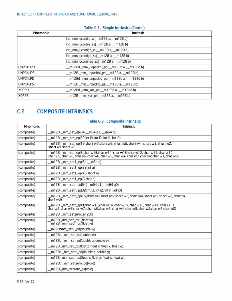
INTEL® C/C++ COMPILER INTRINSICS AND FUNCTIONAL EQUIVALENTS
C.2 COMPOSITE INTRINSICS
int _mm_ucomilt_ss(__m128 a, __m128 b)
int _mm_ucomile_ss(__m128 a, __m128 b)
int _mm_ucomigt_ss(__m128 a, __m128 b)
int _mm_ucomige_ss(__m128 a, __m128 b)
int _mm_ucomineq_ss(__m128 a, __m128 b)
UNPCKHPD __m128d _mm_unpackhi_pd(__m128d a, __m128d b)
UNPCKHPS __m128 _mm_unpackhi_ps(__m128 a, __m128 b)
UNPCKLPD __m128d _mm_unpacklo_pd(__m128d a, __m128d b)
UNPCKLPS __m128 _mm_unpacklo_ps(__m128 a, __m128 b)
XORPD __m128d _mm_xor_pd(__m128d a, __m128d b)
XORPS __m128 _mm_xor_ps(__m128 a, __m128 b)
Table C-2. Composite IntrinsicsMnemonic Intrinsic
(composite) __m128i _mm_set_epi64(__m64 q1, __m64 q0)
(composite) __m128i _mm_set_epi32(int i3, int i2, int i1, int i0)
(composite) __m128i _mm_set_epi16(short w7,short w6, short w5, short w4, short w3, short w2, short w1,short w0)
(composite) __m128i _mm_set_epi8(char w15,char w14, char w13, char w12, char w11, char w10, char w9, char w8, char w7,char w6, char w5, char w4, char w3, char w2,char w1, char w0)
(composite) __m128i _mm_set1_epi64(__m64 q)
(composite) __m128i _mm_set1_epi32(int a)
(composite) __m128i _mm_set1_epi16(short a)
(composite) __m128i _mm_set1_epi8(char a)
(composite) __m128i _mm_setr_epi64(__m64 q1, __m64 q0)
(composite) __m128i _mm_setr_epi32(int i3, int i2, int i1, int i0)
(composite) __m128i _mm_setr_epi16(short w7,short w6, short w5, short w4, short w3, short w2, short w,short w0)
(composite) __m128i _mm_setr_epi8(char w15,char w14, char w13, char w12, char w11, char w10,char w9, char w8,char w7, char w6,char w5, char w4, char w3, char w2,char w1,char w0)
(composite) __m128i _mm_setzero_si128()
(composite) __m128 _mm_set_ps1(float w)__m128 _mm_set1_ps(float w)
(composite) __m128cmm_set1_pd(double w)
(composite) __m128d _mm_set_sd(double w)
(composite) __m128d _mm_set_pd(double z, double y)
(composite) __m128 _mm_set_ps(float z, float y, float x, float w)
(composite) __m128d _mm_setr_pd(double z, double y)
(composite) __m128 _mm_setr_ps(float z, float y, float x, float w)
(composite) __m128d _mm_setzero_pd(void)
(composite) __m128 _mm_setzero_ps(void)
Table C-1. Simple Intrinsics (Contd.)Mnemonic Intrinsic
C-14 Vol. 2C
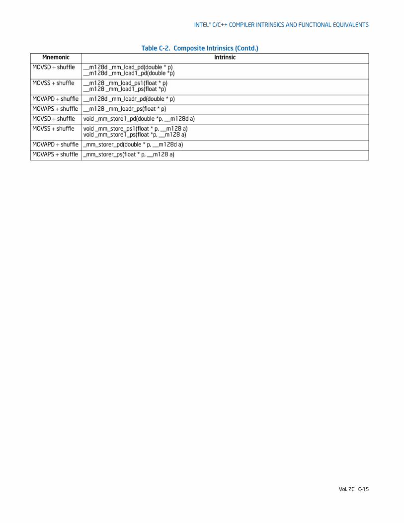
INTEL® C/C++ COMPILER INTRINSICS AND FUNCTIONAL EQUIVALENTS
MOVSD + shuffle __m128d _mm_load_pd(double * p)__m128d _mm_load1_pd(double *p)
MOVSS + shuffle __m128 _mm_load_ps1(float * p)__m128 _mm_load1_ps(float *p)
MOVAPD + shuffle __m128d _mm_loadr_pd(double * p)
MOVAPS + shuffle __m128 _mm_loadr_ps(float * p)
MOVSD + shuffle void _mm_store1_pd(double *p, __m128d a)
MOVSS + shuffle void _mm_store_ps1(float * p, __m128 a)void _mm_store1_ps(float *p, __m128 a)
MOVAPD + shuffle _mm_storer_pd(double * p, __m128d a)
MOVAPS + shuffle _mm_storer_ps(float * p, __m128 a)
Table C-2. Composite Intrinsics (Contd.)Mnemonic Intrinsic
Vol. 2C C-15

INTEL® C/C++ COMPILER INTRINSICS AND FUNCTIONAL EQUIVALENTS
C-16 Vol. 2C

INDEX
Numerics0000, B-5964-bit mode
control and debug registers, 2-15default operand size, 2-15direct memory-offset MOVs, 2-13general purpose encodings, B-24immediates, 2-14introduction, 2-9machine instructions, B-1reg (reg) field, B-4REX prefixes, 2-9, B-2RIP-relative addressing, 2-14SIMD encodings, B-54special instruction encodings, B-94summary table notation, 3-10
AAAA instruction, 3-23, 3-25AAD instruction, 3-25AAM instruction, 3-27AAS instruction, 3-29Access rights, segment descriptor, 3-565ADC instruction, 3-31, 3-594ADD instruction, 3-23, 3-35, 3-292, 3-594ADDPD instruction, 3-38ADDPS instruction, 3-40Addressing methods
RIP-relative, 2-14Addressing, segments, 1-6ADDSD instruction, 3-42ADDSS instruction, 3-44ADDSUBPD instruction, 3-46ADDSUBPS instruction, 3-49AESDEC/AESDECLAST- Perform One Round of an AES Decryption Flow,
3-58AESIMC- Perform the AES InvMixColumn Transformation, 3-54AESKEYGENASSIST - AES Round Key Generation Assist, 3-62AND instruction, 3-64, 3-594ANDNPD instruction, 3-71ANDNPS instruction, 3-73ANDPD instruction, 3-67ANDPS instruction, 3-69Arctangent, x87 FPU operation, 3-395ARPL instruction, 3-75authenticated code execution mode, 6-4
BBase (operand addressing), 2-4BCD integers
packed, 3-292, 3-294, 3-333, 3-335unpacked, 3-23, 3-25, 3-27, 3-29
Binary numbers, 1-6Bit order, 1-4bootstrap processor, 6-21, 6-28, 6-37, 6-39, 6-40BOUND instruction, 3-89, 4-621BOUND range exceeded exception (#BR), 3-89, 4-621Branch hints, 2-2Brand information, 3-226
processor brand index, 3-229processor brand string, 3-226
BSF instruction, 3-92BSR instruction, 3-95BSWAP instruction, 3-98BT instruction, 3-100BTC instruction, 3-103, 3-594BTR instruction, 3-106, 3-594BTS instruction, 3-109, 3-594Byte order, 1-4
CCache and TLB information, 3-219Cache Inclusiveness, 3-201Caches, invalidating (flushing), 3-529, 4-653CALL instruction, 3-112GETSEC, 6-3CBW instruction, 3-131CDQ instruction, 3-290CDQE instruction, 3-131CF (carry) flag, EFLAGS register, 3-35, 3-100, 3-103, 3-106, 3-109, 3-133,
3-142, 3-296, 3-495, 3-501, 4-146, 4-443, 4-512, 4-530, 4-534, 4-561, 4-575
CLC instruction, 3-133CLD instruction, 3-134CLFLUSH instruction, 3-135
CPUID flag, 3-218CLI instruction, 3-137CLTS instruction, 3-140CMC instruction, 3-142CMOVcc flag, 3-218CMOVcc instructions, 3-143
CPUID flag, 3-218CMP instruction, 3-150CMPPD instruction, 3-153CMPPS instruction, 3-163CMPS instruction, 3-170, 4-468CMPSB instruction, 3-170CMPSD instruction, 3-170, 3-176CMPSQ instruction, 3-170CMPSS instruction, 3-182CMPSW instruction, 3-170CMPXCHG instruction, 3-188, 3-594CMPXCHG16B instruction, 3-191
CPUID bit, 3-214CMPXCHG8B instruction, 3-191
CPUID flag, 3-217COMISD instruction, 3-194COMISS instruction, 3-196Compatibility mode
introduction, 2-9see 64-bit modesummary table notation, 3-11
Compatibility, software, 1-5compilers
documentation, 1-9Condition code flags, EFLAGS register, 3-143Condition code flags, x87 FPU status word
flags affected by instructions, 3-18setting, 3-445, 3-447, 3-450
Conditional jump, 3-544Conforming code segment, 3-566Constants (floating point), loading, 3-383Control registers, moving values to and from, 4-49Cosine, x87 FPU operation, 3-351, 3-420CPL, 3-137, 4-625CPUID instruction, 3-198, 3-218
36-bit page size extension, 3-218AP-485, 1-9APIC on-chip, 3-217basic CPUID information, 3-199cache and TLB characteristics, 3-200CLFLUSH flag, 3-218CLFLUSH instruction cache line size, 3-211CMPXCHG16B flag, 3-214CMPXCHG8B flag, 3-217CPL qualified debug store, 3-214debug extensions, CR4.DE, 3-217debug store supported, 3-218deterministic cache parameters leaf, 3-200, 3-202, 3-204, 3-205,
3-206extended function information, 3-206feature information, 3-216
Vol. 2C INDEX-1
INDEX
FPU on-chip, 3-217FSAVE flag, 3-218FXRSTOR flag, 3-218HT technology flag, 3-219IA-32e mode available, 3-207input limits for EAX, 3-208L1 Context ID, 3-214local APIC physical ID, 3-211machine check architecture, 3-218machine check exception, 3-217memory type range registers, 3-217MONITOR feature information, 3-224MONITOR/MWAIT flag, 3-214MONITOR/MWAIT leaf, 3-201, 3-202, 3-203, 3-204MWAIT feature information, 3-224page attribute table, 3-218page size extension, 3-217performance monitoring features, 3-225physical address bits, 3-208physical address extension, 3-217power management, 3-224, 3-225processor brand index, 3-211, 3-226processor brand string, 3-207, 3-226processor serial number, 3-200, 3-218processor type field, 3-210RDMSR flag, 3-217returned in EBX, 3-211returned in ECX & EDX, 3-212self snoop, 3-219SpeedStep technology, 3-214SS2 extensions flag, 3-219SSE extensions flag, 3-219SSE3 extensions flag, 3-214SSSE3 extensions flag, 3-214SYSENTER flag, 3-217SYSEXIT flag, 3-217thermal management, 3-224, 3-225thermal monitor, 3-214, 3-218, 3-219time stamp counter, 3-217using CPUID, 3-198vendor ID string, 3-208version information, 3-199, 3-224virtual 8086 Mode flag, 3-217virtual address bits, 3-208WRMSR flag, 3-217
CQO instruction, 3-290CR0 control register, 4-549CS register, 3-114, 3-514, 3-533, 3-553, 4-44, 4-341CVTDQ2PD instruction, 3-236CVTDQ2PS instruction, 3-243CVTPD2DQ instruction, 3-245CVTPD2PI instruction, 3-248CVTPD2PS instruction, 3-250CVTPI2PD instruction, 3-253CVTPI2PS instruction, 3-255CVTPS2DQ instruction, 3-257, 3-258CVTPS2PD instruction, 3-259CVTPS2PI instruction, 3-262CVTSD2SI instruction, 3-264CVTSD2SS instruction, 3-266CVTSI2SD instruction, 3-268CVTSI2SS instruction, 3-270CVTSS2SD instruction, 3-272CVTSS2SI instruction, 3-274CVTTPD2DQ instruction, 3-276CVTTPD2PI instruction, 3-276, 3-279CVTTPS2DQ instruction, 3-281CVTTPS2PI instruction, 3-284CVTTSD2SI instruction, 3-286CVTTSS2SI instruction, 3-288CWD instruction, 3-290CWDE instruction, 3-131
C/C++ compiler intrinsicscompiler functional equivalents, C-1composite, C-17description of, 3-15lists of, C-1simple, C-2
DD (default operation size) flag, segment descriptor, 4-346DAA instruction, 3-292DAS instruction, 3-294Debug registers, moving value to and from, 4-53DEC instruction, 3-296, 3-594Denormalized finite number, 3-450Detecting and Enabling SMX
level 2, 6-2DF (direction) flag, EFLAGS register, 3-134, 3-172, 3-505, 3-597, 4-114,
4-179, 4-516, 4-562Displacement (operand addressing), 2-4DIV instruction, 3-299Divide error exception (#DE), 3-299DIVPD instruction, 3-303DIVPS instruction, 3-305DIVSD instruction, 3-307DIVSS instruction, 3-309DS register, 3-171, 3-574, 3-597, 4-114, 4-178, 4-179
EEDI register, 4-515, 4-562, 4-567Effective address, 3-579EFLAGS register
condition codes, 3-147, 3-342, 3-348flags affected by instructions, 3-18popping, 4-351popping on return from interrupt, 3-533pushing, 4-434pushing on interrupts, 3-514saving, 4-501status flags, 3-150, 3-549, 4-522, 4-602
EIP register, 3-113, 3-514, 3-533, 3-553EMMS instruction, 3-317Encodings
See machine instructions, opcodesENTER instruction, 3-319GETSEC, 6-4, 6-12Error numbers
VM-instruction error field, 5-34ES register, 3-574, 4-179, 4-515, 4-516, 4-567, 4-568ESI register, 3-171, 3-597, 4-114, 4-178, 4-562ESP register, 3-114, 4-341Exceptions
BOUND range exceeded (#BR), 3-89, 4-621notation, 1-7overflow exception (#OF), 3-513returning from, 3-533
GETSEC, 6-4, 6-6Exponent, extracting from floating-point number, 3-468Extract exponent and significand, x87 FPU operation, 3-468
FF2XM1 instruction, 3-325, 3-468FABS instruction, 3-327FADD instruction, 3-329FADDP instruction, 3-329Far pointer, loading, 3-573Far return, RET instruction, 4-471FBLD instruction, 3-333FBSTP instruction, 3-335FCHS instruction, 3-338FCLEX instruction, 3-340
INDEX-2 Vol. 2C

INDEX
FCMOVcc instructions, 3-342FCOM instruction, 3-344FCOMI instruction, 3-348FCOMIP instruction, 3-348FCOMP instruction, 3-344FCOMPP instruction, 3-344FCOS instruction, 3-351FDECSTP instruction, 3-353FDIV instruction, 3-355FDIVP instruction, 3-355FDIVR instruction, 3-359FDIVRP instruction, 3-359Feature information, processor, 3-198FFREE instruction, 3-363FIADD instruction, 3-329FICOM instruction, 3-364FICOMP instruction, 3-364FIDIV instruction, 3-355FIDIVR instruction, 3-359FILD instruction, 3-367FIMUL instruction, 3-390FINCSTP instruction, 3-369FINIT instruction, 3-371FINIT/FNINIT instructions, 3-412FIST instruction, 3-373FISTP instruction, 3-373FISTTP instruction, 3-377FISUB instruction, 3-437FISUBR instruction, 3-441FLD instruction, 3-380FLD1 instruction, 3-383FLDCW instruction, 3-385FLDENV instruction, 3-387FLDL2E instruction, 3-383FLDL2T instruction, 3-383FLDLG2 instruction, 3-383FLDLN2 instruction, 3-383FLDPI instruction, 3-383FLDZ instruction, 3-383Floating point instructions
machine encodings, B-95Floating-point exceptions
SSE and SSE2 SIMD, 3-21x87 FPU, 3-21
Flushingcaches, 3-529, 4-653TLB entry, 3-531
FMUL instruction, 3-390FMULP instruction, 3-390FNCLEX instruction, 3-340FNINIT instruction, 3-371FNOP instruction, 3-394FNSAVE instruction, 3-412FNSTCW instruction, 3-428FNSTENV instruction, 3-387, 3-431FNSTSW instruction, 3-434FPATAN instruction, 3-395FPREM instruction, 3-398FPREM1 instruction, 3-401FPTAN instruction, 3-404FRNDINT instruction, 3-407FRSTOR instruction, 3-409FS register, 3-574FSAVE instruction, 3-412FSAVE/FNSAVE instructions, 3-409FSCALE instruction, 3-416FSIN instruction, 3-418FSINCOS instruction, 3-420FSQRT instruction, 3-423FST instruction, 3-425FSTCW instruction, 3-428FSTENV instruction, 3-431
FSTP instruction, 3-425FSTSW instruction, 3-434FSUB instruction, 3-437FSUBP instruction, 3-437FSUBR instruction, 3-441FSUBRP instruction, 3-441FTST instruction, 3-445FUCOM instruction, 3-447FUCOMI instruction, 3-348FUCOMIP instruction, 3-348FUCOMP instruction, 3-447FUCOMPP instruction, 3-447FXAM instruction, 3-450FXCH instruction, 3-452FXRSTOR instruction, 3-454
CPUID flag, 3-218FXSAVE instruction, 3-458, 4-647, 4-649, 4-663, 4-675, 4-682, 4-686,
4-691CPUID flag, 3-218
FXTRACT instruction, 3-416, 3-468FYL2X instruction, 3-470FYL2XP1 instruction, 3-472
GGDT (global descriptor table), 3-586, 3-589GDTR (global descriptor table register), 3-586, 4-526General-purpose instructions
64-bit encodings, B-24non-64-bit encodings, B-9
General-purpose registersmoving value to and from, 4-44popping all, 4-346pushing all, 4-431
GETSEC, 6-1, 6-3, 6-7GS register, 3-574
HHADDPD instruction, 3-474, 3-476HADDPS instruction, 3-477Hexadecimal numbers, 1-6HLT instruction, 3-481HSUBPD instruction, 3-483HSUBPS instruction, 3-486Hyper-Threading Technology
CPUID flag, 3-219
IIA-32e mode
CPUID flag, 3-207introduction, 2-9, 2-16see 64-bit modesee compatibility mode
IA32_SYSENTER_CS MSR, 4-593, 4-598IA32_SYSENTER_EIP MSR, 4-593IA32_SYSENTER_ESP MSR, 4-593IDIV instruction, 3-490IDT (interrupt descriptor table), 3-514, 3-586IDTR (interrupt descriptor table register), 3-586, 4-544IF (interrupt enable) flag, EFLAGS register, 3-137, 4-563Immediate operands, 2-4IMUL instruction, 3-494IN instruction, 3-499INC instruction, 3-501, 3-594Index (operand addressing), 2-4Initialization x87 FPU, 3-371initiating logical processor, 6-4, 6-6, 6-12, 6-13, 6-27, 6-28INS instruction, 3-504, 4-468INSB instruction, 3-504INSD instruction, 3-504instruction encodings, B-89, B-98
Vol. 2C INDEX-3
INDEX
Instruction formatbase field, 2-4description of reference information, 3-1displacement, 2-4immediate, 2-4index field, 2-4Mod field, 2-4ModR/M byte, 2-4opcode, 2-3operands, 1-6prefixes, 2-1reg/opcode field, 2-4r/m field, 2-4scale field, 2-4SIB byte, 2-4See also: machine instructions, opcodes
Instruction reference, nomenclature, 3-1Instruction set, reference, 3-1INSW instruction, 3-504INT 3 instruction, 3-513Integer, storing, x87 FPU data type, 3-373Intel 64 architecture
definition of, 1-3instruction format, 2-1relation to IA-32, 1-3
Intel developer link, 1-9Intel NetBurst microarchitecture, 1-2Intel software network link, 1-9Intel VTune Performance Analyzer
related information, 1-9Intel Xeon processor, 1-1Intel® Trusted Execution Technology, 6-4Inter-privilege level
call, CALL instruction, 3-113return, RET instruction, 4-471
Interruptsinterrupt vector 4, 3-513returning from, 3-533software, 3-513
INTn instruction, 3-513INTO instruction, 3-513Intrinsics
compiler functional equivalents, C-1composite, C-17description of, 3-15list of, C-1simple, C-2
INVD instruction, 3-529INVLPG instruction, 3-531IOPL (I/O privilege level) field, EFLAGS register, 3-137, 4-434, 4-563IRET instruction, 3-533IRETD instruction, 3-533
JJcc instructions, 3-544JMP instruction, 3-552Jump operation, 3-552
LL1 Context ID, 3-214LAHF instruction, 3-563LAR instruction, 3-565Last branch
interrupt & exception recordingdescription of, 4-485
LDDQU instruction, 3-569LDMXCSR instruction, 3-571LDS instruction, 3-573LDT (local descriptor table), 3-589LDTR (local descriptor table register), 3-589, 4-547
LEA instruction, 3-579LEAVE instruction, 3-582LES instruction, 3-573LFENCE instruction, 3-584LFS instruction, 3-573LGDT instruction, 3-586LGS instruction, 3-573LIDT instruction, 3-586LLDT instruction, 3-589LMSW instruction, 3-592Load effective address operation, 3-579LOCK prefix, 3-32, 3-36, 3-65, 3-104, 3-107, 3-110, 3-189, 3-296, 3-501,
3-594, 4-161, 4-166, 4-169, 4-513, 4-575, 4-657, 4-661, 4-669
Locking operation, 3-594LODS instruction, 3-596, 4-468LODSB instruction, 3-596LODSD instruction, 3-596LODSQ instruction, 3-596LODSW instruction, 3-596Log epsilon, x87 FPU operation, 3-470Log (base 2), x87 FPU operation, 3-472LOOP instructions, 3-600LOOPcc instructions, 3-600LSL instruction, 3-603LSS instruction, 3-573LTR instruction, 3-607
MMachine check architecture
CPUID flag, 3-218description, 3-218
Machine instructions64-bit mode, B-1condition test (tttn) field, B-7direction bit (d) field, B-8floating-point instruction encodings, B-95general description, B-1general-purpose encodings, B-9–B-53legacy prefixes, B-2MMX encodings, B-55–B-58opcode fields, B-2operand size (w) bit, B-5P6 family encodings, B-59Pentium processor family encodings, B-53reg (reg) field, B-3, B-4REX prefixes, B-2segment register (sreg) field, B-6sign-extend (s) bit, B-5SIMD 64-bit encodings, B-54special 64-bit encodings, B-94special fields, B-2special-purpose register (eee) field, B-6SSE encodings, B-60–B-69SSE2 encodings, B-69–B-86SSE3 encodings, B-87–B-89SSSE3 encodings, B-89–B-93VMX encodings, B-115–B-116, B-117–??See also: opcodes
Machine status word, CR0 register, 3-592, 4-549MASKMOVDQU instruction, 4-53MASKMOVQ instruction, 4-11MAXPD instruction, 4-17MAXPS instruction, 4-20MAXSD instruction, 4-23MAXSS instruction, 4-25measured environment, 6-1Measured Launched Environment, 6-1, 6-33MFENCE instruction, 4-27MINPD instruction, 4-29MINPS instruction, 4-32
INDEX-4 Vol. 2C
INDEX
MINSD instruction, 4-35MINSS instruction, 4-37MLE, 6-1MMX instructions
CPUID flag for technology, 3-218encodings, B-55
Mod field, instruction format, 2-4Model & family information, 3-224ModR/M byte, 2-4
16-bit addressing forms, 2-632-bit addressing forms of, 2-7description of, 2-4
MONITOR instruction, 4-39CPUID flag, 3-214feature data, 3-224
MOV instruction, 4-42MOV instruction (control registers), 4-49MOV instruction (debug registers), 4-53, 4-62MOVAPD instruction, 4-56MOVAPS instruction, 4-59MOVD instruction, 4-62MOVDDUP instruction, 4-68MOVDQ2Q instruction, 4-77MOVDQA instruction, 4-71MOVDQU instruction, 4-74MOVHLPS instruction, 4-79MOVHPD instruction, 4-81MOVHPS instruction, 4-83MOVLHP instruction, 4-85MOVLHPS instruction, 4-85MOVLPD instruction, 4-87MOVLPS instruction, 4-89MOVMSKPD instruction, 4-91MOVMSKPS instruction, 4-93MOVNTDQ instruction, 4-112MOVNTI instruction, 4-112MOVNTPD instruction, 4-103MOVNTPS instruction, 4-105MOVNTQ instruction, 4-107MOVQ instruction, 4-62, 4-109MOVQ2DQ instruction, 4-111MOVS instruction, 4-113, 4-468MOVSB instruction, 4-113MOVSD instruction, 4-113, 4-118MOVSHDUP instruction, 4-121MOVSLDUP instruction, 4-124MOVSQ instruction, 4-113MOVSS instruction, 4-127MOVSW instruction, 4-113MOVSX instruction, 4-130MOVSXD instruction, 4-130MOVUPD instruction, 4-133MOVUPS instruction, 4-136MOVZX instruction, 4-139MSRs (model specific registers)
reading, 4-452MUL instruction, 3-27, 4-146MULPD instruction, 4-149MULPS instruction, 4-151MULSD instruction, 4-153MULSS instruction, 4-155Multi-byte no operation, 4-161, 4-164, B-16MVMM, 6-1, 6-6, 6-7, 6-49MWAIT instruction, 4-157
CPUID flag, 3-214feature data, 3-224
NNaN. testing for, 3-445Near
return, RET instruction, 4-471
NEG instruction, 3-594, 4-161NetBurst microarchitecture (see Intel NetBurst microarchitecture)No operation, 4-161, 4-164, B-16Nomenclature, used in instruction reference pages, 3-1NOP instruction, 4-164NOT instruction, 3-594, 4-166Notation
bit and byte order, 1-4exceptions, 1-7hexadecimal and binary numbers, 1-6instruction operands, 1-6reserved bits, 1-5segmented addressing, 1-6
Notational conventions, 1-4NT (nested task) flag, EFLAGS register, 3-533
OOF (carry) flag, EFLAGS register, 3-495OF (overflow) flag, EFLAGS register, 3-35, 3-513, 4-146, 4-512, 4-530,
4-534, 4-575Opcode format, 2-3Opcodes
addressing method codes for, A-2extensions, A-20extensions tables, A-21group numbers, A-20integers
one-byte opcodes, A-10two-byte opcodes, A-12
key to abbreviations, A-2look-up examples, A-5, A-20, A-23ModR/M byte, A-20one-byte opcodes, A-5, A-10opcode maps, A-1operand type codes for, A-3register codes for, A-4superscripts in tables, A-8two-byte opcodes, A-5, A-6, A-7, A-12VMX instructions, B-115, B-117x87 ESC instruction opcodes, A-23
Operands, 1-6OR instruction, 3-594, 4-168ORPD instruction, 4-171ORPS instruction, 4-173OUT instruction, 4-175OUTS instruction, 4-178, 4-468OUTSB instruction, 4-178OUTSD instruction, 4-178OUTSW instruction, 4-178Overflow exception (#OF), 3-513
PP6 family processors
description of, 1-1machine encodings, B-59
PABSB instruction, 4-184PABSD instruction, 4-184PABSW instruction, 4-184PACKSSDW instruction, 4-188PACKSSWB instruction, 4-188PACKUSWB instruction, 4-195PADDB instruction, 4-198PADDD instruction, 4-198PADDQ instruction, 4-202PADDSB instruction, 4-204PADDSW instruction, 4-204PADDUSB instruction, 4-207PADDUSW instruction, 4-207PADDW instruction, 4-198PALIGNR instruction, 4-210
Vol. 2C INDEX-5
INDEX
PAND instruction, 4-212PANDN instruction, 4-214GETSEC, 6-5PAUSE instruction, 4-216PAVGB instruction, 4-218PAVGW instruction, 4-218PCE flag, CR4 register, 4-456PCMPEQB instruction, 4-231PCMPEQD instruction, 4-231PCMPEQW instruction, 4-231PCMPGTB instruction, 4-241PCMPGTD instruction, 4-241PCMPGTW instruction, 4-241PE (protection enable) flag, CR0 register, 3-592Pending break enable, 3-219Pentium 4 processor, 1-1Pentium II processor, 1-2Pentium III processor, 1-2Pentium Pro processor, 1-2Pentium processor, 1-1Pentium processor family processors
machine encodings, B-53Performance-monitoring counters
CPUID inquiry for, 3-225PEXTRW instruction, 4-254PHADDD instruction, 4-257PHADDSW instruction, 4-260PHADDW instruction, 4-257PHSUBD instruction, 4-264PHSUBSW instruction, 4-267PHSUBW instruction, 4-264Pi, 3-383PINSRW instruction, 4-272, 4-374PMADDUBSW instruction, 4-275PMADDUDSW instruction, 4-275PMADDWD instruction, 4-277PMAXSW instruction, 4-285PMAXUB instruction, 4-288PMINSW instruction, 4-300PMINUB instruction, 4-303PMOVMSKB instruction, 4-306PMULHRSW instruction, 4-322PMULHUW instruction, 4-325PMULHW instruction, 4-328PMULLW instruction, 4-333PMULUDQ instruction, 4-336POP instruction, 4-339POPA instruction, 4-346POPAD instruction, 4-346POPF instruction, 4-351POPFD instruction, 4-351POPFQ instruction, 4-351POR instruction, 4-355PREFETCHh instruction, 4-357Prefixes
Address-size override prefix, 2-2Branch hints, 2-2branch hints, 2-2instruction, description of, 2-1legacy prefix encodings, B-2LOCK, 2-2, 3-594Operand-size override prefix, 2-2REP or REPE/REPZ, 2-2REPNE/REPNZ, 2-2REP/REPE/REPZ/REPNE/REPNZ, 4-466REX prefix encodings, B-2Segment override prefixes, 2-2
PSADBW instruction, 4-360Pseudo-functions
VMfail, 5-2VMfailInvalid, 5-2VMfailValid, 5-2
VMsucceed, 5-2PSHUFB instruction, 4-363PSHUFD instruction, 4-366PSHUFHW instruction, 4-368PSHUFLW instruction, 4-370PSHUFW instruction, 4-372PSIGNB instruction, 4-374PSIGND instruction, 4-374PSIGNW instruction, 4-374PSLLD instruction, 4-381PSLLDQ instruction, 4-379PSLLQ instruction, 4-381PSLLW instruction, 4-381PSRAD instruction, 4-388PSRAW instruction, 4-388PSRLD instruction, 4-395PSRLDQ instruction, 4-393PSRLQ instruction, 4-395PSRLW instruction, 4-395PSUBB instruction, 4-401PSUBD instruction, 4-401PSUBQ instruction, 4-405PSUBSB instruction, 4-407PSUBSW instruction, 4-407PSUBUSB instruction, 4-410PSUBUSW instruction, 4-410PSUBW instruction, 4-401PUNPCKHBW instruction, 4-415PUNPCKHDQ instruction, 4-415PUNPCKHQDQ instruction, 4-415PUNPCKHWD instruction, 4-415PUNPCKLBW instruction, 4-421PUNPCKLDQ instruction, 4-421PUNPCKLQDQ instruction, 4-421PUNPCKLWD instruction, 4-421PUSH instruction, 4-426PUSHA instruction, 4-431PUSHAD instruction, 4-431PUSHF instruction, 4-434PUSHFD instruction, 4-434PXOR instruction, 4-437
RRC (rounding control) field, x87 FPU control word, 3-374, 3-383, 3-425RCL instruction, 4-439RCPPS instruction, 4-447RCPSS instruction, 4-450RCR instruction, 4-439RDMSR instruction, 4-452, 4-456, 4-462
CPUID flag, 3-217RDPMC instruction, 4-454RDTSC instruction, 4-460, 4-462, 4-464Reg/opcode field, instruction format, 2-4Related literature, 1-8Remainder, x87 FPU operation, 3-401REP/REPE/REPZ/REPNE/REPNZ prefixes, 3-172, 3-505, 4-179, 4-466Reserved
use of reserved bits, 1-5Responding logical processor, 6-6responding logical processor, 6-4, 6-5, 6-6RET instruction, 4-471REX prefixes
addressing modes, 2-11and INC/DEC, 2-10encodings, 2-10, B-2field names, 2-11ModR/M byte, 2-10overview, 2-9REX.B, 2-10REX.R, 2-10REX.W, 2-10
INDEX-6 Vol. 2C
INDEX
special encodings, 2-13RIP-relative addressing, 2-14ROL instruction, 4-439ROR instruction, 4-439Rounding
modes, floating-point operations, 4-485Rounding control (RC) field
MXCSR register, 4-485x87 FPU control word, 4-485
Rounding, round to integer, x87 FPU operation, 3-407RPL field, 3-75RSM instruction, 4-494RSQRTPS instruction, 4-496RSQRTSS instruction, 4-499R/m field, instruction format, 2-4
SSafer Mode Extensions, 6-1SAHF instruction, 4-501SAL instruction, 4-503SAR instruction, 4-503SBB instruction, 3-594, 4-511Scale (operand addressing), 2-4Scale, x87 FPU operation, 3-416Scan string instructions, 4-515SCAS instruction, 4-468, 4-515SCASB instruction, 4-515SCASD instruction, 4-515SCASW instruction, 4-515Segment
descriptor, segment limit, 3-603limit, 3-603registers, moving values to and from, 4-44selector, RPL field, 3-75
Segmented addressing, 1-6Self Snoop, 3-219GETSEC, 6-2, 6-4, 6-6SENTER sleep state, 6-12SETcc instructions, 4-520GETSEC, 6-5SF (sign) flag, EFLAGS register, 3-35SFENCE instruction, 4-525SGDT instruction, 4-526SHAF instruction, 4-501Shift instructions, 4-503SHL instruction, 4-503SHLD instruction, 4-529SHR instruction, 4-503SHRD instruction, 4-533SHUFPD instruction, 4-537SHUFPS instruction, 4-540SIB byte, 2-4
32-bit addressing forms of, 2-8description of, 2-4
SIDT instruction, 4-526, 4-544Significand, extracting from floating-point number, 3-468SIMD floating-point exceptions, unmasking, effects of, 3-571Sine, x87 FPU operation, 3-418, 3-420SINIT, 6-5SLDT instruction, 4-547GETSEC, 6-5SMSW instruction, 4-549SpeedStep technology, 3-214SQRTPD instruction, 4-552SQRTPS instruction, 4-554SQRTSD instruction, 4-557SQRTSS instruction, 4-559Square root, Fx87 PU operation, 3-423SS register, 3-574, 4-44, 4-341SSE extensions
cacheability instruction encodings, B-68
CPUID flag, 3-219floating-point encodings, B-60instruction encodings, B-60integer instruction encodings, B-67memory ordering encodings, B-68
SSE2 extensionscacheability instruction encodings, B-86CPUID flag, 3-219floating-point encodings, B-70integer instruction encodings, B-79
SSE3CPUID flag, 3-214
SSE3 extensionsCPUID flag, 3-214event mgmt instruction encodings, B-88floating-point instruction encodings, B-87integer instruction encodings, B-88, B-89
SSSE3 extensions, B-89, B-98CPUID flag, 3-214
Stack, pushing values on, 4-426Status flags, EFLAGS register, 3-147, 3-150, 3-342, 3-348, 3-549, 4-522,
4-602STC instruction, 4-561STD instruction, 4-562Stepping information, 3-224STI instruction, 4-563STMXCSR instruction, 4-566STOS instruction, 4-468, 4-567STOSB instruction, 4-567STOSD instruction, 4-567STOSQ instruction, 4-567STOSW instruction, 4-567STR instruction, 4-572String instructions, 3-170, 3-504, 3-596, 4-113, 4-178, 4-515, 4-567SUB instruction, 3-29, 3-294, 3-594, 4-574SUBPD instruction, 4-577SUBSS instruction, 4-584SWAPGS instruction, 4-586SYSCALL instruction, 4-588SYSENTER instruction, 4-590
CPUID flag, 3-217SYSEXIT instruction, 4-595
CPUID flag, 3-217SYSRET instruction, 4-599
TTangent, x87 FPU operation, 3-404Task register
loading, 3-607storing, 4-572
Task switchCALL instruction, 3-113return from nested task, IRET instruction, 3-533
TEST instruction, 4-601, 4-643Thermal Monitor
CPUID flag, 3-219Thermal Monitor 2, 3-214
CPUID flag, 3-214Time Stamp Counter, 3-217Time-stamp counter, reading, 4-462, 4-464TLB entry, invalidating (flushing), 3-531Trusted Platform Module, 6-6TS (task switched) flag, CR0 register, 3-140TSD flag, CR4 register, 4-462, 4-464TSS, relationship to task register, 4-572
UUCOMISD instruction, 4-604UCOMISS instruction, 4-606UD2 instruction, 4-608
Vol. 2C INDEX-7
INDEX
Undefined, format opcodes, 3-445Unordered values, 3-344, 3-445, 3-447UNPCKHPD instruction, 4-609UNPCKHPS instruction, 4-612UNPCKLPD instruction, 4-615UNPCKLPS instruction, 4-618
VVERR instruction, 4-625Version information, processor, 3-198VERW instruction, 4-625VEX, 3-4VEX.B, 3-4VEX.L, 3-4VEX.mmmmm, 3-4VEX.pp, 3-5VEX.R, 3-6VEX.vvvv, 3-4VEX.W, 3-4VEX.X, 3-4Virtual Machine Monitor, 6-1VM (virtual 8086 mode) flag, EFLAGS register, 3-533VMCALL instruction, 5-1VMCLEAR instruction, 5-1VMCS
error numbers, 5-34VM-instruction error field, 5-34
VMLAUNCH instruction, 5-1VMM, 6-1VMPTRLD instruction, 5-1VMPTRST instruction, 5-1VMREAD instruction, 5-1VMRESUME instruction, 5-1, 5-2VMWRITE instruction, 5-1VMXOFF instruction, 5-1VMXON instruction, 5-2
WWAIT/FWAIT instructions, 4-651GETSEC, 6-6WBINVD instruction, 4-653WBINVD/INVD bit, 3-201Write-back and invalidate caches, 4-653WRMSR instruction, 4-655
CPUID flag, 3-217
Xx87 FPU
checking for pending x87 FPU exceptions, 4-651constants, 3-383initialization, 3-371instruction opcodes, A-23
x87 FPU control wordloading, 3-385, 3-387RC field, 3-374, 3-383, 3-425restoring, 3-409saving, 3-412, 3-431storing, 3-428
x87 FPU data pointer, 3-387, 3-409, 3-412, 3-431x87 FPU instruction pointer, 3-387, 3-409, 3-412, 3-431x87 FPU last opcode, 3-387, 3-409, 3-412, 3-431x87 FPU status word
condition code flags, 3-344, 3-364, 3-445, 3-447, 3-450loading, 3-387restoring, 3-409saving, 3-412, 3-431, 3-434TOP field, 3-369x87 FPU flags affected by instructions, 3-18
x87 FPU tag word, 3-387, 3-409, 3-412, 3-431XADD instruction, 3-594, 4-657
XCHG instruction, 3-594, 4-660XFEATURE_ENABLED_MASK, 4-663, 4-676, 4-682, 4-686, 4-687, 4-691,
4-692XGETBV, 4-663, 4-675, B-59XLAB instruction, 4-665XLAT instruction, 4-665XOR instruction, 3-594, 4-668XORPD instruction, 4-671XORPS instruction, 4-673XRSTOR, 4-683, 4-687, B-59XSAVE, 4-663, 4-664, 4-675, 4-676, 4-677, 4-678, 4-679, 4-680, 4-682,
4-683, 4-684, 4-685, 4-686, 4-687, 4-689, 4-690, 4-692, B-59XSETBV, 4-686, 4-691, B-59
ZZF (zero) flag, EFLAGS register, 3-188, 3-565, 3-600, 3-603, 4-468, 4-625
INDEX-8 Vol. 2C
Related Documents


