Integration of silk protein in organic and light-emitting transistors R. Capelli 1 , J. J. Amsden 2 , G. Generali 1 , S. Toffanin 1 , V. Benfenati 1 , M. Muccini 1 , D. L. Kaplan 2 , F. G. Omenetto 2,3 , and R. Zamboni 1 1 Istituto per lo Studio dei Materiali Nanostrutturati, CNR, via P. Gobetti 101, 40129-Bologna, Italy 2 Department of Biomedical Engineering, Tufts University, 4 Colby Street, Medford, MA, 02155, USA 3 Department of Physics, Tufts University, 4 Colby Street, Medford, MA, 02155, USA Abstract We present the integration of a natural protein into electronic and optoelectronic devices by using silk fibroin as a thin film dielectric in an organic thin film field-effect transistor (OFET) ad an organic light emitting transistor device (OLET) structures. Both n- (perylene) and p-type (thiophene) silk-based OFETs are demonstrated. The measured electrical characteristics are in agreement with high-efficiency standard organic transistors, namely charge mobility of the order of 10 -2 cm 2 /Vs and on/off ratio of 10 4 . The silk-based optolectronic element is an advanced unipolar n-type OLET that yields a light emission of 100nW. The future of electronics has been envisioned as “soft and rubbery”(1). A step toward real – life applications of flexible electronics has been made by demonstrating silicon circuits bonded to elastomeric substrates (1,2) and innovative organic electronic and optoelectronics devices (3-5). Organic thin film field effect transistors (OFETs), organic light emitting diodes (OLEDs) and organic light emitting transistors (OLETs) (6-10) have been fabricated onto plastic substrates and integrated into plastic optics (11, 12). Nonetheless, in this era of heightened environmental awareness and of increasing demand for more eco-sustainable manufacturing processes, a major challenge is moving from non-renewable energy manufacturing to “eco-sustainable” processes. The use of biologically based materials and their technological integration provides a compelling path towards this goal (13). In this context, natural fibroin, the constituent protein of silk, may play a key role. Fibroin has been recently demonstrated to be an excellent material for fabrication of optical elements namely, refractive and diffractive lenses, gratings, photonic crystal structures, silk-holograms, silk- optical fibers, silk microfluidic silk-devices (14-22). Moreover, silk is an established biomaterial that has been used for centuries for medical sutures and successfully applied, among other things, for drug release, showing a controllable degradation lifetime range from weeks to years (23) and enabling targeted drug delivery in brain astroglyal cells (24). Processing and manipulation are carried out in ambient conditions (21) and the unique properties of natural silk fibroin to host organic structures, enable the fabrication of bioactive optical devices (25). It is worth noting how very recently silicon electronics in form of nanomembranes has been integrated onto a water-soluble silk substrates demonstrating a largely, albeit not completely, bioresorbable, implantable silicon transistor (26). An alternative to silicon is the use of water-soluble, synthetic polymers like poly(vinyl alcohol) (PVA), and thermoplastic polyester poly(L-lactide-co-glycolide) (PLGA)l Such polymers have been used as constituents of an organic (p-type) semiconductor film by using PVA as the dielectric layer and PLGA as the substrate of a biodegradable p-type thin-film transistor (27). These previous accomplishments point to the importance of combining NIH Public Access Author Manuscript Org Electron. Author manuscript; available in PMC 2012 August 14. Published in final edited form as: Org Electron. 2011 July ; 12(7): 1146–1151. doi:10.1016/j.orgel.2011.04.005. NIH-PA Author Manuscript NIH-PA Author Manuscript NIH-PA Author Manuscript

Welcome message from author
This document is posted to help you gain knowledge. Please leave a comment to let me know what you think about it! Share it to your friends and learn new things together.
Transcript
Integration of silk protein in organic and light-emittingtransistors
R. Capelli1, J. J. Amsden2, G. Generali1, S. Toffanin1, V. Benfenati1, M. Muccini1, D. L.Kaplan2, F. G. Omenetto2,3, and R. Zamboni11 Istituto per lo Studio dei Materiali Nanostrutturati, CNR, via P. Gobetti 101, 40129-Bologna, Italy2 Department of Biomedical Engineering, Tufts University, 4 Colby Street, Medford, MA, 02155,USA3 Department of Physics, Tufts University, 4 Colby Street, Medford, MA, 02155, USA
AbstractWe present the integration of a natural protein into electronic and optoelectronic devices by usingsilk fibroin as a thin film dielectric in an organic thin film field-effect transistor (OFET) ad anorganic light emitting transistor device (OLET) structures. Both n- (perylene) and p-type(thiophene) silk-based OFETs are demonstrated. The measured electrical characteristics are inagreement with high-efficiency standard organic transistors, namely charge mobility of the orderof 10-2 cm2/Vs and on/off ratio of 104. The silk-based optolectronic element is an advancedunipolar n-type OLET that yields a light emission of 100nW.
The future of electronics has been envisioned as “soft and rubbery”(1). A step toward real –life applications of flexible electronics has been made by demonstrating silicon circuitsbonded to elastomeric substrates (1,2) and innovative organic electronic and optoelectronicsdevices (3-5). Organic thin film field effect transistors (OFETs), organic light emittingdiodes (OLEDs) and organic light emitting transistors (OLETs) (6-10) have been fabricatedonto plastic substrates and integrated into plastic optics (11, 12). Nonetheless, in this era ofheightened environmental awareness and of increasing demand for more eco-sustainablemanufacturing processes, a major challenge is moving from non-renewable energymanufacturing to “eco-sustainable” processes. The use of biologically based materials andtheir technological integration provides a compelling path towards this goal (13). In thiscontext, natural fibroin, the constituent protein of silk, may play a key role. Fibroin has beenrecently demonstrated to be an excellent material for fabrication of optical elements namely,refractive and diffractive lenses, gratings, photonic crystal structures, silk-holograms, silk-optical fibers, silk microfluidic silk-devices (14-22). Moreover, silk is an establishedbiomaterial that has been used for centuries for medical sutures and successfully applied,among other things, for drug release, showing a controllable degradation lifetime range fromweeks to years (23) and enabling targeted drug delivery in brain astroglyal cells (24).Processing and manipulation are carried out in ambient conditions (21) and the uniqueproperties of natural silk fibroin to host organic structures, enable the fabrication ofbioactive optical devices (25). It is worth noting how very recently silicon electronics inform of nanomembranes has been integrated onto a water-soluble silk substratesdemonstrating a largely, albeit not completely, bioresorbable, implantable silicon transistor(26). An alternative to silicon is the use of water-soluble, synthetic polymers like poly(vinylalcohol) (PVA), and thermoplastic polyester poly(L-lactide-co-glycolide) (PLGA)l Suchpolymers have been used as constituents of an organic (p-type) semiconductor film by usingPVA as the dielectric layer and PLGA as the substrate of a biodegradable p-type thin-filmtransistor (27). These previous accomplishments point to the importance of combining
NIH Public AccessAuthor ManuscriptOrg Electron. Author manuscript; available in PMC 2012 August 14.
Published in final edited form as:Org Electron. 2011 July ; 12(7): 1146–1151. doi:10.1016/j.orgel.2011.04.005.
NIH
-PA Author Manuscript
NIH
-PA Author Manuscript
NIH
-PA Author Manuscript
organic electronics and synthetic organic biodegradable materials to take a first step towardsbiodegradable and environmentally sustainable electronic devices.
We demonstrate here how a natural protein such as silk fibroin, can be integrated as afunctional and efficient dielectric into organic optoelectronic devices, replacing traditionalinorganic oxide layers such as SiO2, plastic PMMA, or other synthetic organic materials.
Figure 1 shows the schematic of the fabricated n- and p-type silk organic thin filmtransistors. A 400nm thick film of silk fibroin is spin coated from aqueous solution onto anoptically transparent glass/ITO substrate, patterned ITO acting as a gate contact. The silkfilm is rendered water insoluble by inducing beta sheet formation (i.e. crosslinking) aspreviously described (18). A 15 nm thick film of N,N'-ditridecylperylene-3,4,9,10-tetracarboxylic diimide (P13) is vacuum deposited at a sublimation rate of 0.1 Å/s as a n-type organic semiconductor for electron conduction on top of the silk film. A 50 nm thicksource and drain gold contacts are vacuum thermo-deposited through a metal mask thuscompleting a 70 μm and 15 mm channel length and width top-contact organic field-effecttransistor (OFET) configuration. With the same protocol and parameters, a p-typesemiconductor, namely the α,ω-dihexyl-quaterthiophene (DH4T) has been grown for holeconduction. It is worth nothing that the semiconductor compounds were not modified ormanipulated from their commercially available form namely, P13 by Sigma-Aldrich, andDH4T (ActivInk P0400) by Polyera Corporation . The molecular structure of the grownmoieties and the output curves of the respective n- and p-type silk organic FET are shown aswell in figure 1. Both P13 and DH4T are well known and extensively researched materialsfor electron (n-type) and hole (p-type) transport organic thin film transistors (6,28,29). Assuch, they provide an ideal system to benchmark the silk-based OFETs and and OLETs. Theelectrical characterization of the fabricated silk-organic transistors has been performed witha probe station equipped with a parametric analyzer both in atmosphere controlled dry-boxsystems and in air at room temperature. Is worth noting how the I-V characteristics ofOFETs can be adequately described by standard models (30, 31) and the mobility of the n-and p-type silk based transistors were derived from measured output curves in the saturationregime.
The saturation curves measured at Vd-s = ±90 V, where Vd-s is the voltage between drain-source contacts depending on the n- or p-type semiconducting material, are reported infigure 1. The two nearly overlapping lines are for forward and backward scanning of theGate-Source voltage while Vd-s is kept constant. This indicates the near absence ofhysteresis and consequently low charge trapping in the silk dielectric layer in particular forelectron transport, i.e. the silk-P13 device.
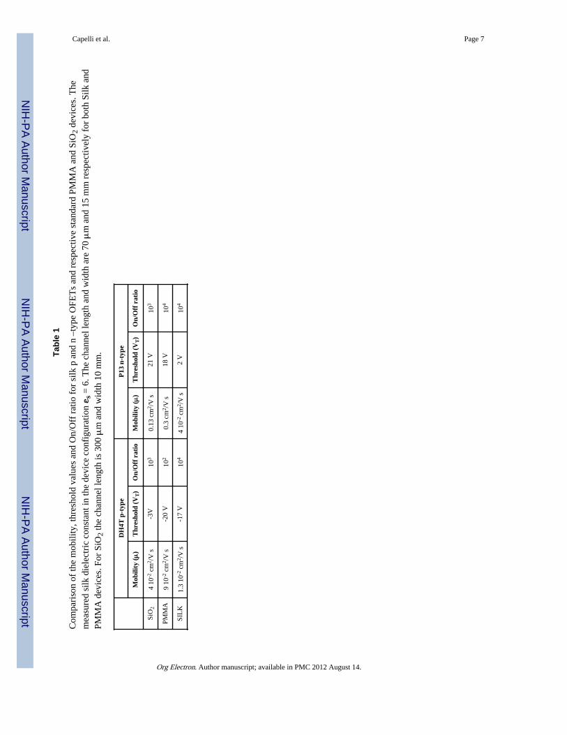
The charge mobility values associated to the measurement are μn = 4 10-2 cm2/Vs for thesilk-P13 and μp = 1.3 10-2 cm2/Vs for the silk- DH4T. A comparison of the parameters ofthe silk-based devices and PMMA and SiO2-based devices are reported in Table 1. We notethat the measurements are comparable to efficient charge mobility values (n- and p-type) ofthin film OFET reported in the literature (28-30) and with our previously obtained resultsfrom standard SiO2 – PMMA gated OFETs (28). Moreover, we should underline how themeasured voltage threshold for the silk-P13 transistor is one order of magnitude lower,namely 1.8 V at 20 V, than the respective standard OFET. The other defining parameter toassess the performance of an OFET is the on/off switch ratio which is also included in table1. In this case, the switching rate of 104 matches the highest values reported for thin filmorganic transistor based on P13 and DHFT organic semiconductors
To explore optical utility in these devices, organic light emitting transistors have been alsostudied. These recently designed structures (6-11) have the ability to combine in a single
Capelli et al. Page 2
Org Electron. Author manuscript; available in PMC 2012 August 14.
NIH
-PA Author Manuscript
NIH
-PA Author Manuscript
NIH
-PA Author Manuscript
device the advantages and functions of a transistor and of electroemission. Moreover,electroemission efficiency and nanoscale localization of the light emission make OLETs abreakthrough multifunctional device concept. The first evidence of OLETs emission hasbeen demonstrated for a unipolar emitting device (6,7). To study these results in silk,wehave leveraged the best-performing silk-transistor, (the silk-P13), and operated the device inthe locus mode. The emission was collected by using a calibrated photodiode . The obtainedresults are shown in figure 2.
When Vgs=Vds of 75 V, a nonlinear intensity of the emitted light is observed. The measuredrelevant operation parameters assessing the performance of the unipolar silk-OLET deviceare: Vth=1,4V; n-Mobility= 0,013 cm2/Vs; light emission intensity= 100nW atVgs=Vds=90V.
The present results demonstrate how natural silk fibroin can be successfully used as adielectric material for fabrication of advanced n- and p- type silk-based organic transistorsand light emitting transistors. The combined use of silk in electronics as presented here incombination with previous work on silk-based photonics, thin-film and conformalelectronics sets the stage for a powerful approach towards the fabrication of eco-sustainableand multifunctional bioactive devices. The favorable substrate properties of this all naturalbiopolymeric substrate (ref. Tao, H., J. J. Amsden, A. C. Strikwerda, K. Fan, D. L. Kaplan,X. Zhang, R. D. Averitt, F. G. Omenetto. 2010. Metamaterial silk composites at terahertzfrequencies. Advanced Materials July 21 Epub ahead of print [PMID 20665563], Kim, D.H., J. Viventi, J. J. Amsden, L. Vigeland, Y. S. Kim, J. A. Blanco, B. Panilaitis, E. S.Frechette, D. Contreras, D. L. Kaplan, F. G. Omenetto, Y. Huang, K. C. Hwang, M. R.Zakin, B. Litt, J. A. Rogers. 2010. Dissolvable films of silk fibroin for ultrathin conformalbiointegrated electronics. Nature Materials 9(6):511-517 [PMID: 20400953]) can be alsoexploited in the future as an alternative to the rigid substrates used here enabling fullydegradable devices and opening a path for sustainable high-tech manufacturing.
AcknowledgmentsFinancial support from EU projects PF6 035859-2 (BIMORE) and FP7-ICT- 248052 (PHOTO-FET), Italian MIURprojects FIRBRBIP06YWBH (NODIS), FIRB-RBIP0642YL (LUCI), and Italian MSE project Industria2015(ALADIN) is acknowledged.
This material is based upon work supported in part by the U.S. Army Research Laboratory and the U.S. ArmyResearch Office under contract number W911 NF-07-1-0618 and by the DARPA-DSO the AFOSR and the NIHP41 Tissue Engineering Resource Center.
References1. Rogers, John A.; Huang, Yonggang. PNAS. 2009; 27:10875–10876. [PubMed: 19567838]
2. Kim, Dae-Hyeong; Rogers, John A. Adv. Mater. 2008; 20:4887–4892.
3. Forrest SR. Nature. 2004; 428:911. [PubMed: 15118718]
4. Singh, Th. Birendra; Sariciftci, Niyazi Serdar. Ann. Rev. Mater. Res. 2006; 36:199–230.
5. Dodabalapur, Ananth. Materials Today. 2006; 9:24–30.
6. Muccini, Michele. Nature Mater. 2006; 5:605–613. [PubMed: 16880804]
7. Hepp A, et al. Phys. Rev. Lett. 2003; 91:157406. [PubMed: 14611497]
8. Rost C, et al. Appl. Phys Lett. 2004; 85:1613–1615.
9. Zaumseil J, Friend RH, Sirringhaus H. Nature Mater. 2006; 5:69–74.
10. Capelli R, et al. Nature Materials. 2010; 9:496–503.
11. Santato C, et al. Appl. Phys. Lett. 2005; 86:141106.
12. Melpignano P, Biondo V, Sinesi S, Gale Michael T. Westenhöfer Susanne, Murgia M, Caria S,Zamboni R. Appl. Phys. Lett. 2006; 88:153514.
Capelli et al. Page 3
Org Electron. Author manuscript; available in PMC 2012 August 14.
NIH
-PA Author Manuscript
NIH
-PA Author Manuscript
NIH
-PA Author Manuscript
13. Hagen JA, Li W, Steckl AJ, Grote JG. Appl. Phys. Lett. 2006; 88:171109.
14. Omenetto, Fiorenzo G.; Kaplan, David L. Nature Photonics. 2008; 2:641–643.
15. Wang X, Kluge JA, Leisk GG, Kaplan DL. Biomaterials. 2008; 29:1054–1064. [PubMed:18031805]
16. Kim U-J, et al. Biomacromolecules. 2004; 5:786–792. [PubMed: 15132662]
17. Jin H-J, Fridrikh SV, Rutledge GC, Kaplan DL. Biomacromolecules. 2002; 3:1233–1239.[PubMed: 12425660]
18. Jin H-J, et al. Adv. Func. Mater. 2005; 15:1241–1247.
19. Wang X, Kim HJ, Xu P, Matsumoto A, Kaplan DL. Langmuir. 2005; 21:11335–11341. [PubMed:16285808]
20. Jiang C, et al. Adv. Func. Mater. 2007; 17:2229–2237.
21. Perry H, Gopinath A, Kaplan DL, Dal Negro L, Omenetto FG. Adv. Mater. 2008; 20:3070–3072.
22. Lawrence BD, Cronin-Golomb M, Georgakoudi I, Kaplan DL, Omenetto FG. Biomacromolecules.2008; 9:1214–1220. [PubMed: 18370418]
23. Wiltz, Andrew; Pritchard, Eleanor M.; Li, Tianfu; Lan, Jin-Quan; Kaplan, David L.; Boison,Detlev. Biomaterials. 2008; 29:3609–3616. [PubMed: 18514814]
24. Benfenati, Valentina; Toffanin, Stefano; Capelli, Raffaella; Camassa, Laura M.A.; Ferroni,Stefano; Kaplan, David L.; Omenetto, Fiorenzo G.; Muccini, Michele; Zamboni, Roberto.Biomaterials. in press doi:10.1016.
25. Domachuk, Peter; Perry, Hannah; Amsden, Jason J.; Kaplan, David L.; Omenetto, Fiorenzo G.Appl. Phys. Lett. 2009; 95:253702. [PubMed: 20087427]
26. Kim, Dae-Hyeong; Kim, Yun-Soung; Amsden, Jason; Panilaitis, Bruce; Kaplan, David L.;Omenetto, Fiorenzo G.; Zakin, Mitchell R.; Rogers, John A. Appl. Phys. Lett. 2009; 95:133701.[PubMed: 20145699]
27. Bettinger, Christopher J.; Bao, Zhenan. Adv. Mat. 2009; 21:1–5.
28. Dinelli F, Capelli R, Loi MA, Murgia M, Muccini M, Facchetti A, Marks TJ. Adv. Mater. 2006;18:1416–1420.
29. Malenfant PRL, Dimitrakopoulos CD, Gelorme JD, Kosbar LL, Graham TO, Curioni A, AndreoniW. Appl. Phys. Lett. 2002; 80:2517–2519.
30. Sze, SM. Wyley-InterScience. 2nd edition. New York: 1981. Physics of semiconductor devices.
31. Horowitz G, Hajlaoui R, Bourgouga R, Hajlaoui M. Synth. Met. 1999; 101:401–404.
32. Kim, Dae-Hyeong, et al. Nature Materials. 2010; 9:511–517. doi:10.1038.
33. Tao, Hu, et al. Adv. Mater. 2010; 22:3527–3531. [PubMed: 20665563]
Capelli et al. Page 4
Org Electron. Author manuscript; available in PMC 2012 August 14.
NIH
-PA Author Manuscript
NIH
-PA Author Manuscript
NIH
-PA Author Manuscript
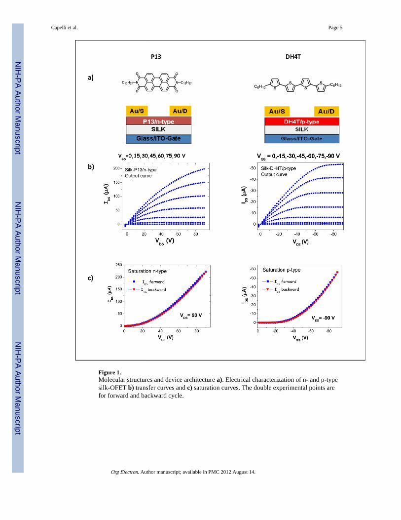
Figure 1.Molecular structures and device architecture a). Electrical characterization of n- and p-typesilk-OFET b) transfer curves and c) saturation curves. The double experimental points arefor forward and backward cycle.
Capelli et al. Page 5
Org Electron. Author manuscript; available in PMC 2012 August 14.
NIH
-PA Author Manuscript
NIH
-PA Author Manuscript
NIH
-PA Author Manuscript
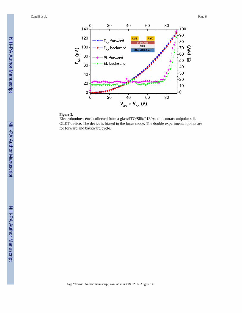
Figure 2.Electroluminescence collected from a glass/ITO/Silk/P13/Au top contact unipolar silk-OLET device. The device is biased in the locus mode. The double experimental points arefor forward and backward cycle.
Capelli et al. Page 6
Org Electron. Author manuscript; available in PMC 2012 August 14.
NIH
-PA Author Manuscript
NIH
-PA Author Manuscript
NIH
-PA Author Manuscript
NIH
-PA Author Manuscript
NIH
-PA Author Manuscript
NIH
-PA Author Manuscript
Capelli et al. Page 7
Tabl
e 1
Com
pari
son
of th
e m
obili
ty, t
hres
hold
val
ues
and
On/
Off
rat
io f
or s
ilk p
and
n –
type
OFE
Ts
and
resp
ectiv
e st
anda
rd P
MM
A a
nd S
iO2
devi
ces.
The
mea
sure
d si
lk d
iele
ctri
c co
nsta
nt in
the
devi
ce c
onfi
gura
tion ε s
= 6
. The
cha
nnel
leng
th a
nd w
idth
are
70 μ
m a
nd 1
5 m
m r
espe
ctiv
ely
for
both
Silk
and
PMM
A d
evic
es. F
or S
iO2
the
chan
nel l
engt
h is
300
μm
and
wid
th 1
0 m
m.
DH
4T p
-typ
eP
13 n
-typ
e
Mob
ility
(μ
)T
hres
hold
(V
T)
On/
Off
rat
ioM
obili
ty (μ
)T
hres
hold
(V
T)
On/
Off
rat
io
SiO
24
10-2
cm
2 /V
s-3
V10
30.
13 c
m2 /
V s
21 V
103
PMM
A9
10-2
cm
2 /V
s-2
0 V
102
0.3
cm2 /
V s
18 V
104
SIL
K1.
3 10
-2 c
m2 /
V s
-17
V10
44
10-2
cm
2 /V
s2
V10
4
Org Electron. Author manuscript; available in PMC 2012 August 14.
Related Documents