Integrated Report 2020 HAMAMATSU PHOTONICS K.K.

Welcome message from author
This document is posted to help you gain knowledge. Please leave a comment to let me know what you think about it! Share it to your friends and learn new things together.
Transcript
Integrated Repor t
20 20
Cat. No. XINT1012E02
JUN. 2021 DNP
HAMAMATSU PHOTONICS K.K.325-6 Sunayama-cho, Naka-ku, Hamamatsu City, Shizuoka Prefecture, 430-8587, Japan
Investor Relat ions Off ice
TEL
FAX
(053)452-2141
(053)456-7889
www.hamamatsu.com
HAMAMATSU PHOTONICS K.K.
INTRODUCTION
Management Philosophy of the Hamamatsu Photonics Group
President’s Message
What is “Light”?
02
03
05
OUR HISTORY
The Origin of Management
Our History
Historical Episodes
13
15
17
BUSINESS MODEL
Hamamatsu Photonics's Value Creation Model with Light 19
PRODUCTS AND APPLICATIONS
Our Products and Applications
Medical-Bio
Industry
Analysis Transport
07
09
11
12
BUSINESS ACTIVITIES
Table of Contents
Financial Data for Seven Years
Financial Review
Board Members
Message from Outside Director
Our Stance toward Stakeholders/Closing Message
Global Organizations
Corporate Profile
39
41
43
45
46
47
49
CORPORATE INFORMATION AND DATA
Editorial Policy
Reporting Organization
Reporting Period
The reporting period for this integrated report is FY2020 (October 2019 to September 2020).
Hamamatsu Photonics published the Integrated Report 2020 as a medium to share mid-to-long term
value creation through both financial and non-financial information. The International <IR> Framework
provided by the International Integrated Reporting Council (IIRC) and the Guidance for Integrated
Corporate Disclosure and Company-investor Dialogue for Collaborative Value Creation provided by the
Ministry of Economy, Trade and Industry were used as reference in preparing this integrated report.
Our corporate website also includes even more extensive and detailed information. Please read the
Integrated Report 2020 together with the information on our website.
The Integrated Report 2020 focuses on reporting of non-consolidated information about Hamamatsu Photonics K.K. The
scope of the financial information encompasses 26 companies (as of September 30, 2020), including Hamamatsu
Photonics K.K., 21 consolidated subsidiaries, and 4 entities accounted for using the equity method.
Guidance for
Collaborative
Value Creation
Review and Vision of Each Division
Electron Tube Division
Solid State Division
Systems Division
Central Research Laboratory
Research and Development
Contributions to Academic Research
27
29
31
33
35
37
38
Management Philosophy of the Hamamatsu Photonics Group
We pursue the unknown where no one has yet explored. By leveraging photonics technology to
establish new industries and reach for the world's highest levels of manufacturing excellence, we
build enterprise value and contribute to the development of science and technology.
Light is a fundamental technology that supports various industries, and further advances in
photonics technology are required on a global scale, to achieve technological innovation today and
to improve the performance and accuracy of electronic equipment in the future. However, only a
small fraction of the nature of light has been elucidated. We explore fields not yet explained. Based
on the knowledge generated by that inquiry, we enhance our enterprise value by discovering
practical applications with which to create new industries and expand our business operations.
At the same time, we have a duty to generate a stable earnings base and continuous growth on
which a long-term development of technology depends. To respond flexibly and quickly to the
expansion of the photonics industry and to changes in the business environment, we have formed
a framework for the proactive investment in R&D and equipment for continuously stable and high
earnings, based on our medium-to-long-term vision.
In addition, we believe that people, technology and knowledge are the foundation of sound
management. We improve ourselves everyday through our work, discovering the things that only
we can do. In so doing, we conduct technology development which is backed up by the knowledge,
needs and competitive technologies for building the photonics industry. We believe it is vital that
we, guided by a mind of “Wa” *, foster a corporate culture that can combine our individual talents to
form a whole that is greater than the sum of its parts. At the heart of this, effort is a bottom-up
operational approach that is focused on the workplace.
*“Wa”: means collaborative spirit and integration of diversified talents.
ESG ACTIVITIES
Activities for the Environment
Activities for Society
Activities for Governance
21
23
25
CONTENTS MANAGEMENT PHILOSOPHY
01 Hamamatsu Photonics Integrated Report 2020 02Hamamatsu Photonics Integrated Report 2020
Pursuit of Core Photonics TechnologiesIn 1926, in Hamamatsu , Japan, the Japanese ka takana
character “イ” was projected electronically on a cathode-ray tube. That was the instant that Professor Kenjiro Takayanagi, later
respectfully known as the “father of Japanese television,” created
something never been before in the wor ld. This televis ion
technology revolutionized the lives of people around the world.
Before industr ies uti l ized photonic technology, our founder,
Heihachiro Horiuchi, who studied under Professor Takayanagi
realized the future potential of photonics and started a business
using photoelectr ic conversion technology, inher i ted from
Professor Takayanagi. Hamamatsu Photonics has continued to
pursue the possibilities of photonics while always holding dear to
the spirit of Professor Takayanagi. One of these people is our
former President, Teruo Hiruma.
Teruo Hiruma, the Company’s former President, often said “Try
before you say you can’t.” He always embodied a spir it to do
something new in order to become the best in the world, with the
bel ief our products must not only be the best in Japan but
around the globe. Performing research that aims for something
that does not exist and developing technologies thought to be
impossible can sometimes be difficult and sometimes produce
unexpected results. “Light” is always present around us and is
still filled with much mystery. Playing a central role in photonics
technology, we continue to build the foundation for the future.
Inverted Pyramid Structure Supporting Contributions of Value to Society
Unlike the general industry pyramid structure, industries that
u t i l i ze pho ton ics employ an inver ted pyramid s t r uc tu re.
Hamamatsu Photonics creates photonic devices at the bottom of
the inverted triangle, while customers use our photonic devices
to create modules above us. The next level comprises customers
who create system products, whi le customers who supply
services are at the top. Hamamatsu Photonics may be at the
bottom of th is pyramid st ructure, but we are not s imply a
company that supplies components. We create vital products
known as “Key Enabling Technology,” which are essential core
technologies for industries that utilize photonics.
Contributing to Society through BusinessIn recent years, natural disasters, assumed to be caused by
global warming, have been occurring almost every year, and the
scale of damage is increasing. In August 2020, Hamamatsu City,
Sh i zuoka Pre fec tu re , whe re we a re based , reco rded a
temperature of 41.1°C, tying the highest recorded temperature in
Japan. This and similar examples show us that the impact of
global warming has become an issue that we cannot ignore in
our daily l ives. In March 2020, we announced our long-term
vision of global warming countermeasures to cut greenhouse
gas emissions by 83% for scope 1 and 2 by FY2051 compared
with FY2018. Many of our products are used for environmental
analysis, which is the basis of global warming countermeasures,
and many are used to overcome COVID-19 such as for PCR
testing and X-ray CT scans to check for pneumonia, etc. These
products support society in many situations, including daily life.
While our products' contributions are not always apparent since
they are not the end products, knowing our products themselves
contributes to society is important for us to grow together with
society and our employees to have a strong sense of pride. I
believe that this sense of pride is the foundation that helps our
employees become aware of social issues as an extension of
their own problems and motives them to find new solutions.
However, nothing can be done only with the photonic devices.
Our products start to have significance once incorporated into
the products of our customers. In other words, co-creation with
cus tomers i s wha t p l ays a bene f i c i a l ro l e . Th i s i s why
communication with customers is so important for us. COVID-19
has diversified the way we communicate with each other. I would
like to continue to strive to build a co-creation system in which
customers who have issues related to photonics can immediately
contact us.
Diversification of CommunicationUntil now, we have always placed importance on face-to-face
communication in our sales and our development activities. Now
those face-to-face sales activities became impossible due to
COVID-19 there is a feeling in Japan that a certain decrease in
sales will be unavoidable as a result of these circumstances. This
is, however, a bit different overseas. In the US par t icular ly
web-based communicat ion has improved product iv i ty and
increased sales in some cases. I believe that diversification of
communication will serve as a source of growth for us. In the
past, because of distance and time differences, only the sales
s ta f f c o u l d c o m mu n i c a te w i t h o u r c u s to m e rs , n ow o u r
d eve l o p m e n t s t a f f c a n p a r t i c i p a t e i n m a k i n g d e e p e r
communication possible with our customers. Although it is said
that Japan as a whole is lagging in digitalization, we recognize
that there are vast areas where we can grow further by utilizing IT
more in the future.
From Human Resources Development to Regional Development
We have long been adopting an department-independent profit
system to promote management philosophy. However, in order to
develop our people so they can make appropriate decisions when
emergencies such as COVID-19 occur, we need to cultivate the
next generation of leaders with venture spirits to launch startup
companies. Developing young leaders may not be an urgent task,
but we will need to do so now if we want such leaders ten years
from now. After witnessing COVID-19 pandemic, I feel the
impor tance of working on things that are not urgent but very
important for our future. In order to nurture startup companies, I
think the role of a mentor is important to give advice to young
entrepreneurs and lead them to success based on his or her own
experience as done in the US. I would like to see next-generation
industries that utilize photonics established by energetic young
people who are willing to launch startups within the Company and
experienced mentors willing to support them. We are currently
working on creating such a framework within the Company. I
would also like to see us help small- to medium-sized companies
and venture companies outside the Company that manufacture
medical instruments and bio instruments. We have a CVC
(Corporate Venture Capital) function within the Company for this
purpose and have also establ ished a course cal led BPxD
(Biophotonics Design) at the Graduate School for the Creation of
New Photonics Industries*. Along with our optical technology,
Hamamatsu City has fostered processing technology, cultivated in
the textile, musical instrument, and transportation industries.
Hamamatsu City can offer technical support to people who want
to manufacture new medical instruments or bio instruments. I
hope that the efforts to create new industries by taking advantage
of regional characteristics will become a model case and create
new industr ies for the next generation in regions other than
Hamamatsu. It is meaningless if our Company alone is full of
vitality. I believe that if the entire region where we live becomes
energized,not only our employees but also our families and
society will develop for the better.
*Offering education at the doctorate level only, the Graduate School for the Creation of New Photonics
Industries aims to create new industries that use photonics technologies.
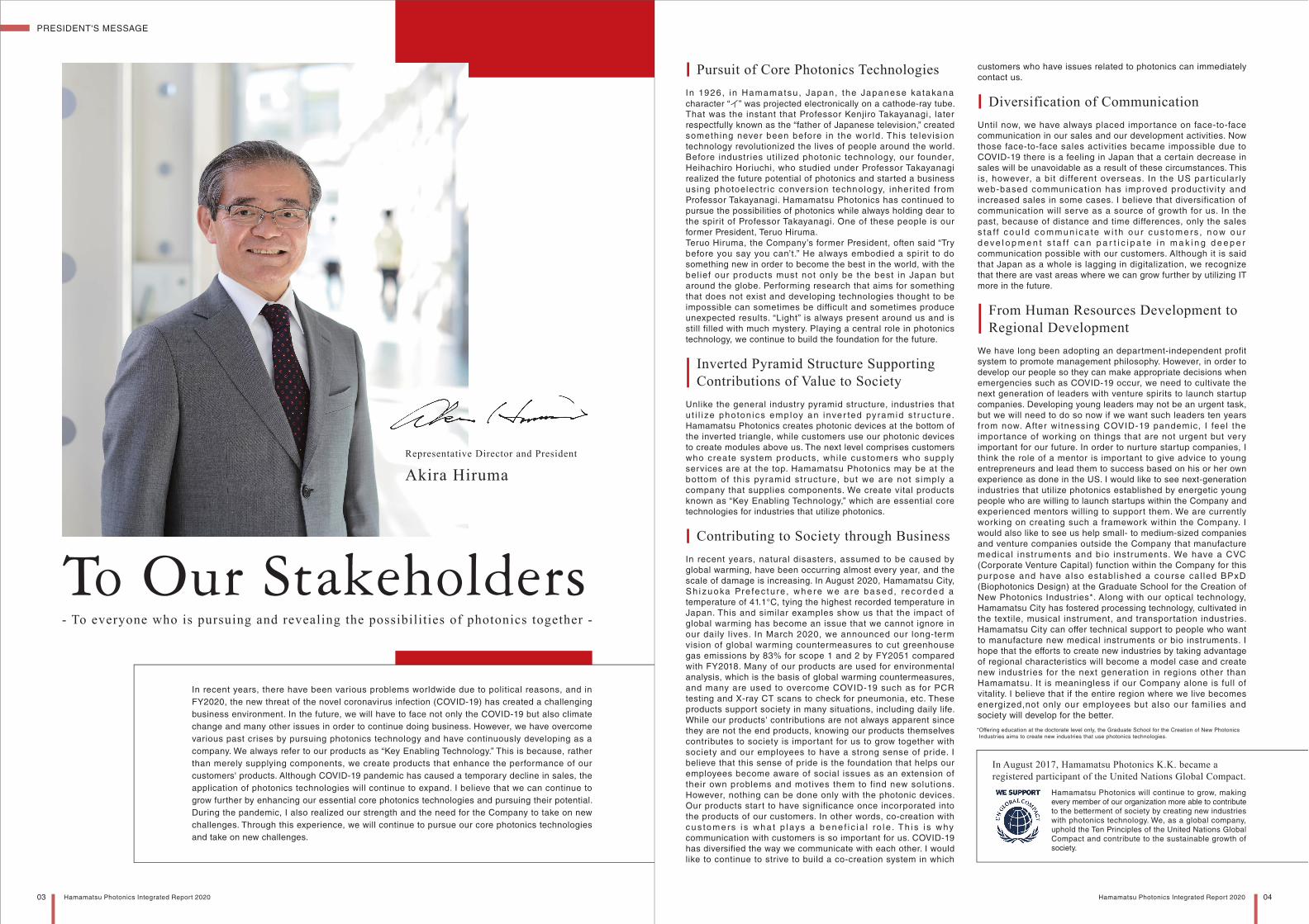
To Our Stakeholders
Hamamatsu Photonics will continue to grow, making
every member of our organization more able to contribute
to the betterment of society by creating new industries
with photonics technology. We, as a global company,
uphold the Ten Principles of the United Nations Global
Compact and contribute to the sustainable growth of
society.
In August 2017, Hamamatsu Photonics K.K. became a registered participant of the United Nations Global Compact.
In recent years, there have been various problems worldwide due to political reasons, and in
FY2020, the new threat of the novel coronavirus infection (COVID-19) has created a challenging
business environment. In the future, we will have to face not only the COVID-19 but also climate
change and many other issues in order to continue doing business. However, we have overcome
various past crises by pursuing photonics technology and have continuously developing as a
company. We always refer to our products as “Key Enabling Technology.” This is because, rather
than merely supplying components, we create products that enhance the performance of our
customers' products. Although COVID-19 pandemic has caused a temporary decline in sales, the
application of photonics technologies will continue to expand. I believe that we can continue to
grow further by enhancing our essential core photonics technologies and pursuing their potential.
During the pandemic, I also realized our strength and the need for the Company to take on new
challenges. Through this experience, we will continue to pursue our core photonics technologies
and take on new challenges.
- To everyone who is pursuing and revealing the possibilities of photonics together -
Representative Director and President
Akira Hiruma
PRESIDENT'S MESSAGE
03 Hamamatsu Photonics Integrated Report 2020 04Hamamatsu Photonics Integrated Report 2020
W h a t i s “ L i g h t ” ?Always striving to reveal the infinite and hidden potential of light.
Wave-Particle Duality of Photons
This is Young’ s Interference Experiment or
Double-slit Interference Experiment. This
experiment shows interference fringes appear
even if the light is drastically weakened to the
level of having only one particle. This demonstrated
that in the double-slit interference experiment,
one photon particle simultaneously passed
through the two slits and interfered by itself.
Photon has the wave-particle duality.
▲Watch a video of the experiment.
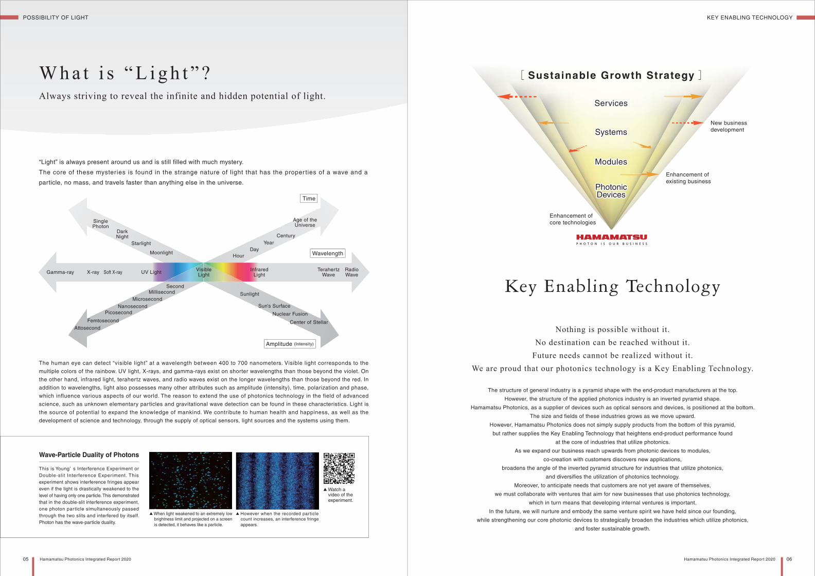
“Light” is always present around us and is still filled with much mystery.
The core of these mysteries is found in the strange nature of light that has the proper ties of a wave and a
particle, no mass, and travels faster than anything else in the universe.
The human eye can detect “visible light” at a wavelength between 400 to 700 nanometers. Visible light corresponds to the
multiple colors of the rainbow. UV light, X-rays, and gamma-rays exist on shorter wavelengths than those beyond the violet. On
the other hand, infrared light, terahertz waves, and radio waves exist on the longer wavelengths than those beyond the red. In
addition to wavelengths, light also possesses many other attributes such as amplitude (intensity), time, polarization and phase,
which influence various aspects of our world. The reason to extend the use of photonics technology in the field of advanced
science, such as unknown elementary particles and gravitational wave detection can be found in these characteristics. Light is
the source of potential to expand the knowledge of mankind. We contribute to human health and happiness, as well as the
development of science and technology, through the supply of optical sensors, light sources and the systems using them.
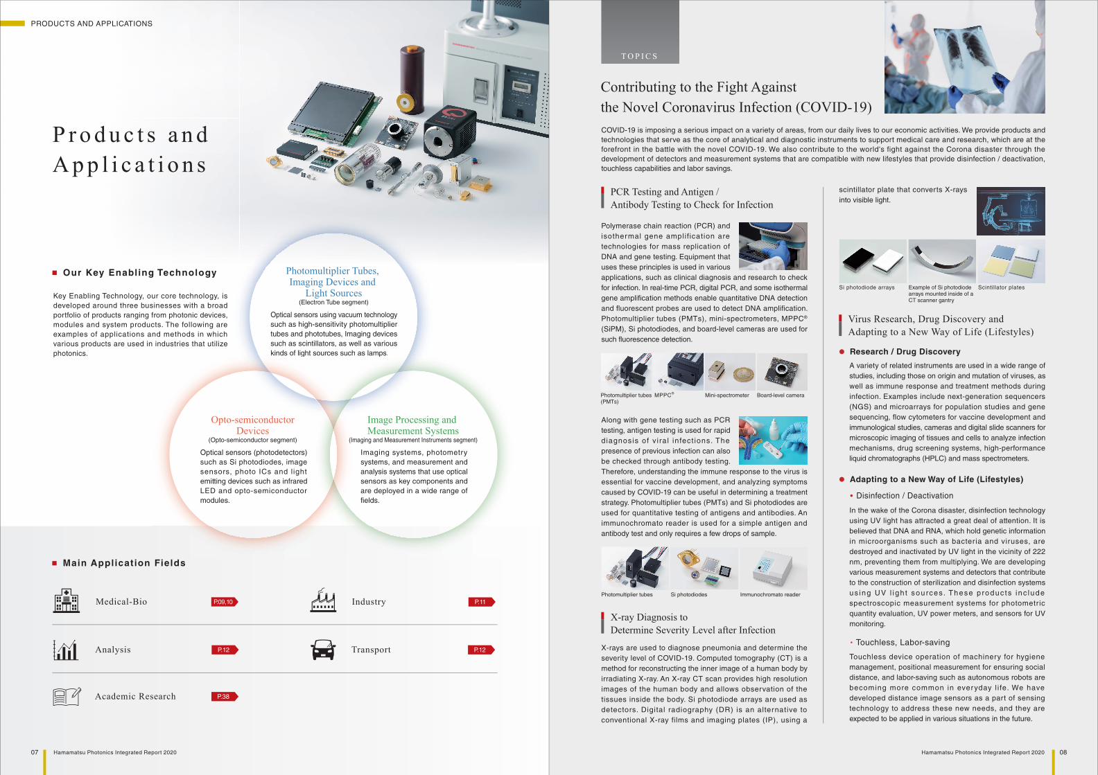
Key Enabling Technology
Nothing is possible without it.No destination can be reached without it.
Future needs cannot be realized without it.We are proud that our photonics technology is a Key Enabling Technology.
The structure of general industry is a pyramid shape with the end-product manufacturers at the top.
However, the structure of the applied photonics industry is an inverted pyramid shape.
Hamamatsu Photonics, as a supplier of devices such as optical sensors and devices, is positioned at the bottom.
The size and fields of these industries grows as we move upward.
However, Hamamatsu Photonics does not simply supply products from the bottom of this pyramid,
but rather supplies the Key Enabling Technology that heightens end-product performance found
at the core of industries that utilize photonics.
As we expand our business reach upwards from photonic devices to modules,
co-creation with customers discovers new applications,
broadens the angle of the inverted pyramid structure for industries that utilize photonics,
and diversifies the utilization of photonics technology.
Moreover, to anticipate needs that customers are not yet aware of themselves,
we must collaborate with ventures that aim for new businesses that use photonics technology,
which in turn means that developing internal ventures is important.
In the future, we will nurture and embody the same venture spirit we have held since our founding,
while strengthening our core photonic devices to strategically broaden the industries which utilize photonics,
and foster sustainable growth.
Wavelength
Time
SinglePhoton
DarkNight
Moonlight
Starlight
Sunlight
Sun’s Surface
Nuclear Fusion
Center of Stellar
Amplitude (Intensity)
Attosecond
Femtosecond
Picosecond
Nanosecond
Microsecond
MillisecondSecond
Hour
Day
Year
Century
Age of theUniverse
RadioWave
TerahertzWave
InfraredLight
VisibleLight
UV LightSoft X-rayX-rayGamma-ray
Sustainable Growth Strategy
ServicesServicesServices
SystemsSystemsSystems
ModulesModulesModules
PhotonicDevicesPhotonicDevicesPhotonicDevices
New business
development
Enhancement of
existing business
Enhancement of
core technologies
POSSIBILITY OF LIGHT KEY ENABLING TECHNOLOGY
05 Hamamatsu Photonics Integrated Report 2020 06Hamamatsu Photonics Integrated Report 2020
▲ However when the recorded particle
count increases, an interference fringe
appears.
▲When light weakened to an extremely low
brightness limit and projected on a screen
is detected, it behaves like a particle.
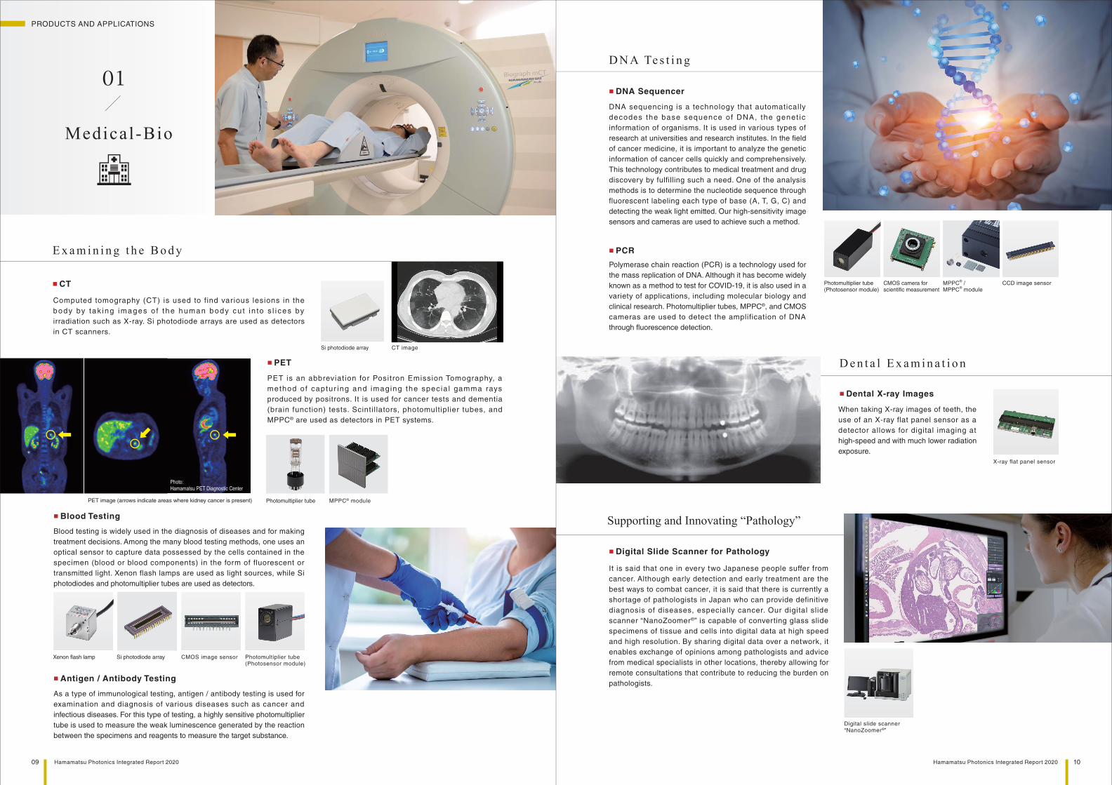
P r o d u c t s a n d A p p l i c a t i o n s
Key Enabling Technology, our core technology, is
developed around three businesses with a broad
portfolio of products ranging from photonic devices,
modules and system products. The following are
examples of applications and methods in which
various products are used in industries that utilize
photonics.
Medical-Bio P.09,10
Transport P.12
Industry P.11
Academic Research P.38
Analysis P.12
Contributing to the Fight Against the Novel Coronavirus Infection (COVID-19)COVID-19 is imposing a serious impact on a variety of areas, from our daily lives to our economic activities. We provide products and
technologies that serve as the core of analytical and diagnostic instruments to support medical care and research, which are at the
forefront in the battle with the novel COVID-19. We also contribute to the world's fight against the Corona disaster through the
development of detectors and measurement systems that are compatible with new lifestyles that provide disinfection / deactivation,
touchless capabilities and labor savings.
A variety of related instruments are used in a wide range of
studies, including those on origin and mutation of viruses, as
well as immune response and treatment methods during
infection. Examples include next-generation sequencers
(NGS) and microarrays for population studies and gene
sequencing, flow cytometers for vaccine development and
immunological studies, cameras and digital slide scanners for
microscopic imaging of tissues and cells to analyze infection
mechanisms, drug screening systems, high-performance
liquid chromatographs (HPLC) and mass spectrometers.
● Research / Drug Discovery
● Adapting to a New Way of Life (Lifestyles)
In the wake of the Corona disaster, disinfection technology
using UV light has attracted a great deal of attention. It is
believed that DNA and RNA, which hold genetic information
in microorganisms such as bacteria and viruses, are
destroyed and inactivated by UV light in the vicinity of 222
nm, preventing them from multiplying. We are developing
various measurement systems and detectors that contribute
to the construction of sterilization and disinfection systems
us ing UV l i gh t sou rces. These p roduc ts i nc lude
spectroscopic measurement systems for photometric
quantity evaluation, UV power meters, and sensors for UV
monitoring.
・・Disinfection / Deactivation
Touchless device operation of machinery for hygiene
management, positional measurement for ensuring social
distance, and labor-saving such as autonomous robots are
becoming more common in everyday l i fe. We have
developed distance image sensors as a part of sensing
technology to address these new needs, and they are
expected to be applied in various situations in the future.
・ Touchless, Labor-saving
Polymerase chain reaction (PCR) and
isothermal gene amplification are
technologies for mass replication of
DNA and gene testing. Equipment that
uses these principles is used in various
applications, such as clinical diagnosis and research to check
for infection. In real-time PCR, digital PCR, and some isothermal
gene amplification methods enable quantitative DNA detection
and fluorescent probes are used to detect DNA amplification.
Photomultiplier tubes (PMTs), mini-spectrometers, MPPC®
(SiPM), Si photodiodes, and board-level cameras are used for
such fluorescence detection.
PCR Testing and Antigen / Antibody Testing to Check for Infection
Photomultiplier tubes (PMTs)
MPPC®
Mini-spectrometer Board-level camera
Si photodiode arrays Example of Si photodiode arrays mounted inside of a CT scanner gantry
Scintillator plates
scintillator plate that converts X-rays
into visible light.
T O P I C S
Main Application Fields
Photomultiplier tubes Si photodiodes Immunochromato reader
Virus Research, Drug Discovery and Adapting to a New Way of Life (Lifestyles)
X-rays are used to diagnose pneumonia and determine the
severity level of COVID-19. Computed tomography (CT) is a
method for reconstructing the inner image of a human body by
irradiating X-ray. An X-ray CT scan provides high resolution
images of the human body and allows observation of the
tissues inside the body. Si photodiode arrays are used as
detectors. Digital radiography (DR) is an alternative to
conventional X-ray films and imaging plates (IP), using a
X-ray Diagnosis to Determine Severity Level after Infection
Along with gene testing such as PCR
testing, antigen testing is used for rapid
diagnosis of v i ra l infect ions. The
presence of previous infection can also
be checked through antibody testing.
Therefore, understanding the immune response to the virus is
essential for vaccine development, and analyzing symptoms
caused by COVID-19 can be useful in determining a treatment
strategy. Photomultiplier tubes (PMTs) and Si photodiodes are
used for quantitative testing of antigens and antibodies. An
immunochromato reader is used for a simple antigen and
antibody test and only requires a few drops of sample.
Our Key Enabling Technology Photomultiplier Tubes, Imaging Devices and
Light Sources(Electron Tube segment)
Optical sensors using vacuum technology
such as high-sensitivity photomultiplier
tubes and phototubes, Imaging devices
such as scintillators, as well as various
kinds of light sources such as lamps.kinds of light sources such
Opto-semiconductorDevices
(Opto-semiconductor segment)
Optical sensors (photodetectors)
such as Si photodiodes, image
sensors, photo ICs and light
emitting devices such as infrared
LED and opto-semiconductor
modules.
as lamps.sources such
Image Processing and Measurement Systems
(Imaging and Measurement Instruments segment)
Imaging systems, photometry
systems, and measurement and
analysis systems that use optical
sensors as key components and
are deployed in a wide range of
fields.
PRODUCTS AND APPLICATIONS
07 Hamamatsu Photonics Integrated Report 2020 08Hamamatsu Photonics Integrated Report 2020
Medical-Bio
Computed tomography (CT) is used to find var ious lesions in the
body by tak ing images o f t he human body cu t i n to s l i ces by
irradiation such as X-ray. Si photodiode arrays are used as detectors
in CT scanners.
■ CT
■ DNA Sequencer
Supporting and Innovating “Pathology”
■ Digital Slide Scanner for Pathology
It is said that one in every two Japanese people suffer from
cancer. Although early detection and early treatment are the
best ways to combat cancer, it is said that there is currently a
shortage of pathologists in Japan who can provide definitive
diagnosis of diseases, especially cancer. Our digital slide
scanner “NanoZoomer®” is capable of converting glass slide
specimens of tissue and cells into digital data at high speed
and high resolution. By sharing digital data over a network, it
enables exchange of opinions among pathologists and advice
from medical specialists in other locations, thereby allowing for
remote consultations that contribute to reducing the burden on
pathologists.
DNA sequencing is a technology that automatically
decodes the base sequence of DNA, the genet ic
information of organisms. It is used in various types of
research at universities and research institutes. In the field
of cancer medicine, it is important to analyze the genetic
information of cancer cells quickly and comprehensively.
This technology contributes to medical treatment and drug
discovery by fulfilling such a need. One of the analysis
methods is to determine the nucleotide sequence through
fluorescent labeling each type of base (A, T, G, C) and
detecting the weak light emitted. Our high-sensitivity image
sensors and cameras are used to achieve such a method.
■ PCR
Polymerase chain reaction (PCR) is a technology used for
the mass replication of DNA. Although it has become widely
known as a method to test for COVID-19, it is also used in a
variety of applications, including molecular biology and
clinical research. Photomultiplier tubes, MPPC®, and CMOS
cameras are used to detect the amplification of DNA
through fluorescence detection.
Digital slide scanner “NanoZoomer®”
Blood testing is widely used in the diagnosis of diseases and for making
treatment decisions. Among the many blood testing methods, one uses an
optical sensor to capture data possessed by the cells contained in the
specimen (blood or blood components) in the form of fluorescent or
transmitted light. Xenon flash lamps are used as light sources, while Si
photodiodes and photomultiplier tubes are used as detectors.
As a type of immunological testing, antigen / antibody testing is used for
examination and diagnosis of various diseases such as cancer and
infectious diseases. For this type of testing, a highly sensitive photomultiplier
tube is used to measure the weak luminescence generated by the reaction
between the specimens and reagents to measure the target substance.
■ Blood Testing
■ Antigen / Antibody Testing
Xenon flash lamp Si photodiode array Photomultiplier tube(Photosensor module)
CMOS image sensor
PET is an abbreviat ion for Positron Emission Tomography, a
method o f captur ing and imaging the spec ia l gamma rays
produced by positrons. It is used for cancer tests and dementia
(brain function) tests. Scintil lators, photomultiplier tubes, and
MPPC® are used as detectors in PET systems.
■ PET
CT image
E x a m i n i n g t h e B o d y
D N A Te s t i n g
■ Dental X-ray Images
When taking X-ray images of teeth, the
use of an X-ray flat panel sensor as a
detector allows for digital imaging at
high-speed and with much lower radiation
exposure.
X-ray flat panel sensor
D e n t a l E x a m i n a t i o n
01
PET image (arrows indicate areas where kidney cancer is present)
Photo: Hamamatsu PET Diagnostic Center
Si photodiode array
Photomultiplier tube MPPC® module
MPPC® /
MPPC® module
Photomultiplier tube(Photosensor module)
CMOS camera for scientific measurement
CCD image sensor
PRODUCTS AND APPLICATIONS
09 Hamamatsu Photonics Integrated Report 2020 10Hamamatsu Photonics Integrated Report 2020
Supporting Innovative Automotive Technologies to Realize Safety, Security and Comfort
■ LiDAR and Other Automotive Related Technologies
LiDAR (Light Detection and Ranging) is a technology that serves as the
eyes of self-driving systems, using infrared lasers and sensors to
determine the position and distance of surrounding objects. The distance
is measured by irradiating a laser light onto an object and capturing the
reflected light with an optical sensor. Pulse laser diodes, etc. are used as
light sources, and various optical sensors such as Si photodiodes and Si
APDs are used as detectors. In addition to this technology, our
opto-semiconductor devices are used for many functions designed for
safety, security, and comfort, including ambient light level detection to
achieve automatic headlight, raindrop detection for automatic-windshield
wiper, and sunlight level detection for automatic air conditioning.
Inspection of the Inside of Things
■ X-ray Non-destructive Inspection
X-ray non-destructive inspection, which enables
non-contac t , non-des t ruc t i ve inspec t ion and
analys is of the st ructure and proper t ies of an
object in real time, is widely used in our daily life.
Examples inc lude produc t ion and inspec t ion
p r o c e s s e s i n t h e m a n u fa c t u r i n g i n d u s t r y,
inspection of infrastructure equipment, inspection
of foreign matter in food, and baggage inspection
at airports. Our microfocus X-ray sources are used
as X-ray sources, and X-ray line sensor cameras
and Si photodiode arrays are used as detectors.
Microfocus X-ray source
X-ray line scan camera Si photodiode arrays
Soft X-ray source
Image taken during baggage inspection Internal shape inspection of Li-ion batteries
Protecting the Health of the Earth
Light sources and optical sensors using infrared light
are used to detect greenhouse gases and air
pollutants. X-rays, beta rays, and neutron rays are
used to measure dust (PM2.5), and ultraviolet rays
are used to decompose pollutants in the atmosphere.
■ Atmospheric Measurement
■Water Quality Tests
Water quality tests are conducted to detect water pollution in rivers, oceans, and groundwater, which can cause environmental
degradation and health hazards. A number of potential contaminants exist in water, and their major components are regulated
by law and regulations regarding their reference values and measurement methods. Our high-sensitivity optical sensors and
high-intensity light sources are used in water quality testing equipment that needs to be able to detect extremely small amounts
of contaminants.
Xenon flash lamps Si photodiode Image sensor Photomultiplier tube Phototubes
Mid infrared LEDs Quantum cascade laser Xenon flash lamp InAsSb photovoltaic detectors
Analysis03Industry02
Transport04
Distance measurement(self-driving, collision avoidance)
Head-up display Ambient light level detection(automatic headlight)
In-vehiclenetwork
Sunlight level detection(automatic air conditioning)
Raindrop detection(automatic-windshield wiper)
Laser-driven light source “LDLS TM”
Photosensor with front-end IC MPPC®
Pulse laser diodes InGaAs APD Si PIN photodiodeSi APD
Multifaceted Support for Semiconductor Manufacturing
■ Semiconductor Manufacturing / Inspection
Our products are also widely used during the
manufacture of semiconductors, which are
indispensable in modern life. These products
include image sensors, photomultiplier tubes,
and other optical sensors used in the inspection
process such as lamps, laser-driven light
sources, known as LDLSTM, Stealth Dicing
EngineTM system for cutting wafers at high
speed and with high quality, and failure
analysis systems that can identify failure
locations on semiconductor wafers.
TDI-CCD image sensors Stealth Dicing EngineTM
systemFailure analysis system
PRODUCTS AND APPLICATIONS
11 Hamamatsu Photonics Integrated Report 2020 12Hamamatsu Photonics Integrated Report 2020
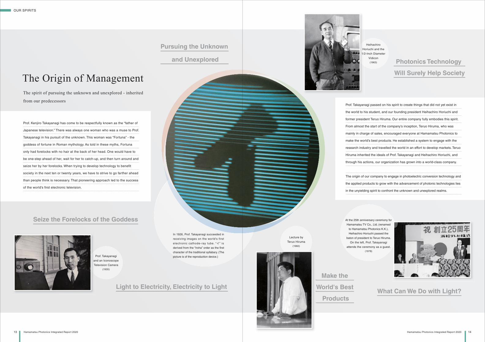
Pursuing the Unknown
and Unexplored
Seize the Forelocks of the Goddess
Light to Electricity, Electricity to Light
Photonics Technology
Will Surely Help Society
What Can We Do with Light?
Make the
World's Best
Products
Lecture by
Teruo Hiruma
(1960)
Prof. Takayanagi
and an Iconoscope
Television Camera
(1935)
Heihachiro
Horiuchi and the
1/2-Inch Diameter
Vidicon
(1963)
At the 25th anniversary ceremony for
Hamamatsu TV Co., Ltd. (renamed
to Hamamatsu Photonics K.K.),
Heihachiro Horiuchi passed the
baton of president to Teruo Hiruma.
On the left, Prof. Takayanagi
attends the ceremony as a guest.
(1978)
The Origin of ManagementThe spirit of pursuing the unknown and unexplored - inherited
from our predecessors
In 1926, Prof. Takayanagi succeeded in
receiving images on the world's first
e lectronic cathode-ray tube. “イ” is
derived from the “Iroha” order as the first
character of the traditional syllabary. (The
picture is of the reproduction device.)
H
1/2
W
an
T
a
T
OUR SPIRITS
13 Hamamatsu Photonics Integrated Report 2020 14Hamamatsu Photonics Integrated Report 2020
Prof. Kenjiro Takayanagi has come to be respectfully known as the “father of
Japanese television.” There was always one woman who was a muse to Prof.
Takayanagi in his pursuit of the unknown. This woman was “Fortuna” - the
goddess of fortune in Roman mythology. As told in these myths, Fortuna
only had forelocks with no hair at the back of her head. One would have to
be one-step ahead of her, wait for her to catch-up, and then turn around and
seize her by her forelocks. When trying to develop technology to benefit
society in the next ten or twenty years, we have to strive to go farther ahead
than people think is necessary. That pioneering approach led to the success
of the world’s first electronic television.
Prof. Takayanagi passed on his spirit to create things that did not yet exist in
the world to his student, and our founding president Heihachiro Horiuchi and
former president Teruo Hiruma. Our entire company fully embodies this spirit.
From almost the start of the company’s inception, Teruo Hiruma, who was
mainly in charge of sales, encouraged everyone at Hamamatsu Photonics to
make the world’s best products. He established a system to engage with the
research industry and travelled the world in an effort to develop markets. Teruo
Hiruma inherited the ideals of Prof. Takayanagi and Heihachiro Horiuchi, and
through his actions, our organization has grown into a world-class company.
The origin of our company to engage in photoelectric conversion technology and
the applied products to grow with the advancement of photonic technologies lies
in the unyielding spirit to confront the unknown and unexplored realms.
The his tory of our growth
▶ ▶ ▶
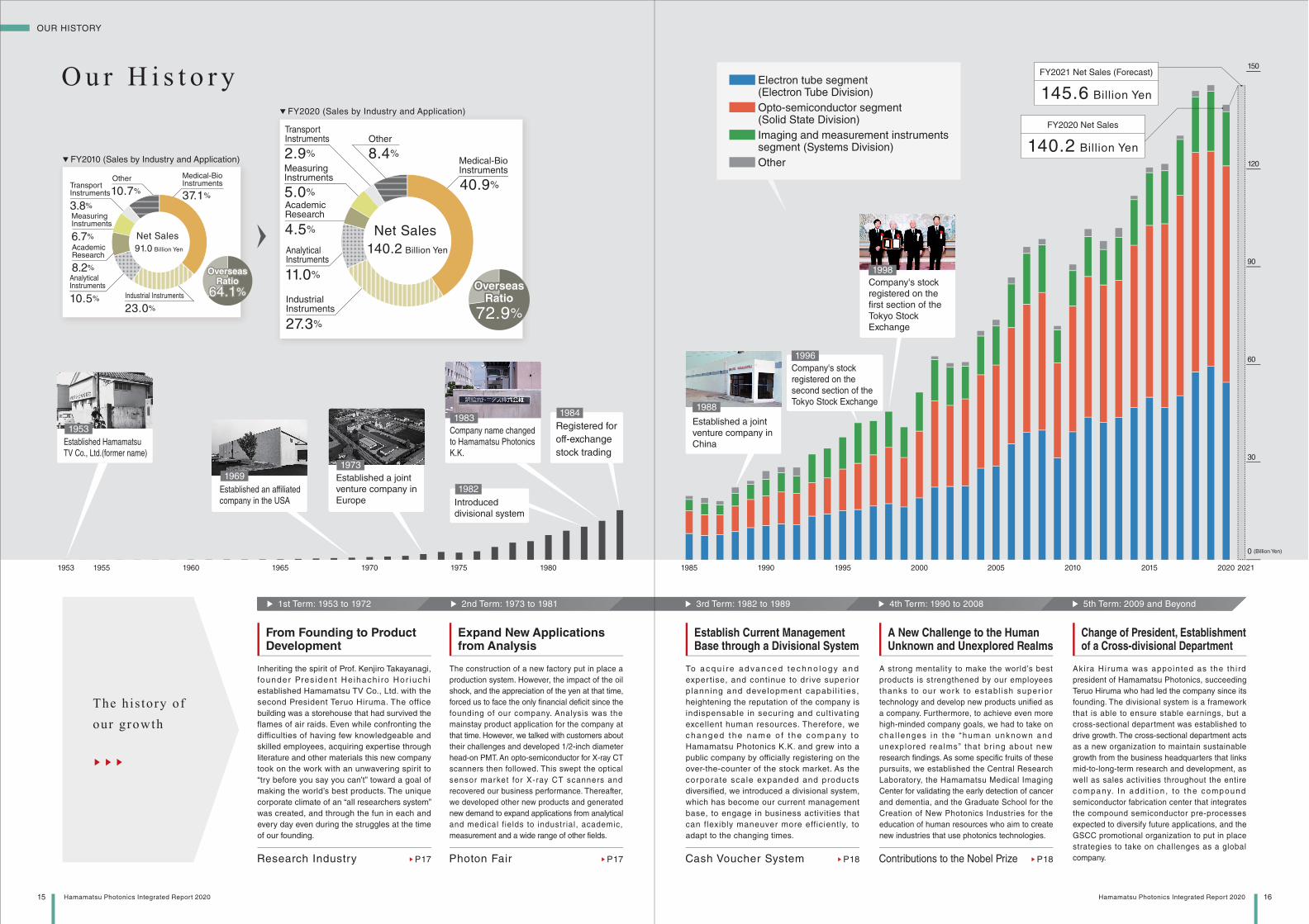
O u r H i s t o r y
1953 1955 1960 1965 1970 1975 1980 1985 1990 1995 2000 2005 2010 2015 2020 2021
1984
1982
1996
FY2021 Net Sales (Forecast)
145.6 Billion Yen
FY2020 Net Sales
140.2 Billion Yen
To a c q u i re a d va n c e d te c h n o l o g y a n d
exper tise, and continue to dr ive superior
p lanning and development capabi l i t ies,
heightening the reputation of the company is
indispensable in securing and cultivating
excellent human resources. Therefore, we
changed t he name o f t he company to
Hamamatsu Photonics K.K. and grew into a
public company by officially registering on the
over-the-counter of the stock market. As the
corporate scale expanded and products
diversified, we introduced a divisional system,
which has become our current management
base, to engage in business activities that
can flexibly maneuver more efficiently, to
adapt to the changing times.
Establish Current Management Base through a Divisional System
▶P18Cash Voucher System
▶ 3rd Term: 1982 to 1989
Change of President, Establishment of a Cross-divisional Department
Akira Hi ruma was appointed as the th i rd
president of Hamamatsu Photonics, succeeding
Teruo Hiruma who had led the company since its
founding. The divisional system is a framework
that is able to ensure stable earnings, but a
cross-sectional department was established to
drive growth. The cross-sectional department acts
as a new organization to maintain sustainable
growth from the business headquarters that links
mid-to-long-term research and development, as
well as sales activities throughout the entire
company. I n add i t i on , to t he compound
semiconductor fabrication center that integrates
the compound semiconductor pre-processes
expected to diversify future applications, and the
GSCC promotional organization to put in place
strategies to take on challenges as a global
company.
▶ 5th Term: 2009 and Beyond
A strong mentality to make the world’s best
products is strengthened by our employees
thanks to our work to es tabl ish super ior
technology and develop new products unified as
a company. Furthermore, to achieve even more
high-minded company goals, we had to take on
cha l l enges in the “human unknown and
unexplored realms” that br ing about new
research findings. As some specific fruits of these
pursuits, we established the Central Research
Laboratory, the Hamamatsu Medical Imaging
Center for validating the early detection of cancer
and dementia, and the Graduate School for the
Creation of New Photonics Industries for the
education of human resources who aim to create
new industries that use photonics technologies.
A New Challenge to the Human Unknown and Unexplored Realms
▶P18Contributions to the Nobel Prize
▶ 4th Term: 1990 to 2008
The construction of a new factory put in place a
production system. However, the impact of the oil
shock, and the appreciation of the yen at that time,
forced us to face the only financial deficit since the
founding of our company. Analysis was the
mainstay product application for the company at
that time. However, we talked with customers about
their challenges and developed 1/2-inch diameter
head-on PMT. An opto-semiconductor for X-ray CT
scanners then followed. This swept the optical
sensor market for X-ray CT scanners and
recovered our business performance. Thereafter,
we developed other new products and generated
new demand to expand applications from analytical
and medical fields to industr ial, academic,
measurement and a wide range of other fields.
▶P17Photon Fair
Expand New Applications from Analysis
▶ 2nd Term: 1973 to 1981
Inheriting the spirit of Prof. Kenjiro Takayanagi,
founder Pres ident He ihach i ro Hor iuch i
established Hamamatsu TV Co., Ltd. with the
second President Teruo Hiruma. The office
building was a storehouse that had survived the
flames of air raids. Even while confronting the
difficulties of having few knowledgeable and
skilled employees, acquiring expertise through
literature and other materials this new company
took on the work with an unwavering spirit to
“try before you say you can’t” toward a goal of
making the world’s best products. The unique
corporate climate of an “all researchers system”
was created, and through the fun in each and
every day even during the struggles at the time
of our founding.
Research Industry ▶P17
From Founding to Product Development
▶ 1st Term: 1953 to 1972
0 (Billion Yen)
30
60
90
120
150
1953
19691973
1983
1998
Company's stock
registered on the
first section of the
Tokyo Stock
Exchange
Company's stock
registered on the
second section of the
Tokyo Stock Exchange
Established Hamamatsu
TV Co., Ltd.(former name)
Established an affiliated
company in the USA
Established a joint
venture company in
Europe Introduced
divisional system
Company name changed
to Hamamatsu Photonics
K.K.
Registered for
off-exchange
stock trading
1988
Established a joint
venture company in
China
Net Sales
91.0 Billion Yen
▼ FY2010 (Sales by Industry and Application)
10.5%
Analytical Instruments
8.2%
Academic Research
6.7%
Measuring Instruments
3.8%
Transport Instruments
23.0%
Industrial Instruments
10.7%
Other
37.1%
Medical-Bio Instruments
OverseasRatio
64.1%
OverseasRatio
64.1%
Net Sales
140.2 Billion Yen
40.9%
27.3%
8.4%
Industrial Instruments
11.0%
Analytical Instruments
4.5%
Academic Research
5.0%
Measuring Instruments
2.9%
Transport Instruments
▼ FY2020 (Sales by Industry and Application)
Medical-Bio Instruments
Other
OverseasRatio
72.9%
OverseasRatio
72.9%
OUR HISTORY
15 Hamamatsu Photonics Integrated Report 2020 16Hamamatsu Photonics Integrated Report 2020
Electron tube segment (Electron Tube Division)
Opto-semiconductor segment (Solid State Division)
Imaging and measurement instruments segment (Systems Division)
Other
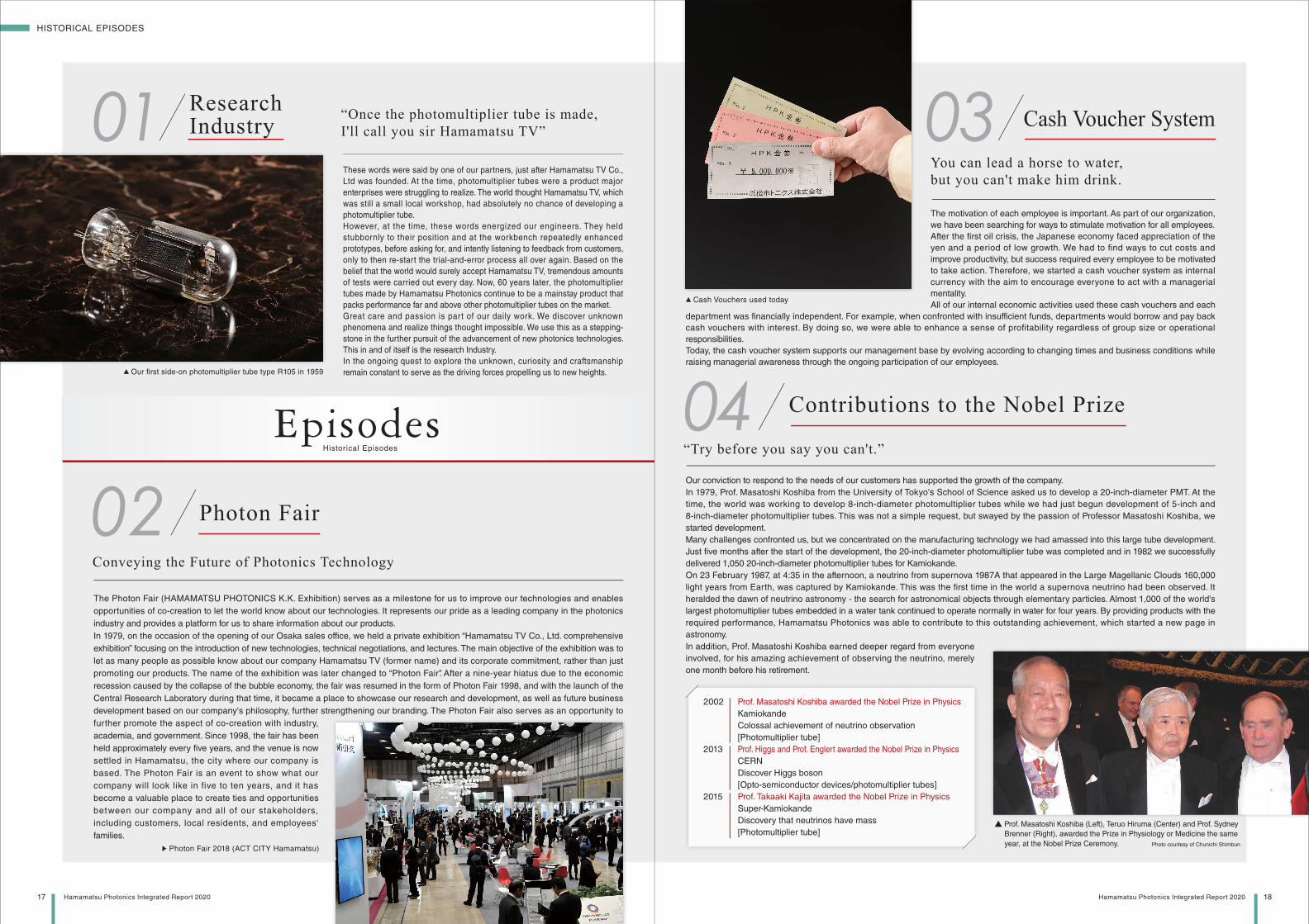
The motivation of each employee is important. As part of our organization,
we have been searching for ways to stimulate motivation for all employees.
After the first oil crisis, the Japanese economy faced appreciation of the
yen and a period of low growth. We had to find ways to cut costs and
improve productivity, but success required every employee to be motivated
to take action. Therefore, we started a cash voucher system as internal
currency with the aim to encourage everyone to act with a managerial
mentality.
All of our internal economic activities used these cash vouchers and each
department was financially independent. For example, when confronted with insufficient funds, departments would borrow and pay back
cash vouchers with interest. By doing so, we were able to enhance a sense of profitability regardless of group size or operational
responsibilities.
Today, the cash voucher system supports our management base by evolving according to changing times and business conditions while
raising managerial awareness through the ongoing participation of our employees.
03 Cash Voucher System
You can lead a horse to water, but you can't make him drink.
▲ Our first side-on photomultiplier tube type R105 in 1959
Historical Episodes
Episodes
The Photon Fair (HAMAMATSU PHOTONICS K.K. Exhibition) serves as a milestone for us to improve our technologies and enables
opportunities of co-creation to let the world know about our technologies. It represents our pride as a leading company in the photonics
industry and provides a platform for us to share information about our products.
In 1979, on the occasion of the opening of our Osaka sales office, we held a private exhibition “Hamamatsu TV Co., Ltd. comprehensive
exhibition” focusing on the introduction of new technologies, technical negotiations, and lectures. The main objective of the exhibition was to
let as many people as possible know about our company Hamamatsu TV (former name) and its corporate commitment, rather than just
promoting our products. The name of the exhibition was later changed to “Photon Fair”. After a nine-year hiatus due to the economic
recession caused by the collapse of the bubble economy, the fair was resumed in the form of Photon Fair 1998, and with the launch of the
Central Research Laboratory during that time, it became a place to showcase our research and development, as well as future business
development based on our company's philosophy, further strengthening our branding. The Photon Fair also serves as an opportunity to
further promote the aspect of co-creation with industry,
academia, and government. Since 1998, the fair has been
held approximately every five years, and the venue is now
settled in Hamamatsu, the city where our company is
based. The Photon Fair is an event to show what our
company will look like in five to ten years, and it has
become a valuable place to create ties and opportunities
between our company and all of our stakeholders,
including customers, local residents, and employees'
families.
02 Photon Fair
▶ Photon Fair 2018 (ACT CITY Hamamatsu)
▲ Cash Vouchers used today
Our conviction to respond to the needs of our customers has supported the growth of the company.
In 1979, Prof. Masatoshi Koshiba from the University of Tokyo's School of Science asked us to develop a 20-inch-diameter PMT. At the
time, the world was working to develop 8-inch-diameter photomultiplier tubes while we had just begun development of 5-inch and
8-inch-diameter photomultiplier tubes. This was not a simple request, but swayed by the passion of Professor Masatoshi Koshiba, we
started development.
Many challenges confronted us, but we concentrated on the manufacturing technology we had amassed into this large tube development.
Just five months after the start of the development, the 20-inch-diameter photomultiplier tube was completed and in 1982 we successfully
delivered 1,050 20-inch-diameter photomultiplier tubes for Kamiokande.
On 23 February 1987, at 4:35 in the afternoon, a neutrino from supernova 1987A that appeared in the Large Magellanic Clouds 160,000
light years from Earth, was captured by Kamiokande. This was the first time in the world a supernova neutrino had been observed. It
heralded the dawn of neutrino astronomy - the search for astronomical objects through elementary particles. Almost 1,000 of the world's
largest photomultiplier tubes embedded in a water tank continued to operate normally in water for four years. By providing products with the
required performance, Hamamatsu Photonics was able to contribute to this outstanding achievement, which started a new page in
astronomy.
In addition, Prof. Masatoshi Koshiba earned deeper regard from everyone
involved, for his amazing achievement of observing the neutrino, merely
one month before his retirement.
04 Contributions to the Nobel Prize
“Try before you say you can't.”
Prof. Masatoshi Koshiba awarded the Nobel Prize in Physics
Kamiokande
Colossal achievement of neutrino observation
[Photomultiplier tube]
Prof. Higgs and Prof. Englert awarded the Nobel Prize in Physics
CERN
Discover Higgs boson
[Opto-semiconductor devices/photomultiplier tubes]
Prof. Takaaki Kajita awarded the Nobel Prize in Physics
Super-Kamiokande
Discovery that neutrinos have mass
[Photomultiplier tube]
2002
2013
2015
▲ Prof. Masatoshi Koshiba (Left), Teruo Hiruma (Center) and Prof. Sydney
Brenner (Right), awarded the Prize in Physiology or Medicine the same
year, at the Nobel Prize Ceremony. Photo courtesy of Chunichi Shimbun
These words were said by one of our partners, just after Hamamatsu TV Co.,
Ltd was founded. At the time, photomultiplier tubes were a product major
enterprises were struggling to realize. The world thought Hamamatsu TV, which
was still a small local workshop, had absolutely no chance of developing a
photomultiplier tube.
However, at the time, these words energized our engineers. They held
stubbornly to their position and at the workbench repeatedly enhanced
prototypes, before asking for, and intently listening to feedback from customers,
only to then re-start the trial-and-error process all over again. Based on the
belief that the world would surely accept Hamamatsu TV, tremendous amounts
of tests were carried out every day. Now, 60 years later, the photomultiplier
tubes made by Hamamatsu Photonics continue to be a mainstay product that
packs performance far and above other photomultiplier tubes on the market.
Great care and passion is part of our daily work. We discover unknown
phenomena and realize things thought impossible. We use this as a stepping-
stone in the further pursuit of the advancement of new photonics technologies.
This in and of itself is the research Industry.
In the ongoing quest to explore the unknown, curiosity and craftsmanship
remain constant to serve as the driving forces propelling us to new heights.
“Once the photomultiplier tube is made, I'll call you sir Hamamatsu TV”01 Research
Industry
Conveying the Future of Photonics Technology
HISTORICAL EPISODES
17 Hamamatsu Photonics Integrated Report 2020 18Hamamatsu Photonics Integrated Report 2020
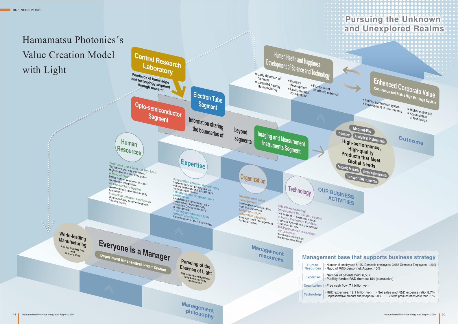
Pursuing the Unknown and Unexplored Realms
Information sharing beyond the boundaries of segments
Electron TubeSegmentOpto-semiconductorSegment
Imaging and MeasurementInstruments Segment
Everyone is a ManagerDepartment Independent Profit System
High-performance,High-quality Products that Meet Global Needs
Medical-BioIndustry Analytical Instruments
Academic ResearchTransport Instruments
Measuring Instruments
HumanResourcesExpertise
OrganizationTechnology
Pursuing of theEssence of LightThe essence of light hasonly been partiallyunderstood
World-leadingManufacturingAim for Number OneandOne of a Kind
Feedback of knowledge and technology acquired
through research
Central ResearchLaboratory
Managementresources
Managementphilosophy
OUR BUSINESSACTIVITIES
Outcome
Continuous and Stable High Earnings System
Enhanced Corporate Value
Management base that supports business strategy
rganrga
Hamamatsu Photonics´s Value Creation Model with Light
・Number of employees: 5,195 (Domestic employees: 3,986 Overseas Employees: 1,209)・Ratio of R&D personnel: Approx. 10%
HumanResources
・Number of patents held: 6,587・Publicly funded R&D themes: 154 (cumulative)
Expertise
・Free cash flow: 7.1 billion yenOrganization
・R&D expenses: 12.1 billion yen ・Net sales and R&D expense ratio: 8.7%・Representative product share: Approx. 90% ・Custom product ratio: More than 70%
Technology
Human Health and Happiness Development of Science and Technology
■ Unique governance system■ Development of new markets
■ Higher motivation■ Accumulation of technology
■ Early detection of diseases■ Extended healthy life expectancy
■ Industry development■ Environmental conservation
■ Promotion of academic research
Yaramaika (Let's Give It a Try) Spirit
“Try before you say you can't.”
High motivation and lofty goals
A Mind of “Wa”Better human relationships and
knowledge integration.All Researchers SystemOvercoming challenges in daily
operationsInteraction between Employees
Club activities, summer festivals,
athletic meets
Cooperation between departments
Presentations on prototypes as
well as research and department
management resultsIndustry-academic-government
partnershipsEstablishing Hamamatsu as a
Preeminent Photonics City
Photonics Declaration 2013
in HamamatsuPursuing performance to its
farthest boundariesAccumulation of tacit knowledge
Sales/Manufacturing/Development Partnership System
Full support of customer needs
In-house Production Facilities
High-mix low-volume production/
customer serviceBuilding co-creation relationships
with customersInformation sharing from the development stage
Departmental sales managementFormulation of sales plans
from the bottom-up.Stable cash flow generation capabilityThrough profit management
by department
BUSINESS MODEL
19 Hamamatsu Photonics Integrated Report 2020 20Hamamatsu Photonics Integrated Report 2020
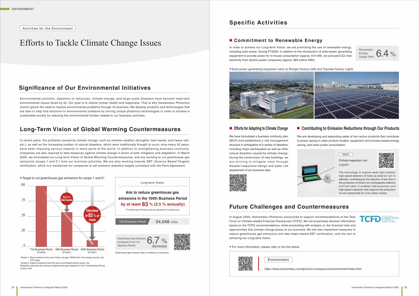
Efforts to Tackle Climate Change Issues
In recent years, the problems caused by climate change, such as extreme weather (droughts, heat waves, and heavy rain,
etc.), as well as the increasing number of natural disasters, which were traditionally thought to occur once every 50 years,
have been imposing ser ious impacts in many par ts of the wor ld. In addi t ion to strengthening business cont inui ty,
companies are also required to take measures against climate change in terms of both mitigation and adaptation. In March
2020, we formulated our Long-term Vision of Global Warming Countermeasures, and are working to cut greenhouse gas
emissions (scope 1 and 2*) from our business activit ies. We are also working towards SBT (Science Based Targets)
certification, which is a mechanism for companies to set emission reduction targets consistent with the Paris Agreement.
Long-Term Vision of Global Warming Countermeasures
Environmental pol lut ion, deplet ion of resources, cl imate change, and large-scale disasters have become impor tant
environmental issues faced by all. Our goal is to realize human health and happiness. That is why Hamamatsu Photonics
cannot ignore the need to resolve environmental problems through its business. We develop products and technologies that
are able to help find solutions to environmental problems by driving unique photonics technologies in order to achieve a
sustainable society by reducing the environmental burden related to our business activities.
Significance of Our Environmental Initiatives
In August 2020, Hamamatsu Photonics announced to support recommendations of the Task
Force on Climate-related Financial Disclosures (TCFD). We will proactively disclose information
based on the TCFD recommendations, while proceeding with analysis on the financial risks and
opportunities that climate change poses to our business. We will also implement measures to
reduce greenhouse gas emissions and take steps toward SBT certification, with the aim of
achieving our Long-term Vision.
Future Challenges and Countermeasures
▼ For more information, please refer to the link below.
Environment
https://www.hamamatsu.com/jp/en/our-company/csr/environment/index.html
Act iv i t ies for the Environment
▼Target to cut greenhouse gas emissions for scope 1 and 2*
Aim to reduce greenhouse gas
emissions in the 104th Business Period
by at least 83 % (2.5 % annually)71st Business Period used as standard for comparison
Long-term Vision
73rd Business Period 54,048 t-CO2
25
0
50
75
100
Specific Activit ies
Greenhouse gas emission data is verified by a third party.
We have formulated a business continuity plan
(BCP) and established a risk management
structure in anticipation of a variety of disasters,
including major earthquakes as well as other
natural disasters caused by climate change.
During the construction of new buildings, we
a re s t r i v i ng to m i t i ga te r i s ks t h rough
disaster-responsive design and water risk
assessment of our business sites.
Efforts for Adapting to Climate Change Contributing to Emission Reductions through Our Products
▼Solar-power generating equipment seen at Shingai Factory (left) and Toyooka Factory (right)
We are developing and expanding sales of low carbon products that contribute
to power saving in older product models, equipment and process-based energy
saving, and lower power consumption.
The technology to capture weak light enables
high-speed detection of holes as small as 1μm in
diameter, contributing to the reduction of tact time in
the production of lithium-ion rechargeable batteries
and fuel cel ls. I t enables high-precision and
high-speed inspection that supports the production
of core components for a low carbon society.
Pinhole inspection unit
C15477
TOPIC
In order to achieve our Long-term Vision, we are promoting the use of renewable energy,
including solar power. During FY2020, in addition to the introduction of solar-power generating
equipment to provide power for in-house consumption (approx. 614 kW), we procured CO2-free
electricity from electric power companies (approx. 684 million kWh).
Renewable
Energy
Usage Rate 6.4 %
Commitment to Renewable Energy
Greenhouse Gas Emissions
(compared to the 71st
Business Period)6.7 %
decrease
*Scope 1: Direct emission from use of fuels, city gas, GHGs from non-energy sources, etc.,
CFC leaks
*Scope 2: Indirect emissions from the use of purchased electric power, etc.
Reduction rate when the amount of greenhouse gas emissions in the 71st Business Period
is set at 100
71st Business Period 84th Business Period 104th Business Period(FY2018) (FY2031) (FY2051)
32.5 %decrease
Decreaseof 83 % or
more
ENVIRONMENT
21 Hamamatsu Photonics Integrated Report 2020 22Hamamatsu Photonics Integrated Report 2020
SOCIAL
23 Hamamatsu Photonics Integrated Report 2020 24Hamamatsu Photonics Integrated Report 2020
We hope to provide value to society, such as the human health and happiness, through our company activit ies. Our
employees are the foundation for us to achieve this goal. Therefore, we work to provide a work-friendly environment for all
of our employees and strive to maintain and improve their physical and mental health. To fulfill that need, we recognize the
importance of building an organization and corporate culture in which employees are encouraged not merely to support the
status quo but to actively engage based on free and innovative thinking.
Significance of Our Activities for Society
Act iv i t ies for Society
▼ For more information, please refer to the link below.
CSR/ESG Information
https://www.hamamatsu.com/jp/en/our-company/csr/index.html
Hamamatsu Photonics pr imari ly recruits science students. This has created a tendency to hire relatively few women
because the percentage of women in the sciences is low. Ensur ing diversi ty is impor tant to faci l i tate mult i faceted
viewpoints in the development of new technology in the future. For this reason, we are engaging in recruitment activities as
per the action plan outlined in the Database on Promotion of Women’s Participation and Advancement in the Workplace.
Additionally, we always str ive to better the working environment and promote health management in an effor t to make
certain every employee can live a prosperous life.
Future Challenges and Countermeasures
The average length of service is 16.4 years for males
and 14.9 years for females with a turnover rate of
0.9%. The average acquisition rate of paid leave was
76.5% (74.6% in the previous year). Additionally, the
percentage of employees on mental health leave was
0.46 %, which is dramatically lower than the average
(0.8 %) of business sites with 1,000 employees.
Fruits of Our Efforts
Efforts for the Vital Human Resources of Hamamatsu Photonics
Specific Activities
In March 2002 the Company introduced a continuing-employment
program. Under this program, the retirement age for monthly
wage earners was raised from 60 to 65 years of age. This means
that employees can extend their employment to 65 years of age if
they desire. In tandem with continuing employment, the Company
offers the same amount of wages as received at the age of 60 for
the period of extension. This scheme creates an environment in
which veteran employees can enjoy making full use of their skills
and capabil i t ies, passing their knowledge on to younger
colleagues. This plan also enables Hamamatsu Photonics to
secure the talented employees it needs.
As many employees join the Company from distant regions,
Hamamatsu Photonics bui lds dormitor ies and provides
residences for single employees. We also provide interested
employees with breakfast and dinner services. Our dormitories
respect single employees’ dignity and privacy. Each resident is
assigned his or her own suite, and no curfew is imposed. We
provide a stable base for their lives where young employees can
fully demonstrate their abilities.
Continuing-employment Program Operation of Dormitories for Single Employees
We believe enriching the home, community and other social infrastructure is impor tant for every employee to actively
participate in the company. That is why we consult with the labor union as necessary and have put programs in place, as
we strive to ensure a work-life balance.
Ensuring Work-life Balance
▼Continuing Employment Comparison by Year
87.5 % 92.7 % 91.9 %
2017 2018 2019
Health Management InitiativesIn accordance with its Corporate Health Policy,
Hamamatsu Photonics promotes heal th
management in cooperation with Photonics
Group Health Insurance Society. Based on the
verification of effectiveness, the Company
implements various measures after proposal,
discussion and approval by the Headquarters
and Branch Health and Safety Committees and
by the Board of Executive Officers.
▼Mental-health Education Programs
FY2017
FY2018
FY2019
Focused on middle-tier employees
Focused on all employees
Focused on managers
▼ Percentage of Employees Answering Stress Check
FY2017
FY2018
FY2019
95.3 %
96.3 %
95.8 %
To eliminate long working hours,
the management oversees employees’
work hours, and the labor-management
council verifies them.
Every Wednesday is designated a
no-overtime day.
Managers are provided with appropriate
training.
When an employee’s overtime seems
excessive, managers engage in dialogue with
that employee and arrange for interviews with
an appropriate professional, such as an
industrial physician or public health nurse.
The company invites outside instructors to
run seminars on topics including childcare
support system, nursing care and mental
health.
Various policies are implemented to
balance work, children, nursing care,
and medical treatments of individuals
and their families.
To maintain and improve the physical
strength of employees, the Company
holds a body design school, and
conducts physical strength
measurements. Employees are also
encouraged to walk and use sports
facilities.
In addition to the regular medical
check-ups mandated by law for the
purpose of the early detection and
treatment of diseases, we also conduct
dental check-ups.
We recommend health screening and
PET examinations to our employees.
Hamamatsu Photonics and the health
insurance society pay a contribution to
the fees.
All employees are encouraged to recognize the signs and different types of stress
through our stress check-up program, known in-house as the “Mental Health
Check”. This aims to reduce stress in the workplace, together with group analysis
and on-site training.
As part of our mental health measures,
we have formulated a three-year,
mental health promotion plan. The
mental health education program is
tailored to each employee rank.
In three consecutive years, 2018, 2019, and
2020, the Company earned certification as
an Excel lent Health and Product iv i ty
Management Corporation (Large Enterprise
Division) (White 500).
Health and
productivity
White 500
▼ For more detailed information about our corporate governance, please refer to the link below.
Basic Policy on Corporate Governance
https://www.hamamatsu.com/resources/pdf/hamamatsu/corporategovernance_en.pdf
CSR/ESG Information
https://www.hamamatsu.com/jp/en/our-company/csr/index.html
Dialogue with Investors Compensation Scheme for Directors
We, at Hamamatsu Photonics hope that our shareholders wil l
hold our shares over the long term. For this reason, we actively
engage in dialogue with our institutional investors based on our
belief that we must facilitate understanding about our businesses.
We also advocate the following policies related to our dialogue
with institutional investors.
We require Directors to strive forward with a medium- to
long-term perspective, rather than merely with a
short-term mindset. Therefore, we see it appropriate to
put basic remuneration at the base of the Company’s
compensation scheme for Directors. We have also
introduced stock-based compensation with restrictions
on transfer as part of the Company’s compensation
scheme. The purpose of this is to encourage our
directors to hold the Company’s stock on a long-term,
stable basis, with the intention that they share the same
perspectives as our shareholders and contribute to the
sustainable growth of Hamamatsu Photonics’ corporate
value. Both basic remuneration and restricted stock
remuneration are determined by the Board of Directors,
and their ratio is generally 85 to 15.
The challenge is whether we can meet matters deemed necessary in the shor t-to-mid-term for stakeholders, while also
satisfying mid-to-long term requirements. Therefore, Hamamatsu Photonics advances its core technologies such as
photodetectors, which are the foundation of its business. Whilst never forgetting the venture spirit held since our founding,
planning and endeavoring to develop new technologies, and cultivating the human resources entrusted with these tasks.
We share the th ings we see as impor tant , as wel l as our va lues, wi th a l l o f our shareholders and var ious other
stakeholders involved to build long-term relationships based on trust. In the future, ongoing contributions to society are
directly connected to the perpetual existence of corporate organizations.
Future Challenges and Countermeasures
Our products are used as key
devices that contribute to human
happiness and the sustainable
growth o f soc ie t y in med ica l ,
analytical, industrial and a wide
range o f o the r f i e lds . We w i l l
enhance ou r co r po ra te va lue
toward ongoing social contributions
in the future. In order to do so,
Hamamatsu Photonics formulates
and shares its corporate philosophy
because all of our employees unified
in both action and principle toward
the future is indispensable. We
believe this can generate stable
earnings, fur thers research and
development, and fosters growth.
Therefore, we are building a distinct
governance structure suitable for
Hamamatsu Photonics.
Significance of Strengthening Corporate Governance
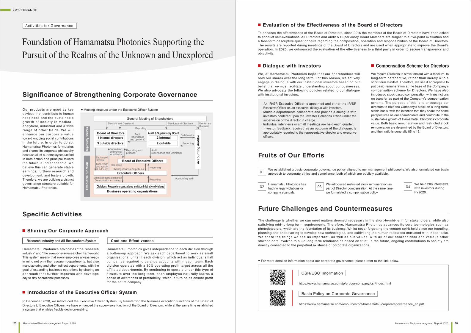
▼ Meeting structure under the Executive Officer System
Supe
rviso
ry fu
nctio
nsE
xecu
tive
fu
nct
ion
General Meeting of Shareholders
Election and Dismissal
Acc
ou
nti
ng
Au
dito
r
Audit & Supervisory BoardCollaboration
Reporting
Reporting
Audit (attendance and opinions)
Election and Dismissal
Election and Dismissal
Board of Directors8 internal directors
3 outside directors
2 internal
2 outside
Executive Officers
Divisions, Research organizations and Administrative divisions
Business operating organizations
Board of Executive Officers
Audit(Attendance and Opinions)
Supervisionand transferof authority
Reporting and proposal
ReportingSharing issues and policies
Reporting
Election and Dismissal
Supervision and transfer of authority
ReportingDirection of business execution
Communication and sharingAccounting audit
Fruits of Our Efforts
01
Hamamatsu Photonics has
had no legal violations or
company scandals.
We established a basic corporate governance policy aligned to our management philosophy. We also formulated our basic
approach to corporate ethics and compliance, both of which are publicly available.
We held 206 interviews
with investors during
FY2020.
We introduced restricted stock remuneration as
part of Director compensation. At the same time,
we formulated a compensation policy
02 0403
GOVERNANCE
25 Hamamatsu Photonics Integrated Report 2020 26Hamamatsu Photonics Integrated Report 2020
Foundation of Hamamatsu Photonics Supporting the Pursuit of the Realms of the Unknown and Unexplored
Act iv i t ies for Governance
Hamamatsu Photonics advocates “the research
industry” and “the everyone-a-researcher framework”.
This system means that every employee always keeps
in mind not only the research departments, but also
manufacturing and other indirect departments, with the
goal of expanding business operations by sharing an
approach that fur ther improves and develops
day-to-day operational processes.
Sharing Our Corporate Approach
Hamamatsu Photonics gives independence to each division through
a bottom-up approach. We ask each depar tment to work as small
organizational units in each division, which act as individual small
companies required to balance accounts within each team. Each
division operates with a 30% operating profit target across all the
affil iated depar tments. By continuing to operate under this type of
structure over the long term, each employee natural ly learns a
sense of awareness of profitability, which in turn helps ensure profit
for the entire company.
Research Industry and All Researchers System Cost and Effectiveness
Introduction of the Executive Officer System
In December 2020, we introduced the Executive Officer System. By transferring the business execution functions of the Board of
Directors to Executive Officers, we have enhanced the supervisory function of the Board of Directors, while at the same time established
a system that enables flexible decision-making.
Specific Activities
Evaluation of the Effectiveness of the Board of Directors
To enhance the effectiveness of the Board of Directors, since 2016 the members of the Board of Directors have been asked
to conduct self-evaluations. All Directors and Audit & Supervisory Board Members are subject to a five-point evaluation and
a free-form descriptive questionnaire regarding the composition, operation and responsibilities of the Board of Directors.
The results are reported during meetings of the Board of Directors and are used when appropriate to improve the Board’s
operation. In 2020, we outsourced the evaluation of the effectiveness to a third party in order to secure transparency and
objectivity.
· An IR/SR Executive Officer is appointed and either the IR/SR
Executive Officer or, an executive, dialogue with investors.
· Multiple departments collaborate and provide a dialogue with
investors centered upon the Invester Relations Office under the
supervision of the director in charge.
· Individual interviews or small meetings are held each quarter.
· Investor feedback received as an outcome of the dialogue, is
appropriately reported to the representative director and executive
officers.
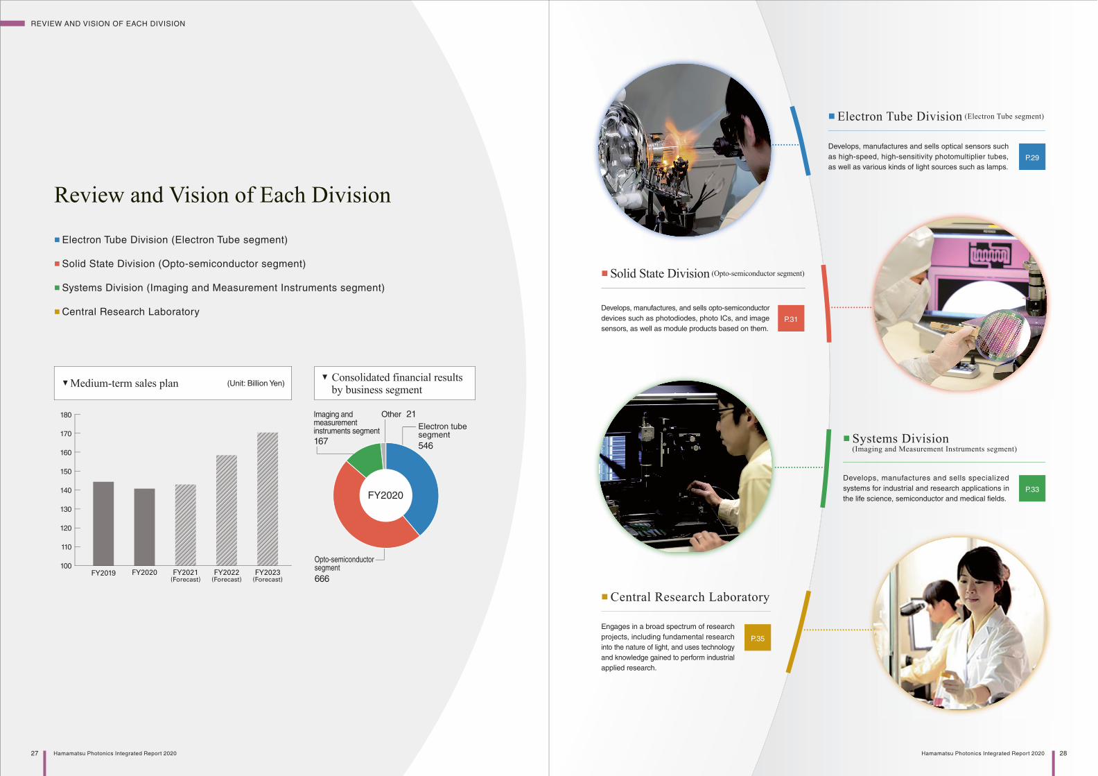
■Electron Tube Division (Electron Tube segment)
Develops, manufactures and sells optical sensors such
as high-speed, high-sensitivity photomultiplier tubes,
as well as various kinds of light sources such as lamps.
P.29
■Central Research Laboratory
Engages in a broad spectrum of research
projects, including fundamental research
into the nature of light, and uses technology
and knowledge gained to perform industrial
applied research.
P.35
■Solid State Division (Opto-semiconductor segment)
Develops, manufactures, and sells opto-semiconductor
devices such as photodiodes, photo ICs, and image
sensors, as well as module products based on them.
P.31
■ Systems Division(Imaging and Measurement Instruments segment)
Develops, manufactures and sells specialized
systems for industrial and research applications in
the life science, semiconductor and medical fields.
P.33
Review and Vision of Each Division
■Electron Tube Division (Electron Tube segment)
■Solid State Division (Opto-semiconductor segment)
■Systems Division (Imaging and Measurement Instruments segment)
■Central Research Laboratory
▼ Consolidated financial results by business segment
546167
21Imaging and measurement instruments segment
FY2020
Electron tube segment
Other180
170
160
150
140
130
120
110
100FY2019 FY2020 FY2021
(Forecast)FY2022(Forecast)
FY2023(Forecast)
(Unit: Billion Yen)▼ Medium-term sales plan
666
Opto-semiconductor segment
REVIEW AND VISION OF EACH DIVISION
27 Hamamatsu Photonics Integrated Report 2020 28Hamamatsu Photonics Integrated Report 2020
For Future Growth
As commun ica t i on becomes more d i ve rs i f i ed due to
COVID-19, I feel that it is necessary to develop products not
on ly in response to prov ided in format ion but a lso in a
proactive manner to inspire our customers. Recently, we
launched an immunochromato reader that can be used for
coronavirus testing. We have developed a wide range of
technolog ies such as evaporat ion, vacuum, and laser
applications, and will continue to develop products that will
bring new awareness to our customers and expand into new
applications.
Features
Electron Tube Division continues to grow as a result of the
strength of product development and market development by
each production department. The manufacturing process for
photomultiplier tubes has required a high-level of manual labor
and this is why I bel ieve development work done at the
production site is essential, as it is where manufacturing actually
takes place. Product development and market development by
department provides a high level of freedom, allowing us to
actively engage in development activities even in small markets.
In order to take advantage of this strength and achieve further
growth, we have created a design team that shares the
technology of each department. In addition to the photomultiplier
tube, which is our most dominant product within Electron Tube
Division, this division offers a wide range of other products, such
as light sources and applied products, that have successfully
developed new markets. By sharing technologies not only within
a particular department but also from other departments, we will
strengthen our product development and continue to achieve
sustainable growth by further developing new markets.
Review of FY2020
In the medical field, sales of photomultiplier tubes (PMT) for
products for in vitro diagnostics (IVD) such as blood analyzers
have increased, thanks to strong demand in Japan and overseas,
specifically China.
However, sales for photomultiplier tubes declined as a result of a
significant fall in sales for oil-well logging devices due to sluggish
oilfield investment as well as a decline in sales for academic
applications and environmental and emission analysis. Regarding
imaging devices and light sources, in the industrial field, sales of
the Stealth Dicing Engine for high-speed, high-quality silicon wafer
dicing decreased, affected by the trade friction between the U.S.
and China, despite the strong sales of xenon lamps for
semiconductor inspection equipment. In addition, sales of
deuterium lamps for environmental analysis, etc. decreased mainly
in Asia due to closures of universities and research institutions in
the second half of the fiscal year. As a result, net sales of imaging
devices and light sources decreased. In total, the Electron Tube
segment comprised of photomultiplier tubes, imaging devices and
light sources closed fiscal year 2020 with net sales of JPY 54,636
million, down by 8.3% from the previous year. In terms of capital
investment, a new building was completed to consolidate
development and administrative departments. This will accelerate
the development of new light source and X-ray source products, as
well as the development of element technologies for electron tube
products that specifically target industrial fields.
Division Director,
Electron Tube Division
Hisaki Kato
Electron tube devices are key devices for measuring and
capturing phenomena that were impossible to find up to
now. We achieve this by applying our long-fostered basic
and element technologies. Our new manufacturing
technology creates innovative devices that are more
compact and optimized for particular usage environments,
expanding the application fields of the equipment in which
those devices are integrated. Electron tube devices that
have actively been used in a wide range of fields including
medical diagnosis, spectroscopic analysis, semiconductors,
biology, and academic research are now being pushed to
their ultimate performance limits to meet customer needs
and to expand the market.
Electron Tube Division (Electron Tube segment)
Photomultiplier Tubes, Imaging Devices, Light Sources, and X-ray Sources
Risks and Opportunities
Market Environment
Market development based
on technologies cultivated
in photomultiplier tubes
Migration from photomultiplier
tubes to opto-semiconductors
Human Resources
Establishment of an information
sharing system that transcends the
boundaries of independent divisions
Lack of information sharing due
to vertically divided organization
COVID-19
Expansion of demand
for in vitro diagnostics
Prolonged stagnation
in economic activitiesRisks
OpportunitiesFY2023(Forecast)
FY2022(Forecast)
FY2021(Forecast)
FY2020FY2019(Billion Yen)
▼ Consolidated financial results by business segment
Net Sales Operating Profit Ratio
70
60
50
40
30
20
10
0
30
35
10
25
20
5
15
0(%)
▼ Sales ratio by industry and application (FY2020)
Academic Research 3.0%
Other 7.9%
Measuring Instruments7.1%
Medical-BioInstruments
36.4%
Medical-BioInstruments
36.4%
28.9%28.9%
IndustrialInstruments
28.9%
IndustrialInstruments
28.9%
AnalyticalInstruments16.7%
ELECTRON TUBE DIVISION
29 Hamamatsu Photonics Integrated Report 2020 30Hamamatsu Photonics Integrated Report 2020
For Future Growth
Ongoing collaboration with our compound semiconductor
fabr icat ion center is being fac i l i ta ted the expansion of
app l ica t ions in the in f ra red range, such as ana ly t i ca l
instruments and transportation instruments in the future. The
market is expected to expand further as industries that utilize
photonics expand. On the other hand, I feel the need to
increase our production capacity based on a concern that
competition will increase along with market expansion. In
addition to investing in buildings and production facilities to
respond to increased sales, we will also actively invest in the
automation of production, inspection, and other processes to
improve productivity more than ever before.
Division Director,
Solid State Division
Takayuki Suzuki
Solid State Division has explored physical properties that
determine opto-semiconductor performance since the
early days in this field and succeeded in creating a variety
of product lineups. Our opto-semiconductor products
incorporate unique semiconductor process technology,
mounting & packaging technology, and MEMS technology,
and cover a wide wavelength range from infrared, visible,
ultraviolet, all the way to X-rays and high energy rays.
They are used for a wide range of purposes including
medical care, industrial applications, academic research,
analysis, and in vehicle electronics. We will continue to
pursue opto-semiconductor technology, always staying
one step ahead, to meet the increasingly sophisticated
needs of the future.
The Solid State Division does not develop technologies or
equipment for a single application but for horizontal expansion to
wider applications in order to maintain high-mix low-volume
production, whilst also increasing production efficiency. This is where
our strength comes from. In addition, this broadening of applications
has given us the ability to come up with creative capabilities to
develop products that our customers want. LiDAR, a technology
which is currently the focus of attention in autonomous driving, is
also used for measuring distances in everyday life (such as distance
measurements at golf courses and robotic vacuum cleaners) as well
as in cutting-edge academic research. Although customer
requirements differ depending on application, our creative capability
and development capability is strengthened by making products
highly functional for each application. In addition, the modularization
efforts that we have focused on in recent years have enabled us to
provide not only sensor capabilities but also optimal functions to
customers with different needs. We will continue to grow by making
proposals that are best suited to our customers.
Features
Solid State Division (Opto-semiconductor segment)
Opto-semiconductors
Risks and Opportunities
Market Environment
Increase in market opportunities
due to expansion of industries
that utilize photonics
Increase in competition due to
expansion of industries that
utilize photonics
Human Resources
Establishment of the employee
education system and clarification
of human resource development plans
Education system based
on on-the-job training
COVID-19
Expanding demand
for semiconductors
due to digitalization
Prolonged stagnation
in economic activitiesRisks
Opportunities
Review of FY2020
In opto-semiconductor devices, in the medical field, sales of Si
photodiodes for X-ray CT and laboratory testing increased,
caused by rising demand in Japan and overseas. However,
sales of X-ray flat panel sensors for dental applications
decreased due to the suspension of production activities by
customers, especially in Europe. In addition, in the industrial
field, sales of image sensors for semiconductor fabrication and
inspection equipment increased in response to the recovery of
the semiconductor market. As a result, the opto-semiconductor
segment generated 66.666 billion yen in net sales, up 1.0 %
year-on-year. As for capital investment, we completed the
construction of a new building at the Shingai Factory in August
2020. This new building will be used to manufacture X-ray flat
panel sensors and components for automotive applications
such as molded photodiodes, photo ICs. Although these
products were affected by the Corona disaster, we expect
significant growth in these fields in the future.
▼ Sales ratio by industry and application (FY2020)
Transport Instruments 5.7%
Measuring Instruments 3.9%
Other 7.0%
49.7%
Medical-BioInstruments
49.7%
Medical-BioInstruments
49.7%
22.5%
IndustrialInstruments
22.5%
IndustrialInstruments
22.5%AnalyticalInstruments 8.7%
Academic Research 2.5%
FY2023(Forecast)
FY2022(Forecast)
FY2021(Forecast)
FY2020FY2019(Billion Yen)
▼ Consolidated financial results by business segment
Net Sales Operating Profit Ratio
80
70
60
50
40
30
20
10
0
30
35
10
25
20
5
15
0(%)
SOLID STATE DIVISION
31 Hamamatsu Photonics Integrated Report 2020 32Hamamatsu Photonics Integrated Report 2020
Our Systems Division is developing and manufacturing
sys tem products tha t in tegra te l igh t de tec t ion
technology, imaging technology, and image processing
technology by using optical sensors. As a leading
sensor manufacturer, we use our exper t ise and
technology to design and develop applied products
that combine core products us ing h igh-speed,
high-sensitivity, and high-resolution technologies, such
a s c a m e ra s , w i t h p e r i p h e ra l te c h n o l o g y a n d
equipment. We develop products that maximize the
performance of sensors.
Systems Division, through a development structure that can
clearly satisfy market needs, has uti l ized this strength in
FY2020 by transforming each depar tment into a group of
expert professionals. This was achieved by organizing each
process, such as product planning, sales strategy, market
research, prototype/principle verification, prototype creation,
and commercialization. By gaining a deeper understanding of
the market in which we have accumulated information and
where we have a large market share, we aim to achieve
sustainable growth by discovering new needs and by planning
new concept products that do not replace existing products.
Features
Review of FY2020
In image processing and measurement systems, sales of digital
slide scanners for remote pathologic diagnosis systems grew due
to rising demand from inter-hospital networks in the U.S. and
Europe. However, sales of digital cameras used in the life
sciences sector and biotechnology sector declined in Japan and
overseas by the impact of a stagnation of activities at universities
and research institutions. In addition, affected by restrained capital
investment primarily in Japan and Europe, sales of failure analysis
systems for semiconductor devices declined. As a result, net sales
for the Imaging and Measurement Instruments business were JPY
16,754 million, down by 9.0% from the previous year.
Systems Division (Imaging and Measurement Instruments segment)
Image Processing and Measurement SystemsImage Processing and Measu
Division Director,
Systems Division
Tadashi Maruno
For Future Growth
In FY2020, we will utilize the functions of the reorganized
organization to accelerate growth by focusing the industrial
instruments, imaging, and medical-bio instruments markets. In the
industrial instruments market, we will launch inline inspection
instruments to meet the needs of the expanding semiconductor
market, and I expect sales to expand in the Asia region. In the
medical-bio instruments market, we are seeing a trend towards
digital slide scanner for pathological diagnosis being approved as
medical devices all over the world. With the Corona disaster,
digitalization is expected to accelerate, and I expect the market to
expand not only in developed countries but also in emerging
countries. In the imaging market, we are making great strides in
technology, including the development of photon counting
cameras in cooperation with other divisions. In the future, we
expect to expand our market share for many other applications in
addition to medical-bio applications, such as academic and
industrial applications.
FY2023(Forecast)
FY2022(Forecast)
FY2021(Forecast)
FY2020FY2019(Billion Yen)
▼ Consolidated financial results by business segment
Net Sales Operating Profit Ratio
30
10
25
20
5
15
0(%)
25
20
15
10
5
0
▼ Sales ratio by industry and application (FY2020)
Analytical Instruments 2.0%
Measuring Instruments 1.2%
Other 11.9%
AcademicResearch
17.0%
IndustrialInstruments
43.1%
IndustrialInstruments
43.1%
Medical-BioInstruments
24.8%
Medical-BioInstruments
24.8%
Risks and Opportunities
Market Environment
Clarification of concepts by
improving organizational structure
Opportunity loss due to
prolonged development
Human Resources
Strengthening of human
resources for software development
through human resource development
Intensified acquisition of
human resources for software
development, especially for AI
COVID-19
Expansion of demand for
remote pathology diagnosis
Prolonged stagnation
in economic activitiesRisks
Opportunities
SYSTEMS DIVISION
33 Hamamatsu Photonics Integrated Report 2020 34Hamamatsu Photonics Integrated Report 2020
What will our future be like 20 or 30 years from now?
How about a future where al l people can enjoy
comfortable and active lives with peace of mind, and
where optimal balance is maintained among the Earth,
its people and all living things? To make this dream a
reality, we will have to overcome many obstacles and
chal lenges. Our Central Research Laboratory is
conducting R&D work that conforms to “sustainability”
values. We call this work “Life Photonics” which is based
on the theme of “life” encompassing a broad range of
areas such as life, living things, human life, vitality
sources, and ways of living. We will continue researching
a diverse spectrum of photonics and optical technologies
taking “Life Photonics” as our motivating theme.
Review of FY2020
For Future Growth
I have again become aware of the importance of goal management.
In this context, I find it useful to set goals by adopting the
Objectives and Key Results (OKR) methodology in which each level
of the organization discusses a major goal. By setting goals that are
recognized by the group, individuals can understand what they
need to do now to achieve the large goal of pursuing the unknown
and unexplored. Although I would like to see us conduct research
on long-term themes fueled by dreams, such as the development of
high power lasers for laser fusion power generation, I also want us
to acquire serendipity (the ability to find something valuable when
looking for something else) and contribute to business as well as
pursue the unknown and unexplored realms of light.
Director,
Central Research Laboratory
Tsutomu HaraBy 1990, Hamamatsu Photonics had established itself as a
world-leading manufacturer of optoelectronic components and
systems. The company had gradually grown, and its divisions
were producing market-leading products. In the field of
research and development, we have been interacting with
world-class researchers and are now participating in joint
research. In order to effectively pursue the unknown and
unexplored realms of light in this environment, we decided to
create our very own Central Research Laboratory. Central
Research Laboratory was established in Hamakita-ku,
Hamamatsu City, to act as a compass, which guides us into
the future. The Tsukuba Research Center (Tsukuba City) and
Industrial Development Center (Nishi-ku, Hamamatsu City)
also became a part of Central Research Laboratory to further
expanding our research base. The Central Research
Laboratory is currently advancing basic research and the
applied research of photonics technology under the keywords
“Life Photonics”. “Life” here does not refer to concepts such as
medical and life sciences but it takes on the broad meaning of
life and living. By making this “life” possible through photonics
technology, we will help build a sustainable society. Central
Research Laboratory has two primary roles. Our first
responsibility is to contribute to Hamamatsu Photonics
business. We will help foster growth by providing the expertise
and technologies necessary for product development in each
division, while collaborating with them to commercialize
products using our accumulated knowledge. Our second
responsibility is to advance research into fundamental
measurement and fundamental physics in the pursuit of the
unknown and unexplored realms of light. By standing
shoulder-to-shoulder with universities and research institutes
worldwide and conducting leading-edge research, Hamamatsu
Photonics obtains new findings develops science and
technology, and contributes to human health and happiness.
Genesis and Role of the Central Research Laboratory
Laboratories
Central Research Laboratory
Tsukuba Research
Center,
Central Research
Laboratory
Industrial Development
Center,
Central Research
Laboratory
Central Research Laboratory
Basic and Applied Research
▼Major Research Outcome
Although we witnessed some limitations in FY2020 due to the
COVID-19 pandemic, it was a year in which I felt that we had
established a foundation for Central Research Laboratory to function
in both of its roles: “to contribute to business” and “to pursue the
unknown and unexplored realms of light”. One example of our
activities is the improvement of the performance of our products
through a series of experiments and improvements, utilizing the
expertise of the research themes of our laboratories and discussing
the problems through collaboration with other divisions. I think this is
a good example of how Central Research Laboratory was able to
utilize the results of its work for non-urgent but important issues for
the future in developing products for the business divisions. Although
many products have been transferred to the business divisions for
commercialization, I felt that there was not enough follow-up support
provided afterwards. After transfer, we are working to not only
contribute to sales by continuing to provide technical support, but
also to pursue new optical technologies by improving problem areas
and responding to customer requests. As a result of our focus on
human resource development, including changes in research
themes, reorganization of personnel, interaction with business units,
and young researcher's projects for selecting themes, I feel that we
have been able to find many projects that involve and impact
business division development.
1990 1995 2000
1991 2003 2008 2013 2019
2004 2006 2010 2016 2018
Established Central Research Laboratory Research Center
Developed a prototype animal PET system and conducted joint research at Kyoto University
Developed near-infrared time-resolved spectroscopy system for quantitative measurement of hemodynamics
Transferred parallel aligned nematic liquid crystal spatial light modulator (PAL-SLM) to business division
Began to use our newly-developed PET system for medical checkups at Hamamatsu Medical Imaging Center
Developed LCOS-SLM, a reflective liquid crystal device that precisely modulates the phase of light and controls wavefront
Succeeded in the production of ultraviolet laser diodes with world’s shortest wavelength (336 nm)
Succeeded in continuous generation of neutrons through laser fusion experiments (through joint research with the Graduate University for the Creation of New Photonics Industries and other institutions)
Succeeded in the commercialization of a photonic crystal laser
Succeeded in optical manipulation of neurotransmission in neurons (through joint research with Yokohama City University)
Developed room temperature terahertz difference frequency quantum cascade laser
Developed a laser diode pumped pulse laser capable of 100 J-class high output power
Developed 250 MW all-solid-state laser (in collaboration with Osaka University)
CENTRAL RESEARCH LABORATORY
35 Hamamatsu Photonics Integrated Report 2020 36Hamamatsu Photonics Integrated Report 2020
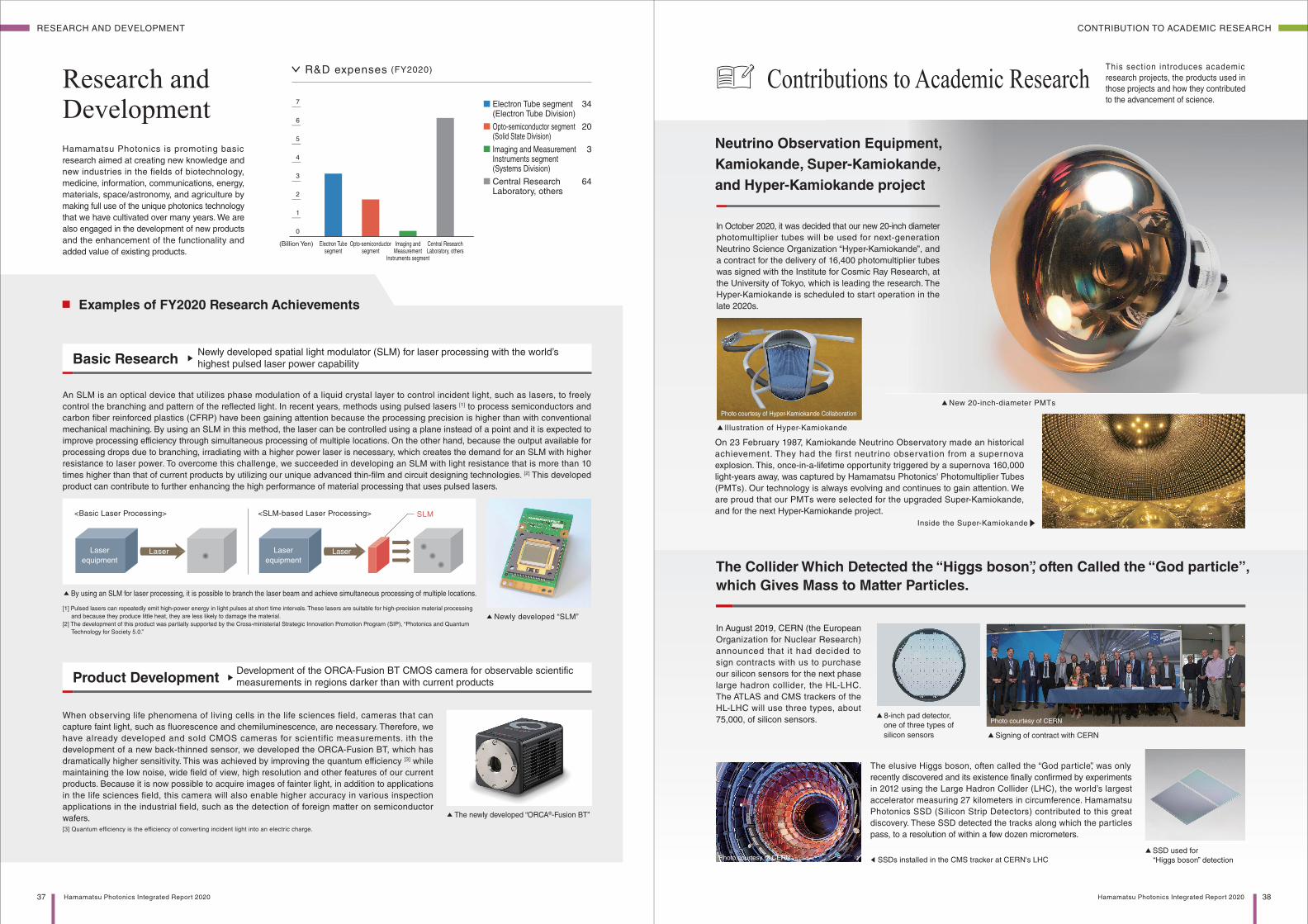
R&D expenses (FY2020)
Electron Tube segment (Electron Tube Division)
Opto-semiconductor segment (Solid State Division)
Imaging and Measurement Instruments segment (Systems Division)
Central Research Laboratory, others
(Billion Yen)
34
20
3
64
7
6
5
4
3
2
1
0
Central ResearchLaboratory, others
Imaging andMeasurement
Instruments segment
Opto-semiconductorsegment
Electron Tubesegment
▶Development of the ORCA-Fusion BT CMOS camera for observable scientific
measurements in regions darker than with current productsProduct Development
When observing life phenomena of living cells in the life sciences field, cameras that can
capture faint light, such as fluorescence and chemiluminescence, are necessary. Therefore, we
have already developed and sold CMOS cameras for scientific measurements. ith the
development of a new back-thinned sensor, we developed the ORCA-Fusion BT, which has
dramatically higher sensitivity. This was achieved by improving the quantum efficiency [3] while
maintaining the low noise, wide field of view, high resolution and other features of our current
products. Because it is now possible to acquire images of fainter light, in addition to applications
in the life sciences field, this camera will also enable higher accuracy in various inspection
applications in the industrial field, such as the detection of foreign matter on semiconductor
wafers.[3] Quantum efficiency is the efficiency of converting incident light into an electric charge.
▲ The newly developed “ORCA®-Fusion BT”
Research and DevelopmentHamamatsu Photonics is promoting basic
research aimed at creating new knowledge and
new industries in the fields of biotechnology,
medicine, information, communications, energy,
materials, space/astronomy, and agriculture by
making full use of the unique photonics technology
that we have cultivated over many years. We are
also engaged in the development of new products
and the enhancement of the functionality and
added value of existing products.
Examples of FY2020 Research Achievements
Contributions to Academic Research
Photo courtesy of CERN
The Collider Which Detected the “Higgs boson”, often Called the “God particle”, which Gives Mass to Matter Particles.
In August 2019, CERN (the European
Organization for Nuclear Research)
announced that it had decided to
sign contracts with us to purchase
our silicon sensors for the next phase
large hadron collider, the HL-LHC.
The ATLAS and CMS trackers of the
HL-LHC will use three types, about
75,000, of silicon sensors.
▲ SSD used for
“Higgs boson” detection◀ SSDs installed in the CMS tracker at CERN's LHC
An SLM is an optical device that utilizes phase modulation of a liquid crystal layer to control incident light, such as lasers, to freely
control the branching and pattern of the reflected light. In recent years, methods using pulsed lasers [1] to process semiconductors and
carbon fiber reinforced plastics (CFRP) have been gaining attention because the processing precision is higher than with conventional
mechanical machining. By using an SLM in this method, the laser can be controlled using a plane instead of a point and it is expected to
improve processing efficiency through simultaneous processing of multiple locations. On the other hand, because the output available for
processing drops due to branching, irradiating with a higher power laser is necessary, which creates the demand for an SLM with higher
resistance to laser power. To overcome this challenge, we succeeded in developing an SLM with light resistance that is more than 10
times higher than that of current products by utilizing our unique advanced thin-film and circuit designing technologies. [2] This developed
product can contribute to further enhancing the high performance of material processing that uses pulsed lasers.
▶Newly developed spatial light modulator (SLM) for laser processing with the world’s
highest pulsed laser power capabilityBasic Research
Laser
equipmentLaser
<Basic Laser Processing>
▲ Newly developed “SLM”[1] Pulsed lasers can repeatedly emit high-power energy in light pulses at short time intervals. These lasers are suitable for high-precision material processing
and because they produce little heat, they are less likely to damage the material.
[2] The development of this product was partially supported by the Cross-ministerial Strategic Innovation Promotion Program (SIP), “Photonics and Quantum
Technology for Society 5.0.”
▲ By using an SLM for laser processing, it is possible to branch the laser beam and achieve simultaneous processing of multiple locations.
Laser
equipmentLaser
<SLM-based Laser Processing> SLM
▲New 20-inch-diameter PMTs
The elusive Higgs boson, often called the “God particle”, was only
recently discovered and its existence finally confirmed by experiments
in 2012 using the Large Hadron Collider (LHC), the world’s largest
accelerator measuring 27 kilometers in circumference. Hamamatsu
Photonics SSD (Silicon Strip Detectors) contributed to this great
discovery. These SSD detected the tracks along which the particles
pass, to a resolution of within a few dozen micrometers.
▲ Signing of contract with CERN
On 23 February 1987, Kamiokande Neutrino Observatory made an historical
achievement. They had the first neutrino observation from a supernova
explosion. This, once-in-a-lifetime opportunity triggered by a supernova 160,000
light-years away, was captured by Hamamatsu Photonics' Photomultiplier Tubes
(PMTs). Our technology is always evolving and continues to gain attention. We
are proud that our PMTs were selected for the upgraded Super-Kamiokande,
and for the next Hyper-Kamiokande project.
Inside the Super-Kamiokande▶
In October 2020, it was decided that our new 20-inch diameter
photomultiplier tubes will be used for next-generation
Neutrino Science Organization “Hyper-Kamiokande”, and
a contract for the delivery of 16,400 photomultiplier tubes
was signed with the Institute for Cosmic Ray Research, at
the University of Tokyo, which is leading the research. The
Hyper-Kamiokande is scheduled to start operation in the
late 2020s.
Neutrino Observation Equipment, Kamiokande, Super-Kamiokande, and Hyper-Kamiokande project
▲ Illustration of Hyper-Kamiokande
Photo courtesy of Hyper-Kamiokande Collaboration
Photo courtesy of CERN▲ 8-inch pad detector,
one of three types of
silicon sensors
This sect ion introduces academic
research projects, the products used in
those projects and how they contributed
to the advancement of science.
RESEARCH AND DEVELOPMENT CONTRIBUTION TO ACADEMIC RESEARCH
37 Hamamatsu Photonics Integrated Report 2020 38Hamamatsu Photonics Integrated Report 2020
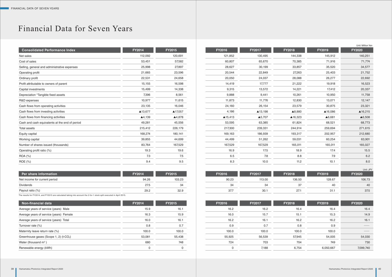
Financial Data for Seven Years
Non-financial data
Average years of service (years) Male
Average years of service (years) Female
Average years of service (years) Total
Turnover rate (%)
Maternity leave return rate (%)
Greenhouse gases (Scope 1, 2) (t-CO2)
Water (thousand m3 )
Renewable energy (kWh)
FY2014 FY2015 FY2016 FY2017 FY2018 FY2019 FY2020
15.9
16.3
16.0
0.8
100.0
53,081
680
0
16.1
15.9
16.1
0.7
100.0
55,438
748
0
16.2
16.0
16.2
0.9
100.0
55,925
724
0
16.2
15.7
16.1
0.7
100.0
56,539
703
7,188
16.4
15.1
16.2
0.8
100.0
57,945
704
6,754
16.4
15.3
16.2
0.9
100.0
54,005
749
6,050,667
16.4
14.9
16.1
54,030
730
7,099,740
Consolidated Performance Index FY2014 FY2015 FY2016 FY2017 FY2018 FY2019 FY2020
Unit: Million Yen
112,092
53,451
25,998
21,665
22,531
15,155
15,499
7,396
10,977
23,135
▲13,677
▲4,139
49,281
215,412
168,274
39,855
83,764
19.3
7.3
9.4
120,691
57,582
27,897
23,596
24,658
16,598
14,338
8,561
11,615
16,046
▲17,057
▲4,878
45,556
226,179
180,141
44,699
167,529
19.6
7.5
9.5
121,852
60,807
28,627
20,544
20,050
14,419
9,315
9,888
11,873
24,160
4,186
▲15,413
53,595
217,300
169,163
44,499
167,529
16.9
6.5
8.3
130,495
65,670
30,199
22,849
24,037
17,777
13,572
9,441
11,776
26,154
▲13,198
▲5,707
63,385
239,331
186,939
51,262
167,529
17.5
7.8
10.0
144,338
70,385
33,857
27,263
28,088
21,222
14,221
10,261
12,830
23,579
▲8,880
▲16,323
61,824
244,914
193,317
59,031
165,011
18.9
8.8
11.2
145,912
71,916
35,520
25,403
26,277
19,918
17,412
10,950
13,071
30,875
▲16,086
▲6,681
68,521
259,694
202,957
60,254
165,011
17.4
7.9
10.1
140,251
71,774
34,577
21,752
22,692
16,523
20,337
11,758
12,147
23,321
▲16,215
▲6,508
68,773
271,615
212,680
63,901
165,027
15.5
6.2
8.0
Per share information FY2014 FY2015 FY2016 FY2017 FY2018 FY2019 FY2020Unit: JPY
94.26
27.5
29.2
103.23
34
32.9
90.23
34
37.7
113.00
34
30.1
136.50
37
27.1
128.67
40
31.1
106.73
40
37.5
Operating profit ratio (%)
Number of shares issued (thousands)
Working capital
Equity capital
Total assets
Cash and cash equivalents at the end of period
Cash flows from financing activities
Cash flows from investing activities
Cash flows from operating activities
R&D expenses
Depreciation *Tangible fixed assets
Capital investments
Profit attributable to owners of parent
Ordinary profit
Operating profit
Selling, general and administrative expenses
Cost of sales
Net sales
ROA (%)
ROE (%)
Payout ratio (%)
Dividends
Net income for current period
The results for FY2014, and FY2015 are calculated taking into account the 2-for-1 stock split executed in April 2015.
FINANCIAL DATA OF SEVEN YEARS
39 Hamamatsu Photonics Integrated Report 2020 40Hamamatsu Photonics Integrated Report 2020
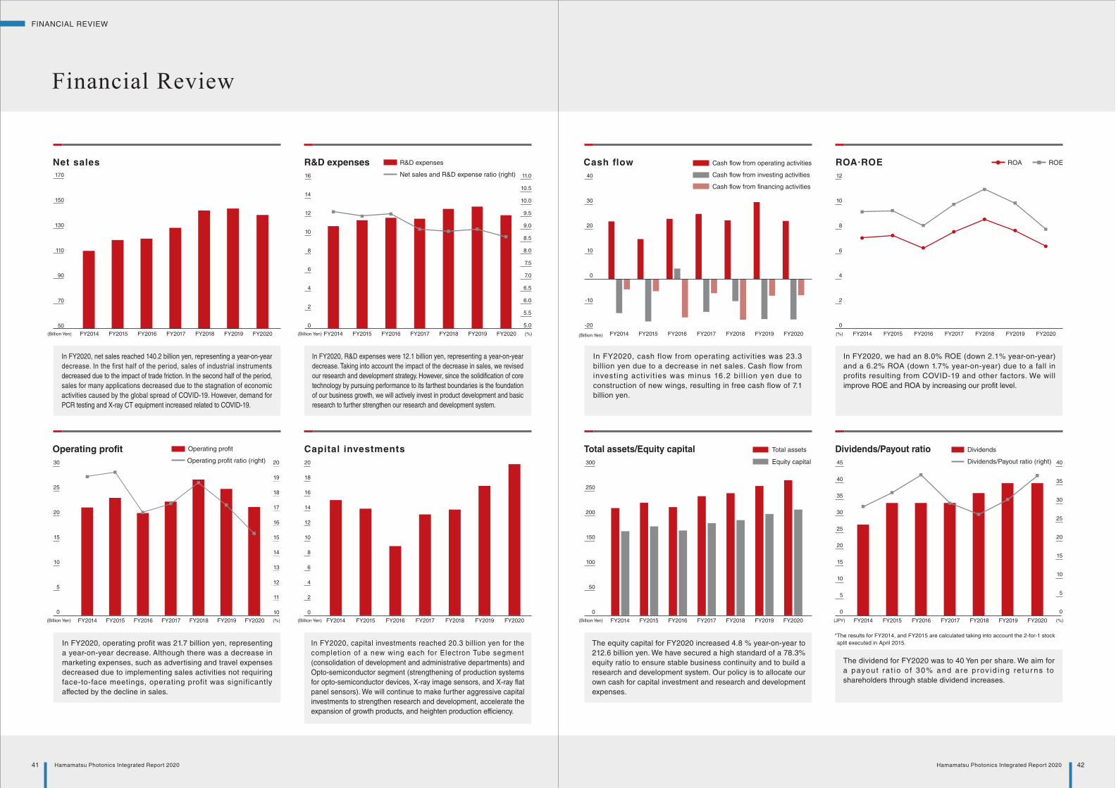
Financial Review
Net sales
In FY2020, net sales reached 140.2 billion yen, representing a year-on-year
decrease. In the first half of the period, sales of industrial instruments
decreased due to the impact of trade friction. In the second half of the period,
sales for many applications decreased due to the stagnation of economic
activities caused by the global spread of COVID-19. However, demand for
PCR testing and X-ray CT equipment increased related to COVID-19.
170
150
130
110
90
70
50
FY2020FY2019FY2018FY2017FY2016FY2015FY2014
16
14
12
10
8
6
4
2
0
R&D expenses
(%) (%)
In FY2020, R&D expenses were 12.1 billion yen, representing a year-on-year
decrease. Taking into account the impact of the decrease in sales, we revised
our research and development strategy. However, since the solidification of core
technology by pursuing performance to its farthest boundaries is the foundation
of our business growth, we will actively invest in product development and basic
research to further strengthen our research and development system.
(%)
Capital investments20
18
16
14
12
10
8
6
4
2
0
In FY2020, capital investments reached 20.3 billion yen for the
completion of a new wing each for Electron Tube segment
(consolidation of development and administrative departments) and
Opto-semiconductor segment (strengthening of production systems
for opto-semiconductor devices, X-ray image sensors, and X-ray flat
panel sensors). We will continue to make further aggressive capital
investments to strengthen research and development, accelerate the
expansion of growth products, and heighten production efficiency.
Cash flow40
30
20
10
0
-10
-20
Cash flow from operating activities
Cash flow from investing activities
Cash flow from financing activities
In FY2020, cash flow from operating activities was 23.3
billion yen due to a decrease in net sales. Cash flow from
invest ing act ivi t ies was minus 16.2 bi l l ion yen due to
construction of new wings, resulting in free cash flow of 7.1
billion yen.
ROA·ROE12
10
8
6
4
2
0
In FY2020, we had an 8.0% ROE (down 2.1% year-on-year)
and a 6.2% ROA (down 1.7% year-on-year) due to a fall in
profits resulting from COVID-19 and other factors. We will
improve ROE and ROA by increasing our profit level.
ROEROA
Dividends/Payout ratio45
40
35
30
25
20
15
10
5
0
40
35
30
25
20
15
10
5
0
The dividend for FY2020 was to 40 Yen per share. We aim for
a payou t ra t i o o f 30% and a re p rov id ing re tu r ns to
shareholders through stable dividend increases.
Dividends/Payout ratio (right)
DividendsTotal assets/Equity capital
(Billion Yen)
300
250
200
150
100
50
0
The equity capital for FY2020 increased 4.8 % year-on-year to
212.6 billion yen. We have secured a high standard of a 78.3%
equity ratio to ensure stable business continuity and to build a
research and development system. Our policy is to allocate our
own cash for capital investment and research and development
expenses.
Total assets
Equity capital
R&D expenses
Net sales and R&D expense ratio (right)
(Billion Yen) (Billion Yen) (Billion Yen)
(JPY)(Billion Yen)
*The results for FY2014, and FY2015 are calculated taking into account the 2-for-1 stock
split executed in April 2015.
Operating profit30
25
20
15
10
5
0
In FY2020, operating profit was 21.7 billion yen, representing
a year-on-year decrease. Although there was a decrease in
marketing expenses, such as advertising and travel expenses
decreased due to implementing sales activities not requiring
face-to-face meetings, operating profit was significantly
affected by the decline in sales.
Operating profit
Operating profit ratio (right) 20
19
18
17
16
15
14
13
12
11
10
(%)(Billion Yen)
11.0
10.5
10.0
9.5
9.0
8.5
8.0
7.5
7.0
6.5
6.0
5.5
5.0
FY2020FY2019FY2018FY2017FY2016FY2015FY2014
FY2020FY2019FY2018FY2017FY2016FY2015FY2014 FY2020FY2019FY2018FY2017FY2016FY2015FY2014
FY2020FY2019FY2018FY2017FY2016FY2015FY2014 FY2020FY2019FY2018FY2017FY2016FY2015FY2014
FY2020FY2019FY2018FY2017FY2016FY2015FY2014 FY2020FY2019FY2018FY2017FY2016FY2015FY2014
FINANCIAL REVIEW
41 Hamamatsu Photonics Integrated Report 2020 42Hamamatsu Photonics Integrated Report 2020
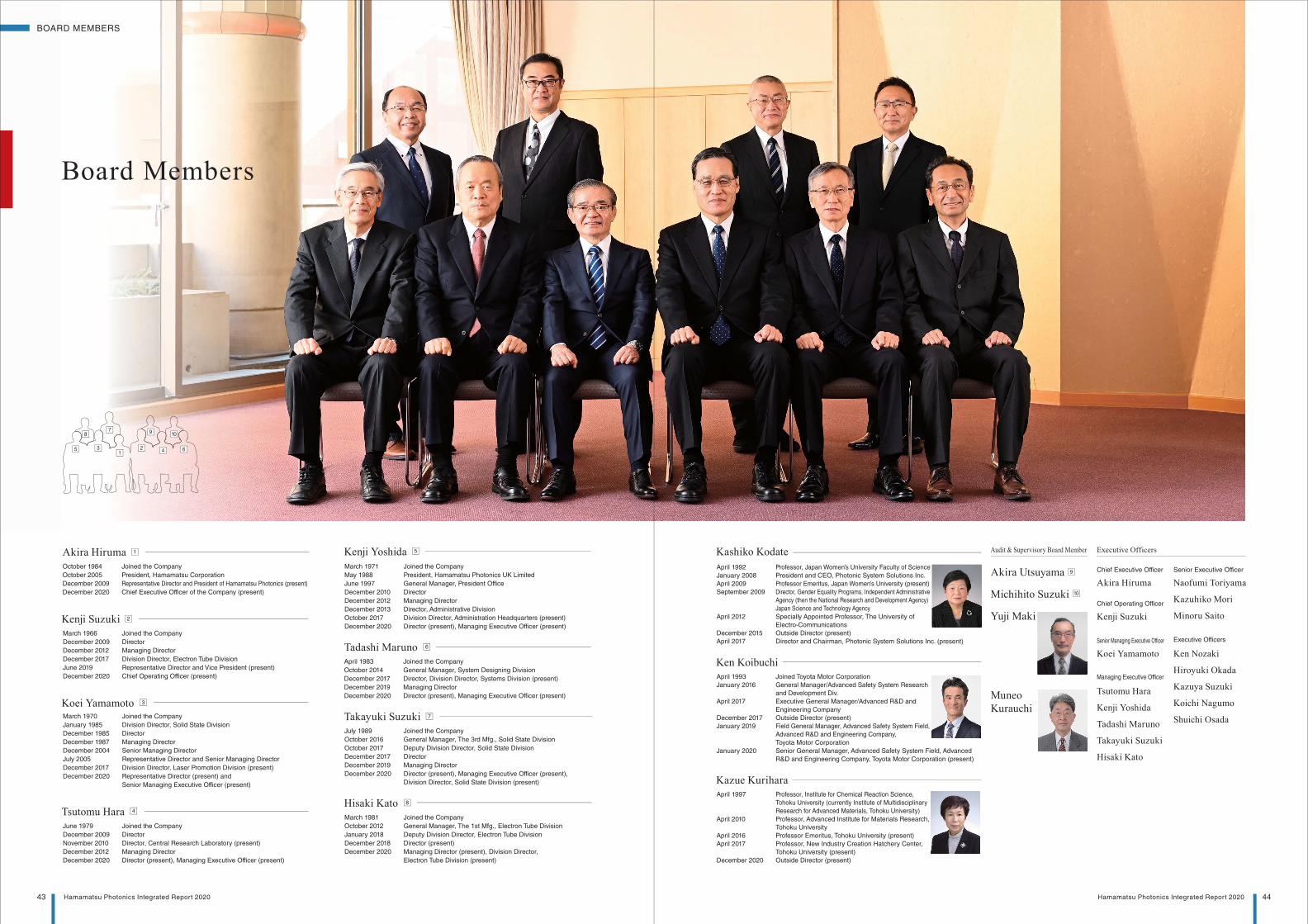
Akira HirumaOctober 1984 Joined the Company
October 2005 President, Hamamatsu Corporation
December 2009 Representative Director and President of Hamamatsu Photonics (present)
December 2020 Chief Executive Officer of the Company (present)
1
9
10
Executive Officers
Chief Executive Officer
Chief Operating Officer
Akira Hiruma
Kenji Suzuki
Senior Managing Executive Officer
Managing Executive Officer
Senior Executive Officer
Naofumi Toriyama
Kazuhiko Mori
Minoru Saito
Executive Officers
Ken Nozaki
Hiroyuki Okada
Kazuya Suzuki
Koichi Nagumo
Shuichi Osada
Akira Utsuyama
Michihito Suzuki
Yuji Maki
Muneo Kurauchi
Audit & Supervisory Board Member
Tsutomu Hara
Kenji Yoshida
Tadashi Maruno
Takayuki Suzuki
Hisaki Kato
Koei Yamamoto
March 1971 Joined the Company
May 1988 President, Hamamatsu Photonics UK Limited
June 1997 General Manager, President Office
December 2010 Director
December 2012 Managing Director
December 2013 Director, Administrative Division
October 2017 Division Director, Administration Headquarters (present)
December 2020 Director (present), Managing Executive Officer (present)
Kenji Yoshida 5
April 1983 Joined the Company
October 2014 General Manager, System Designing Division
December 2017 Director, Division Director, Systems Division (present)
December 2019 Managing Director
December 2020 Director (present), Managing Executive Officer (present)
Tadashi Maruno 6
July 1989 Joined the Company
October 2016 General Manager, The 3rd Mfg., Solid State Division
October 2017 Deputy Division Director, Solid State Division
December 2017 Director
December 2019 Managing Director
December 2020 Director (present), Managing Executive Officer (present),
Division Director, Solid State Division (present)
Takayuki Suzuki 7
March 1981 Joined the Company
October 2012 General Manager, The 1st Mfg., Electron Tube Division
January 2018 Deputy Division Director, Electron Tube Division
December 2018 Director (present)
December 2020 Managing Director (present), Division Director,
Electron Tube Division (present)
Hisaki Kato 8
Kashiko KodateApril 1992 Professor, Japan Women’s University Faculty of Science
January 2008 President and CEO, Photonic System Solutions Inc.
April 2009 Professor Emeritus, Japan Women’s University (present)
September 2009 Director, Gender Equality Programs, Independent Administrative
Agency (then the National Research and Development Agency)
Japan Science and Technology Agency
April 2012 Specially Appointed Professor, The University of
Electro-Communications
December 2015 Outside Director (present)
April 2017 Director and Chairman, Photonic System Solutions Inc. (present)
Ken KoibuchiApril 1993 Joined Toyota Motor Corporation
January 2016 General Manager/Advanced Safety System Research
and Development Div.
April 2017 Executive General Manager/Advanced R&D and
Engineering Company
December 2017 Outside Director (present)
January 2019 Field General Manager, Advanced Safety System Field,
Advanced R&D and Engineering Company,
Toyota Motor Corporation
January 2020 Senior General Manager, Advanced Safety System Field, Advanced
R&D and Engineering Company, Toyota Motor Corporation (present)
Kazue KuriharaApril 1997 Professor, Institute for Chemical Reaction Science,
Tohoku University (currently Institute of Multidisciplinary
Research for Advanced Materials, Tohoku University)
April 2010 Professor, Advanced Institute for Materials Research,
Tohoku University
April 2016 Professor Emeritus, Tohoku University (present)
April 2017 Professor, New Industry Creation Hatchery Center,
Tohoku University (present)
December 2020 Outside Director (present)
Kenji Suzuki 2
March 1966 Joined the Company
December 2009 Director
December 2012 Managing Director
December 2017 Division Director, Electron Tube Division
June 2019 Representative Director and Vice President (present)
December 2020 Chief Operating Officer (present)
Koei Yamamoto 3
March 1970 Joined the Company
January 1985 Division Director, Solid State Division
December 1985 Director
December 1987 Managing Director
December 2004 Senior Managing Director
July 2005 Representative Director and Senior Managing Director
December 2017 Division Director, Laser Promotion Division (present)
December 2020 Representative Director (present) and
Senior Managing Executive Officer (present)
Tsutomu Hara 4
June 1979 Joined the Company
December 2009 Director
November 2010 Director, Central Research Laboratory (present)
December 2012 Managing Director
December 2020 Director (present), Managing Executive Officer (present)
5 31
2 4 6
10978
Board Members
BOARD MEMBERS
43 Hamamatsu Photonics Integrated Report 2020 44Hamamatsu Photonics Integrated Report 2020
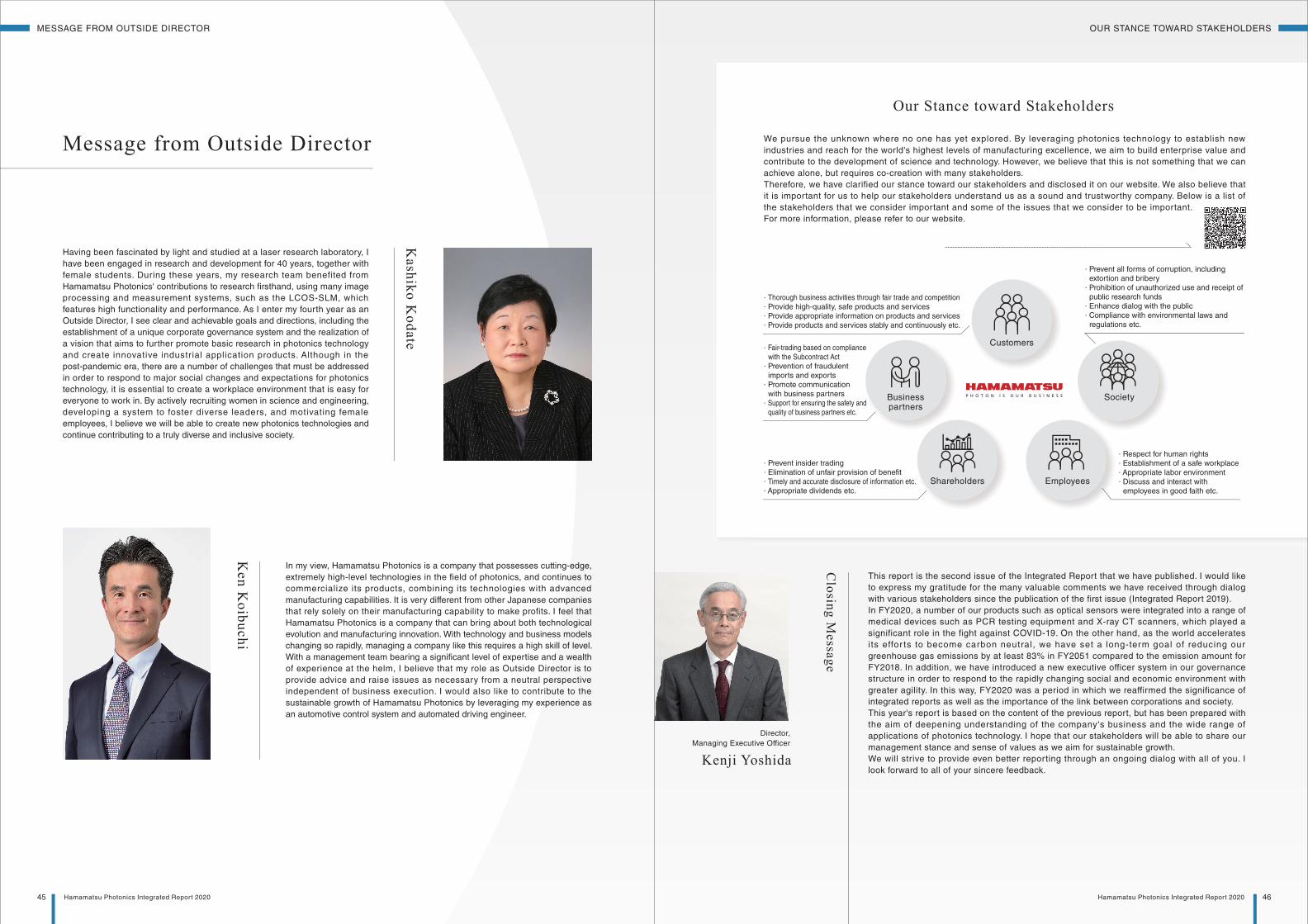
We pursue the unknown where no one has yet explored. By leveraging photonics technology to establish new
industries and reach for the world's highest levels of manufacturing excellence, we aim to build enterprise value and
contribute to the development of science and technology. However, we believe that this is not something that we can
achieve alone, but requires co-creation with many stakeholders.
Therefore, we have clarified our stance toward our stakeholders and disclosed it on our website. We also believe that
it is important for us to help our stakeholders understand us as a sound and trustworthy company. Below is a list of
the stakeholders that we consider important and some of the issues that we consider to be important.
For more information, please refer to our website.
Our Stance toward Stakeholders
This report is the second issue of the Integrated Report that we have published. I would like
to express my gratitude for the many valuable comments we have received through dialog
with various stakeholders since the publication of the first issue (Integrated Report 2019).
In FY2020, a number of our products such as optical sensors were integrated into a range of
medical devices such as PCR testing equipment and X-ray CT scanners, which played a
significant role in the fight against COVID-19. On the other hand, as the world accelerates
its effor ts to become carbon neutral, we have set a long-term goal of reducing our
greenhouse gas emissions by at least 83% in FY2051 compared to the emission amount for
FY2018. In addition, we have introduced a new executive officer system in our governance
structure in order to respond to the rapidly changing social and economic environment with
greater agility. In this way, FY2020 was a period in which we reaffirmed the significance of
integrated reports as well as the importance of the link between corporations and society.
This year's report is based on the content of the previous report, but has been prepared with
the aim of deepening understanding of the company's business and the wide range of
applications of photonics technology. I hope that our stakeholders will be able to share our
management stance and sense of values as we aim for sustainable growth.
We will strive to provide even better reporting through an ongoing dialog with all of you. I
look forward to all of your sincere feedback.
Director,
Managing Executive Officer
Kenji Yoshida
Closing M
essage
Kashiko K
odate
Having been fascinated by light and studied at a laser research laboratory, I
have been engaged in research and development for 40 years, together with
female students. During these years, my research team benefited from
Hamamatsu Photonics' contributions to research firsthand, using many image
processing and measurement systems, such as the LCOS-SLM, which
features high functionality and performance. As I enter my fourth year as an
Outside Director, I see clear and achievable goals and directions, including the
establishment of a unique corporate governance system and the realization of
a vision that aims to further promote basic research in photonics technology
and create innovative industrial application products. Although in the
post-pandemic era, there are a number of challenges that must be addressed
in order to respond to major social changes and expectations for photonics
technology, it is essential to create a workplace environment that is easy for
everyone to work in. By actively recruiting women in science and engineering,
developing a system to foster diverse leaders, and motivating female
employees, I believe we will be able to create new photonics technologies and
continue contributing to a truly diverse and inclusive society.
Message from Outside Director
In my view, Hamamatsu Photonics is a company that possesses cutting-edge,
extremely high-level technologies in the field of photonics, and continues to
commercialize its products, combining its technologies with advanced
manufacturing capabilities. It is very different from other Japanese companies
that rely solely on their manufacturing capability to make profits. I feel that
Hamamatsu Photonics is a company that can bring about both technological
evolution and manufacturing innovation. With technology and business models
changing so rapidly, managing a company like this requires a high skill of level.
With a management team bearing a significant level of expertise and a wealth
of experience at the helm, I believe that my role as Outside Director is to
provide advice and raise issues as necessary from a neutral perspective
independent of business execution. I would also like to contribute to the
sustainable growth of Hamamatsu Photonics by leveraging my experience as
an automotive control system and automated driving engineer.
Ken K
oibuchi
∙ Respect for human rights∙ Establishment of a safe workplace∙ Appropriate labor environment∙ Discuss and interact with
employees in good faith etc.
∙ Prevent all forms of corruption, including
extortion and bribery ∙ Prohibition of unauthorized use and receipt of
public research funds ∙ Enhance dialog with the public∙ Compliance with environmental laws and
regulations etc.
Businesspartners
Shareholders
Customers
Society
Employees
∙ Thorough business activities through fair trade and competition∙ Provide high-quality, safe products and services∙ Provide appropriate information on products and services∙ Provide products and services stably and continuously etc.
∙ Prevent insider trading∙ Elimination of unfair provision of benefit∙ Timely and accurate disclosure of information etc.∙ Appropriate dividends etc.
∙ Fair-trading based on compliance
with the Subcontract Act∙ Prevention of fraudulent
imports and exports∙ Promote communication
with business partners∙ Support for ensuring the safety and
quality of business partners etc.
MESSAGE FROM OUTSIDE DIRECTOR OUR STANCE TOWARD STAKEHOLDERS
45 Hamamatsu Photonics Integrated Report 2020 46Hamamatsu Photonics Integrated Report 2020
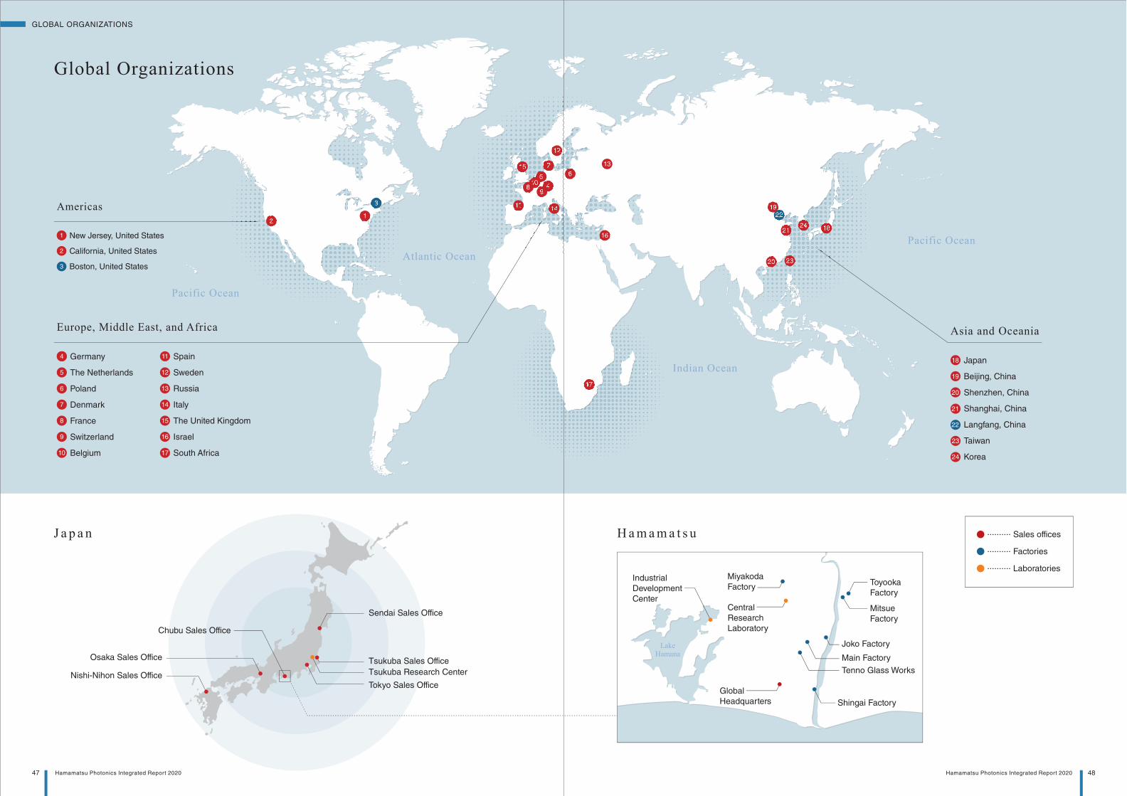
Pacific Ocean
Pacific Ocean
Indian Ocean
Atlantic Ocean
J a p a n
Chubu Sales Office
Sendai Sales Office
Tsukuba Sales Office
Tsukuba Research Center
Tokyo Sales Office
Osaka Sales Office
Nishi-Nihon Sales Office
H a m a m a t s u
Tenno Glass Works
Main Factory
Joko Factory
Toyooka
Factory
Mitsue
Factory
Industrial
Development
CenterCentral
Research
Laboratory
Miyakoda
Factory
Global
Headquarters
LakeHamana
● ·········· Sales offices
● ·········· Factories
● ·········· Laboratories
Shingai Factory
Global Organizations
Germany
The Netherlands
Poland
Denmark
France
Switzerland
Belgium
4
5
6
7
8
9
10
Spain
Sweden
Russia
Italy
The United Kingdom
Israel
South Africa
11
12
13
14
15
16
17
New Jersey, United States
California, United States
Boston, United States
1
2
3
17
21
3
16
13
14
6
12
7
5
94
15
8
11
20
24
23
21
2219
10
Europe, Middle East, and Africa
Americas
18
Japan
Beijing, China
Shenzhen, China
Shanghai, China
Langfang, China
Taiwan
Korea
18
19
20
21
22
23
24
Asia and Oceania
GLOBAL ORGANIZATIONS
47 Hamamatsu Photonics Integrated Report 2020 48Hamamatsu Photonics Integrated Report 2020
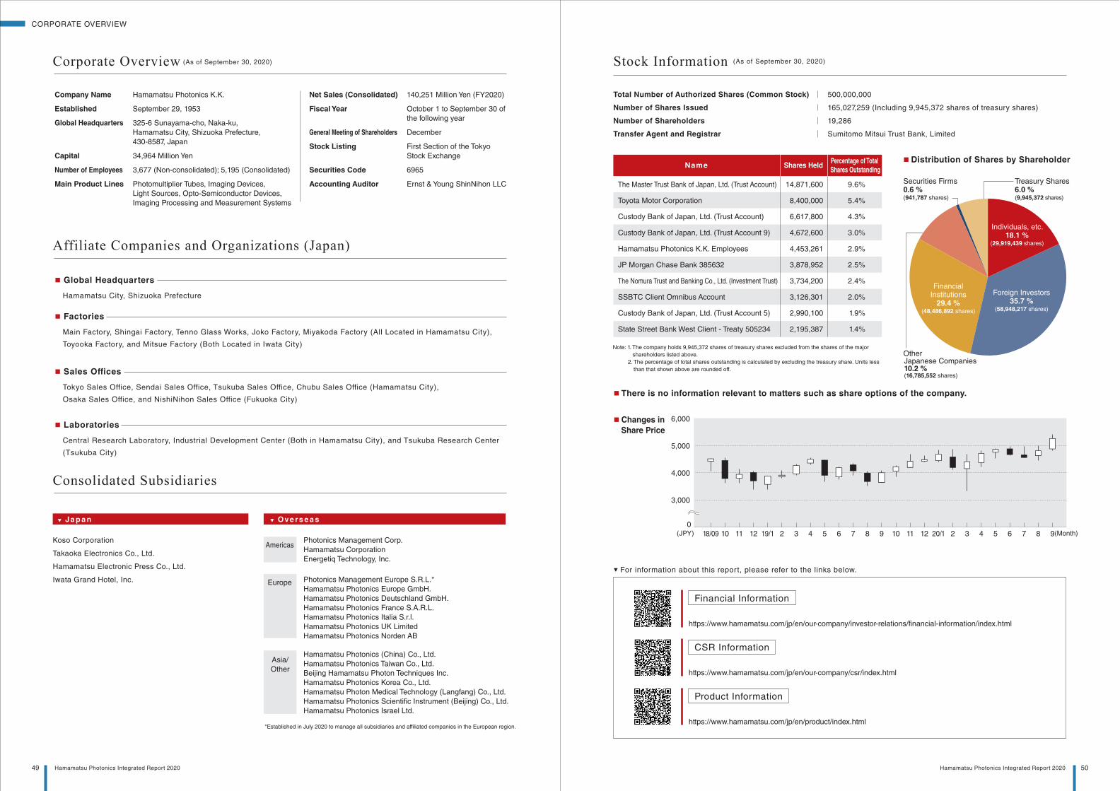
The Master Trust Bank of Japan, Ltd. (Trust Account)
Toyota Motor Corporation
Custody Bank of Japan, Ltd. (Trust Account)
Custody Bank of Japan, Ltd. (Trust Account 9)
Hamamatsu Photonics K.K. Employees
JP Morgan Chase Bank 385632
The Nomura Trust and Banking Co., Ltd. (Investment Trust)
SSBTC Client Omnibus Account
Custody Bank of Japan, Ltd. (Trust Account 5)
State Street Bank West Client - Treaty 505234
14,871,600
8,400,000
6,617,800
4,672,600
4,453,261
3,878,952
3,734,200
3,126,301
2,990,100
2,195,387
9.6%
5.4%
4.3%
3.0%
2.9%
2.5%
2.4%
2.0%
1.9%
1.4%
Name Shares Held Percentage of Total Shares Outstanding
Securities Firms0.6 %(941,787 shares)
Treasury Shares 6.0 %(9,945,372 shares)
FinancialInstitutions
29.4 %(48,486,892 shares)
Foreign Investors35.7 %
(58,948,217 shares)
Individuals, etc.18.1 %
(29,919,439 shares)
Other Japanese Companies10.2 %(16,785,552 shares)
■ Distribution of Shares by Shareholder
Affiliate Companies and Organizations (Japan)
Financial Information
https://www.hamamatsu.com/jp/en/our-company/investor-relations/financial-information/index.html
Product Information
https://www.hamamatsu.com/jp/en/product/index.html
CSR Information
https://www.hamamatsu.com/jp/en/our-company/csr/index.html
■ There is no information relevant to matters such as share options of the company.
■ Changes in Share Price
0(JPY) (Month)
4,000
5,000
3,000
6,000
9876543220/11211109876543219/1121118/09 10
Consolidated Subsidiaries
▼ For information about this report, please refer to the links below.
*Established in July 2020 to manage all subsidiaries and affiliated companies in the European region.
▼ Ja p a n
Koso Corporation
Takaoka Electronics Co., Ltd.
Hamamatsu Electronic Press Co., Ltd.
Iwata Grand Hotel, Inc.
▼ Ove rs e a s
Photonics Management Corp.
Hamamatsu Corporation
Energetiq Technology, Inc.
Photonics Management Europe S.R.L.*
Hamamatsu Photonics Europe GmbH.
Hamamatsu Photonics Deutschland GmbH.
Hamamatsu Photonics France S.A.R.L.
Hamamatsu Photonics Italia S.r.l.
Hamamatsu Photonics UK Limited
Hamamatsu Photonics Norden AB
Hamamatsu Photonics (China) Co., Ltd.
Hamamatsu Photonics Taiwan Co., Ltd.
Beijing Hamamatsu Photon Techniques Inc.
Hamamatsu Photonics Korea Co., Ltd.
Hamamatsu Photon Medical Technology (Langfang) Co., Ltd.
Hamamatsu Photonics Scientific Instrument (Beijing) Co., Ltd.
Hamamatsu Photonics Israel Ltd.
Americas
Europe
Asia/
Other
(As of September 30, 2020)
Total Number of Authorized Shares (Common Stock)
Number of Shares Issued
Number of Shareholders
Transfer Agent and Registrar
500,000,000
165,027,259 (Including 9,945,372 shares of treasury shares)
19,286
Sumitomo Mitsui Trust Bank, Limited
Stock Information
Note: 1. The company holds 9,945,372 shares of treasury shares excluded from the shares of the major
shareholders listed above.
2. The percentage of total shares outstanding is calculated by excluding the treasury share. Units less
than that shown above are rounded off.
CORPORATE OVERVIEW
49 Hamamatsu Photonics Integrated Report 2020 50Hamamatsu Photonics Integrated Report 2020
Company Name
Established
Global Headquarters
Capital
Number of Employees
Main Product Lines
Hamamatsu Photonics K.K.
September 29, 1953
325-6 Sunayama-cho, Naka-ku,
Hamamatsu City, Shizuoka Prefecture,
430-8587, Japan
34,964 Million Yen
3,677 (Non-consolidated); 5,195 (Consolidated)
Photomultiplier Tubes, Imaging Devices,
Light Sources, Opto-Semiconductor Devices,
Imaging Processing and Measurement Systems
Net Sales (Consolidated)
Fiscal Year
General Meeting of Shareholders
Stock Listing
Securities Code
Accounting Auditor
140,251 Million Yen (FY2020)
October 1 to September 30 of
the following year
December
First Section of the Tokyo
Stock Exchange
6965
Ernst & Young ShinNihon LLC
Corporate Overview (As of September 30, 2020)
■ Global Headquarters
Hamamatsu City, Shizuoka Prefecture
■ Factories
Main Factory, Shingai Factory, Tenno Glass Works, Joko Factory, Miyakoda Factory (All Located in Hamamatsu City),
Toyooka Factory, and Mitsue Factory (Both Located in Iwata City)
■ Sales Offices
Tokyo Sales Office, Sendai Sales Office, Tsukuba Sales Office, Chubu Sales Office (Hamamatsu City),
Osaka Sales Office, and NishiNihon Sales Office (Fukuoka City)
■ Laboratories
Central Research Laboratory, Industrial Development Center (Both in Hamamatsu City), and Tsukuba Research Center
(Tsukuba City)

Integrated Repor t
20 20
Cat. No. XINT1012E02
JUN. 2021 DNP
HAMAMATSU PHOTONICS K.K.325-6 Sunayama-cho, Naka-ku, Hamamatsu City, Shizuoka Prefecture, 430-8587, Japan
Investor Relat ions Off ice
TEL
FAX
(053)452-2141
(053)456-7889
www.hamamatsu.com
HAMAMATSU PHOTONICS K.K.
Related Documents