A Dissertation Report on “Integrated Pyro SCB Chip” Submitted to the Savitribai Phule University of PUNE, PUNE In partial fulfillment of the requirements for the Degree of MASTER OF ENGINEERING (VLSI and Embedded systems) (2014-2015) By Pooja Sharma Exam Seat No. 11819 Under the guidance of Dr. Virendra Kumar Prof. Saniya Ansari DEPARTMENT OF ELECTRONICS AND TELECOMMUNICATION ENGINEERING GENBA SOPANRAO MOZE COLLEGE OF ENGINEERING, BALEWADI, PUNE-45

Welcome message from author
This document is posted to help you gain knowledge. Please leave a comment to let me know what you think about it! Share it to your friends and learn new things together.
Transcript

A Dissertation Report on
“Integrated Pyro SCB Chip”
Submitted to the Savitribai Phule University of PUNE, PUNE In partial fulfillment of the requirements for the
Degree of
MASTER OF ENGINEERING (VLSI and Embedded systems)
(2014-2015)
By Pooja Sharma
Exam Seat No. 11819
Under the guidance of
Dr. Virendra Kumar
Prof. Saniya Ansari
DEPARTMENT OF ELECTRONICS AND TELECOMMUNICATION ENGINEERING
GENBA SOPANRAO MOZE COLLEGE OF ENGINEERING, BALEWADI, PUNE-45

GENBA SOPANRAO MOZE COE, Balewadi ,Pune
DEPARTMENT OF ELECTRONICS & TELECOMMUNICATION ENGINEERING
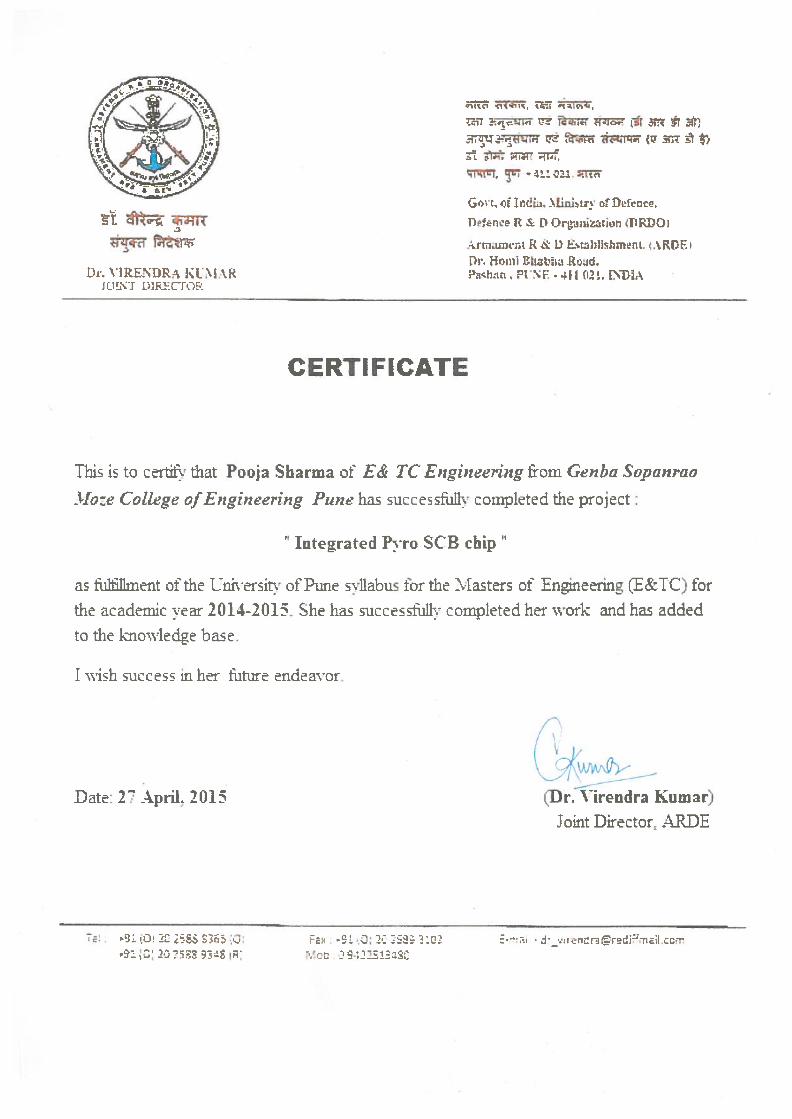
CERTIFICATE
This is to certify that the project report entitled -“INTEGRATED PYRO SCB CHIP” submitted by Ms. Pooja Sharma exam seat no. 11819 is a bonafide work carried out by her under the supervision of Prof. Mrs. Saniya Ansari and Dr. Virendra kumar Verma and it is submitted towards the partial fulfilment of the requirements to Savitribai Phule, Pune University for the degree of Master of Engineering (VLSI and Embedded Systems). Prof. Mrs. Saniya Ansari Prof. Suchitra Jagtap Internal Guide P.G. Coordinator Prof. Neelam Sonawane H.O.D. Principal


G. S. Moze COE, Balewadi, Pune. Dept of E&Tc 2014-15 i
ACKNOWLEDGEMENT
Author is highly greatful to Professor Saniya Ansari , D.Y. Patil School of Engineering, Lohegoan, Pune, for her continuous guidance and inspiration to the successful completion of this work. Author also wants to thank Dr. Virendra Kumar Verma, Joint Director, ARDE, Pune for his support and guidance through- out the project. Author also takes this opportunity to thank Dr. A. M. Sapkal, Head of department, Department of Electronics and Telecommuni- cation for help and support during this work.
Author is also thankful to Dr. K. M. Rajan, Director, Armament R D Establishment, Pune for support and permission to present this work. Authors express their sincere thanks to Shri Kapil Deo, Sc. `G' Associate Director, for the guidance during the course of work.
Pooja Sharma
G. S. Moze COE, Balewadi, Pune. Dept of E&Tc 2014-15 ii
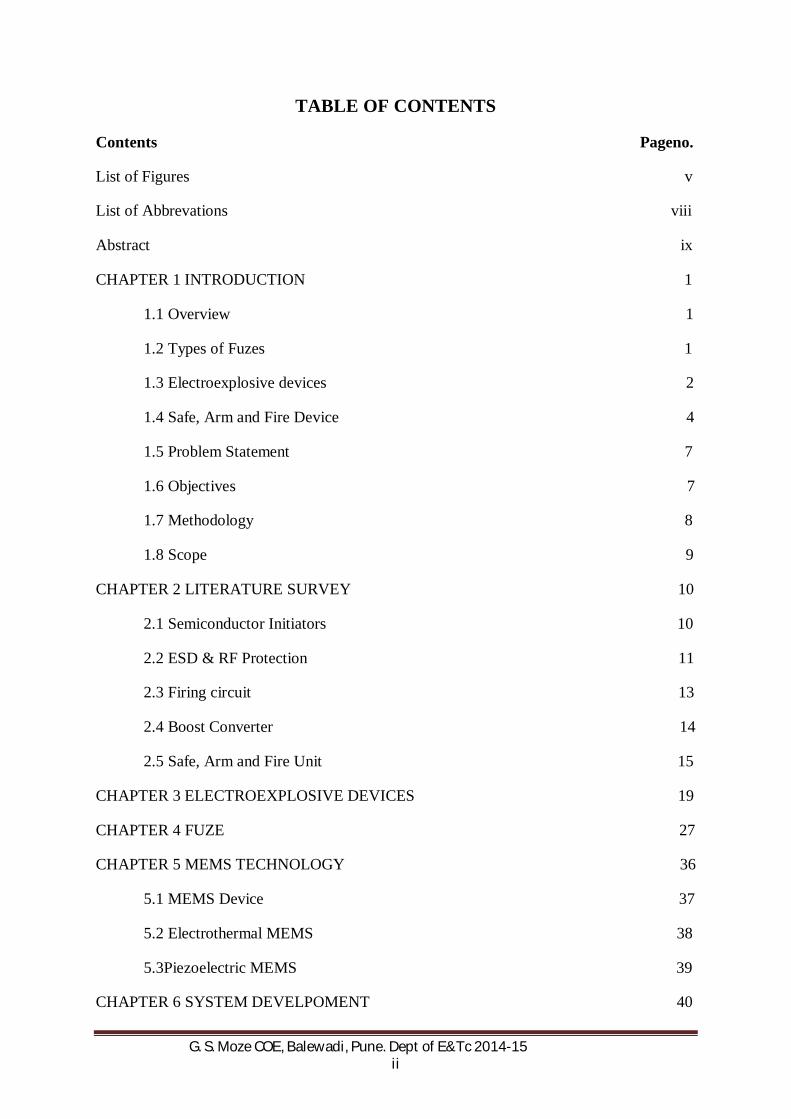
TABLE OF CONTENTS
Contents Pageno.
List of Figures v
List of Abbrevations viii
Abstract ix
CHAPTER 1 INTRODUCTION 1
1.1 Overview 1
1.2 Types of Fuzes 1
1.3 Electroexplosive devices 2
1.4 Safe, Arm and Fire Device 4
1.5 Problem Statement 7
1.6 Objectives 7
1.7 Methodology 8
1.8 Scope 9
CHAPTER 2 LITERATURE SURVEY 10
2.1 Semiconductor Initiators 10
2.2 ESD & RF Protection 11
2.3 Firing circuit 13
2.4 Boost Converter 14
2.5 Safe, Arm and Fire Unit 15
CHAPTER 3 ELECTROEXPLOSIVE DEVICES 19
CHAPTER 4 FUZE 27
CHAPTER 5 MEMS TECHNOLOGY 36
5.1 MEMS Device 37
5.2 Electrothermal MEMS 38
5.3Piezoelectric MEMS 39
CHAPTER 6 SYSTEM DEVELPOMENT 40
G. S. Moze COE, Balewadi, Pune. Dept of E&Tc 2014-15 iii
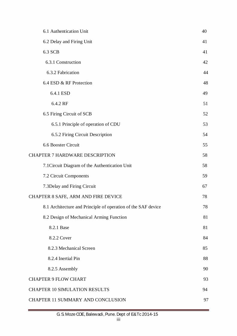
6.1 Authentication Unit 40
6.2 Delay and Firing Unit 41
6.3 SCB 41
6.3.1 Construction 42
6.3.2 Fabrication 44
6.4 ESD & RF Protection 48
6.4.1 ESD 49
6.4.2 RF 51
6.5 Firing Circuit of SCB 52
6.5.1 Principle of operation of CDU 53
6.5.2 Firing Circuit Description 54
6.6 Booster Circuit 55
CHAPTER 7 HARDWARE DESCRIPTION 58
7.1Circuit Diagram of the Authentication Unit 58
7.2 Circuit Components 59
7.3Delay and Firing Circuit 67
CHAPTER 8 SAFE, ARM AND FIRE DEVICE 78
8.1 Architecture and Principle of operation of the SAF device 78
8.2 Design of Mechanical Arming Function 81
8.2.1 Base 81
8.2.2 Cover 84
8.2.3 Mechanical Screen 85
8.2.4 Inertial Pin 88
8.2.5 Assembly 90
CHAPTER 9 FLOW CHART 93
CHAPTER 10 SIMULATION RESULTS 94
CHAPTER 11 SUMMARY AND CONCLUSION 97

G. S. Moze COE, Balewadi, Pune. Dept of E&Tc 2014-15 iv
LIST OF PUBLICATIONS 99
REFERENCES 100
APPENDIX-I 103
APPENDIX-II 105
G. S. Moze COE, Balewadi, Pune. Dept of E&Tc 2014-15 v
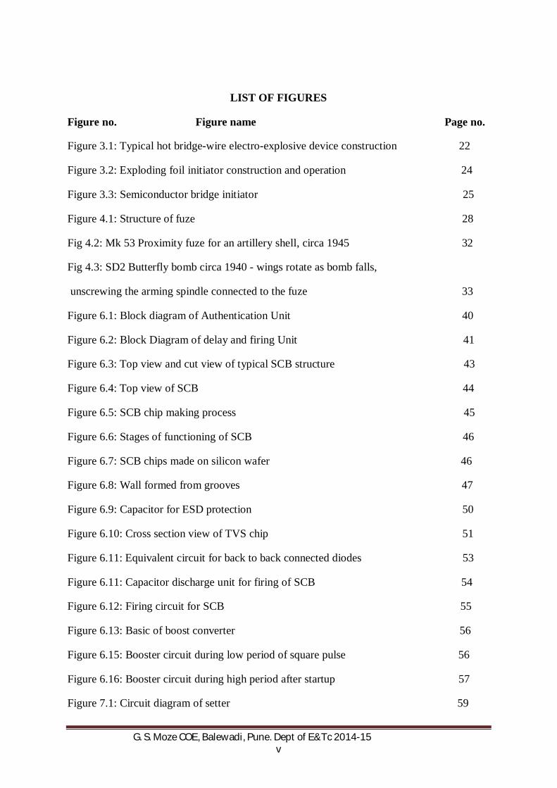
LIST OF FIGURES
Figure no. Figure name Page no.
Figure 3.1: Typical hot bridge-wire electro-explosive device construction 22
Figure 3.2: Exploding foil initiator construction and operation 24
Figure 3.3: Semiconductor bridge initiator 25
Figure 4.1: Structure of fuze 28
Fig 4.2: Mk 53 Proximity fuze for an artillery shell, circa 1945 32
Fig 4.3: SD2 Butterfly bomb circa 1940 - wings rotate as bomb falls,
unscrewing the arming spindle connected to the fuze 33
Figure 6.1: Block diagram of Authentication Unit 40
Figure 6.2: Block Diagram of delay and firing Unit 41
Figure 6.3: Top view and cut view of typical SCB structure 43
Figure 6.4: Top view of SCB 44
Figure 6.5: SCB chip making process 45
Figure 6.6: Stages of functioning of SCB 46
Figure 6.7: SCB chips made on silicon wafer 46
Figure 6.8: Wall formed from grooves 47
Figure 6.9: Capacitor for ESD protection 50
Figure 6.10: Cross section view of TVS chip 51
Figure 6.11: Equivalent circuit for back to back connected diodes 53
Figure 6.11: Capacitor discharge unit for firing of SCB 54
Figure 6.12: Firing circuit for SCB 55
Figure 6.13: Basic of boost converter 56
Figure 6.15: Booster circuit during low period of square pulse 56
Figure 6.16: Booster circuit during high period after startup 57
Figure 7.1: Circuit diagram of setter 59

G. S. Moze COE, Balewadi, Pune. Dept of E&Tc 2014-15 vi
Figure 7.2: PCB layout for setter 60
Figure7.3: 3D model of setter 67
Figure 7.4: Circuit for regulated power supply 68
Figure 7.5: Pin diagram of 7805 69
Figure 7.6: Schematic diagram for Fuzing 70
Figure 7.7: Layer1 circuitry 71
Figure 7.8: Layer1 Top View 72
Figure 7.9: Layer 1 Bottom view 74
Figure 7.10: Layer 1 3D Top view 76
Figure 7.11: Layer 2 3D Bottom view 78
Figure 7.12: Layer 2 schematic 79
Figure 7.13: Layer 2 Top view 80
Figure 7.14: Layer 2 Bottom view (use SCB instead of R1, R2 with TVS diode) 81
Figure 7.15: Pin configuration of ATTINY85 82
Figure 7.16: Functional Block Diagram of ADXL210AQC 83
Fig. 8.1: View of the MEMS SAF device made of three stacked parts 84
Figure 8.2: Operations procedure of the MEMS SAF device (a) in safe mode, (b) mechanically armed, (c) electrically armed and (d) secondary explosive initiation 85
Figure 8.3 (a): Microactuator cavity before the gases are released 86
Figure 8.3(b): Microactuator cavity after the gases are released 87
Figure 8.4: Pressure evolution in the micro actuator cavity
and slide containing the screen 88
Figure 8.5: Pro-E model of Base 89
Figure 8.6: Base 89
Figure 8.7: Pro-E model of Cover 90
Figure 8.8: Cover 91
Figure 8.9: Pro-E model of Mechanical Screen 92

G. S. Moze COE, Balewadi, Pune. Dept of E&Tc 2014-15 vii
Figure 8.10: Mechanical Screen 92
Figure 10.1: Simulation of Authentication unit 93
Figure 10.2: Simulation for Delay and Firing Unit 94
Figure10.3: Capacitor discharge profile 95
Figure10.3: Capacitor discharge profile 95

G. S. Moze COE, Balewadi, Pune. Dept of E&Tc 2014-15 viii
LIST OF ABBREVATIONS
SCB Semiconductor Bridge
EED Electroexplosive Devices
ESD Electrostatic Discharge
RF Radio Frequency
EBW Exploding Bridge Wire
MEMS Microelectromechanical System
SAF Safe Arm and Fire Device
G. S. Moze COE, Balewadi, Pune. Dept of E&Tc 2014-15 ix
ABSTRACT
Micro electromechanical system is the new technology that takes advantage of unique physical properties at micro scale to create mechanical systems with electrical interface using available microelectronic fabrication techniques. This work takes full benefit of this technology and use of it enables improved performance and efficiency. The electronic circuitry provides trigger signals to initiate electro explosive device which is extensively used in military and civil application for initiation of explosive materials. The electro explosive device used is Semiconductor Bridge. As it has high efficiency, less weight, fast functioning time, reduced size, low input energy, low cost, digital compatibility and immune to Electrostatic discharge & radio frequency hazards. In this project Semiconductor Bridge is integrated with Micro electromechanical system based safe, arm and fire device. Here, we have a architecture of Safe, Arm and Fire device that constitute a real breakthrough for safe miniature fuzing device. It combines mechanical arming unit with electrical safety functionality on the same silicon initiator’s chip. The boost converter will boost the voltage from 3V to 30V. Accelerometer attached with microcontroller senses setback force. We have a two layer circuitry one layer is of 0.74*0.68 inches and other layer is of 0.33*0.29 inches.

G. S. Moze COE, Balewadi, Pune. Dept of E&Tc 2014-15 1
CHAPTER 1
INTRODUCTION
1.1 OVERVIEW
SCB is semiconductor bridge which is integrated with MEMS based safe, arm
and fire device pyrotechnically. MEMS is the microelectromechanical system, its
function is to convert electrical energy into mechanical energy. System is designed
with pyro MEMS based electronic fuze.
In military munitions, a fuze is a part of device that initiates function. It is
designed to detonate, or to set forces into action to ignite, detonate or deflagrate,
the charge (or primer) under specified conditions. It contains safety/arming
mechanism, designed to protect the user from premature or accidental detonation. We
provide safety by making the system password protected.
1.2 Types of Fuzes
Time Fuze (time to arm/time to detonate): This device arms after a set period of
time and explodes at the end of a set delay from the time of arming. Either or both
time increments can be setable prior to firing or fixed within the design of the device.
These fuzes are typically used in ammunition and missiles. One current example of a
time fuze is the U.S. Army's M762, now transitioning to production after close to ten
years in development. Another example is MOFA (multi-optional fuze for artillery).
Impact Fuze (time to arm/impact to detonate): The device arms after a set
period of time and detonates on impact. This type of fuze is typically used in
ammunition, bombs and missiles.
Delay Fuzes: The device arms after a set period of time and detonates a set period
of time after impact. This type of fuze is used on ammunition, bombs and missiles.
Proximity Fuzes: The device arms after a set period of time and detonates when
at the closet point of approach to a target. This type of fuze is typically on
ammunition, rockets and missiles.
G. S. Moze COE, Balewadi, Pune. Dept of E&Tc 2014-15 2
1.3 Electro explosives devices
Hot Bridge-wire: Hot bridge-wireEEDs have been in use almost since the
discovery of energetic materials. Hot bridge-wire devices use a small piece of wire,
typically tungsten or platinum.The EED spot charge is initiated by applying a current
pulse to the EED. The current pulse heats the bridge-wire and initiates the spot
charge. The spot charge is coupled to other energetic materials that make up the EED
explosive train. The output of the spot charge begins the detonation process.
Exploding Bridge-wire: In this interesting variation on the hot bridge- wire
concept, the bridge-wire material is heated rapidly enough so a shock wave is created
as the bridge-wire material vaporizes. The shock wave amplitude and velocity is
sufficient to couple it to a relatively insensitive energetic material such as
pentaerythrioltetranitrate (PETN).
Because EBW EED system safety is suffciently great, they have been used in
diffussion weapon warheads. Because the wire in the EBW EED initiates the shock
wave in the energetic material, a very specific firing signature is required to cause the
EED to function high order.
Exploding bridge wire based explosive devices are safe but are unsuitable for use
in electronic fuses due to high voltage required for its operation.
Exploding Foil Initiator: The EFI is a miniaturized version of the flying plate
sensitivity test mechanism. The EFI replaces the energetic material used to drive the
flying plate with an electrically initiated exploding metal foil. The EFI is a very high
speed EED and is constructed with low inductance electrical connections. The EFI
has vastly improved system safety over that of systems using both hot bridge-wire and
EBW EEDs. The EFI is a signature specific EFI. The EFI can only detonate when
coupled to the proper firing circuit.
Semiconductor Plasma Initiators: Semiconductor plasma initiators use the heat
transfer characteristics of silicon plasma to initiate energetic materials. These
materials are sensitive to the heat released by the condensing silicon plasma as it
diffuses through the energetic material. Since the energetic material depends on the

G. S. Moze COE, Balewadi, Pune. Dept of E&Tc 2014-15 3
plasma temperature and rate of diffusion through the material, the high order function
of a semiconductor initiation mechanism is signature specific.
Semiconductor Junction Ignite: One type of silicon plasma initiator is the
semiconductor junction ignite (SJI). The SJI uses the silicon plasma initiation
mechanism. It provides additional handling and RFI immunity by its unique diode
structure. Electrically, the SJI looks like two schottky diodes connected in series at the
cathodes. To low level signals such as RFI, the schottky diode junctions cannot be
forward biased and act as two capacitors in a series unable to dissipate any power.
However, when the all-fire threshold is exceeded, the schottky diode junctions heat
rapidly generating silicon plasma that can be used to initiate insensitive energetic
materials.
Semiconductor Bridge: Another type of silicon plasma initiator is the
Semiconductor Bridge (SCB). The SCB resembles a bow tie of silicon that has been
vapour deposited on a sapphire substrate. The silicon plasma is generated when the
all-fire signal is delivered to the SCB. If the fire pulse is not delivered quickly
enough, the silicon bow tie opens and does not generate plasma providing RFI and
other small signal immunity.Main needs of igniters, low energy, reliability and safety,
was fulfilled by semiconductor bridges (SCB).
SCB uses heavily doped polysilicon bridge which is much smaller than
conventional bridge-wires. Passage of a current pulse with significantly less energy
than that required for hot-wire ignition produces a plasma discharge in SCB which
ignites the explosive pressed against the bridge, producing an explosive output within
few microseconds.
SCB devices have very wide range of applications. They are being used in airbag
ignition, in rock blasting detonators, and in military igniters and detonators. They are
particularly attractive for applications where only very low ignition energy is
available.
They can also be combined with other microelectronic circuits or can be integrated
on chip with peripheral circuitry which can be manufactured using MEMS
technology.
G. S. Moze COE, Balewadi, Pune. Dept of E&Tc 2014-15 4
1.4 Safe, Arm and Fire Device
An Arm Fire (AF) device is a safety device that provides electrical and mechanical
interruption of an ignition train in order to prevent the unintended functioning of a
missile's rocket motor. These devices are used to prevent accidental or inadvertent
ignition of rocket motors during flight or in any usage which could cause an extreme
hazard to personnel or facilities. AF devices incorporate a fail-safe mechanism that
enables the device to remain armed only while power is applied. When power is
removed from the device, they return to the safe position. Safe and Arm (S&A) device
is a safety device which can be fail-safe or which can incorporate a latching
mechanism which enables the device to remain armed after power is removed and can
typically be returned to safe position by applying power. Latching S&A devices are
commonly used to initiate system destruct in the event of a test failure. Fail-safe S&A
devices are typically used for launch vehicle initiation and for rocket motor stage
separation during flight. S&A devices commonly use an Explosive Train (ET) to
transfer energy to another device from the S&A.
S&A and AF devices are essential elements of today's complex launch vehicles,
missiles and weapons systems. These devices must be compact, highly reliable and
satisfy stringent performance requirements. Using traditional manufacturing methods,
current S&A devices are precision electromechanical systems that are typically 4
inches by 4 inches by 3 inches and weigh 3.7 pounds. Today's advanced S&A designs
are 2.25 inches by 2.25 inches by 2 inches and weigh 1.25 pounds. An innovative
design for S&A and AF devices that is based on MEMS (micro-electromechanical
systems) propulsion technology could reduce the size by a factor of ten and reduce the
weight to grams.
The main functions of a SAF device are to keep the device safe, to arm it and to
contain one energetic material necessary for initiating the munition. A MEMS SAF is
not a “sensor” or a miniaturized pyrotechnical initiator, but it combines both sensing
and actuation functions in a very tiny volume and must operate with a high reliability
level.
An electronic safe arm and fire (ESAF) device is a standard feature on most guided
missiles today. As its name suggests, an ESAF device is used to safely arm and
trigger a guided missile Warhead(s). An ESAF device should ensure that the missile

G. S. Moze COE, Balewadi, Pune. Dept of E&Tc 2014-15 5
has been launched, has traveled a minimum safe distance, and is operating properly
before the Warhead or Warheads are armed or fired. If the missile has multiple
Warheads, the ESAF device should fire the Warheads at delayed intervals. The
missile launcher has to be confident that the Warhead or Warheads will detonate at
the proper time.
ESAFs and Firing Modules are suitable for a wide range of electronic safe and fire
applications:
Hard target penetrating missiles and munitions
Miniaturized munitions
Tactical missiles
Precision guided munitions
Rockets
Artillery
Mortars
Key Features
MIL-STD-1316 compliant
Redundant safety circuitry and mechanisms
Arming delay timers constructed from dissimilar technologies
Shock-hardened designs, proven to protect during hard target
penetration
Miniaturized packaging for the smallest, lightest ESAFs and FMs in
the industry
Tiny, on-board, shock-hardened data recorder available for integration
into the ESAF or FM circuit card
All ESAFs and FMs designed to detonate through height of burst,
impact, or trigger delay timer
Patented, removable detonator design for full functionality testing
including arming and firing
High-reliability for long-term storage.

G. S. Moze COE, Balewadi, Pune. Dept of E&Tc 2014-15 6
Pyrotechnics is the science of using materials capable of undergoing self-contained
and self-sustained exothermic chemical reactions for the production of heat, light, gas,
smoke and/or sound. Pyrotechnics include not only the manufacture of fireworks but
items such as safety matches, oxygen candles, explosive bolts and fasteners,
components of the automotive airbag and gas pressure blasting in mining, quarrying
and demolition. Individuals responsible for the safe storage, handling, and functioning
of pyrotechnic devices are referred to as pyrotechnicians.
Micropyrotechnics can be defined as the integration of an energetic material into a
multi-functional microsystem, for which the thermal, mechanical and chemical energy
released by decomposition can be exploited. The chemical energy can be released by
sublimation, or combustion, or detonation conditions. This approach is promising
because:
1. The concept is very simple: all that is necessary is to know how to
deposit a mass of energetic material and integrate a heating platform at the
same location.
2. The system is flexible: the stored energy and the pressure generated
depend on the volume of energetic material, such that it can be adapted to
various applications.
3. The release of energy or generation of pressure is triggered by
electrical signal and is therefore fully controllable by electronics.
4. A wide variety of usages may be made depending on the application:
for example, decomposition gases can be used to generate a thrust. The
combustion heat can be used directly for local heating and to satisfy very high
energy needs (for example welding, stripping). Combustion heat can also be
transformed into electrical or mechanical energy, or specific gases can be
generated.
Also the point is to be able to insert the energetic materials into the global
microsystem depending on the application. These lead to the following challenges:
1. Optimization of initiation is a crucial point for the progress of this technology.
The objective is to minimize the energy to be supplied to trigger the initiation such
that these systems are compatible with microsystem constraints.
G. S. Moze COE, Balewadi, Pune. Dept of E&Tc 2014-15 7
2. The reduction of the dimensions towards the limits of micropyrotechnics, to
make further progress in the integration level, mass and cost reduction.
3. The choice of energetic materials to be integrated. The energetic material is at
the heart of the technology. It must be selected and formulated precisely as a function
of the application and as a function of the expected performances in terms of initiation
and actuation.
4. The choice of architecture and the development of a simple, integratable, robust
and reliable manufacturing and assembly technology.
The airbag is the most well-known application of micropyrotechnics, followed by
the generation of forces which is the most researched use of micropyrotechnics: more
than half of the research papers addressing the applications of micropyrotechnics
focus on micropropulsion. This concerns the development of microthruster arrays for
the space industry and to a lesser degree for the military. Drug injection is also an
application that has generated important research in Europe. Other applications are
emerging and present very interesting and innovative perspectives in this field, such
as fluid microactuating or the production of electrical microgenerators.
1.5 Problem Statement Obtaining an integratable, compatible, low cost energy source providing a
sufficient quantity of easily accessible energy within a miniaturized system has been
an ongoing challenge for decades. Also challenges for functions embodied in a
conventional mechanical arm and fire system to integrate them in small package made
of assembly of different parts are taken into consideration.
1.6 Objective A SAF device is used to safely arm and trigger a guided missile Warhead(s). For
the people that work around explosive weapons, safety is a vital concern that affects
all facets of a weapon's life - from transportation, to storage, to maintenance, to
buildup, to upload, to flight, and to release. To ensure that the weapon is in an
"armed" condition only when desired and in a "safe" condition at all other times is the
function of the safe and arm device, which is an integral part of the weapon's fuse.

G. S. Moze COE, Balewadi, Pune. Dept of E&Tc 2014-15 8
A SAF device should ensure that the munition has been launched, has traveled a
minimum safe distance, and is operating properly before the Warhead or Warheads
are armed or fired[5]. MEMS technology has matured to the state where compact and
reliable S&A/AF device designs can be created using well established and
demonstrated MEMS manufacturing processes. Furthermore, these MEMS systems
can be designed, built, tested and flight qualified using existing MEMS design and
manufacturing methods and fabrication infrastructures.
Thus in short the objectives of SAF are:
Integration of sensing elements, actuators, pyrotechnical elements and
safety functions in a very tiny volume with a sufficient reliability level.
Use of electrical micro actuator to move the metallic screen from the
safe position to arm position
Reductions in the size, weight, volume, parts count and cost.
To ensure safety of the warhead through the service life of the munition.
It must arm the explosive, in flight after a safe launch and at a range
from the launching point.
Initiate the warhead at the desired location approximately the target.
Even after storage for years it must function correctly whenever munition is
fired.
Should be rugged enough to withstand various environmental conditions.
1.7 Methodology The literature review regarding the project is done in continuation of
objectives.
The results and conclusion of the papers gives a brief idea of the gaps
in the work up till now. Considering these gaps the work can be decided.
The size and complexity of SAF is one of the major parameter which
can be considered as a main boundary condition.
The designing of S&A is to be done by adopting MEMS technology.
Fabrication of the S&A device is to be done using MEMS fabrication
technology.
Experimentation to check its strength through the impact test.
G. S. Moze COE, Balewadi, Pune. Dept of E&Tc 2014-15 9
FEM analysis for the new developed MEMS based S&A device.
1.8 Scope A safe arm and fire device (SAF) constitute a real breakthrough for safe miniature
fuzing device. On the one hand, it takes all the functions embodied in a conventional
mechanical arm and fire system and integrates them in a single 1cm3 package. On the
other hand, it combines a mechanical arming unit with electrical safety functionalities
on the same pyrotechnical initiator’s chip. Integration of good energetic material to
improve the actuation reliability and improve mechanical arming hermiticity is also
considered within the scope of project.

G. S. Moze COE, Balewadi, Pune. Dept of E&Tc 2014-15 10
CHAPTER 2
LITERATURE SURVEY
2.1 Semiconductor initiators
Solid state initiator: One of the first semiconductor devices proposed was the
solid state initiator (SSI) patented by L. E. Hollander in 1968 [1]. He used "off the
shelf" grade silicon materials (approximately 0.2-cm resistivity) to produce 50 devices
designed for 28V firing sets and measured function times of less than 20 ms.
(Function time is the interval between the start of the firing pulse and the explosive
output of the component.) The patent also established that the critical temperature at
which the resistivity of semiconductor material drops can be controlled during the
manufacturing of the semiconductor device by appropriate doping of silicon material.
Semiconductor Bridge Initiator: Bickes and Schwarz of Sandia National
Laboratories, Albuquerque, NM, developed the semiconductor bridge in 1984-85 and
received US patent 4708060 in 1987 [2]. SCB Technologies a New Mexico
corporation obtained license from SNL in 1989 for further development as well as
production and commercialization of the SCB. The patent describes the device which
consists of a small doped polysilicon (or silicon) volume formed on a silicon (or
sapphire) substrate. The length of the bridge is determined by the spacing of the
aluminium lands. The lands provide a low ohmic contact to the underlying doped
layer. Wires ultrasonically bonded to the lands permit a current pulse to flow from
land to land through the bridge; the ultrasonic process produces very strong bonds and
is a cost effective procedure. The doped layer is typically 2 m thick; bridges are
nominally 100 m long and 380 m wide. Bridge resistance at ambient conditions is 1;
however, the bridge dimensions can be easily altered to produce other resistances.
Thin Film Bridge: A thin film bridge initiator for initiating explosives include a
thin film resistive element of a selected composition of Nichrome or Tantalum nitride
either of which is evaporated or sputtered upon an alumina substrate. Robert L. Proffit
received US patent for Thin Film Bridge in 1988 [3].

G. S. Moze COE, Balewadi, Pune. Dept of E&Tc 2014-15 11
The structure described was very cost effective, reliable, safe and fast. It also
described process of manufacturing several bridge initiators at one time on single
wafer.
Integrated Silicon Plasma Switch: Received by Eldon Nerheim in 1989 [4] the
US patent describes that the switch comprises a silicon substrate on which is formed a
_rst pair of spaced-apart conductive wire bond pads joined by a thin ribbon of
amorphous silicon or poly-silicon material. A high voltage of 2000V is applied across
it and when trigger current of predetermined amplitude is made to flow, a plasma
cloud is created. It utilizes semiconductor integrated circuit techniques in its
manufacturing.
Tungsten Bridge: This 1990 patent of Bickes eliminated the doping process of
Semiconductor Bridge by depositing a tungsten layer over undoped silicon layer [5].
Device operation is same as the doped device due to the formation of tungsten silicide
which acts as dopant. This device exhibited substantially shorted ignition times than
standard metal bridges and foil ignition devices.
Surface Connectable SCB: Martinez-Tovar published patent on surface
connectable SCB in 2000 [7]. It has a metal layer comprised of metal lands and
electrical connectors which terminate in ats electrical contacts on the back surface of
the element. It may also contain back-to-back zener diodes to provide unbiased
protection against electrostatic discharge. When configured as a semiconductor bridge
element, among other uses, finds use as an igniter for an explosive element.
2.2 ESD and RF protection
RF and ESD Insensitive Electro-Explosive Device EED: In this 1992 invention
of Baginski an electro-explosive device (EED) having a layer of zirconium is placed
on the bridge element and explodes into plasma along with the bridge element in
order to ignite a pyrotechnic compound [6]. The substrate using integrated circuit
fabrication techniques and the conductive bridge of the EED is over coated with a
composite overcoat comprising a metal and an oxidizer, which produces a chemical
explosion upon plasma vaporization of the conductive bridge.

G. S. Moze COE, Balewadi, Pune. Dept of E&Tc 2014-15 12
The said circuit integration consists of palladium layer, zirconium layer which may
not be there in the conventional processes. Hence the manufacturing of this kind of
integrated chip may not be possible using conventional process.
ESD safety Circuit using Zener Diode: This invention relates generally to
protecting explosive initiators, and more particularly, to a protective Zener diode that
is connected directly across spaced electrically conductive lands of a semiconductor
bridge for activating an explosive initiator [8]. The Zener diode is chosen to conduct
in the backward direction in response to a positive voltage of about 1.1 times
thepredetermined minimum firing voltage. The Zener diode is an integrated circuit
component on the same substrate as the layer and lands.
The said circuit can be fabricated using conventional processes and technology.
The SCB bridge gap for plasma generation should be open for explosive initiation.
The Zener diode can be integrated by designing it for a predetermined breakdown
voltage. In this case the integrated components are only SCB and Zener diode.
High voltage transient protection circuit using back-to-back Zener diodes: A
semiconductor device utilized in a monolithic integrated circuit for protection against
large voltage transients comprises back-to-back Zener diodes. The Zener diodes are
formed in the integrated chip [9]. This invention doesn't describe the application on
any type of EED. This circuit is a general idea to protect any circuit from high voltage
transients.
The result of connecting the back-to-back Zener diode groups in series is to
effectively extend the operating voltage range in the circuit before avalanche
breakdown occurs, without having to make use of additional processing steps. The
operating voltagerange is extended from the former 12 volts to a wider range of about
25 volts by using twopairs of back to back Zener diodes. The said ESD protection
circuit can be fabricated using conventional processes and technology.
Voltage Protected SCB: In 1999, Bernardo Martinez-Tovar published a patent
which describes a semiconductor bridge ignite device having integral voltage anti-
fuse protection. A fusible link or a resistor is deposited in parallel to the device. High

G. S. Moze COE, Balewadi, Pune. Dept of E&Tc 2014-15 13
voltage protection is achieved by interposing a dielectric material within the ignite as
controllable anti-fuse.
Pin-to-pin Electrostatic Discharge Protection for Semiconductor Bridges: The
goal of this research is to protect SCB initiators against pin-to-pin ESD without
a_ecting their performance [10]. Two techniques were investigated. In the first, a
parallel capacitor is used to attenuate high frequencies. The second uses a parallel
zener diode to limit the voltage amplitude. Both the 1 F capacitor and the 14V zener
diode protected the SCBs from ESD. The capacitor provided the best protection. The
protection circuits had no effect on the SCB's threshold voltage.
2.3 Firing Circuits
Detonator Firing Element: In 1989, in U. S. Patent 4,819,560 inventors presented
more intelligent initiation device which was based on his prior patent [12]. It relates to
a logic-controlled explosive igniter, more particularly to a semiconductor bridge
igniter mounted on the same semiconductor die as its triggering switch.
It describes logic of shift registers for converting a serial pulse into plurality of
energized parallel outputs and a network that is connected to each output for
providing trigger voltage only when preselected pattern of shift register outputs are
energized. All this logic is integrated on same substrate as of the SCB. It also gives
circuit for electronic time delay. This circuit contains oscillator which starts
generating string of pulses after it receives trigger. A counter will count these pulses
and a comparator compares count value with predetermined value.
Electronic Detonator Delay Circuit: This patent which was received by David
Ewick in 1999. It describes an electronic delay circuit for use in a detonator and has a
switching circuit and a timer circuit. Switching circuit is an integrated, dielectrically
isolated, bipolar CMOS circuit whereas timer circuit is conventional CMOS circuit.
Use of Bi-CMOS switching circuit allows for greater efficiency of energy transfer
from storage capacitor to the semiconductor bridge.
CDU Firing Set: The capacitor was external to the firing set circuit box and was
connected to the circuitry with banana plugs; this permitted to easily change the
G. S. Moze COE, Balewadi, Pune. Dept of E&Tc 2014-15 14
capacitor. The capacitances ranged from 1uF to 40uF [13]. For each test we calculate
the energy delivered by the firing set to the SCB. Function times were obtained by a
photodiode that viewed the ash when the unit fired. The times reported are the time
interval from the trigger signal to the firing set to the light ash. Current through the
bridge is monitored with the current viewing resistor (CVR). A 5 V, 10 p trigger fires
the switch which can be an SCR or an FET.
Firing Set: The firing set [14] consists of low voltage capacitor discharge unit
(CDU) with a 50 µF capacitor charged to 28 V (nominal). Because the SCB dynamic
impedance changes significantly during the process that produces the plasma
discharge, two FET switches in parallel are required to discharge the 35 Amp current
pulse into SCB. Small firing set size was needed for this application consequently, the
CDU charge capacitor needed to be a small value.
Therefore, to get the energy output to the desired level, a voltage doubler was used
which allowed to build the firing set in the available volume.
Energetic Unit Based on Semiconductor Bridge: The WO 2012/176198 patent
describes development of energetic unit that has reduced both size and energy
requirement [15]. The energetic unit use Semiconductor Bridge. In this device a
segment of doped or undoped semiconductor matter acts as a bridge between two
conducting lands. When electric potential is applied to the lands an electric current
flows through the bridge creating plasma which ignites an energetic material that is in
contact with or close proximity to the bridge. Purpose of the patent is to provide
miniaturised energetic unit which can be activated by very small quantity of energy
and can be manufactured using techniques of MEMS technology allowing extreme
miniaturization and low expense.
2.4 Boost Converters
DC-DC Boost Converter: This paper presents a design and simulation of DC/DC
boost converter [17]. This system has a nonlinear dynamic behaviour, as it work in
switch-mode. Moreover, it is exposed to significant variations which may take this
system away from nominal conditions, due to changes on the load or on the line

G. S. Moze COE, Balewadi, Pune. Dept of E&Tc 2014-15 15
voltage at the input. This paper analyses the equations of a boost converter and
propose a design components and simulation of DC/DC boost converter.
DC-DC Boost Converter with constant output voltage: From a fluctuating or
variable input voltage boost converter is able to step up the input voltage to higher
constant dc output voltage using voltage feedback technique [18]. By this technique
the output of the converter is measured and compared with a reference voltage. The
differential of the compared value will be used to produce a pulse width modulation
signal to control switch in boost converter.
2.5 Safe Arm and Fire unit
Integration of MEMS based safe arm and fire device: Rossi C. in her paper
describes a new architecture of a Safe Arm and Fire device (SAF) that could
constitute a real breakthrough for safe miniature fuzing device[19]. It takes all the
functions embodied in a conventional mechanical arm and fire system and integrates
them in a single 1cm3 package made of assembly of different parts. On the other hand,
for the first time combination of a mechanical arming unit with electrical safety
functionalities on the same silicon initiator’s chip is done. The paper presents the
design, fabrication and test of one miniature SAF device integrating a
micropyrotechnical actuation.
Fabrication, assembly & tests of a MEMS based safe, Arm & Fire device:
Rossi C. in her paper proposed a Safe Arm and Fire device (SAF) that could
constitute a real breakthrough for safe miniature fuzing device[20]. For the first time,
it combines a mechanical arming unit with electrical safety functionalities on the same
pyrotechnical initiator’s chip. It respects the STANAG 4187 norm (1A/W during 5
minutes of not fire) and requires 500mW for ignition.
Micropyrotechnics, a new technology for making energetic microsystems:
review and prospective: Esteve D. reviewed the micropyrotechnics related works.
Micropyrotechnic[21] is the integration of an energetic material into microsystem, for
which the thermal, mechanical and chemical energy released by decomposition can be
exploited. After a state-of-the art of micropyrotechnics and its application to

G. S. Moze COE, Balewadi, Pune. Dept of E&Tc 2014-15 16
microsystems, authors tried to identify obvious difficulties and insufficiencies that
may require future work, particularly in terms of the development of new materials,
new modelling tools and new processes for integration into microsystems. A section
is dedicated to the current micropyrotechnic applications including emerging ones. In
conclusion, the perspectives of this discipline are discussed and the authors try to give
some guidelines for future investigations.
Materials, Fabrication and Assembly Technologies for Advanced MEMS
Based Safety and Arming Mechanisms for Projectile Munitions: Robinson C. H.
in his paper outlines the U. S. Army’s technical progress toward realizing a miniature,
inexpensive, mass producible micro-electro-mechanical systems (MEMS)- based
mechanical safety and arming (S&A) device with embedded compatible micro-scale
firetrain for projectile munition fuzes[22]. It illustrates the significant advances in
MEMS S&A design simplification, MEMS metal fabrication, and automated micro-
assembly technology. These advances have taken place since a June 2005 feasibility
demonstration of MEMS S&A in a 20-mm high-explosive air-burst munition for the
developmental Objective Individual Combat Weapon.
Ultra miniature electro-mechanical safety and arming device: Robinson C.H.
describes a ultra-miniature[23], electro-mechanical, MEMS type safe and arming
(S&A) device for medium- or large-artillery rounds, including, three sequenced S&A
interlocks: a setback slider, which is positioned partially within and partially
extending from an arming slider, such that, upon firing acceleration, the setback slider
will compress into a channel within the arming slider (unlocking the 1st interlock);
freeing the arming slider to move toward its arming position under urging of the
round’s spin; a stop and release mechanism formed by a flexible latch arm which
impacts upon a safety catch located within the frame in which the arming slider is
mounted, such that the arming slider is stopped until a release command signal is
initiated by the fuze circuit, triggering a spot charge which generates an expanding
gas wave that flexes the latch arm from contact with the safety catch (unlocking the
2nd interlock), thereby freeing the arming slider to continue its motion into an arming
position (unlocking the 3rd interlock) and aligning the parts of the firetrain within the
G. S. Moze COE, Balewadi, Pune. Dept of E&Tc 2014-15 17
device, such that upon signal from the fuze circuit an output charge from the device
will ignite the acceptor charge within the round.
Design of MEMS Electronic Safety and Arming Mechanism for Projectile
Munition: Verma V.K. describes an electronic Safing and Arming Mechanism
(SAM) apparatus disposed in a projectile having a spin axis and a spin rate[24],
including a battery; a power supply board connected to the battery. A firing board
connected to the power supply board includes an accelerometer that is oriented
perpendicular to and disposed a fixed distance from the spin axis. The output of the
accelerometer varies according to the fixed distance from the spin axis and the spin
rate of the projectile. A comparator compares the output of the accelerometer to a
threshold voltage and an output of the comparator is low when the output of the
accelerometer is less than the threshold voltage and the output of the comparator is
high when the output of the accelerometer exceeds the threshold voltage. A rectifier
connected to the output of the comparator; a firing capacitor, the rectifier being
connected between the battery and the firing capacitor whereby when the output of
the comparator is high the comparator saturates a gate of the rectifier thereby allowing
the firing capacitor to charge.
Fabrication of Fuze Micro-electro-mechanical System Safety Device: Liqun
D.U. studied the application of MEMS-based fuze safety and arm devices[25]. The
reduction in volume allows more payload and, thus, makes small-caliber rounds more
effective and the weapon system more affordable. In this paper, a new micro
fabrication method of metal-based fuze MEMS safety device is presented based on
ultra violet (UV)-LIGA technology. The method consists of SU-8 thick photoresist
lithography process, micro electroforming process, no back plate growing process,
and SU-8 photoresist sacrificial layer process. Three kinds of double-layer moveable
metal devices have been fabricated on metal substrates directly with the method. The
smallest dimension of the devices is 40 μm, which meets the requirement of size. To
evaluate the adhesion property between electroforming deposit layer and substrate
qualitatively, the impact experiments have been done on the device samples. The
experimental result shows that the samples are still in good condition and workable
after undergoing impact pulses with 20kg peak and 150μs duration and completely

G. S. Moze COE, Balewadi, Pune. Dept of E&Tc 2014-15 18
met the requirement of strength. The presented fabrication method provides a new
option for the development of MEMS fuze and is helpful for the fabrication of similar
kinds of micro devices.
Final characterizations of MEMS-based pyrotechnical microthrusters: The
paper by Carole Rossi ∗, Benoıt Larangot, Denis Lagrange, Amar Chaalane describes
about microthrusters[31]. Within an European project,1 MEMS-based pyrotechnical
devices have been developed. The operational concept is simply based on the
combustion of a solid energetic material stored in a micromachined chamber. One
possible application is the micropropulsion for nanosatellite but other applications can
be addressed as microrocket for military needs.
Arrays built to validate the concept contain 16 Ø1.5mm×1.5mm rockets on
200mm2. After a brief overview of the design and dimension, this paper presents the
final experimentations that permitted to validate the pyrotechnical thrusters concept.
At the millimetre scale, having a successful and reproducible ignition as well as a
sustained propellant’s combustion is a critical point of this technology. That is why,
ignition, combustion and thrust has been experimented with great attention to fully
validate the concept and results are reported in this paper.
A MEMS-based solid propellant microthruster with Au/Ti igniter: K.L. Zhang
in his paper outlines a solid propellant microthruster with Au/Ti igniter[29] is
demonstrated as an improved micropropulsion system for microspacecraft. The new
design provides the microthruster with a high degree of flexibility and integration.
Single microthruster and microthruster arrays have been successfully fabricated using
standard microfabrication technologies. The performance of the solid propellant
microthruster with Au/Ti igniter is also compared with that of a solid propellant
microthruster having a wire igniter.
G. S. Moze COE, Balewadi, Pune. Dept of E&Tc 2014-15 19
CHAPTER 3
ELECTRO EXPLOSIVE DEVICES
Electro-explosive devices (EEDs) are single use transducers that convert electrical
energy into either heat or mechanical energy. They do so through a complex process
that liberates the chemical energy stored in the energetic materials comprising the
EED components. EEDs include exploding bridge wire detonators, hot wire
detonators, explosive foil detonators and semiconductor plasma initiators.
A large number of electro-explosive devices contain a small metal bridge-wire
heated by a current pulse from a firing set with nominal output voltages ranging from
one to several tens of Volts. Heat transport is by means of thermal conduction from
the bridge-wire to the exoergic material next to the wire, producing an explosive
output typically measured in milliseconds after the onset of the current pulse. No-fire
(the maximum current that can be applied to the bridge-wire for a period of time
without causing ignition) and all-fire (the minimum current level required for reliable
ignition) current levels are often strongly dependent upon the exoergic material and
the physical construction of the explosive device.
An EED with explosive output can be used to initiate an explosive train. The
explosive output of an EED is relatively small. It must be increased using other
energetic materials in the explosive train with decreasing shock sensitivity and
increasing volumetric energy content. Thus, a small electrical input signal can initiate
an explosive event that moves tons of rock.
Types of EED: (Classification based on output of EED)
EEDs are coupled to systems in various ways. EEDs are initiated by an electrical
stimulus. They then drive a system by means of the EED energetic material reaction.
In many cases, the energetic materials used in an EED are very sensitive to the input
stimuli. Although sensitive, the energetic output from the sensitive energetic materials
is limited. It must be supplemented with other materials to achieve the desired effect.
The EED output may be immediate, 20 to 100 microseconds, or may incorporate a
time delay between the initiation stimulus and EED output, up to several hundred
milliseconds.

G. S. Moze COE, Balewadi, Pune. Dept of E&Tc 2014-15 20
Heat output: With active automotive restraint systems, we come into contact with
heat output EEDs on a daily basis. The purpose of a heat output EED is to initiate a
rapid burning process.
In the automotive passive restraint system, the heat output EED initiates sodium
azide pellets that generate combustion products to fill the air bag. The entire airbag
deployment from the time an impact is detected to the time the airbag begins to
deflate must occur within 20 milliseconds to have the desired lifesaving effect. The
stimuli from a heat output EED are hot combustion products and high temperature
particulates. They are coupled to other energetic materials with decreasing sensitivity
and increasing heat and particulate output. Such is the case of the airbag igniter and
solid rocket motor initiators.
Explosive output: Another common use for an EED is to initiate an explosive
train. Explosive trains are used in military ordnance applications and in commercial
mining and demolition applications. A material is said to detonate or explode when a
mechanical shock wave—with suitable amplitude—propagates through a material
initiating a chemical reaction in the material. An explosive material is designed to
upon initiation generate large local pressures in very small time intervals. The
pressure is generated fast enough so that the reaction products do not have sufficient
time to move appreciably before the shock wave propagates further into the explosive
material.
As the shock wave propagates, it begins to attenuate. However, the propagating
shock wave continues to initiate a chemical reaction that creates a localized high-
pressure zone. The high-pressure zone adds energy to the shock wave maintaining its
amplitude. The shock wave continues to propagate until all of the energetic material is
consumed.
An EED with explosive output can be used to initiate an explosive train. The
explosive output of an EED is relatively small. It must be increased using other
energetic materials in the explosive train with decreasing shock sensitivity and
increasing volumetric energy content. Thus, a small electrical input signal can initiate
an explosive event that moves tons of rock.
G. S. Moze COE, Balewadi, Pune. Dept of E&Tc 2014-15 21
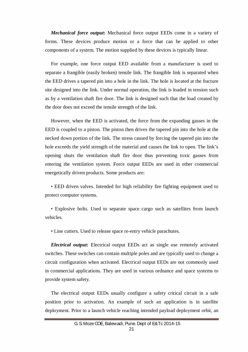
Mechanical force output: Mechanical force output EEDs come in a variety of
forms. These devices produce motion or a force that can be applied to other
components of a system. The motion supplied by these devices is typically linear.
For example, one force output EED available from a manufacturer is used to
separate a frangible (easily broken) tensile link. The frangible link is separated when
the EED drives a tapered pin into a hole in the link. The hole is located at the fracture
site designed into the link. Under normal operation, the link is loaded in tension such
as by a ventilation shaft fire door. The link is designed such that the load created by
the door does not exceed the tensile strength of the link.
However, when the EED is activated, the force from the expanding gasses in the
EED is coupled to a piston. The piston then drives the tapered pin into the hole at the
necked down portion of the link. The stress caused by forcing the tapered pin into the
hole exceeds the yield strength of the material and causes the link to open. The link’s
opening shuts the ventilation shaft fire door thus preventing toxic gasses from
entering the ventilation system. Force output EEDs are used in other commercial
energetically driven products. Some products are:
• EED driven valves. Intended for high reliability fire fighting equipment used to
protect computer systems.
• Explosive bolts. Used to separate space cargo such as satellites from launch
vehicles.
• Line cutters. Used to release space re-entry vehicle parachutes.
Electrical output: Electrical output EEDs act as single use remotely activated
switches. These switches can contain multiple poles and are typically used to change a
circuit configuration when activated. Electrical output EEDs are not commonly used
in commercial applications. They are used in various ordnance and space systems to
provide system safety.
The electrical output EEDs usually configure a safety critical circuit in a safe
position prior to activation. An example of such an application is in satellite
deployment. Prior to a launch vehicle reaching intended payload deployment orbit, an
G. S. Moze COE, Balewadi, Pune. Dept of E&Tc 2014-15 22
electrical output EED may be used to keep all firing energy away from circuits
intended to fire explosive bolts used to deploy payloads. When the launch vehicle
reaches the intended orbit position, the electrical output EED is activated enabling the
explosive bolt firing circuits.
Various electro-explosive devices are as follows:
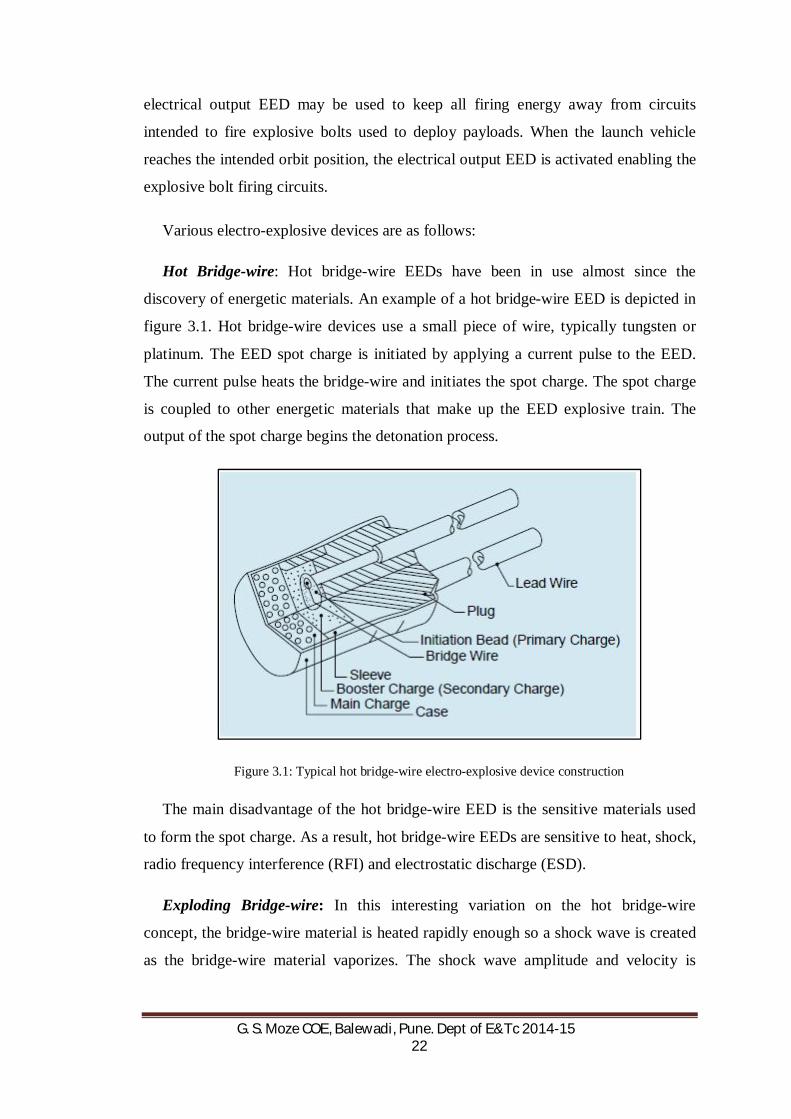
Hot Bridge-wire: Hot bridge-wire EEDs have been in use almost since the
discovery of energetic materials. An example of a hot bridge-wire EED is depicted in
figure 3.1. Hot bridge-wire devices use a small piece of wire, typically tungsten or
platinum. The EED spot charge is initiated by applying a current pulse to the EED.
The current pulse heats the bridge-wire and initiates the spot charge. The spot charge
is coupled to other energetic materials that make up the EED explosive train. The
output of the spot charge begins the detonation process.
Figure 3.1: Typical hot bridge-wire electro-explosive device construction
The main disadvantage of the hot bridge-wire EED is the sensitive materials used
to form the spot charge. As a result, hot bridge-wire EEDs are sensitive to heat, shock,
radio frequency interference (RFI) and electrostatic discharge (ESD).
Exploding Bridge-wire: In this interesting variation on the hot bridge-wire
concept, the bridge-wire material is heated rapidly enough so a shock wave is created
as the bridge-wire material vaporizes. The shock wave amplitude and velocity is

G. S. Moze COE, Balewadi, Pune. Dept of E&Tc 2014-15 23
sufficient to couple it to a relatively insensitive energetic material such as
pentaerythrioltetranitrate (PETN).
Because EBW EED system safety is sufficiently great, they have been used in
fission weapon warheads. Because the wire in the EBW EED initiates the shock wave
in the energetic material, a very specific firing signature is required to cause the EED
to function high order.
Exploding bridge wire based explosive devices are safe but are unsuitable for use
in electronic fuses due to high voltage required for its operation.
Exploding Foil Initiator: The EFI is a miniaturized version of the flying plate
sensitivity test mechanism. The EFI replaces the energetic material used to drive the
flying plate with an electrically initiated exploding metal foil. Figure 3.2 depicts the
typical construction of an EFI. The EFI is a very high speed EED and is constructed
with low inductance electrical connections. The EFI has vastly improved system
safety over that of systems using both hot bridge-wire and EBW EEDs. The EFI is a
signature specific EFI. The EFI can only detonate when coupled to the proper firing
circuit.
Conventional EEDs are susceptible to deterioration or detonation from continuous
low levels of RFI because of gradual heating of the spot charge. However, newer EED
initiation mechanisms provide substantial immunity to RFI susceptibility.
Additionally, because the all-fire pulse is signature specific, firing circuits and system
designs can provide greater operational and safety reliability.
Semiconductor Plasma Initiators: Semiconductor plasma initiators use the heat
transfer characteristics of silicon plasma to initiate energetic materials. These
materials are sensitive to the heat released by the condensing silicon plasma as it
diffuses through the energetic material. Since the energetic material depends on the
plasma temperature and rate of diffusion through the material, the high order function
of a semiconductor initiation mechanism is signature specific.
Semiconductor Junction Ignite: One type of silicon plasma initiator is the
semiconductor junction ignite (SJI). The SJI uses the silicon plasma initiation
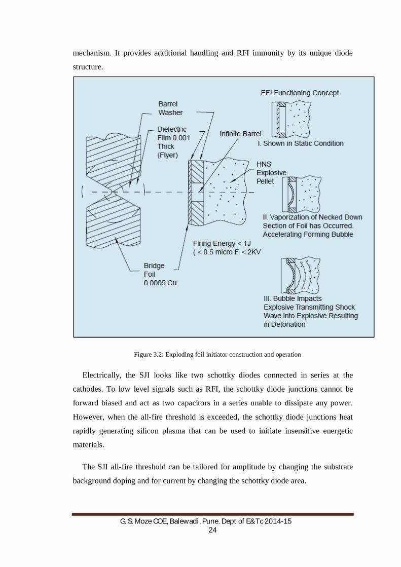
G. S. Moze COE, Balewadi, Pune. Dept of E&Tc 2014-15 24
mechanism. It provides additional handling and RFI immunity by its unique diode
structure.
Figure 3.2: Exploding foil initiator construction and operation
Electrically, the SJI looks like two schottky diodes connected in series at the
cathodes. To low level signals such as RFI, the schottky diode junctions cannot be
forward biased and act as two capacitors in a series unable to dissipate any power.
However, when the all-fire threshold is exceeded, the schottky diode junctions heat
rapidly generating silicon plasma that can be used to initiate insensitive energetic
materials.
The SJI all-fire threshold can be tailored for amplitude by changing the substrate
background doping and for current by changing the schottky diode area.

G. S. Moze COE, Balewadi, Pune. Dept of E&Tc 2014-15 25
Semiconductor Bridge: Another type of silicon plasma initiator is the
Semiconductor Bridge (SCB). The SCB resembles a bow tie of silicon that has been
vapour deposited on a sapphire substrate. The silicon plasma is generated when the
all-fire signal is delivered to the SCB. If the fire pulse is not delivered quickly
enough, the silicon bow tie opens and does not generate plasma providing RFI and
other small signal immunity.
Figure 3.3: Semiconductor bridge initiator
Main needs of igniters, low energy, reliability and safety, was fulfilled by
semiconductor bridges (SCB).SCB uses heavily doped poly-silicon bridge which is
much smaller than conventional bridge-wires. Passage of a current pulse with
significantly less energy than that required for hot-wire ignition produces a plasma
discharge in SCB which ignites the explosive pressed against the bridge, producing an
explosive output within few microseconds.
Production of bridges is routine poly-silicon on-silicon wafer process. The finished
wafers are diced into chips and the chips are placed on a header holding incoming
electrical leads. Aluminium or gold wires are then used to connect the bridge to
header leads. Computer generated masks are used to define the bridge; thus, the SCB
design can be easily tailored for particular application. Because of the intimate
thermal contact of the bridge with underlying substrate excellent no-fire currents are
obtained.

G. S. Moze COE, Balewadi, Pune. Dept of E&Tc 2014-15 26
Direct comparisons of the components built with SCBs substituted for bridge-wires
show that the energy for SCB ignition is at least 10 times less than that of bridge-
wires. Further the function times for SCB devices are only few tens of microseconds.
SCB devices have very wide range of applications. They are being used in airbag
ignition, in rock blasting detonators, and in military igniters and detonators. They are
particularly attractive for applications where only very low ignition energy is
available.
They can also be combined with other microelectronic circuits or can be integrated
on chip with peripheral circuitry which can be manufactured using MEMs technology.

G. S. Moze COE, Balewadi, Pune. Dept of E&Tc 2014-15 27
CHAPTER 4
FUZE
SCB is integ rated with MEMS based safe, arm and fire (SAF) device. A SAF
Device is employed in military and defence applications particularly used in missiles
for fuzing.
In military munitions, a fuze is the part of the device that initiates function. The
term fuze is used to indicate a ignition device incorporating mechanical and/or
electronic components. A Fuze is a device used in munitions which is designed
to detonate, or to set forces into action to ignite, detonate or deflagrate, the charge (or
primer) under specified conditions. In contrast to a simple pyrotechnic fuse, a
munitions fuze always has some form of safety/arming mechanism, designed to
protect the user from premature or accidental detonation.
The fuze is designed to initiate the warhead either on hitting the target or at some
distance from the target. Today, most missiles and bombs use electronic fuzes. Fuzing
mechanisms are devices used to ‘safe’, ‘arm’ and detonate explosive military
munitions (such as missiles, mines, demolition charges, explosive shells, unguided
bombs and various submunitions). The initiation may also be done after certain time
delay, after the projectile has been fired.
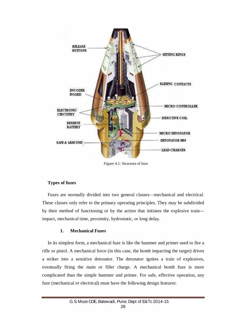
Structure of Fuze
The structure of fuzing mechanism is given in the fig 4.1. The whole circuitry is
consist of three layers. The power supply consists of DC-DC converter with battery,
an analog switch is there used for fast switching and SAF is the safe, arm and fire unit
which do mechanical arming functions. Release buttons are there which are connected
to nose of fuze and can be operated by operator. By pressing these buttons missile will
start functioning. Heating resistances are there which when comes in contact with
propellant can produce hot gases which do arming and ignite the explosive train.
Rather than using these resistances, I will use SCB here because its ignition time is
very low so delay time will be reduced. Also it is highly safe and good immune to
ESD & RF protection. Three switches are there 2 ON-OFF and 1 OFF-ON switch
which are also used in SAF device.
G. S. Moze COE, Balewadi, Pune. Dept of E&Tc 2014-15 28
Figure 4.1: Structure of fuze
Types of fuzes
Fuzes are normally divided into two general classes—mechanical and electrical.
These classes only refer to the primary operating principles. They may be subdivided
by their method of functioning or by the action that initiates the explosive train—
impact, mechanical time, proximity, hydrostatic, or long delay.
1. Mechanical Fuzes
In its simplest form, a mechanical fuze is like the hammer and primer used to fire a
rifle or pistol. A mechanical force (in this case, the bomb impacting the target) drives
a striker into a sensitive detonator. The detonator ignites a train of explosives,
eventually firing the main or filler charge. A mechanical bomb fuze is more
complicated than the simple hammer and primer. For safe, effective operation, any
fuze (mechanical or electrical) must have the following design features:

G. S. Moze COE, Balewadi, Pune. Dept of E&Tc 2014-15 29
• It must remain safe in stowage, while it is handled in normal movement, and
during loading and downloading evolutions.
• It must remain safe while being carried aboard the aircraft.
• It must remain safe until the bomb is released and is well clear of the delivery
aircraft (arming delay or safe separation period) Depending upon the type of target,
the fuze may be required to delay the detonation of the bomb after impact for a preset
time (functioning delay). Functioning delay may vary from a few milliseconds to
many hours.
• It should not detonate the bomb if the bomb is accidentally released or if the
bomb is jettisoned in a safe condition from the aircraft. To provide these qualities, a
number of design features are used. Most features are common to all types of fuzes.
2. Electrical Fuzes
Electrical fuzes have many characteristics of mechanical fuzes. They differ in fuze
initiation. An electrical impulse is used to initiate the electrical fuze rather than the
mechanical action of arming vane rotation. An electrical pulse from the delivery
aircraft charges capacitors in the fuze as the bomb is released from the aircraft.
Arming and functioning delays are produced by a series of resistor/capacitor networks
in the fuze. The functioning delay is electromechanically initiated, with the necessary
circuits closed by means of shock-sensitive switches. The electric bomb fuze remains
safe until it is energized by the electrical charging system carried in the aircraft.
Because of the interlocks provided in the release equipment, electrical charging can
occur only after the bomb is released from the rack or shackle and has begun its
separation from the aircraft; however, it is still connected electrically to the aircraft's
bomb arming unit. At this time, the fuze receives an energizing charge required for
selection of the desired arming and impact times.
I. Fuze categorization by munition type
The situation of usage and characterstics of the munitions it is intended to activate
the affect fuze design e.g. its safety and actuation mechanism.

G. S. Moze COE, Balewadi, Pune. Dept of E&Tc 2014-15 30
1. Artillery Fuzes
Artillery Fuzes are tailored to function in the special circumstances of artillery
projectiles, the relevant factor are the projectile’s initial rapid acceleration, high
velocity and usually rapid rotation, which affect both safety and arming requirements
and options and the target may be moving or stationary.
Artillery Fuzes may be initiated by a timer mechanism, impact or detection of
proximity to the target or a combination of these.
2. Hand grenade fuze
Requirements of hand grenade fuze are defined by the projectile’s small size and
slow delivery over a short distance. This necessitates manual arming before throwing
as the grenade has insufficient initial acceleration for arming to be driven by
"setback" and no rotation to drive arming by centrifugal force.
3. Aerial bomb fuzes
These are also referred to as "pistols". The main design consideration is that the
projectile is large and accelerating vertically downwards and may or may not be
rotating relatively slowly.
4. Landmine fuze
The main design consideration is that the bomb the fuze is intended to actuate is
stationary, and the target itself is moving in making contact.
5. Naval mine fuzes
Relevant design factors are that the mine may be static or moving downward
through the water, and the target is typically moving on or below the water surface,
usually above the mine.
Early artillery time fuzes were nothing more than a hole filled with gunpowder
leading from the surface to the centre of the projectile. The flame from the burning of
the gunpowder propellant ignited this "fuze" on firing, and burned through to the
centre during flight, then igniting or exploding whatever the projectile may have been
filled with.
G. S. Moze COE, Balewadi, Pune. Dept of E&Tc 2014-15 31
By the 19th century devices more recognisable as modern artillery "fuzes" were
being made of carefully selected wood and trimmed to burn for a predictable time
after firing. These were still typically fired from smoothbore muzzle-loaders with a
relatively large gap between the shell and barrel, and still relied on flame from the
gunpowder propellant charge escaping past the shell on firing to ignite the wood fuze
and hence initiate the timer.
In the mid-to-late 19th century adjustable metal time fuzes, the fore-runners of
today's time fuzes, containing burning gunpowder as the delay mechanism became
common, in conjunction with the introduction of rifled artillery. Rifled guns
introduced a tight fit between shell and barrel and hence could no longer rely on the
flame from the propellant to initiate the timer. The new metal fuzes typically use the
shock of firing ("setback") and/or the projectiles's rotation to "arm" the fuze and
initiate the timer : hence introducing a safety factor previously absent.
During World War I, mechanical, or clockwork, time fuzes were introduced for
artillery by Germany, and some variants are still in use.
As late as World War I, some countries were still using hand-grenades with simple
black match fuses much like those of modern fireworks: the infantryman lit the fuse
before throwing the grenade and hoped the fuse burned for the several seconds
intended. These were soon superseded in 1915 by the Mills bomb, the first modern
hand grenade with a relatively safe and reliable time fuze initiated by pulling out a
safety pin and releasing an arming handle on throwing.
Modern time often use an electronic delay system.
6. Impact fuzes
Impact, percussion and contact fuzes detonate when their forward motion rapidly
decreases, typically on physically striking an object such as target. The detonation
may be instantaneous and deliberately delayed to occur a present fraction of a second
after penetration of the target. An instantaneous “superquick” fuze will detonate
instantlyon the slight physical contact with the target. A fuze with agraze action will
also detonate on the change of direction caused by slight glancing blow on a physical
obstruction such as the ground.
Impact fuzes in artillery usage may be mounted in the shell nose ("point
detonating") or shell base ("base detonating").
G. S. Moze COE, Balewadi, Pune. Dept of E&Tc 2014-15 32
7. Proximity fuzes
Proximity fuzes cause a missile warhead or other munition (e.g. air-dropped bomb
or sea mine) to detonate when it comes within a certain pre-set distance of the target,
or vice versa. Proximity fuzes utilize sensors incorporating one or more combinations
of the following: radar, active sonar, passive
acoustic, infrared, magnetic, photoelectric, seismic or even television cameras. These
may take the form of an anti-handling device designed specifically to kill or severely
injure anyone who tampers with the munition in some way e.g. lifting or tilting it.
Regardless of the sensor used, the pre-set triggering distance is calculated such that
the explosion will occur sufficiently close to the target that it is either destroyed or
severely damaged.
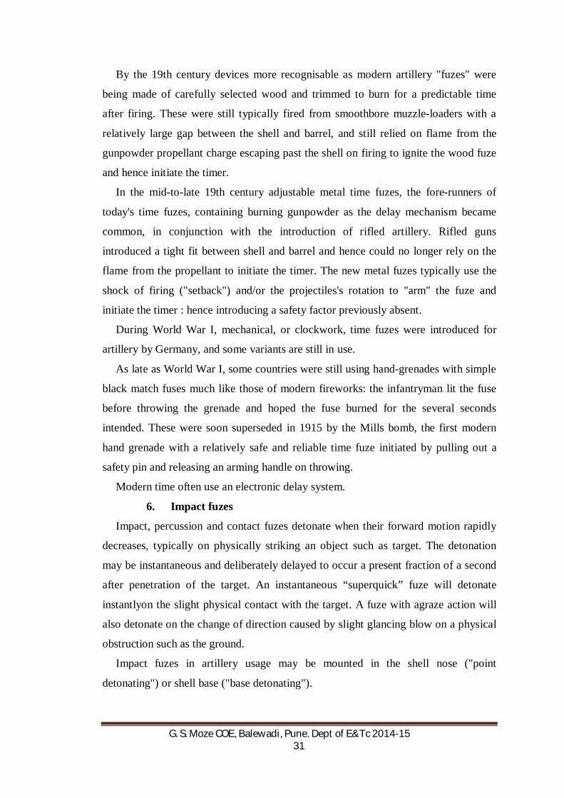
Figure 4.2: Mk 53 Proximity fuze for an artillery shell, circa 1945
8. Remote detonators
Remote detonators use wires or radio waves to remotely command the device
to detonate.
9. Barometric fuzes
Barometric fuzes cause a bomb to detonate at a certain pre-set altitude above sea
level by means of a radar, barometric altimeter or aninfrared rangefinder.

G. S. Moze COE, Balewadi, Pune. Dept of E&Tc 2014-15 33
10. Combination fuzes
A fuze assembly may include more than one fuze in series or parallel
arrangements. The RPG-7 usually has an impact (PIBD) fuze in parallel with a 4.5
second time fuze; so detonation occurs on impact, but not later than after 4.5 seconds.
Military weapons containing explosives have fuzing systems including a series
time fuze to ensure that they do not initiate (explode) prematurely within a danger
distance of the munition launch platform. In general, the munition has to travel a
certain distance, wait for a period of time (via clockwork, electronic or even a
chemical delay), or have some form of arming pin/plug removed. Only when these
processes have occurred will the arming process of the series time fuze be complete.
Mines often have a parallel time fuze to detonate and destroy the mine after a pre-
determined period to minimize casualties after the anticipated duration of hostilities.
Detonation of modern naval minesmay require simultaneous detection of a series
arrangement of acoustic, magnetic, and/or pressure sensors to complicate mine-
sweeping efforts.
Fuze safety/arming mechanism
The multiple safety/arming features in the M734 mortar fuze are representative of
the sophistication of modern electronic fuzes.
Figure 4.3: SD2 Butterfly bomb circa 1940 - wings rotate as bomb falls, unscrewing the arming
spindle connected to the fuze

G. S. Moze COE, Balewadi, Pune. Dept of E&Tc 2014-15 34
Safety/arming mechanisms can be as simple as the spring-loaded safety levers
on M67 or RGD-5 grenade fuzes, which will not initiate the explosive train so long as
the pin is kept in the grenade, or the safety lever is held down on a pinless grenade.
Alternatively, it can be as complex as the electronic timer-countdown on an
influence sea mine, which gives the vessel laying it sufficient time to move out of the
blast zone before the magnetic or acoustic sensors are fully activated.
In modern artillery shells, most fuzes incorporate several safety features to prevent
a fuze arming before it leaves the gun barrel. These safety features may include
arming on "setback" or by centrifugal force, and often both operating together. Set-
back arming uses theinertia of the accelerating artillery shell to remove a safety
feature as the projectile accelerates from rest to its in-flight speed. Rotational arming
requires that the artillery shell reach a certain rpm before centrifugal forces cause a
safety feature to disengage or move an arming mechanism to its armed position.
Artillery shells are fired through a rifled barrel, which forces them to spin during
flight.
In other cases the bomb, mine or projectile has a fuze that prevents accidental
initiation e.g. stopping the rotation of a small propeller(unless a lanyard pulls out a
pin) so that the striker-pin cannot hit the detonator even if the weapon is dropped on
the ground. These types of fuze operate with aircraft weapons, where the weapon may
have to be jettisoned over friendly territory to allow a damaged aircraft to continue to
fly. The crew can choose to jettison the weapons safe by dropping the devices with
safety pins still attached, or drop them liveby removing the safety pins as the weapons
leave the aircraft.
Aerial bombs and depth charges can be nose and tail fuzed using different
detonator/initiator characteristics so that the crew can choose which effect fuze will
suit target conditions that may not have been known before the flight. The arming
switch is set to one of safe, nose, or tail at the crew's choice.
Base fuzes are also used by artillery and tanks for shells of the 'squash head' type.
Some types of armour piercing shells have also used base fuzes, as have nuclear
artillery shells.
The most sophisticated fuze mechanisms of all are those fitted to nuclear weapons,
and their safety/arming devices are correspondingly complex. In addition
to PAL protection, the fuzing used in nuclear weapons features multiple, highly

G. S. Moze COE, Balewadi, Pune. Dept of E&Tc 2014-15 35
sophisticated environmental sensors e.g. sensors requiring highly specific acceleration
and deceleration profiles before the warhead can be fully armed. The intensity and
duration of the acceleration/deceleration must match the environmental conditions
which the bomb/missile warhead would actually experience when dropped or fired.
Furthermore, these events must occur in the correct order.
Note: some fuzes, e.g. those used in air-dropped bombs and landmines may
contain anti-handling devices specifically designed to kill bomb disposal personnel.
The technology to incorporate booby-trap mechanisms in fuzes has existed since at
least 1940 e.g. the German ZUS40 anti-removal bomb fuze.

G. S. Moze COE, Balewadi, Pune. Dept of E&Tc 2014-15 36
CHAPTER 5
MEMS Technology
MEMS stands for microelectromechanical systems where different physical
properties of material at micro scale is utilized to electrically control the mechanical
response of a microsystem and vice versa. Electro-thermal, electrostatics,
piezoelectric, piezoresistivity are some of the physical phenomenon adopted by
MEMS technology. They often function as transducers for conversion of energy from
one form to another. For example, application of force on piezoelectric MEMS would
yield electrical current signal. Conversely by applying electric field on a piezoelectric
MEMS world’s smallest motor has been fabricated. Application of heat to a
bimaterial structure can produce mechanical movement due to differential rate of
thermal expansion.
Since in energy scavenging the energy harvested is very small in quantity it is quite
inefficient to use regular size machines and systems for the purpose. To harvest small
amount of energy, small transducers like MEMS can be more beneficial.
To realize a microelectromechanical system with desired response, many obstacles
were overcome in steps that involved studies identifying the problem at hand and
researching for solutions. The challenges involved in design and development of the
MEMS device are listed below:
1. Study of the properties of materials to characterize the
thermomechanical responsivity of the MEMS structure and find optimized
dimension for desired range of responsivity. Develop finite element model and
formulate generalized analytical model to estimate the device response under
given conditions.
2. Find environmental conditions required for thermal actuation of the
MEMS device and continued self-oscillation without any excitation external to
the system or the source. Using finite element modeling and analytical
modeling to estimate the period of oscillation of the MEMS structure and the
magnitude of temperature cycling that occurs in the structure.
3. Characterize pyroelectric capacitors and their power generation
capacity corresponding to temperature cycle frequency. Study

G. S. Moze COE, Balewadi, Pune. Dept of E&Tc 2014-15 37
thermomechanical properties of pyroelectric materials for integrating the thin-
film pyroelectric capacitors with the MEMS device. Develop model to
approximate the magnitude and the profile of the power generation from the
combined structure.
4. Design a low power current rectifier and energy storage circuit for
storing the harvested energy from the MEMS structure for powering
subsequent low power mobile or wireless electronics.
With an intention to find an innovative and more efficient way to extract
pyroelectric energy a design of a self-governed temperature cycling system taking
advantage of recent developments in microelectromechanical system is conceived and
design properties and conditions are studied to realize a functional system with
optimized performance for maximum energy conversion efficiency.
5.1 MEMS Devices MEMS stands for microelectromechanical systems. It is an emerging technology
using the microfabrication tools and techniques of integrated circuit manufacturing
industry to fabricate micron scale machines driven by electrical energy. Typically
MEMS technology consists of devices or structures that may or may not have a
moving part but utilizes some mechanical properties and are electronically controlled.
Functional elements of MEMS devices are miniaturized structures that are used as
sensors and actuators. Notable application of MEMS devices are sensors,
micromirrors, microactuators, micropumps, accelerometers, gyroscope, radio
frequency resonators etc.
In functional MEMS devices few basic structures are used to control the
mechanical movement or electrical performances. In microscale the regular
macroscale physics such as gravity, inertia becomes obsolete and other properties
such as stress, thermal capacity or ferroelectricity become more important. In sensors
these properties are utilized to sense pressure, presence of particular gas, light etc. and
to produce electrical signals that are further conditioned by associated
microelectronics to produce useful information. In MEMS actuator similar properties
are utilized to electrically gain control over the mechanical performance of the
G. S. Moze COE, Balewadi, Pune. Dept of E&Tc 2014-15 38
structure. Based on which property is utilized, MEMS devices can be electrothermal,
electrostatic, piezoelectric etc. For this study a detail look at electrothermal and
piezoelectric MEMS devices and their behavior is provided in the next sub-sections.
5.2 Electrothermal MEMS
Electrothermal MEMS takes advantage of Joule heating to control the temperature
of the structure and utilizes its thermal properties. In many applications electrothermal
MEMS are used for mechanical movement achieved by thermal expansion due to
controlled heating of the device.
Examples of electrothermal MEMS include micromirrors, microactuators such as
microgrippers, temperature sensors etc.
Often in electrothermal MEMS devices a beam like structure is used that can be
either unimorph or bimorph. In a unimorph structure, the device is made of a single
material of high resistivity usually polysilicon or silicon nitride. The electrical current
flows through the body of the device and generates heat due to resistive loss. Since
the device is in micro scale, the resistance is high and produces enough heat to
thermally expand the device body and cause deformation. Thus thermally caused
deformation is utilized for actuation. In unimorph structures high current has to flow
through the device to raise the temperature high enough to achieve sufficient thermal
expansion to reach the desired level actuation. Very high temperature operation is
involved in this case, and accordingly the device life is reduced.
In a bimorph structure typically more than one type of material is involved. In
similar fashion to unimorph structure, Joule heating is used to increase the
temperature of the device in desired places. Since different materials have different
thermal expansion rates, their expanded length vary and if they are attached to each
other a resultant deflection occurs in an attempt to balance the compressive and
tensile forces experienced by the two materials thermally expanding at differential
rate. In most cases the device involves a cantilever structure that actuates based upon
the temperature increase and the deflection of the cantilever beam.
Electrothermal MEMS are also used as sensors where upon the absorption of heat
the micro structures deform to produce an electrical signal [64]. Since the Joule

G. S. Moze COE, Balewadi, Pune. Dept of E&Tc 2014-15 39
heating process is nonreversible, deformation is converted to electrical signal by other
forms of transducers, such as laser reflection or piezoelectric transducers. Because of
its high sensitivity electrothermal MEMS are widely used for infrared imaging .
5.3 Piezoelectric MEMS
MEMS technology benefits itself tremendously by making use of the piezoelectric
properties of material. The property of materials to deform upon application of
electric field is largely used in MEMS technology to actuate micro devices and
structures. Since this process is reversible, piezoelectric property is also utilized in
MEMS based sensors, for example, in pressure sensors.
In microactuators fabricated using piezoelectric materials, electric potential is
applied to deform the device structures in a desirable form to actuate micromotors,
pump microfluidic channels, close microswitches, tune capacitors, adjust micromirror
positions and so on. Application of potential causes polarization in the lattice structure
of the piezoelectric materials that displaces the position of the atoms in the structure
causing deformation. Direction of the deformation is dependent on the piezoelectric
coefficient and the direction of the applied voltage to the material.
Piezoelectric MEMS has also been widely researched and more recently
commercially developed for energy harvesting from pressure and vibrations. In
piezoelectric energy harvesters a MEMS structure is allowed to pick up vibration or
experience pressure which generates electric potential in the material. The generated
potential is typically intermittent and requires conditioning circuit to rectify and store
the harvested energy for use. The piezoelectric conversion efficiency needs to be
higher for energy harvesting application.
Similarly for sensor application the piezoelectric material functions as transducer
to convert pressure to electrical signals [65]. In this case low amplitude of converted
electrical signal is acceptable for the purpose of analysis. Note that in comparison
with electrothermal MEMS that controls the mechanical behavior with electric
current, piezoelectric MEMS control the mechanical response with electric potential.

G. S. Moze COE, Balewadi, Pune. Dept of E&Tc 2014-15 40
CHAPTER 6
SYSTEM DEVELOPMENT
The proposed system consists of two parts
Authentication Unit
Delay and Firing Unit
6.1 Authentication Unit –Figure no.6.1 shows the block diagram of the Setter.
The setter consists of LCD, Microcontroller, battery and keypad to enter the password
and arming command. The microcontroller sends commands to the firing unit. The
detonator ID, delay time for arming is fed from the setter which is then set into the
firing unit. The setter is password protected and hence avoids unauthorised access.
The maximum input voltage of the system is 9-12V.
Figure 6.1: Block diagram of Authentication Unit

G. S. Moze COE, Balewadi, Pune. Dept of E&Tc 2014-15 41
6.2 Delay and Firing Unit:
The block diagram of Timer or delay unit is as shown in figure 8. The system can
be further divided into two parts as described below.
Figure 6.2: Block Diagram of delay and firing Unit
The Delay and Firing Unit is divided into two parts:
1. ESD & RF protected SCB
2. Circuit for voltage boosting with delay
6.3 Semiconductor Bridge
Semiconductor Bridges (SCBs) are finding increased use as initiators for explosive
and pyrotechnic devices. They offer advantages in reduced voltage and energy
requirements coupled with excellent safety features. SCBs operate in a detonator,
particularly with respect to the interaction of explosive powder and SCB.
Plasma generated from SCBs is used to ignite explosives, where the heavily doped
poly-silicon in contact with power gets melted and evaporated to form high pressure
plasma upon introduction of large currents through the SCB. Because the typical
value of bridge resistance is one ohm, the bridge is ohmic-heated through the
G. S. Moze COE, Balewadi, Pune. Dept of E&Tc 2014-15 42
electrical current. The SCB may melt down and eventually evaporate if enough
electrical energy is deposited into the bridge within a limited time.
Once the bridge material is vaporized the applied electric voltage breakes down the
silicon gas generating silicon plasma. This is called as late-time discharge. This
plasma will eventually ignite the explosive material. The SCB works within few
microseconds compared with the milliseconds response of a conventional hot-wire
unit.
A semiconductor bridge comprises a substrate of non-electrically conductive
material, a doped semiconductor layer on the substrate as well as first and second
metal lands forming ohmic contacts on the doped semiconductor layer. An explosive
charge bridges a gap between the metal lands across the doped semiconductor layer.
The lands, gap, semiconductor layer and charge are dimensioned and arranged so that
in response to a current equal to or in excess of a predetermined level having a
duration equal to or in excess of a predetermined value being applied across the gap,
plasma having sufficient energy to energize the explosives is formed in the gap.
6.3.1 Construction
An SCB consists of a small doped polysilicon volume formed on a silicon
substrate. The length of the bridge (100 m) is determined by the spacing of the
aluminium lands seen in the figure. The doped layer is 2 m thick and the bridge is 380
m wide. The lands provide a low ohmic contact to the underlying doped layer. Wires
ultrasonically bonded to the lands permit a current pulse to flow from land to land
through the bridge. The current pulse through the SCB causes it to burst into bright
plasma discharge that heats the exoergic powder pressed against it by a convective
process that is both rapid and efficient. Consequently, SCB devices operate at very
low energies and function very quickly. But despite low energy for ignition, the
substrate provides a reliable heat sink for excellent no-fire levels.

G. S. Moze COE, Balewadi, Pune. Dept of E&Tc 2014-15 43
Figure 6.3: Top view and cut view of typical SCB structure
The semiconductor bridge device comprises of following components. An
electrically non-conducting substrate, which may comprise, e.g, sapphire, silicon
dioxide on silicon or silicon nitride on silicon, has an electrically conducting material,
e.g, a semiconductor, which optionally may be a doped semiconductor, mounted
thereon. The electrically conducting material has a temperature coefficient of
electrical resistivity which is negative at a given temperature above about 20oC and
below about 1400oC. the electrically conducting material, which may be selected from
mono crystalline silicon, polycrystalline silicon and amorphous silicon defines a
bridge connecting a pair of spaced-apart pads. The bridge and pads are so
dimensioned and conFIgured that the passage there through of an electrical current of
selected characteristics releases energy at the bridge.
A pair of spaced-apart metallized lands are disposed one on each of the spaced-
apart parts so as to leave at least a portion of the bridge uncovered. Each of the
metallized lands comprises (i) a base layer comprised of titanium and disposed upon
its associated pad, (ii) an intermediate layer comprised of titanium and tungsten and
disposed on its associated base layer, and (iii) a top layer comprised of a tungsten and
disposed on its associated intermediate layer.
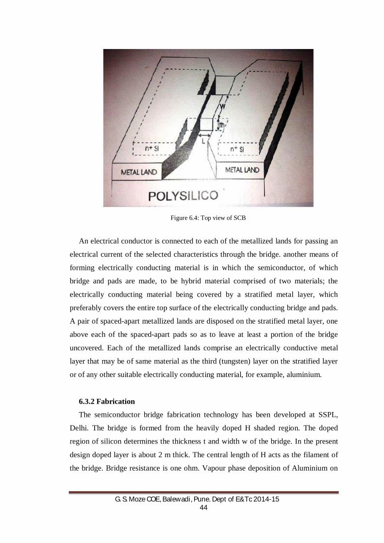
G. S. Moze COE, Balewadi, Pune. Dept of E&Tc 2014-15 44
Figure 6.4: Top view of SCB
An electrical conductor is connected to each of the metallized lands for passing an
electrical current of the selected characteristics through the bridge. another means of
forming electrically conducting material is in which the semiconductor, of which
bridge and pads are made, to be hybrid material comprised of two materials; the
electrically conducting material being covered by a stratified metal layer, which
preferably covers the entire top surface of the electrically conducting bridge and pads.
A pair of spaced-apart metallized lands are disposed on the stratified metal layer, one
above each of the spaced-apart pads so as to leave at least a portion of the bridge
uncovered. Each of the metallized lands comprise an electrically conductive metal
layer that may be of same material as the third (tungsten) layer on the stratified layer
or of any other suitable electrically conducting material, for example, aluminium.
6.3.2 Fabrication
The semiconductor bridge fabrication technology has been developed at SSPL,
Delhi. The bridge is formed from the heavily doped H shaded region. The doped
region of silicon determines the thickness t and width w of the bridge. In the present
design doped layer is about 2 m thick. The central length of H acts as the filament of
the bridge. Bridge resistance is one ohm. Vapour phase deposition of Aluminium on
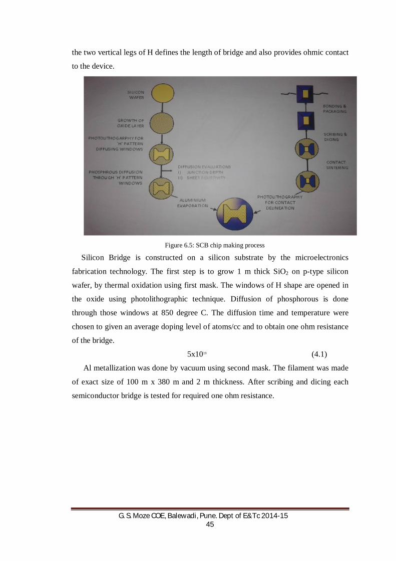
G. S. Moze COE, Balewadi, Pune. Dept of E&Tc 2014-15 45
the two vertical legs of H defines the length of bridge and also provides ohmic contact
to the device.
Figure 6.5: SCB chip making process
Silicon Bridge is constructed on a silicon substrate by the microelectronics
fabrication technology. The first step is to grow 1 m thick SiO2 on p-type silicon
wafer, by thermal oxidation using first mask. The windows of H shape are opened in
the oxide using photolithographic technique. Diffusion of phosphorous is done
through those windows at 850 degree C. The diffusion time and temperature were
chosen to given an average doping level of atoms/cc and to obtain one ohm resistance
of the bridge.
5x10¹⁹ (4.1)
Al metallization was done by vacuum using second mask. The filament was made
of exact size of 100 m x 380 m and 2 m thickness. After scribing and dicing each
semiconductor bridge is tested for required one ohm resistance.
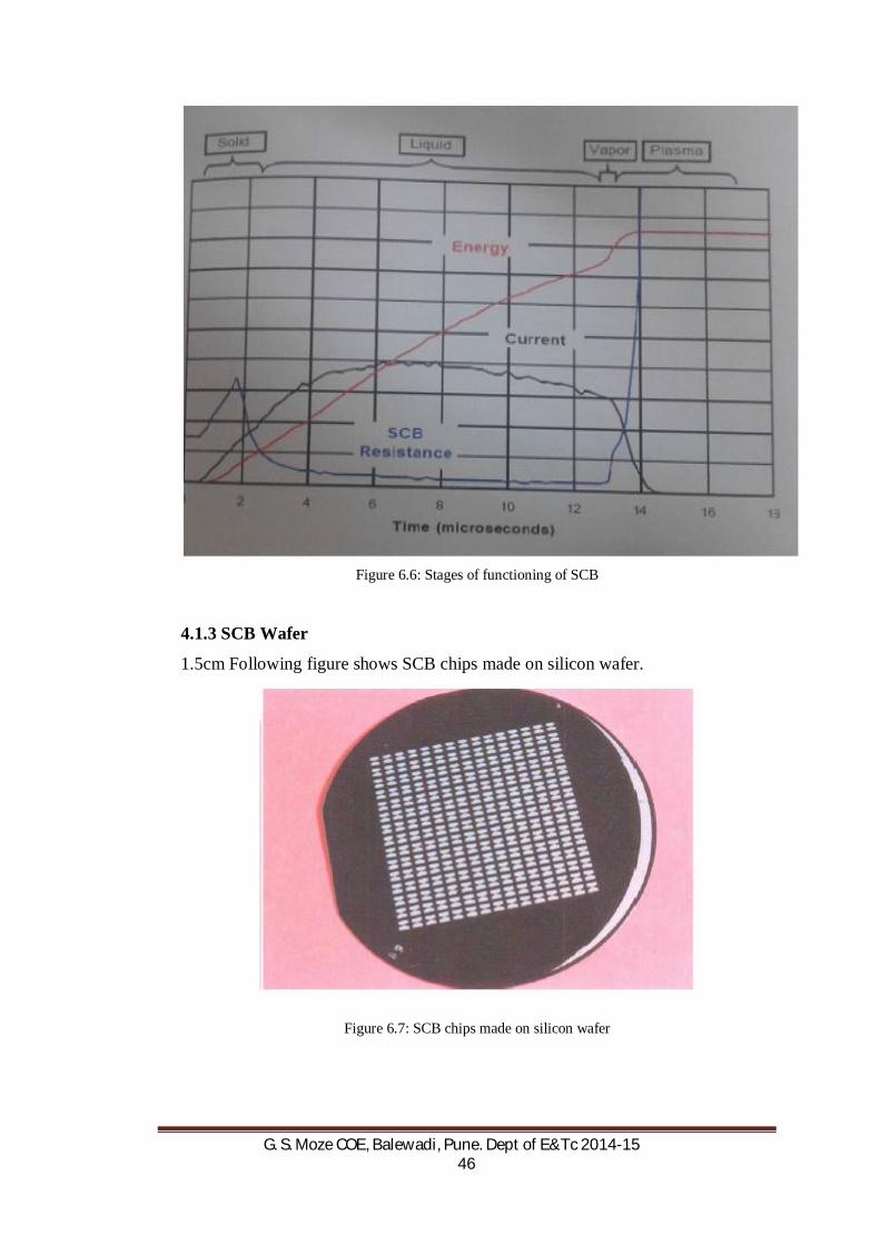
G. S. Moze COE, Balewadi, Pune. Dept of E&Tc 2014-15 46
Figure 6.6: Stages of functioning of SCB
4.1.3 SCB Wafer
1.5cm Following figure shows SCB chips made on silicon wafer.
Figure 6.7: SCB chips made on silicon wafer
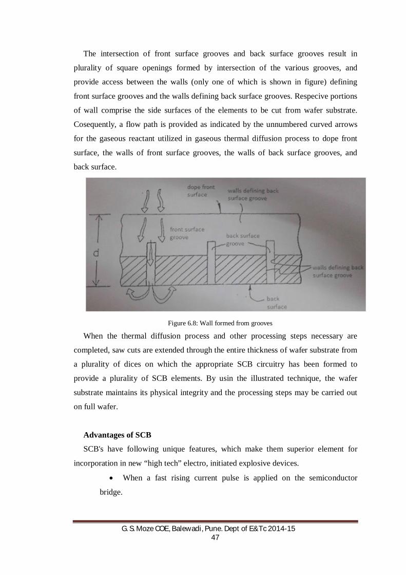
G. S. Moze COE, Balewadi, Pune. Dept of E&Tc 2014-15 47
The intersection of front surface grooves and back surface grooves result in
plurality of square openings formed by intersection of the various grooves, and
provide access between the walls (only one of which is shown in figure) defining
front surface grooves and the walls defining back surface grooves. Respecive portions
of wall comprise the side surfaces of the elements to be cut from wafer substrate.
Cosequently, a flow path is provided as indicated by the unnumbered curved arrows
for the gaseous reactant utilized in gaseous thermal diffusion process to dope front
surface, the walls of front surface grooves, the walls of back surface grooves, and
back surface.
Figure 6.8: Wall formed from grooves
When the thermal diffusion process and other processing steps necessary are
completed, saw cuts are extended through the entire thickness of wafer substrate from
a plurality of dices on which the appropriate SCB circuitry has been formed to
provide a plurality of SCB elements. By usin the illustrated technique, the wafer
substrate maintains its physical integrity and the processing steps may be carried out
on full wafer.
Advantages of SCB
SCB's have following unique features, which make them superior element for
incorporation in new “high tech” electro, initiated explosive devices.
When a fast rising current pulse is applied on the semiconductor
bridge.

G. S. Moze COE, Balewadi, Pune. Dept of E&Tc 2014-15 48
SCB's generate hot plasma for ignition of the explosive powder
pressed against the bridge. Ignition is via micro - convective heat transfer
process and not merely a thermal conductive heat transfer as with hot wires.
Ignition energy for SCB's is one tenth to that of conventional bridge-
wires metal foils.
SCB function (i.e. produce a usable explosive output) a thousand
times faster than bridge wires.
By changing the area of bridge one can greatly vary the no fire level
of the device without greatly affecting the all fire energy.
SCB devices are explosively safe. They have high no fire current.
SCBs are highly resistant to ESD pulse.
SCBs being semiconductor should not be compared with metal foils.
SCB cannot fail like metal foils. Current pulse required to function SCB is a
unique signal preventing their accidental operation.
Due to the above unique features SCB's have great benefit for several
application of ignition in pyrotechnic, propellants and explosive devices.
6.4 ESD and RF Protection
SCB is a low energy and small size initiator device with very small firing delay. A
Semiconductor Bridge (SCB) can initiate unintentionally by Electrostatic Discharge
(ESD) and high power RF. The safety of SCB from ESD and RF is of vital
importance. The SCB may fire unintentionally by human handling. There are various
methods implemented to protect the SCB against ESD and RF. The protection of
explosive initiators was done using Zener diode, back to back Zener diodes, TVS
diodes, Schottky diodes etc that were connected along with SCB either by integrating
or as a discrete components. High-level electromagnetic energy produced by Radio
frequency radiation can also induce electrical currents or voltages that may cause
premature activation of Electro-Explosive Devices (EEDs) and electrical arcs that
may ignite flammable materials.
Semiconductor bridge (SCB) initiator is a transducer. Under the effect of high
electrical energy, the power transforms into thermal power. Then the doped
polysilicon layer vaporises and generates high temperature plasma which heats the

G. S. Moze COE, Balewadi, Pune. Dept of E&Tc 2014-15 49
explosive. Ultimately, when the temperature reaches ignition temperature, the
explosive detonates.
SCB itself has a good insensitive characteristic against electrostatic inherently.
SCB initiators do not fire under the test conditions of 500pF 5000ohms and 25kV.
6.4.1 ESD Electrostatic Discharge (ESD) interference is a specialized type of ambient
interference that results from the extremely rapid equalization of charges between
conductive surfaces. One common type of ESD is static generated by friction between
two insulating materials. Humans experience ESD as a brief electric shock.
Electronic parts straddling a charged and uncharged plastic surface experience
ESD as a current flow that can be large enough to instantly cause damage or
destruction.
ESD produces heat, light, sound, and electromagnetic radiation throughout the
entire spectrum. A simple ESD spark can set fires, fog film, shock personnel and
ignite explosives. The failure of only one semiconductor junction in an electronic
device can render the device useless. Worse, ESD can cause latent failure so that
components can pass testing, but later fail in field use. Modern military and
commercial electronic devices can have millions of semiconductor junctions. The
effects of ESD are cumulative and progressive degradation that is not readily apparent
can occur over time.
As the representative of modern advanced initiators, SCB initiators have low-firing
energy, short function time and high-reliability. But as a kind of EED, SCB still can
be affected by the electrostatic energy between the pin-to-pin or pin-to-case. The
electrostatic can cause the change of the performance. The pin-to-case electrostatic
mainly generates electrostatic spark and then the spark ignites the explosive to
accidentally ignite initiators or change the electrical explosion property.
Electrostatic is a kind of electric charge in a relatively steady state. When the
objects which have different electrostatic potentials are close to or directly contact
with each other, it can result in charge transfer. Accordingly, we define it as
electrostatic discharge which is expressed as ESD for short. Though the quantity of
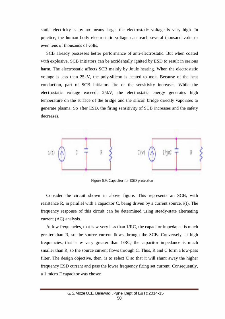
G. S. Moze COE, Balewadi, Pune. Dept of E&Tc 2014-15 50
static electricity is by no means large, the electrostatic voltage is very high. In
practice, the human body electrostatic voltage can reach several thousand volts or
even tens of thousands of volts.
SCB already possesses better performance of anti-electrostatic. But when coated
with explosive, SCB initiators can be accidentally ignited by ESD to result in serious
harm. The electrostatic affects SCB mainly by Joule heating. When the electrostatic
voltage is less than 25kV, the poly-silicon is heated to melt. Because of the heat
conduction, part of SCB initiators fire or the sensitivity increases. While the
electrostatic voltage exceeds 25kV, the electrostatic energy generates high
temperature on the surface of the bridge and the silicon bridge directly vaporises to
generate plasma. So after ESD, the firing sensitivity of SCB increases and the safety
decreases.
Figure 6.9: Capacitor for ESD protection
Consider the circuit shown in above figure. This represents an SCB, with
resistance R, in parallel with a capacitor C, being driven by a current source, i(t). The
frequency response of this circuit can be determined using steady-state alternating
current (AC) analysis.
At low frequencies, that is w very less than 1/RC, the capacitor impedance is much
greater than R, so the source current flows through the SCB. Conversely, at high
frequencies, that is w very greater than 1/RC, the capacitor impedance is much
smaller than R, so the source current flows through C. Thus, R and C form a low-pass
filter. The design objective, then, is to select C so that it will shunt away the higher
frequency ESD current and pass the lower frequency firing set current. Consequently,
a 1 micro F capacitor was chosen.
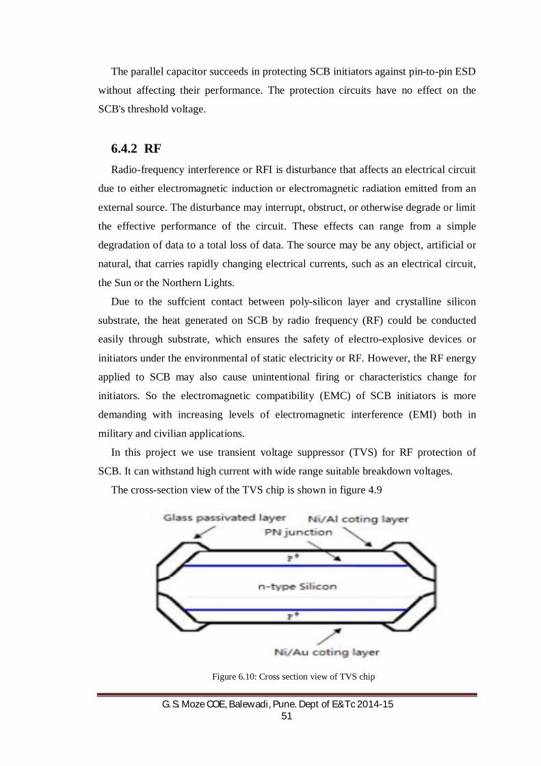
G. S. Moze COE, Balewadi, Pune. Dept of E&Tc 2014-15 51
The parallel capacitor succeeds in protecting SCB initiators against pin-to-pin ESD
without affecting their performance. The protection circuits have no effect on the
SCB's threshold voltage.
6.4.2 RF Radio-frequency interference or RFI is disturbance that affects an electrical circuit
due to either electromagnetic induction or electromagnetic radiation emitted from an
external source. The disturbance may interrupt, obstruct, or otherwise degrade or limit
the effective performance of the circuit. These effects can range from a simple
degradation of data to a total loss of data. The source may be any object, artificial or
natural, that carries rapidly changing electrical currents, such as an electrical circuit,
the Sun or the Northern Lights.
Due to the suffcient contact between poly-silicon layer and crystalline silicon
substrate, the heat generated on SCB by radio frequency (RF) could be conducted
easily through substrate, which ensures the safety of electro-explosive devices or
initiators under the environmental of static electricity or RF. However, the RF energy
applied to SCB may also cause unintentional firing or characteristics change for
initiators. So the electromagnetic compatibility (EMC) of SCB initiators is more
demanding with increasing levels of electromagnetic interference (EMI) both in
military and civilian applications.
In this project we use transient voltage suppressor (TVS) for RF protection of
SCB. It can withstand high current with wide range suitable breakdown voltages.
The cross-section view of the TVS chip is shown in figure 4.9
Figure 6.10: Cross section view of TVS chip
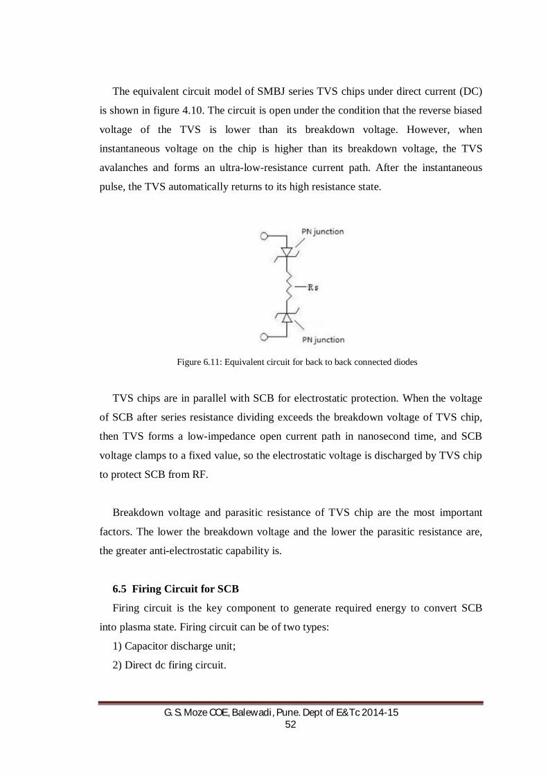
G. S. Moze COE, Balewadi, Pune. Dept of E&Tc 2014-15 52
The equivalent circuit model of SMBJ series TVS chips under direct current (DC)
is shown in figure 4.10. The circuit is open under the condition that the reverse biased
voltage of the TVS is lower than its breakdown voltage. However, when
instantaneous voltage on the chip is higher than its breakdown voltage, the TVS
avalanches and forms an ultra-low-resistance current path. After the instantaneous
pulse, the TVS automatically returns to its high resistance state.
Figure 6.11: Equivalent circuit for back to back connected diodes
TVS chips are in parallel with SCB for electrostatic protection. When the voltage
of SCB after series resistance dividing exceeds the breakdown voltage of TVS chip,
then TVS forms a low-impedance open current path in nanosecond time, and SCB
voltage clamps to a fixed value, so the electrostatic voltage is discharged by TVS chip
to protect SCB from RF.
Breakdown voltage and parasitic resistance of TVS chip are the most important
factors. The lower the breakdown voltage and the lower the parasitic resistance are,
the greater anti-electrostatic capability is.
6.5 Firing Circuit for SCB
Firing circuit is the key component to generate required energy to convert SCB
into plasma state. Firing circuit can be of two types:
1) Capacitor discharge unit;
2) Direct dc firing circuit.

G. S. Moze COE, Balewadi, Pune. Dept of E&Tc 2014-15 53
Both circuits are used to produce required all fire current for SCB. Capacitor
discharge unit can be used where voltage supply is high i.e. 24V. Capacitor value in
CDU is so chosen that it can supply required current i.e. 2 Amp and sufficient energy
for functioning delay of the SCB.
6.5.1 Principle of Operation of CDU
CDU unit consist of Capacitor as main storage element of charge, and producing
the required energy for firing of SCB. The firing circuit is illustrated in Figure 4.5,
and the capacitance of ignition capacitor value should be chosen so that it can produce
the required energy with suffcient all fire current. The SCB is connected with switch
2. Consider capacitor is charged with external battery, and switch 2 is closed, then
capacitor will discharge through SCB thereby proving the required energy to SCB,
due to joule heating the SCB will evaporate and within few microseconds the SCB
will converted into plasma state, which causes primary charge for explosive devices.
[14]
Figure 6.11: Capacitor discharge unit for firing of SCB
The firing energy can be calculated based on formula
E=1/(CV2)
Where E is the energy in Joule,
C is the capacitor.
V is the voltage supply.
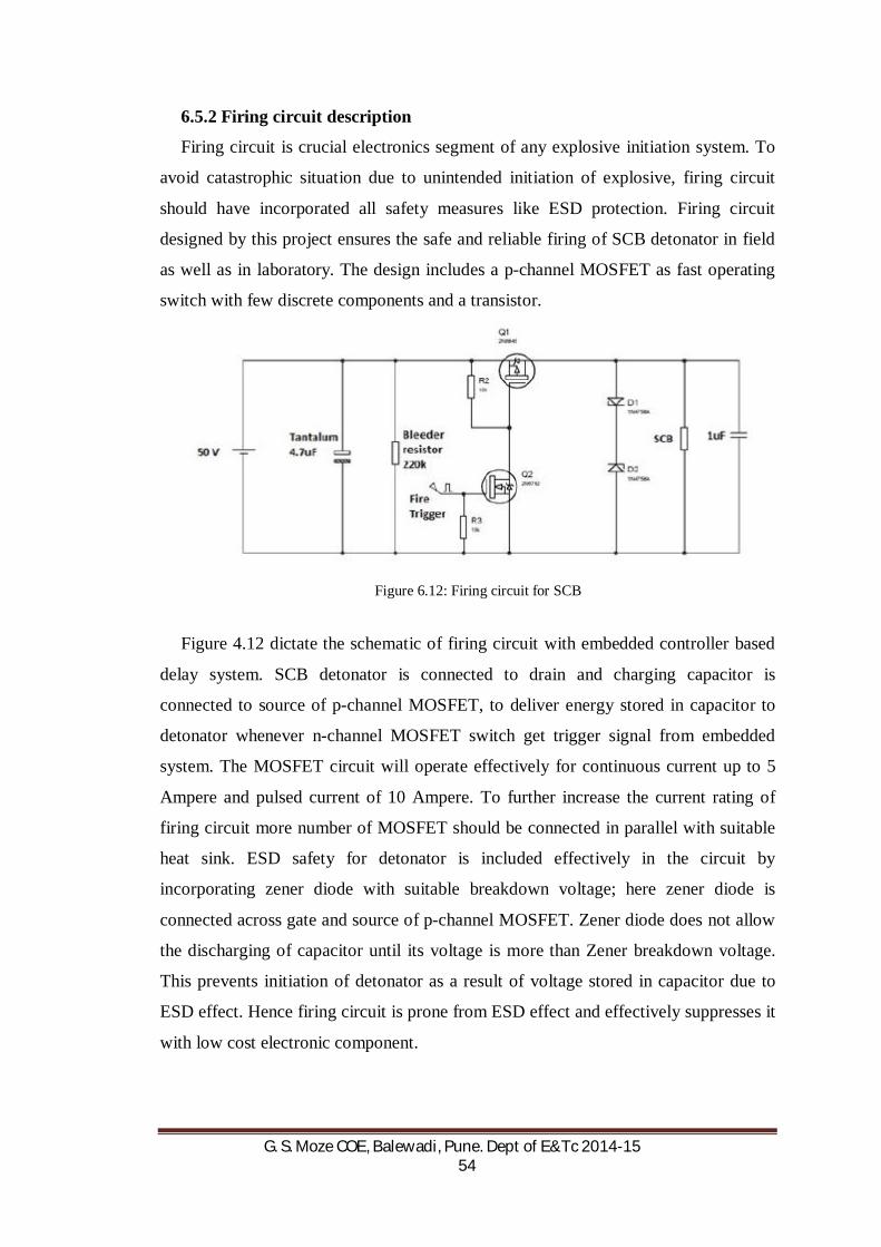
G. S. Moze COE, Balewadi, Pune. Dept of E&Tc 2014-15 54
6.5.2 Firing circuit description
Firing circuit is crucial electronics segment of any explosive initiation system. To
avoid catastrophic situation due to unintended initiation of explosive, firing circuit
should have incorporated all safety measures like ESD protection. Firing circuit
designed by this project ensures the safe and reliable firing of SCB detonator in field
as well as in laboratory. The design includes a p-channel MOSFET as fast operating
switch with few discrete components and a transistor.
Figure 6.12: Firing circuit for SCB
Figure 4.12 dictate the schematic of firing circuit with embedded controller based
delay system. SCB detonator is connected to drain and charging capacitor is
connected to source of p-channel MOSFET, to deliver energy stored in capacitor to
detonator whenever n-channel MOSFET switch get trigger signal from embedded
system. The MOSFET circuit will operate effectively for continuous current up to 5
Ampere and pulsed current of 10 Ampere. To further increase the current rating of
firing circuit more number of MOSFET should be connected in parallel with suitable
heat sink. ESD safety for detonator is included effectively in the circuit by
incorporating zener diode with suitable breakdown voltage; here zener diode is
connected across gate and source of p-channel MOSFET. Zener diode does not allow
the discharging of capacitor until its voltage is more than Zener breakdown voltage.
This prevents initiation of detonator as a result of voltage stored in capacitor due to
ESD effect. Hence firing circuit is prone from ESD effect and effectively suppresses it
with low cost electronic component.

G. S. Moze COE, Balewadi, Pune. Dept of E&Tc 2014-15 55
As per required delay period Microcontroller can be configured precisely, once
delay time is over it will send a triggering pulse of logic 1 to n-channel MOSFET.
The current delivered by Microcontroller is enough to drive this MOSFET directly to
activate p-channel MOSFET. Resistor R3 provides the required biasing to n-channel
MOSFET. Trigger pulse switches on n-channel and p-channel MOSFET; intern
delivers energy stored in capacitor to detonator connected across drain of MOSFET.
The instantaneous initiation of detonator takes place while passing energy through it.
Zener diode protects discharge of capacitor until its voltage reaches to Zener
breakdown voltage.
Before implementing embedded firing circuit on to actual hardware, software
simulation has been done using widely accepted electronic simulation environment
called Multisim.
6.6 Booster Circuit
The Booster circuit works on the principle of DC-DC Boost Converter. The key
principle that drives the converter is the tendency of inductor to resist changes in
current by creating and destroying a magnetic field. In a Boost Converter, the output
voltage is always higher than the input voltage. Typically a boost converter consists of
at least two semiconductors and at least one energy storing element. In proposed
design, Energy Reserve Capacitor (ERC) is used to store the boosted voltage.
Tantalum Capacitor is used to lower the leakage current. The available supply voltage
is 6 volts which needs to be boosted for about 30V for trigger.
Figure 6.13: Basic of boost converter
Figure 6.13 illustrates the basic circuit of a Boost converter. However, in this
example the switching transistor is a power MOSFET, both Bipolar power transistors
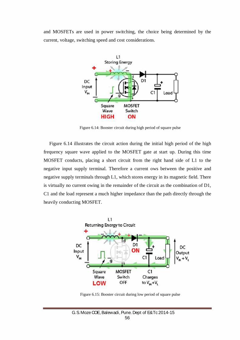
G. S. Moze COE, Balewadi, Pune. Dept of E&Tc 2014-15 56
and MOSFETs are used in power switching, the choice being determined by the
current, voltage, switching speed and cost considerations.
Figure 6.14: Booster circuit during high period of square pulse
Figure 6.14 illustrates the circuit action during the initial high period of the high
frequency square wave applied to the MOSFET gate at start up. During this time
MOSFET conducts, placing a short circuit from the right hand side of L1 to the
negative input supply terminal. Therefore a current ows between the positive and
negative supply terminals through L1, which stores energy in its magnetic field. There
is virtually no current owing in the remainder of the circuit as the combination of D1,
C1 and the load represent a much higher impedance than the path directly through the
heavily conducting MOSFET.
Figure 6.15: Booster circuit during low period of square pulse

G. S. Moze COE, Balewadi, Pune. Dept of E&Tc 2014-15 57
Figure 6.15 shows the current path during the low period of the switching square
wave cycle. As the MOSFET is rapidly turned off the sudden drop in current causes
L1 to produce a back e.m.f. in the opposite polarity to the voltage across L1 during
the on period, to keep current owing. This results in two voltages, the supply voltage
VIN and the back e.m.f.(VL) across L1 in series with each other.
This higher voltage (VIN +VL), now that there is no current path through the
MOSFET, forward biases D1. The resulting current through D1 charges up C1 to VIN
+VL minus the small forward voltage drop across D1, and also supplies the load.
Figure 4.16 shows the circuit action during MOSFET on periods after the initial
startup. Each time the MOSFET conducts, the cathode of D1 is more positive than its
anode, due to the charge on C1.
Figure 6.16: Booster circuit during high period after startup
D1 is therefore turned off so the output of the circuit is isolated from the input,
however the load continues to be supplied with VIN +VL from the charge on C1.
Although the charge C1 drains away through the load during this period, C1 is
recharged each time the MOSFET switches off, so maintaining an almost steady
output voltage across the load.
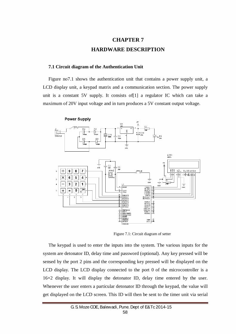
G. S. Moze COE, Balewadi, Pune. Dept of E&Tc 2014-15 58
CHAPTER 7
HARDWARE DESCRIPTION
7.1 Circuit diagram of the Authentication Unit
Figure no7.1 shows the authentication unit that contains a power supply unit, a
LCD display unit, a keypad matrix and a communication section. The power supply
unit is a constant 5V supply. It consists of[1] a regulator IC which can take a
maximum of 20V input voltage and in turn produces a 5V constant output voltage.
Figure 7.1: Circuit diagram of setter
The keypad is used to enter the inputs into the system. The various inputs for the
system are detonator ID, delay time and password (optional). Any key pressed will be
sensed by the port 2 pins and the corresponding key pressed will be displayed on the
LCD display. The LCD display connected to the port 0 of the microcontroller is a
16×2 display. It will display the detonator ID, delay time entered by the user.
Whenever the user enters a particular detonator ID through the keypad, the value will
get displayed on the LCD screen. This ID will then be sent to the timer unit via serial
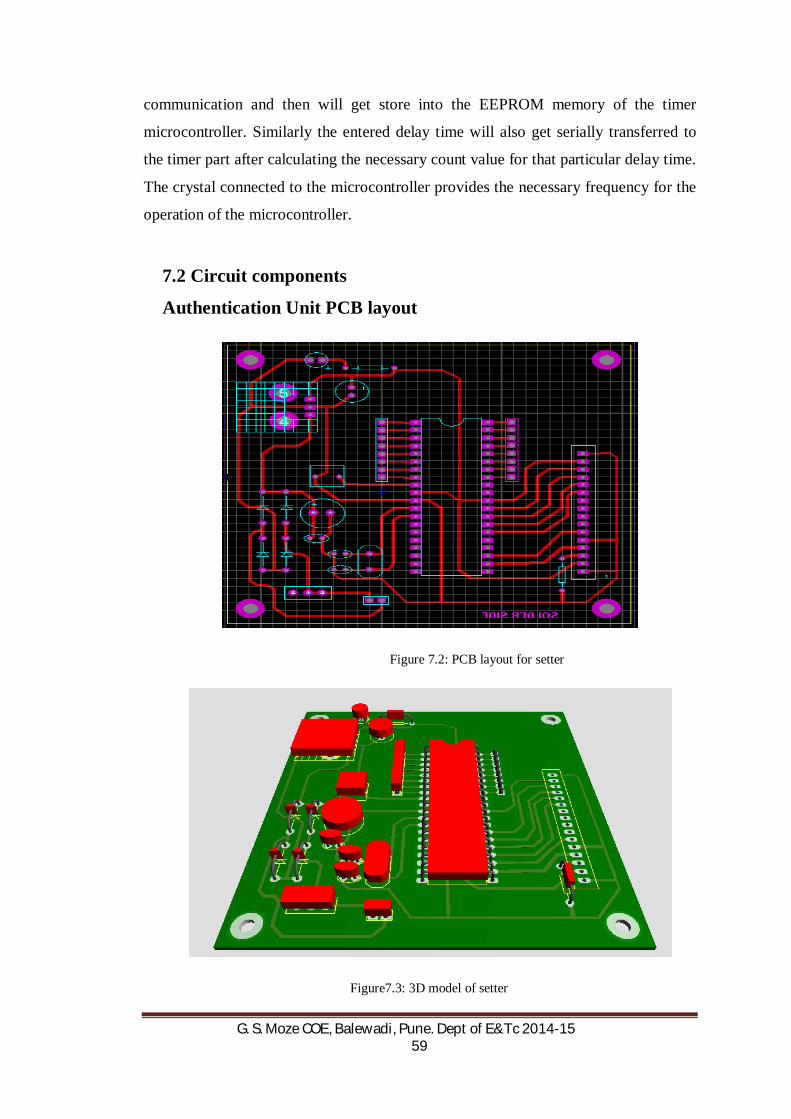
G. S. Moze COE, Balewadi, Pune. Dept of E&Tc 2014-15 59
communication and then will get store into the EEPROM memory of the timer
microcontroller. Similarly the entered delay time will also get serially transferred to
the timer part after calculating the necessary count value for that particular delay time.
The crystal connected to the microcontroller provides the necessary frequency for the
operation of the microcontroller.
7.2 Circuit components
Authentication Unit PCB layout
Figure 7.2: PCB layout for setter
Figure7.3: 3D model of setter

G. S. Moze COE, Balewadi, Pune. Dept of E&Tc 2014-15 60
1. POWER SUPPLY
A regulated power supply is very much essential for several electronic devices due
to the semiconductor material employed in them have a fixed rate of current as well as
voltage. The device may get damaged if there is any deviation from the fixed rate.
The AC power supply gets converted into constant DC by this circuit. By the help of a
voltage regulator DC, unregulated output will be fixed to a constant voltage.
The circuit is made up of linear voltage regulator 7805 along with capacitors and
resistors with bridge rectifier made up from diodes. From giving an unchanging
voltage supply to building confident that output reaches uninterrupted to the
appliance, the diodes along with capacitors handle elevated efficient signal conveyal.
ICs regulator is mainly used in the circuit to maintain the exact voltage which is
followed by the power supply. A regulator is mainly employed with the capacitor
connected in parallel to the input terminal and the output terminal of the IC regulator.
For the checking of gigantic alterations in the input as well as in the output filter,
capacitors are used. While the bypass capacitors are used to check the small period
spikes on the input and output level. Bypass capacitors are mainly of small values that
are used to bypass the small period pulses straightly into the Earth.
A circuit diagram having regulator IC and all the above discussed components
arrangement revealed in the figure below.
Figure 7.4: Circuit for regulated power supply

G. S. Moze COE, Balewadi, Pune. Dept of E&Tc 2014-15 61
Functions of Components
C1: This capacitor is known as bypass capacitor and is employed to bypass
extremely tiny duration spikes to the ground with no distress the other components.
C2: C2 is the filter capacitor employed to steady the slow changes in the voltage
applied at the input of the circuit. Escalating the value of the capacitor amplify the
stabilization as well as the declining value of the capacitor reduces the stabilization.
Moreover this capacitor is not alone capable to ensure very constricted period spikes
emerge at the input.
C3: C3 is known as a filter capacitor employed in the circuit to steady the slow
alterations in the output voltage. Raising the value of the capacitor enlarges the
stabilization furthermore declining the value of the capacitor declined the
stabilization. Moreover this capacitor is not alone capable to ensure very fine duration
spikes happen at the output.
C4: C4 is known as bypass capacitor and worked to bypass very small period
spikes to the earth with no influence the other components.
U1: U1 is the IC with positive DC and it upholds the output voltage steady exactly
at a constant value even although there are major deviation in the input voltage.
IC 7805 is a DC regulated IC of 5V. This IC is very flexible and is widely
employed in all types of circuit like a voltage regulator. It is a three terminal device
and mainly called input , output and ground. Pin diagram of the IC 7805 is shown in
the diagram below.

G. S. Moze COE, Balewadi, Pune. Dept of E&Tc 2014-15 62
Figure 7.5: Pin diagram of 7805
PIN DESCRIPTION
1. INPUT: In this pin of the IC positive unregulated voltage is given in
regulation.
2. GROUND: In this pin where the ground is given. This pin is neutral
for equally the input and output.
3. OUTPUT: The output of the regulated 5V volt is taken out at this pin
of the IC regulator.
The output generated from the unregulated DC output is susceptible to the
fluctuations of the input signal. IC voltage regulator is connected with bridge rectifier
in series so to steady the DC output against the variations in the input DC voltage. To
obtain a stable output of 5V, IC 7805 is attached with 6-0-6V along with 500mA step
down transformer as well as with rectifier. To suppress the oscillation which might
generate in the regulator IC, C2 capacitor of 0.1 uF value is used. When the power
supply filter is far away from the regulated IC capacitor C2 is used. Ripple rejection
in the regulator is been improved by C4 capacitor by avoiding the ripple voltage to be
amplified at the regulator output. The output voltage is strengthen and deduction of
the output voltage is done capacitor C3. To avoid the chance of the input get shorted
D5 diode is used to save the regulator. If D5 is not presented in the circuit, the output

G. S. Moze COE, Balewadi, Pune. Dept of E&Tc 2014-15 63
capacitor can leave its charge immediately during low impedance course inside the
regulators.
2. ATmega 16: ATmega 16 microcontroller DIP(40 pin) is used for the
authentication unit. The ATmega16 is a low-power CMOS 8-bit microcontroller
based on the AVR enhanced RISC architecture. By executing powerful instructions in
a single clock cycle, the ATmega16 achieves throughputs approaching 1 MIPS per
MHz allowing the system designer to optimize power consumption versus processing
speed.
Features
• High-performance, Low-power Atmel® AVR® 8-bit Microcontroller
• Advanced RISC Architecture
– 131 Powerful Instructions – Most Single-clock Cycle Execution
– 32 x 8 General Purpose Working Registers
– Fully Static Operation
– Up to 16 MIPS Throughput at 16 MHz
– On-chip 2-cycle Multiplier
• High Endurance Non-volatile Memory segments
– 16 Kbytes of In-System Self-programmable Flash program memory
– 512 Bytes EEPROM
– 1 Kbyte Internal SRAM
– Write/Erase Cycles: 10,000 Flash/100,000 EEPROM
– Data retention: 20 years at 85°C/100 years at 25°C(1)
– Optional Boot Code Section with Independent Lock Bits
In-System Programming by On-chip Boot Program
True Read-While-Write Operation
– Programming Lock for Software Security
• JTAG (IEEE std. 1149.1 Compliant) Interface
– Boundary-scan Capabilities According to the JTAG Standard
– Extensive On-chip Debug Support
– Programming of Flash, EEPROM, Fuses, and Lock Bits through the JTAG
Interface
• Peripheral Features

G. S. Moze COE, Balewadi, Pune. Dept of E&Tc 2014-15 64
– Two 8-bit Timer/Counters with Separate Prescalers and Compare Modes
– One 16-bit Timer/Counter with Separate Prescaler, Compare Mode, and Capture
Mode
– Real Time Counter with Separate Oscillator
– Four PWM Channels
– 8-channel, 10-bit ADC
8 Single-ended Channels
7 Differential Channels in TQFP Package Only
2 Differential Channels with Programmable Gain at 1x, 10x, or 200x
– Byte-oriented Two-wire Serial Interface
– Programmable Serial USART
– Master/Slave SPI Serial Interface
– Programmable Watchdog Timer with Separate On-chip Oscillator
– On-chip Analog Comparator
• Special Microcontroller Features
– Power-on Reset and Programmable Brown-out Detection
– Internal Calibrated RC Oscillator
– External and Internal Interrupt Sources
– Six Sleep Modes: Idle, ADC Noise Reduction, Power-save, Power-down,
Standby and Extended Standby
• I/O and Packages
– 32 Programmable I/O Lines
– 40-pin PDIP, 44-lead TQFP, and 44-pad QFN/MLF
• Operating Voltages
– 2.7V - 5.5V for ATmega16L
– 4.5V - 5.5V for ATmega16
• Speed Grades
– 0 - 8 MHz for ATmega16L
– 0 - 16 MHz for ATmega16
• Power Consumption @ 1 MHz, 3V, and 25°C for ATmega16L
– Active: 1.1 mA
– Idle Mode: 0.35 mA
– Power-down Mode: < 1 µA

G. S. Moze COE, Balewadi, Pune. Dept of E&Tc 2014-15 65
Pin Configuration
Pin Descriptions
VCC: Digital supply voltage.
GND: Ground.
Port A (PA7..PA0): Port A serves as the analog inputs to the A/D Converter.
Port A also serves as an 8-bit bi-directional I/O port, if the A/D Converter is not
used. Port pins can provide internal pull-up resistors (selected for each bit). The
Port A output buffers have symmetrical drive characteristics with both high sink
and source capability. When pins PA0 to PA7 are used as inputs and are externally
pulled low, they will source current if the internal pull-up resistors are activated.
The Port A pins are tri-stated when a reset condition becomes active, even if the
clock is not running.
Port B (PB7..PB0): Port B is an 8-bit bi-directional I/O port with internal pull-
up resistors (selected for each bit). The Port B output buffers have symmetrical
drive characteristics with both high sink and source capability. As inputs, Port B
pins that are externally pulled low will source current if the pull-up resistors are
activated. The Port B pins are tri-stated when a reset condition becomes active,
even if the clock is not running. Port B also serves the functions of various special
features of the ATmega16.

G. S. Moze COE, Balewadi, Pune. Dept of E&Tc 2014-15 66
Port C (PC7..PC0): Port C is an 8-bit bi-directional I/O port with internal pull-
up resistors (selected for each bit). The Port C output buffers have symmetrical
drive characteristics with both high sink and source capability. As inputs, Port C
pins that are externally pulled low will source current if the pull-up resistors are
activated. The Port C pins are tri-stated when a reset condition becomes active,
even if the clock is not running. If the JTAG interface is enabled, the pull-up
resistors on pins PC5(TDI), PC3(TMS) and PC2(TCK) will be activated even if a
reset occurs. Port C also serves the functions of the JTAG interface and other
special features of the ATmega16.
Port D (PD7..PD0): Port D is an 8-bit bi-directional I/O port with internal pull-
up resistors (selected for each bit). The Port D output buffers have symmetrical
drive characteristics with both high sink and source capability. As inputs, Port D
pins that are externally pulled low will source current if the pull-up resistors are
activated. The Port D pins are tri-stated when a reset condition becomes active,
even if the clock is not running. Port D also serves the functions of various special
features of the ATmega16.
RESET: Reset Input. A low level on this pin for longer than the minimum
pulse length will generate a reset, even if the clock is not running. The minimum
pulse length is given in Table 15 on page 38. Shorter pulses are not guaranteed to
generate a reset.
XTAL1: Input to the inverting Oscillator amplifier and input to the internal
clock operating circuit
XTAL2: Output from the inverting Oscillator amplifier.
AVCC: AVCC is the supply voltage pin for Port A and the A/D Converter. It
should be externally connected to VCC, even if the ADC is not used. If the ADC is
used, it should be connected to VCC through a low-pass filter.
AREF: AREF is the analog reference pin for the A/D Converter.
3. Keypad:
The keypad has 16 keys in a 4*4 matrix form. The keys are used to enter the
password , det. ID and then to feed the delay time. The delay will be entered as 2-digit
number.
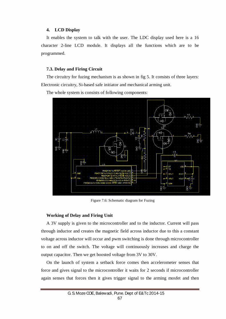
G. S. Moze COE, Balewadi, Pune. Dept of E&Tc 2014-15 67
4. LCD Display
It enables the system to talk with the user. The LDC display used here is a 16
character 2-line LCD module. It displays all the functions which are to be
programmed.
7.3. Delay and Firing Circuit
The circuitry for fuzing mechanism is as shown in fig 5. It consists of three layers:
Electronic circuitry, Si-based safe initiator and mechanical arming unit.
The whole system is consists of following components:
Figure 7.6: Schematic diagram for Fuzing
Working of Delay and Firing Unit
A 3V supply is given to the microcontroller and to the inductor. Current will pass
through inductor and creates the magnetic field across inductor due to this a constant
voltage across inductor will occur and pwm switching is done through microcontroller
to on and off the switch. The voltage will continuously increases and charge the
output capacitor. Then we get boosted voltage from 3V to 30V.
On the launch of system a setback force comes then accelerometer senses that
force and gives signal to the microcontroller it waits for 2 seconds if microcontroller
again senses that forces then it gives trigger signal to the arming mosfet and then
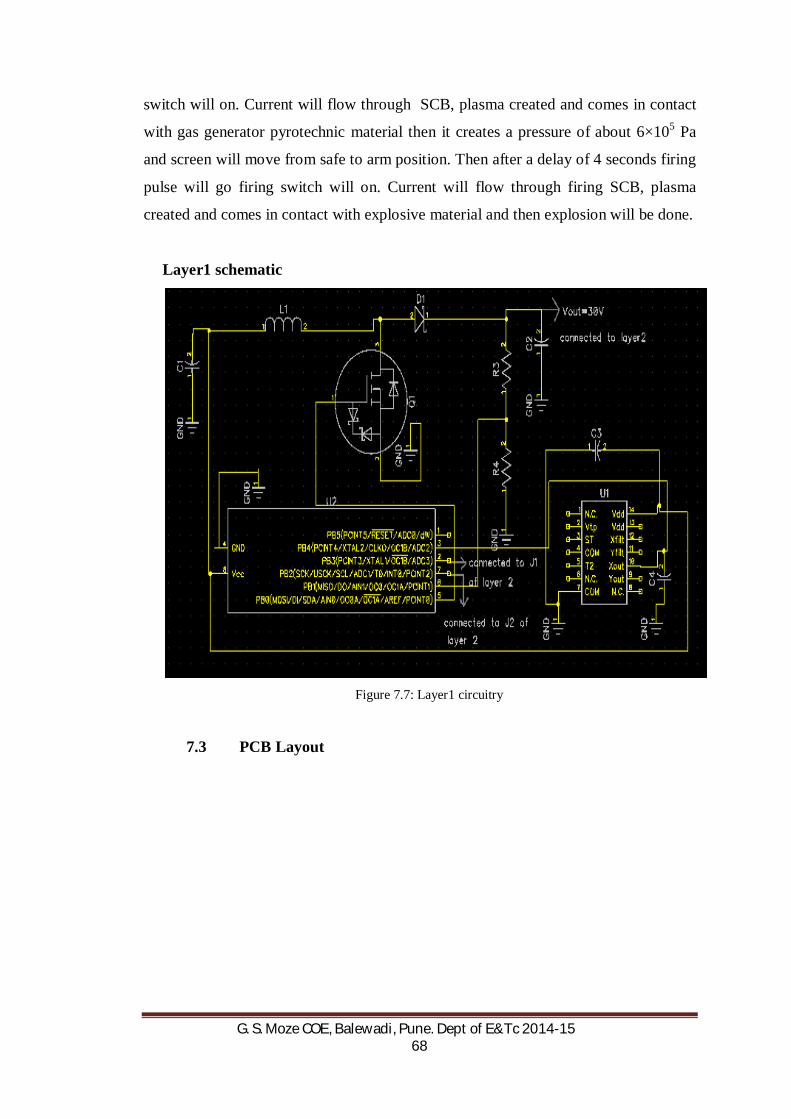
G. S. Moze COE, Balewadi, Pune. Dept of E&Tc 2014-15 68
switch will on. Current will flow through SCB, plasma created and comes in contact
with gas generator pyrotechnic material then it creates a pressure of about 6×10⁵ Pa
and screen will move from safe to arm position. Then after a delay of 4 seconds firing
pulse will go firing switch will on. Current will flow through firing SCB, plasma
created and comes in contact with explosive material and then explosion will be done.
Layer1 schematic
Figure 7.7: Layer1 circuitry
7.3 PCB Layout
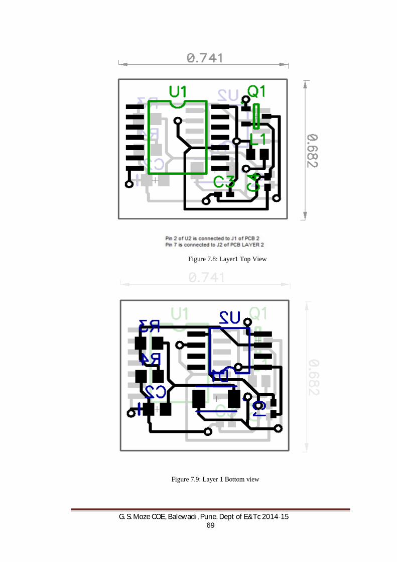
G. S. Moze COE, Balewadi, Pune. Dept of E&Tc 2014-15 69
Figure 7.8: Layer1 Top View
Figure 7.9: Layer 1 Bottom view

G. S. Moze COE, Balewadi, Pune. Dept of E&Tc 2014-15 70
1.) 3D models of Layer 1
Figure 7.10: Layer 1 3D Top view
Figure 7.11: Layer 2 3D Bottom view
Layer 2 schematic

G. S. Moze COE, Balewadi, Pune. Dept of E&Tc 2014-15 71
Figure 7.12: Layer 2 schematic
1.) PCB Layout of layer 2
Figure 7.13: Layer 2 Top view

G. S. Moze COE, Balewadi, Pune. Dept of E&Tc 2014-15 72
Figure 7.14: Layer 2 Bottom view (use SCB instead of R1, R2 with TVS diode)
1. POWER SUPPLY UNIT
We give 3V supply through a Li-ion battery connected with 0.1µf capacitor. Then
it is connected to the inductor of 10 mH. A MOSFET of 2N7002CK is connected to
the 8-pin microcontroller which increases switching speed of MOSFET the power is
boosted from 3V to 30V.
2. ATtiny85
The purpose of using the 8-pin microcontroller is to achieve miniaturization. Atmel
tinyAVR® devices are optimized for applications that require performance, power
efficiency, and ease-of-use in a small package. Alf (Egil Bogen) and Vegard
(Wollan)'s RISC processor. The use of "AVR" generally refers to the 8-bit RISC line
of Atmel AVR Microcontrollers. The AVR is a modified Harvard architecture
machine where program and data are stored in separate physical memory systems that
appear in different address spaces, but having the ability to read data items from
program memory using special instructions.
All tinyAVR devices are based on the same architecture and compatible with other
AVR devices. Integrated ADC, EEPROM memory and brown-out detector we can

G. S. Moze COE, Balewadi, Pune. Dept of E&Tc 2014-15 73
build applications without adding external components. TinyAVR offers flash
memory and on-chip debug for fast, secure, cost-effective in-circuit upgrades that
significantly cuts in time to market.
The devices are supported by the Atmel Studio development platform. It enables
code development in C or Assembly, provides cycle-accurate simulation, and
integrates seamlessly with starter kits, programmers, debuggers, evaluation kits, and
reference designs. This results in faster development, a more-production development
team, and rapid time-to-market.
The tinyAVR offers an unrivalled combination of miniaturization, processing
power, analog performance, and system-level integration. The tinyAVR is the most
compact, feature-rich device in the AVR family—and the only device capable of
operating at just 0.7V.
7.2.1 Key Features of the Atmel AVR family
1. High Performance, Low Power AVR® 8-Bit Microcontroller
2. Advanced RISC Architecture
– 120 Powerful Instructions – Most Single Clock Cycle Execution
– 32 x 8 General Purpose Working Registers
– Fully Static Operation
3. Non-volatile Program and Data Memories
– 2/4/8K Bytes of In-System Programmable Program Memory Flash
4. Endurance: 10,000 Write/Erase Cycles
– 128/256/512 Bytes In-System Programmable EEPROM
5. Endurance: 100,000 Write/Erase Cycles
– 128/256/512 Bytes Internal SRAM
– Programming Lock for Self-Programming Flash Program and EEPROM Data
Security
6.Peripheral Features
– 8-bit Timer/Counter with Prescaler and Two PWM Channels
– 8-bit High Speed Timer/Counter with Separate Prescaler
7. 2 High Frequency PWM Outputs with Separate Output Compare Registers
8. Programmable Dead Time Generator

G. S. Moze COE, Balewadi, Pune. Dept of E&Tc 2014-15 74
– USI – Universal Serial Interface with Start Condition Detector
– 10-bit ADC
9. 4 Single Ended Channels
10. 2 Differential ADC Channel Pairs with Programmable Gain (1x, 20x)
11. Temperature Measurement: Programmable Watchdog Timer with Separate
On- chip Oscillator & On-chip Analog Comparator.
12. Special Microcontroller Features: debug WIRE On-chip Debug System, In-
System Programmable via SPI Port, External and Internal Interrupt Sources, Low
Power Idle, ADC Noise Reduction, and Power-down Modes. Enhanced Power-on
Reset Circuit, Programmable Brown-out Detection Circuit & Internal Calibrated
Oscillator.
13. I/O and Packages
– Six Programmable I/O Lines
– 8-pin PDIP, 8-pin SOIC, 20-pad QFN/MLF, and 8-pin TSSOP (only
ATtiny45/V)
14. Operating Voltage
– 1.8 - 5.5V for ATtiny25V/45V/85V
– 2.7 - 5.5V for ATtiny25/45/85
15. Speed Grade
– ATtiny25V/45V/85V: 0 – 4 MHz @ 1.8 - 5.5V, 0 - 10 MHz @ 2.7 - 5.5V
– ATtiny25/45/85: 0 – 10 MHz @ 2.7 - 5.5V, 0 - 20 MHz @ 4.5 - 5.5V
16. Industrial Temperature Range
17. Low Power Consumption
– Active Mode: 1 MHz, 1.8V: 300 μA
– Power-down Mode: 0.1 μA at 1.8V
Pin configuration of ATtiny85 microcontroller
Figure 7.15: Pin configuration of ATTINY85
G. S. Moze COE, Balewadi, Pune. Dept of E&Tc 2014-15 75
Pin Description
1. VCC: Supply voltage.
2. GND: Ground.
3. Port B (PB5..PB0): Port B is a 6-bit bi-directional I/O port with internal pull-
up resistors (selected for each bit). The Port B output buffers have symmetrical
drive characteristics with both high sink and source capability. As inputs, Port B
pins that are externally pulled low will source current if the pull-up resistors are
activated. The Port B pins are tri-stated when a reset condition becomes active,
even if the clock is not running.
4. RESET: Reset input. A low level on this pin for longer than the
minimum pulse length will generate a reset, even if the clock is not running
and provided the reset pin has not been disabled. The reset pin can also be
used as a (weak) I/O pin.
Accelerometer
The ADXL210 are low cost, low power, complete 2-axis accelerometers with a
measurement range of either ±10 g. The ADXL210 can measure both dynamic
acceleration (e.g., vibration) and static acceleration (e.g., gravity).

G. S. Moze COE, Balewadi, Pune. Dept of E&Tc 2014-15 76
Figure 7.16: Functional Block Diagram of ADXL210AQC
The outputs are digital signals whose duty cycles (ratio of pulse width to period)
are proportional to the acceleration in each of the 2 sensitive axes. These outputs may
be measured directly with a microprocessor counter, requiring no A/D converter or
glue logic. The output period is adjustable from 0.5 ms to 10 ms via a single resistor
(RSET). If a voltage output is desired, a voltage output proportional to acceleration is
available from the XFILT and YFILT pins, or may be reconstructed by filtering the duty
cycle outputs.
The bandwidth of the ADXL202/ADXL210 may be set from 0.01 Hz to 5 kHz via
capacitors CX and CY. The typical noise floor is 500 µg/kHz allowing signals below
5 mg to be resolved for bandwidths below 60 Hz.The ADXL210 is available in a
hermetic 14-lead Surface Mount CERPAK, specified over the 0oC to +70oC
commercial or –40oC to +85oC industrial temperature range.
Features of accelerometer ADXL210AQC are as follows:
2-Axis Acceleration Sensor on a Single IC Chip
Measures Static Acceleration as Well as Dynamic Acceleration
Duty Cycle Output with User Adjustable Period

G. S. Moze COE, Balewadi, Pune. Dept of E&Tc 2014-15 77
Low Power <0.6 mA
Faster Response than Electrolytic, Mercury or Thermal
Tilt Sensors
Bandwidth Adjustment with a Single Capacitor Per Axis
5 mg Resolution at 60 Hz Bandwidth
+3 V to +5.25 V Single Supply Operation
1000 g Shock Survival
APPLICATIONS
2-Axis Tilt Sensing
Computer Peripherals
Inertial Navigation
Seismic Monitoring
Vehicle Security Systems
Battery Powered Motion Sensing
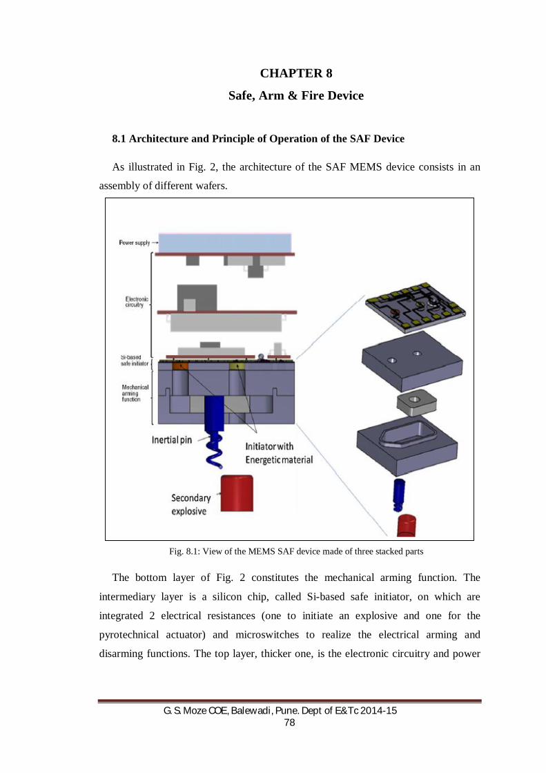
G. S. Moze COE, Balewadi, Pune. Dept of E&Tc 2014-15 78
CHAPTER 8
Safe, Arm & Fire Device
8.1 Architecture and Principle of Operation of the SAF Device
As illustrated in Fig. 2, the architecture of the SAF MEMS device consists in an
assembly of different wafers.
Fig. 8.1: View of the MEMS SAF device made of three stacked parts
The bottom layer of Fig. 2 constitutes the mechanical arming function. The
intermediary layer is a silicon chip, called Si-based safe initiator, on which are
integrated 2 electrical resistances (one to initiate an explosive and one for the
pyrotechnical actuator) and microswitches to realize the electrical arming and
disarming functions. The top layer, thicker one, is the electronic circuitry and power

G. S. Moze COE, Balewadi, Pune. Dept of E&Tc 2014-15 79
supply integrating if required one super capacity. To prevent that a shock unlocks the
mechanical screen, an inertial pin can be inserted into the device to block the screen.
The SAF device operations procedure is illustrated in Fig. 8.2.
Figure 8.2: Operations procedure of the MEMS SAF device (a) in safe mode, (b) mechanically
armed, (c) electrically armed and (d) secondary explosive initiation by initiator
The MEMS SAF is stored in safe mode: the screen is locked and the initiator pads
are both connected to the electrical ground (Fig. 3a). The first order is for the
mechanical arming (Fig. 3b): the inertial pin is removed by the acceleration; then the
microcontroller sends an electrical order to the microactuator resistance. The gas
generated by the pyrotechnical actuator moves the screen in armed position. Then, the
SAF is electrically armed, that is to say the microinitiator electrical short-circuit to
electrical ground is cut (Fig. 3c). At this stage, if the operator does not send an order
to stop the procedure, the microcontroller sends an electrical order to the initiator to
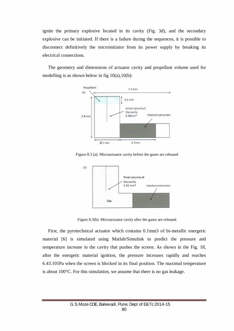
G. S. Moze COE, Balewadi, Pune. Dept of E&Tc 2014-15 80
ignite the primary explosive located in its cavity (Fig. 3d), and the secondary
explosive can be initiated. If there is a failure during the sequences, it is possible to
disconnect definitively the microinitiator from its power supply by breaking its
electrical connections.
The geometry and dimensions of actuator cavity and propellant volume used for
modelling is as shown below in fig 10(a),10(b):
Figure 8.3 (a): Microactuator cavity before the gases are released
Figure 8.3(b): Microactuator cavity after the gases are released
First, the pyrotechnical actuator which contains 0.1mm3 of bi-metallic energetic
material [6] is simulated using Matlab/Simulink to predict the pressure and
temperature increase in the cavity that pushes the screen. As shown in the Fig. 18,
after the energetic material ignition, the pressure increases rapidly and reaches
6.43.105Pa when the screen is blocked in its final position. The maximal temperature
is about 100°C. For this simulation, we assume that there is no gas leakage.
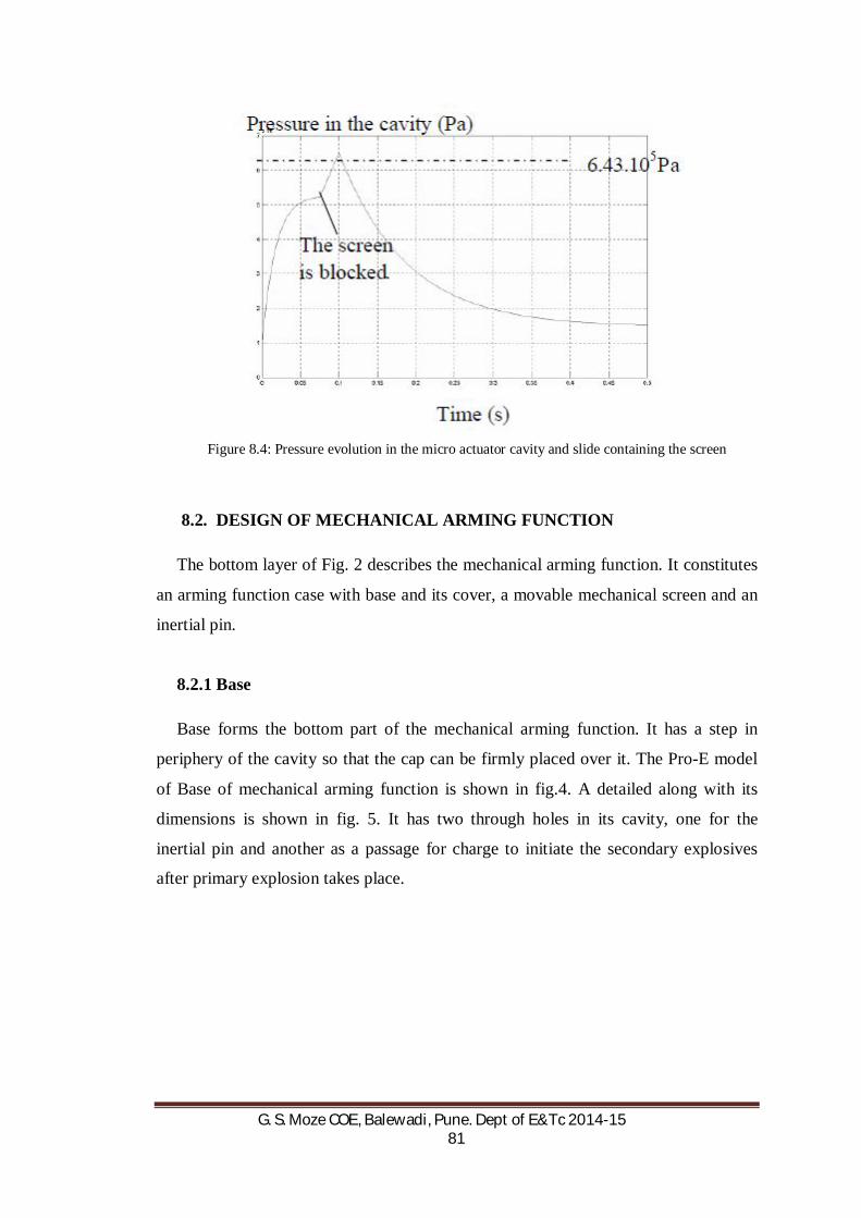
G. S. Moze COE, Balewadi, Pune. Dept of E&Tc 2014-15 81
Figure 8.4: Pressure evolution in the micro actuator cavity and slide containing the screen
8.2. DESIGN OF MECHANICAL ARMING FUNCTION
The bottom layer of Fig. 2 describes the mechanical arming function. It constitutes
an arming function case with base and its cover, a movable mechanical screen and an
inertial pin.
8.2.1 Base
Base forms the bottom part of the mechanical arming function. It has a step in
periphery of the cavity so that the cap can be firmly placed over it. The Pro-E model
of Base of mechanical arming function is shown in fig.4. A detailed along with its
dimensions is shown in fig. 5. It has two through holes in its cavity, one for the
inertial pin and another as a passage for charge to initiate the secondary explosives
after primary explosion takes place.
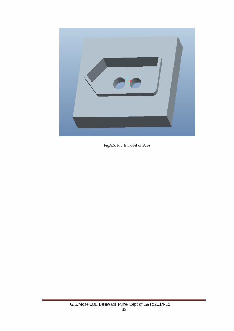
G. S. Moze COE, Balewadi, Pune. Dept of E&Tc 2014-15 82
Fig.8.5: Pro-E model of Base
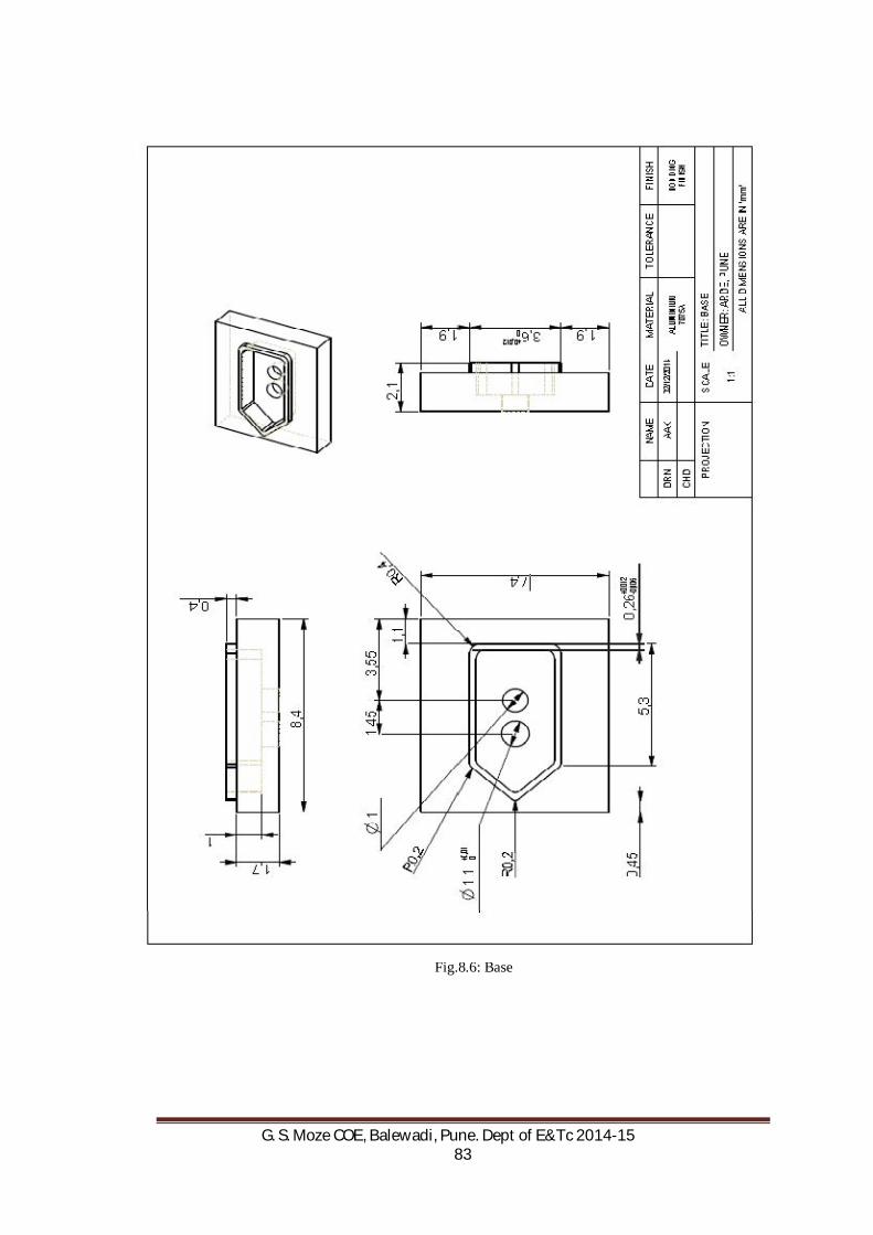
G. S. Moze COE, Balewadi, Pune. Dept of E&Tc 2014-15 83
Fig.8.6: Base

G. S. Moze COE, Balewadi, Pune. Dept of E&Tc 2014-15 84
8.2.2 Cover
Cover forms the top part or cap of the mechanical arming function. It has the
complementary print as a crenel shape to that of base so that it can be placed over
the base. The Pro-E model of Cover of mechanical arming function is shown in
fig. 6. The Cover of mechanical arming function along with its dimensions is
shown in fig.7. It also contains two through holes, one for the actuation of the
microinitiator and another for the passage for charge to initiate the secondary
explosives after primary explosion takes place.
Figure 8.7: Pro-E model of Cover

G. S. Moze COE, Balewadi, Pune. Dept of E&Tc 2014-15 85
Figure 8.8: Cover
8.2.3 Mechanical Screen
Mechanical screen of the SAF device interrupts the explosive train to keep the
detonator safe and to arm it by mechanically moving from the safe position. It is

G. S. Moze COE, Balewadi, Pune. Dept of E&Tc 2014-15 86
placed in the cavity formed in Base of mechanical arming function. The Pro-E model
of Mechanical Screen of mechanical arming function is shown in fig.8. The
Mechanical Screen along with its dimensions can be seen in fig. 9. The corner radius
of curvature is slightly larger than the one of the slide corners in which it moves. It is
thus able to achieve its end of course in force in the slider and to remain thus blocked
in armed position. It too has a through hole for the inertial pin which keeps the screen
in safe position.
Figure 8.9: Pro-E model of Mechanical Screen

G. S. Moze COE, Balewadi, Pune. Dept of E&Tc 2014-15 87
Figure 8.10: Mechanical Screen

G. S. Moze COE, Balewadi, Pune. Dept of E&Tc 2014-15 88
8.2.4 Inertial Pin
To prevent that a shock unlocks the mechanical screen, an inertial pin is inserted
into the device to block the screen and keep it in safe position. The Pro-E model of
Inertial Pin is shown in fig.10 and detailed design is as shown in fig.11. It consists of
a circular cylinder to which attached is the spring that keeps the inertial pin to lock the
mechanical screen and be in safe condition.
Fig. 10: Pro-E model of Mechanical Screen
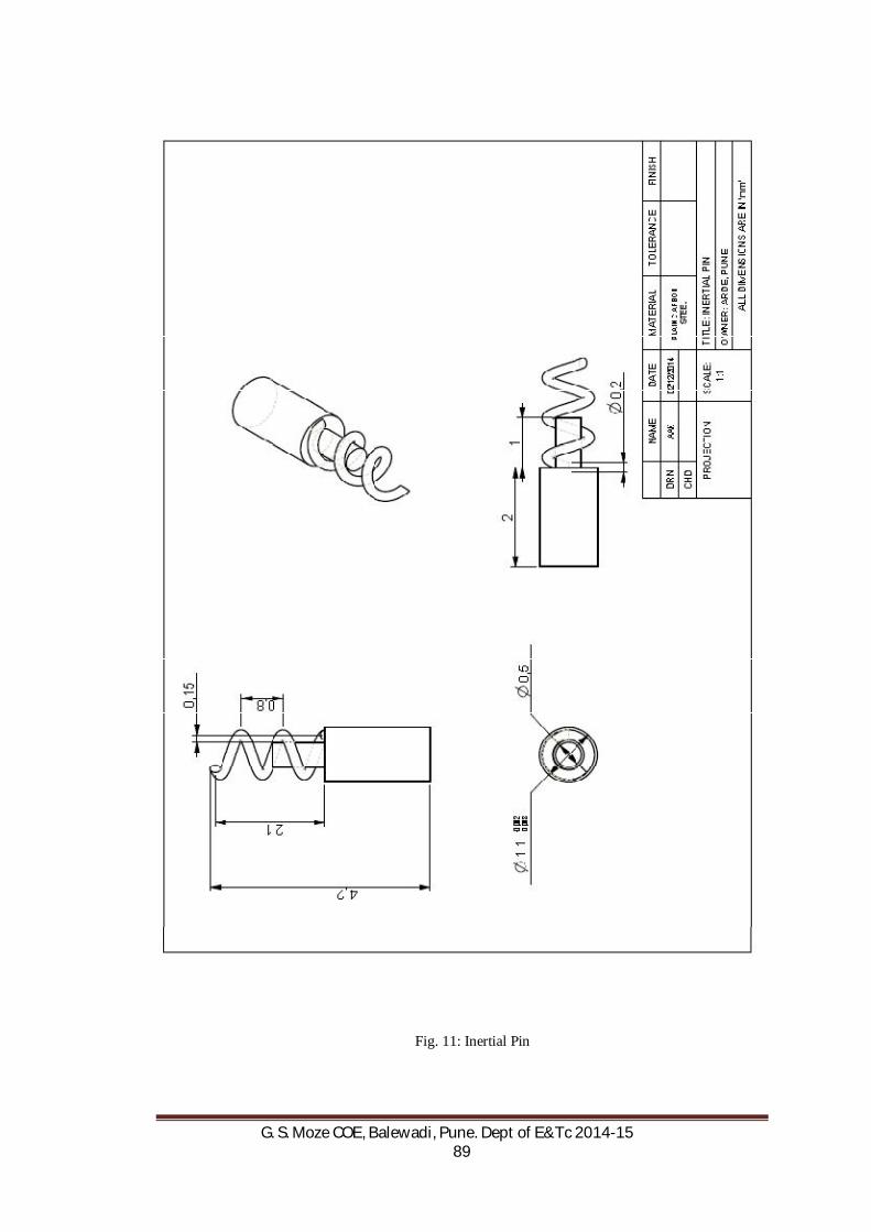
G. S. Moze COE, Balewadi, Pune. Dept of E&Tc 2014-15 89
Fig. 11: Inertial Pin
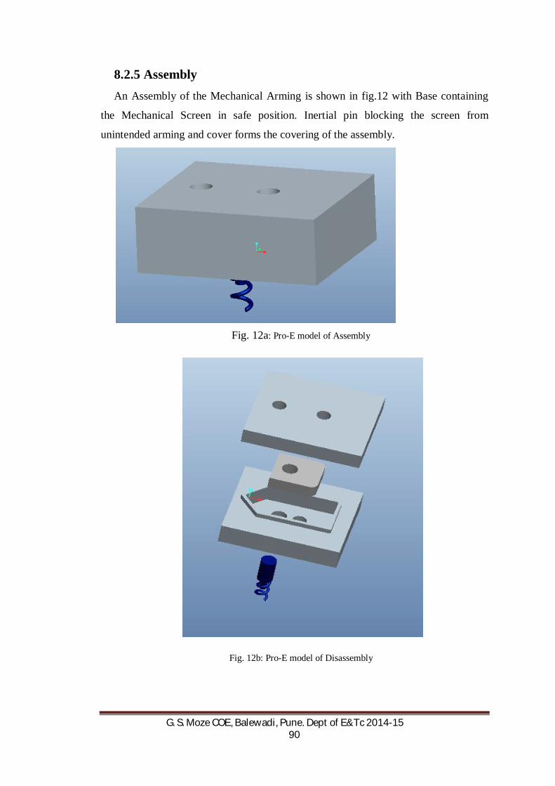
G. S. Moze COE, Balewadi, Pune. Dept of E&Tc 2014-15 90
8.2.5 Assembly An Assembly of the Mechanical Arming is shown in fig.12 with Base containing
the Mechanical Screen in safe position. Inertial pin blocking the screen from
unintended arming and cover forms the covering of the assembly.
Fig. 12a: Pro-E model of Assembly
Fig. 12b: Pro-E model of Disassembly
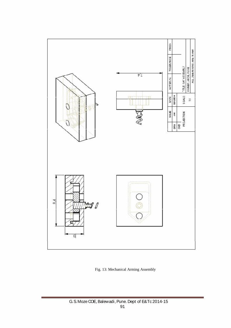
G. S. Moze COE, Balewadi, Pune. Dept of E&Tc 2014-15 91
Fig. 13: Mechanical Arming Assembly
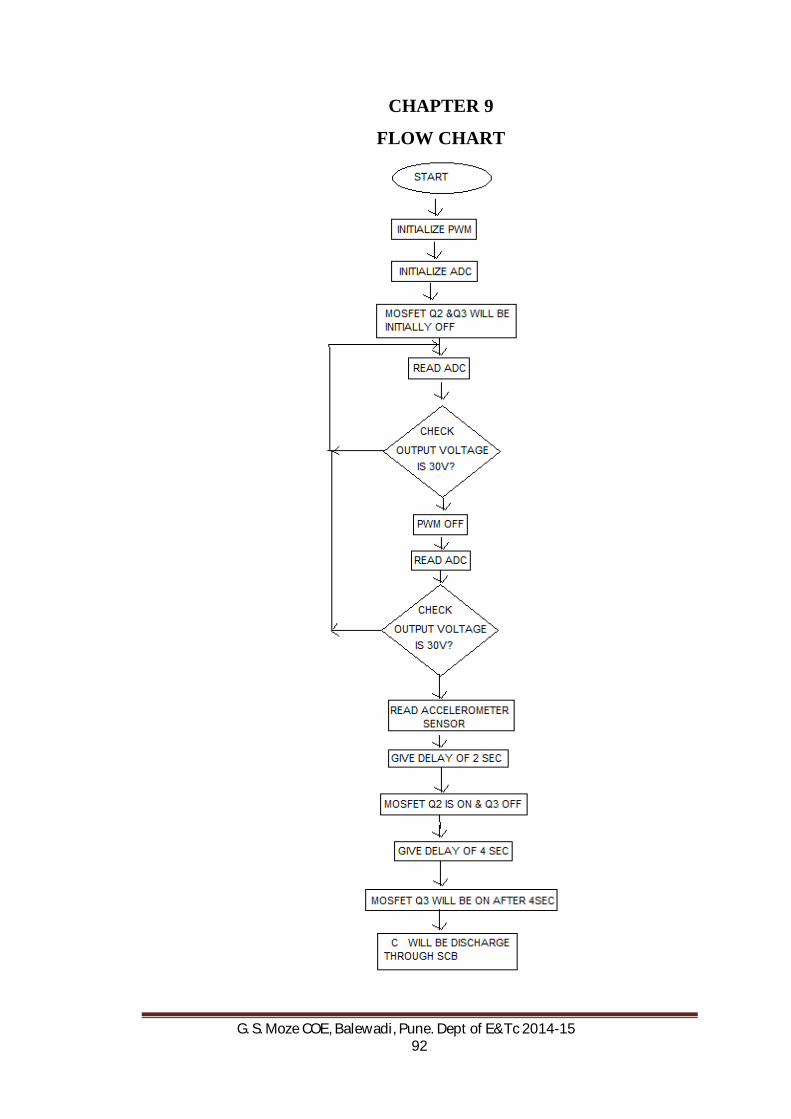
G. S. Moze COE, Balewadi, Pune. Dept of E&Tc 2014-15 92
CHAPTER 9
FLOW CHART
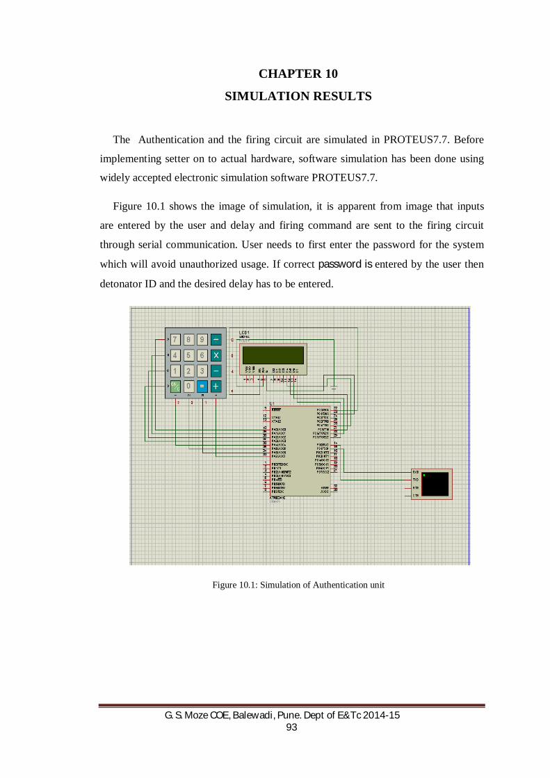
G. S. Moze COE, Balewadi, Pune. Dept of E&Tc 2014-15 93
CHAPTER 10
SIMULATION RESULTS
The Authentication and the firing circuit are simulated in PROTEUS7.7. Before
implementing setter on to actual hardware, software simulation has been done using
widely accepted electronic simulation software PROTEUS7.7.
Figure 10.1 shows the image of simulation, it is apparent from image that inputs
are entered by the user and delay and firing command are sent to the firing circuit
through serial communication. User needs to first enter the password for the system
which will avoid unauthorized usage. If correct password is entered by the user then
detonator ID and the desired delay has to be entered.
Figure 10.1: Simulation of Authentication unit
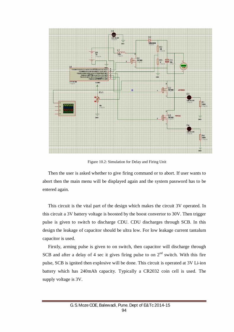
G. S. Moze COE, Balewadi, Pune. Dept of E&Tc 2014-15 94
Figure 10.2: Simulation for Delay and Firing Unit
Then the user is asked whether to give firing command or to abort. If user wants to
abort then the main menu will be displayed again and the system password has to be
entered again.
This circuit is the vital part of the design which makes the circuit 3V operated. In
this circuit a 3V battery voltage is boosted by the boost convertor to 30V. Then trigger
pulse is given to switch to discharge CDU. CDU discharges through SCB. In this
design the leakage of capacitor should be ultra low. For low leakage current tantalum
capacitor is used.
Firstly, arming pulse is given to on switch, then capacitor will discharge through
SCB and after a delay of 4 sec it gives firing pulse to on 2nd switch. With this fire
pulse, SCB is ignited then explosive will be done. This circuit is operated at 3V Li-ion
battery which has 240mAh capacity. Typically a CR2032 coin cell is used. The
supply voltage is 3V.
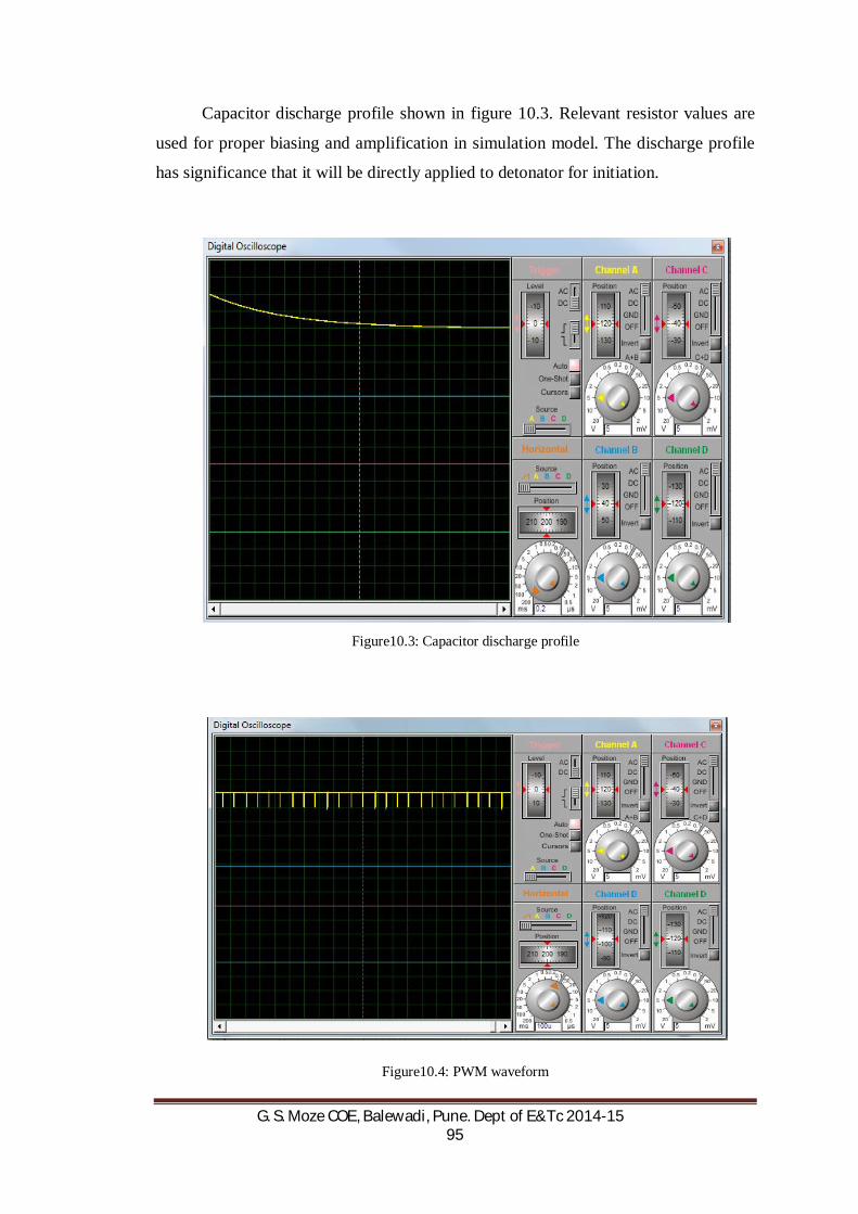
G. S. Moze COE, Balewadi, Pune. Dept of E&Tc 2014-15 95
Capacitor discharge profile shown in figure 10.3. Relevant resistor values are
used for proper biasing and amplification in simulation model. The discharge profile
has significance that it will be directly applied to detonator for initiation.
Figure10.3: Capacitor discharge profile
Figure10.4: PWM waveform

G. S. Moze COE, Balewadi, Pune. Dept of E&Tc 2014-15 96
Relevant values for the capacitor, inductor and the duty cycle for PWM are taken
for the boost convertor circuit. The duty cycle for the PWM of the microcontroller
used in the firing circuit is 92% to obtain the boosted voltage of 30volts. PWM is used
for switching the MOSFET of the boost convertor circuit.

G. S. Moze COE, Balewadi, Pune. Dept of E&Tc 2014-15 97
CHAPTER 11
SUMMARY &CONCLUSION
The MEMS SAF device previously designed used 20-pin microcontroller so it took
more space. As, today is the age of miniaturization we obtain it by using an ATtiny10
6-pin microcontroller. Hence, it fulfills the requirement of compactness, reliability
and speed. By using SCB instead of resistances we get our system more compact, safe
with fast ignition time.
SCB provides safe, reliable and low energy means of initiators. For explosive
detonations SCBs are best suited. Voltage booster circuit boosts the input voltage to
about 30V. The firing circuit of SCB designed in this project produces a high current
pulse for sufficient time required for plasma generation. The design can be made with
discrete as well as integrated components.
The integrated chip needed to be developed using mixed signal VLSI technology.
It has various units which were simulated and the results are acceptable for proper
functioning of SCB chip. It can have more units such as reset unit or power
managemant unit or logic unit that has higher functionality as per requirement. The
resulting chip will be compact in size and will have maximized functionality.
Based on specifications, schematic and PCB layout is made in Diptrace freeware
2.4.0.2 software, simulation is done in Proteous 7.7 and modelling is done in the Pro-
E 5.0. 2D drawings of mechanical arming parts of SAF layer are drawn. Designs are
prepared for the same.
11.1 Future Scope
The future scope of system is to make the system wireless. This can be done by
transferring wireless power transfer also wireless data transfer. This can be done
through inductive wireless power and data transfer and also capacitive wireless power
and data transfer. There are also many ways to transfer wireless power and data
transfer.

G. S. Moze COE, Balewadi, Pune. Dept of E&Tc 2014-15 98
11.2 Applications
Integrated pyro SCB chip is used in:
Military
Defence
G. S. Moze COE, Balewadi, Pune. Dept of E&Tc 2014-15 99
LIST OF PUBLICATIONS
1) Paper presented in First International Conference on Emerging Trends in
Electronics and Communication Engineering(ETECE-2015) Organized by
Department of Electronics & Telecommunication, Bharatiya Vidyapeeth Deemed
University College of Engineering, Pune-43 on 2-3 April 2015.
Paper Title "Pyro MEMS Design for Fuze", Pooja Sharma1, Dr. Virendra Kumar2,
Archana Singh3 ,1&3 G. S. Moze COE Balewadi, Pune, Savitribai Phule Pune
University, Pune , 2 ARDE-DRDO Pashan, Pune.
2) Paper published in International Journal of Electrical, Electronics and Data
communication, ISSN(Online):2321-2950, ISSN(Print):2320-2084, Special issue-1,
April 2015.
Paper Title "Pyro MEMS Design for Fuze", Pooja Sharma1, Dr. Virendra Kumar2,
Archana Singh3 ,1&3 G. S. Moze COE Balewadi, Pune, Savitribai Phule Pune
University, Pune , 2 ARDE-DRDO Pashan, Pune.
G. S. Moze COE, Balewadi, Pune. Dept of E&Tc 2014-15 100
REFERENCES 1. L. E. Hollander, Jr., “Semiconductor Transducers”, US. Patent 3,392.576, Jul
16, 1968.
2. Robert W. Bikes Jr.; Alfred C. Schwarz. “Semi-Conductor Bridge (SCB)
Igniter”, US. Patent 4,708,060, November 24, 1987.
3. Robert L. Pro_t, John L. Wells, Alan L. Lause, John C. Cole, “Thin Film bridge
initiator and method therfor”, US Patent 4,729,315, Mar 8, 1988.
4. Eldon Nerheim, “Integrated silicon plasma switch”, US Patent 4,840,122, June
20, 1989.
5. David A. Benson, Robert BickesJr, Robert S. Blewer, “Tungsten bridge for low
energy ignition of explosive and energetic materials”, US Patent 4,976.200, dec 11,
1990.
6. Thomas A. Baginski, “Method of forming radio frequency and electrostatic
discharge insensitive electro-explosive devices” Patent No.US 6272965 B1.
7. Bernardo Martinez-Tovar, John A. Montoya, “Surface connectable
semiconductor bridge elements, devices and methods”, Patent No. EP 0948812 B1, 2
Mar 2005.
8. J. Keith Hartman; Carroll B. “Zener diode for protection of integrated circuit
explosive bridge” Patent Number: 5,309,841, May 10, 1994.
9. Avery, “Protective integrated circuit device utilizing back-to-back Zener
diodes”, Patent Number :US 4405933 A. 20 Sep 1983.
10. Tony L. King and William W. Tarbell, “Pin-to-pin Electrostatic Discharge
Protection for Semiconductor Bridges”, Sandia National Laboratories, 2002.
11. Thomas A. Baginski, Keith A, Thomas “A RF-Insensitive Electroexplosive
Device with 500 V standoff capability”,Members, IEEE.
12. Vivian E. Patz; Stafford A. Smithies “Detonator Firing Element” Patent
Number: 4,819,560, April 11, 1989.
13. Robert W. Bickes, Jr. and David E. Wackerbarth “Semiconductor Bridge, SCB,
Ignition Studies of AI/CuOThermitet”, Western State Section of the Combustion
Institute 1997 Spring Meeting.
14. R. W. Bickes, Jr. “Explosive systems Utilizing semiconductor bridge, SCB,
Technology”, Explosive Components Department, Sandia National Laboratories.
G. S. Moze COE, Balewadi, Pune. Dept of E&Tc 2014-15 101
15. Aviv Ronen; YairBaruchi; EranZvulun, “Energetic unit based on
semiconductor bridge” Patent Number: WO 2012/176198, December 27, 2012.
16. Sanjeev Sharma, Sushil Kumar, “Simulation Model of Boost Converter used in
Photovoltaic System”, EN Deptt.,KIET,Ghaziabad, International Journal of Advances
in Electrical and Electronics Engineering.
17. B. M. Hasaneen, Adel Mohammed, “Design and simulation of DC/DC Boost
Converter”, IEEE, Power Systems Conference, 2008.
18. S. Masri, P. W. Chan, “Design and development of DC-DC boost converter
with constant output voltage”, IEEE, ICIAS, 2010.
19. Pezous H., Rossi C., Sanchez M., Mathieu F., Dollat X., Charlot S., Salvagnac
L., Conedera V., Integration of MEMS based safe arm and fire device, Sensors and
Actuators A 159 (2010) 157–167
20. Pezous H., Sanchez M., Mathieu F., Dollat X., Charlot S., Rossi C.,
Fabrication, Assembly and Tests of a MEMS based Safe, Arm and Fire Device,
Proceedings of PowerMEMS 2008+ microEMS2008, Sendai, Japan, November 9-12,
(2008)
21. Rossi C., Esteve D. , Micropyrotechnics, a new technology for making
energetic microsystems: review and prospective, Sensors and Actuators A 120 (2005)
297–310
22. Robinson C. H., Hoang T. Q., Gelak M. R., Smith G. L., Wood R. H.,
Materials, Fabrication and Assembly Technologies for Advanced MEMS Based
Safety and Arming Mechanisms for Projectile Munitions.
23. Patent No.: US 8,276,515 B1 (United States), May 1’ 2009, Ultra-Miniature
Electro-Mechanical Safety and Arming Device, Oct. 2, 2012
24. Verma V.K., Kokate V. K., Nandgavc P., Design of MEMS Electronic Safety
and Arming Mechanism for Projectile Munition,
25. Liqun D.U., Shengfang J, Weirong N., Qijia W, Fabrication of Fuze Micro-
electro-mechanical System Safety Device,
26. Patent No.: US 8,640,620 B1 (United States), March 5’ 2012, Non-Inertial
Safe And Arm Device, 2014
27. Patent No.: US 6,295,932 B1 (United States), March 15’ 1999, Electronic Safe
Arm And Fire Device, 2001

G. S. Moze COE, Balewadi, Pune. Dept of E&Tc 2014-15 102
28. Patent No.: US 6,431,071 B1 (United States), Sept 18’ 2000, MEMS Arm Fire
And Safe And Arm Devices.2002
29. Zhang K.L., Choua S.K., Ang S.S., Tang X.S., A MEMS-based solid
propellant microthruster with Au/Ti igniter, Sensors and Actuators A 122 (2005) 113–
123
30. Stewart D.S., Miniaturization Of Explosive Technology And Microdetonics,
Mechanics of 21st Century - ICTAM04
31. Rossi C., Briand D., Dumonteuil M., Camps T., Pham P.Q., Rooij N.F.,
Matrix of 10×10 addressed solid propellant microthrusters: Review of the
technologies, Sensors and Actuators A Physical 126, issue 1, 241-252, 2006
32. Rossi C., Zhang K., Estève D., Alphonse P., Tailhades P., Vahlas C.,
Nanoenergetic Materials for MEMS: A Review, Journal of Microelectromechanical
Systems, Vol. 16, No. 4, August 2007

G. S. Moze COE, Balewadi, Pune. Dept of E&Tc 2014-15 103
APPENDIX I
Component List for Authentication Unit
The following components are used for the setter circuit.
1) Atmega 16 microcontroller DIP(40 pin)
2) 4*4 matrix Keypad
3) LCD(16*2) Display
4) Diode 1N4007 four diodes are used to form the rectifier.
5) Capacitors 1000uF,470 uF ceramic capacitors and two capacitors of 22pF are
used.
6) Crystal of 8MHz is used.
7) Resistor 270 ohms.
8) Male and female berg strips (40*1).
9) 8 pin male and female relimate connectors.
10) 2 pin male and female relimate connectors.
Component List for Delay and firing unit
1) ATTINY85 SOIC
2) MOSFET 2N7002CK SOT23 Surface-Mounted Device (SMD) plastic package
3) Inductor L1 of 100uH (EIA 0805)TDK MLF2012
4) Capacitor C1 is 4.7uF (Tantalum chip capacitor) 35V(EIA 1210)TRJ series AVX
5) Capacitor C2 0.1uF (0402)ceramic capacitor used at the input(Vishay).
6) Diode(schottky diode)10MQ060N.
7)TVS diode surface mount TRANSZORB transient voltage suppressor by
Vishay,D0214AA(SMBJ)package,partno.P6SM56CA. Connect TVS 12v breakdown
(1mm*1mm) diode and 0.1uf Capacitor (1mm*1mm) on the other side of the PCB.
8) Thick film chip resistor SMD Resistor R1,R2,R3 SMD 0805 R1=15K ohm, 0805
R2=1K ohm R3(0805) leave 1.4mm*1.4mm for SCB do not connect R3(it is

G. S. Moze COE, Balewadi, Pune. Dept of E&Tc 2014-15 104
component created in diptrace with dimensions 1.4mm*1.4mm) connect SCB
instead of R3}.

G. S. Moze COE, Balewadi, Pune. Dept of E&Tc 2014-15 105
APPENDIX II
Softwares used in the project are listed below
1) Dip Trace 2.4.0.2(Freeware version)
2) PROTEUS 7.7
1) Dip Trace
The software used for designing the double sided PCB of the delay and firing unit
is Dip Trace version 2.4.0.2 (Freeware version). Dip Trace is quality Schematic
Capture and PCB Design software that offers everything to create simple or complex
multi-layer boards from schematic to manufacturing files. There are different modules
in Dip Trace for the following tasks
a) Schematic capture
b) PCB layout
c) Creation of libraries
d) 3D Modeling
a) Schematic Capture
Advanced schematic tool with support of multi-sheet and multi-level hierarchical
design that allows the designer to connect pins visually, without wires, using net
ports, buses, or logically. Electrical Rule Check and hierarchy verification work from
the earliest stages of design till the work is done. Schematic supports import and
export of different EDA/CAD and net-list formats.
b) PCB Layout
High-quality board design tool of the DipTrace environment. PCB Layout features
smart placement and routing tools, shape-based auto router, copying hierarchical
blocks, smart project structure, and verification features that ensure accuracy even for
the most complex projects. Real-time DRC allows the designer to fix errors on the fly
and increases quality all the way to project completion. Import and export a wide
range of EDA, CAD, net-list and manufacturing formats.

G. S. Moze COE, Balewadi, Pune. Dept of E&Tc 2014-15 106
c) Library Creation
Cross-module library management system with component and pattern editors and
direct import from outside the DipTrace design environment. Component and Pattern
editors support smart library structure and fast creation of components and patterns
with integrated templates. Bulk pin naming, pad numbering, and editing features
allow the designer to build multi-part complex components and patterns with
hundreds of pins faster than ever before.
d) 3D Modelling
Works as a part of PCB Layout and Pattern Editor. The 3D module allows the
designer to preview the board with installed components on any design stage, rotate
and move it in real-time with hardware acceleration. Board 3D model can be exported
to mechanical CAD (STEP, VRML). DipTrace imports 3DS, VRML, STEP, and
IGES files as 3D models. 3500+ models are supplied free of charge.
2) PROTEUS 7.7
Proteus Professional - software was used for PCB design of the Setter and for
simulation of the setter and firing and delay unit. It is a software for automated design
of electronic circuits. The package is a system of circuit simulation, based on the
models of electronic components in PSpice.
A distinctive feature of the package Proteus Professional is the possibility of
modelling of the programmable devices: microcontrollers, microprocessors, DSP and
others. Additionally, the package of Proteus Professional is a system design of printed
circuit boards. Proteus Professional can simulate the following microcontrollers:
8051, ARM7, AVR, Motorola, PIC, Basic Stamp. The library contains the
components of reference data Co-simulation of microprocessor software within a
mixed mode SPICE simulator. Available for PIC, 8051, AVR, HC11,
ARM7/LPC2000 and Basic Stamp processors. See your code interact with simulated
hardware in real-time.

G. S. Moze COE, Balewadi, Pune. Dept of E&Tc 2014-15 107
Interactive peripheral models for displays, keypads, etc. Over 8000 analogue and
digital device models. Extensive single step and debugging facilities including system
wide diagnostics. Works with popular compilers and assemblers. Professional
schematic capture and PCB design software with automatic component placement,
track routing and design
validation. Includes full feature schematic capture environment. Create PCBs
automatically or manually from a schematic. Extensive support for power planes.
Outputs to industry standard CADCAM formats. Integrated 3D Viewer provides
board visualisation during design. Interactive SPICE circuit simulator included with
all versions.
Related Documents