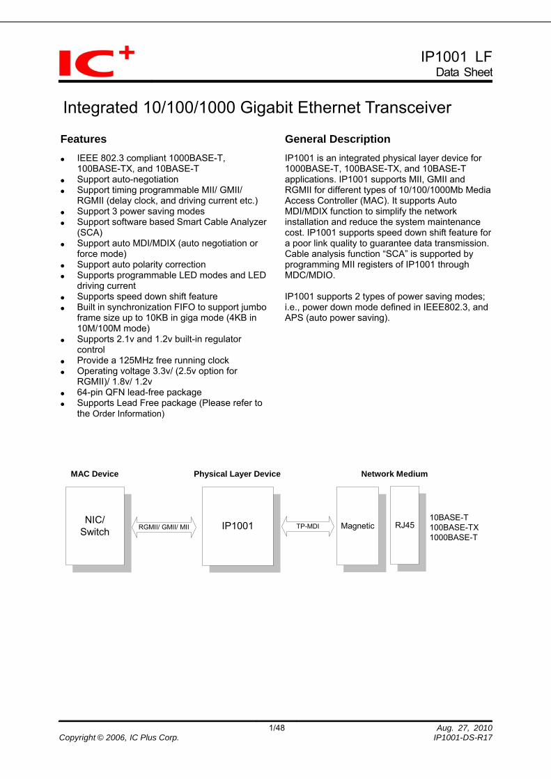
IP1001 LF Data Shee t Integrated 10/100/1000 Gigabit Ethernet Transceiver Features General Description z IEEE 802.3 compliant 1000BASE-T, 100BASE-TX, and 10BASE-T z Support auto-negotiation z Support timing programmable MII/ GMII/ RGMII (delay clock, and driving current etc.) z Support 3 power saving modes z Support software based Smart Cable Analyzer (SCA) z Support auto MDI/MDIX (auto negotiation or force mode) z Support auto polarity correction z Supports programmable LED modes and LED driving current z Supports speed down shift feature z Built in synchronization FIFO to support jumbo frame size up to 10KB in giga mode (4KB in 10M/100M mode) z Supports 2.1v and 1.2v built-in regulator control z Provide a 125MHz free running clock z Operating voltage 3.3v/ (2.5v option for RGMII)/ 1.8v/ 1.2v z 64-pin QFN lead-free package z Supports Lead Free package (Please refer to the Order Information) IP1001 is an integrated physical layer device for 1000BASE-T, 100BASE-TX, and 10BASE-T applications. IP1001 supports MII, GMII and RGMII for different types of 10/100/1000Mb Media Access Controller (MAC). It supports Auto MDI/MDIX function to simplify the network installation and reduce the system maintenance cost. IP1001 supports speed down shift feature for a poor link quality to guarantee data transmission. Cable analysis function “SCA” is supported by programming MII registers of IP1001 through MDC/MDIO. IP1001 supports 2 types of power saving modes; i.e., power down mode defined in IEEE802.3, and APS (auto power saving). RGMII/ GMII/ MII TP-MDI Physical Layer Device Network Medium IP1001 Magnetic NIC/ Switch MAC Device RJ45 10BASE-T 100BASE-TX 1000BASE-T 1/48 Aug. 27, 2010 Copyright © 2006, IC Plus Corp. IP1001-DS-R17

Welcome message from author
This document is posted to help you gain knowledge. Please leave a comment to let me know what you think about it! Share it to your friends and learn new things together.
Transcript
IP1001 LFData Sheet
Integrated 10/100/1000 Gigabit Ethernet Transceiver
Features General Description IEEE 802.3 compliant 1000BASE-T,
100BASE-TX, and 10BASE-T Support auto-negotiation Support timing programmable MII/ GMII/
RGMII (delay clock, and driving current etc.) Support 3 power saving modes Support software based Smart Cable Analyzer
(SCA) Support auto MDI/MDIX (auto negotiation or
force mode) Support auto polarity correction Supports programmable LED modes and LED
driving current Supports speed down shift feature Built in synchronization FIFO to support jumbo
frame size up to 10KB in giga mode (4KB in 10M/100M mode)
Supports 2.1v and 1.2v built-in regulator control
Provide a 125MHz free running clock Operating voltage 3.3v/ (2.5v option for
RGMII)/ 1.8v/ 1.2v 64-pin QFN lead-free package Supports Lead Free package (Please refer to
the Order Information)
IP1001 is an integrated physical layer device for 1000BASE-T, 100BASE-TX, and 10BASE-T applications. IP1001 supports MII, GMII and RGMII for different types of 10/100/1000Mb Media Access Controller (MAC). It supports Auto MDI/MDIX function to simplify the network installation and reduce the system maintenance cost. IP1001 supports speed down shift feature for a poor link quality to guarantee data transmission. Cable analysis function “SCA” is supported by programming MII registers of IP1001 through MDC/MDIO. IP1001 supports 2 types of power saving modes; i.e., power down mode defined in IEEE802.3, and APS (auto power saving).
RGMII/ GMII/ MII TP-MDI
Physical Layer Device Network Medium
IP1001IP1001
MagneticMagneticNIC/
Switch
NIC/Switch
MAC Device
RJ45RJ45
10BASE-T100BASE-TX1000BASE-T
1/48 Aug. 27, 2010Copyright © 2006, IC Plus Corp. IP1001-DS-R17
IP1001 LFData Sheet
2/48 Aug. 27, 2010Copyright © 2006, IC Plus Corp. IP1001-DS-R17
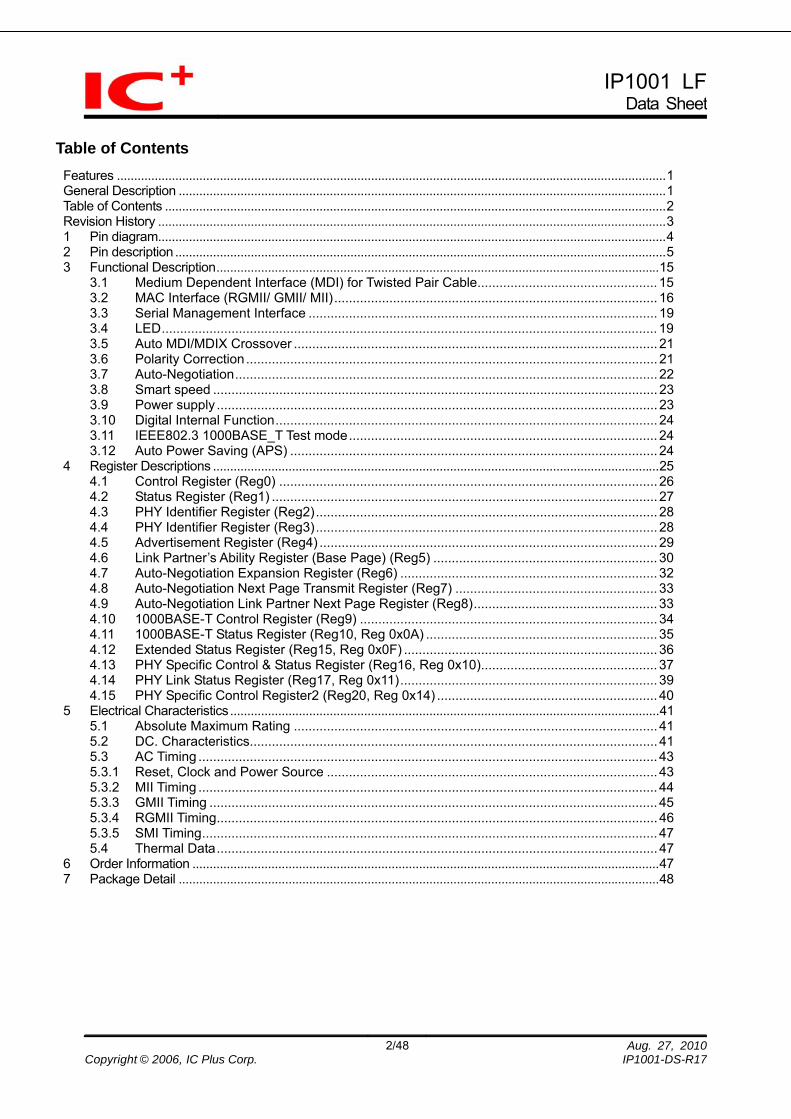
Table of Contents Features ................................................................................................................................................................1 General Description ..............................................................................................................................................1 Table of Contents ..................................................................................................................................................2 Revision History ....................................................................................................................................................3 1 Pin diagram....................................................................................................................................................4 2 Pin description ...............................................................................................................................................5 3 Functional Description.................................................................................................................................15
3.1 Medium Dependent Interface (MDI) for Twisted Pair Cable................................................. 15 3.2 MAC Interface (RGMII/ GMII/ MII)........................................................................................ 16 3.3 Serial Management Interface ............................................................................................... 19 3.4 LED....................................................................................................................................... 19 3.5 Auto MDI/MDIX Crossover ................................................................................................... 21 3.6 Polarity Correction................................................................................................................ 21 3.7 Auto-Negotiation................................................................................................................... 22 3.8 Smart speed ......................................................................................................................... 23 3.9 Power supply ........................................................................................................................ 23 3.10 Digital Internal Function........................................................................................................ 24 3.11 IEEE802.3 1000BASE_T Test mode.................................................................................... 24 3.12 Auto Power Saving (APS) .................................................................................................... 24
4 Register Descriptions ..................................................................................................................................25 4.1 Control Register (Reg0) ....................................................................................................... 26 4.2 Status Register (Reg1) ......................................................................................................... 27 4.3 PHY Identifier Register (Reg2)............................................................................................. 28 4.4 PHY Identifier Register (Reg3)............................................................................................. 28 4.5 Advertisement Register (Reg4) ............................................................................................ 29 4.6 Link Partner’s Ability Register (Base Page) (Reg5) ............................................................. 30 4.7 Auto-Negotiation Expansion Register (Reg6) ...................................................................... 32 4.8 Auto-Negotiation Next Page Transmit Register (Reg7) ....................................................... 33 4.9 Auto-Negotiation Link Partner Next Page Register (Reg8).................................................. 33 4.10 1000BASE-T Control Register (Reg9) ................................................................................. 34 4.11 1000BASE-T Status Register (Reg10, Reg 0x0A) ............................................................... 35 4.12 Extended Status Register (Reg15, Reg 0x0F) ..................................................................... 36 4.13 PHY Specific Control & Status Register (Reg16, Reg 0x10)................................................ 37 4.14 PHY Link Status Register (Reg17, Reg 0x11)...................................................................... 39 4.15 PHY Specific Control Register2 (Reg20, Reg 0x14) ............................................................ 40
5 Electrical Characteristics.............................................................................................................................41 5.1 Absolute Maximum Rating ................................................................................................... 41 5.2 DC. Characteristics............................................................................................................... 41 5.3 AC Timing ............................................................................................................................. 43 5.3.1 Reset, Clock and Power Source .......................................................................................... 43 5.3.2 MII Timing ............................................................................................................................. 44 5.3.3 GMII Timing .......................................................................................................................... 45 5.3.4 RGMII Timing........................................................................................................................ 46 5.3.5 SMI Timing............................................................................................................................ 47 5.4 Thermal Data........................................................................................................................ 47
6 Order Information ........................................................................................................................................47 7 Package Detail ............................................................................................................................................48
IP1001 LFData Sheet
3/48 Aug. 27, 2010Copyright © 2006, IC Plus Corp. IP1001-DS-R17
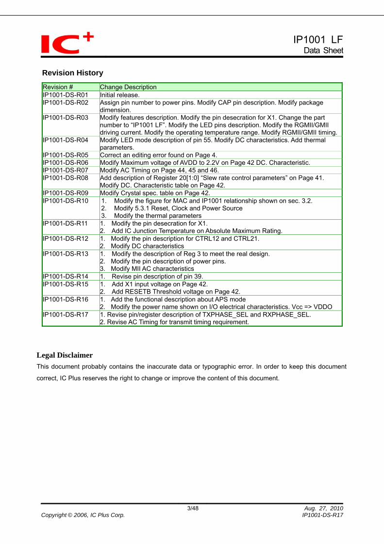
Revision History
Revision # Change Description IP1001-DS-R01 Initial release. IP1001-DS-R02 Assign pin number to power pins. Modify CAP pin description. Modify package
dimension. IP1001-DS-R03 Modify features description. Modify the pin desecration for X1. Change the part
number to “IP1001 LF”. Modify the LED pins description. Modify the RGMII/GMII driving current. Modify the operating temperature range. Modify RGMII/GMII timing.
IP1001-DS-R04 Modify LED mode description of pin 55. Modify DC characteristics. Add thermal parameters.
IP1001-DS-R05 Correct an editing error found on Page 4. IP1001-DS-R06 Modify Maximum voltage of AVDD to 2.2V on Page 42 DC. Characteristic. IP1001-DS-R07 Modify AC Timing on Page 44, 45 and 46. IP1001-DS-R08 Add description of Register 20[1:0] “Slew rate control parameters” on Page 41.
Modify DC. Characteristic table on Page 42. IP1001-DS-R09 Modify Crystal spec. table on Page 42. IP1001-DS-R10 1. Modify the figure for MAC and IP1001 relationship shown on sec. 3.2.
2. Modify 5.3.1 Reset, Clock and Power Source 3. Modify the thermal parameters
IP1001-DS-R11 1. Modify the pin desecration for X1. 2. Add IC Junction Temperature on Absolute Maximum Rating.
IP1001-DS-R12 1. Modify the pin description for CTRL12 and CTRL21. 2. Modify DC characteristics
IP1001-DS-R13 1. Modify the description of Reg 3 to meet the real design. 2. Modify the pin description of power pins. 3. Modify MII AC characteristics
IP1001-DS-R14 1. Revise pin description of pin 39. IP1001-DS-R15 1. Add X1 input voltage on Page 42.
2. Add RESETB Threshold voltage on Page 42. IP1001-DS-R16 1. Add the functional description about APS mode
2. Modify the power name shown on I/O electrical characteristics. Vcc => VDDO IP1001-DS-R17 1. Revise pin/register description of TXPHASE_SEL and RXPHASE_SEL.
2. Revise AC Timing for transmit timing requirement. Legal Disclaimer This document probably contains the inaccurate data or typographic error. In order to keep this document
correct, IC Plus reserves the right to change or improve the content of this document.
IP1001 LFData Sheet
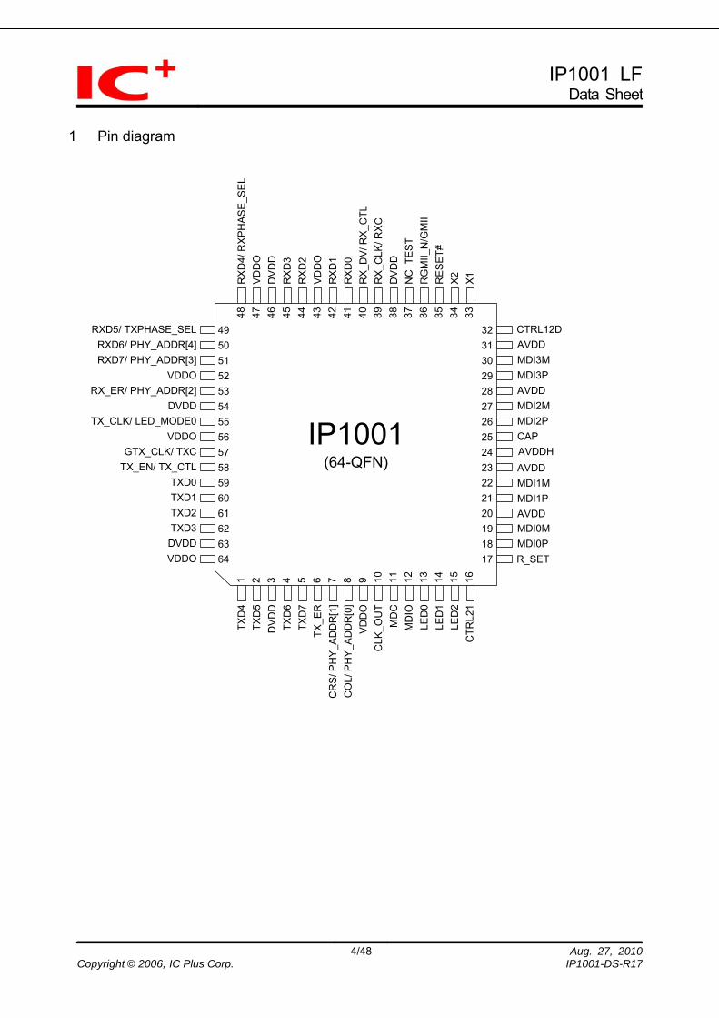
1 Pin diagram
IP1001(64-QFN)
TXD
4
RXD5/ TXPHASE_SEL
TXD
5D
VD
DTX
D6
TXD
7TX
_ER
CR
S/ P
HY
_AD
DR
[1]
CO
L/ P
HY
_AD
DR
[0]
VD
DO
CLK
_OU
TM
DC
MD
IOLE
D0
LED
1LE
D2
CTR
L21
RX
D4/
RX
PH
AS
E_S
EL
VD
DO
DV
DD
RX
D3
RX
D2
VD
DO
RX
D1
RX
D0
RX
_DV
/ RX
_CTL
RX
_CLK
/ RX
CD
VD
DN
C_T
ES
TR
GM
II_N
/GM
IIR
ES
ET#
X2 X1
RXD6/ PHY_ADDR[4]RXD7/ PHY_ADDR[3]
VDDORX_ER/ PHY_ADDR[2]
DVDDTX_CLK/ LED_MODE0
VDDOGTX_CLK/ TXC
TX_EN/ TX_CTLTXD0TXD1TXD2TXD3DVDDVDDO
AVDDMDI3MMDI3PAVDDMDI2MMDI2PCAPAVDDH
R_SET
AVDDMDI1MMDI1PAVDD
CTRL12D
MDI0MMDI0P
49505152535455565758596061626364
32313029282726252423222120191817
48 47 46 45 44 43 42 41 40 39 38 37 36 35 34 33
1 2 3 4 5 6 7 8 9 10 11 12 13 14 15 16
4/48 Aug. 27, 2010Copyright © 2006, IC Plus Corp. IP1001-DS-R17
IP1001 LFData Sheet
5/48 Aug. 27, 2010Copyright © 2006, IC Plus Corp. IP1001-DS-R17
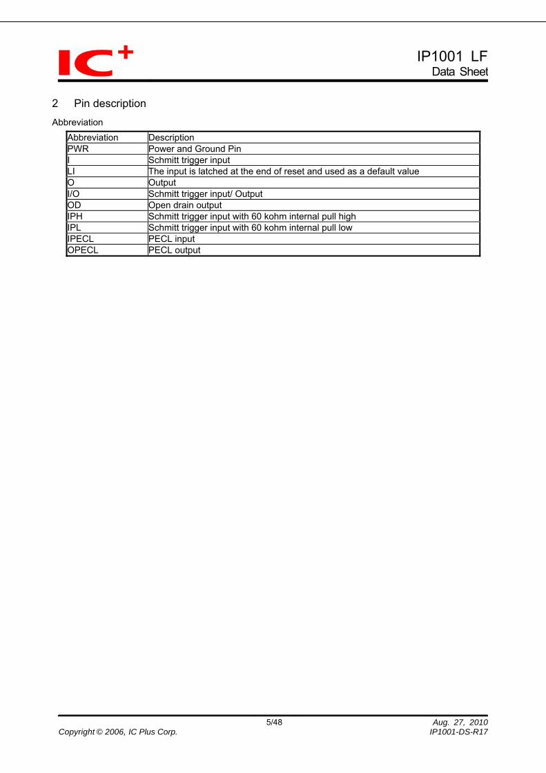
2 Pin description Abbreviation
Abbreviation Description PWR Power and Ground Pin I Schmitt trigger input LI The input is latched at the end of reset and used as a default value O Output I/O Schmitt trigger input/ Output OD Open drain output IPH Schmitt trigger input with 60 kohm internal pull high IPL Schmitt trigger input with 60 kohm internal pull low IPECL PECL input OPECL PECL output
IP1001 LFData Sheet
6/48 Aug. 27, 2010Copyright © 2006, IC Plus Corp. IP1001-DS-R17
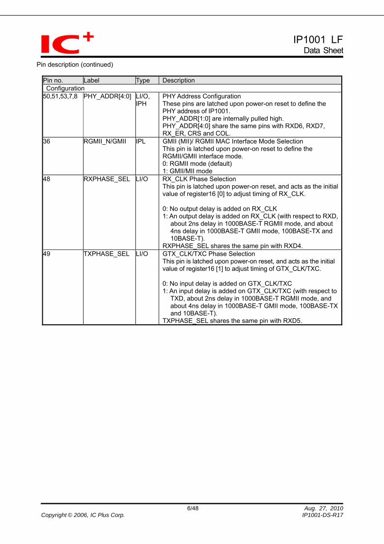
Pin description (continued)
Pin no. Label Type Description Configuration
50,51,53,7,8 PHY_ADDR[4:0] LI/O, IPH
PHY Address Configuration These pins are latched upon power-on reset to define the PHY address of IP1001. PHY_ADDR[1:0] are internally pulled high. PHY_ADDR[4:0] share the same pins with RXD6, RXD7, RX_ER, CRS and COL.
36 RGMII_N/GMII IPL GMII (MII)/ RGMII MAC Interface Mode Selection This pin is latched upon power-on reset to define the RGMII/GMII interface mode. 0: RGMII mode (default) 1: GMII/MII mode
48 RXPHASE_SEL LI/O RX_CLK Phase Selection This pin is latched upon power-on reset, and acts as the initial value of register16 [0] to adjust timing of RX_CLK. 0: No output delay is added on RX_CLK 1: An output delay is added on RX_CLK (with respect to RXD,
about 2ns delay in 1000BASE-T RGMII mode, and about 4ns delay in 1000BASE-T GMII mode, 100BASE-TX and 10BASE-T).
RXPHASE_SEL shares the same pin with RXD4. 49 TXPHASE_SEL LI/O GTX_CLK/TXC Phase Selection
This pin is latched upon power-on reset, and acts as the initial value of register16 [1] to adjust timing of GTX_CLK/TXC. 0: No input delay is added on GTX_CLK/TXC 1: An input delay is added on GTX_CLK/TXC (with respect to
TXD, about 2ns delay in 1000BASE-T RGMII mode, and about 4ns delay in 1000BASE-T GMII mode, 100BASE-TX and 10BASE-T).
TXPHASE_SEL shares the same pin with RXD5.
IP1001 LFData Sheet
7/48 Aug. 27, 2010Copyright © 2006, IC Plus Corp. IP1001-DS-R17
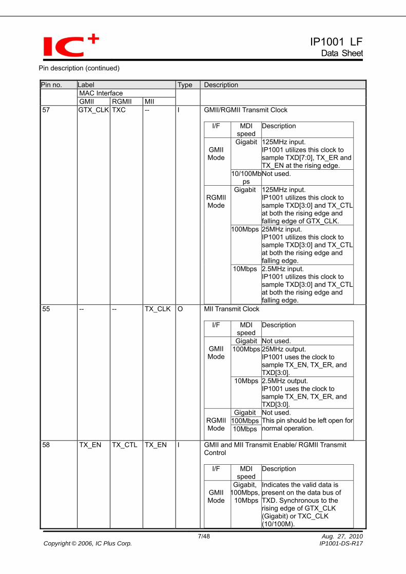
Pin description (continued) Pin no. Label Type Description
MAC Interface GMII RGMII MII
57 GTX_CLK TXC -- I GMII/RGMII Transmit Clock
I/F MDI speed
Description
Gigabit 125MHz input. IP1001 utilizes this clock to sample TXD[7:0], TX_ER and TX_EN at the rising edge.
GMII Mode
10/100Mb
ps Not used.
Gigabit 125MHz input. IP1001 utilizes this clock to sample TXD[3:0] and TX_CTL at both the rising edge and falling edge of GTX_CLK.
100Mbps 25MHz input. IP1001 utilizes this clock to sample TXD[3:0] and TX_CTL at both the rising edge and falling edge.
RGMIIMode
10Mbps 2.5MHz input. IP1001 utilizes this clock to sample TXD[3:0] and TX_CTL at both the rising edge and falling edge.
55 -- -- TX_CLK O MII Transmit Clock
I/F MDI speed
Description
Gigabit Not used. 100Mbps 25MHz output.
IP1001 uses the clock to sample TX_EN, TX_ER, and TXD[3:0].
GMII Mode
10Mbps 2.5MHz output. IP1001 uses the clock to sample TX_EN, TX_ER, and TXD[3:0].
Gigabit100Mbps
RGMIIMode
10Mbps
Not used. This pin should be left open for normal operation.
58 TX_EN TX_CTL TX_EN I GMII and MII Transmit Enable/ RGMII Transmit
Control
I/F MDI speed
Description
GMII Mode
Gigabit,100Mbps,
10Mbps
Indicates the valid data is present on the data bus of TXD. Synchronous to the rising edge of GTX_CLK (Gigabit) or TXC_CLK (10/100M).
IP1001 LFData Sheet
8/48 Aug. 27, 2010Copyright © 2006, IC Plus Corp. IP1001-DS-R17
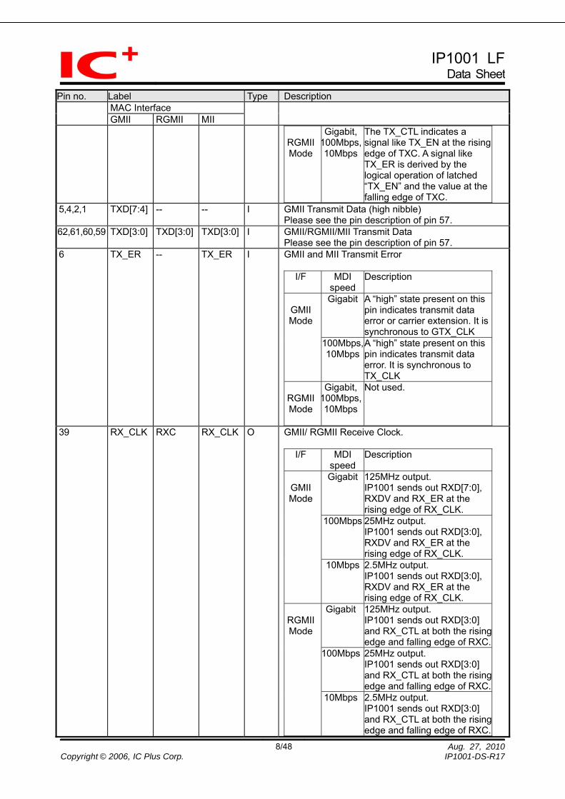
Pin no. Label Type Description MAC Interface GMII RGMII MII
RGMIIMode
Gigabit,100Mbps,10Mbps
The TX_CTL indicates a signal like TX_EN at the rising edge of TXC. A signal like TX_ER is derived by the logical operation of latched “TX_EN” and the value at the falling edge of TXC.
5,4,2,1 TXD[7:4] -- -- I GMII Transmit Data (high nibble) Please see the pin description of pin 57.
62,61,60,59 TXD[3:0] TXD[3:0] TXD[3:0] I GMII/RGMII/MII Transmit Data Please see the pin description of pin 57.
6 TX_ER -- TX_ER I GMII and MII Transmit Error
I/F MDI speed
Description
Gigabit A “high” state present on this pin indicates transmit data error or carrier extension. It is synchronous to GTX_CLK
GMII Mode
100Mbps,10Mbps
A “high” state present on this pin indicates transmit data error. It is synchronous to TX_CLK
RGMIIMode
Gigabit,100Mbps,10Mbps
Not used.
39 RX_CLK RXC RX_CLK O GMII/ RGMII Receive Clock.
I/F MDI
speedDescription
Gigabit 125MHz output. IP1001 sends out RXD[7:0], RXDV and RX_ER at the rising edge of RX_CLK.
100Mbps 25MHz output. IP1001 sends out RXD[3:0], RXDV and RX_ER at the rising edge of RX_CLK.
GMII Mode
10Mbps 2.5MHz output. IP1001 sends out RXD[3:0], RXDV and RX_ER at the rising edge of RX_CLK.
Gigabit 125MHz output. IP1001 sends out RXD[3:0] and RX_CTL at both the rising edge and falling edge of RXC.
100Mbps 25MHz output. IP1001 sends out RXD[3:0] and RX_CTL at both the rising edge and falling edge of RXC.
RGMIIMode
10Mbps 2.5MHz output. IP1001 sends out RXD[3:0] and RX_CTL at both the rising edge and falling edge of RXC.
IP1001 LFData Sheet
9/48 Aug. 27, 2010Copyright © 2006, IC Plus Corp. IP1001-DS-R17
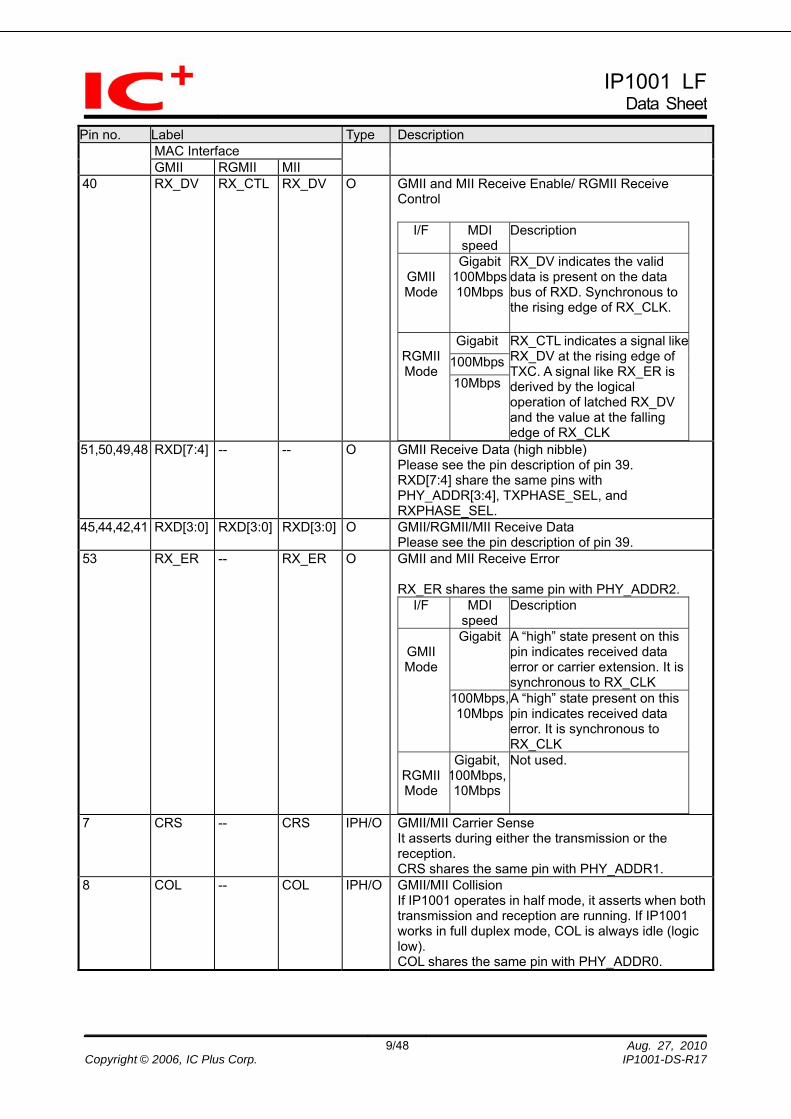
Pin no. Label Type Description MAC Interface GMII RGMII MII
40 RX_DV RX_CTL RX_DV O GMII and MII Receive Enable/ RGMII Receive Control
I/F MDI speed
Description
GMII Mode
Gigabit100Mbps10Mbps
RX_DV indicates the valid data is present on the data bus of RXD. Synchronous to the rising edge of RX_CLK.
Gigabit100Mbps
RGMIIMode
10Mbps
RX_CTL indicates a signal like RX_DV at the rising edge of TXC. A signal like RX_ER is derived by the logical operation of latched RX_DV and the value at the falling edge of RX_CLK
51,50,49,48 RXD[7:4] -- -- O GMII Receive Data (high nibble) Please see the pin description of pin 39. RXD[7:4] share the same pins with PHY_ADDR[3:4], TXPHASE_SEL, and RXPHASE_SEL.
45,44,42,41 RXD[3:0] RXD[3:0] RXD[3:0] O GMII/RGMII/MII Receive Data Please see the pin description of pin 39.
53 RX_ER -- RX_ER O GMII and MII Receive Error RX_ER shares the same pin with PHY_ADDR2.
I/F MDI speed
Description
Gigabit A “high” state present on this pin indicates received data error or carrier extension. It is synchronous to RX_CLK
GMII Mode
100Mbps,10Mbps
A “high” state present on this pin indicates received data error. It is synchronous to RX_CLK
RGMIIMode
Gigabit,100Mbps,10Mbps
Not used.
7 CRS -- CRS IPH/O GMII/MII Carrier Sense
It asserts during either the transmission or the reception. CRS shares the same pin with PHY_ADDR1.
8 COL -- COL IPH/O GMII/MII Collision If IP1001 operates in half mode, it asserts when both transmission and reception are running. If IP1001 works in full duplex mode, COL is always idle (logic low). COL shares the same pin with PHY_ADDR0.
IP1001 LFData Sheet
10/48 Aug. 27, 2010Copyright © 2006, IC Plus Corp. IP1001-DS-R17
Pin description (continued)
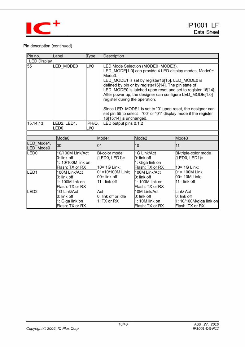
Pin no. Label Type Description LED Display
55 LED_MODE0 LI/O LED Mode Selection (MODE0~MODE3). LED_MODE[1:0] can provide 4 LED display modes, Mode0~ Mode3. LED_MODE1 is set by register16[15]. LED_MODE0 is defined by pin or by register16[14]. The pin state of LED_MODE0 is latched upon reset and set to register 16[14]. After power up, the designer can configure LED_MODE[1:0] register during the operation. Since LED_MODE1 is set to “0” upon reset, the designer can set pin 55 to select “00” or “01” display mode if the register 16[15:14] is unchanged.
15,14,13 LED2, LED1, LED0
IPH/O,LI/O
LED output pins 0,1,2
Mode0 Mode1 Mode2 Mode3 LED_Mode1, LED_Mode0 00 01 10 11
LED0 10/100M Link/Act 0: link off 1: 10/100M link on Flash: TX or RX
1G Link/Act 0: link off 1: Giga link on Flash: TX or RX
LED1 100M Link/Act 0: link off 1: 100M link on Flash: TX or RX
Bi-color mode {LED0, LED1}= 10= 1G Link; 01=10/100M Link; 00= link off 11= link off
100M Link/Act 0: link off 1: 100M link on Flash: TX or RX
Bi-triple-color mode {LED0, LED1}= 10= 1G Link; 01= 100M Link 00= 10M Link; 11= link off
LED2 1G Link/Act 0: link off 1: Giga link on Flash: TX or RX
Act 0: link off or idle 1: TX or RX
10M Link/Act 0: link off 1: 10M link on Flash: TX or RX
Link/ Act 0: link off 1: 10/100M/giga link onFlash: TX or RX
IP1001 LFData Sheet
11/48 Aug. 27, 2010Copyright © 2006, IC Plus Corp. IP1001-DS-R17
Pin description (continued)
Pin no. Label Type Description Serial Management Interface
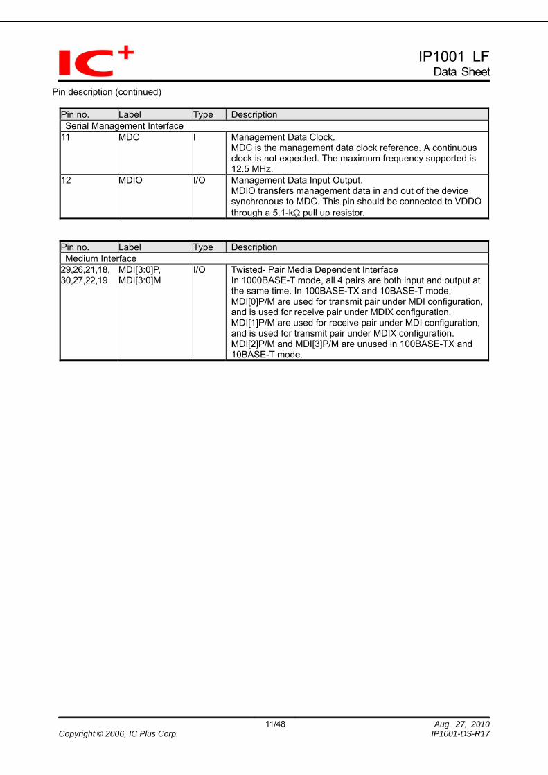
11 MDC I Management Data Clock. MDC is the management data clock reference. A continuous clock is not expected. The maximum frequency supported is 12.5 MHz.
12 MDIO I/O Management Data Input Output. MDIO transfers management data in and out of the device synchronous to MDC. This pin should be connected to VDDO through a 5.1-kΩ pull up resistor.
Pin no. Label Type Description Medium Interface
29,26,21,18, 30,27,22,19
MDI[3:0]P, MDI[3:0]M
I/O Twisted- Pair Media Dependent Interface In 1000BASE-T mode, all 4 pairs are both input and output at the same time. In 100BASE-TX and 10BASE-T mode, MDI[0]P/M are used for transmit pair under MDI configuration, and is used for receive pair under MDIX configuration. MDI[1]P/M are used for receive pair under MDI configuration, and is used for transmit pair under MDIX configuration. MDI[2]P/M and MDI[3]P/M are unused in 100BASE-TX and 10BASE-T mode.
IP1001 LFData Sheet
Pin description (continued)
Pin no. Label Type Description Miscellaneous
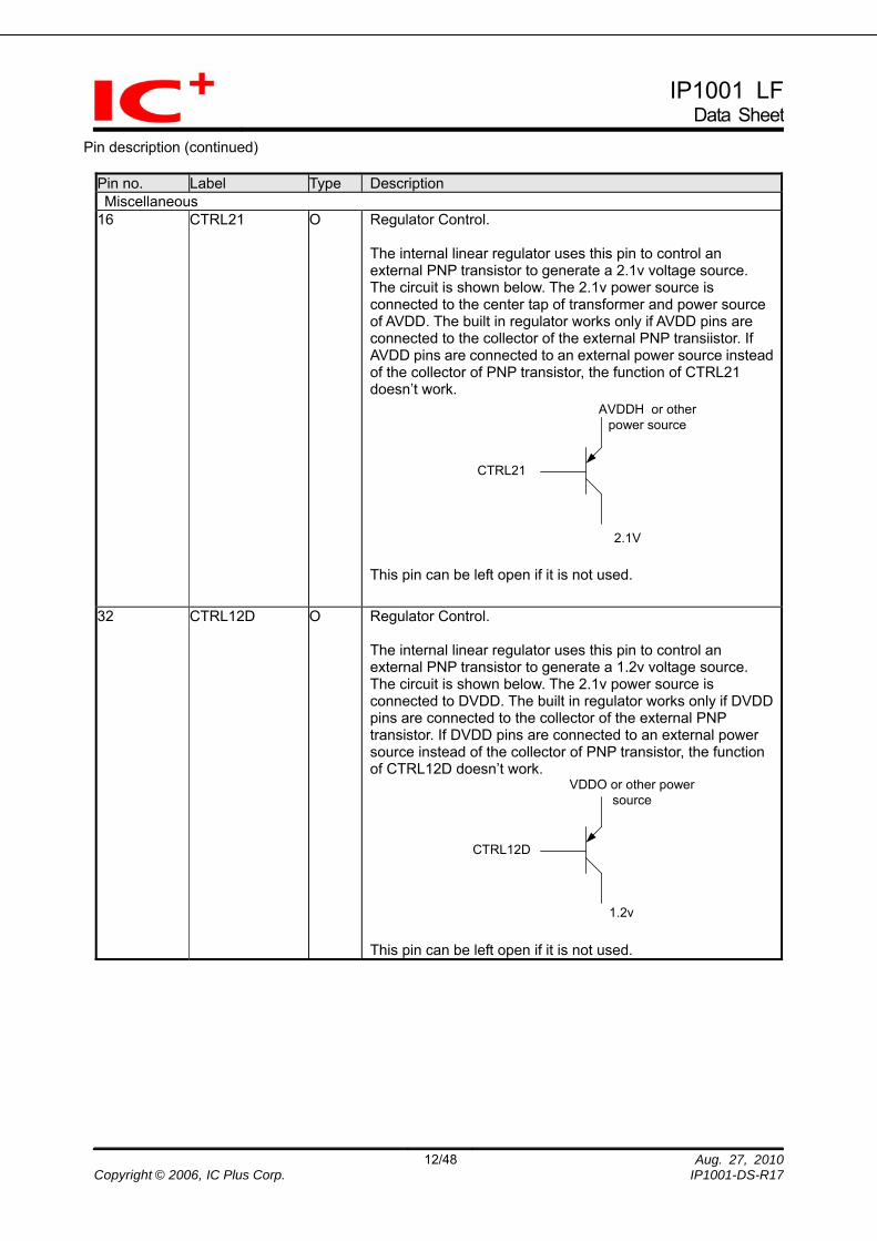
16 CTRL21 O Regulator Control. The internal linear regulator uses this pin to control an external PNP transistor to generate a 2.1v voltage source. The circuit is shown below. The 2.1v power source is connected to the center tap of transformer and power source of AVDD. The built in regulator works only if AVDD pins are connected to the collector of the external PNP transiistor. If AVDD pins are connected to an external power source instead of the collector of PNP transistor, the function of CTRL21 doesn’t work.
AVDDH or otherpower source
CTRL21
2.1V This pin can be left open if it is not used.
32 CTRL12D O Regulator Control. The internal linear regulator uses this pin to control an external PNP transistor to generate a 1.2v voltage source. The circuit is shown below. The 2.1v power source is connected to DVDD. The built in regulator works only if DVDD pins are connected to the collector of the external PNP transistor. If DVDD pins are connected to an external power source instead of the collector of PNP transistor, the function of CTRL12D doesn’t work.
VDDO or other powersource
CTRL12D
1.2v This pin can be left open if it is not used.
12/48 Aug. 27, 2010Copyright © 2006, IC Plus Corp. IP1001-DS-R17
IP1001 LFData Sheet
13/48 Aug. 27, 2010Copyright © 2006, IC Plus Corp. IP1001-DS-R17
Pin description (continued)
Pin no. Label Type Description Miscellaneous
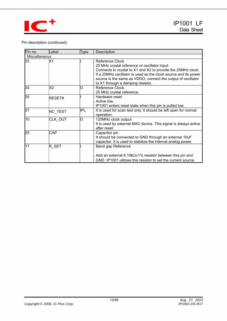
33 X1 I Reference Clock. 25 MHz crystal reference or oscillator input. Connects to crystal to X1 and X2 to provide the 25MHz clock. If a 25MHz oscillator is used as the clock source and its power source is the same as VDDO, connect the output of oscillator to X1 through a damping resistor.
34 X2 O Reference Clock. 25 MHz crystal reference.
35 RESET# I Hardware reset Active low. IP1001 enters reset state when this pin is pulled low.
37 NC_TEST IPL It is used for scan test only. It should be left open for normal operation.
10 CLK_OUT O 125MHz clock output It is used by external MAC device. This signal is always active after reset.
25 CAP Capacitor pin It should be connected to GND through an external 10uF capacitor. It is used to stabilize the internal analog power.
17 R_SET I Band gap Reference Add an external 6.19kΩ±1% resistor between this pin and GND. IP1001 utilizes this resistor to set the current source.
IP1001 LFData Sheet
14/48 Aug. 27, 2010Copyright © 2006, IC Plus Corp. IP1001-DS-R17
Pin description (continued)
Pin no. Label Type Description Power pins
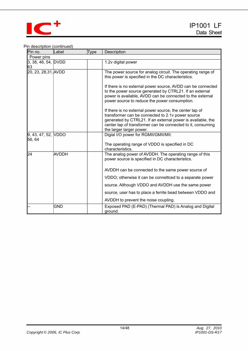
3, 38, 46, 54, 63
DVDD 1.2v digital power
20, 23, 28,31, AVDD The power source for analog circuit. The operating range of this power is specified in the DC characteristics. If there is no external power source, AVDD can be connected to the power source generated by CTRL21. If an external power is available, AVDD can be connected to the external power source to reduce the power consumption. If there is no external power source, the center tap of transformer can be connected to 2.1v power source generated by CTRL21. If an external power is available, the center tap of transformer can be connected to it, consuming the larger larger power.
9, 43, 47, 52, 56, 64
VDDO Digial I/O power for RGMII/GMII/MII. The operating range of VDDO is specified in DC characteristics.
24 AVDDH The analog power of AVDDH. The operating range of this power source is specified in DC characteristics. AVDDH can be connected to the same power source of
VDDO; otherwise it can be connettced to a separate power
source. Although VDDO and AVDDH use the same power
source, user has to place a ferrite bead between VDDO and
AVDDH to prevent the noise coupling. -- GND Exposed PAD (E-PAD) (Thermal PAD) is Analog and Digital
ground.
IP1001 LFData Sheet
15/48 Aug. 27, 2010Copyright © 2006, IC Plus Corp. IP1001-DS-R17
3 Functional Description The IP1001 is an Ethernet transceiver for 1000BASE-T, 100BASE-TX, and 10BASE-T. It uses one pair of UTP wires to transmit data and uses another pair to receive data when working in 100BASE-TX or 10BASE-T. It uses four pairs of UTP wires to transmit and to receive data when working in 1000BASE-T. It supports auto-negotiation, including next page exchanging, speed (1000M, 100M, 10M), duplex (full/ half) mode and master/slave resolution. This device also supports RGMII/ GMII/ MII to interface a MAC device. Registers in the IP1001 can be accessed via the SMI (MDC/MDIO). Three LEDs shows the various statuses of the device. Pair skews in the cables are automatically adjusted. Wiring errors are automatically corrected via pair swapping (automatic MDI/MDIX) and polarity correction.
3.1 Medium Dependent Interface (MDI) for Twisted Pair Cable
The interface between IP1001 and CAT5 cable consists of four signal pairs, channel A, B, C and D, that are used for 1000BASE-T transmission/receiving. Each signal pair consists of two bi-directional pins that transmit and receive data stream at the same time. When the IP1001 operates in 100BASE-TX or 10BASE-T mode, only channel A and B are used, one for transmission and the other for reception. IP1001 will handle the MDIX/MDI crossover issue of the twisted-pair wire automatically. Please refer to section 3.5 Auto MDI/MDIX Crossover for detail.
IP1001 LFData Sheet
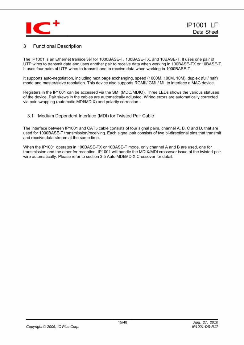
3.2 MAC Interface (RGMII/ GMII/ MII)
IP1001 supports RGMII and GMII/ MII interfaces. User can select the one of the interfaces by configure pin 36 and IP1001 will latch the setting at the end of hardware reset. If pin 36 is connected to GND through a resistor R44, RGMII is selected. If pin 36 is connected to VDDO through a resistor R24, GMII/ MII is selected.
R44 5.1K
GMII/MII interface RGMII interface
16/48 Aug. 27, 2010Copyright © 2006, IC Plus Corp. IP1001-DS-R17
RGMII_N/GMIIR24 5.1K RGMII_N/GMIIVDDO
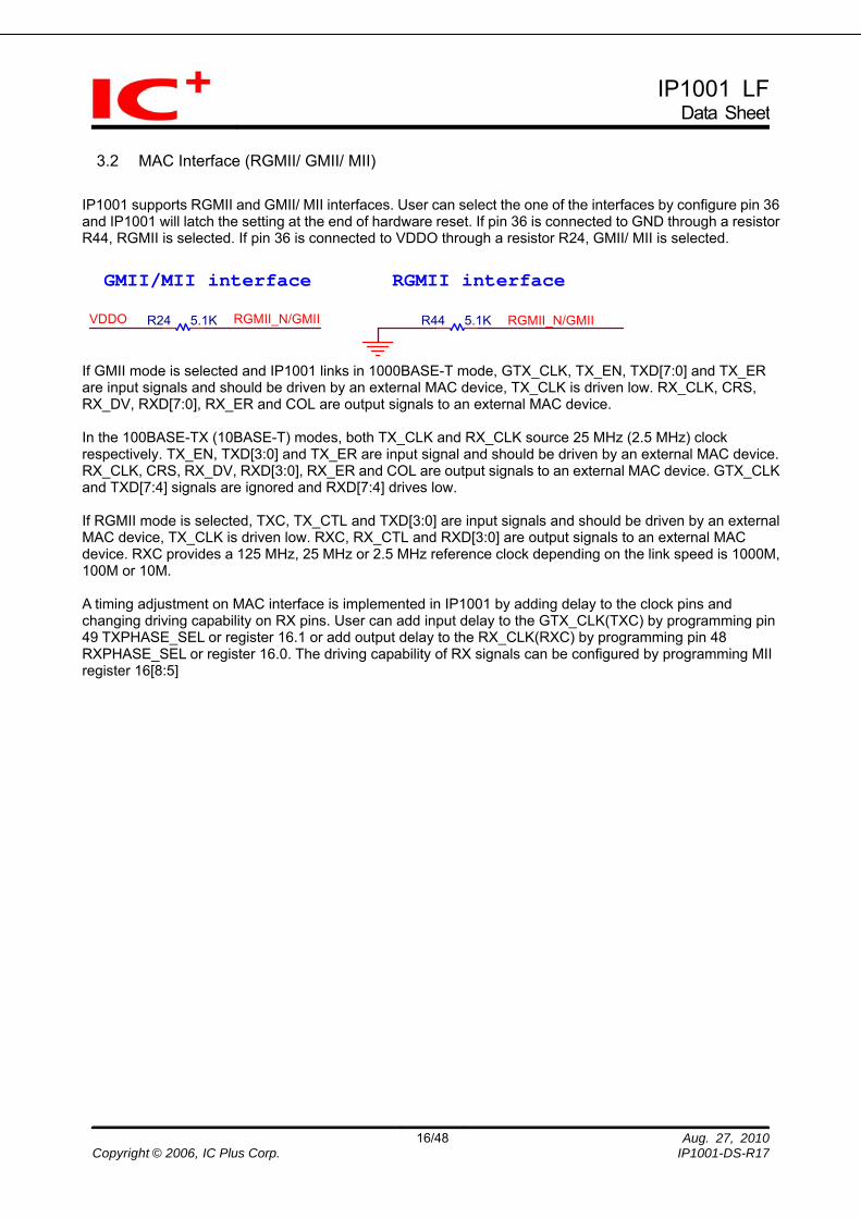
If GMII mode is selected and IP1001 links in 1000BASE-T mode, GTX_CLK, TX_EN, TXD[7:0] and TX_ER are input signals and should be driven by an external MAC device, TX_CLK is driven low. RX_CLK, CRS, RX_DV, RXD[7:0], RX_ER and COL are output signals to an external MAC device. In the 100BASE-TX (10BASE-T) modes, both TX_CLK and RX_CLK source 25 MHz (2.5 MHz) clock respectively. TX_EN, TXD[3:0] and TX_ER are input signal and should be driven by an external MAC device. RX_CLK, CRS, RX_DV, RXD[3:0], RX_ER and COL are output signals to an external MAC device. GTX_CLK and TXD[7:4] signals are ignored and RXD[7:4] drives low. If RGMII mode is selected, TXC, TX_CTL and TXD[3:0] are input signals and should be driven by an external MAC device, TX_CLK is driven low. RXC, RX_CTL and RXD[3:0] are output signals to an external MAC device. RXC provides a 125 MHz, 25 MHz or 2.5 MHz reference clock depending on the link speed is 1000M, 100M or 10M. A timing adjustment on MAC interface is implemented in IP1001 by adding delay to the clock pins and changing driving capability on RX pins. User can add input delay to the GTX_CLK(TXC) by programming pin 49 TXPHASE_SEL or register 16.1 or add output delay to the RX_CLK(RXC) by programming pin 48 RXPHASE_SEL or register 16.0. The driving capability of RX signals can be configured by programming MII register 16[8:5]
IP1001 LFData Sheet
MII/GMII/RGMII selection and signal direction
IP1001 MAC
TXD[3:0]
TX_ER
RXD[3:0]
RX_ER
RXDV/ RXCTL
CRS
COL
RXCTL
TD[3:0]
RXD[3:0]
transformer MDI[3:0]P/M
TXEN/ TXCTL TXCTL
RX_CLK/ RXC RXC
GTX_CLK/ TXC TXC
RGMII is active if pin 36 RGMII_N/GMII is pulled low.
TX_CLK
IP1001 MAC
TXD[3:0]
TX_ER
RXD[3:0]
RX_ER
RXDV/ RXCTL
CRS
COL
RXER
RXDV
CRS
TXD[3:0]
TXER
RXD[3:0]
COL
transformer MDI[3:0]P/M
TXEN/ TXCTL
TX_CLK
TXEN
RX_CLK/ RXC RXCLK
GTX_CLK/ TXC
TXCLK
MII is active if pin 36 RGMII_N/GMII is pulled high and IP1001 islinked at 100M, or 10M.
IP1001 MAC
TXD[7:0]
TX_ER
RXD[7:0]
RX_ER
RXDV/ RXCTL
CRS
COL
RXER
RXDV
CRS
TXD[7:0]
TXER
RXD[7:0]
COL
transformer MDI[3:0]P/M
TXEN/ TXCTL
TX_CLK
TXEN
RX_CLK/ RXC RXCLK
GTX_CLK/ TXC GTX_CLK
GMII is active if pin 36 RGMII_N/GMII is pulled high and IP1001is linked at giga mode.
17/48 Aug. 27, 2010Copyright © 2006, IC Plus Corp. IP1001-DS-R17
IP1001 LFData Sheet
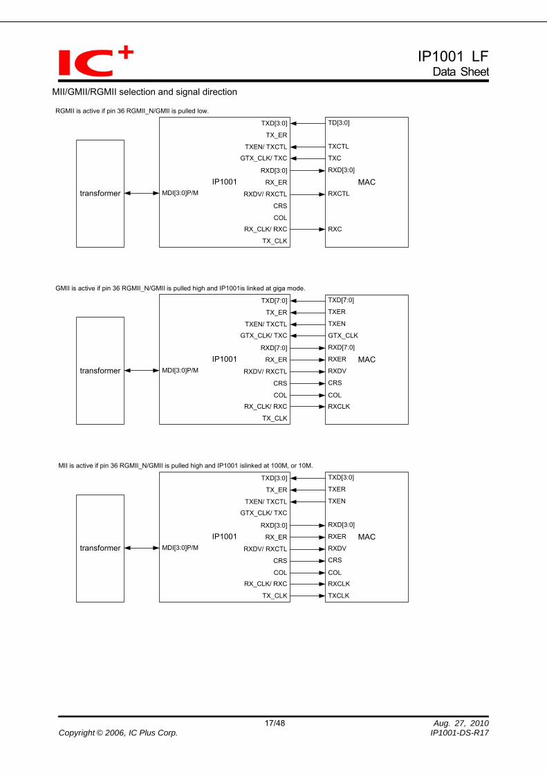
Waveform of RGMII and GMII (MII)
T X C
T X _ C T LG M II's
T X _ E N T X E R R
T X D [3 :0 ] T X D [3 :0 ] T X D [7 :4 ]
R X C
R X _ C T LG M II's
R X _ D V R X E R R
R X D [3 :0 ] R X D [3 :0 ] R X D [7 :4 ]
R G M II
G T X _ C L K
T X _ E N , T X _ E R
T X D [7 :0 ]
R X _ C L K
R X _ D V , R X _ E R
R X D [7 :0 ]
G M II (M II)
(T X _C LK )
(T X D [3 :0 ])
(T X _ E N , T X _ E R )
(R X _C LK )
(R X D [3 :0 ])
(R X _ D V , R X _ E R )
T X E R R = G M II's T X _ E N (X O R ) G M II's T X _ E R
R X E R R = G M II's R X _ D V (X O R ) G M II's R X _ E R
18/48 Aug. 27, 2010Copyright © 2006, IC Plus Corp. IP1001-DS-R17
IP1001 LFData Sheet
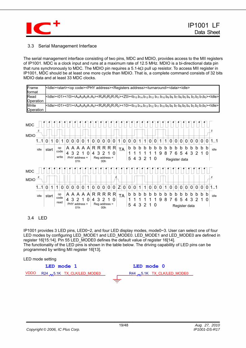
3.3 Serial Management Interface
The serial management interface consisting of two pins, MDC and MDIO, provides access to the MII registers of IP1001. MDC is a clock input and runs at a maximum rate of 12.5 MHz. MDIO is a bi-directional data pin that runs synchronously to MDC. The MDIO pin requires a 5.1-kΩ pull up resistor. To access MII register in IP1001, MDC should be at least one more cycle than MDIO. That is, a complete command consists of 32 bits MDIO data and at least 33 MDC clocks.
Frame format
<Idle><start><op code><PHY address><Registers address><turnaround><data><idle>
Read Operation
<Idle><01><10><A4A3A2A1A0><R4R3R2R1R0><Z0><b15 b14 b13 b12 b11 b10 b9 b8 b7 b6 b5 b4 b3 b2 b1b0><Idle>
Write Operation
<Idle><01><01><A4A3A2A1A0><R4R3R2R1R0><10><b15 b14 b13 b12 b11 b10 b9 b8 b7 b6 b5 b4 b3 b2 b1b0><Idle>
000000001100110001000001000010101..1
idle start opcode
PHY address =01h
Reg address =00h
TA
Register data
b15
b14
b13
b12
b11
b10
b9
b8
b7
b6
b5
b4
b3
b2
b1
b0
idleA4
A3
A2
A1
A0
R4
R3
R2
R1
R0
write
zz
00000000100011000Z00000100000110
idle start opcode
PHY address =01h
Reg address =00h
TA
Register data
b15
b14
b13
b12
b11
b10
b9
b8
b7
b6
b5
b4
b3
b2
b1
b0
idleA4
A3
A2
A1
A0
R4
R3
R2
R1
R0
read
zz z
MDC
MDIO
MDC
MDIO
1..1
1..1
1..1
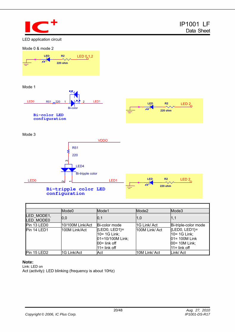
3.4 LED
IP1001 provides 3 LED pins, LED0~2, and four LED display modes, mode0~3. User can select one of four LED modes by configuring LED_MODE1 and LED_MODE0. LED_MODE1 and LED_MODE0 are defined in register 16[15:14]. Pin 55 LED_MODE0 defines the default value of register 16[14]. The functionality of the LED pins is shown in the table below. The driving capability of LED pins can be programmed by writing MII register 16[13]. LED mode setting
R24 5.1K
LED mode 1TX_CLK/LED_MODE0
LED mode 0VDDO TX_CLK/LED_MODE0R44 5.1K
19/48 Aug. 27, 2010Copyright © 2006, IC Plus Corp. IP1001-DS-R17
IP1001 LFData Sheet
LED application circuit Mode 0 & mode 2
R2 220 ohm
LED LED 0,1,2
Mode 1
Bi-color
1 2
Bi-color LEDconfiguration
R2 220 ohm
LED
20/48 Aug. 27, 2010Copyright © 2006, IC Plus Corp. IP1001-DS-R17
LED1LED0 R51 220LED 2
Mode 3
R51
220
LED0
VDDO
3
LED4
Bi-tripple color
LED1
Bi-tripple color LEDconfiguration
2 1
R2 220 ohm
LED LED 2
Mode0 Mode1 Mode2 Mode3 LED_MODE1, LED_MODE0 0,0 0,1 1,0 1,1
Pin 13 LED0 10/100M Link/Act 1G Link/ Act Pin 14 LED1 100M Link/Act
Bi-color mode {LED0, LED1}= 10= 1G Link; 01=10/100M Link; 00= link off 11= link off
100M Link/ Act Bi-triple-color mode {LED0, LED1}= 10= 1G Link; 01= 100M Link 00= 10M Link; 11= link off
Pin 15 LED2 1G Link/Act Act 10M Link/ Act Link/ Act Note: Link: LED on Act (activity): LED blinking (frequency is about 10Hz)
IP1001 LFData Sheet
21/48 Aug. 27, 2010Copyright © 2006, IC Plus Corp. IP1001-DS-R17
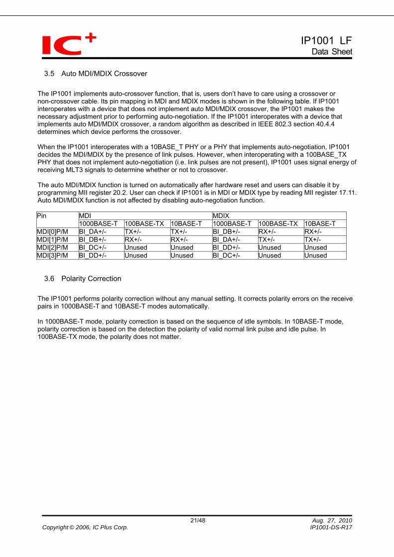
3.5 Auto MDI/MDIX Crossover
The IP1001 implements auto-crossover function, that is, users don’t have to care using a crossover or non-crossover cable. Its pin mapping in MDI and MDIX modes is shown in the following table. If IP1001 interoperates with a device that does not implement auto MDI/MDIX crossover, the IP1001 makes the necessary adjustment prior to performing auto-negotiation. If the IP1001 interoperates with a device that implements auto MDI/MDIX crossover, a random algorithm as described in IEEE 802.3 section 40.4.4 determines which device performs the crossover. When the IP1001 interoperates with a 10BASE_T PHY or a PHY that implements auto-negotiation, IP1001 decides the MDI/MDIX by the presence of link pulses. However, when interoperating with a 100BASE_TX PHY that does not implement auto-negotiation (i.e. link pulses are not present), IP1001 uses signal energy of receiving MLT3 signals to determine whether or not to crossover. The auto MDI/MDIX function is turned on automatically after hardware reset and users can disable it by programming MII register 20.2. User can check if IP1001 is in MDI or MDIX type by reading MII register 17.11. Auto MDI/MDIX function is not affected by disabling auto-negotiation function.
MDI MDIX Pin 1000BASE-T 100BASE-TX 10BASE-T 1000BASE-T 100BASE-TX 10BASE-T
MDI[0]P/M BI_DA+/- TX+/- TX+/- BI_DB+/- RX+/- RX+/- MDI[1]P/M BI_DB+/- RX+/- RX+/- BI_DA+/- TX+/- TX+/- MDI[2]P/M BI_DC+/- Unused Unused BI_DD+/- Unused Unused MDI[3]P/M BI_DD+/- Unused Unused BI_DC+/- Unused Unused
3.6 Polarity Correction
The IP1001 performs polarity correction without any manual setting. It corrects polarity errors on the receive pairs in 1000BASE-T and 10BASE-T modes automatically. In 1000BASE-T mode, polarity correction is based on the sequence of idle symbols. In 10BASE-T mode, polarity correction is based on the detection the polarity of valid normal link pulse and idle pulse. In 100BASE-TX mode, the polarity does not matter.

IP1001 LFData Sheet
22/48 Aug. 27, 2010Copyright © 2006, IC Plus Corp. IP1001-DS-R17
3.7 Auto-Negotiation
IP1001 will performs Auto-Negotiation automatically if one of the following conditions happened: 1) Power up reset, hardware reset, or software reset (by programming MII register 0.15). 2) Restart Auto-Negotiation (by programming MII register 0.9). 3) Transition from power down to power up (by programming MII register 0.11). 4) Link is down. Once Auto-Negotiation is initiated, IP1001 sends out the appropriate base pages/ next pages to advertise its capability and negotiate with the link partner to determine speed, duplex, and master/slave. Note that IP1001 handles the base page/ next page exchanges automatically without user intervention. To link at Giga mode, the link partner of IP1001 has to support Auto-Negotiation, too. Once IP1001 completes Auto-Negotiation it updates the statuses in registers 1, 5, 6, 10 and 17. The advertised abilities can be changed by writing registers 4 and 9. It is noted that a write access to register 4 or 9 has no effect once the IP1001 begins transmitting Fast Link Pulses (FLPs). This guarantees that the transmitted FLPs are consistent. Register 7 is treated in a similar way as registers 4 and 9 during additional next page exchanges. If the link partner doesn’t support Auto-Negotiation, IP1001 determines the link speed using parallel detection and the link result is either 10M half duplex or 100M half duplex. Please refer to IEEE 802.3 clause 28 and 40 for more detailed description of Auto-Negotiation. Auto-Negotiation can be disabled by programming register 0.12. When Auto-Negotiation is disabled, the speed and duplex of IP1001 can be changed by programming registers 0.13, 0.6 and 0.8, respectively.
IP1001 LFData Sheet
3.8 Smart speed
IP1001 supports smart speed function. If IP1001 can’t link at Gigabit speed due to cable quality, the link speed is down shift to 100M automatically if smart speed option is turned on. If the function is turned off, IP1001 will link down if it can’t link at Giga mode due to cable quality. The function is default on and it can be enabled/disabled by programming MII register 16.11.
3.9 Power supply
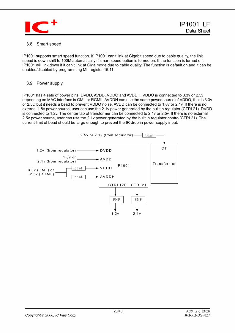
IP1001 has 4 sets of power pins, DVDD, AVDD, VDDO and AVDDH. VDDO is connected to 3.3v or 2.5v depending on MAC interface is GMII or RGMII. AVDDH can use the same power source of VDDO, that is 3.3v or 2.5v, but it needs a bead to prevent VDDO noise. AVDD can be connected to 1.8v or 2.1v. If there is no external 1.8v power source, user can use the 2.1v power generated by the built in regulator (CTRL21). DVDD is connected to 1.2v. The center tap of transformer can be connected to 2.1v or 2.5v. If there is no external 2.5v power source, user can use the 2.1v power generated by the built in regulator control(CTRL21). The current limit of bead should be large enough to prevent the IR drop in power supply input.
IP 10 01
D V D D
A V D D
V D D O
A V D D H
1 .2 v (from reg u la to r)
1 .8v o r2 .1v (from reg u la to r)
3 .3v (G M II) o r2 .5v (R G M II)
bead
bead
T ra ns fo rm er
C T
2 .5 v o r 2 .1 v (fro m re gu la to r)
C T R L1 2D C T R L 21
PN P PN P
1 .2v 2 .1 v
bead
23/48 Aug. 27, 2010Copyright © 2006, IC Plus Corp. IP1001-DS-R17
IP1001 LFData Sheet
24/48 Aug. 27, 2010Copyright © 2006, IC Plus Corp. IP1001-DS-R17
3.10 Digital Internal Function
The IP1001 integrates all necessary function blocks to achieve the communication ability over CAT5 unshielded twisted pair cables. These function blocks include analog blocks and digital blocks. Analog function blocks includes analog to digital converter (ADC), digital to analog converter (DAC), active hybrid, and high-speed 1.25GHz transmitter/receiver. Digital function blocks include digital adaptive feed-forward equalizer (FFE), decision-feedback equalizer (DFE), echo canceller (EC), near-end-cross-talk canceller, baseline wander canceller, and digital phase lock-loop (DPLL). Some other encoding/decoding blocks are also necessary in the transmission/receiving data path.
3.11 IEEE802.3 1000BASE_T Test mode
IP1001 supports four test modes for 1000BASE_T defined in IEEE802.3 clause 40.6. User can force IP1001 to be in test mode to characterize its waveform, jitter, and distortion by programming MII register 9[15:13].
3.12 Auto Power Saving (APS)
IP1001 provides the auto power saving mode to minimize the power consumption during the link down state. This function is enabled by reset default and can be configured by register 20.11. When set to APS mode, IP1001 will transmit link pulse every 50ms. When set to normal operating mode, IP1001 will transmit link pulse based on IEEE802.3 standard, i.e, a burst of Fast Link Pulse every 16ms. Since the power consumption is proportional to the number of the transmitted link pulse, it is recommended that the designer keeps APS enabled to minimize the power consumption during link down state.
IP1001 LFData Sheet
25/48 Aug. 27, 2010Copyright © 2006, IC Plus Corp. IP1001-DS-R17
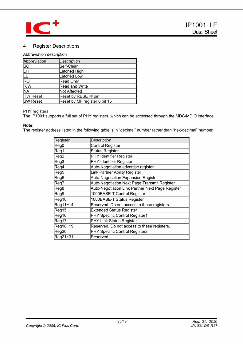
4 Register Descriptions Abbreviation description Abbreviation Description SC Self-Clear LH Latched High LL Latched Low RO Read Only R/W Read and Write NA Not Affected HW Reset Reset by RESET# pin SW Reset Reset by MII register 0 bit 15 PHY registers The IP1001 supports a full set of PHY registers, which can be accessed through the MDC/MDIO interface. Note: The register address listed in the following table is in “decimal” number rather than “hex-decimal” number.
Register Description Reg0 Control Register Reg1 Status Register Reg2 PHY Identifier Register Reg3 PHY Identifier Register Reg4 Auto-Negotiation advertise register Reg5 Link Partner Ability Register Reg6 Auto-Negotiation Expansion Register Reg7 Auto-Negotiation Next Page Transmit Register Reg8 Auto-Negotiation Link Partner Next Page Register Reg9 1000BASE-T Control Register Reg10 1000BASE-T Status Register Reg11~14 Reserved. Do not access to these registers. Reg15 Extended Status Register Reg16 PHY Specific Control Register1 Reg17 PHY Link Status Register Reg18~19 Reserved. Do not access to these registers. Reg20 PHY Specific Control Register2 Reg21~31 Reserved
IP1001 LFData Sheet
26/48 Aug. 27, 2010Copyright © 2006, IC Plus Corp. IP1001-DS-R17
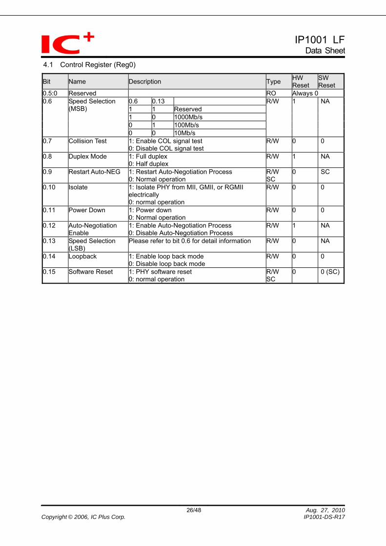
4.1 Control Register (Reg0)
Bit Name Description Type HW Reset
SW Reset
0.5:0 Reserved RO Always 0 0.6 0.13 1 1 Reserved 1 0 1000Mb/s 0 1 100Mb/s
0.6 Speed Selection (MSB)
0 0 10Mb/s
R/W 1 NA
0.7 Collision Test 1: Enable COL signal test 0: Disable COL signal test
R/W 0 0
0.8 Duplex Mode 1: Full duplex 0: Half duplex
R/W 1 NA
0.9 Restart Auto-NEG 1: Restart Auto-Negotiation Process 0: Normal operation
R/W SC
0 SC
0.10 Isolate 1: Isolate PHY from MII, GMII, or RGMII electrically 0: normal operation
R/W 0 0
0.11 Power Down 1: Power down 0: Normal operation
R/W 0 0
0.12 Auto-Negotiation Enable
1: Enable Auto-Negotiation Process 0: Disable Auto-Negotiation Process
R/W 1 NA
0.13 Speed Selection (LSB)
Please refer to bit 0.6 for detail information R/W 0 NA
0.14 Loopback 1: Enable loop back mode 0: Disable loop back mode
R/W 0 0
0.15 Software Reset 1: PHY software reset 0: normal operation
R/W SC
0 0 (SC)
IP1001 LFData Sheet
27/48 Aug. 27, 2010Copyright © 2006, IC Plus Corp. IP1001-DS-R17
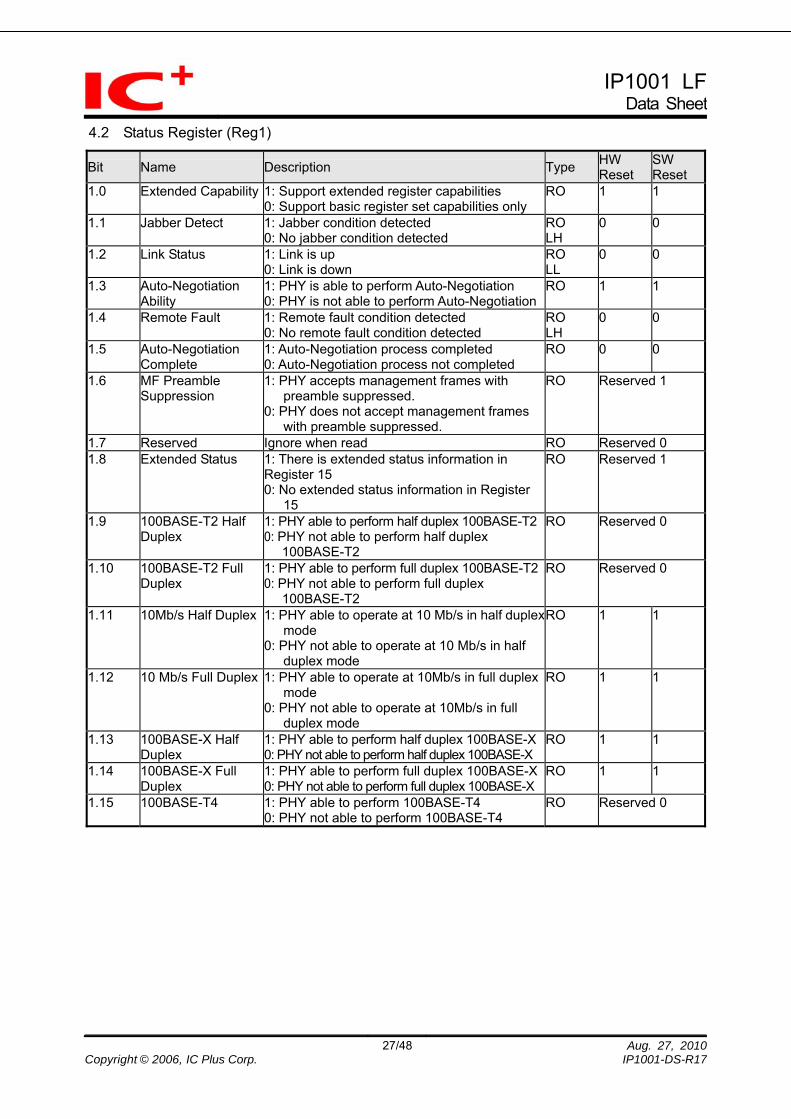
4.2 Status Register (Reg1)
Bit Name Description Type HW Reset
SW Reset
1.0 Extended Capability 1: Support extended register capabilities 0: Support basic register set capabilities only
RO 1 1
1.1 Jabber Detect 1: Jabber condition detected 0: No jabber condition detected
RO LH
0 0
1.2 Link Status 1: Link is up 0: Link is down
RO LL
0 0
1.3 Auto-Negotiation Ability
1: PHY is able to perform Auto-Negotiation 0: PHY is not able to perform Auto-Negotiation
RO 1 1
1.4 Remote Fault 1: Remote fault condition detected 0: No remote fault condition detected
RO LH
0 0
1.5 Auto-Negotiation Complete
1: Auto-Negotiation process completed 0: Auto-Negotiation process not completed
RO 0 0
1.6 MF Preamble Suppression
1: PHY accepts management frames with preamble suppressed.
0: PHY does not accept management frames with preamble suppressed.
RO Reserved 1
1.7 Reserved Ignore when read RO Reserved 0 1.8 Extended Status 1: There is extended status information in
Register 15 0: No extended status information in Register
15
RO Reserved 1
1.9 100BASE-T2 Half Duplex
1: PHY able to perform half duplex 100BASE-T20: PHY not able to perform half duplex
100BASE-T2
RO Reserved 0
1.10 100BASE-T2 Full Duplex
1: PHY able to perform full duplex 100BASE-T20: PHY not able to perform full duplex
100BASE-T2
RO Reserved 0
1.11 10Mb/s Half Duplex 1: PHY able to operate at 10 Mb/s in half duplexmode
0: PHY not able to operate at 10 Mb/s in half duplex mode
RO 1 1
1.12 10 Mb/s Full Duplex 1: PHY able to operate at 10Mb/s in full duplex mode
0: PHY not able to operate at 10Mb/s in full duplex mode
RO 1 1
1.13 100BASE-X Half Duplex
1: PHY able to perform half duplex 100BASE-X0: PHY not able to perform half duplex 100BASE-X
RO 1 1
1.14 100BASE-X Full Duplex
1: PHY able to perform full duplex 100BASE-X0: PHY not able to perform full duplex 100BASE-X
RO 1 1
1.15 100BASE-T4 1: PHY able to perform 100BASE-T4 0: PHY not able to perform 100BASE-T4
RO Reserved 0
IP1001 LFData Sheet
28/48 Aug. 27, 2010Copyright © 2006, IC Plus Corp. IP1001-DS-R17
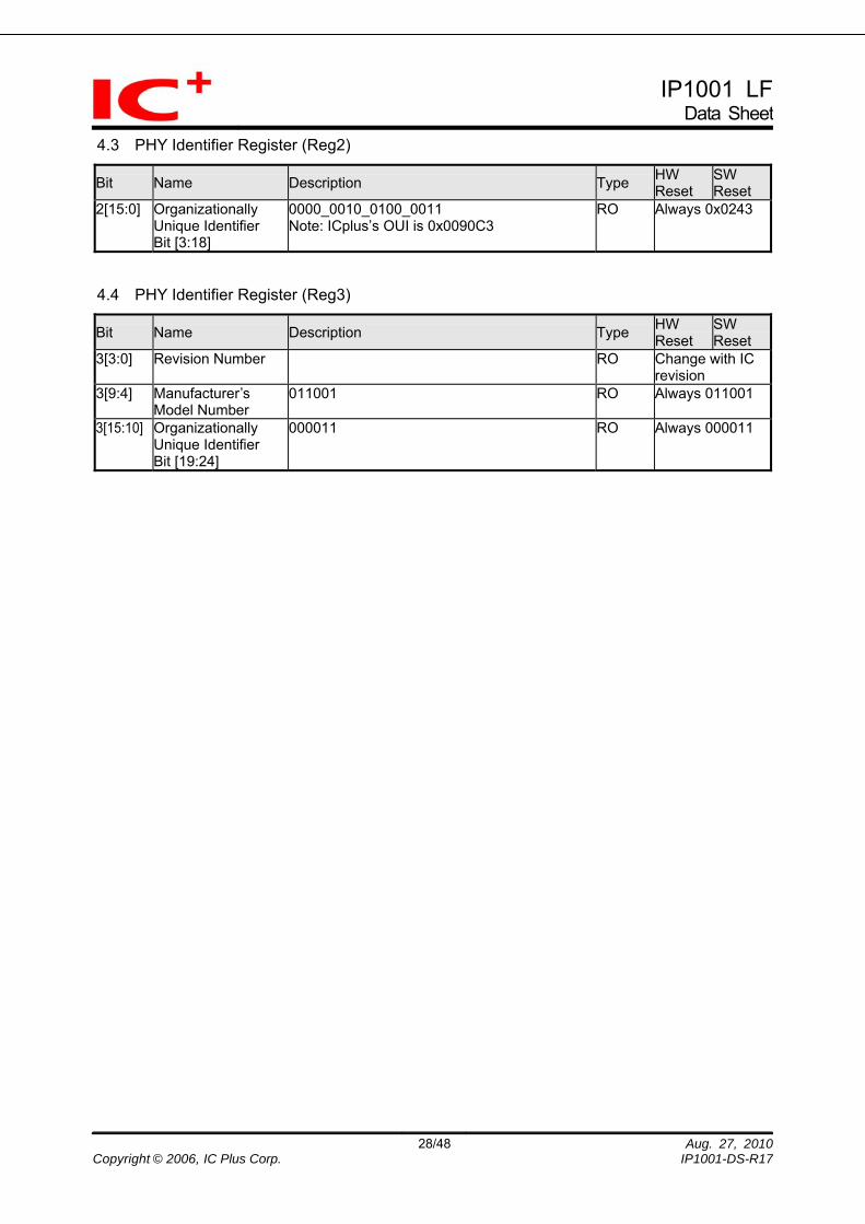
4.3 PHY Identifier Register (Reg2)
Bit Name Description Type HW Reset
SW Reset
2[15:0] Organizationally Unique Identifier Bit [3:18]
0000_0010_0100_0011 Note: ICplus’s OUI is 0x0090C3
RO Always 0x0243
4.4 PHY Identifier Register (Reg3)
Bit Name Description Type HW Reset
SW Reset
3[3:0] Revision Number RO Change with IC revision
3[9:4] Manufacturer’s Model Number
011001 RO Always 011001
3[15:10] Organizationally Unique Identifier Bit [19:24]
000011 RO Always 000011

IP1001 LFData Sheet
29/48 Aug. 27, 2010Copyright © 2006, IC Plus Corp. IP1001-DS-R17
4.5 Advertisement Register (Reg4)
Bit Name Description Type HW Reset
SW Reset
4[4:0] Selector Filed Only CSMA/CD <00001> is specified. No other
protocols are supported.
RO 00001 00001
4.5 10BASE-T Half Duplex
1 = 10Base-T full duplex is supported 0 = 10Base-T full duplex not supported
R/W 1 1
4.6 10BASE-T Full Duplex
1 = 10Base-T half duplex is supported 0 = 10Base-T half duplex not supported
R/W 1 1
4.7 100BASE-TX Half Duplex
1 = 100Base-TX half duplex is supported 0 = 100Base-TX half duplex not supported
R/W 1 1
4.8 100BASE-TX Full Duplex
1 = 100Base-TX full duplex is supported
0 = 100Base-TX full duplex not supported
R/W 1 1
4.9 100BASE-T4 1 = 100Base-T4 is supported 0 = 100Base-T4 not supported
RO Reserved 0
4.10 PAUSE 1 = flow control is supported 0 = flow control is not supported
R/W 0
4.11 Asymmetric Pause 1 = asymmetric flow control is supported 0 = asymmetric flow control is not supported
R/W 0
4.12 Reserved Ignore when read R/W 0 0 4.13 Remote Fault 1 = Advertise remote fault detection capability
0 = Not advertise remote fault detection
capability
R/W 0
4.14 Reserved Ignore when read RO Reserved 0 4.15 Next Page 1 = Next pages are supported
0 = Next pages are not supported
R/W 1
IP1001 LFData Sheet
30/48 Aug. 27, 2010Copyright © 2006, IC Plus Corp. IP1001-DS-R17
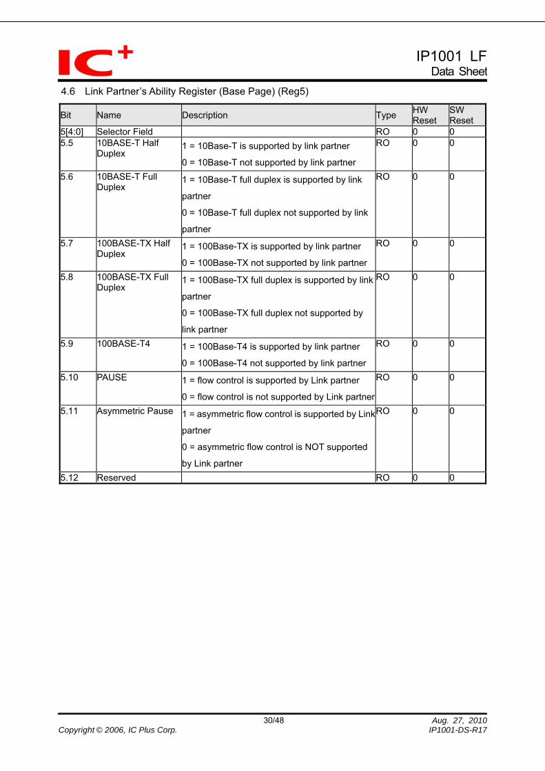
4.6 Link Partner’s Ability Register (Base Page) (Reg5)
Bit Name Description Type HW Reset
SW Reset
5[4:0] Selector Field RO 0 0 5.5 10BASE-T Half
Duplex 1 = 10Base-T is supported by link partner
0 = 10Base-T not supported by link partner
RO 0 0
5.6 10BASE-T Full Duplex
1 = 10Base-T full duplex is supported by link
partner
0 = 10Base-T full duplex not supported by link
partner
RO 0 0
5.7 100BASE-TX Half Duplex
1 = 100Base-TX is supported by link partner
0 = 100Base-TX not supported by link partner
RO 0 0
5.8 100BASE-TX Full Duplex
1 = 100Base-TX full duplex is supported by link
partner
0 = 100Base-TX full duplex not supported by
link partner
RO 0 0
5.9 100BASE-T4 1 = 100Base-T4 is supported by link partner
0 = 100Base-T4 not supported by link partner
RO 0 0
5.10 PAUSE 1 = flow control is supported by Link partner
0 = flow control is not supported by Link partner
RO 0 0
5.11 Asymmetric Pause 1 = asymmetric flow control is supported by Link
partner
0 = asymmetric flow control is NOT supported
by Link partner
RO 0 0
5.12 Reserved RO 0 0
IP1001 LFData Sheet
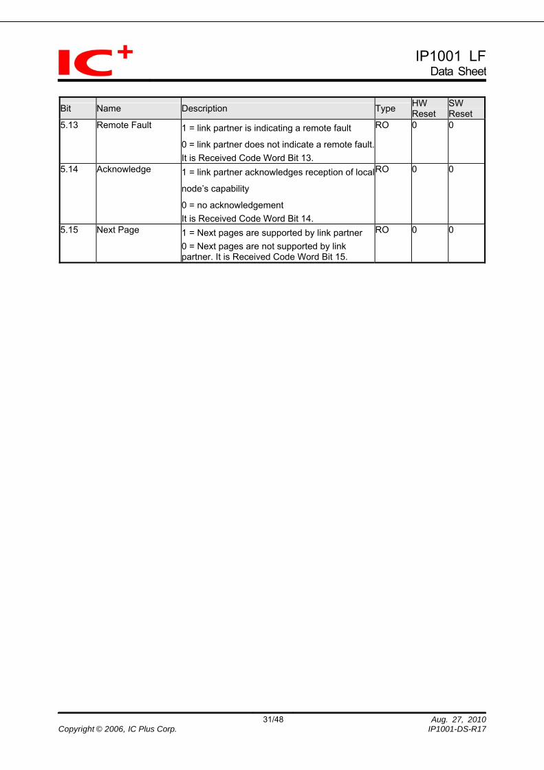
31/48 Aug. 27, 2010Copyright © 2006, IC Plus Corp. IP1001-DS-R17
Bit Name Description Type HW Reset
SW Reset
5.13 Remote Fault 1 = link partner is indicating a remote fault
0 = link partner does not indicate a remote fault.It is Received Code Word Bit 13.
RO 0 0
5.14 Acknowledge 1 = link partner acknowledges reception of local
node’s capability
RO
0 = no acknowledgement It is Received Code Word Bit 14.
0 0
5.15 Next Page 1 = Next pages are supported by link partner 0 = Next pages are not supported by link partner. It is Received Code Word Bit 15.
RO 0 0
IP1001 LFData Sheet
32/48 Aug. 27, 2010Copyright © 2006, IC Plus Corp. IP1001-DS-R17
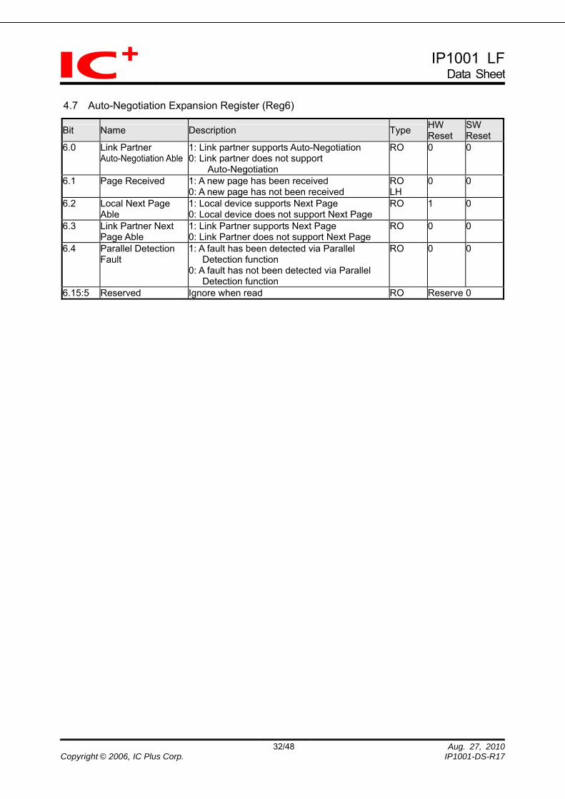
4.7 Auto-Negotiation Expansion Register (Reg6)
Bit Name Description Type HW Reset
SW Reset
6.0 Link Partner Auto-Negotiation Able
1: Link partner supports Auto-Negotiation 0: Link partner does not support
Auto-Negotiation
RO 0 0
6.1 Page Received 1: A new page has been received 0: A new page has not been received
RO LH
0 0
6.2 Local Next Page Able
1: Local device supports Next Page 0: Local device does not support Next Page
RO 1 0
6.3 Link Partner Next Page Able
1: Link Partner supports Next Page 0: Link Partner does not support Next Page
RO 0 0
6.4 Parallel Detection Fault
1: A fault has been detected via Parallel Detection function
0: A fault has not been detected via Parallel Detection function
RO 0 0
6.15:5 Reserved Ignore when read RO Reserve 0
IP1001 LFData Sheet
33/48 Aug. 27, 2010Copyright © 2006, IC Plus Corp. IP1001-DS-R17
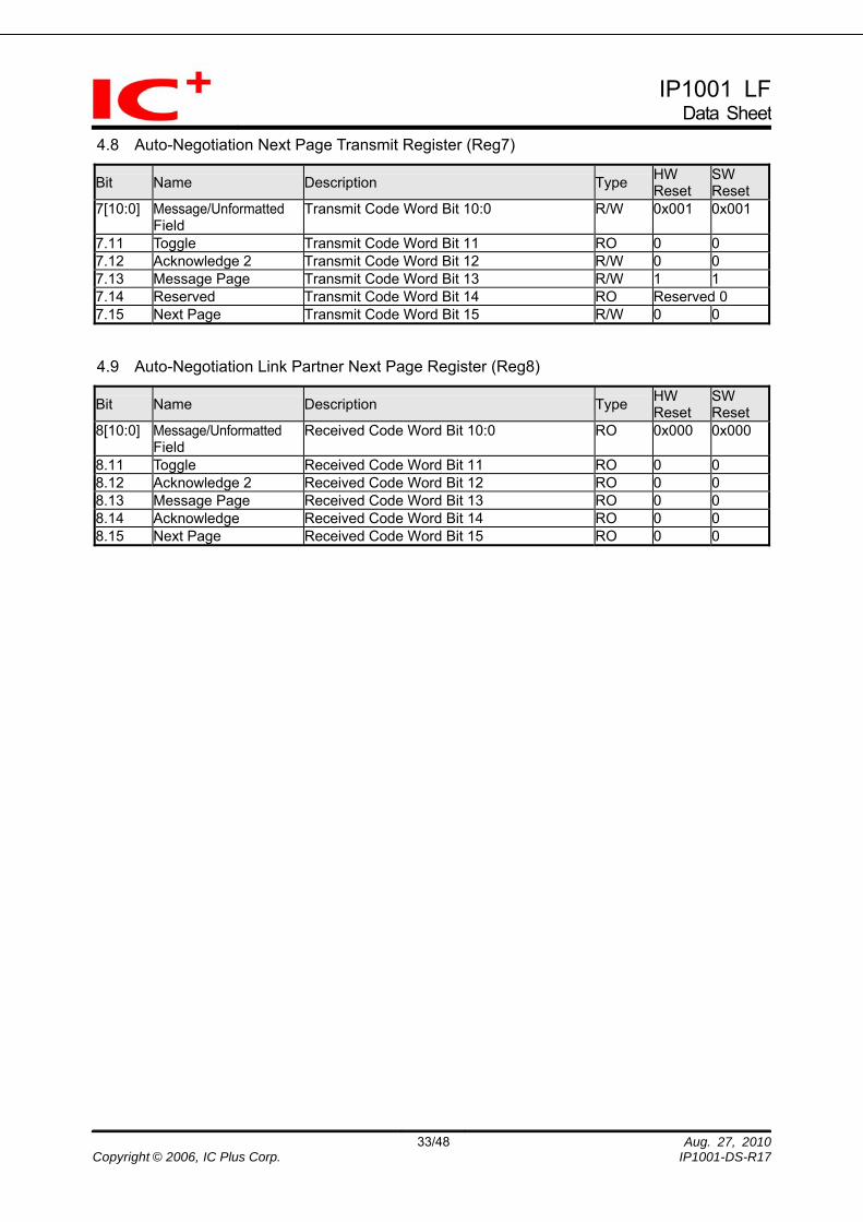
4.8 Auto-Negotiation Next Page Transmit Register (Reg7)
Bit Name Description Type HW Reset
SW Reset
7[10:0] Message/Unformatted Field
Transmit Code Word Bit 10:0 R/W 0x001 0x001
7.11 Toggle Transmit Code Word Bit 11 RO 0 0 7.12 Acknowledge 2 Transmit Code Word Bit 12 R/W 0 0 7.13 Message Page Transmit Code Word Bit 13 R/W 1 1 7.14 Reserved Transmit Code Word Bit 14 RO Reserved 0 7.15 Next Page Transmit Code Word Bit 15 R/W 0 0
4.9 Auto-Negotiation Link Partner Next Page Register (Reg8)
Bit Name Description Type HW Reset
SW Reset
8[10:0] Message/Unformatted Field
Received Code Word Bit 10:0 RO 0x000 0x000
8.11 Toggle Received Code Word Bit 11 RO 0 0 8.12 Acknowledge 2 Received Code Word Bit 12 RO 0 0 8.13 Message Page Received Code Word Bit 13 RO 0 0 8.14 Acknowledge Received Code Word Bit 14 RO 0 0 8.15 Next Page Received Code Word Bit 15 RO 0 0
IP1001 LFData Sheet
34/48 Aug. 27, 2010Copyright © 2006, IC Plus Corp. IP1001-DS-R17
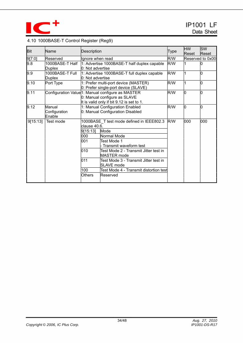
4.10 1000BASE-T Control Register (Reg9)
Bit Name Description Type HW Reset
SW Reset
9[7:0] Reserved Ignore when read R/W Reserved to 0x009.8 1000BASE-T Half
Duplex 1: Advertise 1000BASE-T half duplex capable0: Not advertise
R/W 1 0
9.9 1000BASE-T Full Duplex
1: Advertise 1000BASE-T full duplex capable 0: Not advertise
R/W 1 0
9.10 Port Type 1: Prefer multi-port device (MASTER) 0: Prefer single-port device (SLAVE)
R/W 1 0
9.11 Configuration Value 1: Manual configure as MASTER 0: Manual configure as SLAVE It is valid only if bit 9.12 is set to 1.
R/W 0 0
9.12 Manual Configuration Enable
1: Manual Configuration Enabled 0: Manual Configuration Disabled
R/W 0 0
1000BASE_T test mode defined in IEEE802.3 clause 40.6. 9[15:13] Mode 000 Normal Mode 001 Test Mode 1
- Transmit waveform test 010 Test Mode 2 - Transmit Jitter test in
MASTER mode 011 Test Mode 3 - Transmit Jitter test in
SLAVE mode 100 Test Mode 4 - Transmit distortion test
9[15:13] Test mode
Others Reserved
R/W 000 000
IP1001 LFData Sheet
35/48 Aug. 27, 2010Copyright © 2006, IC Plus Corp. IP1001-DS-R17
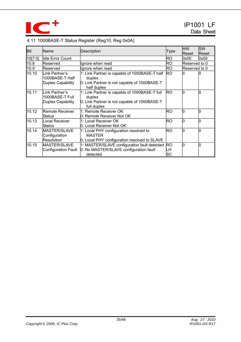
4.11 1000BASE-T Status Register (Reg10, Reg 0x0A)
Bit Name Description Type HW Reset
SW Reset
10[7:0] Idle Error Count RO 0x00 0x00 10.8 Reserved Ignore when read RO Reserved to 0 10.9 Reserved Ignore when read RO Reserved to 0 10.10 Link Partner’s
1000BASE-T Half Duplex Capability
1: Link Partner is capable of 1000BASE-T half duplex
0: Link Partner is not capable of 1000BASE-T half duplex
RO 0 0
10.11 Link Partner’s 1000BASE-T Full Duplex Capability
1: Link Partner is capable of 1000BASE-T full duplex
0: Link Partner is not capable of 1000BASE-T full duplex
RO 0 0
10.12 Remote Receiver Status
1: Remote Receiver OK 0: Remote Receiver Not OK
RO 0 0
10.13 Local Receiver Status
1: Local Receiver OK 0: Local Receiver Not OK
RO 0 0
10.14 MASTER/SLAVE Configuration Resolution
1: Local PHY configuration resolved to MASTER
0: Local PHY configuration resolved to SLAVE
RO 0 0
10.15 MASTER/SLAVE Configuration Fault
1: MASTER/SLAVE configuration fault detected0: No MASTER/SLAVE configuration fault
detected
RO LH SC
0 0
IP1001 LFData Sheet
36/48 Aug. 27, 2010Copyright © 2006, IC Plus Corp. IP1001-DS-R17
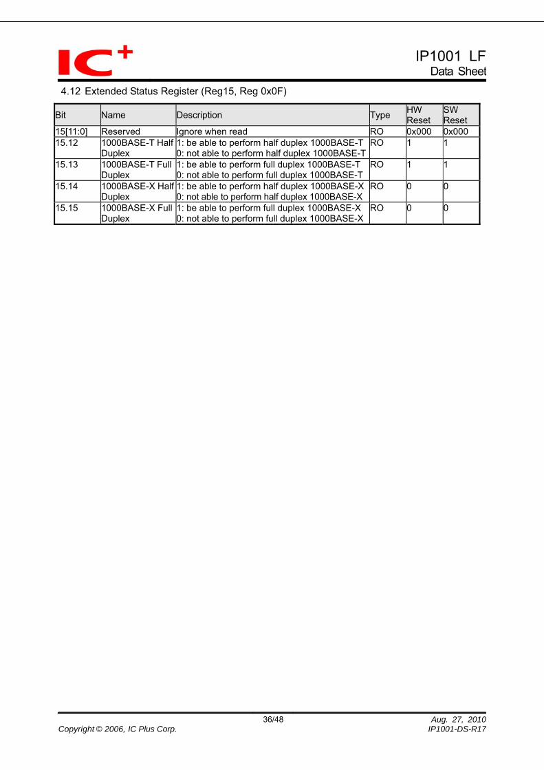
4.12 Extended Status Register (Reg15, Reg 0x0F)
Bit Name Description Type HW Reset
SW Reset
15[11:0] Reserved Ignore when read RO 0x000 0x000 15.12 1000BASE-T Half
Duplex 1: be able to perform half duplex 1000BASE-T0: not able to perform half duplex 1000BASE-T
RO 1 1
15.13 1000BASE-T Full Duplex
1: be able to perform full duplex 1000BASE-T 0: not able to perform full duplex 1000BASE-T
RO 1 1
15.14 1000BASE-X Half Duplex
1: be able to perform half duplex 1000BASE-X0: not able to perform half duplex 1000BASE-X
RO 0 0
15.15 1000BASE-X Full Duplex
1: be able to perform full duplex 1000BASE-X 0: not able to perform full duplex 1000BASE-X
RO 0 0
IP1001 LFData Sheet
37/48 Aug. 27, 2010Copyright © 2006, IC Plus Corp. IP1001-DS-R17
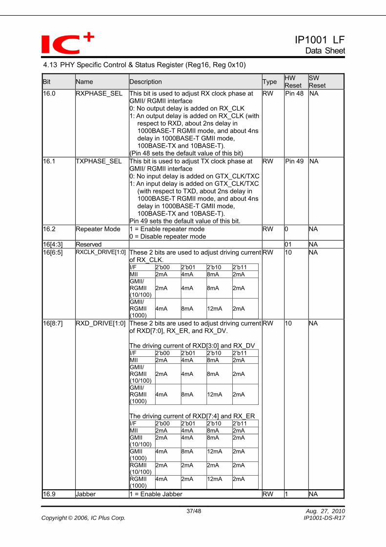
4.13 PHY Specific Control & Status Register (Reg16, Reg 0x10)
Bit Name Description Type HW Reset
SW Reset
16.0 RXPHASE_SEL This bit is used to adjust RX clock phase at GMII/ RGMII interface 0: No output delay is added on RX_CLK 1: An output delay is added on RX_CLK (with
respect to RXD, about 2ns delay in 1000BASE-T RGMII mode, and about 4ns delay in 1000BASE-T GMII mode, 100BASE-TX and 10BASE-T).
(Pin 48 sets the default value of this bit)
RW Pin 48 NA
16.1 TXPHASE_SEL This bit is used to adjust TX clock phase at GMII/ RGMII interface 0: No input delay is added on GTX_CLK/TXC1: An input delay is added on GTX_CLK/TXC
(with respect to TXD, about 2ns delay in 1000BASE-T RGMII mode, and about 4ns delay in 1000BASE-T GMII mode, 100BASE-TX and 10BASE-T).
Pin 49 sets the default value of this bit.
RW Pin 49 NA
16.2 Repeater Mode 1 = Enable repeater mode 0 = Disable repeater mode
RW 0 NA
16[4:3] Reserved 01 NA 16[6:5] RXCLK_DRIVE[1:0] These 2 bits are used to adjust driving current
of RX_CLK. I/F 2’b00 2’b01 2’b10 2’b11 MII 2mA 4mA 8mA 2mA GMII/ RGMII (10/100)
2mA
4mA
8mA
2mA
GMII/ RGMII (1000)
4mA
8mA
12mA
2mA
RW 10 NA
16[8:7] RXD_DRIVE[1:0] These 2 bits are used to adjust driving current of RXD[7:0], RX_ER, and RX_DV. The driving current of RXD[3:0] and RX_DV I/F 2’b00 2’b01 2’b10 2’b11 MII 2mA 4mA 8mA 2mA GMII/ RGMII (10/100)
2mA
4mA
8mA
2mA
GMII/ RGMII (1000)
4mA
8mA
12mA
2mA
The driving current of RXD[7:4] and RX_ER I/F 2’b00 2’b01 2’b10 2’b11 MII 2mA 4mA 8mA 2mA GMII (10/100)
2mA 4mA 8mA 2mA
GMII (1000)
4mA 8mA 12mA 2mA
RGMII (10/100)
2mA 2mA 2mA 2mA
RGMII (1000)
4mA 2mA 12mA 2mA
RW 10 NA
16.9 Jabber 1 = Enable Jabber RW 1 NA
IP1001 LFData Sheet
38/48 Aug. 27, 2010Copyright © 2006, IC Plus Corp. IP1001-DS-R17
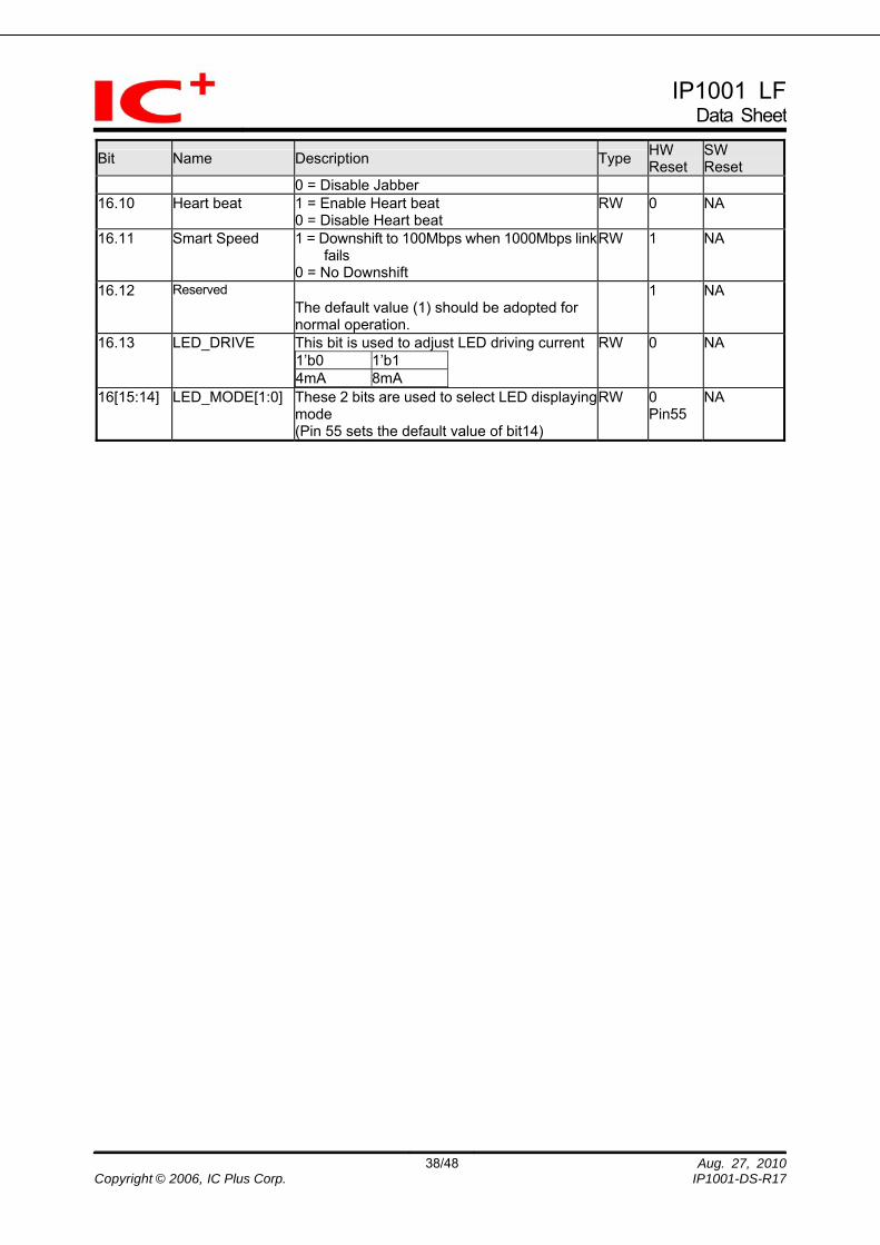
Bit Name Description Type HW Reset
SW Reset
0 = Disable Jabber 16.10 Heart beat 1 = Enable Heart beat
0 = Disable Heart beat RW 0 NA
16.11 Smart Speed 1 = Downshift to 100Mbps when 1000Mbps linkfails
RW
0 = No Downshift
1 NA
16.12 Reserved
The default value (1) should be adopted for normal operation.
1 NA
16.13 LED_DRIVE This bit is used to adjust LED driving current1’b0 1’b1 4mA 8mA
RW 0 NA
16[15:14] LED_MODE[1:0] These 2 bits are used to select LED displayingmode
RW
(Pin 55 sets the default value of bit14)
0 Pin55
NA
IP1001 LFData Sheet
39/48 Aug. 27, 2010Copyright © 2006, IC Plus Corp. IP1001-DS-R17
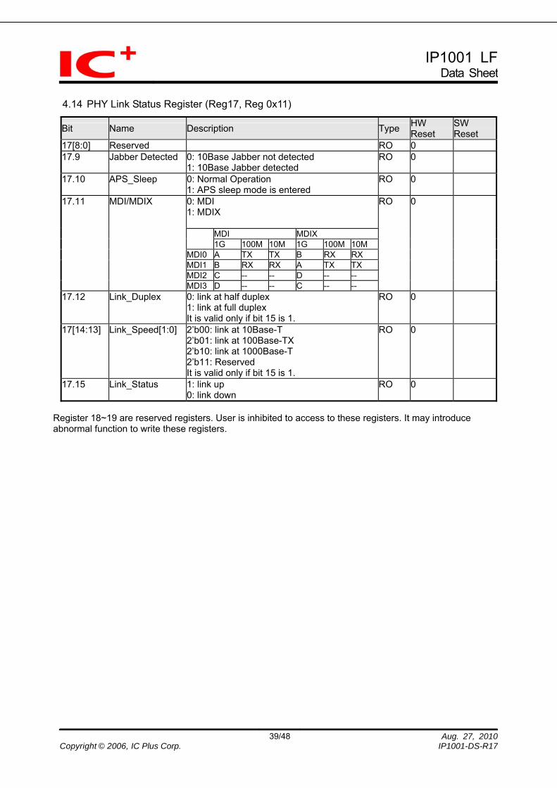
4.14 PHY Link Status Register (Reg17, Reg 0x11)
Bit Name Description Type HW Reset
SW Reset
17[8:0] Reserved RO 0 17.9 Jabber Detected 0: 10Base Jabber not detected
1: 10Base Jabber detected RO 0
17.10 APS_Sleep 0: Normal Operation 1: APS sleep mode is entered
RO 0
0: MDI 1: MDIX
MDI MDIX 1G 100M 10M 1G 100M 10M
MDI0 A TX TX B RX RX MDI1 B RX RX A TX TX MDI2 C -- -- D -- --
17.11 MDI/MDIX
MDI3 D -- -- C -- --
RO 0
17.12 Link_Duplex 0: link at half duplex 1: link at full duplex It is valid only if bit 15 is 1.
RO 0
17[14:13] Link_Speed[1:0] 2’b00: link at 10Base-T 2’b01: link at 100Base-TX 2’b10: link at 1000Base-T 2’b11: Reserved It is valid only if bit 15 is 1.
RO 0
17.15 Link_Status 1: link up 0: link down
RO 0
Register 18~19 are reserved registers. User is inhibited to access to these registers. It may introduce abnormal function to write these registers.
IP1001 LFData Sheet
40/48 Aug. 27, 2010Copyright © 2006, IC Plus Corp. IP1001-DS-R17
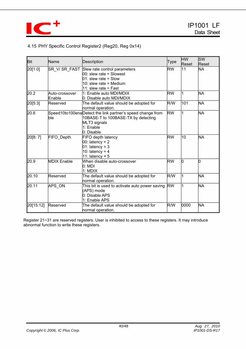
4.15 PHY Specific Control Register2 (Reg20, Reg 0x14)
Bit Name Description Type HW Reset
SW Reset
20[1:0] SR_V/ SR_FAST Slew rate control parameters 00: slew rate = Slowest 01: slew rate = Slow 10: slew rate = Medium 11: slew rate = Fast
RW 11 NA
20.2 Auto-crossover Enable
1: Enable auto MDI/MDIX 0: Disable auto MDI/MDIX
RW 1 NA
20[5:3] Reserved The default value should be adopted for normal operation.
R/W 101 NA
20.6 Speed10to100enable
Detect the link partner’s speed change from 10BASE-T to 100BASE-TX by detecting MLT3 signals 1: Enable 0: Disable
RW 1 NA
20[8: 7] FIFO_Depth FIFO depth latency 00: latency = 2 01: latency = 3 10: latency = 4 11: latency = 5
RW 10 NA
20.9 MDIX Enable When disable auto-crossover 0: MDI 1: MDIX
RW 0 0
20.10 Reserved The default value should be adopted for normal operation.
R/W 1 NA
20.11 APS_ON This bit is used to activate auto power saving (APS) mode
RW
0: Disable APS 1: Enable APS
1 NA
20[15:12] Reserved The default value should be adopted for normal operation.
R/W 0000 NA
Register 21~31 are reserved registers. User is inhibited to access to these registers. It may introduce abnormal function to write these registers.
IP1001 LFData Sheet
41/48 Aug. 27, 2010Copyright © 2006, IC Plus Corp. IP1001-DS-R17
5 Electrical Characteristics
5.1 Absolute Maximum Rating
Stresses exceed those values listed under Absolute Maximum Ratings may cause permanent damage to the device. Functional performance and device reliability are not guaranteed under these conditions. All voltages are specified with respect to GND. Supply Voltage –0.3V to 4.0V Input Voltage –0.3V to 5.0V Storage Temperature –65°C to 150°C IC Junction Temperature –40°C to 125°C Ambient Operating Temperature (Ta) -10°C to 70°C
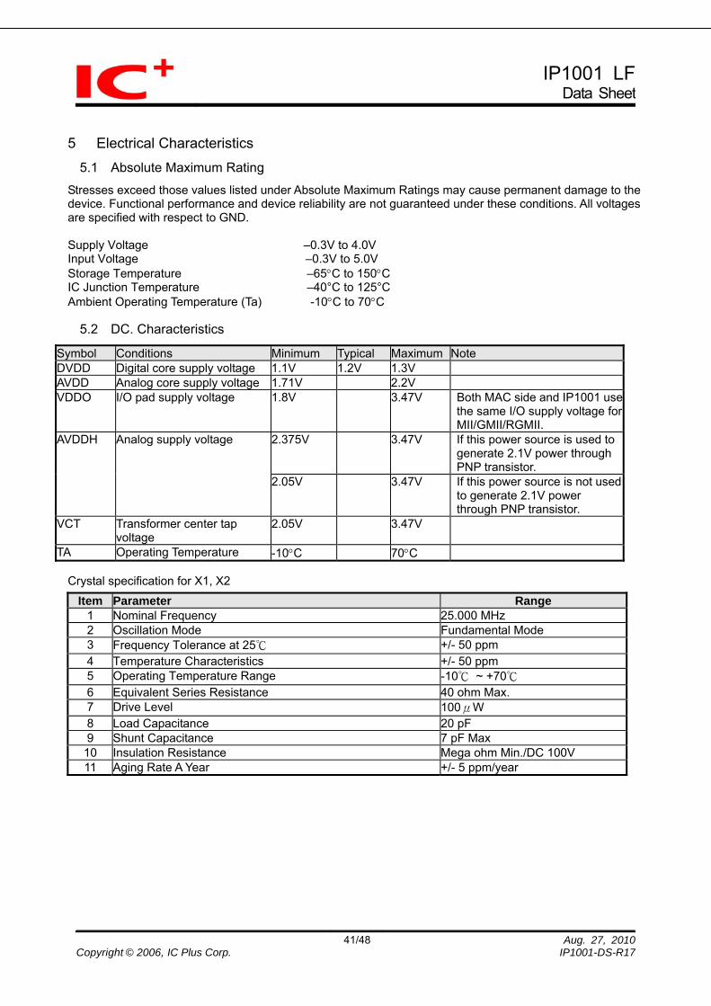
5.2 DC. Characteristics
Symbol Conditions Minimum Typical Maximum Note DVDD Digital core supply voltage 1.1V 1.2V 1.3V AVDD Analog core supply voltage 1.71V 2.2V VDDO I/O pad supply voltage 1.8V 3.47V Both MAC side and IP1001 use
the same I/O supply voltage for MII/GMII/RGMII.
2.375V 3.47V If this power source is used to generate 2.1V power through PNP transistor.
AVDDH Analog supply voltage
2.05V 3.47V If this power source is not used to generate 2.1V power through PNP transistor.
VCT Transformer center tap voltage
2.05V 3.47V
TA Operating Temperature -10°C 70°C Crystal specification for X1, X2
Item Parameter Range 1 Nominal Frequency 25.000 MHz 2 Oscillation Mode Fundamental Mode 3 Frequency Tolerance at 25℃ +/- 50 ppm 4 Temperature Characteristics +/- 50 ppm 5 Operating Temperature Range -10℃ ~ +70℃ 6 Equivalent Series Resistance 40 ohm Max. 7 Drive Level 100μW 8 Load Capacitance 20 pF 9 Shunt Capacitance 7 pF Max
10 Insulation Resistance Mega ohm Min./DC 100V 11 Aging Rate A Year +/- 5 ppm/year
IP1001 LFData Sheet
42/48 Aug. 27, 2010Copyright © 2006, IC Plus Corp. IP1001-DS-R17
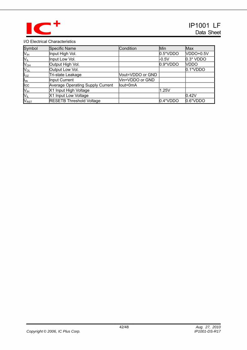
I/O Electrical Characteristics Symbol Specific Name Condition Min Max VIH Input High Vol. 0.5*VDDO VDDO+0.5V VIL Input Low Vol. -0.5V 0.3* VDDO VOH Output High Vol. 0.9*VDDO VDDO VOL Output Low Vol. 0.1*VDDO IOZ Tri-state Leakage Vout=VDDO or GND IIN Input Current Vin=VDDO or GND Icc Average Operating Supply Current Iout=0mA VIH X1 Input High Voltage 1.25V VIL X1 Input Low Voltage 0.42V VRST RESETB Threshold Voltage 0.4*VDDO 0.6*VDDO
IP1001 LFData Sheet
5.3 AC Timing 5.3.1 Reset, Clock and Power Source
Symbol Description Min. Typ. Max. Unit
Tclk_lead X1 clock valid period before reset released 10 - - ms Trst Reset period 10 - - ms Tclk_MII_rdy MII/GMII/RGMII clock output ready after reset
released - 1 - µs
Tclk_out_rdy CLK_OUT clock out ready after reset released (Pin 10 output)
0 - 20 ns
Tdiff Time difference between VDDO and AVDD, AVDDH, DVDD
30 ms
Tpwr_lead All power source ready before reset released 11 ms
AVDD, AVDDH,DVDD
VDDO
X1 CLOCK
RESET
Tdiff Tpwr_lead
Tclk_lead
Trst
Tclk_out_rdy
CLK_OUT
43/48 Aug. 27, 2010Copyright © 2006, IC Plus Corp. IP1001-DS-R17
IP1001 LFData Sheet
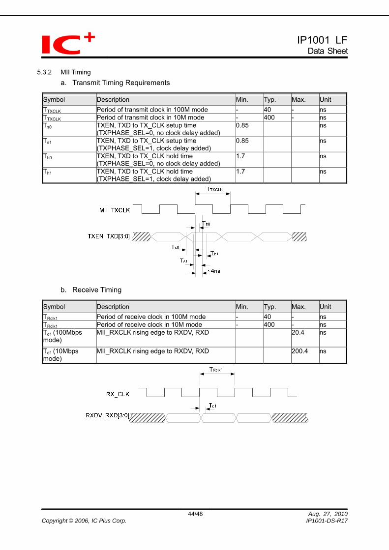
5.3.2 MII Timing
a. Transmit Timing Requirements
Symbol Description Min. Typ. Max. Unit TTXCLK Period of transmit clock in 100M mode - 40 - ns TTXCLK Period of transmit clock in 10M mode - 400 - ns Ts0 TXEN, TXD to TX_CLK setup time
(TXPHASE_SEL=0, no clock delay added) 0.85 ns
Ts1 TXEN, TXD to TX_CLK setup time (TXPHASE_SEL=1, clock delay added)
0.85 ns
Th0 TXEN, TXD to TX_CLK hold time (TXPHASE_SEL=0, no clock delay added)
1.7 ns
Th1 TXEN, TXD to TX_CLK hold time (TXPHASE_SEL=1, clock delay added)
1.7 ns
b. Receive Timing
Symbol Description Min. Typ. Max. Unit TRclk1 Period of receive clock in 100M mode - 40 - ns TRclk1 Period of receive clock in 10M mode - 400 - ns Td1 (100Mbps mode)
MII_RXCLK rising edge to RXDV, RXD
20.4 ns
Td1 (10Mbps mode)
MII_RXCLK rising edge to RXDV, RXD 200.4 ns
44/48 Aug. 27, 2010Copyright © 2006, IC Plus Corp. IP1001-DS-R17
IP1001 LFData Sheet
5.3.3 GMII Timing
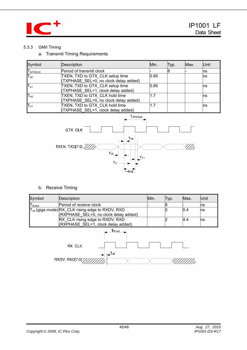
a. Transmit Timing Requirements
Symbol Description Min. Typ. Max. Unit TGTXCLK Period of transmit clock - 8 - ns Ts0 TXEN, TXD to GTX_CLK setup time
(TXPHASE_SEL=0, no clock delay added) 0.85 ns
Ts1 TXEN, TXD to GTX_CLK setup time (TXPHASE_SEL=1, clock delay added)
0.85 ns
Th0 TXEN, TXD to GTX_CLK hold time (TXPHASE_SEL=0, no clock delay added)
1.7 ns
Th1 TXEN, TXD to GTX_CLK hold time (TXPHASE_SEL=1, clock delay added)
1.7 ns
b. Receive Timing
Symbol Description Min. Typ. Max. Unit TRclk2 Period of receive clock - 8 - ns
RX_CLK rising edge to RXDV, RXD (RXPHASE_SEL=0, no clock delay added)
0 0.4 ns Td2 (giga mode)
RX_CLK rising edge to RXDV, RXD (RXPHASE_SEL=1, clock delay added)
2 4.4 ns
45/48 Aug. 27, 2010Copyright © 2006, IC Plus Corp. IP1001-DS-R17
IP1001 LFData Sheet
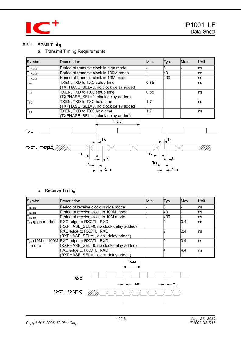
5.3.4 RGMII Timing
a. Transmit Timing Requirements
Symbol Description Min. Typ. Max. Unit TTXCLK Period of transmit clock in giga mode - 8 - ns TTXCLK Period of transmit clock in 100M mode - 40 - ns TTXCLK Period of transmit clock in 10M mode - 400 - ns Ts0 TXEN, TXD to TXC setup time
(TXPHASE_SEL=0, no clock delay added) 0.85 ns
Ts1 TXEN, TXD to TXC setup time (TXPHASE_SEL=1, clock delay added)
0.85 ns
Th0 TXEN, TXD to TXC hold time (TXPHASE_SEL=0, no clock delay added)
1.7 ns
Th1 TXEN, TXD to TXC hold time (TXPHASE_SEL=1, clock delay added)
1.7 ns
b. Receive Timing
Symbol Description Min. Typ. Max. Unit TRclk3 Period of receive clock in giga mode - 8 - ns TRclk3 Period of receive clock in 100M mode - 40 - ns TRclk3 Period of receive clock in 10M mode - 400 - ns
RXC edge to RXCTL, RXD (RXPHASE_SEL=0, no clock delay added)
0 0.4 ns Td3 (giga mode)
RXC edge to RXCTL, RXD (RXPHASE_SEL=1, clock delay added)
2 2.4 ns
RXC edge to RXCTL, RXD (RXPHASE_SEL=0, no clock delay added)
0 0.4 ns Td3 (10M or 100M mode
RXC edge to RXCTL, RXD (RXPHASE_SEL=1, clock delay added)
4 4.4 ns
46/48 Aug. 27, 2010Copyright © 2006, IC Plus Corp. IP1001-DS-R17
IP1001 LFData Sheet
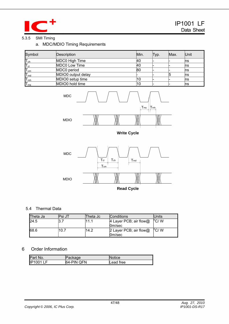
5.3.5 SMI Timing a. MDC/MDIO Timing Requirements
Symbol Description Min. Typ. Max. Unit Tch MDC0 High Time 40 - - ns Tcl MDC0 Low Time 40 - - ns Tcm MDC0 period 80 - - ns Tmd MDIO0 output delay - - 5 ns Tmh MDIO0 setup time 10 - - ns Tms MDIO0 hold time 10 - - ns
MDC
MDIO
Tms Tmh
Write Cycle
Tcl Tch
Tcm
Tmd
MDC
MDIO
Read Cycle
5.4 Thermal Data
Theta Ja Psi JT Theta Jc Conditions Units 24.5 3.7 11.1 4 Layer PCB; air flow@
0m/sec oC/ W
68.6 10.7 14.2 2 Layer PCB; air flow@ 0m/sec
oC/ W
6 Order Information
Part No. Package Notice IP1001 LF 64-PIN QFN Lead free
47/48 Aug. 27, 2010Copyright © 2006, IC Plus Corp. IP1001-DS-R17
IP1001 LFData Sheet
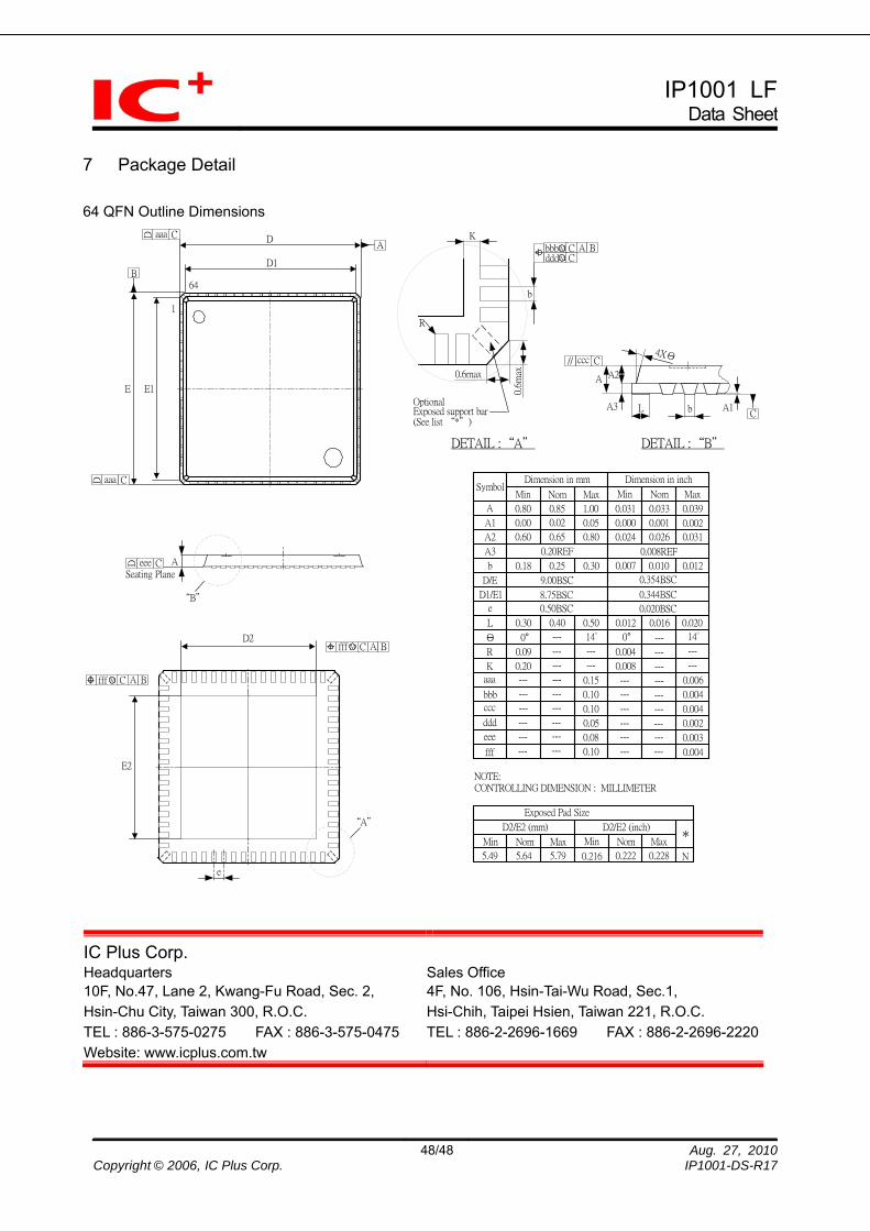
7 Package Detail 64 QFN Outline Dimensions
D2
E2
“A"
e
A
“B"
Seating Plane
D eee C
D
D1
E E1
1
64
D aaa C
B
A
D aaa C
fff M C A B
fff M C A B
bL
4XΘ
A1A3
A2A
DETAIL :“B"
C
// ccc C
DETAIL :“A"
0.6max
0.6m
ax
b
OptionalExposed support bar(See list “*")
K
R
bbb M C A BdddM C
Dimension in mm Dimension in inch
Min MaxNom
A
Symbol
A1
A2
Min MaxNom
A3
b
D/E
D1/E1
e
L
Θ
R
K
aaa
bbb
ccc
ddd
eee
fff
0.80 0.85 1.00
0.00 0.02 0.05
0.60 0.65 0.80
0.031 0.033 0.039
0.000 0.001 0.002
0.024 0.026 0.031
0.20REF 0.008REF
0.18 0.25 0.30 0.007 0.010 0.012
9.00BSC
8.75BSC
0.50BSC
0.354BSC
0.344BSC
0.020BSC
0.30 0.40 0.50 0.012 0.016 0.020
0° 14°0° 14°
0.09
0.20
0.15
0.10
0.10
0.05
0.08
0.10
---
---
---
---
---
---
---
---
---
---
---
---
---
---
---
---
---
0.004
0.008
0.006
0.004
0.004
0.002
0.004
0.003
---
---
---
---
---
---
---
---
---
---
---
---
---
---
---
---
---
NOTE:CONTROLLING DIMENSION : MILLIMETER
Exposed Pad Size
D2/E2 (mm) D2/E2 (inch)
Min MaxNom Min MaxNom
5.49 5.64 5.79 0.216 0.222 0.228 N
*
IC Plus Corp. Headquarters Sales Office 10F, No.47, Lane 2, Kwang-Fu Road, Sec. 2, 4F, No. 106, Hsin-Tai-Wu Road, Sec.1, Hsin-Chu City, Taiwan 300, R.O.C. Hsi-Chih, Taipei Hsien, Taiwan 221, R.O.C. TEL : 886-3-575-0275 FAX : 886-3-575-0475 TEL : 886-2-2696-1669 FAX : 886-2-2696-2220Website: www.icplus.com.tw
48/48 Aug. 27, 2010Copyright © 2006, IC Plus Corp. IP1001-DS-R17
Related Documents