Instructor Instructor : Prof. Dr. Ir. Djoko : Prof. Dr. Ir. Djoko Hartanto, M.Sc. Hartanto, M.Sc. : Arief Udhiarto, M.T : Arief Udhiarto, M.T Source Source : : U.C. Berkeley ELECTRONICS DEVICE

Instructor: Prof. Dr. Ir. Djoko Hartanto, M.Sc. : Arief Udhiarto, M.T Source: Source: U.C. Berkeley ELECTRONICS DEVICE.
Dec 13, 2015
Welcome message from author
This document is posted to help you gain knowledge. Please leave a comment to let me know what you think about it! Share it to your friends and learn new things together.
Transcript
InstructorInstructor : Prof. Dr. Ir. Djoko Hartanto, M.Sc.: Prof. Dr. Ir. Djoko Hartanto, M.Sc.: Arief Udhiarto, M.T: Arief Udhiarto, M.T
SourceSource :: U.C. Berkeley
ELECTRONICS DEVICE
Electrical Engineering Department University of Indonesia 2
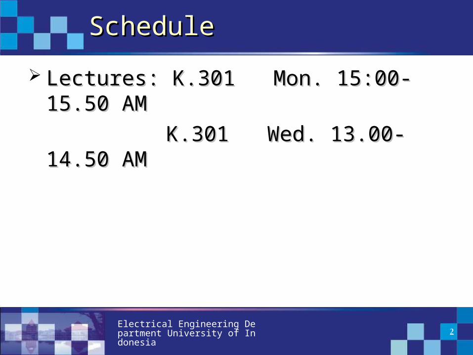
ScheduleSchedule
Lectures: K.301 Mon. 15:00-15.50 Lectures: K.301 Mon. 15:00-15.50 AMAM
K.301 Wed. 13.00-14.50 K.301 Wed. 13.00-14.50 AM AM
Electrical Engineering Department University of Indonesia 3
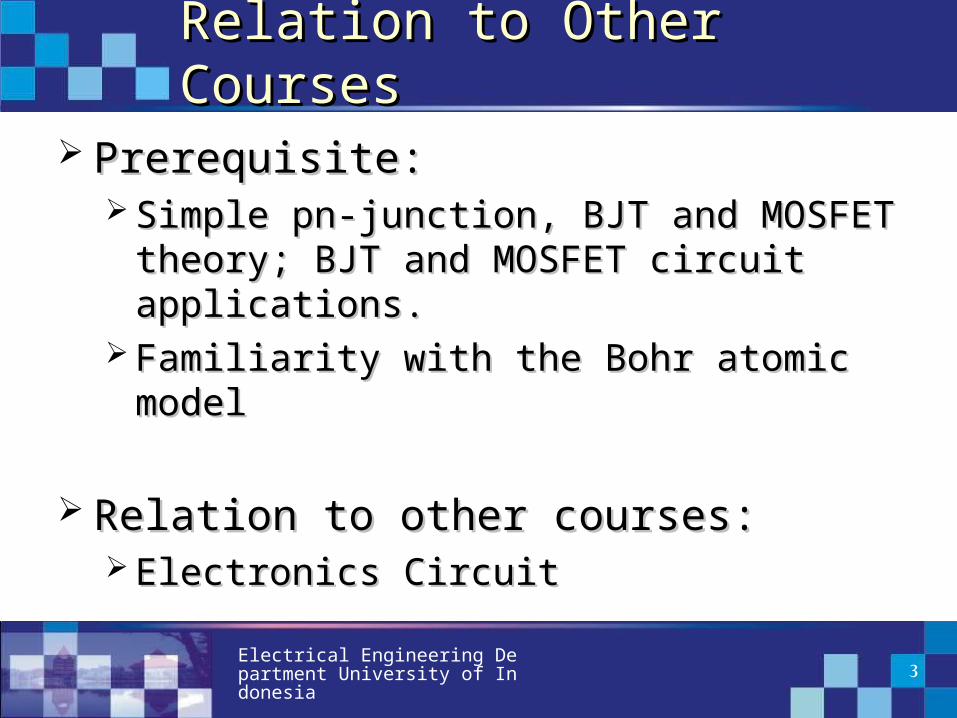
Relation to Other CoursesRelation to Other Courses
Prerequisite:Prerequisite: Simple pn-junction, BJT and MOSFET Simple pn-junction, BJT and MOSFET
theory; BJT and MOSFET circuit theory; BJT and MOSFET circuit applications.applications.
Familiarity with the Bohr atomic modelFamiliarity with the Bohr atomic model
Relation to other courses:Relation to other courses: Electronics CircuitElectronics Circuit
Electrical Engineering Department University of Indonesia 4
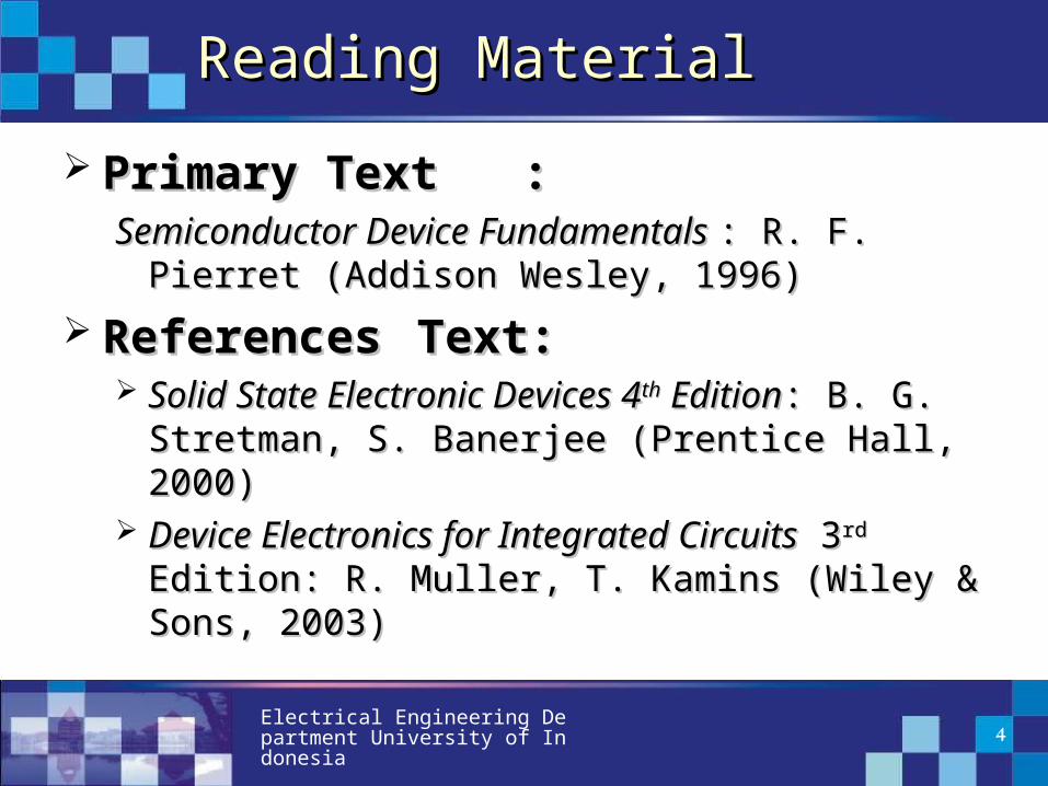
Reading MaterialReading Material
Primary TextPrimary Text ::Semiconductor Device Fundamentals Semiconductor Device Fundamentals : R. F. : R. F.
Pierret (Addison Wesley, 1996)Pierret (Addison Wesley, 1996)
ReferencesReferences Text: Text: Solid State Electronic Devices 4Solid State Electronic Devices 4thth Edition Edition: B. : B.
G. Stretman, S. Banerjee (Prentice Hall, G. Stretman, S. Banerjee (Prentice Hall, 2000) 2000)
Device Electronics for Integrated CircuitsDevice Electronics for Integrated Circuits 3 3rdrd Edition: R. Muller, T. Kamins (Wiley & Sons, Edition: R. Muller, T. Kamins (Wiley & Sons, 2003)2003)

Electrical Engineering Department University of Indonesia 5
SAPSAP
1. Course 1. Course : : Electronics DeviceElectronics Device
2. Course Code2. Course Code : : EES 210804EES 210804 SKS: 4 SKS: 4 Semester: 3Semester: 33. Instructor 3. Instructor : : Prof. Dr. Ir. Djoko Hartanto M.Sc. Prof. Dr. Ir. Djoko Hartanto M.Sc. (DH)(DH)
Arief Udhiarto, M.T (AU)Arief Udhiarto, M.T (AU)
4. Class System4. Class System : : SingleSingle 5. Course’s Objective5. Course’s Objective : mastering in basic concept of : mastering in basic concept of integrated-integrated- circuit operation devices circuit operation devices specially in silicon-specially in silicon- integrated circuits integrated circuits
6. Grading System (%) : 6. Grading System (%) : Homework (10) Homework (10) , , MT (35) , MT (35) , Seminar (15) , FT (40) Seminar (15) , FT (40)
Electrical Engineering Department University of Indonesia 6
MiscellanyMiscellany
Academic (dis)honesty Departmental policy will be strictly
followed Collaboration (not cheating!) is encouraged
Classroom etiquette: Arrive in class on time! Turn off cell phones, pagers, MP3/MP4
players, etc. No distracting conversations Ask question as much as possible
Electrical Engineering Department University of Indonesia 7
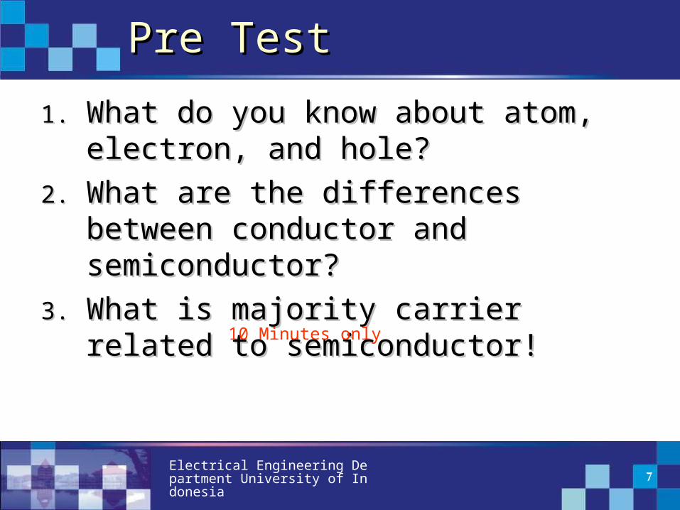
Pre TestPre Test
1.1. What do you know about atom, What do you know about atom, electron, and hole?electron, and hole?
2.2. What are the differences between What are the differences between conductor and semiconductor?conductor and semiconductor?
3.3. What is majority carrier related to What is majority carrier related to semiconductor!semiconductor!
10 Minutes only
Electrical Engineering Department University of Indonesia 8
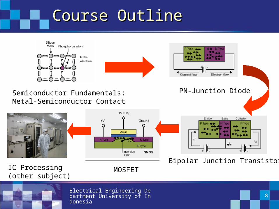
Course OutlineCourse Outline
Semiconductor Fundamentals;Metal-Semiconductor Contact
PN-Junction Diode
Bipolar Junction TransistorMOSFETIC Processing
(other subject)
Electrical Engineering Department University of Indonesia 9
Overview of IC Devices and Semiconductor Fundamentals
Reading Assignment : Pierret Chap 1, Chap 2
Electrical Engineering Department University of Indonesia 10
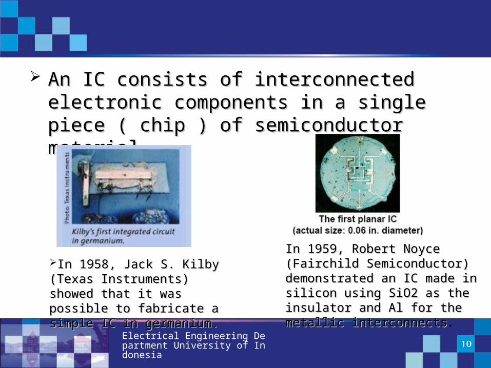
An IC consists of interconnected electronic An IC consists of interconnected electronic components in a single piece ( chip ) of components in a single piece ( chip ) of semiconductor materialsemiconductor material
In 1958, Jack S. Kilby (Texas In 1958, Jack S. Kilby (Texas Instruments) showed that it was Instruments) showed that it was possible to fabricate a simple IC in possible to fabricate a simple IC in germanium.germanium.
In 1959, Robert Noyce (Fairchild In 1959, Robert Noyce (Fairchild Semiconductor) demonstrated an IC Semiconductor) demonstrated an IC made in silicon using SiO2 as the made in silicon using SiO2 as the insulator and Al for the metallic insulator and Al for the metallic interconnectsinterconnects.
Electrical Engineering Department University of Indonesia 11
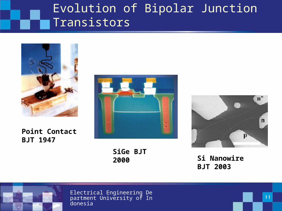
Evolution of Bipolar Junction Transistors
Point Contact BJT 1947
SiGe BJT2000 Si Nanowire BJT
2003
Electrical Engineering Department University of Indonesia 12
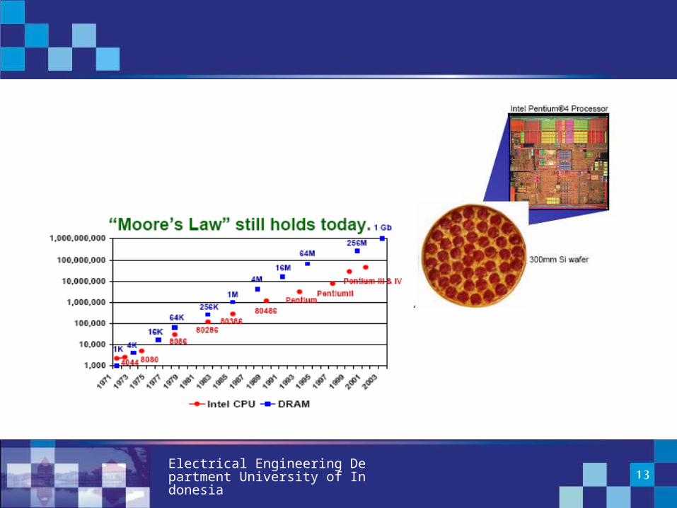
From a Few, to Billions
By connecting a large number of components, By connecting a large number of components, each performing simple operations, an IC that each performing simple operations, an IC that performs very complex tasks can be built.performs very complex tasks can be built.
The degree of integration has increased at an The degree of integration has increased at an exponential pace over the past ~40 years.exponential pace over the past ~40 years. The number of devices on a chip doubles every ~18 The number of devices on a chip doubles every ~18
months, for the same price.months, for the same price.
Electrical Engineering Department University of Indonesia 13
Electrical Engineering Department University of Indonesia 14
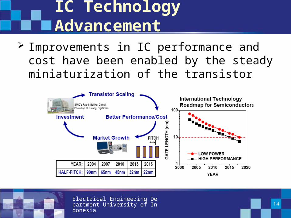
IC Technology Advancement
Improvements in IC performance and cost have been enabled by the steady miniaturization of the transistor
Electrical Engineering Department University of Indonesia 15
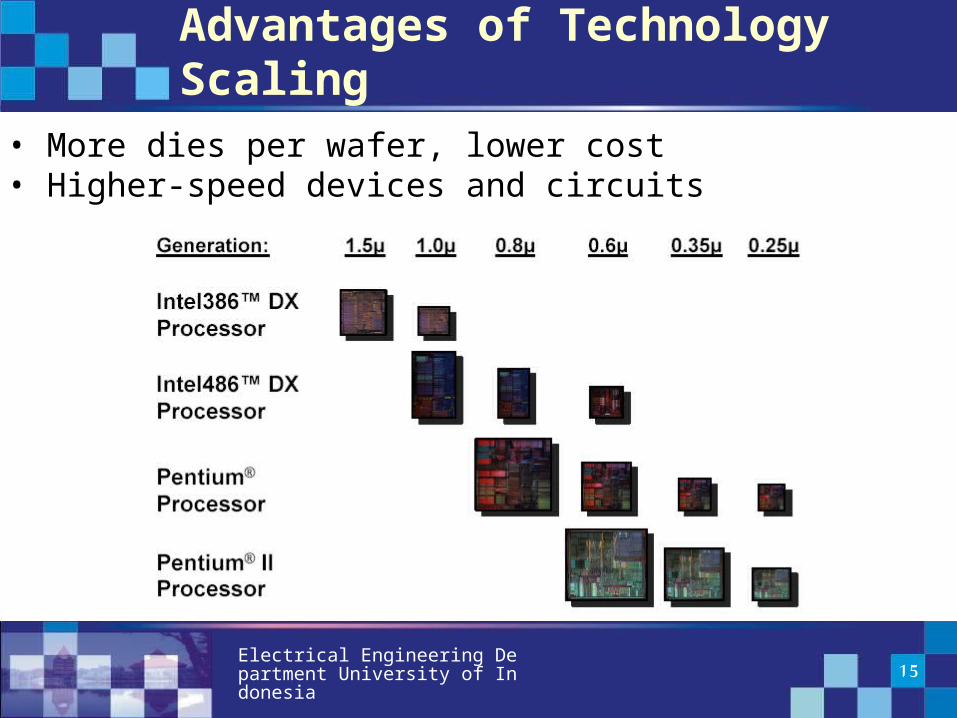
Advantages of Technology Scaling
• More dies per wafer, lower cost• Higher-speed devices and circuits
Electrical Engineering Department University of Indonesia 16
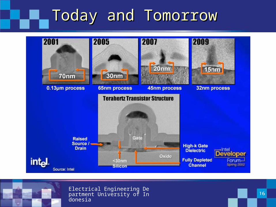
Today and TomorrowToday and Tomorrow
Electrical Engineering Department University of Indonesia 17
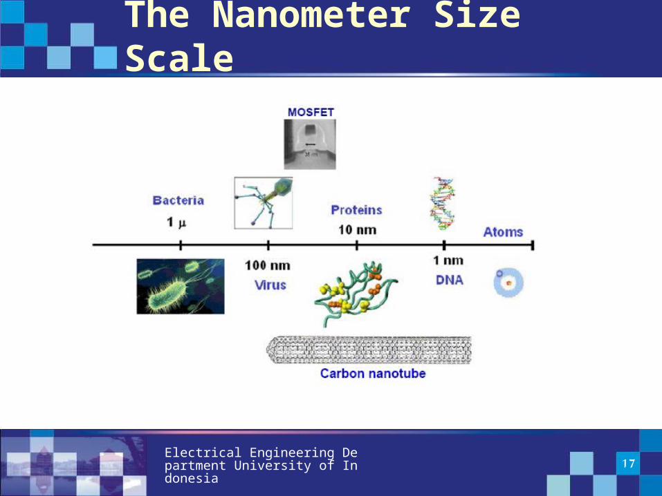
The Nanometer Size Scale
Electrical Engineering Department University of Indonesia 18
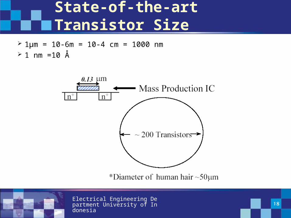
State-of-the-art Transistor Size
1µm = 10-6m = 10-4 cm = 1000 nm 1 nm =10 Å

Electrical Engineering Department University of Indonesia 19
CZ Crystal GrowthCZ Crystal Growth
Electrical Engineering Department University of Indonesia 20
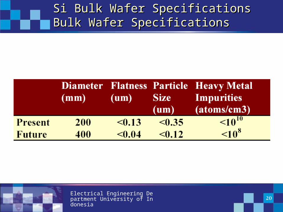
Si Bulk Wafer Specifications Bulk Si Bulk Wafer Specifications Bulk Wafer SpecificationsWafer Specifications
Electrical Engineering Department University of Indonesia 21
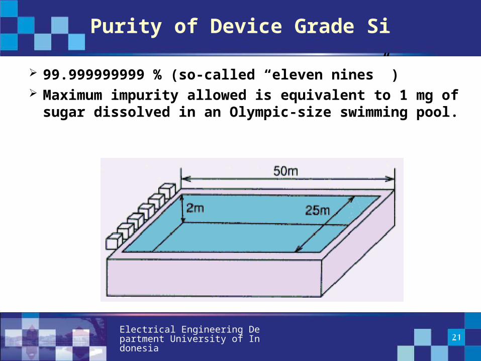
Purity of Device Grade Si
99.999999999 % (so-called “eleven nines” ) Maximum impurity allowed is equivalent to 1 mg
of sugar dissolved in an Olympic-size swimming pool.

Electrical Engineering Department University of Indonesia 22
Flatness deviation and particle sizes
Dimensions are equivalent to 1/1000 of a baseballplaced inside a sports dome.
Electrical Engineering Department University of Indonesia 23
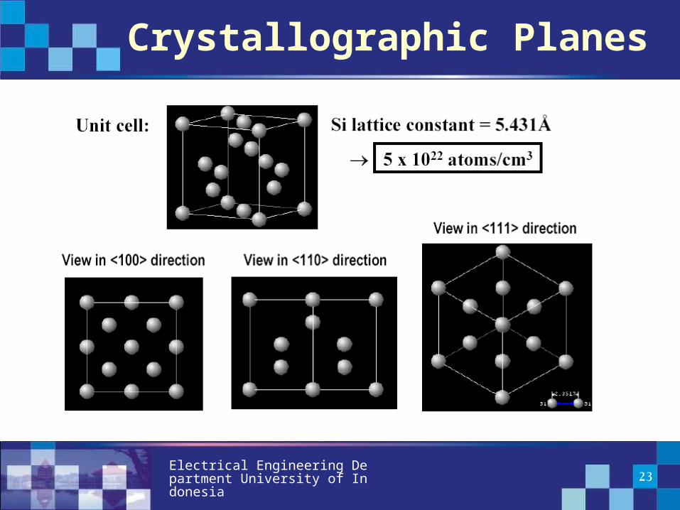
Crystallographic Planes

Electrical Engineering Department University of Indonesia 24
Miller IndicesCrystallographic Notation
h: inverse x-interceptk: inverse y-interceptl: inverse z-intercept
(Intercept values are in multiples of the lattice constant;h, k and l are reduced to 3 integers having the same ratio.)

Electrical Engineering Department University of Indonesia 25
Crystallographic PlanesCrystallographic Planes and Si and Si WafersWafers
Silicon wafers are usually cut along the (100) plane with a flat or notch to orient the wafer during IC fabrication

Electrical Engineering Department University of Indonesia 26
Bulk Si Wafer to IC Chip
Electrical Engineering Department University of Indonesia 27
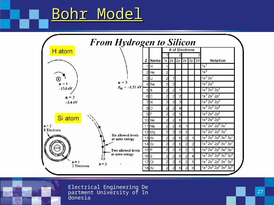
Bohr ModelBohr Model
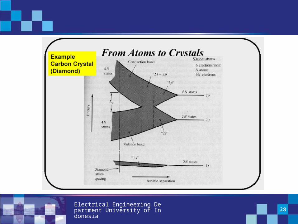
Electrical Engineering Department University of Indonesia 28
Electrical Engineering Department University of Indonesia 29
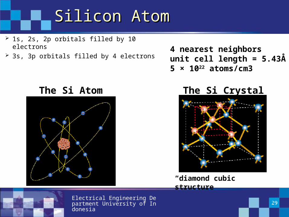
Silicon AtomSilicon Atom 1s, 2s, 2p orbitals filled by 10 electrons 3s, 3p orbitals filled by 4 electrons 4 nearest neighbors
unit cell length = 5.43Å5 × 10²² atoms/cm3
“diamond cubic ” structure
The Si Atom The Si Crystal
Electrical Engineering Department University of Indonesia 30
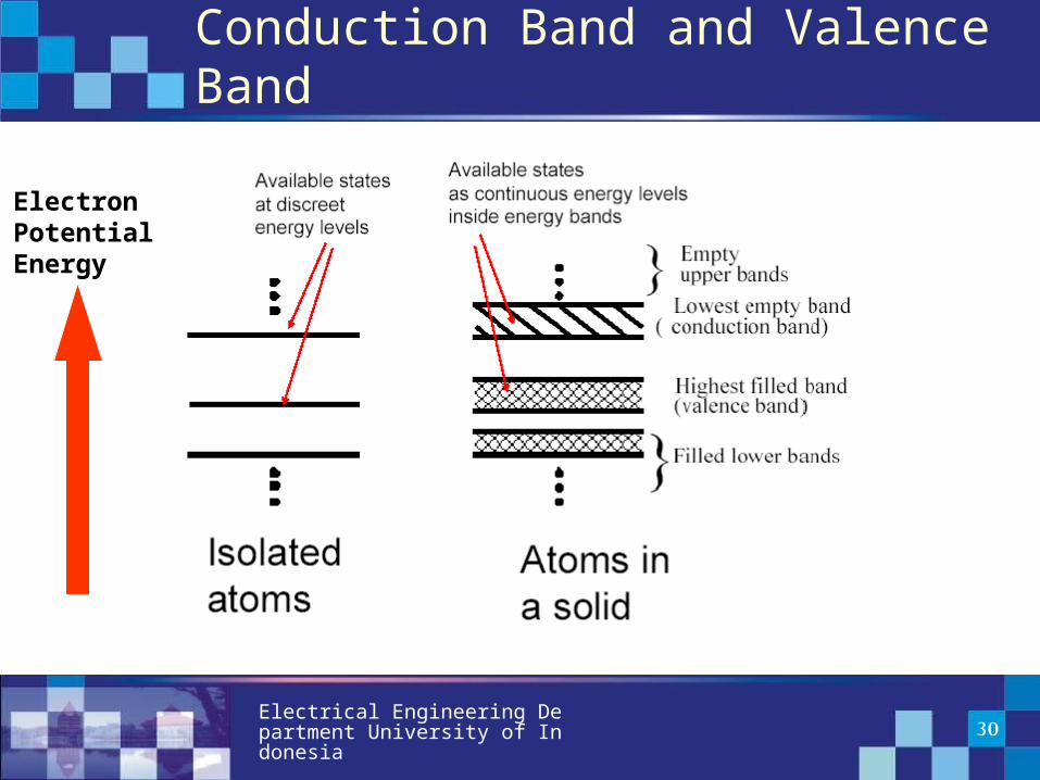
Conduction Band and Valence Band
ElectronPotentialEnergy
Electrical Engineering Department University of Indonesia 31
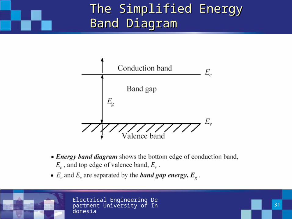
The Simplified Energy Band The Simplified Energy Band DiagramDiagram

Electrical Engineering Department University of Indonesia 32
Semiconductors, Insulators, and Semiconductors, Insulators, and ConductorsConductors
• Totally filled band and totally empty bands do not allow current flow. (just as there is no motion of liquid in a totally filled or totally empty bottle
• Metal conduction band is half-filled• Semiconductors have lower Eg’s than insulators and
can be doped
Electrical Engineering Department University of Indonesia 33
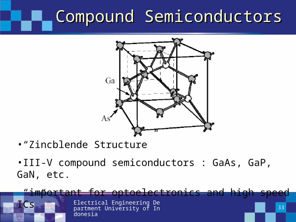
Compound SemiconductorsCompound Semiconductors
•“Zincblende Structure”
•III-V compound semiconductors : GaAs, GaP, GaN, etc.
“important for optoelectronics and high speed ICs”
Electrical Engineering Department University of Indonesia 34
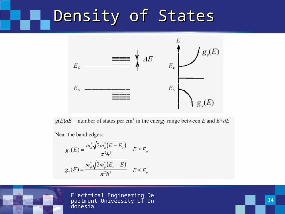
Density of StatesDensity of States
Electrical Engineering Department University of Indonesia 35
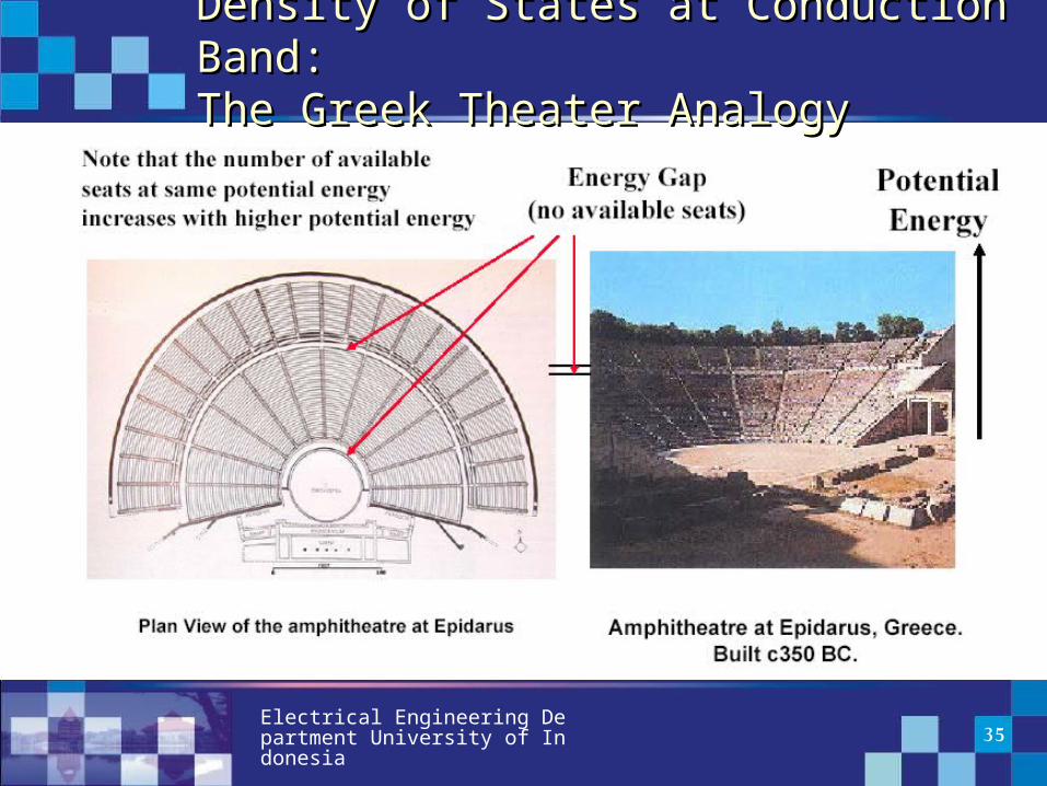
Density of States at Conduction Density of States at Conduction Band:Band:The Greek Theater AnalogyThe Greek Theater Analogy
Electrical Engineering Department University of Indonesia 36
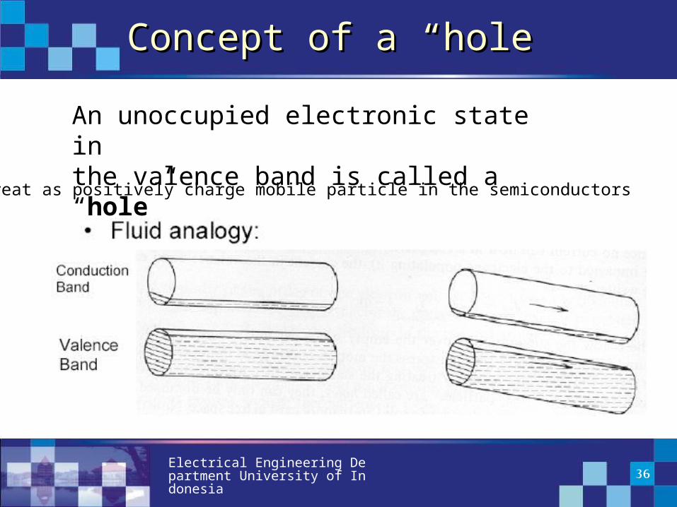
Concept of a “hole”Concept of a “hole”
An unoccupied electronic state inthe valence band is called a “hole”
Treat as positively charge mobile particle in the semiconductors
Electrical Engineering Department University of Indonesia 37
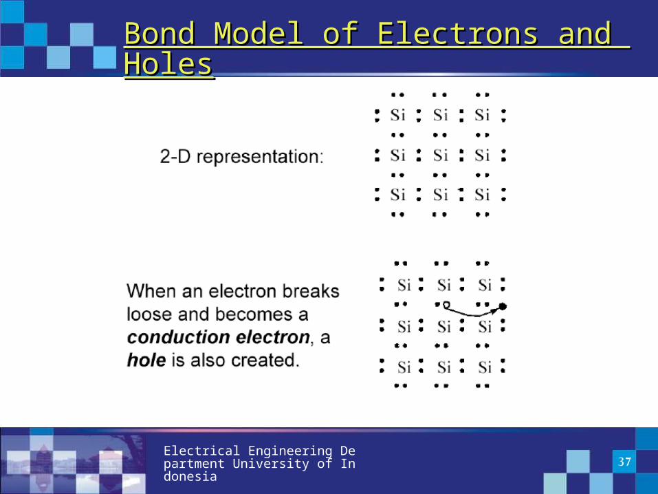
Bond Model of Electrons and HoleBond Model of Electrons and Holess
Electrical Engineering Department University of Indonesia 38
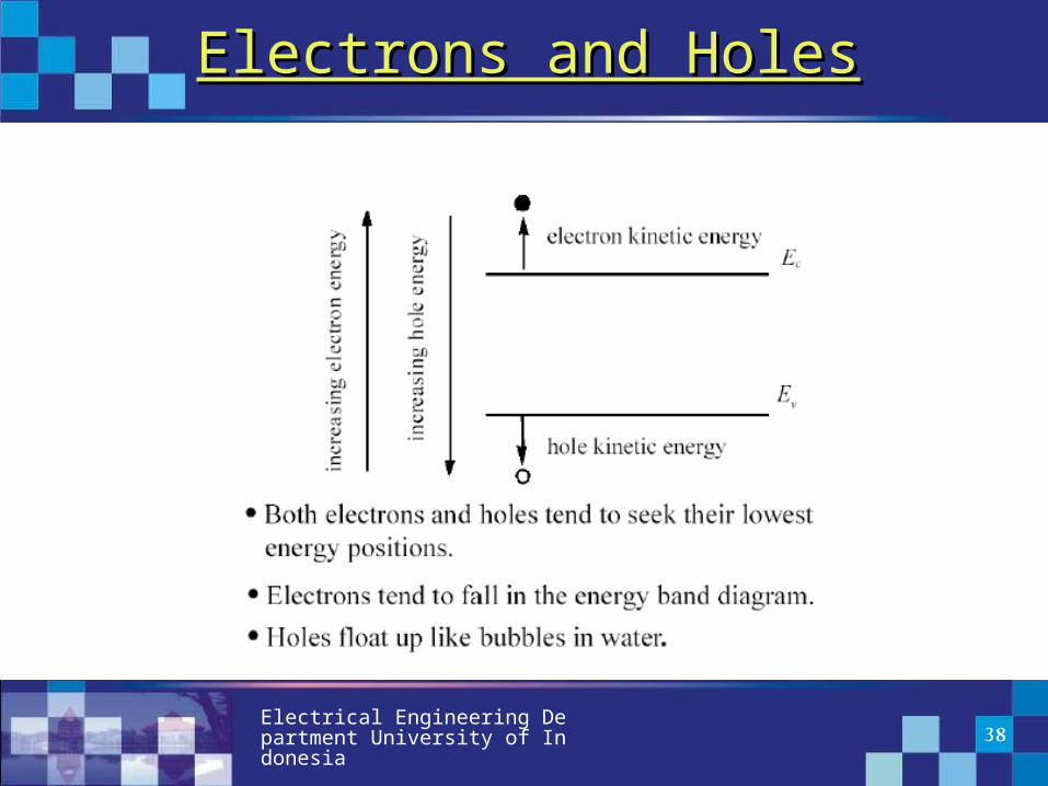
Electrons and HolesElectrons and Holes
Related Documents