1 INPUT POWER FACTOR PROBLEM AND CORRECTION FOR INDUSTRIAL DRIVES BY OSUNDE, DAVIDSON OTENGHABUN B.Sc (Hons), M.Sc (Electrical Engineering), MBA, M.Sc (Economics), Lagos MNSE, AMIEE, R. Eng A THESIS SUBMITTED TO THE SCHOOL OF POST GRADUATE STUDIES, UNIVERSITY OF LAGOS, LAGOS, NIGERIA, FOR THE AWARD OF THE DEGREE OF DOCTOR OF PHILOSOPHY (Ph.D) IN ELECTRICAL AND ELECTRONICS ENGINEERING MARCH 2010

Welcome message from author
This document is posted to help you gain knowledge. Please leave a comment to let me know what you think about it! Share it to your friends and learn new things together.
Transcript

1
INPUT POWER FACTOR PROBLEM AND CORRECTION FOR
INDUSTRIAL DRIVES
BY
OSUNDE, DAVIDSON OTENGHABUN
B.Sc (Hons), M.Sc (Electrical Engineering), MBA, M.Sc (Economics), Lagos
MNSE, AMIEE, R. Eng
A THESIS SUBMITTED TO THE SCHOOL OF POST GRADUATE
STUDIES, UNIVERSITY OF LAGOS, LAGOS, NIGERIA, FOR THE
AWARD OF THE DEGREE OF DOCTOR OF PHILOSOPHY (Ph.D) IN
ELECTRICAL AND ELECTRONICS ENGINEERING
MARCH 2010

2
SCHOOL OF POSTGRADUATE STUDIES
UNIVERSITY OF LAGOS
CERTIFICATION
This is to certify that the Thesis
“INPUT POWER FACTOR PROBLEM AND CORRECTION FOR
INDUSTRIAL DRIVES”
Submitted to the
School of Postgraduate Studies
University of Lagos
For the award of the Degree of
DOCTOR OF PHILOSOPHY (Ph.D)
is a record of original research carried out
By
OSUNDE, DAVIDSON OTENGHABUN
in the Department of Electrical and Electronics Engineering
_______________________ ____________ ________
AUTHOR‘S NAME SIGNATURE DATE
________________________ ____________ ________
1ST
SUPERVISOR‘S NAME SIGNATURE DATE
_______________________ ____________ ________
2nd
SUPERVISOR‘S NAME SIGNATURE DATE
________________________ ____________ ________
1st INTERNAL EXAMINER SIGNATURE DATE
________________________ ____________ ________
2ND
INTERNAL EXAMINER SIGNATURE DATE
________________________ ____________ ________
EXTERNAL EXAMINER SIGNATURE DATE
________________________ ____________ ________
SPGS REPRESENTATIVE SIGNATURE DATE

3
DECLARATION
I declare that this thesis is a record of the research work carried out by me. I also certify that
neither this nor the original work contained therein has been accepted in any previous application
for a degree.
All sources of information are specifically acknowledged by means of reference.
__________________ ________________
OSUNDE, O. D DATE

4
DEDICATION
To my entire family and all those who have contributed to my progress in life particularly my
wife, Osunde, Isimeme Okaneme and my lovely Children: Osasere Davidson (Jnr), Osayi
Stephen and Osarieme Stephanie

5
ACKNOWLEDGEMENTS
It is with great pleasure that I acknowledge the encouragement and guidance of my supervisors:
Prof. C.C Okoro and Prof. C.O.A. Awosope for their thorough supervision of this thesis.
Particularly, I wish to express my unreserved gratitude to Prof. C.C. Okoro for his confidence in
my ability to undertake this research up to doctoral level. I am indeed very grateful for his
interest, guidance, and understanding and above all for making his wealth of experience and
resources available to me. I hope my emerging career will meet his expectations to justify his
huge academic and professional investment on my training. His capacity for hard work,
diligence, thoroughness and honesty serve as a source of inspirations for my aspirations. I am
also indebted to all lecturers and staff of the department of Electrical/Electronics Engineering of
the University Of Lagos: Prof. F.N. Okafor, the acting head of department, Prof. R.I. Salawu
(retired), Prof. S.A. Adekola (retired), Prof. O. Adegbenro, Prof. A.I. Mowete, Dr. T.O.
Akinbulire, (PG co – ordinator), Dr. P.B Osofisan (retired), Mr. Lawal (retired), former head of
Electrical machines laboratory, and others not mentioned for their guidance, advise and useful
suggestions. I remain grateful to Prof. V.O. Olunloyo of Systems Engineering, Prof. O. Ogboja
(late) of Chemical Engineering, Prof. B.O. Oghojafor of Business Administration, Prof.
Fakieyesi of Economics department for their supports and words of encouragements and in
particular to the present Dean of Engineering, Prof. M.A Salau
My profound and unreserved gratitude goes to the immediate past Vice – Chancellor, Prof. Oye
Ibidapo – Obe for granting me a one year study leave as a visiting research scholar on an
exchange programme to the Michigan State University, USA. Most of my modeling analysis and
laboratory experiments were carried out at the Michigan State University – Power Electronics
Laboratory under the supervision of Prof. P.Z. Peng. I am indeed grateful to him and other staff
and Ph.D students of the Power Electronics group. More importantly, I remain grateful to the
entire Michigan State University for hosting me and making my stay a worthwhile one.
I would also like to acknowledge the following colleagues who have assisted and contributed in
various ways to the completion of this work often with enthusiasm and encouragement: Mr.
Peter Otomewo, MD, Perbeto Ventures, Dr. Olumuyiwa Asaolu, and Engr. Chinedu Ucheagbu.
My special thanks go to my brother, Patrick Osunde in Atlanta Georgia, USA, for his
contributions and to all my friends in America: Barr. Lucky Osagie Enobakhare (NY),

6
Nosa Aimufua (NY), Francis Omoregbe (Chicago), Late Larry Umumagbe (NY), Engr. Ese Osa
(NY), Engr. James Babalola (TX), Engr. Ayo Adedeji (TX), Dr. Emman Ogogo (NY), Dr.
Richardson Osazee (GA), Mr. Omoruyi Osakpamwan (MI), Mr. Daniel Osunde (CA), Engr.
Chuks Iyasele (TX) and others not mentioned for their moral and financial supports.
It is with all my heart that I acknowledge the moral supports, patience, understanding and
encouragement of my beloved wife – Osunde, Isimeme Okaneme and my wonderful children,
Osasere Davidson (Jnr), Osayi Stephen and Osarieme Stephanie. You are all more precious than
Gold
Finally, I thank the almighty God for his abundant blessings showered on me throughout my
course in life. I am indeed grateful to him for his guidance, protection and good health.
Osunde, O .D
Lagos, Nigeria

7
TABLE OF CONTENTS
Page Title i
Certification ii
Declaration iii
Dedication iv
Acknowledgements v
Table of Contents vii
List of Figures xi
List of Tables xv
List of Abbreviations xvi
List of Notations xviii
Abstract xx
CHAPTER 1:
INTRODUCTION
1.1 Background of Study 1
1.2. Statement of the problem 3
1.3 Aim 3
1.4 Objectives 4
1.5 Scope of study 4
1.6 Significance of study 5
1.7 Operational Definition of Terms 5
1.8 Presentation of Thesis 8
CHAPTER 2:
LITERATURE AND THEORETICAL FRAMEWORK
2.1 Literature Review 9

8
2.2. The Thyristor 14
2.2.1 I-V Characteristics of a thyristor 15
2.2.2 Dynamic Characteristics of a Thyristor 18
2.3 Circuits and Devices used in power Factor correction Schemes 23
2.3.1 Operational amplifiers and applications 24
2.3.2 Operational amplifier as an Inverting Amplifier 25
2.3.3 Operational amplifier as a non - inverting Amplifier 25
2.3.4 Operational amplifier as an Integrator 26
2.3.5 Operational amplifier as a Differentiator 26
2.3.6 Operational amplifier as a Comparator 27
2.4 The 555 Timer IC 27
2.4;1 Monostable mode 28
2.4.2 Astable mode 29
2.5 The Single – Phase Asymmetrical Bridge Converter 31
CHAPTER THREE:
MODELLING AND ANALYSIS OF THE BRIDGE CONVERTER WITH
DC MOTOR LOAD
3.0 Introduction 34
3.1 Modelling the DC Motor 34
3.2 Piece – Wise Linear analysis of the Single – Phase Bridge Converter with DC
Motor Load
36
3.3 Modes of Operation 37
3.4 Analysis for AC input current 40
3.5 Harmonics in the AC input Current 50
3.6 Impact of Multiple Drives on Supply Systems 55
3.7 Behaviour Factors of the Drive 59

9
3.8 The Input Power Factor Problem 62
3.9 Generalised Analysis for the Asymmetrical Bridge 63
CHAPTER 4:
POWER FACTOR CORRECTION (PFC) CONTROL SCHEMES
4.0 Introduction 68
4.1 Passive and Active methods of power factor correction 68
4.1.1 Passive Power Factor Correction Techniques 68
4.1.2 Active Power Factor Correction Techniques 69
4.2 Performance evaluation of the various techniques 69
4.3 Performance Analysis for the methods of control of the Asymmetrical Bridge 79
CHAPTER 5:
PULSE WIDTH MODULATION (PWM) FOR INPUT POWER FACTOR
CORRECTION
5.1 Pulse Width Modulation 84
5.2 Types of PWM 86
5.2;1 Equal pulse width modulation (EPWM) 87
5.2.2 Sinusoidal pulse width modulation (SPWM) 87
5.3 Analysis for predicting the Behaviour factors on the AC input current of the
Asymmetrical Bridge with pulse width modulation (PWM)
88
5.4 Comparison of Results with the Asymmetrical Bridge without PFC control 96
5.5 AC – DC Boost – Type Asymmetrical Converter for Power Factor Correction 98
5.5.1 The AC – DC Asymmetric Drive with Power Factor Correction Circuit 98
5.5.2 AC – DC Boost - Type Asymmetrical Converter for PFC 98

10
5.5.3 Control of the Active Boost Switch of the PWM 100
5.6 Waveforms of the PWM control Signals of the Drive 104
5.7 A Simplified PWM AC – DC Asymmetrical Bridge with PFC control 107
5.7.1 Description of the proposed circuit 108
5.7.2 Operation of the Bridgeless Converter 109
5.7.3 Design Considerations of the proposed AC – DC Converter 111
CHAPTER 6:
RESULTS AND DISCUSSION
6.1 Waveforms of the Input Voltage, Current and harmonics with PWM PFC 117
6.1.1 Comparative Results of the PWM and PAC controls 118
6.2 Discussion of Results 119
CHAPTER 7:
CONCLUSIONS AND RECOMMENDATIONS
7.1 Conclusions 121
7.2 Contributions to Knowledge 122
7.3 Recommendations for further work 123
REFERENCES 124
APPENDICES 135

11
LIST OF FIGURES
Figure Page
2.1 Thyristor Structure and symbols
14
2.2 Static I – V characteristics of a thyristor
16
2.3 Junction biased conditions.
17
2.4 Distribution of gate and anode current during delay time
19
2.5 Thyristor voltage and current waveforms during turn-on and turn-off processes
22
2.6 A circuit model of an operational amplifier (op amp) with gain and
input and output resistances Rin and Rout
24
2.7 Inverting amplifier circuit
25
2.8 Non - inverting amplifier circuit
26
2.9 Integrator circuit
26
2.10 Differentiator circuit
27
2.11 The 741 IC as a Comparator 27
2.12 Schematic of a 555 in monostable mode 29
2.13 Standard 555 Astable Circuit 30
2.14 Single – phase Asymmetrical Bridge Converter 33
3.1 Magnetisation Characteristics of a DC Motor 35
3.2 The asymmetrical single-phase bridge converter with a DC Motor Load
36
3.3 Control Circuit Layout a Single – Phase asymmetric Bridge Drive
38
3.4 Operational intervals and Waveforms of the Bridge Converter 38
3.5 Bridge Converter with half Cycle Equivalent Circuits
40
3.6 Variation of the Forward commutation angle ‗μ‘ with Firing angle ‗α‘ of the
controller
43
12
3.7 Variation of the Reverse commutation angle ‗β‘ with Firing angle ‗α‘ of the he
controller
45
3.8 Motor Input current at different Firing angles of the Thyristors: The power
factor problem in Graphics
49
3.9 Harmonics Spectrum of the controller at different Firing angles
53
3.10 Variation of Input current harmonic components for different delay angles 54
3.11 Variation of specified Harmonic Currents with Firing Angle 55
3.12 Multiple drives connected to the same source
56
3.13 Input current and waveform for a single drive: N = 1500, PF = 0.628
57
3.14 Input current and waveform for Two Drives in parallel: N = 1500, PF = 0.166 57
3.15 Input current and waveform for Three Drives in Parallel N = 1500, PF = 0.106
58
3.16 Variation of Power Factor with Number of Drives
58
3.17 Behaviour Factors of the Asymmetrical Single – Phase Bridge
66
4.1 Voltage and current waveforms for Phase Angle control – (PAC)
70
4.2 Voltage and current waveforms for Symmetrical Angle control – (SAC)
70
4.3 Voltage and current waveforms for Extinction Angle control – (EAC)
71
4.4 Voltage and current waveforms for Sequence control with forced commutation 71
4.5 Voltage and current waveforms for Pulse Width Modulation control – (PWM)
72
4.6 Relationships between the Input Power Factor and Output Voltage for the
various PFC control techniques
82
4.7 Relationships between the Harmonic Factor and Output Voltage for the
various PFC control techniques
82
4.8 Relationships between the Displacement Factor and Output Voltage
for the various PFC control techniques
82
5.1 Comparator Input and Output waveforms 85
5.2 Practical PWM Circuit 86

13
5.3 Waveforms of Currents and Voltages for Sinusoidal PWM
87
5.4 Harmonic Currents for specified Harmonic numbers 95
5.5 Variation of Power Factor with Output Voltage of the Bridge
96
5.6 Variation of Harmonic Factor with Output Voltage of the Bridge
97
5.7 Variation of Displacement Factor with Output Voltage of the Bridge
97
5.8 Gate Firing Circuit implementation of the PWM Controlled Asymmetrical
Single – Phase Drive
99
5.9 Asymmetrical AC –DC Boost- type Converter with input power factor correction 100
5.10 Schematic circuit layout for the PWM Controlled Asymmetric Single – Phase
Bridge (Boost Switch Control)
101
5.11 Gate Firing Circuit Implementation of the PWM Controlled Asymmetric
Single – Phase Drive (Thyristor Cuntrol)
102
5.12 Test rig with controlled DC machines and the Asymmetrical Bridge with
PWM Controllers
103
5.13 A Triangular wave signal at 10 KHz with a DC signal
104
5.14 A Triangular wave signal at 8 KHz with a DC signal 104
5.15 Comparator signal output modulated at 10KHz
105
5.16 Comparator signal output modulated at 8KHz
105
5.17 Comparator signal output modulated at 6KHz
105
5.18 Comparator signal output modulated at 5KHz
105
5.19 Thyristors complimentary gate signals at 10kHz
106
5.20 Thyristors complimentary gate signals at 8kHz
106
5.21 Input Current and Voltage waveforms (PF = 0.9995) at 10KHz
106
5.22 Input Current and Voltage waveforms (PF = 0.9993) at 8KHz 106

14
5.23 Harmonics of the PWM Controlled Asymmetric Single – Phase Drive
107
5.24 Bridgeless AC – DC PFC Configuration
108
5.25 Current Flow path for the Positive half cycle
109
5.26 Current Flow path for the negative half cycle
110
5.27 Operation of the Bridgeless converter 113
5.28 Triggering Circuit of the Bridgeless Converter (Voltage feedforward approach) of
the proposed AC – DC Converter: Active Boost Control
116
6.1 Input Current and Voltage waveforms (PF = 0.9998) at 10 KHz
117
6.2 Input Current and Voltage waveforms (PF = 0.9996) at 8KHz
117
6.3 Laboratory Results of the PWM Controlled Asymmetric Single – Phase
Drive
117
6.4 Input current waveform of the asymmetrical single phase bridge feeding
a DC motor load without PFC control (PF = 0.628)
118
6.5 Input current waveform of the asymmetrical single phase bridge feeding
a DC motor load with PFC control (PF = 0.9998)
118
6.6 Input Harmonic Current for the asymmetrical single phase bridge feeding
a DC motor load without PFC control
118
6.7 Input Harmonic Current for the asymmetrical single phase bridge feeding
a DC motor load with PWM PFC control
118

15
LIST OF TABLES
Table Page
4.1 Generalised Equations for Various Converter – Control Techniques using their
simplified models
81

16
LIST OF ABBREVIATIONS
AC Alternating Current
DC Direct Current
PF Power Factor
DF Displacement Factor
HF Harmonic Factor
RF Ripple Factor
FF Form Factor
PFC Power Factor Correction
THD Total Harmonic Distortion
PAC Phase Angle Control
AAC Asymmetrical Angle Control
EAC Extinction Angle Control
SAC Symmetrical Angle Control
SHE Selective Harmonic Elimination
PWM Pulse Width Modulation
IEC International Electrotechnical Commission
EPWM Equal Pulse Width Modulation
SPWM Sinusoidal Pulse Width Modulation
CICM Continuous Inductor Current Mode
DICM Discontinuous Inductor Current Mode
EI Electromagnetic Interference

17
SCR Silicon Controlled Rectifier
IGBT Insulated Gate Bipolar Transistor
MOSFET Metal Oxide Semiconductor Field Effect Transistor
PHCN Power Holding Company of Nigeria
NNPC Nigerian National Petroleum Corporation
THR The threshold at which the interval ends
DIS Connected to a capacitor whose discharge time will influence the
timing interval
GND Ground

18
LIST OF NOTATIONS
Delay or Firing Angle
Extinction Angle (Angle after at which reverse commutation begins)
T Period
f Frequency
sf Switching Frequency
t Time
d Duty Cycle
D Constant Duty Circle
ti Instantaneous Current
I Constant Current
n Turns Ratio
N Number of Turns
P Active Power
Q Reactive Power
R Resistor
S Apparent Power
S Active Switch
C Capacitor
L Inductor
offT Off - Time of an Active Switch
ONT On - Time of an Active Switch
X Reactance
sT Switching Period
Displacement Angle
fi Forced Current Component
ni Natural Current Component
v Instantaneous Voltage

19
E Motor Induced Emf
sV RMS Value of Phase Voltage
sI RMS Value of Phase Current
1sI Fundamental Current of sI
1s Phase Angle Between sV and 1sI
acPF AC Input Power Factor
Angular Frequency
Delay time
Turn – OFF time
Gate recovery time
Reverse recovery time
Gate recovery time
Circuit turn – off time
Input resistance
Output resistance
Output voltage
Gain of an amplifier
Angle representing a half cycle in radians
( ) The motor back emf,
( ) The Armature inductance of a DC motor
( ) The Armature resistance of a DC motor
( ) The instantaneous input current to a DC motor

20
ABSTRACT
The Asymmetrical Single - phase drive has an input power factor problem over its control range.
With the race towards industrialisation, power networks in developing economies would face
increasing power factor problems with extended application of these drives in industrial and
traction systems. This project investigates the assertion that power factor of supply networks
with multiple drives deteriorates with increased number of drives. The power factor problem is
established analytically following a complete characterization of the AC input current of the
drives. The methods of improving the input power factor of industrial drives are studied and the
Pulse Width Modulation technique adopted for achieving power factor improvement for such
industrial drives. The PWM scheme developed in the laboratory showed improved power factor.
Generalised performance equations for the methods and their comparative controls, design and
harmonic spectra are developed for application of industrial drives.
CHAPTER ONE
INTRODUCTION
1.1 Background of study

21
In an ideal power system, the voltage supplied to customer equipment and the resulting input
currents should be sinusoidal waves. In practice, however, these waveforms can be quite
distorted. This deviation from perfect sinusoids is usually expressed in terms of harmonic content
of the voltage and current waveforms. Most equipment connected to an electricity distribution
network usually may need controlled power conversion equipment which produces a non -
sinusoidal line current due to the nonlinear load. With such loads as RLC, the switching action of
the devices makes the system non- linear. Also, with the steadily increasing use of such
equipment, line current harmonics have become a significant problem. Their adverse effects on
the power system are well recognized. Harmonics are unwanted frequency components, which
arise from the use of semi-conductor controllers. Modern industries and applications which
include the steel plants, traction systems, industrial drives, furnaces etc generate voltage and
current harmonics which have adverse effects on the supply lines and equipment connected to
such lines. The harmonics generated according to Okoro (1982, 1986) and Redl (1994) result in
distortion of line voltages, degradation of power factor of electrical equipment thereby increasing
the reactive power consumption and also overall running cost of equipment. The overall effects
are reduced efficiency, increased heating effect and lead to Poor Power Factor on the AC inputs
of the industrial drives. Also, voltage distortion produces such effects as motor prematurely
burning out due to overheating, increased losses and lower efficiency.
There are many problems associated with harmonics within an industrial plant (Agu 1997) and
there have been many efforts made without results in the past aimed at collecting data on
harmonics from industrial companies operating in Nigeria.(Agu 1997). The up - coming
Ajaokuta Steel Company and subsequent industrialization from subsidiary companies are
expected to increase the harmonic currents in the National Grid. This study investigates the
impact of these harmonics on the AC power supply inputs to these industries. In steel plants,
most equipment for moving raw materials and finished products are fed from controlled single –
phase AC – DC bridge converters which produce the worst case of harmonic distortion. There is
therefore the need to mitigate harmonics at the point where the offending equipment is connected
to the power system.
Power system harmonic distortion is not a new phenomenon. Effort to limit it to acceptable
proportions has been a concern to power engineers from the early days of utility systems Okoro
(1982). At that time, the distortion was typically caused by the magnetic saturation of

22
transformers by certain industrial loads such as arc furnaces or arc welders. The major concerns
were the effects of harmonics on synchronous and induction machines, telephone interference
and power capacitor failures (Agu 1997). In the past, harmonic problems could often be tolerated
because equipment was of conservative design and grounded WYE- Delta transformer
connection was used judiciously. Also, star connections of three – phase windings in rotating
machines eliminate the 3rd - order harmonics. S.M. Bashi et. al (2005) proposed a harmonic
injection technique, which reduces the line frequency harmonics of the single switch three-phase
boost rectifier. In this method, a periodic voltage is injected in the control circuit to vary the duty
cycle of the rectifier switch within a line cycle so that the fifth-order harmonic of the input
current is reduced to meet the total harmonic distortion (THD) requirement. Ying-Tung Hsiao
(2001) presents a method capable of designing power filters to reduce harmonic distortion and
correct the power factor in an Industrial distribution network. The proposed method minimizes
the designed filters‘ total investment cost such that the harmonic distortion is within an
acceptable range. The optimization process considers the discrete nature of the size of the
element of the filter.
It is to be noted that the presence of harmonics in the supply waveforms has other wide-ranging
effects on the supply system. These include:
Communication system interference.
Degradation of equipment performance and effective life
Sudden equipment failure
Protective system mal-operation
Increased power transmission losses
Overheating in transformer, shunt capacitor, power cables, AC machines and switchgear
leading to pre-mature ageing
Harmonics result in distortion of line voltages and currents, degradation of power factor of
electrical equipment thereby increasing the reactive power consumption and also overall running
cost of equipment.
The poor Power Factor problems on the AC input of Industrial drives is expected to increase
with increased industrialisation where large numbers of such drives are connected to the National
Power (PHCN) Network. In order to completely understand the effects of harmonic distortions

23
and poor input power factor on controlled drives, the single – phase asymmetrical bridge Drive
was chosen for the study.
The choice of this Drive is influenced by the fact that
it presents a high level of harmonic content
it has a wide range of applications in traction and industrial motor control systems
it is increasingly being applied to main-line rail propulsion systems
it is widely used in low power motor control systems
it is simple and inexpensive
1.2 Statement of the problem
Increasing national interest in the Steel Industries with many auxiliary Industries, the
applications of industrial drives are bound to increase geometrically and the Input Power Factor
problem due to such drives would also increase. Manufacturing industries may have to pay more
for their electricity because of the increased reactive power drawn by industrial drives. These
justify the effort to investigate the power factor problem and methods of improving poor power
factor in drives.
1.3 Aim
The main aim of this work is to investigate the input power factor problems associated with
industrial drives using the Asymmetrical Bridge Converter as a case study and profer solutions
with a view to preparing for increased industrialization and a stable and secured power system
network in the 21st Century.
1.4 Objectives
The objectives of this study are
1. establishing the Poor Input Power Factor Problem analytically by;
developing an understanding of the operation of the asymmetric single - phase
bridge with a DC motor load.

24
obtaining an explicit expressions of current for each interval of operation of the
drive using the piece - wise linear method of analysis and also, a complete
characterization of the drive by solution of transcendental equations
characterizing the behavior factors of the drive by obtaining the Power Factor
(PF), Harmonic Factor (HF) and the Displacement Factor (DF).
obtaining harmonics that contribute to the poor input power factor and create
malfunctioning of nearby Power and Communication equipment.
2. establishing the Poor Input Factor Problem experimentally in the Laboratory and showing
that power factor gets worse with multiple drives connected to the same power supply
3. critically investigating the various existing power factor correction techniques so as to
propose an efficient method of power factor correction and further develop the scheme in
the laboratory for application to Industrial Drives.
4. analytically and experimentally demonstrating how the chosen technique improves the
Input Power Factor for Industrial Drives
1.5 Scope of study
To study the Poor Input Power Factor problems of drives, by mathematically modelling the
Asymmetrical single – Phase Bridge converter with a DC motor load and to analytically
characterise the bridge and subsequently validate the theoretical results using laboratory
experimentations on a 5KW, 220V DC motor load.
1.6 Significance of the study
The results of the study would elucidate the performance of industrial drives and provide design
and operational data for a growing number of users of industrial drives. In particular, the results
would be useful to the steel sectors like the Ajaokuta Steel Company, Ajaokuta, Delta Steel
Company at Aladja, Oshogbo Steel rolling mills, the Coal Mining Company at Udi, in Enugu

25
State, Aluminum smelting Plant at Ikot – Abasi and the manufacturing industries where a large
number of drives are used, More importantly, the Power Industry that constantly suffers from the
effects of these harmonics would also benefit from the research.
1.7 Operational Definition of Terms
Power Factor( ): This is defined as:
(1.1)
If the supply voltage is an undistorted sinusoid, only then the fundamental component of the
current will contribute to the mean input power.
Therefore,
(1.2)
Where rms supply phase voltage
rms supply phase current
rms fundamental component of the supply current
angle between supply voltage and fundamental component of
Supply Current
The input power factor is an important parameter because it decides the volt – ampere
requirement of the drive system. For the same power demand, if the power factor is poor more
volt – amperes (and hence more current) are drawn from the supply current.
Input Displacement Factor( ): This may be called fundamental power factor and is defined
as:
(1.3)

26
Where is known as the input displacement angle. Thus, for the same power demand, if the
displacement factor is low, more fundamental current is drawn from the supply.
Harmonic Factor( ): The input current, being non – sinusoidal, contains currents of
harmonic frequencies. The harmonic factor is defined as:
(
) ⁄
(∑
)
⁄
(1.4)
Where, rms value of the nth
harmonic current
rms value of the fundamental harmonic current
The harmonic factor indicates the harmonic content in the input supply current and thus
measures the distortion of the input current.
Form Factor (FF): This is a measure of the slope of the output current defined as:
(1.5)
Ripple Factor (RF): This is a measure of the ripple content of the ac input Current defined as:
(1.6)
But the effective (rms) value of the ac component of the output current is:
√ (1.7)
√.
/
= √ (1.8)

27
Total Harmonic Distortions (THD): This is called a distortion index of fundamental and
distortion component in the supply current tis . It is expressed in percentage as:
1
1
1
22
100100%s
ss
s
distortion
I
II
I
ITHD
1100
2
1
s
s
I
I (1.9)
Asymmetrical Bridge: This is a half – controlled single – phase AC – DC converter comprising
of two thyristors and two diodes.
The motivation for this research work is the anticipated rapid industrial development in the
steel sector where a large number of drives will be in use thus increasing the harmonic
content of power supplies available and thereby bringing the associated poor power factor
problems to the fore. The choice of the asymmetrical single – phase drive is because of the worst
harmonics it presents to AC supply. Previous work by Kataoka et.al (1977) and (1979) on a three
– phase AC – DC converter and single – phase AC – DC converters demonstrate recent interest
in the power factor problem. Kataoka et.al (1979) employs the PWM power factor correction
technique to achieve a high power factor. The limitations of Kataoka‘s work are: high switching
frequencies resulting in an increased switching loss, lower efficiency, voltage losses, reduced
reliability and the use of many semi – conductor devices thus, leading to high cost of
implementation. The asymmetrical bridge is half controlled incorporating two thyristors and two
diodes compared to Kataoka‘s fully controlled single – phase AC – DC converter that presents
low harmonics to AC supply. The high harmonics presented to AC supply by the asymmetrical
bridge leads to a low power factor which is the basis of this study. This research will investigate
the methods for power factor correction with a view to recommending the most viable method
for adoption.
1.8 Presentation of Thesis
This thesis is arranged in the following order: Chapter two contains the literature review, where
previous studies relating to the present research are discussed. Also presented in this chapter, is a
theoretical framework on circuits and devices used in the implementation of the research. The

28
methodology for this study is discussed in chapters three, four and five; In particular, chapter
three derives the input power factor problem in industrial drives analytically by obtaining the
input current during the four intervals of operation and simulating the current flow on a digital
computer. Also in this chapter, the harmonics spectrum of the input current was obtained and the
results of the laboratory experiments involving the parallel connection of a number of drives to
the same AC supply are also discussed. In chapter four, the various methods of power factor
improvement techniques are evaluated. A detailed discussion and an analysis of the PWM
scheme are presented in chapter five. Also, results of laboratory test and measurement of the
PFC circuit design and implementation is presented. The results, though show a great
improvement in power factor, an alternative circuit using fewer semi – conductor devices with a
lower switching frequency and increased efficiency at a low cost is also discussed in chapter
five. Test and discussions of the results of the research work are presented in chapter six. Also, a
comparison of results is made with the results obtained without power factor control. Finally, the
conclusion, Contributions to Knowledge and the recommendations for further work are presented
in chapter seven.
CHAPTER TWO
LITERATURE AND THEORETICAL FRAMEWORK
2.1 Literature Review

29
Most of the researches on PFC for non-linear loads are related to the reduction of the harmonic
content of the line current. Earlier attempts were made by Fujita and Akagi (1998) at reducing
harmonics using harmonic filters in situations where harmonics present a problem on the AC
system. The filter was placed at the input to the converter to control their level by providing a
shunt path of low impedance at the harmonic frequency. However, problems in such filter design
include:
Fluctuations in supply (fundamental) frequency from its nominal value
Effects of ageing causing changes in filter component values and hence variation in the
tuned frequency
Initial off - tuning as a result of manufacturing tolerances and the size of the tuning steps
used.
The cost of providing filters is generally high in relation to the cost of the converter and their
application tends to be confined to large converters or for the control of specified problems.
Another method was to increase the load inductance to reduce the ripple current; it was found out
that the AC system current contains a significant amount of ripples. At high power rating, the
required inductance is bulky and heavy. In traction system for instance a 0.3mH choke weighs
about three tons. Hence, as an alternative, a capacitive smoothening was introduced at the output
of the converter. Again, the current drawn from the AC supply over a relatively short part of
each – cycle results in high levels of harmonics being introduced into the supply.
In general, three methods have been used for power factor correction. Agu (1997) suggested the
modulation of the rate of switching of the devices as a means of reducing the generation of
harmonics and the use of multiple single – phase converters with forced commutation circuits.
Pitel and Sarosh (1997) and Zander (1973) proposed the use of filters incorporating inductive
and capacitive elements. The contribution made by Pitel and Sarosh of the possible thermal
overloading due to harmonics, transmission losses, equipment failure due to harmonics and sub-
harmonic resonance (sub- harmonic torques) and transformer insulation failure as well as relay
mal-operation for some class of relays calls attention to industry problem due to harmonic
currents. Redl (1996) has discussed several solutions to achieve PFC depending on whether
active switches (controllable by an external control input) are used or not. PFC solutions can be
categorized as passive or active. S.-K. Ki1 (2008) employs both active and passive PFC
techniques at different time slots to achieve high power conversion efficiency and a high power

30
factor. The general configuration of active PFC converter is by connecting a PF corrector in
series with a DC–DC converter. This configuration is commonly used in high power application.
The passive approach employs inductors and capacitors to filter and eliminate harmonic currents
and can improve PF substantially. The advantage of passive PFC over the active PFC is high
efficiency and low electromagnetic interference problem because of the absence of high
switching frequency devices. Unfortunately, the usage of this approach is limited due to
unattractive physical size and weight of magnetic components
In passive PFC, only passive elements are used in addition to the converter or rectifier to
improve the shape of the line current. Obviously, the output voltage is not controllable. For
active PFC, active switches are used in conjunction with reactive elements in order to increase
the effectiveness of the current shaping and to obtain controllable output voltage. The switching
frequency further divides the active PFC solutions into two classes: low and high frequency. In
low-frequency active PFC, switching takes place at low – order harmonics of the line –
frequency and it is synchronized with the line voltage. In high- frequency active PFC, the
switching frequency is much higher than the line – frequency.
Passive PFC methods use passive components in conjunction with the bridge converter. One of
the simplest ways as Mohan, et al (1995) suggested is to add an inductor at the AC – side of the
diode in series with the line voltage. The maximum PF obtained is 0.76. According to Dewan
(1981) and Kelly (1992), the inductor can also be placed at the dc – side of the converter. This
results in a PF of 0.9 but with a square shape input current. Kelly (1989) placed a capacitor
across the supply to the converter (to achieve a PF of 0.905), but with a non-sinusoidal input
current. The shape of the line current was further improved by Redl (1994), by using a
combination of low pass input and output filters. Passive resonant circuits have been used to
attenuate harmonics, Vorperian (1990), by placing large reactive elements (for example a series
resonance band – pass filter) at the AC source and tuned to the line frequency to achieve a high
PF. However, this is practical for higher frequencies. Hence, the parallel (Band Stop) resonant
filter was used to replace the series –filter (Band pass filter). This was then tuned at the third
harmonic. It allows for lower values of reactive elements when compared to the series resonant
and band pass filter. Another possibility by Erickson (1997) is to use harmonic traps. This is a
series of resonance network connected in parallel to an AC source and tuned at a harmonic
frequency that must be attenuated. It results in a good line current improvement but at the

31
expense of an increased circuit complexity. Harmonic traps can also be used in conjunction with
other reactive networks such as the band- stop filter, (Redl 1991 and Sokai et al 1998), by
placing a capacitor at the input of the converter to reduce harmonics but at the expense of a lower
PF. The low PF is not due to the harmonic currents but due to the series connected capacitors.
Passive power factor corrections have certain advantages such as simplicity, reliability and
ruggedness, insensitivity to noise and surges, no generation of high frequency electromagnetic
interference (EMI) and no high frequency switching loss. However, they also have several
drawbacks. They are bulky and heavy because line – frequency reactive components are used.
They also have poor dynamic response, they lack voltage regulation and the shape of their input
current depends on the load. Even though line current harmonics are reduced, the fundamental
component may show an excessive phase shift that reduces the power factor. Moreover, circuits
based on resonant networks are sensitive to the line frequency. In harmonic trap filters, series
resonance is used to attenuate a specific harmonic. However, parallel- resonance at different
frequency occurs too, which can amplify other harmonics (Erickson 1997). The contribution
made by the various authors on the use of passive PFC was adopted and modified in the design
of the bridgeless AC-DC converter for PFC using active power switching device by having the
inductor placed in series at the input to the converter, together with a filtering capacitor placed in
parallel across the load to form a boost converter
Active power PFC involves the use of power switching devices such as the thyristor (SCR),
metal oxide semi-conductor field effect transistor MOSFET or the insulated gate bipolar
transistors IGBT Kelly (1991). The Pulse Width Modulation (PWM) technique involves the
switching of power devices with pulses obtained by modulating a ramp with DC reference signal
in an equal pulse width or sinusoidal pulse width and producing in – phase voltage and current at
the AC input of the converter, thus improving the power factor.
According to Dong Dui et.al (2007) power factor correction (PFC) has become an important
design consideration for switching power supplies. For low power applications (below 200W),
the single – phase isolated PFC power supply (SSIPP) proposed by Redl et.al (1994) is a cost
effective design solution to provide PFC. Basically, the current of SSIPP employs a cascade
structure consisting of a boost PFC converter and a forward converter for output regulation.

32
Mohan et.al (1995) listed the following five different active control measures used in improving
the input power factor.
I. Extinction angle control - (EAC)
II. Symmetrical angle control - (SAC)
III. Selective harmonic elimination - (SHE)
IV. Sequential control with forced commutation
V. Pulse Width Modulation - (PWM)
This project will evaluate the performance of the above methods of power factor correction as
presented in section 4.1 of this report and results showed that the PWM control scheme has the
advantage of eliminating lower order harmonics by the proper choice of appropriate number of
pulses per half cycle. Hence, it has become increasingly applied in PFC designs. For higher order
harmonics according to Sen (1993) and Paul et.al (2006), an input filter can eliminate most of the
harmonic currents from the line, thereby making the line current essentially sinusoidal.
According to Jianhui (2006), Mohammed (2008) and Mohan et.al (1995), there are two basic
types of Pulse Width Modulation (PWM)
Equal pulse width modulation (EPWM)
Sinusoidal pulse width modulation (SPWM)
The Equal Pulse Width Modulation involves comparing a triangular voltage with a DC signal in
comparator to produce pulses at the output of the comparator that are used to trigger the
switching device. While, in the Sinusoidal PWM control, the pulse widths are generated by
comparing a triangular reference voltage Vr of amplitude Ar and a frequency fr with a carrier half
sinusoid voltage Vc of variable amplitude Ac and frequency 2fs (Rashid M.H 1993, Bingsen
Wang et.al 2007 and Jianhui Zhang 2006). The sinusoidal voltage is in phase with the input
voltage Vs and has twice the supply frequency fs. The widths of the pulses (and the output
voltage) are varied by changing the amplitude Ac or the modulating index M from 0 to 1.
Researches on PFC carried out by Kataoka et.al (1977) and (1979), Omar et.al (2004),
Malinowski et.al (2004) and Helonde et.al (2008) on three – phase AC – DC converter and on
single – phase AC – DC converters by Patil (2002), Lu DDC et.al (2003), Kil (2008) and Dylan

33
et.al (2008) employs the PWM scheme to achieve a high Power Factor. In particular, Kataoka
et.al (1977), (1979) used the single – phase and three – phase AC to DC converters that has
associated commutation resonant LC circuits and current path diodes. The limitations of
Kataoka‘s work are:
The required switching frequency of the boost switch is usually high. This in turn
increases the switching losses and lowers the efficiency.
Special design of the dc – side inductor is necessary to carry dc current as well as high
frequency ripple current.
The series diode in the path of power flow contributes to voltage losses and reduced
reliability.
At any given point, three semi – conductor devices exist in the power flow path
The resonant LC commutation circuits increases the number of components and losses in
the system.
In this research, various methods for power factor improvement will be investigated and the most
effective and efficient method adopted for the control of the Asymmetrical Single – Phase Bridge
with two thyristors and two diodes and having the worst form of harmonics on the AC input of
the converter in other to overcome the limitations of Kataoka‘s. The Asymmetrical Single –
Phase Bridge converter was chosen for this study because
It is half controlled and presents the worst form of harmonics to AC line current
compared to Kataoka‘s (1977), (1979) fully controlled single and three – phase
converters that presents low harmonics to AC supply. The effect of high harmonics on
AC supply is a low power factor which is the focus of this research.
The asymmetrical single – phase bridge circuit is also easier to construct
The benchmark for this research work and the choice of the Asymmetrical AC – DC Single –
Phase Converter in addition to the above is influenced by the worst form of harmonics it presents
to a.c line current compared to three – phase AC – DC converter of Kataoka
2.2 The Thyristor
A thyristor is a four layer, three-junction, four layer p-n-p-n semiconductor switching device. It
has three terminals; anode, cathode and gate. Fig. 2.1 (a) gives wafer structure of a typical

34
thyristor. Basically, a thyristor consists of four layers of alternate p-type and n-type silicon
semiconductors with three junctions J1, J2 and J3 as shown in Fig. 2.1 (a). The Gate terminal is
usually kept near the cathode terminal as shown Fig. 2.1 (a). The circuit symbols for a thyristor
are shown respectively in Figs. 2.1 (b). The terminal connected to outer ‗p‘ region is called
anode (A), the terminal connected to outer ‗n‘ region is called cathode (C) and that connected to
inner ‗p‘ region is called the gate (G). For large current applications, thyristors need better
cooling; this is achieved to a great extent by mounting them onto heat sinks.
Fig. 2.1: Thyristor Structure and symbols
(a): Structure (b): Symbols
SCR rating has improved considerably since its introduction in 1957. Now SCRs of voltage
rating up to 10 kV and an rms current rating of 3000 A with corresponding power-handling
capacity of 30 MW are available. As SCRs are solid state devices, they are compact, possess
high reliability and have low loss. Because of these useful features, SCR is almost universally
employed these days for all high power-controlled devices.
An SCR is so called because silicon is used for its construction and its operation as a rectifier
(very low resistance in the forward conduction and very high resistance in the reverse direction)

35
can be controlled. Like the diode, an SCR is a unidirectional device that blocks the current flow
from cathode to anode. Unlike the diode, a thyristor also blocks the current flow from anode to
cathode until it is triggered into conduction by a proper gate signal between gate and cathode
terminals.
2.2.1 I – V Characteristics of the thyristor
The static V-I characteristics of a thyristor is shown in Fig. 2.2. Here Va is the anode voltage
across thyristor terminals A, K and Ia is the anode current. The V-I characteristic shown in Fig.
2.2 reveals that a thyristor has three basic modes of operation
Modes of operation of a Thyristors:
Reverse blocking mode — Voltage is applied in the direction that would be blocked by a diode
Forward blocking mode — Voltage is applied in the direction that would cause a diode to
conduct, but the thyristor has not yet been triggered into conduction
Forward conducting mode — The thyristor has been triggered into conduction and will remain
conducting until the forward current drops below a threshold value known as the "holding
current"
Reverse Blocking Mode: When cathode is made positive with respect to anode the thyristor is
reverse biased as shown in Fig. 2.3 (a). Junctions J1 J3 are seen to be reverse biased whereas
junction J2 is forward biased. The device behaves as if two diodes are connected in series with
reverse voltage applied across them. A small leakage current of the order of a few milliamperes
(or a few microamperes depending upon the SCR rating) flows. This is reverse blocking mode,
called the off-state, of the thyristor. If the reverse voltage is increased, then at a critical
breakdown level, called reverse breakdown voltage VBR, an avalanche occurs at J1 and J3 and the
reverse current increases rapidly. A large current associated with VBR gives rise to more losses in
the SCR. This may lead to thyristor damage as the junction temperature may exceed its
permissible temperature rise. It should, therefore, be ensured that maximum working reverse
voltage across a thyristor does not exceed VBR. When reverse voltage applied across a thyristor is
less than VBR, the device offers high impedance in the reverse direction. The SCR in the reverse
blocking mode may therefore be treated as an open switch.
36
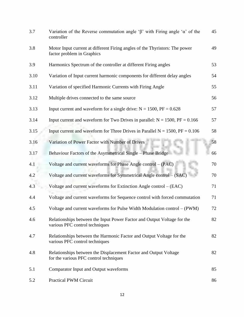
Fig. 2.2: Static I – V Characteristics of a thyristor
Note that V-I characteristic after avalanche breakdown during reverse blocking mode is
applicable only when load resistance is zero. In case load resistance is present, a large anode
current associated with avalanche breakdown at VBR would cause substantial voltage drop across
load and as a result, V-I characteristic in third quadrant would bend to the right of vertical line
drawn at VBR.
37
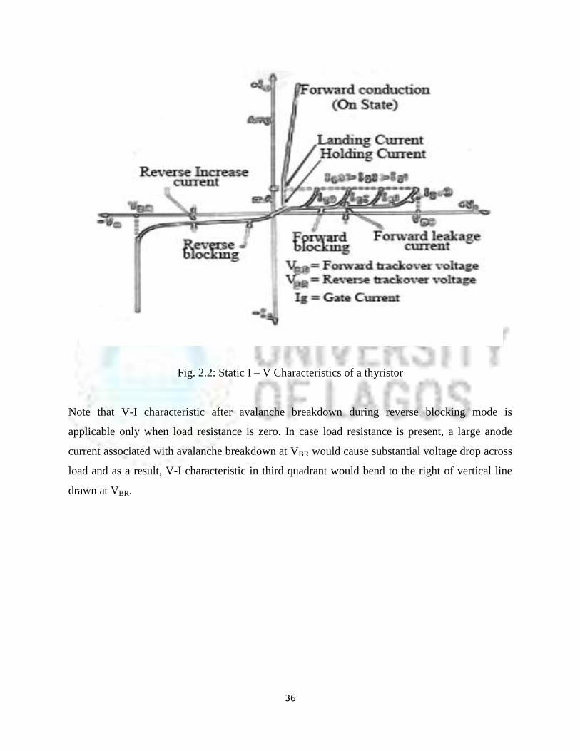
Fig. 2.3: Junction biased conditions
(a) J2 forward biased and J2, J1 reverse biased,
(b) J2 reversed biased and J1, J3 forward biased.
Forward Blocking Mode: When anode is positive with respect to the cathode, with gate circuit
open, thyristor is said to be forward biased as shown in Fig. 2.3 (b). It is seen from this figure
that junctions J1, J3 are forward biased but junction J2 is reverse biased. In this mode, a small
current, called forward leakage current, flows as shown in Figs. 2.2 and 2.3 (b). In case the
forward voltage is increased, then the reverse biased junction J2 will have an avalanche
breakdown at a voltage called forward breakover voltage VB0. When forward voltage is less than
VBO, SCR offers high impedance. Therefore, a thyristor can be treated as an open switch even in
the forward blocking mode.
Forward Conduction Mode: In this mode, thyristor conducts currents from anode to cathode with
a very small voltage drop across it. A thyristor is brought from forward blocking mode to
forward conduction mode by turning it on, by exceeding the forward breakover voltage or by
applying a gate pulse between gate and cathode. In this mode, thyristor is in on-state and behaves
like a closed switch. Voltage drop across thyristor in the on state is of the order of 1 to 2 V
depending on the rating of SCR. It may be seen from Fig. 2.2 that this voltage drop increases
slightly with an increase in anode current. In conduction mode, anode current is limited by load
impedance alone as voltage drop across SCR is quite small. This small voltage drop VT across
the device is due to ohmic drop in the four layers

38
2.2.2 Dynamic Characteristics of a Thyristor
Static and switching characteristics of thyristors are always taken into consideration for
economical and reliable design of converter equipment. Static characteristics of a thyristor have
already been examined. In this section; switching, dynamic or transient, characteristics of
thyristors are discussed.
During turn-on and turn-off processes, a thyristor is subjected to different voltages across it and
different currents through it. The time variations of the voltage across a thyristor and the current
through it during turn-on and turn-off processes give the dynamic or switching characteristics of
a thyristor. The switching characteristics during turn-on are described and then the switching
characteristics during turn-off
Switching Characteristics during Turn-on
Before a thyristor is turned on, it is forward-biased and a positive gate voltage between gate and
cathode. There is, however, a transition time from forward off-state to forward on state. This
transition time called thyristor turn-on time is defined as the time during which it changes from
forward blocking state to final on-state. Total turn-on time can be divided into three intervals; (i)
delay time td , (ii) rise time tr and (iii) spread time tp , Fig. 2.5.
(i) Delay time td : The delay time td is measured from the instant at which gate current reaches
0.9 Ig to the instant at which anode current reaches 0.1Ia. Here Ig and Ia are respectively the final
values of gate and anode currents. The delay time may also be defined as the time during which
anode voltage falls from Va to 0.9Va where Va = initial value of anode voltage. Another way of
defining delay time is the time during which anode current rises from forward leakage current to
0.1 Ia where Ia = final value of anode current. With the thyristor initially in the forward blocking
state, the anode voltage is OA and anode current is small leakage current as shown in Fig. 2.6.
Initiation of turn-on process is indicated by a rise in anode current from small forward leakage
current and a fall in anode-cathode voltage from forward blocking voltage OA. As gate current
begins to flow from gate to cathode with the application of gate signal, the gate current has non-
uniform distribution of current density over the cathode surface due to the p layer. Its value is
much higher near the gate but decreases rapidly as the distance from the gate increases, see

39
Fig. 2.4(a). This shows that during delay time td, anode current flows in a narrow region near the
gate where gate current density is the highest.
The delay time can be decreased by applying high gate current and more forward voltage
between anode and cathode. The delay time is fraction of a microsecond.
Fig. 2.4: Distribution of gate and anode current during delay time
(ii) Rise time tr: The rise time tr is the time taken by the anode current to rise from 0.1 Ia to 0.9 Ia.
The rise time is also defined as the time required for the forward blocking off-state voltage to fall
from 0.9 to 0.1 of its initial value OA. The rise time is inversely proportional to the magnitude of
gate current and its build up rate. Thus tr can be reduced if high and steep current pulses are
applied to the gate. However, the main factor determining tr is the nature of anode circuit. For
example, for series RL circuit, the rate of rise of anode current is slow, therefore, tr is more. For
RC series circuit, di/dt is high, tr is therefore, less.
From the beginning of rise time tr anode current starts spreading from the narrow conducting
region near the gate. The anode current spreads at a rate of about 0.1 mm per microsecond. As
the rise time is small, the anode current is not able to spread over the entire cross-section of
cathode. Fig. 2.4(b) illustrates how anode current expands over cathode surface area during turn-
on process of a thyristor. Here the thyristor is taken to have single gate electrode away from the

40
centre of p-layer. It is seen that anode current conducts over a small conducting channel even
after tr -this conducting channel area is however, greater than that during td. During rise time,
turn-on losses in the thyristor are the highest due to high anode voltage (Va) and large anode
current (Ia) occurring together in the thyristor as shown in Fig. 2.5. As these losses occur only
over a small conducting region, local hot spots may be formed and the device may be damaged.
(iii) Spread time tp : The spread time is the time taken by the anode current to rise from 0.9 Ia to
Ia. It is also defined as the time for the forward blocking voltage to fall from 0.1 of its value to
the on-state voltage drop (1 to 1.5 V). During this time, conduction spreads over the entire cross-
section of the cathode of SCR. The spreading interval depends on the area of cathode and on gate
structure of the SCR. After the spread time, anode current attains steady state value and the
voltage drop across SCR is equal to the on-state voltage drop of the order of 1 to 1.5 V, Fig. 2.5.
Total turn-on time of an SCR is equal to the sum of delay time, rise time and spread time.
Thyristor manufacturers usually specify the rise time which is typically of the order of 1 to 4 µ-
sec. Total turn-on time depends upon the anode circuit parameters and the gate signal wave
shapes.
During turn-on, SCR may be considered to be a charge controlled device. A certain amount of
charge must be injected into the gate region for the thyristor conduction to begin. This charge is
directly proportional to the value of gate current. Therefore, the higher the magnitude of gate
current, the lesser time it takes to inject this charge. The turn-on time can therefore be reduced by
using higher values of gate currents. The magnitude of gate current is usually 3 to 5 times the
minimum gate current required to trigger an SCR.
When gate current is several times higher than the minimum gate current required, a thyristor is
said to be hard-fired or overdriven. Hard-firing or overdriving of a thyristor reduces its turn-on
time and enhances it di/dt capability.
Switching Characteristics during Turn-off
Thyristor turn-off means that it has changed from on to off state and is capable of blocking the
forward voltage. This dynamic process of the SCR from conduction state to forward blocking
state is called commutation process or turn-off process.
41
Once the thyristor is on, gate loses control. The SCR can be turned off by reducing the anode
current below holding current. If forward voltage is applied to the SCR at the moment its anode
current falls to zero, the device will not be able to block this forward voltage as the carriers
(holes and electrons) in the four layers are still favourable for conduction. The device will
therefore go into conduction immediately even though gate signal is not applied. In order to
obviate such an occurrence, it is essential that the thyristor is reverse biased for a finite period
after the anode current has reached zero.
Fig.2.5: Thyristor voltage and current waveforms during turn-on and turn-off processes

42
The turn-off time tq of a thyristor is defined as the time between the instant anode current
becomes zero and the instant SCR regains forward blocking capability. During time tq all the
excess carriers from the four layers of SCR must be removed. This removal of excess carriers
consists of sweeping out of holes from outer p-layer and electrons from outer n-layer. The
carriers around junction J2 can be removed only by recombination. The turn-off time is divided
into two intervals; reverse recovery time trr and the gate recovery time tg r ; i.e. tq = trr + tgr.
The thyristor characteristics during turn-on and turn-off processes are shown in one Fig. 2.5 so as
to gain insight into these processes.
At instant tl anode current becomes zero. After tl anode current builds up in the reverse direction
with the same di/dt slope as before tl The reason for the reversal of anode current after tl is due to
the presence of carriers stored in the four layers. The reverse recovery current removes excess
carriers from the end junctions J1 and J3 between the instants tl and t3. In other words, reverse
recovery current flows due to the sweeping out of holes from top p-layer and electrons from
bottom n-layer. At instant t2, when about 60% of the stored charges are removed from the outer
two layers, carrier density across J1 and J3 begins to decrease and with this reverse recovery
current also starts decaying. The reverse current decay is fast in the beginning but gradual
thereafter. The fast decay of recovery current causes a reverse voltage across the device due to
the circuit inductance. This reverse voltage surge appears across the thyristor terminals and may
therefore damage it. In practice, this is avoided by using protective RC elements across SCR. At
instant t3 , when reverse recovery current has fallen to nearly zero value, end junctions J1 and J3
recover and SCR is able to block the reverse voltage. For a thyristor, reverse recovery
phenomenon between t1 and t3 is similar to that of a rectifier diode.
At the end of reverse recovery period (t3 -the middle junction J2 still has trapped charges,
therefore, the thyristor is not able to block the forward voltage at t3 The trapped charges around
J2, i.e. in the inner two layers, cannot flow to the external circuit, therefore, these trapped charges
must decay only by recombination. This recombination is possible if a reverse voltage is
maintained across SCR, though the magnitude of this voltage is not important. The rate of
recombination of charges is independent of the external circuit parameters. The time for the
recombination of charges between t3 and t4 is called gate recovery time tg.. At instant t 4, junction

43
J2 recovers and the forward voltage can be reapplied between anode and cathode. The thyristor
turn-off time tq is in the range of 3 to 100 µsec. The turn-off time is influenced by the magnitude
of forward current, di/dt at the time of commutation and junction temperature. An increase in the
magnitude of these factors increases the thyristor turn-off time. If the value of forward current
before commutation is high, trapped charges around junction J2 are more. The time required for
their recombination is more and therefore turn-off time is increased. But turn-off time decreases
with an increase in the magnitude of reverse voltage, particularly in the range of 0 to - 50 V. This
is because high reverse voltage sucks out the carriers out of the junctions Jl , J3 and the adjacent
transition regions at a faster rate. It is evident from above that turn-off time tq is not a constant
parameter of a thyristor.
The thyristor turn-off time tq is applicable to an individual SCR. In actual practice, thyristor (or
thyristors) form a part of the power circuit. The turn-off time provided to the thyristor by the
practical circuit is called circuit turn-off time tc. It is defined as the time between the instant
anode current becomes zero and the instant reverse voltage due to practical circuit reaches zero,
see Fig. 2.5. Time tc must be greater than tq for reliable turn-off, otherwise the device may turn-
on at an undesired instant, a process called commutation failure.
Thyristors with slow turn-off time (50 - 100 (usee) are called converter grade SCRs and those
with fast turn-off time (3 - 50 µsec) are called inverter-grade SCRs. Converter-grade SCRs are
cheaper and are used where slow turn-off is possible as in phase-controlled rectifiers, ac voltage
controllers, cycloconverters etc. Inverter-grade SCRs are costlier and are used in inverters,
choppers and force-commutated converters.
2.3 Circuits and Devices used in power Factor correction Schemes
A number of the devices discussed in this section were used in the implementation of this
research work. The operational amplifier for instance was used as an integrator to obtain the
required saw tooth signals that was compared with a dc signal to obtain the desired pulses needed
to turn – on the gates of the thyristors. The 555 timer was used either in the astable or monostale
mode to generate pulses. The applications of an operational amplifier and the 555 timer are
presented below.

44
2.3.1 Operational amplifiers and applications
The op-amp is basically a differential amplifier having a large voltage gain, very high input
impedance and low output impedance. The op-amp has a "inverting" or (-) input and "non-
inverting" or (+) input and a single output. The op-amp is usually powered by a dual polarity
power supply in the range of +/- 5 volts to +/- 15 volts. A simple dual polarity power supply is
shown in the figure below which can be assembled with two 9 volt batteries.
Figure 2.6: A circuit model of an operational amplifier (op amp) with gain and input and
output resistances Rin and Rout.
A circuit model of an operational amplifier is shown in Figure 2.6. The output voltage of the op
amp is linearly proportional to the voltage difference between the input terminals v+ - v- by a
factor of the gain, ‗A‘. However, the output voltage is limited to the range –Vcc ≤ v ≤ Vcc, where
Vcc is the supply voltage specified by the designer of the op amp. The range –Vcc ≤ v ≤ Vcc, is
often called the linear region of the amplifier, and when the output swings to Vcc or - Vcc, the op
amp is said to be saturated.
An ideal op amp has infinite gain (A = ∞), infinite input resistance (Rin = ∞), and zero output
resistance (Rout = 0). A consequence of the assumption of infinite gain is that, if the output
voltage is within the finite linear region, then v+ = v- . A real op amp has a gain on the range 103
- 105 (depending on the type), and hence actually maintains a very small difference in input
terminal voltages when operating in its linear region. The operational amplifier can be used as an
inverter amplifier, non – inverting amplifier, integrator, differentiator, comparator etc.
45
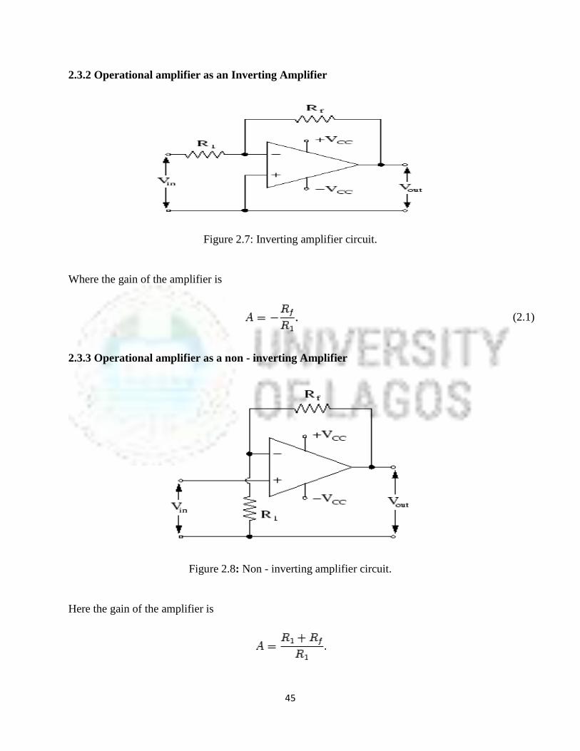
2.3.2 Operational amplifier as an Inverting Amplifier
Figure 2.7: Inverting amplifier circuit.
Where the gain of the amplifier is
(2.1)
2.3.3 Operational amplifier as a non - inverting Amplifier
Figure 2.8: Non - inverting amplifier circuit.
Here the gain of the amplifier is

46
2.3.4 Operational amplifier as an Integrator
Figure 2.9: Integrator circuit.
The output signal of the amplifier is
(2.2)
2.3.5 Operational amplifier as a Differentiator
Figure 2.10: Differentiator circuit.
47
The output signal of the amplifier is
(2.3)
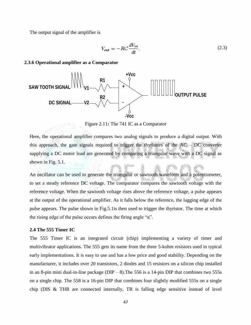
2.3.6 Operational amplifier as a Comparator
R1
R2DC SIGNAL
SAW TOOTH SIGNAL
OUTPUT PULSE
V1
V2
+Vcc
-Vcc
+
-
Figure 2.11: The 741 IC as a Comparator
Here, the operational amplifier compares two analog signals to produce a digital output. With
this approach, the gate signals required to trigger the thyristors of the AC – DC converter
supplying a DC motor load are generated by comparing a triangular wave with a DC signal as
shown in Fig. 5.1.
An oscillator can be used to generate the triangular or sawtooth waveform and a potentiometer,
to set a steady reference DC voltage. The comparator compares the sawtooth voltage with the
reference voltage. When the sawtooth voltage rises above the reference voltage, a pulse appears
at the output of the operational amplifier. As it falls below the reference, the lagging edge of the
pulse appears. The pulse shown in Fig.5.1is then used to trigger the thyristor. The time at which
the rising edge of the pulse occurs defines the firing angle ―α‖.
2.4 The 555 Timer IC
The 555 Timer IC is an integrated circuit (chip) implementing a variety of timer and
multivibrator applications. The 555 gets its name from the three 5-kohm resistors used in typical
early implementations. It is easy to use and has a low price and good stability. Depending on the
manufacturer, it includes over 20 transistors, 2 diodes and 15 resistors on a silicon chip installed
in an 8-pin mini dual-in-line package (DIP – 8).The 556 is a 14-pin DIP that combines two 555s
on a single chip. The 558 is a 16-pin DIP that combines four slightly modified 555s on a single
chip (DIS & THR are connected internally, TR is falling edge sensitive instead of level

48
sensitive).Also available are ultra-low power versions of the 555 such as the 7555 and TLC555.
The 7555 requires slightly different wiring using fewer external components and less power.
The 555 has three operating modes:
Monostable mode: in this mode, the 555 functions as a "one-shot". Applications include
timers, missing pulse detection, bounce free switches, touch switches, Frequency Divider,
Capacitance Measurement, Pulse Width Modulation (PWM) etc
Astable - Free Running mode: the 555 can operate as an oscillator. Uses include LED and
lamp flashers, pulse generation, logic clocks, tone generation, security alarms, pulse
position modulation, etc.
Bistable mode or Schmitt trigger: the 555 can operate as a flip - flop, if the DIS pin is not
connected and no capacitor is used. Uses include bounce free latched switches, etc.
2.4.1 Monostable mode
In the monostable mode, the 555 timer acts as a ―one-shot‖ pulse generator. The pulse begins
when the 555 timer receives a trigger signal. The width of the pulse is determined by the time
constant of an RC network, which consists of a capacitor (C) and a resistor (R). The pulse ends
when the charge on the C equals 2/3 of the supply voltage. The pulse width can be lengthened or
shortened to the need of the specific application by adjusting the values of R and C. The pulse
width of time t is given by
(2.4)
which is the time it takes to charge C to 2/3 of the supply voltage. See RC circuit for an
explanation of this effect.
The relationships of the trigger signal, the voltage on the C and the pulse width are shown below
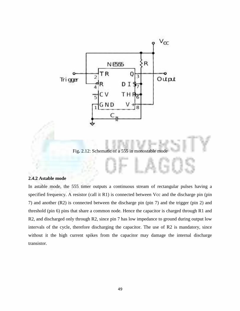
49
Fig. 2.12: Schematic of a 555 in monostable mode
2.4.2 Astable mode
In astable mode, the 555 timer outputs a continuous stream of rectangular pulses having a
specified frequency. A resistor (call it R1) is connected between Vcc and the discharge pin (pin
7) and another (R2) is connected between the discharge pin (pin 7) and the trigger (pin 2) and
threshold (pin 6) pins that share a common node. Hence the capacitor is charged through R1 and
R2, and discharged only through R2, since pin 7 has low impedance to ground during output low
intervals of the cycle, therefore discharging the capacitor. The use of R2 is mandatory, since
without it the high current spikes from the capacitor may damage the internal discharge
transistor.

50
Fig.2.13: Standard 555 Astable Circuit
In the astable mode, the frequency of the pulse stream depends on the values of R1, R2 and C:
(2.5)
The high time from each pulse is given by
(2.6)
and the low time from each pulse is given by
(2.7)
where R1 and R2 are the values of the resistors in ohms and C is the value of the capacitor in
farad.

51
2.5 The Single – Phase Asymmetrical Bridge Converter.
The circuit arrangement of an asymmetrical single – phase bridge converter used for AC - DC
conversion is shown in Fig. 2.14. The choice of this controller for this study is influenced by the
fact that:
It presents the worst form of harmonics to its loads which distorts the AC input voltage
and current
It has a wide range of applications
It is increasingly being applied to main line rail propulsion system
It is used in low power motor control system
It is simple to construct
In Fig.2.14, during the positive half – cycle, thyristor T1 is forward biased. When T1 is fired at
ωt = α the load is connected to the input supply through T1 and D2 in the interval α ≤ ωt ≤ π.
During the interval π ≤ ωt ≤ (π+α), the input voltage is negative and the freewheeling diode D1 is
now forward biased and conducts to provide the continuity of current in the inductive load. The
load current is transferred from T1 and D2 and thyristor T1 and diode D2 are turned – off. During
the negative half – cycle of the input voltage, thyristor T2 is forward biased and the firing of
thyristor T2 at ωt ≤ (π+α) will reverse biased D2. The diode D2 is turned – off and the load is
connected to the supply through T2 and D1.
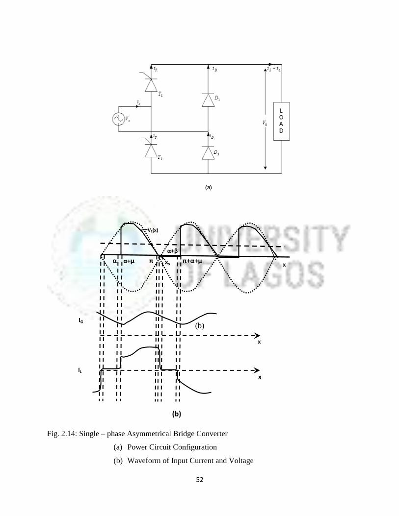
52
(b)
Fig. 2.14: Single – phase Asymmetrical Bridge Converter
(a) Power Circuit Configuration
(b) Waveform of Input Current and Voltage
V2(x)
IG
IL
α+β
x
x
x
α α+µ π π+α+µ
xs
(b)

53
The input current is clearly non - sinusoidal with the input voltage, this is as a result of the
harmonics introduced into the supply due to the switching action of semi – conductor devices
Now that the basic concept of the of the devices used for this research has been described, the
subsequent chapters will discuss the establishment of the input power factor problem, the various
methods of power factor correction improvement schemes and the most efficient and effective
method for the solution to the poor input power factor in drives.

54
CHAPTER THREE
MODELLING AND ANALYSIS OF THE BRIDGE CONVERTER WITH
DC MOTOR LOAD
3.0 Introduction
To investigate the problem of harmonics in the AC line current and analytically predict it
waveshape, the single – Phase Bridge will be considered to have four intervals of operations
(Metha et.al 1974) – Forward Commutation Interval, Conduction Interval, Free-wheeling
Interval and Reverse Commutation Interval. This is because, as a result of the finite source
inductance, current in a thyristor fired at an instant ‗α‘ does not rise instantaneously. Explicit
expressions are to be developed in each of these intervals using the piecewise linear (PWL)
method, with the simplifying assumptions that the terminal conditions of one interval are the
initial conditions for the next interval. The waveform of the AC input current is obtained by
using the equations determined for the intervals in a half cycle.
The waveform of the input current degenerate as the firing angle of the drive increases. Fourier
integral method was applied to the explicit expressions for the motor input current to derived
equations for the harmonic currents. It has equally been shown by experiments that where a
number of drives are connected to the same AC source, the power factor worsens.
3.1 Modelling the DC Motor
The prediction of supply input current in a DC Drive is influenced by the motor parameters when
the motor fed from the Bridge. The subsequent electrical loop equation is of the form:
( ) ( ) ( ) ( ) ( ) ( )
(3.1)
Where,
( ) is the output voltage of the Bridge
( ) is the motor back emf,
( ) is the Armature inductance,
( ) is the Armature resistance,
( ) is the instantaneous input current
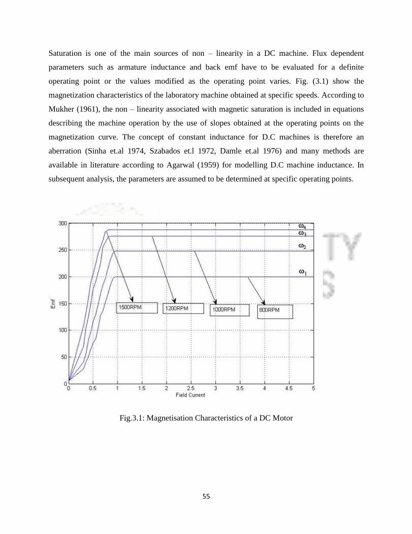
55
Saturation is one of the main sources of non – linearity in a DC machine. Flux dependent
parameters such as armature inductance and back emf have to be evaluated for a definite
operating point or the values modified as the operating point varies. Fig. (3.1) show the
magnetization characteristics of the laboratory machine obtained at specific speeds. According to
Mukher (1961), the non – linearity associated with magnetic saturation is included in equations
describing the machine operation by the use of slopes obtained at the operating points on the
magnetization curve. The concept of constant inductance for D.C machines is therefore an
aberration (Sinha et.al 1974, Szabados et.l 1972, Damle et.al 1976) and many methods are
available in literature according to Agarwal (1959) for modelling D.C machine inductance. In
subsequent analysis, the parameters are assumed to be determined at specific operating points.
Fig.3.1: Magnetisation Characteristics of a DC Motor

56
3.2 Piece – Wise Linear analysis of the Single – Phase Bridge Converter with DC Motor
Load
The circuit configuration of the asymmetrical single-phase bridge converter with a half- cycle
equivalent supplying a separately excited dc motor operating in a discontinuous armature
conduction current mode is shown in Fig.3.2.The control circuit layout of the drive is presented
in Figure (3.3).The main difficulty in predicting the input ac current of the controller and in
analysing the converter circuits is that the switching action of the devices makes the circuits non
– linear (Okoro C.C 1987 and Ira Pitel et.al 1977). This difficulty is overcome by using linear
equivalent circuits which represent the system in particular time domains of operation according
to Mellit et.al (1974) and Nisit et.al (1978).
(a)
Fig.3.2: The asymmetrical single-phase bridge converter with a DC Motor Load
(a): Main circuit (b): Half cycle equivalent

57
The waveform of the currents and voltages of the controller presented in Figure 3.4 show the
various intervals of operation
3.3 Modes of Operation
The operation of the Asymmetrical Bridge may be described by the equivalent circuits
representing each interval of operation as presented in Fig.3.5. In analyzing the circuits for the
different intervals, the terminal conditions of one interval are the initial conditions for the next
interval and the simplifying equations are based on the following assumptions (Metha et.al 1974
and Okoro 1980)
That the thyristor are ideal switches.
That a steady- state condition has been established to justify repetitive representation of
the cycles.
Non-linearity in operation of the machine is included in the parameters of the system
equations.
That the motor is separately excited and the operating point fixes the parameters of the
machine.
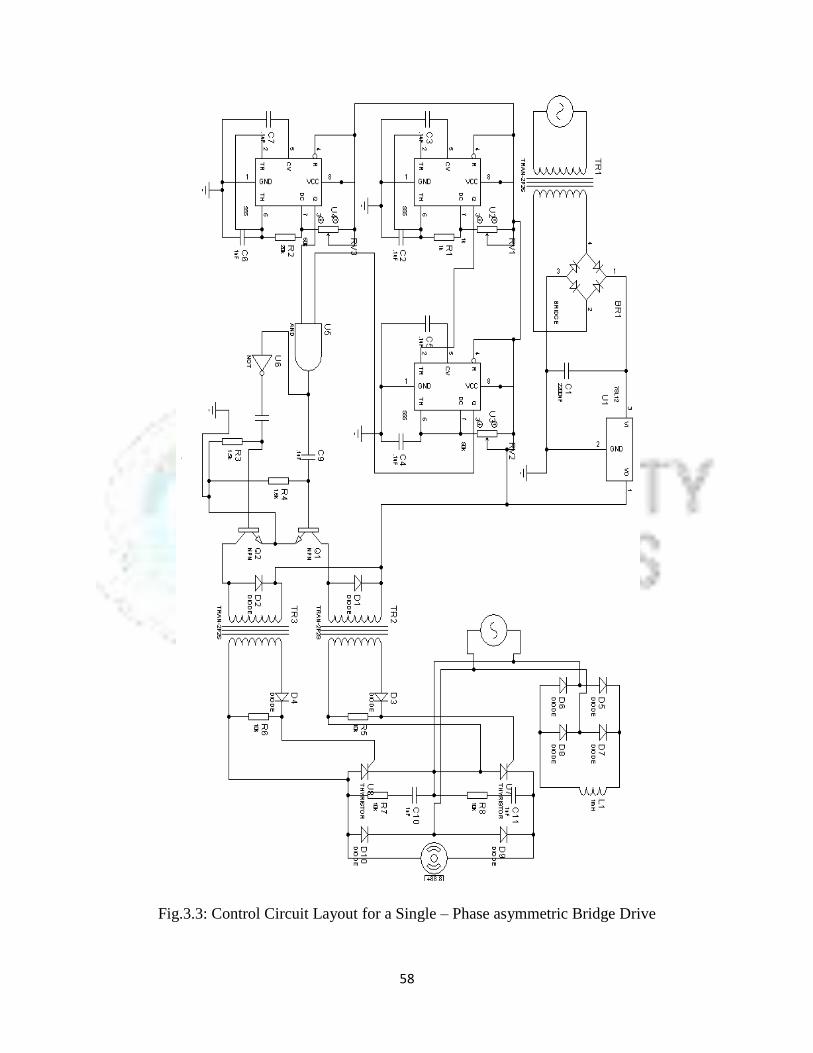
58
Fig.3.3: Control Circuit Layout for a Single – Phase asymmetric Bridge Drive
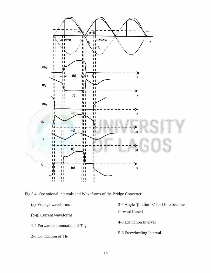
59
Fig.3.4: Operational intervals and Waveforms of the Bridge Converter
(a) Voltage waveforms
(b-g) Current waveforms
1-2 Forward commutation of Th1
2-3 Conduction of Th1
3-4 Angle ‗β‘ after ‗π‘ for D2 to become
forward biased
4-5 Extinction Interval
5-6 Freewheeling Interval
V2(x)
Ith1
ID2
Ith2
ID1
IG
IL
(a)
1 2 (b) 3 4 5 6
(c)
(d)
(e)
(f)
(g)
x
x
x
x
x
x
x
α α+µ π π+α+µ
xs
α+β
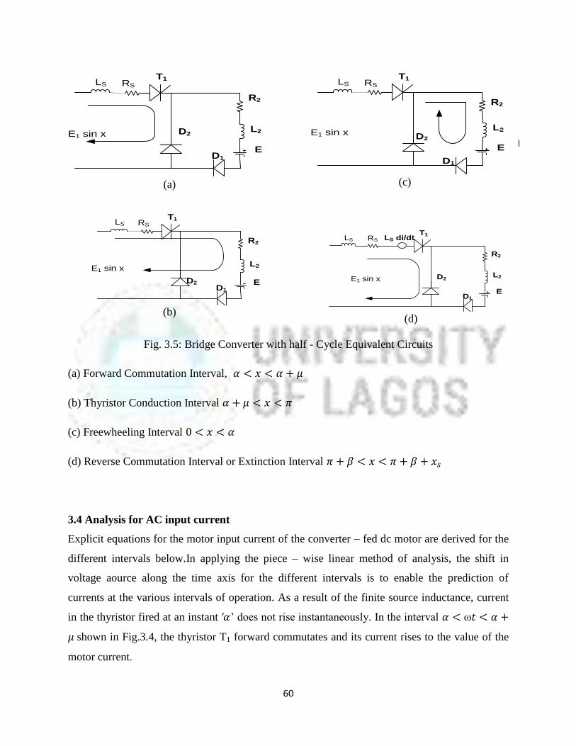
60
RSLS
D1
E
L2
R2
T1
D2E1 sin x
(a)
RSLS
D1
E
L2
R2
T1
D2
E1 sin x
(b)
RSLS
D1
E
L2
R2
T1
D2E1 sin x
(c)
RSLS
D1
E
L2
R2
T1
D2E1 sin x
LS di/dt
(d)
Fig. 3.5: Bridge Converter with half - Cycle Equivalent Circuits
(a) Forward Commutation Interval,
(b) Thyristor Conduction Interval
(c) Freewheeling Interval
(d) Reverse Commutation Interval or Extinction Interval
3.4 Analysis for AC input current
Explicit equations for the motor input current of the converter – fed dc motor are derived for the
different intervals below.In applying the piece – wise linear method of analysis, the shift in
voltage aource along the time axis for the different intervals is to enable the prediction of
currents at the various intervals of operation. As a result of the finite source inductance, current
in the thyristor fired at an instant ‘ does not rise instantaneously. In the interval ω
shown in Fig.3.4, the thyristor T1 forward commutates and its current rises to the value of the
motor current.

61
(A) Forward commutation interval
This is defined by interval ω
And having initial condition ω
Equation for current during this interval is obtained from the equivalent circuit of Fig.3.5 (a) as;
(ω ) (3.2)
Where and are the source supply resistance and inductance respectively.
Equation (3.2) can be solved by either Laplace function method or integrating factor method
Using integrating factor method of solving differential equations, the current at the end of the
interval is obtained as;
( ) ⌈ ( ) ( ) ⌉
The current at the end of the interval when , ( ) , is then,
[ ( ) ( ) .
/] (3.3)
Where =
, | | √( )
, .
/ , =
| |,
A complete analysis is given in APPENDIX I
(B) Conduction interval ( )
In this interval , the current flows in the path shown in Fig. 3.5(b) and the equation
governing this interval with respect to the equivalent circuit is defined by equation (3.4).
( ) (3.4)
Where and
Initial conditions ( ) when
Using integrating factor method of solving differential equations, the current in this interval is;
( ) , (ω ) - , ( ( ) ) -
(3.5)

62
Where,
| |
(
)
(C) Freewheeling interval 0 ω
In this interval, the load is not connected to the supply, current flows in the path shown in
Fig.3.5(c).
This interval is define by the equation
(3.6)
Whose initial condition is ( ) ω
The current in this interval derived from equation (3 - 6) is;
( )
,
- (3.7)
At then
( )
,
-
When ( ) , then,
Substituting the value of
,
- (3.8)
Therefore,
[
]
(3.9)
Also, the current at during the conduction interval is equally .

63
∴ , then, ( )
Hence from equation (3.9);
, - , ( ( ) ) - ( )
(3.10)
Equation (3.3) can be substituted into equation (3.10) to give a transcendental equation ( )
emanating from a combination of equation (3.9) and (3.10) which is solved to obtain the
commutation angle, ‗ for any gating angle
Fig. (3.6) Shows the variation of the commutation angle ‗μ‘ as the firing angle ‗α‘ is altered.
Fig.3.6: Variation of the Forward commutation angle ‗μ‘ with Firing angle ‗α‘ of the
controller
Angle ‗ ‘ after ‗ ‘
The freewheeling diode ‘in Fig.3.5(c) becomes forward biased when the instantaneous supply
voltage equals the induced voltage in the source inductance. The induced voltage in the source
inductance reverses biases ‘, until the angle ‗ ‘ after ‗ ‘ when this voltage is neutralized by
the instantaneous supply voltage. The current in the conducting thyristor begins to decay to zero
and in attempt to oppose this, the voltage in the armature circuit inductance forward biases to
begin the freewheeling mode Mellitt (1974)

64
If the angle ‘ is defined as then the equation for current in the conduction interval-as
shown in equation (3.5) becomes;
( ) , ( ) - , ( ( ) ) - ( )
(3.11)
The freewheeling interval begins when;
( )
(3.12)
From equation (3.11),
( )
, ( )-
, ( ( ) ) -
( )
(3.13)
Now, using equation (3.13) in (3.12),
, ( )-
, ( ( ) ) -
( )
(3.14)
If ( ( ) ),
Then, , ( )- ( )
( )
(3.15)
The value of the motor input current at the beginning of the freewheeling is obtained from
equation (3.11) but the value of the angle ‘ after corresponding to this current is obtained by
solving the transcendental equation (3.15).
The relationship between ‗α‘ and ‗β‘ is shown in Fig. (3.7).

65
Fig. 3.7: Variation of the Reverse commutation angle ‗β‘ with Firing angle ‗α‘ of the controller
(D) Reverse Commutation or Extinction Interval
The reverse commutation of current from a conducting thyristor is opposed by the voltage
induced in the source inductance. Defining from , the current in the reverse
commutating thyristor falls to zero from the value at , i.e .
The equation of current obtained from the equivalent circuit of Fig. 3.5(d) is
( ) (3.16)
Re-arranging,
( )
Natural Component =
Where,
Forced Response = ( )
( )
Where, .
/, and √ ( )

66
∴ ( )
( ) (3.17)
Initial condition, , ( )
Hence,
( ) (3.18)
Substituting equation (3.18) in (3.17);
( )
( ) 0
( ) 1
(3.19)
( ) [ ( ) ]
(3.20)
Where,
The equations of currents for the different intervals put together and plotted for different firing
angles are displayed in Fig. 3.8 Also, Figs.3.6 and 3.7 provide a complete characterization of the
waveforms of the Asymmetrical Single – Phase Bridge that enables one to obtain the waveform
of Fig.3.8 which present the input power factor problem obtained using explicit analytical
equations for current derived during the intervals of operation of the Asymmetrical Single –
Phase Bridge.
The results of Fig. 3.8 clearly show that as the firing angle of the thyristors of the drive are
increased; the instantaneous input current deteriorates which is an indication of an increased
harmonic current present in the supply leading to a low input power factor

67
(a): Motor input current for a ‗200‘
Firing angle
(b): Motor input current for a ‗400‘
Firing angle
Fig.3.8: (a – b): Motor Input current at different Firing angles of the Thyristors: The power factor
problem in Graphics
Angle 't' (degs) --->
Insta
nta
neous A
.C I
nput
Curr
ent
(A)-
-->
Reverse commutation interval
freewheeling interval
Forward commutation interval
conduction interval
Angle after
Angle 't' (degs) --->
Inst
anta
neou
s A
.C I
nput
Cur
rent
(A
)---
>
Reverse commutation interval
freewheeling interval
Forward commutation interval
conduction interval
Angle after

68
(c): Motor input current for a ‗600‘
Firing angle
(d): Motor input current for a ‗800‘
Firing angle
Fig.3.8: (c – d): Motor Input current at different Firing angles of the Thyristors: The power factor
problem in Graphics
Angle 't' (degs) --->
Insta
nta
neous A
.C I
nput
Curr
ent
(A)-
-->
Reverse commutation interval
freewheeling interval
Forward commutation interval
conduction interval
Angle after
Angle 't' (degs) --->
Insta
nta
neous A
.C I
nput
Curr
ent
(A)-
-->
Reverse commutation interval
freewheeling interval
Forward commutation interval
conduction interval
Angle after

69
(e): Motor input current for a ‗1000‘
Firing angle
(f): Motor input current for a ‗1600‘
Firing angle
Fig.3.8: (e – f): Motor Input current at different Firing angles of the Thyristors: The power factor
problem in Graphics
Angle 't' (degs) --->
Inst
anta
neou
s A
.C I
nput
Cur
rent
(A
)---
>
Reverse commutation interval
freewheeling interval
Forward commutation interval
conduction interval
Angle after
Angle 't' (degs) --->
Inst
anta
neou
s A
.C I
nput
Cur
rent
(A
)---
>
Reverse commutation interval
freewheeling interval
Forward commutation interval
conduction interval
Angle after

70
3.5 Harmonics in the AC input Current
The harmonic spectrum of the motor input current is obtained from Fourier analysis of the
explicit expressions for the armature current over a period of the waveform such that;
( ) ∑ ( ) (3.21)
The coefficients are obtained as
∫ ( )
(3.22)
∫ ( )
(3.23)
T is the period.
The coefficients are obtained as presented in Appendix II
For (n = 1, 3, 5, ….∞)
.
/ ( )
⁄ ⁄
( )
0
( ) ( ) ( ) ( )
1
0
( )
1
* ( ( ) ) + 0
( ) ⁄ ( ) ( ) ( )
( ) 1
( ) 2
( ) ⁄ ( )
⁄ ( ) ( )
( ) 3
2
( ) ( ) ( ) ( ) ( ) ( )
3 (3.24)
In a compact form An can be presented as:

71
2
132 2
132 2
6 5
6
2
1 5 2
22
2
cos 1 1 cos1
cos 1 1 cos1
sin sin2
21cos sin 1
1
21 sin cos
1
n
n
n
u
n
kn u
n
kn u
n
A n u A n
n
kn u n n u e
n
I Ae n n n
n
A
1
11 1
11 1
1 1 1 12
1 1
cos 1 cos 11
cos 1 cos 11
2 sin sin cos cos
1 sin
u
kn n u
n
kn n u
n
k e n n u n u n
n n n
(3.25)
Bn (n=1, 3, 5……. )
2.
/ 0
– ( ) ⁄
⁄ ( )
( ) 1
.
/
0 ( ) ( ) ( ) ( )
13
2 0
( )
13
* ( ( ) )
+ 0 ( )
( ) ⁄ ( ) ( ) ( )
( ) 1
2 – ( ) ( ) ( ) ( ) ( ) ( )
3
( ) 2 ( )
( ) ⁄ ( )
⁄ ( )
( ) 3
(3.26)

72
In a compact form Bn can be presented as;
13 sin 1 1 sin2 21
13 sin 1 1 sin2 21
21 cos 1 cos
56
21 6 cos 1 sin2
1
251 2 2 cos
2 221
2
k nn u
n
k nn u
n
nA n u A n
n
uk n
B n n u n e n unn
I An e n n
n
sin
1 sin 1 sin 11 11
1 sin 1 sin 11 11
cos sin12 sin
1 1 12 1 cos sin1 11
n
kn u n
n
kn u n
n
n n nk
u
e n n u n un
(3.27)
The harmonic spectrum of the input current for varying delay angles are shown in Figs.3.9 (a-d)
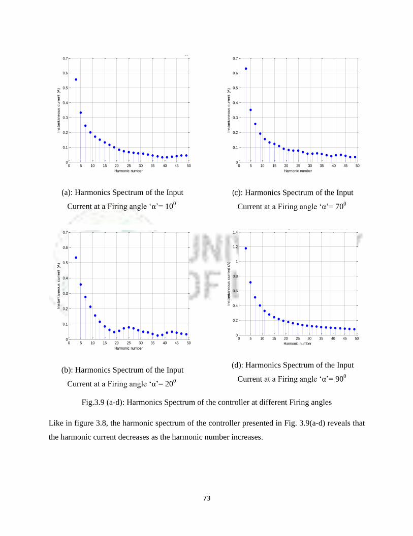
73
(a): Harmonics Spectrum of the Input
Current at a Firing angle ‗α‘= 100
(b): Harmonics Spectrum of the Input
Current at a Firing angle ‗α‘= 200
(c): Harmonics Spectrum of the Input
Current at a Firing angle ‗α‘= 700
(d): Harmonics Spectrum of the Input
Current at a Firing angle ‗α‘= 900
Fig.3.9 (a-d): Harmonics Spectrum of the controller at different Firing angles
Like in figure 3.8, the harmonic spectrum of the controller presented in Fig. 3.9(a-d) reveals that
the harmonic current decreases as the harmonic number increases.
0 5 10 15 20 25 30 35 40 45 500
0.1
0.2
0.3
0.4
0.5
0.6
0.7
Harmonic number
Insta
nta
neous c
urr
ent
(A)
Plot of Instantaneous Current Amplitude versus Harmonic Number for = 10o
0 5 10 15 20 25 30 35 40 45 500
0.1
0.2
0.3
0.4
0.5
0.6
0.7
Harmonic number
Insta
nta
neous c
urr
ent
(A)
Plot of Instantaneous Current Amplitude versus Harmonic Number for = 20o
0 5 10 15 20 25 30 35 40 45 500
0.1
0.2
0.3
0.4
0.5
0.6
0.7
Harmonic number
Insta
nta
neous c
urr
ent
(A)
Plot of Instantaneous Current Amplitude versus Harmonic Number for = 70o
0 5 10 15 20 25 30 35 40 45 500
0.2
0.4
0.6
0.8
1
1.2
1.4
Harmonic number
Insta
nta
neous c
urr
ent
(A)
Plot of Instantaneous Current Amplitude versus Harmonic Number for = 90o
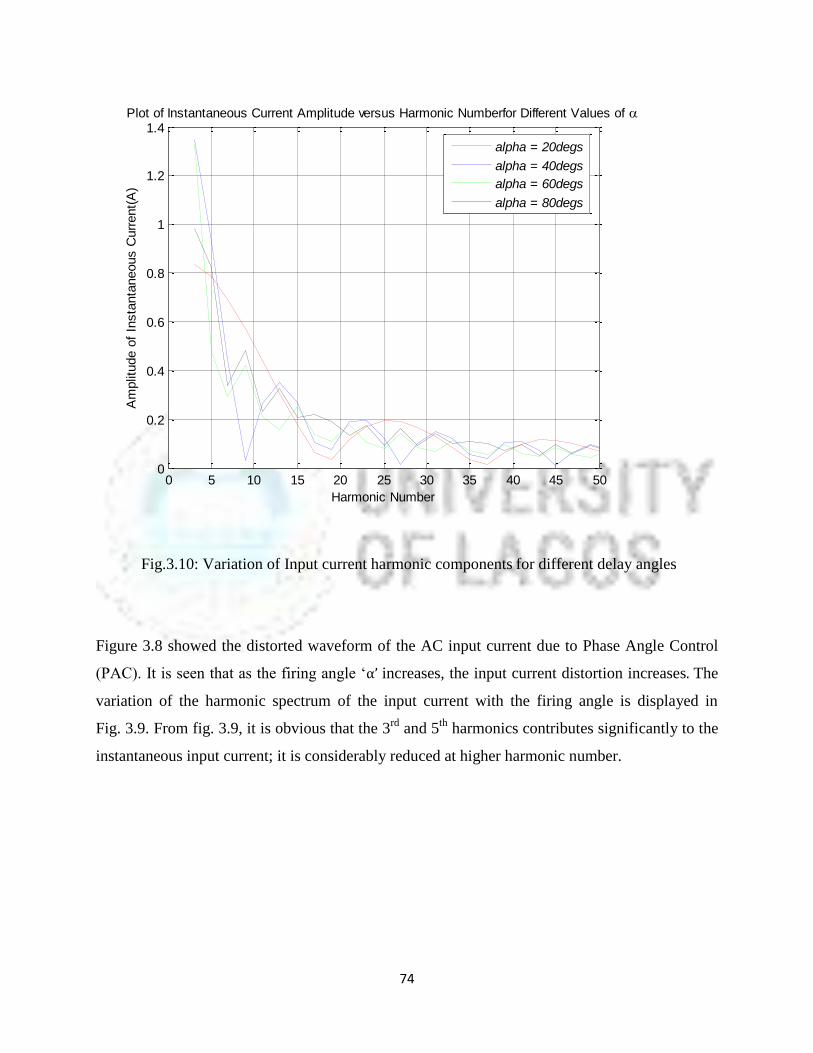
74
Fig.3.10: Variation of Input current harmonic components for different delay angles
Figure 3.8 showed the distorted waveform of the AC input current due to Phase Angle Control
(PAC). It is seen that as the firing angle ‗α’ increases, the input current distortion increases. The
variation of the harmonic spectrum of the input current with the firing angle is displayed in
Fig. 3.9. From fig. 3.9, it is obvious that the 3rd
and 5th
harmonics contributes significantly to the
instantaneous input current; it is considerably reduced at higher harmonic number.
0 5 10 15 20 25 30 35 40 45 500
0.2
0.4
0.6
0.8
1
1.2
1.4
Harmonic Number
Am
plit
ude o
f In
sta
nta
neous C
urr
ent(
A)
Plot of Instantaneous Current Amplitude versus Harmonic Numberfor Different Values of
alpha = 20degs
alpha = 40degs
alpha = 60degs
alpha = 80degs
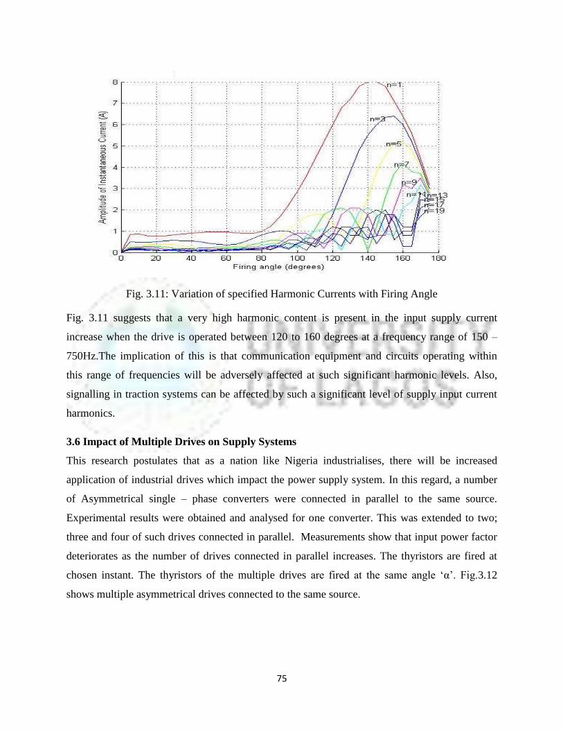
75
Fig. 3.11: Variation of specified Harmonic Currents with Firing Angle
Fig. 3.11 suggests that a very high harmonic content is present in the input supply current
increase when the drive is operated between 120 to 160 degrees at a frequency range of 150 –
750Hz.The implication of this is that communication equipment and circuits operating within
this range of frequencies will be adversely affected at such significant harmonic levels. Also,
signalling in traction systems can be affected by such a significant level of supply input current
harmonics.
3.6 Impact of Multiple Drives on Supply Systems
This research postulates that as a nation like Nigeria industrialises, there will be increased
application of industrial drives which impact the power supply system. In this regard, a number
of Asymmetrical single – phase converters were connected in parallel to the same source.
Experimental results were obtained and analysed for one converter. This was extended to two;
three and four of such drives connected in parallel. Measurements show that input power factor
deteriorates as the number of drives connected in parallel increases. The thyristors are fired at
chosen instant. The thyristors of the multiple drives are fired at the same angle ‗α‘. Fig.3.12
shows multiple asymmetrical drives connected to the same source.

76
Fig. 3.12: Multiple drives connected to the same AC source
Waveforms of the input current and voltage were obtained from the oscilloscope display while
measurements of the corresponding input power factor were recorded. The non – sinusoidal input
waveform deteriorates each time the number of drives is increased and the power factor worsens.
The waveforms of the supply voltage and current as the number of drives is increased are shown
in figs. 3.13, 3.14 and 3.15, thereby establishing experimentally the power factor problem with
Drive 1
Drive 2
Drive 3
Drive N
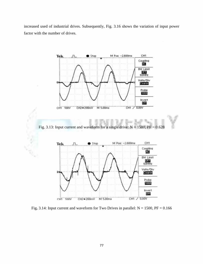
77
increased used of industrial drives. Subsequently, Fig. 3.16 shows the variation of input power
factor with the number of drives.
Fig. 3.13: Input current and waveform for a single drive: N = 1500, PF = 0.628
Fig. 3.14: Input current and waveform for Two Drives in parallel: N = 1500, PF = 0.166
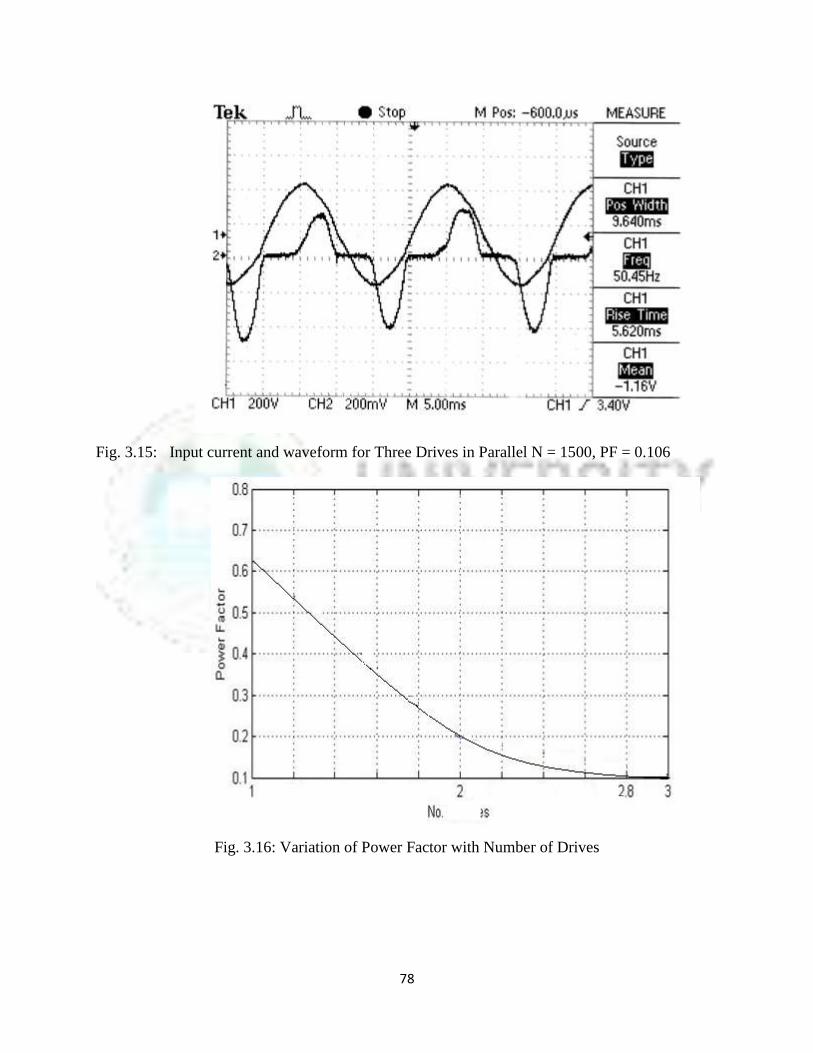
78
Fig. 3.15: Input current and waveform for Three Drives in Parallel N = 1500, PF = 0.106
Fig. 3.16: Variation of Power Factor with Number of Drives

79
3.7 Behaviour Factors of the Drive
The basic concept employed in the study is presented and described below.
A. Input Power Factor (PF)
In an AC to DC converter (asymmetrical single – phase bridge converter), the ac source voltage
is usually non sinusoidal and often times contains harmonics. Consequently, only the
fundamental component of the converter input current at the source frequency contributes to real
converter input power. For an a.c to d.c converter supplied by an m- phase ac source, the
converter real power (P) and the apparent power (S) inputs (Rashid 1993, Mohan 1995) are:
11 s
CosImVP ss (3.28)
S= ss ImV (3.29)
where,
sV = Rms value of the converter input phase voltage
sI = Rms value of the converter input current
1sI = Rms fundamental component of sI
1s = Phase angle between Vs and
1sI
Then,
Input power Factor acPF
acPF = ss
sss
ImV
CosImV
S
P 11
(3.30)
=1
1
s
s
sCos
I
I (3.31)
= (Distortion Factor). (Displacement Factor)
Ideally, if the input power factor is unity (Rashid 1993), its converter input current is sinusoidal
and in phase with the source voltage. But this is not the case because the converter control
introduces harmonics and often times phase angle difference in the converter input current.

80
B. Input Displacement Factor (DF)
This may be referred to as fundamental power factor defined as:
1s
CosDF (3.32)
Where,
1s = is the displacement angle.
For the same power demand, if the displacement factor is low, more fundamental current is
drawn from the supply.
C. Harmonic Factor. (HF)
The harmonic factor indicates the harmonic content in the input supply current and this measures
the distortion of the input current.
1
1
1
22
s
ss
s
distortion
I
II
I
IHF
(3.33)
=
11
2
1
2
2
s
sn
s
I
I
I
In
s
n
(3.34)
Where,
22
1 distortionss III (3.35)
sI = Input supply current
1sI = Input fundamental current
distortionI = Current distortion component
D. Form Factor (FF)
This is a measure of the shape of the output defined (Rashid 1993) as:
dc
rms
V
VFF (3.36)
E. Ripple Factor (RF)
Ripple factor measures the amount of ripple content and is defined as:
dc
ripple
dc
ac
V
V
V
VRF (3.37)

81
Where,
acV = Effective (rms) value of the ac component of output voltage
= 22
dcrms VV (3.38)
Therefore,
dc
dcrms
V
VVRF
22
= 1
2
dc
rms
V
V
= 12 FF (3.39)
F. Total Harmonic Distortions (THD)
This is called a distortion index of fundamental and distortion component in the supply current
tis . It is expressed in percentage as:
1
1
1
22
100100%s
ss
s
distortion
I
II
I
ITHD
1100
2
1
s
s
I
I
1
2
2
1
s
s
I
ITHD
Therefore,
21
1
THDI
I
s
s (3.40)
Substituting equation (3.32) in (3.31)
DFI
IPF
s
s1
Hence from equation (3.40),

82
DFTHD
PF .1
1
2 (3.41)
From equation (3.41), it is clear that if the displacement factor is unity, a total harmonic
distortion of 100 percent (Sen 1980), which is possible in drives unless corrective measures are
taken, can reduce the power factor to approximately 0.7 (or 2
1 = (0.707)).
3.8 The Input Power Factor Problem
To establish the input power factor problem of the asymmetrical Single – Phase Bridge, Fourier
series analysis will be employed. In an ideal converter, both the AC source voltage and the
converter input current are sinusoidal i.e.
1SS II
and,
01S (i.e. phase angle between SV and
1SI )
11 sac CosPF
Hence in an ideal converter, the AC input power factor is unity.
To establish the power factor problem in an ac to dc converter of an asymmetrical single-phase
bridge, the following should be noted:
Where SI and 1SI obtained from Fourier analysis of the waveform are different, it implies that
the converter input current is non – sinusoidal and hence not in phase with the ac source voltage;
this brings about the phase difference between SV and 1SI . And from equation (3.31), the ac
input current power factor acPF deviates from unity. Implying that there is an input power factor
problem.
Where the Fourier waveform analysis contains harmonics, it shows that the converter input
current is not sinusoidal and is out of phase with the ac source voltage; this is because harmonics
bring about a distortion in the waveform of a signal.
Fourier series analysis will be needed in order to determine:
(a) The Harmonic Factor (HF)
(b) The Displacement Factor (DF)
(c) The Input Power Factor (PFac)
From these derivations, the input power factor will become clearer.

83
3.9 Generalised Analysis for the Asymmetrical Bridge.
The instantaneous input current to an asymmetrical Single – Phase Bridge can be expressed in
Fourier series as:
tis =I dc tna
n
n cos(...2,1
+ )sin tnbn (3.42)
Solving for components ―Idc‖, ―an‖ and ―bn‖ we have that;
I 0dc
na =
nn
I a sin2
For n = 1, 3, 5…. odd
nb = )cos1(2
nn
I a For n=1, 3, 5…..old
Hence equation (3.42) can be written as:
...5,3,1
cossin2
n
as tnn
n
ItI
tnn
n
I a
sincos12
= )sincos(..3,2,1
tnbtna n
n
n
(3.43)
Equation (3.43) can also be written in the form;
)(tis = nn
n
tnI
sin2..3,2,1
where,
2
tan 1
n
b
a
n
nn

84
Thus, the rms value of the nth harmonic current of the input current is derived as:
2
122
2
1nns baI
n
2cos
22
as II
n
2cos
221
as II
(i.e. n = 1)
Determination of the rms value of the input current supply is derived as sI :
2
1
2 )(2
2
tdII as=
2
1
1
aI
Now,
PF = 1
1 cos s
s
s
I
I
Where,
21
s
Hence,
PF
2
1
cos12
From the expression of equation (3.33);

85
HF
2
12
2
1
2
22
1
11
1
s
s
s
ss
I
I
I
II
Substituting for sI and 1sI
HF =
2
1
1cos14
If 1s is the angle between the fundamental component of the input current and AC input
voltage, then the displacement factor DF is:
DF = nscos
2
nCos
2cos
1
sCos (3.44)
Derivations of the expressions for PF, HF and DF is presented in APPENDIX III
Fig. 3.17: shows the variation of the behaviour factors with the firing angle of the bridge
thyristors.
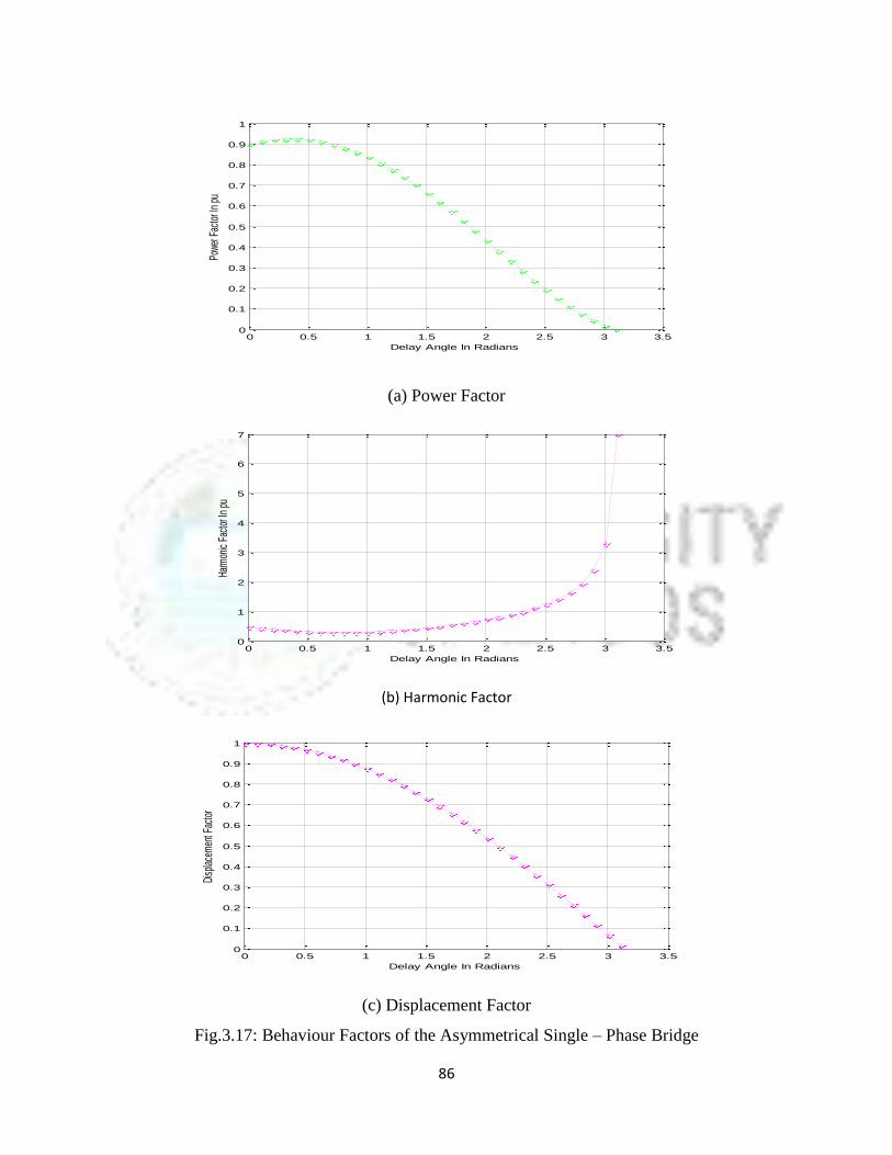
86
(a) Power Factor
(b) Harmonic Factor
(c) Displacement Factor
Fig.3.17: Behaviour Factors of the Asymmetrical Single – Phase Bridge
0 0.5 1 1.5 2 2.5 3 3.50
0.1
0.2
0.3
0.4
0.5
0.6
0.7
0.8
0.9
1
Delay Angle In Radians
Powe
r Fac
tor I
n pu
0 0.5 1 1.5 2 2.5 3 3.50
1
2
3
4
5
6
7
Delay Angle In Radians
Harm
onic
Fac
tor I
n pu
0 0.5 1 1.5 2 2.5 3 3.50
0.1
0.2
0.3
0.4
0.5
0.6
0.7
0.8
0.9
1
Delay Angle In Radians
Disp
lace
men
t Fac
tor

87
From figs. 3.15, 3.16 and 3.17, it is clear that as the firing or the delay angles of the thyristors of
the drive is increased, its power factor deteriorates and the harmonic content is increased
tremendously, Also, results of the analytical descriptions of the input current model of fig. 3.4
presented in fig. 3.8(a – f) reveals that the supply input current deteriorates as a result of the high
harmonic current present in the supply leading to a low input power factor. The poor input power
factor problem was further demonstrated experimentally by having a number of Asymmetrical
single – phase converters connected in parallel to the same source. Results shown in figs 3.13,
3.14 and 3.15 indicates that the input power factor deteriorates with an increase in the number of
such drives connected in parallel, thus establishing the input power factor problem in industrial
drives where many drives are constantly in use.
The various existing schemes employed in input power factor improvement are discussed in the
next chapter. Their performance characteristics expressions will be obtained in other to evaluate
and compare their performance at improving power factor.

88
CHAPTER FOUR
POWER FACTOR CORRECTION (PFC) CONTROL SCHEMES
4.0 Introduction
This chapter presents the various methods of power factor control and improvement techniques.
Both passive and active methods of control are discussed. A performance characteristic of the
various control schemes has been derived and simulation results of the behaviour factors for the
different schemes using MATLAB are also presented for comparison and evaluation.
4.1 Passive and Active methods of power factor correction
There are two approaches to solving the power factor problem. One way is by Passive control
method which involves the use of capacitors and inductors and the second is by Active control
method which involves the use of active devices like the Silicon Controlled Rectifier (SCR),
Metallic Oxide Semi – Conductor Field Effect Transistor (MOSFET) and Insulated Gate Bipolar
Transistor (IGBT). Some of these devices can be turned on either naturally or by Forced
commutation i.e by means of an external circuit.
4.1.1 Passive Power Factor Correction Techniques
The traditional methods of power factor correction involve the use of capacitive and inductive
elements. They are limited to low power applications and may lead to resonance because of RLC
components. Besides, the waveform distortion caused by non-linear loads, which distort the
current, and voltage waveforms introduce harmonic currents in the supply, which cannot be
completely eliminated by the application of the traditional passive power factor correction
methods. New methods of power factor improvement techniques have evolved employing
Natural and Forced Commutation (Patel et.al 1983). Passive power factor corrections have
certain advantage such as simplicity, reliability and ruggedness, insensitivity to noise and surges,
no generation of high frequency EMI and no high frequency switching loss. However, they have
several drawbacks. They are bulky and heavy because line – frequency reactive components are
used. They also have poor dynamic response, lack voltage regulation and the shape of their input
current depends on the load.

89
4.1.2 Active Power Factor Correction Techniques
Better characteristic are obtained with active PFC circuits. Active PFC involves the use of power
switching devices such as the thyristor (SCR), metal oxide semi-conductor field effect transistor
MOSFET or the insulated gate bipolar transistors IGBT. In all active PFC, active switches are
used in conjunction with reactive elements in order to increase the effectiveness of the current
shaping. The switching frequency further divides the active PFC solutions into two classes: low
and high frequency. In low-frequency active PFC, switching takes place at low – order
harmonics of the line – frequency and it is synchronized with the line voltage. In high- frequency
active PFC, the switching frequency is much higher than the line – frequency. Advancement of
power semi – conductor devices has made the active control method more popular and realizable
when implemented in practical systems. It achieves a high power factor and at a reduced
harmonic level. The various PFC techniques of interest depend on the type of control scheme
implemented.
Active PFC is classed into two categories;
I. Natural Commutation Control Scheme: This involved the use of controlled flywheeling;
Asymmetrical Control and Sequence as well as Simultaneous Control.
II. Forced Commutation Control Scheme: These may the Extinction Angle Control (EAC),
Symmetrical Angle Control (SAC), Selective Harmonic Elimination (SHE) and Sequence
Control with forced Commutation.
The various methods of control of the Asymmetrical Bridge will be evaluated and the results
compared so as to adopt one that has a great potential for improved AC input Power Factor for
development in the laboratory.
4.2 Performance evaluation of the various techniques
The simplified voltage and current waveforms shown in Figs 4.1 - 4.4, were used to obtain the
performance characteristic expressions for evaluation of the various control techniques as
presented in table 1. (Dubey et.al 1986)
In deriving the expressions for the behaviour factors of the bridge using the simplified
waveforms, it was assumed;
That the load current is constant
That the current is ripple free

90
Fig. 4.1: Voltage and current waveforms for Phase Angle control – (PAC)
Fig. 4.2: Voltage and current waveforms for Symmetrical Angle control – (SAC)

91
Fig.4.3: Voltage and current waveforms for Extinction Angle control – (EAC)
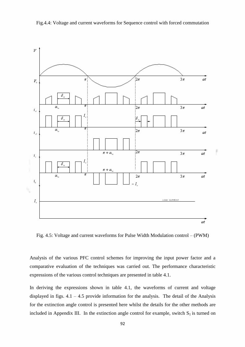
92
Fig.4.4: Voltage and current waveforms for Sequence control with forced commutation
Fig. 4.5: Voltage and current waveforms for Pulse Width Modulation control – (PWM)
Analysis of the various PFC control schemes for improving the input power factor and a
comparative evaluation of the techniques was carried out. The performance characteristic
expressions of the various control techniques are presented in table 4.1.
In deriving the expressions shown in table 4.1, the waveforms of current and voltage
displayed in figs. 4.1 – 4.5 provide information for the analysis. The detail of the Analysis
for the extinction angle control is presented here whilst the details for the other methods are
included in Appendix III. In the extinction angle control for example, switch S1 is turned on

93
at 0t and turned off by forced commutation at ωt = β. Switch S2 is turned on at ωt = π and
is turned off at ωt = (π + β). The output voltage is controlled by the extinction angle β. The
waveforms for voltage and current through the switches are shown in Fig. 4.3
Consider the waveform of Fig.4.3 for the Extinction Angle Control (EAC),
The average output voltage is:
0
)(1
ttdSinnVV mdc (4.1)
0
1ttdSinVV mdc
=
0
1CosVm
=
CosVm 1 (4.2)
dcV can be varied from
mV2 to 0 by varying ‗β‘ from π to 0
The maximum average output voltage is
mdm
VV
2 (4.3)
Hence, the normalized average output Voltage nV is;
m
m
dm
dc
n V
CosV
V
VV
2
1
= Cos12
1 (4.4)
The rms output voltage is given by:
2
1
0
221
tdSinVV mrms (4.5)

94
= 2
1
02
2
2
11
td
tCosVm
=2
1
04
2
2
1
tSintVm
=2
1
4
2
2
1
SinVm
= 2
1
221
2
Sin
Vm (4.6)
Similarly, the instantaneous input current can be expressed in Fourier series as:
,...3,2,1n
nndcs tSinnbtCosnaIti (4.7)
Where,
2
02
1tdtiI sdc (4.8)
02
1tdtis
=
02
1tdItdI aa
=
tt
I a
02
= 002
aI
0dcI (4.9)
0
`1
ttdCosntia sn (4.10)

95
=
0
1ttdCosnIttdCosnI aa
=
n
tSinn
n
tSinnI a
0
=
SinnSinnSinnn
Ia 0
nSinnSinnCosnnCosSinSinnn
I a
=
Sinnn
Ia2 For n = 1, 3, 5, (4.11)
= 0 for n = 2, 4, 6, (4.12)
0
1ttdSinntib sn (4.13)
=
0
1ttdSinntIttdSinntI aa
=
n
tCosn
n
tCosnI a
0
CosnnCosCosnCosI a 00
=
CosnSinnSinnCosnCosnCosnCosn
Ia 00
=
CosnSinnSinnCosnCosnCosnn
Ia 1
Cosnn
Ib a
n 12
For n = 1, 3, 5, (4.14)
= 0 for n = 2, 4, 6. (4.15)
Since, 0dcI ,

96
The instantaneous input current can now be written as:
,...5,3,1
2n
nns tSinnIti (4.16)
Where, n
nn
b
a1tan (4.17)
Cosn
Sinn
Cosnn
I
Sinnn
I
a
a
1tan
12
2
tan 11
=
22
2222tan
22
22tan
2
1
2
1
nSin
nSin
nCos
nCos
nSin
nSin
nnSin
=
2
2tan
22
222
tan 1
2
1
nSin
nCos
nSin
nCos
nSin
Hence,
2
2tan
n
Sin
nCos
n (4.18)
But, 122 nn SinCos (4.19)
nn
n
CosCos
Sin
22
21
1 (4.20)
n
nCos
1
tan1 2
Substituting equation (4.18) into equation (4.20),

97
nCosn
Sin
nCos
22
2
1
2
21
simplifying gives; 2
22
nSinCos n (4.21)
hence, 2
nSinCos n
therefore, Displacement factor (DF) becomes,
1CosDF
=2
Sin leading (4.22)
Thus, the rms value of the nth harmonic component of the input current is:
2
122
2
1nns baI
n (4.23)
= 2
122
122
2
1
Cosn
n
ISinn
n
I aa
= 21
22 212
2
nCosCosnnSin
n
I a
= 2
1
2112
2
Cosn
n
I a
= 2
1
122
2
Cosn
n
I a
= 2
1
2
222
2
2
nSin
n
I a
= 2
1
2
22
4
nSin
n
I a (4.24)

98
Hence, 2
22
nSinI
nI asn
(4.25)
The rms value of the fundamental current (i.e. n=1) is:
2
221
SinII as (4.26)
Next, the rms input current is 2
1
21
tdtiI ss
(4.27)
2
1
0
21
tdI a =2
1
0
1
tI a
=
aI (4.28)
From equation (3.33), the expression for the harmonic current factor is:
2
1
2
1
1
s
s
I
IHF (4.29)
Substituting equations (4.26) and (4.28) in equations (4.29), it becomes:
2
12
2
1
2
2
1
222
1
2
22
SinSin
I
I
a
a
=
2
1
2
2
1
2
2
1
28
1
28
SinSin
=
2
1
114
Cos (4.30)
From equation (3.31), the expression for the input current power factor is:

99
11 Cos
I
IPF
s
s (4.31)
And from equation (4.22),
2
1
SinCos (4.32)
Hence substituting equations (4.26), (4.28) and (4.32) into equation (4.31) and simplifying,
2
2
22
2
Sin
I
Sin
a
=2
22 2
Sin
=
2
122
2
22 2 CosSin
=
Cos12 (4.33)
The performance expressions in table 4.1 for the output voltage and the behaviour factors of
the drive; displacement factor, harmonic factor and input power factor of the extinction angle
control scheme are represented by equations (4.4), (4.22), (4.30) and (4.33) respectively.
Matlab programming was used to simulate these expressions and their results are presented in
Figs. 4.6, 4.7 and 4.8. Similar expressions for the other active control schemes can be derived
in a similar way presented above. (See APPENDIX IV)
4.3 Performance Analysis for the methods of control of the Asymmetrical Bridge
The performance expressions for the different methods of controls of the Asymmetrical
bridge given in table 4.1 (Dubey etal 1986 and Sen 1991) were simulated to obtain a
complete monograph of the behaviour factors of the drive as shown in Figs. 4.5, 4.7 and 4.8.

100
(a)
Control
Technique
Output Voltage Displacement
Factor (DF)
Harmonic Current (HF) Input Current (PF)
Conventional
phase Angle
Control
(PAC)
Cos12
1
2
Cos
2
1
114
Cos
2
1
2
222
Cos
Controlled
Flywheeling
Cos12
1
2
Cos
2
1
114
Cos
2
1
2
222
Cos
Sequence
Control
0.5<Va<1.0pu
0<Va<0.5pu
Cos34
1
Cos14
1
2
1
610
3
Cos
Cos
2
Cos
2
1
135
4
31
Cos
2
1
114
Cos
2
1
2
32
3
Cos
2
1
1
12
Cos
Extinction
AngleControl
(EAC)
Cos12
1
2
Sin
2
1
114
Cos
Cos12
Symmetrical
Angle Control
(SAC)
Cos 1 2
1
21
8
2
Cos 2
1
2
22
Cos
Sequence
Control (with
Forced
Commutation)
0.5<Va<1.0pu
0<Va<0.5pu
Cos12
1
2
Cos
1
1
2
1
21
12
2
3
Cos
2
1
21
8
2
Cos
2
1
2
3
12
Cos
2
1
21
22
Cos
Sinusoidal
PWM,
“p”Pulses/half
cycle with kth
pulse from αk to
δk
p
m mm
m
Cos
Cos
12
1
1
2
1
1
2
1 1
2
p
m
mmm
p
m
mmm
CosCos
2
1
1
12
p
m
mmm
p
m
mmm CosCos

101
Control Technique
Output Voltage Harmonic Current/Output Current
Input Current/Output Current
Conventional Phase Angle Control (PAC)
Cos12
1
2
22
nCos
n 2
1
Controlled Flywheeling Cos1
2
1
2
22
nCos
n 2
1
Sequence Control 0.5<Va<1.0pu
0<Va<0.5pu
Cos34
1
Cos14
1
2
1
351
Cosnn
Cosnn
2
2
1
4
31
2
1
12
1
Extinction Angle Control (EAC)
Cos12
1
2
22
nSin
n 2
1
Symmetrical Angle Control (SAC)
Cos
Cosnn
22
2
1
21
Sequence Control (with Forced Commutatio)
0.5<Va<1.0pu
0<Va<0.5pu
Cos12
1
2
Cos
Cosn
12
Cosnn
2
2
1
2
31
21
2
1
Sinusoidal PWM, “p” pulses/half cycle with k
th
pulse from αk to δk
p
m
mmm CosCos12
1
p
m
mmm CosnCosnn 1
2
2
1
1
1
p
m
mmm
(b)
Table 4.1: Generalised Equations for Various Converter – Control Techniques using their
simplified models
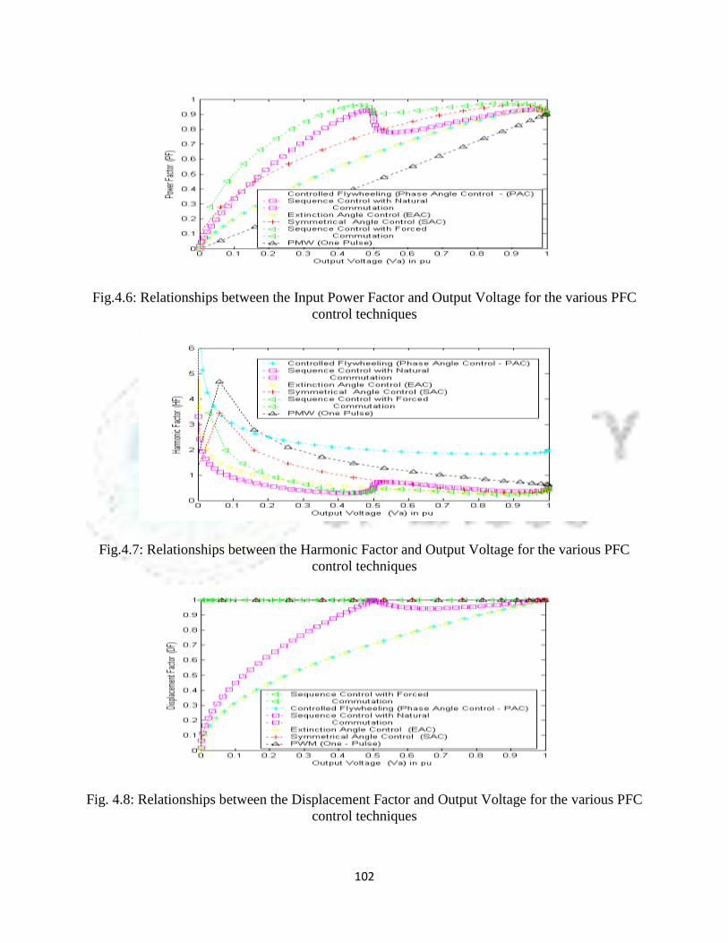
102
Fig.4.6: Relationships between the Input Power Factor and Output Voltage for the various PFC
control techniques
Fig.4.7: Relationships between the Harmonic Factor and Output Voltage for the various PFC
control techniques
Fig. 4.8: Relationships between the Displacement Factor and Output Voltage for the various PFC
control techniques

103
The various power factor correction (PFC) techniques for improving power factor of the
Asymmetrical Single – Phase Drive have been discussed in the preceding section. The
performance characteristics simulated from the simplified equations are shown in Figs. 4.6 to 4.8
for convenience of comparison. Information about the total harmonic content (Fig.4.7) is
important only if input filters are not used. Currents with high harmonic content distort the
supply voltage. In some control schemes, the harmonic factor is high in the low speed region
(Fig.4.7). This is due to high contents of higher harmonics, which are easily filtered out if input
filters are not used. The important current harmonics that the designer needs to consider are those
of the lowest order. In this regard, the PWM control scheme has the advantage because by the
proper choice of pulse numbers per half cycle, the lower order harmonics can be eliminated. An
input filter can eliminate most of the harmonic current from the line thereby making the line
currents essentially sinusoidal. A higher number of pulses per half cycle increase the ripple
frequency of the motor current. The armature circuit inductance may be sufficient to smooth out
the motor current and additional inductance may not be necessary at the armature circuit.
Also from Fig.4.8, the PWM control scheme gives a unity displacement factor implying that it
can be used to achieve a near unity power factor; hence it is adopted for further development and
applications in the laboratory for power factor improvement.

104
CHAPTER FIVE
PULSE WIDTH MODULATION (PWM) FOR INPUT POWER FACTOR
CORRECTION
5.1 Pulse Width Modulation
The various methods of improving the poor power factor were evaluated in chapter four and the
PWM control scheme for power factor correction was adopted as the most effective because it
provides an improved power factor close to unity. Also, by proper choice of the number of
pulses per half cycle, the lower- order harmonics can be eliminated. The input supply current is
essentially sinusoidal and the need for input filters to reduce harmonic currents is obviated. In
Pulse Width Modulation, the converter switches are turned on and off several times during a half
circle and the output voltage is controlled by varying the width of the pulses (Mohan 1995, Tao
2000 and Lazaro 2007). By having many pulses of the output voltage per half cycle of the
source voltage, the ripple in the motor current can be substantially reduced and discontinuous
conduction can be completely eliminated without using any filter inductance. (Ismail 2006)
The operation of the Pulse Width Modulation control scheme involves an astable multivibrator
triggering a monostable to produce pulses of variable width which are then integrated to obtain a
triangular signal at a desired frequency.(for example, 20KHz). The triangular signal together
with a DC signal are fed into an AND gate. This produces a train of high frequency pulses used
to trigger the bridge thyristors. The pulses are processed to a Darlington pair with pulse
transformers at the collector of the transistors. The pulse transformers are used to isolate the
electronic control circuit from the power circuit of the asymmetrical bridge. Waveforms of the
electronic control circuits and the input current and voltage are used to explain the success of the
scheme.
The choice of the pulse width modulation technique was based on the comparative analysis of
the various methods of power factor correction techniques presented in the preceding section. It
gives improved characteristics in terms of higher input power factor and sinusoidal shape of
input current (Lu Bing et.al 2005, Srinivasan, R 1999 and Liu Y et.al 2003).
The Comparator input and output waveforms are shown in Fig.5.1

105
V
rA
cA
rV
cV
gV1S 2S 1S
0 t
0 t
m
m
Fig. 5.1: Comparator Input and Output waveforms.
In Fig. 5.1,
Ac represents the amplitude of the carrier signal (sawtooth waveform) and
Af represents the amplitude of the reference signal (DC voltage)
In the PWM control, the displacement factor is unity and the power factor is improved. The
lower-order harmonics are eliminated or reduced. For example, with four pulses per half – cycle,
the lowest-order harmonic is the fifth and with six pulses per half – cycle, the lowest harmonic is
the seventh. (Grahame et.al 2003 and Rashid et.al 1993)
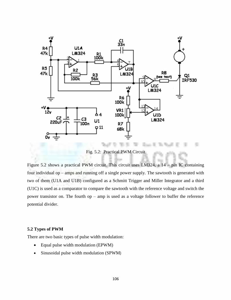
106
Fig. 5.2: Practical PWM Circuit
Figure 5.2 shows a practical PWM circuit. This circuit uses LM324, a 14 – pin IC containing
four individual op – amps and running off a single power supply. The sawtooth is generated with
two of them (U1A and U1B) configured as a Schmitt Trigger and Miller Integrator and a third
(U1C) is used as a comparator to compare the sawtooth with the reference voltage and switch the
power transistor on. The fourth op – amp is used as a voltage follower to buffer the reference
potential divider.
5.2 Types of PWM
There are two basic types of pulse width modulation:
Equal pulse width modulation (EPWM)
Sinusoidal pulse width modulation (SPWM)

107
5.2.1 Equal pulse width modulation (EPWM)
This involves comparing a triangular voltage with a DC signal in a comparator to produce pulses
at the output of the comparator that are used to trigger the switching device as presented in
preceding section.
5.2.2 Sinusoidal pulse width modulation (SPWM)
In the sinusoidal PWM control shown in Fig.5.3, the pulse widths are generated by comparing a
triangular reference voltage Vr of amplitude Ar and frequency fr with a carrier half sinusoidal
voltage Vc of variable amplitude Ac and frequency 2fs. The sinusoidal voltage is in phase with
the input phase voltage Vs and has twice the supply frequency fs. The widths of the pulses (and
the output voltage) are varied by changing the amplitude Ac or the modulation index ‗M‘ from 0
to 1. The modulation index is defined as:
r
c
A
AM (5.1)
cV
rV
Carrier
Signal
Reference
Signal
V
rA
cA
1Ti
2Ti
si
0i
aI LOAD
CURRENT
m
m
m
m
aI
aI
aI
aI
2
2
2
2
3
3
3
3
m
m
mm
t
t
t
t
t
Fig.5.3: Waveforms of Currents and Voltages for Sinusoidal PWM.

108
5.3 Analysis for predicting the Behaviour factors on the AC input current of the
Asymmetrical Bridge with pulse width modulation (PWM)
The performance of the converter can be determined in two steps: (Rashid 1993;
Venkatarmmaman and Wang 2004)
(i) By considering only one pair of pulses such that if one pulse starts at ωt =α1 and ends at
ωt = α1 + δ1, the other pulse starts at ωt = π +α1 and ends at ωt = (π + α1 + δ1) and`
(ii) By combining the effects of all points. If m th pulse starts at ωt = αm and its width is δm,
the input current due to ‗p‘ number of pulse is found from equation (5-2) below.
In an attempt to evaluate the expressions for the behaviour factors of the drive, we consider the
Fourier expression of a sine waveform, since with a PWM Power factor controlled drive, a
sinusoidal input current waveform results with a near unity power factor fig. 5.20.
The instantaneous input current to the bridge is expressed in Fourier series as:
(5.2)
And due to symmetry of the input current waveform, there will be no even harmonics and
will be zero:
(5.3)
If is the width of the pulse, then can be written in the form;
(5.4)

109
Therefore, Idc equal zero.
The coefficients of equation (5.2) are:
(5.5)
For ―n‖ even,
(5.6)

110
For ―n‖ odd,
Provided that ≪ or that ―p‖ ≫ 1,
Therefore,
for all ―n‖ (5.7)
Similarly,
(5.8)

111
For ―n‖ even,
(5.9)
For ‖n‖ odd,
(5.10)
Hence,
(5.11)
Since = 0, and an = 0 for δm ≪ αm, then.
(5.12)
Determination of rms value of the nth harmonic current:
(5.13)

112
Substituting for ,
Therefore,
(5.14)
Determination of rms value of the input current ― ‖.
(5.15)
(5.16)
For ―p‖ pulses,
(5.17)
Displacement Factor (DF);

113
But
Therefore,
(5.18)
Harmonic Factor (HF);
Previously, (HF) was defined in section 3.7 as;
Substituting for ― ‖ and ― ‖ gives,
(5.19)
Input Power Factor (PF).
Input power factor as defined in equation (3.31) is;
Again substituting for ― ‖ and ― ‖,

114
(5.20)
In an effort to compare the behaviour factors obtained with the PWM scheme and those obtained
by Phase Angle Control scheme, there is the need to evaluate the output voltage with the PWM
control scheme so as to have a comparison on the same basis.
Now, the average output voltage due to ―p‖ number of pulses is:
(5.21)
If we let ,
Then the maximum dc voltage is , which is obtained by varying ― ‖ and ― ‖ from 0 to π
The normalized dc output voltage Vn is;

115
(5.22)
The equation of the rms value of the nth
harmonic current was plotted against harmonic numbers
for various pulses ―m‖; for m = 4, 6, 8, 10. The results are displayed in Fig. 5.4(a-d). Also,
results of computer simulations of the expressions for Power Factor, Harmonic Factor and the
Displacement factor compared with those obtained for the Phase Angle Control are displayed in
Figs. 5.5, 5.6 and 5.7 respectively.
Fig. 5.4(a-d): Harmonic Currents for specified Harmonic numbers
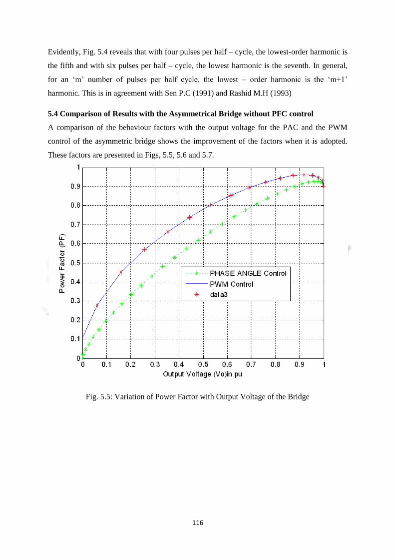
116
Evidently, Fig. 5.4 reveals that with four pulses per half – cycle, the lowest-order harmonic is
the fifth and with six pulses per half – cycle, the lowest harmonic is the seventh. In general,
for an ‗m‘ number of pulses per half cycle, the lowest – order harmonic is the ‗m+1‘
harmonic. This is in agreement with Sen P.C (1991) and Rashid M.H (1993)
5.4 Comparison of Results with the Asymmetrical Bridge without PFC control
A comparison of the behaviour factors with the output voltage for the PAC and the PWM
control of the asymmetric bridge shows the improvement of the factors when it is adopted.
These factors are presented in Figs, 5.5, 5.6 and 5.7.
Fig. 5.5: Variation of Power Factor with Output Voltage of the Bridge
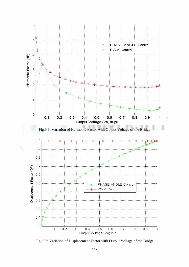
117
Fig.5.6: Variation of Harmonic Factor with Output Voltage of the Bridge
Fig, 5.7: Variation of Displacement Factor with Output Voltage of the Bridge

118
5.5 AC – DC Boost – Type Asymmetrical Converter for Power Factor Correction
5.5.1 The AC – DC Asymmetric Drive with Power Factor Correction Circuit
Power Factor correction of the Asymmetric Single – Phase Drive can be achieved by the
PWM scheme by generating thyristor gate signals as described in section 2.35 and 5.1. The
circuit implementation is presented in Fig. 5.8.
There are numerous variations of the firing circuits and the control logic circuits that can be
used to control the firing of the thyristors. One of such ways has been discussed earlier. The
principle of operation of the thyristor firing circuit designed and built for controlling the
thyristors of the Asymmetrical Single – Phase Bridge shown in Fig.5.8 is hereby described.
The 50-Hz astable signal clocks the monostable through pin 2 known as the trigger input. The
monostable triggers at one period of the astable signal fed into it. The monostable period of
oscillation can be varied to adjust the pulse width. The output of the monostable is logically
added with another 20KHz astable signal which is used in the modulation. The output of the
AND gate (acting as a Comparator) is a modulated pulse signal with a positive going
transition. The period before the first rising edge defines the firing angle of the thyristors. A
path of this signal is fed through an inverter to invert the signal. This produces a
complimentary signal that is used to fire the other thyristor. The output of the inverted signal
is processed through a high pass filter to filter off signals below 50Hz thus turning the signal
to leading spikes which go to the pulse transformer and then to a clipping diode to clip all the
negative signals. The signals from the pulse transformers are complimentary and are used to
fire the gate of the thyristors. The test rig made up of the controlled DC motor with a load DC
generator and the Asymmetrical bridge system are shown in Fig.5.12.
5.5.2 AC – DC Boost - Type Asymmetrical Converter for PFC
The conventional active boost arrangement of an AC – DC Single – Phase Converter feeding
a DC load is shown in Fig.5.9. Like every other boost regulator configurations used in power
factor correction except the fly back converter (Dubey et al 1986), it share a common input-
output power line, hence the output is not isolated and is electrically linked to the ac line
supply. The controls for this system are for;
I. The active boost switch ―S‖ of the PWM scheme and
II. The thyristors of the bridge
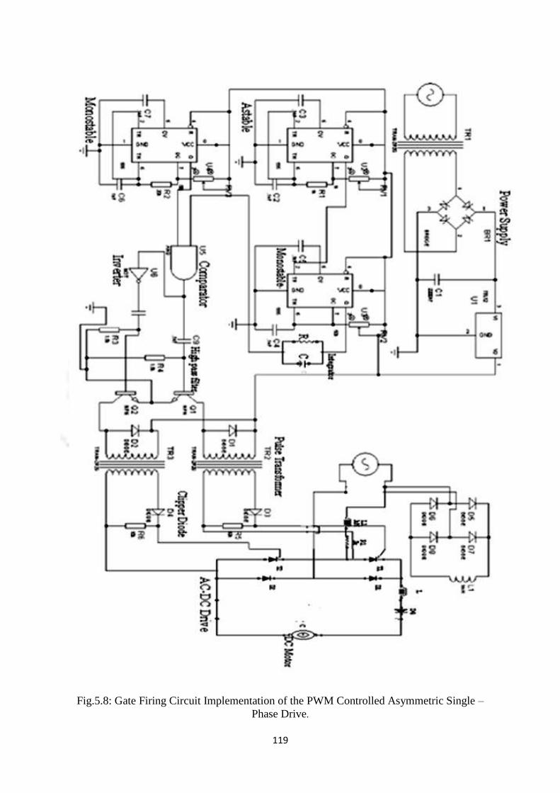
119
Fig.5.8: Gate Firing Circuit Implementation of the PWM Controlled Asymmetric Single –
Phase Drive.
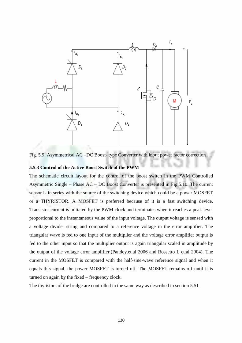
120
Fig. 5.9: Asymmetrical AC –DC Boost- type Converter with input power factor correction
5.5.3 Control of the Active Boost Switch of the PWM
The schematic circuit layout for the control of the boost switch in the PWM Controlled
Asymmetric Single – Phase AC – DC Boost Converter is presented in Fig.5.10. The current
sensor is in series with the source of the switching device which could be a power MOSFET
or a THYRISTOR. A MOSFET is preferred because of it is a fast switching device.
Transistor current is initiated by the PWM clock and terminates when it reaches a peak level
proportional to the instantaneous value of the input voltage. The output voltage is sensed with
a voltage divider string and compared to a reference voltage in the error amplifier. The
triangular wave is fed to one input of the multiplier and the voltage error amplifier output is
fed to the other input so that the multiplier output is again triangular scaled in amplitude by
the output of the voltage error amplifier.(Pandey.et.al 2006 and Rossetto L et.al 2004). The
current in the MOSFET is compared with the half-sine-wave reference signal and when it
equals this signal, the power MOSFET is turned off. The MOSFET remains off until it is
turned on again by the fixed – frequency clock.
The thyristors of the bridge are controlled in the same way as described in section 5.51
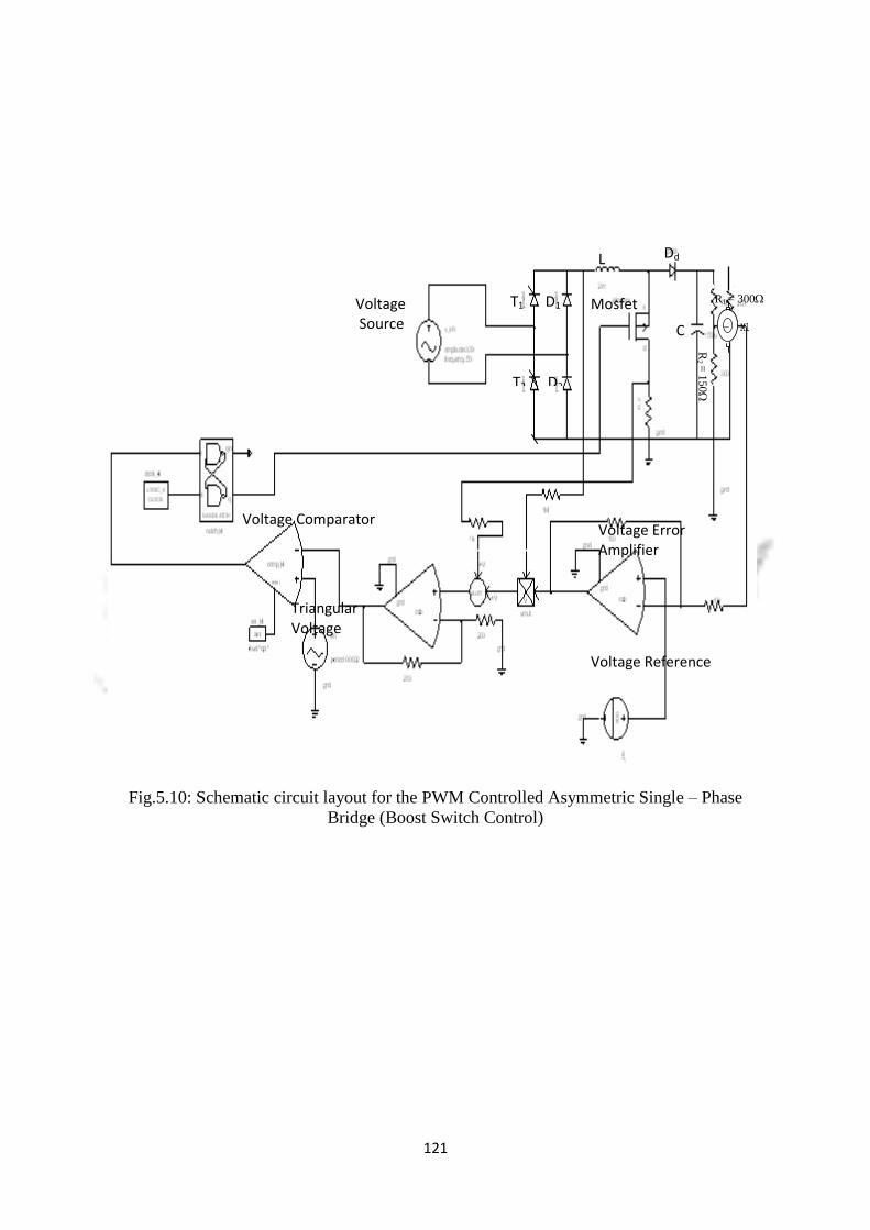
121
Fig.5.10: Schematic circuit layout for the PWM Controlled Asymmetric Single – Phase
Bridge (Boost Switch Control)
M1M1
Voltage Reference
Voltage Comparator
L Dd
Voltage Error Amplifier
Voltage Source
Triangular Voltage
Mosfet
C
T1 D1
T2 D2
R1 = 300
R2
= 1
50
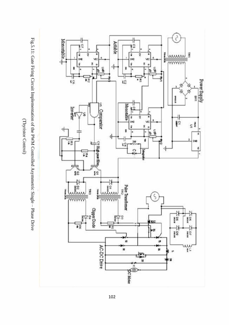
122
The
The
F
ig.5
.11: G
ate Firin
g C
ircuit Im
plem
entatio
n o
f the P
WM
Contro
lled A
sym
metric S
ingle –
Phase D
rive
Fig
.5.1
1: G
ate Firin
g C
ircuit Im
plem
entatio
n o
f the P
WM
Contro
lled A
sym
metric S
ingle –
Phase D
rive
(Thyristo
r Contro
l)
102
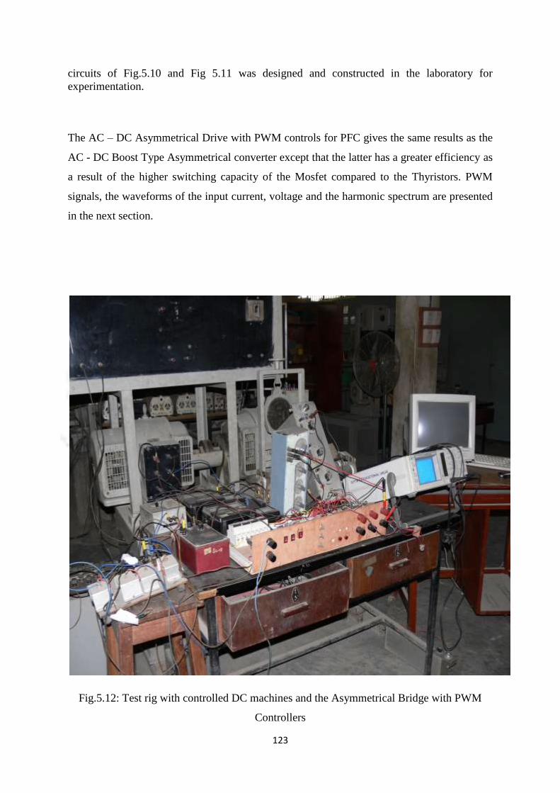
123
circuits of Fig.5.10 and Fig 5.11 was designed and constructed in the laboratory for
experimentation.
The AC – DC Asymmetrical Drive with PWM controls for PFC gives the same results as the
AC - DC Boost Type Asymmetrical converter except that the latter has a greater efficiency as
a result of the higher switching capacity of the Mosfet compared to the Thyristors. PWM
signals, the waveforms of the input current, voltage and the harmonic spectrum are presented
in the next section.
Fig.5.12: Test rig with controlled DC machines and the Asymmetrical Bridge with PWM
Controllers
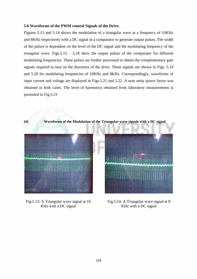
124
5.6 Waveforms of the PWM control Signals of the Drive.
Figures 5.13 and 5.14 shows the modulation of a triangular wave at a frequency of 10KHz
and 8KHz respectively with a DC signal in a comparator to generate output pulses. The width
of the pulses is dependent on the level of the DC signal and the modulating frequency of the
triangular wave. Figs.5.15 – 5.18 show the output pulses of the comparator for different
modulating frequencies. These pulses are further processed to obtain the complementary gate
signals required to turn on the thyristors of the drive. These signals are shown in Figs. 5.19
and 5.20 for modulating frequencies of 10KHz and 8KHz. Correspondingly, waveforms of
input current and voltage are displayed in Figs.5.21 and 5.22. A near unity power factor was
obtained in both cases. The level of harmonics obtained from laboratory measurements is
presented in Fig.5.23
(A) Waveforms of the Modulation of the Triangular wave signals with a DC signal
Fig.5.13: A Triangular wave signal at 10
KHz with a DC signal
Fig.5.14: A Triangular wave signal at 8
KHz with a DC signal
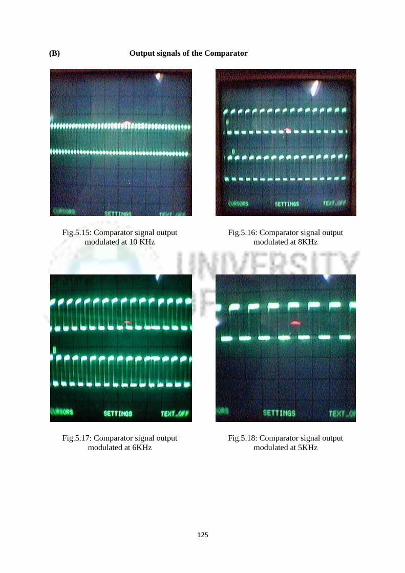
125
(B) Output signals of the Comparator
Fig.5.15: Comparator signal output
modulated at 10 KHz
Fig.5.16: Comparator signal output
modulated at 8KHz
Fig.5.17: Comparator signal output
modulated at 6KHz
Fig.5.18: Comparator signal output
modulated at 5KHz
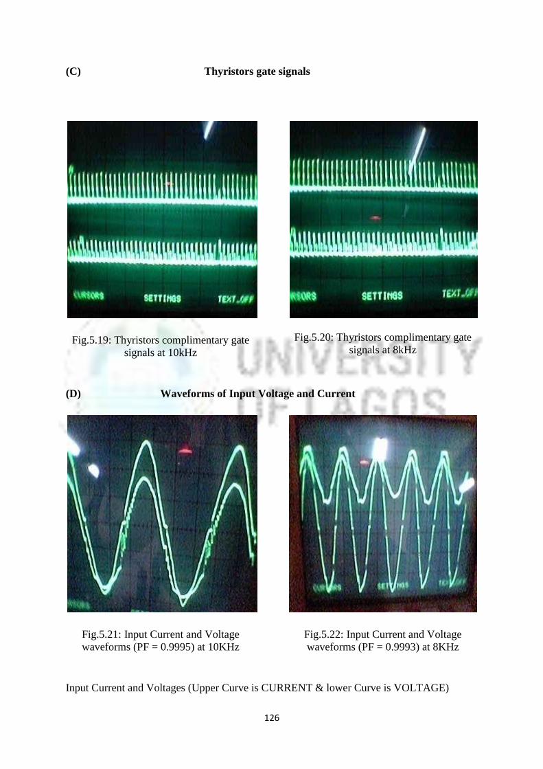
126
(C) Thyristors gate signals
Fig.5.19: Thyristors complimentary gate
signals at 10kHz
Fig.5.20: Thyristors complimentary gate
signals at 8kHz
(D) Waveforms of Input Voltage and Current
Fig.5.21: Input Current and Voltage
waveforms (PF = 0.9995) at 10KHz
Fig.5.22: Input Current and Voltage
waveforms (PF = 0.9993) at 8KHz
Input Current and Voltages (Upper Curve is CURRENT & lower Curve is VOLTAGE)

127
(E) Harmonics
Fig. 5.23: Harmonics of the PWM Controlled Asymmetric Single – Phase Drive
5.7 A Simplified PWM AC – DC Asymmetrical Bridge with PFC control
The active boost PFC circuit for the Single – Phase drives of Fig.5.9 and the asymmetrical
Single – Phase Bridge of Fig.5.8 are both efficient in power factor control. However, the
conventional active boost PFC has the following limitations according to Martinez R, and
Enjeti P.N. (1996):
The required switching frequency of the boost switch is usually high. This in turn
increases the switching losses and lowers the efficiency.
Special design of the dc – side inductor is necessary to carry dc current as well as high
frequency ripple current.
The diode Dd in the series path of power flow contributes to voltage losses and
reduced reliability.
At any given point, three semi – conductor devices exist in the power flow path
An alternative circuit that gives similar results but overcomes the limitations of the
conventional PWM (Sanzaeihi et.al 2006) circuits is proposed in Fig.5.24. It has a reduced
harmonic current content for switching power converters and motor drive systems fed from a
modified asymmetrical single – Phase Bridge acting as a boost converter. Analysis and

128
design approach of the proposed circuit along with experimental results are presented in the
next section.
5.7.1 Description of the proposed circuit
The laboratory model presented in Fig.5.9 though effective for PFC applications uses
asymmetrical bridge to rectify the AC input voltage to DC, which is then followed by the
boost section. This approach is good for a low to medium power range. As the power level
increases, the diodes of the drive begin to become an important consideration to deal with the
problem of heat dissipation in a limited surface area from the efficiency point of view. The
proposed Bridgeless AC – DC asymmetric single – phase drive with PWM power factor
correction (Lu Bing et.al 2005, Laszlo H et.al 2007 and P kong et.al (2006) scheme is
presented in Fig. 5.24.
Fig. 5.24: Bridgeless AC – DC PFC Configuration
The bridgeless configuration applied in this research, avoids the need for the conventional
input bridge, and yet maintains the classic boost arrangement. This is easily done by
replacing the thyristors of the asymmetrical single - phase bridge converter in fig.5.9 by a
power MOSFET with a diode connected between the drain and the source of the MOS switch
as shown in Fig.5.24. A thyristor could be used as the switching device too.
In this approach, the series diode Dd in the conventional boost circuitry of Fig.5.9 has been
eliminated. Also, the dc – side inductor is no longer necessary and instead an ac – side
inductor is required.

129
The advantages of the proposed approach are (Eric Ho Y.K et.al 2000):
Improved characteristics in terms of input power factor and sinusoidal shape of the
input current.
Only two semi-conductor device drops exist in the power flow path at any given
instant.
The boost inductor ‗L‘ on the ac side contributes to the reduction in Electromagnetic
(EMI) interference.
The gates of the MOS switches are referenced to the same ground.
5.7.2 Operation of the Bridgeless Converter
The analysis shall be discussed in two ways according to Martinez R and Enjeti P.N. (1996).
To understand the operation, the proposed circuit of figure 5.24 can be viewed as two
sections: section one operates as the boost stage (positive half cycle) and the second operates
as the return path for AC signal during the negative half cycle. (Martinez R. et.al 1996 and
Laszlo H et.al 2007)
Fig.5.25: Current Flow path for the Positive half cycle.
E

130
L
C
Controller
1D2D
1M 2M
sVoV
Negative half cycle
Return
C
H
O
P
P
E
R
L
R
E
Fig.5.26: Current Flow path for the negative half cycle.
(a) Positive ―Half Cycle‖.
When the AC input goes positive, the gate of MOSFET M1 is driven high and current flows
through the input, and through the inductor, storing energy. When M1 turns off, energy in the
inductor is released and current flows through D1, through the load and returns through the
body diode of M2 back to the input mains as shown in Fig.5.25.
During the off – time, the current flows through the inductor ―L‘ (during this time, the
inductor discharges its energy) into the boost diode D1 and close the circuit through the load.
(b) Negative ―Half Cycle‖
During the negative half cycle, circuit operation is mirrored as the positive half cycle as
shown in Fig.5.26. M2 turns ON, current flows through the inductor storing energy. When
M2 turns off, energy is released as current flows through D2 through the load and back to the
mains through the body diode of M1.
It should be noted that the two power MOSFETs are driven synchronously. It does not matter
whether the sections are performing as an active boost or as a path for the current to return. In
either case, there is the benefit of lower power dissipation when current flows through the
power MOSFETs during the return phase.

131
Figure 5.28: shows the Circuit Layout for the simultaneous gate firing of the MOSFETs (or
Thyristors) of the proposed design
Another way to understand the proposed circuit is to view its modes of operation as
illustrated in Fig. 5.27.
Mode 1 in Fig.5.27 (a) occurs when the input ac voltage is positive and the switches are open
(off). Current flows through diode D1 through the capacitor and load and back through the
anti-parallel diode of M2. Fig.5.27 (b) shows Mode 2, which occurs when the input ac voltage
is positive and the switches are closed (on). Input Current flows through switch M1 and back
through the anti – parallel diode of M2, thus providing a path for the input current. At the
same time, the bulk capacitor discharges and supplies current to the load. Mode 3 in
Fig.5.27(c) occurs when the input ac voltage is negative and the switches are open (off).
Current flows through diode D2, through the capacitor and load and back through the anti-
parallel diode of M1. Fig.5.27 (d) shows Mode 4, which occurs when the input ac is negative
and the switches are closed (on). Input currents flows through switch M2 and back through
the anti – parallel diode of M1, thus providing a path for the input current. At the same time,
the dc capacitor discharges and supplies current to the load.
5.7.3 Design Considerations of the proposed AC – DC Converter.
Let‘s suppose that the simplified converter Fig.5.24 is a 2.0kw load, from a 230Vrms, 50Hz
Single – phase system. The output has a maximum of 400V dc with a switching frequency of
10KHz and it is to be operated in the Continuous Inductor Conduction Mode (CICM).
It is assumed that switching losses and device power loss are negligible.
Parameters ‗L‘ and ‗C‘ are determined with the specification that the output ripple voltage
shall be within the limits of 5% of the output voltage. The defining equations are derived in
Robert et.al (2000).
Since the switching losses are assumed to be zero,
outin PP
inin IVKW 0.2
AI in 695.8230
2000

132
(a)
(b)
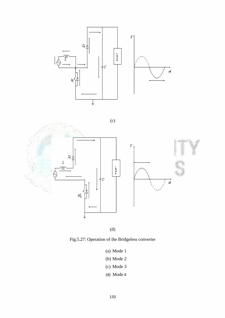
133
(c)
(d)
Fig.5.27: Operation of the Bridgeless converter
(a) Mode 1
(b) Mode 2
(c) Mode 3
(d) Mode 4

134
And,
AII oout 5400
2000
Ripple Voltage is assumed to be 5% of output Voltage,
Therefore,
VVV oc 20400100
5
100
5
Also,
Cf
DIV
s
oc
D is the duty cycle; D= tON/T
Where,
KHzf s 10
But for a boost converter,
D
VV s
o
1
Hence,
400
23011
o
s
V
VD
575.01
425.0
(The duty circle ‗D‘ is not constant and depends on the supply voltage Vs and the level of
output voltage Vo to be achieved )
And,
2010000
425.05
Vf
DIC
s
o
61010
F10
But a value of FC 18 was chosen as the output capacitor in the experimental work. This is
to ensure that the dc output has less ripple content.
It is equally assumed that a 10% value of input current ripple is allowed,
Therefore,
695.8100
10 LII

135
A87.0
But,
Lf
DVI
s
s
Hence,
8695.010000
425.0230
If
DVL
s
s
51035.112
mH23.11
An inductor value of 15mH was used. This is to ensure that the design operates in a CICM.
The diode and MOSFET were rated higher than the combined dc voltage and the anticipated
ripple value (Sen 1991). The proposed circuit of the new design that was constructed in the
laboratory is presented in Fig.5.28. The voltage feed forward PWM switching technique has
been adopted.
The feed forward approach is used to generate the gate signals for triggering the Mosfet
where the output voltage is (V0). The error amplifier compares the sampled output voltage
(Vsp) with a fixed reference voltage, Vref, and generates an error voltage, Ve given by Sen
(1991).
reforefe V
RR
RV
R
RVV
21
2
4
3
(5.23)
This error voltage is then fed to the non – inverting input of an open – loop comparator that
compares the error voltage with a sawtooth signal at its inverting input. The switching
frequency of the sawtooth generator determines the frequency of the converter. The output of
the comparator is a PWM SIGNAL. It is high only when the error voltage is higher than the
sawtooth signal. This PWM signal is then fed to the base drive circuitry that drives the gates
of the two MOSFETS of the proposed converter. The proposed PFC circuit achieved the
same Power Factor.
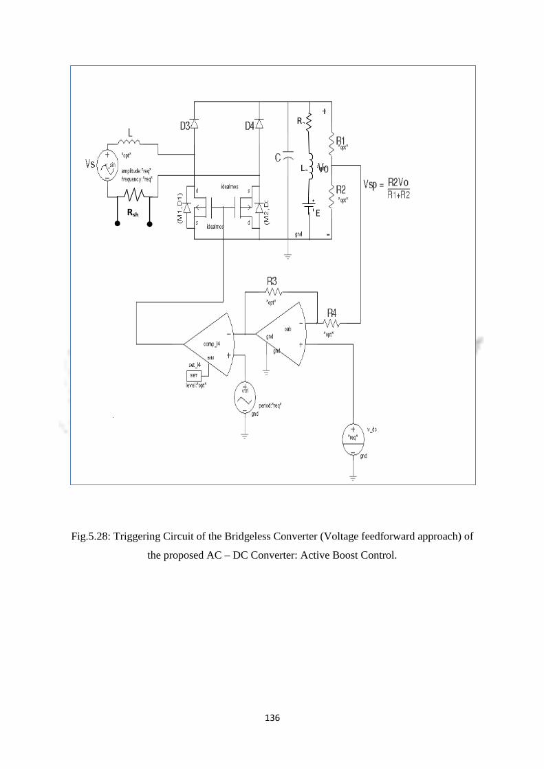
136
Fig.5.28: Triggering Circuit of the Bridgeless Converter (Voltage feedforward approach) of
the proposed AC – DC Converter: Active Boost Control.
E
La
Ra
Rsh
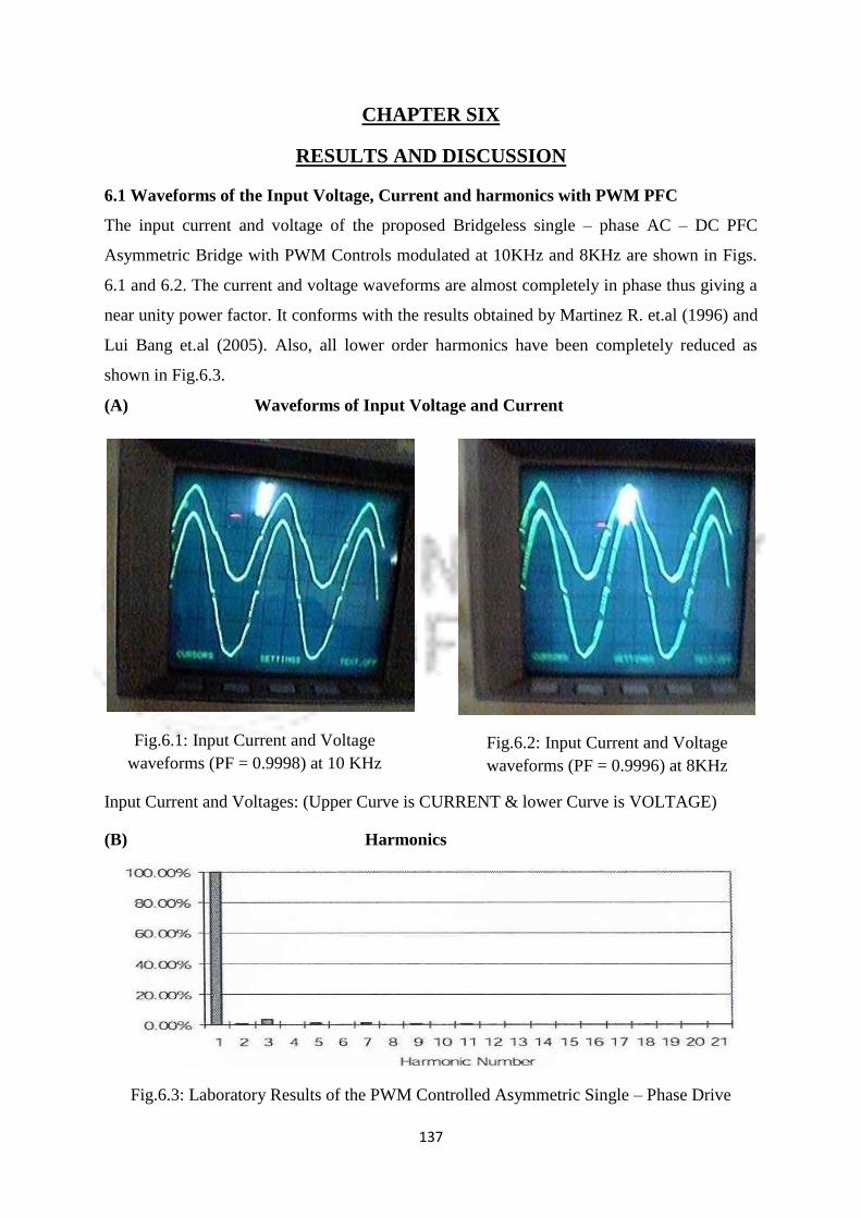
137
CHAPTER SIX
RESULTS AND DISCUSSION
6.1 Waveforms of the Input Voltage, Current and harmonics with PWM PFC
The input current and voltage of the proposed Bridgeless single – phase AC – DC PFC
Asymmetric Bridge with PWM Controls modulated at 10KHz and 8KHz are shown in Figs.
6.1 and 6.2. The current and voltage waveforms are almost completely in phase thus giving a
near unity power factor. It conforms with the results obtained by Martinez R. et.al (1996) and
Lui Bang et.al (2005). Also, all lower order harmonics have been completely reduced as
shown in Fig.6.3.
(A) Waveforms of Input Voltage and Current
Fig.6.1: Input Current and Voltage
waveforms (PF = 0.9998) at 10 KHz
Fig.6.2: Input Current and Voltage
waveforms (PF = 0.9996) at 8KHz
Input Current and Voltages: (Upper Curve is CURRENT & lower Curve is VOLTAGE)
(B) Harmonics
Fig.6.3: Laboratory Results of the PWM Controlled Asymmetric Single – Phase Drive
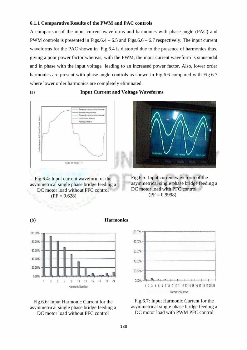
138
6.1.1 Comparative Results of the PWM and PAC controls
A comparison of the input current waveforms and harmonics with phase angle (PAC) and
PWM controls is presented in Figs.6.4 – 6.5 and Figs.6.6 – 6.7 respectively. The input current
waveforms for the PAC shown in Fig.6.4 is distorted due to the presence of harmonics thus,
giving a poor power factor whereas, with the PWM, the input current waveform is sinusoidal
and in phase with the input voltage leading to an increased power factor. Also, lower order
harmonics are present with phase angle controls as shown in Fig.6.6 compared with Fig.6.7
where lower order harmonics are completely eliminated.
(a) Input Current and Voltage Waveforms
Fig.6.4: Input current waveform of the
asymmetrical single phase bridge feeding a
DC motor load without PFC control
(PF = 0.628)
Fig.6.5: Input current waveform of the
asymmetrical single phase bridge feeding a
DC motor load with PFC control
(PF = 0.9998)
(b) Harmonics
Fig.6.6: Input Harmonic Current for the
asymmetrical single phase bridge feeding a
DC motor load without PFC control
Fig.6.7: Input Harmonic Current for the
asymmetrical single phase bridge feeding a
DC motor load with PWM PFC control

139
6.2 Discussion of Results
The non - linearities that influence the parameters of a D.C motor were modeled at the operating
points of the machine to ensure the accuracy of the interval equations. Other non – linearities
introduced by the switching action of the semi - conductor devices of the drive are overcome by
the piece – wise linear method of analysis. Explicit expressions for current at each interval of
operation lead to the piecing together of the non – sinusoidal motor input current and the
complete characterisation of the asymmetrical single - phase bridge by solution of transcendental
equations. The waveforms of the supply currents of the drive are shown in Figs.3.8 (a-f). It
clearly shows that the non - sinusoidal waveform of input current gets more distorted as the
firing angle of the thyristors of the drive increases. The behaviour factors of the drive
(Displacement factor, harmonic factor, and Power factor) were developed to complete the
performance characteristics of the drive. The anticipated increase in power factor deterioration
with increased industrialization was further demonstrated from laboratory measurements on a
supply system feeding multiple drives and the results displayed in Figs.3.13, 3.14 and 3.15 which
clearly indicate a decrease in input power factor as the number of such drives connected to the
same source increases. Figure 3.16 shows the variation of Power Factor with numbers of drives.
The complete mathematical model of the input current is also applied to obtain the Fourier
Spectrum of the motor input Current by the Fourier Integral method. Figures 3.9 and 3.10 reveal
that high lower order harmonics are present in input current which can constitute a menace to
nearby electronic circuits. They also contribute to the poor input power factor of the bridge
supply line. Fig.3.11 suggest that a very high harmonic content is present in the input supply
current when the drive is operated between 120 to 160 degrees at a frequency range of 150 –
750Hz.The implication of this is that communication equipment and circuits operating within
this range of frequencies will be adversely affected at such significant harmonic levels. Also,
signalling in traction systems will be affected too.
Various techniques for poor power factor correction were investigated and the PWM method
identified for detailed further study. The PWM control scheme was analysed to obtain
expressions for the behaviour factors of the drive. The scheme was then designed and
constructed to investigate the drive operation. In Figs. 5.6 – 5.8, a comparison of the behaviour
factors of the input current for the Phase Angle Control (PAC) and the Pulse – Width Modulation
Control (PWM) of the Asymmetrical Bridge showed improved power factor. Measurements of

140
the AC input voltage, current, power factor and also the input harmonic current spectrum
(Fig.5.21-5.23) were taken. The waveforms of voltage and current when compared are almost in
phase implying an achievement of a near unity power factor. Also, the waveform of the input
current in Fig.6.4 and Fig.6.5 when compared shows a sinusoidal input current with PWM
control. Clearly, Fig.6.4 shows the waveforms of input voltages and current with PWM control
technique to be virtually in phase which is in agreement with the results of Martinez R. et.al
(1996) and Lui Bang et.al (2005).
The PWM scheme also can be used to eliminate some lower order harmonics by choice of the
number of pulses per half cycle. For four pulses, the lowest order harmonic is the 5th
as seen in
Fig.5.5 (a) and for eight pulses; the lowest order harmonic is the 9th
harmonic as shown in
Fig.5.5(c). However, the number of pulses per half – cycle must not be too large (Rashid 1993)
as it increases the ripple frequency of the motor current. If it is, the switching loss of the thyristor
increases and special costly thyristors having low turn – off time are required. Six pulses per half
– cycle Fig,5.5(b) appear to be a good choice, in which case harmonic currents below the seventh
are eliminated although, higher pulse numbers improve the motor performance and efficiency,
(Sen 1991). The PWM control scheme is currently being used in Single – Phase traction systems.
Apart from improving the Power Factor and reducing harmonics in the source current, it also
reduces the ripple in the motor current and discontinuity of current conduction (Lai and Chen
1991).

141
CHAPTER SEVEN
CONCLUSION AND RECOMMENDATIONS
7.1 Conclusion
The hypothesis that increased power factor problem would exist in the Nigerian National grid
with growth of heavy industries such as the Ajaokuta Steel Company, the Iron and Mining
Industries, Aladja Steel and other steel related developmental projects has been established. The
non – sinusoidal nature of the ac supply to the asymmetrical single – phase drive was established
analytically and experimentally and the waveform distortion shown to worsen as the firing angle
of the thyristors of the drive is increased. Also, the power factor gets worse as the number of
such drives connected in parallel increases.
It was shown that the conventional PWM Power Factor Correction technique improves the
power factor close to unity. However, the proposed bridgeless PFC gives the same improvement
in Power Factor. The results of the laboratory experiment in Figs.5.21 and Fig.6.1 show that the
input current is a pure sinusoid and in phase with the input voltage and the harmonic spectrum
reveals that lower order harmonics had been eliminated. The same result was achieved with the
alternate circuit – the bridgeless AC – DC Boost converter which offers a modification of the
drive and the control methods. The advantages of the alternate circuit include (Martinez R. et.al
1996):
The use of fewer semiconductor devices
Improved characteristics in terms of higher input power factor and sinusoidal shape of
input current
It incorporates an ac side inductor which contributes to the reduction in EMI interference
Power losses are reduced as a result of the absence of the series diode, therefore leading
to higher reliability.
The proposed PFC overcomes the limitations of the conventional active boost PFC for the Single
– Phase drives despite its improved power factor. These limitations are:
The required switching frequency of the boost switch is usually very high which in turn
increases the switching losses and lowers efficiency
Special design of the dc – side inductor is necessary to carry dc current as well as high
frequency ripple current.

142
Three semi- conductor devices exist in the power flow path and thus contribute to voltage
losses and reduced reliability.
7.2 Contributions to Knowledge
1 The research established the poor input power factor problem in industrial drives
experimentally and analytically using the Piece – Wise Linear (P.W.L) method of
analysis to derive the equations for each interval of operation of the drive. These
equations were then put together to obtain the non – sinusoidal waveform of the bridge
which is the cause of the poor power factor problem. The research has established the
Pulse – Width Modulation (PWM) scheme as an effective method of correcting the poor
input Power Factor in drives using simpler and a robust circuit configuration and has
improved the input power factor of the Asymmetrical Single – Phase Bridge from 0.628
to 0.998 as displayed by the waveform of Figs. 6.4 and 6.5 respectively.
2. Although some of the PFC circuitry had led to improvement of power factor, they had the
limitation of very high switching frequency of the boost switch which in turn increases
the switching losses and lowers efficiency and also three semi – conductor devices exist
in the power flow path contributing to voltage losses and reduced reliability. The present
research proposed an alternative bridge circuit that uses fewer semi – conductor devices
to achieve an improved power factor. The approach led to a higher reliability as a result
of reduced power loss in circuit devices
3. Hitherto application of industrial drives suffers from lack of information on harmonics
resulting from their use. This research has generated a number of drive performance
characteristics and monographs that provide information to users of industrial drives, In
particular, the communications industry that operate at frequencies that exist in the
harmonic spectrum of the drive and the Power Holding Company of Nigeria (PHCN)
which suffers the direct consequences of these harmonics will also benefit from this study
and will be better informed when developing equipment standards used for their network.
Also, the Steel industries that depends on DC and AC motor drives will benefit from the
results of this research

143
7.3 Recommendation for further work
Lack of adequate equipment for measuring the harmonic spectrum of the AC input current made
it difficult to compare the predicted harmonic currents with measured currents. Also, piece –
wise linear analysis of the proposed AC – DC boost converter and the Diode/MOSFET PWM
controlled (Bridgeless) Converter could not be done because of time constraint. Therefore, the
areas that could be considered for further work include;
(a) Measurement of the harmonics in the input current of the drives using a spectrum
analyser with a view to comparing predicted harmonics spectrum with measured ones
(b) A study of the harmonic spectrum of communication signals produced by different
networks in the country with a view to identifying the possibility of industrial drives
producing significant Electromagnetic Interference – EMI with communication systems
(c) More detailed analysis of the proposed alternative circuits to the Asymmetrical Single
Phase Bridge with a view to achieving their complete characterization and behaviour
factors.
(d) The many models of industrial drives and their control circuits are yet to be packaged in
modular form so as to use them to develop experiments for manpower training at
undergraduate and post graduate levels.
(e) Analyses have been carried out for one Drive connected to AC supply to determine the
level of harmonics and power factor. It is hereby suggested that a similar analysis be
made for two, three and four converters connected in parallel to the same source in other
to compare results.

144
REFERENCES
Abdel Aziz et al. (2002). LC Compensators for Power Factor Correction of Nonlinear Loads.
IEEE Transactions on Power Delivery. 1-6.
Agarwal, P.D. (1959). Eddy Current Losses in Solid and Laminated iron. Trans. AIEE.
Vol.78, Part I, Pages 169 – 181.
Agu U. (1997). Relative study of the output characteristics of PWM and phase controlled AC-
DC converters. Conf. Publication. Electric Power Engineering conf. (EPEC), UNN 4-10
Andreycak B. (1993-4). Optimizing performance in UC 3854. Power Factor Correction
Applications. Unitrode products and Applications Handbook. APEC conf. Proc. 584 – 590
Aziz J.A and Salam Z. (2004). A New Pulse-Width Modulation (PWM) Scheme for Modular
Structured Multilevel Voltage Source Inverter. International Journal of Electronics, Vol. 91, No.
4. 211-226.
Balogh L, Redl R. (1993). Power – Factor correction with interleaved Boost Converters in
continuous – induction mode. APEC conf. Proc., 168 – 174.
Banerjee S. and Verghese G. (2000). Nonlinear Phenomena in Power Electronics. New York:
IEEE Press.
Basau, S and Bollen M.H.J. (2005). A novel common power factor correction scheme for homes
and offices. IEE Trans. Power Delivery, 20: 2257-2263
Bashi S.M. Mariun N. Noor S.B. and Athab H.S. (2005). Three-phase Single Switch Power
Factor Correction Circuit with Harmonic Reduction. Journal of Applied Sciences 5 (1). 80-84
Basu S, Bollen MHJ. (2005). A novel common power factor correction scheme for homes and
offices. IEEE Trans. Power Deliv20, (3), pp. 2257–2263
Bazinet J, O‘Connor J.A.(1994). Analysis and Design of a zero voltage Transition Power Factor
Correction Circuit. APEC conf. Proc. 591-597
Bingsen Wang, Giri Venkafaramanan and Ashish Bendre. (2007). Unity Power Factor Control
for Three-Phase Three-Level Rectifiers Without Current Sensors. IEEE Transactions on Industry
Applications vol. 43. No. 5. 1341-1348.
Bowes S.R. (1975). New Sinusoidal Pulse-Width Modulated Inverter. Proceeding of the IEE,
122. 1279-1284.
Brkovic M, Cuk S. (2001). Input Current Shapper using Cuk converter. INTERLEC conf. Proc,
532-539.

145
Buso S, Malesani L and Mattavelli P. (1998). Comparison of Current Control Techniques for
Active Filter Applications. IEEE Transactions on Industrial Electronics, Vol. 45. No. 5. 722-729.
Canesin C.A, Barbi I. (1996). Analysis and design of constant –frequency peak –current
controlled high power factor boost rectifier with slope compensation. Proc. of IEEE Applied
Power Electronics Conference, APEC‘96, 807-813.
Canesin C.A. (1991). A unity Power Factor Multiple Isolated output switching mode power
supply using a single switch. APEC conf. Proc. 430 – 436
Chow M. H. L. Lee Y. S. Lee and Tse C. K. (2000). Single-stage single-switch PFC regulator
with unity power factor, fast transient response and low voltage stress. IEEE Trans. Power
Electron., vol. 15. No. 1, pp. 156–163.
CSC Cherry Semi – conductor: ―Power Conversion IC Data Book‖. 1992
Dallego Ennco, Marco Passoni, Gabriele Sassone and Gluseppe Venchi. (2000). Novel Current
Transducer in a Single – Phase Active Power Factor System. IEEE Transactions on Power
Electronics. Vol. 15, No.3, 234 – 242
Damle, P and Dubey, G.K. (1976). Analysis of a Chopper Fed D.C Series Motor, IEEE
Trans., IECI, Vol. 23. No.1. page 72.
Dewan S.B. (1981). Optimum input and output filters for single-phase rectifier power supply.
IEEE Trans. Industry Applications, vol. IA17, No.3, 282-288.
Dixon J.W, Venegas G. and Moran L. (1997). A Series Active Power Filter based on a
Sinusoidal Current-Controlled Voltage-Source Inverter. IEEE Transactions on Industrial
Electronics, Vol. 44, No. 5. 612-620.
Dixon Jr. L. H. (1990) High Power Factor Preregulator for Off-Line Power Supplies, in Unitrode
Switching Regulated Power Supply Design Manual. Marrimack, NH
Djemouai A, Sawan M and Slamani M. (2000). New CMOS Integrated Pulse Width Modulator
for Voltage Conversion Application. Proceedings of the 7th IEEE International Conference on
Electronics, Circuits and Systems, 116-119.
Dong Dai, Shengnan Li, Xikui Ma, and Chi K. Tse. (2007). Slow-Scale Instability of Single-
Stage Power-Factor-Correction Power Supplies. IEEE Transactions on Circuits and Systems.
VOL. 54, NO. 8. Pp. 1724 - 1735
Dranga O. Tse C. K, Iu H. H. C and Nagy I (2003). Bifurcation behavior of a power-factor-
correction boost converter. Int. J. Bifur. Chaos, vol. 13, no. 10, pp. 3107–3114.
Dubey G.K, Doradla S.R, A.Joshi and Sinha R.M.K. (1986). Thyristorised Power Controllers.
John Wiley and sons USA, 1st Edition.

146
Durry D, Farrer W and Jones B.L. (2000). Performance of thyristor bridge converters employing
flywheeling. Proc. IEE, vol.127, 268-276.
Enjeti P.N, Ziogas P.D and Lindsay J.F. (1990). Programmed PWM Techniques to Eliminate
Harmonics: A Critical Evaluation. IEEE Transactions on Industry Applications, 26, 302-316.
Enjeti P.N. and Martinez R. (1993). A high performance single – phase AC - Dc rectifier with
Input Power Factor Correction. IEEE. Applied power Electronics Conf. (APEC). Proc. Pp. 190-
195
Erickson R, M. Madigan, and Singer S. (2000). Design of a simple High – Power – Factor
Rectifier Based on the Flyback Converter. APEC. Conf. Proc., 792-801.
Erickson R.W. (1997). Fundamental of Power Electronics. New York, NY, USA, Chapman &
Hall.
Farmer W and Andrew D.F. (1978). Fully controlled regenerative bridge with half- controlled
characteristics‖. Proc. IEE, vol.125. 235-243
Femain A., Sebastin J, Villegas P, Hermando M.M and D.G Lamar. (2005). Dynamic limit of a
power factor preregulator. IEEE Trans. Ind. Electron, vol.52, no.1 77-87.
Fujita H and Akagi H. (1998). The Unified Power Flow Conditioner: The Integration of Series-
and Shunt-Active Filters‖. IEEE Transactions on Power Electronics, Vol. 13, No. 2, 315-322.
Grahame G., Holmes Thomas, Lipo A. (2003). Pulse Wave Modulation for Power Converters:
Principles and practice. John Wiley and sons Inc. Ist Edition.
Grigore, V and Kyyra J. (2000). A step-down converter with low input current for power factor
correction. Applied Power Electronics Conference and Exposition. APEC 2000. Fifteenth
Annual IEEE 1: 188-194.
Hanigovszki N. (2005). EMC Output Filters for Adjustable Speed Drives. Ph.D. Dissertation,
Inst. Energy Techn. Aalborg Univ., Aalborg, Denmark.
Helonde J.B and Hiwakar C.S. (2008). Implementation of Direct Current Controlled PWM on
Three Phase BLDC Motor Drive using Four-Switch Converter. Technology and Innovation for
Sustainable Development Conference, 300-305.
Holmes G.D and Lipo T.A.(2003). Pulse Width Modulation for Power Converters. Principles
and Practice, IEEE Press.
Ismail Daut, Rosnazri Ali and Soib Taib (2006). Design of a Single-Phase Rectifier with
Improved Power Factor and Low THD using Boost Converter Technique. American Journal of
Applied Sciences 3 (7). Pp. 1902-1904

147
Itoh J.I and Fujita K. (2000). Novel Unity Power Factor Circuits using Zero-Vector for Single-
Phase Input System. IEEE Trans. Power Electronics, Vol. 15. 36-43.
Itoh R and Deng K. Ishizaka. (1989). Single-Phase Sinusoidal Converter using MOSFETs, IEE
Proceedings, Vol. 136, No. 5, 237-242.
Iu H. H. C. Zhou Y and Tse C. K, (2003). Fast-scale instability in a PFC boost converter under
average current mode control. Int. J. Circuit Theory Appl., vol. 31, no. 6, pp. 611–624.
JJaehong Hahn, Prasad N. Enjeti and Pitel Ira J. (2002). A new three-phase Power Factor
Correction (PFC) scheme using two single-phase modules. IEEE Transactions on Industry
Applications vol. 38. No. 1. 123-130.
Kataoka T, Mizumachi K and Miyaira J. (1977). A pulse-width controlled AC-DC converter to
Improve Power Factor and Waveforms of AC line current. IEEE Conference Record, ISPCC-77,
New York.
Kataoka T, Mizumachi K and Miyaira J (1979). A pulse-width controlled ac-dc converter to
improve power factor and waveforms of ac line current. IEEE Trans. On Ind. Appl, vol.15. 670-
675.
Kelley A.W, Hallouda M. A, Moore M.D, and Nance J. L (1991). Near unity power factor
single-phase ac-to-dc converter using a phase-controlled rectifier. Proc. of IEEE. Applied Power
Electronics Conference, APEC‘91, 387-392.
Kelly A.W, Yadusky W.F. (1989). Rectifier design for minimum line – current harmonics and
maximum power factor. Proc of IEEE Applied Power Electronics Conference. APEC‘89, 13-22.
Kelly A.W, Yadusky W.F. (1992). Rectifier design for minimum line – current harmonics and
maximum power factor. IEEE Trans. On Power Electronics, vol.7, No.2. 332-341.
Ki1 S.-K, Cheng D.K.-W. Lu D.D.-C. (2008). Analysis and design of a single-phase hybrid
mode power factor correction converter. IET Power Electron. Vol. 1, No. 1, pp. 72–83
Kielgas H and Nill R. (1977). Converter Propulsion Systems with 3-Phase Induction Motors for
Electric Traction Vehicles. IEEE Conference Record, ISPCC-77, New York. 336-344
Kit Sum K (1998). Improved valley-fill passive power factor correction current shaper
approaches IEC specification limits. PCIM Magazine, 42-51.
Kocher M.J, Steigerwald R.L.(1983). An AC – to – DC Converter with High Quality Input
Waveforms. IEEE Trans. On Industry Applications. Vol. 1A – 19. No. 4. 586 – 599.
Kolar J.W and Drofenik U. (1999). A new switching loss reduced discontinuous PWM scheme
for a unidirectional three – phase/switch/level boost – type PWM rectifier. Proc.21st INTELEC,
Copenhagen, Denmark, 29-38.

148
Krishnomoorthy K.A, Dubey G.K and Revankar G. N. (1978). Converter control with selective
reduction of line harmonics. Proc. IEE, vol.125, No. 2, 141-145.
Krishnomoorthy K.A, Dubey G.K and Revankar G.N. (1978). General methods for selective
reduction of line harmonics. Proc. IEE, vol.125, No. 11, 1269-70.
Krishnomoorthy K.A, Dubey G.K and Revankar G.N. (1978). Sequence control of converters
with less tripplen harmonics. Jn. Intn. Of Engineers: Electrical Engineering Div. Vol.59, 100-
105.
Lai J.S, Chen D.(1993). Design Consideration for Power Factor Correction Boost Converter
operating at the Boundary of continuous conduction and discontinuous mode. APEC conf. Proc.
267 – 273.
Laszlo, H, Yungtaek Jung and Milan M. Jovanovic. (2007). Performance Evaluation of
Bridgeless PFC Boost Rectifiers. IEE. Pp 165-171
Lazaro A., Barrado A., Sanz M, Salas V and Olias E. (2007). New Power Factor Correction AC-
DC converter with reduced storage capacitor voltage. IEEE Trans. Ind. Electron. Vol. 54. No. 1:
384-397.
Liu K.H, Lin Y.L. (1989). Current waveforms Distortions in Power Factor Correction Circuits
Employing Discontinuous – Mode Boost Converters. PESC. Conf. Proc., 825 – 829.
Liu Y and Smedley, K. (2003). Control of a Dual Boost power factor corrector for high power
applications. IECON 29th Annual Conference of the IEEE.Volume 3, Issue , 2-6 PP. 2929-2932.
LoCascio J, Walban M. T. (1990). Active Power Factor Correction using a Flyback Topology‖.
PCIM conf. Proc., 10 – 17.
Lu DDC, Cheng DK-W, Lee Y-S (2005). Analysis of a high-power factor AC–DC converter
with reduced current and voltage stresses. IEE Proc., Electr. Power Appl. 152, (4), pp. 943–952
Lu DDC, Cheng DK-W, Lee Y-S. (2001). A single-switch power factor corrected converter with
reduced repeated power processing‘. Proc. IEEE Power Electronics Drive Systems (PEDS).
Bali, Indonesia, pp. 26–32
Lu DDC, Cheng DK-W, Lee Y-S. (2003). Analysis and design of a single-stage single switch
power factor corrected converter with direct power transfer‘, IEICE Trans. Commun. E86-B,
(12), pp. 3606–3613
Maksimovic D. (1994). Design of the clamp – current High – power-Factor Boost Rectifier.
APEC conf. Proc, 584 – 590

149
Maksimovic D. (1995). Design of the clamped-current high power factor boost rectifier. IEEE
Trans. on Industry Applications, Vol.31, No.5, 986-992.
Malinowski M. Kazmierkowski M. P. (2004). Simple direct power control of three-phase PWM
rectifier using space – vector modulation (DPC-SVM). IEEE Trans. Ind. Electron, vol.51, no.2,
539-544.
Marek Gotfryd. (2000). Output Voltage and Power Limits in Boost Power Factor in the
Discontinuous Inductor Current Mode‖. IEEE Transactions on Power Electronics, vol.15. No.1.
Martin K.H. Cheung, Martin H.L Chow and Chi K. Tse. (2008). Practical design and evaluation
of a 1KW PFC Power Supply based on Reduced Redundant power processing principle. IEEE
Transaction on Industrial Electronics. Vol. 55. No.2. 665-673.
Martinez R, Enjeti P.N. (1996). A high – performance Single – Phase rectifier with input Power
Factor Correction. IEEE Transaction on Power Electronics, Vol.II. No.2, 311-317.
Mazumder S. K. A. Nayfeh H, and Boroyevich D. (2001). Theoretical and experimental
investigation of the fast- and slow-scale instabilities of a dc/dc converter, IEEE Trans. Power
Electron., vol. 16, no. 2, pp. 201–216.
Mehta P, Mukhopadhyway S and Orhun E (1974). Forced commutated ac-dc converter-
controlled dc drives. IEE conference on Power Electronics – Power semi-conductors and their
Applications, Conference Publications123. 146.-154
Mellitt, B and Rashis. (1974). Analysis of DC Chopper circuits by computer – based piece
– wise linear techniques PROC. IEE, 121(3). pages 173 – 178
Metha P and Mukhopadhyay. (1974). Modes of operation in converter – controlled DC drives.
PROC. IEE Vol. 121, no.3. 219-227
Minghua Fu and Qing Chen. (2001). A DSP Based Controller for Power Factor Correction in a
Rectifier Circuit. Sixteenth Annual IEEE Applied Power Electronics Conference and Exposition,
pp. 144-149.
Mipanic P.N. (1968). The through pass inverter and its application to induction motor speed
control‖. IEEE Transactions on PAS. Vol. PAS-87, 234-246
Mohammed S. Agamy (2008) Single Stage Power Factor Corrected Three-Level Resonant
Converters. Ph.D Thesis. Queen‘s University, Kingston, Ontario, Canada
Mohan N, Undeland T.M and Robbins W.P. (1995). Power Electronics: Converters, Applications
and Design. New York, NY, USA, John Wiley & Sons. Inc. 132-176
Mukher, K.C. (1961). Certain Approaches to the Electromagnetic field problems pertaining to
Dynamo Electric Machines. IEE Monograph, Vol. Part C, Pages 405 -411

150
Nagy I. (2001). Nonlinear phenomena in power electronics. J. Automatika. Vol. 42. No. 3–4, pp.
117–132.
Nalbant M.K, Klein J. (1990). Design of a 1kw power factor correction circuit. PCIM conf.
Proc., 7 – 24.
Nisit, D. C and Chattopadhyay. (1978). Modelling an SCR Bridge DC motor drive.
IEEE Transaction. IECI – 25. pages 187 - 189
Okoro C. C. (1980). An evaluation of the effects of Ripples on DC machines. Ph.D Thesis.
University of Birmingham
Okoro C.C (1987). Behaviour factors of Asymmetrical single-phase converter. Nigerian Journal
of Engineering and Technology, vol.10. No.11-7
Okoro C.C. (1982). Performance Evaluation of a DC motor Fed from an Asymmetrical Single-
Phase Bridge. Proc. IEE, vol.129. PTB No.5, 289-98.
Okoro C.C. (1986). Behaviour factors of power supply with the asymmetrical single – phase
converter load (unpublished)
Oleschuk V and Blaabjerb F. (2002). Direct Synchronized PWM Techniques with Linear Control
Functions for Adjustable Speed Drives. Proc. Of the 17th Annual IEEE Applied Power
Electronics Conference and Exposition (APEC), Vol. 1. 76-82.
Omar A.M, Rahim N.A. and Mekhilef S. (2004). Three-Phase Synchronous PWM for Flyback
Converter with Power-Factor Correction using FPGA ASIC design. IEEE Transactions on
Industrial Electronics, Vol. 51, No. 1. 96-106.
Orabi M. and Ninomiya T. (2003). Nonlinear dynamics of power-factor-correction converter.
IEEE Trans. Ind. Electron., vol. 50, no. 6, pp.1116–1125.
Pandey A, Prof. B. Singh and Prof. D.P Kothari. (2004). Comparative Evaluation of Single –
Phase Unity Power Factor AC – DC Converter Topologies. IE (I) Journal – EL PP102 – 109
Patel H.K and Dubey G.K. (1983). Evaluation of time ratio control schemes for thyristor
controlled drives. Jp. Intn. Of Engineers. Electrical Engineering Div.
Patella B.J. Prodic A, Zirger A, and Maksimovic D. (2003). High-frequency digital PWM
Controller IC for DC-DC Converters. IEEE Transactions on Power Electronics, Vol. 18, No. 1.
438-446.
Patil P.M and Kurkute S.L. (2006). Speed Control of Three Phase Induction Motor using Single
Phase Supply along with Active Power Factor Correction. ACSE Journal, Vol. 6, Issue 3. 23-31.

151
Patil P.M. (2002). An Active Power Factor Correction Technique for Single Phase AC to DC
Boost Converters. Journal of the Institution of Electronics and Telecommunication Engineers.
Vol. 43. No.4.
Pitel Ira and Sarosh, N.T. (1977). A review of the effect and suppression of power converter
harmonic. Industry and Application Society, Annual conf. 119-126
Qiao C and Smetley K.M. (2003). Three-phase unity power factor star connected switch
(VIENNA) rectifier with constant frequency intergration control. IEEE Trans. Ind. Electron,
vol.18, no.4 952-957.
Rashid M.H. (1993). Power Electronics: Circuits, Devices and Application. Prentice - Hall, Inc.
2nd
Edition, 175-182.
Redi R, Erisman B.P. (1994). Reducing distortion in peak – current – controlled Boost power –
Factor correctors. APEC conf. Proc. 1994, 576 – 583.
Redl R, Balogh L. (1992). RMS DC Peak and Harmonic currents in High – frequency Power –
Factor correctors with capacitive Energy storage. APEC conf. Proc, 533-540.
Redl R, Kislovski A.S. (1994). Telecom Power Supplies and power quality. IEEE Power
Electronics Specialists Conference, PESC. 1137-1144
Redl R,Tenti P, Daan J and Van Wyk. (1997). Power electronics: Polluting effects‖. IEEE
spectrum, vol. 345. 33-39
Redl R. (1991). Power factor correction: Why and how?. Power Supply Design Course,
Nurnberg, Germany, 26-28.
Redl R. (1994). Power factor correction in a single-stage switching-mode power supplies—An
overview. Int. J. Electron., vol. 77. No. 5, pp.555–582.
Redl R. (1994). Power factor correction in single – phase switching –mode power supplies – an
overview‖. Int. J. Electronics, vol. 77, No.5. 555-582.
Redl R. (1996). Power electronics and electromagnetic compatibility. Proc. Of. IEEE Power
Electronics Specialist Conference. PESC. 15-21
Robert Martinez and Enjeti P.N. (2000). A High performance Single- Phase Rectifier with input
power factor correction. IEEE Transaction on Power Electronics, Vol. II, No.2.154-163
Rossetto, L, Spiazzi, G and Trenti, P. (2004). Control Techniques For Power Factor Correction
Converters. Applied Power Electronics Conference and Exposition. APEC pp 154-162
Sebastian, J, Jaureguizar, M and Uceda, J. (1994). Industrial Electronics, Control and
Instrumentation. IECON. , 20th International Conference Volume 3, Pp. 1688 - 1693

152
Sen P.C and Doradia S.R (1976). Symmetrical and Extinction angle control of solid state series
motor Drive‖. IEEE Trans.IECI. -23, 31-38.
Sen P.C. (1991). Thyristorised DC Drives. John Wiley and Sons Inc. 1st Edition. Florida. Krieger
Publishing Company.
Silva C. Power Factor Correction with the UC 3854‖. Application Note; Unitrode Integrated
circuit.
Silva C. (2001). Power Factor Correction with the UC 3854‖. Application Note; Unitrode
Integrated circuit.
Simonetti D.S.L, Sebastin J, Dos Reis, and Uceda J. (1992). .Design criteria for Sepic and Cuk
converters as Power Factor Pre-regulators in Discontinuous Conduction Mode. IECON conf.
Proc., 283-288
Sinha, N.K. (1974). Modelling of D.C motors for Control Applications, Trans. IEEE. IECI, Vol.
21. No. 2. Pages 84 – 88.
Sokai N, Sum K and Hamil D. (1998). A capacitor –fed, voltage step-down, single-phase, non
isolated rectifier. Proc. Of IEEE Applied Power Electronics Conference, APEC‘98. 208-215.
Spangler J, Hussain B, and Behera A.K (1991). Electronic fluorescent ballast using a power
factor correction technique for loads greater than 300watts‖. Proc. of IEEE Applied Power
Electronics Conference, APEC‘91. 393-399.
Srinivasan,R and Oruganti, R. (1998). A unity Power Factor Converter Using Half - Bridge
Topology. Power Electronics IEEE Transactions. Vol. 13, No.3 PP. 487-500
Stephanie Bibian and Hua Jin. (2001). Digital Control with Improved Performance for Boost
Power Factor Correction Circuits. Applied Power Electronics Conference and Exposistion,
Sixteenth Annual IEEE. 137-143.
Szabados, B. (1972). A realistic mathematical model for D.C motors. Control Engineering.
U.S.A, Vol.19, No. 3, pages 49 – 53
Tao, F.F and Lee F.C. (2000). A critical – conduction –mode single – stage power factor
correction electronic ballast. Applied Power Electronics Conference and Exposition. APEC
2000. Fifteenth Annual IEEE 1: 603-609.
Trzynadlowski A.M, Wang Z, Nagashima J, Stancu C and Zelechowski M. (2003). Comparative
Investigation of PWM Techniques for a New Drive for Electric Vehicles. IEEE Transactions on
Industry Applications. Vol. 39, No. 5. 1396-1403.
Tse C. K. and di Bernardo M.(2002). Complex behavior of switching power converters. Proc.
IEEE, vol. 90, no. 5, pp. 768–781.

153
Tse C. K.(2003). Complex Behavior of Switching Power Converters. Boca Raton, FL: CRC.
Tse CK. (2003). Circuit theory of power factor correction in switching converters. Int. J. Circuit
Theory Appl., 31, (2), pp. 157–198
Venkatarmmaman G. and Wang B (2004). Dynamic modeling and control of a three-phase pulse
– width modulated converters using phasors. Proc. 35th
Annual IEEE Power Electron Spec.
Conf. Anchen, Germany. 2822-2828.
Vorperian V and Ridley R. B. (1990). A simple scheme for unity power factor rectification for
high frequency ac buses‖. IEEE Trans. on Power Electronics, Vol. 5, No. 1. 77-87.
Wanfeng Zhang, Guang Feng, Yanfei Liu and Bin Wu. (2003). A New Protective control
Strategy for Power Factor Correction. APEC. 403-409.
Wanfeng zhang, Guang Feng, Yanfei Liu and Bin Wu. (2003). Analysis and Implementation of a
New PFC Digital Control Method. PESC. 335-341.
Whitington H.W., Flynn B.W., and Macpherson D.E. (2002). Switch mode power Supplies;
Design and Construction. Research studies press Ltd, 1st Edition. 14-22.
Wong S. C, Tse C. K, Orabi M and Ninomiya T. (2006).The method of double averaging: An
approach for modeling power-factor-correction switching converters. IEEE Trans. Circuits Syst.
I, Reg. Papers, vol. 53, no. 2, pp. 454–462.
Wu X, Tse C. K, Dranga O, and Lu J. (2006). Fast-scale instability of single stage power-factor-
correction power supplies. IEEE Trans. Circuits Syst. I, Reg. Papers, vol. 53, no. 1, pp. 204 –
213.
Wu X, Tse C. K, Wong S. C and Lu J. (2006). Fast-scale bifurcation in single-stage PFC power
supplies operating with DCM boost stage and CCM forward stage. Int. J. Circuit Theory Appl.,
vol. 34, no. 3, pp. 341–355.
Ying-Tung Hsiao (2001). Design of Filters for Reducing Harmonic Distortion and Correcting
Power Factor in Industrial Distribution Systems. Journal of Science and Engineering, Vol. 4, No.
3, pp. 193-199
Youssei N.H.H, Funlech F and Ajhaddad K. (2003).Small signal modeling and control design of
a three –phase AC/DC Vienna converter. Proc. 29th
Annual IEEE IECON Roanoke, VA.
Zander H. (1973). Self – commutated rectifier to improve line conditions. Proc. IEE, vol. 120.
No.9, 126-132
Zheren Lai, Keyue Ma Smedley. (1998). A Family of Continuous Conduction Mode Power
Factor Correction Controllers based on the General Pulse-Width Modulator. IEEE Transactions
on Power Electronics, Vol. 13, No. 3. 501-510.

154
Zhou C (1989). Design and Analysis of an Active Power Factor Correction Circuit, M.S. Thesis,
Virginia Polytechnic Institute and State University.
Zhou C, Ridley R.B and Lee F.C. (1990). Design and Analysis of a Hysteretic Boost Power
Factor Correction Circuit. PESC conf. Proc. 800 – 807
Zhou C, Jovanovic M. (1992). Design Trade – offs in continuous current-mode controlled Boost
Power- Factor correction circuits. HPFC conf. Proc. Pp. 209 – 220.
Zhou C, Jovanovic M. (1992). Design Trade – offs in continuous current-mode controlled Boost
Power- Factor correction circuit. HPFC conf. Proc, 209 – 220.
Zhou C. (1998). Design and Analysis of an Active Power Factor Correction Circuit. M.S. Thesis.
Virginia Polytechnic Institute and State University
Zuccato A, Rossetto L. (1997). Understanding and complying with CISPR and IEC 1000
standards on EMC. EPE Association Tutorial. European Power Electronics Conference EPE‘97.
Rossetto, L, Spiazzi, G and Trenti, P. (2004). Control Techniques For Power Factor Correction
Converters. Applied Power Electronics Conference and Exposition. APEC pp 154-162
Pandey A, Prof. B. Singh and Prof. D.P Kothari. (2004). Comparative Evaluation of Single –
Phase Unity Power Factor AC – DC Converter Topologies. IE (I) Journal – EL PP102 – 109
Laszlo, H, Yungtaek Jung and Milan M. Jovanovic. (2007). Performance Evaluation of
Bridgeless PFC Boost Rectifiers. IEE. Pp 165-171
Enjeti P.N. and Martinez R. (1993). A high performance single – phase AC - Dc rectifier with
Input Power Factor Correction. IEEE. Applied power Electronics Conf. (APEC). Proc. Pp. 190-
195
Liu Y and Smedley, K. (2003). Control of a Dual Boost power factor corrector for high power
applications. IECON 29th Annual Conference of the IEEE.Volume 3, Issue , 2-6 PP. 2929-2932.
Srinivasan,R and Oruganti, R. (1998). A unity Power Factor Converter Using Half - Bridge
Topology. Power Electronics IEEE Transactions. Vol. 13, No.3 PP. 487-500
Lu, B, Dong, W, Zhao, Q and Lee, F.C. (2003). ―Performance evaluation of CoolMOSTM and
SiC diode for single – phase power factor correction applications‖, APEC. Vol.2.Pp. 651 - 657

155
APPENDICES
APPENDIX I
Analysis for obtaining AC input current of the drive
(A) Forward commutation interval
This is defined by interval ω
And having initial condition ω
Equation for current during this interval is obtained from the equivalent circuit of Fig.3.5 (a) as;
(ω ) (1)
Where and are the source supply resistance and inductance respectively.
Using integrating factor method of solving differential equations
∫
Where =
So that,
( )
∫
(ω )
(2)
Since
∫ (ω )
∫
, ∫ -
Where,
( ), and
, ( ),
Therefore,
∫ (ω )
( )
∫
( )
( )
∫
( ) (3)

156
Again from equation (3),
∫ ( )
∫
Where,
( ), ( ),
,
Hence,
∫ ( )
( )
∫ ( )
(4)
Combining equations (3) and (4),
∫ (ω )
=
[ ( )
( ( )
∫ ( )
) ]
Now, if ∫ (ω )
then,
=
[ ( )
( ( )
( ) )]
∴ , ( ) - = ⌊ ( )
( )⌋
( ), ( ) ( )-
Since
, | | √( )
∴ ( ) =
( )
=
(
( ) )
Hence,
, ( )-
.(
( ) )/
( )

157
Simplifying yields,
√( ) ⌊ ( ) ( )⌋
√( )
In the analysis,
√( ) ,
√( ) , .
/ , | | √( )
| | ( )
∴ ( )
| | ( ) (5)
Applying initial condition, ( )
∴
| | ( )
| | ( )
| | ( )
∴ ( )
| | ( )
| | ( )
(6)
If =
| |, then ( ) becomes,
( ) ⌈ ( ) ( )
⌉ (7)
From equation (7), the current at the end of the interval when , ( ) ,then,
[ ( ) ( ) .
/] (8)
(B) Conduction interval ( )
In this interval , the current flows in the path shown in Fig. 3.5(b) and the
equation governing this interval with respect to the equivalent circuit is defined by equation (9).
( ) (9)

158
Where
And,
Initial conditions ( ) when
Rewriting equation (9), gives
( )
(10)
Using integrating factor method of solving differential equations
∫
Where
( )
∫(
( )
)
i.e,
( )
∫ ( )
–
∫
(11)
From equation (3) and (4),
∫ ( )
( )
∫
( ) (12)
Also,
∫ ( )
( )
∫
( ) (13)
Substituting equation (13) into equation (12), gives:
∫ ( )
( )
ω ,
(ω ) ω ∫ (ω
)
- (14)
Let ∫ ( )
,
Then equation (14) simplifies to;
0 ω 1 ( )
ω (ω )
(15)

159
∴ ( )
ω (ω )
( ( ) ) (16)
i.e,
( ( ) )⌊ ( ) (ω )⌋
If
, | | √ ( ) , and
.
/
∴
| | ⌊ ( )
(ω )⌋
| | ∙⌊
| | ( )
| | (ω )⌋
| |⌊ ( ) (ω )⌋
| | (ω )
∴ ( )
(17)
Substituting the expression of ‘ into equation (17),
( )
| | (ω )
Hence,
( )
| |
(ω )
| | (ω )
+
Applying the initial condition, , ( )
∴
| | (ω )
∴
| | (ω )
(18)
Thus,

160
( )
| | (ω )
.
| | (ω )
/
(19)
Suppose,
| |
.
/,
Then,
and
| |
| |
∴ ( ) (ω ) ( ( ) )
i.e, ( ) , (ω ) - , ( ( ) ) -
(20)
(C) Freewheeling interval 0 ω
In this interval, the load is not connected to the supply, current flows in the path shown in
Fig.3.5(c).
This interval is define by the equation
(21)
Whose initial condition is ( ) ω
Rewriting equation (21) gives;
(22)
Using integrating factor method of solving differential equations
∫
Where
∫
(23)
Integrating equation (23);
(24)
Therefore, ( )
(25)

161
Applying initial condition ω ( )
Therefore
Which gives
hence, equation (25) becomes;
( )
,
-
Or, ( )
,
- (26)
At then
Equation (26) can then be written as;
( )
,
- (27)
When ( ) , then,
Substituting the value of into equation (26);
,
- (28)
Therefore,
[
]
(29)
Also, the current at during the conduction interval is equally .
∴ , then, ( )
Hence from equation (29);
, - , ( ( ) ) - ( )
(30)
Equation (8) can be substituted into equation (30) to give a transcendental equation ( )
emanating from a combination of equation (29) and (30) which is solved to obtain the
commutation angle, ‗ for the gating angle
Fig.(3.6) Shows the variation of the commutation angle ‗μ‘ as the firing angle ‗α‘ is altered.

162
Angle ‗ ‘ after ‗ ‘
The freewheeling diode ‘in Fig.3.5(c) becomes forward biased when the instantaneous supply
voltage equals the induced voltage in the source inductance. The induced voltage in the source
inductance reverses biases ‘, until the angle ‗ ‘ after ‗ ‘ when this voltage is neutralized by
the instantaneous supply voltage. The current in the conducting thyristor begins to decay to zero
and in attempt to oppose this, the voltage in the armature circuit inductance forward biases to
begin the freewheeling mode Mellitt (1974)
If the angle ‘ is defined as then the equation for current in the conduction interval-as
shown in equation (20) becomes;
( ) , ( ) - , ( ( ) ) - ( )
(31)
The freewheeling interval begins when;
( )
(32)
From equation 31),
( )
, ( )-
, ( ( ) ) -
( )
(33)
Now, using equation (33) in (32),
, ( )-
, ( ( ) ) -
( )
(34)
If ( ( ) ),
Then, , ( )- ( )
( )
(35)
The value of the motor input current at the beginning of the freewheeling is obtained from
equation (31) but the value of the angle ‘ after corresponding to this current is obtained by
solving the transcendental equation (35).
The relationship between ‗α‘ and ‗β‘ is shown in Fig. (3.7).

163
(D) Reverse Commutation or Extinction Interval
The reverse commutation of current from a conducting thyristor is opposed by the voltage
induced in the source inductance. Defining from , the current in the reverse
commutating thyristor falls to zero from the value at , i.e .
The equation of current obtained from the equivalent circuit of Fig.3.5 (d) is
( ) (36)
Re-arranging,
( )
Natural Component =
Where,
Forced Response = ( )
( )
Where, .
/, and √ ( )
∴ ( )
( ) (37)
Initial condition, , ( )
Hence,
( ) (38)
Substituting equation (38) in (37);
( )
( ) 0
( ) 1
(39)
( ) [ ( ) ] (40)
Where,
The equations of currents for the different intervals put together and plotted for different firing
angles are displayed in Fig. 3.8

164
APPENDIX II:
Analysis of the Harmonics produced by the controller
The harmonic spectrum of the motor input current is obtained from Fourier analysis of the
explicit expressions for the armature current over a period of the waveform such that;
( ) ∑ ( ) (1)
The coefficients are obtained as
∫ ( )
(2)
∫ ( )
(3)
T is the period.
For (n = 1, 3, 5….∞)
For free-wheeling,
For the free-wheeling interval, , the corresponding is expressed as;
∫ ( )
2∫ ( ) ∫ ( ) ∫ ( )
3
(4)
Equation governing this interval is
( ) .
/ ⁄
(5)
∫ ,.
/ ⁄
-
(6)
.
/∫ ⁄
∫
(7)
Resolving equation (7) into parts and solving accordingly,
∴ ∫
(8)
And ∫ ⁄
(9)
Using integration by parts for equation (9)

165
∫ ∫
Where ⁄ and ⁄
and
⁄
∫
⁄
⁄
∫ ⁄
(10)
Applying integration by parts for equation (10),
Where ⁄ and ⁄
and
⁄
∫
⁄
⁄
0
⁄
1 (11)
∴ 0
( ) 1
⁄
⁄
0 ( )
( ) 1
⁄
⁄
0 ( )
⁄
( )
⁄
( ) 1
(12)
Applying equation (12) in equation (9),
∴ ∫ ⁄
0 ( )
⁄
( )
⁄
( ) 1
(13)
Hence combining equation (8) and (13) in equation (6),
.
/ 0 ( )
⁄
( )
⁄
( ) 1
(14)
∴
.
/ ( )
⁄ ⁄
( )
(15)

166
For the conduction interval ( )
This interval is defined as
Equation governing this is
( ) ( ( ) ) * ( ( ) ) + ( ) ⁄ (16)
∴
∫ ( )
∫
** ( ( ) ) + ∫ ( ) ⁄
(17)
Resolving equation (17) into parts and solving accordingly,
∫
( )
(18)
And ∫ ( )
(19)
Applying Integration by part where
∫ ∫
( )
( )
∫
( )
(20)
Integrating equation (20) by parts, where
( ) and
∫ ( )
( )
∫
( )
( )
(21)
( )
,
( )
-
( )
( )
∴ 2
3
( )
( )
( )
( )
(22)

167
Hence,
∫ ( )
0
( )
( )
1
Substituting the limits,
∫ ( )
( ) ( ) ( ) ( )
(23)
Also ∫ ( ) ⁄
(24)
Using integration by part; ∫ ∫
Where
( ) ⁄ and
( ) ⁄
∫ ( ) ⁄ (25)
Integrating ∫ ( ) ⁄ by parts, where
( ) ⁄ and
( ) ⁄
and
( ) ⁄
0 ( ) ⁄
1
0 ( ) ⁄
( ) ⁄
( ) 1
0
( ) 1
( ) ⁄
( ) ⁄
∴ ( )
( ) 2 ( ) ⁄
( ) ⁄
3
( ) ( ) ⁄ ( ) ( ) ⁄
( ) (26)
Applying equation (26) in equation (24),
∫ ( ) ⁄
0
( ) ( ) ⁄ ( ) ( ) ⁄
( ) 1
0 ( ) ( ) ⁄ ( ) ⁄
( ) ( ) ( ) ( )
( ) 1

168
( ) ⁄ ( ) ( ) ( )
( ) (27)
Combining equations (18), (23) and (27) in equation (16), gives
0
( ) ( ) ( ) ( )
1
–
0
( )
1
* ( ( ) ) + 0
( ) ⁄ ( ) ( ) ( )
( ) 1
(28)
For the forward commutation interval
This interval is defined as
And the governing equation is ( ) { ( ) ( ) ⁄ } (29)
In this case,
( ) { ( ) ( ) ( ) ⁄ } (30)
∫ ( )
(31)
Applying equation (30) in equation (31),
∫ { ( ) ( )
( ) ⁄ }
(32)
Resolving equation (32) into parts and solving accordingly,
∫ ( )
( ) ∫ ( ) ⁄
(33)
Applying integration by part
and ( )
and ( )
Therefore,
( )
∫ ( ) (34)

169
Applying integration by part for ∫ ( )
∫ ∫
Where
and
( ) and ( )
∴ ∫ ( ) ( )
∫ ( ) (35)
Hence, ( )
( )
(36)
0
1
( )
( )
∴ ( ) ( )
(37)
∫ ( )
0
( ) ( )
1
∫ ( )
0 ( ) ( ) ( ) ( )
1 0
( ) ( )
1 (38)
Therefore,
∫ ( )
( ) ( ) ( ) ( ) ( ) ( )
(39)
Also, ∫ ( ) ⁄
Applying Integration by parts
( ) ⁄
and
( ) ⁄
∫
( ) ⁄
(40)
Integrating ∫ ( ) ⁄
by parts,
Where ( ) ⁄
∴ ∫ ( ) ⁄
( ) ⁄
,
- ∫
( ) ⁄
(41)

170
Applying equation (40) in equation (39), therefore
( ) ⁄
0 ( ) ⁄
1
0
( ) 1
( ) ⁄
( ) ⁄
( )
( ) 2 ( ) ⁄
( ) ⁄
3
Therefore,
∫ ( ) ⁄
0
( ) ( ) ⁄
( ) ⁄
( ) 1
( )
⁄ ( ) ⁄ ( ) ( )
( ) (42)
Therefore, combining equations (33) and (42) in equation (32) gives
2
( ) ( ) ( ) ( ) ( ) ( )
3
( ) 2
( ) ⁄ ( )
⁄ ( ) ( )
( ) 3 (43)
Since
Therefore combining equations (15), (28) and (32) for the ‘s,
.
/ ( )
⁄ ⁄
( )
0
( ) ( ) ( ) ( )
1
0
( )
1
* ( ( ) ) + 0
( ) ⁄ ( ) ( ) ( )
( ) 1
( ) 2
( ) ⁄ ( )
⁄ ( ) ( )
( ) 3
2
( ) ( ) ( ) ( ) ( ) ( )
3 (44)

171
2
132 2
132 2
6 5
6
2
1 5 2
22
2
cos 1 1 cos1
cos 1 1 cos1
sin sin2
21cos sin 1
1
21 sin cos
1
n
n
n
u
n
kn u
n
kn u
n
A n u A n
n
kn u n n u e
n
I Ae n n n
n
A
1
11 1
11 1
1 1 1 12
1 1
cos 1 cos 11
cos 1 cos 11
2 sin sin cos cos
1 sin
u
kn n u
n
kn n u
n
k e n n u n u n
n n n
(45)
For
Free-wheeling interval
∫ ( )
(46)
∴
∫ ,.
/ ⁄
-
.
/∫ ⁄
∫
(47)
Resolving equation (47) into parts and solving accordingly,
∴ ∫
0
1
(48)
(49)
And ∫ ⁄
(50)
Applying integration by part for the equation (50)

172
∫ ∫
Where ⁄ and ⁄
⁄
∫
⁄
⁄
∫ ⁄
(51)
Applying integration by part for ∫ ⁄
again,
∫ ∫
Where ⁄ and ⁄
and
∫ ⁄
⁄
∫
⁄
(52)
Applying equation (52) in equation (51)
⁄
0
⁄
1
∴ 0
( ) 1
⁄
⁄
( )
( ) 0 ⁄
⁄
1
∴ ( )
⁄
( )
⁄
( ) (53)
∴ ∫ ⁄
0
( ) ⁄
( )
⁄
( ) 1
(54)
( )
⁄
( )
⁄
( )
( )
( )
( )
⁄ ⁄ ( )
( ) (55)
Combining equations (49) and (55) in equation (47),

173
∴
.
/ 0
( ) ⁄
⁄ ( )
( ) 1
.
/ (56)
For conduction interval
This interval is defined as;
And the governing equation is
( ) ( ( ) ) * ( ( ) ) + ( ) ⁄ (57)
But
∫ ( )
Therefore,
∫ ( )
∫
** ( ( ) ) + ∫ ( ) ⁄
(58)
Breaking the equation into parts and applying different methods of analysis,
∫ ( )
(59)
Applying integration by part to equation (59),
∫ ∫
( )
( )
∫
( )
(60)
Integrating ∫ ( )
by parts
( ) and
∫ ( )
( )
∫
( )
(61)
( )
0 ( )
1
.
/
( )
( )
2 ( )
( )
3 (62)

174
Therefore,
∫ ( )
0 ( )
( )
1
(63)
( ) ( )
( ) ( ) ( ) ( )
( ) ( ) ( ) ( )
(64)
Also, ∫
0
1
( )
( )
(65)
And ∫ ( ) ⁄
(66)
Using integration by parts
∫ ∫
Where ( ) ⁄ and ( ) ⁄
and
( ) ⁄
∫
( ) ⁄
(67)
( ) ⁄
∫ ( ) ⁄
(68)
Applying integration by part again,
∫ ∫
Where ( ) ⁄ and ( ) ⁄
and
( ) ⁄
∫
( ) ⁄

175
∴ ( ) ⁄
0
( ) ⁄
1
∴ 0
( ) 1
( ) ⁄
( ) ⁄
( )
( ) 0 ( ) ⁄
( ) ⁄
1
( ) ( ) ⁄
( ) ( ) ⁄
( ) (69)
Hence,
∫ ( ) ⁄
0
( ) ( ) ⁄
( )
( ) ⁄
( ) 1
, ( ) ( ) ⁄ -
( ) , ( ) ⁄ -
( ) , ( ) ( )- , ( )-
( )
( ) ( ) ⁄ ( ) ( ) ( )
( ) (70)
Combining equations (64), (65) and (70) in equations (58), gives
∴
0
( ) ( ) ( ) ( )
1
0
( )
1
* ( ( ) + 0
( ) ( ) ⁄ ( ) ( ) ( )
( ) 1
(71)
For the forward commutation interval
This interval is defined as;
And the governing equation is ( ) { ( ) ( ) ⁄ } (72)
In this case,
( ) { ( ) ( ) ( ) ⁄ }
∫ ( )
∫ { ( ) ( )
( ) ⁄ }

176
∫ ( )
( ) ∫ ( ) ⁄
(73)
Breaking the equation into parts and applying different methods of analysis,
∫ ( )
(74)
Integrating by part and ( )
and ( )
( )
∫ ( ) (75)
Applying integration by part for ∫ ( )
∫ ∫
and
( ) and ( )
∴ ∫ ( ) ( )
∫ ( )
( )
( )
0
1
( )
( )
∴ ( ) ( )
(76)
∫ ( )
0
( ) ( )
1
(77)
∫ ( )
[ ( ) ( ) ( ) ( )
]
0 ( ) ( )
1 (78)
∫ ( )
( ) ( ) ( ) ( ) ( ) ( )
(79)

177
Then ∫ ( ) ⁄
(80)
Applying integration by parts, where
( ) ⁄
and
( ) ⁄
∫
( ) ⁄
(81)
Applying integration by parts for ∫ ( ) ⁄
( ) ⁄
and
∴ ∫ ( ) ⁄
( ) ⁄
∫
( ) ⁄
( ) ⁄
0 ( ) ⁄
1
0
( ) 1
( ) ⁄
( ) ⁄
( )
( ) 2 ( ) ⁄
( ) ⁄
3 (82)
∫ ( ) ⁄
0
( ) ( ) ⁄
( ) ⁄
( ) 1
( )
⁄ ( ) ⁄ ( ) ( )
( ) (83)
Therefore, combining equations (79) and (83) in equations (73)
2
( ) ( ) ( ) ( ) ( ) ( )
3
( ) 2
( ) ⁄ ( )
⁄ ( ) ( )
( ) 3
(84)
Since, (85)

178
Therefore,
2.
/ 0
– ( ) ⁄
⁄ ( )
( ) 1
.
/
0 ( ) ( ) ( ) ( )
13
2 0
( )
13
* ( ( ) )
+ 0 ( )
( ) ⁄ ( ) ( ) ( )
( ) 1
2 – ( ) ( ) ( ) ( ) ( ) ( )
3
( ) 2 ( )
( ) ⁄ ( )
⁄ ( )
( ) 3
(86)
13 sin 1 1 sin2 21
13 sin 1 1 sin2 21
21 cos 1 cos
56
21 6 cos 1 sin2
1
251 2 2 cos
2 221
2
k nn u
n
k nn u
n
nA n u A n
n
uk n
B n n u n e n unn
I An e n n
n
sin
1 sin 1 sin 11 11
1 sin 1 sin 11 11
cos sin12 sin
1 1 12 1 cos sin1 11
n
kn u n
n
kn u n
n
n n nk
u
e n n u n un
(87)

179
( ) ∑( )
{(
) [ – ( )
⁄ ⁄ ( )
( ) ]
(
)
[ ( ) ( ) ( ) ( )
]}
2 0
( )
13
* ( ( ) )
+ 0 ( )
( ) ⁄ ⁄ ( )
( ) 1
2
– ( ) ( ) ( ) ( ) ( ) ( )
3
( ) 2
( ) ( )
⁄ ( ) ⁄ ( )
( ) 3 (88)
(89)
(
) ( )
⁄ ⁄
( )
[
( ) ( ) ( ) ( )
]
[
( )
]
* ( ( ) )
+ [ ( ) ⁄ ( ) ( ) ( )
( ) ]
(
) { ( )
⁄ ( ) ⁄ ( ) ( )
( ) }
2
( ) ( ) ( ) ( ) ( ) ( )
3 (90)

180
APPENDIX III
Generalised Analysis for the Phase Angle Control (PAC).
Consider the waveform of Fig. 4.1for the phase angle control (PAC) of converter.
The average output voltage is,
0
1ttdSinVV mdc (1)
=
ttdSinVm
1
=
tCos
Vm
=
CosCosVm
=
CosVm 1 (2)
Vdc can be varied from
mV2to 0 as varies from 0 to .
The maximum voltage is,
md
VV
2max
Hence the normalized voltage is,
m
m
d
dc
n V
CosV
V
VV
2
1
max
= Cos12
1 pu. (3)

181
The rms value of the input current is given by,
2
1
21
tdtiI ss
(4)
= 2
1
21
tdtI a
=2
1
2
t
I a
= 2
1
aI
=2
1
1
aI (5)
The instantaneous input current is,
....3,2,1n
nndcs tSinnbtCosnaIti (6)
where,
2
0
2
2
1
2
1tdtItdtiI asdc
=
2
2
1tdtItdtI aa
=
2
2 tt
I a
=
22
aI = 0 (7)

182
2
0
1ttdCosntia sn (8)
=
21
ttdCosntIttdCosntI aa
=
2
tSinntSinn
n
I a
=
SinnSinnSinnSinnn
I a 2
=
SinnCosnCosnSinnSinnSinnSinnn
Ia 2
=
Sinnn
I a2 For n =1, 3, 5…… (n = odd) (9)
= 0 For n = 2, 4, 6……. (n = even) (10)
and,
2
0
1tSinntib sn (11)
=
21
ttdSinntIttdSinntI aa
=
2
tCosntCosn
n
I a
=
2CosnCosnCosnCosnn
I a
=
SinnSinnCosnCosnCosnCosnCosnn
I a 2

183
=
Cosnn
I a 12
For n = 1, 3, 5……. (n = odd) (12)
= 0 For n = 2, 4, 6……. (n = even) (13)
Since 0dcI , equation (6) can be written as,
...5,3,1
2n
sss nntSinnIti (14)
where,
2
122
2
1nnsn baI (15)
Substituting,
= 21
22 12
2
CosnnSin
n
I a
= 21
22 212
nCosCosnnSinn
I a
= 2
1
122
Cosnn
I a
=2
1
2
222
2
nCos
n
I a
=2
22
nCos
n
I a (16)
and,
n
ns
b
an
1tan (17)

184
=
Cosnn
In
SinnI
a
a
12
2
tan 1
=
Cosn
Sinn
1tan 1 (18)
But,
22
2
n
Cosn
SinSinn (19)
2
21 2
nCosCosn (20)
Therefore equation (18) becomes,
22
222
tan2
1
n
Cos
nCos
nSin
n
=
2tantan 1 n
=2
n (21)
But nsn
Hence,
Displacement factor (DF) is,
1s
CosDF (22)
=
2
Cos

185
=2
Cos (23)
Harmonic factor (HF) is,
2
1
2
1
1
s
s
I
IHF (24)
=
2
1
2
2
2
1
2
8
CosI
I
a
a
=
2
1
2
1
28
Cos
=
2
1
1
2
18
Cos
=
2
1
114
Cos (25)
Power factor (PF) is,
11 Cos
I
IPF
s
s (26)

186
=
2
2
22
2
1
CosI
Cos
a
=
2
1
2
222
Cos
=
2
1
12
Cos (27)

187
APPENDIX IV
Generalised Analysis for the Symmetrical Angle Control (SAC).
Consider the waveform of Fig. 4.2 for the phase angle control (PAC) of converter
The average output voltage is:
21
ttdSinVV mdc (1)
=
tCos
Vm
=
CosCosVm
=
SinSinCosCosCosVm
=
CosCosVm
=
CosVm2
(2)
and dcV can be varied from
mV2 to 0 (zero) by varying from 0 to
2
.
The maximum average output voltage is,
mdm
VV
2
The normalized output voltage is given by,
m
m
dm
dc
n V
CosV
V
VV
2
2

188
= Cos pu (3)
The rms output voltage is given by:
2
1
221
ttdSinVV mrms (4)
= 2
1
2
21
td
tCosVm
=
4
2
2
tSintVm
2
1
4
22
4
22
SinSinVm
= 2
1
4
2222242
SinSinCosCosSinVm
2
1
4
2242
SinSinVm
=2
1
4
2242
SinVm
= 2
1
222
SinVm (5)
The instantaneous input current is;
....3,2,1n
nndcs tSinnbtCosnaIti (6)
where,

189
2
02
1tdItdIIa aadc
=
2
2tt
I a
=
22
aI
= 0
and
2
0
1ttdCosntia sn
=
21
ttdCosnIttdCosnI aa
=
2
n
tSinn
n
tSinnI a =
SinnSinnSinnSinnn
Ia 2
=
SinnCosnCosnSinn
SinnCosnCosnSinnSinnSinnCosnCosnSinn
n
I a22
= 0 for all values of n (7)
0 na (8)
2
0
1ttdSinntib sn (9)
=
21
ttdSinnIttdSinnI aa

190
=
2tCosntCosn
n
I a
=
CosnCosnCosnCosnn
I a 2
=
SinnSinnCosnCosn
SinnSinnCosnCosnCosnSinnSinnCosnCosn
n
I a22
=
CosnCosnCosnCosnCosnn
I a 22
=
Cosnn
I a4 For n = 1,3,5……(n = odd) (10)
= 0 For n = 2,4,6……(n = even) (11)
Since 0dcI
Again, equation (6) can be written as;
,...5,3,1
2n
nns tnSinIti (12)
where,
0tan 1
n
nn
b
a (13)
Displacement factor DF is,
1CosDF
= 00Cos
= 1 (14)
The rms value of the harmonic input current is:

191
21
22
2
1nns baI
n (15)
=
CosnIn
a
4
2
1
=
CosnIn
a
22 (16)
The rms value of the fundamental current is:
CosII as
221 (17)
The rms input current is:
2
1
21
tdII as (18)
= 2
1
t
I a
= 2
1
aI
= 2
1
2
aI
= 2
1
21
aI (19)
Hence, the harmonic factor can be writtenin the form;
2
1
2
1
1
s
s
I
IHF (20)

192
Substituting,
=
2
1
2
21
8
2
Cos
= 2
1
2
2
18
2
Cos
= 2
1
21
8
2
Cos (21)
Input Power factor PF from equation (3-31) is,
11 Cos
I
IPF
s
s (22)
2
1
2
22
a
a
I
CosI
=
2
1
2
22
Cos
2
1
2
22
Cos
=
2
1
2
22
Cos (23)

193
APPENDIX V
Generalised Analysis for the Sequence with Forced Commutation Control.
Consider the waveform of Fig. 4.1for the Sequence with Forced Commutation
This technique is used for high- voltage applications where two or more converters are connected
in series to share the voltage and to improve the power factor. In the circuits shown below, the
turns ratio is 2s
p
N
N and if 1 and 2 are the delay angles of Converter 1 and Converter 2
respectively, the maximum output voltage is obtained by setting 021
1i1T
2T
1T
2T
2i
pVpN
sN
sN
sV
sV 01V
02V
0V
3T
4T
4T
3T
si
sp NN 2:
LOAD
(a)
tSinVV m
sV
01V
02V
0V
1I
2I
si
0i
aI
aI
aI
aI
aI
aI
aI
2
2
2
2
2
2
2
2
2
2
2
2
2
2
01
t
t
t
t
t
t
t
t
LOAD CURRENT
(b)
Fig.4.1: Sequential Control with Forced Commutation.
(a) Circuits
(b) Waveform of Current and Voltage

194
The operation is such that one converter is operated to obtain an output voltage from 0 to 2
dmV
and the other converter is bypassed through its freewheeling diode. To obtain output voltage
from 2
dmVto dmV , one converter is fully turned on (at delay angle, 01 ) and the delay angle of
the other converter 2 is varied. The waveform shows the output voltage, input currents to the
converter and the input current from the supply when both the converters are operating with a
highly inductive load.
From the generalised analysis for (PAC), the average output voltages of two semi-converters are:
11 1
CosV
V mdc
22 1
CosV
V mdc
The resultant output voltage of converters is:
21 dcdcdc VVV
= 212
CosCosVm
The maximum average output voltage for 021 is
mdm
VV
4
If converter 1 is operating:
10 ,
then,
21 dcdcdc VVV

195
= 11
CosVm (1)
and the normalized average output voltage is;
)1(25.0 1CosV
VV
dm
dcn (2)
If both converters are operating:
01 and 20
then,
21 dcdcdc VVV
= )3( 2
CosVm (3)
and the normalized average output voltage is;
)3(25.0 2CosV
VV
dm
dcn (4)
Analysis.
For 0.5<Vdc<1.0pu
0
1ttdSinVV mdc (5)
=
022
1ttdSin
VttdSinVttdSin
V mm
m
=
tCostCostCos
Vm
2
1
2
10

196
=
22
1
CosCosCosCos
CosVm
=
2
1
222
1
CosCos
CosVm
=
SinSinCosCos
CosVm
2
1
21
=
221
CosCosVm
=
CosVm 1 (6)
dcV can be varied from
mV2 to 0 as varies from 0 to
The maximum voltage is Vdm
mdm
VV
2 (7)
Hence the normalized voltage is maxV
VV dc
n
=
m
m
V
CosV
2
1
= puCos12
1 (8)
The rms value of the input current is given by,
2
1
21
dttiI ss (9)

197
= 2
1
0
22
24
1
dtt
IdttIdtt
I aa
a
=2
1
0 44
tt
tI a
= 2
1
44
aI
=2
1
42
4
aI
=2
1
2
3
aI
=2
1
2
3
aI
=2
1
2
31
aI (10)
The instantaneous input current is given as,
...3,2,1i
nndcs tSinnbtCosnaIti (11)
Due to symmetry,
0dcI (12)
2
0
1ttdSinntib sn (13)

198
=
022
2ttdSinn
IttdSinnIttdSinn
I aa
a
=
22
2
0
tCosntCosn
tCosn
n
I a
=
22
12
CosnCosnCosnCosn
Cosn
n
I a
=
222
12
CosnCosnCosn
Cosn
n
I a
=
2222
12
CosnSinnSinnCosnCosnCosn
n
I a
=
Cosnn
I a 12
For n =1, 3, 5….. (n = Odd) (14)
= 0 For n = 2, 4, 6….. (n = even) (15)
Similarly,
2
0
1ttdCosntia sn (16)
=
2 2
2
0
22
221
ttdCosnI
ttdCosnIttdCosnI
ttdCosnI
ttdCosnIttdCosnI
aa
a
aa
a
=
2
2
2
0
2
222
tSinntSinn
tSinntSinntSinn
tSinn
n
I a

199
=
2
2
2
22
2220
2
SinnSinnSinnSinn
SinnSinnSinnSinnSinnSinn
Sinn
n
I a
2
2
22222
SinnSinn
SinnSinSinnSinn
SinnSinnSinn
n
I a
=
2
2
2222
SinSinnSinnSinnSinn
Sinn
n
I a
2
22
2222
SinnCosnCosnSinn
SinnCosnCosnSinnSinnSinnCosnCosnSinnSinn
n
I a
SinnCosnSinnCosnSinnCosnSinnn
I a 22
= 0 For all values of n (17)
The harmonic value of the harmonic content is,
2
122
2
1baI sn (18)
=
2
12
0
Cosnn
I a
=
n
CosnI a 12 (19)
Equation (11) can be re-written as,

200
.....3,2,1
2n
nns tSinnIti (20)
where,
n
nn
b
a1tan (21)
= 0 since, 0na (22)
Displacement factor (DF) is,
1CosDF (23)
= 00Cos
=1 (24)
Harmonic factor (HF) is,
2
1
2
1
1
s
s
I
IHF (25)
Substituting values for sI and 1sI ,
=
2
12
2
1
1
12
2
32
Cos
=
2
1
2
2
1122
32
Cos

201
=
2
1
21
14
32
Cos
=
2
1
21
12
2
3
Cos (26)
Power factor (PF) is,
11 Cos
I
IPF
s
s (27)
=
2
1
2
31
12
Cos (28)
A similar analysis can be carried out for the interval; 0<Va<0.5 pu to obtain,
Vn = 2
Cospu (29)
DF = 1 (30)
HF = 2
1
21
8
2
Cos (31)
PF =
2
1
21
22
Cos (32)

202
APPENDIX VI
Generalised Analysis for the Pulse Width Modulation Control.
Consider the waveform of Fig. 4.5 for the Sequence with Forced Commutation
The output voltage and the performance parameter of the converter can be determined in two
steps: [67, 70, 90-94].
(i) By considering only one pair of pulses such that if one pulse starts at ωt =α1 and ends at
ωt = α1 + δ1, the other pulse starts at ωt = π +α1 and ends at ωt = (π + α1 + δ1) and`
(ii) By combining the effects of all points. If m th pulse starts at ωt = αm and its width is δm,
the average output voltage due to ‗p‘ number of pulse is found from:
p
m
m
mm
m
ttdSinV1 2
2
(1)
= mm
m
p
m
m tCosV
1
=
p
m
mmmm CosCos
V
1
(2)
Let mmm
Then the maximum dc voltage is
mV2 obtained by varying m and m from 0 to π
The normalized dc output voltage Vn,
maxd
dcn
V
VV (3)
=
m
p
m
mmm
V
CosV
21

203
=
p
m
mm CosCos12
1 (4)
cV
rV
Carrier
Signal
Reference
Signal
V
rA
cA
1Ti
2Ti
si
0i
aI LOAD
CURRENT
m
m
m
m
aI
aI
aI
aI
2
2
2
2
3
3
3
3
m
m
mm
t
t
t
t
t
Fig.5.4: Waveforms of Currents and Voltages for Sinusoidal PWM
If the load current with an average of Ia is continuous and has negligible ripples, the
instantaneous current can be expressed as:
...3,2,1n
nndcs tSinbtCosnaIti (5)

204
And due to symmetry of the input current waveform, there will be no even harmonics and dcI
will be zero and the coefficients of equation (5) are:
2
0
1ttdCosntia sn (6)
=
p
m a
aa
mma
m
mm
m
ttdCosnIttdCosnI1
1
=
p
m
a mm
m
mm
m
tSinntSinnn
I
1
=
p
m
mmmmmma SinnSinnSinnSinn
n
I
1
p
m
mm
mm
mm
mmmmma
SinnCosnCosnSinn
SinnCosn
CosnSinnSinnSinnCosnCosnSinn
n
I
1
= 0 for n = 2, 4, 6… (7)
Similarly,
2
0
1tSinntib sn (8)
p
m
aa
mm
m
mm
m
ttdSinnIttdSinnI1
11
=
p
m
a mm
m
mm
m
tCosntCosnn
I
1
=
p
m
mmmmmma CosnCosnCosnCosnn
I
1
=
p
m mm
mmmmmmma
SinSinnCosnCosn
SinnSinnCosnCosnCosnCosn
n
I
1

205
= 0 For n = 0, 2, 4… (n=even) (9)
=
p
m
mmmmmma CosnCosnCosnCosnn
I
1
=
p
m
mmma CosnCosnn
I
1
22
=
p
m
mmma CosnCosn
n
I
1
2
For n = 1, 3, 5 … (10)
Hence equation (5) can see re-written as:
5,3,1
2n
nas tnSinIti (11)
where,
0tan 1
n
nn
b
a (12)
Since, 0na
and 22
12
1n
nns
bbaI
n (13)
= rms value of the nth harmonic component of the input current.
Substituting equation (7) and (10) in (13),
2
2
1
1
p
m
mmma
s
CosnCosnn
I
I
(14)
p
m
mmma
s CosCosI
I1
21
(15)

206
The rms value of the input current is,
2
1
0
21
dttiI ss (16)
= 2
1
21
mm
m
dttI a
= 21
mm
m
tI a
= 2
11mmm
For all pulses,
2
1
1
p
m
mmma
s
II
(17)
Displacement factor DF is,
1CosDF (18)
From equation (4),
01
Hence,
00CosDF
=1 (19)
Harmonic factor HF is,

207
2
1
2
1
1
s
s
I
IHF (20)
=
2
1
2
12
2
2
12
p
m
mmma
p
im
mmma
CosCosI
I
=
2
1
1
2
1 1
2
p
m
mmm
p
m
mmm
CosCos
(21)
The input power factor PF is,
11 Cos
I
IPF
s
s (22)
substituting equations (15), (17) and (19), in (22)
=
1
2
1
2
1
1
p
m
mmma
p
m
mmma
I
CosCosI
=
p
m
mmm
p
m
mmm CosCos
1
2
1
1
2
=
2
1
1
12
p
m
mmm
p
m
mmm CosCos
(23)

208
APPENDIX VII
Matlab programming of the expressions of PF, HF and DF for the various technique
summarized in table 6.1
Matlab Computer programming for Power Factor
alpha=0.01:0.1:pi;
a=cos(alpha);
b=1+a;
c=sqrt(2)*b;
d=alpha./pi;
e=1-d;
f=sqrt(e);
g=pi*f;
pf=c./g;
vout=b./2;
plot(vout,pf,‗c:*‘)
xlabel('Output Voltage (Va) in pu')
ylabel('Power Factor (PF)')
> hold on
>> alpha=0.01:0.1:pi;
a=cos(alpha);
b=3+a;
c=3*alpha;
d=c./2;
e=2*pi-d;
f=pi*e;
g=sqrt(f);
pf=b./g;
vout=b./4;
>> plot(vout,pf,'m:s')
>> hold on
>> h=1+a;
i=sqrt(2)*h;
j=alpha./pi;
k=1-j;
l=sqrt(k);
m=pi*l;
pf=i./m;
vout=h./4;
>> plot(vout,pf,'m:s')

209
>> xlabel('Output Voltage (Va)')
>> ylabel('Power Factor (PF)')
>> hold on
>> alpha=0.01:0.1:pi;
a=1-cos(alpha);
b=sqrt(2)*a;
c=pi*alpha;
d=sqrt(c);
pf=b./d;
vout=a./2;
>> plot(vout,pf,'y:d')
>> xlabel('Output Voltage (Va)')
>> ylabel('Power Factor (PF)')
>> alpha=0.01:0.1:pi;
a=sqrt(2)*2;
b=a*cos(alpha);
c=2*alpha;
d=pi-c;
e=pi*d;
f=sqrt(e);
pf=b./f;
vout=cos(alpha);
>> plot(vout,pf,'r:+')
Warning: Imaginary parts of complex X and/or Y arguments ignored.
>> xlabel('Output Voltage (Va) in (pu)')
>> ylabel('Power Factor (PF)')
>> hold on
>> alpha=0.01:0.1:pi./2;
h=sqrt(2)*cos(alpha);
m=2*h;
o=2*alpha;
p=o./pi;
q=1-p;
r=sqrt(q);
s=pi*r;
pf=m./s;
t=cos(alpha);
vout=t./2;
>> plot(vout,pf,'g:<')
>> hold on

210
>> alpha=0.01:0.1:pi./2;
a=1+cos(alpha);
b=sqrt(2)*a;
c=3*alpha;
d=c./2;
e=pi-d;
f=pi*e;
g=sqrt(f);
pf=b./g;
vout=a./2;
>> plot(vout,pf,'g:<')
>> hold on
>> alpha=0.01:0.1:pi;
deta=pi;
a=cos(alpha)-cos(alpha+deta);
b=sqrt(deta);
c=sqrt(2/pi);
d=a./b;
pf=c*d;
vout=a./2;
pllot(vout,pf,'k:^')
xlabel('Output Voltage (Va) in pu')
>> ylabel('Power Factor (PF)')
2 Computer Programming for Harmonic Factor (HF)
alpha=0.01:0.1:pi;
a=pi-alpha;
b=pi*a;
c=1+cos(alpha);
d=4*c;
e=b./c;
f=e-1;
hf=sqrt(f);
vout=c./2;
>> plot(vout,hf,'c:*')
>> xlabel('Output Voltage (Va) in pu')
>> ylabel('Harmonic Factor (HF)')
>> hold on

211
>> alpha=0.01:0.1:pi;
a=pi-alpha;
b=pi*a;
c=1+cos(alpha);
d=4*c;
e=b./d;
f=e-1;
hf=sqrt(f);
vout=c./4;
>> plot(vout,hf,'m:s')
>> hold on
>> g=3*alpha;
j=g./4;
m=pi-j;
n=pi*m;
o=3*cos(alpha);
p=5+o;
q=n./p;
r=q-1;
hf=sqrt(r);
s=3+cos(alpha);
vout=s./4;
>> plot(vout,hf,'m:s')
>> xlabel('Output Voltage (Va) in pu')
>> ylabel('Harmonic Facor (HF)')
>> alpha=0.01:0.1:pi;
a=cos(alpha);
b=1-a;
c=4*b;
d=pi*alpha;
e=d./c;
f=e-1;
hf=sqrt(f);
vout=b./2;
>> plot(vout,hf,'y:d')
>> xlabel('Output Voltage (Va) in pu')
>> ylabel('Harmonic Facor (HF)')
>> hold on
>> alpha=0.01:0.1:pi;
a=2*alpha;

212
b=pi-a;
c=pi*b;
d=cos(a);
e=1+d;
f=4*e;
g=c./f;
i=g-1;
hf=sqrt(i);
vout=cos(alpha);
>> plot(vout,hf,'r:+')
Warning: Imaginary parts of complex X and/or Y arguments ignored.
>> xlabel('Output Voltage (Va) in pu')
>> ylabel('Harmonic Facor (HF)')
>> alpha=0.01:0.1:pi./2;
a=pi-2*alpha;
b=pi*a;
c=cos(alpha).*cos(alpha);
d=8*c;
e=b./d;
f=e-1;
hf=sqrt(f);
g=cos(alpha);
vout=g./2;
plot(vout,hf,'g:<')
>> hold on
alpha=0.01:0.1:pi./2;
i=3*alpha;
j=i./2;
k=pi-j;
l=pi*k;
m=1+cos(alpha);
n=m.*m;
o=2*n;
p=l./o;
q=p-1;
hf=sqrt(q);
vout=m./2;
>> plot(vout,hf,'g:<')
>> hold on

213
>> alpha=0.01:0.1:pi;
deta=pi;
a=cos(alpha)-cos(alpha+deta);
b=sqrt(deta);
vout=a./2;
e=pi*b;
f=2*a;
g=e./f;
h=g-1;
hf=sqrt(h);
>> plot(vout,hf,'k:^')
Warning: Imaginary parts of complex X and/or Y arguments ignored.
>> xlabel('Output Voltage (Va) in pu')
>> ylabel('Harmonic Facor (HF)')
Computer Programming for Displacement Factor
alpha=0.01:0.1:pi;
c=cos(alpha);
vout=c./2;
for t=1:1:32;
df(t)=1;
end;
>> plot(vout,df,'g:<')
>> hold on
>> a=1+c;
>> vout=a./2;
>> for t=1:1:32;
df(t)=1;
end;
>> plot(vout,df,'g:<')
>> xlabel('Output Voltage (Va) in pu')
>> ylabel('Displacement Factor (DF)')
>> hold on
>> alpha=0.01:0.1:pi;
a=alpha./2;
df=cos(a);
b=1+cos(alpha);
vout=b./2;
>> plot(vout,df,'c:*')
>> hold on

214
>> alpha=0.01:0.1:pi;
a=alpha./2;
df=cos(a);
b=1+cos(alpha);
c=b./4;
vout=c;
>> plot(vout,df,'m:s')
>> hold on
>> d=3+cos(alpha);
vout=d./4;
h=10+6*cos(alpha);
i=sqrt(h);
df=d./i;
>> plot(vout,df,'m:s')
>> alpha=0.01:0.1:pi;
a=alpha./2;
df=sin(a);
b=cos(alpha);
c=1-b;
vout=c./2;
>> plot(vout,df,'y:d')
>> hold on
>> alpha=0.01:0.1:pi;
for t=1:32
df(t)=1;
end;
vout=cos(alpha);
>> plot(vout,df,'r:+')
>> hold on
>> alpha=0.01:0.1:pi;
t=1:1:32;
df(t)=1;
alpha=0.01:0.1:pi;
deta=pi;
for t=1:1:32;
df(t)=1;
end;
a=cos(alpha)-cos((alpha)+deta);
vout=a./2;
>> plot(vout,df,'k:^')

215
APPENDIX VIII
Published Paper I
This was a paper presented and published from my research work in the proceedings of
International Conference and Exhibition on Power Systems held at the University of Lagos,
Akoka, Lagos, Nigeria, 23 – 25 July, 2007 Pages 191 - 197
THE INPUT POWER FACTOR PROBLEM FOR INDUSTRIAL DRIVES
Prof. C.C.Okoro and O.D. Osunde
Department of Electrical and Electronics Engineering
University of Lagos, Lagos, Nigeria.
Email: [email protected] and [email protected].
ABSTRACT: This paper presents the input
power factor problem of an Industrial drive
connected to a DC motor load and operated
either in the continuous or discontinuous
mode. An indepth mathematical analysis of
the drive system, its behaviour factors
(Harmonic factor, Displacement factor,
Power factor etc) and techniques for poor
power factor reduction is also discussed.
Keywords: Drives, Power Factor, Harmonic
Factor, Displacement Factor.
1. INTRODUCTION
With the re – awakening of the long
abandoned Ajaokuta Steel Rolling mills,
Aluminum Smelting plant at Ikot – Abasi,
Aladja Steel rolling mills, a large number of
converters are expected to be in use. Also,
the development of many kilometers of rails
from Aladja, following the immediate take
off of the Ajaokuta Steel Mills and
associated industrialization in the steel
sector is expected to increase the harmonic
currents produced by drives in Power
Holding Company of Nigeria (PHCN)
network and hence will bring the associated
problems to the fore [2].
Industrial drives connected to an electricity
distribution network; introduce non –
sinusoidal waveforms at the ac input side as
a result of the switching action of the
devices. It also produces a non – sinusoidal
line current due to the non – linear input
characteristics. With the steadily increasing
use of such drives, line current harmonics
have become a significant problem. Their
adverse effects on the power system are well
recognized [1-3].
Okoro [2], in his study reveals that the
presence of harmonics in the supply
waveforms has a wide – ranging effects on
the supply system. These include:
Degradation of system voltage
waveforms and of equipment
performance and effective life.
Overheating in transformers and
induction motors, shunt capacitors,
power cables, electrical machines
and switchgear leading to premature
ageing.
Increased transmission losses,
protective system mal – operation,
communication system interference
and above all
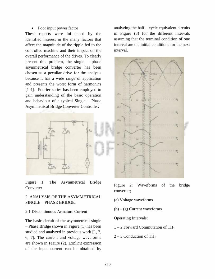
216
Poor input power factor
These reports were influenced by the
identified interest in the many factors that
affect the magnitude of the ripple fed to the
controlled machine and their impact on the
overall performance of the drives. To clearly
present this problem, the single – phase
asymmetrical bridge converter has been
chosen as a peculiar drive for the analysis
because it has a wide range of application
and presents the worst form of harmonics
[1-4]. Fourier series has been employed to
gain understanding of the basic operation
and behaviour of a typical Single – Phase
Asymmetrical Bridge Converter Controller.
Figure 1: The Asymmetrical Bridge
Converter.
2. ANALYSIS OF THE ASYMMETRICAL
SINGLE – PHASE BRIDGE.
2.1 Discontinuous Armature Current
The basic circuit of the asymmetrical single
– Phase Bridge shown in Figure (1) has been
studied and analyzed in previous work [1, 2,
6, 7]. The current and voltage waveforms
are shown in Figure (2). Explicit expression
of the input current can be obtained by
analyzing the half – cycle equivalent circuits
in Figure (3) for the different intervals
assuming that the terminal condition of one
interval are the initial conditions for the next
interval.
Figure 2: Waveforms of the bridge
converter;
(a) Voltage waveforms
(b) – (g) Current waveforms
Operating Intervals:
1 – 2 Forward Commutation of TH1
2 – 3 Conduction of TH1

217
3 – 4 Angle after for to become
forward biased
4 – 5 Extinction interval
5 – 6 Freewheeling interval
(a)
(b)
(c)
(d)
Figure 3: Half circle equivalent circuit
showing path of current during different
intervals
(a) Forward Commutation interva ux
(b) Conduction interval xu
(c) Freewheeling interval x0
(d) Reverse Commutation or Extinction
interval sxx
The simplying equations are based on the
following assumptions [8-12].
That the thyristors are ideal switches
That a steady state condition has
been established to justify repeatitive
representation of the cycles.
Non – linearity in operation of the
machine is included in the
parameters of the system equations.
That the motor is separately excited.
In the forward commutation interval,
ux , fig. 3(b), before the current
in a thyristor gated at delay angle ‗
‘reaches the value of current in the armature,
the equation for the circuit of fig. 3(b) in
which the forward commutating current
flows is:
tEdt
diLiR ss sin1 (1)
With initial condition 0i at 0t , the
current in this interval is given by:
1
111 expsinsin
t
tKti (2)
Where, 1
11
Z
Ek , ss LjRZ 1 ,
s
s
R
L1
s
s
R
L 1
1 tan
Current at the end of the interval when
ut is:

218
1
111 expsinsin
u
tKIao
(3)
In the interval xu , the current
flows in the path shown in Fig. 3(b) and is
given by the equation,
utEERidt
diL sin1 (4)
Where, as LLLL 1 , as RRR
With the initial condition aoIi at 0t ,
the current in the interval is:
PxKxi 222 sincos
aoIPuK 222 sincos
t
ux
exp (5)
Where, R
EK 1
2 , 1E
EP ,
R
L 1
2 tan
R
L
and, utx
In the interval x0 , the load is not
connected to the supply, current flows in the
path shown in fig. 3(c) and is given by;
EiRdt
diL a 2 (6)
Where, aLLL 12
With initial current 1I at 0x , the current
in the free-wheeling interval is;
22
1 exp1exp
x
R
ExIxi
a
(7)
Where, aR
L22
At ux , the current is aoI , which is
given by the equation;
22
1 exp1exp
u
R
EuII
a
ao
(8)
Combining equations (3) and (8), gives the
current at 0x as;
aR
E
uuK
I 1
111
1
expsinsin
aR
Eu
2
exp
(9)
The current at x , during the conduction
interval is also equal to 1I , giving
Iao
P
uK
PKI
22
2
2221
sincos
sincos
uexp (10)
Combining equations (9) and (10), gives a
transcendental equation uf which can be
solved to obtain the commutation angle ‗u ‘
for the gating angle ‗ ‘.
The free – wheeling diode 2D in Fig. 3(c)
becomes forward biased when the
instantaneous supply voltage equals the
source inductance. The induced voltage
reverse biases 2D , until the angle after ‗ ‘
when this voltage is neutralized by the
instantaneous supply voltage. The current in
the conducting thyristor begins to decay to
zero and in an attempt to oppose this, the

219
voltage in the armature circuit inductance
forward biases ‗ 2D ‘ to begin the
freewheeling mode.
The reverse commutation of current from a
conducting thyristor is opposed by the
voltage induced in the source inductance.
Defining ‗ t ‘ from x , the current in a
reverse commutating thyristor falls to zero
from the value at x i.e I .
So, in the interval x , the
conducting thyristor switches off and the
expression for current during this interval is
obtained from the describing equation of
current from Fig.3 (d);
tEiRdt
diL ss sin1 (11)
With the initial condition Ii , the current
during the extinction process is;
IKtKti 1111 sinsin
1
exp
t (12)
These equations for the current at the
various intervals summed together, gives the
current drawn from the supply by the motor
load as shown in Fig. 2.
Work is still been done , to predict the
harmonics and the relationships of the
behaviour factors (power factor, harmonic
factor, displacement factor, peak factor,
distortion factor, etc).
2.2 Continuous Armature Current
The waveform of currents of the drive when
operating in a continuous armature current
mode is as shown in Figure (4). The
assumptions [5-6] are:
That the load is inductive
That the load current is continuous.
Figure (4): Speed control of a separately
excited dc motor by a single phase
Asymmetric bridge converter.
(a) Power circuit
(b) Voltage and current waveforms
for continuous motor current
The instantaneous input current to an
asymmetrical single – Phase Bridge can be
expressed in Fourier series:
tis =I dc tnan
n cos(...2,1
+ )sin tnbn (13)
Where
I dc 2
1
2
0
tdtis
= 2
1 )()( tdtia
-
2
)()( tdtia
Simplifying yields,

220
I 0dc (14)
a )(cos)(1
2
ttdntisn
2
coscos1
ttdntIttdntI aa
=
nn
I a sin2
For n = 1,3,5…. odd
Also,
b n =
1)(sin)(
2
ttdntis
(15)
= )cos1(2
nn
I a for n = 1,3,5… (16)
Equation (13) can be written as
...5,3,1
2n
nsns tnSinnIti (17)
where,
2
122
2
1nnsn baI (18)
This is the nth harmonic current of the input.
Substituting for na and nb ,
2
22
nCos
n
Ia (19)
And, 2
nn
(20)
Hence equation (17) becomes;
....5,3,1 2sin
2cos
4
n
as
ntn
n
n
Iti
(21)
The fundamental current is obtained by
setting n = 1
From equation (19)
2cos
221
as II (i.e. n = 1) (22)
Determination of sI :
2
1
2 )(2
2
tdII as
=
t
I a
2
= 2
1
1
aI (23)
Power factor [6, 7] is defined as;
PF = 1
1 cos s
s
s
I
I
Where,
21
s From equation (20)
and,
PF=
2
1
1
2cos
22
2cos1
a
a
s
s
I
I
I
Icos
2
2
1
cos12
(24)

221
Equation (24) shows the relationship
between Power Factor and the thyristor
firing angle. An increase in the firing angle
reduces the power factor
The expression for harmonic factor [6,7] is;
HF
2
1
22
1
2
22
1
11
11
s
s
s
ss
I
I
I
II
Substituting for sI and 1sI
HF =
2
1
1cos14
(25)
If 1s is the angle between the fundamental
component of the input current and AC
input voltage, then the displacement factor
DF is:
DF = nscos
2
nCos
2cos
1
sCos (26)
3. RESULTS
The expressions derived in equation (21) for
the instantaneous input current are plotted in
Figure (5) for various firing angle of the
thyristors of the drive. Their corresponding
harmonics are displayed in Figure (6).
Evidently, the PF, HF and the DF varies
with the delay or firing angle and their plots
are shown in Figures (7)
Figure (5): Waveform of input currente for a
delay angle of ‗ ‘ = 60 degrees
Figure (6): Harmonics of the single – phase
asymmetric bridge converter
0 2 4 6 8 10 12 14-15
-10
-5
0
5
10
15
wt(radians)
insta
nta
neous c
urr
ent
(A)
0 5 10 150
2
4
6
8
10
12
14
harmonic number
insta
nta
neous c
urr
ent
(A)
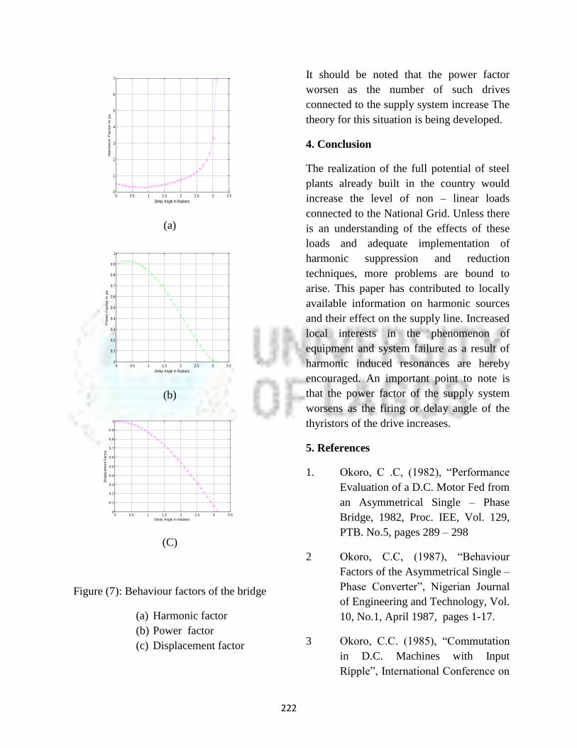
222
(a)
(b)
(C)
Figure (7): Behaviour factors of the bridge
(a) Harmonic factor
(b) Power factor
(c) Displacement factor
It should be noted that the power factor
worsen as the number of such drives
connected to the supply system increase The
theory for this situation is being developed.
4. Conclusion
The realization of the full potential of steel
plants already built in the country would
increase the level of non – linear loads
connected to the National Grid. Unless there
is an understanding of the effects of these
loads and adequate implementation of
harmonic suppression and reduction
techniques, more problems are bound to
arise. This paper has contributed to locally
available information on harmonic sources
and their effect on the supply line. Increased
local interests in the phenomenon of
equipment and system failure as a result of
harmonic induced resonances are hereby
encouraged. An important point to note is
that the power factor of the supply system
worsens as the firing or delay angle of the
thyristors of the drive increases.
5. References
1. Okoro, C .C, (1982), ―Performance
Evaluation of a D.C. Motor Fed from
an Asymmetrical Single – Phase
Bridge, 1982, Proc. IEE, Vol. 129,
PTB. No.5, pages 289 – 298
2 Okoro, C.C, (1987), ―Behaviour
Factors of the Asymmetrical Single –
Phase Converter‖, Nigerian Journal
of Engineering and Technology, Vol.
10, No.1, April 1987, pages 1-17.
3 Okoro, C.C. (1985), ―Commutation
in D.C. Machines with Input
Ripple‖, International Conference on
0 0.5 1 1.5 2 2.5 3 3.50
1
2
3
4
5
6
7
Delay Angle In Radians
Harm
onic
Facto
r In
pu
0 0.5 1 1.5 2 2.5 3 3.50
0.1
0.2
0.3
0.4
0.5
0.6
0.7
0.8
0.9
1
Delay Angle In Radians
Pow
er
Facto
r In
pu
0 0.5 1 1.5 2 2.5 3 3.50
0.1
0.2
0.3
0.4
0.5
0.6
0.7
0.8
0.9
1
Delay Angle In Radians
Dis
pla
cem
ent
Facto
r

223
Electrical Machines, IEE, Savoy
Place, London. Sept. 1985, Conf.
PUB, 254, pages 295 – 298
4. Okoro, C .C. (1993), ―A Qualitative
Investigation of Flux Pulsations in a
D.C Machine with Input Current
Ripple‖, International Conference on
Electrical Machines and Drives,
University of Oxford, 8 – 10th
Nov.
1993. Page 146 - 154
5 P.C Sen (1981) ―Thyristor DC
Drives. John Wiley and Sons Ltd.
NY, 1981.
6 Muhammed R. Rashid: (1993),
―Power Electronics: Devices and
Application‖. Prentice-Hall Inc. 2nd
Edition 1993.
7. P.Mehta, S. Mukhopadhyay, (1974),
―Modes of operation in Converter –
Controlled D.C drives‘. Proc. IEE,
Vol. 121, No. 3, March, 1974. Pages
468-474.
8 Agu, U (1997), ―Relative study of
the output characteristics of PWM
and Phase controlled AC – DC
converters‖, Conf. Publication,
Electric Power Engineering
Conference (EPEC), UNN, 4-5th
.
Dec. 1997. Pages 132 – 140.
9. Fuhao, T and Miyalvi, S: (1974),
―Ac – DC Converter with improved
power Factor and Current Waveform
on AC side, Electrical Engineering in
Japan, Vol. 94, No. 4, 1974. Pages
89-96.
10 Zander H: (1973), ―Self Commutated
Rectifier to improve Line
Conditions‖, Proc. IEE, Vol. 120,
No. 9, Sept. 1973
11. Ira Pitel and Sarosh, N. T,: (1977), A
review of the effects and suppression
of Power Converter Harmonics‖.
Industry and Application Society,
Annual Conference, 1997, pages
119-120.
12. Dewan, S. B. et al: (1970). ―Input
Filter Design with Static Power
Converters‖, IEE Industry and
General Applications, Vol. IGA – 6,
No. 4, July/Aug.1970. Pages 326 –
335.

224
APPENDIX IX
Published Paper II
This was a paper presented and published from my research work in the proceedings of
International Conference on Emerging trends, research directions and training requirements of
21st century Electrical and Electronics Engineering held at the University of Lagos, Akoka,
Lagos, Nigeria, 22 – 24 July, 2009 Pages 52 - 56
BRIDGELESS ASYMMETRICAL SINGLE – PHASE AC – DC BOOST CONVERTER
FOR POWER FACTOR CORRECTION
O.D. Osunde
Department of Electrical and Electronics Engineering
University of Lagos, Lagos, Nigeria.
Email: [email protected]
ABSTRACT: A simplified approach of a
Pulse Width Modulated Single Phase AC –
DC converter for power factor correction is
investigated as a more efficient and cheaper
alternative to the conventional asymmetrical
Boost converter for Power Factor
Correction. The Bridgeless asymmetrical
AC – DC Boost converter employs fewer
semi – conductor devices thereby reducing
power losses and increased reliability. It has
a higher efficiency compared to the
conventional boost PFC that suffers from
high conduction loss. It is however limited
to low and medium power applications.
Keywords: Bridgeless Boost converter,
Power Factor Correction (PFC), PWM
I.INTRODUCTION
Single switch PFC is the most widely used
topology for the PFC applications because
of its simplicity and smaller EMI filter size.
Due to the high conduction losses and
switching losses, this circuit has a low
efficiency at low input line voltage. With the
development of super junction MOSFET,
switching losses of the PFC circuit is
dramatically improved [1]. Meanwhile, the
circuit still suffers from forward voltage
drop of the rectifier bridge caused by high
conduction losses, especially at low input
line. To reduce the rectifier bridge
conduction losses, different topologies have
been developed. Among these topologies,
the bridgeless boost which does not require
circuit switch, is quite simple and has a high
performance [2][3]. The bridgeless PFC
generates less conduction losses compared
with the conventional PFC. Although the
circuit structure is simple, the location of the
boost inductor on the AC side makes it
difficult to sense the AC line voltage and
inductor current. In this paper, the bridgeless
asymmetrical boost that was designed and
constructed is reported. Also, measurements
of the input current and voltage waveforms
together with the input power factor are
presented. A comparative cost analysis of
the conventional asymmetric is also made.

225
II The Bridgeless and the Conventional
Boost Converter
The bridgeless PFC boost rectifiers of Fig.2,
also called the dual boost PFC rectifiers,
compared to the conventional PFC boost
rectifier of Fig.1, generally, improve the
efficiency of the front-end PFC stage by
eliminating one diode forward-voltage drop
in the line-current path. The bridgeless
configuration presented in this paper, avoids
the need for the drive input bridge, yet
maintains the classic boost arrangement.
Fig.1: Asymmetrical Single Phase AC –DC
Boost- type Converter with input power
factor correction
Fig, 2:Bridgeless Asymmetrical Single –
Phase AC –DC PFC configuration
This is easily done by replacing the
thyristors of the asymmetrical single - phase
bridge converter in Fig.1 by a power
MOSFET with a diode connected between
the drain and the source of the MOS switch
as shown in Fig.2. A thyristor could be used
as the switching device too although the
MOSFET is a fast switching device. The
series diode Dd in the conventional boost
circuitry of Fig.1 has been eliminated. Also,
the dc – side inductor is no longer necessary
and instead an ac – side inductor is required.
The advantages of this circuit are :
Improved characteristics in terms of
input power factor and sinusoidal
shape of the input current.
Only two semi-conductor device
drops exist in the power flow path at
any given instant.
The boost inductor ‗L‘ on the ac side
contributes to the reduction in EMI
interference
III Circuit Analysis.
The analysis can be discussed in two ways
[4-5], one of such ways is presented here.
First, to analyze the operation, the circuit of
Fig.2 can be viewed as two sections: section
one operates as the boost stage (positive half
cycle) and the second operates as the return
path for AC signal during the negative half
cycle [6-7].

226
L
C
Controller
1M2M
sV oV
Positive Half Cycle
Return
C
H
O
P
P
E
R
2D
1D
R
L
Fig.3: Bridgeless PFC Configuration for the
positive half cycle
L
C
Controller
1D2D
1M 2M
sVoV
Negative half cycle
Return
C
H
O
P
P
E
R
L
R
E
Fig.4: Bridgeless PFC Configuration for
the negative half cycle
(a) Positive ―Half Cycle‖.
When the AC input goes positive, the gate
of MOSFET M1 is driven high and current
flows through the input, and through the
inductor, storing energy. When M1 turns off,
energy in the inductor is released and
current flows through D1, through the load
and returns through the body diode of M2
back to the input mains Fig.3.
During the off – time, the current flows
through the inductor ―L‘ (during this time,
the inductor discharges its energy) into the
boost diode D1 and close the circuit through
the load.
(b) Negative ―Half Cycle‖
During the negative half cycle, circuit
operation is mirrored as the positive half
cycle as shown in Fig.4, M2 turns ON,
current flows through the inductor storing
energy. When M2 turns off, energy is
released as current flows through D2
through the load and back to the mains
through the body diode of M1.
It should be noted that the two power
MOSFETs are driven synchronously. It does
not matter whether the sections are
performing as an active boost or as a path
for the current to return. In either case, there
is the benefit of lower power dissipation
when current flows through the power
MOSFETs during the return phase.
Fig.5 shows the Circuit Layout for the
simultaneous gate firing of the MOSFETs
(or Thyristors) of the bridgeless circuit by
PWM controls
IV Design Considerations
The circuit of Fig.2 is to supply a 2.0kw
load, from a 230Vrms, 50Hz Single – phase
source. The output has a maximum of 400V
dc with a switching frequency of 10KHz. It
is operated in the Continuous Inductor
Conduction Mode (CICM) [4].
It is assumed that switching losses and
device power loss are negligible.
Parameters ‗L‘ and ‗C‘ are determined with
the specification that the output ripple
voltage shall be within the limits of 5% of
the output voltage. The defining equations
are derived in [6].
Since the switching losses are assumed to be
zero,
outin PP
inin IVKW 0.2
AI in 695.8230
2000
And,
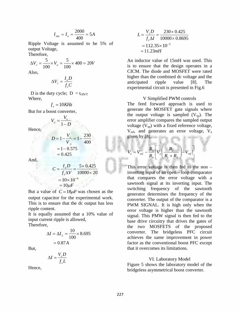
227
AII oout 5400
2000
Ripple Voltage is assumed to be 5% of
output Voltage,
Therefore,
VVV oc 20400100
5
100
5
Also,
Cf
DIV
s
oc
D is the duty cycle; D= tON/T
Where,
KHzf s 10
But for a boost converter,
D
VV s
o
1
Hence,
400
23011
o
s
V
VD
575.01
425.0 And,
2010000
425.05
Vf
DIC
s
o
61010 F10
But a value of FC 18 was chosen as the
output capacitor for the experimental work.
This is to ensure that the dc output has less
ripple content.
It is equally assumed that a 10% value of
input current ripple is allowed,
Therefore,
695.8
100
10 LII
A87.0
But,
Lf
DVI
s
s
Hence,
8695.010000
425.0230
If
DVL
s
s
51035.112
mH23.11
An inductor value of 15mH was used. This
is to ensure that the design operates in a
CICM. The diode and MOSFET were rated
higher than the combined dc voltage and the
anticipated ripple value [8]. The
experimental circuit is presented in Fig.6
V Simplified PWM controls
The feed forward approach is used to
generate the MOSFET gate signals where
the output voltage is sampled (Vsp). The
error amplifier compares the sampled output
voltage (Vsp) with a fixed reference voltage,
Vref, and generates an error voltage, Ve
given by [8].
reforefe V
RR
RV
R
RVV
21
2
4
3
This error voltage is then fed to the non –
inverting input of an open – loop comparator
that compares the error voltage with a
sawtooth signal at its inverting input. The
switching frequency of the sawtooth
generator determines the frequency of the
converter. The output of the comparator is a
PWM SIGNAL. It is high only when the
error voltage is higher than the sawtooth
signal. This PMW signal is then fed to the
base drive circuitry that drives the gates of
the two MOSFETS of the proposed
converter. The bridgeless PFC circuit
achieves the same improvement in power
factor as the conventional boost PFC except
that it overcomes its limitations.
VI. Laboratory Model
Figure 5 shows the laboratory model of the
bridgeless asymmetrical boost converter.
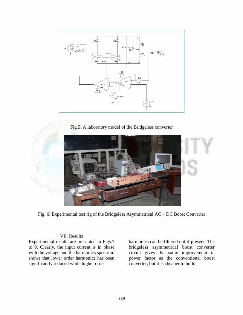
228
Fig.5: A laboratory model of the Bridgeless converter
Fig. 6: Experimental test rig of the Bridgeless Asymmetrical AC – DC Boost Converter
VII. Results
Experimental results are presented in Figs.7
to 9. Clearly, the input current is in phase
with the voltage and the harmonics spectrum
shows that lower order harmonics has been
significantly reduced while higher order
harmonics can be filtered out if present. The
bridgeless asymmetrical boost converter
circuit gives the same improvement in
power factor as the conventional boost
converter, but it is cheaper to build.
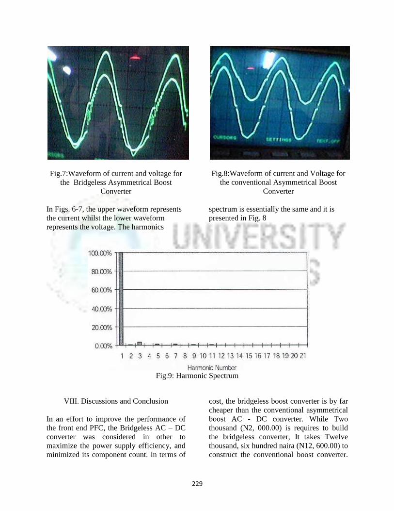
229
Fig.7:Waveform of current and voltage for
the Bridgeless Asymmetrical Boost
Converter
Fig.8:Waveform of current and Voltage for
the conventional Asymmetrical Boost
Converter
In Figs. 6-7, the upper waveform represents
the current whilst the lower waveform
represents the voltage. The harmonics
spectrum is essentially the same and it is
presented in Fig. 8
Fig.9: Harmonic Spectrum
VIII. Discussions and Conclusion
In an effort to improve the performance of
the front end PFC, the Bridgeless AC – DC
converter was considered in other to
maximize the power supply efficiency, and
minimized its component count. In terms of
cost, the bridgeless boost converter is by far
cheaper than the conventional asymmetrical
boost AC - DC converter. While Two
thousand (N2, 000.00) is requires to build
the bridgeless converter, It takes Twelve
thousand, six hundred naira (N12, 600.00) to
construct the conventional boost converter.

230
The circuit arrangement of the bridgeless
PFC boost converter compared with the
conventional PFC boost converter, shows
that a diode has been eliminated from the
line-current path, so that the line current
simultaneously flows through only two
semiconductors resulting in reduced
conduction losses and a higher efficiency.
However, the bridgeless PFC boost
converter has significantly larger noise than
the conventional PFC boost rectifier [9-11]
IX REFERENCES
[1] Lu, B, Dong, W, Zhao, Q, Lee, F.C.;
―Performance evaluation of
CoolMOSTM and SiC diode for
single – phase power factor
correction applications‖, APEC
'03.Pages:651 - 657 vol.2
[2] Liu J.; Chen W.; Zhang J.; Xu, D.;
Lee, F.C.; ―Evaluation of power
losses in different CCM mode
single-phaseboost PFC converters
via a simulation tool‖, IAS 2001,
Pages:2455 - 2459 vol.4
[3] Srinivasan, R.; Oruganti, R.; ―A
unity power factor converter using
half-bridge boost topology‖, IEEE
Transactions on Power Electronics,
Volume: 13 Issue: 3, May 1998,
Pages:487 – 500
[4] Trzynadlowski A.M, Wang Z,
Nagashima J, Stancu C and
Zelechowski M. ―Comparative
Investigation of PWM Techniques
for a New Drive for Electric
Vehicles‖. IEEE Transactions on
Industry Applications. Vol. 39, No.
5. 2003. 1396-1403.
[5] Enjeti P.N, Ziogas P.D and Lindsay
J.F. ―Programmed PWM Techniques
to Eliminate Harmonics: A Critical
Evaluation‖. IEEE Transactions on
Industry Applications, 26, 1990. Pp
302-316.
[6] Robert Martinez and Enjeti P.N. ―A
High performance Single- Phase
Rectifier with input power factor
correction‖ IEEE Transaction on
Power Electronics, Vol. II, No.2.
2000. Pp 154-163
[7] Laszlo, H, Yungtaek Jung and Milan
M. Jovanovic. ―Performance
Evaluation of Bridgeless PFC Boost
Rectifiers‖. IEE. 2007. Pp 165-171
[8] Osunde,O.D ―Input Power Factor
Problem and correction for Industrial
Drives‖. A thesis presented to the
School of Post Graduate Studies of
the University of Lagos, Lagos,
Nigeria (2009).
[6] Okoro C.C ―Behaviour factors of
Asymmetrical single-phase
converter‖. Nigerian Journal of
Engineering and Technology, vol.10.
1987. No.11-7
[7] Okoro C.C. ―Performance
Evaluation of a DC motor Fed from
an Asymmetrical Single-Phase
Bridge‖. Proc. IEE, 1982. vol.129.
PTB No.5, 289-98.
[8] Sen P.C. ―Thyristorised DC Drives‖.
John Wiley and Sons Inc. 1991. 1st
Edition. Florida. Krieger Publishing
Company.
[9] Liu Y and Smedley, K. ―Control of
a Dual Boost power factor corrector
for high power applications‖.
IECON 29th Annual Conference of
the IEEE.Volume 3, Issue , 2-6.
2003. PP. 2929-2932.

231
[10] Liu Y and Smedley, K. ―Control of a
Dual Boost power factor corrector
for high power applications‖.
IECON 29th Annual Conference of
the IEEE.Volume 3, Issue , 2-6.
2003. PP. 2929-2932
[11] Robert Martinez and Enjeti P.N. ―A
High performance Single- Phase
Rectifier with input power factor
correction‖. IEEE Transaction on
Power Electronics, Vol. II, No.2.
2000. Pp 154-163
[12] Laszlo, H, Yungtaek Jung and Milan
M. Jovanovic. ―Performance
Evaluation of Bridgeless PFC Boost
Rectifiers‖. IEE. 2007. Pp 165-171

232
APPENDIX X
Unpublished Papers
1. Correction of Input Power Factor Problem in Industrial Drives
2. Impact of Harmonics in Communications Systems and Circuits
3. Bridgeless Asymmetrical Single – Phase AC – DC Converter for Power
Factor Correction
Related Documents