2006 DATA SHEET DESCRIPTION The µ PD6P8, 6P8A, 6P8B are microcontrollers for infrared remote control transmitters and are provided with a one-time PROM as the program memory. Because users can write progra ms for the µ PD6P8, 6P8A, 6P8B, They are ideal for program evaluation and small- scale production of application systems that use the µ PD67A, 67B, 68A, 68B. When reading this document, also refer to the following documents. µ PD67, 67A, 68, 68A, 69 Data Sheet: U14935E µ PD67B, 68B Data Sheet: U16792E FEATURES • Program memory (one-time PROM): 2026 × 10 bits • Data memory (RAM): 32 × 4 bits • On-chi p carrier gener ator for infrared remote control: The hi gh-level and low-level width can be set separately from 250 ns to 64 µ s (@ fX = 4 MHz operation) via modulo registers • 9-bit programmable timer: 1 channel • Instruction execution time: 16 µ s (@ fX = 4 MHz) • Stack level: 1 level (stack RAM is for data memory RF as well) • I/O pins (KI/O): 8 units • Input pins (KI): 4 units • Sense input pins (S0, S2): 2 units • S1 /LED p in (I /O): 1 unit (when in output mode, this is th e remo te control transmission display pin) • Power supply voltage: VDD = 1.9 to 3.6 V • Operating ambient temperature: TA = –40 to +85°C • Oscillator frequency: fX = 3.5 to 4.5 MHz • On-chi p POC circu it and RAM r etent ion detector • On- chi p os cil lat or ( µ PD6P8B) APPLICATIONS Infrared remote control transmitters (for AV and household electric appliances) 4-BIT SINGLE-CHIP MICROCONTROLLER FOR INFRARED REMOTE CONTROL TRANSMISSION MOS INTEGRATED CIRCUIT µ PD6P8, 6P8A, 6P8B The information in this document is subject to change without notice. Before using this document, please confirm that this is the latest version. Not all products and/or types are available in every country. Please check with an NEC Electronics sales representative for availability and additional information. The mark <R> shows major revised points. Document No. U17848EJ3V0DS00 (3rd edition) Date Published December 2007 N Printed in Japan

Welcome message from author
This document is posted to help you gain knowledge. Please leave a comment to let me know what you think about it! Share it to your friends and learn new things together.
Transcript
7/17/2019 INFRARED REMOTE CONTROL TRANSMISSION
http://slidepdf.com/reader/full/infrared-remote-control-transmission 1/9520
DATA SHEET
DESCRIPTION
The µ PD6P8, 6P8A, 6P8B are microcontrollers for infrared remote control transmitters and are provided with
a one-time PROM as the program memory.
Because users can write programs for the µ PD6P8, 6P8A, 6P8B, They are ideal for program evaluation and small-
scale production of application systems that use the µ PD67A, 67B, 68A, 68B.
When reading this document, also refer to the following documents.
µ PD67, 67A, 68, 68A, 69 Data Sheet: U14935Eµ PD67B, 68B Data Sheet: U16792E
FEATURES
• Program memory (one-time PROM): 2026 × 10 bits
• Data memory (RAM): 32 × 4 bits
• On-chip carrier generator for infrared remote control: The high-level and low-level width can be set separately
from 250 ns to 64 µ s (@ fX = 4 MHz operation) via modulo
registers
• 9-bit programmable timer: 1 channel
• Instruction execution time: 16 µ s (@ fX = 4 MHz)
• Stack level: 1 level (stack RAM is for data memory RF as well)
• I/O pins (KI/O): 8 units
• Input pins (KI): 4 units
• Sense input pins (S0, S2): 2 units
• S1 /LED pin (I /O): 1 unit (when in output mode, this is the remote control
transmission display pin)
• Power supply voltage: VDD = 1.9 to 3.6 V
• Operating ambient temperature: TA = –40 to +85°C
• Oscillator frequency: fX = 3.5 to 4.5 MHz
• On-chip POC circuit and RAM retention detector
• On-chip oscillator (µ PD6P8B)
APPLICATIONS
Infrared remote control transmitters (for AV and household electric appliances)
4-BIT SINGLE-CHIP MICROCONTROLLER
FOR INFRARED REMOTE CONTROL TRANSMISSION
MOS INTEGRATED CIRCUIT
µ PD6P8, 6P8A, 6P8B
The information in this document is subject to change without notice. Before using this document, pleaseconfirm that this is the latest version.Not all products and/or types are available in every country. Please check with an NEC Electronicssales representative for availability and additional information.
The mark <R> shows major revised points.
Document No. U17848EJ3V0DS00 (3rd edition)Date Published December 2007 NPrinted in Japan
7/17/2019 INFRARED REMOTE CONTROL TRANSMISSION
http://slidepdf.com/reader/full/infrared-remote-control-transmission 2/95
2
µ PD6P8, 6P8A, 6P8B
Data Sheet U17848EJ3V0DS
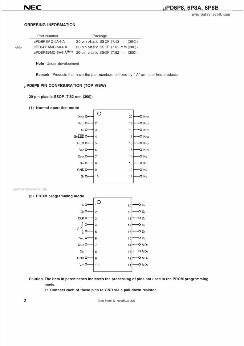
ORDERING INFORMATION
Part Number Package
µ PD6P8MC-5A4-A 20-pin plast ic SSOP (7.62 mm (300))
µ PD6P8AMC-5A4-A 20-pin plastic SSOP (7.62 mm (300))
µ PD6P8BMC-5A4-ANote 20-pin plastic SSOP (7.62 mm (300))
Note Under development
Remark Products that have the part numbers suffixed by “-A” are lead-free products.
µ PD6P8 PIN CONFIGURATION (TOP VIEW)
20-pin plastic SSOP (7.62 mm (300))
(1) Normal operation mode
(2) PROM programming mode
Caution The item in parentheses indicates the processing of pins not used in the PROM programming
mode.
L: Connect each of these pins to GND via a pull-down resistor.
1
2
3
4
5
6
7
8
9
10
KI/O6
KI/O7
S0
S1 /LED
REM
VDD
XOUT
XIN
GND
S2
20
19
18
17
16
15
14
13
12
11
KI/O5
KI/O4
KI/O3
KI/O2
KI/O1
KI/O0
KI3
KI2
KI1
KI0
1
2
3
4
5
6
7
8
9
10
20
19
18
17
16
15
14
13
12
11
D6
D7
CLK
VDD
XOUT
XIN
GND
VPP
D5
D4
D3
D2
D1
D0
MD3
MD2
MD1
MD0
(L)
<R>
7/17/2019 INFRARED REMOTE CONTROL TRANSMISSION
http://slidepdf.com/reader/full/infrared-remote-control-transmission 3/95
3
µ PD6P8, 6P8A, 6P8B
Data Sheet U17848EJ3V0DS
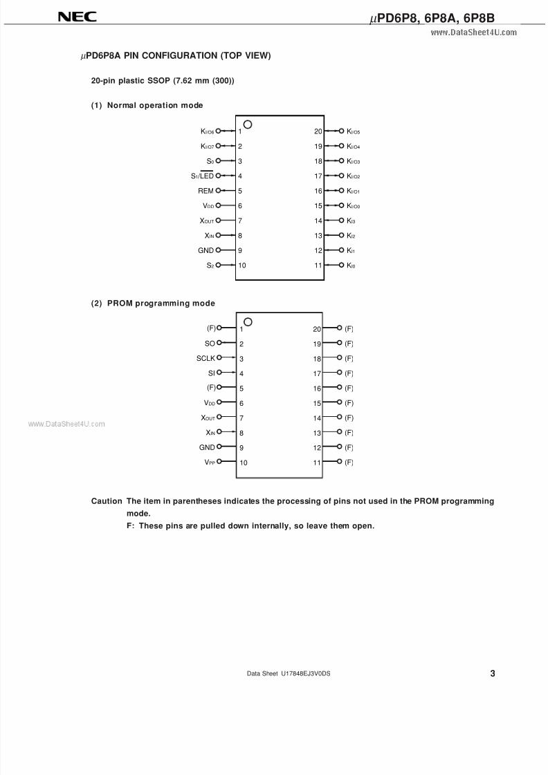
µ PD6P8A PIN CONFIGURATION (TOP VIEW)
20-pin plastic SSOP (7.62 mm (300))
(1) Normal operation mode
(2) PROM programming mode
Caution The item in parentheses indicates the processing of pins not used in the PROM programming
mode.
F: These pins are pulled down internally, so leave them open.
12
3
4
5
6
7
8
9
10
KI/O6
KI/O7
S0
S1 /LED
REM
VDD
XOUT
XIN
GND
S2
2019
18
17
16
15
14
13
12
11
KI/O5
KI/O4
KI/O3
KI/O2
KI/O1
KI/O0
KI3
KI2
KI1
KI0
1
2
3
4
5
6
7
8
9
10
20
19
18
17
16
15
14
13
12
11
SO
SCLK
SI
VDD
XOUT
XIN
GND
VPP
(F)
(F)
(F)
(F)
(F)
(F)
(F)
(F)
(F)
(F)
(F)
(F)
7/17/2019 INFRARED REMOTE CONTROL TRANSMISSION
http://slidepdf.com/reader/full/infrared-remote-control-transmission 4/95
4
µ PD6P8, 6P8A, 6P8B
Data Sheet U17848EJ3V0DS
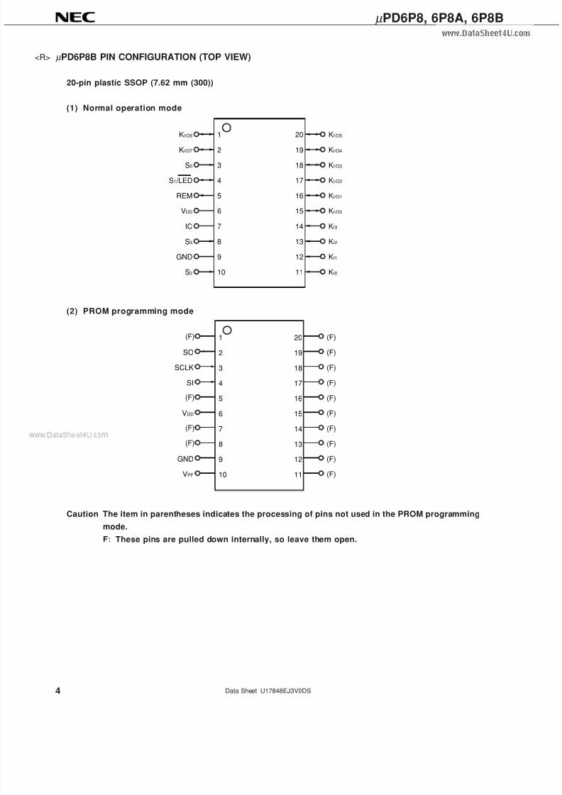
µ PD6P8B PIN CONFIGURATION (TOP VIEW)
20-pin plastic SSOP (7.62 mm (300))
(1) Normal operation mode
(2) PROM programming mode
Caution The item in parentheses indicates the processing of pins not used in the PROM programming
mode.
F: These pins are pulled down internally, so leave them open.
12
3
4
5
6
7
8
9
10
KI/O6
KI/O7
S0
S1 /LED
REM
VDD
IC
S3
GND
S2
2019
18
17
16
15
14
13
12
11
KI/O5
KI/O4
KI/O3
KI/O2
KI/O1
KI/O0
KI3
KI2
KI1
KI0
1
2
3
4
5
6
7
8
9
10
20
19
18
17
16
15
14
13
12
11
SO
SCLK
SI
VDD
GND
VPP
(F)
(F)
(F)
(F)
(F)
(F)
(F)
(F)
(F)
(F)
(F)
(F)
(F)
(F)
<R>
7/17/2019 INFRARED REMOTE CONTROL TRANSMISSION
http://slidepdf.com/reader/full/infrared-remote-control-transmission 5/95
5
µ PD6P8, 6P8A, 6P8B
Data Sheet U17848EJ3V0DS
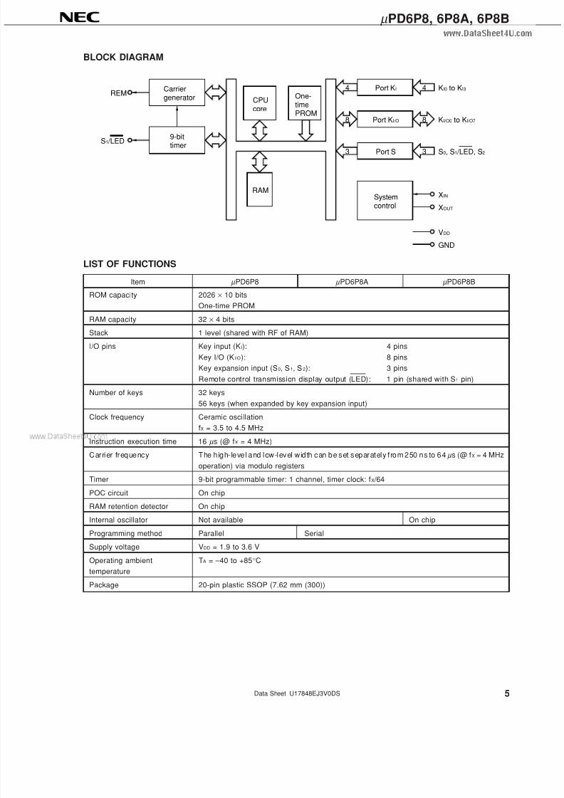
BLOCK DIAGRAM
Item µ PD6P8 µ PD6P8A µ PD6P8B
ROM capacity 2026 × 10 bits
One-time PROM
RAM capacity 32 × 4 bits
Stack 1 level (shared with RF of RAM)
I/O pins Key input (KI): 4 pins
Key I/O (KI/O): 8 pins
Key expansion input (S0, S1, S 2): 3 pins
Remote control transmission display output (LED): 1 pin (shared with S1 pin)
Number of keys 32 keys
56 keys (when expanded by key expansion input)
Clock frequency Ceramic oscillationfX = 3.5 to 4.5 MHz
Instruction execution time 16 µ s (@ fX = 4 MHz)
Carrier frequency The high- level and low-level width can be set separately f rom 250 ns to 64 µ s (@ fX = 4 MHz
operation) via modulo registers
Timer 9-bit programmable timer: 1 channel, timer clock: fX /64
POC circuit On chip
RAM retention detector On chip
Internal oscillator Not available On chip
Programming method Parallel Serial
Supply voltage VDD = 1.9 to 3.6 V
Operating ambient TA = –40 to +85°C
temperature
Package 20-pin plastic SSOP (7.62 mm (300))
KI0 to KI3
KI/O0 to KI/O7
S0, S1 /LED, S2
Port KI
Port KI/O
Port S
4
8
3
4
8
3
RAMSystemcontrol
Carriergenerator
9-bittimer
CPUcore
XIN
XOUT
VDD
GND
REM
S1 /LED
One-timePROM
LIST OF FUNCTIONS
7/17/2019 INFRARED REMOTE CONTROL TRANSMISSION
http://slidepdf.com/reader/full/infrared-remote-control-transmission 6/95
6
µ PD6P8, 6P8A, 6P8B
Data Sheet U17848EJ3V0DS
CONTENTS
1. PIN FUNCTIONS......................................................................................................................... 8
1.1 Normal Operation Mode.................................................................................................................... 8
1.2 PROM Programming Mode............................................................................................................... 10
1.3 Pins I/O Circuits................................................................................................................................. 11
1.4 Recommended Connection of Unused Pins................................................................................... 12
1.5 Notes on Using KI Pin After Reset ................................................................................................... 12
2. DIFFERENCES BETWEEN µ PD67A, 67B, 68A, 68B, AND µ PD6P8, 6P8A, 6P8B.................. 13
3. INTERNAL CPU FUNCTIONS .................................................................................................. 14
3.1 Program Counter (PC): 11 Bits ........................................................................................................ 14
3.2 Stack Pointer (SP): 1 Bit ................................................................................................................... 14
3.3 Address Stack Register (ASR (RF)): 11 Bits ................................................................................... 14
3.4 Program Memory (One-Time PROM): 2,026 Steps × 10 Bits ......................................................... 15
3.5 Data Memory (RAM): 32 × 4 Bits ...................................................................................................... 16
3.6 Data Pointer (DP): 12 Bits ................................................................................................................. 17
3.7 Accumulator (A): 4 Bits .................................................................................................................... 17
3.8 Arithmetic and Logic Unit (ALU): 4 Bits .......................................................................................... 17
3.9 Flags ................................................................................................................................................... 18
3.9.1 Status flag (F) .......................................................................................................................... 18
3.9.2 Carry flag (CY) ........................................................................................................................ 18
4. PORT REGISTERS (PX)........................................................................................................... 19
4.1 KI/O Port (P0)....................................................................................................................................... 20
4.2 KI Port/Special Ports (P1) ................................................................................................................. 20
4.2.1 KI port (P11: bits 4 to 7 of P1) .................................................................................................. 20
4.2.2 S0 port (bit 2 of P1) .................................................................................................................. 21
4.2.3 S1 /LED port (bit 3 of P1).......................................................................................................... 21
4.2.4 S2 port (bit 1 of P1) .................................................................................................................. 21
4.3 Control Register 0 (P3) ..................................................................................................................... 22
4.3.1 RAM retention flag (bit 3 of P3) ............................................................................................... 23
4.4 Control Register 1 (P4) ..................................................................................................................... 25
5. TIMER ......................................................................................................................................... 26
5.1 Timer Configuration .......................................................................................................................... 26
5.2 Timer Operation................................................................................................................................. 27
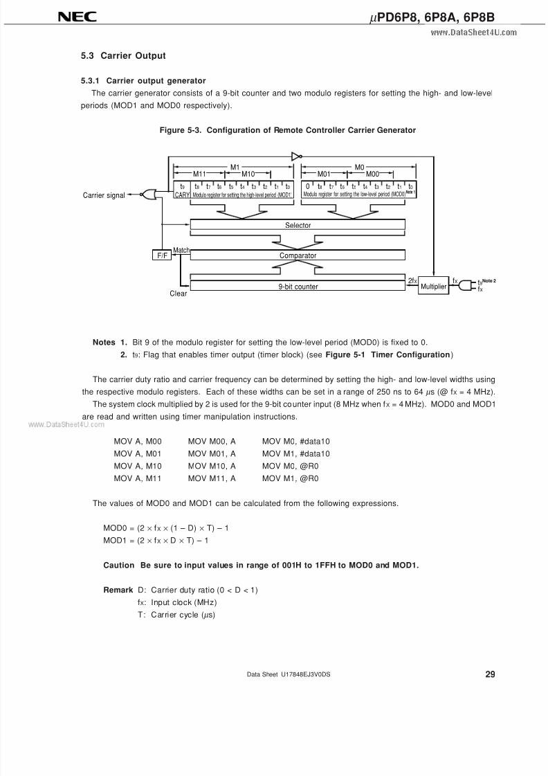
5.3 Carrier Output .................................................................................................................................... 29
5.3.1 Carrier output generator .......................................................................................................... 295.3.2 Carrier output control .............................................................................................................. 30
5.4 Software Control of Timer Output ................................................................................................... 32
6. STANDBY FUNCTION............................................................................................................... 33
6.1 Outline of Standby Function ............................................................................................................ 33
6.2 Standby Mode Setting and Release................................................................................................. 34
6.3 Standby Mode Release Timing ........................................................................................................ 36
7. RESET......................................................................................................................................... 37
7/17/2019 INFRARED REMOTE CONTROL TRANSMISSION
http://slidepdf.com/reader/full/infrared-remote-control-transmission 7/95
7
µ PD6P8, 6P8A, 6P8B
Data Sheet U17848EJ3V0DS
8. POC CIRCUIT ............................................................................................................................ 38
8.1 Functions of POC Circuit .................................................................................................................. 39
8.2 Oscillation Check at Low Supply Voltage....................................................................................... 39
9. SYSTEM CLOCK OSCILLATOR (µ PD6P8, 6P8A) .................................................................. 40
10. INSTRUCTION SET ................................................................................................................... 41
10.1 Machine Language Output by Assembler....................................................................................... 4110.2 Circuit Symbol Description .............................................................................................................. 42
10.3 Mnemonic to/from Machine Language (Assembler Output) Contrast Table .............. .............. ... 43
10.4 Accumulator Manipulation Instructions.......................................................................................... 47
10.5 I/O Instructions .................................................................................................................................. 50
10.6 Data Transfer Instructions................................................................................................................ 51
10.7 Branch Instructions .......................................................................................................................... 53
10.8 Subroutine Instructions .................................................................................................................... 54
10.9 Timer Operation Instructions ........................................................................................................... 55
10.10Others ................................................................................................................................................. 58
11. ASSEMBLER RESERVED WORDS ........................................................................................ 60
11.1 Mask Option Directives..................................................................................................................... 60
11.1.1 OPTION and ENDOP quasi-directives.................................................................................... 60
11.1.2 Mask option definition quasi-directives ................................................................................... 60
12. WRITING AND VERIFYING ONE-TIME PROM (PROGRAM MEMORY) (µ PD6P8) ................. 61
12.1 Operating Mode When Writing/Verifying Program Memory .......................................................... 61
12.2 Program Memory Writing Procedure............................................................................................... 62
12.3 Program Memory Reading Procedure ............................................................................................. 63
13. WRITING AND VERIFICATION OF ONE-TIME PROM (PROGRAM MEMORY) (µ PD6P8A, 6P8B) ......... 64
13.1 Initialization........................................................................................................................................ 64
13.2 Serial Communication Format ......................................................................................................... 65
13.3 Writing of Program Memory ............................................................................................................. 66
13.4 Reading of Program Memory ........................................................................................................... 66
14. ELECTRICAL SPECIFICATIONS (µ PD6P8) ............................................................................. 67
15. ELECTRICAL SPECIFICATIONS (µ PD6P8A) .......................................................................... 74
16. ELECTRICAL SPECIFICATIONS (µ PD6P8B) (TARGET) ........................................................ 79
17. CHARACTERISTIC CURVES (REFERENCE VALUES) (µ PD6P8) ....................................... 84
18. APPLICATION CIRCUIT EXAMPLE .......................................................................................... 85
19. PACKAGE DRAWING ................................................................................................................ 88
20. RECOMMENDED SOLDERING CONDITIONS.......................................................................... 89
APPENDIX A. DEVELOPMENT TOOLS ......................................................................................... 90
APPENDIX B. EXAMPLE OF REMOTE CONTROL TRANSMISSION FORMAT (In the case
of NEC transmission format in command one-shot transmission mode) ........ 91
7/17/2019 INFRARED REMOTE CONTROL TRANSMISSION
http://slidepdf.com/reader/full/infrared-remote-control-transmission 8/95
8
µ PD6P8, 6P8A, 6P8B
Data Sheet U17848EJ3V0DS
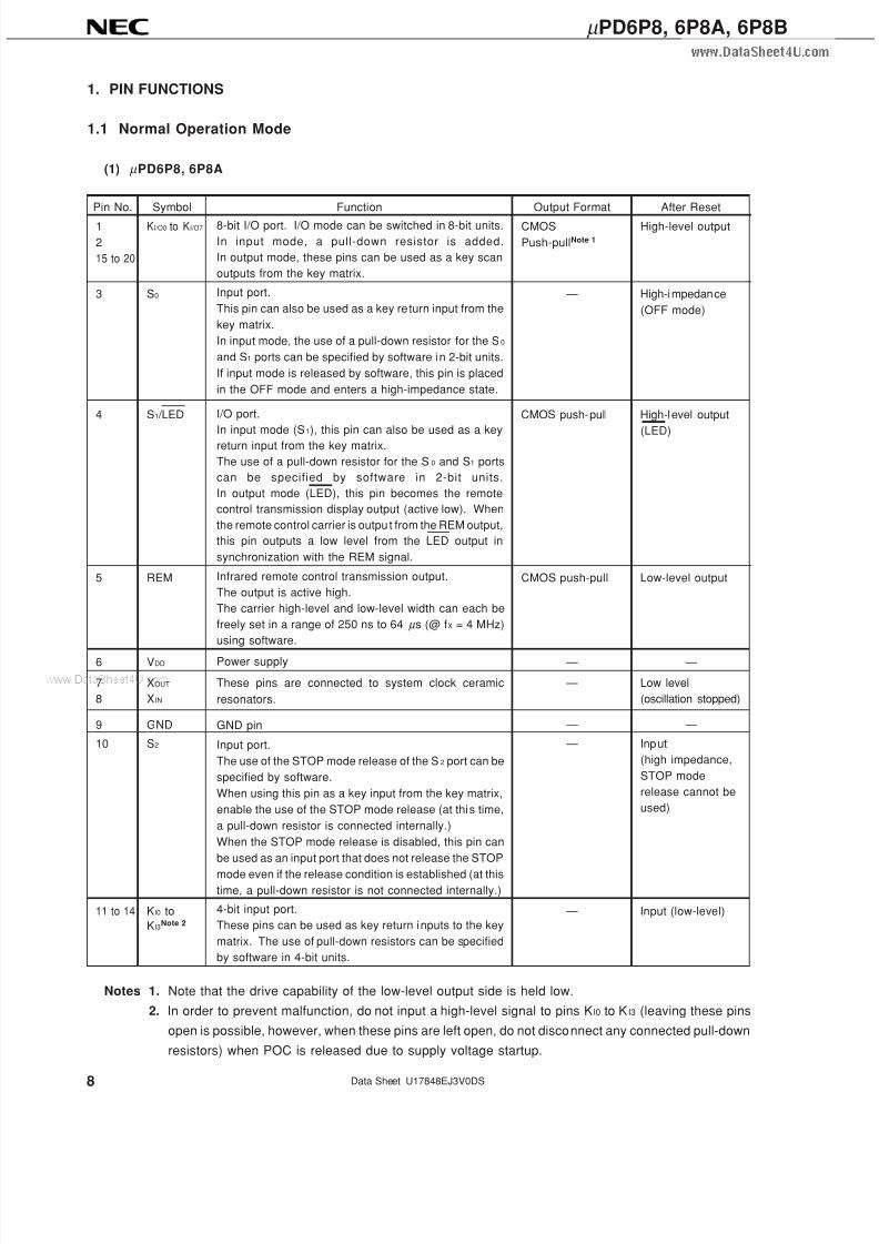
1. PIN FUNCTIONS
1.1 Normal Operation Mode
(1) µ PD6P8, 6P8A
Pin No. Symbol Function Output Format After Reset
1 KI/O0 to KI/O7 CMOS High-level output
2 Push-pullNote 1
15 to 20
3 S0 — High-impedance
(OFF mode)
4 S1 /LED CMOS push-pull High-level output
(LED)
5 REM CMOS push-pull Low-level output
6 VDD — —
7 XOUT — Low level
8 X IN (oscillation stopped)
9 GND — —
10 S2 — Input
(high impedance,
STOP mode
release cannot be
used)
11 to 14 KI0 to — Input (low-level)
KI3Note 2
Notes 1. Note that the drive capability of the low-level output side is held low.
2. In order to prevent malfunction, do not input a high-level signal to pins KI0 to K I3 (leaving these pins
open is possible, however, when these pins are left open, do not disconnect any connected pull-down
resistors) when POC is released due to supply voltage startup.
8-bit I/O port. I/O mode can be switched in 8-bit units.
In input mode, a pull-down resistor is added.
In output mode, these pins can be used as a key scan
outputs from the key matrix.
Input port.
This pin can also be used as a key re turn input from the
key matrix.
In input mode, the use of a pull-down resistor for the S0
and S1 ports can be specified by software in 2-bit units.
If input mode is released by software, this pin is placed
in the OFF mode and enters a high-impedance state.
I/O port.
In input mode (S1), this pin can also be used as a keyreturn input from the key matrix.
The use of a pull-down resistor for the S 0 and S1 ports
can be specified by software in 2-bit units.
In output mode (LED), this pin becomes the remote
control transmission display output (active low). When
the remote control carrier is output from the REM output,
this pin outputs a low level from the LED output in
synchronization with the REM signal.
Infrared remote control transmission output.
The output is active high.
The carrier high-level and low-level width can each be
freely set in a range of 250 ns to 64 µ s (@ fX = 4 MHz)
using software.
Power supply
These pins are connected to system clock ceramic
resonators.
GND pin
Input port.
The use of the STOP mode release of the S2 port can be
specified by software.
When using this pin as a key input from the key matrix,
enable the use of the STOP mode release (at this time,
a pull-down resistor is connected internally.)
When the STOP mode release is disabled, this pin can
be used as an input port that does not release the STOP
mode even if the release condition is established (at this
time, a pull-down resistor is not connected internally.)
4-bit input port.
These pins can be used as key return inputs to the key
matrix. The use of pull-down resistors can be specified
by software in 4-bit units.
7/17/2019 INFRARED REMOTE CONTROL TRANSMISSION
http://slidepdf.com/reader/full/infrared-remote-control-transmission 9/95
9
µ PD6P8, 6P8A, 6P8B
Data Sheet U17848EJ3V0DS
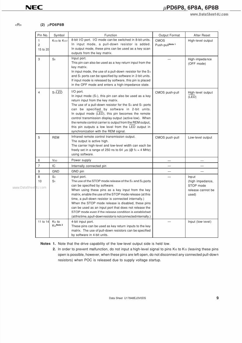
(2) µ PD6P8B
Pin No. Symbol Function Output Format After Reset
1 KI/O0 to KI/O7 CMOS High-level output
2 Push-pullNote 1
15 to 20
3 S0 — High- impedance(OFF mode)
4 S1 /LED CMOS push-pull High- level output
(LED)
5 REM CMOS push-pull Low-level output
6 VDD — —
7 IC — —
9 GND — —
8 S3 — Input
10 S2 (high impedance,
STOP mode
release cannot be
used)
11 to 14 KI0 to — Input (low-level)
KI3Note 2
Notes 1. Note that the drive capability of the low-level output side is held low.
2. In order to prevent malfunction, do not input a high-level signal to pins KI0 to K I3 (leaving these pins
open is possible, however, when these pins are left open, do not disconnect any connected pull-down
resistors) when POC is released due to supply voltage startup.
8-bit I/O port. I/O mode can be switched in 8-bit units.
In input mode, a pull-down resistor is added.
In output mode, these pins can be used as a key scan
outputs from the key matrix.
Input port.This pin can also be used as a key return input from the
key matrix.
In input mode, the use of a pull-down resistor for the S0
and S1 ports can be specified by software in 2-bit units.
If input mode is released by software, this pin is placed
in the OFF mode and enters a high-impedance state.
I/O port.
In input mode (S1), this pin can also be used as a key
return input from the key matrix.
The use of a pull-down resistor for the S0 and S1 ports
can be specified by software in 2-bit units.
In output mode (LED), this pin becomes the remote
control transmission display output (active low). Whenthe remote control carrier is output from the REM output,
this pin outputs a low level from the LED output in
synchronization with the REM signal.
Infrared remote control transmission output.
The output is active high.
The carrier high-level and low-level width can each be
freely set in a range of 250 ns to 64 µ s (@ fX = 4 MHz)
using software.
Power supply
Internally connected pin
GND pin
Input port.
The use of the STOP mode release of the S2 and S3 ports
can be specified by software.
When using these pins as a key input from the key
matrix, enable the use of the STOP mode release (at this
time, a pull-down resistor is connected internally.)
When the STOP mode release is disabled, these pins
can be used as an input port that does not release the
STOP mode even if the release condition is established
(at this time, a pull-down resistor is not connected internally.)
4-bit input port.
These pins can be used as key return inputs to the key
matrix. The use of pull-down resistors can be specified
by software in 4-bit units.
<R>
7/17/2019 INFRARED REMOTE CONTROL TRANSMISSION
http://slidepdf.com/reader/full/infrared-remote-control-transmission 10/95
10
µ PD6P8, 6P8A, 6P8B
Data Sheet U17848EJ3V0DS
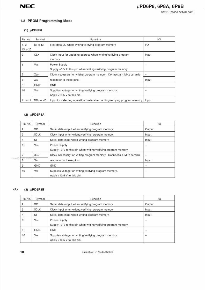
1.2 PROM Programming Mode
(1) µ PD6P8
Pin No. Symbol Function I/O
1, 2 D0 to D7 8-bit data I/O when writing/verifying program memory I/O
15 to 20
3 CLK Clock input for updating address when writing/verifying program Input
memory
6 VDD Power Supply –
Supply +3 V to this pin when writing/verifying program memory.
7 XOUT Clock necessary for writing program memory. Connect a 4 MHz ceramic –
8 XIN resonator to these pins. Input
9 GND GND –
10 VPP Supplies voltage for writing/verifying program memory. –
Apply +10.5 V to this pin.
11 to 14 MD0 to MD3 Input for selecting operation mode when writing/verifying program memory Input
(2) µ PD6P8A
Pin No. Symbol Function I/O
2 SO Serial data output when verifying program memory Output
3 SCLK Clock input when writing/verifying program memory Input
4 SI Serial data input when writing program memory Input
6 VDD Power Supply –
Supply +3 V to this pin when writing/verifying program memory.
7 XOUT Clock necessary for writing program memory. Connect a 4 MHz ceramic –
8 XIN resonator to these pins. Input
9 GND GND –
10 VPP Supplies voltage for writing/verifying program memory. –
Apply +10.5 V to this pin.
(3) µ PD6P8B
Pin No. Symbol Function I/O
2 SO Serial data output when verifying program memory Output
3 SCLK Clock input when writing/verifying program memory Input
4 SI Serial data input when writing program memory Input
6 VDD Power Supply –
Supply +3 V to this pin when writing/verifying program memory.
9 GND GND –
10 VPP Supplies voltage for writing/verifying program memory. –
Apply +10.5 V to this pin.
<R>
7/17/2019 INFRARED REMOTE CONTROL TRANSMISSION
http://slidepdf.com/reader/full/infrared-remote-control-transmission 11/95
11
µ PD6P8, 6P8A, 6P8B
Data Sheet U17848EJ3V0DS
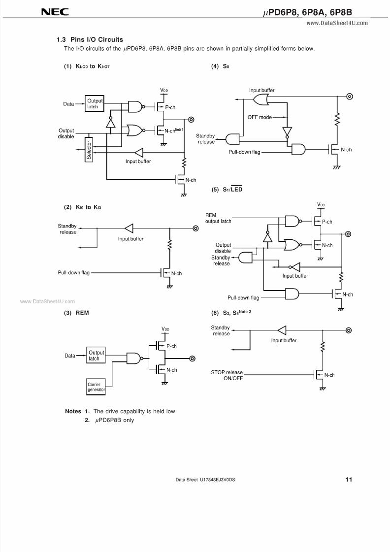
1.3 Pins I/O Circuits
The I/O circuits of the µ PD6P8, 6P8A, 6P8B pins are shown in partially simplified forms below.
(1) KI/O0 to KI/O7 (4) S0
(5) S1/LED
(2) KI0 to KI3
(3) REM (6) S2, S3Note 2
P-ch
N-chNote 1
N-ch
VDD
Outputlatch
Input buffer
Data
Outputdisable
S e l e c t o r
N-ch
Input buffer
Pull-down flag
Standbyrelease
P-ch
N-ch
VDD
Outputlatch
Carriergenerator
Data
OFF mode
Pull-down flag N-ch
Input buffer
Standbyrelease
P-ch
N-ch
N-ch
VDD
REMoutput latch
Input buffer
Outputdisable
Pull-down flag
Standbyrelease
N-ch
Input buffer
STOP releaseON/OFF
Standbyrelease
Notes 1. The drive capability is held low.
2. µ PD6P8B only
7/17/2019 INFRARED REMOTE CONTROL TRANSMISSION
http://slidepdf.com/reader/full/infrared-remote-control-transmission 12/95
12
µ PD6P8, 6P8A, 6P8B
Data Sheet U17848EJ3V0DS
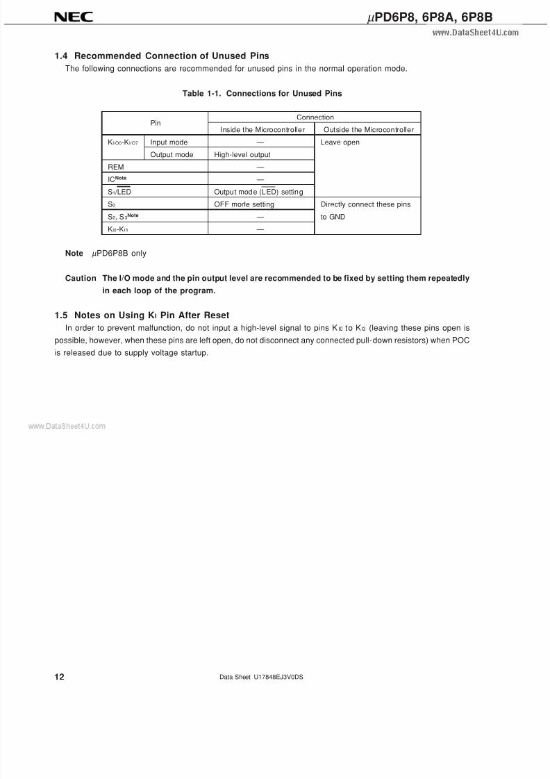
1.4 Recommended Connection of Unused Pins
The following connections are recommended for unused pins in the normal operation mode.
Table 1-1. Connections for Unused Pins
PinConnection
Inside the Microcontroller Outside the Microcontroller
KI/O0-KI/O7 Input mode — Leave open
Output mode High-level output
REM —
ICNote —
S1 /LED Output mode (LED) setting
S0 OFF mode setting Directly connect these pins
S2, S3Note — to GND
KI0-KI3 —
Note µ PD6P8B only
Caution The I/O mode and the pin output level are recommended to be fixed by setting them repeatedly
in each loop of the program.
1.5 Notes on Using KI Pin After Reset
In order to prevent malfunction, do not input a high-level signal to pins KI0 to KI3 (leaving these pins open is
possible, however, when these pins are left open, do not disconnect any connected pull-down resistors) when POC
is released due to supply voltage startup.
7/17/2019 INFRARED REMOTE CONTROL TRANSMISSION
http://slidepdf.com/reader/full/infrared-remote-control-transmission 13/95
13
µ PD6P8, 6P8A, 6P8B
Data Sheet U17848EJ3V0DS
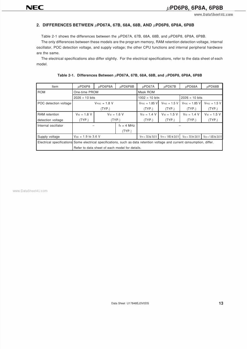
2. DIFFERENCES BETWEEN µ PD67A, 67B, 68A, 68B, AND µ PD6P8, 6P8A, 6P8B
Table 2-1 shows the differences between the µ PD67A, 67B, 68A, 68B, and µ PD6P8, 6P8A, 6P8B.
The only differences between these models are the program memory, RAM retention detection voltage, internal
oscillator, POC detection voltage, and supply voltage; the other CPU functions and internal peripheral hardware
are the same.
The electrical specifications also differ slightly. For the electrical specifications, refer to the data sheet of each
model.
Table 2-1. Differences Between µ PD67A, 67B, 68A, 68B, and µ PD6P8, 6P8A, 6P8B
Item µ PD6P8 µ PD6P8A µ PD6P8B µ PD67A µ PD67B µ PD68A µ PD68B
ROM One-time PROM Mask ROM
2026 × 10 bits 1002 × 10 bits 2026 × 10 bits
POC detection voltage VPOC = 1.8 V VPOC = 1.85 V VPOC = 1.5 V VPOC = 1.85 V VPOC = 1.5 V
(TYP.) (TYP.) (TYP.) (TYP.) (TYP.)
RAM retention VID = 1.8 V VID = 1.6 V VID = 1.4 V VID = 1.5 V VID = 1.4 V VID = 1.5 V
detection voltage (TYP.) (TYP.) (TYP.) (TYP.) (TYP.) (TYP.)Internal oscillator – fX = 4 MHz –
(TYP.)
Supply voltage VDD = 1.9 to 3.6 V VDD = 2.0 to 3.6 V VDD = 1.65 to 3.6 V VDD = 2.0 to 3.6 V VDD = 1.65 to 3.6 V
Electrical specifications Some electrical specifications, such as data retention voltage and current consumption, differ.
Refer to data sheet of each model for details.
7/17/2019 INFRARED REMOTE CONTROL TRANSMISSION
http://slidepdf.com/reader/full/infrared-remote-control-transmission 14/95
14
µ PD6P8, 6P8A, 6P8B
Data Sheet U17848EJ3V0DS
3. INTERNAL CPU FUNCTIONS
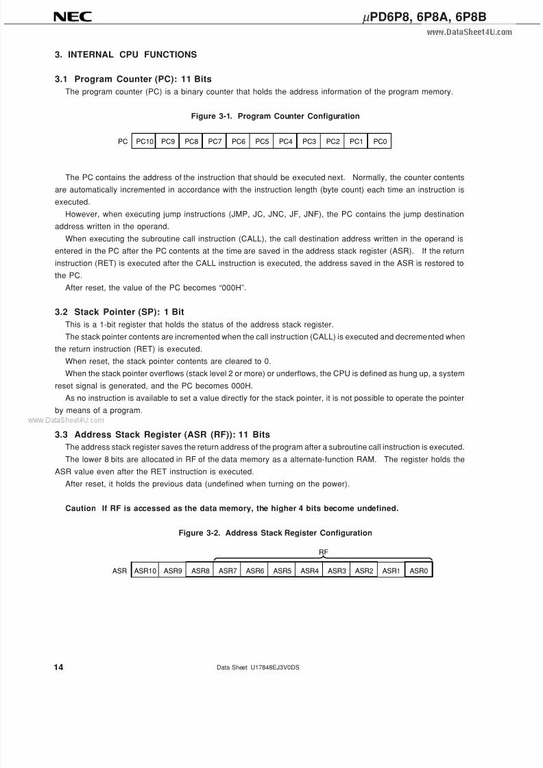
3.1 Program Counter (PC): 11 Bits
The program counter (PC) is a binary counter that holds the address information of the program memory.
Figure 3-1. Program Counter Configuration
The PC contains the address of the instruction that should be executed next. Normally, the counter contents
are automatically incremented in accordance with the instruction length (byte count) each time an instruction is
executed.
However, when executing jump instructions (JMP, JC, JNC, JF, JNF), the PC contains the jump destination
address written in the operand.
When executing the subroutine call instruction (CALL), the call destination address written in the operand is
entered in the PC after the PC contents at the time are saved in the address stack register (ASR). If the return
instruction (RET) is executed after the CALL instruction is executed, the address saved in the ASR is restored tothe PC.
After reset, the value of the PC becomes “000H”.
3.2 Stack Pointer (SP): 1 Bit
This is a 1-bit register that holds the status of the address stack register.
The stack pointer contents are incremented when the call instruction (CALL) is executed and decremented when
the return instruction (RET) is executed.
When reset, the stack pointer contents are cleared to 0.
When the stack pointer overflows (stack level 2 or more) or underflows, the CPU is defined as hung up, a system
reset signal is generated, and the PC becomes 000H.
As no instruction is available to set a value directly for the stack pointer, it is not possible to operate the pointerby means of a program.
3.3 Address Stack Register (ASR (RF)): 11 Bits
The address stack register saves the return address of the program after a subroutine call instruction is executed.
The lower 8 bits are allocated in RF of the data memory as a alternate-function RAM. The register holds the
ASR value even after the RET instruction is executed.
After reset, it holds the previous data (undefined when turning on the power).
Caution If RF is accessed as the data memory, the higher 4 bits become undefined.
Figure 3-2. Address Stack Register Configuration
PC9PC10 PC0PC8 PC7 PC6 PC5 PC4 PC3 PC2 PC1PC
ASR10 ASR9 ASR8 ASR7 ASR6 ASR5 ASR4 ASR3 ASR2 ASR1 ASR0ASR
RF
7/17/2019 INFRARED REMOTE CONTROL TRANSMISSION
http://slidepdf.com/reader/full/infrared-remote-control-transmission 15/95
15
µ PD6P8, 6P8A, 6P8B
Data Sheet U17848EJ3V0DS
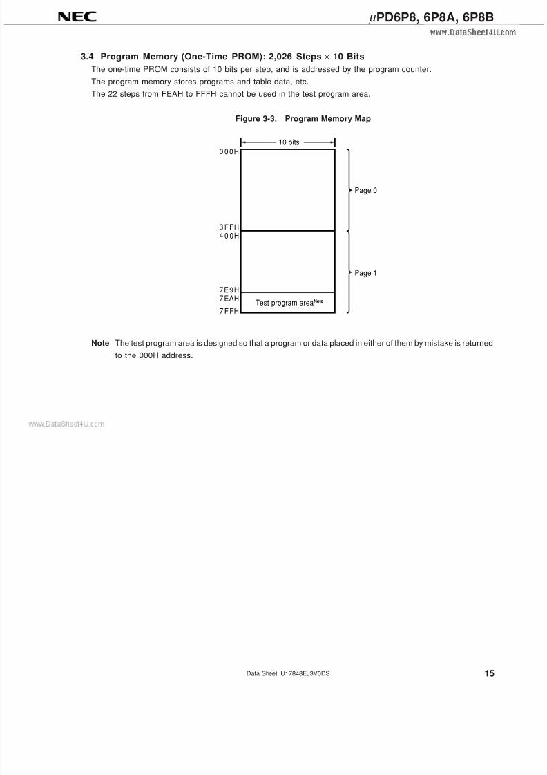
3.4 Program Memory (One-Time PROM): 2,026 Steps × 10 Bits
The one-time PROM consists of 10 bits per step, and is addressed by the program counter.
The program memory stores programs and table data, etc.
The 22 steps from FEAH to FFFH cannot be used in the test program area.
Figure 3-3. Program Memory Map
Note The test program area is designed so that a program or data placed in either of them by mistake is returned
to the 000H address.
0
34
77
7Test program areaNote
Page 0
Page 1
10 bits
H
HH
HH
H
0
F0
9A
F
0
F0
EE
F
7/17/2019 INFRARED REMOTE CONTROL TRANSMISSION
http://slidepdf.com/reader/full/infrared-remote-control-transmission 16/95
16
µ PD6P8, 6P8A, 6P8B
Data Sheet U17848EJ3V0DS
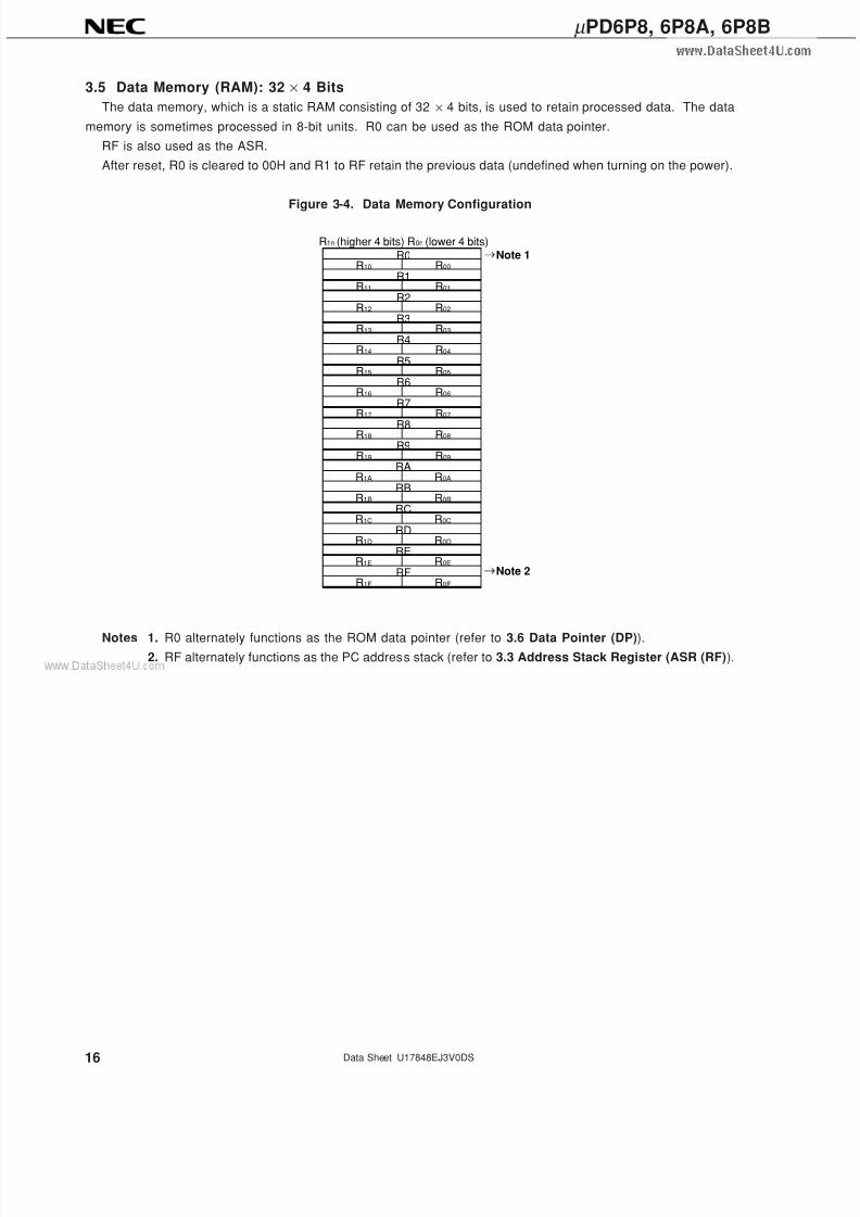
3.5 Data Memory (RAM): 32 × 4 Bits
The data memory, which is a static RAM consisting of 32 × 4 bits, is used to retain processed data. The data
memory is sometimes processed in 8-bit units. R0 can be used as the ROM data pointer.
RF is also used as the ASR.
After reset, R0 is cleared to 00H and R1 to RF retain the previous data (undefined when turning on the power).
Figure 3-4. Data Memory Configuration
Notes 1. R0 alternately functions as the ROM data pointer (refer to 3.6 Data Pointer (DP)).
2. RF alternately functions as the PC address stack (refer to 3.3 Address Stack Register (ASR (RF)).
R0
R1
R2
R3
R4
R5
R6
R7
R8
R9
RA
RB
RC
RD
RE
RF
R10 R00
R11 R01
R12 R02
R13 R03
R14 R04
R15 R05
R16 R06
R17 R07
R18 R08
R19 R09
R1A R0A
R1B R0B
R1C R0C
R1D R0D
R1E R0E
R1F R0F
Note 1
Note 2
R1n (higher 4 bits) R0n (lower 4 bits)
7/17/2019 INFRARED REMOTE CONTROL TRANSMISSION
http://slidepdf.com/reader/full/infrared-remote-control-transmission 17/95
17
µ PD6P8, 6P8A, 6P8B
Data Sheet U17848EJ3V0DS
3.6 Data Pointer (DP): 12 Bits
The ROM data table can be referenced by setting the ROM address in the data pointer to call the ROM contents.
The lower 8 bits of the ROM address are specified by R0 of the data memory; and the higher 4 bits by bits 4
to 7 of the P3 register (CR0).
After reset, the pointer contents become 000H.
Figure 3-5. Data Pointer Configuration
3.7 Accumulator (A): 4 Bits
The accumulator, which refers to a register consisting of 4 bits, plays a leading role in performing various
operations.
After reset, the accumulator contents are left undefined.
Figure 3-6. Accumulator Configuration
A3 A2 A1 A0 A
3.8 Arithmetic and Logic Unit (ALU): 4 Bits
The arithmetic and logic unit (ALU), which refers to an arithmetic circuit consisting of 4 bits, executes simple
(mainly logical) operations.
R00
DP9 DP8 DP7 DP6 DP5 DP4 DP3 DP2 DP1 DP0
R10
R0
b4b5
P3 register
P3 DP10
b6
0
b7
7/17/2019 INFRARED REMOTE CONTROL TRANSMISSION
http://slidepdf.com/reader/full/infrared-remote-control-transmission 18/95
18
µ PD6P8, 6P8A, 6P8B
Data Sheet U17848EJ3V0DS
3.9 Flags
3.9.1 Status flag (F)
Pin and timer statuses can be checked by executing the STTS instruction to check the status flag.
The status flag is set (to 1) in the following cases.
• If the condition specified with the operand is met when the STTS instruction is executed
• When standby mode is released.
• When the release condition is met at the point of executing the HALT instruction. (In this case, the system
does not enter the standby mode.)
Conversely, the status flag is cleared (to 0) in the following cases:
• If the condition specified with the operand is not met when the STTS instruction is executed.
• When the status flag has been set (to 1), the HALT instruction executed, but the release condition is not met
at the point of executing the HALT instruction. (In this case, the system does not enter the standby mode.)
Table 3-1. Conditions for Status Flag (F) to Be Set by STTS Instruction
Operand Value of STTS InstructionCondition for Status Flag (F) to Be Set
b3 b2 b1 b0
0 0 0 0 High level is input to at least one of KI pins.
0 1 1 High level is input to at least one of KI pins.
1 1 0 High level is input to at least one of KI pins.
1 0 1 The down counter of the timer is 0.
1 Either of the combinations [The following condition is added in addition to the above.]
of b2, b1, and b0 above. High level is input to at least one of S0Note 1, S1
Note 1, or S2Note 2 pins.
Notes 1. The S0 and S1 pins must be set to input mode (bit 2 and bit 0 of the P4 register are set to 0 and 1,
respectively).
2. The use of STOP mode release for the S2 pin must be enabled (bit 3 of the P4 register is set to 1).
3.9.2 Carry flag (CY)
The carry flag is set (to 1) in the following cases:
• If the ANL instruction or the XRL instruction is executed when bit 3 of the accumulator is 1 and bit 3 of the
operand is 1.
• If the RL instruction or the RLZ instruction is executed when bit 3 of the accumulator is 1.
• If the INC instruction or the SCAF instruction is executed when the value of the accumulator is 0FH.
The carry flag is cleared (to 0) in the following cases:
• If the ANL instruction or the XRL instruction is executed when at least either bit 3 of the accumulator or bit
3 of the operand is 0.
• If the RL instruction or the RLZ instruction is executed when bit 3 of the accumulator is 0.
• If the INC instruction or the SCAF instruction is executed when the value of the accumulator is other than 0FH.
• If the ORL instruction is executed.
• When data is written to the accumulator by the MOV instruction or the IN instruction.
7/17/2019 INFRARED REMOTE CONTROL TRANSMISSION
http://slidepdf.com/reader/full/infrared-remote-control-transmission 19/95
19
µ PD6P8, 6P8A, 6P8B
Data Sheet U17848EJ3V0DS
4. PORT REGISTERS (PX)
The KI/O port, the KI port, the special ports (S0, S1 /LED, S2), and the control registers are treated as port registers.
After reset, the port register values are as shown below.
Figure 4-1. Port Register Configuration
Notes 1. ×: Refers to the value based on the KI and S2 pin state.
2. ×: Refers to the value based on decrease of power supply voltage (0 when VDD ≤ V ID)
Remark VID: RAM retention detection voltage
Table 4-1. Relationship Between Ports and Reading/Writing
Port Name Input Mode Output ModeRead Write Read Write
KI/O Pin state Output latch Output latch Output latch
KI Pin state — — —
S0 Pin state — Note —
S1 /LED Pin state — Pin state —
S2 Pin state — — —
Note When in OFF mode, “1” is always read.
Port register
P0
KI/O7
P00
After reset
FFH
KI/O6 KI/O5 KI/O4 KI/O3 KI/O2 KI/O1 KI/O0
P10
P1
KI3
P01
××××11×1BNote 1
KI2 KI1 KI0 S1 /LED S0 S2 1
P11
P3 (control register 0)
DP11
P03
0000×000BNote 2
DP10 DP9 DP8
RAMretention
flag – – –
P13
P4 (control register 1)
0
P04
26H
0KI
Pull-downS0 /S1
Pull-downS2
STOP releaseS1 /LED mode KI/O mode S0 mode
P14
7/17/2019 INFRARED REMOTE CONTROL TRANSMISSION
http://slidepdf.com/reader/full/infrared-remote-control-transmission 20/95
20
µ PD6P8, 6P8A, 6P8B
Data Sheet U17848EJ3V0DS
4.1 KI/O Port (P0)
The KI/O port is an 8-bit I/O port for key scan output.
I/O mode is set by bit 1 of the P4 register.
If a read instruction is executed, the pin state can be read in input mode, whereas the output latch contents can
be read in output mode.
If a write instruction is executed, data can be written to the output latch regardless of input or output mode.
After reset, the port is placed in output mode and the value of the output latch (P0) becomes 1111 1111B.
The KI/O port incorporates a pull-down resistor, allowing pull-down in input mode only.
Caution When a key is double-pressed, a high-level output and a low-level output may conflict at the
KI/O port. To avoid this, the low-level output current of the KI/O port is held low. Therefore, be
careful when using the K I/O port for purposes other than key scan output.
The KI/O port is designed so that even when connected directly to VDD within the normal supply
voltage range (VDD = 1.9 to 3.6 V), no problem occurs.
Table 4-2. KI/O Port (P0)
Bit b7 b6 b5 b4 b3 b2 b1 b0
Name KI/O7 KI/O6 KI/O5 KI/O4 KI/O3 KI/O2 KI/O1 KI/O0
b0 to b7: When reading: In input mode, the KI/O pin’s state is read.
In output mode, the KI/O pin’s output latch contents are read.
When writing: Data is written to the KI/O pin’s output latch regardless of input or output mode.
4.2 KI Port/Special Ports (P1)
4.2.1 KI port (P11: bits 4 to 7 of P1)
The KI port is a 4-bit input port for key input. The pin state can be read.
The use of a pull-down resistor for the KI port can be specified in 4-bit units by software using bit 5 of the P4register. After reset, a pull-down resistor is connected.
Table 4-3. KI/Special Port Register (P1)
Bit b7 b6 b5 b4 b3 b2 b1 b0
Name KI3 KI2 KI1 KI0 S1 /LED S0 S2 Fixed to “1”
b1: The state of the S2 pin is read (read only).
b2: In input mode, state of the S0 pin is read (read only).
In OFF mode, this bit is fixed to 1.
b3: The state of the S1 /LED pin is read regardless of input/output mode (read only).b4 to b7: The state of the KI pin is read (read only).
Caution In order to prevent malfunction, be sure to input a low level to one or more of pins KI0 to KI3
when POC is released by supply voltage rising (Can be left open. When open, leave the pull-
down resistor connected).
7/17/2019 INFRARED REMOTE CONTROL TRANSMISSION
http://slidepdf.com/reader/full/infrared-remote-control-transmission 21/95
21
µ PD6P8, 6P8A, 6P8B
Data Sheet U17848EJ3V0DS
4.2.2 S0 port (bit 2 of P1)
The S0 port is an input/OFF mode port.
The pin state can be read by setting this port to input mode using bit 0 of the P4 register.
In input mode, the use of a pull-down resistor for the S0 and S1 /LED port can be specified in 2-bit units by software
using bit 4 of the P4 register.
If input mode is released (thus set to OFF mode), the pin becomes high-impedance but is configured so that
through current does not flow internally. In OFF mode, 1 can be read regardless of the pin state.
After reset, S0 is set to OFF mode, thus becoming high-impedance.
4.2.3 S1/LED port (bit 3 of P1)
The S1 /LED port is an I/O port.
Input or output mode can be set using bit 2 of the P4 resister. The pin state can be read in both input mode
and output mode.
When in input mode, the use of a pull-down resis tor for the S0 and S1 /LED por ts can be specified in 2-bi t uni ts
by software using bit 4 of the P4 register.
When in output mode, the pull-down resistor is automatically disconnected and this pin becomes the remote
control transmission display pin (refer to 5 TIMER).
After reset, S1 /LED is placed in output mode, and a high level is output.
4.2.4 S2 port (bit 1 of P1)
The S2 port is an input port.
Use of STOP mode release for the S2 port can be specified by bit 3 of the P4 register.
When using the pin as a key input from a key matrix, enable (bit 3 of the P4 register is set to 1) the use of STOP
mode release (at this time, a pull-down resistor is connected internally.) When STOP mode release is disabled
(bit 3 of the P4 register is set to 0), it can be used as an input port that does not release the STOP mode even if
the release condition is met (at this time, a pull-down resistor is not connected internally.)
The state of the pin can be read in both cases.
After reset, S2 is set to input mode where the STOP mode release is disabled, and enters a high-impedance
state.
7/17/2019 INFRARED REMOTE CONTROL TRANSMISSION
http://slidepdf.com/reader/full/infrared-remote-control-transmission 22/95
22
µ PD6P8, 6P8A, 6P8B
Data Sheet U17848EJ3V0DS
4.3 Control Register 0 (P3)
Control register 0 consists of 8 bits. The contents that can be controlled are as shown below.
After reset, the register becomes 0000 ×000BNote.
Note ×: Refers to the value based on a decrease of power supply voltage (0 when VDD ≤ V ID)
Remark VID: RAM retention detection voltage
Table 4-4. Control Register 0 (P3)
Bit b7Note b6 b5 b4 b3 b2 b1 b0
Name DP (Data Pointer) —
DP11 DP10 DP9 DP8
Setting 0 0 0 0 0 Not retainable Fixed to 0
1 1 1 1 1 Retainable
After reset 0 0 0 0 0 0 0 0
b3: RAM retention f lag. For funct ion detai ls, refer to 4.3.1 RAM retention flag (bit 3 of P3).
b4 to b7: Specify the higher bits of the ROM data pointer (DP8 to DP11).
Note Set b7 to 0 in the case of the µ PD6P8, 6P8A, 6P8B.
RAMretentionflag
7/17/2019 INFRARED REMOTE CONTROL TRANSMISSION
http://slidepdf.com/reader/full/infrared-remote-control-transmission 23/95
23
µ PD6P8, 6P8A, 6P8B
Data Sheet U17848EJ3V0DS
4.3.1 RAM retention flag (bit 3 of P3)
The RAM retention flag indicates whether the supply voltage has fallen below the level at which the contents
of the RAM are lost while the battery is being exchanged or when the battery voltage has dropped.
This flag is at bit 3 of control register 0 (P3).
It is cleared to 0 if the supply voltage drops below the RAM retention detection voltage. If this flag is 0, it can
be judged that the RAM contents have been lost or that power has just been applied. This flag can be used to initialize
the RAM via software. After initializing the RAM and writing the necessary data to it, set this RAM retention flag
to 1 by software. At this time, 1 means that data has been set to the RAM.
Figure 4-2. Supply Voltage Transition and Detection Voltage (µ PD6P8)
VDD
VPOC /VID
0 V
RAM retention flag
(A)
(4)(3)(2)
Set to 1 Flag contentsare read
(1)
t
POC detection voltage/ RAM retention detection voltageVPOC = V ID = 1.8 V (TYP.)
(1) If the supply voltage rises after the battery has been set, and exceeds VPOC (POC detection voltage),
reset is cleared. Because the supply voltage rises from 0 V, which is lower than V ID (RAM retention
detection voltage), the RAM retention flag remains in the initial status 0.
(2) The supply voltage has now risen to the level at which the device can operate. Write the necessary data
to the RAM and set the RAM retention flag to 1.
(3) The device is reset if the supply voltage drops below VPOC. At point (A) in the figure, the voltage is lower
than VID. Consequently, the RAM retention flag is cleared to 0.
(4) If the RAM retention flag is checked by software after reset has been cleared, it is 0. This means that
the contents of the RAM may have been lost. If this case, initialize the RAM by software.
Cautions 1. The software developed for the µ PD67A, 68A and 69A (using the RAM retention flag) can
be used for the µ PD6P8 as is.
2. Unlike the µ PD67A, 68A and 69A, the RAM retention detection voltage of the µ PD6P8 is the
same as the POC detection voltage. When software is newly developed, it is not necessary
to use the RAM retention flag if only the RAM is initialized by reset.
7/17/2019 INFRARED REMOTE CONTROL TRANSMISSION
http://slidepdf.com/reader/full/infrared-remote-control-transmission 24/95
24
µ PD6P8, 6P8A, 6P8B
Data Sheet U17848EJ3V0DS
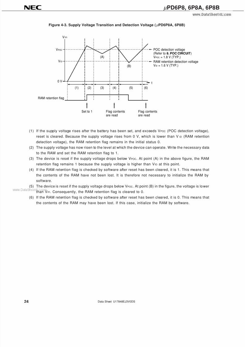
Figure 4-3. Supply Voltage Transition and Detection Voltage (µ PD6P8A, 6P8B)
(1) If the supply voltage rises after the battery has been set, and exceeds VPOC (POC detection voltage),
reset is cleared. Because the supply voltage rises from 0 V, which is lower than V ID (RAM retention
detection voltage), the RAM retention flag remains in the initial status 0.
(2) The supply voltage has now risen to the level at which the device can operate. Write the necessary data
to the RAM and set the RAM retention flag to 1.
(3) The device is reset if the supply voltage drops below VPOC. At point (A) in the above figure, the RAM
retention flag remains 1 because the supply voltage is higher than VID at this point.
(4) If the RAM retention flag is checked by software after reset has been cleared, it is 1. This means that
the contents of the RAM have not been lost. It is therefore not necessary to initialize the RAM by
software.(5) The device is reset if the supply voltage drops below VPOC. At point (B) in the figure, the voltage is lower
than VID. Consequently, the RAM retention flag is cleared to 0.
(6) If the RAM retention flag is checked by software after reset has been cleared, it is 0. This means that
the contents of the RAM may have been lost. If this case, initialize the RAM by software.
VDD
VPOC
VID
0 V
RAM retention flag
(A)
(B)
(6)(5)(4)(3)(2)
Set to 1 Flag contentsare read
Flag contentsare read
(1)
t
POC detection voltage(Refer to 8. POC CIRCUIT)VPOC = 1.8 V (TYP.)
RAM retention detection voltageVID = 1.6 V (TYP.)
7/17/2019 INFRARED REMOTE CONTROL TRANSMISSION
http://slidepdf.com/reader/full/infrared-remote-control-transmission 25/95
25
µ PD6P8, 6P8A, 6P8B
Data Sheet U17848EJ3V0DS
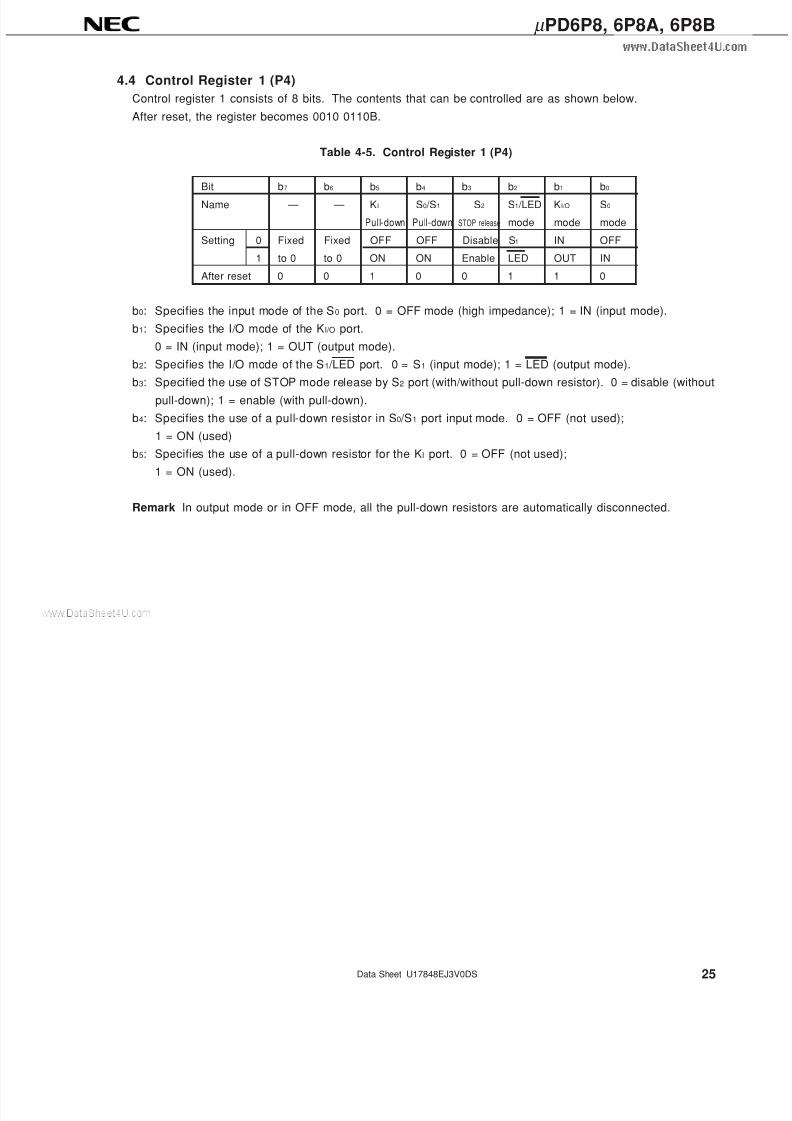
4.4 Control Register 1 (P4)
Control register 1 consists of 8 bits. The contents that can be controlled are as shown below.
After reset, the register becomes 0010 0110B.
Table 4-5. Control Register 1 (P4)
Bit b7 b6 b5 b4 b3 b2 b1 b0
Name — — KI S0 /S1 S2 S1 /LED KI/O S0
Pull-down Pull-down STOP release mode mode mode
Setting 0 Fixed Fixed OFF OFF Disable S1 IN OFF
1 to 0 to 0 ON ON Enable LED OUT IN
After reset 0 0 1 0 0 1 1 0
b0: Specifies the input mode of the S0 port. 0 = OFF mode (high impedance); 1 = IN (input mode).
b1: Specifies the I/O mode of the KI/O port.
0 = IN (input mode); 1 = OUT (output mode).
b2: Specifies the I/O mode of the S1 /LED port. 0 = S1 (input mode); 1 = LED (output mode).
b3: Specified the use of STOP mode release by S2 port (with/without pull-down resistor). 0 = disable (without
pull-down); 1 = enable (with pull-down).
b4: Specifies the use of a pull-down resistor in S0 /S1 port input mode. 0 = OFF (not used);
1 = ON (used)
b5: Specifies the use of a pull-down resistor for the KI port. 0 = OFF (not used);
1 = ON (used).
Remark In output mode or in OFF mode, all the pull-down resistors are automatically disconnected.
7/17/2019 INFRARED REMOTE CONTROL TRANSMISSION
http://slidepdf.com/reader/full/infrared-remote-control-transmission 26/95
26
µ PD6P8, 6P8A, 6P8B
Data Sheet U17848EJ3V0DS
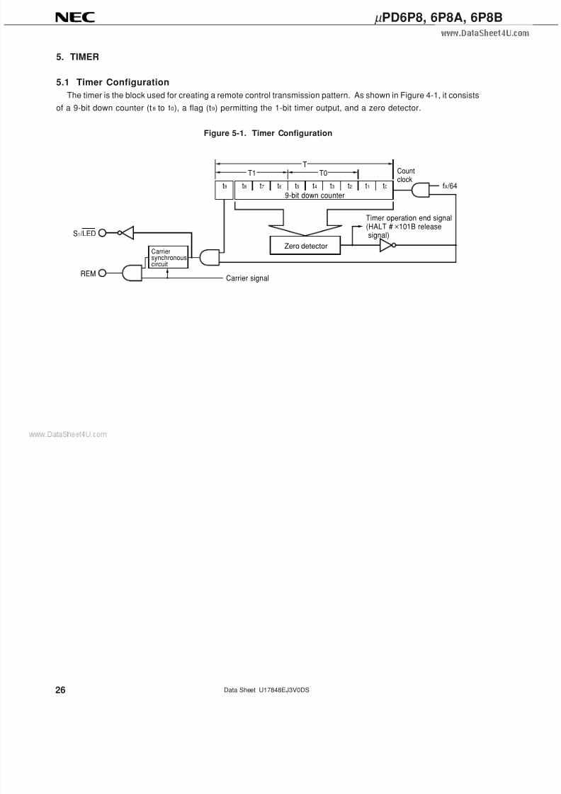
5. TIMER
5.1 Timer Configuration
The timer is the block used for creating a remote control transmission pattern. As shown in Figure 4-1, it consists
of a 9-bit down counter (t8 to t0), a flag (t9) permitting the 1-bit timer output, and a zero detector.
Figure 5-1. Timer Configuration
S1 /LED
REM
Carriersynchronouscircuit
Carrier signal
Zero detector
9-bit down counter
t9 t8 t7 t6 t5 t4 t3 t2 t1 t0
TT1
fX /64
Timer operation end signal(HALT # 101B release signal)
Countclock
T0
7/17/2019 INFRARED REMOTE CONTROL TRANSMISSION
http://slidepdf.com/reader/full/infrared-remote-control-transmission 27/95
27
µ PD6P8, 6P8A, 6P8B
Data Sheet U17848EJ3V0DS
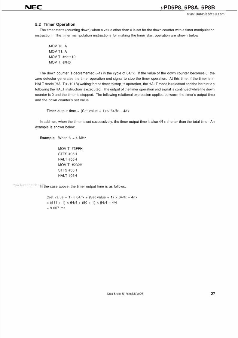
5.2 Timer Operation
The timer starts (counting down) when a value other than 0 is set for the down counter with a timer manipulation
instruction. The timer manipulation instructions for making the timer start operation are shown below:
MOV T0, A
MOV T1, A
MOV T, #data10MOV T, @R0
The down counter is decremented (–1) in the cycle of 64/f X. If the value of the down counter becomes 0, the
zero detector generates the timer operation end signal to stop the timer operation. At this time, if the timer is in
HALT mode (HALT #×101B) waiting for the timer to stop its operation, the HALT mode is released and the instruction
following the HALT instruction is executed. The output of the timer operation end signal is continued while the down
counter is 0 and the timer is stopped. The following relational expression applies between the timer’s output time
and the down counter’s set value.
Timer output time = (Set value + 1) × 64/fX – 4/fX
In addition, when the timer is set successively, the timer output time is also 4/f X shorter than the total time. An
example is shown below.
Example When fX = 4 MHz
MOV T, #3FFH
STTS #05H
HALT #05H
MOV T, #232H
STTS #05H
HALT #05H
In the case above, the timer output time is as follows.
(Set value + 1) × 64/fX + (Set value + 1) × 64/fX – 4/fX
= (511 + 1) × 64/4 + (50 + 1) × 64/4 – 4/4
= 9.007 ms
7/17/2019 INFRARED REMOTE CONTROL TRANSMISSION
http://slidepdf.com/reader/full/infrared-remote-control-transmission 28/95
28
µ PD6P8, 6P8A, 6P8B
Data Sheet U17848EJ3V0DS
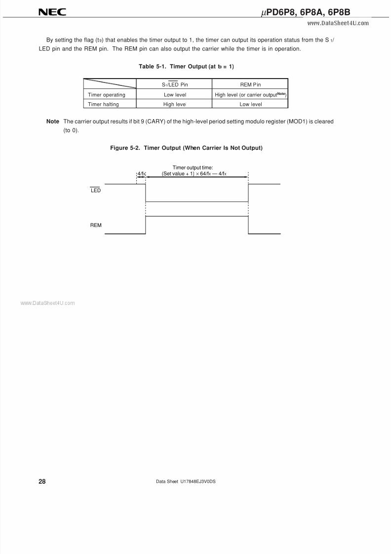
By setting the flag (t9) that enables the timer output to 1, the timer can output its operation status from the S1 /
LED pin and the REM pin. The REM pin can also output the carrier while the timer is in operation.
Table 5-1. Timer Output (at t9 = 1)
S1 /LED Pin REM Pin
Timer operating Low level High level (or carrier outputNote
)Timer halting High level Low level
Note The carrier output results if bit 9 (CARY) of the high-level period setting modulo register (MOD1) is cleared
(to 0).
Figure 5-2. Timer Output (When Carrier Is Not Output)
Timer output time:(Set value + 1) × 64/fX — 4/fX
LED
REM
4/fX
7/17/2019 INFRARED REMOTE CONTROL TRANSMISSION
http://slidepdf.com/reader/full/infrared-remote-control-transmission 29/95
29
µ PD6P8, 6P8A, 6P8B
Data Sheet U17848EJ3V0DS
5.3 Carrier Output
5.3.1 Carrier output generator
The carrier generator consists of a 9-bit counter and two modulo registers for setting the high- and low-level
periods (MOD1 and MOD0 respectively).
Figure 5-3. Configuration of Remote Controller Carrier Generator
Notes 1. Bit 9 of the modulo register for setting the low-level period (MOD0) is fixed to 0.
2. t9: Flag that enables timer output (timer block) (see Figure 5-1 Timer Configuration)
The carrier duty ratio and carrier frequency can be determined by setting the high- and low-level widths using
the respective modulo registers. Each of these widths can be set in a range of 250 ns to 64 µ s (@ fX = 4 MHz).
The system clock multiplied by 2 is used for the 9-bit counter input (8 MHz when fX = 4 MHz). MOD0 and MOD1are read and written using timer manipulation instructions.
MOV A, M00 MOV M00, A MOV M0, #data10
MOV A, M01 MOV M01, A MOV M1, #data10
MOV A, M10 MOV M10, A MOV M0, @R0
MOV A, M11 MOV M11, A MOV M1, @R0
The values of MOD0 and MOD1 can be calculated from the following expressions.
MOD0 = (2 × fX × (1 – D) × T) – 1
MOD1 = (2 × fX × D × T) – 1
Caution Be sure to input values in range of 001H to 1FFH to MOD0 and MOD1.
Remark D: Carrier duty ratio (0 < D < 1)
fX: Input clock (MHz)
T: Carrier cycle (µ s)
Carrier signal
F/FMatch
Clear
M11
t9CARY Modulo register for setting the high-level period (MOD1) Modulo register for setting the low-level period (MOD0) Note 1
t8 t7 t6 t5 t4 t3 t2 t1 t0 t80 t7 t6 t5 t4 t3 t2 t1 t0
2fX fX
fX
t9Note 2
M10M1
M01
Selector
Comparator
9-bit counter Multiplier
M00M0
7/17/2019 INFRARED REMOTE CONTROL TRANSMISSION
http://slidepdf.com/reader/full/infrared-remote-control-transmission 30/95
30
µ PD6P8, 6P8A, 6P8B
Data Sheet U17848EJ3V0DS
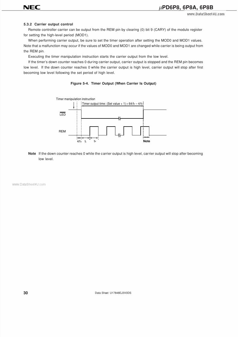
5.3.2 Carrier output control
Remote controller carrier can be output from the REM pin by clearing (0) bit 9 (CARY) of the modulo register
for setting the high-level period (MOD1).
When performing carrier output, be sure to set the timer operation after setting the MOD0 and MOD1 values.
Note that a malfunction may occur if the values of MOD0 and MOD1 are changed while carrier is being output from
the REM pin.
Executing the timer manipulation instruction starts the carrier output from the low level.
If the timer’s down counter reaches 0 dur ing carrier output, carrier output is stopped and the REM pin becomes
low level. If the down counter reaches 0 while the carrier output is high level, carrier output will stop after first
becoming low level following the set period of high level.
Figure 5-4. Timer Output (When Carrier Is Output)
Note If the down counter reaches 0 while the carrier output is high level, carrier output will stop after becoming
low level.
Timer output time: (Set value + 1) × 64/fX – 4/fX
LED
REM
NotetHtL
Timer manipulation instruction
4/fX
7/17/2019 INFRARED REMOTE CONTROL TRANSMISSION
http://slidepdf.com/reader/full/infrared-remote-control-transmission 31/95
31
µ PD6P8, 6P8A, 6P8B
Data Sheet U17848EJ3V0DS
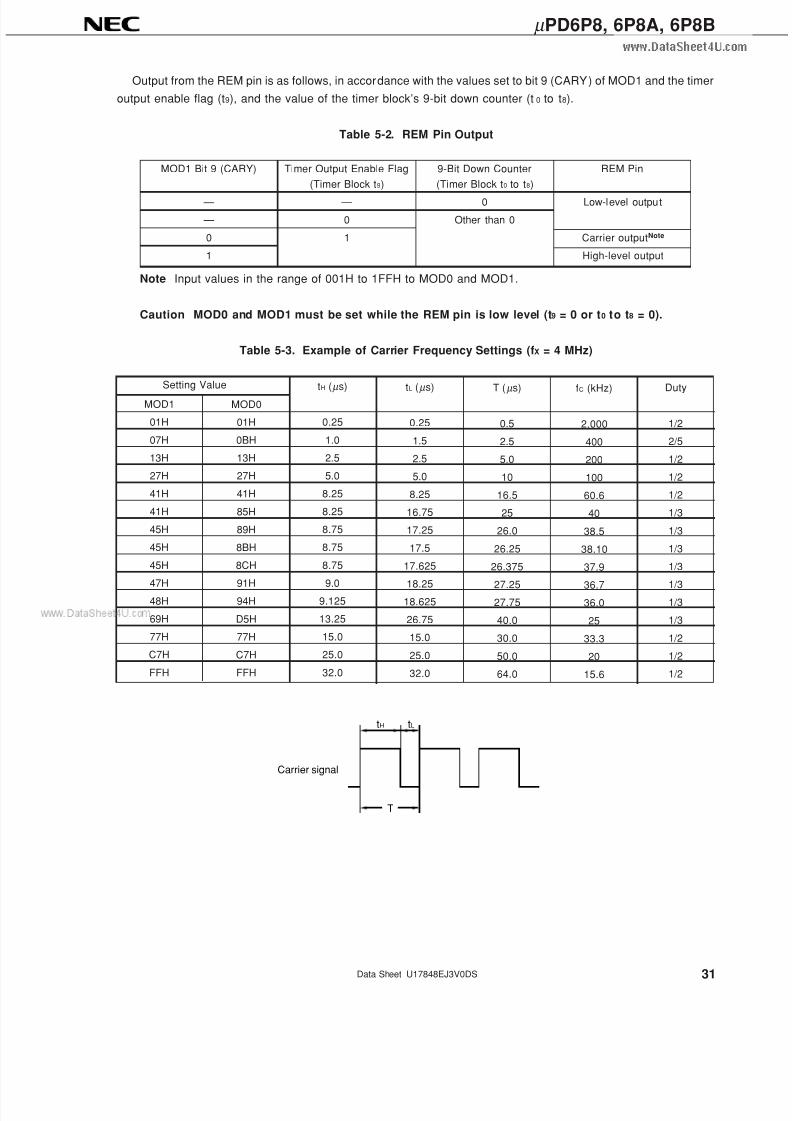
Output from the REM pin is as follows, in accordance with the values set to bit 9 (CARY) of MOD1 and the timer
output enable flag (t9), and the value of the timer block’s 9-bit down counter (t 0 to t8).
Table 5-2. REM Pin Output
MOD1 Bit 9 (CARY) Timer Output Enable Flag 9-Bit Down Counter REM Pin
(Timer Block t9) (Timer Block t0 to t8)
— — 0 Low-level output
— 0 Other than 0
0 1 Carrier outputNote
1 High-level output
Note Input values in the range of 001H to 1FFH to MOD0 and MOD1.
Caution MOD0 and MOD1 must be set while the REM pin is low level (t9 = 0 or t0 to t8 = 0).
Table 5-3. Example of Carrier Frequency Settings (fX = 4 MHz)
Setting Value tH (µ s)
0.25
1.0
2.5
5.0
8.25
8.25
8.75
8.75
8.75
9.09.125
13.25
15.0
25.0
32.0
MOD1
01H
07H
13H
27H
41H
41H
45H
45H
45H
47H48H
69H
77H
C7H
FFH
MOD0
01H
0BH
13H
27H
41H
85H
89H
8BH
8CH
91H94H
D5H
77H
C7H
FFH
tL (µ s)
0.25
1.5
2.5
5.0
8.25
16.75
17.25
17.5
17.625
18.2518.625
26.75
15.0
25.0
32.0
T (µ s)
0.5
2.5
5.0
10
16.5
25
26.0
26.25
26.375
27.25
27.75
40.0
30.0
50.0
64.0
fC (kHz)
2,000
400
200
100
60.6
40
38.5
38.10
37.9
36.7
36.0
25
33.3
20
15.6
Duty
1/2
2/5
1/2
1/2
1/2
1/3
1/3
1/3
1/3
1/31/3
1/3
1/2
1/2
1/2
tH tL
T
Carrier signal
7/17/2019 INFRARED REMOTE CONTROL TRANSMISSION
http://slidepdf.com/reader/full/infrared-remote-control-transmission 32/95
32
µ PD6P8, 6P8A, 6P8B
Data Sheet U17848EJ3V0DS
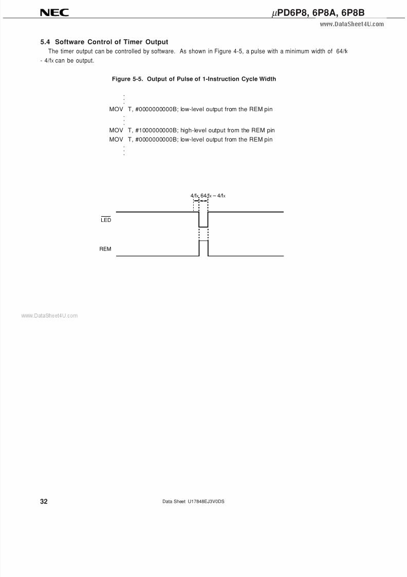
5.4 Software Control of Timer Output
The timer output can be controlled by software. As shown in Figure 4-5, a pulse with a minimum width of 64/f X
- 4/fX can be output.
Figure 5-5. Output of Pulse of 1-Instruction Cycle Width
.
..MOV T, #0000000000B; low-level output from the REM pin
.
.
.
MOV T, #1000000000B; high-level output from the REM pin
MOV T, #0000000000B; low-level output from the REM pin...
64/fX – 4/fX
LED
REM
4/fX
7/17/2019 INFRARED REMOTE CONTROL TRANSMISSION
http://slidepdf.com/reader/full/infrared-remote-control-transmission 33/95
33
µ PD6P8, 6P8A, 6P8B
Data Sheet U17848EJ3V0DS
6. STANDBY FUNCTION
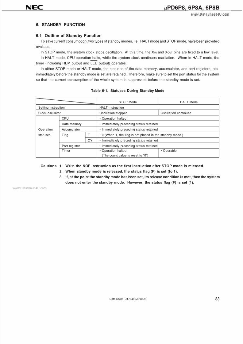
6.1 Outline of Standby Function
To save current consumption, two types of standby modes, i.e., HALT mode and STOP mode, have been provided
available.
In STOP mode, the system clock stops oscillation. At this time, the XIN and XOUT pins are fixed to a low level.
In HALT mode, CPU operation halts, while the system clock continues oscillation. When in HALT mode, the
timer (including REM output and LED output) operates.
In either STOP mode or HALT mode, the statuses of the data memory, accumulator, and port registers, etc.
immediately before the standby mode is set are retained. Therefore, make sure to set the port status for the system
so that the current consumption of the whole system is suppressed before the standby mode is set.
Table 6-1. Statuses During Standby Mode
STOP Mode HALT Mode
Setting instruction HALT instruction
Clock oscillator Oscillation stopped Oscillation continued
CPU • Operation haltedData memory • Immediately preceding status retained
Operation Accumulator • Immediately preceding status retained
statuses Flag F • 0 (When 1, the flag is not placed in the standby mode.)
CY • Immediately preceding status retained
Port register • Immediately preceding status retained
Timer • Operation halted • Operable
(The count value is reset to “0”)
Cautions 1. Write the NOP instruction as the first instruction after STOP mode is released.
2. When standby mode is released, the status flag (F) is set (to 1).
3. If, at the point the standby mode has been set, its release condition is met, then the system
does not enter the standby mode. However, the status flag (F) is set (1).
7/17/2019 INFRARED REMOTE CONTROL TRANSMISSION
http://slidepdf.com/reader/full/infrared-remote-control-transmission 34/95
34
µ PD6P8, 6P8A, 6P8B
Data Sheet U17848EJ3V0DS
6.2 Standby Mode Setting and Release
The standby mode is set with the HALT #b3b2b1b0B instruction for both STOP mode and HALT mode. For the
standby mode to be set, the status flag (F) is required to have been cleared (to 0).
The standby mode is released by the release condition specified with the reset (POC) or the operand of HALT
instruction. If the standby mode is released, the status flag (F) is set (to 1).
Even when the HALT instruction is executed in the state that the status flag (F) has been set (to 1), the standby
mode is not set. If the release condition is not met at this time, the status flag is cleared (to 0). If the release condition
is met, the status flag remains set (to 1).
Even in the case when the release condition has been already met at the point that the HALT instruction is
executed, the standby mode is not set. Here, also, the status flag (F) is set (to 1).
Caution Depending on the status of the status flag (F), the HALT instruction may not be executed. Be
careful about this. For example, when setting HALT mode after checking the key status with
the STTS instruction, the system does not enter HALT mode as long as the status flag (F)
remains set (to 1) and thus sometimes performs an unintended operation. In this case, the
intended operation can be realized by executing the STTS instruction immediately after setting
the timer to clear (to 0) the status flag.
Example STTS #03H ;To check the KI pin status.
MOV T, #0xxH ;To set the timer
STTS #05H ;To clear the status flag
(During this time, be sure not to execute an instruction that may set the status flag.)
HALT #05H ;To set HALT mode
Table 6-2. Addresses Executed After Standby Mode Release
Release Condition Address Executed After Release
Reset Address 0Release condit ion shown in Table 5-3 The address fol lowing the HALT instruction
…
…
7/17/2019 INFRARED REMOTE CONTROL TRANSMISSION
http://slidepdf.com/reader/full/infrared-remote-control-transmission 35/95
35
µ PD6P8, 6P8A, 6P8B
Data Sheet U17848EJ3V0DS
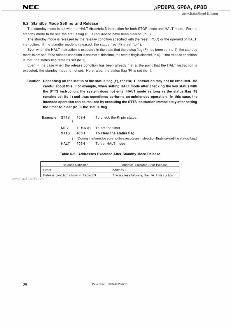
Table 6-3. Standby Mode Setup (HALT #b3b2b1b0B) and Release Conditions
Operand Value of
HALT Instruction Setting Mode Precondition for Setup Release Condition
b3 b2 b1 b0
0 0 0 0 STOP All KI/O pins are high-level output. High level is input to at least one
of K I pins.
0 1 1 STOP All KI/O pins are high-level output. High level is input to at least one
of K I pins.
1 1 0 STOPNote 1 The KI/O0 pin is high-level output. High level is input to at least one
of K I pins.
1 Any of the STOP [The following condition is added in addition to the above.]
combinations of — High level is input to at least one
b2b1b0 above of S0, S1 and S2 pinsNote 2.
0/1 1 0 1 HALT — When the timer’s down counter is 0
Notes 1. When setting HALT #×110B, configure a key matrix by using the KI/O0 pin and the KI pin so that the
standby mode can be released.
2. At least one of the S0, S1 and S2 pins (the pin used for releasing the standby mode) must be specified
as follows:
S0, S1 pins: Input mode (specified by bits 0 and 2 of the P4 register)
S2 pin: Use of STOP mode release enabled (specified by bit 3 of the P4 register)
Cautions 1. The internal reset takes effect when the HALT instruction is executed with an operand value
other than that above or when the precondition has not been satisfied when executing the
HALT instruction.
2. If STOP mode is set when the timer’s down counter is not 0 (timer operating), the system
is placed in STOP mode only after all the 10 bits of the timer’s down counter and the timer
output permit flag are cleared to 0.
3. Write the NOP instruction as the first instruction after STOP mode is released.
7/17/2019 INFRARED REMOTE CONTROL TRANSMISSION
http://slidepdf.com/reader/full/infrared-remote-control-transmission 36/95
36
µ PD6P8, 6P8A, 6P8B
Data Sheet U17848EJ3V0DS
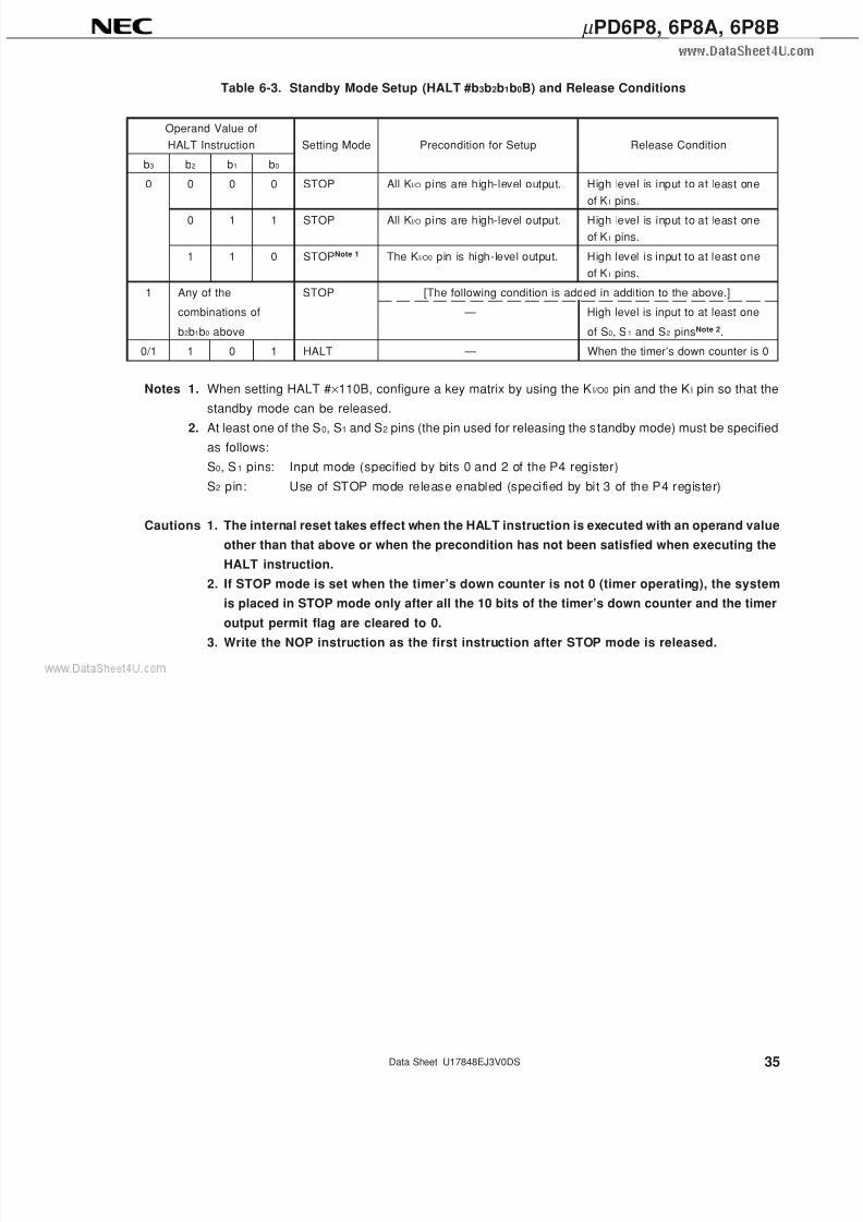
6.3 Standby Mode Release Timing
(1) STOP mode release timing
Figure 6-1. STOP Mode Release by Release Condition
Caution When a release condition is met in the STOP mode, the device is released from the STOP mode,
and goes into a wait state. At this time, if the release condition is not held, the device goes
into STOP mode again after the wait time has elapsed. Therefore, when releasing the STOP
mode, it is necessary to hold the release condition longer than the wait time.
(2) HALT mode release timing
Figure 6-2. HALT Mode Release by Release Condition
Wait
(52/fX + α)
HALT modeOperation
modeSTOP mode
Oscillationstopped Oscillation
Operationmode
Oscillation
HALT instruction(STOP mode)
Standbyrelease signal
Clock
α : Oscillation growth time
HALT mode Operation mode
Oscillation
Operation
mode
HALT instruction(HALT mode)Standby
release signal
Clock
7/17/2019 INFRARED REMOTE CONTROL TRANSMISSION
http://slidepdf.com/reader/full/infrared-remote-control-transmission 37/95
37
µ PD6P8, 6P8A, 6P8B
Data Sheet U17848EJ3V0DS
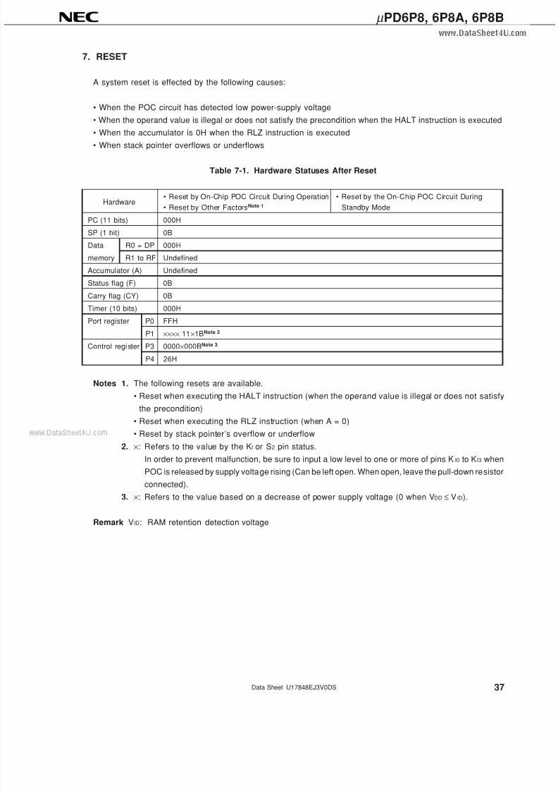
7. RESET
A system reset is effected by the following causes:
• When the POC circuit has detected low power-supply voltage
• When the operand value is illegal or does not satisfy the precondition when the HALT instruction is executed
• When the accumulator is 0H when the RLZ instruction is executed
• When stack pointer overflows or underflows
Table 7-1. Hardware Statuses After Reset
Hardware• Reset by On-Chip POC Circuit During Operation • Reset by the On-Chip POC Circuit During
• Reset by Other FactorsNote 1 Standby Mode
PC (11 bits) 000H
SP (1 bit) 0B
Data R0 = DP 000H
memory R1 to RF Undefined
Accumulator (A) Undefined
Status flag (F) 0B
Carry flag (CY) 0B
Timer (10 bits) 000H
Port register P0 FFH
P1 ×××× 11×1BNote 2
Control register P3 0000×000BNote 3
P4 26H
Notes 1. The following resets are available.
• Reset when executing the HALT instruction (when the operand value is illegal or does not satisfy
the precondition)
• Reset when executing the RLZ instruction (when A = 0)
• Reset by stack pointer’s overflow or underflow
2. ×: Refers to the value by the KI or S2 pin status.
In order to prevent malfunction, be sure to input a low level to one or more of pins KI0 to KI3 when
POC is released by supply voltage rising (Can be left open. When open, leave the pull-down resistor
connected).
3. ×: Refers to the value based on a decrease of power supply voltage (0 when VDD ≤ V ID).
Remark VID: RAM retention detection voltage
7/17/2019 INFRARED REMOTE CONTROL TRANSMISSION
http://slidepdf.com/reader/full/infrared-remote-control-transmission 38/95
38
µ PD6P8, 6P8A, 6P8B
Data Sheet U17848EJ3V0DS
8. POC CIRCUIT
The POC circuit monitors the power supply voltage and applies an internal reset to the microcontroller when the
battery is replaced.
Cautions 1. There are cases in which the POC circuit cannot detect a low power supply voltage of less
than 1 ms. Therefore, if the power supply voltage has become low for a period of less than
1 ms, the POC circuit may malfunction because it does not generate an internal reset signal.
2. Clock oscillation is stopped by the resonator due to low power supply voltage before the
POC circuit generates the internal reset signal. In this case, malfunction may result when
the power supply voltage is recovered after the oscillation is stopped. This type of
phenomenon takes place because the POC circuit does not generate an internal reset signal
(because the power supply voltage recovers before the low power supply voltage is
detected) even though the clock has stopped. If, by any chance, a malfunction has taken
place, remove the battery for a short time and put it back. In most cases, normal operation
will be resumed.
3. In order to prevent malfunction, be sure to input a low level to one or more of pins KI0 to
KI3 when POC is released due to supply voltage rising (Can be left open. When open, leavethe pull-down resistor connected).
7/17/2019 INFRARED REMOTE CONTROL TRANSMISSION
http://slidepdf.com/reader/full/infrared-remote-control-transmission 39/95
39
µ PD6P8, 6P8A, 6P8B
Data Sheet U17848EJ3V0DS
8.1 Functions of POC Circuit
The POC circuit has the following functions:
• Generates an internal reset signal when VDD ≤ VPOC.
• Cancels an internal reset signal when VDD > VPOC.
Here, VDD: power supply voltage, VPOC: POC detection voltage.
Notes 1. Actually, oscillation stabilization wait time must elapse before the circuit is switched to operation mode.
The oscillation stabilization wait time is about 534/fX to 918/fX (when about 134 to 230 µ s; @ fX = 4 MHz).
2. For the POC circuit to generate an internal reset signal when the power supply voltage has fallen,
it is necessary for the power supply voltage to be kept less than the V POC for the period of 1 ms or
more. Therefore, in reality, there is the time lag of up to 1 ms until the reset takes effect.
3. The POC detection voltage (VPOC) varies between approximately 1.7 to 1.9 V; thus, the reset may
be canceled at a power supply voltage smaller than the guaranteed range (VDD = 1.9 to 3.6 V).
However, as long as the conditions for operating the POC circuit are met, the actual lowest operatingpower supply voltage becomes lower than the POC detection voltage. Therefore, there is no
malfunction occurring due to a shortage of power supply voltage. However, malfunction for such
reasons as the clock not oscillating due to low power supply voltage may occur (refer to Cautions
3 in 8 POC CIRCUIT).
8.2 Oscillation Check at Low Supply Voltage
A reliable reset operation can be expected of the POC circuit if it satisfies the condition that the clock can oscillate
even at low power supply voltage (the oscillation start voltage of the resonator being even lower than the POC
detection voltage). Whether this condition is met or not can be checked by measuring the oscillation status in a
product that actually includes a POC circuit, as follows.
<1> Connect a storage oscilloscope to the XOUT pin so that the oscillation status can be measured.
<2> Connect a power supply whose output voltage can be varied and then gradually raise the power supply
voltage VDD from 0 V (making sure to avoid VDD > 3.6V).
At first (during VDD < approx. 1.7 V), the XOUT pin is 0 V regardless of the VDD. However, at the point that VDD
reaches the POC detection voltage (VPOC = 1.8 V (TYP.)), the voltage of the XOUT pin jumps to about 0.5VDD. Maintain
this power supply voltage for a while to measure the waveform of the XOUT pin. If by any chance the oscillation
start voltage of the resonator is lower than the POC detection voltage, the growing oscillation of the XOUT pin can
be confirmed within several ms after the VDD has reached the VPOC.
VDD
3.6 V
1.9 V
VPOC
Approx. 1.7 V
0 V
Internal reset signal
Reset
Operating ambient temperature TA = – 40 to + 85°C
Clock frequency fX = 3.5 to 4.5 MHz
←POC detection voltage VPOC = 1.8 V (TYP.)Note 3
→ t
Operation mode ↑ ResetNote 2
↑
Note 1
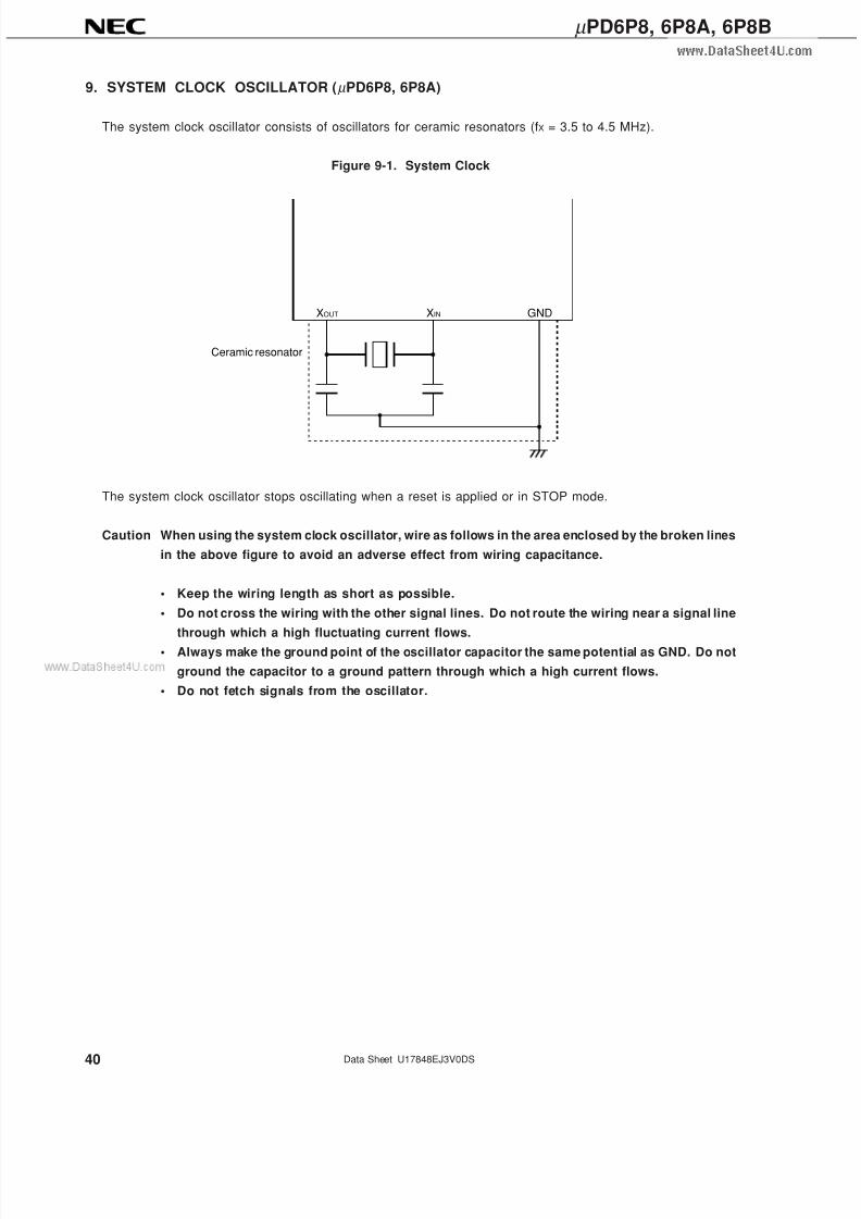
7/17/2019 INFRARED REMOTE CONTROL TRANSMISSION
http://slidepdf.com/reader/full/infrared-remote-control-transmission 40/95
40
µ PD6P8, 6P8A, 6P8B
Data Sheet U17848EJ3V0DS
9. SYSTEM CLOCK OSCILLATOR (µ PD6P8, 6P8A)
The system clock oscillator consists of oscillators for ceramic resonators (fX = 3.5 to 4.5 MHz).
Figure 9-1. System Clock
The system clock oscillator stops oscillating when a reset is applied or in STOP mode.
Caution When using the system clock oscillator, wire as follows in the area enclosed by the broken lines
in the above figure to avoid an adverse effect from wiring capacitance.
• Keep the wiring length as short as possible.
• Do not cross the wiring with the other signal lines. Do not route the wiring near a signal line
through which a high fluctuating current flows.• Always make the ground point of the oscillator capacitor the same potential as GND. Do not
ground the capacitor to a ground pattern through which a high current flows.
• Do not fetch signals from the oscillator.
XOUT XIN GND
Ceramic resonator
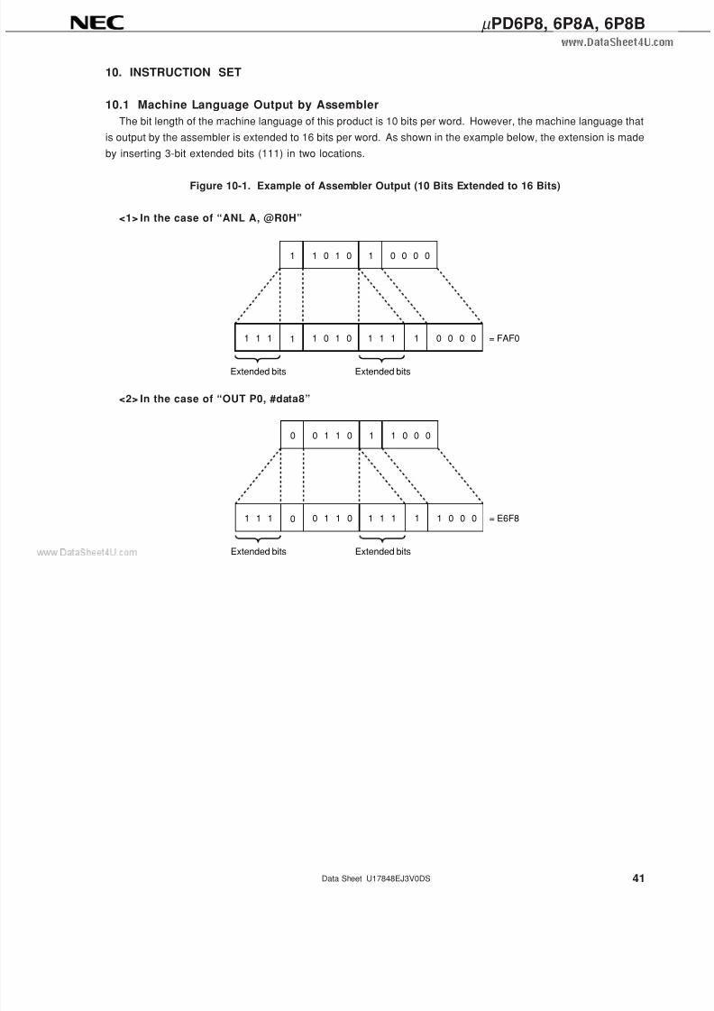
7/17/2019 INFRARED REMOTE CONTROL TRANSMISSION
http://slidepdf.com/reader/full/infrared-remote-control-transmission 41/95
41
µ PD6P8, 6P8A, 6P8B
Data Sheet U17848EJ3V0DS
10. INSTRUCTION SET
10.1 Machine Language Output by Assembler
The bit length of the machine language of this product is 10 bits per word. However, the machine language that
is output by the assembler is extended to 16 bits per word. As shown in the example below, the extension is made
by inserting 3-bit extended bits (111) in two locations.
Figure 10-1. Example of Assembler Output (10 Bits Extended to 16 Bits)
<1> In the case of “ANL A, @R0H”
1
1
1 0 1 0 1 0 0 0 0
1 0 1 0 1 0 0 0 01 1 11 1 1
Extended bitsExtended bits
= FAF0
<2> In the case of “OUT P0, #data8”
0
0
0 1 1 0 1 1 0 0 0
0 1 1 0 1 1 0 0 01 1 11 1 1
Extended bitsExtended bits
= E6F8
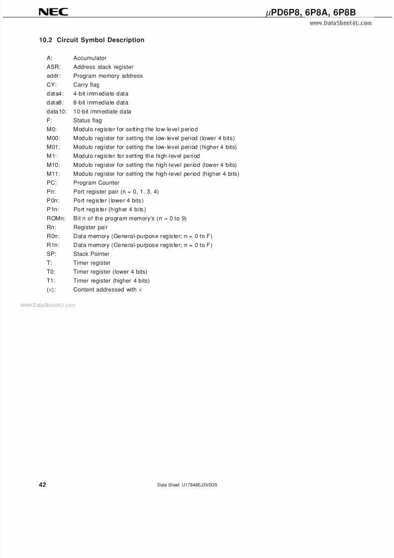
7/17/2019 INFRARED REMOTE CONTROL TRANSMISSION
http://slidepdf.com/reader/full/infrared-remote-control-transmission 42/95
42
µ PD6P8, 6P8A, 6P8B
Data Sheet U17848EJ3V0DS
10.2 Circuit Symbol Description
A: Accumulator
ASR: Address stack register
addr: Program memory address
CY: Carry flag
data4: 4-bit immediate data
data8: 8-bit immediate data
data10: 10-bit immediate data
F: Status flag
M0: Modulo register for sett ing the low-level period
M00: Modulo register for setting the low-level period (lower 4 bits)
M01: Modulo register for setting the low-level period (higher 4 bits)
M1: Modulo register for setting the high-level period
M10: Modulo register for setting the high-level period (lower 4 bits)
M11: Modulo register for setting the high-level period (higher 4 bits)
PC: Program Counter
Pn: Port register pair (n = 0, 1, 3, 4)P0n: Port register ( lower 4 bits)
P1n: Port register (h igher 4 bi ts)
ROMn: Bit n of the program memory’s (n = 0 to 9)
Rn: Register pair
R0n: Data memory (General-purpose register; n = 0 to F)
R1n: Data memory (General-purpose register; n = 0 to F)
SP: Stack Pointer
T: Timer register
T0: Timer register (lower 4 bits)
T1: Timer register (higher 4 bits)
(×
): Content addressed with×
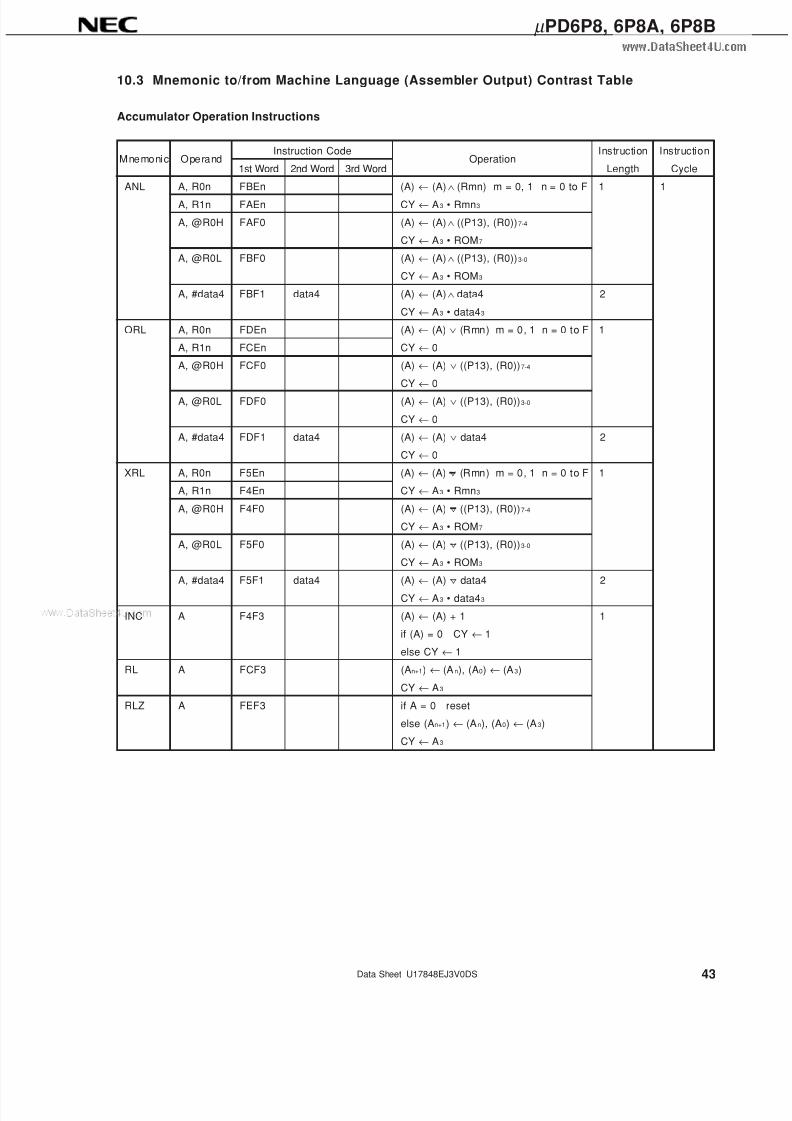
7/17/2019 INFRARED REMOTE CONTROL TRANSMISSION
http://slidepdf.com/reader/full/infrared-remote-control-transmission 43/95
43
µ PD6P8, 6P8A, 6P8B
Data Sheet U17848EJ3V0DS
10.3 Mnemonic to/from Machine Language (Assembler Output) Contrast Table
Accumulator Operation Instructions
Mnemonic OperandInstruction Code
OperationInstruction Instruction
1st Word 2nd Word 3rd Word Length Cycle
ANL A, R0n FBEn (A) ← (A) (Rmn) m = 0, 1 n = 0 to F 1 1
A, R1n FAEn CY ← A3 • Rmn3
A, @R0H FAF0 (A) ← (A) ((P13), (R0))7-4
CY ← A3 • ROM7
A, @R0L FBF0 (A) ← (A) ((P13), (R0))3-0
CY ← A3 • ROM3
A, #data4 FBF1 data4 (A) ← (A) data4 2
CY ← A3 • data43
ORL A, R0n FDEn (A) ← (A) ∨ (Rmn) m = 0, 1 n = 0 to F 1
A, R1n FCEn CY ← 0
A, @R0H FCF0 (A) ← (A) ∨ ((P13), (R0))7-4
CY ← 0
A, @R0L FDF0 (A) ← (A) ∨ ((P13), (R0))3-0
CY ← 0
A, #data4 FDF1 data4 (A) ← (A) ∨ data4 2
CY ← 0
XRL A, R0n F5En (A) ← (A) ∨ (Rmn) m = 0, 1 n = 0 to F 1
A, R1n F4En CY ← A3 • Rmn3
A, @R0H F4F0 (A) ← (A) ∨ ((P13), (R0))7-4
CY ← A3 • ROM7
A, @R0L F5F0 (A) ← (A) ∨ ((P13), (R0))3-0
CY ← A3 • ROM3
A, #data4 F5F1 data4 (A)←
(A)∨
data4 2CY ← A3 • data43
INC A F4F3 (A) ← (A) + 1 1
if (A) = 0 CY ← 1
else CY ← 1
RL A FCF3 (An+1) ← (An), (A0) ← (A3)
CY ← A3
RLZ A FEF3 if A = 0 reset
else (An+1) ← (An), (A0) ← (A3)
CY ← A3
∨
∨
∨
∨
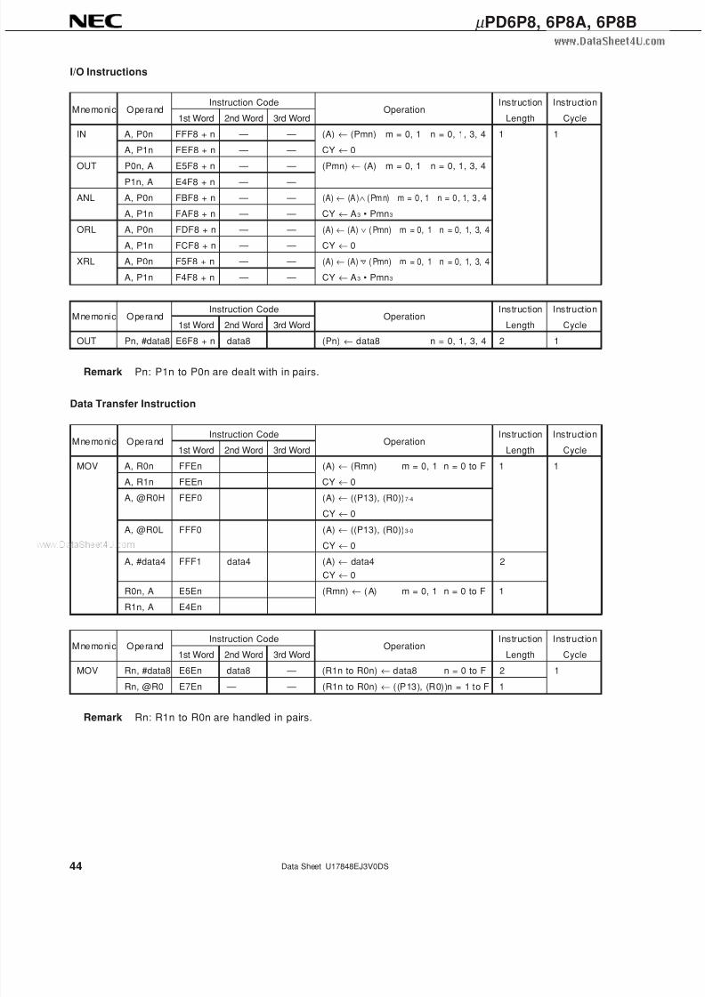
7/17/2019 INFRARED REMOTE CONTROL TRANSMISSION
http://slidepdf.com/reader/full/infrared-remote-control-transmission 44/95
44
µ PD6P8, 6P8A, 6P8B
Data Sheet U17848EJ3V0DS
I/O Instructions
Mnemonic OperandInstruction Code
OperationInstruction Instruction
1st Word 2nd Word 3rd Word Length Cycle
IN A, P0n FFF8 + n — — (A) ← (Pmn) m = 0, 1 n = 0, 1, 3, 4 1 1
A, P1n FEF8 + n — — CY ← 0
OUT P0n, A E5F8 + n — — (Pmn) ← (A) m = 0, 1 n = 0, 1, 3, 4
P1n, A E4F8 + n — —
ANL A, P0n FBF8 + n — — (A) ← (A) (Pmn) m = 0 , 1 n = 0 , 1, 3 , 4
A, P1n FAF8 + n — — CY ← A3 • Pmn3
ORL A, P0n FDF8 + n — — (A) ← (A) ∨ (Pmn) m = 0, 1 n = 0, 1, 3, 4
A, P1n FCF8 + n — — CY ← 0
XRL A, P0n F5F8 + n — — (A) ← (A) ∨ (Pmn) m = 0, 1 n = 0, 1, 3, 4
A, P1n F4F8 + n — — CY ← A3 • Pmn3
Mnemonic OperandInstruction Code
OperationInstruction Instruction
1st Word 2nd Word 3rd Word Length Cycle
OUT Pn, #data8 E6F8 + n data8 (Pn) ← data8 n = 0, 1, 3, 4 2 1
Remark Pn: P1n to P0n are dealt with in pairs.
Data Transfer Instruction
Mnemonic OperandInstruction Code
OperationInstruction Instruction
1st Word 2nd Word 3rd Word Length Cycle
MOV A, R0n FFEn (A) ← (Rmn) m = 0, 1 n = 0 to F 1 1
A, R1n FEEn CY ← 0
A, @R0H FEF0 (A) ← ((P13), (R0))7-4
CY ← 0
A, @R0L FFF0 (A) ← ((P13), (R0))3-0
CY ← 0
A, #data4 FFF1 data4 (A) ← data4 2
CY ← 0
R0n, A E5En (Rmn) ← (A) m = 0, 1 n = 0 to F 1
R1n, A E4En
Mnemonic OperandInstruction Code
OperationInstruction Instruction
1st Word 2nd Word 3rd Word Length Cycle
MOV Rn, #data8 E6En data8 — (R1n to R0n) ← data8 n = 0 to F 2 1
Rn, @R0 E7En — — (R1n to R0n) ← ((P13), (R0))n = 1 to F 1
Remark Rn: R1n to R0n are handled in pairs.
∨
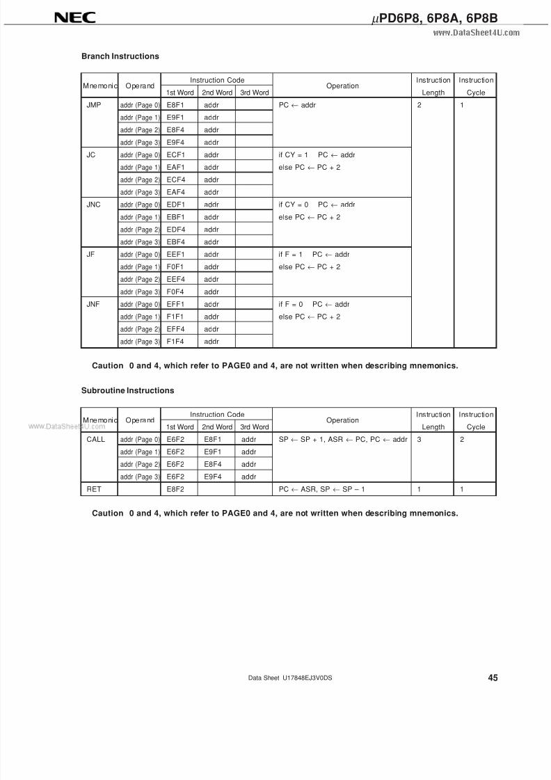
7/17/2019 INFRARED REMOTE CONTROL TRANSMISSION
http://slidepdf.com/reader/full/infrared-remote-control-transmission 45/95
45
µ PD6P8, 6P8A, 6P8B
Data Sheet U17848EJ3V0DS
Branch Instructions
Mnemonic OperandInstruction Code
OperationInstruction Instruction
1st Word 2nd Word 3rd Word Length Cycle
JMP addr (Page 0) E8F1 addr PC ← addr 2 1
addr (Page 1) E9F1 addr
addr (Page 2) E8F4 addr
addr (Page 3) E9F4 addr
JC addr (Page 0) ECF1 addr if CY = 1 PC ← addr
addr (Page 1) EAF1 addr else PC ← PC + 2
addr (Page 2) ECF4 addr
addr (Page 3) EAF4 addr
JNC addr (Page 0) EDF1 addr if CY = 0 PC ← addr
addr (Page 1) EBF1 addr else PC ← PC + 2
addr (Page 2) EDF4 addr
addr (Page 3) EBF4 addr
JF addr (Page 0) EEF1 addr if F = 1 PC ← addr
addr (Page 1) F0F1 addr else PC ← PC + 2
addr (Page 2) EEF4 addr
addr (Page 3) F0F4 addr
JNF addr (Page 0) EFF1 addr if F = 0 PC ← addr
addr (Page 1) F1F1 addr else PC ← PC + 2
addr (Page 2) EFF4 addr
addr (Page 3) F1F4 addr
Caution 0 and 4, which refer to PAGE0 and 4, are not written when describing mnemonics.
Subroutine Instructions
Mnemonic OperandInstruction Code
OperationInstruction Instruction
1st Word 2nd Word 3rd Word Length Cycle
CALL addr (Page 0) E6F2 E8F1 addr SP ← SP + 1, ASR ← PC, PC ← addr 3 2
addr (Page 1) E6F2 E9F1 addr
addr (Page 2) E6F2 E8F4 addr
addr (Page 3) E6F2 E9F4 addr
RET E8F2 PC ← ASR, SP ← SP – 1 1 1
Caution 0 and 4, which refer to PAGE0 and 4, are not written when describing mnemonics.
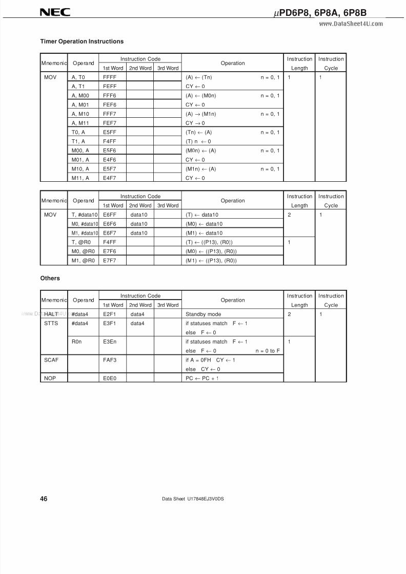
7/17/2019 INFRARED REMOTE CONTROL TRANSMISSION
http://slidepdf.com/reader/full/infrared-remote-control-transmission 46/95
46
µ PD6P8, 6P8A, 6P8B
Data Sheet U17848EJ3V0DS
Timer Operation Instructions
Mnemonic OperandInstruction Code
OperationInstruction Instruction
1st Word 2nd Word 3rd Word Length Cycle
MOV A, T0 FFFF (A) ← (Tn) n = 0, 1 1 1
A, T1 FEFF CY ← 0
A, M00 FFF6 (A) ← (M0n) n = 0, 1
A, M01 FEF6 CY ← 0
A, M10 FFF7 (A) → (M1n) n = 0, 1
A, M11 FEF7 CY → 0
T0, A E5FF (Tn) ← (A) n = 0, 1
T1, A F4FF (T) n ← 0
M00, A E5F6 (M0n) ← (A) n = 0, 1
M01, A E4F6 CY ← 0
M10, A E5F7 (M1n) ← (A) n = 0, 1
M11, A E4F7 CY ← 0
Mnemonic OperandInstruction Code
OperationInstruction Instruction
1st Word 2nd Word 3rd Word Length Cycle
MOV T, #data10 E6FF data10 (T) ← data10 2 1
M0, #data10 E6F6 data10 (M0) ← data10
M1, #data10 E6F7 data10 (M1) ← data10
T, @R0 F4FF (T) ← ((P13), (R0)) 1
M0, @R0 E7F6 (M0) ← ((P13), (R0))
M1, @R0 E7F7 (M1) ← ((P13), (R0))
Others
Mnemonic OperandInstruction Code
OperationInstruction Instruction
1st Word 2nd Word 3rd Word Length Cycle
HALT #data4 E2F1 data4 Standby mode 2 1
STTS #data4 E3F1 data4 if statuses match F ← 1
else F ← 0
R0n E3En if statuses match F ← 1 1
else F ← 0 n = 0 to F
SCAF FAF3 if A = 0FH CY ← 1
else CY ← 0
NOP E0E0 PC ← PC + 1
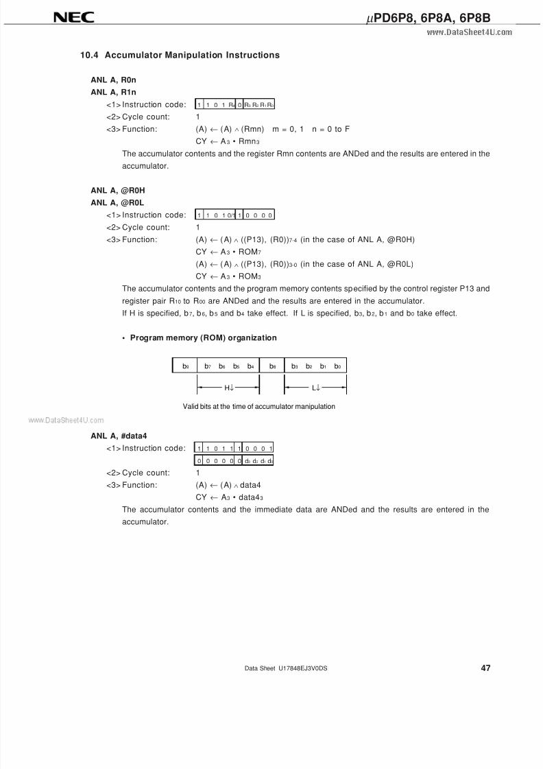
7/17/2019 INFRARED REMOTE CONTROL TRANSMISSION
http://slidepdf.com/reader/full/infrared-remote-control-transmission 47/95
47
µ PD6P8, 6P8A, 6P8B
Data Sheet U17848EJ3V0DS
10.4 Accumulator Manipulation Instructions
ANL A, R0n
ANL A, R1n
<1> Instruction code: 1 1 0 1 R4 0 R3 R2 R1R0
<2> Cycle count: 1
<3> Function: (A) ← (A) (Rmn) m = 0, 1 n = 0 to F
CY ← A3 • Rmn3
The accumulator contents and the register Rmn contents are ANDed and the results are entered in the
accumulator.
ANL A, @R0H
ANL A, @R0L
<1> Instruction code: 1 1 0 1 0/1 1 0 0 0 0
<2> Cycle count: 1
<3> Function: (A) ← (A) ((P13), (R0))7-4 (in the case of ANL A, @R0H)
CY ← A3 • ROM7
(A)←
(A) ((P13), (R0))3-0 (in the case of ANL A, @R0L)CY ← A3 • ROM3
The accumulator contents and the program memory contents specified by the control register P13 and
register pair R10 to R00 are ANDed and the results are entered in the accumulator.
If H is specified, b7, b6, b5 and b4 take effect. If L is specified, b3, b2, b1 and b0 take effect.
• Program memory (ROM) organization
ANL A, #data4
<1> Instruction code: 1 1 0 1 1 1 0 0 0 1
0 0 0 0 0 0 d3 d2 d1 d0
<2> Cycle count: 1
<3> Function: (A) ← (A) data4
CY ← A3 • data43
The accumulator contents and the immediate data are ANDed and the results are entered in the
accumulator.
∨
∨
∨
∨
b9 b8b7 b6 b5 b4 b3 b2 b1 b0
H↓ L↓
Valid bits at the time of accumulator manipulation
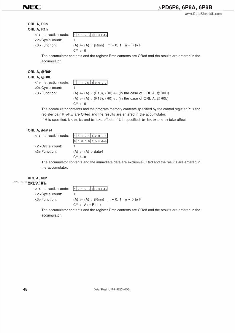
7/17/2019 INFRARED REMOTE CONTROL TRANSMISSION
http://slidepdf.com/reader/full/infrared-remote-control-transmission 48/95
48
µ PD6P8, 6P8A, 6P8B
Data Sheet U17848EJ3V0DS
ORL A, R0n
ORL A, R1n
<1> Instruction code: 1 1 1 0 R4 0 R3 R2 R1R0
<2> Cycle count: 1
<3> Function: (A) ← (A) ∨ (Rmn) m = 0, 1 n = 0 to F
CY ← 0
The accumulator contents and the register Rmn contents are ORed and the results are entered in the
accumulator.
ORL A, @R0H
ORL A, @R0L
<1> Instruction code: 1 1 1 0 0/1 1 0 0 0 0
<2> Cycle count: 1
<3> Function: (A) ← (A) ∨ (P13), (R0))7-4 (in the case of ORL A, @R0H)
(A) ← (A) ∨ (P13), (R0))3-0 (in the case of ORL A, @R0L)
CY ← 0
The accumulator contents and the program memory contents specified by the control register P13 and
register pair R10-R00 are ORed and the results are entered in the accumulator.If H is specified, b7, b6, b5 and b4 take effect. If L is specified, b3, b2, b1 and b0 take effect.
ORL A, #data4
<1> Instruction code: 1 1 1 0 1 1 0 0 0 1
0 0 0 0 0 0 d3 d2 d1 d0
<2> Cycle count: 1
<3> Function: (A) ← (A) ∨ data4
CY ← 0
The accumulator contents and the immediate data are exclusive-ORed and the results are entered in
the accumulator.
XRL A, R0n
XRL A, R1n
<1> Instruction code: 1 0 1 0 R4 0 R3 R2 R1R0
<2> Cycle count: 1
<3> Function: (A) ← (A) ∨ (Rmn) m = 0, 1 n = 0 to F
CY ← A3 • Rmn3
The accumulator contents and the register Rmn contents are ORed and the results are entered in the
accumulator.
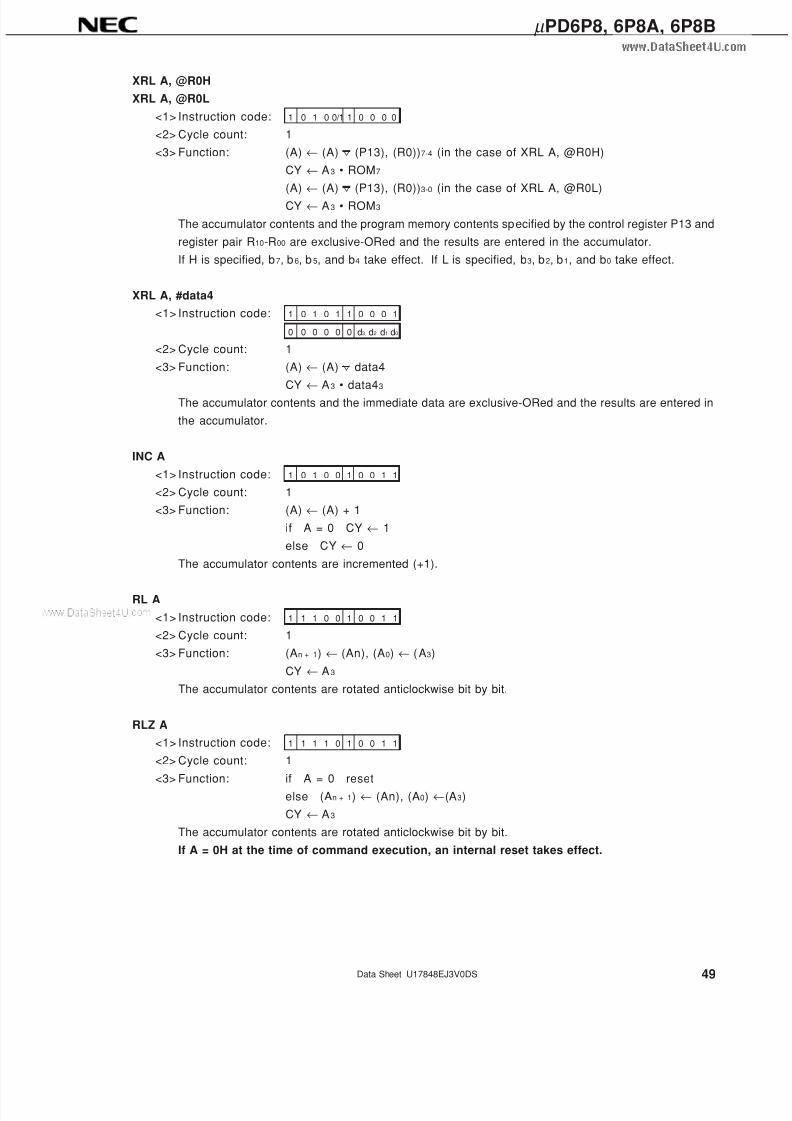
7/17/2019 INFRARED REMOTE CONTROL TRANSMISSION
http://slidepdf.com/reader/full/infrared-remote-control-transmission 49/95
49
µ PD6P8, 6P8A, 6P8B
Data Sheet U17848EJ3V0DS
XRL A, @R0H
XRL A, @R0L
<1> Instruction code: 1 0 1 0 0/1 1 0 0 0 0
<2> Cycle count: 1
<3> Function: (A) ← (A) ∨ (P13), (R0))7-4 (in the case of XRL A, @R0H)
CY ← A3 • ROM7
(A) ← (A) ∨ (P13), (R0))3-0 (in the case of XRL A, @R0L)
CY ← A3 • ROM3
The accumulator contents and the program memory contents specified by the control register P13 and
register pair R10-R00 are exclusive-ORed and the results are entered in the accumulator.
If H is specified, b7, b6, b5, and b4 take effect. If L is specified, b3, b2, b1, and b0 take effect.
XRL A, #data4
<1> Instruction code: 1 0 1 0 1 1 0 0 0 1
0 0 0 0 0 0 d3 d2 d1 d0
<2> Cycle count: 1
<3> Function: (A) ← (A) ∨ data4
CY←
A3 • data43
The accumulator contents and the immediate data are exclusive-ORed and the results are entered in
the accumulator.
INC A
<1> Instruction code: 1 0 1 0 0 1 0 0 1 1
<2> Cycle count: 1
<3> Function: (A) ← (A) + 1
if A = 0 CY ← 1
else CY ← 0
The accumulator contents are incremented (+1).
RL A
<1> Instruction code: 1 1 1 0 0 1 0 0 1 1
<2> Cycle count: 1
<3> Function: (An + 1) ← (An), (A0) ← (A3)
CY ← A3
The accumulator contents are rotated anticlockwise bit by bit.
RLZ A
<1> Instruction code: 1 1 1 1 0 1 0 0 1 1
<2> Cycle count: 1
<3> Function: if A = 0 resetelse (An + 1) ← (An), (A0) ←(A3)
CY ← A3
The accumulator contents are rotated anticlockwise bit by bit.
If A = 0H at the time of command execution, an internal reset takes effect.
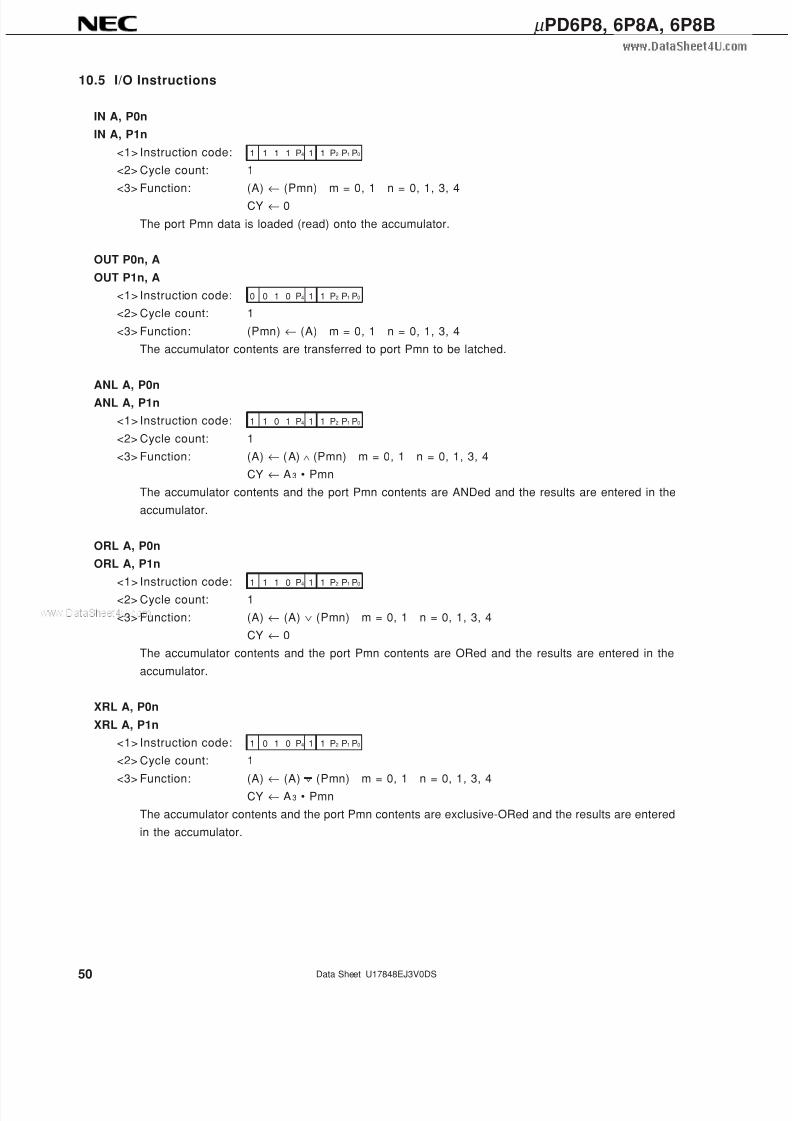
7/17/2019 INFRARED REMOTE CONTROL TRANSMISSION
http://slidepdf.com/reader/full/infrared-remote-control-transmission 50/95
50
µ PD6P8, 6P8A, 6P8B
Data Sheet U17848EJ3V0DS
10.5 I/O Instructions
IN A, P0n
IN A, P1n
<1> Instruction code: 1 1 1 1 P4 1 1 P2 P1 P0
<2> Cycle count: 1
<3> Function: (A) ← (Pmn) m = 0, 1 n = 0, 1, 3, 4
CY ← 0
The port Pmn data is loaded (read) onto the accumulator.
OUT P0n, A
OUT P1n, A
<1> Instruction code: 0 0 1 0 P4 1 1 P2 P1 P0
<2> Cycle count: 1
<3> Function: (Pmn) ← (A) m = 0, 1 n = 0, 1, 3, 4
The accumulator contents are transferred to port Pmn to be latched.
ANL A, P0nANL A, P1n
<1> Instruction code: 1 1 0 1 P4 1 1 P2 P1 P0
<2> Cycle count: 1
<3> Function: (A) ← (A) (Pmn) m = 0, 1 n = 0, 1, 3, 4
CY ← A3 • Pmn
The accumulator contents and the port Pmn contents are ANDed and the results are entered in the
accumulator.
ORL A, P0n
ORL A, P1n
<1> Instruction code: 1 1 1 0 P4 1 1 P2 P1 P0
<2> Cycle count: 1
<3> Function: (A) ← (A) ∨ (Pmn) m = 0, 1 n = 0, 1, 3, 4
CY ← 0
The accumulator contents and the port Pmn contents are ORed and the results are entered in the
accumulator.
XRL A, P0n
XRL A, P1n
<1> Instruction code: 1 0 1 0 P4 1 1 P2 P1 P0
<2> Cycle count: 1
<3> Function: (A) ← (A) ∨ (Pmn) m = 0, 1 n = 0, 1, 3, 4CY ← A3 • Pmn
The accumulator contents and the port Pmn contents are exclusive-ORed and the results are entered
in the accumulator.
∨

7/17/2019 INFRARED REMOTE CONTROL TRANSMISSION
http://slidepdf.com/reader/full/infrared-remote-control-transmission 51/95
51
µ PD6P8, 6P8A, 6P8B
Data Sheet U17848EJ3V0DS
OUT Pn, #data8
<1> Instruction code: 0 0 1 1 0 1 1 P2 P1 P0
: 0 d7 d6 d5 d4 0 d3 d2 d1 d0
<2> Cycle count: 1
<3> Function: (Pn) ← data8 n = 0, 1, 3, 4
The immediate data is transferred to port Pn. In this case, port Pn refers to P1n to P0n operating in pairs.
10.6 Data Transfer Instructions
MOV A, R0n
MOV A, R1n
<1> Instruction code: 1 1 1 1 R4 0 R3 R2 R1R0
<2> Cycle count: 1
<3> Function: (A) ← (Rmn) m = 0, 1 n = 0 to F
CY ← 0
The register Rmn contents are transferred to the accumulator.
MOV A, @R0H<1> Instruction code: 1 1 1 1 0 1 0 0 0 0
<2> Cycle count: 1
<3> Function: (A) ← ((P13), (R0))7-4
CY ← 0
The higher 4 bits (b7 b6 b5 b4) of the program memory specified by control register P13 and register pair
R10-R00 are transferred to the accumulator. b9 is ignored.
MOV A, @R0L
<1> Instruction code: 1 1 1 1 1 1 0 0 0 0
<2> Cycle count: 1
<3> Function: (A)←
((P13), (R0))3-0
CY ← 0
The lower 4 bits (b3 b2 b1 b0) of the program memory specified by control register P13 and register pair
R10 to R00 are transferred to the accumulator. b8 is ignored.
• Program memory (ROM) contents
b9 b8b7 b6 b5 b4 b3 b2 b1 b0
@R0 H @R0 L
MOV A, #data4<1> Instruction code: 1 1 1 1 1 1 0 0 0 1
: 0 0 0 0 0 0 d3 d2 d1 d0
<2> Cycle count: 1
<3> Function: (A) ← data4
CY ← 0
The immediate data is transferred to the accumulator.
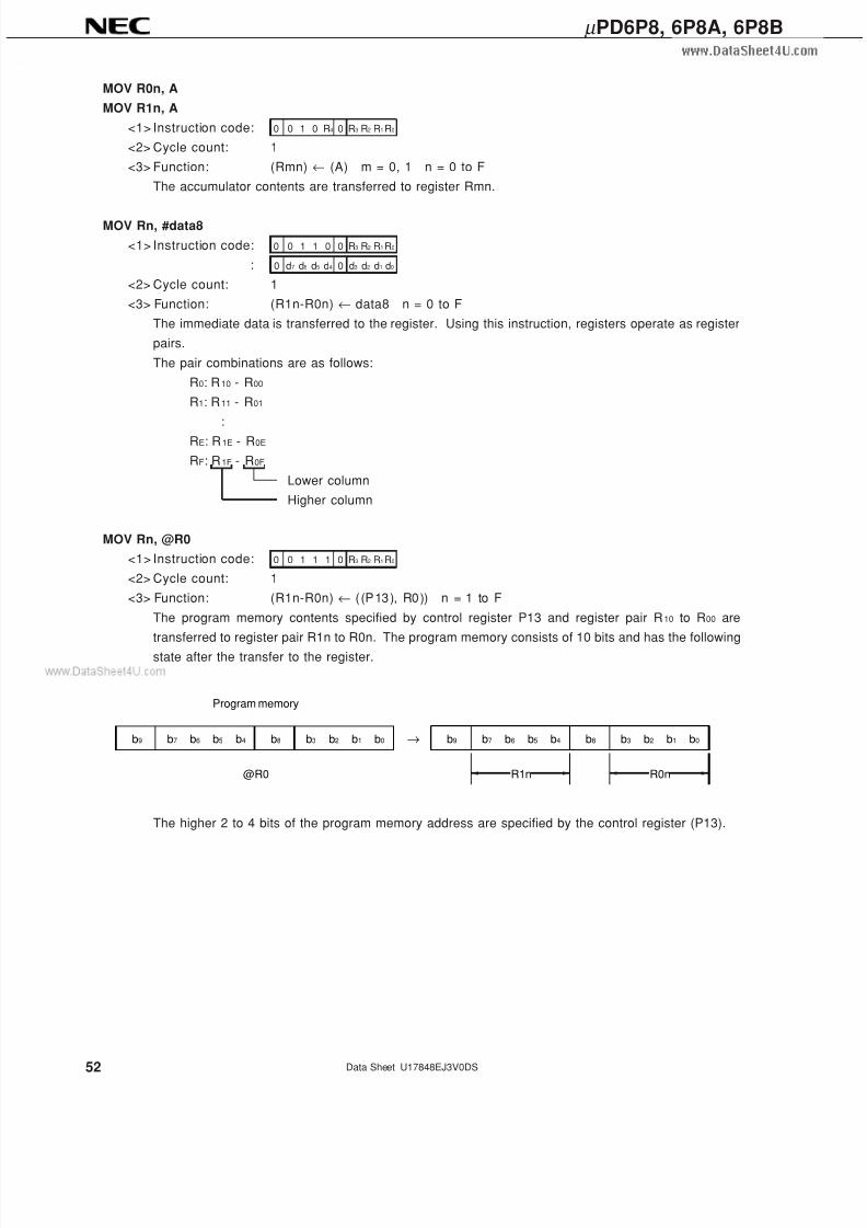
7/17/2019 INFRARED REMOTE CONTROL TRANSMISSION
http://slidepdf.com/reader/full/infrared-remote-control-transmission 52/95
52
µ PD6P8, 6P8A, 6P8B
Data Sheet U17848EJ3V0DS
MOV R0n, A
MOV R1n, A
<1> Instruction code: 0 0 1 0 R4 0 R3 R2 R1R0
<2> Cycle count: 1
<3> Function: (Rmn) ← (A) m = 0, 1 n = 0 to F
The accumulator contents are transferred to register Rmn.
MOV Rn, #data8
<1> Instruction code: 0 0 1 1 0 0 R3 R2 R1R0
: 0 d7 d6 d5 d4 0 d3 d2 d1 d0
<2> Cycle count: 1
<3> Function: (R1n-R0n) ← data8 n = 0 to F
The immediate data is transferred to the register. Using this instruction, registers operate as register
pairs.
The pair combinations are as follows:
R0: R10 - R00
R1: R11 - R01
:RE: R1E - R0E
RF: R1F - R0F
Lower column
Higher column
MOV Rn, @R0
<1> Instruction code: 0 0 1 1 1 0 R3 R2 R1R0
<2> Cycle count: 1
<3> Function: (R1n-R0n) ← ( (P13), R0)) n = 1 to F
The program memory contents specified by control register P13 and register pair R10 to R00 are
transferred to register pair R1n to R0n. The program memory consists of 10 bits and has the followingstate after the transfer to the register.
b9 b8b7 b6 b5 b4 b3 b2 b1 b0b9 b8b7 b6 b5 b4 b3 b2 b1 b0
@R0
→
R1n R0n
Program memory
The higher 2 to 4 bits of the program memory address are specified by the control register (P13).
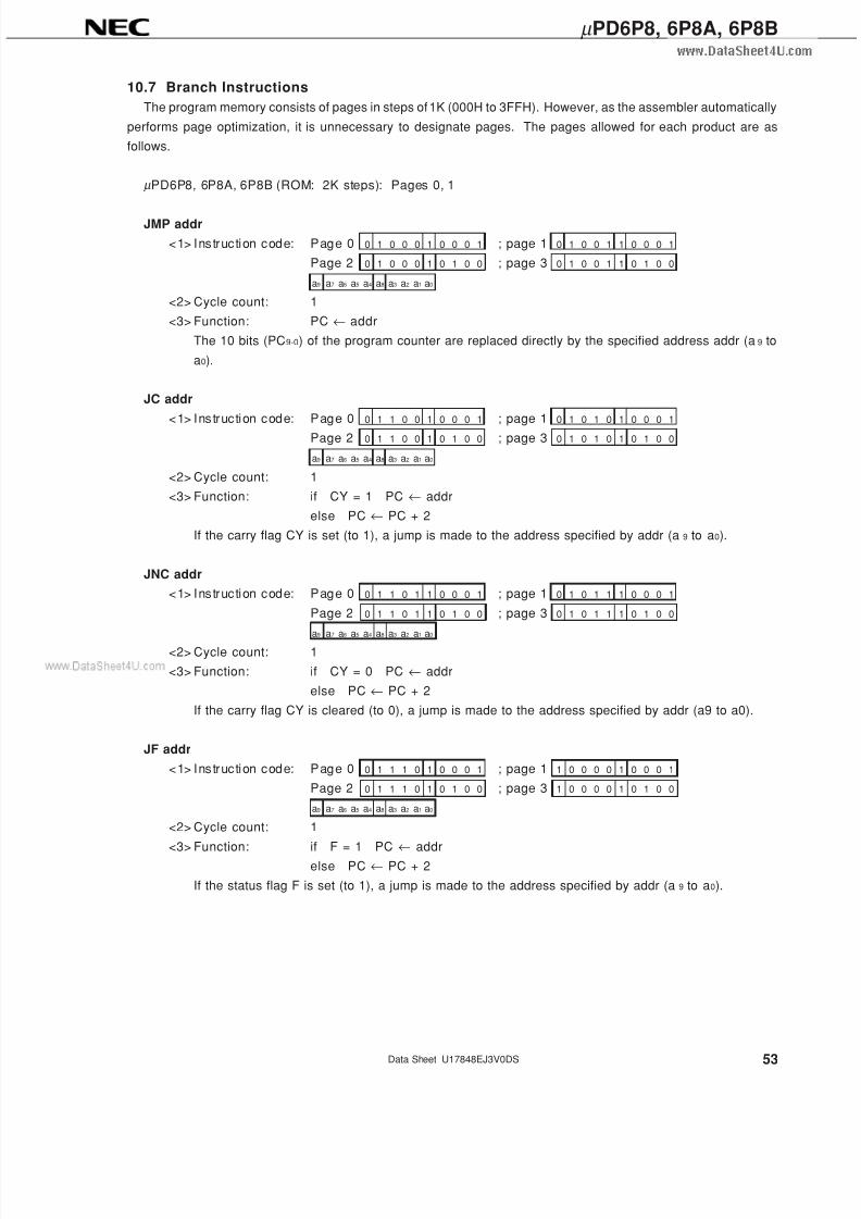
7/17/2019 INFRARED REMOTE CONTROL TRANSMISSION
http://slidepdf.com/reader/full/infrared-remote-control-transmission 53/95
53
µ PD6P8, 6P8A, 6P8B
Data Sheet U17848EJ3V0DS
10.7 Branch Instructions
The program memory consists of pages in steps of 1K (000H to 3FFH). However, as the assembler automatically
performs page optimization, it is unnecessary to designate pages. The pages allowed for each product are as
follows.
µ PD6P8, 6P8A, 6P8B (ROM: 2K steps): Pages 0, 1
JMP addr
<1> Instruction code: Page 0 0 1 0 0 0 1 0 0 0 1 ; page 1 0 1 0 0 1 1 0 0 0 1
Page 2 0 1 0 0 0 1 0 1 0 0 ; page 3 0 1 0 0 1 1 0 1 0 0
a9 a7 a6 a5 a4 a8 a3 a2 a1 a0
<2> Cycle count: 1
<3> Function: PC ← addr
The 10 bits (PC9-0) of the program counter are replaced directly by the specified address addr (a 9 to
a0).
JC addr
<1> Instruction code: Page 0 0 1 1 0 0 1 0 0 0 1 ; page 1 0 1 0 1 0 1 0 0 0 1Page 2 0 1 1 0 0 1 0 1 0 0 ; page 3 0 1 0 1 0 1 0 1 0 0
a9 a7 a6 a5 a4 a8 a3 a2 a1 a0
<2> Cycle count: 1
<3> Function: if CY = 1 PC ← addr
else PC ← PC + 2
If the carry flag CY is set (to 1), a jump is made to the address specified by addr (a 9 to a0).
JNC addr
<1> Instruction code: Page 0 0 1 1 0 1 1 0 0 0 1 ; page 1 0 1 0 1 1 1 0 0 0 1
Page 2 0 1 1 0 1 1 0 1 0 0 ; page 3 0 1 0 1 1 1 0 1 0 0
a9 a7 a6 a5 a4 a8 a3 a2 a1 a0
<2> Cycle count: 1
<3> Function: if CY = 0 PC ← addr
else PC ← PC + 2
If the carry flag CY is cleared (to 0), a jump is made to the address specified by addr (a9 to a0).
JF addr
<1> Instruction code: Page 0 0 1 1 1 0 1 0 0 0 1 ; page 1 1 0 0 0 0 1 0 0 0 1
Page 2 0 1 1 1 0 1 0 1 0 0 ; page 3 1 0 0 0 0 1 0 1 0 0
a9 a7 a6 a5 a4 a8 a3 a2 a1 a0
<2> Cycle count: 1
<3> Function: if F = 1 PC ← addrelse PC ← PC + 2
If the status flag F is set (to 1), a jump is made to the address specified by addr (a 9 to a0).
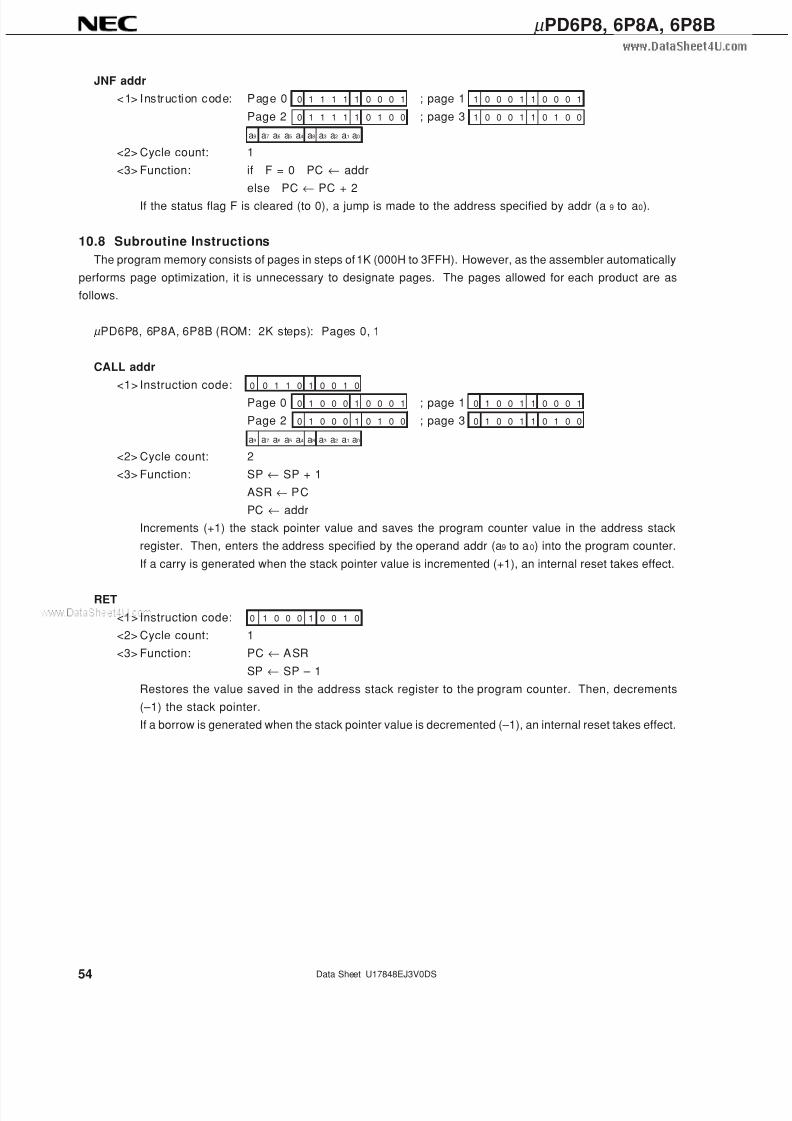
7/17/2019 INFRARED REMOTE CONTROL TRANSMISSION
http://slidepdf.com/reader/full/infrared-remote-control-transmission 54/95
54
µ PD6P8, 6P8A, 6P8B
Data Sheet U17848EJ3V0DS
JNF addr
<1> Instruction code: Page 0 0 1 1 1 1 1 0 0 0 1 ; page 1 1 0 0 0 1 1 0 0 0 1
Page 2 0 1 1 1 1 1 0 1 0 0 ; page 3 1 0 0 0 1 1 0 1 0 0
a9 a7 a6 a5 a4 a8 a3 a2 a1 a0
<2> Cycle count: 1
<3> Function: if F = 0 PC ← addr
else PC ← PC + 2
If the status flag F is cleared (to 0), a jump is made to the address specified by addr (a 9 to a0).
10.8 Subroutine Instructions
The program memory consists of pages in steps of 1K (000H to 3FFH). However, as the assembler automatically
performs page optimization, it is unnecessary to designate pages. The pages allowed for each product are as
follows.
µ PD6P8, 6P8A, 6P8B (ROM: 2K steps): Pages 0, 1
CALL addr
<1> Instruction code: 0 0 1 1 0 1 0 0 1 0Page 0 0 1 0 0 0 1 0 0 0 1 ; page 1 0 1 0 0 1 1 0 0 0 1
Page 2 0 1 0 0 0 1 0 1 0 0 ; page 3 0 1 0 0 1 1 0 1 0 0
a9 a7 a6 a5 a4 a8 a3 a2 a1 a0
<2> Cycle count: 2
<3> Function: SP ← SP + 1
ASR ← PC
PC ← addr
Increments (+1) the stack pointer value and saves the program counter value in the address stack
register. Then, enters the address specified by the operand addr (a9 to a0) into the program counter.
If a carry is generated when the stack pointer value is incremented (+1), an internal reset takes effect.
RET
<1> Instruction code: 0 1 0 0 0 1 0 0 1 0
<2> Cycle count: 1
<3> Function: PC ← ASR
SP ← SP – 1
Restores the value saved in the address stack register to the program counter. Then, decrements
(–1) the stack pointer.
If a borrow is generated when the stack pointer value is decremented (–1), an internal reset takes effect.
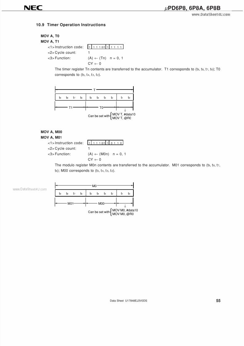
7/17/2019 INFRARED REMOTE CONTROL TRANSMISSION
http://slidepdf.com/reader/full/infrared-remote-control-transmission 55/95
55
µ PD6P8, 6P8A, 6P8B
Data Sheet U17848EJ3V0DS
10.9 Timer Operation Instructions
MOV A, T0
MOV A, T1
<1> Instruction code: 1 1 1 1 0/1 1 1 1 1 1
<2> Cycle count: 1
<3> Function: (A) ← (Tn) n = 0, 1
CY ← 0
The timer register Tn contents are transferred to the accumulator. T1 corresponds to (t9, t8, t7, t6); T0
corresponds to (t5, t4, t3, t2).
↓
t9 t8 t7 t6 t5 t4 t3 t2 t1 t0
Can be set with
T1 T0
MOV T, #data10MOV T, @R0
T
MOV A, M00
MOV A, M01
<1> Instruction code: 1 1 1 1 0/1 1 0 1 1 0
<2> Cycle count: 1
<3> Function: (A) ← (M0n) n = 0, 1
CY ← 0
The modulo register M0n contents are transferred to the accumulator. M01 corresponds to (t9, t8, t7,
t6); M00 corresponds to (t5, t4, t3, t2).
↓
t9 t8 t7 t6 t5 t4 t3 t2 t1 t0
Can be set with
M01 M00
MOV M0, #data10MOV M0, @R0
M0
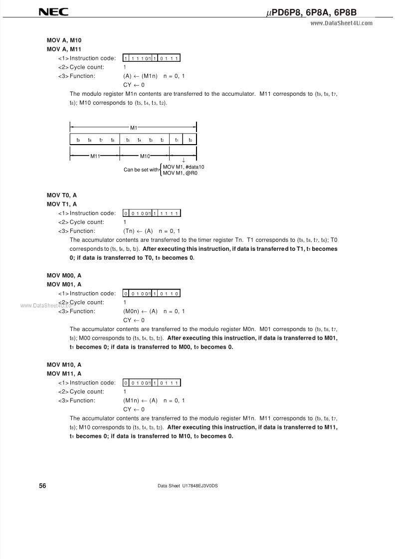
7/17/2019 INFRARED REMOTE CONTROL TRANSMISSION
http://slidepdf.com/reader/full/infrared-remote-control-transmission 56/95
56
µ PD6P8, 6P8A, 6P8B
Data Sheet U17848EJ3V0DS
MOV A, M10
MOV A, M11
<1> Instruction code: 1 1 1 1 0/1 1 0 1 1 1
<2> Cycle count: 1
<3> Function: (A) ← (M1n) n = 0, 1
CY ← 0
The modulo register M1n contents are transferred to the accumulator. M11 corresponds to (t9, t8, t7,
t6); M10 corresponds to (t5, t4, t3, t2).
↓
t9 t8 t7 t6 t5 t4 t3 t2 t1 t0
Can be set with
M11 M10
MOV M1, #data10MOV M1, @R0
M1
MOV T0, A
MOV T1, A
<1> Instruction code: 0 0 1 0 0/1 1 1 1 1 1
<2> Cycle count: 1
<3> Function: (Tn) ← (A) n = 0, 1
The accumulator contents are transferred to the timer register Tn. T1 corresponds to (t9, t8, t7, t6); T0
corresponds to (t5, t4, t3, t2). After executing this instruction, if data is transferred to T1, t1 becomes
0; if data is transferred to T0, t0 becomes 0.
MOV M00, A
MOV M01, A
<1> Instruction code: 0 0 1 0 0/1 1 0 1 1 0
<2> Cycle count: 1
<3> Function: (M0n) ← (A) n = 0, 1
CY ← 0
The accumulator contents are transferred to the modulo register M0n. M01 corresponds to (t9, t8, t7,
t6); M00 corresponds to (t5, t4, t3, t2). After executing this instruction, if data is transferred to M01,
t1 becomes 0; if data is transferred to M00, t0 becomes 0.
MOV M10, A
MOV M11, A
<1> Instruction code: 0 0 1 0 0/1 1 0 1 1 1
<2> Cycle count: 1
<3> Function: (M1n) ← (A) n = 0, 1
CY ← 0
The accumulator contents are transferred to the modulo register M1n. M11 corresponds to (t9, t8, t7,
t6); M10 corresponds to (t5, t4, t3, t2). After executing this instruction, if data is transferred to M11,
t1 becomes 0; if data is transferred to M10, t0 becomes 0.
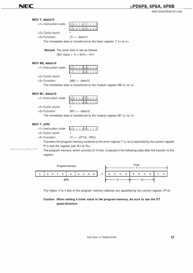
7/17/2019 INFRARED REMOTE CONTROL TRANSMISSION
http://slidepdf.com/reader/full/infrared-remote-control-transmission 57/95
57
µ PD6P8, 6P8A, 6P8B
Data Sheet U17848EJ3V0DS
MOV T, #data10
<1> Instruction code: 0 0 1 1 0 1 1 1 1 1
t1 t9 t8 t7 t6 t0 t5 t4 t3 t2
<2> Cycle count: 1
<3> Function: (T) ← data10
The immediate data is transferred to the timer register T (t 9 to t0).
Remark The timer time is set as follows.
(Set value + 1) × 64/fX – 4/fX
MOV M0, #data10
<1> Instruction code: 0 0 1 1 0 1 0 1 1 0
t1 t9 t8 t7 t6 t0 t5 t4 t3 t2
<2> Cycle count: 1
<3> Function: (M0) ← data10
The immediate data is transferred to the modulo register M0 (t 9 to t0).
MOV M1, #data10<1> Instruction code: 0 0 1 1 0 1 0 1 1 1
t1 t9 t8 t7 t6 t0 t5 t4 t3 t2
<2> Cycle count: 1
<3> Function: (M1) ← data10
The immediate data is transferred to the modulo register M1 (t 9 to t0).
MOV T, @R0
<1> Instruction code: 0 0 1 1 1 1 1 1 1 1
<2> Cycle count: 1
<3> Function: (T) ← ((P13), (R0))
Transfers the program memory contents to the timer register T (t9 to t0) specified by the control registerP13 and the register pair R10 to R00.
The program memory, which consists of 10 bits, is placed in the following state after the transfer to the
register.
t9 t8 t7 t6 t5 t4 t3 t2 t1 t0
T1 T0
t1 t0t9 t8 t7 t6 t5 t4 t3 t2
@R0
→
Program memory Timer
T
The higher 2 to 4 bits of the program memory address are specified by the control register (P13).
Caution When setting a timer value in the program memory, be sure to use the DT
quasi-directive.
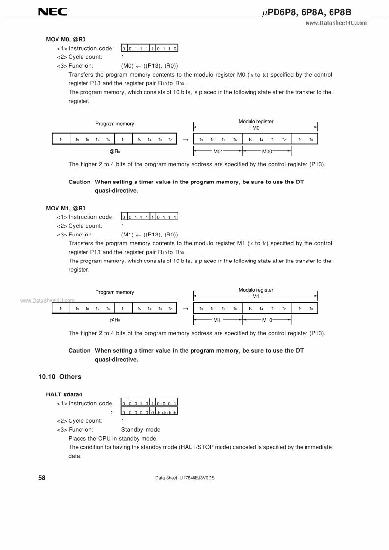
7/17/2019 INFRARED REMOTE CONTROL TRANSMISSION
http://slidepdf.com/reader/full/infrared-remote-control-transmission 58/95
58
µ PD6P8, 6P8A, 6P8B
Data Sheet U17848EJ3V0DS
MOV M0, @R0
<1> Instruction code: 0 0 1 1 1 1 0 1 1 0
<2> Cycle count: 1
<3> Function: (M0) ← ((P13), (R0))
Transfers the program memory contents to the modulo register M0 (t9 to t0) specified by the control
register P13 and the register pair R10 to R00.
The program memory, which consists of 10 bits, is placed in the following state after the transfer to the
register.
t9 t8 t7 t6 t5 t4 t3 t2 t1 t0
M01 M00
t1 t0t9 t8 t7 t6 t5 t4 t3 t2
@R0
→
Program memory Modulo register
M0
The higher 2 to 4 bits of the program memory address are specified by the control register (P13).
Caution When setting a timer value in the program memory, be sure to use the DT
quasi-directive.
MOV M1, @R0
<1> Instruction code: 0 0 1 1 1 1 0 1 1 1
<2> Cycle count: 1
<3> Function: (M1) ← ((P13), (R0))
Transfers the program memory contents to the modulo register M1 (t9 to t0) specified by the control
register P13 and the register pair R10 to R00.
The program memory, which consists of 10 bits, is placed in the following state after the transfer to the
register.
t9 t8 t7 t6 t5 t4 t3 t2 t1 t0
M11 M10
t1 t0t9 t8 t7 t6 t5 t4 t3 t2
@R0
→
Program memory Modulo register
M1
The higher 2 to 4 bits of the program memory address are specified by the control register (P13).
Caution When setting a timer value in the program memory, be sure to use the DT
quasi-directive.
10.10 Others
HALT #data4
<1> Instruction code: 0 0 0 1 0 1 0 0 0 1
: 0 0 0 0 0 0 d3 d2 d1 d0
<2> Cycle count: 1
<3> Function: Standby mode
Places the CPU in standby mode.
The condition for having the standby mode (HALT/STOP mode) canceled is specified by the immediate
data.
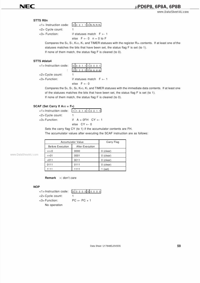
7/17/2019 INFRARED REMOTE CONTROL TRANSMISSION
http://slidepdf.com/reader/full/infrared-remote-control-transmission 59/95
59
µ PD6P8, 6P8A, 6P8B
Data Sheet U17848EJ3V0DS
STTS R0n
<1> Instruction code: 0 0 0 1 1 0 R3 R2 R1R0
<2> Cycle count: 1
<3> Function: if statuses match F ← 1
else F ← 0 n = 0 to F
Compares the S0, S1, KI/O, KI, and TIMER statuses with the register R0n contents. If at least one of the
statuses matches the bits that have been set, the status flag F is set (to 1).
If none of them match, the status flag F is cleared (to 0).
STTS #data4
<1> Instruction code: 0 0 0 1 1 1 0 0 0 1
: 0 0 0 0 0 0 d3 d2 d1 d0
<2> Cycle count: 1
<3> Function: if statuses match F ← 1
else F ← 0
Compares the S0, S1, S2, KI/O, KI, and TIMER statuses with the immediate data contents. If at least one
of the statuses matches the bits that have been set, the status flag F is set (to 1).
If none of them match, the status flag F is cleared (to 0).
SCAF (Set Carry If ACC = FH)
<1> Instruction code: 1 1 0 1 0 1 0 0 1 1
<2> Cycle count: 1
<3> Function: if A = 0FH CY ← 1
else CY ← 0
Sets the carry flag CY (to 1) if the accumulator contents are FH.
The accumulator values after executing the SCAF instruction are as follows:
Accumulator Value Carry Flag
Before Execution After Execution×××0 0000 0 (clear)
××01 0001 0 (clear)
×011 0011 0 (clear)
0111 0111 0 (clear)
1111 1111 1 (set)
Remark ×: don’t care
NOP
<1> Instruction code: 0 0 0 0 0 0 0 0 0 0
<2> Cycle count: 1<3> Function: PC ← PC + 1
No operation
7/17/2019 INFRARED REMOTE CONTROL TRANSMISSION
http://slidepdf.com/reader/full/infrared-remote-control-transmission 60/95
60
µ PD6P8, 6P8A, 6P8B
Data Sheet U17848EJ3V0DS
11. ASSEMBLER RESERVED WORDS
11.1 Mask Option Directives
When creating a program in the µ PD6P8, 6P8A, 6P8B, it is necessary to use a mask option quasi-directive in
the assembler’s source program. To create a program for the µ PD6P8, 6P8A, or 6P8B, a mask option pseudo
instruction must be used in the assembler source program, but since the µ PD6P8, 6P8A, or 6P8B does not have
a mask option, describe NOUSECAP.
11.1.1 OPTION and ENDOP quasi-directives
The quasi-directives from the OPTION quasi-directive down to the ENDOP quasi-directive are called the mask
option definition block. The format of the mask option definition block is as follows:
Format
Symbol field Mnemonic field Operand field Comment field
[Label:] OPTION [; Comment]
:
:
ENDOP
11.1.2 Mask option definition quasi-directives
The quasi-directives that can be used in the mask option definition block are listed in Table 10-1.
The mask option definition can only be specified as follows. Be sure to specify the following quasi-directives.
Example
Symbol field Mnemonic field Operand field Comment field
OPTION
NOUSECAP ; Capacitor for oscillation
ENDOP ; not incorporated
Table 11-1. Mask Option Definition Directives
Name Mask Option Definition Quasi-Directive PRO File
Address Value Data Value
CAP NOUSECAP 2043H 00
(Capacitor for oscillation not incorporated)
7/17/2019 INFRARED REMOTE CONTROL TRANSMISSION
http://slidepdf.com/reader/full/infrared-remote-control-transmission 61/95
61
µ PD6P8, 6P8A, 6P8B
Data Sheet U17848EJ3V0DS
12.WRITING AND VERIFYING ONE-TIME PROM (PROGRAM MEMORY) (µ PD6P8)
The program memory of the µ PD6P8 is a one-time PROM of 2026 × 10 bits.
To write or verify this one-time PROM, the pins shown in Table 5-1 are used. Note that no address input pin
is used. Instead, the address is updated by using the clock input from the CLK pin.
Table 12-1. Pins Used to Write/Verify Program Memory
Pin Name Function
VPP Supplies voltage when writing/verifying program memory.
Apply +10.5 V to this pin.
VDD Power supply.
Supply +3 V to this pin when writing/verifying program memory.
CLK Inputs clock to update address when writing/verifying program memory.
By inputting a pulse four times to the CLK pin, the address of the program memory is updated.
MD0 to MD3 Input to select the operation mode when writing/verifying program memory.
D0 to D7 Inputs/outputs 8-bit data when writing/verifying program memory.
XIN, XOUT Clock necessary for writing program memory. Connect a 4 MHz ceramic resonator to this pin.
12.1 Operating Mode When Writing/Verifying Program Memory
The µ PD6P8 is set in the program memory write/verify mode when +10.5 V is applied to the V PP pin after the
µ PD6P8 has been in the reset status (VDD = 3 V, VPP = 0 V) for a specific time. In this mode, the operating modes
shown in Table 5-2 can be set by setting the MD0 through MD3 pins. Connect all the pins other than those shown
in Table 5-1 to GND via pull-down resistors.
Table 12-2. Setting Operating Mode
Setting of Operating Mode Operating Mode
VPP VDD MD0 MD1 MD2 MD3
+10.5 V +3 V H L H L Clear program memory address to 0
L H H H Write mode
L L H H Verify mode
H × H H Program inhibit mode
×: don’t care (L or H)
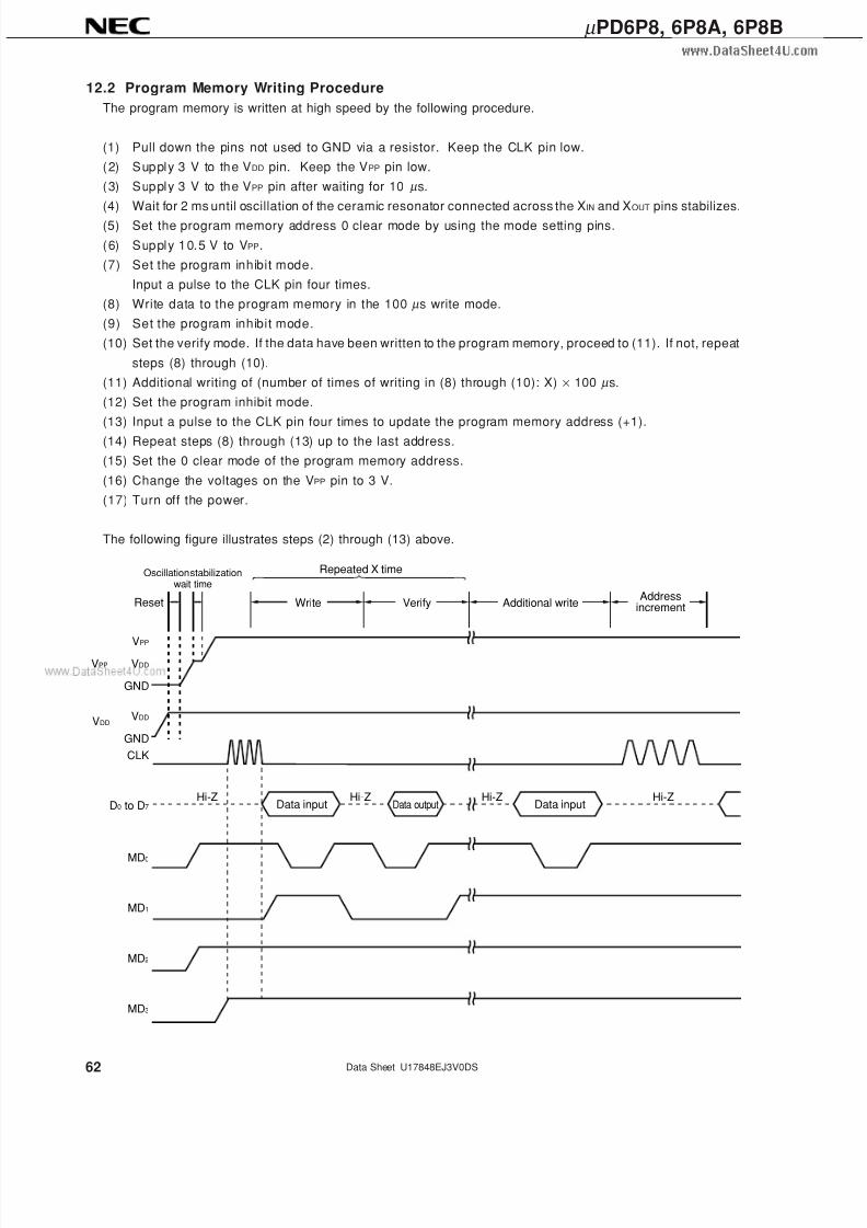
7/17/2019 INFRARED REMOTE CONTROL TRANSMISSION
http://slidepdf.com/reader/full/infrared-remote-control-transmission 62/95
62
µ PD6P8, 6P8A, 6P8B
Data Sheet U17848EJ3V0DS
12.2 Program Memory Writing Procedure
The program memory is written at high speed by the following procedure.
(1) Pull down the pins not used to GND via a resistor. Keep the CLK pin low.
(2) Supply 3 V to the VDD pin. Keep the VPP pin low.
(3) Supply 3 V to the VPP pin after waiting for 10 µ s.
(4) Wait for 2 ms until oscillation of the ceramic resonator connected across the XIN and XOUT pins stabilizes.
(5) Set the program memory address 0 clear mode by using the mode setting pins.
(6) Supply 10.5 V to VPP.
(7) Set the program inhibit mode.
Input a pulse to the CLK pin four times.
(8) Write data to the program memory in the 100 µ s write mode.
(9) Set the program inhibit mode.
(10) Set the verify mode. If the data have been written to the program memory, proceed to (11). If not, repeat
steps (8) through (10).
(11) Additional writing of (number of times of writing in (8) through (10): X) × 100 µ s.
(12) Set the program inhibit mode.
(13) Input a pulse to the CLK pin four times to update the program memory address (+1).(14) Repeat steps (8) through (13) up to the last address.
(15) Set the 0 clear mode of the program memory address.
(16) Change the voltages on the VPP pin to 3 V.
(17) Turn off the power.
The following figure illustrates steps (2) through (13) above.
VPP
VDD
GND
VDD
GND
CLK
VPP
D0 to D7
MD0
MD1
MD2
MD3
VDD
Repeated X time
Reset
Oscillation stabilizationwait time
Write Verify Additional writeAddress
increment
Data inputHi-Z Hi-Z Hi-Z
Data output Data inputHi-Z
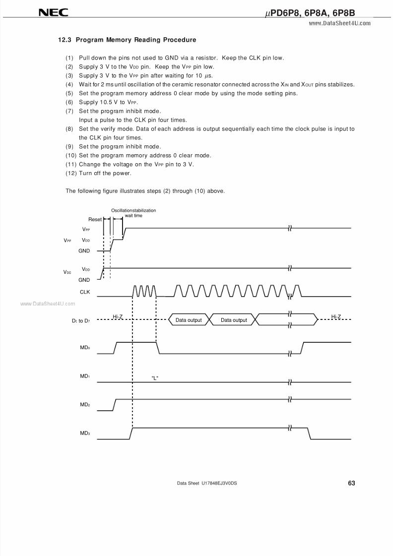
7/17/2019 INFRARED REMOTE CONTROL TRANSMISSION
http://slidepdf.com/reader/full/infrared-remote-control-transmission 63/95
63
µ PD6P8, 6P8A, 6P8B
Data Sheet U17848EJ3V0DS
12.3 Program Memory Reading Procedure
(1) Pull down the pins not used to GND via a resistor. Keep the CLK pin low.
(2) Supply 3 V to the VDD pin. Keep the VPP pin low.
(3) Supply 3 V to the VPP pin after waiting for 10 µ s.
(4) Wait for 2 ms until oscillation of the ceramic resonator connected across the XIN and XOUT pins stabilizes.
(5) Set the program memory address 0 clear mode by using the mode setting pins.
(6) Supply 10.5 V to VPP.
(7) Set the program inhibit mode.
Input a pulse to the CLK pin four times.
(8) Set the verify mode. Data of each address is output sequentially each time the clock pulse is input to
the CLK pin four times.
(9) Set the program inhibit mode.
(10) Set the program memory address 0 clear mode.
(11) Change the voltage on the VPP pin to 3 V.
(12) Turn off the power.
The following figure illustrates steps (2) through (10) above.
VPP
VDD
GND
VDD
GND
CLK
VPP
VDD
D0 to D7
MD0
MD1
MD2
MD3
Reset
Oscillation stabilizationwait time
Hi-Z Hi-ZData output Data output
"L"
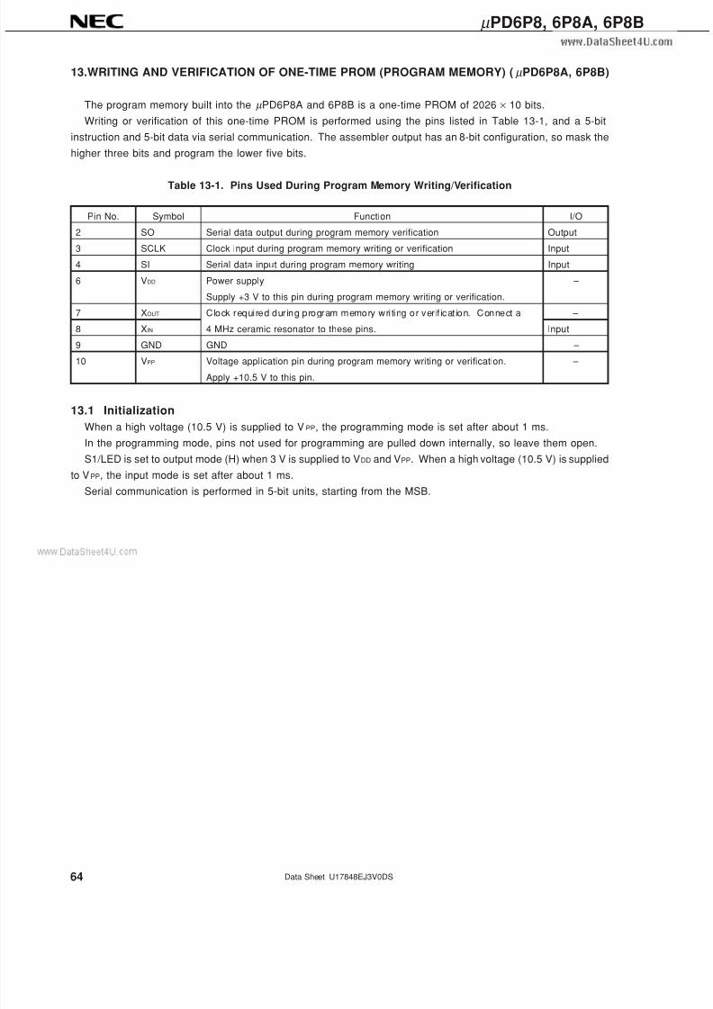
7/17/2019 INFRARED REMOTE CONTROL TRANSMISSION
http://slidepdf.com/reader/full/infrared-remote-control-transmission 64/95
64
µ PD6P8, 6P8A, 6P8B
Data Sheet U17848EJ3V0DS
13.WRITING AND VERIFICATION OF ONE-TIME PROM (PROGRAM MEMORY) (µ PD6P8A, 6P8B)
The program memory built into the µ PD6P8A and 6P8B is a one-time PROM of 2026 × 10 bits.
Writing or verification of this one-time PROM is performed using the pins listed in Table 13-1, and a 5-bit
instruction and 5-bit data via serial communication. The assembler output has an 8-bit configuration, so mask the
higher three bits and program the lower five bits.
Table 13-1. Pins Used During Program Memory Writing/Verification
Pin No. Symbol Function I/O
2 SO Serial data output during program memory verification Output
3 SCLK Clock input during program memory writing or verification Input
4 SI Serial data input during program memory writing Input
6 VDD Power supply –
Supply +3 V to this pin during program memory writing or verification.
7 XOUT Clock required dur ing program memory wri ting or ver if icat ion. Connect a –
8 XIN 4 MHz ceramic resonator to these pins. Input
9 GND GND –
10 VPP Voltage application pin during program memory writing or verification. –
Apply +10.5 V to this pin.
13.1 Initialization
When a high voltage (10.5 V) is supplied to VPP, the programming mode is set after about 1 ms.
In the programming mode, pins not used for programming are pulled down internally, so leave them open.
S1/LED is set to output mode (H) when 3 V is supplied to VDD and VPP. When a high voltage (10.5 V) is supplied
to VPP, the input mode is set after about 1 ms.
Serial communication is performed in 5-bit units, starting from the MSB.
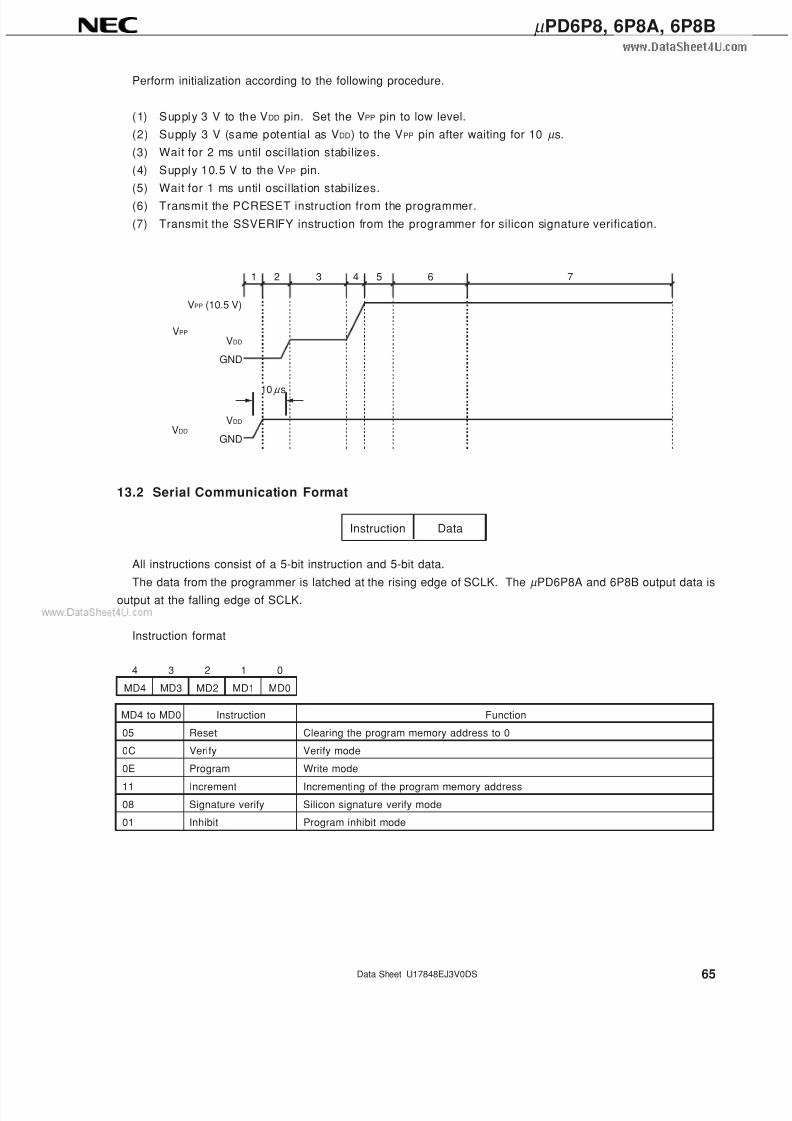
7/17/2019 INFRARED REMOTE CONTROL TRANSMISSION
http://slidepdf.com/reader/full/infrared-remote-control-transmission 65/95
65
µ PD6P8, 6P8A, 6P8B
Data Sheet U17848EJ3V0DS
Perform initialization according to the following procedure.
(1) Supply 3 V to the VDD pin. Set the VPP pin to low level.
(2) Supply 3 V (same potential as VDD) to the VPP pin after waiting for 10 µ s.
(3) Wait for 2 ms until oscillation stabilizes.
(4) Supply 10.5 V to the VPP pin.
(5) Wait for 1 ms until oscillation stabilizes.
(6) Transmit the PCRESET instruction from the programmer.
(7) Transmit the SSVERIFY instruction from the programmer for silicon signature verification.
1
VPP (10.5 V)
VDD
VPP
VDD
GND
VDD
GND
2 3 4 5 6 7
10 s µ
13.2 Serial Communication Format
Instruction Data
All instructions consist of a 5-bit instruction and 5-bit data.
The data from the programmer is latched at the rising edge of SCLK. The µ PD6P8A and 6P8B output data isoutput at the falling edge of SCLK.
Instruction format
4 3 2 1 0
MD4 MD3 MD2 MD1 MD0
MD4 to MD0 Instruction Function
05 Reset Clearing the program memory address to 0
0C Verify Verify mode
0E Program Write mode
11 Increment Incrementing of the program memory address
08 Signature verify Silicon signature verify mode
01 Inhibit Program inhibit mode
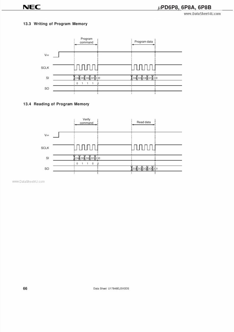
7/17/2019 INFRARED REMOTE CONTROL TRANSMISSION
http://slidepdf.com/reader/full/infrared-remote-control-transmission 66/95
66
µ PD6P8, 6P8A, 6P8B
Data Sheet U17848EJ3V0DS
13.3 Writing of Program Memory
CI4
VPP
SCLK
SI
Programcommand Program data
SO
CI3 CI2 CI1
0 1 1 1
CI4 CI3 CI2 CI1CI0
0
CI0
13.4 Reading of Program Memory
CI4
VPP
SCLK
SI
SO
CI3 CI2 CI1
0 1 1 0
DO4 DO3 DO2 DO1
CI0
0
DO1
Verifycommand Read data
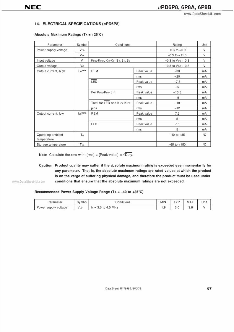
7/17/2019 INFRARED REMOTE CONTROL TRANSMISSION
http://slidepdf.com/reader/full/infrared-remote-control-transmission 67/95
67
µ PD6P8, 6P8A, 6P8B
Data Sheet U17848EJ3V0DS
14. ELECTRICAL SPECIFICATIONS (µ PD6P8)
Absolute Maximum Ratings (TA = +25°C)
Parameter Symbol Conditions Rating Unit
Power supply voltage VDD –0.3 to +5.0 V
VPP –0.3 to +11.0 V
Input voltage VI KI/O0-KI/O7, K I0-KI3, S0, S1, S2 –0.3 to VDD + 0.3 V
Output voltage VO –0.3 to VDD + 0.3 V
Output current, high IOHNote REM Peak value –30 mA
rms –20 mA
LED Peak value –7.5 mA
rms –5 mA
Per KI/O0-KI/O7 pin Peak value –13.5 mA
rms –9 mA
Total for LED and K I/O0-KI/O7 Peak value –18 mA
pins rms –12 mA
Output current, low IOLNote REM Peak value 7.5 mA
rms 5 mA
LED Peak value 7.5 mA
rms 5 mA
Operating ambient TA –40 to +85 °C
temperature
Storage temperature Tstg –65 to +150 °C
Note Calculate the rms with: [rms] = [Peak value] × √Duty.
Caution Product quality may suffer if the absolute maximum rating is exceeded even momentarily for
any parameter. That is, the absolute maximum ratings are rated values at which the product
is on the verge of suffering physical damage, and therefore the product must be used under
conditions that ensure that the absolute maximum ratings are not exceeded.
Recommended Power Supply Voltage Range (TA = –40 to +85°C)
Parameter Symbol Conditions MIN. TYP. MAX. Unit
Power supply voltage VDD fX = 3.5 to 4.5 MHz 1.9 3.0 3.6 V
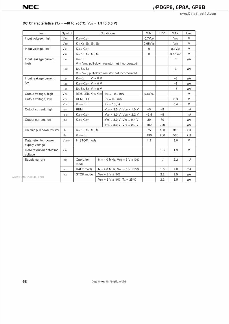
7/17/2019 INFRARED REMOTE CONTROL TRANSMISSION
http://slidepdf.com/reader/full/infrared-remote-control-transmission 68/95
68
µ PD6P8, 6P8A, 6P8B
Data Sheet U17848EJ3V0DS
DC Characteristics (TA = –40 to +85°C, VDD = 1.9 to 3.6 V)
Item Symbol Conditions MIN. TYP. MAX. Unit
Input voltage, high VIH1 KI/O0-KI/O7 0.7VDD VDD V
VIH2 KI0-KI3, S0, S1, S2 0.65VDD VDD V
Input voltage, low VIL1 KI/O0-KI/O7 0 0.3VDD V
VIL2 KI0-KI3, S0, S1, S2 0 0.15VDD V
Input leakage current, ILIH1 KI0-KI3 3 µ A
high VI = VDD, pull-down resistor not incorporated
ILIH2 S0, S1, S2 3 µ A
VI = VDD, pull-down resistor not incorporated
Input leakage current, ILIL1 KI0-KI3 VI = 0 V –3 µ A
low ILIL2 KI/O0-KI/O7 VI = 0 V –3 µ A
ILIL3 S0, S1, S2 VI = 0 V –3 µ A
Output voltage, high VOH1 REM, LED, KI/O0-KI/O7 IOH = –0.3 mA 0.8VDD V
Output voltage, low VOL1 REM, LED IOL = 0.3 mA 0.3 V
VOL2 KI/O0-KI/O7 IOL = 15 µ A 0.4 V
Output current, high IOH1 REM VDD = 3.0 V, VOH = 1.0 V –5 –9 mA
IOH2 KI/O0-KI/O7 VDD = 3.0 V, VOH = 2.2 V –2.5 –5 mA
Output current, low IOL1 KI/O0-KI/O7 VDD = 3.0 V, VOL = 0.4 V 30 70 µ A
VDD = 3.0 V, VOL = 2.2 V 100 220 µ A
On-chip pull-down resistor R1 KI0-KI3, S0, S1, S2 75 150 300 kΩ
R2 KI/O0-KI/O7 130 250 500 kΩ
Data retention power VDDOR In STOP mode 1.2 3.6 V
supply voltage
RAM retention detection VID 1.8 1.9 V
voltage
Supply current IDD1 Operation fX = 4.0 MHz, VDD = 3 V ±10% 1.1 2.2 mA
mode
IDD2 HALT mode fX = 4.0 MHz, VDD = 3 V ±10% 1.0 2.0 mA
IDD3 STOP mode VDD = 3 V ±10% 2.2 9.5 µ A
VDD = 3 V ±10%, TA = 25°C 2.2 3.5 µ A
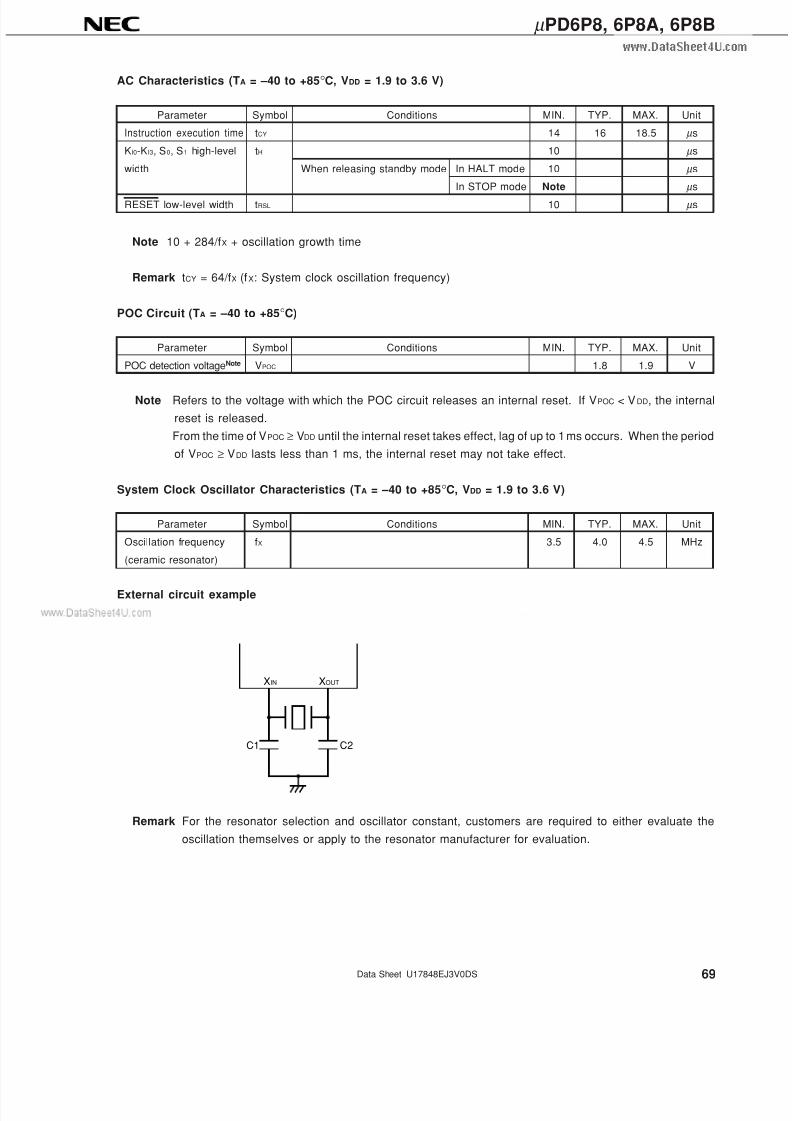
7/17/2019 INFRARED REMOTE CONTROL TRANSMISSION
http://slidepdf.com/reader/full/infrared-remote-control-transmission 69/95
69
µ PD6P8, 6P8A, 6P8B
Data Sheet U17848EJ3V0DS
Remark For the resonator selection and oscillator constant, customers are required to either evaluate the
oscillation themselves or apply to the resonator manufacturer for evaluation.
XIN XOUT
C1 C2
AC Characteristics (TA = –40 to +85°C, VDD = 1.9 to 3.6 V)
Parameter Symbol Conditions MIN. TYP. MAX. Unit
Instruction execution time tCY 14 16 18.5 µ s
KI0-KI3, S0, S1 high-level tH 10 µ s
width When releasing standby mode In HALT mode 10 µ s
In STOP mode Note µ s
RESET low-level width tRSL 10 µ s
Note 10 + 284/fX + oscillation growth time
Remark tCY = 64/fX (fX: System clock oscillation frequency)
POC Circuit (TA = –40 to +85°C)
Parameter Symbol Conditions MIN. TYP. MAX. Unit
POC detection voltageNote VPOC 1.8 1.9 V
Note Refers to the voltage with which the POC circuit releases an internal reset. If VPOC < VDD, the internal
reset is released.
From the time of VPOC ≥ VDD until the internal reset takes effect, lag of up to 1 ms occurs. When the period
of VPOC ≥ VDD lasts less than 1 ms, the internal reset may not take effect.
System Clock Oscillator Characteristics (TA = –40 to +85°C, VDD = 1.9 to 3.6 V)
Parameter Symbol Conditions MIN. TYP. MAX. Unit
Oscillation frequency fX 3.5 4.0 4.5 MHz
(ceramic resonator)
External circuit example
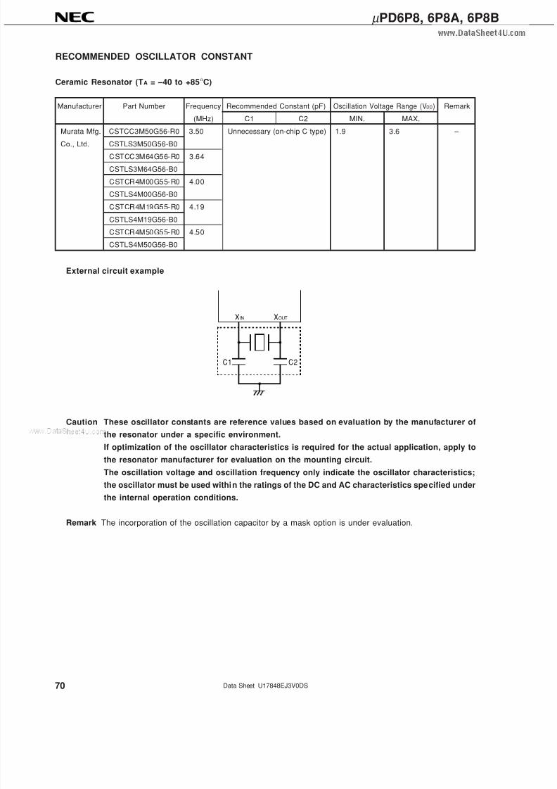
7/17/2019 INFRARED REMOTE CONTROL TRANSMISSION
http://slidepdf.com/reader/full/infrared-remote-control-transmission 70/95
70
µ PD6P8, 6P8A, 6P8B
Data Sheet U17848EJ3V0DS
RECOMMENDED OSCILLATOR CONSTANT
Ceramic Resonator (TA = –40 to +85°C)
Manufacturer Part Number Frequency Recommended Constant (pF) Oscillation Voltage Range (VDD) Remark
(MHz) C1 C2 MIN. MAX.
Murata Mfg. CSTCC3M50G56-R0 3.50 Unnecessary (on-chip C type) 1.9 3.6 –
Co., Ltd. CSTLS3M50G56-B0
CSTCC3M64G56-R0 3.64
CSTLS3M64G56-B0
CSTCR4M00G55-R0 4.00
CSTLS4M00G56-B0
CSTCR4M19G55-R0 4.19
CSTLS4M19G56-B0
CSTCR4M50G55-R0 4.50
CSTLS4M50G56-B0
External circuit example
Caution These oscillator constants are reference values based on evaluation by the manufacturer of
the resonator under a specific environment.
If optimization of the oscillator characteristics is required for the actual application, apply to
the resonator manufacturer for evaluation on the mounting circuit.
The oscillation voltage and oscillation frequency only indicate the oscillator characteristics;
the oscillator must be used within the ratings of the DC and AC characteristics specified under
the internal operation conditions.
Remark The incorporation of the oscillation capacitor by a mask option is under evaluation.
XIN XOUT
C1 C2
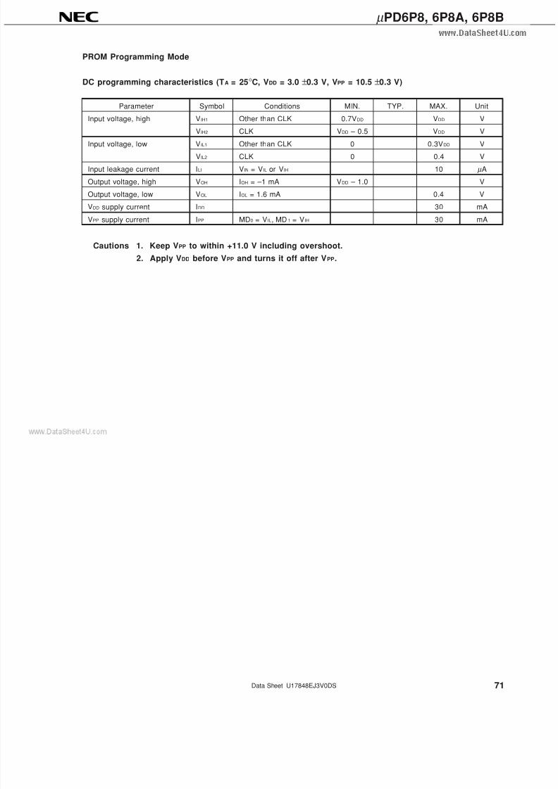
7/17/2019 INFRARED REMOTE CONTROL TRANSMISSION
http://slidepdf.com/reader/full/infrared-remote-control-transmission 71/95
71
µ PD6P8, 6P8A, 6P8B
Data Sheet U17848EJ3V0DS
PROM Programming Mode
DC programming characteristics (TA = 25°C, VDD = 3.0 ±0.3 V, VPP = 10.5 ±0.3 V)
Parameter Symbol Conditions MIN. TYP. MAX. Unit
Input voltage, high VIH1 Other than CLK 0.7VDD VDD V
VIH2 CLK VDD – 0.5 VDD V
Input voltage, low VIL1 Other than CLK 0 0.3VDD V
VIL2 CLK 0 0.4 V
Input leakage current ILI VIN = VIL or VIH 10 µ A
Output voltage, high VOH IOH = –1 mA VDD – 1.0 V
Output voltage, low VOL IOL = 1.6 mA 0.4 V
VDD supply current IDD 30 mA
VPP supply current IPP MD0 = VIL, MD1 = VIH 30 mA
Cautions 1. Keep VPP to within +11.0 V including overshoot.
2. Apply VDD before VPP and turns it off after VPP.
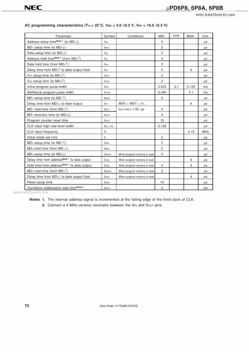
7/17/2019 INFRARED REMOTE CONTROL TRANSMISSION
http://slidepdf.com/reader/full/infrared-remote-control-transmission 72/95
72
µ PD6P8, 6P8A, 6P8B
Data Sheet U17848EJ3V0DS
AC programming characteristics (TA = 25°C, VDD = 3.0 ±0.3 V, VPP = 10.5 ±0.3 V)
Parameter Symbol Conditions MIN. TYP. MAX. Unit
Address setup timeNote 1 (to MD0↓) tAS 2 µ s
MD1 setup time (to MD0↓) tM1S 2 µ s
Data setup time (to MD0↓) tDS 2 µ s
Address hold timeNote 1 (from MD0↑) tAH 2 µ s
Data hold time (from MD0↑) tDH 2 µ s
Delay time from MD0↑ to data output float tDF 0 4 µ s
VPP setup time (to MD3↑) tVPS 2 µ s
VDD setup time (to MD3↑) tVDS 2 µ s
Initial program pulse width tPW 0.095 0.1 0.105 ms
Additional program pulse width tOPW 0.095 2.1 ms
MD0 setup time (to MD1↑) tMOS 2 µ s
Delay time from MD0↓ to data output tDV MD0 = MD1 = VIL 4 µ s
MD1 hold time (from MD0↑) tM1H tM1H+tM1R ≥ 50 µ s 2 µ s
MD1 recovery time (to MD0↓) tM1R 2 µ s
Program counter reset time tPCR 10 µ s
CLK input high-/low-level width tXH, tXL 0.125 µ s
CLK input frequency fX 4.19 MHz
Initial mode set time tI 2 µ s
MD3 setup time (to MD1↑) tM3S 2 µ s
MD3 hold time (from MD1↓) tM3H 2 µ s
MD3 setup time (to MD0↓) tM3SR When program memory is read 2 µ s
Delay time from addressNote 1 to data output tOAD When program memory is read 4 µ s
Hold time from addressNote 1 to data output tHAD When program memory is read 0 4 µ s
MD3 hold time (from MD0↑) tM3HR When program memory is read 2 µ s
Delay time from MD3↓ to data output float tDFR When program memory is read 4 µ s
Reset setup time tRES
10 µ sOscillation stabilization wait timeNote 2 tWAIT 2 ms
Notes 1. The internal address signal is incremented at the falling edge of the third clock of CLK.
2. Connect a 4 MHz ceramic resonator between the XIN and XOUT pins.
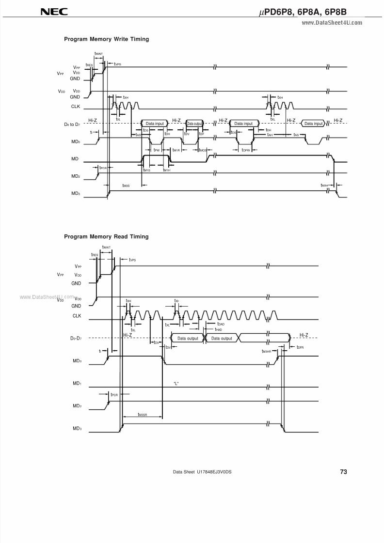
7/17/2019 INFRARED REMOTE CONTROL TRANSMISSION
http://slidepdf.com/reader/full/infrared-remote-control-transmission 73/95
73
µ PD6P8, 6P8A, 6P8B
Data Sheet U17848EJ3V0DS
tM3SR
tPCR
tDV
tDV
tI
tXL tDAD
tHAD
tVPS
tXH
tXL
tXH
tM3HR
tDFR
VPP
VPP VDD
GND
VDDVDD
GND
CLK
D0-D7
MD0
MD1
MD2
MD3
tRES
Hi-Z Hi-Z
tWAIT
Data output
"L"
Data output
tRES tVPS
tXH
tXL
tAS
tXH
tXL
tAS tAH
tDHtDS
tOPW
tDFtDV
tMOStM1R
tDH
tDS
tPW
tI
tM3H
tM1HtM1StPCR
tM3S
Hi-Z Hi-Z Hi-Z Hi-Z Hi-Z
tWAIT
VPP
VDD
GND
VDD
GND
CLK
VPP
D0 to D7
MD0
MD1
MD2
MD3
VDD
Data input Data output Data input Data input
Program Memory Read Timing
Program Memory Write Timing
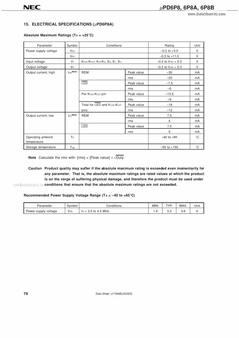
7/17/2019 INFRARED REMOTE CONTROL TRANSMISSION
http://slidepdf.com/reader/full/infrared-remote-control-transmission 74/95
74
µ PD6P8, 6P8A, 6P8B
Data Sheet U17848EJ3V0DS
15. ELECTRICAL SPECIFICATIONS (µ PD6P8A)
Absolute Maximum Ratings (TA = +25°C)
Parameter Symbol Conditions Rating Unit
Power supply voltage VDD –0.3 to +5.0 V
VPP –0.3 to +11.0 V
Input voltage VI KI/O0-KI/O7, K I0-KI3, S0, S1, S2 –0.3 to VDD + 0.3 V
Output voltage VO –0.3 to VDD + 0.3 V
Output current, high IOHNote REM Peak value –30 mA
rms –20 mA
LED Peak value –7.5 mA
rms –5 mA
Per KI/O0-KI/O7 pin Peak value –13.5 mA
rms –9 mA
Total for LED and K I/O0-KI/O7 Peak value –18 mA
pins rms –12 mA
Output current, low IOLNote REM Peak value 7.5 mA
rms 5 mA
LED Peak value 7.5 mA
rms 5 mA
Operating ambient TA –40 to +85 °C
temperature
Storage temperature Tstg –65 to +150 °C
Note Calculate the rms with: [rms] = [Peak value] × √Duty.
Caution Product quality may suffer if the absolute maximum rating is exceeded even momentarily for
any parameter. That is, the absolute maximum ratings are rated values at which the product
is on the verge of suffering physical damage, and therefore the product must be used under
conditions that ensure that the absolute maximum ratings are not exceeded.
Recommended Power Supply Voltage Range (TA = –40 to +85°C)
Parameter Symbol Conditions MIN. TYP. MAX. Unit
Power supply voltage VDD fX = 3.5 to 4.5 MHz 1.9 3.0 3.6 V
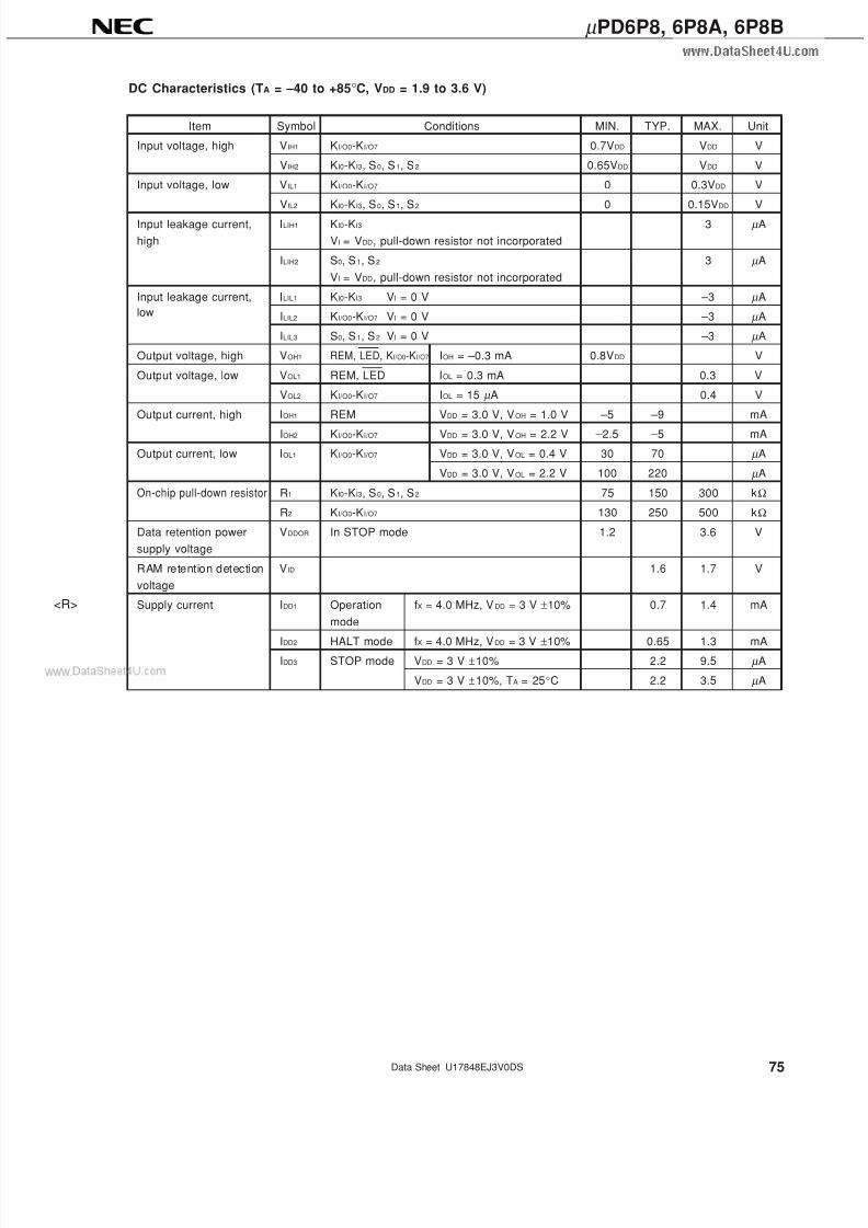
7/17/2019 INFRARED REMOTE CONTROL TRANSMISSION
http://slidepdf.com/reader/full/infrared-remote-control-transmission 75/95
75
µ PD6P8, 6P8A, 6P8B
Data Sheet U17848EJ3V0DS
DC Characteristics (TA = –40 to +85°C, VDD = 1.9 to 3.6 V)
Item Symbol Conditions MIN. TYP. MAX. Unit
Input voltage, high VIH1 KI/O0-KI/O7 0.7VDD VDD V
VIH2 KI0-KI3, S0, S1, S2 0.65VDD VDD V
Input voltage, low VIL1 KI/O0-KI/O7 0 0.3VDD V
VIL2 KI0-KI3, S0, S1, S2 0 0.15VDD V
Input leakage current, ILIH1 KI0-KI3 3 µ A
high VI = VDD, pull-down resistor not incorporated
ILIH2 S0, S1, S2 3 µ A
VI = VDD, pull-down resistor not incorporated
Input leakage current, ILIL1 KI0-KI3 VI = 0 V –3 µ A
low ILIL2 KI/O0-KI/O7 VI = 0 V –3 µ A
ILIL3 S0, S1, S2 VI = 0 V –3 µ A
Output voltage, high VOH1 REM, LED, KI/O0-KI/O7 IOH = –0.3 mA 0.8VDD V
Output voltage, low VOL1 REM, LED IOL = 0.3 mA 0.3 V
VOL2 KI/O0-KI/O7 IOL = 15 µ A 0.4 V
Output current, high IOH1 REM VDD = 3.0 V, VOH = 1.0 V –5 –9 mA
IOH2 KI/O0-KI/O7 VDD = 3.0 V, VOH = 2.2 V –2.5 –5 mA
Output current, low IOL1 KI/O0-KI/O7 VDD = 3.0 V, VOL = 0.4 V 30 70 µ A
VDD = 3.0 V, VOL = 2.2 V 100 220 µ A
On-chip pull-down resistor R1 KI0-KI3, S0, S1, S2 75 150 300 kΩ
R2 KI/O0-KI/O7 130 250 500 kΩ
Data retention power VDDOR In STOP mode 1.2 3.6 V
supply voltage
RAM retention detection VID 1.6 1.7 V
voltage
Supply current IDD1 Operation fX = 4.0 MHz, VDD = 3 V ±10% 0.7 1.4 mA
mode
IDD2 HALT mode fX = 4.0 MHz, VDD = 3 V ±10% 0.65 1.3 mA
IDD3 STOP mode VDD = 3 V ±10% 2.2 9.5 µ A
VDD = 3 V ±10%, TA = 25°C 2.2 3.5 µ A
<R>
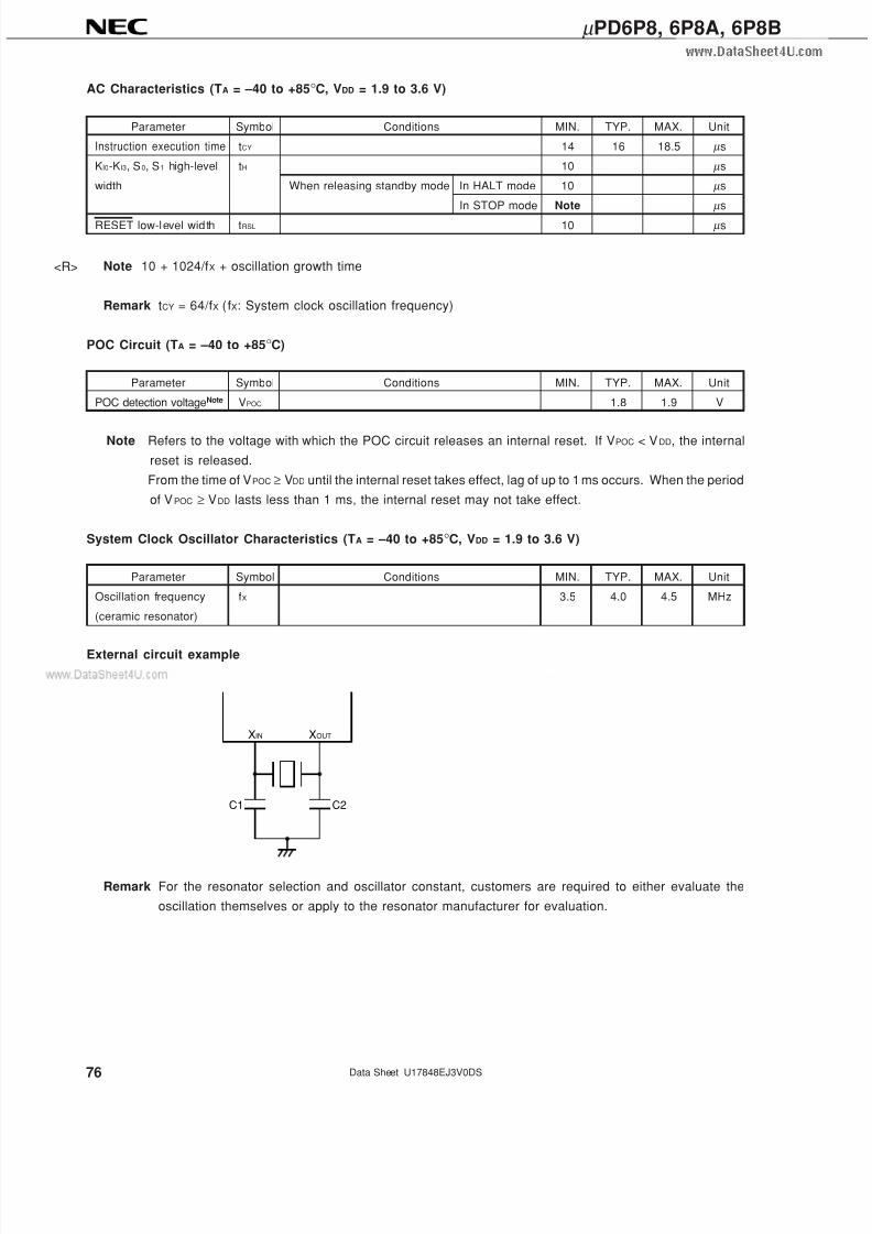
7/17/2019 INFRARED REMOTE CONTROL TRANSMISSION
http://slidepdf.com/reader/full/infrared-remote-control-transmission 76/95
76
µ PD6P8, 6P8A, 6P8B
Data Sheet U17848EJ3V0DS
Remark For the resonator selection and oscillator constant, customers are required to either evaluate the
oscillation themselves or apply to the resonator manufacturer for evaluation.
XIN XOUT
C1 C2
AC Characteristics (TA = –40 to +85°C, VDD = 1.9 to 3.6 V)
Parameter Symbol Conditions MIN. TYP. MAX. Unit
Instruction execution time tCY 14 16 18.5 µ s
KI0-KI3, S0, S1 high-level tH 10 µ s
width When releasing standby mode In HALT mode 10 µ s
In STOP mode Note µ s
RESET low-level wid th tRSL 10 µ s
Note 10 + 1024/fX + oscillation growth time
Remark tCY = 64/fX (fX: System clock oscillation frequency)
POC Circuit (TA = –40 to +85°C)
Parameter Symbol Conditions MIN. TYP. MAX. Unit
POC detection voltageNote VPOC 1.8 1.9 V
Note Refers to the voltage with which the POC circuit releases an internal reset. If VPOC < VDD, the internal
reset is released.
From the time of VPOC ≥ VDD until the internal reset takes effect, lag of up to 1 ms occurs. When the period
of VPOC ≥ VDD lasts less than 1 ms, the internal reset may not take effect.
System Clock Oscillator Characteristics (TA = –40 to +85°C, VDD = 1.9 to 3.6 V)
Parameter Symbol Conditions MIN. TYP. MAX. Unit
Oscillation frequency fX 3.5 4.0 4.5 MHz
(ceramic resonator)
External circuit example
<R>
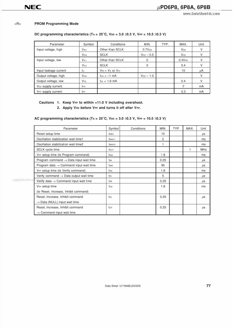
7/17/2019 INFRARED REMOTE CONTROL TRANSMISSION
http://slidepdf.com/reader/full/infrared-remote-control-transmission 77/95
77
µ PD6P8, 6P8A, 6P8B
Data Sheet U17848EJ3V0DS
PROM Programming Mode
DC programming characteristics (TA = 25°C, VDD = 3.0 ±0.3 V, VPP = 10.5 ±0.3 V)
Parameter Symbol Conditions MIN. TYP. MAX. Unit
Input voltage, high VIH1 Other than SCLK 0.7VDD VDD V
VIH2 SCLK VDD – 0.5 VDD V
Input voltage, low VIL1 Other than SCLK 0 0.3VDD V
VIL2 SCLK 0 0.4 V
Input leakage current ILI VIN = VIL or VIH 10 µ A
Output voltage, high VOH IOH = –1 mA VDD – 1.0 V
Output voltage, low VOL IOL = 1.6 mA 0.4 V
VDD supply current IDD 2 mA
VPP supply current IPP 0.3 mA
Cautions 1. Keep VPP to within +11.0 V including overshoot.
2. Apply VDD before VPP and turns it off after VPP.
AC programming characteristics (TA = 25°C, VDD = 3.0 ±0.3 V, VPP = 10.5 ±0.3 V)
Parameter Symbol Conditions MIN. TYP. MAX. Unit
Reset setup time tRES 10 µ s
Oscillation stabilization wait time1 tWAIT1 2 ms
Oscillation stabilization wait time2 tWAIT2 1 ms
SCLK cycle time tKCY 1 MHz
VPP setup time (to Program command) tWA 1.8 ms
Program command → Data input wait time tWI 0.25 µ s
Program data → Command input wait time tWR 90 µ s
VPP setup time (to Verify command) tRA 1.8 msVerify command → Data output wait time tRI 5 µ s
Verify data → Command input wait time tRE 0.25 µ s
VPP setup time tOA 1.8 ms
(to Reset, Increase, Inhibit command)
Reset, Increase, Inhibit command tOI 0.25 µ s
→ Data (NULL) input wait time
Reset, Increase, Inhibit command tOT 0.25 µ s
→ Command input wait time
<R>
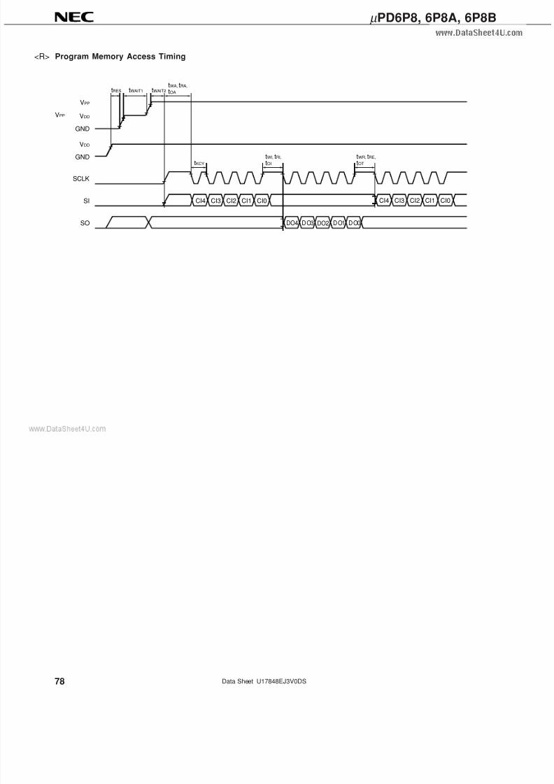
7/17/2019 INFRARED REMOTE CONTROL TRANSMISSION
http://slidepdf.com/reader/full/infrared-remote-control-transmission 78/95
78
µ PD6P8, 6P8A, 6P8B
Data Sheet U17848EJ3V0DS
Program Memory Access Timing
SCLK
SI
SO
VPP
GND
VDD
GND
VDD
VPP
DO4 DO3 DO2 DO1 DO0
CI4 CI3 CI2 CI1 CI0
tRES tWAIT1 tWAIT2tWA, tRA,
tOA
tKCY
tWI, tRI,
tOI
tWR, tRE,
tOT
CI4 CI3 CI2 CI1 CI0
<R>
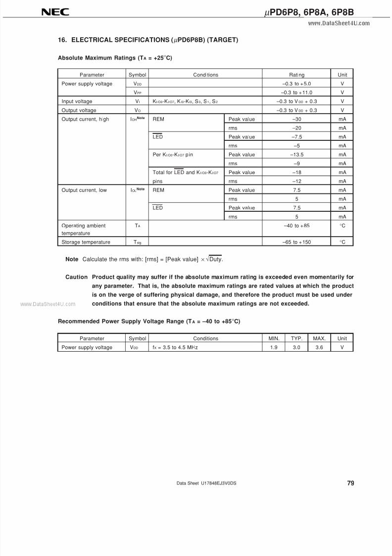
7/17/2019 INFRARED REMOTE CONTROL TRANSMISSION
http://slidepdf.com/reader/full/infrared-remote-control-transmission 79/95
79
µ PD6P8, 6P8A, 6P8B
Data Sheet U17848EJ3V0DS
16. ELECTRICAL SPECIFICATIONS (µ PD6P8B) (TARGET)
Absolute Maximum Ratings (TA = +25°C)
Parameter Symbol Conditions Rating Unit
Power supply voltage VDD –0.3 to +5.0 V
VPP –0.3 to +11.0 V
Input voltage VI KI/O0-KI/O7, K I0-KI3, S0, S1, S2 –0.3 to VDD + 0.3 V
Output voltage VO –0.3 to VDD + 0.3 V
Output current, high IOHNote REM Peak value –30 mA
rms –20 mA
LED Peak value –7.5 mA
rms –5 mA
Per KI/O0-KI/O7 pin Peak value –13.5 mA
rms –9 mA
Total for LED and K I/O0-KI/O7 Peak value –18 mA
pins rms –12 mA
Output current, low IOLNote REM Peak value 7.5 mA
rms 5 mA
LED Peak value 7.5 mA
rms 5 mA
Operating ambient TA –40 to +85 °C
temperature
Storage temperature Tstg –65 to +150 °C
Note Calculate the rms with: [rms] = [Peak value] × √Duty.
Caution Product quality may suffer if the absolute maximum rating is exceeded even momentarily for
any parameter. That is, the absolute maximum ratings are rated values at which the product
is on the verge of suffering physical damage, and therefore the product must be used under
conditions that ensure that the absolute maximum ratings are not exceeded.
Recommended Power Supply Voltage Range (TA = –40 to +85°C)
Parameter Symbol Conditions MIN. TYP. MAX. Unit
Power supply voltage VDD fX = 3.5 to 4.5 MHz 1.9 3.0 3.6 V
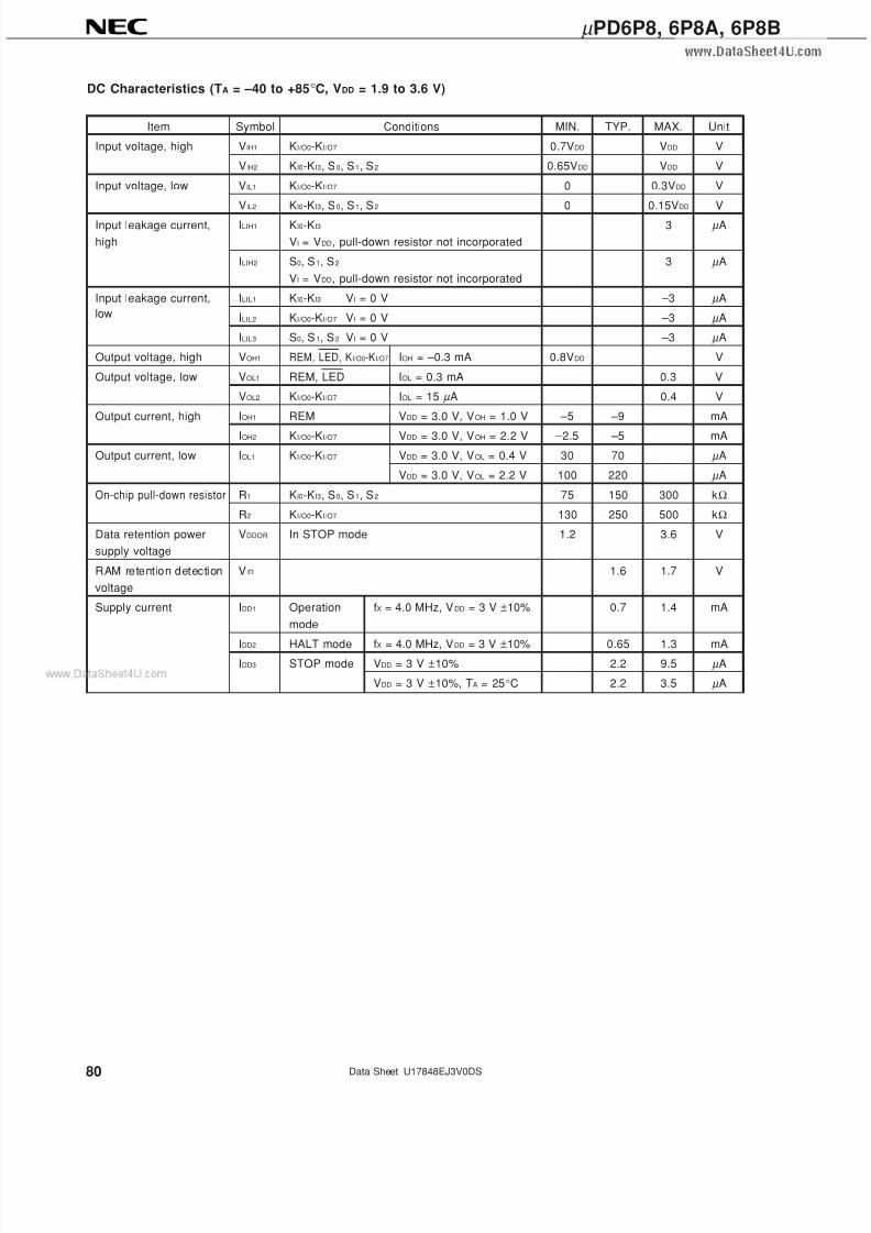
7/17/2019 INFRARED REMOTE CONTROL TRANSMISSION
http://slidepdf.com/reader/full/infrared-remote-control-transmission 80/95
80
µ PD6P8, 6P8A, 6P8B
Data Sheet U17848EJ3V0DS
DC Characteristics (TA = –40 to +85°C, VDD = 1.9 to 3.6 V)
Item Symbol Conditions MIN. TYP. MAX. Unit
Input voltage, high VIH1 KI/O0-KI/O7 0.7VDD VDD V
VIH2 KI0-KI3, S0, S1, S2 0.65VDD VDD V
Input voltage, low VIL1 KI/O0-KI/O7 0 0.3VDD V
VIL2 KI0-KI3, S0, S1, S2 0 0.15VDD V
Input leakage current, ILIH1 KI0-KI3 3 µ A
high VI = VDD, pull-down resistor not incorporated
ILIH2 S0, S1, S2 3 µ A
VI = VDD, pull-down resistor not incorporated
Input leakage current, ILIL1 KI0-KI3 VI = 0 V –3 µ A
low ILIL2 KI/O0-KI/O7 VI = 0 V –3 µ A
ILIL3 S0, S1, S2 VI = 0 V –3 µ A
Output voltage, high VOH1 REM, LED, KI/O0-KI/O7 IOH = –0.3 mA 0.8VDD V
Output voltage, low VOL1 REM, LED IOL = 0.3 mA 0.3 V
VOL2 KI/O0-KI/O7 IOL = 15 µ A 0.4 V
Output current, high IOH1 REM VDD = 3.0 V, VOH = 1.0 V –5 –9 mA
IOH2 KI/O0-KI/O7 VDD = 3.0 V, VOH = 2.2 V –2.5 –5 mA
Output current, low IOL1 KI/O0-KI/O7 VDD = 3.0 V, VOL = 0.4 V 30 70 µ A
VDD = 3.0 V, VOL = 2.2 V 100 220 µ A
On-chip pull-down resistor R1 KI0-KI3, S0, S1, S2 75 150 300 kΩ
R2 KI/O0-KI/O7 130 250 500 kΩ
Data retention power VDDOR In STOP mode 1.2 3.6 V
supply voltage
RAM retention detection VID 1.6 1.7 V
voltage
Supply current IDD1 Operation fX = 4.0 MHz, VDD = 3 V ±10% 0.7 1.4 mA
mode
IDD2 HALT mode fX = 4.0 MHz, VDD = 3 V ±10% 0.65 1.3 mA
IDD3 STOP mode VDD = 3 V ±10% 2.2 9.5 µ A
VDD = 3 V ±10%, TA = 25°C 2.2 3.5 µ A
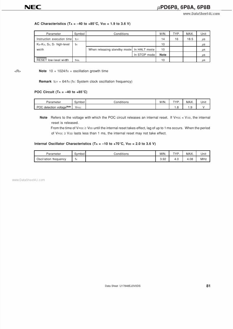
7/17/2019 INFRARED REMOTE CONTROL TRANSMISSION
http://slidepdf.com/reader/full/infrared-remote-control-transmission 81/95
81
µ PD6P8, 6P8A, 6P8B
Data Sheet U17848EJ3V0DS
AC Characteristics (TA = –40 to +85°C, VDD = 1.9 to 3.6 V)
Parameter Symbol Conditions MIN. TYP. MAX. Unit
Instruction execution time tCY 14 16 18.5 µ s
KI0-KI3, S0, S1 high-level tH 10 µ s
width When releasing standby mode In HALT mode 10 µ s
In STOP mode Note µ s
RESET low-level width tRSL 10 µ s
Note 10 + 1024/fX + oscillation growth time
Remark tCY = 64/fX (fX: System clock oscillation frequency)
POC Circuit (TA = –40 to +85°C)
Parameter Symbol Conditions MIN. TYP. MAX. Unit
POC detection voltageNote VPOC 1.8 1.9 V
Note Refers to the voltage with which the POC circuit releases an internal reset. If VPOC < VDD, the internal
reset is released.
From the time of VPOC ≥ VDD until the internal reset takes effect, lag of up to 1 ms occurs. When the period
of VPOC ≥ VDD lasts less than 1 ms, the internal reset may not take effect.
Internal Oscillator Characteristics (TA = –10 to +70°C, VDD = 2.0 to 3.6 V)
Parameter Symbol Conditions MIN. TYP. MAX. Unit
Oscillation frequency fX 3.92 4.0 4.08 MHz
<R>
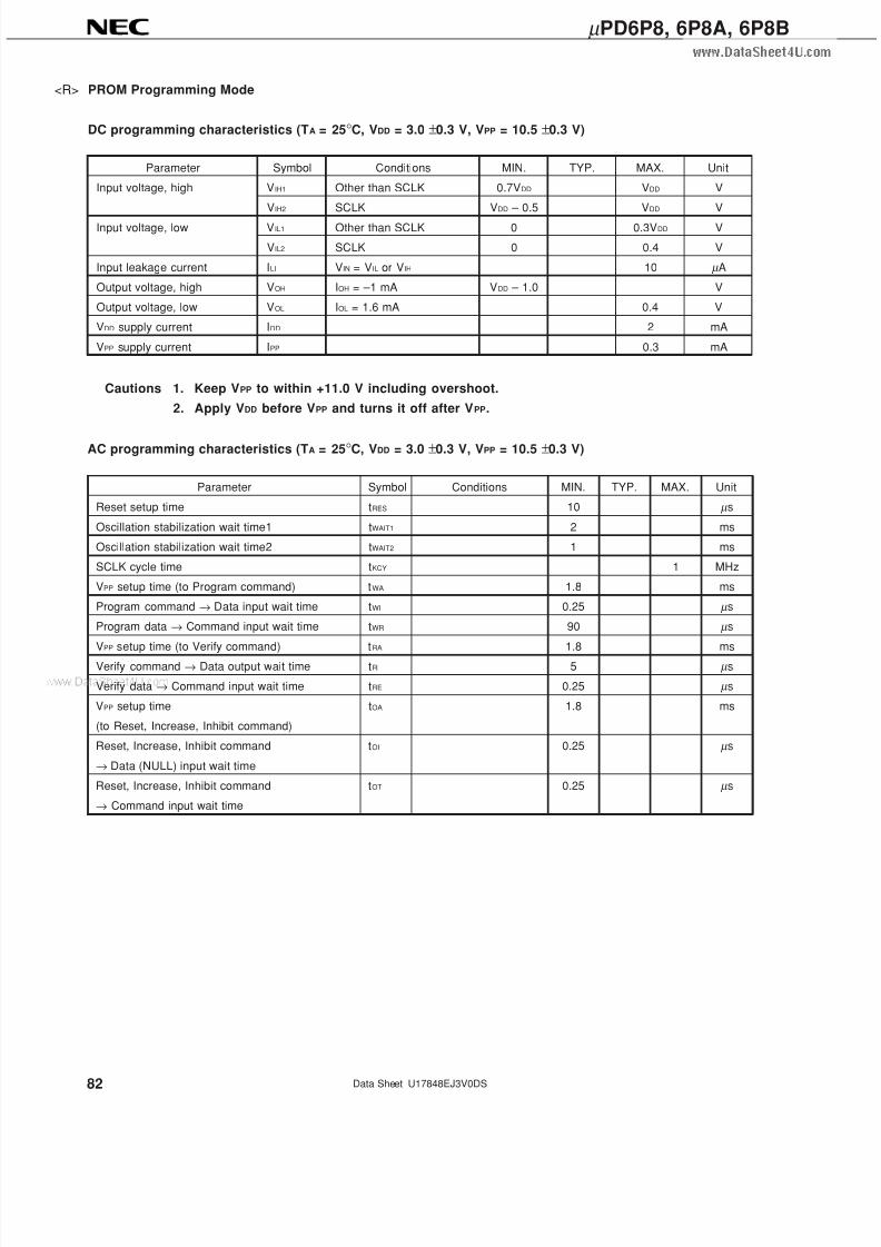
7/17/2019 INFRARED REMOTE CONTROL TRANSMISSION
http://slidepdf.com/reader/full/infrared-remote-control-transmission 82/95
82
µ PD6P8, 6P8A, 6P8B
Data Sheet U17848EJ3V0DS
PROM Programming Mode
DC programming characteristics (TA = 25°C, VDD = 3.0 ±0.3 V, VPP = 10.5 ±0.3 V)
Parameter Symbol Conditions MIN. TYP. MAX. Unit
Input voltage, high VIH1 Other than SCLK 0.7VDD VDD V
VIH2 SCLK VDD – 0.5 VDD V
Input voltage, low VIL1 Other than SCLK 0 0.3VDD V
VIL2 SCLK 0 0.4 V
Input leakage current ILI VIN = VIL or VIH 10 µ A
Output voltage, high VOH IOH = –1 mA VDD – 1.0 V
Output voltage, low VOL IOL = 1.6 mA 0.4 V
VDD supply current IDD 2 mA
VPP supply current IPP 0.3 mA
Cautions 1. Keep VPP to within +11.0 V including overshoot.
2. Apply VDD before VPP and turns it off after VPP.
AC programming characteristics (TA = 25°C, VDD = 3.0 ±0.3 V, VPP = 10.5 ±0.3 V)
Parameter Symbol Conditions MIN. TYP. MAX. Unit
Reset setup time tRES 10 µ s
Oscillation stabilization wait time1 tWAIT1 2 ms
Oscillation stabilization wait time2 tWAIT2 1 ms
SCLK cycle time tKCY 1 MHz
VPP setup time (to Program command) tWA 1.8 ms
Program command → Data input wait time tWI 0.25 µ s
Program data → Command input wait time tWR 90 µ s
VPP setup time (to Verify command) tRA 1.8 msVerify command → Data output wait time tRI 5 µ s
Verify data → Command input wait time tRE 0.25 µ s
VPP setup time tOA 1.8 ms
(to Reset, Increase, Inhibit command)
Reset, Increase, Inhibit command tOI 0.25 µ s
→ Data (NULL) input wait time
Reset, Increase, Inhibit command tOT 0.25 µ s
→ Command input wait time
<R>
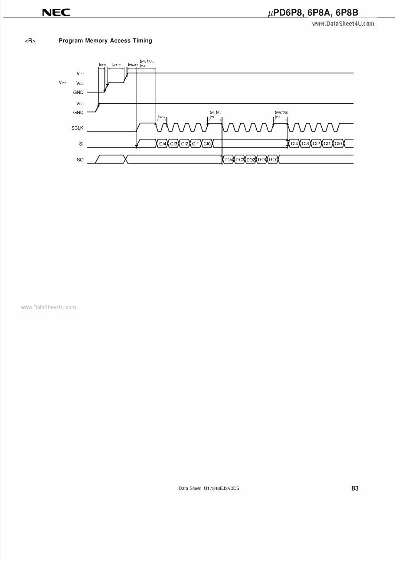
7/17/2019 INFRARED REMOTE CONTROL TRANSMISSION
http://slidepdf.com/reader/full/infrared-remote-control-transmission 83/95
83
µ PD6P8, 6P8A, 6P8B
Data Sheet U17848EJ3V0DS
Program Memory Access Timing
SCLK
SI
SO
VPP
GND
VDD
GND
VDD
VPP
DO4 DO3 DO2 DO1 DO0
CI4 CI3 CI2 CI1 CI0
tRES tWAIT1 tWAIT2tWA, tRA,
tOA
tKCY
tWI, tRI,
tOI
tWR, tRE,
tOT
CI4 CI3 CI2 CI1 CI0
<R>
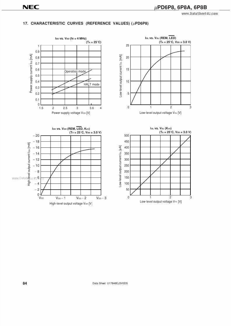
7/17/2019 INFRARED REMOTE CONTROL TRANSMISSION
http://slidepdf.com/reader/full/infrared-remote-control-transmission 84/95
84
µ PD6P8, 6P8A, 6P8B
Data Sheet U17848EJ3V0DS
17. CHARACTERISTIC CURVES (REFERENCE VALUES) (µ PD6P8)
P o w e r s u p p l y c u r r e n t I D D
[ m A ]
Power supply voltage VDD [V]
IDD vs. VDD (fx = 4 MHz)
(TA = 25°C)
1.5 2 32.5 3.6 40
0.1
0.2
0.3
0.4
0.5
0.6
0.7
0.8
0.9
1
Operation mode
HALT mode
25
20
15
10
5
0 1 2 3
L o w - l e v e l o u t p u t c u r r e n t I O L
[ m A
]
Low-level output voltage VOL [V]
IOL vs. VOL (REM, LED)
(TA = 25°C, VDD = 3.0 V)
− 20
− 18
− 16
− 14
− 12
− 10
− 8
− 6
− 4
− 2
0VDD VDD − 1 VDD − 2 VDD − 3
H i g h - l e v e l o u t p u t c u r r e n t I O H
[ m A ]
High-level output voltage VOH [V]
IOH vs. VOH (REM, LED, KI/O)
(TA = 25°C, VDD = 3.0 V)500
450
400
350
300
250
200
150
100
50
0 1 2 3
L o w - l e v e l o u t
p u t c u r r e n t I O L
[ A ]
µ
Low-level output voltage VOL [V]
IOL vs. VOL (KI/O)
(TA = 25°C, VDD = 3.0 V)
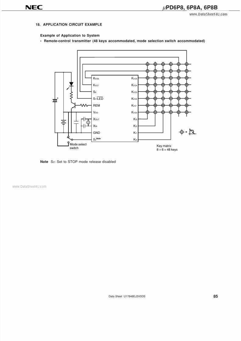
7/17/2019 INFRARED REMOTE CONTROL TRANSMISSION
http://slidepdf.com/reader/full/infrared-remote-control-transmission 85/95
85
µ PD6P8, 6P8A, 6P8B
Data Sheet U17848EJ3V0DS
Note S2: Set to STOP mode release disabled
KI/O6
KI/O7
S0
S1 /LED
REM
VDD
XOUT
XIN
GND
S2Note
KI/O5
KI/O4
KI/O3
KI/O2
KI/O1
KI/O0
KI3
KI2
KI1
KI0
Key matrix8 × 6 = 48 keys
+
Mode selectswitch
18. APPLICATION CIRCUIT EXAMPLE
Example of Application to System
• Remote-control transmitter (48 keys accommodated, mode selection switch accommodated)
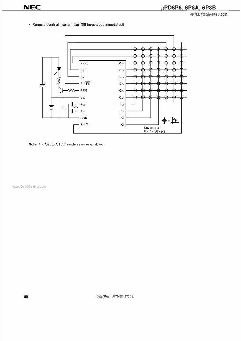
7/17/2019 INFRARED REMOTE CONTROL TRANSMISSION
http://slidepdf.com/reader/full/infrared-remote-control-transmission 86/95
86
µ PD6P8, 6P8A, 6P8B
Data Sheet U17848EJ3V0DS
• Remote-control transmitter (56 keys accommodated)
Note S2: Set to STOP mode release enabled
KI/O6
KI/O7
S0
S1 /LED
REM
VDD
XOUT
XIN
GND
S2Note
K I/O5
K I/O4
K I/O3
K I/O2
K I/O1
K I/O0
K I3
K I2
K I1
K I0
Key matrix8 × 7 = 56 keys
+
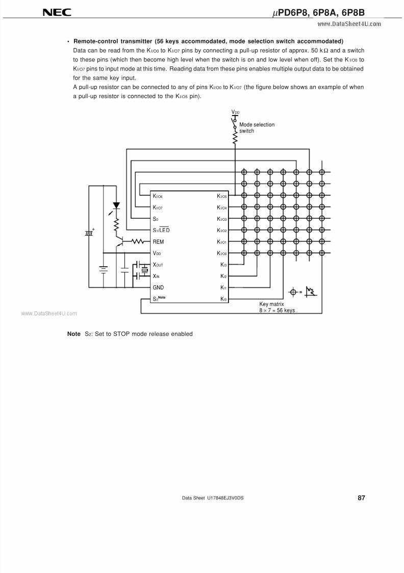
7/17/2019 INFRARED REMOTE CONTROL TRANSMISSION
http://slidepdf.com/reader/full/infrared-remote-control-transmission 87/95
87
µ PD6P8, 6P8A, 6P8B
Data Sheet U17848EJ3V0DS
• Remote-control transmitter (56 keys accommodated, mode selection switch accommodated)
Data can be read from the KI/O0 to KI/O7 pins by connecting a pull-up resistor of approx. 50 k Ω and a switch
to these pins (which then become high level when the switch is on and low level when off). Set the K I/O0 to
KI/O7 pins to input mode at this time. Reading data from these pins enables multiple output data to be obtained
for the same key input.
A pull-up resistor can be connected to any of pins KI/O0 to K I/O7 (the figure below shows an example of when
a pull-up resistor is connected to the KI/O5 pin).
Note S2: Set to STOP mode release enabled
KI/O6
KI/O7
S0
S1 /LED
REM
VDD
XOUT
XIN
GND
S2Note
K I/O5
K I/O4
K I/O3
K I/O2
K I/O1
K I/O0
KI3
KI2
KI1
KI0Key matrix8 × 7 = 56 keys
Mode selectionswitch
VDD
+
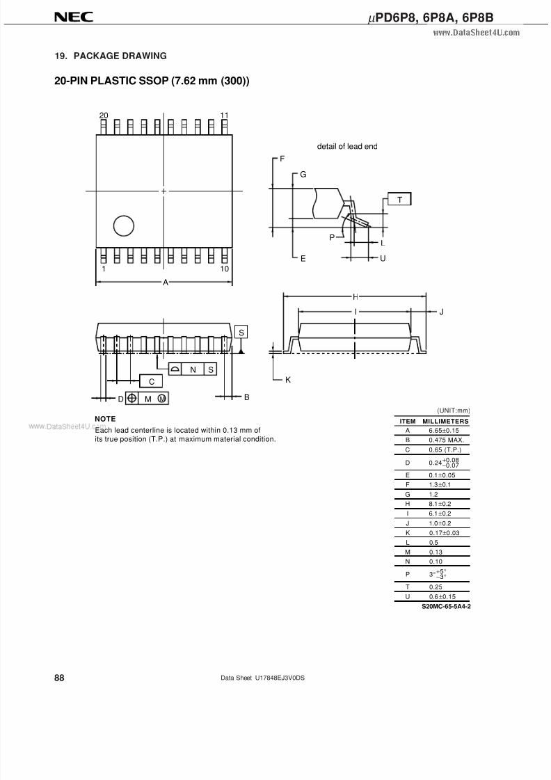
7/17/2019 INFRARED REMOTE CONTROL TRANSMISSION
http://slidepdf.com/reader/full/infrared-remote-control-transmission 88/95
88
µ PD6P8, 6P8A, 6P8B
Data Sheet U17848EJ3V0DS
19. PACKAGE DRAWING
N S
C
D M M
PL
U
T
G
F
E
B
K
J
detail of lead end
S
20 11
1 10A
H
I
ITEM
B
C
I
LM
N
20-PIN PLASTIC SSOP (7.62 mm (300))
A
K
D
E
F
G
H
J
P
T
MILLIMETERS
0.65 (T.P.)
0.475 MAX.
0.130.5
6.1±0.2
0.10
6.65±0.15
0.17±0.03
0.1±0.05
0.24
1.3±0.1
8.1±0.2
1.2
+−
1.0±0.2
3°+5°−3°
0.25
0.6±0.15U
NOTE
S20MC-65-5A4-2
Each lead centerline is located within 0.13 mm of
its true position (T.P.) at maximum material condition.
0.080.07
(UNIT:mm)
7/17/2019 INFRARED REMOTE CONTROL TRANSMISSION
http://slidepdf.com/reader/full/infrared-remote-control-transmission 89/95
89
µ PD6P8, 6P8A, 6P8B
Data Sheet U17848EJ3V0DS
20. RECOMMENDED SOLDERING CONDITIONS
The µ PD6P8, 6P8A, and 6P8B must be soldered and mounted under the following recommended conditions.
For soldering methods and conditions other than those recommended below, contact an NEC Electronics sales
representative.
For technical information, see the following website.
Semiconductor Device Mount Manual (http://www.necel.com/pkg/en/mount/index.html)
Table 20-1. Surface Mounting Soldering Conditions
µ PD6P8MC-5A4-A, 6P8AMC-5A4-A, 6P8BMC-5A4-A: 20-pin plastic SSOP (7.62 mm (300))
Soldering Method Soldering ConditionsRecommended
Condition Symbol
Infrared reflow Package peak temperature: 260°C, Time: 60 seconds max. (at 220°C or higher), IR60-207-3
Count: Three times or less, Exposure limit: 7 daysNote
(after that, prebake at 125°C for 2 to 72 hours)
Wave soldering For details, contact an NEC Electronics sales representative. – Partial heating Pin temperature: 350°C max., Time: 3 seconds max. (per pin row) –
Note After opening the dry pack, store it at 25°C or less and 65% RH or less for the allowable storage period.
Caution Do not use different soldering methods together (except for partial heating).
Remark Products that have the part numbers suffixed by “-A” are lead-free products.
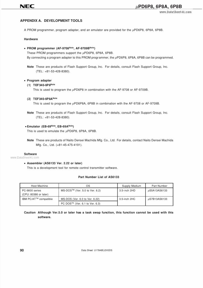
7/17/2019 INFRARED REMOTE CONTROL TRANSMISSION
http://slidepdf.com/reader/full/infrared-remote-control-transmission 90/95
90
µ PD6P8, 6P8A, 6P8B
Data Sheet U17848EJ3V0DS
APPENDIX A. DEVELOPMENT TOOLS
A PROM programmer, program adapter, and an emulator are provided for the µ PD6P8, 6P8A, 6P8B.
Hardware
• PROM programmer (AF-9708Note, AF-9709BNote)
These PROM programmers support the µ PD6P8, 6P8A, 6P8B.
By connecting a program adapter to this PROM programmer, the µ PD6P8, 6P8A, 6P8B can be programmed.
Note These are products of Flash Support Group, Inc. For details, consult Flash Support Group, Inc.
(TEL: +81-53-428-8380).
• Program adapter
(1) TEF340-6P8Note
This is used to program the µ PD6P8 in combination with the AF-9708 or AF-9709B.
(2) TEF340-6P8A
Note
This is used to program the µ PD6P8A, 6P8B in combination with the AF-9708 or AF-9709B.
Note These are products of Flash Support Group, Inc. For details, consult Flash Support Group, Inc.
(TEL: +81-53-428-8380).
• Emulator (EB-69Note, EB-69ANote)
This is used to emulate the µ PD6P8, 6P8A, 6P8B.
Note These are products of Naito Densei Machida Mfg. Co., Ltd. For details, contact Naito Densei Machida
Mfg. Co., Ltd. (+81-45-475-4191).
Software
• Assembler (AS6133 Ver. 2.22 or later)
This is a development tool for remote control transmitter software.
Part Number List of AS6133
Host Machine OS Supply Medium Part Number
PC-9800 series MS-DOSTM (Ver. 5.0 to Ver. 6.2) 3.5-inch 2HD µ S5A13AS6133
(CPU: 80386 or later)
IBM PC/ATTM compatible MS-DOS (Ver. 6.0 to Ver. 6.22) 3.5-inch 2HC µ S7B13AS6133
PC DOSTM (Ver. 6.1 to Ver. 6.3)
Caution Although Ver.5.0 or later has a task swap function, this function cannot be used with this
software.
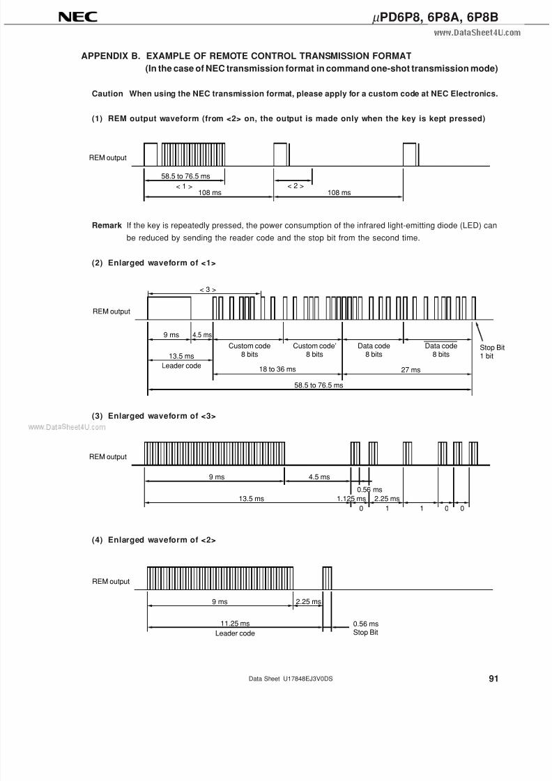
7/17/2019 INFRARED REMOTE CONTROL TRANSMISSION
http://slidepdf.com/reader/full/infrared-remote-control-transmission 91/95
91
µ PD6P8, 6P8A, 6P8B
Data Sheet U17848EJ3V0DS
APPENDIX B. EXAMPLE OF REMOTE CONTROL TRANSMISSION FORMAT
(In the case of NEC transmission format in command one-shot transmission mode)
Caution When using the NEC transmission format, please apply for a custom code at NEC Electronics.
(1) REM output waveform (from <2> on, the output is made only when the key is kept pressed)
REM output
58.5 to 76.5 ms
108 ms 108 ms< 1 > < 2 >
Remark If the key is repeatedly pressed, the power consumption of the infrared light-emitting diode (LED) can
be reduced by sending the reader code and the stop bit from the second time.
(2) Enlarged waveform of <1>
REM output
13.5 ms
Leader code
9 ms 4.5 ms
Custom code8 bits
Custom code’8 bits
Data code8 bits
Data code8 bits
27 ms18 to 36 ms
58.5 to 76.5 ms
Stop Bit1 bit
< 3 >
(3) Enlarged waveform of <3>
REM output
9 ms
13.5 ms
0
4.5 ms
1 1 0 0
2.25 ms1.125 ms
0.56 ms
(4) Enlarged waveform of <2>
REM output
9 ms
11.25 ms
2.25 ms
0.56 msStop BitLeader code
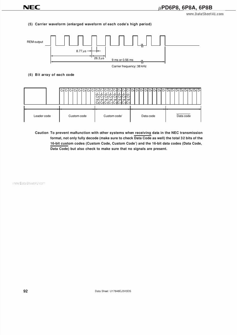
7/17/2019 INFRARED REMOTE CONTROL TRANSMISSION
http://slidepdf.com/reader/full/infrared-remote-control-transmission 92/95
92
µ PD6P8, 6P8A, 6P8B
Data Sheet U17848EJ3V0DS
(5) Carrier waveform (enlarged waveform of each code’s high period)
REM output
8.77 s
9 ms or 0.56 ms
Carrier frequency: 38 kHz
26.3 s
µ
µ
(6) Bit array of each code
C0 C1 C2 C3 C4 C5 C6 C7 C0’
C0
orC8
C1’
C1
orC9
C2’
C2
orC10
C3’
C3
orC11
C4’
C4
orC12
C5’
C5
orC13
C6’
C6
orC14
C7’
C7
orC15
D0 D1 D2 D3 D4 D5 D6 D7 D0 D1 D2 D3 D4 D5 D6 D7= = = = = = = =
Data codeData codeCustom code’Custom codeLeader code
Caution To prevent malfunction with other systems when receiving data in the NEC transmission
format, not only fully decode (make sure to check Data Code as well) the total 32 bits of the
16-bit custom codes (Custom Code, Custom Code’) and the 16-bit data codes (Data Code,
Data Code) but also check to make sure that no signals are present.
7/17/2019 INFRARED REMOTE CONTROL TRANSMISSION
http://slidepdf.com/reader/full/infrared-remote-control-transmission 93/95
93
µ PD6P8, 6P8A, 6P8B
Data Sheet U17848EJ3V0DS
1
2
3
4
VOLTAGE APPLICATION WAVEFORM AT INPUT PIN
Waveform distortion due to input noise or a reflected wave may cause malfunction. If the input of the
CMOS device stays in the area between V IL (MAX) and VIH (MIN) due to noise, etc., the device may
malfunction. Take care to prevent chattering noise from entering the device when the input level is
fixed, and also in the transition period when the input level passes through the area between V IL (MAX)
and V IH (MIN).
HANDLING OF UNUSED INPUT PINS
Unconnected CMOS device inputs can be cause of malfunction. If an input pin is unconnected, it is
possible that an internal input level may be generated due to noise, etc., causing malfunction. CMOS
devices behave differently than Bipolar or NMOS devices. Input levels of CMOS devices must be fixed
high or low by using pull-up or pull-down circuitry. Each unused pin should be connected to VDD or
GND via a resistor if there is a possibility that it will be an output pin. All handling related to unused pins
must be judged separately for each device and according to related specifications governing the device.
PRECAUTION AGAINST ESD
A strong electric field, when exposed to a MOS device, can cause destruction of the gate oxide and
ultimately degrade the device operation. Steps must be taken to stop generation of static electricity as
much as possible, and quickly dissipate it when it has occurred. Environmental control must be
adequate. When it is dry, a humidifier should be used. It is recommended to avoid using insulators that
easily build up static electricity. Semiconductor devices must be stored and transported in an anti-static
container, static shielding bag or conductive material. All test and measurement tools including work
benches and floors should be grounded. The operator should be grounded using a wrist strap.
Semiconductor devices must not be touched with bare hands. Similar precautions need to be taken for
PW boards with mounted semiconductor devices.
STATUS BEFORE INITIALIZATION
Power-on does not necessarily define the initial status of a MOS device. Immediately after the power
source is turned ON, devices with reset functions have not yet been initialized. Hence, power-on doesnot guarantee output pin levels, I/O settings or contents of registers. A device is not initialized until the
reset signal is received. A reset operation must be executed immediately after power-on for devices
with reset functions.
POWER ON/OFF SEQUENCE
In the case of a device that uses different power supplies for the internal operation and external
interface, as a rule, switch on the external power supply after switching on the internal power supply.
When switching the power supply off, as a rule, switch off the external power supply and then the
internal power supply. Use of the reverse power on/off sequences may result in the application of an
overvoltage to the internal elements of the device, causing malfunction and degradation of internal
elements due to the passage of an abnormal current.
The correct power on/off sequence must be judged separately for each device and according to related
specifications governing the device.
INPUT OF SIGNAL DURING POWER OFF STATE
Do not input signals or an I/O pull-up power supply while the device is not powered. The current
injection that results from input of such a signal or I/O pull-up power supply may cause malfunction and
the abnormal current that passes in the device at this time may cause degradation of internal elements.
Input of signals during the power off state must be judged separately for each device and according to
related specifications governing the device.
NOTES FOR CMOS DEVICES
5
6
7/17/2019 INFRARED REMOTE CONTROL TRANSMISSION
http://slidepdf.com/reader/full/infrared-remote-control-transmission 94/95
94
µ PD6P8, 6P8A, 6P8B
Data Sheet U17848EJ3V0DS
The information in this document is current as of December, 2007. The information is subject to
change without notice. For actual design-in, refer to the latest publications of NEC Electronics data
sheets or data books, etc., for the most up-to-date specifications of NEC Electronics products. Not
all products and/or types are available in every country. Please check with an NEC Electronics sales
representative for availability and additional information.
No part of this document may be copied or reproduced in any form or by any means without the prior
written consent of NEC Electronics. NEC Electronics assumes no responsibility for any errors that may
appear in this document.
NEC Electronics does not assume any liability for infringement of patents, copyrights or other intellectual
property rights of third parties by or arising from the use of NEC Electronics products listed in this document
or any other liability aris ing from the use of such products. No license, express, implied or otherwise, isgranted under any patents, copyrights or other intellectual property rights of NEC Electronics or others.
Descriptions of circuits, software and other related information in this document are provided for illustrative
purposes in semiconductor product operation and application examples. The incorporation of these
circuits, software and information in the design of a customer's equipment shall be done under the full
responsibility of the customer. NEC Electronics assumes no responsibility for any losses incurred by
customers or third parties arising from the use of these circuits, software and information.
While NEC Electronics endeavors to enhance the quality, reliability and safety of NEC Electronics products,
customers agree and acknowledge that the possibilit y of defects thereof cannot be eliminated entirely. To
minimize risks of damage to property or injury (including death) to persons arising from defects in NEC
Electronics products, customers must incorporate sufficient safety measures in their design, such as
redundancy, fire-containment and anti-failure features.
NEC Electronics products are classified into the following three quality grades: "Standard", "Special" and
"Specific".The "Specific" quality grade applies only to NEC Electronics products developed based on a customer-
designated "quality assurance program" for a specific application. The recommended applications of an NEC
Elect ronics product depend on its quality grade, as indicated below. Customers must check the quality grade of
each NEC Electronics product before using it in a particular application.
The quality grade of NEC Electronics products is "Standard" unless otherwise expressly specified in NEC
Electronics data sheets or data books, etc. If customers wish to use NEC Electronics products in applications
not intended by NEC Electronics, they must contact an NEC Electronics sales representative in advance to
determine NEC Electronics' willingness to support a given application.
(Note)
•
•
•
•
•
•
M8E 02. 11-1
(1)
(2)
"NEC Electronics" as used in this statement means NEC Electronics Corporation and also includes its
majority-owned subsidiaries.
"NEC Electronics products" means any product developed or manufactured by or for NEC Electronics (as
defined above).
Computers, office equipment, communications equipment, test and measurement equipment, audio
and visual equipment, home electronic appliances, machine tools, personal electronic equipment
and industrial robots.
Transportation equipment (automobiles, trains, ships, etc.), traffic control systems, anti-disaster
systems, anti-crime systems, safety equipment and medical equipment (not specifically designed
for life support).
Aircraft, aerospace equipment, submersible repeaters, nuclear reactor control systems, life
support systems and medical equipment for life support, etc.
"Standard":
"Special":
"Specific":
MS-DOS is either a registered trademark or a trademark of Microsoft Corporation in the United States and/
or other countries.
PC/AT and PC DOS are trademarks of International Business Machines Corporation.
Caution: This product uses SuperFlash® technology licensed from Silicon Storage Technology, Inc.
7/17/2019 INFRARED REMOTE CONTROL TRANSMISSION
http://slidepdf.com/reader/full/infrared-remote-control-transmission 95/95
µ PD6P8, 6P8A, 6P8B
NEC Electronics Corporation1753, Shimonumabe, Nakahara-ku,
Kawasaki, Kanagawa 211-8668,
JapanTel: 044-435-5111
http://www.necel.com/
[America]
NEC Electronics America, Inc.2880 Scott Blvd.
Santa Clara, CA 95050-2554, U.S.A.
Tel: 408-588-6000 800-366-9782
http://www.am.necel.com/
[Asia & Oceania]
NEC Electronics (China) Co., Ltd7th Floor, Quantum Plaza, No. 27 ZhiChunLu HaidianDistrict, Beijing 100083, P.R.ChinaTel: 010-8235-1155http://www.cn.necel.com/
Shanghai BranchRoom 2509-2510, Bank of China Tower,200 Yincheng Road Central,Pudong New Area, Shanghai, P.R.China P.C:200120Tel:021-5888-5400http://www.cn.necel.com/
Shenzhen BranchUnit 01, 39/F, Excellence Times Square Building,No. 4068 Yi Tian Road, Futian District, Shenzhen,P.R.China P.C:518048Tel:0755-8282-9800http://www.cn.necel.com/
NEC Electronics Hong Kong Ltd.Unit 1601-1613, 16/F., Tower 2, Grand Century Place,193 Prince Edward Road West, Mongkok, Kowloon, Hong KongTel: 2886-9318http://www.hk.necel.com/
NEC Electronics Taiwan Ltd.7F, No. 363 Fu Shing North RoadTaipei, Taiwan, R. O. C.Tel: 02-8175-9600http://www.tw.necel.com/
NEC Electronics Singapore Pte. Ltd.238A Thomson Road,
#12-08 Novena Square,Singapore 307684Tel: 6253-8311http://www.sg.necel.com/
NEC Electronics Korea Ltd.11F., Samik Lavied’or Bldg., 720-2,Yeoksam-Dong, Kangnam-Ku,Seoul, 135-080, KoreaTel: 02-558-3737http://www.kr.necel.com/
For further information,please contact:
[Europe]
NEC Electronics (Europe) GmbHArcadiastrasse 1040472 Düsseldorf, Germany
Tel: 0211-65030
http://www.eu.necel.com/
Hanover OfficePodbielskistrasse 166 B30177 Hannover
Tel: 0 511 33 40 2-0
Munich OfficeWerner-Eckert-Strasse 9
81829 MünchenTel: 0 89 92 10 03-0
Stuttgart Office
Industriestrasse 370565 StuttgartTel: 0 711 99 01 0-0
United Kingdom BranchCygnus House, Sunrise Parkway
Linford Wood, Milton Keynes
MK14 6NP, U.K.Tel: 01908-691-133
Succursale Française9, rue Paul Dautier, B.P. 52
78142 Velizy-Villacoublay Cédex
FranceTel: 01-3067-5800
Sucursal en EspañaJuan Esplandiu, 15
28007 Madrid, SpainTel: 091-504-2787
Tyskland FilialTäby Centrum
Entrance S (7th floor)
18322 Täby, SwedenTel: 08 638 72 00
Filiale ItalianaVia Fabio Filzi, 25/A
20124 Milano, Italy
Tel: 02-667541
Branch The NetherlandsSteijgerweg 6
Related Documents