Infrared Detector & ASIC Technology Markus Loose STScI, May 8, 2014

Welcome message from author
This document is posted to help you gain knowledge. Please leave a comment to let me know what you think about it! Share it to your friends and learn new things together.
Transcript

Infrared Detector & ASIC TechnologyMarkus Loose
STScI, May 8, 2014

STScI Lecture 2
Outline
May 08, 2014
• CMOS-based Detectors (infrared)– General Properties of Solid State Detectors– CMOS-based Multiplexers– Examples
• Control ASICs– General Description– Example: SIDECAR ASIC
– Preamp, Biases, ADCs– Noise performance and issues
• Conclusion

STScI Lecture 3
CMOS-based Infrared Sensors
May 08, 2014
( CMOS: Complimentary Metal Oxide Silicon )

4
The Ideal Detector
• Detect 100% of photons
• Each photon detected as a delta function
• Large number of pixels
• Time tag for each photon
• Measure photon wavelength
• Measure photon polarization
Oct 15, 2009 Scientific Detector Workshop, Garching, Germany
Up to 98% quantum efficiency
One electron for each photon gfdg
~1,400 million pixels (>109)
No - framing detectors
No – defined by filter
No – defined by filter
Plus Read Noise and other “Features”

STScI Lecture 5May 08, 2014
Hybrid Imager Architecture
Image of indium bump array in comparison to
human hair(credit: Laser Focus World)

STScI Lecture 6
Energy of a Photon
May 08, 2014
Wavelength (m) Energy (eV) Band
0.3 4.13 UV
0.5 2.48 Vis
0.7 1.77 Vis
1.0 1.24 NIR
2.5 0.50 SWIR
5.0 0.25 MWIR
10.0 0.12 LWIR
20.0 0.06 VLWIR
• Energy of photons is measured in electron-volts (eV)• eV = energy that an electron gets when it “falls” through a 1 Volt field.
STScI Lecture 7
An Electron-Volt (eV) is extremely small
May 08, 2014
1 eV = 1.6 • 10-19 J (J = joule)
1 J = N • m = kg • m • sec-2 • m
1 kg raised 1 meter = 9.8 J = 6.1 • 1019 eV
• The energy of a photon is VERY small– The energy of a SWIR (2.5 m) photon is 0.5 eV
• Drop a peanut M&M® candy from a height of 2 inches– Energy is equal to 6 x 10¹⁵ eV (a peanut M&M® is ~2 g)– This is equal to 1.2 x 10¹⁶ SWIR photons
• 1 million x 1 million x 12,000• The number of photons that will be detected in ~1 million images from
the James Webb Space Telescope (JWST)• A 2-inch peanut M&M® drop is more energy than will be detected during
the entire 5-10 year lifetime of the JWST !
STScI Lecture 8
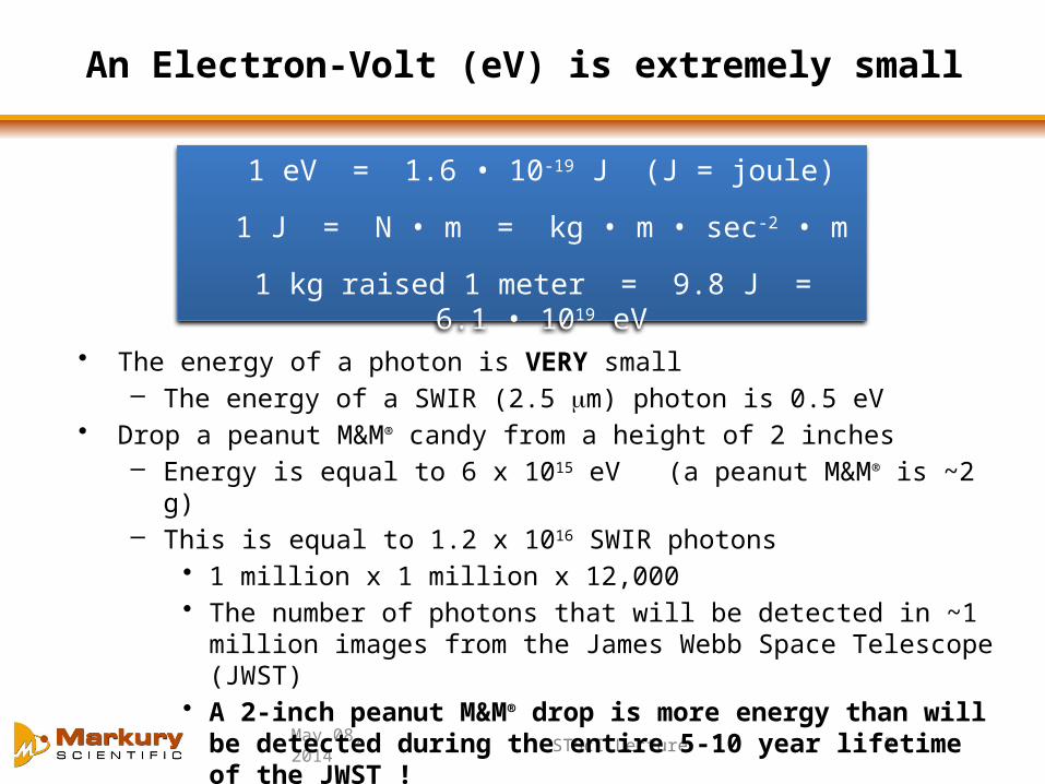
Photon Detection
May 08, 2014
Conduction Band
Valence Band
Eg
For an electron to be excited from theconduction band to the valence band
h > Eg
h = Planck constant (6.6310-34 Joule•sec)n = frequency of light (cycles/sec) = /c Eg = energy gap of material (electron-volts)
Material Name Symbol Eg (eV) c (m)
Silicon Si 1.12 1.1
Indium-Gallium-Arsenide InGaAs 0.73 – 0.48 1.68 – 2.6
Mercury-Cadmium-Teluride HgCdTe 1.00 – 0.07 1.24 – 18
Indium Antimonide InSb 0.23 5.5
Arsenic doped Silicon Si:As 0.05 25
c = 1.238 / Eg (eV)

STScI Lecture 9May 08, 2014
CCD Approach CMOS Approach
PixelCharge generation &charge integration
Charge generation, charge integration &
charge-to-voltage conversion
+
PhotodiodePhotodiode Amplifier
Array ReadoutCharge transfer
from pixel to pixel
Multiplexing of pixel voltages: Successively
connect amplifiers to common bus
Sensor Output Output amplifier performs
charge-to-voltage conversion
Various options possible:- no further circuitry (analog out)- add. amplifiers (analog output)- A/D conversion (digital output)
General CMOS Detector Concept
STScI Lecture
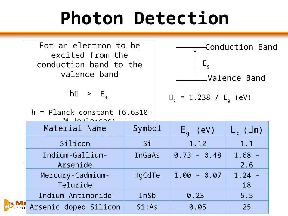
General Architecture of CMOS-Based Image Sensors
May 08, 201410
Pixel Array
Horizontal Scanner / Column
Buffers
Ver
tica
l S
can
ner
fo
r R
ow
Sel
ecti
on
Control &
TimingLogic
(optional)
Bias Generation
& DACs(optional)
Analog Amplification
A/D conversion (optional)
Analog Output
Digital Output

STScI Lecture 11
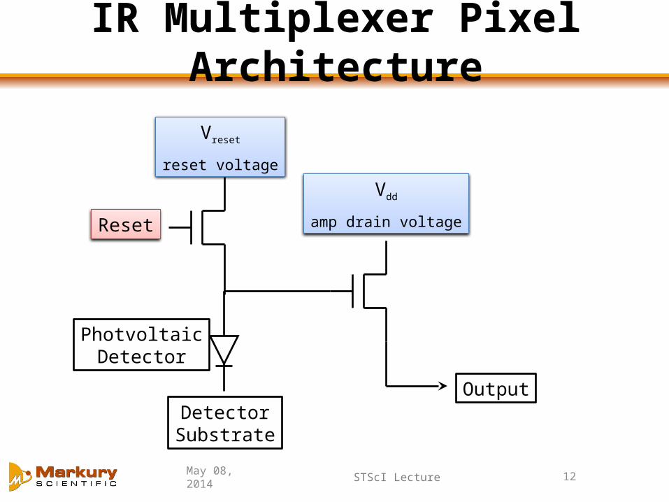
IR Multiplexer Pixel Architecture
May 08, 2014
Vdd
amp drain voltage
OutputDetectorSubstrate
PhotvoltaicDetector
STScI Lecture 12
IR Multiplexer Pixel Architecture
May 08, 2014
Vdd
amp drain voltage
OutputDetectorSubstrate
PhotvoltaicDetector
Vreset
reset voltage
Reset

STScI Lecture 13
IR Multiplexer Pixel Architecture
May 08, 2014
OutputDetectorSubstrate
PhotvoltaicDetector
Vreset
reset voltage
Reset
Vdd
amp drain voltage
Enable “Clock” (red)
“Bias voltage” (purple)

STScI Lecture 14May 08, 2014
Special Scanning Techniques in CMOS
• Different scanning methods are available to reduce the number of pixels being read:– Allows for higher frame rate or lower pixel rate (reduction in noise)– Can reduce power consumption due to reduced data
Random Read• Random access
(read or reset) of certain pixels
• Selective reset of saturated pixels
• Fast reads of selected pixels
Subsampling• Skipping of certain
pixels/rows when reading the array
• Used to obtain higher frame rates on full-field images
Windowing• Reading of one or
multiple rectangular subwindows
• Used to achieve higher frame rates (e.g. AO, guiding)
Binning• Combining several
pixels into larger super pixels
• Used to achieve lower noise and higher frame rates
* Binning is typically less efficient in CMOS than in CCDs.

STScI Lecture 15
Possible Reset Schemes for HxRG
May 08, 2014
Reticle
Stitched CMOS Sensor
Pixel by pixel reset Line by line reset Global reset
Full field
Window

STScI Lecture 16
Astronomy Application: Guiding
May 08, 201416
• Special windowing can be used to perform full-field science integration in parallel with fast window reads.Þ Simultaneous guide operation and science
data capture within the same detector.
Full field row Window Full field row
Full field row
Window Window
Full field row Full field row
• Two methods possible:– Interleaved reading of full-field and window
• No scanning restrictions or crosstalk issues• Overhead reduces full-field frame rate
– Parallel reading of full-field and window• Requires additional output channel• Parallel read may cause crosstalk or conflict• No overhead maintains maximum full-field frame
rate
STScI Lecture 17
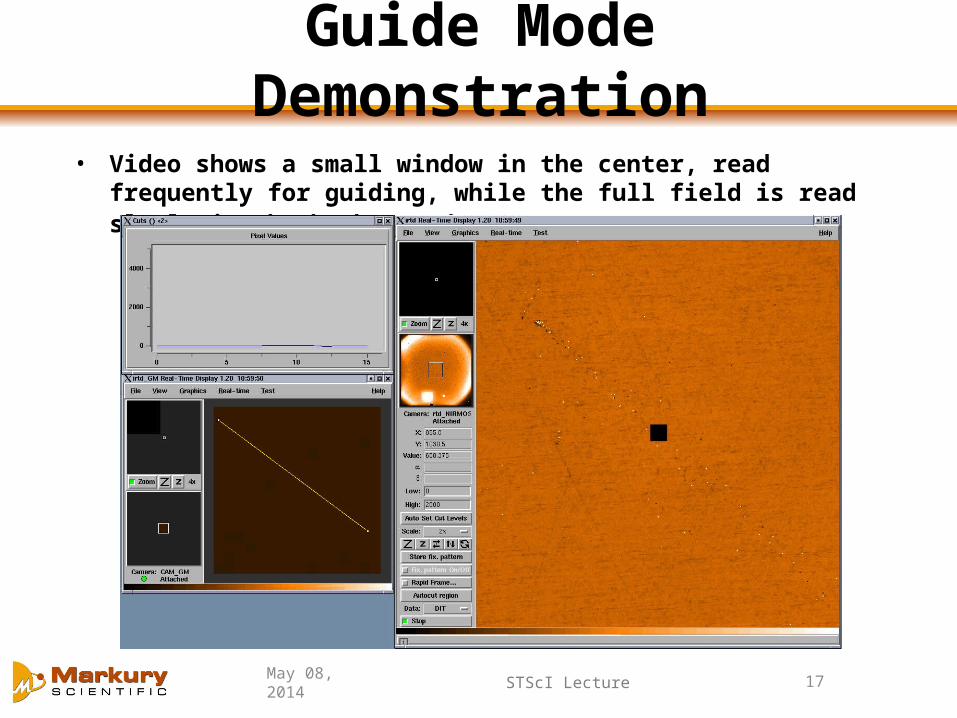
Guide Mode Demonstration
May 08, 2014
• Video shows a small window in the center, read frequently for guiding, while the full field is read slowly in the background

STScI Lecture 18May 08, 2014
H A W A I I - 2 R G
H A W A I I - 2 R GHgCdTe Astronomy Wide Area Infrared Imager
with 2k2 Resolution, Reference pixels and Guide Mode
2k x 2k HAWAII-2RG with HyViSI detector 2 x 2 Mosaic of HAWAII-2RG detectors
Teledyne HAWAII-2RG Hybrid Detector Array
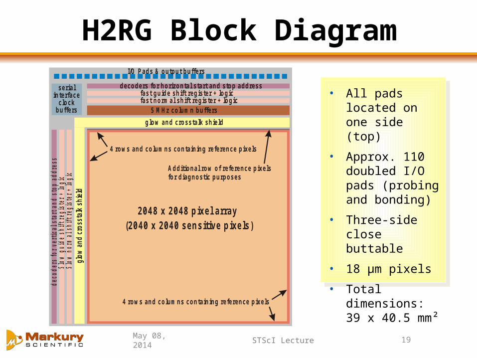
STScI Lecture 19May 08, 2014
5 MHz column buffersfast normal shift register + logic
glow
and
cro
ssta
lk s
hiel
d
g low and crosstalk shield
Additional row of reference pixels for diagnostic purposes
2048 x 2048 pixel array(2040 x 2040 sensitive pixels)
4 rows and columns containing reference pixels
4 rows and columns containing reference pixels
serial interface
clock buffers
fast guide shift register + logic
Slow
gui
de s
hift
regi
ster
+ lo
gic
Slow
nor
mal
shi
ft re
gist
er +
logi
c
decoders for horizontal start and stop address
I/O Pads & output buffers
deco
ders
for v
ertic
al s
tart
and
sto
p ad
dres
s
• All pads located on one side (top)
• Approx. 110 doubled I/O pads (probing and bonding)
• Three-side close buttable
• 18 µm pixels
• Total dimensions: 39 x 40.5 mm²
H2RG Block Diagram

20May 08, 2014 STScI Lecture
JWST - James Webb Space Telescope 15 Teledyne 2K×2K infrared arrays on board (~63 million pixels)
• International collaboration• 6.5 meter primary mirror and tennis court size sunshield• 2018 launch on Ariane 5 rocket• L2 orbit (2.4 million km from Earth)
Two 2x2 mosaicsof SWIR 2Kx2K
Two individual MWIR 2Kx2K
NIRCam(Near Infrared Camera)
• Wide field imager• Studies morphology of objects
and structure of the universe• U. Arizona / Lockheed Martin
• Spectrograph• Measures chemical composition,
temperature and velocity• European Space Agency / NASA
NIRSpec(Near Infrared Spectrograph)
1x2 mosaic of MWIR 2Kx2K
FGS / NIRISS (Fine Guidance Sensors /Near-Infrared Imager and
Slitless Spectrograph)
• Acquisition and guiding• Images guide stars for telescope
stabilization• Canadian Space Agency
3 individual MWIR 2Kx2K
STScI Lecture 21May 08, 2014
Control ASICs
22
How to Operate an Image Sensor?
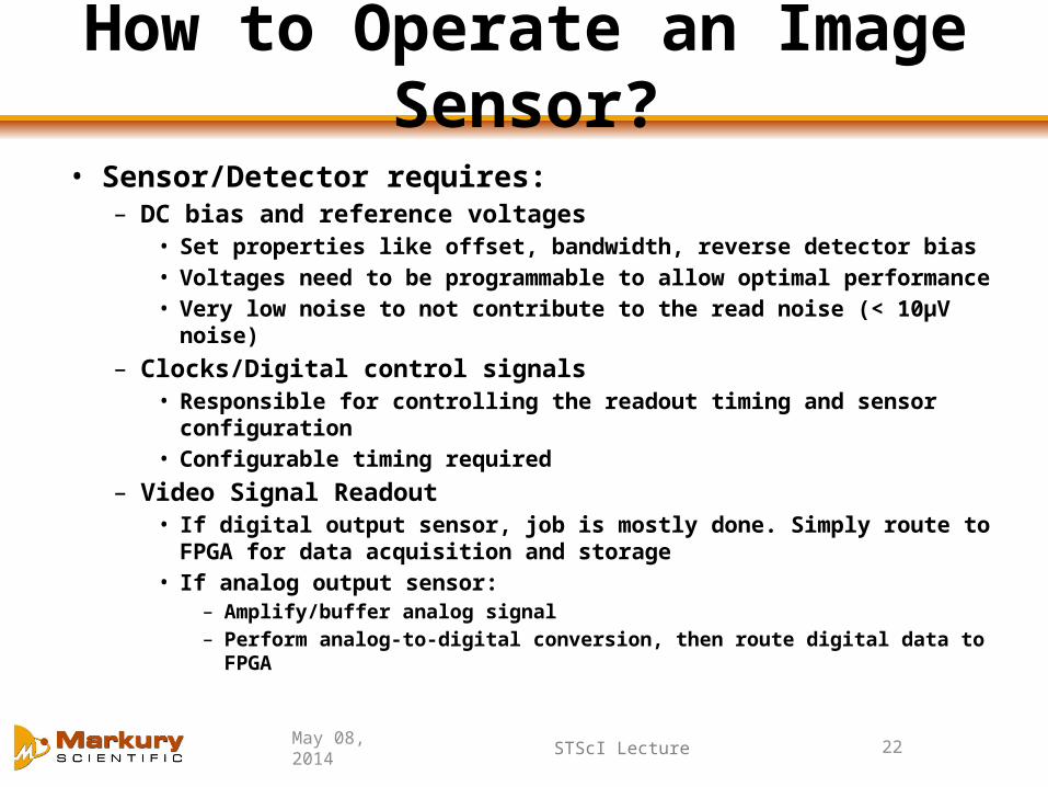
• Sensor/Detector requires:– DC bias and reference voltages
• Set properties like offset, bandwidth, reverse detector bias• Voltages need to be programmable to allow optimal performance• Very low noise to not contribute to the read noise (< 10µV noise)
– Clocks/Digital control signals• Responsible for controlling the readout timing and sensor configuration• Configurable timing required
– Video Signal Readout• If digital output sensor, job is mostly done. Simply route to FPGA for
data acquisition and storage• If analog output sensor:
– Amplify/buffer analog signal– Perform analog-to-digital conversion, then route digital data to FPGA
May 08, 2014 STScI Lecture
STScI Lecture 23
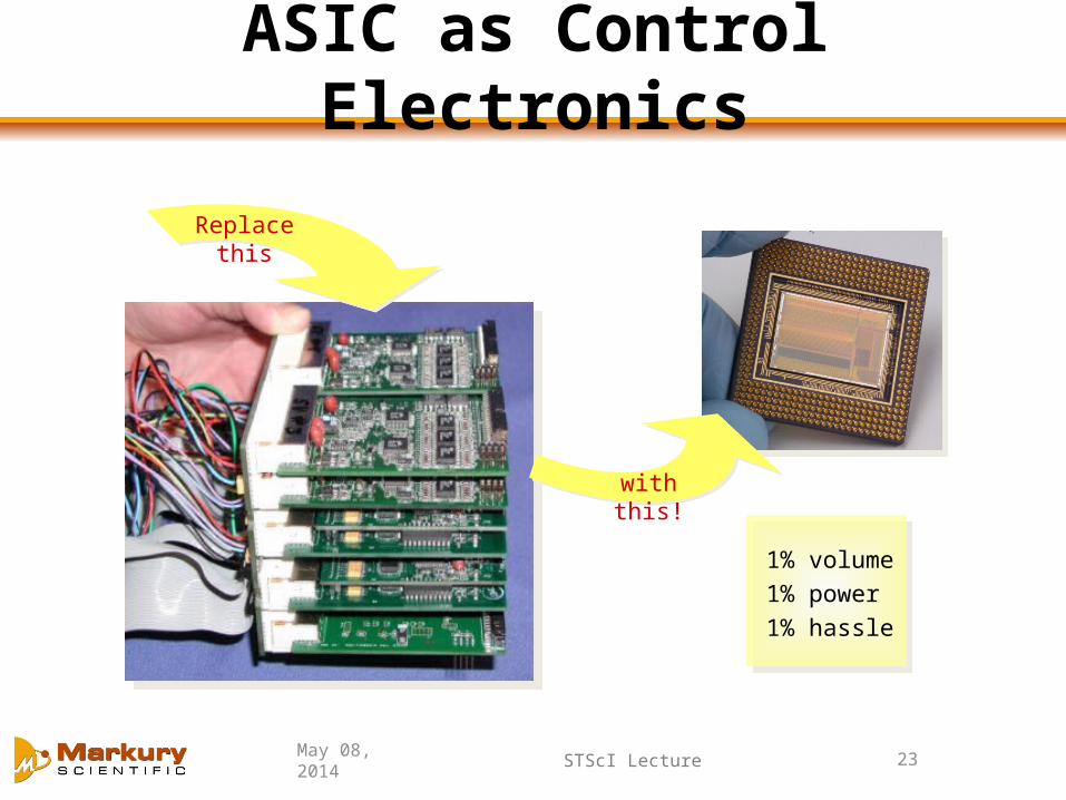
ASIC as Control Electronics
May 08, 2014
Replace this
with this!
1% volume1% power1% hassle

STScI Lecture 24May 08, 2014
Digital ControlMicrocontroller for Clock Generation
and Signal ProcessingBias
Generator
Amplification and A/D
Conversion
Data Memory
Program Memory
Data Memory
Digital I/O
Interface
SIDECAR
Exte
rnal
El
ectr
onic
s
Mul
tiple
xer,
e.g.
HAW
AII-
2RG
analog mux out
bias voltages
clocksmain clock
data in
data out
synchron.
Digital Generic I/O
System for Image Digitization, Enhancement, Control And Retrieval
SIDECAR ASIC Architecture

STScI Lecture 25May 08, 2014
SIDECAR ASIC Features• 36 analog input channels, each channel provides:
– 500 kHz A/D conversion with 16 bit resolution – 10 MHz A/D conversion with 12 bit resolution – gain = 0 dB …. 27 dB in steps of 3 dB– optional low-pass filter with programmable cutoff– optional internal current source (as source follower load)
• 20 analog output channels, each channel provides:– programmable output voltage and driver strength– programmable current source or current sink– internal reference generation (bandgap or vdd)
• 32 digital I/O channels to generate clock patterns, each channel provides:– input / output / high-ohmic– selectable output driver strength and polarity– pattern generator (16 bit pattern) independent of microcontroller– programmable delay (1ns - 250µs)
• 16 bit low-power microprocessor core (single event upset proof)– responsible for timing generation and data processing– 16 kwords program memory (32 kByte) and 8 kwords data memory (16 kByte)– 36 kwords ADC data memory, 24 bit per word (108 kByte)– additional array processor for adding, shifting and multiplying on all 36 data channels in parallel
(e.g. on-chip CDS, leaky memory or other data processing tasks)

STScI Lecture 26May 08, 2014
SIDECAR Operating a HAWAII-2RG / 1RG
PCPCSoftware for
SIDECAR Control and Data Capture
PCI Cardor USB
interface
Vreset
Dsub
Clock
000 w
384 w
0cd w
HAWAII-2RG HAWAII-2RG SIDECAR ASICSIDECAR ASIC
Analog Supply
Data In
Data Out
Master Clock
Digital Supply
3.3V 3.3V
Analog Video
Biases
Power Supply
Serial Interface
Clocks
Only 7 lines needed to operate the SIDECAR ASIC
in base configuration (3 signal & 4 power lines)
The SIDECAR ASIC provides all 27 signals required to operate the
HAWAII-2RG
The microcontroller driven SIDECAR ASIC generates
all biases & clocks and digitizes the analog video
outputs
Sensor Chip Assembly
Sensor Chip Assembly
Inside the dewar at cryogenic temperatures

May 08, 2014 STScI Lecture 27
SIDECAR ASIC Flight Package for JWST
• Ceramic board with ASIC die and decoupling caps
• Invar box with top and bottom lid• Two 37-pin MDM connectors
– FPE-to-ASIC connection– ASIC-to-SCA connection
• Qualified to NASA Technology Readiness Level 6 (TRL-6)
• 15 mW power when reading out of four ports in parallel, with 16 bit digitization at 100 kHz per port.
FPE side
SCA side
SIDECAR
Comparison:
LGA Package
ACS (HST)

STScI Lecture 28May 08, 2014
Missions Employing SIDECAR ASICs• James Webb Space Telescope
– NIRCam, NIRSpec, FGS/NIRISS instruments– H2RG IR detectors, T = 38K (ASIC), planned launch in 2018
• Hubble Space Telescope– ACS (Advanced Camera for Surveys)– CCD detector, T = 300K (ASIC), launched in 2009
• Landsat Data Continuity Mission– TIRS (Thermal InfraRed Sensor) instrument– QWIP detector, T = 300K (ASIC), launched in 2013
• OSIRIS-REx Asteroid Mission– OVIRS (OSIRIS-REx Visible and IR Spectrometer) instrument– H1RG IR detector, T = 300K (ASIC), planned launch in 2016
• Euclid Mission– NISP (Near IR Spectrometer Photometer) instrument– H2RG IR detector, T = ~140K (ASIC), planned launch in 2020
• MOSFIRE (Multi-Object Spectrometer For Infra-Red Exploration)– H2RG IR detector, T < 120K (ASIC), deployed at the Keck Telescope
• FourStar Wide Field Infrared Camera– H2RG IR detector, T < 120K (ASIC), deployed at the Magellan Baade 6.5m Telescope
JWST
HSTLDCM
OSIRIS-RExEuclid

STScI Lecture 29May 08, 2014
Pre-Amplifier Block Diagram
• Capacitor Feedback Design• Gain programmable by
setting Cin and Cfb• Gain = Cin/Cfb
• Low pass filter with programmable cutoff
S3
S1
S1
V1
V2
V3
V4
S3
S4
S4
V1
V2
Vref mid
bypass
S5 S5
SAR_En SAR ADC output
LPF
Pipe_En Pipeline ADC output
S2
S2
Cin
Cin
Cfb
S6
VpremidrefS6
VpremidrefCfb S6
S6

STScI Lecture 30May 08, 2014
Preamp Drift and MitigationData taken as 512 x 64 frames for efficiency, Gain = 4
Drift
kTC row noise
kTC removed (CCD mode)
σ= 52 ADU
σ= 2.6 ADU
σ= 13.9 ADU
STScI Lecture 31May 08, 2014
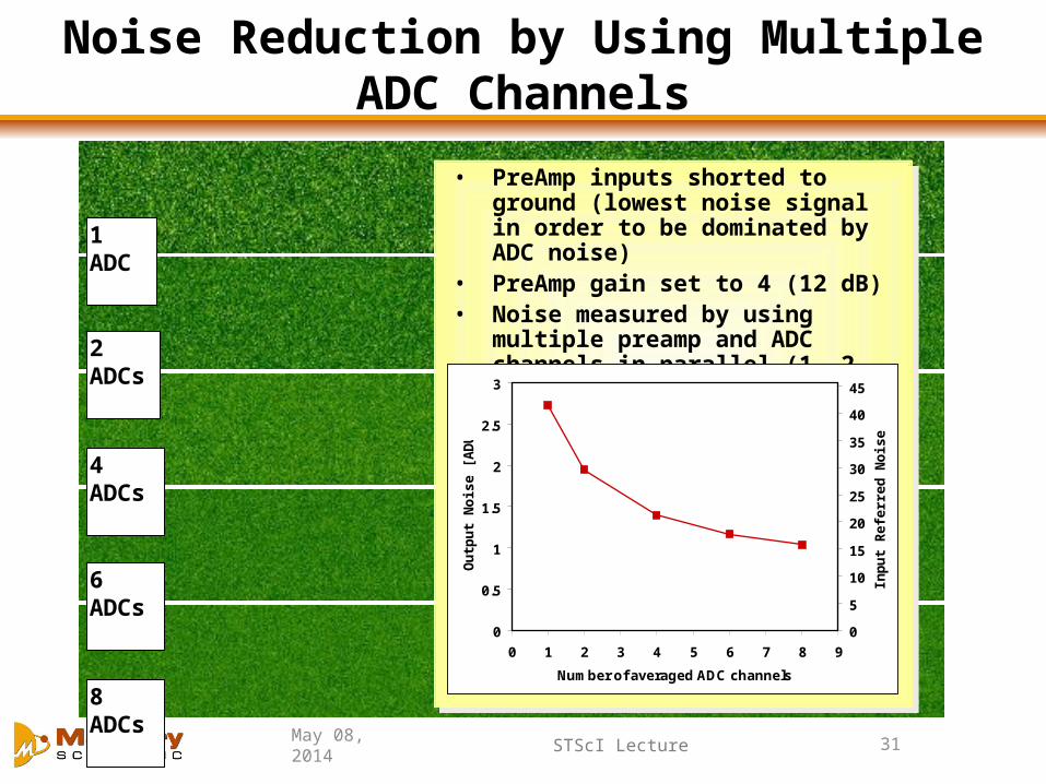
Noise Reduction by Using Multiple ADC Channels
1 ADC
2 ADCs
4 ADCs
6 ADCs
8 ADCs
• PreAmp inputs shorted to ground (lowest noise signal in order to be dominated by ADC noise)
• PreAmp gain set to 4 (12 dB)• Noise measured by using multiple
preamp and ADC channels in parallel (1, 2, 4, 6, and 8)
• Noise reduces almost as the square root of the number of channels used
0
0.5
1
1.5
2
2.5
3
0 1 2 3 4 5 6 7 8 9
Number of averaged ADC channels
Ou
tpu
t N
ois
e [
AD
U]
0
5
10
15
20
25
30
35
40
45
Inp
ut
Re
ferr
ed
No
ise
[µ
V]

STScI Lecture 32
Bias Generator Block Diagram
• SIDECAR has 20 Channels• Each Channel provides
programmable voltage and current sources
• Noise is caused mostly by buffer (1/f noise of MOS transistors)
• Drive strength of buffer can be adjusted to modulate the bandwidth
• Feedback compensation can be adjusted for stability
• Buffer can be configured for single or dual stage operation
• => Tuning required for optimal noise performance
May 08, 2014

STScI Lecture 33May 08, 2014
Bias Generator Noise• Bias output 1 routed back into PreAmp• PreAmp gain set to 22 (27 dB)• Use 4 ADCs in parallel to reduce PreAmp & ADC noise• Noise on bias without filtering is about 35µV (11.6
ADU)• Noise can be reduced by RC filtering to less than 5µV
0
2
4
6
8
10
12
14
0.001 0.01 0.1 1 10 100 1000
RC filter time contant [ms]
Ou
tpu
t N
ois
e [A
DU
]
0
5
10
15
20
25
30
35
40
45
Inp
ut
Ref
erre
d N
ois
e [µ
V]
total noise
bias noise
Bias noise as a function of RC filter time constant
PreAmp & ADC noise floor
Unfiltered Noise of Bias Output 1
Filtered Noise of Bias Output 1 (tRC = 360 ms)

STScI Lecture 34May 08, 2014
Noise Power Spectrum of the Bias Outputs
-60
-50
-40
-30
-20
-10
0
10
20
0.1 1 10 100 1000 10000 100000
Frequency [Hz]
No
ise
[d
Bµ
V/r
oo
tHz]
-60
-50
-40
-30
-20
-10
0
10
20
0.1 1 10 100 1000 10000 100000
Frequency [Hz]
No
ise
[d
Bµ
V/r
oo
tHz]
FFT of temporal noise measurement with RC filter set to tRC= 3 µs
FFT of temporal noise measurement with RC filter set to tRC= 3 ms

STScI Lecture 35May 08, 2014
-60
-50
-40
-30
-20
-10
0
10
20
0.1 1 10 100 1000 10000 100000
Frequency [Hz]
No
ise
[d
Bµ
V/r
oo
tHz]
-60
-50
-40
-30
-20
-10
0
10
20
0.1 1 10 100 1000 10000 100000
Frequency [Hz]
No
ise
[d
Bµ
V/r
oo
tHz]
FFT of temporal noise measurement with RC filter set to tRC= 360ms
FFT of temporal noise measurement with grounded PreAmp inputs (i.e. noise floor)
Noise Power Spectrum of the Bias Outputs, Part 2

STScI Lecture 36May 08, 2014
Analog-to-Digital Conversion
• Quantization noise of an ADC is (1/√12) Least Significant Bit = 0.289 LSB
• Typically set gain of amplifier chain so that quantization noise is much less than readout noise. If readout noise is 4 electrons, set gain so that LSB equals ~2 electrons
• 16 bit ADC is most commonly used in astronomy. At ~2 electrons per ADU (analog to digital unit), or LSB, full well of a 16 bit ADC will be ~130,000 electrons; good match to the typical full well of a CCD or Short-Wave IR detector of 100,000 electrons.
Highly exaggerated quantization noise“Don’t do this at home”

STScI Lecture 37May 08, 2014
Differential Non-Linearity (DNL)
DNL = (VD+1 – VD) / VLSB-Ideal – 1
Code 10 is missingDNL = -1
Code 10 is reducedDNL = -0.5
Code 100 is increasedDNL = +1
• DNL describes the distance of an ADC code from its adjacent code. • It is measured as a change in input voltage magnitude, and then converted to
number of Least Significant Bits (LSBs).

STScI Lecture 38May 08, 2014
Integral Non-Linearity (INL)
• INL describes the deviation of the ADC transfer function from a straight line • It can be computed as the integral of the DNL, and is expressed in LSB
INL = (VD – VZero) / VLSB-Ideal – D

STScI Lecture 39May 08, 2014
16-bit ADC Linearity
Output Code
DN
L [ L
SB ]
-1
-0.8
-0.6
-0.4
-0.2
0
0.2
0.4
0.6
0.8
1
0 10000 20000 30000 40000 50000 60000
DNL
Output Code
INL
[ LSB
]
-4
-3
-2
-1
0
1
2
3
4
0 10000 20000 30000 40000 50000 60000
INL
• Differential Non-Linearity: < ± 0.3 LSB• Integral Non-Linearity: < ± 0.2 LSB• Temporal Noise: 2.7 LSB

STScI Lecture 40May 08, 2014
ADC Linearity Pitfalls
Optimal Vcm
Vcm off by 80 mV
Vcm off by 160 mV
• Differential ADC is composed of 2 separate single-ended ADCs
– If one of the two ADCs saturates before the second one does, the transfer slope changes by 2
Slope change
Slope change
• Requires careful adjustment of the ADC reference and common mode voltages
• Simultaneous optimal tuning for all channels does not exist due to component mismatch
• Avoid lower and upper end of ADC for science

STScI Lecture 41May 08, 2014
1/F Noise in NIRSpec/JWST
• Traditional CDS • Optimal CDS
σCDS ~ 18 e- rms σCDS ~ 8 e- rms

STScI Lecture 42May 08, 2014
IRS^2 Noise Reduction ModeExample: NIRSpec 1000s Dark Up-the-Ramp Signal
• Improved Reference Sampling & Subtraction (IRS^2) is a method to utilized reference pixels in a more efficient way
– In every output channel, read reference pixels from the top or bottom or rows in-between the regular science pixels (e.g. read 4 reference pixels every 16 science pixels)
– Use Fourier analysis to determine the frequency-dependent correlation between signal and reference pixels, and subtract the reference pixel signal accordingly
Nominal (no IRS^2) IRS^2 IRS^2 (using real pixels as reference)

STScI Lecture 43May 08, 2014
ACS 1/f NoiseBias Frame without correction(superbias subtracted)
Bias Frame with correction(superbias subtracted)

STScI Lecture 44
Conclusion
• Infrared Detectors (Image Sensors)– Hybrid design: Detector material bump-bonded to readout chip– Different detector materials possible
• HgCdTe for astronomy: lowest dark current and adjustable bandgap– Flexible readout options like guide mode or single-pixel reset
• Control ASICs– Provide all functions to operate the detector
• Clocking, Biasing, A/D conversion– Single-chip solution in contrast to discrete electronics
• Lower power, space, weight– Can run cryogenically (next to the cooled detector)– Performance Improvements desired (lower noise, no artifacts)
May 08, 2014
Related Documents