
Welcome message from author
This document is posted to help you gain knowledge. Please leave a comment to let me know what you think about it! Share it to your friends and learn new things together.
Transcript
INFN sez. di Torino
CMOS process example
Gianni Mazza

Main steps
Gianni Mazza
� FEOL ( Front End Of the Line )� up to the transistor creation
� BEOL ( Back End Of the Line )� metalization
The two steps correspond to different design teams and are treated separately

Problem� Substrate is either p doped or n doped� PMOS requires n doped substrate� NMOS requires p doped substrate
� Is it possible to have both PMOS and NMOS on the same substrate ?
Gianni Mazza

Solution : well ( or tub )A n-doped ( p-doped ) region is implanted on a p-doped ( n-doped ) substrate.CMOS process : Complementary MOS process
Gianni Mazza

Considerations
� Well and substrate creates a p-n junction� Reduced mobility in the well� P-well vs. n-well� Source-bulk connection� Twin well and pseudo twin well processes� Triple well
Gianni Mazza

Well implantation - 1
Gianni Mazza

Well implantation - 2
Gianni Mazza

Well implantation - 3
Gianni Mazza

Well implantation - 4
Gianni Mazza

Well implantation - 5
Gianni Mazza

Field implant - 1
Gianni Mazza

Field implant - 2
Gianni Mazza

Field implant - 3
Gianni Mazza

LOCOS - 1
Gianni Mazza

LOCOS - 2
Gianni Mazza
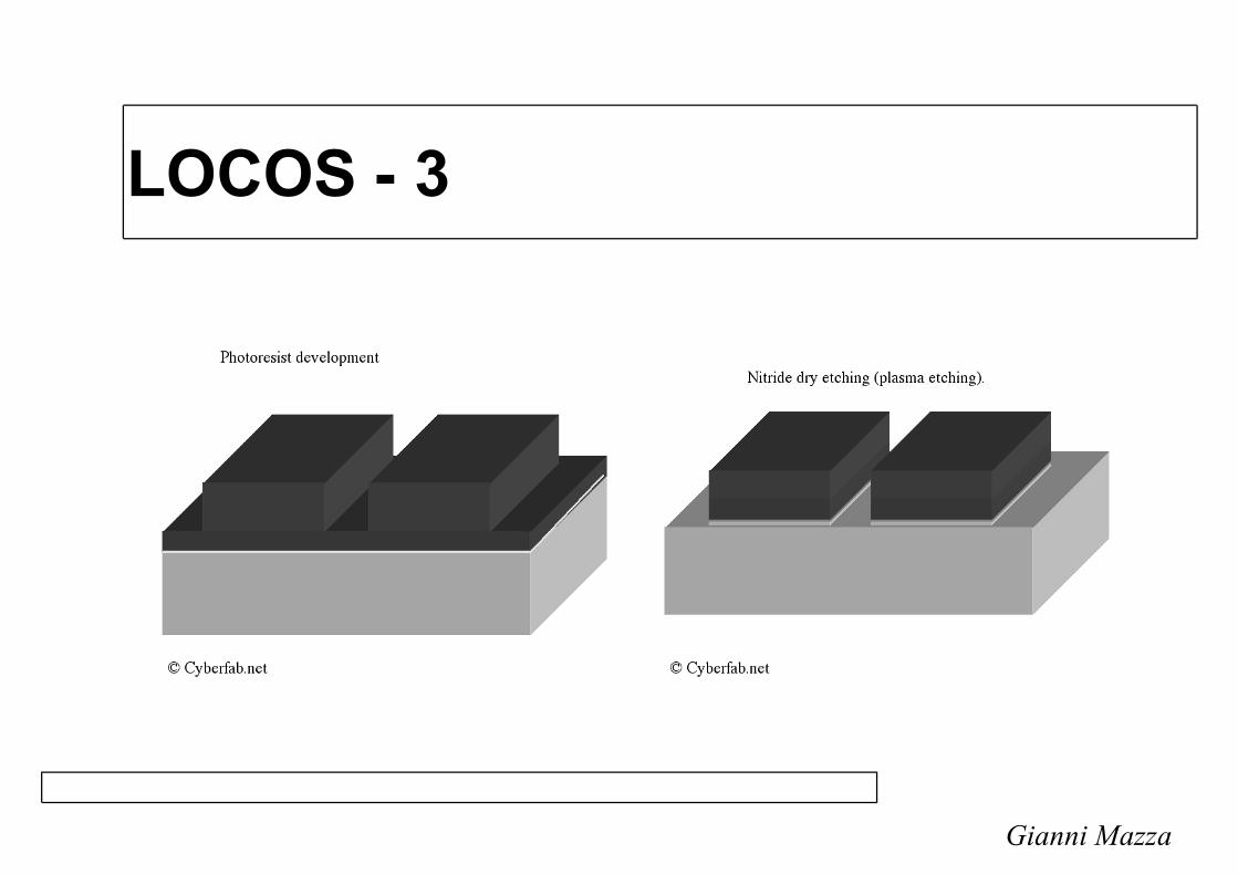
LOCOS - 3
Gianni Mazza

LOCOS - 4
Gianni Mazza

LOCOS - 5
Gianni Mazza

Parasitic MOS - 1
Gianni Mazza

Parasitic MOS - 2
Gianni Mazza

Bird�s beak
Gianni Mazza

Poly Buffered LOCOS (PBL)� For tighter geometries, the pad oxide thickness is reduced by using the following stack: Polysilicon 50 nm/oxide 5-10 nm/nitride 100-240 nm. This allows the bird 's beak to be reduced to 0.2 micron. � The sequence is the same as for LOCOS except that there are added steps to remove the polysilicon layer underneath the nitride.� The nitride layer is removed using a wet bench and acid bath whereas the polysilicon is removed using dry etching in a chlorine based plasma.
Gianni Mazza

Deep trench isolation - 1
Gianni Mazza

Deep trench isolation - 2
Gianni Mazza

Deep trench isolation - 3
Gianni Mazza

Deep trench isolation - 4
Gianni Mazza

Deep trench isolation - 5
Gianni Mazza
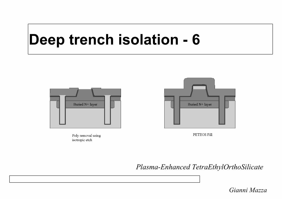
Deep trench isolation - 6
Gianni Mazza
Plasma-Enhanced TetraEthylOrthoSilicate

Deep trench isolation - 7
Gianni Mazza

Deep trench isolation - 8
Gianni Mazza

Deep trench isolation - 9
Gianni Mazza

Isolation Technologies
Gianni Mazza

Gate formation - 1
Gianni Mazza

Gate formation - 2
Gianni Mazza

LDD Implant - 1
Gianni Mazza

LDD Implant - 2
Gianni Mazza

LDD Implant - 3
Gianni Mazza

Spacer
Gianni Mazza

NMOS S/D implant
Gianni Mazza

PMOS S/D implant

Silicide formation
Gianni Mazza

PMD deposition - 1
Gianni Mazza

PMD deposition - 2
Gianni Mazza

PMD deposition - 3
Gianni Mazza

Contact formation - 1
Gianni Mazza

Contact formation - 2
Gianni Mazza

W fill - 1
Gianni Mazza

W fill - 2
Gianni Mazza

First metal layer - 1
Gianni Mazza

First metal layer - 2
Gianni Mazza

First metal layer - 3
Gianni Mazza

Inter-metal dielectric - 1
Gianni Mazza

Inter-metal dielectric - 2
Gianni Mazza

Via etch
Gianni Mazza

W fill - 1
Gianni Mazza

W fill - 2
Gianni Mazza

Second metal layer
Gianni Mazza

Final cross section
Gianni Mazza

Damascene process
Gianni Mazza
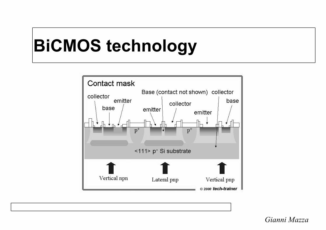
BiCMOS technology
Gianni Mazza
Bipolar transistors� Requires epitaxial process ( buried layer to
decrease collector resistance )� Good npn vertical transistor� Bad pnp lateral transistor� Good pnp vertical transistor with grounded
collector
Gianni Mazza

SiGe - 1
Gianni Mazza

SiGe - 2
Gianni Mazza

Latch-up - 1
Gianni Mazza


Latch-up - 4
Gianni Mazza
To prevent latch-up :
� Substrate contacts to lower RS and R
W� Increase distance between nMOS and nWell� Shallow Trench Insulation� SOI technologies

SOI process
Gianni Mazza

SOI techniques
Gianni Mazza
� Wafer bonding and etch back� Silicon on sapphire/zirconia (Zr
2O)
� Recrystallization from the melt� Selective epitaxy over holes in the oxide (ELO)� Porous silicon (FIPOX)� Oxygen implantation (SIMOX)� Silicon-On-Nothing (SON)

SOI structure
Gianni Mazza

Parasitic capacitance
Gianni Mazza

Tolerance to SEU
Gianni Mazza

3-D ICs
Gianni Mazza

µChannel cooling
Gianni Mazza
Related Documents


