Influence of the metallic contact in extreme-ultraviolet and soft x-ray diamond based Schottky photodiodes I. Ciancaglioni, C. Di Venanzio, Marco Marinelli, E. Milani, G. Prestopino et al. Citation: J. Appl. Phys. 110, 054513 (2011); doi: 10.1063/1.3633219 View online: http://dx.doi.org/10.1063/1.3633219 View Table of Contents: http://jap.aip.org/resource/1/JAPIAU/v110/i5 Published by the American Institute of Physics. Related Articles Efficiency droop in AlGaInP and GaInN light-emitting diodes Appl. Phys. Lett. 100, 111106 (2012) Dominant ultraviolet electroluminescence from p-ZnO:As/n-SiC(6H) heterojunction light-emitting diodes Appl. Phys. Lett. 100, 101112 (2012) High 5.2 peak-to-valley current ratio in Si/SiGe resonant interband tunnel diodes grown by chemical vapor deposition Appl. Phys. Lett. 100, 092104 (2012) Characterization of germanium/silicon p–n junction fabricated by low temperature direct wafer bonding and layer exfoliation Appl. Phys. Lett. 100, 092102 (2012) AlGaN-based ultraviolet light-emitting diodes using fluorine-doped indium tin oxide electrodes Appl. Phys. Lett. 100, 081110 (2012) Additional information on J. Appl. Phys. Journal Homepage: http://jap.aip.org/ Journal Information: http://jap.aip.org/about/about_the_journal Top downloads: http://jap.aip.org/features/most_downloaded Information for Authors: http://jap.aip.org/authors Downloaded 19 Mar 2012 to 160.80.88.68. Redistribution subject to AIP license or copyright; see http://jap.aip.org/about/rights_and_permissions

Welcome message from author
This document is posted to help you gain knowledge. Please leave a comment to let me know what you think about it! Share it to your friends and learn new things together.
Transcript

Influence of the metallic contact in extreme-ultraviolet and soft x-raydiamond based Schottky photodiodesI Ciancaglioni C Di Venanzio Marco Marinelli E Milani G Prestopino et al Citation J Appl Phys 110 054513 (2011) doi 10106313633219 View online httpdxdoiorg10106313633219 View Table of Contents httpjapaiporgresource1JAPIAUv110i5 Published by the American Institute of Physics Related ArticlesEfficiency droop in AlGaInP and GaInN light-emitting diodes Appl Phys Lett 100 111106 (2012) Dominant ultraviolet electroluminescence from p-ZnOAsn-SiC(6H) heterojunction light-emitting diodes Appl Phys Lett 100 101112 (2012) High 52 peak-to-valley current ratio in SiSiGe resonant interband tunnel diodes grown by chemical vapordeposition Appl Phys Lett 100 092104 (2012) Characterization of germaniumsilicon pndashn junction fabricated by low temperature direct wafer bonding and layerexfoliation Appl Phys Lett 100 092102 (2012) AlGaN-based ultraviolet light-emitting diodes using fluorine-doped indium tin oxide electrodes Appl Phys Lett 100 081110 (2012) Additional information on J Appl PhysJournal Homepage httpjapaiporg Journal Information httpjapaiporgaboutabout_the_journal Top downloads httpjapaiporgfeaturesmost_downloaded Information for Authors httpjapaiporgauthors
Downloaded 19 Mar 2012 to 160808868 Redistribution subject to AIP license or copyright see httpjapaiporgaboutrights_and_permissions
Influence of the metallic contact in extreme-ultraviolet and soft x-raydiamond based Schottky photodiodes
I Ciancaglioni1 C Di Venanzio1 Marco Marinelli1 E Milani1 G Prestopino1C Verona1a) G Verona-Rinati1 M Angelone2 M Pillon2 and N Tartoni31Dip di Ing Meccanica Universita di Roma ldquoTor Vergata rdquo Roma 00133 Italy2Associazione EURATOM-ENEA sulla Fusione Frascati Roma 00044 Italy3Diamond Light Source Harwell Science and Innovation Campus Chilton-Didcot OX11 0DE OxfordshireUnited Kingdom
(Received 21 June 2011 accepted 2 August 2011 published online 15 September 2011)
X-ray and UV photovoltaic Schottky photodiodes based on single crystal diamond were recently
developed at Rome ldquoTor Vergatardquo University laboratories In this work different rectifying
metallic contact materials were thermally evaporated on the oxidized surface of intrinsic single
crystal diamond grown by chemical vapor deposition Their impact on the detection performance
in the extreme UV and soft x-ray spectral regions was studied The electrical characterization of
the metal=diamond Schottky junctions was performed at room temperature by measuring the
capacitancendashvoltage characteristics The diamond photodiodes were then tested both over the
extreme UV spectral region from 10 to 60 eV by using He-Ne DC gas discharge as a radiation
source and toroidal vacuum monochromator and in the soft x-ray range from 6 to 20 keV at the
Diamond Light Source synchrotron x-ray beam-line in Harwell (UK) In both experimental setups
time response and spectral responsivity were analyzed for all the investigated Schottky contact
materials A good agreement between the experimental data and theoretical results from Monte
Carlo simulations is found VC 2011 American Institute of Physics [doi10106313633219]
I INTRODUCTION
Diamond is a semiconducting material with extreme op-
tical and electronic properties12 that make it an ideal mate-
rial for the fabrication of high performance visible-blind
detectors for ultraviolet (UV) and soft x-ray (XR) radiation3
Several attempts were made to build up photodetectors from
natural or synthetic diamonds45 A great effort is also being
devoted to produce devices from synthetic single crystal dia-
mond (SCD) films grown by homoepitaxial chemical vapor
deposition (CVD) onto low-cost SCD substrates67
Different photodetector structures based on CVD dia-
mond have been reported by several research groups89 A
promising approach is to use a Schottky photodiode (PD) in
a multilayered transverse configuration due to its low leak-
age current low noise level zero-bias operation no signal
due to secondary electrons fast response time and good
responsivity1011 The main detection mechanism in Schottky
photodiodes is based on collection of photogenerated
electronndashhole pairs in the depleted layer region beneath the
Schottky metal contact so that the development of good
Schottky contacts plays a significant role on the overall
detection performance of such devices
Many authors have studied the electrical properties of
metal=diamond interfaces evidencing the importance of
physico-chemical treatments of diamond surface and of
Schottky metal contacts1213 The aim of this paper is to per-
form a systematic analysis of several rectifying metallic con-
tact materials on our diamond based photodiodes to
investigate the physical properties of different metal=diamond
interfaces and their role in the detection performance in the
extreme UV and soft x-ray spectral region To this purpose
electro-optical measurements such as C-V characteristics
spectral responsivity and time response evaluation were
performed
II EXPERIMENTAL SETUP
The diamond photodetectors investigated in the present
study consist of a multilayered structure obtained by a three
step deposition process as reported in Ref 11 This proce-
dure allows a nominally intrinsic single crystal diamond
layer which is the detecting region sandwiched between a
Schottky metallic contact of 3 mm in diameter and a highly
conductive boron doped diamond layer acting as backing
contact In Ref 11 it has been also shown that the nominally
intrinsic layer acts as a slightly p-type doped layer with a
concentration of acceptor of the order to 1014 cm3 The
scheme of the device is shown in Fig 1
Due to the small penetration depth of the extreme UV
radiation in diamond14 a 2 lm thick intrinsic diamond layer
was used for the measurement in this spectral region
(UV-PD in the following) In the case of soft x-ray detection
similar detectors with an intrinsic diamond thickness of
about 30 lm were used instead (XR-PDs in the following)
due to the higher penetration depth of the incident radiation
UV-PDs were fabricated using Schottky contacts made
of five different semitransparent metals on the very same
SCD 63 A thick silver (Ag) 68 A thick platinum (Pt)
100 A thick aluminum (Al) 120 A thick chromium (Cr) and
70 A thick gold (Au) Their thickness was measured directly
a)Author to whom correspondence should be addressed Electronic mail
claudioveronauniroma2it
0021-89792011110(5)0545136$3000 VC 2011 American Institute of Physics110 054513-1
JOURNAL OF APPLIED PHYSICS 110 054513 (2011)
Downloaded 19 Mar 2012 to 160808868 Redistribution subject to AIP license or copyright see httpjapaiporgaboutrights_and_permissions
by a thickness monitor with a resolution of about 1 A Exper-
imental tests were performed according to the following pro-
cedure (i) the intrinsic diamond surface of the UV-PD
detector was metalized with a metallic contact (ii) measure-
ments were performed and (iii) the diamond surface was
carefully cleaned by wet etching before depositing a new
contact The whole procedure was repeated a few times for
each metal contact to verify the repeatability and the reliabil-
ity of the cleaning=deposition process As reported in Ref
15 for contacts in the nanometer thickness range contact
inhomogeneity may have an impact on the electrical proper-
ties Although we cannot rule out such an effect in our case
scanning electron microscope (SEM) observation did not
evidence any lack of uniformity
The UV-PD has been tested in our laboratories over the
extreme UV spectral region from 10 to 60 eV using a He-Ne
DC gas discharge as a radiation source and a toroidal grating
vacuum monochromator (Jobin Yvon model LHT-30) with a
5 A wavelength resolution The photodetector response was
compared to that of a calibrated NIST silicon photodiode16
placed in the same position by using a three dimension me-
chanical (X-Y-Z) stage powered by stepper motors The pho-
tocurrent was measured by a Keithley 6517 A electrometer
The UV-PD was encapsulated in a copper=vetronite shielded
housing with a 2 mm pinhole to collimate the radiation on
the sensitive area of the detectors and to obtain the same illu-
minated area on the silicon photodiode In such a housing
the top surface metal contact is grounded and the photocur-
rent is measured from p-type diamond electrode so that the
signal is not affected by secondary electron emission current
from the illuminated contact17ndash19 Only the internal photo-
current produced inside the diamond is thus measured
In the case of the x-ray detectors four similar XR-PDs
with different metallic contacts were tested at the beamline
B16 of Diamond Light Source (DLS) synchrotron 100 nm
thick Al contact 25 nm thick Pt contact 22 nm thick Au
contact and 20 nm Cr thick contact A monochromatic beam
delivered by a double crystal monochromator was used in
the region from 6 keV to 20 keV The beam was focused by
the beam line optics (spot size about 300 lm) so as to be
completely intercepted by the sensitive area of the detector
Due to the low energy of the beam a tube filled with helium
was used to minimize the air path and to reduce the
absorption The detectors were operated in current mode and
a variable gain low noise current amplifier FEMTO model
DLPCA-200 (Ref 20) was used as front-end electronics
The XR-PDs under test were placed in a grounded metal box
on top of a high resolution translational stage so that high
precision positioning of the detector with respect to the beam
was achieved The time response of the XR-PDs was meas-
ured by using a rotating mechanical chopper placed in front
of the x-ray radiation beam and a Tektronix oscilloscope
Finally a PTB calibrated silicon detector was also placed on
the translational stage nearly the diamond detector and used
during the energy response measurement
III RESULTS AND DISCUSSIONS
The I-V characteristics of the metal=diamond Schottky
junction of the photodetector were performed at room tem-
perature by using a Keithley 6517 A pico-ampere meter The
I-V characteristics were obtained by applying a voltage to
the p-type diamond layer while earthing the metallic contact
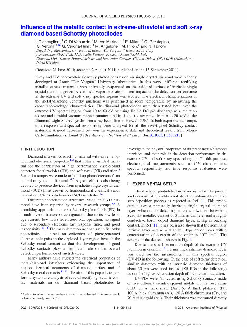
Figure 2 shows the typical I-V characteristic of the diamond
Schottky photodiode A very high rectification ratio of order
of 108 was observed at 63 V In the inset of the figure the
I-V characteristic in forward region for the different metallic
contacts is also reported In this region the forward current
density is well described by the thermionic emission (TE)
theory and a rough approximation of the Schottky barrier
height and the ideality factor can be extracted for the differ-
ent metallizations Ideality factors below 18 were estimated
for all the investigated contacts with barrier heights in the
range between 18 and 2 eV
Capacitance-voltage (C-V) measurements were per-
formed by using an Agilent 4284 A LCR meter to get infor-
mation on the depletion region width of the Schottky barrier
formed by the metal electrode which extends within the
intrinsic diamond layer In first approximation at low fre-
quency the junction capacitance of the device is approxi-
mated to that of a parallel plate capacitor so that the
depletion thickness W of the detector as a function of the
applied bias voltage VB was estimated from the C-V data
according to the following equation21
FIG 1 (Color online) Schematic representation of Schottky diamond
photodiodes
FIG 2 (Color online) Currentndashvoltage (I-V) characteristics Inset magni-
fied view of I-V characteristic in forward voltage region for all the investi-
gated metallic contacts
054513-2 Ciancaglioni et al J Appl Phys 110 054513 (2011)
Downloaded 19 Mar 2012 to 160808868 Redistribution subject to AIP license or copyright see httpjapaiporgaboutrights_and_permissions
W frac14
ffiffiffiffiffiffiffiffiffiffiffiffiffiffiffiffiffiffiffiffiffiffiffiffiffiffiffiffiffiffiffiffi2e0erethVB thorn VBITHORN
qNA
sfrac14 e0er
A
C(1)
where A is the contact area q the electric charge o the
dielectric constant of free space r the diamond dielectric
constant VBI the built-in potential at the Schottky barrier
and NA the concentration of electrically active defects
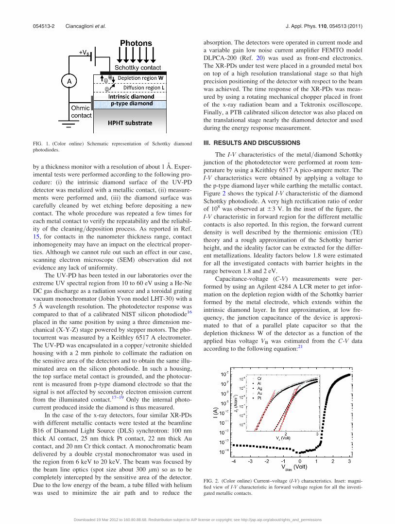
Figure 3 shows the capacitancendashvoltage curves for both
UV-PD and XR-PDs with different metallic contacts at room
temperature and at 100 kHz frequency in the reverse bias
region Using Eq (1) a depletion thickness of about 2 lm is
extracted from the experimental data for the UV-PD detec-
tors at all bias voltages applied (see Fig 3(a)) Such a thick-
ness is approximately the nominally intrinsic diamond film
thickness thus demonstrating that the sensing layer is fully
depleted
For the XR-PDs (see Fig 3(b)) the width of the deple-
tion layer at zero bias voltage is evaluated to be approxi-
mately 125 lm 14 lm 2 lm and 215 lm for Al Cr Pt
and Au contacts respectively In this case the depletion
width increases extending into the thick intrinsic diamond
layer as reverse bias increases up to 20 V
Both the active defects concentration NA and the built-in
potential VBI can be derived from the results reported in Fig
3(b) for the XR-PDs The best fit of the experimental data
was performed by using Eq (1) in the low voltage region
the results of which are summarized in Table I For the four
tested XR-PDs devices NA is of the order of 1014 cm3
In the next sections the effect of the metallic contact
materials on time response and responsivity of both diamond
based photodetectors is analyzed
A Extreme UV characterization
The normalized time response under illumination of He-
Ne DC gas discharge at zero applied voltage is reported in
Fig 4 for the UV-PD with different metal contacts The UV-PD
metalized with Ag Pt Al and Cr shows fast rise and decay
times of the photocurrent The responses are reproducible
and undesired effects such as persistent photocurrent and pri-
ming or memory effects are negligible The response time
which was estimated to be about 60 ms is completely
ascribed to the electrometer preamplifier time constant On
the other hand the detector operating with Au contact clearly
shows a slow component of the photocurrent to reach the
FIG 3 (Color online) Capacitancendashvoltage (C-V) char-
acteristics and corresponding depletion thickness (W) of
(a) UV-PD and (b) XR-PD detectors respectively The
full lines are the best fit calculated by Eq (1)
TABLE I Fit parameters of Eq (1)
Detector
Active defects
concentration NA (cm3)
Built-in
potential VBI (V)
XR-PD_Al 501014 15
XR-PD_Cr 361014 12
XR-PD_Pt 311014 21
XR-PD_Au 731014 48
FIG 4 (Color online) Normalized time response under illumination of
HendashNe DC gas discharge radiation source of the UV-PD for the different
metals
054513-3 Ciancaglioni et al J Appl Phys 110 054513 (2011)
Downloaded 19 Mar 2012 to 160808868 Redistribution subject to AIP license or copyright see httpjapaiporgaboutrights_and_permissions
plateau value once irradiated and a photocurrent persistence
decaying exponentially with a time constant of about 4 s
This behavior of the Au contact has been checked by repeat-
ing a few times the whole cleaning=metallization=test proce-
dure both on the investigated SCD sample and on different
samples In all cases a slow component of the photocurrent
was always observed using thermally evaporated Au
The emission spectrum of the DC discharge He-Ne lamp
in the 10-60 eV energy range was then measured by the
UV-PD for each different metallic contact The absolute
responsivity of UV-PD expressed in amperes per watt
(A=W) was evaluated from the obtained spectra by compar-
ing the diamond response with the one of a calibrated silicon
photodiode The results are shown in Fig 5 All the obtained
responsivity curves show a minimum between 15 and 20 eV
A monotonically increasing responsivity is observed at
higher photon energy for all cases with the exception of Cr
the responsivity of which decreases above 40 eV
An accurate estimation of the responsivity obtained
from the Au contact is not reported in this paper because the
photoresponse was affected by persistent photocurrent and
high noise even at low level signals
The experimental data were compared with the theoreti-
cal curve obtained by calculating the fraction of energy de-
posited in the diamond layer and by taking into account
absorption losses in the Schottky metal electrode22
RethA=WTHORN frac14 eth1 eadiamDdiamTHORNeaMetaldMetal
EetheVTHORN (2)
where E is the mean electron-hole pair creation energy
(132 eV for diamond) a is the absorption coefficient of the
materials Ddiam is the active diamond thickness and dMetal is
the thickness of the metallic contact The transmission values
in Eq (2) are readily calculated from the material thickness
and the known x-ray optical data for elements23 The dashed
lines plotted in Fig 5 are the results of the fit calculated
according to Eq (2) The thickness of the tested metallic
contacts and the effective thickness of intrinsic diamond
estimated by the C-V curves were taken into account
Clearly the fit curves do not reproduce the experimental
data thus indicating that other contributions must be consid-
ered when calculating the device responsivity Because the
UV-induced charges are generated at the metal=diamond
interface such a contribution could be related to the diamond
surface properties In the investigated photon energies the
penetration depth of photons in diamond shows a deep mini-
mum at about 16 eV1423 the trend of which is qualitatively
similar to the responsivity curves observed in Fig 5 This
suggests the existence of a dead layer located at diamond
surface probably related to the recombination of photo-
generated carriers close to the metal-diamond interface2425
In this region in fact the photogenerated carriers could be
trapped very efficiently by the defects of the diamond surface
giving a low contribution to the photocurrent Under this
assumption in first approximation Eq (2) must be multi-
plied by the additional term exp(-adiamddiam) where adiam(k)
is the diamond absorption coefficient and ddiam is the thick-
ness of the dead diamond layer
The responsivity curves reported in Fig 5 as solid lines
are the results of the fits using the values reported in Table II
They show a good agreement with the experimental data for
all tested metallic contacts
B Soft x-ray characterization
Figure 6 shows the XR-PD photocurrent measured dur-
ing 10 keV x-ray irradiation chopped at 39 kHz Rise and
FIG 5 Absolute spectral responsivity of UV-PD
between 10 and 60 eV for each different metallic con-
tact The dashed lines are the results of the fit calculated
by Eq (2) The solid line curves correspond to Eq (2)
multiplied by the exponential term related to the dead
diamond layer
TABLE II Fit parameters of Eq (2) multiplied by the additional term exp
(-adiamddiam)
Detector
Depletion layer
W (lm)frac14Ddiam
Dead diamond
layer ddiam (nm)
Metal contact
thickness dmetal (nm)
UV-PD_Al 184 70 10
UV-PD_Cr 190 55 12
UV-PD_Pt 191 55 68
UV-PD_Ag 186 58 63
054513-4 Ciancaglioni et al J Appl Phys 110 054513 (2011)
Downloaded 19 Mar 2012 to 160808868 Redistribution subject to AIP license or copyright see httpjapaiporgaboutrights_and_permissions
decay times of the photoresponse of about 50 ls are
observed for all the investigated contact metals a value
roughly corresponding to the full opening time of the aper-
ture of the mechanical chopper The slow component
observed in the UV measurement when using gold contact
could not be measured in this case being its time scale
approximately five orders of magnitude longer than the
adopted chopping time
The absolute responsivities versus x-ray photon energy
were obtained by comparing the currents measured in dia-
mond with the PTB silicon current and applying the proper
calibration factors The experimental data reported in Fig 7
were obtained for the tested XR-PDs in the 6 keV to 20 keV
energy range Due to its 30 lm thickness the intrinsic dia-
mond layer is only partially depleted in the adopted unbiased
operating conditions and carriers generated outside the
depletion region within the minority carrier diffusion length
L are collected too (see Fig 1) Therefore both drift and dif-
fusion contribution to the current due to photogenerated
carriers must be taken into account Previous results1126
show that the diffusion length L is about 26 lm This value
is added to the depletion layer thickness calculated from the
C-V curves to evaluate the effective thickness of the active
diamond layer of XR-PDs
The energy deposited in the diamond was thus obtained
by using the actual thickness values reported in Table III for
both the evaporated metal contact and the active diamond
layer
The x-ray high penetration depth makes the previously
mentioned dead diamond layer negligible The fitting curves
(dashed lines in Fig 7) however do not satisfactorily repro-
duce the experimental the data especially for Pt and Au con-
tacts The described procedure only takes into account
energy deposited in the detector by carrier photo-generation
Energy deposition is however an inherently stochastic
process in which other channels besides carrier photogenera-
tion occur each with its proper cross section and detector ge-
ometry dependence In particular in the x-ray region it is
very important to take into account the physical interactions
of radiation with matter ie Compton photon scattering
photo and knock-on secondary electrons which are not con-
sidered in the fitting procedure described in the preceding
text To accurately simulate the ionizing mechanism inside a
detector volume Monte Carlo methods must therefore be
used A 3-D Monte Carlo simulation of the experimental
data was performed by using the MCNP-5 radiation transport
code27 The simulation was carried out using the data
reported in Table III The results of the Monte Carlo simula-
tion reported in Fig 7 as solid lines are now in good agree-
ment with the experimental data
The observed large difference in responsivities among
the four tested XR-PDs reflects the difference interaction
between x-ray beam and different metal contacts material In
particular the responsivity of detectors with Pt and Au con-
tact is higher than that of detectors using Al and Cr contacts
Indeed platinum and gold have an atomic number (ZPtfrac14 78
and ZAu =79) higher than aluminum and chromium (ZAlfrac14 13
and ZCrfrac14 24) so as to produce many photo and knock-on
secondary electrons that substantially contribute to the
energy deposition in the diamond layer This is even more
evident at high photon energies above 10 keV where a clear
FIG 6 (Color online) Temporal response of the XR-PDs under 10 keV
x-ray beam chopped at 39 kHz
FIG 7 Experimental and theoretical spectral respon-
sivity of the XR-PDs in the range from 6 to 20 keV
The dashed lines are the results of the fit calculated by
Eq (2) The solid line curves correspond to Monte
Carlo simulations
054513-5 Ciancaglioni et al J Appl Phys 110 054513 (2011)
Downloaded 19 Mar 2012 to 160808868 Redistribution subject to AIP license or copyright see httpjapaiporgaboutrights_and_permissions
change in the behavior of the responsivity curves is observed
for both metals
IV CONCLUSIONS
Performance parameters such as time response and spec-
tral responsivity were analyzed for a single crystal diamond
photodiode in the extreme UV and soft x-ray spectral region
as a function of the Schottky metal contact material The
results show that the electro-optical performance of a dia-
mond detector is influenced by the used metal and the energy
dependent absorption length of the detected radiation
In the extreme UV region all contacts except the Au
contact show similar behavior in terms of time response and
no undesired effects such as persistent photocurrent or mem-
ory effects are observed The responsivity of UV-PD with
Ag Al Cr and Pt contacts show similar trends in the energy
range from 10 eV up to 60 eV increasing toward the edges
of the investigated spectral range and showing a minimum at
intermediate photon energies between 15 and 20 eV This is
attributed to the photon induced carriers which in this spec-
tral region are generated mainly close to the metal=diamond
interface The results of the fitting procedure show that a
dead diamond layer must be taken into account this is most
likely related to the high recombination of photo-generated
carriers near the metal electrode and significantly affects the
detector responsivity The thickness of this dead layer
region was observed in the range between 55 and 7 nm
The spectral responsivities of the XR-PDs were meas-
ured in the range from 6 to 20 keV showing a different trend
as a function of the metallic contacts The experimental data
were compared with the results of a 3 D Monte Carlo photon
and electron transport calculation A good agreement
between experimental data and simulated curves was
obtained and the main features of the responsivity curves
were explained in terms of the different Z-numbers of the
metals used for the contacts
1J E Field Properties of Diamond Academic London 19792J Prins The Physics of Diamond edited by A Paoletti and A Tucciarone
(IOS Press Amsterdam 1997)3J-F Hochedez J Alvarez F D Auret P Bergonzo M-C Castex A
Deneuville J M Defise B Fleck P Gibart S A Goodman O Hainaut
J-P Kleider P Lemaire J Manca E Monroy E Munoz P Muret
M Nesladek F Omnes E Pace J L Pau V Ralchenko J Roggen
U Schuhle and C Van Hoof Diamond Relat Mater 11 427 (2002)4L Barberini S Cadeddu and M Caria Nucl Instrum Methods Phys
Res A 460 127 (2001)5R D McKeag and R B Jackman Diamond Relat Mater 7 513 (1998)6T Teraji S Yoshizaki H Wada M Hamada and T Ito Diamond Relat
Mater 13 858 (2004)7J H Kaneko T Teraji Y Hirai M Shiraishi S Kawamura S Yoshi-
zaki T Ito K Ochiai T Nishitani and T Sawamura Rev Sci Instrum
75 358 (2004)8Meiyong Liao Y Koide and J Alvarez Appl Phys Lett 88 33504
(2006)9A BenMoussa K Haenen U Kroth V Mortet H A Barkad D Bolsee
C Hermans M Richter J C De Jaeger and J F Hochedez Semicond
Sci Technol 23 035026 (2008)10M Angelone M Pillon M Marinelli E Milani G Prestopino C Ver-
ona G Verona-Rinati I Coffey A Murari and N Tartoni Nucl
Instrum Methods Phys Res A 623 726 (2010)11S Almaviva M Marinelli E Milani G Prestopino A Tucciarone
C Verona G Verona-Rinati M Angelone M Pillon I Dolbnya K
Sawhney and N Tartoni J Appl Phys 107 1 (2010)12R D Mckeag R D Marshall B Baral S S M Chan and R B Jackman
Diam Relat Mater 6 374 (1997)13C Jany F Foulon P Bergonzo and R D Marshall Diam Relat Mater
7 951 (1998)14D Palik Handbook of Optical Constants of Solids II Academic New
York 199115J Alvarez F Houze J P Kleider M Y Liao and Y Koide Superlattices
Microstruct 40 343 (2006)16See http==wwwird-inccom for information about international radiation
detectors (IRDs)17M C Rossi Spaziani F Conte and G Ralchenko V Diam Relat Mat
14 552 (2005)18T Saito and K Hayashi Appl Phys Lett 86 122113 (2005)19I Ciancaglioni M Marinelli E Milani G Prestopino C Verona G
Verona-Rinati M Angelone and M Pillon J Appl Phys 110 014501
(2011)20See wwwfemto de for more information on the low noise current amplifier
FEMTO21D Neamen Semiconductor Physics and Devices Basic Principles
(McGraw-Hill Companies Chicago 1997)22S M Sze Physics of Semiconductor Devices (Wiley New York 1981)23http==henke lblgov=optical_constants=filter2forhtml for information on
filter transmission24J W Keister and J Smedley Nucl Instrum Methods Phys Res A 606
774 (2009)25S Almaviva M Marinelli E bMilani G Prestopino A Tucciarone C
Verona G Verona-Rinati M Angelone and M Pillon Diam Rel Mater
19 78 (2010)26A Lo Giudice P Olivero C Manfredotti M Marinelli E Milani F
Picollo G Prestopino A Re V Rigato C Verona G Verona-Rinati
and E Vittone Phys Status Solidi (RRL) 5 80 (2011)27See http==mcnp-greenlanlgov= for information about MCNP-5 radiation
transport code
TABLE III Parameters employed in the Monte Carlo simulations
Detector
Depletion
layer W
(lm)
Diffusion
length L
(lm)
Active diamond
thickness
WthornL(lm)frac14Ddiam
Metal contact
thickness
dmetal (nm)
XR-PD_Al 125 260 385 100
XR-PD_Cr 140 260 400 20
XR-PD_Pt 200 260 460 25
XR-PD_Au 220 260 480 22
054513-6 Ciancaglioni et al J Appl Phys 110 054513 (2011)
Downloaded 19 Mar 2012 to 160808868 Redistribution subject to AIP license or copyright see httpjapaiporgaboutrights_and_permissions
Influence of the metallic contact in extreme-ultraviolet and soft x-raydiamond based Schottky photodiodes
I Ciancaglioni1 C Di Venanzio1 Marco Marinelli1 E Milani1 G Prestopino1C Verona1a) G Verona-Rinati1 M Angelone2 M Pillon2 and N Tartoni31Dip di Ing Meccanica Universita di Roma ldquoTor Vergata rdquo Roma 00133 Italy2Associazione EURATOM-ENEA sulla Fusione Frascati Roma 00044 Italy3Diamond Light Source Harwell Science and Innovation Campus Chilton-Didcot OX11 0DE OxfordshireUnited Kingdom
(Received 21 June 2011 accepted 2 August 2011 published online 15 September 2011)
X-ray and UV photovoltaic Schottky photodiodes based on single crystal diamond were recently
developed at Rome ldquoTor Vergatardquo University laboratories In this work different rectifying
metallic contact materials were thermally evaporated on the oxidized surface of intrinsic single
crystal diamond grown by chemical vapor deposition Their impact on the detection performance
in the extreme UV and soft x-ray spectral regions was studied The electrical characterization of
the metal=diamond Schottky junctions was performed at room temperature by measuring the
capacitancendashvoltage characteristics The diamond photodiodes were then tested both over the
extreme UV spectral region from 10 to 60 eV by using He-Ne DC gas discharge as a radiation
source and toroidal vacuum monochromator and in the soft x-ray range from 6 to 20 keV at the
Diamond Light Source synchrotron x-ray beam-line in Harwell (UK) In both experimental setups
time response and spectral responsivity were analyzed for all the investigated Schottky contact
materials A good agreement between the experimental data and theoretical results from Monte
Carlo simulations is found VC 2011 American Institute of Physics [doi10106313633219]
I INTRODUCTION
Diamond is a semiconducting material with extreme op-
tical and electronic properties12 that make it an ideal mate-
rial for the fabrication of high performance visible-blind
detectors for ultraviolet (UV) and soft x-ray (XR) radiation3
Several attempts were made to build up photodetectors from
natural or synthetic diamonds45 A great effort is also being
devoted to produce devices from synthetic single crystal dia-
mond (SCD) films grown by homoepitaxial chemical vapor
deposition (CVD) onto low-cost SCD substrates67
Different photodetector structures based on CVD dia-
mond have been reported by several research groups89 A
promising approach is to use a Schottky photodiode (PD) in
a multilayered transverse configuration due to its low leak-
age current low noise level zero-bias operation no signal
due to secondary electrons fast response time and good
responsivity1011 The main detection mechanism in Schottky
photodiodes is based on collection of photogenerated
electronndashhole pairs in the depleted layer region beneath the
Schottky metal contact so that the development of good
Schottky contacts plays a significant role on the overall
detection performance of such devices
Many authors have studied the electrical properties of
metal=diamond interfaces evidencing the importance of
physico-chemical treatments of diamond surface and of
Schottky metal contacts1213 The aim of this paper is to per-
form a systematic analysis of several rectifying metallic con-
tact materials on our diamond based photodiodes to
investigate the physical properties of different metal=diamond
interfaces and their role in the detection performance in the
extreme UV and soft x-ray spectral region To this purpose
electro-optical measurements such as C-V characteristics
spectral responsivity and time response evaluation were
performed
II EXPERIMENTAL SETUP
The diamond photodetectors investigated in the present
study consist of a multilayered structure obtained by a three
step deposition process as reported in Ref 11 This proce-
dure allows a nominally intrinsic single crystal diamond
layer which is the detecting region sandwiched between a
Schottky metallic contact of 3 mm in diameter and a highly
conductive boron doped diamond layer acting as backing
contact In Ref 11 it has been also shown that the nominally
intrinsic layer acts as a slightly p-type doped layer with a
concentration of acceptor of the order to 1014 cm3 The
scheme of the device is shown in Fig 1
Due to the small penetration depth of the extreme UV
radiation in diamond14 a 2 lm thick intrinsic diamond layer
was used for the measurement in this spectral region
(UV-PD in the following) In the case of soft x-ray detection
similar detectors with an intrinsic diamond thickness of
about 30 lm were used instead (XR-PDs in the following)
due to the higher penetration depth of the incident radiation
UV-PDs were fabricated using Schottky contacts made
of five different semitransparent metals on the very same
SCD 63 A thick silver (Ag) 68 A thick platinum (Pt)
100 A thick aluminum (Al) 120 A thick chromium (Cr) and
70 A thick gold (Au) Their thickness was measured directly
a)Author to whom correspondence should be addressed Electronic mail
claudioveronauniroma2it
0021-89792011110(5)0545136$3000 VC 2011 American Institute of Physics110 054513-1
JOURNAL OF APPLIED PHYSICS 110 054513 (2011)
Downloaded 19 Mar 2012 to 160808868 Redistribution subject to AIP license or copyright see httpjapaiporgaboutrights_and_permissions
by a thickness monitor with a resolution of about 1 A Exper-
imental tests were performed according to the following pro-
cedure (i) the intrinsic diamond surface of the UV-PD
detector was metalized with a metallic contact (ii) measure-
ments were performed and (iii) the diamond surface was
carefully cleaned by wet etching before depositing a new
contact The whole procedure was repeated a few times for
each metal contact to verify the repeatability and the reliabil-
ity of the cleaning=deposition process As reported in Ref
15 for contacts in the nanometer thickness range contact
inhomogeneity may have an impact on the electrical proper-
ties Although we cannot rule out such an effect in our case
scanning electron microscope (SEM) observation did not
evidence any lack of uniformity
The UV-PD has been tested in our laboratories over the
extreme UV spectral region from 10 to 60 eV using a He-Ne
DC gas discharge as a radiation source and a toroidal grating
vacuum monochromator (Jobin Yvon model LHT-30) with a
5 A wavelength resolution The photodetector response was
compared to that of a calibrated NIST silicon photodiode16
placed in the same position by using a three dimension me-
chanical (X-Y-Z) stage powered by stepper motors The pho-
tocurrent was measured by a Keithley 6517 A electrometer
The UV-PD was encapsulated in a copper=vetronite shielded
housing with a 2 mm pinhole to collimate the radiation on
the sensitive area of the detectors and to obtain the same illu-
minated area on the silicon photodiode In such a housing
the top surface metal contact is grounded and the photocur-
rent is measured from p-type diamond electrode so that the
signal is not affected by secondary electron emission current
from the illuminated contact17ndash19 Only the internal photo-
current produced inside the diamond is thus measured
In the case of the x-ray detectors four similar XR-PDs
with different metallic contacts were tested at the beamline
B16 of Diamond Light Source (DLS) synchrotron 100 nm
thick Al contact 25 nm thick Pt contact 22 nm thick Au
contact and 20 nm Cr thick contact A monochromatic beam
delivered by a double crystal monochromator was used in
the region from 6 keV to 20 keV The beam was focused by
the beam line optics (spot size about 300 lm) so as to be
completely intercepted by the sensitive area of the detector
Due to the low energy of the beam a tube filled with helium
was used to minimize the air path and to reduce the
absorption The detectors were operated in current mode and
a variable gain low noise current amplifier FEMTO model
DLPCA-200 (Ref 20) was used as front-end electronics
The XR-PDs under test were placed in a grounded metal box
on top of a high resolution translational stage so that high
precision positioning of the detector with respect to the beam
was achieved The time response of the XR-PDs was meas-
ured by using a rotating mechanical chopper placed in front
of the x-ray radiation beam and a Tektronix oscilloscope
Finally a PTB calibrated silicon detector was also placed on
the translational stage nearly the diamond detector and used
during the energy response measurement
III RESULTS AND DISCUSSIONS
The I-V characteristics of the metal=diamond Schottky
junction of the photodetector were performed at room tem-
perature by using a Keithley 6517 A pico-ampere meter The
I-V characteristics were obtained by applying a voltage to
the p-type diamond layer while earthing the metallic contact
Figure 2 shows the typical I-V characteristic of the diamond
Schottky photodiode A very high rectification ratio of order
of 108 was observed at 63 V In the inset of the figure the
I-V characteristic in forward region for the different metallic
contacts is also reported In this region the forward current
density is well described by the thermionic emission (TE)
theory and a rough approximation of the Schottky barrier
height and the ideality factor can be extracted for the differ-
ent metallizations Ideality factors below 18 were estimated
for all the investigated contacts with barrier heights in the
range between 18 and 2 eV
Capacitance-voltage (C-V) measurements were per-
formed by using an Agilent 4284 A LCR meter to get infor-
mation on the depletion region width of the Schottky barrier
formed by the metal electrode which extends within the
intrinsic diamond layer In first approximation at low fre-
quency the junction capacitance of the device is approxi-
mated to that of a parallel plate capacitor so that the
depletion thickness W of the detector as a function of the
applied bias voltage VB was estimated from the C-V data
according to the following equation21
FIG 1 (Color online) Schematic representation of Schottky diamond
photodiodes
FIG 2 (Color online) Currentndashvoltage (I-V) characteristics Inset magni-
fied view of I-V characteristic in forward voltage region for all the investi-
gated metallic contacts
054513-2 Ciancaglioni et al J Appl Phys 110 054513 (2011)
Downloaded 19 Mar 2012 to 160808868 Redistribution subject to AIP license or copyright see httpjapaiporgaboutrights_and_permissions
W frac14
ffiffiffiffiffiffiffiffiffiffiffiffiffiffiffiffiffiffiffiffiffiffiffiffiffiffiffiffiffiffiffiffi2e0erethVB thorn VBITHORN
qNA
sfrac14 e0er
A
C(1)
where A is the contact area q the electric charge o the
dielectric constant of free space r the diamond dielectric
constant VBI the built-in potential at the Schottky barrier
and NA the concentration of electrically active defects
Figure 3 shows the capacitancendashvoltage curves for both
UV-PD and XR-PDs with different metallic contacts at room
temperature and at 100 kHz frequency in the reverse bias
region Using Eq (1) a depletion thickness of about 2 lm is
extracted from the experimental data for the UV-PD detec-
tors at all bias voltages applied (see Fig 3(a)) Such a thick-
ness is approximately the nominally intrinsic diamond film
thickness thus demonstrating that the sensing layer is fully
depleted
For the XR-PDs (see Fig 3(b)) the width of the deple-
tion layer at zero bias voltage is evaluated to be approxi-
mately 125 lm 14 lm 2 lm and 215 lm for Al Cr Pt
and Au contacts respectively In this case the depletion
width increases extending into the thick intrinsic diamond
layer as reverse bias increases up to 20 V
Both the active defects concentration NA and the built-in
potential VBI can be derived from the results reported in Fig
3(b) for the XR-PDs The best fit of the experimental data
was performed by using Eq (1) in the low voltage region
the results of which are summarized in Table I For the four
tested XR-PDs devices NA is of the order of 1014 cm3
In the next sections the effect of the metallic contact
materials on time response and responsivity of both diamond
based photodetectors is analyzed
A Extreme UV characterization
The normalized time response under illumination of He-
Ne DC gas discharge at zero applied voltage is reported in
Fig 4 for the UV-PD with different metal contacts The UV-PD
metalized with Ag Pt Al and Cr shows fast rise and decay
times of the photocurrent The responses are reproducible
and undesired effects such as persistent photocurrent and pri-
ming or memory effects are negligible The response time
which was estimated to be about 60 ms is completely
ascribed to the electrometer preamplifier time constant On
the other hand the detector operating with Au contact clearly
shows a slow component of the photocurrent to reach the
FIG 3 (Color online) Capacitancendashvoltage (C-V) char-
acteristics and corresponding depletion thickness (W) of
(a) UV-PD and (b) XR-PD detectors respectively The
full lines are the best fit calculated by Eq (1)
TABLE I Fit parameters of Eq (1)
Detector
Active defects
concentration NA (cm3)
Built-in
potential VBI (V)
XR-PD_Al 501014 15
XR-PD_Cr 361014 12
XR-PD_Pt 311014 21
XR-PD_Au 731014 48
FIG 4 (Color online) Normalized time response under illumination of
HendashNe DC gas discharge radiation source of the UV-PD for the different
metals
054513-3 Ciancaglioni et al J Appl Phys 110 054513 (2011)
Downloaded 19 Mar 2012 to 160808868 Redistribution subject to AIP license or copyright see httpjapaiporgaboutrights_and_permissions
plateau value once irradiated and a photocurrent persistence
decaying exponentially with a time constant of about 4 s
This behavior of the Au contact has been checked by repeat-
ing a few times the whole cleaning=metallization=test proce-
dure both on the investigated SCD sample and on different
samples In all cases a slow component of the photocurrent
was always observed using thermally evaporated Au
The emission spectrum of the DC discharge He-Ne lamp
in the 10-60 eV energy range was then measured by the
UV-PD for each different metallic contact The absolute
responsivity of UV-PD expressed in amperes per watt
(A=W) was evaluated from the obtained spectra by compar-
ing the diamond response with the one of a calibrated silicon
photodiode The results are shown in Fig 5 All the obtained
responsivity curves show a minimum between 15 and 20 eV
A monotonically increasing responsivity is observed at
higher photon energy for all cases with the exception of Cr
the responsivity of which decreases above 40 eV
An accurate estimation of the responsivity obtained
from the Au contact is not reported in this paper because the
photoresponse was affected by persistent photocurrent and
high noise even at low level signals
The experimental data were compared with the theoreti-
cal curve obtained by calculating the fraction of energy de-
posited in the diamond layer and by taking into account
absorption losses in the Schottky metal electrode22
RethA=WTHORN frac14 eth1 eadiamDdiamTHORNeaMetaldMetal
EetheVTHORN (2)
where E is the mean electron-hole pair creation energy
(132 eV for diamond) a is the absorption coefficient of the
materials Ddiam is the active diamond thickness and dMetal is
the thickness of the metallic contact The transmission values
in Eq (2) are readily calculated from the material thickness
and the known x-ray optical data for elements23 The dashed
lines plotted in Fig 5 are the results of the fit calculated
according to Eq (2) The thickness of the tested metallic
contacts and the effective thickness of intrinsic diamond
estimated by the C-V curves were taken into account
Clearly the fit curves do not reproduce the experimental
data thus indicating that other contributions must be consid-
ered when calculating the device responsivity Because the
UV-induced charges are generated at the metal=diamond
interface such a contribution could be related to the diamond
surface properties In the investigated photon energies the
penetration depth of photons in diamond shows a deep mini-
mum at about 16 eV1423 the trend of which is qualitatively
similar to the responsivity curves observed in Fig 5 This
suggests the existence of a dead layer located at diamond
surface probably related to the recombination of photo-
generated carriers close to the metal-diamond interface2425
In this region in fact the photogenerated carriers could be
trapped very efficiently by the defects of the diamond surface
giving a low contribution to the photocurrent Under this
assumption in first approximation Eq (2) must be multi-
plied by the additional term exp(-adiamddiam) where adiam(k)
is the diamond absorption coefficient and ddiam is the thick-
ness of the dead diamond layer
The responsivity curves reported in Fig 5 as solid lines
are the results of the fits using the values reported in Table II
They show a good agreement with the experimental data for
all tested metallic contacts
B Soft x-ray characterization
Figure 6 shows the XR-PD photocurrent measured dur-
ing 10 keV x-ray irradiation chopped at 39 kHz Rise and
FIG 5 Absolute spectral responsivity of UV-PD
between 10 and 60 eV for each different metallic con-
tact The dashed lines are the results of the fit calculated
by Eq (2) The solid line curves correspond to Eq (2)
multiplied by the exponential term related to the dead
diamond layer
TABLE II Fit parameters of Eq (2) multiplied by the additional term exp
(-adiamddiam)
Detector
Depletion layer
W (lm)frac14Ddiam
Dead diamond
layer ddiam (nm)
Metal contact
thickness dmetal (nm)
UV-PD_Al 184 70 10
UV-PD_Cr 190 55 12
UV-PD_Pt 191 55 68
UV-PD_Ag 186 58 63
054513-4 Ciancaglioni et al J Appl Phys 110 054513 (2011)
Downloaded 19 Mar 2012 to 160808868 Redistribution subject to AIP license or copyright see httpjapaiporgaboutrights_and_permissions
decay times of the photoresponse of about 50 ls are
observed for all the investigated contact metals a value
roughly corresponding to the full opening time of the aper-
ture of the mechanical chopper The slow component
observed in the UV measurement when using gold contact
could not be measured in this case being its time scale
approximately five orders of magnitude longer than the
adopted chopping time
The absolute responsivities versus x-ray photon energy
were obtained by comparing the currents measured in dia-
mond with the PTB silicon current and applying the proper
calibration factors The experimental data reported in Fig 7
were obtained for the tested XR-PDs in the 6 keV to 20 keV
energy range Due to its 30 lm thickness the intrinsic dia-
mond layer is only partially depleted in the adopted unbiased
operating conditions and carriers generated outside the
depletion region within the minority carrier diffusion length
L are collected too (see Fig 1) Therefore both drift and dif-
fusion contribution to the current due to photogenerated
carriers must be taken into account Previous results1126
show that the diffusion length L is about 26 lm This value
is added to the depletion layer thickness calculated from the
C-V curves to evaluate the effective thickness of the active
diamond layer of XR-PDs
The energy deposited in the diamond was thus obtained
by using the actual thickness values reported in Table III for
both the evaporated metal contact and the active diamond
layer
The x-ray high penetration depth makes the previously
mentioned dead diamond layer negligible The fitting curves
(dashed lines in Fig 7) however do not satisfactorily repro-
duce the experimental the data especially for Pt and Au con-
tacts The described procedure only takes into account
energy deposited in the detector by carrier photo-generation
Energy deposition is however an inherently stochastic
process in which other channels besides carrier photogenera-
tion occur each with its proper cross section and detector ge-
ometry dependence In particular in the x-ray region it is
very important to take into account the physical interactions
of radiation with matter ie Compton photon scattering
photo and knock-on secondary electrons which are not con-
sidered in the fitting procedure described in the preceding
text To accurately simulate the ionizing mechanism inside a
detector volume Monte Carlo methods must therefore be
used A 3-D Monte Carlo simulation of the experimental
data was performed by using the MCNP-5 radiation transport
code27 The simulation was carried out using the data
reported in Table III The results of the Monte Carlo simula-
tion reported in Fig 7 as solid lines are now in good agree-
ment with the experimental data
The observed large difference in responsivities among
the four tested XR-PDs reflects the difference interaction
between x-ray beam and different metal contacts material In
particular the responsivity of detectors with Pt and Au con-
tact is higher than that of detectors using Al and Cr contacts
Indeed platinum and gold have an atomic number (ZPtfrac14 78
and ZAu =79) higher than aluminum and chromium (ZAlfrac14 13
and ZCrfrac14 24) so as to produce many photo and knock-on
secondary electrons that substantially contribute to the
energy deposition in the diamond layer This is even more
evident at high photon energies above 10 keV where a clear
FIG 6 (Color online) Temporal response of the XR-PDs under 10 keV
x-ray beam chopped at 39 kHz
FIG 7 Experimental and theoretical spectral respon-
sivity of the XR-PDs in the range from 6 to 20 keV
The dashed lines are the results of the fit calculated by
Eq (2) The solid line curves correspond to Monte
Carlo simulations
054513-5 Ciancaglioni et al J Appl Phys 110 054513 (2011)
Downloaded 19 Mar 2012 to 160808868 Redistribution subject to AIP license or copyright see httpjapaiporgaboutrights_and_permissions
change in the behavior of the responsivity curves is observed
for both metals
IV CONCLUSIONS
Performance parameters such as time response and spec-
tral responsivity were analyzed for a single crystal diamond
photodiode in the extreme UV and soft x-ray spectral region
as a function of the Schottky metal contact material The
results show that the electro-optical performance of a dia-
mond detector is influenced by the used metal and the energy
dependent absorption length of the detected radiation
In the extreme UV region all contacts except the Au
contact show similar behavior in terms of time response and
no undesired effects such as persistent photocurrent or mem-
ory effects are observed The responsivity of UV-PD with
Ag Al Cr and Pt contacts show similar trends in the energy
range from 10 eV up to 60 eV increasing toward the edges
of the investigated spectral range and showing a minimum at
intermediate photon energies between 15 and 20 eV This is
attributed to the photon induced carriers which in this spec-
tral region are generated mainly close to the metal=diamond
interface The results of the fitting procedure show that a
dead diamond layer must be taken into account this is most
likely related to the high recombination of photo-generated
carriers near the metal electrode and significantly affects the
detector responsivity The thickness of this dead layer
region was observed in the range between 55 and 7 nm
The spectral responsivities of the XR-PDs were meas-
ured in the range from 6 to 20 keV showing a different trend
as a function of the metallic contacts The experimental data
were compared with the results of a 3 D Monte Carlo photon
and electron transport calculation A good agreement
between experimental data and simulated curves was
obtained and the main features of the responsivity curves
were explained in terms of the different Z-numbers of the
metals used for the contacts
1J E Field Properties of Diamond Academic London 19792J Prins The Physics of Diamond edited by A Paoletti and A Tucciarone
(IOS Press Amsterdam 1997)3J-F Hochedez J Alvarez F D Auret P Bergonzo M-C Castex A
Deneuville J M Defise B Fleck P Gibart S A Goodman O Hainaut
J-P Kleider P Lemaire J Manca E Monroy E Munoz P Muret
M Nesladek F Omnes E Pace J L Pau V Ralchenko J Roggen
U Schuhle and C Van Hoof Diamond Relat Mater 11 427 (2002)4L Barberini S Cadeddu and M Caria Nucl Instrum Methods Phys
Res A 460 127 (2001)5R D McKeag and R B Jackman Diamond Relat Mater 7 513 (1998)6T Teraji S Yoshizaki H Wada M Hamada and T Ito Diamond Relat
Mater 13 858 (2004)7J H Kaneko T Teraji Y Hirai M Shiraishi S Kawamura S Yoshi-
zaki T Ito K Ochiai T Nishitani and T Sawamura Rev Sci Instrum
75 358 (2004)8Meiyong Liao Y Koide and J Alvarez Appl Phys Lett 88 33504
(2006)9A BenMoussa K Haenen U Kroth V Mortet H A Barkad D Bolsee
C Hermans M Richter J C De Jaeger and J F Hochedez Semicond
Sci Technol 23 035026 (2008)10M Angelone M Pillon M Marinelli E Milani G Prestopino C Ver-
ona G Verona-Rinati I Coffey A Murari and N Tartoni Nucl
Instrum Methods Phys Res A 623 726 (2010)11S Almaviva M Marinelli E Milani G Prestopino A Tucciarone
C Verona G Verona-Rinati M Angelone M Pillon I Dolbnya K
Sawhney and N Tartoni J Appl Phys 107 1 (2010)12R D Mckeag R D Marshall B Baral S S M Chan and R B Jackman
Diam Relat Mater 6 374 (1997)13C Jany F Foulon P Bergonzo and R D Marshall Diam Relat Mater
7 951 (1998)14D Palik Handbook of Optical Constants of Solids II Academic New
York 199115J Alvarez F Houze J P Kleider M Y Liao and Y Koide Superlattices
Microstruct 40 343 (2006)16See http==wwwird-inccom for information about international radiation
detectors (IRDs)17M C Rossi Spaziani F Conte and G Ralchenko V Diam Relat Mat
14 552 (2005)18T Saito and K Hayashi Appl Phys Lett 86 122113 (2005)19I Ciancaglioni M Marinelli E Milani G Prestopino C Verona G
Verona-Rinati M Angelone and M Pillon J Appl Phys 110 014501
(2011)20See wwwfemto de for more information on the low noise current amplifier
FEMTO21D Neamen Semiconductor Physics and Devices Basic Principles
(McGraw-Hill Companies Chicago 1997)22S M Sze Physics of Semiconductor Devices (Wiley New York 1981)23http==henke lblgov=optical_constants=filter2forhtml for information on
filter transmission24J W Keister and J Smedley Nucl Instrum Methods Phys Res A 606
774 (2009)25S Almaviva M Marinelli E bMilani G Prestopino A Tucciarone C
Verona G Verona-Rinati M Angelone and M Pillon Diam Rel Mater
19 78 (2010)26A Lo Giudice P Olivero C Manfredotti M Marinelli E Milani F
Picollo G Prestopino A Re V Rigato C Verona G Verona-Rinati
and E Vittone Phys Status Solidi (RRL) 5 80 (2011)27See http==mcnp-greenlanlgov= for information about MCNP-5 radiation
transport code
TABLE III Parameters employed in the Monte Carlo simulations
Detector
Depletion
layer W
(lm)
Diffusion
length L
(lm)
Active diamond
thickness
WthornL(lm)frac14Ddiam
Metal contact
thickness
dmetal (nm)
XR-PD_Al 125 260 385 100
XR-PD_Cr 140 260 400 20
XR-PD_Pt 200 260 460 25
XR-PD_Au 220 260 480 22
054513-6 Ciancaglioni et al J Appl Phys 110 054513 (2011)
Downloaded 19 Mar 2012 to 160808868 Redistribution subject to AIP license or copyright see httpjapaiporgaboutrights_and_permissions
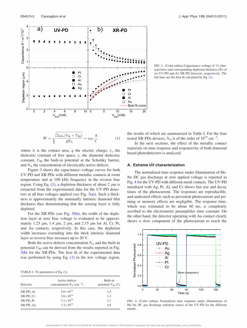
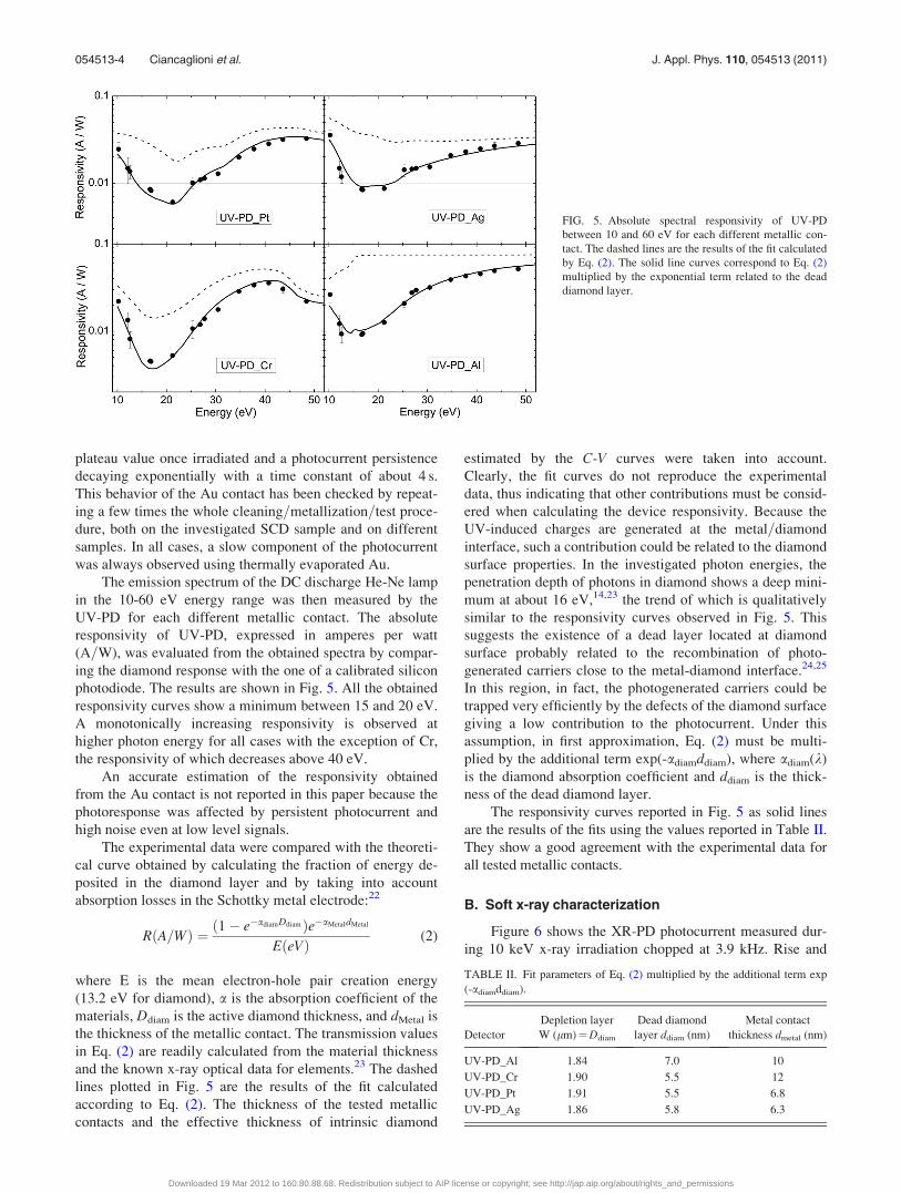
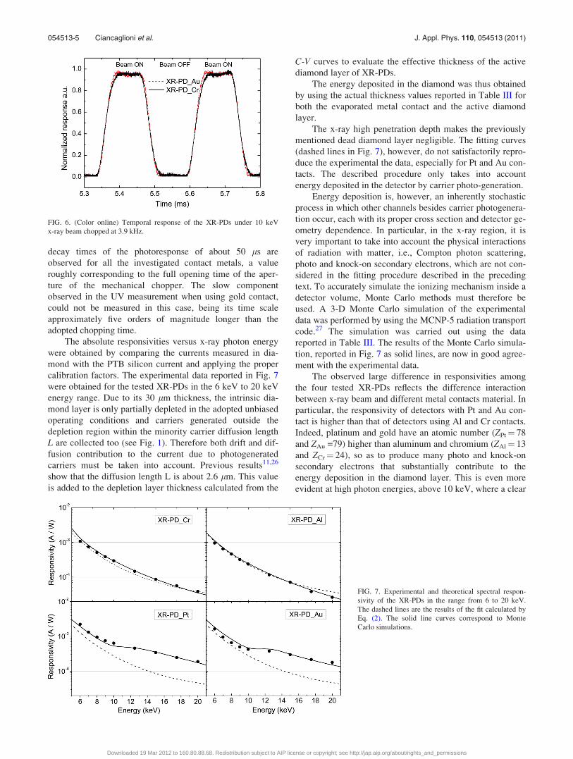
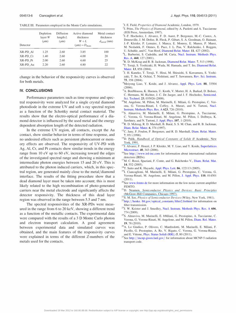
Related Documents