Research Article Influence of Film Thickness and Heat Treatment on the Physical Properties of Mn Doped Sb 2 Se 3 Nanocrystalline Thin Films I. K. El Zawawi, Manal A. Mahdy, and E. A. El-Sayad Solid State Physics Department, National Research Centre, Dokki, Giza 12622, Egypt Correspondence should be addressed to Manal A. Mahdy; [email protected] Received 28 November 2016; Revised 19 February 2017; Accepted 1 March 2017; Published 23 April 2017 Academic Editor: Meiyong Liao Copyright © 2017 I. K. El Zawawi et al. is is an open access article distributed under the Creative Commons Attribution License, which permits unrestricted use, distribution, and reproduction in any medium, provided the original work is properly cited. Nanocrystalline thin films of Sb 37.07 Mn 1.95 Se 60.98 with different thickness (7, 20, 40, and 80nm) were successfully prepared via inert gas condensation technique. As-deposited films showed amorphous structure by grazing incident in-plane X-ray diffraction (GIIXD) technique. All films of different thicknesses were heat treated at 433 K for 90 min. e GIIXD pattern of annealed films showed nanocrystalline orthorhombic structure. e effect of thickness of annealed films on the structure and optical properties was studied. Calculated particle sizes are 20.67 and 24.15 for 40 and 80 nm thickness of heat treated film. High resolution transmission electron microscope HRTEM images and their diffraction patterns proved that 40nm film thickness annealed at different temperature has nanocrystalline nature with observed (high) crystallinity that increases with annealing temperature. Blue shiſt of optical energy gap was observed from 1.68 to 2 eV with decreasing film thickness from 80 to 7 nm. Film thickness of 40 nm was exposed to different heat treated temperatures from 353 to 473K to detect its effect on structure and optical and electrical properties. Blue shiſt from 1.73 to 1.9 eV was observed in its optical band gap due to direct transition as heat treatment temperature decreasing from 473 to 353 K. Electrical conductivity was studied for different heat treated films of thickness 40 nm, and intrinsic conduction mechanism is dominant. e activation energy was affected by heat treatment process. 1. Introduction in film technology is very important for many modern and promising technological applications, hence the emphasis on examining the surface science increasing the interest of physicists on account of its proven and many semiconductor devices applications like solar cells. Among these thin films, nanostructure thin films occupy large area in most modern applications because of its unique new properties that depend on the size quantization effect [1]. V 2 -VI 3 semiconductor group attracts the attention of many scientists as a result of their physical properties that make them relevant in many applications [2]. in films of Sb 2 S 3 and Sb 2 Se 3 specially have a great interest in switching, microwave, and optoelectronic applications [2– 4]. Sb 2 Se 3 is considered a promising candidate for verifying >20% device efficiency as previously verified from theoret- ical calculations [5, 6]. Antimony (Sb) and selenium (Se) are abundant and nontoxic elements that produced Sb 2 Se 3 compound more suitable for photovoltaic application [7–9]. Nanostructure thin film of Sb 2 Se 3 was previously discussed [10]. Sb 2 Se 3 crystallized in orthorhombic structure and characterized by strong absorption coefficient (>10 −5 cm −1 ) [3, 8]. Many researchers studied the effect of incorporation of Mn atoms on V 2 VI 3 compounds [11–15]. In the earlier studies, chemical preparation methods such as solvothermal method [16–19], hydrothermal method [20–22], organometallic syn- thetic route [23], and microwave-assisted method [24] were used to synthesize Sb 2 Se 3 nanomaterials. In the present work, the synthesis of Sb 1− Mn Se 3 nanomaterial was demonstrated by inert gas condensation (IGC) as a physical method. Two effects were studied for the synthesized films. First, the effect of film thickness on the optical properties was discussed. Second, the effect of heat treatment on the structure and optical and electrical properties was demonstrated. Hindawi Journal of Nanomaterials Volume 2017, Article ID 7509098, 14 pages https://doi.org/10.1155/2017/7509098

Welcome message from author
This document is posted to help you gain knowledge. Please leave a comment to let me know what you think about it! Share it to your friends and learn new things together.
Transcript

Research ArticleInfluence of Film Thickness and Heat Treatment on the PhysicalProperties of Mn Doped Sb2Se3 Nanocrystalline Thin Films
I. K. El Zawawi, Manal A. Mahdy, and E. A. El-Sayad
Solid State Physics Department, National Research Centre, Dokki, Giza 12622, Egypt
Correspondence should be addressed to Manal A. Mahdy; [email protected]
Received 28 November 2016; Revised 19 February 2017; Accepted 1 March 2017; Published 23 April 2017
Academic Editor: Meiyong Liao
Copyright © 2017 I. K. El Zawawi et al.This is an open access article distributed under the Creative Commons Attribution License,which permits unrestricted use, distribution, and reproduction in any medium, provided the original work is properly cited.
Nanocrystalline thin films of Sb37.07Mn1.95Se60.98 with different thickness (7, 20, 40, and 80 nm) were successfully prepared viainert gas condensation technique. As-deposited films showed amorphous structure by grazing incident in-plane X-ray diffraction(GIIXD) technique. All films of different thicknesses were heat treated at 433K for 90min. The GIIXD pattern of annealedfilms showed nanocrystalline orthorhombic structure. The effect of thickness of annealed films on the structure and opticalproperties was studied. Calculated particle sizes are 20.67 and 24.15 for 40 and 80 nm thickness of heat treated film. High resolutiontransmission electron microscope HRTEM images and their diffraction patterns proved that 40 nm film thickness annealed atdifferent temperature has nanocrystalline nature with observed (high) crystallinity that increases with annealing temperature. Blueshift of optical energy gap was observed from 1.68 to 2 eV with decreasing film thickness from 80 to 7 nm. Film thickness of 40 nmwas exposed to different heat treated temperatures from 353 to 473K to detect its effect on structure and optical and electricalproperties. Blue shift from 1.73 to 1.9 eV was observed in its optical band gap due to direct transition as heat treatment temperaturedecreasing from 473 to 353K. Electrical conductivity was studied for different heat treated films of thickness 40 nm, and intrinsicconduction mechanism is dominant. The activation energy 𝐸𝑎 was affected by heat treatment process.
1. Introduction
Thin film technology is very important formanymodern andpromising technological applications, hence the emphasison examining the surface science increasing the interest ofphysicists on account of its proven and many semiconductordevices applications like solar cells. Among these thin films,nanostructure thin films occupy large area in most modernapplications because of its unique new properties that dependon the size quantization effect [1].
V2-VI3 semiconductor group attracts the attention ofmany scientists as a result of their physical propertiesthat make them relevant in many applications [2]. Thinfilms of Sb2S3 and Sb2Se3 specially have a great interest inswitching, microwave, and optoelectronic applications [2–4]. Sb2Se3 is considered a promising candidate for verifying>20% device efficiency as previously verified from theoret-ical calculations [5, 6]. Antimony (Sb) and selenium (Se)are abundant and nontoxic elements that produced Sb2Se3
compound more suitable for photovoltaic application [7–9].Nanostructure thin film of Sb2Se3 was previously discussed[10]. Sb2Se3 crystallized in orthorhombic structure andcharacterized by strong absorption coefficient (>10−5 cm−1)[3, 8].
Many researchers studied the effect of incorporation ofMnatoms onV2VI3 compounds [11–15]. In the earlier studies,chemical preparation methods such as solvothermal method[16–19], hydrothermal method [20–22], organometallic syn-thetic route [23], and microwave-assisted method [24] wereused to synthesize Sb2Se3 nanomaterials.
In the present work, the synthesis of Sb1−𝑥Mn𝑥Se3nanomaterial was demonstrated by inert gas condensation(IGC) as a physical method. Two effects were studied forthe synthesized films. First, the effect of film thickness onthe optical properties was discussed. Second, the effect ofheat treatment on the structure and optical and electricalproperties was demonstrated.
HindawiJournal of NanomaterialsVolume 2017, Article ID 7509098, 14 pageshttps://doi.org/10.1155/2017/7509098

2 Journal of Nanomaterials
2. Experimental
Thin films of Sb1−𝑥Mn𝑥Se3 of different thickness (7, 20, 40,and 80 nm) have been synthesized via inert gas condensation(IGC) method on freshly cleaned glass substrates at 300K.Edward coating unit Model E-306 was used to synthesizethin films under background argon gas with pressure of∼2 × 10⁻³ Torr. Gold quartz crystal sensor was attachedto thickness monitor (FTM5) used for recording the filmthickness during deposition process. Heat treatment processwas performed on different thickness of films at 433K for90min. Film of thickness 40 nm is exposed to heat treatmentat different temperatures of 353, 393, 433, and 473K for90min.
The quantitative chemical analysis of the thin film wasdetermined using energy dispersive X-ray analysis (EDX)technique. The EDX unit connected with field emissionscanning electron microscope.
Grazing incident in-plane X-ray diffraction (GIIXD)technique was used to examine the structure of thin filmsusing Philips X’Pert diffractometer with CuK𝛼. High resolu-tion transmission electronmicroscope (HRTEM)was used toinspect the micrographs and structure of films. The surfacemorphology of the thin films was inspected by field emis-sion scanning electron microscope (FESEM) Model QuantaFEG 250, Czech Republic. Double beam spectrophotometer(Model JascoV-570) was used for recording transmission andreflection spectra of thin films in the spectral range from 190to 2500 nm at room temperature.
The d.c. electrical conductivity of heat treated film ofthickness 40 nm at different temperatures was measured invacuum of ∼10−2 Torr at Pyrex cryostat.The resistance of thinfilms was recorded between two silver electrodes to ensuregood ohmic contact using 6517B Keithley electrometer. Thetemperature of thin film was determined during experimentusing �-type thermocouple as a temperature sensor.
3. Results and Discussion
Thin films of different thickness of Mn doped Sb2Se3 (7, 20,40, and 80 nm) were deposited by inert gas condensation(IGC) technique.The elemental chemical composition analy-sis of the successful deposited thin film of thickness 80 nm onstub of carbon was measured. The EDX results demonstratethat the thin film is composed of the elements Sb, Mn, andSe with the atomic ratios (at %) of 37.07, 1.95, and 60.98respectively. This confirms that the chemical composition ofexamined films is Sb37.07Mn1.95Se60.98 as derived from theEDX results.
The most effective way to understand the constituentof thin films is obtained through analyzing their structural,electrical, and optical properties.Therefore, the effect of boththickness of annealed films and annealing will be discussedon basis of their structural and physical behaviors.
The grazing incident in-plane X-ray diffraction (GIIXD)patterns of Sb37.07Mn1.95Se60.98 films of constant thickness80 nm and different conditions of being as-deposited andheat treated at 433K for 90min at vacuum of 10−2 Torr
were recorded in Figure 1. The X-ray pattern of as-depositedfilm showed amorphous structure due to the absence of anydiffraction peaks as seen in Figure 1(a). Otherwise, definitediffraction peaks are observed in X-ray pattern for heattreated film (Figure 1(b)). These diffraction peaks indicatedcrystallization with orthorhombic structure according to theX-ray international card (number 15-0861) [25]. This result isin agreement with that recorded previously by other authors[10, 18, 26]. Since EDX results proved the presence of Mndopant with 1.95 at%, Sb has a deficiency in its atomic percentfrom Sb2Se3 compound. Also, no diffraction peaks appearedin theX-ray pattern forMn element. So, it is expected thatMnintroduced substitutionally with the Sb element in the latticeof Sb2Se3 compound as a result of Mn dopant has a slightlysmaller ionic radius (0.58 A) than that of Sb (0.76 A) [27].This substitutional introducing of Mn with Sb element hasbeen proved in our previous work [28], which showed thatthe unit cell volume of Sb35.75Mn1.43Se62.82 polycrystallinepowder is slightly smaller than that of Sb2Se3 compound.The crystallite size was calculated from the X-ray peak withorientation (230) according to Scherrer formula as follows[29, 30]:
𝐷 = 𝑘𝜆𝛽 cos (𝜃) , (1)
where 𝐷 is the crystallite or particle size, 𝜆 is the X-ray wavelength, 𝑘 represents the particle shape factor, and𝛽 represents the peak full width at half maximum. Theestimated particle size of heat treatment film (80 nm) is about24.15 nm. This range indicated that the film crystallizes dueto being heat treated at 433K for 90min at nanocrystallineorthorhombic structure.
Thin film of thickness 40 nm was annealed at differenttemperatures and the effect of annealing temperature wasstudied on its structure.
Figure 2 shows GIIXD patterns of thin film (40 nm)annealed at 353, 393, 433, and 473K for 90min. The X-ray patterns for thin film after being heat treated at 353K(Figure 2(a)) showed very low crystallinity with the absenceof sharp X-ray peaks, whereas high resolution transmissionelectron microscopy (HRTEM) examination for the sameheat treated film at 353 K, resulting in diffraction patternthat showed some definite rings as illustrated in the insetdiffraction pattern in Figure 2(a).These definite rings indicatethe presence of crystalline nature for the examined heattreated film at 353K.This emphasizes that the HRTEM couldgive more information for examining the structure of thinfilms with low thickness.
On the other side, for the GIIXD studies, the crystallinitystarts to appear after thin film was heat treated at 393K asillustrated in Figure 2(b). This crystallinity is represented byappearance of some small diffraction lines which crystallizedin a single phase of an orthorhombic structure with planes oforientation (120), (130), (230), (240), (530), and (061), whileafter heat treatment at higher temperatures 433 and 473K(Figure 2(c, d)), the crystallization increases by appearanceof more diffraction lines with higher intensities than thoseillustrated for heat treated film at 393K.The insets ofHRTEMdiffraction pattern for heat treated films at 393, 433, and

Journal of Nanomaterials 3
(b)
(220
)
(221
)
(020
)
(411
)(3
40)
(422
)
(531
)
(600
)(250
)
(610
)(4
31)
(360
)
(321
)(311
) (240
)(3
01)
(211
)(2
30)
(130
)
(120
)
Inte
nsity
(a.u
.)
As deposited(a)
20 30 40 50 60 70 80102 (degree)
433K
Figure 1: GIIXD pattern of Sb37.07Mn1.95Se60.98 film of 80 nm thickness (a) as-deposited and (b) annealed at 433K for 90min.In
tens
ity (a
.u.)
(120
)
(130
) (230
)
(520
)
(530
)
(061
)(3
22)(4
30)
(321
)(2
40)
(301
)(2
11)
(a)
(a)
(b)
(c)
(c)
(d)
(d)
(b)
20 30 40 50 60 70 80102 (degree)
433K
393K
353K
473K
Figure 2: GIIXD patterns of Sb37.07Mn1.95Se60.98 film of 40 nm thickness with different annealing temperature and the inset HRTEMdiffraction patterns: (a) 353 K, (b) 393K, (c) 433K, and (d) 473K.
473K shown in Figure 2(b, c, d), respectively, confirm theincrease in crystallinity of the studied films with increasingthe annealing temperature.
From Figure 2, it is concluded that the crystallinity of40 nm film thickness improved with rising annealing tem-perature, resulting in the degree of crystallinity dependenceon the heating temperatures during annealing process. Thebroadening in X-ray peaks appears to be due to the nanocrys-talline structure in the heat treated films. From the width
of X-ray peak with orientation line (230), the crystallite sizecan be estimated according to (1). The calculated crystallitesizes for 40 nm film thickness heat treated at 433 and 473Kfrom peak orientation of (230) are 20.67 and 21.41 nm. Thecrystallite size from GIIXD pattern for heat treated film at393K is not accurately calculated due to the lower intensityof the representative line (230).
The micrograph images with different magnifications ofHRTEM for film thickness 40 nm exposed to heat treatment

4 Journal of Nanomaterials
50nm
(a)
10nm
2 nm
(b)
50nm
(c)
10nm
(d)
50nm
(e)
10nm
(f)
50nm
(g)
10nm
(h)
Figure 3: HRTEM images for 40 nm film thickness after exposure to different annealing temperatures (a, b) 353 K, (c, d) 393K, (e, f) 433 K,and (g, h) 473K.
process at different annealing temperatures from 353 to 473Kare illustrated in Figure 3. Figures 3(a), 3(c), 3(e), and 3(g)demonstrate the micrograph images at magnification scale50 nm that shows the nanoparticle of the annealed film atdifferent annealing temperatures. In the other side, Figures3(b), 3(d), 3(f), and 3(h) illustrate the long-range order forperiodicity of lattice which proved the high crystallinity ofannealed films as explained with X-ray patterns and HRTEMdiffraction patterns in Figure 2. Also, it is observed that thecrystallinity depends on the annealing temperature; that is, itincreases with rising annealing temperature.
The surface morphology of 40 nm film thicknessannealed at different temperature has been examined byfield emission scanning electron microscope (FESEM) asillustrated in Figure 4. The heat treated films showed asmooth homogenous surface and the appearance of someaggregates has been realized in Figure 4(d) than other films,indicating some nanoparticle aggregation due to the effect ofhigh annealing temperature at 473K.
Transmission T and reflection 𝑅 spectra ofSb37.07Mn1.95Se60.98 thin film with different thicknessesafter annealing at 433K were illustrated in Figure 5. It

Journal of Nanomaterials 5
500 nm
(a)
500 nm
(b)
500 nm
(c)
500 nm
(d)
Figure 4: FESEM images of Sb37.07Mn1.95Se60.98 film of 40 nm thickness with different annealing temperatures (a) 353 K, (b) 393K, (c) 433K,and (d) 473K.
7nm20 nm
40nm80nm
1000 1500 2000 2500500𝜆 (nm)
0
20
40
60
80
100
𝒯%
(a)
7nm20 nm
40nm80nm
1000 1500 2000 2500500 (nm)
0
10
20
30
40
50
60
70
80
R%
(b)
Figure 5: TransmissionT and reflection 𝑅 spectra as a function of wavelength for Sb37.07Mn1.95Se60.98 film with different thickness.
is obvious that the values of T and R depend on filmthickness. As observed, T values increase with decreasingfilm thickness, while R values rise with increasing filmthickness as depicted in Figure 5(b).
The study of the absorption coefficient 𝛼 spectra inthe region near the fundamental edge provides importantinformation around interband transitions and optical bandgap structure of the materials. The absorption coefficient 𝛼
6 Journal of Nanomaterials
7nm20 nm
40nm80nm
1 2 3 40E (eV)
×105
0
2
4
6
8
(=G
−1)
Figure 6: Absorption coefficient as a function of photon energy for Sb37.07Mn1.95Se60.98 film with different thickness.
20 40 60 800Film thickness (nm)
0.09
0.10
0.11
0.12
0.13
Eo
Figure 7: Band tail width 𝐸𝑜 as a function of film thickness for Sb37.07Mn1.95Se60.98 thin films.
spectra of the prepared annealed films were calculated fromtransmission and reflection spectra [31]. The calculated 𝛼values as a function of photon energy are shown in Figure 6.It is observable from Figure 6 that all the films underinvestigation have high absorption behavior lying in regionof ≥105 cm−1.
At energies lower than the band edge, the bandtail width, 𝐸𝑜, can be estimated from the slope ofstraight portion in the plot ln(𝛼) versus photon energy[32]. In this region, the absorption coefficient obeys an
exponential behavior according to the following Urbach rule[33]:
𝛼 = 𝛼𝑜 exp(ℎ]𝐸𝑜) , (2)
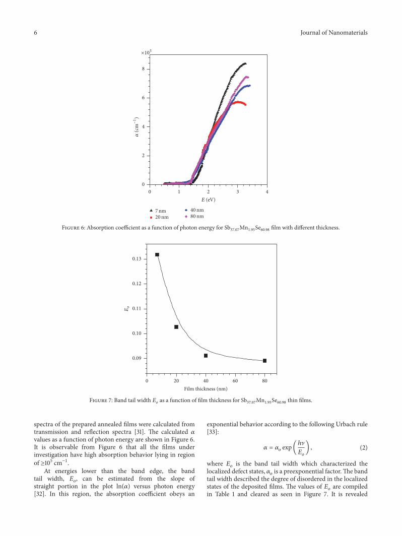
where 𝐸𝑜 is the band tail width which characterized thelocalized defect states, 𝛼𝑜 is a preexponential factor.The bandtail width described the degree of disordered in the localizedstates of the deposited films. The values of 𝐸𝑜 are compiledin Table 1 and cleared as seen in Figure 7. It is revealed
Journal of Nanomaterials 7
×1011
0.5 1.0 1.5 2.0 2.5 3.00.0E (eV)
7nm
(E)2
(=G
−1?6
)2
0
4
8
12
16
20
(a)
×1011
0.5 1.0 1.5 2.0 2.5 3.00.0E (eV)
20 nm(
E)2
(=G
−1?6
)2
0
2
4
6
8
10
12
(b)
×1011
0.5 1.0 1.5 2.0 2.5 3.00.0E (eV)
40nm
0
2
4
6
8
(E)2
(=G
−1?6
)2
(c)
×1011
0.5 1.0 1.5 2.0 2.5 3.00.0E (eV)
80nm
0
2
4
6
8
(E)2
(=G
−1?6
)2
(d)
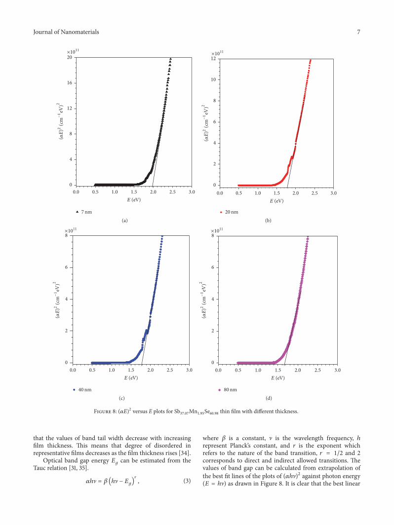
Figure 8: (𝛼𝐸)2 versus E plots for Sb37.07Mn1.95Se60.98 thin film with different thickness.
that the values of band tail width decrease with increasingfilm thickness. This means that degree of disordered inrepresentative films decreases as the film thickness rises [34].
Optical band gap energy 𝐸𝑔 can be estimated from theTauc relation [31, 35].
𝛼ℎ] = 𝛽 (ℎ] − 𝐸𝑔)𝑟 , (3)
where 𝛽 is a constant, ] is the wavelength frequency, ℎrepresent Planck’s constant, and 𝑟 is the exponent whichrefers to the nature of the band transition, 𝑟 = 1/2 and 2corresponds to direct and indirect allowed transitions. Thevalues of band gap can be calculated from extrapolation ofthe best fit lines of the plots of (𝛼ℎ])2 against photon energy(𝐸 = ℎ]) as drawn in Figure 8. It is clear that the best linear

8 Journal of Nanomaterials
0 20 40 60 801
2
3
4
5
6
Film thickness (nm)
no
0
2
4
6
8
10
12
14
n
7nm20 nm
40nm80nm
1000 1500 2000 2500500𝜆 (nm)
Figure 9: Refractive index 𝑛 of Sb37.07Mn1.95Se60.98 thin film of different thickness as function of wavelength. The inset figure representsvariation of refractive index 𝑛𝑜 at 2000 nm wavelength with film thickness.
Table 1: Particle size and optical parameters of Sb37.07Mn1.95Se60.98 thin film with different thickness after being heat treated at 433K for90min.
Film thickness (nm) 𝐷 (nm) 𝐸𝑔 (eV) 𝐸𝑜 (eV) 𝛼𝑜 (cm−1)7 — 2.00 0.132 135.820 — 1.80 0.103 134.140 20.67 1.76 0.091 80.980 24.15 1.68 0.089 36.6
fit is obtained for 𝑟 = 1/2, which refers to direct allowedtransition for all heat treated films with thickness from 7 to80 nm. The band gap values ranging from 2.00 to 1.68 eVfor film thickness increased from 7 to 80 nm. The obtainedvalue (2 eV) of 𝐸𝑔 is close to the previously reported results[36] and that reported for thin films of Sb2Se3 preparedvia spray pyrolysis technique [37]. Table 1 showed that theband gap was affected by the film thickness, it decreaseswith rising film thickness, and it is larger than that corre-sponding to the bulk material of Sb2Se3 which is about 1 eV[36].
The spectral variations of the calculated refractive index𝑛 of the investigated heat treatment thin films with differentthicknesses were illustrated in Figure 9. The refractive indexincreases with increasing film thickness in wavelength spec-tral range from 1000 to 2500 nm. The inset figure illustratesthe variation of refractive index 𝑛𝑜 with film thickness atwavelength 2000 nm. It is noted that 𝑛𝑜 values increasedexponentially from 1.74 to 5.51 as the film thickness increasesfrom 7 to 80 nm.
It is clear from Table 1 that as film thickness increasesthe particle size 𝐷 increases and both energy gaps 𝐸𝑔 and 𝐸𝑜decrease.
The effect of annealing temperature was studied on theoptical and electrical properties of 40 nm film thickness todetect the effect of the crystallinity on film behaviors.
Transmission T and reflection 𝑅 spectra for 40 nmfilm thickness of Sb37.07Mn1.95Se60.98 after being annealedat different temperatures were depicted in Figure 10. Thedependence of transmission and reflection values on heattreatment process are observed, resulting in values decreasingas the heat treated temperature increases, while 𝑅 valuesincrease with temperature of heat treatment process. Theincrement of heat treated temperature leads to imperfectiondecrement in films under investigation. This result is dueto crystallinity increasing after performing heat treatmentprocess as proved by GIIXD patterns (Figure 2).The increasein film crystallinity with rising of annealing temperatureagrees with that reported at previous results [38].
The calculated absorption coefficient 𝛼 as a function ofphoton energy 𝐸 for 40 nm film thickness after heat treatedat different temperature was illustrated in Figure 11.The filmshave high absorption coefficient values of about 105 cm−1 thatrepresent strong absorption values.
According to (3), optical band gap 𝐸𝑔 was estimated fromthe extrapolation of linear part of the curves in Figure 12, and

Journal of Nanomaterials 9
1000 1500 2000 2500500 (nm)
0
20
40
60
80
100
353K393K
433K473K
%
(a)
353K393K
433K473K
10
20
30
40
50
60
70
80
R%
1000 1500 2000 2500500 (nm)
(b)
Figure 10: TransmissionT and reflection𝑅 spectra as a function ofwavelength for 40 nmfilm thickness with different annealing temperature.
353K393K
433K473K
1 2 3 40E (eV)
×105
0
2
4
6
8
10
(=G)−
1
Figure 11: Absorption coefficient spectra for 40 nm film thickness with different annealing temperature.
the best linear fit was observed for exponent 𝑟 = 1/2 (directallowed transition). The estimated 𝐸𝑔 values were collectedin Table 2; it is observable that the 𝐸𝑔 values decreasewith increasing heat treated temperature which influencethe crystallinity of the thin films. On the other hand, therefractive index 𝑛 of heat treated thin films from 353 to 473K
was shown in Figure 13. The calculated values of refractiveindex 𝑛𝑜 at 2000 nm were inset in Figure 13; it increases withheat treatment as a result of improving crystallinity.
Conductivity is an important property, which gives morereliable information about the transport phenomena andother physical properties of the materials.

10 Journal of Nanomaterials
0.5 1.0 1.5 2.0 2.5 3.00.0E (eV)
7×10
11
0
1
2
3
4
5
6
(E)2
(=G
−1?6
)2
353K(a)
7×10
11
0
1
2
3
4
5
6
(E)2
(=G
−1?6
)2
393K
1.0 1.5 2.0 2.5 3.00.5E (eV)
(b)
×1011
433K
0.5 1.0 1.5 2.0 2.5 3.00.0E (eV)
0
1
2
3
4
5
6
7
8
(E)2
(=G
−1?6
)2
(c)473K
×1011
0
1
2
3
4
5
6
7
8
(E)2
(=G
−1?6
)2
0.5 1.0 1.5 2.0 2.5 3.00.0E (eV)
(d)
Figure 12: (𝛼𝐸)2 versus 𝐸 plots for 40 nm film thickness with different annealing temperature.
Table 2: Calculated values of particle size𝐷, optical band gap 𝐸𝑔, activation energy 𝐸𝑎, and preexponential factor 𝜎𝑜 for 40 nm film thicknessannealed at different temperatures 𝑇 (K).𝑇 (K) 𝐷 (nm) 𝐸𝑔 (eV) 𝐸𝑎 (eV) 𝜎𝑜 (Ω⋅m)−1
353 — 1.90 0.978 4.60 × 1010393 — 1.79 0.809 9.97 × 108433 20.67 1.76 0.765 2.77 × 108473 21.41 1.73 0.768 1.92 × 10⁸

Journal of Nanomaterials 11
2.1
2.4
2.7
3.0
3.3
2
4
6
8
10
12
14
n
1000 1500 2000 2500500 (nm)
353K393K
433K473K
400 440 480360
no
T (K)
Figure 13: Refractive index of 40 nm film thickness of different annealing temperature. The inset figure represents variation of refractiveindex at 2000 nm wavelength with annealing temperatures.
Electrical conductivity at temperature 𝑇 is given by thefollowing relation [39, 40]:
𝜎 (𝑇) = 𝜎𝑜 exp(− 𝐸𝑎𝑘𝐵𝑇) , (4)
where 𝑘𝐵 is a Boltzmann constant, 𝜎𝑜 is a preexponentialfactor, and 𝐸𝑎 represents the material activation energy.
The variation of resistivity with temperature was recordedfor all annealed films of 40 nm thickness. The calculatedd.c. conductivity 𝜎 versus temperature 𝑇 was depicted inFigure 14.The electrical conductivity increases with tempera-ture, which indicates the semiconductor behavior ofmaterials[41]. It is obvious from Figure 14 that conductivity has arapid variation with temperature in the whole temperaturerange. This means that the current density increases due tothe thermal activated process. The linear behavior of ln(𝜎)with reciprocal of temperature 𝑇 for all films indicates thatconduction is through the process of thermal activation.The electrical conductivity for all measured films indicatesstraight lines with one slope, which refers to one type ofconduction mechanism.
The activation energy 𝐸𝑎 of thin films can be calculatedfrom the slope of the straight lines (Figure 14) and thepreexponential factor 𝜎𝑜 calculated from the intersection ofthese straight lines with the ordinate axis. The calculatedvalues of 𝐸𝑎 and 𝜎𝑜 are assembled in Table 2. These val-ues of 𝐸𝑎 are probably due to the Fermi level shift, andit was found to be nearly equal to half of the obtainedoptical band gap, indicating that the intrinsic conductionmechanism in measured heat treated thin films of 40 nmthickness is dominant [39, 42]. The intrinsic mechanism in
semiconductor materials is due to the carrier mobility. Itcould be concluded that the heat treatment temperature doesnot influence the conduction mechanism of the investigatedfilms. Moreover, the activation energy 𝐸𝑎 was found tovary with the heat treatment temperature as shown in Fig-ure 15. Calculated 𝐸𝑎 decreases rapidly with increasing heattreated temperature from 353 to 393K and is approximatelyconstant with higher temperature of 433 and 473K. Thepreexponential factor 𝜎𝑜 depends on the temperature of heattreatment process; it decreases with increasing heat treatmenttemperature.
From Table 2, it could be noticed that rising in tem-perature of heat treatment at constant heating time resultsin an increase in particle size which reflects decreasingin other optical and electrical parameters as 𝐸𝑔, 𝐸𝑎, and𝜎𝑜.
4. Conclusion
Sb37.07Mn1.95Se60.98 nanostructure thin film was physicallysynthesized with inert gas condensation method. Severalthicknesses 7, 20, 40, and 80 nm were deposited on glasssubstrates and then heat treated for 90min at 433K. Filmthickness effect on structure and optical properties wasexamined. Optical band gap was shifted to higher energy(blue shift) with decreasing film thickness. Film thicknessof 40 nm was exposed to different annealing tempera-ture ranging from 353 to 473K. Structure was affected byannealing temperature and blue shift in optical propertiesis observed with rising temperature. The long-range orderof lattice periodicity was cleared in the HRTEM results

12 Journal of Nanomaterials
1.8 2.0 2.2 2.4 2.6 2.8 3.0 3.2
0
2
353K
−2
−4
−6
−8
−10
−12
1000/T (+)−1
ln(
)(Ω
G)−
1
(a)
1.8 2.0 2.2 2.4 2.6 2.8 3.0 3.2
0
2
4
393K
−2
−4
−6
−8
−10
−12
1000/T (+)−1
ln(
)(Ω
G)−
1(b)
1.8 2.0 2.2 2.4 2.6 2.8 3.0 3.2
433K
0
2
−2
−4
−6
−8
−10
1000/T (+)−1
ln(
)(Ω
G)−
1
(c)
2.0 2.2 2.4 2.6 2.8 3.0 3.2
473K
0
2
−2
−4
−6
−8
−10
1000/T (+)−1
ln(
)(Ω
G)−
1
(d)
Figure 14: Representation of ln(𝜎) as a function of 1/𝑇 for 40 nm film thickness at different annealing temperature.
and lattice crystallinity affected by heat treated process ofthe films. Some nanoparticle aggregates appear by FESEMdue to the exposed of thin film to high annealing tem-perature. Result of d.c. electrical conductivity for annealed40 nm revealed an intrinsic conduction mechanism, andthe calculated activation energy changed with heat treatedtemperature.
It could be concluded that the crystallinity of annealedSb37.07Mn1.95Se60.98 nanocrystalline films was enhanced andthe particle size increases as a result of both effects of
increasing film thickness and annealing temperature. Thisis consequently reflected on their optical and electricalproperties by decreasing their direct optical band gap, degreeof disorder, and activation energy.
Conflicts of Interest
The authors declare that there are no conflicts of interestregarding the publication of this paper.

Journal of Nanomaterials 13
360 400 440 4800.70
0.75
0.80
0.85
0.90
0.95
1.00
Ea
(eV
)
T (K)
Figure 15: Variation of activation energy of 40 nm film thicknesswith annealing temperature.
Acknowledgments
This researchwas funded byNational ResearchCentre, Cairo,Egypt, internal Project no. 10040206.
References
[1] Y. Hanifehpour, S. W. Joo, and B.-K. Min, “Lu3+/Yb3+ andLu3+/Er3+ co-doped antimony selenide nanomaterials: syn-thesis, characterization, and electrical, thermoelectrical, andoptical properties,” Nanoscale Research Letters, vol. 8, no. 1,article 141, 2013.
[2] I. S. Virt, I. O. Rudyj, I. V. Kurilo et al., “Properties ofSb2S3 and Sb2Se3 thin films obtained by pulsed laser ablation,”Semiconductors, vol. 47, no. 7, pp. 1003–1007, 2013.
[3] Y. Zhou, L. Wang, S. Chen et al., “Thin-film Sb2Se3 photo-voltaics with oriented one-dimensional ribbons and benigngrain boundaries,” Nature Photonics, vol. 9, no. 6, pp. 409–415,2015.
[4] S. Messina, M. T. S. Nair, and P. K. Nair, “Antimony selenideabsorber thin films in all-chemically deposited solar cells,”Journal of the Electrochemical Society, vol. 156, no. 5, pp. H327–H332, 2009.
[5] M. R. Filip, C. E. Patrick, and F. Giustino, “GW quasiparticleband structures of stibnite, antimonselite, bismuthinite, andguanajuatite,” Physical Review B, vol. 87, no. 20, Article ID205125, 2013.
[6] C. E. Patrick and F. Giustino, “Structural and electronic proper-ties of semiconductor-sensitized solar-cell interfaces,”AdvancedFunctional Materials, vol. 21, no. 24, pp. 4663–4667, 2011.
[7] X. Liu, J. Chen, M. Luo et al., “Thermal evaporation andcharacterization of Sb2Se3 thin film for substrate Sb2Se3/CdSsolar cells,” ACS Applied Materials & Interfaces, vol. 6, no. 13,pp. 10687–10695, 2014.
[8] Y. Lai, Z. Chen, C. Han et al., “Preparation and characterizationof Sb2Se3 thin films by electrodeposition and annealing treat-ment,” Applied Surface Science, vol. 261, pp. 510–514, 2012.
[9] T. T. Ngo, S. Chavhan, I. Kosta, O. Miguel, H.-J. Grande, and R.Tena-Zaera, “Electrodeposition of antimony selenide thin filmsand application in semiconductor sensitized solar cells,” ACSApplied Materials and Interfaces, vol. 6, no. 4, pp. 2836–2841,2014.
[10] A. U. Bajpeyee, “Deposition and characterization of antimonyselenide thin films,”Multilogic in Science, vol. 2, pp. 38–43, 2012.
[11] J. Horak, P. Lost’ak, C. Drasar, J. S. Dyck, Z. Zhou, and C. Uher,“Defect structure of Sb2−𝑥Mn𝑥Te3 single crystals,” Journal ofSolid State Chemistry, vol. 178, no. 9, pp. 2907–2912, 2005.
[12] J. Choi, S. Choi, J. Choi et al., “Magnetic properties ofMn-dopedBi2Te3 and Sb2Te3,” Physica Status Solidi (B) Basic Research, vol.241, no. 7, pp. 1541–1544, 2004.
[13] J. Choi, H.-W. Lee, B.-S. Kim et al., “Mn-doped V2VI3 semicon-ductors: single crystal growth andmagnetic properties,” Journalof Applied Physics, vol. 97, no. 10, Article ID 10D324, 2005.
[14] J. S. Dyck, P. Svanda, P. Lost’ak, J. Horak, W. Chen, and C.Uher, “Magnetic and transport properties of the V2-VI3 dilutedmagnetic semiconductor Sb2−𝑥Mn𝑥Te3,” Journal of AppliedPhysics, vol. 94, no. 12, pp. 7631–7635, 2003.
[15] P. Janıcek, C. Drasar, P. Lost’Ak, J. Vejpravova, andV. Sechovsky,“Transport,magnetic, optical and thermodynamic properties ofBi2−𝑥Mn𝑥Se3 single crystals,” Physica B: Condensed Matter, vol.403, no. 19-20, pp. 3553–3558, 2008.
[16] K. W. Sun, C.-H. Yang, T.-Y. Ko, H.-W. Chang, and C.-W. Liu,“Spectroscopy of a single Sb2Se3 nanorod,” Pure and AppliedChemistry, vol. 81, no. 8, pp. 1511–1522, 2009.
[17] J. Ma, Y. Wang, Y. Wang et al., “One-dimensional Sb2Se3nanostructures: solvothermal synthesis, growth mechanism,optical and electrochemical properties,”CrystEngComm, vol. 13,no. 7, pp. 2369–2374, 2011.
[18] T. Y. Ko, C. H. Yang, K. W. Sun, H. W. Chang, B. Sarkar, andC. W. Liu, “Electrical and optical properties of a single Sb2Se3nanorod,” Central European Journal of Chemistry, vol. 7, no. 2,pp. 197–204, 2009.
[19] Y. Zhang, G. Li, B. Zhang, and L. Zhang, “Synthesis and charac-terization of hollow Sb2Se3 nanospheres,”Materials Letters, vol.58, no. 17-18, pp. 2279–2282, 2004.
[20] G.-Y. Chen, B. Dneg, G.-B. Cai et al., “The fractal splittinggrowth of Sb2S3 and Sb2Se3 hierarchical nanostructures,” Jour-nal of Physical Chemistry C, vol. 112, no. 3, pp. 672–679, 2008.
[21] Q. Xie, Z. Liu, M. Shao, L. Kong, W. Yu, and Y. Qian, “Polymer-controlled growth of Sb2Se3 nanoribbons via a hydrothermalprocess,” Journal of Crystal Growth, vol. 252, no. 4, pp. 570–574,2003.
[22] J. Wang, Z. Deng, and Y. Li, “Synthesis and characterization ofSb2Se3 nanorods,”Materials Research Bulletin, vol. 37, no. 3, pp.495–502, 2002.
[23] G. Chen,W.Wang, C.Wang, T. Ding, and Q. Yang, “Controlledsynthesis of ultrathin Sb2Se3 nanowires and application forflexible photodetectors,”Advanced Science, vol. 2, no. 10, ArticleID 1500109, 2015.
[24] Y.-Q. Liu, M. Zhang, F.-X. Wang, and G.-B. Pan, “Facilemicrowave-assisted synthesis of uniform Sb2Se3 nanowiresfor high performance photodetectors,” Journal of MaterialsChemistry C, vol. 2, no. 2, pp. 240–244, 2014.
[25] 2001 JCPDS-International Centre for Diffraction Data, Cardnumber (15-0861).

14 Journal of Nanomaterials
[26] Z. Li, H. Zhu, Y. Guo et al., “Efficiency enhancement of Sb2Se3thin-film solar cells by the co-evaporation of Se and Sb2Se3,”Applied Physics Express, vol. 9, no. 5, Article ID 052302, 2016.
[27] R. D. Shannon, “Revised effective ionic radii and systematicstudies of interatomic distances in halides and chalcogenides,”Acta Crystallographica Section A, vol. 32, pp. 751–767, 1976.
[28] M. A. Mahdy, I. K. El Zawawi, and E. A. El-Sayad,“Influence of temperature on the magnetic behavior ofthe Sb35.75Mn1.43Se62.82 compound,” The European PhysicalJournal Plus, vol. 132, no. 2, article 81, 2017.
[29] B. D. Cullitty, Elements of X-Ray Diffraction, Addison-Wesley,Boston, Mass, USA, 2nd edition, 1978.
[30] S. Kumar, P. Yousaf Khan, N. K. Verma, and S. K. Chakarvarti,“Optical parameters of ZnSe chalcogenide nanostructures,”Chalcogenide Letters, vol. 5, no. 7, pp. 143–152, 2008.
[31] J. I. Pankove,Optical Processes in Semiconductors, Prentice-Hall,Englewood Cliffs, NJ, USA, 1971.
[32] N. kumar, U. Parihar, R. Kumar, K. J. Patel, C. J. Panchal,and N. Padha, “Effect of film thickness on optical propertiesof tin selenide thin films prepared by thermal evaporationfor photovoltaic applications,” American Journal of MaterialsScience, vol. 2, no. 1, pp. 41–45, 2012.
[33] J. Tauc, “Optical properties of amorphous semiconductors,” inAmorphous and Liquid Semiconductors, 220, chapter 4, p. 159,Plenum Press, London, UK, 1974.
[34] I. K. El Zawawi and M. A. Mahdy, “Synthesis and characteriza-tion of low particle size nanocrystalline SnSe thin films,” Journalof Materials Science: Materials in Electronics, vol. 24, no. 6, pp.2106–2111, 2013.
[35] J. Tauc, Amorphous and Liquid Semiconductors, Plenum, Lon-don, UK, 1974.
[36] A. M. Fernandez and M. G. Merino, “Preparation and charac-terization of Sb2Se3 thin films prepared by electrodeposition forphotovoltaic applications,”Thin Solid Films, vol. 366, no. 1-2, pp.202–206, 2000.
[37] K. Y. Rajpure, C. D. Lokhande, and C. H. Bhosale, “Effect of thesubstrate temperature on the properties of spray deposited Sb-Se thin films from non-aqueous medium,”Thin Solid Films, vol.311, no. 1-2, pp. 114–118, 1997.
[38] E.A. El-Sayad, B. S. Farag, andL. I. Soliman, “Effect of annealingtemperature on the structural and optical properties of Sb-Mn-Se thin films,” Journal of Physics D: Applied Physics, vol. 42, no.22, Article ID 225401, 2009.
[39] B. Kuznetsov, Physical Principles of Microelectronics, Mir Pub-lishers, 1974, English Translation.
[40] N. F. Mott and E. A. Davis, Electronic Process in Non-CrystallineMaterials, Clarendon Press, Oxford, UK, 1979.
[41] F. Skuban, S. R. Lukic, D. M. Petrovic, I. Savic, and Y. S.Tver’yanovich, “Optical gap and dc conductivity of disorderedmaterials of (As2Se3)100−𝑥(SbSI)𝑥 type,” Journal of Optoelectron-ics and Advanced Materials, vol. 7, no. 4, pp. 1793–1799, 2005.
[42] E. A. El-Sayad, B. S. Farag, and A. T. Amin, “Electrical prop-erties of crystalline Pb𝑥Sn1−𝑥Te0.5Se0.5 thin films,” Vacuum, vol.84, pp. 807–811, 2010.

Submit your manuscripts athttps://www.hindawi.com
ScientificaHindawi Publishing Corporationhttp://www.hindawi.com Volume 2014
CorrosionInternational Journal of
Hindawi Publishing Corporationhttp://www.hindawi.com Volume 2014
Polymer ScienceInternational Journal of
Hindawi Publishing Corporationhttp://www.hindawi.com Volume 2014
Hindawi Publishing Corporationhttp://www.hindawi.com Volume 2014
CeramicsJournal of
Hindawi Publishing Corporationhttp://www.hindawi.com Volume 2014
CompositesJournal of
NanoparticlesJournal of
Hindawi Publishing Corporationhttp://www.hindawi.com Volume 2014
Hindawi Publishing Corporationhttp://www.hindawi.com Volume 2014
International Journal of
Biomaterials
Hindawi Publishing Corporationhttp://www.hindawi.com Volume 2014
NanoscienceJournal of
TextilesHindawi Publishing Corporation http://www.hindawi.com Volume 2014
Journal of
NanotechnologyHindawi Publishing Corporationhttp://www.hindawi.com Volume 2014
Journal of
CrystallographyJournal of
Hindawi Publishing Corporationhttp://www.hindawi.com Volume 2014
The Scientific World JournalHindawi Publishing Corporation http://www.hindawi.com Volume 2014
Hindawi Publishing Corporationhttp://www.hindawi.com Volume 2014
CoatingsJournal of
Advances in
Materials Science and EngineeringHindawi Publishing Corporationhttp://www.hindawi.com Volume 2014
Smart Materials Research
Hindawi Publishing Corporationhttp://www.hindawi.com Volume 2014
Hindawi Publishing Corporationhttp://www.hindawi.com Volume 2014
MetallurgyJournal of
Hindawi Publishing Corporationhttp://www.hindawi.com Volume 2014
BioMed Research International
MaterialsJournal of
Hindawi Publishing Corporationhttp://www.hindawi.com Volume 2014
Related Documents