1 INF 5490 RF MEMS LN07: RF MEMS phase shifters Resonators, I Spring 2010, Oddvar Søråsen Department of Informatics, UoO

Welcome message from author
This document is posted to help you gain knowledge. Please leave a comment to let me know what you think about it! Share it to your friends and learn new things together.
Transcript
1
INF 5490 RF MEMS
LN07: RF MEMS phase shiftersResonators, I
Spring 2010, Oddvar SøråsenDepartment of Informatics, UoO
2
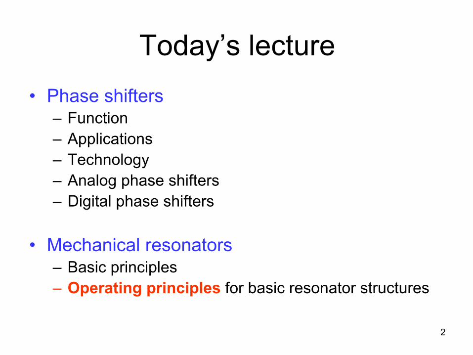
Today’s lecture•
Phase shifters–
Function
–
Applications–
Technology
–
Analog phase shifters–
Digital phase shifters
•
Mechanical resonators–
Basic principles
–
Operating principles
for basic resonator structures
3
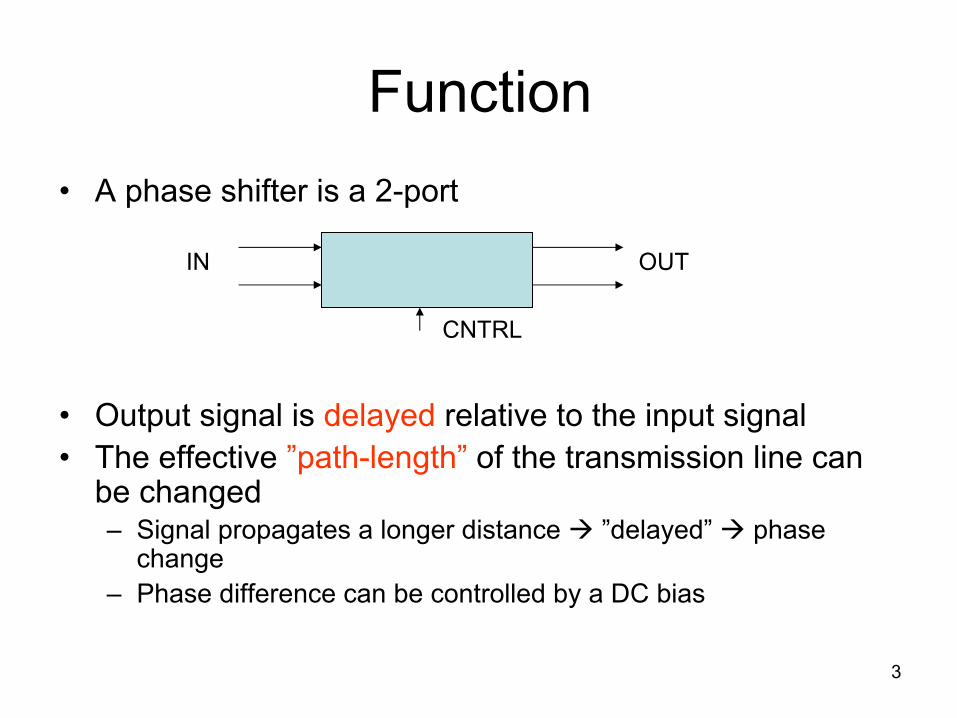
Function•
A phase shifter is a 2-port
•
Output signal is delayed
relative to the input signal•
The effective ”path-length”
of the transmission line can
be changed–
Signal propagates a longer distance ”delayed” phase change
–
Phase difference can be controlled by a DC bias
IN OUT
CNTRL
4
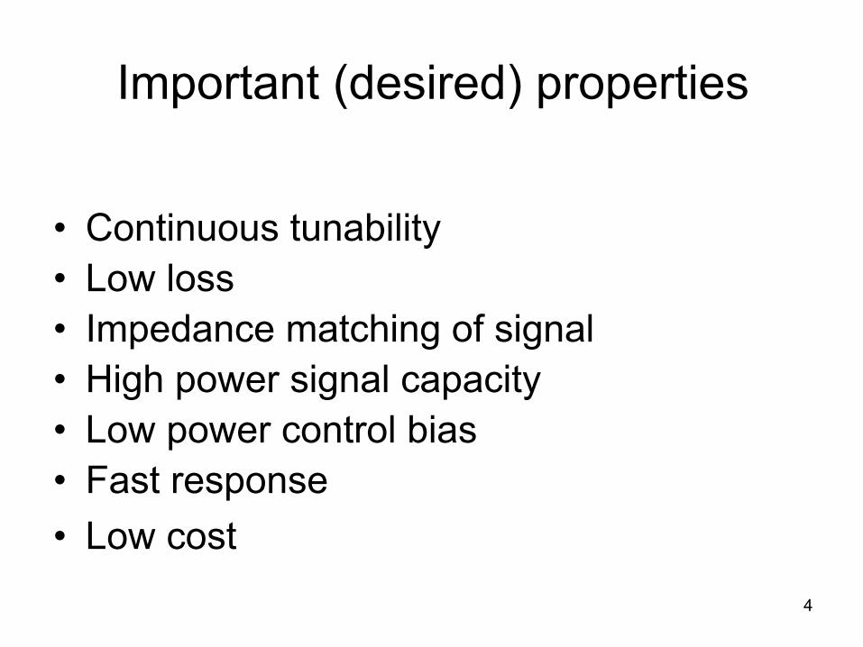
Important (desired) properties
•
Continuous tunability•
Low loss
•
Impedance matching of signal•
High power signal capacity
•
Low power control bias•
Fast response
•
Low cost
5
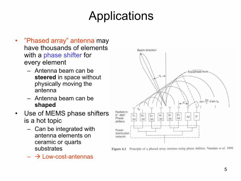
Applications
•
”Phased array”
antenna
may have thousands of elements with a phase shifter
for every element–
Antenna beam can be steered
in space without physically moving the antenna
–
Antenna beam can be shaped
•
Use of MEMS phase shifters is a hot topic –
Can be integrated with antenna elements on ceramic or quarts substrates
– Low-cost-antennas
6
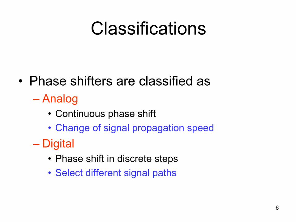
Classifications
•
Phase shifters are classified as –
Analog
•
Continuous phase shift•
Change of signal propagation speed
–
Digital•
Phase shift in discrete steps
•
Select different signal paths
7
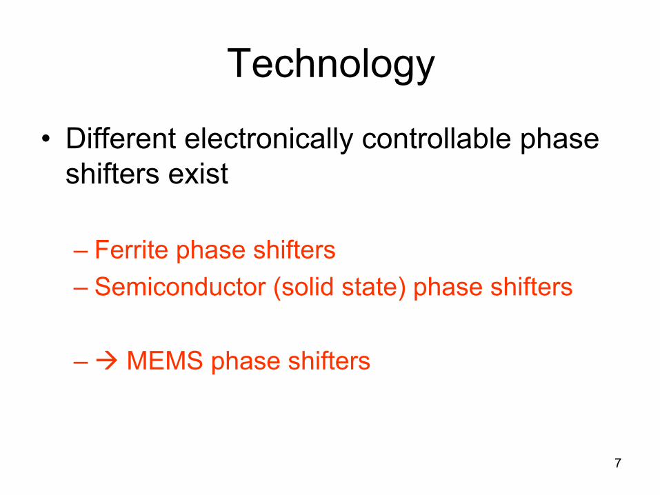
Technology
•
Different electronically controllable phase shifters exist
–
Ferrite phase shifters–
Semiconductor (solid state) phase shifters
– MEMS phase shifters
8
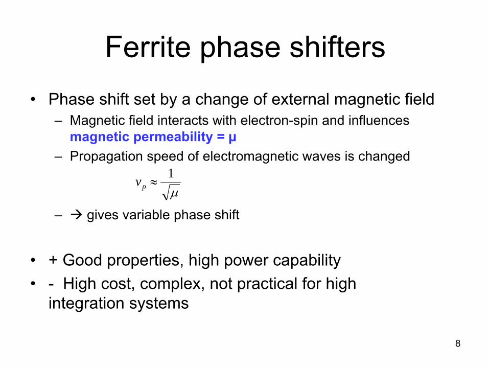
Ferrite phase shifters•
Phase shift set by a change of external magnetic field–
Magnetic field interacts with electron-spin and influences magnetic permeability = µ
–
Propagation speed of electromagnetic waves is changed
– gives variable phase shift
•
+ Good properties, high power capability•
-
High cost, complex, not practical for high
integration systems
μ1
≈pv
9
Semiconductor phase shifters
•
Switching in/out different line segments by using IC switches–
PIN-diode, GaAs
FET
•
+ Cheap, small, monolithic integration with amplifiers is possible
•
-
Can not give continuous phase variation•
-
Significant RF loss, high insertion loss
•
-
Poor power capability
10
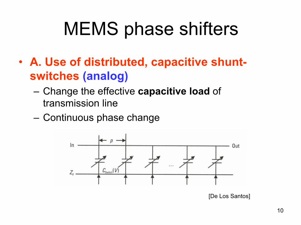
MEMS phase shifters
•
A. Use of distributed, capacitive shunt- switches (analog)
–
Change the effective capacitive load
of transmission line
–
Continuous phase change
[De Los Santos]
11
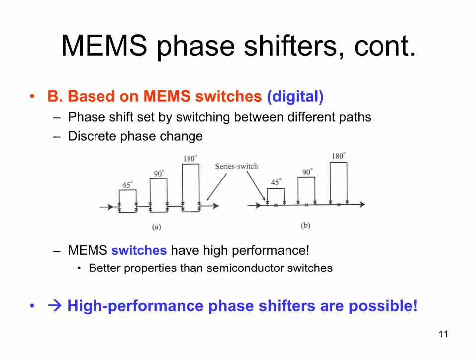
MEMS phase shifters, cont.•
B. Based on MEMS switches
(digital)
–
Phase shift set by switching between different paths–
Discrete phase change
–
MEMS switches
have high performance!•
Better properties than semiconductor switches
• High-performance phase shifters are possible!
12
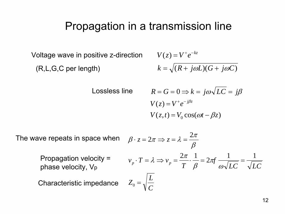
))((
)(
CjGLjRk
eVzV kz
ωω ++=
= −+
)cos(),()(
0
0 ztVtzVeVzV
jLCjkGRzj
βω
βωβ
−==
==⇒==−+
CLZ
LCLCf
TvTv
zz
pp
=
==⋅=⇒=⋅
==⇒=⋅
0
11212
22
ωπ
βπλ
βπλπβ
Propagation in a transmission line
Voltage wave in positive z-direction
(R,L,G,C per length)
Lossless line
The wave repeats in space when
Propagation velocity = phase velocity, Vp
Characteristic impedance
13
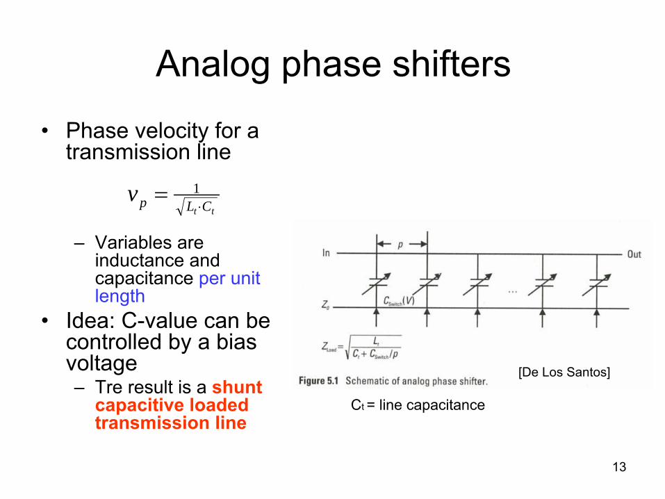
Analog phase shifters
•
Phase velocity for a transmission line
–
Variables are inductance and capacitance per unit length
•
Idea: C-value can be controlled by a bias voltage–
Tre
result is a shunt capacitive loaded transmission line
tt CLpv⋅
= 1
Ct = line capacitance
[De Los Santos]
14
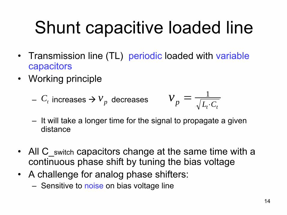
Shunt capacitive loaded line•
Transmission line (TL) periodic
loaded with variable
capacitors•
Working principle
–
increases decreases
–
It will take a longer time for the signal to propagate a given distance
•
All C_switch
capacitors change at the same time with a continuous phase shift by tuning the bias voltage
•
A challenge for analog phase shifters:–
Sensitive to noise
on bias voltage line
tt CLpv⋅
= 1tC pv
15
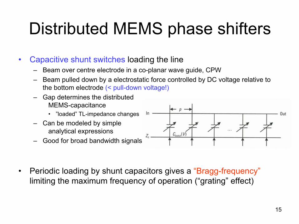
Distributed MEMS phase shifters
•
Capacitive shunt switches
loading the line–
Beam over centre electrode in a co-planar wave guide, CPW–
Beam pulled down by a electrostatic force controlled by DC voltage relative to the bottom electrode (< pull-down voltage!)
–
Gap determines the distributed MEMS-capacitance•
”loaded”
TL-impedance changes–
Can be modeled by simple analytical expressions
–
Good for broad bandwidth signals
•
Periodic loading by shunt capacitors gives a “Bragg-frequency”
limiting the maximum frequency of operation (“grating”
effect)
16
cp
vp
cv
Z
r
p
rrrp
ετ
εμεεμεεεμ
εμ
==
=⋅≈==
=
000
0
1111
cZ
CZL
cZZvC
CZLCv
CZLCLZ
r
r
p
p
ε
ε
020
00
0
200
1
11
==
==
==
⋅=⇒=
)(
)/(1
/
_
_
_0
switchloadedp
loaded
switchloadedp
switchloaded
CpCpLv
ppCCL
v
pCCLZ
+⋅==
+⋅=
+=
τ
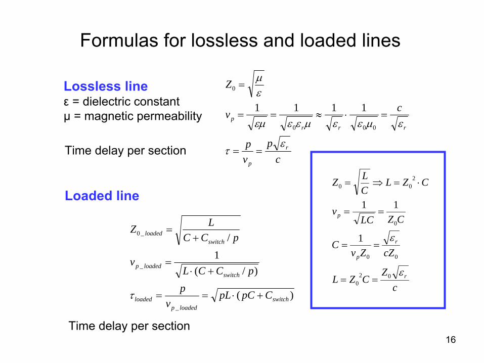
Formulas for lossless and loaded lines
Lossless lineε
= dielectric constantµ
= magnetic permeability
Time delay per section
Loaded line
Time delay per section
17
Challenges for MEMS shunt-switch phase shifters
•
Low switch speed (μs) slow adaptation to given delay•
High actuation voltage, Vs = 20 –
100 V
–
Vs reduced by reducing the gap•
Complex fabrication (yield)•
Parasitic up-state capacitance contributes significantly •
More sensitive to pull-in–
Vs reduced by using materials with lower Youngs
modulus•
Use polymers (E = 5 GPa, metals have 50 –
100 GPa)•
Polymers can give 1/3 actuation voltage compared with metals•
How to use micro stereo lithography to fabricate such structures
is described in Varadan
(not syllabus)
• Good enough properties for phased array antennas
18
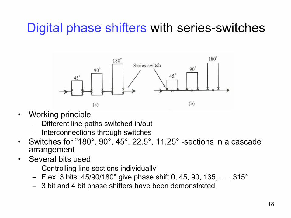
Digital phase shifters
with series-switches
•
Working principle–
Different line paths switched in/out–
Interconnections through switches•
Switches for ”180°, 90°, 45°, 22.5°, 11.25°
-sections in a cascade arrangement
•
Several bits used–
Controlling line sections individually–
F.ex. 3 bits: 45/90/180°
give phase shift 0, 45, 90, 135, …
, 315°–
3 bit and 4 bit phase shifters have been demonstrated
19
Digital MEMS phase shifters
•
Based on MEMS switches •
MEMS switches have high performance!
–
Negligible actuation power –
Negligible standby power consumption
–
Low insertion loss–
High isolation
–
Limited speed, 1 –
30 μs•
Not always critical
20
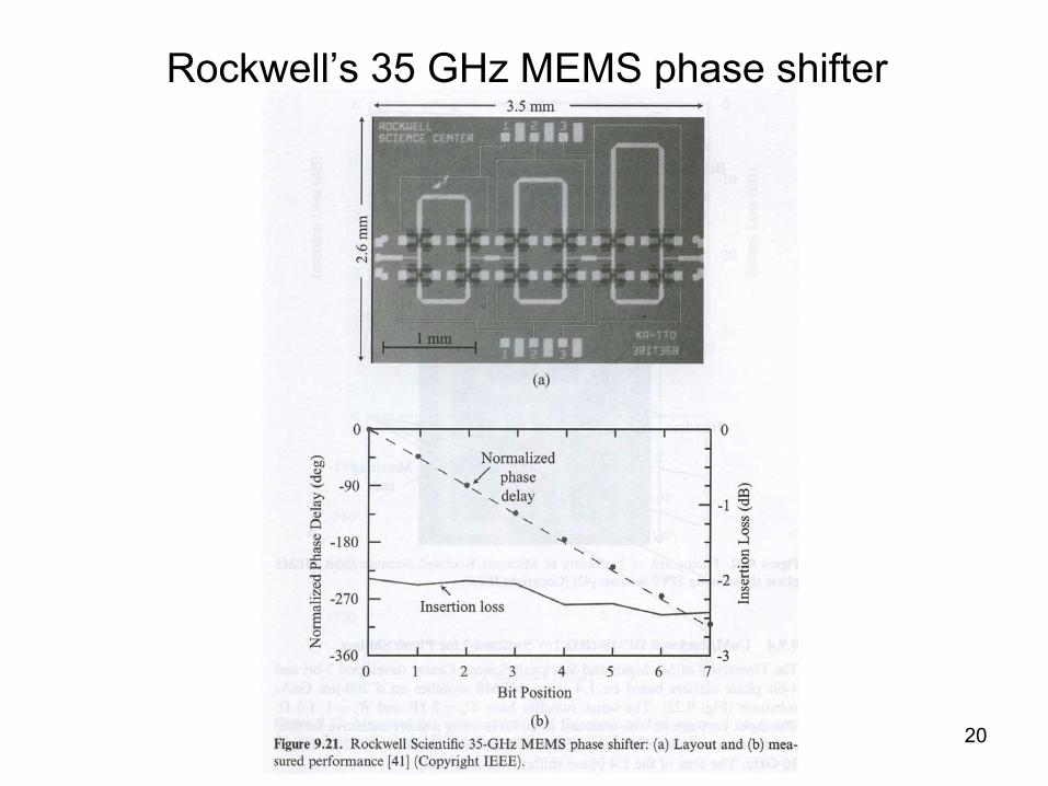
Rockwell’s 35 GHz MEMS phase shifter
21
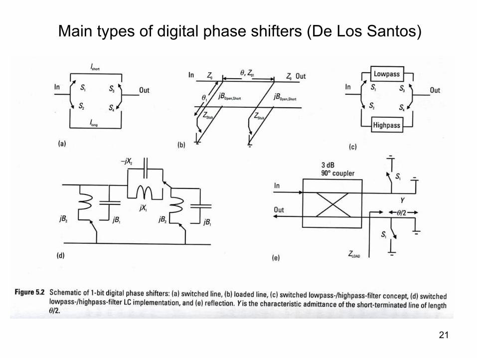
Main types of digital phase shifters (De Los Santos)
22
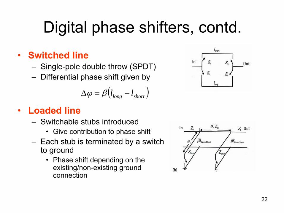
Digital phase shifters, contd.•
Switched line–
Single-pole double throw (SPDT)–
Differential phase shift given by
•
Loaded line–
Switchable
stubs introduced•
Give contribution to phase shift–
Each stub is terminated by a switch to ground
•
Phase shift depending on the existing/non-existing ground connection
( )shortlong ll −=Δ βϕ
23
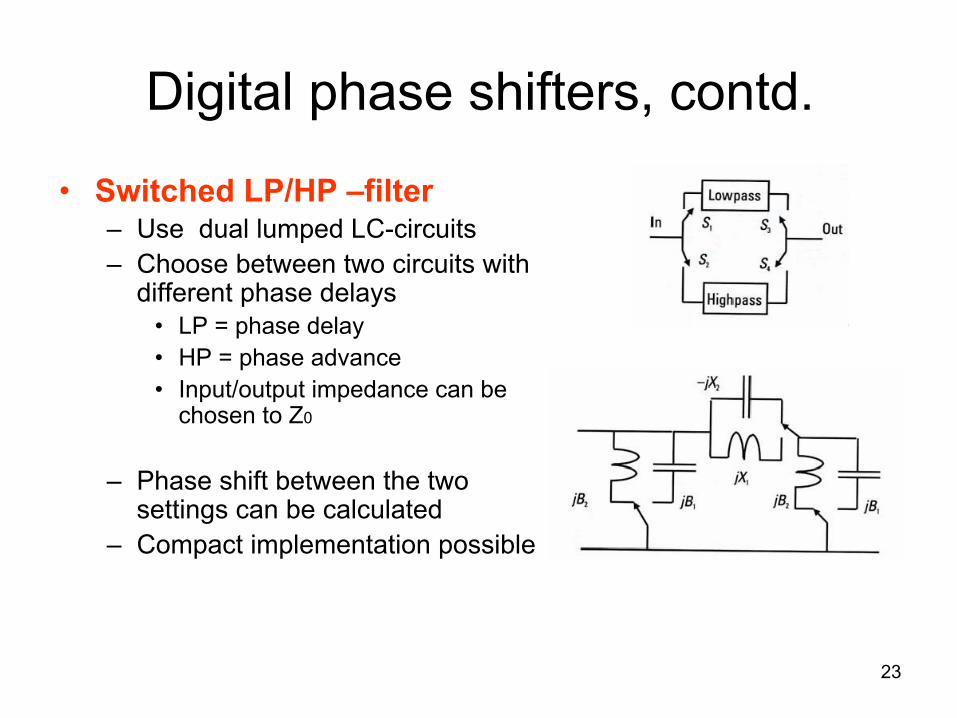
Digital phase shifters, contd.
•
Switched LP/HP –filter–
Use dual lumped LC-circuits–
Choose between two circuits with different phase delays
•
LP = phase delay•
HP = phase advance•
Input/output impedance can be chosen to Z0
–
Phase shift between the two settings can be calculated
–
Compact implementation possible
24
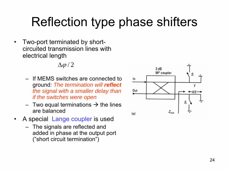
Reflection type phase shifters•
Two-port terminated by short-
circuited transmission lines with electrical length
–
If MEMS switches are connected to ground: The termination will reflect the signal with a smaller delay than if the switches were open
–
Two equal terminations the lines are balanced
•
A special Lange coupler
is used–
The signals are reflected and added in phase at the output port (”short circuit termination”)
2/ϕΔ
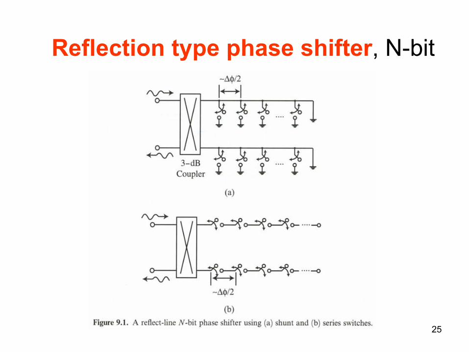
25
Reflection type phase shifter, N-bit
26
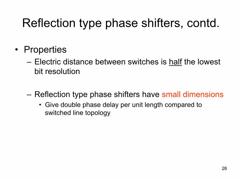
Reflection type phase shifters, contd.
•
Properties–
Electric distance between switches is half
the lowest
bit resolution
–
Reflection type phase shifters have small dimensions•
Give double phase delay per unit length compared to switched line topology
27
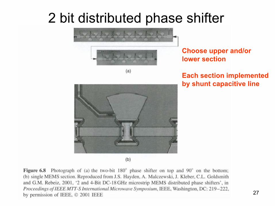
2 bit distributed phase shifter
Choose upper and/or lower section
Each section implementedby shunt capacitive line
28
Today’s lecture•
Phase shifters–
Functionality
–
Applications–
Technology
–
Analog phase shifters–
Digital phase shifters
•
Mechanical resonators–
Basic principles
–
Operating principles
for basic resonator structures
29
Mechanical resonators
•
Basic principles•
Various types of resonators
•
Typical properties
•
Working principle
for –
Comb-resonator
–
Clamped-Clamped (c-c) beam resonator–
”free-free (f-f) beam”
resonator
30
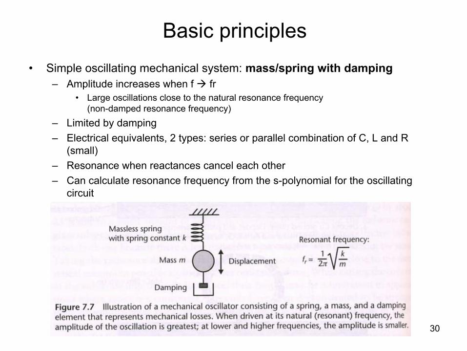
Basic principles•
Simple oscillating mechanical system: mass/spring with damping–
Amplitude increases when f fr•
Large oscillations close to the natural resonance frequency (non-damped resonance frequency)
–
Limited by damping–
Electrical equivalents, 2 types: series or parallel combination of C, L and R (small)
–
Resonance when reactances
cancel each other–
Can calculate resonance frequency from the s-polynomial for the oscillating circuit
31
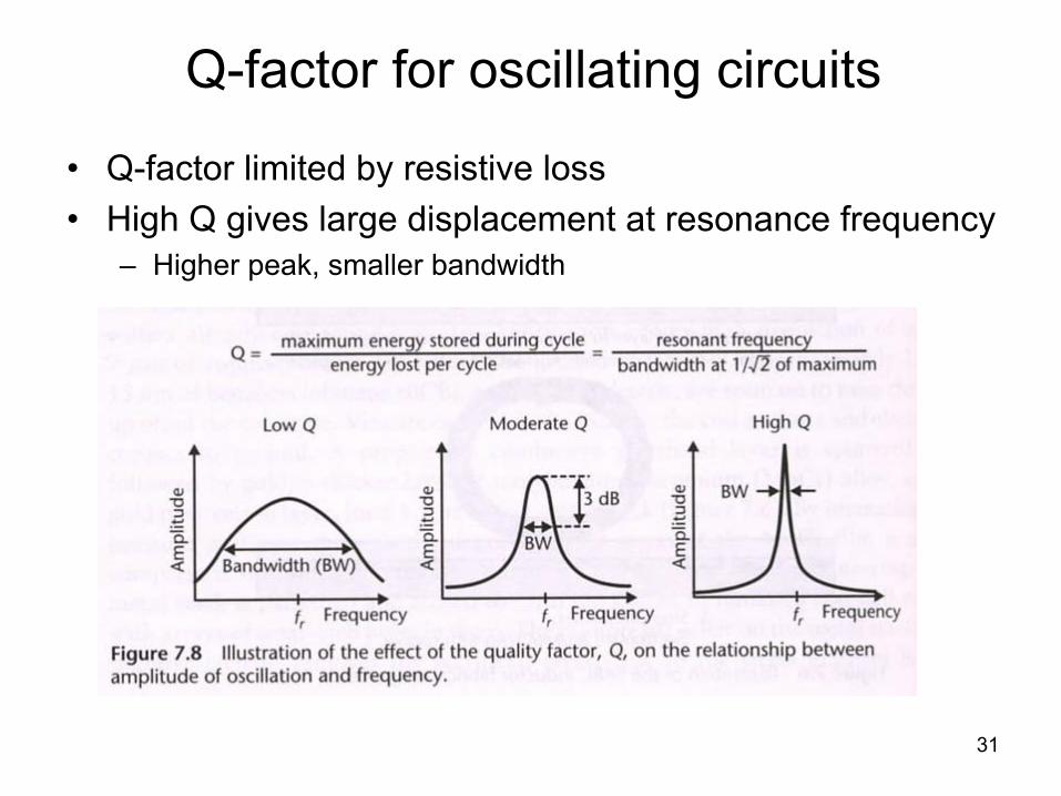
Q-factor for oscillating circuits
•
Q-factor limited by resistive loss•
High Q gives large displacement at resonance frequency–
Higher peak, smaller bandwidth
32
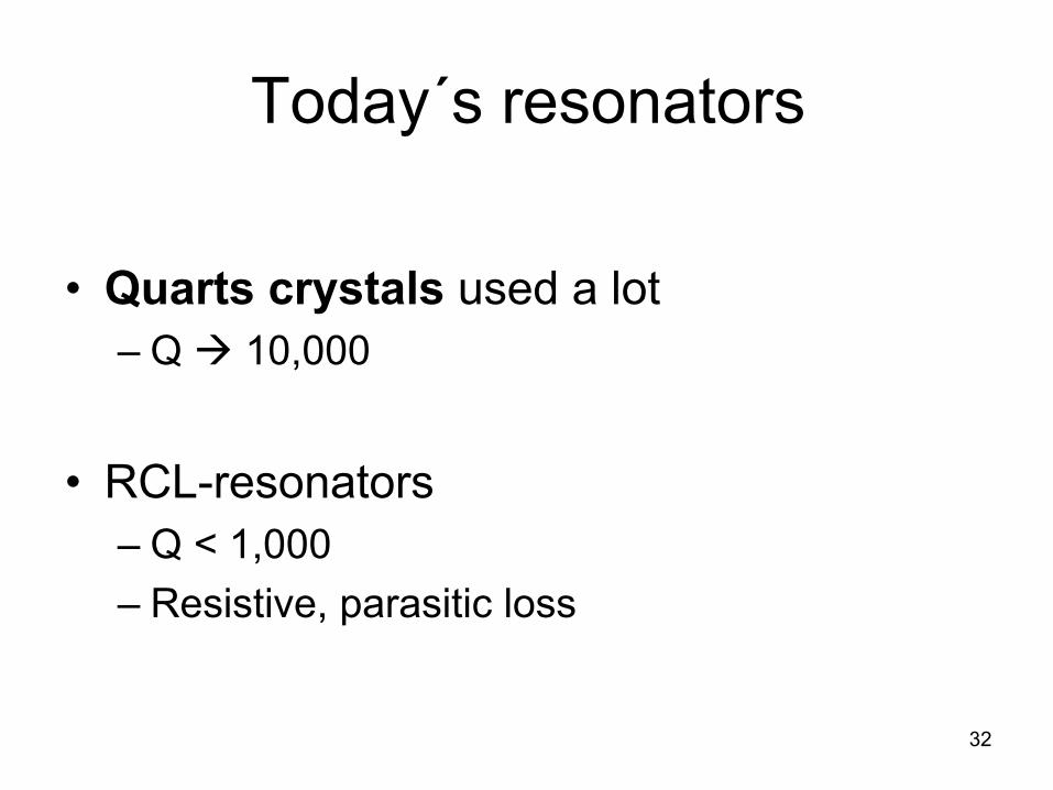
Today´s
resonators
•
Quarts crystals used a lot–
Q 10,000
•
RCL-resonators–
Q < 1,000
–
Resistive, parasitic loss
33
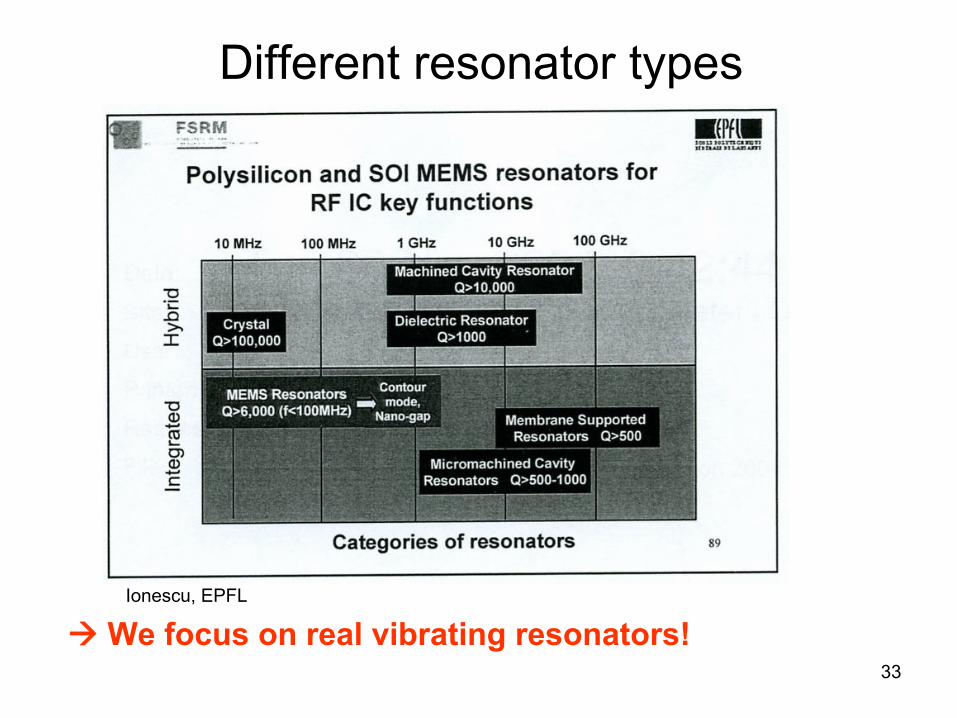
Different resonator types
We focus on real vibrating resonators!Ionescu, EPFL
34
Typical properties
•
Vibrating resonators can be scaled
down to micrometer lengths–
Analogy with IC-technology
– Reduced dimensions give mass reduction and increased spring constant increased resonance frequency
• Vibrating MEMS resonators can give high Q-factor
35
MEMS resonators
•
MEMS resonators can be used for basic circuit functions–
Frequency reference: oscillator
•
Can be realized without external discrete passive components!
•
Relevant frequencies for MEMS resonators–
0.8 –
2.5 GHz for front-end wireless systems–
500 kHz for IF frequency
–
Filtering–
Mixing and filtering (”mixlers”, Nguyen)
36
Vibrating MEMS resonators
•
Classification (De Los Santos)
–
One-port:
same electrode used for excitation and detection of beam vibration
–
Two-port:
separate electrodes for excitation and detection of the vibrating beam structure
37
Lateral and vertical movement
•
Lateral movement–
Parallel to substrate
–
Ex.: Folded beam comb-structure•
Vertical movement–
Perpendicular to substrate
–
Ex.: clamped-clamped beam (c-c
beam)–
”free-free beam”
(f-f
beam)
38
Working principles for basic resonator structures
•
Resonator using
folded beam comb-structure–
Developed at UoC, Berkeley–
One of the earliest resonator designs fabricated
•
Comb-structures are in general used in many types of MEMS systems–
For example used for accelerometer, gyro,
variable
capacitance
39
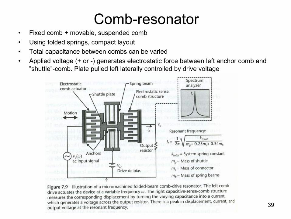
Comb-resonator•
Fixed comb + movable, suspended comb •
Using folded springs, compact layout•
Total capacitance between combs can be varied•
Applied voltage (+ or -) generates electrostatic force between left anchor comb and ”shuttle”-comb. Plate pulled left laterally controlled by drive voltage
40
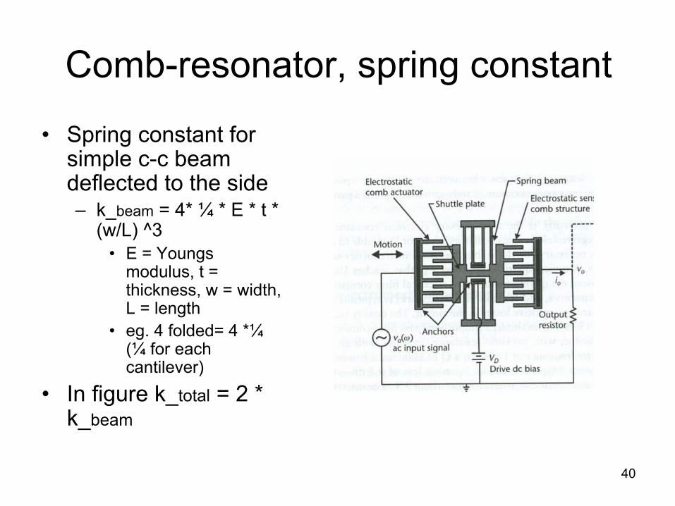
Comb-resonator, spring constant
•
Spring constant for simple c-c
beam
deflected to the side–
k_beam
= 4* ¼
* E * t * (w/L) ^3
•
E = Youngs
modulus, t = thickness, w = width, L = length
•
eg. 4 folded= 4 *¼
(¼
for each cantilever)
•
In figure k_total
= 2 * k_beam
41
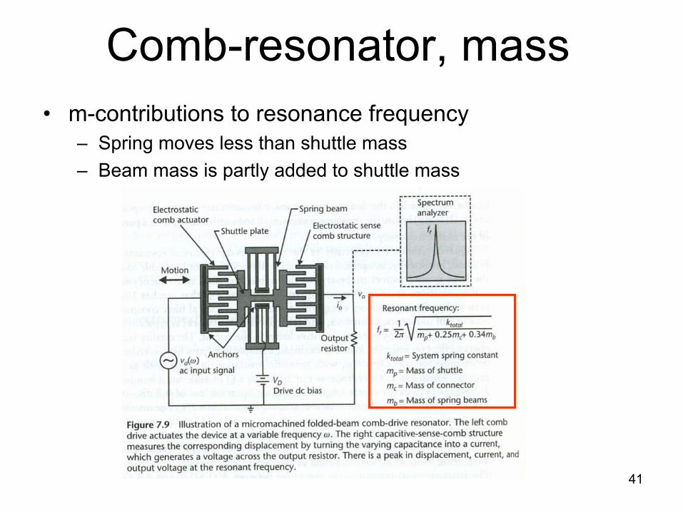
Comb-resonator, mass•
m-contributions to resonance frequency–
Spring moves less than shuttle mass–
Beam mass is partly added to shuttle mass
42
Comb-resonator, summary
•
Summary of modeling:•
Force: Fe = ½ dC/dx V ^2 (force is always attractive)–
Input signal Va
* cos
(ωt)–
Fe ~ Va^2 * ½
[1 + cos
(2ωt)]–
Driving force is 2x input frequency + DC: NOT DESIRABLE•
Add DC bias, Vd–
Fe ~ Vd
^2 + 2 Vd
* Va
* cos
ω
t
+ negligible term (2ωt)–
Linear AC force-component ~ Vd
* Va, has same frequency as Va: ω. Is emphasized!
•
C increases when finger-overlap increases–
ε
* A/d (A = comb thickness * overlap-length)•
dC/dx
= constant for a given design (linear change, C is
proportional to length variation)
43
Comb-resonator, output current
•
A time varying capacitance at the output comb is established–
Calculating of output current when Vd
is constant and
C is varying•
I0 = d/dt
(Q) = d/dt
(C*V) = Vd
* dC/dt
= Vd
* dC/dx
* dx/dt•
I0 = Vd
* dC/dx
* ω
* x_max•
I0 plotted versus frequency, shows a BP -characteristic
–
Detailed modeling in next lecture!
44
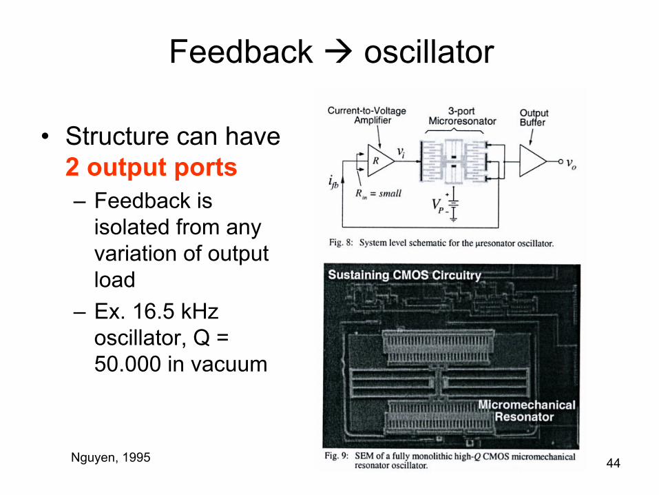
Feedback oscillator
•
Structure can have 2 output ports–
Feedback is isolated from any variation of output load
–
Ex. 16.5 kHz oscillator, Q = 50.000 in vacuum
Nguyen, 1995
45
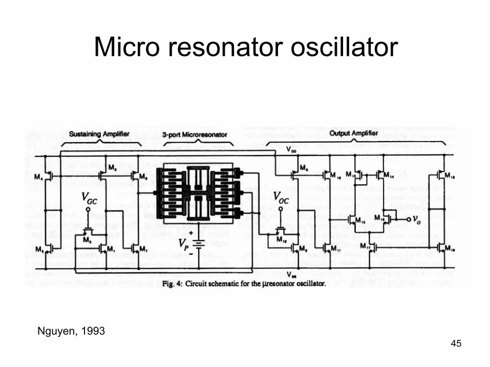
Micro resonator oscillator
Nguyen, 1993
46
Design parameters for comb-structure
•
To achieve high resonance frequency–
Total spring constant
should increase–
Or dynamic mass
should decrease•
Difficult, since a given number of fingers are needed for electrostatic actuation
–
k and m depend on material choice, layout, dimensions•
E/ρ
expresses the spring constant relative to mass
–
Frequency can increase by using a material with larger E/ρ
ratio than Si
•
Aluminium
and Titanium has E/ρ
lower than for Si•
Si carbide, poly diamond has E/ρ
higher than for Si (poly diamond is a relevant research topic)
•
Alternatively: use of other structures
47
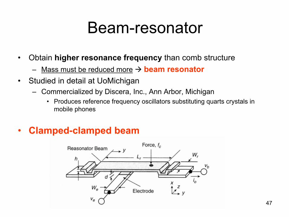
Beam-resonator
•
Obtain higher resonance frequency
than comb structure –
Mass must be reduced more beam resonator•
Studied in detail at UoMichigan–
Commercialized by Discera, Inc., Ann Arbor, Michigan•
Produces reference frequency oscillators substituting quarts crystals in mobile phones
•
Clamped-clamped beam
48
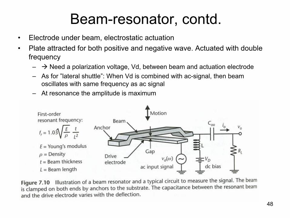
Beam-resonator, contd.•
Electrode under beam, electrostatic actuation•
Plate attracted for both positive and negative wave. Actuated with double frequency
– Need a polarization voltage, Vd, between beam and actuation electrode–
As for ”lateral shuttle”: When Vd
is combined with ac-signal, then beam oscillates with same frequency as ac signal
–
At resonance the amplitude is maximum
49
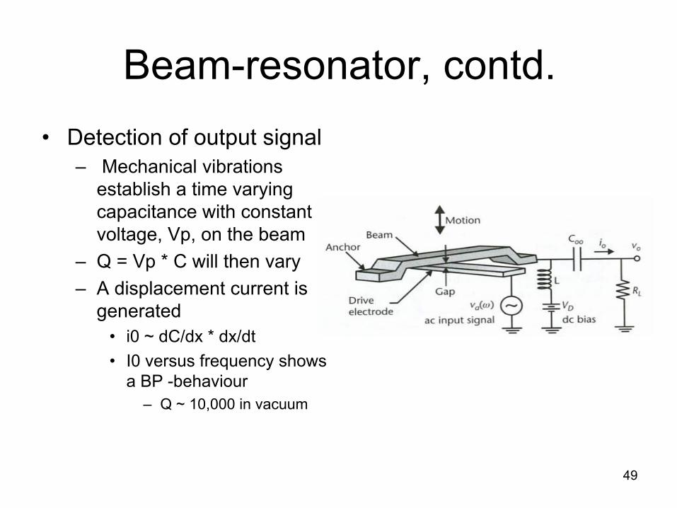
Beam-resonator, contd.•
Detection of output signal–
Mechanical vibrations establish a time varying capacitance with constant voltage, Vp, on the beam
–
Q = Vp
* C will then vary–
A displacement current is generated
•
i0 ~ dC/dx
* dx/dt•
I0 versus frequency shows a BP -behaviour
–
Q ~ 10,000 in vacuum
50
Benefits of beam-resonators
•
Simple structure
•
Smaller dimensions, smaller mass higher resonance frequency
•
Can have many frequency references on one single chip
•
More linear frequency variation with respect to temp over a larger interval
•
Integration with electronics possible reduced cost
51
c-c
beam
•
c-c
beam can be used as a reference-oscillator or HF/VHF filter/mixer
• An example: poly beam [Nguyen et al]–
l = 41 μm, w = 8 μm, t = 1.9 μm
–
g = 130 nm, Vd = 10 V, va = 3 mV– fr = 8.5 MHz– Deflection amplitude = 4.9 nm at beam centre– Q = 8,000 at 9 Pa– Q < 1 000 at 1 atm
52
Loss in c-c-beam•
Reasons for Q degradation for MEMS resonators–
Energy loss to substrate via anchors–
Air/gas damping–
Intrinsic friction–
Small dimensions (low stored energy compared with energy loss)
•
To obtain higher resonance frequency: stiffness
of a given resonator beam has to be increased–
More energy pr cycle leaks to substrate via anchors– Q-factor decreases
•
c-c-beam
is not the best structure for high frequencies!–
Eks. Q = 8,000 at 10 MHz, Q = 300 at 70 MHz• ”free-free beam” can be used to reduce substrate loss via
anchors!
53
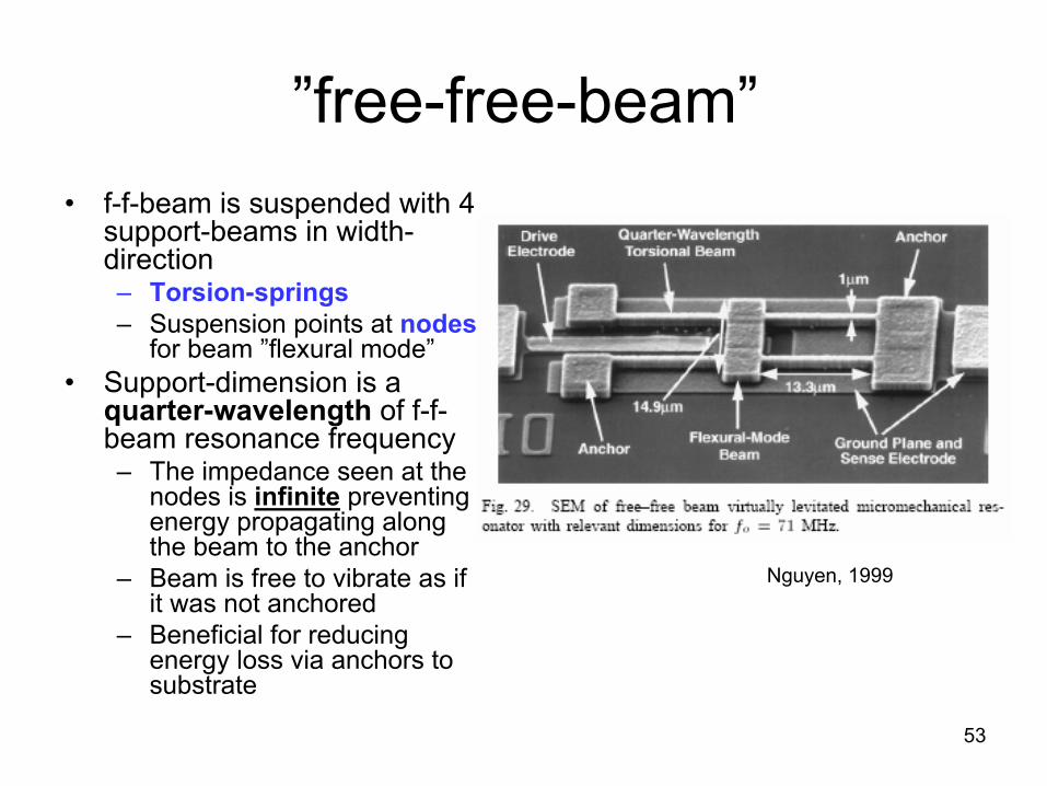
”free-free-beam”•
f-f-beam
is suspended with 4 support-beams in width-
direction–
Torsion-springs–
Suspension points at nodes
for beam ”flexural mode”
•
Support-dimension is a quarter-wavelength
of f-f-
beam
resonance frequency–
The impedance seen at the nodes is infinite
preventing energy propagating along the beam to the anchor
–
Beam is free to vibrate as if it was not anchored
–
Beneficial for reducing energy loss via anchors to substrate
Nguyen, 1999
54
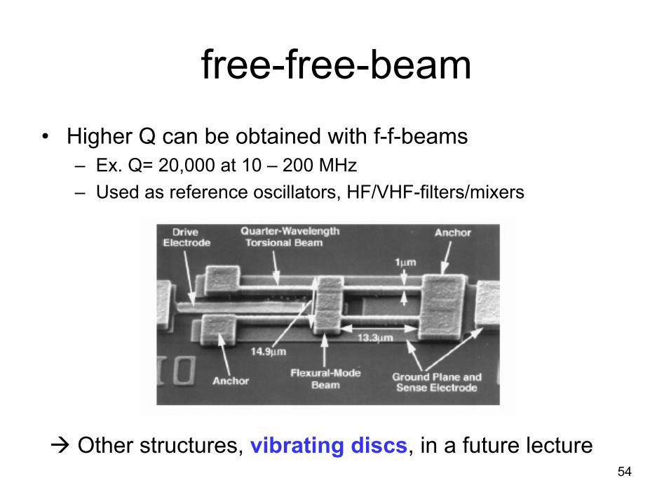
free-free-beam•
Higher Q can be obtained with f-f-beams–
Ex. Q= 20,000 at 10 –
200 MHz–
Used as reference oscillators, HF/VHF-filters/mixers
Other structures, vibrating discs, in a future lecture
Related Documents