pss applications and materials science a status solidi www.pss-a.com physica REPRINT phys. stat. sol. (a) 205, No. 8, 1961–1966 (2008) / DOI 10.1002/pssa.200778852

Welcome message from author
This document is posted to help you gain knowledge. Please leave a comment to let me know what you think about it! Share it to your friends and learn new things together.
Transcript
p s sapplications and materials science
a
statu
s
soli
di
www.pss-a.comph
ysi
ca
REPRINT
#/3.!5 ,./ (+.3' ,1./ 0.$5%-&'-2&'3 ") .(/ "'25 2%%.%,'3 3'-(%.,.(/ ,'*1/.4!'2, 3.00'&'/, .(/ "'25 *!&&'/,%
62(274 3-4&"# $# .# 924%/4& '7/.# +) 5-20-2,7$# 74: 3) !) :/% 8741/%*
$
%$T-O3-8$73W &$ \;N<)-( X7N3<303W C0T$O<WO &$ #7?$7>-O<- &W EWO3W( D0- %OQ ,73V7<W *$O7-O&<7W &$ ,98$<&-( @2U( @1HH=H61 EWO3W(
EWO30?-9
"
'$73OW &$ \;N<)-( A7</$ON<&-&$ &W I<7>W( @6HH *O-?-( EWO30?-9
#
'$73$O W[ FT3<)-9 B$)>7W9W?J( '>-7?)>07 X7N3<303$ W[ FT3<)N( \<7$ I$)>-7<)N -7& E>JN<)N( '><7$N$ ,)-&$8J W[ C)<$7)$N(
'>-7?)>07( EQDQ '><7-
!
'$\XB$)( A7</$ON<&-&$ GW/- &$ K<N+W-4%$T-O3-8$73W &$ \;N<)-( A7</$ON<&-&$ &$ !/WO-( EWO30?-9
D$)$</$& 5 M07$ 1HH6( O$/<N$& 6 I-J 1HH"( -))$T3$& 6 I-J 1HH"
E0+9<N>$& W79<7$ 1U M09J 1HH"
#!$" 5"Q26QEN( 5"QYYQ]-( 62Q5UQK$( 6"Q55QK<( "UQHYQZ&( "UQUYQM:
X7&<08 3<7 WL<&$ SXBFR [<98N >-/$ +$$7 &$TWN<3$& W73W ?9-NN
N0+N3O-3$N -3 OWW8 3$8T$O-30O$ +J <W7 +$-8 -NN<N3$& &$TWN<=
3<W7 3$)>7<P0$ SX*,%R -3 &<[[$O$73 <W7 +$-8 )0OO$73N S"H]
U1H 8,RQ B>$ $[[$)3 W[ 3>$ <W7 +$-8 )0OO$73 W7 [<98N TOWT$O=
3<$N >-N +$$7 N30&<$&Q B>$ [<98N TO$T-O$& -3 9W. <W7 +$-8 )0O=
O$73 S"H 8,R N>W. -7 -98WN3 -8WOT>W0N N3O0)30O$Q ,N 3>$ <W7
+$-8 )0OO$73 <N <7)O$-N$&( [<98N N>W. - TO$[$OO$& WO<$73-3<W7
-9W7? 3>$ S111R &<O$)3<W7Q ,\I 8$-N0O$8$73N N>W. 3>-3 3>$
N0O[-)$ DIC OW0?>7$NN W[ 3>$ [<98 <7)O$-N$N -N 3>$ )0OO$73
?W$N 0TQ B>$ WT3<)-9 TOWT$O3<$N >-/$ +$$7 N30&<$& +J 8$-N0O=
<7? 3>$ 3O-7N8<33-7)$Q X3 >-N +$$7 [W07& 3>-3 3>$ [<98 TO$T-O$&
-3 UHH 8, )0OO$73 >-N 3>$ ><?>$N3 3O-7N8<33-7)$Q B>$ WT3<)-9
)W7N3-73N W[ 3>$ [<98N >-/$ +$$7 )-9)09-3$& +J [<33<7? 3>$
3O-7N8<33-7)$Q B>$ Z-99 8$-N0O$8$73N -9NW N>W.$& 3>-3 3>$
[<98 TO$T-O$& -3 UHH 8, )0OO$73 >-N W7$ W[ 3>$ 9W.$O $9$)3O<=
)-9 O$N<N3</<3<$NQ \BXD 8$-N0O$8$73N N>W. 3>-3 3>$ [<98 TO$=
T-O$& -3 UHH 8, )0OO$73 >-N 3>$ ><?>$N3 <7[O-=O$& O$[9$)3-7)$Q
,99 3>$ 8$-N0O$8$73N N>W. 3>$ UHH 8, <W7 +$-8 )0OO$73 )-7
TOW&0)$ ?WW& P0-9<3J XBF [<98NQ
phys. stat. sol. (a) 205, No. 8, 1961–1966 (2008) / DOI 10.1002/pssa.200778852
© 2008 WILEY-VCH Verlag GmbH & Co. KGaA, Weinheim
phys. stat. sol. (a) 205, No. 8, 1961–1966 (2008) / DOI 10.1002/pssa.200778852 p s sapplications and materials science
a
statu
s
soli
di
www.pss-a.comph
ysi
ca
Indium tin oxide thin films prepared by ion beam assisted deposition technique at different ion beam currents
Lijian Meng*, 1, 2, 3, Jinsong Gao3, V. Teixeira2, and M. P. dos Santos4
1 Departamento de Física, Instituto Superior de Engenharia do Porto, Rua Dr. António Bernardino de Almeida, 431, 4200-072 Porto, Portugal
2 Centro de Física, Universidade do Minho, 4700 Braga, Portugal 3 Center of Optical Technology, Changchun Institute of Optics, Fine Mechanics and Physics, Chinese Academy of Sciences,
Changchun, P.R. China 4 CeFITec, Universidade Nova de Lisboa/Departamento de Física, Universidade de Évora, Portugal
Received 6 June 2007, revised 7 May 2008, accepted 7 May 2008 Published online 21 July 2008
PACS 68.37.Ps, 68.55.–a, 73.61.Le, 78.66.Li, 81.05.Hd, 81.15.Jj * Corresponding author: e-mail [email protected], Phone: +351 22 8340500, Fax: +351 22 8321159, Web: www.defi.isep.ipp.pt/~ljm
© 2008 WILEY-VCH Verlag GmbH & Co. KGaA, Weinheim
1 Introduction Indium tin oxide (ITO) film, as a transparent conductive oxide material, is known for its ex-cellent transmittance in the visible region and high electri-cal conductivity. It has been widely used as a transparent electrode in the areas of organic light emitting devices [1], flat panel display devices [2], electrochromic devices [3], electromagnetic shielding [4] and solar cells [5]. Many deposition techniques have been successfully used to pro-duce ITO films, such as sputtering [2, 4], electron beam evaporation [6], sol–gel [7], laser ablation [8], spray pyro-lysis [9], chemical vapour deposition [10], and reactive thermal deposition [11]. Generally, to obtain ITO films with low resistivity and high transmittance in the visible region, most of the conventional techniques mentioned above require a high substrate temperature or a post-annealing process. For producing organic luminescent de-
vices, ITO films need to be deposited at room temperature because of the low thermal stability of the organic sub-strates. However, the ITO films deposited at room tem-perature using conventional techniques usually show a high electrical resistivity and are not suitable for the appli-cations. Therefore, one of the important technical problems in the manufacturing processes of optoelectronic devices is the development of a low temperature deposition technique. It has been found that the ion beam assisted deposition (IBAD) technique can produce ITO films with low electri-cal resistivity without extra-heating the substrate [1, 12–16]. Although the bombardment of the ion beam on the substrate will raise the substrate temperature, the tempera-ture will not exceed 100 °C, according to our experiences. By this way one can produce high quality ITO films on polymer substrates. Many parameters can have influences
Indium tin oxide (ITO) films have been deposited onto glass substrates at room temperature by ion beam assisted deposi-tion technique (IBAD) at different ion beam currents (80–120 mA). The effect of the ion beam current on films proper-ties has been studied. The films prepared at low ion beam cur-rent (80 mA) show an almost amorphous structure. As the ion beam current is increased, films show a preferred orientation along the (222) direction. AFM measurements show that the surface RMS roughness of the film increases as the current goes up. The optical properties have been studied by measur-
ing the transmittance. It has been found that the film prepared at 100 mA current has the highest transmittance. The optical constants of the films have been calculated by fitting the transmittance. The Hall measurements also showed that the film prepared at 100 mA current has one of the lower electri-cal resistivities. FTIR measurements show that the film pre-pared at 100 mA current has the highest infra-red reflectance. All the measurements show the 100 mA ion beam current can produce good quality ITO films.
1962 L. Meng et al.: Indium tin oxide thin films prepared by ion beam assisted deposition technique
© 2008 WILEY-VCH Verlag GmbH & Co. KGaA, Weinheim www.pss-a.com
ph
ysic
ap s sstat
us
solid
i a
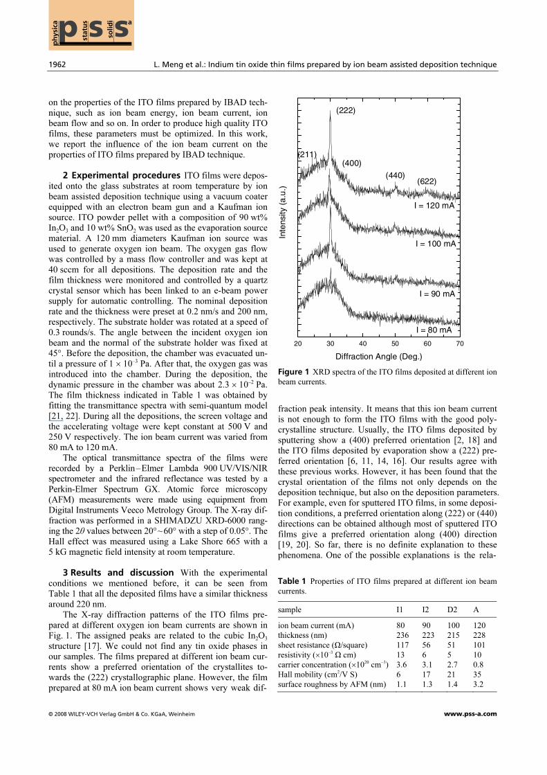
on the properties of the ITO films prepared by IBAD tech-nique, such as ion beam energy, ion beam current, ion beam flow and so on. In order to produce high quality ITO films, these parameters must be optimized. In this work, we report the influence of the ion beam current on the properties of ITO films prepared by IBAD technique. 2 Experimental procedures ITO films were depos-ited onto the glass substrates at room temperature by ion beam assisted deposition technique using a vacuum coater equipped with an electron beam gun and a Kaufman ion source. ITO powder pellet with a composition of 90 wt% In2O3 and 10 wt% SnO2 was used as the evaporation source material. A 120 mm diameters Kaufman ion source was used to generate oxygen ion beam. The oxygen gas flow was controlled by a mass flow controller and was kept at 40 sccm for all depositions. The deposition rate and the film thickness were monitored and controlled by a quartz crystal sensor which has been linked to an e-beam power supply for automatic controlling. The nominal deposition rate and the thickness were preset at 0.2 nm/s and 200 nm, respectively. The substrate holder was rotated at a speed of 0.3 rounds/s. The angle between the incident oxygen ion beam and the normal of the substrate holder was fixed at 45°. Before the deposition, the chamber was evacuated un-til a pressure of 1 × 10⁻³ Pa. After that, the oxygen gas was introduced into the chamber. During the deposition, the dynamic pressure in the chamber was about 2.3 × 10⁻² Pa. The film thickness indicated in Table 1 was obtained by fitting the transmittance spectra with semi-quantum model [21, 22]. During all the depositions, the screen voltage and the accelerating voltage were kept constant at 500 V and 250 V respectively. The ion beam current was varied from 80 mA to 120 mA. The optical transmittance spectra of the films were recorded by a Perklin–Elmer Lambda 900 UV/VIS/NIR spectrometer and the infrared reflectance was tested by a Perkin-Elmer Spectrum GX. Atomic force microscopy (AFM) measurements were made using equipment from Digital Instruments Veeco Metrology Group. The X-ray dif-fraction was performed in a SHIMADZU XRD-6000 rang-ing the 2θ values between 20°~60° with a step of 0.05°. The Hall effect was measured using a Lake Shore 665 with a 5 kG magnetic field intensity at room temperature. 3 Results and discussion With the experimental conditions we mentioned before, it can be seen from Table 1 that all the deposited films have a similar thickness around 220 nm. The X-ray diffraction patterns of the ITO films pre-pared at different oxygen ion beam currents are shown in Fig. 1. The assigned peaks are related to the cubic In2O3 structure [17]. We could not find any tin oxide phases in our samples. The films prepared at different ion beam cur-rents show a preferred orientation of the crystallites to-wards the (222) crystallographic plane. However, the film prepared at 80 mA ion beam current shows very weak dif-
20 30 40 50 60 70
(622)(440)
(400)(211)
I = 90 mA
I = 120 mA
I = 80 mA
Intens
ity(a.u.)
Diffraction Angle (Deg.)
I = 100 mA
(222)
Figure 1 XRD spectra of the ITO films deposited at different ion beam currents.
fraction peak intensity. It means that this ion beam current is not enough to form the ITO films with the good poly-crystalline structure. Usually, the ITO films deposited by sputtering show a (400) preferred orientation [2, 18] and the ITO films deposited by evaporation show a (222) pre-ferred orientation [6, 11, 14, 16]. Our results agree with these previous works. However, it has been found that the crystal orientation of the films not only depends on the deposition technique, but also on the deposition parameters. For example, even for sputtered ITO films, in some deposi-tion conditions, a preferred orientation along (222) or (440) directions can be obtained although most of sputtered ITO films give a preferred orientation along (400) direction [19, 20]. So far, there is no definite explanation to these phenomena. One of the possible explanations is the rela-
Table 1 Properties of ITO films prepared at different ion beam currents.
sample I1 I2 D2 A
ion beam current (mA) 80 90 100 120 thickness (nm) 236 223 215 228 sheet resistance (Ω/square) 117 56 51 101 resistivity (×10–3 Ω cm) 13 6 5 10 carrier concentration (×1020 cm–3) 3.6 3.1 2.7 0.8 Hall mobility (cm2/V S) 6 17 21 35 surface roughness by AFM (nm) 1.1 1.3 1.4 3.2
phys. stat. sol. (a) 205, No. 8 (2008) 1963
www.pss-a.com © 2008 WILEY-VCH Verlag GmbH & Co. KGaA, Weinheim
Original
Paper
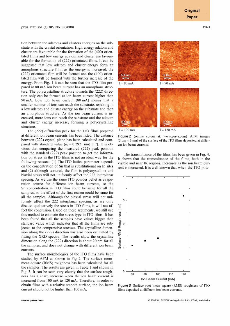
tion between the adatoms and clusters energies on the sub-strate with the crystal orientation. High energy adatom and cluster are favourable for the formation of the (400) orien-tated films and low energy adatom and cluster are favour-able for the formation of (222) orientated films. It can be suggested that low adatom and cluster energy form an amorphous structure film, as the energy is increased, the (222) orientated film will be formed and the (400) orien-tated film will be formed with the further increase of the energy. From Fig. 1 it can be seen that the ITO film pre-pared at 80 mA ion beam current has an amorphous struc-ture. The polycrystalline structure towards the (222) direc-tion only can be formed at ion beam current higher than 90 mA. Low ion beam current (80 mA) means that a smaller number of ions can reach the substrate, resulting in a low adatom and cluster energy on the substrate and then an amorphous structure. As the ion beam current is in-creased, more ions can reach the substrate and the adatom and cluster energy increase, forming a polycrystalline structure. The (222) diffraction peak for the ITO films prepared at different ion beam currents has been fitted. The distance between (222) crystal plane has been calculated and com-pared with standard value (d0 = 0.2921 nm) [17]. It is ob-vious that comparing the measured (222) peak position with the standard (222) peak position to get the informa-tion on stress in the ITO films is not an ideal way for the following reasons: (1) The ITO lattice parameter depends on the concentration of Sn that is substitutional on In sites and (2) although textured, the film is polycrystalline and biaxial stress will not uniformly affect the 222 interplanar spacing. As we use the same ITO powder pellet as evapo-ration source for different ion beam currents, so the Sn concentration in ITO films could be same for all the samples, so the effect of the first reason could be same for all the samples. Although the biaxial stress will not uni-formly affect the 222 interplanar spacing, as we only discuss qualitatively the stress in ITO films, it will not af-fect the conclusion. Based on these arguments, we still use this method to estimate the stress type in ITO films. It has been found that all the samples have values bigger than standard value which indicates that all the films are sub-jected to the compressive stresses. The crystalline dimen-sion along the (222) direction has also been estimated by fitting the XRD spectra. The results show the crystalline dimension along the (222) direction is about 20 nm for all the samples, and does not change with different ion beam currents. The surface morphologies of the ITO films have been studied by AFM as shown in Fig. 2. The surface room-mean-square (RMS) roughness has been calculated for all the samples. The results are given in Table 1 and shown in Fig. 3. It can be seen very clearly that the surface rough-ness has a sharp increase when the ion beam current is increased from 100 mA to 120 mA. Therefore, in order to obtain films with a relative smooth surface, the ion beam current should not be higher than 100 mA.
I = 80 mA I = 90 mA
I = 100 mA I = 120 mA
600nm 600nm
600nm 600nm
Figure 2 (online colour at: www.pss-a.com) AFM images (3 µm × 3 µm) of the surface of the ITO films deposited at differ-ent ion beam currents.
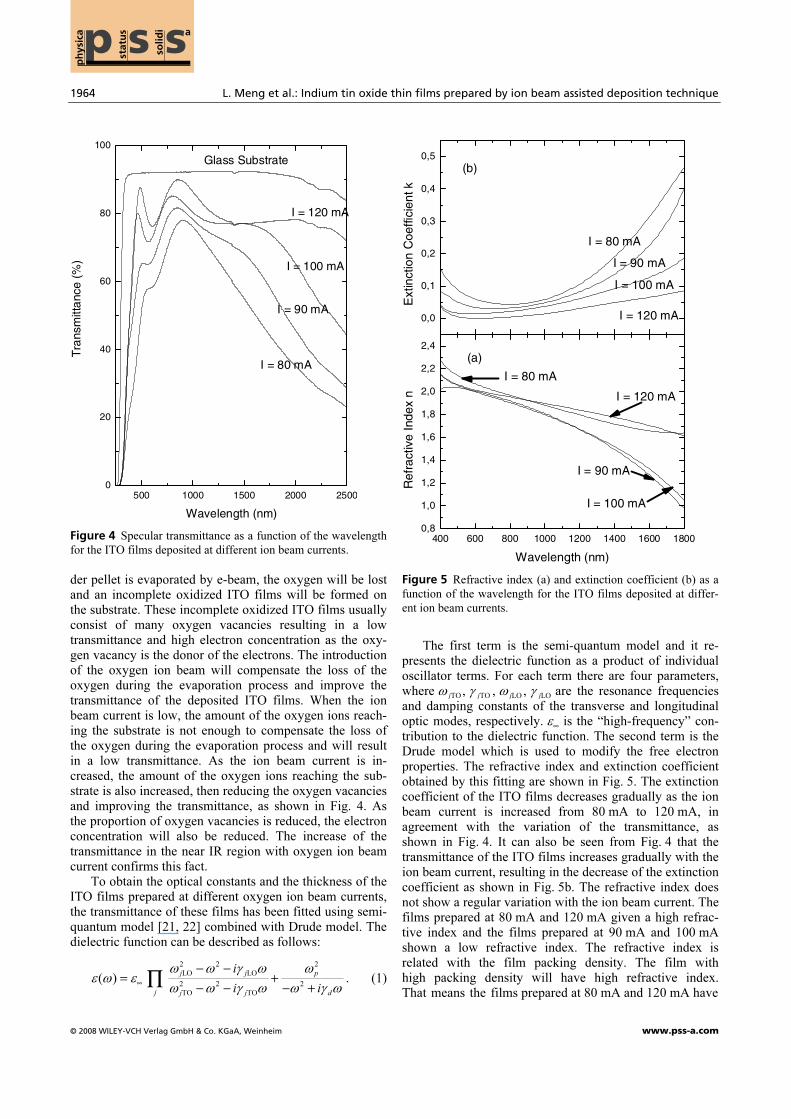
The transmittance of the films has been given in Fig. 4. It shows that the transmittance of the films, both in the visible and near IR regions, increases as the ion beam cur-rent is increased. It is well known that when the ITO pow-
80 90 100 110 1200
1
2
3
4
Surface
RMSRou
ghne
ss(nm)
Ion Beam Current (mA)
Figure 3 Surface root mean square (RMS) roughness of ITO films deposited at different ion beam currents.
1964 L. Meng et al.: Indium tin oxide thin films prepared by ion beam assisted deposition technique
© 2008 WILEY-VCH Verlag GmbH & Co. KGaA, Weinheim www.pss-a.com
ph
ysic
ap s sstat
us
solid
i a
500 1000 1500 2000 25000
20
40
60
80
100
Trans
mittanc
e(%
)
Wavelength (nm)
I = 120 mA
I = 100 mA
I = 90 mA
I = 80 mA
Glass Substrate
Figure 4 Specular transmittance as a function of the wavelength for the ITO films deposited at different ion beam currents. der pellet is evaporated by e-beam, the oxygen will be lost and an incomplete oxidized ITO films will be formed on the substrate. These incomplete oxidized ITO films usually consist of many oxygen vacancies resulting in a low transmittance and high electron concentration as the oxy-gen vacancy is the donor of the electrons. The introduction of the oxygen ion beam will compensate the loss of the oxygen during the evaporation process and improve the transmittance of the deposited ITO films. When the ion beam current is low, the amount of the oxygen ions reach-ing the substrate is not enough to compensate the loss of the oxygen during the evaporation process and will result in a low transmittance. As the ion beam current is in-creased, the amount of the oxygen ions reaching the sub-strate is also increased, then reducing the oxygen vacancies and improving the transmittance, as shown in Fig. 4. As the proportion of oxygen vacancies is reduced, the electron concentration will also be reduced. The increase of the transmittance in the near IR region with oxygen ion beam current confirms this fact. To obtain the optical constants and the thickness of the ITO films prepared at different oxygen ion beam currents, the transmittance of these films has been fitted using semi-quantum model [21, 22] combined with Drude model. The dielectric function can be described as follows:
2 2 2
LO LO
2 2 2
TO TO
( ) .j j p
j j j d
i
i i
ω ω γ ω ωε ω ε
ω ω γ ω ω γ ω•
- -
= +
- - - +’ (1)
400 600 800 1000 1200 1400 1600 18000,8
1,0
1,2
1,4
1,6
1,8
2,0
2,2
2,4
0,0
0,1
0,2
0,3
0,4
0,5
RefractiveInde
xn
Wavelength (nm)
(a)
I = 80 mA
I = 120 mA
I = 90 mA
I = 100 mA
ExtinctionCoe
fficien
tk
I = 80 mA
I = 90 mA
I = 100 mA
I = 120 mA
(b)
Figure 5 Refractive index (a) and extinction coefficient (b) as a function of the wavelength for the ITO films deposited at differ-ent ion beam currents.
The first term is the semi-quantum model and it re- presents the dielectric function as a product of individual oscillator terms. For each term there are four parameters, where
TOjω , TOjγ ,
LOjω , LOjγ are the resonance frequencies
and damping constants of the transverse and longitudinal optic modes, respectively. ε
•
is the “high-frequency” con-tribution to the dielectric function. The second term is the Drude model which is used to modify the free electron properties. The refractive index and extinction coefficient obtained by this fitting are shown in Fig. 5. The extinction coefficient of the ITO films decreases gradually as the ion beam current is increased from 80 mA to 120 mA, in agreement with the variation of the transmittance, as shown in Fig. 4. It can also be seen from Fig. 4 that the transmittance of the ITO films increases gradually with the ion beam current, resulting in the decrease of the extinction coefficient as shown in Fig. 5b. The refractive index does not show a regular variation with the ion beam current. The films prepared at 80 mA and 120 mA given a high refrac-tive index and the films prepared at 90 mA and 100 mA shown a low refractive index. The refractive index is related with the film packing density. The film with high packing density will have high refractive index. That means the films prepared at 80 mA and 120 mA have

phys. stat. sol. (a) 205, No. 8 (2008) 1965
www.pss-a.com © 2008 WILEY-VCH Verlag GmbH & Co. KGaA, Weinheim
Original
Paper
80 90 100 110 120
50
60
70
80
90
100
110
120
0
2
4
6
8
10
12
140
1
2
3
4
0
5
10
15
20
25
30
35
40
She
etRes
istanc
e(W
/Squ
are)
Ion Beam Current (mA)
(a)
Res
istiv
ity(x10
-3W-cm)
ElectronCon
centratio
n(x10
20cm
-3)
(b)
HallM
obility
(cm
2 /VS)
Figure 6 Sheet resistance and resistivity (a), and carrier concen-
tration and Hall mobility (b) of ITO films deposited at different
ion beam currents. higher packing densities than the films prepared at 90 mA and 100 mA. Generally, an amorphous film has a compact structure and a high packing density; a polycrystalline film has a columnar structure and a low packing density. That is why films prepared at 80 mA ion beam current have a high refractive index. At the high ion beam current (120 mA), the film structure may be improved, the number of the void may decrease and results in a small increase of the refrac-tive index. In fact, it can be seen that the variation of the refractive index in the visible region is small, the big di-vergence only happens in the infrared region. The variation of the refractive index in the infrared region results not only from the difference of the packing density, but also from the behaviour of the free carriers. Both the carrier concentration and mobility will influence the film refrac-tive index in this region. The electrical properties of the ITO films prepared at different ion beam currents are given in Fig. 6. It can be seen from Fig. 6a that the electrical re-sistivity and the sheet resistance of the ITO films decrease as the ion beam current increases and reach the minima values at 100 mA ion beam current, and then increase as the ion beam current is increased further. The Hall meas-urements show that although the electron concentration in ITO films decreases as the ion beam current is increased, the Hall mobility increases as the ion beam current is in-
creased. The electrical resistivity is related with both the electron concentration and the Hall mobility. Although the ITO film prepared at 100 mA ion beam current has a low electron concentration, it has a high Hall mobility, result-ing in a low electrical resistivity. The decrease of the elec-tron concentration with the ion beam current can be related with the disappearance of the oxygen vacancies. As the ion beam current is increased, the amount of the oxygen ions reaching the substrate also increases; it will compensate the loss of the oxygen during the evaporation process and reduce the amount of the oxygen vacancies, producing then a low electron concentration. The Hall mobility is related with the film structure. As the ion beam current is in-creased, the oxygen vacancies vanish, the scattering possi-bility of the carriers by oxygen vacancies decreases and results in an increase of the Hall mobility, as shown in Fig. 6b. The reflectance of the ITO films prepared at different ion beam currents in the infer-red region is given in Fig. 7. This feature is very important for the application of the ITO films in the electromagnetic shield area. It can be seen that only the films prepared at 90 mA and 100 mA give high reflectance in IR region. There is a very simple rela-tion between the infrared reflection R and the sheet resis-tance R
[23, 24]:
2
IR 0 0(1 2 ) .R c Rε
−
= +
(2)
12000 16000 20000 2400040
50
60
70
80
90
Reflectan
ce(%
)
Wavelength (nm)
I = 80 mA
I = 120 mA
I = 90 mA
I = 100 mA
Figure 7 Infrared reflectance spectra for ITO films deposited at
different ion beam currents.
1966 L. Meng et al.: Indium tin oxide thin films prepared by ion beam assisted deposition technique
© 2008 WILEY-VCH Verlag GmbH & Co. KGaA, Weinheim www.pss-a.com
ph
ysic
ap s sstat
us
solid
i a
It can be seen that the high sheet resistance will result in a low infrared reflection. Table 1 shows that the films prepared both at 80 mA and 120 mA have high sheet resist-ance and then a low reflectance in the infrared region.
4 Conclusions ITO films have been deposited onto glass substrates at room temperature by ion beam assisted deposition technique at different ion beam currents (80–120 mA). It has been found that the ion beam current has a great influence on ITO films properties. The lowest electri-cal resistivity (5 × 10⁻³ Ω cm) with good transmittance has been obtained for the ITO film prepared at 100 mA ion beam current. It gives the way to deposit ITO films with good qualities without extra heating of the substrate during the deposition process. The FTIR measurements also show that the film prepared at 100 mA has the highest reflec-tance in the IR region. Therefore, the ITO film prepared at 100 mA ion beam current shows a good quality, high transmittance in the visible region, low electrical resistivity and high infrared reflectance, and then seems to be the most adequate for the applications both in the transparent conductive electrode area and in the electromagnetic wave shield area.
Acknowledgements This work was carried out in the
Centre of Optical Technology, Changchun Institute of Optics,
Fine Mechanics and Physics of Chinese Academy of Sciences,
during Lijian Meng’s visit to the centre as a senior visiting re-
searcher. Lijian Meng is thankful to the Fundação para a Ciência
e a Tecnologia (Portugal) for providing a fellowship (SFRH-
BSAB-514).
References
[1] J. T. Lim, N. G. Cho, C. H. Jeong, J. H. Lee, J. H. Lim, and
G. Y. Yeom, J. Korean Phys. Soc. 47, 142 (2005).
[2] S. K. Park, J. I. Han, W. K. Kim, and M. G. Kwak, Thin
Solid Films 397, 49 (2001).
[3] Y. Djaoued, V. H. Phong, S. Badilescu, P. V. Ashrit, F. E.
Girouard, and V.-V. Truong, Thin Solid Films 293, 108
(1997).
[4] J. L. Huang, B. S. Yau, C. Y. Chen, W. T. Lo, and D. F. Lii,
Ceram. Int. 27, 363 (2001).
[5] B. Zimmermann, M. Glatthaar, M. Niggemann, M. K. Riede,
A. Hinsch, and A. Gombert, Sol. Energy Mater. Sol. Cells
91, 374 (2007).
[6] J. George and C. S. Menon, Surf. Coat. Technol. 132, 45
(2002).
[7] S. R. Ramanan, Thin Solid Films 389, 207 (2001).
[8] B. Thestrup, J. Schou, A. Nordskov, and N. B. Larsen,
Appl. Surf. Sci. 142, 248 (1999).
[9] E. Benamar, M. Rami, C. Messaoudi, D. Sayah, and A. En-
naoui, Sol. Energy Mater. Sol. Cells 56, 125 (1999).
[10] Z. B. Zhou, R. Q. Cui, Q. J. Pang, Y. D. Wang, F. Y. Meng,
T. T. Sun, Z. M. Ding, and X. B. Yu, Appl. Surf. Sci. 172,
245 (2001).
[11] P. Thilakan and J. Kumar, Mat. Sci. Eng. B 55, 195 (1998).
[12] D. Kim and S. Kim, Surf. Coat. Technol. 154, 204 (2002).
[13] C. Liu, T. Mihara, T. Matsutani, T. Asanuma, and
M. Kiuchi, Solid State Commun. 126, 509 (2003).
[14] S. K. Koh, Y. G. Han, J. H. Lee, U. J. Yeo, and J. S. Cho,
Thin Solid Films 496, 81 (2006).
[15] J. W. Bae, H. J. Kim, J. S. Kim, Y. H. Lee, N. E. Lee,
G. Y. Yeom, and Y. W. Ko, Surf. Coat. Technol. 131, 196
(2000).
[16] C. Liu, T. Mihara, T. Matsutani, T. Asanuma, and
M. Kiuchi, Nucl. Instrum. Methods B 206, 348 (2003).
[17] Powder Diffraction File, Joint Committee on Powder
Diffraction Standards (ASTM, Philadelphia, PA, 1967),
Card 6-0416.
[18] L. J. Meng and M. P. dos Santos, Thin Solid Films 289, 65
(1996).
[19] L. J. Meng and M. P. dos Santos, Thin Solid Films 303, 151
(1997).
[20] L. J. Meng and M. P. dos Santos, J. Vac. Sci. Technol.
A 18, 1668 (2000).
[21] F. Gervais and B. Piriou, Phys. Rev. B 11, 3944 (1975).
[22] M. Schubert, T. E. Tiwald, and C. M. Herzinger, Phys. Rev.
B 61, 8187 (2000).
[23] P. K. Biswas, A. De, N. C. Pramanik, P. K. Chakraborty,
K. Ortner, V. Hock, and S. Korder, Mater. Lett. 57, 2326
(2003).
[24] G. Frank, E. Kauer, and H. Kostlin, Thin Solid Films 77,
107 (1981).
Related Documents