Features • Incorporates the ARM920T ™ ARM ® Thumb ® Processor – 200 MIPS at 180 MHz, Memory Management Unit – 16-KByte Data Cache, 16-KByte Instruction Cache, Write Buffer – In-circuit Emulator including Debug Communication Channel – Mid-level Implementation Embedded Trace Macrocell (256-ball BGA Package Only) • Low Power: On VDDCORE 24.4 mA in Normal Mode, 520 μA in Standby Mode • Additional Embedded Memories – 16K Bytes of SRAM and 128K Bytes of ROM • External Bus Interface (EBI) – Supports SDRAM, Static Memory, Burst Flash, Glueless Connection to CompactFlash ® and NAND Flash/SmartMedia ™ • System Peripherals for Enhanced Performance: – Enhanced Clock Generator and Power Management Controller – Two On-chip Oscillators with Two PLLs – Very Slow Clock Operating Mode and Software Power Optimization Capabilities – Four Programmable External Clock Signals – System Timer Including Periodic Interrupt, Watchdog and Second Counter – Real-time Clock with Alarm Interrupt – Debug Unit, Two-wire UART and Support for Debug Communication Channel – Advanced Interrupt Controller with 8-level Priority, Individually Maskable Vectored Interrupt Sources, Spurious Interrupt Protected – Seven External Interrupt Sources and One Fast Interrupt Source – Four 32-bit PIO Controllers with Up to 122 Programmable I/O Lines, Input Change Interrupt and Open-drain Capability on Each Line – 20-channel Peripheral DMA Controller (PDC) • Ethernet MAC 10/100 Base-T – Media Independent Interface (MII) or Reduced Media Independent Interface (RMII) – Integrated 28-byte FIFOs and Dedicated DMA Channels for Receive and Transmit • USB 2.0 Full Speed (12 Mbits per second) Host Double Port – Dual On-chip Transceivers (Single Port Only on 208-lead PQFP Package) – Integrated FIFOs and Dedicated DMA Channels • USB 2.0 Full Speed (12 Mbits per second) Device Port – On-chip Transceiver, 2-Kbyte Configurable Integrated FIFOs • Multimedia Card Interface (MCI) – Automatic Protocol Control and Fast Automatic Data Transfers – MMC and SD Memory Card-compliant, Supports Up to Two SD Memory Cards • Three Synchronous Serial Controllers (SSC) – Independent Clock and Frame Sync Signals for Each Receiver and Transmitter –I 2 S Analog Interface Support, Time Division Multiplex Support – High-speed Continuous Data Stream Capabilities with 32-bit Data Transfer • Four Universal Synchronous/Asynchronous Receiver/Transmitters (USART) – Support for ISO7816 T0/T1 Smart Card – Hardware Handshaking – RS485 Support, IrDA Up To 115 Kbps – Full Modem Control Lines on USART1 • Master/Slave Serial Peripheral Interface (SPI) – 8- to 16-bit Programmable Data Length, 4 External Peripheral Chip Selects • Two 3-channel, 16-bit Timer/Counters (TC) – Three External Clock Inputs, Two Multi-purpose I/O Pins per Channel – Double PWM Generation, Capture/Waveform Mode, Up/Down Capability • Two-wire Interface (TWI) – Master Mode Support, All 2-wire Atmel EEPROMs Supported • IEEE 1149.1 JTAG Boundary Scan on All Digital Pins • Power Supplies – 1.65V to 1.95V for VDDCORE, VDDOSC and VDDPLL – 3.0V to 3.6V for VDDIOP (Peripheral I/Os) and for VDDIOM (Memory I/Os)Available • in a 208-lead PQFP or 256-ball BGA Package ARM920T ™ - based Microcontroller AT91RM9200 Summary Rev. 1768IS-ATARM–30-Sep-05

Welcome message from author
This document is posted to help you gain knowledge. Please leave a comment to let me know what you think about it! Share it to your friends and learn new things together.
Transcript

ARM920T™-based Microcontroller
AT91RM9200 Summary
Rev. 1768IS-ATARM–30-Sep-05
Features• Incorporates the ARM920T™ ARM® Thumb® Processor
– 200 MIPS at 180 MHz, Memory Management Unit– 16-KByte Data Cache, 16-KByte Instruction Cache, Write Buffer– In-circuit Emulator including Debug Communication Channel– Mid-level Implementation Embedded Trace Macrocell (256-ball BGA Package Only)
• Low Power: On VDDCORE 24.4 mA in Normal Mode, 520 µA in Standby Mode • Additional Embedded Memories
– 16K Bytes of SRAM and 128K Bytes of ROM• External Bus Interface (EBI)
– Supports SDRAM, Static Memory, Burst Flash, Glueless Connection to CompactFlash® and NAND Flash/SmartMedia™
• System Peripherals for Enhanced Performance:– Enhanced Clock Generator and Power Management Controller– Two On-chip Oscillators with Two PLLs– Very Slow Clock Operating Mode and Software Power Optimization Capabilities– Four Programmable External Clock Signals– System Timer Including Periodic Interrupt, Watchdog and Second Counter– Real-time Clock with Alarm Interrupt– Debug Unit, Two-wire UART and Support for Debug Communication Channel– Advanced Interrupt Controller with 8-level Priority, Individually Maskable Vectored
Interrupt Sources, Spurious Interrupt Protected– Seven External Interrupt Sources and One Fast Interrupt Source– Four 32-bit PIO Controllers with Up to 122 Programmable I/O Lines, Input Change
Interrupt and Open-drain Capability on Each Line– 20-channel Peripheral DMA Controller (PDC)
• Ethernet MAC 10/100 Base-T– Media Independent Interface (MII) or Reduced Media Independent Interface (RMII)– Integrated 28-byte FIFOs and Dedicated DMA Channels for Receive and Transmit
• USB 2.0 Full Speed (12 Mbits per second) Host Double Port– Dual On-chip Transceivers (Single Port Only on 208-lead PQFP Package)– Integrated FIFOs and Dedicated DMA Channels
• USB 2.0 Full Speed (12 Mbits per second) Device Port – On-chip Transceiver, 2-Kbyte Configurable Integrated FIFOs
• Multimedia Card Interface (MCI)– Automatic Protocol Control and Fast Automatic Data Transfers – MMC and SD Memory Card-compliant, Supports Up to Two SD Memory Cards
• Three Synchronous Serial Controllers (SSC)– Independent Clock and Frame Sync Signals for Each Receiver and Transmitter– I2S Analog Interface Support, Time Division Multiplex Support– High-speed Continuous Data Stream Capabilities with 32-bit Data Transfer
• Four Universal Synchronous/Asynchronous Receiver/Transmitters (USART)– Support for ISO7816 T0/T1 Smart Card – Hardware Handshaking – RS485 Support, IrDA Up To 115 Kbps– Full Modem Control Lines on USART1
• Master/Slave Serial Peripheral Interface (SPI)– 8- to 16-bit Programmable Data Length, 4 External Peripheral Chip Selects
• Two 3-channel, 16-bit Timer/Counters (TC)– Three External Clock Inputs, Two Multi-purpose I/O Pins per Channel– Double PWM Generation, Capture/Waveform Mode, Up/Down Capability
• Two-wire Interface (TWI)– Master Mode Support, All 2-wire Atmel EEPROMs Supported
• IEEE 1149.1 JTAG Boundary Scan on All Digital Pins• Power Supplies
– 1.65V to 1.95V for VDDCORE, VDDOSC and VDDPLL– 3.0V to 3.6V for VDDIOP (Peripheral I/Os) and for VDDIOM (Memory I/Os)Available
• in a 208-lead PQFP or 256-ball BGA Package

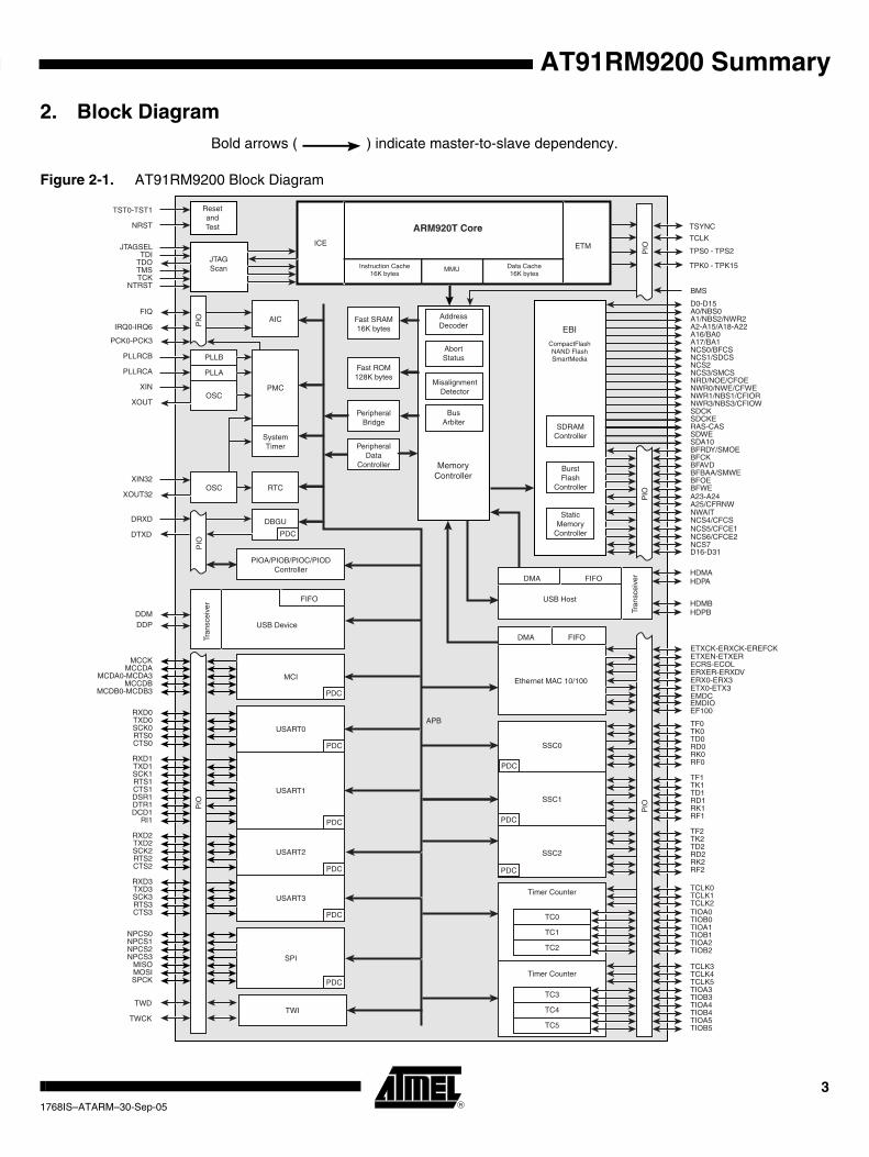
1. DescriptionThe AT91RM9200 is a complete system-on-chip built around the ARM920T ARM Thumb pro-cessor. It incorporates a rich set of system and application peripherals and standard interfaces in order to provide a single-chip solution for a wide range of compute-intensive applications that require maximum functionality at minimum power consumption at lowest cost.
The AT91RM9200 incorporates a high-speed on-chip SRAM workspace, and a low-latency External Bus Interface (EBI) for seamless connection to whatever configuration of off-chip mem-ories and memory-mapped peripherals is required by the application. The EBI incorporates controllers for synchronous DRAM (SDRAM), Burst Flash and Static memories and features specific circuitry facilitating the interface for NAND Flash/SmartMedia and Compact Flash.
The Advanced Interrupt Controller (AIC) enhances the interrupt handling performance of the ARM920T processor by providing multiple vectored, prioritized interrupt sources and reducing the time taken to transfer to an interrupt handler.
The Peripheral DMA Controller (PDC) provides DMA channels for all the serial peripherals, enabling them to transfer data to or from on- and off-chip memories without processor interven-tion. This reduces the processor overhead when dealing with transfers of continuous data streams.The AT91RM9200 benefits from a new generation of PDC which includes dual pointers that simplify significantly buffer chaining.
The set of Parallel I/O (PIO) controllers multiplex the peripheral input/output lines with general-purpose data I/Os for maximum flexibility in device configuration. An input change interrupt, open drain capability and programmable pull-up resistor is included on each line.
The Power Management Controller (PMC) keeps system power consumption to a minimum by selectively enabling/disabling the processor and various peripherals under software control. It uses an enhanced clock generator to provide a selection of clock signals including a slow clock (32 kHz) to optimize power consumption and performance at all times.
The AT91RM9200 integrates a wide range of standard interfaces including USB 2.0 Full Speed Host and Device and Ethernet 10/100 Base-T Media Access Controller (MAC), which provides connection to a extensive range of external peripheral devices and a widely used networking layer. In addition, it provides an extensive set of peripherals that operate in accordance with sev-eral industry standards, such as those used in audio, telecom, Flash Card, infrared and Smart Card applications.
To complete the offer, the AT91RM9200 benefits from the integration of a wide range of debug features including JTAG-ICE, a dedicated UART debug channel (DBGU) and an embedded real time trace. This enables the development and debug of all applications, especially those with real-time constraints.
21768IS–ATARM–30-Sep-05
AT91RM9200 Summary
AT91RM9200 Summary
2. Block DiagramBold arrows ( ) indicate master-to-slave dependency.
Figure 2-1. AT91RM9200 Block Diagram
ARM920T Core
JTAGScan
ICE
AIC Fast SRAM16K bytes
PIO
PLLB
PLLA
OSCPMC
SystemTimer
OSC RTC
EBI
PIOA/PIOB/PIOC/PIODController
DBGU
MCI
USART0
USART1
USART2
USART3
SPI
SSC0
SSC1
SSC2
Timer Counter
TC0
TC1
TC2
Timer Counter
TC3
TC4
TC5
TWI
PIO
PIO
D0-D15A0/NBS0A1/NBS2/NWR2A2-A15/A18-A22A16/BA0A17/BA1NCS0/BFCSNCS1/SDCS
NCS3/SMCSNRD/NOE/CFOENWR0/NWE/CFWENWR1/NBS1/CFIORNWR3/NBS3/CFIOWSDCKSDCKERAS-CASSDWESDA10BFRDY/SMOEBFCKBFAVDBFBAA/SMWEBFOEBFWEA23-A24
NWAIT
NCS5/CFCE1
D16-D31
TF0TK0TD0RD0RK0RF0
TF1TK1TD1RD1RK1RF1
TF2TK2TD2RD2RK2RF2
TCLK0TCLK1TCLK2TIOA0TIOB0TIOA1TIOB1TIOA2TIOB2
TCLK3TCLK4TCLK5TIOA3TIOB3TIOA4TIOB4TIOA5TIOB5
TWD
TWCK
JTAGSELTDI
TDOTMSTCK
NTRST
FIQ
IRQ0-IRQ6
PCK0-PCK3
PLLRCB
PLLRCA
XIN
XOUT
XIN32
XOUT32
DDMDDP
MCCKMCCDA
MCDA0-MCDA3MCCDB
RXD0TXD0SCK0RTS0CTS0
RXD1TXD1SCK1RTS1CTS1DSR1DTR1DCD1
RI1
RXD2TXD2SCK2RTS2CTS2
RXD3TXD3SCK3RTS3CTS3
NPCS0NPCS1NPCS2NPCS3
MISOMOSISPCK
MCDB0-MCDB3
HDMA
HDPB
HDPA
HDMB
DRXD
DTXD
Ethernet MAC 10/100
ETXCK-ERXCK-EREFCKETXEN-ETXERECRS-ECOLERXER-ERXDVERX0-ERX3ETX0-ETX3EMDC
SDRAMController
BurstFlash
Controller
StaticMemory
Controller
PIO
Instruction Cache16K bytes
Data Cache16K bytes
MMU
EMDIO
DMA FIFO
DMA FIFO
USB HostFIFO
USB Device
Tran
scei
ver
PIO
PIO
PIO
ResetandTest
TST0-TST1
NRST
APB
Fast ROM128K bytes
BMS
NCS2
A25/CFRNW
NCS4/CFCS
MisalignmentDetector
AddressDecoder
AbortStatus
NCS6/CFCE2
Tran
scei
ver
NCS7
MemoryController
BusArbiter
PeripheralBridge
PeripheralData
Controller
EF100
ETM
TSYNC
TCLK
TPS0 - TPS2
TPK0 - TPK15
CompactFlashNAND FlashSmartMedia
PDC
PDC
PDC
PDC
PDC
PDC
PDC
PDCPDCPDC
PDC
PDC
31768IS–ATARM–30-Sep-05

3. Key FeaturesThis section presents the key features of each block.
3.1 ARM920T Processor• ARM9TDMI™-based on ARM® Architecture v4T
• Two instruction sets
– ARM® High-performance 32-bit Instruction Set
– Thumb® High Code Density 16-bit Instruction Set
• 5-Stage Pipeline Architecture:
– Instruction Fetch (F)
– Instruction Decode (D)
– Execute (E)
– Data Memory (M)
– Register Write (W)
• 16-Kbyte Data Cache, 16-Kbyte Instruction Cache
– Virtually-addressed 64-way Associative Cache
– 8 words per line
– Write-though and write-back operation
– Pseudo-random or Round-robin replacement
– Low-power CAM RAM implementation
• Write Buffer
– 16-word Data Buffer
– 4-address Address Buffer
– Software Control Drain
• Standard ARMv4 Memory Management Unit (MMU)
– Access permission for sections
– Access permission for large pages and small pages can be specified separately for each quarter of the pages
– 16 embedded domains
– 64 Entry Instruction TLB and 64 Entry Data TLB
• 8-, 16-, 32-bit Data Bus for Instructions and Data
3.2 Debug and Test • Integrated Embedded In-Circuit-Emulator
• Debug Unit
– Two-pin UART
– Debug Communication Channel
– Chip ID Register
• Embedded Trace Macrocell: ETM9 Rev2a
– Medium Level Implementation
– Half-rate Clock Mode
41768IS–ATARM–30-Sep-05
AT91RM9200 Summary

AT91RM9200 Summary
– Four Pairs of Address Comparators
– Two Data Comparators
– Eight Memory Map Decoder Inputs
– Two Counters
– One Sequencer
– One 18-byte FIFO
• IEEE1149.1 JTAG Boundary Scan on all Digital Pins
3.3 Boot Program• Default Boot Program stored in ROM-based products
• Downloads and runs an application from external storage media into internal SRAM
• Downloaded code size depends on embedded SRAM size
• Automatic detection of valid application
• Bootloader supporting a wide range of non-volatile memories
– SPI DataFlash® connected on SPI NPCS0
– Two-wire EEPROM
– 8-bit parallel memories on NCS0
• Boot Uploader in case no valid program is detected in external NVM and supporting several communication media
• Serial communication on a DBGU (XModem protocol)
• USB Device Port (DFU Protocol)
3.4 Embedded Software Services• Compliant with ATPCS
• Compliant with AINSI/ISO Standard C
• Compiled in ARM/Thumb Interworking
• ROM Entry Service
• Tempo, Xmodem and DataFlash services
• CRC and Sine tables
3.5 Reset Controller• Two reset input lines (NRST and NTRST) providing, respectively:
• Initialization of the User Interface registers (defined in the user interface of each peripheral) and:
– Sample the signals needed at bootup
– Compel the processor to fetch the next instruction at address zero.
• Initialization of the embedded ICE TAP controller.
3.6 Memory Controller• Programmable Bus Arbiter handling four Masters
– Internal Bus is shared by ARM920T, PDC, USB Host Port and Ethernet MAC Masters
51768IS–ATARM–30-Sep-05
– Each Master can be assigned a priority between 0 and 7
• Address Decoder provides selection for
– Eight external 256-Mbyte memory areas
– Four internal 1-Mbyte memory areas
– One 256-Mbyte embedded peripheral area
• Boot Mode Select Option
– Non-volatile Boot Memory can be internal or external
– Selection is made by BMS pin sampled at reset
• Abort Status Registers
– Source, Type and all parameters of the access leading to an abort are saved
• Misalignment Detector
– Alignment checking of all data accesses
– Abort generation in case of misalignment
• Remap command
– Provides remapping of an internal SRAM in place of the boot NVM
3.7 External Bus Interface• Integrates three External Memory Controllers:
– Static Memory Controller
– SDRAM Controller
– Burst Flash Controller
• Additional logic for NAND Flash/SmartMedia and CompactFlash support
• Optimized External Bus:
– 16- or 32-bit Data Bus
– Up to 26-bit Address Bus, up to 64-Mbytes addressable
– Up to 8 Chip Selects, each reserved to one of the eight Memory Areas
– Optimized pin multiplexing to reduce latencies on External Memories
• Configurable Chip Select Assignment:
– Burst Flash Controller or Static Memory Controller on NCS0
– SDRAM Controller or Static Memory Controller on NCS1
– Static Memory Controller on NCS3, Optional NAND Flash/SmartMedia Support
– Static Memory Controller on NCS4 - NCS6, Optional CompactFlash Support
– Static Memory Controller on NCS7
3.8 Static Memory Controller• External memory mapping, 512-Mbyte address space
• Up to 8 Chip Select Lines
• 8- or 16-bit Data Bus
• Remap of Boot Memory
• Multiple Access Modes supported
– Byte Write or Byte Select Lines
61768IS–ATARM–30-Sep-05
AT91RM9200 Summary

AT91RM9200 Summary
– Two different Read Protocols for each Memory Bank
• Multiple device adaptability
– Compliant with LCD Module
– Programmable Setup Time Read/Write
– Programmable Hold Time Read/Write
• Multiple Wait State Management
– Programmable Wait State Generation
– External Wait Request
– Programmable Data Float Time
3.9 SDRAM Controller• Numerous configurations supported
– 2K, 4K, 8K Row Address Memory Parts
– SDRAM with two or four Internal Banks
– SDRAM with 16- or 32-bit Data Path
• Programming facilities
– Word, half-word, byte access
– Automatic page break when Memory Boundary has been reached
– Multibank Ping-pong Access
– Timing parameters specified by software
– Automatic refresh operation, refresh rate is programmable
• Energy-saving capabilities
– Self-refresh and Low-power Modes supported
• Error detection
– Refresh Error Interrupt
• SDRAM Power-up Initialization by software
• Latency is set to two clocks (CAS Latency of 1, 3 Not Supported)
• Auto Precharge Command not used
3.10 Burst Flash Controller• Multiple Access Modes supported
– Asynchronous or Burst Mode Byte, Half-word or Word Read Accesses
– Asynchronous Mode Half-word Write Accesses
• Adaptability to different device speed grades
– Programmable Burst Flash Clock Rate
– Programmable Data Access Time
– Programmable Latency after Output Enable
• Adaptability to different device access protocols and bus interfaces
– Two Burst Read Protocols: Clock Control Address Advance or Signal Controlled Address Advance
– Multiplexed or separate address and data buses
71768IS–ATARM–30-Sep-05

– Continuous Burst and Page Mode Accesses supported
3.11 Peripheral DMA Controller (PDC)• Generates transfers to/from peripherals such as DBGU, USART, SSC, SPI and MCI
• Twenty channels
• One Master Clock cycle needed for a transfer from memory to peripheral
• Two Master Clock cycles needed for a transfer from peripheral to memory
3.12 Advanced Interrupt Controller• Controls the interrupt lines (nIRQ and nFIQ) of an ARM® Processor
• Thirty-two individually maskable and vectored interrupt sources
– Source 0 is reserved for the Fast Interrupt Input (FIQ)
– Source 1 is reserved for system peripherals (ST, RTC, PMC, DBGU…)
– Source 2 to Source 31 control thirty embedded peripheral interrupts or external interrupts
– Programmable Edge-triggered or Level-sensitive Internal Sources
– Programmable Positive/Negative Edge-triggered or High/Low Level-sensitive External Sources
• 8-level Priority Controller
– Drives the Normal Interrupt of the processor
– Handles priority of the interrupt sources 1 to 31
– Higher priority interrupts can be served during service of lower priority interrupt
• Vectoring
– Optimizes Interrupt Service Routine Branch and Execution
– One 32-bit Vector Register per interrupt source
– Interrupt Vector Register reads the corresponding current Interrupt Vector
• Protect Mode
– Easy debugging by preventing automatic operations
• General Interrupt Mask
– Provides processor synchronization on events without triggering an interrupt
3.13 Power Management Controller• Optimizes the power consumption of the whole system
• Embeds and controls:
– One Main Oscillator and One Slow Clock Oscillator (32.768Hz)
– Two Phase Locked Loops (PLLs) and Dividers
– Clock Prescalers
• Provides:
– the Processor Clock PCK
– the Master Clock MCK
– the USB Clocks, UHPCK and UDPCK, respectively for the USB Host Port and the USB Device Port
81768IS–ATARM–30-Sep-05
AT91RM9200 Summary
AT91RM9200 Summary
– Programmable automatic PLL switch-off in USB Device suspend conditions
– up to thirty peripheral clocks
– four programmable clock outputs PCK0 to PCK3
• Four operating modes:
– Normal Mode, Idle Mode, Slow Clock Mode, Standby Mode
3.14 System Timer• One Period Interval Timer, 16-bit programmable counter
• One Watchdog Timer, 16-bit programmable counter
• One Real-time Timer, 20-bit free-running counter
• Interrupt Generation on event
3.15 Real Time Clock• Low power consumption
• Full asynchronous design
• Two hundred year calendar
• Programmable Periodic Interrupt
• Alarm and update parallel load
• Control of alarm and update Time/Calendar Data In
3.16 Debug Unit• System peripheral to facilitate debug of Atmel’s ARM®-based systems
• Composed of the following functions
– Two-pin UART
– Debug Communication Channel (DCC) support
– Chip ID Registers
• Two-pin UART
– Implemented features are 100% compatible with the standard Atmel USART
– Independent receiver and transmitter with a common programmable Baud Rate Generator
– Even, Odd, Mark or Space Parity Generation
– Parity, Framing and Overrun Error Detection
– Automatic Echo, Local Loopback and Remote Loopback Channel Modes
– Interrupt generation
– Support for two PDC channels with connection to receiver and transmitter
• Debug Communication Channel Support
– Offers visibility of COMMRX and COMMTX signals from the ARM Processor
– Interrupt generation
• Chip ID Registers
– Identification of the device revision, sizes of the embedded memories, set of peripherals
91768IS–ATARM–30-Sep-05

3.17 PIO Controller• Up to 32 programmable I/O Lines
• Fully programmable through Set/Clear Registers
• Multiplexing of two peripheral functions per I/O Line
• For each I/O Line (whether assigned to a peripheral or used as general purpose I/O)
– Input change interrupt
– Glitch filter
– Multi-drive option enables driving in open drain
– Programmable pull up on each I/O line
– Pin data status register, supplies visibility of the level on the pin at any time
• Synchronous output, provides Set and Clear of several I/O lines in a single write
3.18 USB Host Port• Compliance with Open HCI Rev 1.0 specification
• Compliance with USB V2.0 Full-speed and Low-speed Specification
• Supports both Low-speed 1.5 Mbps and Full-speed 12 Mbps USB devices
• Root hub integrated with two downstream USB ports
• Two embedded USB transceivers
• Supports power management
• Operates as a master on the Memory Controller
3.19 USB Device Port• USB V2.0 full-speed compliant, 12 Mbits per second
• Embedded USB V2.0 full-speed transceiver
• Embedded dual-port RAM for endpoints
• Suspend/Resume logic
• Ping-pong mode (two memory banks) for isochronous and bulk endpoints
• Six general-purpose endpoints
– Endpoint 0, Endpoint 3: 8 bytes, no ping-pong mode
– Endpoint 1, Endpoint 2: 64 bytes, ping-pong mode
– Endpoint 4, Endpoint 5: 256 bytes, ping-pong mode
3.20 Ethernet MAC• Compatibility with IEEE Standard 802.3
• 10 and 100 Mbits per second data throughput capability
• Full- and half-duplex operation
• MII or RMII interface to the physical layer
• Register interface to address, status and control registers
• DMA interface, operating as a master on the Memory Controller
• Interrupt generation to signal receive and transmit completion
• 28-byte transmit and 28-byte receive FIFOs
101768IS–ATARM–30-Sep-05
AT91RM9200 Summary

AT91RM9200 Summary
• Automatic pad and CRC generation on transmitted frames
• Address checking logic to recognize four 48-bit addresses
• Supports promiscuous mode where all valid frames are copied to memory
• Supports physical layer management through MDIO interface
3.21 Serial Peripheral Interface• Supports communication with serial external devices
– Four chip selects with external decoder support allow communication with up to 15 peripherals
– Serial memories, such as DataFlash and 3-wire EEPROMs
– Serial peripherals, such as ADCs, DACs, LCD Controllers, CAN Controllers and Sensors
– External co-processors
• Master or slave serial peripheral bus interface
– 8- to 16-bit programmable data length per chip select
– Programmable phase and polarity per chip select
– Programmable transfer delays between consecutive transfers and between clock and data per chip select
– Programmable delay between consecutive transfers
– Selectable mode fault detection
• Connection to PDC channel optimizes data transfers
– One channel for the receiver, one channel for the transmitter
– Next buffer support
3.22 Two-wire Interface• Compatibility with standard two-wire serial memory
• One, two or three bytes for slave address
• Sequential Read/Write operations
3.23 USART• Programmable Baud Rate Generator
• 5- to 9-bit full-duplex synchronous or asynchronous serial communications
– 1, 1.5 or 2 stop bits in Asynchronous Mode or 1 or 2 stop bits in Synchronous Mode
– Parity generation and error detection
– Framing error detection, overrun error detection
– MSB- or LSB-first
– Optional break generation and detection
– By 8 or by-16 over-sampling receiver frequency
– Optional hardware handshaking RTS-CTS
– Optional modem signal management DTR-DSR-DCD-RI
– Receiver time-out and transmitter timeguard
– Optional Multi-drop Mode with address generation and detection
111768IS–ATARM–30-Sep-05
• RS485 with driver control signal
• ISO7816, T = 0 or T = 1 Protocols for interfacing with smart cards
– NACK handling, error counter with repetition and iteration limit
• IrDA modulation and demodulation
– Communication at up to 115.2 Kbps
• Test Modes
– Remote Loopback, Local Loopback, Automatic Echo
• Connection of two Peripheral DMA Controller (PDC) channels
– Offers buffer transfer without processor intervention
3.24 Serial Synchronous Controller• Provides serial synchronous communication links used in audio and telecom applications
• Contains an independent receiver and transmitter and a common clock divider
• Interfaced with two PDC channels to reduce processor overhead
• Offers a configurable frame sync and data length
• Receiver and transmitter can be programmed to start automatically or on detection of different event on the frame sync signal
• Receiver and transmitter include a data signal, a clock signal and a frame synchronization signal
3.25 Timer Counter• Three 16-bit Timer Counter Channels
• Wide range of functions including:
– Frequency Measurement
– Event Counting
– Interval Measurement
– Pulse Generation
– Delay Timing
– Pulse Width Modulation
– Up/down Capabilities
• Each channel is user-configurable and contains:
– Three external clock inputs
– Five internal clock inputs
– Two multi-purpose input/output signals
• Internal interrupt signal
• Two global registers that act on all three TC Channels
3.26 MultiMedia Card Interface• Compatibility with MultiMedia Card Specification Version 2.2
• Compatibility with SD Memory Card Specification Version 1.0
• Cards clock rate up to Master Clock divided by 2
• Embedded power management to slow down clock rate when not used
121768IS–ATARM–30-Sep-05
AT91RM9200 Summary
AT91RM9200 Summary
• Supports two slots
– One slot for one MultiMedia Card bus (up to 30 cards) or one SD Memory Card
• Support for stream, block and multi-block data read and write
• Connection to a Peripheral DMA Controller (PDC) channel
– Minimizes processor intervention for large buffer transfers
131768IS–ATARM–30-Sep-05

4. AT91RM9200 Product Properties
4.1 Power Supplies
The AT91RM9200 has five types of power supply pins:
• VDDCORE pins. They power the core, including processor, memories and peripherals; voltage ranges from 1.65V to 1.95V, 1.8V nominal.
• VDDIOM pins. They power the External Bus Interface I/O lines; voltage ranges from 3.0V to 3.6V, 3V or 3.3V nominal.
• VDDIOP pins. They power the Peripheral I/O lines and the USB transceivers; voltage ranges from 3.0V to 3.6V, 3V or 3.3V nominal.
• VDDPLL pins. They power the PLL cells; voltage ranges from 1.65V to 1.95V, 1.8V nominal.
• VDDOSC pin. They power both oscillators; voltage ranges from 1.65V to 1.95V, 1.8V nominal.
The double power supplies VDDIOM and VDDIOP are identified in Table 4-1 on page 15 and Table 4-2 on page 17. These supplies enable the user to power the device differently for inter-facing with memories and for interfacing with peripherals.
Ground pins are common to all power supplies, except VDDPLL and VDDOSC pins. For these pins, GNDPLL and GNDOSC are provided, respectively.
4.2 Pinout
The AT91RM9200 is available in two packages:
• 208-lead PQFP, 31.2 x 31.2 mm, 0.5 mm lead pitch
• 256-ball BGA, 15 x 15 mm, 0.8 mm ball pitch
The product features of the 256-ball BGA package are extended compared to the 208-lead PQFP package. The features that are available only with the 256-ball BGA package are:
• Parallel I/O Controller D
• ETM port with outputs multiplexed on the PIO Controller D
• a second USB Host transceiver, opening the Hub capabilities of the embedded USB Host.
141768IS–ATARM–30-Sep-05
AT91RM9200 Summary
AT91RM9200 Summary
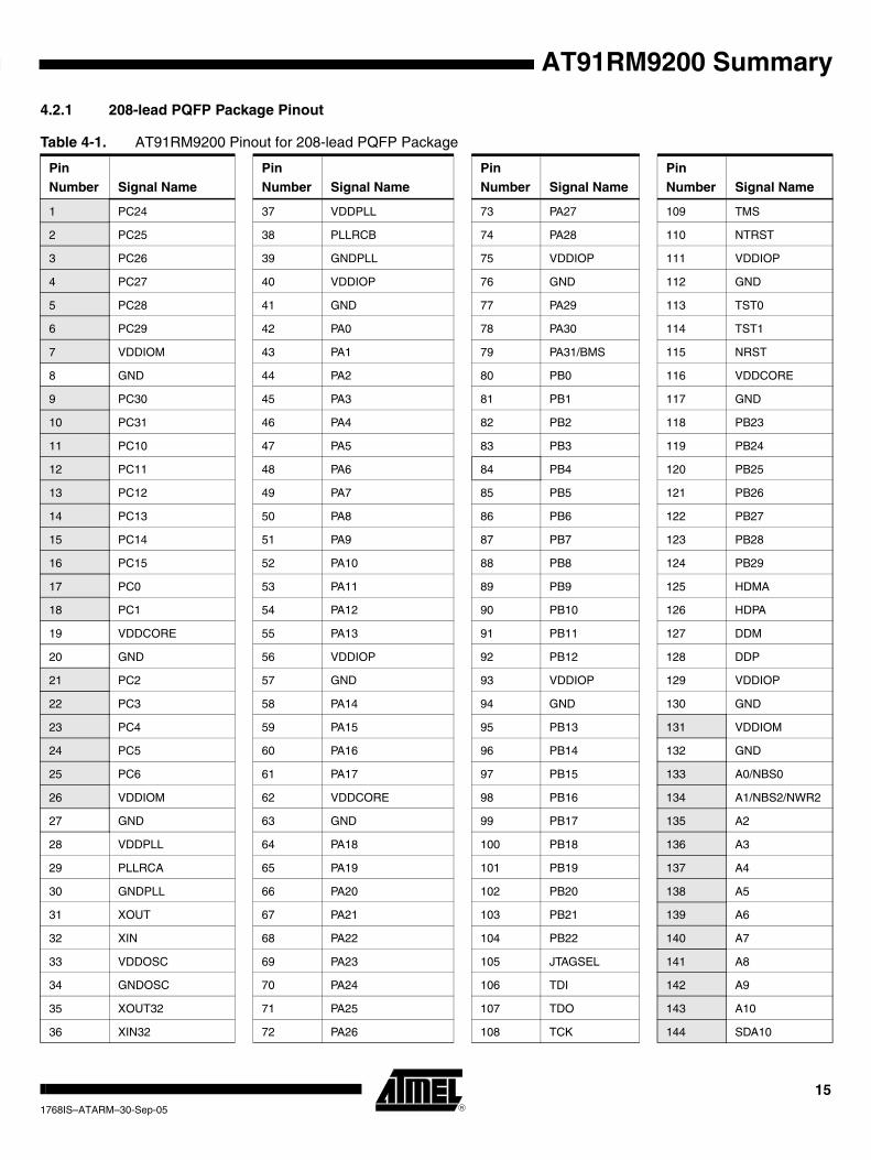
4.2.1 208-lead PQFP Package Pinout
Table 4-1. AT91RM9200 Pinout for 208-lead PQFP Package
PinNumber Signal Name
PinNumber Signal Name
PinNumber Signal Name
PinNumber Signal Name
1 PC24 37 VDDPLL 73 PA27 109 TMS
2 PC25 38 PLLRCB 74 PA28 110 NTRST
3 PC26 39 GNDPLL 75 VDDIOP 111 VDDIOP
4 PC27 40 VDDIOP 76 GND 112 GND
5 PC28 41 GND 77 PA29 113 TST0
6 PC29 42 PA0 78 PA30 114 TST1
7 VDDIOM 43 PA1 79 PA31/BMS 115 NRST
8 GND 44 PA2 80 PB0 116 VDDCORE
9 PC30 45 PA3 81 PB1 117 GND
10 PC31 46 PA4 82 PB2 118 PB23
11 PC10 47 PA5 83 PB3 119 PB24
12 PC11 48 PA6 84 PB4 120 PB25
13 PC12 49 PA7 85 PB5 121 PB26
14 PC13 50 PA8 86 PB6 122 PB27
15 PC14 51 PA9 87 PB7 123 PB28
16 PC15 52 PA10 88 PB8 124 PB29
17 PC0 53 PA11 89 PB9 125 HDMA
18 PC1 54 PA12 90 PB10 126 HDPA
19 VDDCORE 55 PA13 91 PB11 127 DDM
20 GND 56 VDDIOP 92 PB12 128 DDP
21 PC2 57 GND 93 VDDIOP 129 VDDIOP
22 PC3 58 PA14 94 GND 130 GND
23 PC4 59 PA15 95 PB13 131 VDDIOM
24 PC5 60 PA16 96 PB14 132 GND
25 PC6 61 PA17 97 PB15 133 A0/NBS0
26 VDDIOM 62 VDDCORE 98 PB16 134 A1/NBS2/NWR2
27 GND 63 GND 99 PB17 135 A2
28 VDDPLL 64 PA18 100 PB18 136 A3
29 PLLRCA 65 PA19 101 PB19 137 A4
30 GNDPLL 66 PA20 102 PB20 138 A5
31 XOUT 67 PA21 103 PB21 139 A6
32 XIN 68 PA22 104 PB22 140 A7
33 VDDOSC 69 PA23 105 JTAGSEL 141 A8
34 GNDOSC 70 PA24 106 TDI 142 A9
35 XOUT32 71 PA25 107 TDO 143 A10
36 XIN32 72 PA26 108 TCK 144 SDA10
151768IS–ATARM–30-Sep-05
Note: 1. Shaded cells define the pins powered by VDDIOM.
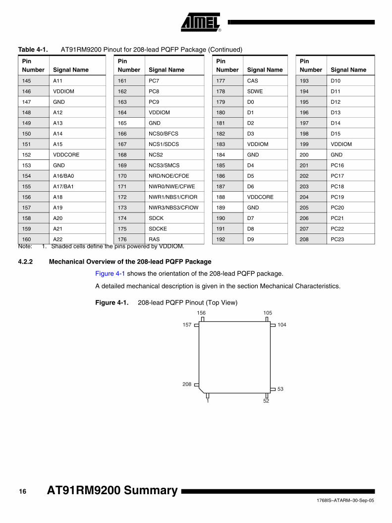
4.2.2 Mechanical Overview of the 208-lead PQFP Package
Figure 4-1 shows the orientation of the 208-lead PQFP package.
A detailed mechanical description is given in the section Mechanical Characteristics.
Figure 4-1. 208-lead PQFP Pinout (Top View)
145 A11 161 PC7 177 CAS 193 D10
146 VDDIOM 162 PC8 178 SDWE 194 D11
147 GND 163 PC9 179 D0 195 D12
148 A12 164 VDDIOM 180 D1 196 D13
149 A13 165 GND 181 D2 197 D14
150 A14 166 NCS0/BFCS 182 D3 198 D15
151 A15 167 NCS1/SDCS 183 VDDIOM 199 VDDIOM
152 VDDCORE 168 NCS2 184 GND 200 GND
153 GND 169 NCS3/SMCS 185 D4 201 PC16
154 A16/BA0 170 NRD/NOE/CFOE 186 D5 202 PC17
155 A17/BA1 171 NWR0/NWE/CFWE 187 D6 203 PC18
156 A18 172 NWR1/NBS1/CFIOR 188 VDDCORE 204 PC19
157 A19 173 NWR3/NBS3/CFIOW 189 GND 205 PC20
158 A20 174 SDCK 190 D7 206 PC21
159 A21 175 SDCKE 191 D8 207 PC22
160 A22 176 RAS 192 D9 208 PC23
Table 4-1. AT91RM9200 Pinout for 208-lead PQFP Package (Continued)
PinNumber Signal Name
PinNumber Signal Name
PinNumber Signal Name
PinNumber Signal Name
1 52
53
104
105156
157
208
161768IS–ATARM–30-Sep-05
AT91RM9200 Summary
AT91RM9200 Summary
4.2.3 256-ball BGA Package Pinout
Table 4-2. AT91RM9200 Pinout for 256-ball BGA Package
Pin Signal Name Pin Signal Name Pin Signal Name Pin Signal Name
A1 TDI C3 PD14 E5 TCK G14 PA1
A2 JTAGSEL C4 PB22 E6 GND G15 PA2
A3 PB20 C5 PB19 E7 PB15 G16 PA3
A4 PB17 C6 PD10 E8 GND G17 XIN32
A5 PD11 C7 PB13 E9 PB7 H1 PD23
A6 PD8 C8 PB12 E10 PB3 H2 PD20
A7 VDDIOP C9 PB6 E11 PA29 H3 PD22
A8 PB9 C10 PB1 E12 PA26 H4 PD21
A9 PB4 C11 GND E13 PA25 H5 VDDIOP
A10 PA31/BMS C12 PA20 E14 PA9 H13 VDDPLL
A11 VDDIOP C13 PA18 E15 PA6 H14 VDDIOP
A12 PA23 C14 VDDCORE E16 PD3 H15 GNDPLL
A13 PA19 C15 GND E17 PD0 H16 GND
A14 GND C16 PA8 F1 PD16 H17 XOUT32
A15 PA14 C17 PD5 F2 GND J1 PD25
A16 VDDIOP D1 TST1 F3 PB23 J2 PD27
A17 PA13 D2 VDDIOP F4 PB25 J3 PD24
B1 TDO D3 VDDIOP F5 PB24 J4 PD26
B2 PD13 D4 GND F6 VDDCORE J5 PB28
B3 PB18 D5 VDDIOP F7 PB16 J6 PB29
B4 PB21 D6 PD7 F9 PB11 J12 GND
B5 PD12 D7 PB14 F11 PA30 J13 GNDOSC
B6 PD9 D8 VDDIOP F12 PA28 J14 VDDOSC
B7 GND D9 PB8 F13 PA4 J15 VDDPLL
B8 PB10 D10 PB2 F14 PD2 J16 GNDPLL
B9 PB5 D11 GND F15 PD1 J17 XIN
B10 PB0 D12 PA22 F16 PA5 K1 HDPA
B11 VDDIOP D13 PA21 F17 PLLRCB K2 DDM
B12 PA24 D14 PA16 G1 PD19 K3 HDMA
B13 PA17 D15 PA10 G2 PD17 K4 VDDIOP
B14 PA15 D16 PD6 G3 GND K5 DDP
B15 PA11 D17 PD4 G4 PB26 K13 PC5
B16 PA12 E1 NRST G5 PD18 K14 PC4
B17 PA7 E2 NTRST G6 PB27 K15 PC6
C1 TMS E3 GND G12 PA27 K16 VDDIOM
C2 PD15 E4 TST0 G13 PA0 K17 XOUT
171768IS–ATARM–30-Sep-05

Note: 1. Shaded cells define the pins powered by VDDIOM.
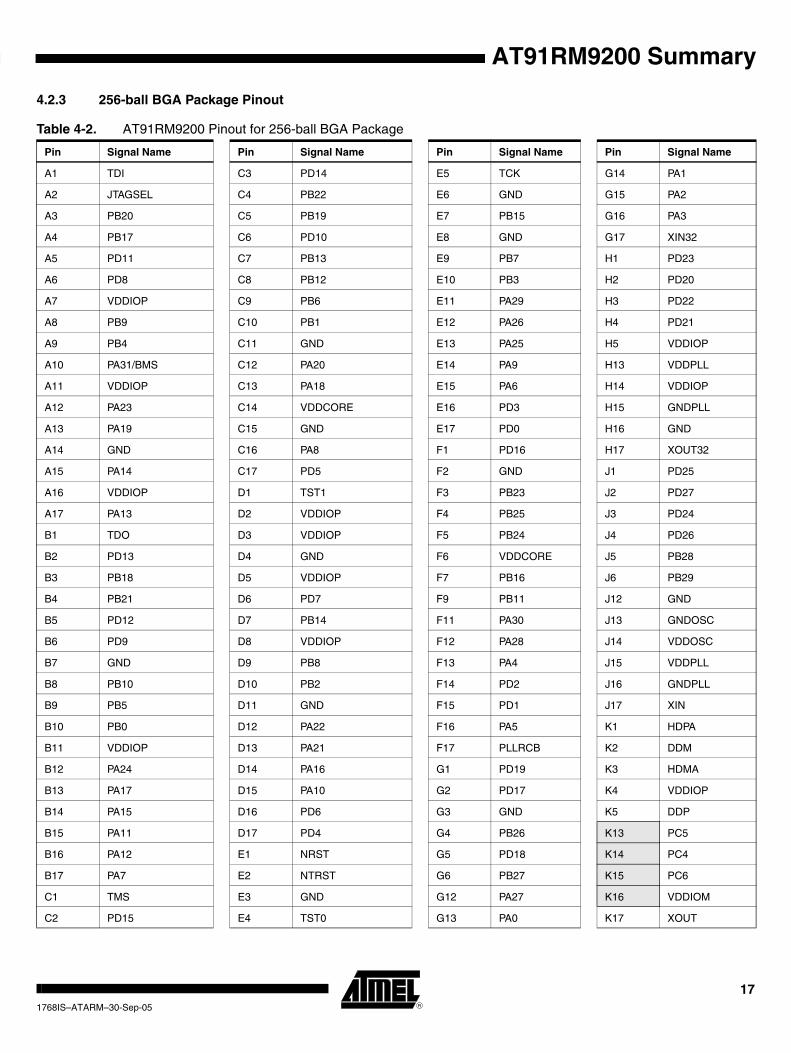
4.2.4 Mechanical Overview of the 256-ball BGA Package
Figure 4-2 on page 19 shows the orientation of the 256-ball BGA Package.
A detailed mechanical description is given in the section Mechanical Characteristics.
L1 GND N2 A5 P13 D15 T7NWR1/NBS1/ CFIOR
L2 HDPB N3 A9 P14 PC26 T8 SDWE
L3 HDMB N4 A4 P15 PC27 T9 GND
L4 A6 N5 A14 P16 VDDIOM T10 VDDCORE
L5 GND N6 SDA10 P17 GND T11 D9
L6 VDDIOP N7 A8 R1 GND T12 D12
L12 PC10 N8 A21 R2 GND T13 GND
L13 PC15 N9 NRD/NOE/CFOE R3 A18 T14 PC19
L14 PC2 N10 RAS R4 A20 T15 PC21
L15 PC3 N11 D2 R5 PC8 T16 PC23
L16 VDDCORE N12 GND R6 VDDIOM T17 PC25
L17 PLLRCA N13 PC28 R7 NCS3/SMCS U1 VDDCORE
M1 VDDIOM N14 PC31 R8NWR3/NBS3/ CFIOW
U2 GND
M2 GND N15 PC30 R9 D0 U3 A16/BA0
M3 A3 N16 PC11 R10 VDDIOM U4 A19
M4 A1/NBS2/NWR2 N17 PC12 R11 D8 U5 GND
M5 A10 P1 A7 R12 D13 U6 NCS0/BFCS
M6 A2 P2 A13 R13 PC17 U7 SDCK
M7 GND P3 A12 R14 VDDIOM U8 CAS
M9 NCS1/SDCS P4 VDDIOM R15 PC24 U9 D3
M11 D4 P5 A11 R16 PC29 U10 D6
M12 GND P6 A22 R17 VDDIOM U11 D7
M13 PC13 P7 PC9 T1 A15 U12 D11
M14 PC1 P8 NWR0/NWE/CFWE T2 VDDCORE U13 D14
M15 PC0 P9 SDCKE T3 A17/BA1 U14 PC16
M16 GND P10 D1 T4 PC7 U15 PC18
M17 PC14 P11 D5 T5 VDDIOM U16 PC20
N1 A0/NBS0 P12 D10 T6 NCS2 U17 PC22
Table 4-2. AT91RM9200 Pinout for 256-ball BGA Package (Continued)
Pin Signal Name Pin Signal Name Pin Signal Name Pin Signal Name
181768IS–ATARM–30-Sep-05
AT91RM9200 Summary

AT91RM9200 Summary
Figure 4-2. 256-ball BGA Pinout (Top View)
4.3 Peripheral Multiplexing on PIO Lines
The AT91RM9200 features four PIO controllers:
• PIOA and PIOB, multiplexing I/O lines of the peripheral set.
• PIOC, multiplexing the data bus bits 16 to 31 and several External Bus Interface control signals. Using PIOC pins increases the number of general-purpose I/O lines available but prevents 32-bit memory access.
• PIOD, available in the 256-ball BGA package option only, multiplexing outputs of the peripheral set and the ETM port.
Each PIO Controller controls up to 32 lines. Each line can be assigned to one of two peripheral functions, A or B. The tables in the following paragraphs define how the I/O lines of the peripher-als A and B are multiplexed on the PIO Controllers A, B, C and D. The two columns “Function” and “Comments” have been inserted for the user’s own comments; they may be used to track how pins are defined in an application.
The column “Reset State” indicates whether the PIO line resets in I/O mode or in peripheral mode. If equal to “I/O”, the PIO line resets in input with the pull-up enabled so that the device is maintained in a static state as soon as the NRST pin is asserted. As a result, the bit correspond-ing to the PIO line in the register PIO_PSR (Peripheral Status Register) resets low.
If a signal name is in the “Reset State” column, the PIO line is assigned to this function and the corresponding bit in PIO_PSR resets high. This is the case for pins controlling memories, either address lines or chip selects, and that require the pin to be driven as soon as NRST raises. Note that the pull-up resistor is also enabled in this case.
See Table 4-3 on page 20, Table 4-4 on page 21, Table 4-5 on page 22 and Table 4-6 on page 23.
191768IS–ATARM–30-Sep-05

4.3.1 PIO Controller A Multiplexing
Table 4-3. Multiplexing on PIO Controller A
PIO Controller A Application Usage
I/O Line Peripheral A Peripheral BReset State Function Comments
PA0 MISO PCK3 I/O
PA1 MOSI PCK0 I/O
PA2 SPCK IRQ4 I/O
PA3 NPCS0 IRQ5 I/O
PA4 NPCS1 PCK1 I/O
PA5 NPCS2 TXD3 I/O
PA6 NPCS3 RXD3 I/O
PA7 ETXCK/EREFCK PCK2 I/O
PA8 ETXEN MCCDB I/O
PA9 ETX0 MCDB0 I/O
PA10 ETX1 MCDB1 I/O
PA11 ECRS/ECRSDV MCDB2 I/O
PA12 ERX0 MCDB3 I/O
PA13 ERX1 TCLK0 I/O
PA14 ERXER TCLK1 I/O
PA15 EMDC TCLK2 I/O
PA16 EMDIO IRQ6 I/O
PA17 TXD0 TIOA0 I/O
PA18 RXD0 TIOB0 I/O
PA19 SCK0 TIOA1 I/O
PA20 CTS0 TIOB1 I/O
PA21 RTS0 TIOA2 I/O
PA22 RXD2 TIOB2 I/O
PA23 TXD2 IRQ3 I/O
PA24 SCK2 PCK1 I/O
PA25 TWD IRQ2 I/O
PA26 TWCK IRQ1 I/O
PA27 MCCK TCLK3 I/O
PA28 MCCDA TCLK4 I/O
PA29 MCDA0 TCLK5 I/O
PA30 DRXD CTS2 I/O
PA31 DTXD RTS2 I/O
201768IS–ATARM–30-Sep-05
AT91RM9200 Summary

AT91RM9200 Summary
4.3.2 PIO Controller B Multiplexing
Table 4-4. Multiplexing on PIO Controller B
PIO Controller B Application Usage
I/O Line Peripheral A Peripheral BReset State Function Comments
PB0 TF0 RTS3 I/O
PB1 TK0 CTS3 I/O
PB2 TD0 SCK3 I/O
PB3 RD0 MCDA1 I/O
PB4 RK0 MCDA2 I/O
PB5 RF0 MCDA3 I/O
PB6 TF1 TIOA3 I/O
PB7 TK1 TIOB3 I/O
PB8 TD1 TIOA4 I/O
PB9 RD1 TIOB4 I/O
PB10 RK1 TIOA5 I/O
PB11 RF1 TIOB5 I/O
PB12 TF2 ETX2 I/O
PB13 TK2 ETX3 I/O
PB14 TD2 ETXER I/O
PB15 RD2 ERX2 I/O
PB16 RK2 ERX3 I/O
PB17 RF2 ERXDV I/O
PB18 RI1 ECOL I/O
PB19 DTR1 ERXCK I/O
PB20 TXD1 I/O
PB21 RXD1 I/O
PB22 SCK1 I/O
PB23 DCD1 I/O
PB24 CTS1 I/O
PB25 DSR1 EF100 I/O
PB26 RTS1 I/O
PB27 PCK0 I/O
PB28 FIQ I/O
PB29 IRQ0 I/O
211768IS–ATARM–30-Sep-05

4.3.3 PIO Controller C Multiplexing
The PIO Controller C has no multiplexing and only peripheral A lines are used. Selecting Peripheral B on the PIO Controller C has no effect.
Table 4-5. Multiplexing on PIO Controller C
PIO Controller C Application Usage
I/O Line Peripheral A Peripheral BReset State Function Comments
PC0 BFCK I/O
PC1 BFRDY/SMOE I/O
PC2 BFAVD I/O
PC3 BFBAA/SMWE I/O
PC4 BFOE I/O
PC5 BFWE I/O
PC6 NWAIT I/O
PC7 A23 A23
PC8 A24 A24
PC9 A25/CFRNW A25
PC10 NCS4/CFCS NCS4
PC11 NCS5/CFCE1 NCS5
PC12 NCS6/CFCE2 NCS6
PC13 NCS7 NCS7
PC14 I/O
PC15 I/O
PC16 D16 I/O
PC17 D17 I/O
PC18 D18 I/O
PC19 D19 I/O
PC20 D20 I/O
PC21 D21 I/O
PC22 D22 I/O
PC23 D23 I/O
PC24 D24 I/O
PC25 D25 I/O
PC26 D26 I/O
PC27 D27 I/O
PC28 D28 I/O
PC29 D29 I/O
PC30 D30 I/O
PC31 D31 I/O
221768IS–ATARM–30-Sep-05
AT91RM9200 Summary
AT91RM9200 Summary
4.3.4 PIO Controller D Multiplexing
The PIO Controller D multiplexes pure output signals on peripheral A connections, in particular from the EMAC MII inter-face and the ETM Port on the peripheral B connections.
The PIO Controller D is available only in the 256-ball BGA package option of the AT91RM9200.
Table 4-6. Multiplexing on PIO Controller D
PIO Controller D Application Usage
I/O Line Peripheral A Peripheral BReset State Function Comments
PD0 ETX0 I/O
PD1 ETX1 I/O
PD2 ETX2 I/O
PD3 ETX3 I/O
PD4 ETXEN I/O
PD5 ETXER I/O
PD6 DTXD I/O
PD7 PCK0 TSYNC I/O
PD8 PCK1 TCLK I/O
PD9 PCK2 TPS0 I/O
PD10 PCK3 TPS1 I/O
PD11 TPS2 I/O
PD12 TPK0 I/O
PD13 TPK1 I/O
PD14 TPK2 I/O
PD15 TD0 TPK3 I/O
PD16 TD1 TPK4 I/O
PD17 TD2 TPK5 I/O
PD18 NPCS1 TPK6 I/O
PD19 NPCS2 TPK7 I/O
PD20 NPCS3 TPK8 I/O
PD21 RTS0 TPK9 I/O
PD22 RTS1 TPK10 I/O
PD23 RTS2 TPK11 I/O
PD24 RTS3 TPK12 I/O
PD25 DTR1 TPK13 I/O
PD26 TPK14 I/O
PD27 TPK15 I/O
231768IS–ATARM–30-Sep-05

4.3.5 Pin Name Description
Table 4-7 gives details on the pin name classified by peripheral.
Table 4-7. Pin Description List
Pin Name Function TypeActiveLevel Comments
Power
VDDIOM Memory I/O Lines Power Supply Power 3.0V to 3.6V
VDDIOP Peripheral I/O Lines Power Supply Power 3.0V to 3.6V
VDDPLL Oscillator and PLL Power Supply Power 1.65V to 1.95V
VDDCORE Core Chip Power Supply Power 1.65V to 1.95V
VDDOSC Oscillator Power Supply Power 1.65V to 1.95V
GND Ground Ground
GNDPLL PLL Ground Ground
GNDOSC Oscillator Ground Ground
Clocks, Oscillators and PLLs
XIN Main Crystal Input Input
XOUT Main Crystal Output Output
XIN32 32KHz Crystal Input Input
XOUT32 32KHz Crystal Output Output
PLLRCA PLL A Filter Input
PLLRCB PLL B Filter Input
PCK0 - PCK3 Programmable Clock Output Output
ICE and JTAG
TCK Test Clock Input Schmitt trigger
TDI Test Data In Input Internal Pull-up, Schmitt trigger
TDO Test Data Out Output Tri-state
TMS Test Mode Select Input Internal Pull-up, Schmitt trigger
NTRST Test Reset Signal Input Low Internal Pull-up, Schmitt trigger
JTAGSEL JTAG Selection Input Schmitt trigger
ETM
TSYNC Trace Synchronization Signal Output
TCLK Trace Clock Output
TPS0 - TPS2 Trace ARM Pipeline Status Output
TPK0 - TPK15 Trace Packet Port Output
Reset/Test
NRST Microcontroller Reset Input Low No on-chip pull-up, Schmitt trigger
TST0 - TST1 Test Mode Select InputMust be tied low for normal operation, Schmitt trigger
241768IS–ATARM–30-Sep-05
AT91RM9200 Summary

AT91RM9200 Summary
Memory Controller
BMS Boot Mode Select Input
Debug Unit
DRXD Debug Receive Data Input Debug Receive Data
DTXD Debug Transmit Data Output Debug Transmit Data
AIC
IRQ0 - IRQ6 External Interrupt Inputs Input
FIQ Fast Interrupt Input Input
PIO
PA0 - PA31 Parallel IO Controller A I/O Pulled-up input at reset
PB0 - PB29 Parallel IO Controller B I/O Pulled-up input at reset
PC0 - PC31 Parallel IO Controller C I/O Pulled-up input at reset
PD0 - PD27 Parallel IO Controller D I/O Pulled-up input at reset
EBI
D0 - D31 Data Bus I/O Pulled-up input at reset
A0 - A25 Address Bus Output 0 at reset
SMC
NCS0 - NCS7 Chip Select Lines Output Low 1 at reset
NWR0 - NWR3 Write Signal Output Low 1 at reset
NOE Output Enable Output Low 1 at reset
NRD Read Signal Output Low 1 at reset
NUB Upper Byte Select Output Low 1 at reset
NLB Lower Byte Select Output Low 1 at reset
NWE Write Enable Output Low 1 at reset
NWAIT Wait Signal Input Low
NBS0 - NBS3 Byte Mask Signal Output Low 1 at reset
EBI for CompactFlash Support
CFCE1 - CFCE2 CompactFlash Chip Enable Output Low
CFOE CompactFlash Output Enable Output Low
CFWE CompactFlash Write Enable Output Low
CFIOR CompactFlash IO Read Output Low
CFIOW CompactFlash IO Write Output Low
CFRNW CompactFlash Read Not Write Output
CFCS CompactFlash Chip Select Output Low
Table 4-7. Pin Description List (Continued)
Pin Name Function TypeActiveLevel Comments
251768IS–ATARM–30-Sep-05

EBI for NAND Flash/SmartMedia Support
SMCS NAND Flash/SmartMedia Chip Select Output Low
SMOE NAND Flash/SmartMedia Output Enable Output Low
SMWE NAND Flash/SmartMedia Write Enable Output Low
SDRAM Controller
SDCK SDRAM Clock Output
SDCKE SDRAM Clock Enable Output High
SDCS SDRAM Controller Chip Select Output Low
BA0 - BA1 Bank Select Output
SDWE SDRAM Write Enable Output Low
RAS - CAS Row and Column Signal Output Low
SDA10 SDRAM Address 10 Line Output
Burst Flash Controller
BFCK Burst Flash Clock Output
BFCS Burst Flash Chip Select Output Low
BFAVD Burst Flash Address Valid Output Low
BFBAA Burst Flash Address Advance Output Low
BFOE Burst Flash Output Enable Output Low
BFRDY Burst Flash Ready Input High
BFWE Burst Flash Write Enable Output Low
Multimedia Card Interface
MCCK Multimedia Card Clock Output
MCCDA Multimedia Card A Command I/O
MCDA0 - MCDA3 Multimedia Card A Data I/O
MCCDB Multimedia Card B Command I/O
MCDB0 - MCDB3 Multimedia Card B Data I/O
USART
SCK0 - SCK3 Serial Clock I/O
TXD0 - TXD3 Transmit Data Output
RXD0 - RXD3 Receive Data Input
RTS0 - RTS3 Ready To Send Output
CTS0 - CTS3 Clear To Send Input
DSR1 Data Set Ready Input
DTR1 Data Terminal Ready Output
DCD1 Data Carrier Detect Input
RI1 Ring Indicator Input
Table 4-7. Pin Description List (Continued)
Pin Name Function TypeActiveLevel Comments
261768IS–ATARM–30-Sep-05
AT91RM9200 Summary

AT91RM9200 Summary
USB Device Port
DDM USB Device Port Data - Analog
DDP USB Device Port Data + Analog
USB Host Port
HDMA USB Host Port A Data - Analog
HDPA USB Host Port A Data + Analog
HDMB USB Host Port B Data - Analog
HDPB USB Host Port B Data + Analog
Ethernet MAC
EREFCK Reference Clock Input RMII only
ETXCK Transmit Clock Input MII only
ERXCK Receive Clock Input MII only
ETXEN Transmit Enable Output
ETX0 - ETX3 Transmit Data Output ETX0 - ETX1 only in RMII
ETXER Transmit Coding Error Output MII only
ERXDV Receive Data Valid Input MII only
ECRSDV Carrier Sense and Data Valid Input RMII only
ERX0 - ERX3 Receive Data Input ERX0 - ERX1 only in RMII
ERXER Receive Error Input
ECRS Carrier Sense Input MII only
ECOL Collision Detected Input MII only
EMDC Management Data Clock Output
EMDIO Management Data Input/Output I/O
EF100 Force 100 Mbits/sec. Output High RMII only
Synchronous Serial Controller
TD0 - TD2 Transmit Data Output
RD0 - RD2 Receive Data Input
TK0 - TK2 Transmit Clock I/O
RK0 - RK2 Receive Clock I/O
TF0 - TF2 Transmit Frame Sync I/O
RF0 - RF2 Receive Frame Sync I/O
Timer/Counter
TCLK0 - TCLK5 External Clock Input Input
TIOA0 - TIOA5 I/O Line A I/O
TIOB0 - TIOB5 I/O Line B I/O
Table 4-7. Pin Description List (Continued)
Pin Name Function TypeActiveLevel Comments
271768IS–ATARM–30-Sep-05
SPI
MISO Master In Slave Out I/O
MOSI Master Out Slave In I/O
SPCK SPI Serial Clock I/O
NPCS0 SPI Peripheral Chip Select 0 I/O Low
NPCS1 - NPCS3 SPI Peripheral Chip Select Output Low
Two-Wire Interface
TWD Two-wire Serial Data I/O
TWCK Two-wire Serial Clock I/O
Table 4-7. Pin Description List (Continued)
Pin Name Function TypeActiveLevel Comments
281768IS–ATARM–30-Sep-05
AT91RM9200 Summary

AT91RM9200 Summary
4.4 Peripheral Identifiers
The AT91RM9200 embeds a wide range of peripherals. Table 4-8 defines the peripheral identifi-ers of the AT91RM9200. A peripheral identifier is required for the control of the peripheral interrupt with the Advanced Interrupt Controller and for the control of the peripheral clock with the Power Management Controller.
Table 4-8. Peripheral Identifiers
Peripheral
ID
Peripheral
Mnemonic
Peripheral
Name
External
Interrupt
0 AIC Advanced Interrupt Controller FIQ
1 SYSIRQ
2 PIOA Parallel I/O Controller A
3 PIOB Parallel I/O Controller B
4 PIOC Parallel I/O Controller C
5 PIOD Parallel I/O Controller D
6 US0 USART 0
7 US1 USART 1
8 US2 USART 2
9 US3 USART 3
10 MCI Multimedia Card Interface
11 UDP USB Device Port
12 TWI Two-wire Interface
13 SPI Serial Peripheral Interface
14 SSC0 Synchronous Serial Controller 0
15 SSC1 Synchronous Serial Controller 1
16 SSC2 Synchronous Serial Controller 2
17 TC0 Timer/Counter 0
18 TC1 Timer/Counter 1
19 TC2 Timer/Counter 2
20 TC3 Timer/Counter 3
21 TC4 Timer/Counter 4
22 TC5 Timer/Counter 5
23 UHP USB Host Port
24 EMAC Ethernet MAC
25 AIC Advanced Interrupt Controller IRQ0
26 AIC Advanced Interrupt Controller IRQ1
27 AIC Advanced Interrupt Controller IRQ2
28 AIC Advanced Interrupt Controller IRQ3
29 AIC Advanced Interrupt Controller IRQ4
30 AIC Advanced Interrupt Controller IRQ5
31 AIC Advanced Interrupt Controller IRQ6
291768IS–ATARM–30-Sep-05
4.4.1 System Interrupt
The System Interrupt is the wired-OR of the interrupt signals coming from:
• the Memory Controller
• the Debug Unit
• the System Timer
• the Real-Time Clock
• the Power Management Controller
The clock of these peripherals cannot be controlled and the Peripheral ID 1 can only be used within the Advanced Interrupt Controller.
4.4.2 External Interrupts
All external interrupt signals, i.e., the Fast Interrupt signal FIQ or the Interrupt signals IRQ0 to IRQ6, use a dedicated Peripheral ID. However, there is no clock control associated with these peripheral IDs.
301768IS–ATARM–30-Sep-05
AT91RM9200 Summary
AT91RM9200 Summary
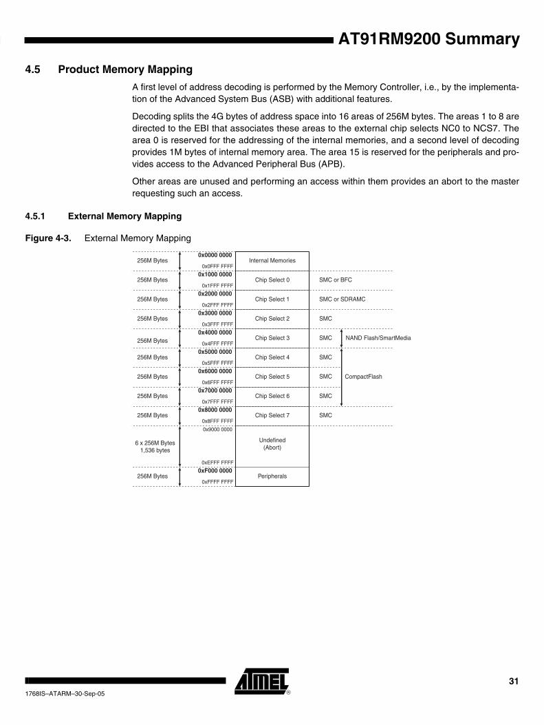
4.5 Product Memory Mapping
A first level of address decoding is performed by the Memory Controller, i.e., by the implementa-tion of the Advanced System Bus (ASB) with additional features.
Decoding splits the 4G bytes of address space into 16 areas of 256M bytes. The areas 1 to 8 are directed to the EBI that associates these areas to the external chip selects NC0 to NCS7. The area 0 is reserved for the addressing of the internal memories, and a second level of decoding provides 1M bytes of internal memory area. The area 15 is reserved for the peripherals and pro-vides access to the Advanced Peripheral Bus (APB).
Other areas are unused and performing an access within them provides an abort to the master requesting such an access.
4.5.1 External Memory Mapping
Figure 4-3. External Memory Mapping
0x0000 0000
0x0FFF FFFF
0x1000 0000
0x1FFF FFFF
0x2000 0000
0x2FFF FFFF
0x3000 0000
0x3FFF FFFF
0x4000 0000
0x4FFF FFFF
0x5000 0000
0x5FFF FFFF
0x6000 0000
0x6FFF FFFF
0x7000 0000
0x7FFF FFFF
0x8000 0000
0x8FFF FFFF
0x9000 0000
0xEFFF FFFF
0xF000 0000
0xFFFF FFFF
256M Bytes
256M Bytes
256M Bytes
256M Bytes
256M Bytes
256M Bytes
256M Bytes
256M Bytes
256M Bytes
256M Bytes
6 x 256M Bytes1,536 bytes
Internal Memories
Chip Select 0
Chip Select 1
Chip Select 2
Chip Select 3
Chip Select 4
Chip Select 5
Chip Select 6
Chip Select 7
Undefined(Abort)
Peripherals
SMC or BFC
SMC or SDRAMC
SMC
SMC
SMC
SMC
SMC
SMC
CompactFlash
NAND Flash/SmartMedia
311768IS–ATARM–30-Sep-05

4.5.2 Internal Memory Mapping
4.5.2.1 Internal RAM
The AT91RM9200 integrates a high-speed, 16-Kbyte internal SRAM. After reset and until the Remap Command is performed, the SRAM is only accessible at address 0x20 0000. After Remap, the SRAM is also available at address 0x0.
4.5.2.2 Internal ROM
The AT91RM9200 integrates a 128-Kbyte Internal ROM. At any time, the ROM is mapped at address 0x10 0000. It is also accessible at address 0x0 after reset and before the Remap Com-mand if the BMS is tied high during reset.
4.5.2.3 USB Host Port
The AT91RM9200 integrates a USB Host Port Open Host Controller Interface (OHCI). The reg-isters of this interface are directly accessible on the ASB Bus and are mapped like a standard internal memory at address 0x30 0000.
Figure 4-4. Internal Memory Mapping
256Mbytes
Internal Memory Area 0
Undefined Area(Abort)
0x0000 0000
0x000F FFFF
0x0010 0000
0x001F FFFF
0x0020 0000
0x002F FFFF
0x0030 0000
0x0FFF FFFF
1 MBytes
1 MBytes
1 MBytes
252M bytes
Internal Memory Area 1Internal ROM
Internal Memory Area 2Internal SRAM
Internal Memory Area 3USB Host Port0x003F FFFF
0x0040 0000
1 MBytes
321768IS–ATARM–30-Sep-05
AT91RM9200 Summary
AT91RM9200 Summary
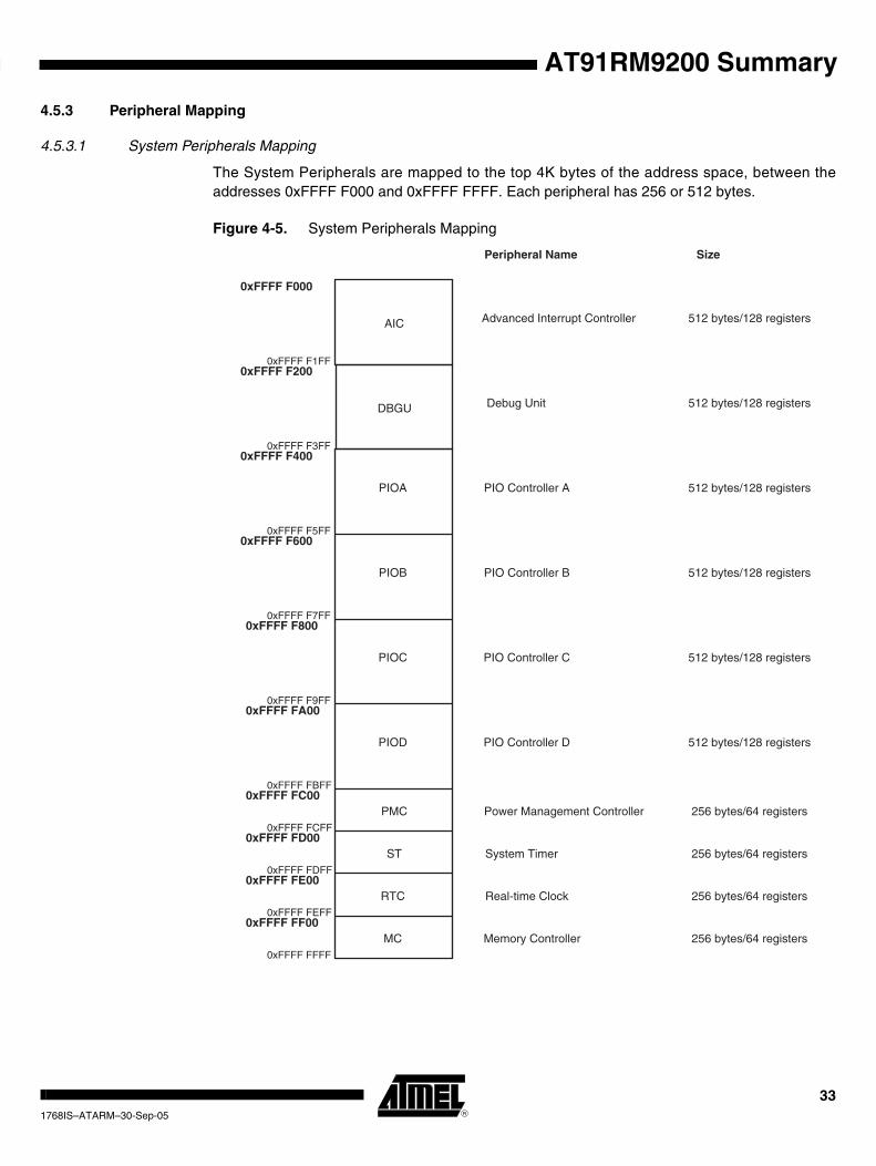
4.5.3 Peripheral Mapping
4.5.3.1 System Peripherals Mapping
The System Peripherals are mapped to the top 4K bytes of the address space, between the addresses 0xFFFF F000 and 0xFFFF FFFF. Each peripheral has 256 or 512 bytes.
Figure 4-5. System Peripherals Mapping
0xFFFF FFFF
0xFFFF FF00MC Memory Controller 256 bytes/64 registers
Peripheral Name Size
0xFFFF FEFF
0xFFFF FE000xFFFF FDFF
0xFFFF FD000xFFFF FCFF
0xFFFF FC00
0xFFFF FA00
0xFFFF F800
0xFFFF F600
0xFFFF F400
0xFFFF F200
0xFFFF F000
0xFFFF FBFF
0xFFFF F9FF
0xFFFF F7FF
0xFFFF F5FF
0xFFFF F3FF
0xFFFF F1FF
256 bytes/64 registers
256 bytes/64 registers
256 bytes/64 registers
Real-time Clock
System Timer
Power Management Controller
PIO Controller C
PIO Controller B
PIO Controller A
Debug Unit
Advanced Interrupt Controller
512 bytes/128 registers
512 bytes/128 registers
512 bytes/128 registers
512 bytes/128 registers
512 bytes/128 registers
512 bytes/128 registers
RTC
ST
PMC
PIOD
PIOC
PIOB
PIOA
DBGU
AIC
PIO Controller D
331768IS–ATARM–30-Sep-05

4.5.3.2 User Peripherals Mapping
The User Peripherals are mapped in the upper 256M bytes of the address space, between the addresses 0xFFFA 0000and 0xFFFE 3FFF. Each peripheral has a 16-Kbyte address space.
Figure 4-6. User Peripherals Mapping
16K Bytes
Peripheral Name Size
16K Bytes
16K Bytes
16K Bytes
16K Bytes
16K Bytes
16K Bytes
16K Bytes
0xFFFA 0000
0xFFFA 3FFF
TC0, TC1, TC2 Timer/Counter 0, 1 and 2
16K Bytes
16K Bytes
16K Bytes
16K Bytes
16K Bytes
16K Bytes
Reserved
Reserved
0xFFFA 4000
0xFFFA 7FFF
TC3, TC4, TC5 Timer/Counter 3, 4 and 5
UDP USB Device Port0xFFFB 0000
0xF000 0000
0xFFF9 FFFF
0xFFFA 8000
0xFFFA FFFF
0xFFFB 3FFF
MCI Multimedia Card Interface0xFFFB 4000
0xFFFB 7FFF
TWI Two-Wire Interface0xFFFB 8000
0xFFFB BFFF
EMAC Ethernet MAC0xFFFB C000
0xFFFB FFFF
USART0 Universal Synchronous Asynchronous Receiver Transmitter 0
0xFFFC 0000
0xFFFC 3FFF
USART1 Universal Synchronous Asynchronous Receiver Transmitter 1
0xFFFC 4000
0xFFFC 7FFF
USART2 Universal Synchronous Asynchronous Receiver Transmitter 2
0xFFFC 8000
0xFFFC BFFF
USART3 Universal Synchronous Asynchronous Receiver Transmitter 3
0xFFFC C000
0xFFFC FFFF
SSC0 Serial Synchronous Controller 00xFFFD 0000
0xFFFD 3FFF
SSC1 Serial Synchronous Controller 10xFFFD 4000
0xFFFD 7FFF
SSC2 Serial Synchronous Controller 20xFFFD 8000
0xFFFD BFFF
Reserved
0xFFFD C000
0xFFFD FFFF
SPI Serial Peripheral Interface0xFFFE 0000
0xFFFE 3FFF
Reserved
0xFFFE 4000
0xFFFE FFFF
341768IS–ATARM–30-Sep-05
AT91RM9200 Summary
AT91RM9200 Summary
4.6 Peripheral Implementation
4.6.1 USART
The USART describes features allowing management of the Modem Signals DTR, DSR, DCD and RI.
In the AT91RM9200, only the USART1 implements these signals, named DTR1, DSR1, DCD1 and RI1.
The USART0, USART2 and USART3 do not implement all the modem signals. Only RTS and CTS (RTS0 and CTS0, RTS2 and CTS2, RTS3 and CTS3, respectively) are implemented in these USARTs for other features.
Thus, programming the USART0, USART2 or the USART3 in Modem Mode may lead to unpre-dictable results. In these USARTs, the commands relating to the Modem Mode have no effect and the status bits relating the status of the modem signals are never activated.
4.6.2 Timer Counter
The Timer Counter 0 to 5 are described with five generic clock inputs, TIMER_CLOCK1 to TIMER_CLOCK5. In the AT91RM9200, these clock inputs are connected to the Master Clock (MCK), to the Slow Clock (SLCK) and to divisions of the Master Clock.
Table 4-9 gives the correspondence between the Timer Counter clock inputs and clocks in the AT91RM9200. Each Timer Counter 0 to 5 displays the same configuration.
Table 4-9. Timer Counter Clocks Assignment
TC Clock Input Clock
TIMER_CLOCK1 MCK/2
TIMER_CLOCK2 MCK/8
TIMER_CLOCK3 MCK/32
TIMER_CLOCK4 MCK/128
TIMER_CLOCK5 SLCK
351768IS–ATARM–30-Sep-05

5. Revision History
Doc. Rev Source Comments
Lit°1768A • Date Qualified: May 2001
Lit°1768B • Date Qualified: September 2001
Lit°1768C • Date Qualified: November 2001
Lit°1768D • Date Qualified: 5 Mar-02
Lit°1768E • Date Qualified: 12-Julr-02
Lit°1768F • Date Qualified: 5 Feb-03
Doc. Rev Source Comments
1768GS Review • Date Qualified: 04-Sep-03
• Page 2; Added Description.
• Page 3; Updated Figure 1, Block Diagram, remove reference to Multi-master Memory Controller.
• Page 4; Added section Key Features. Updated all descriptions of key blocks
• Page 17; Added text to section Peripheral Mulitplexing on PIO Lines.
• Page 18; Expanded Table 3, Multiplexing on PIO Controller A.
• Page 19: Expanded Table 4, Multiplexing on PIO Controller B.
• Page 20; Expanded Table 5, Multiplexing on PIO Controller C.
• Page 21; Expanded Table 6, Multiplexing on PIO Controller D.
• Page 27; Updated Table 8, Peripheral Identifiers, Peripheral ID 1 description.
• Page 28; Added section Product Memory Mapping.
• Page 30; Updated and corrected Figure 6, System Peripherals Mapping.
• Page 31; Updated and corrected Figure 7, User Peripherals Mapping.
Doc. Rev Source Comments
1768HS CSRs/Review • Date Qualified: Unqualified/Internal on Intranet 27-Jan-05
• Global; Reformat in Corporate Template.
• Global; Peripheral Data Controller (PDC) nenamed Peripheral DMA Controller.
CSR 04-066 • Page 1; Features: USART Hardware Handshaking. Software Handshaking removed.
CSR 03-209 • Page 3; Figure 1: NWAIT pin added to block diagram.
CSR 03-244 • Page 14; Table 1. AT91RM9200 Pinout for 208-lead PQFP package, pins 28, 30, 37 and 39 names changed
CSR 04-315 • Page 23; Table 7. Pin Description, ICE and JTAG description, “Internal Pullup” added to comments for all signals, except TDO.
CSR 03-209 • Page 24; Table 7. Pin Description, NWAIT pin added.
361768IS–ATARM–30-Sep-05
AT91RM9200 Summary

AT91RM9200 Summary
1768IS Corrected power consumption values on page 1.
CSR 05-348 In Table 4-7, “Pin Description List,” on page 24 added mention of Schmitt trigger for pins JTAGSEL, TDI, TCK, TMS, NTRST, TST0, TST1 and NRST.
Doc. Rev Source Comments
371768IS–ATARM–30-Sep-05
Printed on recycled paper.
Disclaimer: The information in this document is provided in connection with Atmel products. No license, express or implied, by estoppel or otherwise, to any intellectual property right is granted by this document or in connection with the sale of Atmel products. EXCEPT AS SET FORTH IN ATMEL’S TERMS AND CONDI-TIONS OF SALE LOCATED ON ATMEL’S WEB SITE, ATMEL ASSUMES NO LIABILITY WHATSOEVER AND DISCLAIMS ANY EXPRESS, IMPLIED OR STATUTORY WARRANTY RELATING TO ITS PRODUCTS INCLUDING, BUT NOT LIMITED TO, THE IMPLIED WARRANTY OF MERCHANTABILITY, FITNESS FOR A PARTICULAR PURPOSE, OR NON-INFRINGEMENT. IN NO EVENT SHALL ATMEL BE LIABLE FOR ANY DIRECT, INDIRECT, CONSEQUENTIAL, PUNITIVE, SPECIAL OR INCIDEN-TAL DAMAGES (INCLUDING, WITHOUT LIMITATION, DAMAGES FOR LOSS OF PROFITS, BUSINESS INTERRUPTION, OR LOSS OF INFORMATION) ARISING OUT OF THE USE OR INABILITY TO USE THIS DOCUMENT, EVEN IF ATMEL HAS BEEN ADVISED OF THE POSSIBILITY OF SUCH DAMAGES. Atmel makes no representations or warranties with respect to the accuracy or completeness of the contents of this document and reserves the right to make changes to specifications and product descriptions at any time without notice. Atmel does not make any commitment to update the information contained herein. Unless specifically provided otherwise, Atmel products are not suitable for, and shall not be used in, automotive applications. Atmel’s products are not intended, authorized, or warranted for use as components in applications intended to support or sustain life.
Atmel Corporation Atmel Operations
2325 Orchard ParkwaySan Jose, CA 95131, USATel: 1(408) 441-0311Fax: 1(408) 487-2600
Regional Headquarters
EuropeAtmel SarlRoute des Arsenaux 41Case Postale 80CH-1705 FribourgSwitzerlandTel: (41) 26-426-5555Fax: (41) 26-426-5500
AsiaRoom 1219Chinachem Golden Plaza77 Mody Road TsimshatsuiEast KowloonHong KongTel: (852) 2721-9778Fax: (852) 2722-1369
Japan9F, Tonetsu Shinkawa Bldg.1-24-8 ShinkawaChuo-ku, Tokyo 104-0033JapanTel: (81) 3-3523-3551Fax: (81) 3-3523-7581
Memory2325 Orchard ParkwaySan Jose, CA 95131, USATel: 1(408) 441-0311Fax: 1(408) 436-4314
Microcontrollers2325 Orchard ParkwaySan Jose, CA 95131, USATel: 1(408) 441-0311Fax: 1(408) 436-4314
La ChantrerieBP 7060244306 Nantes Cedex 3, FranceTel: (33) 2-40-18-18-18Fax: (33) 2-40-18-19-60
ASIC/ASSP/Smart CardsZone Industrielle13106 Rousset Cedex, FranceTel: (33) 4-42-53-60-00Fax: (33) 4-42-53-60-01
1150 East Cheyenne Mtn. Blvd.Colorado Springs, CO 80906, USATel: 1(719) 576-3300Fax: 1(719) 540-1759
Scottish Enterprise Technology ParkMaxwell BuildingEast Kilbride G75 0QR, Scotland Tel: (44) 1355-803-000Fax: (44) 1355-242-743
RF/AutomotiveTheresienstrasse 2Postfach 353574025 Heilbronn, GermanyTel: (49) 71-31-67-0Fax: (49) 71-31-67-2340
1150 East Cheyenne Mtn. Blvd.Colorado Springs, CO 80906, USATel: 1(719) 576-3300Fax: 1(719) 540-1759
Biometrics/Imaging/Hi-Rel MPU/ High Speed Converters/RF Datacom
Avenue de RochepleineBP 12338521 Saint-Egreve Cedex, FranceTel: (33) 4-76-58-30-00Fax: (33) 4-76-58-34-80
Literature Requestswww.atmel.com/literature
© Atmel Corporation 2005. All rights reserved. Atmel®, logo and combinations thereof, Everywhere You Are®, DataFlash® and others, are the registered trademarks or trademarks of Atmel Corporation or its subsidiaries. ARM®, Thumb® and others are registered trademarks of ARM Ltd. Other terms and product names may be trademarks of others.
1768IS–ATARM–30-Sep-05
Related Documents