50kW 150kW 150kW A 1 A 3 V OUT V IN- 6 REF 5 RFI Filtered Inputs 2 V+ 7 V- 4 1 8 150kW 150kW 50kW A 2 V IN+ RFI Filtered Inputs 3 INA333 R G G = 1 + 100kW R G RFI Filtered Inputs RFI Filtered Inputs Product Folder Sample & Buy Technical Documents Tools & Software Support & Community An IMPORTANT NOTICE at the end of this data sheet addresses availability, warranty, changes, use in safety-critical applications, intellectual property matters and other important disclaimers. PRODUCTION DATA. INA333 SBOS445C – JULY 2008 – REVISED DECEMBER 2015 INA333 Micro-Power (50μA), Zerø-Drift, Rail-to-Rail Out Instrumentation Amplifier 1 1 Features 1• Low Offset Voltage: 25 μV (Maximum), G ≥ 100 • Low Drift: 0.1 μV/°C, G ≥ 100 • Low Noise: 50 nV/√Hz, G ≥ 100 • High CMRR: 100 dB (Minimum), G ≥ 10 • Low Input Bias Current: 200 pA (Maximum) • Supply Range: 1.8 V to 5.5 V • Input Voltage: (V–) +0.1 V to (V+) –0.1 V • Output Range: (V–) +0.05 V to (V+) –0.05 V • Low Quiescent Current: 50 μA • Operating Temperature: –40°C to +125°C • RFI Filtered Inputs • 8-Pin VSSOP and 8-Pin WSON Packages 2 Applications • Bridge Amplifiers • ECG Amplifiers • Pressure Sensors • Medical Instrumentation • Portable Instrumentation • Weigh Scales • Thermocouple Amplifiers • RTD Sensor Amplifiers • Data Acquisition 3 Description The INA333 device is a low-power, precision instrumentation amplifier offering excellent accuracy. The versatile 3-operational amplifier design, small size, and low power make it ideal for a wide range of portable applications. A single external resistor sets any gain from 1 to 1000. The INA333 is designed to use an industry- standard gain equation: G = 1 + (100 kΩ /R G ). The INA333 device provides very low offset voltage (25 μV, G ≥ 100), excellent offset voltage drift (0.1 μV/°C, G ≥ 100), and high common-mode rejection (100 dB at G ≥ 10). It operates with power supplies as low as 1.8 V (±0.9 V) and quiescent current is only 50 μA, making it ideal for battery- operated systems. Using autocalibration techniques to ensure excellent precision over the extended industrial temperature range, the INA333 device also offers exceptionally low noise density (50 nV/√Hz) that extends down to DC. The INA333 device is available in both 8-pin VSSOP and WSON surface-mount packages and is specified over the T A = –40°C to +125°C temperature range. Device Information (1) PART NUMBER PACKAGE BODY SIZE (NOM) INA333 VSSOP (8) 3.00 mm × 3.00 mm WSON (8) 3.00 mm × 3.00 mm (1) For all available packages, see the orderable addendum at the end of the data sheet. Simplified Schematic

Welcome message from author
This document is posted to help you gain knowledge. Please leave a comment to let me know what you think about it! Share it to your friends and learn new things together.
Transcript
50kW
150kW 150kW
A1
A3
VOUT
VIN-
6
REF5
RFI Filtered Inputs2
V+
7
V-
4
1
8
150kW 150kW
50kW
A2
VIN+ RFI Filtered Inputs3
INA333
RG
G = 1 +100kW
RG
RFI Filtered Inputs
RFI Filtered Inputs
Product
Folder
Sample &Buy
Technical
Documents
Tools &
Software
Support &Community
An IMPORTANT NOTICE at the end of this data sheet addresses availability, warranty, changes, use in safety-critical applications,intellectual property matters and other important disclaimers. PRODUCTION DATA.
INA333SBOS445C –JULY 2008–REVISED DECEMBER 2015
INA333 Micro-Power (50μA), Zerø-Drift, Rail-to-Rail Out Instrumentation Amplifier
1
1 Features1• Low Offset Voltage: 25 μV (Maximum), G ≥ 100• Low Drift: 0.1 μV/°C, G ≥ 100• Low Noise: 50 nV/√Hz, G ≥ 100• High CMRR: 100 dB (Minimum), G ≥ 10• Low Input Bias Current: 200 pA (Maximum)• Supply Range: 1.8 V to 5.5 V• Input Voltage: (V–) +0.1 V to (V+) –0.1 V• Output Range: (V–) +0.05 V to (V+) –0.05 V• Low Quiescent Current: 50 μA• Operating Temperature: –40°C to +125°C• RFI Filtered Inputs• 8-Pin VSSOP and 8-Pin WSON Packages
2 Applications• Bridge Amplifiers• ECG Amplifiers• Pressure Sensors• Medical Instrumentation• Portable Instrumentation• Weigh Scales• Thermocouple Amplifiers• RTD Sensor Amplifiers• Data Acquisition
3 DescriptionThe INA333 device is a low-power, precisioninstrumentation amplifier offering excellent accuracy.The versatile 3-operational amplifier design, smallsize, and low power make it ideal for a wide range ofportable applications.
A single external resistor sets any gain from 1 to1000. The INA333 is designed to use an industry-standard gain equation: G = 1 + (100 kΩ / RG).
The INA333 device provides very low offset voltage(25 μV, G ≥ 100), excellent offset voltage drift(0.1 μV/°C, G ≥ 100), and high common-moderejection (100 dB at G ≥ 10). It operates with powersupplies as low as 1.8 V (±0.9 V) and quiescentcurrent is only 50 μA, making it ideal for battery-operated systems. Using autocalibration techniquesto ensure excellent precision over the extendedindustrial temperature range, the INA333 device alsooffers exceptionally low noise density (50 nV/√Hz)that extends down to DC.
The INA333 device is available in both 8-pin VSSOPand WSON surface-mount packages and is specifiedover the TA = –40°C to +125°C temperature range.
Device Information(1)
PART NUMBER PACKAGE BODY SIZE (NOM)
INA333VSSOP (8) 3.00 mm × 3.00 mmWSON (8) 3.00 mm × 3.00 mm
(1) For all available packages, see the orderable addendum atthe end of the data sheet.
Simplified Schematic
2
INA333SBOS445C –JULY 2008–REVISED DECEMBER 2015 www.ti.com
Product Folder Links: INA333
Submit Documentation Feedback Copyright © 2008–2015, Texas Instruments Incorporated
Table of Contents1 Features .................................................................. 12 Applications ........................................................... 13 Description ............................................................. 14 Revision History..................................................... 25 Pin Configuration and Functions ......................... 36 Specifications......................................................... 4
6.1 Absolute Maximum Ratings ...................................... 46.2 ESD Ratings.............................................................. 46.3 Recommended Operating Conditions....................... 46.4 Thermal Information ................................................. 46.5 Electrical Characteristics........................................... 56.6 Typical Characteristics .............................................. 7
7 Detailed Description ............................................ 137.1 Overview ................................................................. 137.2 Functional Block Diagram ....................................... 137.3 Feature Description................................................. 13
7.4 Device Functional Modes........................................ 138 Application and Implementation ........................ 14
8.1 Application Information............................................ 148.2 Typical Application ................................................. 14
9 Power Supply Recommendations ...................... 1910 Layout................................................................... 20
10.1 Layout Guidelines ................................................. 2010.2 Layout Example .................................................... 20
11 Device and Documentation Support ................. 2111.1 Device Support...................................................... 2111.2 Documentation Support ........................................ 2211.3 Trademarks ........................................................... 2211.4 Electrostatic Discharge Caution............................ 2211.5 Glossary ................................................................ 23
12 Mechanical, Packaging, and OrderableInformation ........................................................... 23
4 Revision HistoryNOTE: Page numbers for previous revisions may differ from page numbers in the current version.
Changes from Revision B (October 2008) to Revision C Page
• Added ESD Ratings table, Feature Description section, Device Functional Modes, Application and Implementationsection, Power Supply Recommendations section, Layout section, Device and Documentation Support section, andMechanical, Packaging, and Orderable Information section ................................................................................................. 1
RG
VIN-
VIN+
V-
RG
V+
VOUT
REF
1
2
3
4
8
7
6
5
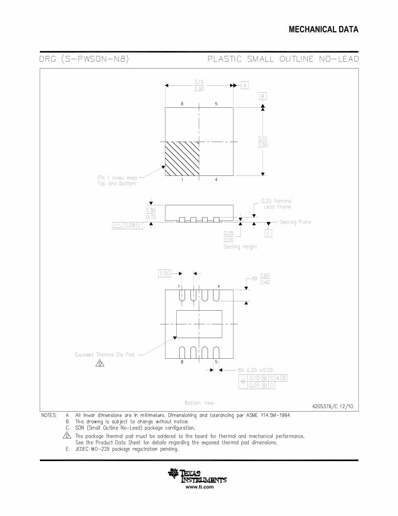
ExposedThermalDie Pad
onUnderside
VIN-
VIN+
V-
RG
V+
VOUT
1
2
3
4
8
7
6
5
RG
REF
3
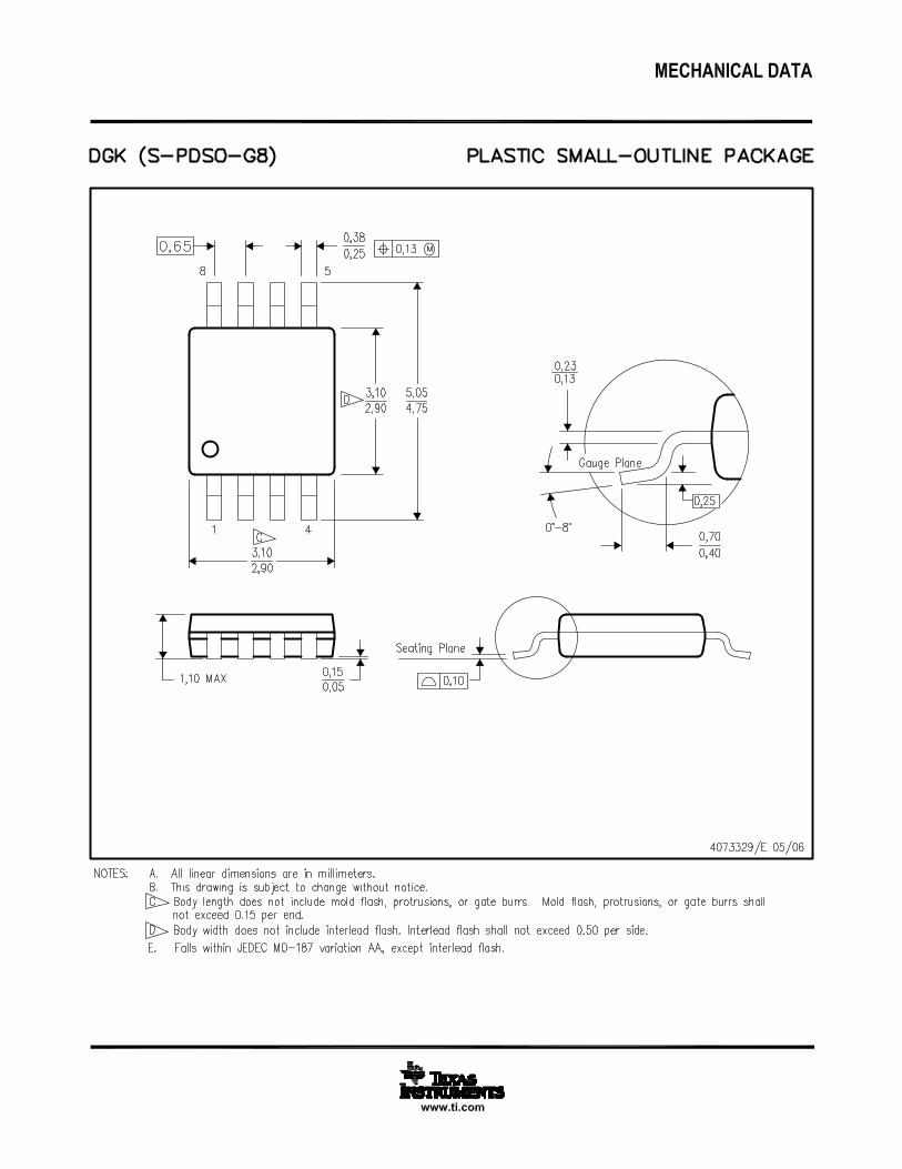
INA333www.ti.com SBOS445C –JULY 2008–REVISED DECEMBER 2015
Product Folder Links: INA333
Submit Documentation FeedbackCopyright © 2008–2015, Texas Instruments Incorporated
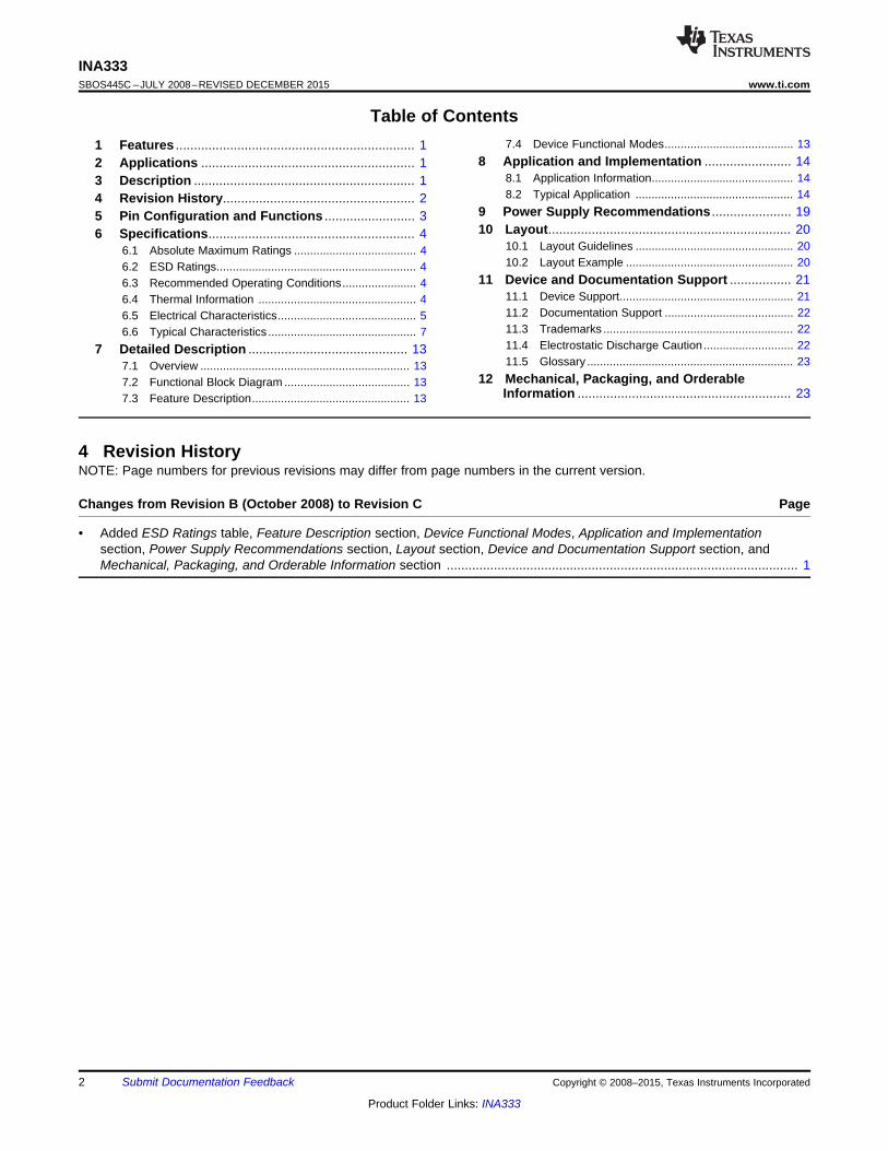
5 Pin Configuration and Functions
DGK Package8-Pin VSSOP
Top ViewDRG Package8-Pin WSON
Top View
Pin FunctionsPIN
I/O DESCRIPTIONNAME NO.REF 5 I Reference input. This pin must be driven by low impedance or connected to ground.RG 1, 8 — Gain setting pins. For gains greater than 1, place a gain resistor between pins 1 and 8.V+ 7 — Positive supplyV– 4 — Negative supplyVIN+ 3 I Positive inputVIN– 2 I Negative inputVOUT 6 O Output
4
INA333SBOS445C –JULY 2008–REVISED DECEMBER 2015 www.ti.com
Product Folder Links: INA333
Submit Documentation Feedback Copyright © 2008–2015, Texas Instruments Incorporated
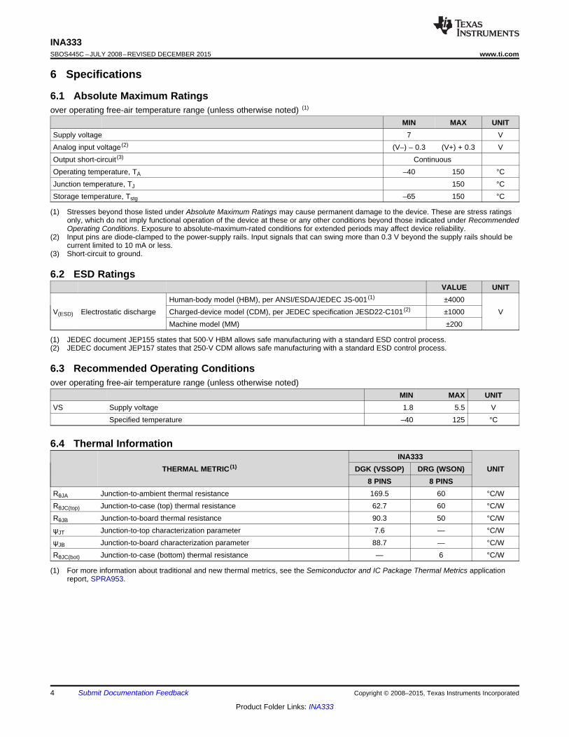
(1) Stresses beyond those listed under Absolute Maximum Ratings may cause permanent damage to the device. These are stress ratingsonly, which do not imply functional operation of the device at these or any other conditions beyond those indicated under RecommendedOperating Conditions. Exposure to absolute-maximum-rated conditions for extended periods may affect device reliability.
(2) Input pins are diode-clamped to the power-supply rails. Input signals that can swing more than 0.3 V beyond the supply rails should becurrent limited to 10 mA or less.
(3) Short-circuit to ground.
6 Specifications
6.1 Absolute Maximum Ratingsover operating free-air temperature range (unless otherwise noted) (1)
MIN MAX UNITSupply voltage 7 VAnalog input voltage (2) (V–) – 0.3 (V+) + 0.3 VOutput short-circuit (3) ContinuousOperating temperature, TA –40 150 °CJunction temperature, TJ 150 °CStorage temperature, Tstg –65 150 °C
(1) JEDEC document JEP155 states that 500-V HBM allows safe manufacturing with a standard ESD control process.(2) JEDEC document JEP157 states that 250-V CDM allows safe manufacturing with a standard ESD control process.
6.2 ESD RatingsVALUE UNIT
V(ESD) Electrostatic dischargeHuman-body model (HBM), per ANSI/ESDA/JEDEC JS-001 (1) ±4000
VCharged-device model (CDM), per JEDEC specification JESD22-C101 (2) ±1000Machine model (MM) ±200
6.3 Recommended Operating Conditionsover operating free-air temperature range (unless otherwise noted)
MIN MAX UNITVS Supply voltage 1.8 5.5 V
Specified temperature –40 125 °C
(1) For more information about traditional and new thermal metrics, see the Semiconductor and IC Package Thermal Metrics applicationreport, SPRA953.
6.4 Thermal Information
THERMAL METRIC (1)INA333
UNITDGK (VSSOP) DRG (WSON)8 PINS 8 PINS
RθJA Junction-to-ambient thermal resistance 169.5 60 °C/WRθJC(top) Junction-to-case (top) thermal resistance 62.7 60 °C/WRθJB Junction-to-board thermal resistance 90.3 50 °C/WψJT Junction-to-top characterization parameter 7.6 — °C/WψJB Junction-to-board characterization parameter 88.7 — °C/WRθJC(bot) Junction-to-case (bottom) thermal resistance — 6 °C/W
5
INA333www.ti.com SBOS445C –JULY 2008–REVISED DECEMBER 2015
Product Folder Links: INA333
Submit Documentation FeedbackCopyright © 2008–2015, Texas Instruments Incorporated
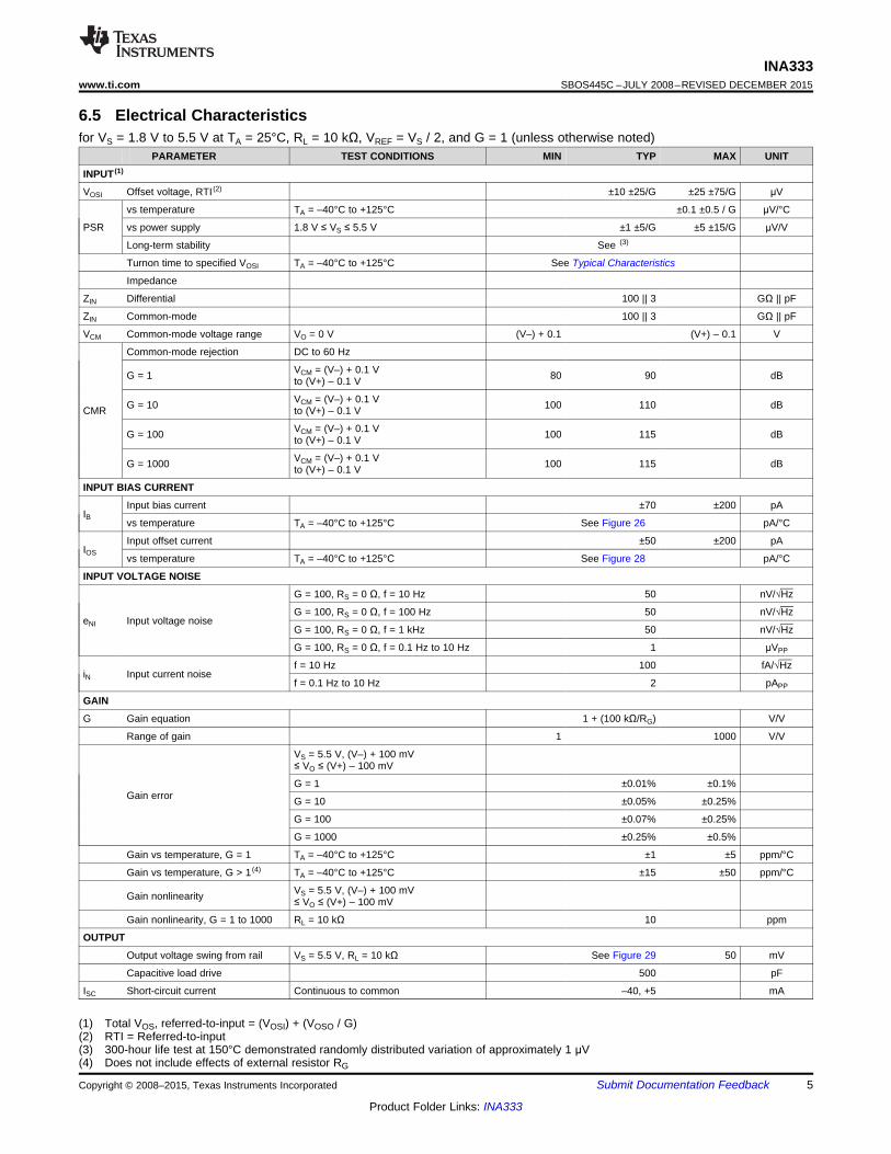
(1) Total VOS, referred-to-input = (VOSI) + (VOSO / G)(2) RTI = Referred-to-input(3) 300-hour life test at 150°C demonstrated randomly distributed variation of approximately 1 μV(4) Does not include effects of external resistor RG
6.5 Electrical Characteristicsfor VS = 1.8 V to 5.5 V at TA = 25°C, RL = 10 kΩ, VREF = VS / 2, and G = 1 (unless otherwise noted)
PARAMETER TEST CONDITIONS MIN TYP MAX UNIT
INPUT (1)
VOSI Offset voltage, RTI (2) ±10 ±25/G ±25 ±75/G μV
PSR
vs temperature TA = –40°C to +125°C ±0.1 ±0.5 / G μV/°C
vs power supply 1.8 V ≤ VS ≤ 5.5 V ±1 ±5/G ±5 ±15/G μV/V
Long-term stability See (3)
Turnon time to specified VOSI TA = –40°C to +125°C See Typical Characteristics
Impedance
ZIN Differential 100 || 3 GΩ || pF
ZIN Common-mode 100 || 3 GΩ || pF
VCM Common-mode voltage range VO = 0 V (V–) + 0.1 (V+) – 0.1 V
CMR
Common-mode rejection DC to 60 Hz
G = 1 VCM = (V–) + 0.1 Vto (V+) – 0.1 V 80 90 dB
G = 10 VCM = (V–) + 0.1 Vto (V+) – 0.1 V 100 110 dB
G = 100 VCM = (V–) + 0.1 Vto (V+) – 0.1 V 100 115 dB
G = 1000 VCM = (V–) + 0.1 Vto (V+) – 0.1 V 100 115 dB
INPUT BIAS CURRENT
IBInput bias current ±70 ±200 pA
vs temperature TA = –40°C to +125°C See Figure 26 pA/°C
IOSInput offset current ±50 ±200 pA
vs temperature TA = –40°C to +125°C See Figure 28 pA/°C
INPUT VOLTAGE NOISE
eNI Input voltage noise
G = 100, RS = 0 Ω, f = 10 Hz 50 nV/√Hz
G = 100, RS = 0 Ω, f = 100 Hz 50 nV/√Hz
G = 100, RS = 0 Ω, f = 1 kHz 50 nV/√Hz
G = 100, RS = 0 Ω, f = 0.1 Hz to 10 Hz 1 μVPP
iN Input current noisef = 10 Hz 100 fA/√Hz
f = 0.1 Hz to 10 Hz 2 pAPP
GAIN
G Gain equation 1 + (100 kΩ/RG) V/V
Range of gain 1 1000 V/V
Gain error
VS = 5.5 V, (V–) + 100 mV≤ VO ≤ (V+) – 100 mV
G = 1 ±0.01% ±0.1%
G = 10 ±0.05% ±0.25%
G = 100 ±0.07% ±0.25%
G = 1000 ±0.25% ±0.5%
Gain vs temperature, G = 1 TA = –40°C to +125°C ±1 ±5 ppm/°C
Gain vs temperature, G > 1 (4) TA = –40°C to +125°C ±15 ±50 ppm/°C
Gain nonlinearity VS = 5.5 V, (V–) + 100 mV≤ VO ≤ (V+) – 100 mV
Gain nonlinearity, G = 1 to 1000 RL = 10 kΩ 10 ppm
OUTPUT
Output voltage swing from rail VS = 5.5 V, RL = 10 kΩ See Figure 29 50 mV
Capacitive load drive 500 pF
ISC Short-circuit current Continuous to common –40, +5 mA
6
INA333SBOS445C –JULY 2008–REVISED DECEMBER 2015 www.ti.com
Product Folder Links: INA333
Submit Documentation Feedback Copyright © 2008–2015, Texas Instruments Incorporated
Electrical Characteristics (continued)for VS = 1.8 V to 5.5 V at TA = 25°C, RL = 10 kΩ, VREF = VS / 2, and G = 1 (unless otherwise noted)
PARAMETER TEST CONDITIONS MIN TYP MAX UNIT
FREQUENCY RESPONSE
Bandwidth, –3dB
G = 1 150 kHz
G = 10 35 kHz
G = 100 3.5 kHz
G = 1000 350 Hz
SR Slew rateVS = 5 V, VO = 4-V step, G = 1 0.16 V/μs
VS = 5 V, VO = 4-V step, G = 100 0.05 V/μs
tS Settling time to 0.01%VSTEP = 4 V, G = 1 50 μs
VSTEP = 4 V, G = 100 400 μs
tS Settling time to 0.001%VSTEP = 4 V, G = 1 60 μs
VSTEP = 4 V, G = 100 500 μs
Overload recovery 50% overdrive 75 μs
REFERENCE INPUT
RIN 300 kΩ
Voltage range V– V+ V
POWER SUPPLY
Voltage rangeSingle voltage range +1.8 +5.5 V
Dual voltage range ±0.9 ±2.75 V
IQQuiescent current VIN = VS / 2 50 75 μA
vs temperature TA = –40°C to +125°C 80 μA
TEMPERATURE RANGE
Specified temperature range –40 125 °C
Operating temperature range –40 150 °C
0
5
10
15
20
25
-
-
-
-
-
0 0.5 1.0 1.5
V (V)CM
V(
V)
mO
S
5.02.0
V = 5VS
3.0 4.02.5 3.5 4.5
V = 1.8VS
Time (1s/div)
Gain = 1
Nois
e (
1V
/div
)m
-75.0
Output Offset Voltage ( V)m
Popula
tion
V = 5.5VS
-7.5 0
7.5
15.0
22.5
30.0
37.5
45.0
52.5
60.0
67.5
-15.0
-22.5
-30.0
-37.5
-45.0
-52.5
-60.0
-67.5
75.0
-0.5
0
Output Voltage Offset Drift ( V/ C)m °
Popula
tion
0.5
0
V = 5.5VS
-0.0
5 0
0.0
5
0.1
0
0.1
5
0.2
0
0.2
5
0.3
0
0.3
5
0.4
0
0.4
5
-0.1
0
-0.1
5
-0.2
0
-5
0.2
-0.3
0
-0.3
5
-0.4
0
-0.4
5
-25.0
Input Offset Voltage ( V)m
Popula
tion
V = 5.5VS
-2.5 0
2.5
5.0
7.5
10.0
12.5
15.0
17.5
20.0
22.5
-5.0
-7.5
-10.0
-12.5
-15.0
-17.5
-20.0
-22.5
25.0
-0.1
0
Input Voltage Offset Drift ( V/ C)m °
Popula
tion
0.1
0
V = 5.5VS
-0.0
1 0
0.0
1
0.0
2
0.0
3
0.0
4
0.0
5
0.0
6
0.0
7
0.0
8
0.0
9
-2
0.0
-3
0.0
-4
0.0
-5
0.0
-6
0.0
-7
0.0
-8
0.0
-9
0.0
7
INA333www.ti.com SBOS445C –JULY 2008–REVISED DECEMBER 2015
Product Folder Links: INA333
Submit Documentation FeedbackCopyright © 2008–2015, Texas Instruments Incorporated
6.6 Typical Characteristicsat TA = 25°C, VS = 5 V, RL = 10 kΩ, VREF = midsupply, and G = 1 (unless otherwise noted)
Figure 1. Input Offset Voltage Figure 2. Input Voltage Offset Drift (–40°C to 125°C)
Figure 3. Output Offset Voltage Figure 4. Output Voltage Offset Drift (–40°C to 125°C)
Figure 5. Offset Voltage vs Common-Mode Voltage Figure 6. 0.1-Hz to 10-Hz Noise
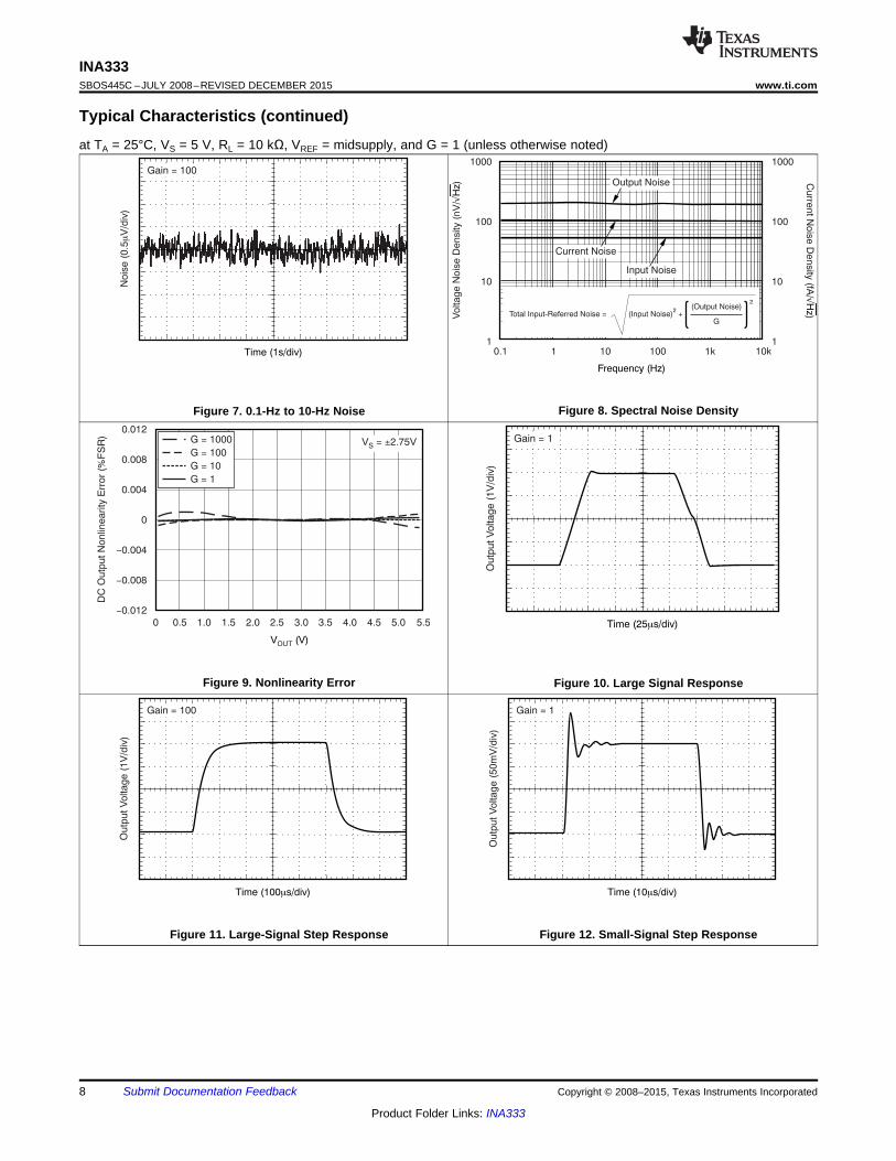
Time (100 s/div)m
Gain = 100
Ou
tpu
t V
olta
ge
(1
V/d
iv)
Time (10 s/div)m
Gain = 1
Ou
tpu
t V
olta
ge
(5
0m
V/d
iv)
0.012
0.008
0.004
0
0.004
0.008
0.012
-
-
-
0 1.0
V (V)OUT
DC
Ou
tpu
t N
on
line
arity
Err
or
(%F
SR
)
5.52.0 3.0 4.00.5 1.5 2.5 3.5 4.5 5.0
G = 1000
G = 100
G = 10
G = 1
V = 2.75V±S
Time (25 s/div)m
Gain = 1
Outp
ut V
oltage (
1V
/div
)
1000
100
10
10.1 1 10 100 1k
Frequency (Hz)
Voltage N
ois
e D
ensity (
nV
/)
ÖH
z
10k
Current Noise
Output Noise
Input Noise
Total Input-Referred Noise = (Input Noise) +2
(Output Noise)
G
2
1000
100
10
1
Curre
nt N
ois
e D
ensity
(f)
A/Ö
Hz
Time (1s/div)
Gain = 100
Nois
e (
0.5
V/d
iv)
m
8
INA333SBOS445C –JULY 2008–REVISED DECEMBER 2015 www.ti.com
Product Folder Links: INA333
Submit Documentation Feedback Copyright © 2008–2015, Texas Instruments Incorporated
Typical Characteristics (continued)at TA = 25°C, VS = 5 V, RL = 10 kΩ, VREF = midsupply, and G = 1 (unless otherwise noted)
Figure 7. 0.1-Hz to 10-Hz Noise Figure 8. Spectral Noise Density
Figure 9. Nonlinearity Error Figure 10. Large Signal Response
Figure 11. Large-Signal Step Response Figure 12. Small-Signal Step Response
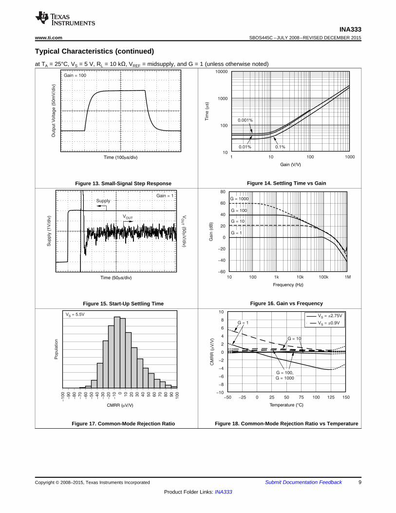
-1
00
CMRR ( V/V)m
Po
pu
latio
n
10
0
V = 5.5VS
-1
0 0
10
20
30
40
50
60
70
80
90
-2
0
-3
0
-4
0
-5
0
-6
0
-7
0
-8
0
-9
0
10
8
6
4
2
0
2
4
6
8
10
-
-
-
-
--50 -25 0 25 50 75 100
Temperature ( C)°
CM
RR
(V
/V)
m
G = 100,
G = 1000
150
V = 2.75VS ±
V = 0.9V±S
125
G = 1
G = 10
80
60
40
20
0
20
40
60
-
-
-
10 100 1k 10k
Frequency (Hz)
Gain
(dB
)
1M
G = 1
G = 1000
G = 100
G = 10
100kTime (50 s/div)m
Gain = 1
Supply
(1V
/div
)
Supply
VOUT
V(5
0V
/div
)m
OU
T
10000
1000
100
101 10 100
Gain (V/V)
Tim
e (
s)
m
1000
0.01%
0.001%
0.1%
Time (100 s/div)m
Gain = 100
Outp
ut V
oltage (
50m
V/d
iv)
9
INA333www.ti.com SBOS445C –JULY 2008–REVISED DECEMBER 2015
Product Folder Links: INA333
Submit Documentation FeedbackCopyright © 2008–2015, Texas Instruments Incorporated
Typical Characteristics (continued)at TA = 25°C, VS = 5 V, RL = 10 kΩ, VREF = midsupply, and G = 1 (unless otherwise noted)
Figure 13. Small-Signal Step Response Figure 14. Settling Time vs Gain
Figure 15. Start-Up Settling Time Figure 16. Gain vs Frequency
Figure 17. Common-Mode Rejection Ratio Figure 18. Common-Mode Rejection Ratio vs Temperature
1.8
1.6
1.4
1.2
1.0
0.8
0.6
0.4
0.2
0
Output Voltage (V)
Com
mon-M
ode V
oltage (
V)
0 0.2 0.4 0.5 0.8 1.0 1.81.2 1.4 1.6
All Gains
V = +1.8VS
V = 0REF
160
140
120
100
80
60
40
20
010 100 1k 10k 100k
Frequency (Hz)
+P
SR
R (
dB
)
1M1
G = 100
G = 1000
G = 10
G = 1
5
4
3
2
1
00 1 2 3 4
Output Voltage (V)
Com
mon-M
ode V
oltage (
V)
5
V = +5VS
V = 0REF
All Gains
0.9
0.7
0.5
0.3
0.1
0.1
0.3
0.5
0.7
0.9
-
-
-
-
-
-0.9 -0.7 -0.5 -0.3 -0.1 0.1
Output Voltage (V)
Com
mon-M
ode V
oltage (
V)
0.9
V = 0.9VS ±
V = 0REF
0.3 0.5 0.7
All Gains
160
140
120
100
80
60
40
20
010 100 1k 10k
Frequency (Hz)
CM
RR
(dB
)
100k
G = 1
G = 1000
G = 100
G = 10
2.5
-2.5 -2.0 -1.0 0 1.0 2.0
Output Voltage (V)
Com
mon-M
ode V
oltage (
V)
2.5
2.0
1.0
0
-1.0
-2.0
2.5
V = 2.5V
V = 0
±S
REF
All Gains
10
INA333SBOS445C –JULY 2008–REVISED DECEMBER 2015 www.ti.com
Product Folder Links: INA333
Submit Documentation Feedback Copyright © 2008–2015, Texas Instruments Incorporated
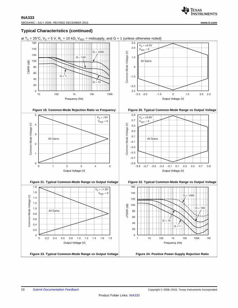
Typical Characteristics (continued)at TA = 25°C, VS = 5 V, RL = 10 kΩ, VREF = midsupply, and G = 1 (unless otherwise noted)
Figure 19. Common-Mode Rejection Ratio vs Frequency Figure 20. Typical Common-Mode Range vs Output Voltage
Figure 21. Typical Common-Mode Range vs Output Voltage Figure 22. Typical Common-Mode Range vs Output Voltage
Figure 23. Typical Common-Mode Range vs Output Voltage Figure 24. Positive Power-Supply Rejection Ratio
(V+)(V+) 0.25-
(V+) 0.50-
(V+) 0.75-
(V+) 1.00-
(V+) 1.25-
(V ) + 1.75-
(V ) + 0.75-
(V ) + 1.00-
(V ) + 0.50-
(V ) + 0.25-
(V )-
0 10 30 40 50 60
I (mA)OUT
V(V
)O
UT
(V+) 1.75-
(V+) 1.50-
(V ) + 1.50-
(V ) + 1.25-
20
+125 C°
+25 C°
- °40 C
VS = 2.75V±
VS = 0.9V±
80
70
60
50
40
30
20
10
0-50 -25 0 25 50 75 100
Temperature ( C)°
I(
A)
mQ
150125
V = 5VS
V = 1.8VS
200
180
160
140
120
100
80
60
40
20
00 0.5 1.0 1.5
V (V)CM
| I
(pA
)B
|
5.02.0
V = 5VS
3.0 4.02.5 3.5 4.5
V = 1.8VS
250
200
150
100
50
0
50
100
-
-
-50 -25 0 25 50 75 100
Temperature ( C)°
I(p
A)
OS
150125
V = 0.9V±S
V = 2.75V±S
160
140
120
100
80
60
40
20
0
20-
0.1 1 10 100 1k 10k 100k
Frequency (Hz)
-P
SR
R (
dB
)
1M
G = 1000
V = 5VS
G = 100
G = 1
G = 10
1200
1000
800
600
400
200
0
200-
-50 -25 0 25 50 75 100
Temperature ( C)°
I(p
A)
B
150
+IB
-IB
125
V = 0.9V±S V = 2.75V±S
11
INA333www.ti.com SBOS445C –JULY 2008–REVISED DECEMBER 2015
Product Folder Links: INA333
Submit Documentation FeedbackCopyright © 2008–2015, Texas Instruments Incorporated
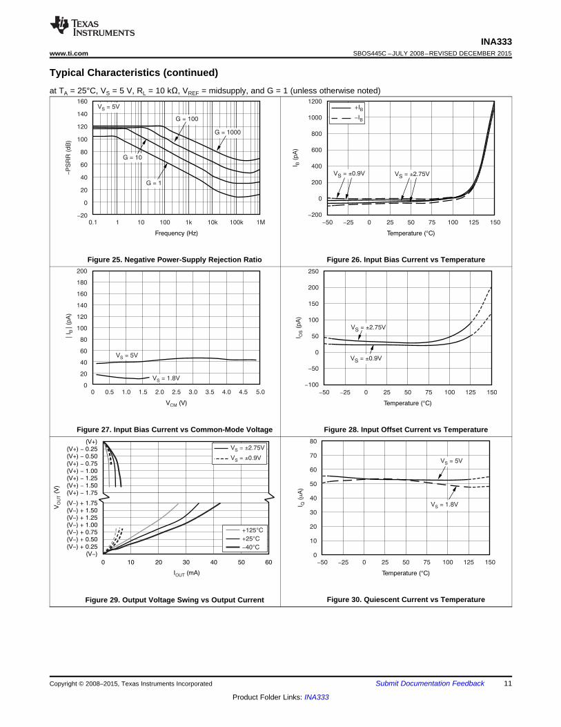
Typical Characteristics (continued)at TA = 25°C, VS = 5 V, RL = 10 kΩ, VREF = midsupply, and G = 1 (unless otherwise noted)
Figure 25. Negative Power-Supply Rejection Ratio Figure 26. Input Bias Current vs Temperature
Figure 27. Input Bias Current vs Common-Mode Voltage Figure 28. Input Offset Current vs Temperature
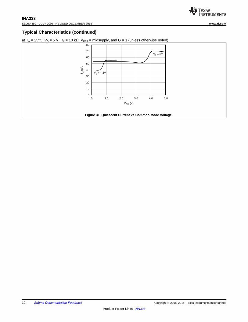
Figure 29. Output Voltage Swing vs Output Current Figure 30. Quiescent Current vs Temperature
80
70
60
50
40
30
20
10
00 1.0
V (V)CM
I(
A)
mQ
5.02.0
V = 5VS
3.0 4.0
V = 1.8VS
12
INA333SBOS445C –JULY 2008–REVISED DECEMBER 2015 www.ti.com
Product Folder Links: INA333
Submit Documentation Feedback Copyright © 2008–2015, Texas Instruments Incorporated
Typical Characteristics (continued)at TA = 25°C, VS = 5 V, RL = 10 kΩ, VREF = midsupply, and G = 1 (unless otherwise noted)
Figure 31. Quiescent Current vs Common-Mode Voltage
50kW
150kW 150kW
A1
A3
VOUT
VIN-
6
REF5
RFI Filtered Inputs2
V+
7
V-
4
1
8
150kW 150kW
50kW
A2
VIN+ RFI Filtered Inputs3
INA333
RG
G = 1 +100kW
RG
RFI Filtered Inputs
RFI Filtered Inputs
13
INA333www.ti.com SBOS445C –JULY 2008–REVISED DECEMBER 2015
Product Folder Links: INA333
Submit Documentation FeedbackCopyright © 2008–2015, Texas Instruments Incorporated
7 Detailed Description
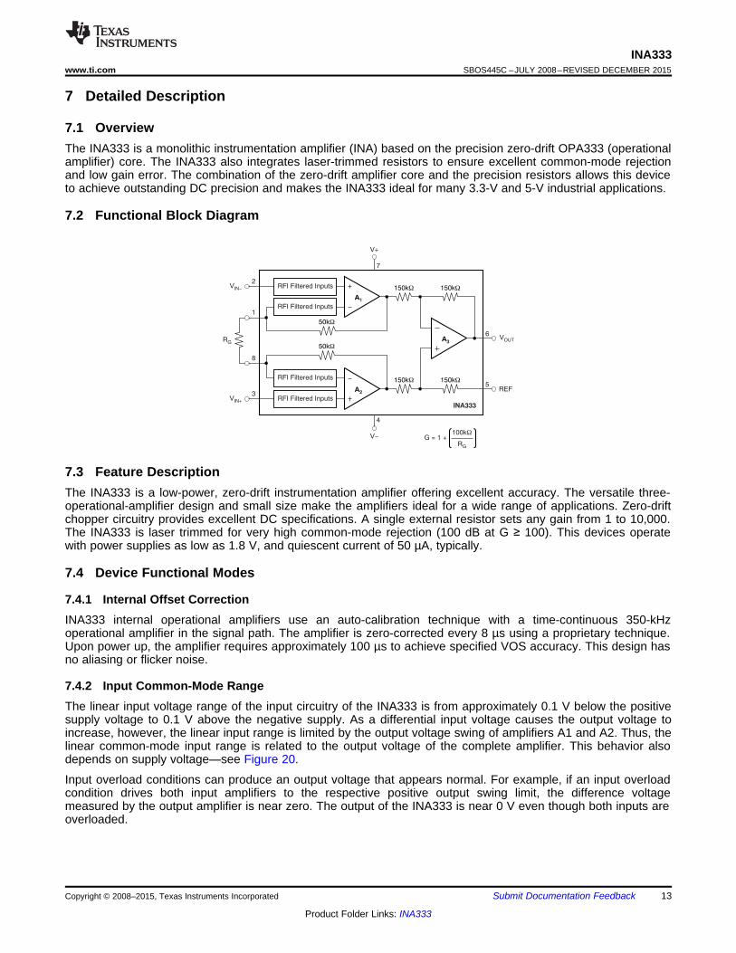
7.1 OverviewThe INA333 is a monolithic instrumentation amplifier (INA) based on the precision zero-drift OPA333 (operationalamplifier) core. The INA333 also integrates laser-trimmed resistors to ensure excellent common-mode rejectionand low gain error. The combination of the zero-drift amplifier core and the precision resistors allows this deviceto achieve outstanding DC precision and makes the INA333 ideal for many 3.3-V and 5-V industrial applications.
7.2 Functional Block Diagram
7.3 Feature DescriptionThe INA333 is a low-power, zero-drift instrumentation amplifier offering excellent accuracy. The versatile three-operational-amplifier design and small size make the amplifiers ideal for a wide range of applications. Zero-driftchopper circuitry provides excellent DC specifications. A single external resistor sets any gain from 1 to 10,000.The INA333 is laser trimmed for very high common-mode rejection (100 dB at G ≥ 100). This devices operatewith power supplies as low as 1.8 V, and quiescent current of 50 µA, typically.
7.4 Device Functional Modes
7.4.1 Internal Offset CorrectionINA333 internal operational amplifiers use an auto-calibration technique with a time-continuous 350-kHzoperational amplifier in the signal path. The amplifier is zero-corrected every 8 µs using a proprietary technique.Upon power up, the amplifier requires approximately 100 µs to achieve specified VOS accuracy. This design hasno aliasing or flicker noise.
7.4.2 Input Common-Mode RangeThe linear input voltage range of the input circuitry of the INA333 is from approximately 0.1 V below the positivesupply voltage to 0.1 V above the negative supply. As a differential input voltage causes the output voltage toincrease, however, the linear input range is limited by the output voltage swing of amplifiers A1 and A2. Thus, thelinear common-mode input range is related to the output voltage of the complete amplifier. This behavior alsodepends on supply voltage—see Figure 20.
Input overload conditions can produce an output voltage that appears normal. For example, if an input overloadcondition drives both input amplifiers to the respective positive output swing limit, the difference voltagemeasured by the output amplifier is near zero. The output of the INA333 is near 0 V even though both inputs areoverloaded.
A1
A2
A3
6
150kW150kW
150kW150kW
7
4
3
8
1
2VIN-
VIN+
RG
V+
V-
INA333
G = 1 +100kW
RG
5
RFI Filter
50kW
50kW
RFI Filter
Load
V = G (V´ V- )O IN+ IN-
0.1 Fm
0.1 Fm
+
-
VO
RG
Also drawn in simplified form:
INA333
Ref
VO
VIN-
VIN+
Ref
RFI Filter
RFI Filter
14
INA333SBOS445C –JULY 2008–REVISED DECEMBER 2015 www.ti.com
Product Folder Links: INA333
Submit Documentation Feedback Copyright © 2008–2015, Texas Instruments Incorporated
8 Application and Implementation
NOTEInformation in the following applications sections is not part of the TI componentspecification, and TI does not warrant its accuracy or completeness. TI’s customers areresponsible for determining suitability of components for their purposes. Customers shouldvalidate and test their design implementation to confirm system functionality.
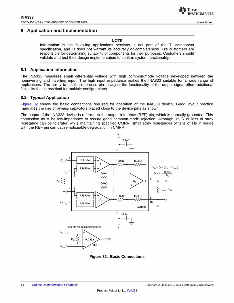
8.1 Application InformationThe INA333 measures small differential voltage with high common-mode voltage developed between thenoninverting and inverting input. The high input impedance makes the INA333 suitable for a wide range ofapplications. The ability to set the reference pin to adjust the functionality of the output signal offers additionalflexibility that is practical for multiple configurations.
8.2 Typical ApplicationFigure 32 shows the basic connections required for operation of the INA333 device. Good layout practicemandates the use of bypass capacitors placed close to the device pins as shown.
The output of the INA333 device is referred to the output reference (REF) pin, which is normally grounded. Thisconnection must be low-impedance to assure good common-mode rejection. Although 15 Ω or less of strayresistance can be tolerated while maintaining specified CMRR, small stray resistances of tens of Ωs in serieswith the REF pin can cause noticeable degradation in CMRR.
Figure 32. Basic Connections
15
INA333www.ti.com SBOS445C –JULY 2008–REVISED DECEMBER 2015
Product Folder Links: INA333
Submit Documentation FeedbackCopyright © 2008–2015, Texas Instruments Incorporated
Typical Application (continued)8.2.1 Design RequirementsThe device can be configured to monitor the input differential voltage when the gain of the input signal is set bythe external resistor RG. The output signal references to the Ref pin. The most common application is where theoutput is referenced to ground when no input signal is present by connecting the Ref pin to ground. When theinput signal increases, the output voltage at the OUT pin increases, too.
8.2.2 Detailed Design Procedure
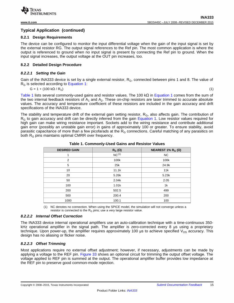
8.2.2.1 Setting the GainGain of the INA333 device is set by a single external resistor, RG, connected between pins 1 and 8. The value ofRG is selected according to Equation 1:
G = 1 + (100 kΩ / RG) (1)
Table 1 lists several commonly-used gains and resistor values. The 100 kΩ in Equation 1 comes from the sum ofthe two internal feedback resistors of A1 and A2. These on-chip resistors are laser trimmed to accurate absolutevalues. The accuracy and temperature coefficient of these resistors are included in the gain accuracy and driftspecifications of the INA333 device.
The stability and temperature drift of the external gain setting resistor, RG, also affects gain. The contribution ofRG to gain accuracy and drift can be directly inferred from the gain Equation 1. Low resistor values required forhigh gain can make wiring resistance important. Sockets add to the wiring resistance and contribute additionalgain error (possibly an unstable gain error) in gains of approximately 100 or greater. To ensure stability, avoidparasitic capacitance of more than a few picofarads at the RG connections. Careful matching of any parasitics onboth RG pins maintains optimal CMRR over frequency.
(1) NC denotes no connection. When using the SPICE model, the simulation will not converge unless aresistor is connected to the RG pins; use a very large resistor value.
Table 1. Commonly-Used Gains and Resistor ValuesDESIRED GAIN RG (Ω) NEAREST 1% RG (Ω)
1 NC (1) NC2 100k 100k5 25k 24.9k10 11.1k 11k20 5.26k 5.23k50 2.04k 2.05100 1.01k 1k200 502.5 499500 200.4 2001000 100.1 100
8.2.2.2 Internal Offset CorrectionThe INA333 device internal operational amplifiers use an auto-calibration technique with a time-continuous 350-kHz operational amplifier in the signal path. The amplifier is zero-corrected every 8 μs using a proprietarytechnique. Upon power-up, the amplifier requires approximately 100 μs to achieve specified VOS accuracy. Thisdesign has no aliasing or flicker noise.
8.2.2.3 Offset TrimmingMost applications require no external offset adjustment; however, if necessary, adjustments can be made byapplying a voltage to the REF pin. Figure 33 shows an optional circuit for trimming the output offset voltage. Thevoltage applied to REF pin is summed at the output. The operational amplifier buffer provides low impedance atthe REF pin to preserve good common-mode rejection.
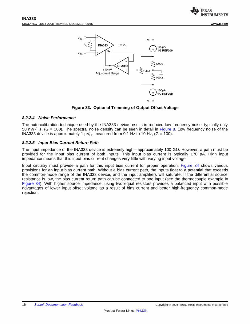
10kW
OPA333
±10mV
Adjustment Range
100W
100W
100 Am
1/2 REF200
100 Am
1/2 REF200
V+
V-
RG INA333
Ref
VO
VIN-
VIN+
16
INA333SBOS445C –JULY 2008–REVISED DECEMBER 2015 www.ti.com
Product Folder Links: INA333
Submit Documentation Feedback Copyright © 2008–2015, Texas Instruments Incorporated
Figure 33. Optional Trimming of Output Offset Voltage
8.2.2.4 Noise PerformanceThe auto-calibration technique used by the INA333 device results in reduced low frequency noise, typically only50 nV/√Hz, (G = 100). The spectral noise density can be seen in detail in Figure 8. Low frequency noise of theINA333 device is approximately 1 μVPP measured from 0.1 Hz to 10 Hz, (G = 100).
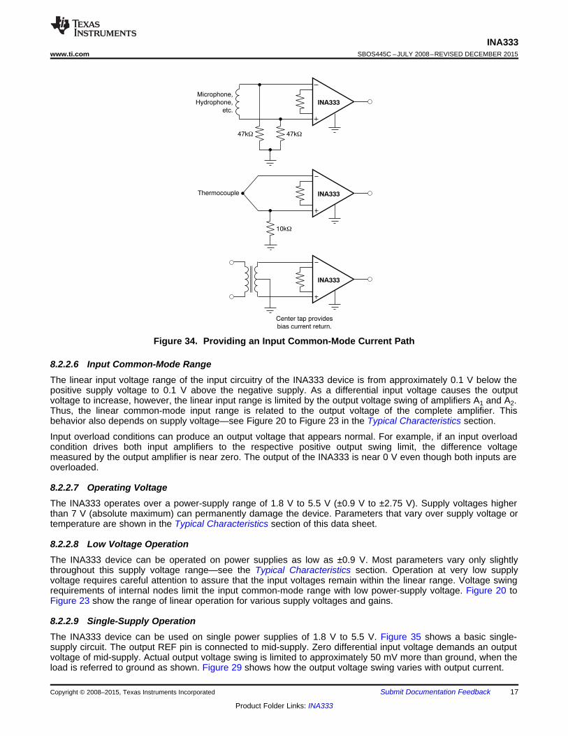
8.2.2.5 Input Bias Current Return PathThe input impedance of the INA333 device is extremely high—approximately 100 GΩ. However, a path must beprovided for the input bias current of both inputs. This input bias current is typically ±70 pA. High inputimpedance means that this input bias current changes very little with varying input voltage.
Input circuitry must provide a path for this input bias current for proper operation. Figure 34 shows variousprovisions for an input bias current path. Without a bias current path, the inputs float to a potential that exceedsthe common-mode range of the INA333 device, and the input amplifiers will saturate. If the differential sourceresistance is low, the bias current return path can be connected to one input (see the thermocouple example inFigure 34). With higher source impedance, using two equal resistors provides a balanced input with possibleadvantages of lower input offset voltage as a result of bias current and better high-frequency common-moderejection.
INA333
47kW47kW
INA333
10kW
Microphone,
Hydrophone,
etc.
Thermocouple
INA333
Center tap provides
bias current return.
17
INA333www.ti.com SBOS445C –JULY 2008–REVISED DECEMBER 2015
Product Folder Links: INA333
Submit Documentation FeedbackCopyright © 2008–2015, Texas Instruments Incorporated
Figure 34. Providing an Input Common-Mode Current Path
8.2.2.6 Input Common-Mode RangeThe linear input voltage range of the input circuitry of the INA333 device is from approximately 0.1 V below thepositive supply voltage to 0.1 V above the negative supply. As a differential input voltage causes the outputvoltage to increase, however, the linear input range is limited by the output voltage swing of amplifiers A1 and A2.Thus, the linear common-mode input range is related to the output voltage of the complete amplifier. Thisbehavior also depends on supply voltage—see Figure 20 to Figure 23 in the Typical Characteristics section.
Input overload conditions can produce an output voltage that appears normal. For example, if an input overloadcondition drives both input amplifiers to the respective positive output swing limit, the difference voltagemeasured by the output amplifier is near zero. The output of the INA333 is near 0 V even though both inputs areoverloaded.
8.2.2.7 Operating VoltageThe INA333 operates over a power-supply range of 1.8 V to 5.5 V (±0.9 V to ±2.75 V). Supply voltages higherthan 7 V (absolute maximum) can permanently damage the device. Parameters that vary over supply voltage ortemperature are shown in the Typical Characteristics section of this data sheet.
8.2.2.8 Low Voltage OperationThe INA333 device can be operated on power supplies as low as ±0.9 V. Most parameters vary only slightlythroughout this supply voltage range—see the Typical Characteristics section. Operation at very low supplyvoltage requires careful attention to assure that the input voltages remain within the linear range. Voltage swingrequirements of internal nodes limit the input common-mode range with low power-supply voltage. Figure 20 toFigure 23 show the range of linear operation for various supply voltages and gains.
8.2.2.9 Single-Supply OperationThe INA333 device can be used on single power supplies of 1.8 V to 5.5 V. Figure 35 shows a basic single-supply circuit. The output REF pin is connected to mid-supply. Zero differential input voltage demands an outputvoltage of mid-supply. Actual output voltage swing is limited to approximately 50 mV more than ground, when theload is referred to ground as shown. Figure 29 shows how the output voltage swing varies with output current.
300W
+3V
150W
R(1)
1
2V V- D
2V + VD
3V
RG INA333 VO
Ref
1.5V
18
INA333SBOS445C –JULY 2008–REVISED DECEMBER 2015 www.ti.com
Product Folder Links: INA333
Submit Documentation Feedback Copyright © 2008–2015, Texas Instruments Incorporated
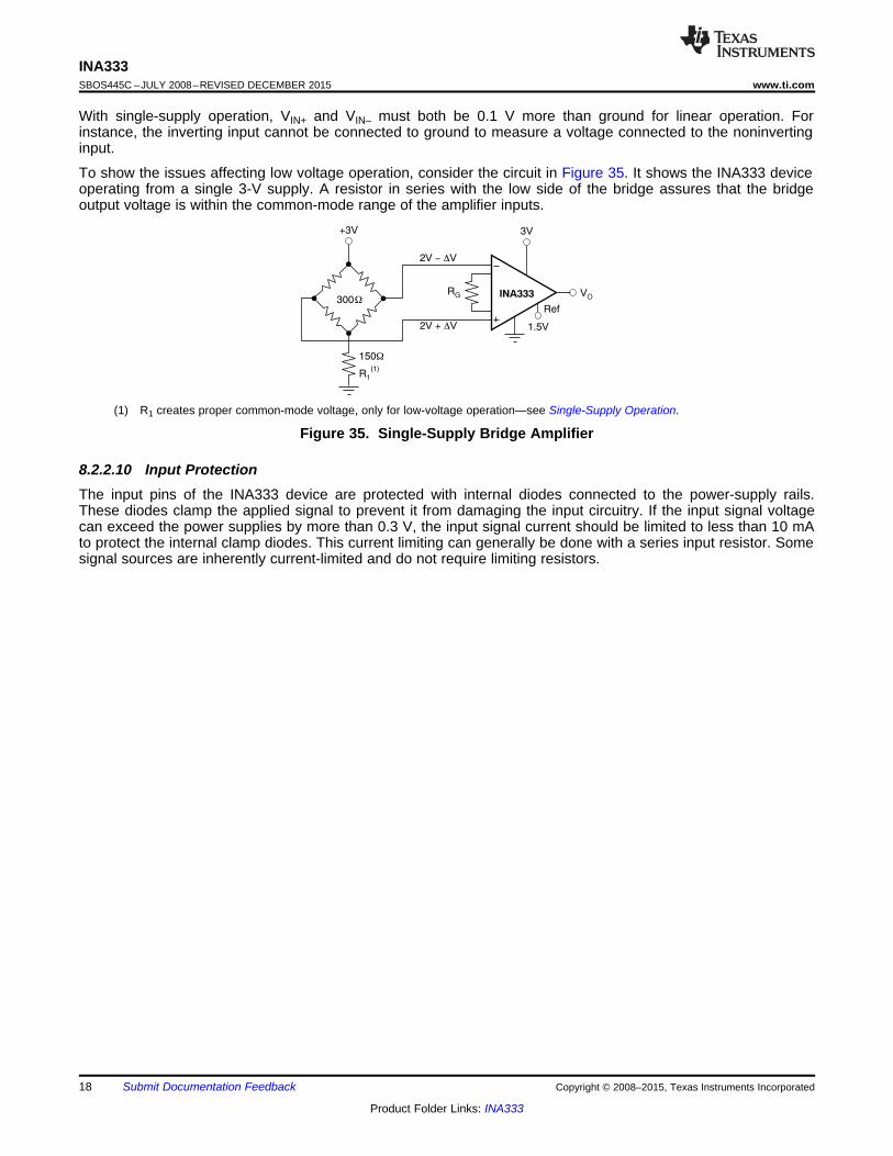
With single-supply operation, VIN+ and VIN– must both be 0.1 V more than ground for linear operation. Forinstance, the inverting input cannot be connected to ground to measure a voltage connected to the noninvertinginput.
To show the issues affecting low voltage operation, consider the circuit in Figure 35. It shows the INA333 deviceoperating from a single 3-V supply. A resistor in series with the low side of the bridge assures that the bridgeoutput voltage is within the common-mode range of the amplifier inputs.
(1) R1 creates proper common-mode voltage, only for low-voltage operation—see Single-Supply Operation.
Figure 35. Single-Supply Bridge Amplifier
8.2.2.10 Input ProtectionThe input pins of the INA333 device are protected with internal diodes connected to the power-supply rails.These diodes clamp the applied signal to prevent it from damaging the input circuitry. If the input signal voltagecan exceed the power supplies by more than 0.3 V, the input signal current should be limited to less than 10 mAto protect the internal clamp diodes. This current limiting can generally be done with a series input resistor. Somesignal sources are inherently current-limited and do not require limiting resistors.
Time (10 s/div)m
Gain = 1
Ou
tpu
t V
olta
ge
(5
0m
V/d
iv)
Time (100 s/div)m
Gain = 100
Ou
tpu
t V
olta
ge
(5
0m
V/d
iv)
Time (25 s/div)m
Gain = 1
Ou
tpu
t V
olta
ge
(1
V/d
iv)
Time (100 s/div)m
Gain = 100
Ou
tpu
t V
olta
ge
(1
V/d
iv)
19
INA333www.ti.com SBOS445C –JULY 2008–REVISED DECEMBER 2015
Product Folder Links: INA333
Submit Documentation FeedbackCopyright © 2008–2015, Texas Instruments Incorporated
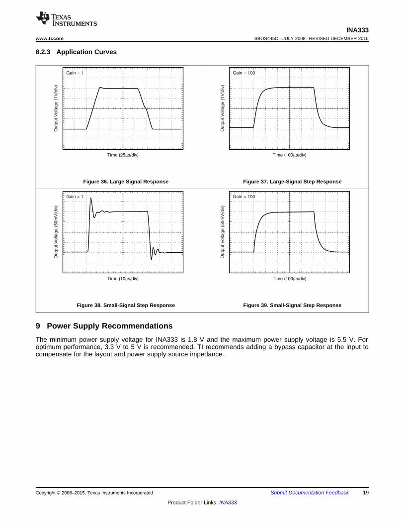
8.2.3 Application Curves
Figure 36. Large Signal Response Figure 37. Large-Signal Step Response
Figure 38. Small-Signal Step Response Figure 39. Small-Signal Step Response
9 Power Supply RecommendationsThe minimum power supply voltage for INA333 is 1.8 V and the maximum power supply voltage is 5.5 V. Foroptimum performance, 3.3 V to 5 V is recommended. TI recommends adding a bypass capacitor at the input tocompensate for the layout and power supply source impedance.
RG
V+
VO
Ref
RG
V-IN
V+IN
V-
VIN-
VIN+
V- GND
BypassCapacitor
Gain Resistor
BypassCapacitor
GND
V+
VOUT
20
INA333SBOS445C –JULY 2008–REVISED DECEMBER 2015 www.ti.com
Product Folder Links: INA333
Submit Documentation Feedback Copyright © 2008–2015, Texas Instruments Incorporated
10 Layout
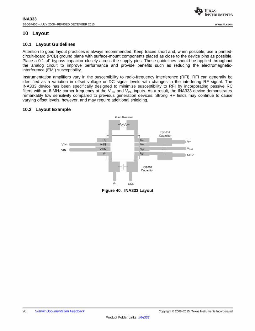
10.1 Layout GuidelinesAttention to good layout practices is always recommended. Keep traces short and, when possible, use a printed-circuit-board (PCB) ground plane with surface-mount components placed as close to the device pins as possible.Place a 0.1-μF bypass capacitor closely across the supply pins. These guidelines should be applied throughoutthe analog circuit to improve performance and provide benefits such as reducing the electromagnetic-interference (EMI) susceptibility.
Instrumentation amplifiers vary in the susceptibility to radio-frequency interference (RFI). RFI can generally beidentified as a variation in offset voltage or DC signal levels with changes in the interfering RF signal. TheINA333 device has been specifically designed to minimize susceptibility to RFI by incorporating passive RCfilters with an 8-MHz corner frequency at the VIN+ and VIN– inputs. As a result, the INA333 device demonstratesremarkably low sensitivity compared to previous generation devices. Strong RF fields may continue to causevarying offset levels, however, and may require additional shielding.
10.2 Layout Example
Figure 40. INA333 Layout
VC
CV
CC
Vre
f+
Vre
f+
Vre
f+
Rset 2.5M
VoA2
VoA1
-
+
+
3
1
5
4
2
U5 OPA369
-
+
+
3
1
5
4
2
U6 OPA369
1/2 of matchedmonolithic dual
NPN transistors(example: MMDT3904)
Input I 10n
uC
Vre
f/2
2.5
V+
VM1
VC
CV
CC
Vre
f+
Vre
f+
V1 5uC Vref/2 2.5
Vdiff
Vout
+
-
+
U1 OPA335
R3
14k R8 10k
C1
1n
+
RG
RG V+
V-
Ref
_
Out
2
1
8
3
6
7
5
4 U1 INA333
VC
C
1/2 of matchedmonolithic dual
NPN transistors(example: MMDT3904)
NOTE: Temperature compensation
of logging transistors is not shown.
Optional buffer for driving
SAR converters with
sampling systems of 33kHz.³
RELATED PRODUCTS
For monolithic logarithmic amplifiers (such as LOG112 or LOG114) see the link in footnote 1.
21
INA333www.ti.com SBOS445C –JULY 2008–REVISED DECEMBER 2015
Product Folder Links: INA333
Submit Documentation FeedbackCopyright © 2008–2015, Texas Instruments Incorporated
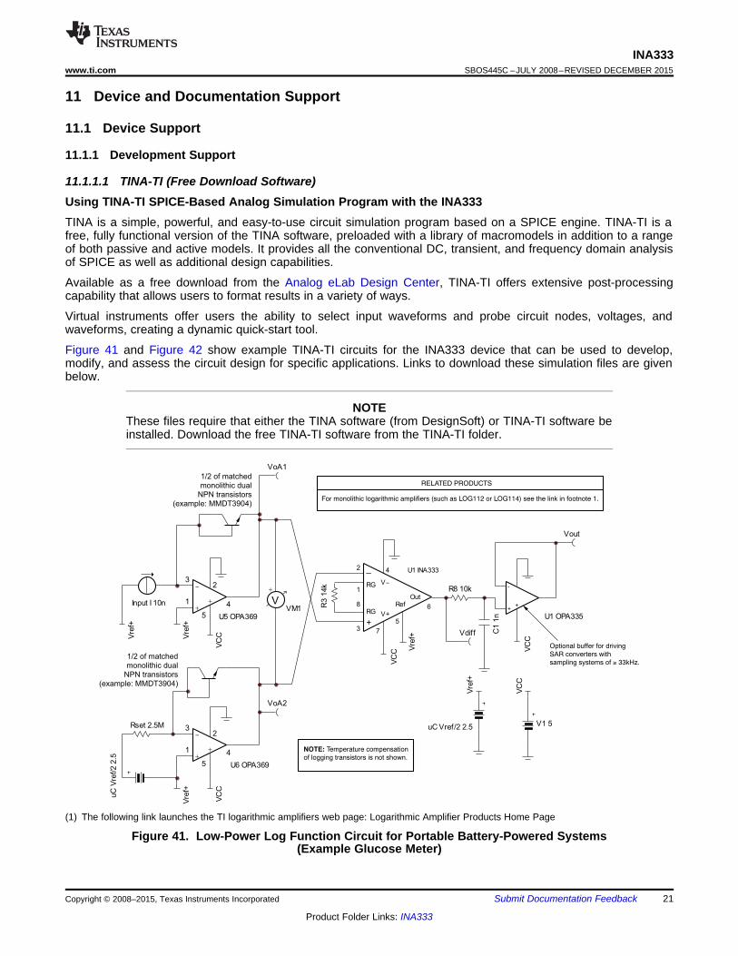
11 Device and Documentation Support
11.1 Device Support
11.1.1 Development Support
11.1.1.1 TINA-TI (Free Download Software)Using TINA-TI SPICE-Based Analog Simulation Program with the INA333TINA is a simple, powerful, and easy-to-use circuit simulation program based on a SPICE engine. TINA-TI is afree, fully functional version of the TINA software, preloaded with a library of macromodels in addition to a rangeof both passive and active models. It provides all the conventional DC, transient, and frequency domain analysisof SPICE as well as additional design capabilities.
Available as a free download from the Analog eLab Design Center, TINA-TI offers extensive post-processingcapability that allows users to format results in a variety of ways.
Virtual instruments offer users the ability to select input waveforms and probe circuit nodes, voltages, andwaveforms, creating a dynamic quick-start tool.
Figure 41 and Figure 42 show example TINA-TI circuits for the INA333 device that can be used to develop,modify, and assess the circuit design for specific applications. Links to download these simulation files are givenbelow.
NOTEThese files require that either the TINA software (from DesignSoft) or TINA-TI software beinstalled. Download the free TINA-TI software from the TINA-TI folder.
(1) The following link launches the TI logarithmic amplifiers web page: Logarithmic Amplifier Products Home Page
Figure 41. Low-Power Log Function Circuit for Portable Battery-Powered Systems(Example Glucose Meter)
3V
3VVREF
3V
VREF
3V
3V
3V
VREF
V4 3
R
2.5kSET1
W
A
+
IREF1
+
-
+U3
OPA333
R
2.5kSET2
W
A
+
IREF2
R
2k1
W
R
100ZERO
W
RWb
3W
RWc
4W
RWd
3W
RWa
3W
+
-
+
U2
OPA333
C
470nF7
OUTF
GNDF
OUTS
GNDS
In
EN
U1 REF3212
+
-
+OPA3331 OPA333
V+
VRTD
VT 25
VT+
VT-
Mon+ Mon-
RTD+
RTD-
EMU21 RTD3
R
100kGAIN
W
VDIFF
T3 BF256AT1 BF256A
Use BF861AUse BF861A
G
S
RTD Resistance
(Volts = Ohms)
Temp ( C)
(Volts = C)
°
°
Pt100 RTD
PGA112 MSP430
VREF+
+
RG
V+
V-
Ref
_2
1
8
3
6
7
5
4 U1 INA333
3V
RG
Out
22
INA333SBOS445C –JULY 2008–REVISED DECEMBER 2015 www.ti.com
Product Folder Links: INA333
Submit Documentation Feedback Copyright © 2008–2015, Texas Instruments Incorporated
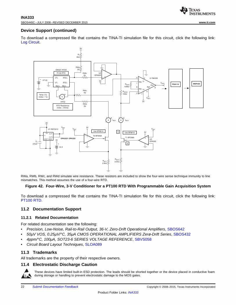
Device Support (continued)To download a compressed file that contains the TINA-TI simulation file for this circuit, click the following link:Log Circuit.
RWa, RWb, RWc, and RWd simulate wire resistance. These resistors are included to show the four-wire sense technique immunity to linemismatches. This method assumes the use of a four-wire RTD.
Figure 42. Four-Wire, 3-V Conditioner for a PT100 RTD With Programmable Gain Acquisition System
To download a compressed file that contains the TINA-TI simulation file for this circuit, click the following link:PT100 RTD.
11.2 Documentation Support
11.2.1 Related DocumentationFor related documentation see the following:• Precision, Low-Noise, Rail-to-Rail Output, 36-V, Zero-Drift Operational Amplifiers, SBOS642• 50μV VOS, 0.25μV/°C, 35μA CMOS OPERATIONAL AMPLIFIERS Zerø-Drift Series, SBOS432• 4ppm/°C, 100μA, SOT23-6 SERIES VOLTAGE REFERENCE, SBVS058• Circuit Board Layout Techniques, SLOA089
11.3 TrademarksAll trademarks are the property of their respective owners.
11.4 Electrostatic Discharge CautionThese devices have limited built-in ESD protection. The leads should be shorted together or the device placed in conductive foamduring storage or handling to prevent electrostatic damage to the MOS gates.
23
INA333www.ti.com SBOS445C –JULY 2008–REVISED DECEMBER 2015
Product Folder Links: INA333
Submit Documentation FeedbackCopyright © 2008–2015, Texas Instruments Incorporated
11.5 GlossarySLYZ022 — TI Glossary.
This glossary lists and explains terms, acronyms, and definitions.
12 Mechanical, Packaging, and Orderable InformationThe following pages include mechanical, packaging, and orderable information. This information is the mostcurrent data available for the designated devices. This data is subject to change without notice and revision ofthis document. For browser-based versions of this data sheet, refer to the left-hand navigation.
PACKAGE OPTION ADDENDUM
www.ti.com 20-Aug-2021
Addendum-Page 1
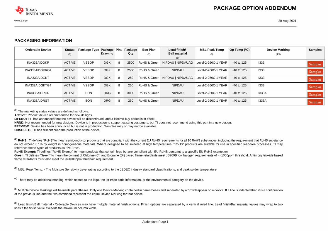
PACKAGING INFORMATION
Orderable Device Status(1)
Package Type PackageDrawing
Pins PackageQty
Eco Plan(2)
Lead finish/Ball material
(6)
MSL Peak Temp(3)
Op Temp (°C) Device Marking(4/5)
Samples
INA333AIDGKR ACTIVE VSSOP DGK 8 2500 RoHS & Green NIPDAU | NIPDAUAG Level-2-260C-1 YEAR -40 to 125 I333
INA333AIDGKRG4 ACTIVE VSSOP DGK 8 2500 RoHS & Green NIPDAU Level-2-260C-1 YEAR -40 to 125 I333
INA333AIDGKT ACTIVE VSSOP DGK 8 250 RoHS & Green NIPDAU | NIPDAUAG Level-2-260C-1 YEAR -40 to 125 I333
INA333AIDGKTG4 ACTIVE VSSOP DGK 8 250 RoHS & Green NIPDAU Level-2-260C-1 YEAR -40 to 125 I333
INA333AIDRGR ACTIVE SON DRG 8 3000 RoHS & Green NIPDAU Level-2-260C-1 YEAR -40 to 125 I333A
INA333AIDRGT ACTIVE SON DRG 8 250 RoHS & Green NIPDAU Level-2-260C-1 YEAR -40 to 125 I333A
(1) The marketing status values are defined as follows:ACTIVE: Product device recommended for new designs.LIFEBUY: TI has announced that the device will be discontinued, and a lifetime-buy period is in effect.NRND: Not recommended for new designs. Device is in production to support existing customers, but TI does not recommend using this part in a new design.PREVIEW: Device has been announced but is not in production. Samples may or may not be available.OBSOLETE: TI has discontinued the production of the device.
(2) RoHS: TI defines "RoHS" to mean semiconductor products that are compliant with the current EU RoHS requirements for all 10 RoHS substances, including the requirement that RoHS substancedo not exceed 0.1% by weight in homogeneous materials. Where designed to be soldered at high temperatures, "RoHS" products are suitable for use in specified lead-free processes. TI mayreference these types of products as "Pb-Free".RoHS Exempt: TI defines "RoHS Exempt" to mean products that contain lead but are compliant with EU RoHS pursuant to a specific EU RoHS exemption.Green: TI defines "Green" to mean the content of Chlorine (Cl) and Bromine (Br) based flame retardants meet JS709B low halogen requirements of <=1000ppm threshold. Antimony trioxide basedflame retardants must also meet the <=1000ppm threshold requirement.
(3) MSL, Peak Temp. - The Moisture Sensitivity Level rating according to the JEDEC industry standard classifications, and peak solder temperature.
(4) There may be additional marking, which relates to the logo, the lot trace code information, or the environmental category on the device.
(5) Multiple Device Markings will be inside parentheses. Only one Device Marking contained in parentheses and separated by a "~" will appear on a device. If a line is indented then it is a continuationof the previous line and the two combined represent the entire Device Marking for that device.
(6) Lead finish/Ball material - Orderable Devices may have multiple material finish options. Finish options are separated by a vertical ruled line. Lead finish/Ball material values may wrap to twolines if the finish value exceeds the maximum column width.
PACKAGE OPTION ADDENDUM
www.ti.com 20-Aug-2021
Addendum-Page 2
Important Information and Disclaimer:The information provided on this page represents TI's knowledge and belief as of the date that it is provided. TI bases its knowledge and belief on informationprovided by third parties, and makes no representation or warranty as to the accuracy of such information. Efforts are underway to better integrate information from third parties. TI has taken andcontinues to take reasonable steps to provide representative and accurate information but may not have conducted destructive testing or chemical analysis on incoming materials and chemicals.TI and TI suppliers consider certain information to be proprietary, and thus CAS numbers and other limited information may not be available for release.
In no event shall TI's liability arising out of such information exceed the total purchase price of the TI part(s) at issue in this document sold by TI to Customer on an annual basis.
OTHER QUALIFIED VERSIONS OF INA333 :
• Automotive : INA333-Q1
NOTE: Qualified Version Definitions:
• Automotive - Q100 devices qualified for high-reliability automotive applications targeting zero defects
PACKAGE MATERIALS INFORMATION
www.ti.com 3-Jun-2022
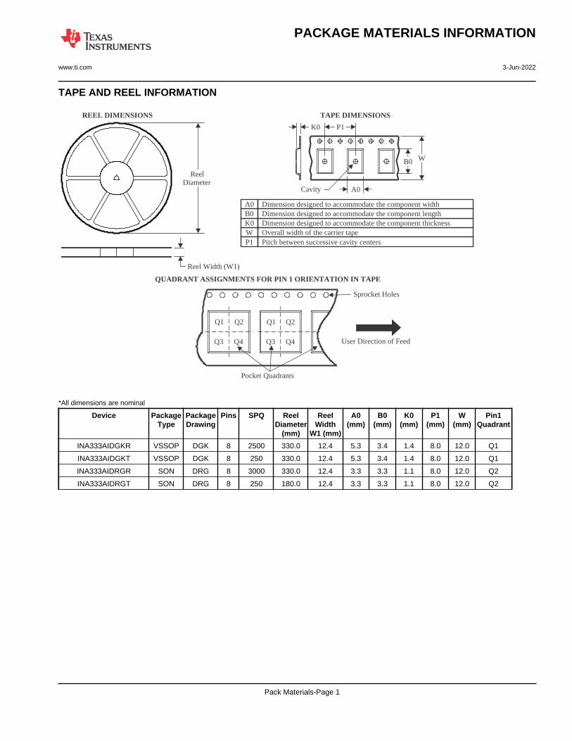
TAPE AND REEL INFORMATION
Reel Width (W1)
REEL DIMENSIONS
A0B0K0W
Dimension designed to accommodate the component lengthDimension designed to accommodate the component thicknessOverall width of the carrier tapePitch between successive cavity centers
Dimension designed to accommodate the component width
TAPE DIMENSIONS
K0 P1
B0 W
A0Cavity
QUADRANT ASSIGNMENTS FOR PIN 1 ORIENTATION IN TAPE
Pocket Quadrants
Sprocket Holes
Q1 Q1Q2 Q2
Q3 Q3Q4 Q4 User Direction of Feed
P1
ReelDiameter
*All dimensions are nominal
Device PackageType
PackageDrawing
Pins SPQ ReelDiameter
(mm)
ReelWidth
W1 (mm)
A0(mm)
B0(mm)
K0(mm)
P1(mm)
W(mm)
Pin1Quadrant
INA333AIDGKR VSSOP DGK 8 2500 330.0 12.4 5.3 3.4 1.4 8.0 12.0 Q1
INA333AIDGKT VSSOP DGK 8 250 330.0 12.4 5.3 3.4 1.4 8.0 12.0 Q1
INA333AIDRGR SON DRG 8 3000 330.0 12.4 3.3 3.3 1.1 8.0 12.0 Q2
INA333AIDRGT SON DRG 8 250 180.0 12.4 3.3 3.3 1.1 8.0 12.0 Q2
Pack Materials-Page 1
PACKAGE MATERIALS INFORMATION
www.ti.com 3-Jun-2022
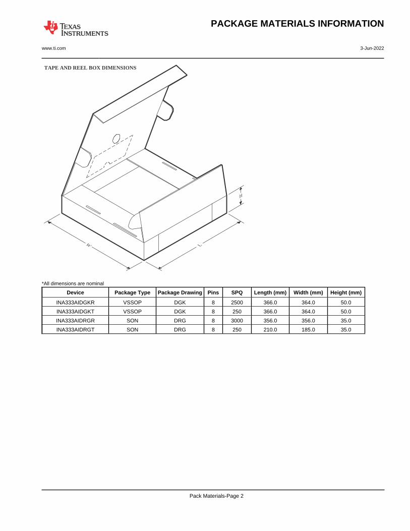
TAPE AND REEL BOX DIMENSIONS
Width (mm)
W L
H
*All dimensions are nominal
Device Package Type Package Drawing Pins SPQ Length (mm) Width (mm) Height (mm)
INA333AIDGKR VSSOP DGK 8 2500 366.0 364.0 50.0
INA333AIDGKT VSSOP DGK 8 250 366.0 364.0 50.0
INA333AIDRGR SON DRG 8 3000 356.0 356.0 35.0
INA333AIDRGT SON DRG 8 250 210.0 185.0 35.0
Pack Materials-Page 2
www.ti.com
PACKAGE OUTLINE
C
8X 0.30.2
2.4 0.12X1.5
1.45 0.1
6X 0.5
0.80.7
8X 0.60.4
0.050.00
A 3.12.9
B
3.12.9
(DIM A) TYPOPT 01 SHOWN
WSON - 0.8 mm max heightDRG0008BPLASTIC SMALL OUTLINE - NO LEAD
4218886/A 01/2020
DIMENSION AOPTION 01 (0.1)OPTION 02 (0.2)
PIN 1 INDEX AREA
SEATING PLANE
0.05 C
1
4 5
8
(OPTIONAL)PIN 1 ID 0.1 C A B
0.08 C
THERMAL PADEXPOSED
NOTES: 1. All linear dimensions are in millimeters. Any dimensions in parenthesis are for reference only. Dimensioning and tolerancing per ASME Y14.5M. 2. This drawing is subject to change without notice. 3. The package thermal pad must be soldered to the printed circuit board for thermal and mechanical performance.
SCALE 4.000
www.ti.com
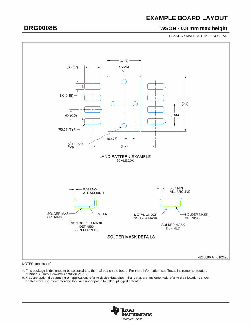
EXAMPLE BOARD LAYOUT
0.07 MINALL AROUND
0.07 MAXALL AROUND
8X (0.25)
(2.4)
(2.7)
6X (0.5)
(1.45)
( 0.2) VIATYP
(0.475)
(0.95)
8X (0.7)
(R0.05) TYP
WSON - 0.8 mm max heightDRG0008BPLASTIC SMALL OUTLINE - NO LEAD
4218886/A 01/2020
SYMM
1
4 5
8
LAND PATTERN EXAMPLESCALE:20X
NOTES: (continued) 4. This package is designed to be soldered to a thermal pad on the board. For more information, see Texas Instruments literature number SLUA271 (www.ti.com/lit/slua271).5. Vias are optional depending on application, refer to device data sheet. If any vias are implemented, refer to their locations shown on this view. It is recommended that vias under paste be filled, plugged or tented.
SOLDER MASKOPENINGSOLDER MASK
METAL UNDER
SOLDER MASKDEFINED
METALSOLDER MASKOPENING
SOLDER MASK DETAILS
NON SOLDER MASKDEFINED
(PREFERRED)
www.ti.com
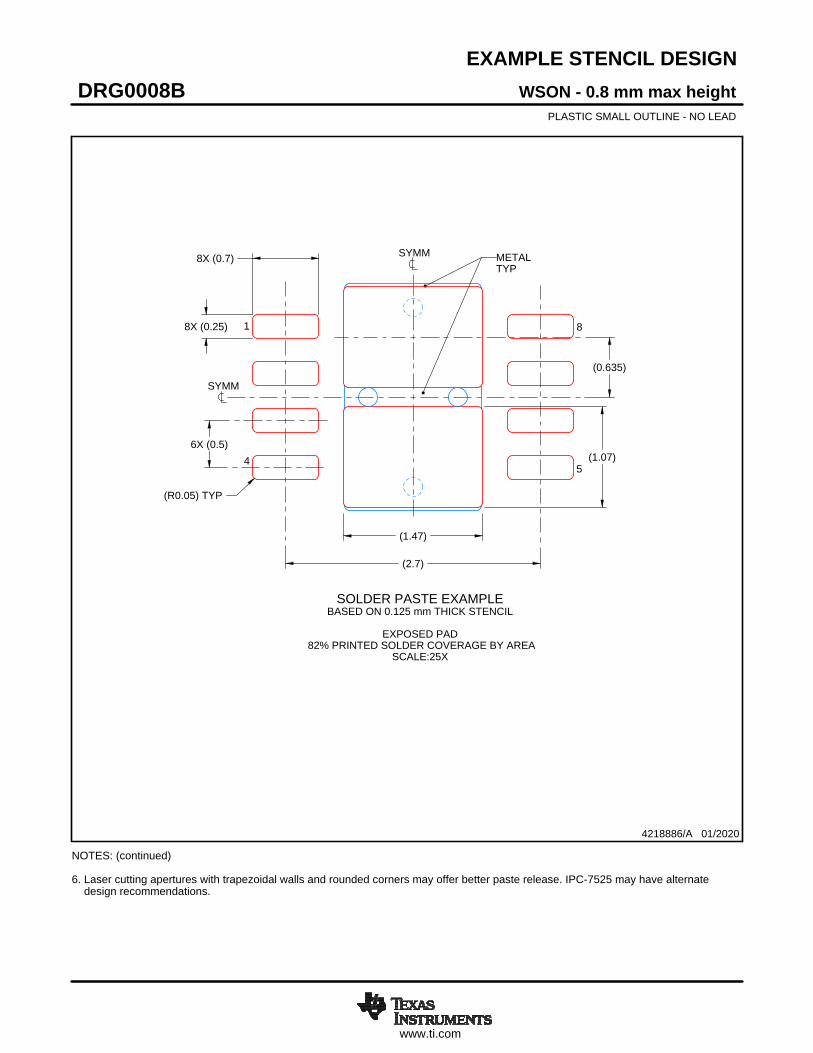
EXAMPLE STENCIL DESIGN
(R0.05) TYP
8X (0.25)
8X (0.7)
(1.47)
(1.07)
(2.7)
(0.635)
6X (0.5)
WSON - 0.8 mm max heightDRG0008BPLASTIC SMALL OUTLINE - NO LEAD
4218886/A 01/2020
NOTES: (continued) 6. Laser cutting apertures with trapezoidal walls and rounded corners may offer better paste release. IPC-7525 may have alternate design recommendations.
SOLDER PASTE EXAMPLEBASED ON 0.125 mm THICK STENCIL
EXPOSED PAD
82% PRINTED SOLDER COVERAGE BY AREASCALE:25X
SYMM
1
45
8
METALTYP
SYMM

IMPORTANT NOTICE AND DISCLAIMERTI PROVIDES TECHNICAL AND RELIABILITY DATA (INCLUDING DATA SHEETS), DESIGN RESOURCES (INCLUDING REFERENCE DESIGNS), APPLICATION OR OTHER DESIGN ADVICE, WEB TOOLS, SAFETY INFORMATION, AND OTHER RESOURCES “AS IS” AND WITH ALL FAULTS, AND DISCLAIMS ALL WARRANTIES, EXPRESS AND IMPLIED, INCLUDING WITHOUT LIMITATION ANY IMPLIED WARRANTIES OF MERCHANTABILITY, FITNESS FOR A PARTICULAR PURPOSE OR NON-INFRINGEMENT OF THIRD PARTY INTELLECTUAL PROPERTY RIGHTS.These resources are intended for skilled developers designing with TI products. You are solely responsible for (1) selecting the appropriate TI products for your application, (2) designing, validating and testing your application, and (3) ensuring your application meets applicable standards, and any other safety, security, regulatory or other requirements.These resources are subject to change without notice. TI grants you permission to use these resources only for development of an application that uses the TI products described in the resource. Other reproduction and display of these resources is prohibited. No license is granted to any other TI intellectual property right or to any third party intellectual property right. TI disclaims responsibility for, and you will fully indemnify TI and its representatives against, any claims, damages, costs, losses, and liabilities arising out of your use of these resources.TI’s products are provided subject to TI’s Terms of Sale or other applicable terms available either on ti.com or provided in conjunction with such TI products. TI’s provision of these resources does not expand or otherwise alter TI’s applicable warranties or warranty disclaimers for TI products.TI objects to and rejects any additional or different terms you may have proposed. IMPORTANT NOTICE
Mailing Address: Texas Instruments, Post Office Box 655303, Dallas, Texas 75265Copyright © 2022, Texas Instruments Incorporated
Related Documents