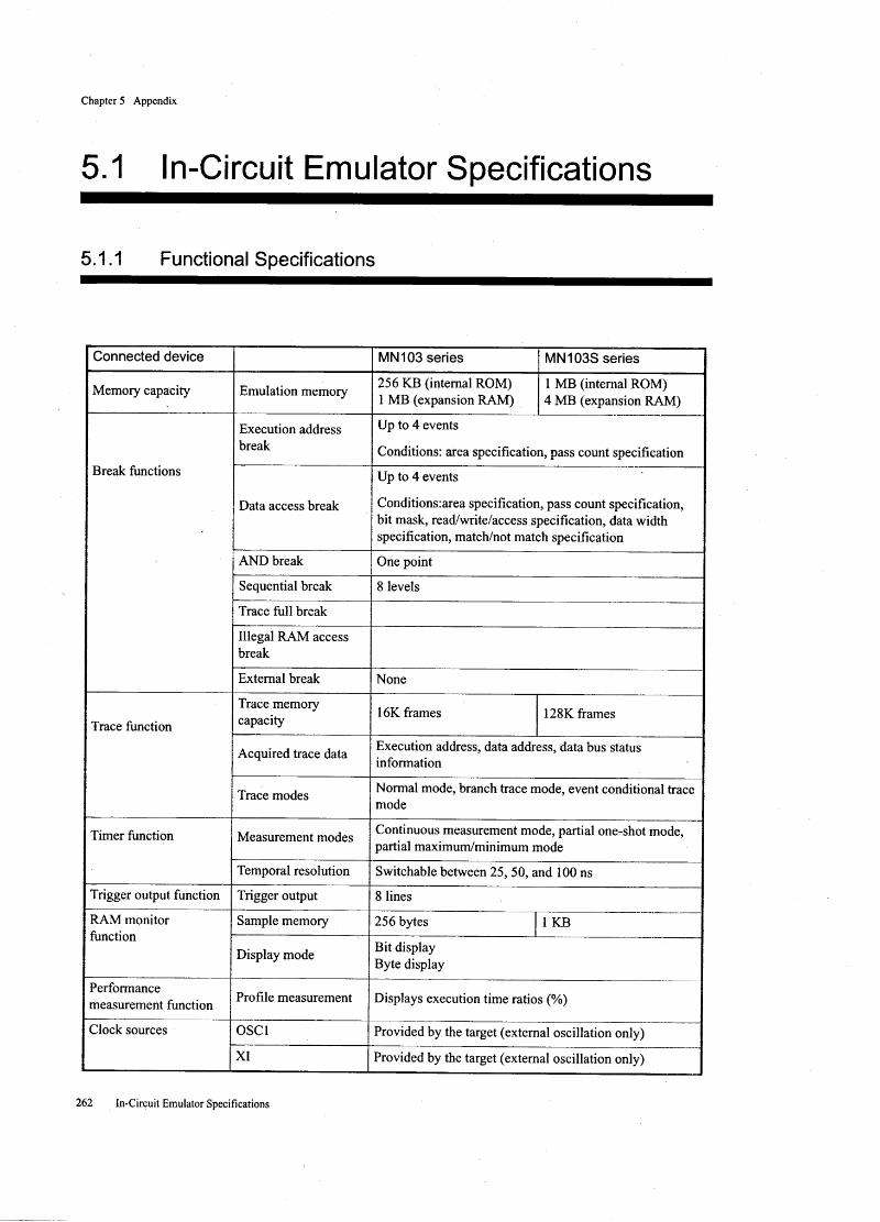
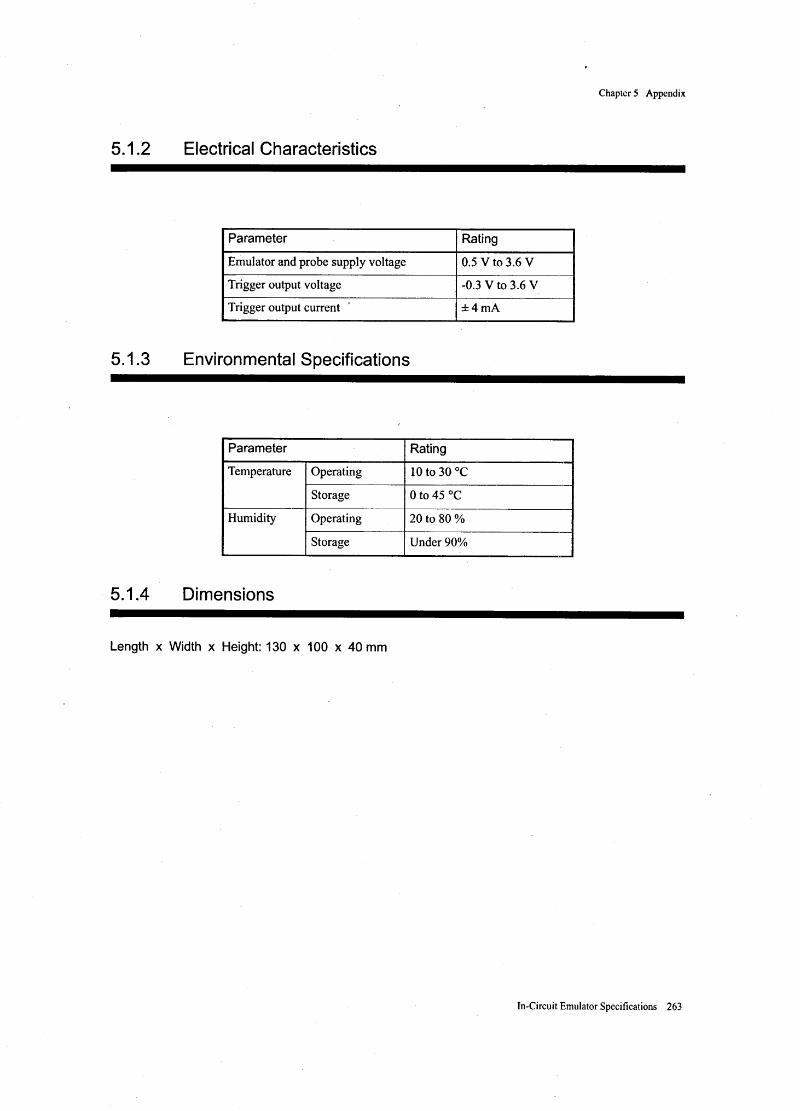
No.SS07-23SC2-0E - 1 - In-Circuit Emulator MN103SC2 Product Name Product Number Note ICE PX-ICE103SC2 In-circuit Emulator Specification ICE dimensional drawing (when connected to the target) Cable PX-CBL-PAD103S Emulator Controller PX-PAD-103S Power supply box Common to MN103S series. Dummy target PRB-EX-DMY103SA5/A7/C2 Needed when debugging software with a stand-alone ICE. (Joint screws for socket are sold separately.) Socket joint screw MS-5 Option Probe PX-OPT-103S Common to MN103S series. PX-IFC-PCC-6 Compliant with PCMCIA Ver2.1/JEIDA Ver4.2. Interface PX-IFC-PCI-6 Compliant with PCI2.1 of PCI-SIG standard. When using the Low Profile PCI with small-footprint PC's, replace the bracket by the provided one. PX-SDX103S00-0P0* PanaX Series Debugger Debugger PX-DBF103S00-0P0* DebugFactory® Builder C Compiler/Assembler PX-ICC103S00-0P0* MN103SC2 ICE OPTION Product Name Product Number Note 396 pin PGA socket PX-ADP-MEP396S Target connection adapter PX-ADP44QF10-103-YQ-K01 Instruction

Welcome message from author
This document is posted to help you gain knowledge. Please leave a comment to let me know what you think about it! Share it to your friends and learn new things together.
Transcript

No.SS07-23SC2-0E
- 1 -
In-Circuit Emulator MN103SC2
Product Name Product Number Note
ICE PX-ICE103SC2
In-circuit Emulator Specification
ICE dimensional drawing
(when connected to the target)
Cable PX-CBL-PAD103S
Emulator Controller PX-PAD-103S Power supply box
Common to MN103S series.
Dummy target PRB-EX-DMY103SA5/A7/C2Needed when debugging software with a stand-alone ICE.
(Joint screws for socket are sold separately.)
Socket joint screw MS-5
Option Probe PX-OPT-103S Common to MN103S series.
PX-IFC-PCC-6 Compliant with PCMCIA Ver2.1/JEIDA Ver4.2.
Interface
PX-IFC-PCI-6
Compliant with PCI2.1 of PCI-SIG standard.
When using the Low Profile PCI with small-footprint PC's,
replace the bracket by the provided one.
PX-SDX103S00-0P0* PanaX Series Debugger Debugger
PX-DBF103S00-0P0* DebugFactory® Builder
C Compiler/Assembler PX-ICC103S00-0P0*
MN103SC2 ICE OPTION Product Name Product Number Note
396 pin PGA socket PX-ADP-MEP396S
Target
connection adapter PX-ADP44QF10-103-YQ-K01 Instruction

No.SS07-23SC2-0E
- 2 -
PX-ICE103SC2 PX-CBL-PAD103S
PX-PAD-103S PRB-EX-DMY103SA5/A7/C2
MS-5 PX-OPT-103S

No.SS07-23SC2-0E
- 3 -
PX-IFC-PCC-6 PX-IFC-PCI-6
PX-ADP-MEP396C PX-ADP44QF10-103-YQ-K01


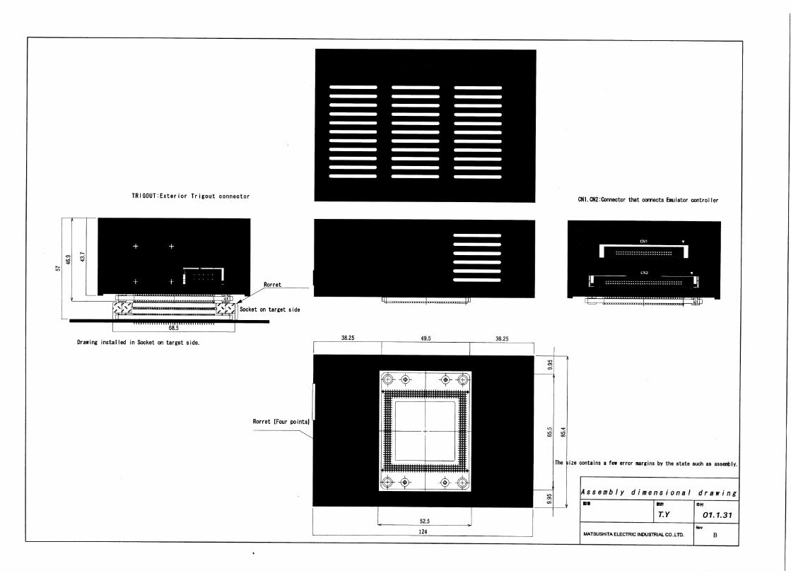

1
124
28.3
9.95
26.3
43.7
29
24
85.4
Emulator controller( PX-PAD-103S )
Target board
20
12 12
Target board
Flexible cableKC200-50N
44pin-10mm : PX-ADP44QF10-103-YQ-K01
TOP
SIDE
BOTTOM
( Unit : mm )
1pin
A1
MN103S-Emulator
9.95
9.95
9.95
49.5
135 (Reference)
Emulator controller( PX-PAD-103S )
Emulator controller( PX-PAD-103S )
Apr 14 , 2008
Adapter boardPX-EX103S-044/048-01-44
Target socket boardEXB044SA-PA(4 screws included)
<Sold separately>Socket from TOKYO ELETECH CORPORATION- NQPACK044SA or NQPACK044SA-SL
22
25
MN103S Emulator Target conversion adapter Dimension / Connection diagrams
Replace screws (with spacers and rubber feet) included in the set.
Conversion boardPX-EX103S-100/80(4 screws included)
Software & Solutions Development CenterCorporate System LSI Development DivisionSemiconductor CompanyMatsushita Electric Industrial Co., Ltd.
Panasonic
PanaXseries MN103S
20
2016
S/N. 06X-31E-566A1-103S

2
Set name : PX-ADP44QF10-103-YQ-K01Supported package: QFP 44pin-10mm squareSupported product: MN103SFC2A, MN103SFC2D (As of October 2006)Components:1.Conversion board n=1 *
(PX-EX103S-100/80, No.PB04019A1 )2.Joining screw n=4 *3.Adapter board (PX-EX103S-044/048-01-44) n=14.50-signals flexible cable (KC200-50N) n=15.Target socket board (EXB044SA-PA) n=16.Screw for the target socket board n=4 *7.Screw (with a spacer and a rubber foot) n=4 *
MN103S Emulator Target conversion adapter Components
7.Screw (with a spacer and a rubber foot)
4.50-signals flexible cable (KC200-50N)
3.Adapter board(PX-EX103S-044/048-01-44) 5.Target socket
board(EXB044SA-PA)
6.Screw for the target socket board
- This adapter requires a socket from TOKYO ELETECH CORPORATION separately.Product number:
- NQPACK044SA or NQPACK044SA-SL (Supported for 44pin-10mm square)“-SL” indicates that a long screw for fixing the target is included.
For details (size, foot pattern, etc.) of connector, refer to the website of TOKYO ELETECHCORPORATION.
http://www.tetc.co.jp/e_index.htm
* : Common in the series of MN103S emulator adapter.
Software & Solutions Development CenterCorporate System LSI Development DivisionSemiconductor Company Matsushita Electric Industrial Co., Ltd.
1.Conversion board( PX-EX103S-100/80,
No.PB04019A1)2.Joining screw
44pin-side
Apr 14 , 2008S/N. 06X-31E-566A1-103S

3
MN103S Emulator Target conversion adapter Installation
*1*2
*2*2
7. Fix the adapter board (PX-EX103S-044/048-01-44) on the conversion board.
9. Connect the flexible cables withthe conversion board and the target socket board.
10. Installation has been completed.
Ex) Target board
8. Screw NQPACK (Sold separately) and the target socket board.
(Note the corner cut)
*1*2
1. Replace screws on the bottom surface of the emulator housing byscrews with spacers and rubberfeet.
2. The screws have been replaced. 3. Insert the longer side of joining screws into the
emulator housing.
4. Put the conversion board on the joining screws. (Make sure to join the mark ”A1”)
5-1. Tighten the rear two screws evenly.
5-2. Tighten the front two screws evenly.
Alternate5-1 and 5-2
6. The conversion board has been installed if there is no space.
Note:*1 When connecting parts, make sure to join the marks "1 pin" and "A1" respectively. *2 Special attentions should be paid to needle-points of YQPACK and the conversion board
not to bend or break them.Software & Solutions Development CenterCorporate System LSI Development DivisionSemiconductor CompanyMatsushita Electric Industrial Co., Ltd.
Apr 14 , 2008S/N. 06X-31E-566A1-103S

4
MN103S Emulator Target conversion adapter Clock diagram
OSCI
Emulator Target board
X34
Z34C2
C1
X1(Chip)
X2(Lead)
JP2
JP1
OSC1
JP3
Adapterboard
- Circuit diagram (Example: MN103SFC2A, MN103SFC2D)
Flexible cable
Conversion board
Target socket board
-OSCI or OSCO from the target board is disabled.The emulator uses oscillators or resonators on the conversion board. The clock from the target board can use by short with solder.
-Neither oscillator/ resonator nor condenser is included with shipment. Prepare parts as needed.
- Short JP1-JP3 with solder depending on your parts.- Recommended parts
X1 : Ceramic resonator (Chip) :Murata Manufacturing Co., Ltd. CSTCE**MOG52-R0 (** : **MHz)
X2 : Ceramic resonator (Lead) :Murata Manufacturing Co., Ltd. CSTLS**MOG53-B0 (** : **MHz)Crystal unit : Kyocera Corporation HC-49/U-S
OSC1: Clock crystal oscillator : Kyocera Corporation FXO-31FC1 : Condenser :1608 typeC2 : Condenser :1608 type
Parts(ex. Crystal unit, Condenser)
Software & Solutions Development CenterCorporate System LSI Development DivisionSemiconductor CompanyMatsushita Electric Industrial Co., Ltd.
- Ceramic resonator (Chip)
4 31 2
C1OSC1
JP1
JP2JP3
X2
X1
C2
BOTTOM VIEW
CN1
R3
U3
AM
Z34(OSCI)
X34(OSCO)
- Clock crystal oscillator
4 31 2
C1
OSC1
JP1
JP2 JP3
X2
X1
C2
CN1
U3
AM
Z34(OSCI)
X34(OSCO)
BOTTOM VIEW
- Crystal resonator (Lead)
4 31 2
C1OSC1
JP1
JP2JP3
X2
X1
C2Z34(OSCI)
CN1X34(OSCO)
R3
U3
AM
BOTTOM VIEW
Solder
MCU
OSCO
OSCI
X34
Z34
U3
R3
U3
R3
OSCO
2 13 4
Apr 14 , 2008S/N. 06X-31E-566A1-103S

5
Emulator
MCU
Target board
VDD
5.0V
VDD2
1.8V
C7
R
VSS
C10 C9
C5C4
C8
C3
VDD5.0V
VDD2
VSS
VDD5.0V
VSS
R
MN103S Emulator Target conversion adapter Power supply / GND diagrams
Reserve
ReserveOFF
- Short VDD3 and VSS on the conversion board and those on the target with short thick wires respectively.
- No condenser is included with shipment. Prepare parts as needed.- Feature of condenser
3.5mm x 2.8mm : C3 , C4 , C5 , C6 , C7 , C81608 type : C9, C10 (C1 , C2)
Software & Solutions Development CenterCorporate System LSI Development DivisionSemiconductor CompanyMatsushita Electric Industrial Co., Ltd.
- Circuit diagram (Example: MN103SFC2A, MN103SFC2D)
Conversion board
Adapterboard
Flexible cable Target socket
board
Short(wire)
Short(wire) Test pin
(red)
Test pin(black)
Test pin(yellow)
VSS forEmulator
USR pin = 44 pins
: Regulator
VDD21.8V
・・・・
・・・・
・・
・・・・
・・・・
・・
4 31 2
C1
OSC1
JP1
JP2JP3
X2
X1
C2
BOTTOM VIEW
+ +
・・・・・・・
・・・・・・・
・・・・・・・
・・・・・・・
C3 C4
・・・・
・・・・
・・
・・・・
・・・・
・・
+
+
+
C7 C10
C6
C5
C8C9 +
CN1 CN2
VDD VSS
VDD2
VDDVSS
VDD2A
C
E
G
J
9 7 5 3 1
B
D
F
H
- Parts allocation on the conversion board
A1
To target VDDTo target GND
To target GND
C6
Reserve
Reserve
Emulator1.8V
S/N. 06X-31E-566A1-103S Apr 14 , 2008
Related Documents


