IN CA CLECTRONIC DIVICES ASSZF 110 *77—liZ _ ml k ~ I _ END 2 -78 I I I 1

Welcome message from author
This document is posted to help you gain knowledge. Please leave a comment to let me know what you think about it! Share it to your friends and learn new things together.
Transcript
IN CA CLECTRONIC DIVICES
ASSZ F 110 *77—liZ
_ mlk~ I
_
END
2 -78 I
I
I
1
~ •
I I________________ 8
I 25 ~D I .4
-
/0000
D D CJAW 29 1978 (III
U~~~~~~ j~ jyJA
-~
I ( ( ~~~~I I 1 I( ~~~~~~~~~~~~~~~~~~~~~~~~~~~~~~~~~~~~~~~~~
r ~~~~~~ _ _ _ _I Appro ’v.d to. public rs~e a iDi.~i~vtãc~ Unlimitsd
O~ Rockwell Internat ional
i / ’ i(~) P’1
C/ - ---
~~~~~~~~~~ — -
~
ADVANCED SEMICONDUCTOR TECHNOLOGYFOR ALTERNATE ENERGY SOURCES — D-C io A-c ~4VERTER S
p’~C
- —---—-~
15 Nov...nii~~ ~~77-
~~~~~~~~~~~ T~~~~e~~~~~~~~~~~T/KI
~~nLrJ
(il~X 7? i~~
‘- D D C~
t t ~~~ AlternaU;e Fnergy Sources
// 1 ~~~~~~~~
y,. 5—7 Deco,.~ h~ . 1977 ULX Miami Beach, ~~~~~~~~~~~~‘ ‘
THE DISTRIBUTION OF THIS REPORT ISUNLIMITED
Rockwell Internat ionalElectronic Dsvlcss DivisionElectronics Riuser*. Cents.
3370 M.r&oma Avifl ueP0 Boi4162 C
Anahei m . Cah$o,n~a 92803 ci
ADVANCE D SEMICONDUCTOR TECHNO LOGyFOR ALTERNATE ENERGY SOURCES - D-C TO A-C IN VERTERS
C. T. KielnerRockwell Internationa l
Anaheim , CA 82803, USA
ABSTRACT
Alternate or advanced energy conversion methods frequently requi re d—c to a—cconversion since the energy output must be synchronized with an existing uti litygrid. The objective of thi s paper is to describe va rious preliminary system conceptsfor Interfacing advanced solid—state energy converters to the utility grid with asignificant potential for reducing Initial capital Investment.Recent ERDA sponsore d studie~~
1~~1~~~ve identified the solid-state d-c to a-c inverteras a key element for fu rther development . These studies indicated that an lnve rtersynchronized to the utility grid can di rectly transform solar phot ovoltaj c, arraygenerated energy to local load (residence) demand with any excess energy feedbackto the utility grid. Where the solar energy Is insufficient to supply the local load ,It is supplemented by the utility grid. Several key issues were identified in therefe renced studies. One of these involved the considerable weight and cost asso-ciated with the d-c to a—c Inverter/Transformer vs a Transformerless Inverter thatwould have “Float’ with respect to the power grid return. This paper addressesthi s issue as well as the anticipated solution to the problem using advanced semi-conductor technology.
Conside rable emphasis is placed on the expected technology/cost advantages whichcould be anticipated using recent breakthroughs in the area of A~ GaAs/GaAs photo-voltaic materials by means of the CVD processl3,4J and Planar Solar Concentrators(PSC’s)15J . As an example, a combined photovoltaIc/f n~rerter system has beenpostulated to pro vide peak load sharing using utility grid feedback as suggested byStater-Goradftz . 16J
The primary emphasis of thi s paper Is placed on the d-c to a-c inverter technologyIntegrated into an overall alternate energy system. The objecti ve being to (a) mini-mize initial capital cost , (b) maximize energy conservation , and (C) defe r utilitycapital Com mitments .
1. INTRODUCTIO N
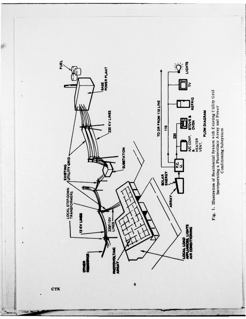
Recent studies (”2 1 sponsored by E RDA/NASA concluded, among othe r things , thatthe most economic configuration for a Photovoltafc Residential Prototype Systemwould omit local load storage (batteries) in favor of utility grid feedback. Figure 1illustrates how an Ideal system of this type might Finction. The flow diagramIllust rates a photovoltaic array interfacing through a power conditioning unit to thelocal load and the utility grid. The introduction of large numbers of systems wouldresult in a displacement of fuel consumption and also result In considerable energyconservation. Fundamentally, there is no reason why a system of this type cannotbe placed in operation now except for the high initial cost .
1CTK
~~~~~~~~ ~~~~
—
~~~~~~~~~~~~
—
~~~~~~~~~~~~~~~
-
—
—-
— --~~~~~ — I
Energy management techniques may have to be developed in order to optimize thestability and contro l of the utility network , however , this should not be a limitation .Significan t capital defe rment might be achieved in area s where peak power demandduring the summer months can be attributable largely to running 220 V air condition-ing comp ressor systems during peak insola tion periods. }lectr ic SpaCe h ia t ing doesnot appear economical compared to a thermal system which might be considered aspa rt of the photovoltaic arr ay l~ l .
It should be pointed out that rugged and reliable light-weight photovolta ic arraysoffe r one of the most attractive means for retrofitting existing residences to theut i lization of Solar energy conversion , hence, excessive weight build -up for athermal heating system could be counter-productive , although forced air ductingmight be one way of ove rcoming high weight .
Recent advances in makin g sola r photovo ltaic cells from A2GaA~ /GaA s (Gall iumArsenide ) usi ng the Chemical Vapo r Deposition (CVD) proccssl3i has opened furtheroppo rt u nities to accele rate development of low -cost photovoltaic arrays. GalliumArsenide photovolta ic cells are cha racte rized by Increased output with temperaturesup to 100°C which makes thi s type of device extremely attractive for Solar arraysusing concentratio n. 171
A very recent breakth rough in multip le -dye Plana r Solar Concent rators (PSC ’s)suggest s that up to a 100:1 concent ration ratio would be obtainable with a 0.75 con-version efficiencyi5~ Combining the GaA s CVD process for fabricat i ng photovolta icst rips with the PSC’s cou rn provide a very low-cost system. Given that an arraycould be fabricated at a reasonable cost , it would also have to include a d-c to a-cin ver te r for synchronization to the utility grid. It is conceivable that this invertercould be extremely light weight using advanced semiconductor technolo gy , such as ,power field effect transisto rs (Power FET ’s). The cont rols for this inve rter canbe readi ly programmed in advanced microprocessor chips at very low cost. Thefollowi ng sections will discuss these aspects in more detail.
ii. trr i~rr~ GRID FEEDBACK
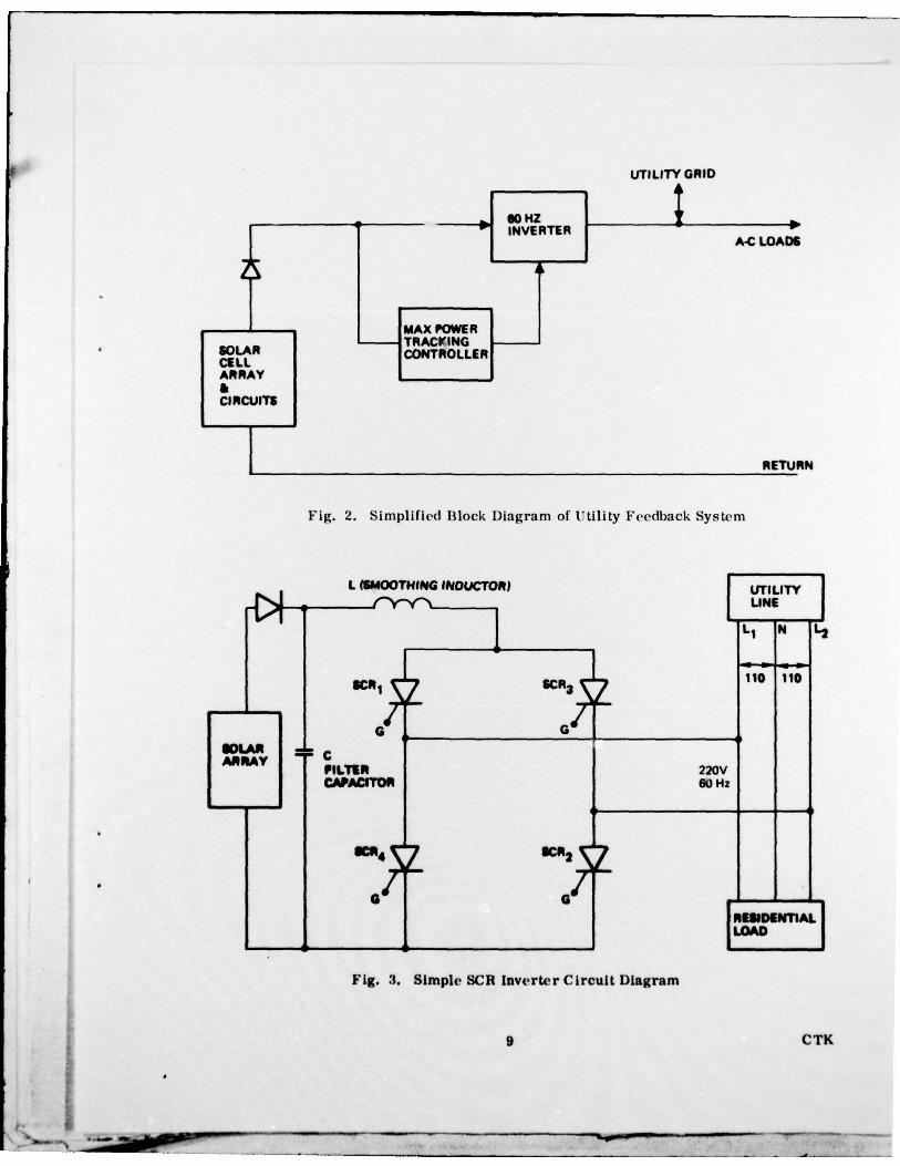
FIgure 2 illustrates a flow diagram for utilit y gri d feedback. ~Vhen the sola r arraypower output capability allow s the inverter output power to exceed the house loaddema nd the excess power flows back into the ut i lity gri d which , in fact , would causethe Watt-Ho ur meter to reverse di rection and in theory , the homeow ner would beselling power to the utility company ! Aside from the economic implications of thistechnique, ‘evera l technical aspects must be examined. One of these Involves thetype of d-c to a-c conversion that is implemented. Simple d— c to a-c convertersconvert a d—c voltage to a squarewave of a-c voltage . The squa rewave is rich inha rmonies , and al though a single photovoltalc syste m (— 10kW ) feeding a 10 MWgrid will have a negligible effect on overall line dist ortion , ma ny such systems canhave a serious effect on line voltage quality and can have adverse effects on inductionmot ors and other reactive loads that “heat up ” from 3rd , 5th , etc. , ha rmonics. Itis safe to assume tha t a sinewave d-c to a-c inverter would be prefe rable , and inthe case of widespread usage , mandatory . Present sinewave inverter s used asstandby uninterruptable power sources (UPS’s) a re heavy (100 lb/IiVA) and expensive($1000/k W) due In large pa rt to the reactive components (Transformers , Inductors ,and Capacitors). The semiconductors (SCH ’s and Rectifiers) are light , and alt houghinitia lly expensive ($100/kW) have been decreasing in cost due to the highly
2
_____________ ___________________________
competitive and automation-intensive nature of the modern semiconductor Indust ry .It is this semiconductor area of progress that offers the best hope for drasticallyreducing the cost of d-c to a-c inverters which could be produced without using re-active components.
Present SCR inve rters requi re L-C networks for commutation and current smoothingas shown in FIg. 3. For a 10kW system (gene rally accepted size for residentialusage) the smoot hi ng inductor would be on the order of 30 ml! and “ eigh abou t 70 lb.The commutati ng capacitor would be on the order of 1500 to 3000 ~F and of compa r-able weight . Bot h of these components use Copper , Al umin um , Tin and high-grademagnetic mate rial which presently averages (In the agg regate) of around $2 /lbwitho ut labor. In addition , the se are labor intensive components that require con-side rable man ual effo rt . Quality con t rol standards must also be high. It is evident ,there fore , tha t an all semiconductor d-c to a-c inve rter would eliminate the needfor these baseline cost component s and there fo re, open the door for a truly low—costsystem .
Substituting transisto rs for the SCR’s in Fig. 3 would not eliminate the need forind uctor L, or capacitor C since the line voltage basically perfo rm s the commuta-tion process. What is required then ? The answer is that an all-electronic alternateof Fig. 3 must be developed which would use advanced semiconductor technologyusing a new system configu ration. This postulated system Is discussed in the nextsection.
III . POSTULATED SYSTEM
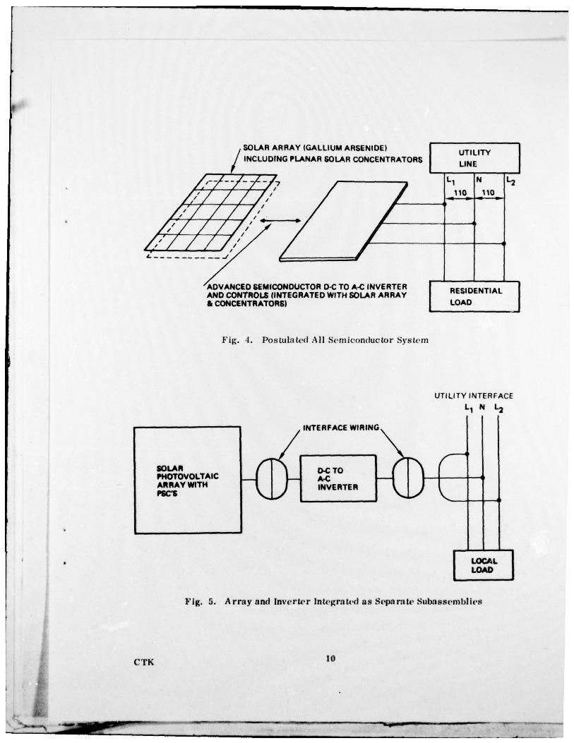
Thi s all semicond uctor system is Illustrated in Fig. 4. The system would operateas follows:
(1) The Solar ar ray would produce a d-c voltage which would be switched insection s by the cont rols in the advanced d-c to a-c converter to producesinusoidal waveforms which would closely duplicate the utility linevoltage . This would be accomplished by using an adva nced microprocessorcirc uit which would monitor (a) the utility line voltage , (b) the character is—tics of the residential load , and (c) the solar array output (includingma ximum power tr ack ing )afld the status of all internal switching circuitry .
(2) Whe n the control circuits establish that the a rray power can be trans-formed to the load and utility interface , the properly phased and synchro-ni zed a-c power from the arra y will be graduaily applied.
(3) Since tu rn-on and turn-off transients caused by refrige rators could bedamagi ng to the elect ronics, semiconductor surge a rrestors would alsobe int roduced as well as ligh tningand heavy duty utility power surgea rrestors (MOV’ s). Also , the heavy transient loads will be supplied bythe utility line since these do not contribute to appreciable energy lossbut would cause the d-c to a-c lnverter to be overdesigned for line andload surges.
3CTK
I L _ _ _ _ _ _ _ _ _ _ _ _ _ _ _ _
—...~~~~~
—I fl_i
— — ________________________________________________

(4) When solar insolation is minimum (at night), the array power would notbe available and the inverter would disconnect from the power line . Duringpeak insolati on period s, the heat In the planar sola r concentrator (Con-cent ration Ratio of 100 to 1) combined with heat loss in the inverter (about5 percent of the inverted power would result in heating) could easily bedissipated by free convect ion prov ided the re is air space between the roofand the assembly. If the heat were to be used for space heating, it wouldprobably be most effective to use lightweight aluminum tubing to air-coolthe array and augment the air conditioning or heating units with conventionalair compressors.
Although this postulated system could probably be used In a wide variety of climato-logical locations , it appears more likely to be the most cost effective where airconditioning costs are high and escalating. The two most likely locations areSouthern Florida and Phoenix , Arizona. The lightweight structure and fairly highdisplacement of electrical energy could be particularly appealing to mobile homeowners. One problem may arise however. The peak demand for air conditioningcan extend beyond the insolation period . This could require some local energystorage. Storage can be justified only if the utility offers an attractive Inducement(peak power rates) or If there are tax benefits. A new law signed recently byGovernor Brown of California allow s up to a 55 percent State Income Tax deduction(Itemized to a maximum of $3000) for solar or alternate energy equipment.
Similar laws at the Federal level could provide the wherewithal to convert manyexisting fixed income homeowners with a system of the type described he rein. Ifwe assume that the economic environment for such a system were to be viable , itis also necessary to consider some of the other requirement s that would drive thedesign , in particula r , integrating the d-c to a-c converter system with the residenceand the utility.
lv . INTEGRATiON OF THE D-C TO A-C INV ER TEH
The first rule to be observed in this effo rt must address the Initial capital cost ofthe system. The planar solar concentrator should reduce the effective cost of theGallium Arsenide Photovoltaic Array by roughly a factor of 25. Recent advancesin Chemical Vapor Deposition of AOGaAs/GaAs Indicates that cells with up to a20 percent conversion efficiency might be fabricated in mass production at costsof $2. 50 to $5. 00/peak W. A 25 to 1 reduction over cost due to the PSC techniquewould result in an overall array cost of 10~ to 20w/peak W, or $100 to $200/peakkW. The all solid-state d-c to a-c inverter could easily fall in the same category.
• Since this is still very speculative , let us assume tha t an overall cost for theassembly shown In Fig. 4 came to aroun d $400/peak kW and one were to invest$4000 In this system (10 kW peak). As a result , one would have bought 10 peak kWwhich would tend to average a round 50 kWh per day during the summer months andsomewhat less in the winter. At 6w/kWh this is approximately $3. 00/day or about$90/mo to offset utility costs. If one assumes an average of $60/mo savings forthe year , thi s is a return of $720 in the first year. if the $4000 were borrowed at10 percent annua l int erest , the $400 of annual Interest would be the offset for payback by the energy with a net gain of $320/year . However , it should be pointed outthat the interest could also be a deductible expense and hence , for a 33 percentbracket this would add back another $133 to the $320 for a net return of $453/year.
4CTK
-~~~ -~~~~~~~~~ — -.— .— —--— --- — — —.-—-—-

There is no reason to believe that this system should not last at least 10 years andand possibly 20, hence it could be paid off early and simply reduce utility costs aftersay 3 to 5 years. Additiona l square footage could be purchased and hence , offsetmore non-renewable energy. The excess could then be sold by the utility for Elec-trolysis (Hydrogen production) or industrial use. Fortunately, it is possible forindust ry to adjust schedules to take advantage of peak energy availability and thismight be accomplished without signi ficant changes in the present work schedules.
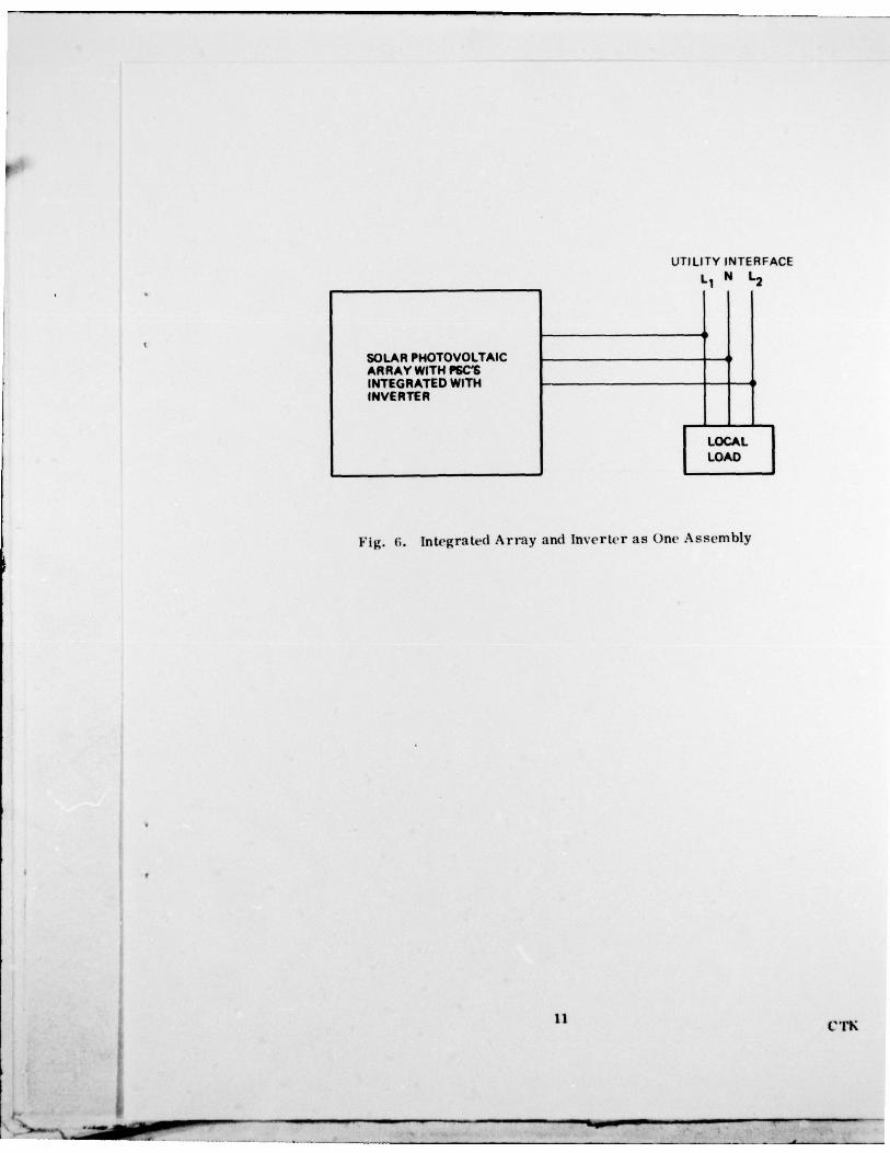
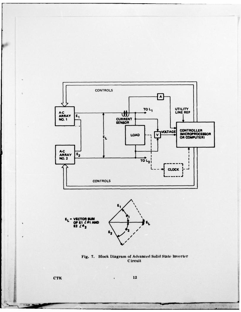
The re are two possible ways to integrate the d-c to a-c Inverter with the Solar arrayand utility grid in order to minimize initial capital investment. One method wouldtreat the d-c to a-c Inverter as a separate entity with appropriate wiring between thearray and the utility grid (as shown in Fig. 5) and the other would integrate the d-cto a—c inverter with the arra y (as shown in Fig. 6). The latter method holds themost promise since thi s reduces the wiring coats and is more amenable to automaticproduction of Array/Inverter. Figure 7 shows a block diagram of a simplifiedequivalent circuit recent ly patented by the author181 which can accomplish the result sintended for the confi gu ration shown in Fig. 6.
The block diagram Illustrates how the array can be subdivided to provide isolatedd—c sou rce to semiconductor bridge circuits which can be con t rolled by a micro-processor to produce two or more quasi-sine waves (or other wave forms) whichare then added vector ially to provide a variable amplitude which is also cont rolledby the microprocessor (or othe r type of computer) to synchronize the a-c output tothe utility line. Either bipolar transistors or field effect transistors can be usedto perfo rm the switchi ng. Protective devices such as , semiconductor surge arrestorscan be included to prevent damage to the array/inverter by utility power surges orlocal load transients. The most significant aspect of thi s techni que would be theabsence of heavy and expensive reactive component s coupled with a lightweight ,highly producible set of ha rdware.
V. KEY ISSUES
Before advanced semiconductor technology can be extensively applied to AlternateEnergy sources, several key issues must be resolved. Some of these issues aregiven as follows:
(1) The opt imum energy payback period
(2) The optimum cost payback period
• (3) The target initIal cost to the customer vs the number of units thatcould be produced and sold
(4) Isolation/Sa fety and protection of the Array/Inverter and pe rsonnel.
(5) Incentives for the semiconductor manufacture r to enter this areaof business.
5
CTK
S — — - - --—-- - - —--— —-— — —e7— ~-~_--
~~~~~~~~~ -T-fl • .rr rV
At present , these issues are being addressed by various individuals , agencies andindustries on a piecemeal basis. As an overall National (or international) energypolicy takes shape, it should be possible to channel the highly Inventive and costreduction processes established by the semiconductor indust ry to provide aninnovative , utilizable source of alternate energy (such as photovoltalc) which couldbe readily Integrated int o the existing electrical networks.
Vi. SUMMARY
As a result of thi s prelimina ry study, it is evident that advanced semiconductortechnology can provide significant breakthroughs in cost and an early realization ofsolar energy displacement of non-renewable fuel. Utility grid feedback and light-weight photovoitaic collectors using advanced semiconductor technology appear to bevery compatible with existing residences and utili ty networks. The use of galliumarsenide photovoltaic semiconductor material and multiple—dye planar solar concen-trators may provide a signi ficant reduction in array cost. Present d-c to a-c invertersare too costly, however , by using advanced semiconductor technology and greatlyreducing or avoiding reactive component s can provide a significant lowering of initialcapital investment . The pape r outline s one of several ways such a system might bearranged provided the key Issues associated with energy policy can be resolved.
VII. RE FERE NCES
1. “Definition Study for Photovoltaic Residential Prototype System ” byN. F. Shepard Jr. , R. La ndes and W. Kornrumpf , C. E. Doc. No.76SDS4225 prepared for ERDA/NASA under Cont ract No. NAS3- 19769.
2. “Definition Study for Photovoitaic Residential Prototype System ” byM. S. Imamura , II. Hulstrom and C. Cookson , Martin MariettaReport No. MC-76-394 prepared for E RDA/NASA under Contract No.NAS3- 19768.
3. “HIgh-Efficiency GaAfAs/GaA s Heterostruct u re Sola r Cells Grown byMetalorgani c Chemical Vapor Deposition” by R. D. Dupuls , P. D. Dapkus ,R . D. Yingli ng, and L. A. Moudy, Applied Physics Letters ~‘ol 31No. 3 1 August 1977 pp 201-203.
4. “Preparation of Epitaxial InP Film from Triethylindium and P113, ”dated July 1, 1977 by H. M. Manesevit and K. L. h ess, 19t h ElectronicMaterial Confe rence , lih lca , NY , June 28-July 1, 1977.
5. “Photon Trapping and Energy Transfe r In Multiple-Dye PlasticMatrices: An Efficient Solar-Energy Concentrator” by 13. A. Sw art z ,T. Cole, and A. H. Zewail of A. M. Noyes Laboratory of ChemicalPhysics Cal Tech, Pasadena , CA, Optics Letters, Vol 1 No. 2 ,August 1977 pp 73 -75.
6. “An Integrated Photovoltaic/Thermal High Intensity Solar EnergySystem (u SES) Concept for Residential Applications” by B. L. Saterand C. Goradln , 11th lntersociety Energy Conversion Confe rence , Vol 11pp 1316—1323 , September 12-17, 1976.
6CTK
4
— • • 0*~~~ —-
~~~
- —
~
-
—~
7. “Terrestrial Photovoltaic Power Systems with Sunlight Concentration ”by College of Engi neering and Applied Sciences , Arizona State Uni versity.Report ERC-R-760 14 prepa red for Sandia Laboratories under Cont ractNo. 02-7850.
8. “Di stribution System for a—c Electrical Energy Derived from d-c EnergySources” 4 , 052 , 657 issued Octobe r 4 , 1977 , Kleiner et. al. Assignedto Rockwell International.
CT I(
0I-
o w . E .9 .~o I- i--<Z
~~~~~ &D
~
\\\\
> ~~d1~~~~ flJ
IIIt I 1~_ _ _ _ _
h ~~~~~~~~~~~~~~~~~~~~~~~~
ii Ii8
CTK
______________________________________ ________ -____••.p— -
- -~
UTILITY GRID
_ _ _ _ _ _ _ _ _ _ _ _ _ _ _ _ _ _ _ 10HZ _ _ _ _ _ _ _ _ _ _ _ _ _ _ _ _ _ _
I ~1 INVERTE R
I A C LOADS
•
MAX POWERTRACWIPIG• CO$TROLLER
ARRAY ___________
&CIR CUITS
~1 RETURN
Fig. 2. Simplified Block Diagram of Ut i l i ty Feedback System
L (SMOOTHING INDUCTOR) ui-u.rrvNE
I I PILTER I[_. J ~ pAcrToR 10Hz
ICR2
0 0RESIDENTIALLOAD
Fi g. 3. Simple SCR Inverte r Circuit Diagram
9 CTK
- - -
SOLA R ARRAY (GALLIUM ARSENI DE) UTI LITY
L1 N L2110 110
~~ ~~~~~~~~
INCLUDING PLANAR SOLAR CONCENTRATORS L LINE____ J
L J
~~~~ANCED SEMICONDUCTOR D~ TO A~~ INVERTER r RESIDENTIALAND CONTROL.$ (INTEGRATED WITH SOLAR ARRAY -]& CONCENTRATORS) LOAD
Fi g. 4. Postula ted All Semiconducto r System
UTILITY INTERFACEL1 N L2
INTERFACE W1RING
SOLARPHOTOVOLTAICARRAY WiTH INVERTERPSC.S
LL0AD IFig. 5. Arra y and Invt ’rter Integra ted as Sepa ra te Subassemblies
k CTK 10
H-i _ _ _ _ _ _ _ _ _ _ _ _
p
UTILITY INT ERFACE
_ _ _ _ _ _ _ _ _ _ _ _ _ _ _
L 1 N 1.3
SOLAR PHOTOVOLTAIC _________________ —
ARRAY WITH PSCSIN TEGR ATE D WITH — —
INVERTER
T LOCAL
_______________________ [~ LOAD
Fig. 6. Integra ted Array and Inverte r as One Assembly
I 11 C l’K
—- -~~~~~~~~~~-~~ -
-
-.~~~~ - .
-- ~— -~ -~A
It CONTROLS
A
I A.C _ _ _ _ _ _ LINE REF
ARRAYNO. 1 i—
TO L1 UTILITY
CURRENT ______ - ______SENSOR
VOLTAGE CONTROLLERLOAD -
~~ v (MICROPROCESSORI OR COMPUTER)
___________________________________ II _ _
I ARRAY_ _ _ _ _ _ _ _ _ _ _ _ _ _ _
INO. 2 TOL~~
-- CLOCKI S
CONTROLS
L
K~
’A
1
’
Oil
op ii L#i *a~o12 LO 3 2 .‘£
3
/
Fig. 7. Block Dia gra m of Advanced Solid State Inverte rCircuit
CTK • 12
p. 1!
_____________________
_______________________________________________________________—
_1__ -- --- __Iw-.-- —
-.
- —
Related Documents


