Freescale Semiconductor Hardware User Guide for i.MX53 Quick Start Board, Preliminary Rev 0.9 i PUBI – Public Use Business Information Hardware Reference Manual for i.MX53 Quick Start i.MX53 Quick Start Board Take your Multimedia Experience to the max semiconductor freescale TM

Welcome message from author
This document is posted to help you gain knowledge. Please leave a comment to let me know what you think about it! Share it to your friends and learn new things together.
Transcript

Freescale Semiconductor
Hardware User Guide for i.MX53 Quick Start Board, Preliminary Rev 0.9 i PUBI – Public Use Business Information
Hardware Reference Manual for i.MX53 Quick Start
i.MX53 Quick Start Board Take your Multimedia
Experience to the max
semiconductor freescale TM

Freescale Semiconductor
Hardware User Guide for i.MX53 Quick Start Board, Preliminary Rev 0.9 ii PUBI – Public Use Business Information
How to Reach Us: Home Page: www.freescale.com E-mail: [email protected] USA/Europe or Locations Not Listed: Freescale Semiconductor Technical Information Center, CH370 1300 N. Alma School Road Chandler, Arizona 85224 +1-800-521-6274 or +1-480-768-2130 [email protected] Europe, Middle East, and Africa: Freescale Halbleiter Deutschland GmbH Technical Information Center Schatzbogen 7 81829 Muenchen, Germany +44 1296 380 456 (English) +46 8 52200080 (English) +49 89 92103 559 (German) +33 1 69 35 48 48 (French) [email protected] Japan: Freescale Semiconductor Japan Ltd. Headquarters ARCO Tower 15F 1-8-1, Shimo-Meguro, Meguro-ku, Tokyo 153-0064, Japan 0120 191014 or +81 3 5437 9125 [email protected] Asia/Pacific: Freescale Semiconductor Hong Kong Ltd. Technical Information Center 2 Dai King Street Tai Po Industrial Estate Tai Po, N.T., Hong Kong +800 2666 8080 [email protected] For Literature Requests Only: Freescale Semiconductor Literature Distribution Center P.O. Box 5405 Denver, Colorado 80217 1-800-441-2447 or 303-675-2140 Fax: 303-675-2150 [email protected]
Information in this document is provided solely to enable system and software implementers to use Freescale Semiconductor products. There are no express or implied copyright licenses granted hereunder to design or fabricate any integrated circuits or integrated circuits based on the information in this document. Freescale Semiconductor reserves the right to make changes without further notice to any products herein. Freescale Semiconductor makes no warranty, representation or guarantee regarding the suitability of its products for any particular purpose, nor does Freescale Semiconductor assume any liability arising out of the application or use of any product or circuit, and specifically disclaims any and all liability, including without limitation consequential or incidental damages. “Typical” parameters that may be provided in Freescale Semiconductor data sheets and/or specifications can and do vary in different applications and actual performance may vary over time. All operating parameters, including “Typicals”, must be validated for each customer application by customer’s technical experts. Freescale Semiconductor does not convey any license under its patent rights nor the rights of others. Freescale Semiconductor products are not designed, intended, or authorized for use as components in systems intended for surgical implant into the body, or other applications intended to support or sustain life, or for any other application in which the failure of the Freescale Semiconductor product could create a situation where personal injury or death may occur. Should Buyer purchase or use Freescale Semiconductor products for any such unintended or unauthorized application, Buyer shall indemnify and hold Freescale Semiconductor and its officers, employees, subsidiaries, affiliates, and distributors harmless against all claims, costs, damages, and expenses, and reasonable attorney fees arising out of, directly or indirectly, any claim of personal injury or death associated with such unintended or unauthorized use, even if such claim alleges that Freescale Semiconductor was negligent regarding the design or manufacture of the part. Learn More: For more information about Freescale products, please visit www.freescale.com. Freescale™ and the Freescale logo are trademarks of Freescale Semiconductor, Inc. All other product or service names are the property of their respective owners. © Freescale Semiconductor, Inc. 2011. All rights reserved.

Freescale Semiconductor
Hardware User Guide for i.MX53 Quick Start Board, Preliminary Rev 0.9 iii PUBI – Public Use Business Information
Hardware Reference Manual for i.MX53 Quick Start
Table of Contents 1. Introduction .......................................................................................................................................... 1
1.1. i.MX53-QUICK START Board Overview ......................................................................................... 1
1.2. i.MX53-QUICK START Board Kit Contents ..................................................................................... 2
2. List of Acronyms .................................................................................................................................... 3
3. Specifications ........................................................................................................................................ 4
3.1. i.MX535 Processor ........................................................................................................................ 4
3.2. DDR3 DRAM Memory ................................................................................................................... 7
3.3. Dialog DA9053 PMIC ..................................................................................................................... 7
3.4. MicroSD Card Slot (J4) ................................................................................................................... 8
3.5. SD Card Slot (J5) ............................................................................................................................ 8
3.6. SATA 7-pin Data Connector (J7) .................................................................................................... 8
3.7. VGA Video Output (J8) .................................................................................................................. 8
3.8. LVDS Video Output (J9) ................................................................................................................. 9
3.9. Ethernet (J2B)................................................................................................................................ 9
3.10. Dual USB Host Connector (J2A) ................................................................................................. 9
3.11. Micro-B USB Device Connector (J3) ........................................................................................ 10
3.12. Audio Input/Output (J6/J18) ................................................................................................... 10
3.13. 5V Power Connector (J1)......................................................................................................... 10
3.14. Debug UART Connector (J16) .................................................................................................. 11
3.15. JTAG Connector (J15) .............................................................................................................. 11
3.16. Expansion Header (J13) ........................................................................................................... 12
3.17. User Interface Buttons ............................................................................................................ 12
3.18. User Interface LED Indicators .................................................................................................. 13
3.19. Optional Li-ION Batter Connector (J14) .................................................................................. 14
3.20. Optional Back-Up Coin Cell posts (JP1, JP2) ............................................................................ 14
3.21. PCB Shorting Traces ................................................................................................................ 15
4. Quick Start Board Connectors and Expansion Port............................................................................. 15
4.1. Wall 5V Power Jack (J1)............................................................................................................... 16
4.2. RJ45 Ethernet Connector (J2B) ................................................................................................... 17
4.3. VGA DB15 Connector (J8) ........................................................................................................... 18
4.4. Debug UART DB9 Connector (J16) .............................................................................................. 19
4.5. Headphone Output Connector (J18) ........................................................................................... 20
4.6. Microphone Input Connector (J6) ............................................................................................... 21

Freescale Semiconductor
Hardware User Guide for i.MX53 Quick Start Board, Preliminary Rev 0.9 iv
PUBI – Public Use Business Information
4.7. Dual USB Host Jack (J2) ............................................................................................................... 22
4.8. micro-B USB Device Connector (J3) ............................................................................................ 23
4.9. SATA 7-pin Data Connector (J7) .................................................................................................. 24
4.10. SD Card Connector (J5) ........................................................................................................... 25
4.11. microSD Card Connector (J3) .................................................................................................. 26
4.12. 20-pin ARM JTAG Connector (J15) .......................................................................................... 27
4.13. LVDS Connector (J9) ................................................................................................................ 28
5. Quick Start Board Architecture and Design ........................................................................................ 29
5.1. 5V Power Supply ......................................................................................................................... 30
5.2. Dialog DA9053 PMIC ................................................................................................................... 31
5.2.1. Quick Start Power Rails ....................................................................................................... 33
5.2.2. Li-ION Battery Charging ...................................................................................................... 35
5.2.3. Backlight LED Driver ............................................................................................................ 35
5.2.4. Touch-Screen Operation ..................................................................................................... 36
5.2.5. Miscellaneous ..................................................................................................................... 36
5.3. 3.2V Secondary Voltage Regulator ............................................................................................. 38
5.4. i.MX53 Applications Processor ................................................................................................... 39
5.4.1. Peripheral Module Logic Voltage Levels ............................................................................. 39
5.4.2. Boot Mode Operations and Selections ............................................................................... 41
5.4.3. Clock Signals ........................................................................................................................ 48
5.4.4. i.MX53 Internal Regulators ................................................................................................. 49
5.4.5. Watch Dog Timer ................................................................................................................ 49
5.5. DDR3 SDRAM Memory ................................................................................................................ 51
5.6. Micro SD Card Connector ............................................................................................................ 52
5.7. Full Size SD Card Connector ........................................................................................................ 53
5.8. VGA Video Output ....................................................................................................................... 54
5.9. LVDS Video Output...................................................................................................................... 55
5.10. Expansion Port ........................................................................................................................ 56
5.11. Audio ....................................................................................................................................... 57
5.12. Ethernet .................................................................................................................................. 58
5.13. USB Host connections ............................................................................................................. 59
5.14. SATA ........................................................................................................................................ 60
5.15. Debug UART Serial Port........................................................................................................... 61
5.16. JTAG Operations ...................................................................................................................... 62
6. Connector Pin-Outs ............................................................................................................................. 63

Freescale Semiconductor
Hardware User Guide for i.MX53 Quick Start Board, Preliminary Rev 0.9 v
PUBI – Public Use Business Information
Hardware Reference Manual for i.MX53 Quick Start
7. Board Accessories ............................................................................................................................... 80
7.1. HDMI Daughter Card ................................................................................................................... 80
7.2. LCD Display Daughter Card ......................................................................................................... 82
7.3. LVDS Display Set (Coming Soon) ................................................................................................. 84
8. Mechanical PCB Information .............................................................................................................. 86
9. Board Verification ............................................................................................................................... 88
10. Troubleshooting .............................................................................................................................. 92
10.1. PMIC Voltage Rail Test Points ................................................................................................. 93
11. Known Issues ................................................................................................................................... 95
12. PCB Component Locations .............................................................................................................. 96
13. Schematics .................................................................................................................................... 101
14. Bill of Materials ............................................................................................................................. 115
15. PCB information ............................................................................................................................ 122

Freescale Semiconductor
Hardware User Guide for i.MX53 Quick Start Board, Preliminary Rev 0.9 vi PUBI – Public Use Business Information
List of Figures
Figure 1. DC Power Jack …………………………………………………………………………………………………………… 16
Figure 2. RJ45 Ethernet Connector……………………………………………………………………………………………. 17
Figure 3. VGA Connector………………………………………………………………………………………………………….. 18
Figure 4. Debug UART Connector…………………………………………………………………………………………….. 19
Figure 5. Headphone Output Connector………………………………………………………………………………….. 20
Figure 6. Microphone Connector (J6) …………………………………………………………………………………….. 21
Figure 7. Dual USB Host Connectors (J2) ……………………………………………………………………………….…. 22
Figure 8. micro-B USB Device Connector (J3) ………………………………………………………………………….. 23
Figure 9. SATA Data Connector (J7) ………………………………………………………………………………………… 24
Figure 10. SD Card Connector (J5) …………………………………………………………………………………………….. 25
Figure 11. microSD Card Connector (J4) ……………………………………………………………………………………. 26
Figure 12. JTAG Connector (J15) ……………………………………………………………………………………….….…… 27
Figure 13. LDVS Connector (J9) ……………………………………………………………………………………..…….…….. 28
Figure 14. i.MX53 Smart-Start Block Diagram…………………………………………………………………………….. 29
Figure 15. Board Main Power Circuit. ……………………………………………………………………………………….… 30
Figure 16. Boot Mode Resistor Locations TOP…………………………………………………………………………….. 46
Figure 17. Boot Mode Resistor Locations BOTTOM…………………………………………………………………….. 47
Figure 18. Clock Source Locations………………………………………………………………………………………………. 48
Figure 19. Watch Dog Timer Reset Trigger…………………………………………………………………………………. 50
Figure 20. Power Jack (J1) …………………………………………………………………………………………………………. 64
Figure 21. Micro-B USB Connector (J3) …………………………………………………………………………………….. 64
Figure 22. Ethernet/Dual USB Conn (J2) …………………………………………………………………………………… 65
Figure 23. Headphone Connector (J18) ……………………………………………………………………………………. 66
Figure 24. Microphone Connector (J6) ……………………………………………………………………………………. 66
Figure 25. VGA DB15 Connector (J8) …………………………………………………………………………………………. 67
Figure 26. LVDS Connector (J9) …………………………………………………………………………………………………. 68
Figure 27. SATA Data Connector (J7) …………………………………………………………………………………………. 69
Figure 28. SD Card Connector (J5) …………………………………………………………………………………………….. 70
Figure 29. microSD Card Connector (J4) ……………………………………………………………………………………. 71
Figure 30. Debug UART Connector (J16) ……………………………………………………………………………………. 72
Figure 31. JTAG Connector (J15) ……………………………………………………………………………………………….. 73
Figure 32. Expansion Port (J13) ……………………………………………………………………………………………….… 74
Figure 33. Optional HDMI Daughter Card…………………………………………………………………………………… 80
Figure 34. MCIMX28LCD 4.3” WVGA Display Daughter Card…………………………………………….………… 82
Figure 35. LVDS Display Kit………………………………………………………………………………………………………… 84
Figure 36. Quick Start Board Dimensions…………………………………………………………………………………… 86
Figure 37. Ethernet Loopback Cable………………………………………………………………………………………….. 91
Figure 38. Regulator Output Capacitor Positions Bottom………………………………………………………….. 93
Figure 39. Regulator Output Capacitor Positions Top………………………………………………………………… 94
Figure 40. Major Component Highlights Top…………………………………………………………………………….. 97

Freescale Semiconductor
Hardware User Guide for i.MX53 Quick Start Board, Preliminary Rev 0.9 vii PUBI – Public Use Business Information
Hardware Reference Manual for i.MX53 Quick Start
List of Figures (con)
Figure 41. Major Component Highlights Bottom………………………………………………………………………… 98
Figure 42. Assembly Drawing Top………………………………………………………………………………………………. 99
Figure 43. Assembly Drawing Bottom…………………………………………………………………………………………100
Figure 44. DC 5V INPUT……………………………………………………………………………………………….……………..102
Figure 45. MX53 POWER……………………………………………………………………………………………….……………103
Figure 46. MX53 DDR3 MEMORY…………………………………………………………………………………….………….104
Figure 47. MX53 CONTROL…………………………………………………………………………………………………………105
Figure 48. MX53 USB……………………………………………………………………………………………………….…………106
Figure 49. MX53 SD INTERFACE………………………………………………………………………………………….………107
Figure 50. MX53 AUDIO……………………………………………………………………………………………………….…….108
Figure 51. MX53 SATA…………………………………………………………………………………………………………..……109
Figure 52. MX53 VGA……………………………………………………………………………………………………………..….110
Figure 53. MX53 ETHERNET…………………………………………………………………………………………………….…111
Figure 54. EXPANSION HEADER……………………………………………………………………………………………….…112
Figure 55. DA9053 PMIC…………………………………………………………………………………………………………….113
Figure 56. DEBUG, ACCELEROMETER……………………………………………………………………………………….…114
Figure 57. Top Etch Layer…………………………………………………………………………………………………………..123
Figure 58. Second Etch Layer……………………………………………………………………………………………………..124
Figure 59. Third Etch Layer…………………………………………………………………………………………………………125
Figure 60. Fourth Etch Layer………………………………………………………………………………………………………126
Figure 61. Fifth Etch Layer………………………………………………………………………………………………………….127
Figure 62. Sixth Etch Layer………………………………………………………………………………………………………….128
Figure 63. Seventh Etch Layer……………………………………………………………………………………………………..129
Figure 64. Bottom Etch Layer………………………………………………………………………………………………………130
Figure 65. Soldermask Top………………………………………………………………………………………………………….131
Figure 66. Soldermask Bottom……………………………………………………………………………………………………132
Figure 67. Pastemask Top…………………………………………………………………………………………………………..133
Figure 68. Pastemask Bottom……………………………………………………………………………………………………..134
Figure 69. Silkscreen Top…………………………………………………………………………………………………………….135
Figure 70. Silkscreen Bottom………………………………………………………………………………………………………136

Freescale Semiconductor
Hardware User Guide for i.MX53 Quick Start Board, Preliminary Rev 0.9 viii PUBI – Public Use Business Information
List of Tables
Table 1. Regulator Timing Sequence…………………………………………………………………………………………32
Table 2. Quick Start Board Power Supply Rails…………………………………………………………………………33
Table 3. Port ID Resistor Values……………………………………………………………………………………………….36
Table 4. Module Voltage Supplies…………………………………………………………………………………………….40
Table 5. BOOT_MODE pin Settings………………………………………………………………………………………..…41
Table 6A. BOOT_CFG Word1……………………………………………………………………………………………………… 41
Table 6B. BOOT_CFG Word2……………………………………………………………………………………………………… 41
Table 6C. BOOT_CFG Word3……………………………………………………………………………………………………… 42
Table 7. Boot Mode Resistors TOP……………………………………………………………………………………………46
Table 8. Boot Mode Resistors BOTTOM…………………………………………………………………………………… 47
Table 9. DDR3 SDRAM Chip Organization………………………………………………………………………………… 51
Table 10. Micro-SD Card Boot Options……………………………………………………………………………………… 52
Table 11. Full Size SD Card Boot Options…………………………………………………………………………………… 53
Table 12. SATA Boot Mode Configuration Table. ……………………………………………………………………… 60
Table 13. Terminal Setting Parameters……………………………………………………………………………………… 61
Table 14. Power Jack (J1) …………………………………………………………………………………………………………. 64
Table 15. Micro-B USB Connector (J3) ………………………………………………………………………………………. 64
Table 16. Ethernet/Dual USB Conn (J2) ……………………………………………………………………………………..65
Table 17. Headphone Connector (J18) ……………………………………………………………………………………… 66
Table 18. Microphone Connector (J6) ………………………………………………………………………………………. 66
Table 19. VGA DB15 Connector (J8) …………………………………………………………………………………………. 67
Table 20. LVDS Connector (J9) …………………………………………………………………………………………………. 68
Table 21. SATA Data Connector (J7) …………………………………………………………………………………………. 69
Table 22. SD Card Connector (J5) ……………………………………………………………………………………………… 70
Table 23. microSD Card Connector (J4) ……………………………………………………………………………………. 71
Table 24. Debug UART Connector (J16) ……………………………………………………………………………………. 72
Table 25. JTAG Connector (J15) ……………………………………………………………………………………………….. 73
Table 26. Expansion Port (J13) …………………………………………………………………………………………………. 74
Table 27. Expansion Port Pin-Mux Table……………………………………………………………………………………. 76
Table 28. Board Stack up information………………………………………………………………………………………… 87
Table 29. Problem Resolution Table………………………………………………………………………………………….. 92
Table 30. Output Capacitors and Values BOTTOM…………………………………………………………………….. 93
Table 31. Output Capacitors and Values TOP……………………………………………………………………………. 94

Freescale Semiconductor
Hardware User Guide for i.MX53 Quick Start Board, Preliminary Rev 0.9 1
PUBI – Public Use Business Information
Hardware Reference Manual for i.MX53 Quick Start
1. Introduction
This document is the Hardware Reference Manual for the i.MX53 Quick Start board based on the
Freescale Semiconductor i.MX53 Applications Processor. This board is fully supported by Freescale
Semiconductor. This Manual includes system setup and debugging, and provides detailed information
on the overall design and usage of the i.MX53 Quick Start board from a Hardware Systems perspective.
1.1. i.MX53-QUICK START Board Overview
The Quick Start Board is an i.MX535 platform designed to showcase many of the most commonly used
features of the i.MX535 Applications Processor in a small, low cost package. The MCIMX53-START is an
entry level development board and a near perfect subset of its larger sister board, the MCIMX53SMD,
which is available as a full, near-form factor tablet. Developers can start working with code on the
Quick Start board, and then port it over to the SMD Tablet if additional features are desired. This gives
the developer the option of becoming familiar with the i.MX535 Applications Processor before investing
a large amount or resources in more specific designs. Features of the i.MX53 Quick Start board are:
Processor: Freescale Applications Processor MCIMX535DVV1B
DRAM Memory: Micron 8Gb DDR3 SDRAM MT41J128M16HA-187E:D
PMIC: Dialog Semiconductor DA9053
Mass Storage: 5 in 1 SD/MMC/SDIO Card Connector
microSD Card Connector
7-pin SATA Data Connector
Video Output: 15-Pin D-Sub VGA Connector
30-Pin LVDS Connector
Ethernet: RJ-45 Connector for 10/100 Base-T
USB: Dedicated HS USB 2.0 Standard-A Host Connector
Shared HS USB 2.0 Standard - Host and Micro-B Device Connectors
Audio Connectors: 3.5mm Stereo Head Phone output
3.5mm Mono-Microphone input and Mono Head Phone (right channel) output
Power Connectors: 5V mm Barrel Connector
Debug Connectors: 9-Pin D-Sub Debug UART Connector
20-Pin Standard ARM JTAG Connector
Expansion Header: 120-Pin Header (Populated) to Support 1 of the following:
Optional HDMI Output Daughter Card (orderable)
Optional WVGA and WQVGA LCD Display Daughter Cards (orderable)
Camera Daughter Card (custom)
SDIO Based WiFi Daughter card (custom)

Freescale Semiconductor
Hardware User Guide for i.MX53 Quick Start Board, Preliminary Rev 0.9 2
Freescale Confidential Propietary – NDA Required
User Interface Buttons: Power, Reset, 2 User-Defined Buttons
Indicators: 8 Status LEDs – External Power, PMIC ON, Fault Condition, and more
Li-ION Battery Connector: 3-Pin Header (unpopulated) for Li-ION Battery for Low Power Operation
Coin Cell: Connection point for 2-Pin Coin Cell (unpopulated) for RTC Operation
PCB: 3.0 inch x 3.0 inch (76.2 mm x 76.2 mm), 10 - layer board
1.2. i.MX53-QUICK START Board Kit Contents
The i.MX53-Quick Start Board comes with the following items:
� i.MX53-QUICK START Board
� microSD Card preloaded with Ubuntu Demonstration Software
� USB Cable (Standard-A to Micro-B connectors)
� 5V/2.0A Power Supply
� Quick Start Guide
� Documentation DVD
1.3. i.MX53 Quick Start Board Revision History
� Rev A – Proof of Concept
� Rev B – Prototype (Internal Freescale Development)
� Rev C – Production (Silicon: i.MX53 Rev 2.0, DA9053 Rev AA)
The board version will be printed on a label, usually attached to the top of the SD Card Connector (J5).
The board version will be the letter designation following the schematic revision:
SCH-26565 REV C

Freescale Semiconductor
Hardware User Guide for i.MX53 Quick Start Board, Preliminary Rev 0.9 3
PUBI – Public Use Business Information
Hardware Reference Manual for i.MX53 Quick Start
2. List of Acronyms
The following acronyms will be used throughout this document.
AC97 - Audio Codec ‘97
CMC - Common Mode Choke
CODEC - Compression/Decompression
DDR - Double Data Rate
DNP - Do Not Populate
HDMI - High Definition Multimedia Interface
I2C - Inter-Integrated Circuit
I2S - Integrated Interchip Sound
IC - Integrated Circuit
IDE - Integrated Debug Environment
LAN - Local Area Network
LCB - i.MX53 Smart-Start
LCD -Liquid Crystal Display
LPDDR2 - Low Power DDR2
MMC - Multi Media Card
PMIC - Power Management Companion IC
RMII - Reduced Media Independent Interface
RTC - Real-Time Clock
SDRAM - Synchronous Dynamic Random Access Memory
SD - Secure Digital
SPI - Serial Peripheral Interface
SSI - Synchronous Serial Interface
ULPI - UTMI Low Pin Interface
USB - Universal Serial Bus
UTMI - Universal Transceiver Macrocell Interface
WDOG - Watch Dog
WLAN - Wireless LAN

Freescale Semiconductor
Hardware User Guide for i.MX53 Quick Start Board, Preliminary Rev 0.9 4
Freescale Confidential Propietary – NDA Required
3. Specifications
3.1. i.MX535 Processor The i.MX535 Applications Processor (AP) is based on ARM Cortex-A8
TM Platform, which has the following
features:
• MMU, L1 Instruction and L1 Data Cache
• Unified L2 cache
• Target frequency of the core (including Neon, VFPv3 and L1 Cache): 1.0 GHz
• Neon coprocessor (SIMD Media Processing Architecture) and Vector Floating Point (VFP-Lite)
coprocessor supporting VFPv3
• TrustZone
The memory system consists of the following components:
• Level 1 Cache:
− Instruction (32 Kbyte)
− Data (32 Kbyte)
• Level 2 Cache:
− Unified instruction and data (256 Kbyte)
• Level2 (internal) memory:
− Boot ROM, including HAB (64 Kbyte)
− Internal multimedia/shared, fast access RAM (128 Kbyte)
− Secure/non-secure RAM (16 Kbyte)
• External memory interfaces:
− 16/32-bit DDR2-800, LV-DDR2-800 or DDR3-800 up to 2 Gbyte
− 32 bit LPDDR2
− 8/16-bit NAND SLC/MLC Flash, up to 66 MHz, 4/8/14/16-bit ECC
− 16-bit NOR Flash. All WEIMv2 pins are muxed on other interfaces (data with NFC pins).
I/O muxing logic selects WEIMv2 port, as primary muxing at system boot.
− 16-bit SRAM, cellular RAM
− Samsung One NANDTM
and managed NAND including eMMC up to rev 4.4 (in muxed I/O
mode)
The i.MX53 system is built around the following system on chip interfaces:
• 64-bit AMBA AXI v1.0 bus – used by ARM platform, multimedia accelerators (such as VPU, IPU,
GPU3D, GPU2D) and the external memory controller (EXTMC) operating at 200 MHz.
• 32-bit AMBA AHB 2.0 bus – used by the rest of the bus master peripherals operating at 133
MHz.
• 32-bit IP bus – peripheral bus used for control (and slow data traffic) of the most system
peripheral devices operating at 66 MHz.
The i.MX53 makes use of dedicated hardware accelerators to achieve state-of-the-art multimedia
performance. The use of hardware accelerators provides both high performance and low power
consumption while freeing up the CPU core for other tasks.

Freescale Semiconductor
Hardware User Guide for i.MX53 Quick Start Board, Preliminary Rev 0.9 5
PUBI – Public Use Business Information
Hardware Reference Manual for i.MX53 Quick Start
The i.MX53 incorporates the following hardware accelerator:
• VPU, version 3 – video processing unit
• GPU3D – 3D graphics processing unit, OpenGL ES 2.0, version 3, 33 Htri/s, 200 Mpix/s, and 800
Mpix/s z-plane performance, 256 Kbyte RAM memory.
• GPU2D – 2D graphics accelerator, OpenVG 1.1, version 1, 200 Mpix/s performance.
• IPU, version 3M – image processing unit
• ASRC – asynchronous sample rate converter
The I.MX53 includes the following interfaces to external devices:
NOTE
Not all the interfaces are available simultaneously depending on I/O
multiplexer configuration.
• Hard disk drives:
− PATA, up to U-DMA mode 5, 100 MByte/s
− SATA II, 1.5 Gbps
• Displays:
− Five interfaces available. Total rate of all interfaces is up to 180 Mpixels/s, 24 bpp. Up to
two interfaces may be active as once.
− Two parallel 24-bit display ports. The primary port is up to 165 Mpix/s (for example,
UXGA @ 60 Hz).
− LVDS serial ports: one dual channel port up to 165 Mpix/s or two independent single
channel ports up to 85 MP/s (for example, WXGA @ 60 Hz) each.
− TV-out/VGA port up to 150 Mpix/s (for example, 1080p60).
• Camera sensors:
− Two parallel 20-bit camera ports. Primary up to 180-MHz peak clock frequency,
secondary up to 120-MHz peak clock frequency.
• Expansion cards:
− Four SD/MMC card ports: three supporting 416 Mbps (8-bit i/f) and one enhanced port
supporting 832 Mbps (8-bit, eMMC 4.4)
• USB
− High-speed (HS) USB 2.0 OTG (up to 480 Mbps), with integrated HS USB PHY
− Three USB 2.0 (480 Mbps) hosts:
� High-speed host with integrated on-chip high speed PHY
� Two high-speed hosts for external HS/FS transceivers through ULPI/serial,
support IC-USB

Freescale Semiconductor
Hardware User Guide for i.MX53 Quick Start Board, Preliminary Rev 0.9 6
Freescale Confidential Propietary – NDA Required
• Miscellaneous interfaces:
− One-wire (OWIRE) port
− Three I2S/SSI/AC97 ports, supporting up to 1.4 Mbps, each connected to audio
multiplexer (AUDMUX) providing four external ports.
− Five UART RS232 ports, up to 4.0 Mbps each. One supports 8-wire, the other four
support 4-wire.
− Two high speed enhanced CSPI (ECSPI) ports plus one CSPI port
− Three I2C ports, supporting 400 kbps.
− Fast Ethernet controller, IEEE1588 V1 compliant, 10/100 Mbps
− Two controller area network (FlexCAN) interfaces, 1 Mbps each
− Sony Philips Digital Interface (SPDIF), Rx and Tx
− Enhanced serial audio interface (ESAI), up to 1.4 Mbps each channel
− Key pad port (KPP)
− Two pulse-width modulators (PWM)
− GPIO with interrupt capabilities
− Secure JTAG controller (SJC)
The system supports efficient and smart power control and clocking:
• Supporting DVFS (Dynamic Voltage and Frequency Scaling) and DPTC (Dynamic Process and
Temperature Compensation) techniques for low power modes.
• Power gating SRPG (State Retention Power Gating) for ARM core and Neon
• Support for various levels of system power modes.
• Flexible clock gating control scheme
• On-chip temperature monitor
• On-chip oscillator amplifier supporting 32.768 kHZ external crystal
• On-chip LDO voltage regulators for PLLs
Security functions are enabled and accelerated by the following hardware:
• ARM TrustZone including the TZ architecture (separation of interrupts, memory mapping, and so
on)
• Secure JTAG controller (SJC) – Protecting JTAC from debug port attacks by regulating or blocking
the access to the system debug features.
• Secure real-time clock (SRTC) – Tamper resistant RTC with dedicated power domain and
mechanism to detect voltage and clock glitches.
• Real-time integrity checker, version 3 (RTICv3) – RTIC type 1, enhanced with SHA-256 engine
• SAHARAv4 Lite – Cryptographic accelerator that includes true random number generator (TRNG)
• Security controller, version 2 (SCCv2) – Improved SCC with AES engine, secure/nonsecure RAM
and support for multiple keys as well as TZ/non-TZ separation.
• Central Security Unit (CSU) – Enhancement for the IIM (IC Identification Module). CSU is
configured during boot and by e-fuses and determines the security level operation mode as well
as the TrustZone (TZ) policy.
• Advanced High Assurance BOOT (A-HAB) – HAB with the next embedded enhancements:
SHA-256, 2046-bit RSA key, version control mechanism, warm boot, CSU and TZ initialization.
Freescale Semiconductor
Hardware User Guide for i.MX53 Quick Start Board, Preliminary Rev 0.9 7
PUBI – Public Use Business Information
Hardware Reference Manual for i.MX53 Quick Start
3.2. DDR3 DRAM Memory
The i.MX53-Quick Start board uses four 2-Gigabit DDR3 SDRAM ICs manufactured by Micron for a total
onboard RAM memory of 1 GigaByte. The SDRAM data width for each IC is 16-bits. The chips are
arranged in pairs that are controlled by each of the two chip select pins to form 32-bit words for the
i.MX53 CPU. On Die Termination (ODT) functionality has been implemented on the board, as well as the
ability to separate out the I/O Voltage Supply from the main SDRAM Voltage Supply if desired.
3.3. Dialog DA9053 PMIC
The DA9053 device is a small (7 x 7 mm, 0.5mm pitch) 169 ball VFBGA that provides nearly all power
supply functions for the Quick Start board. The following is a feature list of the major functionality
provided by the DA9053 PMIC for the Quick Start board:
• Power Supply resources:
o 12 Low Drop Out (LDO) regulators
� 1 for internal PMIC purposes only (LDOCORE)
� 1 for charging optional back up coin cell
� 10 for platform needs
o 4 DC/DC Buck Converters (3 with DVS)
� 1 for the ARM Core supply (VBUCKCORE)
� 1 for the Peripheral Core supply (VBUCKPRO)
� 1 for the external SDRAM memory (VBUCKMEM)
� 1 for the internal cache memory (VBUCKPERI)
o 1 White LED driver and boost converter
• Li-ION battery Charger
• Resistive touch screen interface
• Expansion Port Card ID detect
• Wall voltage supply over-voltage protection
• 1 HS-I2C interface
• External LDO regulator enable

Freescale Semiconductor
Hardware User Guide for i.MX53 Quick Start Board, Preliminary Rev 0.9 8
Freescale Confidential Propietary – NDA Required
3.4. MicroSD Card Slot (J4)
The microSD Card slot is used as the primary means to boot the Quick Start board. The power source for
the microSD Card slot is VLDO3_3V3. The microSD Card slot is not normally configured with a card
detect feature. The MicroSD Card slot can be configured to boot from a MMCmicro card with an
alternate boot option setting (see section on Boot Options).
3.5. SD Card Slot (J5)
The SD Card slot is a 5-in-1 SD/MMC connector that acts as a secondary external memory media slot.
The power source for the SD Card Slot is the auxiliary LDO regulator (DCDC_3V2). The SD Card slot can
be configured as the boot source with an alternate boot option setting, as well as being configured for
either SD or MMC card operation (see section on Boot Options). The SD Card Slot supports full 8-bit
parallel data transfers and can support SDIO cards (WiFi, BT, etc) designed to fit in a standard SD card
slot. The Quick Start board has specifically been tested with an Atheros SD-25 WiFi card.
3.6. SATA 7-pin Data Connector (J7)
The SATA connector provides the means to connect an external SATA memory device to the Quick Start
board. Commonly, this would be an External hard drive or a DVD/CD reader. Power for the SATA device
needs to be supplied externally by the user via a 12-pin power connector. It is possible to boot from a
SATA drive by making OTP fuse changes. Once the fuse changes are made, they cannot be reversed.
3.7. VGA Video Output (J8)
A standard VGA signal is output directly from the i.MX53 Processor with minimum external components
required. Power for the TVE module of the i.MX535 Processor is supplied by VLDO7 of the PMIC and is
set to 2.75V. If VGA output is not desired, it is possible to program the PMIC to turn off VLDO7 to
conserve power. The VGA output supports a variety of video formats up to 150 Mega-Pixels per second.
Level shifters are required on the Horizontal and Vertical Synchronization signals as well as the VGA I2C
communications signals in order to meet VGA specifications.

Freescale Semiconductor
Hardware User Guide for i.MX53 Quick Start Board, Preliminary Rev 0.9 9
PUBI – Public Use Business Information
Hardware Reference Manual for i.MX53 Quick Start
3.8. LVDS Video Output (J9)
The LVDS module of the i.MX53 Processor is connected to a 30-pin LVDS connector. While the i.MX53
Processor is capable of outputting to two separate LVDS displays, only one connector is pinned out on
the Quick Start board. The pin outs on the LVDS connector match the optional cable and 10” HannStar
LVDS display that can be purchased optionally from Freescale. The single LVDS connector will support
video formats up to 165 Mega-Pixels per second. The power source for the LVDS module is a switchable
output of the VBUCKPERI DCDC converter. This rail is shared with the SATA module and the USB module.
If these modules are not being used, the PMIC can be programmed to turn off power to these three
modules without affecting other 2.5V supplies to the remainder of the i.MX53 Applications Processor.
3.9. Ethernet (J2B)
The i.MX53 Processor Fast Ethernet Module outputs RMII formatted signals to an external Ethernet PHY.
The processor is capable of 10/100 Base-T speeds. The Quick Start board uses the SMSC LAN8720A
Ethernet Transceiver in a QFN-24 package. 3.2V power is supplied to the Ethernet IC from the external
LDO regulator. The output of the Ethernet PHY is connected to an RJ45 jack with integrated magnetic.
3.10. Dual USB Host Connector (J2A)
The USB module of the i.MX53 Processor provides two high speed USB PHYs that are connected to each
of the USB-A Host Jacks on connector J2. One PHY provides Host-only functionality and is connected to
the upper USB jack on the connector tower. The second PHY is USB 2.0 OTG capable and is connected to
the lower USB jack on the connector tower. Both jacks receive 5V power directly from the 5V Wall
Power Supply, via a FET that can be controlled by software, and a 1.1A Poly-fuse. The PMIC provides an
over-voltage functionality to limit voltage applied to the USB jack in the event that a DC Power Supply
other than the original supply provided is used. Also, there is no current regulating device to limit
current supplied to each jack, other than the Poly-fuse.
NOTE
The lower USB Host Jack is cross connected with the Micro-B USB Device connector. This was done as a
convenience to the user as cables with micro-A plugs are still uncommon at the time the board was
designed. The USB OTG PHY will switch to ‘device’ mode if a USB Host is attached to the micro-B
connector with a cable. This design is not recommended for release to the general electronics consumer
population. This board has not been tested for USB compliance.

Freescale Semiconductor
Hardware User Guide for i.MX53 Quick Start Board, Preliminary Rev 0.9 10
Freescale Confidential Propietary – NDA Required
3.11. Micro-B USB Device Connector (J3)
The micro-B USB connector is connected to the USB OTG PHY on the i.MX53 Processer, and is also
connected to the Lower USB Host Jack on the connector tower. The connector’s external USB 5V power
pin is connected to the USB_OTG_ID pin, which is normally pulled to ground via a 3.3K Ohm resistor.
When a powered USB Host device is attached to the micro-B USB connector, the USB_OTG_ID pin is
pulled high and sends a signal to the USB OTG PHY to operate in device mode. The connector’s external
USB 5V power pin is not connected to the PMIC, or any other power rails on the Quick Start board.
Therefore, it is not possible to supply power to the Quick Start board via the USB connections.
3.12. Audio Input/Output (J6/J18)
Analog audio input and output are provided by Freescale’s Low Power Stereo Codec, SGTL5000. The
audio codec is connected to the i.MX53 Applications Processor via 4-wire I2S communications, utilizing
the AUDMUX5 port of the processor. The audio codec’s Headphone Amp provides up to 58 mW output
to 16-Ohm headphones at a typical SNR of 98 dB and THD+N of -86 dB. Typical power consumption is
11.6 mW. In addition, the audio codec can perform several enhancements to the output including virtual
surround, added bass and three different types of equalization. The Microphone Input module of the
Stereo Codec is also used, with the microphone input connected to the tip pin of the Microphone Jack
(J6). Microphone Bias voltage is applied on the Quick Start board and not as a separate connection to
the Microphone Jack. If the user desires to use a combined microphone, mono headphone device, the
ferrite bead on L25 can be moved to the L22 pads, redirecting the right channel output to the
Microphone Jack. A 2.5mm to 3.5mm adapter may be necessary to convert the microphone, mono
headphone device to fit the Microphone Jack. On both the Headphone Jack and Microphone jack, a
fourth pin is used to detect the insertion of a plug into either jack. When a standard 3-pin device is
inserted into the 4-pin jack, the detect line is grounded, indicating to the i.MX53 Processor that the plug
has been inserted.
3.13. 5V Power Connector (J1)
A 2.0mm x 6.5mm barrel connector is used which should fit standard DC Plugs with an inner dimension
of 2.1mm and an outer dimension of 5.5mm. If an alternate power supply is used (not the original,
supplied power supply), it should supply no more than 5.25V / 3A output. If the PMIC senses too high
voltage at the connector input, it will turn off isolation FET Q1 to protect the Quick Start board. In
between the Power Connector and the isolation FET is a single blow, fast acting fuse to protect the
Quick Start board from an over current situation fault. If a Wall Power Supply is properly connected to
the Quick Start board, and the green 5V power LED indicator is not lit, it could mean that either the fuse
has been blown, or that the voltage output of the power supply is too high.

Freescale Semiconductor
Hardware User Guide for i.MX53 Quick Start Board, Preliminary Rev 0.9 11
PUBI – Public Use Business Information
Hardware Reference Manual for i.MX53 Quick Start
3.14. Debug UART Connector (J16)
UART1 of the i.MX53 Processor is connected to an RS-232 output to be used as a debug output for the
developer. The Transmit (TX) and Receive (RX) signals are sent through two 1.8V to 3.2V level shifters to
convert the logic signal voltages to the correct values for the Sipex SP3232 RS-232 transceiver. The CTS
and RTS signals are not used on the Quick Start board. The RS-232 transceiver receives its power from
the external 3.2V LDO Regulator. If the output of the regulator is turned off for power savings measures,
debug output will be lost.
If the designer wishes to use the port as an Applications UART Port, changes can be made in software to
reconfigure the port. A male-to-male gender changer can be used to properly convert the port.
To access the debug data output during development, connect the Debug UART Connector to a suitable
host computer and open a terminal emulation program (ie, Teraterm or HyperTerminal). Proper settings
for the terminal program are:
• BAUD RATE: 115,200
• DATA: 8 bit
• PARITY: None
• STOP BIT: 1-bit
• FLOW CONTROL: None
3.15. JTAG Connector (J15)
A standard 20-pin ARM JTAG connector is provided on the Quick Start board. Logic signals to the JTAG
connector are 1.8V signals. A 1.8V reference signal is provided to pin 1 of the connector so that the
attached JTAG tool can automatically configure the logic signals for the right voltage. If the JTAG tool
does not have an automatic logic voltage sense, make sure that the tool is configured for 1.8V logic.
JTAG tools that have been specifically tested with the Quick Start board are:
• JTAG Commander (Macraigor)
• DS-5 and RealView (ARM Ltd.)
• Trace32 (Lauterbach)
• J-Link (Segger/Codesourcery)
• J-Link (IAR)

Freescale Semiconductor
Hardware User Guide for i.MX53 Quick Start Board, Preliminary Rev 0.9 12
Freescale Confidential Propietary – NDA Required
3.16. Expansion Header (J13)
A 120-pin Expansion Port Header is provided on the Quick Start board for use with many optionally
expansion boards available from Freescale, or for custom designed boards made be the developer. At
the time of initial production, the following expansion boards are available from Freescale:
• MCIMXHDMICARD HDMI signal output daughter card
• MCIMX28LCD 4.3” WVGA Touch Panel LCD Display
The Expansion Port makes the following features of the i.MX53 Processor available to be used on a
custom built expansion card:
• Two Serial Peripheral Interfaces (SPI) CSPI, eCSDPI2
• Two I2S/SSI/AC97 Ports AUDMUX4, AUDMUX5
• Two Inter-Integrated Circuits (I2C) I2C1, I2C2
• 2 UARTs UART4, UART5
• SPDIF Audio
• USB ULPI Port USBH2
• 24-bit Data and display control signals
• Resistive Touch Screen Interface
• Various Voltage rails
3.17. User Interface Buttons
There are four user interface buttons on the Quick Start board. Their functionality is as follows:
POWER: In the ‘Power Off’ state, momentarily pressing the POWER button will begin the PMIC
power on cycle. The PMIC supplied voltage rails will come up in the proper sequence to
power the i.MX53 Processor. When the processor is fully powered, the boot cycle will be
initiated.
In the ‘Power On’ state, momentarily pressing the POWER button will send a signal to a
GPIO port for user defined action, but will not initiate a hardware shutdown.
In the ‘Power On’ state, holding the power button down for greater than 5 seconds will
result in the PMIC initiating a shutdown to the ‘Standby’ power condition. This will also
be the result from the ‘Power Off’ state as the PMIC will transition into the ‘Power On’
state and will still see the POWER button as held down.

Freescale Semiconductor
Hardware User Guide for i.MX53 Quick Start Board, Preliminary Rev 0.9 13
PUBI – Public Use Business Information
Hardware Reference Manual for i.MX53 Quick Start
RESET: Pressing the RESET button in the ‘Power On’ state will force the i.MX53 Applications
Processor to immediately turn off, and reinitiate a boot cycle from the Processor Power
Off state. The RESET button has no effect on the PMIC or the voltage rails.
Pressing the RESET button when the Quick Start board is powered off will have no
effect.
USERDEF1: These two buttons are user defined buttons attached to PATA_DATA14 (P6) for
USERDEF2: USERDEF1 and PATA_DATA15 (P5) for USERDEF2. The two GPIO pins are normally pulled
high by an internal resistor. The two buttons function by connecting the pins to ground,
thus inserting a low signal. The developer is left to determine the actions of these two
pins in code. Sample codes do not assign functionality to either pin.
3.18. User Interface LED Indicators
There are eight LED status indicators located next to the microSD card connector. These LEDs have the
following functions:
5V: The 5V status LED (D1) is a Green LED connected directly to the 5V_MAIN power rail.
This LED indicates that 5V wall power is being properly supplied to the Quick Start
board. If this light is not lit, it would indicate one of three problems:
1) Fuse F1 has been blown and needs to be replaced.
2) Voltage from the wall supply is greater than 5.5V and the over voltage
protection feature is disabling power to the board.
3) The DC Power supply is not plugged in or malfunctioning.
PMIC: The PMIC status LED (D9) is a Green LED gated by the PMIC SYS_UP signal from the
PMIC. This LED indicates that the PMIC is in the fully on condition and supplying power
to the processor and other voltage rails as directed by software.
USER: The User status LED (D16) is a Green LED gated by the PATA_DATA1 (L3) GPIO pin. The
developer is left to determine the action of this pin in code. Sample codes do not assign
functionality to the pin. The LED comes on by default when the processor starts up.
FLT: The FLT status LED (D14) is a Red LED gated by the NVDD_FAULT signal from the PMIC.
The LED will turn on anytime the PMIC is not outputting the requested voltages or when
the PMIC senses a fault condition and will begin to power down the voltage rails. This
may aid in trouble shooting power problems if both the PMIC and FLT LEDs are on at the
same time, it indicates that the PMIC is causing a shutdown based on a fault it has
sensed.
3.3V: The 3.3V status LED (D10) is a Blue LED gated by the External Regulator 3.2V power rail.
This power rail can be turned off by software for power savings measures. This LED
provides an easy visual recognition as to the status of this bus.

Freescale Semiconductor
Hardware User Guide for i.MX53 Quick Start Board, Preliminary Rev 0.9 14
Freescale Confidential Propietary – NDA Required
SATA: The SATA status LED (D11) is a Blue LED gated by the SATA_1V3 (VLDO5) power rail.
This power rail can be turned off by software for power savings measures. This LED
provides an easy visual recognition as to the status of this bus.
VGA: The VGA status LED (D12) is a Blue LED gated by the TVDAC_2V75 (VLDO7) power rail.
This power rail can be turned off by software for power savings measures. This LED
provides an easy visual recognition as to the status of this bus.
LCD: The LCD status LED (D13) is a Blue LED gated by the LCD_3V2 power rail.
Normally the LCD_3V2 power rail receives power directly from the DCDC_3V2 power
rail, but the LCD can also be configured to receive power from VIOHI_2V772 (VLDO4). In
the alternate voltage supply configuration, this LED will provide visual recognition as to
the status of the LCD bus.
3.19. Optional Li-ION Battery Connector (J14)
On the Quick Start board, there is a footprint (J14) available to solder a three pin wafer connector
(Molex 0530470310 or equivalent). This connector will mate to Li-ION batteries commercially available
as replacement batteries to commonly available MP3 players. The developer should make sure that the
polarity of the battery matches the polarity of the connector as replacement batteries may vary from
different manufacturers. When installed, a battery can be charged from the external 5V wall power
source. A battery will not be charged when only a USB cable is connected to the Quick Start board.
When powering a board from only a battery, the 5V power rail and the DCDC_3V2 power rail will not be
powered. Therefore, the Ethernet subsystem and Audio subsystem will not be operational under normal
board configurations. Depending on the battery capacity, it may be necessary to power down additional
subsystem voltage rails to extend battery life to a usable amount.
The battery charging feature is an autonomous operation of the Dialog DA9053 PMIC that does not
require software support. Battery charging may be prevented by software by making registry changes to
the PMIC. The developer may need to verify in software that PMIC registry settings are proper for
battery charging operations. The footprints for testing with a battery were included for skilled
developers looking to experiment.
3.20. Optional Back-Up Coin Cell posts (JP1, JP2)
On the Quick Start board, there are two through-holes (JP1 and JP2) next to the power connector. These
through-holes are positioned to hold a Lithium coin cell battery (Sanyo ML1220-VM1 or equivalent). For
proper operation, the coin cell posts should be soldered direction to the Quick Start board, with the
positive terminal connected to JP1 and the negative terminal connected to JP2. The DA9053 PMIC will
charge the coin cell when 5V Wall Power is available. When 5V Wall Power is removed, the coin cell will
provide power only to the RTC power rail (VLDO1) supplying power to the i.MX53 processor. The length
of time a coin cell can power the RTC subsystem may vary.

Freescale Semiconductor
Hardware User Guide for i.MX53 Quick Start Board, Preliminary Rev 0.9 15
PUBI – Public Use Business Information
Hardware Reference Manual for i.MX53 Quick Start
3.21. PCB Shorting Traces
On the Quick Start PCB, there are 29 sets of standard footprints with a copper trace between them to
short the two pads together. The PCB is produced with these pads unpopulated. These shorting traces
are placed throughout the PCB at locations in line with major power rails and critical components. The
purpose of these shorting traces it to allow the skilled developer to manually cut the trace between the
pads to either:
1) Isolate power to major subsystems or components.
2) Install small value precision resistors to measure current consumption of major subsystems.
3) Or reconfigure power sources to subsystems or components using wires soldered to the pads.
To restore a shorting trace back to normal after the trace is cut, it is only necessary to solder a Zero Ohm
resistor to the pads.
4. Quick Start Board Connectors and Expansion Port
The Quick Start board provides a number of connectors for a variety of inputs and outputs to and from
the board. The following subsections describe these connections in detail.

Freescale Semiconductor
Hardware User Guide for i.MX53 Quick Start Board, Preliminary Rev 0.9 16
Freescale Confidential Propietary – NDA Required
4.1. Wall 5V Power Jack (J1)
The 5V/2A AC-to-DC power supply that comes with the Quick Start board is plugged into the Power Jack
(J1) on the board as show in Figure 1. If the original power supply is lost, it is possible to use a substitute
power supply for the Quick Start board. Voltage above 5.5V, and below 12V, will trigger the Over-
Voltage protection circuitry on the board. It is not recommended to use a higher voltage since, in the
event of a failure to the protection circuitry, damage to the board will result. A voltage supply above 12V
will damage the PMIC part.
Figure 1. DC Power Jack
Power Jack (J1)
Freescale Semiconductor
Hardware User Guide for i.MX53 Quick Start Board, Preliminary Rev 0.9 17
PUBI – Public Use Business Information
Hardware Reference Manual for i.MX53 Quick Start
4.2. RJ45 Ethernet Connector (J2B)
A standard Cat-V Ethernet cable is attached to the Quick Start board at the Ethernet/Dual USB
connector J2. The connector contains integrated magnetic which allows the Ethernet IC to auto
configure the port for the correct connection to either a switch or directly to a host PC on a peer-to-peer
network. It is not necessary to use a crossover cable when connecting directly to another computer. The
Ethernet/Dual USB connector is shown in Figure 2.
Figure 2a. Ethernet Port
Figure 2. RJ45 Ethernet Connector
Ethernet/Dual USB
Connector (J2)

Freescale Semiconductor
Hardware User Guide for i.MX53 Quick Start Board, Preliminary Rev 0.9 18
Freescale Confidential Propietary – NDA Required
4.3. VGA DB15 Connector (J8)
To connect the Quick Start board to a computer monitor in the base configuration, a VGA cable is
required. Connect the free end of the VGA cable to connector J8 to the point shown in Figure 3.
Figure 3. VGA Connector
VGA DB15
Connector (J8)

Freescale Semiconductor
Hardware User Guide for i.MX53 Quick Start Board, Preliminary Rev 0.9 19
PUBI – Public Use Business Information
Hardware Reference Manual for i.MX53 Quick Start
4.4. Debug UART DB9 Connector (J16)
To connect a host PC to the Quick Start board to receive Debugging information, a Null Modem serial
cable is required. This cable is not supplied with the Quick Start kit. The male plug end of the serial cable
is connected to the board at the point shown in Figure 4. The other end of the serial cable is connected
to a PC. For newer generation computers that do not have a serial port, a USB-to-Serial cable can be
used. There is no need for any special cabling to support debug information output.
Figure 4. Debug UART Connector
Debug UART DB9
Connector (J16)
Freescale Semiconductor
Hardware User Guide for i.MX53 Quick Start Board, Preliminary Rev 0.9 20
Freescale Confidential Propietary – NDA Required
4.5. Headphone Output Connector (J18)
Any set of ear buds or head phones with a standard 3.5mm stereo jack can be connected to the Audio
Output jack at the point shown in Figure 5. Ear buds are not supplied as part of the Quick Start kit.
Figure 5. Headphone Output Connector
Head Phone
Connector (J18)

Freescale Semiconductor
Hardware User Guide for i.MX53 Quick Start Board, Preliminary Rev 0.9 21
PUBI – Public Use Business Information
Hardware Reference Manual for i.MX53 Quick Start
4.6. Microphone Input Connector (J6)
The Quick Start board provides a 3.5mm stereo connector for a microphone input. The microphone is
not provided as part of the Quick Start kit. The developer has several choices as to the type of device
plugged into this connector. A mono microphone will input its signal though the tip of the 3.5mm plug.
The microphone bias is applied on the Quick Start board, therefore a microphone which uses a wire to
send the bias signal to the actual condenser is not necessary, but will not interfere with the microphone
operation. The Quick Start board can also be configured for use with a microphone/mono-output ear
bud commonly used on cellular phones. To have right channel sound output on this connector, it would
be necessary for the developer to move the ferrite bead from the L25 pads and solder it to the L22 pads.
This will remove the signal from the headphone output connector. The developer may also find it
necessary to use a 2.5mm to 3.5mm adapter with most cellular microphone/earphone sets. As
manufactured, the developer may also use a two plug headphone, microphone set commonly used for
VOIP services on a PC. The microphone is connecter at the point shown in Figure 6.
Figure 6. Microphone Connector (J6)
Microphone
Connector (J6)

Freescale Semiconductor
Hardware User Guide for i.MX53 Quick Start Board, Preliminary Rev 0.9 22
Freescale Confidential Propietary – NDA Required
4.7. Dual USB Host Jack (J2)
The Quick Start board has two USB Host only connectors that can be used to support USB devices. The
upper USB port is connected to the High-speed (HS) USB 2.0 module of the i.MX53 processor and can
support; 1) Any single, high-power USB device, 2) Any combination of USB devices though a self-
powered hub not to exceed 500 mA current draw, or 3) Any combination of USB devices through a
powered hub. The lower USB port is connected to the High-speed (HS) USB 2.0 OTG module of the
i.MX53 processor and is cross-connected with the micro-B USB device connector (J3). As long as the
Quick Start board is not connected to a USB Host device through the micro-B USB connector, the same
combinations of USB devices can be used on the lower port as used on the upper port. The lower USB
port requires configuration as a Host port in software, and is not available as a Host port during the
initial boot sequence. USB cables can be inserted into the Dual USB connector at the point shown in
Figure 7.
Figure 7a. USB Connectors
Figure 7. Dual USB Host Connectors (J2)
Ethernet/Dual USB
Connector (J2)
Upper
Lower

Freescale Semiconductor
Hardware User Guide for i.MX53 Quick Start Board, Preliminary Rev 0.9 23
PUBI – Public Use Business Information
Hardware Reference Manual for i.MX53 Quick Start
4.8. micro-B USB Device Connector (J3)
The Quick Start board has one micro-B USB device connector that can be used to connect the Quick
Start board to a USB Host computer. The micro-B connector is connected to the High-speed (HS) USB 2.0
OTG module of the i.MX53 processor and is cross connected with the lower USB Host port on J2. When a
5V supply is seen on the micro-B connector (from the USB Host), the i.MX53 processor will configure the
OTG module for device mode, which will prevent the lower USB Host port from operating correctly. The
5V power provided by the attached USB Host is only used by the i.MX53 processor for sensing that the
host is present. The Quick Start board will not draw power from the connected USB Host and will not
operate without a 5V DC power source or charged Li-ION battery. The micro-B connector is keyed and
will not accept a micro-A plug from a cable. A micro-B to USB-A cable is supplied as part of the Quick
Start kit and can be inserted into the micro-B USB connector at the point shown in Figure 8.
Figure 8. micro-B USB Device Connector (J3)
micro-B USB
Connector (J3)

Freescale Semiconductor
Hardware User Guide for i.MX53 Quick Start Board, Preliminary Rev 0.9 24
Freescale Confidential Propietary – NDA Required
4.9. SATA 7-pin Data Connector (J7)
A SATA 7-pin Data connector (J7) is provided on the Quick Start Board and is connected to the SATA
module of the i.MX53 processor. The Quick Start board is capable of communicating with any standard
SATA device, such as a hard drive or optical DVD/CD reader. The SATA device, SATA cables and power
supply for the SATA device are not provides as part of the Quick Start kit and are the responsibility of the
developer. It is possible to initiate a boot from an attached SATA device. See the software reference
manuals for instructions on how to configure the Quick Start board for SATA boot. The SATA Data cable
is plugged into the Quick Start board at the location shown in Figure 9.
Figure 9. SATA Data Connector (J7)
SATA 7-pin Data
Connector (J7)

Freescale Semiconductor
Hardware User Guide for i.MX53 Quick Start Board, Preliminary Rev 0.9 25
PUBI – Public Use Business Information
Hardware Reference Manual for i.MX53 Quick Start
4.10. SD Card Connector (J5)
The Quick Start board has one full size SD/MMC connector that can be used for memory, or for third-
party SDIO type cards such as WiFi or Bluetooth. The SD Card Connector (J5) connects a full 8-bit parallel
data bus to the SD3 port of the i.MX53 processor. The SD Card Connector receives power from the
DCDC_3V2 power rail supplied by the supplementary Voltage Regulator. The Quick Start board does not
come pre-configured to boot from the full size SD Card Connector, but the board can be modified to
support booting from this connector instead of the microSD Card Connector. See the section on Quick
Start boot options on how to make the necessary changes (Section 5.4.2). The SD Card Connector is not
spring loaded, so pushing the card into the slot will not initiate an action to disengage the SD Card. The
SD Card is inserted facing up at the location shown in Figure 10.
Figure 10. SD Card Connector (J5)
SD Card
Connector (J5)
Freescale Semiconductor
Hardware User Guide for i.MX53 Quick Start Board, Preliminary Rev 0.9 26
Freescale Confidential Propietary – NDA Required
4.11. microSD Card Connector (J4)
The Quick Start board has one micro SD/MMC connector that can be used for memory. The micro SD
Card Connector (J4) connects a 4-bit parallel data bus to the SD1 port of the i.MX53 processor. The
micro SD Card Connector receives power from the VLDO3 power rail. The Quick Start board comes
configured to boot from the micro SD Card Connector by default. The micro SD Card Connector is spring
loaded and will eject a properly inserted card if the card is pushed in again. Caution: If the card is
ejected while serving as the file system, the processor will undergo a software crash. The micro SD Card
is inserted facing up at the location shown in Figure 11.
Figure 11. microSD Card Connector (J4)
microSD
Connector (J4)

Freescale Semiconductor
Hardware User Guide for i.MX53 Quick Start Board, Preliminary Rev 0.9 27
PUBI – Public Use Business Information
Hardware Reference Manual for i.MX53 Quick Start
4.12. 20-pin ARM JTAG Connector (J15)
The Quick Start board contains a standard 20-pin ARM JTAG connector (J15) for advanced debugging
with a third-party emulator. The header is configured for use with 1.8V data signals. The developer
should exercise caution when selecting the appropriate debugging tools. If an emulator set for 3.3V
power and data is connected to the Quick Start board, the i.MX53 processor will be damaged. The
emulator JTAG cable is connected to the bottom side of the Quick Start board at the location shown in
Figure 12.
Figure 12. JTAG Connector (J15)
VGA DB15
Connector (J8)
JTAG
Connector
(J15)

Freescale Semiconductor
Hardware User Guide for i.MX53 Quick Start Board, Preliminary Rev 0.9 28
Freescale Confidential Propietary – NDA Required
4.13. LVDS Connector (J9)
The Quick Start board includes a 30-pin (Hirose, DF19G-30P-1H(56)) connector for use with an LVDS
display. The developer can create custom cables that will allow the Quick Start board to be used with a
wide variety of commercially available LVDS displays. The pin-out for this connector is used on other
Freescale designed boards in the i.MX53 series, such as the MCIMX53SMD tablet. Freescale has
available a cable and LVDS display (HannStar, HSD100PXN1-A00-C11) for purchase if the developer
wishes to use a pre-tested configuration. The LVDS display can be used in conjunction with the optional
LCD display, the VGA output or the optional HDMI card, as long as the total video output does not
exceed the specified limits of the i.MX53 processor. The pin-out table for the connector is located in
different section of this user guide. This connector is located on the bottom side of the board in the
location shown in Figure 13.
Figure 13. LDVS Connector (J9)
LDVS
Connector
(J9)

Freescale Semiconductor
Hardware User Guide for i.MX53 Quick Start Board, Preliminary Rev 0.9 29
PUBI – Public Use Business Information
Hardware Reference Manual for i.MX53 Quick Start
5. Quick Start Board Architecture and Design
This section is designed to provide the developer detailed information about the electrical design and
practical considerations that went into the Quick Start board. This section is organized to discuss each
block in the following high level block diagram of the Quick Start board, as shown in Figure 14.
Figure 14. i.MX53 Smart-Start Block Diagram
Freescale Semiconductor
Hardware User Guide for i.MX53 Quick Start Board, Preliminary Rev 0.9 30
Freescale Confidential Propietary – NDA Required
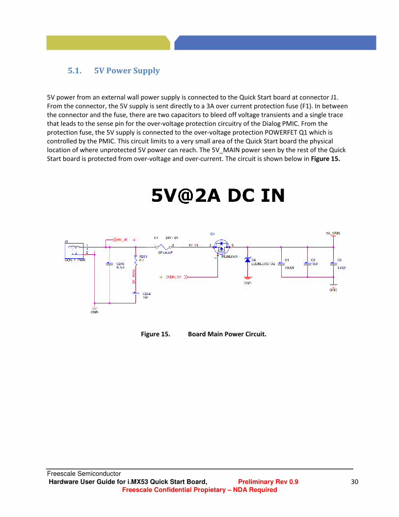
5.1. 5V Power Supply
5V power from an external wall power supply is connected to the Quick Start board at connector J1.
From the connector, the 5V supply is sent directly to a 3A over current protection fuse (F1). In between
the connector and the fuse, there are two capacitors to bleed off voltage transients and a single trace
that leads to the sense pin for the over-voltage protection circuitry of the Dialog PMIC. From the
protection fuse, the 5V supply is connected to the over-voltage protection POWERFET Q1 which is
controlled by the PMIC. This circuit limits to a very small area of the Quick Start board the physical
location of where unprotected 5V power can reach. The 5V_MAIN power seen by the rest of the Quick
Start board is protected from over-voltage and over-current. The circuit is shown below in Figure 15.
Figure 15. Board Main Power Circuit.
Freescale Semiconductor
Hardware User Guide for i.MX53 Quick Start Board, Preliminary Rev 0.9 31
PUBI – Public Use Business Information
Hardware Reference Manual for i.MX53 Quick Start
5.2. Dialog DA9053 PMIC
The Dialog PMIC provides all regulated power to the Quick Start board with the exception of a
supplemental 3.2V/1A voltage regulator. Physically, the PMIC is located in the upper right corner of the
Quick Start board, as close to the power connector as possible, while still maintaining room for
supporting components. From this location, power is supplied to the rest of the board.
When 5V power is first attached to the Quick Start board, the PMIC will remain in an OFF state until the
POWER button is pressed. In the OFF state, the PMIC will generate power on the VDDOUT rail at
approximately 3.6V (different if Li-ION battery attached) for use by the PMIC as a supply for all
regulators. In addition, the PMIC generates a VDDCORE voltage of 2.5V for internal PMIC use, and to
serve as a pull-up source for the nONKEY/KEEPACT and nSHUTDOWN control inputs. This ensures that
these two button are active whenever power is available to the Quick Start boar.
When the POWER button is initially pressed, the PMIC senses the Active Low signal on the nONKEY pin
and begins to power on all voltage rails in preprogrammed sequence. The sequence is determined
primarily by the order in which power must be supplied to the i.MX53 processor. Once the core
operations of the processor are fully powered, other power rails are turned on.
The first voltage regulator to power on is always VLDO1. This regulator supplies a maximum of 40 mA
current at 1.3V and powers on only the Secure RTC module of the i.MX53 Processor. This turns on the
RTC Clock (32.768KHz) and Watch Dog features. In the event a System Reset is triggered, or the Quick
Start board is placed into Standby, VLDO1 will remain powered ON. The only time that VLDO1 will turn
off is if all power is removed from the Quick Start board, or if a software command is sent to the PMIC to
turn off VLDO1. In the case that a developer attaches an optional coin cell to JP1/JP2, the coin cell will
provide power to keep VLDO1 operating.
The power sequence requirements for the i.MX53 Applications Processor from the data sheet are as
follows:
1. NVCC_SRTC_POW (VLDO1)
2. VCC, VDDA, VDDGP, VDD_REG [in any order]
3. All other supplies [in any order]
NOTE: in case the internal regulator is used for VDDA generation, the VDD_REG should be powered up
together with VCC and VDDGP, before the other supplies. In case the internal regulator is not used to
generate VDDA (as on the Quick Start board), the VDD_REG is independent and has no power-up
restrictions.
The power on timing sequence shown in Table 1 is the sequence programmed into the Dialog PMIC. It is
one way of providing sequences power to the i.MX53 processor. Designers are free to change the power
timing sequence on their own board designs as long as the timing requirements are met. Freescale has
not formally tested other power on timing sequences.

Freescale Semiconductor
Hardware User Guide for i.MX53 Quick Start Board, Preliminary Rev 0.9 32
Freescale Confidential Propietary – NDA Required
Regulator Time Slot
VBUCKPRO 19 mSEC
VBUCKPERI
VLDO6
VLDO8
VLDO10
23 mSEC
VBUCKCORE 27 mSEC
VBUCKMEM
VBUCKPERI/SW
VLDO2
VLDO5
31 mSEC
VLDO4
VLDO7
35 mSEC
VLDO3
VLDO9
DCDC_3V2
64 mSEC
Table 1. Regulator Timing Sequence
The Dialog PMIC will enter a SHUTDOWN/STANDBY condition by one of three ways; By a command from
the i.MX53 Processor via I2C communications, by i.MX53 Processor action to hold the nONKEY/KEEPACT
pin low for at least five seconds, or by hardware if the user holds down the POWER button for more
than five seconds. All three actions result in the Dialog PMIC powering down the voltage regulators in
reverse order of the power on sequence, except for VLDO1. A subsequent press of the POWER button
will initiate the same power on sequence as shown in Table 1.
The various power rails supplied by the PMIC are discussed in the section on Quick Start Power Rails.
Other features of the Dialog PMIC implemented by the Quick Start board are discussed in subsequent
sub-sections including: Li-ION Battery Charging, Backlight LED Driver, Touch-Screen Operation,
Miscellaneous.

Freescale Semiconductor
Hardware User Guide for i.MX53 Quick Start Board, Preliminary Rev 0.9 33
PUBI – Public Use Business Information
Hardware Reference Manual for i.MX53 Quick Start
5.2.1. Quick Start Power Rails
Table 2 shows all the voltage supply rails used on the Quick Start board, their voltages and the major
subsystems they supply on the board:
Regulator Voltage Named Rails Powers
VBUCKCORE 1.1V VBUCKCORE VDDGP VDDGP
VBUCKPRO 1.3V VBUCKPRO VCC_1V3 VCC
VBUCKMEM 1.5V VBUCKMEM DDR_1.5V
DDRQ_1.5V
NVCC_EMI_DRAM
DDR3 SDRAM
VBUCKMEM/SW 1.5V VMEM_SW
DDR_1.5V (ALT)
DDRQ_1.5V (ALT)
ALTERNATE FOR:
DDR3 SDRAM LOGIC
DDR3 SDRAM CORE
VBUCKPERI 2.5V VBUCKPERI
VDD_REG_2V5
NVCC_XTAL_2V5
LVDS_2V5 (ALT)
SATA_PHY_2V5 (ALT)
VUSB_2V5 (ALT)
VDD_REG
NVCC_XTAL
ALTERNATE FOR:
LVDS MODULE
SATA MODULE
USB MODULE 2.5V
VBUCKPERI/SW 2.5V VPERI_SW
LVDS_2V5
SATA_PHY_2V5
VUSB_2V5
LVDS MODULE
SATA MODULE
USB MODULE 2.5V
BOOST Current Source VLCD_BLT EXPANSION PORT LCD
BACKLIGHT SUPPLY
VLDO1 1.3V VLDO1_1V3_RTC
NVCC_SRTC
NVCC_SRTC
VLDO2 1.3V DIG_PLL_1V3 ALTERNATE FOR:
DIG_PLL
VLDO3 3.3V VLDO3_3V3 SD1_3V3 MICROSD CARD (SD1)
I2C1/I2C2
BOOT_SEL
NVCC-EIM-MAIN
NVCC_EIM_SEC
NVCC_SD1&2
NVCC_PATA
NVCC_FEC
NVCC_GPIO
NVCC_KEYPAD
Table 2. Quick Start Board Power Supply Rails

Freescale Semiconductor
Hardware User Guide for i.MX53 Quick Start Board, Preliminary Rev 0.9 34
Freescale Confidential Propietary – NDA Required
VLDO4 2.775V VIOHI_2V775 LCD_3V2
(ALT)
NVCC_LCD1
NVCC_LCD2
EXPANSION PORT (LCD)
VLDO5 1.3V VLDO5_1V3 SATA_1V3 SATA MODULE 1.3V
VLDO6 1.3V VLDO6_1V3
VDDAL_1V3
VDDAL
VLDO7 2.75V VLDO7_2V75
TVDAC_2V75
VGA MODULE (TV DCA)
VLDO8 1.8V VLDO8_1V8 NVCC_RESET
NVCC_JTAG
NVCC_CKIH
NVCC_NANDF
NVCC_CSI
VDD_ANA_PLL
BOOT_SEL
VLDO9 1.5V VLDO9_1V5 EXPANSION PORT
VLDO10 1.3V VLDO10_1V3
VDDA_1V3
VDDAL
DCDC-3V2 3.2V DCDC-3V2
AUDIO_3V2
FEC_3V2
VDD_FUSE
LCD_3V2
ETHERNET
AUDIO
VGA_IO_SIGNALS
USB 3.3V
SD CARD (SD3)
EXPANSION PORT
Table 2. Quick Start Board Power Supply Rails (con)

Freescale Semiconductor
Hardware User Guide for i.MX53 Quick Start Board, Preliminary Rev 0.9 35
PUBI – Public Use Business Information
Hardware Reference Manual for i.MX53 Quick Start
5.2.2. Li-ION Battery Charging
The Dialog PMIC contains a fully autonomous Li-ION battery charger. When wall power is first applied to
the Quick Start board, the PMIC will begin to apply a pre-charge to the positive battery terminal. If the
PMIC senses a fully discharged battery or a fault condition (eg, no battery), the PMIC will disconnect
VDDOUT from the battery and allow the regulators to receive power independent what is attached to
VBAT. The footprints for testing with a battery were included for skilled developers looking to
experiment. As manufactured, the Quick Start board does not support Li_ION battery operations
without modifications by the developer.
If the PMIC senses the battery voltage above the BAT_FAULT threshold for 40 msec, the PMIC will then
begin a fast linear charge of the Li-ION battery by controlling the voltage on VDDOUT. If the PMIC is
unable to increase VDDOUT above VBAT to continue charging the battery, the PMIC has an alternate
current charging method using an active diode. Charging will continue until the battery voltage reaches
the programmed level. The Li-ION charging circuit also makes use of a temperature sensor (thermistor)
attached to the body of the battery. If the resulting voltage measurement at TBAT falls outside the
threshold value programmed into the registry settings, the PMIC will suspend the charging current until
the battery temperature reduces back to with the threshold values. See the Dialog PMIC datasheet for a
more detailed explanation.
The PMIC is initially programmed with default settings to charge most Li-ION batteries. These settings
may be changed by software and the software documentation should be consulted for actually PMIC
registry values. These values can be changed in software as the developer sees fit. For more detailed
information on how the battery charging function works and how to change default charging
parameters. Since the 5V power pin of the USB micro-B connector is not connected to the PMIC, all
discussion concerning battery charge current limits due to exceeding the USB standards do not apply to
the Quick Start board.
In designing a board using the Dialog PMIC, it is important to include a capacitor of 47 uF or greater
attached to the VBAT pin if any operations are planned without a Li-ION battery. If during the initial pre-
charge phase, the Dialog PMIC does not sense any voltage present when the pre-charge voltage is
momentarily removed and VBAT voltage is measured, the PMIC will assume a massive board failure and
will not supply any voltage via the regulators.
5.2.3. Backlight LED Driver
The Dialog PMIC provides a Boost circuit which controls an external MOSFET Q8. The PMIC is capable of
driving 3 independent strings of up to 5 white LEDs each with a voltage of approximately 24 Volts and a
maximum of 50 mA. The Quick Start board does not have a direct connection for white backlight LEDs,
but does supply one connection to the Expansion Port that can be used to support an attached LCD
Daughter Card. The Expansion Port uses the LED1_IN port of the PMIC.
Freescale Semiconductor
Hardware User Guide for i.MX53 Quick Start Board, Preliminary Rev 0.9 36
Freescale Confidential Propietary – NDA Required
When designing a circuit to use the Backlight LED driver, it is important to connect the cathode
(negative) end of the LED string directly to the LED_IN port of the PMIC. The PMIC controls the supply
voltage to the Backlight LEDs by ensuring that the voltage sensed on the LED_IN port is above a
threshold voltage of 0.7V. If more than one LED_IN ports are used, the lowest port must be above the
threshold value. If the designer connects the cathode end of the Backlight LED string to GROUND, the
boost circuit will not work.
The MOSFET used in the boost circuit should have a low ON Resistance value for best efficiency. The
MOSTFET chosen for the Quick Start board, ON Semiconductor NTLJF4156NT1G, also contains a
necessary diode used in the boost circuitry. This helps reduce the number of components.
5.2.4. Touch-Screen Operation
The Dialog PMIC contains an autonomous Touch Screen Interface which will measure the XY positions
from a standard 4-WIRE resistive touch panel. The single ADC channel will detect the presence of a pen
touch on the panel, and that will trigger a series of voltage measurements on each of the four touch
panel wires (X+, X-, Y+, Y-) by the ADC in a pre-selected sequence. The resulting voltage readings are
then reported to the i.MX53 Applications Processor for conversion to a panel X-Y position via the I2C
communications link.
To ensure the Touch Screen Interface wakes up autonomously with a pen stroke, it is necessary to
supply a 1.8V reference voltage to the TSIREF_GPIO_7 pin of the PMIC. It is recommended that one of
the high PSSR Regulators of the PMIC be used to supply this voltage. VLDO6 – VLDO9 are possible
sources for supplying this reference voltage.
5.2.5. Miscellaneous
If a coin cell battery is attached to the Quick Start board, it will automatically charge using the
programmed charging settings whenever wall power is supplied to the Quick Start board. When the
battery voltage reaches the programmed level, charging will stop. Battery discharge will not begin until
wall power is removed from the board and, if a Li-ION battery is attached, the main battery discharges
to the battery cut off level.
There are two port ID traces connected from the Expansion Port header to two of the ADC pins of the
PMIC. Each unique Daughter Card designed by Freescale has a different resistor value attached to the
two ID traces on the Daughter Card. It is possible to use this voltage divider identification system to
determine at boot time if a daughter card is attached, and if so, which specific daughter card it is.
Resistor values for the two daughter cards commonly used with the Quick start board are shown in
Table 3.

Freescale Semiconductor
Hardware User Guide for i.MX53 Quick Start Board, Preliminary Rev 0.9 37
PUBI – Public Use Business Information
Hardware Reference Manual for i.MX53 Quick Start
PORT_ID0 Measured Voltage PORT_ID1 Measured Voltage
MCIMX28LCD 18.0K 1.61 V 130.0K 2.32 V
MCIMXHDMICARD 2.74K 0.54 V 130.0K 2.32 V
Table 3. Port ID Resistor Values
Over-Voltage protection is sensed by the DCIN (B4) pin of the PMIC. The voltage sensed by this pin must
be between 4.5V and 5.5V. If the voltage meets this threshold value, the voltage seen at DCIN is blocked
from the DCIN_SEL (B3) pin and the P-Channel MOSFET turns ON. Otherwise, DCIN_SEL remains high
and power is blocked from the rest of the Quick Start Board.
The TP (L5) pin of the PMIC must be connected to ground. When designing with a 0.5mm pitch uBGA
package, there is limited space for vias and traces under the BGA. To assist with layout, Freescale has
confirmed that all pins labeled ‘NO CONNECT’ on the PMIC are in no manner bonded out to the silicon.
Therefore, for routing purposes, it is possible to route the trace from an interior pin through one or
more ‘NO CONNECT’ pins, or to place a via directly under a ‘NO CONNECT’ pin without requiring a via-in-
pad technique. If the CAD Layout Engineer decides to place a via under a ‘NO CONNECT’ pin, the via
should not be tented as trapped gases during the assembly process may cause the solder ball from the
‘NO CONNECT’ pin to blow out into other pins and cause internal shorts under the BGA.
The I2C communications channel between the Processor and the PMIC is Channel 1. This channel is only
shared with the accelerometer. This channel operates at TTL logic level of 1.8V. The NRESET (F10) pin of
the PMIC is directly connected to the Active Low POR_B (C19) pin of the i.MX Processor. The PMIC will
hold the Processor in the RESET state until all the power rails are fully powered. The NIRQ (E10) pin of
the PMIC is connected to the GPIO_ 16 (C6) pin of the Processor. This pin is not a dedicated pin for an
interrupt request, but can be programmed in Software to inform the Processor that the PMIC has
information to be given to the Processor.
The PMIC has several different options for Pull-Up levels on each of its output pins. In some cases,
VDDOUT is one option, along with power supplied to both the VDD_IO1 (L4) and VDD_IO2 (K4) pins as
Pull-Up source. The exact source of Pull-Up power is determined by the registry settings of the PMIC and
can be pre-programmed at the factory as the designer wishes. Some Pull-Up registry settings apply to
groups of pins, so care must be made in selecting which source power source is used for a particular
grouping of pins. The Dialog PMIC Datasheet contains much more detailed information on the registry
settings. For the Quick Start board, VLDO3 (3.3V) is connected to VDD_IO1 primarily to ensure that the
3V3_EN signal sent to the external regulator is sufficient to turn on the regulator, and VLDO8 (1.8V) is
connected to VDD_IO2 to provide for proper I2C TTL logic levels.

Freescale Semiconductor
Hardware User Guide for i.MX53 Quick Start Board, Preliminary Rev 0.9 38
Freescale Confidential Propietary – NDA Required
5.3. 3.2V Secondary Voltage Regulator
To provide power in excess of the Dialog PMIC’s capability, an external Voltage Regulator (Richtek,
RT8010) is used. The regulator is adjustable and is set to 3.2V so that, in the event the processor may
see two different sources for the required 3.3V power supply, the i.MX53 processor will preferentially
draw from VLDO3_3V3. The regulator is controlled (enabled) from the PWR_UP_GP_FB2 (J10) pin of the
Dialog PMIC. This is the only GPIO pin that can be programmed to turn on during the voltage timing
sequence of the Dialog PMIC and is timed to turn on at the same time VLDO3_3V3 comes on. The
internal pull-up power source for this GPIO is programmed to be from VDD_IO1 (VLDO3_3V3) which is
the same voltage source for the Dialog RTC system. Since the i.MX53 standby power system is operated
at 1.3V, this prevented using the Dialog RTC system as an input to the i.MX53 processor. If the developer
does not want to enable the external voltage regulator from the Dialog GPIO pin, it would be possible to
reconfigure VDD_IO1 to be 1.3V and use the Dialog RTC clock instead. This is a design choice for the
developer.
The external voltage regulator supplies power to the following general board areas and is expected to
supply up to the maximum specified currents as follows:
� i.MX53 USB Phy 10 mA
� VGA Connector Output 10 mA
� Audio 10 mA
� Debug UART 60 mA
� Ethernet 100 mA
� Expansion Port (HDMI) 30 mA
� SD Card 60 mA
For the Expansion Port and the SD Card socket, it may be that the current draws exceed the above
estimates if a custom designed board is added to the Expansion Port, or if an SDIO device is plugged into
the SD Card Socket (ie, WiFi, Bluetooth). The external voltage regulator is capable of supplying up to 1A
of current and should be capable of accommodating most custom configurations.
Since the Quick Start board was originally designed, it has been found that VDDA, VDDAL, and DIG_PLL
can all be powered internally by the i.MX53 processor (with the correct eFuse settings). This would then
free the PMIC VLDO2, VLDO6 and VLDO10 power sources for other uses. VLDO6 and VLDO10 will be able
to supply the above expected loads, provided a high current draw SDIO card is not inserted in the SD
Card Socket. The designer is free to rearrange power rails as desired.
Freescale Semiconductor
Hardware User Guide for i.MX53 Quick Start Board, Preliminary Rev 0.9 39
PUBI – Public Use Business Information
Hardware Reference Manual for i.MX53 Quick Start
5.4. i.MX53 Applications Processor
The i.MX53 Applications Processor is physically located in the central portion of the Quick Start board.
The most critical components for placement after the processor are the DDR3 SDRAM ICs. The
remainder of the components and connectors are arranged around the periphery of the board in
locations that minimize trace routing. The i.MX53 Processor is a highly integrated system-on-chips with
many modules controlled by the main Arm Cortex-A8 core. Most modules have Logic Voltage inputs
which allow the designer to modify logic levels to suit the needs of connected ICs. A more detailed
explanation of these Logic Voltage Inputs is presented in the Peripheral Module Logic Voltage Levels
subsection. The information for voltage levels and other chip specific details come from the I.MX53 Data
Sheet, which may be revised from time to time. In the event that the most recent data sheet and the
User Guide do not agree, the Data Sheet should always take precedence. Every effort will be made to
keep the User Guide current to the most recent Data Sheet.
The i.MX53 Processor initializes out of reset according to its preprogrammed ROM code. After initial
wakeup, it then attempts to read the logic levels on 26 different pins. Depending which pins are
high/low, the Processor will then select one of the allowed boot options to begin the boot process. This
is further explained in the subsection on Boot Mode Operations and Selections.
The clock signals required by the i.MX53 Processor and the rest of the Quick Start board are further
explained in the section on Clock Signals. The i.MX53 Processor has the ability to supply a limited
amount of filtered power for internal purposes using an internal voltage regulator. The operation of this
regulator is explained further in the i.MX53 Internal Regulator subsection. The Processor also has an
internal Watch Dog Timer (WDOG) circuit that can be used to reset the Processor in the event it stops
functioning correctly. The supporting circuitry is explained in further detail in the subsection titled
Watch Dog Time.
5.4.1. Peripheral Module Logic Voltage Levels
By convention, pins used on the I.MX53 Processor to set module logic voltage levels begin with NVCC_.
This is to aid the developer in the design of a project based on the i.MX53 Processor. There are 25 such
pins used, and practically speaking, they supply the internal pull-up voltages for pins designated for data
output. These 25 pins are shown in detail in Table 4. Module Voltage Supplies. Once a voltage level is
selected for a particular module, all pins within that module will use the same voltage level. It is
important for the developer not to try to use an external pull-up to a different voltage level for
individual pins. Level shifters must be used if certain pins need to have different voltage levels to
interface with external ICs. If a different voltage level is used on an external pull-up, one or both of the
affected power rails will most likely have a different voltage level than intended throughout the design.
On a newly designed board that shows unexpected voltage levels, this may be the first thing to check.
On the Quick Start board, there are a number of unpopulated pull-up resistors. This is a result of the
initial design being conservative, and the addition of external pull-up resistors to supplement internal
i.MX53 pull-up supply voltage. Subsequent Quick Start board usage has shown these pull-ups to be
unnecessary, so they are unpopulated.

Freescale Semiconductor
Hardware User Guide for i.MX53 Quick Start Board, Preliminary Rev 0.9 40
Freescale Confidential Propietary – NDA Required
Module Allowed Values Quick Start board
NVCC_EMI_DRAM_1
NVCC_EMI_DRAM_2
NVCC_EMI_DRAM_3
NVCC_EMI_DRAM_4
NVCC_EMI_DRAM_5
External Memory Interface 1.425V - 1.9V 1.5V (Match DDR3 Memory)
NVCC_NANDF NAND Flash 1.65V - 3.6V 1.8V
NVCC_EIM_MAIN_1
NVCC_EIM_MAIN_2
NVCC_EIM_SEC
External Interface Module 1.65V - 3.6V 3.3V
NVCC_RESET Reset Logic Levels 1.65V - 3.1V 1.8V (Match PMIC)
NVCC_SD1 SD Card Module 1 1.65V - 3.6V 3.3V (Match SD Cards)
NVCC_SD2 SD Card Module 2 1.65V - 3.6V 3.3V
NVCC_PATA Parallel ATA 1.65V - 3.6V 3.3V
NVCC_LCD_1
NVCC_LCD_2
LCD Module 1.65V - 3.1V 2.775V
NVCC_CSI Camera Sensor Interface 1.65V - 3.6V 1.8V
NVCC_FEC Fast Ethernet Controller 1.65V - 3.6V 3.3V (Match Ethernet PHY)
NVCC_GPIO General Purpose I/O 1.65V - 3.6V 3.3V
NVCC_JTAG JTAG Module 1.65V - 3.1V 1.8V
NVCC_KEYPAD Keypad Port 1.65V - 3.6V 3.3V (Match Audio CODEC)
NVCC_CKIH Clock Amplifier Circuit 1.65V - 1.95V 1.8V
NVCC_XTAL 24MHz Crystal Supply 2.25V - 2.75V 2.5V
NVCC_SRTC_POW Secure Real Time Clock 1.1V - 1.3V 1.3V
NVCC_LVDS Low Voltage Differential Signaling 2.375V - 2.625V 2.5V
NVCC_LVDS_BG LVDS Band Gap 2.375V - 2.625V 2.5V
Table 4. Module Voltage Supplies
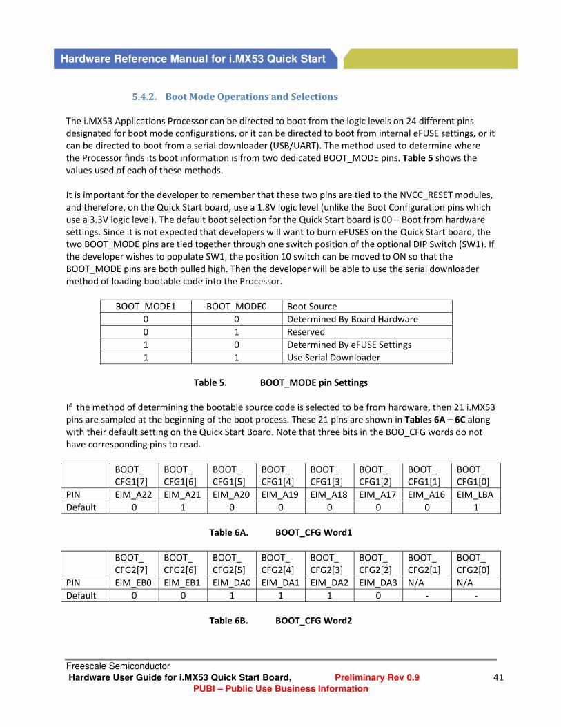
Freescale Semiconductor
Hardware User Guide for i.MX53 Quick Start Board, Preliminary Rev 0.9 41
PUBI – Public Use Business Information
Hardware Reference Manual for i.MX53 Quick Start
5.4.2. Boot Mode Operations and Selections
The i.MX53 Applications Processor can be directed to boot from the logic levels on 24 different pins
designated for boot mode configurations, or it can be directed to boot from internal eFUSE settings, or it
can be directed to boot from a serial downloader (USB/UART). The method used to determine where
the Processor finds its boot information is from two dedicated BOOT_MODE pins. Table 5 shows the
values used of each of these methods.
It is important for the developer to remember that these two pins are tied to the NVCC_RESET modules,
and therefore, on the Quick Start board, use a 1.8V logic level (unlike the Boot Configuration pins which
use a 3.3V logic level). The default boot selection for the Quick Start board is 00 – Boot from hardware
settings. Since it is not expected that developers will want to burn eFUSES on the Quick Start board, the
two BOOT_MODE pins are tied together through one switch position of the optional DIP Switch (SW1). If
the developer wishes to populate SW1, the position 10 switch can be moved to ON so that the
BOOT_MODE pins are both pulled high. Then the developer will be able to use the serial downloader
method of loading bootable code into the Processor.
BOOT_MODE1 BOOT_MODE0 Boot Source
0 0 Determined By Board Hardware
0 1 Reserved
1 0 Determined By eFUSE Settings
1 1 Use Serial Downloader
Table 5. BOOT_MODE pin Settings
If the method of determining the bootable source code is selected to be from hardware, then 21 i.MX53
pins are sampled at the beginning of the boot process. These 21 pins are shown in Tables 6A – 6C along
with their default setting on the Quick Start Board. Note that three bits in the BOO_CFG words do not
have corresponding pins to read.
BOOT_
CFG1[7]
BOOT_
CFG1[6]
BOOT_
CFG1[5]
BOOT_
CFG1[4]
BOOT_
CFG1[3]
BOOT_
CFG1[2]
BOOT_
CFG1[1]
BOOT_
CFG1[0]
PIN EIM_A22 EIM_A21 EIM_A20 EIM_A19 EIM_A18 EIM_A17 EIM_A16 EIM_LBA
Default 0 1 0 0 0 0 0 1
Table 6A. BOOT_CFG Word1
BOOT_
CFG2[7]
BOOT_
CFG2[6]
BOOT_
CFG2[5]
BOOT_
CFG2[4]
BOOT_
CFG2[3]
BOOT_
CFG2[2]
BOOT_
CFG2[1]
BOOT_
CFG2[0]
PIN EIM_EB0 EIM_EB1 EIM_DA0 EIM_DA1 EIM_DA2 EIM_DA3 N/A N/A
Default 0 0 1 1 1 0 - -
Table 6B. BOOT_CFG Word2

Freescale Semiconductor
Hardware User Guide for i.MX53 Quick Start Board, Preliminary Rev 0.9 42
Freescale Confidential Propietary – NDA Required
BOOT_
CFG3[7]
BOOT_
CFG3[6]
BOOT_
CFG3[5]
BOOT_
CFG3[4]
BOOT_
CFG3[3]
BOOT_
CFG3[2]
BOOT_
CFG3[1]
BOOT_
CFG3[0]
PIN EIM_DA4 EIM_DA5 EIM_DA6 EIM_DA7 EIM_DA8 EIM_DA9 EIM_DA10 N/A
Default 0 0 0 0 0 0 0 -
Table 6C. BOOT_CFG Word3
Of these 21 pins, four of them have the same meaning regardless of the selected boot source. These
four BOOT_CFG bits with their meanings are as follows:
BOOT_CFG1[1] Processor Speed setting during boot:
0 – 800 MHz
1 – 400 MHz
BOOT_CFG1[0] MMU Enabled during boot:
0 – MMU not enabled
1 – Initializing MMU with L1 Cache during boot
BOOT_CFG2[3] AXI/DDR Speed setting during boot:
0 – PLL2: 400MHz
1 – PLL2: 333MHz
BOOT_CFG2[2] Oscillator Frequency Select:
0 – Auto Detect
1 – Set to 24MHz
The six pins that determine where bootable code is stored are BOOT_CFG1[7:2]. Depending on which
boot source is selected, some of these pins may have different meanings. Those pins will show up as an
‘X’ for logic level. The specific logic levels and their meanings are as follows:
BOOT_CFG1[7:2] Boot Code Source Selection
0000 - NOR/OneNAND Boot
0001 - Reserved
0010 - PATA/SATA Boot
0011 - Serial ROM (I2C/SPI) Boot
01XX - SD/MMC (eSD/eMMC) Boot
1XXX - NAND Flash Boot
For each of the bootable source selections, the remaining BOOT_CFG pins have different meanings. The
pins are meant to choose initialization settings required for each specific boot source. The following
paragraphs will specify those choices base by bootable source:

Freescale Semiconductor
Hardware User Guide for i.MX53 Quick Start Board, Preliminary Rev 0.9 43
PUBI – Public Use Business Information
Hardware Reference Manual for i.MX53 Quick Start
NOR/OneNAND
BOOT_CFG1[3] Memory Type 0 – NOR Flash
1 – OneNAND
BOOT_CFG2[7:6] Muxing Scheme 00 – Muxed, 16-bit data (low half) interface
01 – Not muxed, 16-bit data (high half) interface
10 – Reserved
11 – Reserved
BOOT_CFG3[7:6] OneNAND Page Size 00 – 1KB
01 – 2KB
10 – 4KB
11 – Reserved
HD (PATA/SATA)
BOOT_CFG1[3] HD Type 0 – PATA
1 – SATA
Serial-ROM
BOOT_CFG1[3] Serial ROM Select 0 – I2C
1 – SPI
BOOT_CFG2[5] SPI Addressing 0 – 2-byte (16-bit)
1 – 3-byte (24-bit)
BOOT_CFG3[5:4] Port Select 00 – I2C1/eCSPI1
01 – I2C2/eCSPI2
10 – I2C3/CSPI
11 – Reserved
BOOT_CFG3[3:2] Chip Select (SPI Only) 00 – CS0
01 – CS1
10 – CS2
11 – CS3

Freescale Semiconductor
Hardware User Guide for i.MX53 Quick Start Board, Preliminary Rev 0.9 44
Freescale Confidential Propietary – NDA Required
SD/eSD
BOOT_CFG1[4] Fast Boot 0 – Regular
1 – Fast Boot
BOOT_CFG1[3] SD/MMC Speed 0 – High
1 – Normal
BOOT_CFG2[5] Bus Width 0 – 1-bit
1 – 4-bit
BOOT_CFG3[5:4] Port Select 00 – eSDHC1
01 – eSDHC2
10 – eSDHC3
11 – eSDHC4
MMC/eMMC
BOOT_CFG1[4] Fast Boot 0 – Regular Boot
1 – Fast Boot
BOOT_CFG1[3] SD/MMC Speed 0 – High
1 – Normal
BOOT_CFG2[7:5] Bus Width 000 – 1-bit
001 – 4-bit
010 – 8-bit
011 – Reserved
100 – Reserved
101 – 4-bit DDR (MMC 4.4)
110 – 8-bit DDR (MMC 4.4)
111 – Reserved
BOOT_CFG3[5:4] Port Select 00 – eSDHC1
01 – eSDHC2
10 – eSDHC3 (eMMC4.4)
11 – eSDHC4
BOOT_CFG3[3] DLL Override 0 – Use Default ROM
1 – Use eFUSE DLL Override
BOOT_CFG3[2] Fast Boot Acknowledge 0 – Enabled
1 – Disabled

Freescale Semiconductor
Hardware User Guide for i.MX53 Quick Start Board, Preliminary Rev 0.9 45
PUBI – Public Use Business Information
Hardware Reference Manual for i.MX53 Quick Start
NAND
BOOT_CFG1[6] Muxed On: 0 – PATA
1 – WEIM
BOOT_CFG1[5:4] Interleave Scheme: 00 – No Interleaving
01 – 2 Device
10 – 4 Device
11 – Reserved
BOOT_CFG1[3:2] Address Cycles: 00 – 3
01 – 4
10 – 5
11 – 6
BOOT_CFG2[7:6] Page Size: 00 – 512 + 16 Bytes (4-bit ECC)
01 – 2KB + 64 Bytes
10 – 4KB + 128 Bytes
11 – 4KB + 218 Bytes
BOOT_CFG2[5] NAND Interface 0 – 8-bit
1 – 16-bit
BOOT_CFG2[2] NAND Flash Clock Frequency 0 – AXI DDR Frequency divide by 12
1 – AXI DDR Frequency divide by 28
BOOT_CFG3[7] Bad Block Skip Step (Stride Size) 0 – 1 Block
1 – 8 Block
BOOT_CFG3[6] LBA-NAND Select 0 – Non LBA (11ms delay)
1 – LBA (22ms delay)
BOOT_CFG3[5] NAND use R/nB Signals? 0 – No
1 – Yes
BOOT_CFG3[4:3] ECC/Spare Select 00 – 8-bit ECC
01 – 14-bit ECC
10 – 16-bit ECC
11 – ECC Off
BOOT_CFG3[2:1] Pages in Block 00 – 32 Pages
01 – 64 Pages
10 – 128 Pages
11 – 256 Pages

Freescale Semiconductor
Hardware User Guide for i.MX53 Quick Start Board, Preliminary Rev 0.9 46
Freescale Confidential Propietary – NDA Required
When the Quick Start board was originally designed, several of the BOOT_CFG pins were selectable by
the 10 position DIP Switch (SW1). After initial testing of the Quick Start board, the optimum BOOT_CFG
settings for flexibility and ease of use were determined. These are the default settings on the board,
which set the microSD card connector (SD1) as the default boot source. As the developer becomes more
familiar with the board and wishes to experiment more, it is recommended that the next step for the
developer is to write code for the microSD card to initialize as alternative boot source and pass off the
boot process to the new source.
As further experience is gained, the developer may wish to install the optional DIP switch on SW1
(Multicomp MCNHDS-10-T). The boot-switch was originally removed to improve ease of use and ensure
all members of the community are developing the same way. Installing the boot-switch will allow the
developer to gain access to selecting either SD card socket as the bootable source, or to select the serial
downloader method. Finally, for the skilled developers, it is possible to desolder and rearrange some of
the pull-up and pull-down resistors on the Quick Start board. Figures 16 and 17 highlight all of the pull-
up and pull-down resistors used, and also highlights sources of either high (3.3V) or low (GND) logic
levels.
Figure 16. Boot Mode Resistor Locations TOP
Table 7. Boot Mode Resistors TOP
Resistor Boot Configuration Bit Pull UP/Down
R46 BOOT_CGF1[6] Pull Up
R47 BOOT_CGF1[7] Pull Down
R48 BOOT_CGF2[7] Pull Up (DNP)
R46
R47 R48

Freescale Semiconductor
Hardware User Guide for i.MX53 Quick Start Board, Preliminary Rev 0.9 47
PUBI – Public Use Business Information
Hardware Reference Manual for i.MX53 Quick Start
Figure 17. Boot Mode Resistor Locations BOTTOM
Table 8. Boot Mode Resistors BOTTOM
Resistor Boot Configuration Bit Pull UP/Down
R56 BOOT_CGF1[1] Pull Down
R62 BOOT_CGF2[3] Pull Up
R64 BOOT_CGF3[4] Pull Down
R65 BOOT_CGF3[3] Pull Down
R57 BOOT_CGF1[0] Pull Up
R60 BOOT_CGF2[5] Pull Up
R61 BOOT_CGF2[4] Pull Up
R59 BOOT_CGF2[6] Pull Down
R65
R64
R62
R59 R61
R60 R57
R56

Freescale Semiconductor
Hardware User Guide for i.MX53 Quick Start Board, Preliminary Rev 0.9 48
Freescale Confidential Propietary – NDA Required
5.4.3. Clock Signals
The Quick Start board has three external clocks, two of which are dedicated to the i.MX53 Processor,
and one dedicated to the Ethernet PHY. The 24 MHz crystal (Y1) is the main clock source for the
Processor. The crystal is located on the bottom side of the board as shown in Figure 18. It is driven by its
own 2.5V supply pin, NVCC_XTAL. Although the crystal frequency for the board is set to be 24MHz, the
default BOOT_CFG2[2] pin that controls specifying the frequency is left to auto detect. In the case of
24MHz, the actual setting is not important. If a clock oscillator is used, it would be connected to the pin
EXTAL (AB11) and the pin XTAL (AC11) should be left floating. The 24 MHz clock signal can be output
from any GPIO pin for use in other locations. On the Quick Start board, the clock signal is output on
GPIO_0 and is the net is labeled GPIO_0(CLK0). The clock signal is sent to the Audio Codec as the clock
source for the audio sub-system, and it is also sent to the expansion port as an available clock signal for
a custom designed card as needed.
The 32.768KHz crystal (QZ1) is the clock source used by the i.MX53 Processor for the Secure Real Time
Clock module. It receives power from the NVCC_SRTC pin which is connected to the VLDO1 1.3V voltage
regulator. The 32.768KHz clock signal is not sent anywhere else on the Quick Start board. The location of
the crystal is also shown in Figure 18.
Figure 18. Clock Source Locations
The clock source for the Ethernet PHY is a 50 MHz Oscillator (X1) with an enable pin and is shown in
Figure 18. The oscillator was originally placed to support both the SATA module and the Ethernet PHY. It
is no longer used for the SATA module, and only supplies a clock signal to the Ethernet PHY. It is
powered by the DCDC_3V2 power rail and, by default, is always on when the DCDC_3V2 rail is powered
on. It is possible for the developer to remove resistor R110 and place a zero Ohm resistor across R197 to
give the developer software control of the oscillator through pin GPIO_4 (D4).
Y1
QZ1
X1

Freescale Semiconductor
Hardware User Guide for i.MX53 Quick Start Board, Preliminary Rev 0.9 49
PUBI – Public Use Business Information
Hardware Reference Manual for i.MX53 Quick Start
5.4.4. i.MX53 Internal Regulators
The i.MX53 Applications Processor contains two internal voltage regulators which can supply VDDA,
VDDAL, VDD_DIG_PLL and VDD_ANA_PLL. The power input for this pin is VDD_REG (pin G18). On the
Quick Start board, this pin is connected to VBUCKPERI and is set to 2.5V.
The Digital PLL voltage regulator can be selected to supply VDD_DIG_PLL through an internal (on die)
connection. The VDD_DIG_PLL pin can also be connected to the VDDA and VDDAL pins through an
external connection to allow the Digital PLL regulator to supply these rails as well. The Digital PLL
regulator is set to start at a reduced voltage value of 1.2V, but is programmed by software to increase to
1.3V early in the boot process. On the Quick Start board, the VDD_DIG_PLL connection to VLDO2 is not
populated by default, so that VDD_DIG_PLL power is supplied by the internal regulator. The VDDA
supply pins are connected to VLDO10 through a shorting trace SH22. If the developer wishes to
experiment with supplying VDDA from the internal regulator, the trace between the two pads of SH22
can be cut, and a wire soldered between SH22 pin 2 and resistor R210 pin 2. The VDDAL supply pin is
connected to VLDO6 through a shorting trace SH24. If the developer wishes to experiment with
supplying VDDAL from the internal regulator, the trace between the two pads of SH24 can be cut, and a
wire soldered between SH24 pin 2 and resistor R210 pin 2.
The Analog PLL voltage regulator can be selected to supply VDD_ANA_PLL through an internal (on die)
connection. The Analog PLL is set to supply a voltage of 1.8V. On the Quick Start board, the
VDD_ANA_PLL connection to VLDO8 is not populated by default, so that VDD_ANA_PLL is supply by the
internal regulator.
Developer Note: During the boot process, it takes approximately 310msec for VDD_DIG_PLL to change
from 1.2V to 1.3V. During this time, the i.MX53 core will not run at full speed/maximum processor
loading. It will operate in the reduced power mode, and the limitations of the reduced power mode
discussed in the datasheet apply. It is expected that during the first 310msec, processor loading will not
be an issue.
5.4.5. Watch Dog Timer
The i.MX53 Application Processor has an internal Watch Dog Timer circuit. On the Quick Start board, the
WDOG output is assigned to GPIO_9. The WDOG is an active low signal. The Dialog PMIC does not have
a specific pin to accept a Watch Dog signal to force a Processor reset. Therefore, the WDOG signal is
modified by hardware components on the Quick Start board and applied to the Processor Reset pin
(POR_B, pin C19). By using an active-low enabled buffer, the active low WDOG signal can be
transformed into a low pulse, which returns back to the logic high state immediately after the i.MX53
Processor resets ( ~ 700 nsec). This allows the processor to reset the WDOG signal and then come out of
reset. The buffer IC also is in a tri-state condition when the WDOG signal is normally high, thus allowing
the push-button reset circuitry to work. The Watch Dog circuitry is shown in Figure 19.

Freescale Semiconductor
Hardware User Guide for i.MX53 Quick Start Board, Preliminary Rev 0.9 50
Freescale Confidential Propietary – NDA Required
Figure 19. Watch Dog Timer Reset Trigger
In normal operation, WDT_OUTPUT is high, which keeps WDT_OUT_FLT high and the buffer in the OFF
state. As soon as the WDOG goes active low, WDT_OUT_FLT is pulled low through C253, and the buffer
(U22) is enabled. The always low input to the buffer is then sent to the POR_B pin and forces the
Processor into reset. The RC circuit formed by R215 and C253 will then begin to raise the voltage level
on WDT_OUT_FLT, until after XX msec, the active low output enable pin of U22 will turn off the Buffer
and POR_B will return high. In coming out of reset, the WDOG will then return to the HIGH or OFF state,
and the Processor will return to normal operations.

Freescale Semiconductor
Hardware User Guide for i.MX53 Quick Start Board, Preliminary Rev 0.9 51
PUBI – Public Use Business Information
Hardware Reference Manual for i.MX53 Quick Start
5.5. DDR3 SDRAM Memory
The Quick Start board has four 128MX16 DDR3 SDRAM chips for a total of 1GB RAM memory. The chips
are organized in two different arrays, differentiated by the chip selects, storing either the upper 16-bits
or the lower 16-bits of a 32-bit word. This organization is shown in Table 9 below.
Chip Select ‘0’ Chip Select ‘1’
Lower 16-bits [15:0] U3 U4
Upper 16-bits [31:16] U5 U6
Table 9. DDR3 SDRAM Chip Organization
In this organization, there are 21 traces that connect to all four DDR3 chips and the i.MX53 Processor (14
Address, 3 Bank Address, 3 Control, and Reset). These are the most critical traces since they will see the
most loading. The remaining traces are connected to two DDR3 chips and the Processor, and will only
see one active DDR3 chip at a time. Note that the two clock traces are tied with the data traces
(SDCLK_0 for the lower 16-bits, SDCLK_1 for the upper 16-bits). This limits the clock traces to only one
active DDR3 chip at a time as well.
In the physical layout, the DDR3 chips are placed to minimize routing of the address traces. The two chip
select ‘0’ chips are placed on top, and the two chip select ‘1’ chips are placed on the bottom side,
directly below the chips with the same data traces. The data traces are not necessarily connected to the
DDR3 chips in sequential order, but for ease of routing, are connected as best determined by the layout
and other critical traces. The i.MX53 Processor has the capability of remapping SDRAM word bit order
based on chip select used, so that words can be physically stored in memory in correct order. If this is a
feature the developer wishes to implement, there is more information in the software reference
manual.
The DDR_VREF is created by a simple voltage divider using 470 Ohm 1% resistors and 0.1 uF capacitors
for stability. The relatively small value resistors provide enough current to maintain a steady mid-point
voltage. The calibration resistors used by the four DDR3 chips and the Processor are 240 Ohm 1%
resistors. This resistor value is specified by the DDR3 Specifications. There is a 200 Ohm resistor between
each clock differential pair to maintain the correct impedance between the two traces. The DDR3
SDRAM should be rated for 1066 MHz or faster.
For skilled designers wishing to double the amount of DDR3 SDRAM available for use with the i.MX53
processor using eight x8 width DDR3 chips, the following considerations should be weighed carefully
before proceeding: Four DDR3 chips on a chip select line will exceed the current supply capability of the
VBUCKMEM power source. An additional 1.5V power source would need to be added. Also, attaching
the address lines to eight DDR3 chips is a great amount of loading. Premium PCB materials would be
required to reduce losses. Freescale has tested and validated using eight DDR2 SDRAM chips in this
manner. Using eight DDR3 SDRAM chips has not yet been tried.

Freescale Semiconductor
Hardware User Guide for i.MX53 Quick Start Board, Preliminary Rev 0.9 52
Freescale Confidential Propietary – NDA Required
Developers should note that using different configurations of SDRAM requires register changes on the
i.MX53 Processor to ensure that timing and address sequencing is set up correctly. Software
initialization settings will be different depending on SDRAM configuration.
5.6. Micro SD Card Connector
The microSD Card Connector (J4) is directly connected to the eSDHC channel 1 module of the i.MX53
Applications processor. This card socket will support up to a 4-bit data transfer from an microSD card or
a microMMC card inserted into the socket. The Quick Start board is designed to boot a microSD Card
from the microSD card socket with no additional modifications. If the developer wishes to boot from a
microMMC card, the following options shown in Table 10 below are available:
Option Net Condition Notes:
SD Card Operations EIM_A20 Default Low Position 8 on DIP Switch SW1
MMC Card Operations EIM_A20 Pull High Position 8 on DIP Switch SW1
Table 10. Micro-SD Card Boot Options
The main power for the microSD Card Socket is 3.3V from (VLDO3_3V3). This ensures that if the external
voltage regulator is turned off for power savings, the microSD Card Socket still has power. Power to the
card socket is through SH1. If the developer wants to supply power from a different power source, this
trace can be cut. The developer should note that the internal i.MX53 processor eSDHC module is
powered by a 3V3 source, so changing the voltage of the cards socket on the Quick Start board is not
recommended.
The SD1 Clock trace has a 22 Ohm series termination resistor (R211). This resistor is inserted to prevent
a reflected signal from being sensed by the i.M53 processor. This has been found to occur on MMC card
operation and is recommended for all designs. In addition, the following eSDHC channel 1 trace is pulled
high to 3.3V (VLDO2_3V3).
� SD3 Command (R76)
By default, the Quick Start board is manufactured with a 3M 29-08-05WB-MG part for availability
reasons. The combined Data3/Card Detect trace is not supported by the BSP software. It is possible for
the developer to remove the original card socket and repopulate the position with an alternate microSD
Card Socket made by Proconn, MSPN09-A0-2000. The developer should also then populate R108 with a
suitable pull-up resistor (10K). This will then give the developer the option to use the card detect trace
for channel 1 connected to EIM_DA13 (pin AC7).

Freescale Semiconductor
Hardware User Guide for i.MX53 Quick Start Board, Preliminary Rev 0.9 53
PUBI – Public Use Business Information
Hardware Reference Manual for i.MX53 Quick Start
5.7. Full Size SD Card Connector
The full size SD Card connector (J5) is directly connected to the eSDHC channel 3 module of the i.MX53
Applications processor. This card socket will support up to a full 8-bit data transfer from an SD card,
SDIO device, or MMC card inserted into the socket. The Quick Start board was designed by default not
to boot from the J5 card socket. If the developer wishes to boot from J5, the following options shown in
Table 11 below are available:
Option Net Condition Notes:
Boot From J5 Card Socket EIM_DA6 Pull High Position 2 on DIP Switch SW1
High Speed Operations EIM_A18 Pull High Position 6 on DIP Switch SW1
Fast Boot EIM_A19 Pull High Position 7 on DIP Switch SW1
SD Card Operations EIM_A20 Default Low Position 8 on DIP Switch SW1
MMC Card Operations EIM_A20 Pull High Position 8 on DIP Switch SW1
Table 11. Full Size SD Card Boot Options
The Quick Start board is configured to have the ROM code try to initiate boot operations in the 4-bit
data mode, by setting BOOT_CFG[6:5] to (01). Section 6.4.3.6 explains the SD/MMC boot options in
greater detail for the interested developer.
Main power to the SD Card Connector is from the external LDO regulator (DCDC_3V2). If this regulator is
turned off for power savings purposes, the card socket will not function. It is possible for the developer
to cut the trace between the pads of SH32 and attach a different source of power to the pad next to the
card socket via a wire solder. Note that the eSDHC module internal to the i.MX53 processor is operating
at 3.3V, therefore it is recommended that the alternate source also be 3.3V. Cutting the SH32 trace
should only be used if a SDIO device inserted into the socket is drawing more power than the LDO
Regulator is capable of supplying.
The SD3 Clock trace has a 22 Ohm series termination resistor (R212). This resistor is inserted to prevent
a reflected signal from being sensed by the i.M53 processor. This has been found to occur on MMC card
operation and is recommended for all designs. In addition, the following eSDHC channel 3 traces are
pulled high to 3.2V (DCDC_3V2).
� SD3 Command (R89)
� SD3 Card Detect (R88)
� SD3 Write Protect (R87)

Freescale Semiconductor
Hardware User Guide for i.MX53 Quick Start Board, Preliminary Rev 0.9 54
Freescale Confidential Propietary – NDA Required
5.8. VGA Video Output
The i.MX53 Applications Processor TV Encoder module provides three component video output signals
that can be used as either a TV signal or as a VGA signal to a connected monitor. The Quick Start board
configures these signals for use as a VGA output through connector J8. In addition to the 3 video signals,
Horizontal and Vertical Synchronization signals, I2C Data and Clock and a 5V reference signal are
connected to the VGA output in accordance with the VGA Video Standard. The video data signals are
referenced to 2.75V (TVDAC_2V75), while all other signals are referenced to 5V. The synchronization
signals leave the i.MX53 Processor referenced to 3.3V, but go through a pair of one-way level shifters
(U12, U13) to meet the VGA standard required 5V reference. Similarly, the I2C Channel two signals leave
the processor referenced to 3.2V, but go through a bi-directional level shifter (U14) to also become
referenced to 5V. See the connector section for the actual pin-out of J8.
The Component Video signals are terminated to ground, each with a 75 Ohm resistor to meet cabling
requirements. A separate VGA ground plane has been created to minimize noise on the video signals by
necking through a small trace. The voltage reference signal for the TVDAC module is provided by placing
a 1.05K 1% Ohm resistor at pin Y18. The constant current source provided by the TVDAC module
generates the exact voltage reference required by the VGA standard. A 0.1uF capacitor should be
connected to pin AA19 to reduce noise on the voltage reference sense point. Each of the Component
Video output traces should be connected to their respective feedback pins. This provides the Cable
Detection (CD) circuitry the ability to detect whether a cable has been plugged into the connector. The
CD circuitry is not active for TV signal output, so it would not be necessary to connect the feedback
circuit in that case. If any signal filtering or conditioning components are added to the Component Video
traces, the feedback pins should be connected after the additional components (ie, feedback pins should
tap into to the connector side of the Component Video signals). A ferrite bead is recommended near the
voltage input pins of the TVDAC module to reduce noise in the video module.

Freescale Semiconductor
Hardware User Guide for i.MX53 Quick Start Board, Preliminary Rev 0.9 55
PUBI – Public Use Business Information
Hardware Reference Manual for i.MX53 Quick Start
5.9. LVDS Video Output
The i.MX53 Applications processor contains two separate LVDS modules that can be operated
independently. Each module provides five sets of differential pair signals, four used for data and one
pair for the clock signal. The Quick Start board uses only one of the two modules to provide an optional
secondary display panel that can be used in conjunction with one of the other primary means of video
output, or if desired, to be used as the sole video output. Developers who wish to use two LVDS outputs
at the same time may wish to consider the MCIMX53SMD Tablet for development. The Quick Start
board makes use of three of the differential pair data pins and the clock pins. These signals, combined
with a display enable pin, a contrast pin, two separate channels of I2C communications, an interrupt pin,
and power supplies (5V and 3.2V), will provide the necessary signals to support many of the LVDS
display panels currently available on the Market. The connector used is a 30-pin connector that meets
the LVDS standards for connectors (Hirose, DF19G-30P-1H(56)).
Development work with LVDS panels was done with the Hannstar HSD100PXN1-A00-C11 display. This
display determined the signal ordering on the connector. To aid in development work, Freescale has
purchased a large number of LVDS display and has contracted to make customer cables that will connect
the displays to the Quick Start board. This LVDS display kit will be available from Freescale as described
in the board accessory section.
If the developer wishes to use a different LVDS display, a custom cable would most likely be required to
ensure the plug on the cable end that connected to the display was the right type and to re-order the
signals to match the ordering on the display. For use with other displays, signals are referenced to the
following voltages:
LVDS Data/Clock 2.5V (LVDS_2V5)
Display Control 3.3V (VLDO3_3V3)
I2C channel two 3.2V (DCDC_3V2)
I2C channel three 3.3V (VLDO3_3V3)
Isolation resistors on the i2C channel two traces (R213, R214) provide a means of isolating the LVDS
connector from other functions on the board if the LVDS connector is interfering with I2C
communication. In addition, the empty pads can also serve as attachment points for hand soldered
wires if the developer wishes to run different signals to this connector.
The i.MX53 Applications Processor has both an internal and external method to measure Band Gap
resistance. If the internal method is chosen by software, pin AA14 can be left floating. If the external
method is desired, a 28.0K 1% Ohm resistor should be attached between pin AA14 and ground. It is
recommended that this resistor be added routinely to give software the option of choosing between the
two methods. It is also recommended to place a 49.9 1% Ohm resistor as the voltage input pin of U14
(NVCC_LVDS_BG) to filter the power used in measuring the Band Gap.

Freescale Semiconductor
Hardware User Guide for i.MX53 Quick Start Board, Preliminary Rev 0.9 56
Freescale Confidential Propietary – NDA Required
5.10. Expansion Port
The function of the Quick Start board Expansion Port is to bring out many of the i.MX53 pins that are
otherwise unused on the Quick Start board. The overriding design considerations for this port were to
be able to support HDMI functionality through a daughter card (primary) while also being able to
support an existing LCD daughter card (secondary). In meeting these considerations, the Expansion Port
was also constrained to meet a general power/signal format adopted across all recent i.MX
development board designs, primarily for safety and equipment damage consideration. For these
reasons, there may be some functionalities of the i.MX53 chip that are not accessible on the i.MX53
Quick Start board. This board simply cannot be all things to all people. The MCIMX53SMD is available for
developers looking for more options.
For developers who are interested in designing custom daughter cards for use with the Quick Start
board, the following capabilities are available from the Expansion Port. Please note that many pins are
muxed, so that not all features are available at the same time:
• Two Serial Peripheral Interfaces (SPI) CSPI, eCSDPI2
• Two I2S/SSI/AC97 Ports AUDMUX4, AUDMUX5
• Two Inter-Integrated Circuits (I2C) I2C1, I2C2
• 2 UARTs UART4, UART5
• SPDIF Audio
• USB ULPI Port USBH2
• 24-bit Data and display control signals
• Resistive Touch Screen Interface
• CSI Camera
In addition to the Data/Signal traces to support the above functionality, the following power sources are
also included on the Expansion Port:
• 5V_MAIN 5V DC Power Supply
• LCD_3V2 3.2V DCDC_3V2
• VIOHI_2V775 2.775V VLDO4
• VLDO8_1V8 1.8V VLDO8
• VLDO9_1V5 1.5V VLDO9
• VLCD_BLT Current Source PMIC LED Driver
Note that VLDO9 is only used by the Expansion Port on the Quick Start board. The developer is free to
reprogram the voltage of the LDO regulator on the PMIC for whatever voltage may be required subject
to the following limitations (1.25V – 3.6V, 100mA). The proper connector to mate with Expansion Port
J13 is made by Samtec, QTH-060-XX-L-D-A, where XX determines the height of the connector.
For a table of available pin-mux options, see the expansion port pin-out in section 6.

Freescale Semiconductor
Hardware User Guide for i.MX53 Quick Start Board, Preliminary Rev 0.9 57
PUBI – Public Use Business Information
Hardware Reference Manual for i.MX53 Quick Start
5.11. Audio
The main Audio CODEC used on the Quick Start board is the Freescale SGTL5000 Low Power Stereo
Codec with Headphone Amp. The i.MX53 Applications Processor provides digital sound information
from the AUDMUX module channel 5 port via I2S communications protocol. The Audio CODEC also
receives command instructions from the I2C channel 2 bus and receives a 24 MHz clock input signal
from GPIO_0 of the i.MX53 processor. These seven connections with the processor are the only required
signals.
The Audio CODEC provides a Left and Right Stereo output signal capable of providing a 16 Ohm set of
headphones/earbuds with up to 58 mW of power. The Audio CODEC is also capable of receiving a single
microphone channel, and converting the information to a digital format and transmitting it back to the
processor. The CODEC also generates the necessary microphone bias voltage to allow proper condenser
operation.
The Quick Start board was designed to be used with a range of microphone options, including the mono-
microphone/earbud sets commonly used with cellular phones. For this reason, the microphone bias
voltage is connected to the microphone input signal on the Quick Start board, rather than connecting
the bias voltage signal to a separate channel on the Microphone Jack (J6) and allowing a higher end
microphone to connect the bias source closer to the connector. In addition, the right channel audio
output of the Audio CODEC can be sent to the Microphone Jack. The Quick Start board does not come
with this feature by default, but the developer can easily populate the L22 footprint with a ferrite bead
or a zero Ohm jumper.
The Quick Start board is also designed with a cable detect feature on both the Headphone and
Microphone Jacks. One option would be to use an audio connector with an internal flag that would
make or break depending on whether the connector barrel was inserted into the jack. These connectors
are available, but are often more expensive and may have supply problems. On the Quick Start board, a
four pin, Audio/Video style connector was chosen to implement the cable detect feature. When a three
connector cable is inserted into the connector, the cable detect pin is shorted to the ground pin, sending
an active low signal back to the processor to indicate that a cable was inserted. For this reason, the
ground pin on the Microphone and Headphone Jacks must be system ground and not a virtual audio
ground. Therefore, the Audio CODEC was designed to use the AC Coupled audio mode which makes use
of two 220uF capacitors. If the developer wishes to design a board that uses a flagged jack for cable
detection or does not implement a cable detection scheme, it would then be possible to use the Direct
Drive feature of the Audio CODEC and eliminate the need for the large capacitors.
The Audio CODEC can be reset by software via the I2C channel, but there is no hardware reset pin on
the CODEC. Should I2C communications be lost between the Audio CODEC and the Processor, it may be
necessary to shutdown DCDC_3V2 power to the Quick Start board and reinitialize the Audio CODEC by
the power on sequence.

Freescale Semiconductor
Hardware User Guide for i.MX53 Quick Start Board, Preliminary Rev 0.9 58
Freescale Confidential Propietary – NDA Required
5.12. Ethernet
The Ethernet subsystem of the Quick Start board is provided by the SMSC LAN8720 Ethernet Transceiver
(U17). The Ethernet Transceiver (or PHY) receives standard RMII Ethernet signals from the Fast Ethernet
Controller (FEC) of the i.MX53 Applications Processor. The Processor takes care of all Ethernet protocols
at the MAC layer and above. The PHY is responsible only for the Link Layer formatting. The PHY receives
a 50MHz clock signal from the oscillator X1. On initial versions of the i.MX53 silicon, this clock signal was
shared with the SATA module of the i.MX53 Processor. On current versions of the Quick Start board, the
50 MHz clock signal is only used to support the Ethernet subsystem.
The two control traces from the i.MX53 Processor to the Ethernet PHY are and Active low Interrupt trace
(FEC_nINT) and an Active Low reset line (FEC_nRST). When the PHY comes out of reset, it is internally
programmed to establish communications with an attached Ethernet device and be ready to correctly
format all communications, whether they are being transmitted or received by the processor. If
communications become unreliable, the processor can restart the PHY by forcing it into reset and
allowing the PHY come back out of reset normally.
The PHY is connected directly to the integrated magnetics of the Ethernet/Dual USB connector (J2), with
two pairs of differential traces for receive and transmit, and connections to the indicator LEDs. The
differential pair traces are biased externally with 49.9 1% Ohm pull-up resistors. The magnetics included
in the Ethernet connector were chosen to enable the auto-negotiation feature of the PHY to work
correctly. When initially connected to another Ethernet device, the PHY will negotiate to determine if it
connected to a switch type device or another Ethernet end device, and will reconfigure the Transmit and
Receive inputs to correctly match the device attached. This eliminates the need for cross-over cables
when directly connecting to another Ethernet end device.
The LED status indicators are driven by the PHY to show a connected link and activity on the link. It is
important to note that the LED control lines from the PHY also serve as PHY feature selection options. At
boot time, the LED1 control pin serves to determine whether the 1.2V internal regulator should be
turned on or off, and the LED2 control pins determines whether the PHY accepts an external reference
clock or internally generates the clock signal and outputs it to the processor for reference. See the
LAN8720 datasheet for further details.
If a board designer wishes to reduce costs in the implementation of Ethernet, it is possible to replace the
oscillator with a lower cost 50 MHz crystal. The LAN8720 has more information on this implementation.
The oscillator was originally designed to support two different subsystems on the board, and is no
longer an necessary expense.
Freescale Semiconductor
Hardware User Guide for i.MX53 Quick Start Board, Preliminary Rev 0.9 59
PUBI – Public Use Business Information
Hardware Reference Manual for i.MX53 Quick Start
5.13. USB Host connections
The i.MX53 Applications Processors contains three USB 2.0 Host ports and one USB 2.0 OTG port. Of
these four ports, only two (Host1 and OTG) are connected internally to a transceiver to provide USB
Data signals suitable (UTMI) for direct connection to a USB jack. The other two (Host2 and Host3) ports
require a connection to an external serial transceiver or a direct connection to another USB device using
ULPI communications. On the Quick Start board, only the Host1 and OTG ports are utilized
The Host1 USB Port is connected to the Upper USB-A Host slot of the Ethernet/Dual USB Connector (J2).
A Common Mode Choke is inserted in the USB data lines to ensure compliance with North America and
Europe emissions testing. The 5V-Main power rail is connected to the USB_5V pins of the Ethernet/Dual
USB Connector, after first going through a 1.1A fuse for over-current protection and a PNP MOSFET to
allow the Processor to control USB_5V power (USB_PWREN). No attempt is made on the Quick Start
board to regulate the actual voltage level of this power rail, nor to regulate the amount of current drawn
by each port (except by the 1.1A fuse). Power from the DCDC_3V2 and the VBUS_2V5 voltage rails are
supplied to the HOST1 part through small value resistors for noise filtering. The USB_H1_VBUS is a
reference voltage signal only and is provide by the 5V_Main power rail via the USB Bus Power control
MOSFET.
In much the same way as described above, the OTG Port is connected to the Lower USB-A Host slot of
the Ethernet/Dual USB Connector (J2). The USB_5V power source is the same source as supplied to the
upper port, but the USB OTG data lines go through a separate Common Mode Choke. The difference
between the Host1 and the OTG Port connections is that the OTG Port is also connected to a Micro-B
USB Device port. In the normal implementation of OTG, the same connector is used for both Host and
Device USB connections. A high or low signal on the USB ID pin would indicate whether a Host (A) plug
or a Device (B) plug was attached. Since most Host plugs available today are the full size plugs, but most
portable USB Devices are moving toward the Micro-B connector, a two connector approach was
implemented on the Quick Start board. The USB_5V power supplied by an attached Host device through
the Micro-B connector will provide a TTL logic high signal to the OTG Port through USB_OTG_ID (pin
C16). The ID signal is corrected to the proper logic by way of a simple voltage divider. When the OTG
Port senses this logic high condition, the OTG Port will switch to device operations, regardless of
whether there is a USB Device plugged into the Lower USB Host Port. This USB OTG configuration is used
for demonstration purposes only and is not recommended for mass production. The developer is
cautioned to only plug one cable into the Lower USB Host Port OR the micro-B Device port at a time,
since two cables might degrade the USB signal beyond acceptable operating limits.
The External USB 5V power supplied by a connected USB device is only used in two locations on the
Quick Start board. It is used to provide the USB ID signal (passive sense) and to provide the
USB_OTG_VBUS reference signal. For the board designer, two 6.04K Ohm 1% resistors are used, one
attached to each of the Host1 and OTG Ports. These resistor are used to set the Band Gap levels.

Freescale Semiconductor
Hardware User Guide for i.MX53 Quick Start Board, Preliminary Rev 0.9 60
Freescale Confidential Propietary – NDA Required
5.14. SATA
The internal SATA PHY of the i.MX53 Applications Processor provides the two differential pair data
signals necessary for SATA operations. No external transceiver is required. Each of the four data lines
pass through a 0.01 uF capacitor for decoupling. These capacitors are placed as close to the SATA
connector as possible. The Processor SATA module receives 2.5V power from VBUCKPERI for the PHY
portion of the module and 1.3V power from VLDO5_1V3 for the controller portion of the module. A 191
Ohm 1% resistor is required to be connected to the SATA_REXT pin (C13). This resistor received a small,
constant current at the initialization of the SATA module to allow for cable impedance calibration. After
module initialization, this resistor is not used.
The i.MX53 Applications Processor provides two pins to receive an external differential pair clock input
for use by the SATA module. Testing of the i.MX53 Processor confirms that the internally generated
clock signal is working properly. Therefore the external clock components are not populated and the
eFuses for the Processor are configured for internal clock operation.
The 7-pin SATA data connector is suitable for use will all SATA capable storage media devices including
Hard Drives and Optical Media storage devices (DVD/CD). It is possible to configure the Quick Start
Board to boot directly from a SATA device. To enable the Quick Start board to boot from SATA, the
developer will have the make the following modifications to the board:
1) Solder a 10-DIP Switch onto the pads for SW1. A suitable switch is manufactured by Multicomp
(MCNHDS-10-T). Move Switches 6 and 8 to the ON (UP) position. Alternately, two wires can be
soldered between pads 6 & 15 and 8 & 13 on the SW1 footprint (this effectively take the place
of moving the switch to the on position.
2) Rotate R46 in the clockwise direction by 90 degrees pivoting around pad R46.2. Add a wire from
the unconnected end of the 4.7K Ohm resistor to as suitable ground point. The pad for R47.2 is
the closest ground point.
Table 12 below shows the TTL logic levels on the external boot configuration (BOOT_CFG1) scheme to
modify the board from SD/MMC boot to use SATA boot.
CFG1[7] CFG1[6] CFG1[5] CFG1[4] CFG1[3]
SD/MMC Boot (Default) 0 1 - - -
SATA Boot 0 0 1 0 1
Table 12. SATA Boot Mode Configuration Table.

Freescale Semiconductor
Hardware User Guide for i.MX53 Quick Start Board, Preliminary Rev 0.9 61
PUBI – Public Use Business Information
Hardware Reference Manual for i.MX53 Quick Start
5.15. Debug UART Serial Port
The i.MX53 Applications Processor has 5 independent UART Ports (UART1 – UART5). The Processor will
boot by default using UART1 to output serial debugging information, specifically on pins CSI0_DAT10
(pin R5) and CSI0_DAT11 (pinT2). These two pins are output from the NVCC_CSI module, which is pulled
up to 1.8V on the Quick Start board. In order to convert the UART Transmit and Receive signal to a 3.2V
logic signal, two single-direction level shifters (U25, U26) are used. The level shifted signals are sent to a
low cost, RS232 transceiver, which reformats the signals to the correct voltages and drives the signals.
The resulting cable ready signals are then connected to the RS232 Debug connector. No RTS or CTS
signals are sent from the Processor to the Debug connector since these signals are commonly ignored by
most applications. The required terminal settings to receive debug information during the boot cycle are
shown in Table 13:
Table 13. Terminal Setting Parameters
If the developer wishes to repurpose the Debug UART connector in software into an Applications
connector, the Quick Start board can support this using a Null Modem Adapter. The adapters are readily
available from most cable and electronics stores at a small cost.
See the section on the Expansion Port to find how to access some of the other UART channels on the
Quick Start board.
Data Rate 115,200 Baud
Data bits 8
Parity None
Stop bits 1
Flow Control None

Freescale Semiconductor
Hardware User Guide for i.MX53 Quick Start Board, Preliminary Rev 0.9 62
Freescale Confidential Propietary – NDA Required
5.16. JTAG Operations
The i.MX53 Applications Processor accepts five JATG signals from an attached debugging device on
dedicated pins. A sixth pin on the processor accepts a board HW configured input specific to the Quick
Start board only. The five JTAG signal used by the Processor are:
� JTAG_TCK TAP Clock
� JTAG_TMS TAP Machine State
� JTAG_TDI TAP Data In
� JTAG_TDO TAP Data Out
� JTAG_nTRST TAP Reset Request (Active Low)
The TAP Clock signal is provided by the attached debugging device and serves as a reference for data
exchange between the debugging device and the Processor. The TAP Machine State is a logical signal
provided by the debugging device to let the Processor (or Target) know what state to enter next. Per
JATG specifications, all questions of state have two options that can be selected with either a ‘high’ or
‘low’ signal. The TAP Data In and TAP Data Out signal are used only for data transfer.
The Active Low TAP Reset Request is initiated by the debugging device and resets the TAP (JTAG)
module within the Processor. This gives the debugging device the ability to reset the internal Processor
JTAG module if required without affecting the remainder of the Processor. The system JTAG reset signal
provided by the attached debugging device does not go to the JTAG module of the processor, but goes
to the external processor reset circuitry which will fully reset the i.MX53 processor, but not the power
rails.
The JTAG_MOD pin used by the JTAG module of the i.MX53 Processor determines how much of the
i.MX53 processor is connected to the JTAG Debugging device. In the pull-down mode (default on the
Quick Start board) allows all of the i.MX53 TAPs (SJC, SDMA, ARM) to be connected to the debugging
device in a daisy chain connection. If the JTAG_MOD pin is pulled high, then the attached debugging
device can only access the SJC TAP.
Three other common JTAG signals used by debugging devices (Return Clock, Data Enable, and Data
Acknowledge) are not used by the i.MX53 Applications Processor and are either pulled-up or pulled-
down by the Quick Start board.
On the Quick Start board, the logic signals for JTAG are designed to be 1.8V. A 1.8V reference signal from
VLDO8_1V8 is connected to pin 1 of the 20-pin JTAG connector to provide this logic level signal to the
attached debugging device. In addition, for debugging devices that required power, a limited amount
(~0.5 A) of 3.2V power can be supplied to the debugging device. If the device requires 1.8V power
(instead of 3.2V power), the Quick Start board can be configured to supply this as well, but in a very
limited amount (100 mA).

Freescale Semiconductor
Hardware User Guide for i.MX53 Quick Start Board, Preliminary Rev 0.9 63
PUBI – Public Use Business Information
Hardware Reference Manual for i.MX53 Quick Start
6. Connector Pin-Outs
This section fully describes the signals going to each of the 13 connectors used on the Quick Start board.
Although this information is available on the schematic, the footprint used in manufacturing the PCB is
also included to provide a map to the actual signals on the board. The image of the footprint provide is
for the PCB side that the connector mounts. Therefore, to find corresponding pins on the opposite side
of the PCB, the image should be reversed. In addition to the pin tables and footprints, there is also a pin-
mux table provided for the Expansion Port so that the developer can readily see the possible signals
brought out through the Expansion Port. These details are included in the following tables and figures:
Table 14. Power Jack (J1) Figure 20. Power Jack (J1)
Table 15. Micro-B USB Connector (J3) Figure 21. Micro-B USB Connector (J3)
Table 16. Ethernet/Dual USB Conn (J2) Figure 22. Ethernet/Dual USB Conn (J2)
Table 17. Headphone Connector (J18) Figure 23. Headphone Connector (J18)
Table 18. Microphone Connector (J6) Figure 24. Microphone Connector (J6)
Table 19. VGA DB15 Connector (J8) Figure 25. VGA DB15 Connector (J8)
Table 20. LVDS Connector (J9) Figure 26. LVDS Connector (J9)
Table 21. SATA Data Connector (J7) Figure 27. SATA Data Connector (J7)
Table 22. SD Card Connector (J5) Figure 28. SD Card Connector (J5)
Table 23. microSD Card Connector (J4) Figure 29. microSD Card Connector (J4)
Table 24. Debug UART Connector (J16) Figure 30. Debug UART Connector (J16)
Table 25. JTAG Connector (J15) Figure 31. JTAG Connector (J15)
Table 26. Expansion Port (J13) Figure 32. Expansion Port (J13)
Table 27. Expansion Port Pin-Mux Table
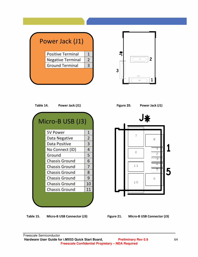
Freescale Semiconductor
Hardware User Guide for i.MX53 Quick Start Board, Preliminary Rev 0.9 64
Freescale Confidential Propietary – NDA Required
Power Jack (J1)
Micro-B USB (J3)
Positive Terminal 1
Negative Terminal 2
Ground Terminal 3
Table 14. Power Jack (J1) Figure 20. Power Jack (J1)
5V Power 1
Data Negative 2
Data Positive 3
No Connect (ID) 4
Ground 5
Chassis Ground 6
Chassis Ground 7
Chassis Ground 8
Chassis Ground 9
Chassis Ground 10
Chassis Ground 11
Table 15. Micro-B USB Connector (J3) Figure 21. Micro-B USB Connector (J3)

Freescale Semiconductor
Hardware User Guide for i.MX53 Quick Start Board, Preliminary Rev 0.9 65
PUBI – Public Use Business Information
Hardware Reference Manual for i.MX53 Quick Start
Ethernet/Dual
USB (J2)
Transmit Core Tap 1
Transmit Data Positive 2
Transmit Data Negative 3
Receive Data Positive 4
Receive Data Negative 5
NC6 6
NC7 7
NC8 8
NC9 9
Receive Core Tap 10
LED1 Anode 11
LED1 Cathode 12
LED2 Anode 13
LED2 Cathode 14
Top USB 5V Power T1
Top USB Data Negative T2
Top USB Data Positive T3
Top USB Ground T4
Bottom USB 5V Power B1
Bottom USB Data Negative B2
Bottom USB Data Positive B3
Bottom USB Ground B4
Shield Ground S1
Shield Ground S2
Shield Ground S3
Shield Ground S4
Shield Ground S5
Shield Ground S6
Shield Ground S7
Shield Ground S8
Table 16. Ethernet/Dual USB Conn (J2) Figure 22. Ethernet/Dual USB Conn (J2)

Freescale Semiconductor
Hardware User Guide for i.MX53 Quick Start Board, Preliminary Rev 0.9 66
Freescale Confidential Propietary – NDA Required
Headphone
Connector (J18)
Microphone
Connector (J6)
Right channel 1
Left Channel Ground Flag 3
Left Channel (Tip) 4
Analog Ground (Ring) 5
Plug Sense 6
Table 17. Headphone Connector (J18) Figure 23. Headphone Connector (J18)
Right channel 1
Microphone Ground Flag 3
Microphone Signal (Tip) 4
Analog Ground (Ring) 5
Plug Sense 6
Table 18. Microphone Connector (J6) Figure 24. Microphone Connector (J6)

Freescale Semiconductor
Hardware User Guide for i.MX53 Quick Start Board, Preliminary Rev 0.9 67
PUBI – Public Use Business Information
Hardware Reference Manual for i.MX53 Quick Start
VGA DB15 (J8)
Component Video Pr 1
Component Video Y 2
Component Video Pb 3
No Connect 4
Ground 5
DAC Ref Ground 6
DAC Ref Ground 7
DAC Ref Ground 8
5V VGA REF 9
Ground 10
No Connect 11
VGA I2C (Data) 12
VGA Horiz Synch 13
VGA Vert Synch 14
VGA I2C (Clock) 15
Table 19. VGA DB15 Connector (J8) Figure 25. VGA DB15 Connector (J8)

Freescale Semiconductor
Hardware User Guide for i.MX53 Quick Start Board, Preliminary Rev 0.9 68
Freescale Confidential Propietary – NDA Required
LVDS
Connector (J9)
Table 20. LVDS Connector (J9) Figure 26. LVDS Connector (J9)
Backlight Enable 1
VCC 3V2 Supply 2
VCC 3V2 Supply 3
EDID 3V2 Supply 4
LED Brightness Adjust 5
EDID I2C (Clock) 6
EDID I2C (Data) 7
LVDS Transmit 0 Negative 8
LVDS Transmit 0 Positive 9
Ground 10
LVDS Transmit 1 Negative 11
LVDS Transmit 1 Positive 12
Ground 13
LVDS Transmit 2 Negative 14
LVDS Transmit 2 Positive 15
Ground 16
LVDS Clock Negative 17
LVDS Clock Positive 18
Ground 19
Touch Panel 5V Supply 20
Touch Panel 5V Supply 21
Ground 22
Ground 23
LED 5V Supply 24
LED 5V Supply 25
LED 5V Supply 26
LVDS I2C (Clock) 27
LVDS I2C (Data) 28
LVDS I2C Interrupt 29
No Connect 30

Freescale Semiconductor
Hardware User Guide for i.MX53 Quick Start Board, Preliminary Rev 0.9 69
PUBI – Public Use Business Information
Hardware Reference Manual for i.MX53 Quick Start
SATA DATA
Connector (J7)
Table 21. SATA Data Connector (J7) Figure 27. SATA Data Connector (J7)
Ground 1
Transmit Data Positive 2
Transmit Data Negative 3
Ground 4
Receive Data Negtive 5
Receive Data Positive 6
Ground 7
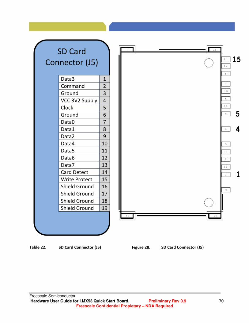
Freescale Semiconductor
Hardware User Guide for i.MX53 Quick Start Board, Preliminary Rev 0.9 70
Freescale Confidential Propietary – NDA Required
SD Card
Connector (J5)
Data3 1
Command 2
Ground 3
VCC 3V2 Supply 4
Clock 5
Ground 6
Data0 7
Data1 8
Data2 9
Data4 10
Data5 11
Data6 12
Data7 13
Card Detect 14
Write Protect 15
Shield Ground 16
Shield Ground 17
Shield Ground 18
Shield Ground 19
Table 22. SD Card Connector (J5) Figure 28. SD Card Connector (J5)

Freescale Semiconductor
Hardware User Guide for i.MX53 Quick Start Board, Preliminary Rev 0.9 71
PUBI – Public Use Business Information
Hardware Reference Manual for i.MX53 Quick Start
microSD Card
Connector (J4)
Data2 1
Data3 2
Command 3
VCC 3V3 Supply 4
Clock 5
Ground 6
Data0 7
Data1 8
Shield GND1 SH1
Shield GND2 SH2
Shield GND3 SH3
Shield GND4 SH4
Table 23. microSD Card Connector (J4) Figure 29. microSD Card Connector (J4)

Freescale Semiconductor
Hardware User Guide for i.MX53 Quick Start Board, Preliminary Rev 0.9 72
Freescale Confidential Propietary – NDA Required
Debug UART
Connector (J16)
No Connect (CD) 1
Data Transmit 2
Data Receive 3
No Connect (DTR) 4
Ground 5
No Connect (DSR) 6
No Connect (RTS) 7
No Connect (CTS) 8
No Connect (RI) 9
Shield Ground M1
Shield Ground M2
Table 24. Debug UART Connector (J16) Figure 30. Debug UART Connector (J16)

Freescale Semiconductor
Hardware User Guide for i.MX53 Quick Start Board, Preliminary Rev 0.9 73
PUBI – Public Use Business Information
Hardware Reference Manual for i.MX53 Quick Start
JTAG
Connector (J15)
1.8V Logic Reference 1
3.3V JTAG Supply Voltage 2
JTAG TAP Reset (Active Low) 3
Ground 4
JTAG Test Data In 5
Ground 6
JTAG TAP Machine State 7
Ground 8
JTAG TAP Clock 9
Ground 10
RTCK (Pulled Low) 11
Ground 12
JTAG Test Data Out 13
Ground 14
JTAG System Reset (Active Low) 15
Ground 16
Debug Request (Pulled High) 17
Ground 18
Debug Acknowledge (Pulled Low) 19
Ground 20
Table 25. JTAG Connector (J15) Figure 31. JTAG Connector (J15)

Freescale Semiconductor
Hardware User Guide for i.MX53 Quick Start Board, Preliminary Rev 0.9 74
Freescale Confidential Propietary – NDA Required
Expansion Port Connector (J13)
Table 26. Expansion Port (J13) Figure 32. Expansion Port (J13)
SH8 Shield Ground Shield Ground SH7
120 No Connect No Connect 119
118 No Connect Display Read 117
116 Display Data Ready 1.5V Power (VLDO9) 115
114 Display Horiz Synch 1.5V Power (VLDO9) 113
112 Backlight Brightness Adj 1.5V Power (VLDO9) 111
110 Display Vert Synch Display Write 109
108 Display Data23 Disp Chip Sel1 (Act Low) 107
106 Display Data22 Disp Chip Sel0 (Act Low) 105
104 Display Data21 Ground 103
102 Display Data20 Touch Screen X-Neg 101
100 Display Data19 Touch Screen X-Pos 99
98 Display Data18 Touch Screen Y-Neg 97
96 Display Data17 Touch Screen Y-Positive 95
94 Display Data16 Ground 93
92 Display Data15 IIS Reset 91
90 Display Data14 IIS Clock 89
88 Display Data13 IIS Master Out-Slave In 87
86 Display Data12 IIS Master In-Slave Out 85
84 Display Data11 Exp Card ID1 83
82 Display Data10 IIS Chip Sel (Active Low) 81
80 Display Data09 Display Power Enable 79
78 Display Data08 5V Power 77
76 Display Data07 5V Power 75
74 Display Data06 5V Power 73
72 Display Data05 No Connect 71
70 Display Data04 No Connect 69
68 Display Data03 No Connect 67
66 Display Data02 No Connect 65
64 Display Data01 Audio System Clock 63
62 Display Data00 Exp Card ID0 61
SH6 Shield Ground Shield Ground SH5

Freescale Semiconductor
Hardware User Guide for i.MX53 Quick Start Board, Preliminary Rev 0.9 75
PUBI – Public Use Business Information
Hardware Reference Manual for i.MX53 Quick Start
Expansion Port Connector (J13)
Table 26. Expansion Port (J13) Figure 32. Expansion Port
SH4 Shield Ground Shield Ground SH3
60 Ground Display Rst (Active Low) 59
58 Display Vert Synch No Connect 57
56 Display Horiz Synch No Connect 55
54 Ground Display Power Down 53
52 Display Data19 No Connect 51
50 Display Data18 3.2V Power 49
48 Ground 3.2V Power 47
46 Display Data17 3.2V Power 45
44 Display Data16 Display Data Clock 43
42 Ground No Connect 41
40 SPDIF Data Transmit No Connect 39
38 SPDIF Data Clock No Connect 37
36 Ground Display Pixel Clock 35
34 Display Data15 Display Reset 33
32 Display Data14 I2C Clock 31
30 Ground I2C Data 29
28 Display Data13 No Connect 27
26 Display Data12 1.8V Power (VLDO8) 25
24 Ground No Connect 23
22 No Connect No Connect 21
20 No Connect 1.8V Power (VLDO8) 19
18 Ground 1.8V Power (VLDO8) 17
16 No Connect Display Backlight Return 15
14 No Connect 5V Power 13
12 Ground 5V Power 11
10 No Connect Display Backlight Power 9
8 5V Power 5V Power 7
6 Ground 3.2V Power 5
4 5V Power 2.775V Power (VLDO4) 3
2 5V Power 1.8V Power (VLDO8) 1
SH2 Shield Ground Shield Ground SH1

Freescale Semiconductor
Hardware User Guide for i.MX53 Quick Start Board, Preliminary Rev 0.9 76
Freescale Confidential Propietary – NDA Required
J13 PIN J13 Name i.MX53 Pin Name ALT(1) ALT(2) ALT(3)
26 CSI0_DAT12 CSI0_DAT12 GPIO5_30 uart4 TXD_MUX
28 CSI0_DAT13 CSI0_DAT13 GPIO5_31 uart4 RXD_MUX
29 I2C2_SDA KEY_ROW3 GPIO4_13 H2_DP ASRC_EXT_CLK
31 I2C2_SCL KEY_COL3 GPIO4_12 H2_DM spdif IN1
32 CSI0_DAT14 CSI0_DAT14 GPIO6_0 uart5 TXD_MUX
33 DISP0_RESET EIM_WAIT GPIO5_0 WEIM_DTACK_B
34 CSI0_DAT15 CSI0_DAT15 GPIO6_18 uart5 RXD_MUX
35 CSI0_PIXCLK CSI0_PIXCLK GPIO5_18
38 PCLOCK GPIO_7 GPIO1_7 EPITO can1 TXCAN
40 SPDIF_TX GPIO_17 GPIO1_12 SDMA_EXT_EVENT0 PMIC_RDY
43 DISP0_DCLK DI0_DISP_CLK GPIO4_15 USBH2_DIR
44 CSI0_DAT16 CSI0_DAT16 GPIO6_2 uart4 RTS
46 CSI0_DAT17 CSI0_DAT17 GPIO6_3 uart4 CTS
50 CSI0_DAT18 CSI0_DAT18 GPIO6_4 uart5 RTS
52 CSI0_DAT19 CSI0_DAT19 GPIO6_5 uart6 CTS
53 SCSI0_PWDN NANDF_RB0 GPIO6_10
56 CSI0_VSYNCH CSI0_VSYNCH GPIO5_21
58 CSI0_HSYNCH CSI0_MCLK GPIO5_19 ccm CSI0_MCLK
59 CSI0_RSTB NANDF_WP_B GPIO6_9
62 DISP0_DAT0 DISP0_DAT0 GPIO4_21 cspi SCLK USBH2_DAT0
63 GPIO_0(CLK0) GPIO_0 GPIO1_0 KEY_COL5 SSI_EXT1_CLK
64 DISP0_DAT1 DISP0_DAT1 GPIO4_22 cspi MOSI USBH2_DAT1
66 DISP0_DAT2 DISP0_DAT2 GPIO4_23 cspi MISO USBH2_DAT2
68 DISP0_DAT3 DISP0_DAT3 GPIO4_24 cspi SS0 USBH2_DAT3
70 DISP0_DAT4 DISP0_DAT4 GPIO4_25 cspi SS1 USBH2_DAT4
72 DISP0_DAT5 DISP0_DAT5 GPIO4_26 cspi SS2 USBH2_DAT5
74 DISP0_DAT6 DISP0_DAT6 GPIO4_27 cspi SS3 USBH2_DAT6
76 DISP0_DAT7 DISP0_DAT7 GPIO4_28 cspi RDY USBH2_DAT7
78 DISP0_DAT8 DISP0_DAT8 GPIO4_29 pwm1 PWMO wdog1 WDOG_B
Legend
UART4 AUDMUX4 I2C1 ECSPI2 USBH2
UART5 AUDMUX5 I2C2 CSPI SPDIF
Table 27. Expansion Port Pin-Mux Table

Freescale Semiconductor
Hardware User Guide for i.MX53 Quick Start Board, Preliminary Rev 0.9 77
PUBI – Public Use Business Information
Hardware Reference Manual for i.MX53 Quick Start
J13 PIN J13 Name ALT(4) ALT(5) ALT(6) ALT(7)
26 CSI0_DAT12 USBH3_DATA0 DEBUG_PC6 EMI_DEBUG41 tpiu TRACE9
28 CSI0_DAT13 USBH3_DATA1 DEBUG_PC7 EMI_DEBUG42 tpiu TRACE10
29 I2C2_SDA i2c2 SDA 32K_OUT ccm PLL4_BYP usb1 LINESTATE0
31 I2C2_SCL i2c2 SCL ecspi1 SS3 fec CRS usb1 SIECLOCK
32 CSI0_DAT14 USBH3_DATA2 DEBUG_PC8 EMI_DEBUG43 tpiu TRACE11
33 DISP0_RESET
34 CSI0_DAT15 USBH3_DATA3 DEBUG_PC9 EMI_DEBUG44 tpiu TRACE12
35 CSI0_PIXCLK
DEBUG_PC0 EMI_DEBUG29
38 PCLOCK uart2 TXD_MUX firi RXD spdifPLOCK ccm PLL2_BYP
40 SPDIF_TX CE_RTC_FSV_TRIG spdif OUT1 SNOOP2 JTAG_ACT
43 DISP0_DCLK
DEBUG_CORE_STATE0 EMI_DEBUG0 usb1 AVALID
44 CSI0_DAT16 USBH3_DATA4 DEBUG_PC10 EMI_DEBUG45 tpiu TRACE13
46 CSI0_DAT17 USBH3_DATA5 DEBUG_PC11 EMI_DEBUG46 tpiu TRACE14
50 CSI0_DAT18 USBH3_DATA6 DEBUG_PC12 EMI_DEBUG47 tpiu TRACE15
52 CSI0_DAT19 USBH3_DATA7 DEBUG_PC13 EMI_DEBUG48 usb2 BISTOK
53 SCSI0_PWDN
usb1 VSTATUS3
56 CSI0_VSYNCH
DEBUG_PC3 EMI_DEBUG32 tpiu TRACE0
58 CSI0_HSYNCH
DEBUG_PC1
59 CSI0_RSTB
usb1 VSTATUS2
62 DISP0_DAT0
DEBUG_CORE_RUN EMI_DEBUG5 usb2 TXREADY
63 GPIO_0(CLK0) EPITO SRTC_ALARM_DEB USBH1_PWR csu TD
64 DISP0_DAT1
DEBUG_EVENT_CHAN_SEL EMI_DEBUG6 usb2 RXVALID
66 DISP0_DAT2
DEBUG_MODE EMI_DEBUG7 usb2 RXACTIVE
68 DISP0_DAT3
DEBUG_EVENT_BUS_ERROR EMI_DEBUG8 usb2 RXERROR
70 DISP0_DAT4
DEBUG_BUS_RWB EMI_DEBUG9 usb2 SIECLOCK
72 DISP0_DAT5
DEBUG_MATCHED_DMBUS EMI_DEBUG10 usb2 LINESTATE0
74 DISP0_DAT6
DEBUG_RTBUFFER_WRITE EMI_DEBUG11 usb2 LINESTATE1
76 DISP0_DAT7
DEBUG_EVENT_CHANNEL0 EMI_DEBUG12 usb2 VBUSVALID
78 DISP0_DAT8
DEBUG_EVENT_CHANNEL1 EMI_DEBUG13 usb2 AVALID
Legend
UART4 AUDMUX4 I2C1 ECSPI2 USBH2
UART5 AUDMUX5 I2C2 CSPI SPDIF
Table 27. Expansion Port Pin-Mux Table (con)
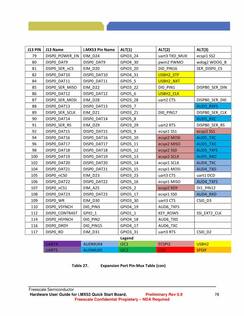
Freescale Semiconductor
Hardware User Guide for i.MX53 Quick Start Board, Preliminary Rev 0.9 78
Freescale Confidential Propietary – NDA Required
J13 PIN J13 Name i.MX53 Pin Name ALT(1) ALT(2) ALT(3)
79 DISP0_POWER_EN EIM_D24 GPIO3_24 uart3 TXD_MUX ecspi1 SS2
80 DISP0_DAT9 DISP0_DAT9 GPIO4_30 pwm2 PWMO wdog2 WDOG_B
81 DSIP0_SER_nCS EIM_D20 GPIO3_20 DI0_PIN16 SER_DISP0_CS
82 DISP0_DAT10 DISP0_DAT10 GPIO4_31 USBH2_STP
84 DISP0_DAT11 DISP0_DAT11 GPIO5_5 USBH2_NXT
85 DISP0_SER_MISO EIM_D22 GPIO3_22 DI0_PIN1 DISPB0_SER_DIN
86 DISP0_DAT12 DISP0_DAT12 GPIO5_6 USBH2_CLK
87 DISP0_SER_MOSI EIM_D28 GPIO3_28 uart2 CTS DISPB0_SER_DI0
88 DISP0_DAT13 DISP0_DAT13 GPIO5_7
AUD5_RXFS
89 DISP0_SER_SCLK EIM_D21 GPIO3_21 DI0_PIN17 DISPB0_SER_CLK
90 DISP0_DAT14 DISP0_DAT14 GPIO5_8
AUD5_RXC
91 DISP0_SER_RS EIM_D29 GPIO3_29 uart2 RTS DISPB0_SER_RS
92 DISP0_DAT15 DISP0_DAT15 GPIO5_9 ecspi1 SS1 ecspi2 SS1
94 DISP0_DAT16 DISP0_DAT16 GPIO5_10 ecspi2 MOSI AUD5_TXC
96 DISP0_DAT17 DISP0_DAT17 GPIO5_11 ecspi2 MISO AUD5_TXD
98 DISP0_DAT18 DISP0_DAT18 GPIO5_12 ecspi2 SS0 AUD5_TXFS
100 DISP0_DAT19 DISP0_DAT19 GPIO5_13 ecspi2 SCLK AUD5_RXD
102 DISP0_DAT20 DISP0_DAT20 GPIO5_14 ecspi1 SCLK AUD4_TXC
104 DISP0_DAT21 DISP0_DAT21 GPIO5_15 ecspi1 MOSI AUD4_TXD
105 DISP0_nCS0 EIM_D23 GPIO3_23 uart3 CTS uart1 DCD
106 DISP0_DAT22 DISP0_DAT22 GPIO5_16 ecspi1 MISO AUD4_TXFS
107 DISP0_nCS1 EIM_A25 GPIO5_2 ecspi2 RDY DI1_PIN12
108 DISP0_DAT23 DISP0_DAT23 GPIO5_17 ecspi1 SS0 AUD4_RXD
109 DISP0_WR EIM_D30 GPIO3_30 uart3 CTS CSI0_D3
110 DISP0_VSYNCH DI0_PIN3 GPIO4_19 AUD6_TXFS
112 DISP0_CONTRAST GPIO_1 GPIO1_1 KEY_ROW5 SSI_EXT2_CLK
114 DISP0_HSYNCH DI0_PIN2 GPIO4_18 AUD6_TXD
116 DISP0_DRDY DI0_PIN15 GPIO4_17 AUD6_TXC
117 DISP0_RD EIM_D31 GPIO3_31 uart3 RTS CSI0_D2
Legend
UART4 AUDMUX4 I2C1 ECSPI2 USBH2
UART5 AUDMUX5 I2C2 CSPI SPDIF
Table 27. Expansion Port Pin-Mux Table (con)

Freescale Semiconductor
Hardware User Guide for i.MX53 Quick Start Board, Preliminary Rev 0.9 79
PUBI – Public Use Business Information
Hardware Reference Manual for i.MX53 Quick Start
J13 PIN J13 Name ALT(4) ALT(5) ALT(6) ALT(7)
79 DISP0_POWER_EN cspi SS2 AUD5_RXFS ecspi2 SS2 uart1 DTR
80 DISP0_DAT9
DEBUG_EVENT_CHANNEL2 EMI_DEBUG14 usb2 VSTATUS0
81 DSIP0_SER_nCS cspi SS0 EPITO uart1 RTS USBH2_PWR
82 DISP0_DAT10
DEBUG_EVENT_CHANNEL3 EMI_DEBUG15 usb2 VSTATUS1
84 DISP0_DAT11
DEBUG_EVENT_CHANNEL4 EMI_DEBUG16 usb2 VSTATUS2
85 DISP0_SER_MISO cspi MISO
USBOTG_PWR
86 DISP0_DAT12
DEBUG_EVENT_CHANNEL5 EMI_DEBUG17 usb2 VSTATUS3
87 DISP0_SER_MOSI cspi MOSI i2c1 SDA EXT_TRIG DI0_PIN13
88 DISP0_DAT13
DEBUG_EVT_CHN_LINES0 EMI_DEBUG18 usb2 VSTATUS4
89 DISP0_SER_SCLK cspi SCLK i2c1 SCL USBOTG_OC
90 DISP0_DAT14
DEBUG_EVT_CHN_LINES1 EMI_DEBUG19 usb2 VSTATUS5
91 DISP0_SER_RS cspi SS0 DI0_PIN15 CSI1_VSYNCH DI0_PIN14
92 DISP0_DAT15
DEBUG_EVT_CHN_LINES2 EMI_DEBUG20 usb2 VSTATUS6
94 DISP0_DAT16 SDMA_EXT_EVENT0 DEBUG_EVT_CHN_LINES3 EMI_DEBUG21 usb2 VSTATUS7
96 DISP0_DAT17 SDMA_EXT_EVENT1 DEBUG_EVT_CHN_LINES4
98 DISP0_DAT18 AUD4_RXFS DEBUG_EVT_CHN_LINES5 EMI_DEBUG23 WEIM_CS2
100 DISP0_DAT19 AUD4_RXC DEBUG_EVT_CHN_LINES6 EMI_DEBUG24 WEIM_CS3
102 DISP0_DAT20
DEBUG_EVT_CHN_LINES7 EMI_DEBUG25 sata_phy TDI
104 DISP0_DAT21
DEBUG_BUS_DEVICE0 EMI_DEBUG26 sata_phy TDO
105 DISP0_nCS0 DI0_DO_CS DI1_PIN2 CSI1_DATA_EN DI1_PIN14
106 DISP0_DAT22
DEBUG_BUS_DEVICE1 EMI_DEBUG27 sata_phy TCK
107 DISP0_nCS1 cspi SS1
DIO_D1_CS
108 DISP0_DAT23
DEBUG_BUS_DEVICE2 EMI_DEBUG28 sata_phy TMS
109 DISP0_WR DI0_PIN11 DISP1_DAT21 USBH1_OC USBH2_OC
110 DISP0_VSYNCH
DEBUG_CORE_STATE3 EMI_DEBUG3 usb1 IDDIG
112 DISP0_CONTRAST pwm2 PWMO wdog2 WDOG_B esdhc1 CD src TESTER_ACK
114 DISP0_HSYNCH
DEBUG_CORE_STATE2 EMI_DEBUG2 usb1 ENDSSN
116 DISP0_DRDY
DEBUG_CORE_STATE1 EMI_DEBUG1 usb1 BVALID
117 DISP0_RD DI0_PIN12 DISP1_DAT20 USBH1_PWR USBH2_PWR
Legend
UART4 AUDMUX4 I2C1 ECSPI2 USBH2
UART5 AUDMUX5 I2C2 CSPI SPDIF
Table 27. Expansion Port Pin-Mux Table (con)

Freescale Semiconductor
Hardware User Guide for i.MX53 Quick Start Board, Preliminary Rev 0.9 80
Freescale Confidential Propietary – NDA Required
7. Board Accessories
7.1. HDMI Daughter Card
For developers wishing to output video via HDMI, there is an optional HDMI daughter card which can be
purchased for use with the Quick Start board. The part number for the optional card is
MCIMXHDMICARD, and this card can be purchased directly from Freescale.com. This HDMI card is
connected to J13, and occupies the Expansion Port. The brass standoff on the HDMI card is threaded to
accept a standard metric M3 machine screw. This will allow for a more sturdy connection if the
developer plans to work with HDMI for a long period of time. Figure 33 below shows the HDMI card that
is available.
The schematics for the HDMI daughter card can be found on the freescale.com/imxquickstart website.
The daughter card uses the Silicon Image SiI9022 HDMI Transmitter to reformat the display signals into
the correct HDMI format and drive the video signals out the attached HDMI cable. Common Mode
Chokes have been placed on the output of the Transmitter to meet FCC and CE emissions requirements.
Figure 33. Optional HDMI Daughter Card
Freescale Semiconductor
Hardware User Guide for i.MX53 Quick Start Board, Preliminary Rev 0.9 81
PUBI – Public Use Business Information
Hardware Reference Manual for i.MX53 Quick Start
In order to use the optional HDMI card with the Quick Start board, the environmental variables must be
correctly set to support the card. This change needs to be done only one time, when the HDMI card is
first used. The change requires the developer to use a host computer running a terminal window. When
the power button is first pressed, the developer has 3 seconds to defeat the AUTOBOOT feature by
pressing any key on the host computer. Once the boot cycle has been stopped, the developer now has
access to change the boot environmental variables on the software image. At the terminal window, the
developer should type the following two lines, pressing the enter key after each line:
setenv bootargs_base ‘set bootargs console=ttymxc0,115200 ${hdmi}’
saveenv
Once the change is saved (saveenv), the Quick Start board can be turned off and then back on, or the
developer can type boot on the terminal to restart the boot process. The Quick Start board is now
correctly configured for HDMI operation. A note for developers: The HDMI parameters are contained in
the U-BOOT code, and the recommended line to change the video output parameters only tells U-BOOT
to substitute the stored parameters into the boot process. If the developer wishes to enter the exact
string of variables into the U-BOOT code, the following line can be used instead of the first line above:
setenv bootargs_base ‘set bootargs console=ttymxc0,115200 video=mxcdi0fb:RGB24,1024x768M-16@60’
The above entry is all one line. After the line entry is made, the saveenv entry is also needed.

Freescale Semiconductor
Hardware User Guide for i.MX53 Quick Start Board, Preliminary Rev 0.9 82
Freescale Confidential Propietary – NDA Required
7.2. LCD Display Daughter Card
For developers wishing to output video to a touch screen LCD, there is an optional WVGA daughter card
which can be purchased for use with the Quick Start board. The part number for the optional card is
MCIMX28LCD, and this card can be purchased directly from Freescale.com. This LCD Display card is
connected to J13, and occupies the Expansion Port. The brass standoff on the LCD Display card nearest
the connector is threaded to accept a standard metric M3 machine screw. This will allow for a more
sturdy connection if the developer plans to work with LCD display for a long period of time. In addition,
the developer may also wish to screw into the remaining 3 brass stand-offs metric M3 machines screws
that are approximately 25mm long. The screws can be adjust to provide support to the LCD card as it
hangs over the Quick Start board. Figure 34 below shows the LCD card that is available.
The schematics for the LCD Display daughter card can be found on the freescale.com/imxquickstart
website. The daughter card uses the Seiko 43WVF1G-0 WVGA display, and provides all the power
required for correct operations, regulated on the Display card. Power for the LCD Display, with the
exception of the back light circuitry, comes from the MAIN_5V power source and does not go through
the Dialog DA9053 PMIC.
Figure 34. MCIMX28LCD 4.3” WVGA Display Daughter Card

Freescale Semiconductor
Hardware User Guide for i.MX53 Quick Start Board, Preliminary Rev 0.9 83
PUBI – Public Use Business Information
Hardware Reference Manual for i.MX53 Quick Start
In order to use the optional LCD daughter card with the Quick Start board, the environmental variables
must be correctly set to support the card. This change needs to be done only one time, when the LCD
Display card is first used. The change requires the developer to use a host computer running a terminal
window. When the power button is first pressed, the developer has 3 seconds to defeat the AUTOBOOT
feature by pressing any key on the host computer. Once the boot cycle has been stopped, the developer
now has access to change the boot environmental variables on the software image. At the terminal
window, the developer should type the following two lines, pressing the enter key after each line:
setenv bootargs_base ‘set bootargs console=ttymxc0,115200 ${lcd}’
saveenv
Once the change is saved (saveenv), the Quick Start board can be turned off and then back on, or the
developer can type boot on the terminal to restart the boot process. The Quick Start board is now
correctly configured for LCD operation. A note for developers: The LCD parameters are contained in the
U-BOOT code, and the recommended line to change the video output parameters only tells U-BOOT to
substitute the stored parameters into the boot process. If the developer wishes to enter the exact string
of variables into the U-BOOT code, the following line can be used instead of the first line above:
setenv bootargs_base ‘set bootargs console=ttymxc0,115200 video=mxcdi0fb:RGB24,SEIKO-WVGA
The above entry is all one line. After the line entry is made, the saveenv entry is also needed.

Freescale Semiconductor
Hardware User Guide for i.MX53 Quick Start Board, Preliminary Rev 0.9 84
Freescale Confidential Propietary – NDA Required
7.3. LVDS Display Set (Coming Soon)
For developers wishing to output video to a LVDS panel, there is an optional LVDS panel which can be
purchased for use with the Quick Start board. The part number for the optional card is MCIMX-LVDS,
and may be purchased directly from Freescale.com. The LVDS Display kit comes with the panel,
mounted in a frame, and a 15 inch cable that will connect directly to the LVDS connector (J9) on the
Quick Start board. The LVDS panel can be used in parallel with the other video outputs (VGA, HDMI,
LCD) giving the developer a second screen if desired. Figure 35 below shows the LVDS Display available.
The LVDS display is the same panel used on the i.MX53 SMD Tablet. The LVDS module is manufactured
by HannStar Display Corp and is part number HSD100PXN1-A00-C11. The two support legs can be
inserted in the corresponding slots on the frame to allow the developer to chose any desired display
orientation.
Figure 35. LVDS Display Kit
Place Holder Picture.
Need a better one.

Freescale Semiconductor
Hardware User Guide for i.MX53 Quick Start Board, Preliminary Rev 0.9 85
PUBI – Public Use Business Information
Hardware Reference Manual for i.MX53 Quick Start
In order to use the optional LVDS Display Panel with the Quick Start board, the environmental variables
must be correctly set to support the card. This change needs to be done only one time, when the LVDS
Panel is first used. The change requires the developer to use a host computer running a terminal
window. When the power button is first pressed, the developer has 3 seconds to defeat the AUTOBOOT
feature by pressing any key on the host computer. Once the boot cycle has been stopped, the developer
now has access to change the boot environmental variables on the software image. At the terminal
window, the developer should type the following two lines, pressing the enter key after each line:
setenv bootargs_base ‘set bootargs console=ttymxc0,115200 ${lvds}’
saveenv
Once the change is saved (saveenv), the Quick Start board can be turned off and then back on, or the
developer can type boot on the terminal to restart the boot process. The Quick Start board is now
correctly configured for outputting video to the LVDS panel. A note for developers: The LVDS sd
parameters are contained in the U-BOOT code, and the recommended line to change the video output
parameters only tells U-BOOT to substitute the stored parameters into the boot process. If the
developer wishes to enter the exact string of variables into the U-BOOT code, the following line can be
used instead of the first line above:
setenv bootargs_base ‘set bootargs console=ttymxc0,115200 video=mxcdi0fb:RGB666,XGA ldb’
The above entry is all one line. After the line entry is made, the saveenv entry is also needed.

Freescale Semiconductor
Hardware User Guide for i.MX53 Quick Start Board, Preliminary Rev 0.9 86
Freescale Confidential Propietary – NDA Required
8. Mechanical PCB Information
The overall dimensions of the i.MX53 Quick Start PCB are shown in Figure 36. Quick Start Board
Dimensions.
3 Inches
3 Inches
Figure 36. Quick Start Board Dimensions
The Printed Circuit Board was made using standard 8-layer technology. The material used was FR-4 Hi
Temp. The board stack up is as follows:
� Top Layer
� Ground-1 Layer
� Signal-1 Layer
� Power-1 Layer
� Power-2 Layer
� Signal-2 Layer
� Ground-2 Layer
� Bottom Layer

Freescale Semiconductor
Hardware User Guide for i.MX53 Quick Start Board, Preliminary Rev 0.9 87
PUBI – Public Use Business Information
Hardware Reference Manual for i.MX53 Quick Start
The stack up information provided by the PCB Fabrication Facility is as shown in Table 28. Board Stack
up information. Widths and thickness are shown in mils. Impedances are shown in Ohms. The material
used in calculating this stack up was 370HR.
Single End Trace Differential Pair Traces
Lay
er
Th
ick
ne
ss
De
scri
pti
on
Co
pp
er
Oz.
Tra
ce W
idth
Ca
lcu
late
d
Imp
ed
an
ce
Ta
rge
t
Imp
ed
an
ce
Re
fere
nce
Pla
ne
Tra
ce W
idth
Sp
ace
Wid
th
Dif
f P
air
s
(Pit
ch)
Ca
lcu
late
d
Imp
ed
an
ce
Ta
rge
t
Imp
ed
an
ce
Re
fere
nce
Pla
ne
0.70 Mask
1.20 Plating
1 0.60 Signal 0.50 8.50 50.32 50 2 4.75 5.25 10 100.82 100 2
3.25 73.94 75 2 6.25 4.75 11 89.51 90 2
5.00 Prepreg
2 0.60 GND 0.50
4.00 Core
3 0.44 Signal 0.37 3.75 6.25 10 89.69 90 2,4
3.25 49.60 50 2,4 3.00 6.00 9 99.88 100 2,4
3.00 Prepreg
4 0.60 Power 0.50
30.00 Core
5 0.60 Power 0.50
3.00 Prepreg
6 0.44 Signal 0.37 3.75 6.25 10 89.69 90 5,7
3.25 49.60 50 5,7 3.00 6.00 9 99.88 100 5,7
4.00 Core
7 0.60 GND 0.50
5.00 Prepreg
8 0.60 Signal 0.50 8.50 50.32 50 7 4.75 5.25 10 100.82 100 7
3.25 73.94 75 7 6.25 4.75 11 89.51 90 7
1.20 Plating
0.70 Mask
62.28 = Total Thickness
Table 28. Board Stack up information

Freescale Semiconductor
Hardware User Guide for i.MX53 Quick Start Board, Preliminary Rev 0.9 88
Freescale Confidential Propietary – NDA Required
9. Board Verification
The On Board Diagnostic Scan (OBDS) tool used by the factory acceptance test tools is included on the
MicroSD card image that is shipped with the i.MX53 Quick Start board. If the original image is corrupted
or over-written by the software developer, a fresh image can be downloaded from the
freescale.com/imxquickstart web site.
To access the OBDS tool, a serial cable and a host PC running a terminal program (TerraTerminal,
HyperTerminal, etc) will be required. After connecting the host terminal to the Quick Start board, press
the power button on the board. Before U-BOOT completes the Autoboot countdown (3 seconds) press
any key on the host computer. This will stop the Ubuntu Kernel from continuing the boot process and
allow the developer to access the code on the MicroSD card. On the host computer terminal window,
type the following line:
Ext2load mmc 0:1 0x70800000 /unit_tests/obds.bin
After the prompt returns:
Loading file “/unit_tests/obds.bin” from mmc device 0:1 (xxa1)
XXXXXX bytes read
Type:
go 70800000
This will begin the OBDS diagnostic tool. The tool has 16 tests that it can perform. They are as follows:
MAC Address confirmation
Debug UART Test
DDR3 Test
USBH1 Enumeration Test (Upper Host Port)
Secure Real Time Clock Test
Dialog PMIC ID Test
SATA Test
I2C Device Test
GPIO Test
Ethernet Test
I2S Audio Test
LCD Daughter Card Test
LVDS Display Test
VGA Video Test
HDMI Daughter Card Test
MMC/SD Card Test

Freescale Semiconductor
Hardware User Guide for i.MX53 Quick Start Board, Preliminary Rev 0.9 89
PUBI – Public Use Business Information
Hardware Reference Manual for i.MX53 Quick Start
The first question that the user will be asked by the OBDS test is if the user would like to AUTORUN the
OBDS test. A yes answer (y or Y) will keep the OBDS test from prompting the user for any test that does
not require direct user action. Any other key press will cause the OBDS test to prompt for all tests. A yes
answer to this question is primarily for mass testing of Quick Start boards. Single users of this test can
run this test with prompts without significant loss of time.
The tests are straight forward, and if a supporting piece of equipment is required, the test will prompt
the user for it. In order to complete all the tests, you would need to have the following equipment:
USB HOST1 Test – Attached USB device required
SATA Test – Attached SATA device required.
Ethernet Test – The Ethernet loop back test plug as described below is required.
Head Phone Test – A set of earphones or speakers are required.
LCD Test – The optional LCD Display card is required
LVDS Test – The optional LVDS display kit is required
VGA Video Test – Connection to a VGA monitor is required
HDMI Test – The optional HDMI card is required
MMC/SD Card slot – A full size SD card is required in card slot J5.
If the developer does not have one or more of the above items, the test can easily be skipped when
asked if the user would like to perform the test. A complete cycle of tests covers 16 different aspects of
the board. When the last test is run, the OBDS tool will print out a summary of the test results. A failure
in any one particular area would indicate that there is a hardware fault with the Quick Start board that
should be addressed. If all tests pass, but the developer code does not function correctly, the problem is
most likely with the code. A more detailed description of the tests is as follows:
1) MAC Address confirmation. The i.MX53 Processor reads the MAC Address programmed into the
Processor eFUSEs and prints them out on the terminal window. The resulting print out should
match the MAC address label on the Quick Start board. If the two numbers match, the test has
passed.
2) UART Test. When the test is running, the test expects different characters to be input from the
keyboard of the host computer. After a character is input, the i.MX53 Processor receives the
input, transmits to the terminal window the received character, and then asks the user to
confirm that the character is correct by pressing the ‘x’ key. The test is exited by typing an ‘x’ as
an input character.
3) DDR Test. The test writes predetermined data onto the DDR3 memory, reads those memory
blocks back out, and then compares the two values for errors. If the values match, the test
passes.
4) USBH1 Enumeration Test. Any USB device is plugged into the upper HOST connector (the lower
port is connected to the USBOTG module). After confirming that a USB device is plugged in, the
I.MX53 will read the device enumeration data and print it out on the terminal window. If the
Processor cannot read enumeration information, the test fails.
Freescale Semiconductor
Hardware User Guide for i.MX53 Quick Start Board, Preliminary Rev 0.9 90
Freescale Confidential Propietary – NDA Required
5) Secure Real Time Clock Test. The i.MX53 Processor checks to make sure the RTC clock is
counting. If the clock is counting, the test passes.
6) PMIC Device ID Test. The i.MX53 Processor attempts to communicate with the PMIC using the
attached I2C channel. If the two devices communicate, the test passes.
7) SATA Test. The processor attempts to communicate with an attached SATA device. If the
processor detects the internal 50 MHz clock signal and communications coming from an
attached SATA device, the test passes.
8) I2C Test. The processor attempts to communicate with one of the I2C devices on the Quick Start
board. If communications complete correctly, the test passes.
9) GPIO Test. The Processor drives the USER LED light controlled by PATA_DA_1 (pin L3) alternately
high and low. If the user light appears to blink, the test passes.
10) FEC Ethernet Test. The Processor drives a data packet out of the Ethernet Jack, into the loop
back cable, and then receives the test packet back. If the received packet matches the sent
packet, the test passes.
11) I2S Audio Test. The Processor gives a tone to the Audio CODEC. If the tone can be heard through
both speakers of the attached headphones, the test passes. After the user requests the test to
be run, the user is prompted to insert a headphone set into jack (J18). When the headphones
are connected, the user presses the ‘y’ key to confirm the headphones are attached. A sound
will play. The test will then prompt you to replay the tone if needed. If the tone is no longer
needed, the test will then prompt for an answer as to whether the tone was heard or not.
12) LCD Display test. If this test is selected, an image will be displayed on the attached LCD card.
Once the image is displayed, the test will prompt the user to confirm whether or not the image
is seen. If the image is seen, the test passes.
13) LVDS Display test. If this test is selected, an image will be displayed on the attached LVDS Panel.
Once the image is displayed, the test will prompt the user to confirm whether or not the image
is seen. If the image is seen, the test passes.
14) VGA Video test. If this test is selected, an image will be displayed on the attached video monitor.
Once the image is displayed, the test will prompt the user to confirm whether or not the image
is seen. If the image is seen, the test passes.
15) HDMI test. If this test is selected, an image will be displayed on the attached video monitor.
Once the image is displayed, the test will prompt the user to confirm whether or not the image
is seen. If the image is seen, the test passes.

Freescale Semiconductor
Hardware User Guide for i.MX53 Quick Start Board, Preliminary Rev 0.9 91
PUBI – Public Use Business Information
Hardware Reference Manual for i.MX53 Quick Start
16) MMC/SD Test. If the user selects this test to be run, the user will be prompted to insert an
MMC/SD card into the full size SD Card slot (J5). When the user confirms that the card is
present, the processor will attempt to read the current SD card settings and manufacturing
information on the SD card. If the Processor can read this information, the test passes.
The only special equipment required to complete the bank of OBDS tests is the Ethernet Loop back
cable. This can be purchased on line (single plug Ethernet Lookback Cable) or it can be created by the
developer by cutting one end of an unneeded Ethernet cable and connecting the wire from pin 1 to the
wire from pin3, and connecting the wire from pin 2 to the wire from pin 6. All other wires remain
unconnected. The four wires used will be solid Green, solid Orange, Green/White stripe, and
Orange/White stripe. The solid colors are connected together and the striped colors are connected
together. While the solid colors will always be connected to pins 2 and 6, the specific pin a color is
attached to will depend on which plug is used. They same is true for the striped wires connected to
pins1 and 3. A diagram of this cable is shown in Figure 37 below.
Figure 37. Ethernet Loopback Cable
Freescale Semiconductor
Hardware User Guide for i.MX53 Quick Start Board, Preliminary Rev 0.9 92
Freescale Confidential Propietary – NDA Required
10. Troubleshooting
The i.MX53 Quick Start board does not have specific troubleshooting features designed into the board.
The board has proven robust during the initial test and development periods and should provide years
of good service to the developer if treated with due caution. The test pads that are included on the
schematic and on the board were not specifically designed for testing, but were placed on the board for
developers who wanted to make wire connections to specific pins that might not be available without
the test pads. One basic troubleshooting technique that is available to developers is to measure the
voltage rails outputs on all the rails coming from the PMIC. The subsection on PMIC voltage rails
presents a diagram with points the developer can use to make measurements. A second basic
troubleshooting technique would be to measure clock frequencies to ensure the clock are running
correctly. The position of the crystals and oscillators are in the design section under the i.MX53
Applications Processor.
Aside from actual hardware difficulties, the Table 29 presents some other issues that may help the
developer solve technical difficulties:
Symptoms Possible Problem Action
No 5V power to the Quick Start
board, no Green LED light.
Attached power supply is not
within the 4.5V – 5.5V window.
Use the power supply that came
with the Quick Start board kit.
Fuse F1 has blown. Use
multimeter to check for open.
Replace the fuse with a new 3A,
0603 surface mount fuse.
Intermittent signal on Debug
UART, or color issues on VGA
video output.
Cold solder connection on
connector pins have broken
loose after several cable
insertions.
Examine the pins on the affected
connector (J8 or J16). If a pin can
wiggle back and forth, a solder
iron should be used to reconnect
the pin. Note: There is epoxy
over the pins to increase pin
strength. The epoxy may need to
be removed first.
No Debug information on the
Host Computer Terminal
Window.
Incorrect Serial Cable used (eg
Null modem cable)
Verify that serial cable is correct.
Lower USB Host Port is not
working correctly.
Quick Start board is attached to
a Host device through the Micro-
B Connector.
Remove cable from Micro-B
connector if Lower USB Host
Port operations is desired.
Table 29. Problem Resolution Table
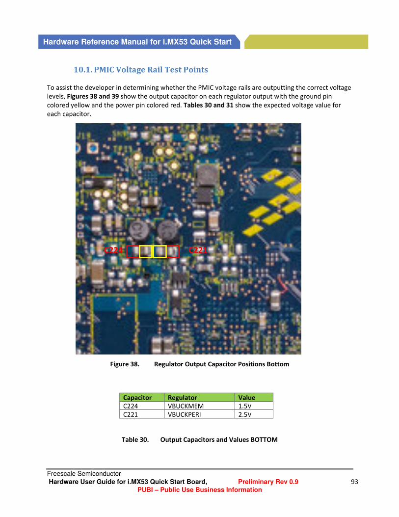
Freescale Semiconductor
Hardware User Guide for i.MX53 Quick Start Board, Preliminary Rev 0.9 93
PUBI – Public Use Business Information
Hardware Reference Manual for i.MX53 Quick Start
10.1. PMIC Voltage Rail Test Points
To assist the developer in determining whether the PMIC voltage rails are outputting the correct voltage
levels, Figures 38 and 39 show the output capacitor on each regulator output with the ground pin
colored yellow and the power pin colored red. Tables 30 and 31 show the expected voltage value for
each capacitor.
Figure 38. Regulator Output Capacitor Positions Bottom
Capacitor Regulator Value
C224 VBUCKMEM 1.5V
C221 VBUCKPERI 2.5V
Table 30. Output Capacitors and Values BOTTOM
C221 C224
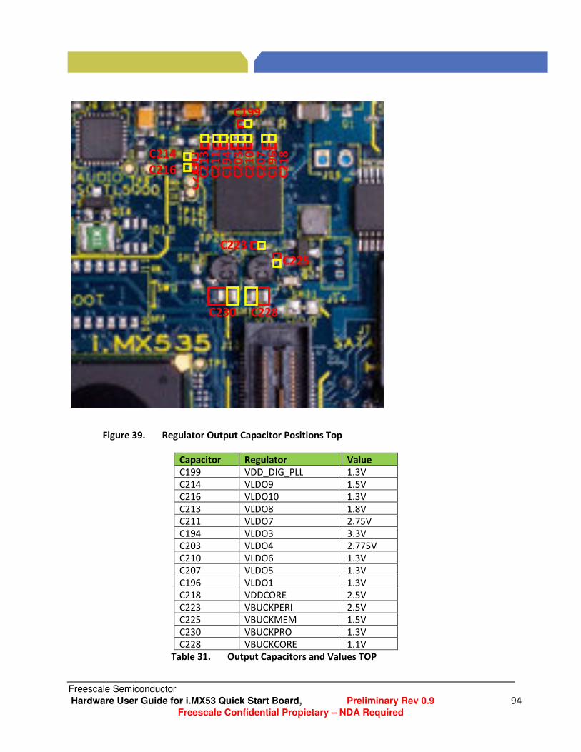
Freescale Semiconductor
Hardware User Guide for i.MX53 Quick Start Board, Preliminary Rev 0.9 94
Freescale Confidential Propietary – NDA Required
Figure 39. Regulator Output Capacitor Positions Top
Capacitor Regulator Value
C199 VDD_DIG_PLL 1.3V
C214 VLDO9 1.5V
C216 VLDO10 1.3V
C213 VLDO8 1.8V
C211 VLDO7 2.75V
C194 VLDO3 3.3V
C203 VLDO4 2.775V
C210 VLDO6 1.3V
C207 VLDO5 1.3V
C196 VLDO1 1.3V
C218 VDDCORE 2.5V
C223 VBUCKPERI 2.5V
C225 VBUCKMEM 1.5V
C230 VBUCKPRO 1.3V
C228 VBUCKCORE 1.1V
Table 31. Output Capacitors and Values TOP
C2
13
C2
13
C2
11
C1
94
C2
03
C2
10
C2
07
C1
96
C2
18
C199
C214
C216
C223
C225
C230 C228
Freescale Semiconductor
Hardware User Guide for i.MX53 Quick Start Board, Preliminary Rev 0.9 95
PUBI – Public Use Business Information
Hardware Reference Manual for i.MX53 Quick Start
11. Known Issues
At the initial launching of the Quick Start board, the following issues are known to exist:
1) SATA boot will not function with the sample grade i.MX53 ICs (rev 2.0 prototype silicon). The
problem is an IC problem related to using the internal SATA clock. Since the external clock
components have been removed from the Quick Start board, the SATA boot feature is not
usable. The work around is to initialize SATA with minimum code on a microSD card, then pass
the boot process to the SATA drive early. This problem is being fixed with the rev 2.1 production
silicon i.MX53 Processor.
2) There is a defect in the Video Processing Unit (VPU) of the i.MX53 Processor (rev 2.0). The
defect causes the DDR3 SDRAM to miscalculate some blocks in video processing resulting in
defects observable on the video output in high processing modes (1080p). This defect is being
corrected on the rev 2.1 production silicon i.MX53 processor. For initial production Quick Start
boards, the VCC voltage is being raised to 1.35V. This is not a recommended solution for
customer use, but is sufficient for development work on the Quick Start board.
3) The Dialog DA9053 PMIC rev AA silicon has a 1.2A limitation of the VDDOUT supply rail. This is
the voltage supply for all the PMIC regulators. The i.MX53 demonstration software is drawing
close to the 1.2A limit, and at times, voltage dips occur on the VDDOUT supply rail as the Quick
Start board tries to draw more power than the PMIC can supply. This has led to some abrupt
shutdowns in the testing cycle, as VDDOUT dips down below the allowed threshold. When it
becomes available, the DA9053 rev BB silicon will increase the current limit to 1.8A. For the
initial Quick Start boards, a 220 uF capacitor has been placed across JP19 pin2 and JP2 to
smooth out sudden momentary drops in voltage. This fix is only being used for the preliminary
rev AA silicon.

Freescale Semiconductor
Hardware User Guide for i.MX53 Quick Start Board, Preliminary Rev 0.9 96
Freescale Confidential Propietary – NDA Required
12. PCB Component Locations
To aid the developer in locating major components on the Quick Start board, their locations have been
highlighted and annotated in the same way that the connectors have been highlighted. These pictures
are presented as the following Figures:
Figure 40. Major Component Highlights Top
Figure 41. Major Component Highlights Bottom
The Assembly Drawings for all component locations are shown in a picture format for easy reference
when using this document. The actual Gerber artwork for the assembly drawings is available from the
i.MX53 Quick Start web site. The Assembly drawings are shown in the following figures:
Figure 42. Assembly Drawing Top
Figure 43. Assembly Drawing Bottom

Freescale Semiconductor
Hardware User Guide for i.MX53 Quick Start Board, Preliminary Rev 0.9 97
PUBI – Public Use Business Information
Hardware Reference Manual for i.MX53 Quick Start
U2 i.MX53 Application Processor U20 Dialog DA9053 PMIC
U3 DDR3 SDRAM U23 MMA8450QT Accelerometer
U5 DDR3 SDRAM U24 RS232 UART Transceiver
U9 SGTL5000 Audio CODEC F1 3A Fuse
Figure 40. Major Component Highlights Top
U2
U5 U3
U9
U20
U24
U23
F1

Freescale Semiconductor
Hardware User Guide for i.MX53 Quick Start Board, Preliminary Rev 0.9 98
Freescale Confidential Propietary – NDA Required
U1 3.2V Voltage Regulator
U4 DDR3 SDRAM
U6 DDR3 SDRAM
U17 Ethernet PHY
Figure 41. Major Component Highlights Bottom
U17
U1
U4 U6

Freescale Semiconductor
Hardware User Guide for i.MX53 Quick Start Board, Preliminary Rev 0.9 99
PUBI – Public Use Business Information
Hardware Reference Manual for i.MX53 Quick Start
Figure 42. Assembly Drawing Top
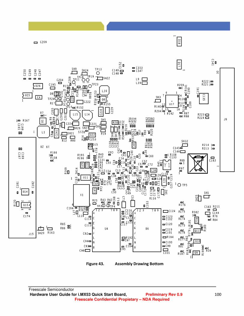
Freescale Semiconductor
Hardware User Guide for i.MX53 Quick Start Board, Preliminary Rev 0.9 100
Freescale Confidential Propietary – NDA Required
Figure 43. Assembly Drawing Bottom

Freescale Semiconductor
Hardware User Guide for i.MX53 Quick Start Board, Preliminary Rev 0.9 101
PUBI – Public Use Business Information
Hardware Reference Manual for i.MX53 Quick Start
13. Schematics
The main portion of the schematics consist of 13 pages. These pages are shown here for reference
purposes. They can be found in the original Cadence Allegro-OrCAD format (.DSN file) and in a PDF
format on the i.MX53 Quick Start web site. The following figures show the schematic pages:
Figure 44. DC 5V INPUT
Figure 45. MX53 POWER
Figure 46. MX53 DDR3 MEMORY
Figure 47. MX53 CONTROL
Figure 48. MX53 USB
Figure 49. MX53 SD INTERFACE
Figure 50. MX53 AUDIO
Figure 51. MX53 SATA
Figure 52. MX53 VGA
Figure 53. MX53 ETHERNET
Figure 54. EXPANSION HEADER
Figure 55. DA9053 PMIC
Figure 56. DEBUG, ACCELEROMETER

Freescale Semiconductor
Hardware User Guide for i.MX53 Quick Start Board,
Freescale Confidential Propietary
Figur
for i.MX53 Quick Start Board, Preliminary Rev 0.9
Freescale Confidential Propietary – NDA Required
Figure 44. DC 5V INPUT
102

Fre
escale
Sem
iconducto
r
Hard
ware
User G
uid
e fo
r i.MX
53 Q
uic
k S
tart B
oard
, Pre
limin
ary
Re
v 0
.9 1
03
PU
BI –
Pu
blic
Use B
us
ine
ss In
form
atio
n
Ha
rdw
are
Re
fere
nce
Ma
nu
al fo
r i.MX
53
Qu
ick
Sta
rt
Figu
re 4
5.
MX
53
PO
WE
R
SH27
0
C49
0.01UF
C46
0.1UF
C70
0.1UF
VDDA_1V3
C50
0.01UF
C47
0.1UF
NVCC_SRTC
i.MX53 - POWER
U2E
GND_1A1
GND_2A2
GND_3A11
GND_4A13
GND_5A18
GND_6A22
GND_7A23
GND_8B1
GND_9B11
GND_10B13
GND_11B18
GND_12B23
GND_13C12
GND_14C20
GND_15C21
GND_16D19
GND_17E19
GND_18F19
GND_19F20
GND_20F21
GND_21F22
GND_22G7
VDDGP_1G8
VDDGP_2G10
VDDGP_3G11
VDDGP_4H7
VDDGP_5H9
VCC_1H13
VCC_2J14
VCC_3J16
VCC_4K13
VCC_5K15
VCC_6L14
VCC_7L16
NVCC_EMI_DRAM_1H18
NVCC_EMI_DRAM_2K17
NVCC_EMI_DRAM_3N17
NVCC_EMI_DRAM_4P17
NVCC_EIM_MAIN_1U9
NVCC_EIM_MAIN_2U10
NVCC_EIM_SECU7
NVCC_LCD_1J6
SVCCB22
NVCC_CSIR7
NVCC_FECF11
NVCC_GPIOF8
NVCC_JTAGG9
NVCC_KEYPADF7
VDD_ANA_PLLG16
VDD_DIG_PLLH17
NVCC_XTALV12
NVCC_SRTC_POWV11
FASTR_ANAE18
FASTR_DIGE17
VDD_FUSEG15
VDDA_1G12
VDDA_2M7
NVCC_RESETH16
GND_23G19
GND_24H8
GND_25H10
GND_26H12
GND_27J9
GND_28J11
GND_29J13
GND_30J15
GND_31J17
GND_32J20
GND_33K8
VDDGP_6H11
VDDGP_7J8
VDDGP_8J10
VDDGP_9J12
VDDGP_10K7
VDDGP_11K9
VDDGP_12K11
VCC_8M9
VCC_9M11
VCC_10M13
VCC_11M15
VCC_12N8
VCC_13N10
VCC_14N12
VCC_15N14
VCC_16N16
NVCC_PATAN7
NVCC_SD1H15
NVCC_SD2H14
VDDA_3M17
VDDAL1F9
NVCC_CKIHG17
NVCC_NANDFT12
SVDDGPB2
GND_94AB22
GND_95AB2
VDDGP_13L8
VDDGP_14L10
VDD_REGG18
VDDGP_15L12
NVCC_EMI_DRAM_5T18
GND_34K10
GND_35K12
GND_36K14
GND_37K16
GND_38K21
GND_39L7
GND_40L9
GND_41L11
GND_42L13
GND_43L15
GND_44M8
GND_45M10
GND_46M12
GND_47M14
GND_48M16
GND_49N9
GND_50N11
GND_51N13
GND_52N15
GND_53P7
GND_54P8
GND_55P10
GND_56P12
GND_57P14
GND_58P16
GND_59P21
GND_60R9
GND_61R11
GND_62R13
GND_63R15
GND_64R17
GND_65R20
GND_66T8
GND_67T10
GND_68AA11
GND_69T14
GND_70T16
GND_71U15
GND_72U19
GND_73V15
GND_74V18
GND_75V19
GND_76V20
GND_77V21
GND_78V22
GND_79W19
GND_80Y14
GND_81Y15
GND_82Y19
GND_83AA15
GND_84AA20
GND_85AA21
GND_86AB1
GND_87AB18
GND_88AB23
GND_89AC1
GND_90AC2
GND_91AC18
GND_92AC22
GND_93AC23
VCC_17P9
VCC_18P11
VCC_19P13
VCC_20P15
VCC_21R8
VCC_22R10
VCC_23R12
VCC_24R14
VCC_25R16
VCC_26T7
VCC_27T9
VCC_28T11
VCC_29T13
VCC_30T15
VCC_31T17
VCC_32U8
VCC_33U18
VDDA_4U12
NVCC_LCD_2J7
C45
22UF
C72
0.1UF
C52
0.1UF
NVCC_XTAL_2V5
C69
0.1UF
To VBUCKPERI
@2.5V 1A max.
VDDGP
SH9
0
C53
0.1UF
VIOHI_2V775
SATA_PHY_2V5
3.3V
VLDO5_1V3
C54
0.1UF
1.8V
1.8V
VLDO8_1V8
SH25
0
THIS MUST BE POWERED UP FIRST
SATA_1V3
TP2
VUSB_2V5
C55
0.1UF
C41
22UF
SH1
0
SH29
0
C68
0.1UF
R20
0.02
DNP
C56
0.1UF
VLDO8_1V8
VBUCKCORE
C35
0.22UF
C16
0.22UF
C12
0.22UF
GND
C27
0.22UF
GND
SD1_3V3
3.3V
3.3V
3.3V
3.3V
3.3V
3.3V
3.3V
C13
0.22UF
GND
SH2
0
C29
0.22UF
VDDAL_1V3
C21
0.22UF
VBUCKMEM
C44
0.1UF
C37
0.22UF
C14
0.22UF
C51
22UF
C57
0.1UF
VPERI_SW
VMEM_SW
R190
To VBUCKPRO
@1.3V 1A max.
To VBUCKCORE
@0.85-1.3V 2A max
C30
0.22UF
VDD_FUSE
SH3
0
SH24
0
C58
0.1UF
GND
IMX_NVCC_XTAL
FASTR_SIG
IMX_VDDA_1V2
GND
VDD_REG_2V5
C22
0.22UF
LVDS_2V5
R12
0
SH5
0
L3
120OHMDNP
1 2
SH6
0
VIOHI_2V775
SVCC
C71
22UF
1.8V
C59
0.1UF
DDRQ_1.5V
TP1
To VLDO10_1V3
@1.3V 250mA max
2.775V
C38
0.22UF
C28
10UF
SH7
0
GNDC65
22UF
GND
NVCC_XTAL_2V5
C60
0.1UF
1.8V
DIG_PLL_INT
VDDAL_1V3
LCD_3V2
P lac e on TO P
VCC_1V3
GND
SH8
0
C31
0.22UF
1.8V
DDR_1.5V
L2
120OHM
1 2
2.5V
To VLDO4_2V775
@2.775V 150mA max.
VDDA_1V3
3.3V
NVCC_SRTC
C23
0.22UF
C40
10UF
C17
0.22UF
VBUCKPRO
C39
0.22UF
GND
R25
0
GND
1.2V
C32
0.22UF
VDDGP
VLDO3_3V3
C9
0.22UF
FASTR_SIGFASTR_SIG
C61
0.1UF
C24
0.22UF
GND
C18
0.22UF
GND
GND
C33
0.22UF
GND
C10
0.22UF
C43
0.22UF
C25
0.22UF
C19
0.22UF
C42
0.22UF
SH21
0
DIG_PLL_1V3
GND
GND
GNDR210 0
DNP
GND
C34
0.22UF
C11
0.22UF
C26
0.22UF
C64
0.22UF
GND
R170.02DNP
1.8V
These signals are reserved for Freescale
manufacturing use only. User must tie both
connections to GND.
C62
0.1UF
Outputs from DA9053
AUDIO_3V2
VLDO1_1V3_RTC
SH11
0
VDD_FUSE
C63
0.1UF
Customer Note:
Internal generation of VDD_ANA and VDD_DIG have been
proven to work correctly. For customer designs, it is
possible to remove VLDO6, VLDO8 and VLDO10 from
VDDAL, VDD_DIG_PLL, and VDDA respectively, and use
those LDO regulators for other purposes. VDDA and
VDDAL need to be connected to VDD_DIG_PLL
externally in that case.
VBUCKPERI
R800 DNP
2.775V
SVDDGP
SH4
0
Note:
If the internal chip regulators for PLL
circuits are not used, R12 should be
1K Ohm to limit current to VDD_FUSE.
If the internal chip regulators are
supplied by VDD_REG_2V5,
R12 should be 0 Ohm.
VLDO3_3V3
SH13
0
VLDO7_2V75
C66
0.1UF
To VBUCKMEM
@1.5V 1A max.
C1522UF
VCC_1V3
SH26
0
VLDO10_1V3
C36
47UF
ANA_PLL_1.8V
SH22
0
VDD_REG_2V5
C67
0.1UF
VB
UC
KP
ER
I_S
UP
TVDAC_2V75
P lac e on TO P
C48
0.01UF
C20
47UF
DDR_1.5V
GND
FEC_3V2
VLDO6_1V3
DCDC_3V2
Drawing Title:
Size Document Number Rev
Date: Sheet of
Page Title:
ICAP Classif ication: FCP: FIUO: PUBI:
SCH-26565 PDF: SPF-26565 C
MCIMX53-QUICKSTART
C
Tuesday , February 01, 2011
MX53 POWER
4 15
___ ___X

Fre
escale
Sem
iconducto
r
Hard
ware
User G
uid
e fo
r i.MX
53 Q
uic
k S
tart B
oard
, Pre
limin
ary
Re
v 0
.9 1
04
Fre
es
cale
Co
nfid
en
tial P
rop
ieta
ry –
ND
A R
eq
uire
d
Figu
re 4
6.
MX
53
DD
R3
ME
MO
RY
C81
0.1UF
DRAM_SDWE
EIM_SDBA1EIM_SDBA0
DRAM_A7DRAM_A6
EIM_SDBA2
DRAM_A9DRAM_A8
DRAM_A11DRAM_A10
DRAM_A13DRAM_A12
DDR_VREF
DRAM_SDCLK_1
C76
0.1UF
EIM_SDODT0
DRAM_DQM1
DRAM_D26DRAM_D25DRAM_D24
DRAM_D31DRAM_D23
DRAM_D16
DRAM_D30DRAM_D29DRAM_D28
DRAM_D27
DRAM_D21DRAM_D20DRAM_D19DRAM_D18DRAM_D17
DRAM_D22
DRAM_D[15..0]
C104
0.01UF
DRAM_DQM1
C127
0.1UF
DRAM_DQM0
C82
0.01UF
DRAM_A0
DRAM_A2DRAM_A1
DRAM_SDWE
DRAM_A4DRAM_A3
EIM_SDBA0
DRAM_A6DRAM_A5
EIM_SDBA2EIM_SDBA1
DRAM_A8DRAM_A7
EIM_SDODT1
DRAM_A10DRAM_A9
DDRQ_1.5V
DRAM_A12DRAM_A11
DRAM_A13
DRAM_DQM2
R26470
DDR_1.5V
DDRQ_1.5V
C83
0.1UF
DRAM_DQM3DRAM_DQM2
DRAM_D[31..16]
DDR_1.5V
DRAM_D[15..0]
C128
0.1UF
C84
0.01UF
DRAM_RESET
DRAM_SDWE
DRAM_D[15..0]
EIM_SDBA1EIM_SDBA0
EIM_SDBA2
C101
0.1UF
DRAM_DQM3
USE: ELPIDA EDJ2116DASE-DJ-F or MICRON MT41J128M16HA-15E
DRAM_SDQS3_B
DRAM_SDQS3
DRAM_SDQS2
DRAM_SDQS3_B
DRAM_SDQS2_B
C85
10UF
R27470
DRAM_CS0
C86
0.1UF
R28200
DRAM_DQM3DRAM_DQM2
DRAM_CAL_MX53
DRAM_SDCKE0
C93
0.01UF
DDRQ_1.5V
C129
0.1UF
DDR_1.5V
C91
10UF
DRAM_SDQS0_BDRAM_SDQS0
DRAM_A0
R300
R29200
C87
0.1UF
DRAM_SDCKE0
DRAM_CS0
DDRQ_1.5V
DRAM_CASDRAM_RAS
C103
0.1UF
R190240
C95
0.01UF
DRAM_D31
DRAM_D18
DRAM_D30
DRAM_D27
DRAM_D19
DRAM_D22
DRAM_D20
DRAM_D17
DRAM_D29
DRAM_D21
DRAM_D24
DRAM_D26
DRAM_D23
DRAM_D16
DRAM_D28
DRAM_D25
R310
C92
0.1UF
DRAM_A1
DRAM_CS1
DRAM_SDCLK_0DRAM_SDCLK_0_B
DDR_1.5V
DRAM_SDCKE1
DRAM_RASDRAM_CAS
DRAM_CS1
DRAM_A2
C112
10UF
DDRQ_1.5V
R320
C88
0.1UF
C119
0.1UF
C97
0.01UF
DRAM_A3
R191240
DRAM_SDCLK_0_B
DRAM_SDCLK_0
DRAM_A[13..0]
C94
0.1UF
DRAM_A4
R330
DRAM_SDCKE1
DDRQ_1.5V
DRAM_RASDRAM_CAS
Drawing Title:
Size Document Number Rev
Date: Sheet of
Page Title:
ICAP Classif ication: FCP: FIUO: PUBI:
SOURCE:SCH-26565 PDF:SPF-26565 C
MCIMX53-QUICKSTART
C
Tuesday , February 01, 2011
MX53 DDR3
5 15
___ ___X
EIM_SDODT0
DRAM_A5
C130
10UF
C89
0.1UF
C120
0.1UF
DDRQ_1.5V
R192240
DDR_VREFDDR_VREF
DRAM_D0
C96
0.1UF
DRAM_A6
2G_DDR3_SDRAM_128MX16
U3
MT41J128M16HA-15E
A0N3
A1P7
A2P3
A3N2
A4P8
A5P2
A6R8
A7R2
A8T8
A9R3
BA0M2
BA1N8
BA2M3
VD
D1
B2
VD
D2
D9
VD
D3
G7
VD
D4
K2
VD
D5
K8
VD
D6
N1
VD
D7
N9
VD
D8
R1
VD
D9
R9
VD
DQ
1A
1
VD
DQ
2A
8
VD
DQ
3C
1
VD
DQ
4C
9
VS
S1
A9
VS
S2
B3
VS
S3
E1
VS
S4
G8
VS
S5
J2
VS
S6
J8
VS
S7
M1
VS
S8
M9
VS
S9
P1
VS
S1
0P
9
VS
S1
1T
1
VS
S1
2T
9
VS
SQ
1B
1
VS
SQ
2B
9
VS
SQ
3D
1
VS
SQ
4D
8
VS
SQ
5E
2
NC_L1L1
NC_L9L9
NC_M7M7
NC_T7T7
DQ0E3
DQ1F7
DQ2F2
DQ3F8
DQ4H3
DQ5H8
DQ6G2
DQ7H7
A10/APL7
A11R7
A12/BCN7
LDQSF3
LDQSG3
UDQSC7
UDQSB7
DQ8D7
DQ9C3
DQ10C8
DQ11C2
DQ12A7
DQ13A2
DQ14B8
DQ15A3
VD
DQ
5D
2
VD
DQ
6E
9
VD
DQ
7F
1
VD
DQ
8H
2
VD
DQ
9H
9V
SS
Q6
E8
VS
SQ
7F
9
VS
SQ
8G
1
VS
SQ
9G
9
A13T3
NC_J9J9NC_J1J1CK
J7
CKK7
CKEK9
CSL2
RASJ3
CASK3
WEL3
RESETT2
ODTK1
VREFCAM8
VREFDQH1
ZQL8
LDME7
UDMD3
C107
0.01UF
DRAM_SDQS0
DRAM_D8
DRAM_D15
DRAM_D7
DRAM_D14
DRAM_D13DRAM_D12
DRAM_D11
DRAM_D10DRAM_D9
DRAM_D4DRAM_D3
DRAM_D2
DRAM_D1DRAM_D0
DRAM_D6DRAM_D5
C118
10UF
DRAM_A7DRAM_SDCLK_1
DRAM_SDCLK_1_B
C90
0.1UF
DRAM_D14
DRAM_D1
DRAM_D10
DRAM_D3
DRAM_D9DRAM_D8
DRAM_D15
DRAM_D7
DRAM_D6DRAM_D5DRAM_D2
DRAM_D0
DRAM_D13DRAM_D12
DRAM_D11
DRAM_D4
C121
0.1UF
DDR_VREF
DRAM_A8
R193240
DRAM_D[31..16]
DRAM_SDQS0_B
C113
0.1UF
DRAM_A0
C109
0.01UF
DRAM_A9
DRAM_SDQS1_BDRAM_SDQS1
DRAM_D[31..16]
EIM_SDODT1
EIM_SDBA0
DRAM_D1
C98
10UF
DRAM_A10
2G_DDR3_SDRAM_128MX16
U4
MT41J128M16HA-15E
A0N3
A1P7
A2P3
A3N2
A4P8
A5P2
A6R8
A7R2
A8T8
A9R3
BA0M2
BA1N8
BA2M3
VD
D1
B2
VD
D2
D9
VD
D3
G7
VD
D4
K2
VD
D5
K8
VD
D6
N1
VD
D7
N9
VD
D8
R1
VD
D9
R9
VD
DQ
1A
1
VD
DQ
2A
8
VD
DQ
3C
1
VD
DQ
4C
9
VS
S1
A9
VS
S2
B3
VS
S3
E1
VS
S4
G8
VS
S5
J2
VS
S6
J8
VS
S7
M1
VS
S8
M9
VS
S9
P1
VS
S1
0P
9
VS
S1
1T
1
VS
S1
2T
9
VS
SQ
1B
1
VS
SQ
2B
9
VS
SQ
3D
1
VS
SQ
4D
8
VS
SQ
5E
2
NC_L1L1
NC_L9L9
NC_M7M7
NC_T7T7
DQ0E3
DQ1F7
DQ2F2
DQ3F8
DQ4H3
DQ5H8
DQ6G2
DQ7H7
A10/APL7
A11R7
A12/BCN7
LDQSF3
LDQSG3
UDQSC7
UDQSB7
DQ8D7
DQ9C3
DQ10C8
DQ11C2
DQ12A7
DQ13A2
DQ14B8
DQ15A3
VD
DQ
5D
2
VD
DQ
6E
9
VD
DQ
7F
1
VD
DQ
8H
2
VD
DQ
9H
9V
SS
Q6
E8
VS
SQ
7F
9
VS
SQ
8G
1
VS
SQ
9G
9
A13T3
NC_J9J9NC_J1J1CK
J7
CKK7
CKEK9
CSL2
RASJ3
CASK3
WEL3
RESETT2
ODTK1
VREFCAM8
VREFDQH1
ZQL8
LDME7
UDMD3
C106
0.1UF
C122
0.1UF
DRAM_SDQS1
DRAM_D2
DRAM_A11
R194240
EIM_SDBA1
DRAM_SDQS0DRAM_SDQS0_B
DRAM_SDQS1_BDRAM_SDQS1
C114
0.1UF
EIM_SDBA0
DRAM_A12
DRAM_A1
DRAM_D3
DRAM_A2
i.MX53 - DDR
U2J
DRAM_A0M19
DRAM_A1L21
DRAM_A2M20
DRAM_A3N20
DRAM_A5N21
DRAM_A6M22
DRAM_A7N22
DRAM_A8N23
DRAM_A9M21
DRAM_A10K19
DRAM_A11L22
DRAM_A12L20
DRAM_A13L23
DRAM_A14N18
DRAM_SDBA0R19
DRAM_SDBA1P20
DRAM_RASJ19
DRAM_CASL18
DRAM_SDWEL19
DRAM_SDCKE0H19
DRAM_SDCKE1T19
DRAM_SDCLK_0K23
DRAM_SDCLK_0_BK22
DRAM_CS0K18
DRAM_CS1P19
DRAM_SDQS0H23
DRAM_SDQS3Y22
DRAM_D0H20
DRAM_D1G21
DRAM_D2J21
DRAM_D3G20
DRAM_D4J23
DRAM_D5G23
DRAM_D6J22
DRAM_D7G22
DRAM_D8E21
DRAM_D9D21
DRAM_D10E22
DRAM_D11D20
DRAM_D12E23
DRAM_D13C23
DRAM_D14F23
DRAM_D15C22
DRAM_D16U20
DRAM_D17T21
DRAM_D18U21
DRAM_D19R21
DRAM_D20U23
DRAM_D21R22
DRAM_D22U22
DRAM_D23R23
DRAM_D24Y20
DRAM_D25W21
DRAM_D26Y21
DRAM_D27W22
DRAM_D28AA23
DRAM_D29V23
DRAM_D30AA22
DRAM_D31W23
DRAM_DQM0H21
DRAM_DQM1E20
DRAM_DQM2T20
DRAM_DQM3W20
DRAM_SDBA2N19
DRAM_SDQS0_BH22
DRAM_SDQS1D23
DRAM_SDQS2T22
DRAM_SDQS3_BY23
DRAM_SDQS2_BT23
DRAM_SDQS1_BD22
DRAM_SDODT0J18
DRAM_SDODT1R18
DRAM_SDCLK_1_BP23DRAM_SDCLK_1P22
DRAM_RESETP18
DRAM_CALIBRATIONM23
DRAM_A15M18
DRAM_A4K20
DDR_VREFL17
DRAM_A3
EIM_SDODT0
DRAM_SDQS1_B
C105
10UF
DRAM_A13
C730.1UF
C108
0.1UF
C111
0.01UF
EIM_SDBA2
DRAM_D4
C123
0.1UF
DRAM_SDQS2
DRAM_SDQS3_BDRAM_SDQS3
DRAM_SDQS2_B
EIM_SDBA1
DDR_VREF
C77
0.1UF
DRAM_CAL_DDRA
C115
0.1UF
DRAM_D5
DRAM_SDQS2
DRAM_CLK0
DRAM_RAS
C124
10UF
DRAM_D6
1) Data pins can be swapped
within each byte
2) Data bytes can be
swapped
3) DQMx and DQSx must
follow each byte
When swapping bytes 0 or 1
into 2 or 3, must then use
32 bit access. Cannot use
16-bit access.
C110
0.1UF
NOTE:
DDR data pins can be
swapped for improved
routing according to the
following rules:
EIM_SDBA2
DDR_VREF
DRAM_CLK0# C75
0.1UF
DRAM_CAL_DDRBDRAM_RESET
DRAM_SDQS2_B
DRAM_CAS
DRAM_D7
C116
0.1UF
C100
0.01UF
C740.1UF
DDR_1.5V
DRAM_SDCLK_0_BDRAM_SDCLK_0
DRAM_CLK1
DRAM_D10DRAM_D9DRAM_D8
DRAM_D13DRAM_D12DRAM_D11
DRAM_D15DRAM_D14
2G_DDR3_SDRAM_128MX16
U5
MT41J128M16HA-15E
A0N3
A1P7
A2P3
A3N2
A4P8
A5P2
A6R8
A7R2
A8T8
A9R3
BA0M2
BA1N8
BA2M3
VD
D1
B2
VD
D2
D9
VD
D3
G7
VD
D4
K2
VD
D5
K8
VD
D6
N1
VD
D7
N9
VD
D8
R1
VD
D9
R9
VD
DQ
1A
1
VD
DQ
2A
8
VD
DQ
3C
1
VD
DQ
4C
9
VS
S1
A9
VS
S2
B3
VS
S3
E1
VS
S4
G8
VS
S5
J2
VS
S6
J8
VS
S7
M1
VS
S8
M9
VS
S9
P1
VS
S1
0P
9
VS
S1
1T
1
VS
S1
2T
9
VS
SQ
1B
1
VS
SQ
2B
9
VS
SQ
3D
1
VS
SQ
4D
8
VS
SQ
5E
2
NC_L1L1
NC_L9L9
NC_M7M7
NC_T7T7
DQ0E3
DQ1F7
DQ2F2
DQ3F8
DQ4H3
DQ5H8
DQ6G2
DQ7H7
A10/APL7
A11R7
A12/BCN7
LDQSF3
LDQSG3
UDQSC7
UDQSB7
DQ8D7
DQ9C3
DQ10C8
DQ11C2
DQ12A7
DQ13A2
DQ14B8
DQ15A3
VD
DQ
5D
2
VD
DQ
6E
9
VD
DQ
7F
1
VD
DQ
8H
2
VD
DQ
9H
9V
SS
Q6
E8
VS
SQ
7F
9
VS
SQ
8G
1
VS
SQ
9G
9
A13T3
NC_J9J9NC_J1J1CK
J7
CKK7
CKEK9
CSL2
RASJ3
CASK3
WEL3
RESETT2
ODTK1
VREFCAM8
VREFDQH1
ZQL8
LDME7
UDMD3
DRAM_CAL_DDRDDRAM_RESET
DRAM_SDQS3
DDR_VREF
C78
0.1UF
DRAM_SDWE
DRAM_A5DRAM_A4
DRAM_A9DRAM_A8DRAM_A7DRAM_A6
DRAM_CS1
DDR_1.5V
DRAM_CLK1#
DRAM_CS0
DRAM_A11DRAM_A10
C117
0.1UF
DRAM_D17DRAM_D16
DRAM_A13DRAM_A12
DRAM_D20DRAM_D19DRAM_D18
DRAM_D23DRAM_D22DRAM_D21
DRAM_RAS
C125
0.1UF
DRAM_CAS
DRAM_CAL_DDRC
DRAM_RESET
DRAM_SDCKE0
DRAM_SDCLK_0DRAM_SDCLK_0_B
EIM_SDODT1
C102
0.01UF
2G_DDR3_SDRAM_128MX16
U6
MT41J128M16HA-15E
A0N3
A1P7
A2P3
A3N2
A4P8
A5P2
A6R8
A7R2
A8T8
A9R3
BA0M2
BA1N8
BA2M3
VD
D1
B2
VD
D2
D9
VD
D3
G7
VD
D4
K2
VD
D5
K8
VD
D6
N1
VD
D7
N9
VD
D8
R1
VD
D9
R9
VD
DQ
1A
1
VD
DQ
2A
8
VD
DQ
3C
1
VD
DQ
4C
9
VS
S1
A9
VS
S2
B3
VS
S3
E1
VS
S4
G8
VS
S5
J2
VS
S6
J8
VS
S7
M1
VS
S8
M9
VS
S9
P1
VS
S10
P9
VS
S11
T1
VS
S12
T9
VS
SQ
1B
1
VS
SQ
2B
9
VS
SQ
3D
1
VS
SQ
4D
8
VS
SQ
5E
2
NC_L1L1
NC_L9L9
NC_M7M7
NC_T7T7
DQ0E3
DQ1F7
DQ2F2
DQ3F8
DQ4H3
DQ5H8
DQ6G2
DQ7H7
A10/APL7
A11R7
A12/BCN7
LDQSF3
LDQSG3
UDQSC7
UDQSB7
DQ8D7
DQ9C3
DQ10C8
DQ11C2
DQ12A7
DQ13A2
DQ14B8
DQ15A3
VD
DQ
5D
2
VD
DQ
6E
9
VD
DQ
7F
1
VD
DQ
8H
2
VD
DQ
9H
9V
SS
Q6
E8
VS
SQ
7F
9
VS
SQ
8G
1
VS
SQ
9G
9
A13T3
NC_J9J9NC_J1J1CK
J7
CKK7
CKEK9
CSL2
RASJ3
CASK3
WEL3
RESETT2
ODTK1
VREFCAM8
VREFDQH1
ZQL8
LDME7
UDMD3
DRAM_D25DRAM_D24
C79
0.1UF
DRAM_D28DRAM_D27DRAM_D26
DRAM_D30DRAM_D29
DRAM_D31
DRAM_SDCLK_1_B
DDR_1.5V
DRAM_A0
DRAM_A2DRAM_A1
DRAM_A4DRAM_A3
DDRQ_1.5V
DRAM_SDWE
DRAM_A6DRAM_A5
DDR_1.5V
DRAM_A8DRAM_A7
DRAM_A10DRAM_A9
DRAM_A12DRAM_A11
DRAM_A13
DDRQ_1.5V
DRAM_DQM0
DRAM_SDCKE1 DRAM_RESET
C126
0.1UF
DRAM_SDCLK_1DRAM_SDCLK_1_B DRAM_DQM0
DRAM_DQM1
C80
0.01UF
DRAM_SDCLK_1_BDRAM_SDCLK_1
DRAM_A1DRAM_A0
DRAM_A3DRAM_A2
C99
0.1UF
DRAM_A5DRAM_A4

Fre
escale
Sem
iconducto
r
Hard
ware
User G
uid
e fo
r i.MX
53 Q
uic
k S
tart B
oard
, Pre
limin
ary
Re
v 0
.9 1
05
PU
BI –
Pu
blic
Use B
us
ine
ss In
form
atio
n
Ha
rdw
are
Re
fere
nce
Ma
nu
al fo
r i.MX
53
Qu
ick
Sta
rt
Figu
re 4
7.
MX
53
CO
NT
RO
L
SA
TA
_LE
D
BOOT_CFG1_3
BOOT_CFG1_1
BOOT_CFG1_0
EIM_A218
EIM_A228 BOOT_CFG1_4
R374.7K
GND
R57 4.7K
LC
D_LE
D
G
D S
GS D
Q12
BSS138DW-7
BOOT_CFG1_5
AUDIO_IN
SA
TA
_L
ED
A
GND
BOOT_CFG2_3
GND
R404.7K
P
N
FDC6321C
DUAL FETQ13
FDC6321C_NL
G23
D16
G11
S22
D24
S15
VLDO3_3V3
R58 4.7K
C133
18pF
C134
18pF
SATA_CLK_GPEN 10
JTAG_TDO 15
R81470
5V
_LE
D
D14
RED
AC
5V_MAIN
R1731.0K
GND
SATA_IN
SY
S_U
P_A
VCC
GND
U22
NC7SP125P5X
1
2
3 4
5
GND
Drawing Title:
Size Document Number Rev
Date: Sheet of
Page Tit le:
ICAP Classif ication: FCP: FIUO: PUBI:
SOURCE:SCH-26565 PDF:SPF-26565 C
MCIMX53-QUICKSTART
C
Tuesday , February 01, 2011
MX53 CONTROL
6 15
___ ___X
R480DNP
R1741.0K
GND
R1751.0K
R59 4.7K
R46 4.7K
VLDO3_3V3
R1761.0K
R177
470
R4110K
GND
R178
470
SPDIF_TX 13
GND
R183
1.0KS
YS
_LE
D
R60 4.7K
GNDAUDIO_3V2
R380DNP
R184
1.0K
JTAG_MOD
VLDO3_3V3
MX53_XTAL
5V_MAIN
CKIH2CKIH1
Y1
24MHz
1 4
32
MX53_EXTAL
VLDO3_3V3
R187
470
US
ER
_LE
D
D16
LED_GREEN
AC
"USER"5V_MAIN
nV
DD
_F
LT
US
ER
_LE
D_A
TP5
nVDD_FAULT 6,14
PMIC_STBY_REQ
EIM_EB08
R61 4.7K
BOOT_MODE0
"3.3V"
BOOT_MODE1
EIM_EB18
G
D S
GS D
Q9
BSS138DW-7
BOOT_CFG2_4
EIM_DA08
FLT
_LE
DA
R16810K
TEST_MODE
EIM_DA28
BOOT_CFG2_5
VLDO3_3V3
GND
EIM_LBA8
SATA_1V3
R62 4.7K
BOOT_CFG2_6
GND
EIM_DA88
GND
GND
GND
R360DNP
EIM_A208
GND
R49 1.0K
QZ1
32.768KHZ
21
GND
BOOT_CFG2_7
GND
C21712PF
DISP0_CONTRAST 11,13
GND
C21912PF
EIM_A198
GND
R50 1.0K
GND
SW1_10BOOT_MODE0BOOT_MODE1
CPU_ECKIL
EIM_A188
GND
BOOT_CFG3_3
D15
BAT760
21
"SATA"
EIM_A168
R63 4.7K
CPU_CKIL
EIM_DA18
i.MX53 - CONTROL PINS
NVCC_SRTC
NVCC_JTAG
NVCC_GPIO
NVCC_XTAL
NVCC_RESET
TVDAC_1
NVCC_KEYPAD
NVCC_GPIO
NVCC_SRTC
NVCC_CKIH
U2C
JTAG_TCKD9
JTAG_TMSA8
JTAG_TDIB8
JTAG_TDOA7
JTAG_TRSTBE9
JTAG_MODC9
GPIO_0C8
GPIO_1B7
GPIO_2C7
GPIO_3A6
GPIO_4D8
GPIO_5A5
GPIO_6B6
GPIO_7A4
BOOT_MODE0C18
BOOT_MODE1B20
POR_BC19 RESET_IN_BA21
CKIH1B21
ECKILAC10
TEST_MODED17
XTALAC11EXTALAB11
PMIC_STBY_REQW15
PMIC_ON_REQW14
GPIO_8B5
GPIO_9E8CKIH2
D18
GPIO_10W16
GPIO_11V17
GPIO_12W17
GPIO_13AA18
GPIO_14W18
GPIO_16C6
GPIO_17A3
GPIO_18D7
GPIO_19B4
CKILAB10
SW3
TL1015AF160QG
12
RESET
EIM_DA78
JTAG_TMS 15
BOOT_CFG3_4
VBUCKPRO
EIM_DA68
"VGA"
GPIO_0(CLK0) 9,13
BOOT_CFG3_5
JTAG_TDI 15
GND
R64 4.7K
VDDCORE
GND
JTAG_TCK 15
SW2
TL1015AF160QG
1 2
"LCD"
R8210K
JTAG_nTRST 15
VLDO8_1V8
R65 4.7K
R179
1.0K
FLT
_LE
D
SW1
SW
_D
IP-1
0/S
M
DNP
123456789
18
17
16
15
14
13
12
11
10
19
20
MX53_nONKEYnONKEY/KEEPACT6,14
5V_MAIN
D1
LED_GREEN
AC
SW1_D
SW1_8
SW1_7
D9
LED_GREEN
AC
R181
1.0K
SW4
TL1015AF160QG
12
SW5
TL1015AF160QG
12
USER_UI1 8
TVDAC_2V75
USER_UI2 8
USER DEFINED BUTTONS
USERDEF2
USERDEF1
GND
VLDO8_1V8
VLDO3_3V3
VLDO8_1V8
VLDO8_1V8
R180
1.0K
GND
C253
2.2UF
WDT_OUTPUT
JTAG_nSRST 15nRESET
R215100K
GND
R1347K
WATCHDOG TIMER
RESET TRIGGER
TP3
R1010K
PMIC_ON_REQ
nRESET14
BOOT_CFG1_6
BOOT_CFG1_7
GND
LCD_3V2
BOOT FROM SD/MMC
R182
1.0K
I2C3_SDA 11
I2C3_SCL 11R198
1.0K
VLDO3_3V3VLDO8_1V8
PCLOCK 13
nVDD_FAULT6,14
R2214.7K
R2224.7K
R5110.0K
VD
D_
FLT
R5210.0K
R47 4.7K
1.8V
SYS_UP14
"PMIC PWR"
"5V PWR"
GND
nONKEY/KEEPACT 6,14
WDT_OUT_FLT
USER_IN
R3410K
5V_MAIN
1.8V
C131
0.1UF
R53 4.7K
R14200KDNP
VG
A_LE
D
R3510K
D10
BLUE
AC
TV_IN
"FAULT"
D11
BLUE
AC
AU
DIO
_LE
D
SW1_2
D12
BLUE
AC
R4510MDNP
D13
BLUE
AC
WDT_OUTPUT
VLDO8_1V8
PMIC_ON_REQA
C132
0.1UF
R54 4.7K
VG
A_
LE
DA
R4410K
LCD_IN
GND
R3910K
TP4
AU
DIO
_LE
DA
R216 10K
R217 10K
R218 10K
R219 10K
R220 10K
USER_LED_EN 8
G
D S
GS D
Q10
BSS138DW-7
R55 4.7K
nONKEY/KEEPACT 6,14
1.8V
GND
R4249.9DNP
R4349.9DNP
nIRQ 14
BOOT OPTION TABLE
5V_MAIN
SY
S_L
ED
_A
PWR
G
D S
GS D
Q11
BSS138DW-7
R56 4.7KSW1_6
LC
D_L
ED
A

Fre
escale
Sem
iconducto
r
Hard
ware
User G
uid
e fo
r i.MX
53 Q
uic
k S
tart B
oard
, Pre
limin
ary
Re
v 0
.9 1
06
Fre
es
cale
Co
nfid
en
tial P
rop
ieta
ry –
ND
A R
eq
uire
d
Figu
re 4
8.
MX
53
US
B
R19910
R66
100
R70
6.04K
R71
6.04K
USB_HOST5V
Q152N7002
3
1
2
5V_MAIN
DCDC_3V2
GND
C2391.0UF
C2401.0UF
FEC_USB_SHIELD12
GND
DCDC_3V2
USB_H2_5V
R185 100
GND
USB_H1_VBUS
C138
0.1UF
C136
0.1UF
R186 100
USBHOST_DP
USB_HOST5V
USB_HOST5V
R68
1.0
R69
1.0
C139
0.1UF
R72
1.0
C142
0.1UF
GND
R73
1.0
GND
GND
R1953.3K
R1963.3K
USBCOMB53_DNGND
SH28
0
EXT_USB5V
Q14
IRLML64011
32
USBCOMB53_DP
USB_HOST5V_EN
EXT_USB5V
USBCOMB_DN
D17
SR05
2
1 4
3
D18
SR05
2
1 4
3
5V_MAIN
USBCOMB_DP
USB_PWREN8
USB_OTG_VBUS
Drawing Title:
Size Document Number Rev
Date: Sheet of
Page Title:
ICAP Classif ication: FCP: FIUO: PUBI:
SOURCE:SCH-26565 PDF:SPF-26565 C
MCIMX53-QUICKSTART
C
Tuesday , February 01, 2011
MX53 USB
7 15
___ ___X
L5
90OHM
21
4 3
USB MICRO-BDEVICE ONLY
L6
90OHM
2 1
43
USB_H1_RREREXT USBCOMB_DN
GND
USBCOMB_DP
Layout: Route 90ohm DIFF pairs on top layer only.
F2
1.1A
12
USBOTG_C_VBUS
L7
120OHM
1 2
USBHOST53_DN
J347346-0001
11
22
33
44
55
G1
6
G2
7
G3
8G
49
G5
10
G6
11
L9
120OHM
1 2
TP6
USBHOST53_DP
TP8
USBCOMB53_DP
USB_H1_GPANAIO
USBCOMB53_DN
GND
USB_OTG_GPANAIO
GNDGND
USB_OTG_VDDA25_UNFLTUSB_OTG_VDDA25
C137
2.2UF
L4
120OHM
1 2
VUSB_2V5
V D- D+ G
V D- D+ G
HYBRID DUAL USB + RJ45
J2A
B1B2B3B4
S1
T1T2T3T4
S4S3
S2
USB_OTG_VDDA33
USBHOST_DN
USBHOST53_DP
GND
USBHOST_DN
USBCOMB_DPUSBCOMB_DN
GND
GND
i.MX53 USB
U2G
USB_OTG_VBUSE15
USB_OTG_IDC16
USB_OTG_VDDA25F14
USB_OTG_DNA19
USB_OTG_VDDA33G14
USB_OTG_DPB19
USB_OTG_RREFEXTD16
USB_OTG_GPANAIOF15
USB_H1_GPANAIOA16
USB_H1_RREFEXTB16
USB_H1_DPA17
USB_H1_VDDA33G13
USB_H1_DNB17
USB_H1_VDDA25F13
USB_H1_VBUSD15 GND
C141
0.01UF
BOTTOM USB HOSTSHARED WITH USB DEVICE
GND
5V_MAIN
GND GND
GND
USB_H1_VDDA25_UNFLT
ESD Protection
C140
2.2UF
USB_H1_VDDA25
VUSB_2V5L8
120OHM
1 2
C135
1000pf
USB_OTG_ID
USB_H1_VDDA33
USB_OTG_RREFEXT
USBHOST_DP
USBHOST53_DN
C242
100UF
USB_H1_5V
USB_HST5V
L19
120OHM
1 2
USBOTG_C_GND
C243
100UF
R2004.7K
Note:1) The Lower USB Host Jack and theMicro USB Device Jack are crossconnected. The user can plug onecable into either jack, but cannotplug cables into both jacks at thesame time.
GND

Fre
escale
Sem
iconducto
r
Hard
ware
User G
uid
e fo
r i.MX
53 Q
uic
k S
tart B
oard
, Pre
limin
ary
Re
v 0
.9 1
07
PU
BI –
Pu
blic
Use B
us
ine
ss In
form
atio
n
Ha
rdw
are
Re
fere
nce
Ma
nu
al fo
r i.MX
53
Qu
ick
Sta
rt
Figu
re 4
9.
MX
53
SD
INT
ER
FAC
E
SD3_DATA3
SD1_3V3
SD1_3V3
FEC_MDIO12
J4
SD/MMC SKT
DAT21
CD/DAT32
CMD3
VDD4
CLK5
VSS6
DAT07
DAT18
GN
D1
SH
1
GN
D2
SH
2
GN
D3
SH
3
GN
D4
SH
4
SD1_CMD
1.8V
1.8V
1.8V
1.8V
1.8V
USB_PWREN 7
SD1_CLKSD INTERFACES
FEC_RXD012
SD1_DATA0
SD1
FEC_RXD112
SD3_CLK
USER_LED_EN 6
SD1_DATA1FEC_CRS_DV12
SD3_CMD
SD3
FEC_RX_ER12SD1_DATA2
i.MX53 - MISC.
NVCC_FEC
NVCC_KEYPAD
NVCC_SD1
NVCC_SD2
NVCC_PATA
U2B
KEY_COL0C5
KEY_COL1E7
KEY_COL2C4
KEY_COL3F6
KEY_COL4E5
KEY_ROW0B3
KEY_ROW1D6
KEY_ROW2D5
KEY_ROW3D4
KEY_ROW4E6
SD1_CMDF18
SD1_CLKE16
SD1_DATA0A20
SD1_DATA1C17
SD1_DATA2F17
SD1_DATA3F16
SD2_CMDC15
SD2_CLKE14
SD2_DATA0D13
SD2_DATA1C14
SD2_DATA2D14
SD2_DATA3E13
FEC_CRS_DVD11
FEC_MDCE10
FEC_MDIOD12
FEC_REF_CLKE12
FEC_RXD0C11
FEC_RX_ERF12
FEC_RXD1E11
FEC_TX_ENC10
FEC_TXD0F10
FEC_TXD1D10
PATA_BUFFER_ENK4
PATA_CS_0L5
PATA_CS_1L2
PATA_DA_0K6
PATA_DA_1L3
PATA_DA_2L4
PATA_DATA0L1
PATA_DATA1M1
PATA_DATA2L6
PATA_DATA3M2
PATA_DATA4M3
PATA_DATA5M4
PATA_DATA6N1
PATA_DATA7M5
PATA_DATA8N2
PATA_DATA9N3
PATA_DATA10N4
PATA_DATA11M6
PATA_DATA12N5
PATA_DATA13N6
PATA_DATA14P6
PATA_DATA15P5
PATA_DIORK3
PATA_DIOWJ3
PATA_DMACKJ2
PATA_DMARQJ1
PATA_INTRQK5
PATA_IORDYK1
PATA_RESET_BK2
SD1_DATA3
C143
0.1UF
FEC_TXD012
R854.7K
R864.7K
Drawing Title:
Size Document Number Rev
Date: Sheet of
Page Title:
ICAP Classif ication: FCP: FIUO: PUBI:
SOURCE:SCH-26565 PDF:SPF-26565 C
MCIMX53-QUICKSTART
C
Tuesday , February 01, 2011
MX53 SD INTERFACE
8 15
___ ___X
FEC_TXD112
C145
0.1UF
VLDO3_3V3
FEC_TX_EN12
I2C2_SDA9,11,13
FEC_MDC12
I2S_DIN9
VLDO3_3V3
FEC_nRST 12
SD1_CD
R10810KDNP
SD1_3V3
SD1_CD
CSI0_RSTB 13CSI0_PWDN 13
C144
10UF
I2C2_SCL9,11,13
R8410KDNP
I2S_DOUT9
SD3_CLK
GND
GND
SD1_DATA3
USER_UI2 6USER_UI1 6
GND
C146
10UF
DCDC_3V2
SD3_CD
DCDC_3V2
SD3_DATA7
SD3_DATA5
SD1_CMD
GND
SD3_DATA0
SD3_CMD
SD3_WP
I2S_LRCLK9
SD1_DATA1
SD3_DATA1
SD3_DATA4
SD3_DATA6
SD3_DATA2
SD1_DATA2
GND
SD1_CLK
GND
SD3_DATA3
I2S_SCLK9HEADPHONE_DET_B 9MIC_DET_B 9
J5
CONN CRD 19
DAT29
DAT31
CMD2
VSS13
VDD4
CLK5
VSS26
DAT07
DAT18
DAT410
DAT511
DAT612
DAT713
CD14
GND116
WP15
GND217
GND318
GND419
SD3_DATA4
R9710KDNP
SD3_DATA5SD3_DATA6SD3_DATA7
FEC_REF_CLK10,12
R7610K
MX_VGA_HSY NC 11
EIM_A20 6EIM_A19 6
EIM_DA1 6EIM_DA0 6
MX_VGA_VSYNC 11
EIM_DA7 6EIM_DA6 6
EIM_DA2 6
EIM_EB0 6
EIM_LBA 6
EIM_DA8 6
EIM_A16 6
EIM_A18 6
EIM_EB1 6
SD3_DATA0
EIM_A21 6EIM_A22 6
DISP0_POWER_EN 13
DISP0_RESET 13
R144
0
SD3_CD
R145
0
EIM_OE
BOOT_CFG1_0
EIM_RW
SD3_WP
BOOT_CFG2_3
BOOT_CFG1_5
BOOT_CFG1_4
BOOT_CFG1_3
BOOT_CFG1_1
SH32
0BOOT_CFG2_7
BOOT_CFG2_6
BOOT_CFG2_5
BOOT_CFG2_4
DISP0_nCS1 13
SDCARD_VDD
BOOT_CFG3_5
BOOT_CFG3_4
BOOT_CFG3_3
R211 22
R212 22
i.MX53 - EIM
NVCC_EIM_MAIN
NVCC_EIM_SEC
NVCC_EIM_MAIN
NVCC_EIM_MAIN
NVCC_NANDF
U2A
EIM_OEV8
EIM_WAITAB9
EIM_BCLKW11
EIM_LBAAA6
EIM_RWAB4
EIM_EB0AC3
EIM_EB1AB5
EIM_EB2Y 3
EIM_EB3Y 4
EIM_CS0W8
EIM_CS1Y 7
EIM_A16AA5
EIM_A17V7
EIM_A18AB3
EIM_A19W7
EIM_A20Y 6
EIM_A21AA4
EIM_A22AA3
EIM_A23V6
EIM_A24Y 5
EIM_A25W6
EIM_D16U6
EIM_D17U5
EIM_D18V1
EIM_D19V2
EIM_D20W1
EIM_D21V3
EIM_D22W2
EIM_D23Y 1
EIM_D24Y 2
EIM_D25W3
EIM_D26V5
EIM_D27V4
EIM_D28AA1
EIM_D29AA2
EIM_D30W4
EIM_D31W5
EIM_DA0Y 8
EIM_DA1AC4
EIM_DA2AA7
EIM_DA3W9
EIM_DA4AB6
EIM_DA5V9
EIM_DA6Y 9
EIM_DA7AC5
EIM_DA8AA8
EIM_DA9W10
EIM_DA10AB7
EIM_DA11AC6
EIM_DA12V10
EIM_DA13AC7
EIM_DA14Y 10
EIM_DA15AA9
NANDF_WE_BAB8
NANDF_RE_BAC8
NANDF_ALEY 11
NANDF_CLEAA10
NANDF_WP_BAC9
NANDF_RB0U11
NANDF_CS0W12
NANDF_CS1V13
NANDF_CS2V14
NANDF_CS3W13
BOOT_CFG1_7
BOOT_CFG1_6
DISP0_SER_SCLK 13DISP0_SER_MISO 13
DISP0_SER_RS 13DISP0_SER_MOSI 13
DISP0_SER_nCS 13
SD3_CLK_A
DISP0_RD 11,13DISP0_WR 13
DISP0_nCS0 13
SD1_CLK_A
SD1_DATA0
LCD_BLT_EN 11
SD3_DATA1
R8710K
ACCL_EN 15
ACCL_INT2_IN 15ACCL_INT1_IN 15
R8810K
R8910K
SD3_DATA2
FEC_nINT 12

Fre
escale
Sem
iconducto
r
Hard
ware
User G
uid
e fo
r i.MX
53 Q
uic
k S
tart B
oard
, Pre
limin
ary
Re
v 0
.9 1
08
Fre
es
cale
Co
nfid
en
tial P
rop
ieta
ry –
ND
A R
eq
uire
d
Figu
re 5
0.
MX
53
AU
DIO
MIC
GND_ANALOG
C150
0.1UF
C152
0.1UF
C153
0.1UF
GND_ANALOG
AUDIO_HP_VGND TP22
HP_DET_ESD
J6
AUD_555
11 33 44 66
AUDIO_3V2
3.2V DETECTION LEVEL
J18
AUD_555
11 33 44 66
HEAD_RIGHT
R104
33
HP_L_ESD
I2C2_SDA8,11,13
I2S_SCLK8
HEAD_LEFT
HP_R_ESD
I2S_LRCLK8
I2S_DOUT8
I2C2_SCL8,11,13
I2S_DIN8
C151
1.0UF
GPIO_0(CLK0)6,13
R101
2.2K
HEADPHONE_DET_B8
C149
4.7uF
MIC_R_ESD
C147
0.1UF
Drawing Title:
Size Document Number Rev
Date: Sheet of
Page Title:
ICAP Classif ication: FCP: FIUO: PUBI:
SOURCE:SCH-26565 PDF:SPF-26565 C
MCIMX53-QUICKSTART
C
Wednesday , January 12, 2011
MX53 AUDIO
9 15
___ ___X
L20 220OHM
L21 220OHM
L22 220OHM
DNP
L23 220OHM
TP9
L24 220OHM
L25 220OHM
AU
DIO
_V
DD
D
MICBIAS
AUDIO_3V2
+
C154
220UF
GND
L10
120OHM
1 2
+
C157
220UF
GND
MIC_DET_B8
AUDIO_VAG
AUDIO_CPFILT
MIC_DET_ESD
SH12
0
GND_ANALOG
Note:
To support a MONO Headset with MIC, populate L22
MIC
GND
HP_L
HP_R
GND
GND_ANALOG
MIC_IN
HEAD_RIGHTHP_R
Headphone
HP_L
MICBIAS MIC_L_ESD
U9
SGTL5000 32QFN
I2S_SCLK24
NC522
LINEIN_L14
CPFILT18
VD
DIO
20
NC419
SYS_MCLK21
I2S_DOUT25
I2S_DIN26
HP_L6
CTRL_DATA27
NC628
CTRL_CLK29
GN
D1
1
NC18
HP_R2
GN
D2
3
VD
DA
5
LINEOUT_L12
LINEOUT_R11
MIC15
NC317
LINEIN_R13
AG
ND
7I2S_LRCLK
23
VD
DD
30
CT
RL_A
DR
0_C
S31
CT
RL_M
OD
E32
HP_VGND4
NC29
VAG10
MIC_BIAS16
GN
D3-P
AD
33
AUDIO_VDDA
AUDIO_3V2
R17010K
Audio CODEC
R17110K
C148
0.1UF
MIC
GND
AUD_SYS_MCLK
3.3V DETECTION LEVEL
TP10

Fre
escale
Sem
iconducto
r
Hard
ware
User G
uid
e fo
r i.MX
53 Q
uic
k S
tart B
oard
, Pre
limin
ary
Re
v 0
.9 1
09
PU
BI –
Pu
blic
Use B
us
ine
ss In
form
atio
n
Ha
rdw
are
Re
fere
nce
Ma
nu
al fo
r i.MX
53
Qu
ick
Sta
rt
Figu
re 5
1.
MX
53
SA
TA
C166 0.01UF
C167 0.01UF
SATA
C169 0.01UF
NOTE: Internal SATA clock reference was
confirmed on tapeout T02.0. Optional
parts have been removed from
further production runs.
C16810PFDNP
Drawing Title:
Size Document Number Rev
Date: Sheet of
Page Title:
ICAP Classif ication: FCP: FIUO: PUBI:
SOURCE:SCH-26565 PDF:SPF-26565 C
MCIMX53-QUICKSTART
C
Tuesday , February 01, 2011
MX53 SATA
10 15
___ ___X
C17010PFDNP
R112191
SATA_REFCLKM
SATA_RXP
SATA_TXPSATA_TXN
SATA_RXN
100 Ohm Differential Pairs
SATA_REF
i.MX53 SATA
U2F
VPH1A9
SATA_TXMB10
SATA_TXPA10
SATA_RXPB12
SATA_RXMA12
SATA_REXTC13
SATA_REFCLKMA14 SATA_REFCLKPB14
VP1A15
VPH2B9
VP2B15
SATA_RXP_CON
DIN
DOUT +
DOUT-
VCC
GND
U11
FIN1001M5DNP
12
3
45
DCDC_3V2
SATA_TXP_CON
SATA_REFCLKP
SATA_CLK_OE
SATA_REF_CLK
DCDC_3V2
To VLDO5_1V3
@1.3V 150mA max
SATA_PHY_2V5
To VBUCKPERI
@2.5V 1A max.
SATA_1V3
X1
50MHz
OUT3
GND2
VCC4
OE1
J7
CON 7 SATA
GND1
TXp2 TXn3
GND4
RXn5 RXp6
GND7
SATA_RXN_CON
SATA_TXN_CON
R11010K
GND
GNDGND
GNDGNDGNDGND
GND
GND
GND
GND
GND
R111 100 DNP
SATA_CLK_GPEN 6
FEC_REF_CLK 8,12
R1970DNP
C164
0.1UF
Mount these capacitors very
close to the connector J7.
SH14
0
C1630.1UFDNP
C159
0.1UF
C160
0.1UFL27120OHM
12
C161
0.1UF
C162
0.1UF
C165 0.01UF
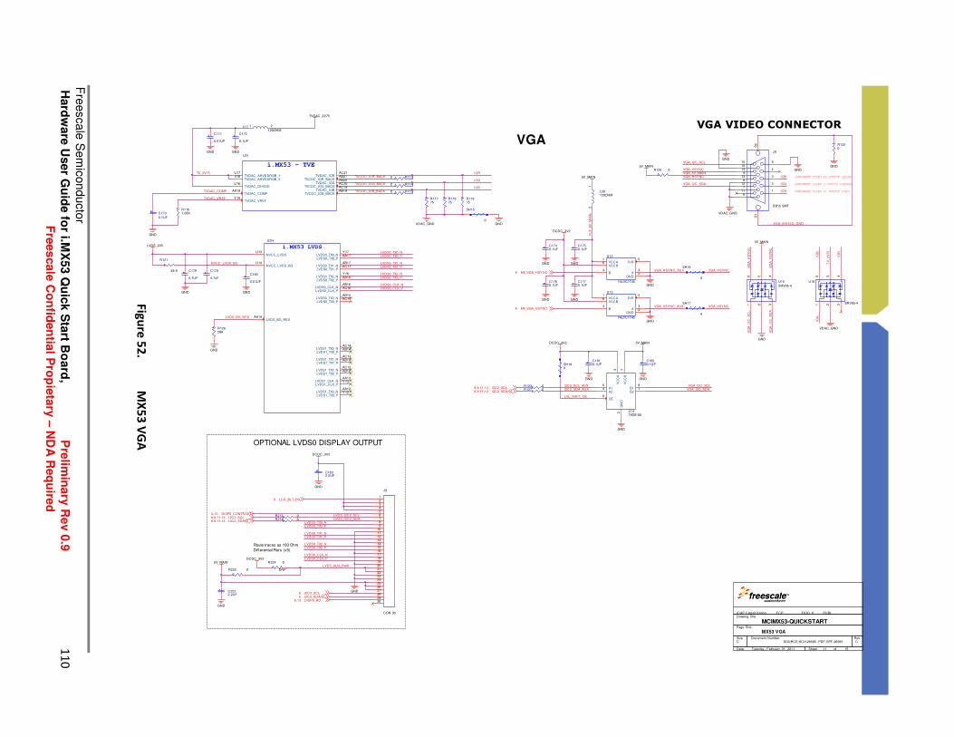
Fre
escale
Sem
iconducto
r
Hard
ware
User G
uid
e fo
r i.MX
53 Q
uic
k S
tart B
oard
, Pre
limin
ary
Re
v 0
.9 1
10
Fre
es
cale
Co
nfid
en
tial P
rop
ieta
ry –
ND
A R
eq
uire
d
Figu
re 5
2.
MX
53
VG
A
C1770.1UF
VG
A_
I2C
_S
CL
LVDS0_TX1_P
R1161.05K
VG
A_
I2C
_S
DA
R1150
C171
0.01UF
IOB
L11120OHM
1 2
TVCDC_IOR_BACK
TVCDC_IOG_BACK
TVCDC_IOB_BACK
R1140
IOGR1130
i.MX53 LVDS
U2H
LVDS0_CLK_NAB16
LVDS0_CLK_PAC16
LVDS0_TX0_NY17
LVDS0_TX0_PAA17
LVDS0_TX1_NAB17
LVDS0_TX1_PAC17
LVDS0_TX2_NY16
LVDS0_TX2_PAA16
LVDS0_TX3_NAB15
LVDS0_TX3_PAC15
LVDS1_CLK_NAA13
LVDS1_CLK_PY13
LVDS1_TX0_NAC14
LVDS1_TX0_PAB14
LVDS1_TX1_NAC13
LVDS1_TX1_PAB13
LVDS1_TX2_NAC12
LVDS1_TX2_PAB12
LVDS1_TX3_NAA12
LVDS1_TX3_PY12
LVDS_BG_RESAA14
NVCC_LVDSU13
NVCC_LVDS_BGU14
IOR
TVDAC_COMP
C173
0.1UF
TVDAC_VREF
LVDS0_TX2_N
VG
A_
VS
YN
C
SH180
MX_VGA_HSYNC8
i.MX53 - TVE
U2I
TVDAC_VREFY18
TVDAC_COMPAA19
TVDAC_IORAC21
TVDAC_IOGAB20
TVDAC_IOBAC19
TVCDC_IOR_BACKAB21
TVCDC_IOG_BACKAC20
TVCDC_IOB_BACKAB19
TVDAC_AHVDDRGB_1U17
TVDAC_AHVDDRGB_2V16
TVDAC_DHVDDU16
LVDS_2V5
LVDS0_TX1_NNVCC_LVDS_BG
LVDS0_CLK_N
LVDS0_TX2_PLVDS0_TX2_N
LVDS0_TX1_P
LVDS0_TX0_N
LVDS0_CLK_P
LVDS0_TX0_P
LVDS_BG_RES
VG
A_
HS
YN
C
VGA
GND
MX_VGA_VSYNC8
U16
SRV05-4
4
25
316
GNDGND
C180
0.01UF
DCDC_3V2
GND
GND GND
GND
GND
GND
LVDS0_CLK_N
GND
GND GND
GND
GND
GND
R123 0
GND
C178
4.7uF
GND
R121
49.9
R127 0
C172
0.1UF
GND
Drawing Title:
Size Document Number Rev
Date: Sheet of
Page Title:
ICAP Classif ication: FCP: FIUO: PUBI:
SOURCE:SCH-26565 PDF:SPF-26565 C
MCIMX53-QUICKSTART
C
Tuesday , February 01, 2011
MX53 VGA
11 15
___ ___X
C1810.1UF
GND
R12628K
R11775
GND
C179
0.1UF
I2C2_SDA8,9,11,13
GND
R11875
GND
VDAC_GND
C1820.1UF
R11975
VDAC_GND
VDAC_GND
5V_MAIN
DCDC_3V2
I2C2_SCL8,9,11,13
LVDS0_TX2_P
R1220
Route traces as 100 Ohm
Differential Pairs (x5)
LVL_SHFT_OE
SH15
0
LVDS_AUX_PWR
SH16
0
DISP0_RD8,13
I2C3_SCL6I2C3_SDA6
R223 0
R224 0
DNP
DCDC_3V2
SH17
0
J9
CON 30
123456789
101112131415161718192021222324252627282930
C1740.1UF
LVDS0_CLK_P
OPTIONAL LVDS0 DISPLAY OUTPUT
LVDS0_TX0_PLVDS0_TX0_N
C1750.1UF
LCD_BLT_EN8
DISP0_CONTRAST6,13
TVDAC_2V75
5V_MAIN
TV
_2
V75
VGA_I2C_SCL
VGA_5V_MAIN
J8
DB15 SMT
1
2
3
4
6
5
7
8
9
10
11
12
13
14
15
S2
S1
VGA_I2C_SDA COMPONENT VIDEO Y OUTPUT (GREEN)
COMPONENT VIDEO Pb OUTPUT (BLUE)IOB
VGA VIDEO CONNECTOR
IOR
VGA_VSYNC
VGA_SHIELD_GND
COMPONENT VIDEO Pr OUTPUT (RED)
VGA_HSYNC
DCDC_3V2
IOG
L28120OHM
12
5V_MAIN
FLT
_5V
_M
AIN
VGA_VSYNC
U15
SRV05-4
4
25
316
U12
74LVC1T45
VCCA1
GND2A3
B4
DIR5
VCCB6
U13
74LVC1T45
VCCA1
GND2A3
B4
DIR5
VCCB6
VGA_HSYNC
VGA_VSYNC_AUX
VGA_HSYNC_AUX
C1832.2UF
R120 0
C1760.1UF
C2522.2UF
I2C2_SCL8,9,11,13I2C2_SDA8,9,11,13
GND
5V_MAIN
U14TXS0102
OE6
B21B18
VC
CB
7
VC
CA
3
A15
A24
GN
D2
I2C2_SCL_AUXVGA_I2C_SDA
R213 0
VGA_I2C_SCLI2C2_SDA_AUX
R214 0
5V_MAIN
LVDS_I2C2_SDALVDS_I2C2_SCL
IOG
IOB
IOR
TV_2V75
LVDS0_TX1_N

Fre
escale
Sem
iconducto
r
Hard
ware
User G
uid
e fo
r i.MX
53 Q
uic
k S
tart B
oard
, Pre
limin
ary
Re
v 0
.9 1
11
PU
BI –
Pu
blic
Use B
us
ine
ss In
form
atio
n
Ha
rdw
are
Re
fere
nce
Ma
nu
al fo
r i.MX
53
Qu
ick
Sta
rt
Figu
re 5
3.
MX
53
ET
HE
RN
ET
R1401.5K
R13749.9
R13849.9
FEC_nRST8
GND
GNDGND
GND
GND
FEC_TX_EN8
GND
GND
FEC_TXD18
R14149.9
R13949.9
FEC_TXD08
FEC_MDC8
R208
100
R209
100
C192
0.1UF
FEC_nINT 8
ENET0_LED1R
ENET0_LED2R
FEC_RX_ER 8
FEC_CRS_DV8FEC_RXD18
FEC_REF_CLK8,10
C191
0.022UF
FEC_RXD08
C189
15pF
C190
15pF
FEC_A3V2
FEC_3V2
R14312.1K
R20410K
C193
1.0UF
R14210K
C184
0.1UF
U17
LAN8720A
MDIO12
MDC13
LED2/INTSEL2
RXD1/MODE17 RXD0/MODE08
LED1/REGOFF3
TXEN16
TXD017
TXD118
CRS_DV/MODE211
RST15
XTAL1/CLKIN5
XTAL24
VD
D2A
1
VD
D1A
19
RXP23
RXN22
TXN20
TXP21
VDDCR6
INT/REFCLKO14
RBIAS24
RXER/PHYAD010
VD
DIO
9
VS
S2
5
1CT:1
TRANSMIT
TX+
TX-
RX-
1
2
3
6
4
5
7
8
RX+
1CT:1CT
RECEIVE
R1 R2
R3
R4
0.1uF 5%
0.001uF 2kV 20%
C1
C2
R[1-4] - 75 OHMS 5%
YELLOW
GREEN
SHIELD
ORANGE
"This part will be populated with parts that may or may not have internal LED currentresistors. External LED resistors must beused, color and brightness of LEDs may v ary ."
J2B
HYBRID DUAL USB + RJ45
TD+2
CT_T1
TD-3
RD+4
RD-5
CT_R10
Y-13
Y+14
G-11
G+12
NC66
NC77
NC88
NC99
SGND5S5
SGND6S6
SGND7S7
SGND8S8
C185
0.1UF
L12
120OHM
1 2
FEC_3V2
FEC_3V2
FEC_VDDCR
TXP0
TXN0
FEC_A3V2
FEC_A3V2
RXP0
FAST ETHERNET PHY
FEC_RBIAS
C186
0.1UF
RXN0
ENET0_100MLED2
ENET0_LINKLED1
FEC_3V2
ENET0_LINKLED1
ENET0_100MLED2
FEC_USB_SHIELD 7
FEC_MDIO8
Drawing Title:
Size Document Number Rev
Date: Sheet of
Page Title:
ICAP Classif ication: FCP: FIUO: PUBI:
SOURCE:SCH-26565 PDF:SPF-26565 C
MCIMX53-QUICKSTART
C
Friday , January 14, 2011
MX53 FEC
12 15
___ ___X

Fre
escale
Sem
iconducto
r
Hard
ware
User G
uid
e fo
r i.MX
53 Q
uic
k S
tart B
oard
, Pre
limin
ary
Re
v 0
.9 1
12
Fre
es
cale
Co
nfid
en
tial P
rop
ieta
ry –
ND
A R
eq
uire
d
Figu
re 5
4.
EX
PA
NS
ION
HE
AD
ER
DISP0_DAT23
DISP0_DAT4
VLCD_BLT
DISP0_HSYNC
DISP0_DAT5
I2C2_SCL8,9,11I2C2_SDA8,9,11
DISP0_VSYNC
GND
TS_XN14
GND
DISP0_VSYNC
TS_XP14
DISP0_DAT6
TS_YN14TS_YP14
Drawing Title:
Size Document Number Rev
Date: Sheet of
Page Title:
ICAP Classif ication: FCP: FIUO: PUBI:
SOURCE:SCH-26565 PDF:SPF-26565 C
MCIMX53-QUICKSTART
C
Tuesday , February 01, 2011
EXPANSION HEADER
13 15
___ ___X
DISP0_DAT7
DISP0_HSYNC
1.8V
1.8V
1.8V
1.8V
1.8V
1.8V
1.8V
1.8V
1.8V
DISP0_DRDY
1.8V
1.8V
1.8V
1.8V
1.8V
1.8V
J13
QSH-060-01-L-D-A
1 23 45 67 89 10
11 1213 1415 1617 1819 2021 2223 2425 2627 2829 3031 3233 3435 3637 3839 4041 4243 4445 4647 4849 5051 5253 5455 5657 5859 60
SH1 SH2
SH3 SH4
SH5 SH6
SH7 SH8
61 6263 6465 6667 6869 7071 7273 7475 7677 7879 8081 8283 8485 8687 8889 9091 9293 9495 9697 9899 100
101 102103 104105 106107 108109 110111 112113 114115 116117 118119 120
PORT_ID014
DISP0_DAT8
DISP0_DRDY
SS5.635" LONG
DNP
EXP HDR
STANDOFF
GND
R169
2.74K
DISP0_DAT9
PORT_ID114
VLDO8_1V8
DISP0_DAT0
PCLOCK 6
DISP0_DCLK
DISP0_DAT10
EXPANSION HEADER FOR DEBUG AND LCD I/F
DISP0_DAT11
LCD_3V2
DISP0_SER_RS8
EXP_HDR_PIN_79
DISP0_DAT12
DISP0_SER_SCLK8
DISP0_RD8,11
VLDO9_1V5
DISP0_SER_nCS8
CSI0_DAT16
CSI0_DAT15
CSI0_DAT14
CSI0_DAT13
CSI0_DAT12
CSI0_PIXCLKCSI0_VSYNCH
CSI0_DAT19
CSI0_DAT18
CSI0_DAT17
CSI0_HSYNCH
DISP0_RESET8
CSI0_PWDN8
CSI0_RSTB8
DISP0_SER_MOSI8DISP0_DAT13
I2C1_SDA14,15
CSI0_DAT13CSI0_DAT12
CSI0_DAT18
CSI0_DAT17CSI0_DAT16
CSI0_DAT15CSI0_DAT14
CSI0_DAT19
DISP0_DAT1
SPDIF MCLOCK
CSI0_VSY NCHCSI0_HSYNCH
5V_MAIN
DISP0_DAT14
5V_MAIN
DISP0_WR8
LCD_3V2
5V_MAIN
DISP0_DCLK
DISP0_SER_MISO8
DISP0_DAT2
DISP0_POWER_EN8
DISP0_nCS18
UART1_RX15
GPIO_0(CLK0)6,9
CSI0_PIXCLK
DISP0_DAT15
DISP0_nCS08
VLDO8_1V8
i.MX53 - IPU
NVCC_CSI
NVCC_LCD
U2D
CSI0_DAT8T1
CSI0_DAT9R4
CSI0_DAT10R5
CSI0_DAT11T2
CSI0_DAT12T3
CSI0_DAT13T6
CSI0_DAT14U1
CSI0_DAT15U2
CSI0_DAT16T4
CSI0_DAT17T5
CSI0_DAT18U3
CSI0_DAT19U4
CSI0_VSY NCP4
CSI0_PIXCLKP1
CSI0_MCLKP2
DI0_PIN4D2
DISP0_DAT0J5
DISP0_DAT1J4
DISP0_DAT2H2
DISP0_DAT3F1
DISP0_DAT4G2
DISP0_DAT5H3
DISP0_DAT6G1
DISP0_DAT7H6
DISP0_DAT8G6
DISP0_DAT9E2
DISP0_DAT10G3
DISP0_DAT11H5
DISP0_DAT12H1
DISP0_DAT13E1
DISP0_DAT14F2
DISP0_DAT15F3
DISP0_DAT16D1
DISP0_DAT17F5
DISP0_DAT18G4
DISP0_DAT19G5
DISP0_DAT20F4
DISP0_DAT21C1
DISP0_DAT22E3
DISP0_DAT23C3
DI0_PIN3C2
DI0_DISP_CLKH4
DI0_PIN2D3
DI0_PIN15E4
CSI0_DAT4R1
CSI0_DAT5R2
CSI0_DAT6R6
CSI0_DAT7R3
CSI0_DATA_ENP3
VLDO8_1V8
DISP0_DAT3 LCD_BLT1_N14
DISP0_DAT16
I2C1_SCL14,15
DISP0_DAT4
DISP0_DAT17
UART1_TX15
DISP0_DAT5
DISP0_DAT18
SPDIF_TX 6
DISP0_DAT6
DISP0_DAT19
DISP0_DAT0
DISP0_DAT7
DISP0_DAT20
DISP0_DAT1
VIOHI_2V775
DISP0_DAT8
DISP0_DAT12DISP0_DAT11DISP0_DAT10DISP0_DAT9
DISP0_DAT15DISP0_DAT14DISP0_DAT13
DISP0_CONTRAST 6,11
R18810KDNP
DISP0_DAT21
R18910KDNP
DISP0_DAT2
DISP0_DAT16
DISP0_DAT20DISP0_DAT19DISP0_DAT18DISP0_DAT17
DISP0_DAT23DISP0_DAT22DISP0_DAT21
DISP0_DAT22
DISP0_DAT3

Fre
escale
Sem
iconducto
r
Hard
ware
User G
uid
e fo
r i.MX
53 Q
uic
k S
tart B
oard
, Pre
limin
ary
Re
v 0
.9 1
13
PU
BI –
Pu
blic
Use B
us
ine
ss In
form
atio
n
Ha
rdw
are
Re
fere
nce
Ma
nu
al fo
r i.MX
53
Qu
ick
Sta
rt
Figu
re 5
5.
DA
90
53
PM
IC
R148 200K
TP16
R1510
GND
TBAT
VLDO3_3V3
TS_XN13
C223
0.1UF
C2141.0UF
TP18
GND
C209
0.47UF
VBUCKCORE
5V_MAIN
PORT_ID013
SWBUCKMEM
U20C
DA9053
VCENTERA7
VSW_A8A8
VSW_A9A9
VBUS_PROT_A5A5
VBUS_PROT_A6A6
VBUS_SELB5
VDDOUT_A11A11
VDDOUT_A10A10
VBUSB6
AD_CONTB11
DCIN_PROT_A3A3
DCIN_PROT_A4A4
VBAT_A13A13
VBAT_A12A12
DCIN_SELB3
DCINB4
D-B13
D+C13
VBBATB2
VREFA2
IREFD5
VDD_REFC2
TBATL6
ADCIN4_GPIO_0C6
ADCIN5_GPIO_1C5
ADCIN6_GPIO_2C4
TSIYN_GPIO_3K6
TSIYP_GPIO_4K8
TSIXN_GPIO_5K5
TSIXP_GPIO_6K7
TSIREF_GPIO_7K9
OUT_32KK12
XOUTB1
XINC1
VLDO5_1V3
TP19
TBAT
VDDOUT
GND
VLDO6_1V3
PMIC_VDD_REF
TS_XP13
TP20
VLDO7_2V75
C208
0.1UF
PORT_ID113
VLDO8_1V8
L16
4.7UH
1 2
Supply for DDR3
memories @1.5V
C205
47UF
L14 2.2UH
CDRH2D18/HP-2R2NC
1 2
TP11
GND
BOOST_PROT
BOOST_SENSE_P
DIG_PLL_1V3
JP1HDR 1X1DNP
1
LCD_BLT1_N13
TESTP
VLDO8_1V8
VDDCORE
I2C1_SDA13,15
JP2HDR 1X1DNP
1
GND
GND
ADCIN6/GPIO_2
C201
10UF
L15 2.2UH
CDRH2D18/HP-2R2NC
1 2
TSIREF_GPIO_7
NC
Q8
NTLJF4156N
5
4 3
2
16
8
7
VLDO9_1V5
C227
4.7uF
C200
10UF
L17 2.2UH
CDRH2D18/HP-2R2NC
1 2
ADCIN6/GPIO_2
C2162.2UF
GND
GND
C2132.2UF
GND
C23022UF
L18 2.2UH
CDRH2D18/HP-2R2NC
1 2
C2112.2UF
PMIC_VREF
I2C1_SCL13,15
C2102.2UF
SYS_EN
VLDO8_1V8
C2032.2UF
R1524.7K
VDDCORE
C204
4.7uF
U20D
DA9053
VDD_IO1L4
VDD_IO2K4
NRESETF10
NIRQE10
NVDD_FAULT_GPIO_13C11
GP_FB1_GPIO_12B10
PWR_UP_GP_FB2J10
TPL5
NONKEY_KEEP_ACTM11
SYS_EN_GPIO_8D10
PWR_EN_GPIO_9C10
PWR1_EN_GPIO_10L2
ACC_ID_DET_GPIO_11L3
NSHUTDOWND11
SOL10
SIK10
SKL11
NCSK11
DATA_GPIO_14N1
CLK_GPIO_15M2
GND
C1942.2UF
C195
10UF
SHDN_5V3
GND
VLDO3_3V3
VDDOUT
VBUCKPRO
C2180.1UF
VMEM_SW
VDDOUT
U20A
DA9053
VDD_LDO1E2
VLDO1D1
VLDO2F2
VDD_LDO2E1
VDD_LDO3_4J2
VLDO3J1
VLDO4H1
VDD_LDO5G2
VDD_LDO6H2
VLDO5F1
VLDO6G1
VDD_LDO7_8K2
VDD_LDO9_10M3
VLDO7K1
VLDO8L1
VLDO9M1
VLDO10N2
VDDCORED2
TSIREF_GPIO_7
GND
LCD_BLT3_N
U20B
DA9053
VBUCKPERIE12
SWBUCKPERIL13
VPERI_SWD12
VBUCKMEMC12
SWBUCKMEMM13
VMEM_SWB12
SY S_UPL12
SWBUCKCORE_G13G13
SWBUCKCORE_F13F13
VBUCKPROM12
SWBUCKPROH13
SW_BOOSTM10
BOOST_SENSE_PN10
BOOST_SENSE_NN9
BOOST_PROTN11
LED1_INM9
LED2_INL8
LED3_INL7
VSS_NOISY_D6D6
VDDBUCK_MEMN13
VDDBUCK_PER_PRO_K13K13
VDDBUCK_PER_PRO_J13J13
VDDBUCK_CORE_D13D13
VDDBUCK_CORE_E13E13
VBUCKCOREF12
PWR_EN
SWBUCKPRO
TP24
GND
GND
PMIC_IREF
VDDOUT
VSW
GND
VBBAT
U20E
DA9053
VSS_NOISY_E8E8
VSS_NOISY_E7E7
VSS_NOISY_G9G9
VSS_NOISY_H8H8
VSS_NOISY_E9E9
VSS_NOISY_F8F8
VSS_NOISY_E6E6
VSS_NOISY_J7J7
VSS_NOISY_H7H7
VSS_NOISY_E5E5
VSS_NOISY_G7G7
VSS_NOISY_F7F7
VSS_NOISY_F6F6
VSS_QUIET_H6H6
VSS_NOISY_J9J9
VSS_QUIET_G5G5
VSS_QUIET_J5J5
VSS_QUIET_J6J6
VSS_NOISY_F5F5
VSS_NOISY_F9F9
VSS_NOISY_G8G8
VSS_NOISY_J8J8
VSS_NOISY_H9H9
VSS_QUIET_H5H5
VSS_NOISY_D7D7
VSS_QUIET_G6G6
PMIC_IREF
GND
GND
nIRQ 6
VDDCORE
C22010UF
GND
U20F
DA9053
NC_A1A1
NC_B7B7
NC_B8B8
NC_B9B9
NC_C3C3
NC_C7C7
NC_C8C8
NC_C9C9
NC_D3D3
NC_D4D4
NC_D8D8
NC_D9D9
NC_E3E3
NC_E4E4
NC_E11E11
NC_F3F3
NC_F4F4
NC_F11F11
NC_G3G3
NC_G4G4
NC_G10G10
NC_G11G11
NC_G12G12
NC_H3H3
NC_H4H4
NC_H10H10
NC_H11H11
NC_H12H12
NC_J3J3
NC_J4J4
NC_J11J11
NC_J12J12
NC_K3K3
NC_L9L9
NC_M4M4
NC_M5M5
NC_M6M6
NC_M7M7
NC_M8M8
NC_N5N5
NC_N6N6
NC_N7N7
NC_N3N3
NC_N4N4
NC_N8N8
NC_N12N12
PWR1_EN
GND
GND
GND
VLDO10_1V3
LCD_BLT2_N
TP12
GND
1000mA max
GND
GND
GND
GND
PMIC_VDD_REF
GND
TP13
GND
VBAT
VBUCKCORE
SH30
0
GND
TP23
GND
GND
C2312.2UFDNP
JP2
JP1
R1530.1
LCD_BLT3_N
GP_FB1
SW_BOOST
Q7Si2333DS
1
32
GND
5V_MAIN
Supply for VDD_REG to
be configured @2.5V
R14910K
3V3_EN 3
GND
nONKEY/KEEPACT6
VPERI_SW
1000mA max
R20310K
R15010K
C2292.2UF
3V3_EN
TESTP
VBBAT
LCD_BLT2_N
1000mA max
GND
GND
R15568K
3.6 to VBAT+200mV
GPIO_14
2000mA max
nVDD_FAULT 6
GND
C206
1.0UF
VDDOUT_SUP
TBAT
GND
C22422UF
TP21
C215
1.0UF
C22122UF
-
+
4mm
13mm
nIRQ
5V_JK3
VBUCKPERI
C212
0.22UF
TP17
J14
CON_1X3
DNP
123
VIOHI_2V775
SWBUCKPERI
VDDOUT
TESTP
SWBUCKCORE
C1961.0UF
CL
2.7mm -+
GND
GND
J19
HDR 1X2DNP
12
AD_CONT
GND
I2C1_SDA
nRESET
VCENTER
C22222UF
Supply for CORE to
be configured @1.1V
TP15
R1541M
C22622UF
VBUCKMEM
GND
C22822UF
GND
TS_YN13
GND
TBAT
GND
C1991.0UF
Drawing Title:
Size Document Number Rev
Date: Sheet of
Page Title:
ICAP Classif ication: FCP: FIUO: PUBI:
SOURCE:SCH-26565 PDF:SPF-26565 C
MCIMX53-QUICKSTART
D
Wednesday , January 12, 2011
PMIC DA9053
14 15
___ ___X
nRESET I2C1_SCL
nRESET 6
nSHUTDOWN
GPIO_15
ML1220-VM1
LAYOUT &
KEEPOUT
C225
0.1UF
C2071.0UF
VLCD_BLT
TS_YP13
L13 2.2UH1 2
TP14
CL 3mm
VLDO3_3V3
Pins D7 and F5 canbe left open as they
are "NC" pins.
SYS_UP 6
JP1 and JP2 for
OPTIONAL
COIN CELL
Note:
Traces are routed to NC pins for layout purposes only.
This allows signals to route out of chip via NC pins
on the top layer. NC pins are not connected to any
pad internal to the PMIC.
VLDO1_1V3_RTC
D8 BAT76021
nSHUTDOWN
Supply for VCC to
be configured @1.3V

Fre
escale
Sem
iconducto
r
Hard
ware
User G
uid
e fo
r i.MX
53 Q
uic
k S
tart B
oard
, Pre
limin
ary
Re
v 0
.9 1
14
Fre
es
cale
Co
nfid
en
tial P
rop
ieta
ry –
ND
A R
eq
uire
d
Figu
re 5
6.
DE
BU
G, A
CC
ELE
RO
ME
TE
R
GNDGND
VLDO8_1V8
ACCL_EN8
ACCL_INT1_IN 8
I2C1_SCL 13,14I2C1_SDA 13,14
ACCL_INT2_IN 8
VLDO8_1V8 L26600 OHM
12
ACCELEROMETERVLDO8_1V8
JTAG THROUGH HOLE CONNECTOR
Drawing Title:
Size Document Number Rev
Date: Sheet of
Page Title:
ICAP Classif ication: FCP: FIUO: PUBI:
SOURCE:SCH-26565 PDF:SPF-26565 C
MCIMX53-QUICKSTART
C
Wednesday , January 12, 2011
DEBUG, ACCELEROMETER
15 15
___ ___X
UART DB9 SMT CONNECTOR
R15810K
R15910KDNP
R16010K
R157100R161
10K
R167100
R16210K
JTAG_nSRST6
R16410K
J15
TST-110-05-T-D-RA
1 23 45 67 89 10
11 1213 1415 1617 1819 20
R16510K
R1630DNP
JTAG_DACK
R16610K
DCDC_3V2
GND GND
JTAG_RTCK
JTAG_PWRVTREF_JTAG
JTAG_DE
C238
1000pF
C234
1.0UF
UART1_RX13
C235
0.1UF
C232
0.1UF
C236
0.1UF
C233
0.1UF
C237
0.1UF
UART_RXL
UART_VP
UART_C1M
UART_TXL
UART_C1P
GND
DCDC_3V2
DCE_TX
UART_C2M
DCE_RX
UART_C2P
GND
GNDUART_VM
UART1_TX 13
U24SP3232
VC
C1
6
C2+4
R1IN13
R2IN8
R1OUT12
R2OUT9
C1-3
C1+1
GN
D1
5
V+
2
V-6
C2-5
T1IN11
T2IN10
T1OUT14
T2OUT7
J16
DB 9
594837261
M2
M1
Female DB-9 ConnectorUART_SHIELD_GND
CD1
DCE
2
O
5
4
3
8
7
6
9
I
O
I
O
I
O
O
RX
TX
DSR
GND
DTR
CTS
RTS
RI
GND
GND GND
DCE_TX
DCE_RX
U25
74LVC1T45
VCCA1
GND2 A3
B4
DIR5
VCCB6
U26
74LVC1T45
VCCA1
GND2 A3
B4
DIR5
VCCB6
GND
GND
C247
0.1UF
C249
0.1UF
C248
0.1UF
C250
0.1UF
GND
GND
GND
GND
DCDC_3V2
DCDC_3V2
VLDO8_1V8
VLDO8_1V8
JTAG_nTRST6
JTAG_TMS6JTAG_TDI6
U23
MMA8450QT
VD
D1
1
NC22
NC33 SCL
4
GN
D1
5
SDA6
SA07
EN8
INT29
TEST/GND10
INT111
GND12
GN
D2
13
VD
D2
14
NC1515
NC1616
JTAG_TCK6
UART_RXL
R20210KDNP
R20610K
SH20
0
ACCL_SA0
ACCL_VDD
GND
GND
GND
JTAG_TDO6
GND
C246
0.1UF
UART_TXL
VLDO8_1V8

Freescale Semiconductor
Hardware User Guide for i.MX53 Quick Start Board, Preliminary Rev 0.9 115
PUBI – Public Use Business Information
Hardware Reference Manual for i.MX53 Quick Start
14. Bill of Materials
The Bill of Materials used to manufacture the Quick Start board is presented in this section. The
capacitors and resistors used are considered generic type components and do not include manufacturer
names or part numbers. The remainder of the parts have manufactures and part numbers provided for
the primary part specified. Second source vendors are not included. The final section of the Bill of
materials includes the list of parts not populated on the Quick Start board at the time of manufacture.
Parts are listed in the following tables:
Table 32. Generic Resistors
Table 33. Generic Capacitors
Table 34. Specified Components
Table 35. Non-Populated Components
Generic Resistors Description QTY Reference Designator
RES MF ZERO OHM 1/20W 5% 0201 4 R123, R127, R213, R214
RES MF ZERO OHM 1/16W 5% 0402 12 R25, R30, R31, R32, R33, R113, R114, R115, R144, R145, R151,
R223
RES MF ZERO OHM 1/10W -- 0603 3 R12, R19, R120
RES MF ZERO OHM 1/8W -- 0805 1 R122
RES MF 0.1 OHM 1/8W 1% 0402 2 R153, R201
RES MF 1.0 OHM 1/16W 1% 0402 4 R68, R69, R72, R73
RES MF 22 OHM 1/16W 5% 0402 2 R211, R212
RES 10 OHM 1/20W 5% 0201 1 R199
RES MF 33.0 OHM 1/20W 5% 0201 1 R104
RES MF 49.9 OHM 1/20W 1% 0201 5 R121, R137, R138, R139, R141
RES MF 75 OHM 1/20W 5% 0201 3 R117, R118, R119
RES TF 100 OHM 1/20W 5% RC0201 7 R66, R157, R167, R185, R186, R208, R209
RES MF 191 OHM 1/16W 1% 0402 1 R112
RES MF 200 OHM 1/16W 1% 0402 2 R28, R29
Table 32. Generic Resistors

Freescale Semiconductor
Hardware User Guide for i.MX53 Quick Start Board, Preliminary Rev 0.9 116
Freescale Confidential Propietary – NDA Required
Generic Resistors Description QTY Reference Designator
RES MF 240 OHM 1/16W 1% 0402 5 R190, R191, R192, R193, R194
RES MF 470 OHM 1/20W 1% 0201 6 R26, R27, R81, R177, R178, R187
RES MF 1.0K 1/20W 1% 0201 13 R49, R50, R173, R174, R175, R176, R179, R180, R181, R182,
R183, R184, R198
RES MF 1.05K 1/16W 1% 0402 1 R116
RES MF 1.5K 1/20W 5% 0201 1 R140
RES MF 2.2K 1/20W 5% 0201 1 R101
RES MF 2.74K 1/16W 1% 0402 1 R169
RES 3.3K 1/20W 5% RC0201 ROHS 2 R195, R196
RES MF 4.7K 1/20W 5% 0201 3 R85, R86, R200
RES MF 4.7K OHM 1/20W 1% 0201 20 R37, R40, R46, R47, R53, R54, R55, R56, R57, R58, R59, R60,
R61, R62, R63, R64, R65, R152, R221, R222
RES MF 6.04K 1/16W 1% 0402 2 R70, R71
RES MF 10K 1/20W 5% 0201 33 R10, R34, R35, R39, R41, R44, R76, R82, R87, R88, R89, R110,
R142, R149, R150, R158, R160, R161, R162, R164, R165, R166,
R168, R170, R171, R203, R204, R206, R216, R217, R218, R219,
R220
RES MF 10.0K 1/20W 1% 0201 2 R51, R52
RES MF 12.1K 1/16W 1% 0402 1 R143
RES MF 28K 1/16W 1% 0402 1 R126
RES MF 47K 1/20W 5% 0201 1 R13
RES MF 68K 1/20W 1% 0201 1 R155
RES MF 100K 1/20W 1% 0201 3 R7, R9, R215
RES MF 200K 1/16W 1% 0402 1 R148
RES MF 432K 1/16W 1% 0402 1 R8
RES MF 1.0M 1/20W 5% 0201 1 R154
Table 32. Generic Resistors (con.)

Freescale Semiconductor
Hardware User Guide for i.MX53 Quick Start Board, Preliminary Rev 0.9 117
PUBI – Public Use Business Information
Hardware Reference Manual for i.MX53 Quick Start
Generic Capacitors Description QTY Reference Designator
CAP CER 10PF 25V 5% C0G 0201 1 C5
CAP CER 12PF 25V 5% C0G 0201 2 C217, C219
CAP CER 15PF 25V 5% C0G 0201 2 C189, C190
CAP CER 18PF 25V 5% C0G 0201 2 C133, C134
CAP CER 1000PF 16V 10% X7R 0201 1 C238
CAP CER 1000PF 2KV 10% X7R 1210 1 C135
CAP CER 0.01UF 10V 10% X5R 0201 22 C48, C49, C50, C80, C82, C84, C93, C95, C97, C100, C102, C104,
C107, C109, C111, C141, C165, C166, C167, C169, C171, C180
CAP CER 0.022UF 10V 10% X5R 0201 1 C191
CAP CER 0.1UF 6.3V 10% X5R 0201 104 C8, C44, C46, C47, C52, C53, C54, C55, C56, C57, C58, C59, C60,
C61, C62, C63, C66, C67, C68, C69, C70, C72, C73, C74, C75,
C76, C77, C78, C79, C81, C83, C86, C87, C88, C89, C90, C92,
C94, C96, C99, C101, C103, C106, C108, C110, C113, C114,
C115, C116, C117, C119, C120, C121, C122, C123, C125, C126,
C127, C128, C129, C131, C132, C136, C138, C139, C142, C143,
C145, C147, C148, C150, C152, C153, C159, C160, C161, C162,
C164, C172, C174, C175, C176, C177, C179, C181, C182, C184,
C185, C186, C192, C208, C218, C223, C225, C232, C233, C235,
C236, C237, C246, C247, C248, C249, C250
CAP CER 0.1UF 16V 10% X7R 0402 1 C173
CAP CER 0.1UF 35V 10% X5R 0402 1 C245
CAP CER 0.22UF 6.3V 20% X5R 0201 31 C9, C10, C11, C12, C13, C14, C16, C17, C18, C19, C21, C22, C23,
C24, C25, C26, C27, C29, C30, C31, C32, C33, C34, C35, C37,
C38, C39, C42, C43, C64, C212
CAP CER 0.47UF 6.3V 10% X5R 0402 1 C209
CAP CER 1.0UF 35V 10% X5R 0603 1 C244
CAP CER 1.0UF 10V 10% X5R 0402 12 C3, C151, C193, C196, C199, C206, C207, C214, C215, C234,
C239, C240
CAP CER 2.2UF 6.3V 20% X5R 0402 11 C137, C140, C183, C194, C203, C210, C211, C213, C216, C252,
C253
CAP CER 2.2UF 25V 10% X5R 0805 1 C229
CAP CER 4.7UF 6.3V 20% X5R 0402 4 C149, C178, C204, C227
CAP CER 10UF 6.3V 20% X5R 0603 17 C7, C28, C40, C85, C91, C98, C105, C112, C118, C124, C130,
C144, C146, C195, C200, C201, C220
CAP CER 10UF 10V 10% X5R 0805 2 C2, C4
CAP CER 22UF 6.3V 20% X5R 0805 12 C15, C41, C45, C51, C65, C71, C221, C222, C224, C226, C228,
C230
CAP CER 47uF 6.3V 20% X5R 0805 3 C20, C36, C205
CAP CER 100UF 6.3V 20% X5R 1206 4 C1, C241, C242, C243
Table 33. Generic Capacitors

Freescale Semiconductor
Hardware User Guide for i.MX53 Quick Start Board, Preliminary Rev 0.9 118
Freescale Confidential Propietary – NDA Required
SPECIFIED COMPONENTS Description QTY Reference Designator Manufacturer Part Number
CAP TANT 220UF ESR=0.800 OHM
4V 20% -- 3216-10 2 C154,C157 NICHICON F950G227MSAAQ2
IND FER BEAD 120OHM@100MHZ
2A 25% 0603 3 L7,L9,L19 MURATA BLM18PG121SH1
IND FER BEAD 120 OHM@100MHZ
500MA 25% 0603 2 L10,L12 MURATA BLM18AG121SN1J
IND PWR 4.7UH@100KHZ 1.1A 20%
SMT 1 L1 TDK VLF4012AT-4R7M1R1
IND PWR 2.2UH@100KHZ 1.6A 30%
SMD 4 L14,L15,L17,L18
SUMIDA
ELECTRIC
CDRH2D18/HP-
2R2NC
IND CHK 90 OHM@100MHZ 330MA
25% 0805 2 L5,L6 MURATA DLW21HN900SQ2L
IND FER 120OHM@100MHZ
300MA 25% 0402 6 L2,L4,L8,L11,L27,L28 MURATA BLM15HB121SN1D
IND FER BEAD 600 OHM@100MHZ
300MA 25% 0402 1 L26 MURATA BLM15HD601SN1D
IND FER BEAD 220OHM@100MHZ
700MA 25% 0402 5 L20,L21,L23,L24,L25 MURATA BLM15EG221SN1_
IND PWR 2.2UH@1MHZ 1.5A 20%
SMD 1 L13 TDK VLS3012T-2R2M1R5
IND PWR 4.7UH@1MHZ 1A 20%
SMD 1 L16 TDK VLS3012T-4R7M1R0
CON 1 PWR PLUG DIAM 2.0MM RA
TH -- 430H NI 1 J1 CUI STACK PJ-202A
CON 5 AUD JACK 3.2MM SKT RA TH
-- 197H SN 079L 2 J6,J18 CUI STACK SJ-43515TS
HDR 2X10 RA SHRD TH 100MIL CTR
365H SN 230L 1 J15 SAMTEC TST-110-05-T-D-RA
CON 1X7 PLUG SATA TH 50MIL SP
331H -- 96L 1 J7 3M 5607-5102-SH
CON 2X60 SKT SMT 0.5MM SP AU 1 J13 SAMTEC QSH-060-01-L-D-A
CON 19 CRD SKT SMT -- 150H AU 1 J5
PROCONN
TECHNOLOGY SDC013-A0-501F
CON 30 SHRD SKT RA SMT 1MM SP
AU 1 J9 HIROSE DF19G-30P-1H(56)
Table 34. Specified Components
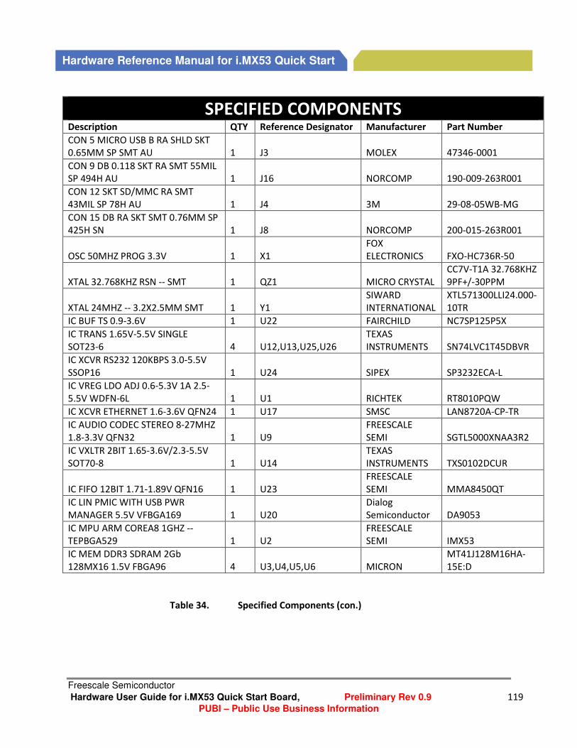
Freescale Semiconductor
Hardware User Guide for i.MX53 Quick Start Board, Preliminary Rev 0.9 119
PUBI – Public Use Business Information
Hardware Reference Manual for i.MX53 Quick Start
SPECIFIED COMPONENTS Description QTY Reference Designator Manufacturer Part Number
CON 5 MICRO USB B RA SHLD SKT
0.65MM SP SMT AU 1 J3 MOLEX 47346-0001
CON 9 DB 0.118 SKT RA SMT 55MIL
SP 494H AU 1 J16 NORCOMP 190-009-263R001
CON 12 SKT SD/MMC RA SMT
43MIL SP 78H AU 1 J4 3M 29-08-05WB-MG
CON 15 DB RA SKT SMT 0.76MM SP
425H SN 1 J8 NORCOMP 200-015-263R001
OSC 50MHZ PROG 3.3V 1 X1
FOX
ELECTRONICS FXO-HC736R-50
XTAL 32.768KHZ RSN -- SMT 1 QZ1 MICRO CRYSTAL
CC7V-T1A 32.768KHZ
9PF+/-30PPM
XTAL 24MHZ -- 3.2X2.5MM SMT 1 Y1
SIWARD
INTERNATIONAL
XTL571300LLI24.000-
10TR
IC BUF TS 0.9-3.6V 1 U22 FAIRCHILD NC7SP125P5X
IC TRANS 1.65V-5.5V SINGLE
SOT23-6 4 U12,U13,U25,U26
TEXAS
INSTRUMENTS SN74LVC1T45DBVR
IC XCVR RS232 120KBPS 3.0-5.5V
SSOP16 1 U24 SIPEX SP3232ECA-L
IC VREG LDO ADJ 0.6-5.3V 1A 2.5-
5.5V WDFN-6L 1 U1 RICHTEK RT8010PQW
IC XCVR ETHERNET 1.6-3.6V QFN24 1 U17 SMSC LAN8720A-CP-TR
IC AUDIO CODEC STEREO 8-27MHZ
1.8-3.3V QFN32 1 U9
FREESCALE
SEMI SGTL5000XNAA3R2
IC VXLTR 2BIT 1.65-3.6V/2.3-5.5V
SOT70-8 1 U14
TEXAS
INSTRUMENTS TXS0102DCUR
IC FIFO 12BIT 1.71-1.89V QFN16 1 U23
FREESCALE
SEMI MMA8450QT
IC LIN PMIC WITH USB PWR
MANAGER 5.5V VFBGA169 1 U20
Dialog
Semiconductor DA9053
IC MPU ARM COREA8 1GHZ --
TEPBGA529 1 U2
FREESCALE
SEMI IMX53
IC MEM DDR3 SDRAM 2Gb
128MX16 1.5V FBGA96 4 U3,U4,U5,U6 MICRON
MT41J128M16HA-
15E:D
Table 34. Specified Components (con.)

Freescale Semiconductor
Hardware User Guide for i.MX53 Quick Start Board, Preliminary Rev 0.9 120
Freescale Confidential Propietary – NDA Required
SPECIFIED COMPONENTS Description QTY Reference Designator Manufacturer Part Number
LED ULTRA-BRIGHT GREEN SMT
0603 3 D1,D9,D16 LITE ON LTST-C190KGKT
LED BLUE -- 20MA SMT 4 D10,D11,D12,D13 LITE ON LTST-C190TBKT
LED ULTRA BRIGHT RED SGL 30MA
0603 1 D14 LITE ON LTST-C190KRKT
TRAN NMOS 60V 115MA SOT23 1 Q15 ON SEMI 2N7002LT1G
DIODE TVS ARRAY 12A 5V 300W
SOT23_S6 2 U15,U16 SEMTECH CORP SRV05-4.TCT
MOSFET,DUAL N & P CHANNEL,
SOT6 ROHS 1 Q13 FAIRCHILD FDC6321C_NL
DIODE SCH 1A 20V SOD323 2 D8,D15 PHILIPS SEMI BAT760
TRAN NMOS DUAL 200MA 50V
SOT363 4 Q9,Q10,Q11,Q12 DIODES INC BSS138DW-7-F
TRAN PMOS PWR 12V 4.3A SOT23 2 Q1,Q14
INTERNATIONAL
RECTIFIER IRLML6401TRPBF
DIODE TVS ESD PROT ULT LOW CAP
5-5.4V SOD-923 1 D4 ON SEMI ESD9L5.0ST5G
TRAN NMOS PWR 4.6A 30V DIODE
SCHOTTKY 2.0A WDFN6 1 Q8 ON SEMI NTLJF4156NT1G
TRAN PMOS PWR 4.1A 12V SOT-23 1 Q7 VISHAY INT SI2333DS-T1-E3
DIODE TVS 2-CH ARRAY 25A 5V
500W SOT-143 2 D17,D18 SEMTECH CORP SR05.TCT
FUSE PLYSW 1.1A HOLD 6V SMT
ROHS 1 F2
TYCO
ELECTRONICS MICROSMD110F-2
FUSE CBKR 3A 24V 0603 1 F1 BOURNS SF-0603F300-2
SW SPST PB 50MA 12V SMT 4 SW2,SW3,SW4,SW5 E SWITCH TL1015AF160QG
CON 22 RJ-45/DUAL USB RA TH
50MIL SP 1231H AU 90L 1 J2
PREMIER
MAGNETICS RJ45-103YDD2
Table 34. Specified Components (con.)

Freescale Semiconductor
Hardware User Guide for i.MX53 Quick Start Board, Preliminary Rev 0.9 121
PUBI – Public Use Business Information
Hardware Reference Manual for i.MX53 Quick Start
NON-POPULATED COMPONENTS Description QTY Reference Designator Manufacturer Part Number
CAP CER 10PF 25V 5% C0G 0201 0 C168, C170
CAP CER 0.1UF 6.3V 10% X5R 0201 0 C163
CAP CER 2.2UF 50V 10% X7R 1206 0 C231
IND FER 120OHM@100MHZ
300MA 25% 0402 0 L3 MURATA BLM15HB121SN1D
IND FER BEAD 220OHM@100MHZ
700MA 25% 0402 0 L22 MURATA BLM15EG221SN1_
CON 1X3 PLUG SHRD TH 1.25MM
165H SN 0 J14 MOLEX 0530470310
HDR 1X2 TH 100MIL SP 165H AU 0 J19 SAMTEC TLW-102-06-G-S
HDR 1X1 TH -- 330H SN 115L 0 JP1, JP2 SAMTEC TSW-101-23-T-S
IC DRV LVDS 1-BIT HIGH SPEED DIFF
3.3V SOT23-5 0 U11 FAIRCHILD FIN1001M5
RES MF ZERO OHM 1/20W 5% 0201 0 R36, R38, R48, R197
RES MF ZERO OHM 1/16W 5% 0402 0 R210, R224
RES MF ZERO OHM 1/10W -- 0603 0 R80, R163
RES MF 0.02OHM 1/4W 0.5% 0805 0 R17, R20
RES MF 49.9 OHM 1/20W 1% 0201 0 R42, R43
RES TF 100 OHM 1/20W 5% RC0201 0 R111
RES MF 10K 1/20W 5% 0201 0 R84, R97, R108, R159,
R188, R189, R202
RES MF 200K 1/20W 5% 0201 0 R14
RES MF 10M 1/20W 5% 0201 0 R45
SW SPST DIP SMT 50V 100MA
DIP10 0 SW1 Multicomp MCNHDS-10-T
Table 35. Non-Populated Components

Freescale Semiconductor
Hardware User Guide for i.MX53 Quick Start Board, Preliminary Rev 0.9 122
Freescale Confidential Propietary – NDA Required
15. PCB information
This section provides the Gerber artwork in a picture format for easy reference when using this
document. The actual Gerber files are available from the i.MX53 Quick Start web site. The Gerber file
package consists of all artwork files and additional supplemental files. The 14 artwork files are shown in
the following figures:
Figure 57. Top Etch Layer
Figure 58. Second Etch Layer
Figure 59. Third Etch Layer
Figure 60. Fourth Etch Layer
Figure 61. Fifth Etch Layer
Figure 62. Sixth Etch Layer
Figure 63. Seventh Etch Layer
Figure 64. Bottom Etch Layer
Figure 65. Soldermask Top
Figure 66. Soldermask Bottom
Figure 67. Pastemask Top
Figure 68. Pastemask Bottom
Figure 69. Silkscreen Top
Figure 70. Silkscreen Bottom

Freescale Semiconductor
Hardware User Guide for i.MX53 Quick Start Board, Preliminary Rev 0.9 123
PUBI – Public Use Business Information
Hardware Reference Manual for i.MX53 Quick Start
Figure 57. Top Etch Layer

Freescale Semiconductor
Hardware User Guide for i.MX53 Quick Start Board, Preliminary Rev 0.9 124
Freescale Confidential Propietary – NDA Required
Figure 58. Second Etch Layer

Freescale Semiconductor
Hardware User Guide for i.MX53 Quick Start Board, Preliminary Rev 0.9 125
PUBI – Public Use Business Information
Hardware Reference Manual for i.MX53 Quick Start
Figure 59. Third Etch Layer

Freescale Semiconductor
Hardware User Guide for i.MX53 Quick Start Board, Preliminary Rev 0.9 126
Freescale Confidential Propietary – NDA Required
Figure 60. Fourth Etch Layer

Freescale Semiconductor
Hardware User Guide for i.MX53 Quick Start Board, Preliminary Rev 0.9 127
PUBI – Public Use Business Information
Hardware Reference Manual for i.MX53 Quick Start
Figure 61. Fifth Etch Layer

Freescale Semiconductor
Hardware User Guide for i.MX53 Quick Start Board, Preliminary Rev 0.9 128
Freescale Confidential Propietary – NDA Required
Figure 62. Sixth Etch Layer

Freescale Semiconductor
Hardware User Guide for i.MX53 Quick Start Board, Preliminary Rev 0.9 129
PUBI – Public Use Business Information
Hardware Reference Manual for i.MX53 Quick Start
Figure 63. Seventh Etch Layer

Freescale Semiconductor
Hardware User Guide for i.MX53 Quick Start Board, Preliminary Rev 0.9 130
Freescale Confidential Propietary – NDA Required
Figure 64. Bottom Etch Layer

Freescale Semiconductor
Hardware User Guide for i.MX53 Quick Start Board, Preliminary Rev 0.9 131
PUBI – Public Use Business Information
Hardware Reference Manual for i.MX53 Quick Start
Figure 65. Soldermask Top

Freescale Semiconductor
Hardware User Guide for i.MX53 Quick Start Board, Preliminary Rev 0.9 132
Freescale Confidential Propietary – NDA Required
Figure 66. Soldermask Bottom

Freescale Semiconductor
Hardware User Guide for i.MX53 Quick Start Board, Preliminary Rev 0.9 133
PUBI – Public Use Business Information
Hardware Reference Manual for i.MX53 Quick Start
Figure 67. Pastemask Top

Freescale Semiconductor
Hardware User Guide for i.MX53 Quick Start Board, Preliminary Rev 0.9 134
Freescale Confidential Propietary – NDA Required
Figure 68. Pastemask Bottom
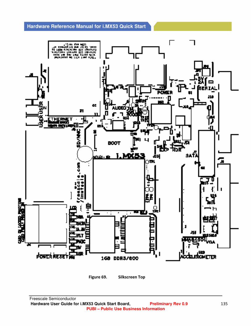
Freescale Semiconductor
Hardware User Guide for i.MX53 Quick Start Board, Preliminary Rev 0.9 135
PUBI – Public Use Business Information
Hardware Reference Manual for i.MX53 Quick Start
Figure 69. Silkscreen Top

Freescale Semiconductor
Hardware User Guide for i.MX53 Quick Start Board, Preliminary Rev 0.9 136
Freescale Confidential Propietary – NDA Required
Figure 70. Silkscreen Bottom