NXP Semiconductors Data Sheet: Technical Data Document Number: IMX8MDQLQIEC Rev. 1.1, 07/2019 Ordering Information See Table 2 on page 6 NXP reserves the right to change the production detail specifications as may be required to permit improvements in the design of its products. MIMX8MQ7CVAHZAA MIMX8MQ7CVAHZAB MIMX8MQ6CVAHZAA MIMX8MQ6CVAHZAB MIMX8MD7CVAHZAA MIMX8MD7CVAHZAB MIMX8MD6CVAHZAA MIMX8MD6CVAHZAB MIMX8MQ5CVAHZAA MIMX8MQ5CVAHZAB Package Information Bare Die Package FBGA 17 x 17 mm, 0.65 mm pitch 1 i.MX 8M Dual / 8M QuadLite / 8M Quad introduction The i.MX 8M Dual / 8M QuadLite / 8M Quad processors represent NXP’s latest market of connected streaming audio/video devices, scanning/imaging devices, and various devices requiring high-performance, low-power processors. The i.MX 8M Dual / 8M QuadLite / 8M Quad processors feature advanced implementation of a quad Arm ® Cortex®-A53 core, which operates at speeds of up to 1.3 GHz. A general purpose Cortex ® -M4 core processor is for low-power processing. The DRAM controller supports 32-bit/16-bit LPDDR4, DDR4, and DDR3L memory. There are a number of other interfaces for connecting peripherals, such as WLAN, Bluetooth, GPS, displays, and camera sensors. The i.MX 8M Quad and i.MX 8M Dual processors have hardware acceleration for video playback up to 4K, and can drive the video outputs up to 60 fps. Although the i.MX 8M QuadLite processor does not have hardware acceleration for video decode, it allows for video playback with software decoders if needed. i.MX 8M Dual / 8M QuadLite / 8M Quad Applications Processors Data Sheet for Industrial Products 1. i.MX 8M Dual / 8M QuadLite / 8M Quad introduction . . . 1 1.1. Block diagram . . . . . . . . . . . . . . . . . . . . . . . . . . . . 5 1.2. Ordering information . . . . . . . . . . . . . . . . . . . . . . . 6 2. Modules list . . . . . . . . . . . . . . . . . . . . . . . . . . . . . . . . . . . 8 2.1. Recommended connections for unused interfaces 12 3. Electrical characteristics . . . . . . . . . . . . . . . . . . . . . . . . 13 3.1. Chip-level conditions . . . . . . . . . . . . . . . . . . . . . . 13 3.2. Power supplies requirements and restrictions . . . 25 3.3. PLL electrical characteristics . . . . . . . . . . . . . . . . 27 3.4. On-chip oscillators . . . . . . . . . . . . . . . . . . . . . . . . 28 3.5. I/O DC parameters . . . . . . . . . . . . . . . . . . . . . . . 30 3.6. I/O AC parameters . . . . . . . . . . . . . . . . . . . . . . . 32 3.7. Output buffer impedance parameters . . . . . . . . . 35 3.8. System modules timing . . . . . . . . . . . . . . . . . . . . 37 3.9. External peripheral interface parameters . . . . . . 38 4. Boot mode configuration . . . . . . . . . . . . . . . . . . . . . . . . 74 4.1. Boot mode configuration pins . . . . . . . . . . . . . . . 74 4.2. Boot device interface allocation . . . . . . . . . . . . . . 75 5. Package information and contact assignments . . . . . . . 76 5.1. 17 x 17 mm package information . . . . . . . . . . . . 76 5.2. DDR pin function list for 17 x 17 mm package . . 96 6. Revision history . . . . . . . . . . . . . . . . . . . . . . . . . . . . . . 100

Welcome message from author
This document is posted to help you gain knowledge. Please leave a comment to let me know what you think about it! Share it to your friends and learn new things together.
Transcript

NXP SemiconductorsData Sheet: Technical Data
Document Number: IMX8MDQLQIECRev. 1.1, 07/2019
Ordering Information
See Table 2 on page 6
NXP reserves the right to change the production detail specifications as may be required to permit improvements in the design of its products.
MIMX8MQ7CVAHZAA MIMX8MQ7CVAHZAB
MIMX8MQ6CVAHZAA MIMX8MQ6CVAHZAB
MIMX8MD7CVAHZAA MIMX8MD7CVAHZAB
MIMX8MD6CVAHZAA MIMX8MD6CVAHZAB
MIMX8MQ5CVAHZAA MIMX8MQ5CVAHZAB
Package InformationBare Die Package
FBGA 17 x 17 mm, 0.65 mm pitch
1 i.MX 8M Dual / 8M QuadLite / 8M Quad introduction
The i.MX 8M Dual / 8M QuadLite / 8M Quad processorsrepresent NXP’s latest market of connected streamingaudio/video devices, scanning/imaging devices, andvarious devices requiring high-performance, low-powerprocessors.
The i.MX 8M Dual / 8M QuadLite / 8M Quad processors feature advanced implementation of a quad Arm® Cortex®-A53 core, which operates at speeds of up to 1.3 GHz. A general purpose Cortex®-M4 core processor is for low-power processing. The DRAM controller supports 32-bit/16-bit LPDDR4, DDR4, and DDR3L memory. There are a number of other interfaces for connecting peripherals, such as WLAN, Bluetooth, GPS, displays, and camera sensors. The i.MX 8M Quad and i.MX 8M Dual processors have hardware acceleration for video playback up to 4K, and can drive the video outputs up to 60 fps. Although the i.MX 8M QuadLite processor does not have hardware acceleration for video decode, it allows for video playback with software decoders if needed.
i.MX 8M Dual / 8M QuadLite / 8M Quad Applications Processors Data Sheet for Industrial Products
1. i.MX 8M Dual / 8M QuadLite / 8M Quad introduction . . . 11.1. Block diagram . . . . . . . . . . . . . . . . . . . . . . . . . . . . 51.2. Ordering information . . . . . . . . . . . . . . . . . . . . . . . 6
2. Modules list . . . . . . . . . . . . . . . . . . . . . . . . . . . . . . . . . . . 82.1. Recommended connections for unused interfaces 12
3. Electrical characteristics . . . . . . . . . . . . . . . . . . . . . . . . 133.1. Chip-level conditions . . . . . . . . . . . . . . . . . . . . . . 133.2. Power supplies requirements and restrictions . . . 253.3. PLL electrical characteristics . . . . . . . . . . . . . . . . 273.4. On-chip oscillators . . . . . . . . . . . . . . . . . . . . . . . . 283.5. I/O DC parameters . . . . . . . . . . . . . . . . . . . . . . . 303.6. I/O AC parameters . . . . . . . . . . . . . . . . . . . . . . . 323.7. Output buffer impedance parameters . . . . . . . . . 353.8. System modules timing . . . . . . . . . . . . . . . . . . . . 373.9. External peripheral interface parameters . . . . . . 38
4. Boot mode configuration . . . . . . . . . . . . . . . . . . . . . . . . 744.1. Boot mode configuration pins . . . . . . . . . . . . . . . 744.2. Boot device interface allocation . . . . . . . . . . . . . . 75
5. Package information and contact assignments . . . . . . . 765.1. 17 x 17 mm package information . . . . . . . . . . . . 765.2. DDR pin function list for 17 x 17 mm package . . 96
6. Revision history . . . . . . . . . . . . . . . . . . . . . . . . . . . . . . 100

i.MX 8M Dual / 8M QuadLite / 8M Quad Applications Processors Data Sheet for Industrial Products, Rev. 1.1, 07/2019
2 NXP Semiconductors
i.MX 8M Dual / 8M QuadLite / 8M Quad introduction
Table 1. Features
Subsystem Feature
Arm Cortex-A53 MPCore platform Quad symmetric Cortex-A53 processors: • 32 KB L1 Instruction Cache • 32 KB L1 Data Cache • Support L1 cache RAMs protection with parity/ECC
Support of 64-bit Armv8-A architecture: • 1 MB unified L2 cache • Support L2 cache RAMs protection with ECC • Frequency of 1.5 GHz
Arm Cortex-M4 core platform 16 KB L1 Instruction Cache
16 KB L1 Data Cache
256 KB tightly coupled memory (TCM)
Connectivity Two PCI Express Gen2 interfaces
Two USB 3.0/2.0 controllers with integrated PHY interfaces
Two Ultra Secure Digital Host Controller (uSDHC) interfaces
One Gigabit Ethernet controller with support for EEE, Ethernet AVB, and IEEE 1588
Four Universal Asynchronous Receiver/Transmitter (UART) modules
Four I2C modules
Three SPI modules
External memory interface 32/16-bit DRAM interface: LPDDR4-3200, DDR4-2400, DDR3L-1600
8-bit NAND-Flash
eMMC 5.0 Flash
SPI NOR Flash
QuadSPI Flash with support for XIP
GPIO and pin multiplexing GPIO modules with interrupt capability
Input/output multiplexing controller (IOMUXC) to provide centralized pad control
On-chip memory Boot ROM (128 KB)
On-chip RAM (128 KB + 32 KB)
Power management Temperature sensor with programmable trip points
Flexible power domain partitioning with internal power switches to support efficient power management

i.MX 8M Dual / 8M QuadLite / 8M Quad introduction
i.MX 8M Dual / 8M QuadLite / 8M Quad Applications Processors Data Sheet for Industrial Products, Rev. 1.1, 07/2019
NXP Semiconductors 3
Multimedia Video Processing Unit: • 4Kp60 HEVC/H.265 main, and main 10 decoder • 4Kp60 VP9 decoder • 4Kp30 AVC/H.264 decoder • 1080p60 MPEG-2, MPEG-4p2, VC-1, VP8, RV9, AVS, MJPEG, H.263 decoder
Graphic Processing Unit: • 4 shader • 267 million triangles/sec • 1.6 Giga pixel/sec • 32 GFLOPs 32-bit or 64 GFLOPs 16-bit • Support OpenGL ES 1.1, 2.0, 3.0, 3.1, Open CL 1.2, and Vulkan
HDMI Display Interface: • HDMI 2.0a supporting one display: resolution up to 4096 x 2160 at 60 Hz, support
HDCP 2.2 and HDCP 1.41
• 20+ Audio interfaces 32-bit @ 384 kHz fs, with Time Division Multiplexing (TDM) support
• S/PDIF input and output • Audio Return Channel (ARC) on HDMI • Upscale HD graphics to 4K for display • Downscale 4K video to HD for display • Display Port • Embedded Display Port
MIPI-DSI Display Interface: • MIPI-DSI 4 channels supporting one display, resolution up to 1920 x 1080 at 60 Hz • LCDIF display controller • Output can be LCDIF output or DC display controller output
Audio: • S/PDIF input and output • Five synchronous audio interface (SAI) modules supporting I2S, AC97, TDM, and
codec/DSP interfaces, including one SAI with 16 Tx and 16 Rx channels, one SAI with 8 Tx and 8 Rx channels, and three SAI with 2 Tx and 2 Rx channels
• One SAI for 8 Tx channels for HDMI output audio • One S/PDIF input for HDMI ARC input
Camera inputs: • Two MIPI-CSI2 camera inputs (4-lane each)
Security Resource Domain Controller (RDC) supports four domains and up to eight regions
Arm TrustZone (TZ) architecture
On-chip RAM (OCRAM) secure region protection using OCRAM controller
High Assurance Boot (HAB)
Cryptographic acceleration and assurance (CAAM) module
Secure non-volatile storage (SNVS): Secure real-time clock (RTC)
Secure JTAG controller (SJC)
Table 1. Features (continued)
Subsystem Feature
i.MX 8M Dual / 8M QuadLite / 8M Quad Applications Processors Data Sheet for Industrial Products, Rev. 1.1, 07/2019
4 NXP Semiconductors
i.MX 8M Dual / 8M QuadLite / 8M Quad introduction
NOTE
The actual feature set depends on the part numbers as described in Table 2. Functions such as display and camera interfaces, and connectivity interfaces, may not be enabled for specific part numbers.
System debug Arm CoreSight debug and trace architecture
TPIU to support off-chip real-time trace
ETF with 4 KB internal storage to provide trace buffering
Unified trace capability for Quad Cortex-A53 and Cortex-M4 CPUs
Cross Triggering Interface (CTI)
Support for 5-pin (JTAG) debug interface
1 Please contact the NXP sales and marketing team for order details on HDCP enable parts.
Table 1. Features (continued)
Subsystem Feature
i.MX 8M Dual / 8M QuadLite / 8M Quad introduction
i.MX 8M Dual / 8M QuadLite / 8M Quad Applications Processors Data Sheet for Industrial Products, Rev. 1.1, 07/2019
NXP Semiconductors 5
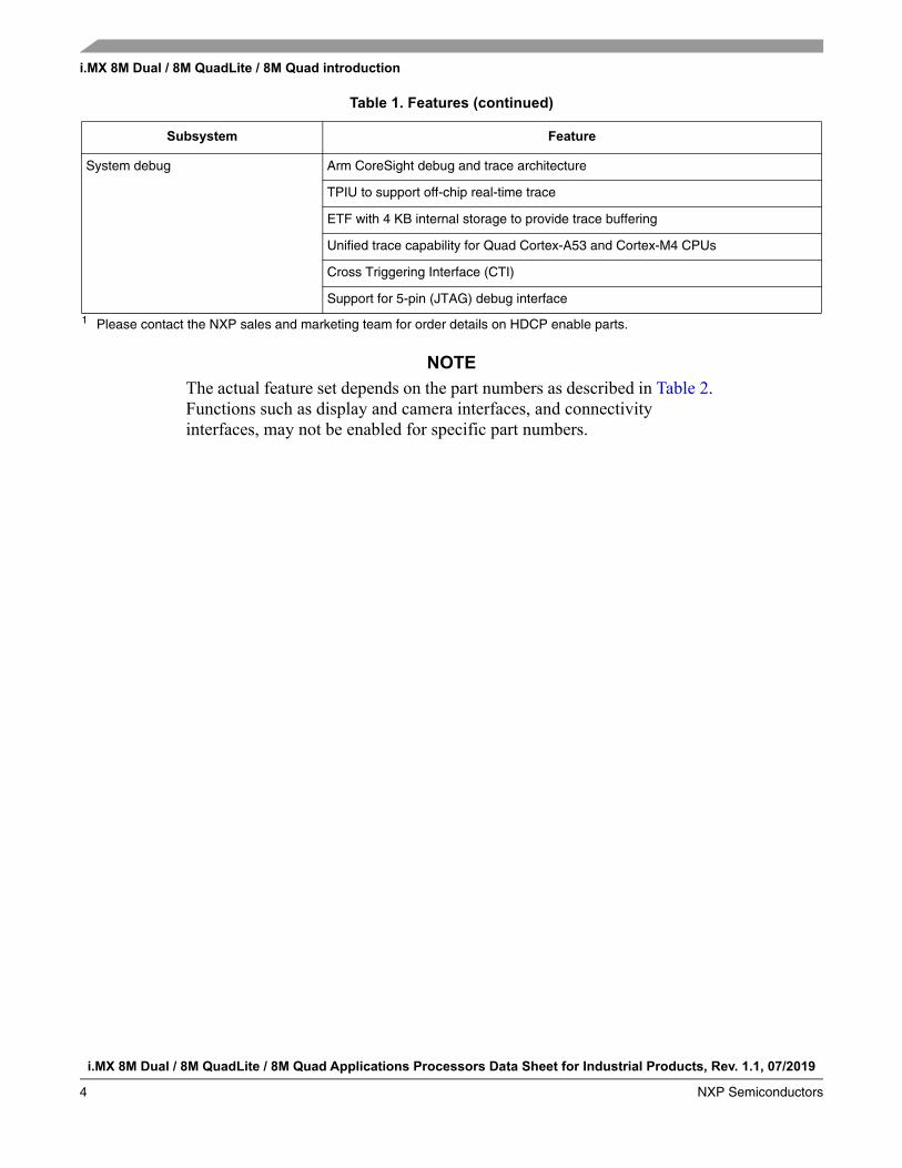
1.1 Block diagramFigure 1 shows the functional modules in the i.MX 8M Dual / 8M QuadLite / 8M Quad processor system.
Figure 1. i.MX 8M Dual / 8M QuadLite / 8M Quad system block diagram
System Control
Smart DMA x2
Temperature Sensor
Timer x3
Secure JTAG
Watchdog x3
Low Power, Security CPU
Connectivity and I/O
1 GB Ethernet (IEEE1588, EEE, and AVB)
PWM x4
Multimedia
USB 3.0/2.0 OTG x2
S/PDIF Rx and Tx,
MIPI DSI Display x1
HDMI 2.0a output
External Memory
Security
TrustZone
DRM Ciphers
Secure Clock
eFuse Key Storage
Random Number
32 KB Secure RAM
Main CPU Platform
Quad Cortex-A53
32 KB I-cache 32 KB D-cache
NEON FPU
1 MB L2 Cache
Cortex-M4
16 KB I-cache 16 KB D-cache
256 KB TCM
3D Graphics: 4 ShaderOpenGL/ES 3.1, CL 1.2, Vulkan
4Kp60 HEVC/H.265
4Kp30 H.264 Decoder and VP9
1080p60 MPEG-2, MPEG-4p2,VC-1, VP8, RV9, AVS,MJPEG, H.263 Decoder
4Kp60 Display
LPDDR4-3200
2x eMMC 5/SD 3NAND CTL (BCH62)
QuadSPI (XIP)
Temp Monitor
I2S/SAI x6
PCIe 2.0 x2 (1-lane, each)
UART x4, 5 MbpsI2C x4, SPI x3
HDCP 2.2
MIPI CSI2 Capture x2
4Kp60 VP9 DDR4-2400DDR3L-1600

i.MX 8M Dual / 8M QuadLite / 8M Quad Applications Processors Data Sheet for Industrial Products, Rev. 1.1, 07/2019
6 NXP Semiconductors
i.MX 8M Dual / 8M QuadLite / 8M Quad introduction
1.2 Ordering informationTable 2 shows examples of orderable sample part numbers covered by this data sheet. This table does not include all possible orderable part numbers. If your desired part number is not listed in the table, or you have questions about available parts, contact your NXP representative.
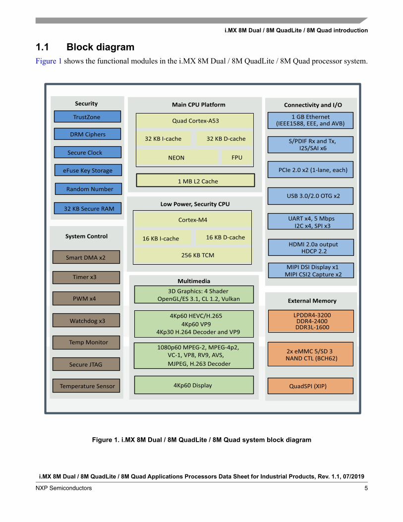
Figure 2 describes the part number nomenclature so that the users can identify the characteristics of the specific part number.
Contact an NXP representative for additional details.
Table 2. Orderable part numbers
Part number OptionsCortex-A53 CPU speed
grade
Qualification tier
Temperature Tj (C)
Package
MIMX8MQ7CVAHZAA1
MIMX8MQ7CVAHZAB1
1 Part number requires a Dolby VisionTM license from Dolby.
8M Quad 1.3 GHz Industrial -40 to +105 17 x 17 mm,0.65 mm pitch, FBGA
MIMX8MQ6CVAHZAAMIMX8MQ6CVAHZAB
8M Quad 1.3 GHz Industrial -40 to +105 17 x 17 mm,0.65 mm pitch, FBGA
MIMX8MD7CVAHZAA1
MIMX8MD7CVAHZAB18M Dual 1.3 GHz Industrial -40 to +105 17 x 17 mm,
0.65 mm pitch, FBGA
MIMX8MD6CVAHZAAMIMX8MD6CVAHZAB
8M Dual 1.3 GHz Industrial -40 to +105 17 x 17 mm,0.65 mm pitch, FBGA
MIMX8MQ5CVAHZAAMIMX8MQ5CVAHZAB
8M Quad Lite 1.3 GHz Industrial -40 to +105 17 x 17 mm,0.65 mm pitch, FBGA
i.MX 8M Dual / 8M QuadLite / 8M Quad introduction
i.MX 8M Dual / 8M QuadLite / 8M Quad Applications Processors Data Sheet for Industrial Products, Rev. 1.1, 07/2019
NXP Semiconductors 7
Figure 2. Part number nomenclature—i.MX 8M Dual / 8M QuadLite / 8M Quad processors
*Please contact the NXP sales and marketing team for order details on HDCP enable parts.
Temperature (Tj) +Commercial: 0 to + 95 °C D
Industrial: -40 to +105 °C C
Frequency $$
1.5 GHz JZ
1.3 GHz HZ
Package Type ROHS
17 x 17 mm, 0.65 mm pitch, FCBGA bare die package VA
Qualification Level M
Samples P
Mass Production M
Special S
i.MX 8 Family Part # Series Description
i.MX 8MQ Quad core
i.MX 8MD Dual core
Silicon Rev A
Rev. 1.0 A
Rev. 1.1 B
Fusing %
- A
HDCP customer programmable
D
HDCP NXP programmed C
M IMX8MQ @ + VN $$ % A
Part Differentiator @
VPU decode + Dolby Vision + HDR10 + GPU 7
VPU decode + HDR10 + GPU 6
GPU, No VPU 5
i.MX 8M Dual / 8M QuadLite / 8M Quad Applications Processors Data Sheet for Industrial Products, Rev. 1.1, 07/2019
8 NXP Semiconductors
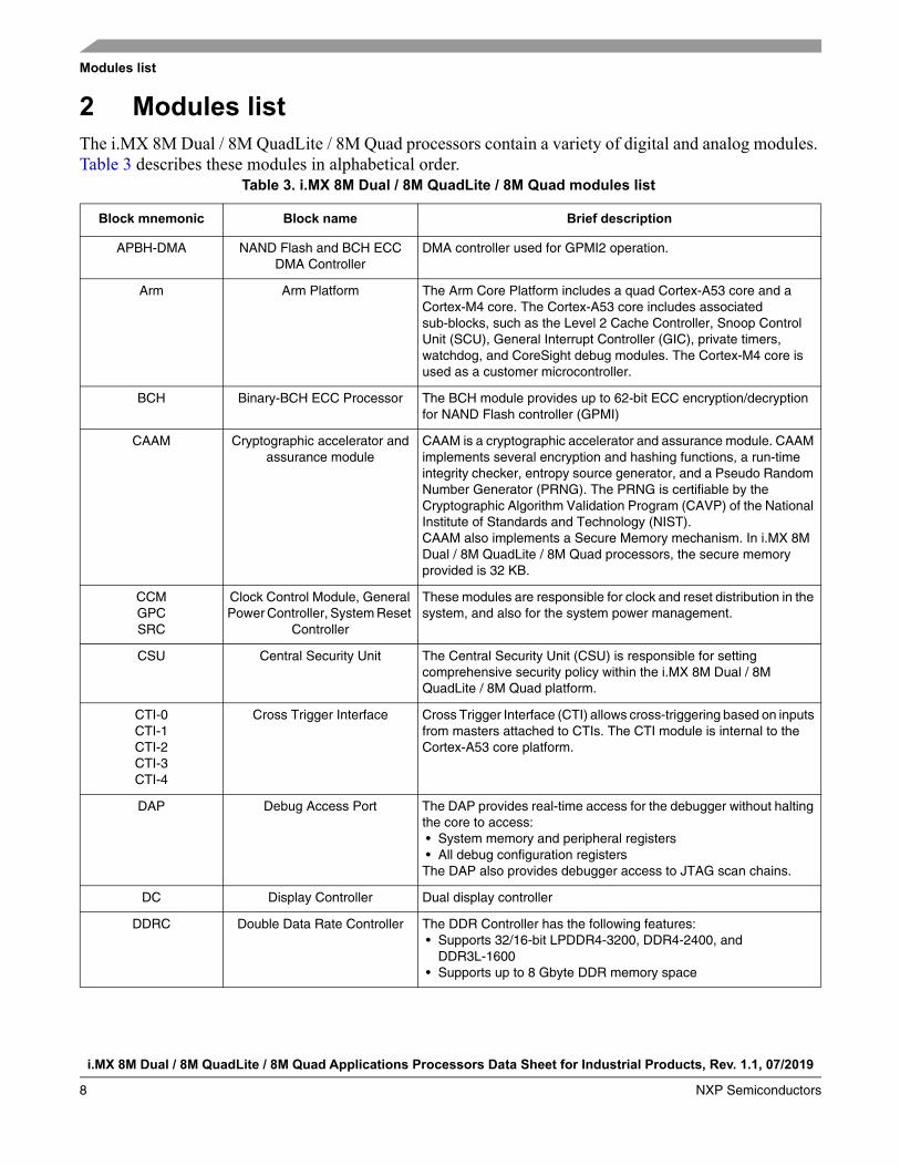
Modules list
2 Modules listThe i.MX 8M Dual / 8M QuadLite / 8M Quad processors contain a variety of digital and analog modules. Table 3 describes these modules in alphabetical order.
Table 3. i.MX 8M Dual / 8M QuadLite / 8M Quad modules list
Block mnemonic Block name Brief description
APBH-DMA NAND Flash and BCH ECC DMA Controller
DMA controller used for GPMI2 operation.
Arm Arm Platform The Arm Core Platform includes a quad Cortex-A53 core and a Cortex-M4 core. The Cortex-A53 core includes associated sub-blocks, such as the Level 2 Cache Controller, Snoop Control Unit (SCU), General Interrupt Controller (GIC), private timers, watchdog, and CoreSight debug modules. The Cortex-M4 core is used as a customer microcontroller.
BCH Binary-BCH ECC Processor The BCH module provides up to 62-bit ECC encryption/decryption for NAND Flash controller (GPMI)
CAAM Cryptographic accelerator and assurance module
CAAM is a cryptographic accelerator and assurance module. CAAM implements several encryption and hashing functions, a run-time integrity checker, entropy source generator, and a Pseudo Random Number Generator (PRNG). The PRNG is certifiable by the Cryptographic Algorithm Validation Program (CAVP) of the National Institute of Standards and Technology (NIST).CAAM also implements a Secure Memory mechanism. In i.MX 8M Dual / 8M QuadLite / 8M Quad processors, the secure memory provided is 32 KB.
CCMGPCSRC
Clock Control Module, General Power Controller, System Reset
Controller
These modules are responsible for clock and reset distribution in the system, and also for the system power management.
CSU Central Security Unit The Central Security Unit (CSU) is responsible for setting comprehensive security policy within the i.MX 8M Dual / 8M QuadLite / 8M Quad platform.
CTI-0CTI-1CTI-2CTI-3CTI-4
Cross Trigger Interface Cross Trigger Interface (CTI) allows cross-triggering based on inputs from masters attached to CTIs. The CTI module is internal to the Cortex-A53 core platform.
DAP Debug Access Port The DAP provides real-time access for the debugger without halting the core to access: • System memory and peripheral registers • All debug configuration registersThe DAP also provides debugger access to JTAG scan chains.
DC Display Controller Dual display controller
DDRC Double Data Rate Controller The DDR Controller has the following features: • Supports 32/16-bit LPDDR4-3200, DDR4-2400, and
DDR3L-1600 • Supports up to 8 Gbyte DDR memory space
Modules list
i.MX 8M Dual / 8M QuadLite / 8M Quad Applications Processors Data Sheet for Industrial Products, Rev. 1.1, 07/2019
NXP Semiconductors 9
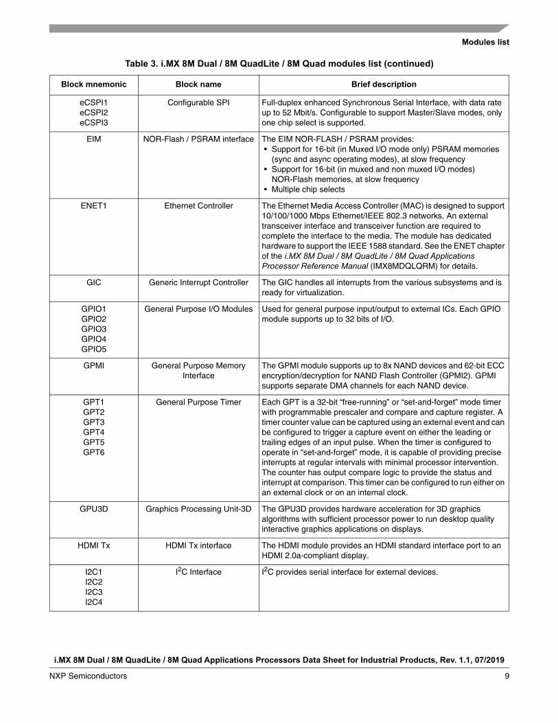
eCSPI1eCSPI2eCSPI3
Configurable SPI Full-duplex enhanced Synchronous Serial Interface, with data rate up to 52 Mbit/s. Configurable to support Master/Slave modes, only one chip select is supported.
EIM NOR-Flash / PSRAM interface The EIM NOR-FLASH / PSRAM provides: • Support for 16-bit (in Muxed I/O mode only) PSRAM memories
(sync and async operating modes), at slow frequency • Support for 16-bit (in muxed and non muxed I/O modes)
NOR-Flash memories, at slow frequency • Multiple chip selects
ENET1 Ethernet Controller The Ethernet Media Access Controller (MAC) is designed to support 10/100/1000 Mbps Ethernet/IEEE 802.3 networks. An external transceiver interface and transceiver function are required to complete the interface to the media. The module has dedicated hardware to support the IEEE 1588 standard. See the ENET chapter of the i.MX 8M Dual / 8M QuadLite / 8M Quad Applications Processor Reference Manual (IMX8MDQLQRM) for details.
GIC Generic Interrupt Controller The GIC handles all interrupts from the various subsystems and is ready for virtualization.
GPIO1GPIO2GPIO3GPIO4GPIO5
General Purpose I/O Modules Used for general purpose input/output to external ICs. Each GPIO module supports up to 32 bits of I/O.
GPMI General Purpose Memory Interface
The GPMI module supports up to 8x NAND devices and 62-bit ECC encryption/decryption for NAND Flash Controller (GPMI2). GPMI supports separate DMA channels for each NAND device.
GPT1GPT2GPT3GPT4GPT5GPT6
General Purpose Timer Each GPT is a 32-bit “free-running” or “set-and-forget” mode timer with programmable prescaler and compare and capture register. A timer counter value can be captured using an external event and can be configured to trigger a capture event on either the leading or trailing edges of an input pulse. When the timer is configured to operate in “set-and-forget” mode, it is capable of providing precise interrupts at regular intervals with minimal processor intervention. The counter has output compare logic to provide the status and interrupt at comparison. This timer can be configured to run either on an external clock or on an internal clock.
GPU3D Graphics Processing Unit-3D The GPU3D provides hardware acceleration for 3D graphics algorithms with sufficient processor power to run desktop quality interactive graphics applications on displays.
HDMI Tx HDMI Tx interface The HDMI module provides an HDMI standard interface port to an HDMI 2.0a-compliant display.
I2C1I2C2I2C3I2C4
I2C Interface I2C provides serial interface for external devices.
Table 3. i.MX 8M Dual / 8M QuadLite / 8M Quad modules list (continued)
Block mnemonic Block name Brief description

i.MX 8M Dual / 8M QuadLite / 8M Quad Applications Processors Data Sheet for Industrial Products, Rev. 1.1, 07/2019
10 NXP Semiconductors
Modules list
IOMUXC IOMUX Control This module enables flexible I/O multiplexing. Each IO pad has a default as well as several alternate functions. The alternate functions are software configurable.
LCDIF LCD interface The LCDIF is a general purpose display controller used to drive a wide range of display devices varying in size and capability.
MIPI CSI2 (four-lane) MIPI Camera Serial Interface This module provides two four-lane MIPI camera serial interfaces, each of them can operate up to a maximum bit rate of 1.5 Gbps.
MIPI DSI (four-lane) MIPI Display Serial Interface This module provides a four-lane MIPI display serial interface operating up to a maximum bit rate of 1.5 Gbps.
OCOTP_CTRL OTP Controller The On-Chip OTP controller (OCOTP_CTRL) provides an interface for reading, programming, and/or overriding identification and control information stored in on-chip fuse elements. The module supports electrically programmable poly fuses (eFUSEs). The OCOTP_CTRL also provides a set of volatile software-accessible signals that can be used for software control of hardware elements, not requiring non volatility. The OCOTP_CTRL provides the primary user-visible mechanism for interfacing with on-chip fuse elements. Among the uses for the fuses are unique chip identifiers, mask revision numbers, cryptographic keys, JTAG secure mode, boot characteristics, and various control signals requiring permanent non volatility.
OCRAM On-Chip Memory controller The On-Chip Memory controller (OCRAM) module is designed as an interface between the system’s AXI bus and the internal (on-chip) SRAM memory module.In i.MX 8M Dual / 8M QuadLite / 8M Quad processors, the OCRAM is used for controlling the 128 KB multimedia RAM through a 64-bit AXI bus.
PCIe1PCIe2
2x PCI Express 2.0 The PCIe IP provides PCI Express Gen 2.0 functionality.
PMU Power Management Unit Integrated power management unit. Used to provide power to various SoC domains.
PWM1PWM2PWM3PWM4
Pulse Width Modulation The pulse-width modulator (PWM) has a 16-bit counter and is optimized to generate sound from stored sample audio images. It can also generate tones. It uses 16-bit resolution and a 4x16 data FIFO to generate sound.
QSPI Quad SPI The Quad SPI module acts as an interface to external serial flash devices. This module contains the following features: • Flexible sequence engine to support various flash vendor devices • Single pad/Dual pad/Quad pad mode of operation • Single Data Rate/Double Data Rate mode of operation • Parallel Flash mode • DMA support • Memory mapped read access to connected flash devices • Multi master access with priority and flexible and configurable
buffer for each master
Table 3. i.MX 8M Dual / 8M QuadLite / 8M Quad modules list (continued)
Block mnemonic Block name Brief description

Modules list
i.MX 8M Dual / 8M QuadLite / 8M Quad Applications Processors Data Sheet for Industrial Products, Rev. 1.1, 07/2019
NXP Semiconductors 11
SAI1SAI2SAI3SAI4SAI5SAI6
Synchronous Audio Interface The SAI module provides a synchronous audio interface (SAI) that supports full duplex serial interfaces with frame synchronization, such as I2S, AC97, TDM, and codec/DSP interfaces.
SDMA Smart Direct Memory Access The SDMA is a multichannel flexible DMA engine. It helps in maximizing system performance by offloading the various cores in dynamic data routing. It has the following features: • Powered by a 16-bit Instruction-Set micro-RISC engine • Multi channel DMA supporting up to 32 time-division multiplexed
DMA channels • 48 events with total flexibility to trigger any combination of
channels • Memory accesses including linear, FIFO, and 2D addressing • Shared peripherals between Arm and SDMA • Very fast Context-Switching with 2-level priority based preemptive
multi tasking • DMA units with auto-flush and prefetch capability • Flexible address management for DMA transfers (increment,
decrement, and no address changes on source and destination address)
• DMA ports can handle unidirectional and bidirectional flows (Copy mode)
• Up to 8-word buffer for configurable burst transfers for EMIv2.5 • Support of byte-swapping and CRC calculations • Library of Scripts and API is available
SJC Secure JTAG Controller The SJC provides JTAG interface (designed to be compatible with JTAG TAP standards) to internal logic. The i.MX 8M Dual / 8M QuadLite / 8M Quad processors use JTAG port for production, testing, and system debugging. Additionally, the SJC provides BSR (Boundary Scan Register) standard support, designed to be compatible with IEEE 1149.1 and IEEE 1149.6 standards. The JTAG port must be accessible during platform initial laboratory bring-up, for manufacturing tests and troubleshooting, as well as for software debugging by authorized entities. The SJC of the i.MX 8M Dual / 8M QuadLite / 8M Quad incorporates three security modes for protecting against unauthorized accesses. Modes are selected through eFUSE configuration.
SNVS Secure Non-Volatile Storage Secure Non-Volatile Storage, including Secure Real Time Clock, Security State Machine, and Master Key Control.
SPDIF1SPDIF2
Sony Philips Digital Interconnect Format
A standard audio file transfer format, developed jointly by the Sony and Phillips corporations. It supports Transmitter and Receiver functionality.
TEMPSENSOR Temperature Sensor Temperature sensor
TZASC Trust-Zone Address Space Controller
The TZASC (TZC-380 by Arm) provides security address region control functions required for intended application. It is used on the path to the DRAM controller.
Table 3. i.MX 8M Dual / 8M QuadLite / 8M Quad modules list (continued)
Block mnemonic Block name Brief description
i.MX 8M Dual / 8M QuadLite / 8M Quad Applications Processors Data Sheet for Industrial Products, Rev. 1.1, 07/2019
12 NXP Semiconductors
Modules list
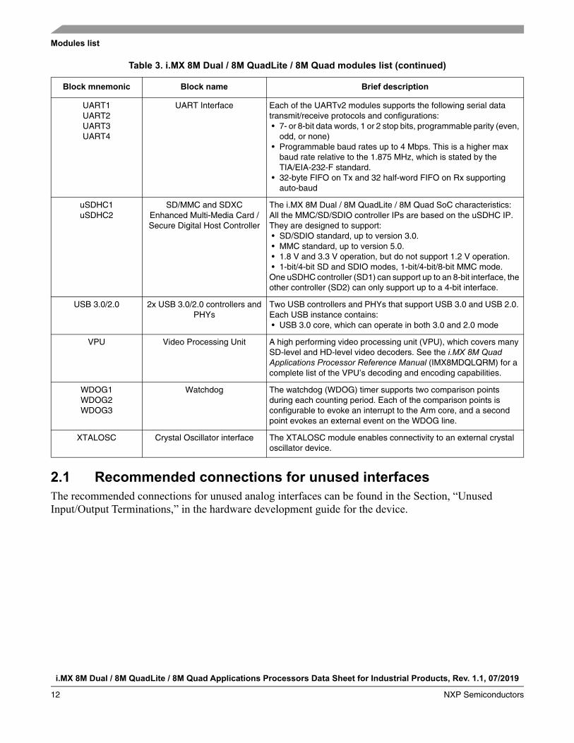
2.1 Recommended connections for unused interfacesThe recommended connections for unused analog interfaces can be found in the Section, “Unused Input/Output Terminations,” in the hardware development guide for the device.
UART1UART2UART3UART4
UART Interface Each of the UARTv2 modules supports the following serial data transmit/receive protocols and configurations: • 7- or 8-bit data words, 1 or 2 stop bits, programmable parity (even,
odd, or none) • Programmable baud rates up to 4 Mbps. This is a higher max
baud rate relative to the 1.875 MHz, which is stated by the TIA/EIA-232-F standard.
• 32-byte FIFO on Tx and 32 half-word FIFO on Rx supporting auto-baud
uSDHC1uSDHC2
SD/MMC and SDXCEnhanced Multi-Media Card / Secure Digital Host Controller
The i.MX 8M Dual / 8M QuadLite / 8M Quad SoC characteristics:All the MMC/SD/SDIO controller IPs are based on the uSDHC IP. They are designed to support: • SD/SDIO standard, up to version 3.0. • MMC standard, up to version 5.0. • 1.8 V and 3.3 V operation, but do not support 1.2 V operation. • 1-bit/4-bit SD and SDIO modes, 1-bit/4-bit/8-bit MMC mode.One uSDHC controller (SD1) can support up to an 8-bit interface, the other controller (SD2) can only support up to a 4-bit interface.
USB 3.0/2.0 2x USB 3.0/2.0 controllers and PHYs
Two USB controllers and PHYs that support USB 3.0 and USB 2.0. Each USB instance contains: • USB 3.0 core, which can operate in both 3.0 and 2.0 mode
VPU Video Processing Unit A high performing video processing unit (VPU), which covers many SD-level and HD-level video decoders. See the i.MX 8M Quad Applications Processor Reference Manual (IMX8MDQLQRM) for a complete list of the VPU’s decoding and encoding capabilities.
WDOG1WDOG2WDOG3
Watchdog The watchdog (WDOG) timer supports two comparison points during each counting period. Each of the comparison points is configurable to evoke an interrupt to the Arm core, and a second point evokes an external event on the WDOG line.
XTALOSC Crystal Oscillator interface The XTALOSC module enables connectivity to an external crystal oscillator device.
Table 3. i.MX 8M Dual / 8M QuadLite / 8M Quad modules list (continued)
Block mnemonic Block name Brief description
Electrical characteristics
i.MX 8M Dual / 8M QuadLite / 8M Quad Applications Processors Data Sheet for Industrial Products, Rev. 1.1, 07/2019
NXP Semiconductors 13
3 Electrical characteristicsThis section provides the device and module-level electrical characteristics for the i.MX 8M Dual / 8M QuadLite / 8M Quad processors.
3.1 Chip-level conditions
This section provides the device-level electrical characteristics for the IC. See Table 4 for a quick reference to the individual tables and sections.
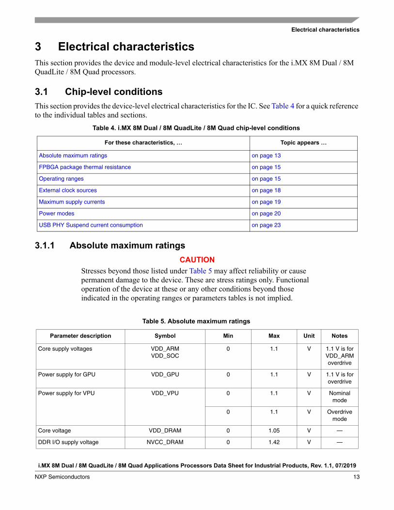
3.1.1 Absolute maximum ratings
CAUTION
Stresses beyond those listed under Table 5 may affect reliability or cause permanent damage to the device. These are stress ratings only. Functional operation of the device at these or any other conditions beyond those indicated in the operating ranges or parameters tables is not implied.
Table 4. i.MX 8M Dual / 8M QuadLite / 8M Quad chip-level conditions
For these characteristics, … Topic appears …
Absolute maximum ratings on page 13
FPBGA package thermal resistance on page 15
Operating ranges on page 15
External clock sources on page 18
Maximum supply currents on page 19
Power modes on page 20
USB PHY Suspend current consumption on page 23
Table 5. Absolute maximum ratings
Parameter description Symbol Min Max Unit Notes
Core supply voltages VDD_ARMVDD_SOC
0 1.1 V 1.1 V is for VDD_ARM overdrive
Power supply for GPU VDD_GPU 0 1.1 V 1.1 V is for overdrive
Power supply for VPU VDD_VPU 0 1.1 V Nominal mode
0 1.1 V Overdrive mode
Core voltage VDD_DRAM 0 1.05 V —
DDR I/O supply voltage NVCC_DRAM 0 1.42 V —

i.MX 8M Dual / 8M QuadLite / 8M Quad Applications Processors Data Sheet for Industrial Products, Rev. 1.1, 07/2019
14 NXP Semiconductors
Electrical characteristics
Power supply for analog domain VDDA_1P8 0 1.98 V —
GPIO supply voltage NVCC_JTAG, NVCCGPIO1, NVCC_ENT, NVCC_SD1,
NVCC_SD2, NVCC_NAND, NVCC_SA1, NVCC_SAI2, NVCC_SAI3, NVCC_SAI5, NVCC_ECSPI, NVCC_I2C,
NVCC_UART
0 3.6 V 1.8 V mode/3.3 V
mode
SNVS IO supply voltage NVCC_SNVS 0 3.6 V 3.3 V mode only
VDD_SNVS supply voltage VDD_SNVS 0 0.99 V —
PLL 1.8 V supply voltage VDDA_DRAM 0 1.89 V —
Supply for 25 MHz crystal VDDA_1P8_XTAL_25M 0 1.98 V —
Supply for 27 MHz crystal VDDA_1P8_XTAL_27M 0 1.98 V —
HDMI supply voltage HDMI_AVDDCLK 0 0.99 —
HDMI_AVDDIO 0 1.90 —
HDMI_AVDDCORE 0 0.99 —
PCIe PHY supply voltage PCIE_VP 0 0.99 V —
PCIE_VPH 0 3.63 V —
PCIE_VPTX 0 0.99 V —
MIPI supply voltage MIPI_VDDA 0 1.1 V —
MIPI_VDDHA 0 1.98 V —
MIPI_VDD 0 1.1 V —
MIPI_VDDPLL 0 1.1 V
USB high supply voltage USB1_VDD33, USB1_VPH, USB2_VDD33, USB2_VPH
0 3.63 V —
USB_VBUS input detected USB1_VBUS,USB2_VBUS
0 5.25 V —
Input voltage on USB*_DP, USB*_DN pins
USB1_DP/USB1_DNUSB2_DP/USB2_DN
0 USB1_VDD33USB2_VDD33
V —
Temperature sensor VDD_1P8_TSENSOR 0 1.98 V —
Fuse power EFUSE_VQPS 0 1.98 V —
Input/output voltage range Vin/Vout 0 OVDD1+0.3 V —
ESD damage immunity: Vesd
V
—
• Human Body Model (HBM) • Charge Device Model (CDM)
——
2000500
Storage temperature range TSTORAGE –40 150 oC —
Table 5. Absolute maximum ratings (continued)
Parameter description Symbol Min Max Unit Notes

Electrical characteristics
i.MX 8M Dual / 8M QuadLite / 8M Quad Applications Processors Data Sheet for Industrial Products, Rev. 1.1, 07/2019
NXP Semiconductors 15
3.1.2 Thermal resistance
3.1.2.1 FPBGA package thermal resistance
Table 6 displays the thermal resistance data.
3.1.3 Operating ranges
Table 7 provides the operating ranges of the i.MX 8M Dual / 8M QuadLite / 8M Quad processors. For details on the chip's power structure, see the “Power Management Unit (PMU)” chapter of the i.MX 8M Dual / 8M QuadLite / 8M Quad Applications Processor Reference Manual (IMX8MDQLQRM).
1 OVDD is the I/O supply voltage.
Table 6. Thermal resistance data
Rating Test conditions Symbol17 x 17
pkg valueUnit
Junction to Ambient1
1 Junction temperature is a function of die size, on-chip power dissipation, package thermal resistance, mounting site (board) temperature, ambient temperature, air flow, power dissipation of other components on the board, and board thermal resistance.
Single-layer board (1s); natural convection2 Four-layer board (2s2p); natural convection2
2 Per JEDEC JESD51-2 with the single layer board horizontal. Thermal test board meets JEDEC specification for the specified package.
RJARJA Bare die: 16.4
oC/WoC/W
Junction to Ambient1 Single-layer board (1s); airflow 200 ft/min2,3
Four-layer board (2s2p); airflow 200 ft/min2,3
3 Per JEDEC JESD51-6 with the board horizontal.
RJARJA Bare die: 13.9
oC/WoC/W
Junction to Board1,4
4 Thermal resistance between the die and the printed circuit board per JEDEC JESD51-8. Board temperature is measured on the top surface of the board near the package.
— RJB Bare die: 4.6 oC/W
Junction to Case1,5
5 Thermal resistance between the die and the case top surface as measured by the cold plate method (MIL SPEC-883 Method 1012.1).
— RJC Bare die: 0.1 oC/W
Table 7. Operating ranges
Parameter description Symbol Min Typ Max1 Unit Comment
Power supply for Quad-A53 VDD_ARM 0.81 0.9 1.05 V Nominal mode—the maximum Arm core frequency supported in this mode is 800 MHz.
0.9 1.0 1.05 V Overdrive mode—the maximum Arm core frequency supported in this mode is defined in Table 2.
Power supply for SoC logic VDD_SOC 0.9 0.95 0.99 V —

i.MX 8M Dual / 8M QuadLite / 8M Quad Applications Processors Data Sheet for Industrial Products, Rev. 1.1, 07/2019
16 NXP Semiconductors
Electrical characteristics
Power supply for GPU VDD_GPU 0.81 0.9 1.05 V Nominal mode—the maximum GPU frequency supported in this mode is 800 MHz.
0.9 1.0 1.05 V Overdrive mode—the maximum GPU frequency supported in this mode is 1 GHz.
Power supply for VPU VDD_VPU 0.81 0.9 1.05 V Nominal mode—the maximum VPU frequency supported in this mode is 550/500/588 MHz.
0.9 1.0 1.05 V Overdrive mode—the maximum VPU G2/G1/AXI Bus frequency supported in this mode is 660/600/800 MHz.
Core voltage VDD_DRAM 0.81 0.9 1.05 V Nominal mode—the maximum DRAM working frequency supported in this mode is 933 MHz.
0.99 1.0 1.05 V Overdrive mode—the maximum DRAM working frequency supported in this mode is 1600 MHz
Power Supply Analog Domain
VDDA_1P8 1.62 1.8 1.98 V Power for internal analog blocks—must match the range of voltages that the rechargeable backup battery supports.
PLL 1.8 V supply voltage VDDA_DRAM 1.71 1.8 1.89 V —
Backup battery supply range
VDD_SNVS 0.81 0.9 0.99 V —
Supply for 25 MHz crystal VDD_1P8_XTAL_25M 1.6 1.8 1.98 V —
Supply for 27 MHz crystal VDD_1P8_XTAL_27M 1.6 1.8 1.98 V —
Temperature sensor VDD_1P8_TSENSOR 1.6 1.8 1.98 V —
Table 7. Operating ranges (continued)
Parameter description Symbol Min Typ Max1 Unit Comment

Electrical characteristics
i.MX 8M Dual / 8M QuadLite / 8M Quad Applications Processors Data Sheet for Industrial Products, Rev. 1.1, 07/2019
NXP Semiconductors 17
USB supply voltages USB1_VDD33/USB1_VPH
3.069 3.3 3.63 V This rail is for USB
USB2_VDD33/USB2_VPH
3.069 3.3 3.63 V This rail is for USB
USB1/2_DVDD 0.837 0.900 0.990 V 0.9 V supply for USB high speed operation
USB1/2_VP 0.837 0.900 0.990 V 0.9 V supply for USB super speed operation
USB1/2_VPTX 0.837 0.900 0.990 V 0.9 V supply for PHY transmit
USB1_VBUS/USB2_VBUS
0.8 1.4 5.25 V —
DDR I/O supply voltage NVCC_DRAM 1.06 1.10 1.17 V LPDDR4
1.14 1.2 1.26 V DDR4
1.28 1.35 1.42 V DDR3L
DRAM_VREF 0.49 x NVCC_D
RAM
0.5 x NVCC_D
RAM
0.51 x NVCC_D
RAM
V Set to one-half NVCC_DRAM
GPIO supply voltages NVCC_JTAG, NVCC_SD1, NVCC_SD2,
NVCC_NAND, NVCC_SAI1, NVCC_SAI2, NVCC_SAI3, NVCC_SAI5,
NVCC_ECSPI, NVCC_I2C,
NVCC_UART
1.65,3.0
1.8,3.3
1.95,3.6
V —
NVCC_ENET 1.65,2.253.0
1.8,2.53.3
1.95,2.753.6
V —
NVCC_GPIO1 1.653.0
1.8,3.3
1.95,3.6
V Power for GPIO1_IO00 ~ GPIO1_IO15
NVCC_SNVS 3.0 3.3 3.6 V Power for 3.3 V only
HDMI supply voltage HDMI_AVDDCLK 0.850 0.900 0.990 V 0.9 V supply for HDMI high speed clock
HDMI_AVDDIO 1.700 1.800 1.900 V 1.8 V supply for HDMI bias and PLL
HDMI_AVDDCORE 0.850 0.900 0.990 V 0.9 V supply for HDMI analog
Table 7. Operating ranges (continued)
Parameter description Symbol Min Typ Max1 Unit Comment

i.MX 8M Dual / 8M QuadLite / 8M Quad Applications Processors Data Sheet for Industrial Products, Rev. 1.1, 07/2019
18 NXP Semiconductors
Electrical characteristics
3.1.4 External clock sources
A 25 MHz oscillator is used as the primary clock source for the PLLs to generate the clock for CPU, BUS, and high-speed interfaces. For fractional PLLs, the 25 MHz clock from the oscillator can be directly used as the PLL reference clock.
A 27 MHz oscillator is used as the reference clock for HDMI PHY. Also it can be used as the alternative source for the fractional PLLs.
A 32 kHz clock input pin is used as the RTC clock source. It is expected to be supplied by an external 32.768 kHz oscillator.
Two pairs of differential clock inputs, named as CLK1P and CLK1N, can be used as the reference clock for the PLL. This is mainly used for a high-speed clock input during testing.
Four clock inputs to the CCM from normal GPIO pads via IOMUX can be used as the clock sources in the CCM.Table 8 shows the interface frequency requirements.
MIPI supply voltage MIPI_VDDA 0.81 0.9/1.0 1.1 V Analog core power supply
MIPI_VDDHA 1.62 1.8 1.98 V Analog IO power supply
MIPI_VDD 0.81 0.9/1.0 1.1 V Digital core power supply
MIPI_VDDPLL 0.81 0.9/1.0 1.1 V Analog supply for MIPI PLL
Voltage rails supplied from 1.8 V PHY
PCIE_VPH 1.6743.069
1.83.3
1.983.63
V Supplied from PMIC
PCIE_VP, PCIE_VPTX 0.837 0.9 0.99 V Supplied from PMIC
Temperature sensor accuracy
Tdelta — ±3 — °C Typical accuracy over the range –40°C to 125°C
Fuse power EFUSE_VQPS 1.71 1.8 1.98 V Power supply for internal use
Junction temperature, industrial
TJ -40 — +105 oC See Table 2 for complete list of
junction temperature capabilities.
1 Applying the maximum voltage results in maximum power consumption and heat generation. A voltage set point = (Vmin + the supply tolerance) is recommended. This result in an optimized power/speed ratio.
Table 8. External input clock frequency
Parameter description Symbol Min Typ Max Unit
RTC1,2
1 External oscillator or a crystal with internal oscillator amplifier.
fckil — 32.7683 — kHz
XTALI_25M/XTALO_25M2 fxtal 20 25 40 MHz
XTALI_27M/XTALO_27M2 fxtal 20 27 40 MHz
Table 7. Operating ranges (continued)
Parameter description Symbol Min Typ Max1 Unit Comment

Electrical characteristics
i.MX 8M Dual / 8M QuadLite / 8M Quad Applications Processors Data Sheet for Industrial Products, Rev. 1.1, 07/2019
NXP Semiconductors 19
The typical values shown in Table 8 are required for use with NXP BSPs to ensure precise time keeping and USB operation. For RTC operation, two clock sources are available.The decision of choosing a clock source should be made based on real-time clock use and precision timeout.
3.1.5 Maximum supply currents
Power consumption is highly dependent on the application. Estimating the maximum supply currents required for power supply design is difficult because the use cases that requires maximum supply current is not a realistic use cases.To help illustrate the effect of the application on power consumption, data was collected while running industry standard benchmarks that are designed to be compute and graphic intensive. The results pro-vided are intended to be used as guidelines for power supply design. Devices used for the tests were from the high current end of the expected process variation.
2 The required frequency stability of this clock source is application dependent.3 Recommended nominal frequency 32.768 kHz.
Table 9. Maximum supply currents1
Power rail Max current Unit
VDD_ARM 384 to 31001 mA
VDD_SOC 1400 to 25001 mA
VDD_GPU 0 to 20401 mA
VDD_VPU 0 to 6101 mA
VDD_DRAM 600 to 8701 mA
VDDA_0P9 50 mA
VDDA_1P8 20 mA
VDDA_DRAM 30 mA
VDD_SNVS 5 mA
NVCC_SNVS 5 mA
NVCC_<XXX> Imax = N x C x V x (0.5 x F)Where:N—Number of IO pins supplied by the power lineC—Equivalent external capacitive loadV—IO voltage(0.5 x F)—Data change rate. Up to 0.5 of the clock rate (F). In this equation, Imax is in Amps, C in Farads, V in Volts, and F in Hertz.
NVCC_DRAM 375 to 7501 mA
DRAM_VFEF 10 mA
USB1_DVDD 9.2 mA
USB2_DVDD 9.2 mA

i.MX 8M Dual / 8M QuadLite / 8M Quad Applications Processors Data Sheet for Industrial Products, Rev. 1.1, 07/2019
20 NXP Semiconductors
Electrical characteristics
3.1.6 Power modes
The i.MX 8M Dual / 8M QuadLite / 8M Quad processor support the following power modes:• RUN Mode: All external power rails are on, CPU is active and running; other internal modules can
be on/off based on application.• IDLE Mode: When there is no thread running and all high-speed devices are not active, the CPU
can automatically enter this mode. The CPU can be in the power-gated state but with L2 dataretained, DRAM and the bus clock are reduced. Most of the internal logic is clock gated but still
USB1_VP 35.7 mA
USB2_VP 35.7 mA
USB1_VPTX 21.2 mA
USB2_VPTX 21.2 mA
USB1_VDD33 24.5 mA
USB2_VDD33 24.5 mA
USB1_VPH 20.3 mA
USB2_VPH 20.3 mA
PCIE_VP (PCIE1) 38.1 mA
PCIE_VP (PCIE2) 38.1 mA
PCIE_VPH (PCIE1) 43 mA
PCIE_VPH (PCIE2) 43 mA
PCIE_VPTX (PCIE1) 14.3 mA
PCIE_VPTX (PCIE2) 14.3 mA
HDMI_AVDDCLK 95.89 mA
HDMI_AVDDCORE
HDMI_AVDDIO 6.551 mA
MIPI_VDDA (DSI) 17.1 mA
MIPI_VDDHA (DSI) 4.2 mA
MIPI_VDD (DSI) 14.4 mA
MIPI_VDDPLL (DSI) 3.8 mA
MIPI_VDDA (CSI1/2) 18.79 mA
MIPI_VDDHA (CSI1/2) 2.97 mA
EFUSE_VQPS 96.35 mA
1 Use case dependent
Table 9. Maximum supply currents1 (continued)
Power rail Max current Unit

Electrical characteristics
i.MX 8M Dual / 8M QuadLite / 8M Quad Applications Processors Data Sheet for Industrial Products, Rev. 1.1, 07/2019
NXP Semiconductors 21
remains powered. The M4 core can remain running. Compared with RUN mode, all the externalpower rails from the PMIC remain the same, and most of the modules still remain in their state.
• Deep Sleep Mode (DSM): The most efficient power saving mode where all the clocks are off andall the unnecessary power supplies are off.
• SNVS Mode: This mode is also called RTC mode. Only the power for the SNVS domain remainson to keep RTC and SNVS logic alive.
• OFF Mode: All power rails are off.Table 10. Chip power in different LP mode
Mode Supply Max.1
1 All the power numbers defined in the table are based on typical silicon at 25oC. Use case dependent
Unit
SNVS VDD_SNVS (1.0 V) 1.39 mA
NVCC_SNVS (3.6 V) 4.25
Total2
2 Sum of the listed supply rails.
17 mW
Deep Sleep Mode (DSM) VDD_SOC (1.0 V) 148.50 mA
VDDA_1P8 (2.0 V) 12.82
VDDA_0P9 (1.0 V) 0.30
VDDA_DRAM (1.8 V) 0.50
VDD_SNVS (1.0 V) 0.25
NVCC_SNVS (3.3 V) 4.80
NVCC_DRAM (1.17 V) 4.51
Total2 197 mW
IDLE VDD_ARM (1.0 V) 152.10 mA
VDD_SOC (1.0 V) 132.90
VDD_DRAM (1.0 V) 44.10
VDDA_1P8 (2.0 V) 13.53
VDDA_0P9 (1.0 V) 0.30
VDDA_DRAM (1.8 V) 1.32
VDD_SNVS (1.0 V) 0.25
NVCC_SNVS (3.3 V) 4.34
NVCC_DRAM (1.17 V) 13.12
Total2 389 mW
RUN Total 1 to 4 W
i.MX 8M Dual / 8M QuadLite / 8M Quad Applications Processors Data Sheet for Industrial Products, Rev. 1.1, 07/2019
22 NXP Semiconductors
Electrical characteristics
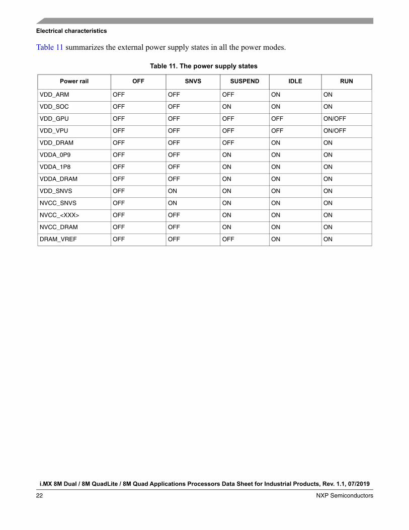
Table 11 summarizes the external power supply states in all the power modes.
Table 11. The power supply states
Power rail OFF SNVS SUSPEND IDLE RUN
VDD_ARM OFF OFF OFF ON ON
VDD_SOC OFF OFF ON ON ON
VDD_GPU OFF OFF OFF OFF ON/OFF
VDD_VPU OFF OFF OFF OFF ON/OFF
VDD_DRAM OFF OFF OFF ON ON
VDDA_0P9 OFF OFF ON ON ON
VDDA_1P8 OFF OFF ON ON ON
VDDA_DRAM OFF OFF ON ON ON
VDD_SNVS OFF ON ON ON ON
NVCC_SNVS OFF ON ON ON ON
NVCC_<XXX> OFF OFF ON ON ON
NVCC_DRAM OFF OFF ON ON ON
DRAM_VREF OFF OFF OFF ON ON
Electrical characteristics
i.MX 8M Dual / 8M QuadLite / 8M Quad Applications Processors Data Sheet for Industrial Products, Rev. 1.1, 07/2019
NXP Semiconductors 23
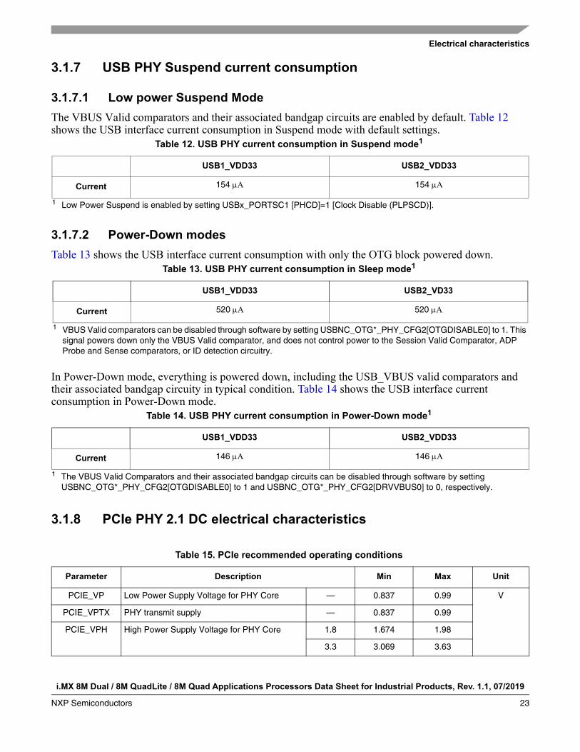
3.1.7 USB PHY Suspend current consumption
3.1.7.1 Low power Suspend Mode
The VBUS Valid comparators and their associated bandgap circuits are enabled by default. Table 12 shows the USB interface current consumption in Suspend mode with default settings.
3.1.7.2 Power-Down modes
Table 13 shows the USB interface current consumption with only the OTG block powered down.
In Power-Down mode, everything is powered down, including the USB_VBUS valid comparators and their associated bandgap circuity in typical condition. Table 14 shows the USB interface current consumption in Power-Down mode.
3.1.8 PCIe PHY 2.1 DC electrical characteristics
Table 12. USB PHY current consumption in Suspend mode1
1 Low Power Suspend is enabled by setting USBx_PORTSC1 [PHCD]=1 [Clock Disable (PLPSCD)].
USB1_VDD33 USB2_VDD33
Current 154 154
Table 13. USB PHY current consumption in Sleep mode1
1 VBUS Valid comparators can be disabled through software by setting USBNC_OTG*_PHY_CFG2[OTGDISABLE0] to 1. This signal powers down only the VBUS Valid comparator, and does not control power to the Session Valid Comparator, ADP Probe and Sense comparators, or ID detection circuitry.
USB1_VDD33 USB2_VD33
Current 520 520
Table 14. USB PHY current consumption in Power-Down mode1
1 The VBUS Valid Comparators and their associated bandgap circuits can be disabled through software by setting USBNC_OTG*_PHY_CFG2[OTGDISABLE0] to 1 and USBNC_OTG*_PHY_CFG2[DRVVBUS0] to 0, respectively.
USB1_VDD33 USB2_VDD33
Current 146 146
Table 15. PCIe recommended operating conditions
Parameter Description Min Max Unit
PCIE_VP Low Power Supply Voltage for PHY Core — 0.837 0.99 V
PCIE_VPTX PHY transmit supply — 0.837 0.99
PCIE_VPH High Power Supply Voltage for PHY Core 1.8 1.674 1.98
3.3 3.069 3.63
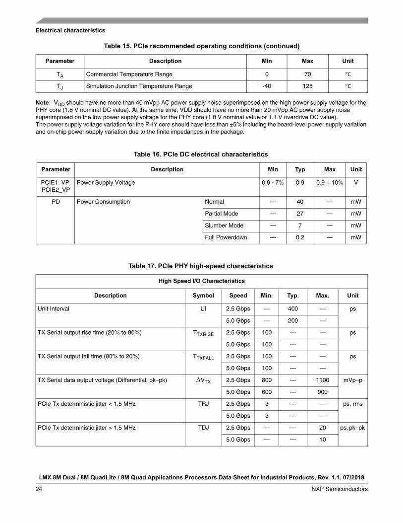
i.MX 8M Dual / 8M QuadLite / 8M Quad Applications Processors Data Sheet for Industrial Products, Rev. 1.1, 07/2019
24 NXP Semiconductors
Electrical characteristics
Note: VDD should have no more than 40 mVpp AC power supply noise superimposed on the high power supply voltage for the PHY core (1.8 V nominal DC value). At the same time, VDD should have no more than 20 mVpp AC power supply noise superimposed on the low power supply voltage for the PHY core (1.0 V nominal value or 1.1 V overdrive DC value). The power supply voltage variation for the PHY core should have less than ±5% including the board-level power supply variation and on-chip power supply variation due to the finite impedances in the package.
TA Commercial Temperature Range 0 70 °C
TJ Simulation Junction Temperature Range -40 125 °C
Table 16. PCIe DC electrical characteristics
Parameter Description Min Typ Max Unit
PCIE1_VP, PCIE2_VP
Power Supply Voltage 0.9 - 7% 0.9 0.9 + 10% V
PD Power Consumption Normal — 40 — mW
Partial Mode — 27 — mW
Slumber Mode — 7 — mW
Full Powerdown — 0.2 — mW
Table 17. PCIe PHY high-speed characteristics
High Speed I/O Characteristics
Description Symbol Speed Min. Typ. Max. Unit
Unit Interval UI 2.5 Gbps — 400 — ps
5.0 Gbps — 200 —
TX Serial output rise time (20% to 80%) TTXRISE 2.5 Gbps 100 — — ps
5.0 Gbps 100 — —
TX Serial output fall time (80% to 20%) TTXFALL 2.5 Gbps 100 — — ps
5.0 Gbps 100 — —
TX Serial data output voltage (Differential, pk–pk) VTX 2.5 Gbps 800 — 1100 mVp–p
5.0 Gbps 600 — 900
PCIe Tx deterministic jitter < 1.5 MHz TRJ 2.5 Gbps 3 — — ps, rms
5.0 Gbps 3 — —
PCIe Tx deterministic jitter > 1.5 MHz TDJ 2.5 Gbps — — 20 ps, pk–pk
5.0 Gbps — — 10
Table 15. PCIe recommended operating conditions (continued)
Parameter Description Min Max Unit
Electrical characteristics
i.MX 8M Dual / 8M QuadLite / 8M Quad Applications Processors Data Sheet for Industrial Products, Rev. 1.1, 07/2019
NXP Semiconductors 25
PCIe PHY interface is compliant with PCIe Express GEN2.
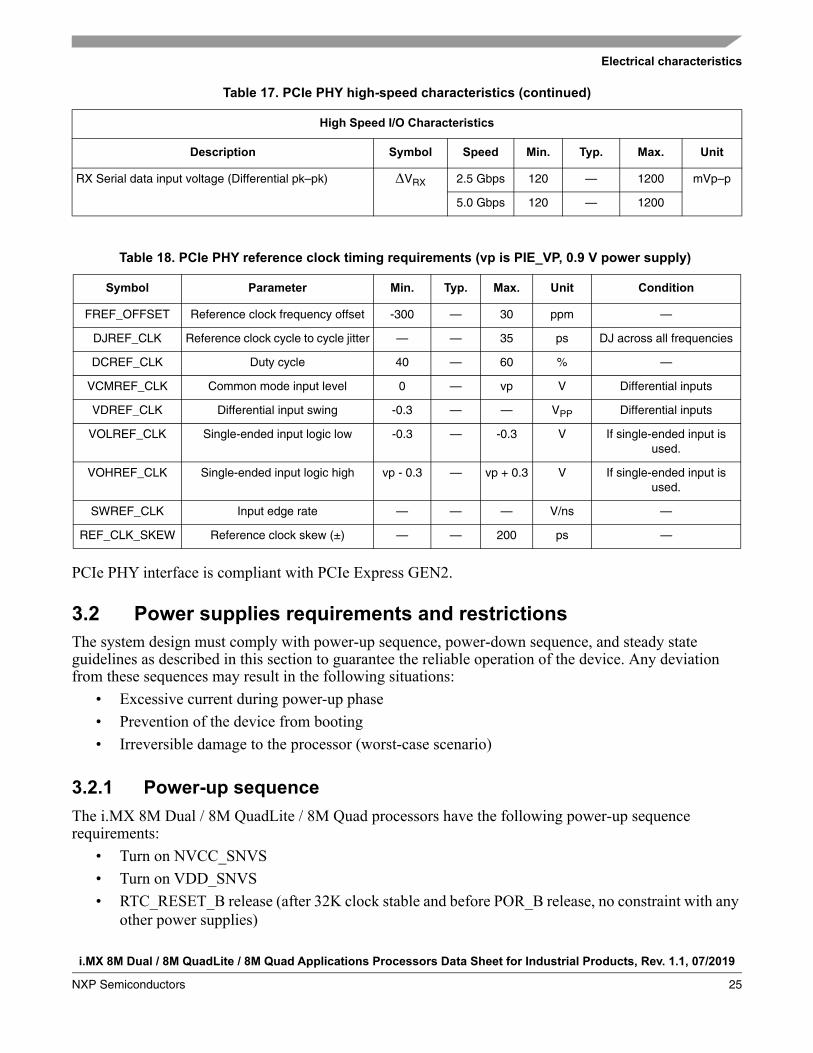
3.2 Power supplies requirements and restrictionsThe system design must comply with power-up sequence, power-down sequence, and steady state guidelines as described in this section to guarantee the reliable operation of the device. Any deviation from these sequences may result in the following situations:
• Excessive current during power-up phase• Prevention of the device from booting• Irreversible damage to the processor (worst-case scenario)
3.2.1 Power-up sequence
The i.MX 8M Dual / 8M QuadLite / 8M Quad processors have the following power-up sequence requirements:
• Turn on NVCC_SNVS• Turn on VDD_SNVS• RTC_RESET_B release (after 32K clock stable and before POR_B release, no constraint with any
other power supplies)
RX Serial data input voltage (Differential pk–pk) VRX 2.5 Gbps 120 — 1200 mVp–p
5.0 Gbps 120 — 1200
Table 18. PCIe PHY reference clock timing requirements (vp is PIE_VP, 0.9 V power supply)
Symbol Parameter Min. Typ. Max. Unit Condition
FREF_OFFSET Reference clock frequency offset -300 — 30 ppm —
DJREF_CLK Reference clock cycle to cycle jitter — — 35 ps DJ across all frequencies
DCREF_CLK Duty cycle 40 — 60 % —
VCMREF_CLK Common mode input level 0 — vp V Differential inputs
VDREF_CLK Differential input swing -0.3 — — VPP Differential inputs
VOLREF_CLK Single-ended input logic low -0.3 — -0.3 V If single-ended input is used.
VOHREF_CLK Single-ended input logic high vp - 0.3 — vp + 0.3 V If single-ended input is used.
SWREF_CLK Input edge rate — — — V/ns —
REF_CLK_SKEW Reference clock skew (±) — — 200 ps —
Table 17. PCIe PHY high-speed characteristics (continued)
High Speed I/O Characteristics
Description Symbol Speed Min. Typ. Max. Unit

i.MX 8M Dual / 8M QuadLite / 8M Quad Applications Processors Data Sheet for Industrial Products, Rev. 1.1, 07/2019
26 NXP Semiconductors
Electrical characteristics
• Turn on VDD_SOC and VDDA_0P9• Turn on VDD_ARM, VDD_GPU, VDD_VPU, and VDD_DRAM (no sequence between these
four rails)• Turn on VDDA_1P8_XXX, VDDA_DRAM (no sequence between these rails)• Turn on NVCC_XXX and NVCC_DRAM (no sequence between these rails)• POR_B release (it should be asserted during the entire power up sequence)
If the GPU/VPU is not used during the ROM boot sequence, VDD_GPU/VDD_VPU can stay off to reduce the power during boot, and then turned on by software afterwards.
During the chip power up, the power of the PCIe PHY, USB PHY, HDMI PHY, and MIPI PHY could stay off. After chip power up, the power of these PHys should be turned on. If any of the PHY power are turned on during the power up sequence, the POR_B can be released after the PHY power is stable.
3.2.2 Power-down sequence
The i.MX 8M Dual / 8M QuadLite / 8M Quad processors have the following power-down sequence requirements:
• Turn off NVCC_SNVS and VDD_SNVS last• Turn off VDD_SOC after the other power rails or at the same time as other rails• No sequence for other power rails during power down
3.2.3 Power supplies usage
I/O pins should not be externally driven while the I/O power supply for the pin (NVCC_xxx) is OFF. This can cause internal latch-up and malfunctions due to reverse current flows. For information about the I/O power supply of each pin, see “Power Rail” columns in the pin list tables of Section 5, Package information and contact assignments.”
Table 19 lists the modules in each power domain.
Table 19. The modules in the power domains
Power Domain Modules in the domain
VDD_ARM Arm A53
VDD_GPU GC7000L GPU
VDD_VPU G1 and G2 VPU
VDD_DRAM DRAM controller and PHY
VDD_SNVS SNVS_LP
VDD_SOC All the other modules
Electrical characteristics
i.MX 8M Dual / 8M QuadLite / 8M Quad Applications Processors Data Sheet for Industrial Products, Rev. 1.1, 07/2019
NXP Semiconductors 27
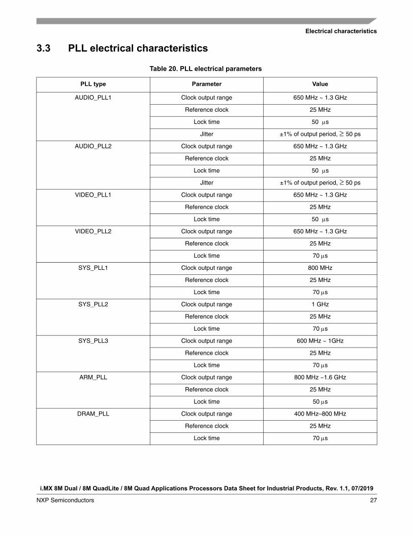
3.3 PLL electrical characteristics
Table 20. PLL electrical parameters
PLL type Parameter Value
AUDIO_PLL1 Clock output range 650 MHz ~ 1.3 GHz
Reference clock 25 MHz
Lock time 50 s
Jitter ±1% of output period, 50 ps
AUDIO_PLL2 Clock output range 650 MHz ~ 1.3 GHz
Reference clock 25 MHz
Lock time 50 s
Jitter ±1% of output period, 50 ps
VIDEO_PLL1 Clock output range 650 MHz ~ 1.3 GHz
Reference clock 25 MHz
Lock time 50 s
VIDEO_PLL2 Clock output range 650 MHz ~ 1.3 GHz
Reference clock 25 MHz
Lock time 70 s
SYS_PLL1 Clock output range 800 MHz
Reference clock 25 MHz
Lock time 70 s
SYS_PLL2 Clock output range 1 GHz
Reference clock 25 MHz
Lock time 70 s
SYS_PLL3 Clock output range 600 MHz ~ 1GHz
Reference clock 25 MHz
Lock time 70 s
ARM_PLL Clock output range 800 MHz ~1.6 GHz
Reference clock 25 MHz
Lock time 50 s
DRAM_PLL Clock output range 400 MHz–800 MHz
Reference clock 25 MHz
Lock time 70 s

i.MX 8M Dual / 8M QuadLite / 8M Quad Applications Processors Data Sheet for Industrial Products, Rev. 1.1, 07/2019
28 NXP Semiconductors
Electrical characteristics
3.4 On-chip oscillators
3.4.1 OSC25M and OSC27M
A 25 MHz oscillator is used as the primary clock source for the PLLs to generate the clock for the CPU, BUS, and high-speed interfaces. For fractional PLLs, the 25 MHz clock from the oscillator can be used as the PLL reference clock directly.
A 27 MHz oscillator is used as the reference clock for HDMI PHY. It can also be used as the alternative source for the fractional PLLs.
Table 21 lists the electrical specifications of this oscillator when loaded with an NX5032GA 40 MHz crystal unit at 40 MHz frequency. All values are valid only for the device TJ operating specification of -40 oC to 125 oC.
GPU_PLL Clock output range 800 MHz ~1.6 GHz
Reference clock 25 MHz
Lock time 50 s
VPU_PLL Clock output range 400 MHz ~ 800 MHz
Reference clock 25 MHz
Lock time 50 s
Table 21. Electrical specification of oscillator @ 1.8 V
Parameter Min Typ Max Unit
Voltage swing on external pin1
1 The start-up time is dependent upon crystal characteristics, board leakage, etc.; high ESR and excessive capacitive loads can cause long start-up time.
250 — 800 mV
Power consumption (analog supply RMS current in OSC mode)2, 3
2 Electrical parameters are subject to change.3 Maximum current is observed during startup. After oscillation is stable, the current from HV supply comes down.
— — 4 mA
Start-up time1, 2 — — 2 ms
Table 20. PLL electrical parameters (continued)
PLL type Parameter Value

Electrical characteristics
i.MX 8M Dual / 8M QuadLite / 8M Quad Applications Processors Data Sheet for Industrial Products, Rev. 1.1, 07/2019
NXP Semiconductors 29
Table 22 shows the transconductance specification of the oscillator (in mA/V).
Table 23 shows the input clock specifications.
Table 24 shows core output clock specification.
Table 25 shows VIL/VIH specification at EXTAL.
Table 22. Transconductance specification of oscillator
GM_sel Min Max
111 10 25
Table 23. Input clock specification
Parameter Min Typ Max Unit
Clock Frequency in OSC mode 20 — 40 MHz
Input Clock Frequency in Bypass mode
— — 50 MHz
Input Clock Rise/Fall Time in Bypass mode
— — 1 ns
Input Clock Duty Cycle in Bypass mode
47.50 50 52.50 %
Table 24. Core output clock specification
Parameter Min Typ Max Unit
Output Clock Frequency in OSC mode
20 — 40 MHz
Output Clock Duty Cycle in OSC mode
45 50 55 %
Output Clock Frequency in Bypass mode
— — 50 MHz
Capacitive Loading on Outputs Clock
— 150 500 fF
Output Clock Rise/Fall Time in Bypass mode
— 0.1 0.5 ns
Output Clock Duty Cycle in Bypass mode
40 50 60 %
Table 25. Transconductance specification of oscillator
Parameter Condition Min Max Unit
VILEXTAL VREF = 0.5 x avdd (xosc HV supply)
0 VREF - 0.5 V
VIHEXTAL VREF + 0.5 avdd
i.MX 8M Dual / 8M QuadLite / 8M Quad Applications Processors Data Sheet for Industrial Products, Rev. 1.1, 07/2019
30 NXP Semiconductors
Electrical characteristics
3.5 I/O DC parameters
This section includes the DC parameters of the following I/O types:• General Purpose I/O (GPIO)• Double Data Rate I/O (DDR) for LPDDR4, DDR4, and DDR3L modes• Differential I/O (CLKx)
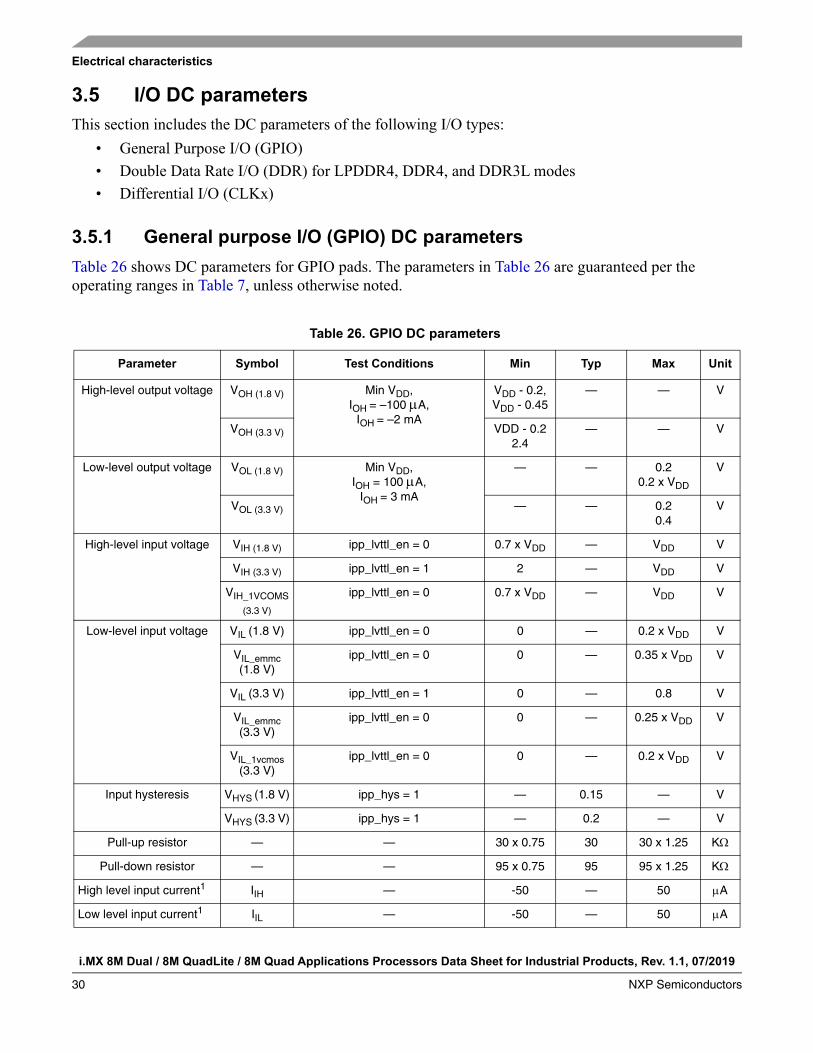
3.5.1 General purpose I/O (GPIO) DC parameters
Table 26 shows DC parameters for GPIO pads. The parameters in Table 26 are guaranteed per the operating ranges in Table 7, unless otherwise noted.
Table 26. GPIO DC parameters
Parameter Symbol Test Conditions Min Typ Max Unit
High-level output voltage VOH (1.8 V) Min VDD, IOH = –100 A,
IOH = –2 mA
VDD - 0.2,VDD - 0.45
— — V
VOH (3.3 V) VDD - 0.22.4
— — V
Low-level output voltage VOL (1.8 V) Min VDD, IOH = 100 A,
IOH = 3 mA
— — 0.20.2 x VDD
V
VOL (3.3 V) — — 0.20.4
V
High-level input voltage VIH (1.8 V) ipp_lvttl_en = 0 0.7 x VDD — VDD V
VIH (3.3 V) ipp_lvttl_en = 1 2 — VDD V
VIH_1VCOMS
(3.3 V)
ipp_lvttl_en = 0 0.7 x VDD — VDD V
Low-level input voltage VIL (1.8 V) ipp_lvttl_en = 0 0 — 0.2 x VDD V
VIL_emmc (1.8 V)
ipp_lvttl_en = 0 0 — 0.35 x VDD V
VIL (3.3 V) ipp_lvttl_en = 1 0 — 0.8 V
VIL_emmc (3.3 V)
ipp_lvttl_en = 0 0 — 0.25 x VDD V
VIL_1vcmos (3.3 V)
ipp_lvttl_en = 0 0 — 0.2 x VDD V
Input hysteresis VHYS (1.8 V) ipp_hys = 1 — 0.15 — V
VHYS (3.3 V) ipp_hys = 1 — 0.2 — V
Pull-up resistor — — 30 x 0.75 30 30 x 1.25 K
Pull-down resistor — — 95 x 0.75 95 95 x 1.25 K
High level input current1 IIH — -50 — 50 A
Low level input current1 IIL — -50 — 50 A
Electrical characteristics
i.MX 8M Dual / 8M QuadLite / 8M Quad Applications Processors Data Sheet for Industrial Products, Rev. 1.1, 07/2019
NXP Semiconductors 31
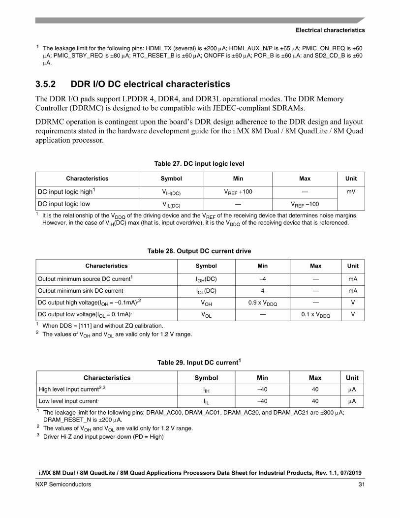
3.5.2 DDR I/O DC electrical characteristics
The DDR I/O pads support LPDDR 4, DDR4, and DDR3L operational modes. The DDR Memory Controller (DDRMC) is designed to be compatible with JEDEC-compliant SDRAMs.
DDRMC operation is contingent upon the board’s DDR design adherence to the DDR design and layout requirements stated in the hardware development guide for the i.MX 8M Dual / 8M QuadLite / 8M Quad application processor.
1 The leakage limit for the following pins: HDMI_TX (several) is ±200 A; HDMI_AUX_N/P is ±65 A; PMIC_ON_REQ is ±60 A; PMIC_STBY_REQ is ±80 A; RTC_RESET_B is ±60 A; ONOFF is ±60 A; POR_B is ±60 A; and SD2_CD_B is ±60 A.
Table 27. DC input logic level
Characteristics Symbol Min Max Unit
DC input logic high1
1 It is the relationship of the VDDQ of the driving device and the VREF of the receiving device that determines noise margins. However, in the case of VIH(DC) max (that is, input overdrive), it is the VDDQ of the receiving device that is referenced.
VIH(DC) VREF +100 — mV
DC input logic low VIL(DC) — VREF –100
Table 28. Output DC current drive
Characteristics Symbol Min Max Unit
Output minimum source DC current1
1 When DDS = [111] and without ZQ calibration.
IOH(DC) –4 — mA
Output minimum sink DC current IOL(DC) 4 — mA
DC output high voltage(IOH = –0.1mA),2
2 The values of VOH and VOL are valid only for 1.2 V range.
VOH 0.9 x VDDQ — V
DC output low voltage(IOL = 0.1mA), VOL — 0.1 x VDDQ V
Table 29. Input DC current1
1 The leakage limit for the following pins: DRAM_AC00, DRAM_AC01, DRAM_AC20, and DRAM_AC21 are ±300 A; DRAM_RESET_N is ±200 A.
Characteristics Symbol Min Max Unit
High level input current2,3
2 The values of VOH and VOL are valid only for 1.2 V range.3 Driver Hi-Z and input power-down (PD = High)
IIH –40 40 A
Low level input current, IIL –40 40 A
i.MX 8M Dual / 8M QuadLite / 8M Quad Applications Processors Data Sheet for Industrial Products, Rev. 1.1, 07/2019
32 NXP Semiconductors
Electrical characteristics
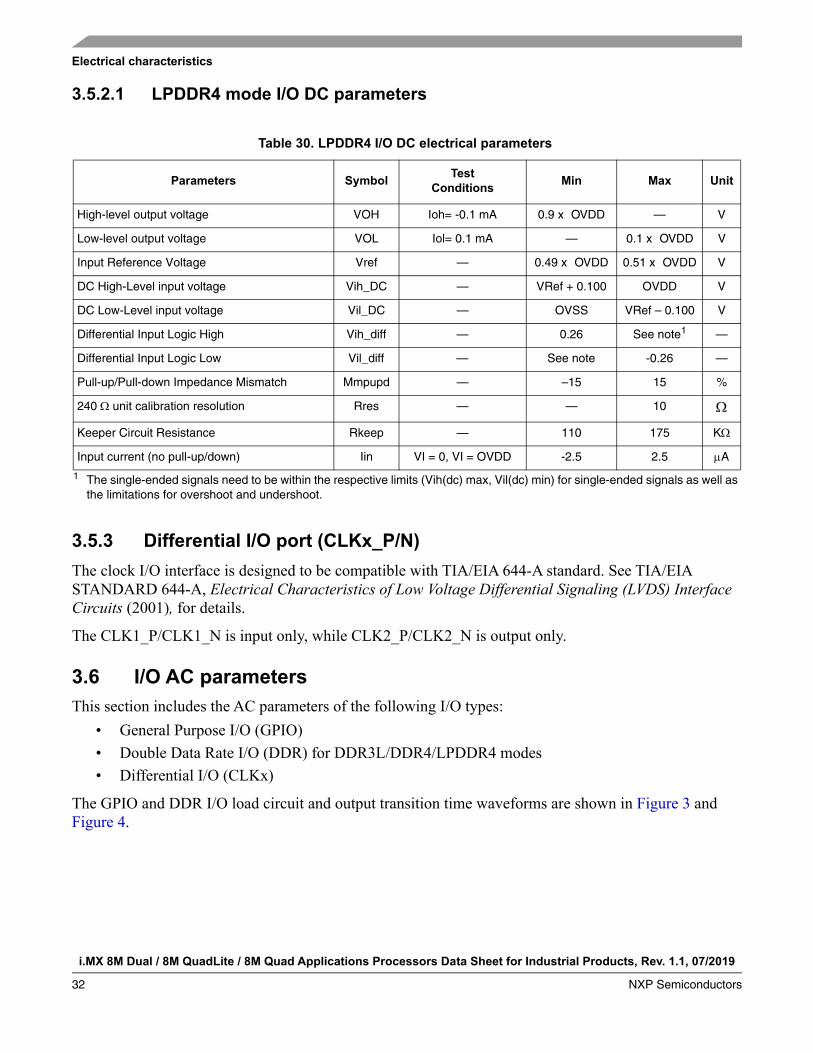
3.5.2.1 LPDDR4 mode I/O DC parameters
3.5.3 Differential I/O port (CLKx_P/N)
The clock I/O interface is designed to be compatible with TIA/EIA 644-A standard. See TIA/EIA STANDARD 644-A, Electrical Characteristics of Low Voltage Differential Signaling (LVDS) Interface Circuits (2001), for details.
The CLK1_P/CLK1_N is input only, while CLK2_P/CLK2_N is output only.
3.6 I/O AC parameters
This section includes the AC parameters of the following I/O types:• General Purpose I/O (GPIO)• Double Data Rate I/O (DDR) for DDR3L/DDR4/LPDDR4 modes• Differential I/O (CLKx)
The GPIO and DDR I/O load circuit and output transition time waveforms are shown in Figure 3 and Figure 4.
Table 30. LPDDR4 I/O DC electrical parameters
Parameters SymbolTest
ConditionsMin Max Unit
High-level output voltage VOH Ioh= -0.1 mA 0.9 x OVDD — V
Low-level output voltage VOL Iol= 0.1 mA — 0.1 x OVDD V
Input Reference Voltage Vref — 0.49 x OVDD 0.51 x OVDD V
DC High-Level input voltage Vih_DC — VRef + 0.100 OVDD V
DC Low-Level input voltage Vil_DC — OVSS VRef – 0.100 V
Differential Input Logic High Vih_diff — 0.26 See note1
1 The single-ended signals need to be within the respective limits (Vih(dc) max, Vil(dc) min) for single-ended signals as well as the limitations for overshoot and undershoot.
—
Differential Input Logic Low Vil_diff — See note -0.26 —
Pull-up/Pull-down Impedance Mismatch Mmpupd — –15 15 %
240 unit calibration resolution Rres — — 10
Keeper Circuit Resistance Rkeep — 110 175 K
Input current (no pull-up/down) Iin VI = 0, VI = OVDD -2.5 2.5 A

Electrical characteristics
i.MX 8M Dual / 8M QuadLite / 8M Quad Applications Processors Data Sheet for Industrial Products, Rev. 1.1, 07/2019
NXP Semiconductors 33
Figure 3. Load circuit for output
Figure 4. Output transition time waveform
3.6.1 General purpose I/O AC parameters
This section presents the I/O AC parameters for GPIO in different modes. Note that the fast or slow I/O behavior is determined by the appropriate control bits in the IOMUXC control registers.
Table 31. Maximum input cell delay time
Cell name
Max Delay PAD Y (ns)
VDD = 1.62 VT = 125°C
WCS model—
VDD = 3.0VT = 125°C
WCS model
PBIJGTOV36PUD_MCLAMP_LVGPIO_EW 1.54 — 1.3
Table 32. Output cell delay time for fixed load
ParameterSimulated Cell Delay A PAD (ns)
VDD = 1.62 V, T = 125°C VDD = 2.97 V, T = 125°C
dse[2:0] fsel[1:0] Driver Type CL = 15 pF CL = 15 pF
011 00 3 x Slow Slew 3.1 3.3
011 11 3 x Fast Slew 2.1 2.6
100 00 4 x Slow Slew 3.7 3.9
100 11 4 x Fast Slew 2.3 2.8
101 00 5 x Slow Slew 3.1 3.5
101 11 5 x Fast Slew 2.1 2.5
Test PointFrom Output Under Test
CL
CL includes package, probe and fixture capacitance
0 V
OVDD
20%
80% 80%
20%
tr tfOutput (at pad)
i.MX 8M Dual / 8M QuadLite / 8M Quad Applications Processors Data Sheet for Industrial Products, Rev. 1.1, 07/2019
34 NXP Semiconductors
Electrical characteristics
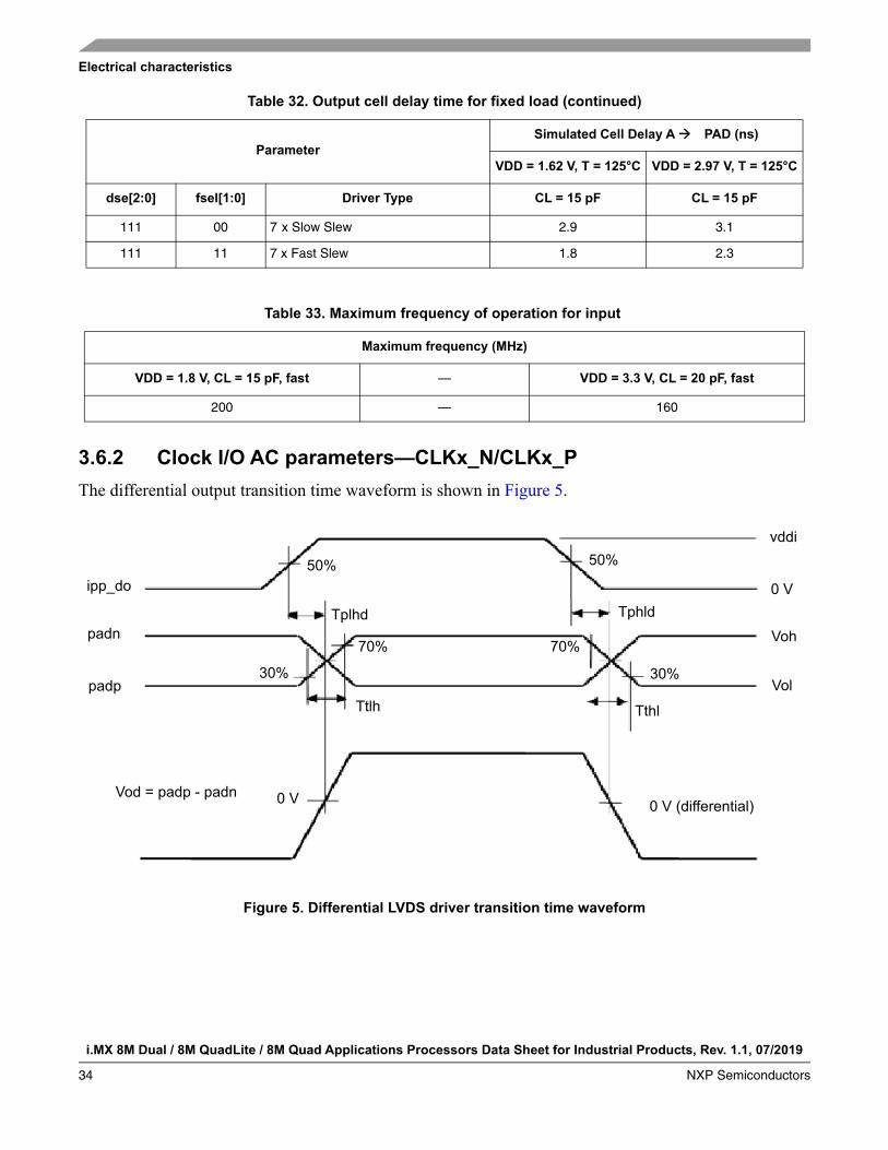
3.6.2 Clock I/O AC parameters—CLKx_N/CLKx_P
The differential output transition time waveform is shown in Figure 5.
Figure 5. Differential LVDS driver transition time waveform
111 00 7 x Slow Slew 2.9 3.1
111 11 7 x Fast Slew 1.8 2.3
Table 33. Maximum frequency of operation for input
Maximum frequency (MHz)
VDD = 1.8 V, CL = 15 pF, fast — VDD = 3.3 V, CL = 20 pF, fast
200 — 160
Table 32. Output cell delay time for fixed load (continued)
ParameterSimulated Cell Delay A PAD (ns)
VDD = 1.62 V, T = 125°C VDD = 2.97 V, T = 125°C
dse[2:0] fsel[1:0] Driver Type CL = 15 pF CL = 15 pF
ipp_do
padn
padp
Vod = padp - padn 0 V 0 V (differential)
30% 30%
50% 50%
0 V
vddi
Voh
VolTtlh Tthl
70% 70%
Tplhd Tphld
Electrical characteristics
i.MX 8M Dual / 8M QuadLite / 8M Quad Applications Processors Data Sheet for Industrial Products, Rev. 1.1, 07/2019
NXP Semiconductors 35
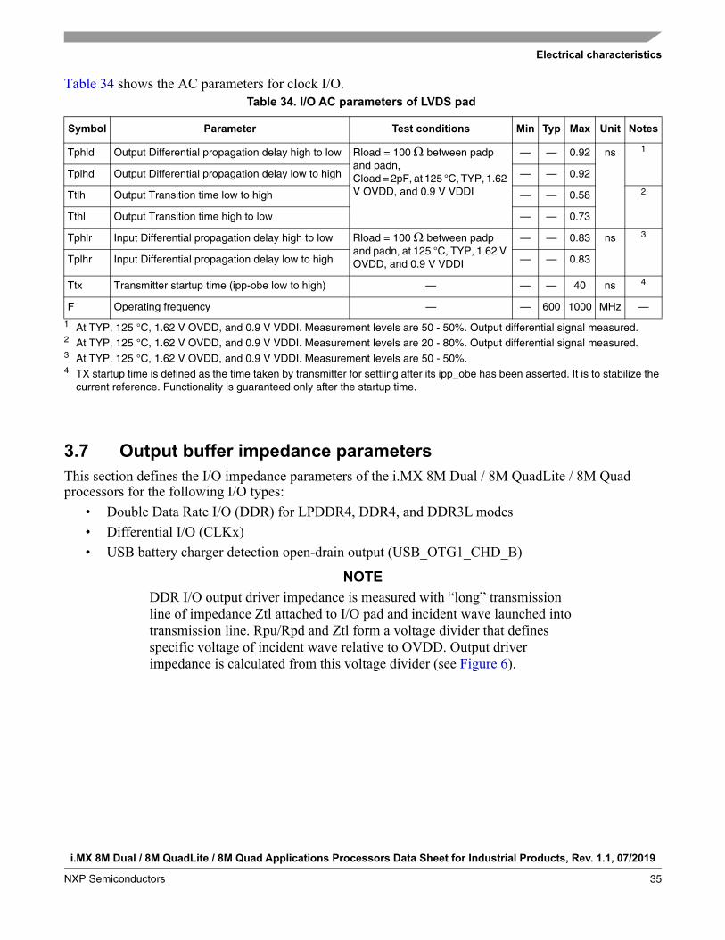
Table 34 shows the AC parameters for clock I/O.
3.7 Output buffer impedance parametersThis section defines the I/O impedance parameters of the i.MX 8M Dual / 8M QuadLite / 8M Quad processors for the following I/O types:
• Double Data Rate I/O (DDR) for LPDDR4, DDR4, and DDR3L modes• Differential I/O (CLKx)• USB battery charger detection open-drain output (USB_OTG1_CHD_B)
NOTE
DDR I/O output driver impedance is measured with “long” transmission line of impedance Ztl attached to I/O pad and incident wave launched into transmission line. Rpu/Rpd and Ztl form a voltage divider that defines specific voltage of incident wave relative to OVDD. Output driver impedance is calculated from this voltage divider (see Figure 6).
Table 34. I/O AC parameters of LVDS pad
Symbol Parameter Test conditions Min Typ Max Unit Notes
Tphld Output Differential propagation delay high to low Rload = 100 between padp and padn, Cload = 2pF, at 125 °C, TYP, 1.62 V OVDD, and 0.9 V VDDI
— — 0.92 ns 1
1 At TYP, 125 °C, 1.62 V OVDD, and 0.9 V VDDI. Measurement levels are 50 - 50%. Output differential signal measured.
Tplhd Output Differential propagation delay low to high — — 0.92
Ttlh Output Transition time low to high — — 0.58 2
2 At TYP, 125 °C, 1.62 V OVDD, and 0.9 V VDDI. Measurement levels are 20 - 80%. Output differential signal measured.
Tthl Output Transition time high to low — — 0.73
Tphlr Input Differential propagation delay high to low Rload = 100 between padp and padn, at 125 °C, TYP, 1.62 V OVDD, and 0.9 V VDDI
— — 0.83 ns 3
3 At TYP, 125 °C, 1.62 V OVDD, and 0.9 V VDDI. Measurement levels are 50 - 50%.
Tplhr Input Differential propagation delay low to high — — 0.83
Ttx Transmitter startup time (ipp-obe low to high) — — — 40 ns 4
4 TX startup time is defined as the time taken by transmitter for settling after its ipp_obe has been asserted. It is to stabilize the current reference. Functionality is guaranteed only after the startup time.
F Operating frequency — — 600 1000 MHz —
i.MX 8M Dual / 8M QuadLite / 8M Quad Applications Processors Data Sheet for Industrial Products, Rev. 1.1, 07/2019
36 NXP Semiconductors
Electrical characteristics
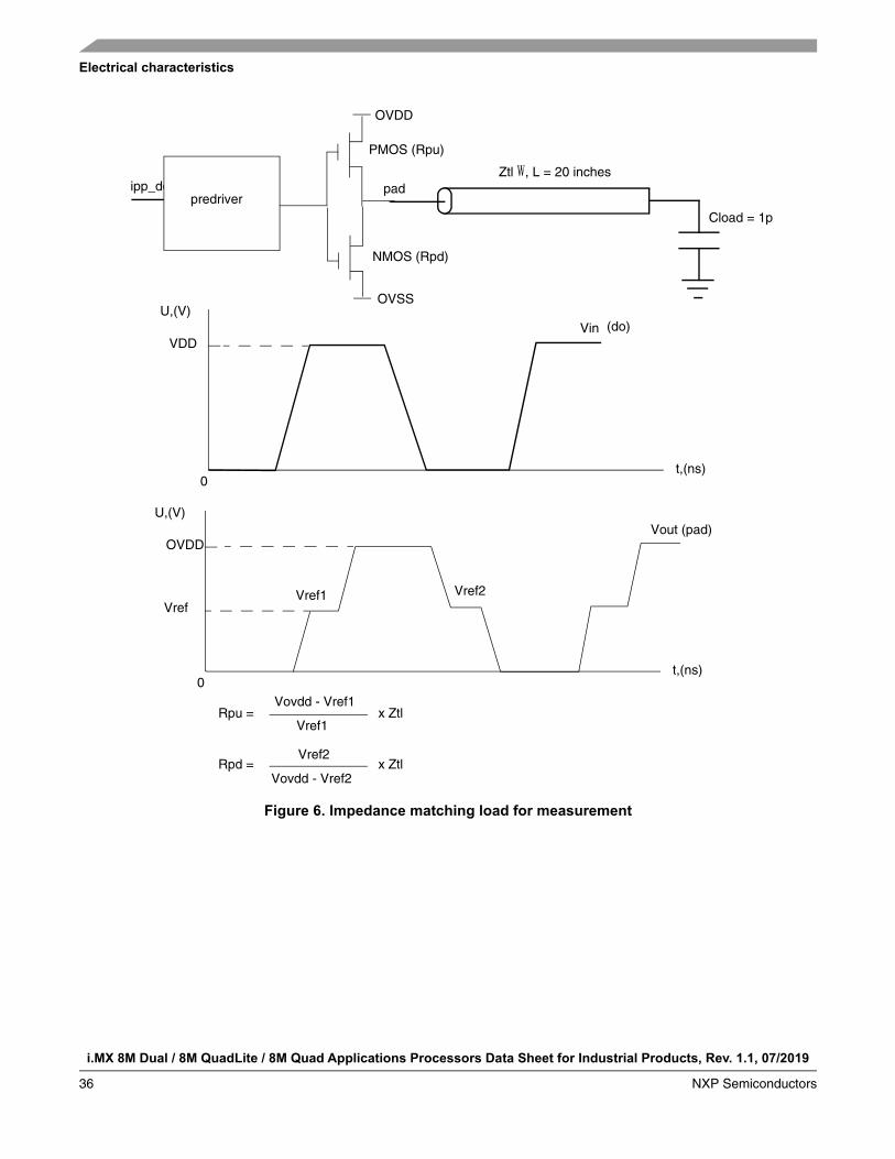
Figure 6. Impedance matching load for measurement
ipp_do
Cload = 1p
Ztl W, L = 20 inches
predriver
PMOS (Rpu)
NMOS (Rpd)
pad
OVDD
OVSS
t,(ns)0
U,(V)
OVDD
t,(ns)0
VDDVin (do)
Vout (pad)U,(V)
Vref
Rpu = Vovdd - Vref1
Vref1x Ztl
Rpd = x ZtlVref2
Vovdd - Vref2
Vref1 Vref2

Electrical characteristics
i.MX 8M Dual / 8M QuadLite / 8M Quad Applications Processors Data Sheet for Industrial Products, Rev. 1.1, 07/2019
NXP Semiconductors 37
3.7.1 DDR I/O output buffer impedance
Table 35 shows DDR I/O output buffer impedance of i.MX 8M Dual / 8M QuadLite / 8M Quad processors.
Note:
1. Output driver impedance is controlled across PVTs using ZQ calibration procedure.
2. Calibration is done against 240 external reference resistor.
3. Output driver impedance deviation (calibration accuracy) is ±5% (max/min impedance) across PVTs.
3.7.2 Differential I/O output buffer impedance
The Differential CCM interface is designed to be compatible with TIA/EIA 644-A standard. See, TIA/EIA STANDARD 644-A, Electrical Characteristics of Low Voltage Differential Signaling (LVDS) Interface Circuits (2001) for details.
3.7.3 USB battery charger detection driver impedance
The USB_OTG1_CHD_B open-drain output pin can be used to signal to power management and monitoring device results of USB Battery Charger detection routines for the USB_OTG1 PHY instance. Use of this pin requires an external pullup resistor, for more information see Table 5.
3.8 System modules timing
This section contains the timing and electrical parameters for the modules in each i.MX 8M Dual / 8M QuadLite / 8M Quad processor.
Table 35. DDR I/O output buffer impedance
Parameter SymbolTest Conditions
DSE (Drive Strength)
Typical
UnitNVCC_DRAM = 1.35 V (DDR3L)
DDR_SEL = 11
NVCC_DRAM = 1.2 V(DDR4)
NVCC_DRAM = 1.1 V (LPDDR4)
DDR_SEL = 10
Output Driver Impedance
Rdrv 000000 Hi-Z Hi-Z Hi-Z
000010 240 240 240
000110 120 120 120
001010 80 80 80
001110 60 60 60
011010 48 48 48
011110 40 40 40
111010 34 34 34

i.MX 8M Dual / 8M QuadLite / 8M Quad Applications Processors Data Sheet for Industrial Products, Rev. 1.1, 07/2019
38 NXP Semiconductors
Electrical characteristics
3.8.1 Reset timings parameters
Figure 7 shows the reset timing and Table 36 lists the timing parameters.
Figure 7. Reset timing diagram
3.8.2 WDOG Reset timing parameters
Figure 8 shows the WDOG reset timing and Table 37 lists the timing parameters.
Figure 8. WDOGx_B timing diagram
NOTE
RTC_XTALI is approximately 32 kHz. RTC_XTALI cycle is one period or approximately 30 ms.
NOTE
WDOGx_B output signals (for each one of the Watchdog modules) do not have dedicated pins, but are muxed out through the IOMUX. See the IOMUXC chapter of the i.MX 8M Dual / 8M QuadLite / 8M Quad Applications Processor Reference Manual (IMX8MDQLQRM) for detailed information.
3.9 External peripheral interface parameters
The following subsections provide information on external peripheral interfaces.
Table 36. Reset timing parameters
ID Parameter Min Max Unit
CC1 Duration of POR_B to be qualified as valid. 1 — RTC_XTALI cycle
Table 37. WDOGx_B timing parameters
ID Parameter Min Max Unit
CC3 Duration of WDOG1_B Assertion 1 — RTC_XTALI cycle
POR_B
CC1
(Input)
WDOGx_B
CC3
(Output)
Electrical characteristics
i.MX 8M Dual / 8M QuadLite / 8M Quad Applications Processors Data Sheet for Industrial Products, Rev. 1.1, 07/2019
NXP Semiconductors 39
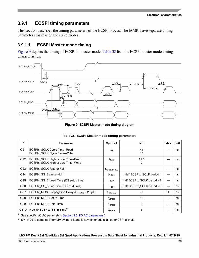
3.9.1 ECSPI timing parameters
This section describes the timing parameters of the ECSPI blocks. The ECSPI have separate timing parameters for master and slave modes.
3.9.1.1 ECSPI Master mode timing
Figure 9 depicts the timing of ECSPI in master mode. Table 38 lists the ECSPI master mode timing characteristics.
Figure 9. ECSPI Master mode timing diagram
Table 38. ECSPI Master mode timing parameters
ID Parameter Symbol Min Max Unit
CS1 ECSPIx_SCLK Cycle Time–ReadECSPIx_SCLK Cycle Time–Write
tclk 4315
— ns
CS2 ECSPIx_SCLK High or Low Time–ReadECSPIx_SCLK High or Low Time–Write
tSW 21.57
— ns
CS3 ECSPIx_SCLK Rise or Fall1
1 See specific I/O AC parameters Section 3.6, I/O AC parameters.”
tRISE/FALL — — ns
CS4 ECSPIx_SS_B pulse width tCSLH Half ECSPIx_SCLK period — ns
CS5 ECSPIx_SS_B Lead Time (CS setup time) tSCS Half ECSPIx_SCLK period - 4 — ns
CS6 ECSPIx_SS_B Lag Time (CS hold time) tHCS Half ECSPIx_SCLK period - 2 — ns
CS7 ECSPIx_MOSI Propagation Delay (CLOAD = 20 pF) tPDmosi -1 1 ns
CS8 ECSPIx_MISO Setup Time tSmiso 18 — ns
CS9 ECSPIx_MISO Hold Time tHmiso 0 — ns
CS10 RDY to ECSPIx_SS_B Time2
2 SPI_RDY is sampled internally by ipg_clk and is asynchronous to all other CSPI signals.
tSDRY 5 — ns
CS7
CS2
CS2
CS4
CS6 CS5
CS8CS9
ECSPIx_SCLK
ECSPIx_SS_B
ECSPIx_MOSI
ECSPIx_MISO
ECSPIx_RDY_B
CS10
CS3
CS3CS1

i.MX 8M Dual / 8M QuadLite / 8M Quad Applications Processors Data Sheet for Industrial Products, Rev. 1.1, 07/2019
40 NXP Semiconductors
Electrical characteristics
3.9.1.2 ECSPI Slave mode timing
Figure 10 depicts the timing of ECSPI in Slave mode. Table 39 lists the ECSPI Slave mode timing characteristics.
Figure 10. ECSPI Slave mode timing diagram
Table 39. ECSPI Slave mode timing parameters
ID Parameter Symbol Min Max Unit
CS1 ECSPIx_SCLK Cycle Time–ReadECSPI_SCLK Cycle Time–Write
tclk 1543
— ns
CS2 ECSPIx_SCLK High or Low Time–ReadECSPIx_SCLK High or Low Time–Write
tSW 721.5
— ns
CS4 ECSPIx_SS_B pulse width tCSLH Half ECSPIx_SCLK period — ns
CS5 ECSPIx_SS_B Lead Time (CS setup time) tSCS 5 — ns
CS6 ECSPIx_SS_B Lag Time (CS hold time) tHCS 5 — ns
CS7 ECSPIx_MOSI Setup Time tSmosi 4 — ns
CS8 ECSPIx_MOSI Hold Time tHmosi 4 — ns
CS9 ECSPIx_MISO Propagation Delay (CLOAD = 20 pF) tPDmiso 4 19 ns
CS1
CS7 CS8
CS2
CS2
CS4
CS6 CS5
CS9
ECSPIx_SCLK
ECSPIx_SS_B
ECSPIx_MISO
ECSPIx_MOSI
Electrical characteristics
i.MX 8M Dual / 8M QuadLite / 8M Quad Applications Processors Data Sheet for Industrial Products, Rev. 1.1, 07/2019
NXP Semiconductors 41
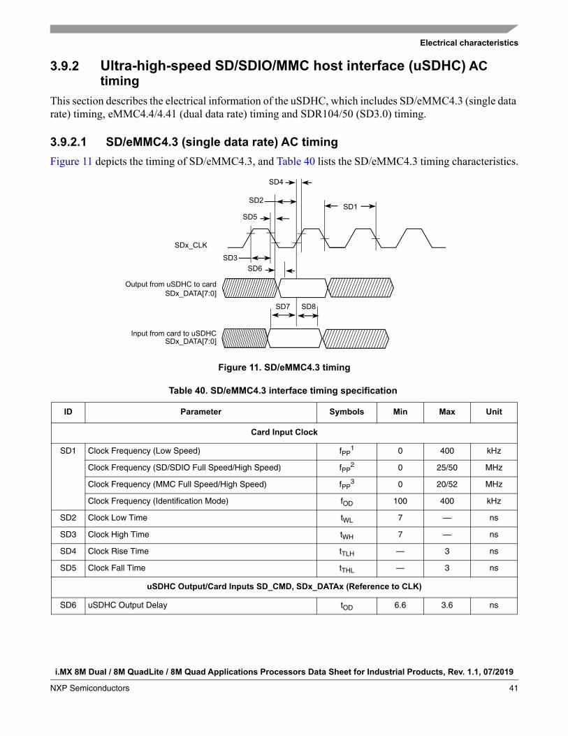
3.9.2 Ultra-high-speed SD/SDIO/MMC host interface (uSDHC) AC timing
This section describes the electrical information of the uSDHC, which includes SD/eMMC4.3 (single data rate) timing, eMMC4.4/4.41 (dual data rate) timing and SDR104/50 (SD3.0) timing.
3.9.2.1 SD/eMMC4.3 (single data rate) AC timing
Figure 11 depicts the timing of SD/eMMC4.3, and Table 40 lists the SD/eMMC4.3 timing characteristics.
Figure 11. SD/eMMC4.3 timing
Table 40. SD/eMMC4.3 interface timing specification
ID Parameter Symbols Min Max Unit
Card Input Clock
SD1 Clock Frequency (Low Speed) fPP1 0 400 kHz
Clock Frequency (SD/SDIO Full Speed/High Speed) fPP2 0 25/50 MHz
Clock Frequency (MMC Full Speed/High Speed) fPP3 0 20/52 MHz
Clock Frequency (Identification Mode) fOD 100 400 kHz
SD2 Clock Low Time tWL 7 — ns
SD3 Clock High Time tWH 7 — ns
SD4 Clock Rise Time tTLH — 3 ns
SD5 Clock Fall Time tTHL — 3 ns
uSDHC Output/Card Inputs SD_CMD, SDx_DATAx (Reference to CLK)
SD6 uSDHC Output Delay tOD 6.6 3.6 ns
SD1
SD3
SD5
SD4
SD7
SDx_CLK
SD2
SD8
SD6
Output from uSDHC to card
Input from card to uSDHCSDx_DATA[7:0]
SDx_DATA[7:0]

i.MX 8M Dual / 8M QuadLite / 8M Quad Applications Processors Data Sheet for Industrial Products, Rev. 1.1, 07/2019
42 NXP Semiconductors
Electrical characteristics
3.9.2.2 eMMC4.4/4.41 (dual data rate) AC timing
Figure 12 depicts the timing of eMMC4.4/4.41. Table 41 lists the eMMC4.4/4.41 timing characteristics. Be aware that only DATA is sampled on both edges of the clock (not applicable to CMD).
Figure 12. eMMC4.4/4.41 timing
uSDHC Input/Card Outputs SD_CMD, SDx_DATAx (Reference to CLK)
SD7 uSDHC Input Setup Time tISU 2.5 — ns
SD8 uSDHC Input Hold Time4 tIH 1.5 — ns
1 In Low-Speed mode, card clock must be lower than 400 kHz, voltage ranges from 2.7 to 3.6 V.2 In Normal (Full) -Speed mode for SD/SDIO card, clock frequency can be any value between 0 – 25 MHz. In High-speed mode,
clock frequency can be any value between 0 – 50 MHz.3 In Normal (Full) -Speed mode for MMC card, clock frequency can be any value between 0 – 20 MHz. In High-speed mode,
clock frequency can be any value between 0 – 52 MHz.4 To satisfy hold timing, the delay difference between clock input and cmd/data input must not exceed 2 ns.
Table 41. eMMC4.4/4.41 interface timing specification
ID Parameter Symbols Min Max Unit
Card Input Clock
SD1 Clock Frequency (eMMC4.4/4.41 DDR) fPP 0 52 MHz
SD1 Clock Frequency (SD3.0 DDR) fPP 0 50 MHz
uSDHC Output / Card Inputs SD_CMD, SDx_DATAx (Reference to CLK)
SD2 uSDHC Output Delay tOD 2.7 6.9 ns
uSDHC Input / Card Outputs SD_CMD, SDx_DATAx (Reference to CLK)
Table 40. SD/eMMC4.3 interface timing specification (continued)
ID Parameter Symbols Min Max Unit
SD1
SD2
SD3
Output from eSDHCv3 to card
Input from card to eSDHCv3SDx_DATA[7:0]
SDx_CLK
SD4
SD2
......
......
SDx_DATA[7:0]
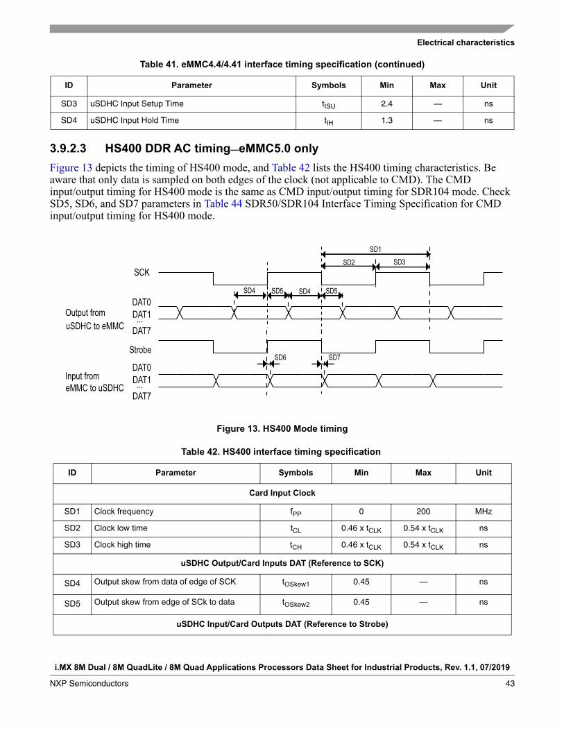
Electrical characteristics
i.MX 8M Dual / 8M QuadLite / 8M Quad Applications Processors Data Sheet for Industrial Products, Rev. 1.1, 07/2019
NXP Semiconductors 43
3.9.2.3 HS400 DDR AC timing—eMMC5.0 only
Figure 13 depicts the timing of HS400 mode, and Table 42 lists the HS400 timing characteristics. Be aware that only data is sampled on both edges of the clock (not applicable to CMD). The CMD input/output timing for HS400 mode is the same as CMD input/output timing for SDR104 mode. Check SD5, SD6, and SD7 parameters in Table 44 SDR50/SDR104 Interface Timing Specification for CMD input/output timing for HS400 mode.
Figure 13. HS400 Mode timing
SD3 uSDHC Input Setup Time tISU 2.4 — ns
SD4 uSDHC Input Hold Time tIH 1.3 — ns
Table 42. HS400 interface timing specification
ID Parameter Symbols Min Max Unit
Card Input Clock
SD1 Clock frequency fPP 0 200 MHz
SD2 Clock low time tCL 0.46 x tCLK 0.54 x tCLK ns
SD3 Clock high time tCH 0.46 x tCLK 0.54 x tCLK ns
uSDHC Output/Card Inputs DAT (Reference to SCK)
SD4 Output skew from data of edge of SCK tOSkew1 0.45 — ns
SD5 Output skew from edge of SCk to data tOSkew2 0.45 — ns
uSDHC Input/Card Outputs DAT (Reference to Strobe)
Table 41. eMMC4.4/4.41 interface timing specification (continued)
ID Parameter Symbols Min Max Unit
SD7
SD1
SD5 SD5
SD6
SCK
Output from
Strobe
Input from
uSDHC to eMMC
eMMC to uSDHC
DAT0DAT1
DAT7...
DAT0DAT1
DAT7...
SD4SD4
SD3SD2
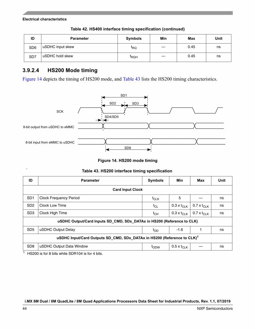
i.MX 8M Dual / 8M QuadLite / 8M Quad Applications Processors Data Sheet for Industrial Products, Rev. 1.1, 07/2019
44 NXP Semiconductors
Electrical characteristics
3.9.2.4 HS200 Mode timing
Figure 14 depicts the timing of HS200 mode, and Table 43 lists the HS200 timing characteristics.
Figure 14. HS200 mode timing
iti
SD6 uSDHC input skew tRQ — 0.45 ns
SD7 uSDHC hold skew tRQH — 0.45 ns
Table 43. HS200 interface timing specification
ID Parameter Symbols Min Max Unit
Card Input Clock
SD1 Clock Frequency Period tCLK 5 — ns
SD2 Clock Low Time tCL 0.3 x tCLK 0.7 x tCLK ns
SD3 Clock High Time tCH 0.3 x tCLK 0.7 x tCLK ns
uSDHC Output/Card Inputs SD_CMD, SDx_DATAx in HS200 (Reference to CLK)
SD5 uSDHC Output Delay tOD -1.6 1 ns
uSDHC Input/Card Outputs SD_CMD, SDx_DATAx in HS200 (Reference to CLK)1
1 HS200 is for 8 bits while SDR104 is for 4 bits.
SD8 uSDHC Output Data Window tODW 0.5 x tCLK — ns
Table 42. HS400 interface timing specification (continued)
ID Parameter Symbols Min Max Unit
SCK
8-bit output from uSDHC to eMMC
8-bit input from eMMC to uSDHCSD8
SD4/SD5
SD2 SD3
SD1
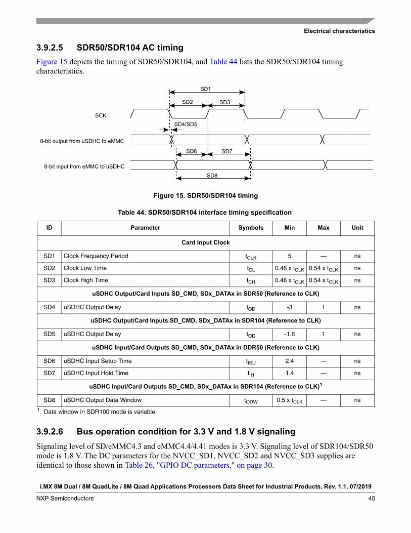
Electrical characteristics
i.MX 8M Dual / 8M QuadLite / 8M Quad Applications Processors Data Sheet for Industrial Products, Rev. 1.1, 07/2019
NXP Semiconductors 45
3.9.2.5 SDR50/SDR104 AC timing
Figure 15 depicts the timing of SDR50/SDR104, and Table 44 lists the SDR50/SDR104 timing characteristics.
Figure 15. SDR50/SDR104 timing
3.9.2.6 Bus operation condition for 3.3 V and 1.8 V signaling
Signaling level of SD/eMMC4.3 and eMMC4.4/4.41 modes is 3.3 V. Signaling level of SDR104/SDR50 mode is 1.8 V. The DC parameters for the NVCC_SD1, NVCC_SD2 and NVCC_SD3 supplies are identical to those shown in Table 26, "GPIO DC parameters," on page 30.
Table 44. SDR50/SDR104 interface timing specification
ID Parameter Symbols Min Max Unit
Card Input Clock
SD1 Clock Frequency Period tCLK 5 — ns
SD2 Clock Low Time tCL 0.46 x tCLK 0.54 x tCLK ns
SD3 Clock High Time tCH 0.46 x tCLK 0.54 x tCLK ns
uSDHC Output/Card Inputs SD_CMD, SDx_DATAx in SDR50 (Reference to CLK)
SD4 uSDHC Output Delay tOD -3 1 ns
uSDHC Output/Card Inputs SD_CMD, SDx_DATAx in SDR104 (Reference to CLK)
SD5 uSDHC Output Delay tOD -1.6 1 ns
uSDHC Input/Card Outputs SD_CMD, SDx_DATAx in DDR50 (Reference to CLK)
SD6 uSDHC Input Setup Time tISU 2.4 — ns
SD7 uSDHC Input Hold Time tIH 1.4 — ns
uSDHC Input/Card Outputs SD_CMD, SDx_DATAx in SDR104 (Reference to CLK)1
1 Data window in SDR100 mode is variable.
SD8 uSDHC Output Data Window tODW 0.5 x tCLK — ns
SCK
8-bit output from uSDHC to eMMC
8-bit input from eMMC to uSDHCSD8
SD7SD6
SD4/SD5
SD2 SD3
SD1

i.MX 8M Dual / 8M QuadLite / 8M Quad Applications Processors Data Sheet for Industrial Products, Rev. 1.1, 07/2019
46 NXP Semiconductors
Electrical characteristics
3.9.3 Ethernet controller (ENET) AC electrical specifications
The following timing specs are defined at the chip I/O pin and must be translated appropriately to arrive at timing specs/constraints for the physical interface.
3.9.3.1 RMII mode timing
Figure 16 shows RMII mode timings. Table 45 describes the timing parameters (M16–M21) shown in the figure.
Figure 16. RMII mode signal timing diagram
Table 45. RMII signal timing
ID Characteristic Min. Max. Unit
M16 ENET_CLK pulse width high 35% 65% ENET_CLK period
M17 ENET_CLK pulse width low 35% 65% ENET_CLK period
M18 ENET_CLK to ENET0_TXD[1:0], ENET_TX_DATA invalid 4 — ns
M19 ENET_CLK to ENET0_TXD[1:0], ENET_TX_DATA valid — 15 ns
M20 ENET_RX_DATAD[1:0], ENET_RX_EN(ENET_RX_EN), ENET_RX_ER to ENET_CLK setup
4 — ns
M21 ENET_CLK to ENET_RX_DATAD[1:0], ENET_RX_EN, ENET_RX_ER hold 2 — ns
ENET_CLK (input)
ENET_TX_EN
M16
M17
M18
M19
M20 M21
ENET_RX_DATA[1:0]
ENET_TX_DATA (output)
ENET_RX_ER
ENET_RX_EN (input)

Electrical characteristics
i.MX 8M Dual / 8M QuadLite / 8M Quad Applications Processors Data Sheet for Industrial Products, Rev. 1.1, 07/2019
NXP Semiconductors 47
Table 46. RMII signal mapping
Pad name Description Mode Alt Mode Direction Comment
ENET_MDC enet1.MDC RMII/RGMII ALT0 O —
ENET_MDIO enet1.MDIO RMII/RGMII ALT0 I/O —
ENET_TD3 RGMII.TD3 RGMII ALT0 O Only used for RGMII
ENET_TD2 RMII.CLK;RGMII.TD2
RMII/RGMII ALT0 I/O Used as RMII clock and RGMII data, there are two RGMII clock schemes. • MAC generate output 50M reference
clock for PHY, and MAC also uses this 50M clock.
• MAC uses external 50M clock.
ENET_TD1 RMII and RGMII.TD1
RMII/RGMII ALT0 O —
ENET_TD0 RMII and RGMII.TD0
RMII/RGMII ALT0 O —
ENET_TX_CTL RMII.TX_EN;RGMII.TX_CTL
RMII/RGMII ALT0 O —
ENET_TXC RMII.TX_ERR;RGMII.TX_CLK
RGMII ALT0/ALT1 O For RMII, ENET_TXC works as RMII.TX_ERR, need to work in the ALT1 mode.For RGMII, ENET_TXC works as RGMII_TX_CLK, need to work in the ALT0 mode.
ENET_RX_CTL RMII.RX_EN (CRS_DV);
RGMII.RX_CTL
RMII/RGMII ALT0 I —
ENET_RXC RMII.RX_ERR;RGMII.RX_CLK
RGMII ALT0/ALT1 I For RMII, ENET_RXC works as RMII.RX_ERR, need to work in the ALT1 mode.For RGMII, ENET_RXC works as RGMII_RX_CLK, need to work in the ALT0 mode.
ENET_RD0 RMII and RGMII.RD0
RMII/RGMII ALT0 I —
ENET_RD1 RMII and RGMII.RD1
RMII/RGMII ALT0 I —
ENET_RD2 RGMII RD2 RGMII ALT0 I —
ENET_RD3 RGMII RD3 RGMII ALT0 I —
GPIO1_IO06 enet1.MDC RMII/RGMII ALT1 O —
GPIO1_IO07 enet1.MDIO RMII/RGMII ALT1 I/O —

i.MX 8M Dual / 8M QuadLite / 8M Quad Applications Processors Data Sheet for Industrial Products, Rev. 1.1, 07/2019
48 NXP Semiconductors
Electrical characteristics
3.9.3.2 RGMII signal switching specifications
The following timing specifications meet the requirements for RGMII interfaces for a range of transceiver devices.
I2C1_SCL enet1.MDC RMII/RGMII ALT1 O —
I2C1_SDA enet1.MDIO RMII/RGMII ALT1 I/O —
GPIO1_IO08 enet1.1588_EVENT0_IN
RMII/RGMII ALT1 I Capture/compare block input/output event bus signal. When configured for capture and a rising edge is detected, the current timer value is latched and transferred into the corresponding ENET_TCCRn register for inspection by software. When configured for comparison, the corresponding signal 1588_EVENT is asserted for one cycle when the timer reaches the comparsion value programmed in the register ENET_TCCRn. An interrupt or DMA request can be triggered if the corresponding bit in the ENET_TCSRn[TIE] or ENET_TCSRn[TDRE] is set.
GPIO1_IO00 ENET_PHY_REF_CLK_ROOT
RGMII ALT1 O Reference clock is for PHY.
Table 47. RGMII signal switching specifications1
1 The timings assume the following configuration:DDR_SEL = (11)bDSE (drive-strength) = (111)b
Symbol Description Min. Max. Unit
Tcyc2
2 For 10 Mbps and 100 Mbps, Tcyc will scale to 400 ns ±40 ns and 40 ns ±4 ns respectively.
Clock cycle duration 7.2 8.8 ns
TskewT3
3 For all versions of RGMII prior to 2.0; this implies that PC board design will require clocks to be routed such that an additional trace delay of greater than 1.5 ns and less than 2.0 ns will be added to the associated clock signal. For 10/100, the Max value is unspecified.
Data to clock output skew at transmitter -500 500 ps
TskewR3 Data to clock input skew at receiver 1 2.6 ns
Duty_G4
4 Duty cycle may be stretched/shrunk during speed changes or while transitioning to a received packet's clock domain as long as minimum duty cycle is not violated and stretching occurs for no more than three Tcyc of the lowest speed transitioned between.
Duty cycle for Gigabit 45 85 %
Duty_T4 Duty cycle for 10/100T 40 90 %
Tr/Tf Rise/fall time (20–80%) — 0.98 ns
Table 46. RMII signal mapping (continued)
Pad name Description Mode Alt Mode Direction Comment
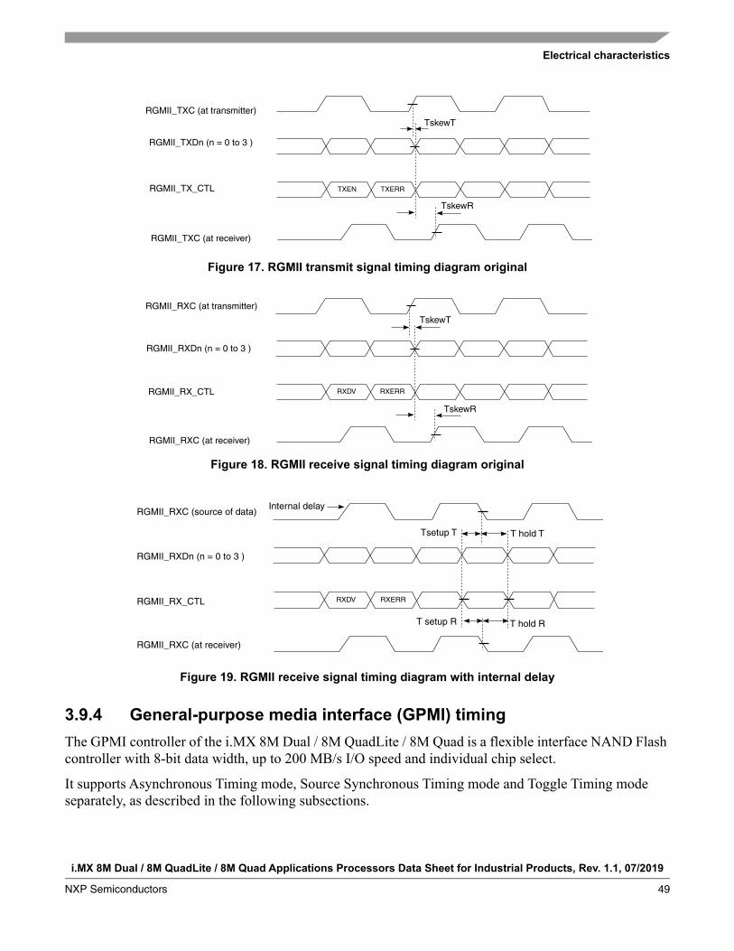
Electrical characteristics
i.MX 8M Dual / 8M QuadLite / 8M Quad Applications Processors Data Sheet for Industrial Products, Rev. 1.1, 07/2019
NXP Semiconductors 49
Figure 17. RGMII transmit signal timing diagram original
Figure 18. RGMII receive signal timing diagram original
Figure 19. RGMII receive signal timing diagram with internal delay
3.9.4 General-purpose media interface (GPMI) timing
The GPMI controller of the i.MX 8M Dual / 8M QuadLite / 8M Quad is a flexible interface NAND Flash controller with 8-bit data width, up to 200 MB/s I/O speed and individual chip select.
It supports Asynchronous Timing mode, Source Synchronous Timing mode and Toggle Timing mode separately, as described in the following subsections.
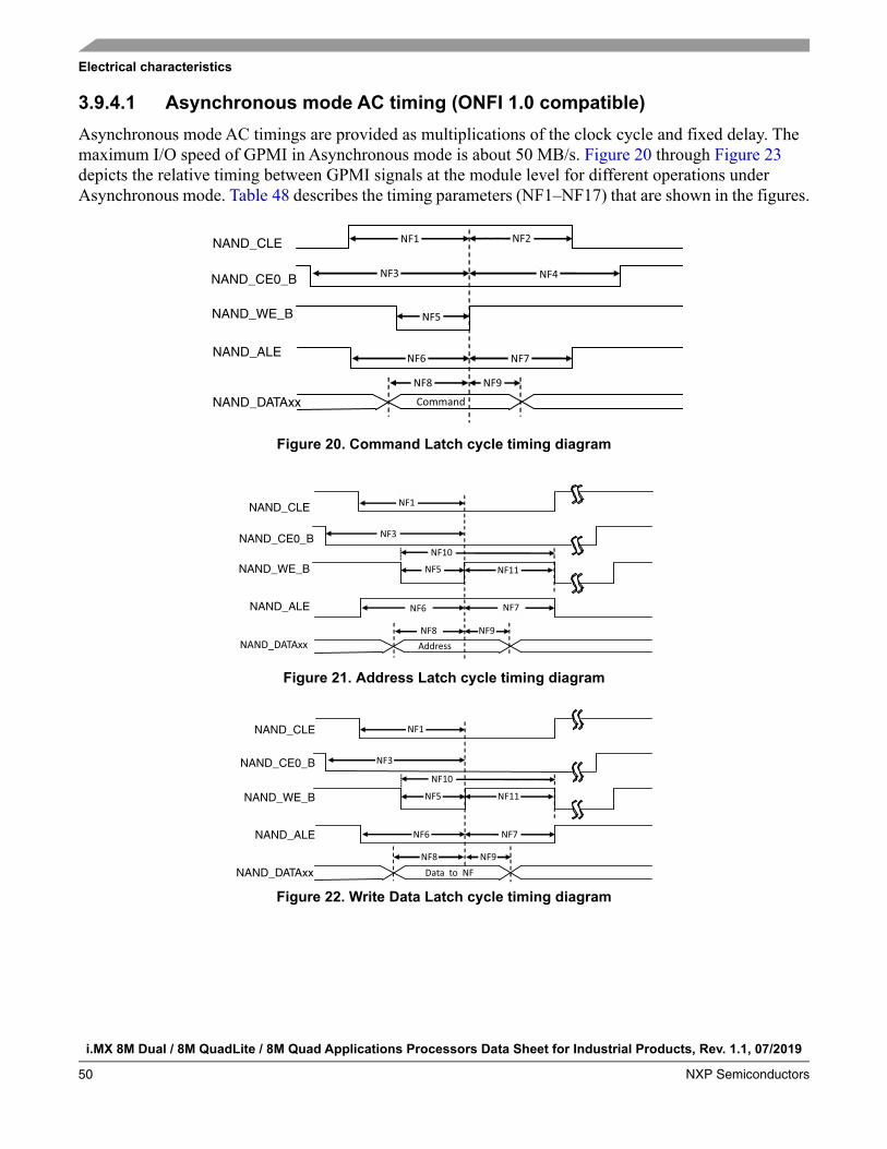
i.MX 8M Dual / 8M QuadLite / 8M Quad Applications Processors Data Sheet for Industrial Products, Rev. 1.1, 07/2019
50 NXP Semiconductors
Electrical characteristics
3.9.4.1 Asynchronous mode AC timing (ONFI 1.0 compatible)
Asynchronous mode AC timings are provided as multiplications of the clock cycle and fixed delay. The maximum I/O speed of GPMI in Asynchronous mode is about 50 MB/s. Figure 20 through Figure 23 depicts the relative timing between GPMI signals at the module level for different operations under Asynchronous mode. Table 48 describes the timing parameters (NF1–NF17) that are shown in the figures.
Figure 20. Command Latch cycle timing diagram
Figure 21. Address Latch cycle timing diagram
Figure 22. Write Data Latch cycle timing diagram
Command
NF8 NF9
NF7NF6
NF5
NF2NF1
NF3 NF4
Address
NF10
NF11
NF9NF8
NF7
NF6
NF5
NF1
NF3
NAND_DATAxx
Data to NF
NF10
NF11
NF7 NF6
NF5
NF1
NF3
NF9NF8

Electrical characteristics
i.MX 8M Dual / 8M QuadLite / 8M Quad Applications Processors Data Sheet for Industrial Products, Rev. 1.1, 07/2019
NXP Semiconductors 51
Figure 23. Read Data Latch cycle timing diagram (Non-EDO Mode)
Figure 24. Read Data Latch cycle timing diagram (EDO mode)
Table 48. Asynchronous mode timing parameters1
ID Parameter Symbol
TimingT = GPMI Clock Cycle Unit
Min. Max.
NF1 NAND_CLE setup time tCLS (AS + DS) T - 0.12 [see notes2,3] ns
NF2 NAND_CLE hold time tCLH DH T - 0.72 [see note2] ns
NF3 NAND_CE0_B setup time tCS (AS + DS + 1) T [see notes3,2] ns
NF4 NAND_CE0_B hold time tCH (DH+1) T - 1 [see note2] ns
NF5 NAND_WE_B pulse width tWP DS T [see note2] ns
NF6 NAND_ALE setup time tALS (AS + DS) T - 0.49 [see notes3,2] ns
NF7 NAND_ALE hold time tALH DH T - 0.42 [see note2] ns
NF8 Data setup time tDS DS T - 0.26 [see note2] ns
NF9 Data hold time tDH DH T - 1.37 [see note2] ns
NF10 Write cycle time tWC (DS + DH) T [see note2] ns
NF11 NAND_WE_B hold time tWH DH T [see note2] ns
NF12 Ready to NAND_RE_B low tRR4 (AS + 2) T [see 3,2] — ns
NF13 NAND_RE_B pulse width tRP DS T [see note2] ns
NF14 READ cycle time tRC (DS + DH) T [see note2] ns
NF15 NAND_RE_B high hold time tREH DH T [see note2] ns
Data from NF
NF14
NF15
NF17NF16NF12
NF13
Data from NF
NF14
NF15
NF17
NF16
NF12
NF13
NAND_DATAxx
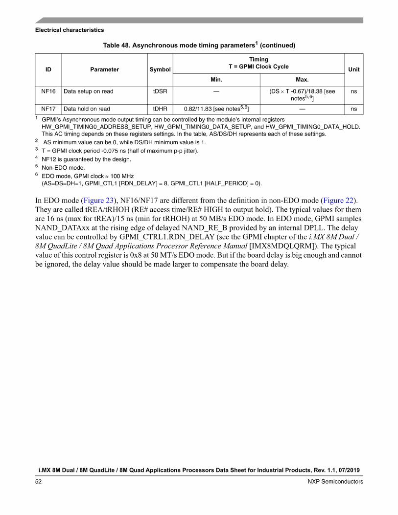
i.MX 8M Dual / 8M QuadLite / 8M Quad Applications Processors Data Sheet for Industrial Products, Rev. 1.1, 07/2019
52 NXP Semiconductors
Electrical characteristics
In EDO mode (Figure 23), NF16/NF17 are different from the definition in non-EDO mode (Figure 22). They are called tREA/tRHOH (RE# access time/RE# HIGH to output hold). The typical values for them are 16 ns (max for tREA)/15 ns (min for tRHOH) at 50 MB/s EDO mode. In EDO mode, GPMI samples NAND_DATAxx at the rising edge of delayed NAND_RE_B provided by an internal DPLL. The delay value can be controlled by GPMI_CTRL1.RDN_DELAY (see the GPMI chapter of the i.MX 8M Dual / 8M QuadLite / 8M Quad Applications Processor Reference Manual [IMX8MDQLQRM]). The typical value of this control register is 0x8 at 50 MT/s EDO mode. But if the board delay is big enough and cannot be ignored, the delay value should be made larger to compensate the board delay.
NF16 Data setup on read tDSR — (DS T -0.67)/18.38 [see notes5,6]
ns
NF17 Data hold on read tDHR 0.82/11.83 [see notes5,6] — ns1 GPMI’s Asynchronous mode output timing can be controlled by the module’s internal registers
HW_GPMI_TIMING0_ADDRESS_SETUP, HW_GPMI_TIMING0_DATA_SETUP, and HW_GPMI_TIMING0_DATA_HOLD. This AC timing depends on these registers settings. In the table, AS/DS/DH represents each of these settings.
2 AS minimum value can be 0, while DS/DH minimum value is 1.3 T = GPMI clock period -0.075 ns (half of maximum p-p jitter).4 NF12 is guaranteed by the design.5 Non-EDO mode.6 EDO mode, GPMI clock 100 MHz
(AS=DS=DH=1, GPMI_CTL1 [RDN_DELAY] = 8, GPMI_CTL1 [HALF_PERIOD] = 0).
Table 48. Asynchronous mode timing parameters1 (continued)
ID Parameter Symbol
TimingT = GPMI Clock Cycle Unit
Min. Max.

Electrical characteristics
i.MX 8M Dual / 8M QuadLite / 8M Quad Applications Processors Data Sheet for Industrial Products, Rev. 1.1, 07/2019
NXP Semiconductors 53
3.9.4.2 Source synchronous mode AC timing (ONFI 2.x compatible)
Figure 25 to Figure 27 show the write and read timing of Source Synchronous mode.
Figure 25. Source Synchronous mode command and address timing diagram
NF18
NF25 NF26
NF25 NF26
NF20
NF21
NF20
NF23
NF24
NF19
NF22
NF21
CMD ADD
NAND_CLE
NAND_ALE
NAND_WE/RE_B
NAND_CLK
NAND_DQS
NAND_DQSOutput enable
NAND_DATA[7:0]
NAND_DATA[7:0]Output enable

i.MX 8M Dual / 8M QuadLite / 8M Quad Applications Processors Data Sheet for Industrial Products, Rev. 1.1, 07/2019
54 NXP Semiconductors
Electrical characteristics
Figure 26. Source Synchronous mode data write timing diagram
Figure 27. Source Synchronous mode data read timing diagram
NF23
NF18
NF25
NF26
NF27
NF25
NF26
NF28 NF28
NF29 NF29
NF23 NF24
NF24
NF19
NF27
NF22
NAND_WE/RE_B
Output enable
Output enable
NF23
NF18
NF25
NF26NF25
NF26NF23 NF24
NF24
NF19
NF22
NF25
NF26
NAND_ALE
NF25
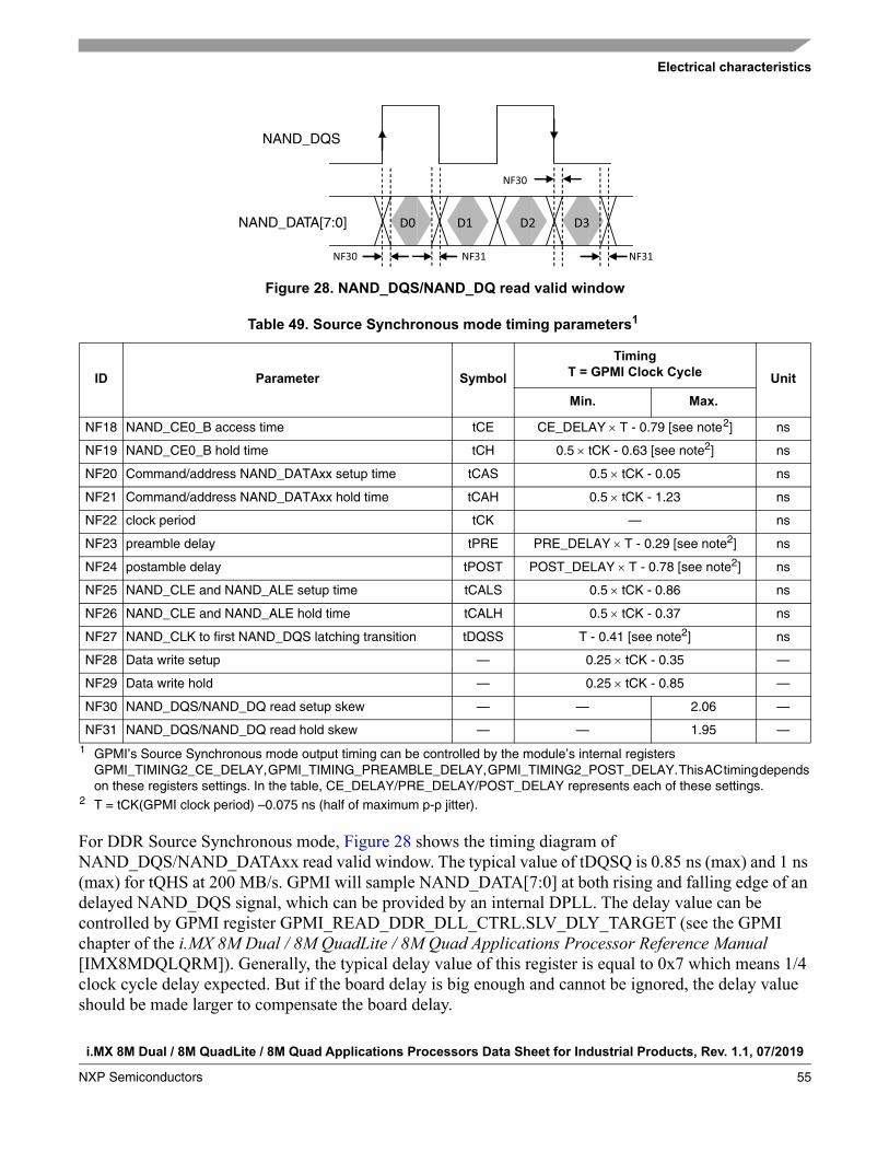
Electrical characteristics
i.MX 8M Dual / 8M QuadLite / 8M Quad Applications Processors Data Sheet for Industrial Products, Rev. 1.1, 07/2019
NXP Semiconductors 55
Figure 28. NAND_DQS/NAND_DQ read valid window
For DDR Source Synchronous mode, Figure 28 shows the timing diagram of NAND_DQS/NAND_DATAxx read valid window. The typical value of tDQSQ is 0.85 ns (max) and 1 ns (max) for tQHS at 200 MB/s. GPMI will sample NAND_DATA[7:0] at both rising and falling edge of an delayed NAND_DQS signal, which can be provided by an internal DPLL. The delay value can be controlled by GPMI register GPMI_READ_DDR_DLL_CTRL.SLV_DLY_TARGET (see the GPMI chapter of the i.MX 8M Dual / 8M QuadLite / 8M Quad Applications Processor Reference Manual [IMX8MDQLQRM]). Generally, the typical delay value of this register is equal to 0x7 which means 1/4 clock cycle delay expected. But if the board delay is big enough and cannot be ignored, the delay value should be made larger to compensate the board delay.
Table 49. Source Synchronous mode timing parameters1
1 GPMI’s Source Synchronous mode output timing can be controlled by the module’s internal registers GPMI_TIMING2_CE_DELAY, GPMI_TIMING_PREAMBLE_DELAY, GPMI_TIMING2_POST_DELAY. This AC timing depends on these registers settings. In the table, CE_DELAY/PRE_DELAY/POST_DELAY represents each of these settings.
ID Parameter Symbol
TimingT = GPMI Clock Cycle Unit
Min. Max.
NF18 NAND_CE0_B access time tCE CE_DELAY T - 0.79 [see note2]
2 T = tCK(GPMI clock period) –0.075 ns (half of maximum p-p jitter).
ns
NF19 NAND_CE0_B hold time tCH 0.5 tCK - 0.63 [see note2] ns
NF20 Command/address NAND_DATAxx setup time tCAS 0.5 tCK - 0.05 ns
NF21 Command/address NAND_DATAxx hold time tCAH 0.5 tCK - 1.23 ns
NF22 clock period tCK — ns
NF23 preamble delay tPRE PRE_DELAY T - 0.29 [see note2] ns
NF24 postamble delay tPOST POST_DELAY T - 0.78 [see note2] ns
NF25 NAND_CLE and NAND_ALE setup time tCALS 0.5 tCK - 0.86 ns
NF26 NAND_CLE and NAND_ALE hold time tCALH 0.5 tCK - 0.37 ns
NF27 NAND_CLK to first NAND_DQS latching transition tDQSS T - 0.41 [see note2] ns
NF28 Data write setup — 0.25 tCK - 0.35 —
NF29 Data write hold — 0.25 tCK - 0.85 —
NF30 NAND_DQS/NAND_DQ read setup skew — — 2.06 —
NF31 NAND_DQS/NAND_DQ read hold skew — — 1.95 —
D0 D1 D2 D3
NF30
NF31
NF30
NF31
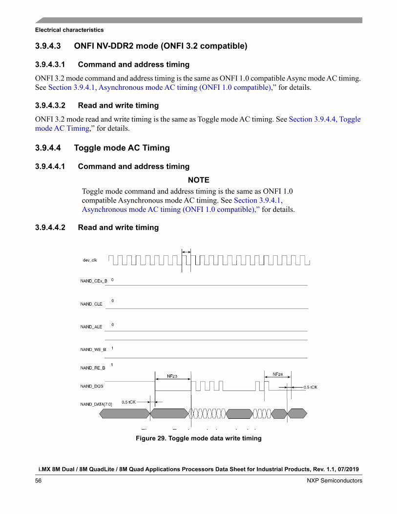
i.MX 8M Dual / 8M QuadLite / 8M Quad Applications Processors Data Sheet for Industrial Products, Rev. 1.1, 07/2019
56 NXP Semiconductors
Electrical characteristics
3.9.4.3 ONFI NV-DDR2 mode (ONFI 3.2 compatible)
3.9.4.3.1 Command and address timing
ONFI 3.2 mode command and address timing is the same as ONFI 1.0 compatible Async mode AC timing. See Section 3.9.4.1, Asynchronous mode AC timing (ONFI 1.0 compatible),” for details.
3.9.4.3.2 Read and write timing
ONFI 3.2 mode read and write timing is the same as Toggle mode AC timing. See Section 3.9.4.4, Toggle mode AC Timing,” for details.
3.9.4.4 Toggle mode AC Timing
3.9.4.4.1 Command and address timing
NOTE
Toggle mode command and address timing is the same as ONFI 1.0 compatible Asynchronous mode AC timing. See Section 3.9.4.1, Asynchronous mode AC timing (ONFI 1.0 compatible),” for details.
3.9.4.4.2 Read and write timing
Figure 29. Toggle mode data write timing

Electrical characteristics
i.MX 8M Dual / 8M QuadLite / 8M Quad Applications Processors Data Sheet for Industrial Products, Rev. 1.1, 07/2019
NXP Semiconductors 57
Figure 30. Toggle mode data read timing
Table 50. Toggle mode timing parameters1
ID Parameter Symbol
TimingT = GPMI Clock Cycle Unit
Min. Max.
NF1 NAND_CLE setup time tCLS (AS + DS) T - 0.12 [see note2s,3]
NF2 NAND_CLE hold time tCLH DH T - 0.72 [see note2]
NF3 NAND_CE0_B setup time tCS (AS + DS) T - 0.58 [see notes,2]
NF4 NAND_CE0_B hold time tCH DH T - 1 [see note2]
NF5 NAND_WE_B pulse width tWP DS T [see note2]
NF6 NAND_ALE setup time tALS (AS + DS) T - 0.49 [see notes,2]
NF7 NAND_ALE hold time tALH DH T - 0.42 [see note2]
NF8 Command/address NAND_DATAxx setup time tCAS DS T - 0.26 [see note2]
NF9 Command/address NAND_DATAxx hold time tCAH DH T - 1.37 [see note2]
NF18 NAND_CEx_B access time tCE CE_DELAY T [see notes4,2] — ns
NF22 clock period tCK — — ns
NF23 preamble delay tPRE PRE_DELAY T [see notes5,2] — ns
i.MX 8M Dual / 8M QuadLite / 8M Quad Applications Processors Data Sheet for Industrial Products, Rev. 1.1, 07/2019
58 NXP Semiconductors
Electrical characteristics
For DDR Toggle mode, Figure 28 shows the timing diagram of NAND_DQS/NAND_DATAxx read valid window. The typical value of tDQSQ is 1.4 ns (max) and 1.4 ns (max) for tQHS at 133 MB/s. GPMI samples NAND_DATA[7:0] at both the rising and falling edges of a delayed NAND_DQS signal, which is provided by an internal DPLL. The delay value of this register can be controlled by the GPMI register GPMI_READ_DDR_DLL_CTRL.SLV_DLY_TARGET (see the GPMI chapter of the i.MX 8M Dual / 8M QuadLite / 8M Quad Applications Processor Reference Manual [IMX8MDQLQRM]). Generally, the typical delay value is equal to 0x7, which means a 1/4 clock cycle delay is expected. But if the board delay is big enough and cannot be ignored, the delay value should be made larger to compensate the board delay.
3.9.5 HDMI 2.0 Tx module timing parameters
See the following specifications:• HDMI 2.0a specification (HDMI.org)• DisplayPort 1.3 standard (VESA.org)
— DP supports 1.6 GHz (RBR), 2.7 GHz (HBR), and 5.4 GHz (HBR2) rates. Those rates are managed in API (Host).
— RBR supports 1080p60 (RGB 8b), HBR supports 4kp30 (RGB 8b) and HBR2 supports 4kp60 (RGB 8b).
See bandwidth details below.Effective bandwidth per rate with 4 lanes:— RBR: 1.62 x 4 x 8 / 10 = 5.184 Gbps— HBR: 2.7 x 4 x 8 / 10 = 8.64 Gbps
NF24 postamble delay tPOST POST_DELAY T +0.43 [see note2]
— ns
NF28 Data write setup tDS6 0.25 tCK - 0.32 — ns
NF29 Data write hold tDH6 0.25 tCK - 0.79 — ns
NF30 NAND_DQS/NAND_DQ read setup skew tDQSQ7 — 3.18 ns
NF31 NAND_DQS/NAND_DQ read hold skew tQHS7 — 3.27 ns1 The GPMI toggle mode output timing can be controlled by the module’s internal registers
HW_GPMI_TIMING0_ADDRESS_SETUP, HW_GPMI_TIMING0_DATA_SETUP, and HW_GPMI_TIMING0_DATA_HOLD. This AC timing depends on these register’s settings. In the table, AS/DS/DH represents each of these settings.
2 AS minimum value can be 0, while DS/DH minimum value is 1.3 T = tCK (GPMI clock period) -0.075 ns (half of maximum p-p jitter).4 CE_DELAY represents HW_GPMI_TIMING2[CE_DELAY]. NF18 is guaranteed by the design. Read/Write operation is started
with enough time of ALE/CLE assertion to low level.5 PRE_DELAY+1 (AS+DS)6 Shown in Figure 29.7 Shown in Figure 30.
Table 50. Toggle mode timing parameters1 (continued)
ID Parameter Symbol
TimingT = GPMI Clock Cycle Unit
Min. Max.

Electrical characteristics
i.MX 8M Dual / 8M QuadLite / 8M Quad Applications Processors Data Sheet for Industrial Products, Rev. 1.1, 07/2019
NXP Semiconductors 59
— HBR2: 1.62 x4 x 8 / 10 = 17.28 GbpsBandwidth required per resolution (CEA-861-F):— 1920 x 1080 (24 b/px) 60 fps: 3.56 Gbps— 3840 x 2160 (24 b/px) 30 fps: 7.13 Gbps— 3840 x 2160 (24 b/px) 30 fps: 14.26 Gbps
• Embedded DisplayPort 1.4 standard (VESA.org)— eDP link rates: R216 (2.16 Gbps), R243 (2.43 Gbps), R324 (3.24 Gbps), and R432 (4.32 Gbps)— Fast Link Training is also supported
DDC link requires external pull-up resistors to be connected to a 5 V supply. The following table provides the range for those pull-ups.
3.9.6 I2C bus characteristics
The Inter-Integrated Circuit (I2C) provides functionality of a standard I2C master and slave. The I2C is designed to be compatible with the I2C Bus Specification, version 2.1, by Philips Semiconductor (now NXP Semiconductors).
3.9.7 MIPI D-PHY timing parameters
This section describes MIPI D-PHY electrical specifications.
3.9.7.1 MIPI HS-TX specifications
Table 51. Pull-up resistors for DDC link
Ball Name Min Typ Max Unit
HDMI_TX0_DDC_SCL 1.5 — 2 K
HDMI_TX0_DDC_SDA 1.5 — 2 K
Table 52. MIPI high-speed transmitter DC specifications
Symbol Parameter Min Typ Max Unit
VCMTX1
1 Value when driving into load impedance anywhere in the ZID range.
High Speed Transmit Static Common Mode Voltage 150 200 250 mV
|VCMTX|(1,0) VCMTX mismatch when Output is Differential-1 or Differential-0 — — 3 mV
|VOD|1 High Speed Transmit Differential Voltage 140 200 270 mV
|VOD| VOD mismatch when Output is Differential-1 or Differential-0 — — 12 mV
VOHHS1 High Speed Output High Voltage — — 360 mV
ZOS Single Ended Output Impedance 40 50 62.5
ZOS Single Ended Output Impedance Mismatch — — 10 %
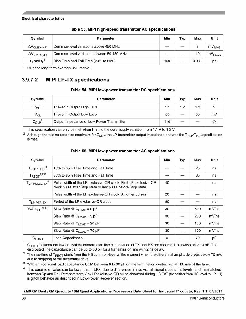
i.MX 8M Dual / 8M QuadLite / 8M Quad Applications Processors Data Sheet for Industrial Products, Rev. 1.1, 07/2019
60 NXP Semiconductors
Electrical characteristics
3.9.7.2 MIPI LP-TX specifications
Table 53. MIPI high-speed transmitter AC specifications
Symbol Parameter Min Typ Max Unit
VCMTX(HF) Common-level variations above 450 MHz — — 8 mVRMS
VCMTX(LF) Common-level variation between 50-450 MHz — — 10 mVPEAK
tR and tF1
1 UI is the long-term average unit interval.
Rise Time and Fall Time (20% to 80%) 160 — 0.3 UI ps
Table 54. MIPI low-power transmitter DC specifications
Symbol Parameter Min Typ Max Unit
VOH1
1 This specification can only be met when limiting the core supply variation from 1.1 V to 1.3 V.
Thevenin Output High Level 1.1 1.2 1.3 V
VOL Thevenin Output Low Level -50 — 50 mV
ZOLP2
2 Although there is no specified maximum for ZOLP, the LP transmitter output impedance ensures the TRLP/TFLP specification is met.
Output Impedance of Low Power Transmitter 110 — —
Table 55. MIPI low-power transmitter AC specifications
Symbol Parameter Min Typ Max Unit
TRLP /TFLP1
1 CLOAD includes the low equivalent transmission line capacitance of TX and RX are assumed to always be < 10 pF. The distributed line capacitance can be up to 50 pF for a transmission line with 2 ns delay.
15% to 85% Rise Time and Fall Time — — 25 ns
TREOT1,2,3
2 The rise-time of TREOT starts from the HS common-level at the moment when the differential amplitude drops below 70 mV, due to stopping of the differential drive.
3 With an additional load capacitance CCM between 0 to 60 pF on the termination center, tap at RX side of the lane.
30% to 85% Rise Time and Fall Time — — 35 ns
TLP-PULSE-TX4
4 This parameter value can be lower than TLPX, due to differences in rise vs. fall signal slopes, trip levels, and mismatches between Dp and Dn LP transmitters. Any LP exclusive-OR pulse observed during HS EoT (transition from HS level to LP-11) is glitch behavior as described in Low-Power Receiver section.
Pulse width of the LP exclusive-OR clock: First LP exclusive-OR clock pulse after Stop state or last pulse before Stop state
40 — — ns
Pulse width of the LP exclusive-OR clock: All other pulses 20 — — ns
TLP-PER-TX Period of the LP exclusive-OR clock 90 — — ns
V/tSR1,5,6,7 Slew Rate @ CLOAD = 0 pF 30 — 500 mV/ns
Slew Rate @ CLOAD = 5 pF 30 — 200 mV/ns
Slew Rate @ CLOAD = 20 pF 30 — 150 mV/ns
Slew Rate @ CLOAD = 70 pF 30 — 100 mV/ns
CLOAD Load Capacitance 0 — 70 pF
Electrical characteristics
i.MX 8M Dual / 8M QuadLite / 8M Quad Applications Processors Data Sheet for Industrial Products, Rev. 1.1, 07/2019
NXP Semiconductors 61
3.9.7.3 MIPI LP-RX specifications
3.9.7.4 MIPI LP-CD specifications
3.9.7.5 MIPI DC specifications
5 When the output voltage is between 15% and 85% of the fully settled LP signal levels.6 Measured as average across any 50 mV segment of the output signal transition.7 This value represents a corner point in a piecewise linear curve.
Table 56. MIPI low power receiver DC specifications
Symbol Parameter Min Typ Max Unit
VIH Logic 1 input voltage 880 — 1.3 mV
VIL Logic 0 input voltage, not in ULP state — — 550 mV
VIL-ULPS Logic 0 input voltage, ULP state — — 300 mV
VHYST Input hysteresis 25 — — mV
Table 57. MIPI low power receiver AC specifications
Symbol Parameter Min Typ Max Unit
eSPIKE1,2
1 Time-voltage integration of a spike above VIL when in LP-0 state or below VIH when in LP-1 state.2 An impulse below this value will not change the receiver state.
Input pulse rejection — — 300 V.ps
TMIN-RX3
3 An input pulse greater than this value shall toggle the output.
Minimum pulse width response 20 0 0 ns
VINT Peak Interference amplitude — — 200 mV
fINT Interference frequency 450 — — MHz
Table 58. MIPI contention detector DC specifications
Symbol Parameter Min Typ Max Unit
VIHCD Logic 1 contention threshold 450 — — mV
VILCD Logic 0 contention threshold — — 200 mV
Table 59. MIPI input characteristics DC specifications
Symbol Parameter Min Typ Max Unit
VPIN Pad signal voltage range -50 — 1350 mV
ILEAK1 Pin leakage current -30 — 30 A
VGNDSH Ground shift -50 — 50 mV

i.MX 8M Dual / 8M QuadLite / 8M Quad Applications Processors Data Sheet for Industrial Products, Rev. 1.1, 07/2019
62 NXP Semiconductors
Electrical characteristics
3.9.8 PCIe PHY parameters
The PCIe interface is designed to be compatible with PCIe specification Gen2 x1 lane and supports the PCI Express 1.1/2.0 standard.
3.9.8.1 PCIEx_RESREF reference resistor connection
The impedance calibration process requires connection of reference resistor 200 1% precision resistor on PCIEx_RESREF pads to ground. It is used for termination impedance calibration.
3.9.9 Pulse width modulator (PWM) timing parameters
This section describes the electrical information of the PWM. The PWM can be programmed to select one of three clock signals as its source frequency. The selected clock signal is passed through a prescaler before being input to the counter. The output is available at the pulse-width modulator output (PWMO) external pin.Figure 31 depicts the timing of the PWM, and Table 60 lists the PWM timing parameters.
Figure 31. PWM timing
3.9.10 Quad SPI (QSPI) timing parameters
This section describes the electrical information for QSPI.
VPIN(absmax)2 Maximum pin voltage level -0.15 — 1.45 V
TVPIN(absmax)3 Maximum transient time above VPIN(max) or below VPIN(min) — — 20 ns
1 When the pad voltage is within the signal voltage range between VGNDSH(min) to VOH + VGNDSH(max) and the Lane Module is in LP receive mode.
2 This value includes ground shift.3 The voltage overshoot and undershoot beyond the VPIN is only allowed during a single 20 ns window after any LP-0 to LP-1
transition or vice versa. For all other situations it must stay within the VPIN range.
Table 60. PWM output timing parameters
ID Parameter Min Max Unit
PWM Module Clock Frequency 0 ipg_clk (66 MHz) MHz
P1 PWM output pulse width high 15 — ns
P2 PWM output pulse width low 15 — ns
Table 59. MIPI input characteristics DC specifications (continued)

Electrical characteristics
i.MX 8M Dual / 8M QuadLite / 8M Quad Applications Processors Data Sheet for Industrial Products, Rev. 1.1, 07/2019
NXP Semiconductors 63
Measurement is with a load of 35 pF on SCK and SIO pins and an input slew rate of 1 V/ns.
3.9.10.1 SDR Mode
Figure 32. QuadSPI input/read timing (SDR mode with internal sampling)
Figure 33. QuadSPI input/read timing (SDR mode with loopback DQS sampling)
NOTE
• For internal sampling, the timing values assume using sample point 0, that is QuadSPIx_SMPR[SDRSMP] = 0.
Table 61. QuadSPI input timing (SDR mode with internal sampling)
Symbol ParameterValue
UnitMin Max
TIS Setup time for incoming data 8.67 — ns
TIH Hold time requirement for incoming data 0 — ns
Table 62. QuadSPI input/read timing (SDR mode with loopback DQS sampling)
Symbol ParameterValue
UnitMin Max
TIS Setup time for incoming data 2 — ns
TIH Hold time requirement for incoming data 1 — ns
TIS TIH TIS TIH
QSPIx_SCLK
QSPIx_DATA[0:3]
1 2 3 4
TIS TIS TIHTIH
QSPIx_SCLK
QSPIx_DATA[0:3]
QSPIx_DQS

i.MX 8M Dual / 8M QuadLite / 8M Quad Applications Processors Data Sheet for Industrial Products, Rev. 1.1, 07/2019
64 NXP Semiconductors
Electrical characteristics
• For loopback DQS sampling, the data strobe is output to the DQS pad together with the serial clock. The data strobe is looped back from DQS pad and used to sample input data.
Figure 34. QuadSPI output/write timing (SDR mode)
NOTE
Tcss and Tcsh are configured by the QuadSPIx_FLSHCR register; the default value of 3 is shown on the timing. See the i.MX 8M Dual / 8M QuadLite / 8M Quad Applications Processor Reference Manual (IMX8MDQLQRM) for more details.
Table 63. QuadSPI output/write timing (SDR mode)
Symbol ParameterValue
UnitMin Max
TDVO Output data valid time — 2 ns
TDHO Output data hold time -0.5 — ns
TCK SCK clock period 10 — ns
TCSS Chip select output setup time 3 — ns
TCSH Chip select output hold time 3 — ns
TCSS TCKTCSH
TDVO
TDHO
TDVO
TDHO
QSPIx_SCLK
QSPIx_CS
QSPIx_SIO

Electrical characteristics
i.MX 8M Dual / 8M QuadLite / 8M Quad Applications Processors Data Sheet for Industrial Products, Rev. 1.1, 07/2019
NXP Semiconductors 65
3.9.10.2 DDR mode
Figure 35. QuadSPI input/read timing (DDR mode with internal sampling)
Figure 36. QuadSPI input/read timing (DDR mode with loopback DQS sampling)
NOTE
• For internal sampling, the timing values assume using sample point 0, that is QuadSPIx_SMPR[SDRSMP] = 0.
Table 64. QuadSPI input/read timing (DDR mode with internal sampling)
Symbol ParameterValue
UnitMin Max
TIS Setup time for incoming data 8.67 — ns
TIH Hold time requirement for incoming data 0 — ns
Table 65. QuadSPI input/read timing (DDR mode with loopback DQS sampling)
Symbol ParameterValue
UnitMin Max
TIS Setup time for incoming data 2 — ns
TIH Hold time requirement for incoming data 1 — ns
TIS TIH TIS TIH
QSPIx_SCLK
QSPIx_DATA[0:3]
1 2 3 4
TIS TIHTIS TIH
QSPIx_SCLK
QSPIx_DATA[0:3]
QSPIx_DQS

i.MX 8M Dual / 8M QuadLite / 8M Quad Applications Processors Data Sheet for Industrial Products, Rev. 1.1, 07/2019
66 NXP Semiconductors
Electrical characteristics
• For loopback DQS sampling, the data strobe is output to the DQS pad together with the serial clock. The data strobe is looped back from DQS pad and used to sample input data.
Figure 37. QuadSPI output/write timing (DDR mode)
NOTE
Tcss and Tcsh are configured by the QuadSPIx_FLSHCR register; the default value of 3 is shown on the timing. See the i.MX 8M Dual / 8M QuadLite / 8M Quad Applications Processor Reference Manual (IMX8MDQLQRM) for more details.
3.9.11 SAI/I2S switching specifications
This section provides the AC timings for the SAI in Master (clocks driven) and Slave (clocks input) modes. All timings are given for non inverted serial clock polarity (SAI_TCR[TSCKP] = 0, SAI_RCR[RSCKP] = 0) and non inverted frame sync (SAI_TCR[TFSI] = 0, SAI_RCR[RFSI] = 0). If the polarity of the clock and/or the frame sync have been inverted, all the timings remain valid by inverting the clock signal (SAI_BCLK) and/or the frame sync (SAI_FS) shown in the figures below.
Table 66. QuadSPI output/write timing (DDR mode)
Symbol ParameterValue
UnitMin Max
TDVO Output data valid time — (0.25 x TSCLK) + 2 ns
TDHO Output data hold time (0.25 x TSCLK) - 0.5 — ns
TCK SCK clock period 20 — ns
TCSS Chip select output setup time 3 — SCK cycle(s)
TCSH Chip select output hold time 3 — ns
Table 67. Master mode SAI timing
Num Characteristic Min Max Unit
S1 SAI_MCLK cycle time 20 — ns
S2 SAI_MCLK pulse width high/low 40% 60% MCLK period
S3 SAI_BCLK cycle time 40 — ns
1 2
TCSS TCK
TDVO
TDHO
TDVO
TDHO
TCSH
QSPIx_SCLK
QSPIx_CS
QSPIx_SIO

Electrical characteristics
i.MX 8M Dual / 8M QuadLite / 8M Quad Applications Processors Data Sheet for Industrial Products, Rev. 1.1, 07/2019
NXP Semiconductors 67
Figure 38. SAI timing—Master modes
S4 SAI_BCLK pulse width high/low 40% 60% BCLK period
S5 SAI_BCLK to SAI_FS output valid — 15 ns
S6 SAI_BCLK to SAI_FS output invalid 0 — ns
S7 SAI_BCLK to SAI_TXD valid — 15 ns
S8 SAI_BCLK to SAI_TXD invalid 0 — ns
S9 SAI_RXD/SAI_FS input setup before SAI_BCLK 15 — ns
S10 SAI_RXD/SAI_FS input hold after SAI_BCLK 0 — ns
Table 68. Slave mode SAI timing
Num Characteristic Min Max Unit
S11 SAI_BCLK cycle time (input) 40 — ns
S12 SAI_BCLK pulse width high/low (input) 40% 60% BCLK period
S13 SAI_FS input setup before SAI_BCLK 10 — ns
S14 SAI_FA input hold after SAI_BCLK 2 — ns
S15 SAI_BCLK to SAI_TXD/SAI_FS output valid — 20 ns
S16 SAI_BCLK to SAI_TXD/SAI_FS output invalid 0 — ns
S17 SAI_RXD setup before SAI_BCLK 10 — ns
S18 SAI_RXD hold after SAI_BCLK 2 — ns
Table 67. Master mode SAI timing (continued)
Num Characteristic Min Max Unit
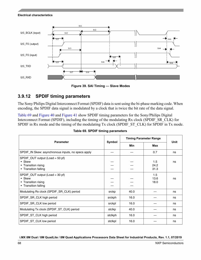
i.MX 8M Dual / 8M QuadLite / 8M Quad Applications Processors Data Sheet for Industrial Products, Rev. 1.1, 07/2019
68 NXP Semiconductors
Electrical characteristics
Figure 39. SAI Timing — Slave Modes
3.9.12 SPDIF timing parameters
The Sony/Philips Digital Interconnect Format (SPDIF) data is sent using the bi-phase marking code. When encoding, the SPDIF data signal is modulated by a clock that is twice the bit rate of the data signal.
Table 69 and Figure 40 and Figure 41 show SPDIF timing parameters for the Sony/Philips Digital Interconnect Format (SPDIF), including the timing of the modulating Rx clock (SPDIF_SR_CLK) for SPDIF in Rx mode and the timing of the modulating Tx clock (SPDIF_ST_CLK) for SPDIF in Tx mode.
Table 69. SPDIF timing parameters
Parameter SymbolTiming Parameter Range
Unit Min Max
SPDIF_IN Skew: asynchronous inputs, no specs apply — — 0.7 ns
SPDIF_OUT output (Load = 50 pf) • Skew • Transition rising • Transition falling
———
———
1.524.231.3
ns
SPDIF_OUT output (Load = 30 pf) • Skew • Transition rising • Transition falling
———
———
1.513.618.0
ns
Modulating Rx clock (SPDIF_SR_CLK) period srckp 40.0 — ns
SPDIF_SR_CLK high period srckph 16.0 — ns
SPDIF_SR_CLK low period srckpl 16.0 — ns
Modulating Tx clock (SPDIF_ST_CLK) period stclkp 40.0 — ns
SPDIF_ST_CLK high period stclkph 16.0 — ns
SPDIF_ST_CLK low period stclkpl 16.0 — ns

Electrical characteristics
i.MX 8M Dual / 8M QuadLite / 8M Quad Applications Processors Data Sheet for Industrial Products, Rev. 1.1, 07/2019
NXP Semiconductors 69
Figure 40. SPDIF_SR_CLK timing diagram
Figure 41. SPDIF_ST_CLK timing diagram
3.9.13 UART I/O configuration and timing parameters
3.9.13.1 UART RS-232 I/O configuration in different modes
The UART interfaces of the i.MX 8M Dual / 8M QuadLite / 8M Quad can serve both as DTE or DCE device. This can be configured by the DCEDTE control bit (default 0—DCE mode). Table 70 shows the UART I/O configuration based on the enabled mode.
3.9.13.2 UART RS-232 Serial mode timing
This section describes the electrical information of the UART module in the RS-232 mode.
Table 70. UART I/O configuration vs. mode
PortDTE Mode DCE Mode
Direction Description Direction Description
UARTx_RTS_B Output UARTx_RTS_B from DTE to DCE Input UARTx_RTS_B from DTE to DCE
UARTx_CTS_B Input UARTx_CTS_B from DCE to DTE Output UARTx_CTS_B from DCE to DTE
UARTx_TX_ DATA Input Serial data from DCE to DTE Output Serial data from DCE to DTE
UARTx_RX _DATA Output Serial data from DTE to DCE Input Serial data from DTE to DCE
SPDIF_SR_CLK
(Output)
VM VM
srckp
srckphsrckpl
SPDIF_ST_CLK
(Input)
VM VM
stclkp
stclkphstclkpl

i.MX 8M Dual / 8M QuadLite / 8M Quad Applications Processors Data Sheet for Industrial Products, Rev. 1.1, 07/2019
70 NXP Semiconductors
Electrical characteristics
3.9.13.2.1 UART transmitter
Figure 42 depicts the transmit timing of UART in the RS-232 Serial mode, with 8 data bit/1 stop bit format. Table 71 lists the UART RS-232 Serial mode transmit timing characteristics.
Figure 42. UART RS-232 Serial mode transmit timing diagram
3.9.13.2.2 UART receiver
Figure 43 depicts the RS-232 Serial mode receive timing with 8 data bit/1 stop bit format. Table 72 lists Serial mode receive timing characteristics.
Figure 43. UART RS-232 Serial mode receive timing diagram
Table 71. RS-232 Serial mode transmit timing parameters
ID Parameter Symbol Min Max Unit
UA1 Transmit Bit Time tTbit 1/Fbaud_rate1 - Tref_clk
2
1 Fbaud_rate: Baud rate frequency. The maximum baud rate the UART can support is (ipg_perclk frequency)/16.2 Tref_clk: The period of UART reference clock ref_clk (ipg_perclk after RFDIV divider).
1/Fbaud_rate + Tref_clk —
Table 72. RS-232 Serial mode receive timing parameters
ID Parameter Symbol Min Max Unit
UA2 Receive Bit Time1
1 The UART receiver can tolerate 1/(16 x Fbaud_rate) tolerance in each bit. But accumulation tolerance in one frame must not exceed 3/(16 x Fbaud_rate).
tRbit 1/Fbaud_rate2 - 1/(16
x Fbaud_rate)
2 Fbaud_rate: Baud rate frequency. The maximum baud rate the UART can support is (ipg_perclk frequency)/16.
1/Fbaud_rate + 1/(16 x Fbaud_rate)
—
StartBit Bit 1 Bit 2Bit 0 Bit 4 Bit 5 Bit 6 Bit 7UARTx_TX_DATA
(output)Bit 3 STOP
BIT
NextStartBit
PossibleParity
Bit
Par Bit
UA1
UA1 UA1
UA1
Bit 1 Bit 2Bit 0 Bit 4 Bit 5 Bit 6 Bit 7UARTx_RX_DATA(output)
Bit 3StartBit STOP
BIT
NextStartBit
PossibleParity
Bit
Par Bit
UA2 UA2
UA2 UA2
Electrical characteristics
i.MX 8M Dual / 8M QuadLite / 8M Quad Applications Processors Data Sheet for Industrial Products, Rev. 1.1, 07/2019
NXP Semiconductors 71
3.9.14 USB PHY parameters
This section describes the USB-OTG PHY parameters.
The USB PHY meets the electrical compliance requirements defined in the Universal Serial Bus Revision 3.0 OTG, USB Host with the amendments below (On-The-Go and Embedded Host Supplement to the USB Revision 3.0 Specification is not applicable to Host port):
• USB ENGINEERING CHANGE NOTICE— Title: 5V Short Circuit Withstand Requirement Change— Applies to: Universal Serial Bus Specification, Revision 2.0
• Errata for USB Revision 2.0 April 27, 2000 as of 12/7/2000• USB ENGINEERING CHANGE NOTICE
— Title: Pull-up/Pull-down resistors— Applies to: Universal Serial Bus Specification, Revision 2.0
• USB ENGINEERING CHANGE NOTICE— Title: Suspend Current Limit Changes— Applies to: Universal Serial Bus Specification, Revision 2.0
• USB ENGINEERING CHANGE NOTICE— Title: USB 2.0 Phase Locked SOFs— Applies to: Universal Serial Bus Specification, Revision 2.0
• On-The-Go and Embedded Host Supplement to the USB Revision 2.0 Specification— Revision 2.0, version 1.1a, July 27, 2010
• Battery Charging Specification (available from USB-IF)— Revision 1.2, December 7, 2010
3.9.14.1 USB_OTG*_REXT reference resistor connection
The bias generation and impedance calibration process for the USB OTG PHYs requires connection of reference resistors 200 1% precision on each of USB_OTG1_REXT and USB_OTG2_REXT pads to ground.
3.9.14.2 USB_OTG_CHD_B USB battery charger detection external pullup resistor connection
The usage and external resistor connection for the USB_OTG_CHD_B pin are described in Table 5, and Section 3.7.3, USB battery charger detection driver impedance.”
3.9.15 USB 2.0 PHY parameters
USB 2.0 PHY parameters are compatible with USB 3.0 PHY. See Section 3.9.16, USB 3.0 PHY parameters for more detailed information.
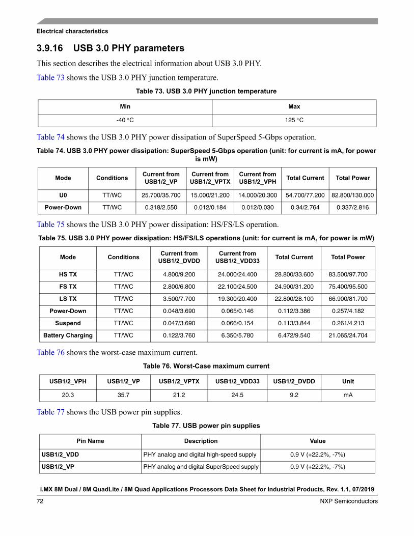
i.MX 8M Dual / 8M QuadLite / 8M Quad Applications Processors Data Sheet for Industrial Products, Rev. 1.1, 07/2019
72 NXP Semiconductors
Electrical characteristics
3.9.16 USB 3.0 PHY parameters
This section describes the electrical information about USB 3.0 PHY.
Table 73 shows the USB 3.0 PHY junction temperature.
Table 74 shows the USB 3.0 PHY power dissipation of SuperSpeed 5-Gbps operation.
Table 75 shows the USB 3.0 PHY power dissipation: HS/FS/LS operation.
Table 76 shows the worst-case maximum current.
Table 77 shows the USB power pin supplies.
Table 73. USB 3.0 PHY junction temperature
Min Max
-40 C 125 C
Table 74. USB 3.0 PHY power dissipation: SuperSpeed 5-Gbps operation (unit: for current is mA, for power is mW)
Mode ConditionsCurrent from USB1/2_VP
Current from USB1/2_VPTX
Current from USB1/2_VPH
Total Current Total Power
U0 TT/WC 25.700/35.700 15.000/21.200 14.000/20.300 54.700/77.200 82.800/130.000
Power-Down TT/WC 0.318/2.550 0.012/0.184 0.012/0.030 0.34/2.764 0.337/2.816
Table 75. USB 3.0 PHY power dissipation: HS/FS/LS operations (unit: for current is mA, for power is mW)
Mode ConditionsCurrent from
USB1/2_DVDDCurrent from
USB1/2_VDD33Total Current Total Power
HS TX TT/WC 4.800/9.200 24.000/24.400 28.800/33.600 83.500/97.700
FS TX TT/WC 2.800/6.800 22.100/24.500 24.900/31.200 75.400/95.500
LS TX TT/WC 3.500/7.700 19.300/20.400 22.800/28.100 66.900/81.700
Power-Down TT/WC 0.048/3.690 0.065/0.146 0.112/3.386 0.257/4.182
Suspend TT/WC 0.047/3.690 0.066/0.154 0.113/3.844 0.261/4.213
Battery Charging TT/WC 0.122/3.760 6.350/5.780 6.472/9.540 21.065/24.704
Table 76. Worst-Case maximum current
USB1/2_VPH USB1/2_VP USB1/2_VPTX USB1/2_VDD33 USB1/2_DVDD Unit
20.3 35.7 21.2 24.5 9.2 mA
Table 77. USB power pin supplies
Pin Name Description Value
USB1/2_VDD PHY analog and digital high-speed supply 0.9 V (+22.2%, -7%)
USB1/2_VP PHY analog and digital SuperSpeed supply 0.9 V (+22.2%, -7%)
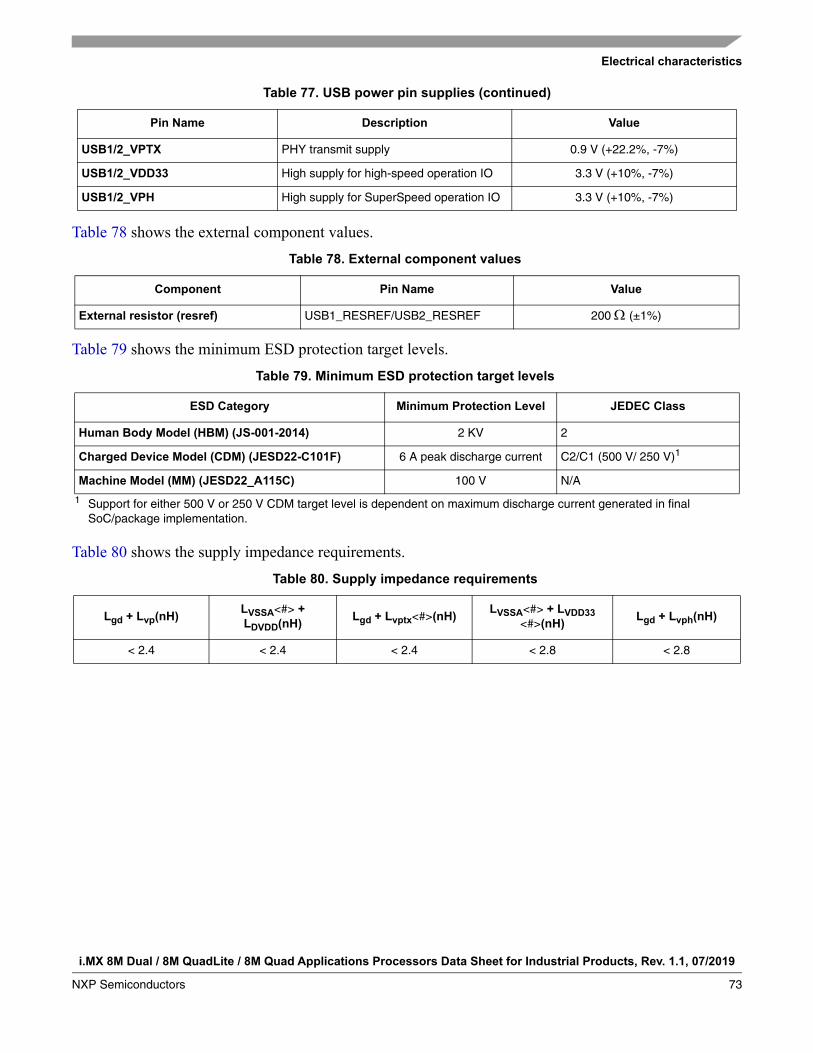
Electrical characteristics
i.MX 8M Dual / 8M QuadLite / 8M Quad Applications Processors Data Sheet for Industrial Products, Rev. 1.1, 07/2019
NXP Semiconductors 73
Table 78 shows the external component values.
Table 79 shows the minimum ESD protection target levels.
Table 80 shows the supply impedance requirements.
USB1/2_VPTX PHY transmit supply 0.9 V (+22.2%, -7%)
USB1/2_VDD33 High supply for high-speed operation IO 3.3 V (+10%, -7%)
USB1/2_VPH High supply for SuperSpeed operation IO 3.3 V (+10%, -7%)
Table 78. External component values
Component Pin Name Value
External resistor (resref) USB1_RESREF/USB2_RESREF 200 (±1%)
Table 79. Minimum ESD protection target levels
ESD Category Minimum Protection Level JEDEC Class
Human Body Model (HBM) (JS-001-2014) 2 KV 2
Charged Device Model (CDM) (JESD22-C101F) 6 A peak discharge current C2/C1 (500 V/ 250 V)1
1 Support for either 500 V or 250 V CDM target level is dependent on maximum discharge current generated in final SoC/package implementation.
Machine Model (MM) (JESD22_A115C) 100 V N/A
Table 80. Supply impedance requirements
Lgd + Lvp(nH)LVSSA<#> + LDVDD(nH)
Lgd + Lvptx<#>(nH)LVSSA<#> + LVDD33
<#>(nH)Lgd + Lvph(nH)
< 2.4 < 2.4 < 2.4 < 2.8 < 2.8
Table 77. USB power pin supplies (continued)
Pin Name Description Value

i.MX 8M Dual / 8M QuadLite / 8M Quad Applications Processors Data Sheet for Industrial Products, Rev. 1.1, 07/2019
74 NXP Semiconductors
Boot mode configuration
4 Boot mode configurationThis section provides information on Boot mode configuration pins allocation and boot devices interfaces allocation.
4.1 Boot mode configuration pinsTable 81 provides boot options, functionality, fuse values, and associated pins. Several input pins are also sampled at reset and can be used to override fuse values, depending on the value of BT_FUSE_SEL fuse. The boot option pins are in effect when BT_FUSE_SEL fuse is ‘0’ (cleared, which is the case for an unblown fuse). For detailed Boot mode options configured by the Boot mode pins, see the “System Boot, Fusemap, and eFuse” chapter in the i.MX 8M Dual / 8M QuadLite / 8M Quad Applications Processor Reference Manual (IMX8MDQLQRM).
Table 81. Fuses and associated pins used for boot
PinDirectionat Reset
eFuse nameState during reset
(POR_Basserted)
State after reset(POR_B
deasserted)Details
BOOT_MODE0 Input N/A Input with 95 K pull down Input with 95 K pull down Boot mode selection
BOOT_MODE1 Input N/A Input with 95 K pull down Input with 95 K pull down Boot mode selection
SAI1_RXD0 Input BOOT_CFG[0] Input with 95 K pull down Input with 95 K pull down Boot options pin value overrides fuse settings for BT_FUSE_SEL = “0“. Signal configuration as fuse override input at power up. These are special I/O lines that control the boot configuration during product development. In production, the boot configuration can be controlled by fuses.
SAI1_RXD1 Input BOOT_CFG[1] Input with 95 K pull down Input with 95 K pull down
SAI1_RXD2 Input BOOT_CFG[2] Input with 95 K pull down Input with 95 K pull down
SAI1_RXD3 Input BOOT_CFG[3] Input with 95 K pull down Input with 95 K pull down
SAI1_RXD4 Input BOOT_CFG[4] Input with 95 K pull down Input with 95 K pull down
SAI1_RXD5 Input BOOT_CFG[5] Input with 95 K pull down Input with 95 K pull down
SAI1_RXD6 Input BOOT_CFG[6] Input with 95 K pull down Input with 95 K pull down
SAI1_RXD7 Input BOOT_CFG[7] Input with 95 K pull down Input with 95 K pull down
SAI1_TXD0 Input BOOT_CFG[8] Input with 95 K pull down Input with 95 K pull down
SAI1_TXD1 Input BOOT_CFG[9] Input with 95 K pull down Input with 95 K pull down
SAI1_TXD2 Input BOOT_CFG[10] Input with 95 K pull down Input with 95 K pull down
SAI1_TXD3 Input BOOT_CFG[11] Input with 95 K pull down Input with 95 K pull down
SAI1_TXD4 Input BOOT_CFG[12] Input with 95 K pull down Input with 95 K pull down
SAI1_TXD5 Input BOOT_CFG[13] Input with 95 K pull down Input with 95 K pull down
SAI1_TXD6 Input BOOT_CFG[14] Input with 95 K pull down Input with 95 K pull down
SAI1_TXD7 Input BOOT_CFG[15] Input with 95 K pull down Input with 95 K pull down

Boot mode configuration
i.MX 8M Dual / 8M QuadLite / 8M Quad Applications Processors Data Sheet for Industrial Products, Rev. 1.1, 07/2019
NXP Semiconductors 75
4.2 Boot device interface allocationTable 82 lists the interfaces that can be used by the boot process in accordance with the specific Boot mode configuration. The table also describes the interface’s specific modes and IOMUXC allocation, which are configured during boot when appropriate.
Table 82. Interface allocation during boot
Interface IP Instance Allocated Pads During Boot Comment
NAND Flash GPMI NAND_ALE, NAND_CE0_B, NAND_CLE, NAND_DATA00, NAND_DATA01, NAND_DATA02, NAND_DATA03, NAND_DATA04, NAND_DATA05, NAND_DATA06, NAND_DATA07, NAND_DQS, NAND_RE_B, NAND_READY_B, NAND_WE_B, NAND_WP_B
8-bit, only CS0 is supported.
SD/MMC USDHC-1 GPIO1_IO03, GPIO1_IO06, GPIO1_IO07, SD1_RESET_B, SD1_CLK, SD1_CMD, SD1_STROBE, SD1_DATA0, SD1_DATA1, SD1_DATA2, SD1_DATA3, SD1_DATA4, SD1_DATA5, SD1_DATA6, SD1_DATA7
1, 4, or 8-bit
SD/MMC USDHC-2 GPIO1_IO04, GPIO1_IO08, GPIO1_IO07, SD2_RESET_B, SD2_CD_B, SD2_WP, SD2_CLK, SD2_CMD, SD2_DATA0, SD2_DATA1, SD2_DATA2, SD2_DATA3
1 or 4-bit
USB USB_OTG PHY — —

i.MX 8M Dual / 8M QuadLite / 8M Quad Applications Processors Data Sheet for Industrial Products, Rev. 1.1, 07/2019
76 NXP Semiconductors
Package information and contact assignments
5 Package information and contact assignmentsThis section includes the contact assignment information and mechanical package drawing.
5.1 17 x 17 mm package information
5.1.1 17 x 17 mm, 0.65 mm pitch, ball matrix
Figure 44 shows the top, bottom, and side views of the 17 × 17 mm BGA package.
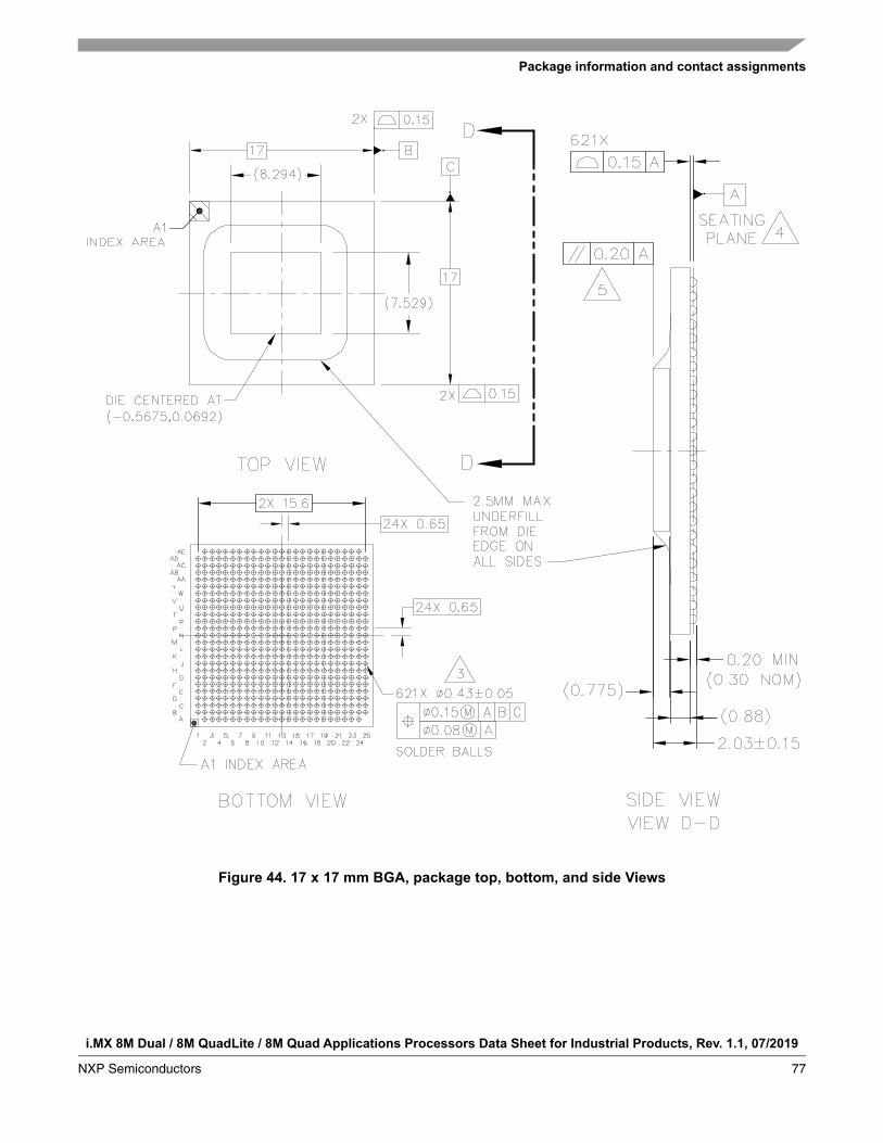
Package information and contact assignments
i.MX 8M Dual / 8M QuadLite / 8M Quad Applications Processors Data Sheet for Industrial Products, Rev. 1.1, 07/2019
NXP Semiconductors 77
Figure 44. 17 x 17 mm BGA, package top, bottom, and side Views
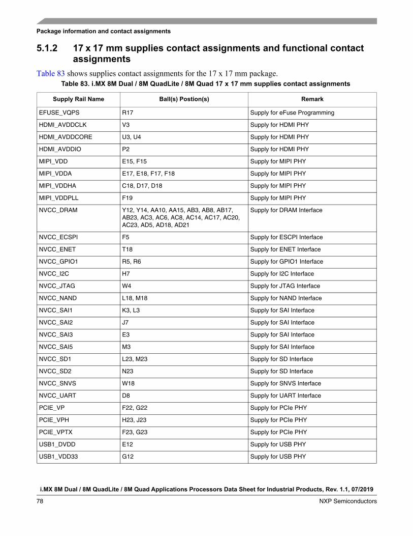
i.MX 8M Dual / 8M QuadLite / 8M Quad Applications Processors Data Sheet for Industrial Products, Rev. 1.1, 07/2019
78 NXP Semiconductors
Package information and contact assignments
5.1.2 17 x 17 mm supplies contact assignments and functional contact assignments
Table 83 shows supplies contact assignments for the 17 x 17 mm package.Table 83. i.MX 8M Dual / 8M QuadLite / 8M Quad 17 x 17 mm supplies contact assignments
Supply Rail Name Ball(s) Postion(s) Remark
EFUSE_VQPS R17 Supply for eFuse Programming
HDMI_AVDDCLK V3 Supply for HDMI PHY
HDMI_AVDDCORE U3, U4 Supply for HDMI PHY
HDMI_AVDDIO P2 Supply for HDMI PHY
MIPI_VDD E15, F15 Supply for MIPI PHY
MIPI_VDDA E17, E18, F17, F18 Supply for MIPI PHY
MIPI_VDDHA C18, D17, D18 Supply for MIPI PHY
MIPI_VDDPLL F19 Supply for MIPI PHY
NVCC_DRAM Y12, Y14, AA10, AA15, AB3, AB8, AB17, AB23, AC3, AC6, AC8, AC14, AC17, AC20, AC23, AD5, AD18, AD21
Supply for DRAM Interface
NVCC_ECSPI F5 Supply for ESCPI Interface
NVCC_ENET T18 Supply for ENET Interface
NVCC_GPIO1 R5, R6 Supply for GPIO1 Interface
NVCC_I2C H7 Supply for I2C Interface
NVCC_JTAG W4 Supply for JTAG Interface
NVCC_NAND L18, M18 Supply for NAND Interface
NVCC_SAI1 K3, L3 Supply for SAI Interface
NVCC_SAI2 J7 Supply for SAI Interface
NVCC_SAI3 E3 Supply for SAI Interface
NVCC_SAI5 M3 Supply for SAI Interface
NVCC_SD1 L23, M23 Supply for SD Interface
NVCC_SD2 N23 Supply for SD Interface
NVCC_SNVS W18 Supply for SNVS Interface
NVCC_UART D8 Supply for UART Interface
PCIE_VP F22, G22 Supply for PCIe PHY
PCIE_VPH H23, J23 Supply for PCIe PHY
PCIE_VPTX F23, G23 Supply for PCIe PHY
USB1_DVDD E12 Supply for USB PHY
USB1_VDD33 G12 Supply for USB PHY
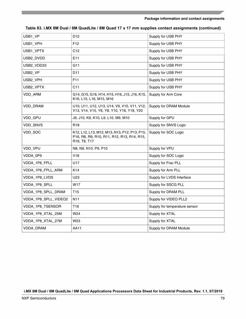
Package information and contact assignments
i.MX 8M Dual / 8M QuadLite / 8M Quad Applications Processors Data Sheet for Industrial Products, Rev. 1.1, 07/2019
NXP Semiconductors 79
USB1_VP D12 Supply for USB PHY
USB1_VPH F12 Supply for USB PHY
USB1_VPTX C12 Supply for USB PHY
USB2_DVDD E11 Supply for USB PHY
USB2_VDD33 G11 Supply for USB PHY
USB2_VP D11 Supply for USB PHY
USB2_VPH F11 Supply for USB PHY
USB2_VPTX C11 Supply for USB PHY
VDD_ARM G14, G15, G16, H14, H15, H16, J15, J16, K15, K16, L15, L16, M15, M16
Supply for Arm Core
VDD_DRAM U10, U11, U12, U13, U14, V9, V10, V11, V12, V13, V14, V15, Y6, Y8, Y10, Y16, Y18, Y20
Supply for DRAM Module
VDD_GPU J9, J10, K9, K10, L9, L10, M9, M10 Supply for GPU
VDD_SNVS R18 Supply for SNVS Logic
VDD_SOC K12, L12, L13, M12, M13, N13, P12, P13, P15, P16, R8, R9, R10, R11, R12, R13, R14, R15, R16, T8, T17
Supply for SOC Logic
VDD_VPU N8, N9, N10, P9, P10 Supply for VPU
VDDA_0P9 V18 Supply for SOC Logic
VDDA_1P8_FPLL U17 Supply for Frac PLL
VDDA_1P8_FPLL_ARM K14 Supply for Arm PLL
VDDA_1P8_LVDS U23 Supply for LVDS Interface
VDDA_1P8_SPLL W17 Supply for SSCG PLL
VDDA_1P8_SPLL_DRAM T15 Supply for DRAM PLL
VDDA_1P8_SPLL_VIDEO2 N11 Supply for VIDEO PLL2
VDDA_1P8_TSENSOR T16 Supply for temperature sensor
VDDA_1P8_XTAL_25M W24 Supply for XTAL
VDDA_1P8_XTAL_27M W23 Supply for XTAL
VDDA_DRAM AA11 Supply for DRAM Module
Table 83. i.MX 8M Dual / 8M QuadLite / 8M Quad 17 x 17 mm supplies contact assignments (continued)

i.MX 8M Dual / 8M QuadLite / 8M Quad Applications Processors Data Sheet for Industrial Products, Rev. 1.1, 07/2019
80 NXP Semiconductors
Package information and contact assignments
VSS A2, A24, B1, B25, C8, C10, C13, C15, C24, D10, D13, D15, D23, E4, E10, E13, E14, E16, E19, E20, E21, E22, E23, F10, F13, F14, F16, F20, G9, G10, G13, G17, G18, G24, H8, H9, H10, H11, H12, H13, H17, H18, J3, J8, J11, J12, J13, J14, J17, J18, J19, K8, K11, K17, K18, K23, L8, L11, L14, L17, M8, M11, M14, M17, N3, N14, N15, N16, N17, N18, P6, P8, P11, P14, P17, P18, P23, R7, T3, T4, T9, T10, T11, T12, T13, U8, U9, U15, U18, V4, V8, V16, W1, W7, W8, W9, W10, W11, W12, W13, W14, W15, W16, W25, Y2, Y3, Y4, Y5, Y7, Y9, Y11, Y13, Y15, Y17, Y19, Y21, Y22, Y23, Y24, AA5, AA16, AA21, AB2, AB9, AB11, AB18, AB24, AC4, AC19, AC22, AD1, AD7, AD9, AD11, AD13, AD16, AD25, AE2, AE5, AE21, AE24
—
VSSA_FPLL U16 Return path of VDDA_1P8_FPLL
VSSA_FPLL_ARM K13 Return path of VDDA_1P8_FPLL_ARM
VSSA_SPLL V17 Return path of VDDA_1P8_SPLL
VSSA_SPLL_DRAM T14 Return path of VDDA_1P8_SPLL_DRAM
VSSA_SPLL_VIDEO2 N12 Return path of VDDA_1P8_SPLL_VIDEO2
VSSA_XTAL_25M V23 Return path of VDDA_1P8_XTAL_25M
VSSA_XTAL_27M W22 Return path of VDDA_1P8_XTAL_27M
Table 83. i.MX 8M Dual / 8M QuadLite / 8M Quad 17 x 17 mm supplies contact assignments (continued)

Package information and contact assignments
i.MX 8M Dual / 8M QuadLite / 8M Quad Applications Processors Data Sheet for Industrial Products, Rev. 1.1, 07/2019
NXP Semiconductors 81
Table 84 shows an alpha-sorted list of functional contact assignments for the 17 x 17 mm package.Table 84. i.MX 8M Dual / 8M QuadLite / 8M Quad 17 x 17 mm functional contact assignments
Ball name Ball Power group Ball type1
Reset condition2
Defaultmode(Reset mode)
Default function(Signal name)
Input/Output
Value
BOOT_MODE0 W6 NVCC_JTAG GPIO ALT0 ccmsrcgpcmix.BOOT_MODE[0]
Input PD (90 K)
BOOT_MODE1 V6 NVCC_JTAG GPIO ALT0 ccmsrcgpcmix.BOOT_MODE[1]
Input PD (90 K)
CLK1_P R23 VDDA LVDS — — — —
CLK1_N T23 VDDA LVDS — — — —
CLK2_P T22 VDDA LVDS — — — —
CLK2_N U22 VDDA LVDS — — — —
DRAM_AC00 AC16 NVCC_DRAM DDR — — — —
DRAM_AC01 AE17 NVCC_DRAM DDR — — — —
DRAM_AC02 AE18 NVCC_DRAM DDR — — — —
DRAM_AC03 AC18 NVCC_DRAM DDR — — — —
DRAM_AC04 AD14 NVCC_DRAM DDR — — — —
DRAM_AC05 AE14 NVCC_DRAM DDR — — — —
DRAM_AC06 AE13 NVCC_DRAM DDR — — — —
DRAM_AC07 AB15 NVCC_DRAM DDR — — — —
DRAM_AC08 AD17 NVCC_DRAM DDR — — — —
DRAM_AC09 AE16 NVCC_DRAM DDR — — — —
DRAM_AC10 AD20 NVCC_DRAM DDR — — — —
DRAM_AC11 AE20 NVCC_DRAM DDR — — — —
DRAM_AC12 AD19 NVCC_DRAM DDR — — — —
DRAM_AC13 AE19 NVCC_DRAM DDR — — — —
DRAM_AC14 AB16 NVCC_DRAM DDR — — — —
DRAM_AC15 AC15 NVCC_DRAM DDR — — — —
DRAM_AC16 AE15 NVCC_DRAM DDR — — — —
DRAM_AC17 AD15 NVCC_DRAM DDR — — — —
DRAM_AC19 AB14 NVCC_DRAM DDR — — — —
DRAM_AC20 AD10 NVCC_DRAM DDR — — — —
DRAM_AC21 AE10 NVCC_DRAM DDR — — — —
DRAM_AC22 AD8 NVCC_DRAM DDR — — — —
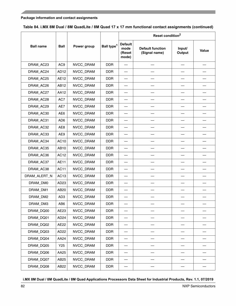
i.MX 8M Dual / 8M QuadLite / 8M Quad Applications Processors Data Sheet for Industrial Products, Rev. 1.1, 07/2019
82 NXP Semiconductors
Package information and contact assignments
DRAM_AC23 AC9 NVCC_DRAM DDR — — — —
DRAM_AC24 AD12 NVCC_DRAM DDR — — — —
DRAM_AC25 AE12 NVCC_DRAM DDR — — — —
DRAM_AC26 AB12 NVCC_DRAM DDR — — — —
DRAM_AC27 AA12 NVCC_DRAM DDR — — — —
DRAM_AC28 AC7 NVCC_DRAM DDR — — — —
DRAM_AC29 AE7 NVCC_DRAM DDR — — — —
DRAM_AC30 AE6 NVCC_DRAM DDR — — — —
DRAM_AC31 AD6 NVCC_DRAM DDR — — — —
DRAM_AC32 AE8 NVCC_DRAM DDR — — — —
DRAM_AC33 AE9 NVCC_DRAM DDR — — — —
DRAM_AC34 AC10 NVCC_DRAM DDR — — — —
DRAM_AC35 AB10 NVCC_DRAM DDR — — — —
DRAM_AC36 AC12 NVCC_DRAM DDR — — — —
DRAM_AC37 AE11 NVCC_DRAM DDR — — — —
DRAM_AC38 AC11 NVCC_DRAM DDR — — — —
DRAM_ALERT_N AC13 NVCC_DRAM DDR — — — —
DRAM_DM0 AD23 NVCC_DRAM DDR — — — —
DRAM_DM1 AB20 NVCC_DRAM DDR — — — —
DRAM_DM2 AD3 NVCC_DRAM DDR — — — —
DRAM_DM3 AB6 NVCC_DRAM DDR — — — —
DRAM_DQ00 AE23 NVCC_DRAM DDR — — — —
DRAM_DQ01 AD24 NVCC_DRAM DDR — — — —
DRAM_DQ02 AE22 NVCC_DRAM DDR — — — —
DRAM_DQ03 AD22 NVCC_DRAM DDR — — — —
DRAM_DQ04 AA24 NVCC_DRAM DDR — — — —
DRAM_DQ05 Y25 NVCC_DRAM DDR — — — —
DRAM_DQ06 AA25 NVCC_DRAM DDR — — — —
DRAM_DQ07 AB25 NVCC_DRAM DDR — — — —
DRAM_DQ08 AB22 NVCC_DRAM DDR — — — —
Table 84. i.MX 8M Dual / 8M QuadLite / 8M Quad 17 x 17 mm functional contact assignments (continued)
Ball name Ball Power group Ball type1
Reset condition2
Defaultmode(Reset mode)
Default function(Signal name)
Input/Output
Value
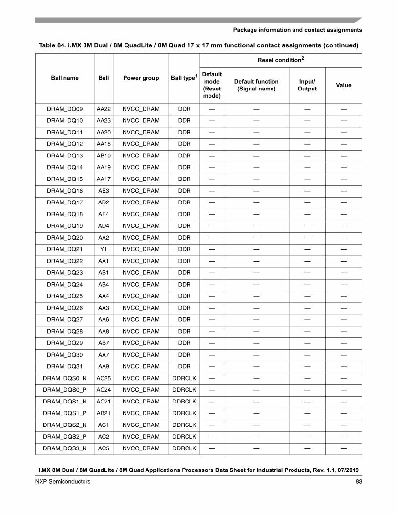
Package information and contact assignments
i.MX 8M Dual / 8M QuadLite / 8M Quad Applications Processors Data Sheet for Industrial Products, Rev. 1.1, 07/2019
NXP Semiconductors 83
DRAM_DQ09 AA22 NVCC_DRAM DDR — — — —
DRAM_DQ10 AA23 NVCC_DRAM DDR — — — —
DRAM_DQ11 AA20 NVCC_DRAM DDR — — — —
DRAM_DQ12 AA18 NVCC_DRAM DDR — — — —
DRAM_DQ13 AB19 NVCC_DRAM DDR — — — —
DRAM_DQ14 AA19 NVCC_DRAM DDR — — — —
DRAM_DQ15 AA17 NVCC_DRAM DDR — — — —
DRAM_DQ16 AE3 NVCC_DRAM DDR — — — —
DRAM_DQ17 AD2 NVCC_DRAM DDR — — — —
DRAM_DQ18 AE4 NVCC_DRAM DDR — — — —
DRAM_DQ19 AD4 NVCC_DRAM DDR — — — —
DRAM_DQ20 AA2 NVCC_DRAM DDR — — — —
DRAM_DQ21 Y1 NVCC_DRAM DDR — — — —
DRAM_DQ22 AA1 NVCC_DRAM DDR — — — —
DRAM_DQ23 AB1 NVCC_DRAM DDR — — — —
DRAM_DQ24 AB4 NVCC_DRAM DDR — — — —
DRAM_DQ25 AA4 NVCC_DRAM DDR — — — —
DRAM_DQ26 AA3 NVCC_DRAM DDR — — — —
DRAM_DQ27 AA6 NVCC_DRAM DDR — — — —
DRAM_DQ28 AA8 NVCC_DRAM DDR — — — —
DRAM_DQ29 AB7 NVCC_DRAM DDR — — — —
DRAM_DQ30 AA7 NVCC_DRAM DDR — — — —
DRAM_DQ31 AA9 NVCC_DRAM DDR — — — —
DRAM_DQS0_N AC25 NVCC_DRAM DDRCLK — — — —
DRAM_DQS0_P AC24 NVCC_DRAM DDRCLK — — — —
DRAM_DQS1_N AC21 NVCC_DRAM DDRCLK — — — —
DRAM_DQS1_P AB21 NVCC_DRAM DDRCLK — — — —
DRAM_DQS2_N AC1 NVCC_DRAM DDRCLK — — — —
DRAM_DQS2_P AC2 NVCC_DRAM DDRCLK — — — —
DRAM_DQS3_N AC5 NVCC_DRAM DDRCLK — — — —
Table 84. i.MX 8M Dual / 8M QuadLite / 8M Quad 17 x 17 mm functional contact assignments (continued)
Ball name Ball Power group Ball type1
Reset condition2
Defaultmode(Reset mode)
Default function(Signal name)
Input/Output
Value
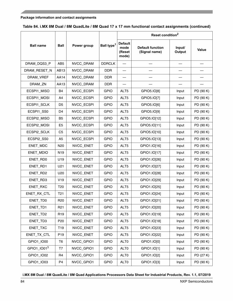
i.MX 8M Dual / 8M QuadLite / 8M Quad Applications Processors Data Sheet for Industrial Products, Rev. 1.1, 07/2019
84 NXP Semiconductors
Package information and contact assignments
DRAM_DQS3_P AB5 NVCC_DRAM DDRCLK — — — —
DRAM_RESET_N AB13 NVCC_DRAM DDR — — — —
DRAM_VREF AA14 NVCC_DRAM DDR — — — —
DRAM_ZN AA13 NVCC_DRAM DDR — — — —
ECSPI1_MISO B4 NVCC_ECSPI GPIO ALT5 GPIO5.IO[8] Input PD (90 K)
ECSPI1_MOSI A4 NVCC_ECSPI GPIO ALT5 GPIO5.IO[7] Input PD (90 K)
ECSPI1_SCLK D5 NVCC_ECSPI GPIO ALT5 GPIO5.IO[6] Input PD (90 K)
ECSPI1_SS0 D4 NVCC_ECSPI GPIO ALT5 GPIO5.IO[9] Input PD (90 K)
ECSPI2_MISO B5 NVCC_ECSPI GPIO ALT5 GPIO5.IO[12] Input PD (90 K)
ECSPI2_MOSI E5 NVCC_ECSPI GPIO ALT5 GPIO5.IO[11] Input PD (90 K)
ECSPI2_SCLK C5 NVCC_ECSPI GPIO ALT5 GPIO5.IO[10] Input PD (90 K)
ECSPI2_SS0 A5 NVCC_ECSPI GPIO ALT5 GPIO5.IO[13] Input PD (90 K)
ENET_MDC N20 NVCC_ENET GPIO ALT5 GPIO1.IO[16] Input PD (90 K)
ENET_MDIO N19 NVCC_ENET GPIO ALT5 GPIO1.IO[17] Input PD (90 K)
ENET_RD0 U19 NVCC_ENET GPIO ALT5 GPIO1.IO[26] Input PD (90 K)
ENET_RD1 U21 NVCC_ENET GPIO ALT5 GPIO1.IO[27] Input PD (90 K)
ENET_RD2 U20 NVCC_ENET GPIO ALT5 GPIO1.IO[28] Input PD (90 K)
ENET_RD3 V19 NVCC_ENET GPIO ALT5 GPIO1.IO[29] Input PD (90 K)
ENET_RXC T20 NVCC_ENET GPIO ALT5 GPIO1.IO[25] Input PD (90 K)
ENET_RX_CTL T21 NVCC_ENET GPIO ALT5 GPIO1.IO[24] Input PD (90 K)
ENET_TD0 R20 NVCC_ENET GPIO ALT5 GPIO1.IO[21] Input PD (90 K)
ENET_TD1 R21 NVCC_ENET GPIO ALT5 GPIO1.IO[20] Input PD (90 K)
ENET_TD2 R19 NVCC_ENET GPIO ALT5 GPIO1.IO[19] Input PD (90 K)
ENET_TD3 P20 NVCC_ENET GPIO ALT5 GPIO1.IO[18] Input PD (90 K)
ENET_TXC T19 NVCC_ENET GPIO ALT5 GPIO1.IO[23] Input PD (90 K)
ENET_TX_CTL P19 NVCC_ENET GPIO ALT5 GPIO1.IO[22] Input PD (90 K)
GPIO1_IO00 T6 NVCC_GPIO1 GPIO ALT0 GPIO1.IO[0] Input PD (90 K)
GPIO1_IO013 T7 NVCC_GPIO1 GPIO ALT0 GPIO1.IO[1] Input PD (90 K)
GPIO1_IO02 R4 NVCC_GPIO1 GPIO ALT0 GPIO1.IO[2] Input PD (27 K)
GPIO1_IO03 P4 NVCC_GPIO1 GPIO ALT0 GPIO1.IO[3] Input PD (90 K)
Table 84. i.MX 8M Dual / 8M QuadLite / 8M Quad 17 x 17 mm functional contact assignments (continued)
Ball name Ball Power group Ball type1
Reset condition2
Defaultmode(Reset mode)
Default function(Signal name)
Input/Output
Value

Package information and contact assignments
i.MX 8M Dual / 8M QuadLite / 8M Quad Applications Processors Data Sheet for Industrial Products, Rev. 1.1, 07/2019
NXP Semiconductors 85
GPIO1_IO04 P5 NVCC_GPIO1 GPIO ALT0 GPIO1.IO[4] Input PD (90 K)
GPIO1_IO054 P7 NVCC_GPIO1 GPIO ALT0 GPIO1.IO[5] Input PU (27 K)
GPIO1_IO06 N5 NVCC_GPIO1 GPIO ALT0 GPIO1.IO[6] Input PD (90 K)
GPIO1_IO07 N6 NVCC_GPIO1 GPIO ALT0 GPIO1.IO[7] Input PD (90 K)
GPIO1_IO08 N7 NVCC_GPIO1 GPIO ALT0 GPIO1.IO[8] Input PD (90 K)
GPIO1_IO09 M6 NVCC_GPIO1 GPIO ALT0 GPIO1.IO[9] Input PD (90 K)
GPIO1_IO10 M7 NVCC_GPIO1 GPIO ALT0 GPIO1.IO[10] Input PD (90 K)
GPIO1_IO11 L6 NVCC_GPIO1 GPIO ALT0 GPIO1.IO[11] Input PD (90 K)
GPIO1_IO12 L7 NVCC_GPIO1 GPIO ALT0 GPIO1.IO[12] Input PD (90 K)
GPIO1_IO13 K6 NVCC_GPIO1 GPIO ALT0 GPIO1.IO[13] Input PD (90 K)
GPIO1_IO14 K7 NVCC_GPIO1 GPIO ALT0 GPIO1.IO[14] Input PD (90 K)
GPIO1_IO15 J6 NVCC_GPIO1 GPIO ALT0 GPIO1.IO[15] Input PD (90 K)
HDMI_AUX_N V2 HDMI_AVDDIO PHY — — — —
HDMI_AUX_P V1 HDMI_AVDDIO PHY — — — —
HDMI_CEC W3 HDMI_AVDDIO PHY — — — —
HDMI_DDC_SCL R3 HDMI_AVDDIO PHY — — — —
HDMI_DDC_SDA P3 HDMI_AVDDIO PHY — — — —
HDMI_HPD W2 HDMI_AVDDIO PHY — — — —
HDMI_REFCLK_N R1 HDMI_AVDDIO PHY — — — —
HDMI_REFCLK_P R2 HDMI_AVDDIO PHY — — — —
HDMI_REXT P1 HDMI_AVDDIO PHY — — — —
HDMI_TX_M_LN_0 T2 HDMI_AVDDIO PHY — — — —
HDMI_TX_M_LN_1 U1 HDMI_AVDDIO PHY — — — —
HDMI_TX_M_LN_2 N1 HDMI_AVDDIO PHY — — — —
HDMI_TX_M_LN_3 M2 HDMI_AVDDIO PHY — — — —
HDMI_TX_P_LN_0 T1 HDMI_AVDDIO PHY — — — —
HDMI_TX_P_LN_1 U2 HDMI_AVDDIO PHY — — — —
HDMI_TX_P_LN_2 N2 HDMI_AVDDIO PHY — — — —
HDMI_TX_P_LN_3 M1 HDMI_AVDDIO PHY — — — —
I2C1_SCL E7 NVCC_I2C GPIO ALT5 GPIO5.IO[14] Input PD (90 K)
Table 84. i.MX 8M Dual / 8M QuadLite / 8M Quad 17 x 17 mm functional contact assignments (continued)
Ball name Ball Power group Ball type1
Reset condition2
Defaultmode(Reset mode)
Default function(Signal name)
Input/Output
Value
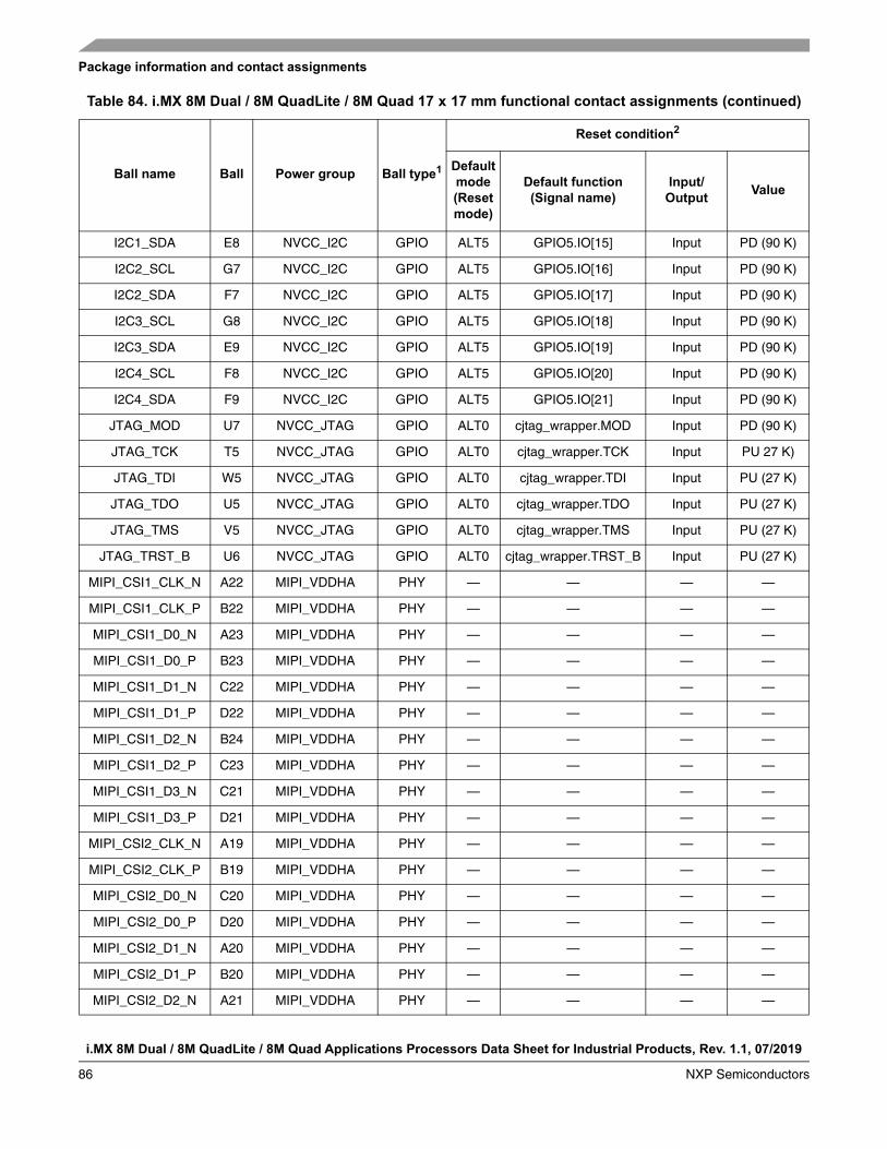
i.MX 8M Dual / 8M QuadLite / 8M Quad Applications Processors Data Sheet for Industrial Products, Rev. 1.1, 07/2019
86 NXP Semiconductors
Package information and contact assignments
I2C1_SDA E8 NVCC_I2C GPIO ALT5 GPIO5.IO[15] Input PD (90 K)
I2C2_SCL G7 NVCC_I2C GPIO ALT5 GPIO5.IO[16] Input PD (90 K)
I2C2_SDA F7 NVCC_I2C GPIO ALT5 GPIO5.IO[17] Input PD (90 K)
I2C3_SCL G8 NVCC_I2C GPIO ALT5 GPIO5.IO[18] Input PD (90 K)
I2C3_SDA E9 NVCC_I2C GPIO ALT5 GPIO5.IO[19] Input PD (90 K)
I2C4_SCL F8 NVCC_I2C GPIO ALT5 GPIO5.IO[20] Input PD (90 K)
I2C4_SDA F9 NVCC_I2C GPIO ALT5 GPIO5.IO[21] Input PD (90 K)
JTAG_MOD U7 NVCC_JTAG GPIO ALT0 cjtag_wrapper.MOD Input PD (90 K)
JTAG_TCK T5 NVCC_JTAG GPIO ALT0 cjtag_wrapper.TCK Input PU 27 K)
JTAG_TDI W5 NVCC_JTAG GPIO ALT0 cjtag_wrapper.TDI Input PU (27 K)
JTAG_TDO U5 NVCC_JTAG GPIO ALT0 cjtag_wrapper.TDO Input PU (27 K)
JTAG_TMS V5 NVCC_JTAG GPIO ALT0 cjtag_wrapper.TMS Input PU (27 K)
JTAG_TRST_B U6 NVCC_JTAG GPIO ALT0 cjtag_wrapper.TRST_B Input PU (27 K)
MIPI_CSI1_CLK_N A22 MIPI_VDDHA PHY — — — —
MIPI_CSI1_CLK_P B22 MIPI_VDDHA PHY — — — —
MIPI_CSI1_D0_N A23 MIPI_VDDHA PHY — — — —
MIPI_CSI1_D0_P B23 MIPI_VDDHA PHY — — — —
MIPI_CSI1_D1_N C22 MIPI_VDDHA PHY — — — —
MIPI_CSI1_D1_P D22 MIPI_VDDHA PHY — — — —
MIPI_CSI1_D2_N B24 MIPI_VDDHA PHY — — — —
MIPI_CSI1_D2_P C23 MIPI_VDDHA PHY — — — —
MIPI_CSI1_D3_N C21 MIPI_VDDHA PHY — — — —
MIPI_CSI1_D3_P D21 MIPI_VDDHA PHY — — — —
MIPI_CSI2_CLK_N A19 MIPI_VDDHA PHY — — — —
MIPI_CSI2_CLK_P B19 MIPI_VDDHA PHY — — — —
MIPI_CSI2_D0_N C20 MIPI_VDDHA PHY — — — —
MIPI_CSI2_D0_P D20 MIPI_VDDHA PHY — — — —
MIPI_CSI2_D1_N A20 MIPI_VDDHA PHY — — — —
MIPI_CSI2_D1_P B20 MIPI_VDDHA PHY — — — —
MIPI_CSI2_D2_N A21 MIPI_VDDHA PHY — — — —
Table 84. i.MX 8M Dual / 8M QuadLite / 8M Quad 17 x 17 mm functional contact assignments (continued)
Ball name Ball Power group Ball type1
Reset condition2
Defaultmode(Reset mode)
Default function(Signal name)
Input/Output
Value
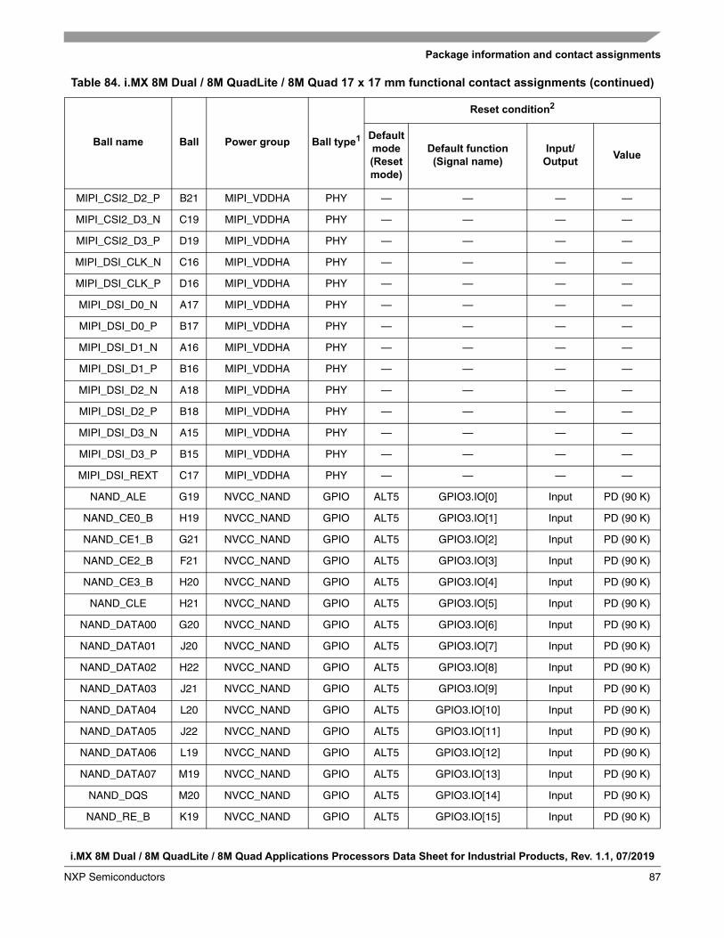
Package information and contact assignments
i.MX 8M Dual / 8M QuadLite / 8M Quad Applications Processors Data Sheet for Industrial Products, Rev. 1.1, 07/2019
NXP Semiconductors 87
MIPI_CSI2_D2_P B21 MIPI_VDDHA PHY — — — —
MIPI_CSI2_D3_N C19 MIPI_VDDHA PHY — — — —
MIPI_CSI2_D3_P D19 MIPI_VDDHA PHY — — — —
MIPI_DSI_CLK_N C16 MIPI_VDDHA PHY — — — —
MIPI_DSI_CLK_P D16 MIPI_VDDHA PHY — — — —
MIPI_DSI_D0_N A17 MIPI_VDDHA PHY — — — —
MIPI_DSI_D0_P B17 MIPI_VDDHA PHY — — — —
MIPI_DSI_D1_N A16 MIPI_VDDHA PHY — — — —
MIPI_DSI_D1_P B16 MIPI_VDDHA PHY — — — —
MIPI_DSI_D2_N A18 MIPI_VDDHA PHY — — — —
MIPI_DSI_D2_P B18 MIPI_VDDHA PHY — — — —
MIPI_DSI_D3_N A15 MIPI_VDDHA PHY — — — —
MIPI_DSI_D3_P B15 MIPI_VDDHA PHY — — — —
MIPI_DSI_REXT C17 MIPI_VDDHA PHY — — — —
NAND_ALE G19 NVCC_NAND GPIO ALT5 GPIO3.IO[0] Input PD (90 K)
NAND_CE0_B H19 NVCC_NAND GPIO ALT5 GPIO3.IO[1] Input PD (90 K)
NAND_CE1_B G21 NVCC_NAND GPIO ALT5 GPIO3.IO[2] Input PD (90 K)
NAND_CE2_B F21 NVCC_NAND GPIO ALT5 GPIO3.IO[3] Input PD (90 K)
NAND_CE3_B H20 NVCC_NAND GPIO ALT5 GPIO3.IO[4] Input PD (90 K)
NAND_CLE H21 NVCC_NAND GPIO ALT5 GPIO3.IO[5] Input PD (90 K)
NAND_DATA00 G20 NVCC_NAND GPIO ALT5 GPIO3.IO[6] Input PD (90 K)
NAND_DATA01 J20 NVCC_NAND GPIO ALT5 GPIO3.IO[7] Input PD (90 K)
NAND_DATA02 H22 NVCC_NAND GPIO ALT5 GPIO3.IO[8] Input PD (90 K)
NAND_DATA03 J21 NVCC_NAND GPIO ALT5 GPIO3.IO[9] Input PD (90 K)
NAND_DATA04 L20 NVCC_NAND GPIO ALT5 GPIO3.IO[10] Input PD (90 K)
NAND_DATA05 J22 NVCC_NAND GPIO ALT5 GPIO3.IO[11] Input PD (90 K)
NAND_DATA06 L19 NVCC_NAND GPIO ALT5 GPIO3.IO[12] Input PD (90 K)
NAND_DATA07 M19 NVCC_NAND GPIO ALT5 GPIO3.IO[13] Input PD (90 K)
NAND_DQS M20 NVCC_NAND GPIO ALT5 GPIO3.IO[14] Input PD (90 K)
NAND_RE_B K19 NVCC_NAND GPIO ALT5 GPIO3.IO[15] Input PD (90 K)
Table 84. i.MX 8M Dual / 8M QuadLite / 8M Quad 17 x 17 mm functional contact assignments (continued)
Ball name Ball Power group Ball type1
Reset condition2
Defaultmode(Reset mode)
Default function(Signal name)
Input/Output
Value
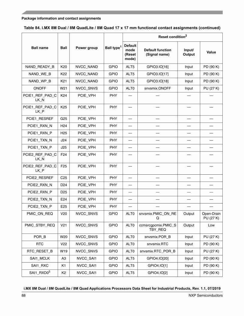
i.MX 8M Dual / 8M QuadLite / 8M Quad Applications Processors Data Sheet for Industrial Products, Rev. 1.1, 07/2019
88 NXP Semiconductors
Package information and contact assignments
NAND_READY_B K20 NVCC_NAND GPIO ALT5 GPIO3.IO[16] Input PD (90 K)
NAND_WE_B K22 NVCC_NAND GPIO ALT5 GPIO3.IO[17] Input PD (90 K)
NAND_WP_B K21 NVCC_NAND GPIO ALT5 GPIO3.IO[18] Input PD (90 K)
ONOFF W21 NVCC_SNVS GPIO ALT0 snvsmix.ONOFF Input PU (27 K)
PCIE1_REF_PAD_CLK_N
K24 PCIE_VPH PHY — — — —
PCIE1_REF_PAD_CLK_P
K25 PCIE_VPH PHY — — — —
PCIE1_RESREF G25 PCIE_VPH PHY — — — —
PCIE1_RXN_N H24 PCIE_VPH PHY — — — —
PCIE1_RXN_P H25 PCIE_VPH PHY — — — —
PCIE1_TXN_N J24 PCIE_VPH PHY — — — —
PCIE1_TXN_P J25 PCIE_VPH PHY — — — —
PCIE2_REF_PAD_CLK_N
F24 PCIE_VPH PHY — — — —
PCIE2_REF_PAD_CLK_P
F25 PCIE_VPH PHY — — — —
PCIE2_RESREF C25 PCIE_VPH PHY — — — —
PCIE2_RXN_N D24 PCIE_VPH PHY — — — —
PCIE2_RXN_P D25 PCIE_VPH PHY — — — —
PCIE2_TXN_N E24 PCIE_VPH PHY — — — —
PCIE2_TXN_P E25 PCIE_VPH PHY — — — —
PMIC_ON_REQ V20 NVCC_SNVS GPIO ALT0 snvsmix.PMIC_ON_REQ
Output Open-DrainPU (27 K)
PMIC_STBY_REQ V21 NVCC_SNVS GPIO ALT0 ccmsrcgpcmix.PMIC_STBY_REQ
Output Low
POR_B W20 NVCC_SNVS GPIO ALT0 snvsmix.POR_B Input PU (27 K)
RTC V22 NVCC_SNVS GPIO ALT0 snvsmix.RTC Input PD (90 K)
RTC_RESET_B W19 NVCC_SNVS GPIO ALT0 snvsmix.RTC_POR_B Input PU (27 K)
SAI1_MCLK A3 NVCC_SAI1 GPIO ALT5 GPIO4.IO[20] Input PD (90 K)
SAI1_RXC K1 NVCC_SAI1 GPIO ALT5 GPIO4.IO[1] Input PD (90 K)
SAI1_RXD05 K2 NVCC_SAI1 GPIO ALT5 GPIO4.IO[2] Input PD (90 K)
Table 84. i.MX 8M Dual / 8M QuadLite / 8M Quad 17 x 17 mm functional contact assignments (continued)
Ball name Ball Power group Ball type1
Reset condition2
Defaultmode(Reset mode)
Default function(Signal name)
Input/Output
Value

Package information and contact assignments
i.MX 8M Dual / 8M QuadLite / 8M Quad Applications Processors Data Sheet for Industrial Products, Rev. 1.1, 07/2019
NXP Semiconductors 89
SAI1_RXD15 L2 NVCC_SAI1 GPIO ALT5 GPIO4.IO[3] Input PD (90 K)
SAI1_RXD25 H2 NVCC_SAI1 GPIO ALT5 GPIO4.IO[4] Input PD (90 K)
SAI1_RXD35 J2 NVCC_SAI1 GPIO ALT5 GPIO4.IO[5] Input PD (90 K)
SAI1_RXD45 J1 NVCC_SAI1 GPIO ALT5 GPIO4.IO[6] Input PD (90 K)
SAI1_RXD55 F1 NVCC_SAI1 GPIO ALT5 GPIO4.IO[7] Input PD (90 K)
SAI1_RXD65 G2 NVCC_SAI1 GPIO ALT5 GPIO4.IO[8] Input PD (90 K)
SAI1_RXD75 G1 NVCC_SAI1 GPIO ALT5 GPIO4.IO[9] Input PD (90 K)
SAI1_RXFS L1 NVCC_SAI1 GPIO ALT5 GPIO4.IO[0] Input PD (90 K)
SAI1_TXC E1 NVCC_SAI1 GPIO ALT5 GPIO4.IO[11] Input PD (90 K)
SAI1_TXD05 F2 NVCC_SAI1 GPIO ALT5 GPIO4.IO[12] Input PD (90 K)
SAI1_TXD15 E2 NVCC_SAI1 GPIO ALT5 GPIO4.IO[13] Input PD (90 K)
SAI1_TXD25 B2 NVCC_SAI1 GPIO ALT5 GPIO4.IO[14] Input PD (90 K)
SAI1_TXD35 D1 NVCC_SAI1 GPIO ALT5 GPIO4.IO[15] Input PD (90 K)
SAI1_TXD45 D2 NVCC_SAI1 GPIO ALT5 GPIO4.IO[16] Input PD (90 K)
SAI1_TXD55 C2 NVCC_SAI1 GPIO ALT5 GPIO4.IO[17] Input PD (90 K)
SAI1_TXD65 B3 NVCC_SAI1 GPIO ALT5 GPIO4.IO[18] Input PD (90 K)
SAI1_TXD75 C1 NVCC_SAI1 GPIO ALT5 GPIO4.IO[19] Input PD (90 K)
SAI1_TXFS H1 NVCC_SAI1 GPIO ALT5 GPIO4.IO[10] Input PD (90 K)
SAI2_MCLK H5 NVCC_SAI2 GPIO ALT5 GPIO4.IO[27] Input PD (90 K)
SAI2_RXC H3 NVCC_SAI2 GPIO ALT5 GPIO4.IO[22] Input PD (90 K)
SAI2_RXD0 H6 NVCC_SAI2 GPIO ALT5 GPIO4.IO[23] Input PD (90 K)
SAI2_RXFS J4 NVCC_SAI2 GPIO ALT5 GPIO4.IO[21] Input PD (90 K)
SAI2_TXC J5 NVCC_SAI2 GPIO ALT5 GPIO4.IO[25] Input PD (90 K)
SAI2_TXD0 G5 NVCC_SAI2 GPIO ALT5 GPIO4.IO[26] Input PD (90 K)
SAI2_TXFS H4 NVCC_SAI2 GPIO ALT5 GPIO4.IO[24] Input PD (90 K)
SAI3_MCLK D3 NVCC_SAI3 GPIO ALT5 GPIO5.IO[2] Input PD (90 K)
SAI3_RXC F4 NVCC_SAI3 GPIO ALT5 GPIO4.IO[29] Input PD (90 K)
SAI3_RXD F3 NVCC_SAI3 GPIO ALT5 GPIO4.IO[30] Input PD (90 K)
SAI3_RXFS G4 NVCC_SAI3 GPIO ALT5 GPIO4.IO[28] Input PD (90 K)
SAI3_TXC C4 NVCC_SAI3 GPIO ALT5 GPIO5.IO[0] Input PD (90 K)
Table 84. i.MX 8M Dual / 8M QuadLite / 8M Quad 17 x 17 mm functional contact assignments (continued)
Ball name Ball Power group Ball type1
Reset condition2
Defaultmode(Reset mode)
Default function(Signal name)
Input/Output
Value

i.MX 8M Dual / 8M QuadLite / 8M Quad Applications Processors Data Sheet for Industrial Products, Rev. 1.1, 07/2019
90 NXP Semiconductors
Package information and contact assignments
SAI3_TXD C3 NVCC_SAI3 GPIO ALT5 GPIO5.IO[1] Input PD (90 K)
SAI3_TXFS G3 NVCC_SAI3 GPIO ALT5 GPIO4.IO[31] Input PD (90 K)
SAI5_MCLK K4 NVCC_SAI5 GPIO ALT5 GPIO3.IO[25] Input PD (90 K)
SAI5_RXC L5 NVCC_SAI5 GPIO ALT5 GPIO3.IO[20] Input PD (90 K)
SAI5_RXD0 M5 NVCC_SAI5 GPIO ALT5 GPIO3.IO[21] Input PD (90 K)
SAI5_RXD1 L4 NVCC_SAI5 GPIO ALT5 GPIO3.IO[22] Input PD (90 K)
SAI5_RXD2 M4 NVCC_SAI5 GPIO ALT5 GPIO3.IO[23] Input PD (90 K)
SAI5_RXD3 K5 NVCC_SAI5 GPIO ALT5 GPIO3.IO[24] Input PD (90 K)
SAI5_RXFS N4 NVCC_SAI5 GPIO ALT5 GPIO3.IO[19] Input PD (90 K)
SD1_CLK L25 NVCC_SD1 GPIO ALT5 GPIO2.IO[0] Input PD (90 K)
SD1_CMD L24 NVCC_SD1 GPIO ALT5 GPIO2.IO[1] Input PD (90 K)
SD1_DATA0 M25 NVCC_SD1 GPIO ALT5 GPIO2.IO[2] Input PD (90 K)
SD1_DATA1 M24 NVCC_SD1 GPIO ALT5 GPIO2.IO[3] Input PD (90 K)
SD1_DATA2 N25 NVCC_SD1 GPIO ALT5 GPIO2.IO[4] Input PD (90 K)
SD1_DATA3 P25 NVCC_SD1 GPIO ALT5 GPIO2.IO[5] Input PD (90 K)
SD1_DATA4 N24 NVCC_SD1 GPIO ALT5 GPIO2.IO[6] Input PD (90 K)
SD1_DATA5 P24 NVCC_SD1 GPIO ALT5 GPIO2.IO[7] Input PD (90 K)
SD1_DATA6 R25 NVCC_SD1 GPIO ALT5 GPIO2.IO[8] Input PD (90 K)
SD1_DATA7 T25 NVCC_SD1 GPIO ALT5 GPIO2.IO[9] Input PD (90 K)
SD1_RESET_B R24 NVCC_SD1 GPIO ALT5 GPIO2.IO[10] Input PD (90 K)
SD1_STROBE T24 NVCC_SD1 GPIO ALT5 GPIO2.IO[11] Input PD (90 K)
SD2_CD_B L21 NVCC_SD2 GPIO ALT5 GPIO2.IO[12] Input PD (90 K)
SD2_CLK L22 NVCC_SD2 GPIO ALT5 GPIO2.IO[13] Input PD (90 K)
SD2_CMD M22 NVCC_SD2 GPIO ALT5 GPIO2.IO[14] Input PD (90 K)
SD2_DATA0 N22 NVCC_SD2 GPIO ALT5 GPIO2.IO[15] Input PD (90 K)
SD2_DATA1 N21 NVCC_SD2 GPIO ALT5 GPIO2.IO[16] Input PD (90 K)
SD2_DATA2 P22 NVCC_SD2 GPIO ALT5 GPIO2.IO[17] Input PD (90 K)
SD2_DATA3 P21 NVCC_SD2 GPIO ALT5 GPIO2.IO[18] Input PD (90 K)
SD2_RESET_B R22 NVCC_SD2 GPIO ALT5 GPIO2.IO[19] Input PD (90 K)
SD2_WP M21 NVCC_SD2 GPIO ALT5 GPIO2.IO[20] Input PD (90 K)
Table 84. i.MX 8M Dual / 8M QuadLite / 8M Quad 17 x 17 mm functional contact assignments (continued)
Ball name Ball Power group Ball type1
Reset condition2
Defaultmode(Reset mode)
Default function(Signal name)
Input/Output
Value

Package information and contact assignments
i.MX 8M Dual / 8M QuadLite / 8M Quad Applications Processors Data Sheet for Industrial Products, Rev. 1.1, 07/2019
NXP Semiconductors 91
SPDIF_EXT_CLK E6 NVCC_SAI3 GPIO ALT5 GPIO5.IO[5] Input PD (90 K)
SPDIF_RX G6 NVCC_SAI3 GPIO ALT5 GPIO5.IO[4] Input PD (90 K)
SPDIF_TX F6 NVCC_SAI3 GPIO ALT5 GPIO5.IO[3] Input PD (90 K)
TEST_MODE V7 NVCC_JTAG GPIO ALT0 tcu.TEST_MODE Input PD (90 K)
UART1_RXD C7 NVCC_UART GPIO ALT5 GPIO5.IO[22] Input PD (90 K)
UART1_TXD A7 NVCC_UART GPIO ALT5 GPIO5.IO[23] Input PD (90 K)
UART2_RXD B6 NVCC_UART GPIO ALT5 GPIO5.IO[24] Input PD (90 K)
UART2_TXD D6 NVCC_UART GPIO ALT5 GPIO5.IO[25] Input PD (90 K)
UART3_RXD A6 NVCC_UART GPIO ALT5 GPIO5.IO[26] Input PD (90 K)
UART3_TXD B7 NVCC_UART GPIO ALT5 GPIO5.IO[27] Input PD (90 K)
UART4_RXD C6 NVCC_UART GPIO ALT5 GPIO5.IO[28] Input PD (90 K)
UART4_TXD D7 NVCC_UART GPIO ALT5 GPIO5.IO[29] Input PD (90 K)
USB1_DN B14 USB1_VDD33 PHY — — — —
USB1_DP A14 USB1_VDD33 PHY — — — —
USB1_ID C14 USB1_VDD33 PHY — — — —
USB1_RESREF A11 USB1_VPH PHY — — — —
USB1_RX_N B12 USB1_VPH PHY — — — —
USB1_RX_P A12 USB1_VPH PHY — — — —
USB1_TX_N B13 USB1_VPH PHY — — — —
USB1_TX_P A13 USB1_VPH PHY — — — —
USB1_VBUS D14 USB1_VDD33 PHY — — — —
USB2_DN B10 USB2_VDD33 PHY — — — —
USB2_DP A10 USB2_VDD33 PHY — — — —
USB2_ID C9 USB2_VDD33 PHY — — — —
USB2_RESREF B11 USB2_VPH PHY — — — —
USB2_RX_N B8 USB2_VPH PHY — — — —
USB2_RX_P A8 USB2_VPH PHY — — — —
USB2_TX_N B9 USB2_VPH PHY — — — —
USB2_TX_P A9 USB2_VPH PHY — — — —
USB2_VBUS D9 USB2_VDD33 PHY — — — —
Table 84. i.MX 8M Dual / 8M QuadLite / 8M Quad 17 x 17 mm functional contact assignments (continued)
Ball name Ball Power group Ball type1
Reset condition2
Defaultmode(Reset mode)
Default function(Signal name)
Input/Output
Value
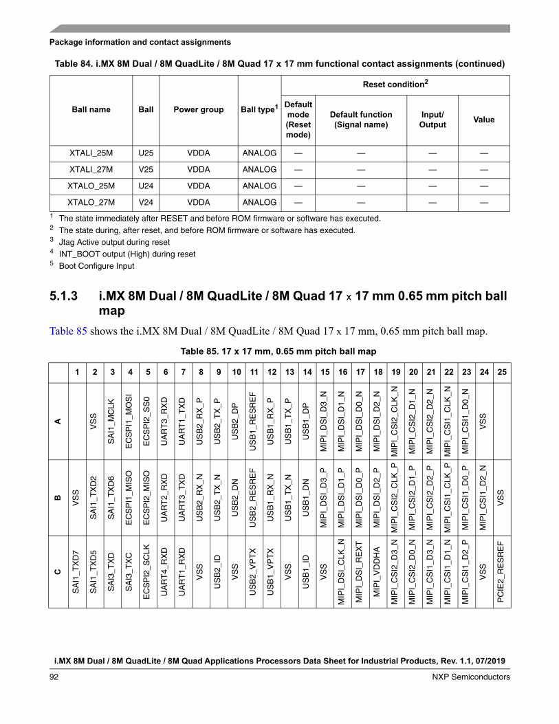
i.MX 8M Dual / 8M QuadLite / 8M Quad Applications Processors Data Sheet for Industrial Products, Rev. 1.1, 07/2019
92 NXP Semiconductors
Package information and contact assignments
5.1.3 i.MX 8M Dual / 8M QuadLite / 8M Quad 17 x 17 mm 0.65 mm pitch ball map
Table 85 shows the i.MX 8M Dual / 8M QuadLite / 8M Quad 17 x 17 mm, 0.65 mm pitch ball map.
XTALI_25M U25 VDDA ANALOG — — — —
XTALI_27M V25 VDDA ANALOG — — — —
XTALO_25M U24 VDDA ANALOG — — — —
XTALO_27M V24 VDDA ANALOG — — — —
1 The state immediately after RESET and before ROM firmware or software has executed.2 The state during, after reset, and before ROM firmware or software has executed.3 Jtag Active output during reset4 INT_BOOT output (High) during reset5 Boot Configure Input
Table 85. 17 x 17 mm, 0.65 mm pitch ball map
1 2 3 4 5 6 7 8 9 10 11 12 13 14 15 16 17 18 19 20 21 22 23 24 25
A
VS
S
SA
I1_M
CLK
EC
SP
I1_M
OS
I
EC
SP
I2_S
S0
UA
RT
3_R
XD
UA
RT
1_T
XD
US
B2_
RX
_P
US
B2_
TX
_P
US
B2_
DP
US
B1_
RE
SR
EF
US
B1_
RX
_P
US
B1_
TX
_P
US
B1_
DP
MIP
I_D
SI_
D3_
N
MIP
I_D
SI_
D1_
N
MIP
I_D
SI_
D0_
N
MIP
I_D
SI_
D2_
N
MIP
I_C
SI2
_CLK
_N
MIP
I_C
SI2
_D1_
N
MIP
I_C
SI2
_D2_
N
MIP
I_C
SI1
_CLK
_N
MIP
I_C
SI1
_D0_
N
VS
S
B
VS
S
SA
I1_T
XD
2
SA
I1_T
XD
6
EC
SP
I1_M
ISO
EC
SP
I2_M
ISO
UA
RT
2_R
XD
UA
RT
3_T
XD
US
B2_
RX
_N
US
B2_
TX
_N
US
B2_
DN
US
B2_
RE
SR
EF
US
B1_
RX
_N
US
B1_
TX
_N
US
B1_
DN
MIP
I_D
SI_
D3_
P
MIP
I_D
SI_
D1_
P
MIP
I_D
SI_
D0_
P
MIP
I_D
SI_
D2_
P
MIP
I_C
SI2
_CLK
_P
MIP
I_C
SI2
_D1_
P
MIP
I_C
SI2
_D2_
P
MIP
I_C
SI1
_CLK
_P
MIP
I_C
SI1
_D0_
P
MIP
I_C
SI1
_D2_
N
VS
S
C
SA
I1_T
XD
7
SA
I1_T
XD
5
SA
I3_T
XD
SA
I3_T
XC
EC
SP
I2_S
CLK
UA
RT
4_R
XD
UA
RT
1_R
XD
VS
S
US
B2_
ID
VS
S
US
B2_
VP
TX
US
B1_
VP
TX
VS
S
US
B1_
ID
VS
S
MIP
I_D
SI_
CLK
_N
MIP
I_D
SI_
RE
XT
MIP
I_V
DD
HA
MIP
I_C
SI2
_D3_
N
MIP
I_C
SI2
_D0_
N
MIP
I_C
SI1
_D3_
N
MIP
I_C
SI1
_D1_
N
MIP
I_C
SI1
_D2_
P
VS
S
PC
IE2_
RE
SR
EF
Table 84. i.MX 8M Dual / 8M QuadLite / 8M Quad 17 x 17 mm functional contact assignments (continued)
Ball name Ball Power group Ball type1
Reset condition2
Defaultmode(Reset mode)
Default function(Signal name)
Input/Output
Value

Package information and contact assignments
i.MX 8M Dual / 8M QuadLite / 8M Quad Applications Processors Data Sheet for Industrial Products, Rev. 1.1, 07/2019
NXP Semiconductors 93
D
SA
I1_T
XD
3
SA
I1_T
XD
4
SA
I3_M
CLK
EC
SP
I1_S
S0
EC
SP
I1_S
CLK
UA
RT
2_T
XD
UA
RT
4_T
XD
NV
CC
_UA
RT
US
B2_
VB
US
VS
S
US
B2_
VP
US
B1_
VP
VS
S
US
B1_
VB
US
VS
S
MIP
I_D
SI_
CLK
_P
MIP
I_V
DD
HA
MIP
I_V
DD
HA
MIP
I_C
SI2
_D3_
P
MIP
I_C
SI2
_D0_
P
MIP
I_C
SI1
_D3_
P
MIP
I_C
SI1
_D1_
P
VS
S
PC
IE2_
RX
N_N
PC
IE2_
RX
N_P
E
SA
I1_T
XC
SA
I1_T
XD
1
NV
CC
_SA
I3
VS
S
EC
SP
I2_M
OS
I
SP
DIF
_EX
T_C
LK
I2C
1_S
CL
I2C
1_S
DA
I2C
3_S
DA
VS
S
US
B2_
DV
DD
US
B1_
DV
DD
VS
S
VS
S
MIP
I_V
DD
VS
S
MIP
I_V
DD
A
MIP
I_V
DD
A
VS
S
VS
S
VS
S
VS
S
VS
S
PC
IE2_
TX
N_N
PC
IE2_
TX
N_P
F
SA
I1_R
XD
5
SA
I1_T
XD
0
SA
I3_R
XD
SA
I3_R
XC
NV
CC
_EC
SP
I
SP
DIF
_TX
I2C
2_S
DA
I2C
4_S
CL
I2C
4_S
DA
VS
S
US
B2_
VP
H
US
B1_
VP
H
VS
S
VS
S
MIP
I_V
DD
VS
S
MIP
I_V
DD
A
MIP
I_V
DD
A
MIP
I_V
DD
PLL
VS
S
NA
ND
_CE
2_B
PC
IE_V
P
PC
IE_V
PT
X
PC
IE2_
RE
F_P
AD
_CLK
_N
PC
IE2_
RE
F_P
AD
_CLK
_P
G
SA
I1_R
XD
7
SA
I1_R
XD
6
SA
I3_T
XF
S
SA
I3_R
XF
S
SA
I2_T
XD
0
SP
DIF
_RX
I2C
2_S
CL
I2C
3_S
CL
VS
S
VS
S
US
B2_
VD
D33
US
B1_
VD
D33
VS
S
VD
D_A
RM
VD
D_A
RM
VD
D_A
RM
VS
S
VS
S
NA
ND
_ALE
NA
ND
_DA
TA
00
NA
ND
_CE
1_B
PC
IE_V
P
PC
IE_V
PT
X
VS
S
PC
IE1_
RE
SR
EF
H
SA
I1_T
XF
S
SA
I1_R
XD
2
SA
I2_R
XC
SA
I2_T
XF
S
SA
I2_M
CLK
SA
I2_R
XD
0
NV
CC
_I2C
VS
S
VS
S
VS
S
VS
S
VS
S
VS
S
VD
D_A
RM
VD
D_A
RM
VD
D_A
RM
VS
S
VS
S
NA
ND
_CE
0_B
NA
ND
_CE
3_B
NA
ND
_CLE
NA
ND
_DA
TA
02
PC
IE_V
PH
PC
IE1_
RX
N_N
PC
IE1_
RX
N_P
J
SA
I1_R
XD
4
SA
I1_R
XD
3
VS
S
SA
I2_R
XF
S
SA
I2_T
XC
GP
IO1_
IO15
NV
CC
_SA
I2
VS
S
VD
D_G
PU
VD
D_G
PU
VS
S
VS
S
VS
S
VS
S
VD
D_A
RM
VD
D_A
RM
VS
S
VS
S
VS
S
NA
ND
_DA
TA
01
NA
ND
_DA
TA
03
NA
ND
_DA
TA
05
PC
IE_V
PH
PC
IE1_
TX
N_N
PC
IE1_
TX
N_P
Table 85. 17 x 17 mm, 0.65 mm pitch ball map (continued)
1 2 3 4 5 6 7 8 9 10 11 12 13 14 15 16 17 18 19 20 21 22 23 24 25
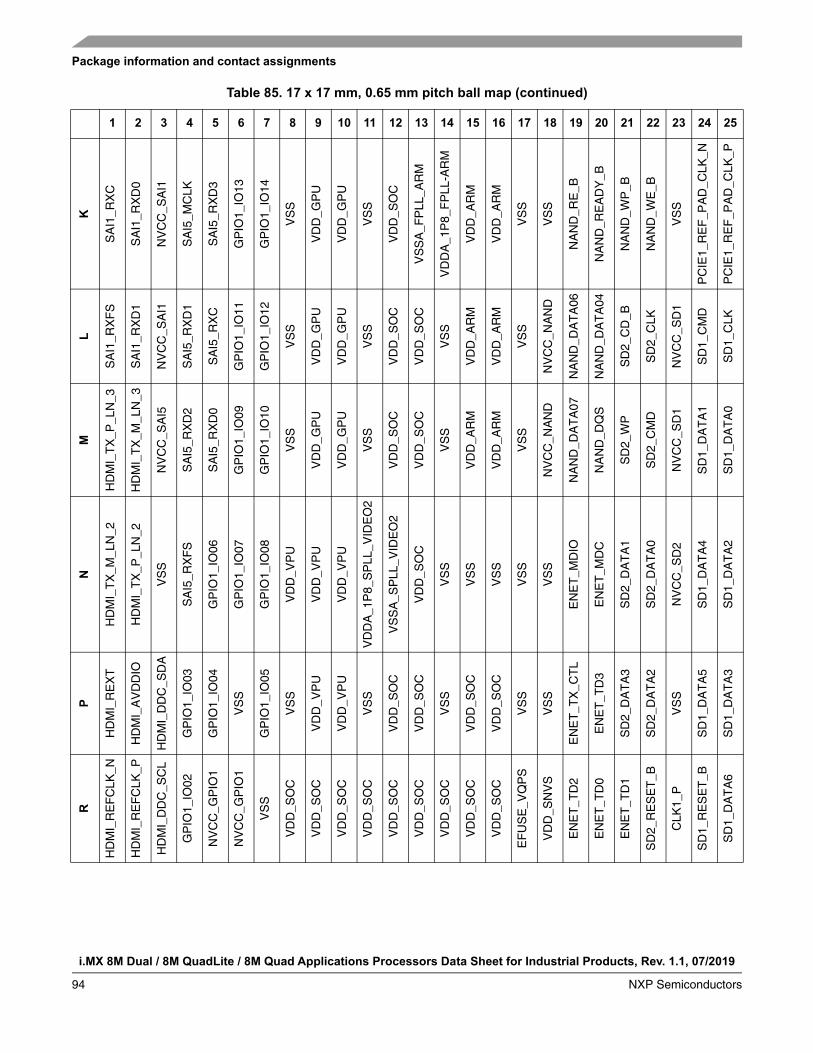
i.MX 8M Dual / 8M QuadLite / 8M Quad Applications Processors Data Sheet for Industrial Products, Rev. 1.1, 07/2019
94 NXP Semiconductors
Package information and contact assignments
K
SA
I1_R
XC
SA
I1_R
XD
0
NV
CC
_SA
I1
SA
I5_M
CLK
SA
I5_R
XD
3
GP
IO1_
IO13
GP
IO1_
IO14
VS
S
VD
D_G
PU
VD
D_G
PU
VS
S
VD
D_S
OC
VS
SA
_FP
LL_A
RM
VD
DA
_1P
8_F
PLL
-AR
M
VD
D_A
RM
VD
D_A
RM
VS
S
VS
S
NA
ND
_RE
_B
NA
ND
_RE
AD
Y_B
NA
ND
_WP
_B
NA
ND
_WE
_B
VS
S
PC
IE1_
RE
F_P
AD
_CLK
_N
PC
IE1_
RE
F_P
AD
_CLK
_P
L
SA
I1_R
XF
S
SA
I1_R
XD
1
NV
CC
_SA
I1
SA
I5_R
XD
1
SA
I5_R
XC
GP
IO1_
IO11
GP
IO1_
IO12
VS
S
VD
D_G
PU
VD
D_G
PU
VS
S
VD
D_S
OC
VD
D_S
OC
VS
S
VD
D_A
RM
VD
D_A
RM
VS
S
NV
CC
_NA
ND
NA
ND
_DA
TA
06
NA
ND
_DA
TA
04
SD
2_C
D_B
SD
2_C
LK
NV
CC
_SD
1
SD
1_C
MD
SD
1_C
LK
M
HD
MI_
TX
_P_L
N_3
HD
MI_
TX
_M_L
N_3
NV
CC
_SA
I5
SA
I5_R
XD
2
SA
I5_R
XD
0
GP
IO1_
IO09
GP
IO1_
IO10
VS
S
VD
D_G
PU
VD
D_G
PU
VS
S
VD
D_S
OC
VD
D_S
OC
VS
S
VD
D_A
RM
VD
D_A
RM
VS
S
NV
CC
_NA
ND
NA
ND
_DA
TA
07
NA
ND
_DQ
S
SD
2_W
P
SD
2_C
MD
NV
CC
_SD
1
SD
1_D
AT
A1
SD
1_D
AT
A0
N
HD
MI_
TX
_M_L
N_2
HD
MI_
TX
_P_L
N_2
VS
S
SA
I5_R
XF
S
GP
IO1_
IO06
GP
IO1_
IO07
GP
IO1_
IO08
VD
D_V
PU
VD
D_V
PU
VD
D_V
PU
VD
DA
_1P
8_S
PLL
_VID
EO
2
VS
SA
_SP
LL_V
IDE
O2
VD
D_S
OC
VS
S
VS
S
VS
S
VS
S
VS
S
EN
ET
_MD
IO
EN
ET
_MD
C
SD
2_D
AT
A1
SD
2_D
AT
A0
NV
CC
_SD
2
SD
1_D
AT
A4
SD
1_D
AT
A2
P
HD
MI_
RE
XT
HD
MI_
AV
DD
IO
HD
MI_
DD
C_S
DA
GP
IO1_
IO03
GP
IO1_
IO04
VS
S
GP
IO1_
IO05
VS
S
VD
D_V
PU
VD
D_V
PU
VS
S
VD
D_S
OC
VD
D_S
OC
VS
S
VD
D_S
OC
VD
D_S
OC
VS
S
VS
S
EN
ET
_TX
_CT
L
EN
ET
_TD
3
SD
2_D
AT
A3
SD
2_D
AT
A2
VS
S
SD
1_D
AT
A5
SD
1_D
AT
A3
R
HD
MI_
RE
FC
LK_N
HD
MI_
RE
FC
LK_P
HD
MI_
DD
C_S
CL
GP
IO1_
IO02
NV
CC
_GP
IO1
NV
CC
_GP
IO1
VS
S
VD
D_S
OC
VD
D_S
OC
VD
D_S
OC
VD
D_S
OC
VD
D_S
OC
VD
D_S
OC
VD
D_S
OC
VD
D_S
OC
VD
D_S
OC
EF
US
E_V
QP
S
VD
D_S
NV
S
EN
ET
_TD
2
EN
ET
_TD
0
EN
ET
_TD
1
SD
2_R
ES
ET
_B
CLK
1_P
SD
1_R
ES
ET
_B
SD
1_D
AT
A6
Table 85. 17 x 17 mm, 0.65 mm pitch ball map (continued)
1 2 3 4 5 6 7 8 9 10 11 12 13 14 15 16 17 18 19 20 21 22 23 24 25
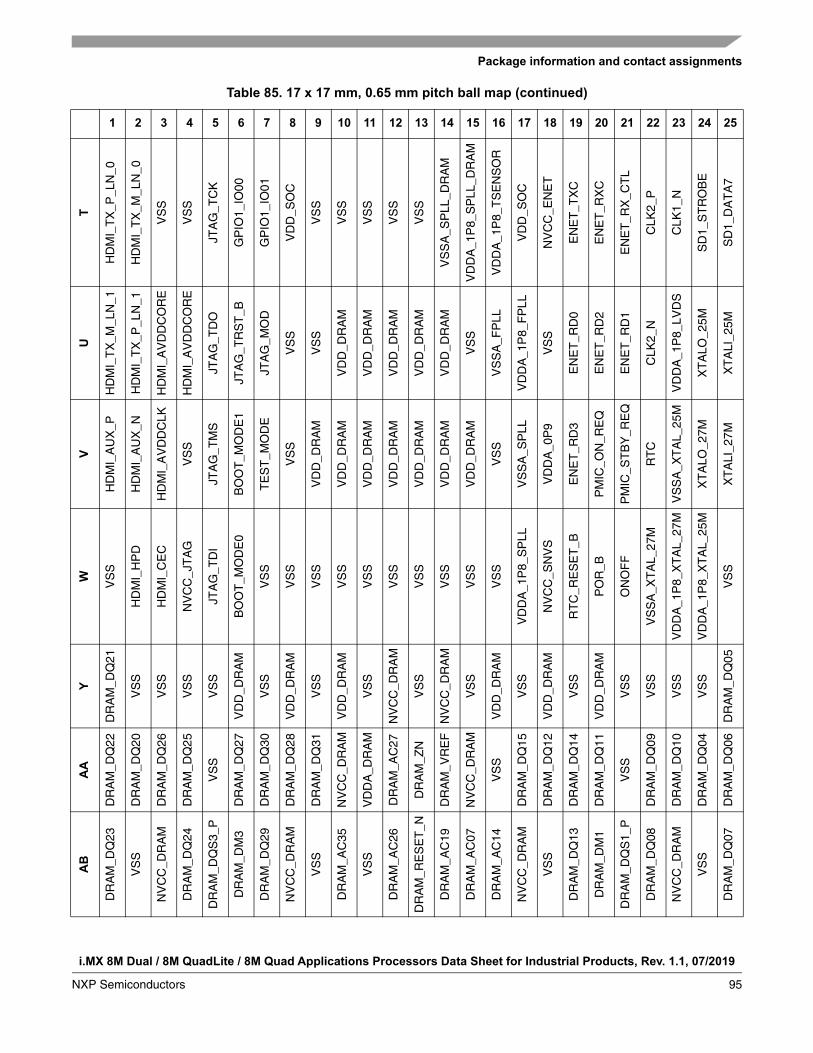
Package information and contact assignments
i.MX 8M Dual / 8M QuadLite / 8M Quad Applications Processors Data Sheet for Industrial Products, Rev. 1.1, 07/2019
NXP Semiconductors 95
T
HD
MI_
TX
_P_L
N_0
HD
MI_
TX
_M_L
N_0
VS
S
VS
S
JTA
G_T
CK
GP
IO1_
IO00
GP
IO1_
IO01
VD
D_S
OC
VS
S
VS
S
VS
S
VS
S
VS
S
VS
SA
_SP
LL_D
RA
M
VD
DA
_1P
8_S
PLL
_DR
AM
VD
DA
_1P
8_T
SE
NS
OR
VD
D_S
OC
NV
CC
_EN
ET
EN
ET
_TX
C
EN
ET
_RX
C
EN
ET
_RX
_CT
L
CLK
2_P
CLK
1_N
SD
1_S
TR
OB
E
SD
1_D
AT
A7
U
HD
MI_
TX
_M_L
N_1
HD
MI_
TX
_P_L
N_1
HD
MI_
AV
DD
CO
RE
HD
MI_
AV
DD
CO
RE
JTA
G_T
DO
JTA
G_T
RS
T_B
JTA
G_M
OD
VS
S
VS
S
VD
D_D
RA
M
VD
D_D
RA
M
VD
D_D
RA
M
VD
D_D
RA
M
VD
D_D
RA
M
VS
S
VS
SA
_FP
LL
VD
DA
_1P
8_F
PLL
VS
S
EN
ET
_RD
0
EN
ET
_RD
2
EN
ET
_RD
1
CLK
2_N
VD
DA
_1P
8_LV
DS
XT
ALO
_25M
XT
ALI
_25M
V
HD
MI_
AU
X_P
HD
MI_
AU
X_N
HD
MI_
AV
DD
CLK
VS
S
JTA
G_T
MS
BO
OT
_MO
DE
1
TE
ST
_MO
DE
VS
S
VD
D_D
RA
M
VD
D_D
RA
M
VD
D_D
RA
M
VD
D_D
RA
M
VD
D_D
RA
M
VD
D_D
RA
M
VD
D_D
RA
M
VS
S
VS
SA
_SP
LL
VD
DA
_0P
9
EN
ET
_RD
3
PM
IC_O
N_R
EQ
PM
IC_S
TB
Y_R
EQ
RT
C
VS
SA
_XT
AL_
25M
XT
ALO
_27M
XT
ALI
_27M
W VS
S
HD
MI_
HP
D
HD
MI_
CE
C
NV
CC
_JT
AG
JTA
G_T
DI
BO
OT
_MO
DE
0
VS
S
VS
S
VS
S
VS
S
VS
S
VS
S
VS
S
VS
S
VS
S
VS
S
VD
DA
_1P
8_S
PLL
NV
CC
_SN
VS
RT
C_R
ES
ET
_B
PO
R_B
ON
OF
F
VS
SA
_XT
AL_
27M
VD
DA
_1P
8_X
TA
L_27
M
VD
DA
_1P
8_X
TA
L_25
M
VS
S
Y
DR
AM
_DQ
21
VS
S
VS
S
VS
S
VS
S
VD
D_D
RA
M
VS
S
VD
D_D
RA
M
VS
S
VD
D_D
RA
M
VS
S
NV
CC
_DR
AM
VS
S
NV
CC
_DR
AM
VS
S
VD
D_D
RA
M
VS
S
VD
D_D
RA
M
VS
S
VD
D_D
RA
M
VS
S
VS
S
VS
S
VS
S
DR
AM
_DQ
05
AA
DR
AM
_DQ
22
DR
AM
_DQ
20
DR
AM
_DQ
26
DR
AM
_DQ
25
VS
S
DR
AM
_DQ
27
DR
AM
_DQ
30
DR
AM
_DQ
28
DR
AM
_DQ
31
NV
CC
_DR
AM
VD
DA
_DR
AM
DR
AM
_AC
27
DR
AM
_ZN
DR
AM
_VR
EF
NV
CC
_DR
AM
VS
S
DR
AM
_DQ
15
DR
AM
_DQ
12
DR
AM
_DQ
14
DR
AM
_DQ
11
VS
S
DR
AM
_DQ
09
DR
AM
_DQ
10
DR
AM
_DQ
04
DR
AM
_DQ
06
AB
DR
AM
_DQ
23
VS
S
NV
CC
_DR
AM
DR
AM
_DQ
24
DR
AM
_DQ
S3_
P
DR
AM
_DM
3
DR
AM
_DQ
29
NV
CC
_DR
AM
VS
S
DR
AM
_AC
35
VS
S
DR
AM
_AC
26
DR
AM
_RE
SE
T_N
DR
AM
_AC
19
DR
AM
_AC
07
DR
AM
_AC
14
NV
CC
_DR
AM
VS
S
DR
AM
_DQ
13
DR
AM
_DM
1
DR
AM
_DQ
S1_
P
DR
AM
_DQ
08
NV
CC
_DR
AM
VS
S
DR
AM
_DQ
07
Table 85. 17 x 17 mm, 0.65 mm pitch ball map (continued)
1 2 3 4 5 6 7 8 9 10 11 12 13 14 15 16 17 18 19 20 21 22 23 24 25

i.MX 8M Dual / 8M QuadLite / 8M Quad Applications Processors Data Sheet for Industrial Products, Rev. 1.1, 07/2019
96 NXP Semiconductors
Package information and contact assignments
5.2 DDR pin function list for 17 x 17 mm package
Table 86 shows the DDR pin function list for 17 x 17 mm package.
AC
DR
AM
_DQ
S2_
N
DR
AM
_DQ
S2_
P
NV
CC
_DR
AM
VS
S
DR
AM
_DQ
S3_
N
NV
CC
_DR
AM
DR
AM
_AC
28
NV
CC
_DR
AM
DR
AM
_AC
23
DR
AM
_AC
34
DR
AM
_AC
38
DR
AM
_AC
36
DR
AM
_ALE
RT
_N
NV
CC
_DR
AM
DR
AM
_AC
15
DR
AM
_AC
00
NV
CC
_DR
AM
DR
AM
_AC
03
VS
S
NV
CC
_DR
AM
DR
AM
_DQ
S1_
N
VS
S
NV
CC
_DR
AM
DR
AM
_DQ
S0_
P
DR
AM
_DQ
S0_
N
AD
VS
S
DR
AM
_DQ
17
DR
AM
_DM
2
DR
AM
_DQ
19
NV
CC
_DR
AM
DR
AM
_AC
31
VS
S
DR
AM
_AC
22
VS
S
DR
AM
_AC
20
VS
S
DR
AM
_AC
24
VS
S
DR
AM
_AC
04
DR
AM
_AC
17
VS
S
DR
AM
_AC
08
NV
CC
_DR
AM
DR
AM
_AC
12
DR
AM
_AC
10
NV
CC
_DR
AM
DR
AM
_DQ
03
DR
AM
_DM
0
DR
AM
_DQ
01
VS
S
AE
VS
S
DR
AM
_DQ
16
DR
AM
_DQ
18
VS
S
DR
AM
_AC
30
DR
AM
_AC
29
DR
AM
_AC
32
DR
AM
_AC
33
DR
AM
_AC
21
DR
AM
_AC
37
DR
AM
_AC
25
DR
AM
_AC
06
DR
AM
_AC
05
DR
AM
_AC
16
DR
AM
_AC
09
DR
AM
_AC
01
DR
AM
_AC
02
DR
AM
_AC
13
DR
AM
_AC
11
VS
S
DR
AM
_DQ
02
DR
AM
_DQ
00
VS
S
Table 86. DDR pin function list for 17 x 17 mm package
Die level pin name LPDDR4 DDR4 DDR3L BALL
DRAM_DQS0_P DQS0_t_A DQSL_t_A DQSL_A AC24
DRAM_DQS0_N DQS0_C_A DQSL_C_A DQSL#_A AC25
DRAM_DM0 DMI0_A DML_N_A / DBIL_n_A DML_A AD23
DRAM_DQ00 DQ0_A DQL0_A DQL0_A AE23
DRAM_DQ01 DQ1_A DQL1_A DQL1_A AD24
DRAM_DQ02 DQ2_A DQL2_A DQL2_A AE22
DRAM_DQ03 DQ3_A DQL3_A DQL3_A AD22
DRAM_DQ04 DQ4_A DQL4_A DQL4_A AA24
DRAM_DQ05 DQ5_A DQL5_A DQL5_A Y25
DRAM_DQ06 DQ6_A DQL6_A DQL6_A AA25
DRAM_DQ07 DQ7_A DQL7_A DQL7_A AB25
DRAM_DQS1_P DQS1_t_A DQSU_t_A DQSU_A AB21
DRAM_DQS1_N DQS1_c_A DQSU_c_A DQSU#_A AC21
DRAM_DM1 DMI1_A DMU_n_A / DBIU_n_A DMU_A AB20
DRAM_DQ08 DQ08_A DQU0_A DQU0_A AB22
DRAM_DQ09 DQ09_A DQU1_A DQU1_A AA22
Table 85. 17 x 17 mm, 0.65 mm pitch ball map (continued)
1 2 3 4 5 6 7 8 9 10 11 12 13 14 15 16 17 18 19 20 21 22 23 24 25
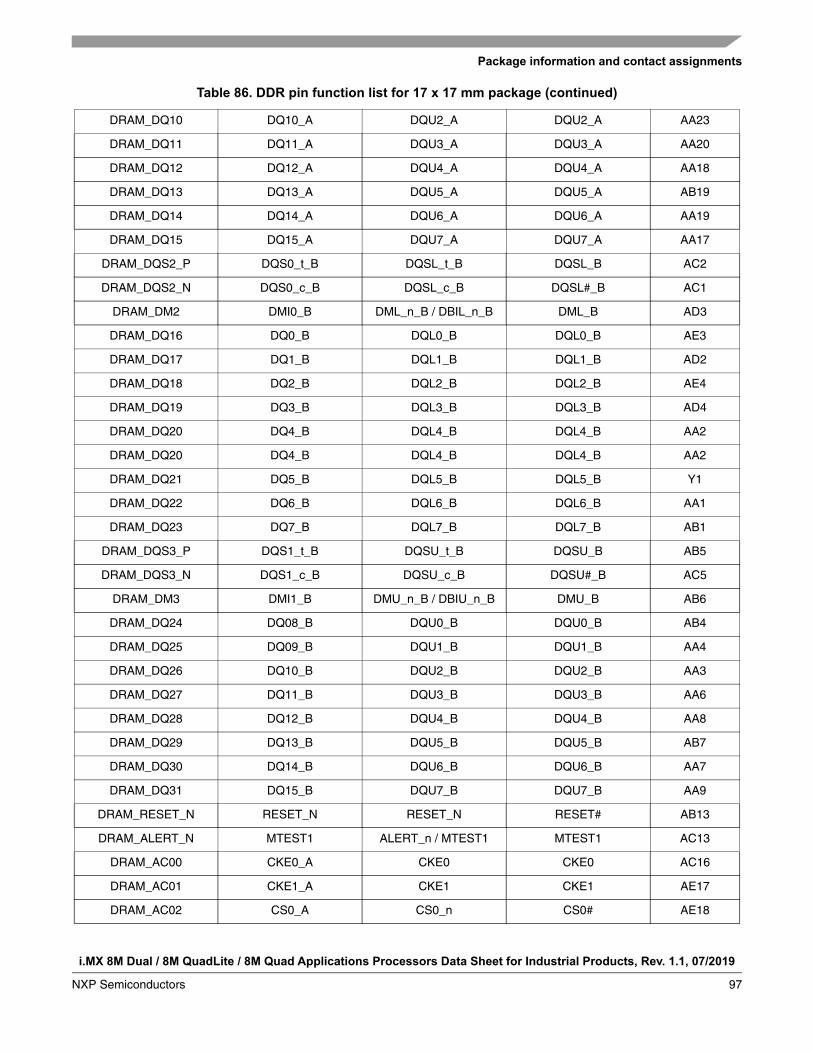
Package information and contact assignments
i.MX 8M Dual / 8M QuadLite / 8M Quad Applications Processors Data Sheet for Industrial Products, Rev. 1.1, 07/2019
NXP Semiconductors 97
DRAM_DQ10 DQ10_A DQU2_A DQU2_A AA23
DRAM_DQ11 DQ11_A DQU3_A DQU3_A AA20
DRAM_DQ12 DQ12_A DQU4_A DQU4_A AA18
DRAM_DQ13 DQ13_A DQU5_A DQU5_A AB19
DRAM_DQ14 DQ14_A DQU6_A DQU6_A AA19
DRAM_DQ15 DQ15_A DQU7_A DQU7_A AA17
DRAM_DQS2_P DQS0_t_B DQSL_t_B DQSL_B AC2
DRAM_DQS2_N DQS0_c_B DQSL_c_B DQSL#_B AC1
DRAM_DM2 DMI0_B DML_n_B / DBIL_n_B DML_B AD3
DRAM_DQ16 DQ0_B DQL0_B DQL0_B AE3
DRAM_DQ17 DQ1_B DQL1_B DQL1_B AD2
DRAM_DQ18 DQ2_B DQL2_B DQL2_B AE4
DRAM_DQ19 DQ3_B DQL3_B DQL3_B AD4
DRAM_DQ20 DQ4_B DQL4_B DQL4_B AA2
DRAM_DQ20 DQ4_B DQL4_B DQL4_B AA2
DRAM_DQ21 DQ5_B DQL5_B DQL5_B Y1
DRAM_DQ22 DQ6_B DQL6_B DQL6_B AA1
DRAM_DQ23 DQ7_B DQL7_B DQL7_B AB1
DRAM_DQS3_P DQS1_t_B DQSU_t_B DQSU_B AB5
DRAM_DQS3_N DQS1_c_B DQSU_c_B DQSU#_B AC5
DRAM_DM3 DMI1_B DMU_n_B / DBIU_n_B DMU_B AB6
DRAM_DQ24 DQ08_B DQU0_B DQU0_B AB4
DRAM_DQ25 DQ09_B DQU1_B DQU1_B AA4
DRAM_DQ26 DQ10_B DQU2_B DQU2_B AA3
DRAM_DQ27 DQ11_B DQU3_B DQU3_B AA6
DRAM_DQ28 DQ12_B DQU4_B DQU4_B AA8
DRAM_DQ29 DQ13_B DQU5_B DQU5_B AB7
DRAM_DQ30 DQ14_B DQU6_B DQU6_B AA7
DRAM_DQ31 DQ15_B DQU7_B DQU7_B AA9
DRAM_RESET_N RESET_N RESET_N RESET# AB13
DRAM_ALERT_N MTEST1 ALERT_n / MTEST1 MTEST1 AC13
DRAM_AC00 CKE0_A CKE0 CKE0 AC16
DRAM_AC01 CKE1_A CKE1 CKE1 AE17
DRAM_AC02 CS0_A CS0_n CS0# AE18
Table 86. DDR pin function list for 17 x 17 mm package (continued)

i.MX 8M Dual / 8M QuadLite / 8M Quad Applications Processors Data Sheet for Industrial Products, Rev. 1.1, 07/2019
98 NXP Semiconductors
Package information and contact assignments
DRAM_AC03 CS1_A C0 — AC18
DRAM_AC04 CK_t_A BG0 BA2 AD14
DRAM_AC05 CK_c_A BG1 A14 AE14
DRAM_AC06 — ACT_n A15 AE13
DRAM_AC07 — A9 A9 AB15
DRAM_AC08 CA0_A A12 A12 / BC# AD17
DRAM_AC09 CA1_A A11 A11 AE16
DRAM_AC10 CA2_A A7 A7 AD20
DRAM_AC11 CA3_A A8 A8 AE20
DRAM_AC12 CA4_A A6 A6 AD19
DRAM_AC13 CA5_A A5 A5 AE19
DRAM_AC14 — A4 A4 AB16
DRAM_AC15 — A3 A3 AC15
DRAM_AC16 — CK_t_A CK_A AE15
DRAM_AC17 — CK_c_A CK#_A AD15
DRAM_AC19 MTEST MTEST MTEST AB14
DRAM_AC20 CKE0_B CK_t_B CK_B AD10
DRAM_AC21 CKE1_B CK_c_B CK#_B AE10
DRAM_AC22 CS1_B — — AD8
DRAM_AC23 CS0_B — — AC9
DRAM_AC24 CK_t_B A2 A2 AD12
DRAM_AC25 CK_c_B A1 A1 AE12
DRAM_AC26 — BA1 BA1 AB12
DRAM_AC27 — PARITY — AA12
DRAM_AC28 CA2_B A13 A13 AC7
DRAM_AC29 CA3_B BA0 BA0 AE7
DRAM_AC30 CA4_B A10 / AP A10 / AP AE6
DRAM_AC31 CA5_B A0 A0 AD6
DRAM_AC32 CA0_B C2 — AE8
DRAM_AC33 CA1_B CAS_n / A15 CAS# AE9
DRAM_AC34 — WE_n / A14 WE# AC10
DRAM_AC35 — RAS_n / A16 RAS# AB10
DRAM_AC36 — ODT0 ODT0 AC12
DRAM_AC37 — ODT1 ODT1 AE11
Table 86. DDR pin function list for 17 x 17 mm package (continued)

Package information and contact assignments
i.MX 8M Dual / 8M QuadLite / 8M Quad Applications Processors Data Sheet for Industrial Products, Rev. 1.1, 07/2019
NXP Semiconductors 99
DRAM_AC38 — CS1_n CS1# AC11
DRAM_ZN ZQ ZQ ZQ AA13
DRAM_VREF VREF VREF VREF AA14
Table 86. DDR pin function list for 17 x 17 mm package (continued)

i.MX 8M Dual / 8M QuadLite / 8M Quad Applications Processors Data Sheet for Industrial Products, Rev. 1.1, 07/2019
100 NXP Semiconductors
Revision history
6 Revision historyTable 87 provides a revision history for this data sheet.
Table 87. Revision history
Rev.number
Date Substantive change(s)
Rev. 1.1 05/2019 • Updated the package type information in the Figure 2, "Part number nomenclature—i.MX 8M Dual / 8M QuadLite / 8M Quad processors"
• Updated eCSPI description in the Table 3, "i.MX 8M Dual / 8M QuadLite / 8M Quad modules list" • Added the core voltage, analog domain voltage, PLL 1.8 V voltage, 25 MHz crystal voltage, 27 MHz
crystal voltage, DDR I/O voltage, HDMI voltage, MIPI voltage, PCIe voltage, temperature sensor voltage, and fuse power in the Table 5, "Absolute maximum ratings"
• Updated the Table 6, "Thermal resistance data" • Updated the RUN mode unit in the Table 10, "Chip power in different LP mode"
Rev. 1 10/2018 • Updated the Table 2, "Orderable part numbers" • Updated the Figure 2, "Part number nomenclature—i.MX 8M Dual / 8M QuadLite / 8M Quad
processors"
Rev. 0.2 08/2018 • Updated the Table 7, "Operating ranges" • Updated the Section 3.1.4, External clock sources • Updated the Section 3.2.1, Power-up sequence • Updated the Figure 5, "Differential LVDS driver transition time waveform" • Updated the Section 3.9.3.1, RMII mode timing • Updated the Section 5.1.2, 17 x 17 mm supplies contact assignments and functional contact
assignments • Fixed a typo in the Table 85, "17 x 17 mm, 0.65 mm pitch ball map"
Rev. 0.1 05/2018 • Added a note in the Table 2, "Orderable part numbers" • Updated the Table 3, "i.MX 8M Dual / 8M QuadLite / 8M Quad modules list" • Updated the Table 7, "Operating ranges" • Updated the Table 9, "Maximum supply currents" • Updated the Table 10, "Chip power in different LP mode" • Added the Table 11, "The power supply states" • Updated the PCIe parameters in the Table 15, "PCIe recommended operating conditions" • Updated and added a leakage limit note in the Table 26, "GPIO DC parameters" • Added a leakage limit note in the Table 29, "Input DC current" • Updated the timing parameters in the Table 38, "ECSPI Master mode timing parameters" and Table 39,
"ECSPI Slave mode timing parameters" • Updated the Section 3.9.8.1, PCIEx_RESREF reference resistor connection • Updated the Table 59, "MIPI input characteristics DC specifications" • Removed the SPI interfaces from the Table 82, "Interface allocation during boot" • Updated the PCIe and MIPI power group in the Table 84, "i.MX 8M Dual / 8M QuadLite / 8M Quad
17 x 17 mm functional contact assignments" • Updated the Table 85, "17 x 17 mm, 0.65 mm pitch ball map"
Rev. 0 01/2018 • Initial version

Document Number: IMX8MDQLQIECRev. 1.107/2019
nformation in this document is provided solely to enable system and software implementers
to use NXP products. There are no express or implied copyright licenses granted hereunder
to design or fabricate any integrated circuits based on the information in this document. NXP
reserves the right to make changes without further notice to any products herein.
NXP makes no warranty, representation, or guarantee regarding the suitability of its products
for any particular purpose, nor does NXP assume any liability arising out of the application
or use of any product or circuit, and specifically disclaims any and all liability, including
without limitation consequential or incidental damages. “Typical” parameters that may be
provided in NXP data sheets and/or specifications can and do vary in different applications,
and actual performance may vary over time. All operating parameters, including “typicals”
must be validated for each customer application by customer‚ customer’s technical experts.
NXP does not convey any license under its patent rights nor the rights of others. NXP sells
products pursuant to standard terms and conditions of sale, which can be found at the
following address: nxp.com/SalesTermsandConditions.
While NXP has implemented advanced security features, all products may be subject to
unidentified vulnerabilities. Customers are responsible for the design and operation of their
applications and products to reduce the effect of these vulnerabilities on customer’s
applications and products, and NXP accepts no liability for any vulnerability that is
discovered. Customers should implement appropriate design and operating safeguards to
minimize the risks associated with their applications and products.
NXP, the NXP logo, NXP SECURE CONNECTIONS FOR A SMARTER WORLD,
COOLFLUX, EMBRACE, GREENCHIP, HITAG, I2C BUS, ICODE, JCOP, LIFE VIBES,
MIFARE, MIFARE CLASSIC, MIFARE DESFire, MIFARE PLUS, MIFARE FLEX, MANTIS,
MIFARE ULTRALIGHT, MIFARE4MOBILE, MIGLO, NTAG, ROADLINK, SMARTLX,
SMARTMX, STARPLUG, TOPFET, TRENCHMOS, UCODE, Freescale, the Freescale logo,
AltiVec, C-5, CodeTEST, CodeWarrior, ColdFire, ColdFire+, C-Ware, the Energy Efficient
Solutions logo, Kinetis, Layerscape, MagniV, mobileGT, PEG, PowerQUICC, Processor
Expert, QorIQ, QorIQ Qonverge, Ready Play, SafeAssure, the SafeAssure logo, StarCore,
Symphony, VortiQa, Vybrid, Airfast, BeeKit, BeeStack, CoreNet, Flexis, MXC, Platform in a
Package, QUICC Engine, SMARTMOS, Tower, TurboLink, and UMEMS are trademarks of
NXP B.V. All other product or service names are the property of their respective owners.
AMBA, Arm, Arm7, Arm7TDMI, Arm9, Arm11, Artisan, big.LITTLE, Cordio, CoreLink,
CoreSight, Cortex, DesignStart, DynamIQ, Jazelle, Keil, Mali, Mbed, Mbed Enabled, NEON,
POP, RealView, SecurCore, Socrates, Thumb, TrustZone, ULINK, ULINK2, ULINK-ME,
ULINK-PLUS, ULINKpro, μVision, Versatile are trademarks or registered trademarks of Arm
Limited (or its subsidiaries) in the US and/or elsewhere. The related technology may be
protected by any or all of patents, copyrights, designs and trade secrets. All rights reserved.
Oracle and Java are registered trademarks of Oracle and/or its affiliates. The Power
Architecture and Power.org word marks and the Power and Power.org logos and related
marks are trademarks and service marks licensed by Power.org.
© 2018-2019 NXP B.V.
How to Reach Us:
Home Page: nxp.com
Web Support: nxp.com/support
Related Documents