Freescale Semiconductor, Inc. Application Note © 2014 Freescale Semiconductor, Inc. All rights reserved. This application note enables users to design and route audio clocking signals. Through several use cases, this document illustrates clock jitter values of the i.MX 6 system-on-chip (SoC) family, measured on the Freescale SABRE AI and SABRE SD development platforms. The reader will be enabled to choose the appropriate audio clocking scheme for the i.MX 6 SoC and become familiar with the expected jitter values in different scenarios. NOTE Because the data provided in this application note is based on empirical measurements on a small sample size, the results presented are not guaranteed. 1 Overview of internal i.MX 6 audio clock topology The i.MX 6 processor family has a dedicated Audio PLL (PLL4), which, along with the Audio IP (Intellectual Property) module, generates signals for a wide range of audio peripherals. The PLL4 can be configured to generate a reference clock in the 650 MHz to 1.3 GHz range. Operating Document Number: AN4952 Rev. 0, 06/2014 Contents 1. Overview of internal i.MX 6 audio clock topology . . 1 2. Board-level audio clock topologies . . . . . . . . . . . . . . 2 3. Audio clock quality requirements . . . . . . . . . . . . . . . . 4 4. Test conditions . . . . . . . . . . . . . . . . . . . . . . . . . . . . . . 5 5. Test results . . . . . . . . . . . . . . . . . . . . . . . . . . . . . . . . . 7 6. Data analysis . . . . . . . . . . . . . . . . . . . . . . . . . . . . . . . 13 7. Conclusions and recommendations . . . . . . . . . . . . . 14 8. Revision history . . . . . . . . . . . . . . . . . . . . . . . . . . . . 15 A. Code example . . . . . . . . . . . . . . . . . . . . . . . . . . . . . . 16 i.MX 6 Audio Clock Configuration Options by Naoum Gitnik

Welcome message from author
This document is posted to help you gain knowledge. Please leave a comment to let me know what you think about it! Share it to your friends and learn new things together.
Transcript
Freescale Semiconductor, Inc.Application Note
© 2014 Freescale Semiconductor, Inc. All rights reserved.
This application note enables users to design and route audio clocking signals. Through several use cases, this document illustrates clock jitter values of the i.MX 6 system-on-chip (SoC) family, measured on the Freescale SABRE AI and SABRE SD development platforms.
The reader will be enabled to choose the appropriate audio clocking scheme for the i.MX 6 SoC and become familiar with the expected jitter values in different scenarios.
NOTE
Because the data provided in this application note is based on empirical measurements on a small sample size, the results presented are not guaranteed.
1 Overview of internal i.MX 6 audio clock topology
The i.MX 6 processor family has a dedicated Audio PLL (PLL4), which, along with the Audio IP (Intellectual Property) module, generates signals for a wide range of audio peripherals. The PLL4 can be configured to generate a reference clock in the 650 MHz to 1.3 GHz range. Operating
Document Number: AN4952Rev. 0, 06/2014
Contents1. Overview of internal i.MX 6 audio clock topology . . 12. Board-level audio clock topologies . . . . . . . . . . . . . . 23. Audio clock quality requirements . . . . . . . . . . . . . . . . 44. Test conditions . . . . . . . . . . . . . . . . . . . . . . . . . . . . . . 55. Test results . . . . . . . . . . . . . . . . . . . . . . . . . . . . . . . . . 76. Data analysis . . . . . . . . . . . . . . . . . . . . . . . . . . . . . . . 137. Conclusions and recommendations . . . . . . . . . . . . . 148. Revision history . . . . . . . . . . . . . . . . . . . . . . . . . . . . 15A. Code example . . . . . . . . . . . . . . . . . . . . . . . . . . . . . . 16
i.MX 6 Audio Clock Configuration Optionsby Naoum Gitnik
i.MX 6 Audio Clock Configuration Options Application Note, AN4952, Rev. 0, 06/2014
2 Freescale Semiconductor
Board-level audio clock topologies
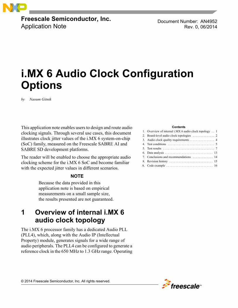
the audio PLL module in this range conditions it to provide common clock signals (such as a bit clock, word clock, and so on) which are required for external audio peripherals. This makes the i.MX6 family an excellent choice for audio applications ranging from the low-cost to high-definition.
The internal i.MX 6 audio clock configuration overview is illustrated in Figure 1 and is described as follows:
• The audio PLL input signal comes from either the built-in crystal oscillator (24 MHz OSC) or ANACLK_x pads, depending on the CCM_ANALOG_PLL_AUDIO[BYPASS_CLK_SRC] register settings.
• The CLKOx output signal can be configured to output either the ESAI_CLK_ROOT, SSI_CLK_ROOT, or SPDIF_CLK_ROOT clock signal, and so on.
Figure 1. i.MX 6 audio clock configuration
2 Board-level audio clock topologiesThis document describes aspects and details of the master clock generation for audio codecs used in the two Freescale development platforms based on the i.MX 6 microprocessor series:
• Smart Application Blueprint for Rapid Engineering for Automotive Infotainment (SABRE AI based on i.MX 6Solo processor),
• Smart Application Blueprint for Rapid Engineering Platform for Smart Devices (SABRE SD based on i.MX 6Quad processor).
These two platforms use different audio topologies.
PMU_MISC1[LVDSCLKx_IBEN]
CCM_ANALOG_PLL_AUDIO[BYPASS_CLK_SRC]
PMU_MISC1[LVDSCLKx_OBEN]
PMU_MISC1[LVDSCLKx_SEL]
CSCMR2[ESAI_CLK_SEL]
CSCMR1[SSIx_CLK_SEL]
ESAI_CLK_ROOT
SSI_CLK_ROOT
CCM_OCOSR[CLKOx_SEL]
SPDIF_CLK_ROOT
CDCDR[SPDIFx_CLK_SEL]
OSCAudioPLL4
ESAI
SSI
SPDIF
ANACLK_x
CLKOx
i.MX 6 Audio Clock Configuration Options Application Note, AN4952, Rev. 0, 06/2014
Freescale Semiconductor 3
Board-level audio clock topologies
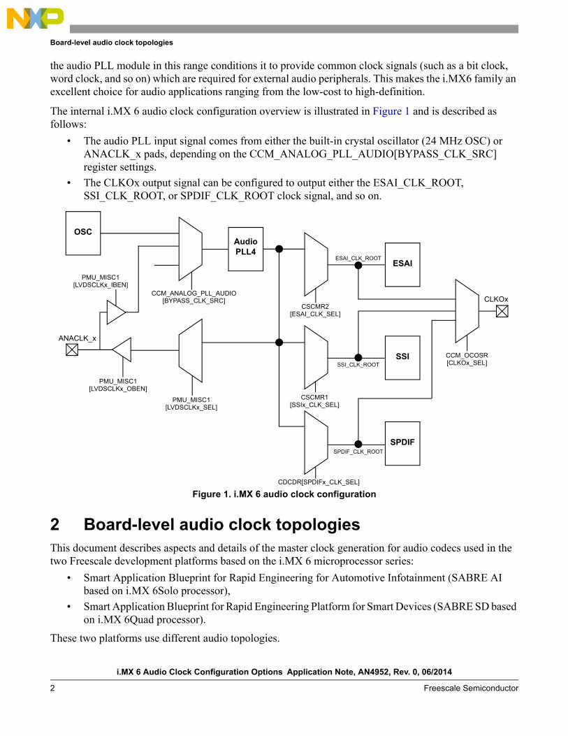
2.1 SABRE AI platform topology
Audio topology used on the SABRE AI platform (see Figure 2) has the following features:
• Uses the CS42888 audio codec IC by Cirrus Logic.
• The 24.576 MHz master clock (MCLK) is routed as a single-ended trace.
• 24.576 MHz frequency is generated by an external clock oscillator with single-ended output.
Figure 2. SABRE AI platform based on the i.MX 6 series
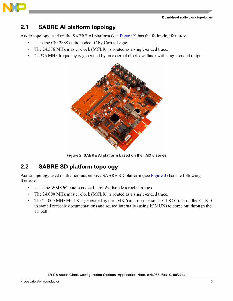
2.2 SABRE SD platform topology
Audio topology used on the non-automotive SABRE SD platform (see Figure 3) has the following features:
• Uses the WM8962 audio codec IC by Wolfson Microelectronics.
• The 24.000 MHz master clock (MCLK) is routed as a single-ended trace.
• The 24.000 MHz MCLK is generated by the i.MX 6 microprocessor as CLKO1 (also called CLKO in some Freescale documentation) and routed internally (using IOMUX) to come out through the T5 ball.
i.MX 6 Audio Clock Configuration Options Application Note, AN4952, Rev. 0, 06/2014
4 Freescale Semiconductor
Audio clock quality requirements
Figure 3. SABRE SD platform based on the i.MX 6 series
3 Audio clock quality requirements
3.1 SABRE AI platform requirements
The CS42888 data sheet by Cirrus Logic contains no MCLK jitter tolerance requirements. Nevertheless, as per their customer support data, when a 12.288 MHz clock is used, jitter values less than ~2800 ps RMS and ~140 ps RMS must be used to guarantee the stated THD+N values for a 1 kHz and 20 kHz input tone, respectively.
Because the 24.576 MHz value is twice as high as mentioned above, to maintain the same clock quality, the jitter tolerance requirement for the whole input tone frequency range is ~70 ps RMS.
3.2 SABRE SD platform requirements
The WM8962 data sheet by Wolfson Microelectronics contains no MCLK jitter tolerance requirements. Because the design demonstrates good subjective audio quality while running test video clips, no such information has been requested from Wolfson customer support.
Note that both codecs belong to the same IC generation, therefore, they most likely have very close jitter tolerance values.
i.MX 6 Audio Clock Configuration Options Application Note, AN4952, Rev. 0, 06/2014
Freescale Semiconductor 5
Test conditions
4 Test conditions
4.1 Coverage
For comprehensive analysis purposes, two cases with extreme jitter behaviors have been tested:
• The single-core i.MX 6Solo SABRE AI platform running a minimal OBDS (On-Board Diagnostic Suite) style code.
• The quad-core i.MX 6Quad SABRE SD platform in real-life conditions—that is, when heavy computation load of i.MX 6 processor causes additional noise on its power rails thus increasing jitter of the generated clock.
The following jitter values are measured:
• For 24.000 MHz, the i.MX 6 generated clock on the SABRE SD platform in heavy-load conditions.
• For 24.000 MHz and 24.576 MHz, the i.MX 6 generated clock on the SABRE AI platform in light-load conditions,.
• For the external 24.576 MHz oscillator clock in the existing SABRE AI design in light-load conditions.
4.2 Audio clock schemes
4.2.1 SABRE AI clock schemes
4.2.1.1 Existing clock scheme
In the existing scheme used by the SABRE AI platform, the single-ended 24.576 MHz audio master clock is generated externally, converted into an LVDS signal, and brought to the CLK2_P/N pins, configured as LVDS inputs.
4.2.1.2 Initial jitter measurement scheme
The initial plan of the clock jitter test was to:
• Measure jitter from a 24.576 MHz clock
• Generate the clock internal to i.MX 6 using the audio PLL
• Define the clock as CLKO2 signal inside i.MX 6
• Route the clock internally to the A17 ball acting as a single-ended 3.3 V-rated output
• Measure jitter
The A17 ball has been selected due to the ease of moving its original function in the existing design to a different ball.
i.MX 6 Audio Clock Configuration Options Application Note, AN4952, Rev. 0, 06/2014
6 Freescale Semiconductor
Test conditions
4.2.1.3 Final jitter measurement scheme
While implementing the original test plan, the following i.MX 6 limitations were encountered:
• The audio PLL can only be used as a source for the CLKO1 signal, not CLKO2.
• CLKO1, however, can be routed internally as a source for CLKO2.
Therefore, it has been decided to use this opportunity and measure the CLKO1 signal jitter as well, providing more clock output options for customers to select from:
• A single-ended 3.3 V-rated output from the T5 ball
• A differential LVDS signal from CLK2_P/N
4.2.2 SABRE SD clock schemes
Due to the platform hardware and software specifics, there is no easy way to change the audio master clock frequency or its internal routing without impacting audio performance, so only the existing scheme has been tested.
i.MX 6 Audio Clock Configuration Options Application Note, AN4952, Rev. 0, 06/2014
Freescale Semiconductor 7
Test results
5 Test results
5.1 SABRE AI data
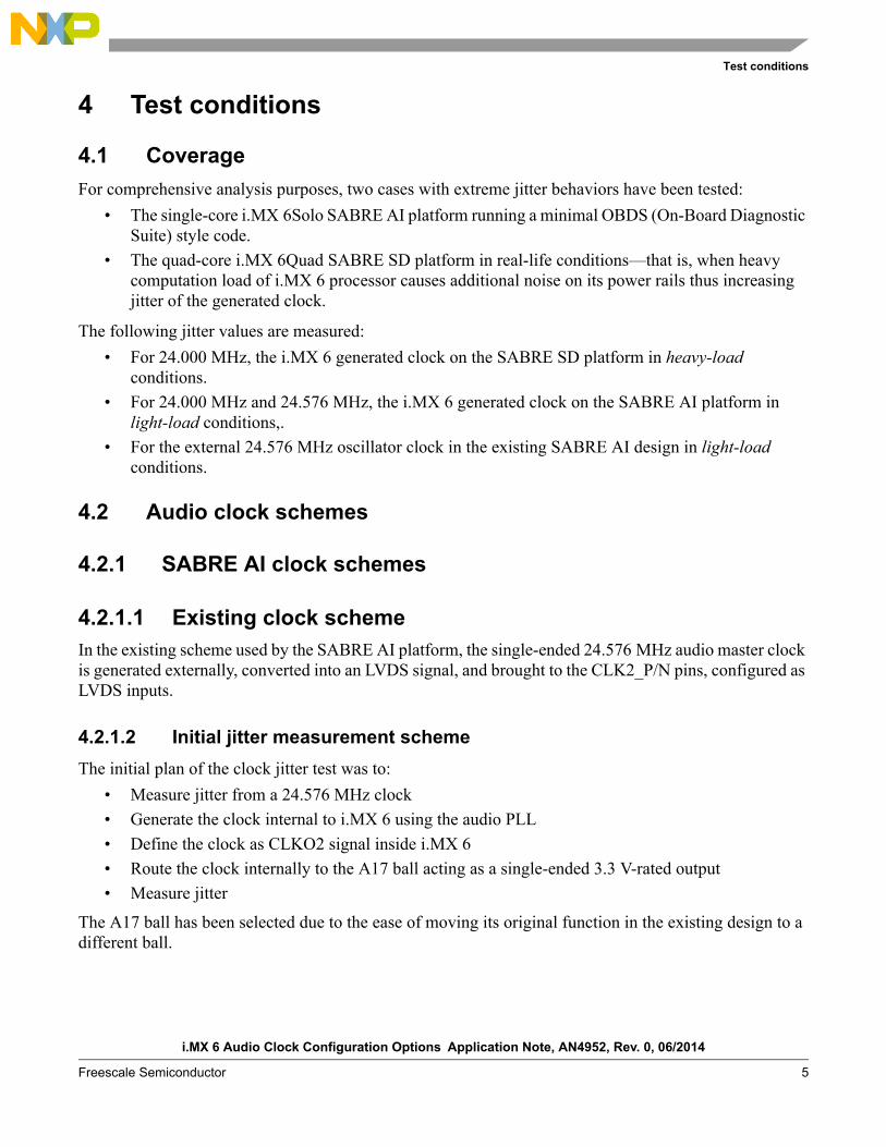
Figure 4. RMS jitter on external oscillator single-ended24.576 MHz output of SABRE-AI design (i.MX 6Solo, OBDS)
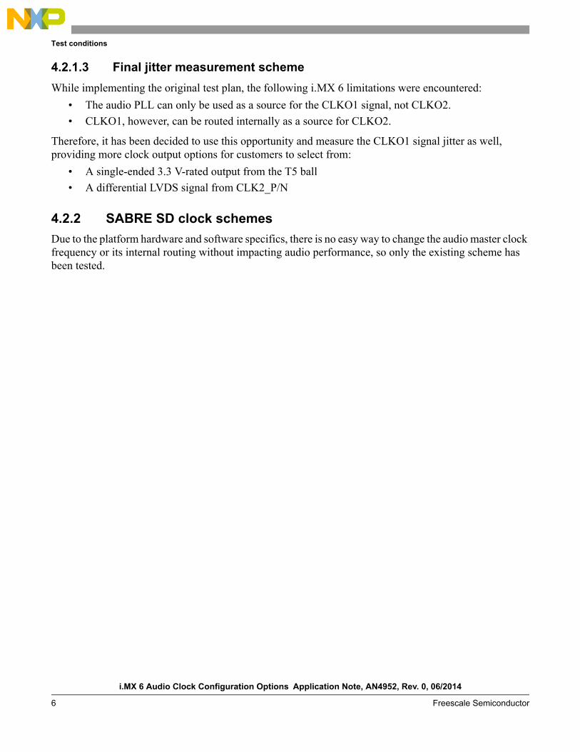
Figure 5. Peak-to-peak jitter on external oscillator single-ended24.576 MHz output of SABRE-AI design (i.MX 6Solo, OBDS)
i.MX 6 Audio Clock Configuration Options Application Note, AN4952, Rev. 0, 06/2014
8 Freescale Semiconductor
Test results
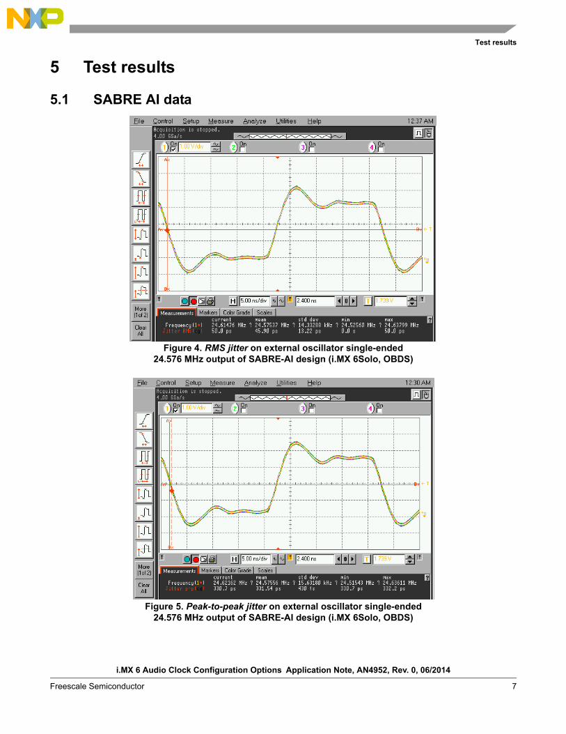
Figure 6. RMS jitter of single-ended 24.576 MHz CLKO1 (T5 ball)output of SABRE-AI design (i.MX 6Solo, OBDS)
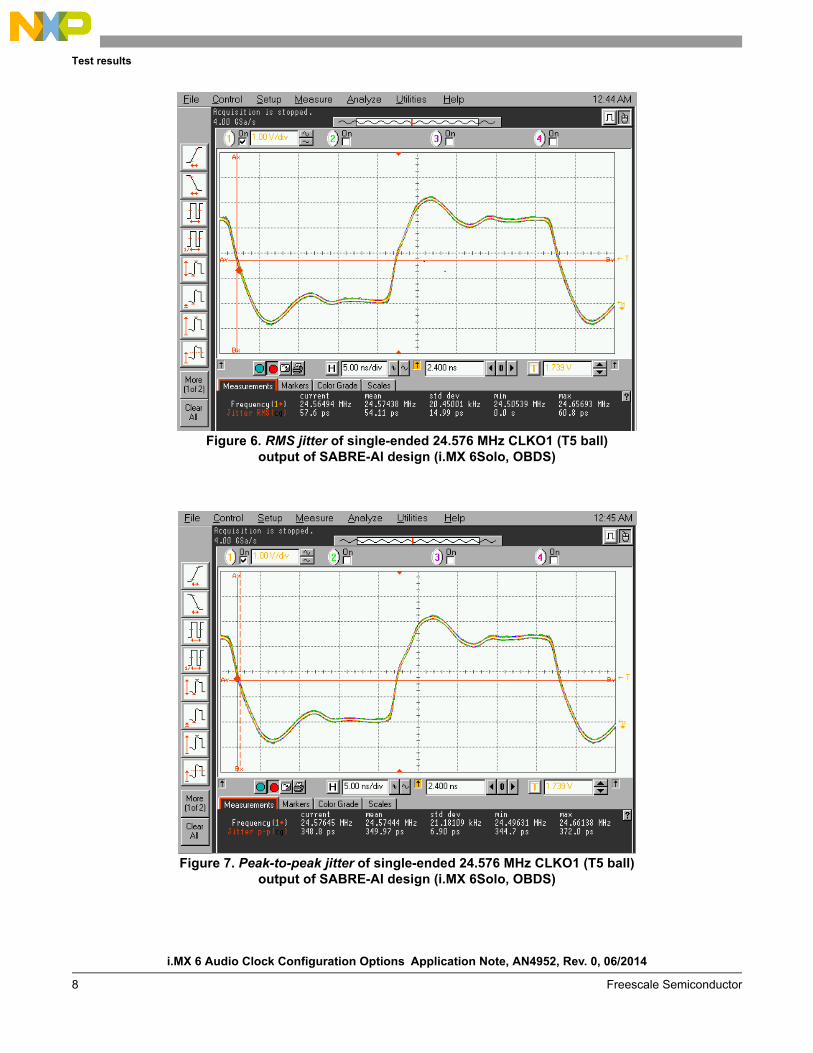
Figure 7. Peak-to-peak jitter of single-ended 24.576 MHz CLKO1 (T5 ball)output of SABRE-AI design (i.MX 6Solo, OBDS)
i.MX 6 Audio Clock Configuration Options Application Note, AN4952, Rev. 0, 06/2014
Freescale Semiconductor 9
Test results
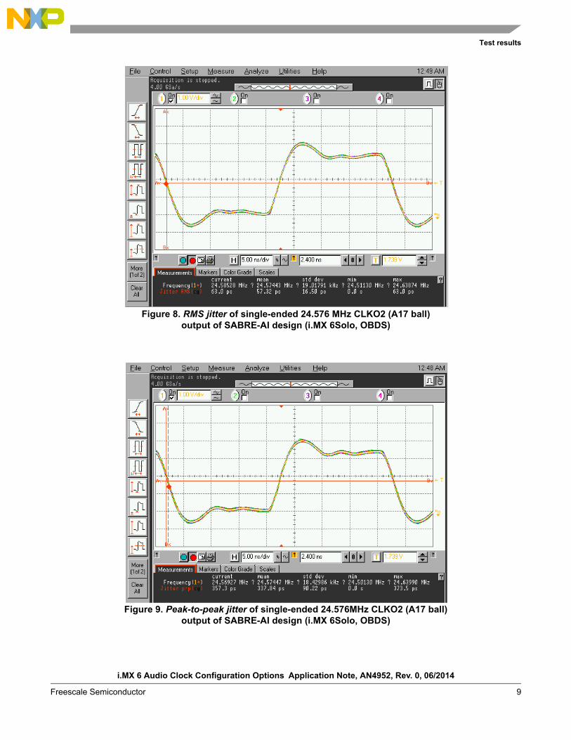
Figure 8. RMS jitter of single-ended 24.576 MHz CLKO2 (A17 ball) output of SABRE-AI design (i.MX 6Solo, OBDS)
Figure 9. Peak-to-peak jitter of single-ended 24.576MHz CLKO2 (A17 ball)output of SABRE-AI design (i.MX 6Solo, OBDS)
i.MX 6 Audio Clock Configuration Options Application Note, AN4952, Rev. 0, 06/2014
10 Freescale Semiconductor
Test results
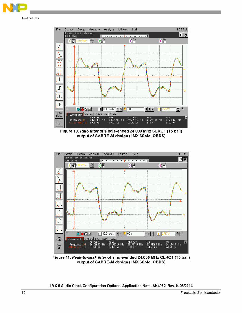
Figure 10. RMS jitter of single-ended 24.000 MHz CLKO1 (T5 ball)output of SABRE-AI design (i.MX 6Solo, OBDS)
Figure 11. Peak-to-peak jitter of single-ended 24.000 MHz CLKO1 (T5 ball)output of SABRE-AI design (i.MX 6Solo, OBDS)
i.MX 6 Audio Clock Configuration Options Application Note, AN4952, Rev. 0, 06/2014
Freescale Semiconductor 11
Test results
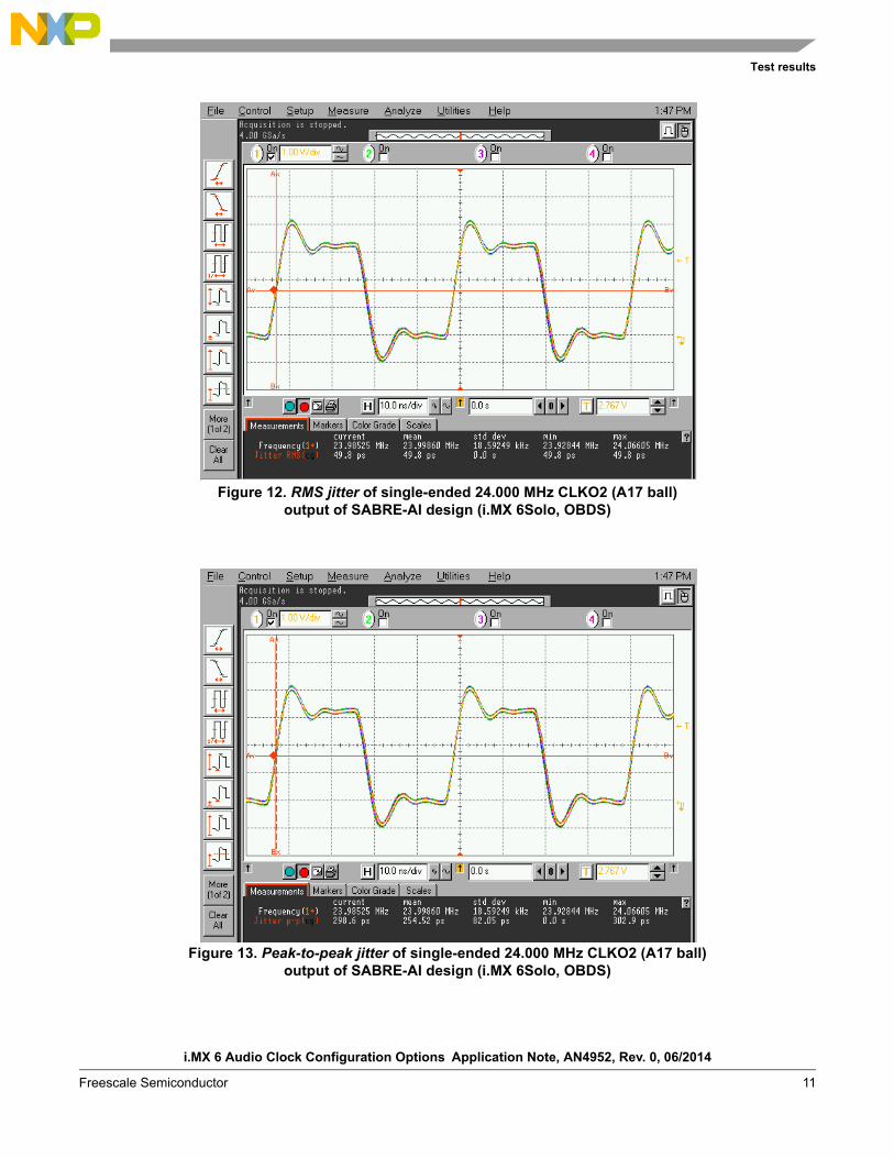
Figure 12. RMS jitter of single-ended 24.000 MHz CLKO2 (A17 ball) output of SABRE-AI design (i.MX 6Solo, OBDS)
Figure 13. Peak-to-peak jitter of single-ended 24.000 MHz CLKO2 (A17 ball)output of SABRE-AI design (i.MX 6Solo, OBDS)
i.MX 6 Audio Clock Configuration Options Application Note, AN4952, Rev. 0, 06/2014
12 Freescale Semiconductor
Test results
5.2 SABRE SD data
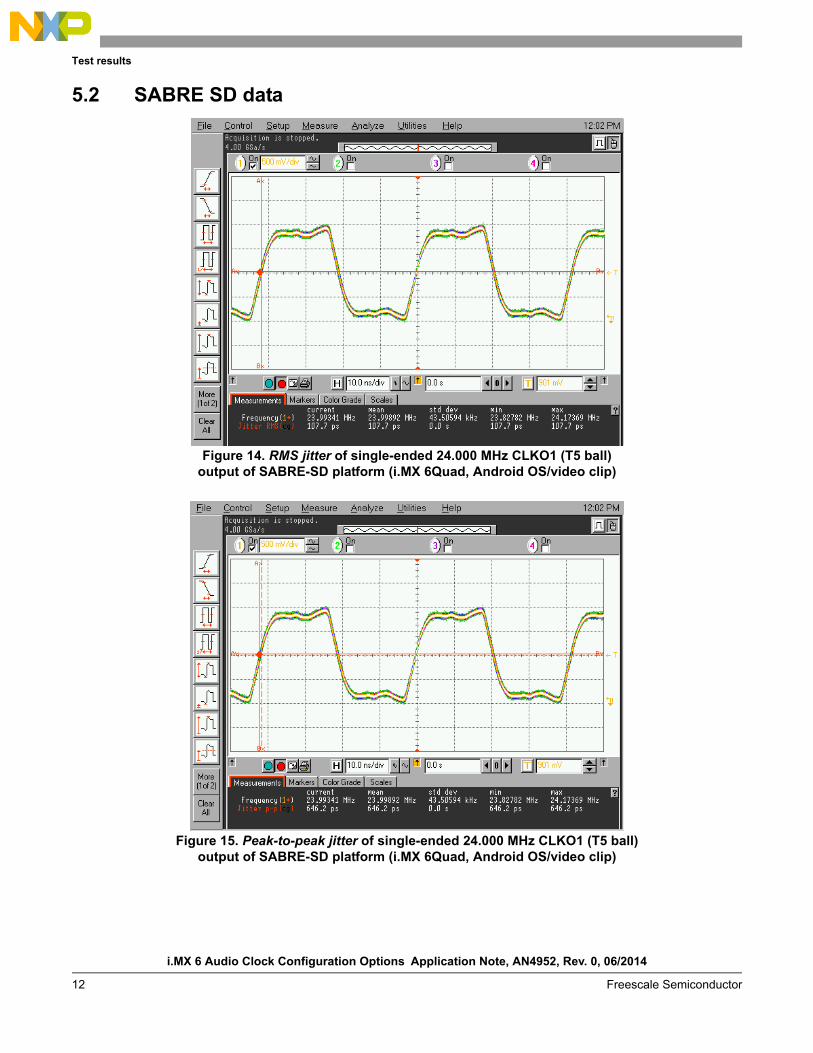
Figure 14. RMS jitter of single-ended 24.000 MHz CLKO1 (T5 ball)output of SABRE-SD platform (i.MX 6Quad, Android OS/video clip)
Figure 15. Peak-to-peak jitter of single-ended 24.000 MHz CLKO1 (T5 ball)output of SABRE-SD platform (i.MX 6Quad, Android OS/video clip)
i.MX 6 Audio Clock Configuration Options Application Note, AN4952, Rev. 0, 06/2014
Freescale Semiconductor 13
Data analysis
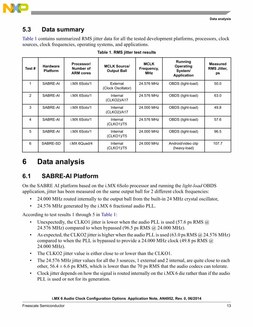
5.3 Data summary
Table 1 contains summarized RMS jitter data for all the tested development platforms, processors, clock sources, clock frequencies, operating systems, and applications.
6 Data analysis
6.1 SABRE-AI Platform
On the SABRE AI platform based on the i.MX 6Solo processor and running the light-load OBDS application, jitter has been measured on the same output ball for 2 different clock frequencies:
• 24.000 MHz routed internally to the output ball from the built-in 24 MHz crystal oscillator,
• 24.576 MHz generated by the i.MX 6 fractional audio PLL.
According to test results 1 through 5 in Table 1:
• Unexpectedly, the CLKO1 jitter is lower when the audio PLL is used (57.6 ps RMS @ 24.576 MHz) compared to when bypassed (96.5 ps RMS @ 24.000 MHz).
• As expected, the CLKO2 jitter is higher when the audio PLL is used (63.0 ps RMS @ 24.576 MHz) compared to when the PLL is bypassed to provide a 24.000 MHz clock (49.8 ps RMS @ 24.000 MHz).
• The CLKO2 jitter value is either close to or lower than the CLKO1.
• The 24.576 MHz jitter values for all the 3 sources, 1 external and 2 internal, are quite close to each other, 56.4 ± 6.6 ps RMS, which is lower than the 70 ps RMS that the audio codecs can tolerate.
• Clock jitter depends on how the signal is routed internally on the i.MX 6 die rather than if the audio PLL is used or not for its generation.
Table 1. RMS jitter test results
Test #HardwarePlatform
Processor/Number ofARM cores
MCLK Source/Output Ball
MCLKFrequency,
MHz
RunningOperatingSystem/
Application
MeasuredRMS Jitter,
ps
1 SABRE-AI i.MX 6Solo/1 External(Clock Oscillator)
24.576 MHz OBDS (light-load) 50.0
2 SABRE-AI i.MX 6Solo/1 Internal(CLKO2)/A17
24.576 MHz OBDS (light-load) 63.0
3 SABRE-AI i.MX 6Solo/1 Internal(CLKO2)/A17
24.000 MHz OBDS (light-load) 49.8
4 SABRE-AI i.MX 6Solo/1 Internal(CLKO1)/T5
24.576 MHz OBDS (light-load) 57.6
5 SABRE-AI i.MX 6Solo/1 Internal(CLKO1)/T5
24.000 MHz OBDS (light-load) 96.5
6 SABRE-SD i.MX 6Quad/4 Internal(CLKO1)/T5
24.000 MHz Android/video clip(heavy-load)
107.7
i.MX 6 Audio Clock Configuration Options Application Note, AN4952, Rev. 0, 06/2014
14 Freescale Semiconductor
Conclusions and recommendations
6.2 SABRE-SD platform
According to Section 4.2.2, “SABRE SD clock schemes,” jitter has only been measured for CLKO1 at 24.000 MHz and appears to be 107.7 ps RMS (test 6 in Table 1), which is somewhat higher than what the codec tolerates (see Section 3.2, “SABRE SD platform requirements”).
Although formal audio performance tests are yet to be conducted, the audio performance has been subjectively evaluated on multiple Internet-quality video-streaming samples.
7 Conclusions and recommendations
7.1 Dependence on internal i.MX 6 design
Tests have been conducted on two members of the i.MX 6 processor family—6Solo and 6Quad. Although the different number of ARM cores causes a different die size (hence different block placement), the vast majority of the design blocks are shared, including the audio PLL and the relevant IOMUX pins in this case. Therefore, the following statements are valid:
• Relative clock jitter behavior for different scenarios—using (24.576 MHz) or bypassing (24.000 MHz) the audio PLL block, observed for one of the i.MX 6 family members is quite applicable to the other family members, especially those with the same die size.
• It is recommended to run the clock from the built-in 24 MHz crystal oscillator through the audio PLL module instead of bypassing it, even if there is no need to change the clock frequency. Low jitter in this case is achieved by the fact that noise requirements inside the PLL module are much stricter than those for regular digital blocks, which are used in the bypass option.
• Clock jitter value on a specific output ball strongly depends on the internal processor routing, so the relative clock jitter behavior on different output balls observed on one of the i.MX 6 family members most likely does not correlate with behavior of the family members with a different die size.
7.2 Dependence on board layout
Although basic signal integrity aspects (for example, impedance matching) have been taken into account in the layout, there is still room for audio master clock crosstalk improvement based on external trace routing. The following routing techniques are recommended:
• Shortening the clock traces as much as possible.
• Providing proper spacing between clock traces and adjacent, potentially noisy, areas.
• Shielding clock traces with grounded guard traces.
• Shielding clock traces by running them within the inner layers.
• Routing the clock inside the i.MX 6 to the output ball optimal for the specific board layout.
• Having the clock signal routed as a differential pair rather than a single-ended trace.
i.MX 6 Audio Clock Configuration Options Application Note, AN4952, Rev. 0, 06/2014
Freescale Semiconductor 15
Revision history
7.2.1 Routing clock as differential pair
Significant jitter improvement can be achieved by routing the audio master clock to the codec as a differential pair; in this case:
• A single-ended-to-LVDS converter must be placed as close as possible to the processor minimizing the single-ended trace length.
• Using one of the 2 available LVDS ball pairs (CLK1_N/P or CLK2_N/P) might be an option, although they are optimized for frequencies higher than those mentioned in the document.
8 Revision history
Revision History
Revision Date Change description
Rev. 0 06/2014 Initial release.
i.MX 6 Audio Clock Configuration Options Application Note, AN4952, Rev. 0, 06/2014
16 Freescale Semiconductor
Code example
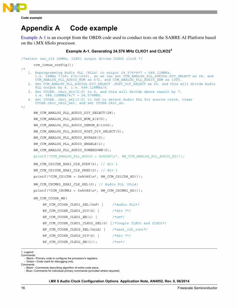
Appendix A Code exampleExample A-1 is an excerpt from the OBDS code used to conduct tests on the SABRE AI Platform based on the i.MX 6Solo processor.
Example A-1. Generating 24.576 MHz CLKO1 and CLKO21
/*select osc_clk 24MHz, CLKO1 output drives CLKO2 clock */
ccm_iomux_config();/*
1. Reprogramming Audio PLL (PLL4) to output 24.576*4*7 = 688.128MHz, i.e. 24MHz *(28+ 672/1000), so we can set CCM_ANALOG_PLL_AUDIOn.DIV_SELECT as 28, and CCM_ANALOG_PLL_AUDIO_NUM as 672, and CCM_ANALOG_PLL_AUDIO_DEM as 1000.
2. Set CCM_ANALOG_PLL_AUDIOn.DIV_SELECT .POST_DIV_SELECT as 00, and this will divide Audio PLL output by 4, i.e. 688.128MHz/4.
3. Set CCOSR. cko1_div[2:0] to 6, and this will divide above result by 7, i.e. 688.128MHz/4/7 = 24.576MHz.
4. Set CCOSR. cko1_sel[3:0] to 0xF to select Audio PLL for source clock, clear CCOSR.cko1_cko2_sel, and set CCOSR.cko1_en.
*/
BW_CCM_ANALOG_PLL_AUDIO_DIV_SELECT(28);
BW_CCM_ANALOG_PLL_AUDIO_NUM_A(672);
BW_CCM_ANALOG_PLL_AUDIO_DENOM_B(1000);
BW_CCM_ANALOG_PLL_AUDIO_POST_DIV_SELECT(0);
BW_CCM_ANALOG_PLL_AUDIO_BYPASS(0);
BW_CCM_ANALOG_PLL_AUDIO_ENABLE(1);
BW_CCM_ANALOG_PLL_AUDIO_POWERDOWN(0);
printf("CCM_ANALOG_PLL_AUDIO = 0x%08X\n", HW_CCM_ANALOG_PLL_AUDIO_RD());
BW_CCM_CS1CDR_ESAI_CLK_PODF(0); // div 1
BW_CCM_CS1CDR_ESAI_CLK_PRED(0); // div 1
printf("CCM_CS1CDR = 0x%08X\n", HW_CCM_CS1CDR_RD());
BW_CCM_CSCMR2_ESAI_CLK_SEL(0); // Audio PLL (PLL4)
printf("CCM_CSCMR2 = 0x%08X\n", HW_CCM_CSCMR2_RD());
HW_CCM_CCOSR_WR(
BF_CCM_CCOSR_CLKO1_SEL(0xF) | /*Audio PLL*/
BF_CCM_CCOSR_CLKO1_DIV(6) | /*div 7*/
BF_CCM_CCOSR_CLKO1_EN(1) | /*on*/
BF_CCM_CCOSR_CLKO1_CLKO2_SEL(0) |/*Couple CLKO1 and CLKO2*/
BF_CCM_CCOSR_CLKO2_SEL(0x1A) | /*esai_clk_root*/
BF_CCM_CCOSR_CLKO2_DIV(6) | /*div 7*/
BF_CCM_CCOSR_CLKO2_EN(1)); /*on*/
1. Legend:Commands:
- Black—Primary code to configure the processor's registers.- Green—Code used for debugging only.
Comments:- Black—Comments describing algorithm of entire code piece.- Blue—Comments for individual primary commands (provided where required).
Document Number: AN4952Rev. 006/2014
Information in this document is provided solely to enable system and software
implementers to use Freescale products. There are no express or implied copyright
licenses granted hereunder to design or fabricate any integrated circuits based on the
information in this document.
Freescale reserves the right to make changes without further notice to any products
herein. Freescale makes no warranty, representation, or guarantee regarding the
suitability of its products for any particular purpose, nor does Freescale assume any
liability arising out of the application or use of any product or circuit, and specifically
disclaims any and all liability, including without limitation consequential or incidental
damages. “Typical” parameters that may be provided in Freescale data sheets and/or
specifications can and do vary in different applications, and actual performance may
vary over time. All operating parameters, including “typicals,” must be validated for
each customer application by customer’s technical experts. Freescale does not convey
any license under its patent rights nor the rights of others. Freescale sells products
pursuant to standard terms and conditions of sale, which can be found at the following
address: freescale.com/SalesTermsandConditions.
How to Reach Us:Home Page: freescale.com
Web Support: freescale.com/support
Freescale and the Freescale logo are trademarks of Freescale Semiconductor, Inc.,
Reg. U.S. Pat. & Tm. Off. All other product or service names are the property of their
respective owners. ARM and the ARM powered logo are registered trademarks of ARM
Limited.
© 2014 Freescale Semiconductor, Inc.
Related Documents


