1 Improving the Security of Wireless Sensor Networks by Protecting the Sensor Nodes against Side Channel Attacks Introduction Wireless sensor networks (WSNs) are becoming an essential building block in application fields such as critical infrastructure protection, industrial automation and telemedicine to name a few areas in which security plays a central role. Potential attackers of those applications will most probably attack the most vulnerable part of the overall systems, i.e. the WSNs. The wireless sensor nodes can be attacked by “standard” network based approaches but also by physical means if they are left unattended in remote sites which is, after all, the preferred application for WSN. We are convinced that protecting the wireless sensor nodes is essential since compromised nodes put the whole system at risk. The challenge with sensor nodes is that they are low cost and running with extremely limited resources but are expected to be operational for long time intervals up to several years. The long life time provides potential attackers with a lot of time to execute an attack and even worse to benefit from a successful attack. Figure 1 illustrates the features of WSNs as well as potential ways to attack it such as network attacks and tampering attacks. During recent years much research effort has been spent on improving the network security of WSN, including research on secure protocols, efficient implementations of crypto operations etc. But, even though physical attacks are easy to execute only little research has been done in the area of protection against side channel attacks. The latter might even be simplified by highly optimizes implementations that do not take into account the observability of physical parameters such as execution time or power consumption, but focus on efficiency only. We are aware of only one project named TAMPRES [TAMPRES] that aims at developing suitable means to protect WSNs against tampering attacks. Figure 1. Attributes of wireless sensor networks and indication of potential ways attacking them

Welcome message from author
This document is posted to help you gain knowledge. Please leave a comment to let me know what you think about it! Share it to your friends and learn new things together.
Transcript

1
Improving the Security of Wireless Sensor
Networks by Protecting the Sensor Nodes
against Side Channel Attacks
Introduction
Wireless sensor networks (WSNs) are becoming an essential building block in application fields such
as critical infrastructure protection, industrial automation and telemedicine to name a few areas in
which security plays a central role. Potential attackers of those applications will most probably attack
the most vulnerable part of the overall systems, i.e. the WSNs. The wireless sensor nodes can be
attacked by “standard” network based approaches but also by physical means if they are left
unattended in remote sites which is, after all, the preferred application for WSN. We are convinced
that protecting the wireless sensor nodes is essential since compromised nodes put the whole system at
risk. The challenge with sensor nodes is that they are low cost and running with extremely limited
resources but are expected to be operational for long time intervals up to several years. The long life
time provides potential attackers with a lot of time to execute an attack and even worse to benefit from
a successful attack. Figure 1 illustrates the features of WSNs as well as potential ways to attack it such
as network attacks and tampering attacks. During recent years much research effort has been spent on
improving the network security of WSN, including research on secure protocols, efficient
implementations of crypto operations etc. But, even though physical attacks are easy to execute only
little research has been done in the area of protection against side channel attacks. The latter might
even be simplified by highly optimizes implementations that do not take into account the observability
of physical parameters such as execution time or power consumption, but focus on efficiency only.
We are aware of only one project named TAMPRES [TAMPRES] that aims at developing suitable
means to protect WSNs against tampering attacks.
Figure 1. Attributes of wireless sensor networks and indication of potential ways attacking them

2
In this chapter we will discuss side channel attacks against implementations of cryptographic functions
as well as state of the art countermeasures. We aim not at providing full details on potential attacks
but aim for a solid overview of attacks especially considering also attacks normally not taken into
account since they are thought to be too expensive. The issue here is that expensive equipment that is
needed for some attacks can be rented for a few hundred EUROs per hour, i.e. cost do no longer
provide protection. Therefore we are convinced that also this type of attack and appropriate
countermeasures need to be considered when designing “secure” sensor nodes.
The rest of this chapter is structured as follows. In the first section we will introduce cryptographic
algorithms and explain what type of vulnerabilities in the implementations can be exploited. The
following section will shortly introduce the physical parameters that can be used to gather information
about intermediate states of the cryptographic functions that help to deduce the key. Then in the third
section we will describe non-invasive, semi-invasive and invasive attacks against cryptographic
devices using selected examples to illustrate the principles. The fourth section discusses
countermeasures against the side channel attacks introduced previously. We will close that section and
the chapter by setting up the countermeasures in contrast to the attacks.
1. Weaknesses of cryptographic algorithms
Cryptographic algorithms are the key for securing communication, if applied correctly they can ensure
confidentiality, authentication, authorization and data integrity. The crypto systems mostly used today
are RSA (Rivest, Shamir, Adleman) [RSA77], ECC (Elliptic Curve Cryptosystem) [Koblitz], [Miller]
and AES (Advanced Encryption Standard) [Nist_01]. The two former are so called asymmetric cipher
systems. These systems use two keys per participant. One key needs to be published, whereas the
other one needs to be kept secret. Using these public-private key pairs features such as digital
signatures and data integrity can be ensured. In addition asymmetric cipher systems can be used to
distribute keys for symmetric cipher systems. When it comes to securing wireless systems especially
wireless sensor nodes that are battery powered ECC is the favorite system since it requires less
computational effort and by far smaller keys than RSA. AES is a symmetric cipher system and is
normally used to encrypt and decrypt bulk data, but cannot provide data integrity or digital signatures.
In order to guarantee the above mentioned security features cryptographic algorithms are evaluated by
independent experts. The main point of the evaluation is the cryptographic strengths of a newly
proposed approach. This feature is normally assessed by mathematical means. Thus, the concrete
implementation of a certain algorithm is not taken into account, which is in principle fully okay since
the broad variety of realizations clearly hinders thorough evaluation of the implementations

3
themselves. Please note that as part of the selection of the advanced encryption standard (AES)
implementation issues have been considered, but the focus was on throughput and energy efficiency,
while resistance against side channel attacks was not taken into account [NIST_01]. The threat that
results from the fact that the implementation is not part of the assessment of the security of
cryptographic algorithms is, that potential attackers can exploit specific feature of a certain
implementation.
In this chapter we are focusing on RSA and ECC due to the fact that they are used to distribute keys
for symmetric approaches such as AES. In more clear words if an RSA or ECC key is lost, the
damage is by far more severe than if an AES key is lost. Please note that AES suffers from similar
problems when it comes to side channel attack as RSA and ECC and that such attacks and
countermeasures are well reported in literature [Zhou05].
1.1 RSA
The RSA cryptosystem – as public key cryptosystem – is exploiting the fact that factorization of large
integers is an extremely time consuming task. That means a potential attacker cannot gain any
knowledge about the private key of a certain person/system even if he knows the public key of that
person/system. The RSA key is composed of three integers:
- public exponent e;
- private exponent d;
- modulo n
The integer pair (e, n) is used as the public and needs to be published. The private key is built of the
pair (d, n) and needs to be kept secret. To be more correct only d needs to be protected since n is
published anyway. For details concerning constraints for e, d, and n as well as correct key generation
please refer to [NIST01].
In order to exchange data confidentially two persons e.g. Alice and Bob need to know their public
keys i.e. Bob needs to know (eAlice , nAlice) and Alice needs to know (eBob , nBob). The following lines
describe the operations Bob needs to perform to send an encrypted message to Alice:
1. Represent the message as binary number x
2. Compute the modular exponentiation mod and then
3. send the result to Alice

4
Alice retrieves the encrypted message y and performs the following steps:
1. mod
2. Transform the resulting number into text and display the message
Even though Alice and Bob execute a private and a public key operation respectively, the basic
mathematical operation is the same namely a modular exponentiation. This operation can be
implemented using the “square-and-multiply” algorithm. When applying this algorithm squaring is
done for each bit of the key independent of its value whereas the multiplication is executed only if the
respective bit value is „1‟. The negative aspect is that by that it reveals the number of „1‟ in the private
key if the operation can be observed by the attacker. This is due to the fact that the difference in the
number of calculations can be registered as difference in the computing time and/or consumed energy.
This is especially true if the attacker knows the input.
Input: x - binary representation of message
(key, n) – exponent and modulo of the RSA-keys
Output : y=xkey
mod n
1. y=1; z=x
2. for i=0 to (key_length-1)
3. if keyi = 1 then y = y z mod n // this is the problematic part
4. z = z2 mod n
5. Output y
Algorithm 1: RSA modular exponentiation implemented as “square-and-multiply”
In the algorithm displayed above step number 3 is the one that reveals information about the RSA key.
Other physical parameters than time and power that can be used to determine the key bits are
discussed later in this chapter together with proper illustration how the key can be extracted. In
addition we will introduce countermeasures in that section of this chapter.
1.2 ECC
There are two types of elliptic curves (EC) used for standardized cryptographic systems. These are
elliptic curves over prime fields GF(p) and curves over binary fields GF(2n) [SEC2], [NIST01]. The
latter are best suited for hardware implementations. Elliptic curve cryptography uses mathematical
operations that are defined in finite fields, i.e. Galois fields (GF). The cryptographic protocols ECDH
[Barker07], ECAES [Kaliski99], [ANSI] und ECDSA [SEC1] that define key generation, de- and
encryption and the generation/verification of digital signature are all based on the EC point

5
multiplication denoted as kP operation. Coefficient k is a large integer and P=(x,y) is a point on the
elliptic curve. All three integers k, x, y are according to the NIST standardization large numbers of
more than 200 bit length to provide security until 2030 [SEC2]. As an asymmetric crypto system ECC
uses two keys a private and a public one. The private key is an integer here denotes as k and the public
key is composed of the parameters of the selected curve and a specific point P that is calculated by
multiplying the private key with the base point G of the elliptic curve i.e. P=k∙G. All parameters of the
curve i.e. its equation, base point G, number of points etc. are not only part of the public key but also
part of the private key k.
As for RSA two entities that want to exchange messages using ECC need to know the public key of
each other. I.e. Bob needs to know all parameters of EC EAlice as well as the EC point
and Alice knows all parameters of EC EBob and the EC point . In
order to send an encrypted message to Alice Bob needs to perform the following steps:
1 – transform the message to be sent in a binary number
2 – interpret this number as the x-coordinate of a point on EC EAlice and search for the
corresponding y-coordinate. To do this Bob needs the equation of EC EAlice e.g. y2=x
3+x+1 that
is part of the public key of Alice. The result of this step is a point M=(x,y).
3 – generate a random number d and calculate the following two EC-points: R=d∙GAlice und
S=d∙PAlice+M. These two points – R and S – constitute the message that is sent to Alice
When Alice receives the two points she needs to perform the following calculations in order to
retrieve the plain text:
1 – calculate point M: M=S-kAlice∙R=(x,y) using her private key kAlice
2 – transform the x coordinate of the resulting point M into text and display it
In such a message exchange the sender (Bob) performs ECC public key operations and the receiver
computes an ECC private key operation. Both operations are using the same basic mechanism i.e. the
EC point multiplication kP. The cryptographic operations using the public key i.e. encryption and
signature verification require two kP operations, whereas signature generation and decryption require
only a single kP operation.
The kP operation is a complex computation that can be realized using the „double-and-add“-algorithm
[Hanker04] in which the result is computed as a sequence point doubling 2P operations and point

6
additions P+Q. Each bit in k triggers a point doubling, whereas the point addition is execute if and
only if the current bit is „1‟.
Input: P=(x,y) - binary representation of the message
k – private key or generated random number depending on the type of
operation
Output: Q=k P
1. Q=O; R=P
2. for i=0 to (k_length-1)
3. if ki = 1 then Q = Q+R // here is the operation depending on individual bits
//of the number k
4. R = 2P
5. Output Q
Algorithm 2: EC point multiplication implemented as “double-and-add”
The weakness of „double-and-add“ is pretty similar to the one of „square-and-multiply“. The number
of calculations to be performed per key bit depends on the value of the individual key bits. In both
algorithms both operations are executed if and only if the bit value is „1‟. That means the time and
power consumed to compute “double-and-add” for a zero in the key is by far less than for a one in the
key. These parameters can be observed and analyzed by an attacker revealing at least the number of
ones and zeros in the key and by that extremely speeding up the determination of the key.
Another issue is the quality of the random numbers used. For ECC it has an even more important role
than for other crypto graphic approaches since each message exchange requires fresh random
numbers. Secure random number generators are out of the scope of this chapter but are discussed in
[Drut02], [Fischer02], [Schel06]. Additional issues of ECC implementations are analyzed in [Fan10].
2. Physical Parameters and their influence on key extraction
The cryptographic strengths of a cipher algorithm may depend according to the definition of
Kerckhoff [Hanker04] only on the used key that is kept secret. This means a potential attacker may
know the algorithm itself, the plain text, the encrypted text and even the length of the key. In such a
situation the attacker can test different numbers in order to reveal the key. Such an attempt is called
brute force attack and the attacker needs to test 2n number in the worst case to get a key of length n.
The average number of attempts is 2n−1
.

7
The situation changes dramatically, if the attacker gets physical access to device running the cipher
algorithm. In such a case the attacker can record not only the input and output values of the completed
cryptographic operation but also intermediate values of the cryptographic operation that provide
additional information and by that simplify the determination of the key. Each physically measureable
parameter represents such information: execution time of individual steps of the operation, average
energy consumption during operation, distribution of the energy consumption during the operation,
temperature, electromagnetic emission etc. Figure 2 illustrates the knowledge of the attacker as well as
the physical parameters that can be exploited to reveal the key.
Figure 2. Implementation of a crypto-system as „black box“ and data known by the attacker: input data, output data,
measurable physical parameters and their relation to the key
Any implementation of a crypto-system can be interpreted as a „black box“ that manipulates input data
to get corresponding output data according to the implemented algorithm g and a secret key: Output =
g(Input, secrete key). The attacker knows input, output and g his aim is to reveal the secrete key.
Achieving this by just analyzing pairs of input and output data is a very time intensive task and the
time required grows exponentially with the length of the secrete key. The time to reveal a key is often
used to determine the security of a cipher algorithm for a given key length. [Eberle04], [Giry11] state
that a computational effort of 1024
MIPS years is sufficient to protect a key till 2030, but please note
that this assessment is made under the assumption that an attacker knows only input and output data,
Output Input
Cryptographic Chip
secure information:
secret key
attacker knows
attacker can measure:
- time
- power consumption
- temperature
- electromagnetic radiation
- other physical parameters
measured parameter = f (Input, secret key)
measured parameters can be used for
secret key extraction

8
i.e. nothing about intermediate values, the consumed energy, execution time or any other additional
data. This means that the attacker has no physical access to the implementation.
Please note that the whole situation changes dramatically if the attacker gets physical access to the
device under attack. In such a situation the assumption that the attacker knows only input and output
data as well as the cipher algorithm does no longer hold true. The physical access allows to gather
additional information about the computation e.g. intermediate results i.e. values for which the en-
/decryption was not yet fully completed or execution times for example. This information is then
exploited to reveal the secret key. Due to the fact that such data is available the attacker does no longer
need to run a brute force attack.
The fact that intermediate steps of a cipher algorithm can be observed is due to the properties of the
CMOS (Complementary Metal Oxid Semiconductor Technology) logic that is used to build
cryptographic devices. Each manufacturer provides a set of gates that realizes Boolean functions such
as XOR, AND or OR. In addition to its logical inputs and outputs each gate has a connection to the
Vdd (power supply). As long as the state of the input values does not change the value of the output
also does not change the gate is inactive and the power consumption is negligible. But if the input
value(s) change the gate becomes active and its transistors (or at least a part of them) switches. This
causes current to flow through the gate. This current leads to a set of observable physical side effects:
large power consumption, changes in the electromagnetic field near by the gate, optical emission etc.
The vast majority of today‟s cryptographic devices uses a synchronous design. This means all gates
are retrieving new input values and are switching at the same time triggered by the clock signal. The
actual number of switching gates depends on the input values and varies from clock signal to clock
signal. In more clear words the number of switching gates is directly connected to the secrete key and
to the input data that can be controlled by the attacker. Thus, by knowing the algorithm and the input
data the attacker can use the measured physical side effects to reveal the secret key. In order to reveal
the secret key the attacker can additionally try to influence the measurable physical parameters. This is
due to the fact that the CMOS logic reacts on changes in its environment, i.e. it works reliable and
stable only if the predefined/specified conditions are kept. Deviations of temperature, clock frequency,
electromagnetic field, light etc. may alter the states of individual transistors of the device under attack.
This leads to the fact that the calculated output value is no longer correct. Analyzing pairs of such
faulty value may provide additional information to the attacker that simplify to reveal the key.
Attacks can be classified into active and passive attacks depending on whether or not the device under
attack is manipulated. The following paragraphs provide a short introduction of the different types of
attacks.

9
Passive Attacks
Timing attack
This attack exploits the variations in computational time for secret key operations. The time
elapsed between providing a certain input and getting back the corresponding output is
measured. This time depends on the input forming a time distribution. If it depends also on the
key, it may become feasible to reveal the secret key.
Successful attacks are report for:
- RSA, DSA, Diffie-Hellman [Kocher_TA],
- ECC [Brum11]
- AES [Koeune99]
Power Analysis attacks [Kocher98], [Kocher11]
While the chip is operating the current power consumption is measured. This can be done for
the whole chip but also for selected part of it.
They are two kinds of Power Analysis (PA):
- SPA (Simple Power Analysis): only very few measurements are done and primarily
visual inspection is used to identify relevant power fluctuations.
- DPA (Differential Power Analysis): a lot of measurements is executed and afterwards
statistical analysis and error correction techniques are applied to extract information
correlated to secret keys.
Successful attacks are report for:
- RSA [Kocher11]
- ECC [Kadir11]
- AES [Mangard02]
Electromagnetic Analysis (EMA)
In this attack the electromagnetic emission of a chip is measured and recorded. This can be
done for the complete chip but also for selected parts of it. The latter may provide better
results for later analysis.

10
Similar to PA two kinds of EMA can be differentiated:
- SEMA (Simple Electro Magnetic Analysis) only few measurements are needed to
reveal the key e.g. by optical inspection of the measured traces
- DEMA (Differential Electro Magnetic Analysis) many traces are recorded and
analyzed in a similar ways as for DPA
Successful attacks are report for:
- RSA [Perin12], [Mangard12]
- ECC [KekeWu09], [Mulder10]
- AES [Carlier04]
Optical emission analysis
Photon emission is related to CMOS gate switching activities. This effect can be recorded and
visualized with photosensitive charge-coupled device camera (CCD). The spectrum that is
most affected is from 500 nm to above 1200 nm.
Successful attacks are report for:
- Memory cells [Skor09]
- AES [Ferrigno08]
Optical or infrared imaging
Optical imaging of a chip can reveal significant information about the structure of the chip.
E.g. it immediately shows where memory blocks are located since they have a regular
structure in contrast to logic blocks. An additional source of information are pictures taken
with microscope that provide data with respect to the on chip wiring on different metal layers.
This type of attack can be executed from the front or backside of the chip. The specific issue
with this attack is that the backside of the chip is used to extract information. This simplifies
especially optical attacks against the structure since the metal layer do not block the view on
the structure as it is the case from the front side [Skor05]. This type of attack can also be used
to extract data from memory cells.

11
Data remanence analysis
Residue charge of transistors can be measured. This attack exploits the fact that the charge of
transistors building the memory does not vanish immediately when the voltage is switched off
in case of volatile memory and that it does not fully vanish in case of non-volatile memory.
The really challenging issue here is that even erasing does not fully hide the original content of
the memory cell.
Successful attacks are report for:
- SRAM [Tuan07], [Skor02]
- erased EPROM, EEPROM and Flash memory [Skor_05]
Active Attacks
Laser scanning
In order to improve the success rate of attacks based on laser scanning techniques the effect
that photons can ionize active areas inside the chip (photovoltaic effect) can be exploited. The
photon injection increases the current noticeable for closed transistor channels, but for open
channels this effect is negligible.
They are two laser scanning techniques described in the literature:
- optical beam induced current (OBIC) [Wills90]: photocurrents are used directly to
produce the image
- light-induced voltage alteration (LIVA) [Ajluni95]: images are produced by
monitoring the voltage changes of the constant current power supply as the optical
beam is scanned across the IC surface
Successful attacks are report for extraction of information from SRAM [Samyde02], [Skor05]
Glitch and Fault injections
The main idea of glitch and fault attacks is to induce a fault in the chip in order to bring it into
an undefined state that reveals additional information an attacker can exploit to reveal the key
or to get access to the stored data.

12
- Clock glitch
By increasing the clock rate above the specified working frequency the chip might no
longer work correctly. As a result it might be that output registers are not fully updated by
the last operation since it did not complete and by that the registers contain intermediate
results that are normally not accessible. Thus the attacker can gain access to these data.
- Power glitch [Kaliski97]
Alteration of the voltage changes the switching times of the transistors, this means the
signal delay of the gates changes which can lead to similar effects as those described for
clock glitches.
- Electromagnetic impulse
Strong changes in the electromagnetic field in near vicinity of a chip can lead to changes
in the state of gates: it can induce electrical current or change the strength of current. This
can influence the states of transistors (open or closed) leading to a faulty behavior of the
chip, with the same consequences as discussed above.
- Ultra-Violet (UV) flashes
The photon effect changes the intensity of the current in a certain number of transistors
across the whole chip what will lead to similar effects as those discussed already.
- Laser fault
Laser fault attacks are taking advantage of the precise positioning of the laser beam in
comparison to UV flashes e.g. if each memory cell shall be altered individually. The
photon effect induced a local current in the effected transistors that leads to state changes
of the flip flops [Skor03]
- Thermal fault
Also changing the temperature of the chip may cause a faulty state and by that help to
extract key material [Skor_09].
Figure 3 displays a low cost device that can be built for less than 2500 Euros (600 Euros
equipment/1500 Euros manufacturing cost) and used to run different types of attacks. The board
displayed was developed in the TAMPRES project for supporting glitch and fault attacks [Schmidt11].

13
The board consists of:
A socket for a daughter board on which the device under attack (DUA) needs to soldered. This
architecture allows to attack several devices independent of their form factor using the same
and may be optimized main board.
A set of different power supplies that can be controlled digitally or manually
A set of different shunts for measuring the power consumption
Different clocks
Power supply for laser
An FPGA to control the whole board including the communication with the device under
attack
In addition the design was intentionally done pretty spacious in order to provide easy manual
access to all parts
This equipment enables the attacker to:
Control and record the communication with the DuA
Generate power and clock glitches
Measure power consumption i.e. record traces for SPA and DPA
Shoot laser impulses on the DuA, that needs to be depackaged before hand
Figure 3. Board for running glitch and fault attacks
For analyzing the structure of the ASIC using optical imaging or laser based fault injection the chips
needs to be decapsulated at least some parts. Depackaging allows the attacker to run more and more
sophisticated attacks and can be done mechanically or by using acids.

14
The equipment for the decapsulation is cheap. The process using nitric and/or sulphuric acid can be
done in any chemical laboratory and requires not more than a few days and a few devices. At IHP
some chips have been depackaged using these acids, the results i.e. the different levels of destruction
of the ASICs are shown in Figure 4 - Figure 6.
Figure 4. Two different chips fully destroyed after initial attempt to depackage them, the right chip called TSN was designed
and manufactured at IHP and used for further experiments shown in the following figures
Figure 5. Somewhat successful attempt to depackage the TSN, at least the ASIC is undamaged but bond wires are destroyed
Figure 6. Successfully depackaged TSN, ASIC and bond wires are undamaged
Some attacks e.g. EMA or clock glitches do not really require the ASIC to be decapsulated. There are
some attacks that can be run on a still packaged device but also after depackaging. Power analysis is

15
such an attack. In case the chip is not decapsulated the power consumption of the whole ASIC is
measured at its pins. If the ASIC is still working properly after decapsulation, the power
measurements can be done directly at the upper metal layers using a micro probing station. To run this
type of attack it is necessary to remove also the highest layer of the chip, i.e. the passivation layer, at
least in parts. The degree of alterations on the device under attack (DuA) is the basis for one of the
most used classifications of attacks. The following three classes can be distinguished:
Non-invasive attacks:
Attacks that can be executed without any alteration of the chip are denoted as non-invasive
attacks. When executing the attack all necessary values are measured and recorded using an
intact chip. The special danger of these attacks is that they can be executed without leading to
any type of traces in more clear words they can go undetected.
invasive attacks:
This type of attacks requires the most complex alterations of the DuA. In these cases the chips
needs to be decapsulated and at least the passivation is removed.
semi-invasive attacks
In this type of attacks the chip is decapsulated e.g. in order to improve the quality of some
measurements, but they can be done without any additional changes on the DuA, i.e. even the
passivation does not need to be removed.
The following section introduces some examples of successful attacks.
3. Examples of attacks
In this section we will introduce some successful attacks that show how the effect of the cryptographic
operations on measurable values can be visualized and used to extract the secret key material.
One of the most reported attacks is the power analysis. It is based on the analysis of the current power
consumption, while the chip is operating. Usually these measurements are performed on the pins of
the chip. Decapsulation of the chips is not necessary in this case.

16
Figure 7 shows the typical electrical circuit for this type of measurements. Figure 8 shows the
measurement set-up in IHP.
Figure 7. Typical measurements circuit for running a power analysis attack
Figure 8. Measurement set-up of a power analysis attack at IHP
Figure 9 and Figure 10 show the measurements result of an RSA-chip and of an ECC-chip,
respectively. In both graphs the current power consumption of the cryptographic chip under attack is
Input
Crypto- Output
clock Chip
Oscilloscope
+
|
tester
17
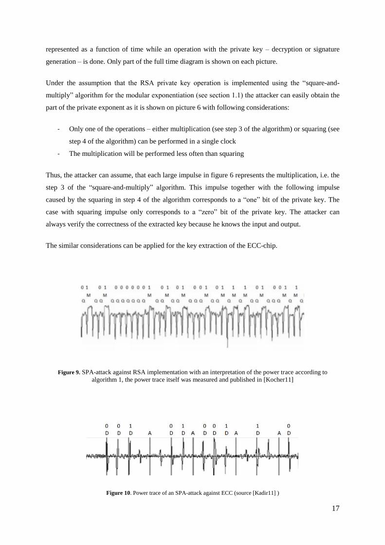
represented as a function of time while an operation with the private key – decryption or signature
generation – is done. Only part of the full time diagram is shown on each picture.
Under the assumption that the RSA private key operation is implemented using the “square-and-
multiply” algorithm for the modular exponentiation (see section 1.1) the attacker can easily obtain the
part of the private exponent as it is shown on picture 6 with following considerations:
- Only one of the operations – either multiplication (see step 3 of the algorithm) or squaring (see
step 4 of the algorithm) can be performed in a single clock
- The multiplication will be performed less often than squaring
Thus, the attacker can assume, that each large impulse in figure 6 represents the multiplication, i.e. the
step 3 of the “square-and-multiply” algorithm. This impulse together with the following impulse
caused by the squaring in step 4 of the algorithm corresponds to a “one” bit of the private key. The
case with squaring impulse only corresponds to a “zero” bit of the private key. The attacker can
always verify the correctness of the extracted key because he knows the input and output.
The similar considerations can be applied for the key extraction of the ECC-chip.
Figure 9. SPA-attack against RSA implementation with an interpretation of the power trace according to
algorithm 1, the power trace itself was measured and published in [Kocher11]
Figure 10. Power trace of an SPA-attack against ECC (source [Kadir11] )

18
After decapsulation of the chip the current power consumption can be also measured directly on the
chip wires using special equipment. This invasive technique is called “microprobing”.
Figure 11 shows the microprobing station in IHP. It contains a set of different active and passive
probes and manipulators, a high resolution microscope, device test socket and precision x-y stepper
table.
Figure 11. Microprobing Station at IHP
In order to get an electrical contact to the measurement points the surface of the chip need to be
prepared properly i.e. the passivation need to be removed. This can be done in two different ways:
- Chemical etching, in this case the passivation will be removed in a pretty large area
- Using a laser-cutter allows to remove the passivation at selected points only
The latter is by far more suited for microprobing since it provides a better contact to the measurement
point as shown in Figure 12. Figure 13 shows the measurement process using a microprobing station
at IHP.

19
Figure 12. Microprobing: in order to do measurements directly at the metal layer the passivation need to be removed. Using
a laser cutter the area in which the passivation is removed can be kept small, this helps to create a stable electrical contact
since the needle cannot move around.
Figure 13. Microprobing: two needle probers with contact to the chip for measurements
The measurements can be done also on other metal layers if additional special equipment is ready to
use. If other layers than the two top metal layers shall be attacked a Focused Ion Beam station (FIB) is
needed. It consists of a vacuum chamber with an ion source that normally accelerates Gallium ions and
bundles them to a beam. This ion beam can be used to modify on chip wiring i.e. those wires can be
cut but new wires can be implanted as well. The current power consumption of the cryptographic chip
can be measured after the changing its structure with a FIB. These measurement results can provide
the attacker additional helpful information for the key extraction.
Modern FIB stations come with an additional electron source in order to provide visualization
according to the scanning electron microscope (SEM) principle. The lateral resolution of the ion beam
is about 4nm and the one of the SEM about 2 nm. Thus, the granularity of resolution is by far smaller
than the currently used CMOS technologies.

20
Figure 14 shows the IHP FIB station, and Figure 15 and Figure 16 illustrate the changes in the chip
structure realized using a FIB.
Figure 14. Focused Ion Beam Station at IHP
Figure 15. Picture taken with the IHP FIB-station showing modification of the structure of chip manufactured at IHP

21
Figure 16. Modifications of a chip structure using a FIB (source [TUBerlin])
The typical examples of semi-invasive attacks are different imaging techniques for passively obtaining
information (microscope and infrared imaging, optical emission analysis) or influence on the chip with
light or temperature. These attacks are possible only after decapsulation of the chip since they require
access to its surface. The electrical contact to internal lines of the chip is not required and the structure
of the chip is not destroyed or modified, what differentiates semi-invasive from invasive attacks.
Semi-invasive attacks can be applied for modification of SRAM and EEPROM content, or for
obtaining information about any individual transistor as well for changing states of transistors
[Skor05].
A practical low-cost attack is described in [Skor03]. The attack exploits the sensitivity of transistors to
light: illuminating a transistor causes it to conduct. It can cause a security fault in chip that can result
in access to the memory cells that store private key. For this attack a cheap photoflash lamp was
mounted on top of a manual probing station that contains a microscope with the maximum
magnification of 1500x. Authors [Skor03] experimented with the 8-bit microcontroller PIC16F84 of
Microchip Technology Inc. [MIT]. Figure 17 and Figure 18 show the experimental equipment and the
tested microcontroller respectively.

22
Figure 17. Experimental equipment: probing workstation with mounted photoflash lamp (source [Skor03])
Figure 18. Microchip Technology Inc.‟s 8-bit microcontroller PIC16F84 original and decapsulated (source [Skor03])
According to [Skor03] it was possible to change any individual bit of the SRAM array. These results
are published 10 years ago. Semi-invasive attacks are currently becoming a very serious threat to
hardware security. For example, [Trichina10] presented a successful semi-invasive two-fault laser
attack on a protected RSA implementation running on a 32-bit ARM Cortex M3 core [ARM].
In next section we give a short overview of principles of countermeasures.

23
4. Principles of countermeasures
In this section we focus on basic principles of countermeasures since an exhausting discussion of
specific countermeasures will never be complete and new types of attacks will require new
individually designed countermeasures. But we will provide an example of a successful
countermeasure pattern i.e. the use dummy operations.
The following enumeration provides a solid overview on principles of countermeasures as well as
individual means:
Prevent access to measurement and manipulation relevant parts of the chip
Shielding and covering of the chip or even the PCB (printed circuit board) to defeat non-
invasive attacks and to increase the complexity of the chip preparation for invasive and
semi-invasive attacks
o Different types of housing
- Weather and/or intrusion resistant casing
- Integrated Faradey-cage to prevent EMA
- etc.
o resin-, foam covering including PINs
o passive shielding of the chip structure e.g. use of additional metal layers to
prevent optical imaging and EMA
technological approaches to defeat invasive and semi-invasive attacks
o etching resistant passivation layer
o manufacturing in smaller technologies
o increase number of layers per chip
o hide memory in lower layers of the chip
o protect or destroy test structures and/or scan chains
Detection of - and reaction on manipulations
Anti-Tampering means
o Sensors e.g. light, power, voltage, frequency, temperature to detect attempts to
open the chip
o Active shielding of the chip structure: additional metal layers or wires that cover
the ASIC and that are connected to a certain voltage or signal, alterations in the
voltage or the signal indicate a manipulation
o Error detection and correction: redundant implementation of blocks with identical
functionality. Manipulations are detected if those blocks provide different results
Typical reactions after detecting manipulations

24
o Overwriting the memory ( best with random numbers)
o Switching off the device
o Chip self destruction
Reduce the information provided by the measurement values
Security by obscurity
o No information about the used crypto algorithm
o No standardized solution (own elliptic curve)
o Unmarking, remarking and repackaging of the chip
Flawless Implementation
o algorithmic:
- flawless re-design of crypto implementations (e.g. use „dummy
operations“)
- PUFs (Physically Unclonable Functions) to store the private key
- etc.
o hardware:
- integration of „dummy“ gates
- gates with power consumption independent of the input values
- asynchronous design
- dual-rail logic
Information concealment
o Adapt the signal to noise ratio
o Execute program code in random order
o Use modules with random power consumption
o Randomization, e.g. blinding, doubling, masking
In the following paragraph we will use the “double-and-add” and the “square-and-multiply”
algorithms to illustrate an algorithmic approach to increase the effort for key extraction.
In section 1 of this chapter we already explained the weaknesses of „double-and-add“ algorithm used
for implementing the EC point multiplication and the one of the „square-and-multiply“ algorithm used
for RSA exponentiation. The major issue of both algorithms is the different number of operations
executed depending on the bit values of the key. I.e. if the current key bit is a ‚0„ only one of the two
operations is performed, point doubling in case of EC point multiplication and squaring in case of
RSA. The time difference or the difference in power consumption in comparison to the case when the
current key bit value is a ‚1„ i.e. when two operations are executed is measurable. Figure 19 shows a
successful example of an SEMA against an ASIC, providing an ECC implementation. The private key
can be extracted by simple optical inspection of the power consumption.

25
Figure 19. Successful SEMA-Attack against an ECC implementation: current power consumption as a function of time
during the execution of the „double-and-add“ algorithm, (source [KekeWu09])
In order to avoid key extraction by analyzing the execution time or power consumption the algorithms
can be modified. The modified algorithms are denoted as „double-and-add-always“ and „square-and-
multiply-always“ respectively. The main idea is to introduce additional operations that are not needed
to compute the correct result but that are used only to ensure that the calculation time and the energy
consumption are independent of the key bits. The drawback of such means is the increased resource
consumption, chip area and/or energy consumption.
Figure 20 shows the measurement results for the „double-and-add-always“ algorithm. In this
implementation the point doubling and the point addition are executed independent of the value of the
individual key bits. So, the key extraction can be avoided, see Figure 20 now there is a point addition
executed after each point doubling operation.
Figure 20. Current power consumption as a function of time during the execution of the „double-and-add“ algorithm,
(source [KekeWu09]) SEMA-resistant Implementation, i.e.” double-and-add-always”
The following table shows attacks, exploited effects countermeasures, and provides an assessment
whether or not a certain countermeasure helps against a certain attack. No value in the table means no
effect of the countermeasure on the attack, „y‟ means helpful means, +- means the attack becomes
more difficult if such a means is deployed but is still feasible. „y1‟ means that the counter measure is

26
successful if the attack is detected. We are aware of the fact that this is extremely difficult for non-
invasive attacks.
Table 1. Attacks and countermeasures
Attacks
Name
and
short description of countermeasures
non-invasive decapsulated chip (semi invasive, invasive)
Tim
ing
att
ack
Po
wer
Anal
ysi
s (P
A)
Ele
ctro
Mag
net
ic A
nal
ysi
s
An
aly
sis
of
test
str
uct
ure
s (S
can
chai
ns)
Gli
tch
Ele
ctro
Mag
net
ic A
nal
ysi
s
Imag
ing
Op
tica
l em
issi
on
An
aly
sis
(bac
ksi
de)
Dat
a R
eman
ence
Anal
ysi
s
Fau
lt I
nje
ctio
n (
fro
nt
side)
Fau
lt I
nje
ctio
n (
bac
k s
ide)
PA
w
ith
Mic
rop
robin
g
Alt
erat
ion
of
the
chip
str
uct
ure
erän
der
ung
der
Str
uktu
r R
ever
se-E
ng
inee
rin
g
An
aly
sis
of
test
str
uct
ure
s
Smaller technology Smaller voltage side-channel leakage
less informative ± ± ± ± ± ± ± ± ± ± ±
Additional metal layers Access to transistors from the front side
is more difficult ± ± ± ± ± ± ± ±
Destroying test structures (HW)
Avoiding Access to measurement point
used for test purposes ± y
Dummy Gate side- channel leakage per clock less
informative since some not really use
gates are switching y y ± ± ± ± ± ± ± ± ±
Internal Clock Aims at preventing manipulation
(acceleration and deacceleration) of the
clock ± ± y ± ±
±
Internal voltage control Aims at preventing manipulation of the
voltage ± ± y ± ±
Asynchronous design Analysis of measurement results is more
difficult, the alignment due to the clock
is missing
± ±
± ±
±
Signal-Noise Ratio side-channel leakage less informative,
peaks in consumption not that easy
detectable y y ±
±
Dummy Operations
Create constant side- channel leakage
per processed bit of the key i.e. side-
channel leakage≠f(key) chip will
consist of more gates
y y y ± ±
±
Blinding, Duplication,
Masking
side-channel leakage is no longer a direct
function of the inputs; it does not
necessarily mean that the side-channel
leakage is also independent of the key
y ± ± ± ±
±
Coating with integrated
destruction of the correct function chip
Aims at preventing measurements at the
correct working chip
y y y y y y y y y ± ± ±
Reaction on detected
tampering e.g.
invalidating sensitive parts of the memory
No longer correct data e.g. secret keys
stored in the memory y1 y1 y1 y1 y y y y y y y y
Reaction on detected
tampering: switching off the device
No functionality of the chip if an attack
was detected, i.e. access to secret data is
prohibited y y y y y y y y y y y
Ex
plo
ited
ph
ysic
al
effe
ct f
or
att
ack
E
xec
uti
on
tim
e o
f th
e al
gori
thm
as
a fu
nct
ion o
f
tim
e (t
ime
=f(
inp
uts
))
Dif
fere
nce
s in
th
e p
ow
er c
onsu
mpti
on
bet
wee
n
acti
ve
and
in
acti
ve
gat
es
EM
-rad
iati
on
th
at i
s em
itte
d w
hen
tra
nsi
sto
rs
are
swit
chin
g
Inte
rmed
iate
mea
sure
men
t poin
ts i
mple
mente
d
for
test
pu
rpo
ses
and
/or
scan
chai
ns
Dep
end
ency
of
tran
sist
ors
on e
nvir
onm
enta
l
con
dit
ion
s
EM
-rad
iati
on
th
at i
s em
itte
d w
hen
tra
nsi
sto
rs
are
swit
chin
g
Str
uct
ure
of
a n
on
-wo
rkin
g c
hip
can
no
t be
anal
yze
d
Lu
min
esce
nce
th
at c
om
es w
ith t
ransi
stors
swit
chin
g t
Rem
ain
ing
ch
arg
e o
f th
e tr
ansi
sto
rs
Dep
end
ency
of
tran
sist
ors
on e
nvir
onm
enta
l
con
dit
ion
s (
at a
wo
rkin
g d
evic
e)
Mea
sure
men
t at
th
e on c
hip
wir
ing a
re s
ourc
e of
dif
fere
nt
inte
rmed
iate
val
ues
Th
e st
ruct
ure
of
the
chip
is
alte
red u
sing a
FIB
e.g
. im
pla
nti
ng
new
conta
cts
Th
e v
isib
le s
tru
ctu
re o
f th
e ch
ip:
tran
sist
ors
, on
chip
wir
ing
etc
. w
ill
be
reco
rded
e.g
. by p
hoto
s
Inte
rmed
iate
mea
sure
men
t poin
ts i
mple
mente
d
for
test
pu
rpo
ses
and/o
r sc
an c
hai
ns

27
Conclusion
In this chapter we introduced side channel attacks as a significant threat for wireless sensor networks,
since in those systems the individual sensor node can be accessed physically and being analysed
afterwards. Even though such attacks are known for years they have never been considered before in
the area of WSNs. This might be partly due to the fact that other security problems have gained more
attention since they have been considered more likely than the more complex and more expensive side
channel attacks. However the cost of side channel attacks can no longer be considered as a protection
means since high end equipment can be rented for a few hundred EURO per hour. Thus we tried to
create more awareness for side channel attacks and potential countermeasures in this chapter.
References
Ajluni95 C. Ajluni: Two New Imaging Techniques Promise To Improve IC Defect Identification, Electronic
Design, vol. 43(14), pp. 37–38
ANSI ANSI X9.63: Public Key Cryptographyfor the Financial Services Industry: Elliptic Curve Key
Agreementand Key Transport Schemes, ftp://ftp.iks-jena.de/mitarb/lutz/standards/ansi/X9/x963-7-5-
98.pdf
ARM 32-bit ARM Cortex M3 core documentation, http://www.arm.com/products/processors/cortex-
m/cortex-m3.php
Barker07 E. Barker, D. Johnson, and M. Smid: Nist special publication 800-56a, recommendation for pair-wise
key establishment schemes using discrete logarithm cryptography (revised),
http://csrc.nist.gov/publications/nistpubs/800-56A/SP800-56A_Revision1_Mar08-2007.pdf
Brum11 B. Brumley, N. Tuveri: Remote Timing Attacks are Still Practical, Cryptology ePrint Archive
http://eprint.iacr.org/2011/232
Carlier04 V. Carlier, H. Chabanne, E. Dottax, and H. Pelletier: Electromagnetic side channels of an FPGA
implementation of AES, IACR Cryptology ePrint Archive, Technical report, SAGEM SA
Drut02 Milos Drutarovskı and Viktor Fischer: True Random Number Generator Embedded in Altera ACEX
Devices, In Proceedings of DCIS‟02, pp. 587–592
Eberle04 Hans Eberle, Sheueling Chang Shantz, Vipul Gupta, Nils Gura: Accelerating Next-Generation Public-
key Cryptography on General-purpose CPU, Hot Chips 16, IEEE Symposium on High Performance
Chips, Stanford University
Fan10 Junfeng Fan, Xu Guo, Elke De Mulder, Patrick Schaumont, Bart Preneel, Ingrid Verbauwhede: State-
of-the-art of Secure ECC Implementations: A Survey on Known Side-channel Attacks and
Countermeasures, Proceedings of the 2010 IEEE International Symposium on Hardware-Oriented
Security and Trust (HOST 2010), 13-14 June 2010, Anaheim Convention Center, California, USA.
IEEE Computer Society, pp.76-87
Ferrigno08 J. Ferrigno, M. Hlaváč: When AES blinks: introducing optical side channel, IET Information
Security, Vol. 2, No. 3, 2008, pp. 94–98
Fischer02 Viktor Fischer and Milos Drutarovskı: True Random Number Generator Embedded in Reconfigurable
Hardware, Springer-Verlag, Proceedings of CHES‟02, Lecture Notes in Computer Science, vol. 2523,
pp. 415–430

28
Giry11 Damien Giry, Jean-Jacques Quisquater: Cryptographic key length recommendation, BlueKrypt - v
26.6, 2010, http://keylength.com
Hanker04 D. Hankerson, A. Menezes, and S. Vanstone: Guide to Elliptic Curve Cryptography, Springer-Verlag
New York, Inc.
Kadir11 Sahbuddin Abdul Kadir, Arif Sasongko: Simple power analysis attack against elliptic curve
cryptography processor on FPGA implementation, In International Conference on Electrical
Engineering and Informatics, pp. 1-4
Kaliski97 B. Kaliski and M. Robshaw: Comments on some new attacks on cryptographic devices, RSA
Laboratories , Technical report Bulletin Number 5,
Kaliski99 Burt Kaliski: Elliptic Curve Cryptography, RSA Labor,
http://www.scribd.com/doc/59254287/48/ECAES-Encryption
KekeWu09 Keke Wu, Huiyun Li: Electromagnetic analysis on elliptic curve cryptosystems: Measures and
counter-measures for smart cards, In Third International Symposium on Intelligent Information
Technology Application, IEEE, pp. 40–43
Koblitz N. Koblitz: Elliptic curve cryptosystems, in Mathematics of Computation Vol. 48, Nr. 177, 1987, pp.
203–209
Kocher_TA Paul C. Kocher: Timing Attacks on Implementations of Diffie-Hellman, RSA, DSS, and Other
Systems, Proceeding of CRYPTO 1996, pp. 104-113
Kocher11 Paul Kocher, Joshua Jaffe: Introduction to differential power analysis, Journal of Cryptographic
Engineering, vol. 1(1), pp. 5-27
Kocher98 P. Kocher, J. Jaffe, and B. Jun: Differential power analysis, Technical report,
http://www.cryptography.com/public/pdf/DPA.pdf
Koeune99 F. Koeune, J.-J. Quisquater: A Timing Attack against Rijndael, Katholische Universitaet Louvain,
Crypto Group, Technical report CG-1999/1
http://citeseerx.ist.psu.edu/viewdoc/summary?doi=10.1.1.42.679
Mangard02 S. Mangard: A simple power-analysis (SPA) attack on implementations of the AES key expansion, In
P. Lee and C. Lim, editors, ICISC, pp. 243–358
Mangard12 Johann Heyszl, Stefan Mangard, Benedikt Heinz, Frederic Stumpf, Georg Sigl: Localized
Electromagnetic Analysis of Cryptographic Implementations, LNCS Topics in Cryptology - CT-RSA
2012 - The Cryptographers' Track at the RSA Conference 2012, Springer
Miller V. Miller: Use of elliptic curves in cryptography, V. Miller: Use of elliptic curves in cryptography.
Proceeding CRYPTO ‟85 in Advances in Cryptology, Springer-Verlag London, 1986, pp. 417-426
MTI Microchip Technology Incorporation, http://www.microchip.com/
Mulder10 Elke De Mulder: Electromagnetic Techniques and Probes for Side-Channel Analysis on
Cryptographic Devices, Dissertation, Katholieke Universiteit Leuven ,
http://www.cosic.esat.kuleuven.be/publications/thesis-182.pdf
NIST_01 NIST Computer Security Division: Advanced Encryption Standard, FIPS 197,
http://csrc.nist.gov/publications/fips/fips197/fips-197.pdf
NIST01 NIST Computer Security Division: Digital Signature Standard (DSS), FIPS 186-3,
http: //csrc.nist.gov/publications/fips/fips186-3/fips_186-3.pdf
Perin12 G Perin, L Torres, P Benoit and P Maurine: Amplitude Demodulation-based EM Analysis of
Different RSA Implementations, Proceeding of DATE-2012, 12-16 March 2012, pp. 1167 – 1172

29
RSA77 R. L. Rivest, A. Shamir, and L. M. Adelman: A method for obtaining digital signatures and public
key cryptosystems, Technical Report MIT/LCS/TM-82, Laboratory for Computer Science,
Massachusetts Institute of Technology, Cambridge
Samyde02 David Samyde, Sergei Skorobogatov: On a new way to read data from memory, In SISW2002 First
International IEEE Security in Storage Workshop, USA
Schel06 Dries Schellekens, Bart Preneel, Ingrid Verbauwhede: FPGA Vendor Agnostic True Random Number
Generator, Field Programmable Logic and Applications, 2006 (FPL '06), pp. 1-6
Schmidt11 Jörn-Marc Schmidt, Mario Kirschbaum: Analysis of attacks on sensor nodes software and hardware,
TAMPREs - Tamper Resistant Sensor Node - Project, Deliverable D1.2 Report,
http://www.tampres.eu/
SEC1 Certicom Research, Standards for efficient cryptography group (secg) Sec 1: Elliptic curve
cryptography, http://www.secg.org/download/aid-780/sec1-v2.pdf
SEC2 Second Standards for Efficient Cryptography Group (SECG), SEC 2: Recommended Elliptic Curve
Domain Parameters, http://www.secg.org/download/aid-784/sec2-v2.pdf
Skor_05 Sergei Skorobogatov: Data Remanence in Flash Memory Devices, Springer-Verlag, Cryptographic
Hardware and Embedded Systems Workshop (CHES-2005), 30 August - 1 September 2005, LNCS
3659, pp.339-353
Skor_09 Skorobogatov, S. : Local Heating Attacks on Flash Memory Devices, Proceedings of the 2009 IEEE
International Symposium on Hardware-Oriented Security and Trust (HOST 2009), Moscone Center,
San Francisco
Skor02 Sergei Skorobogatov: Low Temperature Data Remanence in Static RAM, Technical Report UCAM-
CL-TR-536, University of Cambridge, Computer Laboratory
Skor03 S. Skorobogatov and R. Anderson: Optical fault induction attacks, In B. Kaliski, C. Koc, and C. Paar,
editors, Cryptographic Hardware and Embedded Systems - CHES 2002, Springer Berlin / Heidelberg,
Lecture Notes in Computer Science, vol. 2523, pp. 2–12
Skor05 S. P. Skorobogatov: Semi-invasive attacks - a new approach to hardware security analysis, Computer
Laboratory, University of Cambridge, Technical report ucam-cl-tr-630
Skor09 S. P. Skorobogatov: Using optical emission analysis for estimating contribution to power analysis,
IEEE Computer Society, In Fault Diagnosis and Tolerance in Cryptography (FDTC), 2009, pp. 111–
119
TAMPRES Project: tamper resistant sensor nodes, http://www.tampres.eu/
Trich10 Elena Trichina, Roman Korkikyan: Multi Fault Laser Attacks on Protected CRT-RSA, Fault
Diagnosis and Tolerance in Cryptography (FDTC), 2010 Workshop on 21-21 Aug. 2010, pp. 75 - 86,
Tuan07 Tim Tuan, Tom Strader, Steve Trimberger : Analysis of Data Remanence in a 90nm FPGA, IEEE
2007 Custom Integrated Circuits Conference (CICC), pp. 93 - 96
TUBerlin P. Sadewater, K. R. Wirth, S. K. Brahma, C. Boit: Poster: Focused Ion Beam (FIB) Applications, TU
Berlin, Fachgebiet Halbleiterbauelemente, Institut für Hochfrequenz und
Halbleitersystemtechnologien, http://www.hlb.tu-berlin.de/fileadmin/fg6/fib2.pdf
Wills90 K.S. Wills, T. Lewis, G. Billus, H. Hoang: Optical Beam Induced Current Applications For Failure
Analysis of VLSI Devices, Proceedings International Symposium for Testing and Failure Analysis,
pp. 21-26
Zhou05 Zhou Y., Feng D.: Side-Channel Attacks: Ten Years After Its Publication and the Impacts on
Cryptographic Module Security Testing, Cryptology ePrint Archive, Report 2005/388
http://eprint.iacr.org/2005/388.pdf
Related Documents