ARTICLE OPEN Improving stability of organometallic-halide perovskite solar cells using exfoliation two-dimensional molybdenum chalcogenides Meiying Liang 1 ✉ , Adnan Ali 2 , Abdelhak Belaidi 2 , Mohammad Istiaque Hossain 2 , Oskar Ronan 1 , Clive Downing 1 , Nouar Tabet 3 , Stefano Sanvito 1 , Fedwa EI-Mellouhi 2 ✉ and Valeria Nicolosi 1 ✉ Organometallic-halide perovskite solar cells (PSCs) are emerging as the most promising next generation solar cell devices. However, the stability is still the main bottleneck of their further development. Here, we introduce two-dimensional (2D) molybdenum chalcogenides (MoS 2 and MoSe 2 ) (MCs) nanoflakes as a buffer layer between perovskite layer and hole transport layer (HTL) to improve the stability of the organometallic-halide PSCs. 2D MCs are obtained via liquid-phase exfoliated (LPE) approach, and Glass/ FTO/compact-TiO 2 / mesoporous-TiO 2 /FA 85 MA 15 PbI 85 Br 15 /2D MCs/Spiro-OMeTAD/Au structured solar cell devices are designed and fabricated. In this system, 2D MCs act both as a protective layer and an additional HTL of PSCs. This kind of PSCs achieve a relatively high-power conversion efficiency (PCE) of 14.9%, along with a much longer lifetime stability compared to the standard PSCs. After 1 h, PCE of the PSC adding a 2D MCs buffer layer could maintain 93.1% of initial value, while the PCE of the standard PSC dropped dramatically to 78.2% of initial efficiency. Our results pave the way towards the implementation of 2D MCs nanoflakes as a material able to boost the shelf life of PSCs and further provide the opportunity to fabricate large-area PSCs in view of their commercialization. npj 2D Materials and Applications (2020)4:40 ; https://doi.org/10.1038/s41699-020-00173-1 INTRODUCTION Traditional solar energy conversion devices based on crystalline silicon face the challenge of resource limitations and their energy intensive production process 1 . Therefore, there is an urgent need to develop cheap and efficient solar cells 2,3 . High-performance, economically viable, abundant and scalable device components are key to developing the solar cell materials. Organometallic- halide perovskite solar cells (PSCs) are among of the most promising candidates for next generation solar cell technology 4–6 . Organometallic-halide perovskite have intense light absorption coefficient (1.5 × 10 4 cm -1 at 550 nm), long electron and hole diffusion length (up to 1 mm) and high carrier mobility (1–10 cm 2 V -1 s -1 ) 7–10 . However, the stability of PSCs has become a major barrier for their further development in the market 11–17 . Because perovskites are very sensitive to environment such as air, UV light, water, thermal stress and other factors 18–20 . Normally, adding hole and electron transporting layers (HTL and ETL, respectively) in PSCs between the perovskite layer and the electrodes helps to separate and selectively collect the generated charge carriers (holes at the cathode and electrons at the anode electrode) 21 . To date, TiO 2 is the most widely used ETL material for PSCs to prevent electron-hole recombination at the anode 4,6,22 . This kind of ETL typically consists of compact TiO 2 layer (c-TiO 2 , 50–80 nm) and mesoporous TiO 2 layer (mp-TiO 2 , 200–300 nm) 4,6,22 . On the other hand, 2,2′,7,7′‐tetrakis‐(N,N‐di‐4‐methoxyphenylamino)‐9,9′‐spiro- bifluorene (Spiro-MeOTAD) represents the reference hole trans- port material (HTM) used for PSCs due to its facile deposition and high performance 23 . It could effectively transfer the photogener- ated holes from the perovskite to the cathode while blocking the electrons from reaching the cathode. Unfortunately, Spiro- OMeTAD also has serious degradation issues induced by UV light, temperature, additives, and environmental conditions 23 . It appears that Spiro-OMeTAD HTL contributes to the poor stability of PSCs solar cell devices as well. Therefore, many other HTMs, such as copper (I) thiocyanate (CuSCN) 24 , nickel (II) oxide (NiO) 25 , and poly (3,4-ethylenedioxythiophene) polystyrene sulfonate (PEDOT: PSS) 26,27 , have been explored to improve the PV performance including the stability of PSCs. However, these alternative HTMs could hardly compete to replace the ideal band edge positions of the Spiro-OMeTAD with respect to the perovskite absorbing layer. Another strategy to improve the stability of PSCs is inserting a buffer layer into the device structure to optimize the interface between the perovskite layer and Spiro-OMeTAD HTL 28–31 . For either a HTL or a buffer layer, two-dimensional (2D) molybdenum chalcogenides (MCs) (such as molybdenum disulfide [MoS 2 ] and molybdenum diselenide [MoSe 2 ]) are emerging as potential candidates due to their high carrier mobility, low cost (e.g. MoS 2 Sigma-Aldrich, 0.85 € g -1 ), and solution-processable properties 29–36 . 2D MoS 2 nanoflakes have improved the efficient charge extraction across the HTL reducing recombination at the interfaces 35,36 . Therefore, combination of 2D MCs and perovskite gives us opportunity to obtain solar cells with good efficiency and longer-term stability. In this work, 2D MCs (such as MoS 2 and MoSe 2 ) nanoflakes were prepared via liquid-phase exfoliation (LPE) approach, which is a non-destructive, insensitive (to the environment such as air and water) and solution-processable method 37,38 . Then, these 2D MCs nanoflakes were utilized as a buffer layer material between perovskite layer and HTL (i.e., Spiro-OMeTAD) of the device to enhance the stability of PSCs. Based on the previous studies, 1 School of Chemistry, Centre for Research on Adaptive Nanostructures and Nanodevices (CRANN) and Advanced Materials and BioEngineering Research (AMBER), Trinity College Dublin, Dublin 2, Ireland. 2 Qatar Environment and Energy Research Institution (QEERI), Hamad Bin Khalifa University (HBKU), Doha 34110, Qatar. 3 Department of Applied Physics and Astronomy, University of Sharjah, P. O. Box 27272, Sharjah, UAE. ✉ email: [email protected]; [email protected]; [email protected] www.nature.com/npj2dmaterials Published in partnership with FCT NOVA with the support of E-MRS 1234567890():,;

Welcome message from author
This document is posted to help you gain knowledge. Please leave a comment to let me know what you think about it! Share it to your friends and learn new things together.
Transcript

ARTICLE OPEN
Improving stability of organometallic-halide perovskite solarcells using exfoliation two-dimensional molybdenumchalcogenidesMeiying Liang 1✉, Adnan Ali 2, Abdelhak Belaidi 2, Mohammad Istiaque Hossain2, Oskar Ronan1, Clive Downing1, Nouar Tabet 3,Stefano Sanvito1, Fedwa EI-Mellouhi2✉ and Valeria Nicolosi 1✉
Organometallic-halide perovskite solar cells (PSCs) are emerging as the most promising next generation solar cell devices. However,the stability is still the main bottleneck of their further development. Here, we introduce two-dimensional (2D) molybdenumchalcogenides (MoS2 and MoSe2) (MCs) nanoflakes as a buffer layer between perovskite layer and hole transport layer (HTL) toimprove the stability of the organometallic-halide PSCs. 2D MCs are obtained via liquid-phase exfoliated (LPE) approach, and Glass/FTO/compact-TiO2/ mesoporous-TiO2/FA85MA15PbI85Br15/2D MCs/Spiro-OMeTAD/Au structured solar cell devices are designed andfabricated. In this system, 2D MCs act both as a protective layer and an additional HTL of PSCs. This kind of PSCs achieve a relativelyhigh-power conversion efficiency (PCE) of 14.9%, along with a much longer lifetime stability compared to the standard PSCs. After1 h, PCE of the PSC adding a 2D MCs buffer layer could maintain 93.1% of initial value, while the PCE of the standard PSC droppeddramatically to 78.2% of initial efficiency. Our results pave the way towards the implementation of 2D MCs nanoflakes as a materialable to boost the shelf life of PSCs and further provide the opportunity to fabricate large-area PSCs in view of theircommercialization.
npj 2D Materials and Applications (2020) 4:40 ; https://doi.org/10.1038/s41699-020-00173-1
INTRODUCTIONTraditional solar energy conversion devices based on crystallinesilicon face the challenge of resource limitations and their energyintensive production process1. Therefore, there is an urgent needto develop cheap and efficient solar cells2,3. High-performance,economically viable, abundant and scalable device componentsare key to developing the solar cell materials. Organometallic-halide perovskite solar cells (PSCs) are among of the mostpromising candidates for next generation solar cell technology4–6.Organometallic-halide perovskite have intense light absorptioncoefficient (1.5 × 104 cm−1 at 550 nm), long electron and holediffusion length (up to 1mm) and high carrier mobility (1–10 cm2
V−1 s−1)7–10. However, the stability of PSCs has become a majorbarrier for their further development in the market11–17. Becauseperovskites are very sensitive to environment such as air, UV light,water, thermal stress and other factors18–20. Normally, adding holeand electron transporting layers (HTL and ETL, respectively) inPSCs between the perovskite layer and the electrodes helps toseparate and selectively collect the generated charge carriers(holes at the cathode and electrons at the anode electrode)21. Todate, TiO2 is the most widely used ETL material for PSCs to preventelectron-hole recombination at the anode4,6,22. This kind of ETLtypically consists of compact TiO2 layer (c-TiO2, 50–80 nm) andmesoporous TiO2 layer (mp-TiO2, 200–300 nm)4,6,22. On the otherhand, 2,2′,7,7′‐tetrakis‐(N,N‐di‐4‐methoxyphenylamino)‐9,9′‐spiro-bifluorene (Spiro-MeOTAD) represents the reference hole trans-port material (HTM) used for PSCs due to its facile deposition andhigh performance23. It could effectively transfer the photogener-ated holes from the perovskite to the cathode while blocking theelectrons from reaching the cathode. Unfortunately, Spiro-
OMeTAD also has serious degradation issues induced by UV light,temperature, additives, and environmental conditions23. It appearsthat Spiro-OMeTAD HTL contributes to the poor stability of PSCssolar cell devices as well. Therefore, many other HTMs, such ascopper (I) thiocyanate (CuSCN)24, nickel (II) oxide (NiO)25, and poly(3,4-ethylenedioxythiophene) polystyrene sulfonate (PEDOT:PSS)26,27, have been explored to improve the PV performanceincluding the stability of PSCs. However, these alternative HTMscould hardly compete to replace the ideal band edge positions ofthe Spiro-OMeTAD with respect to the perovskite absorbing layer.Another strategy to improve the stability of PSCs is inserting abuffer layer into the device structure to optimize the interfacebetween the perovskite layer and Spiro-OMeTAD HTL28–31.For either a HTL or a buffer layer, two-dimensional (2D)
molybdenum chalcogenides (MCs) (such as molybdenum disulfide[MoS2] and molybdenum diselenide [MoSe2]) are emerging aspotential candidates due to their high carrier mobility, low cost(e.g. MoS2 Sigma-Aldrich, 0.85 € g-1), and solution-processableproperties29–36. 2D MoS2 nanoflakes have improved the efficientcharge extraction across the HTL reducing recombination at theinterfaces35,36. Therefore, combination of 2D MCs and perovskitegives us opportunity to obtain solar cells with good efficiency andlonger-term stability.In this work, 2D MCs (such as MoS2 and MoSe2) nanoflakes were
prepared via liquid-phase exfoliation (LPE) approach, which is anon-destructive, insensitive (to the environment such as air andwater) and solution-processable method37,38. Then, these 2D MCsnanoflakes were utilized as a buffer layer material betweenperovskite layer and HTL (i.e., Spiro-OMeTAD) of the device toenhance the stability of PSCs. Based on the previous studies,
1School of Chemistry, Centre for Research on Adaptive Nanostructures and Nanodevices (CRANN) and Advanced Materials and BioEngineering Research (AMBER), Trinity CollegeDublin, Dublin 2, Ireland. 2Qatar Environment and Energy Research Institution (QEERI), Hamad Bin Khalifa University (HBKU), Doha 34110, Qatar. 3Department of Applied Physicsand Astronomy, University of Sharjah, P. O. Box 27272, Sharjah, UAE. ✉email: [email protected]; [email protected]; [email protected]
www.nature.com/npj2dmaterials
Published in partnership with FCT NOVA with the support of E-MRS
1234567890():,;

Glass/FTO/compact-TiO2/mesoporous-TiO2/FA85MA15PbI85Br15/2DMCs/Spiro-OMeTAD/Au structured solar cells were designed anddemonstrated. (a sketch of the solar cell and its band energydiagram is shown in Fig. 1a and b)22,29,31,39. We investigatedvarious preparation conditions of 2D MC HTL buffer layersfollowed with a characterization of the devices’ power conversionefficiency (PCE) and stability.
RESULTSPreparation of 2D MCs2D MCs nanoflakes (i.e., MoS2 and MoSe2) were obtained viasonication-assisted LPE approach. The principle of LPE method isquite simple. Because of the characteristic of layered structuredmaterials (i.e., strong chemical bonds in-plane but weak interac-tion out-of-plane), ultrasonic energy can easily break up weak vander Waals interactions between each layer to obtain exfoliated 2Dnanoflakes. As shown in Fig. 2a, taking MoS2 as an example, first,bulk MoS2was exfoliated in N-Methyl-2-pyrrolidone (NMP), whoseHansen solubility parameters and surface energy are suitable formost 2D layered materials,using a probe sonic tip37. The sonic tip
was pulsed for 6 s on and 2 s off with 60% amplitude of power toavoid damage to the processor and reduce solvent heating, andthus, degradation. During sonication, the temperature of thesystem was cooled to around 5 °C by continuous flow of coolingwater. Once sonicated, the dispersion was subjected to centrifu-gation to remove any unexfoliated materials. Then, the top 60%supernatant was collected. However, although NMP is the mosteffective solvent for the MoS2 exfoliation, it is toxic (Healthcode ≥ 2, NFPA 704) and has a high boiling point (202 °C).Moreover, it dissolves the perovskite crystals during the proces-sing. Therefore, exfoliated MoS2 nanoflakes were transferred fromNMP to isopropanol (IPA, Health code 1; NFPA 704, boiling point:82.6 °C), forming environmentally friendly colloidal solutions (insetof Fig. 2b) with concentration up to 3mgmL−1. As shown in Fig.2c, UV–vis spectra of exfoliated MoS2 nanoflakes in NMP and IPAdispersions show typical feature absorption peaks of MoS2 (oneabsorption peak onset about 450 nm and two peaks at around674 nm and at around 612 nm), however, at the cost ofconcentration compared to they in NMP dispersion37,40. Inaddition, scanning electron microscopy (SEM, Fig. 2b) imageconfirms the efficient exfoliation into few-layered MoS2
Fig. 1 Structure of the perovskite solar adding a 2D MoS2 HTL buffer layer. a Sketch of the perovskite based solar cell illustrating theapplied 2D MoS2 nanoflakes as a buffer layer between perovskite and Spiro-OMeTAD of PSCs. b Band energy diagram of the whole structure.
Fig. 2 Preparation of the 2D MoS2 nanosheets. a Scheme of the preparation of 2D MoS2 nanoflakes using LPE approach. b SEM image ofexfoliated 2D MoS2 nanoflakes, and inside are exfoliated MoS2 dispersions in an IPA (Scale bar is 500 nm). c Absorbance spectra of exfoliatedMoS2 nanoflakes in NMP and IPA solvents, respectively. d HAADF-STEM (Scale bar is 100 nm) and e high-resolution TEM images of exfoliatedMoS2, inset in part e is fast Fourier transform pattern of exfoliated MoS2 (Scale bar is 5 nm).
M. Liang et al.
2
npj 2D Materials and Applications (2020) 40 Published in partnership with FCT NOVA with the support of E-MRS
1234567890():,;

nanoflakes. High-angle annular dark-field scanning transmissionelectron microscopy (HAADF-STEM, Fig. 2d) image indicates plentyof exfoliated flakes with well-defined edges and no apparentdamage in the basal planes, suggesting the exfoliated material isof high quality. This is further verified by high-resolution TEM(HRTEM, Fig. 2e) and its corresponding fast Fourier transform (FFT,inset of Fig. 2e) pattern of exfoliated MoS2 nanoflakes reveal thehighly crystalline structure of the exfoliated MoS2 nanoflakes. 2DMoSe2 nanoflakes were prepared via the same process as MoS2.HAADF-STEM, HRTEM and its corresponding FFT pattern ofexfoliated 2D MoSe2 nanoflakes presented in SupplementaryFig. 1a, b. Furthermore, different size of 2D MC nanoflakesobtained by centrifuging dispersions at different spin rates(1000 rpm, 3000 rpm, and 5000 rpm) called size selection. Accord-ing to their TEM images and corresponding size distributionhistogram (Supplementary Fig. 2a-f), we could know that whenthe centrifuging rate increased from 1000 rpm to 5000 rpm, theaverage size of the exfoliated 2D MCs nanoflakes decreased from248.27 nm to 42.61 nm. This is expected that increasing thecentrifuging rates decreased the size of the MCs nanoflakes. Andthe thickness of liquid-phase exfoliated 2D MC nanosheets relatesto their size37. The relationship between the dispersed concentra-tion, C, and mean flake dimensions for exfoliated 2D nanosheets is
C / w � tð Þ=L2 (1)
where L is the length, w is the width and t is the thickness. Thisimplies that reducing the concentration and size by increasing thecentrifugation speed will result in thinner nanosheets.
Fabrication of PSCs with a 2D MCs buffer layerAs shown in Fig. 1, a 2D MCs buffer layer was added betweenthe perovskite layer and Spiro-OMeTAD layer (so called “HTLbuffer”) to comprise a Glass/FTO/compact-TiO2/mesoporous-TiO2/FA85MA15PbI85Br15/2D MCs/Spiro-OMeTAD/Au structured PSC. Asrepresentative member of 2D MCs family, MoS2, MoSe2, and
MoTe2 were simulated as HTL buffer layer of the same structuredPSCs. As calculated (Supplementary Fig. 3a, d), adding p-typeMoS2, MoSe2, and MoTe2 show the improvement in performancedue to the increase of the absorbing volume within the MC layersand improve of short-circuit current density (Jsc), Fig. 3 presentsthe fabrication process of the PSCs adding a 2D MCs HTL buffer.Cleaning and depositing ETL layer was done in air atmosphere,after that, samples were transferred into a glovebox to deposit theperovskite, 2D MC buffer, and Spiro-OMeTAD layers. The 2D MCnanoflakes in IPA dispersion was dropped onto the perovskitelayer immediately with the spin-coating started at 2000 rpm andlasted one minute. Compared to the standard PSC, PSCs adding aMoS2 HTL buffer layer, or MoSe2 HTL buffer layer reduced theefficiency to some extent (Supplementary Fig. 4) and this is mainlycaused by the sacrifice of the FF (Supplementary Table 1) becauseof the solvent (i.e., IPA) existing in 2D MCs dispersions. However,this factor could be improved by optimizing deposition process.As shown in Fig. 3, three different conditions were investigated:(P-1) MoS2 deposited on annealed perovskite without furtherannealing; (P-2) MoS2 is deposited on annealed perovskite filmand further annealed at 100 °C in the glove box; (P-3) MoS2 isdeposited on as deposited perovskite film then both films areannealed at 100 °C. Supplementary Fig. 5a, b show the cross-section TEM images presenting the different components of thesolar cell device from the front contact (FTO) to the back contact(Au) of the standard PSC and the PSC with a 2D MoS2 HTL bufferlayer prepared by (P-1), (P-2), and (P-3) methods, respectively.Comparing to the standard solar cell, the perovskite layer of thesolar cell spin-coated the 2D MoS2 dispersion by (P-1) processobviously damaged. This is because the small amount IPA solventin 2D MoS2 dispersions could induce degradation of theperovskite layer. Therefore, adding an annealing process (P-2and P-3) could reduce the damage of IPA on the perovskite layer.However, as shown in Supplementary Fig. 5c, d, the interfacebetween ETL and the perovskite layer of the PSC with a MoS2 HTL
Fig. 3 Three different methods to fabricate the PSCs with a 2D MCs buffer layer. (P-1) MoS2 deposited on annealed perovskite withoutfurther annealing, (P-2) MoS2 is deposited on annealed perovskite film and further annealed at 100 °C for 1 h in the glove box, (P-3) MoS2 isdeposited on as deposited perovskite film then both films are annealed at 100 °C for 1 h.
M. Liang et al.
3
Published in partnership with FCT NOVA with the support of E-MRS npj 2D Materials and Applications (2020) 40

buffer layer annealed separately from the perovskite layer (P-2) ismuch smoother than the one with a MoS2 HTL buffer layerannealed together with the perovskite layer (P-3). It implies a MoS2could influence the growth of the perovskite, so it can reduce thequality of the perovskite layer. Therefore, it’s better to do thedeposition of the MoS2 layer onto the complete perovskite layerby (P-2) method. Figure 4 shows the cross-section TEM image ofthe PSC with a 2D MoS2 HTL buffer layer prepared by (P-2)approach. It shows less roughness then expected at interfacesperovskite / 2D MoS2 / Spiro-OMeTAD which indicates that theinclusion of the MoS2 layer between the perovskite and the Spiro-OMeTAD did not engender big cracks. This could be seen as agood sign for the solar cell operation.
PV performance of PSCs with additional 2D MCs buffer layerFigure 5e shows the IV curves of the four devices includingstandard PSC (without HTL buffer) and PSCs with a 2D MoS2 bufferlayer prepared by three different approaches as described above.
It is clear that the device prepared with sequential annealing (P-2)performs as good as the standard PCS, while the PCS preparedwithout annealing of MoS2 (P-1) or annealing MoS2 together withpristine perovskite film (P-3) performed less efficiently. Interest-ingly, the fill factor (FF) was strongly affected (45.9% instead of64.2%, Fig. 5c, f), followed by the open-circuit voltage (Voc) (0.92 Vinstead of 1.01 V, Fig. 5a, f) but the short-circuit current density(Jsc) was only slightly affected (21.64mA cm-2 instead of 22.22 mAcm-2, Fig. 5b, f). This indicates that there are serious interfaceissues under these two preparation conditions (P-1 and P-3). It isworth noting that IPA can partially dissolve the perovskite, soadding 2D MoS2 buffer layers may lead to a damage of the surfaceof perovskite and this damage can be more serious in cases of(P-1) and (P-3). In (P-1) because the 2D MoS2 film is not annealedso the residues of IPA will have more time to get in contact withthe perovskite surface. In case of (P-3), the 2D MoS2 film is addedon the as deposited perovskite film so not in form of grains(crystals) which is make it surface more soluble than in thecrystalline case. This could be the reason behind the low fill factorof the solar cell devices prepared under these conditions. This is ingood agreement with the cross-section TEM images as mentionedbefore (Supplementary Fig. 5c, d). It is worth noting thatcompared to a standard PSC, a PSC with a MoS2 (P-2) layer hasslightly higher Voc and Jsc so that the efficiency of the device couldmaintain at 14.9% (Fig. 4d, f). This could be attributed toconducting MoS2 nanoflakes improved charge transport propertyof the device36. What’s more, it is clear from the energy bandalignment (Fig. 1b) that MoS2 can act as an electron blocking layer,which suppresses interfacial charge recombination36. In addition,using 2D MoSe2 nanoflakes we studied the effect of thenanoflake’s size to devices’ PV performances. According to theIV curves (Supplementary Fig. 6a–d), we could see that smallersize gave the better PV performance due its higher Jsc and FF thanthe larger size nanoflakes. Therefore, the remaining of thismanuscript focuses on small size 2D MCs nanoflakes integratedinto PSC.
Fig. 4 TEM characterization of a PSC adding a 2DMoS2nanoflakes HTL buffer layer. The cross-section TEM image of aPSC adding a 2D MoS2 nanoflakes HTL buffer layer prepared by P-2(Scale bar is 1 μm).
Fig. 5 Variation of PSC parameters of a standard PSC and a PSCs with a 2D MoS2 HTL buffer layer prepared by P-1, P-2, and P-3 methods.a Voc, b Jsc, c FF, d PCE, e IV curves, and f summary of Voc, FF, Jsc and PEC values of a standard PSC and PSCs adding 2D MCs nanoflakes as P-1,P-2, and P-3.
M. Liang et al.
4
npj 2D Materials and Applications (2020) 40 Published in partnership with FCT NOVA with the support of E-MRS
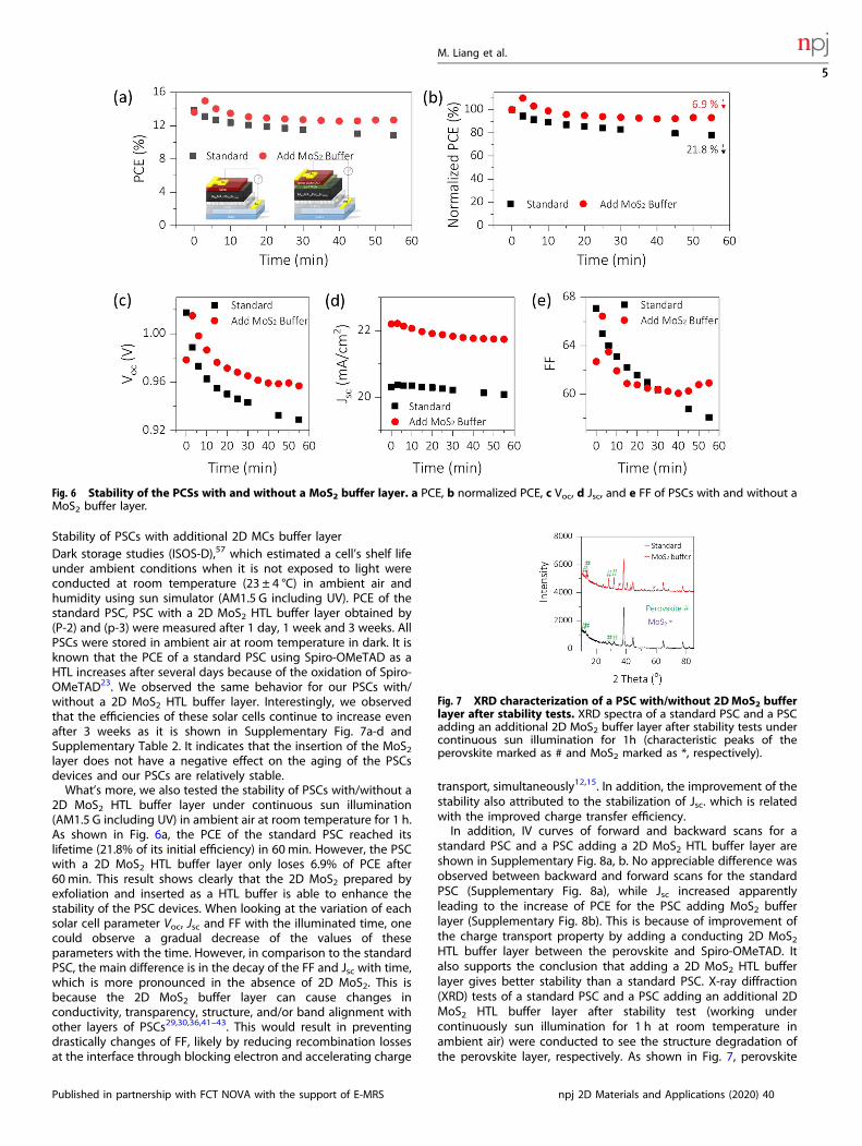
Stability of PSCs with additional 2D MCs buffer layerDark storage studies (ISOS-D),57 which estimated a cell’s shelf lifeunder ambient conditions when it is not exposed to light wereconducted at room temperature (23 ± 4 °C) in ambient air andhumidity using sun simulator (AM1.5 G including UV). PCE of thestandard PSC, PSC with a 2D MoS2 HTL buffer layer obtained by(P-2) and (p-3) were measured after 1 day, 1 week and 3 weeks. AllPSCs were stored in ambient air at room temperature in dark. It isknown that the PCE of a standard PSC using Spiro-OMeTAD as aHTL increases after several days because of the oxidation of Spiro-OMeTAD23. We observed the same behavior for our PSCs with/without a 2D MoS2 HTL buffer layer. Interestingly, we observedthat the efficiencies of these solar cells continue to increase evenafter 3 weeks as it is shown in Supplementary Fig. 7a-d andSupplementary Table 2. It indicates that the insertion of the MoS2layer does not have a negative effect on the aging of the PSCsdevices and our PSCs are relatively stable.What’s more, we also tested the stability of PSCs with/without a
2D MoS2 HTL buffer layer under continuous sun illumination(AM1.5 G including UV) in ambient air at room temperature for 1 h.As shown in Fig. 6a, the PCE of the standard PSC reached itslifetime (21.8% of its initial efficiency) in 60 min. However, the PSCwith a 2D MoS2 HTL buffer layer only loses 6.9% of PCE after60min. This result shows clearly that the 2D MoS2 prepared byexfoliation and inserted as a HTL buffer is able to enhance thestability of the PSC devices. When looking at the variation of eachsolar cell parameter Voc, Jsc and FF with the illuminated time, onecould observe a gradual decrease of the values of theseparameters with the time. However, in comparison to the standardPSC, the main difference is in the decay of the FF and Jsc with time,which is more pronounced in the absence of 2D MoS2. This isbecause the 2D MoS2 buffer layer can cause changes inconductivity, transparency, structure, and/or band alignment withother layers of PSCs29,30,36,41–43. This would result in preventingdrastically changes of FF, likely by reducing recombination lossesat the interface through blocking electron and accelerating charge
transport, simultaneously12,15. In addition, the improvement of thestability also attributed to the stabilization of Jsc. which is relatedwith the improved charge transfer efficiency.In addition, IV curves of forward and backward scans for a
standard PSC and a PSC adding a 2D MoS2 HTL buffer layer areshown in Supplementary Fig. 8a, b. No appreciable difference wasobserved between backward and forward scans for the standardPSC (Supplementary Fig. 8a), while Jsc increased apparentlyleading to the increase of PCE for the PSC adding MoS2 bufferlayer (Supplementary Fig. 8b). This is because of improvement ofthe charge transport property by adding a conducting 2D MoS2HTL buffer layer between the perovskite and Spiro-OMeTAD. Italso supports the conclusion that adding a 2D MoS2 HTL bufferlayer gives better stability than a standard PSC. X-ray diffraction(XRD) tests of a standard PSC and a PSC adding an additional 2DMoS2 HTL buffer layer after stability test (working undercontinuously sun illumination for 1 h at room temperature inambient air) were conducted to see the structure degradation ofthe perovskite layer, respectively. As shown in Fig. 7, perovskite
Fig. 6 Stability of the PCSs with and without a MoS2 buffer layer. a PCE, b normalized PCE, c Voc, d Jsc, and e FF of PSCs with and without aMoS2 buffer layer.
Fig. 7 XRD characterization of a PSC with/without 2DMoS2 bufferlayer after stability tests. XRD spectra of a standard PSC and a PSCadding an additional 2D MoS2 buffer layer after stability tests undercontinuous sun illumination for 1h (characteristic peaks of theperovskite marked as # and MoS2 marked as *, respectively).
M. Liang et al.
5
Published in partnership with FCT NOVA with the support of E-MRS npj 2D Materials and Applications (2020) 40
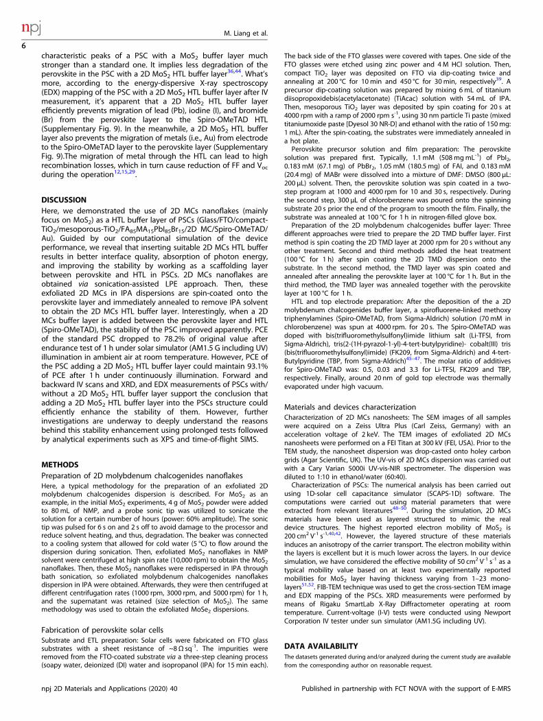
characteristic peaks of a PSC with a MoS2 buffer layer muchstronger than a standard one. It implies less degradation of theperovskite in the PSC with a 2D MoS2 HTL buffer layer36,44. What’smore, according to the energy-dispersive X-ray spectroscopy(EDX) mapping of the PSC with a 2D MoS2 HTL buffer layer after IVmeasurement, it’s apparent that a 2D MoS2 HTL buffer layerefficiently prevents migration of lead (Pb), iodine (I), and bromide(Br) from the perovskite layer to the Spiro-OMeTAD HTL(Supplementary Fig. 9). In the meanwhile, a 2D MoS2 HTL bufferlayer also prevents the migration of metals (i.e., Au) from electrodeto the Spiro-OMeTAD layer to the perovskite layer (SupplementaryFig. 9).The migration of metal through the HTL can lead to highrecombination losses, which in turn cause reduction of FF and Vocduring the operation12,15,29.
DISCUSSIONHere, we demonstrated the use of 2D MCs nanoflakes (mainlyfocus on MoS2) as a HTL buffer layer of PSCs (Glass/FTO/compact-TiO2/mesoporous-TiO2/FA85MA15PbI85Br15/2D MC/Spiro-OMeTAD/Au). Guided by our computational simulation of the deviceperformance, we reveal that inserting suitable 2D MCs HTL bufferresults in better interface quality, absorption of photon energy,and improving the stability by working as a scaffolding layerbetween perovskite and HTL in PSCs. 2D MCs nanoflakes areobtained via sonication-assisted LPE approach. Then, theseexfoliated 2D MCs in IPA dispersions are spin-coated onto theperovskite layer and immediately annealed to remove IPA solventto obtain the 2D MCs HTL buffer layer. Interestingly, when a 2DMCs buffer layer is added between the perovskite layer and HTL(Spiro-OMeTAD), the stability of the PSC improved apparently. PCEof the standard PSC dropped to 78.2% of original value afterendurance test of 1 h under solar simulator (AM1.5 G including UV)illumination in ambient air at room temperature. However, PCE ofthe PSC adding a 2D MoS2 HTL buffer layer could maintain 93.1%of PCE after 1 h under continuously illumination. Forward andbackward IV scans and XRD, and EDX measurements of PSCs with/without a 2D MoS2 HTL buffer layer support the conclusion thatadding a 2D MoS2 HTL buffer layer into the PSCs structure couldefficiently enhance the stability of them. However, furtherinvestigations are underway to deeply understand the reasonsbehind this stability enhancement using prolonged tests followedby analytical experiments such as XPS and time-of-flight SIMS.
METHODSPreparation of 2D molybdenum chalcogenides nanoflakesHere, a typical methodology for the preparation of an exfoliated 2Dmolybdenum chalcogenides dispersion is described. For MoS2 as anexample, in the initial MoS2 experiments, 4 g of MoS2 powder were addedto 80mL of NMP, and a probe sonic tip was utilized to sonicate thesolution for a certain number of hours (power: 60% amplitude). The sonictip was pulsed for 6 s on and 2 s off to avoid damage to the processor andreduce solvent heating, and thus, degradation. The beaker was connectedto a cooling system that allowed for cold water (5 °C) to flow around thedispersion during sonication. Then, exfoliated MoS2 nanoflakes in NMPsolvent were centrifuged at high spin rate (10,000 rpm) to obtain the MoS2nanoflakes. Then, these MoS2 nanoflakes were redispersed in IPA throughbath sonication, so exfoliated molybdenum chalcogenides nanoflakesdispersion in IPA were obtained. Afterwards, they were then centrifuged atdifferent centrifugation rates (1000 rpm, 3000 rpm, and 5000 rpm) for 1 h,and the supernatant was retained (size selection of MoS2). The samemethodology was used to obtain the exfoliated MoSe2 dispersions.
Fabrication of perovskite solar cellsSubstrate and ETL preparation: Solar cells were fabricated on FTO glasssubstrates with a sheet resistance of ~8Ω sq-1. The impurities wereremoved from the FTO-coated substrate via a three-step cleaning process(soapy water, deionized (DI) water and isopropanol (IPA) for 15min each).
The back side of the FTO glasses were covered with tapes. One side of theFTO glasses were etched using zinc power and 4M HCl solution. Then,compact TiO2 layer was deposited on FTO via dip-coating twice andannealing at 200 °C for 10min and 450 °C for 30min, respectively39. Aprecursor dip-coating solution was prepared by mixing 6mL of titaniumdiisopropoxidebis(acetylacetonate) (TiAcac) solution with 54mL of IPA.Then, mesoporous TiO2 layer was deposited by spin coating for 20 s at4000 rpm with a ramp of 2000 rpm s-1, using 30 nm particle Ti paste (mixedtitaniumoxide paste [Dyesol 30 NR-D] and ethanol with the ratio of 150mg:1 mL). After the spin-coating, the substrates were immediately annealed ina hot plate.Perovskite precursor solution and film preparation: The perovskite
solution was prepared first. Typically, 1.1 mM (508mgmL-1) of PbI2,0.183mM (67.1 mg) of PbBr2, 1.05mM (180.5 mg) of FAI, and 0.183mM(20.4 mg) of MABr were dissolved into a mixture of DMF: DMSO (800 μL:200 μL) solvent. Then, the perovskite solution was spin coated in a two-step program at 1000 and 4000 rpm for 10 and 30 s, respectively. Duringthe second step, 300 μL of chlorobenzene was poured onto the spinningsubstrate 20 s prior the end of the program to smooth the film. Finally, thesubstrate was annealed at 100 °C for 1 h in nitrogen-filled glove box.Preparation of the 2D molybdenum chalcogenides buffer layer: Three
different approaches were tried to prepare the 2D TMD buffer layer. Firstmethod is spin coating the 2D TMD layer at 2000 rpm for 20 s without anyother treatment. Second and third methods added the heat treatment(100 °C for 1 h) after spin coating the 2D TMD dispersion onto thesubstrate. In the second method, the TMD layer was spin coated andannealed after annealing the perovskite layer at 100 °C for 1 h. But in thethird method, the TMD layer was annealed together with the perovskitelayer at 100 °C for 1 h.HTL and top electrode preparation: After the deposition of the a 2D
molybdenum chalcogenides buffer layer, a spirofluorene-linked methoxytriphenylamines (Spiro-OMeTAD, from Sigma-Aldrich) solution (70mM inchlorobenzene) was spun at 4000 rpm. for 20 s. The Spiro-OMeTAD wasdoped with bis(trifluoromethylsulfonyl)imide lithium salt (Li-TFSI, fromSigma-Aldrich), tris(2-(1H-pyrazol-1-yl)-4-tert-butylpyridine)- cobalt(III) tris(bis(trifluoromethylsulfonyl)imide) (FK209, from Sigma-Aldrich) and 4-tert-Butylpyridine (TBP, from Sigma-Aldrich)45–47. The molar ratio of additivesfor Spiro-OMeTAD was: 0.5, 0.03 and 3.3 for Li-TFSI, FK209 and TBP,respectively. Finally, around 20 nm of gold top electrode was thermallyevaporated under high vacuum.
Materials and devices characterizationCharacterization of 2D MCs nanosheets: The SEM images of all sampleswere acquired on a Zeiss Ultra Plus (Carl Zeiss, Germany) with anacceleration voltage of 2 keV. The TEM images of exfoliated 2D MCsnanosheets were performed on a FEI Titan at 300 kV (FEI, USA). Prior to theTEM study, the nanosheet dispersion was drop-casted onto holey carbongrids (Agar Scientific, UK). The UV-vis of 2D MCs dispersion was carried outwith a Cary Varian 5000i UV-vis-NIR spectrometer. The dispersion wasdiluted to 1:10 in ethanol/water (60:40).Characterization of PSCs: The numerical analysis has been carried out
using 1D-solar cell capacitance simulator (SCAPS-1D) software. Thecomputations were carried out using material parameters that wereextracted from relevant literatures48–50. During the simulation, 2D MCsmaterials have been used as layered structured to mimic the realdevice structures. The highest reported electron mobility of MoS2 is200 cm2 V-1 s-1,40,42. However, the layered structure of these materialsinduces an anisotropy of the carrier transport. The electron mobility withinthe layers is excellent but it is much lower across the layers. In our devicesimulation, we have considered the effective mobility of 50 cm2 V-1 s-1 as atypical mobility value based on at least two experimentally reportedmobilities for MoS2 layer having thickness varying from 1–23 mono-layers51,52. FIB-TEM technique was used to get the cross-section TEM imageand EDX mapping of the PSCs. XRD measurements were performed bymeans of Rigaku SmartLab X-Ray Diffractometer operating at roomtemperature. Current-voltage (I-V) tests were conducted using NewportCorporation IV tester under sun simulator (AM1.5G including UV).
DATA AVAILABILITYThe datasets generated during and/or analyzed during the current study are availablefrom the corresponding author on reasonable request.
M. Liang et al.
6
npj 2D Materials and Applications (2020) 40 Published in partnership with FCT NOVA with the support of E-MRS
Received: 21 November 2019; Accepted: 15 October 2020;
REFERENCES1. Jean, J., Brown, P. R., Jaffe, R. L., Buonassisi, T. & Bulović, V. Pathways for solar
photovoltaics. Energy Environ. Sci. 8, 1200–1219 (2015).2. Polman, A., Knight, M., Garnett, E. C., Ehrler, B. & Sinke, W. C. Photovoltaic
materials: present efficiencies and future challenges. Science 352, aad4424 (2016).3. Sivula, K. & van de Krol, R. Semiconducting materials for photoelectrochemical
energy conversion. Nat. Rev. Mater. 1, 15010 (2016).4. Burschka, J. et al. Sequential deposition as a route to high-performance per-
ovskite-sensitized solar cells. Nature 499, 316 (2013).5. Jeon, N. J. et al. Compositional engineering of perovskite materials for high-
performance solar cells. Nature 517, 476 (2015).6. Liu, M., Johnston, M. B. & Snaith, H. J. Efficient planar heterojunction perovskite
solar cells by vapour deposition. Nature 501, 395 (2013).7. Green, M. A., Ho-Baillie, A. & Snaith, H. J. The emergence of perovskite solar cells.
Nat. Photonics 8, 506 (2014).8. Kojima, A., Teshima, K., Shirai, Y. & Miyasaka, T. Organometal halide perovskites as
visible-light sensitizers for photovoltaic cells. J. Am. Chem. Soc. 131, 6050–6051(2009).
9. Motta, C., El-Mellouhi, F. & Sanvito, S. Charge carrier mobility in hybrid halideperovskites. Sci. Rep. 5, 12746 (2015).
10. Wojciechowski, K., Saliba, M., Leijtens, T., Abate, A. & Snaith, H. J. Sub-150 °Cprocessed meso-superstructured perovskite solar cells with enhanced efficiency.Energy Environ. Sci. 7, 1142–1147 (2014).
11. Ava, T. T., Al Mamun, A., Marsillac, S. & Namkoong, G. A review: thermal stability ofmethylammonium lead halide based perovskite solar cells. Appl. Sci. 9, 188 (2019).
12. Juarez-Perez, E. J. et al. Role of the selective contacts in the performance of leadhalide perovskite solar cells. J. Phys. Chem. Lett. 5, 680–685 (2014).
13. Etgar, L. et al. Mesoscopic CH3NH3PbI3/TiO2 heterojunction solar cells. J. Am.Chem. Soc. 134, 17396–17399 (2012).
14. Laban, W. A. & Etgar, L. Depleted hole conductor-free lead halide iodide het-erojunction solar cells. Energy Environ. Sci. 6, 3249–3253 (2013).
15. Shi, J. et al. Hole-conductor-free perovskite organic lead iodide heterojunctionthin-film solar cells: high efficiency and junction property. Appl. Phys. Lett. 104,063901 (2014).
16. Eperon, G. E., Burlakov, V. M., Docampo, P., Goriely, A. & Snaith, H. J. Morpholo-gical control for high performance, solution-processed planar heterojunctionperovskite solar cells. Adv. Funct. Mater. 24, 151–157 (2014).
17. Lin, Z. et al. 2D materials advances: from large scale synthesis and controlledheterostructures to improved characterization techniques, defects and applica-tions. 2D Mater. 3, 042001 (2016).
18. Niu, G., Guo, X. & Wang, L. Review of recent progress in chemical stability ofperovskite solar cells. J. Mater. Chem. A 3, 8970–8980 (2015).
19. Grätzel, M. The light and shade of perovskite solar cells. Nat. Mater. 13, 838(2014).
20. Li, X. et al. Outdoor performance and stability under elevated temperatures andlong-term light soaking of triple-layer mesoporous perovskite photovoltaics.Energy Technol. 3, 551–555 (2015).
21. Chatterjee, S., Bera, A. & Pal, A. J. p–i–n Heterojunctions with BiFeO3 perovskitenanoparticles and p- and n-type oxides: photovoltaic properties. ACS Appl. Mater.Inter. 6, 20479–20486 (2014).
22. Ye, W., Xiang, J., Huang, F. & Zhong, D. Towards large-area perovskite solar cells:the influence of compact and mesoporous TiO2 electron transport layers. Mater.Res. Express 5, 085506 (2018).
23. Jena, A. K., Numata, Y., Ikegami, M. & Miyasaka, T. Role of spiro-OMeTAD inperformance deterioration of perovskite solar cells at high temperature and reuseof the perovskite films to avoid Pb-waste. J. Mater. Chem. A 6, 2219–2230 (2018).
24. Qin, P. et al. Inorganic hole conductor-based lead halide perovskite solar cellswith 12.4% conversion efficiency. Nat. Commun. 5, 3834 (2014).
25. Wang, K.-C. et al. Low-temperature sputtered nickel oxide compact thin film aseffective electron blocking layer for mesoscopic NiO/CH3NH3PbI3 perovskiteheterojunction solar cells. ACS Appl. Mater. Inter. 6, 11851–11858 (2014).
26. Seo, J. et al. Benefits of very thin PCBM and LiF layers for solution-processedp–i–n perovskite solar cells. Energy Environ. Sci. 7, 2642–2646 (2014).
27. Malinkiewicz, O. et al. Metal-oxide-free methylammonium lead iodide perovskite-based solar cells: the influence of organic charge transport layers. Adv. EnergyMater. 4, 1400345 (2014).
28. Wang, B. et al. The charge carrier dynamics, efficiency and stability of two-dimensional material-based perovskite solar cells. Chem. Soc. Rev. 48, 4854–4891(2019).
29. Capasso, A. et al. Few-layer MoS2 flakes as active buffer layer for stable perovskitesolar cells. Adv. Energy Mater. 6, 1600920 (2016).
30. Kakavelakis, G. et al. Extending the continuous operating lifetime of perovskitesolar cells with a molybdenum disulfide hole extraction interlayer. Adv. EnergyMater. 8, 1702287 (2018).
31. Najafi, L. et al. MoS2 quantum dot/graphene hybrids for advanced interfaceengineering of a CH3NH3PbI3 perovskite solar cell with an efficiency of over 20%.ACS Nano 12, 10736–10754 (2018).
32. Singh, E., Kim, K. S., Yeom, G. Y. & Nalwa, H. S. Atomically thin-layered molyb-denum disulfide (MoS2) for bulk-heterojunction solar cells. ACS Appl. Mater. Inter.9, 3223–3245 (2017).
33. Kohnehpoushi, S., Nazari, P., Nejand, B. A. & Eskandari, M. MoS2: a two-dimensional hole-transporting material for high-efficiency, low-cost perovskitesolar cells. Nanotechnology 29, 205201 (2018).
34. Akama, T. et al. Schottky solar cell using few-layered transition metal dichalco-genides toward large-scale fabrication of semitransparent and flexible powergenerator. Sci. Rep. 7, 11967 (2017).
35. Wang, D. et al. MoS2 incorporated hybrid hole transport layer for high perfor-mance and stable perovskite solar cells. Synth. Met. 246, 195–203 (2018).
36. Ray, R., Sarkar, A. S. & Pal, S. K. Improving performance and moisture stability ofperovskite solar cells through interface engineering with polymer-2D MoS2nanohybrid. Sol. Energy 193, 95–101 (2019).
37. Coleman, J. N. et al. Two-dimensional nanosheets produced by liquid exfoliationof layered materials. Science 331, 568–571 (2011).
38. O’Neill, A., Khan, U. & Coleman, J. N. Preparation of high concentration disper-sions of exfoliated MoS2 with increased flake size. Chem. Mater. 24, 2414–2421(2012).
39. Giordano, F. et al. Enhanced electronic properties in mesoporous TiO2 via lithiumdoping for high-efficiency perovskite solar cells. Nat. Commun. 7, 10379 (2016).
40. Radisavljevic, B., Radenovic, A., Brivio, J., Giacometti, V. & Kis, A. Single-layer MoS2transistors. Nat. Nanotechnol. 6, 147–150 (2011).
41. Gu, X. et al. A solution-processed hole extraction layer made from ultrathin MoS2nanosheets for efficient organic solar cells. Adv. Energy Mater. 3, 1262–1268(2013).
42. Huo, N. et al. High carrier mobility in monolayer CVD-grown MoS2 throughphonon suppression. Nanoscale 10, 15071–15077 (2018).
43. Dunfield, S. P. et al. From defects to degradation: a mechanistic understanding ofdegradation in perovskite solar cell devices and modules. Adv. Energy Mater. 10,1904054 (2020).
44. Habisreutinger, S. N. et al. Carbon nanotube/polymer composites as a highlystable hole collection layer in perovskite solar cells. Nano Lett. 14, 5561–5568(2014).
45. Abate, A. et al. Protic ionic liquids as p-dopant for organic hole transportingmaterials and their spplication in high efficiency hybrid solar cells. J. Am. Chem.Soc. 135, 13538–13548 (2013).
46. Abate, A. et al. Lithium salts as “redox active” p-type dopants for organic semi-conductors and their impact in solid-state dye-sensitized solar cells. Phys. Chem.Chem. Phys. 15, 2572–2579 (2013).
47. Abate, A., Staff, D. R., Hollman, D. J., Snaith, H. J. & Walker, A. B. Influence ofionizing dopants on charge transport in organic semiconductors. Phys. Chem.Chem. Phys. 16, 1132–1138 (2014).
48. Alfihed, S., Hossain, M., Alharbi, A., Alyamani, A. & Alharbi, F. H. PLD grownpolycrystalline tungsten disulphide (WS2) films. J., Mater. 2013, 5 (2013).
49. Hossain, M. I., Alharbi, F. H. & Tabet, N. Copper oxide as inorganic hole transportmaterial for lead halide perovskite based solar cells. Sol. Energy 120, 370–380(2015).
50. Hossain, M. I., Alharbi, F. H., El-Mellouhi, F. & Tabet, N. Design optimization of solarcell with molybdenum sulfide as light absorber. J. Photonics Energy 8, 1–16(2018).
51. Hippalgaonkar, K. et al. High thermoelectric power factor in two-dimensionalcrystals of MoS2. Phys. Rev. B 95, 115407 (2017).
52. Kayyalha, M., Maassen, J., Lundstrom, M., Shi, L. & Chen, Y. P. Gate-tunable andthickness-dependent electronic and thermoelectric transport in few-layer MoS2.J. Appl. Phys. 120, 134305 (2016).
ACKNOWLEDGEMENTSAuthors wish to acknowledge the Advanced Microscopy Facilities for the use of theirfacilities and Trinity College. V.N. wishes to acknowledge the ERC grants 3D2DPrintand 2DNanocaps and the SFI Centre funding AMBER and IForm. This work issupported by the Qatar National Research Fund (QNRF) through the NationalPriorities Research Program (NPRP8-090-2-047) and by the Qatar Environment andEnergy Research Institute (F.E. and A.A.). A.A. and F.E. would like to thank VinodMadhavan. We are grateful to QEERI’s core labs for SEM, XRD and TEM/FIBcharacterizations.
M. Liang et al.
7
Published in partnership with FCT NOVA with the support of E-MRS npj 2D Materials and Applications (2020) 40

AUTHOR CONTRIBUTIONSV.N., F.E. and M.L. conceived and designed the study. M.L. and A.A. performed theexperiments. M.H. and O.R. are also acknowledged and thanked for the help providedfor computational simulation and characterization parts, respectively. A.B. and C.D.are appreciated for the experimental help. ML wrote the paper. V.N., F.E., S.S., N.T.,A.B., A.A., M.H. and O.R. reviewed and edited the manuscript. All authors read andapproved the manuscript.
COMPETING INTERESTSThe authors declare no competing interests.
ADDITIONAL INFORMATIONSupplementary information is available for this paper at https://doi.org/10.1038/s41699-020-00173-1.
Correspondence and requests for materials should be addressed to M.L., F.E.-M.or V.N.
Reprints and permission information is available at http://www.nature.com/reprints
Publisher’s note Springer Nature remains neutral with regard to jurisdictional claimsin published maps and institutional affiliations.
Open Access This article is licensed under a Creative CommonsAttribution 4.0 International License, which permits use, sharing,
adaptation, distribution and reproduction in anymedium or format, as long as you giveappropriate credit to the original author(s) and the source, provide a link to the CreativeCommons license, and indicate if changes were made. The images or other third partymaterial in this article are included in the article’s Creative Commons license, unlessindicated otherwise in a credit line to the material. If material is not included in thearticle’s Creative Commons license and your intended use is not permitted by statutoryregulation or exceeds the permitted use, you will need to obtain permission directlyfrom the copyright holder. To view a copy of this license, visit http://creativecommons.org/licenses/by/4.0/.
© The Author(s) 2020
M. Liang et al.
8
npj 2D Materials and Applications (2020) 40 Published in partnership with FCT NOVA with the support of E-MRS
Related Documents