3 User’s Manual Micro Programmable Logic Controller

Welcome message from author
This document is posted to help you gain knowledge. Please leave a comment to let me know what you think about it! Share it to your friends and learn new things together.
Transcript
MI
CR
O3
Pr
og
ra
mm
ab
le
L
og
ic
C
on
tr
ol
le
r
Ma
nu
al
User’s Manual
UNITED STATES
IDEC CORPORATION
1213 Elko Drive
Sunnyvale, CA 94089-2240, USA
Tel (408) 747-0550
Toll Free (800) 262-IDEC
Fax (408) 744-9055
Fax (800) 635-6246
E-mail [email protected]
www.industry.net/ideccorp
JAPAN
IDEC IZUMI CORPORATION
7-31, Nishi-Miyahara
1-Chome, Yodogawa-ku
Osaka 532, Japan
Tel (06) 398-2571
Fax (06) 392-9731
CANADA
IDEC CANADA LIMITED
Unit 22-151 Brunel Road
Mississauga, Ontario, L4Z 1X3, Canada
Tel (905) 890-8561
Fax (905) 890-8562
GERMANY
IDEC ELEKTROTECHNIK GmbH
Wendenstraße 331
D-20537 Hamburg, Germany
Tel (040) 25 11 91-93
Fax (040) 25 4 33 61
UNITED KINGDOM
IDEC ELECTRONICS LIMITED
Unit 12, Canbury Business Park
Elm Crescent
Kingston-Upon-Thames
Surrey KT2 6HJ, United Kingdom
Tel (0181) 549-0737
Fax (0181) 546-0963
HONG KONG
IDEC IZUMI (H.K.) CO., LTD.
Room No.1409, Tower 1 Silvercord
30 Canton Road, Tsimshatsui
Kowloon, Hong Kong
Tel (02) 376-2823
Fax (02) 376-0790
TAIWAN
IDEC TAIWAN CORPORATION
3F., No.75, Hsin Tai Wu Road, Sec. 1
Hsi-Chih, Taipei County, Taiwan
Republic of China
Tel (02) 698-2601
Fax (02) 698-2709
AUSTRALIA
IDEC AUSTRALIA PTY. LTD.
2/3 Macro Court
Rowville, Victoria 3178
Australia
Tel (03) 9763-3244
Fax (03) 9763-3255
Users Manual #EM317-0
Printed in the USA 5U 2/97
Micro Programmable Logic Controller
U
SER
’
S
M
ANUAL
P
REFACE
-1
S
AFETY
P
RECAUTIONS
• Read this user’s manual to make sure of correct operation before starting installation, wiring, operation, maintenance, and inspection of the
MICRO
3
.
• All
MICRO
3
’s are manufactured under IDEC’s rigorous quality control system, but users must add a backup or failsafe pro-vision to the control system using the
MICRO
3
in applications where heavy damage or personal injury may be caused in case the
MICRO
3
should fail.• In this user’s manual, safety precautions are categorized in order of importance to Warning and Caution:
• Turn power off to the
MICRO
3
before starting installation, removal, wiring, maintenance, and inspection on the
MICRO
3
. Failure to turn power off may cause electrical shocks or fire hazard.
• Special expertise is required to install, wire, program, and operate the
MICRO
3
. People without such expertise must not use the
MICRO
3
.• Emergency and interlocking circuits must be configured outside the
MICRO
3
. If such a circuit is configured inside the
MICRO
3
, failure of the
MICRO
3
may cause disorder of the control system, damage, or accidents.
• Install the
MICRO
3
according to instructions described in this user’s manual. Improper installation will result in falling, fail-ure, or malfunction of the
MICRO
3
.•
MICRO
3
is designed for installation in equipment. Do not install the
MICRO
3
outside of equipment.• Install the
MICRO
3
in environments described in this user’s manual. If the
MICRO
3
is used in places where the
MICRO
3
is subjected to high-temperature, high-humidity, condensation, corrosive gases, excessive vibrations, and excessive shocks, then electrical shocks, fire hazard, or malfunction will result.
• The pollution degree of the
MICRO
3
is “Pollution degree 2.” Use the
MICRO
3
in environments of pollution degree 2 (accord-ing to IEC664-1).
• All DC power type
MICRO
3
units are “PS2” type (according to EN61131).• Prevent the
MICRO
3
from falling while moving or transporting the
MICRO
3
, otherwise damage or malfunction of the
MICRO
3
will result.• Prevent metal fragments and pieces of wire from dropping inside the
MICRO
3
housing. Put a cover on the
MICRO
3
during installation and wiring. Ingress of such fragments and chips may cause fire hazard, damage, or malfunction.
• Use a power supply of the rated value. Use of a wrong power supply may cause fire hazard.• Use wires of a proper size to meet voltage and current requirements. Tighten M3 terminal screws to a proper tightening
torque of 0.3 to 0.5 N-m.• Use an IEC127-approved fuse on the power line outside the
MICRO
3
. This is required when exporting equipment containing
MICRO
3
to Europe.• Use an IEC127-approved fuse on the output circuit. This is required when exporting equipment containing
MICRO
3
to Europe.
• Use an EU-approved circuit breaker. This is required when exporting equipment containing
MICRO
3
to Europe.• Make sure of safety before starting and stopping the
MICRO
3
or when operating the
MICRO
3
to force outputs on or off. Incorrect operation on the
MICRO
3
may cause machine damage or accidents.• If relays or transistors in the
MICRO
3
output circuit fail, outputs may remain on or off. For output signals which may cause heavy accidents, provide a monitor circuit outside of the
MICRO
3
.• Do not connect to the ground directly from the
MICRO
3
. Connect a protective ground to the equipment containing
MICRO
3
using an M4 or larger screw. This is required when exporting equipment containing
MICRO
3
to Europe.• Do not disassemble, repair, or modify the
MICRO
3
.• Dispose of the battery in the
MICRO
3
when the battery is dead in accordance with pertaining regulations. When storing or disposing of the battery, use a proper container prepared for this purpose. This is required when exporting equipment con-taining
MICRO
3
to Europe.• When disposing of the
MICRO
3
, do so as an industrial waste.• Dispose of the battery in the memory card when the battery is dead in accordance with pertaining regulations.
Warning
Caution
Warning notices are used to emphasize that improper operation may cause severe personal injury or death.
Caution notices are used where inattention might cause personal injury or damage to equipment.
Warning
Caution
P
REFACE
-2 U
SER
’
S
M
ANUAL
MICRO
3
USER’S MANUAL
This user’s manual primarily describes
MICRO
3
’s entire functions shared with the
MICRO
3
C
programmable controllers, such as installation instructions, general specifications, basic and advanced instructions, allocation numbers, and FUN set-tings. For the
MICRO
3
C
additional functions not included in the
MICRO
3
, see the
MICRO
3
C
user’s manual.
MICRO
3
and MICRO
3
C Comparison
Program Loader for MICRO
3
To edit user programs for the
MICRO
3
, read FUN11 (program capacity and PLC type selection) on the program loader, and set the fourth line in the FUN11 screen to 0 to select
MICRO
3
as the PLC type, using the FUN11, , , , 0, and keys. When FUN11 is set to 0, available data registers are limited to D0 through D99 for programming the
MICRO
3
.
Since the loader port on the
MICRO
3
uses RS485 communication while the loader port on the
MICRO
3
C
uses RS232C, a dif-ferent loader cable is needed to connect the program loader to
MICRO
3
or
MICRO
3
C
. Use loader cable FC2A-KL1 or FC2A-KL2 to connect a program loader to the
MICRO
3
loader port.
To use the expanded capabilities of the
MICRO
3
C
such as new advanced instructions for communication and comparison and increased data registers, use an upgraded program loader of version 2.00 or later. To check the program loader version, read FUN31 (program loader version readout/hardware check) using the FUN31 and keys on the program loader.
To connect a program loader to the
MICRO
3
C
loader port, use loader cable 3C (FC2A-KL3C). A program loader can also be connected to the data link terminals on the
MICRO
3
C
using loader cable 4C (FC2A-KL4C). In either case, loader proto-col must be selected for the loader port or data link terminals using the protocol selector switch. For selection of the proto-col selector switch, see the
MICRO
3
C
user’s manual.
PLC MICRO
3
MICRO
3
C
Advanced Instructions 3840(TXD, RXD, CMP2 added; ANR1 deleted)
Data RegistersStandard Processing 100 points 500 points
High-speed Processing 32 points 32 points
Analog Potentiometers1 point (10-I/O type)2 points (16/24-I/O types)
1 point
CommunicationSpecifications
Loader Port Standards EIA RS485 EIA RS232C
Data Link Terminal
Standards EIA RS485 EIA RS485
Baud RateExpansion/data link communication:19,200 bps (fixed)
Expansion/data link communication:19,200 bps (fixed)Loader protocol communication: 9,600 bps (fixed)
Weight (approx.)
290g (10-I/O type)350g (16-I/O type)390g (16-I/O AC input type)400g (24-I/O type)
380g (16-I/O type)430g (24-I/O type)
Standards
EN61131-1, EN61131-2, EN60204-1IEC801-2, -3, -4PrEN50082-2, EN55011UL508, CSA C22.2, No. 142
EN55011 Group 1, Class AEN50082-2UL508, CSA C22.2, No. 142EN61131-1, EN61131-2, EN60204-1
Certification File No.
TÜV Product Service E9 95 09 13332 313UL E102542CSA LR66809
TÜV Product Service B950913332UL E102542CSA LR66809
IMPORTANT INFORMATION
Under no circumstances shall IDEC Corporation be held liable or responsible for indirect or consequential damages resulting from the use of or the application of IDEC PLC components, individually or in combination with other equipment.
All persons using these components must be willing to accept responsibility for choosing the correct component to suit their appli-cation and for choosing an application appropriate for the component, individually or in combination with other equipment.
All diagrams and examples in this manual are for illustrative purposes only. In no way does including these diagrams and examples in this manual constitute a guarantee as to their suitability for any specific application. To test and approve all pro-grams, prior to installation, is the responsibility of the end user.
USER’S MANUAL i
TABLE OF CONTENTS
CHAPTER 1: GENERAL INFORMATION
Features . . . . . . . . . . . . . . . . . . . . . . . . . . . . . . . . . . . . . . . . . . . . . . . . . . . . . . . 1-1Parts Description . . . . . . . . . . . . . . . . . . . . . . . . . . . . . . . . . . . . . . . . . . . . . . . . . 1-2System Setup . . . . . . . . . . . . . . . . . . . . . . . . . . . . . . . . . . . . . . . . . . . . . . . . . . . 1-3General Specifications . . . . . . . . . . . . . . . . . . . . . . . . . . . . . . . . . . . . . . . . . . . . . 1-5Function Specifications. . . . . . . . . . . . . . . . . . . . . . . . . . . . . . . . . . . . . . . . . . . . . 1-7Communication and Noise Specifications. . . . . . . . . . . . . . . . . . . . . . . . . . . . . . . . 1-9Digital DC Input Specifications . . . . . . . . . . . . . . . . . . . . . . . . . . . . . . . . . . . . . . 1-11Digital AC Input Specifications. . . . . . . . . . . . . . . . . . . . . . . . . . . . . . . . . . . . . . . 1-11Digital AC/DC Output (Relay Output) Specifications. . . . . . . . . . . . . . . . . . . . . . . . 1-13Digital DC Output (Transistor Sink Output) Specifications . . . . . . . . . . . . . . . . . . . 1-14Digital DC Output (Transistor Protect Source Output) Specifications . . . . . . . . . . . . 1-15Program Loader Specifications . . . . . . . . . . . . . . . . . . . . . . . . . . . . . . . . . . . . . . 1-18Input Terminal Arrangements. . . . . . . . . . . . . . . . . . . . . . . . . . . . . . . . . . . . . . . . 1-19Output Terminal Arrangements . . . . . . . . . . . . . . . . . . . . . . . . . . . . . . . . . . . . . . 1-20Input Wiring Diagrams. . . . . . . . . . . . . . . . . . . . . . . . . . . . . . . . . . . . . . . . . . . . . 1-21Output Wiring Diagrams . . . . . . . . . . . . . . . . . . . . . . . . . . . . . . . . . . . . . . . . . . . 1-23Dimensions . . . . . . . . . . . . . . . . . . . . . . . . . . . . . . . . . . . . . . . . . . . . . . . . . . . . 1-24Installation . . . . . . . . . . . . . . . . . . . . . . . . . . . . . . . . . . . . . . . . . . . . . . . . . . . . 1-25Disposing of the MICRO3 Units . . . . . . . . . . . . . . . . . . . . . . . . . . . . . . . . . . . . . . 1-26Wiring . . . . . . . . . . . . . . . . . . . . . . . . . . . . . . . . . . . . . . . . . . . . . . . . . . . . . . . . 1-27
CHAPTER 2: OPERATION BASICS
Start/Stop Operation . . . . . . . . . . . . . . . . . . . . . . . . . . . . . . . . . . . . . . . . . . . . . . 2-1Simple Operation . . . . . . . . . . . . . . . . . . . . . . . . . . . . . . . . . . . . . . . . . . . . . . . . . 2-3
CHAPTER 3: PROGRAM LOADER
Parts Description . . . . . . . . . . . . . . . . . . . . . . . . . . . . . . . . . . . . . . . . . . . . . . . . . 3-1Program Loader Operation Modes . . . . . . . . . . . . . . . . . . . . . . . . . . . . . . . . . . . . . 3-3Internal Memory and User Memory . . . . . . . . . . . . . . . . . . . . . . . . . . . . . . . . . . . . 3-3Programming Procedures and Precautions . . . . . . . . . . . . . . . . . . . . . . . . . . . . . . . 3-4Using Editor Mode . . . . . . . . . . . . . . . . . . . . . . . . . . . . . . . . . . . . . . . . . . . . . . . . 3-5Using Transfer Mode . . . . . . . . . . . . . . . . . . . . . . . . . . . . . . . . . . . . . . . . . . . . . . 3-9Using Monitor Mode . . . . . . . . . . . . . . . . . . . . . . . . . . . . . . . . . . . . . . . . . . . . . . 3-12Error Messages for Program Loader Operation . . . . . . . . . . . . . . . . . . . . . . . . . . . 3-20
CHAPTER 4: SPECIAL FUNCTIONS
High-speed Processing Mode . . . . . . . . . . . . . . . . . . . . . . . . . . . . . . . . . . . . . . . . 4-1Catch Input Function. . . . . . . . . . . . . . . . . . . . . . . . . . . . . . . . . . . . . . . . . . . . . . . 4-2Input Filter Function . . . . . . . . . . . . . . . . . . . . . . . . . . . . . . . . . . . . . . . . . . . . . . . 4-3Pulse Output Function. . . . . . . . . . . . . . . . . . . . . . . . . . . . . . . . . . . . . . . . . . . . . . 4-5High-speed Counter Function. . . . . . . . . . . . . . . . . . . . . . . . . . . . . . . . . . . . . . . . . 4-5Expansion Link Function . . . . . . . . . . . . . . . . . . . . . . . . . . . . . . . . . . . . . . . . . . . . 4-6Data Link Function . . . . . . . . . . . . . . . . . . . . . . . . . . . . . . . . . . . . . . . . . . . . . . . . 4-8Computer Link Function . . . . . . . . . . . . . . . . . . . . . . . . . . . . . . . . . . . . . . . . . . . 4-16External Analog Timer . . . . . . . . . . . . . . . . . . . . . . . . . . . . . . . . . . . . . . . . . . . . . 4-18Analog Input Function . . . . . . . . . . . . . . . . . . . . . . . . . . . . . . . . . . . . . . . . . . . . . 4-21Analog Output Function. . . . . . . . . . . . . . . . . . . . . . . . . . . . . . . . . . . . . . . . . . . . 4-27
TABLE OF CONTENTS
ii USER’S MANUAL
CHAPTER 5: CPU CONFIGURATION (FUN)FUN Settings (FUN1 through FUN11) . . . . . . . . . . . . . . . . . . . . . . . . . . . . . . . . . . . 5-1FUN Settings (FUN20 through FUN50) . . . . . . . . . . . . . . . . . . . . . . . . . . . . . . . . . . 5-2Key Operation. . . . . . . . . . . . . . . . . . . . . . . . . . . . . . . . . . . . . . . . . . . . . . . . . . . . 5-3FUN1: Stop Input Number Selection . . . . . . . . . . . . . . . . . . . . . . . . . . . . . . . . . . . . 5-3FUN2: Reset Input Number Selection . . . . . . . . . . . . . . . . . . . . . . . . . . . . . . . . . . . 5-4FUN3: Internal Relay “Keep” Designation . . . . . . . . . . . . . . . . . . . . . . . . . . . . . . . . 5-4FUN4: Shift Register “Keep” Designation . . . . . . . . . . . . . . . . . . . . . . . . . . . . . . . . 5-5FUN5: Processing Mode Selection . . . . . . . . . . . . . . . . . . . . . . . . . . . . . . . . . . . . . 5-5FUN6: Rising or Falling Edge Selection for Catch Inputs . . . . . . . . . . . . . . . . . . . . . . 5-6FUN7: Input Filter Time Selection . . . . . . . . . . . . . . . . . . . . . . . . . . . . . . . . . . . . . . 5-6FUN8: Loader Port Communication Mode Setting . . . . . . . . . . . . . . . . . . . . . . . . . . 5-7FUN9: PLC Address for Network Communication . . . . . . . . . . . . . . . . . . . . . . . . . . . 5-7FUN10: Control Data Register Setting. . . . . . . . . . . . . . . . . . . . . . . . . . . . . . . . . . . 5-8FUN11: Program Capacity and PLC Type Selection. . . . . . . . . . . . . . . . . . . . . . . . . . 5-9FUN20: PLC Error Data Readout and Reset. . . . . . . . . . . . . . . . . . . . . . . . . . . . . . . 5-9FUN21: Timer/Counter Preset Value Readout and Restore. . . . . . . . . . . . . . . . . . . . 5-9FUN22: User Program Protection . . . . . . . . . . . . . . . . . . . . . . . . . . . . . . . . . . . . . 5-10FUN23: PLC System Program Version Readout . . . . . . . . . . . . . . . . . . . . . . . . . . . 5-10FUN24: PLC Operating Status Readout . . . . . . . . . . . . . . . . . . . . . . . . . . . . . . . . . 5-10FUN25: Scan Time Readout. . . . . . . . . . . . . . . . . . . . . . . . . . . . . . . . . . . . . . . . . 5-11FUN26: Operand Data Clear. . . . . . . . . . . . . . . . . . . . . . . . . . . . . . . . . . . . . . . . . 5-11FUN27: Link Formatting Sequence . . . . . . . . . . . . . . . . . . . . . . . . . . . . . . . . . . . . 5-11FUN28: Calendar/Clock Data Readout and Setting . . . . . . . . . . . . . . . . . . . . . . . . 5-12FUN29: User Communication Status Readout . . . . . . . . . . . . . . . . . . . . . . . . . . . . 5-12FUN30: Program Check . . . . . . . . . . . . . . . . . . . . . . . . . . . . . . . . . . . . . . . . . . . . 5-12FUN31: Program Loader Version Readout/Hardware Check . . . . . . . . . . . . . . . . . . 5-13FUN32: Sequential Monitoring . . . . . . . . . . . . . . . . . . . . . . . . . . . . . . . . . . . . . . . 5-13FUN33: Monitor Screen Holding . . . . . . . . . . . . . . . . . . . . . . . . . . . . . . . . . . . . . . 5-13FUN34: Program Loader Beep Sound . . . . . . . . . . . . . . . . . . . . . . . . . . . . . . . . . . 5-14FUN35: Display Language Selection . . . . . . . . . . . . . . . . . . . . . . . . . . . . . . . . . . . 5-14FUN36: Display Data Type Selection. . . . . . . . . . . . . . . . . . . . . . . . . . . . . . . . . . . 5-14FUN40: Memory Card Identification . . . . . . . . . . . . . . . . . . . . . . . . . . . . . . . . . . . 5-15FUN41: Memory Card Formatting . . . . . . . . . . . . . . . . . . . . . . . . . . . . . . . . . . . . . 5-15FUN42: Program Loader System Program Installation . . . . . . . . . . . . . . . . . . . . . . 5-15FUN43: Program Loader System Program Restore . . . . . . . . . . . . . . . . . . . . . . . . . 5-16FUN50: User Communication Data Monitor . . . . . . . . . . . . . . . . . . . . . . . . . . . . . . 5-16
CHAPTER 6: ALLOCATION NUMBERS
Allocation Numbers. . . . . . . . . . . . . . . . . . . . . . . . . . . . . . . . . . . . . . . . . . . . . . . . 6-1Special Internal Relays . . . . . . . . . . . . . . . . . . . . . . . . . . . . . . . . . . . . . . . . . . . . . 6-2Data Register Allocation Numbers . . . . . . . . . . . . . . . . . . . . . . . . . . . . . . . . . . . . . 6-4
TABLE OF CONTENTS
USER’S MANUAL iii
CHAPTER 7: BASIC INSTRUCTIONS
Basic Instruction List . . . . . . . . . . . . . . . . . . . . . . . . . . . . . . . . . . . . . . . . . . . . . . 7-1LOD (Load) and LODN (Load Not). . . . . . . . . . . . . . . . . . . . . . . . . . . . . . . . . . . . . . 7-2OUT (Output) and OUTN (Output Not) . . . . . . . . . . . . . . . . . . . . . . . . . . . . . . . . . . . 7-2AND and ANDN (And Not) . . . . . . . . . . . . . . . . . . . . . . . . . . . . . . . . . . . . . . . . . . . 7-4OR and ORN (Or Not) . . . . . . . . . . . . . . . . . . . . . . . . . . . . . . . . . . . . . . . . . . . . . . 7-4AND LOD (Load) . . . . . . . . . . . . . . . . . . . . . . . . . . . . . . . . . . . . . . . . . . . . . . . . . . 7-5OR LOD (Load) . . . . . . . . . . . . . . . . . . . . . . . . . . . . . . . . . . . . . . . . . . . . . . . . . . . 7-7BPS (Bit Push), BRD (Bit Read), and BPP (Bit Pop) . . . . . . . . . . . . . . . . . . . . . . . . . 7-9TIM, TMH, and TMS (Timer). . . . . . . . . . . . . . . . . . . . . . . . . . . . . . . . . . . . . . . . . 7-14CNT (Counter) . . . . . . . . . . . . . . . . . . . . . . . . . . . . . . . . . . . . . . . . . . . . . . . . . . 7-18CC= and CC≥ (Counter Comparison) . . . . . . . . . . . . . . . . . . . . . . . . . . . . . . . . . . 7-21SFR and SFRN (Forward and Reverse Shift Register) . . . . . . . . . . . . . . . . . . . . . . . 7-23SOTU and SOTD (Single Output Up and Down) . . . . . . . . . . . . . . . . . . . . . . . . . . . 7-27MCS and MCR (Master Control Set and Reset) . . . . . . . . . . . . . . . . . . . . . . . . . . . 7-28JMP (Jump) and JEND (Jump End) . . . . . . . . . . . . . . . . . . . . . . . . . . . . . . . . . . . . 7-30SET and RST (Reset) . . . . . . . . . . . . . . . . . . . . . . . . . . . . . . . . . . . . . . . . . . . . . 7-32END . . . . . . . . . . . . . . . . . . . . . . . . . . . . . . . . . . . . . . . . . . . . . . . . . . . . . . . . . 7-32
CHAPTER 8: ADVANCED INSTRUCTIONS
Advanced Instruction Menus . . . . . . . . . . . . . . . . . . . . . . . . . . . . . . . . . . . . . . . . . 8-1Advanced Instruction List . . . . . . . . . . . . . . . . . . . . . . . . . . . . . . . . . . . . . . . . . . . 8-2Programming Advanced Instructions Using Program Loader . . . . . . . . . . . . . . . . . . . 8-3Revising Advanced Instructions Using Program Loader . . . . . . . . . . . . . . . . . . . . . . 8-3Structure of an Advanced Instruction . . . . . . . . . . . . . . . . . . . . . . . . . . . . . . . . . . . 8-4Input Condition for Advanced Instructions. . . . . . . . . . . . . . . . . . . . . . . . . . . . . . . . 8-4Source and Destination Operands . . . . . . . . . . . . . . . . . . . . . . . . . . . . . . . . . . . . . 8-4Using Timer or Counter as Source Operand . . . . . . . . . . . . . . . . . . . . . . . . . . . . . . 8-4Using Timer or Counter as Destination Operand . . . . . . . . . . . . . . . . . . . . . . . . . . . 8-4Using Input or Output as Source or Destination Operand . . . . . . . . . . . . . . . . . . . . . 8-5Discontinuity of Operand Areas . . . . . . . . . . . . . . . . . . . . . . . . . . . . . . . . . . . . . . . 8-60 NOP (No Operation) . . . . . . . . . . . . . . . . . . . . . . . . . . . . . . . . . . . . . . . . . . . . 8-6
CHAPTER 9: MOVE INSTRUCTIONS
11 MOV (Move) . . . . . . . . . . . . . . . . . . . . . . . . . . . . . . . . . . . . . . . . . . . . . . . . 9-112 MOVN (Move Not) . . . . . . . . . . . . . . . . . . . . . . . . . . . . . . . . . . . . . . . . . . . . 9-313 IMOV (Indirect Move) . . . . . . . . . . . . . . . . . . . . . . . . . . . . . . . . . . . . . . . . . . 9-414 IMOVN (Indirect Move Not) . . . . . . . . . . . . . . . . . . . . . . . . . . . . . . . . . . . . . . 9-5
CHAPTER 10: COMPARISON INSTRUCTIONS
21 CMP= (Compare Equal To) . . . . . . . . . . . . . . . . . . . . . . . . . . . . . . . . . . . . . 10-122 CMP<> (Compare Unequal To) . . . . . . . . . . . . . . . . . . . . . . . . . . . . . . . . . . 10-123 CMP< (Compare Less Than) . . . . . . . . . . . . . . . . . . . . . . . . . . . . . . . . . . . . 10-124 CMP> (Compare Greater Than) . . . . . . . . . . . . . . . . . . . . . . . . . . . . . . . . . . 10-125 CMP<= (Compare Less Than or Equal To) . . . . . . . . . . . . . . . . . . . . . . . . . . 10-126 CMP>= (Compare Greater Than or Equal To) . . . . . . . . . . . . . . . . . . . . . . . . 10-1
CHAPTER 11: BINARY ARITHMETIC INSTRUCTIONS
31 ADD (Addition). . . . . . . . . . . . . . . . . . . . . . . . . . . . . . . . . . . . . . . . . . . . . . 11-132 SUB (Subtraction) . . . . . . . . . . . . . . . . . . . . . . . . . . . . . . . . . . . . . . . . . . . 11-133 MUL (Multiplication). . . . . . . . . . . . . . . . . . . . . . . . . . . . . . . . . . . . . . . . . . 11-134 DIV (Division) . . . . . . . . . . . . . . . . . . . . . . . . . . . . . . . . . . . . . . . . . . . . . . 11-1
TABLE OF CONTENTS
iv USER’S MANUAL
CHAPTER 12: BOOLEAN COMPUTATION INSTRUCTIONS
41 ANDW (AND Word) . . . . . . . . . . . . . . . . . . . . . . . . . . . . . . . . . . . . . . . . . . . 12-142 ORW (OR Word) . . . . . . . . . . . . . . . . . . . . . . . . . . . . . . . . . . . . . . . . . . . . . 12-143 XORW (Exclusive OR Word) . . . . . . . . . . . . . . . . . . . . . . . . . . . . . . . . . . . . . 12-1
CHAPTER 13: BIT SHIFT / ROTATE INSTRUCTIONS
51 SFTL (Shift Left) . . . . . . . . . . . . . . . . . . . . . . . . . . . . . . . . . . . . . . . . . . . . . 13-152 SFTR (Shift Right). . . . . . . . . . . . . . . . . . . . . . . . . . . . . . . . . . . . . . . . . . . . 13-253 ROTL (Rotate Left) . . . . . . . . . . . . . . . . . . . . . . . . . . . . . . . . . . . . . . . . . . . 13-354 ROTR (Rotate Right) . . . . . . . . . . . . . . . . . . . . . . . . . . . . . . . . . . . . . . . . . . 13-4
CHAPTER 14: CLOCK / CALENDAR INSTRUCTIONS
71 CALR (Calendar Read) . . . . . . . . . . . . . . . . . . . . . . . . . . . . . . . . . . . . . . . . 14-172 CALW (Calendar Write) . . . . . . . . . . . . . . . . . . . . . . . . . . . . . . . . . . . . . . . . 14-273 CLKR (Clock Read). . . . . . . . . . . . . . . . . . . . . . . . . . . . . . . . . . . . . . . . . . . 14-374 CLKW (Clock Write) . . . . . . . . . . . . . . . . . . . . . . . . . . . . . . . . . . . . . . . . . . 14-375 ADJ (Adjust). . . . . . . . . . . . . . . . . . . . . . . . . . . . . . . . . . . . . . . . . . . . . . . . 14-4
CHAPTER 15: INTERFACE INSTRUCTIONS
81 DISP (Display) . . . . . . . . . . . . . . . . . . . . . . . . . . . . . . . . . . . . . . . . . . . . . . 15-182 DGRD (Digital Read). . . . . . . . . . . . . . . . . . . . . . . . . . . . . . . . . . . . . . . . . . 15-383 ANR0 (Analog Read 0) . . . . . . . . . . . . . . . . . . . . . . . . . . . . . . . . . . . . . . . . 15-584 ANR1 (Analog Read 1) . . . . . . . . . . . . . . . . . . . . . . . . . . . . . . . . . . . . . . . . 15-5
CHAPTER 16: PULSE, A/D CONVERSION INSTRUCTIONS
91 PULS (Pulse Output). . . . . . . . . . . . . . . . . . . . . . . . . . . . . . . . . . . . . . . . . . 16-192 PWM (Pulse Width Modulation) . . . . . . . . . . . . . . . . . . . . . . . . . . . . . . . . . . 16-393 A/D (Analog/Digital Conversion) . . . . . . . . . . . . . . . . . . . . . . . . . . . . . . . . . 16-5
CHAPTER 17: HIGH-SPEED COUNTER INSTRUCTIONS
A1 HSC0 (Single-stage Comparison). . . . . . . . . . . . . . . . . . . . . . . . . . . . . . . . . 17-1A2 HSC1 (Multi-stage Comparison) . . . . . . . . . . . . . . . . . . . . . . . . . . . . . . . . . 17-3A3 HSC2 (Pulse Output Control). . . . . . . . . . . . . . . . . . . . . . . . . . . . . . . . . . . . 17-6A4 HSC3 (Gate Control). . . . . . . . . . . . . . . . . . . . . . . . . . . . . . . . . . . . . . . . . . 17-9
CHAPTER 18: TROUBLESHOOTING
Error Indicators ERR1 and ERR2. . . . . . . . . . . . . . . . . . . . . . . . . . . . . . . . . . . . . . 18-1Reading Error Data . . . . . . . . . . . . . . . . . . . . . . . . . . . . . . . . . . . . . . . . . . . . . . . 18-1Error Messages . . . . . . . . . . . . . . . . . . . . . . . . . . . . . . . . . . . . . . . . . . . . . . . . . 18-1General Error Codes . . . . . . . . . . . . . . . . . . . . . . . . . . . . . . . . . . . . . . . . . . . . . . 18-2Error Causes and Actions . . . . . . . . . . . . . . . . . . . . . . . . . . . . . . . . . . . . . . . . . . 18-3Troubleshooting Diagrams . . . . . . . . . . . . . . . . . . . . . . . . . . . . . . . . . . . . . . . . . . 18-6
APPENDIX
Execution Times for Instructions . . . . . . . . . . . . . . . . . . . . . . . . . . . . . . . . . . . . . . A-1Type List . . . . . . . . . . . . . . . . . . . . . . . . . . . . . . . . . . . . . . . . . . . . . . . . . . . . . . . A-3
INDEX
USER’S MANUAL 1-1
1: GENERAL INFORMATION
IntroductionThis chapter describes general information for understanding MICRO3 functions and specifications.
FeaturesMICRO3 is a space-saving micro programmable controller, yet has high-performance functions described below:
High-speed Processing Function
MICRO3 operates in standard processing mode or high-speed processing mode. Standard mode has a program capacity of 1012 steps, minimum processing time of 1.2 µsec per basic instruction, and average scan time of 2.9 msec for 1,000 steps.
High-speed processing mode has a program capacity of 100 steps, minimum processing time of 0.2 µsec per basic instruc-tion, and average scan time of 400 µsec for 100 steps. Data and expansion link cannot be used with high-speed processing.
Catch Input Function
The catch input function makes sure to receive short input pulses (40 µsec minimum at the rising edge) from sensors with-out regard to the scan time.
The 10-I/O type MICRO3 base unit can receive short pulse inputs at 6 input terminals (I0 through I5). The 16- and 24-I/O type base units can use 8 input terminals (I0 through I7) for catch inputs.
Input Filter Function (DC Input Type Only)
The input filter can be adjusted for input signal durations. This function is useful for adjusting the input pulse width in sen-sor controller applications and for eliminating input noises and chatter in limit switches.
High-speed Counter Function
MICRO3 has a built-in high-speed counter to make it possible to count up to 4,294,967,295 (FFFF FFFFh) high-speed pulses which cannot be counted by the normal user program processing. The maximum count input frequency is 10 kHz. This function can be used for simple positioning control and simple motor control.
Pulse Output Function
Pulse outputs can be generated using advanced instructions. The PULS (pulse output) instruction can vary the output fre-quency at a fixed duty ratio of 50%. This instruction can be used in combination with the high-speed counter function to control servo motors and stepper motors. The PWM (pulse width modulation) instruction can change the duty ratio at a fixed frequency. This instruction can be used for illumination control.
Computer Link Function
A personal computer can be connected to MICRO3 in 1:1 peer-to-peer or 1:N network communication system to monitor the operating statuses and change data in MICRO3. CUBIQ software is available for easy programming and monitoring.
Expansion Link Function
The I/O points can be expanded from 6 inputs and 4 outputs up to 28 inputs and 20 outputs by connecting another MICRO3 in six combinations, maximizing flexibility, (see note).
Data Link Function
A maximum of seven MICRO3 base units (1 master station and 6 slave stations) can be linked in the data link network for distributed control. FA-3S high-performance CPU can also be used as a master station in the data link system (see note).
Real-time Clock/Calendar Function (16- and 24-I/O Type Units Only)
The 16- and 24-I/O type MICRO3 base units feature a real-time clock/calendar to program year, month, day, day of week, hour, minute, and second using advanced instructions. This function can be used for time-scheduled control of illumina-tion, air conditioners, sprinklers, and many others.
External Analog Timer
MICRO3 is equipped with one or two analog potentiometers to enter analog values. In addition, a separate analog timer unit can also be connected to MICRO3, allowing for fine adjustment of timer preset values on the control panel.
User Program Read and/or Write Protection
User programs in the MICRO3 base unit can be protected from reading and/or writing by setting a pass word. This function is ideal for the security of user programs and prevention of inadvertent rewriting of programs.
Analog I/O Function
A/D and D/A converter units are available for 8-bit conversion to process analog signals.
Note: Expansion link and data link cannot be used concurrently.
1: GENERAL INFORMATION
1-2 USER’S MANUAL
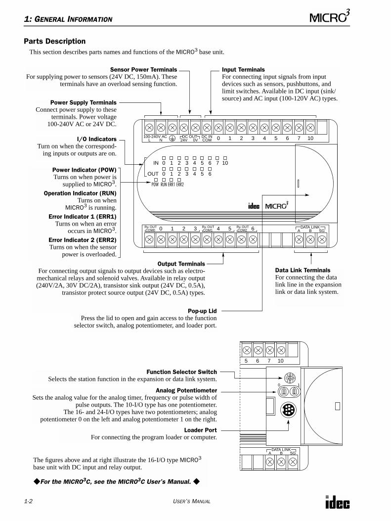
Parts DescriptionThis section describes parts names and functions of the MICRO3 base unit.
Ry. OUTCOM0 0 1 2 3 Ry. OUT
COM1 4 5 Ry. OUTCOM2 6 DATA LINK
A SGB
IN 0 1 2 3 4 5 6 7 10
OUT 0 1 2 3 4 5 6
POW RUN ERR1 ERR2
Power Supply TerminalsConnect power supply to these
terminals. Power voltage100-240V AC or 24V DC.
Sensor Power TerminalsFor supplying power to sensors (24V DC, 150mA). These
terminals have an overload sensing function.
Input TerminalsFor connecting input signals from input devices such as sensors, pushbuttons, and limit switches. Available in DC input (sink/source) and AC input (100-120V AC) types.
I/O IndicatorsTurn on when the correspond-
ing inputs or outputs are on.
Power Indicator (POW)Turns on when power is
supplied to MICRO3.Operation Indicator (RUN)
Turns on whenMICRO3 is running.
Error Indicator 1 (ERR1)Turns on when an error
occurs in MICRO3.Error Indicator 2 (ERR2)Turns on when the sensor
power is overloaded.
Output TerminalsFor connecting output signals to output devices such as electro-mechanical relays and solenoid valves. Available in relay output(240V/2A, 30V DC/2A), transistor sink output (24V DC, 0.5A),
transistor protect source output (24V DC, 0.5A) types.
Data Link TerminalsFor connecting the data link line in the expansion link or data link system.
Pop-up LidPress the lid to open and gain access to the function
selector switch, analog potentiometer, and loader port.
The figures above and at right illustrate the 16-I/O type MICRO3 base unit with DC input and relay output.
For the MICRO3C, see the MICRO3C User’s Manual.
Function Selector SwitchSelects the station function in the expansion or data link system.
Analog PotentiometerSets the analog value for the analog timer, frequency or pulse width of
pulse outputs. The 10-I/O type has one potentiometer.The 16- and 24-I/O types have two potentiometers; analog
potentiometer 0 on the left and analog potentiometer 1 on the right.
Loader PortFor connecting the program loader or computer.
0 1
100-240V ACL N
DC OUT24V 0V
DC INCOM 0 1 2 3 4 5 6 7 10
7
3 4 562
1 0
DATA LINKA SGB
5 6 7 10
1: GENERAL INFORMATION
USER’S MANUAL 1-3
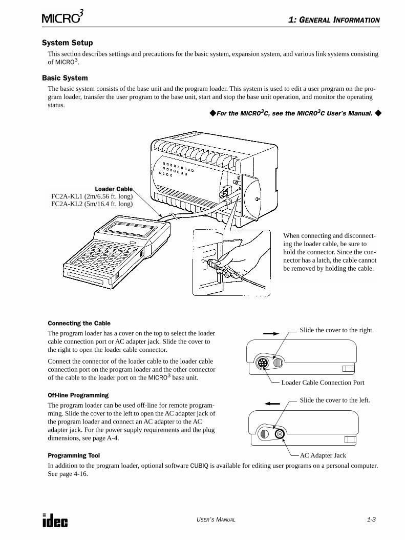
System SetupThis section describes settings and precautions for the basic system, expansion system, and various link systems consisting of MICRO3.
Basic SystemThe basic system consists of the base unit and the program loader. This system is used to edit a user program on the pro-gram loader, transfer the user program to the base unit, start and stop the base unit operation, and monitor the operating status.
Connecting the Cable
The program loader has a cover on the top to select the loader cable connection port or AC adapter jack. Slide the cover to the right to open the loader cable connector.
Connect the connector of the loader cable to the loader cable connection port on the program loader and the other connector of the cable to the loader port on the MICRO3 base unit.
Off-line Programming
The program loader can be used off-line for remote program-ming. Slide the cover to the left to open the AC adapter jack of the program loader and connect an AC adapter to the AC adapter jack. For the power supply requirements and the plug dimensions, see page A-4.
Programming Tool
In addition to the program loader, optional software CUBIQ is available for editing user programs on a personal computer. See page 4-16.
When connecting and disconnect-ing the loader cable, be sure to hold the connector. Since the con-nector has a latch, the cable cannot be removed by holding the cable.
Loader CableFC2A-KL1 (2m/6.56 ft. long)FC2A-KL2 (5m/16.4 ft. long)
For the MICRO3C, see the MICRO3C User’s Manual.
Slide the cover to the right.
Loader Cable Connection Port
Slide the cover to the left.
AC Adapter Jack
1: GENERAL INFORMATION
1-4 USER’S MANUAL
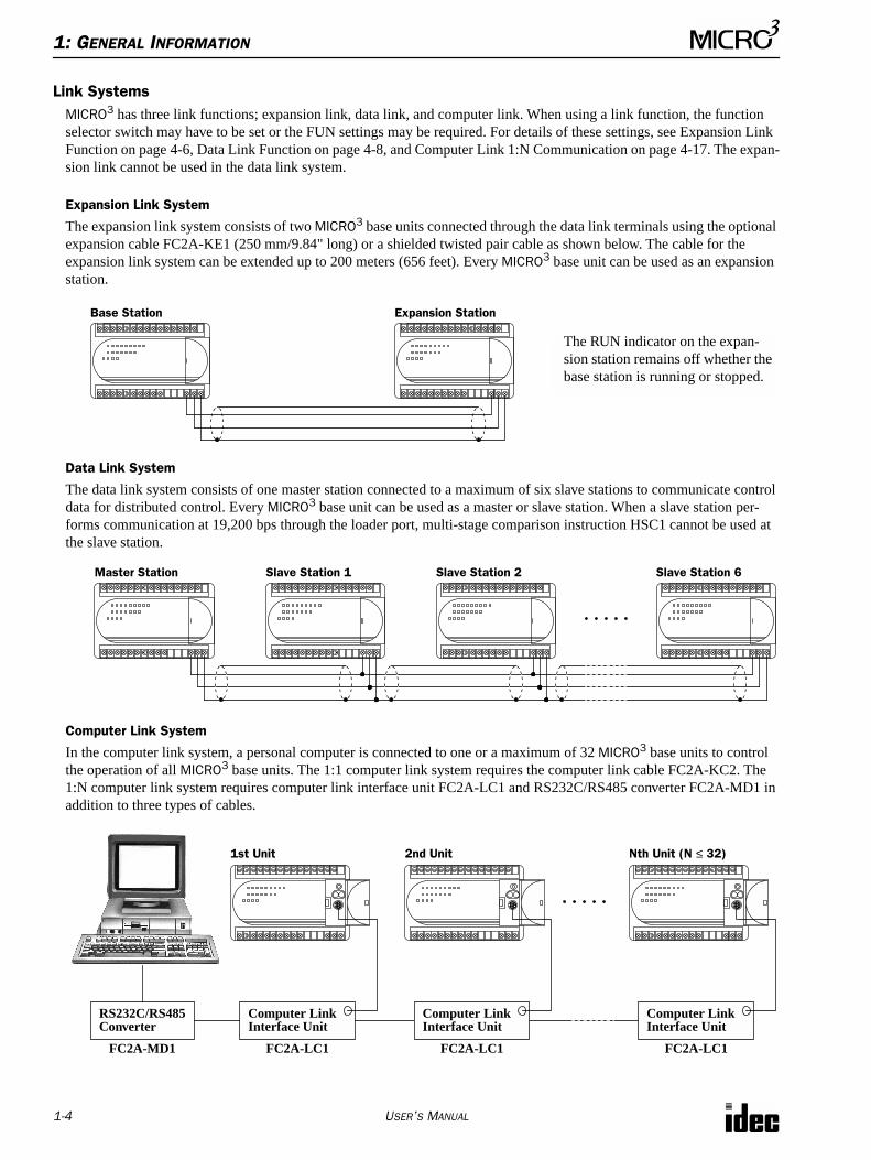
Link SystemsMICRO3 has three link functions; expansion link, data link, and computer link. When using a link function, the function selector switch may have to be set or the FUN settings may be required. For details of these settings, see Expansion Link Function on page 4-6, Data Link Function on page 4-8, and Computer Link 1:N Communication on page 4-17. The expan-sion link cannot be used in the data link system.
Expansion Link System
The expansion link system consists of two MICRO3 base units connected through the data link terminals using the optional expansion cable FC2A-KE1 (250 mm/9.84" long) or a shielded twisted pair cable as shown below. The cable for the expansion link system can be extended up to 200 meters (656 feet). Every MICRO3 base unit can be used as an expansion station.
Data Link System
The data link system consists of one master station connected to a maximum of six slave stations to communicate control data for distributed control. Every MICRO3 base unit can be used as a master or slave station. When a slave station per-forms communication at 19,200 bps through the loader port, multi-stage comparison instruction HSC1 cannot be used at the slave station.
Computer Link System
In the computer link system, a personal computer is connected to one or a maximum of 32 MICRO3 base units to control the operation of all MICRO3 base units. The 1:1 computer link system requires the computer link cable FC2A-KC2. The 1:N computer link system requires computer link interface unit FC2A-LC1 and RS232C/RS485 converter FC2A-MD1 in addition to three types of cables.
Base Station Expansion Station
The RUN indicator on the expan-sion station remains off whether the base station is running or stopped.
Master Station Slave Station 1 Slave Station 2 Slave Station 6
Computer LinkInterface Unit
1st Unit
RS232C/RS485Converter
Computer LinkInterface Unit
2nd Unit
Computer LinkInterface Unit
Nth Unit (N ≤ 32)
FC2A-MD1 FC2A-LC1 FC2A-LC1 FC2A-LC1
1: GENERAL INFORMATION
USER’S MANUAL 1-5
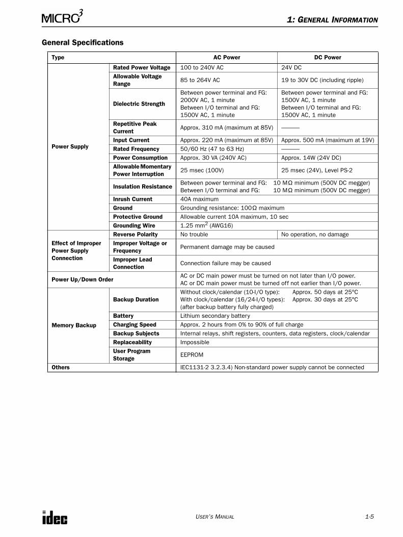
General Specifications
Type AC Power DC Power
Power Supply
Rated Power Voltage 100 to 240V AC 24V DCAllowable Voltage Range
85 to 264V AC 19 to 30V DC (including ripple)
Dielectric Strength
Between power terminal and FG: 2000V AC, 1 minuteBetween I/O terminal and FG: 1500V AC, 1 minute
Between power terminal and FG: 1500V AC, 1 minuteBetween I/O terminal and FG: 1500V AC, 1 minute
Repetitive Peak Current
Approx. 310 mA (maximum at 85V) ———
Input Current Approx. 220 mA (maximum at 85V) Approx. 500 mA (maximum at 19V)Rated Frequency 50/60 Hz (47 to 63 Hz) ———Power Consumption Approx. 30 VA (240V AC) Approx. 14W (24V DC)Allowable Momentary Power Interruption
25 msec (100V) 25 msec (24V), Level PS-2
Insulation ResistanceBetween power terminal and FG: 10 MΩ minimum (500V DC megger)Between I/O terminal and FG: 10 MΩ minimum (500V DC megger)
Inrush Current 40A maximumGround Grounding resistance: 100Ω maximumProtective Ground Allowable current 10A maximum, 10 secGrounding Wire 1.25 mm2 (AWG16)
Effect of Improper Power Supply Connection
Reverse Polarity No trouble No operation, no damageImproper Voltage or Frequency
Permanent damage may be caused
Improper Lead Connection
Connection failure may be caused
Power Up/Down OrderAC or DC main power must be turned on not later than I/O power.AC or DC main power must be turned off not earlier than I/O power.
Memory Backup
Backup DurationWithout clock/calendar (10-I/O type): Approx. 50 days at 25°CWith clock/calendar (16/24-I/O types): Approx. 30 days at 25°C(after backup battery fully charged)
Battery Lithium secondary batteryCharging Speed Approx. 2 hours from 0% to 90% of full chargeBackup Subjects Internal relays, shift registers, counters, data registers, clock/calendarReplaceability ImpossibleUser Program Storage
EEPROM
Others IEC1131-2 3.2.3.4) Non-standard power supply cannot be connected
1: GENERAL INFORMATION
1-6 USER’S MANUAL
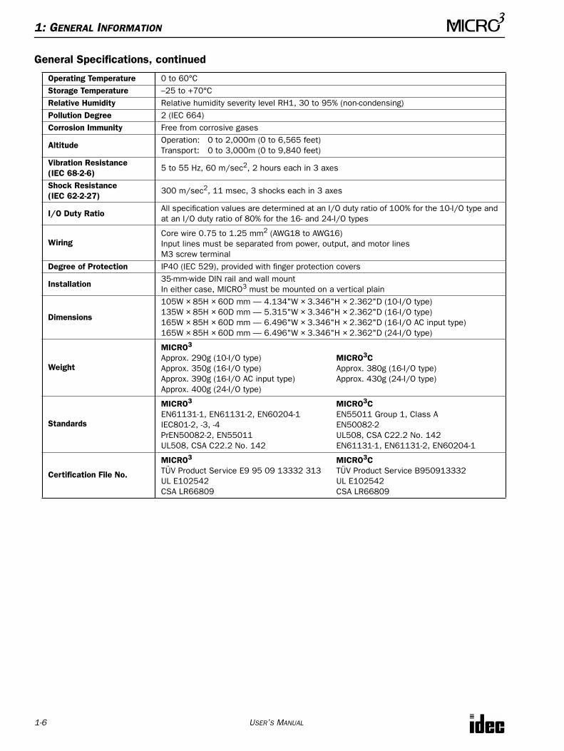
General Specifications, continued
Operating Temperature 0 to 60°CStorage Temperature –25 to +70°CRelative Humidity Relative humidity severity level RH1, 30 to 95% (non-condensing)Pollution Degree 2 (IEC 664)Corrosion Immunity Free from corrosive gases
AltitudeOperation: 0 to 2,000m (0 to 6,565 feet)Transport: 0 to 3,000m (0 to 9,840 feet)
Vibration Resistance (IEC 68-2-6)
5 to 55 Hz, 60 m/sec2, 2 hours each in 3 axes
Shock Resistance (IEC 62-2-27)
300 m/sec2, 11 msec, 3 shocks each in 3 axes
I/O Duty RatioAll specification values are determined at an I/O duty ratio of 100% for the 10-I/O type and at an I/O duty ratio of 80% for the 16- and 24-I/O types
WiringCore wire 0.75 to 1.25 mm2 (AWG18 to AWG16)Input lines must be separated from power, output, and motor linesM3 screw terminal
Degree of Protection IP40 (IEC 529), provided with finger protection covers
Installation35-mm-wide DIN rail and wall mountIn either case, MICRO3 must be mounted on a vertical plain
Dimensions
105W × 85H × 60D mm — 4.134"W × 3.346"H × 2.362"D (10-I/O type)135W × 85H × 60D mm — 5.315"W × 3.346"H × 2.362"D (16-I/O type)165W × 85H × 60D mm — 6.496"W × 3.346"H × 2.362"D (16-I/O AC input type)165W × 85H × 60D mm — 6.496"W × 3.346"H × 2.362"D (24-I/O type)
Weight
MICRO3
Approx. 290g (10-I/O type)Approx. 350g (16-I/O type)Approx. 390g (16-I/O AC input type)Approx. 400g (24-I/O type)
MICRO3CApprox. 380g (16-I/O type)Approx. 430g (24-I/O type)
Standards
MICRO3
EN61131-1, EN61131-2, EN60204-1IEC801-2, -3, -4PrEN50082-2, EN55011UL508, CSA C22.2 No. 142
MICRO3CEN55011 Group 1, Class AEN50082-2UL508, CSA C22.2 No. 142EN61131-1, EN61131-2, EN60204-1
Certification File No.
MICRO3
TÜV Product Service E9 95 09 13332 313UL E102542CSA LR66809
MICRO3CTÜV Product Service B950913332UL E102542CSA LR66809
1: GENERAL INFORMATION
USER’S MANUAL 1-7
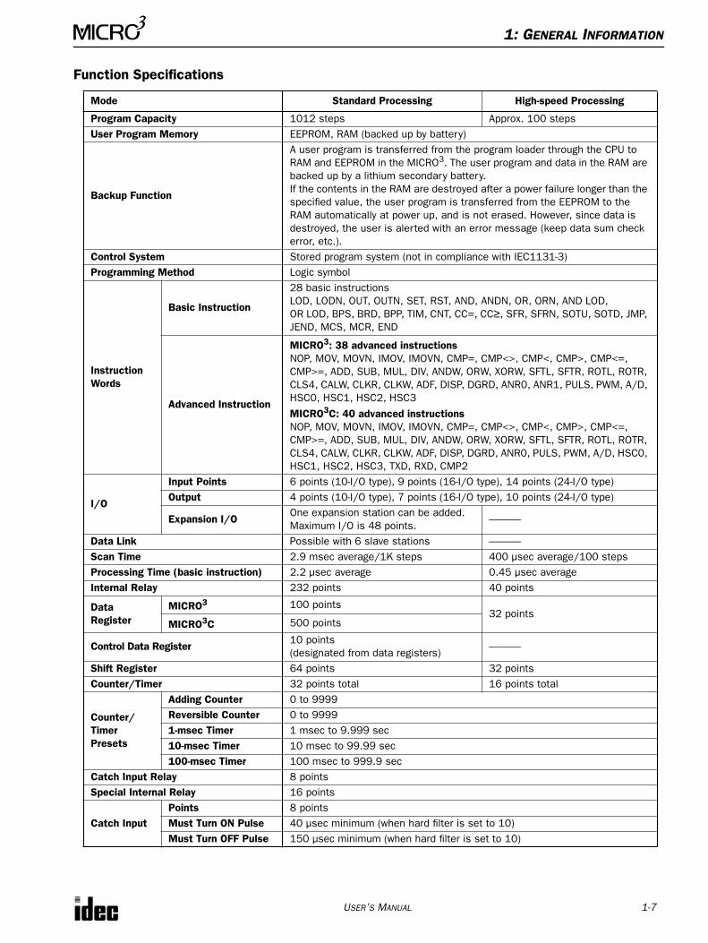
Function Specifications
Mode Standard Processing High-speed Processing
Program Capacity 1012 steps Approx. 100 stepsUser Program Memory EEPROM, RAM (backed up by battery)
Backup Function
A user program is transferred from the program loader through the CPU to RAM and EEPROM in the MICRO3. The user program and data in the RAM are backed up by a lithium secondary battery.If the contents in the RAM are destroyed after a power failure longer than the specified value, the user program is transferred from the EEPROM to the RAM automatically at power up, and is not erased. However, since data is destroyed, the user is alerted with an error message (keep data sum check error, etc.).
Control System Stored program system (not in compliance with IEC1131-3)Programming Method Logic symbol
Instruction Words
Basic Instruction
28 basic instructionsLOD, LODN, OUT, OUTN, SET, RST, AND, ANDN, OR, ORN, AND LOD, OR LOD, BPS, BRD, BPP, TIM, CNT, CC=, CC≥, SFR, SFRN, SOTU, SOTD, JMP, JEND, MCS, MCR, END
Advanced Instruction
MICRO3: 38 advanced instructionsNOP, MOV, MOVN, IMOV, IMOVN, CMP=, CMP<>, CMP<, CMP>, CMP<=, CMP>=, ADD, SUB, MUL, DIV, ANDW, ORW, XORW, SFTL, SFTR, ROTL, ROTR, CLS4, CALW, CLKR, CLKW, ADF, DISP, DGRD, ANR0, ANR1, PULS, PWM, A/D, HSC0, HSC1, HSC2, HSC3
MICRO3C: 40 advanced instructionsNOP, MOV, MOVN, IMOV, IMOVN, CMP=, CMP<>, CMP<, CMP>, CMP<=, CMP>=, ADD, SUB, MUL, DIV, ANDW, ORW, XORW, SFTL, SFTR, ROTL, ROTR, CLS4, CALW, CLKR, CLKW, ADF, DISP, DGRD, ANR0, PULS, PWM, A/D, HSC0, HSC1, HSC2, HSC3, TXD, RXD, CMP2
I/O
Input Points 6 points (10-I/O type), 9 points (16-I/O type), 14 points (24-I/O type)Output 4 points (10-I/O type), 7 points (16-I/O type), 10 points (24-I/O type)
Expansion I/OOne expansion station can be added.Maximum I/O is 48 points.
———
Data Link Possible with 6 slave stations ———Scan Time 2.9 msec average/1K steps 400 µsec average/100 stepsProcessing Time (basic instruction) 2.2 µsec average 0.45 µsec averageInternal Relay 232 points 40 points
Data Register
MICRO3 100 points32 points
MICRO3C 500 points
Control Data Register10 points (designated from data registers)
———
Shift Register 64 points 32 pointsCounter/Timer 32 points total 16 points total
Counter/Timer Presets
Adding Counter 0 to 9999Reversible Counter 0 to 99991-msec Timer 1 msec to 9.999 sec10-msec Timer 10 msec to 99.99 sec100-msec Timer 100 msec to 999.9 sec
Catch Input Relay 8 pointsSpecial Internal Relay 16 points
Catch InputPoints 8 pointsMust Turn ON Pulse 40 µsec minimum (when hard filter is set to 10)Must Turn OFF Pulse 150 µsec minimum (when hard filter is set to 10)
1: GENERAL INFORMATION
1-8 USER’S MANUAL
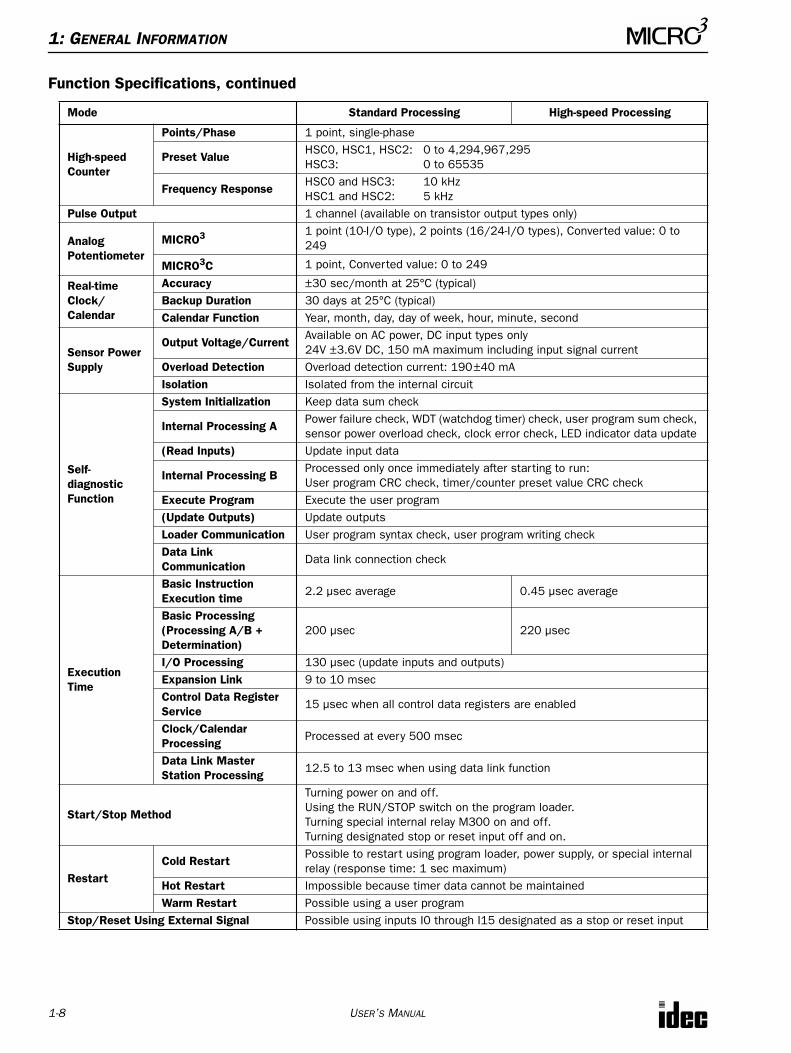
Function Specifications, continued
Mode Standard Processing High-speed Processing
High-speed Counter
Points/Phase 1 point, single-phase
Preset ValueHSC0, HSC1, HSC2: 0 to 4,294,967,295HSC3: 0 to 65535
Frequency ResponseHSC0 and HSC3: 10 kHzHSC1 and HSC2: 5 kHz
Pulse Output 1 channel (available on transistor output types only)
Analog Potentiometer
MICRO3 1 point (10-I/O type), 2 points (16/24-I/O types), Converted value: 0 to 249
MICRO3C 1 point, Converted value: 0 to 249
Real-timeClock/Calendar
Accuracy ±30 sec/month at 25°C (typical)Backup Duration 30 days at 25°C (typical)Calendar Function Year, month, day, day of week, hour, minute, second
Sensor Power Supply
Output Voltage/CurrentAvailable on AC power, DC input types only24V ±3.6V DC, 150 mA maximum including input signal current
Overload Detection Overload detection current: 190±40 mAIsolation Isolated from the internal circuit
Self-diagnostic Function
System Initialization Keep data sum check
Internal Processing APower failure check, WDT (watchdog timer) check, user program sum check, sensor power overload check, clock error check, LED indicator data update
(Read Inputs) Update input data
Internal Processing BProcessed only once immediately after starting to run:User program CRC check, timer/counter preset value CRC check
Execute Program Execute the user program(Update Outputs) Update outputsLoader Communication User program syntax check, user program writing checkData Link Communication
Data link connection check
Execution Time
Basic Instruction Execution time
2.2 µsec average 0.45 µsec average
Basic Processing(Processing A/B + Determination)
200 µsec 220 µsec
I/O Processing 130 µsec (update inputs and outputs)Expansion Link 9 to 10 msecControl Data Register Service
15 µsec when all control data registers are enabled
Clock/Calendar Processing
Processed at every 500 msec
Data Link Master Station Processing
12.5 to 13 msec when using data link function
Start/Stop Method
Turning power on and off.Using the RUN/STOP switch on the program loader.Turning special internal relay M300 on and off.Turning designated stop or reset input off and on.
RestartCold Restart
Possible to restart using program loader, power supply, or special internal relay (response time: 1 sec maximum)
Hot Restart Impossible because timer data cannot be maintainedWarm Restart Possible using a user program
Stop/Reset Using External Signal Possible using inputs I0 through I15 designated as a stop or reset input
1: GENERAL INFORMATION
USER’S MANUAL 1-9
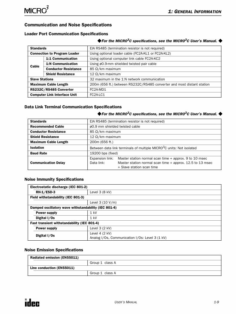
Communication and Noise Specifications
Loader Port Communication Specifications
For the MICRO3C specifications, see the MICRO3C User’s Manual.
Data Link Terminal Communication Specifications
For the MICRO3C specifications, see the MICRO3C User’s Manual.
Noise Immunity Specifications
Noise Emission Specifications
Standards EIA RS485 (termination resistor is not required)Connection to Program Loader Using optional loader cable (FC2A-KL1 or FC2A-KL2)
Cable
1:1 Communication Using optional computer link cable FC2A-KC21:N Communication Using ø0.9-mm shielded twisted pair cableConductor Resistance 85 Ω/km maximumShield Resistance 12 Ω/km maximum
Slave Stations 32 maximum in the 1:N network communicationMaximum Cable Length 200m (656 ft.) between RS232C/RS485 converter and most distant stationRS232C/RS485 Converter FC2A-MD1Computer Link Interface Unit FC2A-LC1
Standards EIA RS485 (termination resistor is not required)Recommended Cable ø0.9 mm shielded twisted cableConductor Resistance 85 Ω/km maximumShield Resistance 12 Ω/km maximumMaximum Cable Length 200m (656 ft.)
Isolation Between data link terminals of multiple MICRO3C units: Not isolatedBaud Rate 19200 bps (fixed)
Communication DelayExpansion link: Master station normal scan time + approx. 9 to 10 msecData link: Master station normal scan time + approx. 12.5 to 13 msec
+ Slave station scan time
Electrostatic discharge (IEC 801-2)RH-1/ESD-3 Level 3 (8 kV)
Field withstandability (IEC 801-3)Level 3 (10 V/m)
Damped oscillatory wave withstandability (IEC 801-4)Power supply 1 kVDigital I/Os 1 kV
Fast transient withstandability (IEC 801-4)Power supply Level 3 (2 kV)
Digital I/OsLevel 4 (2 kV)Analog I/Os, Communication I/Os: Level 3 (1 kV)
Radiated emission (EN55011)Group 1 class A
Line conduction (EN55011)Group 1 class A
1: GENERAL INFORMATION
1-10 USER’S MANUAL
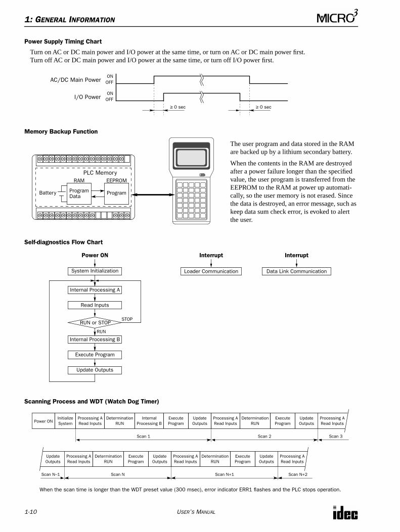
Power Supply Timing Chart
Turn on AC or DC main power and I/O power at the same time, or turn on AC or DC main power first.Turn off AC or DC main power and I/O power at the same time, or turn off I/O power first.
Memory Backup Function
Self-diagnostics Flow Chart
Scanning Process and WDT (Watch Dog Timer)
I/O PowerONOFF
≥ 0 sec
AC/DC Main PowerONOFF
≥ 0 sec
PLC MemoryRAM EEPROM
Battery ProgramData
Program
The user program and data stored in the RAM are backed up by a lithium secondary battery.
When the contents in the RAM are destroyed after a power failure longer than the specified value, the user program is transferred from the EEPROM to the RAM at power up automati-cally, so the user memory is not erased. Since the data is destroyed, an error message, such as keep data sum check error, is evoked to alert the user.
Power ON
System Initialization
Internal Processing A
Read Inputs
RUN or STOP
Internal Processing B
Execute Program
Update Outputs
STOP
RUN
Interrupt
Loader Communication
Interrupt
Data Link Communication
Power ONInitializeSystem
Processing ARead Inputs
DeterminationRUN
InternalProcessing B
ExecuteProgram
UpdateOutputs
Scan 1
Processing ARead Inputs
DeterminationRUN
ExecuteProgram
UpdateOutputs
Processing ARead Inputs
UpdateOutputs
Processing ARead Inputs
DeterminationRUN
ExecuteProgram
UpdateOutputs
Processing ARead Inputs
DeterminationRUN
ExecuteProgram
UpdateOutputs
Scan 2 Scan 3
Scan N–1 Scan N Scan N+1 Scan N+2
Processing ARead Inputs
When the scan time is longer than the WDT preset value (300 msec), error indicator ERR1 flashes and the PLC stops operation.
1: GENERAL INFORMATION
USER’S MANUAL 1-11
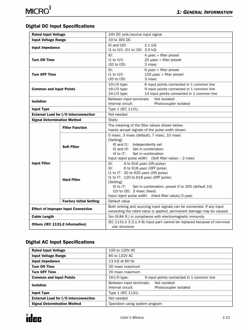
Digital DC Input Specifications
Digital AC Input Specifications
Rated Input Voltage 24V DC sink/source input signalInput Voltage Range 19 to 30V DC
Input ImpedanceI0 and I20: 2.1 kΩI1 to I15, I21 to I35: 3.5 kΩ
Turn ON TimeI0: 4 µsec + filter presetI1 to I15: 20 µsec + filter presetI20 to I35: 3 msec
Turn OFF TimeI0: 6 µsec + filter presetI1 to I15: 120 µsec + filter presetI20 to I35: 3 msec
Common and Input Points10-I/O type: 6 input points connected in 1 common line16-I/O type: 9 input points connected in 1 common line24-I/O type: 14 input points connected in 1 common line
IsolationBetween input terminals: Not isolatedInternal circuit: Photocoupler isolated
Input Type Type 1 (IEC 1131)External Load for I/O Interconnection Not neededSignal Determination Method Static
Input Filter
Filter FunctionThe meaning of the filter values shown below:Inputs accept signals of the pulse width shown.
Soft Filter
0 msec, 3 msec (default), 7 msec, 10 msec[Setting] I0 and I1: Independently set I2 and I3: Set in combination I4 to I7: Set in combinationInput reject pulse width: (Soft filter value) – 2 msec
Hard Filter
I0: 4 to 616 µsec (ON pulse)I0: 6 to 618 µsec (OFF pulse)I1 to I7: 20 to 625 µsec (ON pulse)I1 to I7: 120 to 618 µsec (OFF pulse)[Setting] I0 to I7: Set in combination, preset 0 to 255 (default 10) I10 to I35: 3 msec (fixed)Input reject pulse width: (Hard filter value)/3 µsec
Factory Initial Setting Default value
Effect of Improper Input ConnectionBoth sinking and sourcing input signals can be connected. If any input exceeding the rated value is applied, permanent damage may be caused.
Cable Length 3m (9.84 ft.) in compliance with electromagnetic immunity
Others (IEC 1131-2 Information)IEC 1131-2 3.3.1.4 8) Input part cannot be replaced because of non-mod-
ular structure
Rated Input Voltage 100 to 120V ACInput Voltage Range 85 to 132V ACInput Impedance 13 kΩ at 60 HzTurn ON Time 20 msec maximumTurn OFF Time 20 msec maximumCommon and Input Points 16-I/O type: 9 input points connected in 1 common line
IsolationBetween input terminals: Not isolatedInternal circuit: Photocoupler isolated
Input Type Type 1 (IEC 1131)External Load for I/O Interconnection Not neededSignal Determination Method Operation using system program
1: GENERAL INFORMATION
1-12 USER’S MANUAL
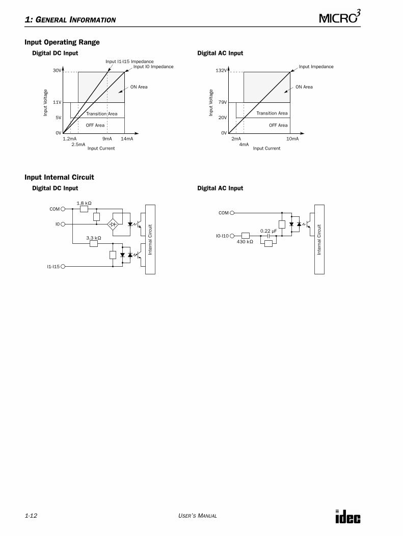
Input Operating Range
Input Internal Circuit
Digital DC Input Digital AC Input
Input I0 ImpedanceInput I1-I15 Impedance
ON Area
Transition Area
OFF Area
Inpu
t Vo
ltage
30V
11V
5V
0V1.2mA
2.5mA9mA 14mA
Input Current
Input Impedance
Transition Area
OFF Area
Inpu
t Vo
ltage
132V
79V
20V
0V2mA
4mA10mA
Input Current
ON Area
Digital DC Input Digital AC Input
COM
I0
Inte
rnal
Circ
uit
1.8 kΩ
3.3 kΩ
I1-I15
COM
Inte
rnal
Circ
uit
0.22 µF
430 kΩI0-I10
1: GENERAL INFORMATION
USER’S MANUAL 1-13
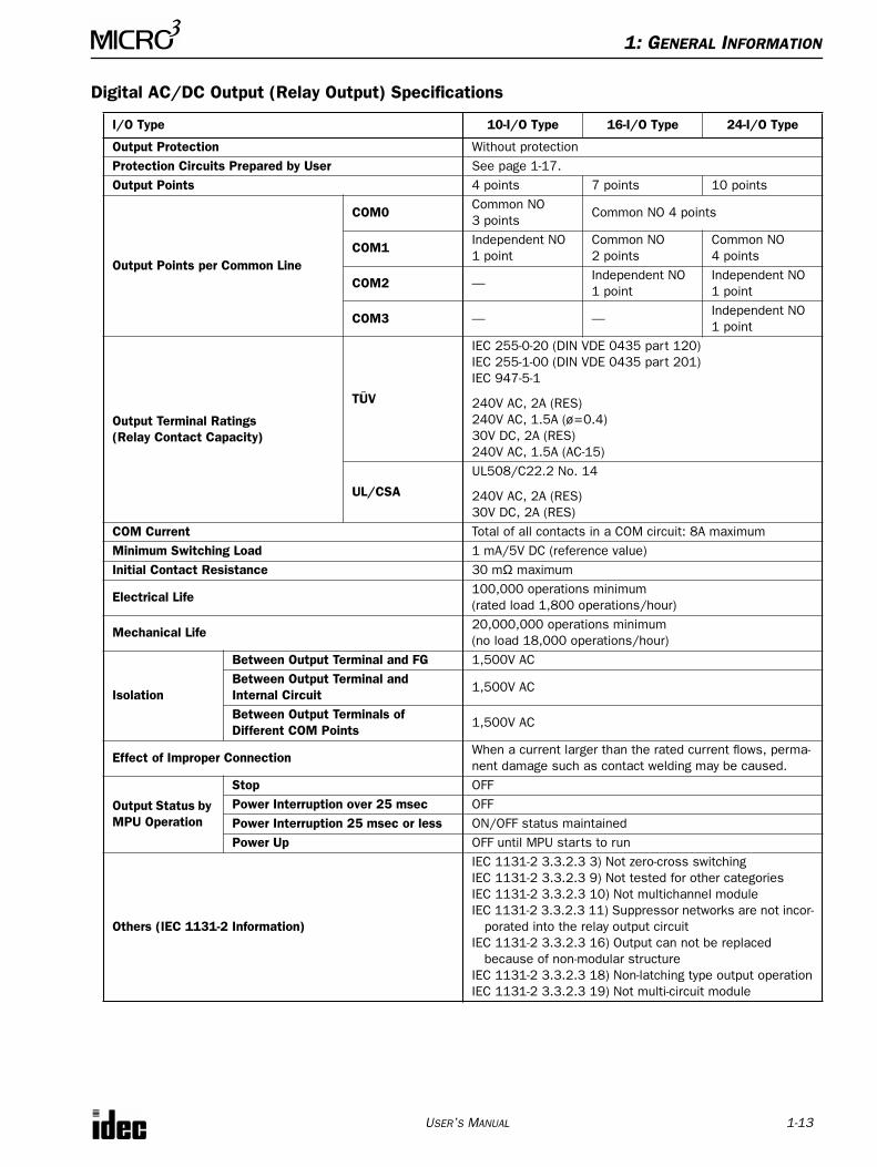
Digital AC/DC Output (Relay Output) Specifications
I/O Type 10-I/O Type 16-I/O Type 24-I/O Type
Output Protection Without protectionProtection Circuits Prepared by User See page 1-17.Output Points 4 points 7 points 10 points
Output Points per Common Line
COM0Common NO 3 points
Common NO 4 points
COM1Independent NO 1 point
Common NO 2 points
Common NO 4 points
COM2 —Independent NO 1 point
Independent NO 1 point
COM3 — —Independent NO 1 point
Output Terminal Ratings(Relay Contact Capacity)
TÜV
IEC 255-0-20 (DIN VDE 0435 part 120)IEC 255-1-00 (DIN VDE 0435 part 201)IEC 947-5-1
240V AC, 2A (RES)240V AC, 1.5A (ø=0.4)30V DC, 2A (RES)240V AC, 1.5A (AC-15)
UL/CSA
UL508/C22.2 No. 14
240V AC, 2A (RES)30V DC, 2A (RES)
COM Current Total of all contacts in a COM circuit: 8A maximumMinimum Switching Load 1 mA/5V DC (reference value)Initial Contact Resistance 30 mΩ maximum
Electrical Life100,000 operations minimum (rated load 1,800 operations/hour)
Mechanical Life20,000,000 operations minimum (no load 18,000 operations/hour)
Isolation
Between Output Terminal and FG 1,500V ACBetween Output Terminal and Internal Circuit
1,500V AC
Between Output Terminals of Different COM Points
1,500V AC
Effect of Improper ConnectionWhen a current larger than the rated current flows, perma-nent damage such as contact welding may be caused.
Output Status by MPU Operation
Stop OFFPower Interruption over 25 msec OFFPower Interruption 25 msec or less ON/OFF status maintainedPower Up OFF until MPU starts to run
Others (IEC 1131-2 Information)
IEC 1131-2 3.3.2.3 3) Not zero-cross switchingIEC 1131-2 3.3.2.3 9) Not tested for other categoriesIEC 1131-2 3.3.2.3 10) Not multichannel moduleIEC 1131-2 3.3.2.3 11) Suppressor networks are not incor-
porated into the relay output circuitIEC 1131-2 3.3.2.3 16) Output can not be replaced
because of non-modular structureIEC 1131-2 3.3.2.3 18) Non-latching type output operationIEC 1131-2 3.3.2.3 19) Not multi-circuit module
1: GENERAL INFORMATION
1-14 USER’S MANUAL
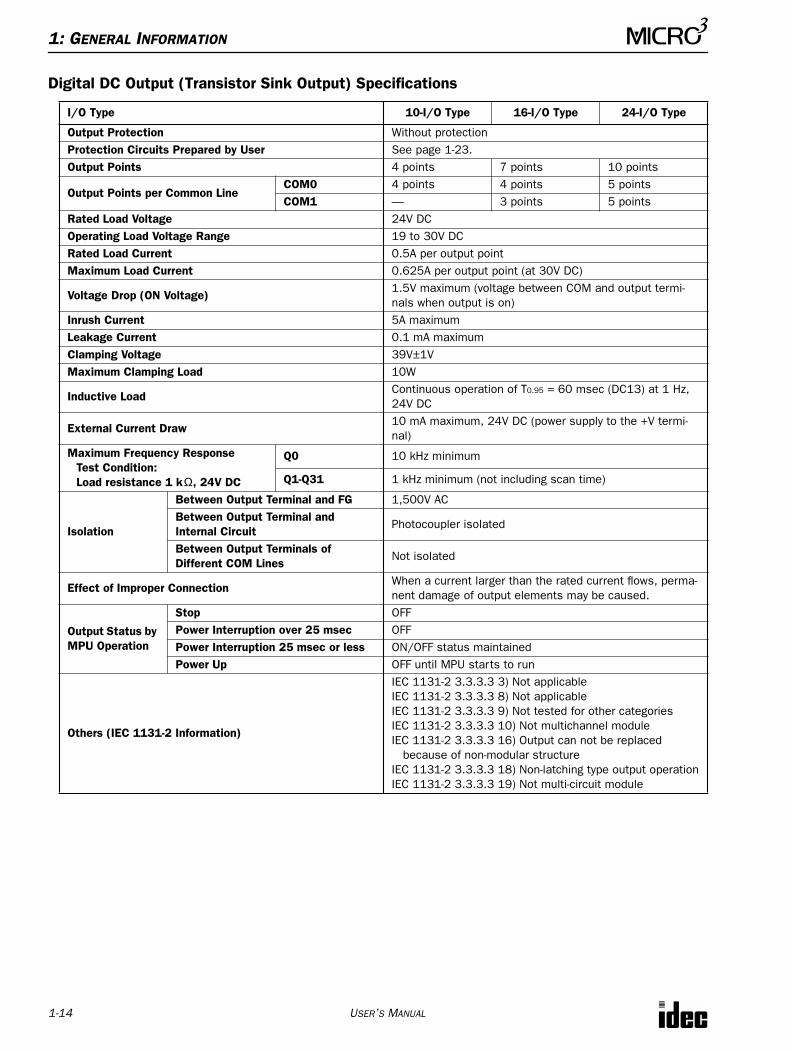
Digital DC Output (Transistor Sink Output) Specifications
I/O Type 10-I/O Type 16-I/O Type 24-I/O Type
Output Protection Without protectionProtection Circuits Prepared by User See page 1-23.Output Points 4 points 7 points 10 points
Output Points per Common LineCOM0 4 points 4 points 5 pointsCOM1 — 3 points 5 points
Rated Load Voltage 24V DCOperating Load Voltage Range 19 to 30V DCRated Load Current 0.5A per output pointMaximum Load Current 0.625A per output point (at 30V DC)
Voltage Drop (ON Voltage)1.5V maximum (voltage between COM and output termi-nals when output is on)
Inrush Current 5A maximumLeakage Current 0.1 mA maximumClamping Voltage 39V±1VMaximum Clamping Load 10W
Inductive LoadContinuous operation of T0.95 = 60 msec (DC13) at 1 Hz, 24V DC
External Current Draw10 mA maximum, 24V DC (power supply to the +V termi-nal)
Maximum Frequency ResponseTest Condition:Load resistance 1 kΩ, 24V DC
Q0 10 kHz minimum
Q1-Q31 1 kHz minimum (not including scan time)
Isolation
Between Output Terminal and FG 1,500V ACBetween Output Terminal and Internal Circuit
Photocoupler isolated
Between Output Terminals of Different COM Lines
Not isolated
Effect of Improper ConnectionWhen a current larger than the rated current flows, perma-nent damage of output elements may be caused.
Output Status by MPU Operation
Stop OFFPower Interruption over 25 msec OFFPower Interruption 25 msec or less ON/OFF status maintainedPower Up OFF until MPU starts to run
Others (IEC 1131-2 Information)
IEC 1131-2 3.3.3.3 3) Not applicableIEC 1131-2 3.3.3.3 8) Not applicableIEC 1131-2 3.3.3.3 9) Not tested for other categoriesIEC 1131-2 3.3.3.3 10) Not multichannel moduleIEC 1131-2 3.3.3.3 16) Output can not be replaced
because of non-modular structureIEC 1131-2 3.3.3.3 18) Non-latching type output operationIEC 1131-2 3.3.3.3 19) Not multi-circuit module
1: GENERAL INFORMATION
USER’S MANUAL 1-15
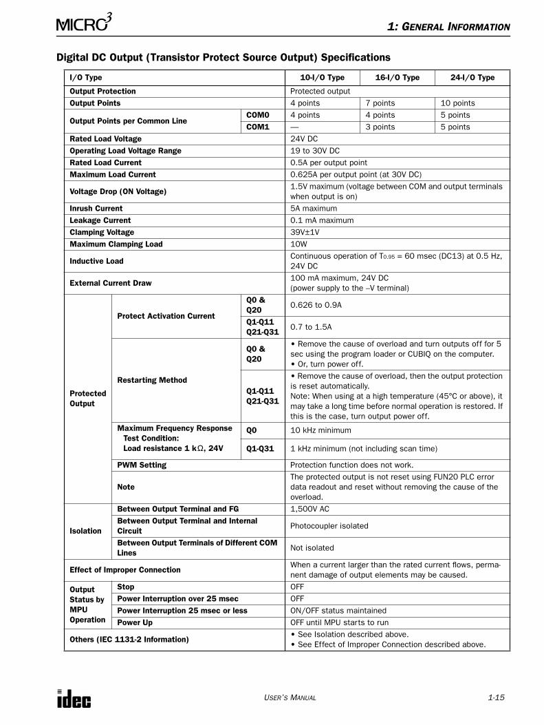
Digital DC Output (Transistor Protect Source Output) Specifications
I/O Type 10-I/O Type 16-I/O Type 24-I/O Type
Output Protection Protected outputOutput Points 4 points 7 points 10 points
Output Points per Common LineCOM0 4 points 4 points 5 pointsCOM1 — 3 points 5 points
Rated Load Voltage 24V DCOperating Load Voltage Range 19 to 30V DCRated Load Current 0.5A per output pointMaximum Load Current 0.625A per output point (at 30V DC)
Voltage Drop (ON Voltage)1.5V maximum (voltage between COM and output terminals when output is on)
Inrush Current 5A maximumLeakage Current 0.1 mA maximumClamping Voltage 39V±1VMaximum Clamping Load 10W
Inductive LoadContinuous operation of T0.95 = 60 msec (DC13) at 0.5 Hz, 24V DC
External Current Draw100 mA maximum, 24V DC (power supply to the –V terminal)
ProtectedOutput
Protect Activation Current
Q0 & Q20
0.626 to 0.9A
Q1-Q11Q21-Q31
0.7 to 1.5A
Restarting Method
Q0 & Q20
• Remove the cause of overload and turn outputs off for 5 sec using the program loader or CUBIQ on the computer.• Or, turn power off.
Q1-Q11Q21-Q31
• Remove the cause of overload, then the output protection is reset automatically.Note: When using at a high temperature (45°C or above), it may take a long time before normal operation is restored. If this is the case, turn output power off.
Maximum Frequency ResponseTest Condition:Load resistance 1 kΩ, 24V
Q0 10 kHz minimum
Q1-Q31 1 kHz minimum (not including scan time)
PWM Setting Protection function does not work.
NoteThe protected output is not reset using FUN20 PLC error data readout and reset without removing the cause of the overload.
Isolation
Between Output Terminal and FG 1,500V ACBetween Output Terminal and Internal Circuit
Photocoupler isolated
Between Output Terminals of Different COM Lines
Not isolated
Effect of Improper ConnectionWhen a current larger than the rated current flows, perma-nent damage of output elements may be caused.
Output Status by MPU Operation
Stop OFFPower Interruption over 25 msec OFFPower Interruption 25 msec or less ON/OFF status maintainedPower Up OFF until MPU starts to run
Others (IEC 1131-2 Information)• See Isolation described above.• See Effect of Improper Connection described above.
1: GENERAL INFORMATION
1-16 USER’S MANUAL
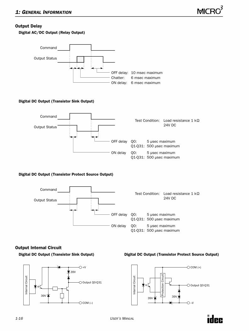
Output DelayDigital AC/DC Output (Relay Output)
Digital DC Output (Transistor Sink Output)
Digital DC Output (Transistor Protect Source Output)
Output Internal Circuit
Command
Output Status
OFF delay: 10 msec maximumChatter: 6 msec maximumON delay: 6 msec maximum
Command
Output Status
OFF delay Q0: 5 µsec maximumQ1-Q31: 500 µsec maximum
ON delay Q0: 5 µsec maximumQ1-Q31: 500 µsec maximum
Test Condition: Load resistance 1 kΩ24V DC
Command
Output Status
OFF delay Q0: 5 µsec maximumQ1-Q31: 500 µsec maximum
ON delay Q0: 5 µsec maximumQ1-Q31: 500 µsec maximum
Test Condition: Load resistance 1 kΩ24V DC
Digital DC Output (Transistor Sink Output)
+V
Output Q0-Q31
Inte
rnal
Circ
uit
COM (–)
39V
39V
Digital DC Output (Transistor Protect Source Output)
COM (+)
Output Q0-Q31
–V
39V 39VProt
ectio
n C
ircui
t
Inte
rnal
Circ
uit
1: GENERAL INFORMATION
USER’S MANUAL 1-17
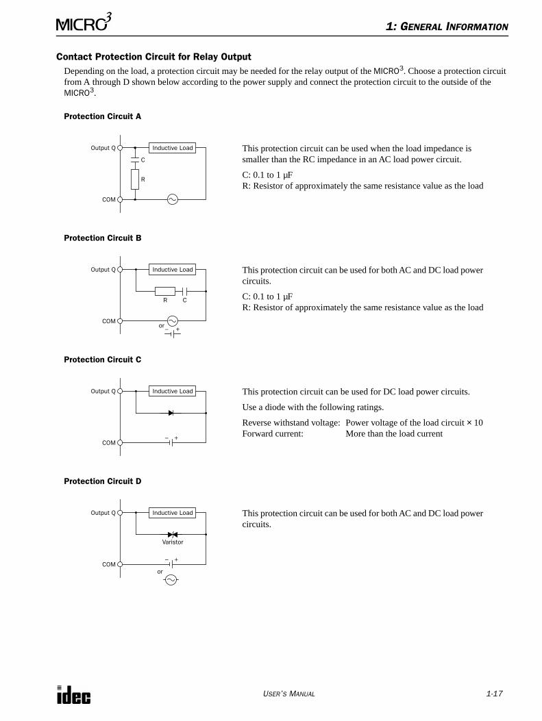
Contact Protection Circuit for Relay OutputDepending on the load, a protection circuit may be needed for the relay output of the MICRO3. Choose a protection circuit from A through D shown below according to the power supply and connect the protection circuit to the outside of the MICRO3.
Protection Circuit A
Protection Circuit B
Protection Circuit C
Protection Circuit D
Inductive Load
COM
C
R
Output Q This protection circuit can be used when the load impedance is smaller than the RC impedance in an AC load power circuit.
C: 0.1 to 1 µFR: Resistor of approximately the same resistance value as the load
Inductive Load
COM
R
Output Q This protection circuit can be used for both AC and DC load power circuits.
C: 0.1 to 1 µFR: Resistor of approximately the same resistance value as the load
C
+or–
Inductive Load
COM
Output Q This protection circuit can be used for DC load power circuits.
Use a diode with the following ratings.
Reverse withstand voltage: Power voltage of the load circuit × 10Forward current: More than the load current+–
Inductive Load
COM
Output Q This protection circuit can be used for both AC and DC load power circuits.
+
or
–
Varistor
1: GENERAL INFORMATION
1-18 USER’S MANUAL
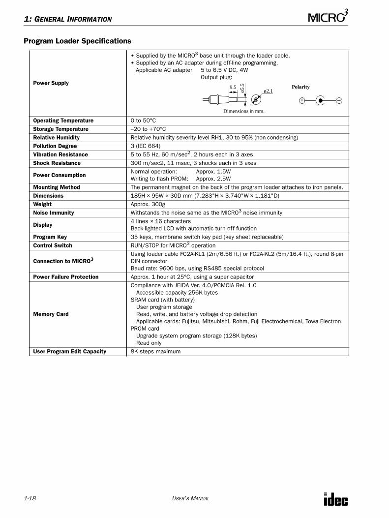
Program Loader Specifications
Power Supply
• Supplied by the MICRO3 base unit through the loader cable.• Supplied by an AC adapter during off-line programming.
Applicable AC adapter 5 to 6.5 V DC, 4WOutput plug:
Operating Temperature 0 to 50°CStorage Temperature –20 to +70°CRelative Humidity Relative humidity severity level RH1, 30 to 95% (non-condensing)Pollution Degree 3 (IEC 664)Vibration Resistance 5 to 55 Hz, 60 m/sec2, 2 hours each in 3 axesShock Resistance 300 m/sec2, 11 msec, 3 shocks each in 3 axes
Power ConsumptionNormal operation: Approx. 1.5WWriting to flash PROM: Approx. 2.5W
Mounting Method The permanent magnet on the back of the program loader attaches to iron panels.Dimensions 185H × 95W × 30D mm (7.283"H × 3.740"W × 1.181"D)Weight Approx. 300gNoise Immunity Withstands the noise same as the MICRO3 noise immunity
Display4 lines × 16 charactersBack-lighted LCD with automatic turn off function
Program Key 35 keys, membrane switch key pad (key sheet replaceable)Control Switch RUN/STOP for MICRO3 operation
Connection to MICRO3Using loader cable FC2A-KL1 (2m/6.56 ft.) or FC2A-KL2 (5m/16.4 ft.), round 8-pin DIN connectorBaud rate: 9600 bps, using RS485 special protocol
Power Failure Protection Approx. 1 hour at 25°C, using a super capacitor
Memory Card
Compliance with JEIDA Ver. 4.0/PCMCIA Rel. 1.0Accessible capacity 256K bytes
SRAM card (with battery)User program storageRead, write, and battery voltage drop detectionApplicable cards: Fujitsu, Mitsubishi, Rohm, Fuji Electrochemical, Towa Electron
PROM cardUpgrade system program storage (128K bytes)Read only
User Program Edit Capacity 8K steps maximum
9.5ø2.1ø5
.5 Polarity
+ –
Dimensions in mm.
1: GENERAL INFORMATION
USER’S MANUAL 1-19
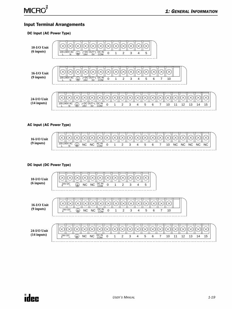
Input Terminal Arrangements
100-240V ACL N
DC OUT24V 0V
DC INCOM 0 1 2 3 4 5
24V DC+ –
DC INCOM 0 1 2 3 4 5NC NC
100-240V ACL N
DC OUT24V 0V
DC INCOM 0 1 2 3 4 5 6 7 10
100-240V ACL N
DC OUT24V 0V
DC INCOM 0 1 2 3 4 5 6 7 10 11 12 13 14 15
100-240V ACL N
AC INCOM 0 1 2 3 4 5 6 7 10 NC NC NC NC NC
10-I/O Unit
NC NC
DC Input (AC Power Type)
16-I/O Unit
24-I/O Unit
AC Input (AC Power Type)
16-I/O Unit
DC Input (DC Power Type)
10-I/O Unit
(6 inputs)
(6 inputs)
(9 inputs)
(14 inputs)
(9 inputs)
DC INCOM 0 1 2 3 4 5 6 7 10
16-I/O Unit(9 inputs)
DC INCOM 0 1 2 3 4 5 6 7 10 11 12 13 14 15
24-I/O Unit(14 inputs)
24V DC+ – NC NC
24V DC+ – NC NC
1: GENERAL INFORMATION
1-20 USER’S MANUAL
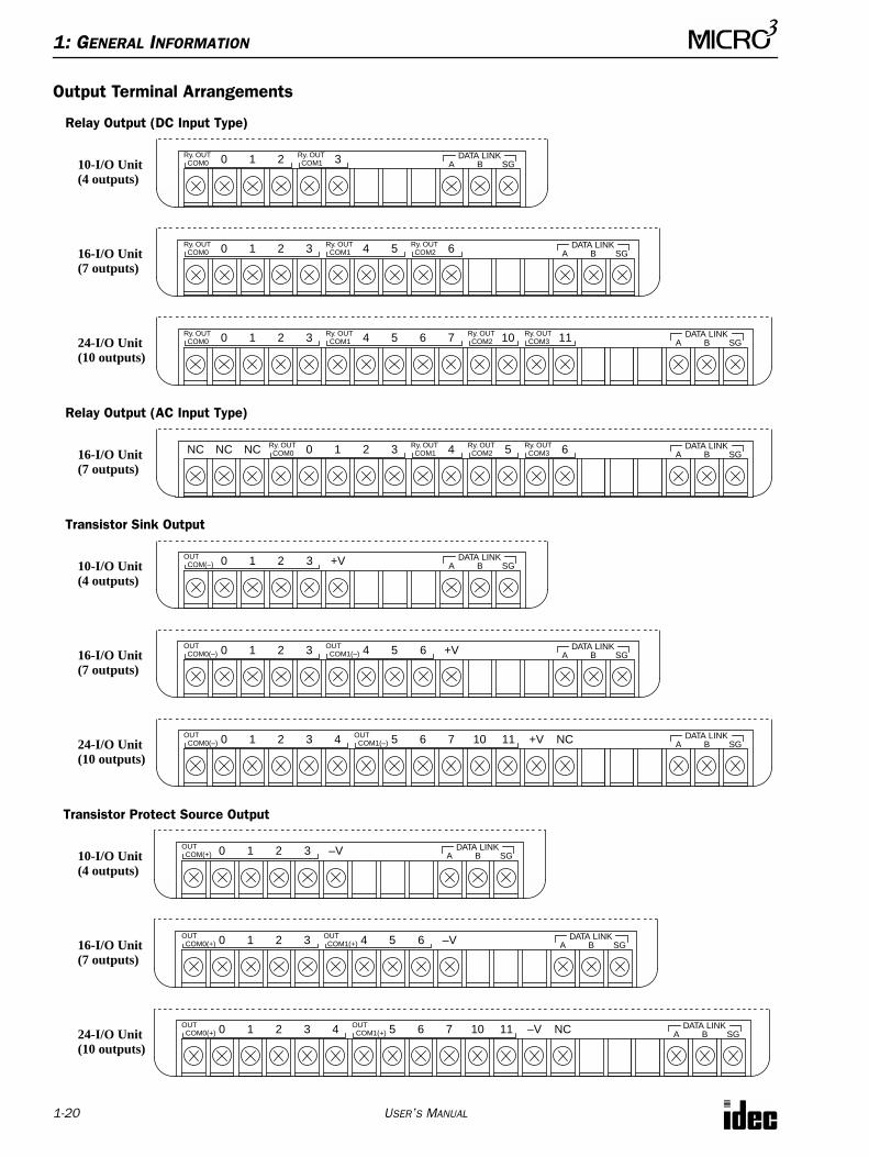
Output Terminal Arrangements
Ry. OUTCOM0 0 1 2 Ry. OUT
COM1 3 DATA LINKA SGB
OUTCOM(–) 0 1 2 3 DATA LINK
A SGB+V
OUTCOM0(–) 0 1 2 3 OUT
COM1(–) 4 5 6 DATA LINKA SGB+V
Ry. OUTCOM0 0 1 2 3 Ry. OUT
COM1 4 5 6 7 Ry. OUTCOM2 10 Ry. OUT
COM3 11 DATA LINKA SGB
Ry. OUTCOM0 0 1 2 3 Ry. OUT
COM2 5 Ry. OUTCOM3 6 DATA LINK
A SGBRy. OUTCOM1 4NC NC NC
10-I/O Unit
Relay Output (DC Input Type)
16-I/O Unit
24-I/O Unit
16-I/O Unit
Relay Output (AC Input Type)
Transistor Sink Output
10-I/O Unit
16-I/O Unit
OUTCOM0(–) 0 1 2 3 NC DATA LINK
A SGB+V4 OUTCOM1(–) 5 6 7 10 1124-I/O Unit
OUTCOM(+) 0 1 2 3 DATA LINK
A SGB–V
OUTCOM0(+) 0 1 2 3 OUT
COM1(+) 4 5 6 DATA LINKA SGB–V
OUTCOM0(+) 0 1 2 3 NC DATA LINK
A SGB–V4 OUTCOM1(+) 5 6 7 10 11
Transistor Protect Source Output
10-I/O Unit
16-I/O Unit
24-I/O Unit
Ry. OUTCOM0 0 1 2 3 Ry. OUT
COM1 4 5 Ry. OUTCOM2 6 DATA LINK
A SGB
(4 outputs)
(7 outputs)
(10 outputs)
(7 outputs)
(4 outputs)
(7 outputs)
(10 outputs)
(4 outputs)
(7 outputs)
(10 outputs)
1: GENERAL INFORMATION
USER’S MANUAL 1-21
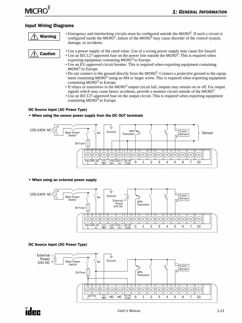
Input Wiring Diagrams
DC Source Input (AC Power Type)
• When using the sensor power supply from the DC OUT terminals
• When using an external power supply
DC Source Input (DC Power Type)
Warning• Emergency and interlocking circuits must be configured outside the MICRO3. If such a circuit is
configured inside the MICRO3, failure of the MICRO3 may cause disorder of the control system, damage, or accidents.
Caution• Use a power supply of the rated value. Use of a wrong power supply may cause fire hazard.• Use an IEC127-approved fuse on the power line outside the MICRO3. This is required when
exporting equipment containing MICRO3 to Europe.• Use an EU-approved circuit breaker. This is required when exporting equipment containing
MICRO3 to Europe.• Do not connect to the ground directly from the MICRO3. Connect a protective ground to the equip-
ment containing MICRO3 using an M4 or larger screw. This is required when exporting equipment containing MICRO3 to Europe.
• If relays or transistors in the MICRO3 output circuit fail, outputs may remain on or off. For output signals which may cause heavy accidents, provide a monitor circuit outside of the MICRO3.
• Use an IEC127-approved fuse on the output circuit. This is required when exporting equipment containing MICRO3 to Europe.
100-240V ACSensorGround
100-240V ACL N
DC OUT24V 0V
DC INCOM 0 1 2 3 4 5 6 7 10
2-wireSensor
+
–N
L Main PowerSwitch
Sw
3A Fuse
NPNTransistor
–
+Ground
100-240V ACL N
DC OUT24V 0V
DC INCOM 0 1 2 3 4 5 6 7 10
ExternalPower
24V DC
100-240V ACN
L Main PowerSwitch
Sw
3A Fuse
2-wireSensor
+
–
NPNTransistor
Main PowerSwitch
24V DC+ –
DC INCOM 0 1 2 3 4 5 6 7 10
ExternalPower
24V DC
–
+
NC NC
3A Fuse
Ground
2-wireSensor
+
–
NPNTransistor
Sw
1: GENERAL INFORMATION
1-22 USER’S MANUAL
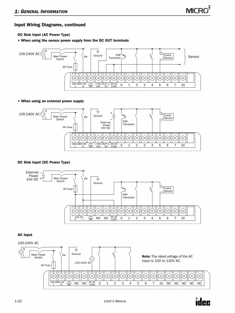
Input Wiring Diagrams, continued
DC Sink Input (AC Power Type)
• When using the sensor power supply from the DC OUT terminals
• When using an external power supply
DC Sink Input (DC Power Type)
AC Input
Sensor
100-240V ACL N
DC OUT24V 0V
DC INCOM 0 1 2 3 4 5 6 7 10
100-240V AC Ground
N
L Main PowerSwitch
Sw
3A Fuse
2-wireSensor
–
+PNP
Transistor
+
–100-240V AC Ground
N
L Main PowerSwitch
Sw
3A Fuse
100-240V ACL N
DC OUT24V 0V
DC INCOM 0 1 2 3 4 5 6 7 10
ExternalPower
24V DC
PNPTransistor
2-wireSensor
–
+
24V DC+ –
DC INCOM 0 1 2 3 4 5 6 7 10NC NC
Main PowerSwitch
ExternalPower
24V DC
–
+
3A Fuse
Ground
Sw
2-wireSensor
–
+
PNPTransistor
100-240V ACL N
AC INCOM 0 1 2 3 4 5 6 7 10 NC NC NC NC NCNC NC
Ground
N
L Main PowerSwitch
Sw
3A Fuse100-120V AC
100-240V AC
Note: The rated voltage of the AC input is 100 to 120V AC.
1: GENERAL INFORMATION
USER’S MANUAL 1-23
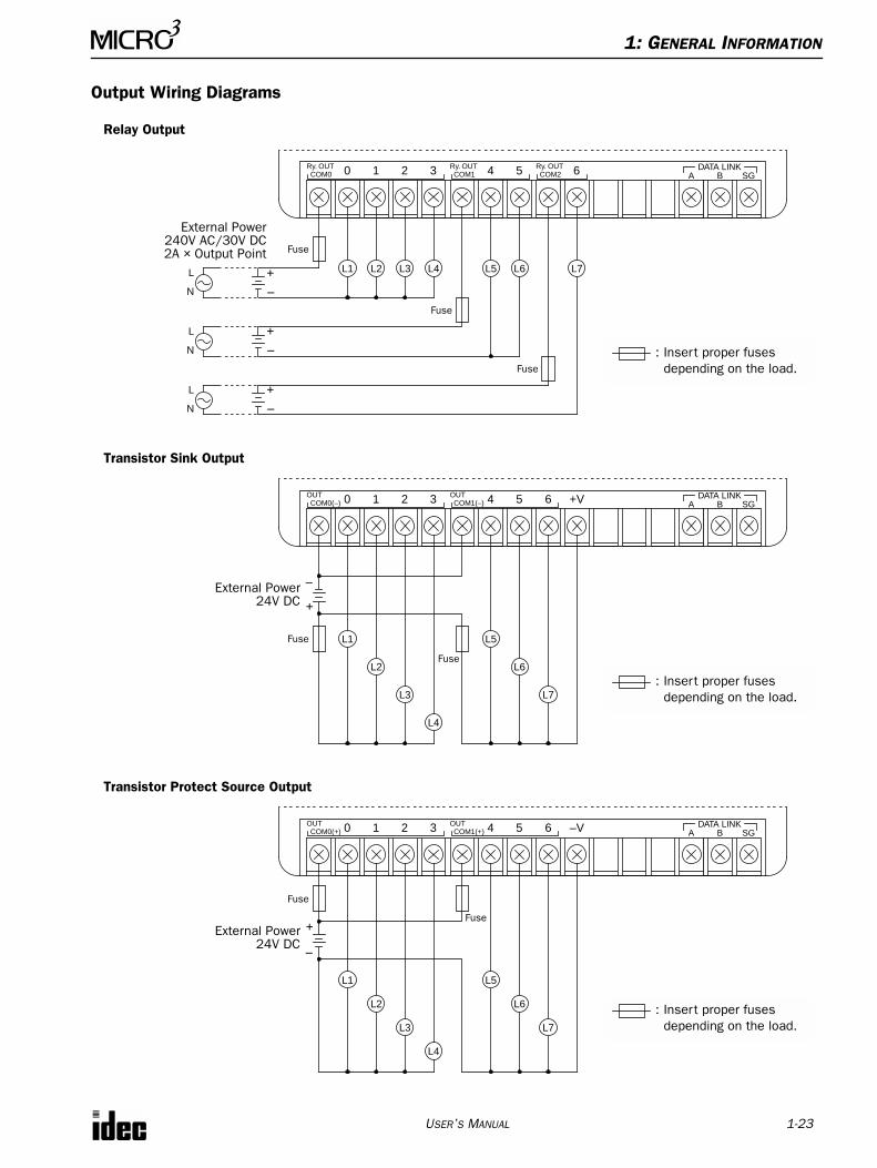
Output Wiring Diagrams
Relay Output
Transistor Sink Output
Transistor Protect Source Output
Fuse
Fuse
Ry. OUTCOM0 0 1 2 3 Ry. OUT
COM1 4 5 Ry. OUTCOM2 6 DATA LINK
A SGB
L4L3L2L1 L5 L6 L7
–+
–+
–+
L
N
L
N
L
N
Fuse
External Power240V AC/30V DC2A × Output Point
: Insert proper fuses depending on the load.
Fuse
L3
L2
L5
L6
External Power –
+
OUTCOM0(–) 0 1 2 3 OUT
COM1(–) 4 5 6 DATA LINKA SGB+V
L1
L4
L7
Fuse
24V DC
: Insert proper fuses depending on the load.
Fuse
L3
L2
L5
L6
External Power
L1
L4
OUTCOM0(+) 0 1 2 3 OUT
COM1(+) 4 5 6 DATA LINKA SGB–V
L7
24V DC
Fuse
–
+
: Insert proper fuses depending on the load.
1: GENERAL INFORMATION
1-24 USER’S MANUAL
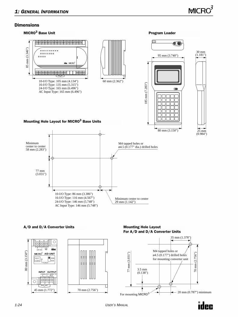
Dimensions85
mm
(3.
346"
)
10-I/O Type: 105 mm (4.134")16-I/O Type: 135 mm (5.315")24-I/O Type: 165 mm (6.496")AC Input Type: 165 mm (6.496")
60 mm (2.362")
95 mm (3.740")30 mm
(1.181")
185
mm
(7.
283"
)
80 mm (3.150") 25 mm(0.984")
10-I/O Type: 86 mm (3.386")16-I/O Type: 116 mm (4.567")24-I/O Type: 146 mm (5.748")AC Input Type: 146 mm (5.748")
M4 tapped holes or ø4.5 (0.177" dia.) drilled holes
77 mm
Minimum center to center
Minimum
29 mm (1.142")
(3.031")
center to center58 mm (2.283")
Mounting Hole Layout for MICRO3 Base Units
MICRO3 Base Unit Program Loader
+ –24V DC
A/D UNIT
I N P U T4 - 2 0 m A
P O W E R
SINK
SCE
+ –ANALOG WIRE TO
IN 0
INPUT OUTPUT
20 mm (0.787") minimum
70 m
m (
2.75
6")
35 mm (1.378")
3.5 mm
77 m
m (
3.03
1")
For mounting MICRO3
M4 tapped holes or ø4.5 (0.177") drilled holes for mounting converter unit
(0.138")
A/D and D/A Converter Units Mounting Hole Layout For A/D and D/A Converter Units
80 m
m (
3.15
0")
45 mm (1.772") 70 mm (2.756")
1: GENERAL INFORMATION
USER’S MANUAL 1-25
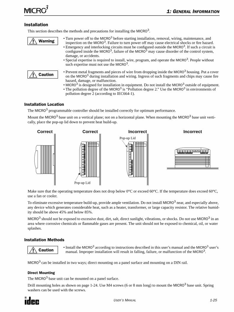
InstallationThis section describes the methods and precautions for installing the MICRO3.
Installation LocationThe MICRO3 programmable controller should be installed correctly for optimum performance.
Mount the MICRO3 base unit on a vertical plane; not on a horizontal plane. When mounting the MICRO3 base unit verti-cally, place the pop-up lid down to prevent heat build-up.
Make sure that the operating temperature does not drop below 0°C or exceed 60°C. If the temperature does exceed 60°C, use a fan or cooler.
To eliminate excessive temperature build-up, provide ample ventilation. Do not install MICRO3 near, and especially above, any device which generates considerable heat, such as a heater, transformer, or large capacity resistor. The relative humid-ity should be above 45% and below 85%.
MICRO3 should not be exposed to excessive dust, dirt, salt, direct sunlight, vibrations, or shocks. Do not use MICRO3 in an area where corrosive chemicals or flammable gases are present. The unit should not be exposed to chemical, oil, or water splashes.
Installation Methods
MICRO3 can be installed in two ways; direct mounting on a panel surface and mounting on a DIN rail.
Direct Mounting
The MICRO3 base unit can be mounted on a panel surface.
Drill mounting holes as shown on page 1-24. Use M4 screws (6 or 8 mm long) to mount the MICRO3 base unit. Spring washers can be used with the screws.
Warning• Turn power off to the MICRO3 before starting installation, removal, wiring, maintenance, and
inspection on the MICRO3. Failure to turn power off may cause electrical shocks or fire hazard.• Emergency and interlocking circuits must be configured outside the MICRO3. If such a circuit is
configured inside the MICRO3, failure of the MICRO3 may cause disorder of the control system, damage, or accidents.
• Special expertise is required to install, wire, program, and operate the MICRO3. People without such expertise must not use the MICRO3.
Caution• Prevent metal fragments and pieces of wire from dropping inside the MICRO3 housing. Put a cover
on the MICRO3 during installation and wiring. Ingress of such fragments and chips may cause fire hazard, damage, or malfunction.
• MICRO3 is designed for installation in equipment. Do not install the MICRO3 outside of equipment.• The pollution degree of the MICRO3 is “Pollution degree 2.” Use the MICRO3 in environments of
pollution degree 2 (according to IEC664-1).
Correct Incorrect IncorrectCorrect
Pop-up Lid
Pop-up Lid
Caution• Install the MICRO3 according to instructions described in this user’s manual and the MICRO3 user’s
manual. Improper installation will result in falling, failure, or malfunction of the MICRO3.
1: GENERAL INFORMATION
1-26 USER’S MANUAL
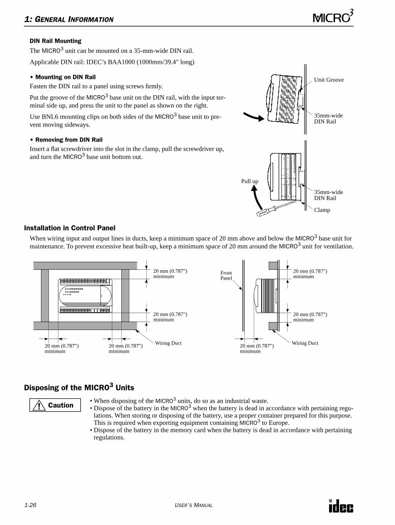
DIN Rail Mounting
The MICRO3 unit can be mounted on a 35-mm-wide DIN rail.
Applicable DIN rail: IDEC’s BAA1000 (1000mm/39.4" long)
• Mounting on DIN RailFasten the DIN rail to a panel using screws firmly.
Put the groove of the MICRO3 base unit on the DIN rail, with the input ter-minal side up, and press the unit to the panel as shown on the right.
Use BNL6 mounting clips on both sides of the MICRO3 base unit to pre-vent moving sideways.
• Removing from DIN RailInsert a flat screwdriver into the slot in the clamp, pull the screwdriver up, and turn the MICRO3 base unit bottom out.
Installation in Control PanelWhen wiring input and output lines in ducts, keep a minimum space of 20 mm above and below the MICRO3 base unit for maintenance. To prevent excessive heat built-up, keep a minimum space of 20 mm around the MICRO3 unit for ventilation.
Disposing of the MICRO3 Units
Unit Groove
35mm-wideDIN Rail
35mm-wideDIN Rail
Pull up
Clamp
Wiring Duct
20 mm (0.787")minimum
20 mm (0.787")minimum
20 mm (0.787")minimum
20 mm (0.787")minimum
20 mm (0.787")minimum
20 mm (0.787")minimum
Wiring Duct
FrontPanel
20 mm (0.787")minimum
Caution• When disposing of the MICRO3 units, do so as an industrial waste.• Dispose of the battery in the MICRO3 when the battery is dead in accordance with pertaining regu-
lations. When storing or disposing of the battery, use a proper container prepared for this purpose. This is required when exporting equipment containing MICRO3 to Europe.
• Dispose of the battery in the memory card when the battery is dead in accordance with pertaining regulations.
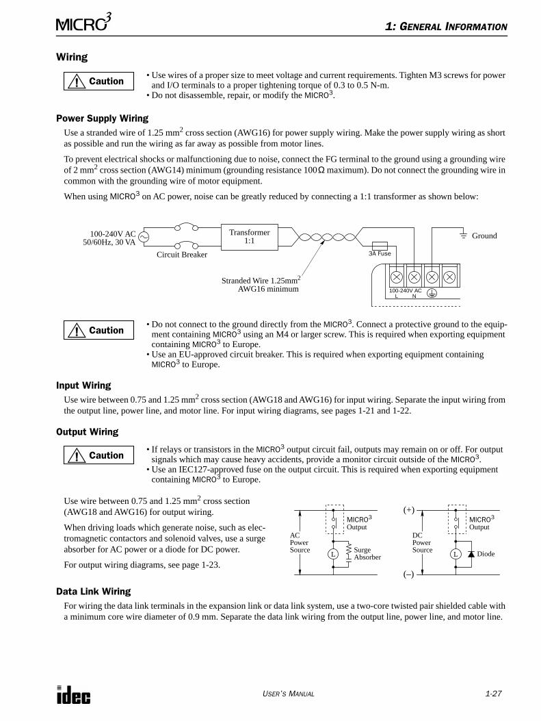
1: GENERAL INFORMATION
USER’S MANUAL 1-27
Wiring
Power Supply WiringUse a stranded wire of 1.25 mm2 cross section (AWG16) for power supply wiring. Make the power supply wiring as short as possible and run the wiring as far away as possible from motor lines.
To prevent electrical shocks or malfunctioning due to noise, connect the FG terminal to the ground using a grounding wire of 2 mm2 cross section (AWG14) minimum (grounding resistance 100Ω maximum). Do not connect the grounding wire in common with the grounding wire of motor equipment.
When using MICRO3 on AC power, noise can be greatly reduced by connecting a 1:1 transformer as shown below:
Input WiringUse wire between 0.75 and 1.25 mm2 cross section (AWG18 and AWG16) for input wiring. Separate the input wiring from the output line, power line, and motor line. For input wiring diagrams, see pages 1-21 and 1-22.
Output Wiring
Use wire between 0.75 and 1.25 mm2 cross section (AWG18 and AWG16) for output wiring.
When driving loads which generate noise, such as elec-tromagnetic contactors and solenoid valves, use a surge absorber for AC power or a diode for DC power.
For output wiring diagrams, see page 1-23.
Data Link WiringFor wiring the data link terminals in the expansion link or data link system, use a two-core twisted pair shielded cable with a minimum core wire diameter of 0.9 mm. Separate the data link wiring from the output line, power line, and motor line.
Caution• Use wires of a proper size to meet voltage and current requirements. Tighten M3 screws for power
and I/O terminals to a proper tightening torque of 0.3 to 0.5 N-m.• Do not disassemble, repair, or modify the MICRO3.
100-240V ACL N
100-240V AC Ground50/60Hz, 30 VA
Transformer1:1
Circuit Breaker
Stranded Wire 1.25mm2
AWG16 minimum
3A Fuse
Caution• Do not connect to the ground directly from the MICRO3. Connect a protective ground to the equip-
ment containing MICRO3 using an M4 or larger screw. This is required when exporting equipment containing MICRO3 to Europe.
• Use an EU-approved circuit breaker. This is required when exporting equipment containing MICRO3 to Europe.
• If relays or transistors in the MICRO3 output circuit fail, outputs may remain on or off. For output signals which may cause heavy accidents, provide a monitor circuit outside of the MICRO3.
• Use an IEC127-approved fuse on the output circuit. This is required when exporting equipment containing MICRO3 to Europe.
Caution
MICRO3
DC
L
Output
PowerSource
MICRO3
AC
L
Output
PowerSource
(+)
(–)
SurgeAbsorber Diode
1: GENERAL INFORMATION
1-28 USER’S MANUAL
Power Supply Voltage
The applicable power range for MICRO3 is 85 to 264V AC or 19 to 30V DC. When MICRO3 is powered up, the inrush cur-rent flow is 40A maximum at 264V AC or 30V DC with the rated input and output.
Power failure voltage varies with the operating conditions of the program loader and the number of I/O points used. In most cases, power failure is detected when the power voltage drops below 85V AC or 19V DC. Operation is stopped at this point to prevent malfunctioning. Momentary power failures of 25 msec or less are not detected at the rated power voltage.
Other Precautions
Crimping TerminalWhen connecting one wire to one terminal, use a crimping terminal shown on the left below.Only when connecting two wires to one terminal, use the longer crimping terminal shown in the middle below.
• Use a power supply of the rated value. Use of a wrong power supply may cause fire hazard.• Use an IEC127-approved fuse on the power line outside the MICRO3. This is required when
exporting equipment containing MICRO3 to Europe.
Caution
• Do not use the MICRO3 in environments outside of the specification values.• Connect the FG terminal to a proper ground; otherwise, electrical shocks may be caused.• Do not touch all screw terminals while the MICRO3 is powered up; otherwise, electrical shocks
may be caused.• Do not touch the input terminals immediately after inputs are turned off; otherwise, electrical
shocks may be caused.
Caution
4 mm(0.157")
5.5 mm(0.217")
5.6 mm(0.220")
5.5 mm(0.217")
ø3.2 mm(0.126" dia.)
ø3.2 mm(0.126" dia.)
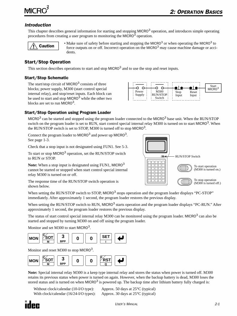
USER’S MANUAL 2-1
2: OPERATION BASICS
IntroductionThis chapter describes general information for starting and stopping MICRO3 operation, and introduces simple operating procedures from creating a user program to monitoring the MICRO3 operation.
Start/Stop OperationThis section describes operations to start and stop MICRO3 and to use the stop and reset inputs.
Start/Stop SchematicThe start/stop circuit of MICRO3 consists of three blocks; power supply, M300 (start control special internal relay), and stop/reset inputs. Each block can be used to start and stop MICRO3 while the other two blocks are set to run MICRO3.
Start/Stop Operation using Program LoaderMICRO3 can be started and stopped using the program loader connected to the MICRO3 base unit. When the RUN/STOP switch on the program loader is set to RUN, start control special internal relay M300 is turned on to start MICRO3. When the RUN/STOP switch is set to STOP, M300 is turned off to stop MICRO3.
Connect the program loader to MICRO3 and power up MICRO3. See page 1-3.
Check that a stop input is not designated using FUN1. See 5-3.
To start or stop MICRO3 operation, set the RUN/STOP switch to RUN or STOP.
Note: When a stop input is designated using FUN1, MICRO3 cannot be started or stopped when start control special internal relay M300 is turned on or off.
The response time of the RUN/STOP switch operation is shown below.
When setting the RUN/STOP switch to STOP, MICRO3 stops operation and the program loader displays “PC-STOP” immediately. After approximately 1 second, the program loader restores the previous display.
When setting the RUN/STOP switch to RUN, MICRO3 starts operation and the program loader displays “PC-RUN.” After approximately 1 second, the program loader restores the previous display.
The status of start control special internal relay M300 can be monitored using the program loader. MICRO3 can also be started and stopped by turning M300 on and off using the program loader.
Monitor and set M300 to start MICRO3.
Monitor and reset M300 to stop MICRO3.
Note: Special internal relay M300 is a keep type internal relay and stores the status when power is turned off. M300 retains its previous status when power is turned on again. However, when the backup battery is dead, M300 loses the stored status and is turned on when MICRO3 is powered up. The backup time after lithium battery fully charged is:
Without clock/calendar (10-I/O type): Approx. 50 days at 25°C (typical)With clock/calendar (16/24-I/O types): Approx. 30 days at 25°C (typical)
Caution• Make sure of safety before starting and stopping the MICRO3 or when operating the MICRO3 to
force outputs on or off. Incorrect operation on the MICRO3 may cause machine damage or acci-dents.
PowerSupply
M300 StopInput
ResetInput
Start
RUN/STOP
MICRO3
Switch
To start operation
To stop operation
(M300 is turned on.)
(M300 is turned off.)
RUN/STOP Switch
MON SOTC
M
3BPP
0 0 SETI
MON SOTC
M
3BPP
0 0 RSTF
Q
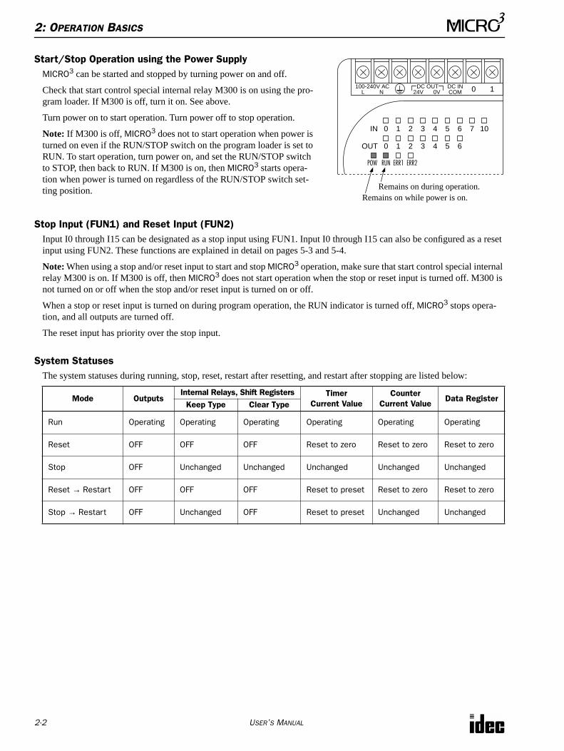
2: OPERATION BASICS
2-2 USER’S MANUAL
Start/Stop Operation using the Power SupplyMICRO3 can be started and stopped by turning power on and off.
Check that start control special internal relay M300 is on using the pro-gram loader. If M300 is off, turn it on. See above.
Turn power on to start operation. Turn power off to stop operation.
Note: If M300 is off, MICRO3 does not to start operation when power is turned on even if the RUN/STOP switch on the program loader is set to RUN. To start operation, turn power on, and set the RUN/STOP switch to STOP, then back to RUN. If M300 is on, then MICRO3 starts opera-tion when power is turned on regardless of the RUN/STOP switch set-ting position.
Stop Input (FUN1) and Reset Input (FUN2)Input I0 through I15 can be designated as a stop input using FUN1. Input I0 through I15 can also be configured as a reset input using FUN2. These functions are explained in detail on pages 5-3 and 5-4.
Note: When using a stop and/or reset input to start and stop MICRO3 operation, make sure that start control special internal relay M300 is on. If M300 is off, then MICRO3 does not start operation when the stop or reset input is turned off. M300 is not turned on or off when the stop and/or reset input is turned on or off.
When a stop or reset input is turned on during program operation, the RUN indicator is turned off, MICRO3 stops opera-tion, and all outputs are turned off.
The reset input has priority over the stop input.
System StatusesThe system statuses during running, stop, reset, restart after resetting, and restart after stopping are listed below:
Mode OutputsInternal Relays, Shift Registers Timer
Current ValueCounter
Current ValueData Register
Keep Type Clear Type
Run Operating Operating Operating Operating Operating Operating
Reset OFF OFF OFF Reset to zero Reset to zero Reset to zero
Stop OFF Unchanged Unchanged Unchanged Unchanged Unchanged
Reset → Restart OFF OFF OFF Reset to preset Reset to zero Reset to zero
Stop → Restart OFF Unchanged OFF Reset to preset Unchanged Unchanged
100-240V ACL N
DC OUT24V 0V
DC INCOM 0 1
IN 0 1 2 3 4 5 6 7 10
OUT 0 1 2 3 4 5 6
POW RUN ERR1 ERR2
Remains on while power is on.Remains on during operation.
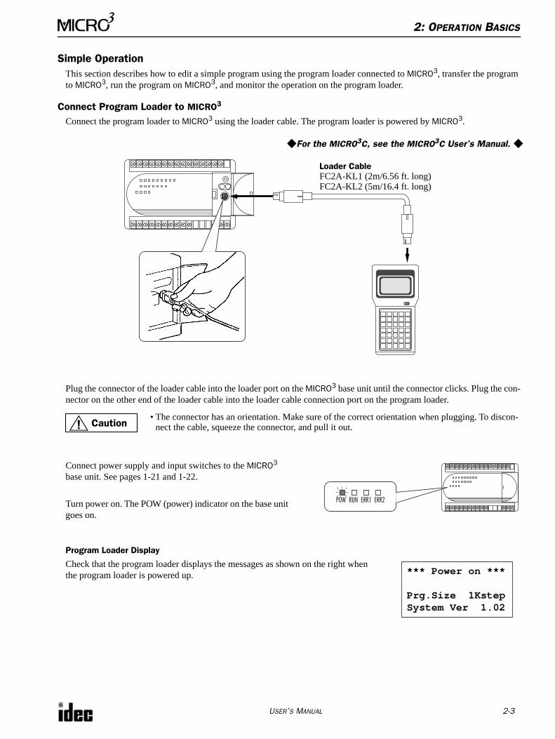
2: OPERATION BASICS
USER’S MANUAL 2-3
Simple OperationThis section describes how to edit a simple program using the program loader connected to MICRO3, transfer the program to MICRO3, run the program on MICRO3, and monitor the operation on the program loader.
Connect Program Loader to MICRO3
Connect the program loader to MICRO3 using the loader cable. The program loader is powered by MICRO3.
Plug the connector of the loader cable into the loader port on the MICRO3 base unit until the connector clicks. Plug the con-nector on the other end of the loader cable into the loader cable connection port on the program loader.
Connect power supply and input switches to the MICRO3 base unit. See pages 1-21 and 1-22.
Turn power on. The POW (power) indicator on the base unit goes on.
Program Loader Display
Check that the program loader displays the messages as shown on the right when the program loader is powered up.
Loader CableFC2A-KL1 (2m/6.56 ft. long)FC2A-KL2 (5m/16.4 ft. long)
For the MICRO3C, see the MICRO3C User’s Manual.
Caution• The connector has an orientation. Make sure of the correct orientation when plugging. To discon-
nect the cable, squeeze the connector, and pull it out.
POW RUN ERR1 ERR2
*** Power on ***
Prg.Size 1KstepSystem Ver 1.02
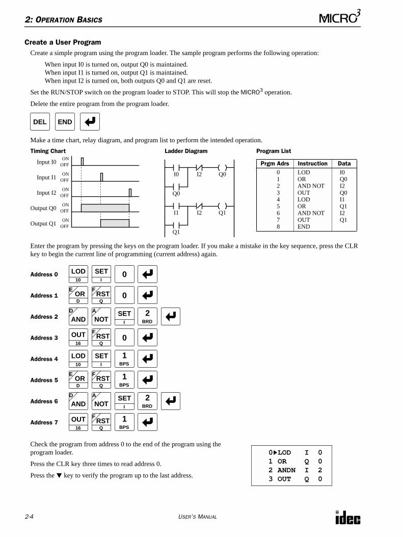
2: OPERATION BASICS
2-4 USER’S MANUAL
Create a User ProgramCreate a simple program using the program loader. The sample program performs the following operation:
When input I0 is turned on, output Q0 is maintained.When input I1 is turned on, output Q1 is maintained.When input I2 is turned on, both outputs Q0 and Q1 are reset.
Set the RUN/STOP switch on the program loader to STOP. This will stop the MICRO3 operation.
Delete the entire program from the program loader.
Make a time chart, relay diagram, and program list to perform the intended operation.
Enter the program by pressing the keys on the program loader. If you make a mistake in the key sequence, press the CLR key to begin the current line of programming (current address) again.
Check the program from address 0 to the end of the program using the program loader.
Press the CLR key three times to read address 0.
Press the key to verify the program up to the last address.
DEL END
Input I0ON
OFF
Input I1ON
OFF
Input I2ON
OFF
Timing Chart
Output Q1ON
OFF
Output Q0ON
OFF
Ladder Diagram
I0 Q0
I2I1 Q1
Q0
Q1
I2
Prgm Adrs Instruction Data012345678
LODORAND NOTOUTLODORAND NOTOUTEND
I0Q0I2Q0I1Q1I2Q1
Program List
Address 0
ORE
D
LOD10
2BRD
0SETI
Address 1 0
SETI
RSTF
Q
Address 2 ANDD
NOTA
Address 3 0RSTF
Q
OUT16
Address 4 LOD10
SETI
1BPS
ORE
DAddress 5 RST
F
Q
1BPS
2BRD
SETI
Address 6 ANDD
NOTA
Address 7 RSTF
Q
OUT16
1BPS
0 LOD I 0 1 OR Q 0 2 ANDN I 2 3 OUT Q 0
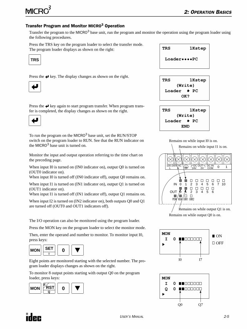
2: OPERATION BASICS
USER’S MANUAL 2-5
Transfer Program and Monitor MICRO3 OperationTransfer the program to the MICRO3 base unit, run the program and monitor the operation using the program loader using the following procedures.
Press the TRS key on the program loader to select the transfer mode. The program loader displays as shown on the right:
Press the key. The display changes as shown on the right.
Press the key again to start program transfer. When program trans-fer is completed, the display changes as shown on the right.
To run the program on the MICRO3 base unit, set the RUN/STOP switch on the program loader to RUN. See that the RUN indicator on the MICRO3 base unit is turned on.
Monitor the input and output operation referring to the time chart on the preceding page.
When input I0 is turned on (IN0 indicator on), output Q0 is turned on (OUT0 indicator on). When input I0 is turned off (IN0 indicator off), output Q0 remains on.
When input I1 is turned on (IN1 indicator on), output Q1 is turned on (OUT1 indicator on). When input I1 is turned off (IN1 indicator off), output Q1 remains on.
When input I2 is turned on (IN2 indicator on), both outputs Q0 and Q1 are turned off (OUT0 and OUT1 indicators off).
The I/O operation can also be monitored using the program loader.
Press the MON key on the program loader to select the monitor mode.
Then, enter the operand and number to monitor. To monitor input I0, press keys:
Eight points are monitored starting with the selected number. The pro-gram loader displays changes as shown on the right.
To monitor 8 output points starting with output Q0 on the program loader, press keys:
TRS 1Kstep
Loader••••PCTRS
TRS 1Kstep (Write) Loader PC OK?
TRS 1Kstep (Write) Loader PC END
100-240V ACL N
DC OUT24V 0V
DC INCOM 0 1
IN 0 1 2 3 4 5 6 7 10
OUT 0 1 2 3 4 5 6
POW RUN ERR1 ERR2
Remains on while output Q0 is on.
Remains on while output Q1 is on.
Remains on while input I1 is on.
Remains on while input I0 is on.
MONI 0
I0 I7
ON
OFF
MON 0SETI
MONI 0 Q 0
Q0 Q7
MON 0RSTF
Q

2: OPERATION BASICS
2-6 USER’S MANUAL
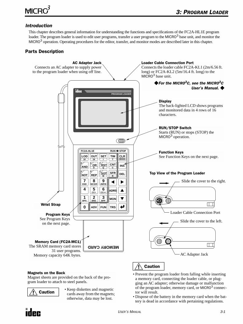
USER’S MANUAL 3-1
3: PROGRAM LOADER
IntroductionThis chapter describes general information for understanding the functions and specifications of the FC2A-HL1E program loader. The program loader is used to edit user programs, transfer a user program to the MICRO3 base unit, and monitor the MICRO3 operation. Operating procedures for the editor, transfer, and monitor modes are described later in this chapter.
Parts Description
LOD10
OUT16
SETI
TIMT
CLR
ANDD
ORE
DRST
F
QCNT
CINS
DELSFRR
SOTC
MNOTA
REPB
7END
8MCS/R
9JMP/E
ADRS
MON
TRS
6CC>=
3BPP
FUN
5CC=
2BRD
ADV
4
1BPS
0
RUN STOPFC2A-HL1E
DisplayThe back-lighted LCD shows programs and monitored data in 4 rows of 16 characters.
RUN/STOP SwitchStarts (RUN) or stops (STOP) the MICRO3 operation.
Function KeysSee Function Keys on the next page.
Memory Card (FC2A-MC1)The SRAM memory card stores
31 user programs.Memory capacity 64K bytes.
Program KeysSee Program Keys
on the next page.
AC Adapter JackConnects an AC adapter to supply power
to the program loader when using off line.
Loader Cable Connection PortConnects the loader cable FC2A-KL1 (2m/6.56 ft. long) or FC2A-KL2 (5m/16.4 ft. long) to the MICRO3 base unit.
For the MICRO3C, see the MICRO3CUser’s Manual.
Slide the cover to the right.
Loader Cable Connection Port
Slide the cover to the left.
AC Adapter Jack
Top View of the Program Loader
Magnets on the BackMagnet sheets are provided on the back of the pro-gram loader to attach to steel panels.
• Keep diskettes and magnetic cards away from the magnets; otherwise, data may be lost.
Caution
MEMORY CARD
Wrist Strap
PROGRAM LOADER
• Prevent the program loader from falling while inserting a memory card, connecting the loader cable, or plug-ging an AC adapter; otherwise damage or malfunction of the program loader, memory card, or MICRO3 connec-tor will result.
• Dispose of the battery in the memory card when the bat-tery is dead in accordance with pertaining regulations.
Caution
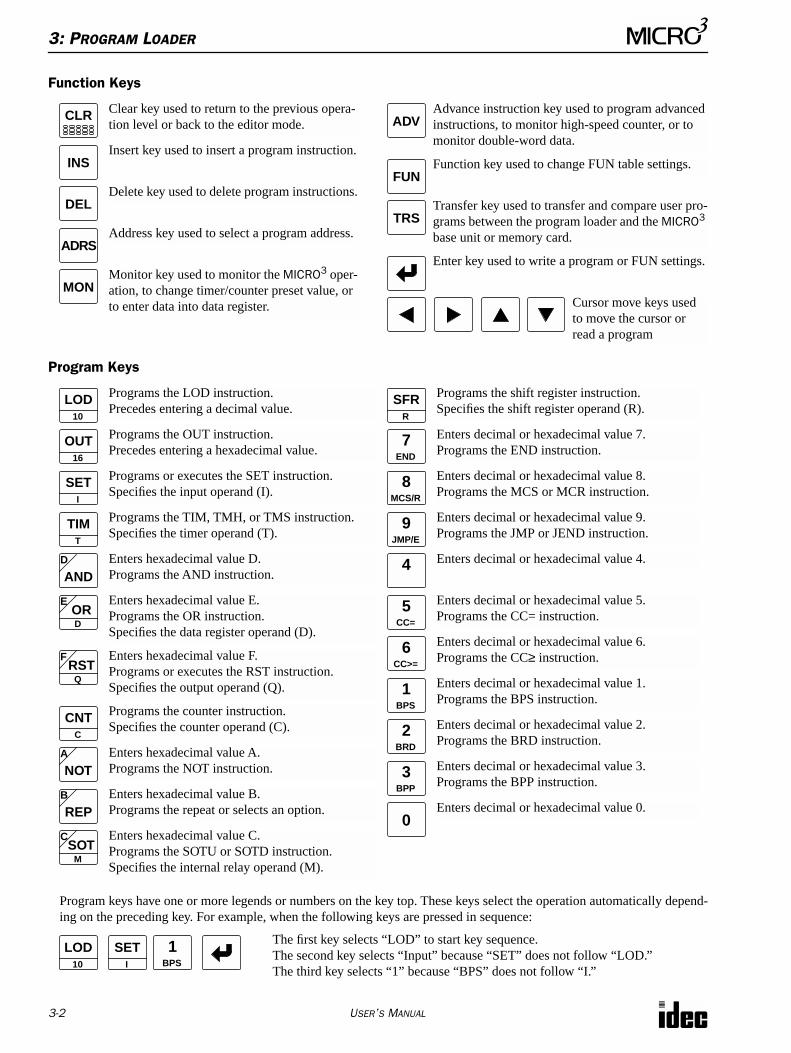
3: PROGRAM LOADER
3-2 USER’S MANUAL
Function Keys
Program Keys
Program keys have one or more legends or numbers on the key top. These keys select the operation automatically depend-ing on the preceding key. For example, when the following keys are pressed in sequence:
The first key selects “LOD” to start key sequence.The second key selects “Input” because “SET” does not follow “LOD.”The third key selects “1” because “BPS” does not follow “I.”
ADVCLR
DEL
ADRS
MON
TRS
FUNINS
Clear key used to return to the previous opera-tion level or back to the editor mode.
Advance instruction key used to program advanced instructions, to monitor high-speed counter, or to monitor double-word data.
Cursor move keys used to move the cursor or read a program
Insert key used to insert a program instruction.
Delete key used to delete program instructions.
Address key used to select a program address.
Monitor key used to monitor the MICRO3 oper-ation, to change timer/counter preset value, or to enter data into data register.
Function key used to change FUN table settings.
Transfer key used to transfer and compare user pro-grams between the program loader and the MICRO3 base unit or memory card.
Enter key used to write a program or FUN settings.
LOD10
OUT16
SETI
TIMT
ANDD
ORE
D
RSTF
Q
CNTC
SFRR
SOTC
M
NOTA
REPB
7END
8MCS/R
9JMP/E
6CC>=
3BPP
5CC=
2BRD
4
1BPS
0
Programs the LOD instruction.Precedes entering a decimal value.
Programs the shift register instruction.Specifies the shift register operand (R).
Programs the OUT instruction.Precedes entering a hexadecimal value.
Programs or executes the SET instruction.Specifies the input operand (I).
Programs the TIM, TMH, or TMS instruction.Specifies the timer operand (T).
Enters hexadecimal value D.Programs the AND instruction.
Enters hexadecimal value E.Programs the OR instruction.Specifies the data register operand (D).
Enters hexadecimal value F.Programs or executes the RST instruction.Specifies the output operand (Q).
Programs the counter instruction.Specifies the counter operand (C).
Enters hexadecimal value A.Programs the NOT instruction.
Enters hexadecimal value B.Programs the repeat or selects an option.
Enters hexadecimal value C.Programs the SOTU or SOTD instruction.Specifies the internal relay operand (M).
Enters decimal or hexadecimal value 7.Programs the END instruction.
Enters decimal or hexadecimal value 8.Programs the MCS or MCR instruction.
Enters decimal or hexadecimal value 9.Programs the JMP or JEND instruction.
Enters decimal or hexadecimal value 4.
Enters decimal or hexadecimal value 5.Programs the CC= instruction.
Enters decimal or hexadecimal value 6.Programs the CC≥ instruction.
Enters decimal or hexadecimal value 1.Programs the BPS instruction.
Enters decimal or hexadecimal value 2.Programs the BRD instruction.
Enters decimal or hexadecimal value 3.Programs the BPP instruction.
Enters decimal or hexadecimal value 0.
LOD10
SETI
1BPS
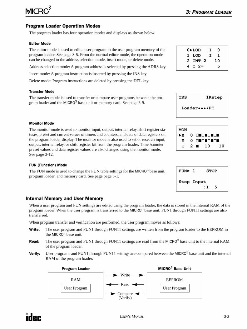
3: PROGRAM LOADER
USER’S MANUAL 3-3
Program Loader Operation ModesThe program loader has four operation modes and displays as shown below.
Editor Mode
The editor mode is used to edit a user program in the user program memory of the program loader. See page 3-5. From the normal editor mode, the operation mode can be changed to the address selection mode, insert mode, or delete mode.
Address selection mode: A program address is selected by pressing the ADRS key.
Insert mode: A program instruction is inserted by pressing the INS key.
Delete mode: Program instructions are deleted by pressing the DEL key.
Transfer Mode
The transfer mode is used to transfer or compare user programs between the pro-gram loader and the MICRO3 base unit or memory card. See page 3-9.
Monitor Mode
The monitor mode is used to monitor input, output, internal relay, shift register sta-tuses, preset and current values of timers and counters, and data of data registers on the program loader display. The monitor mode is also used to set or reset an input, output, internal relay, or shift register bit from the program loader. Timer/counter preset values and data register values are also changed using the monitor mode. See page 3-12.
FUN (Function) Mode
The FUN mode is used to change the FUN table settings for the MICRO3 base unit, program loader, and memory card. See page page 5-1.
Internal Memory and User MemoryWhen a user program and FUN settings are edited using the program loader, the data is stored in the internal RAM of the program loader. When the user program is transferred to the MICRO3 base unit, FUN1 through FUN11 settings are also transferred.
When program transfer and verification are performed, the user program moves as follows:
Write: The user program and FUN1 through FUN11 settings are written from the program loader to the EEPROM in the MICRO3 base unit.
Read: The user program and FUN1 through FUN11 settings are read from the MICRO3 base unit to the internal RAM of the program loader.
Verify: User programs and FUN1 through FUN11 settings are compared between the MICRO3 base unit and the internal RAM of the program loader.
0 LOD I 0 1 LOD I 1 2 CNT 2 10 4 C 2= 5
TRS 1Kstep
Loader••••PC
MONX 0 Y 0 C 2 10 10
FUN 1 STOP
Stop Input :I 5
User Program
RAM
Program Loader MICRO3 Base Unit
Read
Compare
Write
User Program
EEPROM
(Verify)
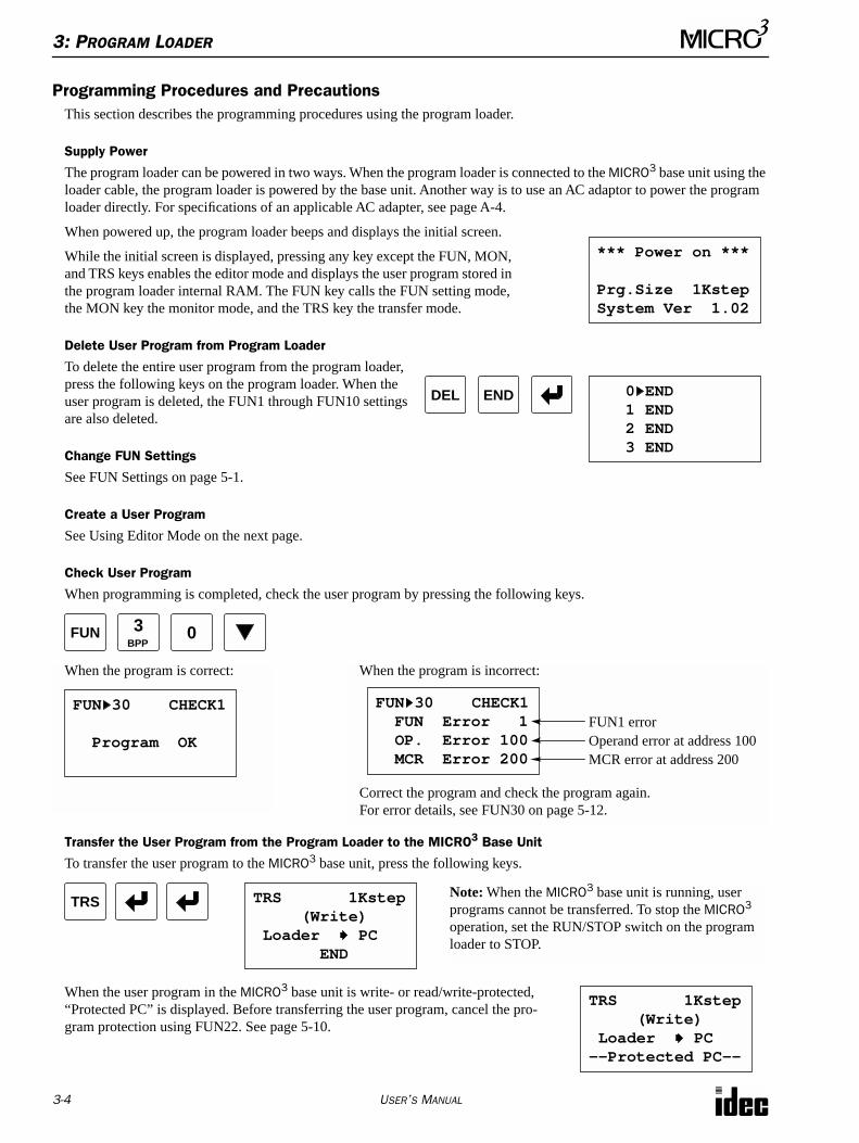
3: PROGRAM LOADER
3-4 USER’S MANUAL
Programming Procedures and PrecautionsThis section describes the programming procedures using the program loader.
Supply Power
The program loader can be powered in two ways. When the program loader is connected to the MICRO3 base unit using the loader cable, the program loader is powered by the base unit. Another way is to use an AC adaptor to power the program loader directly. For specifications of an applicable AC adapter, see page A-4.
When powered up, the program loader beeps and displays the initial screen.
While the initial screen is displayed, pressing any key except the FUN, MON, and TRS keys enables the editor mode and displays the user program stored in the program loader internal RAM. The FUN key calls the FUN setting mode, the MON key the monitor mode, and the TRS key the transfer mode.
Delete User Program from Program Loader
To delete the entire user program from the program loader, press the following keys on the program loader. When the user program is deleted, the FUN1 through FUN10 settings are also deleted.
Change FUN Settings
See FUN Settings on page 5-1.
Create a User Program
See Using Editor Mode on the next page.
Check User Program
When programming is completed, check the user program by pressing the following keys.
Transfer the User Program from the Program Loader to the MICRO3 Base Unit
To transfer the user program to the MICRO3 base unit, press the following keys.
When the user program in the MICRO3 base unit is write- or read/write-protected, “Protected PC” is displayed. Before transferring the user program, cancel the pro-gram protection using FUN22. See page 5-10.
*** Power on ***
Prg.Size 1KstepSystem Ver 1.02
DEL END 0 END 1 END 2 END 3 END
3BPP
FUN 0
When the program is incorrect:
Correct the program and check the program again.For error details, see FUN30 on page 5-12.
FUN 30 CHECK1 FUN Error 1 OP. Error 100 MCR Error 200
FUN1 errorOperand error at address 100MCR error at address 200
When the program is correct:
FUN 30 CHECK1
Program OK
TRSNote: When the MICRO3 base unit is running, user programs cannot be transferred. To stop the MICRO3 operation, set the RUN/STOP switch on the program loader to STOP.
TRS 1Kstep (Write) Loader PC END
TRS 1Kstep (Write) Loader PC--Protected PC--
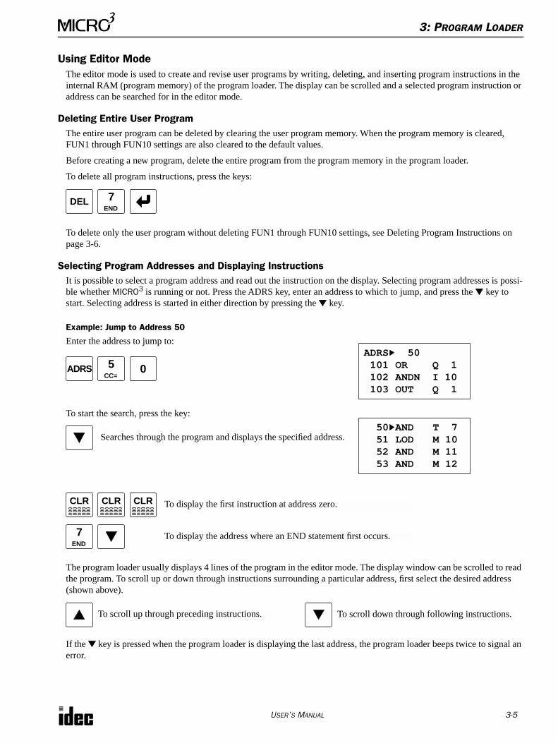
3: PROGRAM LOADER
USER’S MANUAL 3-5
Using Editor ModeThe editor mode is used to create and revise user programs by writing, deleting, and inserting program instructions in the internal RAM (program memory) of the program loader. The display can be scrolled and a selected program instruction or address can be searched for in the editor mode.
Deleting Entire User ProgramThe entire user program can be deleted by clearing the user program memory. When the program memory is cleared, FUN1 through FUN10 settings are also cleared to the default values.
Before creating a new program, delete the entire program from the program memory in the program loader.
To delete all program instructions, press the keys:
To delete only the user program without deleting FUN1 through FUN10 settings, see Deleting Program Instructions on page 3-6.
Selecting Program Addresses and Displaying InstructionsIt is possible to select a program address and read out the instruction on the display. Selecting program addresses is possi-ble whether MICRO3 is running or not. Press the ADRS key, enter an address to which to jump, and press the key to start. Selecting address is started in either direction by pressing the key.
Example: Jump to Address 50
Enter the address to jump to:
To start the search, press the key:
The program loader usually displays 4 lines of the program in the editor mode. The display window can be scrolled to read the program. To scroll up or down through instructions surrounding a particular address, first select the desired address (shown above).
If the key is pressed when the program loader is displaying the last address, the program loader beeps twice to signal an error.
DEL 7END
5CC=
ADRS 0
ADRS 50 101 OR Q 1 102 ANDN I 10 103 OUT Q 1
Searches through the program and displays the specified address. 50 AND T 7 51 LOD M 10 52 AND M 11 53 AND M 12
CLR
7END
CLR CLR To display the first instruction at address zero.
To display the address where an END statement first occurs.
To scroll up through preceding instructions. To scroll down through following instructions.
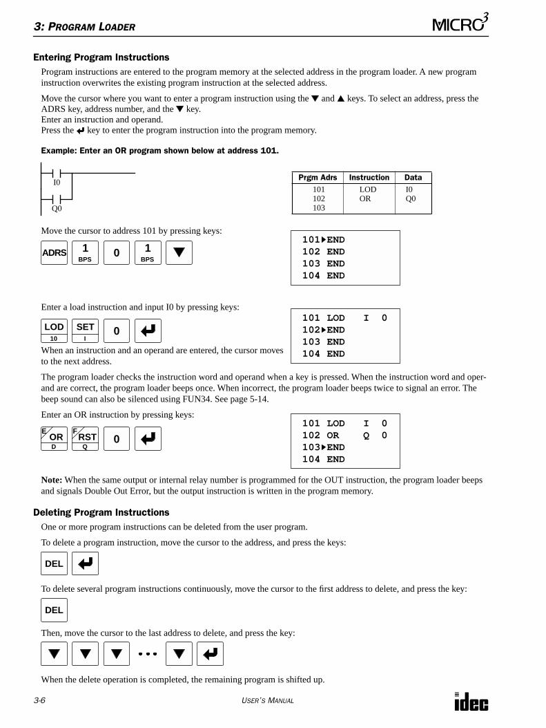
3: PROGRAM LOADER
3-6 USER’S MANUAL
Entering Program InstructionsProgram instructions are entered to the program memory at the selected address in the program loader. A new program instruction overwrites the existing program instruction at the selected address.
Move the cursor where you want to enter a program instruction using the and keys. To select an address, press the ADRS key, address number, and the key.Enter an instruction and operand.Press the key to enter the program instruction into the program memory.
Example: Enter an OR program shown below at address 101.
Move the cursor to address 101 by pressing keys:
Enter a load instruction and input I0 by pressing keys:
When an instruction and an operand are entered, the cursor moves to the next address.
The program loader checks the instruction word and operand when a key is pressed. When the instruction word and oper-and are correct, the program loader beeps once. When incorrect, the program loader beeps twice to signal an error. The beep sound can also be silenced using FUN34. See page 5-14.
Enter an OR instruction by pressing keys:
Note: When the same output or internal relay number is programmed for the OUT instruction, the program loader beeps and signals Double Out Error, but the output instruction is written in the program memory.
Deleting Program InstructionsOne or more program instructions can be deleted from the user program.
To delete a program instruction, move the cursor to the address, and press the keys:
To delete several program instructions continuously, move the cursor to the first address to delete, and press the key:
Then, move the cursor to the last address to delete, and press the key:
When the delete operation is completed, the remaining program is shifted up.
Prgm Adrs Instruction Data101102103
LODOR
I0Q0
I0
Q0
ADRS 1BPS
0 1BPS
101 END 102 END 103 END 104 END
LOD10
SETI
0 101 LOD I 0 102 END 103 END 104 END
0ORE
DRST
F
Q
101 LOD I 0 102 OR Q 0 103 END 104 END
DEL
DEL
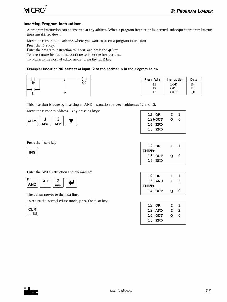
3: PROGRAM LOADER
USER’S MANUAL 3-7
Inserting Program InstructionsA program instruction can be inserted at any address. When a program instruction is inserted, subsequent program instruc-tions are shifted down.
Move the cursor to the address where you want to insert a program instruction.Press the INS key.Enter the program instruction to insert, and press the key.To insert more instructions, continue to enter the instructions.To return to the normal editor mode, press the CLR key.
Example: Insert an NO contact of input I2 at the position * in the diagram below
This insertion is done by inserting an AND instruction between addresses 12 and 13.
Move the cursor to address 13 by pressing keys:
Press the insert key:
Enter the AND instruction and operand I2:
The cursor moves to the next line.
To return the normal editor mode, press the clear key:
Prgm Adrs Instruction Data1112 13
LODOROUT
I0I1Q0
I0
I1
Q0
*
ADRS 3BPP
1BPS
12 OR I 1 13 OUT Q 0 14 END 15 END
INS
12 OR I 1 INST 13 OUT Q 0 14 END
ANDD SET
I
2BRD
12 OR I 1 13 AND I 2 INST 14 OUT Q 0
CLR 12 OR I 1 13 AND I 2 14 OUT Q 0 15 END
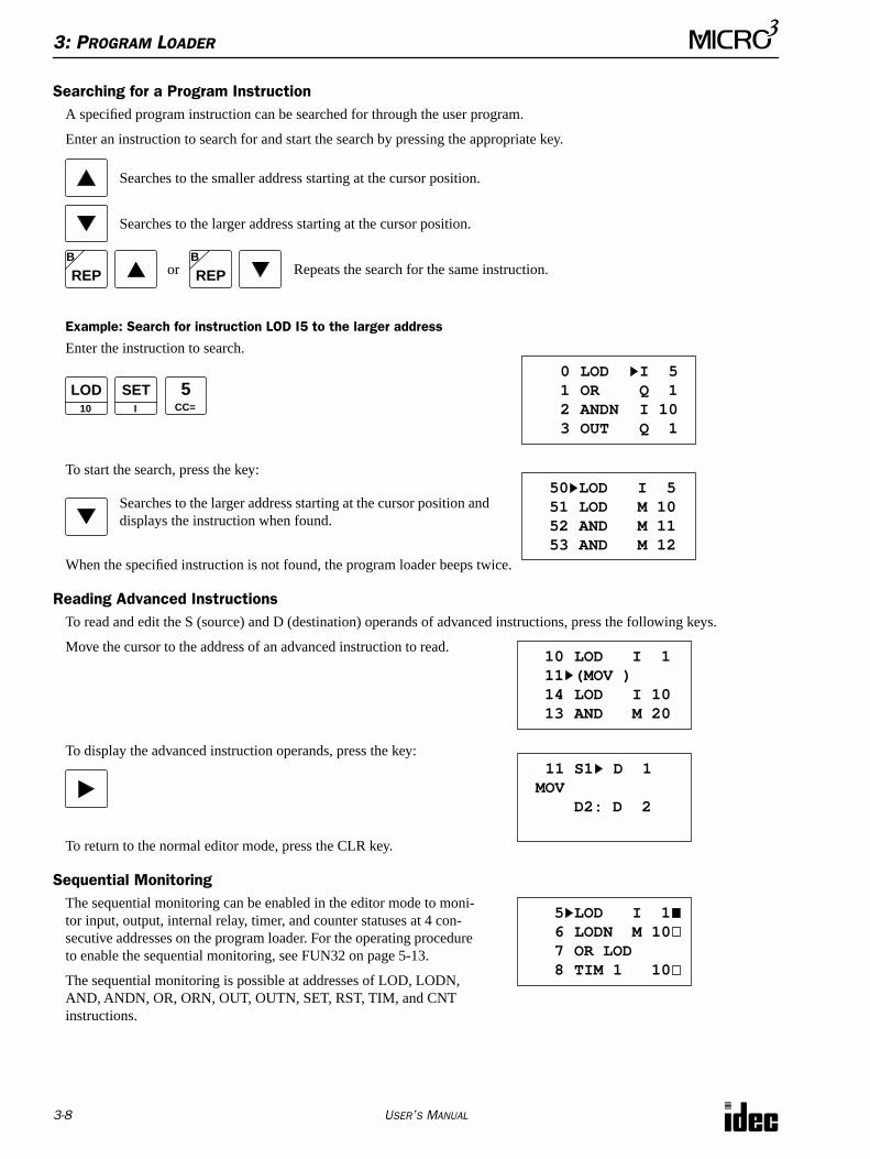
3: PROGRAM LOADER
3-8 USER’S MANUAL
Searching for a Program InstructionA specified program instruction can be searched for through the user program.
Enter an instruction to search for and start the search by pressing the appropriate key.
Example: Search for instruction LOD I5 to the larger address
Enter the instruction to search.
To start the search, press the key:
When the specified instruction is not found, the program loader beeps twice.
Reading Advanced InstructionsTo read and edit the S (source) and D (destination) operands of advanced instructions, press the following keys.
Move the cursor to the address of an advanced instruction to read.
To display the advanced instruction operands, press the key:
To return to the normal editor mode, press the CLR key.
Sequential MonitoringThe sequential monitoring can be enabled in the editor mode to moni-tor input, output, internal relay, timer, and counter statuses at 4 con-secutive addresses on the program loader. For the operating procedure to enable the sequential monitoring, see FUN32 on page 5-13.
The sequential monitoring is possible at addresses of LOD, LODN, AND, ANDN, OR, ORN, OUT, OUTN, SET, RST, TIM, and CNT instructions.
Searches to the smaller address starting at the cursor position.
Searches to the larger address starting at the cursor position.
REPB
Repeats the search for the same instruction.REPB
or
LOD10
SETI
5CC=
0 LOD I 5 1 OR Q 1 2 ANDN I 10 3 OUT Q 1
Searches to the larger address starting at the cursor position and displays the instruction when found.
50 LOD I 5 51 LOD M 10 52 AND M 11 53 AND M 12
10 LOD I 1 11 (MOV ) 14 LOD I 10 13 AND M 20
11 S1 D 1 MOV D2: D 2
5 LOD I 1 6 LODN M 10 7 OR LOD 8 TIM 1 10
3: PROGRAM LOADER
USER’S MANUAL 3-9
Using Transfer ModeUser programs can be transferred between the program loader and the MICRO3 base unit or the memory card installed in the program loader. The transfer mode includes writing, reading, and comparing of user programs.
When the user program in the MICRO3 base unit is protected from writing and/or reading, the program transfer operation cannot be performed. For user program protection, see FUN22 on page 5-10.
Writing Program from Program Loader to MICRO3 Base UnitA user program can be transferred from the program loader to the MICRO3 base unit only when the MICRO3 base unit is stopped. When a user program is transferred, FUN1 through FUN11 settings are also transferred.
Make sure that the MICRO3 base unit is stopped and press the keys:
To start the program transfer, press the enter key:
When the transfer is completed, “END” is displayed.
Note: When error occurs during program transfer, see “Error Messages for Program Loader Operation” on page 20.
Reading Program from MICRO3 Base Unit to Program LoaderA user program can be transferred from the MICRO3 base unit to the program loader whether the MICRO3 base unit is run-ning or not. When a user program is transferred, FUN1 through FUN11 settings are also transferred.
Press the keys:
To start the program transfer, press the enter key:
When the transfer is completed, “END” is displayed.
Note: When an error occurs during the program transfer, see “Error Messages for Program Loader Operation” on page 20.
Comparing Programs between Program Loader and MICRO3 Base UnitUser programs can be compared between the program loader and the MICRO3 base unit whether the MICRO3 base unit is running or not. When user programs are compared, FUN1 through FUN11 settings are also compared.
Press the keys:
To start the program comparison, press the enter key:
When the programs match, “END” is displayed.
Note: When error occurs during program comparison, see “Error Messages for Program Loader Operation” on page 20.
TRSTRS 1Kstep (Write) Loader PC OK?
TRS 1Kstep (Write) Loader PC END
TRSTRS 1Kstep (Read) Loader PC OK?
TRS 1Kstep (Read) Loader PC END
TRS
TRS 1Kstep (Verify) Loader PC OK?
TRS 1Kstep (Verify) Loader PC END
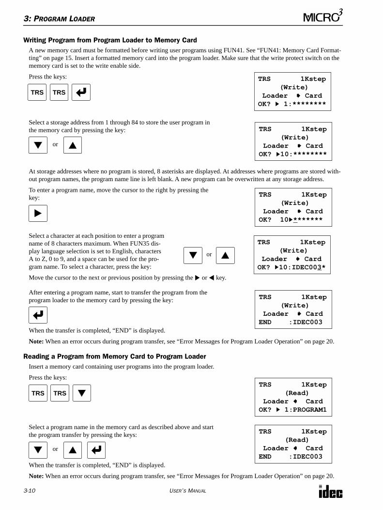
3: PROGRAM LOADER
3-10 USER’S MANUAL
Writing Program from Program Loader to Memory CardA new memory card must be formatted before writing user programs using FUN41. See “FUN41: Memory Card Format-ting” on page 15. Insert a formatted memory card into the program loader. Make sure that the write protect switch on the memory card is set to the write enable side.
Press the keys:
Select a storage address from 1 through 84 to store the user program in the memory card by pressing the key:
At storage addresses where no program is stored, 8 asterisks are displayed. At addresses where programs are stored with-out program names, the program name line is left blank. A new program can be overwritten at any storage address.
To enter a program name, move the cursor to the right by pressing the key:
Select a character at each position to enter a program name of 8 characters maximum. When FUN35 dis-play language selection is set to English, characters A to Z, 0 to 9, and a space can be used for the pro-gram name. To select a character, press the key:
Move the cursor to the next or previous position by pressing the or key.
After entering a program name, start to transfer the program from the program loader to the memory card by pressing the key:
When the transfer is completed, “END” is displayed.
Note: When an error occurs during program transfer, see “Error Messages for Program Loader Operation” on page 20.
Reading a Program from Memory Card to Program LoaderInsert a memory card containing user programs into the program loader.
Press the keys:
Select a program name in the memory card as described above and start the program transfer by pressing the keys:
When the transfer is completed, “END” is displayed.
Note: When an error occurs during program transfer, see “Error Messages for Program Loader Operation” on page 20.
TRS TRS
TRS 1Kstep (Write) Loader Card OK? 1:********
TRS 1Kstep (Write) Loader Card OK? 10:********
or
TRS 1Kstep (Write) Loader Card OK? 10 *******
TRS 1Kstep (Write) Loader Card OK? 10:IDEC003*
or
TRS 1Kstep (Write) Loader Card END :IDEC003
TRS TRSTRS 1Kstep (Read) Loader Card OK? 1:PROGRAM1
TRS 1Kstep (Read) Loader Card END :IDEC003
or
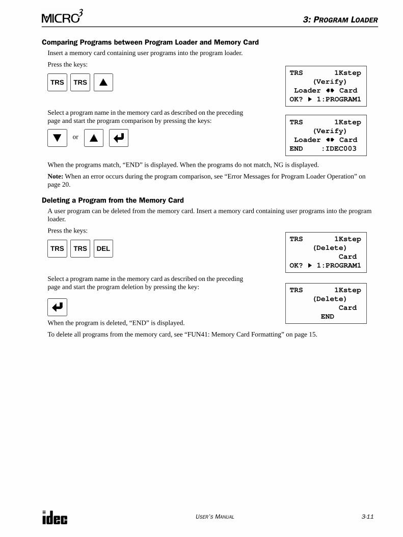
3: PROGRAM LOADER
USER’S MANUAL 3-11
Comparing Programs between Program Loader and Memory CardInsert a memory card containing user programs into the program loader.
Press the keys:
Select a program name in the memory card as described on the preceding page and start the program comparison by pressing the keys:
When the programs match, “END” is displayed. When the programs do not match, NG is displayed.
Note: When an error occurs during the program comparison, see “Error Messages for Program Loader Operation” on page 20.
Deleting a Program from the Memory CardA user program can be deleted from the memory card. Insert a memory card containing user programs into the program loader.
Press the keys:
Select a program name in the memory card as described on the preceding page and start the program deletion by pressing the key:
When the program is deleted, “END” is displayed.
To delete all programs from the memory card, see “FUN41: Memory Card Formatting” on page 15.
TRS TRSTRS 1Kstep (Verify) Loader Card OK? 1:PROGRAM1
TRS 1Kstep (Verify) Loader Card END :IDEC003
or
TRS TRSTRS 1Kstep (Delete) Card OK? 1:PROGRAM1
DEL
TRS 1Kstep (Delete) Card END
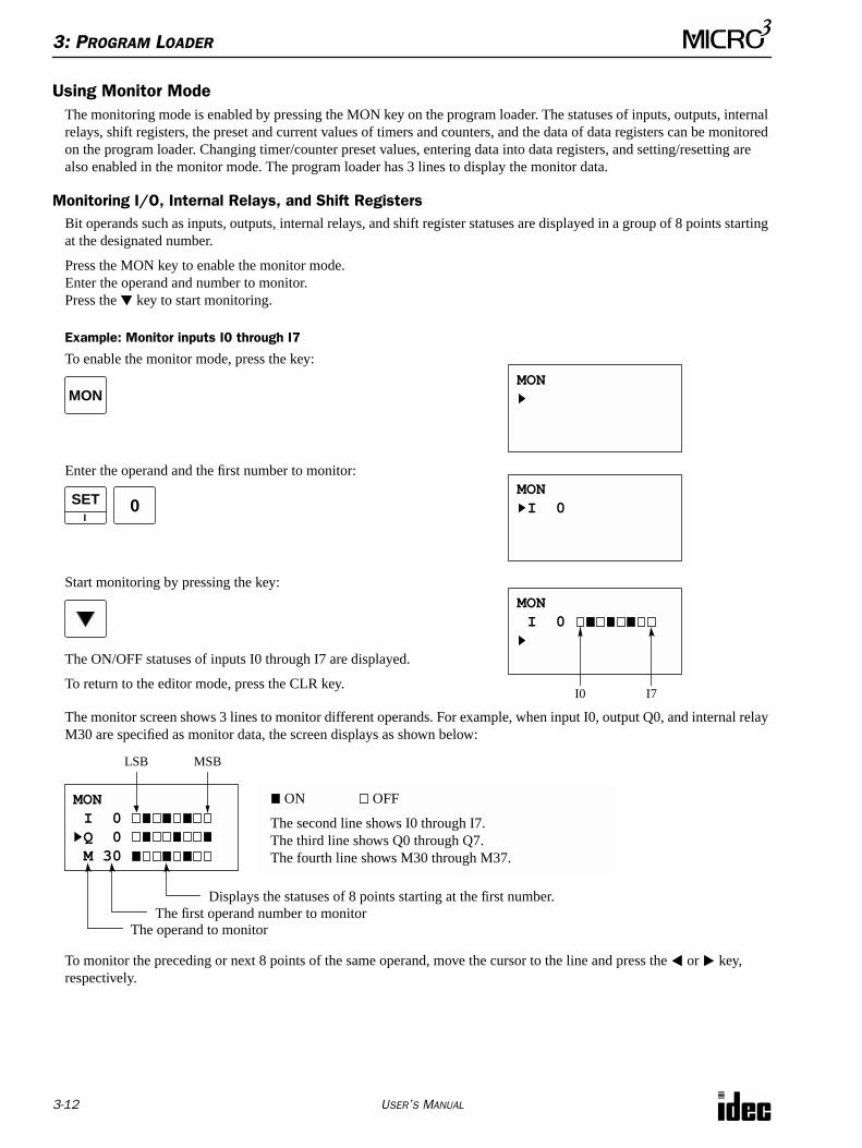
3: PROGRAM LOADER
3-12 USER’S MANUAL
Using Monitor ModeThe monitoring mode is enabled by pressing the MON key on the program loader. The statuses of inputs, outputs, internal relays, shift registers, the preset and current values of timers and counters, and the data of data registers can be monitored on the program loader. Changing timer/counter preset values, entering data into data registers, and setting/resetting are also enabled in the monitor mode. The program loader has 3 lines to display the monitor data.
Monitoring I/O, Internal Relays, and Shift RegistersBit operands such as inputs, outputs, internal relays, and shift register statuses are displayed in a group of 8 points starting at the designated number.
Press the MON key to enable the monitor mode.Enter the operand and number to monitor.Press the key to start monitoring.
Example: Monitor inputs I0 through I7
To enable the monitor mode, press the key:
Enter the operand and the first number to monitor:
Start monitoring by pressing the key:
The ON/OFF statuses of inputs I0 through I7 are displayed.
To return to the editor mode, press the CLR key.
The monitor screen shows 3 lines to monitor different operands. For example, when input I0, output Q0, and internal relay M30 are specified as monitor data, the screen displays as shown below:
To monitor the preceding or next 8 points of the same operand, move the cursor to the line and press the or key, respectively.
MONMON
0MONI 0
SETI
MONI 0
I0 I7
ON OFF
The second line shows I0 through I7.The third line shows Q0 through Q7.The fourth line shows M30 through M37.
Displays the statuses of 8 points starting at the first number.The first operand number to monitor
The operand to monitor
MONI 0 Q 0 M 30
LSB MSB
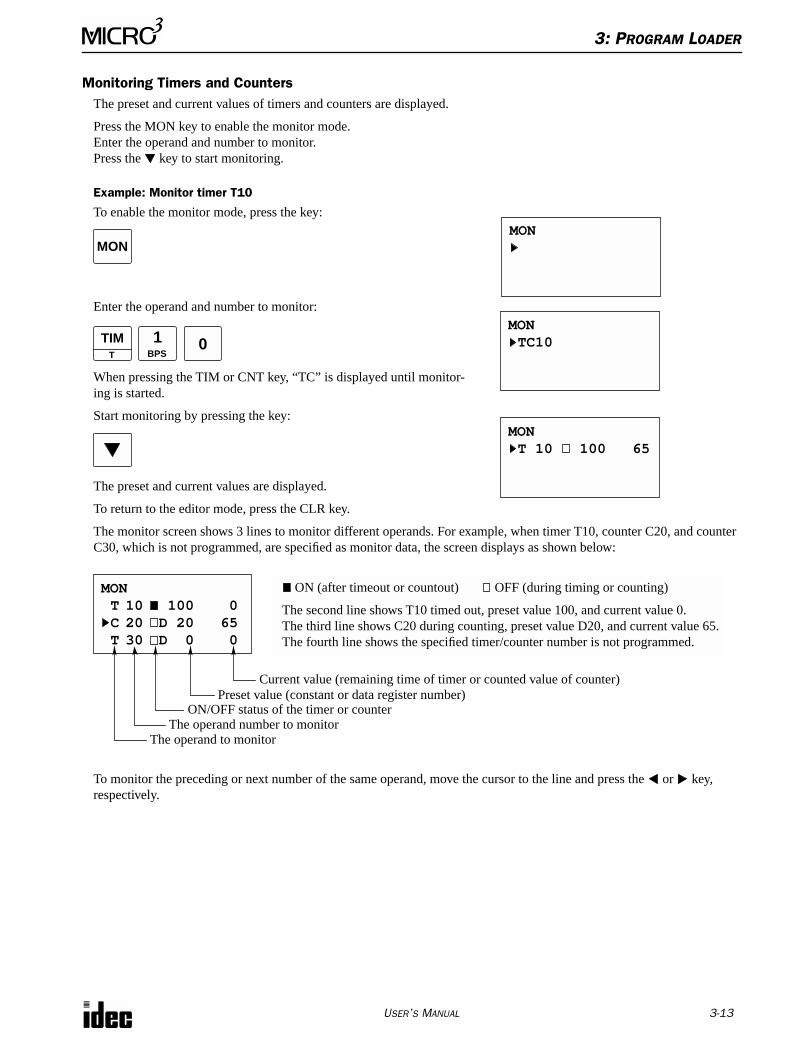
3: PROGRAM LOADER
USER’S MANUAL 3-13
Monitoring Timers and CountersThe preset and current values of timers and counters are displayed.
Press the MON key to enable the monitor mode.Enter the operand and number to monitor.Press the key to start monitoring.
Example: Monitor timer T10
To enable the monitor mode, press the key:
Enter the operand and number to monitor:
When pressing the TIM or CNT key, “TC” is displayed until monitor-ing is started.
Start monitoring by pressing the key:
The preset and current values are displayed.
To return to the editor mode, press the CLR key.
The monitor screen shows 3 lines to monitor different operands. For example, when timer T10, counter C20, and counter C30, which is not programmed, are specified as monitor data, the screen displays as shown below:
To monitor the preceding or next number of the same operand, move the cursor to the line and press the or key, respectively.
MONMON
0TIMT
1BPS
MONTC10
MONT 10 100 65
ON (after timeout or countout) OFF (during timing or counting)
The second line shows T10 timed out, preset value 100, and current value 0.The third line shows C20 during counting, preset value D20, and current value 65.The fourth line shows the specified timer/counter number is not programmed.
Preset value (constant or data register number)ON/OFF status of the timer or counter
The operand to monitor
MONT 10 100 0 C 20 D 20 65 T 30 D 0 0
Current value (remaining time of timer or counted value of counter)
The operand number to monitor
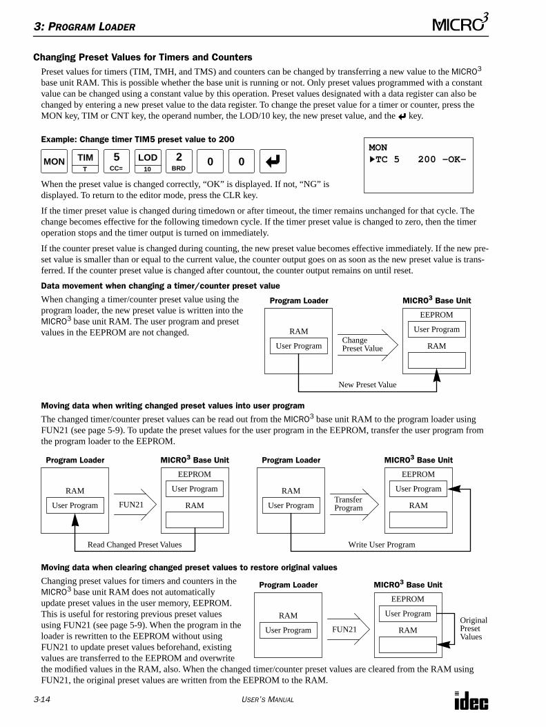
3: PROGRAM LOADER
3-14 USER’S MANUAL
Changing Preset Values for Timers and CountersPreset values for timers (TIM, TMH, and TMS) and counters can be changed by transferring a new value to the MICRO3 base unit RAM. This is possible whether the base unit is running or not. Only preset values programmed with a constant value can be changed using a constant value by this operation. Preset values designated with a data register can also be changed by entering a new preset value to the data register. To change the preset value for a timer or counter, press the MON key, TIM or CNT key, the operand number, the LOD/10 key, the new preset value, and the key.
Example: Change timer TIM5 preset value to 200
When the preset value is changed correctly, “OK” is displayed. If not, “NG” is displayed. To return to the editor mode, press the CLR key.
If the timer preset value is changed during timedown or after timeout, the timer remains unchanged for that cycle. The change becomes effective for the following timedown cycle. If the timer preset value is changed to zero, then the timer operation stops and the timer output is turned on immediately.
If the counter preset value is changed during counting, the new preset value becomes effective immediately. If the new pre-set value is smaller than or equal to the current value, the counter output goes on as soon as the new preset value is trans-ferred. If the counter preset value is changed after countout, the counter output remains on until reset.
Data movement when changing a timer/counter preset value
When changing a timer/counter preset value using the program loader, the new preset value is written into the MICRO3 base unit RAM. The user program and preset values in the EEPROM are not changed.
Moving data when writing changed preset values into user program
The changed timer/counter preset values can be read out from the MICRO3 base unit RAM to the program loader using FUN21 (see page 5-9). To update the preset values for the user program in the EEPROM, transfer the user program from the program loader to the EEPROM.
Moving data when clearing changed preset values to restore original values
Changing preset values for timers and counters in the MICRO3 base unit RAM does not automatically update preset values in the user memory, EEPROM. This is useful for restoring previous preset values using FUN21 (see page 5-9). When the program in the loader is rewritten to the EEPROM without using FUN21 to update preset values beforehand, existing values are transferred to the EEPROM and overwrite the modified values in the RAM, also. When the changed timer/counter preset values are cleared from the RAM using FUN21, the original preset values are written from the EEPROM to the RAM.
MON
MONTC 5 200 -OK-0TIM
T
5CC=
LOD10
2BRD
0
Program Loader MICRO3 Base Unit
ChangeUser Program
EEPROM
RAMUser Program
RAM
Preset Value
New Preset Value
Program Loader MICRO3 Base Unit
FUN21
User Program
EEPROM
RAMUser Program
RAM
Program Loader MICRO3 Base Unit
TransferUser Program
EEPROM
RAMUser Program
RAM
Program
Read Changed Preset Values Write User Program
Program Loader MICRO3 Base Unit
FUN21
User Program
EEPROM
RAMUser Program
RAMOriginalPresetValues
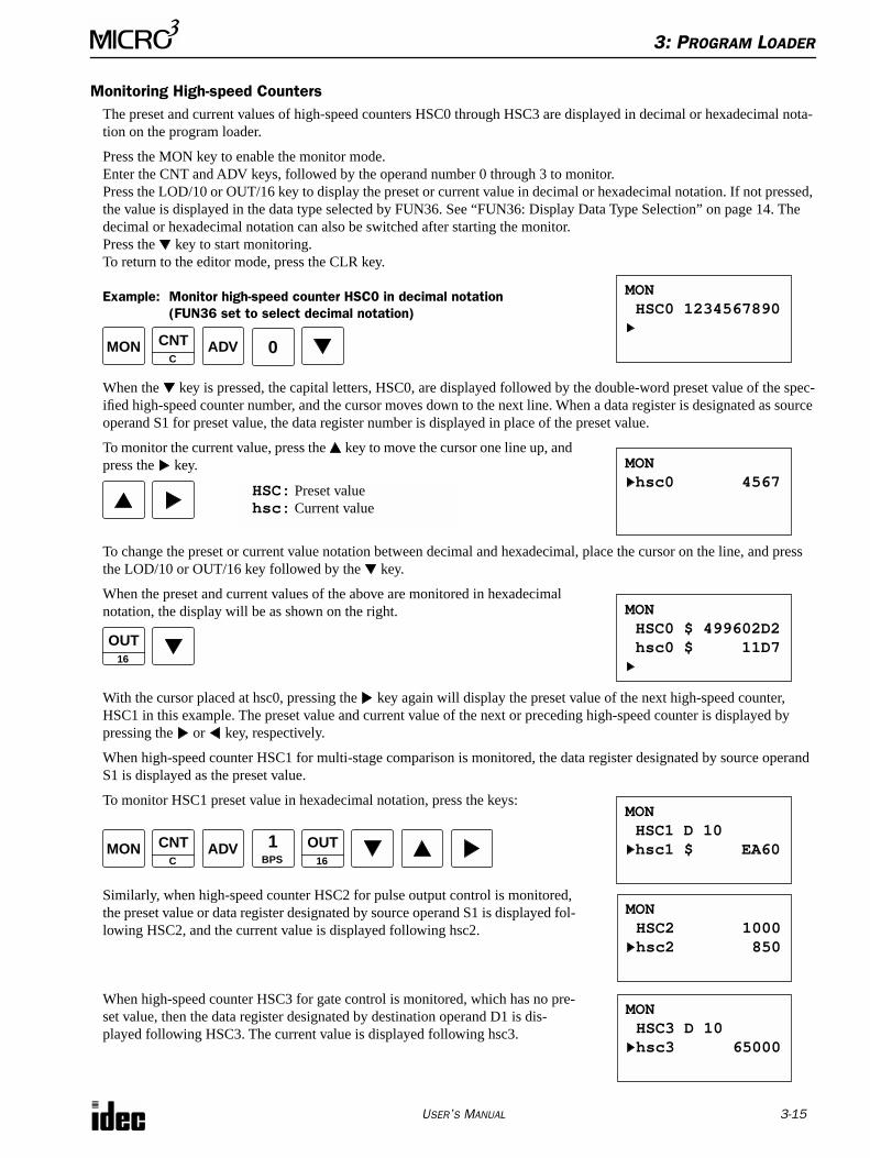
3: PROGRAM LOADER
USER’S MANUAL 3-15
Monitoring High-speed CountersThe preset and current values of high-speed counters HSC0 through HSC3 are displayed in decimal or hexadecimal nota-tion on the program loader.
Press the MON key to enable the monitor mode.Enter the CNT and ADV keys, followed by the operand number 0 through 3 to monitor.Press the LOD/10 or OUT/16 key to display the preset or current value in decimal or hexadecimal notation. If not pressed, the value is displayed in the data type selected by FUN36. See “FUN36: Display Data Type Selection” on page 14. The decimal or hexadecimal notation can also be switched after starting the monitor.Press the key to start monitoring.To return to the editor mode, press the CLR key.
Example: Monitor high-speed counter HSC0 in decimal notation (FUN36 set to select decimal notation)
When the key is pressed, the capital letters, HSC0, are displayed followed by the double-word preset value of the spec-ified high-speed counter number, and the cursor moves down to the next line. When a data register is designated as source operand S1 for preset value, the data register number is displayed in place of the preset value.
To monitor the current value, press the key to move the cursor one line up, and press the key.
To change the preset or current value notation between decimal and hexadecimal, place the cursor on the line, and press the LOD/10 or OUT/16 key followed by the key.
When the preset and current values of the above are monitored in hexadecimal notation, the display will be as shown on the right.
With the cursor placed at hsc0, pressing the key again will display the preset value of the next high-speed counter, HSC1 in this example. The preset value and current value of the next or preceding high-speed counter is displayed by pressing the or key, respectively.
When high-speed counter HSC1 for multi-stage comparison is monitored, the data register designated by source operand S1 is displayed as the preset value.
To monitor HSC1 preset value in hexadecimal notation, press the keys:
Similarly, when high-speed counter HSC2 for pulse output control is monitored, the preset value or data register designated by source operand S1 is displayed fol-lowing HSC2, and the current value is displayed following hsc2.
When high-speed counter HSC3 for gate control is monitored, which has no pre-set value, then the data register designated by destination operand D1 is dis-played following HSC3. The current value is displayed following hsc3.
MONHSC0 1234567890
MON CNTC
ADV 0
MONhsc0 4567
HSC: Preset valuehsc: Current value
MONHSC0 $ 499602D2hsc0 $ 11D7OUT
16
MONHSC1 D 10 hsc1 $ EA60OUT
16MON CNT
CADV 1
BPS
MONHSC2 1000hsc2 850
MONHSC3 D 10 hsc3 65000
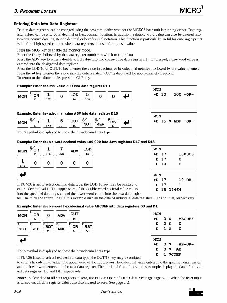
3: PROGRAM LOADER
3-16 USER’S MANUAL
Entering Data into Data RegistersData in data registers can be changed using the program loader whether the MICRO3 base unit is running or not. Data reg-ister values can be entered in decimal or hexadecimal notation. In addition, a double-word value can also be entered into two consecutive data registers in decimal or hexadecimal notation. This function is particularly useful for entering a preset value for a high-speed counter when data registers are used for a preset value.
Press the MON key to enable the monitor mode.Enter the D key, followed by the data register number to which to enter data.Press the ADV key to enter a double-word value into two consecutive data registers. If not pressed, a one-word value is entered into the designated data register.Press the LOD/10 or OUT/16 key to enter the value in decimal or hexadecimal notation, followed by the value to enter.Press the key to enter the value into the data register. “OK” is displayed for approximately 1 second.To return to the editor mode, press the CLR key.
Example: Enter decimal value 500 into data register D10
Example: Enter hexadecimal value ABF into data register D15
The $ symbol is displayed to show the hexadecimal data type.
Example: Enter double-word decimal value 100,000 into data registers D17 and D18
If FUN36 is set to select decimal data type, the LOD/10 key may be omitted to enter a decimal value. The upper word of the double-word decimal value enters into the specified data register, and the lower word enters into the next data regis-ter. The third and fourth lines in this example display the data of individual data registers D17 and D18, respectively.
Example: Enter double-word hexadecimal value ABCDEF into data registers D0 and D1
The $ symbol is displayed to show the hexadecimal data type.
If FUN36 is set to select hexadecimal data type, the OUT/16 key may be omitted to enter a hexadecimal value. The upper word of the double-word hexadecimal value enters into the specified data register and the lower word enters into the next data register. The third and fourth lines in this example display the data of individ-ual data registers D0 and D1, respectively.
Note: To clear data of all data registers to zero, use FUN26 Operand Data Clear. See page page 5-11. When the reset input is turned on, all data register values are also cleared to zero. See page 2-2.
MON 0ORE
D
MOND 10 500 -OK-1
BPS
5CC=
0 0LOD10
MON ORE
D
MOND 15 $ ABF -OK-1
BPS
5CC= NOT
A
REPBOUT
16RST
F
Q
MON
0
ORE
D
MOND 17 100000D 17 0 D 18 0
ADV7END
1BPS
LOD10
1BPS
0 0 0 0
MOND 17 10-OK-D 17 1 D 18 34464
MON 0ORE
D
MOND 0 $ ABCDEFD 0 $ 0 D 1 $ 0
OUT16
ADV
ANDD
ORE
DSOT
C
MNOTA
REPB
RSTF
Q
MOND 0 $ AB-OK-D 0 $ AB D 1 $CDEF
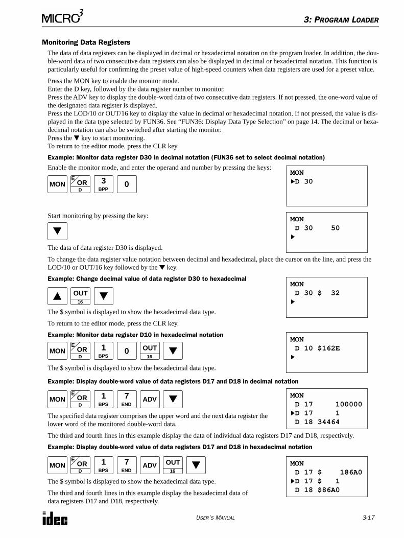
3: PROGRAM LOADER
USER’S MANUAL 3-17
Monitoring Data RegistersThe data of data registers can be displayed in decimal or hexadecimal notation on the program loader. In addition, the dou-ble-word data of two consecutive data registers can also be displayed in decimal or hexadecimal notation. This function is particularly useful for confirming the preset value of high-speed counters when data registers are used for a preset value.
Press the MON key to enable the monitor mode.Enter the D key, followed by the data register number to monitor.Press the ADV key to display the double-word data of two consecutive data registers. If not pressed, the one-word value of the designated data register is displayed.Press the LOD/10 or OUT/16 key to display the value in decimal or hexadecimal notation. If not pressed, the value is dis-played in the data type selected by FUN36. See “FUN36: Display Data Type Selection” on page 14. The decimal or hexa-decimal notation can also be switched after starting the monitor.Press the key to start monitoring.To return to the editor mode, press the CLR key.
Example: Monitor data register D30 in decimal notation (FUN36 set to select decimal notation)
Enable the monitor mode, and enter the operand and number by pressing the keys:
Start monitoring by pressing the key:
The data of data register D30 is displayed.
To change the data register value notation between decimal and hexadecimal, place the cursor on the line, and press the LOD/10 or OUT/16 key followed by the key.
Example: Change decimal value of data register D30 to hexadecimal
The $ symbol is displayed to show the hexadecimal data type.
To return to the editor mode, press the CLR key.
Example: Monitor data register D10 in hexadecimal notation
The $ symbol is displayed to show the hexadecimal data type.
Example: Display double-word value of data registers D17 and D18 in decimal notation
The specified data register comprises the upper word and the next data register the lower word of the monitored double-word data.
The third and fourth lines in this example display the data of individual data registers D17 and D18, respectively.
Example: Display double-word value of data registers D17 and D18 in hexadecimal notation
The $ symbol is displayed to show the hexadecimal data type.
The third and fourth lines in this example display the hexadecimal data of data registers D17 and D18, respectively.
MON 0ORE
D
3BPP
MOND 30
MOND 30 50
MOND 30 $ 32OUT
16
MON 0ORE
D
MOND 10 $162E1
BPS
OUT16
MON ORE
D
MOND 17 100000D 17 1 D 18 34464
ADV7END
1BPS
MON ORE
DMOND 17 $ 186A0D 17 $ 1 D 18 $86A0
ADV7END
1BPS
OUT16
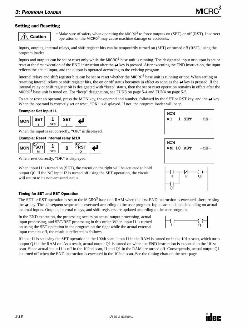
3: PROGRAM LOADER
3-18 USER’S MANUAL
Setting and Resetting
Inputs, outputs, internal relays, and shift register bits can be temporarily turned on (SET) or turned off (RST), using the program loader.
Inputs and outputs can be set or reset only while the MICRO3 base unit is running. The designated input or output is set or reset at the first execution of the END instruction after the key is pressed. After executing the END instruction, the input reflects the actual input, and the output is operated according to the existing program.
Internal relays and shift register bits can be set or reset whether the MICRO3 base unit is running or not. When setting or resetting internal relays or shift register bits, the on or off status becomes in effect as soon as the key is pressed. If the internal relay or shift register bit is designated with “keep” status, then the set or reset operation remains in effect after the MICRO3 base unit is tuned on. For “keep” designation, see FUN3 on page 5-4 and FUN4 on page 5-5.
To set or reset an operand, press the MON key, the operand and number, followed by the SET or RST key, and the key. When the operand is correctly set or reset, “OK” is displayed. If not, the program loader will beep.
Example: Set input I1
When the input is set correctly, “OK” is displayed.
Example: Reset internal relay M10
When reset correctly, “OK” is displayed.
When input I1 is turned on (SET), the circuit on the right will be actuated to hold output Q0. If the NC input I2 is turned off using the SET operation, the circuit will return to its non-actuated status.
Timing for SET and RST Operation
The SET or RST operation is set to the MICRO3 base unit RAM when the first END instruction is executed after pressing the key. The subsequent sequence is executed according to the user program. Inputs are updated depending on actual external inputs. Outputs, internal relays, and shift registers are updated according to the user program.
In the END execution, the processing occurs on actual output processing, actual input processing, and SET/RST processing in this order. When input I1 is turned on using the SET operation in the program on the right while the actual external input remains off, the result is reflected as follows.
If input I1 is set using the SET operation in the 100th scan, input I1 in the RAM is turned on in the 101st scan, which turns output Q1 in the RAM on. As a result, actual output Q1 is turned on when the END instruction is executed in the 101st scan. Since actual input I1 is off in the 102nd scan, I1 and Q1 in the RAM are turned off. Consequently, actual output Q1 is turned off when the END instruction is executed in the 102nd scan. See the timing chart on the next page.
Caution• Make sure of safety when operating the MICRO3 to force outputs on (SET) or off (RST). Incorrect
operation on the MICRO3 may cause machine damage or accidents.
MON
MONI 1 SET -OK-SET
I
1BPS
SETI
MONMONM 10 RST -OK-1
BPSRST
F
QSOT
C
M0
I1 I2 Q0
Q0
I1 Q1
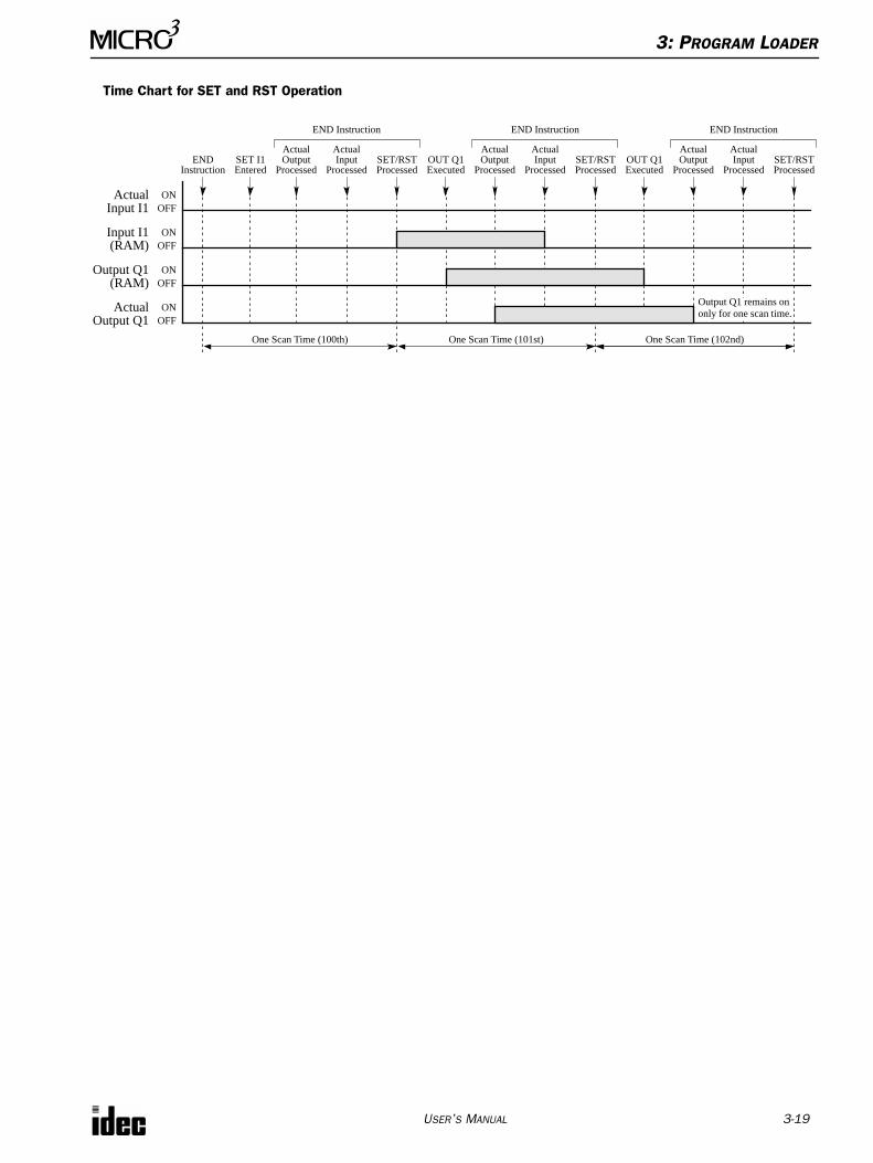
3: PROGRAM LOADER
USER’S MANUAL 3-19
Time Chart for SET and RST Operation
Actual ONOFF
Output Q1 ONOFF
SET I1Entered
Actual
One Scan Time (100th)
ENDInstruction
END Instruction
OutputProcessed
ActualInput
Processed
Actual ONOFF
Input I1 ONOFF
OUT Q1Executed
Input I1
(RAM)
(RAM)
Output Q1
ActualOutput
Processed
ActualInput
ProcessedOUT Q1Executed
SET/RSTProcessed
ActualOutput
Processed
ActualInput
ProcessedSET/RSTProcessed
END Instruction END Instruction
SET/RSTProcessed
One Scan Time (101st) One Scan Time (102nd)
Output Q1 remains on only for one scan time.
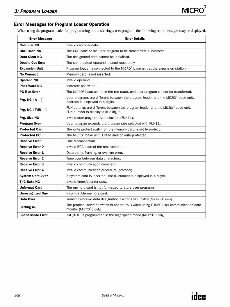
3: PROGRAM LOADER
3-20 USER’S MANUAL
Error Messages for Program Loader OperationWhen using the program loader for programming or transferring a user program, the following error messages may be displayed.
Error Message Error Details
Calendar NG Invalid calendar data.
CRC Code NG The CRC code of the user program to be transferred is incorrect.
Data Clear NG The designated data cannot be initialized.
Double Out Error The same output operand is used repeatedly.
Expansion Unit Program loader is connected to the MICRO3 base unit at the expansion station.
No Connect Memory card is not inserted.
Operand NG Invalid operand.
Pass Word NG Incorrect password.
PC Run Error The MICRO3 base unit is in the run state, and user program cannot be transferred.
Prg. NG–(A ) User programs are different between the program loader and the MICRO3 base unit. Address is displayed in 4 digits.
Prg. NG–(FUN )FUN settings are different between the program loader and the MICRO3 base unit. FUN number is displayed in 2 digits.
Prg. Size NG Invalid user program size selection (FUN11).
Program Over User program exceeds the program size selected with FUN11.
Protected Card The write protect switch on the memory card is set to protect.
Protected PC The MICRO3 base unit is read and/or write protected.
Receive Error Line disconnection.
Receive Error 0 Invalid BCC code of the received data.
Receive Error 1 Data parity, framing, or overrun error.
Receive Error 2 Time over between data characters.
Receive Error 3 Invalid communication command.
Receive Error 4 Invalid communication procedure (protocol).
System Card ???? A system card is inserted. The ID number is displayed in 4 digits.
T/C Data NG Invalid timer/counter data.
Unformat Card The memory card is not formatted to store user programs.
Unrecognized One Incompatible memory card.
Data Over Transmit/receive data designation exceeds 200 bytes (MICRO3C only).
Setting NGThe protocol selector switch is not set to 3 when using FUN50 user communication data monitor (MICRO3C only).
Speed Mode Error TXD/RXD is programmed in the high-speed mode (MICRO3C only).
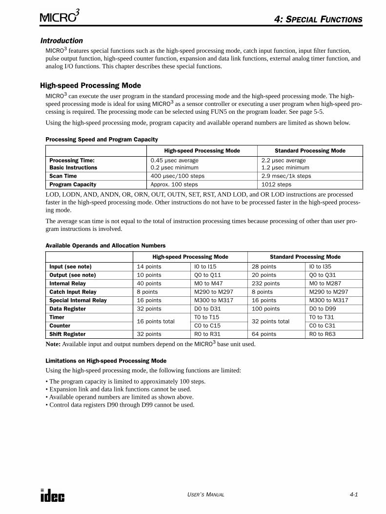
USER’S MANUAL 4-1
4: SPECIAL FUNCTIONS
IntroductionMICRO3 features special functions such as the high-speed processing mode, catch input function, input filter function, pulse output function, high-speed counter function, expansion and data link functions, external analog timer function, and analog I/O functions. This chapter describes these special functions.
High-speed Processing ModeMICRO3 can execute the user program in the standard processing mode and the high-speed processing mode. The high-speed processing mode is ideal for using MICRO3 as a sensor controller or executing a user program when high-speed pro-cessing is required. The processing mode can be selected using FUN5 on the program loader. See page 5-5.
Using the high-speed processing mode, program capacity and available operand numbers are limited as shown below.
Processing Speed and Program Capacity
LOD, LODN, AND, ANDN, OR, ORN, OUT, OUTN, SET, RST, AND LOD, and OR LOD instructions are processed faster in the high-speed processing mode. Other instructions do not have to be processed faster in the high-speed process-ing mode.
The average scan time is not equal to the total of instruction processing times because processing of other than user pro-gram instructions is involved.
Available Operands and Allocation Numbers
Note: Available input and output numbers depend on the MICRO3 base unit used.
Limitations on High-speed Processing Mode
Using the high-speed processing mode, the following functions are limited:
• The program capacity is limited to approximately 100 steps.• Expansion link and data link functions cannot be used.• Available operand numbers are limited as shown above.• Control data registers D90 through D99 cannot be used.
High-speed Processing Mode Standard Processing Mode
Processing Time:Basic Instructions
0.45 µsec average0.2 µsec minimum
2.2 µsec average1.2 µsec minimum
Scan Time 400 µsec/100 steps 2.9 msec/1k stepsProgram Capacity Approx. 100 steps 1012 steps
High-speed Processing Mode Standard Processing Mode
Input (see note) 14 points I0 to I15 28 points I0 to I35Output (see note) 10 points Q0 to Q11 20 points Q0 to Q31Internal Relay 40 points M0 to M47 232 points M0 to M287Catch Input Relay 8 points M290 to M297 8 points M290 to M297Special Internal Relay 16 points M300 to M317 16 points M300 to M317Data Register 32 points D0 to D31 100 points D0 to D99Timer
16 points totalT0 to T15
32 points totalT0 to T31
Counter C0 to C15 C0 to C31Shift Register 32 points R0 to R31 64 points R0 to R63
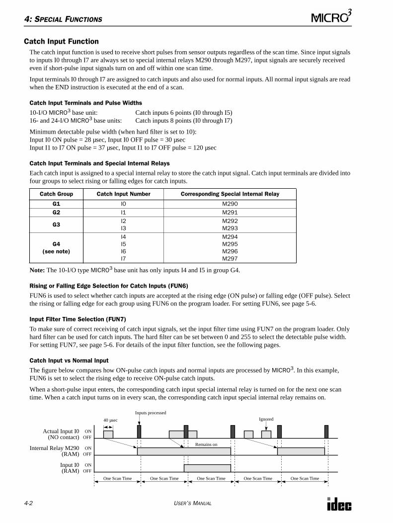
4: SPECIAL FUNCTIONS
4-2 USER’S MANUAL
Catch Input FunctionThe catch input function is used to receive short pulses from sensor outputs regardless of the scan time. Since input signals to inputs I0 through I7 are always set to special internal relays M290 through M297, input signals are securely received even if short-pulse input signals turn on and off within one scan time.
Input terminals I0 through I7 are assigned to catch inputs and also used for normal inputs. All normal input signals are read when the END instruction is executed at the end of a scan.
Catch Input Terminals and Pulse Widths
10-I/O MICRO3 base unit: Catch inputs 6 points (I0 through I5)16- and 24-I/O MICRO3 base units: Catch inputs 8 points (I0 through I7)
Minimum detectable pulse width (when hard filter is set to 10):Input I0 ON pulse = 28 µsec, Input I0 OFF pulse = 30 µsecInput I1 to I7 ON pulse = 37 µsec, Input I1 to I7 OFF pulse = 120 µsec
Catch Input Terminals and Special Internal Relays
Each catch input is assigned to a special internal relay to store the catch input signal. Catch input terminals are divided into four groups to select rising or falling edges for catch inputs.
Note: The 10-I/O type MICRO3 base unit has only inputs I4 and I5 in group G4.
Rising or Falling Edge Selection for Catch Inputs (FUN6)
FUN6 is used to select whether catch inputs are accepted at the rising edge (ON pulse) or falling edge (OFF pulse). Select the rising or falling edge for each group using FUN6 on the program loader. For setting FUN6, see page 5-6.
Input Filter Time Selection (FUN7)
To make sure of correct receiving of catch input signals, set the input filter time using FUN7 on the program loader. Only hard filter can be used for catch inputs. The hard filter can be set between 0 and 255 to select the detectable pulse width. For setting FUN7, see page 5-6. For details of the input filter function, see the following pages.
Catch Input vs Normal Input
The figure below compares how ON-pulse catch inputs and normal inputs are processed by MICRO3. In this example, FUN6 is set to select the rising edge to receive ON-pulse catch inputs.
When a short-pulse input enters, the corresponding catch input special internal relay is turned on for the next one scan time. When a catch input turns on in every scan, the corresponding catch input special internal relay remains on.
Catch Group Catch Input Number Corresponding Special Internal Relay
G1 I0 M290G2 I1 M291
G3I2I3
M292M293
G4(see note)
I4I5I6I7
M294M295M296M297
Actual Input I0 ONOFF
Input I0 ONOFF
Inputs processed
One Scan Time
Internal Relay M290 ONOFF
(NO contact)
(RAM)
(RAM)One Scan Time One Scan Time One Scan Time One Scan Time
40 µsec
Remains on
Ignored
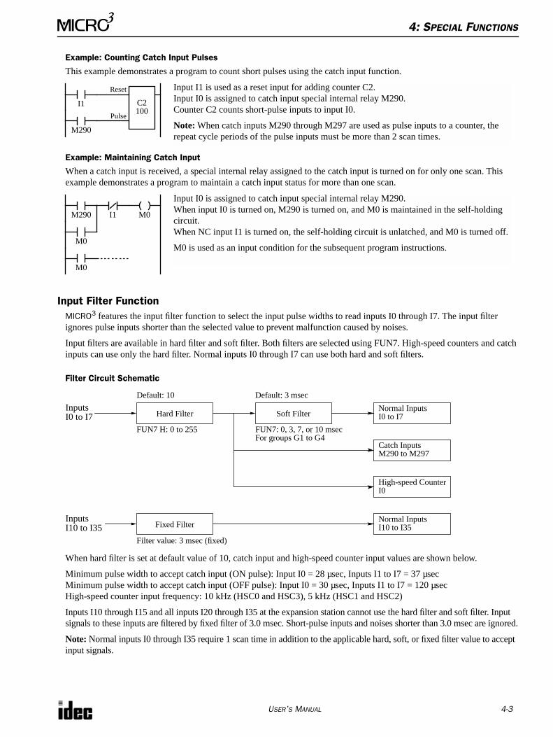
4: SPECIAL FUNCTIONS
USER’S MANUAL 4-3
Example: Counting Catch Input Pulses
This example demonstrates a program to count short pulses using the catch input function.
Example: Maintaining Catch Input
When a catch input is received, a special internal relay assigned to the catch input is turned on for only one scan. This example demonstrates a program to maintain a catch input status for more than one scan.
Input Filter FunctionMICRO3 features the input filter function to select the input pulse widths to read inputs I0 through I7. The input filter ignores pulse inputs shorter than the selected value to prevent malfunction caused by noises.
Input filters are available in hard filter and soft filter. Both filters are selected using FUN7. High-speed counters and catch inputs can use only the hard filter. Normal inputs I0 through I7 can use both hard and soft filters.
Filter Circuit Schematic
When hard filter is set at default value of 10, catch input and high-speed counter input values are shown below.
Minimum pulse width to accept catch input (ON pulse): Input I0 = 28 µsec, Inputs I1 to I7 = 37 µsecMinimum pulse width to accept catch input (OFF pulse): Input I0 = 30 µsec, Inputs I1 to I7 = 120 µsecHigh-speed counter input frequency: 10 kHz (HSC0 and HSC3), 5 kHz (HSC1 and HSC2)
Inputs I10 through I15 and all inputs I20 through I35 at the expansion station cannot use the hard filter and soft filter. Input signals to these inputs are filtered by fixed filter of 3.0 msec. Short-pulse inputs and noises shorter than 3.0 msec are ignored.
Note: Normal inputs I0 through I35 require 1 scan time in addition to the applicable hard, soft, or fixed filter value to accept input signals.
M290
I1 C2100
Reset
Pulse
Input I1 is used as a reset input for adding counter C2.Input I0 is assigned to catch input special internal relay M290.Counter C2 counts short-pulse inputs to input I0.
Note: When catch inputs M290 through M297 are used as pulse inputs to a counter, the repeat cycle periods of the pulse inputs must be more than 2 scan times.
M0
M290
Input I0 is assigned to catch input special internal relay M290.When input I0 is turned on, M290 is turned on, and M0 is maintained in the self-holding circuit.When NC input I1 is turned on, the self-holding circuit is unlatched, and M0 is turned off.
M0 is used as an input condition for the subsequent program instructions.
M0
I1 M0
InputsHard Filter Soft Filter
Normal InputsI0 to I7
Catch InputsM290 to M297
High-speed CounterI0
Normal InputsI10 to I35
Default: 3 msecDefault: 10
Fixed Filter
I0 to I7
InputsI10 to I35
FUN7 H: 0 to 255 FUN7: 0, 3, 7, or 10 msecFor groups G1 to G4
Filter value: 3 msec (fixed)
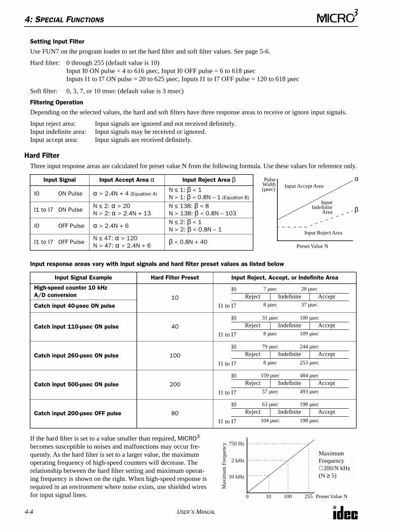
4: SPECIAL FUNCTIONS
4-4 USER’S MANUAL
Setting Input Filter
Use FUN7 on the program loader to set the hard filter and soft filter values. See page 5-6.
Hard filter: 0 through 255 (default value is 10)Input I0 ON pulse = 4 to 616 µsec, Input I0 OFF pulse = 6 to 618 µsecInputs I1 to I7 ON pulse = 20 to 625 µsec, Inputs I1 to I7 OFF pulse = 120 to 618 µsec
Soft filter: 0, 3, 7, or 10 msec (default value is 3 msec)
Filtering Operation
Depending on the selected values, the hard and soft filters have three response areas to receive or ignore input signals.
Input reject area: Input signals are ignored and not received definitely.Input indefinite area: Input signals may be received or ignored.Input accept area: Input signals are received definitely.
Hard FilterThree input response areas are calculated for preset value N from the following formula. Use these values for reference only.
Input response areas vary with input signals and hard filter preset values as listed below
If the hard filter is set to a value smaller than required, MICRO3 becomes susceptible to noises and malfunctions may occur fre-quently. As the hard filter is set to a larger value, the maximum operating frequency of high-speed counters will decrease. The relationship between the hard filter setting and maximum operat-ing frequency is shown on the right. When high-speed response is required in an environment where noise exists, use shielded wires for input signal lines.
Input Signal Input Accept Area α Input Reject Area β
I0 ON Pulse α > 2.4N + 4 (Equation A)N ≤ 1: β < 1N > 1: β < 0.8N – 1 (Equation B)
I1 to I7 ON PulseN ≤ 2: α > 20N > 2: α > 2.4N + 13
N ≤ 138: β < 8N > 138: β < 0.8N – 103
I0 OFF Pulse α > 2.4N + 6N ≤ 2: β < 1N > 2: β < 0.8N – 1
I1 to I7 OFF PulseN ≤ 47: α > 120N > 47: α > 2.4N + 6
β < 0.8N + 40
Input Signal Example Hard Filter Preset Input Reject, Accept, or Indefinite Area
High-speed counter 10 kHzA/D conversion 10Catch input 40-µsec ON pulse
Catch input 110-µsec ON pulse 40
Catch input 260-µsec ON pulse 100
Catch input 500-µsec ON pulse 200
Catch input 200-µsec OFF pulse 80
PulseInput Accept Area
InputIndefinite
Area
Input Reject Area
α
β
Preset Value N
Width(µsec)
Indefinite7 µsec 28 µsec
Reject Accept8 µsec 37 µsec
I0
I1 to I7
Indefinite31 µsec 100 µsec
Reject Accept8 µsec 109 µsec
I0
I1 to I7
8 µsec 253 µsecI1 to I7
Indefinite79 µsec 244 µsec
Reject AcceptI0
Indefinite159 µsec 484 µsec
Reject Accept57 µsec 493 µsec
I0
I1 to I7
Indefinite63 µsec 198 µsec
Reject Accept
104 µsec 198 µsec
I0
I1 to I7
750 Hz
2 kHz
10 kHz
0 255
Max
imum
Fre
quen
cy
Preset Value N10 100
Maximum Frequency≅ 200/N kHz(N ≥ 5)
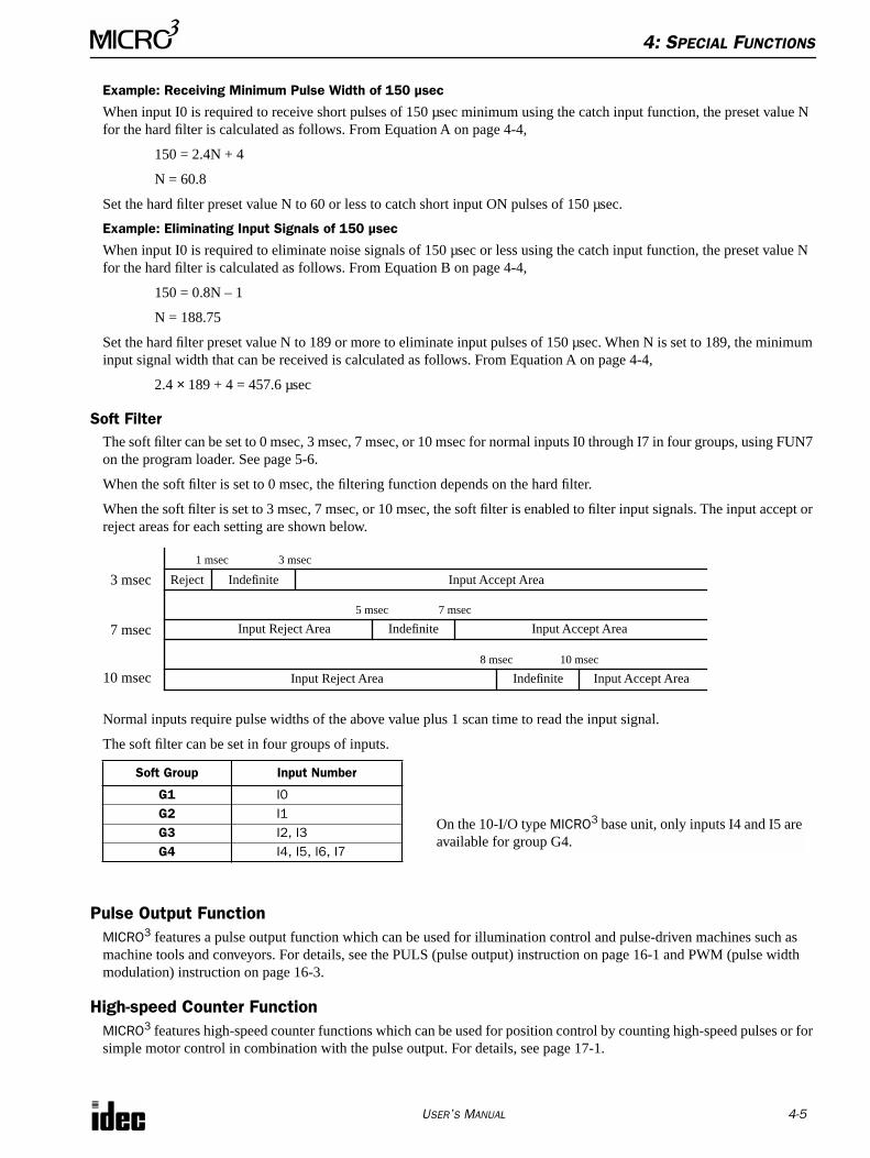
4: SPECIAL FUNCTIONS
USER’S MANUAL 4-5
Example: Receiving Minimum Pulse Width of 150 µsec
When input I0 is required to receive short pulses of 150 µsec minimum using the catch input function, the preset value N for the hard filter is calculated as follows. From Equation A on page 4-4,
150 = 2.4N + 4
N = 60.8
Set the hard filter preset value N to 60 or less to catch short input ON pulses of 150 µsec.
Example: Eliminating Input Signals of 150 µsec
When input I0 is required to eliminate noise signals of 150 µsec or less using the catch input function, the preset value N for the hard filter is calculated as follows. From Equation B on page 4-4,
150 = 0.8N – 1
N = 188.75
Set the hard filter preset value N to 189 or more to eliminate input pulses of 150 µsec. When N is set to 189, the minimum input signal width that can be received is calculated as follows. From Equation A on page 4-4,
2.4 × 189 + 4 = 457.6 µsec
Soft FilterThe soft filter can be set to 0 msec, 3 msec, 7 msec, or 10 msec for normal inputs I0 through I7 in four groups, using FUN7 on the program loader. See page 5-6.
When the soft filter is set to 0 msec, the filtering function depends on the hard filter.
When the soft filter is set to 3 msec, 7 msec, or 10 msec, the soft filter is enabled to filter input signals. The input accept or reject areas for each setting are shown below.
Normal inputs require pulse widths of the above value plus 1 scan time to read the input signal.
The soft filter can be set in four groups of inputs.
Pulse Output FunctionMICRO3 features a pulse output function which can be used for illumination control and pulse-driven machines such as machine tools and conveyors. For details, see the PULS (pulse output) instruction on page 16-1 and PWM (pulse width modulation) instruction on page 16-3.
High-speed Counter FunctionMICRO3 features high-speed counter functions which can be used for position control by counting high-speed pulses or for simple motor control in combination with the pulse output. For details, see page 17-1.
Soft Group Input Number
G1 I0G2 I1G3 I2, I3G4 I4, I5, I6, I7
Indefinite
1 msec 3 msec
Reject Input Accept Area3 msec
IndefiniteInput Reject Area Input Accept Area
5 msec 7 msec
7 msec
Input Accept AreaIndefiniteInput Reject Area
8 msec 10 msec
10 msec
On the 10-I/O type MICRO3 base unit, only inputs I4 and I5 are available for group G4.
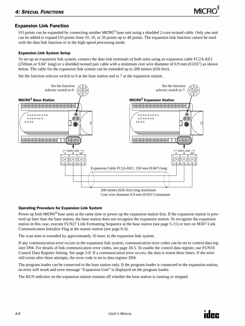
4: SPECIAL FUNCTIONS
4-6 USER’S MANUAL
Expansion Link FunctionI/O points can be expanded by connecting another MICRO3 base unit using a shielded 2-core twisted cable. Only one unit can be added to expand I/O points from 10, 16, or 20 points up to 48 points. The expansion link function cannot be used with the data link function or in the high-speed processing mode.
Expansion Link System Setup
To set up an expansion link system, connect the data link terminals of both units using an expansion cable FC2A-KE1 (250mm or 9.84" long) or a shielded twisted pair cable with a minimum core wire diameter of 0.9 mm (0.035") as shown below. The cable for the expansion link system can be extended up to 200 meters (656 feet).
Set the function selector switch to 0 at the base station and to 7 at the expansion station.
Operating Procedure for Expansion Link System
Power up both MICRO3 base units at the same time or power up the expansion station first. If the expansion station is pow-ered up later than the base station, the base station does not recognize the expansion station. To recognize the expansion station in this case, execute FUN27 Link Formatting Sequence at the base station (see page 5-11) or turn on M307 Link Communication Initialize Flag at the master station (see page 6-3).
The scan time is extended by approximately 10 msec in the expansion link system.
If any communication error occurs in the expansion link system, communication error codes can be set to control data reg-ister D94. For details of link communication error codes, see page 18-5. To enable the control data register, use FUN10 Control Data Register Setting. See page 5-8. If a communication error occurs, the data is resent three times. If the error still exists after three attempts, the error code is set to data register D94.
The program loader can be connected to the base station only. If the program loader is connected to the expansion station, an error will result and error message “Expansion Unit” is displayed on the program loader.
The RUN indicator on the expansion station remains off whether the base station is running or stopped.
7
3 4 562
1 07
3 4 562
1 0
MICRO3 Base Station MICRO3 Expansion Station
Set the functionselector switch to 0.
Set the functionselector switch to 7.
DATA LINKA SGB
DATA LINKA SGB
Expansion Cable FC2A-KE1, 250 mm (9.84") long
200 meters (656 feet) long maximumCore wire diameter 0.9 mm (0.035") minimum
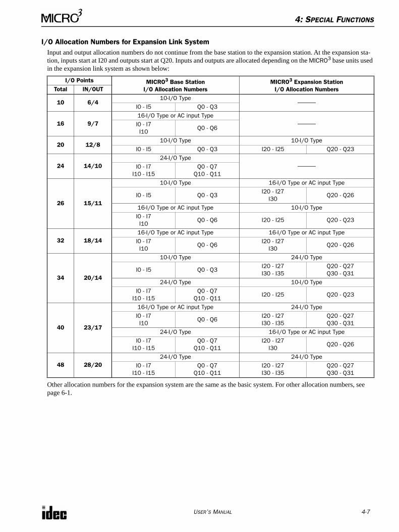
4: SPECIAL FUNCTIONS
USER’S MANUAL 4-7
I/O Allocation Numbers for Expansion Link SystemInput and output allocation numbers do not continue from the base station to the expansion station. At the expansion sta-tion, inputs start at I20 and outputs start at Q20. Inputs and outputs are allocated depending on the MICRO3 base units used in the expansion link system as shown below:
Other allocation numbers for the expansion system are the same as the basic system. For other allocation numbers, see page 6-1.
I/O Points MICRO3 Base Station I/O Allocation Numbers
MICRO3 Expansion Station I/O Allocation NumbersTotal IN/OUT
10 6/410-I/O Type
———I0 - I5 Q0 - Q3
16 9/716-I/O Type or AC input Type
———I0 - I7I10
Q0 - Q6
20 12/810-I/O Type 10-I/O Type
I0 - I5 Q0 - Q3 I20 - I25 Q20 - Q23
24 14/1024-I/O Type
———I0 - I7I10 - I15
Q0 - Q7Q10 - Q11
26 15/11
10-I/O Type 16-I/O Type or AC input Type
I0 - I5 Q0 - Q3I20 - I27
I30Q20 - Q26
16-I/O Type or AC input Type 10-I/O TypeI0 - I7I10
Q0 - Q6 I20 - I25 Q20 - Q23
32 18/1416-I/O Type or AC input Type 16-I/O Type or AC input TypeI0 - I7I10
Q0 - Q6I20 - I27
I30Q20 - Q26
34 20/14
10-I/O Type 24-I/O Type
I0 - I5 Q0 - Q3I20 - I27I30 - I35
Q20 - Q27Q30 - Q31
24-I/O Type 10-I/O TypeI0 - I7
I10 - I15Q0 - Q7
Q10 - Q11I20 - I25 Q20 - Q23
40 23/17
16-I/O Type or AC input Type 24-I/O TypeI0 - I7I10
Q0 - Q6I20 - I27I30 - I35
Q20 - Q27Q30 - Q31
24-I/O Type 16-I/O Type or AC input TypeI0 - I7
I10 - I15Q0 - Q7
Q10 - Q11I20 - I27
I30Q20 - Q26
48 28/2024-I/O Type 24-I/O Type
I0 - I7I10 - I15
Q0 - Q7Q10 - Q11
I20 - I27I30 - I35
Q20 - Q27Q30 - Q31
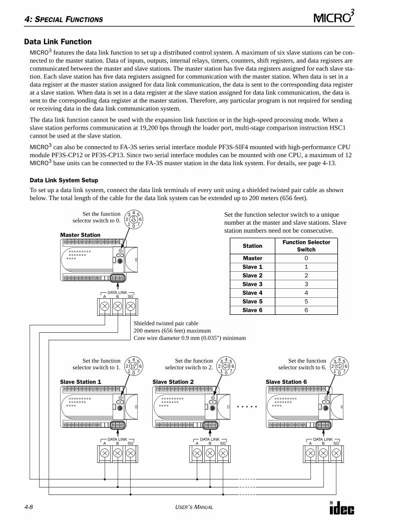
4: SPECIAL FUNCTIONS
4-8 USER’S MANUAL
Data Link FunctionMICRO3 features the data link function to set up a distributed control system. A maximum of six slave stations can be con-nected to the master station. Data of inputs, outputs, internal relays, timers, counters, shift registers, and data registers are communicated between the master and slave stations. The master station has five data registers assigned for each slave sta-tion. Each slave station has five data registers assigned for communication with the master station. When data is set in a data register at the master station assigned for data link communication, the data is sent to the corresponding data register at a slave station. When data is set in a data register at the slave station assigned for data link communication, the data is sent to the corresponding data register at the master station. Therefore, any particular program is not required for sending or receiving data in the data link communication system.
The data link function cannot be used with the expansion link function or in the high-speed processing mode. When a slave station performs communication at 19,200 bps through the loader port, multi-stage comparison instruction HSC1 cannot be used at the slave station.
MICRO3 can also be connected to FA-3S series serial interface module PF3S-SIF4 mounted with high-performance CPU module PF3S-CP12 or PF3S-CP13. Since two serial interface modules can be mounted with one CPU, a maximum of 12 MICRO3 base units can be connected to the FA-3S master station in the data link system. For details, see page 4-13.
Data Link System Setup
To set up a data link system, connect the data link terminals of every unit using a shielded twisted pair cable as shown below. The total length of the cable for the data link system can be extended up to 200 meters (656 feet).
7
3 4 562
1 0
Master Station
Set the functionselector switch to 0.
DATA LINKA SGB
7
3 4 562
1 0
Slave Station 1
Set the functionselector switch to 1.
DATA LINKA SGB
7
3 4 562
1 0
Slave Station 2
Set the functionselector switch to 2.
DATA LINKA SGB
7
3 4 562
1 0
Slave Station 6
Set the functionselector switch to 6.
DATA LINKA SGB
Shielded twisted pair cable200 meters (656 feet) maximumCore wire diameter 0.9 mm (0.035") minimum
Set the function selector switch to a unique number at the master and slave stations. Slave station numbers need not be consecutive.
StationFunction Selector
SwitchMaster 0Slave 1 1Slave 2 2Slave 3 3Slave 4 4Slave 5 5Slave 6 6
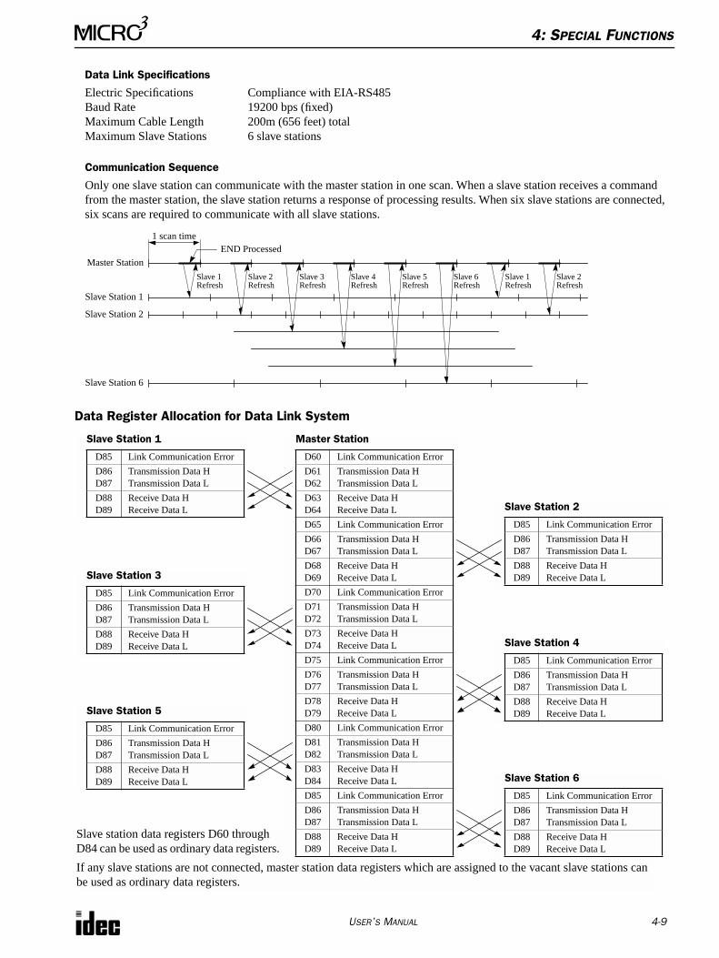
4: SPECIAL FUNCTIONS
USER’S MANUAL 4-9
Data Link Specifications
Electric Specifications Compliance with EIA-RS485Baud Rate 19200 bps (fixed)Maximum Cable Length 200m (656 feet) totalMaximum Slave Stations 6 slave stations
Communication Sequence
Only one slave station can communicate with the master station in one scan. When a slave station receives a command from the master station, the slave station returns a response of processing results. When six slave stations are connected, six scans are required to communicate with all slave stations.
Data Register Allocation for Data Link System
Master Station
Slave 1Refresh
1 scan time
Slave Station 1
END Processed
Slave 2Refresh
Slave 3Refresh
Slave 4Refresh
Slave 5Refresh
Slave 6Refresh
Slave 1Refresh
Slave 2Refresh
Slave Station 2
Slave Station 6
Master Station
D60 Link Communication Error
D61D62
Transmission Data HTransmission Data L
D63D64
Receive Data HReceive Data L
D65 Link Communication Error
D66D67
Transmission Data HTransmission Data L
D68D69
Receive Data HReceive Data L
D70 Link Communication Error
D71D72
Transmission Data HTransmission Data L
D73D74
Receive Data HReceive Data L
D75 Link Communication Error
D76D77
Transmission Data HTransmission Data L
D78D79
Receive Data HReceive Data L
D80 Link Communication Error
D81D82
Transmission Data HTransmission Data L
D83D84
Receive Data HReceive Data L
D85 Link Communication Error
D86D87
Transmission Data HTransmission Data L
D88D89
Receive Data HReceive Data L
Slave Station 1
D85 Link Communication Error
D86D87
Transmission Data HTransmission Data L
D88D89
Receive Data HReceive Data L Slave Station 2
D85 Link Communication Error
D86D87
Transmission Data HTransmission Data L
D88D89
Receive Data HReceive Data LSlave Station 3
D85 Link Communication Error
D86D87
Transmission Data HTransmission Data L
D88D89
Receive Data HReceive Data L
Slave Station 5
D85 Link Communication Error
D86D87
Transmission Data HTransmission Data L
D88D89
Receive Data HReceive Data L
Slave Station 4
D85 Link Communication Error
D86D87
Transmission Data HTransmission Data L
D88D89
Receive Data HReceive Data L
Slave Station 6
D85 Link Communication Error
D86D87
Transmission Data HTransmission Data L
D88D89
Receive Data HReceive Data L
If any slave stations are not connected, master station data registers which are assigned to the vacant slave stations can be used as ordinary data registers.
Slave station data registers D60 through D84 can be used as ordinary data registers.
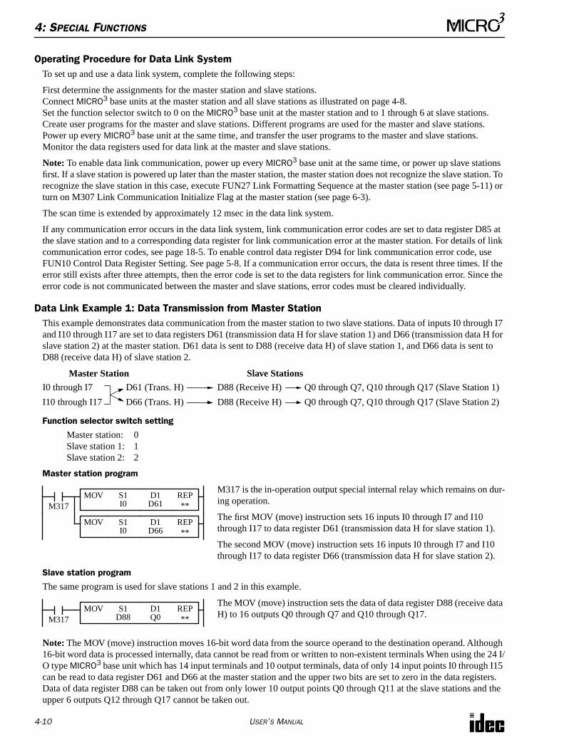
4: SPECIAL FUNCTIONS
4-10 USER’S MANUAL
Operating Procedure for Data Link SystemTo set up and use a data link system, complete the following steps:
First determine the assignments for the master station and slave stations.Connect MICRO3 base units at the master station and all slave stations as illustrated on page 4-8.Set the function selector switch to 0 on the MICRO3 base unit at the master station and to 1 through 6 at slave stations.Create user programs for the master and slave stations. Different programs are used for the master and slave stations.Power up every MICRO3 base unit at the same time, and transfer the user programs to the master and slave stations.Monitor the data registers used for data link at the master and slave stations.
Note: To enable data link communication, power up every MICRO3 base unit at the same time, or power up slave stations first. If a slave station is powered up later than the master station, the master station does not recognize the slave station. To recognize the slave station in this case, execute FUN27 Link Formatting Sequence at the master station (see page 5-11) or turn on M307 Link Communication Initialize Flag at the master station (see page 6-3).
The scan time is extended by approximately 12 msec in the data link system.
If any communication error occurs in the data link system, link communication error codes are set to data register D85 at the slave station and to a corresponding data register for link communication error at the master station. For details of link communication error codes, see page 18-5. To enable control data register D94 for link communication error code, use FUN10 Control Data Register Setting. See page 5-8. If a communication error occurs, the data is resent three times. If the error still exists after three attempts, then the error code is set to the data registers for link communication error. Since the error code is not communicated between the master and slave stations, error codes must be cleared individually.
Data Link Example 1: Data Transmission from Master StationThis example demonstrates data communication from the master station to two slave stations. Data of inputs I0 through I7 and I10 through I17 are set to data registers D61 (transmission data H for slave station 1) and D66 (transmission data H for slave station 2) at the master station. D61 data is sent to D88 (receive data H) of slave station 1, and D66 data is sent to D88 (receive data H) of slave station 2.
Function selector switch setting
Master station: 0Slave station 1: 1Slave station 2: 2
Master station program
Slave station program
The same program is used for slave stations 1 and 2 in this example.
Note: The MOV (move) instruction moves 16-bit word data from the source operand to the destination operand. Although 16-bit word data is processed internally, data cannot be read from or written to non-existent terminals When using the 24 I/O type MICRO3 base unit which has 14 input terminals and 10 output terminals, data of only 14 input points I0 through I15 can be read to data register D61 and D66 at the master station and the upper two bits are set to zero in the data registers. Data of data register D88 can be taken out from only lower 10 output points Q0 through Q11 at the slave stations and the upper 6 outputs Q12 through Q17 cannot be taken out.
Master Station Slave Stations
I0 through I7
I10 through I17
D61 (Trans. H)
D66 (Trans. H)
D88 (Receive H)
D88 (Receive H)
Q0 through Q7, Q10 through Q17 (Slave Station 1)
Q0 through Q7, Q10 through Q17 (Slave Station 2)
M317MOV REP
**
M317 is the in-operation output special internal relay which remains on dur-ing operation.
The first MOV (move) instruction sets 16 inputs I0 through I7 and I10 through I17 to data register D61 (transmission data H for slave station 1).
The second MOV (move) instruction sets 16 inputs I0 through I7 and I10 through I17 to data register D66 (transmission data H for slave station 2).
S1I0
D1D61
MOV REP**
S1I0
D1D66
M317MOV REP
**
The MOV (move) instruction sets the data of data register D88 (receive data H) to 16 outputs Q0 through Q7 and Q10 through Q17.
S1D88
D1Q0
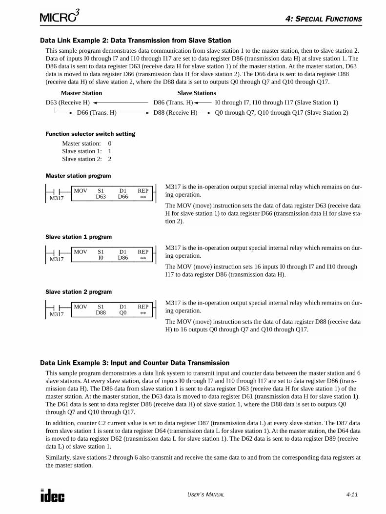
4: SPECIAL FUNCTIONS
USER’S MANUAL 4-11
Data Link Example 2: Data Transmission from Slave StationThis sample program demonstrates data communication from slave station 1 to the master station, then to slave station 2. Data of inputs I0 through I7 and I10 through I17 are set to data register D86 (transmission data H) at slave station 1. The D86 data is sent to data register D63 (receive data H for slave station 1) of the master station. At the master station, D63 data is moved to data register D66 (transmission data H for slave station 2). The D66 data is sent to data register D88 (receive data H) of slave station 2, where the D88 data is set to outputs Q0 through Q7 and Q10 through Q17.
Function selector switch setting
Master station: 0Slave station 1: 1Slave station 2: 2
Master station program
Slave station 1 program
Slave station 2 program
Data Link Example 3: Input and Counter Data TransmissionThis sample program demonstrates a data link system to transmit input and counter data between the master station and 6 slave stations. At every slave station, data of inputs I0 through I7 and I10 through I17 are set to data register D86 (trans-mission data H). The D86 data from slave station 1 is sent to data register D63 (receive data H for slave station 1) of the master station. At the master station, the D63 data is moved to data register D61 (transmission data H for slave station 1). The D61 data is sent to data register D88 (receive data H) of slave station 1, where the D88 data is set to outputs Q0 through Q7 and Q10 through Q17.
In addition, counter C2 current value is set to data register D87 (transmission data L) at every slave station. The D87 data from slave station 1 is sent to data register D64 (transmission data L for slave station 1). At the master station, the D64 data is moved to data register D62 (transmission data L for slave station 1). The D62 data is sent to data register D89 (receive data L) of slave station 1.
Similarly, slave stations 2 through 6 also transmit and receive the same data to and from the corresponding data registers at the master station.
Master Station Slave Stations
D63 (Receive H)
D66 (Trans. H)
D86 (Trans. H)
D88 (Receive H)
I0 through I7, I10 through I17 (Slave Station 1)
Q0 through Q7, Q10 through Q17 (Slave Station 2)
M317MOV REP
**
M317 is the in-operation output special internal relay which remains on dur-ing operation.
The MOV (move) instruction sets the data of data register D63 (receive data H for slave station 1) to data register D66 (transmission data H for slave sta-tion 2).
S1D63
D1D66
M317MOV REP
**
M317 is the in-operation output special internal relay which remains on dur-ing operation.
The MOV (move) instruction sets 16 inputs I0 through I7 and I10 through I17 to data register D86 (transmission data H).
S1I0
D1D86
M317MOV REP
**
M317 is the in-operation output special internal relay which remains on dur-ing operation.
The MOV (move) instruction sets the data of data register D88 (receive data H) to 16 outputs Q0 through Q7 and Q10 through Q17.
S1D88
D1Q0
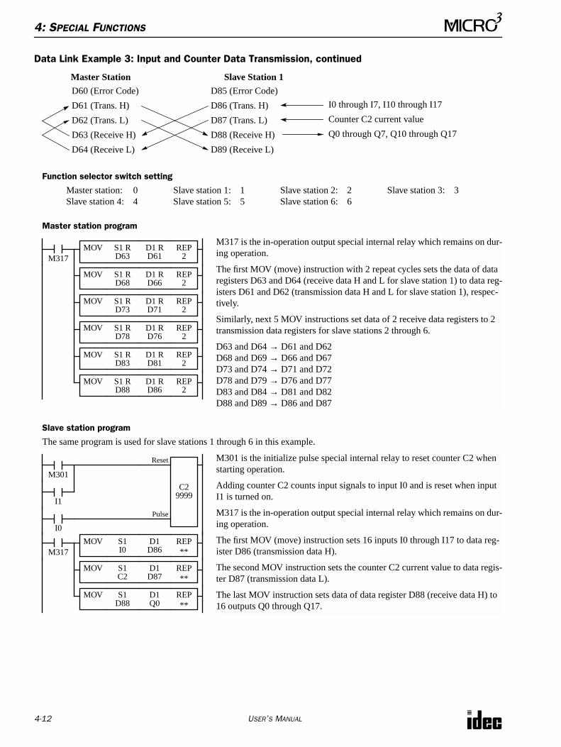
4: SPECIAL FUNCTIONS
4-12 USER’S MANUAL
Data Link Example 3: Input and Counter Data Transmission, continued
Function selector switch setting
Master station: 0 Slave station 1: 1 Slave station 2: 2 Slave station 3: 3Slave station 4: 4 Slave station 5: 5 Slave station 6: 6
Master station program
Slave station program
The same program is used for slave stations 1 through 6 in this example.
Master Station Slave Station 1
D60 (Error Code)
D61 (Trans. H) I0 through I7, I10 through I17
Q0 through Q7, Q10 through Q17
D62 (Trans. L)
D63 (Receive H)
D64 (Receive L)
D85 (Error Code)
D86 (Trans. H)
D87 (Trans. L)
D88 (Receive H)
D89 (Receive L)
Counter C2 current value
M317MOV REP
2
M317 is the in-operation output special internal relay which remains on dur-ing operation.
The first MOV (move) instruction with 2 repeat cycles sets the data of data registers D63 and D64 (receive data H and L for slave station 1) to data reg-isters D61 and D62 (transmission data H and L for slave station 1), respec-tively.
Similarly, next 5 MOV instructions set data of 2 receive data registers to 2 transmission data registers for slave stations 2 through 6.
D63 and D64 → D61 and D62D68 and D69 → D66 and D67D73 and D74 → D71 and D72D78 and D79 → D76 and D77D83 and D84 → D81 and D82D88 and D89 → D86 and D87
S1 RD63
D1 RD61
MOV REP2
S1 RD68
D1 RD66
MOV REP2
S1 RD73
D1 RD71
MOV REP2
S1 RD78
D1 RD76
MOV REP2
S1 RD83
D1 RD81
MOV REP2
S1 RD88
D1 RD86
M301
M301 is the initialize pulse special internal relay to reset counter C2 when starting operation.
Adding counter C2 counts input signals to input I0 and is reset when input I1 is turned on.
M317 is the in-operation output special internal relay which remains on dur-ing operation.
The first MOV (move) instruction sets 16 inputs I0 through I17 to data reg-ister D86 (transmission data H).
The second MOV instruction sets the counter C2 current value to data regis-ter D87 (transmission data L).
The last MOV instruction sets data of data register D88 (receive data H) to 16 outputs Q0 through Q17.
C29999
Reset
I1
I0
M317MOV REP
**S1I0
D1D86
MOV REP**
S1C2
D1D87
MOV REP**
S1D88
D1Q0
Pulse
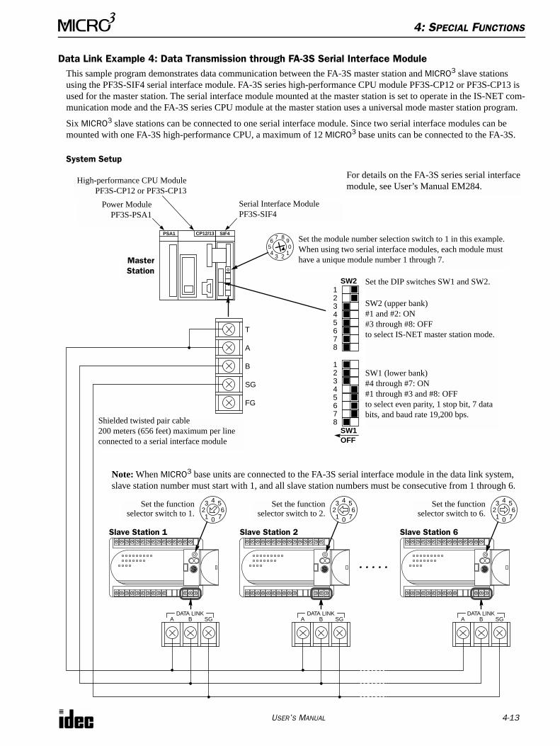
4: SPECIAL FUNCTIONS
USER’S MANUAL 4-13
Data Link Example 4: Data Transmission through FA-3S Serial Interface ModuleThis sample program demonstrates data communication between the FA-3S master station and MICRO3 slave stations using the PF3S-SIF4 serial interface module. FA-3S series high-performance CPU module PF3S-CP12 or PF3S-CP13 is used for the master station. The serial interface module mounted at the master station is set to operate in the IS-NET com-munication mode and the FA-3S series CPU module at the master station uses a universal mode master station program.
Six MICRO3 slave stations can be connected to one serial interface module. Since two serial interface modules can be mounted with one FA-3S high-performance CPU, a maximum of 12 MICRO3 base units can be connected to the FA-3S.
System Setup
PSA1 CP12/13 SIF4
7
3 4 562
1 0
Slave Station 1
Set the functionselector switch to 1. 7
3 4 562
1 0
Slave Station 2
Set the functionselector switch to 2.
DATA LINKA SGB
7
3 4 562
1 0
Slave Station 6
Set the functionselector switch to 6.
DATA LINKA SGB
Shielded twisted pair cable200 meters (656 feet) maximum per line connected to a serial interface module
54
6
3
7
2
8
10
9
12345678
12345678
SW2
SW1OFF
DATA LINKA SGB
T
A
B
SG
FG
Set the module number selection switch to 1 in this example.When using two serial interface modules, each module must have a unique module number 1 through 7.
Set the DIP switches SW1 and SW2.
SW2 (upper bank)#1 and #2: ON#3 through #8: OFFto select IS-NET master station mode.
SW1 (lower bank)#4 through #7: ON#1 through #3 and #8: OFFto select even parity, 1 stop bit, 7 data bits, and baud rate 19,200 bps.
Note: When MICRO3 base units are connected to the FA-3S serial interface module in the data link system, slave station number must start with 1, and all slave station numbers must be consecutive from 1 through 6.
For details on the FA-3S series serial interface module, see User’s Manual EM284.
High-performance CPU ModulePF3S-CP12 or PF3S-CP13
Serial Interface ModulePF3S-SIF4
Power ModulePF3S-PSA1
MasterStation
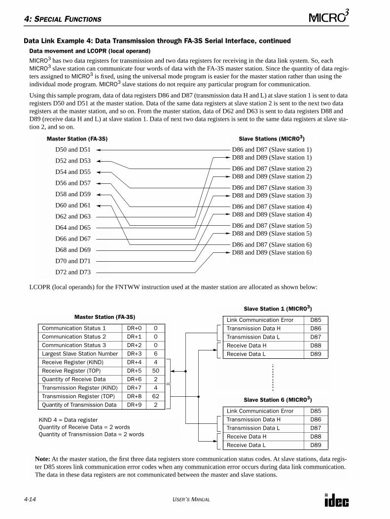
4: SPECIAL FUNCTIONS
4-14 USER’S MANUAL
Data Link Example 4: Data Transmission through FA-3S Serial Interface, continuedData movement and LCOPR (local operand)
MICRO3 has two data registers for transmission and two data registers for receiving in the data link system. So, each MICRO3 slave station can communicate four words of data with the FA-3S master station. Since the quantity of data regis-ters assigned to MICRO3 is fixed, using the universal mode program is easier for the master station rather than using the individual mode program. MICRO3 slave stations do not require any particular program for communication.
Using this sample program, data of data registers D86 and D87 (transmission data H and L) at slave station 1 is sent to data registers D50 and D51 at the master station. Data of the same data registers at slave station 2 is sent to the next two data registers at the master station, and so on. From the master station, data of D62 and D63 is sent to data registers D88 and D89 (receive data H and L) at slave station 1. Data of next two data registers is sent to the same data registers at slave sta-tion 2, and so on.
LCOPR (local operands) for the FNTWW instruction used at the master station are allocated as shown below:
Master Station (FA-3S)
D50 and D51
D52 and D53
D54 and D55
D56 and D57
D58 and D59
D60 and D61
D62 and D63
D64 and D65
D66 and D67
D68 and D69
D70 and D71
D72 and D73
Slave Stations (MICRO3)
D86 and D87 (Slave station 1)D88 and D89 (Slave station 1)
D86 and D87 (Slave station 2)D88 and D89 (Slave station 2)
D86 and D87 (Slave station 3)D88 and D89 (Slave station 3)
D86 and D87 (Slave station 4)D88 and D89 (Slave station 4)
D86 and D87 (Slave station 5)D88 and D89 (Slave station 5)
D86 and D87 (Slave station 6)D88 and D89 (Slave station 6)
Slave Station 6 (MICRO3)
Link Communication Error D85Transmission Data H D86Transmission Data L D87Receive Data H D88Receive Data L D89
Master Station (FA-3S)
Communication Status 1 DR+0 0Communication Status 2 DR+1 0Communication Status 3 DR+2 0Largest Slave Station Number DR+3 6Receive Register (KIND) DR+4 4Receive Register (TOP) DR+5 50Quantity of Receive Data DR+6 2Transmission Register (KIND) DR+7 4Transmission Register (TOP) DR+8 62Quantity of Transmission Data DR+9 2
Slave Station 1 (MICRO3)
Link Communication Error D85Transmission Data H D86Transmission Data L D87Receive Data H D88Receive Data L D89
KIND 4 = Data registerQuantity of Receive Data = 2 wordsQuantity of Transmission Data = 2 words
Note: At the master station, the first three data registers store communication status codes. At slave stations, data regis-ter D85 stores link communication error codes when any communication error occurs during data link communication. The data in these data registers are not communicated between the master and slave stations.
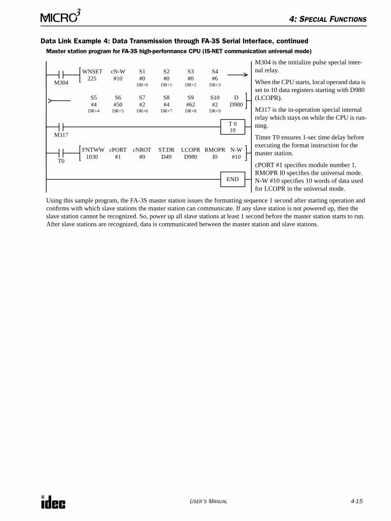
4: SPECIAL FUNCTIONS
USER’S MANUAL 4-15
Data Link Example 4: Data Transmission through FA-3S Serial Interface, continuedMaster station program for FA-3S high-performance CPU (IS-NET communication universal mode)
Using this sample program, the FA-3S master station issues the formatting sequence 1 second after starting operation and confirms with which slave stations the master station can communicate. If any slave station is not powered up, then the slave station cannot be recognized. So, power up all slave stations at least 1 second before the master station starts to run. After slave stations are recognized, data is communicated between the master station and slave stations.
M304
DD980
M304 is the initialize pulse special inter-nal relay.
When the CPU starts, local operand data is set to 10 data registers starting with D980 (LCOPR).
M317 is the in-operation special internal relay which stays on while the CPU is run-ning.
Timer T0 ensures 1-sec time delay before executing the format instruction for the master station.
cPORT #1 specifies module number 1.RMOPR I0 specifies the universal mode.N-W #10 specifies 10 words of data used for LCOPR in the universal mode.
225WNSET cN-W
#10S1#0
N-W#101030
FNTWW cPORT#1
cNROT#0
ST.DRD49
LCOPRD980
RMOPRI0
END
T 010
DR+0
S2#0
DR+1
S3#0
DR+2
S4#6
DR+3
S8#4
DR+7
S7#2
DR+6
S6#50
DR+5
S5#4
DR+4
S9#62
DR+8
S10#2
DR+9
M317
T0
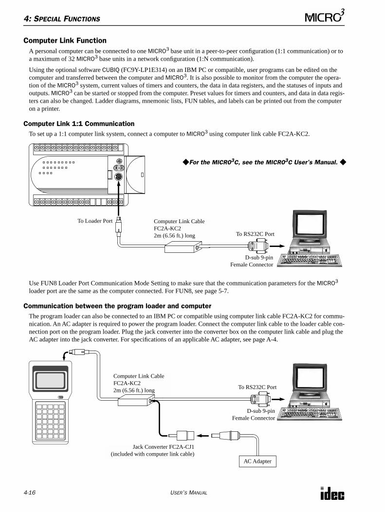
4: SPECIAL FUNCTIONS
4-16 USER’S MANUAL
Computer Link FunctionA personal computer can be connected to one MICRO3 base unit in a peer-to-peer configuration (1:1 communication) or to a maximum of 32 MICRO3 base units in a network configuration (1:N communication).
Using the optional software CUBIQ (FC9Y-LP1E314) on an IBM PC or compatible, user programs can be edited on the computer and transferred between the computer and MICRO3. It is also possible to monitor from the computer the opera-tion of the MICRO3 system, current values of timers and counters, the data in data registers, and the statuses of inputs and outputs. MICRO3 can be started or stopped from the computer. Preset values for timers and counters, and data in data regis-ters can also be changed. Ladder diagrams, mnemonic lists, FUN tables, and labels can be printed out from the computer on a printer.
Computer Link 1:1 CommunicationTo set up a 1:1 computer link system, connect a computer to MICRO3 using computer link cable FC2A-KC2.
Use FUN8 Loader Port Communication Mode Setting to make sure that the communication parameters for the MICRO3 loader port are the same as the computer connected. For FUN8, see page 5-7.
Communication between the program loader and computerThe program loader can also be connected to an IBM PC or compatible using computer link cable FC2A-KC2 for commu-nication. An AC adapter is required to power the program loader. Connect the computer link cable to the loader cable con-nection port on the program loader. Plug the jack converter into the converter box on the computer link cable and plug the AC adapter into the jack converter. For specifications of an applicable AC adapter, see page A-4.
Computer Link CableFC2A-KC22m (6.56 ft.) long
To Loader Port
D-sub 9-pinFemale Connector
To RS232C Port
For the MICRO3C, see the MICRO3C User’s Manual.
Computer Link CableFC2A-KC22m (6.56 ft.) long
Jack Converter FC2A-CJ1(included with computer link cable)
To RS232C Port
AC Adapter
D-sub 9-pinFemale Connector
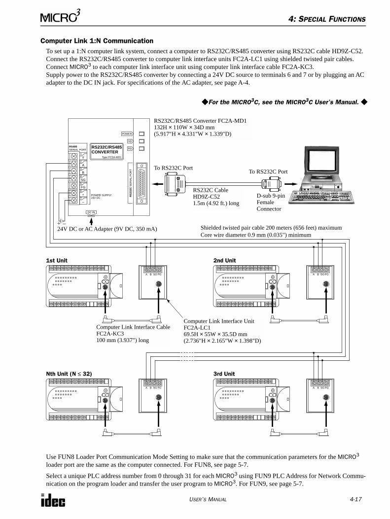
4: SPECIAL FUNCTIONS
USER’S MANUAL 4-17
Computer Link 1:N CommunicationTo set up a 1:N computer link system, connect a computer to RS232C/RS485 converter using RS232C cable HD9Z-C52.Connect the RS232C/RS485 converter to computer link interface units FC2A-LC1 using shielded twisted pair cables.Connect MICRO3 to each computer link interface unit using computer link interface cable FC2A-KC3.Supply power to the RS232C/RS485 converter by connecting a 24V DC source to terminals 6 and 7 or by plugging an AC adapter to the DC IN jack. For specifications of the AC adapter, see page A-4.
Use FUN8 Loader Port Communication Mode Setting to make sure that the communication parameters for the MICRO3 loader port are the same as the computer connected. For FUN8, see page 5-7.
Select a unique PLC address number from 0 through 31 for each MICRO3 using FUN9 PLC Address for Network Commu-nication on the program loader and transfer the user program to MICRO3. For FUN9, see page 5-7.
RS232C/RS485 Converter FC2A-MD1132H × 110W × 34D mm(5.917"H × 4.331"W × 1.339"D)
RS232C CableHD9Z-C521.5m (4.92 ft.) long
D-sub 9-pin Female Connector
To RS232C Port
A B SG FG
To RS232C Port
1st Unit
Computer Link Interface CableFC2A-KC3100 mm (3.937") long
Computer Link Interface UnitFC2A-LC169.5H × 55W × 35.5D mm(2.736"H × 2.165"W × 1.398"D)
A B SG FG
2nd Unit
A B SG FG
3rd Unit
A B SG FG
Nth Unit (N ≤ 32)
–+24V DC or AC Adapter (9V DC, 350 mA)
1
T2
A3
B4
SG5
FG6
+7
–
SD
RD
POWER
DC IN
RS485SERIAL PORT
POWER SUPPLY24V DC
RS
232C
SE
RIA
L P
OR
T
RS232C/RS485CONVERTER
Type FC2A-MD1
Shielded twisted pair cable 200 meters (656 feet) maximumCore wire diameter 0.9 mm (0.035") minimum
For the MICRO3C, see the MICRO3C User’s Manual.
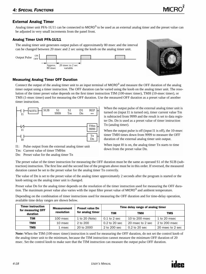
4: SPECIAL FUNCTIONS
4-18 USER’S MANUAL
External Analog TimerAnalog timer unit PFA-1U11 can be connected to MICRO3 to be used as an external analog timer and the preset value can be adjusted in very small increments from the panel front.
Analog Timer Unit PFA-1U11The analog timer unit generates output pulses of approximately 80 msec and the interval can be changed between 20 msec and 2 sec using the knob on the analog timer unit.
Measuring Analog Timer OFF DurationConnect the output of the analog timer unit to an input terminal of MICRO3 and measure the OFF duration of the analog timer output using a timer instruction. The OFF duration can be varied using the knob on the analog timer unit. The reso-lution of the timer preset value depends on the first timer instruction TIM (100-msec timer), TMH (10-msec timer), or TMS (1-msec timer) used for measuring the OFF duration. Use the measured OFF duration as a preset value of another timer instruction.
The preset value of the timer instruction for measuring the OFF duration must be the same as operand S1 of the SUB (sub-traction) instruction. The first line and the second line of the program above must be in this order. If reversed, the measured duration cannot be set to the preset value for the analog timer Tn correctly.
The value of Dn is set to the preset value of the analog timer approximately 2 seconds after the program is started or the knob setting on the analog timer unit is changed.
Preset value Dn for the analog timer depends on the resolution of the timer instruction used for measuring the OFF dura-tion. The maximum preset value also varies with the input filter preset value of MICRO3 and ambient temperature.
Depending on the combination of timer instructions used for measuring the OFF duration and for time-delay operation, available time delay ranges are shown below.
Note: When the TIM (100-msec timer) instruction is used for measuring the OFF duration, do not set the control knob of the analog timer unit to the minimum, because the TIM instruction cannot measure the minimum OFF duration of 20 msec. Set the control knob to make sure that the TIM instruction can measure the output pulse OFF duration.
Timer instruction for measuring OFF
duration
Measurement resolution
Preset value Dn for analog timer
Time delay range of analog timer
TIM TMH TMS
TIM 100 msec 1 to 20 (Note) 0.1 to 2 sec 10 to 200 msec 1 to 20 msecTMH 10 msec 2 to 200 0.2 to 20 sec 20 msec to 2 sec 2 to 200 msecTMS 1 msec 20 to 2000 2 to 200 sec 0.2 to 20 sec 20 msec to 2 sec
Output PulseON
OFF
Approx. 20 msec to 2 secvariable80 msec
I1
When the output pulse of the external analog timer unit is turned on (input I1 is turned on), timer current value Tm is subtracted from 9999 and the result is set to data regis-ter Dn. Dn is used as a preset value of timer instruction Tn (analog timer).
When the output pulse is off (input I1 is off), the 10-msec timer TMH times down from 9999 to measure the OFF duration of the external analog timer unit output.
When input I0 is on, the analog timer Tn starts to time down from the preset value Dn.
SUB S19999
REP**
SOTU S1Tm
D1Dn
I1: Pulse output from the external analog timer unitTm: Current value of timer TMHmDn: Preset value for the analog timer Tn
THm9999I1
I0TnDn
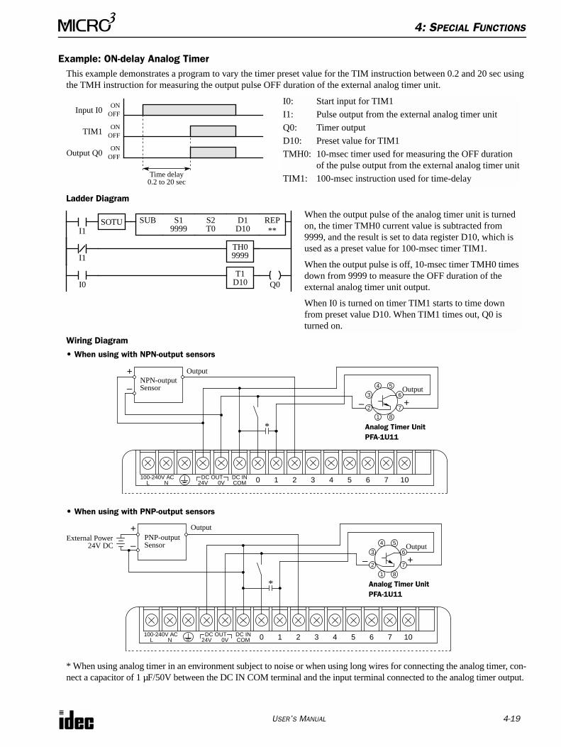
4: SPECIAL FUNCTIONS
USER’S MANUAL 4-19
Example: ON-delay Analog TimerThis example demonstrates a program to vary the timer preset value for the TIM instruction between 0.2 and 20 sec using the TMH instruction for measuring the output pulse OFF duration of the external analog timer unit.
Ladder Diagram
Wiring Diagram
• When using with NPN-output sensors
• When using with PNP-output sensors
* When using analog timer in an environment subject to noise or when using long wires for connecting the analog timer, con-nect a capacitor of 1 µF/50V between the DC IN COM terminal and the input terminal connected to the analog timer output.
Input I0ON
OFF
TIM1ON
OFF
Output Q0ON
OFF
Time delay0.2 to 20 sec
I0: Start input for TIM1
I1: Pulse output from the external analog timer unit
Q0: Timer output
D10: Preset value for TIM1
TMH0: 10-msec timer used for measuring the OFF duration of the pulse output from the external analog timer unit
TIM1: 100-msec instruction used for time-delay
SUB S19999I1
S2T0
D1D10
I1
SOTU
I0
REP**
TH09999
Q0T1
D10
When the output pulse of the analog timer unit is turned on, the timer TMH0 current value is subtracted from 9999, and the result is set to data register D10, which is used as a preset value for 100-msec timer TIM1.
When the output pulse is off, 10-msec timer TMH0 times down from 9999 to measure the OFF duration of the external analog timer unit output.
When I0 is turned on timer TIM1 starts to time down from preset value D10. When TIM1 times out, Q0 is turned on.
54
63
72
81
NPN-outputSensor
+
– Output
+
Analog Timer UnitPFA-1U11
–
*
Output
100-240V ACL N
DC OUT24V 0V
DC INCOM 0 1 2 3 4 5 6 7 10
– 54
63
72
81
PNP-outputSensor
+
Output
+
Analog Timer UnitPFA-1U11
–
*
External Power24V DC
Output
100-240V ACL N
DC OUT24V 0V
DC INCOM 0 1 2 3 4 5 6 7 10
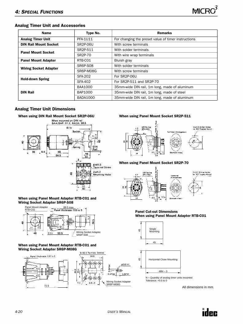
4: SPECIAL FUNCTIONS
4-20 USER’S MANUAL
Analog Timer Unit and Accessories
Analog Timer Unit Dimensions
Name Type No. Remarks
Analog Timer Unit PFA-1U11 For changing the preset value of timer instructionsDIN Rail Mount Socket SR2P-06U With screw terminals
Panel Mount SocketSR2P-511 With solder terminalsSR2P-70 With wire wrap terminals
Panel Mount Adapter RTB-C01 Bluish gray
Wiring Socket AdapterSR6P-S08 With solder terminalsSR6P-M08G With screw terminals
Hold-down SpringSFA-202 For SR2P-06USFA-402 For SR2P-511 and SR2P-70
DIN RailBAA1000 35mm-wide DIN rail, 1m long, made of aluminumBAP1000 35mm-wide DIN rail, 1m long, made of steelBADA1000 35mm-wide DIN rail, 1m long, made of aluminum
When using DIN Rail Mount Socket SR2P-06U When using Panel Mount Socket SR2P-511
When using Panel Mount Socket SR2P-70
When using Panel Mount Adapter RTB-C01 andWiring Socket Adapter SR6P-S08
When using Panel Mount Adapter RTB-C01 andWiring Socket Adapter SR6P-M08G
Wiring Socket AdapterSR6P-S08
Panel Mount AdapterRTB-C01
Wiring Socket AdapterSR6P-M08G
Panel Cut-out DimensionsWhen using Panel Mount Adapter RTB-C01
SingleMounting45
45
Horizontal Close Mounting45
48N – 3
N = Quantity of analog timer units mountedTolerance: +0.5 to 0
All dimensions in mm.
33
88.5 max.
72.5
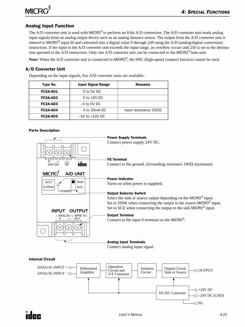
4: SPECIAL FUNCTIONS
USER’S MANUAL 4-21
Analog Input FunctionThe A/D converter unit is used with MICRO3 to perform an 8-bit A/D conversion. The A/D converter unit reads analog input signals from an analog output device such as an analog distance sensor. The output from the A/D converter unit is entered to MICRO3 input I0 and converted into a digital value 0 through 249 using the A/D (analog/digital conversion) instruction. If the input to the A/D converter unit exceeds the input range, an overflow occurs and 250 is set to the destina-tion operand of the A/D instruction. Only one A/D converter unit can be connected to the MICRO3 base unit.
Note: When the A/D converter unit is connected to MICRO3, the HSC (high-speed counter) function cannot be used.
A/D Converter UnitDepending on the input signals, five A/D converter units are available:
Parts Description
Internal Circuit
Type No. Input Signal Range Remarks
FC2A-AD1 0 to 5V DC
FC2A-AD2 0 to 10V DC
FC2A-AD3 –5 to 5V DC
FC2A-AD4 4 to 20mA DC Input resistance 250Ω
FC2A-AD5 –10 to +10V DC
+ –24V DC
A/D UNIT
I N P U T
4-20mA
POWER
SINK
SCE
+ –ANALOG WIRE TO
IN 0
INPUT OUTPUT
Power Supply TerminalsConnect power supply 24V DC.
FG TerminalConnect to the ground. (Grounding resistance 100Ω maximum)
Power IndicatorTurns on when power is supplied.
Output Selector SwitchSelect the sink or source output depending on the MICRO3 input.Set to SINK when connecting the output to the source MICRO3 input.Set to SCE when connecting the output to the sink MICRO3 input.
Output TerminalConnect to the input 0 terminal on the MICRO3.
Analog Input TerminalsConnect analog input signal.
+24V DC
OUTPUT
–24V DC (GND)
FG
DC/DC Converter
Output CircuitSink or Source
IsolationCircuit
OperationCircuit andV/F Converter
DifferentialAmplifier
ANALOG INPUT +
ANALOG INPUT –
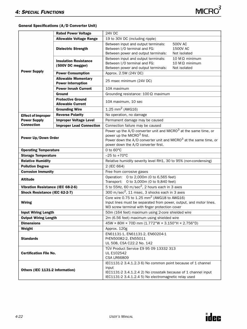
4: SPECIAL FUNCTIONS
4-22 USER’S MANUAL
General Specifications (A/D Converter Unit)
Power Supply
Rated Power Voltage 24V DCAllowable Voltage Range 19 to 30V DC (including ripple)
Dielectric StrengthBetween input and output terminals: 500V ACBetween I/O terminal and FG: 1500V ACBetween power and output terminals: Not isolated
Insulation Resistance(500V DC megger)
Between input and output terminals: 10 M Ω minimumBetween I/O terminal and FG: 10 M Ω minimumBetween power and output terminals: Not isolated
Power Consumption Approx. 2.5W (24V DC)Allowable Momentary Power Interruption
25 msec minimum (24V DC)
Power Inrush Current 10A maximumGround Grounding resistance: 100 Ω maximumProtective Ground Allowable Current
10A maximum, 10 sec
Grounding Wire 1.25 mm2 (AWG16)
Effect of Improper Power Supply Connection
Reverse Polarity No operation, no damageImproper Voltage Level Permanent damage may be causedImproper Lead Connection Connection failure may be caused
Power Up/Down Order
Power up the A/D converter unit and MICRO3 at the same time, or power up the MICRO3 first.Power down the A/D converter unit and MICRO3 at the same time, or power down the A/D converter first.
Operating Temperature 0 to 60°CStorage Temperature –25 to +70°CRelative Humidity Relative humidity severity level RH1, 30 to 95% (non-condensing)Pollution Degree 2 (IEC 664)Corrosion Immunity Free from corrosive gases
AltitudeOperation: 0 to 2,000m (0 to 6,565 feet)Transport: 0 to 3,000m (0 to 9,840 feet)
Vibration Resistance (IEC 68-2-6) 5 to 55Hz, 60 m/sec2, 2 hours each in 3 axesShock Resistance (IEC 62-2-7) 300 m/sec2, 11 msec, 3 shocks each in 3 axes
WiringCore wire 0.75 to 1.25 mm2 (AWG18 to AWG16)Input lines must be separated from power, output, and motor lines.M3 screw terminal with finger protection cover
Input Wiring Length 50m (164 feet) maximum using 2-core shielded wireOutput Wiring Length 2m (6.56 feet) maximum using shielded wireDimensions 45W × 80H × 70D mm (1.772"W × 3.150"H × 2.756"D)Weight Approx. 120g
StandardsEN61131-1, EN61131-2, EN60204-1PrEN50082-2, EN55011UL 508, CSA C22.2 No. 142
Certification File No.TÜV Product Service E9 95 09 13332 313UL E102542CSA LR66809
Others (IEC 1131-2 Information)
IEC1131-2 3.4.1.2.3 6) No common point because of 1 channel inputIEC1131-2 3.4.1.2.4 2) No crosstalk because of 1 channel inputIEC1131-2 3.4.1.2.4 5) No electromagnetic relay used
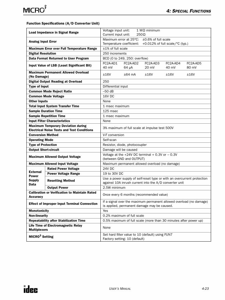
4: SPECIAL FUNCTIONS
USER’S MANUAL 4-23
Function Specifications (A/D Converter Unit)
Load Impedance in Signal RangeVoltage input unit: 1 MΩ minimumCurrent input unit: 250Ω
Analog Input ErrorMaximum error at 25°C: ±0.6% of full scaleTemperature coefficient: +0.012% of full scale/°C (typ.)
Maximum Error over Full Temperature Range ±1% of full scaleDigital Resolution 250 incrementsData Format Returned to User Program BCD (0 to 249, 250: overflow)
Input Value of LSB (Least Significant Bit)FC2A-AD1 FC2A-AD2 FC2A-AD3 FC2A-AD4 FC2A-AD540 mV 64 µA 20 mV 40 mV 80 mV
Maximum Permanent Allowed Overload (No Damage)
±16V ±64 mA ±16V ±16V ±16V
Digital Output Reading at Overload 250Type of Input Differential inputCommon Mode Reject Ratio –50 dBCommon Mode Voltage 16V DCOther Inputs NoneTotal Input System Transfer Time 1 msec maximumSample Duration Time 125 msecSample Repetition Time 1 msec maximumInput Filter Characteristics NoneMaximum Temporary Deviation during Electrical Noise Tests and Test Conditions
3% maximum of full scale at impulse test 500V
Conversion Method V-F conversionOperating Mode Self-scanType of Protection Resistor, diode, photocouplerOutput Short-circuit Damage will be caused
Maximum Allowed Output VoltageVoltage at the +24V DC terminal + 0.3V or – 0.3V (between GND and OUTPUT)
Maximum Allowed Input Voltage Maximum permanent allowed overload (no damage)
External Power Supply Data
Rated Power Voltage 24V DCPower Voltage Range 19 to 30V DC
Resetting MethodUse a power supply of self-reset type or with an overcurrent protection against 10A inrush current into the A/D converter unit
Output Power 2.5W minimumCalibration or Verification to Maintain Rated Accuracy
Once every 6 months (recommended value)
Effect of Improper Input Terminal ConnectionIf a signal over the maximum permanent allowed overload (no damage) is applied, permanent damage may be caused.
Monotonicity YesNon-linearity 0.2% maximum of full scaleRepeatability after Stabilization Time 0.5% maximum of full scale (more than 30 minutes after power up)Life Time of Electromagnetic Relay Multiplexers
None
MICRO3 SettingSet hard filter value to 10 (default) using FUN7Factory setting: 10 (default)
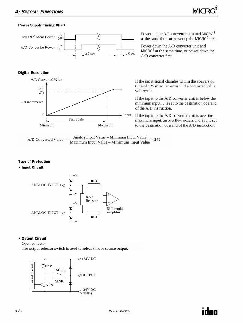
4: SPECIAL FUNCTIONS
4-24 USER’S MANUAL
Power Supply Timing Chart
Digital Resolution
Type of Protection
• Input Circuit
• Output Circuit
A/D Converter PowerONOFF
≥ 0 sec
MICRO3 Main PowerONOFF
≥ 0 sec
Power up the A/D converter unit and MICRO3 at the same time, or power up the MICRO3 first.
Power down the A/D converter unit and MICRO3 at the same time, or power down the A/D converter first.
Input
A/D Converted Value
Minimum Maximum
0
249
250 increments
If the input signal changes within the conversion time of 125 msec, an error in the converted value will result.
If the input to the A/D converter unit is below the minimum input, 0 is set to the destination operand of the A/D instruction.
If the input to the A/D converter unit is over the maximum input, an overflow occurs and 250 is set to the destination operand of the A/D instruction.
A/D Converted ValueAnalog Input Value Minimum Input Value–
Maximum Input Value Minimum Input Value–--------------------------------------------------------------------------------------------------------------------- 249 ×
=
Full Scale
250
ANALOG INPUT +
ANALOG INPUT –
+V
–VInputResistor
10Ω
10Ω
+
–+V
–V
DifferentialAmplifier
Open collectorThe output selector switch is used to select sink or source output.
–24V DC
+24V DC
OUTPUT
(GND)
SINK
SCEPNP
NPNInte
rnal
Cir
cuit
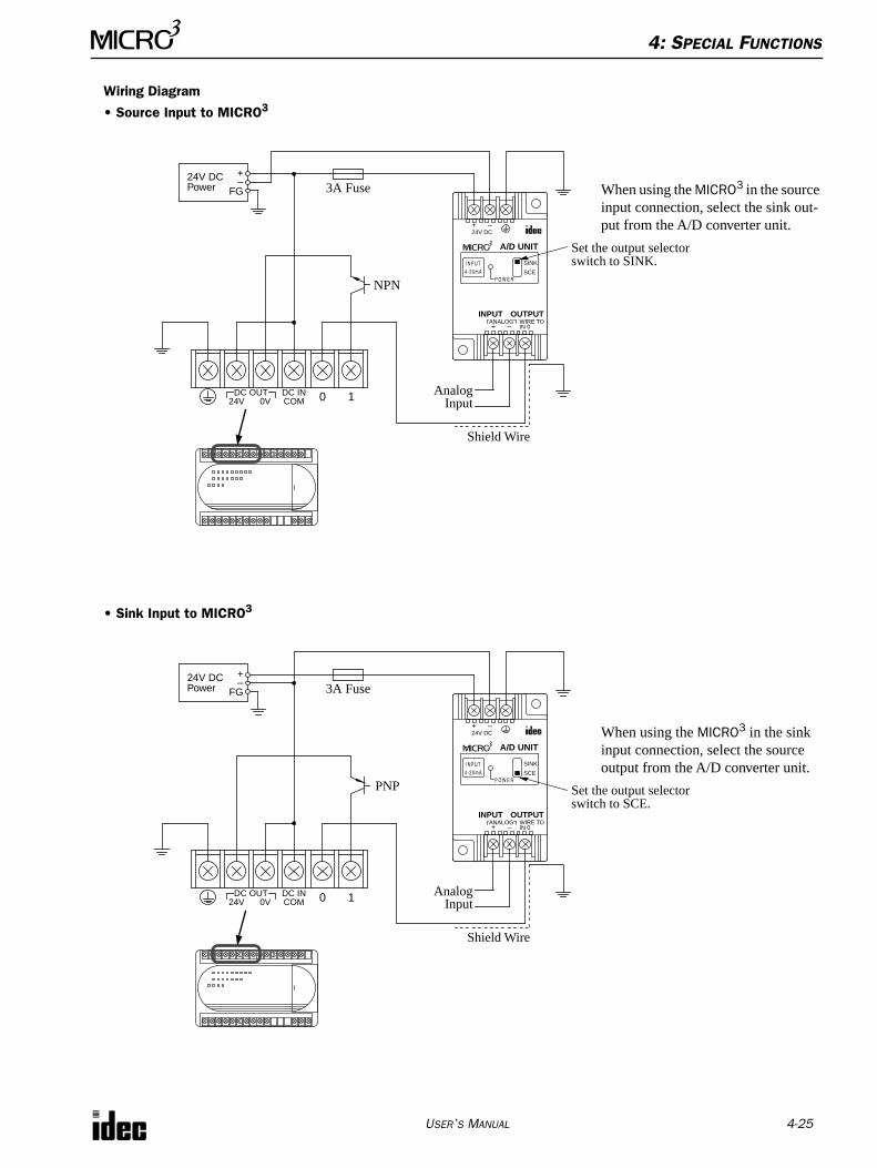
4: S
PECIAL
F
UNCTIONS
U
SER
’
S
M
ANUAL
4-25
Wiring Diagram
• Source Input to MICRO
3
• Sink Input to MICRO
3
+ –
24V DC
A/D UNIT
I N P U T4 - 2 0 m A
P O W E R
SINK
SCE
+ –
ANALOG WIRE TOIN 0
INPUT OUTPUT
DC OUT24V 0V
DC INCOM
0
24V DCPower
+–
FG
Set the output selector
AnalogInput
Shield Wire
switch to SINK.
When using the
MICRO
3
in the source input connection, select the sink out-put from the A/D converter unit.
1
NPN
3A Fuse
+ –24V DC
A/D UNIT
I N P U T4 - 2 0 m A
P O W E R
SINK
SCE
+ –ANALOG WIRE TO
IN 0
INPUT OUTPUT
DC OUT24V 0V
DC INCOM 0
24V DCPower
+–
FG
AnalogInput
Shield Wire
Set the output selector switch to SCE.
When using the MICRO3 in the sink input connection, select the source output from the A/D converter unit.
3A Fuse
1
PNP
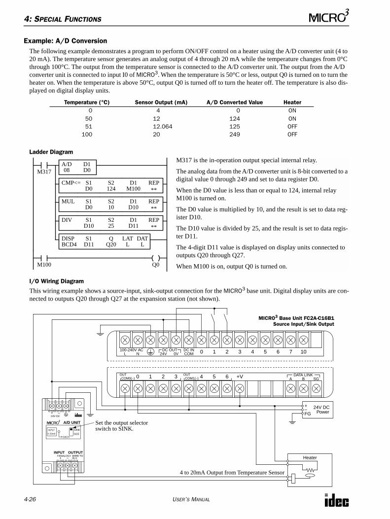
4: S
PECIAL
F
UNCTIONS
4-26 U
SER
’
S
M
ANUAL
Example: A/D Conversion
The following example demonstrates a program to perform ON/OFF control on a heater using the A/D converter unit (4 to 20 mA). The temperature sensor generates an analog output of 4 through 20 mA while the temperature changes from 0°C through 100°C. The output from the temperature sensor is connected to the A/D converter unit. The output from the A/D converter unit is connected to input I0 of
MICRO
3
. When the temperature is 50°C or less, output Q0 is turned on to turn the heater on. When the temperature is above 50°C, output Q0 is turned off to turn the heater off. The temperature is also dis-played on digital display units.
Ladder Diagram
I/O Wiring Diagram
This wiring example shows a source-input, sink-output connection for the
MICRO
3
base unit. Digital display units are con-nected to outputs Q20 through Q27 at the expansion station (not shown).
Temperature (°C) Sensor Output (mA) A/D Converted Value Heater
0 4 0 ON50 12 124 ON51 12.064 125 OFF
100 20 249 OFF
A/DM317
D1
Q0
M317 is the in-operation output special internal relay.
The analog data from the A/D converter unit is 8-bit converted to a digital value 0 through 249 and set to data register D0.
When the D0 value is less than or equal to 124, internal relay M100 is turned on.
The D0 value is multiplied by 10, and the result is set to data reg-ister D10.
The D10 value is divided by 25, and the result is set to data regis-ter D11.
The 4-digit D11 value is displayed on display units connected to outputs Q20 through Q27.
When M100 is on, output Q0 is turned on.
M100
CMP<= S1D0
S2124
D1M100
REP**
MUL S1D0
S210
D1D10
REP**
DIV S1D10
S225
D1D11
REP**
08 D0
DISP DATBCD4
LATLL
S1D11
QQ20
OUTCOM0(–) 0 1 2 3 OUT
COM1(–) 4 5 6 DATA LINKA SGB+V
100-240V ACL N
DC OUT24V 0V
DC INCOM 0 1 2 3 4 5 6 7 10
MICRO3 Base Unit FC2A-C16B1
+ –24V DC
A/D UNIT
I N P U T4 - 2 0 m A
P O W E R
SINK
SCE
+ –ANALOG WIRE TO
IN 0
INPUT OUTPUT
24V DCPower
+–FG
Heater
4 to 20mA Output from Temperature Sensor
Set the output selector switch to SINK.
Source Input/Sink Output
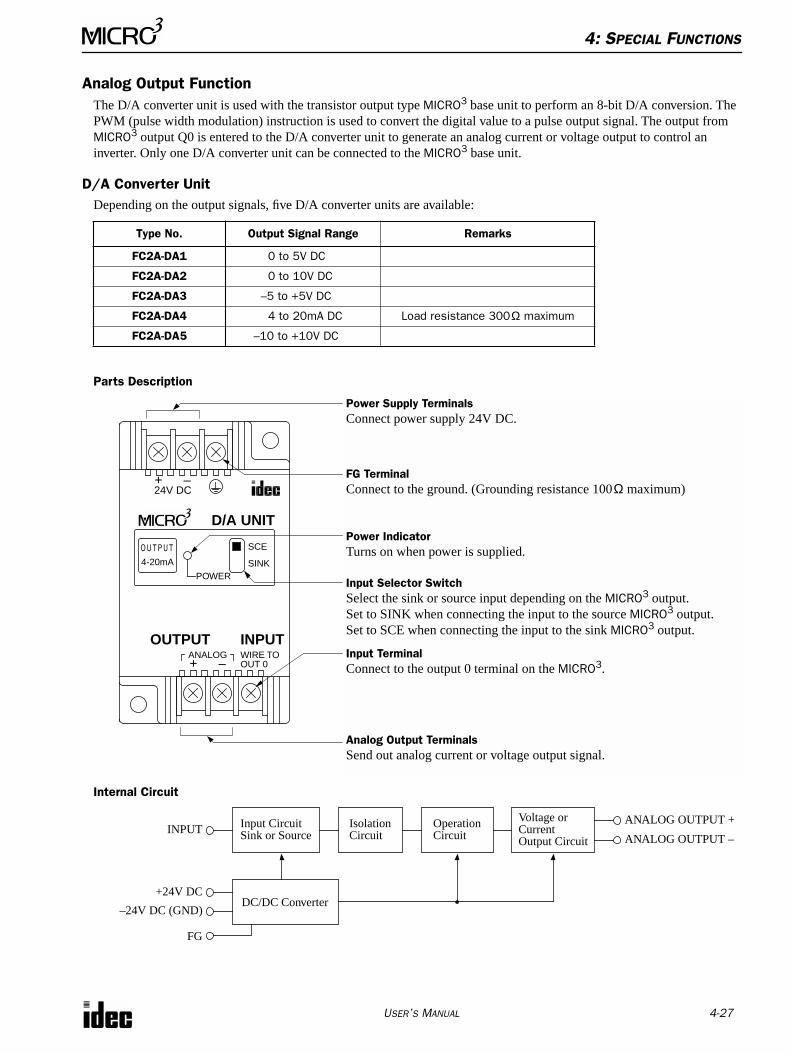
4: S
PECIAL
F
UNCTIONS
U
SER
’
S
M
ANUAL
4-27
Analog Output Function
The D/A converter unit is used with the transistor output type
MICRO
3
base unit to perform an 8-bit D/A conversion. The PWM (pulse width modulation) instruction is used to convert the digital value to a pulse output signal. The output from
MICRO
3
output Q0 is entered to the D/A converter unit to generate an analog current or voltage output to control an inverter. Only one D/A converter unit can be connected to the
MICRO
3
base unit.
D/A Converter Unit
Depending on the output signals, five D/A converter units are available:
Parts Description
Internal Circuit
Type No. Output Signal Range Remarks
FC2A-DA1
0 to 5V DC
FC2A-DA2
0 to 10V DC
FC2A-DA3
–5 to +5V DC
FC2A-DA4
4 to 20mA DC Load resistance 300
Ω
maximum
FC2A-DA5
–10 to +10V DC
Power Supply TerminalsConnect power supply 24V DC.
FG TerminalConnect to the ground. (Grounding resistance 100Ω maximum)
Power IndicatorTurns on when power is supplied.
Input Selector SwitchSelect the sink or source input depending on the MICRO3 output.Set to SINK when connecting the input to the source MICRO3 output.Set to SCE when connecting the input to the sink MICRO3 output.
Input TerminalConnect to the output 0 terminal on the MICRO3.
Analog Output TerminalsSend out analog current or voltage output signal.
+ –24V DC
D/A UNIT
O U T P U T
4-20mA
POWER
SCE
SINK
+ –ANALOG WIRE TO
OUT 0
OUTPUT INPUT
+24V DC
INPUT
–24V DC (GND)
FG
DC/DC Converter
Input CircuitSink or Source
IsolationCircuit
OperationCircuit
Voltage orCurrent
ANALOG OUTPUT +
ANALOG OUTPUT –Output Circuit
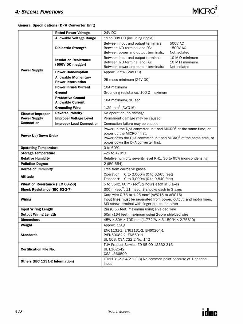
4: SPECIAL FUNCTIONS
4-28 USER’S MANUAL
General Specifications (D/A Converter Unit)
Power Supply
Rated Power Voltage 24V DCAllowable Voltage Range 19 to 30V DC (including ripple)
Dielectric StrengthBetween input and output terminals: 500V ACBetween I/O terminal and FG: 1500V ACBetween power and output terminals: Not isolated
Insulation Resistance(500V DC megger)
Between input and output terminals: 10 M Ω minimumBetween I/O terminal and FG: 10 M Ω minimumBetween power and output terminals: Not isolated
Power Consumption Approx. 2.5W (24V DC)Allowable Momentary Power Interruption
25 msec minimum (24V DC)
Power Inrush Current 10A maximumGround Grounding resistance: 100 Ω maximumProtective Ground Allowable Current
10A maximum, 10 sec
Grounding Wire 1.25 mm2 (AWG16)
Effect of Improper Power Supply Connection
Reverse Polarity No operation, no damageImproper Voltage Level Permanent damage may be causedImproper Lead Connection Connection failure may be caused
Power Up/Down Order
Power up the D/A converter unit and MICRO3 at the same time, or power up the MICRO3 first.Power down the D/A converter unit and MICRO3 at the same time, or power down the D/A converter first.
Operating Temperature 0 to 60°CStorage Temperature –25 to +70°CRelative Humidity Relative humidity severity level RH1, 30 to 95% (non-condensing)Pollution Degree 2 (IEC 664)Corrosion Immunity Free from corrosive gases
AltitudeOperation: 0 to 2,000m (0 to 6,565 feet)Transport: 0 to 3,000m (0 to 9,840 feet)
Vibration Resistance (IEC 68-2-6) 5 to 55Hz, 60 m/sec2, 2 hours each in 3 axesShock Resistance (IEC 62-2-7) 300 m/sec2, 11 msec, 3 shocks each in 3 axes
WiringCore wire 0.75 to 1.25 mm2 (AWG18 to AWG16)Input lines must be separated from power, output, and motor lines.M3 screw terminal with finger protection cover
Input Wiring Length 2m (6.56 feet) maximum using shielded wireOutput Wiring Length 50m (164 feet) maximum using 2-core shielded wireDimensions 45W × 80H × 70D mm (1.772"W × 3.150"H × 2.756"D)Weight Approx. 120g
StandardsEN61131-1, EN61131-2, EN60204-1PrEN50082-2, EN55011UL 508, CSA C22.2 No. 142
Certification File No.TÜV Product Service E9 95 09 13332 313UL E102542CSA LR66809
Others (IEC 1131-2 Information)IEC1131-2 3.4.2.2.3 8) No common point because of 1 channel input
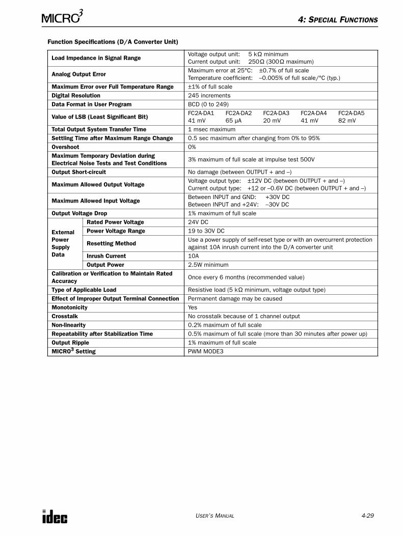
4: SPECIAL FUNCTIONS
USER’S MANUAL 4-29
Function Specifications (D/A Converter Unit)
Load Impedance in Signal RangeVoltage output unit: 5 kΩ minimumCurrent output unit: 250Ω (300Ω maximum)
Analog Output ErrorMaximum error at 25°C: ±0.7% of full scaleTemperature coefficient: –0.005% of full scale/°C (typ.)
Maximum Error over Full Temperature Range ±1% of full scaleDigital Resolution 245 incrementsData Format in User Program BCD (0 to 249)
Value of LSB (Least Significant Bit)FC2A-DA1 FC2A-DA2 FC2A-DA3 FC2A-DA4 FC2A-DA541 mV 65 µA 20 mV 41 mV 82 mV
Total Output System Transfer Time 1 msec maximumSettling Time after Maximum Range Change 0.5 sec maximum after changing from 0% to 95%Overshoot 0%Maximum Temporary Deviation during Electrical Noise Tests and Test Conditions
3% maximum of full scale at impulse test 500V
Output Short-circuit No damage (between OUTPUT + and –)
Maximum Allowed Output VoltageVoltage output type: ±12V DC (between OUTPUT + and –)Current output type: +12 or –0.6V DC (between OUTPUT + and –)
Maximum Allowed Input VoltageBetween INPUT and GND: +30V DCBetween INPUT and +24V: –30V DC
Output Voltage Drop 1% maximum of full scale
External Power Supply Data
Rated Power Voltage 24V DCPower Voltage Range 19 to 30V DC
Resetting MethodUse a power supply of self-reset type or with an overcurrent protection against 10A inrush current into the D/A converter unit
Inrush Current 10AOutput Power 2.5W minimum
Calibration or Verification to Maintain Rated Accuracy
Once every 6 months (recommended value)
Type of Applicable Load Resistive load (5 kΩ minimum, voltage output type)Effect of Improper Output Terminal Connection Permanent damage may be causedMonotonicity YesCrosstalk No crosstalk because of 1 channel outputNon-linearity 0.2% maximum of full scaleRepeatability after Stabilization Time 0.5% maximum of full scale (more than 30 minutes after power up)Output Ripple 1% maximum of full scaleMICRO3 Setting PWM MODE3
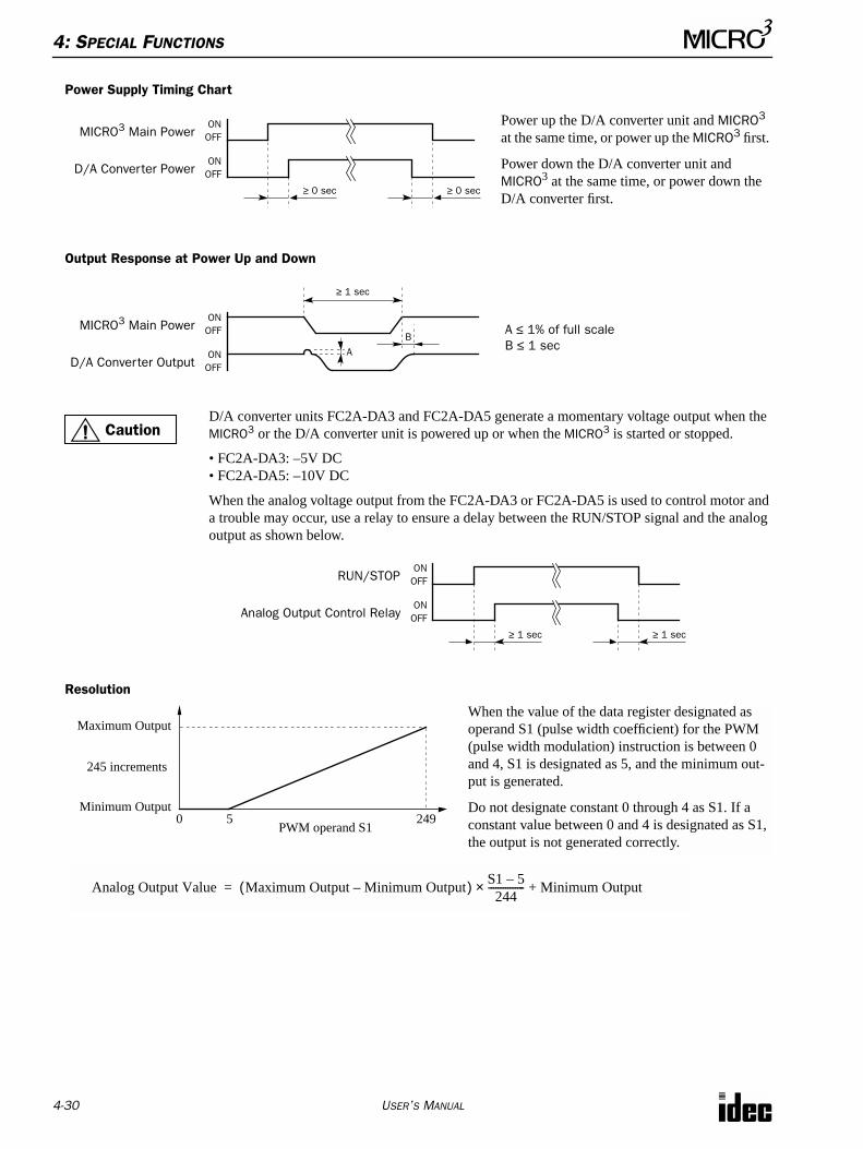
4: SPECIAL FUNCTIONS
4-30 USER’S MANUAL
Power Supply Timing Chart
Output Response at Power Up and Down
Resolution
D/A Converter PowerONOFF
≥ 0 sec
MICRO3 Main PowerONOFF
≥ 0 sec
Power up the D/A converter unit and MICRO3 at the same time, or power up the MICRO3 first.
Power down the D/A converter unit and MICRO3 at the same time, or power down the D/A converter first.
D/A Converter OutputONOFF
A
MICRO3 Main PowerONOFF
≥ 1 sec
BA ≤ 1% of full scaleB ≤ 1 sec
CautionD/A converter units FC2A-DA3 and FC2A-DA5 generate a momentary voltage output when the MICRO3 or the D/A converter unit is powered up or when the MICRO3 is started or stopped.
• FC2A-DA3: –5V DC• FC2A-DA5: –10V DC
When the analog voltage output from the FC2A-DA3 or FC2A-DA5 is used to control motor and a trouble may occur, use a relay to ensure a delay between the RUN/STOP signal and the analog output as shown below.
Analog Output Control RelayONOFF
≥ 1 sec
RUN/STOPONOFF
≥ 1 sec
PWM operand S10 249
Minimum Output
Maximum Output
245 increments
When the value of the data register designated as operand S1 (pulse width coefficient) for the PWM (pulse width modulation) instruction is between 0 and 4, S1 is designated as 5, and the minimum out-put is generated.
Do not designate constant 0 through 4 as S1. If a constant value between 0 and 4 is designated as S1, the output is not generated correctly.
5
Analog Output Value Maximum Output Minimum Output– ( ) S1 5–
244--------------- × Minimum Output+=
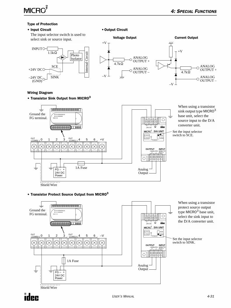
4: S
PECIAL
F
UNCTIONS
U
SER
’
S
M
ANUAL
4-31
Type of Protection
• Input Circuit •Output Circuit
Wiring Diagram
• Transistor Sink Output from MICRO
3
• Transistor Protect Source Output from MICRO
3
ANALOG
+V
–V–24V DC
INPUT
+24V DC
(GND)SINK
SCE
Inte
rnal
Cir
cuit
The input selector switch is used to select sink or source input.
1.5kΩPhotoIsolator
4.7kΩOUTPUT +
ANALOGOUTPUT –
ANALOG
+V
–V
4.7kΩOUTPUT +
ANALOGOUTPUT –
Voltage Output Current Output
24V DCPower
+–FG
Set the input selector
Analog
Shield Wire
+ –24V DC
D/A UNIT
O U TPU T4 - 2 0 m A
P O W E R
SCE
SINK
+ –ANALOG WIRE TO
OUT 0
OUTPUT INPUT
Ground the FG terminal.
switch to SCE.
Output
OUTCOM0(–) 0 1 2 3 OUT
COM1(–) 4 5 6 +V
When using a transistor sink output type MICRO3 base unit, select the source input to the D/A converter unit.
1A Fuse
24V DCPower
+–FG
Set the input selector
Analog
Shield Wire
+ –
24V DC
D/A UNIT
O U TPU T4 - 2 0 m A
P O W E R
SCE
SINK
+ –
ANALOG WIRE TOOUT 0
OUTPUT INPUT
Ground the FG terminal.
switch to SINK.
Output
OUTCOM0(+)
0 1 2 3
OUTCOM1(+)
4 5 6 –V
When using a transistor protect source output type
MICRO
3
base unit, select the sink input to the D/A converter unit.
1A Fuse
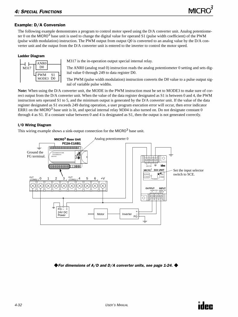
4: S
PECIAL
F
UNCTIONS
4-32 U
SER
’
S
M
ANUAL
Example: D/A Conversion
The following example demonstrates a program to control motor speed using the D/A converter unit. Analog potentiome-ter 0 on the
MICRO
3
base unit is used to change the digital value for operand S1 (pulse width coefficient) of the PWM (pulse width modulation) instruction. The PWM output from output Q0 is converted to an analog value by the D/A con-verter unit and the output from the D/A converter unit is entered to the inverter to control the motor speed.
Ladder Diagram
Note:
When using the D/A converter unit, the MODE in the PWM instruction must be set to MODE3 to make sure of cor-rect output from the D/A converter unit. When the value of the data register designated as S1 is between 0 and 4, the PWM instruction sets operand S1 to 5, and the minimum output is generated by the D/A converter unit. If the value of the data register designated as S1 exceeds 249 during operation, a user program execution error will occur, then error indicator ERR1 on the
MICRO
3
base unit is lit, and special internal relay M304 is also turned on. Do not designate constant 0 through 4 as S1. If a constant value between 0 and 4 is designated as S1, then the output is not generated correctly.
I/O Wiring Diagram
This wiring example shows a sink-output connection for the
MICRO
3
base unit.
M317
M317 is the in-operation output special internal relay.
The ANR0 (analog read 0) instruction reads the analog potentiometer 0 setting and sets dig-ital value 0 through 249 to data register D0.
The PWM (pulse width modulation) instruction converts the D0 value to a pulse output sig-nal of variable pulse widths.
ANR0D0
S1D0
PWMMODE3
MICRO
3
Base Unit
24V DCPower
+–FG
Set the input selector
+ –
24V DC
D/A UNIT
O U TPU T4 - 2 0 m A
P O W E R
SCE
SINK
+ –
ANALOG WIRE TOOUT 0
OUTPUT INPUT
Ground the FG terminal.
switch to SCE.
Inverter+–
FGMotor
FC2A-C16B1
OUTCOM0(–)
0 1 2 3
OUTCOM1(–)
4 5 6 +V
Analog potentiometer 0
For dimensions of A/D and D/A converter units, see page 1-24.
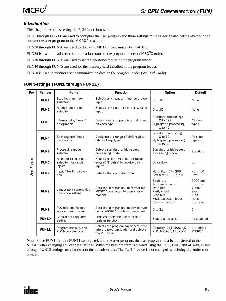
U
SER
’
S
M
ANUAL
5-1
5: CPU C
ONFIGURATION
(FUN)
Introduction
This chapter describes setting the FUN (function) table.
FUN1 through FUN11 are used to configure the user program and these settings must be designated before attempting to transfer the user program to the
MICRO
3
base unit.
FUN20 through FUN28 are used to check the
MICRO
3
base unit status and data.
FUN29 is used to read user communication status to the program loader (
MICRO
3
C
only).
FUN30 through FUN36 are used to set the operation modes of the program loader.
FUN40 through FUN43 are used for the memory card installed in the program loader.
FUN50 is used to monitor user communication data on the program loader (
MICRO
3
C
only).
FUN Settings (FUN1 through FUN11)
Note:
Since FUN1 through FUN11 settings relate to the user program, the user program must be transferred to the
MICRO
3
after changing any of these settings. When the user program is cleared using the DEL, END, and keys, FUN1 through FUN10 settings are also reset to the default values. The FUN11 value is not changed by deleting the entire user program.
For Number Name Function Option Default
Use
r P
rogr
am
FUN1
Stop input number selection
Selects any input terminal as a stop input. 0 to 15 None
FUN2
Reset input number selection
Selects any input terminal as a reset input. 0 to 15 None
FUN3
Internal relay “keep” designation
Designates a range of internal relays as keep type.
Standard processing:0 to 287
High-speed processing:0 to 47
All clear types
FUN4
Shift register “keep” designation
Designates a range of shift register bits as keep type.
Standard processing:0 to 63
High-speed processing:0 to 31
All clear types
FUN5
Processing mode selection
Selects standard or high-speed processing mode.
Standard or high-speed processing mode Standard
FUN6
Rising or falling edge selection for catch inputs
Selects rising (ON pulse) or falling edge (OFF pulse) to receive catch inputs.
Up or down Up
FUN7
Input filter time selec-tion Selects the input filter time. Hard filter: 0 to 255
Soft filter: 0, 3, 7, 10Hard: 10Soft: 3
FUN8
Loader port communica-tion mode setting
Sets the communication format for MICRO
3
connected to computer or modem.
Baud rateTerminator codeData bitsParity checkStop bitsMode selection inputReceive timeout
9600 bps0D (CR)7 bitsEven1 bitNone500 msec
FUN9
PLC address for net-work communication
Sets the communication device num-ber of MICRO
3
in 1:N computer link. 0 to 31 0
FUN10
Control data register setting
Enables or disables control data register function. Enable or disable All disabled
FUN11
Program capacity and PLC type selection
Selects the program capacity to write into the program loader and selects the PLC type.
Capacity: 244, 500, 1KPLC: MICRO
3 , MICRO
3 C
1K (initial)MICRO
3
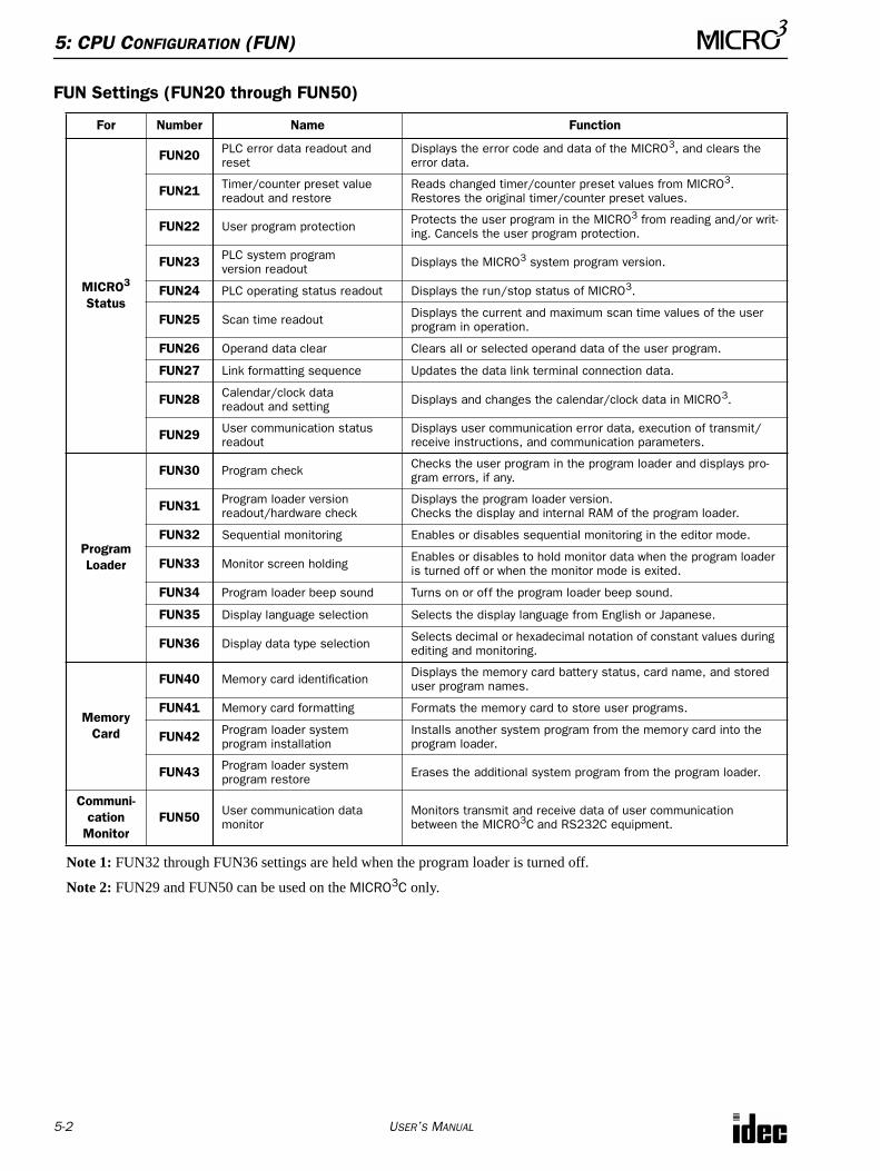
5: CPU C
ONFIGURATION
(FUN)
5-2 U
SER
’
S
MANUAL
FUN Settings (FUN20 through FUN50)
Note 1: FUN32 through FUN36 settings are held when the program loader is turned off.
Note 2: FUN29 and FUN50 can be used on the MICRO3C only.
For Number Name Function
MICRO3
Status
FUN20 PLC error data readout and reset
Displays the error code and data of the MICRO3, and clears the error data.
FUN21 Timer/counter preset value readout and restore
Reads changed timer/counter preset values from MICRO3.Restores the original timer/counter preset values.
FUN22 User program protection Protects the user program in the MICRO3 from reading and/or writ-ing. Cancels the user program protection.
FUN23 PLC system programversion readout Displays the MICRO3 system program version.
FUN24 PLC operating status readout Displays the run/stop status of MICRO3.
FUN25 Scan time readout Displays the current and maximum scan time values of the user program in operation.
FUN26 Operand data clear Clears all or selected operand data of the user program.
FUN27 Link formatting sequence Updates the data link terminal connection data.
FUN28 Calendar/clock datareadout and setting Displays and changes the calendar/clock data in MICRO3.
FUN29 User communication status readout
Displays user communication error data, execution of transmit/receive instructions, and communication parameters.
ProgramLoader
FUN30 Program check Checks the user program in the program loader and displays pro-gram errors, if any.
FUN31 Program loader version readout/hardware check
Displays the program loader version. Checks the display and internal RAM of the program loader.
FUN32 Sequential monitoring Enables or disables sequential monitoring in the editor mode.
FUN33 Monitor screen holding Enables or disables to hold monitor data when the program loader is turned off or when the monitor mode is exited.
FUN34 Program loader beep sound Turns on or off the program loader beep sound.
FUN35 Display language selection Selects the display language from English or Japanese.
FUN36 Display data type selection Selects decimal or hexadecimal notation of constant values during editing and monitoring.
MemoryCard
FUN40 Memory card identification Displays the memory card battery status, card name, and stored user program names.
FUN41 Memory card formatting Formats the memory card to store user programs.
FUN42 Program loader system program installation
Installs another system program from the memory card into the program loader.
FUN43 Program loader system program restore Erases the additional system program from the program loader.
Communi-cation
MonitorFUN50 User communication data
monitorMonitors transmit and receive data of user communication between the MICRO3C and RS232C equipment.
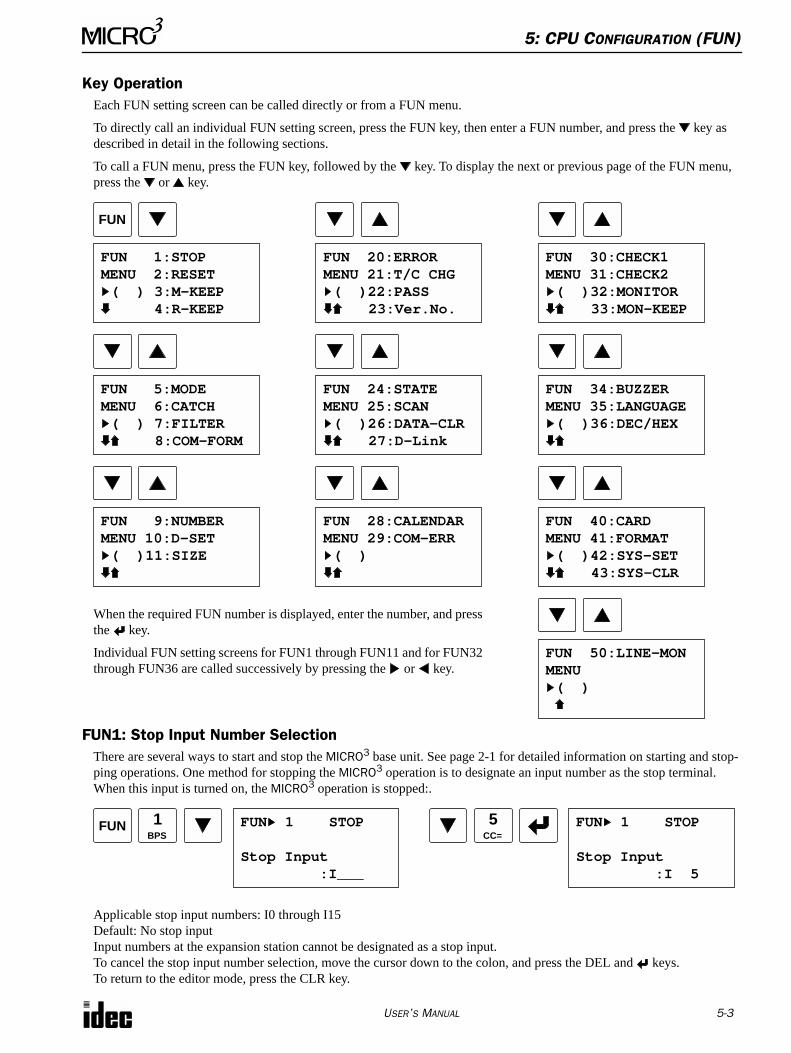
5: CPU CONFIGURATION (FUN)
USER’S MANUAL 5-3
Key OperationEach FUN setting screen can be called directly or from a FUN menu.
To directly call an individual FUN setting screen, press the FUN key, then enter a FUN number, and press the key as described in detail in the following sections.
To call a FUN menu, press the FUN key, followed by the key. To display the next or previous page of the FUN menu, press the or key.
FUN1: Stop Input Number SelectionThere are several ways to start and stop the MICRO3 base unit. See page 2-1 for detailed information on starting and stop-ping operations. One method for stopping the MICRO3 operation is to designate an input number as the stop terminal. When this input is turned on, the MICRO3 operation is stopped:.
Applicable stop input numbers: I0 through I15Default: No stop inputInput numbers at the expansion station cannot be designated as a stop input.To cancel the stop input number selection, move the cursor down to the colon, and press the DEL and keys.To return to the editor mode, press the CLR key.
FUN 1:STOP MENU 2:RESET ( ) 3:M-KEEP 4:R-KEEP
FUN
FUN 5:MODE MENU 6:CATCH ( ) 7:FILTER 8:COM-FORM
FUN 9:NUMBERMENU 10:D-SET( )11:SIZE
FUN 20:ERROR MENU 21:T/C CHG ( )22:PASS 23:Ver.No.
FUN 24:STATE MENU 25:SCAN ( )26:DATA-CLR 27:D-Link
FUN 28:CALENDARMENU 29:COM-ERR ( )
FUN 30:CHECK1 MENU 31:CHECK2 ( )32:MONITOR 33:MON-KEEP
FUN 34:BUZZER MENU 35:LANGUAGE( )36:DEC/HEX
FUN 40:CARDMENU 41:FORMAT( )42:SYS-SET 43:SYS-CLR
When the required FUN number is displayed, enter the number, and press the key.
Individual FUN setting screens for FUN1 through FUN11 and for FUN32 through FUN36 are called successively by pressing the or key.
FUN 50:LINE-MONMENU ( )
FUN 1BPS
FUN 1 STOP
Stop Input :I___
5CC=
FUN 1 STOP
Stop Input :I 5
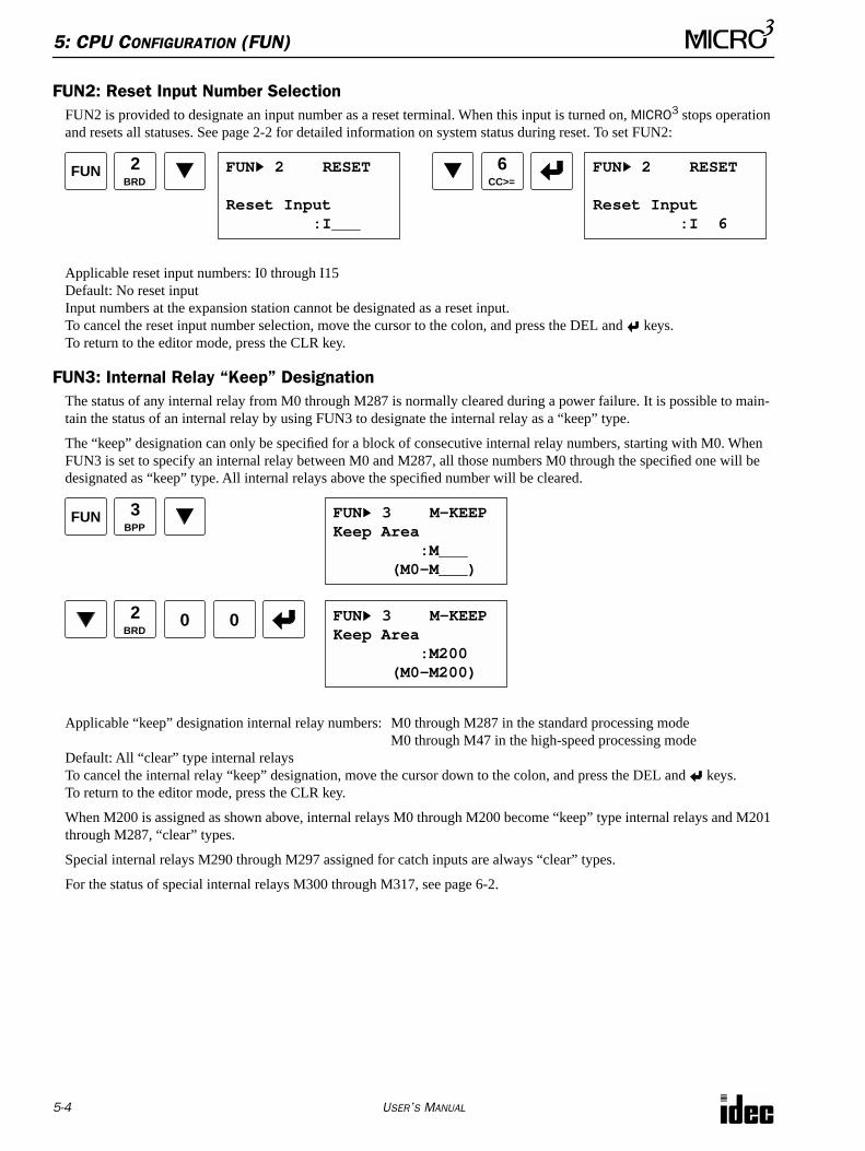
5: CPU CONFIGURATION (FUN)
5-4 USER’S MANUAL
FUN2: Reset Input Number SelectionFUN2 is provided to designate an input number as a reset terminal. When this input is turned on, MICRO3 stops operation and resets all statuses. See page 2-2 for detailed information on system status during reset. To set FUN2:
Applicable reset input numbers: I0 through I15Default: No reset inputInput numbers at the expansion station cannot be designated as a reset input.To cancel the reset input number selection, move the cursor to the colon, and press the DEL and keys.To return to the editor mode, press the CLR key.
FUN3: Internal Relay “Keep” DesignationThe status of any internal relay from M0 through M287 is normally cleared during a power failure. It is possible to main-tain the status of an internal relay by using FUN3 to designate the internal relay as a “keep” type.
The “keep” designation can only be specified for a block of consecutive internal relay numbers, starting with M0. When FUN3 is set to specify an internal relay between M0 and M287, all those numbers M0 through the specified one will be designated as “keep” type. All internal relays above the specified number will be cleared.
Applicable “keep” designation internal relay numbers: M0 through M287 in the standard processing modeM0 through M47 in the high-speed processing mode
Default: All “clear” type internal relaysTo cancel the internal relay “keep” designation, move the cursor down to the colon, and press the DEL and keys.To return to the editor mode, press the CLR key.
When M200 is assigned as shown above, internal relays M0 through M200 become “keep” type internal relays and M201 through M287, “clear” types.
Special internal relays M290 through M297 assigned for catch inputs are always “clear” types.
For the status of special internal relays M300 through M317, see page 6-2.
FUN FUN 2 RESET
Reset Input :I___
FUN 2 RESET
Reset Input :I 6
2BRD
6CC>=
FUN FUN 3 M-KEEPKeep Area :M___ (M0-M___)
3BPP
2BRD
0 0 FUN 3 M-KEEPKeep Area :M200 (M0-M200)
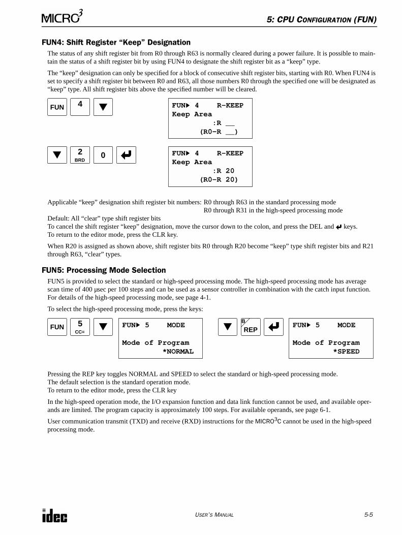
5: CPU CONFIGURATION (FUN)
USER’S MANUAL 5-5
FUN4: Shift Register “Keep” DesignationThe status of any shift register bit from R0 through R63 is normally cleared during a power failure. It is possible to main-tain the status of a shift register bit by using FUN4 to designate the shift register bit as a “keep” type.
The “keep” designation can only be specified for a block of consecutive shift register bits, starting with R0. When FUN4 is set to specify a shift register bit between R0 and R63, all those numbers R0 through the specified one will be designated as “keep” type. All shift register bits above the specified number will be cleared.
Applicable “keep” designation shift register bit numbers: R0 through R63 in the standard processing modeR0 through R31 in the high-speed processing mode
Default: All “clear” type shift register bitsTo cancel the shift register “keep” designation, move the cursor down to the colon, and press the DEL and keys.To return to the editor mode, press the CLR key.
When R20 is assigned as shown above, shift register bits R0 through R20 become “keep” type shift register bits and R21 through R63, “clear” types.
FUN5: Processing Mode SelectionFUN5 is provided to select the standard or high-speed processing mode. The high-speed processing mode has average scan time of 400 µsec per 100 steps and can be used as a sensor controller in combination with the catch input function. For details of the high-speed processing mode, see page 4-1.
To select the high-speed processing mode, press the keys:
Pressing the REP key toggles NORMAL and SPEED to select the standard or high-speed processing mode.The default selection is the standard operation mode.To return to the editor mode, press the CLR key
In the high-speed operation mode, the I/O expansion function and data link function cannot be used, and available oper-ands are limited. The program capacity is approximately 100 steps. For available operands, see page 6-1.
User communication transmit (TXD) and receive (RXD) instructions for the MICRO3C cannot be used in the high-speed processing mode.
FUN FUN 4 R-KEEPKeep Area :R __ (R0-R __)
2BRD
0 FUN 4 R-KEEPKeep Area :R 20 (R0-R 20)
4
FUN FUN 5 MODE
Mode of Program *NORMAL
5CC= REP
BFUN 5 MODE
Mode of Program *SPEED
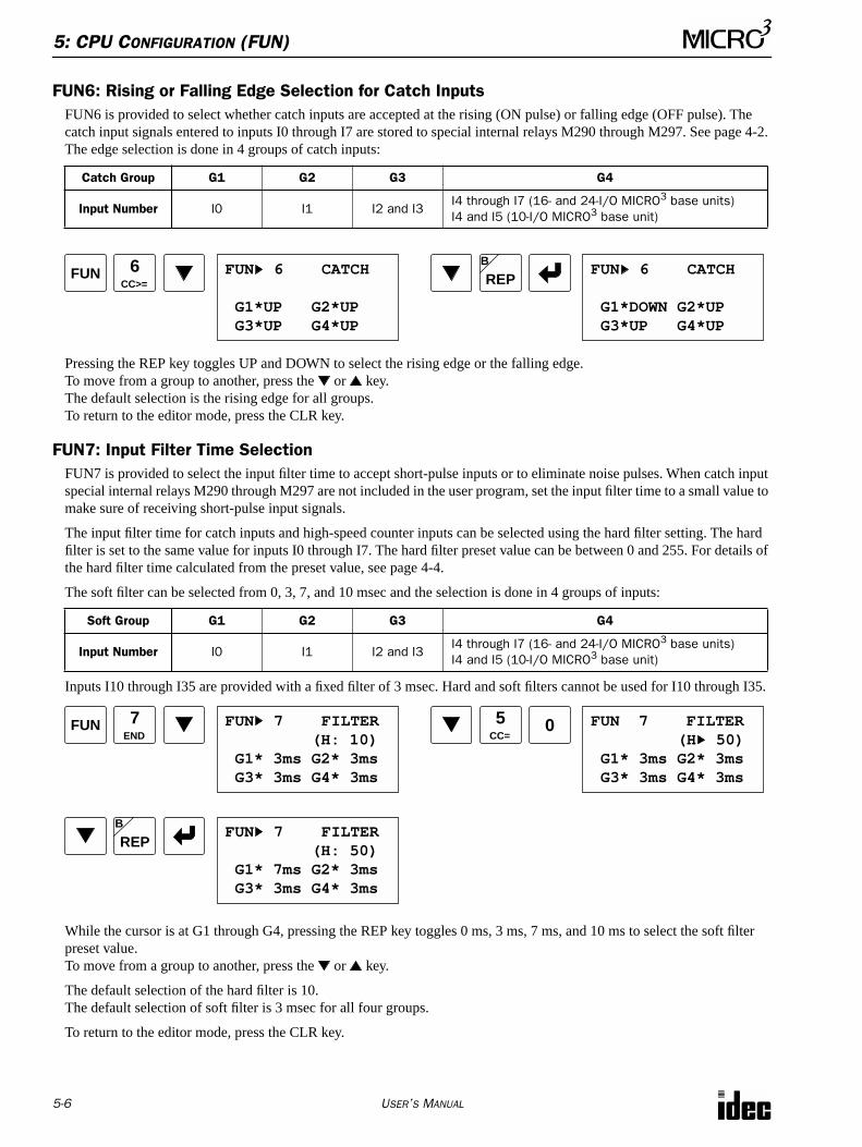
5: CPU CONFIGURATION (FUN)
5-6 USER’S MANUAL
FUN6: Rising or Falling Edge Selection for Catch InputsFUN6 is provided to select whether catch inputs are accepted at the rising (ON pulse) or falling edge (OFF pulse). The catch input signals entered to inputs I0 through I7 are stored to special internal relays M290 through M297. See page 4-2. The edge selection is done in 4 groups of catch inputs:
Pressing the REP key toggles UP and DOWN to select the rising edge or the falling edge.To move from a group to another, press the or key.The default selection is the rising edge for all groups.To return to the editor mode, press the CLR key.
FUN7: Input Filter Time SelectionFUN7 is provided to select the input filter time to accept short-pulse inputs or to eliminate noise pulses. When catch input special internal relays M290 through M297 are not included in the user program, set the input filter time to a small value to make sure of receiving short-pulse input signals.
The input filter time for catch inputs and high-speed counter inputs can be selected using the hard filter setting. The hard filter is set to the same value for inputs I0 through I7. The hard filter preset value can be between 0 and 255. For details of the hard filter time calculated from the preset value, see page 4-4.
The soft filter can be selected from 0, 3, 7, and 10 msec and the selection is done in 4 groups of inputs:
Inputs I10 through I35 are provided with a fixed filter of 3 msec. Hard and soft filters cannot be used for I10 through I35.
While the cursor is at G1 through G4, pressing the REP key toggles 0 ms, 3 ms, 7 ms, and 10 ms to select the soft filter preset value.To move from a group to another, press the or key.
The default selection of the hard filter is 10.The default selection of soft filter is 3 msec for all four groups.
To return to the editor mode, press the CLR key.
Catch Group G1 G2 G3 G4
Input Number I0 I1 I2 and I3I4 through I7 (16- and 24-I/O MICRO3 base units)I4 and I5 (10-I/O MICRO3 base unit)
Soft Group G1 G2 G3 G4
Input Number I0 I1 I2 and I3I4 through I7 (16- and 24-I/O MICRO3 base units)I4 and I5 (10-I/O MICRO3 base unit)
FUN FUN 6 CATCH
G1*UP G2*UP G3*UP G4*UP
REPB6
CC>=FUN 6 CATCH
G1*DOWN G2*UP G3*UP G4*UP
FUN FUN 7 FILTER (H: 10) G1* 3ms G2* 3ms G3* 3ms G4* 3ms
7END
FUN 7 FILTER (H 50) G1* 3ms G2* 3ms G3* 3ms G4* 3ms
REPB
5CC=
0
FUN 7 FILTER (H: 50) G1* 7ms G2* 3ms G3* 3ms G4* 3ms
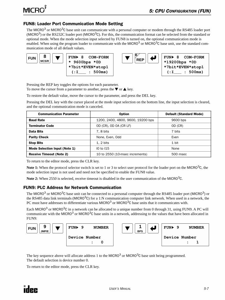
5: CPU CONFIGURATION (FUN)
USER’S MANUAL 5-7
FUN8: Loader Port Communication Mode SettingThe MICRO3 or MICRO3C base unit can communicate with a personal computer or modem through the RS485 loader port (MICRO3) or the RS232C loader port (MICRO3C). For this, the communication format can be selected from the standard or optional mode. When the mode selection input selected by FUN8 is turned on, the optional communication mode is enabled. When using the program loader to communicate with the MICRO3 or MICRO3C base unit, use the standard com-munication mode of all default values.
Pressing the REP key toggles the options for each parameter.To move the cursor from a parameter to another, press the or key.
To restore the default value, move the cursor to the parameter, and press the DEL key.
Pressing the DEL key with the cursor placed at the mode input selection on the bottom line, the input selection is cleared, and the optional communication mode is canceled.
To return to the editor mode, press the CLR key.
Note 1: When the protocol selector switch is set to 1 or 3 to select user protocol for the loader port on the MICRO3C, the mode selection input is not used and need not be specified to enable the FUN8 value.
Note 2: When 2550 is selected, receive timeout is disabled in the user communication of the MICRO3C.
FUN9: PLC Address for Network CommunicationThe MICRO3 or MICRO3C base unit can be connected to a personal computer through the RS485 loader port (MICRO3) or the RS485 data link terminals (MICRO3C) for a 1:N communication computer link network. When used in a network, the PC must have addresses to differentiate various MICRO3 or MICRO3C base units that it communicates with.
Each MICRO3 or MICRO3C in a network can be allocated to a unique number from 0 through 31, using FUN9. A PC will communicate with the MICRO3 or MICRO3C base units in a network, addressing to the values that have been allocated in FUN9:
The key sequence above will allocate address 1 to the MICRO3 or MICRO3C base unit being programmed.The default selection is device number 0.
To return to the editor mode, press the CLR key.
Communication Parameter Option Default (Standard Mode)
Baud Rate 1200, 2400, 4800, 9600, 19200 bps 9600 bps
Terminator Code 0D (CR), 0D 0A (CR LF) 0D (CR)
Data Bits 7, 8 bits 7 bits
Parity Check None, Even, Odd Even
Stop Bits 1, 2 bits 1 bit
Mode Selection Input (Note 1) I0 to I15 None
Receive Timeout (Note 2) 10 to 2550 (10-msec increments) 500 msec
FUN FUN 8 COM-FORM* 9600bps *0D*7bit*EVEN*stop1 (:I___ : 500ms)
REPB8
MCS/RFUN 8 COM-FORM*19200bps *0D*7bit*EVEN*stop1 (:I___ : 500ms)
FUN FUN 9 NUMBER
Device Number : 0
9JMP/E
1BPS
FUN 9 NUMBER
Device Number : 1

5: CPU CONFIGURATION (FUN)
5-8 USER’S MANUAL
FUN10: Control Data Register SettingFUN10 is used to select whether data registers D90 through D99 are enabled as a control data register or not. When the control data register function is enabled, the data register stores various data as shown below. Control data registers are for readout only and can be used in the user program or for monitoring.
The control data register function can be used in the standard processing mode only and cannot be used in the high-speed processing mode.
When the control data register function is disabled, the data register can be used as an ordinary data register.
Control data registers D90 through D99 correspond to 0 through 9 on the right of SERV-. Press the 1 or 0 key to enable or disable the control data register function.
1: Enables the control data register function.0: Disables the control data register function.DEL: Sets 1 at all positions to enable all control data registers.CLR: Clears all changes and restores the previous settings.
or : Moves the cursor.: Ends the setting.
The default setting is to disable all control data register functions.
Note: Since the 10-I/O type MICRO3 base unit does not have the real-time calendar/clock function, data registers D95 through D98 cannot be designated as control data registers and are always used as ordinary data registers. Only 16-I/O and 24-I/O type MICRO3 base units can designate D95 through D98 as control data registers.
To return to the editor mode, press the CLR key.
SERVNumber
Data Register Function Data in Control Data Register
0 D90 Base Unit System Code
MICRO3 base unit system code1: 24-I/O type2: 16-I/O type4: 10-I/O type8: AC input type
16: Protect source output type
1 D91 Base Unit Processing Mode CodeMICRO3 base unit processing mode code0: Standard processing mode1: High-speed processing mode
2 D92 General Error Code See General Error Code on page 18-2
3 D93 User Program Execution Error Code See User Program Execution Error on page 18-5
4 D94 Link Communication Error Code See Link Communication Error on page 18-5
5 D95 (Note) Day of Week (Calendar)0: Sunday, 1: Monday, 2: Tuesday, 3: Wednesday,4: Thursday, 5: Friday, 6: Saturday
6 D96 (Note) Hour (Clock) 0 to 23
7 D97 (Note) Minute (Clock) 0 to 59
8 D98 (Note) Second (Clock) 0 to 59
9 D99 Scan Time (Current Value)Current scan time in msecSee FUN25 on page page 5-11
FUN FUN 10 D-SET
SERV-0123456789 :0000000000
1BPS
0 FUN 10 D-SET
SERV-0123456789 1000000000
1BPS
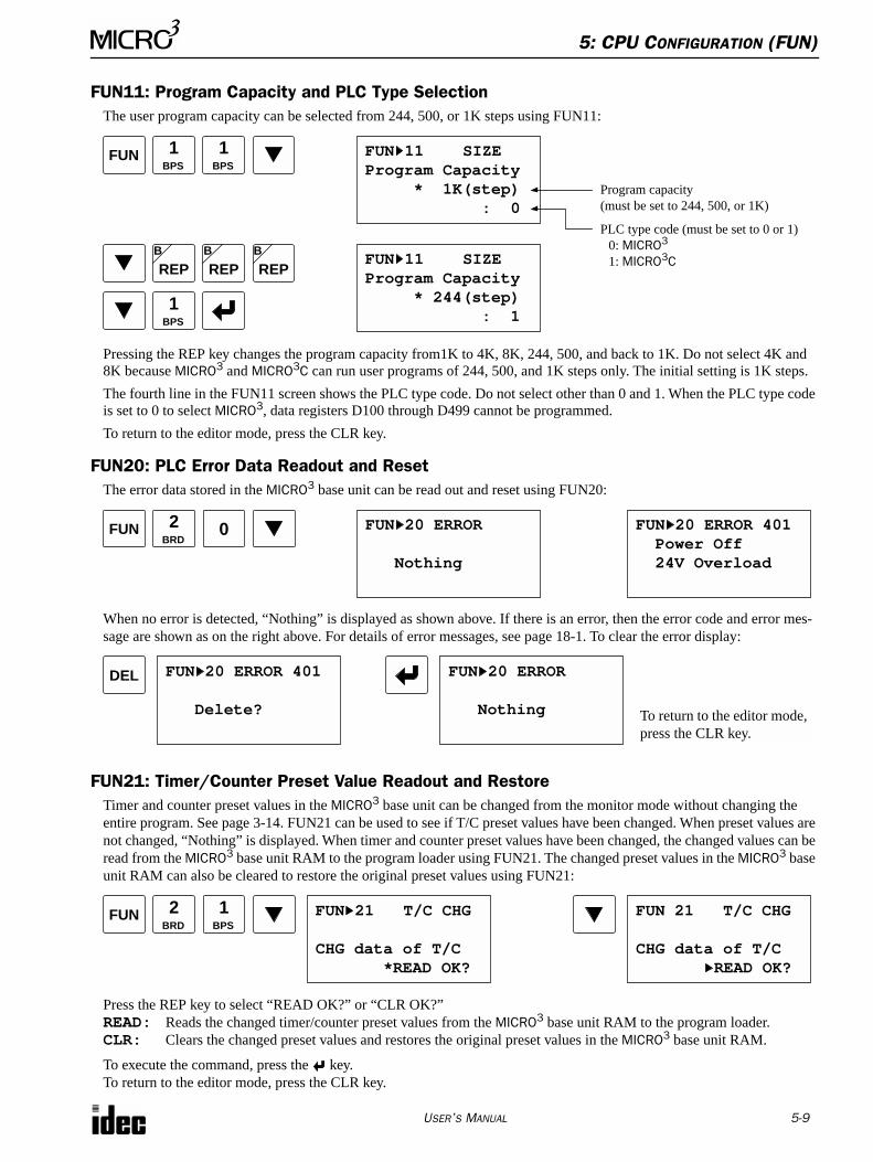
5: CPU CONFIGURATION (FUN)
USER’S MANUAL 5-9
FUN11: Program Capacity and PLC Type SelectionThe user program capacity can be selected from 244, 500, or 1K steps using FUN11:
Pressing the REP key changes the program capacity from1K to 4K, 8K, 244, 500, and back to 1K. Do not select 4K and 8K because MICRO3 and MICRO3C can run user programs of 244, 500, and 1K steps only. The initial setting is 1K steps.
The fourth line in the FUN11 screen shows the PLC type code. Do not select other than 0 and 1. When the PLC type code is set to 0 to select MICRO3, data registers D100 through D499 cannot be programmed.
To return to the editor mode, press the CLR key.
FUN20: PLC Error Data Readout and ResetThe error data stored in the MICRO3 base unit can be read out and reset using FUN20:
When no error is detected, “Nothing” is displayed as shown above. If there is an error, then the error code and error mes-sage are shown as on the right above. For details of error messages, see page 18-1. To clear the error display:
FUN21: Timer/Counter Preset Value Readout and RestoreTimer and counter preset values in the MICRO3 base unit can be changed from the monitor mode without changing the entire program. See page 3-14. FUN21 can be used to see if T/C preset values have been changed. When preset values are not changed, “Nothing” is displayed. When timer and counter preset values have been changed, the changed values can be read from the MICRO3 base unit RAM to the program loader using FUN21. The changed preset values in the MICRO3 base unit RAM can also be cleared to restore the original preset values using FUN21:
Press the REP key to select “READ OK?” or “CLR OK?”READ: Reads the changed timer/counter preset values from the MICRO3 base unit RAM to the program loader.CLR: Clears the changed preset values and restores the original preset values in the MICRO3 base unit RAM.
To execute the command, press the key.To return to the editor mode, press the CLR key.
FUN FUN 11 SIZEProgram Capacity * 1K(step) : 0
1BPS
1BPS
REPB
REPB
REPB
FUN 11 SIZEProgram Capacity * 244(step) : 1
Program capacity(must be set to 244, 500, or 1K)
PLC type code (must be set to 0 or 1) 0: MICRO3
1: MICRO3C
1BPS
FUN FUN 20 ERROR
Nothing
02BRD
FUN 20 ERROR 401 Power Off 24V Overload
FUN 20 ERROR
Nothing
FUN 20 ERROR 401
Delete?
DEL
To return to the editor mode, press the CLR key.
FUN FUN 21 T/C CHG
CHG data of T/C *READ OK?
2BRD
1BPS
FUN 21 T/C CHG
CHG data of T/C READ OK?
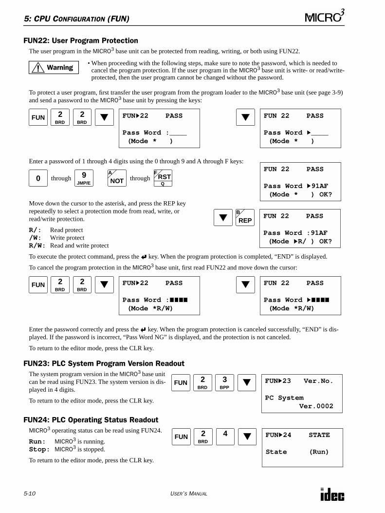
5: CPU CONFIGURATION (FUN)
5-10 USER’S MANUAL
FUN22: User Program ProtectionThe user program in the MICRO3 base unit can be protected from reading, writing, or both using FUN22.
To protect a user program, first transfer the user program from the program loader to the MICRO3 base unit (see page 3-9) and send a password to the MICRO3 base unit by pressing the keys:
Enter a password of 1 through 4 digits using the 0 through 9 and A through F keys:
Move down the cursor to the asterisk, and press the REP key repeatedly to select a protection mode from read, write, or read/write protection.
R/: Read protect/W: Write protectR/W: Read and write protect
To execute the protect command, press the key. When the program protection is completed, “END” is displayed.
To cancel the program protection in the MICRO3 base unit, first read FUN22 and move down the cursor:
Enter the password correctly and press the key. When the program protection is canceled successfully, “END” is dis-played. If the password is incorrect, “Pass Word NG” is displayed, and the protection is not canceled.
To return to the editor mode, press the CLR key.
FUN23: PLC System Program Version ReadoutThe system program version in the MICRO3 base unit can be read using FUN23. The system version is dis-played in 4 digits.
To return to the editor mode, press the CLR key.
FUN24: PLC Operating Status ReadoutMICRO3 operating status can be read using FUN24.
Run: MICRO3 is running.Stop: MICRO3 is stopped.
To return to the editor mode, press the CLR key.
Warning• When proceeding with the following steps, make sure to note the password, which is needed to
cancel the program protection. If the user program in the MICRO3 base unit is write- or read/write-protected, then the user program cannot be changed without the password.
FUN FUN 22 PASS
Pass Word :____ (Mode * )
2BRD
2BRD
FUN 22 PASS
Pass Word ____ (Mode * )
FUN 22 PASS
Pass Word 91AF (Mode * ) OK?
0 9JMP/E
RSTF
QNOTA
through through
FUN 22 PASS
Pass Word :91AF (Mode R/ ) OK?
REPB
FUN FUN 22 PASS
Pass Word : (Mode *R/W)
2BRD
2BRD
FUN 22 PASS
Pass Word (Mode *R/W)
FUN FUN 23 Ver.No.
PC System Ver.0002
2BRD
3BPP
FUN FUN 24 STATE
State (Run)
2BRD
4
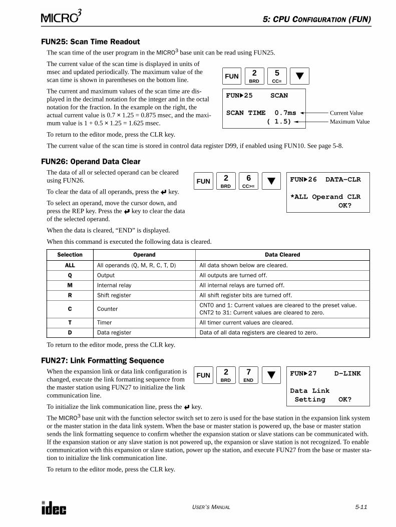
5: CPU CONFIGURATION (FUN)
USER’S MANUAL 5-11
FUN25: Scan Time ReadoutThe scan time of the user program in the MICRO3 base unit can be read using FUN25.
The current value of the scan time is displayed in units of msec and updated periodically. The maximum value of the scan time is shown in parentheses on the bottom line.
The current and maximum values of the scan time are dis-played in the decimal notation for the integer and in the octal notation for the fraction. In the example on the right, the actual current value is 0.7 × 1.25 = 0.875 msec, and the maxi-mum value is 1 + 0.5 × 1.25 = 1.625 msec.
To return to the editor mode, press the CLR key.
The current value of the scan time is stored in control data register D99, if enabled using FUN10. See page 5-8.
FUN26: Operand Data ClearThe data of all or selected operand can be cleared using FUN26.
To clear the data of all operands, press the key.
To select an operand, move the cursor down, and press the REP key. Press the key to clear the data of the selected operand.
When the data is cleared, “END” is displayed.
When this command is executed the following data is cleared.
To return to the editor mode, press the CLR key.
FUN27: Link Formatting SequenceWhen the expansion link or data link configuration is changed, execute the link formatting sequence from the master station using FUN27 to initialize the link communication line.
To initialize the link communication line, press the key.
The MICRO3 base unit with the function selector switch set to zero is used for the base station in the expansion link system or the master station in the data link system. When the base or master station is powered up, the base or master station sends the link formatting sequence to confirm whether the expansion station or slave stations can be communicated with. If the expansion station or any slave station is not powered up, the expansion or slave station is not recognized. To enable communication with this expansion or slave station, power up the station, and execute FUN27 from the base or master sta-tion to initialize the link communication line.
To return to the editor mode, press the CLR key.
Selection Operand Data Cleared
ALL All operands (Q, M, R, C, T, D) All data shown below are cleared.
Q Output All outputs are turned off.
M Internal relay All internal relays are turned off.
R Shift register All shift register bits are turned off.
C CounterCNT0 and 1: Current values are cleared to the preset value.CNT2 to 31: Current values are cleared to zero.
T Timer All timer current values are cleared.
D Data register Data of all data registers are cleared to zero.
FUN
FUN 25 SCAN
SCAN TIME 0.7ms ( 1.5)
2BRD
5CC=
Current Value
Maximum Value
FUN FUN 26 DATA-CLR
*ALL Operand CLR OK?
2BRD
6CC>=
FUN FUN 27 D-LINK
Data Link Setting OK?
2BRD
7END
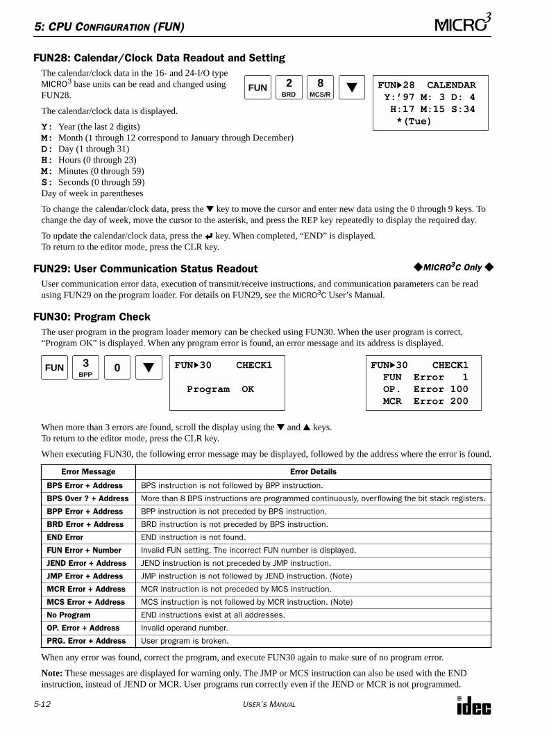
5: CPU CONFIGURATION (FUN)
5-12 USER’S MANUAL
FUN28: Calendar/Clock Data Readout and SettingThe calendar/clock data in the 16- and 24-I/O type MICRO3 base units can be read and changed using FUN28.
The calendar/clock data is displayed.
Y: Year (the last 2 digits)M: Month (1 through 12 correspond to January through December)D: Day (1 through 31)H: Hours (0 through 23)M: Minutes (0 through 59)S: Seconds (0 through 59)Day of week in parentheses
To change the calendar/clock data, press the key to move the cursor and enter new data using the 0 through 9 keys. To change the day of week, move the cursor to the asterisk, and press the REP key repeatedly to display the required day.
To update the calendar/clock data, press the key. When completed, “END” is displayed.To return to the editor mode, press the CLR key.
FUN29: User Communication Status ReadoutUser communication error data, execution of transmit/receive instructions, and communication parameters can be read using FUN29 on the program loader. For details on FUN29, see the MICRO3C User’s Manual.
FUN30: Program CheckThe user program in the program loader memory can be checked using FUN30. When the user program is correct, “Program OK” is displayed. When any program error is found, an error message and its address is displayed.
When more than 3 errors are found, scroll the display using the and keys.To return to the editor mode, press the CLR key.
When executing FUN30, the following error message may be displayed, followed by the address where the error is found.
When any error was found, correct the program, and execute FUN30 again to make sure of no program error.
Note: These messages are displayed for warning only. The JMP or MCS instruction can also be used with the END instruction, instead of JEND or MCR. User programs run correctly even if the JEND or MCR is not programmed.
Error Message Error Details
BPS Error + Address BPS instruction is not followed by BPP instruction.
BPS Over ? + Address More than 8 BPS instructions are programmed continuously, overflowing the bit stack registers.
BPP Error + Address BPP instruction is not preceded by BPS instruction.
BRD Error + Address BRD instruction is not preceded by BPS instruction.
END Error END instruction is not found.
FUN Error + Number Invalid FUN setting. The incorrect FUN number is displayed.
JEND Error + Address JEND instruction is not preceded by JMP instruction.
JMP Error + Address JMP instruction is not followed by JEND instruction. (Note)
MCR Error + Address MCR instruction is not preceded by MCS instruction.
MCS Error + Address MCS instruction is not followed by MCR instruction. (Note)
No Program END instructions exist at all addresses.
OP. Error + Address Invalid operand number.
PRG. Error + Address User program is broken.
FUN FUN 28 CALENDAR Y:’97 M: 3 D: 4 H:17 M:15 S:34 *(Tue)
2BRD
8MCS/R
MICRO3C Only
FUN FUN 30 CHECK1
Program OK
3BPP
0 FUN 30 CHECK1 FUN Error 1 OP. Error 100 MCR Error 200
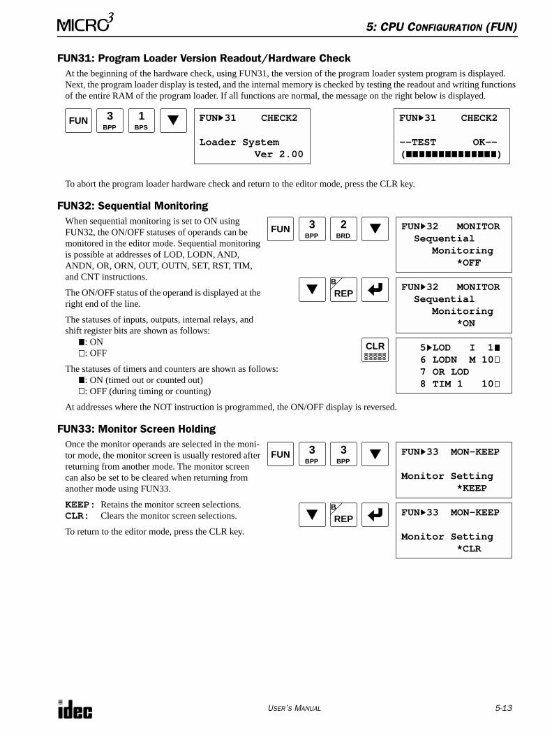
5: CPU CONFIGURATION (FUN)
USER’S MANUAL 5-13
FUN31: Program Loader Version Readout/Hardware CheckAt the beginning of the hardware check, using FUN31, the version of the program loader system program is displayed. Next, the program loader display is tested, and the internal memory is checked by testing the readout and writing functions of the entire RAM of the program loader. If all functions are normal, the message on the right below is displayed.
To abort the program loader hardware check and return to the editor mode, press the CLR key.
FUN32: Sequential MonitoringWhen sequential monitoring is set to ON using FUN32, the ON/OFF statuses of operands can be monitored in the editor mode. Sequential monitoring is possible at addresses of LOD, LODN, AND, ANDN, OR, ORN, OUT, OUTN, SET, RST, TIM, and CNT instructions.
The ON/OFF status of the operand is displayed at the right end of the line.
The statuses of inputs, outputs, internal relays, and shift register bits are shown as follows:
: ON: OFF
The statuses of timers and counters are shown as follows:: ON (timed out or counted out): OFF (during timing or counting)
At addresses where the NOT instruction is programmed, the ON/OFF display is reversed.
FUN33: Monitor Screen HoldingOnce the monitor operands are selected in the moni-tor mode, the monitor screen is usually restored after returning from another mode. The monitor screen can also be set to be cleared when returning from another mode using FUN33.
KEEP: Retains the monitor screen selections.CLR: Clears the monitor screen selections.
To return to the editor mode, press the CLR key.
FUN FUN 31 CHECK2
Loader System Ver 2.00
3BPP
FUN 31 CHECK2
--TEST OK--( )
1BPS
FUN FUN 32 MONITOR Sequential Monitoring *OFF
2BRD
3BPP
FUN 32 MONITOR Sequential Monitoring *ON
REPB
5 LOD I 1 6 LODN M 10 7 OR LOD 8 TIM 1 10
CLR
FUN FUN 33 MON-KEEP
Monitor Setting *KEEP
3BPP
REPB
3BPP
FUN 33 MON-KEEP
Monitor Setting *CLR
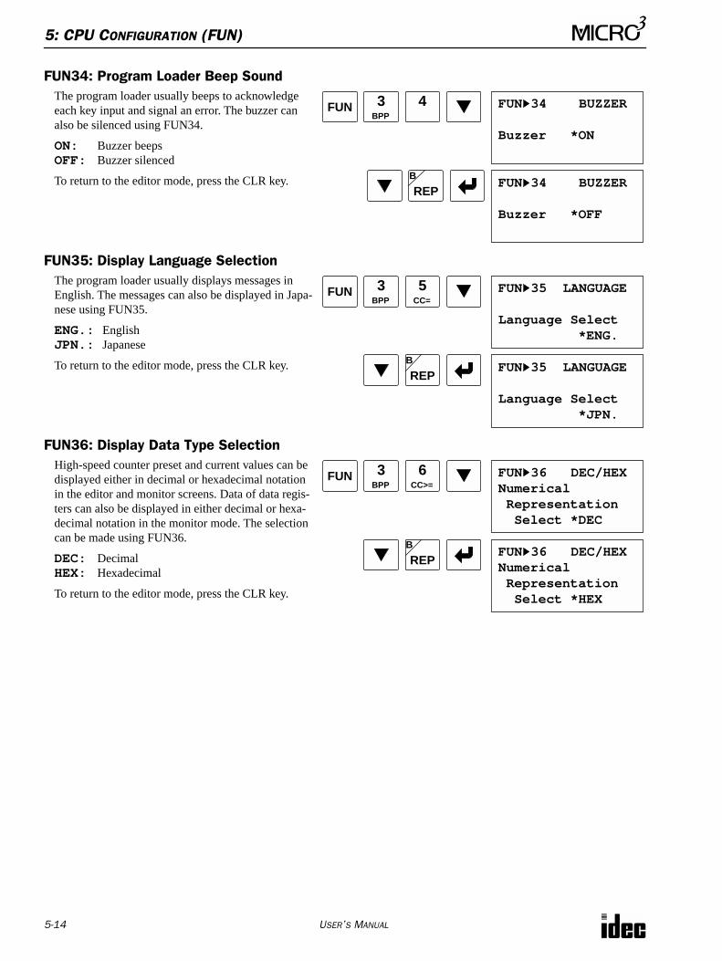
5: CPU CONFIGURATION (FUN)
5-14 USER’S MANUAL
FUN34: Program Loader Beep SoundThe program loader usually beeps to acknowledge each key input and signal an error. The buzzer can also be silenced using FUN34.
ON: Buzzer beepsOFF: Buzzer silenced
To return to the editor mode, press the CLR key.
FUN35: Display Language SelectionThe program loader usually displays messages in English. The messages can also be displayed in Japa-nese using FUN35.
ENG.: EnglishJPN.: Japanese
To return to the editor mode, press the CLR key.
FUN36: Display Data Type SelectionHigh-speed counter preset and current values can be displayed either in decimal or hexadecimal notation in the editor and monitor screens. Data of data regis-ters can also be displayed in either decimal or hexa-decimal notation in the monitor mode. The selection can be made using FUN36.
DEC: DecimalHEX: Hexadecimal
To return to the editor mode, press the CLR key.
FUN FUN 34 BUZZER
Buzzer *ON
3BPP
REPB
4
FUN 34 BUZZER
Buzzer *OFF
FUN FUN 35 LANGUAGE
Language Select *ENG.
3BPP
REPB
5CC=
FUN 35 LANGUAGE
Language Select *JPN.
FUN FUN 36 DEC/HEXNumerical Representation Select *DEC
3BPP
REPB
6CC>=
FUN 36 DEC/HEXNumerical Representation Select *HEX
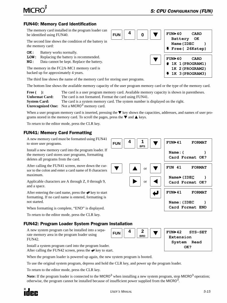
5: CPU CONFIGURATION (FUN)
USER’S MANUAL 5-15
FUN40: Memory Card IdentificationThe memory card installed in the program loader can be identified using FUN40.
The second line shows the condition of the battery in the memory card:
OK: Battery works normally.LOW: Replacing the battery is recommended.NG: Data cannot be kept. Replace the battery.
The memory in the FC2A-MC1 memory card is backed up for approximately 4 years.
The third line shows the name of the memory card for storing user programs.
The bottom line shows the available memory capacity of the user program memory card or the type of the memory card.
Free ( ): The card is a user program memory card. Available memory capacity is shown in parentheses.Unformat Card: The card is not formatted. Format the card using FUN41.System Card: The card is a system memory card. The system number is displayed on the right.Unrecognized One: Not a MICRO3 memory card.
When a user program memory card is inserted, pressing the key shows the capacities, addresses, and names of user pro-grams stored in the memory card. To scroll the pages, press the and keys.
To return to the editor mode, press the CLR key.
FUN41: Memory Card FormattingA new memory card must be formatted using FUN41 to store user programs.
Install a new memory card into the program loader. If the memory card stores user programs, formatting deletes all programs from the card.
After calling the FUN41 screen, move down the cur-sor to the colon and enter a card name of 8 characters maximum.
Applicable characters are A through Z, 0 through 9, and a space.
After entering the card name, press the key to start formatting. If no card name is entered, formatting is not started.
When formatting is complete, “END” is displayed.
To return to the editor mode, press the CLR key.
FUN42: Program Loader System Program InstallationA new system program can be installed into a sepa-rate memory area in the program loader using FUN42.
Install a system program card into the program loader. After calling the FUN42 screen, press the key to start.
When the program loader is powered up again, the new system program is booted.
To use the original system program, depress and hold the CLR key, and power up the program loader.
To return to the editor mode, press the CLR key.
Note: If the program loader is connected to the MICRO3 when installing a new system program, stop MICRO3 operation; otherwise, the program cannot be installed because of insufficient power supplied from the MICRO3.
FUN 40 CARD Battery OK Name(IDEC ) Free( 26Kstep)
FUN 40 CARD 1K 1(PROGRAM1)
1K 2(PROGRAM2) 1K 3(PROGRAM3)
FUN 4
0
FUN 4
1BPS
FUN 41 FORMAT
Name:( ) Card Format OK?
or
or
FUN 41 FORMAT
Name (IDEC ) Card Format OK?
FUN 41 FORMAT
Name:(IDEC ) Card Format END
FUN 42 SYS-SET Extension System Read OK?
FUN 4
2BRD
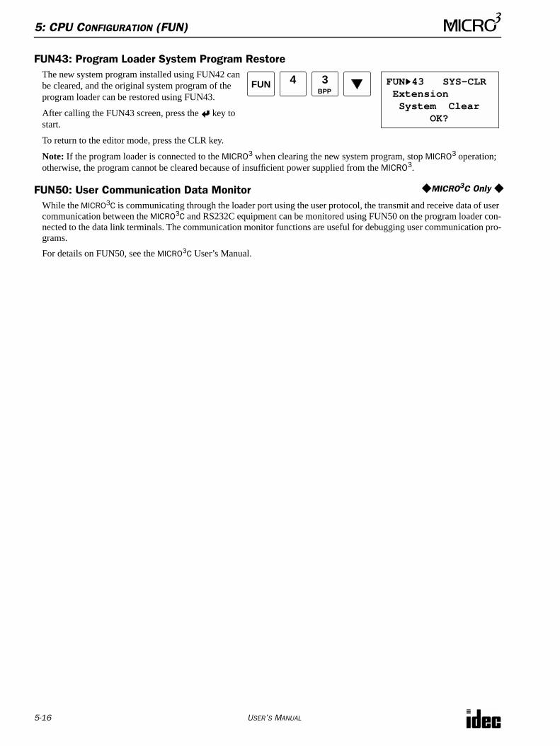
5: CPU CONFIGURATION (FUN)
5-16 USER’S MANUAL
FUN43: Program Loader System Program RestoreThe new system program installed using FUN42 can be cleared, and the original system program of the program loader can be restored using FUN43.
After calling the FUN43 screen, press the key to start.
To return to the editor mode, press the CLR key.
Note: If the program loader is connected to the MICRO3 when clearing the new system program, stop MICRO3 operation; otherwise, the program cannot be cleared because of insufficient power supplied from the MICRO3.
FUN50: User Communication Data MonitorWhile the MICRO3C is communicating through the loader port using the user protocol, the transmit and receive data of user communication between the MICRO3C and RS232C equipment can be monitored using FUN50 on the program loader con-nected to the data link terminals. The communication monitor functions are useful for debugging user communication pro-grams.
For details on FUN50, see the MICRO3C User’s Manual.
FUN 43 SYS-CLR Extension System Clear OK?
FUN 4
3BPP
MICRO3C Only
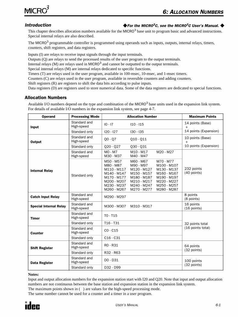
USER’S MANUAL 6-1
6: ALLOCATION NUMBERS
IntroductionThis chapter describes allocation numbers available for the MICRO3 base unit to program basic and advanced instructions. Special internal relays are also described.
The MICRO3 programmable controller is programmed using operands such as inputs, outputs, internal relays, timers, counters, shift registers, and data registers.
Inputs (I) are relays to receive input signals through the input terminals.Outputs (Q) are relays to send the processed results of the user program to the output terminals.Internal relays (M) are relays used in MICRO3 and cannot be outputted to the output terminals.Special internal relays (M) are internal relays dedicated to specific functions.Timers (T) are relays used in the user program, available in 100-msec, 10-msec, and 1-msec timers.Counters (C) are relays used in the user program, available in reversible counters and adding counters.Shift registers (R) are registers to shift the data bits according to pulse inputs.Data registers (D) are registers used to store numerical data. Some of the data registers are dedicated to special functions.
Allocation NumbersAvailable I/O numbers depend on the type and combination of the MICRO3 base units used in the expansion link system. For details of available I/O numbers in the expansion link system, see page 4-7.
Notes:Input and output allocation numbers for the expansion station start with I20 and Q20. Note that input and output allocation numbers are not continuous between the base station and expansion station in the expansion link system.The maximum points shown in ( ) are values for the high-speed processing mode.The same number cannot be used for a counter and a timer in a user program.
Operand Processing Mode Allocation Number Maximum Points
InputStandard andHigh-speed I0 - I7 I10 - I15 14 points (Base)
+14 points (Expansion)Standard only I20 - I27 I30 - I35
OutputStandard andHigh-speed Q0 - Q7 Q10 - Q11 10 points (Base)
+10 points (Expansion)Standard only Q20 - Q27 Q30 - Q31
Internal Relay
Standard andHigh-speed
M0 - M7 M10 - M17 M20 - M27M30 - M37 M40 - M47
232 points(40 points)
Standard only
M50 - M57 M60 - M67 M70 - M77M80 - M87 M90 - M97 M100 - M107M110 - M117 M120 - M127 M130 - M137M140 - M147 M150 - M157 M160 - M167M170 - M177 M180 - M187 M190 - M197M200 - M207 M210 - M217 M220 - M227M230 - M237 M240 - M247 M250 - M257M260 - M267 M270 - M277 M280 - M287
Catch Input Relay Standard andHigh-speed M290 - M297 8 points
(8 points)
Special Internal Relay Standard andHigh-speed M300 - M307 M310 - M317 16 points
(16 points)
TimerStandard andHigh-speed T0 - T15
32 points total(16 points total)
Standard only T16 - T31
CounterStandard andHigh-speed C0 - C15
Standard only C16 - C31
Shift RegisterStandard andHigh-speed R0 - R31 64 points
(32 points)Standard only R32 - R63
Data RegisterStandard andHigh-speed D0 - D31 100 points
(32 points)Standard only D32 - D99
For the MICRO3C, see the MICRO3C User’s Manual.
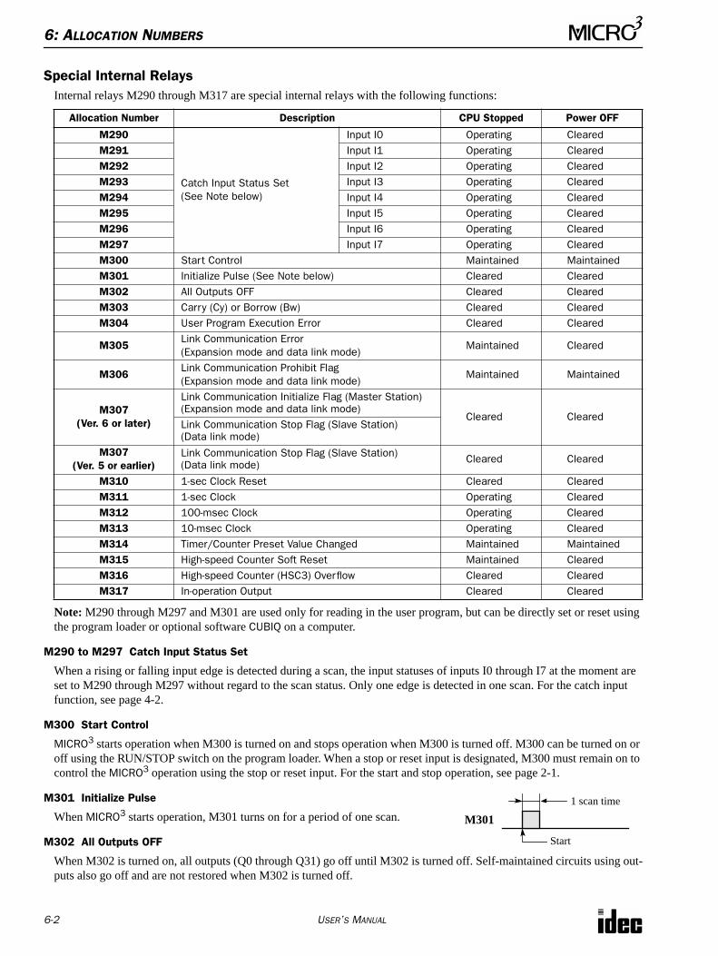
6: ALLOCATION NUMBERS
6-2 USER’S MANUAL
Special Internal RelaysInternal relays M290 through M317 are special internal relays with the following functions:
Note: M290 through M297 and M301 are used only for reading in the user program, but can be directly set or reset using the program loader or optional software CUBIQ on a computer.
M290 to M297 Catch Input Status Set
When a rising or falling input edge is detected during a scan, the input statuses of inputs I0 through I7 at the moment are set to M290 through M297 without regard to the scan status. Only one edge is detected in one scan. For the catch input function, see page 4-2.
M300 Start Control
MICRO3 starts operation when M300 is turned on and stops operation when M300 is turned off. M300 can be turned on or off using the RUN/STOP switch on the program loader. When a stop or reset input is designated, M300 must remain on to control the MICRO3 operation using the stop or reset input. For the start and stop operation, see page 2-1.
M301 Initialize Pulse
When MICRO3 starts operation, M301 turns on for a period of one scan.
M302 All Outputs OFF
When M302 is turned on, all outputs (Q0 through Q31) go off until M302 is turned off. Self-maintained circuits using out-puts also go off and are not restored when M302 is turned off.
Allocation Number Description CPU Stopped Power OFF
M290
Catch Input Status Set(See Note below)
Input I0 Operating ClearedM291 Input I1 Operating ClearedM292 Input I2 Operating ClearedM293 Input I3 Operating ClearedM294 Input I4 Operating ClearedM295 Input I5 Operating ClearedM296 Input I6 Operating ClearedM297 Input I7 Operating ClearedM300 Start Control Maintained MaintainedM301 Initialize Pulse (See Note below) Cleared ClearedM302 All Outputs OFF Cleared ClearedM303 Carry (Cy) or Borrow (Bw) Cleared ClearedM304 User Program Execution Error Cleared Cleared
M305Link Communication Error(Expansion mode and data link mode)
Maintained Cleared
M306Link Communication Prohibit Flag(Expansion mode and data link mode)
Maintained Maintained
M307(Ver. 6 or later)
Link Communication Initialize Flag (Master Station)(Expansion mode and data link mode)
Cleared ClearedLink Communication Stop Flag (Slave Station)(Data link mode)
M307(Ver. 5 or earlier)
Link Communication Stop Flag (Slave Station)(Data link mode) Cleared Cleared
M310 1-sec Clock Reset Cleared ClearedM311 1-sec Clock Operating ClearedM312 100-msec Clock Operating ClearedM313 10-msec Clock Operating ClearedM314 Timer/Counter Preset Value Changed Maintained MaintainedM315 High-speed Counter Soft Reset Maintained ClearedM316 High-speed Counter (HSC3) Overflow Cleared ClearedM317 In-operation Output Cleared Cleared
1 scan time
Start
M301
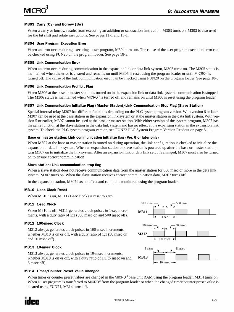
6: ALLOCATION NUMBERS
USER’S MANUAL 6-3
M303 Carry (Cy) and Borrow (Bw)
When a carry or borrow results from executing an addition or subtraction instruction, M303 turns on. M303 is also used for the bit shift and rotate instructions. See pages 11-1 and 13-1.
M304 User Program Execution Error
When an error occurs during executing a user program, M304 turns on. The cause of the user program execution error can be checked using FUN20 on the program loader. See page 18-5.
M305 Link Communication Error
When an error occurs during communication in the expansion link or data link system, M305 turns on. The M305 status is maintained when the error is cleared and remains on until M305 is reset using the program loader or until MICRO3 is turned off. The cause of the link communication error can be checked using FUN20 on the program loader. See page 18-5.
M306 Link Communication Prohibit Flag
When M306 at the base or master station is turned on in the expansion link or data link system, communication is stopped. The M306 status is maintained when MICRO3 is turned off and remains on until M306 is reset using the program loader.
M307 Link Communication Initialize Flag (Master Station)/Link Communication Stop Flag (Slave Station)
Special internal relay M307 has different functions depending on the PLC system program version. With version 6 or later, M307 can be used at the base station in the expansion link system or at the master station in the data link system. With ver-sion 5 or earlier, M307 cannot be used at the base or master station. With either version of the system program, M307 has the same function at the slave station in the data link system and has no effect at the expansion station in the expansion link system. To check the PLC system program version, see FUN23 PLC System Program Version Readout on page 5-11.
Base or master station: Link communication initialize flag (Ver. 6 or later only)When M307 at the base or master station is turned on during operation, the link configuration is checked to initialize the expansion or data link system. When an expansion station or slave station is powered up after the base or master station, turn M307 on to initialize the link system. After an expansion link or data link setup is changed, M307 must also be turned on to ensure correct communication.
Slave station: Link communication stop flagWhen a slave station does not receive communication data from the master station for 800 msec or more in the data link system, M307 turns on. When the slave station receives correct communication data, M307 turns off.
In the expansion station, M307 has no effect and cannot be monitored using the program loader.
M310 1-sec Clock Reset
When M310 is on, M311 (1-sec clock) is reset to zero.
M311 1-sec Clock
When M310 is off, M311 generates clock pulses in 1-sec incre-ments, with a duty ratio of 1:1 (500 msec on and 500 msec off).
M312 100-msec Clock
M312 always generates clock pulses in 100-msec increments, whether M310 is on or off, with a duty ratio of 1:1 (50 msec on and 50 msec off).
M313 10-msec Clock
M313 always generates clock pulses in 10-msec increments, whether M310 is on or off, with a duty ratio of 1:1 (5 msec on and 5 msec off).
M314 Timer/Counter Preset Value Changed
When timer or counter preset values are changed in the MICRO3 base unit RAM using the program loader, M314 turns on. When a user program is transferred to MICRO3 from the program loader or when the changed timer/counter preset value is cleared using FUN21, M314 turns off.
M311
500 msec
1 sec
500 msec
M312
50 msec
100 msec
50 msec
M313
5 msec
10 msec
5 msec
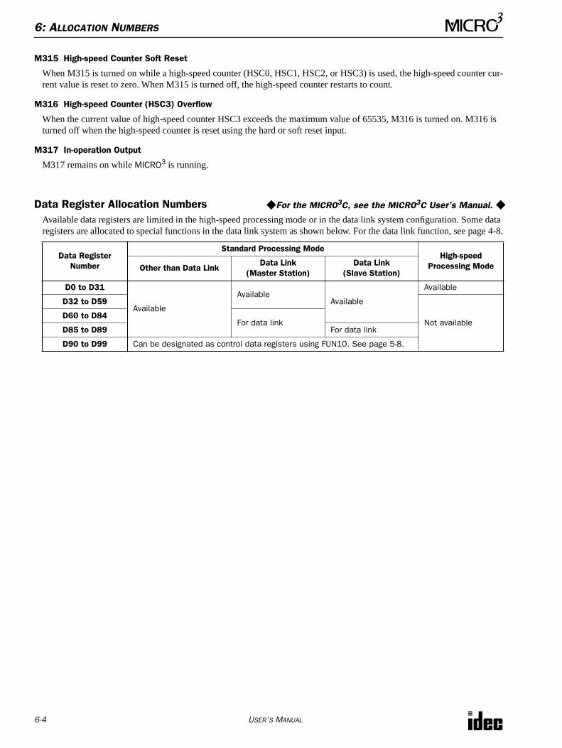
6: ALLOCATION NUMBERS
6-4 USER’S MANUAL
M315 High-speed Counter Soft Reset
When M315 is turned on while a high-speed counter (HSC0, HSC1, HSC2, or HSC3) is used, the high-speed counter cur-rent value is reset to zero. When M315 is turned off, the high-speed counter restarts to count.
M316 High-speed Counter (HSC3) Overflow
When the current value of high-speed counter HSC3 exceeds the maximum value of 65535, M316 is turned on. M316 is turned off when the high-speed counter is reset using the hard or soft reset input.
M317 In-operation Output
M317 remains on while MICRO3 is running.
Data Register Allocation NumbersAvailable data registers are limited in the high-speed processing mode or in the data link system configuration. Some data registers are allocated to special functions in the data link system as shown below. For the data link function, see page 4-8.
Data Register Number
Standard Processing ModeHigh-speed
Processing ModeOther than Data LinkData Link
(Master Station)Data Link
(Slave Station)
D0 to D31
Available
AvailableAvailable
Available
D32 to D59
Not availableD60 to D84
For data linkD85 to D89 For data link
D90 to D99 Can be designated as control data registers using FUN10. See page 5-8.
For the MICRO3C, see the MICRO3C User’s Manual.
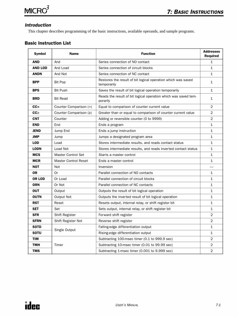
USER’S MANUAL 7-1
7: BASIC INSTRUCTIONS
IntroductionThis chapter describes programming of the basic instructions, available operands, and sample programs.
Basic Instruction List
Symbol Name FunctionAddressesRequired
AND And Series connection of NO contact 1
AND LOD And Load Series connection of circuit blocks 1
ANDN And Not Series connection of NC contact 1
BPP Bit PopRestores the result of bit logical operation which was saved temporarily
1
BPS Bit Push Saves the result of bit logical operation temporarily 1
BRD Bit ReadReads the result of bit logical operation which was saved tem-porarily
1
CC= Counter Comparison (=) Equal to comparison of counter current value 2
CC≥ Counter Comparison (≥) Greater than or equal to comparison of counter current value 2
CNT Counter Adding or reversible counter (0 to 9999) 2
END End Ends a program 1
JEND Jump End Ends a jump instruction 1
JMP Jump Jumps a designated program area 1
LOD Load Stores intermediate results, and reads contact status 1
LODN Load Not Stores intermediate results, and reads inverted contact status 1
MCS Master Control Set Starts a master control 1
MCR Master Control Reset Ends a master control 1
NOT Not Inversion —
OR Or Parallel connection of NO contacts 1
OR LOD Or Load Parallel connection of circuit blocks 1
ORN Or Not Parallel connection of NC contacts 1
OUT Output Outputs the result of bit logical operation 1
OUTN Output Not Outputs the inverted result of bit logical operation 1
RST Reset Resets output, internal relay, or shift register bit 1
SET Set Sets output, internal relay, or shift register bit 1
SFR Shift Register Forward shift register 2
SFRN Shift Register Not Reverse shift register 2
SOTDSingle Output
Falling-edge differentiation output 1
SOTU Rising-edge differentiation output 1
TIM
Timer
Subtracting 100-msec timer (0.1 to 999.9 sec) 2
TMH Subtracting 10-msec timer (0.01 to 99.99 sec) 2
TMS Subtracting 1-msec timer (0.001 to 9.999 sec) 2
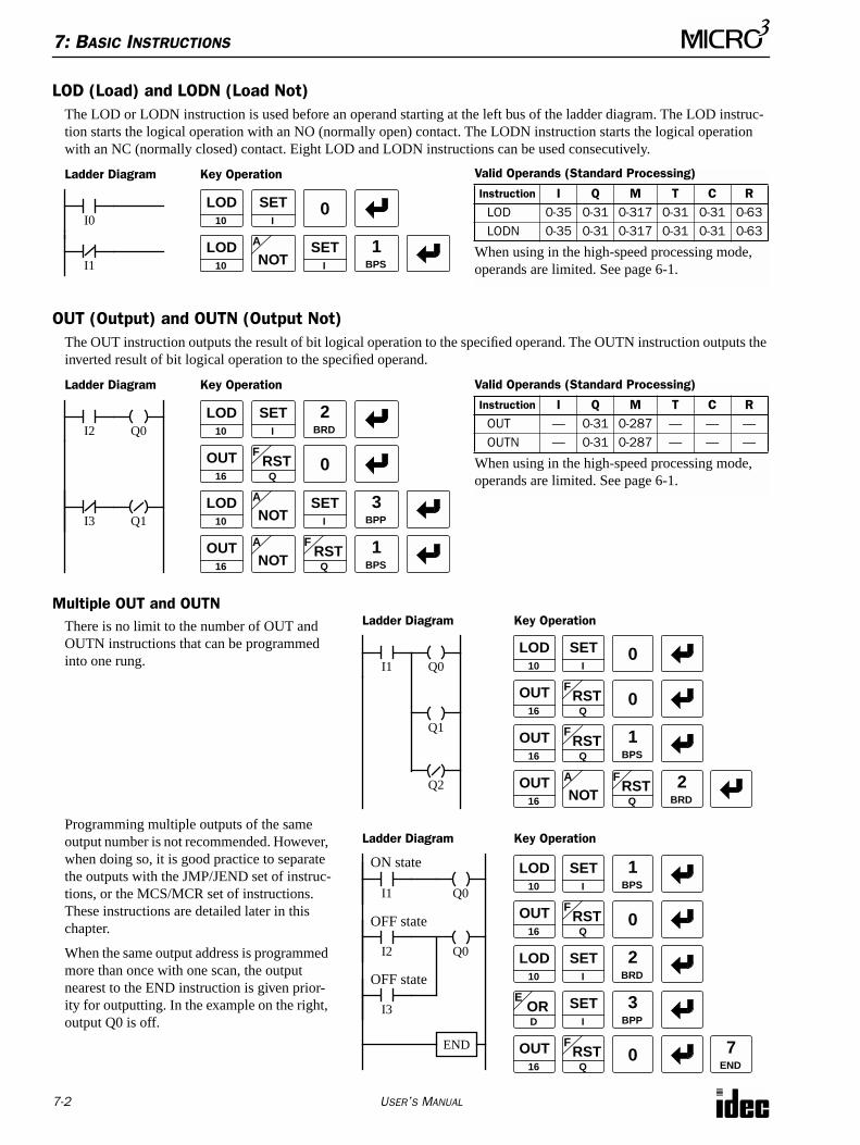
7: BASIC INSTRUCTIONS
7-2 USER’S MANUAL
LOD (Load) and LODN (Load Not)The LOD or LODN instruction is used before an operand starting at the left bus of the ladder diagram. The LOD instruc-tion starts the logical operation with an NO (normally open) contact. The LODN instruction starts the logical operation with an NC (normally closed) contact. Eight LOD and LODN instructions can be used consecutively.
OUT (Output) and OUTN (Output Not)The OUT instruction outputs the result of bit logical operation to the specified operand. The OUTN instruction outputs the inverted result of bit logical operation to the specified operand.
Multiple OUT and OUTNThere is no limit to the number of OUT and OUTN instructions that can be programmed into one rung.
Programming multiple outputs of the same output number is not recommended. However, when doing so, it is good practice to separate the outputs with the JMP/JEND set of instruc-tions, or the MCS/MCR set of instructions. These instructions are detailed later in this chapter.
When the same output address is programmed more than once with one scan, the output nearest to the END instruction is given prior-ity for outputting. In the example on the right, output Q0 is off.
Ladder Diagram Key Operation
I0
I1
LOD10
SETI
NOTA 1
BPS
0
LOD10
SETI
Valid Operands (Standard Processing)
When using in the high-speed processing mode, operands are limited. See page 6-1.
Instruction I Q M T C RLOD 0-35 0-31 0-317 0-31 0-31 0-63LODN 0-35 0-31 0-317 0-31 0-31 0-63
Ladder Diagram Key Operation
I2
I3
LOD10
SETI
NOTA
1BPS
LOD10
SETIQ1
Q0
OUT16
RSTF
Q0
3BPP
2BRD
OUT16 NOT
ARST
F
Q
Valid Operands (Standard Processing)
When using in the high-speed processing mode, operands are limited. See page 6-1.
Instruction I Q M T C ROUT — 0-31 0-287 — — —OUTN — 0-31 0-287 — — —
Ladder Diagram Key Operation
I1
LOD10
SETI
1BPS
Q2
Q0
OUT16
RSTF
Q0
2BRD
OUT16 NOT
ARST
F
Q
Q1
0
OUT16
RSTF
Q
Ladder Diagram Key Operation
I1
LOD10
SETI
Q0
OUT16
RSTF
Q0
2BRD
OUT16
RSTF
Q
Q0I2
I3
END
SETI
ORE
D
1BPS
LOD10
SETI
3BPP
0 7END
ON state
OFF state
OFF state
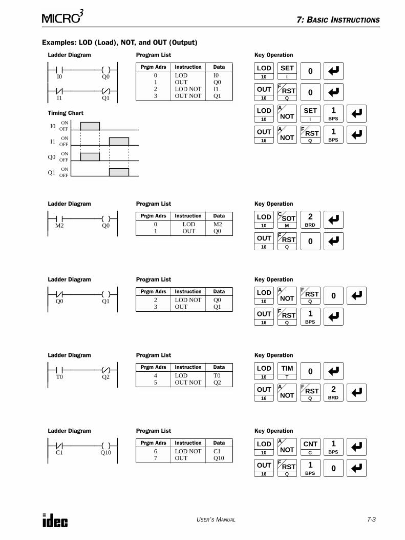
7: BASIC INSTRUCTIONS
USER’S MANUAL 7-3
Examples: LOD (Load), NOT, and OUT (Output)
Ladder Diagram Key Operation
I0
I1
LOD10
SETI
NOTA
1BPS
0
LOD10
SETI
Prgm Adrs Instruction Data
01 23
LODOUTLOD NOTOUT NOT
I0Q0I1Q1
Program List
Q0
OUT16
RSTF
Q0
OUT16
RSTF
QNOTA
1BPS
I0ON
OFF
I1ON
OFF
Q0ON
OFF
Q1ON
OFF
Timing Chart
Q1
Ladder Diagram Key Operation
M2LOD
10
Prgm Adrs Instruction Data
01
LODOUT
M2Q0
Program List
Q0
OUT16
RSTF
Q0
SOTC
M
2BRD
Ladder Diagram
Q1Q0
Key Operation
LOD10
Prgm Adrs Instruction Data
23
LOD NOTOUT
Q0Q1
Program List
OUT16
RSTF
Q
NOTA
RSTF
Q0
1BPS
Ladder Diagram Key Operation
T0LOD
10
Prgm Adrs Instruction Data
45
LODOUT NOT
T0Q2
Program List
OUT16
RSTF
Q
0
2BRD
Q2
NOTA
TIMT
Ladder Diagram Key Operation
LOD10
Prgm Adrs Instruction Data
67
LOD NOTOUT
C1Q10
Program List
Q10
OUT16
RSTF
Q
C1 NOTA
01BPS
CNTC
1BPS
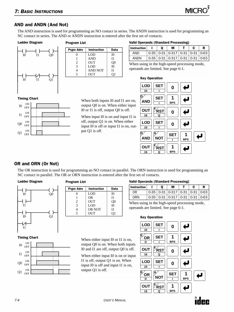
7: BASIC INSTRUCTIONS
7-4 USER’S MANUAL
AND and ANDN (And Not)The AND instruction is used for programming an NO contact in series. The ANDN instruction is used for programming an NC contact in series. The AND or ANDN instruction is entered after the first set of contacts.
OR and ORN (Or Not)The OR instruction is used for programming an NO contact in parallel. The ORN instruction is used for programming an NC contact in parallel. The OR or ORN instruction is entered after the first set of contacts.
Ladder Diagram
Key Operation
I0
LOD10
SETI
NOTA
1BPS
SETI
Q0
OUT16
RSTF
Q
0
OUT16
RSTF
Q
Prgm Adrs Instruction Data
012345
LODANDOUTLODAND NOTOUT
I0I1Q0I0I1Q1
Program List
I1
I1I0
ANDD SET
I
1BPS
0
ANDD 1
BPS
I0ON
OFF
I1ON
OFF
Q0ON
OFF
Q1ON
OFF
Timing Chart When both inputs I0 and I1 are on, output Q0 is on. When either input I0 or I1 is off, output Q0 is off.
When input I0 is on and input I1 is off, output Q1 is on. When either input I0 is off or input I1 is on, out-put Q1 is off.
Q1
Valid Operands (Standard Processing)
When using in the high-speed processing mode, operands are limited. See page 6-1.
Instruction I Q M T C RAND 0-35 0-31 0-317 0-31 0-31 0-63ANDN 0-35 0-31 0-317 0-31 0-31 0-63
LOD10
SETI
0
Ladder Diagram
Key Operation
I0
LOD10
SETI
NOTA
1BPS
SETI
Q0
OUT16
RSTF
Q
0
OUT16
RSTF
Q
Prgm Adrs Instruction Data
012345
LODOROUTLODOR NOTOUT
I0I1Q0I0I1Q1
Program List
I0
SETI
1BPS
0
1BPS
I0ON
OFF
I1ON
OFF
Q0ON
OFF
Q1ON
OFF
Timing Chart When either input I0 or I1 is on, output Q0 is on. When both inputs I0 and I1 are off, output Q0 is off.
When either input I0 is on or input I1 is off, output Q1 is on. When input I0 is off and input I1 is on, output Q1 is off.
Q1
I1
I1
ORE
D
ORE
D
Valid Operands (Standard Processing)
When using in the high-speed processing mode, operands are limited. See page 6-1.
Instruction I Q M T C ROR 0-35 0-31 0-317 0-31 0-31 0-63ORN 0-35 0-31 0-317 0-31 0-31 0-63
LOD10
SETI
0
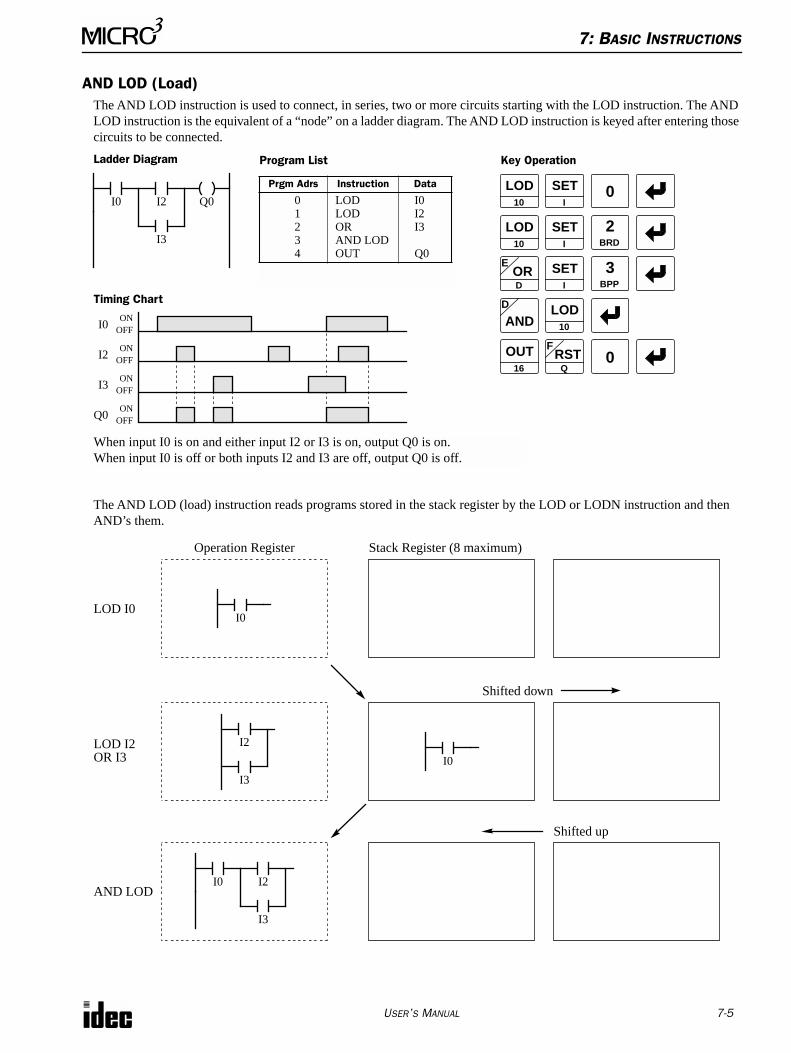
7: BASIC INSTRUCTIONS
USER’S MANUAL 7-5
AND LOD (Load)The AND LOD instruction is used to connect, in series, two or more circuits starting with the LOD instruction. The AND LOD instruction is the equivalent of a “node” on a ladder diagram. The AND LOD instruction is keyed after entering those circuits to be connected.
The AND LOD (load) instruction reads programs stored in the stack register by the LOD or LODN instruction and then AND’s them.
Ladder Diagram Key Operation
I0LOD
10
SETIQ0
0
OUT16
RSTF
Q
Prgm Adrs Instruction Data
01234
LODLODORAND LODOUT
I0I2I3
Q0
Program List
I2
ANDD
I0ON
OFF
I2ON
OFF
I3ON
OFF
Q0ON
OFF
Timing Chart
When input I0 is on and either input I2 or I3 is on, output Q0 is on.When input I0 is off or both inputs I2 and I3 are off, output Q0 is off.
LOD10
SETI
2BRD
ORE
D
SETI
3BPP
LOD10
0
I3
I0
I0
I2
I3
I2
I3
Operation Register Stack Register (8 maximum)
Shifted down
Shifted up
LOD I0
LOD I2OR I3
AND LOD
I0
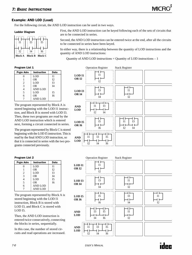
7: BASIC INSTRUCTIONS
7-6 USER’S MANUAL
Example: AND LOD (Load)For the following circuit, the AND LOD instruction can be used in two ways.
First, the AND LOD instruction can be keyed following each of the sets of circuits that are to be connected in series.
Second, the AND LOD instruction can be entered twice at the end, after all the circuits to be connected in series have been keyed.
In either way, there is a relationship between the quantity of LOD instructions and the quantity of AND LOD instructions:
Quantity of AND LOD instructions = Quantity of LOD instructions – 1Block A Block B Block C
Ladder Diagram
I1 I3
I2 I4
I5
I6
I1
Operation Register Stack Register
LOD I1OR I2
Prgm Adrs Instruction Data
01234567
LODORLODORAND LODLODORAND LOD
I1I2I3I4
I5I6
Program List 1
I2
I3
I4
I1
I2
I1
I2
I3
I4
I1
I2
I3
I4
I5
I6
I1
I2
I3
I4
I5
I6
LOD I3OR I4
ANDLOD
LOD I5OR I6
ANDLOD
The program represented by Block A is stored beginning with the LOD I1 instruc-tion, and Block B is stored with LOD I3. Then, these two programs are read by the AND LOD instruction which is entered next, forming a circuit connected in series.
The program represented by Block C is stored beginning with the LOD I5 instruction. This is read by the final AND LOD instruction, so that it is connected in series with the two pro-grams connected previously.
I1
Operation Register Stack Register
LOD I1OR I2
Prgm Adrs Instruction Data
01234567
LODORLODORLODORAND LODAND LOD
I1I2I3I4I5I6
Program List 2
I2
I3
I4
I1
I2
I3
I4
I5
I6
I5
I6
I1
I2
I3
I4
I5
I6
LOD I3OR I4
LOD I5OR I6
ANDLOD
ANDLOD
The program represented by Block A is stored beginning with the LOD I1 instruction, Block B is stored with LOD I3, and Block C is stored with LOD I5.
Then, the AND LOD instruction is entered twice consecutively, connecting the blocks in series, sequentially.
In this case, the number of stored cir-cuits and read operations are increased.
I1
I2
I3
I4
I1
I2
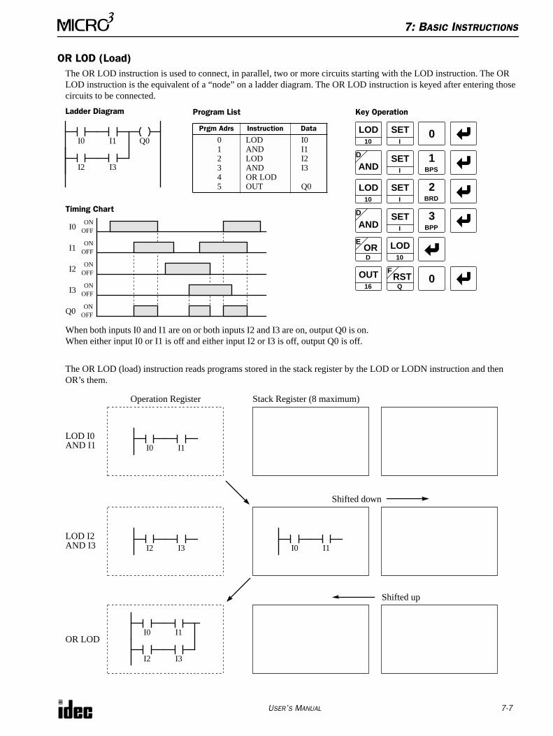
7: BASIC INSTRUCTIONS
USER’S MANUAL 7-7
OR LOD (Load)The OR LOD instruction is used to connect, in parallel, two or more circuits starting with the LOD instruction. The OR LOD instruction is the equivalent of a “node” on a ladder diagram. The OR LOD instruction is keyed after entering those circuits to be connected.
The OR LOD (load) instruction reads programs stored in the stack register by the LOD or LODN instruction and then OR’s them.
I2
I0 I1
I3
Ladder Diagram Key Operation
LOD10
SETIQ0
0
OUT16
RSTF
Q
Prgm Adrs Instruction Data
012345
LODANDLODANDOR LODOUT
I0I1I2I3
Q0
Program List
SETI
1BPSAND
D
I0ON
OFF
I1ON
OFF
I2ON
OFF
I3ON
OFF
Timing Chart
When both inputs I0 and I1 are on or both inputs I2 and I3 are on, output Q0 is on.When either input I0 or I1 is off and either input I2 or I3 is off, output Q0 is off.
LOD10
SETI
2BRD
SETI
3BPP
LOD10
0
Q0ON
OFF
ORE
D
ANDD
I0
I0
I2
I1
I3
Operation Register Stack Register (8 maximum)
Shifted down
Shifted up
LOD I0AND I1
LOD I2AND I3
OR LOD
I1
I0 I1I2 I3
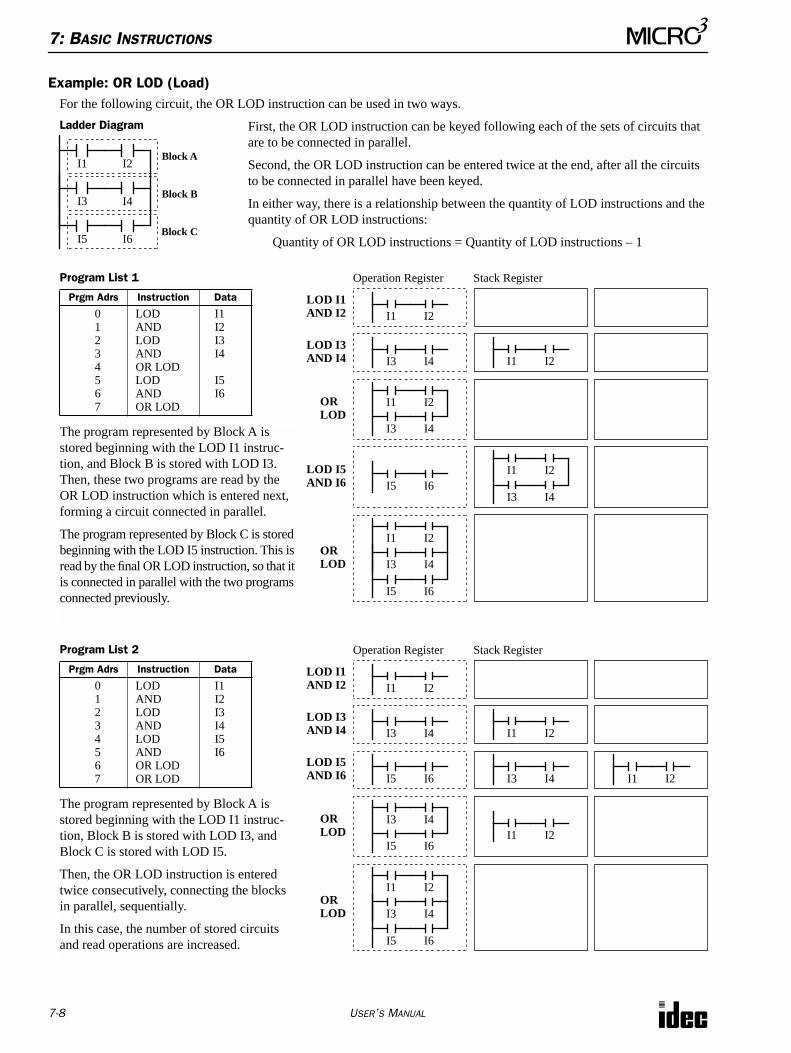
7: BASIC INSTRUCTIONS
7-8 USER’S MANUAL
Example: OR LOD (Load)For the following circuit, the OR LOD instruction can be used in two ways.
First, the OR LOD instruction can be keyed following each of the sets of circuits that are to be connected in parallel.
Second, the OR LOD instruction can be entered twice at the end, after all the circuits to be connected in parallel have been keyed.
In either way, there is a relationship between the quantity of LOD instructions and the quantity of OR LOD instructions:
Quantity of OR LOD instructions = Quantity of LOD instructions – 1
Block A
Ladder Diagram
I1 I2
I3 I4
I5 I6
Block B
Block C
I1
Operation Register Stack Register
LOD I1AND I2
Prgm Adrs Instruction Data
01234567
LODANDLODANDOR LODLODANDOR LOD
I1I2I3I4
I5I6
Program List 1
I2
I1
I3
I2
I4
LOD I3AND I4
ORLOD
LOD I5AND I6
ORLOD
The program represented by Block A is stored beginning with the LOD I1 instruc-tion, and Block B is stored with LOD I3. Then, these two programs are read by the OR LOD instruction which is entered next, forming a circuit connected in parallel.
The program represented by Block C is stored beginning with the LOD I5 instruction. This is read by the final OR LOD instruction, so that it is connected in parallel with the two programs connected previously.
I3 I4 I1 I2
I5 I6I1
I3
I2
I4
I1
I3
I2
I4
I5 I6
I1
Operation Register Stack Register
LOD I1AND I2
Prgm Adrs Instruction Data
01234567
LODANDLODANDLODANDOR LODOR LOD
I1I2I3I4I5I6
Program List 2
I2
LOD I3AND I4
ORLOD
LOD I5AND I6
ORLOD
The program represented by Block A is stored beginning with the LOD I1 instruc-tion, Block B is stored with LOD I3, and Block C is stored with LOD I5.
Then, the OR LOD instruction is entered twice consecutively, connecting the blocks in parallel, sequentially.
In this case, the number of stored circuits and read operations are increased.
I3 I4 I1 I2
I1
I3
I2
I4
I5 I6
I3
I5
I4
I6
I5 I6 I3 I4 I1 I2
I1 I2
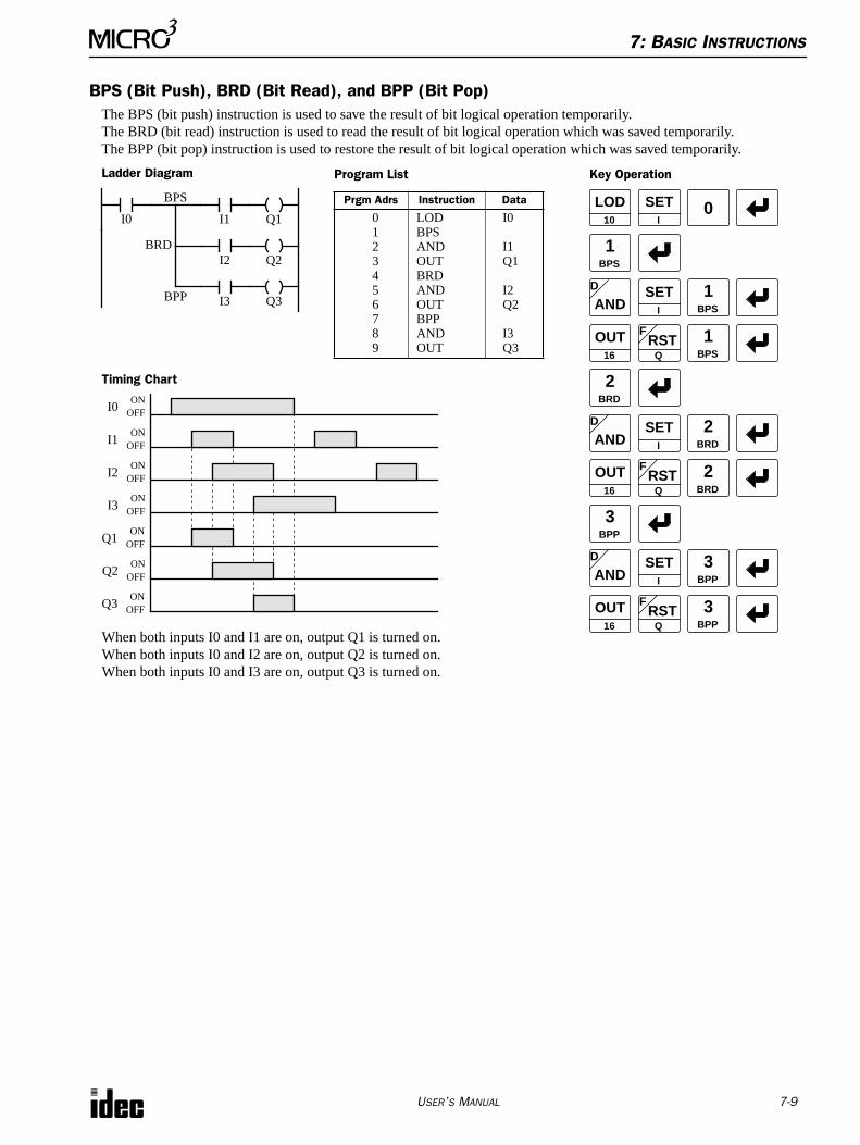
7: BASIC INSTRUCTIONS
USER’S MANUAL 7-9
BPS (Bit Push), BRD (Bit Read), and BPP (Bit Pop)The BPS (bit push) instruction is used to save the result of bit logical operation temporarily. The BRD (bit read) instruction is used to read the result of bit logical operation which was saved temporarily.The BPP (bit pop) instruction is used to restore the result of bit logical operation which was saved temporarily.
I0 I1
I2
Ladder Diagram Key Operation
LOD10
SETIQ1
0
OUT16
RSTF
Q
SETI
1BPS
ANDD
I0ON
OFF
I1ON
OFF
I2ON
OFF
I3ON
OFF
Timing Chart
SETI
2BRD
3BPP
Q1ON
OFF
ANDD
I3
Q2
Q3
3BPP
2BRD
1BPS
1BPS
OUT16
RSTF
Q
2BRD
ANDD SET
I
OUT16
RSTF
Q
3BPP
Q2ON
OFF
Q3ON
OFF
Prgm Adrs Instruction Data
0123456789
LODBPSANDOUTBRDANDOUTBPPANDOUT
I0
I1Q1
I2Q2
I3Q3
Program List
When both inputs I0 and I1 are on, output Q1 is turned on.When both inputs I0 and I2 are on, output Q2 is turned on.When both inputs I0 and I3 are on, output Q3 is turned on.
BPS
BPP
BRD
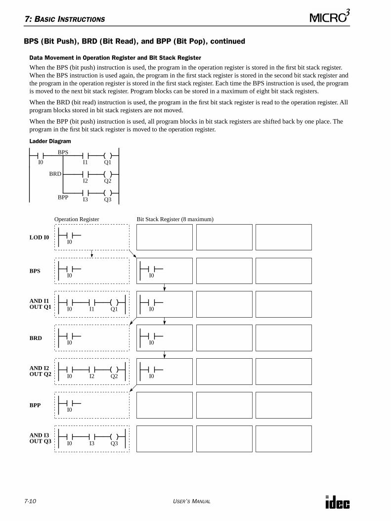
7: BASIC INSTRUCTIONS
7-10 USER’S MANUAL
BPS (Bit Push), BRD (Bit Read), and BPP (Bit Pop), continued
Data Movement in Operation Register and Bit Stack Register
When the BPS (bit push) instruction is used, the program in the operation register is stored in the first bit stack register. When the BPS instruction is used again, the program in the first stack register is stored in the second bit stack register and the program in the operation register is stored in the first stack register. Each time the BPS instruction is used, the program is moved to the next bit stack register. Program blocks can be stored in a maximum of eight bit stack registers.
When the BRD (bit read) instruction is used, the program in the first bit stack register is read to the operation register. All program blocks stored in bit stack registers are not moved.
When the BPP (bit push) instruction is used, all program blocks in bit stack registers are shifted back by one place. The program in the first bit stack register is moved to the operation register.
Operation Register Bit Stack Register (8 maximum)
LOD I0I0
BPSI0 I0
AND I1I0 I1 Q1 I0
BRDI0 I0
I0 I2 Q2 I0
BPPI0
I0 I3 Q3
OUT Q1
AND I2OUT Q2
AND I3OUT Q3
I0 I1
I2
Ladder Diagram
Q1
I3
Q2
Q3
BPS
BPP
BRD
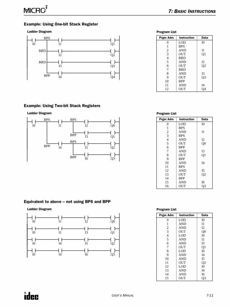
7: BASIC INSTRUCTIONS
USER’S MANUAL 7-11
Example: Using One-bit Stack Register
Example: Using Two-bit Stack Registers
Equivalent to above – not using BPS and BPP
I0 I1
I2
Ladder Diagram
Q1
I3
Q2
Q3
BPS
BRD
Prgm Adrs Instruction Data
0123456789
101112
LODBPSANDOUTBRDANDOUTBRDANDOUTBPPANDOUT
I0
I1Q1
I2Q2
I3Q3
I4Q4
Program List
Q4I4BPP
BRD
I0 I1
Ladder Diagram
Q0
I4
Q1
Q2
BPS Prgm Adrs Instruction Data
0123456789
10111213141516
LODBPSANDBPSANDOUTBPPANDOUTBPPANDBPSANDOUTBPPANDOUT
I0
I1
I2Q0
I3Q1
I4
I5Q2
I6Q3
Program List
Q3
BPP
I2
BPS
I5
BPS
I6BPP
BPP I3
I0 I1
Ladder Diagram
Q0
I4
Q1
Q2
Prgm Adrs Instruction Data
0123456789
101112131415
LODANDANDOUTLODANDANDOUTLODANDANDOUTLODANDANDOUT
I0I1I2Q0I0I1I3Q1I0I4I5Q2I0I4I6Q3
Program List
Q3
I2
I5
I6
I3
I4
I1I0
I0
I0
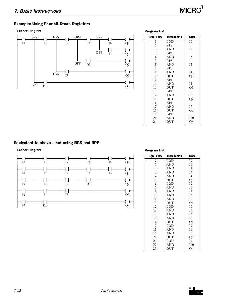
7: BASIC INSTRUCTIONS
7-12 USER’S MANUAL
Example: Using Four-bit Stack Registers
Equivalent to above – not using BPS and BPP
I0 I1
Ladder Diagram
Q0
I10
Q1
Q2
BPS Prgm Adrs Instruction Data
0123456789
101112131415161718192021
LODBPSANDBPSANDBPSANDBPSANDOUTBPPANDOUTBPPANDOUTBPPANDOUTBPPANDOUT
I0
I1
I2
I3
I4Q0
I5Q1
I6Q2
I7Q3
I10Q4
Program List
Q3
BPP
I2
I7BPP
BPP
I4I3
BPS BPS BPS
I5
I6
BPP
Q4
I0 I1
Ladder Diagram
Q0
I10
Q1
Q2
Prgm Adrs Instruction Data
0123456789
1011121314151617181920212223
LODANDANDANDANDOUTLODANDANDANDANDOUTLODANDANDANDOUTLODANDANDOUTLODANDOUT
I0I1I2I3I4Q0I0I1I2I3I5Q1I0I1I2I6Q2I0I1I7Q3I0I10Q4
Program List
Q3
I2
I7
I4I3
I5
I6
Q4
I0
I0
I0
I0
I1
I1
I1
I2
I2 I3
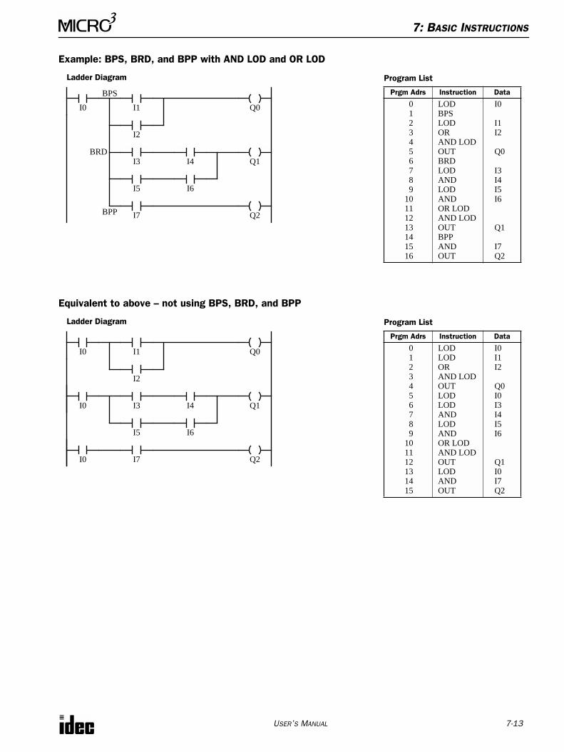
7: BASIC INSTRUCTIONS
USER’S MANUAL 7-13
Example: BPS, BRD, and BPP with AND LOD and OR LOD
Equivalent to above – not using BPS, BRD, and BPP
I0 I1
Ladder Diagram
Q0
I7
Q1
BPS Prgm Adrs Instruction Data
0123456789
10111213141516
LODBPSLODORAND LODOUTBRDLODANDLODANDOR LODAND LODOUTBPPANDOUT
I0
I1I2
Q0
I3I4I5I6
Q1
I7Q2
Program List
BPP
I6
I2
I3BRD
Q2
I4
I5
I0 I1
Ladder Diagram
Q0
I7
Q1
Prgm Adrs Instruction Data
0123456789
101112131415
LODLODORAND LODOUTLODLODANDLODANDOR LODAND LODOUTLODANDOUT
I0I1I2
Q0I0I3I4I5I6
Q1I0I7Q2
Program List
I6
I2
I3
Q2
I4
I5
I0
I0
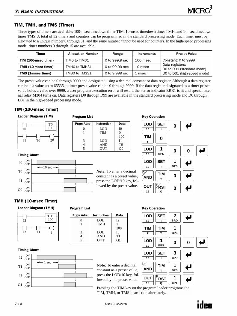
7: BASIC INSTRUCTIONS
7-14 USER’S MANUAL
TIM, TMH, and TMS (Timer)Three types of timers are available; 100-msec timedown timer TIM, 10-msec timedown timer TMH, and 1-msec timedown timer TMS. A total of 32 timers and counters can be programmed in the standard processing mode. Each timer must be allocated to a unique number 0 through 31, and the same number cannot be used for counters. In the high-speed processing mode, timer numbers 0 through 15 are available.
The preset value can be 0 through 9999 and designated using a decimal constant or data register. Although a data register can hold a value up to 65535, a timer preset value can be 0 through 9999. If the data register designated as a timer preset value holds a value over 9999, a user program execution error will result, then error indicator ERR1 is lit and special inter-nal relay M304 turns on. Data registers D0 through D99 are available in the standard processing mode and D0 through D31 in the high-speed processing mode.
TIM (100-msec Timer)
TMH (10-msec Timer)
Timer Allocation Number Range Increments Preset Value
TIM (100-msec timer) TIM0 to TIM31 0 to 999.9 sec 100 msec Constant: 0 to 9999Data registers:D0 to D99 (standard mode)D0 to D31 (high-speed mode)
TMH (10-msec timer) TMH0 to TMH31 0 to 99.99 sec 10 msec
TMS (1-msec timer) TMS0 to TMS31 0 to 9.999 sec 1 msec
I1
I0
T0
Ladder Diagram (TIM) Key Operation
LOD10
SETI
0
OUT16
RSTF
Q
Prgm Adrs Instruction Data
01
345
LODTIM
LODANDOUT
I00100I1T0Q0
Program List
I0ON
OFF
T0ON
OFF
I1ON
OFF
Q0ON
OFF
Timing Chart
LOD10
SETI
0
ANDD
T0100
Q0TIM
T0
1BPS
0 0
LOD10
1BPS
TIMT
0
10 secNote: To enter a decimal constant as a preset value, press the LOD/10 key, fol-lowed by the preset value.
I3
I2
T1
Ladder Diagram (TMH) Key Operation
LOD10
SETI
OUT16
RSTF
Q
Prgm Adrs Instruction Data
01
345
LODTMH
LODANDOUT
I21100I3T1Q1
Program List
I2ON
OFF
T1ON
OFF
I3ON
OFF
Q1ON
OFF
Timing Chart
LOD10
SETI
ANDD
TH1100
Q1TIM
T
1BPS
0
LOD10
1BPS
TIMT
1 sec
3BPP
2BRD
TIMT
1BPS
1BPS
0
Note: To enter a decimal constant as a preset value, press the LOD/10 key, fol-lowed by the preset value.
Pressing the TIM key on the program loader programs the TIM, TMH, or TMS instruction alternately.
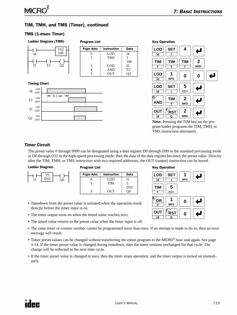
7: BASIC INSTRUCTIONS
USER’S MANUAL 7-15
TIM, TMH, and TMS (Timer), continued
TMS (1-msec Timer)
Timer CircuitThe preset value 0 through 9999 can be designated using a data register D0 through D99 in the standard processing mode or D0 through D31 in the high-speed processing mode; then the data of the data register becomes the preset value. Directly after the TIM, TMH, or TMS instruction with two required addresses, the OUT (output) instruction can be keyed.
• Timedown from the preset value is initiated when the operation result directly before the timer input is on.
• The timer output turns on when the timed value reaches zero.
• The timed value returns to the preset value when the timer input is off.
• The same timer or counter number cannot be programmed more than once. If an attempt is made to do so, then an error message will result.
• Timer preset values can be changed without transferring the entire program to the MICRO3 base unit again. See page 3-14. If the timer preset value is changed during timedown, then the timer remains unchanged for that cycle. The change will be reflected in the next time cycle.
• If the timer preset value is changed to zero, then the timer stops operation, and the timer output is turned on immedi-ately.
I5
I4
T2
Ladder Diagram (TMS) Key Operation
LOD10
SETI
OUT16
RSTF
Q
Prgm Adrs Instruction Data
01
345
LODTMS
LODANDOUT
I42100I5T2Q2
Program List
I4ON
OFF
T2ON
OFF
I5ON
OFF
Q2ON
OFF
Timing Chart
LOD10
SETI
ANDD
TS2100
Q2TIM
T
1BPS
0
LOD10
TIMT
0.1 sec
2BRD
TIMT
0
5CC=
4
TIMT
2BRD
2BRD
Note: Pressing the TIM key on the pro-gram loader programs the TIM, TMH, or TMS instruction alternately.
I1
Ladder Diagram Key Operation
LOD10
SETI
OUT16
RSTF
Q
Prgm Adrs Instruction Data
01
3
LODTIM
OUT
I15D10Q0
Program List
T5D10 Q0
TIMT
1BPS
0
5CC=
ORE
D
1BPS
0
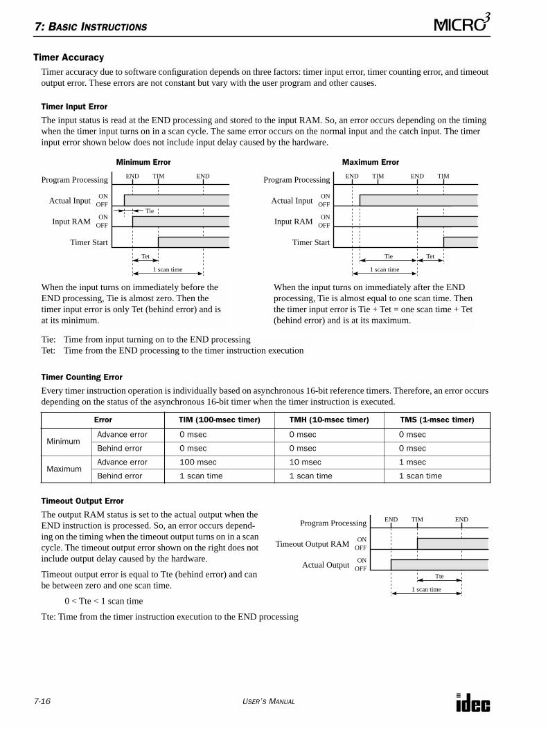
7: BASIC INSTRUCTIONS
7-16 USER’S MANUAL
Timer AccuracyTimer accuracy due to software configuration depends on three factors: timer input error, timer counting error, and timeout output error. These errors are not constant but vary with the user program and other causes.
Timer Input Error
The input status is read at the END processing and stored to the input RAM. So, an error occurs depending on the timing when the timer input turns on in a scan cycle. The same error occurs on the normal input and the catch input. The timer input error shown below does not include input delay caused by the hardware.
Timer Counting Error
Every timer instruction operation is individually based on asynchronous 16-bit reference timers. Therefore, an error occurs depending on the status of the asynchronous 16-bit timer when the timer instruction is executed.
Timeout Output Error
The output RAM status is set to the actual output when the END instruction is processed. So, an error occurs depend-ing on the timing when the timeout output turns on in a scan cycle. The timeout output error shown on the right does not include output delay caused by the hardware.
Timeout output error is equal to Tte (behind error) and can be between zero and one scan time.
0 < Tte < 1 scan time
Tte: Time from the timer instruction execution to the END processing
Error TIM (100-msec timer) TMH (10-msec timer) TMS (1-msec timer)
MinimumAdvance error 0 msec 0 msec 0 msec
Behind error 0 msec 0 msec 0 msec
MaximumAdvance error 100 msec 10 msec 1 msec
Behind error 1 scan time 1 scan time 1 scan time
Program Processing
Actual InputON
OFF
Input RAMON
OFF
Timer Start
Minimum Error
Tie
END
1 scan time
TIM END
Tet
Program Processing
Actual InputON
OFF
Input RAMON
OFF
Timer Start
Maximum Error
END
1 scan time
TIM END
Tet
TIM
Tie
When the input turns on immediately before the END processing, Tie is almost zero. Then the timer input error is only Tet (behind error) and is at its minimum.
When the input turns on immediately after the END processing, Tie is almost equal to one scan time. Then the timer input error is Tie + Tet = one scan time + Tet (behind error) and is at its maximum.
Tie: Time from input turning on to the END processingTet: Time from the END processing to the timer instruction execution
Program Processing
Timeout Output RAMON
OFF
Actual OutputON
OFF
END
1 scan time
TIM END
Tte
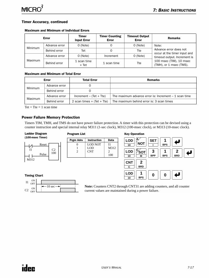
7: BASIC INSTRUCTIONS
USER’S MANUAL 7-17
Timer Accuracy, continued
Maximum and Minimum of Individual Errors
Maximum and Minimum of Total Error
Tet + Tte = 1 scan time
Power Failure Memory ProtectionTimers TIM, TMH, and TMS do not have power failure protection. A timer with this protection can be devised using a counter instruction and special internal relay M311 (1-sec clock), M312 (100-msec clock), or M313 (10-msec clock).
ErrorTimer
Input ErrorTimer Counting
ErrorTimeout Output
ErrorRemarks
MinimumAdvance error 0 (Note) 0 0 (Note) Note:
Advance error does not occur at the timer input and timeout output. Increment is 100 msec (TIM), 10 msec (TMH), or 1 msec (TMS).
Behind error Tet 0 Tte
MaximumAdvance error 0 (Note) Increment 0 (Note)
Behind error1 scan time
+ Tet1 scan time Tte
Error Total Error Remarks
MinimumAdvance error 0
Behind error 0
MaximumAdvance error Increment – (Tet + Tte) The maximum advance error is: Increment – 1 scan time
Behind error 2 scan times + (Tet + Tte) The maximum behind error is: 3 scan times
M312
Ladder Diagram Key Operation
LOD10
SETI
Prgm Adrs Instruction Data
012
LOD NOTLODCNT
I1M3122100
Program List
LOD10
C2100
LOD10
Note: Counters CNT2 through CNT31 are adding counters, and all counter current values are maintained during a power failure.
2BRD
2BRD
I1
NOTA
SOTC
M
3BPP
1BPS
CNTC
1BPS
0 0
1BPSReset
Pulse
I1ON
OFF
C2ON
OFF
Timing Chart
10 sec
(100-msec Timer)
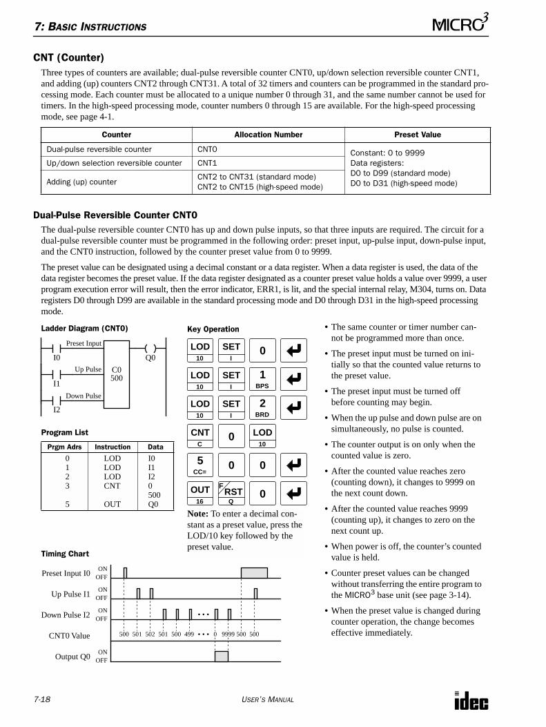
7: BASIC INSTRUCTIONS
7-18 USER’S MANUAL
CNT (Counter)Three types of counters are available; dual-pulse reversible counter CNT0, up/down selection reversible counter CNT1, and adding (up) counters CNT2 through CNT31. A total of 32 timers and counters can be programmed in the standard pro-cessing mode. Each counter must be allocated to a unique number 0 through 31, and the same number cannot be used for timers. In the high-speed processing mode, counter numbers 0 through 15 are available. For the high-speed processing mode, see page 4-1.
Dual-Pulse Reversible Counter CNT0The dual-pulse reversible counter CNT0 has up and down pulse inputs, so that three inputs are required. The circuit for a dual-pulse reversible counter must be programmed in the following order: preset input, up-pulse input, down-pulse input, and the CNT0 instruction, followed by the counter preset value from 0 to 9999.
The preset value can be designated using a decimal constant or a data register. When a data register is used, the data of the data register becomes the preset value. If the data register designated as a counter preset value holds a value over 9999, a user program execution error will result, then the error indicator, ERR1, is lit, and the special internal relay, M304, turns on. Data registers D0 through D99 are available in the standard processing mode and D0 through D31 in the high-speed processing mode.
• The same counter or timer number can-not be programmed more than once.
• The preset input must be turned on ini-tially so that the counted value returns to the preset value.
• The preset input must be turned off before counting may begin.
• When the up pulse and down pulse are on simultaneously, no pulse is counted.
• The counter output is on only when the counted value is zero.
• After the counted value reaches zero (counting down), it changes to 9999 on the next count down.
• After the counted value reaches 9999 (counting up), it changes to zero on the next count up.
• When power is off, the counter’s counted value is held.
• Counter preset values can be changed without transferring the entire program to the MICRO3 base unit (see page 3-14).
• When the preset value is changed during counter operation, the change becomes effective immediately.
Counter Allocation Number Preset Value
Dual-pulse reversible counter CNT0 Constant: 0 to 9999Data registers:D0 to D99 (standard mode)D0 to D31 (high-speed mode)
Up/down selection reversible counter CNT1
Adding (up) counterCNT2 to CNT31 (standard mode)CNT2 to CNT15 (high-speed mode)
500 500
I1
I0
Ladder Diagram (CNT0) Key Operation
LOD10
SETI
OUT16
RSTF
Q
Prgm Adrs Instruction Data
0123
5
LODLODLODCNT
OUT
I0I1I20500Q0
Program List
LOD10
C0500
Q0
1BPS
0
2BRD
I2
Preset Input
Up Pulse
Down Pulse
LOD10
SETI
SETI
CNTC
0 LOD10
5CC=
0 0
0
Preset Input I0ON
OFF
Up Pulse I1ON
OFF
Down Pulse I2ON
OFF
Timing Chart
Output Q0ON
OFF
500 501 502 501CNT0 Value 500 499 0 9999
• • •
• • •
Note: To enter a decimal con-stant as a preset value, press the LOD/10 key followed by the preset value.
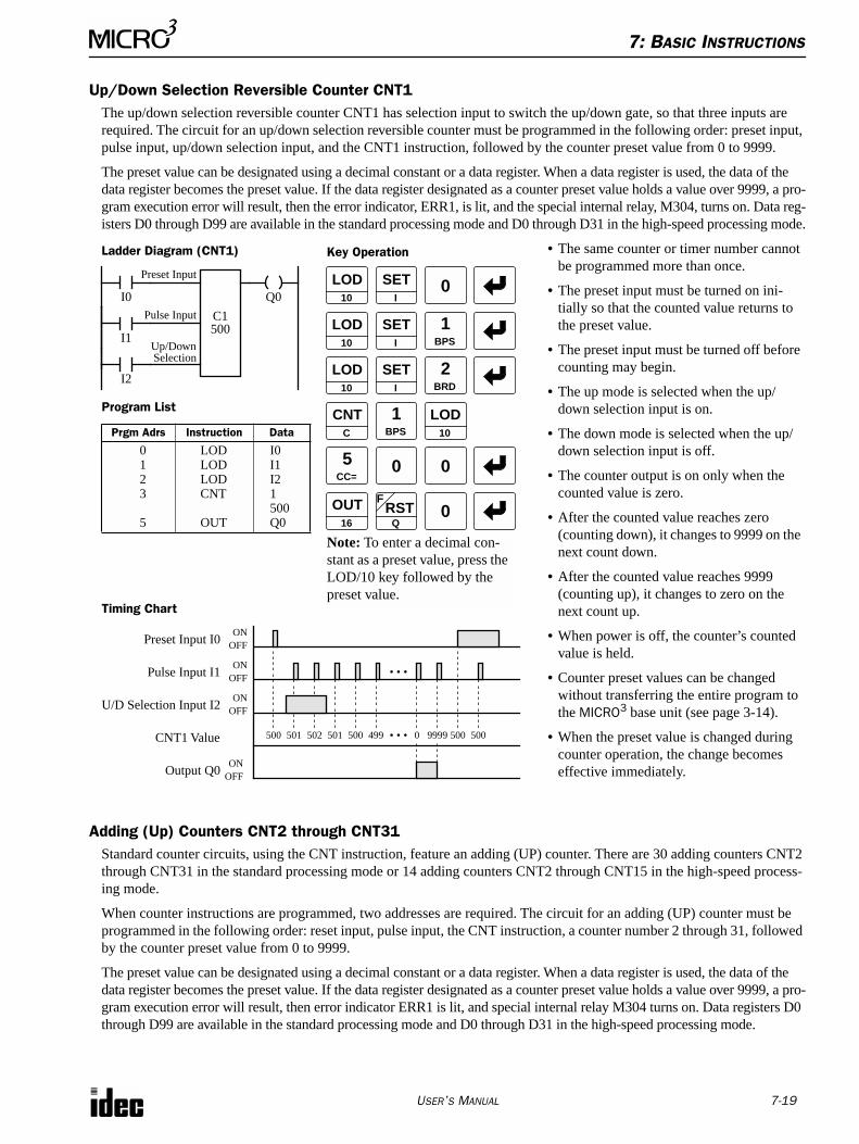
7: BASIC INSTRUCTIONS
USER’S MANUAL 7-19
Up/Down Selection Reversible Counter CNT1The up/down selection reversible counter CNT1 has selection input to switch the up/down gate, so that three inputs are required. The circuit for an up/down selection reversible counter must be programmed in the following order: preset input, pulse input, up/down selection input, and the CNT1 instruction, followed by the counter preset value from 0 to 9999.
The preset value can be designated using a decimal constant or a data register. When a data register is used, the data of the data register becomes the preset value. If the data register designated as a counter preset value holds a value over 9999, a pro-gram execution error will result, then the error indicator, ERR1, is lit, and the special internal relay, M304, turns on. Data reg-isters D0 through D99 are available in the standard processing mode and D0 through D31 in the high-speed processing mode.
• The same counter or timer number cannot be programmed more than once.
• The preset input must be turned on ini-tially so that the counted value returns to the preset value.
• The preset input must be turned off before counting may begin.
• The up mode is selected when the up/down selection input is on.
• The down mode is selected when the up/down selection input is off.
• The counter output is on only when the counted value is zero.
• After the counted value reaches zero (counting down), it changes to 9999 on the next count down.
• After the counted value reaches 9999 (counting up), it changes to zero on the next count up.
• When power is off, the counter’s counted value is held.
• Counter preset values can be changed without transferring the entire program to the MICRO3 base unit (see page 3-14).
• When the preset value is changed during counter operation, the change becomes effective immediately.
Adding (Up) Counters CNT2 through CNT31Standard counter circuits, using the CNT instruction, feature an adding (UP) counter. There are 30 adding counters CNT2 through CNT31 in the standard processing mode or 14 adding counters CNT2 through CNT15 in the high-speed process-ing mode.
When counter instructions are programmed, two addresses are required. The circuit for an adding (UP) counter must be programmed in the following order: reset input, pulse input, the CNT instruction, a counter number 2 through 31, followed by the counter preset value from 0 to 9999.
The preset value can be designated using a decimal constant or a data register. When a data register is used, the data of the data register becomes the preset value. If the data register designated as a counter preset value holds a value over 9999, a pro-gram execution error will result, then error indicator ERR1 is lit, and special internal relay M304 turns on. Data registers D0 through D99 are available in the standard processing mode and D0 through D31 in the high-speed processing mode.
500 500
I1
I0
Ladder Diagram (CNT1) Key Operation
LOD10
SETI
OUT16
RSTF
Q
Prgm Adrs Instruction Data
0123
5
LODLODLODCNT
OUT
I0I1I21500Q0
Program List
LOD10
C1500
Q0
1BPS
0
2BRD
I2
Preset Input
Pulse Input
Up/Down
LOD10
SETI
SETI
CNTC
LOD10
5CC=
0 0
0
1BPS
Selection
Preset Input I0ON
OFF
Pulse Input I1ON
OFF
U/D Selection Input I2ON
OFF
Timing Chart
Output Q0ON
OFF
500 501 502 501CNT1 Value 500 499 0 9999
• • •
• • •
Note: To enter a decimal con-stant as a preset value, press the LOD/10 key followed by the preset value.
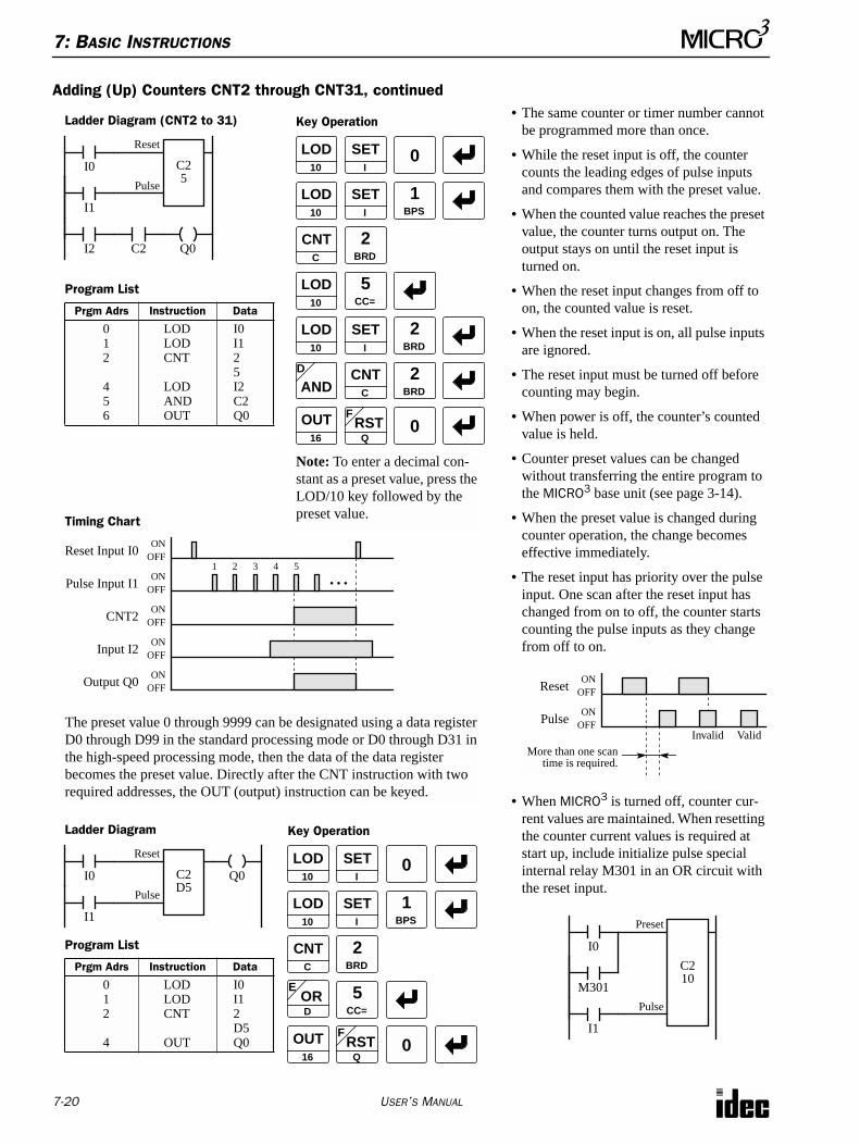
7: BASIC INSTRUCTIONS
7-20 USER’S MANUAL
Adding (Up) Counters CNT2 through CNT31, continued• The same counter or timer number cannot
be programmed more than once.
• While the reset input is off, the counter counts the leading edges of pulse inputs and compares them with the preset value.
• When the counted value reaches the preset value, the counter turns output on. The output stays on until the reset input is turned on.
• When the reset input changes from off to on, the counted value is reset.
• When the reset input is on, all pulse inputs are ignored.
• The reset input must be turned off before counting may begin.
• When power is off, the counter’s counted value is held.
• Counter preset values can be changed without transferring the entire program to the MICRO3 base unit (see page 3-14).
• When the preset value is changed during counter operation, the change becomes effective immediately.
• The reset input has priority over the pulse input. One scan after the reset input has changed from on to off, the counter starts counting the pulse inputs as they change from off to on.
• When MICRO3 is turned off, counter cur-rent values are maintained. When resetting the counter current values is required at start up, include initialize pulse special internal relay M301 in an OR circuit with the reset input.
I1
I0
Ladder Diagram (CNT2 to 31) Key Operation
LOD10
SETI
OUT16
RSTF
Q
Prgm Adrs Instruction Data
012
456
LODLODCNT
LODANDOUT
I0I125I2C2Q0
Program List
C25
Q0
1BPS
0
I2
Reset
PulseLOD
10
SETI
CNTC
LOD10
5CC=
0
Reset Input I0ON
OFF
Pulse Input I1ON
OFF
CNT2ON
OFF
Timing Chart
Output Q0ON
OFF
1
Input I2
• • •
C22
BRD
LOD10
SETI
2BRD
ANDD CNT
C
2BRD
2 3 4 5
ONOFF
The preset value 0 through 9999 can be designated using a data register D0 through D99 in the standard processing mode or D0 through D31 in the high-speed processing mode, then the data of the data register becomes the preset value. Directly after the CNT instruction with two required addresses, the OUT (output) instruction can be keyed.
Prgm Adrs Instruction Data
012
4
LODLODCNT
OUT
I0I12D5Q0
Program List
I1
I0
Ladder Diagram
C2D5
Q0
Reset
Pulse
Key Operation
LOD10
SETI
OUT16
RSTF
Q
1BPS
0
LOD10
SETI
CNTC
0
2BRD
5CC=
ORE
D
Note: To enter a decimal con-stant as a preset value, press the LOD/10 key followed by the preset value.
ResetON
OFF
PulseON
OFF
More than one scantime is required.
ValidInvalid
M301
I0
C210
I1
Preset
Pulse
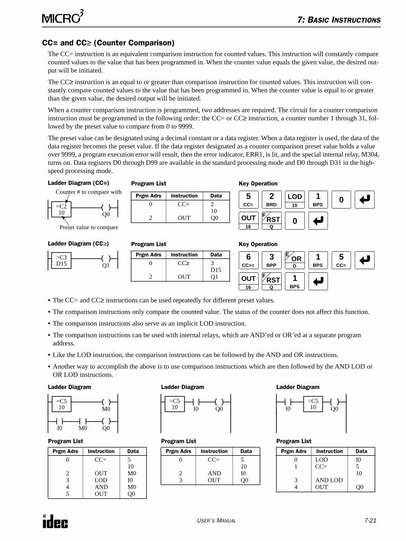
7: BASIC INSTRUCTIONS
USER’S MANUAL 7-21
CC= and CC≥ (Counter Comparison)The CC= instruction is an equivalent comparison instruction for counted values. This instruction will constantly compare counted values to the value that has been programmed in. When the counter value equals the given value, the desired out-put will be initiated.
The CC≥ instruction is an equal to or greater than comparison instruction for counted values. This instruction will con-stantly compare counted values to the value that has been programmed in. When the counter value is equal to or greater than the given value, the desired output will be initiated.
When a counter comparison instruction is programmed, two addresses are required. The circuit for a counter comparison instruction must be programmed in the following order: the CC= or CC≥ instruction, a counter number 1 through 31, fol-lowed by the preset value to compare from 0 to 9999.
The preset value can be designated using a decimal constant or a data register. When a data register is used, the data of the data register becomes the preset value. If the data register designated as a counter comparison preset value holds a value over 9999, a program execution error will result, then the error indicator, ERR1, is lit, and the special internal relay, M304, turns on. Data registers D0 through D99 are available in the standard processing mode and D0 through D31 in the high-speed processing mode.
• The CC= and CC≥ instructions can be used repeatedly for different preset values.
• The comparison instructions only compare the counted value. The status of the counter does not affect this function.
• The comparison instructions also serve as an implicit LOD instruction.
• The comparison instructions can be used with internal relays, which are AND’ed or OR’ed at a separate program address.
• Like the LOD instruction, the comparison instructions can be followed by the AND and OR instructions.
• Another way to accomplish the above is to use comparison instructions which are then followed by the AND LOD or OR LOD instructions.
Ladder Diagram (CC=) Key Operation
LOD10
01BPS
RSTF
Q0OUT
16
Ladder Diagram (CC≥) Key Operation
Prgm Adrs Instruction Data
0
2
CC≥
OUT
3D15Q1
Program List
Q1>C3D15
1BPS
RSTF
Q
OUT16
6CC>=
3BPP
5CC=
1BPS
Q0=C210
Counter # to compare with
Preset value to compare
5CC=
2BRD
Prgm Adrs Instruction Data
0
2
CC=
OUT
210Q0
Program List
ORE
D
Ladder Diagram
M0=C510
I0 M0 Q0
Prgm Adrs Instruction Data
0
2345
CC=
OUTLODANDOUT
510M0I0M0Q0
Program List
Ladder Diagram
Q0=C510 I0
Prgm Adrs Instruction Data
0
23
CC=
ANDOUT
510I0Q0
Program List
Prgm Adrs Instruction Data
01
34
LODCC=
AND LODOUT
I0510
Q0
Program List
Ladder Diagram
Q0=C510I0
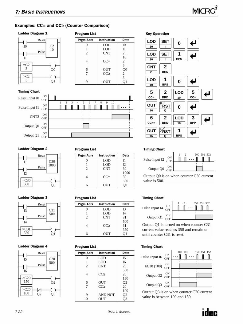
7: BASIC INSTRUCTIONS
7-22 USER’S MANUAL
Examples: CC= and CC≥ (Counter Comparison)
I1
I0
Ladder Diagram 1 Key Operation
LOD10
SETI
OUT16
RSTF
Q
Prgm Adrs Instruction Data
012
4
67
9
LODLODCNT
CC=
OUTCC≥
OUT
I0I121025Q023Q1
Program List
C210
Q0
1BPS
0Reset
PulseLOD
10
SETI
CNTC
LOD10
0
Reset Input I0ON
OFF
Pulse Input I1ON
OFF
CNT2ON
OFF
Timing Chart
Output Q1ON
OFF
1
Output Q0
• • •
2BRD
2BRD
2 3 4 5 6
ONOFF
=C25
Q1>C2
3 1BPS
0
6CC>=
5CC=
LOD10
5CC=
2BRD
LOD10
3BPP
OUT16
RSTF
Q
1BPS
7 8 9 10
I2
I1
Ladder Diagram 2
Prgm Adrs Instruction Data
012
4
6
LODLODCNT
CC=
OUT
I1I230100030500Q0
Program List
C301000
Q0
Reset
Pulse
Pulse Input I2ON
OFF
Output Q0ON
OFF
Timing Chart1
• • •
500 501 502
=C30500
2
Output Q0 is on when counter C30 current value is 500.
I4
I3
Ladder Diagram 3
Prgm Adrs Instruction Data
012
4
6
LODLODCNT
CC≥
OUT
I3I43150031350Q1
Program List
C31500
Q1
Reset
Pulse
Pulse Input I4ON
OFF
Output Q1ON
OFF
Timing Chart1
• • •
350 351 352
>C31350
2
Output Q1 is turned on when counter C31 current value reaches 350 and remain on until counter C31 is reset.
I6
I5
Ladder Diagram 4
Prgm Adrs Instruction Data
012
4
67
910
LODLODCNT
CC≥
OUTCC≥
AND NOTOUT
I5I62050020150Q220100Q2Q3
Program List
C20500
Q2
Reset
Pulse
Pulse Input I6ON
OFF
≥C20 (100)ON
OFF
Timing Chart100
• • •
150 151 152
>C20150
101
Q3>C20100 Q2
Output Q2ON
OFF
Output Q3ON
OFF
• • •
Output Q3 is on when counter C20 current value is between 100 and 150.
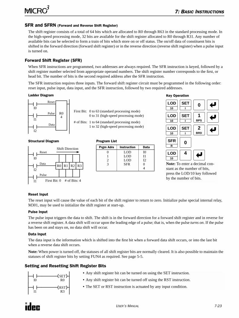
7: BASIC INSTRUCTIONS
USER’S MANUAL 7-23
SFR and SFRN (Forward and Reverse Shift Register)
The shift register consists of a total of 64 bits which are allocated to R0 through R63 in the standard processing mode. In the high-speed processing mode, 32 bits are available for the shift register allocated to R0 through R31. Any number of available bits can be selected to form a train of bits which store on or off status. The on/off data of constituent bits is shifted in the forward direction (forward shift register) or in the reverse direction (reverse shift register) when a pulse input is turned on.
Forward Shift Register (SFR)When SFR instructions are programmed, two addresses are always required. The SFR instruction is keyed, followed by a shift register number selected from appropriate operand numbers. The shift register number corresponds to the first, or head bit. The number of bits is the second required address after the SFR instruction.
The SFR instruction requires three inputs. The forward shift register circuit must be programmed in the following order: reset input, pulse input, data input, and the SFR instruction, followed by two required addresses.
Reset Input
The reset input will cause the value of each bit of the shift register to return to zero. Initialize pulse special internal relay, M301, may be used to initialize the shift register at start-up.
Pulse Input
The pulse input triggers the data to shift. The shift is in the forward direction for a forward shift register and in reverse for a reverse shift register. A data shift will occur upon the leading edge of a pulse; that is, when the pulse turns on. If the pulse has been on and stays on, no data shift will occur.
Data Input
The data input is the information which is shifted into the first bit when a forward data shift occurs, or into the last bit when a reverse data shift occurs.
Note: When power is turned off, the statuses of all shift register bits are normally cleared. It is also possible to maintain the statuses of shift register bits by setting FUN4 as required. See page 5-5.
Setting and Resetting Shift Register Bits
I1
I0
Ladder Diagram Key Operation
LOD10
SETI
Prgm Adrs Instruction Data
0123
LODLODLODSFR
I0I1I204
Program List
R04 1
BPS
0Reset
PulseLOD
10
SETI
LOD10
2BRD
0
I2
DataLOD
10
SETI
SFRR
4
Structural Diagram
I2
I0
R0
Reset
Data
I1
Pulse
R1 R2 R3
Shift Direction
First Bit: 0 # of Bits: 4
First Bit: 0 to 63 (standard processing mode)0 to 31 (high-speed processing mode)
# of Bits: 1 to 64 (standard processing mode)1 to 32 (high-speed processing mode)
Note: To enter a decimal con-stant as the number of bits, press the LOD/10 key followed by the number of bits.
I1
I0 R0SET
R3RST
• Any shift register bit can be turned on using the SET instruction.
• Any shift register bit can be turned off using the RST instruction.
• The SET or RST instruction is actuated by any input condition.
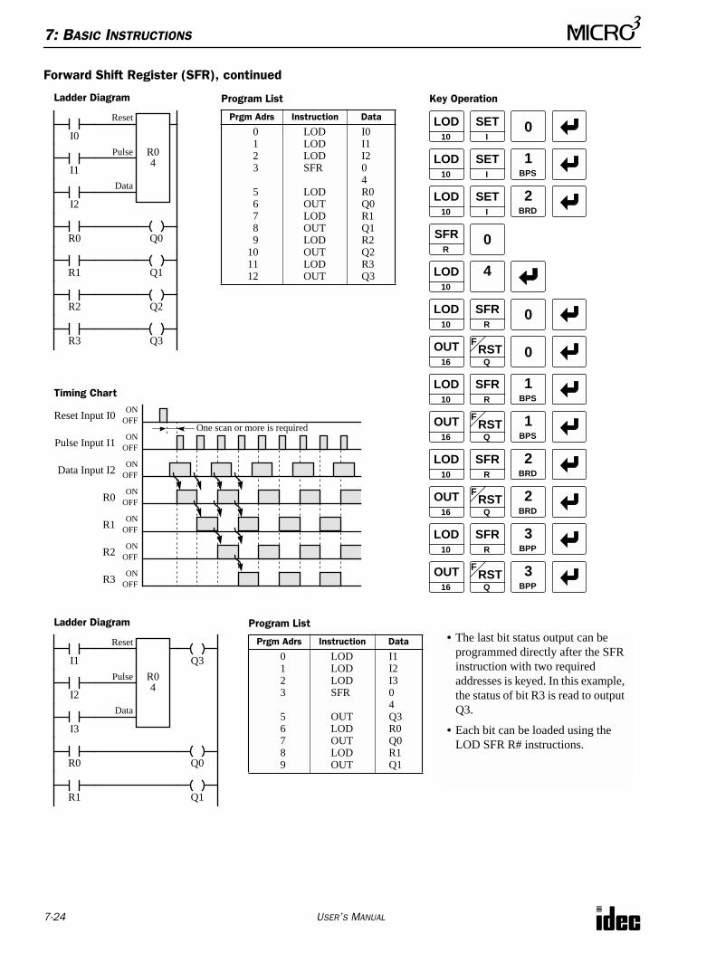
7: BASIC INSTRUCTIONS
7-24 USER’S MANUAL
Forward Shift Register (SFR), continued
I1
I0
Ladder Diagram Key Operation
LOD10
SETI
Prgm Adrs Instruction Data
0123
56789
101112
LODLODLODSFR
LODOUTLODOUTLODOUTLODOUT
I0I1I204R0Q0R1Q1R2Q2R3Q3
Program List
R04 1
BPS
0Reset
PulseLOD
10
SETI
LOD10
Reset Input I0ON
OFF
Pulse Input I1ON
OFF
Data Input I2ON
OFF
Timing Chart
R1ON
OFF
One scan or more is required
R0
2BRD
ONOFF
0
I2
DataLOD
10
SETI
SFRR
4
R3ON
OFF
R2ON
OFF
R0
R1
R2
R3
LOD10
SFRR
0
OUT16
RSTF
Q0
LOD10
SFRR
OUT16
RSTF
Q
LOD10
SFRR
OUT16
RSTF
Q
LOD10
SFRR
OUT16
RSTF
Q
1BPS
1BPS
2BRD
2BRD
3BPP
3BPP
Q0
Q1
Q2
Q3
I2
I1
Ladder Diagram
Prgm Adrs Instruction Data
0123
56789
LODLODLODSFR
OUTLODOUTLODOUT
I1I2I304Q3R0Q0R1Q1
Program List
R04
Reset
Pulse
I3
Data
Q3
R0
R1
Q0
Q1
• The last bit status output can be programmed directly after the SFR instruction with two required addresses is keyed. In this example, the status of bit R3 is read to output Q3.
• Each bit can be loaded using the LOD SFR R# instructions.
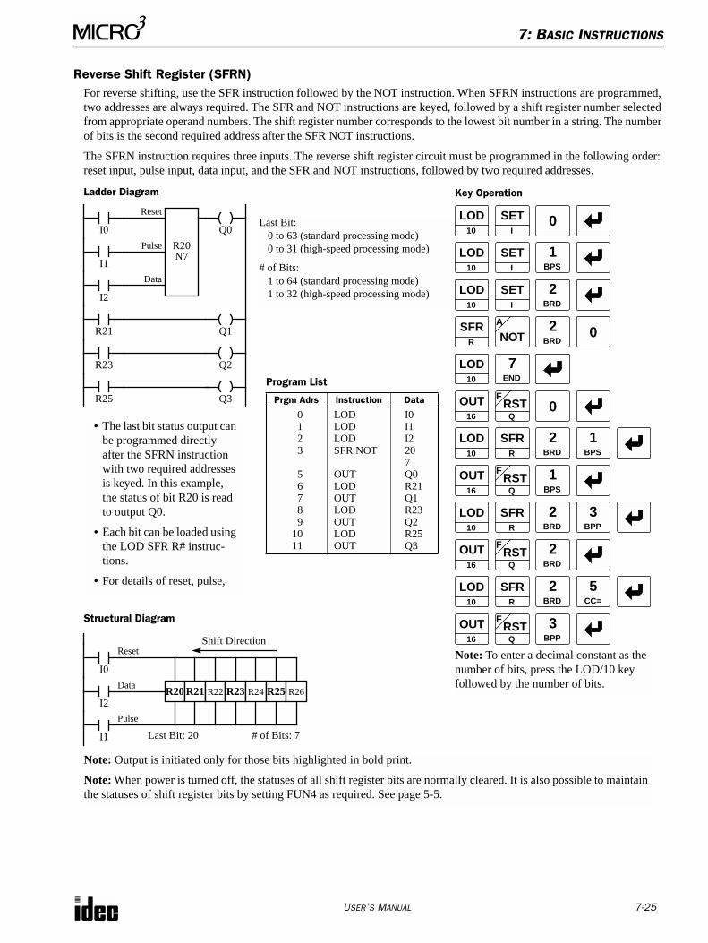
7: BASIC INSTRUCTIONS
USER’S MANUAL 7-25
Reverse Shift Register (SFRN)For reverse shifting, use the SFR instruction followed by the NOT instruction. When SFRN instructions are programmed, two addresses are always required. The SFR and NOT instructions are keyed, followed by a shift register number selected from appropriate operand numbers. The shift register number corresponds to the lowest bit number in a string. The number of bits is the second required address after the SFR NOT instructions.
The SFRN instruction requires three inputs. The reverse shift register circuit must be programmed in the following order: reset input, pulse input, data input, and the SFR and NOT instructions, followed by two required addresses.
I1
I0
Ladder Diagram Key Operation
LOD10
SETI
Prgm Adrs Instruction Data
0123
56789
1011
LODLODLODSFR NOT
OUTLODOUTLODOUTLODOUT
I0I1I2207Q0R21Q1R23Q2R25Q3
Program List
R20N7 1
BPS
0Reset
PulseLOD
10
SETI
LOD10
2BRD
I2
DataLOD
10
SETI
SFRR
R21
R23
R25 OUT16
RSTF
Q0
LOD10
SFRR
OUT16
RSTF
Q
LOD10
SFRR
OUT16
RSTF
Q
LOD10
SFRR
OUT16
RSTF
Q
1BPS
1BPS
2BRD
2BRD
3BPP
Q1
Q2
Q3
Q0Last Bit:
0 to 63 (standard processing mode)0 to 31 (high-speed processing mode)
# of Bits:1 to 64 (standard processing mode)1 to 32 (high-speed processing mode)
NOTA 2
BRD0
7END
2BRD
3BPP
2BRD
5CC=
Structural Diagram
I2
I0
R20
Reset
Data
I1
Pulse
R21 R22 R23
Shift Direction
Last Bit: 20 # of Bits: 7
R24 R25 R26
Note: Output is initiated only for those bits highlighted in bold print.
Note: When power is turned off, the statuses of all shift register bits are normally cleared. It is also possible to maintain the statuses of shift register bits by setting FUN4 as required. See page 5-5.
• The last bit status output can be programmed directly after the SFRN instruction with two required addresses is keyed. In this example, the status of bit R20 is read to output Q0.
• Each bit can be loaded using the LOD SFR R# instruc-tions.
• For details of reset, pulse,
Note: To enter a decimal constant as the number of bits, press the LOD/10 key followed by the number of bits.
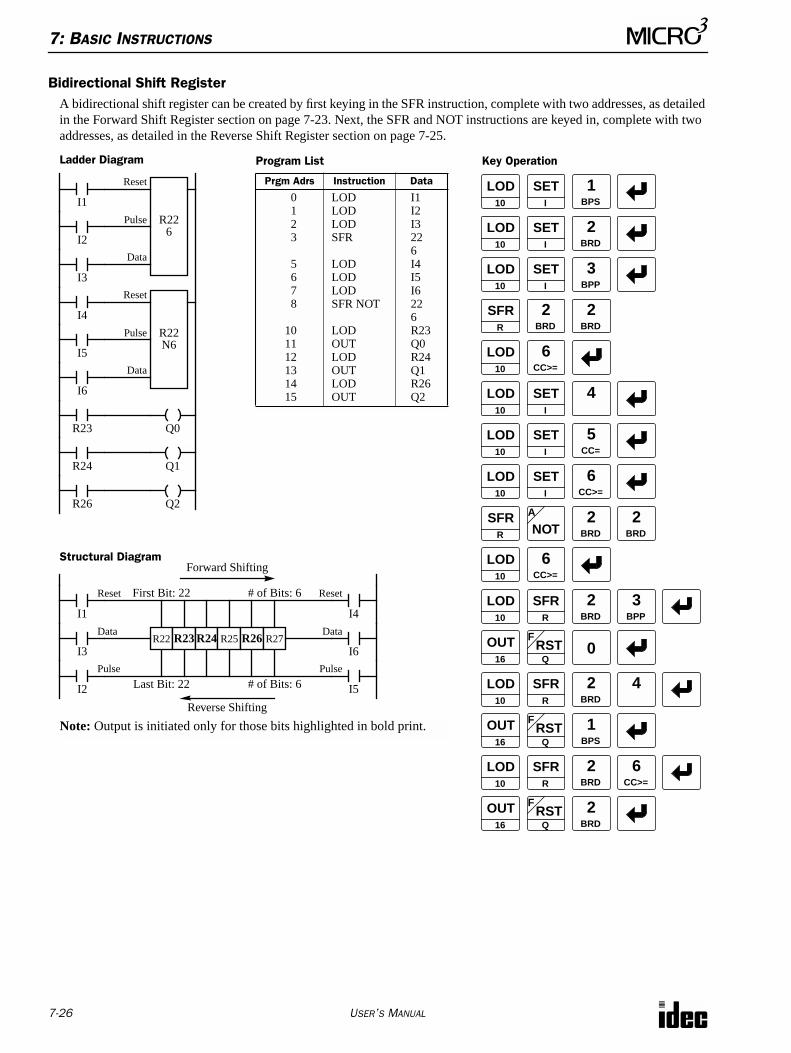
7: BASIC INSTRUCTIONS
7-26 USER’S MANUAL
Bidirectional Shift RegisterA bidirectional shift register can be created by first keying in the SFR instruction, complete with two addresses, as detailed in the Forward Shift Register section on page 7-23. Next, the SFR and NOT instructions are keyed in, complete with two addresses, as detailed in the Reverse Shift Register section on page 7-25.
I2
I1
Ladder Diagram Key Operation
LOD10
SETI
Prgm Adrs Instruction Data
0123
5678
101112131415
LODLODLODSFR
LODLODLODSFR NOT
LODOUTLODOUTLODOUT
I1I2I3226I4I5I6226R23Q0R24Q1R26Q2
Program List
R226
1BPS
Reset
PulseLOD
10
SETI
LOD10
2BRD
I3
DataLOD
10
SETI
SFRR
R23
R24
R26
LOD10
SFRR
OUT16
RSTF
Q
LOD10
SFRR
OUT16
RSTF
Q
LOD10
SFRR
OUT16
RSTF
Q
1BPS
2BRD
2BRD
3BPP
Q0
Q1
Q2
I5
I4
R22N6
Reset
Pulse
I6
Data
Structural Diagram
I3
I1
R22
Reset
Data
I2
Pulse
R23 R24 R25
Forward Shifting
Last Bit: 22 # of Bits: 6
R26 R27
Note: Output is initiated only for those bits highlighted in bold print.
I4
I6
I5
Reset
Data
Pulse
First Bit: 22 # of Bits: 6
Reverse Shifting
LOD10
SETI
LOD10
SETI
LOD10
LOD10
SETI
SFRR
4
2BRD
2BRD
NOTA
6CC>=
2BRD
2BRD
6CC>=
2BRD
3BPP
0
4
2BRD
6CC>=
5CC=
6CC>=
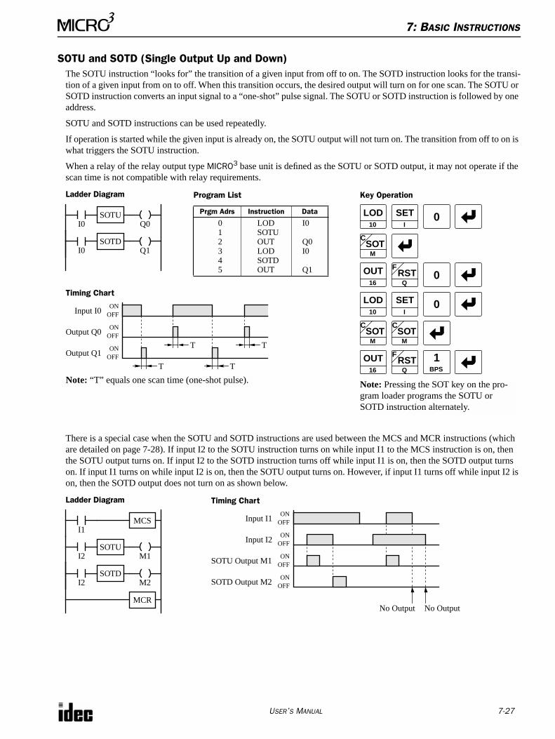
7: BASIC INSTRUCTIONS
USER’S MANUAL 7-27
SOTU and SOTD (Single Output Up and Down)The SOTU instruction “looks for” the transition of a given input from off to on. The SOTD instruction looks for the transi-tion of a given input from on to off. When this transition occurs, the desired output will turn on for one scan. The SOTU or SOTD instruction converts an input signal to a “one-shot” pulse signal. The SOTU or SOTD instruction is followed by one address.
SOTU and SOTD instructions can be used repeatedly.
If operation is started while the given input is already on, the SOTU output will not turn on. The transition from off to on is what triggers the SOTU instruction.
When a relay of the relay output type MICRO3 base unit is defined as the SOTU or SOTD output, it may not operate if the scan time is not compatible with relay requirements.
There is a special case when the SOTU and SOTD instructions are used between the MCS and MCR instructions (which are detailed on page 7-28). If input I2 to the SOTU instruction turns on while input I1 to the MCS instruction is on, then the SOTU output turns on. If input I2 to the SOTD instruction turns off while input I1 is on, then the SOTD output turns on. If input I1 turns on while input I2 is on, then the SOTU output turns on. However, if input I1 turns off while input I2 is on, then the SOTD output does not turn on as shown below.
I0
I0
Ladder Diagram Key Operation
LOD10
SETI
OUT16
RSTF
Q
Prgm Adrs Instruction Data
012345
LODSOTUOUTLODSOTDOUT
I0
Q0I0
Q1
Program List
Input I0ON
OFF
Output Q0ON
OFF
Output Q1ON
OFF
Timing ChartSET
I
Q1
LOD10
0
Note: Pressing the SOT key on the pro-gram loader programs the SOTU or SOTD instruction alternately.
SOTUQ0
SOTD SOTC
M
0
OUT16
RSTF
Q
0
SOTC
MSOT
C
M
1BPS
T
T T
T
Note: “T” equals one scan time (one-shot pulse).
I2
I1
Ladder Diagram
Input I1ON
OFF
SOTU Output M1ON
OFF
SOTD Output M2ON
OFF
Timing Chart
M2
MCS
SOTD
MCRNo Output No Output
I2 M1SOTU
Input I2ON
OFF
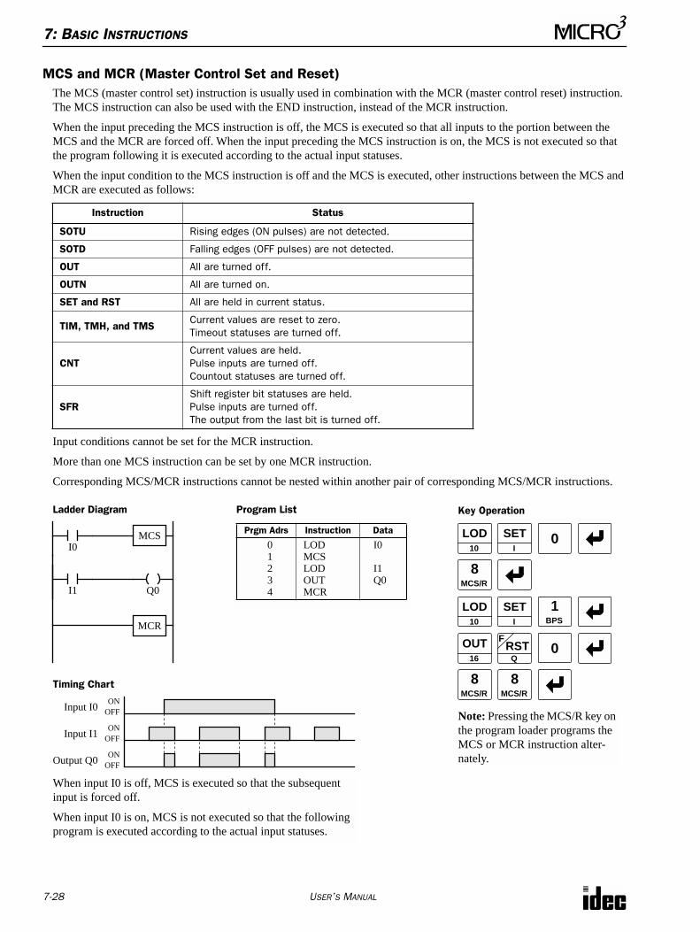
7: BASIC INSTRUCTIONS
7-28 USER’S MANUAL
MCS and MCR (Master Control Set and Reset)The MCS (master control set) instruction is usually used in combination with the MCR (master control reset) instruction. The MCS instruction can also be used with the END instruction, instead of the MCR instruction.
When the input preceding the MCS instruction is off, the MCS is executed so that all inputs to the portion between the MCS and the MCR are forced off. When the input preceding the MCS instruction is on, the MCS is not executed so that the program following it is executed according to the actual input statuses.
When the input condition to the MCS instruction is off and the MCS is executed, other instructions between the MCS and MCR are executed as follows:
Input conditions cannot be set for the MCR instruction.
More than one MCS instruction can be set by one MCR instruction.
Corresponding MCS/MCR instructions cannot be nested within another pair of corresponding MCS/MCR instructions.
Instruction Status
SOTU Rising edges (ON pulses) are not detected.
SOTD Falling edges (OFF pulses) are not detected.
OUT All are turned off.
OUTN All are turned on.
SET and RST All are held in current status.
TIM, TMH, and TMSCurrent values are reset to zero.Timeout statuses are turned off.
CNTCurrent values are held.Pulse inputs are turned off.Countout statuses are turned off.
SFRShift register bit statuses are held.Pulse inputs are turned off.The output from the last bit is turned off.
Ladder Diagram Key Operation
I0LOD
10
SETI
0
RSTF
Q
Prgm Adrs Instruction Data
01234
LODMCSLODOUTMCR
I0
I1Q0
Program List
I1
1BPS
Input I0ON
OFF
Input I1ON
OFF
Output Q0ON
OFF
Timing Chart
LOD10
SETI
MCS
8MCS/R
MCR
Q0
0
8MCS/R
8MCS/R
When input I0 is off, MCS is executed so that the subsequent input is forced off.
When input I0 is on, MCS is not executed so that the following program is executed according to the actual input statuses.
Note: Pressing the MCS/R key on the program loader programs the MCS or MCR instruction alter-nately.
OUT16
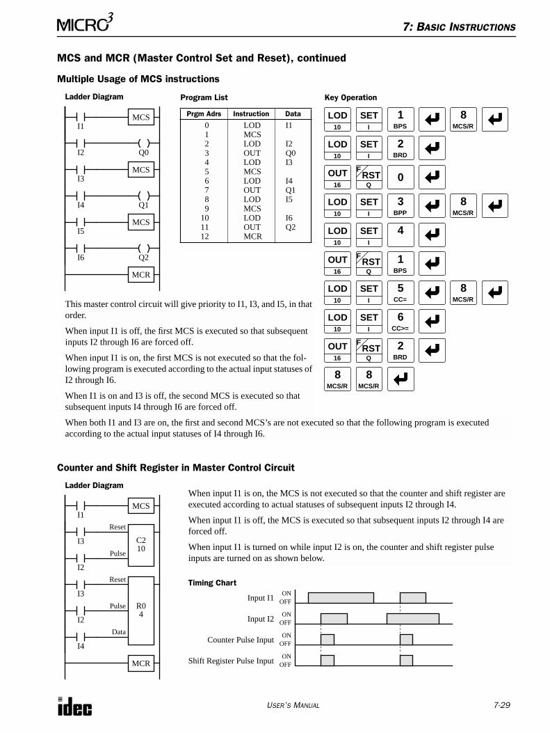
7: BASIC INSTRUCTIONS
USER’S MANUAL 7-29
MCS and MCR (Master Control Set and Reset), continued
Multiple Usage of MCS instructions
Counter and Shift Register in Master Control Circuit
Ladder Diagram Key Operation
I1LOD
10
Prgm Adrs Instruction Data
0123456789
101112
LODMCSLODOUTLODMCSLODOUTLODMCSLODOUTMCR
I1
I2Q0I3
I4Q1I5
I6Q2
Program List
OUT16
RSTF
Q0
2BRDQ0I2
I3
I4
I5
I6
MCS
MCR
MCS
MCS
Q1
Q2
SETI
1BPS
8MCS/R
LOD10
SETI
8MCS/R
LOD10
OUT16
RSTF
Q
2BRD
SETI
1BPS
8MCS/R
LOD10
SETI
6CC>=
3BPP
5CC=
4
LOD10
OUT16
RSTF
Q
SETI
8MCS/R
LOD10
SETI
8MCS/R
This master control circuit will give priority to I1, I3, and I5, in that order.
When input I1 is off, the first MCS is executed so that subsequent inputs I2 through I6 are forced off.
When input I1 is on, the first MCS is not executed so that the fol-lowing program is executed according to the actual input statuses of I2 through I6.
When I1 is on and I3 is off, the second MCS is executed so that subsequent inputs I4 through I6 are forced off.
When both I1 and I3 are on, the first and second MCS’s are not executed so that the following program is executed according to the actual input statuses of I4 through I6.
Ladder Diagram
I1MCS
MCR
I2
I3
R04
Reset
Pulse
I4
Data
I2
I3 C210
Reset
Pulse
Input I1ON
OFF
Counter Pulse InputON
OFF
Shift Register Pulse InputON
OFF
Timing Chart
Input I2ON
OFF
When input I1 is on, the MCS is not executed so that the counter and shift register are executed according to actual statuses of subsequent inputs I2 through I4.
When input I1 is off, the MCS is executed so that subsequent inputs I2 through I4 are forced off.
When input I1 is turned on while input I2 is on, the counter and shift register pulse inputs are turned on as shown below.
7: BASIC INSTRUCTIONS
7-30 USER’S MANUAL
JMP (Jump) and JEND (Jump End)The JMP (jump) instruction is usually used in combination with the JEND (jump end) instruction. At the end of a program, the JMP instruction can also be used with the END instruction, instead of the JEND instruction.
These instructions are used to proceed through the portion of the program between the JMP and the JEND without pro-cessing. This is similar to the MCS/MCR instructions, except that the portion of the program between the MCS and MCR instruction is executed.
When the operation result immediately before the JMP instruction is on, the JMP is valid and the program is not executed. When the operation result immediately before the JMP instruction is off, the JMP is invalid and the program is executed.
When the input condition to the JMP instruction is on and the JMP is executed, other instructions between the JMP and JEND are executed as follows:
Input conditions cannot be set for the JEND instruction.
More than one JMP instruction can be set by one JEND instruction.
Corresponding JMP/JEND instructions cannot be nested within another pair of corresponding JMP/JEND instructions.
Instruction Status
SOTU Rising edges (ON pulses) are not detected.
SOTD Falling edges (OFF pulses) are not detected.
OUT and OUTN All are held in current status.
SET and RST All are held in current status.
TIM, TMH, and TMSCurrent values are held.Timeout statuses are held.
CNTCurrent values are held.Pulse inputs are turned off.Countout statuses are held.
SFRShift register bit statuses are held.Pulse inputs are turned off.The output from the last bit is held.
Ladder Diagram Key Operation
I0LOD
10
SETI
0Prgm Adrs Instruction Data
01234
LODJMPLODOUTJEND
I0
I1Q0
Program List
I1
1BPS
Input I0ON
OFF
Input I1ON
OFF
Output Q0ON
OFF
Timing Chart
LOD10
SETI
JMP
JEND
Q0
0
When input I0 is on, JMP is executed so that the subsequent output status is held.
When input I0 is off, JMP is not executed so that the following program is executed according to the actual input statuses.
Note: Pressing the JMP/E key on the program loader programs the JMP or JEND instruction alter-nately.
9JMP/E
9JMP/E
9JMP/E
RSTF
Q
OUT16
7: BASIC INSTRUCTIONS
USER’S MANUAL 7-31
JMP (Jump) and JEND (Jump End), continued
Ladder Diagram Key Operation
I1LOD
10
Prgm Adrs Instruction Data
0123456789
101112
LODJMPLODOUTLODJMPLODOUTLODJMPLODOUTJEND
I1
I2Q0I3
I4Q1I5
I6Q2
Program List
OUT16
RSTF
Q0
2BRDQ0I2
I3
I4
I5
I6
JMP
JEND
JMP
JMP
Q1
Q2
SETI
1BPS
LOD10
SETI
LOD10
OUT16
RSTF
Q
2BRD
SETI
1BPS
LOD10
SETI
6CC>=
3BPP
5CC=
4
LOD10
OUT16
RSTF
Q
SETI
LOD10
SETI
This jump circuit will give priority to I1, I3, and I5, in that order.
When input I1 is on, the first JMP is executed so that subsequent output statuses of Q0 through Q2 are held.
When input I1 is off, the first JMP is not executed so that the fol-lowing program is executed according to the actual input statuses of I2 through I6.
When I1 is off and I3 is on, the second JMP is executed so that sub-sequent output statuses of Q1 and Q2 are held.
When both I1 and I3 are off, the first and second JMP’s are not exe-cuted so that the following program is executed according to the actual input statuses of I4 through I6.
9JMP/E
9JMP/E
9JMP/E
9JMP/E
9JMP/E
7: BASIC INSTRUCTIONS
7-32 USER’S MANUAL
SET and RST (Reset)The SET and RST (reset) instructions are used to set (on) or reset (off) outputs, internal relays, and shift register bits. The SET and RST instructions require one address which must be selected from the appropriate operand numbers. The same output can be set and reset many times within a program. SET and RST instructions operate in every scan while the input is on.
ENDThe END instruction is always required at the end of a program; however, it is not necessary to program the END instruc-tion after the last programmed instruction. The END instruction already exists at every unused address. (When an address is used for programming, the END instruction is removed.)
The END key is provided on the program loader for purposes other than programming an END instruction, (which is rarely necessary). A useful purpose for the END key is to find the program address for the end of a program:
A scan is the execution of all instructions from address zero to the END instruction. The time required for this execution is referred to as one scan time. The scan time varies with respect to program length, which corresponds to the address where the END instruction is found.
During the scan time, program instructions are processed sequentially. This is why the output instruction closest to the END instruction has priority over a previous instruction for the same output. No output is initiated until all logic within a scan is processed.
Output occurs simultaneously, and this is the first part of the END instruction execution. The second part of the END instruction execution is to monitor all inputs, also done simultaneously. Then program instructions are ready to be pro-cessed sequentially once again.
Valid Operands
When using in the high-speed processing mode, operands are limited. See page 6-1.
Instruction I Q M T C RSET — 0-31 0-287 — — 0-63RST — 0-31 0-287 — — 0-63
Ladder Diagram Key Operation
I0LOD
10
SETI
RSTF
Q
0
RSTF
Q
Prgm Adrs Instruction Data
0123
LODSETLODRST
I0Q0I1Q0
Program List
I1
SETI
1BPS
0
I0ON
OFF
I1ON
OFF
Q0ON
OFF
Timing Chart
Q0SET
Q0RST
RSTF
Q
LOD10
SETI
0
Key Operation
7END
USER’S MANUAL 8-1
8: ADVANCED INSTRUCTIONS
IntroductionThis chapter describes the advanced instruction menus, terms, available operands, formats, and data types used for advanced instructions.
Advanced Instruction MenusAdvanced instructions are programmed using the ADV key of the program loader. To program an advanced instruction using the program loader, select the address where you want to program an advanced instruction, and press the ADV and
keys to display the first menu of advanced instructions:
[MENU1]0:NOP 3:+-*/1:MOV 4:LOGIC2:CMP 5:SFT
ADV
[MENU2]7:CLK A:HSC 8:I/F B:COMM9:EXT
0 NOP 1 END 2 END 3 END
[MOV MENU] 1:MOV 4:IMOVN 2:MOVN 3:IMOV
[CMP MENU] 1:= 4:> 2:<> 5:<= 3:< 6:>=
[+-*/ MENU] 1:ADD+ 4:DIV/ 2:SUB- 3:MUL*
[LOGIC MENU] 1:ANDW 2:ORW 3:XORW
[BIT SFT MENU] 1:SFTL 4:ROTR 2:SFTR 3:ROTL
[CLOCK MENU] 1:CALR 4:CLKW 2:CALW 5:ADJ 3:CLKR
[I/F MENU] 1:DISP 4:ANR1 2:DGRD 3:ANR0
[COMM MENU] 1:TXD 2:RXD 3:CMP2
The MENU1 of advanced instructions include six headings of submenus. To show a sub-menu, press a number 0 through 5. When the submenu is displayed, press a number to pro-gram a required advanced instruction, then the program screen is displayed to enter operands.
The NOP instruction is entered at the selected address in the editor screen immediately when 0 is pressed while the MENU1 is displayed.
It is also possible to jump from the editor screen to the submenu by pressing the ADV key and a number, 0 through 9, A or B.
The MENU2 includes five submenu headings. As described above, to go to a submenu, press a number key 7 through B. When the submenu is displayed, press a number to program a required advanced instruction, then the pro-gram screen is displayed to enter operands
To go back to MENU1 from MENU2, press the key.
Details of programming advanced instructions are described in the following chapters.
Press the 0 key. Press the 3 key.
Press the 1 key.
Press the 2 key.
Press the 7 key.
Press the 8 key.
Press the 4 key.
Press the 5 key.
Press the B key.
To show the MENU2 of advanced instructions, press the key while the MENU1 is dis-played.
[EXT MENU] 1:PULS 2:PWM 3:A/D
Press the 9 key.
[HSC MENU] 1:HSC0 4:HSC3 2:HSC1 3:HSC2
Press the A key.
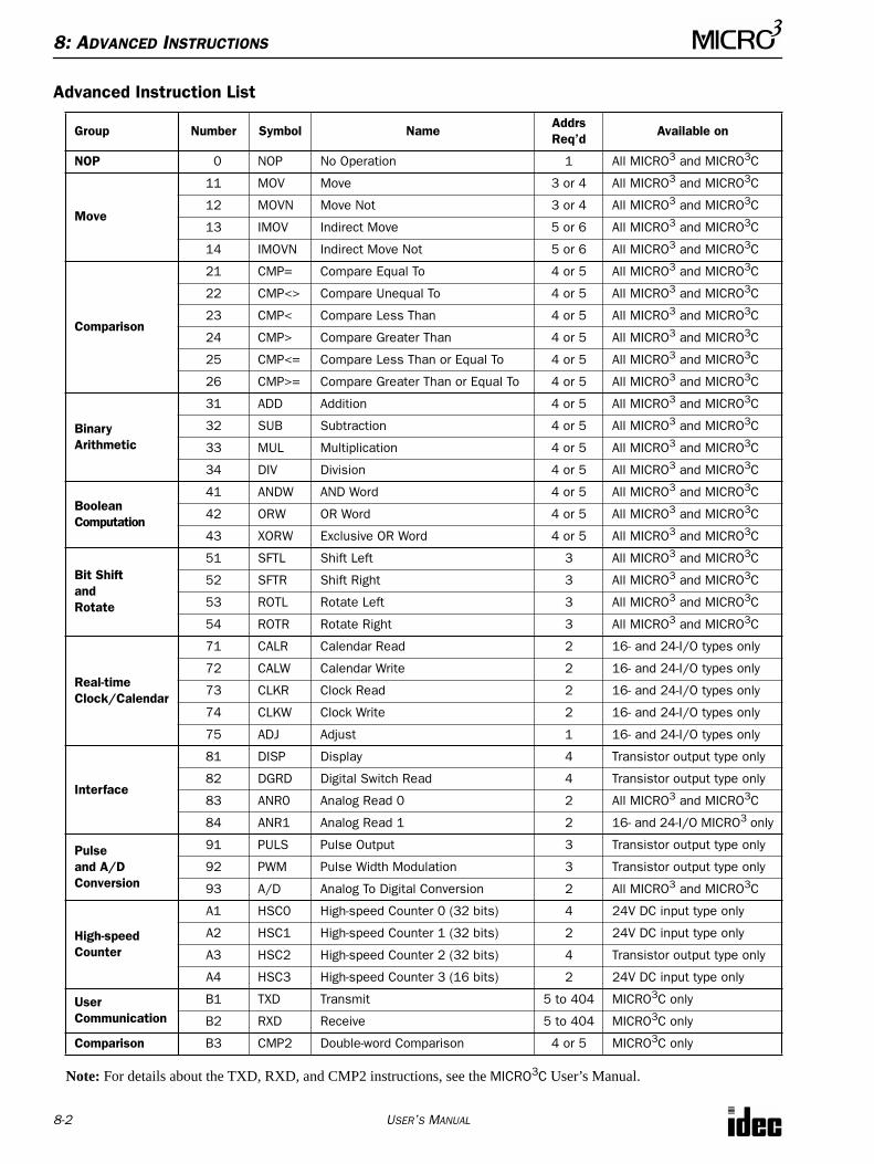
8: ADVANCED INSTRUCTIONS
8-2 USER’S MANUAL
Advanced Instruction List
Note: For details about the TXD, RXD, and CMP2 instructions, see the MICRO3C User’s Manual.
Group Number Symbol NameAddrsReq’d
Available on
NOP 0 NOP No Operation 1 All MICRO3 and MICRO3C
Move
11 MOV Move 3 or 4 All MICRO3 and MICRO3C
12 MOVN Move Not 3 or 4 All MICRO3 and MICRO3C
13 IMOV Indirect Move 5 or 6 All MICRO3 and MICRO3C
14 IMOVN Indirect Move Not 5 or 6 All MICRO3 and MICRO3C
Comparison
21 CMP= Compare Equal To 4 or 5 All MICRO3 and MICRO3C
22 CMP<> Compare Unequal To 4 or 5 All MICRO3 and MICRO3C
23 CMP< Compare Less Than 4 or 5 All MICRO3 and MICRO3C
24 CMP> Compare Greater Than 4 or 5 All MICRO3 and MICRO3C
25 CMP<= Compare Less Than or Equal To 4 or 5 All MICRO3 and MICRO3C
26 CMP>= Compare Greater Than or Equal To 4 or 5 All MICRO3 and MICRO3C
BinaryArithmetic
31 ADD Addition 4 or 5 All MICRO3 and MICRO3C
32 SUB Subtraction 4 or 5 All MICRO3 and MICRO3C
33 MUL Multiplication 4 or 5 All MICRO3 and MICRO3C
34 DIV Division 4 or 5 All MICRO3 and MICRO3C
BooleanComputation
41 ANDW AND Word 4 or 5 All MICRO3 and MICRO3C
42 ORW OR Word 4 or 5 All MICRO3 and MICRO3C
43 XORW Exclusive OR Word 4 or 5 All MICRO3 and MICRO3C
Bit ShiftandRotate
51 SFTL Shift Left 3 All MICRO3 and MICRO3C
52 SFTR Shift Right 3 All MICRO3 and MICRO3C
53 ROTL Rotate Left 3 All MICRO3 and MICRO3C
54 ROTR Rotate Right 3 All MICRO3 and MICRO3C
Real-timeClock/Calendar
71 CALR Calendar Read 2 16- and 24-I/O types only
72 CALW Calendar Write 2 16- and 24-I/O types only
73 CLKR Clock Read 2 16- and 24-I/O types only
74 CLKW Clock Write 2 16- and 24-I/O types only
75 ADJ Adjust 1 16- and 24-I/O types only
Interface
81 DISP Display 4 Transistor output type only
82 DGRD Digital Switch Read 4 Transistor output type only
83 ANR0 Analog Read 0 2 All MICRO3 and MICRO3C
84 ANR1 Analog Read 1 2 16- and 24-I/O MICRO3 only
Pulseand A/DConversion
91 PULS Pulse Output 3 Transistor output type only
92 PWM Pulse Width Modulation 3 Transistor output type only
93 A/D Analog To Digital Conversion 2 All MICRO3 and MICRO3C
High-speedCounter
A1 HSC0 High-speed Counter 0 (32 bits) 4 24V DC input type only
A2 HSC1 High-speed Counter 1 (32 bits) 2 24V DC input type only
A3 HSC2 High-speed Counter 2 (32 bits) 4 Transistor output type only
A4 HSC3 High-speed Counter 3 (16 bits) 2 24V DC input type only
User Communication
B1 TXD Transmit 5 to 404 MICRO3C only
B2 RXD Receive 5 to 404 MICRO3C only
Comparison B3 CMP2 Double-word Comparison 4 or 5 MICRO3C only
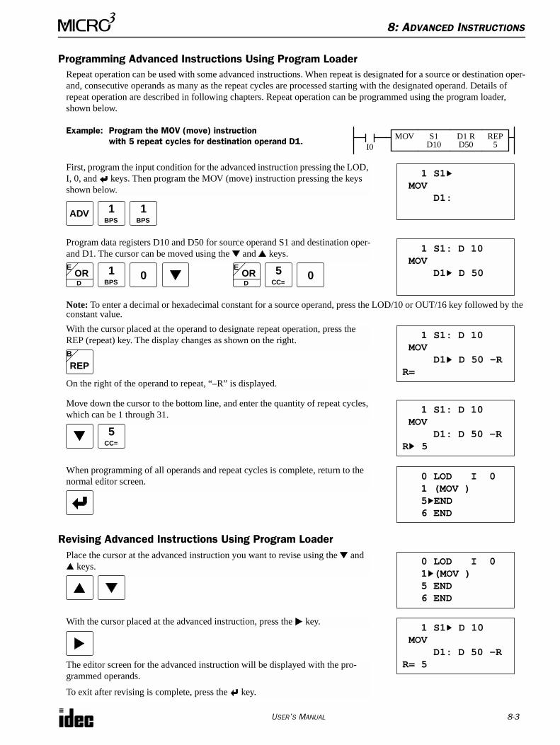
8: ADVANCED INSTRUCTIONS
USER’S MANUAL 8-3
Programming Advanced Instructions Using Program LoaderRepeat operation can be used with some advanced instructions. When repeat is designated for a source or destination oper-and, consecutive operands as many as the repeat cycles are processed starting with the designated operand. Details of repeat operation are described in following chapters. Repeat operation can be programmed using the program loader, shown below.
Example: Program the MOV (move) instructionwith 5 repeat cycles for destination operand D1.
Note: To enter a decimal or hexadecimal constant for a source operand, press the LOD/10 or OUT/16 key followed by the constant value.
Revising Advanced Instructions Using Program Loader
I0MOV S1
D10D1 RD50
REP5
1 S1 MOV D1:
First, program the input condition for the advanced instruction pressing the LOD, I, 0, and keys. Then program the MOV (move) instruction pressing the keys shown below.
ADV 1BPS
1BPS
1 S1: D 10 MOV D1 D 50
Program data registers D10 and D50 for source operand S1 and destination oper-and D1. The cursor can be moved using the and keys.
ORE
D
5CC=
01BPS
0ORE
D
1 S1: D 10 MOV D1 D 50 -RR=
With the cursor placed at the operand to designate repeat operation, press the REP (repeat) key. The display changes as shown on the right.
On the right of the operand to repeat, “–R” is displayed.
REPB
1 S1: D 10 MOV D1: D 50 -RR 5
Move down the cursor to the bottom line, and enter the quantity of repeat cycles, which can be 1 through 31.
5CC=
0 LOD I 0 1 (MOV ) 5 END 6 END
When programming of all operands and repeat cycles is complete, return to the normal editor screen.
0 LOD I 0 1 (MOV ) 5 END 6 END
Place the cursor at the advanced instruction you want to revise using the and keys.
With the cursor placed at the advanced instruction, press the key.
The editor screen for the advanced instruction will be displayed with the pro-grammed operands.
To exit after revising is complete, press the key.
1 S1 D 10 MOV D1: D 50 -RR= 5
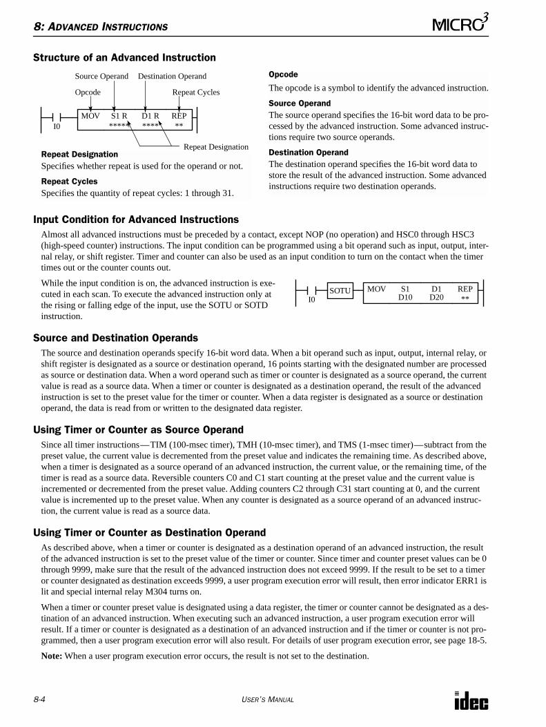
8: ADVANCED INSTRUCTIONS
8-4 USER’S MANUAL
Structure of an Advanced Instruction
Input Condition for Advanced InstructionsAlmost all advanced instructions must be preceded by a contact, except NOP (no operation) and HSC0 through HSC3 (high-speed counter) instructions. The input condition can be programmed using a bit operand such as input, output, inter-nal relay, or shift register. Timer and counter can also be used as an input condition to turn on the contact when the timer times out or the counter counts out.
While the input condition is on, the advanced instruction is exe-cuted in each scan. To execute the advanced instruction only at the rising or falling edge of the input, use the SOTU or SOTD instruction.
Source and Destination OperandsThe source and destination operands specify 16-bit word data. When a bit operand such as input, output, internal relay, or shift register is designated as a source or destination operand, 16 points starting with the designated number are processed as source or destination data. When a word operand such as timer or counter is designated as a source operand, the current value is read as a source data. When a timer or counter is designated as a destination operand, the result of the advanced instruction is set to the preset value for the timer or counter. When a data register is designated as a source or destination operand, the data is read from or written to the designated data register.
Using Timer or Counter as Source OperandSince all timer instructions—TIM (100-msec timer), TMH (10-msec timer), and TMS (1-msec timer)—subtract from the preset value, the current value is decremented from the preset value and indicates the remaining time. As described above, when a timer is designated as a source operand of an advanced instruction, the current value, or the remaining time, of the timer is read as a source data. Reversible counters C0 and C1 start counting at the preset value and the current value is incremented or decremented from the preset value. Adding counters C2 through C31 start counting at 0, and the current value is incremented up to the preset value. When any counter is designated as a source operand of an advanced instruc-tion, the current value is read as a source data.
Using Timer or Counter as Destination OperandAs described above, when a timer or counter is designated as a destination operand of an advanced instruction, the result of the advanced instruction is set to the preset value of the timer or counter. Since timer and counter preset values can be 0 through 9999, make sure that the result of the advanced instruction does not exceed 9999. If the result to be set to a timer or counter designated as destination exceeds 9999, a user program execution error will result, then error indicator ERR1 is lit and special internal relay M304 turns on.
When a timer or counter preset value is designated using a data register, the timer or counter cannot be designated as a des-tination of an advanced instruction. When executing such an advanced instruction, a user program execution error will result. If a timer or counter is designated as a destination of an advanced instruction and if the timer or counter is not pro-grammed, then a user program execution error will also result. For details of user program execution error, see page 18-5.
Note: When a user program execution error occurs, the result is not set to the destination.
Repeat DesignationSpecifies whether repeat is used for the operand or not.
Repeat CyclesSpecifies the quantity of repeat cycles: 1 through 31.
I0MOV S1 R
*****REP**
D1 R****
Opcode
The opcode is a symbol to identify the advanced instruction.
Source OperandThe source operand specifies the 16-bit word data to be pro-cessed by the advanced instruction. Some advanced instruc-tions require two source operands.
Destination OperandThe destination operand specifies the 16-bit word data to store the result of the advanced instruction. Some advanced instructions require two destination operands.
Opcode
Source Operand
Repeat Cycles
Destination Operand
Repeat Designation
I0MOV REP
**S1
D10D1D20
SOTU
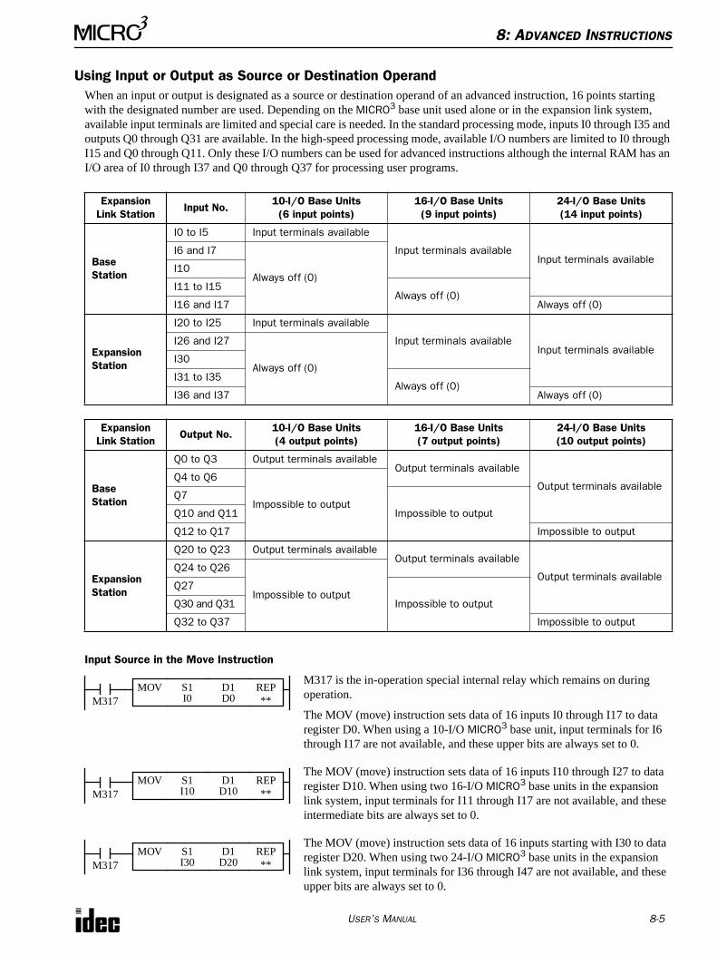
8: ADVANCED INSTRUCTIONS
USER’S MANUAL 8-5
Using Input or Output as Source or Destination OperandWhen an input or output is designated as a source or destination operand of an advanced instruction, 16 points starting with the designated number are used. Depending on the MICRO3 base unit used alone or in the expansion link system, available input terminals are limited and special care is needed. In the standard processing mode, inputs I0 through I35 and outputs Q0 through Q31 are available. In the high-speed processing mode, available I/O numbers are limited to I0 through I15 and Q0 through Q11. Only these I/O numbers can be used for advanced instructions although the internal RAM has an I/O area of I0 through I37 and Q0 through Q37 for processing user programs.
Input Source in the Move Instruction
Expansion Link Station
Input No.10-I/O Base Units
(6 input points)16-I/O Base Units
(9 input points)24-I/O Base Units(14 input points)
BaseStation
I0 to I5 Input terminals available
Input terminals availableInput terminals available
I6 and I7
Always off (0)I10
I11 to I15Always off (0)
I16 and I17 Always off (0)
Expansion Station
I20 to I25 Input terminals available
Input terminals availableInput terminals available
I26 and I27
Always off (0)I30
I31 to I35Always off (0)
I36 and I37 Always off (0)
Expansion Link Station
Output No.10-I/O Base Units(4 output points)
16-I/O Base Units(7 output points)
24-I/O Base Units(10 output points)
BaseStation
Q0 to Q3 Output terminals availableOutput terminals available
Output terminals availableQ4 to Q6
Impossible to outputQ7
Impossible to outputQ10 and Q11
Q12 to Q17 Impossible to output
Expansion Station
Q20 to Q23 Output terminals availableOutput terminals available
Output terminals availableQ24 to Q26
Impossible to outputQ27
Impossible to outputQ30 and Q31
Q32 to Q37 Impossible to output
M317MOV REP
**S1I0
D1D0
M317 is the in-operation special internal relay which remains on during operation.
The MOV (move) instruction sets data of 16 inputs I0 through I17 to data register D0. When using a 10-I/O MICRO3 base unit, input terminals for I6 through I17 are not available, and these upper bits are always set to 0.
The MOV (move) instruction sets data of 16 inputs I10 through I27 to data register D10. When using two 16-I/O MICRO3 base units in the expansion link system, input terminals for I11 through I17 are not available, and these intermediate bits are always set to 0.
The MOV (move) instruction sets data of 16 inputs starting with I30 to data register D20. When using two 24-I/O MICRO3 base units in the expansion link system, input terminals for I36 through I47 are not available, and these upper bits are always set to 0.
M317MOV REP
**S1I10
D1D10
M317MOV REP
**S1I30
D1D20
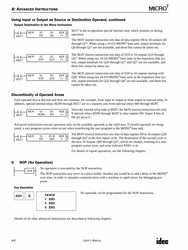
8: ADVANCED INSTRUCTIONS
8-6 USER’S MANUAL
Using Input or Output as Source or Destination Operand, continuedOutput Destination in the Move Instruction
Discontinuity of Operand AreasEach operand area is discrete and does not continue, for example, from input to output or from output to internal relay. In addition, special internal relays M290 through M317 are in a separate area from internal relays M0 through M287.
Advanced instructions execute operation only on the available operands in the valid area. If invalid operands are desig-nated, a user program syntax error occurs when transferring the user program to the MICRO3 base unit.
0 NOP (No Operation)
Key Operation
Details of all other advanced instructions are described in following chapters.
M317MOV REP
**S1D0
D1Q0
M317 is the in-operation special internal relay which remains on during operation.
The MOV (move) instruction sets data of data register D0 to 16 outputs Q0 through Q17. When using a 10-I/O MICRO3 base unit, output terminals for Q4 through Q17 are not available, and these bits cannot be taken out.
The MOV (move) instruction sets data of D10 to 16 outputs Q10 through Q27. When using two 16-I/O MICRO3 base units in the expansion link sys-tem, output terminals for Q10 through Q17 and Q27 are not available, and these bits cannot be taken out.
The MOV (move) instruction sets data of D20 to 16 outputs starting with Q30. When using two 24-I/O MICRO3 base units in the expansion link sys-tem, output terminals for Q32 through Q47 are not available, and these bits cannot be taken out.
M317MOV REP
**S1
D10D1Q10
M317MOV REP
**S1
D20D1Q30
M317MOV REP
**S1
M280D1D0
Since the internal relay ends at M287, the MOV (move) instruction sets only 8 internal relays M280 through M287 to data register D0. Upper 8 bits of D0 are set to 0.
M317MOV REP
2S1D0
D1 RQ20
The MOV (move) instruction sets data of data register D0 to 16 outputs Q20 through Q37 in the first repeat cycle. The destination of the second cycle is the next 16 outputs Q40 through Q57, which are invalid, resulting in a user program syntax error, and error indicator ERR1 is lit.
For details of repeat operations, see the following chapters.
No operation is executed by the NOP instruction.
The NOP instruction may serve as a place holder. Another use would be to add a delay to the MICRO3 scan time, in order to simulate communication with a machine or application, for debugging pur-poses.
NOP
ADVNo operands can be programmed for the NOP instruction.
0 NOP 1 END 5 END 6 END
0
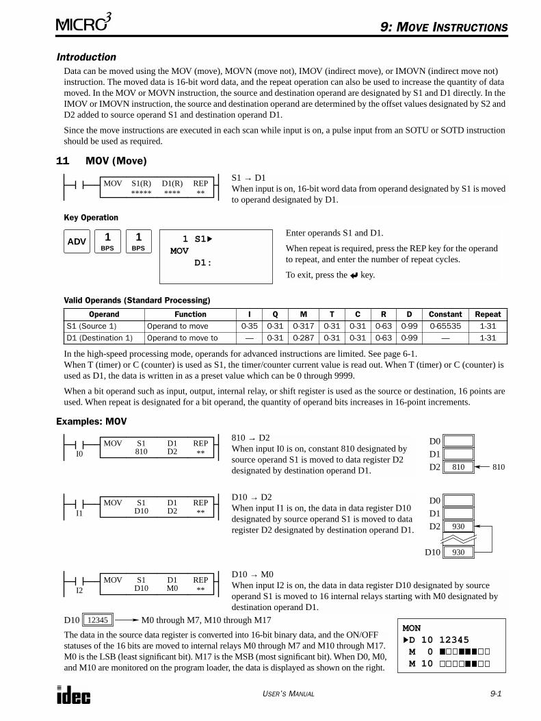
USER’S MANUAL 9-1
9: MOVE INSTRUCTIONS
IntroductionData can be moved using the MOV (move), MOVN (move not), IMOV (indirect move), or IMOVN (indirect move not) instruction. The moved data is 16-bit word data, and the repeat operation can also be used to increase the quantity of data moved. In the MOV or MOVN instruction, the source and destination operand are designated by S1 and D1 directly. In the IMOV or IMOVN instruction, the source and destination operand are determined by the offset values designated by S2 and D2 added to source operand S1 and destination operand D1.
Since the move instructions are executed in each scan while input is on, a pulse input from an SOTU or SOTD instruction should be used as required.
11 MOV (Move)
Key Operation
Valid Operands (Standard Processing)
In the high-speed processing mode, operands for advanced instructions are limited. See page 6-1.When T (timer) or C (counter) is used as S1, the timer/counter current value is read out. When T (timer) or C (counter) is used as D1, the data is written in as a preset value which can be 0 through 9999.
When a bit operand such as input, output, internal relay, or shift register is used as the source or destination, 16 points are used. When repeat is designated for a bit operand, the quantity of operand bits increases in 16-point increments.
Examples: MOV
Operand Function I Q M T C R D Constant RepeatS1 (Source 1) Operand to move 0-35 0-31 0-317 0-31 0-31 0-63 0-99 0-65535 1-31D1 (Destination 1) Operand to move to — 0-31 0-287 0-31 0-31 0-63 0-99 — 1-31
MOV S1(R)*****
REP**
D1(R)****
S1 → D1When input is on, 16-bit word data from operand designated by S1 is moved to operand designated by D1.
ADV 1BPS
1BPS
1 S1 MOV D1:
Enter operands S1 and D1.
When repeat is required, press the REP key for the operand to repeat, and enter the number of repeat cycles.
To exit, press the key.
I0MOV REP
**
810 → D2When input I0 is on, constant 810 designated by source operand S1 is moved to data register D2 designated by destination operand D1.
D1
D0
810D2 810
S1810
D1D2
I1MOV REP
**
D10 → D2When input I1 is on, the data in data register D10 designated by source operand S1 is moved to data register D2 designated by destination operand D1.
D1
D0
930D2
930D10
S1D10
D1D2
I2MOV REP
**
D10 → M0When input I2 is on, the data in data register D10 designated by source operand S1 is moved to 16 internal relays starting with M0 designated by destination operand D1.
12345D10
S1D10
D1M0
MOND 10 12345M 0 M 10
M0 through M7, M10 through M17
The data in the source data register is converted into 16-bit binary data, and the ON/OFF statuses of the 16 bits are moved to internal relays M0 through M7 and M10 through M17. M0 is the LSB (least significant bit). M17 is the MSB (most significant bit). When D0, M0, and M10 are monitored on the program loader, the data is displayed as shown on the right.
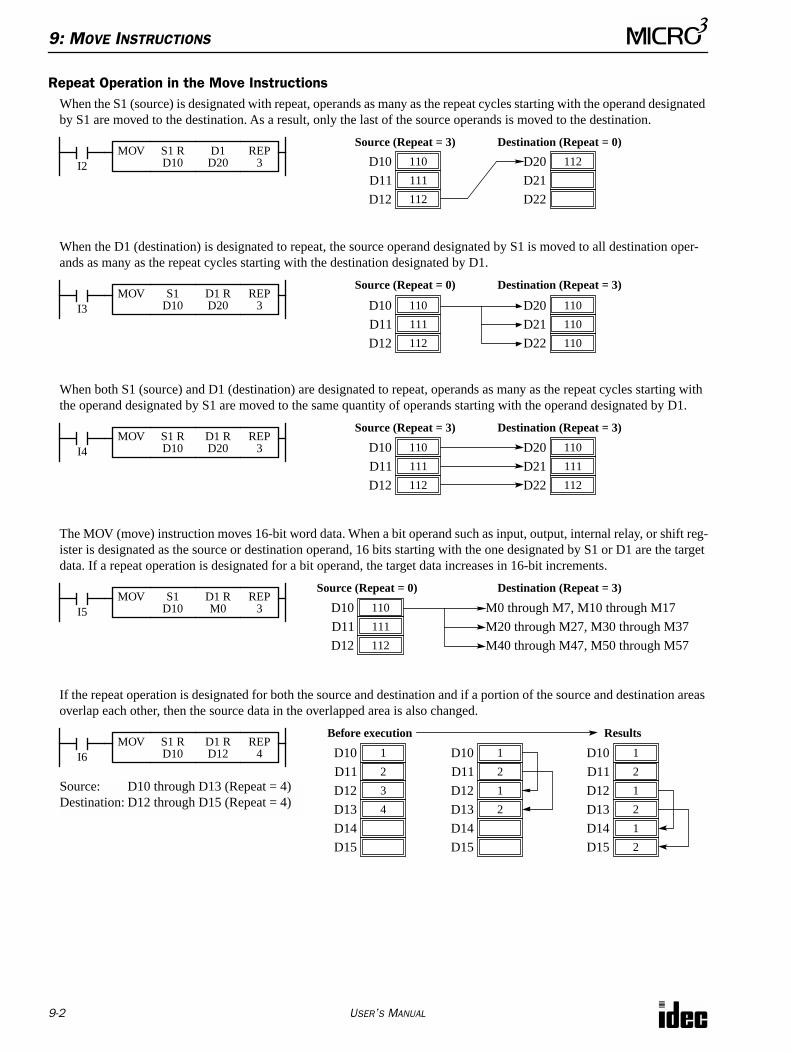
9: MOVE INSTRUCTIONS
9-2 USER’S MANUAL
Repeat Operation in the Move InstructionsWhen the S1 (source) is designated with repeat, operands as many as the repeat cycles starting with the operand designated by S1 are moved to the destination. As a result, only the last of the source operands is moved to the destination.
When the D1 (destination) is designated to repeat, the source operand designated by S1 is moved to all destination oper-ands as many as the repeat cycles starting with the destination designated by D1.
When both S1 (source) and D1 (destination) are designated to repeat, operands as many as the repeat cycles starting with the operand designated by S1 are moved to the same quantity of operands starting with the operand designated by D1.
The MOV (move) instruction moves 16-bit word data. When a bit operand such as input, output, internal relay, or shift reg-ister is designated as the source or destination operand, 16 bits starting with the one designated by S1 or D1 are the target data. If a repeat operation is designated for a bit operand, the target data increases in 16-bit increments.
If the repeat operation is designated for both the source and destination and if a portion of the source and destination areas overlap each other, then the source data in the overlapped area is also changed.
I2MOV REP
3S1 RD10
D1D20
111D11
110D10
112D12
D21
112D20
D22
Source (Repeat = 3) Destination (Repeat = 0)
I3MOV REP
3S1
D10D1 RD20
111D11
110D10
112D12
110D21
110D20
110D22
Source (Repeat = 0) Destination (Repeat = 3)
I4MOV REP
3S1 RD10
D1 RD20
111D11
110D10
112D12
111D21
110D20
112D22
Source (Repeat = 3) Destination (Repeat = 3)
I5MOV REP
3S1
D10D1 RM0
111D11
110D10
112D12
M20 through M27, M30 through M37
M0 through M7, M10 through M17
M40 through M47, M50 through M57
Source (Repeat = 0) Destination (Repeat = 3)
I6MOV REP
4S1 RD10
D1 RD12
2D11
1D10
3D124D13
D14
D15
2D11
1D10
1D122D13
D14
D15
2D11
1D10
1D122D131D142D15
Before execution Results
Source: D10 through D13 (Repeat = 4)Destination: D12 through D15 (Repeat = 4)

9: MOVE INSTRUCTIONS
USER’S MANUAL 9-3
12 MOVN (Move Not)
Key Operation
Valid Operands (Standard Processing)
In the high-speed processing mode, operands for advanced instructions are limited. See page 6-1.When T (timer) or C (counter) is used as S1, the timer/counter current value is read out. When T (timer) or C (counter) is used as D1, the data is written in as a preset value which can be 0 through 9999.
When a bit operand such as input, output, internal relay, or shift register is used as the source or destination, 16 points are used. When repeat is designated for a bit operand, the quantity of operand bits increases in 16-point increments.
Examples: MOVN
Operand Function I Q M T C R D Constant RepeatS1 (Source 1) Operand to move 0-35 0-31 0-317 0-31 0-31 0-63 0-99 0-65535 1-31D1 (Destination 1) Operand to move to — 0-31 0-287 0-31 0-31 0-63 0-99 — 1-31
MOVN S1(R)*****
REP**
D1(R)****
S1 NOT → D1When input is on, 16-bit word data from operand designated by S1 is inverted bit by bit and moved to operand designated by D1.
ADV 1BPS
1 S1 MOV N D1:
Enter operands S1 and D1.
When repeat is required, press the REP key for the operand to repeat, and enter the number of repeat cycles.
To exit, press the key.
2BRD
I0MOVN REP
**
M10 NOT → M50When input I0 is on, the 16 internal relays starting with M10 designated by source operand S1 are inverted bit by bit and moved to 16 internal relays starting with M50 designated by destination operand D1.
M10 through M17, M20 through M27 NOT
S1M10
D1M50
M50 through M57, M60 through M67
The ON/OFF statuses of the 16 internal relays M10 through M17 and M20 through M27 are inverted and moved to 16 inter-nal relays M50 through M57 and M60 through M67. When M50 and M60 are monitored on the program loader, the data is displayed as shown on the right below. M50 is the LSB (least significant bit), and M67 is the MSB (most significant bit).
Before inversion (M27-M10): 0 1 0010 0 0 0 1 0010 1 1MSB LSBS1
After inversion (M67-M50): 1 0 1101 1 1 1 0 1101 0 0MSB LSBD1
MONM 50 M 60
I1MOVN REP
**
810 NOT → D2When input I1 is on, decimal constant 810 designated by source operand S1 is converted into 16-bit binary data, and the ON/OFF statuses of the 16 bits are inverted and moved to data register D2 designated by destination oper-and D1.
D1
D0
64725D2 810
S1810
D1D2
Before inversion (810): 0 0 1000 0 1 0 1 1000 1 0MSB LSBS1
After inversion (64725): 1 1 0111 1 0 1 0 0111 0 1MSB LSBD1
I2MOVN REP
**
D10 NOT → D2When input I2 is on, the data in data register D30 designated by S1 is inverted bit by bit and moved to data register D20 designated by D1.
64605D20
930D30
S1D30
D1D20
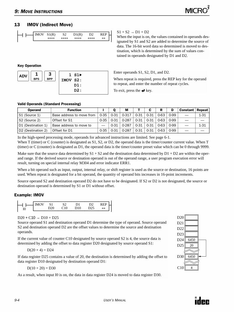
9: MOVE INSTRUCTIONS
9-4 USER’S MANUAL
13 IMOV (Indirect Move)
Key Operation
Valid Operands (Standard Processing)
In the high-speed processing mode, operands for advanced instructions are limited. See page 6-1.When T (timer) or C (counter) is designated as S1, S2, or D2, the operand data is the timer/counter current value. When T (timer) or C (counter) is designated as D1, the operand data is the timer/counter preset value which can be 0 through 9999.
Make sure that the source data determined by S1 + S2 and the destination data determined by D1 + D2 are within the oper-and range. If the derived source or destination operand is out of the operand range, a user program execution error will result, turning on special internal relay M304 and error indicator ERR1.
When a bit operand such as input, output, internal relay, or shift register is used as the source or destination, 16 points are used. When repeat is designated for a bit operand, the quantity of operand bits increases in 16-point increments.
Source operand S2 and destination operand D2 do not have to be designated. If S2 or D2 is not designated, the source or destination operand is determined by S1 or D1 without offset.
Example: IMOV
Operand Function I Q M T C R D Constant RepeatS1 (Source 1) Base address to move from 0-35 0-31 0-317 0-31 0-31 0-63 0-99 — 1-31S2 (Source 2) Offset for S1 0-35 0-31 0-287 0-31 0-31 0-63 0-99 — —D1 (Destination 1) Base address to move to — 0-31 0-287 0-31 0-31 0-63 0-99 — 1-31D2 (Destination 2) Offset for D1 0-35 0-31 0-287 0-31 0-31 0-63 0-99 — —
IMOV S1(R)****
REP**
S1 + S2 → D1 + D2When the input is on, the values contained in operands des-ignated by S1 and S2 are added to determine the source of data. The 16-bit word data so determined is moved to des-tination, which is determined by the sum of values con-tained in operands designated by D1 and D2.
S2****
D1(R)****
D2****
ADV 1BPS
1 S1IMOV S2: D1: D2:
Enter operands S1, S2, D1, and D2.
When repeat is required, press the REP key for the operand to repeat, and enter the number of repeat cycles.
To exit, press the key.
3BPP
I0IMOV REP
**
D20 + C10 → D10 + D25Source operand S1 and destination operand D1 determine the type of operand. Source operand S2 and destination operand D2 are the offset values to determine the source and destination operands.
If the current value of counter C10 designated by source operand S2 is 4, the source data is determined by adding the offset to data register D20 designated by source operand S1:
D(20 + 4) = D24
If data register D25 contains a value of 20, the destination is determined by adding the offset to data register D10 designated by destination operand D1:
D(10 + 20) = D30
As a result, when input I0 is on, the data in data register D24 is moved to data register D30.
D23
D22
6450D24
6450D30
S1D20
D2D25
D1D10
S2C10
D21
D20
20D25
4C10
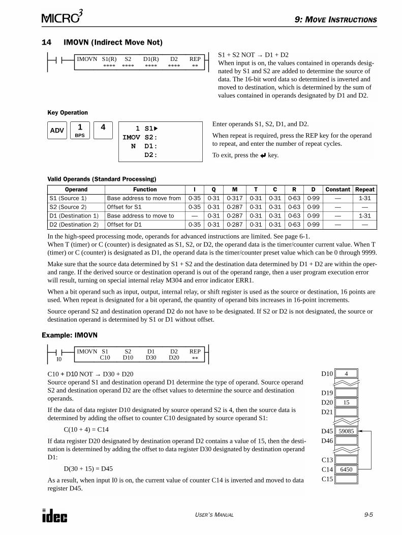
9: MOVE INSTRUCTIONS
USER’S MANUAL 9-5
14 IMOVN (Indirect Move Not)
Key Operation
Valid Operands (Standard Processing)
In the high-speed processing mode, operands for advanced instructions are limited. See page 6-1.When T (timer) or C (counter) is designated as S1, S2, or D2, the operand data is the timer/counter current value. When T (timer) or C (counter) is designated as D1, the operand data is the timer/counter preset value which can be 0 through 9999.
Make sure that the source data determined by S1 + S2 and the destination data determined by D1 + D2 are within the oper-and range. If the derived source or destination operand is out of the operand range, then a user program execution error will result, turning on special internal relay M304 and error indicator ERR1.
When a bit operand such as input, output, internal relay, or shift register is used as the source or destination, 16 points are used. When repeat is designated for a bit operand, the quantity of operand bits increases in 16-point increments.
Source operand S2 and destination operand D2 do not have to be designated. If S2 or D2 is not designated, the source or destination operand is determined by S1 or D1 without offset.
Example: IMOVN
Operand Function I Q M T C R D Constant RepeatS1 (Source 1) Base address to move from 0-35 0-31 0-317 0-31 0-31 0-63 0-99 — 1-31S2 (Source 2) Offset for S1 0-35 0-31 0-287 0-31 0-31 0-63 0-99 — —D1 (Destination 1) Base address to move to — 0-31 0-287 0-31 0-31 0-63 0-99 — 1-31D2 (Destination 2) Offset for D1 0-35 0-31 0-287 0-31 0-31 0-63 0-99 — —
IMOVN S1(R)****
REP**
S1 + S2 NOT → D1 + D2When input is on, the values contained in operands desig-nated by S1 and S2 are added to determine the source of data. The 16-bit word data so determined is inverted and moved to destination, which is determined by the sum of values contained in operands designated by D1 and D2.
S2****
D1(R)****
D2****
ADV 1BPS
1 S1IMOV S2: N D1: D2:
Enter operands S1, S2, D1, and D2.
When repeat is required, press the REP key for the operand to repeat, and enter the number of repeat cycles.
To exit, press the key.
4
I0IMOVN REP
**
C10 + D10 NOT → D30 + D20Source operand S1 and destination operand D1 determine the type of operand. Source operand S2 and destination operand D2 are the offset values to determine the source and destination operands.
If the data of data register D10 designated by source operand S2 is 4, then the source data is determined by adding the offset to counter C10 designated by source operand S1:
C(10 + 4) = C14
If data register D20 designated by destination operand D2 contains a value of 15, then the desti-nation is determined by adding the offset to data register D30 designated by destination operand D1:
D(30 + 15) = D45
As a result, when input I0 is on, the current value of counter C14 is inverted and moved to data register D45.
15D20
D19
D21
59085D45
S1C10
D2D20
D1D30
S2D10
4D10
C15
C13
D46
6450C14

9: MOVE INSTRUCTIONS
9-6 USER’S MANUAL
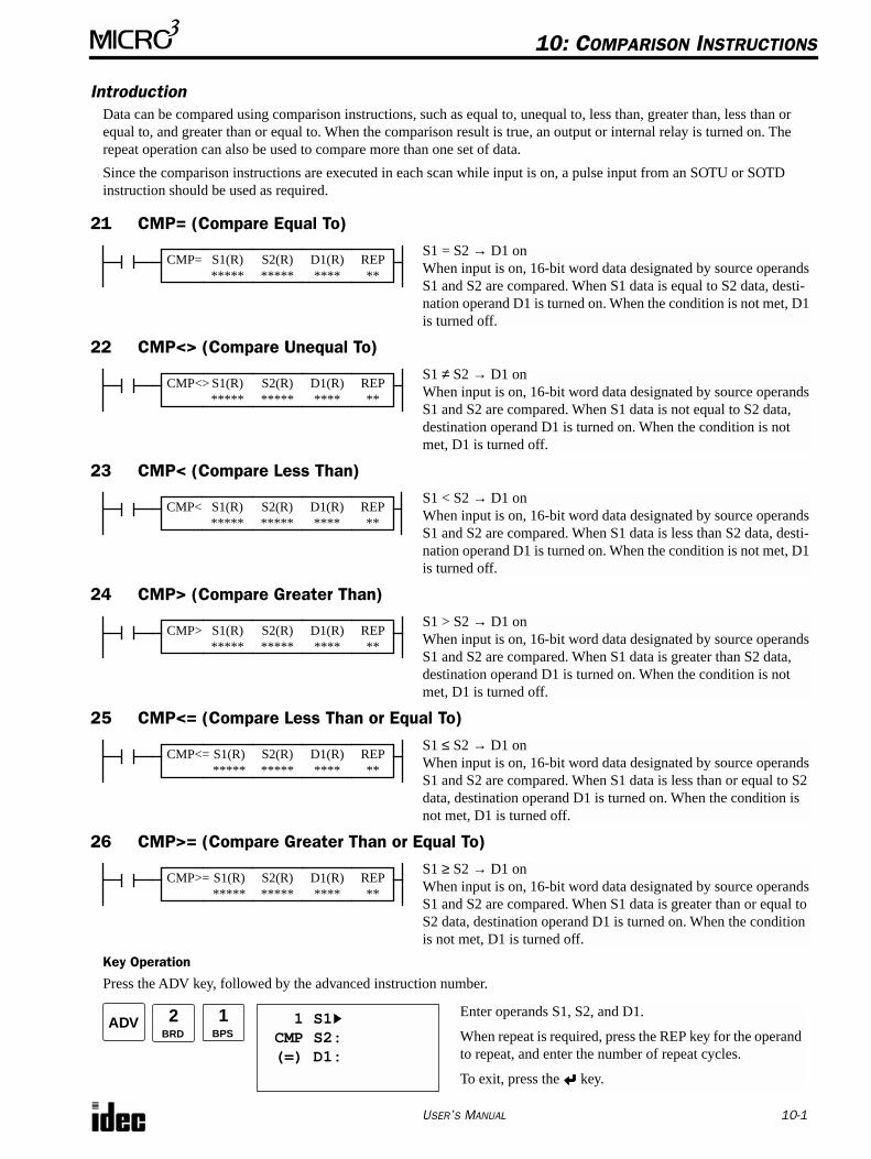
USER’S MANUAL 10-1
10: COMPARISON INSTRUCTIONS
IntroductionData can be compared using comparison instructions, such as equal to, unequal to, less than, greater than, less than or equal to, and greater than or equal to. When the comparison result is true, an output or internal relay is turned on. The repeat operation can also be used to compare more than one set of data.
Since the comparison instructions are executed in each scan while input is on, a pulse input from an SOTU or SOTD instruction should be used as required.
21 CMP= (Compare Equal To)
22 CMP<> (Compare Unequal To)
23 CMP< (Compare Less Than)
24 CMP> (Compare Greater Than)
25 CMP<= (Compare Less Than or Equal To)
26 CMP>= (Compare Greater Than or Equal To)
Key Operation
Press the ADV key, followed by the advanced instruction number.
CMP= S1(R)*****
REP**
D1(R)****
S1 = S2 → D1 onWhen input is on, 16-bit word data designated by source operands S1 and S2 are compared. When S1 data is equal to S2 data, desti-nation operand D1 is turned on. When the condition is not met, D1 is turned off.
S2(R)*****
CMP<> S1(R)*****
REP**
D1(R)****
S1 ≠ S2 → D1 onWhen input is on, 16-bit word data designated by source operands S1 and S2 are compared. When S1 data is not equal to S2 data, destination operand D1 is turned on. When the condition is not met, D1 is turned off.
S2(R)*****
CMP< S1(R)*****
REP**
D1(R)****
S1 < S2 → D1 onWhen input is on, 16-bit word data designated by source operands S1 and S2 are compared. When S1 data is less than S2 data, desti-nation operand D1 is turned on. When the condition is not met, D1 is turned off.
S2(R)*****
CMP> S1(R)*****
REP**
D1(R)****
S1 > S2 → D1 onWhen input is on, 16-bit word data designated by source operands S1 and S2 are compared. When S1 data is greater than S2 data, destination operand D1 is turned on. When the condition is not met, D1 is turned off.
S2(R)*****
CMP<= S1(R) *****
REP**
D1(R)****
S1 ≤ S2 → D1 onWhen input is on, 16-bit word data designated by source operands S1 and S2 are compared. When S1 data is less than or equal to S2 data, destination operand D1 is turned on. When the condition is not met, D1 is turned off.
S2(R)*****
CMP>= S1(R) *****
REP**
D1(R)****
S1 ≥ S2 → D1 onWhen input is on, 16-bit word data designated by source operands S1 and S2 are compared. When S1 data is greater than or equal to S2 data, destination operand D1 is turned on. When the condition is not met, D1 is turned off.
S2(R)*****
ADV 1BPS
1 S1 CMP S2: (=) D1:
2BRD
Enter operands S1, S2, and D1.
When repeat is required, press the REP key for the operand to repeat, and enter the number of repeat cycles.
To exit, press the key.
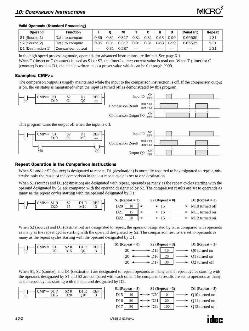
10: COMPARISON INSTRUCTIONS
10-2 USER’S MANUAL
Valid Operands (Standard Processing)
In the high-speed processing mode, operands for advanced instructions are limited. See page 6-1.When T (timer) or C (counter) is used as S1 or S2, the timer/counter current value is read out. When T (timer) or C (counter) is used as D1, the data is written in as a preset value which can be 0 through 9999.
Examples: CMP>= The comparison output is usually maintained while the input to the comparison instruction is off. If the comparison output is on, the on status is maintained when the input is turned off as demonstrated by this program.
This program turns the output off when the input is off.
Repeat Operation in the Comparison InstructionsWhen S1 and/or S2 (source) is designated to repeat, D1 (destination) is normally required to be designated to repeat, oth-erwise only the result of the comparison in the last repeat cycle is set to one destination.
When S1 (source) and D1 (destination) are designated with repeat, operands as many as the repeat cycles starting with the operand designated by S1 are compared with the operand designated by S2. The comparison results are set to operands as many as the repeat cycles starting with the operand designated by D1.
When S2 (source) and D1 (destination) are designated to repeat, the operand designated by S1 is compared with operands as many as the repeat cycles starting with the operand designated by S2. The comparison results are set to operands as many as the repeat cycles starting with the operand designated by D1.
When S1, S2 (source), and D1 (destination) are designated to repeat, operands as many as the repeat cycles starting with the operands designated by S1 and S2 are compared with each other. The comparison results are set to operands as many as the repeat cycles starting with the operand designated by D1.
Operand Function I Q M T C R D Constant RepeatS1 (Source 1) Data to compare 0-35 0-31 0-317 0-31 0-31 0-63 0-99 0-65535 1-31S2 (Source 2) Data to compare 0-35 0-31 0-317 0-31 0-31 0-63 0-99 0-65535 1-31D1 (Destination 1) Comparison output — 0-31 0-287 — — — — — 1-31
I0CMP>= REP
**S1
D10S2C1
D1Q0
Input I0ON
OFF
Comparison ResultD10 ≥ C1D10 < C1
Comparison Output Q0ON
OFF
I0CMP>= REP
**S1
D10S2C1
D1M0
Input I0ON
OFF
Comparison ResultD10 ≥ C1D10 < C1
Output Q0ON
OFFM0 Q0
I1CMP>= REP
3S1 RD20
D1 RM10
15D21
10D20
20D22
M11 turned on
M10 turned off
M12 turned on
S1 (Repeat = 3) D1 (Repeat = 3)S215
S2 (Repeat = 0)
15
15
15
I2CMP>= REP
3S120
D1 RQ0
20D16
10D15
30D17
Q1 turned on
Q0 turned on
Q2 turned off
S2 (Repeat = 3) D1 (Repeat = 3)S2 RD15
S1 (Repeat = 0)
20
20
20
I3CMP>= REP
3S1 RD15
D1 RQ10
20D21
0D20
100D22
Q11 turned on
Q10 turned on
Q12 turned off
S2 (Repeat = 3) D1 (Repeat = 3)S2 RD20
20D16
10D15
30D17
S1 (Repeat = 3)
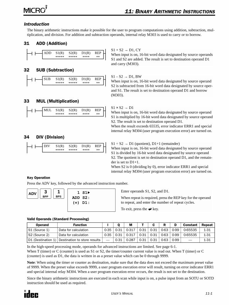
USER’S MANUAL 11-1
11: BINARY ARITHMETIC INSTRUCTIONS
IntroductionThe binary arithmetic instructions make it possible for the user to program computations using addition, subtraction, mul-tiplication, and division. For addition and subtraction operands, internal relay M303 is used to carry or to borrow.
31 ADD (Addition)
32 SUB (Subtraction)
33 MUL (Multiplication)
34 DIV (Division)
Key Operation
Press the ADV key, followed by the advanced instruction number.
Valid Operands (Standard Processing)
In the high-speed processing mode, operands for advanced instructions are limited. See page 6-1.When T (timer) or C (counter) is used as S1 or S2, the timer/counter current value is read out. When T (timer) or C (counter) is used as D1, the data is written in as a preset value which can be 0 through 9999.
Note: When using the timer or counter as destination, make sure that the data does not exceed the maximum preset value of 9999. When the preset value exceeds 9999, a user program execution error will result, turning on error indicator ERR1 and special internal relay M304. When a user program execution error occurs, the result is not set to the destination.
Since the binary arithmetic instructions are executed in each scan while input is on, a pulse input from an SOTU or SOTD instruction should be used as required.
Operand Function I Q M T C R D Constant RepeatS1 (Source 1) Data for calculation 0-35 0-31 0-317 0-31 0-31 0-63 0-99 0-65535 1-31S2 (Source 2) Data for calculation 0-35 0-31 0-317 0-31 0-31 0-63 0-99 0-65535 1-31D1 (Destination 1) Destination to store results — 0-31 0-287 0-31 0-31 0-63 0-99 — 1-31
ADD S1(R)*****
REP**
D1(R)****
S1 + S2 → D1, CY When input is on, 16-bit word data designated by source operands S1 and S2 are added. The result is set to destination operand D1 and carry (M303).
S2(R)*****
SUB S1(R)*****
REP**
D1(R)****
S2(R)*****
S1 – S2 → D1, BW When input is on, 16-bit word data designated by source operand S2 is subtracted from 16-bit word data designated by source oper-and S1. The result is set to destination operand D1 and borrow (M303).
MUL S1(R)*****
REP**
D1(R)****
S1 × S2 → D1 When input is on, 16-bit word data designated by source operand S1 is multiplied by 16-bit word data designated by source operand S2. The result is set to destination operand D1.When the result exceeds 65535, error indicator ERR1 and special internal relay M304 (user program execution error) are turned on.
S2(R)*****
DIV S1(R)*****
REP**
D1(R)****
S1 ÷ S2 → D1 (quotient), D1+1 (remainder) When input is on, 16-bit word data designated by source operand S1 is divided by 16-bit word data designated by source operand S2. The quotient is set to destination operand D1, and the remain-der is set to D1+1. When S2 is 0 (dividing by 0), error indicator ERR1 and special internal relay M304 (user program execution error) are turned on.
S2(R)*****
ADV 1BPS
1 S1 ADD S2: (+) D1:
3BPP
Enter operands S1, S2, and D1.
When repeat is required, press the REP key for the operand to repeat, and enter the number of repeat cycles.
To exit, press the key.
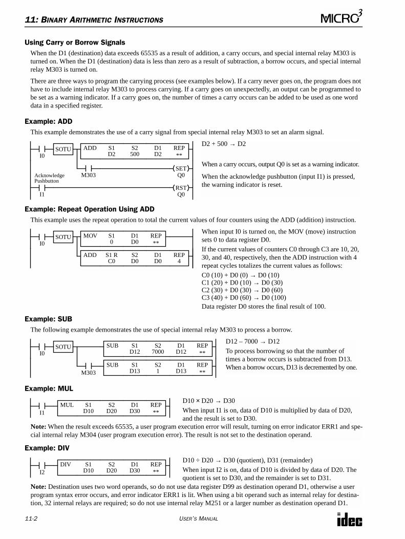
11: BINARY ARITHMETIC INSTRUCTIONS
11-2 USER’S MANUAL
Using Carry or Borrow SignalsWhen the D1 (destination) data exceeds 65535 as a result of addition, a carry occurs, and special internal relay M303 is turned on. When the D1 (destination) data is less than zero as a result of subtraction, a borrow occurs, and special internal relay M303 is turned on.
There are three ways to program the carrying process (see examples below). If a carry never goes on, the program does not have to include internal relay M303 to process carrying. If a carry goes on unexpectedly, an output can be programmed to be set as a warning indicator. If a carry goes on, the number of times a carry occurs can be added to be used as one word data in a specified register.
Example: ADDThis example demonstrates the use of a carry signal from special internal relay M303 to set an alarm signal.
Example: Repeat Operation Using ADDThis example uses the repeat operation to total the current values of four counters using the ADD (addition) instruction.
Example: SUBThe following example demonstrates the use of special internal relay M303 to process a borrow.
Example: MUL
Example: DIV
I0ADD REP
**S1D2
S2500
D1D2
SOTU
Q0SET
M303
I1 Q0RST
D2 + 500 → D2
When a carry occurs, output Q0 is set as a warning indicator.
When the acknowledge pushbutton (input I1) is pressed, the warning indicator is reset.
AcknowledgePushbutton
I0
ADD S1 RC0
S2D0
D1D0
SOTUWhen input I0 is turned on, the MOV (move) instruction sets 0 to data register D0.
If the current values of counters C0 through C3 are 10, 20, 30, and 40, respectively, then the ADD instruction with 4 repeat cycles totalizes the current values as follows:
C0 (10) + D0 (0) → D0 (10)C1 (20) + D0 (10) → D0 (30)C2 (30) + D0 (30) → D0 (60)C3 (40) + D0 (60) → D0 (100)Data register D0 stores the final result of 100.
MOV S10
D1D0
REP**
REP4
I0SUB REP
**S1
D12S2
7000D1D12
SOTU
M303
D12 – 7000 → D12
To process borrowing so that the number of times a borrow occurs is subtracted from D13.When a borrow occurs, D13 is decremented by one.SUB REP
**S1
D13S21
D1D13
I1MUL REP
**S1
D10S2
D20D1D30
D10 × D20 → D30
When input I1 is on, data of D10 is multiplied by data of D20, and the result is set to D30.
Note: When the result exceeds 65535, a user program execution error will result, turning on error indicator ERR1 and spe-cial internal relay M304 (user program execution error). The result is not set to the destination operand.
I2DIV REP
**S1
D10S2
D20D1D30
D10 ÷ D20 → D30 (quotient), D31 (remainder)
When input I2 is on, data of D10 is divided by data of D20. The quotient is set to D30, and the remainder is set to D31.
Note: Destination uses two word operands, so do not use data register D99 as destination operand D1, otherwise a user program syntax error occurs, and error indicator ERR1 is lit. When using a bit operand such as internal relay for destina-tion, 32 internal relays are required; so do not use internal relay M251 or a larger number as destination operand D1.
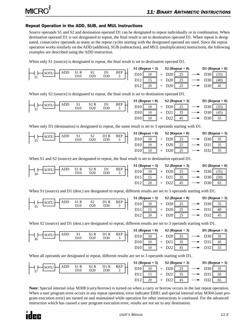
11: BINARY ARITHMETIC INSTRUCTIONS
USER’S MANUAL 11-3
Repeat Operation in the ADD, SUB, and MUL InstructionsSource operands S1 and S2 and destination operand D1 can be designated to repeat individually or in combination. When destination operand D1 is not designated to repeat, the final result is set to destination operand D1. When repeat is desig-nated, consecutive operands as many as the repeat cycles starting with the designated operand are used. Since the repeat operation works similarly on the ADD (addition), SUB (subtraction), and MUL (multiplication) instructions, the following examples are described using the ADD instruction.
When only S1 (source) is designated to repeat, the final result is set to destination operand D1.
When only S2 (source) is designated to repeat, the final result is set to destination operand D1.
When only D1 (destination) is designated to repeat, the same result is set to 3 operands starting with D1.
When S1 and S2 (source) are designated to repeat, the final result is set to destination operand D1.
When S1 (source) and D1 (dest.) are designated to repeat, different results are set to 3 operands starting with D1.
When S2 (source) and D1 (dest.) are designated to repeat, different results are set to 3 operands starting with D1.
When all operands are designated to repeat, different results are set to 3 operands starting with D1.
Note: Special internal relay M308 (carry/borrow) is turned on when a carry or borrow occurs in the last repeat operation. When a user program error occurs in any repeat operation, error indicator ERR1 and special internal relay M304 (user pro-gram execution error) are turned on and maintained while operation for other instructions is continued. For the advanced instruction which has caused a user program execution error, results are not set to any destination.
I1ADD REP
3S1 RD10
D1D30
15D11
10D10
20D12
S1 (Repeat = 3) D1 (Repeat = 0)S2
D20
S2 (Repeat = 0)
+++
(40)D30
(35)D30
45D30
25D20
25D20
25D20
SOTU
I2ADD REP
3S1
D10D1D30
10D10
10D10
10D10
S1 (Repeat = 0) D1 (Repeat = 0)S2 RD20
S2 (Repeat = 3)
+++
(45)D30
(35)D30
55D30
35D21
25D20
45D22
SOTU
I3ADD REP
3S1
D10D1 RD30
10D10
10D10
10D10
S1 (Repeat = 0) D1 (Repeat = 3)S2
D20
S2 (Repeat = 0)
+++
35D31
35D30
35D32
25D20
25D20
25D20
SOTU
I4ADD REP
3S1 RD10
D1D30
15D11
10D10
20D12
S1 (Repeat = 3) D1 (Repeat = 0)S2 RD20
S2 (Repeat = 3)
+++
(50)D30
(35)D30
65D30
35D21
25D20
45D22
SOTU
I5ADD REP
3S1 RD10
D1 RD30
15D11
10D10
20D12
S1 (Repeat = 3) D1 (Repeat = 3)S2
D20
S2 (Repeat = 0)
+++
40D31
35D30
45D32
25D20
25D20
25D20
SOTU
I6ADD REP
3S1
D10D1 RD30
10D10
10D10
10D10
S1 (Repeat = 0) D1 (Repeat = 3)S2 RD20
S2 (Repeat = 3)
+++
45D31
35D30
55D32
35D21
25D20
45D22
SOTU
I7ADD REP
3S1 RD10
D1 RD30
15D11
10D10
20D12
S1 (Repeat = 3) D1 (Repeat = 3)S2 RD20
S2 (Repeat = 3)
+++
50D31
35D30
65D32
35D21
25D20
45D22
SOTU
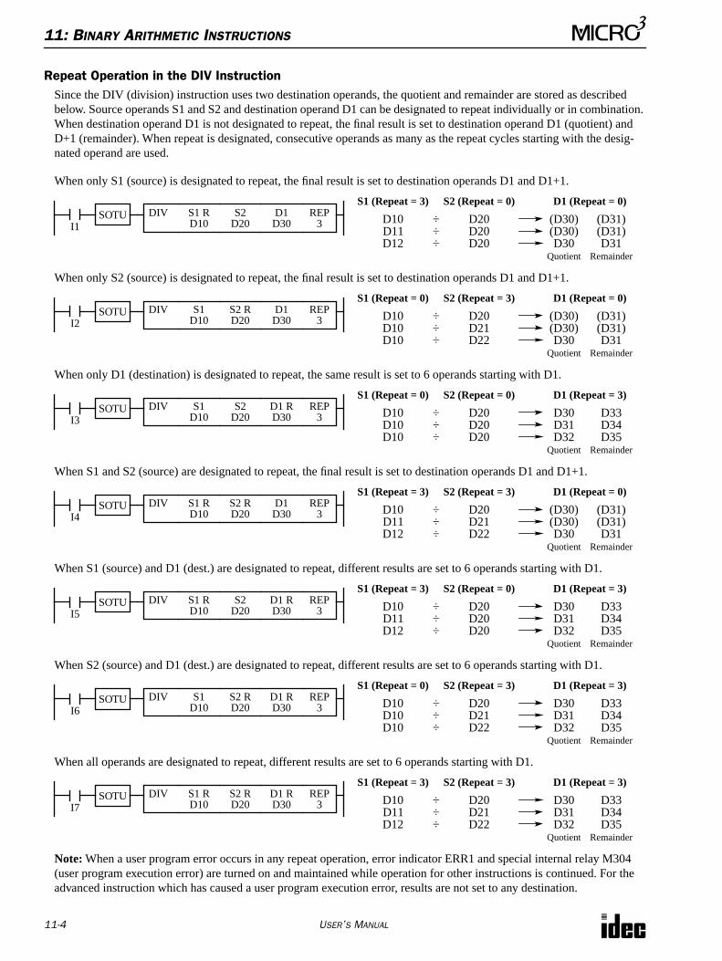
11: BINARY ARITHMETIC INSTRUCTIONS
11-4 USER’S MANUAL
Repeat Operation in the DIV InstructionSince the DIV (division) instruction uses two destination operands, the quotient and remainder are stored as described below. Source operands S1 and S2 and destination operand D1 can be designated to repeat individually or in combination. When destination operand D1 is not designated to repeat, the final result is set to destination operand D1 (quotient) and D+1 (remainder). When repeat is designated, consecutive operands as many as the repeat cycles starting with the desig-nated operand are used.
When only S1 (source) is designated to repeat, the final result is set to destination operands D1 and D1+1.
When only S2 (source) is designated to repeat, the final result is set to destination operands D1 and D1+1.
When only D1 (destination) is designated to repeat, the same result is set to 6 operands starting with D1.
When S1 and S2 (source) are designated to repeat, the final result is set to destination operands D1 and D1+1.
When S1 (source) and D1 (dest.) are designated to repeat, different results are set to 6 operands starting with D1.
When S2 (source) and D1 (dest.) are designated to repeat, different results are set to 6 operands starting with D1.
When all operands are designated to repeat, different results are set to 6 operands starting with D1.
Note: When a user program error occurs in any repeat operation, error indicator ERR1 and special internal relay M304 (user program execution error) are turned on and maintained while operation for other instructions is continued. For the advanced instruction which has caused a user program execution error, results are not set to any destination.
I1DIV REP
3S1 RD10
D1D30 D10
S1 (Repeat = 3) D1 (Repeat = 0)S2
D20
S2 (Repeat = 0)
÷ (D30)D20 (D31)D11D12
÷÷
D20D20
(D30)D30
(D31)D31
Quotient Remainder
SOTU
I2DIV REP
3S1
D10D1D30 D10
S1 (Repeat = 0) D1 (Repeat = 0)S2 RD20
S2 (Repeat = 3)
÷ (D30)D20 (D31)D10D10
÷÷
D21D22
(D30)D30
(D31)D31
Quotient Remainder
SOTU
I3DIV REP
3S1
D10D1 RD30 D10
S1 (Repeat = 0) D1 (Repeat = 3)S2
D20
S2 (Repeat = 0)
÷ D30D20 D33D10D10
÷÷
D20D20
D31D32
D34D35
Quotient Remainder
SOTU
I4DIV REP
3S1 RD10
D1D30 D10
S1 (Repeat = 3) D1 (Repeat = 0)S2 RD20
S2 (Repeat = 3)
÷ (D30)D20 (D31)D11D12
÷÷
D21D22
(D30)D30
(D31)D31
Quotient Remainder
SOTU
I5DIV REP
3S1 RD10
D1 RD30 D10
S1 (Repeat = 3) D1 (Repeat = 3)S2
D20
S2 (Repeat = 0)
÷ D30D20 D33D11D12
÷÷
D20D20
D31D32
D34D35
Quotient Remainder
SOTU
I6DIV REP
3S1
D10D1 RD30 D10
S1 (Repeat = 0) D1 (Repeat = 3)S2 RD20
S2 (Repeat = 3)
÷ D30D20 D33D10D10
÷÷
D21D22
D31D32
D34D35
Quotient Remainder
SOTU
I7DIV REP
3S1 RD10
D1 RD30 D10
S1 (Repeat = 3) D1 (Repeat = 3)S2 RD20
S2 (Repeat = 3)
÷ D30D20 D33D11D12
÷÷
D21D22
D31D32
D34D35
Quotient Remainder
SOTU
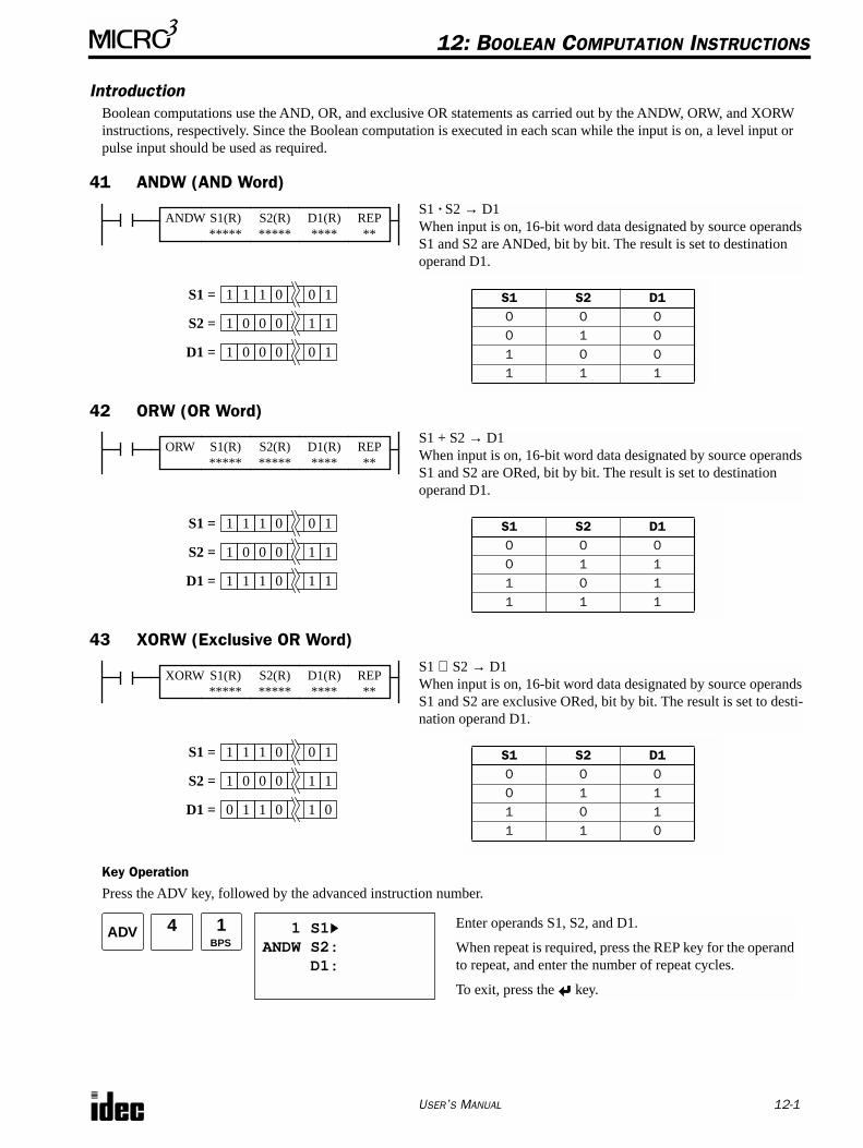
USER’S MANUAL 12-1
12: BOOLEAN COMPUTATION INSTRUCTIONS
IntroductionBoolean computations use the AND, OR, and exclusive OR statements as carried out by the ANDW, ORW, and XORW instructions, respectively. Since the Boolean computation is executed in each scan while the input is on, a level input or pulse input should be used as required.
41 ANDW (AND Word)
42 ORW (OR Word)
43 XORW (Exclusive OR Word)
Key Operation
Press the ADV key, followed by the advanced instruction number.
ANDW S1(R)*****
REP**
D1(R)****
S1 · S2 → D1When input is on, 16-bit word data designated by source operands S1 and S2 are ANDed, bit by bit. The result is set to destination operand D1.
S2(R)*****
S1 = 1 1 1001
S2 = 1 0 1100
D1 = 1 0 1000
S1 S2 D10 0 00 1 01 0 01 1 1
ORW S1(R)*****
REP**
D1(R)****
S1 + S2 → D1When input is on, 16-bit word data designated by source operands S1 and S2 are ORed, bit by bit. The result is set to destination operand D1.
S2(R)*****
S1 = 1 1 1001
S2 = 1 0 1100
D1 = 1 1 1101
S1 S2 D10 0 00 1 11 0 11 1 1
XORW S1(R)*****
REP**
D1(R)****
S1 ⊕ S2 → D1When input is on, 16-bit word data designated by source operands S1 and S2 are exclusive ORed, bit by bit. The result is set to desti-nation operand D1.
S2(R)*****
S1 = 1 1 1001
S2 = 1 0 1100
D1 = 0 1 0101
S1 S2 D10 0 00 1 11 0 11 1 0
ADV 1BPS
1 S1 ANDW S2: D1:
4
Enter operands S1, S2, and D1.
When repeat is required, press the REP key for the operand to repeat, and enter the number of repeat cycles.
To exit, press the key.
12: BOOLEAN COMPUTATION INSTRUCTIONS
12-2 USER’S MANUAL
Valid Operands (Standard Processing)
In the high-speed processing mode, operands for advanced instructions are limited. See page 6-1.When T (timer) or C (counter) is used as S1 or S2, the timer/counter current value is read out. When T (timer) or C (counter) is used as D1, the data is written in as a preset value which can be 0 through 9999.
Note: When using the timer or counter as destination, make sure that the data does not exceed the maximum preset value of 9999. When the preset value exceeds 9999, a user program execution error will result, turning on error indicator ERR1 and special internal relay M304. When a user program execution error occurs, the result is not set to the destination.
Since these Boolean instructions are executed in each scan while input is on, a pulse input from an SOTU or SOTD instruction should be used as required.
Example: XORWTo convert optional output status among a series of 10 output points, use the XORW instruction in combination with 10 internal relay points.
Operand Function I Q M T C R D Constant RepeatS1 (Source 1) Data for computation 0-35 0-31 0-317 0-31 0-31 0-63 0-99 0-65535 1-31S2 (Source 2) Data for computation 0-35 0-31 0-317 0-31 0-31 0-63 0-99 0-65535 1-31D1 (Destination 1) Destination to store results — 0-31 0-287 0-31 0-31 0-63 0-99 — 1-31
M301 M0SET
Ten points of outputs Q0 through Q11 are assigned to 10 points of internal relays M0 through M11.
Five points of M0, M2, M4, M6, and M10 are set by ini-tialize pulse special internal relay M301.
When input I1 is turned on, the XORW instruction is executed to invert the status of outputs Q0, Q2, Q4, Q6, and Q10.
0 0 00 0 0 1 10 0 1 0 1 0 1 0
Q0Q7
Q10Q11Q12
Q17
16 points
This program will invert the status of the shaded outputs at the left from on to off, and those not shaded from off to on.
This example uses the 24-I/O type MICRO3 base unit, which has 10 output terminals Q0 through Q7, Q10, and Q11.
XORW REP**
S1M0
S2Q0
D1Q0
SOTUI1
M2SET
M4SET
M6SET
M10SET
M0M7M10M17
12: BOOLEAN COMPUTATION INSTRUCTIONS
USER’S MANUAL 12-3
Repeat Operation in the ANDW, ORW, and XORW InstructionsSource operands S1 and S2 and destination operand D1 can be designated to repeat individually or in combination. When destination operand D1 is not designated to repeat, the final result is set to destination operand D1. When repeat is desig-nated, consecutive operands as many as the repeat cycles starting with the designated operand are used. Since the repeat operation works similarly on the ANDW (AND word), ORW (OR word), and XORW (exclusive OR word) instructions, the following examples are described using the ANDW instruction.
When only S1 (source) is designated to repeat, the final result is set to destination operand D1.
When only S2 (source) is designated to repeat, the final result is set to destination operand D1.
When only D1 (destination) is designated to repeat, the same result is set to 3 operands starting with D1.
When S1 and S2 (source) are designated to repeat, the final result is set to destination operand D1.
When S1 (source) and D1 (dest.) are designated to repeat, different results are set to 3 operands starting with D1.
When S2 (source) and D1 (dest.) are designated to repeat, different results are set to 3 operands starting with D1.
When all operands are designated to repeat, different results are set to 3 operands starting with D1.
Note: When a user program error occurs in any repeat operation, error indicator ERR1 and special internal relay M304 (user program execution error) are turned on and maintained while operation for other instructions is continued. For the advanced instruction which has caused a user program execution error, results are not set to any destination.
I1ANDW REP
3S1 RD10
D1D30 D10
S1 (Repeat = 3) D1 (Repeat = 0)S2
D20
S2 (Repeat = 0)
· (D30)D20D11D12
··
D20D20
(D30)D30
SOTU
I2ANDW REP
3S1
D10D1D30 D10
S1 (Repeat = 0) D1 (Repeat = 0)S2 RD20
S2 (Repeat = 3)
· (D30)D20D10D10
··
D21D22
(D30)D30
SOTU
I3ANDW REP
3S1
D10D1 RD30 D10
S1 (Repeat = 0) D1 (Repeat = 3)S2
D20
S2 (Repeat = 0)
· D30D20D10D10
··
D20D20
D31D32
SOTU
I4ANDW REP
3S1 RD10
D1D30 D10
S1 (Repeat = 3) D1 (Repeat = 0)S2 RD20
S2 (Repeat = 3)
· (D30)D20D11D12
··
D21D22
(D30)D30
SOTU
I5ANDW REP
3S1 RD10
D1 RD30 D10
S1 (Repeat = 3) D1 (Repeat = 3)S2
D20
S2 (Repeat = 0)
· D30D20D11D12
··
D20D20
D31D32
SOTU
I6ANDW REP
3S1
D10D1 RD30 D10
S1 (Repeat = 0) D1 (Repeat = 3)S2 RD20
S2 (Repeat = 3)
· D30D20D10D10
··
D21D22
D31D32
SOTU
I7ANDW REP
3S1 RD10
D1 RD30 D10
S1 (Repeat = 3) D1 (Repeat = 3)S2 RD20
S2 (Repeat = 3)
· D30D20D11D12
··
D21D22
D31D32
SOTU

12: BOOLEAN COMPUTATION INSTRUCTIONS
12-4 USER’S MANUAL
USER’S MANUAL 13-1
13: BIT SHIFT / ROTATE INSTRUCTIONS
IntroductionBit shift and rotate instructions are used to shift the 16-bit data in the data register designated by source operand S1 to the left or right by the quantity of bits designated. The result is set to the data register designated by source operand S1 and a carry (special internal relay M303). Since the bit shift and rotate instructions are executed in each scan while the input is on, a level input or pulse input should be used as required.
51 SFTL (Shift Left)
Key Operation
Valid Operands (Standard Processing)
In the high-speed processing mode, data registers for this instruction are limited to D0 through D31.Since the bit shift instructions are executed in each scan while input is on, a pulse input from an SOTU or SOTD instruc-tion should be used as required.
Example: SFTL
Operand Function I Q M T C R D Constant RepeatS1 (Source 1) Data for bit shift — — — — — — 0-99 — —bit Quantity of bits to shift — — — — — — — 1-15 —
SFTL S1****
bit**
CY ← S1When input is on, 16-bit data of the data register designated by source operand S1 is shifted to the left by the quantity of bits designated by operand bit. The result is set to the data register, and the last bit status shifted out is set to a carry (special internal relay M303). Zeros are set to the LSB.
0Before shift: 1 0 1010 1 0 1 1 1101 0 0CY
M303
MSB LSBS1
1After shift: 00 1010 1 0 1 1 1101 0 0CY
M303
MSB LSBS1
When bit to shift = 1
Shift to the left
ADV 1BPS
2 S1SFTL ( ) : 1bit
5CC=
Enter operand S1 and the quantity of bits to shift.
Repeat cannot be designated for bit shift instructions.
To exit, press the key.
M301
SFTL
REP**
M301 is the initialize pulse special internal relay.When MICRO3 starts operation, the MOV (move) instruction sets 43690 to data register D10.Each time input I0 is turned on, 16-bit data of data register D10 is shifted to the left by 1 bit as designated by operand bit. The bit status shifted out is set to a carry (special internal relay M303). Zeros are set to the LSB.
0Before shift: D10 = 43690 1 1 1000 1 0 1 1 1000 1 0CY
M303
MSB LSBD10
1After first shift: D10 = 21844 01 1000 1 0 1 1 1000 1 0CY
M303
MSB LSBD10
Bits to shift = 1
SOTUI0
MOV S143690
D1D10
S1D10
bit1
0
00 0111 0 1 0 0 0111 0 00After second shift: D10 = 43688CY
M303
MSB LSBD10
13: BIT SHIFT / ROTATE INSTRUCTIONS
13-2 USER’S MANUAL
52 SFTR (Shift Right)
Key Operation
Valid Operands (Standard Processing)
In the high-speed processing mode, data registers for this instruction are limited to D0 through D31.Since the bit shift instructions are executed in each scan while input is on, a pulse input from an SOTU or SOTD instruc-tion should be used as required.
Example: SFTR
Operand Function I Q M T C R D Constant RepeatS1 (Source 1) Data for bit shift — — — — — — 0-99 — —bit Quantity of bits to shift — — — — — — — 1-15 —
SFTR S1****
bit**
S1 → CYWhen input is on, 16-bit data of the data register designated by source operand S1 is shifted to the right by the quantity of bits designated by operand bit. The result is set to the data register, and the last bit status shifted out is set to a carry (special internal relay M303). Zeros are set to the MSB.
0Before shift: 1 0 1010 1 0 1 1 1101 0 0MSB LSBS1
After shift:MSB LSBS1
When bits to shift = 1CY
M303
0CY
M3031 0 1010 1 0 1 1 1101 00
Shift to the right
ADV 2 S1SFTR ( ) : 1bit
5CC=
2BRD
Enter operand S1 and the quantity of bits to shift.
Repeat cannot be designated for bit shift instructions.
To exit, press the key.
M301
SFTR
REP**
M301 is the initialize pulse special internal relay.When MICRO3 starts operation, the MOV (move) instruction sets 29 to data register D20.Each time input I1 is turned on, 16-bit data of data register D20 is shifted to the right by 2 bits as designated by operand bit. The last bit status shifted out is set to a carry (special internal relay M303). Zeros are set to the MSB’s.
0Before shift: D20 = 29 0 0 0000 0 0 0 0 0110 1 1CY
M303
MSB LSBD20
0After first shift: D20 = 7 10 0000 0 0 0 0 1000 0 1CY
M303
MSB LSBD20
Bits to shift = 2
SOTUI1
MOV S129
D1D20
S1D20
bit2
0
10 0000 0 0 0 0 0000 0 0After second shift: D20 = 1CY
M303
MSB LSBD201
0
0
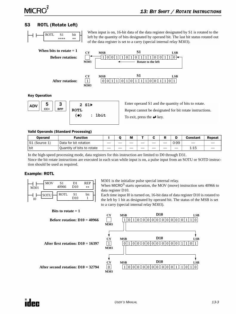
13: BIT SHIFT / ROTATE INSTRUCTIONS
USER’S MANUAL 13-3
53 ROTL (Rotate Left)
Key Operation
Valid Operands (Standard Processing)
In the high-speed processing mode, data registers for this instruction are limited to D0 through D31.Since the bit rotate instructions are executed in each scan while input is on, a pulse input from an SOTU or SOTD instruc-tion should be used as required.
Example: ROTL
Operand Function I Q M T C R D Constant RepeatS1 (Source 1) Data for bit rotation — — — — — — 0-99 — —bit Quantity of bits to rotate — — — — — — — 1-15 —
ROTL S1****
bit**
When input is on, 16-bit data of the data register designated by S1 is rotated to the left by the quantity of bits designated by operand bit. The last bit status rotated out of the data register is set to a carry (special internal relay M303).
Before rotation: 1 0 1010 1 0 1 1 1101 0 0CY
M303
MSB LSBS1When bits to rotate = 1
1After rotation: 0 1010 1 0 1 1 1101 0 0CY
M303
MSB LSBS11
Rotate to the left
ADV 2 S1ROTL ( ) : 1bit
5CC=
3BPP
Enter operand S1 and the quantity of bits to rotate.
Repeat cannot be designated for bit rotate instructions.
To exit, press the key.
M301
ROTL
REP**
M301 is the initialize pulse special internal relay.When MICRO3 starts operation, the MOV (move) instruction sets 40966 to data register D10.Each time input I0 is turned on, 16-bit data of data register D10 is rotated to the left by 1 bit as designated by operand bit. The status of the MSB is set to a carry (special internal relay M303).
Before rotation: D10 = 40966 1 1 0000 0 0 0 0 1100 0 0CY
M303
MSB LSBD10
After first rotation: D10 = 16397
Bits to rotate = 1
SOTUI0
MOV S140966
D1D10
S1D10
bit1
After second rotation: D10 = 32794
1 0 0 0001 0 0 0 0 0100 1 1CY
M303
MSB LSBD10
0 1 0 0000 0 0 0 0 1010 1 0CY
M303
MSB LSBD10

13: BIT SHIFT / ROTATE INSTRUCTIONS
13-4 USER’S MANUAL
54 ROTR (Rotate Right)
Key Operation
Valid Operands (Standard Processing)
In the high-speed processing mode, data registers for this instruction are limited to D0 through D31.Since the bit rotate instructions are executed in each scan while input is on, a pulse input from an SOTU or SOTD instruc-tion should be used as required.
Example: ROTR
Operand Function I Q M T C R D Constant RepeatS1 (Source 1) Data for bit rotation — — — — — — 0-99 — —bit Quantity of bits to rotate — — — — — — — 1-15 —
ROTR S1****
bit**
When input is on, 16-bit data of the data register designated by S1 is rotated to the right by the quantity of bits designated by operand bit. The last bit status rotated out of the data register is set to a carry (special internal relay M303).
Before rotation: 1 0 1010 1 0 1 1 1101 0 0MSB LSBS1When bits to rotate = 1
0After rotation: 1 1100 0 0 1 1 0010 1 1CY
M303
MSB LSBS11
CY
M303Rotate to the right
ADV 2 S1ROTR ( ) : 1bit
5CC=
4
Enter operand S1 and the quantity of bits to rotate.
Repeat cannot be designated for bit rotate instructions.
To exit, press the key.
M301
ROTR
REP**
M301 is the initialize pulse special internal relay.When MICRO3 starts operation, the MOV (move) instruction sets 13 to data register D20.Each time input I1 is turned on, 16-bit data of data register D20 is rotated to the right by 1 bit as designated by operand bit. The last bit status rotated out of the data register is set to a carry (special internal relay M303).
Before rotation: D20 = 13 0 0 0000 0 0 0 0 0100 1 1CY
M303
MSB LSBD20
After first rotation: D20 = 16387
Bits to rotate = 2
SOTUI1
MOV S113
D1D20
S1D20
bit2
After second rotation: D20 = 53248
00 0 0001 0 0 0 0 1000 0 1CY
M303
MSB LSBD20
11 0 0011 0 0 0 0 0000 0 0CY
M303
MSB LSBD20
USER’S MANUAL 14-1
14: CLOCK / CALENDAR INSTRUCTIONS
IntroductionThe 16- and 24-I/O type MICRO3 base units feature five real-time calendar and clock instructions used for programming the calendar and clock; CALR (calendar read), CALW (calendar write), CLKR (clock read), CLKW (clock write), and ADJ (adjust). These instructions cannot be used on the 10-I/O type MICRO3 base unit. After initial setting of calendar and clock using FUN28, date and time are maintained. For FUN28, see page 5-12. If control data registers D95 through D98 are enabled using FUN10, day of week, hour, minute, and second data can be read out to these data registers when the MICRO3 is running or stopped. For FUN10, see page 5-8.
Note: Each clock/calendar instruction can be used only once in a user program.
71 CALR (Calendar Read)
Key Operation
Valid Operands (Standard Processing)
In the high-speed processing mode, data registers for this instruction are limited to D0 through D31.Since the CALR instruction is executed in each scan while input is on, a pulse input from an SOTU or SOTD instruction should be used as required.
Example: CALR
Operand Function I Q M T C R D Constant RepeatDestination to read calendar data — — — — — — 0-99 — —
When input is on, calendar data (year, month, day, and day of week) is read to four data reg-isters starting with the designated operand.
D = Year (0 to 99)D+1 = Month (1 to 12)D+2 = Day (1 to 31)D+3 = Day of week (0 to 6) assigned as follows:
0 1 2 3 4 5 6Sunday Monday Tuesday Wednesday Thursday Friday Saturday
CALR****
ADV 1BPS
0 LOD I 0 1 CALR 3 END 4 END
7END
Enter operand for the first data register to read calendar data.
Four consecutive data registers are required to read data.
To enter the instruction, press the key.
I0
When input I0 is on, calendar data is read to data registers D30 through D33.
D30 = YearD31 = MonthD32 = DayD33 = Day of week
CALRD30
14: CLOCK / CALENDAR INSTRUCTIONS
14-2 USER’S MANUAL
72 CALW (Calendar Write)
Note: Only the months of January, March, May, July, August, October, and December can be programmed with a date of the 31st. The month of February can be programmed with a date of the 29th only for actual leap years. (Leap years are automatically adjusted for).
Note: If month, day, or day of week is assigned a value which is not within the range specified above or if a date is not assigned according to the preceding note, then invalid data will result in a user program execution error, internal relay M304 turns on, and the ERR1 indicator on the MICRO3 base unit also turns on. The error code is stored in data register D93 when the control data register is enabled using FUN10. See page 5-8.
Key Operation
Valid Operands (Standard Processing)
In the high-speed processing mode, data registers for this instruction are limited to D0 through D31.Since the CALW instruction is executed at the rising edge of the input, a pulse input from an SOTU or SOTD instruction is not required.
Example: CALW
Operand Function I Q M T C R D Constant RepeatSource to write the calendar data — — — — — — 0-99 — —
When input is turned on, the calendar is set using data stored in four data registers starting with the designated operand.
D = Year (0 to 99)D+1 = Month (1 to 12)D+2 = Day (1 to 31)D+3 = Day of week (0 to 6) assigned as follows:
0 1 2 3 4 5 6Sunday Monday Tuesday Wednesday Thursday Friday Saturday
CALW****
ADV 0 LOD I 0 1 CALW 3 END 4 END
7END
2BRD
Enter operand for the first data register to write calendar data.
To enter the instruction, press the key.
Store calendar data to four consecutive data registers start-ing with the designated operand.
I1
M301 is the initialize pulse special internal relay.
When MICRO3 starts operation, the MOV instructions set calendar data to data registers D40 through D43.
D40 = 94 (Year 1994)D41 = 4 (April)D42 = 20 (Day)D43 = 3 (Wednesday)
When input I1 is turned on, the calendar is set using data from data regis-ters D40 through D43.
Note: Calendar data can also be set using FUN28. See page 5-12.
CALWD40
M301REP**
MOV S194
D1D40
REP**
MOV S14
D1D41
REP**
MOV S120
D1D42
REP**
MOV S13
D1D43
14: CLOCK / CALENDAR INSTRUCTIONS
USER’S MANUAL 14-3
73 CLKR (Clock Read)
Key Operation
Valid Operands (Standard Processing)
In the high-speed processing mode, data registers for this instruction are limited to D0 through D31.Since the CLKR instruction is executed in each scan while input is on, a pulse input from an SOTU or SOTD instruction should be used as required.
Example: CLKR
74 CLKW (Clock Write)
Note: If time is assigned a value which is not within the range specified above, invalid data will result in a user program execution error, internal relay M304 turns on, and the ERR1 indicator on the MICRO3 base unit also turns on. The error code is stored in data register D93 when the control data register is enabled using FUN10. See page 5-8.
Key Operation
Valid Operands (Standard Processing)
In the high-speed processing mode, data registers for this instruction are limited to D0 through D31.Since the CLKW instruction is executed at the rising edge of the input, a pulse input from an SOTU or SOTD instruction is not required.
Operand Function I Q M T C R D Constant RepeatDestination to read the clock data — — — — — — 0-99 — —
Operand Function I Q M T C R D Constant RepeatDestination to write the clock data — — — — — — 0-99 — —
When input is on, clock data (hour, minute, and second) is read to three data registers start-ing with the designated operand.
D = Hour (0 to 23)D+1 = Minute (0 to 59)D+2 = Second (0 to 59)
CLKR****
ADV 0 LOD I 0 1 CLKR 3 END 4 END
7END
3BPP
Enter operand for the first data register to read clock data.
Three consecutive data registers are required to read the clock data.
To enter the instruction, press the key.
I2
When input I2 is on, clock data is read to data registers D50 through D52.
D50 = Hour (0 to 23)D51 = Minute (0 to 59)D52 = Second (0 to 59)
CLKRD50
When input is turned on, the clock is set using data stored in three data registers starting with the designated operand.
D = Hour (0 to 23)D+1 = Minute (0 to 59)D+2 = Second (0 to 59)
CLKW****
ADV 7END
4
Enter operand for the first data register to write clock data.
To enter the instruction, press the key.
Store clock data to three consecutive data registers starting with the designated operand.
0 LOD I 0 1 CLKW 3 END 4 END
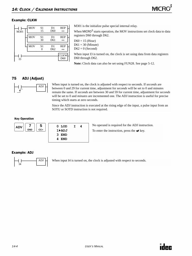
14: CLOCK / CALENDAR INSTRUCTIONS
14-4 USER’S MANUAL
Example: CLKW
75 ADJ (Adjust)
Key Operation
Example: ADJ
I3
M301 is the initialize pulse special internal relay.
When MICRO3 starts operation, the MOV instructions set clock data to data registers D60 through D62.
D60 = 15 (Hour)D61 = 30 (Minute)D62 = 0 (Second)
When input I3 is turned on, the clock is set using data from data registers D60 through D62.
Note: Clock data can also be set using FUN28. See page 5-12.
CLKWD60
M301REP**
MOV S115
D1D60
REP**
MOV S130
D1D61
REP**
MOV S10
D1D62
When input is turned on, the clock is adjusted with respect to seconds. If seconds are between 0 and 29 for current time, adjustment for seconds will be set to 0 and minutes remain the same. If seconds are between 30 and 59 for current time, adjustment for seconds will be set to 0 and minutes are incremented one. The ADJ instruction is useful for precise timing which starts at zero seconds.
Since the ADJ instruction is executed at the rising edge of the input, a pulse input from an SOTU or SOTD instruction is not required.
ADJ
ADV 0 LOD I 4 1 ADJ 3 END 4 END
7END
No operand is required for the ADJ instruction.
To enter the instruction, press the key.
5CC=
When input I4 is turned on, the clock is adjusted with respect to seconds.ADJI4
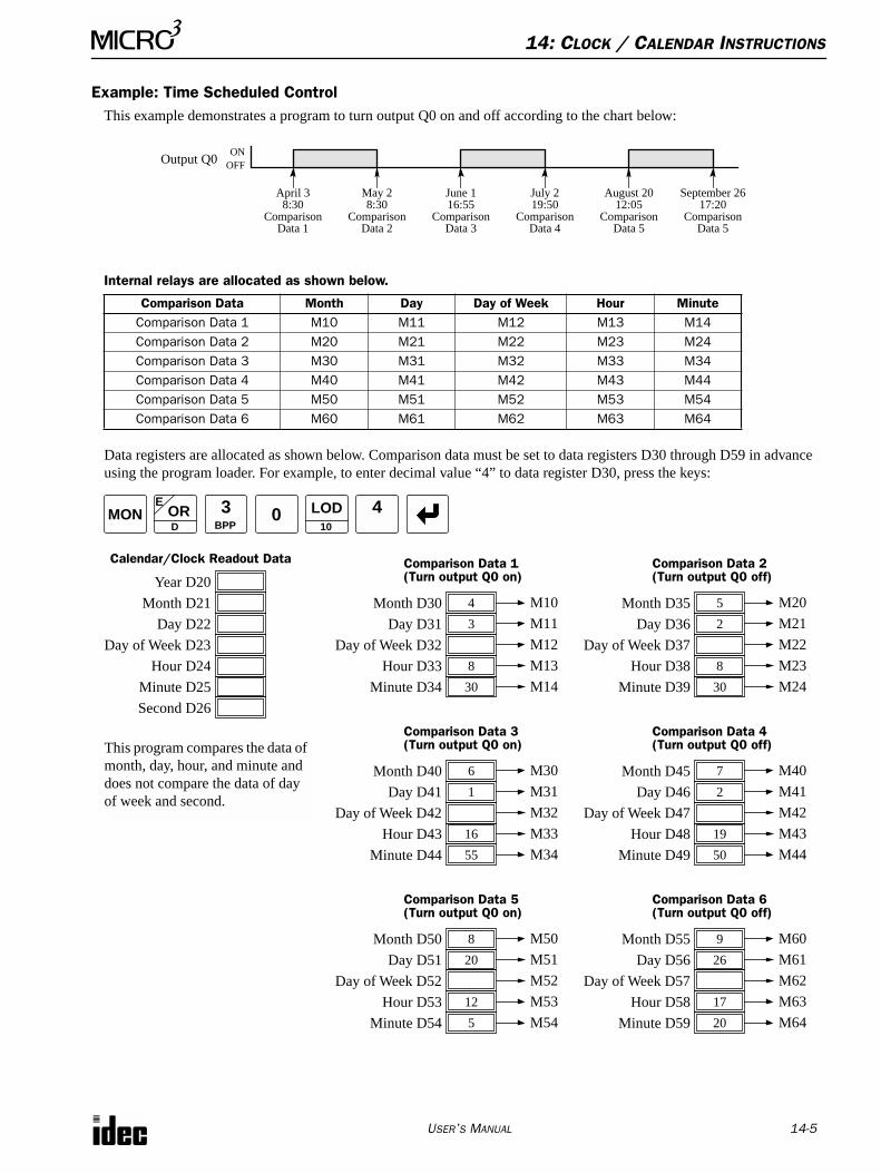
14: CLOCK / CALENDAR INSTRUCTIONS
USER’S MANUAL 14-5
Example: Time Scheduled ControlThis example demonstrates a program to turn output Q0 on and off according to the chart below:
Internal relays are allocated as shown below.
Data registers are allocated as shown below. Comparison data must be set to data registers D30 through D59 in advance using the program loader. For example, to enter decimal value “4” to data register D30, press the keys:
Comparison Data Month Day Day of Week Hour MinuteComparison Data 1 M10 M11 M12 M13 M14Comparison Data 2 M20 M21 M22 M23 M24Comparison Data 3 M30 M31 M32 M33 M34Comparison Data 4 M40 M41 M42 M43 M44Comparison Data 5 M50 M51 M52 M53 M54Comparison Data 6 M60 M61 M62 M63 M64
Output Q0ON
OFF
April 38:30
May 28:30
June 116:55
July 219:50
August 2012:05
September 2617:20
ComparisonData 1
ComparisonData 2
ComparisonData 3
ComparisonData 4
ComparisonData 5
ComparisonData 5
Day of Week D23
Day D22
Hour D24
Month D21
Year D20
Minute D25
Second D26
Calendar/Clock Readout Data
16Hour D43
Day of Week D42
55Minute D44
1Day D41
6Month D40M31
M32
M33
M34
M30
Comparison Data 3
19Hour D48
Day of Week D47
50Minute D49
2Day D46
7Month D45M41
M42
M43
M44
M40
Comparison Data 4
8Hour D33
Day of Week D32
30Minute D34
3Day D31
4Month D30M11
M12
M13
M14
M10
Comparison Data 1
8Hour D38
Day of Week D37
30Minute D39
2Day D36
5Month D35M21
M22
M23
M24
M20
Comparison Data 2
12Hour D53
Day of Week D52
5Minute D54
20Day D51
8Month D50M51
M52
M53
M54
M50
Comparison Data 5
17Hour D58
Day of Week D57
20Minute D59
26Day D56
9Month D55M61
M62
M63
M64
M60
Comparison Data 6
(Turn output Q0 on) (Turn output Q0 off)
(Turn output Q0 on) (Turn output Q0 off)
(Turn output Q0 on) (Turn output Q0 off)
MON 0ORE
D
LOD10
3BPP
4
This program compares the data of month, day, hour, and minute and does not compare the data of day of week and second.
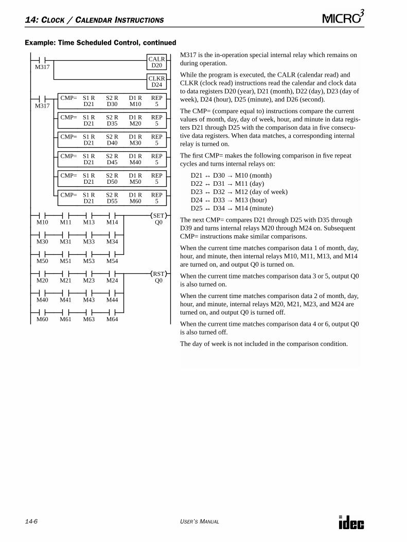
14: CLOCK / CALENDAR INSTRUCTIONS
14-6 USER’S MANUAL
Example: Time Scheduled Control, continued
CMP= S1 R REP5D21M317
M11 Q0SET
S2 RD30
D1 RM10
CMP= S1 R REP5D21
S2 RD35
D1 RM20
CMP= S1 R REP5D21
S2 RD40
D1 RM30
CMP= S1 R REP5D21
S2 RD45
D1 RM40
CMP= S1 R REP5D21
S2 RD50
D1 RM50
CMP= S1 R REP5D21
S2 RD55
D1 RM60
M10 M13 M14
M31M30 M33 M34
M51M50 M53 M54
M21 Q0RST
M20 M23 M24
M41M40 M43 M44
M61M60 M63 M64
M317 is the in-operation special internal relay which remains on during operation.
While the program is executed, the CALR (calendar read) and CLKR (clock read) instructions read the calendar and clock data to data registers D20 (year), D21 (month), D22 (day), D23 (day of week), D24 (hour), D25 (minute), and D26 (second).
The CMP= (compare equal to) instructions compare the current values of month, day, day of week, hour, and minute in data regis-ters D21 through D25 with the comparison data in five consecu-tive data registers. When data matches, a corresponding internal relay is turned on.
The first CMP= makes the following comparison in five repeat cycles and turns internal relays on:
D21 ↔ D30 → M10 (month)D22 ↔ D31 → M11 (day)D23 ↔ D32 → M12 (day of week)D24 ↔ D33 → M13 (hour)D25 ↔ D34 → M14 (minute)
The next CMP= compares D21 through D25 with D35 through D39 and turns internal relays M20 through M24 on. Subsequent CMP= instructions make similar comparisons.
When the current time matches comparison data 1 of month, day, hour, and minute, then internal relays M10, M11, M13, and M14 are turned on, and output Q0 is turned on.
When the current time matches comparison data 3 or 5, output Q0 is also turned on.
When the current time matches comparison data 2 of month, day, hour, and minute, internal relays M20, M21, M23, and M24 are turned on, and output Q0 is turned off.
When the current time matches comparison data 4 or 6, output Q0 is also turned off.
The day of week is not included in the comparison condition.
M317CALRD20
CLKRD24
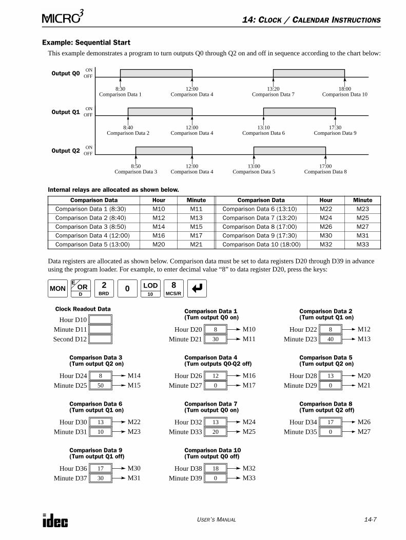
14: CLOCK / CALENDAR INSTRUCTIONS
USER’S MANUAL 14-7
Example: Sequential StartThis example demonstrates a program to turn outputs Q0 through Q2 on and off in sequence according to the chart below:
Internal relays are allocated as shown below.
Data registers are allocated as shown below. Comparison data must be set to data registers D20 through D39 in advance using the program loader. For example, to enter decimal value “8” to data register D20, press the keys:
Comparison Data Hour Minute Comparison Data Hour MinuteComparison Data 1 (8:30) M10 M11 Comparison Data 6 (13:10) M22 M23Comparison Data 2 (8:40) M12 M13 Comparison Data 7 (13:20) M24 M25Comparison Data 3 (8:50) M14 M15 Comparison Data 8 (17:00) M26 M27Comparison Data 4 (12:00) M16 M17 Comparison Data 9 (17:30) M30 M31Comparison Data 5 (13:00) M20 M21 Comparison Data 10 (18:00) M32 M33
Output Q0ON
OFF
8:30Comparison Data 1
12:00Comparison Data 4
13:20Comparison Data 7
18:00Comparison Data 10
Output Q1ON
OFF
8:40Comparison Data 2
12:00Comparison Data 4
13:10Comparison Data 6
17:30Comparison Data 9
Output Q2ON
OFF
8:50Comparison Data 3
12:00Comparison Data 4
13:00Comparison Data 5
17:00Comparison Data 8
Second D12
Minute D11
Hour D10
Clock Readout Data
30Minute D21
8Hour D20M11
M10
Comparison Data 1(Turn output Q0 on)
MON 0ORE
D
LOD10
40Minute D23
8Hour D22M13
M12
Comparison Data 2(Turn output Q1 on)
0Minute D29
13Hour D28M21
M20
Comparison Data 5(Turn output Q2 on)
0Minute D35
17Hour D34M27
M26
Comparison Data 8(Turn output Q2 off)
30Minute D37
17Hour D36M31
M30
Comparison Data 9(Turn output Q1 off)
0Minute D27
12Hour D26M17
M16
Comparison Data 4(Turn outputs Q0-Q2 off)
50Minute D25
8Hour D24M15
M14
Comparison Data 3(Turn output Q2 on)
8MCS/R
2BRD
10Minute D31
13Hour D30M23
M22
Comparison Data 6(Turn output Q1 on)
20Minute D33
13Hour D32M25
M24
Comparison Data 7(Turn output Q0 on)
0Minute D39
18Hour D38M33
M32
Comparison Data 10(Turn output Q0 off)
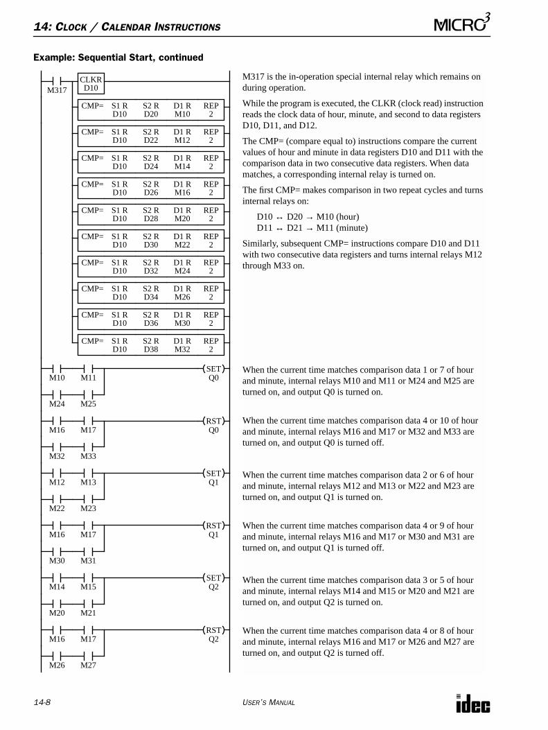
14: CLOCK / CALENDAR INSTRUCTIONS
14-8 USER’S MANUAL
Example: Sequential Start, continued
CMP= S1 R REP2D10
M11 Q0SET
S2 RD20
D1 RM10
CMP= S1 R REP2D10
S2 RD22
D1 RM12
CMP= S1 R REP2D10
S2 RD24
D1 RM14
CMP= S1 R REP2D10
S2 RD26
D1 RM16
CMP= S1 R REP2D10
S2 RD28
D1 RM20
CMP= S1 R REP2D10
S2 RD30
D1 RM22
M10
M25M24
M17M16
M33M32
M13M12
M23M22
M317 is the in-operation special internal relay which remains on during operation.
While the program is executed, the CLKR (clock read) instruction reads the clock data of hour, minute, and second to data registers D10, D11, and D12.
The CMP= (compare equal to) instructions compare the current values of hour and minute in data registers D10 and D11 with the comparison data in two consecutive data registers. When data matches, a corresponding internal relay is turned on.
The first CMP= makes comparison in two repeat cycles and turns internal relays on:
D10 ↔ D20 → M10 (hour)D11 ↔ D21 → M11 (minute)
Similarly, subsequent CMP= instructions compare D10 and D11 with two consecutive data registers and turns internal relays M12 through M33 on.
When the current time matches comparison data 1 or 7 of hour and minute, internal relays M10 and M11 or M24 and M25 are turned on, and output Q0 is turned on.
When the current time matches comparison data 4 or 10 of hour and minute, internal relays M16 and M17 or M32 and M33 are turned on, and output Q0 is turned off.
When the current time matches comparison data 2 or 6 of hour and minute, internal relays M12 and M13 or M22 and M23 are turned on, and output Q1 is turned on.
When the current time matches comparison data 4 or 9 of hour and minute, internal relays M16 and M17 or M30 and M31 are turned on, and output Q1 is turned off.
When the current time matches comparison data 3 or 5 of hour and minute, internal relays M14 and M15 or M20 and M21 are turned on, and output Q2 is turned on.
When the current time matches comparison data 4 or 8 of hour and minute, internal relays M16 and M17 or M26 and M27 are turned on, and output Q2 is turned off.
M317CLKRD10
Q0RST
Q1SET
M17 Q1RST
M16
M31M30
M15M14
M21M20
M17M16
M27M26
Q2SET
Q2RST
CMP= S1 R REP2D10
S2 RD32
D1 RM24
CMP= S1 R REP2D10
S2 RD34
D1 RM26
CMP= S1 R REP2D10
S2 RD36
D1 RM30
CMP= S1 R REP2D10
S2 RD38
D1 RM32
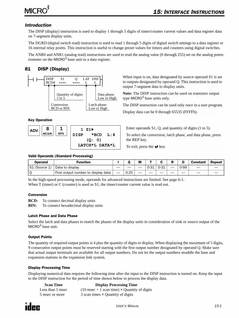
USER’S MANUAL 15-1
15: INTERFACE INSTRUCTIONS
IntroductionThe DISP (display) instruction is used to display 1 through 5 digits of timer/counter current values and data register data on 7-segment display units.
The DGRD (digital switch read) instruction is used to read 1 through 5 digits of digital switch settings to a data register or 16 internal relay points. This instruction is useful to change preset values for timers and counters using digital switches.
The ANR0 and ANR1 (analog read) instructions are used to read the analog value (0 through 255) set on the analog poten-tiometer on the MICRO3 base unit to a data register.
81 DISP (Display)
Key Operation
Valid Operands (Standard Processing)
In the high-speed processing mode, operands for advanced instructions are limited. See page 6-1.When T (timer) or C (counter) is used as S1, the timer/counter current value is read out.
Conversion
BCD: To connect decimal display unitsBIN: To connect hexadecimal display units
Latch Phase and Data Phase
Select the latch and data phases to match the phases of the display units in consideration of sink or source output of the MICRO3 base unit.
Output Points
The quantity of required output points is 4 plus the quantity of digits to display. When displaying the maximum of 5 digits, 9 consecutive output points must be reserved starting with the first output number designated by operand Q. Make sure that actual output terminals are available for all output numbers. Do not let the output numbers straddle the base and expansion stations in the expansion link system.
Display Processing Time
Displaying numerical data requires the following time after the input to the DISP instruction is turned on. Keep the input to the DISP instruction for the period of time shown below to process the display data.
Operand Function I Q M T C R D Constant RepeatS1 (Source 1) Data to display — — — 0-31 0-31 — 0-99 — —Q First output number to display data — 0-25 — — — — — — —
Scan Time Display Processing TimeLess than 5 msec5 msec or more
(10 msec + 1 scan time) × Quantity of digits3 scan times × Quantity of digits
Latch phase:Low or High
Data phase:Low or High
Conversion:BCD or BIN
Quantity of digits:1 to 5
When input is on, data designated by source operand S1 is set to outputs designated by operand Q. This instruction is used to output 7-segment data to display units.
Note: The DISP instruction can be used on transistor output type MICRO3 base units only.
The DISP instruction can be used only once in a user program.
Display data can be 0 through 65535 (FFFFh).
DISP DATS1****
Q****BCD4
LATLL
ADV 1BPS
1 S1DISP *BCD L:4 (Q: 0) LATCH*L DATA*L
Enter operands S1, Q, and quantity of digits (1 to 5).
To select the conversion, latch phase, and data phase, press the REP key.
To exit, press the key.
8MCS/R
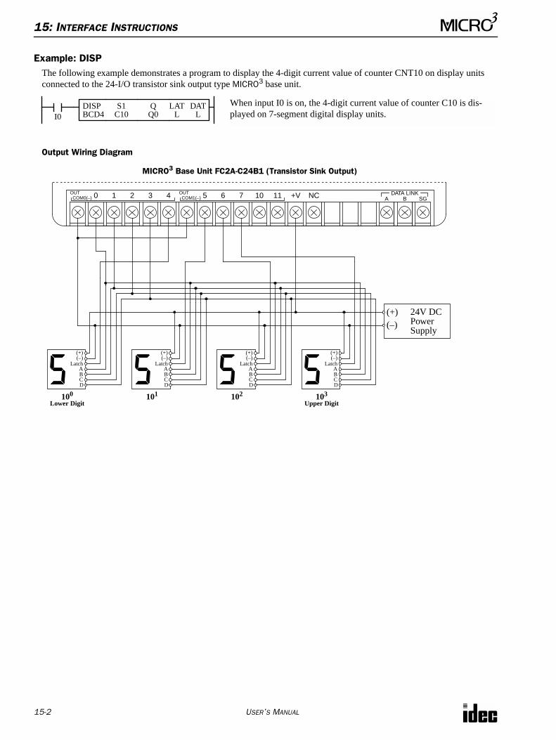
15: INTERFACE INSTRUCTIONS
15-2 USER’S MANUAL
Example: DISP The following example demonstrates a program to display the 4-digit current value of counter CNT10 on display units connected to the 24-I/O transistor sink output type MICRO3 base unit.
Output Wiring Diagram
When input I0 is on, the 4-digit current value of counter C10 is dis-played on 7-segment digital display units.I0
DISP DATBCD4
LATLL
S1C10
QQ0
(+)(–)
LatchABCD
(+)(–)
24V DCPowerSupply
(+)(–)
LatchABCD
(+)(–)
LatchABCD
(+)(–)
LatchABCD
100 101 102 103
OUTCOM0(–) 0 1 2 3 NC DATA LINK
A SGB+V4 OUTCOM1(–) 5 6 7 10 11
MICRO3 Base Unit FC2A-C24B1 (Transistor Sink Output)
Lower Digit Upper Digit
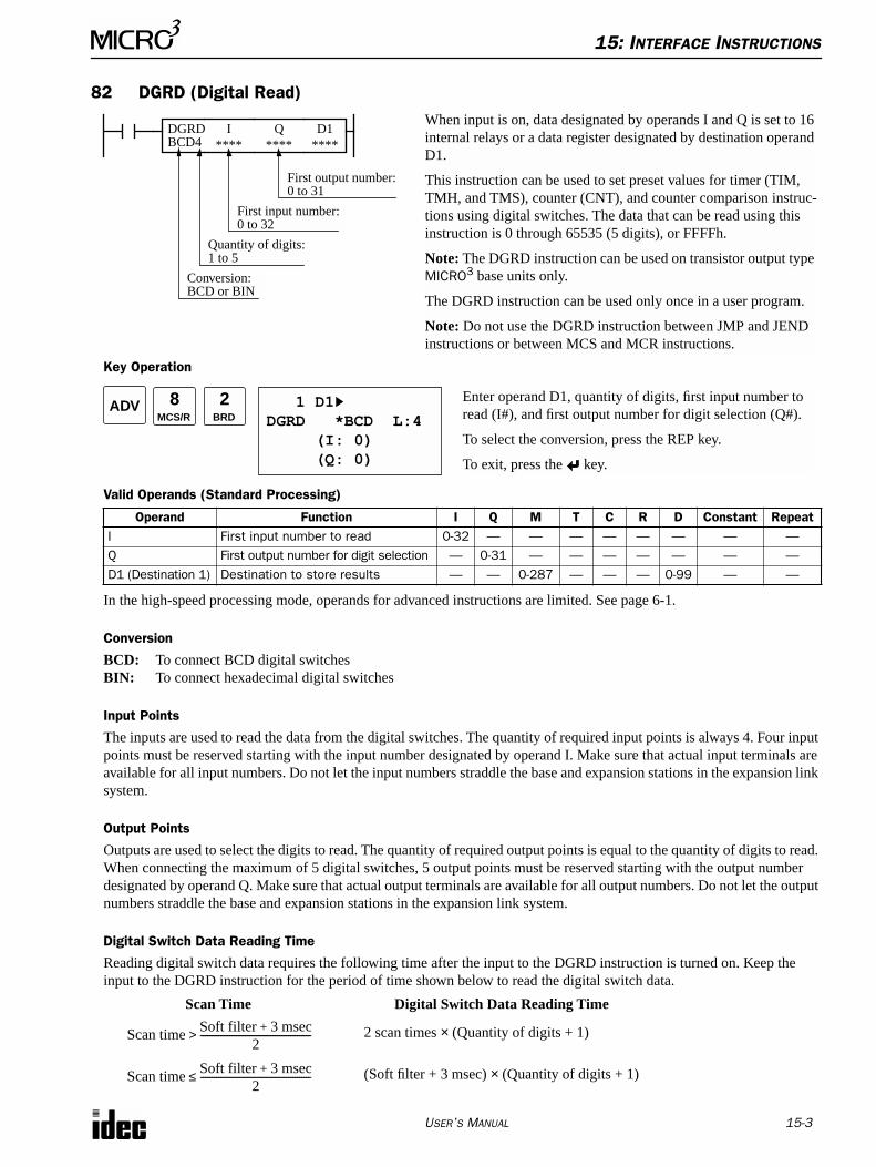
15: INTERFACE INSTRUCTIONS
USER’S MANUAL 15-3
82 DGRD (Digital Read)
Key Operation
Valid Operands (Standard Processing)
In the high-speed processing mode, operands for advanced instructions are limited. See page 6-1.
Conversion
BCD: To connect BCD digital switchesBIN: To connect hexadecimal digital switches
Input Points
The inputs are used to read the data from the digital switches. The quantity of required input points is always 4. Four input points must be reserved starting with the input number designated by operand I. Make sure that actual input terminals are available for all input numbers. Do not let the input numbers straddle the base and expansion stations in the expansion link system.
Output Points
Outputs are used to select the digits to read. The quantity of required output points is equal to the quantity of digits to read. When connecting the maximum of 5 digital switches, 5 output points must be reserved starting with the output number designated by operand Q. Make sure that actual output terminals are available for all output numbers. Do not let the output numbers straddle the base and expansion stations in the expansion link system.
Digital Switch Data Reading Time
Reading digital switch data requires the following time after the input to the DGRD instruction is turned on. Keep the input to the DGRD instruction for the period of time shown below to read the digital switch data.
Operand Function I Q M T C R D Constant RepeatI First input number to read 0-32 — — — — — — — —Q First output number for digit selection — 0-31 — — — — — — —D1 (Destination 1) Destination to store results — — 0-287 — — — 0-99 — —
Scan Time Digital Switch Data Reading Time
2 scan times × (Quantity of digits + 1)
(Soft filter + 3 msec) × (Quantity of digits + 1)
First input number:0 to 32
First output number:0 to 31
Conversion:BCD or BIN
Quantity of digits:1 to 5
When input is on, data designated by operands I and Q is set to 16 internal relays or a data register designated by destination operand D1.
This instruction can be used to set preset values for timer (TIM, TMH, and TMS), counter (CNT), and counter comparison instruc-tions using digital switches. The data that can be read using this instruction is 0 through 65535 (5 digits), or FFFFh.
Note: The DGRD instruction can be used on transistor output type MICRO3 base units only.
The DGRD instruction can be used only once in a user program.
Note: Do not use the DGRD instruction between JMP and JEND instructions or between MCS and MCR instructions.
DGRD I****
Q****BCD4
D1****
ADV 1 D1DGRD *BCD L:4 (I: 0) (Q: 0)
Enter operand D1, quantity of digits, first input number to read (I#), and first output number for digit selection (Q#).
To select the conversion, press the REP key.
To exit, press the key.
8MCS/R
2BRD
Scan time Soft filter 3 msec + 2
--------------------------------------------------
>
Scan time Soft filter 3 msec + 2
--------------------------------------------------
≤
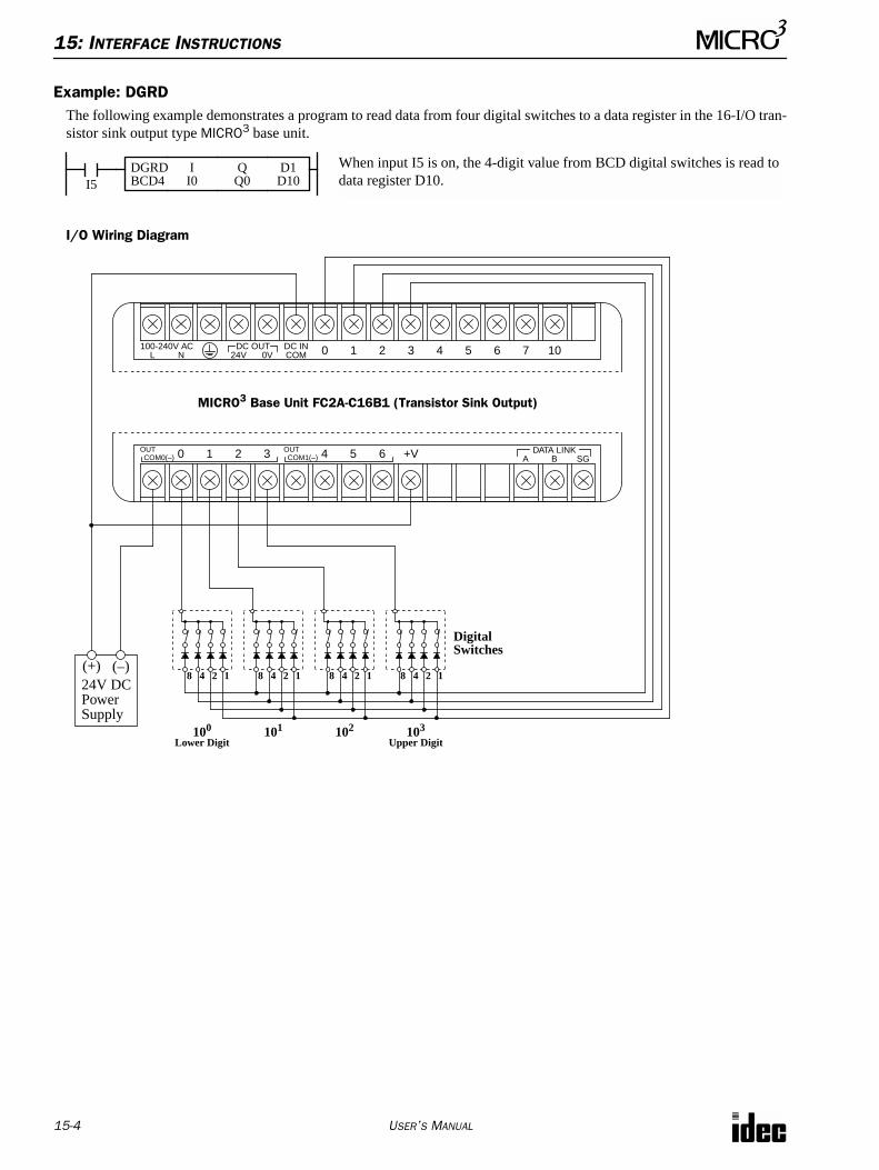
15: I
NTERFACE
I
NSTRUCTIONS
15-4 U
SER
’
S
M
ANUAL
Example: DGRD
The following example demonstrates a program to read data from four digital switches to a data register in the 16-I/O tran-sistor sink output type
MICRO
3
base unit.
I/O Wiring Diagram
When input I5 is on, the 4-digit value from BCD digital switches is read to data register D10.I5
DGRDBCD4
II0
QQ0
D1D10
Digital
24V DC(+) (–)
100
8 4 2 1
101
8 4 2 1
102
8 4 2 1
103
8 4 2 1
PowerSupply
Switches
OUTCOM0(–) 0 1 2 3 OUT
COM1(–) 4 5 6 DATA LINKA SGB+V
MICRO3 Base Unit FC2A-C16B1 (Transistor Sink Output)
Upper DigitLower Digit
100-240V ACL N
DC OUT24V 0V
DC INCOM 0 1 2 3 4 5 6 7 10
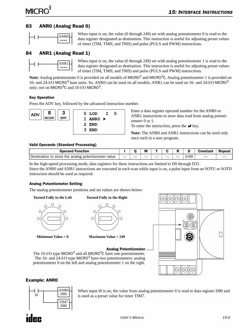
15: I
NTERFACE
I
NSTRUCTIONS
U
SER
’
S
M
ANUAL
15-5
83 ANR0 (Analog Read 0)
84 ANR1 (Analog Read 1)
Note:
Analog potentiometer 0 is provided on all models of
MICRO
3
and
MICRO
3
C
. Analog potentiometer 1 is provided on 16- and 24-I/O
MICRO
3
base units. So, ANR0 can be used on all models. ANR1 can be used on 16- and 24-I/O
MICRO
3
only; not on
MICRO
3
C
and 10-I/O
MICRO
3
.
Key Operation
Press the ADV key, followed by the advanced instruction number.
Valid Operands (Standard Processing)
In the high-speed processing mode, data registers for these instructions are limited to D0 through D31.Since the ANR0 and ANR1 instructions are executed in each scan while input is on, a pulse input from an SOTU or SOTD instruction should be used as required.
Analog Potentiometer Setting
The analog potentiometer positions and set values are shown below:
Example: ANR0
Operand Function I Q M T C R D Constant Repeat
Destination to store the analog potentiometer value — — — — — — 0-99 — —
When input is on, the value (0 through 249) set with analog potentiometer 0 is read to the data register designated as destination. This instruction is useful for adjusting preset values of timer (TIM, TMH, and TMS) and pulse (PULS and PWM) instructions.
ANR0****
When input is on, the value (0 through 249) set with analog potentiometer 1 is read to the data register designated as destination. This instruction is useful for adjusting preset values of timer (TIM, TMH, and TMS) and pulse (PULS and PWM) instructions.
ANR1****
ADV 0 LOD I 0 1 ANR0 2 END 3 END
Enter a data register operand number for the ANR0 or ANR1 instructions to store data read from analog potenti-ometer 0 or 1.To enter the instruction, press the key.
Note: The ANR0 and ANR1 instructions can be used only once each in a user program.
8MCS/R
3BPP
Turned Fully to the Left
Minimum Value = 0
Turned Fully to the Right
Maximum Value = 249
Analog PotentiometerThe 10-I/O type MICRO3 and all MICRO3C have one potentiometer.The 16- and 24-I/O type MICRO3 have two potentiometers: analog
potentiometer 0 on the left and analog potentiometer 1 on the right.
0 17
3 4 562
1 0
When input I0 is on, the value from analog potentiometer 0 is read to data register D80 and is used as a preset value for timer TIM7.
I0ANR0D80
TIM7D80

15: I
NTERFACE
I
NSTRUCTIONS
15-6 U
SER
’
S
M
ANUAL
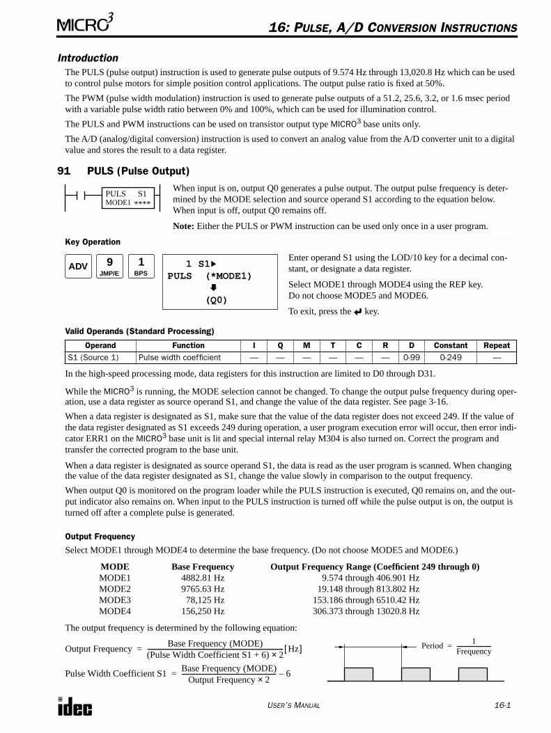
U
SER
’
S
M
ANUAL
16-1
16: P
ULSE
, A/D C
ONVERSION
I
NSTRUCTIONS
Introduction
The PULS (pulse output) instruction is used to generate pulse outputs of 9.574 Hz through 13,020.8 Hz which can be used to control pulse motors for simple position control applications. The output pulse ratio is fixed at 50%.
The PWM (pulse width modulation) instruction is used to generate pulse outputs of a 51.2, 25.6, 3.2, or 1.6 msec period with a variable pulse width ratio between 0% and 100%, which can be used for illumination control.
The PULS and PWM instructions can be used on transistor output type
MICRO
3
base units only.
The A/D (analog/digital conversion) instruction is used to convert an analog value from the A/D converter unit to a digital value and stores the result to a data register.
91 PULS (Pulse Output)
Key Operation
Valid Operands (Standard Processing)
In the high-speed processing mode, data registers for this instruction are limited to D0 through D31.
While the
MICRO
3 is running, the MODE selection cannot be changed. To change the output pulse frequency during oper-ation, use a data register as source operand S1, and change the value of the data register. See page 3-16.
When a data register is designated as S1, make sure that the value of the data register does not exceed 249. If the value of the data register designated as S1 exceeds 249 during operation, a user program execution error will occur, then error indi-cator ERR1 on the MICRO3 base unit is lit and special internal relay M304 is also turned on. Correct the program and transfer the corrected program to the base unit.
When a data register is designated as source operand S1, the data is read as the user program is scanned. When changing the value of the data register designated as S1, change the value slowly in comparison to the output frequency.
When output Q0 is monitored on the program loader while the PULS instruction is executed, Q0 remains on, and the out-put indicator also remains on. When input to the PULS instruction is turned off while the pulse output is on, the output is turned off after a complete pulse is generated.
Output Frequency
Select MODE1 through MODE4 to determine the base frequency. (Do not choose MODE5 and MODE6.)
The output frequency is determined by the following equation:
Operand Function I Q M T C R D Constant RepeatS1 (Source 1) Pulse width coefficient — — — — — — 0-99 0-249 —
MODE Base Frequency Output Frequency Range (Coefficient 249 through 0)MODE1 4882.81 Hz 9.574 through 406.901 HzMODE2 9765.63 Hz 19.148 through 813.802 HzMODE3 78,125 Hz 153.186 through 6510.42 HzMODE4 156,250 Hz 306.373 through 13020.8 Hz
When input is on, output Q0 generates a pulse output. The output pulse frequency is deter-mined by the MODE selection and source operand S1 according to the equation below.When input is off, output Q0 remains off.
Note: Either the PULS or PWM instruction can be used only once in a user program.
PULSMODE1
S1 ****
ADV 1BPS
1 S1PULS (*MODE1) (Q0)
Enter operand S1 using the LOD/10 key for a decimal con-stant, or designate a data register.
Select MODE1 through MODE4 using the REP key.Do not choose MODE5 and MODE6.
To exit, press the key.
9JMP/E
Output FrequencyBase Frequency (MODE)
(Pulse Width Coefficient S1 + 6) 2×---------------------------------------------------------------------------------------- Hz[ ]=
Pulse Width Coefficient S1 Base Frequency (MODE)Output Frequency 2×
------------------------------------------------------------- 6–=
Period 1Frequency-------------------------=
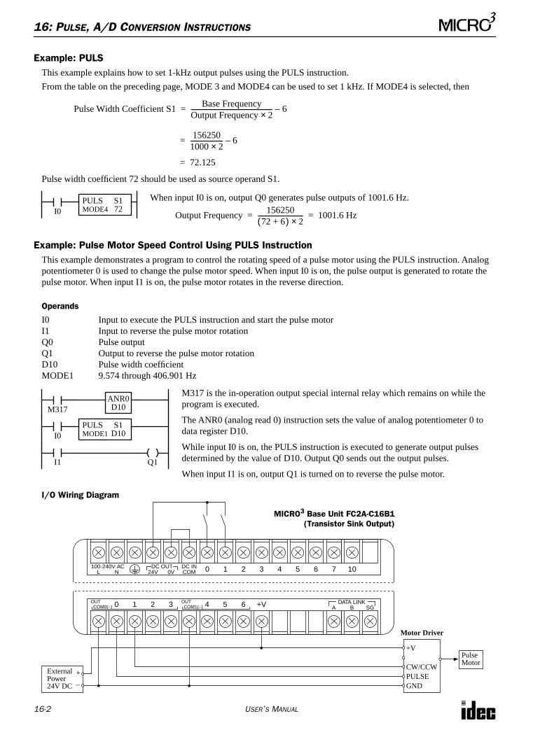
16: PULSE, A/D CONVERSION INSTRUCTIONS
16-2 USER’S MANUAL
Example: PULSThis example explains how to set 1-kHz output pulses using the PULS instruction.
From the table on the preceding page, MODE 3 and MODE4 can be used to set 1 kHz. If MODE4 is selected, then
Pulse width coefficient 72 should be used as source operand S1.
Example: Pulse Motor Speed Control Using PULS InstructionThis example demonstrates a program to control the rotating speed of a pulse motor using the PULS instruction. Analog potentiometer 0 is used to change the pulse motor speed. When input I0 is on, the pulse output is generated to rotate the pulse motor. When input I1 is on, the pulse motor rotates in the reverse direction.
Operands
I0 Input to execute the PULS instruction and start the pulse motorI1 Input to reverse the pulse motor rotationQ0 Pulse outputQ1 Output to reverse the pulse motor rotationD10 Pulse width coefficientMODE1 9.574 through 406.901 Hz
I/O Wiring Diagram
Pulse Width Coefficient S1 Base FrequencyOutput Frequency 2 × ---------------------------------------------------- 6–=
1562501000 2
×
--------------------- 6–=
72.125=
When input I0 is on, output Q0 generates pulse outputs of 1001.6 Hz.
I0PULSMODE4
S172
Output Frequency 15625072 6+
( ) 2
× ----------------------------- 1001.6 Hz= =
M317
PULSMODE1
S1D10I0
ANR0D10
I1 Q1
M317 is the in-operation output special internal relay which remains on while the program is executed.
The ANR0 (analog read 0) instruction sets the value of analog potentiometer 0 to data register D10.
While input I0 is on, the PULS instruction is executed to generate output pulses determined by the value of D10. Output Q0 sends out the output pulses.
When input I1 is on, output Q1 is turned on to reverse the pulse motor.
OUTCOM0(–) 0 1 2 3 OUT
COM1(–) 4 5 6 DATA LINKA SGB+V
+V
CW/CCWPULSEGND
PulseMotor
+
–
ExternalPower24V DC
Motor Driver
100-240V ACL N
DC OUT24V 0V
DC INCOM 0 1 2 3 4 5 6 7 10
MICRO3 Base Unit FC2A-C16B1(Transistor Sink Output)
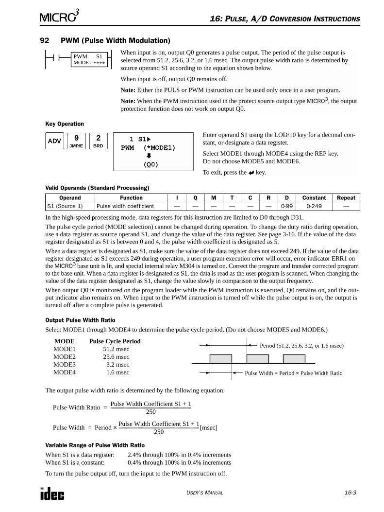
16: P
ULSE
, A/D C
ONVERSION
I
NSTRUCTIONS
U
SER
’
S
M
ANUAL
16-3
92 PWM (Pulse Width Modulation)
Key Operation
Valid Operands (Standard Processing)
In the high-speed processing mode, data registers for this instruction are limited to D0 through D31.
The pulse cycle period (MODE selection) cannot be changed during operation. To change the duty ratio during operation, use a data register as source operand S1, and change the value of the data register. See page 3-16. If the value of the data register designated as S1 is between 0 and 4, the pulse width coefficient is designated as 5.
When a data register is designated as S1, make sure the value of the data register does not exceed 249. If the value of the data register designated as S1 exceeds 249 during operation, a user program execution error will occur, error indicator ERR1 on the
MICRO
3
base unit is lit, and special internal relay M304 is turned on. Correct the program and transfer corrected program to the base unit. When a data register is designated as S1, the data is read as the user program is scanned. When changing the value of the data register designated as S1, change the value slowly in comparison to the output frequency.
When output Q0 is monitored on the program loader while the PWM instruction is executed, Q0 remains on, and the out-put indicator also remains on. When input to the PWM instruction is turned off while the pulse output is on, the output is turned off after a complete pulse is generated.
Output Pulse Width Ratio
Select MODE1 through MODE4 to determine the pulse cycle period. (Do not choose MODE5 and MODE6.)
The output pulse width ratio is determined by the following equation:
Variable Range of Pulse Width Ratio
When S1 is a data register: 2.4% through 100% in 0.4% incrementsWhen S1 is a constant: 0.4% through 100% in 0.4% increments
To turn the pulse output off, turn the input to the PWM instruction off.
Operand Function I Q M T C R D Constant Repeat
S1 (Source 1) Pulse width coefficient — — — — — — 0-99 0-249 —
MODE Pulse Cycle Period
MODE1 51.2 msecMODE2 25.6 msecMODE3 3.2 msecMODE4 1.6 msec
When input is on, output Q0 generates a pulse output. The period of the pulse output is selected from 51.2, 25.6, 3.2, or 1.6 msec. The output pulse width ratio is determined by source operand S1 according to the equation shown below.
When input is off, output Q0 remains off.
Note: Either the PULS or PWM instruction can be used only once in a user program.
Note: When the PWM instruction used in the protect source output type MICRO3, the output protection function does not work on output Q0.
PWMMODE1
S1 ****
ADV
1 S1 PWM (*MODE1) (Q0)
9
JMP/E
2
BRD
Enter operand S1 using the LOD/10 key for a decimal con-stant, or designate a data register.
Select MODE1 through MODE4 using the REP key.Do not choose MODE5 and MODE6.
To exit, press the key.
Period (51.2, 25.6, 3.2, or 1.6 msec)
Pulse Width = Period × Pulse Width Ratio
Pulse Width Ratio Pulse Width Coefficient S1 1+250
---------------------------------------------------------------------------=
Pulse Width PeriodPulse Width Coefficient S1 1+
250--------------------------------------------------------------------------- ×
[msec]=
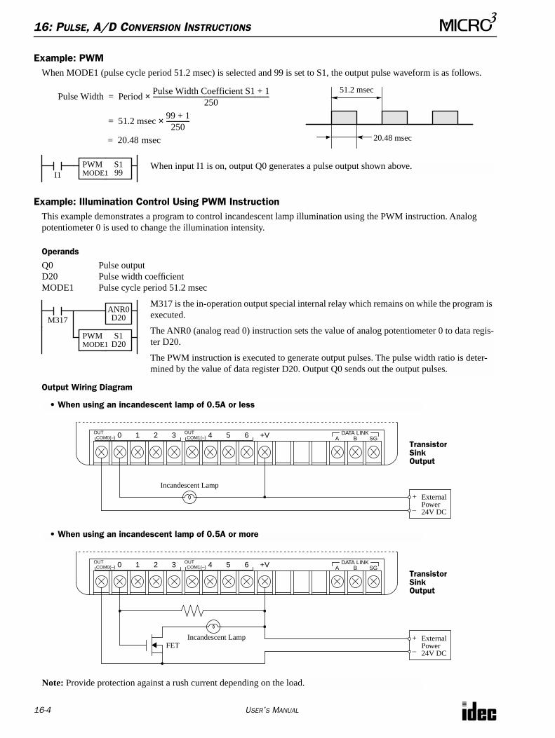
16: P
ULSE
, A/D C
ONVERSION
I
NSTRUCTIONS
16-4 U
SER
’
S
M
ANUAL
Example: PWM
When MODE1 (pulse cycle period 51.2 msec) is selected and 99 is set to S1, the output pulse waveform is as follows.
Example: Illumination Control Using PWM Instruction
This example demonstrates a program to control incandescent lamp illumination using the PWM instruction. Analog potentiometer 0 is used to change the illumination intensity.
Operands
Q0 Pulse outputD20 Pulse width coefficientMODE1 Pulse cycle period 51.2 msec
Output Wiring Diagram
When input I1 is on, output Q0 generates a pulse output shown above.I1
S199
PWMMODE1
Pulse Width PeriodPulse Width Coefficient S1 1+
250---------------------------------------------------------------------------
× =
51.2 msec99 1+
250--------------- × =
20.48 msec=
51.2 msec
20.48 msec
M317
PWMMODE1
S1D20
ANR0D20
M317 is the in-operation output special internal relay which remains on while the program is executed.
The ANR0 (analog read 0) instruction sets the value of analog potentiometer 0 to data regis-ter D20.
The PWM instruction is executed to generate output pulses. The pulse width ratio is deter-mined by the value of data register D20. Output Q0 sends out the output pulses.
OUTCOM0(–) 0 1 2 3 OUT
COM1(–) 4 5 6 DATA LINKA SGB+V
+
–
ExternalPower24V DC
Incandescent Lamp
OUTCOM0(–) 0 1 2 3 OUT
COM1(–) 4 5 6 DATA LINKA SGB+V
+
–
ExternalPower24V DC
Incandescent Lamp
Note: Provide protection against a rush current depending on the load.
TransistorSinkOutput
TransistorSinkOutput
FET
• When using an incandescent lamp of 0.5A or less
• When using an incandescent lamp of 0.5A or more
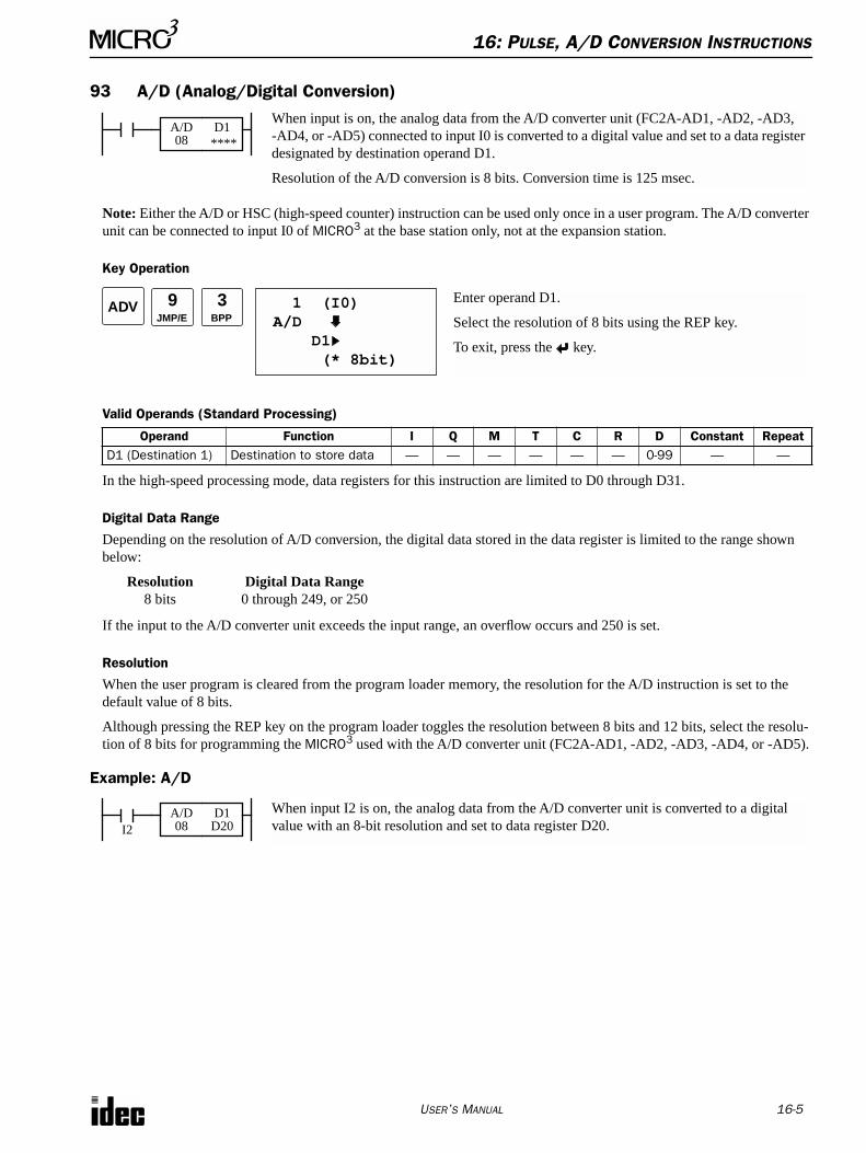
16: P
ULSE
, A/D C
ONVERSION
I
NSTRUCTIONS
U
SER
’
S
M
ANUAL
16-5
93 A/D (Analog/Digital Conversion)
Note: Either the A/D or HSC (high-speed counter) instruction can be used only once in a user program. The A/D converter unit can be connected to input I0 of
MICRO
3 at the base station only, not at the expansion station.
Key Operation
Valid Operands (Standard Processing)
In the high-speed processing mode, data registers for this instruction are limited to D0 through D31.
Digital Data Range
Depending on the resolution of A/D conversion, the digital data stored in the data register is limited to the range shown below:
If the input to the A/D converter unit exceeds the input range, an overflow occurs and 250 is set.
Resolution
When the user program is cleared from the program loader memory, the resolution for the A/D instruction is set to the default value of 8 bits.
Although pressing the REP key on the program loader toggles the resolution between 8 bits and 12 bits, select the resolu-tion of 8 bits for programming the
MICRO
3
used with the A/D converter unit (FC2A-AD1, -AD2, -AD3, -AD4, or -AD5).
Example: A/D
Operand Function I Q M T C R D Constant Repeat
D1 (Destination 1) Destination to store data — — — — — — 0-99 — —
Resolution Digital Data Range
8 bits 0 through 249, or 250
When input is on, the analog data from the A/D converter unit (FC2A-AD1, -AD2, -AD3, -AD4, or -AD5) connected to input I0 is converted to a digital value and set to a data register designated by destination operand D1.
Resolution of the A/D conversion is 8 bits. Conversion time is 125 msec.
A/D08
D1 ****
ADV 1 (I0) A/D D1 (* 8bit)
Enter operand D1.
Select the resolution of 8 bits using the REP key.
To exit, press the key.
9JMP/E
3BPP
I2D1D20
When input I2 is on, the analog data from the A/D converter unit is converted to a digital value with an 8-bit resolution and set to data register D20.
A/D08

16: P
ULSE
, A/D C
ONVERSION
I
NSTRUCTIONS
16-6 U
SER
’
S
M
ANUAL
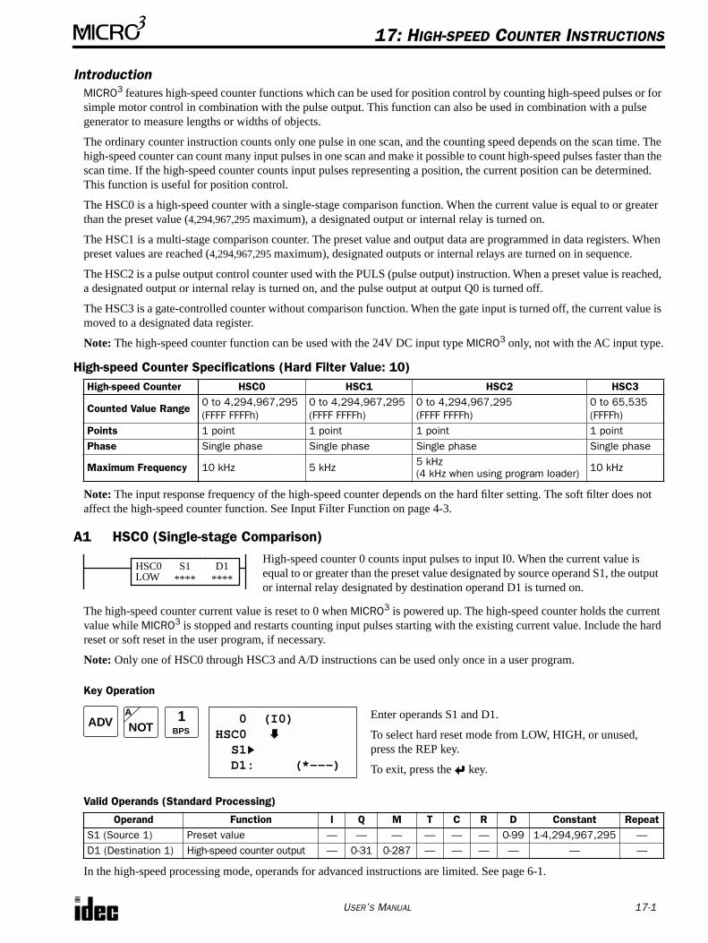
U
SER
’
S
M
ANUAL
17-1
17: H
IGH
-
SPEED
C
OUNTER
I
NSTRUCTIONS
Introduction
MICRO
3
features high-speed counter functions which can be used for position control by counting high-speed pulses or for simple motor control in combination with the pulse output. This function can also be used in combination with a pulse generator to measure lengths or widths of objects.
The ordinary counter instruction counts only one pulse in one scan, and the counting speed depends on the scan time. The high-speed counter can count many input pulses in one scan and make it possible to count high-speed pulses faster than the scan time. If the high-speed counter counts input pulses representing a position, the current position can be determined. This function is useful for position control.
The HSC0 is a high-speed counter with a single-stage comparison function. When the current value is equal to or greater than the preset value (
4,294,967,295
maximum), a designated output or internal relay is turned on.
The HSC1 is a multi-stage comparison counter. The preset value and output data are programmed in data registers. When preset values are reached (
4,294,967,295
maximum), designated outputs or internal relays are turned on in sequence.
The HSC2 is a pulse output control counter used with the PULS (pulse output) instruction. When a preset value is reached, a designated output or internal relay is turned on, and the pulse output at output Q0 is turned off.
The HSC3 is a gate-controlled counter without comparison function. When the gate input is turned off, the current value is moved to a designated data register.
Note:
The high-speed counter function can be used with the 24V DC input type
MICRO
3
only, not with the AC input type.
High-speed Counter Specifications (Hard Filter Value: 10)
Note:
The input response frequency of the high-speed counter depends on the hard filter setting. The soft filter does not affect the high-speed counter function. See Input Filter Function on page 4-3.
A1 HSC0 (Single-stage Comparison)
The high-speed counter current value is reset to 0 when
MICRO
3
is powered up. The high-speed counter holds the current value while
MICRO
3
is stopped and restarts counting input pulses starting with the existing current value. Include the hard reset or soft reset in the user program, if necessary.
Note:
Only one of HSC0 through HSC3 and A/D instructions can be used only once in a user program.
Key Operation
Valid Operands (Standard Processing)
In the high-speed processing mode, operands for advanced instructions are limited. See page 6-1.
High-speed Counter HSC0 HSC1 HSC2 HSC3
Counted Value Range
0 to 4,294,967,295(FFFF FFFFh)
0 to 4,294,967,295(FFFF FFFFh)
0 to 4,294,967,295(FFFF FFFFh)
0 to 65,535(FFFFh)
Points
1 point 1 point 1 point 1 point
Phase
Single phase Single phase Single phase Single phase
Maximum Frequency
10 kHz 5 kHz 5 kHz (4 kHz when using program loader) 10 kHz
Operand Function I Q M T C R D Constant Repeat
S1 (Source 1) Preset value — — — — — — 0-99 1-4,294,967,295 —D1 (Destination 1) High-speed counter output — 0-31 0-287 — — — — — —
High-speed counter 0 counts input pulses to input I0. When the current value is equal to or greater than the preset value designated by source operand S1, the output or internal relay designated by destination operand D1 is turned on.
D1****
S1****
HSC0LOW
ADV 1BPS
0 (I0)HSC0 S1 D1: (*---)
Enter operands S1 and D1.
To select hard reset mode from LOW, HIGH, or unused, press the REP key.
To exit, press the key.
NOTA
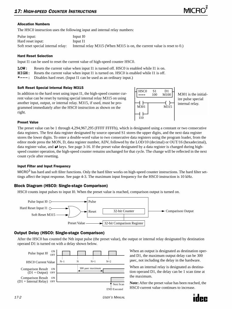
17: H
IGH
-
SPEED
C
OUNTER
I
NSTRUCTIONS
17-2 U
SER
’
S
M
ANUAL
Allocation Numbers
The HSC0 instruction uses the following input and internal relay numbers:
Pulse input: Input I0Hard reset input: Input I1Soft reset special internal relay: Internal relay M315 (When M315 is on, the current value is reset to 0.)
Hard Reset Selection
Input I1 can be used to reset the current value of high-speed counter HSC0.
LOW: Resets the current value when input I1 is turned off. HSC0 is enabled while I1 is on.HIGH: Resets the current value when input I1 is turned on. HSC0 is enabled while I1 is off.*–––: Disables hard reset. (Input I1 can be used as an ordinary input.)
Soft Reset Special Internal Relay M315
In addition to the hard reset using input I1, the high-speed counter cur-rent value can be reset by turning special internal relay M315 on using another input, output, or internal relay. M315, if used, must be pro-grammed immediately after the HSC0 instruction as shown on the right.
Preset Value
The preset value can be 1 through 4,294,967,295 (FFFF FFFFh), which is designated using a constant or two consecutive data registers. The first data register designated by source operand S1 stores the upper digits, and the next data register stores the lower digits. To enter a double-word value to two consecutive data registers using the program loader, from the editor mode press the MON, D, data register number, ADV, followed by the LOD/10 (decimal) or OUT/16 (hexadecimal), data register value, and keys. See page 3-16. If the preset value designated by a data register is changed during high-speed counter operation, the high-speed counter remains unchanged for that cycle. The change will be reflected in the next count cycle after resetting.
Input Filter and Input Frequency
MICRO3 has hard and soft filter functions. Only the hard filter works on high-speed counter instructions. The hard filter set-tings affect the input response. See page 4-3. The maximum input frequency for the HSC0 instruction is 10 kHz.
Block Diagram (HSC0: Single-stage Comparison)HSC0 counts input pulses to input I0. When the preset value is reached, comparison output is turned on.
Output Delay (HSC0: Single-stage Comparison)After the HSC0 has counted the Nth input pulse (the preset value), the output or internal relay designated by destination operand D1 is turned on with a delay shown below.
M301 is the initial-ize pulse special internal relay.
HSC0****
S1 D1M100100
M301
I10
M315
Pulse Input I0
Hard Reset Input I1
Soft Reset M315
Pulse
Reset
32-bit Comparison Register
32-bit Counter Comparison Output
Preset Value
Pulse Input I0ON
OFF
Comparison Result ONOFF
Comparison Result ONOFF
N–1HSC0 Current Value N N+1 N+2
(D1 = Output)
(D1 = Internal Relay)
300 µsec maximum
END Executed
Next Scan
When an output is designated as destination oper-and D1, the maximum output delay can be 300 µsec, not including the delay in the hardware.
When an internal relay is designated as destina-tion operand D1, the delay can be 1 scan time at the maximum.
Note: After the preset value has been reached, the HSC0 current value continues to increase.
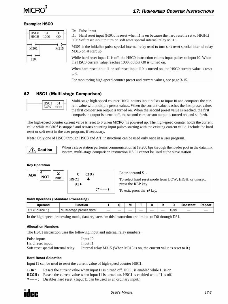
17: HIGH-SPEED COUNTER INSTRUCTIONS
USER’S MANUAL 17-3
Example: HSC0
A2 HSC1 (Multi-stage Comparison)
The high-speed counter current value is reset to 0 when MICRO3 is powered up. The high-speed counter holds the current value while MICRO3 is stopped and restarts counting input pulses starting with the existing current value. Include the hard reset or soft reset in the user program, if necessary.
Note: Only one of HSC0 through HSC3 and A/D instructions can be used only once in a user program.
Key Operation
Valid Operands (Standard Processing)
In the high-speed processing mode, data registers for this instruction are limited to D0 through D31.
Allocation Numbers
The HSC1 instruction uses the following input and internal relay numbers:
Pulse input: Input I0Hard reset input: Input I1Soft reset special internal relay: Internal relay M315 (When M315 is on, the current value is reset to 0.)
Hard Reset Selection
Input I1 can be used to reset the current value of high-speed counter HSC1.
LOW: Resets the current value when input I1 is turned off. HSC1 is enabled while I1 is on.HIGH: Resets the current value when input I1 is turned on. HSC1 is enabled while I1 is off.*–––: Disables hard reset. (Input I1 can be used as an ordinary input.)
Operand Function I Q M T C R D Constant RepeatS1 (Source 1) Multi-stage preset data — — — — — — 0-99 — —
HSC0HIGH
I10
M301
S1 D1Q01000
M315
I0: Pulse inputI1: Hard reset input (HSC0 is reset when I1 is on because the hard reset is set to HIGH.)I10: Soft reset input to turn on soft reset special internal relay M315
M301 is the initialize pulse special internal relay used to turn soft reset special internal relay M315 on at start up.
While hard reset input I1 is off, the HSC0 instruction counts input pulses to input I0. When the HSC0 current value reaches 1000, output Q0 is turned on.
When hard reset input I1 or soft reset input I10 is turned on, the HSC0 current value is reset to 0.
For monitoring high-speed counter preset and current values, see page 3-15.
Multi-stage high-speed counter HSC1 counts input pulses to input I0 and compares the cur-rent value with multiple preset values. When the current value reaches the first preset value, the first comparison output is turned on. When the second preset value is reached, the first comparison output is turned off, the second comparison output is turned on, and so forth.
S1****
HSC1LOW
CautionWhen a slave station performs communication at 19,200 bps through the loader port in the data link system, multi-stage comparison instruction HSC1 cannot be used at the slave station.
ADV 0 (I0)HSC1 S1 (*---)
Enter operand S1.
To select hard reset mode from LOW, HIGH, or unused, press the REP key.
To exit, press the key.
NOTA 2
BRD
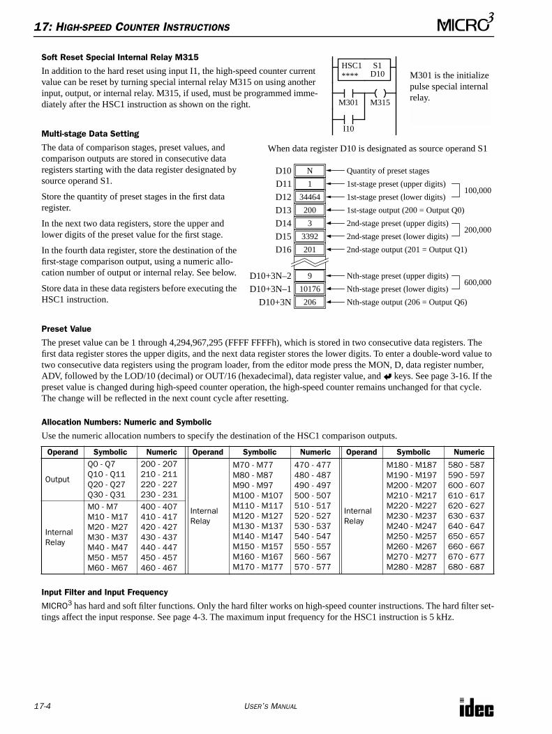
17: HIGH-SPEED COUNTER INSTRUCTIONS
17-4 USER’S MANUAL
Soft Reset Special Internal Relay M315
In addition to the hard reset using input I1, the high-speed counter current value can be reset by turning special internal relay M315 on using another input, output, or internal relay. M315, if used, must be programmed imme-diately after the HSC1 instruction as shown on the right.
Multi-stage Data Setting
The data of comparison stages, preset values, and comparison outputs are stored in consecutive data registers starting with the data register designated by source operand S1.
Store the quantity of preset stages in the first data register.
In the next two data registers, store the upper and lower digits of the preset value for the first stage.
In the fourth data register, store the destination of the first-stage comparison output, using a numeric allo-cation number of output or internal relay. See below.
Store data in these data registers before executing the HSC1 instruction.
Preset Value
The preset value can be 1 through 4,294,967,295 (FFFF FFFFh), which is stored in two consecutive data registers. The first data register stores the upper digits, and the next data register stores the lower digits. To enter a double-word value to two consecutive data registers using the program loader, from the editor mode press the MON, D, data register number, ADV, followed by the LOD/10 (decimal) or OUT/16 (hexadecimal), data register value, and keys. See page 3-16. If the preset value is changed during high-speed counter operation, the high-speed counter remains unchanged for that cycle. The change will be reflected in the next count cycle after resetting.
Allocation Numbers: Numeric and Symbolic
Use the numeric allocation numbers to specify the destination of the HSC1 comparison outputs.
Input Filter and Input Frequency
MICRO3 has hard and soft filter functions. Only the hard filter works on high-speed counter instructions. The hard filter set-tings affect the input response. See page 4-3. The maximum input frequency for the HSC1 instruction is 5 kHz.
Operand Symbolic Numeric Operand Symbolic Numeric Operand Symbolic Numeric
Output
Q0 - Q7Q10 - Q11Q20 - Q27Q30 - Q31
200 - 207210 - 211220 - 227230 - 231
Internal Relay
M70 - M77M80 - M87M90 - M97M100 - M107M110 - M117M120 - M127M130 - M137M140 - M147M150 - M157M160 - M167M170 - M177
470 - 477480 - 487490 - 497500 - 507510 - 517520 - 527530 - 537540 - 547550 - 557560 - 567570 - 577
Internal Relay
M180 - M187M190 - M197M200 - M207M210 - M217M220 - M227M230 - M237M240 - M247M250 - M257M260 - M267M270 - M277M280 - M287
580 - 587590 - 597600 - 607610 - 617620 - 627630 - 637640 - 647650 - 657660 - 667670 - 677680 - 687
Internal Relay
M0 - M7M10 - M17M20 - M27M30 - M37M40 - M47M50 - M57M60 - M67
400 - 407410 - 417420 - 427430 - 437440 - 447450 - 457460 - 467
M301 is the initialize pulse special internal relay.
HSC1****
S1D10
M301
I10
M315
200D13
34464D12
3D14
9D10+3N–2
1D11
ND10
3392D15
100,000
200,000
201D16
10176D10+3N–1206D10+3N
When data register D10 is designated as source operand S1
1st-stage preset (upper digits)
1st-stage preset (lower digits)
600,000
1st-stage output (200 = Output Q0)
2nd-stage preset (upper digits)
2nd-stage preset (lower digits)
2nd-stage output (201 = Output Q1)
Nth-stage preset (upper digits)
Nth-stage preset (lower digits)
Nth-stage output (206 = Output Q6)
Quantity of preset stages
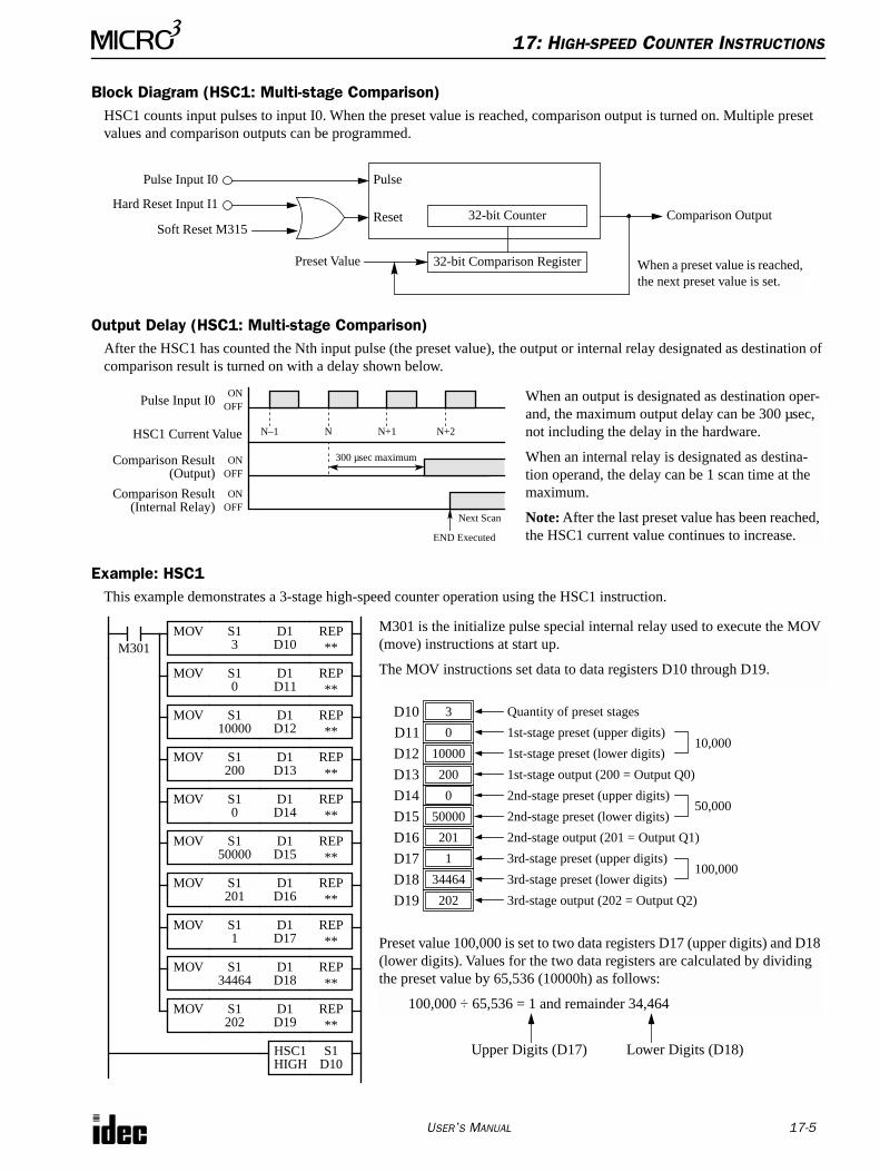
17: HIGH-SPEED COUNTER INSTRUCTIONS
USER’S MANUAL 17-5
Block Diagram (HSC1: Multi-stage Comparison)HSC1 counts input pulses to input I0. When the preset value is reached, comparison output is turned on. Multiple preset values and comparison outputs can be programmed.
Output Delay (HSC1: Multi-stage Comparison)After the HSC1 has counted the Nth input pulse (the preset value), the output or internal relay designated as destination of comparison result is turned on with a delay shown below.
Example: HSC1This example demonstrates a 3-stage high-speed counter operation using the HSC1 instruction.
Pulse Input I0
Hard Reset Input I1
Soft Reset M315
Pulse
Reset
32-bit Comparison Register
32-bit Counter Comparison Output
Preset Value When a preset value is reached, the next preset value is set.
Pulse Input I0ON
OFF
Comparison Result ONOFF
Comparison Result ONOFF
N–1HSC1 Current Value N N+1 N+2
(Output)
(Internal Relay)
300 µsec maximum
END Executed
Next Scan
When an output is designated as destination oper-and, the maximum output delay can be 300 µsec, not including the delay in the hardware.
When an internal relay is designated as destina-tion operand, the delay can be 1 scan time at the maximum.
Note: After the last preset value has been reached, the HSC1 current value continues to increase.
MOV S1
S1D10
3M301 is the initialize pulse special internal relay used to execute the MOV (move) instructions at start up.
The MOV instructions set data to data registers D10 through D19.
M301REP**
D1D10
MOV S10
REP**
D1D11
MOV S110000
REP**
D1D12
MOV S1200
REP**
D1D13
MOV S10
REP**
D1D14
MOV S150000
REP**
D1D15
MOV S1201
REP**
D1D16
MOV S11
REP**
D1D17
MOV S134464
REP**
D1D18
MOV S1202
REP**
D1D19
200D13
10000D12
0D14
0D11
3D10
50000D15
10,000
50,000
201D16
1st-stage preset (upper digits)
1st-stage preset (lower digits)
1st-stage output (200 = Output Q0)
2nd-stage preset (upper digits)
2nd-stage preset (lower digits)
2nd-stage output (201 = Output Q1)
Quantity of preset stages
1D1734464D18
100,000
202D19
3rd-stage preset (upper digits)
3rd-stage preset (lower digits)
3rd-stage output (202 = Output Q2)
Preset value 100,000 is set to two data registers D17 (upper digits) and D18 (lower digits). Values for the two data registers are calculated by dividing the preset value by 65,536 (10000h) as follows:
100,000 ÷ 65,536 = 1 and remainder 34,464
Upper Digits (D17) Lower Digits (D18) HSC1HIGH
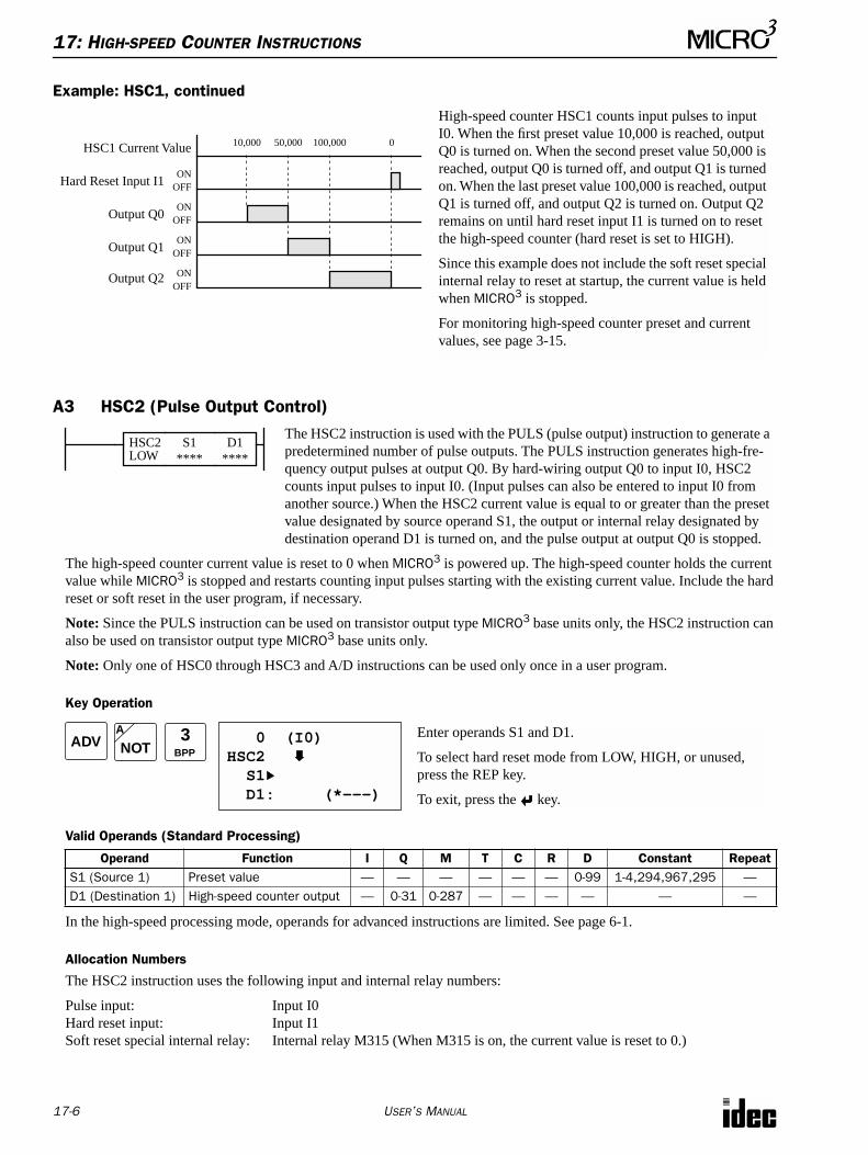
17: HIGH-SPEED COUNTER INSTRUCTIONS
17-6 USER’S MANUAL
Example: HSC1, continued
A3 HSC2 (Pulse Output Control)
The high-speed counter current value is reset to 0 when MICRO3 is powered up. The high-speed counter holds the current value while MICRO3 is stopped and restarts counting input pulses starting with the existing current value. Include the hard reset or soft reset in the user program, if necessary.
Note: Since the PULS instruction can be used on transistor output type MICRO3 base units only, the HSC2 instruction can also be used on transistor output type MICRO3 base units only.
Note: Only one of HSC0 through HSC3 and A/D instructions can be used only once in a user program.
Key Operation
Valid Operands (Standard Processing)
In the high-speed processing mode, operands for advanced instructions are limited. See page 6-1.
Allocation Numbers
The HSC2 instruction uses the following input and internal relay numbers:
Pulse input: Input I0Hard reset input: Input I1Soft reset special internal relay: Internal relay M315 (When M315 is on, the current value is reset to 0.)
Operand Function I Q M T C R D Constant RepeatS1 (Source 1) Preset value — — — — — — 0-99 1-4,294,967,295 —D1 (Destination 1) High-speed counter output — 0-31 0-287 — — — — — —
Output Q2 ONOFF
ONOFF
Output Q1ON
OFF
10,000HSC1 Current Value 50,000 100,000
Output Q0
ONOFFHard Reset Input I1
0
High-speed counter HSC1 counts input pulses to input I0. When the first preset value 10,000 is reached, output Q0 is turned on. When the second preset value 50,000 is reached, output Q0 is turned off, and output Q1 is turned on. When the last preset value 100,000 is reached, output Q1 is turned off, and output Q2 is turned on. Output Q2 remains on until hard reset input I1 is turned on to reset the high-speed counter (hard reset is set to HIGH).
Since this example does not include the soft reset special internal relay to reset at startup, the current value is held when MICRO3 is stopped.
For monitoring high-speed counter preset and current values, see page 3-15.
The HSC2 instruction is used with the PULS (pulse output) instruction to generate a predetermined number of pulse outputs. The PULS instruction generates high-fre-quency output pulses at output Q0. By hard-wiring output Q0 to input I0, HSC2 counts input pulses to input I0. (Input pulses can also be entered to input I0 from another source.) When the HSC2 current value is equal to or greater than the preset value designated by source operand S1, the output or internal relay designated by destination operand D1 is turned on, and the pulse output at output Q0 is stopped.
D1****
S1****
HSC2LOW
ADV 0 (I0)HSC2 S1 D1: (*---)
Enter operands S1 and D1.
To select hard reset mode from LOW, HIGH, or unused, press the REP key.
To exit, press the key.
NOTA 3
BPP
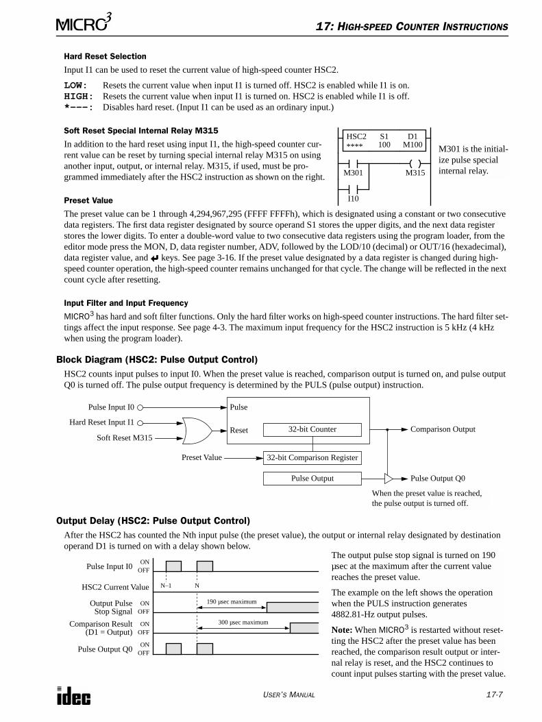
17: HIGH-SPEED COUNTER INSTRUCTIONS
USER’S MANUAL 17-7
Hard Reset Selection
Input I1 can be used to reset the current value of high-speed counter HSC2.
LOW: Resets the current value when input I1 is turned off. HSC2 is enabled while I1 is on.HIGH: Resets the current value when input I1 is turned on. HSC2 is enabled while I1 is off.*–––: Disables hard reset. (Input I1 can be used as an ordinary input.)
Soft Reset Special Internal Relay M315
In addition to the hard reset using input I1, the high-speed counter cur-rent value can be reset by turning special internal relay M315 on using another input, output, or internal relay. M315, if used, must be pro-grammed immediately after the HSC2 instruction as shown on the right.
Preset Value
The preset value can be 1 through 4,294,967,295 (FFFF FFFFh), which is designated using a constant or two consecutive data registers. The first data register designated by source operand S1 stores the upper digits, and the next data register stores the lower digits. To enter a double-word value to two consecutive data registers using the program loader, from the editor mode press the MON, D, data register number, ADV, followed by the LOD/10 (decimal) or OUT/16 (hexadecimal), data register value, and keys. See page 3-16. If the preset value designated by a data register is changed during high-speed counter operation, the high-speed counter remains unchanged for that cycle. The change will be reflected in the next count cycle after resetting.
Input Filter and Input Frequency
MICRO3 has hard and soft filter functions. Only the hard filter works on high-speed counter instructions. The hard filter set-tings affect the input response. See page 4-3. The maximum input frequency for the HSC2 instruction is 5 kHz (4 kHz when using the program loader).
Block Diagram (HSC2: Pulse Output Control)HSC2 counts input pulses to input I0. When the preset value is reached, comparison output is turned on, and pulse output Q0 is turned off. The pulse output frequency is determined by the PULS (pulse output) instruction.
Output Delay (HSC2: Pulse Output Control)After the HSC2 has counted the Nth input pulse (the preset value), the output or internal relay designated by destination operand D1 is turned on with a delay shown below.
M301 is the initial-ize pulse special internal relay.
HSC2****
S1 D1M100100
M301
I10
M315
Pulse Input I0
Hard Reset Input I1
Soft Reset M315
Pulse
Reset
32-bit Comparison Register
32-bit Counter Comparison Output
Preset Value
Pulse Output Pulse Output Q0
When the preset value is reached, the pulse output is turned off.
Pulse Input I0ON
OFF
Output Pulse ONOFF
Comparison Result ONOFF
N–1HSC2 Current Value N
(D1 = Output)
190 µsec maximum
The output pulse stop signal is turned on 190 µsec at the maximum after the current value reaches the preset value.
The example on the left shows the operation when the PULS instruction generates 4882.81-Hz output pulses.
Note: When MICRO3 is restarted without reset-ting the HSC2 after the preset value has been reached, the comparison result output or inter-nal relay is reset, and the HSC2 continues to count input pulses starting with the preset value.
300 µsec maximum
ONOFFPulse Output Q0
Stop Signal
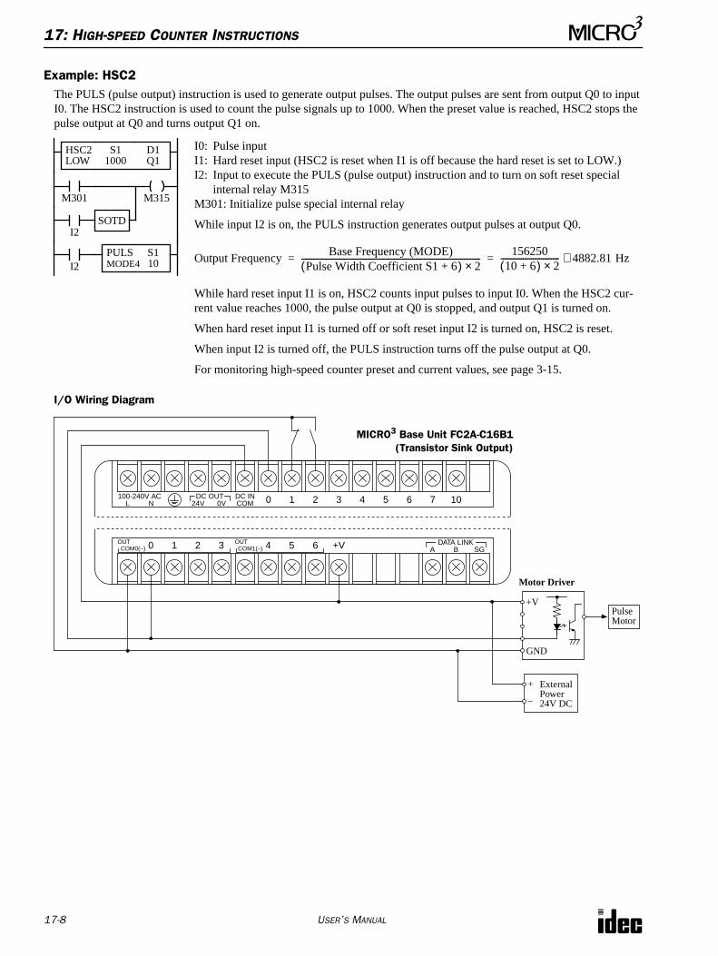
17: HIGH-SPEED COUNTER INSTRUCTIONS
17-8 USER’S MANUAL
Example: HSC2The PULS (pulse output) instruction is used to generate output pulses. The output pulses are sent from output Q0 to input I0. The HSC2 instruction is used to count the pulse signals up to 1000. When the preset value is reached, HSC2 stops the pulse output at Q0 and turns output Q1 on.
I/O Wiring Diagram
I2
M301
S1 D1Q11000
M315
I0: Pulse inputI1: Hard reset input (HSC2 is reset when I1 is off because the hard reset is set to LOW.)I2: Input to execute the PULS (pulse output) instruction and to turn on soft reset special
internal relay M315M301: Initialize pulse special internal relay
While input I2 is on, the PULS instruction generates output pulses at output Q0.
While hard reset input I1 is on, HSC2 counts input pulses to input I0. When the HSC2 cur-rent value reaches 1000, the pulse output at Q0 is stopped, and output Q1 is turned on.
When hard reset input I1 is turned off or soft reset input I2 is turned on, HSC2 is reset.
When input I2 is turned off, the PULS instruction turns off the pulse output at Q0.
For monitoring high-speed counter preset and current values, see page 3-15.
Output Frequency Base Frequency (MODE)Pulse Width Coefficient S1 6+ ( ) 2 ×
-----------------------------------------------------------------------------------------156250
10 6+ ( ) 2 × ----------------------------- 4882.81 Hz ≅ = = PULS
MODE4 I2
S110
SOTD
HSC2LOW
OUTCOM0(–) 0 1 2 3 OUT
COM1(–) 4 5 6 DATA LINKA SGB+V
+V
GND
PulseMotor
Motor Driver
+
–
ExternalPower24V DC
MICRO3 Base Unit FC2A-C16B1
100-240V ACL N
DC OUT24V 0V
DC INCOM 0 1 2 3 4 5 6 7 10
(Transistor Sink Output)
17: H
IGH
-
SPEED
C
OUNTER
I
NSTRUCTIONS
U
SER
’
S
M
ANUAL 17-9
A4 HSC3 (Gate Control)
The high-speed counter current value is reset to 0 when MICRO3 is powered up. The high-speed counter holds the current value while MICRO3 is stopped and restarts counting input pulses starting with the existing current value. Include the hard reset or soft reset in the user program, if necessary.
Note: Only one of HSC0 through HSC3 and A/D instructions can be used only once in a user program.
Key Operation
Valid Operands (Standard Processing)
In the high-speed processing mode, data registers for this instruction are limited to D0 through D31.
Allocation Numbers
The HSC3 instruction uses the following input and internal relay numbers:
Pulse input: Input I0Hard reset input: Input I1Gate input: Input I2Soft reset special internal relay: Internal relay M315 (When M315 is on, the current value is reset to 0.)HSC3 overflow special internal relay: Internal relay M316
Hard Reset Selection
Input I1 can be used to reset the current value of high-speed counter HSC3.
LOW: Resets the current value when input I1 is turned off. HSC3 is enabled while I1 is on.HIGH: Resets the current value when input I1 is turned on. HSC3 is enabled while I1 is off.*–––: Disables hard reset. (Input I1 can be used as an ordinary input.)
Gate Input
Input I2 is allocated as a gate input for the HSC3 instruction. When I2 is on, HSC3 is enabled to count input pulses to input I0. When I2 is turned off, HSC3 is disabled, and the current value is moved to a data register designated by destination operand D1. When I2 is turned on again, HSC3 continues counting from the existing current value.
Soft Reset Special Internal Relay M315
In addition to the hard reset using input I1, the high-speed counter current value can be reset by turning special internal relay M315 on using another input, output, or internal relay. M315, if used, must be programmed imme-diately after the HSC3 instruction as shown on the right.
Input Filter and Input Frequency
MICRO3 has hard and soft filter functions. Only the hard filter works on high-speed counter instructions. The hard filter set-tings affect the input response. See page 4-3. The maximum input frequency for the HSC3 instruction is 10 kHz.
Operand Function I Q M T C R D Constant RepeatD1 (Destination 1) Store the current value — — — — — — 0-99 — —
Gate controlled high-speed counter HSC3 counts input pulses to input I0 while gate control input I2 is on. When gate control input I2 is turned off, the current value is moved to a data register designated by destination operand D1. HSC3 does not compare the current value with a preset value.
HSC3 can count up to 65535. When another input pulse enters at 65535, the current value becomes 0, and special internal relay M316 (HSC3 overflow) is turned on.
D1****
HSC3LOW
ADV 0 (I0)HSC3 GATE=I2 D1 (*---)
Enter operand D1.
To select hard reset mode from LOW, HIGH, or unused, press the REP key.
To exit, press the key.
NOTA 4
M301 is the initialize pulse special internal relay.
HSC3****
D1D10
M301
I10
M315
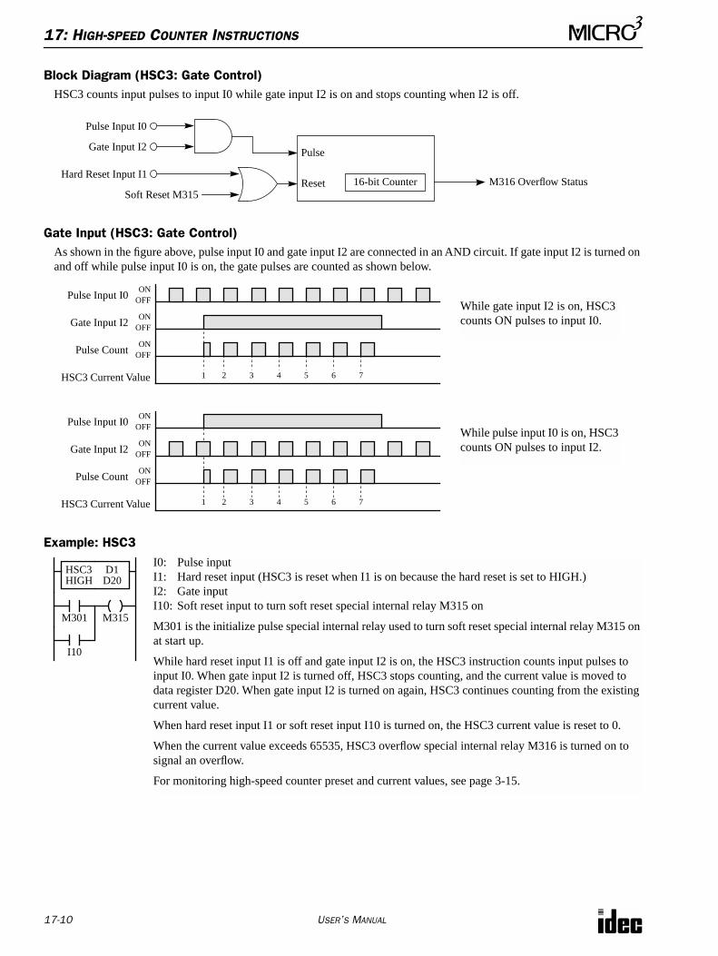
17: HIGH-SPEED COUNTER INSTRUCTIONS
17-10 USER’S MANUAL
Block Diagram (HSC3: Gate Control)HSC3 counts input pulses to input I0 while gate input I2 is on and stops counting when I2 is off.
Gate Input (HSC3: Gate Control)As shown in the figure above, pulse input I0 and gate input I2 are connected in an AND circuit. If gate input I2 is turned on and off while pulse input I0 is on, the gate pulses are counted as shown below.
Example: HSC3
Pulse Input I0
Hard Reset Input I1
Soft Reset M315
Pulse
Reset 16-bit Counter M316 Overflow Status
Gate Input I2
Pulse Input I0ON
OFF
ONOFF
While gate input I2 is on, HSC3 counts ON pulses to input I0.
1HSC3 Current Value 2 3 4
ONOFF
Gate Input I2
Pulse Count
5 6 7
Pulse Input I0ON
OFF
ONOFF
1HSC3 Current Value 2 3 4
ONOFF
Gate Input I2
Pulse Count
5 6 7
While pulse input I0 is on, HSC3 counts ON pulses to input I2.
I10
M301
D1D20
M315
I0: Pulse inputI1: Hard reset input (HSC3 is reset when I1 is on because the hard reset is set to HIGH.)I2: Gate inputI10: Soft reset input to turn soft reset special internal relay M315 on
M301 is the initialize pulse special internal relay used to turn soft reset special internal relay M315 on at start up.
While hard reset input I1 is off and gate input I2 is on, the HSC3 instruction counts input pulses to input I0. When gate input I2 is turned off, HSC3 stops counting, and the current value is moved to data register D20. When gate input I2 is turned on again, HSC3 continues counting from the existing current value.
When hard reset input I1 or soft reset input I10 is turned on, the HSC3 current value is reset to 0.
When the current value exceeds 65535, HSC3 overflow special internal relay M316 is turned on to signal an overflow.
For monitoring high-speed counter preset and current values, see page 3-15.
HSC3HIGH
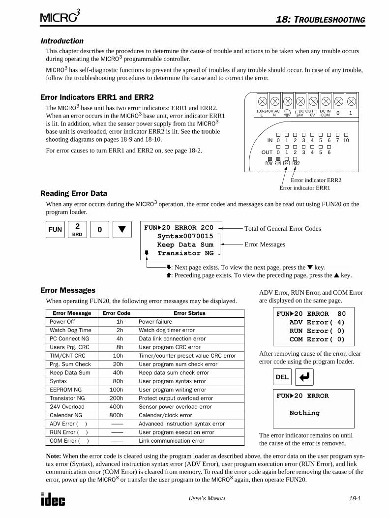
USER’S MANUAL 18-1
18: TROUBLESHOOTING
IntroductionThis chapter describes the procedures to determine the cause of trouble and actions to be taken when any trouble occurs during operating the MICRO3 programmable controller.
MICRO3 has self-diagnostic functions to prevent the spread of troubles if any trouble should occur. In case of any trouble, follow the troubleshooting procedures to determine the cause and to correct the error.
Error Indicators ERR1 and ERR2The MICRO3 base unit has two error indicators: ERR1 and ERR2. When an error occurs in the MICRO3 base unit, error indicator ERR1 is lit. In addition, when the sensor power supply from the MICRO3 base unit is overloaded, error indicator ERR2 is lit. See the trouble shooting diagrams on pages 18-9 and 18-10.
For error causes to turn ERR1 and ERR2 on, see page 18-2.
Reading Error DataWhen any error occurs during the MICRO3 operation, the error codes and messages can be read out using FUN20 on the program loader.
Error MessagesWhen operating FUN20, the following error messages may be displayed.
Note: When the error code is cleared using the program loader as described above, the error data on the user program syn-tax error (Syntax), advanced instruction syntax error (ADV Error), user program execution error (RUN Error), and link communication error (COM Error) is cleared from memory. To read the error code again before removing the cause of the error, power up the MICRO3 or transfer the user program to the MICRO3 again, then operate FUN20.
Error Message Error Code Error StatusPower Off 1h Power failureWatch Dog Time 2h Watch dog timer errorPC Connect NG 4h Data link connection errorUsers Prg. CRC 8h User program CRC errorTIM/CNT CRC 10h Timer/counter preset value CRC errorPrg. Sum Check 20h User program sum check errorKeep Data Sum 40h Keep data sum check errorSyntax 80h User program syntax errorEEPROM NG 100h User program writing errorTransistor NG 200h Protect output overload error24V Overload 400h Sensor power overload errorCalendar NG 800h Calendar/clock errorADV Error ( ) —— Advanced instruction syntax errorRUN Error ( ) —— User program execution errorCOM Error ( ) —— Link communication error
100-240V ACL N
DC OUT24V 0V
DC INCOM 0 1
IN 0 1 2 3 4 5 6 7 10
OUT 0 1 2 3 4 5 6
POW RUN ERR1 ERR2
Error indicator ERR1Error indicator ERR2
FUN 20 ERROR 2C0 Syntax0070015 Keep Data Sum Transistor NG
: Next page exists. To view the next page, press the key.: Preceding page exists. To view the preceding page, press the key.
FUN 2BRD
0 Total of General Error Codes
Error Messages
ADV Error, RUN Error, and COM Error are displayed on the same page.
FUN 20 ERROR 80 ADV Error( 4) RUN Error( 0) COM Error( 0)
After removing cause of the error, clear error code using the program loader.
FUN 20 ERROR
Nothing
DEL
The error indicator remains on until the cause of the error is removed.
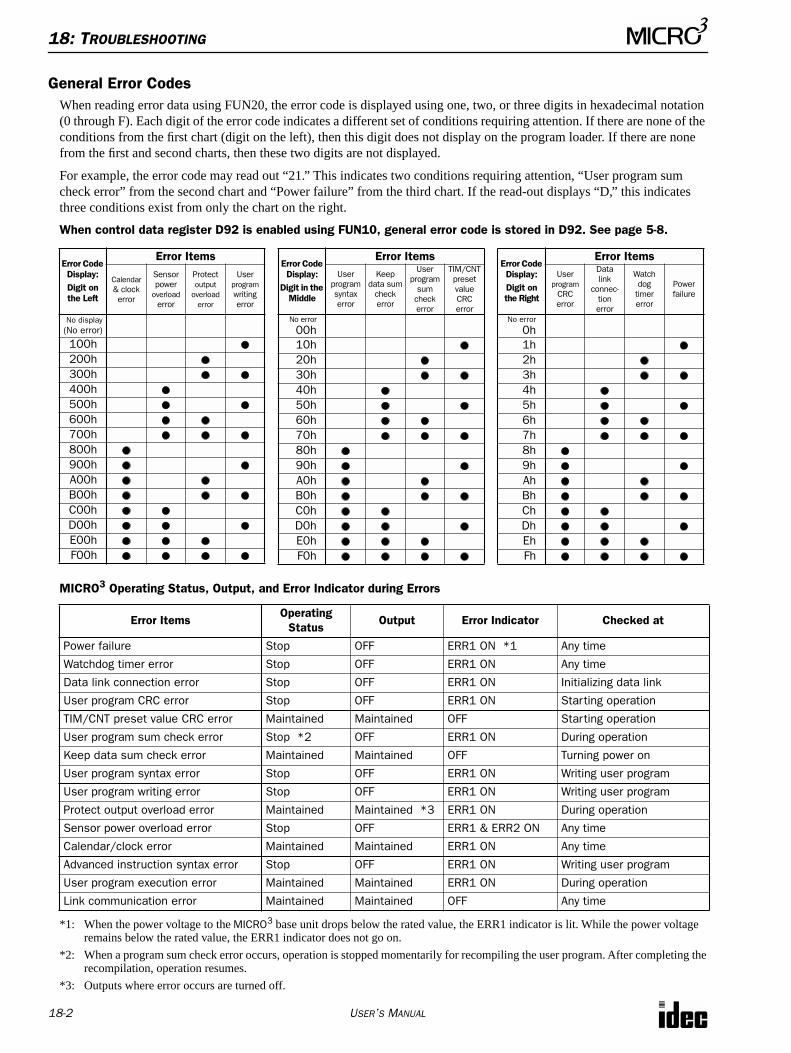
18: TROUBLESHOOTING
18-2 USER’S MANUAL
General Error CodesWhen reading error data using FUN20, the error code is displayed using one, two, or three digits in hexadecimal notation (0 through F). Each digit of the error code indicates a different set of conditions requiring attention. If there are none of the conditions from the first chart (digit on the left), then this digit does not display on the program loader. If there are none from the first and second charts, then these two digits are not displayed.
For example, the error code may read out “21.” This indicates two conditions requiring attention, “User program sum check error” from the second chart and “Power failure” from the third chart. If the read-out displays “D,” this indicates three conditions exist from only the chart on the right.
When control data register D92 is enabled using FUN10, general error code is stored in D92. See page 5-8.
MICRO3 Operating Status, Output, and Error Indicator during Errors
*1: When the power voltage to the MICRO3 base unit drops below the rated value, the ERR1 indicator is lit. While the power voltage remains below the rated value, the ERR1 indicator does not go on.
*2: When a program sum check error occurs, operation is stopped momentarily for recompiling the user program. After completing the recompilation, operation resumes.
*3: Outputs where error occurs are turned off.
Error ItemsOperating
StatusOutput Error Indicator Checked at
Power failure Stop OFF ERR1 ON *1 Any time
Watchdog timer error Stop OFF ERR1 ON Any time
Data link connection error Stop OFF ERR1 ON Initializing data link
User program CRC error Stop OFF ERR1 ON Starting operation
TIM/CNT preset value CRC error Maintained Maintained OFF Starting operation
User program sum check error Stop *2 OFF ERR1 ON During operation
Keep data sum check error Maintained Maintained OFF Turning power on
User program syntax error Stop OFF ERR1 ON Writing user program
User program writing error Stop OFF ERR1 ON Writing user program
Protect output overload error Maintained Maintained *3 ERR1 ON During operation
Sensor power overload error Stop OFF ERR1 & ERR2 ON Any time
Calendar/clock error Maintained Maintained ERR1 ON Any time
Advanced instruction syntax error Stop OFF ERR1 ON Writing user program
User program execution error Maintained Maintained ERR1 ON During operation
Link communication error Maintained Maintained OFF Any time
Error Code Display:Digit on the Left
Error Items
Calendar & clockerror
Sensorpower
overloaderror
Protectoutput
overloaderror
Userprogramwritingerror
No display(No error)
100h200h300h400h500h600h700h800h900hA00hB00hC00hD00hE00hF00h
Error Code Display:
Digit in the Middle
Error ItemsUser
programsyntaxerror
Keepdata sum
checkerror
Userprogram
sum checkerror
TIM/CNTpresetvalueCRCerror
No error
00h10h20h30h40h50h60h70h80h90hA0hB0hC0hD0hE0hF0h
Error Code Display:Digit on the Right
Error ItemsUser
programCRCerror
Datalink
connec-tionerror
Watchdog
timererror
Powerfailure
No error
0h1h2h3h4h5h6h7h8h9hAhBhChDhEhFh
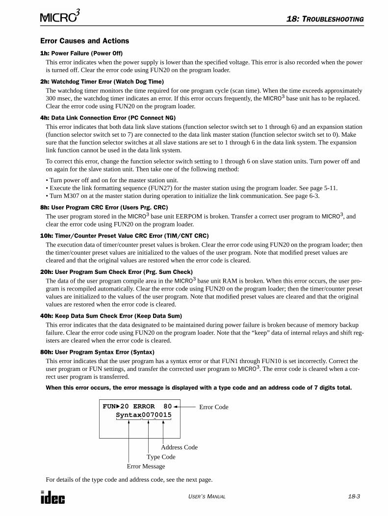
18: TROUBLESHOOTING
USER’S MANUAL 18-3
Error Causes and Actions
1h: Power Failure (Power Off)This error indicates when the power supply is lower than the specified voltage. This error is also recorded when the power is turned off. Clear the error code using FUN20 on the program loader.
2h: Watchdog Timer Error (Watch Dog Time)The watchdog timer monitors the time required for one program cycle (scan time). When the time exceeds approximately 300 msec, the watchdog timer indicates an error. If this error occurs frequently, the MICRO3 base unit has to be replaced. Clear the error code using FUN20 on the program loader.
4h: Data Link Connection Error (PC Connect NG)This error indicates that both data link slave stations (function selector switch set to 1 through 6) and an expansion station (function selector switch set to 7) are connected to the data link master station (function selector switch set to 0). Make sure that the function selector switches at all slave stations are set to 1 through 6 in the data link system. The expansion link function cannot be used in the data link system.
To correct this error, change the function selector switch setting to 1 through 6 on slave station units. Turn power off and on again for the slave station unit. Then take one of the following method:
• Turn power off and on for the master station unit.• Execute the link formatting sequence (FUN27) for the master station using the program loader. See page 5-11.• Turn M307 on at the master station during operation to initialize the link communication. See page 6-3.
8h: User Program CRC Error (Users Prg. CRC)The user program stored in the MICRO3 base unit EERPOM is broken. Transfer a correct user program to MICRO3, and clear the error code using FUN20 on the program loader.
10h: Timer/Counter Preset Value CRC Error (TIM/CNT CRC)The execution data of timer/counter preset values is broken. Clear the error code using FUN20 on the program loader; then the timer/counter preset values are initialized to the values of the user program. Note that modified preset values are cleared and that the original values are restored when the error code is cleared.
20h: User Program Sum Check Error (Prg. Sum Check)The data of the user program compile area in the MICRO3 base unit RAM is broken. When this error occurs, the user pro-gram is recompiled automatically. Clear the error code using FUN20 on the program loader; then the timer/counter preset values are initialized to the values of the user program. Note that modified preset values are cleared and that the original values are restored when the error code is cleared.
40h: Keep Data Sum Check Error (Keep Data Sum)This error indicates that the data designated to be maintained during power failure is broken because of memory backup failure. Clear the error code using FUN20 on the program loader. Note that the “keep” data of internal relays and shift reg-isters are cleared when the error code is cleared.
80h: User Program Syntax Error (Syntax)This error indicates that the user program has a syntax error or that FUN1 through FUN10 is set incorrectly. Correct the user program or FUN settings, and transfer the corrected user program to MICRO3. The error code is cleared when a cor-rect user program is transferred.
When this error occurs, the error message is displayed with a type code and an address code of 7 digits total.
For details of the type code and address code, see the next page.
FUN 20 ERROR 80 Syntax0070015
Error Code
Error Message
Type Code
Address Code
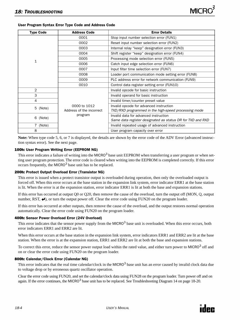
18: TROUBLESHOOTING
18-4 USER’S MANUAL
User Program Syntax Error Type Code and Address Code
Note: When type code 5, 6, or 7 is displayed, the details are shown by the error code of the ADV Error (advanced instruc-tion syntax error). See the next page.
100h: User Program Writing Error (EEPROM NG)This error indicates a failure of writing into the MICRO3 base unit EEPROM when transferring a user program or when set-ting user program protection. The error code is cleared when writing into the EEPROM is completed correctly. If this error occurs frequently, the MICRO3 base unit has to be replaced.
200h: Protect Output Overload Error (Transistor NG)This error is issued when a protect transistor output is overloaded during operation, then only the overloaded output is forced off. When this error occurs at the base station in the expansion link system, error indicator ERR1 at the base station is lit. When the error is at the expansion station, error indicator ERR1 is lit at both the base and expansion stations.
If this error has occurred at output Q0 or Q20, then remove the cause of the overload, turn the output off (MON, Q, output number, RST, ), or turn the output power off. Clear the error code using FUN20 on the program loader.
If this error has occurred at other outputs, then remove the cause of the overload, and the output restores normal operation automatically. Clear the error code using FUN20 on the program loader.
400h: Sensor Power Overload Error (24V Overload)This error indicates that the sensor power supply from the MICRO3 base unit is overloaded. When this error occurs, both error indicators ERR1 and ERR2 are lit.
When this error occurs at the base station in the expansion link system, error indicators ERR1 and ERR2 are lit at the base station. When the error is at the expansion station, ERR1 and ERR2 are lit at both the base and expansion stations.
To correct this error, reduce the sensor power output load within the rated value, and either turn power to MICRO3 off and on or clear the error code using FUN20 on the program loader.
800h: Calendar/Clock Error (Calendar NG)This error indicates that the real time calendar/clock in the MICRO3 base unit has an error caused by invalid clock data due to voltage drop or by erroneous quartz oscillator operation.
Clear the error code using FUN20, and set the calendar/clock data using FUN28 on the program loader. Turn power off and on again. If the error continues, the MICRO3 base unit has to be replaced. See Troubleshooting Diagram 14 on page 18-20.
Type Code Address Code Error Details
1
0001 Stop input number selection error (FUN1)0002 Reset input number selection error (FUN2)0003 Internal relay “keep” designation error (FUN3)0004 Shift register “keep” designation error (FUN4)0005 Processing mode selection error (FUN5)0006 Catch input edge selection error (FUN6)0007 Input filter time selection error (FUN7)0008 Loader port communication mode setting error (FUN8)0009 PLC address error for network communication (FUN9)0010 Control data register setting error (FUN10)
2
0000 to 1012Address of the incorrect
program
Invalid opcode for basic instruction3 Invalid operand for basic instruction4 Invalid timer/counter preset value
5 (Note)Invalid opcode for advanced instructionTXD/RXD programmed in the high-speed processing mode
6 (Note)Invalid data for advanced instructionSame data register designated as status DR for TXD and RXD
7 (Note) Invalid repeated usage of advanced instruction8 User program capacity over error
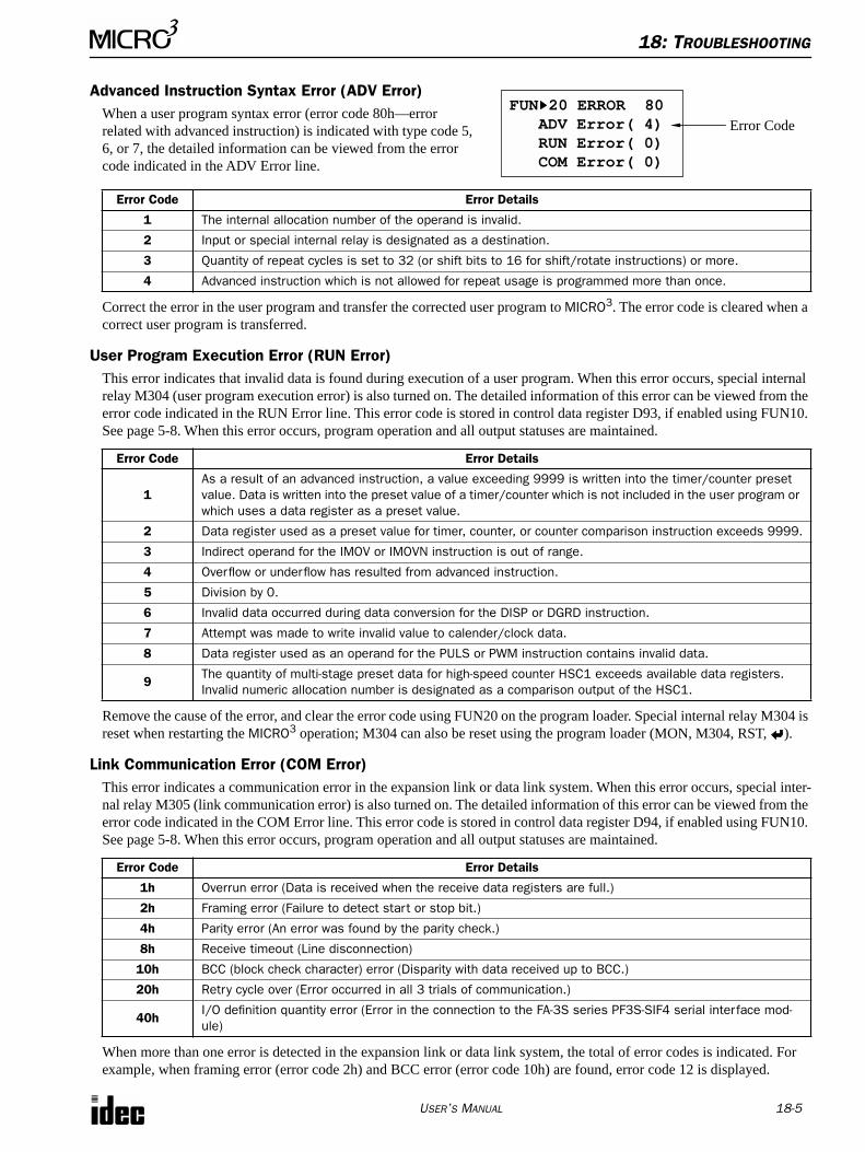
18: TROUBLESHOOTING
USER’S MANUAL 18-5
Advanced Instruction Syntax Error (ADV Error)When a user program syntax error (error code 80h—error related with advanced instruction) is indicated with type code 5, 6, or 7, the detailed information can be viewed from the error code indicated in the ADV Error line.
Correct the error in the user program and transfer the corrected user program to MICRO3. The error code is cleared when a correct user program is transferred.
User Program Execution Error (RUN Error)This error indicates that invalid data is found during execution of a user program. When this error occurs, special internal relay M304 (user program execution error) is also turned on. The detailed information of this error can be viewed from the error code indicated in the RUN Error line. This error code is stored in control data register D93, if enabled using FUN10. See page 5-8. When this error occurs, program operation and all output statuses are maintained.
Remove the cause of the error, and clear the error code using FUN20 on the program loader. Special internal relay M304 is reset when restarting the MICRO3 operation; M304 can also be reset using the program loader (MON, M304, RST, ).
Link Communication Error (COM Error)This error indicates a communication error in the expansion link or data link system. When this error occurs, special inter-nal relay M305 (link communication error) is also turned on. The detailed information of this error can be viewed from the error code indicated in the COM Error line. This error code is stored in control data register D94, if enabled using FUN10. See page 5-8. When this error occurs, program operation and all output statuses are maintained.
When more than one error is detected in the expansion link or data link system, the total of error codes is indicated. For example, when framing error (error code 2h) and BCC error (error code 10h) are found, error code 12 is displayed.
Error Code Error Details
1 The internal allocation number of the operand is invalid.
2 Input or special internal relay is designated as a destination.
3 Quantity of repeat cycles is set to 32 (or shift bits to 16 for shift/rotate instructions) or more.
4 Advanced instruction which is not allowed for repeat usage is programmed more than once.
Error Code Error Details
1As a result of an advanced instruction, a value exceeding 9999 is written into the timer/counter preset value. Data is written into the preset value of a timer/counter which is not included in the user program or which uses a data register as a preset value.
2 Data register used as a preset value for timer, counter, or counter comparison instruction exceeds 9999.
3 Indirect operand for the IMOV or IMOVN instruction is out of range.
4 Overflow or underflow has resulted from advanced instruction.
5 Division by 0.
6 Invalid data occurred during data conversion for the DISP or DGRD instruction.
7 Attempt was made to write invalid value to calender/clock data.
8 Data register used as an operand for the PULS or PWM instruction contains invalid data.
9The quantity of multi-stage preset data for high-speed counter HSC1 exceeds available data registers. Invalid numeric allocation number is designated as a comparison output of the HSC1.
Error Code Error Details
1h Overrun error (Data is received when the receive data registers are full.)
2h Framing error (Failure to detect start or stop bit.)
4h Parity error (An error was found by the parity check.)
8h Receive timeout (Line disconnection)
10h BCC (block check character) error (Disparity with data received up to BCC.)
20h Retry cycle over (Error occurred in all 3 trials of communication.)
40hI/O definition quantity error (Error in the connection to the FA-3S series PF3S-SIF4 serial interface mod-ule)
FUN 20 ERROR 80 ADV Error( 4) RUN Error( 0) COM Error( 0)
Error Code
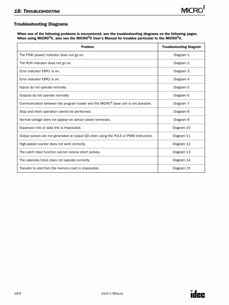
18: TROUBLESHOOTING
18-6 USER’S MANUAL
Troubleshooting Diagrams
When one of the following problems is encountered, see the troubleshooting diagrams on the following pages. When using MICRO3C, also see the MICRO3C User’s Manual for troubles particular to the MICRO3C.
Problem Troubleshooting Diagram
The POW (power) indicator does not go on. Diagram 1
The RUN indicator does not go on. Diagram 2
Error indicator ERR1 is on. Diagram 3
Error indicator ERR2 is on. Diagram 4
Inputs do not operate normally. Diagram 5
Outputs do not operate normally. Diagram 6
Communication between the program loader and the MICRO3 base unit is not possible. Diagram 7
Stop and reset operation cannot be performed. Diagram 8
Normal voltage does not appear on sensor power terminals. Diagram 9
Expansion link or data link is impossible. Diagram 10
Output pulses are not generated at output Q0 when using the PULS or PWM instruction. Diagram 11
High-speed counter does not work correctly. Diagram 12
The catch input function cannot receive short pulses. Diagram 13
The calendar/clock does not operate correctly. Diagram 14
Transfer to and from the memory card is impossible. Diagram 15
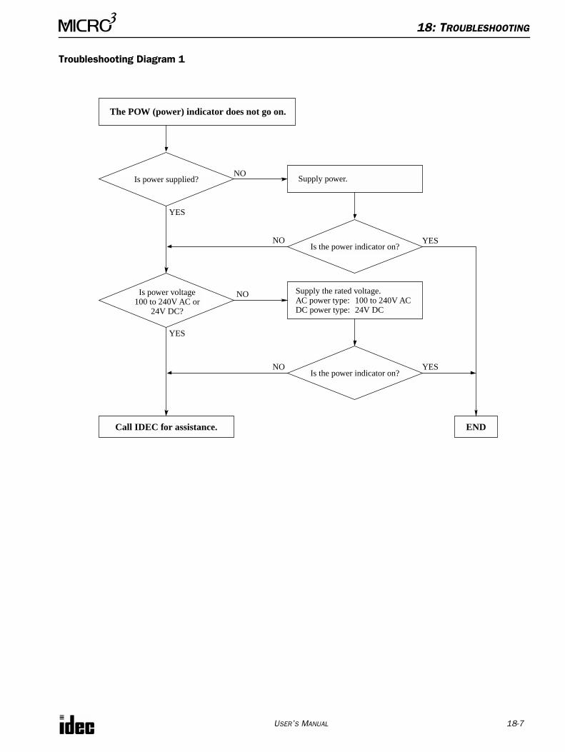
18: TROUBLESHOOTING
USER’S MANUAL 18-7
Troubleshooting Diagram 1
Is power supplied?
Is power voltage 100 to 240V AC or
24V DC?
The POW (power) indicator does not go on.
Is the power indicator on?
Supply power.
ENDCall IDEC for assistance.
Is the power indicator on?
NO
NO
YES
YES
NO
YES
NO YES
Supply the rated voltage.AC power type: 100 to 240V ACDC power type: 24V DC
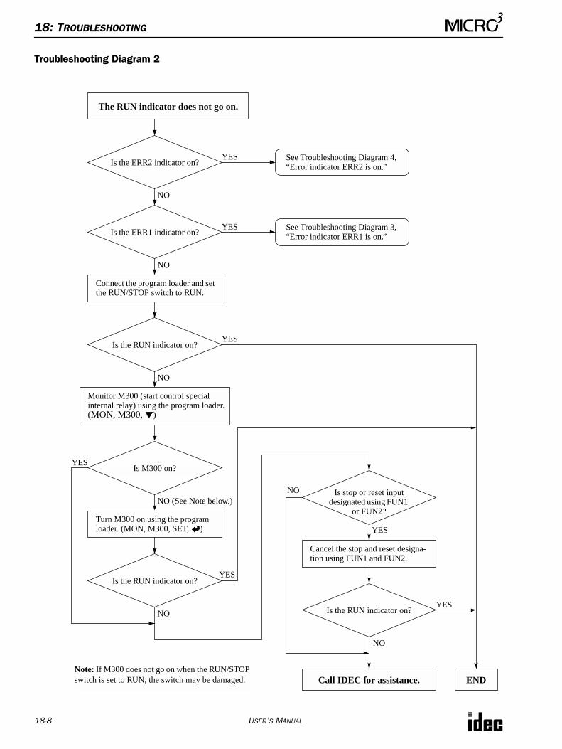
18: TROUBLESHOOTING
18-8 USER’S MANUAL
Troubleshooting Diagram 2
Is stop or reset input designated using FUN1
or FUN2?
The RUN indicator does not go on.
Connect the program loader and set the RUN/STOP switch to RUN.
ENDCall IDEC for assistance.
Is the ERR2 indicator on?
NO
See Troubleshooting Diagram 4,“Error indicator ERR2 is on.”
YES
Is the ERR1 indicator on?
Is the RUN indicator on?
Monitor M300 (start control special internal relay) using the program loader.(MON, M300, )
Is M300 on?
Turn M300 on using the program loader. (MON, M300, SET, )
Is the RUN indicator on?
Cancel the stop and reset designa-tion using FUN1 and FUN2.
Is the RUN indicator on?
See Troubleshooting Diagram 3,“Error indicator ERR1 is on.”
NO
YES
YES
NO
YES
NO (See Note below.)
YES
NO
NO
YES
Note: If M300 does not go on when the RUN/STOP switch is set to RUN, the switch may be damaged.
NO
YES
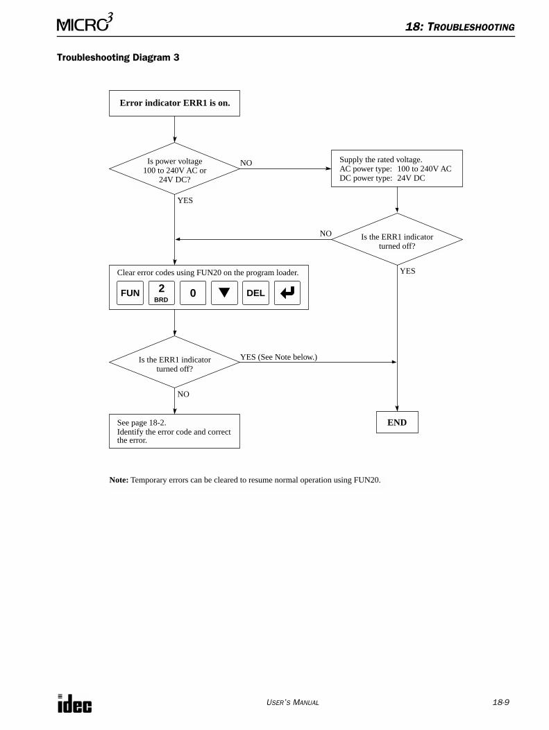
18: TROUBLESHOOTING
USER’S MANUAL 18-9
Troubleshooting Diagram 3
Is the ERR1 indicator turned off?
Error indicator ERR1 is on.
Clear error codes using FUN20 on the program loader.
END
YES
See page 18-2.Identify the error code and correct the error.
NO
YES (See Note below.)
YES
NO
Note: Temporary errors can be cleared to resume normal operation using FUN20.
Is power voltage100 to 240V AC or
24V DC?
Is the ERR1 indicator turned off?
DELFUN 2BRD
0
NO
Supply the rated voltage.AC power type: 100 to 240V ACDC power type: 24V DC
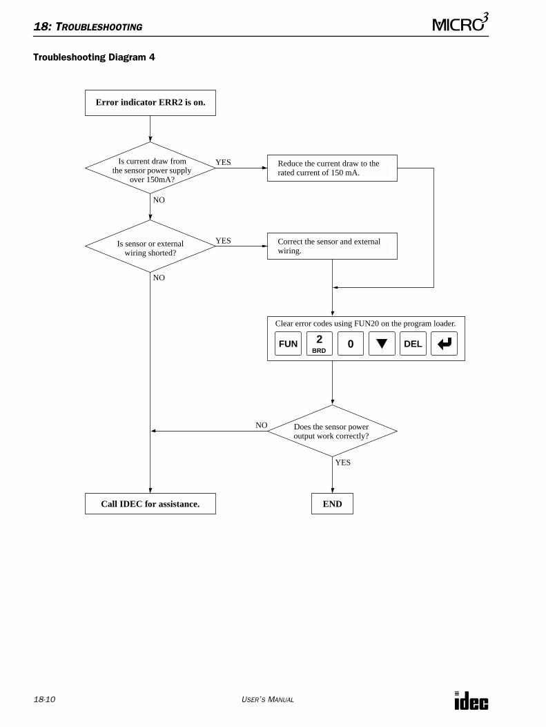
18: TROUBLESHOOTING
18-10 USER’S MANUAL
Troubleshooting Diagram 4
Does the sensor power output work correctly?
Is current draw from the sensor power supply
over 150mA?
Error indicator ERR2 is on.
END
YES
NO
YES
NO
NO
Is sensor or external wiring shorted?
Call IDEC for assistance.
Reduce the current draw to the rated current of 150 mA.
Correct the sensor and external wiring.
YES
Clear error codes using FUN20 on the program loader.
DELFUN 2BRD
0
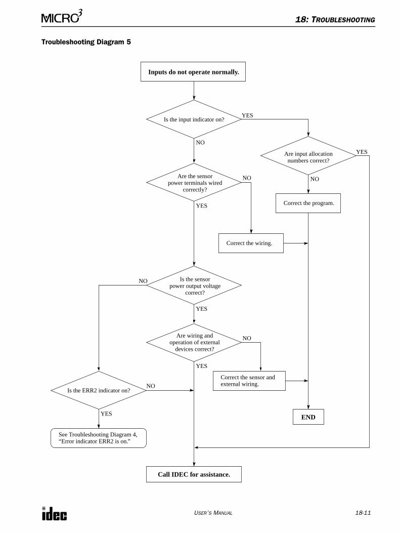
18: TROUBLESHOOTING
USER’S MANUAL 18-11
Troubleshooting Diagram 5
Are wiring and operation of external
devices correct?
Is the sensor power output voltage
correct?
Are the sensor power terminals wired
correctly?
Inputs do not operate normally.
END
YES
NO
Are input allocation numbers correct?
Call IDEC for assistance.
Correct the sensor and external wiring.
Is the input indicator on?
Correct the wiring.
Correct the program.
Is the ERR2 indicator on?
See Troubleshooting Diagram 4,“Error indicator ERR2 is on.”
YES
NONO
YES
YES
YES
NO
NO
NO
YES
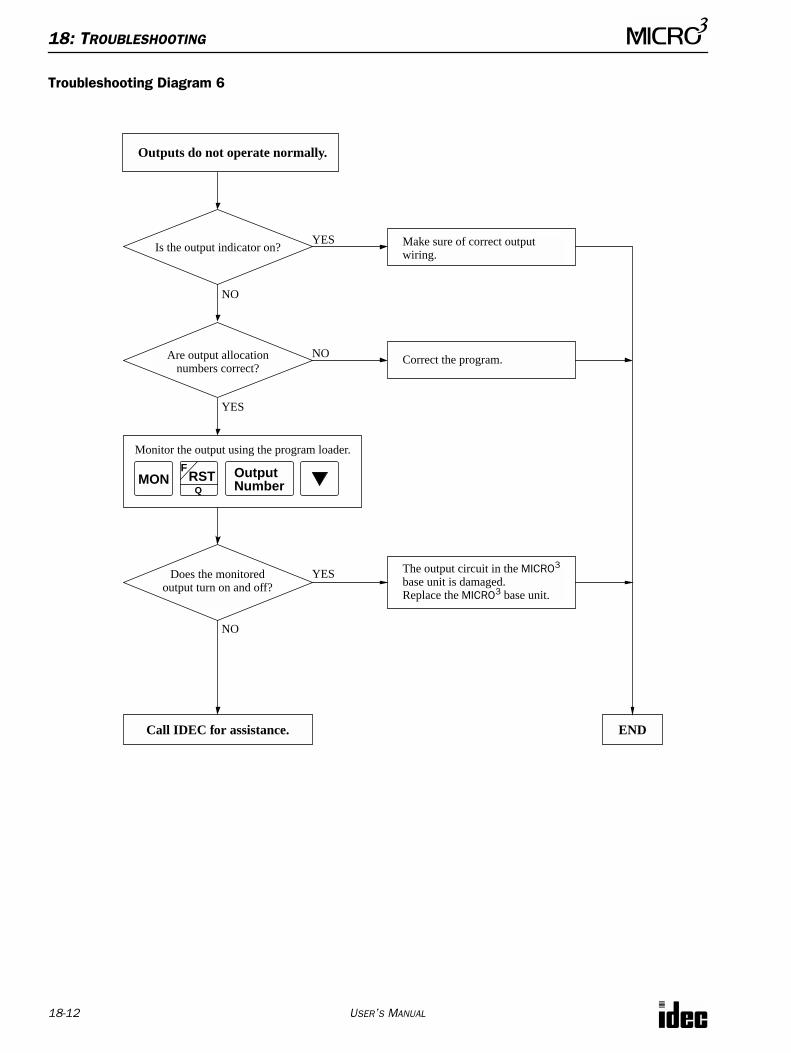
18: TROUBLESHOOTING
18-12 USER’S MANUAL
Troubleshooting Diagram 6
Does the monitored output turn on and off?
YES
NO
YES
NO
YES
Call IDEC for assistance.
Monitor the output using the program loader.
Output
NO
Outputs do not operate normally.
Are output allocation numbers correct?
Is the output indicator on? Make sure of correct output wiring.
Correct the program.
RSTF
QMON Number
The output circuit in the MICRO3 base unit is damaged.Replace the MICRO3 base unit.
END
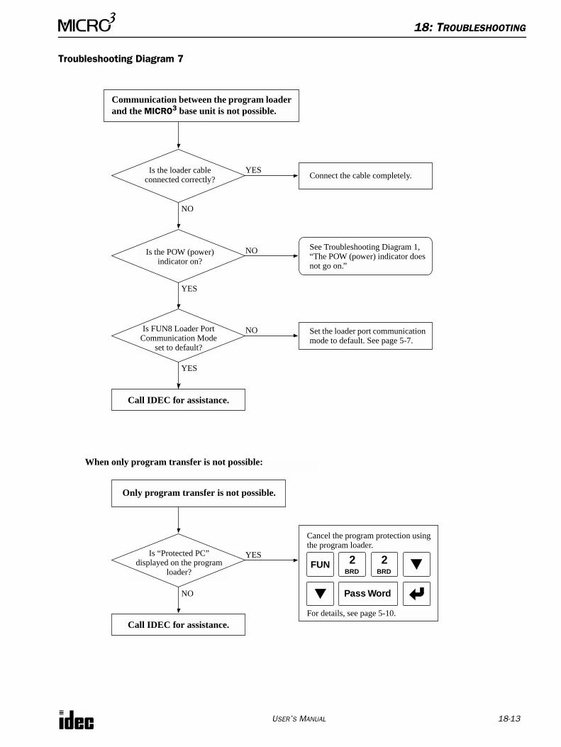
18: TROUBLESHOOTING
USER’S MANUAL 18-13
Troubleshooting Diagram 7
Set the loader port communication mode to default. See page 5-7.
Cancel the program protection using the program loader.
Is “Protected PC” displayed on the program
loader?
YES
NO
YES
NO
YES
Call IDEC for assistance.
Pass Word
NO
Communication between the program loader and the MICRO3 base unit is not possible.
Is the POW (power) indicator on?
Is the loader cableconnected correctly?
See Troubleshooting Diagram 1,“The POW (power) indicator does not go on.”
Connect the cable completely.
Call IDEC for assistance.
When only program transfer is not possible:
Only program transfer is not possible.
FUN 2BRD
2BRD
For details, see page 5-10.
YES
NOIs FUN8 Loader Port Communication Mode
set to default?
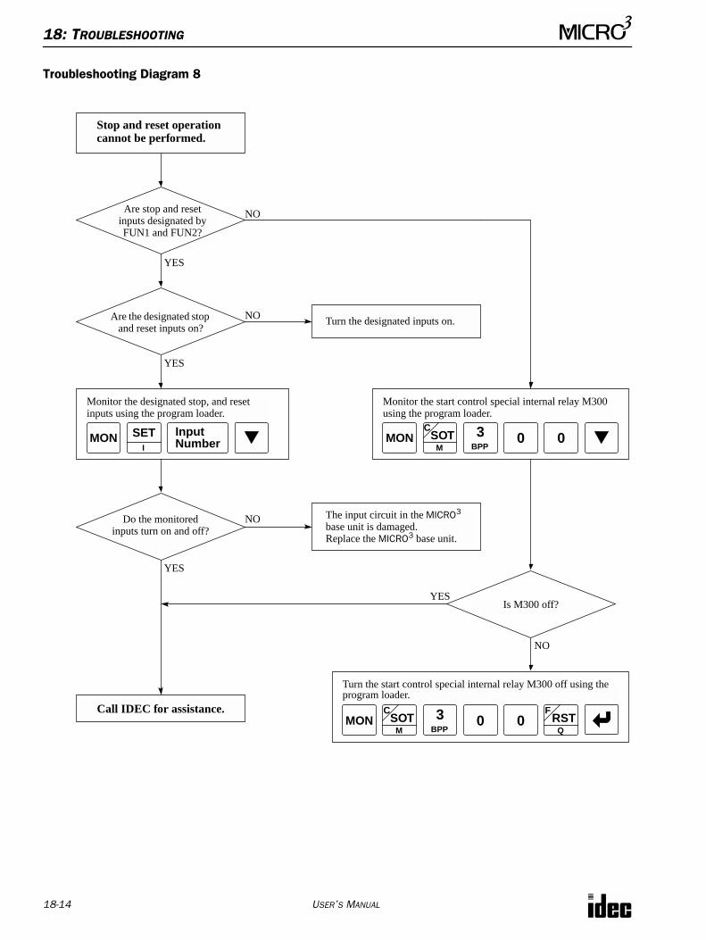
18: TROUBLESHOOTING
18-14 USER’S MANUAL
Troubleshooting Diagram 8
Do the monitored inputs turn on and off?
NO
YES
NO
YES
YES
Call IDEC for assistance.
Monitor the designated stop, and reset inputs using the program loader.
Input
NO
Stop and reset operation cannot be performed.
Are the designated stop and reset inputs on?
Is M300 off?
Turn the designated inputs on.
MON Number
The input circuit in the MICRO3 base unit is damaged.Replace the MICRO3 base unit.
Are stop and reset inputs designated by FUN1 and FUN2?
SETI
Monitor the start control special internal relay M300 using the program loader.
MON 3BPP
0SOTC
M0
YES
Turn the start control special internal relay M300 off using the program loader.
MON 3BPP
0SOTC
M0 RST
F
Q
NO
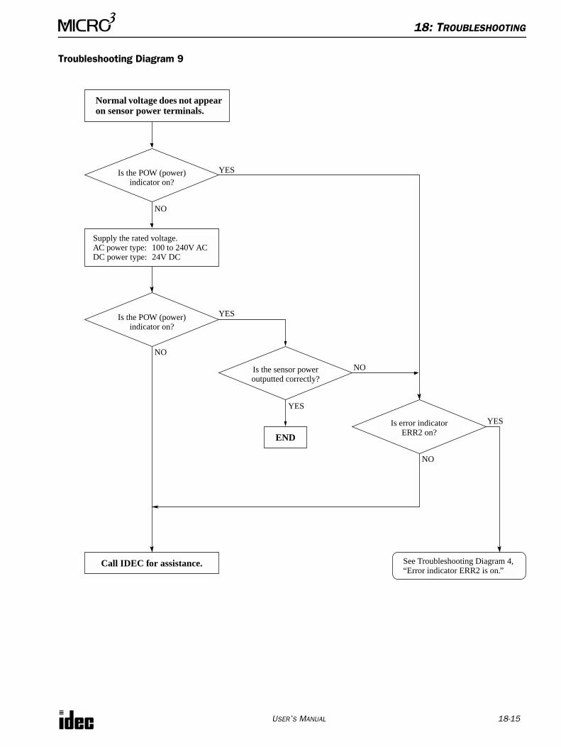
18: TROUBLESHOOTING
USER’S MANUAL 18-15
Troubleshooting Diagram 9
Is error indicator ERR2 on?
YES
NO
NO
YES
YES
Call IDEC for assistance.
Supply the rated voltage.AC power type: 100 to 240V ACDC power type: 24V DC
NO
Normal voltage does not appear on sensor power terminals.
Is the POW (power) indicator on?
NO
YES
Is the POW (power) indicator on?
Is the sensor power outputted correctly?
END
See Troubleshooting Diagram 4,“Error indicator ERR2 is on.”
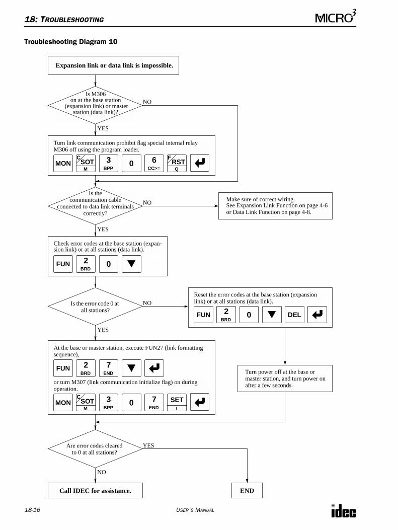
18: TROUBLESHOOTING
18-16 USER’S MANUAL
Troubleshooting Diagram 10
Turn power off at the base or master station, and turn power on after a few seconds.
Is the error code 0 at all stations?
Is thecommunication cable
connected to data link terminals correctly?
Is M306on at the base station
(expansion link) or masterstation (data link)?
NO
YES
Call IDEC for assistance.
NO
Make sure of correct wiring.See Expansion Link Function on page 4-6 or Data Link Function on page 4-8.
END
Turn link communication prohibit flag special internal relay M306 off using the program loader.
MON 3BPP
0SOTC
MRST
F
Q
6CC>=
Check error codes at the base station (expan-sion link) or at all stations (data link).
0
At the base or master station, execute FUN27 (link formatting sequence),
7END
FUN 2BRD
Are error codes cleared to 0 at all stations?
Reset the error codes at the base station (expansion link) or at all stations (data link).
FUN 2BRD
0 DEL
Expansion link or data link is impossible.
NO
YES
YES
YES
NO
FUN 2BRD
or turn M307 (link communication initialize flag) on during operation.
MON 3BPP
0SOTC
M
7END
SETI
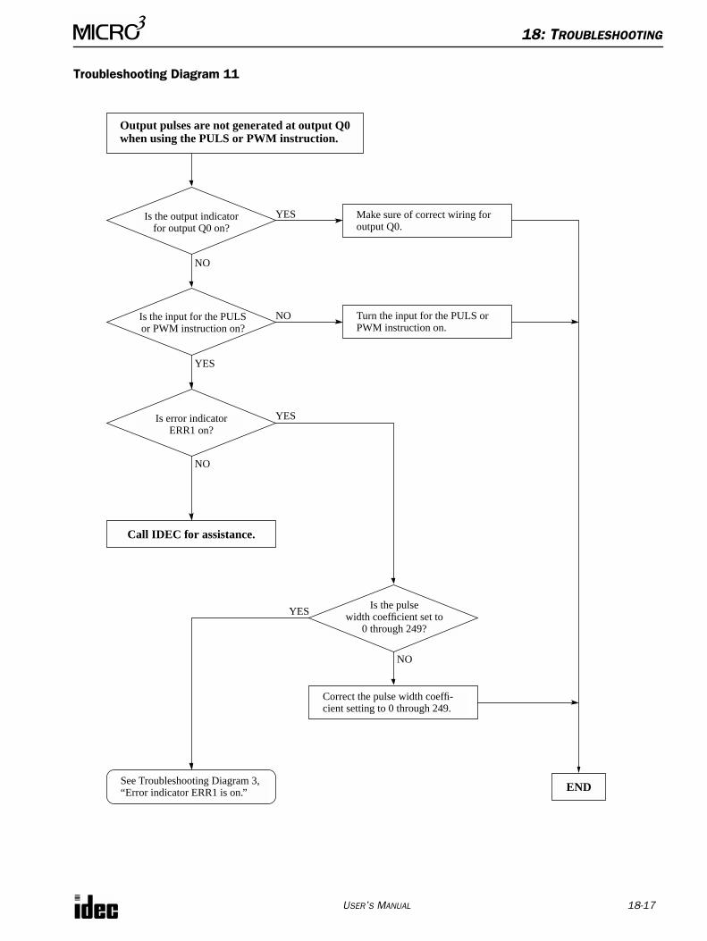
18: TROUBLESHOOTING
USER’S MANUAL 18-17
Troubleshooting Diagram 11
Turn the input for the PULS or PWM instruction on.
Correct the pulse width coeffi-cient setting to 0 through 249.
Is the pulse width coefficient set to
0 through 249?
Is error indicatorERR1 on?
Is the input for the PULS or PWM instruction on?
YES
NO
NO
YES
YES
Call IDEC for assistance.
NO
Make sure of correct wiring for output Q0.
Output pulses are not generated at output Q0 when using the PULS or PWM instruction.
Is the output indicator for output Q0 on?
ENDSee Troubleshooting Diagram 3,“Error indicator ERR1 is on.”
NO
YES
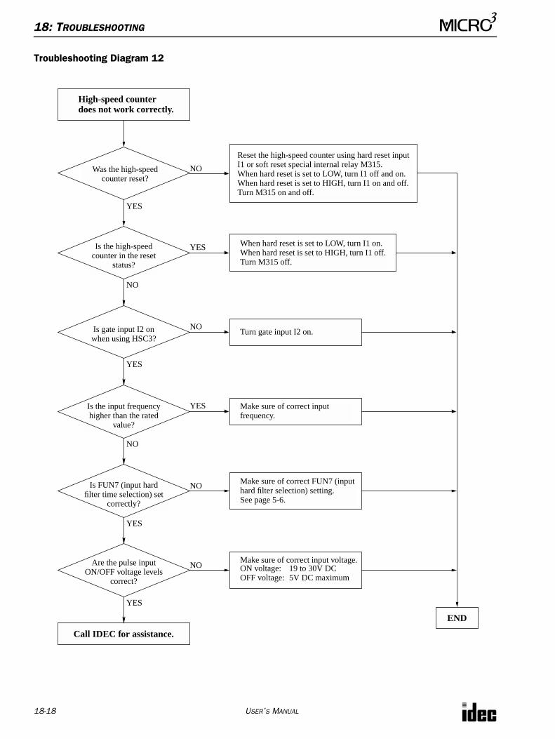
18: TROUBLESHOOTING
18-18 USER’S MANUAL
Troubleshooting Diagram 12
Are the pulse input ON/OFF voltage levels
correct?
Is FUN7 (input hardfilter time selection) set
correctly?
Is the input frequency higher than the rated
value?
Is the high-speed counter in the reset
status?
Reset the high-speed counter using hard reset input I1 or soft reset special internal relay M315.When hard reset is set to LOW, turn I1 off and on.When hard reset is set to HIGH, turn I1 on and off.Turn M315 on and off.
Was the high-speed counter reset?
YES
Call IDEC for assistance.
NO
High-speed counter does not work correctly.
END
NO
YES
Make sure of correct input frequency.
Make sure of correct FUN7 (input hard filter selection) setting.See page 5-6.
Make sure of correct input voltage. ON voltage: 19 to 30V DCOFF voltage: 5V DC maximum
YES
NO
NO
YES
YES
NO
Turn gate input I2 on.
When hard reset is set to LOW, turn I1 on.When hard reset is set to HIGH, turn I1 off.Turn M315 off.
Is gate input I2 on when using HSC3?
YES
NO
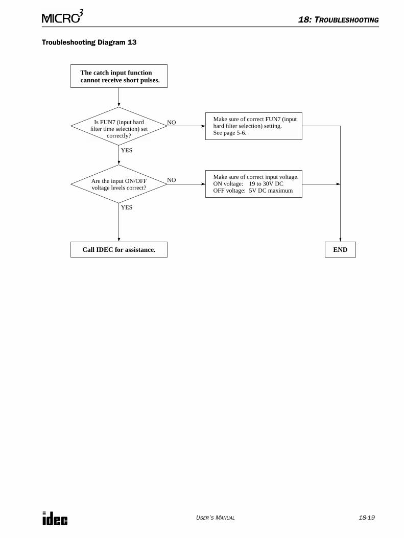
18: TROUBLESHOOTING
USER’S MANUAL 18-19
Troubleshooting Diagram 13
Are the input ON/OFF voltage levels correct?
NO
YES
Call IDEC for assistance.
The catch input function cannot receive short pulses.
END
YES
NO Make sure of correct input voltage. ON voltage: 19 to 30V DCOFF voltage: 5V DC maximum
Is FUN7 (input hardfilter time selection) set
correctly?
Make sure of correct FUN7 (input hard filter selection) setting.See page 5-6.
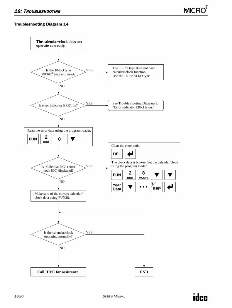
18: TROUBLESHOOTING
18-20 USER’S MANUAL
Troubleshooting Diagram 14
Is the 10-I/O type MICRO3 base unit used?
YES
NO
NO
Call IDEC for assistance.
YES
The clock data is broken. Set the calendar/clock using the program loader.
FUN 2BRD
8MCS/R
YearData REP
B
Is error indicator ERR1 on?
Is “Calendar NG” (error code 800) displayed?
YES
NO
The calendar/clock does not operate correctly.
See Troubleshooting Diagram 3,“Error indicator ERR1 is on.”
Read the error data using the program loader.
FUN 2BRD
0
The 10-I/O type does not have calendar/clock function. Use the 16- or 24-I/O type.
Is the calendar/clock operating normally?
Clear the error code.
DEL
Make sure of the correct calendar/clock data using FUN28.
YES
NO
END
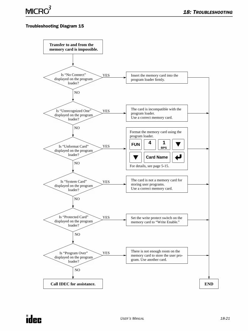
18: TROUBLESHOOTING
USER’S MANUAL 18-21
Troubleshooting Diagram 15
Format the memory card using the program loader.
The card is incompatible with the program loader. Use a correct memory card.
Is “Unrecognized One” displayed on the program
loader?
YES
NO
NO
Call IDEC for assistance.
YES
Transfer to and from the memory card is impossible.
END
NO
YES
Insert the memory card into the program loader firmly.
Is “Unformat Card” displayed on the program
loader?Card Name
FUN
For details, see page 5-15.
4
1BPS
Is “System Card” displayed on the program
loader?
The card is not a memory card for storing user programs. Use a correct memory card.
Is “Protected Card” displayed on the program
loader?
Set the write protect switch on the memory card to “Write Enable.”
Is “Program Over” displayed on the program
loader?
There is not enough room on the memory card to store the user pro-gram. Use another card.
YES
YES
YES
NO
NO
NO
Is “No Connect” displayed on the program
loader?

18: TROUBLESHOOTING
18-22 USER’S MANUAL
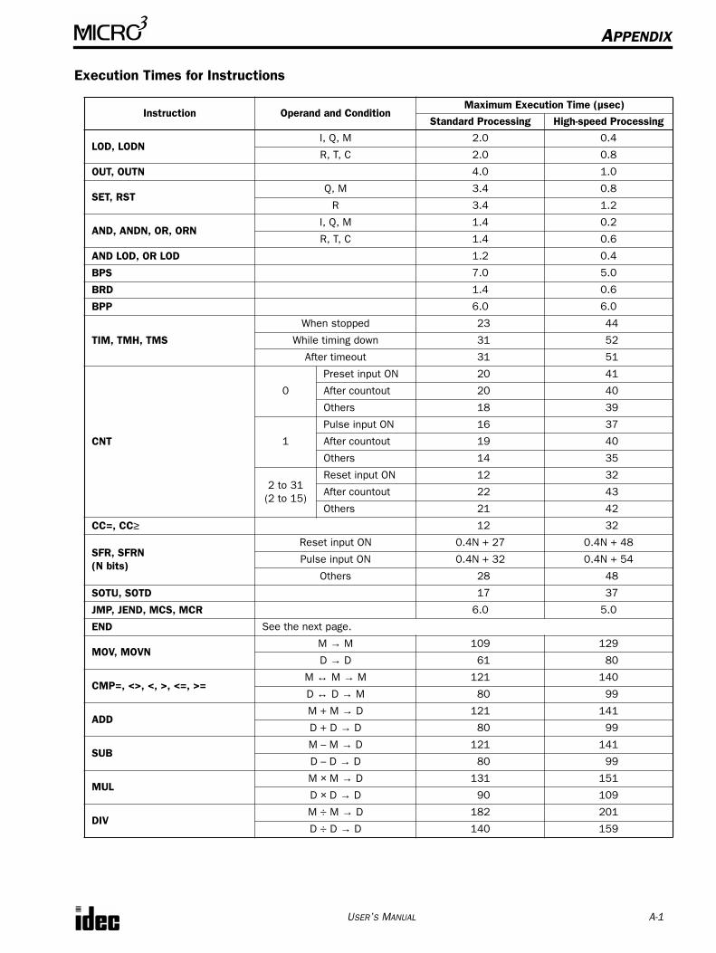
USER’S MANUAL A-1
APPENDIX
Execution Times for Instructions
Instruction Operand and ConditionMaximum Execution Time (µsec)
Standard Processing High-speed Processing
LOD, LODNI, Q, M 2.0 0.4
R, T, C 2.0 0.8
OUT, OUTN 4.0 1.0
SET, RSTQ, M 3.4 0.8
R 3.4 1.2
AND, ANDN, OR, ORNI, Q, M 1.4 0.2
R, T, C 1.4 0.6
AND LOD, OR LOD 1.2 0.4
BPS 7.0 5.0
BRD 1.4 0.6
BPP 6.0 6.0
TIM, TMH, TMS
When stopped 23 44
While timing down 31 52
After timeout 31 51
CNT
0
Preset input ON 20 41
After countout 20 40
Others 18 39
1
Pulse input ON 16 37
After countout 19 40
Others 14 35
2 to 31(2 to 15)
Reset input ON 12 32
After countout 22 43
Others 21 42
CC=, CC≥ 12 32
SFR, SFRN(N bits)
Reset input ON 0.4N + 27 0.4N + 48
Pulse input ON 0.4N + 32 0.4N + 54
Others 28 48
SOTU, SOTD 17 37
JMP, JEND, MCS, MCR 6.0 5.0
END See the next page.
MOV, MOVNM → M 109 129
D → D 61 80
CMP=, <>, <, >, <=, >=M ↔ M → M 121 140
D ↔ D → M 80 99
ADDM + M → D 121 141
D + D → D 80 99
SUBM – M → D 121 141
D – D → D 80 99
MULM × M → D 131 151
D × D → D 90 109
DIVM ÷ M → D 182 201
D ÷ D → D 140 159
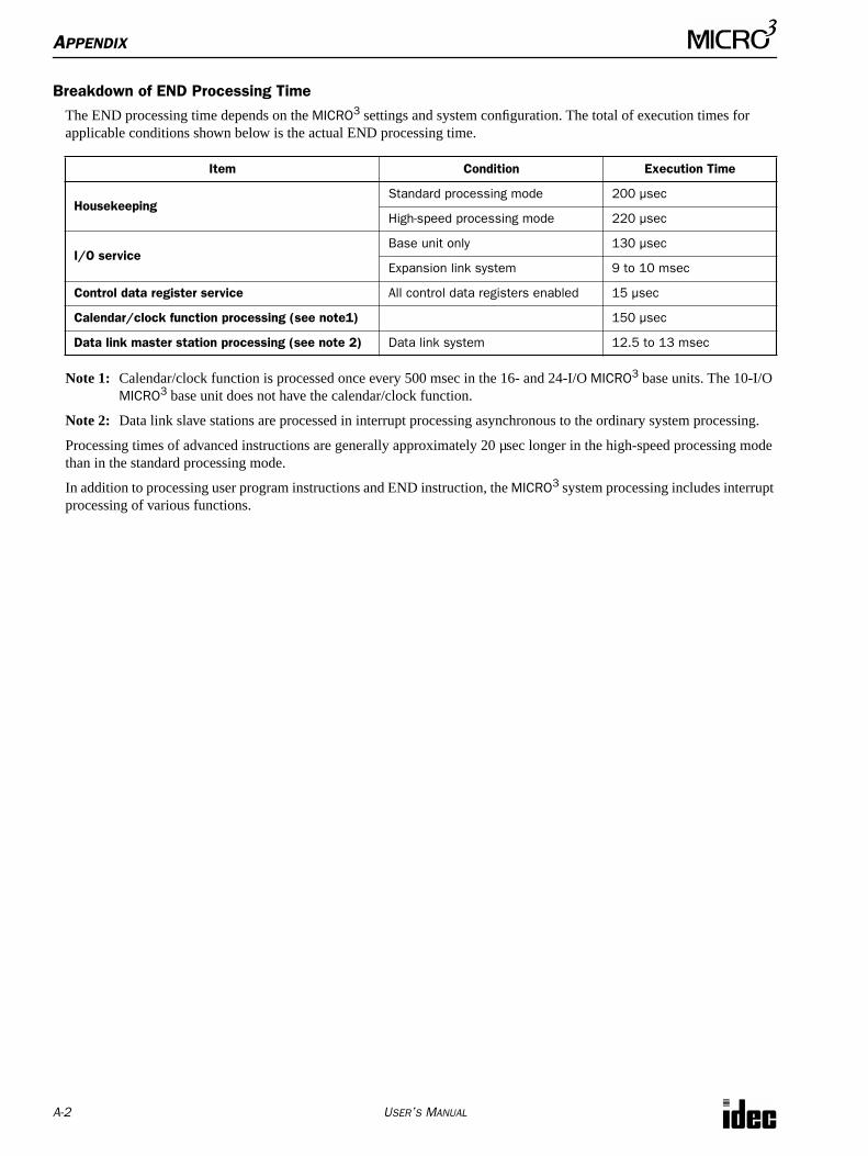
APPENDIX
A-2 USER’S MANUAL
Breakdown of END Processing Time
The END processing time depends on the MICRO3 settings and system configuration. The total of execution times for applicable conditions shown below is the actual END processing time.
Note 1: Calendar/clock function is processed once every 500 msec in the 16- and 24-I/O MICRO3 base units. The 10-I/O MICRO3 base unit does not have the calendar/clock function.
Note 2: Data link slave stations are processed in interrupt processing asynchronous to the ordinary system processing.
Processing times of advanced instructions are generally approximately 20 µsec longer in the high-speed processing mode than in the standard processing mode.
In addition to processing user program instructions and END instruction, the MICRO3 system processing includes interrupt processing of various functions.
Item Condition Execution Time
HousekeepingStandard processing mode 200 µsec
High-speed processing mode 220 µsec
I/O serviceBase unit only 130 µsec
Expansion link system 9 to 10 msec
Control data register service All control data registers enabled 15 µsec
Calendar/clock function processing (see note1) 150 µsec
Data link master station processing (see note 2) Data link system 12.5 to 13 msec
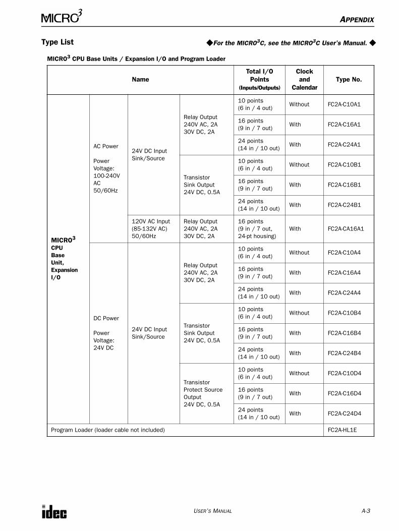
APPENDIX
USER’S MANUAL A-3
Type List
MICRO3 CPU Base Units / Expansion I/O and Program Loader
NameTotal I/O
Points(Inputs/Outputs)
Clockand
CalendarType No.
MICRO3
CPUBaseUnit,ExpansionI/O
AC Power
PowerVoltage:100-240V AC50/60Hz
24V DC InputSink/Source
Relay Output240V AC, 2A30V DC, 2A
10 points(6 in / 4 out)
Without FC2A-C10A1
16 points(9 in / 7 out)
With FC2A-C16A1
24 points(14 in / 10 out)
With FC2A-C24A1
TransistorSink Output24V DC, 0.5A
10 points(6 in / 4 out)
Without FC2A-C10B1
16 points(9 in / 7 out)
With FC2A-C16B1
24 points(14 in / 10 out)
With FC2A-C24B1
120V AC Input(85-132V AC)50/60Hz
Relay Output240V AC, 2A30V DC, 2A
16 points(9 in / 7 out,24-pt housing)
With FC2A-CA16A1
DC Power
PowerVoltage:24V DC
24V DC InputSink/Source
Relay Output240V AC, 2A30V DC, 2A
10 points(6 in / 4 out)
Without FC2A-C10A4
16 points(9 in / 7 out)
With FC2A-C16A4
24 points(14 in / 10 out)
With FC2A-C24A4
TransistorSink Output 24V DC, 0.5A
10 points(6 in / 4 out)
Without FC2A-C10B4
16 points(9 in / 7 out)
With FC2A-C16B4
24 points(14 in / 10 out)
With FC2A-C24B4
TransistorProtect Source Output 24V DC, 0.5A
10 points(6 in / 4 out)
Without FC2A-C10D4
16 points(9 in / 7 out)
With FC2A-C16D4
24 points(14 in / 10 out)
With FC2A-C24D4
Program Loader (loader cable not included) FC2A-HL1E
For the MICRO3C, see the MICRO3C User’s Manual.
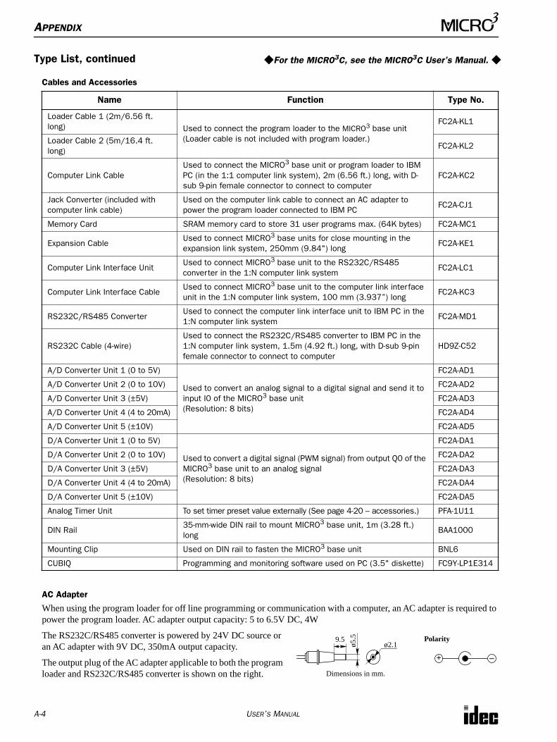
APPENDIX
A-4 USER’S MANUAL
Type List, continued
Cables and Accessories
AC Adapter
When using the program loader for off line programming or communication with a computer, an AC adapter is required to power the program loader. AC adapter output capacity: 5 to 6.5V DC, 4W
The RS232C/RS485 converter is powered by 24V DC source or an AC adapter with 9V DC, 350mA output capacity.
The output plug of the AC adapter applicable to both the program loader and RS232C/RS485 converter is shown on the right.
Name Function Type No.
Loader Cable 1 (2m/6.56 ft. long) Used to connect the program loader to the MICRO3 base unit
(Loader cable is not included with program loader.)
FC2A-KL1
Loader Cable 2 (5m/16.4 ft. long)
FC2A-KL2
Computer Link CableUsed to connect the MICRO3 base unit or program loader to IBM PC (in the 1:1 computer link system), 2m (6.56 ft.) long, with D-sub 9-pin female connector to connect to computer
FC2A-KC2
Jack Converter (included with computer link cable)
Used on the computer link cable to connect an AC adapter to power the program loader connected to IBM PC
FC2A-CJ1
Memory Card SRAM memory card to store 31 user programs max. (64K bytes) FC2A-MC1
Expansion CableUsed to connect MICRO3 base units for close mounting in the expansion link system, 250mm (9.84") long
FC2A-KE1
Computer Link Interface UnitUsed to connect MICRO3 base unit to the RS232C/RS485 converter in the 1:N computer link system
FC2A-LC1
Computer Link Interface CableUsed to connect MICRO3 base unit to the computer link interface unit in the 1:N computer link system, 100 mm (3.937”) long
FC2A-KC3
RS232C/RS485 ConverterUsed to connect the computer link interface unit to IBM PC in the 1:N computer link system
FC2A-MD1
RS232C Cable (4-wire)Used to connect the RS232C/RS485 converter to IBM PC in the 1:N computer link system, 1.5m (4.92 ft.) long, with D-sub 9-pin female connector to connect to computer
HD9Z-C52
A/D Converter Unit 1 (0 to 5V)
Used to convert an analog signal to a digital signal and send it to input I0 of the MICRO3 base unit(Resolution: 8 bits)
FC2A-AD1
A/D Converter Unit 2 (0 to 10V) FC2A-AD2
A/D Converter Unit 3 (±5V) FC2A-AD3
A/D Converter Unit 4 (4 to 20mA) FC2A-AD4
A/D Converter Unit 5 (±10V) FC2A-AD5
D/A Converter Unit 1 (0 to 5V)
Used to convert a digital signal (PWM signal) from output Q0 of the MICRO3 base unit to an analog signal(Resolution: 8 bits)
FC2A-DA1
D/A Converter Unit 2 (0 to 10V) FC2A-DA2
D/A Converter Unit 3 (±5V) FC2A-DA3
D/A Converter Unit 4 (4 to 20mA) FC2A-DA4
D/A Converter Unit 5 (±10V) FC2A-DA5
Analog Timer Unit To set timer preset value externally (See page 4-20 – accessories.) PFA-1U11
DIN Rail35-mm-wide DIN rail to mount MICRO3 base unit, 1m (3.28 ft.) long
BAA1000
Mounting Clip Used on DIN rail to fasten the MICRO3 base unit BNL6
CUBIQ Programming and monitoring software used on PC (3.5" diskette) FC9Y-LP1E314
For the MICRO3C, see the MICRO3C User’s Manual.
9.5ø2.1ø5
.5 Polarity
+ –
Dimensions in mm.
USER’S MANUAL i
INDEX
# 1:1 communication 4-161:N Communication 4-17100-msec clock M312 6-310-msec clock M313 6-31-sec clock M311 6-31-sec clock reset M310 6-324V Overload 18-4
A A/D 16-5converter unit 4-21
ACadapter 4-17, A-4adapter jack 3-1input 1-22
accessories A-4ADD 11-1adding counters CNT2-CNT31 7-19addition 11-1ADJ 14-4adjust 14-4ADV Error 18-5advanced instruction
A/D 16-5ADD 11-1ADJ 14-4ANDW 12-1ANR0 15-5ANR1 15-5CALR 14-1CALW 14-2CLKR 14-3CLKW 14-3CMP< 10-1CMP<= 10-1CMP<> 10-1CMP= 10-1CMP> 10-1CMP>= 10-1DGRD 15-3DISP 15-1DIV 11-1HSC0 17-1HSC1 17-3HSC2 17-6HSC3 17-9IMOV 9-4IMOVN 9-5input condition 8-4list 8-2menus 8-1MOV 9-1MOVN 9-3MUL 11-1NOP 8-6ORW 12-1programming 8-3PULS 16-1PWM 16-3reading 3-8revising 8-3ROTL 13-3ROTR 13-4SFTL 13-1
SFTR 13-2structure 8-4SUB 11-1syntax error 18-5XORW 12-1
advanced instructions 8-1all outputs OFF M302 6-2allocation numbers 6-1analog
input function 4-21output function 4-27potentiometer 15-5potentiometer setting 15-5read 0 15-5read 1 15-5timer unit 4-18, 4-20timer, external 4-18
analog/digital conversion 16-5AND and ANDN instructions 7-4AND LOD instruction 7-5AND word 12-1ANDW 12-1ANR0 15-5ANR1 15-5
B basefrequency 16-1unit
processing mode code 5-8system code 5-8
basicinstructions 7-1system 1-3
bidirectional shift register 7-26bit stack register 7-10Boolean computation 12-1BPS, BRD, and BPP instructions 7-9breakdown of END processing time A-2
C cables and accessories A-4calendar
and clock 14-1read 14-1write 14-2
Calendar NG 18-4calendar/clock
data readout and setting (FUN28) 5-12error 18-4function processing A-2
CALR 14-1CALW 14-2carry (Cy) and borrow (Bw) M303 6-3carry or borrow signals 11-2catch input
function 4-2status set M290-M297 6-2vs normal input 4-2
CC= and CC≥ instructions 7-21changing preset values for timers and counters 3-14clearing changed preset values 3-14CLKR 14-3CLKW 14-3clock
INDEX
ii USER’S MANUAL
read 14-3write 14-3
CMP< 10-1CMP<= 10-1CMP<> 10-1CMP= 10-1CMP> 10-1CMP>= 10-1CNT instruction 7-18COM Error 18-5communication mode setting (FUN8) 5-7compare
equal to 10-1greater than 10-1greater than or equal to 10-1less than 10-1less than or equal to 10-1unequal to 10-1
comparing programsbetween loader and base unit 3-9between loader and memory card 3-11
computer linkcable 4-16function 4-16interface cable 4-17interface unit 4-17system 1-4
contact protection circuit for relay output 1-17control data register
service A-2setting (FUN10) 5-8
counteradding (up) counter 7-19and shift register in master control circuit 7-29comparison instructions 7-21dual-pulse reversible counter 7-18up/down selection reversible 7-19
counting catch input pulses 4-3crimping terminal 1-28
D D/A converter unit 4-27data clear, operand (FUN26) 5-11data input 7-23data link
connection error 18-3data register allocation 4-9function 4-8master station processing A-2system 1-4terminal communication specifications 1-9wiring 1-27
data movement, timer/counter preset value 3-14data register
allocation for data link system 4-9allocation numbers 6-4clearing all data (FUN26) 5-11control data register 5-8entering data 3-16monitoring 3-17
data transmission through FA-3S serial interface module 4-13
data type selection, display 5-14day of week (calendar) 5-8
DC sink input(AC power type) 1-22(DC power type) 1-22
DC source input(AC power type) 1-21(DC power type) 1-21
deletinga program from memory card 3-11entire user program 3-5program instructions 3-6
destination operand 8-4DGRD 15-3digital
data range 16-5read 15-3resolution 4-24
dimensions 1-24analog timer unit 4-20
DIN rail 4-20mount socket 4-20mounting 1-26
direct mounting 1-25discontinuity of operand areas 8-6DISP 15-1display 3-1, 15-1
data type selection (FUN36) 5-14language selection (FUN35) 5-14
displaying instructions 3-5disposing 1-26DIV 11-1division 11-1dual-pulse reversible counter CNT0 7-18
E editor mode 3-3, 3-5EEPROM NG 18-4END instruction 7-32END processing time, breakdown A-2entering
data into data registers 3-16program instructions 3-6
errorcauses and actions 18-3indicator during errors 18-2indicators 18-1messages
program loader operation 3-20exclusive OR word 12-1execution times for instructions A-1expansion cable 4-6expansion link
function 4-6system 1-4system setup 4-6
external analog timer 4-18
F FA-3S serial interface module 4-13formatting memory card 5-15forward shift register 7-23FUN (function) mode 3-3FUN settings 5-1FUN table
(FUN1 through FUN11) 5-1(FUN20 through FUN43) 5-2
INDEX
USER’S MANUAL iii
FUN11 program capacity and PLC type selection Preface-2
FUN31 program loader version readout/hardware check Preface-2
function 4-8keys 3-1 to 3-2selector switch 4-6, 4-8, 4-13specifications 1-7 to 1-8
(A/D converter unit) 4-23(D/A converter unit) 4-29
G gatecontrol HSC3 17-9input 17-9
generalerror code 5-8error codes 18-2specifications 1-5 to 1-6
(A/D converter unit) 4-22(D/A converter unit) 4-28
H hardfilter 4-4reset selection 17-2 to 17-3, 17-7, 17-9
high-speed counter 17-1(HSC3) overflow M316 6-4monitoring 3-15soft reset M315 6-4
high-speed processing mode 4-1hold-down spring 4-20hour (clock) 5-8housekeeping A-2HSC0 17-1HSC1 17-3HSC2 17-6HSC3 17-9
I I/Oallocation numbers for expansion link system 4-7service A-2wiring diagram 15-4, 16-2, 17-8
illumination control using PWM instruction 16-4IMOV 9-4IMOVN 9-5indirect
move 9-4move not 9-5
initialize pulse M301 6-2in-operation output M317 6-4input
condition for advanced instructions 8-4filter
function 4-3time selection (FUN7) 4-2, 5-6
internal circuit 1-12operating range 1-12or output as source or destination operand 8-5specifications 1-11terminal arrangements 1-19wiring 1-27wiring diagrams 1-21 to 1-22
inserting program instructions 3-7installation 1-25
in control panel 1-26
instructionsbasic 7-1binary arithmetic 11-1bit shift and rotate 13-1Boolean computation 12-1clock and calendar 14-1comparison 10-1high-speed counter 17-1interface 15-1move 9-1pulse and A/D conversion 16-1real-time calendar and clock 14-1
internalcircuit
input 1-12output 1-16
memory and user memory 3-3relay “keep” designation (FUN3) 5-4
J jack converter 4-16JMP and JEND instructions 7-30jump instructions 7-30
K keepdata sum check error 18-3designation
internal relay (FUN3) 5-4shift register (FUN4) 5-5
Keep Data Sum 18-3key
function keys 3-1 to 3-2program keys 3-1 to 3-2
L language selection, display 5-14link
communicationerror 18-5error code 5-8error M305 6-3initialize flag M307 6-3prohibit flag M306 6-3stop flag M307 6-3
formatting sequence (FUN27) 5-11systems 1-4
loader cable 1-3connection port 3-1
loader port communicationmode setting (FUN8) 5-7specifications 1-9
LOD and LODN instructions 7-2
M magnets on the back 3-1maintaining catch input 4-3master control instruction 7-28MCS and MCR instructions 7-28memory backup function 1-10memory card 3-1
comparing programs 3-11deleting a program 3-11formatting (FUN41) 5-15identification (FUN40) 5-15reading program 3-10writing program 3-10
minute (clock) 5-8
INDEX
iv USER’S MANUAL
mode 16-1, 16-3module number selection switch 4-13monitor
mode 3-3, 3-12screen holding (FUN33) 5-13
monitoringdata registers 3-17high-speed counters 3-15I/O, internal relays, and shift registers 3-12sequential 3-8timers and counters 3-13
mounting hole layout 1-24MOV 9-1move 9-1move not 9-3MOVN 9-3MUL 11-1multiple usage of MCS instructions 7-29multiplication 11-1multi-stage
comparison HSC1 17-3data setting 17-4
N no operation 8-6noise
emission specifications 1-9immunity specifications 1-9
NOP 8-6numeric and symbolic allocation numbers 17-4
O ON-delay analog timer 4-19opcode 8-4operand data clear (FUN26) 5-11operating procedure
data link system 4-10expansion link system 4-6
operating status during errors 18-2operation
basics 2-1register 7-5, 7-7, 7-10
OR and ORN instructions 7-4OR LOD instruction 7-7OR word 12-1ORW 12-1OUT and OUTN instructions 7-2output
delay 1-16during errors 18-2frequency 16-1frequency range 16-1internal circuit 1-16pulse width ratio 16-3response at power up and down 4-30specifications 1-13 to 1-15terminal arrangements 1-20wiring 1-27wiring diagram 15-2, 16-4wiring diagrams 1-23
P panel mountadapter 4-20socket 4-20
parts descriptionbase unit 1-2
program loader 3-1pass word 5-10PC Connect NG 18-3PLC
address for network communication (FUN9) 5-7error data readout and reset (FUN20) 5-9operating status readout (FUN24) 5-10system program version readout (FUN23) 5-10
power failure 18-3memory protection 7-17
Power Off 18-3power supply
timing chart 1-10, 4-24, 4-30voltage 1-28wiring 1-27
preset valueschanging 3-14restoring 3-14
Prg. Sum Check 18-3processing
mode selection (FUN5) 5-5speed 4-1
programcapacity 4-1capacity and PLC type selection (FUN11) Preface-2,
5-9check (FUN30) 5-12keys 3-1 to 3-2
program loaderbeep sound (FUN34) 5-14connection to computer 4-16error messages 3-20operation modes 3-3specifications 1-18system program installation (FUN42) 5-15system program restore (FUN43) 5-16version readout/hardware check (FUN31) Preface-2,
5-13programming
advanced instructions 8-3procedures and precautions 3-4
protect output overload error 18-4protection,
type of 4-24, 4-31user program (FUN22) 5-10
PULS 16-1pulse
cycle period 16-3input 7-23motor speed control using PULS instruction 16-2output 16-1output control HSC2 17-6width
coefficient 16-1, 16-3modulation 16-3
PWM 16-3
R readingadvanced instructions 3-8error data 18-1program
from base unit to loader 3-9from memory card to loader 3-10
INDEX
USER’S MANUAL v
registerbit stack register 7-10operation register 7-5, 7-7, 7-10stack register 7-5, 7-7
relay output 1-23repeat
cycles 8-4designation 8-4operation
ADD, SUB, and MUL instructions 11-3ANDW, ORW, and XORW instructions 12-3comparison instructions 10-2DIV instruction 11-4move instructions 9-2
reset input 2-2, 7-23number selection (FUN2) 5-4
resetting 3-18resolution 4-24, 4-30, 16-5restore timer/counter preset values 3-14reverse shift register 7-25revising advanced instructions 8-3rising or falling edge selection for catch inputs (FUN6)
4-2, 5-6rotate
left 13-3right 13-4
ROTL 13-3ROTR 13-4RS232C cable 4-17RS232C/RS485 converter 4-17RUN Error 18-5RUN/STOP switch 2-1, 3-1
S scan time(current value) 5-8readout (FUN25) 5-11
scanning process and WDT (watch dog timer) 1-10searching for a program instruction 3-8second (clock) 5-8selecting program addresses 3-5self-diagnostics flow chart 1-10sensor power overload error 18-4sequential
monitoring 3-8monitoring (FUN32) 5-13start 14-7
serial interface module 4-13SET and RST instructions 7-32setting 3-18SFR and SFRN instructions 7-23SFTL 13-1SFTR 13-2shift
left 13-1right 13-2
shift register“keep” designation (FUN4) 5-5instructions 7-23
simple operation 2-3single output instruction 7-27single-stage comparison HSC0 17-1soft
filter 4-5
reset special internal relay M315 17-2, 17-4, 17-7, 17-9SOTU and SOTD instructions 7-27source
and destination operands 8-4operand 8-4
specialfunctions 4-1internal relays 6-2
specificationsdata link 4-9
terminal communication 1-9function 1-7 to 1-8general 1-5 to 1-6high-speed counter 17-1input 1-11loader port communication 1-9noise
emission 1-9immunity 1-9
output 1-13 to 1-15program loader 1-18
stack register 7-5, 7-7start control M300 6-2start/stop
operation 2-1schematic 2-1using power supply 2-2using program loader 2-1
stop input 2-2number selection (FUN1) 5-3
structure of an advanced instruction 8-4SUB 11-1subtraction 11-1Syntax 18-3system
setup 1-3data link 4-8, 4-13expansion link 4-6
statuses 2-2
T terminal arrangementsinput 1-19output 1-20
TIM, TMH, and TMS instructions 7-14TIM/CNT CRC 18-3time scheduled control 14-5timer
accuracy 7-16circuit 7-15
timer or counteras destination operand 8-4as source operand 8-4
timer/counter preset valuechanged M314 6-3CRC error 18-3readout and restore (FUN21) 5-9
transfer mode 3-3, 3-9transistor
protect source output 1-23sink output 1-23
Transistor NG 18-4troubleshooting 18-1
diagrams 18-6
INDEX
vi USER’S MANUAL
type listanalog timer unit and accessories 4-20base units and program loader A-3cables and accessories A-4
type of protection 4-24, 4-31
U up counters CNT2-CNT31 7-19up/down selection reversible counter CNT1 7-19user communication data monitor (FUN50) 5-16user communication status readout (FUN29) 5-12user program
CRC error 18-3execution error 18-5execution error code 5-8execution error M304 6-3sum check error 18-3syntax error 18-3writing error 18-4
user program protection (FUN22) 5-10Users Prg. CRC 18-3using
the editor mode 3-5the monitor mode 3-12the transfer mode 3-9
W Watch Dog Time 18-3watchdog timer error 18-3weight Preface-2wiring 1-27
diagram 4-19, 4-25, 4-31input 1-21 to 1-22output 1-23
socket adapter 4-20wrist strap 3-1writing program
from loader to base unit 3-9from loader to memory card 3-10
X XORW 12-1

MI
CR
O3
Pr
og
ra
mm
ab
le
L
og
ic
C
on
tr
ol
le
r
Ma
nu
al
User’s Manual
UNITED STATES
IDEC CORPORATION
1213 Elko Drive
Sunnyvale, CA 94089-2240, USA
Tel (408) 747-0550
Toll Free (800) 262-IDEC
Fax (408) 744-9055
Fax (800) 635-6246
E-mail [email protected]
www.industry.net/ideccorp
JAPAN
IDEC IZUMI CORPORATION
7-31, Nishi-Miyahara
1-Chome, Yodogawa-ku
Osaka 532, Japan
Tel (06) 398-2571
Fax (06) 392-9731
CANADA
IDEC CANADA LIMITED
Unit 22-151 Brunel Road
Mississauga, Ontario, L4Z 1X3, Canada
Tel (905) 890-8561
Fax (905) 890-8562
GERMANY
IDEC ELEKTROTECHNIK GmbH
Wendenstraße 331
D-20537 Hamburg, Germany
Tel (040) 25 11 91-93
Fax (040) 25 4 33 61
UNITED KINGDOM
IDEC ELECTRONICS LIMITED
Unit 12, Canbury Business Park
Elm Crescent
Kingston-Upon-Thames
Surrey KT2 6HJ, United Kingdom
Tel (0181) 549-0737
Fax (0181) 546-0963
HONG KONG
IDEC IZUMI (H.K.) CO., LTD.
Room No.1409, Tower 1 Silvercord
30 Canton Road, Tsimshatsui
Kowloon, Hong Kong
Tel (02) 376-2823
Fax (02) 376-0790
TAIWAN
IDEC TAIWAN CORPORATION
3F., No.75, Hsin Tai Wu Road, Sec. 1
Hsi-Chih, Taipei County, Taiwan
Republic of China
Tel (02) 698-2601
Fax (02) 698-2709
AUSTRALIA
IDEC AUSTRALIA PTY. LTD.
2/3 Macro Court
Rowville, Victoria 3178
Australia
Tel (03) 9763-3244
Fax (03) 9763-3255
Users Manual #EM317-0
Printed in the USA 5U 2/97
Micro Programmable Logic Controller
Related Documents


