Acta Materialia 50 (2002) 565–574 www.elsevier.com/locate/actamat Imaging of the crystal structure of silicon nitride at 0.8 A ˚ ngstro ¨m resolution 1 A. Ziegler a , C. Kisielowski b , R.O. Ritchie a,* a Materials Sciences Division, Lawrence Berkeley National Laboratory, and Department of Materials Science and Engineering, University of California, Berkeley, CA 94720, USA b National Center for Electron Microscopy, Lawrence Berkeley National Laboratory, Berkeley, CA 94720, USA Received 5 September 2001; received in revised form 21 September 2001; accepted 21 September 2001 Abstract High-resolution transmission electron microscopy is utilized to examine the crystal structure of a silicon nitride ceramic using focus variation methods to achieve sub-a ˚ngstro ¨m resolution at the absolute theoretical information limit of the transmission electron microscope. Specifically, crucial requirements of high instrumental stability, a coherent electron source and optimum imaging conditions have been met by the one-A ˚ ngstrom microscope (OA ˚ M) at the National Center for Electron Microscopy in order to obtain a resolution of 0.8 A ˚ . The resulting high-resolution images reveal the individual atom positions of the in-plane projected crystal structure of silicon nitride and permit detailed structural information. The images correspond closely to computed and simulated images of this crystal structure. 2002 Acta Materialia Inc. Published by Elsevier Science Ltd. All rights reserved. Keywords: Atomic-resolution transmission electron microscopy; Crystal structure; Ceramics 1. Introduction In materials science, to comprehend the forma- tion and interaction of defects, interfaces, nanos- tructures, etc., and their effect on the physical, mechanical and electrical behavior, information at the atomic level is clearly pertinent. Among the * Corresponding author. Tel.: +1-510-486-5798; fax: +1- 510-486-4881. E-mail address: [email protected] (R.O. Ritchie). 1 Work supported by the Director, Office of Science, Office of Basic Energy Sciences, Materials Sciences Division of the US Department of Energy under Contract No. DE-AC03- 76SF00098. 1359-6454/02/$22.00 2002 Acta Materialia Inc. Published by Elsevier Science Ltd. All rights reserved. PII:S1359-6454(01)00363-9 characterization techniques used to retrieve such information, high-resolution transmission electron microscopy (HRTEM) is the most utilized tech- nique as it has the great advantage that it can interrogate structural information in two dimen- sions. However, to access truly atomic level infor- mation, the imaging instrumentation has to be in perfect alignment and highly stable, with an absol- ute minimum in high-voltage, lens-current and thermal-energy spread. Recent progress with HRTEM, however, has made it possible to obtain sub-a ˚ngstro ¨m resolution in a “mid-voltage” microscope via phase retrieval through focus variation, i.e., to extend the resol- ution well beyond its Scherzer point-to-point resol-

Welcome message from author
This document is posted to help you gain knowledge. Please leave a comment to let me know what you think about it! Share it to your friends and learn new things together.
Transcript
Acta Materialia 50 (2002) 565–574www.elsevier.com/locate/actamat
Imaging of the crystal structure of silicon nitride at 0.8Angstrom resolution1
A. Ziegler a, C. Kisielowski b, R.O. Ritchiea,*
a Materials Sciences Division, Lawrence Berkeley National Laboratory, and Department of Materials Science and Engineering,University of California, Berkeley, CA 94720, USA
b National Center for Electron Microscopy, Lawrence Berkeley National Laboratory, Berkeley, CA 94720, USA
Received 5 September 2001; received in revised form 21 September 2001; accepted 21 September 2001
Abstract
High-resolution transmission electron microscopy is utilized to examine the crystal structure of a silicon nitrideceramic using focus variation methods to achieve sub-a˚ngstrom resolution at the absolute theoretical information limitof the transmission electron microscope. Specifically, crucial requirements of high instrumental stability, a coherentelectron source and optimum imaging conditions have been met by the one-A˚ ngstrom microscope (OA˚ M) at theNational Center for Electron Microscopy in order to obtain a resolution of 0.8 A˚ . The resulting high-resolution imagesreveal the individual atom positions of the in-plane projected crystal structure of silicon nitride and permit detailedstructural information. The images correspond closely to computed and simulated images of this crystal structure.2002 Acta Materialia Inc. Published by Elsevier Science Ltd. All rights reserved.
Keywords: Atomic-resolution transmission electron microscopy; Crystal structure; Ceramics
1. Introduction
In materials science, to comprehend the forma-tion and interaction of defects, interfaces, nanos-tructures, etc., and their effect on the physical,mechanical and electrical behavior, information atthe atomic level is clearly pertinent. Among the
* Corresponding author. Tel.:+1-510-486-5798; fax:+1-510-486-4881.
E-mail address: [email protected] (R.O. Ritchie).1 Work supported by the Director, Office of Science, Office
of Basic Energy Sciences, Materials Sciences Division of theUS Department of Energy under Contract No. DE-AC03-76SF00098.
1359-6454/02/$22.00 2002 Acta Materialia Inc. Published by Elsevier Science Ltd. All rights reserved.PII: S1359 -6454(01 )00363-9
characterization techniques used to retrieve suchinformation, high-resolution transmission electronmicroscopy (HRTEM) is the most utilized tech-nique as it has the great advantage that it caninterrogate structural information in two dimen-sions. However, to access truly atomic level infor-mation, the imaging instrumentation has to be inperfect alignment and highly stable, with an absol-ute minimum in high-voltage, lens-current andthermal-energy spread.
Recent progress with HRTEM, however, hasmade it possible to obtain sub-a˚ngstrom resolutionin a “mid-voltage” microscope via phase retrievalthrough focus variation, i.e., to extend the resol-ution well beyond its Scherzer point-to-point resol-
566 A. Ziegler et al. / Acta Materialia 50 (2002) 565–574
ution of 1.7 A to an expected information limit ofabout 0.8 A [1]. The one-Angstrom microscope(OAM) at the National Center for ElectronMicroscopy (Lawrence Berkeley NationalLaboratory) has been used to demonstrate such res-olutions at 0.89 A and 0.85 A [2–5], representingthe highest resolution feasible with the presentHRTEM design. The procedure utilized in thiswork is based on several such studies [6–17] andexploits the sub-angstrom information limit of afield emission TEM in a particular manner via digi-tal image processing [18,19] to produce electronexit waves limited only by the information limitof the HRTEM. Usually, a single HRTEM imagerepresents a highly encoded mixture of the proper-ties of the sample with those of the TEM. A recon-struction of the electron exit wave from a focusedseries of lattice images, on the other hand, allowsthe elimination of imaging artifacts, the extensionof the resolution to the information limit and thesimplification of image interpretation.
In this paper, we use this specific technique toimage, for the first time, the crystal structure of astructural ceramic, namely silicon nitride, with anunprecedented resolution of 0.8 A and a sensitivitythat allows for the detection of single nitrogen col-umns.
2. Background
Bulk silicon nitride (Si3N4) ceramics have beeninvestigated extensively over the last two decades,largely because their mechanical and physicalproperties are relevant for many high-temperatureapplications; these include high strength, highdecomposition temperature (1900°C), good oxi-dation resistance, low coefficient of friction, negli-gible creep, good thermal shock properties, andgood resistance to corrosive environments. Inaddition, thin silicon nitride films and coatingshave been studied in order to understand electricaland thermal conductivity properties. All of theseproperties, and the processing and sinteringbehavior, rely on the specific crystal structure, thelocal chemistry, and the local bonding at interfaces.However, it has been challenging to assess thisinformation experimentally because truly atomic
level imaging on such ceramic structures has notbeen feasible.
The crystal structure data of the Si3N4 matrix,calculated using X-ray diffraction methods, havebeen used for computational modeling. However,confirmation of the computed bonding character-istics using direct imaging of the crystal structureand the structure of the interfacial regions withhigh-resolution transmission electron microscopy,specifically to identify the positions of the additiveions, has not been achieved at truly atomic resol-ution. A problem here is that a point-to-point resol-ution that reaches the theoretical information limitof the TEM of about 0.8 A is required in order toidentify single atom columns in the Si3N4 matrixin [0001] projection. Consequently, the focus vari-ation technique provides the only means to date toobtain images at such a resolution.
3. Experimental procedures
3.1. Material
In this study, we examine a silicon nitride fabri-cated by Geyer and Hoffmann with newlydeveloped two-step sintering technique, consistingof a dilatometer-controlled gas-pressure-sinteringprocess and a successive hot-isostatic pressingdensification [20]. Such highly pure and controlledprocessing was utilized to permit almost impurity-free densification without the usual glass encapsul-ation technique.
Si3N4 powder (UBE SN E10; Ube Industries,Yamaguchi, Japan) was sintered with 2 wt% Y2O3
(fine grade, HCST) to achieve a microstructureconsisting of two morphologies of β-Si3N4 grains:predominantly acicular-shaped, with an averagelength of 5 µm and an aspect ratio of 8:1, and equi-axed, with a size of 0.5–1.5 µm. Samples for exam-ination in the TEM were prepared by grinding,dimpling, and ion milling. The low-voltage ionmilling was performed with a LINDA ion mill(Technoorg LINDA, IV3H/L ion beam thinningunit, Scientific Technical Development Ltd., USA)to produce foils with a thickness of less than 100A and with highly smooth surfaces, surface rough-ness �10 A.

567A. Ziegler et al. / Acta Materialia 50 (2002) 565–574
3.2. Electron microscopy
3.2.1. Electron microscopeElectron microscopy was performed with the
NCEM OAM, a Philips CM300/FEG/UT micro-scope modified to improve its information limitfrom the standard 1.05 A [21] to 0.8 A [2–5]. This300 kV microscope is equipped with a field emis-sion electron source and an ultra-twin objectivelens of low spherical aberrations(Cs = 0.60 mm) and chromatic aberrations(Cc = 1.3 mm). With this microscope, latticeimages can be recorded aberration free to a small-est distance of about 0.8 A.
The specimen stage is a Philips double-tilt low-background holder with a tilting range of±30°/±30°. Images are recorded digitally throughan attached Gatan Image Filter (GIF) on a2048×2048 pixel CCD (charge-coupled device)camera that allows for a total magnification up to38 Mx. Electron exit waves were reconstructedfrom series of twenty lattice images using thePhilips/Brite-Euram software developed by Coeneand Thust [18,19].
3.2.2. Phase retrieval and image reconstructionTo understand the phase retrieval and image
reconstruction technique, it is necessary to notethat an exit-wave function emanating from theback plane of the specimen can be written as afunction containing an amplitude and phaserelationship:
y(r) � A(r)·exp(�ift(r)), (1)
where A(r) is the amplitude and ft(r) is the phase,which depends on the specimen thickness. How-ever, the intensity I captured on the image planeis expressed as:
I � y·y∗ � |y|2, (2)
which is why phase information is lost. The suc-cessive projection of the electron exit wave into animage plane can be written as:
�(u) � H(u)·�(u), (3)
where u is the reciprocal-lattice vector representingthe spatial frequencies, and �(u) and �(u) are theimage and specimen function, respectively. H(u) is
the contrast transfer function (CTF) that describeshow contrast is transferred into the image plane.This transfer function H(u) characterizes micro-scope parameters such as the spherical aberrationsCs of the objective lens and the defocus �f.
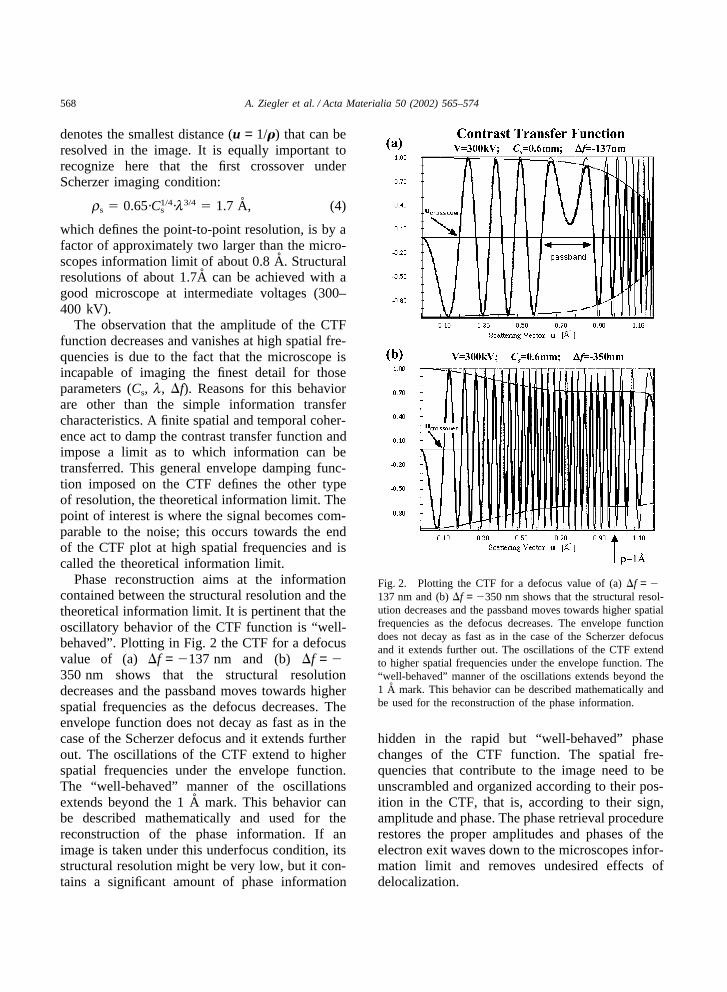
Spatial frequencies are related to the reciprocalof distance and therefore high spatial frequenciessimply correspond to small distances. Hence high-resolution work requires high spatial frequencies.The CTF describes how these spatial frequencies(or contrast) are transferred from the specimen tothe image in a TEM. A typical plot of the CTF forthe classical optimum Scherzer defocus con-ditions, �f = �42 nm, in a weak phase approxi-mation is shown in Fig. 1. Two types of resolutioncan be defined, (i) the structural resolution limitand (ii) the theoretical information limit. The firstcrossover point determines the width of thepassband for spatial frequencies to be transferred(from u = 0 to ucrossover), which in turn determinesthe structural resolution limit. The value of ucrossover
Fig. 1. A typical plot of the CTF for the classical optimumScherzer defocus conditions, �f = �42 nm, is shown. The valueof ucrossover denotes the smallest distance (u = 1/r) that can beresolved in the image, i.e., the structural resolution limit. Struc-tural resolutions of about 1.7 A can be achieved with a goodmicroscope at intermediate voltages (300–400 kV). The obser-vation that the amplitude of the CTF function decreases andvanishes at high spatial frequencies is due to the fact that themicroscope is incapable of imaging the finest detail for thoseparameters (Cs, l, �f). A point of interest is where the signalbecomes comparable to the noise; this occurs towards the endof the CTF plot at high spatial frequencies and is called thetheoretical information limit.
568 A. Ziegler et al. / Acta Materialia 50 (2002) 565–574
denotes the smallest distance (u = 1/r) that can beresolved in the image. It is equally important torecognize here that the first crossover underScherzer imaging condition:
rs � 0.65·C1/4s ·l3/4 � 1.7 A, (4)
which defines the point-to-point resolution, is by afactor of approximately two larger than the micro-scopes information limit of about 0.8 A. Structuralresolutions of about 1.7A can be achieved with agood microscope at intermediate voltages (300–400 kV).
The observation that the amplitude of the CTFfunction decreases and vanishes at high spatial fre-quencies is due to the fact that the microscope isincapable of imaging the finest detail for thoseparameters (Cs, l, �f). Reasons for this behaviorare other than the simple information transfercharacteristics. A finite spatial and temporal coher-ence act to damp the contrast transfer function andimpose a limit as to which information can betransferred. This general envelope damping func-tion imposed on the CTF defines the other typeof resolution, the theoretical information limit. Thepoint of interest is where the signal becomes com-parable to the noise; this occurs towards the endof the CTF plot at high spatial frequencies and iscalled the theoretical information limit.
Phase reconstruction aims at the informationcontained between the structural resolution and thetheoretical information limit. It is pertinent that theoscillatory behavior of the CTF function is “well-behaved” . Plotting in Fig. 2 the CTF for a defocusvalue of (a) �f = �137 nm and (b) �f = �350 nm shows that the structural resolutiondecreases and the passband moves towards higherspatial frequencies as the defocus decreases. Theenvelope function does not decay as fast as in thecase of the Scherzer defocus and it extends furtherout. The oscillations of the CTF extend to higherspatial frequencies under the envelope function.The “well-behaved” manner of the oscillationsextends beyond the 1 A mark. This behavior canbe described mathematically and used for thereconstruction of the phase information. If animage is taken under this underfocus condition, itsstructural resolution might be very low, but it con-tains a significant amount of phase information
Fig. 2. Plotting the CTF for a defocus value of (a) �f = �137 nm and (b) �f = �350 nm shows that the structural resol-ution decreases and the passband moves towards higher spatialfrequencies as the defocus decreases. The envelope functiondoes not decay as fast as in the case of the Scherzer defocusand it extends further out. The oscillations of the CTF extendto higher spatial frequencies under the envelope function. The“well-behaved” manner of the oscillations extends beyond the1 A mark. This behavior can be described mathematically andbe used for the reconstruction of the phase information.
hidden in the rapid but “well-behaved” phasechanges of the CTF function. The spatial fre-quencies that contribute to the image need to beunscrambled and organized according to their pos-ition in the CTF, that is, according to their sign,amplitude and phase. The phase retrieval procedurerestores the proper amplitudes and phases of theelectron exit waves down to the microscopes infor-mation limit and removes undesired effects ofdelocalization.

569A. Ziegler et al. / Acta Materialia 50 (2002) 565–574
It can be seen that the choice of a largeunderfocus aids the information transfer at spatialfrequencies close to the theoretical informationlimit. This was typically extracted from 20 latticeimages recorded around an underfocus of �260nm with a constant defocus interval of �2.4 nm forsuccessive lattice images.
3.3. Computer simulations
Corresponding computer simulations of thecrystal structure were conducted using the com-mercial program CrystalKit [22]. The HRTEMimage simulations were subsequently performedusing these structure models as input to the com-mercial program MacTempas [23]. Through-focusand through-thickness image simulations can becreated with this program from the model crystalstructures. MacTempas is based on the multislicemethod, whereby the structure model is sliced per-pendicular to the direction of the incident beam.The potential content of each single slice modifiesthe incoming electron wave, which is then pro-jected onto the next slice and propagated throughthe entire structure model [23].
4. Results and discussion
4.1. Crystal structure of silicon nitride
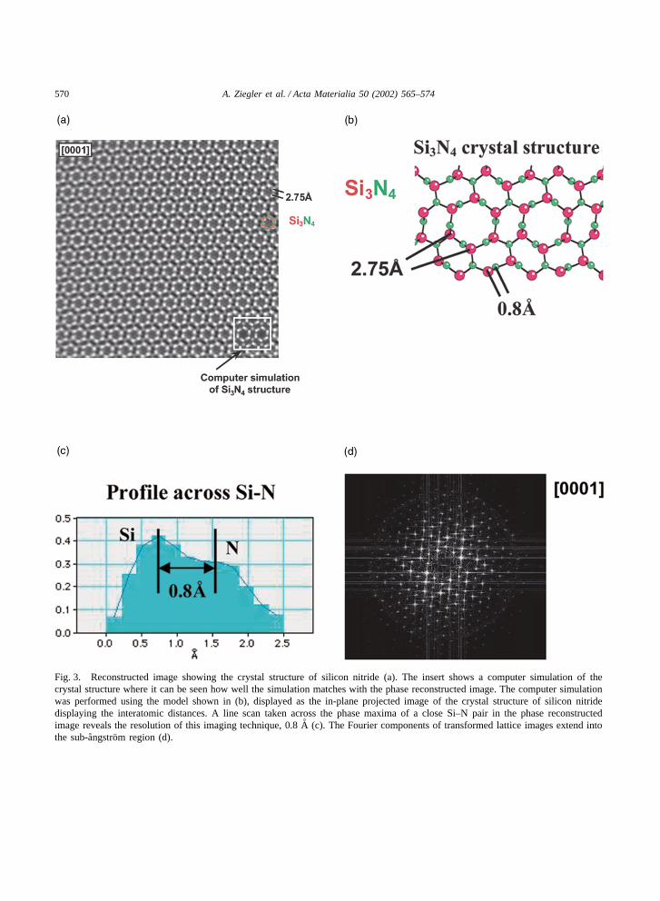
Fig. 3(a) shows the experimentally reconstructedphase of the electron exit wave from the crystalstructure of β-Si3N4 projected along the [0001]direction. It reveals all details of the modeled struc-ture of β-Si3N4 that is shown in schematic form inFig. 3(b). The larger scattering power of silicon com-pared with nitrogen makes the silicon columnsappear as brighter spots. Indeed, the hexagonal crys-tal structure can be directly copied into the experi-mental image of Fig. 3(a). Simulations of the elec-tron exit wave confirm this assignment [inset in Fig.3(a)]. Two nitrogen positions are visible in this pro-jection. The first one is clearly separated amongthree silicon columns and the second one appears asa shoulder on the silicon columns. A line scan acrossphase maxima [Fig. 3(c)] reveals their presence.However, the nitrogen signal is weak at this thick-
ness. Therefore, it is not fully separated from thesilicon signal. The Fourier components of transfor-med lattice images extend into the sub-angstromregion [Fig. 3(d)]. Thus, the phase image of Fig. 3(a)displays sub-angstrom resolution close to the 0.8 Ainformation limit of the microscope. Experimentally,sample tilt is a most limiting factor to obtain suchhigh quality images.
The reconstruction process provides for easierimage interpretation. Fig. 4 shows a comparisonof the regular lattice image obtained under regularScherzer defocus conditions [Fig. 4(b)] with thecorresponding reconstructed phase image of theelectron exit wave [Fig. 4(a)]. It is apparent thatthe Scherzer image displays interference spots atlocations where no atom columns are present inthe real crystal lattice. Since lattice images areinterference patterns, their appearance changeswith defocus and sample thickness. This is demon-strated in Fig. 5 where an array of simulated latticeimages is presented; in this array, the sample thick-ness is increased from top to bottom and the defo-cus value increased from right to left. It is apparentthat the appearance of the image changes drasti-cally with focus and thickness. In contrast, thephase of the reconstructed electron exit wave doesnot change with focus; it exhibits intensity maximaat the positions of the atomic columns. Chemicalinformation can be accessed through the magnitudeof the phase change if the thickness can be esti-mated. In this regard, the image simulations can beused to ascertain the thickness of the sampling areain the specimen by comparing, for example, theScherzer defocus image in Fig. 4(b) with the arrayof simulated images in Fig. 5. Using this approach,we find that the sample thickness to be approx. 80–90 A in this case.
Salient criteria have to be met for such Scherzerand phase-reconstructed HRTEM imaging; theseinclude the presence of atoms, specimen thicknessand electron oscillation in the specimen.
For imaging, it is the atom column density ori-ented in the direction of the incident electron beamthat is important; a denser column of ions causesstronger scattering of the incident electrons. Forphase-reconstructed imaging, a conflict can arisewhen the column density is low. Specifically, if thebonding characteristics are such that atomic dis-
570 A. Ziegler et al. / Acta Materialia 50 (2002) 565–574
Fig. 3. Reconstructed image showing the crystal structure of silicon nitride (a). The insert shows a computer simulation of thecrystal structure where it can be seen how well the simulation matches with the phase reconstructed image. The computer simulationwas performed using the model shown in (b), displayed as the in-plane projected image of the crystal structure of silicon nitridedisplaying the interatomic distances. A line scan taken across the phase maxima of a close Si–N pair in the phase reconstructedimage reveals the resolution of this imaging technique, 0.8 A (c). The Fourier components of transformed lattice images extend intothe sub-angstrom region (d).

571A. Ziegler et al. / Acta Materialia 50 (2002) 565–574
Fig. 4. The phase reconstructed image (a) is compared to the Scherzer defocus image (b) where it can be seen that the single imageas represented in the Scherzer defocus condition does not contain as much information as the phase reconstructed image. Indeed, theScherzer image displays bright spots at locations where there are no atoms in the real lattice, in particular in the middle of the Si-hexagon. A single HRTEM image represents a highly encoded mixture of the properties of the object with those belonging to theTEM. Phase retrieval and focal-series image-reconstruction allows eliminating imaging artifacts, which complicate the interpretationof single images. The phase reconstruction technique utilizes the information of twenty images recorded under different defocus values.
tances are large along the columns, this necessi-tates using a thicker sample to exceed a minimumatom density for good imaging contrast; however,foils thicker than 100 A are not optimal for phasereconstruction purposes.
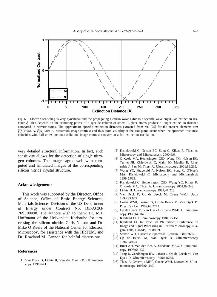
The interaction of electron waves with materialin zone axis orientation is strongly dynamic.Amplitudes and phases of the electron wave oscil-late with the sample thickness and this oscillationperiod is called extinction distance x. Lighteratoms produce a longer extinction distance com-pared to heavier atoms. Relevant extinction dis-tances were extracted from ref. [24] for the presentelements; they are: x(Si)�256 A, x(N)�304 A.Maximum image contrast and thus atom visibilityat the exit plane occur when the specimen thick-ness coincides with half an extinction oscillation.Image contrast vanishes at a full extinction oscil-lation (Fig. 6). The thickness of the current speci-
men results in almost full image contrast for bothtypes of atoms.
The crisp and detailed images obtained withfocus-variation, image-reconstruction, and sub-Angstrom HRTEM imaging are promising forfurther investigations of the actual structure of sili-con nitride, in particular to examine interfaces andgrain boundaries in this material. For example, sin-tering additive ions are known to segregate to suchboundaries, which often consist of nanoscaleamorphous intercrystalline films. These films pro-foundly affect the mechanical properties of cer-amics at both ambient and elevated temperatures.The control of their structure and chemistry is thuscritical to developing new and improved ceramicmicrostructures with superior structural perform-ance; indeed, current studies are directed at usingfocus-variation methods to relate the strength,toughness and fatigue properties of Si3N4 ceramics

572 A. Ziegler et al. / Acta Materialia 50 (2002) 565–574
Fig. 5. An array of simulated images is shown as they would appear in the TEM for different imaging conditions. The thicknessincreases from top to bottom and the defocus value decreases from left to right. The differences in defocus and thickness are notvery large but it can be clearly seen that every image is different. Note for example how small changes in defocus cause significantchanges in the image. Small variations make one perceive a different picture of the object under investigation. Every image containsa different set of phase information, all belonging to the same area of interest. The phase retrieval and image reconstruction methodallows for these individual sets of information to be combined into one image, obtaining a much more complete picture of the object.The image simulations can also be used to ascertain the thickness of the sampling area in the real specimen.
to such a HRTEM characterization of the grainboundary films [25].
5. Conclusions
Focus-variation image-reconstruction HRTEMimaging has been successfully demonstrated for
investigating the atomic structure of a ceramicmaterial with an unprecedented resolution.Specifically, the crystal structure of silicon nitridehas been imaged for the first time at a resolutionof 0.8 A, i.e., at the theoretical information limitof a HRTEM. The resulting high-resolution imagesreveal the individual atom positions of the in-planeprojected crystal structure and allow retrieving
573A. Ziegler et al. / Acta Materialia 50 (2002) 565–574
Fig. 6. Electron scattering is very dynamical and the propagating electron wave exhibits a specific wavelength—an extinction dis-tance x—that depends on the scattering power of a specific column of atoms. Lighter atoms produce a longer extinction distancecompared to heavier atoms. The approximate specific extinction distances extracted from ref. [25] for the present elements are:x(Si)�256 A, x(N)�304 A. Maximum image contrast and thus atom visibility at the exit plane occur when the specimen thicknesscoincides with half an extinction oscillation. Image contrast vanishes at a full extinction oscillation.
very detailed structural information. In fact, suchsensitivity allows for the detection of single nitro-gen columns. The images agree well with com-puted and simulated images of the correspondingsilicon nitride crystal structure.
Acknowledgements
This work was supported by the Director, Officeof Science, Office of Basic Energy Sciences,Materials Sciences Division of the US Departmentof Energy under Contract No. DE-AC03-76SF00098. The authors wish to thank Dr. M.J.Hoffmann of the Universitat Karlsruhe for pro-cessing the silicon nitride, Chris Nelson and Dr.Mike O’Keefe of the National Center for ElectronMicroscopy, for assistance with the HRTEM, andDr. Rowland M. Cannon for helpful discussions.
References
[1] Van Dyck D, Lichte H, Van der Mast KD. Ultramicros-copy 1996;64:1.
[2] Kisielowski C, Nelson EC, Song C, Kilaas R, Thust A.Microscopy and Microanalysis 2000;6:6.
[3] O’Keefe MA, Hetherington CJD, Wang YC, Nelson EC,Turner JH, Kisielowski C, Malm JO, Mueller R, Ring-nalda J, Pan M, Thust A. Ultramicroscopy 2001;89:215.
[4] Wang YC, Fitzgerald A, Nelson EC, Song C, O’KeefeMA, Kisielowski C. Microscopy and Microanalysis1999;5:822.
[5] Kisielowski C, Hetherington CJD, Wang YC, Kilaas R,O’Keefe MA, Thust A. Ultramicroscopy 2001;89:243.
[6] Lichte H. Ultramicroscopy 1992;47:223.[7] Van Dyck D, Op de Beeck M, Coene WMJ. Optik
1993;93:103.[8] Coene WMJ, Janssen G, Op de Beeck M, Van Dyck D.
Phys Rev Lett 1992;69:3743.[9] Op de Beeck M, Van Dyck D, Coene WMJ. Ultramicros-
copy 1996;64:167.[10] Kirkland EJ. Ultramicroscopy 1984;15:151.[11] Kirkland EJ. In: Proc 6th Pfefferkorn Conference on
Image and Signal Processing in Electron Microscopy, Nia-gara Falls, Canada, 1988:139.
[12] Saxton WO. J Microsc Spectrosc Electron 1980;5:665.[13] Op de Beeck M, Van Dyck D. Ultramicroscopy
1996;64:153.[14] Buist AH, Van den Bos A, Miedema MAO. Ultramicros-
copy 1996;64:137.[15] Tang D, Zandbergen HW, Jansen J, Op de Beeck M, Van
Dyck D. Ultramicroscopy 1996;64:265.[16] Thust A, Overwijk MHF, Coene WMJ, Lentzen M. Ultra-
microscopy 1996;64:249.

574 A. Ziegler et al. / Acta Materialia 50 (2002) 565–574
[17] O’Keefe MA. In: Krishbab K, editor. Microstructures ofMaterials, Berkeley (CA): San Francisco Press; 1993:121.
[18] Coene WMJ, Thust A, Op de Beeck M, Van Dyck D.Ultramicroscopy 1996;64:109.
[19] Thust A, Coene WMJ, Op de Beeck M, Van Dyck D.Ultramicroscopy 1996;64:211.
[20] Geyer A. PhD thesis, University of Karlsruhe, Karlsruhe,Germany, 1997.
[21] Bakker H, Bleeker A, Mull P. Ultramicroscopy1996;64:17.
[22] The CrystalKit and MacTempas packages are both avail-able from Total Resolution, National Center for ElectronMicroscopy, Lawrence Berkeley National Laboratory,Berkeley (California).
[23] Kilaas R. In: Bailey GW, editor. 45th Annual Proc ofEMSA, Baltimore (MD): San Francisco Press; 1987:66.
[24] Van Dyck D, Chen JH. Solid State Commun1999;109:501.
[25] Ziegler A, Kisielowski C, Hoffmann MJ, Ritchie RO. JAm Ceram Soc, in review.
Related Documents