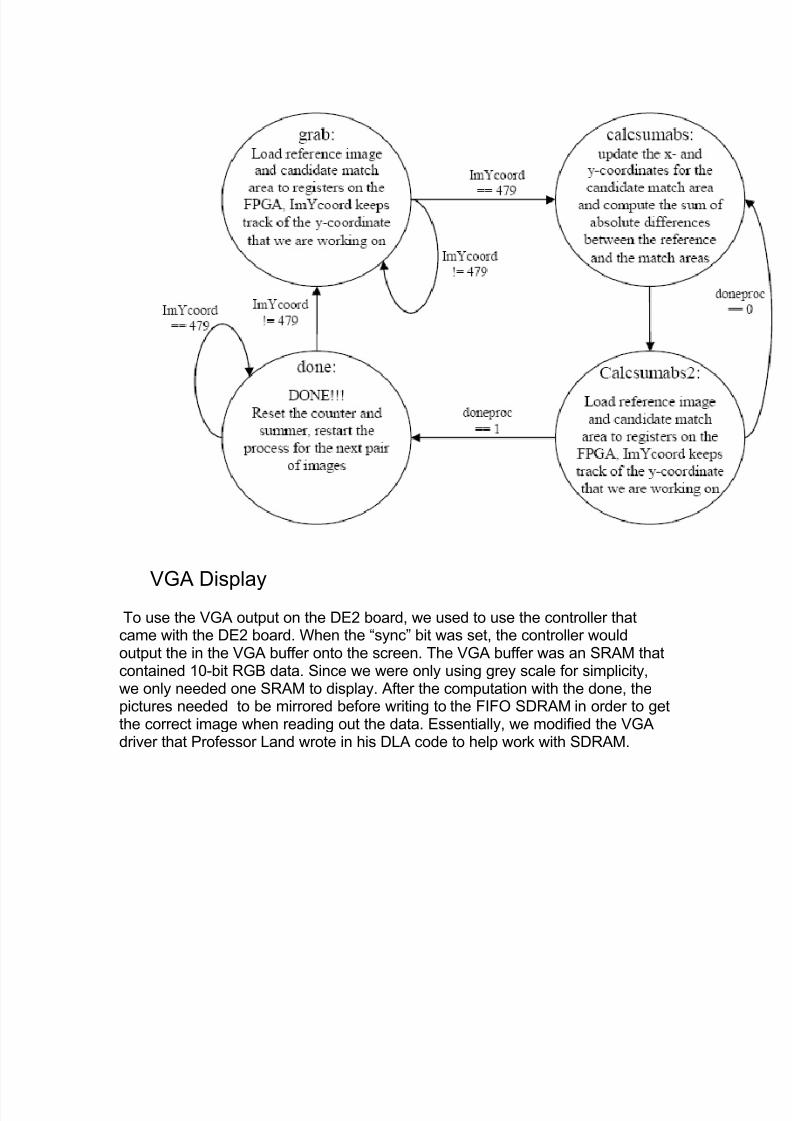
Image motion tracker High-level Description We used the camera module provided by Terasic to capture two frames of images and stored them into SDRAM. To store both images in the SDRAM, we split the SDRAM into two partitions. Before we stored them into the SDRAM, we converted the images into black and white. This was to conserve temporary storage, for both SRAM and registers, and to speed up the compiling and synthesizing time. Also, because the camera was natively only one CCD, the conversion did not lose more content. Since we expected that the number of logic elements required to compute all partitions was too large for our FPGA, we decided to select the search area and reference box to be in the middle of the screen and only worked in this search area to demonstrate that our design was fully functional. It could be scaled-up to compute the full image if we have more resources. Instead of drawing a straight line, we outlined the entire search area and shaded the box with the minimum sum of absolute differences within the search area to see the output more clearly. The data for the outlines were not written back to the SDRAM. Instead, we just added the outline to the image when writing to the VGA buffer in SRAM. When we completed the design, we expected to see a black and white image with two outlines in the middle of the screen, and the smaller box would move around to track movement. Please refer to the Results section for more information. Figure 1 below is a schematic for the algorithm, and Figure 2 is a high-level block diagram for the design.

Welcome message from author
This document is posted to help you gain knowledge. Please leave a comment to let me know what you think about it! Share it to your friends and learn new things together.
Transcript
8/7/2019 Image Motion Tracker
http://slidepdf.com/reader/full/image-motion-tracker 1/8
Image motion tracker
High-level Description
We used the camera module provided by Terasic to capture two frames of images and stored them into SDRAM. To store both images in the SDRAM, wesplit the SDRAM into two partitions. Before we stored them into the SDRAM, weconverted the images into black and white. This was to conserve temporarystorage, for both SRAM and registers, and to speed up the compiling andsynthesizing time. Also, because the camera was natively only one CCD, theconversion did not lose more content. Since we expected that the number of logic elements required to compute all partitions was too large for our FPGA, wedecided to select the search area and reference box to be in the middle of thescreen and only worked in this search area to demonstrate that our design wasfully functional. It could be scaled-up to compute the full image if we have more
resources. Instead of drawing a straight line, we outlined the entire search areaand shaded the box with the minimum sum of absolute differences within thesearch area to see the output more clearly. The data for the outlines were notwritten back to the SDRAM. Instead, we just added the outline to the image whenwriting to the VGA buffer in SRAM. When we completed the design, we expectedto see a black and white image with two outlines in the middle of the screen, andthe smaller box would move around to track movement. Please refer to theResults section for more information. Figure 1 below is a schematic for thealgorithm, and Figure 2 is a high-level block diagram for the design.

8/7/2019 Image Motion Tracker
http://slidepdf.com/reader/full/image-motion-tracker 2/8
Figure 1: The implemented algorithm
Figure 1: A high-level block diagram
8/7/2019 Image Motion Tracker
http://slidepdf.com/reader/full/image-motion-tracker 3/8
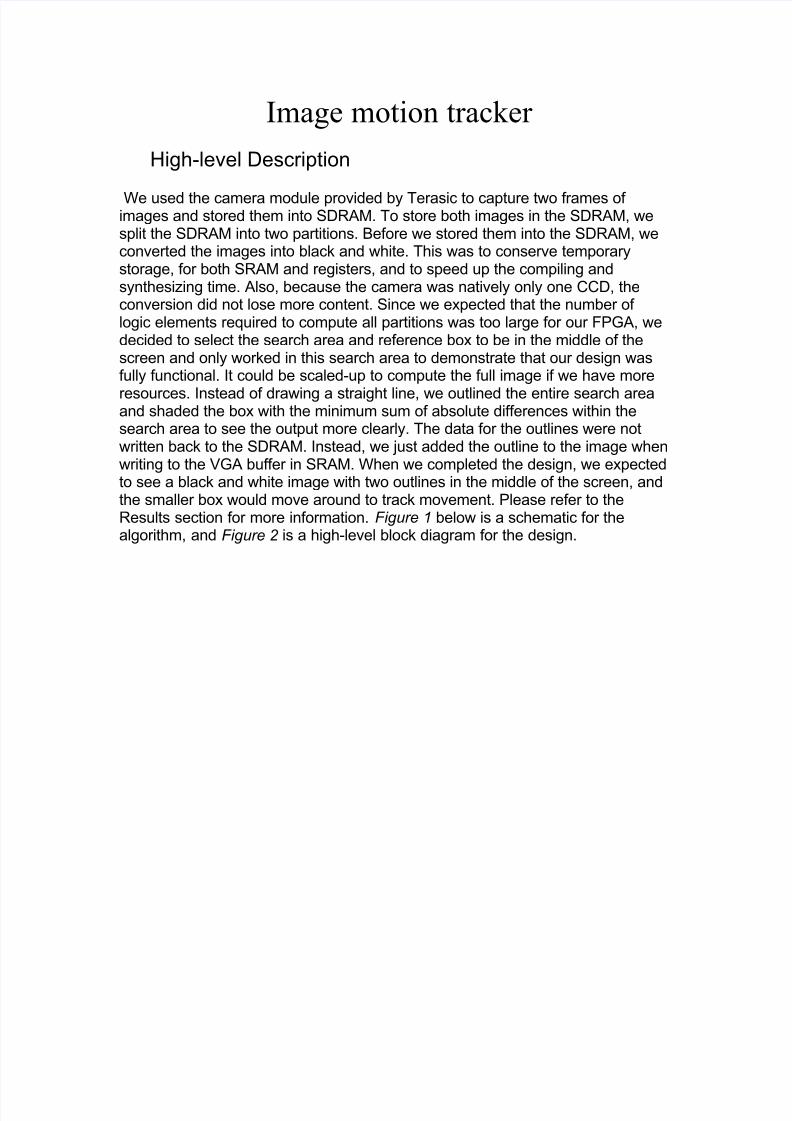
Camera Module
The camera module we used came with a driver that was set up properly to
capture images using a CMOS sensor. The data was processed, stored inSDRAM and sent to the VGA buffer, an SRAM, to display the image onscreen. The driver helped us capture the images easily. The following is apicture of the setup:
Figure 2: An Altera DE2 board with camera module
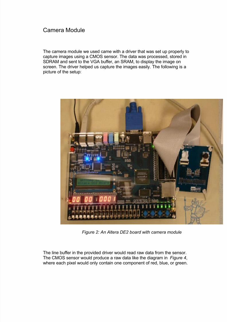
The line buffer in the provided driver would read raw data from the sensor.The CMOS sensor would produce a raw data like the diagram in Figure 4,where each pixel would only contain one component of red, blue, or green.
8/7/2019 Image Motion Tracker
http://slidepdf.com/reader/full/image-motion-tracker 4/8
Since the intensity of green should be twice the blue and red, there are twiceas many pixels of green than blue or red. This is commonly referred to asthe Bayer representation. However, the VGA display needs all threecomponents in one pixel to display properly, so the pixel stored in theSDRAM would be a combination of all three components. Depending on
position of the pixel, the combination of colors would be different. Todetermine the component contents, we would first need to scan in two linesfrom the camera keep track of which four pixels to look at, and the extractthe data and put them into the SDRAM
Figure 4: A schematic for Bayer filter
Memory Setup
We used both SDRAM and SRAM for this system. A FIFO SDRAM wasused to store the data from the camera, and the SRAM was used for VGA
buffer before the image was sent to the VGA display. The SDRAM controller took in a starting address, an ending address, a clock and the length of thedata stream. The controller would then fetch data from or write data to thespecified address on each clock cycle. Since we wanted to store two imagesinto the SDRAM, we needed to partition the RAM into two sections. The sizeof the picture is 640x512, and the starting address of image 1 was set to 0,so the starting address of image 2 was set to 22’h100000 (a lot bigger than

8/7/2019 Image Motion Tracker
http://slidepdf.com/reader/full/image-motion-tracker 5/8
needed) to avoid overwriting the first image. The length of the data streamwas 256.
The SRAM was used to buffer output image for the VGA display. SRAM could beaccessed by specifying the address and the data, without accessing data in
order, which is much easier to access than the SDRAM. After we computed theminimum sum of absolute differences we needed to modify the image byoverlaying the outlines on the original image. We could do this by setting the new16-bit data to the SRAM when we went through each pixel and updated thebuffer at the corresponding address during synchronization. A special featurewas introduced here. We were able to draw the boxes in color though our imagewas in black and white. This was achieved by concatenating the 10-bit black andwhite information with 6-bits of color information with only one of the 6 bits beinghigh. Therefore, the colors would become more noticeable when the neighboringpixels were darker, and less noticeable when the neighboring pixels werebrighter. Essentially, if the search area was black, all three colors would show,
but if the search area was white, no color would show
Computation
After the data was stored in the SDRAM, and the reference area and searcharea were defined, we would extract the data from all the pixels within both areasand put them into 10-bit registers on the FPGA. Then we compute the sum of absolute difference between the reference box and the candidate match area.With our definition, it would take 16x16 = 256 cycles to complete the entirecomputation since our search area was 24x24 and the reference area was 8x8.To compute the absolute difference between two pixels in hardware, we first
compared the values of the data, and then we subtracted the smaller one fromthe larger one. After we compute the first iteration, we kept sum and a temporaryregister, and every iteration, we compared the sum with the temporary register tokeep track of which match area in the search area has the smallest sum. Whenthe entire search area had been gone through, a flag, doneproc, was assertedand the state became "done." The state machine was used to help control thesequence of events happening. We only compared the two most significant bitsof the data because the noise floor was quite high and the information after thethird bit was not helpful for comparison between the two data but made thenumber of logic elements increase by a lot. In this case, if we performed aGaussian filtering, we could increase the signal-to-noise ratio, and we could
detect motion in images that have less intensity contrast. However, due to timeconstraint, we were not able to include that in our project.
8/7/2019 Image Motion Tracker
http://slidepdf.com/reader/full/image-motion-tracker 6/8
VGA Display To use the VGA output on the DE2 board, we used to use the controller thatcame with the DE2 board. When the “sync” bit was set, the controller wouldoutput the in the VGA buffer onto the screen. The VGA buffer was an SRAM thatcontained 10-bit RGB data. Since we were only using grey scale for simplicity,we only needed one SRAM to display. After the computation with the done, thepictures needed to be mirrored before writing to the FIFO SDRAM in order to getthe correct image when reading out the data. Essentially, we modified the VGAdriver that Professor Land wrote in his DLA code to help work with SDRAM.
8/7/2019 Image Motion Tracker
http://slidepdf.com/reader/full/image-motion-tracker 7/8
Result:
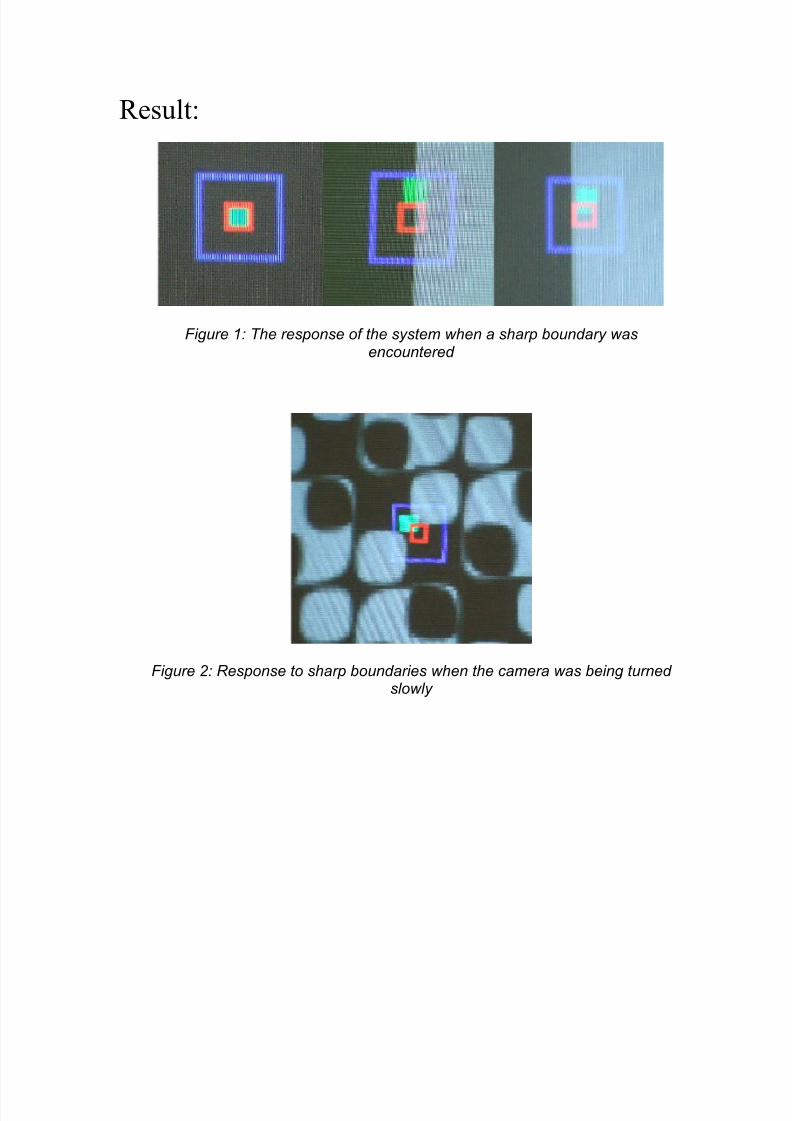
Figure 1: The response of the system when a sharp boundary wasencountered
Figure 2: Response to sharp boundaries when the camera was being turned slowly
8/7/2019 Image Motion Tracker
http://slidepdf.com/reader/full/image-motion-tracker 8/8
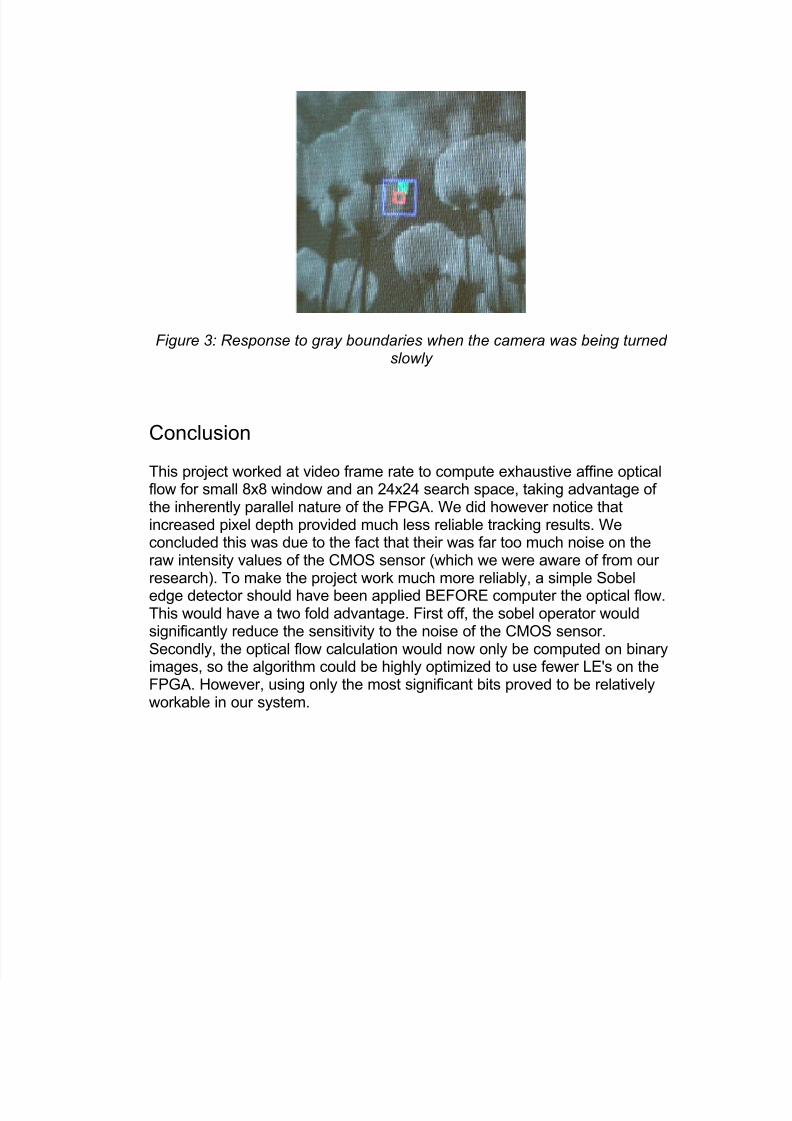
Figure 3: Response to gray boundaries when the camera was being turned slowly
Conclusion
This project worked at video frame rate to compute exhaustive affine opticalflow for small 8x8 window and an 24x24 search space, taking advantage of the inherently parallel nature of the FPGA. We did however notice thatincreased pixel depth provided much less reliable tracking results. Weconcluded this was due to the fact that their was far too much noise on theraw intensity values of the CMOS sensor (which we were aware of from our research). To make the project work much more reliably, a simple Sobeledge detector should have been applied BEFORE computer the optical flow.This would have a two fold advantage. First off, the sobel operator wouldsignificantly reduce the sensitivity to the noise of the CMOS sensor.Secondly, the optical flow calculation would now only be computed on binaryimages, so the algorithm could be highly optimized to use fewer LE's on theFPGA. However, using only the most significant bits proved to be relativelyworkable in our system.
Related Documents