ELECTRONIC CIRCUIT ANALYSIS (ECA) LABORATORY MANUAL (R16-22046) II / IV B.Tech (ECE) : II – SEMESTER Name of the Student : Regd. No & Section : Academic Year : DEPARTMENT OF ELECTRONICS AND COMMUNICATION ENGINEERING SIR C. R. REDDY COLLEGE OF ENGINEERING ELURU – 534 007

Welcome message from author
This document is posted to help you gain knowledge. Please leave a comment to let me know what you think about it! Share it to your friends and learn new things together.
Transcript

ELECTRONIC CIRCUIT ANALYSIS (ECA)
LABORATORY MANUAL (R16-22046)
II / IV B.Tech (ECE) : II – SEMESTER
Name of the Student :
Regd. No & Section :
Academic Year :
DEPARTMENT OF ELECTRONICS AND COMMUNICATION ENGINEERING
SIR C. R. REDDY COLLEGE OF ENGINEERING
ELURU – 534 007
Dept. of ECE., Sir C.R. Reddy College of Engg., Eluru. II/IV (B.Tech) ECE, II-SEM :: ECA-Lab
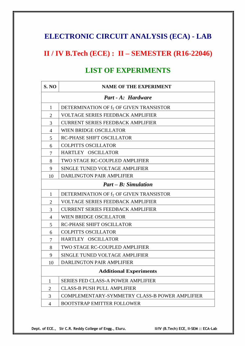
ELECTRONIC CIRCUIT ANALYSIS (ECA) - LAB
II / IV B.Tech (ECE) : II – SEMESTER (R16-22046)
LIST OF EXPERIMENTS
S. NO NAME OF THE EXPERIMENT
Part - A: Hardware
1 DETERMINATION OF fT OF GIVEN TRANSISTOR
2 VOLTAGE SERIES FEEDBACK AMPLIFIER
3 CURRENT SERIES FEEDBACK AMPLIFIER
4 WIEN BRIDGE OSCILLATOR
5 RC-PHASE SHIFT OSCILLATOR
6 COLPITTS OSCILLATOR
7 HARTLEY OSCILLATOR
8 TWO STAGE RC-COUPLED AMPLIFIER
9 SINGLE TUNED VOLTAGE AMPLIFIER
10 DARLINGTON PAIR AMPLIFIER
Part – B: Simulation
1 DETERMINATION OF fT OF GIVEN TRANSISTOR
2 VOLTAGE SERIES FEEDBACK AMPLIFIER
3 CURRENT SERIES FEEDBACK AMPLIFIER
4 WIEN BRIDGE OSCILLATOR
5 RC-PHASE SHIFT OSCILLATOR
6 COLPITTS OSCILLATOR
7 HARTLEY OSCILLATOR
8 TWO STAGE RC-COUPLED AMPLIFIER
9 SINGLE TUNED VOLTAGE AMPLIFIER
10 DARLINGTON PAIR AMPLIFIER
Additional Experiments
1 SERIES FED CLASS-A POWER AMPLIFIER
2 CLASS-B PUSH PULL AMPLIFIER
3 COMPLEMENTARY-SYMMETRY CLASS-B POWER AMPLIFIER
4 BOOTSTRAP EMITTER FOLLOWER
Dept. of ECE., Sir C.R. Reddy College of Engg., Eluru. II/IV (B.Tech) ECE, II-SEM :: ECA-Lab
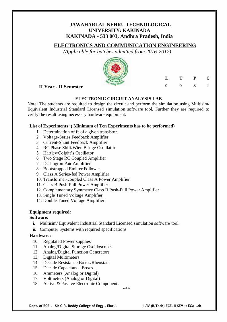
JAWAHARLAL NEHRU TECHNOLOGICAL UNIVERSITY: KAKINADA
KAKINADA - 533 003, Andhra Pradesh, India
ELECTRONICS AND COMMUNICATION ENGINEERING (Applicable for batches admitted from 2016-2017)
II Year - II Semester
ELECTRONIC CIRCUIT ANALYSIS LAB Note: The students are required to design the circuit and perform the simulation using Multisim/ Equivalent Industrial Standard Licensed simulation software tool. Further they are required to verify the result using necessary hardware equipment. List of Experiments :( Minimum of Ten Experiments has to be performed)
1. Determination of fT of a given transistor. 2. Voltage-Series Feedback Amplifier 3. Current-Shunt Feedback Amplifier 4. RC Phase Shift/Wien Bridge Oscillator 5. Hartley/Colpitt’s Oscillator 6. Two Stage RC Coupled Amplifier 7. Darlington Pair Amplifier 8. Bootstrapped Emitter Follower 9. Class A Series-fed Power Amplifier 10. Transformer-coupled Class A Power Amplifier 11. Class B Push-Pull Power Amplifier 12. Complementary Symmetry Class B Push-Pull Power Amplifier 13. Single Tuned Voltage Amplifier 14. Double Tuned Voltage Amplifier
Equipment required: Software:
i. Multisim/ Equivalent Industrial Standard Licensed simulation software tool. ii. Computer Systems with required specifications
Hardware: 10. Regulated Power supplies 11. Analog/Digital Storage Oscilloscopes 12. Analog/Digital Function Generators 13. Digital Multimeters 14. Decade Résistance Boxes/Rheostats 15. Decade Capacitance Boxes 16. Ammeters (Analog or Digital) 17. Voltmeters (Analog or Digital) 18. Active & Passive Electronic Components
***
L T P C
0 0 3 2

Dept. of ECE., Sir C.R. Reddy College of Engg., Eluru. II/IV (B.Tech) ECE, II-SEM :: ECA-Lab

Dept. of ECE., Sir C.R. Reddy College of Engg., Eluru. II/IV (B.Tech) ECE, II-SEM :: ECA-Lab
1a. DETERMINATION OF fT OF GIVEN TRANSISTOR Exp. No: Date:
AIM: To determine the fT of a given transistor.
APPARATUS REQUIRED:
S. No Name Range / Value Quantity
1 Regulated D.C Power supply 0–30 Volts 1 2 Transistor BC107 1 3 Resistors 1K 2 4 Resistors 100k,10K, 4.7K. Each 1 5 Capacitors 10f 3 6 Potentio Meter -- 1 7 Signal Generator ( 0 – 1MHz) 1 8 Dual Trace CRO 20MHz 1 9 Bread Board and connecting wires -- 1 Set
CIRCUIT DIAGRAM:
Dept. of ECE., Sir C.R. Reddy College of Engg., Eluru. II/IV (B.Tech) ECE, II-SEM :: ECA-Lab
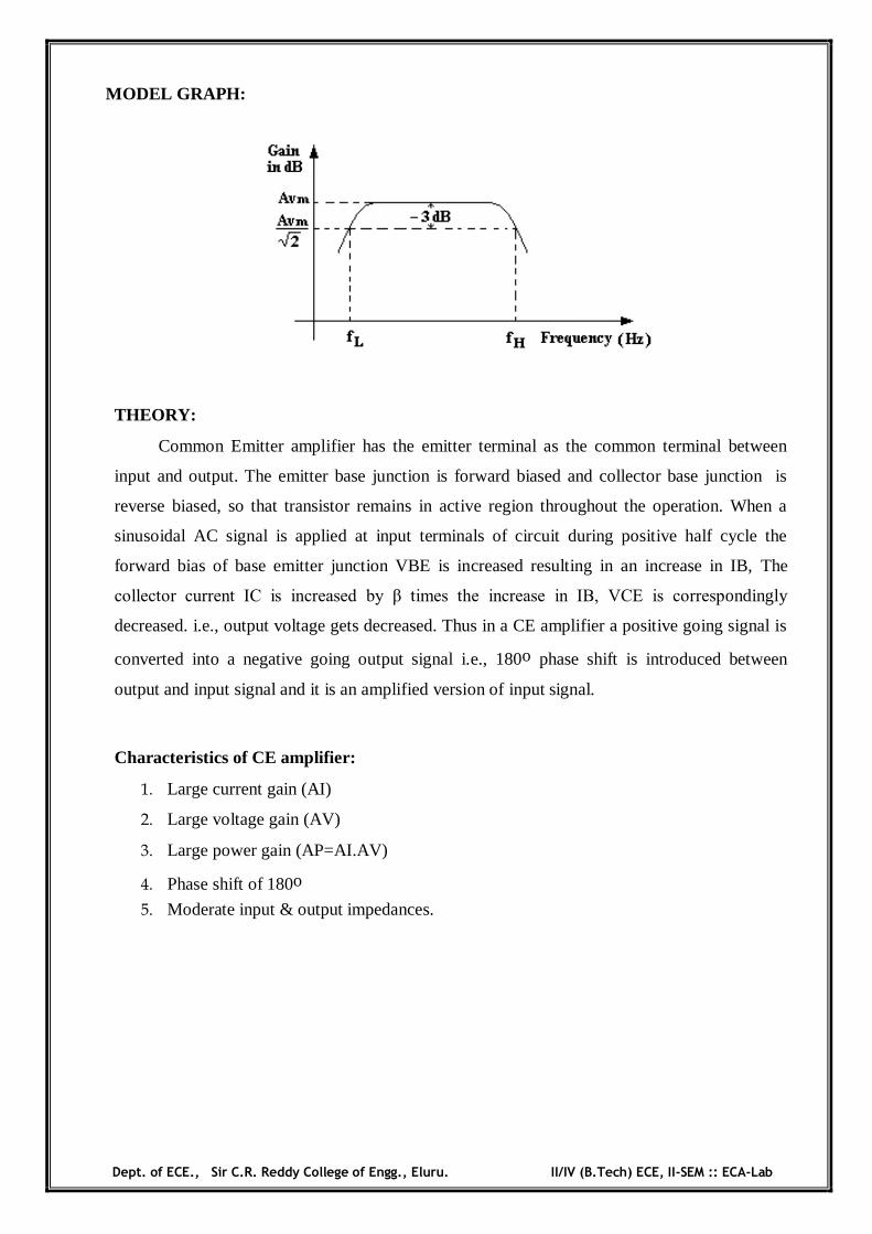
MODEL GRAPH:
THEORY:
Common Emitter amplifier has the emitter terminal as the common terminal between
input and output. The emitter base junction is forward biased and collector base junction is
reverse biased, so that transistor remains in active region throughout the operation. When a
sinusoidal AC signal is applied at input terminals of circuit during positive half cycle the
forward bias of base emitter junction VBE is increased resulting in an increase in IB, The
collector current IC is increased by β times the increase in IB, VCE is correspondingly
decreased. i.e., output voltage gets decreased. Thus in a CE amplifier a positive going signal is
converted into a negative going output signal i.e., 180o phase shift is introduced between
output and input signal and it is an amplified version of input signal.
Characteristics of CE amplifier:
1. Large current gain (AI)
2. Large voltage gain (AV)
3. Large power gain (AP=AI.AV)
4. Phase shift of 180o
5. Moderate input & output impedances.
Dept. of ECE., Sir C.R. Reddy College of Engg., Eluru. II/IV (B.Tech) ECE, II-SEM :: ECA-Lab
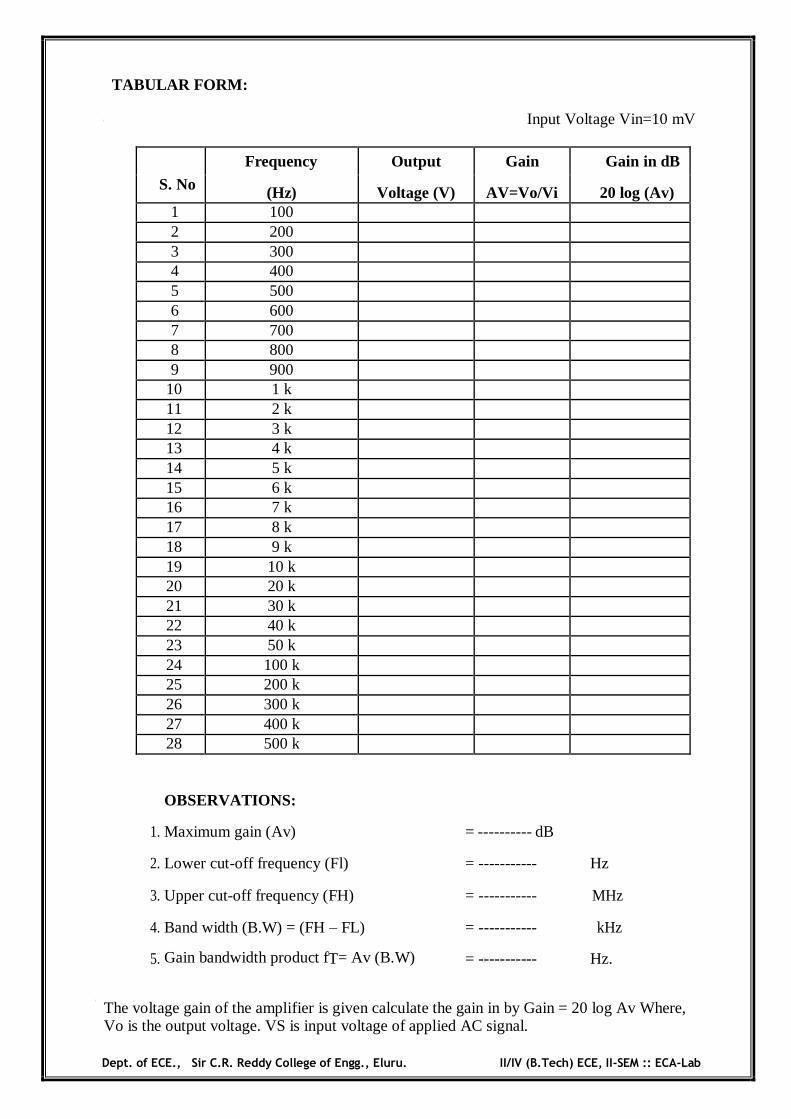
TABULAR FORM:
Input Voltage Vin=10 mV
S. No
Frequency Output Gain Gain in dB
(Hz) Voltage (V) AV=Vo/Vi 20 log (Av) 1 100 2 200 3 300 4 400 5 500 6 600 7 700 8 800 9 900
10 1 k 11 2 k 12 3 k 13 4 k 14 5 k 15 6 k 16 7 k 17 8 k 18 9 k 19 10 k 20 20 k 21 30 k 22 40 k 23 50 k 24 100 k 25 200 k 26 300 k 27 400 k 28 500 k
OBSERVATIONS:
1. Maximum gain (Av) = ---------- dB
2. Lower cut-off frequency (Fl) = ----------- Hz
3. Upper cut-off frequency (FH) = ----------- MHz
4. Band width (B.W) = (FH – FL) = ----------- kHz
5. Gain bandwidth product fT= Av (B.W) = ----------- Hz.
The voltage gain of the amplifier is given calculate the gain in by Gain = 20 log Av Where, Vo is the output voltage. VS is input voltage of applied AC signal.

Dept. of ECE., Sir C.R. Reddy College of Engg., Eluru. II/IV (B.Tech) ECE, II-SEM :: ECA-Lab
PROCEDURE:
1. Connect the circuit as shown in the circuit diagram.
2. Connect the signal generator output to input terminals of the circuit and CH-I of dual
trace CRO.
3. Connect the output terminal of the circuit CH-II of the dual trace CRO.
4. Set the power supply voltage to 9V and connect to the circuit.
5. Set the signal generator output sine wave of 100 Hz at 10 mV constant.
6. Vary the function generator frequency from 100 Hz to 500 kHz (as per in the given
tabular form) and note the corresponding output voltage.
7. Calculation the gain AV =Vo/Vi .
8. PSet the graph frequency verses gain (dB) on a semi log sheet.
RESULT:
VIVA QUESTIONS:
1. What are the advantages and disadvantages of single-stage amplifiers?
2. Why gain falls at HF and LF?
3. Why the gain remains constant at MF?
4. Explain the function of emitter bypass capacitor, Ce?
5. How the band width will effect as more number of stages are cascaded?
6. Define frequency response?
7. What is the phase difference between input and output waveforms of a CE amplifier?
8. What is Early effect?
9. Define fT and give the expression for it?
10. What is meant by Bandwidth of an amplifier?
***
Dept. of ECE., Sir C.R. Reddy College of Engg., Eluru. II/IV (B.Tech) ECE, II-SEM :: ECA-Lab
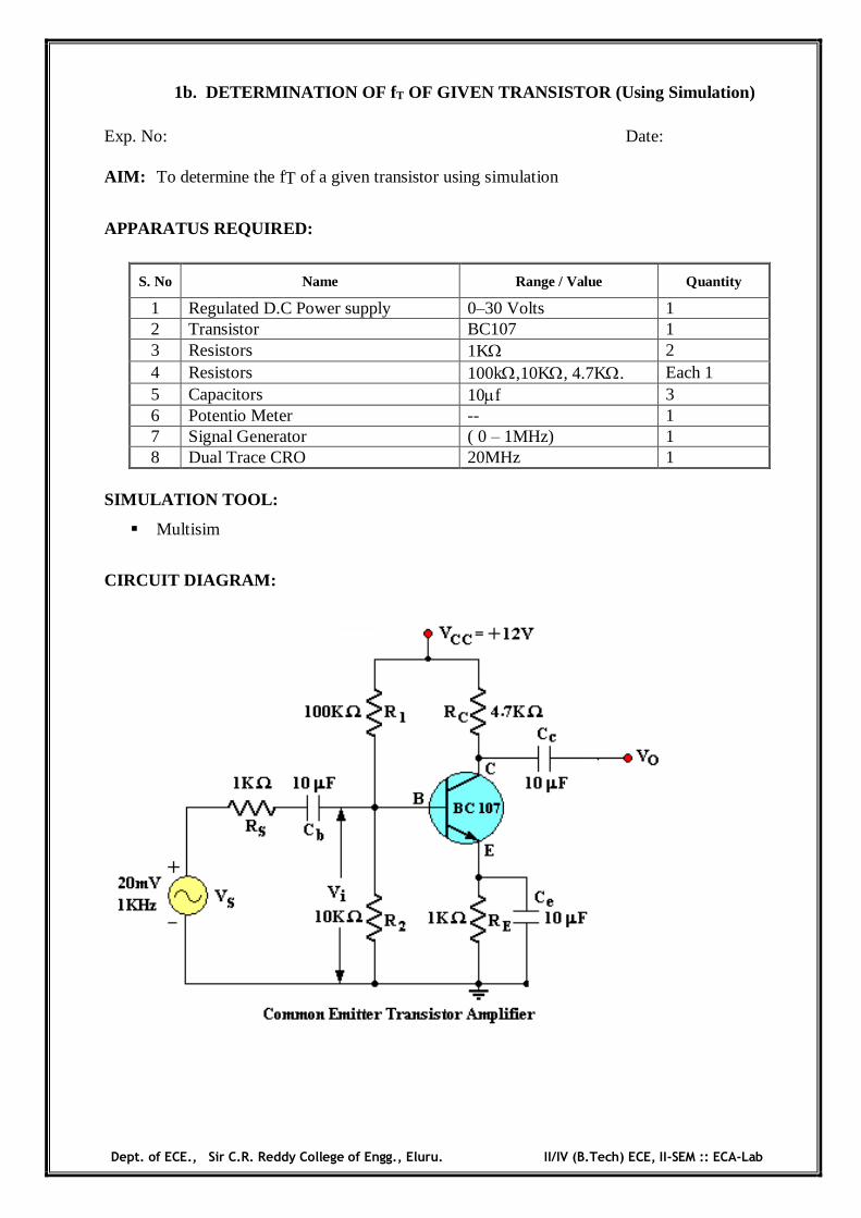
1b. DETERMINATION OF fT OF GIVEN TRANSISTOR (Using Simulation) Exp. No: Date: AIM: To determine the fT of a given transistor using simulation
APPARATUS REQUIRED:
S. No Name Range / Value Quantity
1 Regulated D.C Power supply 0–30 Volts 1 2 Transistor BC107 1 3 Resistors 1K 2 4 Resistors 100k,10K, 4.7K. Each 1 5 Capacitors 10f 3 6 Potentio Meter -- 1 7 Signal Generator ( 0 – 1MHz) 1 8 Dual Trace CRO 20MHz 1
SIMULATION TOOL:
Multisim
CIRCUIT DIAGRAM:

Dept. of ECE., Sir C.R. Reddy College of Engg., Eluru. II/IV (B.Tech) ECE, II-SEM :: ECA-Lab
TABULAR FORM:
Input Voltage Vin=10 mV
S. No
Input Frequency
Output Gain Gain in dB
(Hz) Voltage (V) AV=Vo/Vi 20 log Av 1 100 2 300 3 500 4 700 5 900 6 1 k 7 3 k 8 5 k 9 6 k 10 7 k 11 9 k 12 10 k 13 30 k 14 50 k 15 100 k 16 300 k 17 500 k 18 700 k 19 1M
OBSERVATIONS:
Maximum gain (Av) = ----------- dB
Lower cut-off frequency (Fl) = ----------- Hz
Upper cut-off frequency (FH) = ----------- MHz
Band width (B.W) = (FH – FL) = ----------- kHz
Gain bandwidth product fT= Av (B.W) = ----------- Hz.
RESULT:
Dept. of ECE., Sir C.R. Reddy College of Engg., Eluru. II/IV (B.Tech) ECE, II-SEM :: ECA-Lab
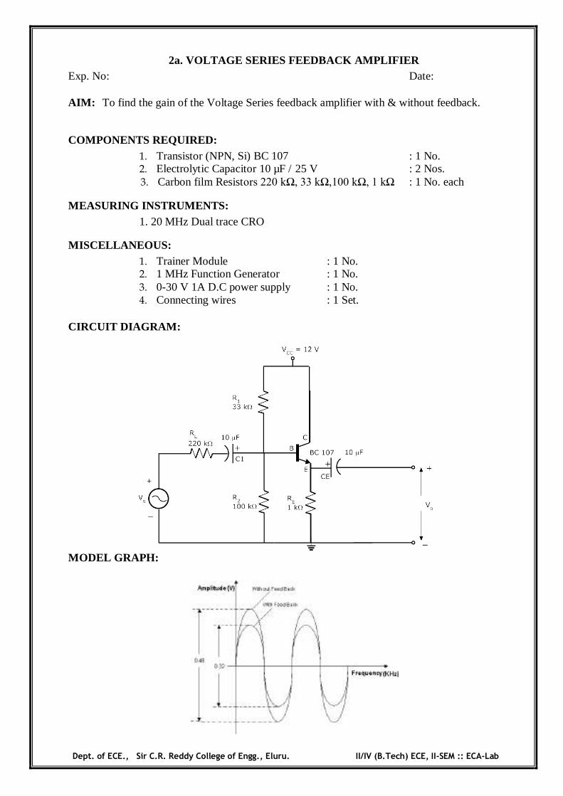
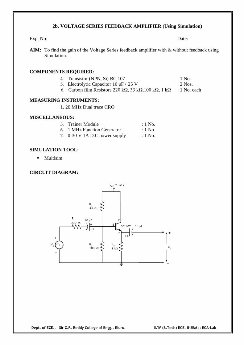
2a. VOLTAGE SERIES FEEDBACK AMPLIFIER Exp. No: Date: AIM: To find the gain of the Voltage Series feedback amplifier with & without feedback.
COMPONENTS REQUIRED: 1. Transistor (NPN, Si) BC 107 : 1 No. 2. Electrolytic Capacitor 10 µF / 25 V : 2 Nos. 3. Carbon film Resistors 220 kΩ, 33 kΩ,100 kΩ, 1 kΩ : 1 No. each
MEASURING INSTRUMENTS: 1. 20 MHz Dual trace CRO
MISCELLANEOUS: 1. Trainer Module : 1 No. 2. 1 MHz Function Generator : 1 No. 3. 0-30 V 1A D.C power supply : 1 No. 4. Connecting wires : 1 Set.
CIRCUIT DIAGRAM:
MODEL GRAPH:
Dept. of ECE., Sir C.R. Reddy College of Engg., Eluru. II/IV (B.Tech) ECE, II-SEM :: ECA-Lab
THEORY:
The other name of voltage series feedback amplifier is shunt derived series fed feedback
amplifier. The fraction of output voltage is applied in series with input voltage through feedback
circuit. Feedback circuit shunt the output but in series with input. So the output impedance is
decreased while input impedance is increased. The input & output impedance of an ideal voltage
series feedback amplifier is infinite & zero respectively. The resistor RE is used to provide
necessary biasing for the amplifier with voltage series feedback gain of the amplifier decreases.
PROCEDURE:
1. Connect the Circuit as per the circuit diagram.
2. Apply a sine wave of 100 mV peak to peak amplitude at 1 kHz from signal generator to
the input of amplifier circuit.
3. Measure the output amplitude VO (p-p) and Calculate the gain of amplifier without
feedback by using A =VO/VS.
4. Calculate the feedback factor β using AF = A / 1+Aβ. Calculate theoretically β value from β = RE / (RE +R).
Dept. of ECE., Sir C.R. Reddy College of Engg., Eluru. II/IV (B.Tech) ECE, II-SEM :: ECA-Lab
TABULAR FORM: Input ac voltage VS = 100 mV p-p Vi = mV
S. No. Input
frequency (Hz)
Output voltage (Volts)
Gain
Gain in dB
1 50
2 100
3 150
4 200
5 500
6 1 k
7 3 k
8 5 k
9 10 k
10 30 k
11 50 k
12 70 k
13 100 k
14 300 k
15 500 k
16 600 k
17 700 k
18 800 k
19 900 k
20 1 M
RESULT:

Dept. of ECE., Sir C.R. Reddy College of Engg., Eluru. II/IV (B.Tech) ECE, II-SEM :: ECA-Lab
VIVA QUESTIONS:
1. Define feedback?
2. Define positive feedback?
3. Define negative feedback?
4. Define sensitivity?
5. What is transfer gain?
6. List out the characteristics of feedback amplifier?
7. What is the effect of input resistance due to series mixing?
8. What happens to output resistance due to voltage sampling?
9. Write the expression for input and output resistance of voltage series feedback amplifier?
10. Give the properties of negative feedback?
***
Dept. of ECE., Sir C.R. Reddy College of Engg., Eluru. II/IV (B.Tech) ECE, II-SEM :: ECA-Lab
2b. VOLTAGE SERIES FEEDBACK AMPLIFIER (Using Simulation) Exp. No: Date: AIM: To find the gain of the Voltage Series feedback amplifier with & without feedback using
Simulation.
COMPONENTS REQUIRED: 4. Transistor (NPN, Si) BC 107 : 1 No. 5. Electrolytic Capacitor 10 µF / 25 V : 2 Nos. 6. Carbon film Resistors 220 kΩ, 33 kΩ,100 kΩ, 1 kΩ : 1 No. each
MEASURING INSTRUMENTS: 1. 20 MHz Dual trace CRO
MISCELLANEOUS: 5. Trainer Module : 1 No. 6. 1 MHz Function Generator : 1 No. 7. 0-30 V 1A D.C power supply : 1 No.
SIMULATION TOOL:
Multisim
CIRCUIT DIAGRAM:
Dept. of ECE., Sir C.R. Reddy College of Engg., Eluru. II/IV (B.Tech) ECE, II-SEM :: ECA-Lab
TABULAR FORM: Input ac voltage VS = 100 mV p-p Vi = mV
S. No. Input frequency
(Hz) Output voltage(V)
Gain
Gain in dB
1 50
2 100
3 150
4 200
5 500
6 1 k
7 3 k
8 5 k
9 10 k
10 30 k
11 40 k
12 50 k
13 60 k
14 70 k
15 80 k
16 90 k
PROCEDURE: 1. Connect the Circuit as per the circuit diagram.
2. Apply a sine wave of 100 mV peak to peak amplitude at 1 kHz from signal generator to
the input of amplifier circuit.
3. Measure the output amplitude VO (p-p) and Calculate the gain of amplifier without
feedback by using A =VO/VS.
4. Calculate the feedback factor β using AF = A / 1+Aβ.
5. Calculate theoretically β value from β = RE / (RE +R). RESULT:

Dept. of ECE., Sir C.R. Reddy College of Engg., Eluru. II/IV (B.Tech) ECE, II-SEM :: ECA-Lab
3a. CURRENT SERIES FEEDBACK AMPLIFIER Exp. No: Date:
AIM: 1. To study the current shunt feedback amplifier 2. To measure the voltage gain of the amplifier at 1 KHz. 3. To obtain the frequency response characteristic and the band width of the
amplifier.
APPARATUS:
CIRCUIT DIAGRAM:
WITHOUT FEEDBACK:
S. No Name Range / Value Quantity
1 Regulated Power Supply (0– 30V) 1
2 Transistor BC 107 1
3 Resistors 100K,4.7K,10K Each 1 4 Resistors 1K - 2 1 5 Capacitors 10F – 3 1 6 Function generator -- 1 7 CRO -- 1
Dept. of ECE., Sir C.R. Reddy College of Engg., Eluru. II/IV (B.Tech) ECE, II-SEM :: ECA-Lab
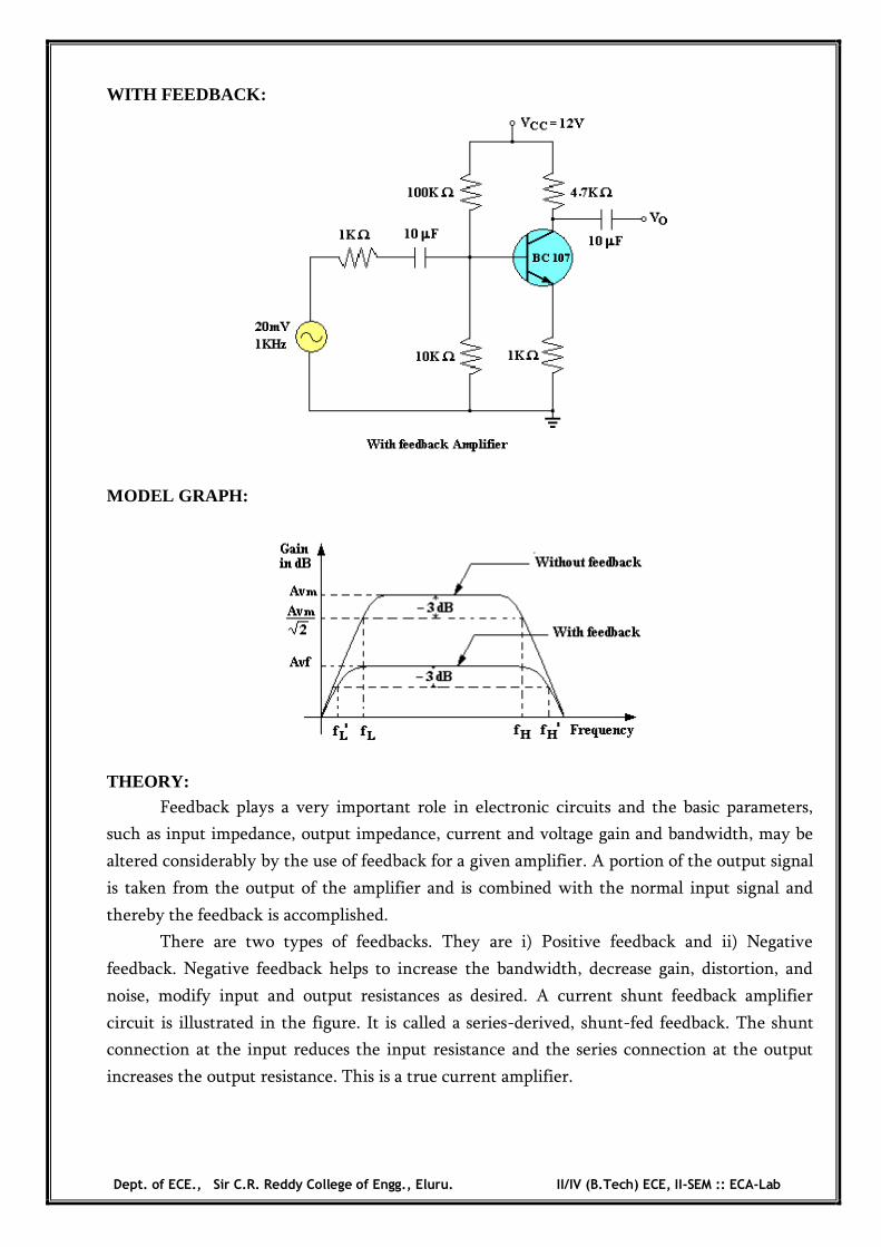
WITH FEEDBACK:
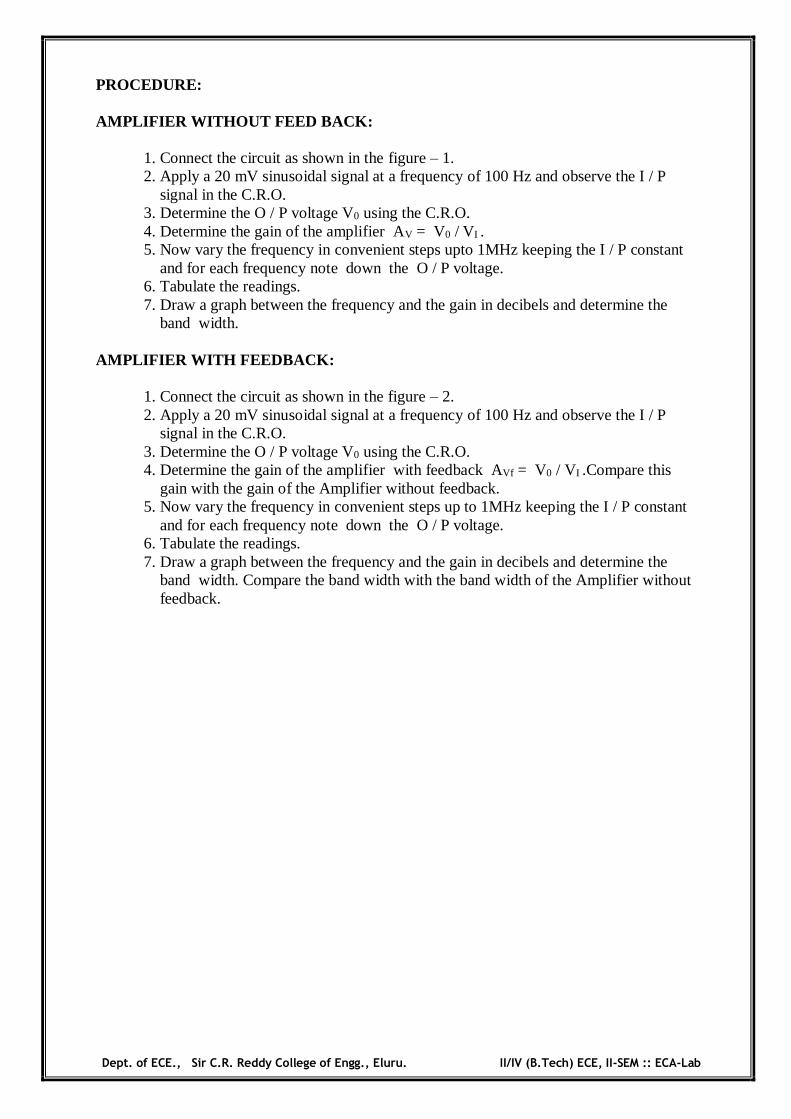
MODEL GRAPH:
THEORY:
Feedback plays a very important role in electronic circuits and the basic parameters,
such as input impedance, output impedance, current and voltage gain and bandwidth, may be
altered considerably by the use of feedback for a given amplifier. A portion of the output signal
is taken from the output of the amplifier and is combined with the normal input signal and
thereby the feedback is accomplished.
There are two types of feedbacks. They are i) Positive feedback and ii) Negative
feedback. Negative feedback helps to increase the bandwidth, decrease gain, distortion, and
noise, modify input and output resistances as desired. A current shunt feedback amplifier
circuit is illustrated in the figure. It is called a series-derived, shunt-fed feedback. The shunt
connection at the input reduces the input resistance and the series connection at the output
increases the output resistance. This is a true current amplifier.
Dept. of ECE., Sir C.R. Reddy College of Engg., Eluru. II/IV (B.Tech) ECE, II-SEM :: ECA-Lab
PROCEDURE: AMPLIFIER WITHOUT FEED BACK:
1. Connect the circuit as shown in the figure – 1. 2. Apply a 20 mV sinusoidal signal at a frequency of 100 Hz and observe the I / P signal in the C.R.O. 3. Determine the O / P voltage V0 using the C.R.O. 4. Determine the gain of the amplifier AV = V0 / VI . 5. Now vary the frequency in convenient steps upto 1MHz keeping the I / P constant and for each frequency note down the O / P voltage. 6. Tabulate the readings. 7. Draw a graph between the frequency and the gain in decibels and determine the band width.
AMPLIFIER WITH FEEDBACK:
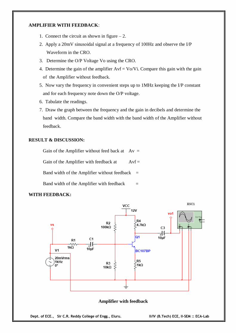
1. Connect the circuit as shown in the figure – 2. 2. Apply a 20 mV sinusoidal signal at a frequency of 100 Hz and observe the I / P signal in the C.R.O. 3. Determine the O / P voltage V0 using the C.R.O. 4. Determine the gain of the amplifier with feedback AVf = V0 / VI .Compare this gain with the gain of the Amplifier without feedback. 5. Now vary the frequency in convenient steps up to 1MHz keeping the I / P constant and for each frequency note down the O / P voltage. 6. Tabulate the readings. 7. Draw a graph between the frequency and the gain in decibels and determine the band width. Compare the band width with the band width of the Amplifier without feedback.
Dept. of ECE., Sir C.R. Reddy College of Engg., Eluru. II/IV (B.Tech) ECE, II-SEM :: ECA-Lab
TABULAR FORM: Vi = 20mV
Frequency (Hz)
Without Feedback With Feedback
V0
(Volts) Gain
AV=V0/Vi Gain in db (20logAV)
O/P V0
(Volts)
Gain AVf
=V0/VI
Gain in db (20logAV)
50
100 300
500
700
1K 3K
5K
7K 10K
30K
50K 70K
100K
300K 500K
700K
1M
RESULT:
Gain of the Amplifier without feedback at 1 kHz is AV = Gain of the Amplifier with feedback at 1 kHz is AVf = Band width of the Amplifier without feedback = Band width of the Amplifier with feedback =
VIVA QUESTIONS:
1. What are the different types of feedback techniques? 2. What is the type of feedback incorporated in oscillators? 3. What are the advantages of negative feedback? 4. Why positive feedback is not used in amplifiers? 5. What is the expression for the desensitivity factor in case of negative feedback? 6. What happens to the band width of an amplifier if we incorporate negative
Feedback? ***
Dept. of ECE., Sir C.R. Reddy College of Engg., Eluru. II/IV (B.Tech) ECE, II-SEM :: ECA-Lab
3b. CURRENT SERIES FEEDBACK AMPLIFIER (Using Simulation) Exp. No: Date: AIM: To Set the frequency response curve of an amplifier with and without feedback. APPARATUS:
S. No Name Range / Value Quantity
1 Regulated Power Supply (0– 30V) 1
2 Transistor BC 107 1 3 Resistors 100K, 10K Each 1 4 Resistors 1K 2 5 Capacitors 10F 3 6 Function generator -- 1 7 CRO -- 1
SIMULATION TOOL:
Multisim
THEORY: When any increase in the output signal results into the input in such a way as to cause the
decrease in the output signal, the amplifier is said to have negative feedback. The advantages of
providing negative feedback are that the transfer gain of the amplifier with feedback can be stabilized
against variations in the hybrid parameters the transistor or the parameters of the other active devices
used in the circuit. The most advantage of the negative feedback is that by proper use of this, there is
significant improvement in the frequency response and in the linearity of the operation of the amplifier.
The main disadvantage of the negative feedback is that the voltage gain is decreased. In
Current-Series feedback, the input impedance of the amplifier is increased and the output impedance is
also increased. Noise and distortions are reduced considerably.
PROCEDURE: AMPLIFIER WITHOUT FEEDBACK:
1. Connect the circuit as shown in figure – 1. 2. Apply a 20mV sinusoidal signal at a frequency of 100Hz and observe the I/P waveform
in the CRO. 3. Determine the O/P Voltage Vo using the CRO. 4. Determine the gain of the amplifier Av = Vo/Vi. 5. Now vary the frequency in convenient steps up to 1MHz keeping the I/P constant and for
each frequency note down the O/P voltage. 6. Tabulate the readings. 7. Draw the graph between the frequency and the gain in decibels and determine the band
width.

Dept. of ECE., Sir C.R. Reddy College of Engg., Eluru. II/IV (B.Tech) ECE, II-SEM :: ECA-Lab
CIRCUIT DIAGRAM: WITHOUT FEEDBACK:
Amplifier without feedback Input and Output waveforms:
Dept. of ECE., Sir C.R. Reddy College of Engg., Eluru. II/IV (B.Tech) ECE, II-SEM :: ECA-Lab
AMPLIFIER WITH FEEDBACK: 1. Connect the circuit as shown in figure – 2.
2. Apply a 20mV sinusoidal signal at a frequency of 100Hz and observe the I/P
Waveform in the CRO.
3. Determine the O/P Voltage Vo using the CRO.
4. Determine the gain of the amplifier Avf = Vo/Vi. Compare this gain with the gain
of the Amplifier without feedback.
5. Now vary the frequency in convenient steps up to 1MHz keeping the I/P constant
and for each frequency note down the O/P voltage.
6. Tabulate the readings.
7. Draw the graph between the frequency and the gain in decibels and determine the
band width. Compare the band width with the band width of the Amplifier without
feedback.
RESULT & DISCUSSION:
Gain of the Amplifier without feed back at Av =
Gain of the Amplifier with feedback at Avf =
Band width of the Amplifier without feedback =
Band width of the Amplifier with feedback =
WITH FEEDBACK:
Amplifier with feedback
Dept. of ECE., Sir C.R. Reddy College of Engg., Eluru. II/IV (B.Tech) ECE, II-SEM :: ECA-Lab
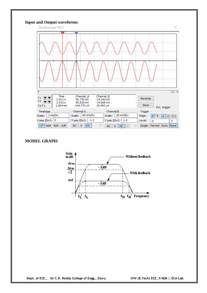
Input and Output waveforms:
MODEL GRAPH:

Dept. of ECE., Sir C.R. Reddy College of Engg., Eluru. II/IV (B.Tech) ECE, II-SEM :: ECA-Lab
Frequency Response:
Frequency response without feed back
Frequency response with feed back
Comparison between Without and With feedbacks in terms of gain and bandwidth
Dept. of ECE., Sir C.R. Reddy College of Engg., Eluru. II/IV (B.Tech) ECE, II-SEM :: ECA-Lab
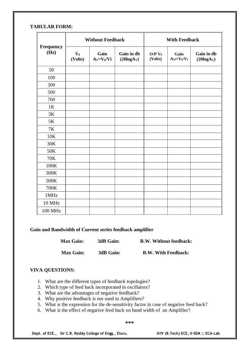
TABULAR FORM:
Gain and Bandwidth of Current series feedback amplifier Max Gain: 3dB Gain: B.W. Without feedback: Max Gain: 3dB Gain: B.W. With Feedback:
VIVA QUESTIONS:
1. What are the different types of feedback topologies? 2. Which type of feed back incorporated in oscillators? 3. What are the advantages of negative feedback? 4. Why positive feedback is not used in Amplifiers? 5. What is the expression for the de-sensitivity factor in case of negative feed back? 6. What is the effect of negative feed back on band width of an Amplifier?
***
Frequency (Hz)
Without Feedback With Feedback
V0
(Volts) Gain
AV=V0/Vi Gain in db (20logAV)
O/P V0
(Volts) Gain
AVf=V0/VI Gain in db (20logAV)
50
100
300
500
700
1K
3K
5K
7K
10K
30K
50K
70K
100K
300K
500K
700K
1MHz
10 MHz
100 MHz

Dept. of ECE., Sir C.R. Reddy College of Engg., Eluru. II/IV (B.Tech) ECE, II-SEM :: ECA-Lab
4a. WIEN BRIDGE OSCILLATOR
Exp. No: Date: AIM: To determine the frequency of oscillations of a given Wien Bridge oscillator and compare
it with the theoretical value. APPARATUS: CIRCUIT DIAGRAM:
OUT PUT WAVE FORM:
S. No Name Range / Value Quantity
1 Regulated Power Supply [- 15V – 0V – +15V] 1 2 OPAMP A741C 1 3 Potentiometer 47 K 1 4 Resistors 3.3 K , 220 Each 2 5 Resistors 12 K 1 6 Capacitors 0.047 F, 0.33 F Each 2 7 CRO. -- 1

Dept. of ECE., Sir C.R. Reddy College of Engg., Eluru. II/IV (B.Tech) ECE, II-SEM :: ECA-Lab
TABULAR FORM:
S.No Capacitance
C ( F ) Resistance
R (Ω)
Theoretical Frequency = 1/(2 RC)
(Hz)
Practical Frequency=1/T
(Hz)
1 0.047 3.3K
2 0.33 220
THEORY The circuit diagram of Wien bridge oscillator is given in figure .The circuit consists of a
two stage RC coupled amplifier which provides a phase shift of 360 0 or 00. A balanced bridged is used as the feedback network which has no need to provide any additional phase shift. The feedback network consists of lead-lag network (R1-C1 and R2-C2) and a voltage divider. The lead–lag network provides positive feedback to the input of first stage and the voltage divider provides a negative feedback to the emitter of Q1. If the bridge is balanced,
where Xc1 and Xc2 are the reactance of the capacitors.
By simplifying and equating the real and imaginary parts on both sides, we get the frequency of oscillation as, the ratio of R3 to R4 being greater than 2 will provide a sufficient gain for the circuit to oscillate at the desired frequency. This oscillator is used in commercial audio signal generator. PROCEDURE:
1. Connect the circuit as shown in the figure. 2. Connect 0.047 F, and 3.3 K in place of C and R. 3. Connect the O/P to the C.R.O and observe the sinusoidal signal and measure its frequency. 4. Connect 0.33 F, and 220 in places of C and R. 5. Observe the sinusoidal signal and measure its frequency. 6. Tabulate the readings and Compare it with theoretical values
FORMULAS:
Practical Frequency of = T
1
Theoretical Frequency 1
2of RC
RESULT: Theoretical frequency = KHz. Practical frequency = KHz.
Dept. of ECE., Sir C.R. Reddy College of Engg., Eluru. II/IV (B.Tech) ECE, II-SEM :: ECA-Lab
VIVA QUESTIONS:
1. What are the different techniques for the stabilization of an oscillator? 2. What is the principle of operation of Wein Bridge oscillator? 3. What is the condition imposed on Rf and R1 to get oscillations in case of Wien Bridge oscillator? 4. State barkhausen criterion? 5. What is the condition imposed on A and to get sustained oscillations?
Extra:
1. Classify oscillators depending on discrete components used 2. What are the differences between oscillators and amplifiers? 3. What did you understand by the term stability of an Oscillator? 4. Which type of feedback used in wein-bridge oscillator? 5. What are the essential parts of an Oscillator? 6. Name two low frequency Oscillators?
7. Name two high frequency Oscillators? 8. What is Barkhausen criterion? 9. What is sustained Oscillation?
***
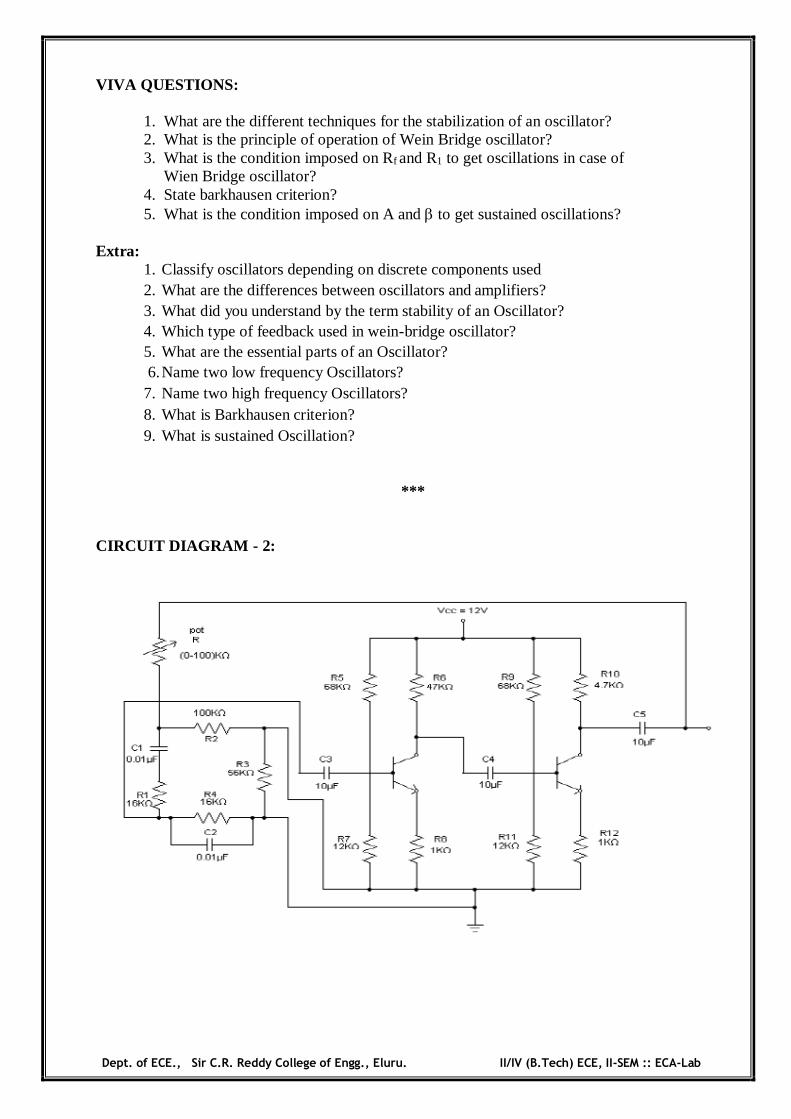
CIRCUIT DIAGRAM - 2:

Dept. of ECE., Sir C.R. Reddy College of Engg., Eluru. II/IV (B.Tech) ECE, II-SEM :: ECA-Lab
Dept. of ECE., Sir C.R. Reddy College of Engg., Eluru. II/IV (B.Tech) ECE, II-SEM :: ECA-Lab
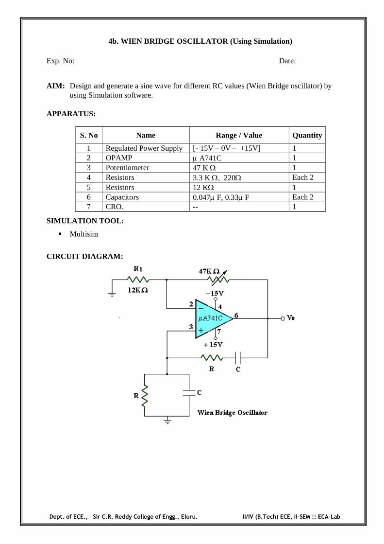
4b. WIEN BRIDGE OSCILLATOR (Using Simulation) Exp. No: Date:
AIM: Design and generate a sine wave for different RC values (Wien Bridge oscillator) by using Simulation software.
APPARATUS: SIMULATION TOOL:
Multisim
CIRCUIT DIAGRAM:
S. No Name Range / Value Quantity
1 Regulated Power Supply [- 15V – 0V – +15V] 1 2 OPAMP A741C 1 3 Potentiometer 47 K 1 4 Resistors 3.3 K , 220 Each 2 5 Resistors 12 K 1 6 Capacitors 0.047 F, 0.33 F Each 2 7 CRO. -- 1

Dept. of ECE., Sir C.R. Reddy College of Engg., Eluru. II/IV (B.Tech) ECE, II-SEM :: ECA-Lab
OUT PUT WAVE FORM:
PROCEDURE:
1. Connect the circuit as shown in the circuit diagram.
2. Connect the output terminal of the circuit to Channel – 1 of the dual trace CRO.
3. Simulate, adjust the potentiometer (i.e., 12 kΩ variable resistance) to get the correct sine
wave form. Place the both cursers in the CRO observe the T2– T1 as T.
4. PSet the graph for the obtained frequency
OBSERVATIONS:
Frequency of oscillations:
GRAPH:
PSet the observed output on a graph sheet. RESULT:
CIRCUIT DIAGRAM - 2:
Dept. of ECE., Sir C.R. Reddy College of Engg., Eluru. II/IV (B.Tech) ECE, II-SEM :: ECA-Lab
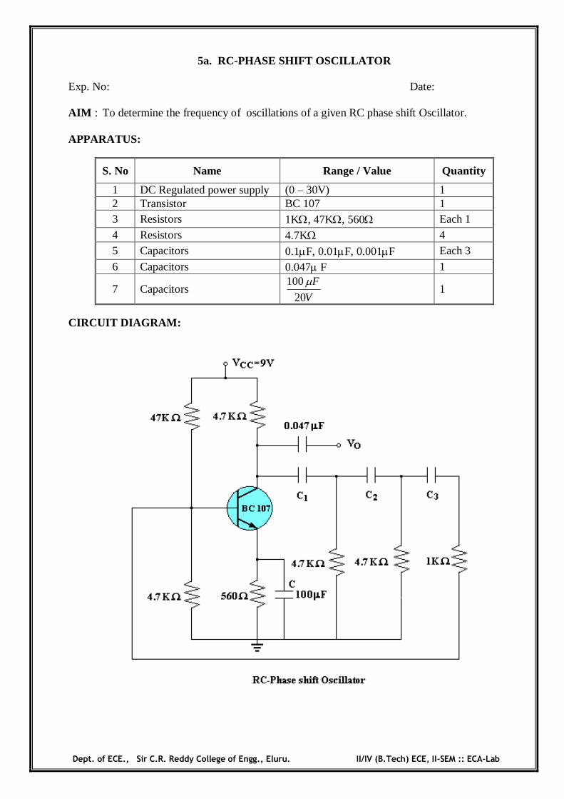
5a. RC-PHASE SHIFT OSCILLATOR
Exp. No: Date: AIM : To determine the frequency of oscillations of a given RC phase shift Oscillator. APPARATUS: CIRCUIT DIAGRAM:
S. No Name Range / Value Quantity
1 DC Regulated power supply (0 – 30V) 1 2 Transistor BC 107 1 3 Resistors 1K, 47K, 560 Each 1
4 Resistors 4.7K 4 5 Capacitors 0.1F, 0.01F, 0.001F Each 3
6 Capacitors 0.047 F 1
7 Capacitors V
F
20
100 1
Dept. of ECE., Sir C.R. Reddy College of Engg., Eluru. II/IV (B.Tech) ECE, II-SEM :: ECA-Lab
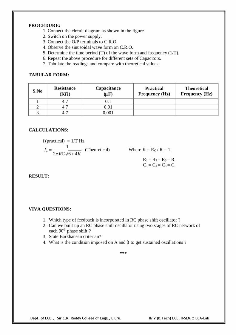
PROCEDURE: 1. Connect the circuit diagram as shown in the figure. 2. Switch on the power supply. 3. Connect the O/P terminals to C.R.O. 4. Observe the sinusoidal wave form on C.R.O. 5. Determine the time period (T) of the wave form and frequency (1/T). 6. Repeat the above procedure for different sets of Capacitors. 7. Tabulate the readings and compare with theoretical values.
TABULAR FORM:
S.No Resistance
(K) Capacitance
(F) Practical
Frequency (Hz) Theoretical
Frequency (Hz)
1 4.7 0.1 2 4.7 0.01 3 4.7 0.001
CALCULATIONS:
f (practical) = 1/T Hz. 1
2 6 4of
RC K
(Theoretical) Where K = RC / R = 1.
R1 = R2 = R3 = R. C1 = C2 = C3 = C.
RESULT: VIVA QUESTIONS:
1. Which type of feedback is incorporated in RC phase shift oscillator ? 2. Can we built up an RC phase shift oscillator using two stages of RC network of
each 900 phase shift ?
3. State Barkhausen criterian? 4. What is the condition imposed on A and to get sustained oscillations ?
***
Dept. of ECE., Sir C.R. Reddy College of Engg., Eluru. II/IV (B.Tech) ECE, II-SEM :: ECA-Lab
5b. RC-PHASE SHIFT OSCILLATOR (Using Simulation)
Exp. No: Date: PRELAB:
1. Study the different types of oscillator and their necessary conditions.
2. Identify all the formulas required to calculate frequency.
OBJECTIVE:
1. To simulate RC phase shift oscillator in Multisim and study the transient response.
2. To determine the phase shift of RC network in the circuit.
SOFTWARE TOOL:
Multisim. APPARATUS:
THEORY: The basic RC Oscillator which is also known as a Phase-shift Oscillator, produces a sine
wave output signal using regenerative feedback obtained from the resistor-capacitor combination. This regenerative feedback from the RC network is due to the ability of the capacitor to store an electric charge, (similar to the LC tank circuit).
This resistor-capacitor feedback network can be connected as shown above to produce a leading phase shift (phase advance network) or interchanged to produce a lagging phase shift (phase retard network) the outcome is still the same as the sine wave oscillations only occur at the frequency at which the overall phase-shift is 360o.
By varying one or more of the resistors or capacitors in the phase-shift network, the frequency can be varied and generally this is done by keeping the resistors the same and using a 3-ganged variable capacitor.
If all the resistors, R and the capacitors, C in the phase shift network are equal in value, then the frequency of oscillations produced by the RC oscillator is given as:
Where:
ƒr is the Output Frequency in Hertz
R is the Resistance in Ohms
C is the Capacitance in Farads
S. No Name Range / Value Quantity
1 DC Regulated power supply
(0 – 30V) 1
2 Transistor BC 107 1 3 Resistors 1K, 47K, 560 Each 1
4 Resistors 4.7K 4
5 Capacitors 0.1F, 0.01F, 0.001F Each 3
6 Capacitors 0.047 F 1
7 Capacitors V
F
20
100 1

Dept. of ECE., Sir C.R. Reddy College of Engg., Eluru. II/IV (B.Tech) ECE, II-SEM :: ECA-Lab
N is the number of RC stages. (N = 3)
CIRCUIT DIAGRAM:
RC PHASESHIFT OSCILLATOR
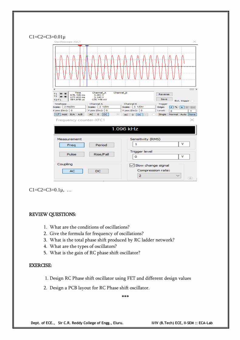
OBSERVATIONS/GRAPHS: C1=C2=C3=0.001µ
Dept. of ECE., Sir C.R. Reddy College of Engg., Eluru. II/IV (B.Tech) ECE, II-SEM :: ECA-Lab
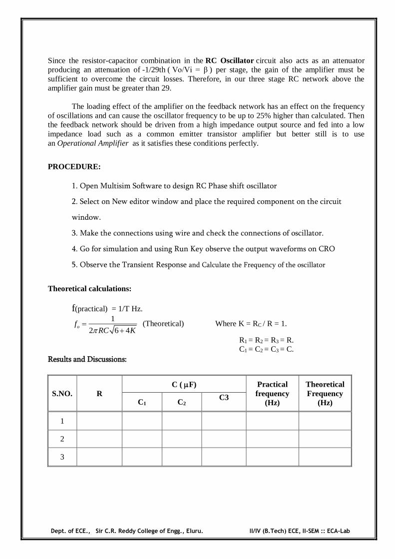
Since the resistor-capacitor combination in the RC Oscillator circuit also acts as an attenuator producing an attenuation of -1/29th ( Vo/Vi = β ) per stage, the gain of the amplifier must be sufficient to overcome the circuit losses. Therefore, in our three stage RC network above the amplifier gain must be greater than 29.
The loading effect of the amplifier on the feedback network has an effect on the frequency of oscillations and can cause the oscillator frequency to be up to 25% higher than calculated. Then the feedback network should be driven from a high impedance output source and fed into a low impedance load such as a common emitter transistor amplifier but better still is to use an Operational Amplifier as it satisfies these conditions perfectly.
PROCEDURE: 1. Open Multisim Software to design RC Phase shift oscillator
2. Select on New editor window and place the required component on the circuit
window.
3. Make the connections using wire and check the connections of oscillator.
4. Go for simulation and using Run Key observe the output waveforms on CRO
5. Observe the Transient Response and Calculate the Frequency of the oscillator
Theoretical calculations:
f(practical) = 1/T Hz. 1
2 6 4of
RC K
(Theoretical) Where K = RC / R = 1.
R1 = R2 = R3 = R. C1 = C2 = C3 = C.
Results and Discussions:
S.NO. R C ( F) Practical
frequency (Hz)
Theoretical Frequency
(Hz) C1 C2 C3
1
2
3
Dept. of ECE., Sir C.R. Reddy College of Engg., Eluru. II/IV (B.Tech) ECE, II-SEM :: ECA-Lab
C1=C2=C3=0.01µ
C1=C2=C3=0.1µ, …
REVIEW QUESTIONS:
1. What are the conditions of oscillations?
2. Give the formula for frequency of oscillations?
3. What is the total phase shift produced by RC ladder network?
4. What are the types of oscillators?
5. What is the gain of RC phase shift oscillator?
EXERCISE:
1. Design RC Phase shift oscillator using FET and different design values
2. Design a PCB layout for RC Phase shift oscillator.
***
Dept. of ECE., Sir C.R. Reddy College of Engg., Eluru. II/IV (B.Tech) ECE, II-SEM :: ECA-Lab
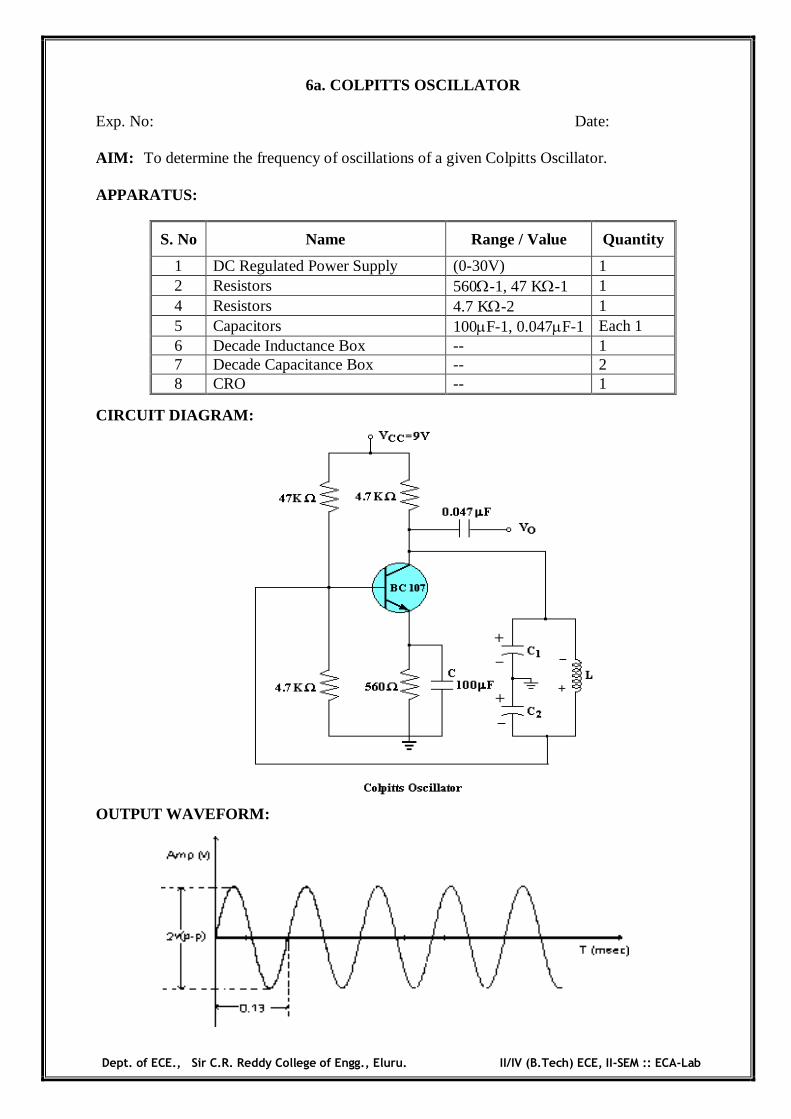
6a. COLPITTS OSCILLATOR
Exp. No: Date: AIM: To determine the frequency of oscillations of a given Colpitts Oscillator. APPARATUS: CIRCUIT DIAGRAM:
OUTPUT WAVEFORM:
S. No Name Range / Value Quantity
1 DC Regulated Power Supply (0-30V) 1 2 Resistors 560-1, 47 K-1 1 4 Resistors 4.7 K-2 1 5 Capacitors 100F-1, 0.047F-1 Each 1 6 Decade Inductance Box -- 1 7 Decade Capacitance Box -- 2 8 CRO -- 1
Dept. of ECE., Sir C.R. Reddy College of Engg., Eluru. II/IV (B.Tech) ECE, II-SEM :: ECA-Lab
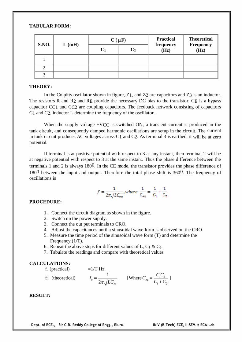
TABULAR FORM:
S.NO. L (mH) C ( F) Practical
frequency (Hz)
Theoretical Frequency
(Hz) C1 C2
1
2
3
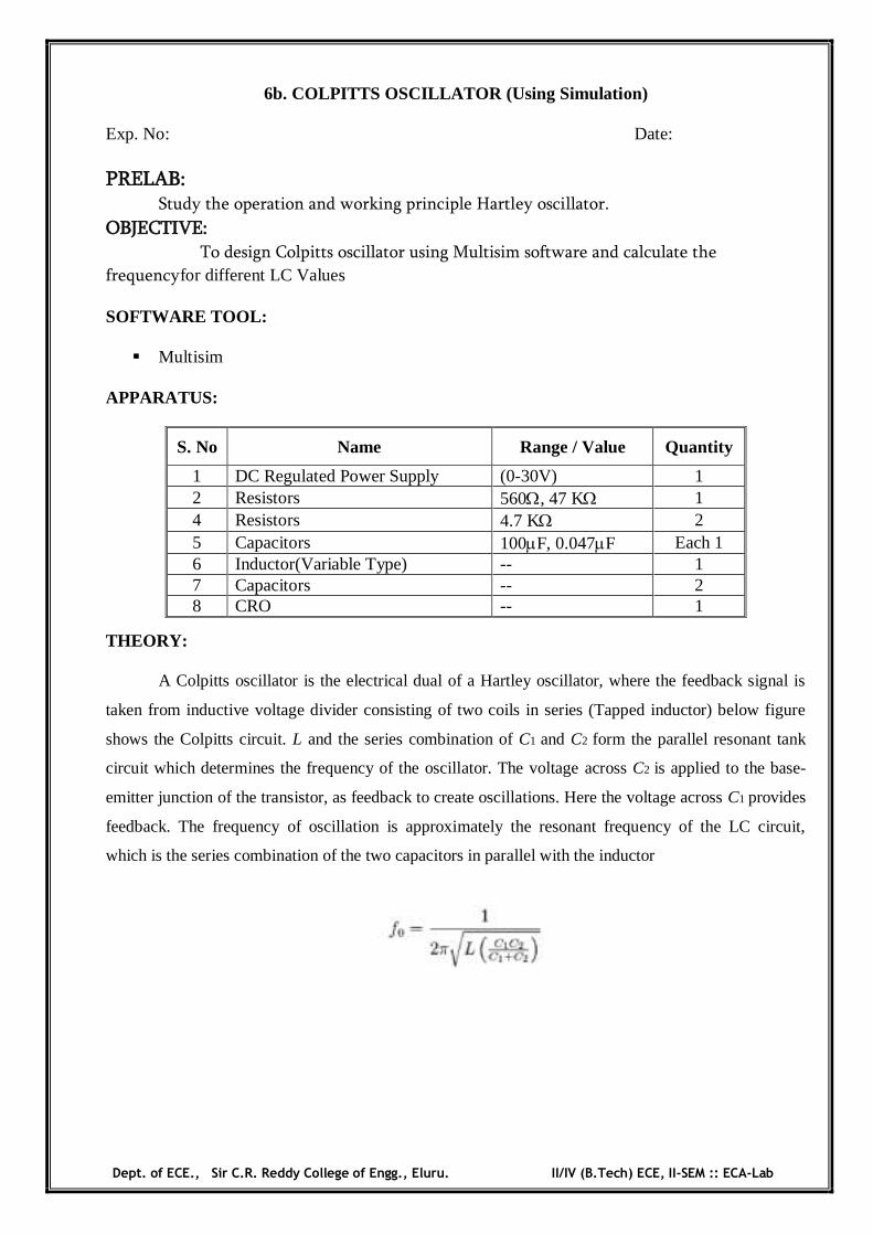
THEORY:
In the Colpitts oscillator shown in figure, Z1, and Z2 are capacitors and Z3 is an inductor. The resistors R and R2 and RE provide the necessary DC bias to the transistor. CE is a bypass capacitor CC1 and CC2 are coupling capacitors. The feedback network consisting of capacitors C1 and C2, inductor L determine the frequency of the oscillator.
When the supply voltage +VCC is switched ON, a transient current is produced in the tank circuit, and consequently damped harmonic oscillations are setup in the circuit. The current in tank circuit produces AC voltages across C1 and C2. As terminal 3 is earthed, it will be at zero potential.
If terminal is at positive potential with respect to 3 at any instant, then terminal 2 will be at negative potential with respect to 3 at the same instant. Thus the phase difference between the terminals 1 and 2 is always 1800. In the CE mode, the transistor provides the phase difference of 1800 between the input and output. Therefore the total phase shift is 3600. The frequency of oscillations is
PROCEDURE:
1. Connect the circuit diagram as shown in the figure. 2. Switch on the power supply. 3. Connect the out put terminals to CRO. 4. Adjust the capacitances until a sinusoidal wave form is observed on the CRO. 5. Measure the time period of the sinusoidal wave form (T) and determine the Frequency (1/T). 6. Repeat the above steps for different values of L, C1 & C2. 7. Tabulate the readings and compare with theoretical values
CALCULATIONS:
f0 (practical) =1/T Hz.
f0 (theoretical) 0
1
2 eq
fLC
. [Where 1 2
1 2eq
C CC
C C
]
RESULT:

Dept. of ECE., Sir C.R. Reddy College of Engg., Eluru. II/IV (B.Tech) ECE, II-SEM :: ECA-Lab
VIVA QUESTIONS:
1. Why RC network oscillator cannot be used at Radio frequencies? 2. Why LC network oscillators are preferred at high frequencies? 3. Why a buffer amplifier is required in between an oscillator and a load? 4. What is meant by ringing in an amplifier? 5. Why the crystal oscillator is highly stable? 6. Draw the electrical equivalent circuit of a crystal oscillator?
Extra: 1. Define oscillator. 2. Which type of Feedback is employed in oscillator? 3. What are the applications of Colpitts oscillator? 4. What is meant by resonant Circuit Oscillators? 5. Define gain and phase Margin? 6. What is a beat frequency oscillator? 7. What is damped Oscillation? 8. Write the expression for frequency of oscillations for colpitts and hartley oscillators? 9. Classify the different types of Oscillators? 10. What are the factors that determine the stability of an oscillator?
***

Dept. of ECE., Sir C.R. Reddy College of Engg., Eluru. II/IV (B.Tech) ECE, II-SEM :: ECA-Lab
Dept. of ECE., Sir C.R. Reddy College of Engg., Eluru. II/IV (B.Tech) ECE, II-SEM :: ECA-Lab
6b. COLPITTS OSCILLATOR (Using Simulation) Exp. No: Date: PRELAB:
Study the operation and working principle Hartley oscillator.
OBJECTIVE: To design Colpitts oscillator using Multisim software and calculate the
frequencyfor different LC Values SOFTWARE TOOL:
Multisim APPARATUS:
THEORY:
A Colpitts oscillator is the electrical dual of a Hartley oscillator, where the feedback signal is
taken from inductive voltage divider consisting of two coils in series (Tapped inductor) below figure
shows the Colpitts circuit. L and the series combination of C1 and C2 form the parallel resonant tank
circuit which determines the frequency of the oscillator. The voltage across C2 is applied to the base-
emitter junction of the transistor, as feedback to create oscillations. Here the voltage across C1 provides
feedback. The frequency of oscillation is approximately the resonant frequency of the LC circuit,
which is the series combination of the two capacitors in parallel with the inductor
S. No Name Range / Value Quantity
1 DC Regulated Power Supply (0-30V) 1 2 Resistors 560, 47 K 1 4 Resistors 4.7 K 2 5 Capacitors 100F, 0.047F Each 1 6 Inductor(Variable Type) -- 1 7 Capacitors -- 2 8 CRO -- 1
Dept. of ECE., Sir C.R. Reddy College of Engg., Eluru. II/IV (B.Tech) ECE, II-SEM :: ECA-Lab
CIRCUIT DIAGRAM:
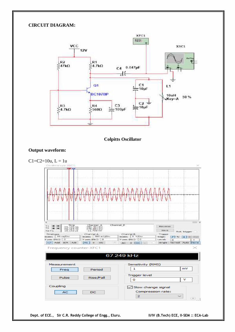
Colpitts Oscillator Output waveform: C1=C2=10u, L = 1u

Dept. of ECE., Sir C.R. Reddy College of Engg., Eluru. II/IV (B.Tech) ECE, II-SEM :: ECA-Lab
PROCEDURE:
1. Connect the circuit diagram as shown in the figure.
2. Switch on the power supply.
3. Connect the output terminals to CRO.
4. Adjust the capacitances until a sinusoidal wave form is observed on the
CRO.
5. Measure the time period of the sinusoidal wave form (T) and determine the
Frequency (1/T).
6. Repeat the above steps for different values of L, C1& C2.
7. Tabulate the readings and compare with theoretical values
RESULTS &DISCUSSIONS: C1=C2= 10u ; L= 3u
Dept. of ECE., Sir C.R. Reddy College of Engg., Eluru. II/IV (B.Tech) ECE, II-SEM :: ECA-Lab
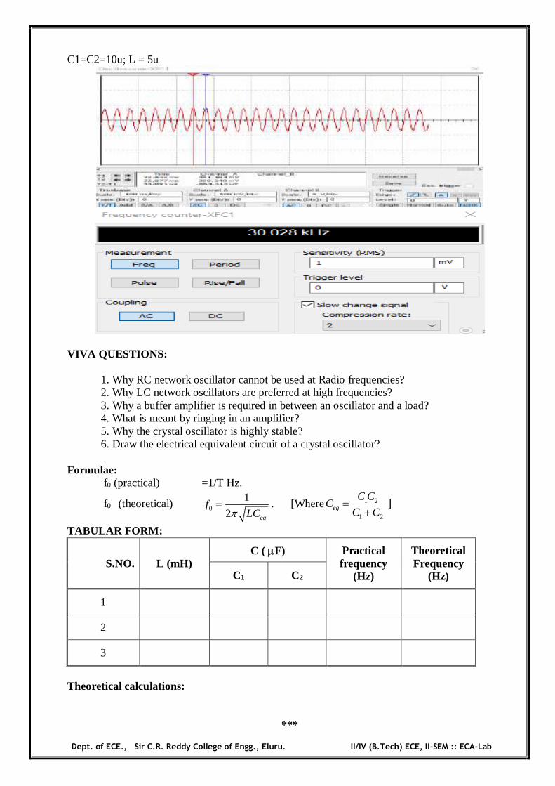
C1=C2=10u; L = 5u
VIVA QUESTIONS:
1. Why RC network oscillator cannot be used at Radio frequencies? 2. Why LC network oscillators are preferred at high frequencies? 3. Why a buffer amplifier is required in between an oscillator and a load? 4. What is meant by ringing in an amplifier? 5. Why the crystal oscillator is highly stable? 6. Draw the electrical equivalent circuit of a crystal oscillator?
Formulae:
f0 (practical) =1/T Hz.
f0 (theoretical) 0
1
2 eq
fLC
. [Where 1 2
1 2eq
C CC
C C
]
TABULAR FORM:
S.NO. L (mH) C ( F) Practical
frequency (Hz)
Theoretical Frequency
(Hz) C1 C2
1
2
3
Theoretical calculations:
***
Dept. of ECE., Sir C.R. Reddy College of Engg., Eluru. II/IV (B.Tech) ECE, II-SEM :: ECA-Lab
7a. HARTLEY OSCILLATOR
Exp. No: Date: AIM: To Determine the frequency of oscillations of a Hartley Oscillator and
compare it with the theoretical values.
APPARATUS: CIRCUIT DIAGRAM:
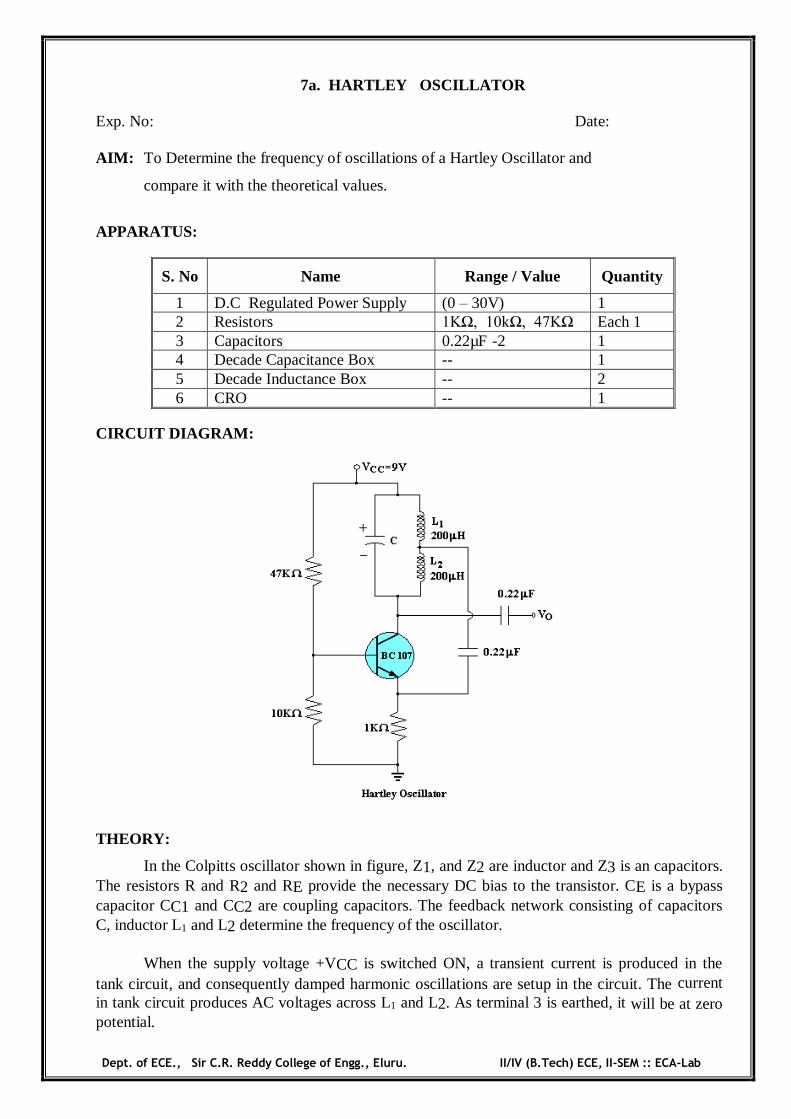
THEORY:
In the Colpitts oscillator shown in figure, Z1, and Z2 are inductor and Z3 is an capacitors. The resistors R and R2 and RE provide the necessary DC bias to the transistor. CE is a bypass capacitor CC1 and CC2 are coupling capacitors. The feedback network consisting of capacitors C, inductor L1 and L2 determine the frequency of the oscillator.
When the supply voltage +VCC is switched ON, a transient current is produced in the tank circuit, and consequently damped harmonic oscillations are setup in the circuit. The current in tank circuit produces AC voltages across L1 and L2. As terminal 3 is earthed, it will be at zero potential.
S. No Name Range / Value Quantity
1 D.C Regulated Power Supply (0 – 30V) 1 2 Resistors 1KΩ, 10kΩ, 47KΩ Each 1 3 Capacitors 0.22µF -2 1 4 Decade Capacitance Box -- 1 5 Decade Inductance Box -- 2 6 CRO -- 1
Dept. of ECE., Sir C.R. Reddy College of Engg., Eluru. II/IV (B.Tech) ECE, II-SEM :: ECA-Lab
If terminal is at positive potential with respect to 3 at any instant, then terminal 2 will be at negative potential with respect to 3 at the same instant. Thus the phase difference between the terminals 1 and 2 is always 1800. In the CE mode, the transistor provides the phase difference of 1800 between the input and output. Therefore the total phase shift is 3600. The frequency of
oscillations is 0
1
2 eq
fL C
PROCEDURE:
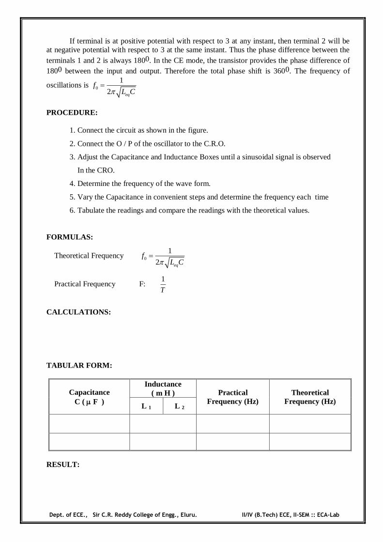
1. Connect the circuit as shown in the figure.
2. Connect the O / P of the oscillator to the C.R.O.
3. Adjust the Capacitance and Inductance Boxes until a sinusoidal signal is observed
In the CRO.
4. Determine the frequency of the wave form.
5. Vary the Capacitance in convenient steps and determine the frequency each time
6. Tabulate the readings and compare the readings with the theoretical values.
FORMULAS:
Theoretical Frequency 0
1
2 eq
fL C
Practical Frequency F: T
1
CALCULATIONS: TABULAR FORM:
Capacitance C ( F )
Inductance ( m H ) Practical
Frequency (Hz) Theoretical
Frequency (Hz) L 1 L 2
RESULT:

Dept. of ECE., Sir C.R. Reddy College of Engg., Eluru. II/IV (B.Tech) ECE, II-SEM :: ECA-Lab
VIVA QUESTIONS:
1. Why RC network oscillator cannot be used at Radio frequencies?
2. Why LC network oscillators are preferred at high frequencies?
3. Why a buffer amplifier is required in between an oscillator and a load?
4. What is meant by ringing in an amplifier?
5. Why the crystal oscillator is highly stable?
6. Draw the electrical equivalent circuit of a crystal oscillator?
***

Dept. of ECE., Sir C.R. Reddy College of Engg., Eluru. II/IV (B.Tech) ECE, II-SEM :: ECA-Lab
Dept. of ECE., Sir C.R. Reddy College of Engg., Eluru. II/IV (B.Tech) ECE, II-SEM :: ECA-Lab
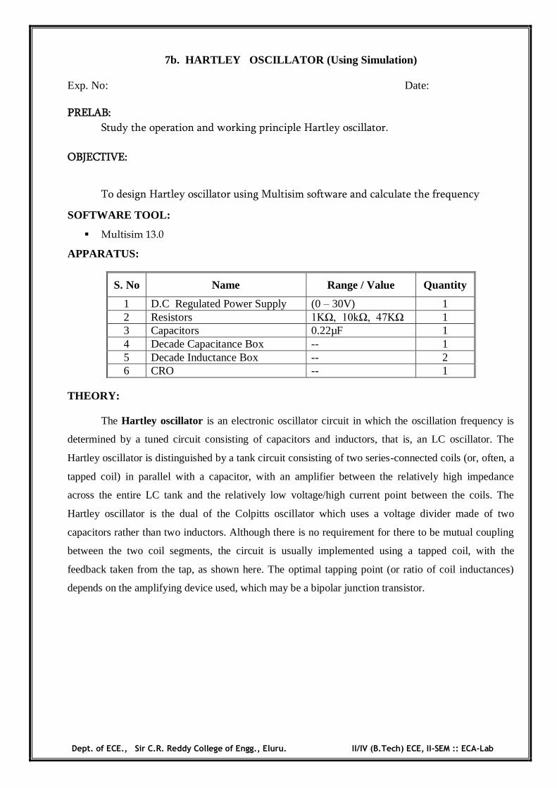
7b. HARTLEY OSCILLATOR (Using Simulation)
Exp. No: Date: PRELAB:
Study the operation and working principle Hartley oscillator.
OBJECTIVE:
To design Hartley oscillator using Multisim software and calculate the frequency
SOFTWARE TOOL:
Multisim 13.0
APPARATUS:
THEORY:
The Hartley oscillator is an electronic oscillator circuit in which the oscillation frequency is
determined by a tuned circuit consisting of capacitors and inductors, that is, an LC oscillator. The
Hartley oscillator is distinguished by a tank circuit consisting of two series-connected coils (or, often, a
tapped coil) in parallel with a capacitor, with an amplifier between the relatively high impedance
across the entire LC tank and the relatively low voltage/high current point between the coils. The
Hartley oscillator is the dual of the Colpitts oscillator which uses a voltage divider made of two
capacitors rather than two inductors. Although there is no requirement for there to be mutual coupling
between the two coil segments, the circuit is usually implemented using a tapped coil, with the
feedback taken from the tap, as shown here. The optimal tapping point (or ratio of coil inductances)
depends on the amplifying device used, which may be a bipolar junction transistor.
S. No Name Range / Value Quantity
1 D.C Regulated Power Supply (0 – 30V) 1 2 Resistors 1KΩ, 10kΩ, 47KΩ 1 3 Capacitors 0.22µF 1 4 Decade Capacitance Box -- 1 5 Decade Inductance Box -- 2 6 CRO -- 1

Dept. of ECE., Sir C.R. Reddy College of Engg., Eluru. II/IV (B.Tech) ECE, II-SEM :: ECA-Lab
CIRCUIT DIAGRAM:
Hartley Oscillator
OUTPUT WAVEFORM:
L1 = L2= 200u; C = 20nf
Dept. of ECE., Sir C.R. Reddy College of Engg., Eluru. II/IV (B.Tech) ECE, II-SEM :: ECA-Lab
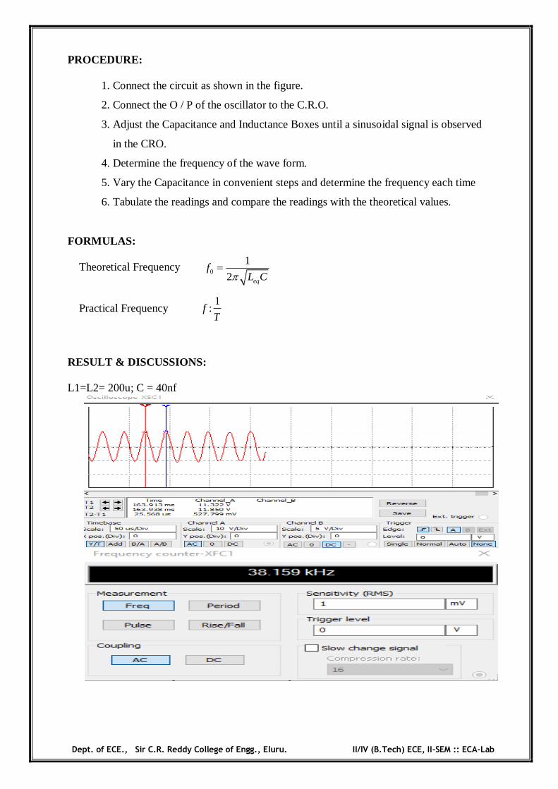
PROCEDURE:
1. Connect the circuit as shown in the figure.
2. Connect the O / P of the oscillator to the C.R.O.
3. Adjust the Capacitance and Inductance Boxes until a sinusoidal signal is observed
in the CRO.
4. Determine the frequency of the wave form.
5. Vary the Capacitance in convenient steps and determine the frequency each time
6. Tabulate the readings and compare the readings with the theoretical values.
FORMULAS:
Theoretical Frequency 0
1
2 eq
fL C
Practical Frequency f :T
1
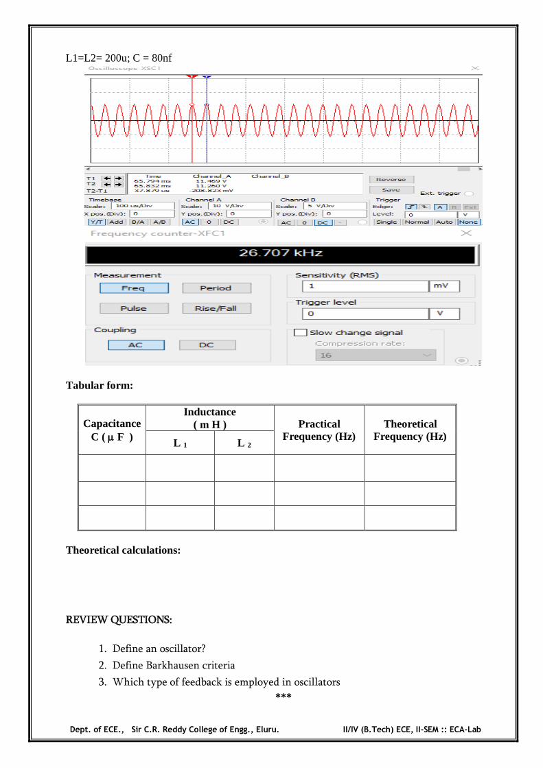
RESULT & DISCUSSIONS: L1=L2= 200u; C = 40nf
Dept. of ECE., Sir C.R. Reddy College of Engg., Eluru. II/IV (B.Tech) ECE, II-SEM :: ECA-Lab
L1=L2= 200u; C = 80nf
Tabular form:
Capacitance C ( F )
Inductance ( m H ) Practical
Frequency (Hz) Theoretical
Frequency (Hz) L 1 L 2
Theoretical calculations:
REVIEW QUESTIONS:
1. Define an oscillator?
2. Define Barkhausen criteria
3. Which type of feedback is employed in oscillators
***
Dept. of ECE., Sir C.R. Reddy College of Engg., Eluru. II/IV (B.Tech) ECE, II-SEM :: ECA-Lab
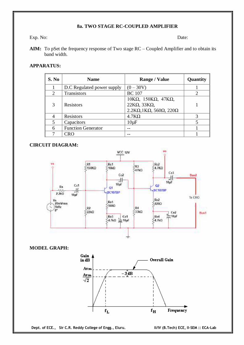
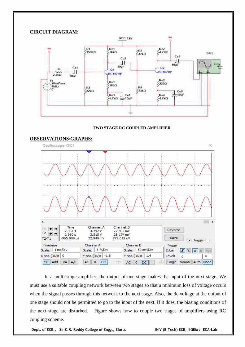
8a. TWO STAGE RC-COUPLED AMPLIFIER
Exp. No: Date: AIM: To pSet the frequency response of Two stage RC – Coupled Amplifier and to obtain its
band width. APPARATUS:
CIRCUIT DIAGRAM:
MODEL GRAPH:
S. No Name Range / Value Quantity
1 D.C Regulated power supply (0 – 30V) 1 2 Transistors BC 107 2
3 Resistors 10KΩ, 150KΩ, 47KΩ, 22KΩ, 33KΩ, 2.2KΩ,1KΩ, 560Ω, 220Ω
1
4 Resistors 4.7KΩ 3 5 Capacitors 10µF 5 6 Function Generator -- 1 7 CRO -- 1
Dept. of ECE., Sir C.R. Reddy College of Engg., Eluru. II/IV (B.Tech) ECE, II-SEM :: ECA-Lab
THEORY As the gain provided by a single stage amplifier is usually not sufficient to drive the load,
so to achieve extra gain multi-stage amplifier are used. In multi-stage amplifiers output of one-stage is coupled to the input of the next stage. The coupling of one stage to another is done with the help of some coupling devices. If it is coupled by RC then the amplifier is called RC-coupled amplifier.
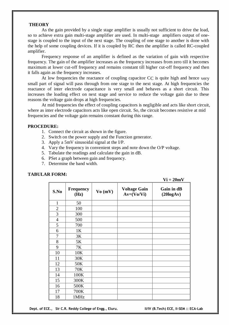
Frequency response of an amplifier is defined as the variation of gain with respective frequency. The gain of the amplifier increases as the frequency increases from zero till it becomes maximum at lower cut-off frequency and remains constant till higher cut-off frequency and then it falls again as the frequency increases.
At low frequencies the reactance of coupling capacitor CC is quite high and hence very small part of signal will pass through from one stage to the next stage. At high frequencies the reactance of inter electrode capacitance is very small and behaves as a short circuit. This increases the loading effect on next stage and service to reduce the voltage gain due to these reasons the voltage gain drops at high frequencies.
At mid frequencies the effect of coupling capacitors is negligible and acts like short circuit, where as inter electrode capacitors acts like open circuit. So, the circuit becomes resistive at mid frequencies and the voltage gain remains constant during this range. PROCEDURE:
1. Connect the circuit as shown in the figure. 2. Switch on the power supply and the Function generator. 3. Apply a 5mV sinusoidal signal at the I/P. 4. Vary the frequency in convenient steps and note down the O/P voltage. 5. Tabulate the readings and calculate the gain in dB. 6. PSet a graph between gain and frequency. 7. Determine the band width.
TABULAR FORM: Vi = 20mV
S.No Frequency (Hz)
Vo (mV) Voltage Gain Av=(Vo/Vi)
Gain in dB (20logAv)
1 50 2 100 3 300 4 500 5 700 6 1K 7 3K 8 5K 9 7K 10 10K 11 30K 12 50K 13 70K 14 100K 15 300K 16 500K 17 700K 18 1MHz
Dept. of ECE., Sir C.R. Reddy College of Engg., Eluru. II/IV (B.Tech) ECE, II-SEM :: ECA-Lab
RESULT:
Upper cut-off frequency = KHz. Lower cut-off frequency = KHz. Bandwidth = KHz.
VIVA QUESTIONS:
1. What is the need for Two stage Amplifier? 2. Differentiate between interacting and non- interacting stages? 3. Give the expression for the overall upper cut-off frequency of a multistage amplifier? 4. What is the effect of multistage amplifier on band width? 5. What is the choice of transistor configuration in multistage amplifier? 6. What is cascade amplifier? 7. What is the advantage of cascade amplifier?
Extra: 1. What are the advantages and disadvantages of multi-stage amplifiers? 2. Why gain falls at HF and LF? 3. Why the gain remains constant at MF?
4. Explain the function of emitter bypass capacitor, CE? 5. How the band width will effect as more number of stages are cascaded? 6. Define frequency response? 7. Give the formula for effective lower cut-off frequency, when N-number of stages is
cascaded? 8. Explain the effect of coupling capacitors and inter-electrode capacitances on
overall gain? 9. By how many times effective upper cut-off frequency will be reduced, if three
identical stages are cascaded? 10. Mention the applications of two-stage RC-coupled amplifiers?
***

Dept. of ECE., Sir C.R. Reddy College of Engg., Eluru. II/IV (B.Tech) ECE, II-SEM :: ECA-Lab
Dept. of ECE., Sir C.R. Reddy College of Engg., Eluru. II/IV (B.Tech) ECE, II-SEM :: ECA-Lab
8b. TWO STAGE RC-COUPLED AMPLIFIER (Using Simulation)
Exp. No: Date: PRELAB:
1. Study the purpose of multistage amplifiers. 2. Learn the different types of coupling methods. 3. Study the effect of cascading on Bandwidth. 4. Identify all the formulae you will need in this Lab. 5. Study the procedure of using Multisim tool (Schematic & Circuit File)
OBJECTIVE:
1. To simulate the Two Stage RC Coupled Amplifier in Multisim and study the transient and frequency response. 2. To determine the phase relationship between the input and output voltages by performing the transient analysis. 3. To determine the maximum gain, 3dB gain, lower and upper cutoff frequencies and bandwidth of Two Stage RC Coupled Amplifier by performing the AC analysis. 4. To determine the effect of cascading on gain and bandwidth.
SOFTWARE TOOL:
Multisim APPARATUS:
THEORY:
An amplifier is the basic building block of most electronic systems. Just as one brick does
not make a house, a single-stage amplifier is not sufficient to build a practical electronic system.
The gain of the single stage is not sufficient for practical applications. The voltage level of a signal
can be raised to the desired level if we use more than one stage. When a number of amplifier
stages are used in succession (one after the other) it is called a multistage amplifier or a cascade
amplifier. Much higher gains can be obtained from the multi-stage amplifiers.
S. No Name Range / Value Quantity
1 D.C Regulated power supply (0 – 30V) 1 2 Transistors BC 107 2
3 Resistors 10KΩ, 150KΩ, 47KΩ, 22KΩ, 33KΩ, 2.2KΩ
1
4 Resistors 1KΩ, 560Ω, 220Ω 1 5 Capacitors 10µF 5 6 Function Generator -- 1 7 CRO -- 1
Dept. of ECE., Sir C.R. Reddy College of Engg., Eluru. II/IV (B.Tech) ECE, II-SEM :: ECA-Lab
CIRCUIT DIAGRAM:
TWO STAGE RC COUPLED AMPLIFIER
OBSERVATIONS/GRAPHS:
In a multi-stage amplifier, the output of one stage makes the input of the next stage. We
must use a suitable coupling network between two stages so that a minimum loss of voltage occurs
when the signal passes through this network to the next stage. Also, the dc voltage at the output of
one stage should not be permitted to go to the input of the next. If it does, the biasing conditions of
the next stage are disturbed. Figure shows how to couple two stages of amplifiers using RC
coupling scheme.

Dept. of ECE., Sir C.R. Reddy College of Engg., Eluru. II/IV (B.Tech) ECE, II-SEM :: ECA-Lab
This is the most widely used method. In this scheme, the signal developed across the
collector resistor RC (R2)of the first stage is coupled to the base of the second stage through the
capacitor CC.(C2) The coupling capacitor blocks the dc voltage of the first stage from reaching the
base of the second stage. In this way, the dc biasing of the next stage is not interfered with. For this
reason, the capacitor CC (C2)is also called a blocking capacitor. As the number of stages
increases, the gain increases and the bandwidth decreases.
RC coupling scheme finds applications in almost all audio small-signal amplifiers used in
record players, tape recorders, public-address systems, radio receivers, television receivers, etc.
PROCEDURE:
1. Open Multisim Software to design two stage RC coupled amplifier circuit
2. Select on New editor window and place the required components of amplifier on the circuit
window.
3. Make the connections using wire and check the connections of oscillator.
4. Go for simulation and using Run Key observe the output waveforms on CRO
5. Indicate the node names and go for AC Analysis with the output node
6. Observe the Transient response and Ac Analysis for the first stage and second stage
separately and draw the magnitude response curve
7. Calculate the bandwidth of the amplifier
INFERENCE: 1. From the transient analysis, it is observed that,___________________________ 2. From the frequency response curve the results observed are tabulated in table 1. 3. From the AC response, it is observed that, _____________________________
Dept. of ECE., Sir C.R. Reddy College of Engg., Eluru. II/IV (B.Tech) ECE, II-SEM :: ECA-Lab
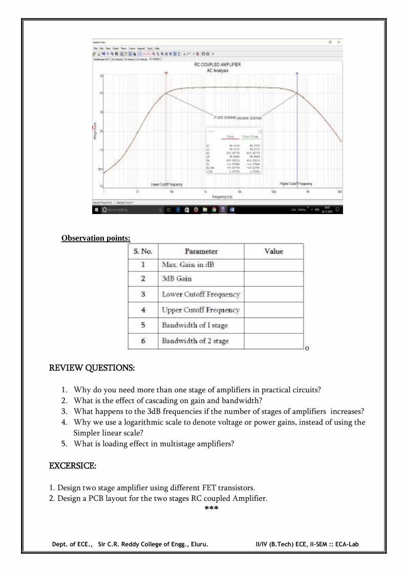
Observation points:
o
REVIEW QUESTIONS:
1. Why do you need more than one stage of amplifiers in practical circuits?
2. What is the effect of cascading on gain and bandwidth?
3. What happens to the 3dB frequencies if the number of stages of amplifiers increases?
4. Why we use a logarithmic scale to denote voltage or power gains, instead of using the
Simpler linear scale?
5. What is loading effect in multistage amplifiers?
EXCERSICE:
1. Design two stage amplifier using different FET transistors.
2. Design a PCB layout for the two stages RC coupled Amplifier. ***
Dept. of ECE., Sir C.R. Reddy College of Engg., Eluru. II/IV (B.Tech) ECE, II-SEM :: ECA-Lab
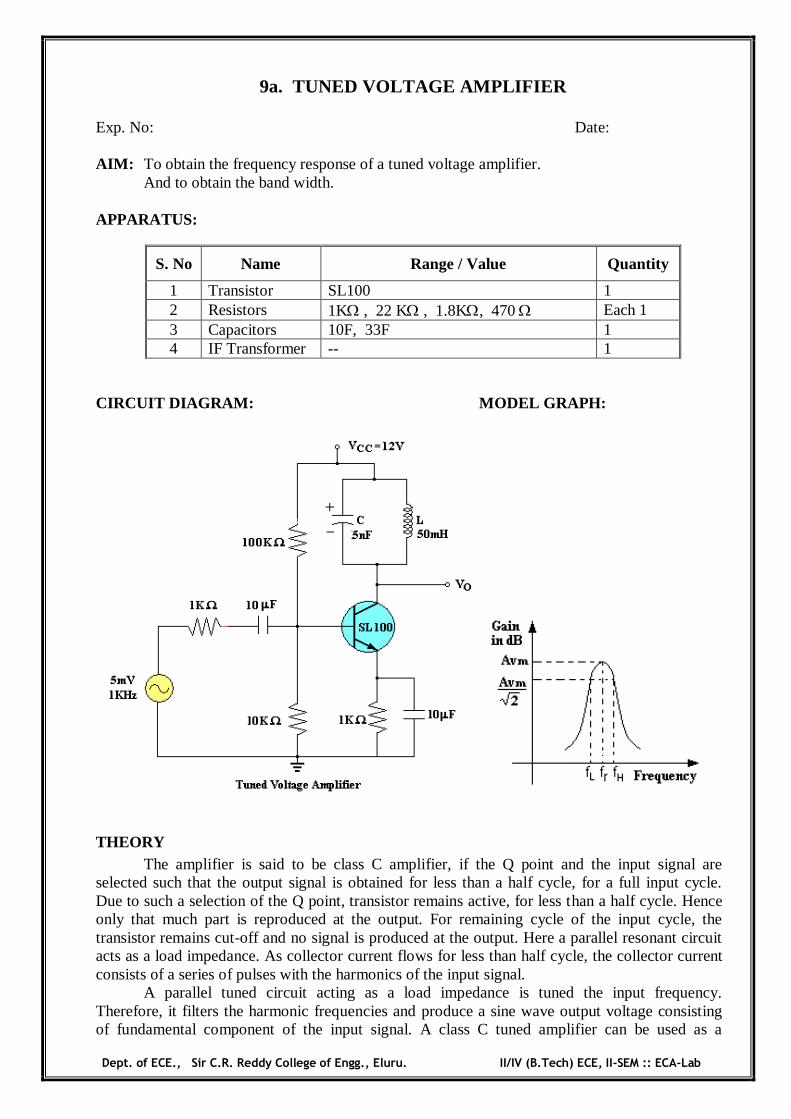
9a. TUNED VOLTAGE AMPLIFIER
Exp. No: Date: AIM: To obtain the frequency response of a tuned voltage amplifier. And to obtain the band width. APPARATUS:
CIRCUIT DIAGRAM: MODEL GRAPH:
THEORY The amplifier is said to be class C amplifier, if the Q point and the input signal are
selected such that the output signal is obtained for less than a half cycle, for a full input cycle. Due to such a selection of the Q point, transistor remains active, for less than a half cycle. Hence only that much part is reproduced at the output. For remaining cycle of the input cycle, the transistor remains cut-off and no signal is produced at the output. Here a parallel resonant circuit acts as a load impedance. As collector current flows for less than half cycle, the collector current consists of a series of pulses with the harmonics of the input signal.
A parallel tuned circuit acting as a load impedance is tuned the input frequency. Therefore, it filters the harmonic frequencies and produce a sine wave output voltage consisting of fundamental component of the input signal. A class C tuned amplifier can be used as a
S. No Name Range / Value Quantity
1 Transistor SL100 1 2 Resistors 1K , 22 K , 1.8K, 470 Each 1 3 Capacitors 10F, 33F 1 4 IF Transformer -- 1
Dept. of ECE., Sir C.R. Reddy College of Engg., Eluru. II/IV (B.Tech) ECE, II-SEM :: ECA-Lab
frequency multiplier if the resonant circuit is tuned to a harmonic of the input signal. Here class-C amplifier is used with parallel tuned circuit. Therefore the output voltage is a maximum at the resonant frequency. The resonant frequency for parallel tuned circuit is given as
Resonant frequency= Fr = PROCEDURE:
1. Connect the circuit as shown in the figure. 2. Apply a 4 mV sinusoidal signal at a frequency of 1 KHz and note down the O/P. 3. Now vary the frequency of the input signal upto 1MHz in suitable steps by keeping
the input voltage constant. 4. Note down the O/P voltage V0. 5. Tabulate the readings. 6. Draw gain Vs frequency graph on semilog sheet and determine the band width.
RESULT: TABULAR FORM:
Vi = 5mV
S.No Frequency
(Hz) Output Voltage ( V0)
(mV) Gain in dB
= 20 log ( V0 / Vi )
1 50 2 100 3 300 4 500 5 700 6 1K 7 3K 8 5K 9 7K
10 10K 11 30K 12 50K 13 70K 14 100K 15 300K 16 500K 17 700K 18 1MHz
Dept. of ECE., Sir C.R. Reddy College of Engg., Eluru. II/IV (B.Tech) ECE, II-SEM :: ECA-Lab
VIVA QUESTIONS:
1. What is a tuned amplifier? 2. Distinguish between a single tuned and a double tuned amplifier? 3. What is meant by stagger tuned amplifier? 4. Is the tuned amplifier a narrow band or a wide band amplifier? 5. Define selectivity? 6. What parameters shall be selected for a highly tuned amplifier? 7. Where the tuned amplifiers are used? 8. What type of tuning is used in the IF stage of a Radio receiver ? 9. What is the relation between the band width of a double tuned and a stagger tuned amplifier? 10. How to improve the band width of a tuned amplifier? 11. What is meant by critical tuning?
***

Dept. of ECE., Sir C.R. Reddy College of Engg., Eluru. II/IV (B.Tech) ECE, II-SEM :: ECA-Lab
Dept. of ECE., Sir C.R. Reddy College of Engg., Eluru. II/IV (B.Tech) ECE, II-SEM :: ECA-Lab
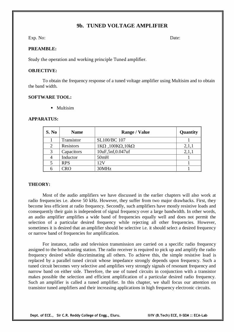
9b. TUNED VOLTAGE AMPLIFIER
Exp. No: Date: PREAMBLE:
Study the operation and working principle Tuned amplifier. OBJECTIVE:
To obtain the frequency response of a tuned voltage amplifier using Multisim and to obtain the band width. SOFTWARE TOOL:
Multisim APPARATUS:
THEORY:
Most of the audio amplifiers we have discussed in the earlier chapters will also work at radio frequencies i.e. above 50 kHz. However, they suffer from two major drawbacks. First, they become less efficient at radio frequency. Secondly, such amplifiers have mostly resistive loads and consequently their gain is independent of signal frequency over a large bandwidth. In other words, an audio amplifier amplifies a wide band of frequencies equally well and does not permit the selection of a particular desired frequency while rejecting all other frequencies. However, sometimes it is desired that an amplifier should be selective i.e. it should select a desired frequency or narrow band of frequencies for amplification.
For instance, radio and television transmission are carried on a specific radio frequency
assigned to the broadcasting station. The radio receiver is required to pick up and amplify the radio frequency desired while discriminating all others. To achieve this, the simple resistive load is replaced by a parallel tuned circuit whose impedance strongly depends upon frequency. Such a tuned circuit becomes very selective and amplifies very strongly signals of resonant frequency and narrow band on either side. Therefore, the use of tuned circuits in conjunction with a transistor makes possible the selection and efficient amplification of a particular desired radio frequency. Such an amplifier is called a tuned amplifier. In this chapter, we shall focus our attention on transistor tuned amplifiers and their increasing applications in high frequency electronic circuits.
S. No Name Range / Value Quantity
1 Transistor SL100/BC 107 1 2 Resistors 1K ,100K,10k 2,1,1 3 Capacitors 10uF,5nf,0.047uf 2,1,1 4 Inductor 50mH 1 5 RPS 12V 1 6 CRO 30MHz 1
Dept. of ECE., Sir C.R. Reddy College of Engg., Eluru. II/IV (B.Tech) ECE, II-SEM :: ECA-Lab
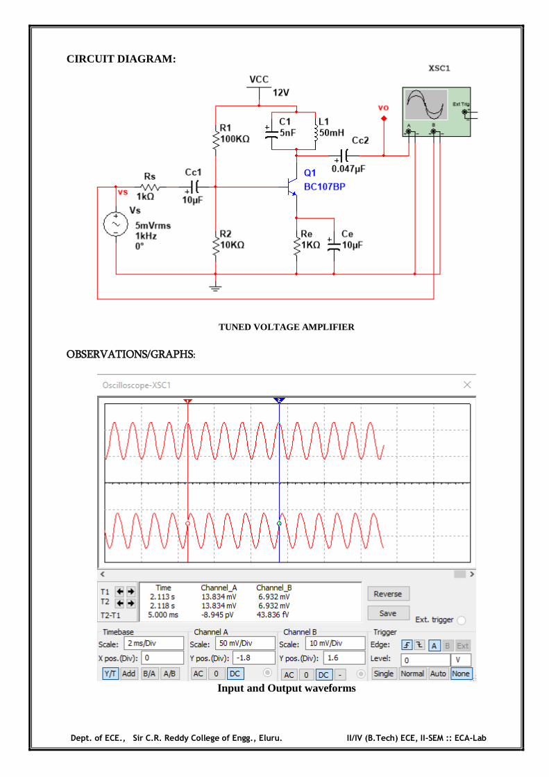
CIRCUIT DIAGRAM:
TUNED VOLTAGE AMPLIFIER
OBSERVATIONS/GRAPHS:
Input and Output waveforms
Dept. of ECE., Sir C.R. Reddy College of Engg., Eluru. II/IV (B.Tech) ECE, II-SEM :: ECA-Lab
Amplifiers which amplify a specific frequency or narrow band of frequencies are called tuned amplifiers. Tuned amplifiers are mostly used for the amplification of high or radio frequencies. It is because radio frequencies are generally single and the tuned circuit permits their selection and efficient amplification. However, such amplifiers are not suitable for the amplification of audio frequencies as they are mixture of frequencies from 20 Hz to 20 kHz and not single. Tuned amplifiers are widely used in radio and television circuits where they are called upon to handle radio frequencies. Below figure shows the circuit of a simple transistor tuned amplifier. Here, instead of load resistor, we have a parallel tuned circuit in the collector. The impedance of this tuned circuit strongly depends upon frequency. It offers a very high impedance at resonant frequency and very small impedance at all other frequencies. If the signal has the same frequency as the resonant frequency of LC circuit, large amplification will result due to high impedance of LC circuit at this frequency. When signals of many frequencies are present at the input of tuned amplifier, it will select and strongly amplify the signals of resonant frequency while rejecting all others. Therefore, such amplifiers are very useful in radio receivers to select the signal from one particular broadcasting station when signals of many other frequencies are present at the receiving aerial. PROCEDURE: 1. Open Multisim Software to design circuit
2. Select on New editor window and place the required component on the circuit
window.
3. Make the connections using wire and check the connections and oscillator.
4. Go for simulation and using Run Key observe the output waveforms on CRO
5. Indicate the node names and go for AC Analysis with the output node
6. Observe the Ac Analysis and draw the magnitude response curve
7. Calculate the bandwidth of the amplifier
RESULT &DISCUSSION: 1. Frequency response of single tuned Amplifier is pSetted.
2. Gain = _______dB (maximum).
3. Bandwidth= (fH—fL) = _________Hz.

Dept. of ECE., Sir C.R. Reddy College of Engg., Eluru. II/IV (B.Tech) ECE, II-SEM :: ECA-Lab
Frequency Response:
Theoretical calculations:
REVIEW QUESTIONS:
1. What is a tuned amplifier?
2. Define Q-factor?
3. What is selectivity?
4. Is tuned amplifier a hallow band or wide band amplifier?
5. Give the applications for tuned amplifier.
***
Dept. of ECE., Sir C.R. Reddy College of Engg., Eluru. II/IV (B.Tech) ECE, II-SEM :: ECA-Lab
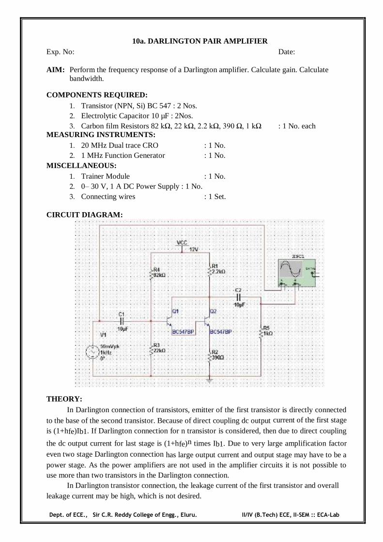
10a. DARLINGTON PAIR AMPLIFIER Exp. No: Date: AIM: Perform the frequency response of a Darlington amplifier. Calculate gain. Calculate
bandwidth.
COMPONENTS REQUIRED: 1. Transistor (NPN, Si) BC 547 : 2 Nos. 2. Electrolytic Capacitor 10 µF : 2Nos. 3. Carbon film Resistors 82 kΩ, 22 kΩ, 2.2 kΩ, 390 Ω, 1 kΩ : 1 No. each
MEASURING INSTRUMENTS: 1. 20 MHz Dual trace CRO : 1 No. 2. 1 MHz Function Generator : 1 No.
MISCELLANEOUS: 1. Trainer Module : 1 No. 2. 0– 30 V, 1 A DC Power Supply : 1 No. 3. Connecting wires : 1 Set.
CIRCUIT DIAGRAM:
THEORY: In Darlington connection of transistors, emitter of the first transistor is directly connected
to the base of the second transistor. Because of direct coupling dc output current of the first stage
is (1+hfe)Ib1. If Darlington connection for n transistor is considered, then due to direct coupling
the dc output current for last stage is (1+hfe)n times Ib1. Due to very large amplification factor
even two stage Darlington connection has large output current and output stage may have to be a power stage. As the power amplifiers are not used in the amplifier circuits it is not possible to use more than two transistors in the Darlington connection.
In Darlington transistor connection, the leakage current of the first transistor and overall leakage current may be high, which is not desired.

Dept. of ECE., Sir C.R. Reddy College of Engg., Eluru. II/IV (B.Tech) ECE, II-SEM :: ECA-Lab
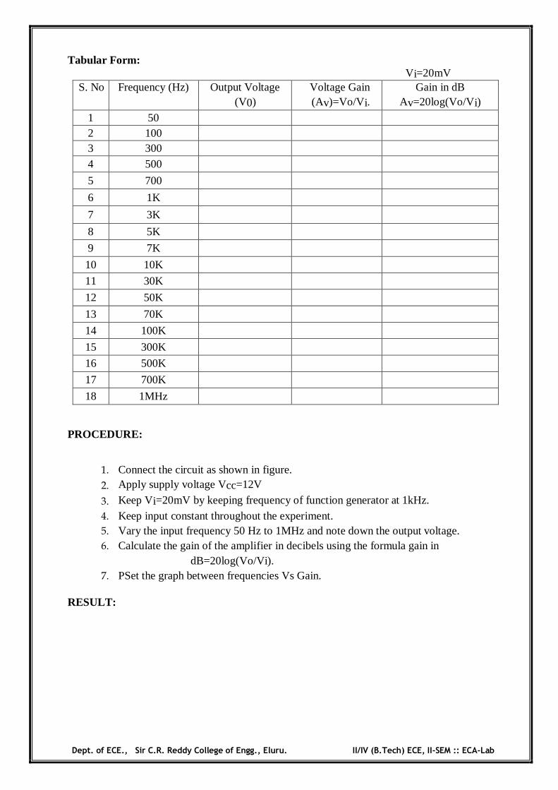
Tabular Form: Vi=20mV
S. No Frequency (Hz) Output Voltage (V0)
Voltage Gain (Av)=Vo/Vi.
Gain in dB Av=20log(Vo/Vi)
1 50
2 100
3 300
4 500
5 700
6 1K
7 3K
8 5K
9 7K
10 10K
11 30K
12 50K
13 70K
14 100K
15 300K
16 500K
17 700K
18 1MHz
PROCEDURE:
1. Connect the circuit as shown in figure. 2. Apply supply voltage Vcc=12 V
3. Keep Vi=20 mV by keeping frequency of function generator at 1kHz. 4. Keep input constant throughout the experiment. 5. Vary the input frequency 50 Hz to 1 MHz and note down the output voltage. 6. Calculate the gain of the amplifier in decibels using the formula gain in
dB=20log(Vo/Vi). 7. PSet the graph between frequencies Vs Gain.
RESULT:
Dept. of ECE., Sir C.R. Reddy College of Engg., Eluru. II/IV (B.Tech) ECE, II-SEM :: ECA-Lab
VIVA-VOCE QUESTIONS:
1. Why do you need more than one stage of amplifiers in practical circuits? 2. What is the effect of cascading on gain and bandwidth? 3. What happens to the 3dB frequencies if the number of stages of amplifiers increases? 4. Why we use a logarithmic scale to denote voltage or power gains, instead of using
the simpler linear scale? 5. What is loading effect in multistage amplifiers? 6. How a Darlington pair works? 7. The cascode amplifier is a multistage configuration of ? 8. The output impedance of a Darlington pair Amplifier is ? 9. The current gain of a Darlington pair amplifier is approximately?
The CE amplifier configuration is preferred over others. why?

Dept. of ECE., Sir C.R. Reddy College of Engg., Eluru. II/IV (B.Tech) ECE, II-SEM :: ECA-Lab
Dept. of ECE., Sir C.R. Reddy College of Engg., Eluru. II/IV (B.Tech) ECE, II-SEM :: ECA-Lab
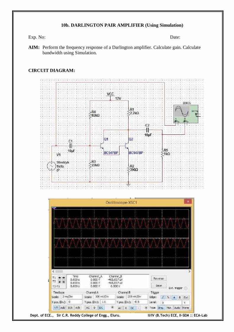
10b. DARLINGTON PAIR AMPLIFIER (Using Simulation) Exp. No: Date:
AIM: Perform the frequency response of a Darlington amplifier. Calculate gain. Calculate bandwidth using Simulation.
CIRCUIT DIAGRAM:
Dept. of ECE., Sir C.R. Reddy College of Engg., Eluru. II/IV (B.Tech) ECE, II-SEM :: ECA-Lab
Tabular Form: Vi=20mV
S. No Frequency (Hz) Output Voltage (V0)
Voltage Gain (Av)=Vo/Vi.
Gain in dB Av=20log(Vo/Vi)
1 50
2 100
3 300
4 500
5 700
6 1K
7 3K
8 5K
9 7K
10 10K
11 30K
12 50K
13 70K
14 100K
15 300K
16 500K
17 700K
18 1MHz
PROCEDURE:
1. Connect the circuit as shown in figure. 2. Apply supply voltage Vcc=12V
3. Keep Vi=20mV by keeping frequency of function generator at 1kHz. 4. Keep input constant throughout the experiment. 5. Vary the input frequency 50 Hz to 1MHz and note down the output voltage. 6. Calculate the gain of the amplifier in decibels using the formula gain in
dB=20log(Vo/Vi). 7. PSet the graph between frequencies Vs Gain.
RESULT:

Dept. of ECE., Sir C.R. Reddy College of Engg., Eluru. II/IV (B.Tech) ECE, II-SEM :: ECA-Lab
11a. SERIES FED CLASS-A POWER AMPLIFIER Exp. No: Date:
AIM: To design a series fed class-A power amplifier in order to achieve max output ac power and efficiency using hardware.
COMPONENTS REQUIRED:
1. Transistor (NPN, Si) BC 107 : 1 Nos.
2. Electrolytic Capacitor 100 nF : 2 Nos.
3. Carbon film Resistors 1 kΩ, 33 Ω and 20 kΩ: 1 No. each
MEASURING INSTRUMENTS:
1. 20 MHz Dual trace CRO : 1 No.
2. Multimeter : 2 Nos.
MISCELLANEOUS:
1. Power Supply 0-30 V DC : 1 No.
2. Bread Board : 1 No.
3. Connecting Wires : 1 Set
CIRCUIT DIAGRAM:
TABULAR FORM: Vin=100 mV
Applied frequency Output voltage(V0) Gain in dB=20log(V0/Vi)
1kHz

Dept. of ECE., Sir C.R. Reddy College of Engg., Eluru. II/IV (B.Tech) ECE, II-SEM :: ECA-Lab
THEORY:
The circuit is called “series fed” because the load RL is connected in series with transistor
output. It is also called as direct coupled amplifier. ICQ=Zero signal collector current
VCEQ=Zero signal collector to emitter voltage power amplifiers are mainly used to deliver more
power to the load. To deliver more power it requires large input signals, so generally power
amplifiers are proceeded by a series of voltage amplifiers. In class-A power amplifiers, Q-point
is located in the middle of DC- load line. So output current flows from complete cycle of input
signal. Under zero signal condition, maximum power dissipation occurs across the transistor. As
the input signal amplitude increases power dissipation reduces. The maximum theoretical
efficiency is 25%.
CALCULATIONS: Take RL=RC=220 Ω
1. DC input power PDC = = ----------------------
2. AC output power PAC= =----------------------
3. Efficiency η = =----------------------
PROCEDURE
1. Connect the circuit diagram and supply the required DC supply.
2. Apply the Ac signal at the input and keep the frequency at 1 kHz and connect the
power output meter at the output. Change the load resistance in steps for each value of
impedance and not down the output power.
3. PSet the graph between o/p power and load impedance. From this graph find the
impedance for which the o/p power is maximum. This is the value of optimum load.
4. Select load impedance which is equal to 0 V or near about the optimum load. See the
waveform of the o/p of the CRO.
5. Calculate the power sensitivity at a maximum power o/p using the relation.
The maximum input signal amplitude which produces undistorted output signal is
.
The practical efficiency of the circuit is .
RESULT:
Dept. of ECE., Sir C.R. Reddy College of Engg., Eluru. II/IV (B.Tech) ECE, II-SEM :: ECA-Lab
VIVA –VOCE QUESTIONS:
1. Differentiate between voltage amplifier and power amplifier?
2. Why power amplifiers are considered as large signal amplifier?
3. When does maximum power dissipation happen in this circuit?
4. What is the maximum theoretical efficiency?
5. Sketch waveform of output current with respective input signal?
6. What are the different types of class-A power amplifiers available?
7. What is the theoretical efficiency of the transformer coupled class-A power amplifier?
8. What is the difference in AC and DC load line?
9. How do you locate the Q-point?
10. What are the applications of class-A power amplifier?

Dept. of ECE., Sir C.R. Reddy College of Engg., Eluru. II/IV (B.Tech) ECE, II-SEM :: ECA-Lab

Dept. of ECE., Sir C.R. Reddy College of Engg., Eluru. II/IV (B.Tech) ECE, II-SEM :: ECA-Lab
11b. SERIES FED CLASS-A POWER AMPLIFIER (Using Simulation) Exp. No: Date: PRELAB:
Study the classification and operation of Small signal and large signal amplifier.
OBJECTIVE:
To observe input and output power of class A Power amplifier, and also calculate
Bandwidth.
SIMULATION TOOL:
Multisim
APPARATUS:
THEORY:
The amplifier is said to be class A power amplifier if the q point and the input signal are
selected such that the output signal is obtained for a full input cycle. For this class the position of q
point is approximately at the mid-point of the load line. For all the values of input signal the
transistor remains in the active region and never entire into the cutoff or saturation region. The
collector current flows for 3600 (life cycle) of the input signal in other words the angle of the
collector current flow is 3600 the class a amplifiers or furthers classified as directly coupled and
transformer coupled and transformer coupled amplifiers in directly coupled type .The load is
directly connected in the collector circuit while in the transformer coupled type, the load is coupled
to the collector using the transformer.
Advantages:
1. Distortion analysis is very important 2. It amplifies audio frequency signals faithfully hence they are called as audio amplifiers
S. No Name Range / Value Quantity
1 D.C Regulated Power Supply (0 – 30V) 1 2 Resistors 100K, 560Ω, 470Ω 1 3 Capacitors 2.2µF ,100uF 1 5 Inductor 1mH 1 6 CRO -- 1
7 Watt meters -- 2
Dept. of ECE., Sir C.R. Reddy College of Engg., Eluru. II/IV (B.Tech) ECE, II-SEM :: ECA-Lab
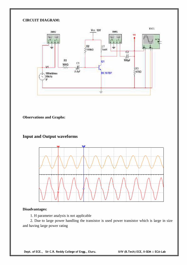
CIRCUIT DIAGRAM:
Observations and Graphs:
Input and Output waveforms
Disadvantages:
1. H parameter analysis is not applicable 2. Due to large power handling the transistor is used power transistor which is large in size and having large power rating

Dept. of ECE., Sir C.R. Reddy College of Engg., Eluru. II/IV (B.Tech) ECE, II-SEM :: ECA-Lab
PROCEDURE:
1. Enter in to the Multisim 2013 software. 2. Customize the screen and then draw the circuit on the screen with the help of mouse. 3. Connect the WATTMETERS on both input and output side. 4. The input terminal is connected to one terminal of CRO and output to other terminal. 5. Start the simulation and observe the input and output waveforms. 6. Note down the values of input and output powers from Watt meters.
CALCULATIONS:
Efficiency (Pac/ PDC) = __________________
P ac = VccIc ; PDC = Vm/2RL = V2pp/8RL
%η = Pac/ PDC X 100
RESULT & DISCUSSION:
Frequency and Phase response:
Review Questions:

Dept. of ECE., Sir C.R. Reddy College of Engg., Eluru. II/IV (B.Tech) ECE, II-SEM :: ECA-Lab
1. Explain the operation of Class A power amplifier?
2. What are the advantages of Class A Power amplifier?
3. What is the efficiency of Class A power amplifier?
4. What is the difference between Small and Large signal Amplifiers?
***
Dept. of ECE., Sir C.R. Reddy College of Engg., Eluru. II/IV (B.Tech) ECE, II-SEM :: ECA-Lab
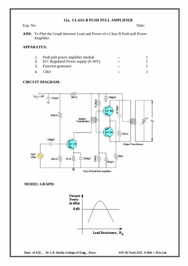
12a. CLASS-B PUSH PULL AMPLIFIER Exp. No: Date:
AIM: To PSet the Graph between Load and Power of a Class B Push pull Power Amplifier.
APPARATUS:
1. Push pull power amplifier module -- 1 2. D.C Regulated Power supply (0-30V). -- 1 3. Function generator -- 1
4. CRO -- 1
CIRCUIT DIAGRAM:
MODEL GRAPH:
Dept. of ECE., Sir C.R. Reddy College of Engg., Eluru. II/IV (B.Tech) ECE, II-SEM :: ECA-Lab
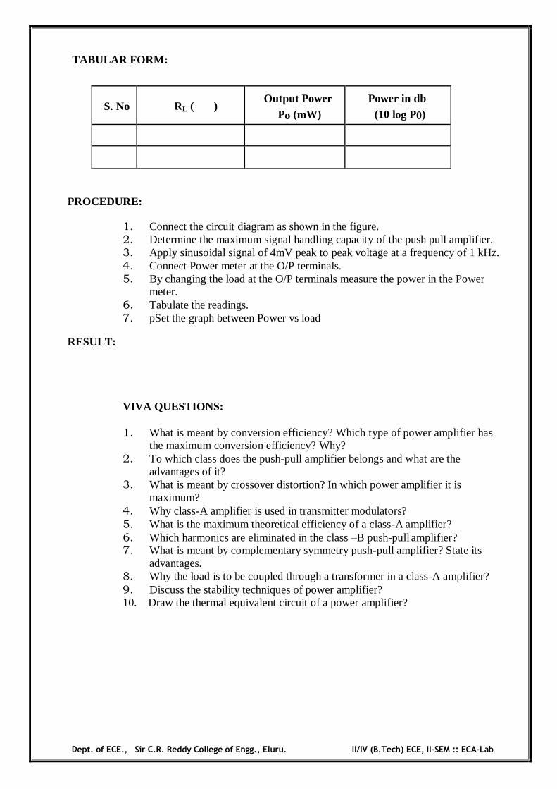
TABULAR FORM:
S. No
RL ( ) Output Power
Po (mW) Power in db
(10 log P0)
PROCEDURE:
1. Connect the circuit diagram as shown in the figure. 2. Determine the maximum signal handling capacity of the push pull amplifier. 3. Apply sinusoidal signal of 4mV peak to peak voltage at a frequency of 1 kHz. 4. Connect Power meter at the O/P terminals. 5. By changing the load at the O/P terminals measure the power in the Power
meter. 6. Tabulate the readings. 7. pSet the graph between Power vs load
RESULT:
VIVA QUESTIONS:
1. What is meant by conversion efficiency? Which type of power amplifier has the maximum conversion efficiency? Why?
2. To which class does the push-pull amplifier belongs and what are the advantages of it?
3. What is meant by crossover distortion? In which power amplifier it is maximum?
4. Why class-A amplifier is used in transmitter modulators? 5. What is the maximum theoretical efficiency of a class-A amplifier? 6. Which harmonics are eliminated in the class –B push-pull amplifier? 7. What is meant by complementary symmetry push-pull amplifier? State its
advantages. 8. Why the load is to be coupled through a transformer in a class-A amplifier? 9. Discuss the stability techniques of power amplifier? 10. Draw the thermal equivalent circuit of a power amplifier?
Dept. of ECE., Sir C.R. Reddy College of Engg., Eluru. II/IV (B.Tech) ECE, II-SEM :: ECA-Lab
12b. CLASS-B POWER AMPLIFIER Exp. No: Date:
PRELAB:
Study the operation of Class B Power amplifier
Identify various distortions occurred in Class B
Identify the different ways to avoid Distortions in class B power amplifier
OBJECTIVE:
To observe input and output power of class B Power amplifier, and also calculate
Bandwidth.
SIMULATION TOOL:
Multisim
APPARATUS:
THEORY:
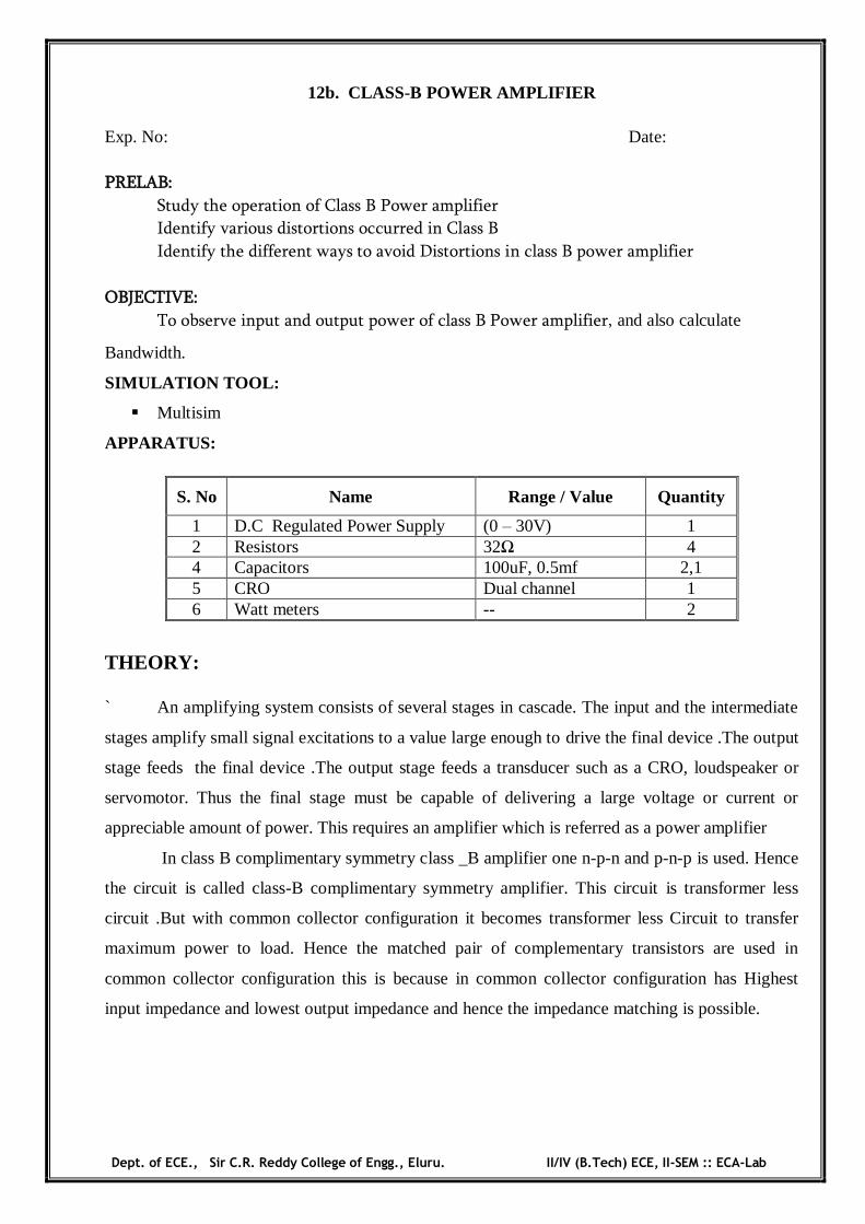
` An amplifying system consists of several stages in cascade. The input and the intermediate
stages amplify small signal excitations to a value large enough to drive the final device .The output
stage feeds the final device .The output stage feeds a transducer such as a CRO, loudspeaker or
servomotor. Thus the final stage must be capable of delivering a large voltage or current or
appreciable amount of power. This requires an amplifier which is referred as a power amplifier
In class B complimentary symmetry class _B amplifier one n-p-n and p-n-p is used. Hence
the circuit is called class-B complimentary symmetry amplifier. This circuit is transformer less
circuit .But with common collector configuration it becomes transformer less Circuit to transfer
maximum power to load. Hence the matched pair of complementary transistors are used in
common collector configuration this is because in common collector configuration has Highest
input impedance and lowest output impedance and hence the impedance matching is possible.
S. No Name Range / Value Quantity
1 D.C Regulated Power Supply (0 – 30V) 1 2 Resistors 32Ω 4 4 Capacitors 100uF, 0.5mf 2,1 5 CRO Dual channel 1
6 Watt meters -- 2

Dept. of ECE., Sir C.R. Reddy College of Engg., Eluru. II/IV (B.Tech) ECE, II-SEM :: ECA-Lab
CIRCUIT DIAGRAM:
Class B Complementary Symmetry Power Amplifier OBSERVATIONS:
Input and output waveforms PROCEDURE:
1. Enter in to the Multisim 2013 software.
2. Customize the screen and then draw the circuit on the screen with the help of mouse.
3. Connect Two Wattmeter and CRO on both input and output side.
4. The input terminal is connected to one terminal of CRO and output to other terminal.
5. Start the simulation and observe the input and output waveforms.
6. Note down the values of VO & VI and find AC and DC power.
7. Hence find efficiency
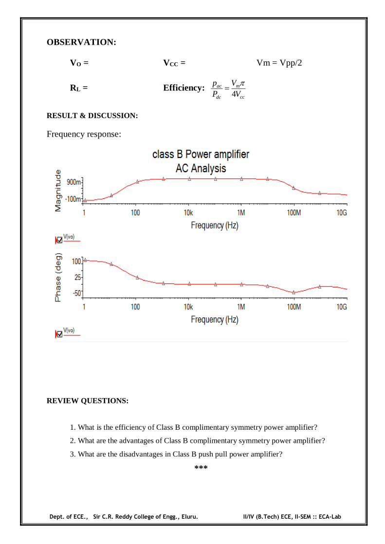
Dept. of ECE., Sir C.R. Reddy College of Engg., Eluru. II/IV (B.Tech) ECE, II-SEM :: ECA-Lab
OBSERVATION:
VO = VCC = Vm = Vpp/2
RL = Efficiency: 4
ac m
ccdc
p VP V
RESULT & DISCUSSION:
Frequency response:
REVIEW QUESTIONS:
1. What is the efficiency of Class B complimentary symmetry power amplifier?
2. What are the advantages of Class B complimentary symmetry power amplifier?
3. What are the disadvantages in Class B push pull power amplifier?
***
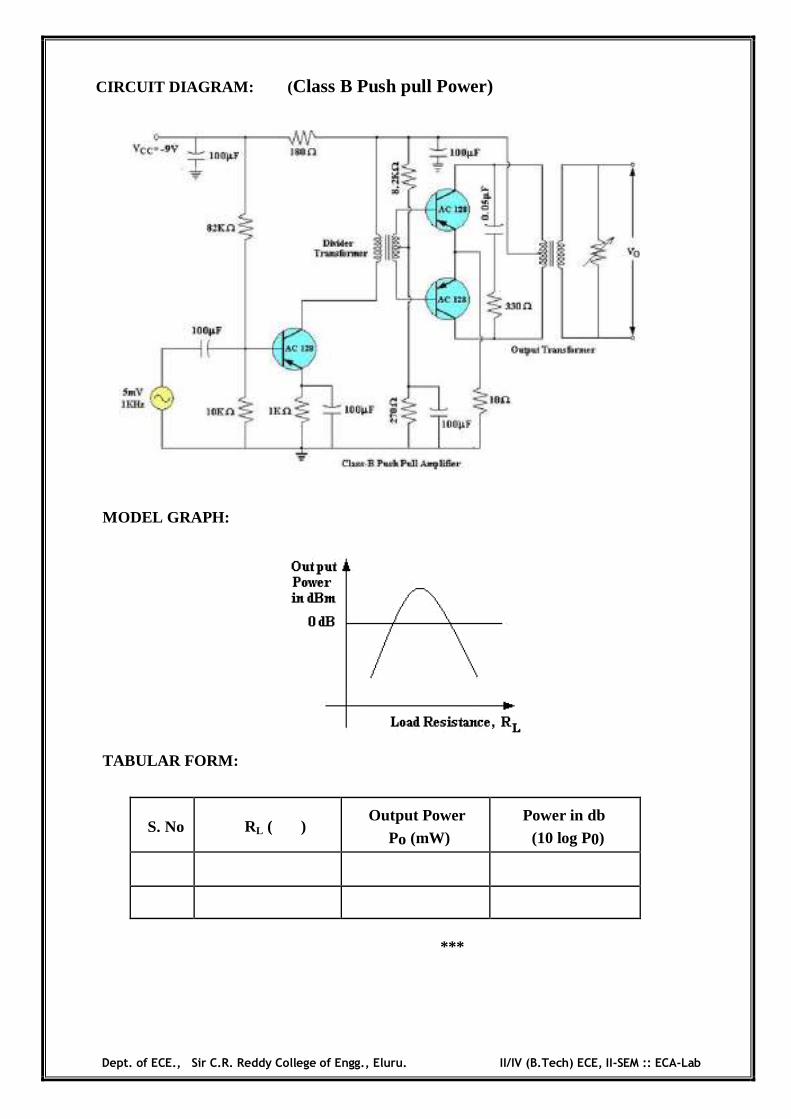
Dept. of ECE., Sir C.R. Reddy College of Engg., Eluru. II/IV (B.Tech) ECE, II-SEM :: ECA-Lab
CIRCUIT DIAGRAM: (Class B Push pull Power)
MODEL GRAPH:
TABULAR FORM:
S. No
RL ( ) Output Power
Po (mW) Power in db
(10 log P0)
***
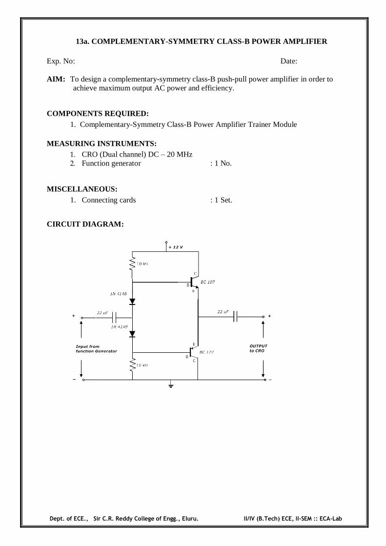
Dept. of ECE., Sir C.R. Reddy College of Engg., Eluru. II/IV (B.Tech) ECE, II-SEM :: ECA-Lab
13a. COMPLEMENTARY-SYMMETRY CLASS-B POWER AMPLIFIER Exp. No: Date: AIM: To design a complementary-symmetry class-B push-pull power amplifier in order to
achieve maximum output AC power and efficiency.
COMPONENTS REQUIRED: 1. Complementary-Symmetry Class-B Power Amplifier Trainer Module
MEASURING INSTRUMENTS:
1. CRO (Dual channel) DC – 20 MHz 2. Function generator : 1 No.
MISCELLANEOUS: 1. Connecting cards : 1 Set.
CIRCUIT DIAGRAM:
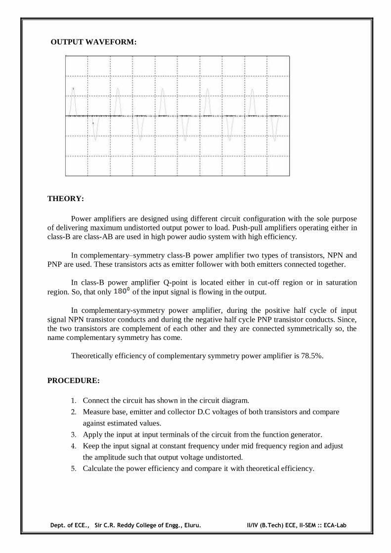
Dept. of ECE., Sir C.R. Reddy College of Engg., Eluru. II/IV (B.Tech) ECE, II-SEM :: ECA-Lab
OUTPUT WAVEFORM:
THEORY:
Power amplifiers are designed using different circuit configuration with the sole purpose of delivering maximum undistorted output power to load. Push-pull amplifiers operating either in class-B are class-AB are used in high power audio system with high efficiency.
In complementary–symmetry class-B power amplifier two types of transistors, NPN and PNP are used. These transistors acts as emitter follower with both emitters connected together.
In class-B power amplifier Q-point is located either in cut-off region or in saturation region. So, that only of the input signal is flowing in the output.
In complementary-symmetry power amplifier, during the positive half cycle of input signal NPN transistor conducts and during the negative half cycle PNP transistor conducts. Since, the two transistors are complement of each other and they are connected symmetrically so, the name complementary symmetry has come.
Theoretically efficiency of complementary symmetry power amplifier is 78.5%.
PROCEDURE:
1. Connect the circuit has shown in the circuit diagram.
2. Measure base, emitter and collector D.C voltages of both transistors and compare
against estimated values.
3. Apply the input at input terminals of the circuit from the function generator.
4. Keep the input signal at constant frequency under mid frequency region and adjust
the amplitude such that output voltage undistorted.
5. Calculate the power efficiency and compare it with theoretical efficiency.
Dept. of ECE., Sir C.R. Reddy College of Engg., Eluru. II/IV (B.Tech) ECE, II-SEM :: ECA-Lab
OBSERVATIONS:
Efficiency is defined as the ratio of AC output power to DC input power
DC input power = VCC × ICQ; AC output power = VP-P2/8RL
CALCULATIONS:
Input DC power = VCC × ICQ;
Output AC power = Vrms x Irms= VPP2 / 8RL,
η =
RESULT:
The maximum input signal amplitude which produces undistorted output signal is -----------------
The practical efficiency of the circuit is
VIVA VOCE QUESTIONS:
1. Differentiate between voltage amplifier and power amplifier.
2. Explain impedance matching provided by transformer.
3. Under what condition power dissipation is maximum for transistor in this
circuit?
4. What is the maximum theoretical efficiency?
5. Sketch current waveform in each transistor with respective input signal.
6. How do you test matched transistors required for this circuit with DMM?
7. What is the theoretical efficiency of the complementary stage amplifier?
8. How do you measure DC and AC output of this amplifier?
9. Is this amplifier working in class A or B.?
10. How can you reduce cross over distortion?

Dept. of ECE., Sir C.R. Reddy College of Engg., Eluru. II/IV (B.Tech) ECE, II-SEM :: ECA-Lab
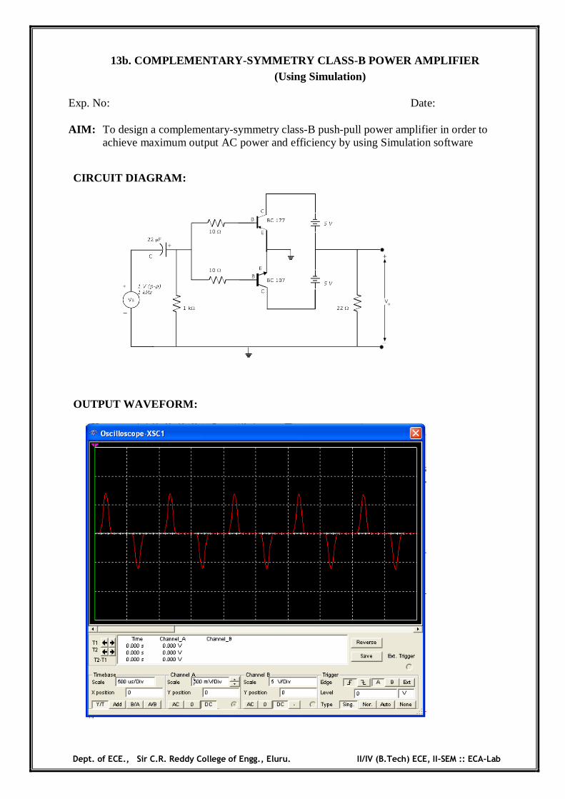
Dept. of ECE., Sir C.R. Reddy College of Engg., Eluru. II/IV (B.Tech) ECE, II-SEM :: ECA-Lab
13b. COMPLEMENTARY-SYMMETRY CLASS-B POWER AMPLIFIER (Using Simulation)
Exp. No: Date: AIM: To design a complementary-symmetry class-B push-pull power amplifier in order to
achieve maximum output AC power and efficiency by using Simulation software
CIRCUIT DIAGRAM:
OUTPUT WAVEFORM:
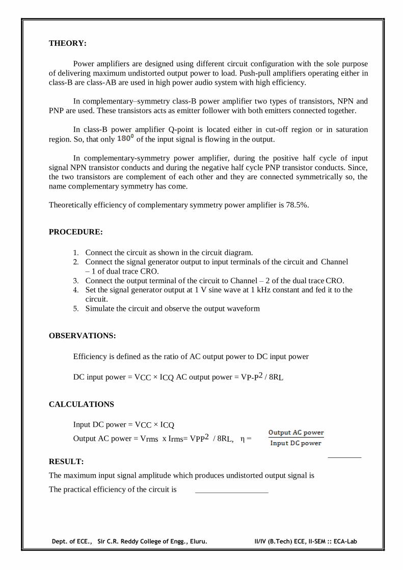
Dept. of ECE., Sir C.R. Reddy College of Engg., Eluru. II/IV (B.Tech) ECE, II-SEM :: ECA-Lab
THEORY:
Power amplifiers are designed using different circuit configuration with the sole purpose of delivering maximum undistorted output power to load. Push-pull amplifiers operating either in class-B are class-AB are used in high power audio system with high efficiency.
In complementary–symmetry class-B power amplifier two types of transistors, NPN and PNP are used. These transistors acts as emitter follower with both emitters connected together.
In class-B power amplifier Q-point is located either in cut-off region or in saturation region. So, that only of the input signal is flowing in the output.
In complementary-symmetry power amplifier, during the positive half cycle of input signal NPN transistor conducts and during the negative half cycle PNP transistor conducts. Since, the two transistors are complement of each other and they are connected symmetrically so, the name complementary symmetry has come. Theoretically efficiency of complementary symmetry power amplifier is 78.5%.
PROCEDURE:
1. Connect the circuit as shown in the circuit diagram. 2. Connect the signal generator output to input terminals of the circuit and Channel
– 1 of dual trace CRO. 3. Connect the output terminal of the circuit to Channel – 2 of the dual trace CRO. 4. Set the signal generator output at 1 V sine wave at 1 kHz constant and fed it to the
circuit. 5. Simulate the circuit and observe the output waveform
OBSERVATIONS:
Efficiency is defined as the ratio of AC output power to DC input power
DC input power = VCC × ICQ AC output power = VP-P2 / 8RL
CALCULATIONS
Input DC power = VCC × ICQ
Output AC power = Vrms x Irms= VPP2 / 8RL, η =
RESULT:
The maximum input signal amplitude which produces undistorted output signal is
The practical efficiency of the circuit is
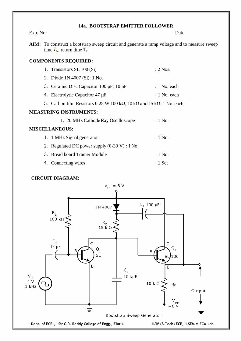
Dept. of ECE., Sir C.R. Reddy College of Engg., Eluru. II/IV (B.Tech) ECE, II-SEM :: ECA-Lab
14a. BOOTSTRAP EMITTER FOLLOWER Exp. No: Date: AIM: To construct a bootstrap sweep circuit and generate a ramp voltage and to measure sweep
time , return time . COMPONENTS REQUIRED:
1. Transistors SL 100 (Si) : 2 Nos.
2. Diode 1N 4007 (Si): 1 No.
3. Ceramic Disc Capacitor 100 µF, 10 nF : 1 No. each
4. Electrolytic Capacitor 47 µF : 1 No. each
5. Carbon film Resistors 0.25 W 100 kΩ, 10 kΩ and 15 kΩ : 1 No. each
MEASURING INSTRUMENTS:
1. 20 MHz Cathode Ray Oscilloscope : 1 No.
MISCELLANEOUS:
1. 1 MHz Signal generator : 1 No.
2. Regulated DC power supply (0-30 V) : 1 No.
3. Bread board Trainer Module : 1 No.
4. Connecting wires : 1 Set
CIRCUIT DIAGRAM:
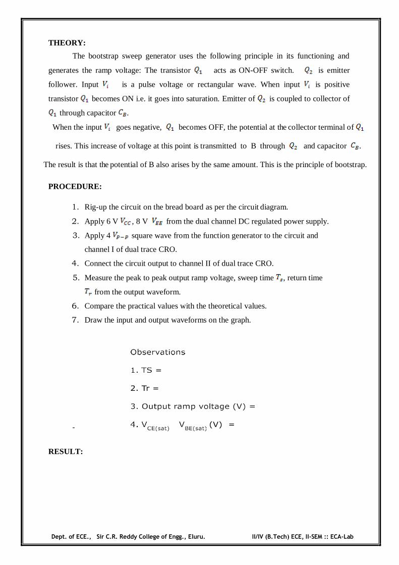
Dept. of ECE., Sir C.R. Reddy College of Engg., Eluru. II/IV (B.Tech) ECE, II-SEM :: ECA-Lab
THEORY:
The bootstrap sweep generator uses the following principle in its functioning and
generates the ramp voltage: The transistor acts as ON-OFF switch. is emitter
follower. Input is a pulse voltage or rectangular wave. When input is positive
transistor becomes ON i.e. it goes into saturation. Emitter of is coupled to collector of
through capacitor .
When the input goes negative, becomes OFF, the potential at the collector terminal of
rises. This increase of voltage at this point is transmitted to B through and capacitor .
The result is that the potential of B also arises by the same amount. This is the principle of bootstrap.
PROCEDURE:
1. Rig-up the circuit on the bread board as per the circuit diagram.
2. Apply 6 V , 8 V from the dual channel DC regulated power supply.
3. Apply 4 square wave from the function generator to the circuit and
channel I of dual trace CRO.
4. Connect the circuit output to channel II of dual trace CRO.
5. Measure the peak to peak output ramp voltage, sweep time , return time
from the output waveform.
6. Compare the practical values with the theoretical values.
7. Draw the input and output waveforms on the graph.
RESULT:
Dept. of ECE., Sir C.R. Reddy College of Engg., Eluru. II/IV (B.Tech) ECE, II-SEM :: ECA-Lab
VIVA QUESTIONS
1. Explain the basic principle involved in bootstrap sweep generator.
2. Mention the type of feedback employed in bootstrap sweep generator.
3. Mention the characteristics of the amplifier used in bootstrap sweep generator.
4. What is input resistance of the bootstrapped amplifiers?
5. What does bootstrapping mean?
6. Why bootstraping is done in a buffer amplifier?

Dept. of ECE., Sir C.R. Reddy College of Engg., Eluru. II/IV (B.Tech) ECE, II-SEM :: ECA-Lab

Dept. of ECE., Sir C.R. Reddy College of Engg., Eluru. II/IV (B.Tech) ECE, II-SEM :: ECA-Lab
14b. BOOTSTRAP EMITTER FOLLOWER (Using Simulation) Exp. No: Date: AIM: To construct a bootstrap sweep circuit and generate a ramp voltage and to measure sweep
time , return time using Simulation.
CIRCUIT DIAGRAM:
OUTPUT WAVEFORM:

Dept. of ECE., Sir C.R. Reddy College of Engg., Eluru. II/IV (B.Tech) ECE, II-SEM :: ECA-Lab
THEORETICAL CALCULATIONS
Sweep time = , Return time =
, R = 15 kΩ, C = 10 nF
PROCEDURE
1. Rig-up the circuit on the bread board as per the circuit diagram.
2. Apply 6 V , 8 V from the dual channel DC regulated power supply.
3. Apply 4 square wave from the function generator to the circuit and channel
I of dual trace CRO.
4. Connect the circuit output to channel II of dual trace CRO.
5. Measure the peak to peak output ramp voltage, sweep time , return time
from the output waveform.
6. Compare the practical values with the theoretical values.
7. Draw the input and output waveforms on the graph.
RESULT:
Dept. of ECE., Sir C.R. Reddy College of Engg., Eluru. II/IV (B.Tech) ECE, II-SEM :: ECA-Lab
Simulation Procedure:
PROCEDURE for 2 stage RC Coupled Amplifier: 1. Connect the circuit as shown in the circuit diagram. 2. Connect the signal generator output to input terminals of the circuit and Channel – A of
dual trace CRO.
3. Connect the output terminal of the circuit to Channel – B of the dual trace CRO.
4. Set the signal generator output at 10 mV sine wave at 1 kHz constant and fed it to the circuit.
5. In the Simulation tab go to analysis - AC analysis. Set the starting frequency as 20 Hz and Stop frequency 10 MHz, vertical scale as linear and no. of points per decade 1000.
6. In the output tab select Add expression write formula as 20*log((VO)/(Vi)) in the expression field. Select OK and Simulate.
7. Select the cursers and find the FH and FL from the frequency response to find out the bandwidth.
PROCEDURE for Class –C Tuned amplifier:
1. Connect the circuit as shown in the circuit diagram. 2. Connect the output terminal of the circuit to Channel – A of the dual trace CRO.
3. In the Simulation tab go to analysis - AC analysis. Set the starting frequency as 10 kHz and Stop frequency 30 kHz, vertical scale as linear and no of points per decade equal to 1000 and simulate.
4. Select the cursers and find the FT from the frequency response to find out the tuned frequency.
PROCEDURE for RC Phase shift & Wein Bridge Oscillator: 1. Connect the circuit as shown in the circuit diagram. 2. Connect the output terminal of the circuit to Channel – 1 of the dual trace CRO.
3. Simulate, adjust the potentiometer (i.e., 12 kΩ variable resistance) to get the correct
sine wave form. Place the both cursers in the CRO observe the T2– T1 as T.
4. PSet the graph for the obtained frequency
PROCEDURE for Shunt and Series Voltage Regulators: 1. Connect the circuit as shown in the circuit diagram. 2. Connect the output terminal of the circuit to Voltmeter.
3. In the Simulation tab go to analysis - DC Sweep. Set the starting value to 0 Volts and stop value 20 Volts, Steps 0.5 Volts and simulate.
4. Select the curser to find out the output voltage for the applied voltages. Note down the voltages in the respective tabular form i.e., Vin and Vout).
5. Repeat the step 4 for all the desired RL.
6. PSet the graph Vin Vs Vout
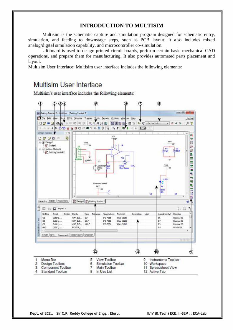
Dept. of ECE., Sir C.R. Reddy College of Engg., Eluru. II/IV (B.Tech) ECE, II-SEM :: ECA-Lab
INTRODUCTION TO MULTISIM
Multisim is the schematic capture and simulation program designed for schematic entry, simulation, and feeding to downstage steps, such as PCB layout. It also includes mixed analog/digital simulation capability, and microcontroller co-simulation.
Ultiboard is used to design printed circuit boards, perform certain basic mechanical CAD operations, and prepare them for manufacturing. It also provides automated parts placement and layout. Multisim User Interface: Multisim user interface includes the following elements:
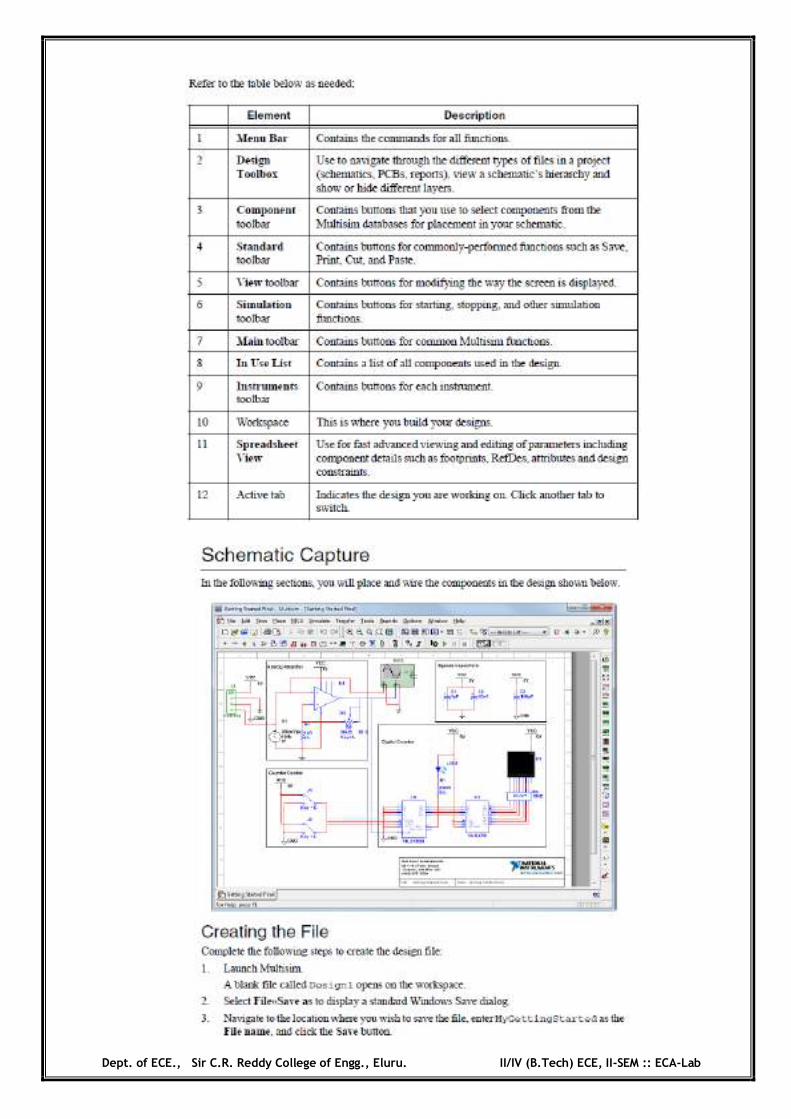
Dept. of ECE., Sir C.R. Reddy College of Engg., Eluru. II/IV (B.Tech) ECE, II-SEM :: ECA-Lab

Dept. of ECE., Sir C.R. Reddy College of Engg., Eluru. II/IV (B.Tech) ECE, II-SEM :: ECA-Lab

Dept. of ECE., Sir C.R. Reddy College of Engg., Eluru. II/IV (B.Tech) ECE, II-SEM :: ECA-Lab

Dept. of ECE., Sir C.R. Reddy College of Engg., Eluru. II/IV (B.Tech) ECE, II-SEM :: ECA-Lab
Dept. of ECE., Sir C.R. Reddy College of Engg., Eluru. II/IV (B.Tech) ECE, II-SEM :: ECA-Lab
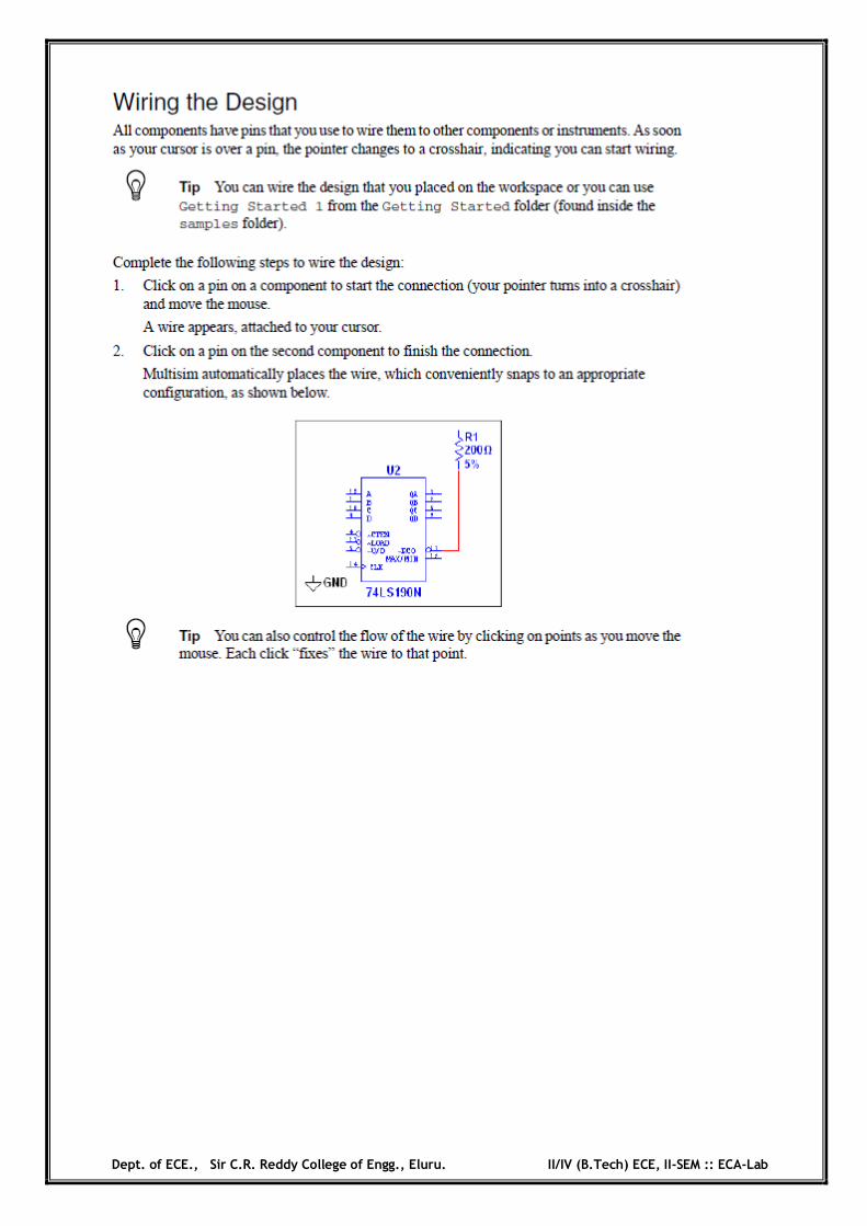
Dept. of ECE., Sir C.R. Reddy College of Engg., Eluru. II/IV (B.Tech) ECE, II-SEM :: ECA-Lab

Dept. of ECE., Sir C.R. Reddy College of Engg., Eluru. II/IV (B.Tech) ECE, II-SEM :: ECA-Lab

Dept. of ECE., Sir C.R. Reddy College of Engg., Eluru. II/IV (B.Tech) ECE, II-SEM :: ECA-Lab
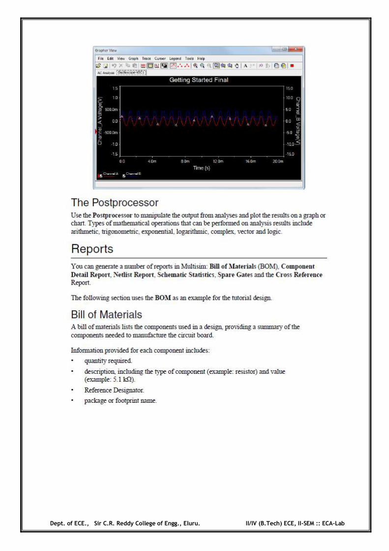
Dept. of ECE., Sir C.R. Reddy College of Engg., Eluru. II/IV (B.Tech) ECE, II-SEM :: ECA-Lab

Dept. of ECE., Sir C.R. Reddy College of Engg., Eluru. II/IV (B.Tech) ECE, II-SEM :: ECA-Lab
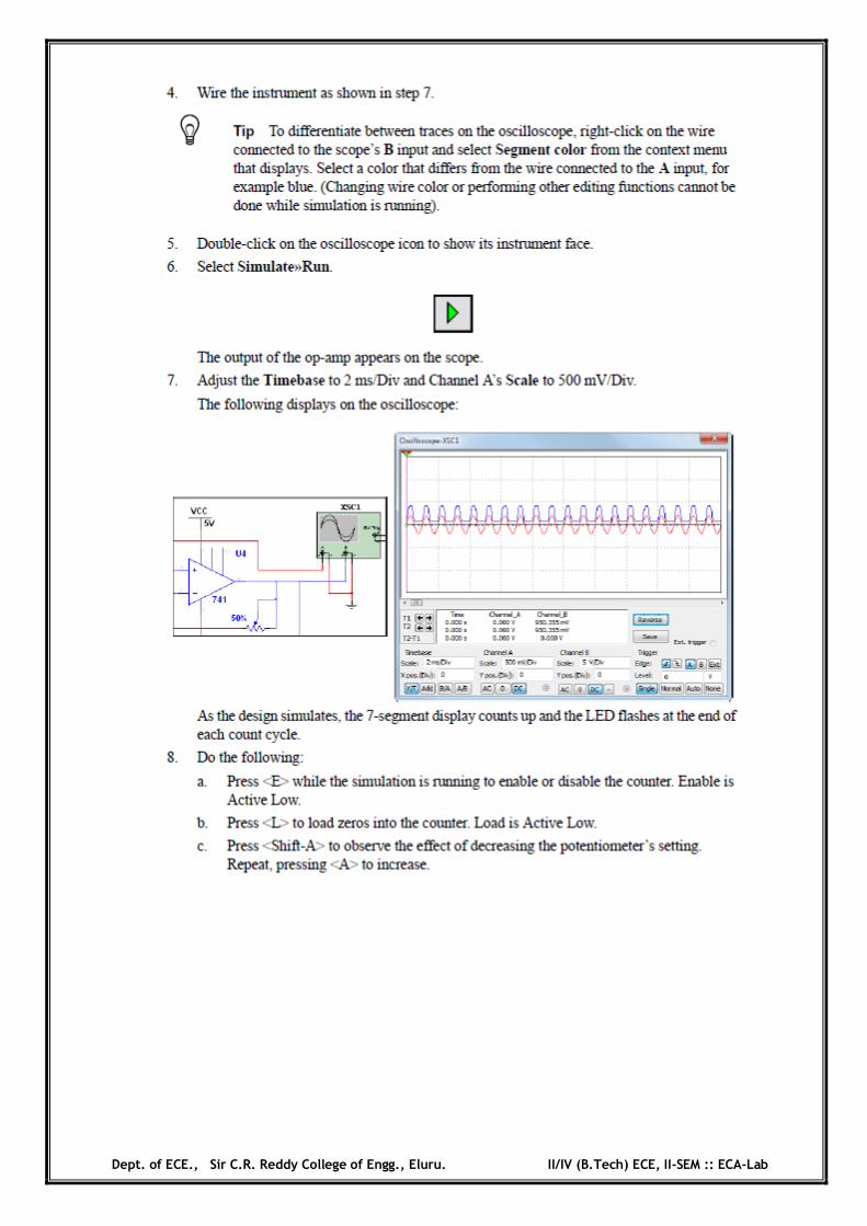
Dept. of ECE., Sir C.R. Reddy College of Engg., Eluru. II/IV (B.Tech) ECE, II-SEM :: ECA-Lab
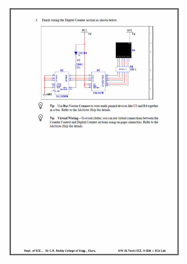
Dept. of ECE., Sir C.R. Reddy College of Engg., Eluru. II/IV (B.Tech) ECE, II-SEM :: ECA-Lab
Related Documents