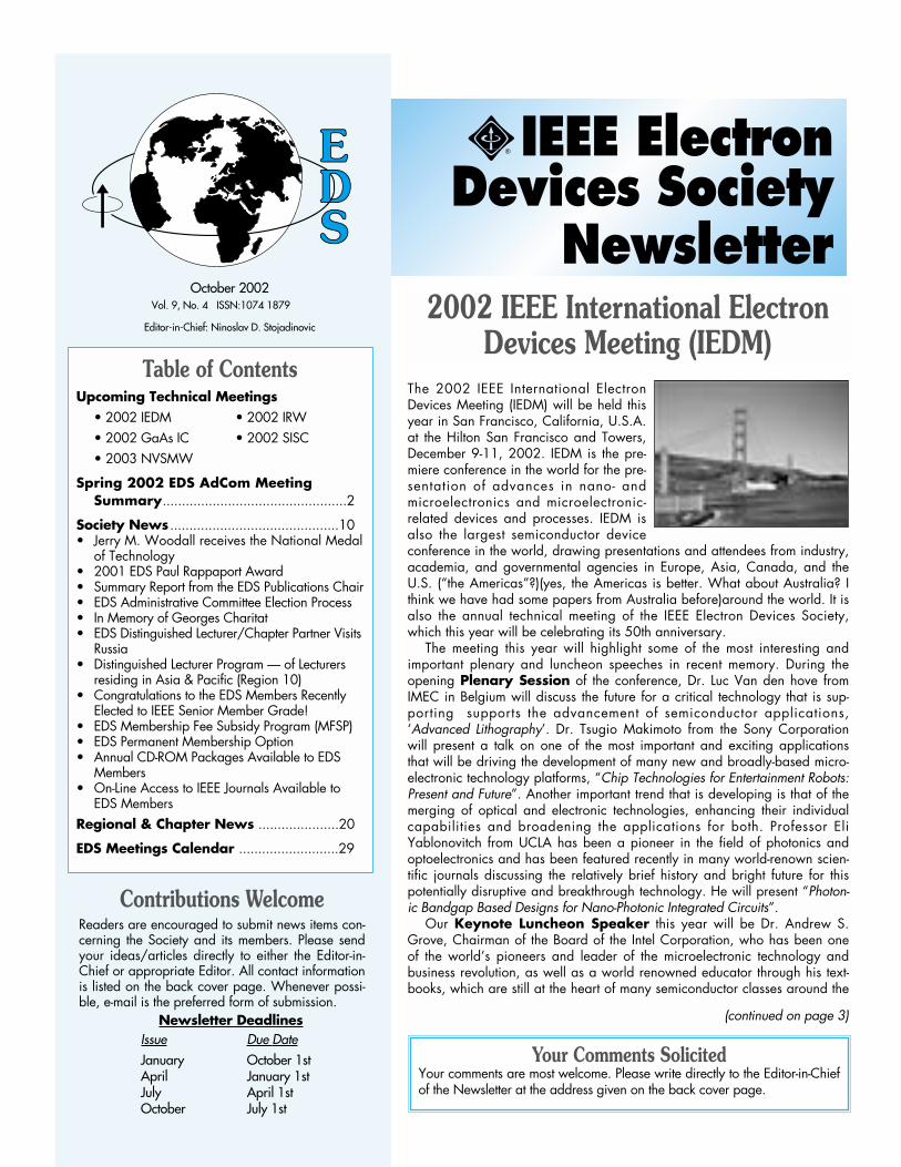
The 2002 IEEE International Electron Devices Meeting (IEDM) will be held this year in San Francisco, California, U.S.A. at the Hilton San Francisco and Towers, December 9-11, 2002. IEDM is the pre- miere conference in the world for the pre- sentation of advances in nano- and microelectronics and microelectronic- related devices and processes. IEDM is also the largest semiconductor device conference in the world, drawing presentations and attendees from industry, academia, and governmental agencies in Europe, Asia, Canada, and the U.S. (“the Americas”?)(yes, the Americas is better. What about Australia? I think we have had some papers from Australia before)around the world. It is also the annual technical meeting of the IEEE Electron Devices Society, which this year will be celebrating its 50th anniversary. The meeting this year will highlight some of the most interesting and important plenary and luncheon speeches in recent memory. During the opening Plenary Session of the conference, Dr. Luc Van den hove from IMEC in Belgium will discuss the future for a critical technology that is sup- porting supports the advancement of semiconductor applications, ‘Advanced Lithography’. Dr. Tsugio Makimoto from the Sony Corporation will present a talk on one of the most important and exciting applications that will be driving the development of many new and broadly-based micro- electronic technology platforms, “Chip Technologies for Entertainment Robots: Present and Future”. Another important trend that is developing is that of the merging of optical and electronic technologies, enhancing their individual capabilities and broadening the applications for both. Professor Eli Yablonovitch from UCLA has been a pioneer in the field of photonics and optoelectronics and has been featured recently in many world-renown scien- tific journals discussing the relatively brief history and bright future for this potentially disruptive and breakthrough technology. He will present “Photon- ic Bandgap Based Designs for Nano-Photonic Integrated Circuits”. Our Keynote Luncheon Speaker this year will be Dr. Andrew S. Grove, Chairman of the Board of the Intel Corporation, who has been one of the world’s pioneers and leader of the microelectronic technology and business revolution, as well as a world renowned educator through his text- books, which are still at the heart of many semiconductor classes around the E D S Contributions Welcome Readers are encouraged to submit news items con- cerning the Society and its members. Please send your ideas/articles directly to either the Editor-in- Chief or appropriate Editor. All contact information is listed on the back cover page. Whenever possi- ble, e-mail is the preferred form of submission. Newsletter Deadlines Issue Due Date January October 1st April January 1st July April 1st October July 1st ® Your Comments Solicited Your comments are most welcome. Please write directly to the Editor-in-Chief of the Newsletter at the address given on the back cover page. Table of Contents Upcoming Technical Meetings • 2002 IEDM • 2002 IRW • 2002 GaAs IC • 2002 SISC • 2003 NVSMW Spring 2002 EDS AdCom Meeting Summary................................................2 Society News ............................................10 • Jerry M. Woodall receives the National Medal of Technology • 2001 EDS Paul Rappaport Award • Summary Report from the EDS Publications Chair • EDS Administrative Committee Election Process • In Memory of Georges Charitat • EDS Distinguished Lecturer/Chapter Partner Visits Russia • Distinguished Lecturer Program — of Lecturers residing in Asia & Pacific (Region 10) • Congratulations to the EDS Members Recently Elected to IEEE Senior Member Grade! • EDS Membership Fee Subsidy Program (MFSP) • EDS Permanent Membership Option • Annual CD-ROM Packages Available to EDS Members • On-Line Access to IEEE Journals Available to EDS Members Regional & Chapter News .....................20 EDS Meetings Calendar ..........................29 IEEE Electron Devices Society Newsletter 2002 IEEE International Electron Devices Meeting (IEDM) (continued on page 3) October 2002 Vol. 9, No. 4 ISSN:1074 1879 Editor-in-Chief: Ninoslav D. Stojadinovic

Welcome message from author
This document is posted to help you gain knowledge. Please leave a comment to let me know what you think about it! Share it to your friends and learn new things together.
Transcript
The 2002 IEEE International ElectronDevices Meeting (IEDM) will be held thisyear in San Francisco, California, U.S.A.at the Hilton San Francisco and Towers,December 9-11, 2002. IEDM is the pre-miere conference in the world for the pre-sentation of advances in nano- andmicroelectronics and microelectronic-related devices and processes. IEDM isalso the largest semiconductor deviceconference in the world, drawing presentations and attendees from industry,academia, and governmental agencies in Europe, Asia, Canada, and theU.S. (“the Americas”?)(yes, the Americas is better. What about Australia? Ithink we have had some papers from Australia before)around the world. It isalso the annual technical meeting of the IEEE Electron Devices Society,which this year will be celebrating its 50th anniversary.
The meeting this year will highlight some of the most interesting andimportant plenary and luncheon speeches in recent memory. During theopening Plenary Session of the conference, Dr. Luc Van den hove fromIMEC in Belgium will discuss the future for a critical technology that is sup-porting supports the advancement of semiconductor applications,‘Advanced Lithography’. Dr. Tsugio Makimoto from the Sony Corporationwill present a talk on one of the most important and exciting applicationsthat will be driving the development of many new and broadly-based micro-electronic technology platforms, “Chip Technologies for Entertainment Robots:Present and Future”. Another important trend that is developing is that of themerging of optical and electronic technologies, enhancing their individualcapabilities and broadening the applications for both. Professor EliYablonovitch from UCLA has been a pioneer in the field of photonics andoptoelectronics and has been featured recently in many world-renown scien-tific journals discussing the relatively brief history and bright future for thispotentially disruptive and breakthrough technology. He will present “Photon-ic Bandgap Based Designs for Nano-Photonic Integrated Circuits”.
Our Keynote Luncheon Speaker this year will be Dr. Andrew S.Grove, Chairman of the Board of the Intel Corporation, who has been oneof the world’s pioneers and leader of the microelectronic technology andbusiness revolution, as well as a world renowned educator through his text-books, which are still at the heart of many semiconductor classes around the
EEDDSS
Contributions WelcomeReaders are encouraged to submit news items con-cerning the Society and its members. Please sendyour ideas/articles directly to either the Editor-in-Chief or appropriate Editor. All contact informationis listed on the back cover page. Whenever possi-ble, e-mail is the preferred form of submission.
Newsletter DeadlinesIssue Due DateJanuary October 1stApril January 1stJuly April 1stOctober July 1st
®
Your Comments SolicitedYour comments are most welcome. Please write directly to the Editor-in-Chiefof the Newsletter at the address given on the back cover page.
Table of ContentsUpcoming Technical Meetings
• 2002 IEDM • 2002 IRW• 2002 GaAs IC • 2002 SISC• 2003 NVSMW
Spring 2002 EDS AdCom Meeting Summary................................................2
Society News ............................................10• Jerry M. Woodall receives the National Medal
of Technology• 2001 EDS Paul Rappaport Award• Summary Report from the EDS Publications Chair• EDS Administrative Committee Election Process• In Memory of Georges Charitat• EDS Distinguished Lecturer/Chapter Partner Visits
Russia• Distinguished Lecturer Program — of Lecturers
residing in Asia & Pacific (Region 10)• Congratulations to the EDS Members Recently
Elected to IEEE Senior Member Grade!• EDS Membership Fee Subsidy Program (MFSP)• EDS Permanent Membership Option • Annual CD-ROM Packages Available to EDS
Members• On-Line Access to IEEE Journals Available to
EDS MembersRegional & Chapter News .....................20
EDS Meetings Calendar ..........................29
IEEE ElectronDevices Society
Newsletter2002 IEEE International Electron
Devices Meeting (IEDM)
(continued on page 3)
October 2002Vol. 9, No. 4 ISSN:1074 1879
Editor-in-Chief: Ninoslav D. Stojadinovic
President Steve Hillenius called the Spring Meeting of the IEEEElectron Devices Society to order on June 8th, 2002 in Honoluluprior to the 2002 VLSI Symposia.
Chair ReportsFollowing the approval of the December 2001 AdCom minutes,Steve updated the current state of the IEEE TAB budget. Againthis year, a deficit is anticipated given the existing infrastructurecosts, and the June TAB meeting will propose how to charge thetechnical societies and committees for their share.
In other actions, the EDS ExCom held a strategic planningmeeting the previous Friday to look at several future societyissues. The topics included what areas (of technology) will EDSemphasize in the future, profiling who future EDS membersmight be, what society benefits will be included with member-ship (such as periodical access), and reassessing the currenttechnical committees. In particular, EDS must broaden the baseof technical interests to embrace emerging research areas suchas nanotechnology, and ensure that these activities reflect theglobal interest and participation of its members. EDS must alsodetermine its role in two new (proposed) TAB technical commit-tees on Semiconductor Manufacturing and Display Technology,respectively.
Treasurer, Paul Yu’s report addressed EDS’ financial positionfor 2001 and 2002. Due primarily to the 2001 TAB infrastruc-ture charges of $1,986.1K and a negative return from invest-ments ($408K), EDS reserves went down by $2,384.6K for2001. For 2002, with projected IEEE fees of $1,384.9K, andconference revenue of only $130K, EDS projects a net loss of$790.8K. Paul has worked with the IEEE office to implement sev-eral cost saving measures to offset this financial condition. Paulstated that the IEEE TAB might require that EDS take measures toimprove our future finances by increasing EDS membership from$6 to $10, increase the fees for EDL and T-ED, and eliminatefuture permanent memberships. AdCom discussion on this topiccentered on three main issues; what is IEEE doing to eliminatetheir budget problems, where is EDS revenue actually coming
IEEE Electron Devices Society Newsletter ❍ October 2002
2
Electron Devices SocietyPresidentSteven J. HilleniusAgere SystemsTel: +1 908 582 6539E-Mail: [email protected]
Vice PresidentHiroshi IwaiTokyo Institute of TechnologyTel: +81 45 924 5471E-Mail: [email protected]
TreasurerPaul K. L. YuUniversity of California at San DiegoTel: +1 858 534 6180E-Mail: [email protected]
SecretaryJohn K. LowellConsultantTel: +1 972 839 4900E-Mail: [email protected]
Sr. Past PresidentBruce F. GriffingDupont OptolithographyTel: +1 512 310 6550E-Mail: [email protected]
Jr. Past PresidentCary Y. YangSanta Clara UniversityTel: +1 408 554 6814E-Mail: [email protected]
EDS Executive DirectorWilliam F. Van Der VortIEEE Operations Center445 Hoes LanePiscataway, NJ 08854Tel: +1 732 562 3926Fax: +1 732 235 1626E-Mail: [email protected]
Awards ChairAlfred U. Mac RaeMac Rae TechnologiesTel: +1 908 464 6769E-Mail: [email protected]
Educational Activities ChairIlesanmi AdesidaUniversity of IllinoisTel: +1 217 244 6379E-Mail: [email protected]
Meetings ChairKenneth F. GallowayVanderbilt UniversityTel: +1 615 322 0720E-Mail: [email protected]
Membership ChairJames B. KuoUniversity of WaterlooTel: +1 519 888 4025E-Mail: [email protected]
Publications ChairRenuka P. JindalAgere SystemsTel: +1 908 582 0438E-Mail: [email protected]
Regions/Chapters ChairHiroshi IwaiTokyo Institute of TechnologyTel: +81 45 924 5471E-Mail: [email protected]
IEEE Newsletter CoordinatorAndrea WatsonIEEE Operations Center445 Hoes LanePiscataway, NJ 08854Tel: +1 732 562 6345Fax: +1 732 981 1855E-Mail: [email protected]
IEEE Electron Devices Society Newsletter (ISSN 1074 1879) is published quarterly by the Electron Devices Society of the Institute of Electrical and ElectronicsEngineers, Inc. Headquarters: 3 Park Avenue, 17th Floor, New York, NY 10016-5997. Printed in the U.S.A. One dollar ($1.00) per member per year is included inthe Society fee for each member of the Electron Devices Society. Periodicals postage paid at New York, NY and at additional mailing offices. Postmaster: Sendaddress changes to IEEE Electron Devices Society Newsletter, IEEE, 445 Hoes Lane, P.O. Box 1331, Piscataway, NJ 08855-1331.
Copyright © 2002 by IEEE: Information contained in this Newsletter may be copied without permission provided that copies are not used or distributed for directcommercial advantage, and the title of the publication and its date appear on each photocopy.
EDS ADCOM ELECTED MEMBERS-AT-LARGE
Term Expires:
2002 2003 *2004
C. L. Claeys (1) I. Adesida (2) M. Estrada del Cueto (1)J. A. Dayton, Jr. (1) T. Hiramoto (1) K. F. Galloway (2)M. Fukuma (1) L. Lunardi (1) S. J. Hillenius (2)K. M. Lau (1) A. A. Santos (2) C. Jagadish (2)K. Lee (1) S. C. Sun (2) J. K. O. Sin (1)M. L. Ostling (1) H. S. P. Wong (1) R. Singh (2)D. L. Pulfrey (1) P. K. L. Yu (2) N.D. Stojadinovic (1)K. Shenai (2)
Number in parenthesis represents term.* Members elected 12/01 (continued on page 8)
Spring 2002 AdCom MeetingSummary
John K. Lowell
October 2002 ❍ IEEE Electron Devices Society Newsletter
3
world. His talk on the “Changing Vectorsof Moore’s Law” will be a highlight of ourconference this year.
The heart of IEDM is its TechnicalProgram. No other meeting presents asmuch leading edge work in such a broadvariety of microelectronic-related topics. Itoffers students and their professors, scien-tists, and engineers a unique opportunityto hear about the latest work being donein their disciplines and related areas, aswell as an opportunity to speak directlywith other experts and colleagues work-ing in these fields. An example of thebreadth of topics to be discussed at thisyear’s meeting is that participation byleaders in the fields of MEMS, bioelec-tronic sensors and systems, and optoelec-tronic technologies are expected amongstthese core areas:
• CMOS Devices• CMOS and Interconnect Reliability• Detectors, Sensors and Displays• Integrated Circuits and Manufacturing• Modeling and Simulation• Processing Technology• Quantum Electronics and Com-
pound Semiconductors• Solid State DevicesAs an important central core of our con-
ference, the CMOS Device sessions willcover the new breakthroughs andadvancements in the areas of devicephysics, novel MOS device structures,CMOS scaling issues, high performance,low power devices, and analog/RFdevices. Other topics of interest are SOI,strained silicon and SiGe device issues,noise behavior of MOS structures anddevice measurement and characterization.
CMOS and Interconnect Reliabili-ty will cover all areas of IC and devicereliability, both the ‘front-end’ and ‘back-end’ of the processes. Specific topics willinclude hot carriers, gate dielectric wear-out and breakdown, process chargingdamage, latch-up, ESD and soft errors. Inaddition, interconnect reliability, electromi-gration, the impact of back-end processingon devices, manufacturing technologies forreliability, as well as reliability issues forSOI and BICMOS will also be addressed.
Upcoming Technical Meetings
IEEE IEDM(continued from page 1)
The Detectors, Sensors and Dis-plays sessions will cover the design, fab-rication, reliability, theory, and modelingof the devices, structures, and integrationtechnology used for imaging, displays,detectors, sensors, and microelectro-mechanical systems (MEMS). A subset ofthese key topics includes CMOS imagers,CCD’s, TFT’s, organic, amorphous andpolycrystalline devices, vacuum micro-electronics, emissive displays and sensorsfor chemical, molecular and biologicalapplications.
Integrated Circuits and Manu-facturing focuses on advances in inte-grated circui ts, novel memory cel lconcepts, full process integration formemory, logic and mixed-mode applica-tions, and their manufacturing issues.Areas of specific interest includes processarchitectures for performance and manu-facturing advances, high-speed logic,advanced memories, multifunction inte-grated circuits, integrated passives, lowpower, low noise, analog, RF and mixedsignal ICs. Topics also include IC manu-facturing technology and methodology,process control, failure analysis, yieldenhancements and modeling.
Modeling and Simulation paperswill include analytical, numerical, andstatistical approaches to modeling elec-tron devices operation, their isolationand interconnection. Other topics includethe modeling of fabrication processesand equipment, simulation algorithms,process characterization, and parameterextraction.
The Processing Technology ses-sions will cover front-end and back-endprocess modules for the fabrication ofCMOS logic, memory, and BICMOSdevices. Topics related to front-end pro-cessing will include substrate technolo-gies, lithography, etching, isolationtechnologies, thin dielectrics, high dielec-tric constant materials for transistor andMIM capacitors, shallow junctions, RTP,silicides, and new materials. Topics relat-ed to back-end processing will includeinterconnect systems, low dielectric con-stant materials, contact and via processes,planarization, and design considerationsfor multilevel interconnects.
Quantum Electronics and Com-
pound Semiconductors will be cov-ered including wide bandgap materialswith electronic and photonic device appli-cations. Specific device structures includeFET’s, HBT’s, high-power transistors, anddevices with quantum, single electron,ballistic or spin effects. Also included arebioelectronics, self-assembly, nano- andmolecular-scale devices, LED’s, lasers,external modulators, photodetectors, opto-electronic and photonic integrated cir-cuits, and optical interconnects.
The Solid State Device sessions willdiscuss discrete and integrated high pow-er/current/voltage devices, silicon (Si)and silicon germanium (SiGe) bipolartransistors, novel analog and digitaldevices and technology, and high speedSi devices. Other integrated RF compo-nent developments to be described willinclude inductors, capacitors and switch-es, and single electron devices in siliconor silicon germanium materials systems.Other even more novel silicon-basedstructures may be included as well newmethods of assessing silicon device andmaterial performance.
The Emerging Technologies ses-sion highlights breakthroughs in impor-tant new technologies that will have amajor impact on a broad variety of appli-cations and this year it will feature invitedtalks from leading experts from aroundthe world on Bioelectronic Devices andSystems. As we enter the 21st century, itis projected that this fascinating newarea of emerging technology will play avery important role in the sensing, evalu-ating, controlling, and communicating ofcritical information in our everyday lives.
Another traditional and very popularpart of IEDM is the Short Course ses-sions. Many critical topics have beendescribed in detail to general as well asexpert audiences during this set of semi-nars over the years. This year there willbe two short courses entitled “RF DeviceTechnologies for Communication Systems”and “The Future of Semiconductor Manu-facturing”.
The very informative and often entertain-ing Evening Panel Discussions atIEDM will this year discuss and debate thefollowing questions: “Will SOI ever becomea mainstream technology?” and “Embed-
ded Memories, what makes sense (cents)?”For Registration and other infor-
mation, visit the IEDM 2002 HomePage on the World Wide Web athttp://www.ieee.org/conference/iedm,or contact Conference Managers MelissaWiderkehr and Phyllis Mahoney, 16220S. Frederick Ave., Gaithesburg, MD20877, USA; TEL: (301) 527-0900, ext.
103; FAX (301) 527-0994; or email:[email protected]
The world famous San Francisco areaprovides many attractions for visitors andwe encourage attendees to explore themin the off hours of the conference. TheIEDM organizers and committee mem-bers look forward to seeing you inDecember 2002.
Jon Candelaria IEDM Publicity Chair
Motorola Labs, Motorola Inc.Tempe, AZ, USA
Philip Wong IEDM Publicity Vice-Chair
IBM T.J. Watson Research Center Yorktown Heights, NY, USA
IEEE Electron Devices Society Newsletter ❍ October 2002
4
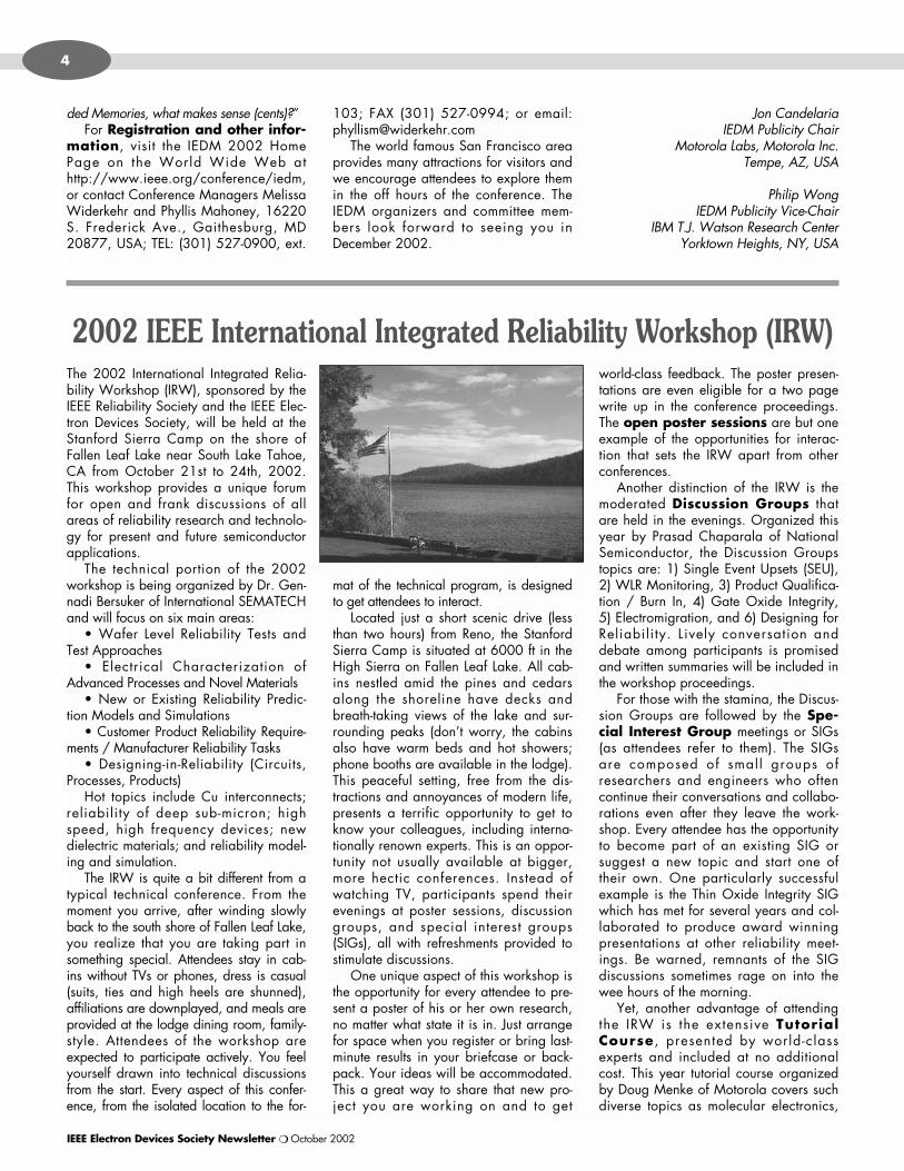
The 2002 International Integrated Relia-bility Workshop (IRW), sponsored by theIEEE Reliability Society and the IEEE Elec-tron Devices Society, will be held at theStanford Sierra Camp on the shore ofFallen Leaf Lake near South Lake Tahoe,CA from October 21st to 24th, 2002.This workshop provides a unique forumfor open and frank discussions of allareas of reliability research and technolo-gy for present and future semiconductorapplications.
The technical portion of the 2002workshop is being organized by Dr. Gen-nadi Bersuker of International SEMATECHand will focus on six main areas:
• Wafer Level Reliability Tests andTest Approaches
• Electrical Characterization ofAdvanced Processes and Novel Materials
• New or Existing Reliability Predic-tion Models and Simulations
• Customer Product Reliability Require-ments / Manufacturer Reliability Tasks
• Designing-in-Reliability (Circuits,Processes, Products)
Hot topics include Cu interconnects;reliability of deep sub-micron; highspeed, high frequency devices; newdielectric materials; and reliability model-ing and simulation.
The IRW is quite a bit different from atypical technical conference. From themoment you arrive, after winding slowlyback to the south shore of Fallen Leaf Lake,you realize that you are taking part insomething special. Attendees stay in cab-ins without TVs or phones, dress is casual(suits, ties and high heels are shunned),affiliations are downplayed, and meals areprovided at the lodge dining room, family-style. Attendees of the workshop areexpected to participate actively. You feelyourself drawn into technical discussionsfrom the start. Every aspect of this confer-ence, from the isolated location to the for-
mat of the technical program, is designedto get attendees to interact.
Located just a short scenic drive (lessthan two hours) from Reno, the StanfordSierra Camp is situated at 6000 ft in theHigh Sierra on Fallen Leaf Lake. All cab-ins nestled amid the pines and cedarsalong the shoreline have decks andbreath-taking views of the lake and sur-rounding peaks (don’t worry, the cabinsalso have warm beds and hot showers;phone booths are available in the lodge).This peaceful setting, free from the dis-tractions and annoyances of modern life,presents a terrific opportunity to get toknow your colleagues, including interna-tionally renown experts. This is an oppor-tunity not usually available at bigger,more hectic conferences. Instead ofwatching TV, participants spend theirevenings at poster sessions, discussiongroups, and special interest groups(SIGs), all with refreshments provided tostimulate discussions.
One unique aspect of this workshop isthe opportunity for every attendee to pre-sent a poster of his or her own research,no matter what state it is in. Just arrangefor space when you register or bring last-minute results in your briefcase or back-pack. Your ideas will be accommodated.This a great way to share that new pro-ject you are working on and to get
world-class feedback. The poster presen-tations are even eligible for a two pagewrite up in the conference proceedings.The open poster sessions are but oneexample of the opportunities for interac-tion that sets the IRW apart from otherconferences.
Another distinction of the IRW is themoderated Discussion Groups thatare held in the evenings. Organized thisyear by Prasad Chaparala of NationalSemiconductor, the Discussion Groupstopics are: 1) Single Event Upsets (SEU),2) WLR Monitoring, 3) Product Qualifica-tion / Burn In, 4) Gate Oxide Integrity,5) Electromigration, and 6) Designing forReliabili ty. Lively conversation anddebate among participants is promisedand written summaries will be included inthe workshop proceedings.
For those with the stamina, the Discus-sion Groups are followed by the Spe-cial Interest Group meetings or SIGs(as attendees refer to them). The SIGsare composed of smal l groups ofresearchers and engineers who oftencontinue their conversations and collabo-rations even after they leave the work-shop. Every attendee has the opportunityto become part of an existing SIG orsuggest a new topic and start one oftheir own. One particularly successfulexample is the Thin Oxide Integrity SIGwhich has met for several years and col-laborated to produce award winningpresentations at other reliability meet-ings. Be warned, remnants of the SIGdiscussions sometimes rage on into thewee hours of the morning.
Yet, another advantage of attendingthe IRW is the extensive TutorialCourse , presented by world-classexperts and included at no additionalcost. This year tutorial course organizedby Doug Menke of Motorola covers suchdiverse topics as molecular electronics,
2002 IEEE International Integrated Reliability Workshop (IRW)
October 2002 ❍ IEEE Electron Devices Society Newsletter
5
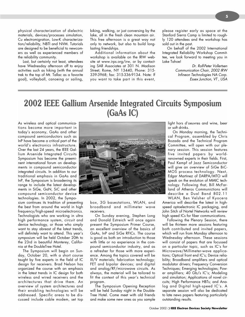
As wireless and optical communica-tions become more important intoday’s economy, GaAs and othercompound semiconductors such asInP have become a critical part of theworld’s electronics infrastructure.Over the last 24 years, the IEEE Gal-lium Arsenide Integrated CircuitsSymposium has become the preemi-nent international forum on develop-ments in compound semiconductorintegrated circuits. In addition to ourtraditional emphasis in GaAs andInP, the Symposium is broadening itsrange to include the latest develop-ments in SiGe, GaN, SiC and othercompound semiconductor devicetechnologies. In 2002, the Sympo-sium continues its tradition of presentingthe best from around the world in highfrequency/high-speed microelectronics.Technologists who are working in ultrahigh performance system, circuit anddevice technology, or those who simplywant to stay abreast of the latest trends,will definitely want to attend. This year’ssymposium will be held October 20th tothe 23rd in beautiful Monterey, Califor-nia at the DoubleTree Hotel.
The Symposium will begin on Sun-day, October 20, with a short coursetaught by five experts in the field of ICdesign for receivers. Brad Nelson hasorganized the course with an emphasisin the latest trends in IC design for bothwireless and wired receivers and thearchi tectures that drive them. Anoverview of system architectures andtheir enabling technologies wil l beaddressed. Specific areas to be dis-cussed include cable modem, set top
box, 3G basestations, WLAN, andbroadband and mil l imeter wavereceivers.
On Sunday evening, Stephen Longand Donald Estreich will once againpresent the Symposium Primer Course,an excellent overview of the basics ofGaAs, InP and SiGe RFICs. The courseis good as both an introduction to thosewith little or no experience in the com-pound semiconductor industry, and asa refresher for those with more experi-ence. Among the topics covered will beIII/V materials; fabrication technology;FET and bipolar devices; and digitaland analog/RF/microwave circuits. Asalways, the material will be tailored tofit the context of this year’s technicalprogram.
The Symposium Opening Receptionwill be held Sunday night in the Double-Tree Hotel. Come meet with old friendsand make some new ones as you sample
light hors d’oeuvres and wine, beeror soft drinks.
On Monday morning, the Techni-cal Program, assembled by ChrisBozada and the Technical ProgramCommittee, will open with our ple-nary session. This session featuresf ive invi ted papers by world-renowned experts in their fields. First,Paul Kempf of Jazz Semiconductorwill give an overview of SiGe BiC-MOS process technology. Next,Edgar Martinez of DARPA/MTO willspeak on the evolution of MMIC tech-nology. Following that, Bill McFar-land of Atheros Communictions willdescribe a Dual Band 802.11WLAN, Ben Velsher of Kyocera
America will describe the latest in high-speed optoelectronic IC packaging, andJohn Sitch of Nortel Networks will reviewhigh speed ICs for fiber communications.
Following the Plenary Session, therewill be thirteen more sessions featuringboth contributed and invited papers,which will run from Monday afternoon toWednesday afternoon. These sessionswill consist of papers that are focussedon a particular topic, such as IC’s forMicrowave/Millimeter-wave applica-tions; Optical front end IC’s; Device relia-bility; Broadband amplifiers and opticalmodulator drivers; Frequency ConversionTechniques; Emerging technologies; Pow-er amplifiers; 40 Gb/s IC’s; Modelingand simulation; Applications of novel cir-cuits; High Performance HBTs; and Ana-log and Digital high-speed IC’s. Aseparate session will also be dedicatedto late news papers featuring particularlyoutstanding results.
2002 IEEE Gallium Arsenide Integrated Circuits Symposium(GaAs IC)
physical characterization of dielectricmaterials, devices/processes simulation,Cu electromigration, Low-K characteriza-tion/reliability, NBTI and NVM. Tutorialsare designed to be beneficial to newcom-ers as well as experienced members ofthe reliability community.
Last, but certainly not least, attendeeshave Wednesday afternoon off to enjoyactivities such as hiking (with the annualtrek to the top of Mt. Tallac as a favoritegoal), volleyball, canoeing or sailing,
biking, walking, or just conversing by thelake, all in the fresh clean mountain air.This free afternoon is a great way notonly to network, but also to build long-lasting friendships.
Additional information about theworkshop is available on the IRW web-site at www.irps.org/irw, or by contact-ing SAR Associates at 301 N. MadisonStreet; Rome, NY 13440, Phone: 315-339-3968; fax: 315-336-9134. Note: Ifyou want to take part in this event,
please register early as space at theStanford Sierra Camp is limited to rough-ly 120 attendees and the workshop hassold out in the past.
On behalf of the 2002 InternationalIntegrated Reliability Workshop Commit-tee, we look forward to meeting you inLake Tahoe!
Dr. Rolf-Peter VollertsenCommunication Chair, 2002 IRW
Infineon Technologies NA Corp.Essex Junction, VT , USA
IEEE Electron Devices Society Newsletter ❍ October 2002
6
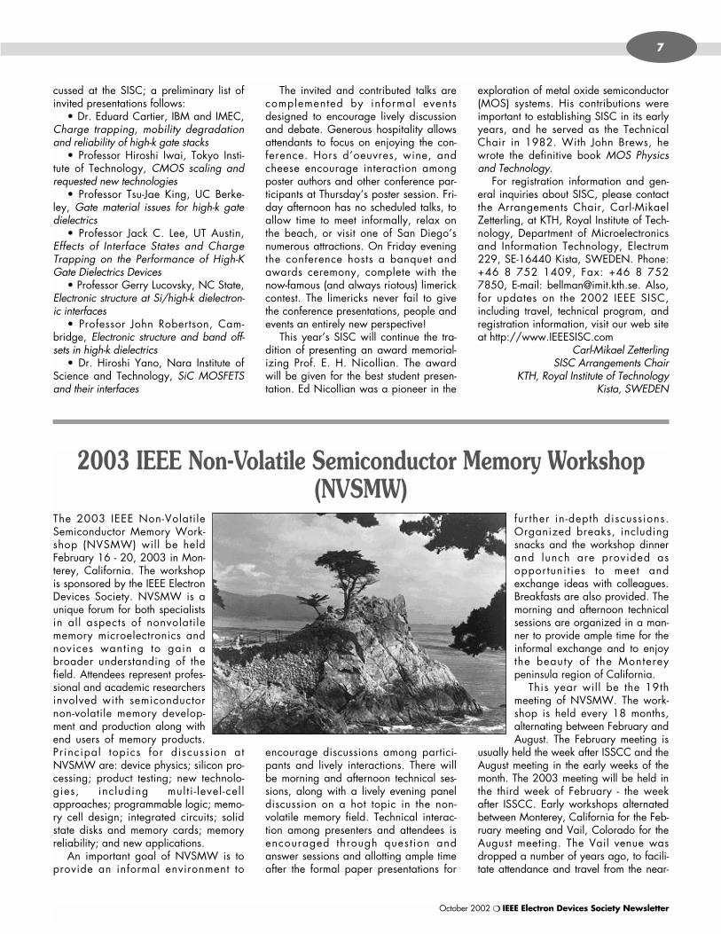
The 2002 IEEE Semiconduc-tor Interface SpecialistsConference (SISC) will be heldDecember 5-7, 2002 in SanDiego, CA, immediately prior tothe IEDM. The SISC provides aunique forum for device engi-neers, solid-state physicists, andmaterials scientists to discussissues of common interest. Princi-pal topics for discussion at SISCare semiconductor/insulatorinterfaces, the physics of insulat-ing thin films, and the interactionamong materials science, devicephysics, and state-of-the-art technology.
This year will be the thirty-third meet-ing of SISC. The first meeting was held in1965 and attendance was by invitation.The conference, now public, alternatesbetween the east and west coasts, andmeets just before the IEDM. An importantgoal of the conference is to provide anenvironment that encourages interplaybetween scientific and technologicalissues. Invited and contributed talks, aswell as a lively poster session, are pre-sented in an informal setting designed to
encourage discussion, and conferenceparticipants enjoy numerous opportuni-ties for social gatherings with renown sci-entists and engineers. Abstracts forcontributed talks are typically due in ear-ly August.
The 2002 SISC will be held at theCatamaran Resort Hotel, 3999 MissionBoulevard, San Diego, CA 92109,phone (619) 488-1081. The Catamaranis on Mission Bay, and one block fromthe Pacific Ocean (see photo). San Diegotypically has fabulous weather, which
complements the Catamaran’s luxuriousHawaiian decor. The hotel grounds arebeautifully lush with colorful fish and trop-ical birds. San Diego also boasts SeaWorld‘, a world-class zoo and historicmonuments, all within an easy drive fromthe Catamaran. Bike and boat rentalsare offered on the Catamaran premises.
The conference emphasis is on silicon-based devices, including the SiC andSiGe systems, and topics evolve with thestate-of-the-art. Invited talks at this year’sconference highlight the many areas dis-
2002 IEEE Semiconductor Interface Specialists Conference(SISC)
In addition to the paper sessions, theSymposium also features six panel sessionson controversial topics of high interest.Panels will feature a moderator and up tosix speakers. The moderator will set thetone of the discussion and the panelists willeach spend three to five minutes stakingout a position. Following that, it will be afree-for-all as audience members maketheir own points and question the panelists.Panel session topics are: The market forcompound semiconductors in defenseapplications; The future of 10Gb/s vs. 40Gb/s systems; Alternative substrate tech-nology (GaAs, InP, GaAs on Si?); The con-troversy over radio on chip vs. radio in amodule; A WLAN power amplifier technol-ogy shootout, and InP vs. SiGe for 40Gb/s communications. There will also bea new feature, our “Fab Forum” which willprovide an opportunity for potential cus-tomers, business partners, or other interest-ed parties to learn about some of the latestIC fab capabilities in our industry.
Another way to keep abreast of thelatest developments in the field will byattending the GaAs IC Technology Exhi-bition, which will be held on October 21and 22 in the Monterey Conference Cen-ter, located adjacent to the DoubleTreeHotel. The Exhibition is open to all con-ference registrants, and features a widevariety of companies who offer state-of-the-art compound semiconductor IC’s aswell as those that products and servicesto the compound semiconductor IC indus-try. An early listing of the exhibitionincluded 30 names, with more to come.The exhibitors will host an ExhibitionOpening Reception on Monday evening,as well as an Exhibition Luncheon onTuesday.
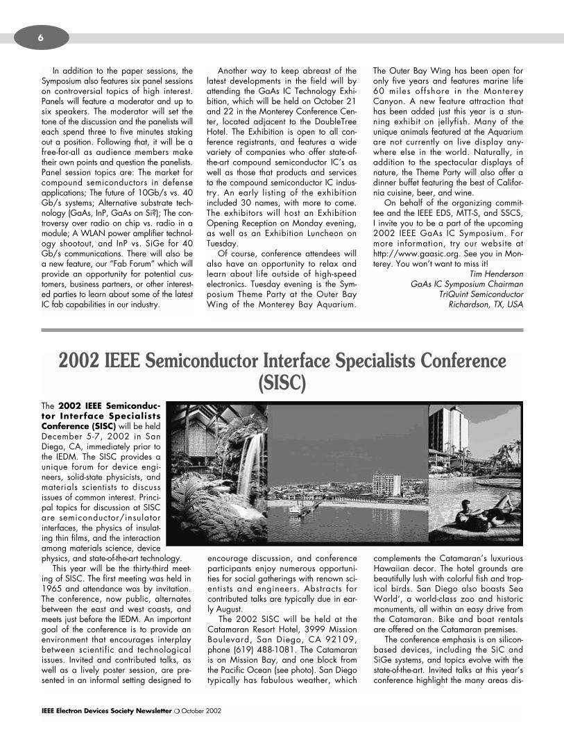
Of course, conference attendees willalso have an opportunity to relax andlearn about life outside of high-speedelectronics. Tuesday evening is the Sym-posium Theme Party at the Outer BayWing of the Monterey Bay Aquarium.
The Outer Bay Wing has been open foronly five years and features marine life60 miles offshore in the MontereyCanyon. A new feature attraction thathas been added just this year is a stun-ning exhibit on jellyfish. Many of theunique animals featured at the Aquariumare not currently on live display any-where else in the world. Naturally, inaddition to the spectacular displays ofnature, the Theme Party will also offer adinner buffet featuring the best of Califor-nia cuisine, beer, and wine.
On behalf of the organizing commit-tee and the IEEE EDS, MTT-S, and SSCS,I invite you to be a part of the upcoming2002 IEEE GaAs IC Symposium. Formore information, try our website athttp://www.gaasic.org. See you in Mon-terey. You won’t want to miss it!
Tim HendersonGaAs IC Symposium Chairman
TriQuint Semiconductor Richardson, TX, USA
October 2002 ❍ IEEE Electron Devices Society Newsletter
7
cussed at the SISC; a preliminary list ofinvited presentations follows:
• Dr. Eduard Cartier, IBM and IMEC,Charge trapping, mobility degradationand reliability of high-k gate stacks
• Professor Hiroshi Iwai, Tokyo Insti-tute of Technology, CMOS scaling andrequested new technologies
• Professor Tsu-Jae King, UC Berke-ley, Gate material issues for high-k gatedielectrics
• Professor Jack C. Lee, UT Austin,Effects of Interface States and ChargeTrapping on the Performance of High-KGate Dielectrics Devices
• Professor Gerry Lucovsky, NC State,Electronic structure at Si/high-k dielectron-ic interfaces
• Professor John Robertson, Cam-bridge, Electronic structure and band off-sets in high-k dielectrics
• Dr. Hiroshi Yano, Nara Institute ofScience and Technology, SiC MOSFETSand their interfaces
The invited and contributed talks arecomplemented by informal eventsdesigned to encourage lively discussionand debate. Generous hospitality allowsattendants to focus on enjoying the con-ference. Hors d’oeuvres, wine, andcheese encourage interaction amongposter authors and other conference par-ticipants at Thursday’s poster session. Fri-day afternoon has no scheduled talks, toallow time to meet informally, relax onthe beach, or visit one of San Diego’snumerous attractions. On Friday eveningthe conference hosts a banquet andawards ceremony, complete with thenow-famous (and always riotous) limerickcontest. The limericks never fail to givethe conference presentations, people andevents an entirely new perspective!
This year’s SISC will continue the tra-dition of presenting an award memorial-izing Prof. E. H. Nicollian. The awardwill be given for the best student presen-tation. Ed Nicollian was a pioneer in the
exploration of metal oxide semiconductor(MOS) systems. His contributions wereimportant to establishing SISC in its earlyyears, and he served as the TechnicalChair in 1982. With John Brews, hewrote the definitive book MOS Physicsand Technology.
For registration information and gen-eral inquiries about SISC, please contactthe Arrangements Chair, Carl-MikaelZetterling, at KTH, Royal Institute of Tech-nology, Department of Microelectronicsand Information Technology, Electrum229, SE-16440 Kista, SWEDEN. Phone:+46 8 752 1409, Fax: +46 8 7527850, E-mail: [email protected]. Also,for updates on the 2002 IEEE SISC,including travel, technical program, andregistration information, visit our web siteat http://www.IEEESISC.com
Carl-Mikael ZetterlingSISC Arrangements Chair
KTH, Royal Institute of TechnologyKista, SWEDEN
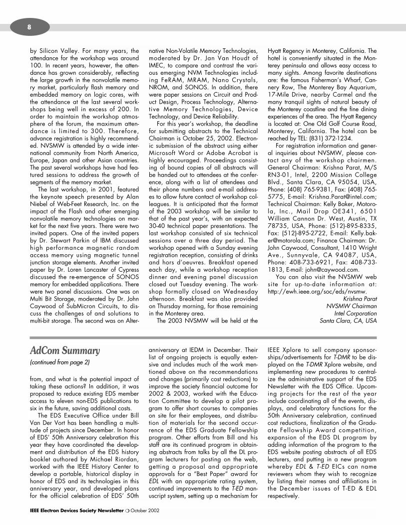
2003 IEEE Non-Volatile Semiconductor Memory Workshop(NVSMW)
The 2003 IEEE Non-VolatileSemiconductor Memory Work-shop (NVSMW) will be heldFebruary 16 - 20, 2003 in Mon-terey, California. The workshopis sponsored by the IEEE ElectronDevices Society. NVSMW is aunique forum for both specialistsin all aspects of nonvolati lememory microelectronics andnovices wanting to gain abroader understanding of thefield. Attendees represent profes-sional and academic researchersinvolved with semiconductornon-volatile memory develop-ment and production along withend users of memory products.Principal topics for discussion atNVSMW are: device physics; silicon pro-cessing; product testing; new technolo-gies, including mult i - level -cel lapproaches; programmable logic; memo-ry cell design; integrated circuits; solidstate disks and memory cards; memoryreliability; and new applications.
An important goal of NVSMW is toprovide an informal environment to
encourage discussions among partici-pants and lively interactions. There willbe morning and afternoon technical ses-sions, along with a lively evening paneldiscussion on a hot topic in the non-volatile memory field. Technical interac-tion among presenters and attendees isencouraged through quest ion andanswer sessions and allotting ample timeafter the formal paper presentations for
further in-depth discussions.Organized breaks, includingsnacks and the workshop dinnerand lunch are provided asopportuni t ies to meet andexchange ideas with colleagues.Breakfasts are also provided. Themorning and afternoon technicalsessions are organized in a man-ner to provide ample time for theinformal exchange and to enjoythe beauty of the Montereypeninsula region of California.
This year will be the 19thmeeting of NVSMW. The work-shop is held every 18 months,alternating between February andAugust. The February meeting is
usually held the week after ISSCC and theAugust meeting in the early weeks of themonth. The 2003 meeting will be held inthe third week of February - the weekafter ISSCC. Early workshops alternatedbetween Monterey, California for the Feb-ruary meeting and Vail, Colorado for theAugust meeting. The Vail venue wasdropped a number of years ago, to facili-tate attendance and travel from the near-
from, and what is the potential impact oftaking these actions? In addition, it wasproposed to reduce existing EDS memberaccess to eleven non-EDS publications tosix in the future, saving additional costs.
The EDS Executive Office under BillVan Der Vort has been handling a multi-tude of projects since December. In honorof EDS’ 50th Anniversary celebration thisyear they have coordinated the develop-ment and distribution of the EDS historybooklet authored by Michael Riordan,worked with the IEEE History Center todevelop a portable, historical display inhonor of EDS and its technologies in thisanniversary year, and developed plansfor the official celebration of EDS’ 50th
anniversary at IEDM in December. Theirlist of ongoing projects is equally exten-sive and includes much of the work men-tioned above on the recommendationsand changes (primarily cost reductions) toimprove the society financial outcome for2002 & 2003, worked with the Educa-tion Committee to develop a pilot pro-gram to offer short courses to companieson site for their employees, and distribu-tion of materials for the second occur-rence of the EDS Graduate Fellowshipprogram. Other efforts from Bill and hisstaff are its continued program in obtain-ing abstracts from talks by all the DL pro-gram lecturers for posting on the web,getting a proposal and appropriateapprovals for a “Best Paper” award forEDL with an appropriate rating system,continued improvements to the T-ED man-uscript system, setting up a mechanism for
IEEE Xplore to sell company sponsor-ships/advertisements for T-DMR to be dis-played on the T-DMR Xplore website, andimplementing new procedures to central-ize the administrative support of the EDSNewsletter with the EDS Office. Upcom-ing projects for the rest of the yearinclude coordinating all of the events, dis-plays, and celebratory functions for the50th Anniversary celebration, continuedcost reductions, finalization of the Gradu-ate Fel lowship Award competi t ion,expansion of the EDS DL program byadding information of the program to theEDS website posting abstracts of all EDSlecturers, and putting in a new programwhereby EDL & T-ED EICs can namereviewers whom they wish to recognizeby listing their names and affiliations inthe December issues of T-ED & EDLrespectively.
by Silicon Valley. For many years, theattendance for the workshop was around100. In recent years, however, the atten-dance has grown considerably, reflectingthe large growth in the nonvolatile memo-ry market, particularly flash memory andembedded memory on logic cores, withthe attendance at the last several work-shops being well in excess of 200. Inorder to maintain the workshop atmos-phere of the forum, the maximum atten-dance is l imited to 300. Therefore,advance registration is highly recommend-ed. NVSMW is attended by a wide inter-national community from North America,Europe, Japan and other Asian countries.The past several workshops have had fea-tured sessions to address the growth ofsegments of the memory market.
The last workshop, in 2001, featuredthe keynote speech presented by AlanNiebel of Web-Feet Research, Inc. on theimpact of the Flash and other emergingnonvolatile memory technologies on mar-ket for the next five years. There were twoinvited papers. One of the invited papersby Dr. Stewart Parkin of IBM discussedhigh performance magnetic randomaccess memory using magnetic tunneljunction storage elements. Another invitedpaper by Dr. Loren Lancaster of Cypressdiscussed the re-emergence of SONOSmemory for embedded applications. Therewere two panel discussions. One was onMulti Bit Storage, moderated by Dr. JohnCaywood of SubMicron Circuits, to dis-cuss the challenges of and solutions tomulti-bit storage. The second was on Alter-
native Non-Volatile Memory Technologies,moderated by Dr. Jan Van Houdt ofIMEC, to compare and contrast the vari-ous emerging NVM Technologies includ-ing FeRAM, MRAM, Nano Crystals,NROM, and SONOS. In addition, therewere paper sessions on Circuit and Prod-uct Design, Process Technology, Alterna-t ive Memory Technologies, DeviceTechnology, and Device Reliability.
For this year’s workshop, the deadlinefor submitting abstracts to the TechnicalChairman is October 25, 2002. Electron-ic submission of the abstract using eitherMicrosoft Word or Adobe Acrobat ishighly encouraged. Proceedings consist-ing of bound copies of all abstracts willbe handed out to attendees at the confer-ence, along with a list of attendees andtheir phone numbers and e-mail address-es to allow future contact of workshop col-leagues. It is anticipated that the formatof the 2003 workshop will be similar tothat of the past year’s, with an expected30-40 technical paper presentations. Thelast workshop consisted of six technicalsessions over a three day period. Theworkshop opened with a Sunday eveningregistration reception, consisting of drinksand hors d’oeuvres. Breakfast openedeach day, while a workshop receptiondinner and evening panel discussionclosed out Tuesday evening. The work-shop formally closed on Wednesdayafternoon. Breakfast was also providedon Thursday morning, for those remainingin the Monterey area.
The 2003 NVSMW will be held at the
Hyatt Regency in Monterey, California. Thehotel is conveniently situated in the Mon-terey peninsula and allows easy access tomany sights. Among favorite destinationsare: the famous Fisherman’s Wharf, Can-nery Row, The Monterey Bay Aquarium,17-Mile Drive, nearby Carmel and themany tranquil sights of natural beauty ofthe Monterey coastline and the fine diningexperiences of the area. The Hyatt Regencyis located at: One Old Golf Course Road,Monterey, California. The hotel can bereached by TEL: (831) 372-1234.
For registration information and gener-al inquiries about NVSMW, please con-tact any of the workshop chairmen.General Chairman: Krishna Parat, M/SRN3-01, Intel, 2200 Mission CollegeBlvd., Santa Clara, CA 95054, USA,Phone: (408) 765-9381, Fax: (408) 765-5775, E-mail: [email protected];Technical Chairman: Kelly Baker, Motoro-la, Inc., Mail Drop OE341, 6501William Cannon Dr. West, Austin, TX78735, USA, Phone: (512)-895-8335,Fax: (512)-895-2722, E-mail: [email protected]; Finance Chairman: Dr.John Caywood, Consultant, 1410 WrightAve., Sunnyvale, CA 94087, USA,Phone: 408-733-6921, Fax: 408-733-1813, E-mail: [email protected].
You can also visit the NVSMW website for up- to-date information at:http://ewh.ieee.org/soc/eds/nvsmw.
Krishna ParatNVSMW Chairman
Intel CorporationSanta Clara, CA, USA
IEEE Electron Devices Society Newsletter ❍ October 2002
8
AdCom Summary(continued from page 2)
Membership Chair, James Kuo, listsEDS current membership as 7890 regu-lar members, 4218 permanent members,and 1364 students for a total of 13489.This is a 1.4% gain over last year’s num-bers at the same time. Recruiting activi-ties have been fruitful bringing in 62 newmembers at IEDM, and 78 at ISSCC. Theefforts started in 2001 to increase SeniorMembership within EDS has also hadsuccess as 120 members have been con-firmed since the program began, and 71others have started the process this year.The application brochures for 2002 inJapanese, Mandarin, and English havebeen distributed, as well as the variouschapter membership subsidies. Jamesand his committee will be continuing therecruitment efforts, student membershipdrives, DL recruiting, and the SM pro-gram going throughout the year. Theywill also be looking at terminated mem-bers to examine the motivations and rea-sons for non-continuance. EDSterminations for 2002 stands at 13.3%,and in general IEEE membership termina-tions especially in Regions 6 & 10 arequite high. This is an important issue bothnow and in EDS future planning to lookat increasing member retention.
Hiroshi Iwai, Regions/Chapters Com-mittee Chair, puts our current chaptertotal at 104. We expect that a new chap-ter in South Brazil, and joint ED/SSC onein Bulgaria will be approved this year.Iwai-san also mentioned that there areefforts underway to change the Frenchchapter from being a joint ED/MTT oneto a full-fledged ED one. Reporting for theEducational Activities Committee, IlesanmiAdessida, focused on three major pro-jects namely the DL program, the EDS Stu-dent Fellowship, and the Short Courses.He reviewed the current status of the DLprogram showing that the effort hasbecome more visible to members throughthe EDS Newsletter and website. Fifty lec-tures are scheduled for 2002 with sixteenlecturers participating and sixteen of thetalks funded. So far EDS has spent $8.4Kon the program from a budget of$12.8K. As for the Graduate Student pro-gram, all the nominations have been col-lected and voting on the seventeennominees by the selection committee is inprogress. Notifications to recipientsshould go out by July 15, 2002. Dr. JackLee gave one company-sponsored shortcourse at Applied Materials in April. KenGalloway, Meetings Chair, listed 140meetings (32 sponsored/co-sponsored,99 technically sponsored, and 9 coopera-
tively sponsored) are scheduled for thisyear. Since 9/11/01, most conferenceslost money, and profits from these meet-ings are expected to drop sharply fromearlier projections.
Key ReportsThe 2002 Symposium on VLSI Technolo-gy has done well at rebounding from lastyear’s slump. Projected income shouldmatch the actual (~$382K), and atten-dance exceeded the predictions. Whilethe short course attendees are not ashigh as in previous years, the meetingshould be successful. There have beensuggestions raised at AdCom that thismeeting consider alternative sites such asShanghai instead of the traditional two(Kyoto & Honolulu) in the future. Whileattendance at the 2001 IEDM dipped incomparison to past meetings, incomeincreased over expectations, assisted bywaiving a substantial hotel penalty.
As presented by Chair Renuka Jindal,EDS Publications continue to progress.With the increased interest in nanotech-nology society-wide, EDS is formulating apolicy statement establishing its areas ofspecialization. The numerous specialissues on this subject planned by varioustechnical societies dramatize the impor-tance of this action. EDS’ Nanotechnolo-gy Technical Committee plans to draft a“memorandum of understanding” todefine our society specialization to avoidconflicts with other publications. A voteto support this action was approved.AdCom also discussed the prevalentproblem of numerous authors on both T-ED & EDL papers. At issue is establishingwhich listed authors performed the major-ity of the work, and which ones were inmainly support roles. In the end,AdCom’s decision was that any author’slist must remain the responsibility of thesubmitting institution, and it is not EDSrole to decide the amount of involvementof each named author. The PublicationsCommittee may work on a “template forfuture authors” suggesting guidelines onhow to select authors, and will adopt apolicy whereby an author list cannot bechanged after a paper has been accept-ed. On a financial note, revenue from T-ED & EDL is increasing as on-line accessreplaces traditional hardcopy distribu-tion. A possible reduction in the numberof on-line publications (currently avail-able to members) from eleven to sixshould result in a substantial cost saving.EDS progress in providing both IEEEXplore access, and an archival DVD for
past T-ED & EDL issues faces some signifi-cant cost hurdles. Papers publishedbefore 1988 are more expensive to digi-tize that those that are post-1988. Forexample, to digitize the pre-1988 papersfor both journals is $190K whereas thepost-1988 material costs $90K, a signifi-cant difference in the face of budgetshortening (see above). It was voted tospend $22K in 2003 to digitize EDLissues published prior to 1988, and$102K in 2004 to complete the digitiza-tion of T-ED issues published from 1952-1987, and discuss digi t izing thepre-1988 IEDM Proceedings (in 2003 &2004) with the IEDM Committee. In afinal Publication action, two winners forthe annual Rappaport award wereannounced, and a motion to establish a“Best EDL paper” named for GeorgeSmith has been submitted to TAB forapproval with the initial presentation totake place in December 2002.
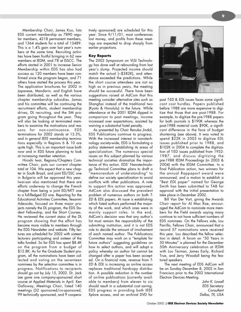
Bill Van Der Vort, giving the AwardsChair report for Al Mac Rae, encour-aged the AdCom to nominate more mem-bers for the Field awards saying manycontinue to not have sufficient numbers ofEDS nominees. On the Fellows side, LouParrillo, Fellows Chair, announced that arecord 57 nominations were receivedthis year. Lou described the fellow selec-tion in detail. A forum on “50 Years in50 Minutes” is planned for the December50th Anniversary celebration at IEDMwith Lou Terman, James Early, RichardTrue, and Jerry Woodall being the fea-tured speakers.
The next meeting of EDS AdCom willbe on Sunday December 8, 2002 in SanFrancisco prior to the 2002 InternationalElectron Devices Meeting.
John K. LowellEDS Secretary
ConsultantDallas, TX, USA
October 2002 ❍ IEEE Electron Devices Society Newsletter
9
IEEE Electron Devices Society Newsletter ❍ October 2002
10
After taking over as publications chair inJanuary 2001, I found several issues thatneeded attention. Some of these issuesfind their roots in our innate desire tomake things better than we find them.Others surfaced due to advances in tech-nology. And finally some just happenedto crop up at this time. In this report, I willgive a snapshot of some of these relatedactivit ies. However, before forgingahead, a more basic need had to beaddressed. The EDS publications commit-tee, consisting of 5 members, was inade-quate to handle the broad charter that ithas. In view of this, the committee wasexpanded to include representation fromall sponsored and co-sponsored EDS pub-lications and all EDS technical commit-tees. With these additions, the number ofmembers in this committee jumped to 32.
The three primary factors that anauthor considers before submitting a man-uscript for publication are speed, circula-tion and quality of the journal. Out ofthese three parameters, the first two areeasily quantified while the third is morenebulous. In the following analysis, wewill primarily examine data pertaining toElectron Device Letters (EDL) and Transac-tions on Electron Devices (T-ED). Let us firstdiscuss the time it takes for us to publishan article. With the centralization of theeditorial support in Piscataway, we contin-ue to be close to the top in terms of publi-cation speed, among all IEEE publications.Currently, with help from Professor ArokiaNathan, we are evaluating our next moveto WEB based publishing. Under this par-adigm, all manuscripts will be handledelectronically from submission throughreview to final publishing. As always,paper copies of the publications will contin-ue to be printed in the foreseeable future.Several IEEE societies have signed up withIEEE’s WEB based platform called Manu-script Central, making a big jump fromtheir manual handling procedures. Howev-er, we in EDS, have been using PC basedsoftware tools to manage our publicationsfor over a decade. Hence we want tomake sure that Manuscript Central pro-vides the necessary level of functionalityand flexibility that we require.
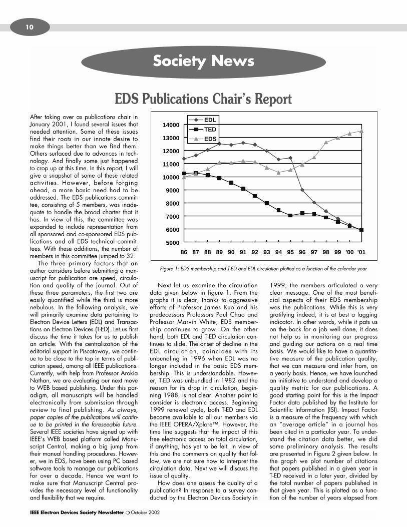
Next let us examine the circulationdata given below in figure 1. From thegraphs it is clear, thanks to aggressiveefforts of Professor James Kuo and hispredecessors Professors Paul Chao andProfessor Marvin White, EDS member-ship continues to grow. On the otherhand, both EDL and T-ED circulation con-tinues to slide. The onset of decline in theEDL circulat ion, coincides with i tsunbundling in 1996 when EDL was nolonger included in the basic EDS mem-bership. This is understandable. Howev-er, T-ED was unbundled in 1982 and thereason for its drop in circulation, begin-ning 1988, is not clear. Another point toconsider is electronic access. Beginning1999 renewal cycle, both T-ED and EDLbecame available to all our members viathe IEEE OPERA/Xplore™. However, thetime line suggests that the impact of thisfree electronic access on total circulation,if anything, has yet to be felt. In view ofthis and the comments on quality that fol-low, we are not sure how to interpret thecirculation data. Next we will discuss theissue of quality.
How does one assess the quality of apublication? In response to a survey con-ducted by the Electron Devices Society in
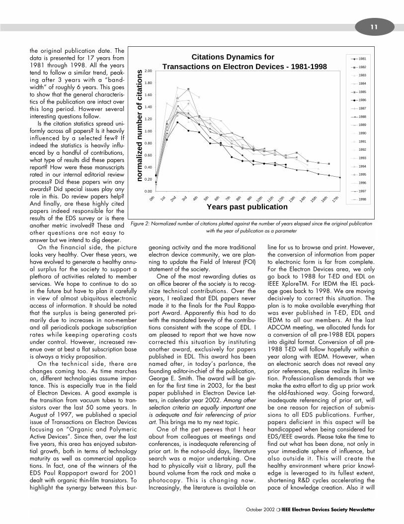
1999, the members articulated a veryclear message. One of the most benefi-cial aspects of their EDS membershipwas the publications. While this is verygratifying indeed, it is at best a laggingindicator. In other words, while it pats uson the back for a job well done, it doesnot help us in monitoring our progressand guiding our actions on a real timebasis. We would like to have a quantita-tive measure of the publication quality,that we can measure and infer from, ona yearly basis. Hence, we have launchedan initiative to understand and develop aquality metric for our publications. Agood starting point for this is the ImpactFactor data published by the Institute forScientific Information (ISI). Impact Factoris a measure of the frequency with whichan “average article” in a journal hasbeen cited in a particular year. To under-stand the citation data better, we didsome preliminary analysis. The resultsare presented in Figure 2 given below. Inthe graph we plot number of citationsthat papers published in a given year inT-ED received in a later year, divided bythe total number of papers published inthat given year. This is plotted as a func-tion of the number of years elapsed from
Society News
EDS Publications Chair’s Report
5000
6000
7000
8000
9000
10000
11000
12000
13000
14000
86 87 88 89 90 91 92 93 94 95 96 97 98 99 '00 '01
EDL
TED
EDS
Figure 1: EDS membership and T-ED and EDL circulation plotted as a function of the calendar year
October 2002 ❍ IEEE Electron Devices Society Newsletter
11
the original publication date. Thedata is presented for 17 years from1981 through 1998. All the yearstend to follow a similar trend, peak-ing after 3 years with a “band-width” of roughly 6 years. This goesto show that the general characteris-tics of the publication are intact overthis long period. However severalinteresting questions follow.
Is the citation statistics spread uni-formly across all papers? Is it heavilyinfluenced by a selected few? Ifindeed the statistics is heavily influ-enced by a handful of contributions,what type of results did these papersreport? How were these manuscriptsrated in our internal editorial reviewprocess? Did these papers win anyawards? Did special issues play anyrole in this. Do review papers help?And finally, are these highly citedpapers indeed responsible for theresults of the EDS survey or is thereanother metric involved? These andother questions are not easy toanswer but we intend to dig deeper.
On the financial side, the picturelooks very healthy. Over these years, wehave evolved to generate a healthy annu-al surplus for the society to support aplethora of activities related to memberservices. We hope to continue to do soin the future but have to plan it carefullyin view of almost ubiquitous electronicaccess of information. It should be notedthat the surplus is being generated pri-marily due to increases in non-memberand all periodicals package subscriptionrates while keeping operating costsunder control. However, increased rev-enue over at best a flat subscription baseis always a tricky proposition.
On the technical side, there arechanges coming too. As time marcheson, different technologies assume impor-tance. This is especially true in the fieldof Electron Devices. A good example isthe transition from vacuum tubes to tran-sistors over the last 50 some years. InAugust of 1997, we published a specialissue of Transactions on Electron Devicesfocusing on “Organic and PolymericActive Devices”. Since then, over the lastfive years, this area has enjoyed substan-tial growth, both in terms of technologymaturity as well as commercial applica-tions. In fact, one of the winners of theEDS Paul Rappaport award for 2001dealt with organic thin-film transistors. Tohighlight the synergy between this bur-
geoning activity and the more traditionalelectron device community, we are plan-ning to update the Field of Interest (FOI)statement of the society.
One of the most rewarding duties asan office bearer of the society is to recog-nize technical contributions. Over theyears, I realized that EDL papers nevermade it to the finals for the Paul Rappa-port Award. Apparently this had to dowith the mandated brevity of the contribu-tions consistent with the scope of EDL. Iam pleased to report that we have nowcorrected this situation by institutinganother award, exclusively for paperspublished in EDL. This award has beennamed after, in today’s parlance, thefounding editor-in-chief of the publication,George E. Smith. The award will be giv-en for the first time in 2003, for the bestpaper published in Electron Device Let-ters, in calendar year 2002. Among otherselection criteria an equally important oneis adequate and fair referencing of priorart. This brings me to my next topic.
One of the pet peeves that I hearabout from colleagues at meetings andconferences, is inadequate referencing ofprior art. In the not-so-old days, literaturesearch was a major undertaking. Onehad to physically visit a library, pull thebound volume from the rack and make aphotocopy. This is changing now.Increasingly, the literature is available on
line for us to browse and print. However,the conversion of information from paperto electronic form is far from complete.For the Electron Devices area, we onlygo back to 1988 for T-ED and EDL onIEEE XploreTM. For IEDM the IEL pack-age goes back to 1998. We are movingdecisively to correct this situation. Theplan is to make available everything thatwas ever published in T-ED, EDL andIEDM to all our members. At the lastADCOM meeting, we allocated funds fora conversion of all pre-1988 EDL papersinto digital format. Conversion of all pre-1988 T-ED will follow hopefully within ayear along with IEDM. However, whenan electronic search does not reveal anyprior references, please realize its limita-tion. Professionalism demands that wemake the extra effort to dig up prior workthe old-fashioned way. Going forward,inadequate referencing of prior art, willbe one reason for rejection of submis-sions to all EDS publications. Further,papers deficient in this aspect will behandicapped when being considered forEDS/IEEE awards. Please take the time tofind out what has been done, not only inyour immediate sphere of influence, butalso outside it. This wil l create thehealthy environment where prior knowl-edge is leveraged to its fullest extent,shortening R&D cycles accelerating thepace of knowledge creation. Also it will
0.00
0.20
0.40
0.60
0.80
1.00
1.20
1.40
1.60
1.80
2.00
0th
1st
2nd
3rd 4t
h5t
h6t
h7t
h8t
h9t
h10
th11
th12
th13
th14
th15
th16
th17
th
norm
aliz
ednu
mbe
rof
cita
tions
1981
1982
1983
1984
1985
1986
1987
1988
1989
1990
1991
1992
1993
1994
1995
1996
1997
1998
Citations Dynamics forTransactions on Electron Devices - 1981-1998
Years past publication
Figure 2: Normalized number of citations plotted against the number of years elapsed since the original publicationwith the year of publication as a parameter
IEEE Electron Devices Society Newsletter ❍ October 2002
12
result in proper credit being given towhere it is due. This should be a win-winsituation for everyone involved.
On the eve of the 50th anniversary ofthe Electron Devices Society, I want tothank everyone for supporting EDS publi-cations in their capacity as authors,reviewers and editors. We aspire to con-tinue to be the choice forum, for the dis-semination of prized technical information,in the field of Electron Devices. Electronicdistribution of information is here with usto stay. If you have any ideas on how wecan make it easier and more efficient foryou to generate and access this informa-tion, please let me know. I am looking for-ward to your suggestions.
Renuka JindalPublications Chair,
Electron Devices SocietyAgere Systems
Bell Labs Room 2D-329600 Mountain AvenueMurray Hill, NJ 07974
EDS Administrative CommitteeElection Process
The Members-at-Large (MAL) of the EDS AdCom are elected for staggeredthree-year terms, with a maximum of two consecutive terms. The 1993 Constitutionand ByLaw changes mandated increasing the number of elected MALs from 18 to22, and required that there be at least two members from both IEEE Region 8(Europe, Mid. East & Africa) and Region 10 (Asia & Pacific). It also required thatthere be at least 1.5 candidates for each opening. From 1999 to 2001, eight, sev-en, and seven positions were filled, respectively. In 2002, eight positions will befilled.
The election procedure begins with the announcement and Call For Nomina-tions in the EDS Newsletter. The slate of nominees is developed by the EDS Nomi-nations Committee and includes the non-Committee and self-nominations received.Nominees are asked to submit a two-page biographical resume in a standard for-mat. Nominations are closed around the end of October, and the biographicalresumes are distributed to the ‘full’ voting members of AdCom prior to the AdCommeeting. Nominees are urged to attend the December AdCom meeting, and theelection is held after the conclusion of the meeting.
A continuing flow of new AdCom members who are interested in working for theimprovement of the Society and its related technical areas is key to the continueddevelopment of EDS and the field of electron devices. Those interested in the field, theSociety, and its operations are encouraged to attend AdCom meetings, becomeinvolved in Society activities, and to consider running for election to AdCom.
Cary Y. YangEDS Nominations & Elections Chair
Santa Clara UniversitySanta Clara, CA, USA
2001 EDS PAUL RAPPAPORT AWARDEach year, the IEEE Electron Devices Society confers the PaulRappaport Award to the best paper published in an EDS publi-cation. This year there were two winners of the award. The firstpaper deals with organic electronics. This is an upcoming areaof technical focus which is expected to see growth in years tocome. The second paper reviews the history of the genesis ofthe solid-state era ushered by the invention of the Bipolar Tran-sistor at Bell Laboratories in 1947. As a related item, Doug Ver-ret has introduced review papers as a standard feature of T-ED.The details of the two winners are given below.
The 2001 award will be presented at the IEDM on 9 Decem-ber, 2002 in San Francisco, CA. It consists of a certificate anda check for $2,500 to be shared among the winners. Briefbiographies of the four winners are given below.
C.D. Dimitrakopoulos is a Research StaffMember at IBM, T. J. Watson Research Cen-ter, Yorktown Heights, NY, where he workson organic semiconductor materials anddevices. He has been with IBM since 1995.From 1993 to 1995, he was a post-doctoralfellow at Philips Research Laboratories inEindhoven, NL, where he also worked onorganic semiconductors. He holds Ph.D.,M.Phil. and M.S. degrees in Materials Sci-
ence from Columbia University and a B.S. degree in Metallurgi-cal Engineering from the National Technical University ofAthens, Greece. He is the author or co-author of 8 patents, sev-eral more pending patent applications and at least 25 papers.
Paper Title Issue/Publication Author(s)
High-PerformanceBottomElectrode June, 2001/Transactions on Ioannis Kymissis,Organic Thin-Film Transistors Electron Devices C.D. Dimitrakopoulos and
Sampath Purushothaman
-Microelectronics: Its Unusual Origin Nov., 2001/Transactions on Raymond M. Warnerand Personality Electron Devices
C.D. Dimitrakopoulos
October 2002 ❍ IEEE Electron Devices Society Newsletter
13
In 2000, he received an IBM Outstanding Innovation Award, for“High Performance Organic Transistors on Plastic”.
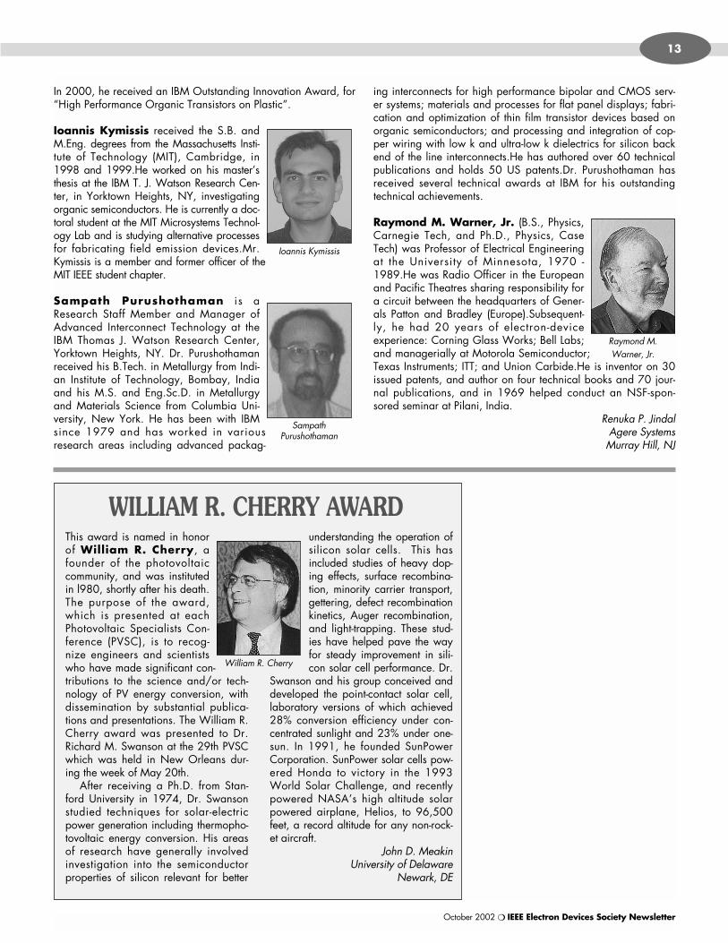
Ioannis Kymissis received the S.B. andM.Eng. degrees from the Massachusetts Insti-tute of Technology (MIT), Cambridge, in1998 and 1999.He worked on his master’sthesis at the IBM T. J. Watson Research Cen-ter, in Yorktown Heights, NY, investigatingorganic semiconductors. He is currently a doc-toral student at the MIT Microsystems Technol-ogy Lab and is studying alternative processesfor fabricating field emission devices.Mr.Kymissis is a member and former officer of theMIT IEEE student chapter.
Sampath Purushothaman is aResearch Staff Member and Manager ofAdvanced Interconnect Technology at theIBM Thomas J. Watson Research Center,Yorktown Heights, NY. Dr. Purushothamanreceived his B.Tech. in Metallurgy from Indi-an Institute of Technology, Bombay, Indiaand his M.S. and Eng.Sc.D. in Metallurgyand Materials Science from Columbia Uni-versity, New York. He has been with IBMsince 1979 and has worked in variousresearch areas including advanced packag-
ing interconnects for high performance bipolar and CMOS serv-er systems; materials and processes for flat panel displays; fabri-cation and optimization of thin film transistor devices based onorganic semiconductors; and processing and integration of cop-per wiring with low k and ultra-low k dielectrics for silicon backend of the line interconnects.He has authored over 60 technicalpublications and holds 50 US patents.Dr. Purushothaman hasreceived several technical awards at IBM for his outstandingtechnical achievements.
Raymond M. Warner, Jr. (B.S., Physics,Carnegie Tech, and Ph.D., Physics, CaseTech) was Professor of Electrical Engineeringat the University of Minnesota, 1970 -1989.He was Radio Officer in the Europeanand Pacific Theatres sharing responsibility fora circuit between the headquarters of Gener-als Patton and Bradley (Europe).Subsequent-ly, he had 20 years of electron-deviceexperience: Corning Glass Works; Bell Labs;and managerially at Motorola Semiconductor;Texas Instruments; ITT; and Union Carbide.He is inventor on 30issued patents, and author on four technical books and 70 jour-nal publications, and in 1969 helped conduct an NSF-spon-sored seminar at Pilani, India.
Renuka P. JindalAgere SystemsMurray Hill, NJ
WILLIAM R. CHERRY AWARDThis award is named in honorof William R. Cherry, afounder of the photovoltaiccommunity, and was institutedin l980, shortly after his death.The purpose of the award,which is presented at eachPhotovoltaic Specialists Con-ference (PVSC), is to recog-nize engineers and scientistswho have made significant con-tributions to the science and/or tech-nology of PV energy conversion, withdissemination by substantial publica-tions and presentations. The William R.Cherry award was presented to Dr.Richard M. Swanson at the 29th PVSCwhich was held in New Orleans dur-ing the week of May 20th.
After receiving a Ph.D. from Stan-ford University in 1974, Dr. Swansonstudied techniques for solar-electricpower generation including thermopho-tovoltaic energy conversion. His areasof research have generally involvedinvestigation into the semiconductorproperties of silicon relevant for better
understanding the operation ofsilicon solar cells. This hasincluded studies of heavy dop-ing effects, surface recombina-tion, minority carrier transport,gettering, defect recombinationkinetics, Auger recombination,and light-trapping. These stud-ies have helped pave the wayfor steady improvement in sili-con solar cell performance. Dr.
Swanson and his group conceived anddeveloped the point-contact solar cell,laboratory versions of which achieved28% conversion efficiency under con-centrated sunlight and 23% under one-sun. In 1991, he founded SunPowerCorporation. SunPower solar cells pow-ered Honda to victory in the 1993World Solar Challenge, and recentlypowered NASA’s high altitude solarpowered airplane, Helios, to 96,500feet, a record altitude for any non-rock-et aircraft.
John D. MeakinUniversity of Delaware
Newark, DE
Ioannis Kymissis
SampathPurushothaman
Raymond M. Warner, Jr.
William R. Cherry
IEEE Electron Devices Society Newsletter ❍ October 2002
14
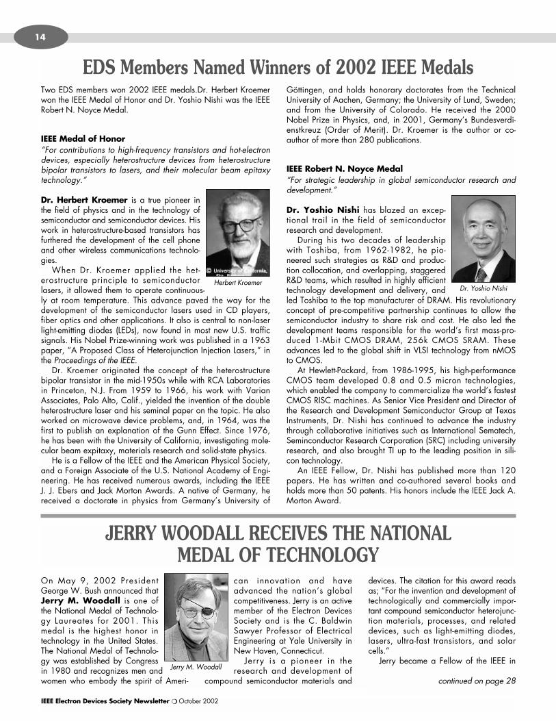
On May 9, 2002 PresidentGeorge W. Bush announced thatJerry M. Woodall is one ofthe National Medal of Technolo-gy Laureates for 2001. Thismedal is the highest honor intechnology in the United States.The National Medal of Technolo-gy was established by Congressin 1980 and recognizes men andwomen who embody the spirit of Ameri-
can innovation and haveadvanced the nation’s globalcompetitiveness. Jerry is an activemember of the Electron DevicesSociety and is the C. BaldwinSawyer Professor of ElectricalEngineering at Yale University inNew Haven, Connecticut.
Jerry is a pioneer in theresearch and development of
compound semiconductor materials and
devices. The citation for this award readsas; “For the invention and development oftechnologically and commercially impor-tant compound semiconductor heterojunc-tion materials, processes, and relateddevices, such as light-emitting diodes,lasers, ultra-fast transistors, and solarcells.”
Jerry became a Fellow of the IEEE in
JERRY WOODALL RECEIVES THE NATIONAL MEDAL OF TECHNOLOGY
Jerry M. Woodall
Two EDS members won 2002 IEEE medals.Dr. Herbert Kroemerwon the IEEE Medal of Honor and Dr. Yoshio Nishi was the IEEERobert N. Noyce Medal.
IEEE Medal of Honor“For contributions to high-frequency transistors and hot-electrondevices, especially heterostructure devices from heterostructurebipolar transistors to lasers, and their molecular beam epitaxytechnology.”
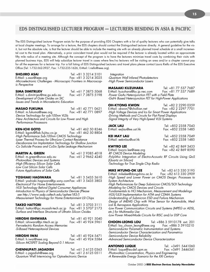
Dr. Herbert Kroemer is a true pioneer inthe field of physics and in the technology ofsemiconductor and semiconductor devices. Hiswork in heterostructure-based transistors hasfurthered the development of the cell phoneand other wireless communications technolo-gies.
When Dr. Kroemer applied the het-erostructure principle to semiconductorlasers, it allowed them to operate continuous-ly at room temperature. This advance paved the way for thedevelopment of the semiconductor lasers used in CD players,fiber optics and other applications. It also is central to non-laserlight-emitting diodes (LEDs), now found in most new U.S. trafficsignals. His Nobel Prize-winning work was published in a 1963paper, “A Proposed Class of Heterojunction Injection Lasers,” inthe Proceedings of the IEEE.
Dr. Kroemer originated the concept of the heterostructurebipolar transistor in the mid-1950s while with RCA Laboratoriesin Princeton, N.J. From 1959 to 1966, his work with VarianAssociates, Palo Alto, Calif., yielded the invention of the doubleheterostructure laser and his seminal paper on the topic. He alsoworked on microwave device problems, and, in 1964, was thefirst to publish an explanation of the Gunn Effect. Since 1976,he has been with the University of California, investigating mole-cular beam expitaxy, materials research and solid-state physics.
He is a Fellow of the IEEE and the American Physical Society,and a Foreign Associate of the U.S. National Academy of Engi-neering. He has received numerous awards, including the IEEEJ. J. Ebers and Jack Morton Awards. A native of Germany, hereceived a doctorate in physics from Germany’s University of
Göttingen, and holds honorary doctorates from the TechnicalUniversity of Aachen, Germany; the University of Lund, Sweden;and from the University of Colorado. He received the 2000Nobel Prize in Physics, and, in 2001, Germany’s Bundesverdi-enstkreuz (Order of Merit). Dr. Kroemer is the author or co-author of more than 280 publications.
IEEE Robert N. Noyce Medal“For strategic leadership in global semiconductor research anddevelopment.”
Dr. Yoshio Nishi has blazed an excep-tional trail in the field of semiconductorresearch and development.
During his two decades of leadershipwith Toshiba, from 1962-1982, he pio-neered such strategies as R&D and produc-tion collocation, and overlapping, staggeredR&D teams, which resulted in highly efficienttechnology development and delivery, andled Toshiba to the top manufacturer of DRAM. His revolutionaryconcept of pre-competitive partnership continues to allow thesemiconductor industry to share risk and cost. He also led thedevelopment teams responsible for the world’s first mass-pro-duced 1-Mbit CMOS DRAM, 256k CMOS SRAM. Theseadvances led to the global shift in VLSI technology from nMOSto CMOS.
At Hewlett-Packard, from 1986-1995, his high-performanceCMOS team developed 0.8 and 0.5 micron technologies,which enabled the company to commercialize the world’s fastestCMOS RISC machines. As Senior Vice President and Director ofthe Research and Development Semiconductor Group at TexasInstruments, Dr. Nishi has continued to advance the industrythrough collaborative initiatives such as International Sematech,Seminconductor Research Corporation (SRC) including universityresearch, and also brought TI up to the leading position in sili-con technology.
An IEEE Fellow, Dr. Nishi has published more than 120papers. He has written and co-authored several books andholds more than 50 patents. His honors include the IEEE Jack A.Morton Award.
EDS Members Named Winners of 2002 IEEE Medals
Herbert KroemerDr. Yoshio Nishi
continued on page 28
October 2002 ❍ IEEE Electron Devices Society Newsletter
15
The EDS Distinguished Lecturer Program exists for the purpose of providing EDS Chapters with a list of quality lecturers who can potentially give talksat local chapter meetings. To arrange for a lecture, the EDS chapters should contact the Distinguished Lecturer directly. A general guideline for the vis-it, but not the absolute rule, is that the lecturer should be able to include the meeting site with an already planned travel schedule at a small incremen-tal cost to the travel plan. Alternatively, a prior coincident travel plan would not be required if the lecturer is already located within an approximatefifty mile radius of a meeting site. Although the concept of the program is to have the lecturers minimize travel costs by combining their visits withplanned business trips, EDS will help subsidize lecturer travel in cases where few/no lecturers will be visiting an area and/or a chapter cannot payfor all the expenses for a lecturer trip. For a full listing of EDS Distinguished Lecturers and travel plans please contact Laura Riello of the EDS ExecutiveOffice (Tel: 1-732-562-3927, Fax: 1-732-235-1626, E-Mail: [email protected]).
EDS DISTINGUISHED LECTURER PROGRAM — LECTURERS RESIDING IN ASIA & PACIFIC
SHOJIRO ASAI Tel: +81 3 3214 3101E-Mail: [email protected] Fax: +81 3 3214 3025-Microelectronic Challenges - Microscopic Frontiers in Macroscop-ic Perspective
SIMA DIMITRIJEV Tel: +61 7 3875 5068E-Mail: [email protected] Fax: +61 7 3875 5198-Development of Gate Oxides on SIC-Issues and Trends in Microelectric Education
MASAO FUKUMA Tel: +81 42 771 0621E-Mail: [email protected] Fax: +81 42 771 0897-Device Technology for sub-100nm VLSIs-New Architecture and Circuits for Low Power and HighPerformance Processors
KEN-ICHI GOTO Tel: +81 462 50 8246E-Mail: [email protected] Fax: +81 462 50 8804-High Performance Sub-100nm CMOS Technology-Laser Thermal Process for Ultra-Low Contact Resistance-Decaborane Ion Implantation Technology for Shallow Junction-Co Salicide Process and CoSix Spike Leakage Mechanism
MARTIN A. GREEN Tel: +61 2 9385 4018E-Mail: [email protected] Fax: +61 2 9662 4240-Photovoltaic Devices and Systems-High Efficiency Silicon Solar Cells-Low Cost Silicon Solar Cells-Future Applications of Solar Cells
YOSHIAKI HAGIWARA Tel: +81 3 5435 3610E-Mail: [email protected]: +81 3 5435 3803-Electronics? For Home Entertainments-VLSI Technology Behind Digital Consumer Appliances-Introduction to Physics of Semiconductor Devices (Pleasesee http://www.ssdp.caltech.edu/aphee183/)
-Measurement Technology for Home Entertainment LSI Chips
TAKEO HATTORI Tel: +81 3 3703 3111E-Mail: [email protected] Fax: +81 3 5707 2173-Surface and Interface Structures of Ultratin Silicon Oxides
HIROSHI ISHIWARA Tel: +81 45 921 5040E-Mail: [email protected] Fax: +81 45 924 5961-Ferroelectric Random Access Memories-Si-Based Heteroepitaxial Devices
HIROSHI IWAI Tel: +81 45 924 5471E-Mail: [email protected] Fax: +81 45 924 5584-Silicon MOSFET Scaling Beyond 0.1 Micron
CHENNUPATI JAGADISH Tel: +61 2 6125 0363E-Mail: [email protected] Fax: +61 2 6125 0511-Quantum Well Intermixing for Optoelectronic Device
Integration-Quantum Well Infared Photodetectors-High Power Semiconductor Lasers
MASAAKI KUZUHARA Tel: +81 77 537 7687E-Mail: [email protected] Fax: +81 77 537 7689-Power GaAs Heterojunction FET with a Field Plate-GaN- Based Heterojunction FET for High-Power Applications
OH-KYONG KWON Tel: +82 2 2290 0359E-Mail: [email protected] Fax: +82 2 2297 7701-High Voltage Devices and Ics for Smart Power Applications-Driving Methods and Circuits for Flat Panel Displays-Signal Integrity of Very High-Speed VLSI Systems
JACK LAU Tel: +852 2358 7043E-Mail: [email protected] Fax: +852 2358 1485
KEI MAY LAU Tel: +852 2358 7049E-Mail: [email protected] Fax: +852 2358 1485
KWYRO LEE Tel: +82 42 869 3433E-Mail: [email protected] Fax: +82 42 869 8590-RF CMOS Device Modeling-Polylithic Integration of Electro-Acoustic RF Circuits Using QoS(Quartz on Silicon)-Technology for True Single Chip Radio
MIKE MYUNG-OK LEE Tel: +82 613 330 3195E-Mail: [email protected] Fax: +82 613 330 2909-High Speed and Lower Power on CMOS Design: Processes toSystem Architecture-High Performances for Deep Submicron CMOS/SOI Technology-Modeling for CMOS Devices and Circuits-Fundamentals to HCI Mechanism, Measurement and Modelings-VLSI/ULSI Implementation for ATM and CDMA Systems-Understanding of Submicron ESD and Failure Mechanism-Design of iMEMS Chip with Wise Sensor for Automobile, Med-ical & Aerospace Applications-Low Power Communication Circuits and Systems (MPEG or ADSL,etc.) for Multimedia Use-Low Power Mixed-Mode Circuits for RISC and/or DSP Core
CHOON-LEONG LOU Tel: +886 3 5910178 ext. 201E-Mail: [email protected] Fax: +886 3 5910210-Semiconductor Parametric Instrumentation and Systems-Semiconductor Device Characterization and Parametrics-Semiconductor Device Reliability-Advanced Semiconductor Device Characterization
ANTONIO LUQUE Tel: +3491 5441060E-Mail: [email protected] Fax: +3491 5446341-Photovoltaic Concentration, Physics and Engineering-A Renewable Energy Scenario for the XXI Century
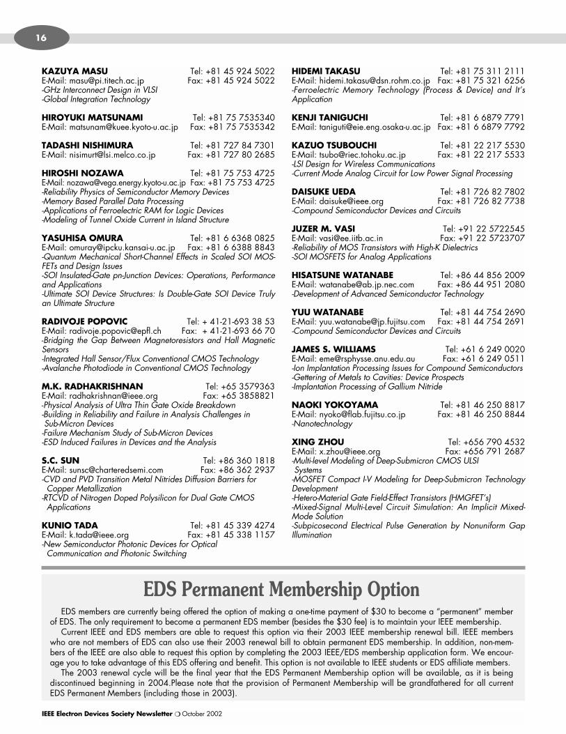
IEEE Electron Devices Society Newsletter ❍ October 2002
16
KAZUYA MASU Tel: +81 45 924 5022E-Mail: [email protected] Fax: +81 45 924 5022-GHz Interconnect Design in VLSI-Global Integration Technology
HIROYUKI MATSUNAMI Tel: +81 75 7535340E-Mail: [email protected] Fax: +81 75 7535342
TADASHI NISHIMURA Tel: +81 727 84 7301E-Mail: [email protected] Fax: +81 727 80 2685
HIROSHI NOZAWA Tel: +81 75 753 4725E-Mail: [email protected] Fax: +81 75 753 4725-Reliability Physics of Semiconductor Memory Devices-Memory Based Parallel Data Processing-Applications of Ferroelectric RAM for Logic Devices-Modeling of Tunnel Oxide Current in Island Structure
YASUHISA OMURA Tel: +81 6 6368 0825E-Mail: [email protected] Fax: +81 6 6388 8843-Quantum Mechanical Short-Channel Effects in Scaled SOI MOS-FETs and Design Issues-SOI Insulated-Gate pn-Junction Devices: Operations, Performanceand Applications-Ultimate SOI Device Structures: Is Double-Gate SOI Device Trulyan Ultimate Structure
RADIVOJE POPOVIC Tel: + 41-21-693 38 53E-Mail: [email protected] Fax: + 41-21-693 66 70-Bridging the Gap Between Magnetoresistors and Hall MagneticSensors-Integrated Hall Sensor/Flux Conventional CMOS Technology-Avalanche Photodiode in Conventional CMOS Technology
M.K. RADHAKRISHNAN Tel: +65 3579363E-Mail: [email protected] Fax: +65 3858821-Physical Analysis of Ultra Thin Gate Oxide Breakdown-Building in Reliability and Failure in Analysis Challenges in Sub-Micron Devices-Failure Mechanism Study of Sub-Micron Devices-ESD Induced Failures in Devices and the Analysis
S.C. SUN Tel: +86 360 1818E-Mail: [email protected] Fax: +86 362 2937-CVD and PVD Transition Metal Nitrides Diffusion Barriers forCopper Metallization
-RTCVD of Nitrogen Doped Polysilicon for Dual Gate CMOSApplications
KUNIO TADA Tel: +81 45 339 4274E-Mail: [email protected] Fax: +81 45 338 1157 -New Semiconductor Photonic Devices for OpticalCommunication and Photonic Switching
HIDEMI TAKASU Tel: +81 75 311 2111E-Mail: [email protected] Fax: +81 75 321 6256-Ferroelectric Memory Technology (Process & Device) and It’sApplication
KENJI TANIGUCHI Tel: +81 6 6879 7791E-Mail: [email protected] Fax: +81 6 6879 7792
KAZUO TSUBOUCHI Tel: +81 22 217 5530E-Mail: [email protected] Fax: +81 22 217 5533-LSI Design for Wireless Communications-Current Mode Analog Circuit for Low Power Signal Processing
DAISUKE UEDA Tel: +81 726 82 7802E-Mail: [email protected] Fax: +81 726 82 7738-Compound Semiconductor Devices and Circuits
JUZER M. VASI Tel: +91 22 5722545E-Mail: [email protected] Fax: +91 22 5723707 -Reliability of MOS Transistors with High-K Dielectrics-SOI MOSFETS for Analog Applications
HISATSUNE WATANABE Tel: +86 44 856 2009E-Mail: [email protected] Fax: +86 44 951 2080-Development of Advanced Semiconductor Technology
YUU WATANABE Tel: +81 44 754 2690E-Mail: [email protected] Fax: +81 44 754 2691-Compound Semiconductor Devices and Circuits
JAMES S. WILLIAMS Tel: +61 6 249 0020E-Mail: [email protected] Fax: +61 6 249 0511-Ion Implantation Processing Issues for Compound Semiconductors-Gettering of Metals to Cavities: Device Prospects-Implantation Processing of Gallium Nitride
NAOKI YOKOYAMA Tel: +81 46 250 8817E-Mail: [email protected] Fax: +81 46 250 8844-Nanotechnology
XING ZHOU Tel: +656 790 4532E-Mail: [email protected] Fax: +656 791 2687-Multi-level Modeling of Deep-Submicron CMOS ULSISystems-MOSFET Compact I-V Modeling for Deep-Submicron TechnologyDevelopment-Hetero-Material Gate Field-Effect Transistors (HMGFET’s)-Mixed-Signal Multi-Level Circuit Simulation: An Implicit Mixed-Mode Solution-Subpicosecond Electrical Pulse Generation by Nonuniform GapIllumination
EDS Permanent Membership OptionEDS members are currently being offered the option of making a one-time payment of $30 to become a “permanent” member
of EDS. The only requirement to become a permanent EDS member (besides the $30 fee) is to maintain your IEEE membership.Current IEEE and EDS members are able to request this option via their 2003 IEEE membership renewal bill. IEEE members
who are not members of EDS can also use their 2003 renewal bill to obtain permanent EDS membership. In addition, non-mem-bers of the IEEE are also able to request this option by completing the 2003 IEEE/EDS membership application form. We encour-age you to take advantage of this EDS offering and benefit. This option is not available to IEEE students or EDS affiliate members.
The 2003 renewal cycle will be the final year that the EDS Permanent Membership option will be available, as it is beingdiscontinued beginning in 2004.Please note that the provision of Permanent Membership will be grandfathered for all currentEDS Permanent Members (including those in 2003).
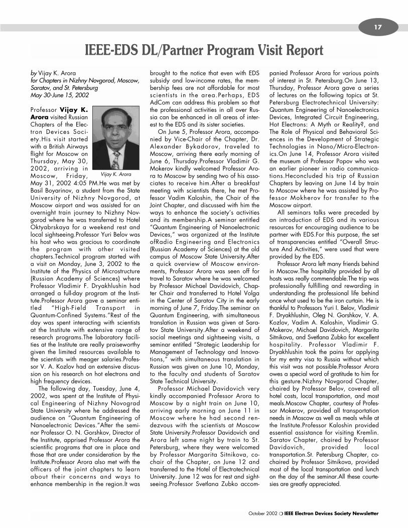
by Vijay K. Arorafor Chapters in Nizhny Novgorod, Moscow,Saratov, and St. PetersburgMay 30-June 15, 2002
Professor Vijay K.Arora visited RussianChapters of the Elec-tron Devices Soci -ety.His visit startedwith a British Airwaysflight for Moscow onThursday, May 30,2002, arriving inMoscow, Friday,May 31, 2002 4:05 PM.He was met byBasil Boyarinov, a student from the StateUniversi ty of Nizhny Novgorod, atMoscow airport and was assisted for anovernight train journey to Nizhny Nov-gorod where he was transferred to HotelOktyabrskaya for a weekend rest andlocal sightseeing.Professor Yuri Belov washis host who was gracious to coordinatethe program with other visi tedchapters.Technical program started witha visit on Monday, June 3, 2002 to theInstitute of the Physics of Microstructure(Russian Academy of Sciences) whereProfessor Vladimir F. Dryakhlushin hadarranged a full-day program at the Insti-tute.Professor Arora gave a seminar enti-t led “High-Field Transport inQuantum-Confined Systems.”Rest of theday was spent interacting with scientistsat the Institute with extensive range ofresearch programs.The laboratory facili-ties at the Institute are really praiseworthygiven the limited resources available tothe scientists with meager salaries.Profes-sor V. A. Kozlov had an extensive discus-sion on his research on hot electrons andhigh frequency devices.
The following day, Tuesday, June 4,2002, was spent at the Institute of Physi-cal Engineering of Nizhny NovogradState University where he addressed theaudience on “Quantum Engineering ofNanoelectronic Devices.”After the semi-nar Professor O. N. Gorshkov, Director ofthe Institute, apprised Professor Arora thescientific programs that are in place andthose that are under consideration by theInstitute.Professor Arora also met with theofficers of the joint chapters to learnabout their concerns and ways toenhance membership in the region.It was
brought to the notice that even with EDSsubsidy and low-income rates, the mem-bership fees are not affordable for mostscientis ts in the area.Perhaps, EDSAdCom can address this problem so thatthe professional activities in all over Rus-sia can be enhanced in all areas of inter-est to the EDS and its sister societies.
On June 5, Professor Arora, accompa-nied by Vice-Chair of the Chapter, Dr.Alexander Bykadorov, traveled toMoscow, arriving there early morning ofJune 6, Thursday.Professor Vladimir G.Mokerov kindly welcomed Professor Aro-ra to Moscow by sending two of his asso-ciates to receive him.After a breakfastmeeting with scientists there, he met Pro-fessor Vadim Kaloshin, the Chair of theJoint Chapter, and discussed with him theways to enhance the society’s activitiesand its membership.A seminar entitled“Quantum Engineering of NanoelectronicDevices,” was organized at the InstituteofRadio Engineering and Electronics(Russian Academy of Sciences) at the oldcampus of Moscow State University.Aftera quick overview of Moscow environ-ments, Professor Arora was seen off fortravel to Saratov where he was welcomedby Professor Michael Davidovich, Chap-ter Chair and transferred to Hotel Volgain the Center of Saratov City in the earlymorning of June 7, Friday.The seminar onQuantum Engineering, with simultaneoustranslation in Russian was given at Sara-tov State University.After a weekend ofsocial meetings and sightseeing visits, aseminar entitled “Strategic Leadership forManagement of Technology and Innova-tions,” with simultaneous translation inRussian was given on June 10, Monday,to the faculty and students of SaratovState Technical University.
Professor Michael Davidovich verykindly accompanied Professor Arora toMoscow by a night train on June 10,arriving early morning on June 11 inMoscow where he had second ren-dezvous with the scientists at MoscowState University.Professor Davidovich andArora left same night by train to St.Petersburg, where they were welcomedby Professor Margarita Sitnikova, co-chair of the Chapter, on June 12 andtransferred to the Hotel of ElectrotechnicalUniversity. June 12 was for rest and sight-seeing.Professor Svetlana Zubko accom-
panied Professor Arora for various pointsof interest in St. Petersburg.On June 13,Thursday, Professor Arora gave a seriesof lectures on the following topics at St.Petersburg Electrotechnical University:Quantum Engineering of NanoelectronicsDevices, Integrated Circuit Engineering,Hot Electrons: A Myth or Reality?, andThe Role of Physical and Behavioral Sci-ences in the Development of StrategicTechnologies in Nano/Micro-Electron-ics.On June 14, Professor Arora visitedthe museum of Professor Popov who wasan earlier pioneer in radio communica-tions.Heconcluded his trip of RussianChapters by leaving on June 14 by trainto Moscow where he was assisted by Pro-fessor Mokherov for transfer to theMoscow airport.
All seminars talks were preceded byan introduction of EDS and its variousresources for encouraging audience to bepartner with EDS.For this purpose, the setof transparencies entitled “Overall Struc-ture And Activities,” were used that wereprovided by the EDS.
Professor Arora left many friends behindin Moscow.The hospitality provided by allhosts was really commendable.The trip wasprofessionally fulfilling and rewarding inunderstanding the professional life behindonce what used to be the iron curtain. He isthankful to Professors Yuri I. Belov, VladimirF. Dryakhlushin, Oleg N. Gorshkov, V. A.Kozlov, Vadim A. Kaloshin, Vladimir G.Mokerov, Michael Davidovich, MargaritaSitnikova, and Svetlana Zubko for excellenthospitality. Professor Vladimir F.Dryakhlushin took the pains for applyingfor my entry visa to Russia without whichthis visit was not possible.Professor Aroraowes a special word of gratitude to him forthis gesture.Nizhny Novgorod Chapter,chaired by Professor Belov, covered allhotel costs, local transportation, and mostmeals.Moscow Chapter, courtesy of Profes-sor Mokerov, provided all transportationneeds in Moscow as well as meals while atthe Institute.Professor Kaloshin providedessential assistance for visiting Kremlin.Saratov Chapter, chaired by ProfessorDavidovich, provided localtransportation.St. Petersburg Chapter, co-chaired by Professor Sitnikova, providedmost of the local transportation and lunchon the day of the seminar.All these courte-sies are greatly appreciated.
October 2002 ❍ IEEE Electron Devices Society Newsletter
17
IEEE-EDS DL/Partner Program Visit Report
Vijay K. Arora
IEEE policy currently allows a 50% discounton IEEE dues and one society membershipfor any individual whose annual salary isless than US$11,000.This offering isreferred to as the Minimum Income SpecialConsiderations Option.The ElectronDevices Society now has a new programfor its chapters called the Membership FeeSubsidy Program (MFSP), which will bothcomplement the IEEE Minimum Incomeoffering and provide a significant addition-al benefit for qualified individuals.
With the EDS Membership Fee SubsidyProgram, EDS will pay the other 50% ofthe IEEE and EDS dues that are not cov-ered by IEEE for individuals qualifying forthe Minimum Income option for 10 indi-viduals per chapter.These individuals canbe either prospective new students/mem-bers or existing students/members.Thisprogram is also available to all unem-ployed members.Although the IEEE Mini-mum Income option allows individuals topurchase publication subscriptions for one-
society at a 50% reduced rate, the EDSMFSP does not cover the payment of pub-lication subscriptions.
If a chapter has individuals who qualifyfor the reduced IEEE Minimum Income offer-ing and the EDS MFSP, all the ChapterChair needs to do is coordinate the obtain-ing and submission of the IEEE/EDS mem-bership application forms (for prospectivenew members) and/or IEEE membershiprenewal bills (for existing members) for theindividuals he/she is proposing to be cov-ered by EDS.The Chapter Chair should alsocontact the EDS Executive Office to adviseof their participation in the program.Allapplication forms and renewal bills shouldbe mailed to the EDS ExecutiveOffice.Once received, the applicationforms and bills will be coded by the Execu-tive Office with a special account numberand submitted to the pertinent IEEE depart-ment for processing.
For a given year of participation in theEDS MFSP, a chapter must replace a min-
imum of the ten members who were paidfor by EDS in the previous year.Also, agiven member will only be allowed tohave his/her memberships paid for byEDS a maximum of two times.These twopolicies will avoid having the same mem-bers receive the benefit each year andencourage new membership.These EDSmembers receiving the MFSP benefits areencouraged to participate in chapteractivities and promote its growth.
Aside from being a program for exist-ing EDS chapters, the EDS MembershipFee Subsidy Program is also an extremelygood means to help facilitate the launch-ing of new chapters in low income geo-graphical areas.For any quest ionsconcerning the program, please contactLaura Riello ([email protected]) of the EDSExecutive Office.
James B. KuoEDS Membership ChairUniversity of Waterloo
Waterloo, Canada
IEEE Electron Devices Society Newsletter ❍ October 2002
18
Richard AllenRaj B. Apte*John R. Beresford*Navakanta BhatRichard C. Blish IIJan BosiersRobert S. ChauChang-Lee ChenRebecca CheungJon A. Christensen*Nikhil Ranjan DasDavid L. DickensheetsLech DobrzanskiPeter N. Ersland*Mehdi FardmaneshPatrick J. FrenchXinghua Fu*Julian William Gardner*Gerard GhibaudoIsrael Greiss
Timothy P. Hogan*Armando Iturralde*Joerg JasperKevin L. Jensen*Jianfei JiangShigeo KawasakiAurangzeb Khan*Muhammad Asif KhanJongdae KimArno G. KostkaChanho Lee*Duk-Dong LeeRuigang Li*Curtis C. LingTuvia LiranEric M. Mair*Santiago Marco*Sean P. McAlister*Kyung-Youl MinS.J. Neil Mitchell*
Saeed MohammadiSani R. NasssifEric F. Nicol*Reginald Perry*Kenneth J. Petrosky*Matthew RowleyChris SeamsShahin SharifzadehZheng John ShenWalter J. SnoeysPaul C.F. Tong*Richard Van Hoesen BoothRama VenkatSorin P. VoinigescuShanhong XiaYong Zhong XiongTerence K.S. Wong*Xinzhang WuViktor Zekeriya*
Congratulations to the EDS MembersRecently Elected to IEEE Senior Member Grade!
* = Individual designated EDS as nominating entityIf you have been in professional practice for 10 years, you may be eligible for Senior Membership, the highest grade of member-
ship for which an individual can apply. New senior members receive a wood and bronze plaque and a credit certificate for up to US$25 for a new IEEE society membership. In addition, a letter will be sent to employers, recognizing this new status.
For more information on senior member status, visit http://www.ieee.org/membership/grades_cats.html#SENIORMEM To apply forsenior member status, fill out an application at http://www.ieee.org/organizations/rab/md/smelev.htm.
EDS MEMBERSHIP FEE SUBSIDY PROGRAM (MFSP)
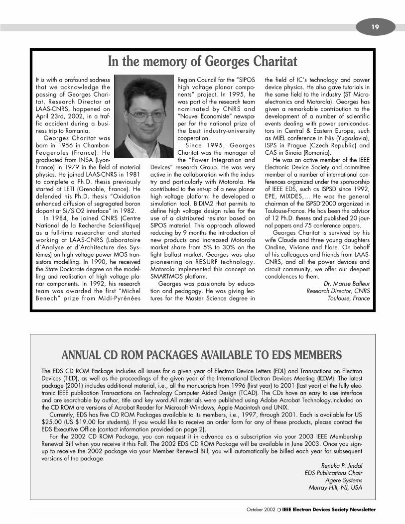
It is with a profound sadnessthat we acknowledge thepassing of Georges Chari-tat, Research Director atLAAS-CNRS, happened onApril 23rd, 2002, in a traf-fic accident during a busi-ness trip to Romania.
Georges Charitat wasborn in 1956 in Chambon-Feugeroles (France). Hegraduated from INSA (Lyon-France) in 1979 in the field of materialphysics. He joined LAAS-CNRS in 1981to complete a Ph.D. thesis previouslystarted at LETI (Grenoble, France). Hedefended his Ph.D. thesis “Oxidationenhanced diffusion of segregated borondopant at Si/SiO2 interface” in 1982.
In 1984, he joined CNRS (CentreNational de la Recherche Scientifique)as a full-time researcher and startedworking at LAAS-CNRS (Laboratoired’Analyse et d’Architecture des Sys-tèmes) on high voltage power MOS tran-sistors modelling. In 1990, he receivedthe State Doctorate degree on the model-ling and realisation of high voltage pla-nar components. In 1992, his researchteam was awarded the first “MichelBenech” prize from Midi-Pyrénées
Region Council for the “SIPOShigh voltage planar compo-nents” project. In 1995, hewas part of the research teamnominated by CNRS and“Nouvel Economiste” newspa-per for the national prize ofthe best industry-universitycooperation.
Since 1995, GeorgesCharitat was the manager ofthe “Power Integration and
Devices” research Group. He was veryactive in the collaboration with the indus-try and particularly with Motorola. Hecontributed to the set-up of a new planarhigh voltage platform: he developed asimulation tool, BIDIM2 that permits todefine high voltage design rules for theuse of a distributed resistor based onSIPOS material. This approach allowedreducing by 9 months the introduction ofnew products and increased Motorolamarket share from 5% to 30% on thelight ballast market. Georges was alsopioneering on RESURF technology.Motorola implemented this concept onSMARTMOS platform.
Georges was passionate by educa-tion and pedagogy. He was giving lec-tures for the Master Science degree in
the field of IC’s technology and powerdevice physics. He also gave tutorials inthe same field to the industry (ST Micro-electronics and Motorola). Georges hasgiven a remarkable contribution to thedevelopment of a number of scientificevents dealing with power semiconduc-tors in Central & Eastern Europe, suchas MIEL conference in Nis (Yugoslavia),ISPS in Prague (Czech Republic) andCAS in Sinaia (Romania).
He was an active member of the IEEEElectronic Device Society and committeemember of a number of international con-ferences organized under the sponsorshipof IEEE EDS, such as ISPSD since 1992,EPE, MIXDES,… He was the generalchairman of the ISPSD’2000 organized inToulouse-France. He has been the advisorof 12 Ph.D. theses and published 20 jour-nal papers and 75 conference papers.
Georges Charitat is survived by hiswife Claude and three young daughtersOndine, Viviane and Flore. On behalfof his colleagues and friends from LAAS-CNRS, and all the power devices andcircuit community, we offer our deepestcondolences to them.
Dr. Marise BafleurResearch Director, CNRS
Toulouse, France
October 2002 ❍ IEEE Electron Devices Society Newsletter
19
In the memory of Georges Charitat
ANNUAL CD ROM PACKAGES AVAILABLE TO EDS MEMBERSThe EDS CD ROM Package includes all issues for a given year of Electron Device Letters (EDL) and Transactions on ElectronDevices (T-ED), as well as the proceedings of the given year of the International Electron Devices Meeting (IEDM). The latestpackage (2001) includes additional material, i.e., all the manuscripts from 1996 (first year) to 2001 (last year) of the fully elec-tronic IEEE publication Transactions on Technology Computer Aided Design (TCAD). The CDs have an easy to use interfaceand are searchable by author, title and key word.All materials were published using Adobe Acrobat Technology.Included onthe CD ROM are versions of Acrobat Reader for Microsoft Windows, Apple Macintosh and UNIX.
Currently, EDS has five CD ROM Packages available to its members, i.e., 1997, through 2001. Each is available for US$25.00 (US $19.00 for students). If you would like to receive an order form for any of these products, please contact theEDS Executive Office (contact information provided on page 2).
For the 2002 CD ROM Package, you can request it in advance as a subscription via your 2003 IEEE MembershipRenewal Bill when you receive it this Fall. The 2002 EDS CD ROM Package will be available in June 2003. Once you sign-up to receive the 2002 package via your Member Renewal Bill, you will automatically be billed each year for subsequentversions of the package.
Renuka P. JindalEDS Publications Chair
Agere Systems Murray Hill, NJ, USA
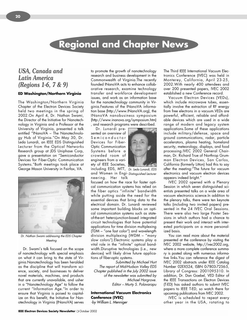
IEEE Electron Devices Society Newsletter ❍ October 2002
20
Regional and Chapter News
USA, Canada and Latin America (Regions 1-6, 7 & 9) ED Washington/Northern Virginia
The Washington/Northern VirginiaChapter of the Electron Devices Societyheld two meetings in the spring of2002.On April 4, Dr. Nathan Swami,the Director of the Initiative for Nanotech-nology in Virginia and a Professor at theUniversity of Virginia, presented a talkentitled “INanoVA – The Nanotechnolo-gy Hub of Virginia.”On May 30, Dr.Leda Lunardi, an IEEE EDS DistinguishedLecturer from the Optical NetworksResearch group at JDS Uniphase Corp,gave a presentation on “SemiconductorDevices for Fiber-Optic CommunicationSystems.”Both meetings took place atGeorge Mason University in Fairfax, VA.
Dr. Swami’s talk focused on the scopeof nanotechnology with special emphasison what it can bring to the state of Vir-ginia.Nanotechnology has been heraldedas the discipline that will transform sci-ence, society, and businesses to delivernovel materials, machines, and productsthat are currently unavailable, and usherin a “Nanotechnology Age” to follow thecurrent “Information Age.”In order toensure that Virginia is poised to capital-ize on this benefit, the Initiative for Nan-otechnology in Virginia (INanoVA) serves
to promote the growth of nanotechnologyresearch and business development in theCommonwealth of Virginia.The recentlyfounded INanoVA acts to enhance collab-orative research, examine technologytransfer and workforce developmentissues, and work as an information basefor the nanotechnology community in Vir-ginia.Features of the INanoVA informa-tion base (http://www.INanoVA.org), theINanoVA nanobusiness symposium(http://www.inanova.org/symposium.htm), and research programs were described.
Dr. Lunardi pre-sented an overview ofS e m i c o n d u c t o rDevices for Fiber-Optic CommunicationSystems before acrowded room ofengineers from a vari-ety of IEEE Societies,including EDS, MTT,and Women in Engi-neering. Her talkfocused on how the race for faster opti-cal communication systems has relied onthe fiber optics “infinite” bandwidthwhile putting aside the need for theessential devices that bring data to theelectrical domain. Dr. Lunardi reviewedsome important building blocks on opti-cal communication systems such as state-of-the-art heterojunction-based integratedcircuit technologies that have potentialapplications for time division multiplexing(TDM – “one fast color”) and wavelengthdivision multiplexing (WDM – “manyslow colors”).Electronic systems play avital role in the “infinite” optical band-width.Disruptive technologies (i.e., newdevices) will likely drive future applica-tions of fiber-optic systems.
Submitted by Michael Hurt The report of Mid-Hudson Valley EDS
Chapter published in the July 2002 issueof the newsletter was submitted by
Michael Hargrove. Editor – Murty S. Polavarapu
International Vacuum ElectronicsConference (IVEC)-by William L. Menniger
The Third IEEE International Vacuum Elec-tronics Conference (IVEC) was held inMonterey, California, April 23-25,2002.With nearly 400 attendees andover 200 presented papers, IVEC 2002established a new Conference record.
Vacuum Electron Devices (VEDs),which include microwave tubes, essen-tially involve the extraction of RF energyfrom free electrons in a vacuum.VEDs arepowerful, efficient, reliable and afford-able devices which are used in a widerange of modern and legacy systemapplications.Some of these applicationsinclude military/defense, space andground communications, radar, particleaccelerators, plasma heating, homelandsecurity, meteorology, displays, and foodprocessing.IVEC 2002 General Chair-man, Dr. Richard True of Northrop Grum-man Electron Devices, San Carlos,California (formerly Litton) had this to sayafter the meeting:”The future for vacuumelectronics and vacuum electron devicesappears indeed bright.”
IVEC 2002 opened with a PlenarySession in which seven distinguished sci-entists presented talks on a wide area ofvacuum electronics science.In addition tothe plenary talks, there were ten keynotetalks (including two invited papers) pre-sented in the 24 IVEC Oral Sessions.There were also two large Poster Ses-sions in which authors had a chance topresent their work and interact with inter-ested participants on a more personal-ized basis.
You can read more about the materialpresented at the conference by visiting theIVEC 2002 website, http://ivec2002.org,where a more complete conference summa-ry is posted along with numerous informa-tive links.You can reference the digest ofIVEC 2002 abstracts under IEEE CatalogNumber 02EX524, ISBN 0-7803-7256-5,Library of Congress: 2001095310. Inaddition, Dr. Dan Goebel, VED Editor ofthe IEEE Transactions on Electron Devices(T-ED) has asked authors to submit IVECpapers to IEEE T-ED, so watch there forupcoming publications from IVEC 2002.
IVEC is scheduled to repeat everyother year in the USA, rotat ing to
Dr. Nathan Swami addressing the EDS ChapterMeeting
Dr. Leda Lunardi, EDSDistinguished Lecturer
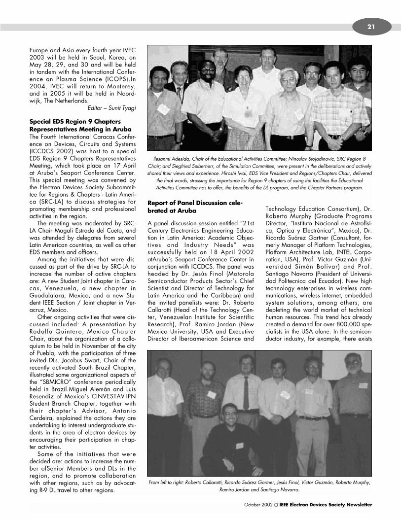
October 2002 ❍ IEEE Electron Devices Society Newsletter
21
Europe and Asia every fourth year.IVEC2003 will be held in Seoul, Korea, onMay 28, 29, and 30 and will be heldin tandem with the International Confer-ence on Plasma Science (ICOPS).In2004, IVEC will return to Monterey,and in 2005 it will be held in Noord-wijk, The Netherlands.
Editor – Sunit Tyagi
Special EDS Region 9 ChaptersRepresentatives Meeting in ArubaThe Fourth International Caracas Confer-ence on Devices, Circuits and Systems(ICCDCS 2002) was host to a specialEDS Region 9 Chapters RepresentativesMeeting, which took place on 17 Aprilat Aruba’s Seaport Conference Center.This special meeting was convened bythe Electron Devices Society Subcommit-tee for Regions & Chapters - Latin Ameri-ca (SRC-LA) to discuss strategies forpromoting membership and professionalactivities in the region.
The meeting was moderated by SRC-LA Chair Magali Estrada del Cueto, andwas attended by delegates from severalLatin American countries, as well as otherEDS members and officers.
Among the initiatives that were dis-cussed as part of the drive by SRC-LA toincrease the number of active chaptersare: A new Student Joint chapter in Cara-cas, Venezuela, a new chapter inGuadalajara, Mexico, and a new Stu-dent IEEE Section / Joint chapter in Ver-acruz, Mexico.
Other ongoing activities that were dis-cussed included: A presentation byRodolfo Quintero, Mexico ChapterChair, about the organization of a collo-quium to be held in November at the cityof Puebla, with the participation of threeinvited DLs. Jacobus Swart, Chair of therecently activated South Brazil Chapter,illustrated some organizational aspects ofthe “SBMICRO” conference periodicallyheld in Brazil.Miguel Alemán and LuisResendiz of Mexico’s CINVESTAV-IPNStudent Branch Chapter, together withtheir chapter’s Advisor, AntonioCerdeira, explained the actions they areundertaking to interest undergraduate stu-dents in the area of electron devices byencouraging their participation in chap-ter activities.
Some of the initiatives that weredecided are: actions to increase the num-ber ofSenior Members and DLs in theregion, and to promote collaborationwith other regions, such as by advocat-ing R-9 DL travel to other regions.
Report of Panel Discussion cele-brated at Aruba
A panel discussion session entitled “21stCentury Electronics Engineering Educa-tion in Latin America: Academic Objec-t ives and Industry Needs” wassuccessfully held on 18 April 2002atAruba’s Seaport Conference Center inconjunction with ICCDCS. The panel washeaded by Dr. Jesús Finol (MotorolaSemiconductor Products Sector’s ChiefScientist and Director of Technology forLatin America and the Caribbean) andthe invited panelists were: Dr. RobertoCallarotti (Head of the Technology Cen-ter, Venezuelan Institute for ScientificResearch), Prof. Ramiro Jordan (NewMexico University, USA and ExecutiveDirector of Iberoamerican Science and
Technology Education Consortium), Dr.Roberto Murphy (Graduate ProgramsDirector, “Instituto Nacional de Astrofísi-ca, Optica y Electrónica”, Mexico), Dr.Ricardo Suárez Gartner (Consultant, for-merly Manager of Platform Technologies,Platform Architecture Lab, INTEL Corpo-ration, USA), Prof. Víctor Guzmán (Uni-versidad Simón Bolívar) and Prof.Santiago Navarro (President of Universi-dad Politecnica del Ecuador). New hightechnology enterprises in wireless com-munications, wireless internet, embeddedsystem solutions, among others, aredepleting the world market of technicalhuman resources. This trend has alreadycreated a demand for over 800,000 spe-cialists in the USA alone. In the semicon-ductor industry, for example, there exists
Ilesanmi Adesida, Chair of the Educational Activities Committee; Ninoslav Stojadinovic, SRC Region 8Chair; and Siegfried Selberherr, of the Simulation Committee, were present in the deliberations and activelyshared their views and experience. Hiroshi Iwai, EDS Vice President and Regions/Chapters Chair, delivered
the final words, stressing the importance for Region 9 chapters of using the facilities the EducationalActivities Committee has to offer, the benefits of the DL program, and the Chapter Partners program.
From left to right: Roberto Callarotti, Ricardo Suárez Gartner, Jesús Finol, Víctor Guzmán, Roberto Murphy,Ramiro Jordan and Santiago Navarro.
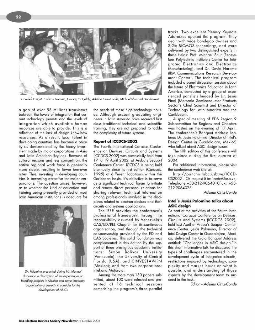
IEEE Electron Devices Society Newsletter ❍ October 2002
22
a gap of over 58 millions transistorsbetween the levels of integration that cur-rent technology permits and the levels ofintegration which available humanresources are able to provide. This is areflection of the lack of design know-howresources. As a result, local talent indeveloping countries has become a prior-ity as demonstrated by the heavy invest-ment made by major corporations in Asiaand Latin American Regions. Because ofcultural reasons and less competition, thenative regional work force is generallymore stable, resulting in lower turn-overrates. Thus, investing in developing coun-tries is becoming attractive for major cor-porations. The question arises, however,as to whether the kind of education andtraining being presently provided at mostLatin American institutions is adequate for
the needs of these high technology hous-es. Although present graduating engi-neers in Latin America have received firstclass traditional technical and scientifictraining, they are not prepared to tacklethe complexity of future systems.
Report of ICCDCS-2002The Fourth International Caracas Confer-ence on Devices, Circuits and Systems(ICCDCS 2002) was successfully held from17 to 19 April 2002, at Aruba’s SeaportConference Center. ICCDCS is being heldbiannually since its first edition (Caracas,1995) at different locations within theCaribbean basin. It’s objective is to serveas a significant technical forum to initiateand renew direct personal relations forsharing relevant technical informationamong professionals involved in the disci-plines related to electron devices and theircircuits and systems applications.
The IEEE provides the conference’sprofessional framework, through theresponsibility assumed by Venezuela’sCAS/ED/PEL Chapter for its continuousorganization, and through the technicalco-sponsorship provided by the ED andCAS Societies. This solid foundation wascomplemented in this edition by the sup-port of three prestigious academic institu-t ions: Simón Bolívar Universi ty(Venezuela), the University of CentralFlorida (USA), and CINVESTAV-IPN(Mexico); and from two corporations:Intel and Motorola.
Among the more than 130 papers sub-mitted, about 100 were selected and pre-sented at 16 technical sessionscomprising the program’s three parallel
tracks. Two excellent Plenary KeynoteAddresses opened the program. Theydealt with wide band-gap devices andSiGe BiCMOS technology, and weredelivered by two distinguished experts inthese fields: Prof. Michael Shur (Rensse-laer Polytechnic Institute’s Center for Inte-grated Electronics and ElectronicsManufacturing), and Dr. David Harame(IBM Communications Research Develop-ment Center). The technical programincluded a panel discussion session aboutthe future of Electronics Education in LatinAmerica, conducted by a group of expe-rienced panelists headed by Dr. JesúsFinol (Motorola Semiconductor ProductsSector’s Chief Scientist and Director ofTechnology for Latin America and theCaribbean).
A special meeting of EDS Region 9Subcommittee for Regions and Chapterswas hosted on the evening of 17 April.The conference’s Banquet Address fea-tured Dr. Jesús Palomino (Director of Intel’sDesign Center in Guadalajara, Mexico)who talked about ASIC design issues.
The fifth edition of this conference willtake place during the first quarter of2004.
For additional information, please visitthe conference web site at:
http://pancho.labc.usb.ve/ICCD-CS2002 . Or request it to: [email protected],Telephone:+58-212-9064010Fax: +58-212-9064025.
Adelmo Ortiz-Conde
Intel´s Jesús Palomino talks aboutASIC designAs part of the activities of the Fourth Inter-national Caracas Conference on Devices,Circuits and Systems (ICCDCS 2002),held last April at Aruba’s Seaport Confer-ence Center. Jesús Palomino, Director ofIntel Design Center in Guadalajara, Mexi-co, delivered the Gala Banquet Addressentitled: “Challenges in ASIC design.”Inthis short informative talk he discussed thetypes of challenges encountered in thedevelopment cycle of integrated circuits,restrictions imposed by technology, com-plexity and market issues on what isdoable, and understanding of thoseaspects by the development team to suc-ceed in the task.
Editor – Adelmo Ortiz-Conde
From left to right: Toshiro Hiramoto, JuinLiou,Tor Fjeldly, Adelmo Ortiz-Conde, Michael Shur and Hiroshi Iwai.
Dr. Palomino presented during his informaldiscussion a description of the experiences on
handling projects in Mexico and some importantorganizational aspects to consider for the
development of ASICs
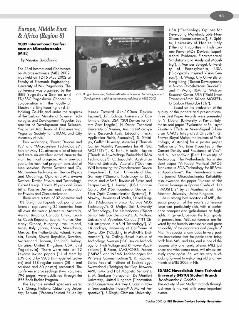
October 2002 ❍ IEEE Electron Devices Society Newsletter
23
Europe, Middle East& Africa (Region 8) 2002 International Confer-ence on Microelectronics(MIEL)
- by Ninoslav Stojadinovic
The 23rd International Conferenceon Microelectronics (MIEL 2002)was held on 12-15 May 2002 atFaculty of Electronic Engineering,University of Nis, Yugoslavia. Theconference was organized by theIEEE Yugoslavia Section andED/SSC Yugoslavia Chapter inco-operation with the Faculty ofElectronic Engineering and Ei-Holding Co.-Nis and under the auspicesof the Serbian Ministry of Science, Tech-nologies and Development, Yugoslav Sec-retariat of Development and Science,Yugoslav Academy of Engineering,Yugoslav Society for ETRAN, and CityAssembly of Nis.
Two workshops, “Power Devices andICs” and “Microsystem Technologies”,held on May 12, attracted a lot of interestand were an excellent introduction to themain technical program. As in previousyears, the technical program consisted ofnine sessions: Power Devices and ICs,Microsystem Technologies, Device Physicsand Modeling, Opto and MicrowaveDevices, Device Physics and Technology,Circuit Design, Device Physics and Relia-bility, Passive Devices, and Semiconduc-tor Physics and Characterization.
There were a total of 37 domestic and103 foreign participants took part at con-ference, representing 35 countries fromall over the world (Armenia, Australia,Austria, Bulgaria, Canada, China, Croat-ia, Czech Republic, Estonia, France, Ger-many, Greece, Hungary, Iran, Ireland,Israel, Italy, Japan, Korea, Macedonia,Mexico, The Netherlands, Poland, Roma-nia, Russia, Slovak Republic, Sweden,Switzerland, Taiwan, Thailand, Turkey,Ukraine, United Kingdom, USA, andYugoslavia). There were total of 22keynote invited papers (11 of them byEDS and 3 by SSCS Distinguished Lectur-ers) and 118 regular papers (58 in oralsessions and 60 posters) presented. Theconference proceedings (two volumes,796 pages) were published through theIEEE Book Broker Program.
The keynote invited speakers were:C.Y. Chang, National Chiao Tung Univer-sity, Taiwan (“Process-Related Reliability
Issues Toward Sub-100nm DeviceRegime”), J.-P. Colinge, University of Cali-fornia at Davis, USA (“SOI Devices for 0.1mm Gate Lengthsî), H. Detter, TechnicalUniversity of Vienna, Austria (ìMicrosys-tems: Research Task, Education Task,Application Fields, Examples”), S. Dimitri-jev, Griffith University, Australia (“Channel-Carrier Mobility Parameters for 4H SiCMOSFETs”), K. Itoh, Hitachi, Japan(“Trends in Low-Voltage Embedded RAMTechnology”), C. Jagadish, AustralianNational University, Australia (“QuantumWell Intermixing for Optoelectronic DeviceIntegration”), E. Kohn, University of Ulm,Germany (“Diamond Technology for Elec-tronics and MEMS: Review of Status andPerspectives”), L. Lunardi, JDS UniphaseCorp., USA (“Semiconductor Device forFiber Optic Communication Systems”), P.Mawby, University of Wales, United King-dom (“Advances in Silicon Carbide MOSTechnology”), G. Meijer, Delft Universityof Technology, The Netherlands (“SmartSensor Interface Electronics”), A. Nathan,University of Waterloo, Canada (“TFT Cir-cuit Integration in a-Si:H Technology”), V.Oklobdzija, University of California atDavis, USA (“Clocking in Multi-GHz Envi-ronment”), M. Ostling, Royal Institute ofTechnology, Sweden (“SiC Device Technol-ogy for High Voltage and RF Power Appli-cations”), R Plana, LAAS/CNRS, France(“MEMS and NEMS Technologies forWireless Communications”), R. Popovic,Swiss Federal Institute of Technology,Switzerland (“Bridging the Gap BetweenAMR, GMR and Hall Magnetic Sensors”),E. M. Sankara Narayanan, De MontfortUniversity, United Kingdom (“Innovationand Competition: Are they Crucial in Pow-er Semiconductor Industry? A Market Per-spective”), R.Singh, Clemson University,
USA (“Technology Options forDeveloping Manufacturable Non-Silicon Nanoelectronics”), P. Spiri-to, University of Naples, Italy(“Thermal Instabilities in High Cur-rent Power MOS Devices: Experi-mental Evidence, ElectrothermalSimulations and Analytical Model-ing”), J. Van der Spiegel, Universi-ty of Pennsylvania, USA(“Biologically Inspired Vision Sen-sors”), H. Wong, City University ofHong Kong (“Recent Developmentsin Silicon Optoelectronic Devices”),and P. Wong, IBM T.J. WatsonResearch Center, USA (“Field EffectTransistors-From Silicon MOSFETsto Carbon Nanotube FETs”).
Based on the evaluation of thequality of the papers and presentations,three Best Paper Awards were presentedto: V. Liberali (University of Pavia, Italy)for an oral paper “Evaluation of Epi LayerResistivity Effects in Mixed-Signal Submi-cron CMOS Integrated Circuits“; G.Reeves (Royal Melbourne Institute of Tech-nology, Australia) for a poster paper“Influence of Via Liner Properties on theCurrent Density and Resistance of Vias“;and N. Nenadovic (Delft University ofTechnology, The Netherlands) for a stu-dent paper “A Novel Vertical DMOSTransistor in SOA Technology for RF-Pow-er Applications“. The international scien-tific journal Microelectronics Reliabilityalso awarded the paper “Nature of HotCarrier Damage in Spacer Oxide of LDDn-MOSFETs“ by S. Manhas et al., DeMontfort University, United Kingdom.
As is among best traditions of MIEL, thesocial program of this year’s conferenceissue was particularly rich, with a confer-ence banquet and gala-dinner as high-lights. In general, besides the high qualityof presentations, MIEL conferences are fla-vored by the friendly atmosphere and greathospitality of the organizers and people ofNis. This special charm adds to very posi-tive impressions that the participants bringback from MIEL and Nis, and is one of thereasons why one rarely attends MIEL justonce: one who comes once, will almost cer-tainly come again. So, we are very muchlooking forward to welcoming old and newfriends at MIEL 2004 in Nis.
ED/SSC Novosibirsk State TechnicalUniversity (NSTU) Student Branch-by Alexander V. GridchinThe activity of our Student Branch throughlast year is marked with some importantevents.
Prof. Dragan Domazet, Serbian Minister of Science, Technologies andDevelopment, is giving the opening address at MIEL 2002
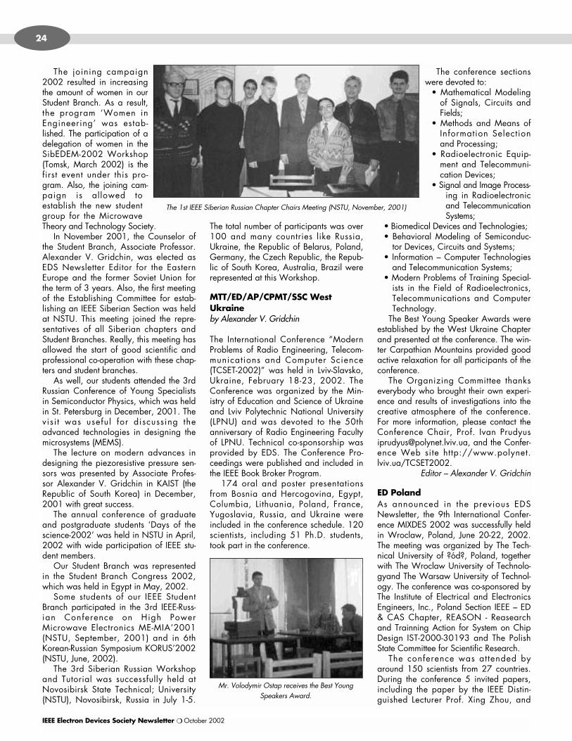
IEEE Electron Devices Society Newsletter ❍ October 2002
24
The joining campaign2002 resulted in increasingthe amount of women in ourStudent Branch. As a result,the program ‘Women inEngineering’ was estab-lished. The participation of adelegation of women in theSibEDEM-2002 Workshop(Tomsk, March 2002) is thefirst event under this pro-gram. Also, the joining cam-paign is allowed toestablish the new studentgroup for the MicrowaveTheory and Technology Society.
In November 2001, the Counselor ofthe Student Branch, Associate Professor.Alexander V. Gridchin, was elected asEDS Newsletter Editor for the EasternEurope and the former Soviet Union forthe term of 3 years. Also, the first meetingof the Establishing Committee for estab-lishing an IEEE Siberian Section was heldat NSTU. This meeting joined the repre-sentatives of all Siberian chapters andStudent Branches. Really, this meeting hasallowed the start of good scientific andprofessional co-operation with these chap-ters and student branches.
As well, our students attended the 3rdRussian Conference of Young Specialistsin Semiconductor Physics, which was heldin St. Petersburg in December, 2001. Thevisi t was useful for discussing theadvanced technologies in designing themicrosystems (MEMS).
The lecture on modern advances indesigning the piezoresistive pressure sen-sors was presented by Associate Profes-sor Alexander V. Gridchin in KAIST (theRepublic of South Korea) in December,2001 with great success.
The annual conference of graduateand postgraduate students ‘Days of thescience-2002’ was held in NSTU in April,2002 with wide participation of IEEE stu-dent members.
Our Student Branch was representedin the Student Branch Congress 2002,which was held in Egypt in May, 2002.
Some students of our IEEE StudentBranch participated in the 3rd IEEE-Russ-ian Conference on High PowerMicrowave Electronics ME-MIA’2001(NSTU, September, 2001) and in 6thKorean-Russian Symposium KORUS’2002(NSTU, June, 2002).
The 3rd Siberian Russian Workshopand Tutorial was successfully held atNovosibirsk State Technical; University(NSTU), Novosibirsk, Russia in July 1-5.
The total number of participants was over100 and many countries like Russia,Ukraine, the Republic of Belarus, Poland,Germany, the Czech Republic, the Repub-lic of South Korea, Australia, Brazil wererepresented at this Workshop.
MTT/ED/AP/CPMT/SSC WestUkraine by Alexander V. Gridchin
The International Conference “ModernProblems of Radio Engineering, Telecom-munications and Computer Science(TCSET-2002)” was held in Lviv-Slavsko,Ukraine, February 18-23, 2002. TheConference was organized by the Min-istry of Education and Science of Ukraineand Lviv Polytechnic National University(LPNU) and was devoted to the 50thanniversary of Radio Engineering Facultyof LPNU. Technical co-sponsorship wasprovided by EDS. The Conference Pro-ceedings were published and included inthe IEEE Book Broker Program.
174 oral and poster presentationsfrom Bosnia and Hercogovina, Egypt,Columbia, Lithuania, Poland, France,Yugoslavia, Russia, and Ukraine wereincluded in the conference schedule. 120scientists, including 51 Ph.D. students,took part in the conference.
The conference sectionswere devoted to:
• Mathematical Modelingof Signals, Circuits andFields;
• Methods and Means ofInformation Selectionand Processing;
• Radioelectronic Equip-ment and Telecommuni-cation Devices;
• Signal and Image Process-ing in Radioelectronicand TelecommunicationSystems;
• Biomedical Devices and Technologies;• Behavioral Modeling of Semiconduc-
tor Devices, Circuits and Systems;• Information – Computer Technologies
and Telecommunication Systems;• Modern Problems of Training Special-
ists in the Field of Radioelectronics,Telecommunications and ComputerTechnology.
The Best Young Speaker Awards wereestablished by the West Ukraine Chapterand presented at the conference. The win-ter Carpathian Mountains provided goodactive relaxation for all participants of theconference.
The Organizing Committee thankseverybody who brought their own experi-ence and results of investigations into thecreative atmosphere of the conference.For more information, please contact theConference Chair, Prof. Ivan [email protected], and the Confer-ence Web site http://www.polynet.lviv.ua/TCSET2002.
Editor – Alexander V. Gridchin
ED PolandAs announced in the previous EDSNewsletter, the 9th International Confer-ence MIXDES 2002 was successfully heldin Wroclaw, Poland, June 20-22, 2002.The meeting was organized by The Tech-nical University of ?ód?, Poland, togetherwith The Wroclaw University of Technolo-gyand The Warsaw University of Technol-ogy. The conference was co-sponsored byThe Institute of Electrical and ElectronicsEngineers, Inc., Poland Section IEEE – ED& CAS Chapter, REASON - Reasearchand Trainning Action for System on ChipDesign IST-2000-30193 and The PolishState Committee for Scientific Research.
The conference was attended byaround 150 scientists from 27 countries.During the conference 5 invited papers,including the paper by the IEEE Distin-guished Lecturer Prof. Xing Zhou, and
The 1st IEEE Siberian Russian Chapter Chairs Meeting (NSTU, November, 2001)
Mr. Volodymir Ostap receives the Best YoungSpeakers Award.
October 2002 ❍ IEEE Electron Devices Society Newsletter
25
over 140 regular papers were presentedat oral, poster and special sessions.
The conference covered the most impor-tant issues in modern electronics. The mostinteresting presentations, appointed by thesession chairmen, were distinguished.Additionally, the special IEEE EDS PolishChapter Award was presented to B. Calvo,S. Celma, P.A. Martinez and M.T. Sanz forthe paper entitled “Novel High Perfor-mance CMOS Current Conveyor”. All thedistinguished papers will be recommendedfor publication in one of the following jour-nals: “Microelectronics Reliability”, “Elec-tron Technology Internet Journal” and“Radioelectronics & Informatics”. After thelecture of Prof. Xing Zhou, the IEEE PolandSection held a meeting. The matters con-cerning the activities of the IEEE Poland sec-tion were discussed. Additionally, duringthe tourist activities, the participants had thechance to learn more about Wroclaw, oneof the most beautiful Polish cities.
In order to mark the first decade of theMIXDES conferences, next year’s 10thConference will be held in the home city ofthe organizers, Lodz, Poland. The Prelimi-nary Call for Papers is already available athttp://www.mixdes.org/downloads/call2003.pdf. More information about theMIXDES Conferences can be found athttp://www.mixdes.org.
By - Irina NaidionovaAs we informed you earlier in our reportsabout IEEE MTT/ED/AP Lithuanian Chap-ter activities it became a good tradition tocarry out joint workshops together withIEEE sections from other countries andregions. This year we got into close pro-fessional contact with Da Yeh Universityof Taiwan and IEEE AP/MTT TaipeiChapter. Chair of the Chapter is Prof.Dau-Chyrh Chang.
In April, 2002 the representatives ofIEEE MTT/ED/AP Lithuanian Chapter heldjoint technical workshop at Da Yeh Uni-versity together with IEEE AP/MTT TaipeiChapter. Speakers Dr. B.Levitas andS.Charchenko “Antenna/RCS/ISAR Timedomain measurements”.
We would like to inform you that thesedays a reciprocal joint technical workshophas been carried out in Vilnius, Lithuaniaon July 3-5. “Time Domain Antenna Mea-surement”.Speaker Prof. Dau-Chyrh Changfrom Da Yeh University of Taiwan.Dr. BorisLevitas, Dr. Henryk Alenkovich, AleksandrMinin, Sergej Charchenko and other spe-cialists of Geozondas company. The work-shop was held successfully. Antennameasurement specialists and technicians
attended the workshop. New opportunitiesof Time and Frequency Domains applica-tion in antenna measurement by usingequipment of Geozondas company havebeen discussed.
The next technical workshop should becarried out in Taiwan on August 31.Attendance of 50 engineers and techni-cians from Taiwan and 5-7 specialistsfrom Geozondas company, Vilnius, isexpected. The workshop program envis-ages demonstration of Geozondas equip-ment for Antenna Measurement in Timeand Frequency Domains.
Editor – Andrzej Napieralski
ED IsraelChair Chapter - Prof. Nathan Croitoru, Secretary - Dr. Gady Golan;
1. On Sunday, March 17th 2002, at theHolon Inst. of Technology (HAIT) - Holon.
Subject of meeting: “Plane plasma dis-charge for microelectronics applications”,Guest lecturer was Mr. Alex Axelevichfrom HAIT. Chairmen of the meeting:Prof. Nathan Croitoru and Dr. GadyGolan – 35 people (most of them werestudents and academic staff) attended themeeting in Holon.
2. On Sunday, June 2nd 2002, at theHolon Inst. of Technology (HAIT) - Holon.
Subject of meeting: “Satellite Communi-cations - Review”, Guest lecturer was Prof.Yaakov Gavan from HAIT. Chairmen ofthe meeting: Prof. Nathan Croitoru andDr. Gady Golan – 20 people (most ofthem were students and academic staff)attended the meeting in Holon.
MTT/ED/AP/LEO UK&RI-by Terry Oxley
Major activities may be summarised as:-15th to 17th May 2002 — The first
Wireless Design Conference (WDC 2002),supported by Agilent Technologies and thelocal IEEE UK&RI MTT/ED/AP/LEO Chap-ter, was held at the Business Design Centre,London, UK. This conference organised byCMP Europe the publishers of MicrowaveEngineering Europe represented a newlylaunched event. It focused on the subjectsthat are important to the professional engi-neer working in the wireless industry;including RF techniques for optical commu-nications. The three-day event incorporatedan exhibition.
The first day presented two full-day train-ing courses on the topics of RF Circuit Designand Digital Modulation Formats. The techni-
cal programme included 12 wireless ses-sions and 4 opto sessions, poster sessionsand workshops; the workshops focused forexample on such topics as software definedradio, MEMS, wireless networking andRF/optoelectronic packaging. The openingplenary session on the second day includedthree keynote presentations: “Building blocksfor wireless internet” by Esko Jurvanen fromIntel Wireless Competence Centre, Stock-holm, Sweden; “Wireless access usingmicrowave photonics” by Alwyn Seeds (IEEEMTT-S Distinguished Microwave Lecturer)from University College, London; and “Thepast, present and future of wireless RF pow-er” by Ray Pengelly from UltraRF, Sunnyvale,CA, USA. Invited papers of the 3rd-day ple-nary session included: “The future of thewireless information society in Europe” by DrJorge Pereira from Information Society (Euro-pean Commission); “Low-IF transceiver archi-tecture for GSM/GPRS applications” byJames Kimery from Silicon Laboratories;“Galileo – new opportunities for location-based services in Europe” by Tony Pratt fromParthus Technologies: and “Why manyhands will make light work of 3G” by PaulBruce from Radioscape.
The conference attracted wide interna-tional representation and was consideredto be highly successful. Over 100 papersubmissions were received in response tothe call-for-papers, and the programmeincorporated some 85 technical papers(including invited papers and workshops)attracting some three hundred delegates.Next year, the Wireless Design Confer-ence 2003 is planned for M.O.C. Munich,Germany. For further information, pleasecontact Ms Nicola Jedrej E-mail:[email protected], or, Mr DavidRoberts E-mail: [email protected] see www.wirelessdesignconf.com.
27th May 2002 - A half-day PhotonicSeminar on High-speed Optical Modulatorswas held at the City University. Four lead-ing experts reviewed the technology andmajor research and developments in thisfield; they covered both electro-optic andelectro-absorption type modulators, encom-passing lithium niobate and semiconduc-tors. Presentations included: “Lithiumniobate modulators” by Dr Mike Murphyfrom JDS Uniphase Corporation;“GaAs/AlGaAs modulations technologyfor microwave-photonic and high bit-ratetelecom applications“ by Dr Rob G Walkerfrom Bookham Technology (Caswell);“Highoutput power, low operating voltage 40Gbit/s electroabsorption modulators” by MJ Robertson from Corning Research Centre;“Application of normal-incidence electro-
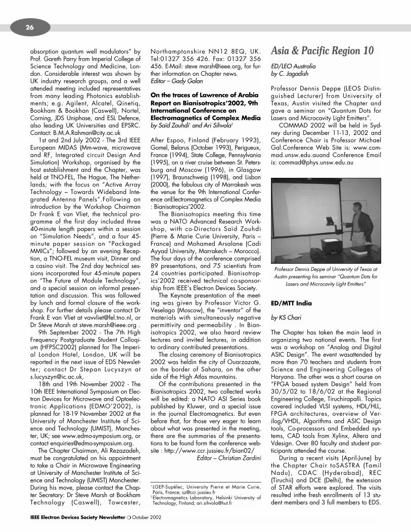
Asia & Pacific Region 10 ED/LEO Australiaby C. Jagadish
Professor Dennis Deppe (LEOS Distin-guished Lecturer) from University ofTexas, Austin visited the Chapter andgave a seminar on “Quantum Dots forLasers and Microcavity Light Emitters”.
COMMAD 2002 will be held in Syd-ney during December 11-13, 2002 andConference Chair is Professor MichaelGal.Conference Web Site is: www.com-mad.unsw.edu.auand Conference Emailis: [email protected]
ED/MTT India
by KS Chari
The Chapter has taken the main lead inorganizing two national events. The firstwas a workshop on “Analog and DigitalASIC Design”. The event wasattended bymore than 70 teachers and students fromScience and Engineering Colleges ofHaryana. The other was a short course on“FPGA based system Design” held from30/5/02 to 18/6/02 at the RegionalEngineering College, Tiruchirapalli. Topicscovered included VLSI systems, HDL/HLL,FPGA architectures, overview of Ver-ilog/VHDL, Algorithms and ASIC Designtools, Co-processors and Embedded sys-tems, CAD tools from Xylinx, Altera andVdesign. Over 80 faculty and student par-ticipants attended the course.
During a recent visits (April-June) bythe Chapter Chair toSASTRA (TamilNadu), CDAC (Hyderabad), REC(Tiruchii) and DCE (Delhi), the extensionof STAR efforts were explored. The visitsresulted inthe fresh enrollments of 13 stu-dent members and 3 full members to EDS.
IEEE Electron Devices Society Newsletter ❍ October 2002
26
absorption quantum well modulators” byProf. Gareth Parry from Imperial College ofScience Technology and Medicine, Lon-don. Considerable interest was shown byUK industry research groups, and a wellattended meeting included representativesfrom many leading Photonics establish-ments; e.g. Agilent, Alcatel, Qinetiq,Bookham & Bookhan (Caswell), Nortel,Corning, JDS Uniphase, and ESL Defence,also leading UK Universities and EPSRC.Contact: [email protected]
1st and 2nd July 2002 - The 3rd IEEEEuropean MIDAS (Mm-wave, microwaveand RF, Integrated circuit Design AndSimulation) Workshop, organised by thehost establishment and the Chapter, washeld at TNO-FEL, The Hague, The Nether-lands; with the focus on “Active ArrayTechnology – Towards Wideband Inte-grated Antenna Panels”.Following anintroduction by the Workshop ChairmanDr Frank E van Vliet, the technical pro-gramme of the first day included three40-minute length papers within a sessionon “Simulation Needs”, and a four 45-minute paper session on “PackagedMMICs”; followed by an evening Recep-tion, a TNO-FEL museum visit, Dinner anda casino visit. The 2nd day technical ses-sions incorporated four 45-minute paperson “The Future of Module Technology”,and a special session on informal presen-tation and discussion. This was followedby lunch and formal closure of the work-shop. For further details please contact DrFrank E van Vliet at [email protected], orDr Steve Marsh at [email protected] .
9th September 2002 - The 7th HighFrequency Postgraduate Student Colloqi-um (HFPSC2002) planned for The Imperi-al London Hotel, London, UK will bereported in the next issue of EDS Newslet-ter; contact Dr Stepan Lucyszyn [email protected],
18th and 19th November 2002 - The10th IEEE International Symposium on Elec-tron Devices for Microwave and Optoelec-tronic Applications (EDMO’2002), isplanned for 18-19 November 2002 at theUniversity of Manchester Institute of Sci-ence and Technology (UMIST), Manches-ter, UK; see www.edmo-symposium.org, orcontact [email protected].
The Chapter Chairman, Ali Rezazadeh,must be congratulated on his appointmentto take a Chair in Microwave Engineeringat University of Manchester Institute of Sci-ence and Technology (UMIST) Manchester.During his move, please contact the Chap-ter Secretary: Dr Steve Marsh at BookhamTechnology (Caswell), Towcester,
Northamptonshire NN12 8EQ, UK.Tel:01327 356 426. Fax: 01327 356456. E-Mail: steve [email protected], for fur-ther information on Chapter news. Editor – Gady Golan
On the traces of Lawrence of ArabiaReport on Bianisotropics’2002, 9thInternational Conference onElectromagnetics of Complex Mediaby Saïd Zouhdi1 and Ari Sihvola2
After Espoo, Finland (February 1993),Gomel, Belarus (October 1993), Perigueux,France (1994), State College, Pennsylvania(1995), on a river cruise between St. Peters-burg and Moscow (1996), in Glasgow(1997), Braunschweig (1998), and Lisbon(2000), the fabulous city of Marrakesh wasthe venue for the 9th International Confer-ence onElectromagnetics of Complex Media: Bianisotropics’2002.
The Bianisotropics meeting this timewas a NATO Advanced Research Work-shop, with co-Directors Saïd Zouhdi(Pierre & Marie Curie University, Paris –France) and Mohamed Arsalane (CadiAyyad University, Marrakech – Morocco).The four days of the conference comprised89 presentations, and 75 scientists from24 countries participated. Bianisotrop-ics’2002 received technical co-sponsor-ship from IEEE’s Electron Devices Society.
The Keynote presentation of the meet-ing was given by Professor Victor G.Veselago (Moscow), the “inventor” of thematerials with simultaneously negativepermittivity and permeability . In Bian-isotropics 2002, we also heard reviewlectures and invited lectures, in additionto ordinary contributed presentations.
The closing ceremony of Bianisotropics2002 was heldin the city of Ouarzazate,on the border of Sahara, on the otherside of the High Atlas mountains.
Of the contributions presented in theBianisotropics 2002, two collected workswill be edited: a NATO ASI Series bookpublished by Kluwer, and a special issuein the journal Electromagnetics. But evenbefore that, for those very eager to learnabout what was presented in the meeting,there are the summaries of the presenta-tions to be found form the conference web-site : http://www.ccr.jussieu.fr/bian02/
Editor – Christian Zardini
1 LGEP-Supélec, University Pierre et Marie Curie,Paris, France; [email protected]
2 Electromagnetics Laboratory, Helsinki University ofTechnology, Finland; [email protected]
Professor Dennis Deppe of University of Texas atAustin presenting his seminar “Quantum Dots for
Lasers and Microcavity Light Emitters”
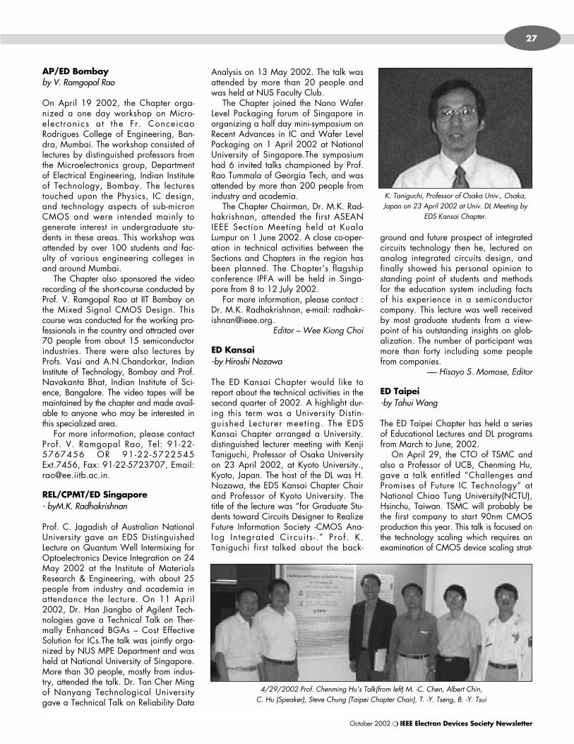
October 2002 ❍ IEEE Electron Devices Society Newsletter
27
AP/ED Bombay by V. Ramgopal Rao
On April 19 2002, the Chapter orga-nized a one day workshop on Micro-electronics at the Fr. ConceicaoRodrigues College of Engineering, Ban-dra, Mumbai. The workshop consisted oflectures by distinguished professors fromthe Microelectronics group, Departmentof Electrical Engineering, Indian Instituteof Technology, Bombay. The lecturestouched upon the Physics, IC design,and technology aspects of sub-micronCMOS and were intended mainly togenerate interest in undergraduate stu-dents in these areas. This workshop wasattended by over 100 students and fac-ulty of various engineering colleges inand around Mumbai.
The Chapter also sponsored the videorecording of the short-course conducted byProf. V. Ramgopal Rao at IIT Bombay onthe Mixed Signal CMOS Design. Thiscourse was conducted for the working pro-fessionals in the country and attracted over70 people from about 15 semiconductorindustries. There were also lectures byProfs. Vasi and A.N.Chandorkar, IndianInstitute of Technology, Bombay and Prof.Navakanta Bhat, Indian Institute of Sci-ence, Bangalore. The video tapes will bemaintained by the chapter and made avail-able to anyone who may be interested inthis specialized area.
For more information, please contactProf. V. Ramgopal Rao, Tel: 91-22-5767456 OR 91-22-5722545Ext.7456, Fax: 91-22-5723707, Email:[email protected].
REL/CPMT/ED Singapore - byM.K. Radhakrishnan
Prof. C. Jagadish of Australian NationalUniversity gave an EDS DistinguishedLecture on Quantum Well Intermixing forOptoelectronics Device Integration on 24May 2002 at the Institute of MaterialsResearch & Engineering, with about 25people from industry and academia inattendance the lecture. On 11 April2002, Dr. Han Jiangbo of Agilent Tech-nologies gave a Technical Talk on Ther-mally Enhanced BGAs – Cost EffectiveSolution for ICs.The talk was jointly orga-nized by NUS MPE Department and washeld at National University of Singapore.More than 30 people, mostly from indus-try, attended the talk. Dr. Tan Cher Mingof Nanyang Technological Universitygave a Technical Talk on Reliability Data
Analysis on 13 May 2002. The talk wasattended by more than 20 people andwas held at NUS Faculty Club.
The Chapter joined the Nano WaferLevel Packaging forum of Singapore inorganizing a half day mini-symposium onRecent Advances in IC and Wafer LevelPackaging on 1 April 2002 at NationalUniversity of Singapore.The symposiumhad 6 invited talks championed by Prof.Rao Tummala of Georgia Tech, and wasattended by more than 200 people fromindustry and academia.
The Chapter Chairman, Dr. M.K. Rad-hakrishnan, attended the first ASEANIEEE Section Meeting held at KualaLumpur on 1 June 2002. A close co-oper-ation in technical activities between theSections and Chapters in the region hasbeen planned. The Chapter’s flagshipconference IPFA will be held in Singa-pore from 8 to 12 July 2002.
For more information, please contact :Dr. M.K. Radhakrishnan, e-mail: [email protected].
Editor – Wee Kiong Choi
ED Kansai -by Hiroshi Nozawa
The ED Kansai Chapter would like toreport about the technical activities in thesecond quarter of 2002. A highlight dur-ing this term was a University Distin-guished Lecturer meeting. The EDSKansai Chapter arranged a University.distinguished lecturer meeting with KenjiTaniguchi, Professor of Osaka Universityon 23 April 2002, at Kyoto University.,Kyoto, Japan. The host of the DL was H.Nozawa, the EDS Kansai Chapter Chairand Professor of Kyoto University. Thetitle of the lecture was “for Graduate Stu-dents toward Circuits Designer to RealizeFuture Information Society -CMOS Ana-log Integrated Circui ts - .” Prof. K.Taniguchi first talked about the back-
ground and future prospect of integratedcircuits technology then he, lectured onanalog integrated circuits design, andfinally showed his personal opinion tostanding point of students and methodsfor the education system including factsof his experience in a semiconductorcompany. This lecture was well receivedby most graduate students from a view-point of his outstanding insights on glob-alization. The number of participant wasmore than forty including some peoplefrom companies.
—- Hisayo S. Momose, Editor
ED Taipei -by Tahui Wang
The ED Taipei Chapter has held a seriesof Educational Lectures and DL programsfrom March to June, 2002.
On April 29, the CTO of TSMC andalso a Professor of UCB, Chenming Hu,gave a talk entitled “Challenges andPromises of Future IC Technology” atNational Chiao Tung University(NCTU),Hsinchu, Taiwan. TSMC will probably bethe first company to start 90nm CMOSproduction this year. This talk is focused onthe technology scaling which requires anexamination of CMOS device scaling strat-
K. Taniguchi, Professor of Osaka Univ., Osaka,Japan on 23 April 2002 at Univ. DL Meeting by
EDS Kansai Chapter.
4/29/2002 Prof. Chenming Hu’s Talk(from left) M. -C. Chen, Albert Chin, C. Hu (Speaker), Steve Chung (Taipei Chapter Chair), T. -Y. Tseng, B. -Y. Tsui
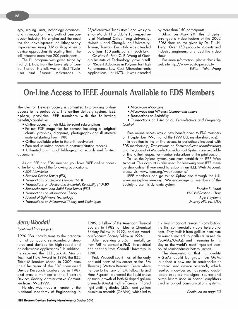
IEEE Electron Devices Society Newsletter ❍ October 2002
28
On-Line Access to IEEE Journals Available to EDS Members The Electron Devices Society is committed to providing on-lineaccess to its periodicals. The on-line delivery system, IEEEXplore, provides IEEE members with the fol lowingbenefits/capabilities:
• Online access to their IEEE personal subscriptions• Full-text PDF image files for content, including all original
charts, graphics, diagrams, photographs and illustrativematerial starting from 1988
• Online available prior to the print equivalent• Free and unlimited access to abstract/citation records• Unlimited printing of bibliographic records and full-text
documents
As an IEEE and EDS member, you have FREE on-line accessto the full articles of the following publications:
• EDS Newsletter• Electron Device Letters (EDL)• Transactions on Electron Devices (T-ED)• Transactions on Device and Materials Reliability (T-DMR)• Electrochemical and Solid State Letters (ESL)• Transactions on Information Theory• Journal of Lightwave Technology • Transactions on Microwave Theory and Techniques
• Microwave Magazine • Microwave and Wireless Components Letters • Transactions on Reliability• Transactions on Ultrasonics, Ferroelectrics and Frequency
Control.
Free on-line access was a new benefit given to EDS memberson 1 September 1998 (start of the 1999 IEEE membership cycle).
In addition to the on-line access to periodicals included withEDS membership, Transactions on Semiconductor Manufacturingand the Journal of Microelectromechanical Systems are availableon-line to their respective member subscribers of the print version.
To use the Xplore system, you must establish an IEEE WebAccount. This account is also used for renewing your IEEE mem-bership online. If you need to establish an IEEE Web Account,please visit www.ieee.org/web/accounts/
IEEE members can go to the Xplore site through the URLwww.ieeexplore.ieee.org. We encourage all members of theSociety to use this dynamic system.
Renuka P. JindalEDS Publications Chair
Agere SystemsMurray Hill, NJ, USA
egy, scaling limits, technology advances,and its impact on the growth of Semicon-ductor Industry. He emphasized the needfor the development of lithographyimprovement using EUV or X-ray when adevice approaches its scaling limit. Thetalk attracted more than 200 participants.
The DL program was given twice byProf. J. J. Liou, from the University of Cen-tral Florida. His talk was entitled “Evolu-t ion and Recent Advances in
RF/Microwave Transistors” and was giv-en on March 11 and June 13, respective-ly at National Chiao Tung University,Hsinchu, and Cheng-Kung University,Tainan, Taiwan. Each talk was attendedby at least 150 participants in each talk.
On May 6, Prof. C. P. Wong of Geor-gia Institute of Technology, gave a talkon “Recent Advances in Polymer for HighPerformance Low Cost MicroelectronicApplications,” at NCTU. It was attended
by more than 150 participants.Also, on May 20, the Chapter
arranged a video lecture of the 2002IEDM short course given by Dr. T. –H.Tseng. Over 150 graduate students andindustry engineers attended the videoshow.
For more information, please check theweb site http://www.edsTaipei.edu.tw.
Editor – Tahui Wang
1990 “For contributions to the prepara-tion of compound semiconductor struc-tures and devices for high-speed andoptoelectronic applications.” In addition,he received the IEEE Jack A. MortonTechnical Field Award in 1984, the IEEEThird Millennium Medal in 2000, wasthe Chairman of the EDS sponsoredDevice Research Conference in 1987and was a member of the ElectronDevices Society Administrative Commit-tee from 1993-1999.
He also was made a member of theNational Academy of Engineering in
1989, a Fellow of the American PhysicalSociety in 1982, an Electro ChemicalSociety Fellow in 1992, and an Ameri-can Vacuum Society Fellow in 1994.
After receiving a B.S. in metallurgyfrom MIT he earned a Ph.D. in electricalengineering from Cornell University in1980.
Prof. Woodall spent most of the earlyand mid parts of his career at the IBMThomas J. Watson Research Center wherehe rose to the rank of IBM Fellow.He andHans Ruprecht pioneered the liquid-phaseepitaxial growth of both Si doped galliumarsenide (GaAs) high efficiency infraredlight emitting diodes (LEDs), and galliumaluminum arsenide (GaAlAs), which led to
his most important research contribution:the first commercially viable heterojunc-tions. They built it from gallium aluminumarsenide mated to gallium arsenide(GaAlAs/GaAs), and it remains to thisday as the world’s most important com-pound semiconductor heterojunction.
This demonstration that high qualityAlGaAs could be grown on GaAslaunched a new era in semiconductormaterial and device research, whichresulted in devices such as semiconductorlasers used as the signal source andpump lasers used in optical amplifiersused in optical communications systems.
Jerry Woodall(continued from page 14
Continued on page 30
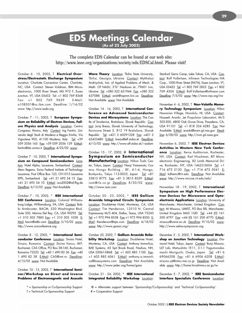
October 2002 ❍ IEEE Electron Devices Society Newsletter
29
October 6 - 10, 2002, T Electrical Over-stress/Electrostatic Discharge SymposiumLocation: Charlotte Convention Center, Charlotte,NC, USA Contact: Steven Voldman, IBM Micro-electronics, 1000 River Street, MS 972 F, EssexJunction, VT, USA 05452 Tel: +1 802 769 8368Fax: +1 802 769 9659 E-Mail:[email protected] Deadline: 1/14/02www: http://www.esda.org
October 7 - 11, 2002, T European Sympo-sium on Reliability of Electron Devices, Fail-ure Physics and Analysis Location: CentroCongressi, Riminu, Italy Contact: Ing Fantini, Uni-versita degli Studi di Modena e Reggio Emilia, ViaVignolese 905, 41100 Modena, Italy Tel: +39059 2056 165 Fax: +39 059 2056 129 E-Mail:[email protected] Deadline: 4/22/02 www:
October 7 - 10, 2002, T International Sympo-sium on Compound Semiconductors Loca-tion: Hotel Alpha, Lausanne, Switzerland Contact:Marc Ilegems, Swiss Federal Institute of TechnologyLausanne, Post Office Box 123, CH-1015 LausanneEPFL, Switzerland Tel: +41 21 693 54 15 Fax:+41 21 693 54 10 E-Mail: [email protected]: 6/15/02 www: Not Available
October 7 - 10, 2002, * IEEE InternationalSOI Conference Location: Colonial Williams-burg Lodge, Williamsburg, VA, USA Contact: Bob-bi Armbruster, BACM, 520 Washington Blvd.Suite 350, Marina Del Rey, CA, USA 90292 Tel:+1 310 305 7885 Fax: +1 310 305 1038 E-Mail: [email protected] Deadline: 5/10/02 www:http://www.soiconference.org
October 8 - 12, 2002, * International Semi-conductor Conference Location: Sinaia Hotel,Sinaia, Romania Contact: Doina Vancu, IMT-Bucharest, CAS Office, PO Box 38-160, Bucharest,Romania 72225 Tel: +40 1 490 82 36 Fax: +401 490 82 38 E-Mail: [email protected] Deadline:4/15/02 www: Not Available
October 10 - 13, 2002, T International Semi-nar/Workshop on Direct and InverseProblems of Electromagnetic and Acoustic
Wave Theory Location: Tbilisi State University,Tbilisi, Georgia, Ukraine Contact: MykhalyoAndriychuk, Inst. of Applied Problems of Mech. &Math. Of NASU, 3”b” Naukova str, 79601 Lviv,Ukraine Tel: +380 322 651944 Fax: +380 322637088 E-Mail: [email protected] Deadline:Not Available www: Not Available
October 14 - 16, 2002, T International Con-ference on Advanced SemiconductorDevices and Microsystems Location: The Cas-tle of Smolenice, Bratislava, Slovak Republic Con-tact: Juraj Breza, Slovak University of Technology,Ikovicova Street 3, 812 19 Bratislava, SlovakRepublic Tel: +421 2 60291328 Fax: +421 265423480 E-Mail: [email protected] Deadline:4/15/02 www: http://www.elf.stuba.sk/~asdam
October 15 - 17, 2002, @ InternationalSymposium on SemiconductorManufacturing Location: Nihon Toshi Cen-ter, Tokyo, Japan Contact: Naoji Yamamoto, Cos-mos Hongo Building , 8F, 4-1-4, Hongo,Bunkyo-ku, Tokyo 113-0033, Japan Tel: +8133815 8775 Fax: +81 3 3815 8529 E-Mail:[email protected] Deadline: 8/30/02 www:http://www.issm.com
October 20 - 23, 2002, * IEEE GalliumArsenide Integrated Circuits SymposiumLocation: Doubletree Hotel, Monterey, CA, USAContact: Tim Henderson, 13510 N. CentralExpressway M/S 404, Dallas, Texas, USA 75243Tel: +1 972 994 8538 Fax:+1 972 994 8505 E-Mail: [email protected] Deadline: 4/18/02www: http://www.gaasic.org/
October 20, 2002, T Gallium Arsenide Relia-bility Workshop Location: Doubletree Hotel,Monterey, CA, USA Contact: Anthony Immorlica,BAE Systems, 65 Spit Brook Road, Nashua, NH,USA 03061-0868 Tel: +1 603 885 1100 Fax:+1 603 885 6061 E-Mail: [email protected] Deadline: Not Availablewww: http://www.jedec.org/home/gaas
October 21 - 24, 2002, * IEEE InternationalIntegrated Reliability Workshop Location:
Stanford Sierra Camp, Lake Tahoe, CA, USA Con-tact: Rolf Vollertsen, Infineon Technologies NACorp., 1000 River Street (967A), Essex Junction, VT,USA 05452 Tel: +1 802 769 2823 Fax: +1 802769 4304 E-Mail: [email protected]: 7/5/02 www: http://www.irps.org/irw
November 4 - 6, 2002, T Non-Volatile Memo-ry Technology Symposium Location: HiltonHawaiian Village, Honolulu, HI, USA Contact:Nazeeh Aranki, Jet Propulsion Laboratort, M/S303-300, 4800 Oak Grove Drive, Pasadena, CA,USA 91101 Tel: +1 818 354 4285 Fax: NotAvailable E-Mail: [email protected] Dead-line: 6/28/02 www: http://nvm.jpl.nasa.gov
November 6, 2002, T IEEE Electron DevicesActivities in Western New York Confer-ence Location: Xerox Auditorium, Rochester,NY, USA Contact: Karl Hirschman, RIT Micro-electronic Engineering, 82 Lomb Memorial Dri-ve, Rochester, NY, USA 14623-5604 Tel: +1716 475 5130 Fax: +1 716 475 5041 E-Mail: [email protected] Deadline: Not Availablewww: http://www.microe.rit.edu/eds/
November 18 - 19, 2002, T InternationalSymposium on High Performance Elec-tron Devices for Microwave and Opto-electronic Applications Location: University ofManchester, Manchester, United Kingdom Con-tact: M Missous, UMIST, PO Box 88, Manchester,United Kingdom M60 1QD Tel: +44 (0) 161200 4797 Fax: +44 (0) 161 200 4770 E-Mail:[email protected] Deadline: 9/10/02 www:http://www.edmo-symposium.org
December 2 - 3, 2002, T International Work-shop on Junction Technology Location: Dia-mond Hotel, Tokyo, Japan Contact: Bunji Mizuno,UJT Lab, Matsushita 1E11, 3-1-1 Yagumonaka-machi Moriguchi, Osaka, Japan Tel: +81 669066208 Fax: +81 6 6906 6208 E-Mail:[email protected] Deadline: Not Avail-able www: http://home.hiroshima-u.ac.jp/iw
December 5 - 7, 2002, * IEEE SemiconductorInterface Specialists Conference Location:
EDS Meetings Calendar(As of 22 July 2002)
The complete EDS Calendar can be found at our web site:http://www.ieee.org/organizations/society/eds/EDSCal.html. Please visit!
* = Sponsorship or Co-Sponsorship Support @ = Alternates support between ‘Sponsorship/Co-Sponsorship’ and ‘Technical Co-Sponsorship’T = Technical Co-Sponsorship Support # = Cooperation Support
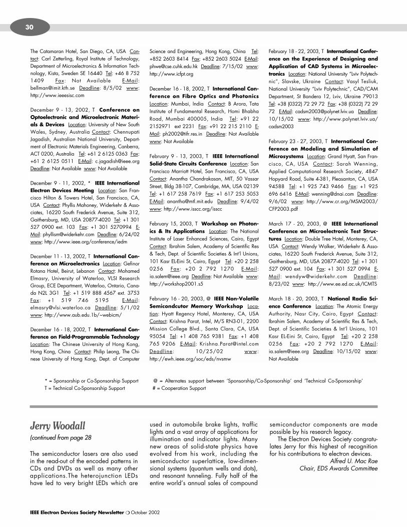
IEEE Electron Devices Society Newsletter ❍ October 2002
30
The Catamaran Hotel, San Diego, CA, USA Con-tact: Carl Zetterling, Royal Institute of Technology,Department of Microelectronics & Information Tech-nology, Kista, Sweden SE 16440 Tel: +46 8 7521409 Fax: Not Available E-Mail:[email protected] Deadline: 8/5/02 www:http://www.ieeesisc.com
December 9 - 13, 2002, T Conference onOptoelectronic and Microelectronic Materi-als & Devices Location: University of New SouthWales, Sydney, Australia Contact: ChennupatiJagadish, Australian National University, Depart-ment of Electronic Materials Engineering, Canberra,ACT 0200, Australia Tel: +61 2 6125 0363 Fax:+61 2 6125 0511 E-Mail: [email protected]: Not Available www: Not Available
December 9 - 11, 2002, * IEEE InternationalElectron Devices Meeting Location: San Fran-cisco Hilton & Towers Hotel, San Francisco, CA,USA Contact: Phyllis Mahoney, Widerkehr & Asso-ciates, 16220 South Frederick Avenue, Suite 312,Gaithersburg, MD, USA 20877-4020 Tel: +1 301527 0900 ext. 103 Fax: +1 301 5270994 E-Mail: [email protected] Deadline: 6/24/02www: http://www.ieee.org/conference/iedm
December 11 - 13, 2002, T International Con-ference on Microelectronics Location: GefinorRotana Hotel, Beirut, Lebanon Contact: MohamedElmasry, University of Waterloo, VLSI ResearchGroup, ECE Department, Waterloo, Ontario, Cana-da N2L 3G1 Tel: +1 519 888 4567 ext. 3753Fax: +1 519 746 5195 E-Mail:[email protected] Deadline: 5/1/02www: http://www.aub.edu.1b/~webicm/
December 16 - 18, 2002, T International Con-ference on Field-Programmable TechnologyLocation: The Chinese University of Hong Kong,Hong Kong, China Contact: Philip Leong, The Chi-nese University of Hong Kong, Dept. of Computer
Science and Engineering, Hong Kong, China Tel:+852 2603 8414 Fax: +852 2603 5024 E-Mail:[email protected] Deadline: 7/15/02 www:http://www.icfpt.org
December 16 - 18, 2002, T International Con-ference on Fibre Optics and PhotonicsLocation: Mumbai, India Contact: B Arora, TataInstitute of Fundamental Research, Homi BhabhaRoad, Mumbai 400005, India Tel: +91 222152971 ext 2231 Fax: +91 22 215 2110 E-Mail: [email protected] Deadline: Not Availablewww: Not Available
February 9 - 13, 2003, T IEEE InternationalSolid-State Circuits Conference Location: SanFrancisco Marriott Hotel, San Francisco, CA, USAContact: Anantha Chandrakasan, MIT, 50 VassarStreet, Bldg 38-107, Cambridge, MA, USA 02139Tel: +1 617 258 7619 Fax: +1 617 253 5053E-Mail: [email protected] Deadline: 9/4/02www: http://www.isscc.org/isscc
February 15, 2003, T Workshop on Photon-ics & Its Applications Location: The NationalInstitute of Laser Enhanced Sciences, Cairo, EgyptContact: Ibrahim Salem, Academy of Scientific Res& Tech, Dept. of Scientific Societies & Int’l Unions,101 Kasr EL-Eini St, Cairo, Egypt Tel: +20 2 2580256 Fax: +20 2 792 1270 E-Mail:[email protected] Deadline: Not Available www:http://workshop2001.s5
February 16 - 20, 2003, @ IEEE Non-VolatileSemicondcutor Memory Workshop Loca-tion: Hyatt Regency Hotel, Monterey, CA, USAContact: Krishna Parat, Intel, M/S RN3-01, 2200Mission College Blvd., Santa Clara, CA, USA95054 Tel: +1 408 765 9381 Fax: +1 408765 9206 E-Mail: [email protected]: 10/25/02 www:http://ewh.ieee.org/soc/eds/nvsmw
February 18 - 22, 2003, T International Confer-ence on the Experience of Designing andApplication of CAD Systems in Microelec-tronics Location: National University “Lviv Polytech-nic”, Slavske, Ukraine Contact: Vasyl Tesliuk,National University “Lviv Polytechnic”, CAD/CAMDepartment, St Bandera 12, Lviv, Ukraine 79013Tel: +38 (0322) 72 29 72 Fax: +38 (0322) 72 2972 E-Mail: [email protected] Deadline:10/15/02 www: http://www.polynet.lviv.ua/cadsm2003
February 23 - 27, 2003, T International Con-ference on Modeling and Simulation ofMicrosystems Location: Grand Hyatt, San Fran-cisco, CA, USA Contact: Sarah Wenning,Applied Computational Research Society, 4847Hopyard Road, Suite 4-381, Pleasanton, CA, USA94588 Tel: +1 925 743 9466 Fax: +1 925696 6416 E-Mail: [email protected] Deadline:9/6/02 www: http://www.cr.org/MSM2003/CFP2003.pdf
March 17 - 20, 2003, @ IEEE InternationalConference on Microelectronic Test Struc-tures Location: Double Tree Hotel, Monterey, CA,USA Contact: Wendy Walker, Widerkehr & Asso-ciates, 16220 South Frederick Avenue, Suite 312,Gaithersburg, MD, USA 20877-4020 Tel: +1 301527 0900 ext. 104 Fax: +1 301 527 0994 E-Mail: [email protected] Deadline:8/23/02 www: http://www.ee.ed.ac.uk/ICMTS
March 18 - 20, 2003, T National Radio Sci-ence Conference Location: The Atomic EnergyAuthority, Nasr City, Cairo, Egypt Contact:Ibrahim Salem, Academy of Scientific Res & Tech,Dept. of Scientific Societies & Int’l Unions, 101Kasr EL-Eini St, Cairo, Egypt Tel: +20 2 2580256 Fax: +20 2 792 1270 E-Mail:[email protected] Deadline: 10/15/02 www:Not Available
* = Sponsorship or Co-Sponsorship Support @ = Alternates support between ‘Sponsorship/Co-Sponsorship’ and ‘Technical Co-Sponsorship’T = Technical Co-Sponsorship Support # = Cooperation Support
The semiconductor lasers are also usedin the read-out of the encoded patterns inCDs and DVDs as well as many otherapplications.The heterojunction LEDshave led to very bright LEDs which are
used in automobile brake lights, trafficlights and a vast array of applications forillumination and indicator lights. Manynew areas of solid-state physics haveevolved from his work, including thesemiconductor superlattice, low-dimen-sional systems (quantum wells and dots),and resonant tunneling. Fully half of theentire world’s annual sales of compound
semiconductor components are madepossible by his research legacy.
The Electron Devices Society congratu-lates Jerry for this highest of recognitionfor his contributions to electron devices.
Alfred U. Mac RaeChair, EDS Awards Committee
Jerry Woodall(continued from page 28
October 2002 ❍ IEEE Electron Devices Society Newsletter
31
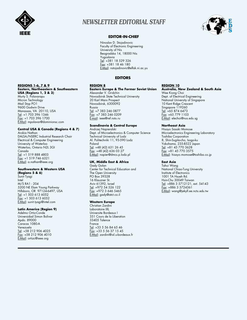
EEDDSS
EDITOR-IN-CHIEF
REGIONS 1-6, 7 & 9Eastern, Northeastern & SoutheasternUSA (Regions 1, 2 & 3)Murty S. PolavarapuMicron TechnologyMail Stop PO19600 Godwin DriveManassas, VA 20110, USATel: +1 703 396 1346Fax: +1 703 396 1700E-Mail: [email protected]
Central USA & Canada (Regions 4 & 7)Arokia NathanDALSA/NSERC Industrial Research ChairElectrical & Computer EngineeringUniversity of WaterlooWaterloo, Ontario N2L 3GICanadaTel: +1 519 888 4803Fax: +1 519 746 6321E-Mail: [email protected]
Southwestern & Western USA (Regions 5 & 6)Sunit TyagiIntelM/S RA1 - 2045200 NE Elam Young ParkwayHillsboro, OR 97124-6497, USATel: +1 503 613 6052Fax: +1 503 613 6052E-Mail: [email protected]
Latin America (Region 9)Adelmo Ortiz-CondeUniversidad Simon BolivarApdo. 89000Caracas 1080-AVenezuelaTel: +58 212 906 4025Fax: +58 212 906 4010E-Mail: [email protected]
REGION 8Eastern Europe & The Former Soviet UnionAlexander V. GridchinNovosibirsk State Technical University20 Karl Marx ProspectNovosibirsk, 6300092RussiaTel: +7 383 246 0877Fax: +7 383 246 0209E-mail: [email protected]
Scandinavia & Central EuropeAndrzej NapieralskiDept. of Microelectronics & Computer ScienceTechnical University of LodzAl. Politechniki 11, 93-590 LodzPolandTel: +48 (42) 631 26 45Fax: +48 (42) 636 03 27E-Mail: [email protected]
UK, Middle East & AfricaGady GolanCenter for Technical Education and The Open UniversityPO Box 3932816 Klauzner St.Aviv 61392, IsraelTel: +972 54 526 122Fax: +972 3 646 5465E-Mail: [email protected]
Western EuropeChristian ZardiniLaboratoire IXLUniversite Bordeaux I351 Cours de la Liberation33405 TalenceFranceTel: +33 5 56 84 65 46Fax: +33 5 56 37 15 45E-Mail: [email protected]
REGION 10Australia, New Zealand & South AsiaWee Kiong Choi Dept. of Electrical EngineeringNational University of Singapore10 Kent Ridge CrescentSingapore 119260Tel: +65 874 6473Fax: +65 779 1103E-Mail: [email protected]
Northeast AsiaHisayo Sasaki MomoseMicroelectronics Engineering LaboratoryToshiba Corporation8, Shin-Sugita-cho, Isogo-kuYokohama, 235-8522 JapanTel: +81 45 770 3628Fax: +81 45 770 3575E-Mail: [email protected]
East AsiaTahui WangNational Chiao-Tung UniversityInstitute of Electronics1001 TA Hsueh Rd.Hsin-Chu 30049 TaiwanTel: +886 3 5712121, ext. 54143Fax: +886 3 5724361E-Mail: [email protected]
NEWSLETTER EDITORIAL STAFF
EDITORS
Ninoslav D. StojadinovicFaculty of Electronic EngineeringUniversity of NisBeogradska 14, 18000 NisYugoslaviaTel: +381 18 529 326Fax: +381 18 46 180E-Mail: [email protected]
Related Documents


